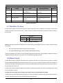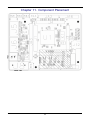
1
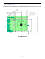
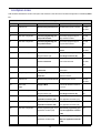
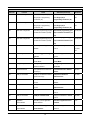
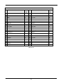
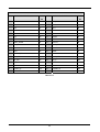
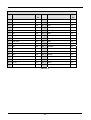
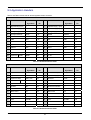
REG10J0025-0100
Renesas Starter Kit for H8SX1664
User's Manual
RENESAS SINGLE-CHIP MICROCOMPUTER
H8SX FAMILY
Rev.1.00
Revision date 30.08.2006
Renesas Technology Europe Ltd.
www.renesas.com
Table of Contents
Table of Contents ...................................................................................................................................................ii
Chapter 1. Preface .................................................................................................................................................4
Chapter 2. Purpose ................................................................................................................................................5
Chapter 3. Power Supply ......................................................................................................................................6
3.1. Requirements ..............................................................................................................................................6
3.2. Power – Up Behaviour................................................................................................................................6
Chapter 4. Board Layout.......................................................................................................................................7
4.1. Component Layout......................................................................................................................................7
4.2. Board Dimensions.......................................................................................................................................8
Chapter 5. Block Diagram.....................................................................................................................................9
Chapter 6. User Circuitry ...................................................................................................................................10
6.1. Switches.....................................................................................................................................................10
6.2. LEDs ..........................................................................................................................................................10
6.3. Potentiometer............................................................................................................................................10
6.4. Serial port..................................................................................................................................................10
6.5. LCD Module .............................................................................................................................................. 11
6.6. Option Links..............................................................................................................................................12
6.7. Oscillator Sources .....................................................................................................................................16
6.8. Reset Circuit..............................................................................................................................................16
6.9. USB Port....................................................................................................................................................17
Chapter 7. Modes.................................................................................................................................................18
7.1. FDT Settings .............................................................................................................................................18
7.1.1. Boot mode............................................................................................................................................19
7.1.2. User Mode ...........................................................................................................................................20
Chapter 8. Programming Methods .....................................................................................................................21
8.1. E8 Header..................................................................................................................................................21
8.2. E10A Header .............................................................................................................................................21
8.3. USB port programming ............................................................................................................................21
8.4. Serial Port Programming .........................................................................................................................22
Chapter 9. Headers..............................................................................................................................................23
9.1. Microcontroller Headers ...........................................................................................................................23
9.2. Application Headers..................................................................................................................................27
Chapter 10. Code Development ..........................................................................................................................30
10.1. Overview..................................................................................................................................................30
10.2. Compiler Restrictions .............................................................................................................................30
10.3. Mode Support ..........................................................................................................................................30
10.4. Breakpoint Support ................................................................................................................................30
10.5. Code located in RAM ..............................................................................................................................30
ii
10.6. HMON Code Size ....................................................................................................................................30
10.7. Memory Map ...........................................................................................................................................32
10.8. Baud Rate Setting...................................................................................................................................33
10.9. Interrupt mask sections .........................................................................................................................33
Chapter 11. Component Placement ....................................................................................................................34
Chapter 12. Additional Information ...................................................................................................................35
iii
Chapter 1. Preface
Cautions
This document may be, wholly or partially, subject to change without notice.
All rights reserved. No one is permitted to reproduce or duplicate, in any form, a part or this entire document without the written
permission of Renesas Technology Europe Limited.
Trademarks
All brand or product names used in this manual are trademarks or registered trademarks of their respective companies or
organisations.
Copyright
© Renesas Technology Europe Ltd. 2006. All rights reserved.
© Renesas Technology Corporation. 2006. All rights reserved.
© Renesas Solutions Corporation. 2006. All rights reserved.
Website:
http://www.renesas.com/
Glossary
ADC
Analog to Digital Converter
BRR
Baud Rate Register
CPU
Central Processing Unit
DAC
Digital to Analog Converter
DMA
Direct Memory Access
ERR
Error Rate
FDT
Flash Development Tool
HMON
Embedded Monitor
RTE
Renesas Technology Europe Ltd.
RSK
Renesas Starter Kit
RSO
Renesas Solutions Corp.
USB
Universal Serial Bus
4
Chapter 2.Purpose
This RSK is an evaluation tool for Renesas microcontrollers.
Features include:
•
Renesas Microcontroller Programming.
•
User Code Debugging.
•
User Circuitry such as switches, LEDs and potentiometer(s).
•
Sample Application.
•
Sample peripheral device initialisation code.
The CPU board contains all the circuitry required for microcontroller operation.
This manual describes the technical details of the RSK hardware. The Quick Start Guide and Tutorial Manual provide details of the
software installation and debugging environment.
5
Chapter 3.Power Supply
3.1.Requirements
This CPU board operates from a 5V power supply.
A diode provides reverse polarity protection only if a current limiting power supply is used.
All CPU boards are supplied with an E8 debugger. This product is able to power the CPU board with up to 300mA. When the CPU board is
connected to another system that system should supply power to the CPU board.
All CPU boards have an optional centre positive supply connector using a 2.0mm barrel power jack.
Warning
The CPU board is neither under not over voltage protected. Use a centre positive supply for this board.
3.2.Power – Up Behaviour
When the RSK is purchased the CPU board has the ‘Release’ or stand alone code from the example tutorial code pre-programmed into the
Renesas microcontroller. On powering up the board the user LEDs will start to flash. Switch 2 will cause the LEDs to flash at a rate
controlled by the potentiometer.
6
Chapter 4.Board Layout
4.1.Component Layout
The following diagram shows top layer component layout of the board.
Application
Board
Interface
JA5
Reset
Switch
RS 232 Serial
JA1
Power
Power LED
E8
Header
LCD Display
J11
J2
USB
Microcontroller
Pin Headers
BUS Interface
J3
J1
J
A
3
User
LEDs
J4
JA6
Boot
LED
JA2
Application
Board
Interface
Potentiometer
Figure 4.1: Board Layout
7
User Switches
4.2.Board Dimensions
The following diagram gives the board dimensions and connector positions. All through hole connectors are on a common 0.1” grid for easy
interfacing.
Figure 4.2 : Board Dimensions
8
Chapter 5.Block Diagram
Figure 5.1 shows the CPU board components and their connectivity.
Power Jack Option
Application Board
Headers
Microcontroller Pin
Headers
Boot mode pins
Boot Circuitry
Microcontroller
Debug Header Option
RESET pin
USB Connector Option
ADC Input
RESn
D-type
latch
BOOT & BOOTn signals
IRQ pin
IRQ pin
IRQ pin
Serial Connector Option
SW2
Potentiometer
SW3
BOOT
RES
SWITCHES
LEDs
User: 4 LEDS
1Green, 1Orange, 2Red
Figure 5.1: Block Diagram
Figure 5.2 shows the connections to the RSK.
Figure 5.2 : RSK Connctions
9
Power: Green
Boot: Orange
Chapter 6.User Circuitry
6.1.Switches
There are four switches located on the CPU board. The function of each switch and its connection are shown in Table 6-1.
Switch
Function
Microcontroller
RES
When pressed; the CPU board microcontroller is reset.
RESn
SW1/BOOT*
Connects to an IRQ input for user controls.
IRQ0n, Pin 84
The switch is also used in conjunction with the RES switch to place
(Port 1, pin 0)
the device in BOOT mode when not using the E8 debugger.
SW2*
Connects to an IRQ line for user controls.
IRQ1n , Pin 85
(Port 1, pin 1)
SW3*
Connects to the ADC trigger input. Option link allows connection to
IRQ3n, Pin 87
IRQ line. The option is a pair of 0R links (R56, R95).
(Port 1, pin 3)
Table 6-1: Switch Functions
*Refer to schematic for detailed connectivity information.
6.2.LEDs
There are six LEDs on the CPU board. The green ‘POWER’ LED lights when the board is powered. The orange BOOT LED indicates the
device is in BOOT mode when lit. The four user LEDs are connected to an IO port and will light when their corresponding port pin is set low.
Table 6-2, below, shows the LED pin references and their corresponding microcontroller port pin connections.
LED Reference (As
Microcontroller Port Pin
Microcontroller Pin
shown on silkscreen)
function
Number
Polarity
LED0
Port B3
3
Active Low
LED1
Port C2
116
Active Low
LED2
Port C3
117
Active Low
LED3
Port 12
86
Active Low
Table 6-2:LED Port
6.3.Potentiometer
A single turn potentiometer is connected to AN0 of the microcontroller. This may be used to vary the input analog voltage value to this pin
between AVCC and Ground.
6.4.Serial port
The microcontroller programming serial port (SCI4) is connected to the E8 connector (J6). This serial port can optionally be connected to
the RS232 transceiver by moving option resistors and fitting the D connector in position J8. The connections to be moved are listed in the
following table.
10
Description
Function
Fit For E8
Remove for E8
Fit for RS232
Remove for
RS232
SCI4 Tx
Programming Serial Port
R6
R37
R37
R6
SCI4 Rx
Programming Serial Port
R5
R36
R36
R5
Table 6-3 - Serial Option Links
The board is designed to accept a straight through RS232 cable. A secondary microcontroller serial port is available and connected to the
application headers. Please refer to the schematic diagram for more details on the available connections.
6.5.LCD Module
A LCD module can be connected to the connector J11. Any module that conforms to the pin connections and has a KS0066u compatible
controller can be used with the tutorial code. The LCD module uses a 4bit interface to reduce the pin allocation. No contrast control is
provided; this must be set on the display module.
Table 6-4 shows the pin allocation and signal names used on this connector.
The module supplied with the CPU board only supports 5V operation.
J13
Pin
Circuit Net Name
Device
Pin
Circuit Net Name
Device
Pin
Pin
1
Ground
-
2
5V Only
-
3
No Connection
-
4
DLCDRS
134
5
R/W (Wired to Write only)
-
6
DLCDE
136
7
No Connection
-
8
No connection
-
9
No Connection
-
10
No connection
-
11
DLCDD4
130
12
DLCDD5
131
13
DLCDD6
132
14
DLCDD7
5
Table 6-4 LCD Module Connections
11
6.6.Option Links
Table 6-5 below describes the function of the option links contained on this CPU board. The default configuration is indicated by BOLD
text.
Option Link Settings
Reference
R3
Function
Power Source
Fitted
Alternative (Removed)
Board can be powered from J7
Disable external power connector
Related To
R13, R22,
R40, R43
R4
E8
Enables E8
R5
Serial Port Configuration
Connects programming port
Disconnects programming port
R6, R36,
(Rx) to E8 connector.
(Rx) from E8 connector.
R37
Connects programming port
Disconnects programming port
R5, R36,
(Tx) to E8 connector.
(Tx) from E8 connector.
R37
Board is powered from VBUS
Board is powered by another
R3, R22,
source
R40, R43
Connects serial port D5 (Tx) to
Disconnects serial port D5 (Rx)
R28, R34,
D-type connector (J8).
from D-type connector (J8).
R35
Connects external 3.3V power
Disconnects external 3.3V power
R3, R13,
source to the board.
source from the board.
R22, R40,
R6
R13
R15
R18
Serial Port Configuration
Power Source
Serial Port Configuration
Power Source
R43
R19
R21
R22
RS232 Serial
Analog Voltage Source
Power Source
Disables RS232 Serial
Enables RS232 Serial
Transceiver
Transceiver
Analog voltage source from on
Analog Voltage Source from
board Vcc.
external connector.
Board can be powered from E8
Disable E8 power source
R46
R3, R13,
R40, R43
R24
MCU Power
Supply to MCU
Fit Low ohm resistor to measure
current
Supply
R28
R30
R31
R32
Serial Port Configuration
Serial Port Configuration
Serial Port Configuration
Serial Port Configuration
Connects serial port D5 (Rx) to
Disconnects serial port D5 (Tx)
R15, R34,
D-type connector (J8).
from D-type connector (J8).
R35
Routes serial port D0 (Rx) to
Disconnects serial port D0 (Rx)
R31
application connector (JA2)
from application connector (JA2)
Routes serial port D0 (Tx) to
Disconnects serial port D0 (Tx)
application connector (JA2)
from application connector (JA2)
Routes programming port (Tx) to
Disconnects programming port
application connector (JA6)
(Tx) from application connector
R30
R33
(JA6)
R33
Serial Port Configuration
Routes programming port (Rx) to
Disconnects programming port
application connector (JA6)
(Rx) from application connector
(JA6)
12
R32
Option Link Settings
Reference
R34
R35
R36
Function
Serial Port Configuration
Serial Port Configuration
Serial Port Configuration
Fitted
Alternative (Removed)
Related To
Connects serial port D5 (Tx) to
Disconnects serial port D5 (Tx)
R15, R28,
D-type (J8) or programming
from D-type (J8) or
R35,
connectors (J9).
programming connectors (J9).
Connects serial port D5 (Rx) to
Disconnects serial port D5 (Rx)
R15, R28,
D-type (J8) or programming
from D-type (J8) or
R34
connectors (J9).
programming connectors (J9).
Connects programming port (Rx)
Disconnects programming port
to external connectors (not E8).
(Rx) to external connectors (not
R5, R6, R37
E8).
R37
Serial Port Configuration
Connects programming port (Tx)
Disconnects programming port
to external connectors (not E8).
(Tx) to external connectors (not
R5, R6, R37
E8).
R40
Power Source
Board is powered by 5V
Board is powered by a 3.3V
R3, R13,
source.
source.
R18, R22,
R43
R42
R44
R46
R47
R48
R49
R50
R51
Ground Signals
Power Source
Analog Voltage Source
LCD Power Source
CON_5V Connection
LCD Power Source
CON_5V Connection
LCD Power Source
Links analog ground to digital
Isolates analog ground from digital
ground.
ground.
Microprocessor uses USB Bus
Microprocessor uses USB Self
Power Mode.
Power Mode.
Analog Voltage Source from
Analog voltage source from on
external connector.
board Vcc.
LCD powered from External 5V
LCD Powered from a different
source (J7).
source.
CON_5V connected to External
CON_5V connected to a
power source (J7).
different source.
LCD powered from VBUS 5V
LCD powered from a different
source.
source.
CON_5V connected to VBUS 5V
CON_5V connected to a
source
different source.
LCD powered from E8.
LCD powered from a different
R21
R49, R51
R50, R52
R47, R51
R48, R52
R47, R49
source.
R52
CON_5V Connection
CON_5V connected to E8
CON_5V connected to a different
R48, R50
source.
R54
R56
Application
Use WDT_OVF of application
Use TDO of application board
Board Interface
board interface
interface
Application
Enable ADTRG of application
Use IRQ3n of application board
Board Interface
board interface
interface
13
R123
R95
Option Link Settings
Reference
R59
R60
R64
R66
R67
R68
R69
R70
R71
R74
R75
R76
R78
R79
R81
R82
R83
R84
Function
Fitted
Alternative (Removed)
Application
Use RxD0 of application board
Use IO1 of application board
Board Interface
interface
interface
Application
Use AN0 of application board
Use AD_POT of application
Board Interface
interface
board interface
Voltage Reference Source
Voltage Reference set to board
Voltage Reference taken from
Vcc signal
external connector (J4).
Application
Use CLK0 of application board
Use TDO of application board
Board Interface
interface
interface
Application
Use IO3 of application board
Use UD of application board
Board Interface
interface
interface
Application
Use DA0 of application board
Use AN6 of application board
Board Interface
interface
interface
Up
Connects Motor control Up to the
Disconnects Motor control Up
microporcessor
from the microprocessor
Application
Use TxD0 of application board
Use IO2 of application board
Board Interface
interface
interface
Application
Use DA1 of application board
Use AN7 of application board
Board Interface
interface
interface
Wn
Connects Motor control Wn to
Disconnects Motor control Wn
the microporcessor
from the microprocessor
Connects Motor control Vp to the
Disconnects Motor control Vp
microporcessor
from the microprocessor
Application
Use IO1 of application board
Use RxD0 of application board
Board Interface
interface
interface
Application
Use UD of application board
Use IO3 of application board
Board Interface
interface
interface
Application
Use IO0 of application board
Use CLK0 of application board
Board Interface
interface
interface
Application
Use TIOCA0 of application
Use Vp of application board
Board Interface
board interface
interface
Application
Use IO2 of application board
Use TxDO of application board
Board Interface
interface
interface
Voltage Reference Source
Voltage Reference taken from
Voltage Reference set to board
external connector (J4).
Vcc signal.
Connects Motor control Vn to the
Disconnects Motor control Vn
microporcessor
from the microprocessor
Vp
Vn
14
Related To
R76
R96
R83
R79
R78
R108
R114
R82
R111
R88
R81
R59
R67
R66
R75
R70
R64
R90
Option Link Settings
Reference
R85
R86
R88
R90
R93
Function
Fitted
Alternative (Removed)
Application
Use IO5 of application board
Use Wp of application board
Board Interface
interface
interface
Wp
Connects Motor control Wp to
Disconnects Motor control Wp
the microprocessor
from the microprocessor
Application
Use IO4 of application board
Use Wn of application board
Board Interface
interface
interface
Application
Use TIOCB0 of application
Use Vn of application board
Board Interface
board interface
interface
Sub Clock
External Clock Source
Crystal
Oscillator Source
R94
Sub Clock
External Clock Source
Crystal
Enable IRQ3n of application
Use ADTRG of application board
Board Interface
board interface
interface
Application
Use AD_POT of application
Use AN0 of application board
Board Interface
board interface
interface
R98
External Subclock Oscillator
Parallel resistor for crystal
Not fitted
R99
Processor Oscillator Source
External Clock Source
Crystal
R100
External main Oscillator
Parallel resistor for crystal
Not fitted
R101
Processor Oscillator Source
Crystal
External Clock Source
R102
Processor Oscillator Source
External Clock Source
Crystal
R103
Sub Clock
Crystal
External Clock Source
Oscillator Source
R105
Sub Clock
R111
R114
R115
R116
R123
R74
R84
R94, R103,
R93, R103,
R56
R60
R93, R94,
R105
Crystal
External Clock Source
Oscillator Source
R108
R85
R105
Application
R96
R86
R105
Oscillator Source
R95
Related To
R93, R94,
R103
Application
Use AN6 of application board
Use DA0 of application board
Board Interface
interface
interface
Application
Use AN7 of application board
Use DA1 of application board
Board Interface
interface
interface
Application
Use TIOCA2 of application
Use Up of application board
Board Interface
board interface
interface
Un
Connects Motor control Un to the
Disconnects Motor control Un
microporcessor
from the microprocessor
Application
Use TIOCB2 of application
Use Un of application board
Board Interface
board interface
interface
Application
Use TD0 of application board
Use WDTOVF of application
Board Interface
interface
board interface
15
R68
R71
R69
R116
R115
R54
Option Link Settings
Reference
R129
Function
Fitted
Boot Mode Selection
Alternative (Removed)
Enables E8 to control the boot
Allows application control of the
mode selection.
boot mode.
R130
Crystal Selection
Fit if 16MHz Crystal Fitted
12MHz Crystal Fitted
R131
Memory Selection
Fit to enable SDRAM
Default
R132
Debugging Adaptor
Enables Debugging via the E10
Enables Debugging via the E8
adaptor.
adaptor.
Enables Serial Boot Mode
Default
R133
Boot Mode Selection
Related To
R133
R129
Table 6-6: 2-Pin jumpers
6.7.Oscillator Sources
A crystal oscillator is fitted on the CPU board and used to supply the main clock input to the Renesas microcontroller. A second crystal
oscillator is provided to drive the real time clock.
Table 6-7 details the oscillators that are fitted and alternative footprints provided on
this CPU board:
Component
Crystal (X1
Fitted
12MHz (HC49/4H package)
Crystal (X2)
Fitted
32.768KHz (90SMX package)
Table 6-7: Oscillators / Resonators
Warning: When replacing the default oscillator with that of another frequency, the debugging monitor will not function unless the following
are corrected:
•
FDT programming kernels supplied are rebuilt for the new frequency
•
The supplied HMON debugging monitor is updated for baud rate register settings.
The user is responsible for code written to support operating speeds other than the default. See the HMON User Manual for details of
making the appropriate modifications in the code to accommodate different operating frequencies.
6.8.Reset Circuit
The CPU Board includes a simple latch circuit that links the mode selection and reset circuit. This provides an easy method for swapping
the device between Boot Mode, User Boot Mode and User mode. This circuit is not required on customer’s boards as it is intended for
providing easy evaluation of the operating modes of the device on the RSK. Please refer to the hardware manual for more information on
the requirements of the reset circuit.
The reset circuit operates by latching the state of the boot switch on pressing the reset button. This control is subsequently used to modify
the mode pin states as required.
The mode pins should change state only while the reset signal is active to avoid possible device damage.
The reset is held in the active state for a fixed period by a pair of resistors and a capacitor. Please check the reset requirements carefully to
ensure the reset circuit on the user’s board meets all the reset timing requirements.
16
6.9.USB Port
This RSK has a Full-speed (12 Mbps) USB port compliant to USB 2.0 specification. It is available as J12 on the RSK. This port allows Boot
mode programming using USB Direct connection which does not require E8. For more details please refer to H8SX/1663 Group Hardware
Manual.
17
Chapter 7.Modes
The CPU board supports User mode and Boot mode. User mode may be used to run and debug user code, while Boot mode may only be
used to program the Renesas microcontroller with program code. To program the user boot MAT, the device must be in Boot mode. Further
details of programming the MATs are available in the H8SX/1663 Group hardware manual.
When using the E8 debugger supplied with the RSK the mode transitions are executed automatically. The CPU board provides
the capability of changing between User and Boot / User Boot modes using a simple latch circuit. This is only to provide a
simple mode control on this board when the E8 is not in use.
To manually enter boot mode, press and hold the SW1/BOOT. The mode pins are held in their boot states while reset is pressed and
released. Release the boot button. The BOOT LED will be illuminated to indicate that the microcontroller is in boot mode.
More information on the operating modes can be found in the device hardware manual.
7.1.FDT Settings
In the following sections the tables identify the FDT settings required to connect to the board using the E8Direct debugger interface. The ‘A’
interface is inverted on the RSK board. This is to ensure the board can function in a known state when the E8 is connected but not
powered. The E8 Debugger contains the following ‘pull’ resistors.
E8 Pin
Resistor
A
Pull Down (100k)
B
Pull Up (100k)
C
Pull Down (100k)
D
Pull Up (100k)
Table 7-1: E8 Mode Pin drives
18
7.1.1.Boot mode
The boot mode settings for this CPU board are shown in Table 7-2 below:
MD2
MD1
MD0
LSI State after Reset
FDT Settings
End
0
1
0
Boot Mode
A
0
Table 7-2: Mode pin settings
The following picture shows these settings made in the E8Direct configuration dialog from HEW.
Figure 7.1: Boot Mode FDT configuration
19
B
0
7.1.2. User Mode
For the device to enter User Mode, reset must be held active while the microcontroller mode pins are held in states specified for User Mode
operation. 100K pull up and pull down resistors are used to set the pin states during reset.
The H8SX/1664 supports 4 user modes. The memory map in all of these modes is 16Mbyte in size. The default user mode for CPU board
supporting H8SX1664 is 7.
MD2
MD1
MD0
LSI State after Reset
FDT Settings
End
1
1
1
User Mode
A
0
Table 7-3: Mode pin settings
Figure 7.2: User mode FDT configuration
20
B
1
Chapter 8.Programming Methods
All of the Flash ROM on the device (i.e. both MATs) can be programmed when the device is in Boot mode. Once in boot mode, the
boot-loader program pre-programmed into the microcontroller executes and attempts a connection with a host (for example a PC). On
establishing a connection with the microcontroller, the host may then transmit program data to the microcontroller via the appropriate
programming port.
Table 8-1 below shows the programming port for this Renesas Microcontroller and its associated pins
Programming Port Table – Programming port pins and their CPU board signal names
E8 Port (J6)
E8_TXD, PIN 5
E8_RXD, PIN 11
CPU board Signal Name
PTTX (Port 6, Pin0)
PTRX (Port 6, Pin 1)
Table 8-1: Serial Port Boot Channel
8.1.E8 Header
This device supports an E8 debugging interface. The E8 provides additional debugging features including hardware breakpoints and
hardware trace capability. (Check with the website at www.renesas.com or your distributor for a full feature list).
Connect the E8 to port J6.
To enable the E8 functions the user must ensure that the jumper link in position J15 is removed.
8.2.E10A Header
This device supports an optional E10A debugging interface. The E10A provides additional debugging features including hardware
breakpoints and hardware trace capability. (Check with the website at www.renesas.com or your distributor for a full feature list).
To utilise the E10A the user will need to fit a 14 way boxed header to J5. To enable the E10A functions the user should also fit a jumper link
in position J15.
When J15 is fitted the microcontroller will not operate correctly unless operated via the E10A.
8.3.USB port programming
The microcontroller must enter boot mode for programming, and the programming port must be connected to a host for program download.
To execute the boot transition, and allow programs to download to the microcontroller, the user must perform the following procedure:
Ensure jumper link in position J16 and R133 are not fitted. (Default position)
Press the BOOT switch and keep this held down.
Press the RESET switch once, and release.
Release the BOOT switch The BOOT LED will be illuminated.
Now connect a USB cable between the host PC and the RSK at J12.
21
The Flash Development Toolkit (FDT) is supplied to allow programs to be loaded directly on to the board using this method. Please select
USB Direct interface while downloading the program.
8.4.Serial Port Programming
This sequence is not required when debugging using the E8 supplied with the kit.
The microcontroller must enter boot mode for programming, and the programming port must be connected to a host for program download.
To execute the boot transition, and allow programs to download to the microcontroller, the user must perform the following procedure:
Fit a jumper link in position J16 or fit R133.
Perform the link changes described in section 6.4 to enable serial debug.
Connect a 1:1 serial cable between the host PC and the CPU board J8.
Depress the BOOT switch and keep this held down.
Depress the RESET switch once, and release.
Release the BOOT switch. The BOOT LED will be illuminated.
The Flash Development Toolkit (FDT) is supplied to allow programs to be loaded directly on to the board using this method.
22
Chapter 9.Headers
9.1.Microcontroller Headers
Table 9-1 to Table 9-4 show the microcontroller pin headers and their corresponding microcontroller connections. The header pins
connect directly to the microcontroller pin unless otherwise stated.
J1
Pin
Circuit Net Name
Device
Pin
Circuit Net Name
Device
Pin
Pin
1
CS1n
1
2
CS2n
2
3
LED0
3
4
Ground
4
5
DLCDD7
5
6
UC_VCC
6
7
MD2
7
8
TxD6
8
9
RxD6
9
10
PM2
10
11
A23
11
12
A22
12
13
A21
13
14
A20
14
15
A19
15
16
Ground
16
17
A18
17
18
A17
18
19
A16
19
20
A15
20
21
A14
21
22
A13
22
23
Ground
23
24
A12
24
25
UC_VCC
25
26
A11
26
27
A10
27
28
A9
28
29
A8
29
30
A7
30
31
A6
31
32
Ground
33
A5
33
34
A4
34
35
A3
35
35
A2
36
Table 9-1: J1
23
J2
Pin
Circuit Net Name
Device
Pin
Circuit Net Name
Pin
Device
Pin
1
A1
37
2
A0
38
3
EMLE
39
4
PM3
40
5
PM4
41
6
UC_VCC
32
7
No connection
8
No connection
9
Ground
32
10
VBUS_DET
46
11
MD_CLK
47
12
Ground
48
13
IO0_CLK0
49
14
UC_VCC
50
15
IO1_RxD0
51
16
IO2_TxD0
52
17
IO3_UD
53
18
IO4_Wn
54
19
IO5_Wp
55
20
TIOCA0_Vp
56
21
TIOCB0_Vn
57
22
TRISTn
58
23
IO6
59
24
IO7
60
25
NMIn
61
26
DREQ1n
62
27
TEND1n
63
28
UC_VCC
64
29
D0
65
30
D1
66
31
D2
67
32
D3
68
33
Ground
69
34
D4
70
35
D5
71
36
D6
72
Table 9-2: J2
24
J3
Pin
Circuit Net Name
Device
Pin
Circuit Net Name
Pin
Device
Pin
1
D7
73
2
UC_VCC
64
3
D8
75
4
D9
76
5
D10
77
6
D11
78
7
Ground
79
8
D12
80
9
D13
81
10
D14
82
11
D15
83
12
IRQ0n
84
13
IRQ1n
85
14
LED3
86
15
IRQ3n_ADTRG
87
16
Ground
79
17
CON_OSC2
89*
18
CON_OSC1
90*
19
RESn
91
20
No connection
21
TxD5
93
22
RxD5
94
23
WDTOVF_TDO
95
24
Ground
88
25
CON_XTAL
98*
26
CON_EXTAL
97*
27
UC_VCC
99
28
P1_6
100
29
P1_7
101
30
STBYn
102
31
Ground
103
32
DACK1n
104
33
TIOCA2_Up
105
34
TIOCB2_Un
106
35
PTTX
108
36
PTRX
107
Table 9-3: J3
25
J4
Pin
Circuit Net Name
Device
Pin
Circuit Net Name
Pin
Device
Pin
1
TRSTn
109
2
UC_VCC
99
3
TMS
111
4
Ground
96
5
TDI
113
6
TCK
114
7
MD0
115
8
LED1
116
9
LED2
117
10
ADPOT_AN0
118
11
AN1
119
12
AN2
120
13
CON_AVCC
121*
14
AN3
122
15
AVss
123
16
AN4
124
17
CON_VREF
125*
18
AN5
126
19
DA0_AN6
127
20
DA1_AN7
128
21
MD1
129
22
DLCDD4
130
23
DLCDD5
131
24
DLCDD6
132
25
MD3
133
26
DLCDRS
134
27
WRn
135
28
DLCDE
136
29
LLWRn
137
30
LHWRn
138
31
RDn
139
32
ASn
140
33
Ground
141
34
BCLK
142
35
UC_VCC
143
36
CS0n
144
Table 9-4: J4
26
9.2.Application Headers
Table 9-5 and Table 9-6 below show the standard application header connections.
JA1
Pin
Generic Header Name
CPU board
Device
Signal Name
Pin
Pin
Generic Header Name
CPU board
Device
Signal Name
Pin
1
Regulated Supply (5V)
---
---
2
Regulated Supply 1 (Gnd)
---
---
3
Regulated Supply (3V3)
---
---
4
Regulated Supply 2 (Gnd)
---
---
5
Analogue Supply
AVcc*
121
6
Analogue Supply
AVss
123
7
Analogue Reference
AVref*
125
8
ADTRG
ADTRG*
87
9
AN0
AD0*
118
10
AD1
AN1
119
11
AN2
AD2
120
12
AD3
AN3
122
13
DAC0
DAC0*
127
14
DAC1
DA1*
128
15
IOPort
IO0*
49
16
IOPort
IO1*
51
17
IOPort
IO2*
52
18
IOPort
IO3*
53
19
IOPort
IO4*
54
20
IOPort
IO5*
55
21
IOPort
IO6
59
22
IOPort
IO7
60
23
Open drain
IRQ3n*
87
24
IIC_EX
---
---
25
IIC_SDA
SDA0
100
26
IIC_SCL
SCL0
101
IRQ3n
Table 9-5: JA1 Standard Generic Header
JA2
Pin
Generic Header Name
CPU board
Device
Signal Name
Pin
Pin
Generic Header Name
CPU board
Device
Signal Name
Pin
1
Open drain
RESn
91
2
External Clock Input
CON_EXTAL*
98
3
Open drain
NMIn
61
4
Regulated Supply (Vss)
---
---
5
Open drain output
WDT_OVF*
95
6
Serial Port
TxD0*
52
7
Open drain
IRQ0
84
8
Serial Port
RxD0*
51
9
Open drain
IRQ1
85
10
Serial Port
CLK0*
49
11
Up/down
UD*
53
12
Serial Port Handshake
---
---
13
Motor control
Up*
105
14
Motor control
Un*
106
15
Motor control
Vp*
56
16
Motor control
Vn*
57
17
Motor control
Wp*
55
18
Motor control
Wn*
54
19
Output
TIOCA0*
56
20
Output
TIOCA2*
105
21
Input
TIOCB0*
57
22
Input
TIOCB2*
106
23
Open drain
IRQ3n*
87
24
Tristate Control
TRISTn
58
25
Reserved
---
---
26
Reserved
---
---
WUP
Table 9-6: JA2 Standard Generic Header
27
JA3
Pin
Generic Header Name
CPU board
Device
Signal Name
Pin
Pin
Generic Header Name
CPU board
Device
Signal Name
Pin
1
Address Bus
A0
38
2
Address Bus
A1
37
3
Address Bus
A2
36
4
Address Bus
A3
35
5
Address Bus
A4
34
6
Address Bus
A5
33
7
Address Bus
A6
31
8
Address Bus
A7
30
9
Address Bus
A8
29
10
Address Bus
A9
28
11
Address Bus
A10
27
12
Address Bus
A11
26
13
Address Bus
A12
24
14
Address Bus
A13
22
15
Address Bus
A14
21
16
Address Bus
A15
20
17
Data Bus
D0
65
18
Data Bus
D1
66
19
Data Bus
D2
67
20
Data Bus
D3
68
21
Data Bus
D4
70
22
Data Bus
D5
71
23
Data Bus
D6
72
24
Data Bus
D7
73
25
Read/Write Control
RDn
139
26
Bus Acknowledge
WRn
135
27
Memory Select
CS0n
144
28
Memory Select
CS1n
1
29
Data Bus
D8
75
30
Data Bus
D9
76
31
Data Bus
D10
77
32
Data Bus
D11
78
33
Data Bus
D12
80
34
Data Bus
D13
81
35
Data Bus
D14
82
36
Data Bus
D15
83
37
Address Bus
A16
19
38
Address Bus
A17
18
39
Address Bus
A18
17
40
Address Bus
A19
15
41
Address Bus
A20
14
42
Address Bus
A21
13
43
Address Bus
A22
12
44
External Device Clock
BCLK
142
45
Memory Select
CS2n
2
46
Bus Control
ASn
140
47
Data Bus Strobe
LHWRn
138
48
Data Bus Strobe
LLWRn
137
49
Reserved
50
Reserved
Table 9-7: JA3 Standard Generic Header
28
JA5
Pin
Generic Header Name
CPU board
Device
Signal Name
Pin
Pin
Generic Header Name
CPU board
Device
Signal Name
Pin
1
AD4
AN4
124
2
AD5
AN5
126
3
AD6
AN6*
127
4
AD7
AN7*
128
5
CAN1TX
---
---
6
CAN1RX
---
---
7
CAN2TX
---
---
8
CAN2RX
---
---
9
Reserved
10
Reserved
11
Reserved
12
Reserved
13
Reserved
14
Reserved
15
Reserved
16
Reserved
17
Reserved
18
Reserved
19
Reserved
20
Reserved
21
Reserved
22
Reserved
23
Reserved
24
Reserved
Table 9-8: JA5 Optional Generic Header
JA6
Pin
Generic Header Name
CPU board
Device
Signal
Pin
Pin
Generic Header Name
CPU board
Device
Signal Name
Pin
Name
1
DMA
DREQ1n
62
2
DMA
DACK1n
104
3
DMA
TEND1n
63
4
Standby (Open drain)
---
---
5
Host Serial
RS232TX*
---
6
Host Serial
RS232RX*
---
7
Serial Port
RxD5
94
8
Serial Port
TxD5
93
9
Serial Port
Synchronous
TxD6
8
10
Serial Port
---
---
11
Serial Port
Synchronous
---
---
12
Serial Port
RxD6
9
13
Reserved
14
Reserved
15
Reserved
16
Reserved
17
Reserved
18
Reserved
19
Reserved
20
Reserved
21
Reserved
22
Reserved
23
Reserved
24
Reserved
25
Reserved
26
Reserved
SCIdTX
SCIdRX
Synchronous
Table 9-9: JA6 Optional Generic Header
* Marked pins are affected by option links (see 6.6).
29
Chapter 10.Code Development
10.1.Overview
Note: For all code debugging using Renesas software tools, the CPU board must either be connected to a PC serial port via a serial cable
or a PC USB port via an E8. An E8 is supplied with the RSK product.
The HMON embedded monitor code is modified for each specific Renesas microcontroller. HMON enables the High-performance
Embedded Workshop (HEW) development environment to establish a connection to the microcontroller and control code execution.
Breakpoints may be set in memory to halt code execution at a specific point.
Unlike other embedded monitors, HMON is designed to be integrated with the user code. HMON is supplied as a library file and several
configuration files. When debugging is no longer required, removing the monitor files and library from the code will leave the user’s code
operational.
The HMON embedded monitor code must be compiled with user software and downloaded to the CPU board, allowing the users’ code to
be debugged within HEW.
Due to the continuous process of improvements undertaken by Renesas the user is recommended to review the information provided on
the Renesas website at www.renesas.com to check for the latest updates to the Compiler and Debugger manuals.
10.2.Compiler Restrictions
The compiler supplied with this RSK is fully functional for a period of 60 days from first use. After the first 60 days of use have expired, the
compiler will default to a maximum of 64k code and data. To use the compiler with programs greater than this size you will need to
purchase the full tools from your distributor.
Warning: The protection software for the compiler will detect changes to the system clock. Changes to the system clock back in
time may cause the trial period to expire prematurely.
10.3.Mode Support
The HMON library is built to support 16Mbyte Advanced Mode only for the H8SX family.
10.4.Breakpoint Support
The device does not include a user break controller. No breakpoints can be located in ROM code. However, code located in RAM may
have multiple breakpoints limited only by the size of the On-Chip RAM. To debug with breakpoints in ROM you need to purchase the
E10A-USB on-chip debugger at additional cost.
10.5.Code located in RAM
Double clicking in the breakpoint column in the HEW code window sets the breakpoint. Breakpoints will remain unless they are double
clicked to remove them. (See the Tutorial Manual for more information on debugging with the HEW environment.)
10.6.HMON Code Size
HMON is built along with the user’s code. Certain elements of the HMON code must remain at a fixed location in memory. Table 10-1
details the HMON components and their size and location in memory. For more information, refer to the map file when building code.
30
Section
RESET_VECTOR
Description
HMON Reset Vector (Vector 0)
Start
Size
Location
(H’bytes)
H’ 0000 0000
0x0004
Required for Start-up of HMON
SCI_VECTORS
HMON Serial Port Vectors (Vector 160, 161, 162, 163)
H’0000 0280
0x000C
PHMON
HMON Code
H’0000 3000
0x276A
CHMON
HMON Constant Data
H’0000 576a
0x0136
BHMON
HMON Un-initialised data
Variable
0x021F
UGenU
FDT Kernel.
H’0000 1000
0xE71
H’0000 0800
0x0004
This is at a fixed location and must not be moved. Should the
kernel need to be moved it must be re-compiled.
CUser_Vectors
Pointer used by HMON to point to the start of user code.
Table 10-1: Memory Map for HMON Components
31
10.7.Memory Map
The memory map shown in this section visually describes the locations of program code sections related to HMON, the FDT kernels and
the supporting code within the ROM/RAM memory areas of the microcontroller.
Figure 10.1: Memory Map
32
10.8.Baud Rate Setting
HMON is initially set to connect at 250000Baud. The value set in the baud rate register for the microcontroller must be altered if the user
wishes to change either the serial communication baud rate of the serial port or the operating frequency of the microcontroller. This value
is defined in the hmonserialconfiguser.h file, as SCI_CFG_BRR (see the Serial Port section for baud rate register setting values). The
project must be re-built and the resulting code downloaded to the microcontroller once the BRR value is changed. Please refer to the
HMON User Manual for further information.
10.9.Interrupt mask sections
HMON has an interrupt priority of 6. The serial port has an interrupt priority of 7. Modules using interrupts should be set to lower than this
value (6 or below), so that serial communications and debugging capability is maintained.
33
Chapter 11. Component Placement
34
Chapter 12. Additional Information
For details on how to use High-performance Embedded Workshop (HEW), refer to the HEW manual available on the CD or installed in the
Manual Navigator.
For information about the H8SX/1664 series microcontrollers refer to the H8SX/1663 Group Hardware Manual
For information about the H8SX/1664 assembly language, refer to the H8SX Series Programming Manual
Further information available for this product can be found on the Renesas website at:
http://www.renesas.com/renesas_starter_kits
General information on Renesas Microcontrollers can be found on the following website.
Global: http://www.renesas.com/
35
Renesas Starter Kit for H8SX1664
User's Manual
Publication Date
Rev.1.00
Published by:
Renesas Technology Europe Ltd.
Dukes Meadow, Millboard Road, Bourne End Buckinghamshire
SL8 5FH, United Kingdom
©2006 Renesas Technology Europe and Renesas Solutions Corp., All Rights Reserved.
Renesas Starter Kit for H8SX1664
User's Manual
Renesas Technology Europe Ltd.
Dukes Meadow, Millboard Road, Bourne End Buckinghamshire SL8 5FH, United Kingdom