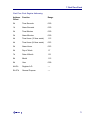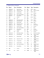
1
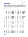
ZT 8903
ZT 8904
ZT 89CT04
Single Board 386 EX Computer
Hardware User Manual
CONTENTS
MANUAL ORGANIZATION .....................................................................................................................6
1. INTRODUCTION .................................................................................................................................8
PRODUCT DEFINITION .............................................................................................................8
ZT 8904..........................................................................................................................9
ZT 89CT04 .....................................................................................................................9
ZT 8903..........................................................................................................................9
STAND ALONE ..............................................................................................................9
STD 32 SINGLE MASTER..............................................................................................9
STD 32 MULTIPLE MASTER..........................................................................................9
FEATURES...............................................................................................................................10
DEVELOPMENT CONSIDERATIONS.......................................................................................11
FUNCTIONAL BLOCKS ............................................................................................................11
STD BUS INTERFACE .................................................................................................11
386 EX CPU .................................................................................................................12
MEMORY AND I/O ADDRESSING ...............................................................................13
LOCAL BUS VIDEO......................................................................................................13
SERIAL I/O ...................................................................................................................13
IEEE 1284 PARALLEL PORT .......................................................................................14
PARALLEL I/O..............................................................................................................14
INTERRUPTS...............................................................................................................14
TIMERS........................................................................................................................15
DMA .............................................................................................................................15
WATCHDOG TIMER ....................................................................................................15
REAL-TIME CLOCK .....................................................................................................15
KEYBOARD CONTROLLER.........................................................................................16
AC POWER-FAIL PROTECTION..................................................................................16
2. GETTING STARTED .........................................................................................................................17
UNPACKING.............................................................................................................................17
SYSTEM REQUIREMENTS ......................................................................................................17
MEMORY CONFIGURATION....................................................................................................17
SYSTEM RAM - 16-BIT PSEUDO STATIC RAM...........................................................17
I/O CONFIGURATION...............................................................................................................19
CONNECTOR CONFIGURATION.............................................................................................20
JUMPER DESCRIPTIONS ........................................................................................................21
SETUP......................................................................................................................................21
SYSTEM CONFIGURATION OVERVIEW .....................................................................21
3. STD BUS INTERFACE ......................................................................................................................23
STD 32 OPERATION ................................................................................................................23
STD 32 OPERATION....................................................................................................23
STD 32 BUS COMPATIBILITY ..................................................................................................24
COMPLIANCE LEVELS................................................................................................24
STD BUS INTERRUPTS ...........................................................................................................24
MASKABLE INTERRUPTS ...........................................................................................25
NON-MASKABLE INTERRUPTS ..................................................................................26
RESET......................................................................................................................................27
MULTIPLE MASTER AND INTELLIGENT I/O............................................................................27
MULTIPLE MASTER ....................................................................................................27
INTELLIGENT I/O.........................................................................................................28
SYSTEM REQUIREMENTS..........................................................................................29
MULTIPLE MASTER RESET ........................................................................................30
2
Contents
4. INTERRUPT CONTROLLER .............................................................................................................31
PROGRAMMABLE REGISTERS...............................................................................................31
INTERRUPT ARCHITECTURE INITIALIZATION REGISTERS (ICW1-ICW4)................34
OPERATIONAL REGISTERS (OCW1-OCW3)..............................................................36
STATUS REGISTERS (IRR, ISR, IPR) .........................................................................37
ADDITIONAL INFORMATION ...................................................................................................38
5. COUNTER/TIMERS...........................................................................................................................39
PROGRAMMABLE REGISTERS...............................................................................................41
COUNT REGISTERS AND COUNT LATCH .................................................................41
STATUS REGISTER ....................................................................................................42
CONTROL REGISTER .................................................................................................43
ADDITIONAL INFORMATION ...................................................................................................44
6. DMA CONTROLLER .........................................................................................................................45
INTEL 386 EX INTERNAL ARCHITECTURE.............................................................................45
DMA IMPLEMENTATION..........................................................................................................47
DMA TRANSFER CYCLES...........................................................................................48
I/O MAPPING ...............................................................................................................48
DMA CONTROLLER OPERATION ...........................................................................................48
PROGRAMMING A DMA CHANNEL ............................................................................49
FLY-BY AND TWO-CYCLE BUS CYCLES....................................................................49
386 EX DMA CONTROLLER REGISTERS ...............................................................................50
PIN MUX CONFIGURATION ........................................................................................51
PERIPHERAL CONNECTIONS AND MASK .................................................................53
CHANNEL 0 REQUESTOR ADDRESS REGISTERS....................................................53
CHANNEL 1 REQUESTOR ADDRESS REGISTERS....................................................55
CHANNEL 0 TARGET ADDRESS REGISTERS ...........................................................56
CHANNEL 1 TARGET ADDRESS REGISTERS ...........................................................58
CHANNEL 0 BYTE COUNT REGISTERS .....................................................................59
CHANNEL 1 BYTE COUNT REGISTERS .....................................................................61
DMA STATUS REGISTER............................................................................................62
DMA COMMAND REGISTERS.....................................................................................63
DMA MODE REGISTERS.............................................................................................64
DMA SOFTWARE REQUEST REGISTER ....................................................................65
DMA SINGLE CHANNEL MASK REGISTER ................................................................66
DMA GROUP CHANNEL MASK ...................................................................................66
DMA BUS SIZE REGISTER..........................................................................................66
DMA CHAINING REGISTER ........................................................................................67
DMA INTERRUPT ENABLE REGISTER.......................................................................68
DMA INTERRUPT STATUS REGISTER.......................................................................68
DMA OVERFLOW ENABLE REGISTER.......................................................................69
7. REAL-TIME CLOCK..........................................................................................................................70
PROGRAMMABLE REGISTERS...............................................................................................70
REGISTER A................................................................................................................72
REGISTER B................................................................................................................73
REGISTER C................................................................................................................73
REGISTER D................................................................................................................74
ADDITIONAL INFORMATION ...................................................................................................74
8. SERIAL CONTROLLER ....................................................................................................................75
ZT 8904 SPECIFICS .................................................................................................................75
ADDRESS MAPPING ...................................................................................................76
INTERRUPT SELECTION ............................................................................................76
HANDSHAKE SIGNALS ...............................................................................................76
RS-485 OPERATION....................................................................................................77
SERIAL CHANNEL INTERFACE ..................................................................................77
3
Contents
PROGRAMMABLE REGISTERS...............................................................................................78
BAUD RATE DIVISORS ...............................................................................................78
DIVISOR LATCH LSB AND MSB..................................................................................79
INTERRUPT CONTROL REGISTER ............................................................................80
INTERRUPT STATUS REGISTER................................................................................81
LINE CONTROL REGISTER ........................................................................................82
LINE STATUS REGISTER............................................................................................83
MODEM CONTROL REGISTER...................................................................................83
MODEM STATUS REGISTER ......................................................................................84
ADDITIONAL INFORMATION ...................................................................................................84
9. CENTRONICS PRINTER INTERFACE ..............................................................................................85
PROGRAMMABLE REGISTERS...............................................................................................85
LINE PRINTER DATA REGISTER ................................................................................85
LINE PRINTER STATUS REGISTER............................................................................85
LINE PRINTER CONTROL REGISTER ........................................................................86
ADDITIONAL INFORMATION ...................................................................................................86
10. PARALLEL I/O ................................................................................................................................87
FUNCTIONAL DESCRIPTION ..................................................................................................87
OUTPUT LATCH ..........................................................................................................88
OUTPUT BUFFER........................................................................................................88
INPUT BUFFER............................................................................................................89
PROGRAMMABLE REGISTERS...............................................................................................89
16C50A STANDARD OPERATING MODE ...................................................................89
16C50A ENHANCED OPERATING MODE ...................................................................90
11. SYSTEM REGISTERS.....................................................................................................................96
PROGRAMMABLE REGISTERS...............................................................................................96
ADDITIONAL INFORMATION ...................................................................................................98
12. WATCHDOG TIMER .......................................................................................................................99
WATCHDOG TIMER OPERATION ...........................................................................................99
PROGRAMMABLE REGISTERS.............................................................................................100
WATCHDOG TIMER CLEAR REGISTER ...................................................................101
WATCHDOG TIMER STATUS REGISTER .................................................................101
WATCHDOG TIMER COUNTER REGISTERS ...........................................................102
WATCHDOG TIMER RELOAD REGISTERS ..............................................................103
ADDITIONAL INFORMATION .................................................................................................103
13. LOCAL BUS VIDEO ......................................................................................................................104
14. NUMERIC DATA PROCESSOR ....................................................................................................105
15. PROGRAMMABLE LED................................................................................................................106
16. AC POWER FAIL ..........................................................................................................................108
A. JUMPER CONFIGURATIONS ........................................................................................................109
JUMPER OPTIONS ................................................................................................................109
JUMPER DESCRIPTIONS..........................................................................................111
B. SPECIFICATIONS ..........................................................................................................................116
ELECTRICAL AND ENVIRONMENTAL SPECIFICATIONS.....................................................116
ABSOLUTE MAXIMUM RATINGS ..............................................................................116
DC OPERATING CHARACTERISTICS.......................................................................116
BATTERY BACKUP CHARACTERISTICS..................................................................117
STD BUS LOADING CHARACTERISTICS .................................................................117
MECHANICAL SPECIFICATIONS...........................................................................................120
CARD DIMENSIONS AND WEIGHT ...........................................................................120
CONNECTORS ..........................................................................................................121
4
Contents
CONNECTOR DESCRIPTIONS .................................................................................123
CABLES .....................................................................................................................133
C. PIA SYSTEM SETUP CONSIDERATIONS .....................................................................................139
PREVENTING SYSTEM LATCHUP ........................................................................................139
POWER SUPPLY SEQUENCE MISMATCH ...............................................................140
SIGNAL LEVEL MISMATCH.......................................................................................142
PROTECTING CMOS INPUTS ...............................................................................................143
RISE TIMES ...............................................................................................................143
INDUCTIVE COUPLING .............................................................................................144
ADDITIONAL INFORMATION .................................................................................................145
D. CUSTOMER SUPPORT..................................................................................................................146
TECHNICAL/SALES ASSISTANCE.........................................................................................146
RELIABILITY...........................................................................................................................146
RETURNING FOR SERVICE ..................................................................................................146
ZIATECH WARRANTY............................................................................................................147
TRADEMARKS .......................................................................................................................148
5
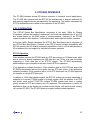
MANUAL ORGANIZATION
The ZT 8904 family of products includes the ZT 8904, ZT 89CT04, and ZT 8903
products. The ZT 8904 is a highly integrated 386 EX single board computer which can
be operated as a stand alone, as a single master in an STD 32 architecture, or as a
permanent or temporary master in an STD 32 architecture.
All features of the ZT 8903 and ZT 8904 are the same, except that the ZT 8903 includes
fewer features. The ZT 8903 is a more economical version of the ZT 8904 because of
fewer features are included.
All features of the ZT 8904 and ZT 89CT04 are the same except for the temperature
variations. The ZT 8904 has an operating temperature range from 0º to 65º C, but the
ZT 89CT04 extends the operating temperature range from -40º to +85º C.
Chapter 1, "Introduction", provides a brief introduction to the ZT 8904. It includes a
product definition, a list of product features, a functional block diagram, a description of
each block, and a diagram locating the major components of the board.
Chapter 2, "Getting Started", summarizes the information needed to make the
ZT 8904 operational. Read this chapter before attempting to use the board.
Chapter 3, "STD Bus Interface", discusses the STD 32 architecture and its effect on
the operation of the ZT 8904.
Chapter 4, "Interrupt Controller", includes information on two Intel-compatible 8259
cascaded interrupt controllers that provide a programmable interface between interruptgenerating peripherals and the CPU.
Chapter 5, "Counter/Timers", includes information on one Intel-compatible 8254
device with a total of three programmable counter/timers.
Chapter 6, "DMA Controller", includes information regarding the DMA controller which
is contained within the 386 EX microprocessor.
Chapter 7, "Real-Time Clock", includes information on the Motorola®-compatible
146818 real-time clock including the major features.
Chapter 8, "Serial Controller", discusses operation of the four ZT 8904 serial ports and
provides descriptions of the two software-configurable serial port registers included on
the ZT 8904.
Chapter 9, "Centronics Printer Interface", includes information on the bidirectional
printer interface which fully supports a Centronics-compatible printer.
Chapter 10, "Parallel I/O", discusses the six 8-bit parallel ports for a total of 48 I/O
signals. The general operation of the six parallel ports is explained in this chapter.
6
Manual Organization
Chapter 11, "System Registers", discusses the three system registers used to control
and monitor a variety of functions on the ZT 8904.
Chapter 12, "Watchdog Timer", lists the major features of the watchdog timer which
monitors the ZT 8904 operation and takes corrective action if the system fails to function
as programmed.
Chapter 13, "Local BUS Video", includes information on the local bus interface which
permits high speed peripherals direct access to the CPU bus.
Chapter 14, "Numeric Data Processor", discusses how the numeric data processor
extends the CPU instruction set to include trigonometric, logarithmic, and exponential
functions.
Chapter 15, "Programmable LED", discusses the ZT 8904's two Light-Emitting Diodes
(LEDs).
Chapter 16, "AC Power Fail", includes information on the AC power-fail detection as a
means for giving the application advanced warning of an impending power failure.
Appendix A, "Jumper Configurations", demonstrations how the ZT 8904 offers
several options tailoring the operation of the board to requirements of specific
applications. The "Jumper Cross Reference" table is included.
Appendix B, "Specifications", describes the electrical, environmental, and mechanical
specifications of the ZT 8904. It includes illustrations of the board dimensions, the P/E
connector pinouts, and cables commonly used with the ZT 8904. Also shown are tables
listing the pin assignments for the ZT 8904's 10 connectors.
Appendix C, "PIA System Setup Considerations", discusses the 16C50A Parallel
Interface Adapter (PIA) device used on the ZT 8904. It is designed by Ziatech to offer
bidirectional I/O signals with or without event sense capability.
Appendix D, "Customer Support", offers technical assistance information for this
product, and also the necessary information should you need to return a Ziatech
product.
7
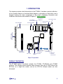
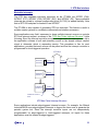
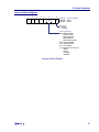
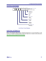
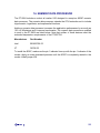
1. INTRODUCTION
This chapter provides a brief introduction to the ZT 8904. It includes a product definition,
a list of product features, a functional block diagram, a description of each block, and a
diagram locating the major components of the board. Unpacking information and
installation instructions are included in Chapter 2, "Getting Started."
1 or 5 Mbyte
Pseudo Static RAM
+5V operation
24 points of
Digital I/O
128 Kbyte SRAM
Push-button reset
AC/DC Power-Fail
Detection
STD 32 and
STD-compatible
1,2,or 4 Mbytes
Flash
Local Bus
Video Option
Intel
386 TM EX
ÛZIATECH
Integrated IDE
Subsystem
Math Coprocessor
Option
1 parallel port
4 serial ports
-2 RS-232
-2 RS-232/485
Major Components
PRODUCT DEFINITION
The ZT 8904 family of products includes the ZT 8904, ZT 89CT04, and ZT 8903
products. The following topics describe these products. Using the ZT 8904 without the
STD bus, as a single bus master, and as an STD 32® multiple master are also
discussed.
8
1. Introduction
ZT 8904
The ZT 8904 is a highly integrated 386 EX single board computer. The board meets the
needs of a wide range of industrial control and processing applications by operating
stand alone, as a single master in an STD 32 architecture, or as a permanent or
temporary master in an STD 32 architecture.
ZT 89CT04
The ZT 89CT04 extends the ZT 8904 operating temperature range from 0 to 65º C to
-40º to +85º C. Except for the temperature variations, all other features of the ZT 8904
and ZT 89CT04 are the same. Unless explicitly stated otherwise, all references in this
manual to the ZT 8904 include the ZT 89CT04.
ZT 8903
The ZT 8903 is a more economical board that includes all the features of the ZT 8904
except those listed below. Unless explicitly stated otherwise, all references in this
manual to the ZT 8904 include the ZT 8903 as well.
•
ZT 8904 supports an IDE drive option not available on the ZT 8903
•
ZT 8904 supports a multiprocessing option not available on the ZT 8903
•
ZT 8904 includes RS-485 support not available on the ZT 8903
•
ZT 8904 includes four serial ports and the ZT 8903 includes two
•
ZT 8904 includes 128 Kbytes of battery-backed RAM not available on the ZT 8903
Stand Alone
The ZT 8904 does not require an STD bus backplane to operate. The ZT 8904 is able to
operate stand-alone in many applications because of the large selection of the most
commonly needed peripheral devices. A power connector location and four mounting
holes are available for stand-alone operation.
STD 32 Single Master
The ZT 8904 supports additional memory and I/O through the STD bus. In an STD 32
architecture, data transfers are dynamically adjusted to support 8-bit and 16-bit boards.
STD 32 Multiple Master
The ZT 8904 can be configured to operate as a permanent master or as a temporary
master in a multiple master architecture. With this architecture, up to seven ZT 8904
boards share STD bus memory and I/O resources. The ZT 8903 does not support
multiple master operation.
9
1. Introduction
FEATURES
•
STD 32 compatible
•
STD 32 multiprocessing option (not supported by ZT 8903)
•
25 MHz Intel® 386 EX CPU
•
Numeric data processor socket
•
Optional local bus video support
•
128 Kbyte battery-backed Static RAM (not supported by ZT 8903)
•
1, 2, or 4 Mbytes of Flash memory
•
1 or 5 Mbytes of RAM memory
•
Standard AT® peripherals include:
•
-
Interrupt controllers (8259)
-
Counter/timers (8254)
-
Real-time clock/CMOS RAM (146818)
-
DMA controller (8237)
Additional AT® peripherals include:
-
Two RS-232 serial channels
-
Two RS-232/485 DMA capable serial channels (not supported by ZT 8903)
-
IEEE 1284 parallel port (Centronics, ECP, EPP)
-
Optional IDE disk drive (not supported by ZT 8903)
•
24-point digital I/O with interrupt driven event sense and programmable debounce
•
Two stage watchdog timer
•
Pushbutton reset
•
Software programmable LED
•
AC/DC power monitor
•
+5 V-only operation (Local charge pump for RS-232 and Flash programming)
•
Compatible with the following software: MS-DOS®, OS/2®, UNIX®, QNX®, VRTX32®,
and Windows® 3.1
•
STD bus standard 4.5" x 6.5" board format
•
DOS or STAR BIOS options
•
Burned in at 55º Celsius and tested to guarantee reliability
•
Five year warranty
10
1. Introduction
DEVELOPMENT CONSIDERATIONS
Ziatech offers a variety of software options for ZT 8904 applications. These options
include STD ROM, STAR BIOS, and Ziatech's Industrial BIOS. Contact the Ziatech for
additional options.
STD ROM allows programmers to develop ROM-based applications without the use of
an operating system. STD ROM connects the ZT 8904 to an IBM-compatible personal
computer through a high speed serial link. The computer is used as a development
station to create, download, and debug applications written in assembly, C, and other
popular programming languages. The Paradigm Systems DEBUG/RT used during the
debug phase includes source level debugging, single step execution, breakpoints and
watchpoints.
The Ziatech Industrial BIOS provides the standard MS-DOS environment and services
in Flash memory on the ZT 8904. Ziatech Industrial BIOS provides standard support for
common peripherals and is supported by many third party development tools such as
program editors, compilers, assemblers, and debuggers. Refer to the Ziatech system
manual for configuration and operating instructions.
STAR BIOS is the DOS platform operating on more than one master in a single
STD bus system. Each master supports the Ziatech Industrial BIOS operating
environment and is capable of sharing STD bus memory and I/O, such as fixed disks,
floppy disks, and video. Refer to the STD 32 STAR SYSTEM™ operating manual for
configuration and operating instructions. The STAR BIOS is not available for the
ZT 8903.
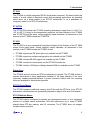
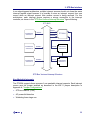
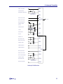
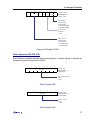
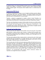
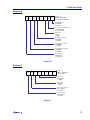
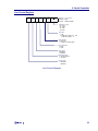
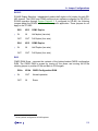
FUNCTIONAL BLOCKS
The "Functional Block Diagram" on the next page illustrates the board's major functional
blocks. A description of the board's features and functional blocks is listed found in the
following topics.
STD Bus Interface
The ZT 8904 operates in STD 32 systems. In an STD 32 system, data transfers are
dynamically sized for either 8 bits or 16 bits. STD 32 compatible memory and I/O boards
are dynamically sensed to determine the width of the data transfer.
In addition to 16-bit data transfers, the STD 32 system provides the platform needed for
multiple master operation. In a multiple master system, up to seven ZT 8901, ZT 8902,
or ZT 8904 boards share STD bus resources with a fixed or rotating priority granted by
an external bus arbiter, such as the ZT 89CT39. The ZT 8903 does not support multiple
master operation.
See Chapter 3, "STD Bus Interface" for more information.
11
1. Introduction
386 EX CPU
ZT 8904
The ZT 8904 supports the Intel 386 EX CPU operating at 25 MHz. The 386 EX is a fully
static 32-bit CPU core integrated with standard PC peripherals. Integrated peripherals
include serial controller, interrupt controller, DMA controller, counter/timers, and
watchdog timer. The 386 EX supports a 64 Mbyte memory address space and a
64 Kbyte I/O address space.
Interrupt
Inputs
24-Point
Digital I/O
Centronics Port
(ECP, EPP)
Two RS-232 and
Two RS-232/485
Serial Ports
IDE
Subsystem
25MHz 386 EX
CPU
Optional 387SX
Math Coprocessor
Battery-Backed
SRAM (128 Kbytes)
AC/DC
Power Detect
Pseudo
Static
RAM
(1 or 5
Mbytes)
Flash
Memory
(1, 2, or 4
Mbytes)
Local Bus
Video
Expansion
5V to 12V
Flash VPP
Generator
Battery
DMA
Controllers
Interrupt
Controllers
Real-Time
Clock
Timers
Watchdog
Timer
®
Bus Interface
(Single and Multiple Master Operation)
Functional Block Diagram
12
1. Introduction
Memory and I/O Addressing
The ZT 8904 includes 1 Mbyte of system RAM, 1, 2, or 4 Mbytes of Flash, and
128 Kbytes of battery-backed RAM. The battery-backed RAM is not available on the
ZT 8903. System RAM can be expanded from 1 Mbyte to 5 Mbytes with the addition of
an optional memory module. Memory operations up to 16 Mbytes that are not decoded
by local memory devices are directed to the STD bus.
Data transfers are dynamically adjusted to support standard architecture STD bus
memory boards with an 8-bit or 16-bit data path. The memory architecture selected for
the Ziatech Industrial BIOS architecture is shown in the "Memory Address Map" in
Chapter 2.
The ZT 8904 also includes many I/O peripherals required for industrial control
applications. I/O operations up to 64 Kbytes not decoded by local I/O devices are
directed to the STD bus. The STD bus I/O expansion signal, IOEXP, is supported to
limit the addressing redundancy of I/O boards decoding fewer than 16 bits of address.
Data transfers are dynamically adjusted to support standard architecture STD bus I/O
boards with an 8-bit or 16-bit data path. A20 is located at port 92h. Set bit 1 to 1 for
disable, 0 for enable. The I/O map architecture selected for the Ziatech Industrial BIOS
architecture is shown in the "I/O Address Map".
Local Bus Video
The ZT 8904 supports both STD bus and local bus video adapters. For STD bus video,
Ziatech offers video boards that support VGA and flat panel displays. For local bus
video, Ziatech offers zVID adapters that plug directly onto the ZT 8904 J6 local bus
connector. Local bus video is up to 300% faster than STD bus video because the data
transfers occur at the CPU operating speed of 25 MHz. For space-constrained
applications, the zVID offerings have the added advantage of not requiring the
additional card cage slot needed by the STD bus offerings.
Serial I/O
The ZT 8903 includes two RS-232 serial ports. The ZT 8904 and ZT 89CT04 include
four RS-232 serial ports, two of which can be software configured for RS-485 operation.
COM1 and COM2 are 16C450 compatible UARTs. COM3 and COM4 are 16C550
compatible UARTS. All of the serial ports include a complete set of handshaking and
modem control signals, maskable interrupt generation, and data transfer rates up to
115 Kbaud, and are implemented with a 5 V charge pump technology to eliminate the
need for a ±12 V supply.
The 386 EX multiplexes COM2 data and handshake signals with DMA signals. This
results in the loss of COM2 handshake if STD bus DMA is used and the complete loss
of COM2 if local printer or serial DMA is used. This selection is controlled with jumpers
W24 through W27 and BIOS configuration.
13
1. Introduction
The serial ports are configured as DTE and are available through the J1 80-pin
frontplane connector. Optional cables convert the serial port interface to standard 9-pin
D-shell connectors. The ZT 90200 cable provides the serial interface for the ZT 8904
and ZT 89CT04. The ZT 90203 cable provides the serial interface for the ZT 8903. A
null-modem option is required to convert the DTE configuration to DCE.
See Chapter 8, "Serial Controller" for more information.
IEEE 1284 Parallel Port
The ZT 8904 includes an IEEE 1284 parallel port for supporting Centronics, EPP, and
ECP devices. The parallel port interface is available through the J1 80-pin frontplane
connector. An optional cable converts the parallel port interface to a standard 25-pin Dshell connector. The ZT 90200 cable provides the parallel interface for the ZT 8904 and
ZT 89CT04. The ZT 90203 cable provides the parallel interface for the ZT 8903.
See Chapter 9, "Centronics Printer Interface" for more information.
Parallel I/O
The ZT 8904 includes three 8-bit parallel I/O ports for a total of 24 parallel I/O lines.
Each line is programmable as an input or an output with readback. The outputs sink
12 mA and do not glitch during power cycles. The 24 lines, available through the J4 50pin frontplane connector, also support software programmable signal debounce and
event sense interrupt generation.
An optional cable (ZT 90072 Digital I/O Cable) connects the parallel I/O interface to an
8, 16, or 24 position I/O module mounting rack, such as Ziatech's ZT 2226 24-Channel
I/O Mounting Rack or those offered by Opto 22®.
See Chapter 10, "Parallel I/O" for more information.
Interrupts
Two interrupt controllers provide a total of 15 interrupt inputs. Interrupt controller
features include support for level-triggered and edge-triggered inputs, fixed and rotating
priorities, and individual input masking. Interrupt sources include counter/timers, serial
I/O, parallel I/O, real-time clock, keyboard, printer, optional IDE drive, and multiple
master communications. There are also three frontplane and four STD bus interrupt
sources. Frontplane interrupts are available via connector J2.
See Chapter 4, "Interrupt Controller" for more information.
14
1. Introduction
Timers
Three timers are included on the ZT 8904. Operating modes supported by the timers
include interrupt on count, frequency divider, square wave generator, software
triggered, hardware triggered, and one shot. The number of counter/timers available to
the application programmer depends on the operating system.
For example, the Ziatech MS DOS operating system uses timer 0 to generate system
tick and timer 2 to control the speaker. Timer 1 is available to the application.
See Chapter 5, "Counter/Timers" for more information.
DMA
One DMA controller provides two DMA channels for data transfers between local or
system I/O and local memory. DMA channel 0 supports both 8-bit and 16-bit STD bus
DMA slaves. The primary use for STD bus DMA is floppy disk expansion. Optionally,
DMA channel 0 supports the local 1284 parallel port or combines with DMA channel 1 to
support one of the local serial ports.
See Chapter 6, "DMA Controller" for more information.
Watchdog Timer
The two-stage watchdog timer optionally monitors system operation. Failure to strobe
the first stage within a programmable time period results in a non-maskable interrupt.
Failure of the non-maskable interrupt service routine to restart the watchdog results in a
stage two reset.
See Chapter 12, "Watchdog Timer" for more information.
Real-Time Clock
The real-time clock performs timekeeping functions and includes more than 200 bytes
of general-purpose battery-backed CMOS RAM.
Timekeeping features include an alarm function, a maskable periodic interrupt, and a
100-year calendar.
CMOS RAM available to the application programmer depends on the operating system.
For example, the Ziatech MS DOS operating system uses the CMOS RAM to store
configuration parameters.
See Chapter 7, "Real-Time Clock" for more information.
15
1. Introduction
Keyboard Controller
The ZT 8904 includes a PC/AT® keyboard controller that operates when the zVID local
bus video adapter is installed. The keyboard connector is located on the zVID adapter.
AC Power-Fail Protection
With the addition of an AC transformer (connected to connector J3), the ZT 8904
monitors AC power to permit an orderly shutdown during a power failure. When AC
power falls below an acceptable operating range, a non-maskable interrupt is generated
to notify the CPU of an impending power failure. When the application software receives
this notification, it saves critical data before the CPU is reset.
See Chapter 16, "AC Power Fail," for more information.
16
2. GETTING STARTED
This chapter summarizes the information needed to make the ZT 8904 operational.
Read this chapter before attempting to use the board.
UNPACKING
Please check the shipping carton for damage. If the shipping carton and contents are
damaged, notify the carrier and Ziatech for an insurance settlement. Retain the shipping
carton and packing material for inspection by the carrier. Save the anti-static bag for
storing or returning the ZT 8904.
Do not return any product to Ziatech without a Return Material Authorization (RMA)
number. Refer to Appendix D, "Customer Support," which explains the procedure for
obtaining an RMA number from Ziatech.
Warning: Like all equipment utilizing MOS devices, the boards must
be protected from static discharge. Never remove any of the
socketed parts except at a static-free workstation. Use the anti-static
bag shipped with your order to handle the boards.
SYSTEM REQUIREMENTS
The ZT 8904 is designed for use with or without an STD bus backplane. The ZT 8904 is
electrically, mechanically, and functionally compatible with the STD 32 Bus Specification
(ZT MSTD32) for STD bus applications. An STD 32 system is required for 16-bit data
transfers to other STD bus boards and for multiple master operation. The ZT 8903 does
not support multiple master operation.
Ziatech recommends vertical mounting and the use of a fan to provide the required
airflow. Refer to Appendix B, "Specifications," for additional specifications.
MEMORY CONFIGURATION
The ZT 8904 addresses 64 Mbytes of memory using a 26-bit memory address. The
memory map is programmable through the CPU chip select registers. The memory
architecture selected for the Ziatech Industrial BIOS architecture is shown in the
"Memory Address Map" figure. The ZT 8904 memory map includes several types of
memory.
System RAM - 16-bit pseudo static RAM
•
Video RAM - located on the STD bus or zVID memory board
•
Video BIOS - 16-bit pseudo static RAM shadowed from video board
17
2. Getting Started
•
Local RAM Drive - 8-bit battery-backed RAM (not available on the ZT 8903) paged
for 128 Kbytes
•
System BIOS - 16-bit pseudo static RAM shadowed from Flash #0
•
Extended RAM - Optional 16-bit pseudo static RAM module
•
Flash #0 - 8-bit Flash
•
Flash #1 - Optional 8-bit Flash
•
STD bus Expansion - 8-bit or 16-bit expansion memory
•
Reserved - Not available
STD bus expansion memory is transferred at a rate of up to 1 Mbyte/second for 8-bit
data and 1.5 Mbytes/second for 16-bit data. The ZT 8904 supports the STD bus wait
request signal, WAITRQ*, to interface to memory boards with longer access time
requirements than those defined by zero wait state STD 32 specifications. During local
memory operations, the STD bus is held static to decrease system electrical noise and
power consumption.
The ZT 8904 supports 128 Kbyte battery backed RAM (BRAM) devices. BRAM is paged
into the system memory map in 64 Kbyte increments at 0xD0000h through 0xDFFFFh.
Paging is performed by writing specific values to bits D4, D3 and D2 of System Register
0 (0X7Bh). BRAM pages are selected as follows:
•
Write XXXX111Xh to select BRAM page 0
•
Write XXXX110Xh to select BRAM page 1
If larger BRAM devices are installed, use sequential codes to select subsequent pages
in the memory map. Note that specific BRAM pages are used by both the Ziatech Single
Master BIOS and by the STAR System BIOS. The Ziatech Technical Support Group
can provide example code for using ZT 8904 BRAM.
18
2. Getting Started
180000h-3FFFFFh
RESERVED
140000h-17FFFFh
FLASH #0
100000h-13FFFFh
FLASH #1
080000h-0FFFFFh
STD BUS EXPANSION
050000h-07FFFFh
RESERVED
010000h-04FFFFh
EXTENDED RAM
EXPANSION MODULE
00E000h-00FFFFh
SYSTEM BIOS
00D000h-00DFFFh
LOCAL RAM DRIVE
STD BUS EXPANSION
00C800h-00CFFFh
STD BUS EXPANSION
00C000h-00C7FFh
VIDEO BIOS
00A000h-00BFFFh
VIDEO RAM
000000h-009FFFh
SYSTEM RAM
Memory Address Map
I/O CONFIGURATION
The ZT 8904 addresses up to 64 Kbytes of I/O using a 16-bit I/O address. The I/O map
is programmable through the CPU configuration registers. The I/O map architecture
selected for the Ziatech Industrial BIOS architecture is shown in the "I/O Address Map"
figure following.
STD bus expansion I/O is transferred at a rate of up to 1 Mbyte/second for 8-bit data
and 1.5 Mbytes/second for 16-bit data. The ZT 8904 supports the STD bus wait request
signal, WAITRQ*, to interface to I/O boards with longer access time requirements than
those defined by zero wait state STD 32 specifications. The STD bus I/O expansion
signal, IOEXP, is also supported. The IOEXP signal is automatically driven low over the
I/O address range FC00h to FFFFh. Application software should use this address range
to access STD bus I/O boards decoding IOEXP and fewer than 16 bits of address to
prevent the board from being redundantly mapped throughout the 64 Kbyte I/O address
space. During local I/O operations, the STD bus is held static to decrease system
electrical noise and power consumption.
19
2. Getting Started
F900h-FFFFh
F800h-F8FFh
F500h-F7FFh
F4D0h-F4FFh
F4C0h-F4CFh
F400h-F4BFh
F100h-F3FFh
F000h-F0FFh
0700-EFFFh
0600h-06FFh
0400-05FFh
03F8h-03FFh
03F6h-03F7h
03F0h-03F5h
0300h-03EFh
02F8h-02FFh
02F0h-02F7h
02E8h-02EFh
02E0h-02E7h
0280h-02DFh
0278h-027Fh
0270h-0277h
026Eh-026Fh
0200h-026Dh
01F8h-01FFh
01F0h-01F7h
0100h-01EFh
00F0h-00FFh
00A2h-00EFh
00A0h-00A1h
0094h-009Fh
0092h-0093h
0090h-0091h
0080h-008Fh
0078h-007Fh
0070h-0077h
0068h-006Fh
0060h-0067h
0044h-005Fh
0040h-0043h
0024h-003Fh
0022h-0023h
0020h-0021h
0010h-001Fh
0000h-000Fh
AVAILABLE
CPU CONFIGURATION
AVAILABLE
CPU CONFIGURATION
WATCHDOG
CPU CONFIGURATION
AVAILABLE
CPU CONFIGURATION
AVAILABLE
RESERVED
AVAILABLE
COM1
IDE
RESERVED
AVAILABLE
COM2
RESERVED
COM4
COM3
RESERVED
PRINTER (IEEE 1284)
RESERVED
CPU CONFIGURATION
RESERVED
AVAILABLE
IDE
AVAILABLE
COPROCESSOR
AVAILABLE
INTERRUPT #2
AVAILABLE
CPU CONFIGURATION
AVAILABLE
DMA PAGE REGS
PARALLEL I/O
REAL TIME CLOCK
RESERVED
KEYBOARD
AVAILABLE
COUNTER / TIMERS
AVAILABLE
CPU CONFIGURATION
INTERRUPT #1
AVAILABLE
DMA
I/O Address Map
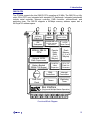
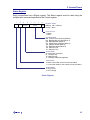
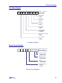
CONNECTOR CONFIGURATION
The following figure shows the locations and assignments of connectors J1 - J8. See
"Connectors" in Appendix B for information on connector pin assignments and cabling.
20
2. Getting Started
J2 (FRONTPLANE INTERRUPT)
J5 (MEMORY EXPANSION)
J3 (AC POWER FAIL)
J3
J7 (POWER CONNECTOR)
J2
J5
J4
J1
P/E (STD 32 INTERFACE)
J6
J6 (LOCAL BUS)
J4 (PARALLEL I/O)
J1 (SERIAL/PRINTER I/O)
Connector Locations
JUMPER DESCRIPTIONS
The ZT 8904 includes several jumper options that tailor the operation of the board to
specific application requirements. These options are summarized in Appendix A,
"Jumper Configurations."
SETUP
The following topics present a brief introduction to the setup and configuration of the
ZT 8904. For documentation specific to the BIOS and other utilities, see the Ziatech
Industrial BIOS manual (shipped with Ziatech Development Systems).
System Configuration Overview
The Ziatech Industrial BIOS and MS-DOS operating system software is preprogrammed
in the ZT 8904's on-board flash memory. The BIOS includes embedded support to allow
the ZT 8904 flash memory to be used as a solid-state drive (SSD) in the MS-DOS
environment. Ziatech also supplies SSD support for QNX (contact Ziatech for SSD
drivers for other operating systems).
21
2. Getting Started
The ZT 8904 is configured during the boot sequence by the BIOS. The BIOS uses
system configuration information stored as SETUP parameters.
To access the SETUP utility, either boot the system and press the "S" key during the
system RAM check, or run the SETUP.COM utility from the MS-DOS prompt.
The SETUP parameters are saved in the battery-backed RAM portion of the ZT 8904's
real-time clock device. The SETUP parameters can also be saved in a file format, or as
the programmed BIOS defaults.
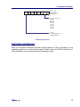
When SETUP is run, an interactive configuration screen is displayed, as shown in the
"BIOS SETUP Utility Screen Example" illustration following.
Note: the SETUP program is a generic utility used for all Ziatech processor boards.
Some parameters not applicable to the ZT 8904 may be labeled "N/A".
The BIOS SETUP screen is organized as a single screen. The SETUP screen allows
the user to select options for such items as base memory and extended memory size
selection, boot source, hard disk type, and floppy disk type.
The parameters in the SETUP screen are easily changed. Use the arrow keys to select
a parameter, then press + or - to step through the valid choices for that parameter. A
dynamic help line at the bottom of the screen helps you determine how to set each
parameter. SETUP accepts only valid parameter sets: if changing one parameter
invalidates another parameter, SETUP automatically updates the invalid parameter.
After setting the parameters, press the F10 key to accept them.
Ziatech Industrial BIOS Setup Utility
Copyright (C) 2000, Ziatech Corporation
Floppy Disk A: .............................. 1.44M
Floppy Disk B: .............................. N/I
Fixed Disk 0: ... 1024 16 63
USER
Fixed Disk 1: ................................. N/I
Amount of System RAM............... 640K
Amount of Extended RAM ........... 4096K
RAM Speed: .................................. 70ns
Power On Diagnostics ................... ON
Execute BIOS In Shadow RAM..... YES
Boot Disk ............... ....................... FLASH
Floppy Interface ............................ STD 32
IDE Interface ................................. STD 32
COM1 Port .................................... ONBOARD
COM2 Port .................................... NONE
LPT1 Port ...................................... ONBOARD
Flash Disk Letter ...........................
Flash Disk Size ..............................
RAM Disk Drive Letter .................
RAM Disk Drive Size ...................
P:
3776K
R:
32K
Erase Flash Disk ........................... NO
Update System Configuration ....... YES
Use the arrow keys to select a parameter, + and - to change the value,
F10 to accept the current parameters, or ESC to quit.
Select not installed or the type of diskette drive installed.
ZT8904
BIOS SETUP Utility Screen Example
22
3. STD BUS INTERFACE
The ZT 8904 includes several I/O devices common to industrial control applications.
The ZT 8904 also operates with the STD 32 bus architectures to support additional I/O
and memory mapped devices as required by the application. This section discusses the
STD 32 architecture and its effect on the operation of the ZT 8904.
STD 32 OPERATION
The STD-80 Series Bus Specification, developed in the early 1980s by Ziatech
Corporation, defines the electrical, mechanical, and functional characteristics of an STD
bus system based on the 8088 series of microprocessors. Features of an STD-80
system include an 8-bit data bus, 24-bit address bus, and single bus master operation.
In the late 1980s, Ziatech developed the STD 32 Bus Specification as an extension to
the STD-80 Bus Specification. Features of an STD 32 system include compatibility with
STD-80 memory and I/O boards, expansion capabilities of up to a 32-bit data bus and a
32-bit address bus, and support for multiple bus master operation.
STD 32 Operation
Data transfers between the ZT 8904 and any STD bus memory or I/O board occur eight
bits at a time for boards supporting an 8-bit data bus and 16 bits at a time for boards
supporting a 16-bit data bus in an STD 32 system. The ZT 8904 automatically
determines the type of transfer at the start of each STD bus operation.
If the application software includes a 16-bit operation with an 8-bit STD bus board, the
ZT 8904 automatically reduces the transfer into two STD bus cycles. If the application
software includes a 16-bit operation with a 16-bit STD bus board, the ZT 8904 performs
the transfer in a single STD bus cycle.
In addition to 16-bit data transfer support, the STD 32 system has another advantage: it
supports up to seven ZT 8904 boards in a single system. With the addition of an STD
bus arbiter, such as the ZT 89CT39, multiple ZT 8904 boards have fixed or rotating
priority access to STD bus memory and I/O resources. This architecture is useful for
applications that can be divided into modular control blocks, with each module running
on a unique ZT 8904. The ZT 8903 does not support multiple master operation.
23
3. STD Bus Interface
STD 32 BUS COMPATIBILITY
The ZT 8904 is compatible with Revision 1.2 of the STD 32 Bus Specification (Ziatech
part number ZT MSTD32). Optional STD 32 features are discussed in terms of
compliance levels.
•
Permanent Master: SA16, SA8 - I, SDMABP, {MD}
•
Temporary Master: SA16, SA8 - I, SDMABP, {MD}
Compliance Levels
The following is a brief description of the STD 32 compliance levels supported by the
ZT 8904.
SA16, SA8
Supports 8-bit and 16-bit data transfers with STD-80 signal format and
timings. The ZT 8904 automatically determines the width of the data
transfer at the start of each STD bus operation. STD-80 compatible
memory and I/O boards are supported.
I
Supports four additional STD bus interrupts: INTRQ1*, INTRQ2*,
INTRQ3*, and INTRQ4*. These interrupts are input from the STD bus and
connected to the interrupt controller through a jumper configuration block
for increased flexibility.
SDMABP
Supports Standard Architecture DMA using BUSRQ*/BUSAK* for request
and acknowledge and the backplane DMA control signals DMAIOR*,
DMAIOW*, and T-C. It is not permissible to program the DMA controller
for cascaded operation.
{MD}
Supports the multiple master (DREQx*, DAKx*) protocol. These two
signals are used by the ZT 8904 in a multiple master architecture to gain
control of STD bus resources. The use of these signals requires a bus
arbiter, such as the ZT 89CT39, to be plugged into Sot X.
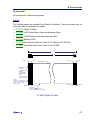
STD BUS INTERRUPTS
The ZT 8904 supports both maskable and non-maskable interrupts from the STD bus.
This section discusses system level issues related to these interrupts. Refer to
Chapter 4, "Interrupt Controller," for more information on the maskable interrupt
controllers.
24
3. STD Bus Interface
Maskable Interrupts
The STD bus maskable interrupts monitored by the ZT 8904 are INTRQ* (P44),
INTRQ1* (P37), INTRQ2* (P50), INTRQ3* (E67), and INTRQ4* (P5). These maskable
interrupts are routed to a jumper configuration block (W17-22) for added flexibility. Note
that an STD 32 backplane is needed to use INTRQ3*.
The ZT 8904 is also capable of generating STD bus interrupts. This feature is useful in
multiple master systems to coordinate communications between processors.
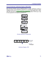
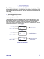
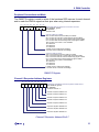
Some applications may find it necessary to share multiple interrupt sources on a single
STD bus interrupt request, as shown in the "STD Bus Polled Interrupt Structure" figure
following. Since the interrupt controller provides a single vector for each input, it is up to
the application software to poll each possible source on the shared interrupt request
signal to determine which is requesting service. This procedure is fine for most
applications, provided that each source can be polled and that the interrupt controller is
programmed for level-triggered operation.
STD BUS
I
INTERRUPT S
SOURCE 1 P
I
INTERRUPT S
SOURCE 2 P
I
INTERRUPT
SOURCE N S
P
INTRQ*
INTRQ*
ZT 8904
INTRQ*
INTRQ*
INTERRUPT STATUS
PORT
STD Bus Polled Interrupt Structure
Some applications include edge-triggered interrupt sources. For example, the Ziatech
Industrial BIOS uses edge-triggered interrupts to support the timer used to generate the
periodic system tick. Since the interrupt controller inputs are not independently
programmable for edge-triggered or level-triggered interrupts, all inputs for these
applications must be treated as edge-triggered.
25
3. STD Bus Interface
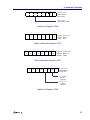
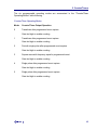
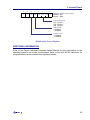
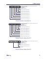
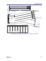
In an edge-triggered architecture, multiple interrupt sources should not share the same
interrupt request signal because it is possible to miss an interrupt request from one
source while an interrupt request from another source is being serviced. For this
architecture, each interrupt source requires a unique connection to the interrupt
controller, as shown in the "STD Bus Vectored Interrupt Structure" figure following.
STD BUS
INTRQ*
INTERRUPT
SOURCE 1
INTRQ*
INTERRUPT
SOURCE 2
INTRQ1*
INTRQ*
INTERRUPT
SOURCE 4
INTERRUPT
SOURCE 3
INTRQ2*
INTRQ*
INTERRUPT
SOURCE 7
INTRQ1*
ZT 8904
INTRQ2*
STD Bus Vectored Interrupt Structure
Non-Maskable Interrupts
The ZT 8904 supports three sources of non-maskable interrupt requests. Each interrupt
source must be jumper enabled as described in the W9-11 jumper description in
Appendix A, "Jumper Configurations."
•
STD bus NMIRQ* (P46)
•
AC power-fail detection
•
Watchdog timer stage one
26
3. STD Bus Interface
RESET
The ZT 8904 is automatically reset with a precision voltage monitoring circuit that
detects when Vcc is below the acceptable operating limit of 4.75 V. Other sources of
reset include watchdog timer stage 2, local pushbutton switch, and the STD bus
pushbutton reset signal, PBRESET* (P48).
The ZT 8904 responds to any of these reset sources by initializing local peripherals and
driving the STD bus system reset, SYSRESET* (P47). The ZT 8904 reset is typically
active for 350 milliseconds.
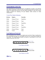
MULTIPLE MASTER AND INTELLIGENT I/O
Ziatech offers the following two architectures for increasing the number of
microprocessors in a single system:
•
Multiple master
•
Intelligent I/O
Applications can use multiple master, intelligent I/O, or a combination of the two.
Multiple Master
A multiple master architecture requires one permanent master and one or more
temporary masters, as illustrated in the "Multiple Master Architecture" figure following.
The ZT 8904 is configured for permanent or temporary master operation through the
installation and removal of resistor packs RP16 and RP17. With both resistor packs
installed, the ZT 8904 functions as a permanent master. With both resistor packs
removed, the ZT 8904 functions as a temporary master. The ZT 8903 does not support
multiple master operation.
In a multiple master architecture, each master has complete access to STD bus
resources and operates at full speed when the local CPU is communicating with local
memory and I/O. It is not until the application software attempts an STD bus access that
arbitration occurs.
The ZT 8904 responds to an STD bus access from the application software by
generating an STD bus request, DREQx* (E16), to an external bus arbiter such as the
ZT 89CT39. The ZT 8904 then suspends all local operation until the bus arbiter returns
an STD bus acknowledge, DAKx* (E15). All arbitration is done in hardware on the
external bus arbiter board and is transparent to the application software. The amount of
time required for this arbitration depends on the amount of time higher priority masters
are in control of STD bus resources. A shared resource locking mechanism is supported
to guarantee exclusive access to STD bus memory or I/O.
27
3. STD Bus Interface
904
00
ZT2
ZT 8
P
MASORARY
TEM
TE
P
MASORARY R
TEM
TER
P
MASORARY
PER
T
ER
MA
ZT 8
ZT 8
MEM I/O SLA
VE
ORY
SLA
904 T
VE
EM
ZT 8
904
904
N
MA
STEENT
SL
R
ARBOT X
ITE
R
ded
bed r
Em pute
Com
TM
Multiple Master Architecture
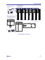
Intelligent I/O
An intelligent I/O system includes a single ZT 8904 and one or more intelligent I/O
boards, such as the ZT 8832. This architecture is illustrated in the following figure
"Intelligent I/O Architecture." The intelligent I/O board incorporates several I/O devices,
a dual-port RAM for processor communications, and a CPU dedicated to controlling
these devices.
Each intelligent I/O board operates at full speed when communicating with local
memory, local I/O, and dual-port RAM. The ZT 8904 also operates at full STD bus
speeds when accessing the dual-port RAM. It is not until the ZT 8904 and the intelligent
I/O board access the dual-port RAM at the same time that arbitration occurs.
All arbitration is done in hardware local to each intelligent I/O board, eliminating the
need for an external bus arbiter. The arbitration is transparent to the application
software. The amount of time required for arbitration depends on the amount of time the
device in control of the dual-port RAM requires to complete operation. A shared
resource locking mechanism is supported to guarantee exclusive access to dual-port
RAM by either the ZT 8904 or the intelligent I/O board.
28
3. STD Bus Interface
ZT 8
832 INTEL
832 INTE
00
ZT2
ZT
ded
bed r
Em pute
Com
LLIG
ENT
LLIG I/O
I/O ENT
LIG
I/O ENT
832 INTE
ZT 8
ZT 8
MEM I/O SLA
ORY
VE
SLA
832 IN
VE
TE
ZT 8
LLIG
I/O ENT
890
4
TM
Intelligent I/O Architecture
Multiple Master Vs. Intelligent I/O
Both multiple master and intelligent I/O architectures are excellent methods of
increasing system performance. The application designer has the freedom to select
either architecture or combine both to meet the needs of the specific application. The
following is a brief comparison of the multiple master and intelligent I/O architectures.
•
An advantage of the multiple master system is that each ZT 8904 has complete
access to all STD bus memory and I/O resources. However, in an intelligent I/O
system, only one ZT 8904 has access to STD bus memory and I/O, including the
dual-port RAM interface to each intelligent I/O board.
•
An advantage of the intelligent I/O system is lower system cost. The intelligent I/O
architecture operates in STD 32 bus structures. Dual port RAM arbitration is local to
each intelligent I/O board, eliminating the need for a system arbiter. Also, most
multiple master implementations require an STD bus memory slave for
communications between the masters. With an intelligent I/O architecture, all
communications between the single master and the intelligent I/O boards are
through the dual-port RAM local to each intelligent I/O board.
System Requirements
The following is a list of considerations for the ZT 8904 operating in a multiple master
architecture.
•
One ZT 8904 must be configured as a permanent master, or there must be another
board in the system responsible for managing the STD bus clock, CLOCK* (P49),
and the system reset, SYSRESET (P47). The remaining ZT 8904 boards must be
configured for temporary master operation: the two socketed resistor packs, RP16
and RP17, must be installed on the permanent master and removed from all
temporary masters. These resistor packs are located next to the STD 32 connector.
29
3. STD Bus Interface
•
An STD 32 backplane is required. The STD-80 backplane does not support the bus
exchange protocol (DREQx* and DAKx*).
•
A ZT 89CT39, or equivalent bus arbiter, is needed to manage ZT 8904 access to the
STD bus resources. The arbitration may also be built directly on to the permanent
master if a ZT 8904 is not used for this function.
Multiple Master Reset
The ZT 8904, configured for single master operation, is automatically reset with a
precision voltage monitoring circuit, watchdog timer, local pushbutton reset, and the
STD bus pushbutton reset signal, PBRESET* (P48). In response to any of these
signals, the ZT 8904 initializes local peripherals and activates the STD bus system
reset, SYSRESET* (P47).
In a multiple master system, a ZT 8904 configured as a permanent master operates the
same as a ZT 8904 operating in a single master architecture. A ZT 8904 configured as
a temporary master manages reset differently. A temporary master does not monitor
PBRESET* and does not generate SYSRESET*. Instead, a temporary master ignores
PBRESET* and monitors SYSRESET*. This enables the temporary masters to be reset
when the permanent master generates SYSRESET*. This also enables the pushbutton
reset on the temporary master to reset only the temporary master while the pushbutton
on the permanent master resets the entire system.
30
4. INTERRUPT CONTROLLER
The ZT 8904 includes two Intel-compatible 8259 cascaded interrupt controllers that
provide a programmable interface between interrupt-generating peripherals and the
CPU. The interrupt controllers monitor 15 interrupts with programmable priority. When
peripherals request service, the interrupt controller interrupts the CPU with a pointer to a
service routine for the highest priority device. The major features of the interrupt
architecture are listed below. The ZT 8904 does not support cascaded interrupt
controllers on the STD bus.
•
15 individually maskable interrupts
•
Level-triggered or edge-triggered recognition
•
Fixed or rotating priorities
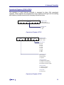
The interrupt architecture is illustrated in the "Interrupt Architecture" figure following.
Interrupt configuration jumpers (W17-22) are used to customize the interrupt
architecture to the needs of the application. These jumpers connect one of two interrupt
sources to an interrupt input. Wire-wrap techniques provide additional flexibility.
The interrupt sources are summarized below.
Backplane: Five STD bus interrupts are routed to the interrupt configuration jumpers.
These interrupts are INTRQ*, INTRQ1*, INTRQ2*, INTRQ3*, and INTRQ4*.
All five interrupts are supported in an STD 32 backplane. These interrupts
are active-low on the STD bus and inverted before they reach the interrupt
configuration jumpers.
Frontplane:Three frontplane interrupts are routed to the configuration jumpers. These
interrupts are available through connector J2 as active-low inputs that are
inverted before reaching the interrupt configuration jumpers. The pin
assignments for connector J2 are given in Appendix B, "Specifications."
Many STD bus boards include a J2-compatible connector for routing
interrupts to the ZT 8904 through a ribbon cable. This architecture is useful if
the application requires more interrupts than are available on the STD bus.
Local:
Local interrupt sources include the keyboard controller, serial ports (COM1,
COM2, COM3, and COM4), multiprocessor communications, 1284 parallel
port, event sense parallel I/O, real-time clock, timer/counters, DMA
controller, Math coprocessor, watchdog timer, and optional IDE controller.
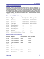
PROGRAMMABLE REGISTERS
Each interrupt controller includes four initialization registers, three control registers, and
three status registers. The I/O port addressing for the interrupt controllers is given in the
31
4. Interrupt Controller
following table. The base address of the master interrupt controller is 20h and the base
address of the slave interrupt controller is A0h.
Interrupt Controller Register Addressing
Address
Register
Operation
Base+0h
IRR, ISR, IPR
Read
Base+0h
ICW1
Write
Base+0h
OCW2, OCW3
Write
Base+1h
OCW1
Read/Write
Base+1h
ICW2, ICW3, ICW4
Write
32
4. Interrupt Controller
IR0
TIMER / COUNTER 0
STD BUS INTRQ1*
0
KEYBOARD CONTROLLER
1
IR1
SYSTEM REGISTER 3
(PORT 7D BIT 1)
IR2
SERIAL PORT COM2
IR3
SERIAL PORT COM1
IR4
INT
TO CPU
MULTIPROCESSING
1
STD BUS INTRQ4*
IR5
J2 PIN 6
W17
0
STD BUS INTRQ2*
LOCAL FLOPPY
J2 PIN 8
1
1
IR6
SYSTEM REGISTER 0
(PORT 7B BIT 0)
1284 PARALLEL
W18
1
IR7
J2 PIN 10
W19
PARALLEL I/O
1
REAL TIME CLOCK
SERIAL PORT COM4
1
IR9
STD BUS INTRQ*
W21
TIMER/COUNTER 1
IR10
TIMER/COUNTER 2
IR11
INT
IR12
DMA CONTROLLER
SERIAL PORT COM3
1
IR13
MATH COPROCESSOR
STD BUS INTRQ3*
IDE CONTROLLER
IR8
W20
W22
0
1
IR14
SYSTEM REGISTER 3
(PORT 7B BIT 6)
WATCHDOG STAGE 1
IR15
Interrupt Architecture
33
4. Interrupt Controller
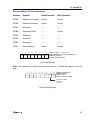
Interrupt Architecture Initialization Registers (ICW1-ICW4)
Each interrupt controller must be initialized before it is used. Initialization consists of
writing two, three, or four initialization commands. The programming sequence for these
registers is given in the "Interrupt Initialization Programming" figure below. ICW1, ICW2,
and ICW3 must be programmed during each initialization sequence. ICW4 may or may
not be programmed, as required by the application.
ICW1
BASE ADDRESS +0
ICW2
BASE ADDRESS +1
ICW3
BASE ADDRESS +1
NO
ICW1 BIT0=1
YES
ICW4
BASE ADDRESS +1
INITIALIZATION
COMPLETE
Interrupt Initialization Programming
7
6
5
4
3
2
1
0
0
0
0
1
LTIM
0
0
1
Register : ICW1
Address: Base+1
Access:Write
Input Trigger
0 Edge Triggered
1 Level triggered
Initialization Register ICW1
34
4. Interrupt Controller
7
5
6
4
3
Vector
2
1
0
0
0
0
Register: ICW2
Address: Base+1
Access: Write
Vector Pointer
Upper 5 bits of pointer
Initialization Register ICW2
7
6
5
4
3
2
1
0
0
0
0
0
0
1
0
0
Register: Master ICW3
Address: Base + 1
Access: Write
Master Initialization Register ICW3
7
6
5
4
3
2
1
0
0
0
0
0
0
0
1
0
Register: Slave ICW3
Address: Base + 1
Access: Write
Slave Initialization Register ICW3
7
6
5
0
0
0
4
SFNM
3
2
1
0
0
0
AEOI
1
Register: ICW4
Address: Base+1
Access:Write
End of interrupt
0 Normal
1 Automatic
Nesting mode
0 Standard
1 Special
Initialization Register ICW4
35
4. Interrupt Controller
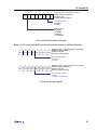
Operational Registers (OCW1-OCW3)
The operation of each interrupt controller is managed by three 8-bit operational
registers. These registers are programmed in any sequence for things such as enabling
and disabling interrupt requests and changing interrupt priorities.
7
5
6
4
3
2
1
0
Register: OCW1
Input Mask
Address: Base + 1
Access: Read and Write
Interrupt mask
0 Reset
1 Set
Operational Register OCW1
7
6
5
4
3
0
0
2
1
0
Register: OCW2
Mode
Level
Address: Base + 0
Access: Write
Interrupt level
000 IR0
001 IR1
010 IR2
011 IR3
100 IR4
101 IR5
110 IR6
111 IR7
Operational mode
End of Interrupt
001 Non-specific
011 Specific
Automatic Rotation
101 Rotate on non-specific
100 Rotate on automatic (set)
000 Rotate on automatic (reset)
Specific Rotation
111 Rotate on specific
110 Set priority level
No Operation
010 Do not use
Operational Register OCW2
36
4. Interrupt Controller
7
5
6
4
3
2
0
1
P
1
0
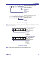
Register: OCW3
SMM
0
SLCT
Address: Base + 0
Access: Write
Read Register
00 Do not use
01 Do not use
10 Select IR register
11 Select IS register
Poll Command
0 No poll
1 Poll
Mask Selection
00 Do not use
01 Do not use
10 Standard mask
11 Special mask
Operational Register OCW3
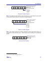
Status Registers (IRR, ISR, IPR)
Each interrupt controller includes three status registers. A status register is selected by
programming the first three bits of OCW3.
7
5
6
4
3
2
1
0
Register: IRR
Request
Address: Base + 0
Access: Read
Input Request Pending
0 No
1 Yes
Status Register IRR
7
6
5
4
3
2
1
0
Service
Register: ISR
Address: Base + 0
Access: Read
Input In Service
0 No
1 Yes
Status Register ISR
37
4. Interrupt Controller
7
6
5
4
3
IR
0
0
0
0
2
1
0
Active
Register: IPR
Address: Base + 0
Access: Read
Highest Active Request
000 IR0
001 IR1
010 IR2
011 IR3
100 IR4
101 IR5
110 IR6
111 IR7
Interrupt
0 No Interrupt present
1 Interrupt present
Status Register IPR
ADDITIONAL INFORMATION
Refer to the Ziatech Industrial Computer System Manual for more information on the
operating system's use of the interrupt inputs. Refer to the Intel 386 EX data book for
more information on the interrupt controller operating modes.
38
5. COUNTER/TIMERS
The ZT 8904 includes one Intel-compatible 8254 device with a total of three
programmable counter/timers. The counter/timers are useful for software timing loops,
timed interrupts, and periodic interrupts. The major features of the counter/timers are
listed below.
•
Three 16-bit counter/timers
•
Six programmable operating modes
•
Binary and BCD counting
•
Interrupt and polled operation
The counter/timer architecture is illustrated in the "Counter/Timer Architecture" figure
below. In some cases, not all counter/timers are available for application development.
In an MS DOS system, for example, counter/timer 0 generates a periodic system
interrupt and should not be programmed by the application. Please refer to the selected
operating system manual for more information.
TIMER 0
1.19318 MHz
CLK0
OUT0
LOGICAL ONE
INTERRUPT IR0
GATE0
TIMER 1
1.19318 MHz
CLK1
OUT1
LOGICAL ONE
GATE1
INTERRUPT IR10 OR
DMA CHANNEL 0
TIMER 2
1.19318 MHz
CLK2
OUT2
LOGICAL ONE
GATE2
INTERRUPT IR11 OR
DMA CHANNEL 1
Counter/Timer Architecture
39
5. Counter/Timers
The six programmable operating modes are summarized in the "Counter/Timer
Operating Modes" table following.
Counter/Timer Operating Modes
Mode
Counter/Timer Output Operation
0
Transitions after programmed count expires
Gate tied high to enable counting
1
Transitions after programmed count expires
Gate tied high to enable counting
2
Periodic single pulse after programmed count expires
Gate tied high to enable counting
3
Square wave with frequency equal to programmed count
Gate tied high to enable counting
4
Single pulse after programmed count expires
Gate tied high to enable counting
5
Single pulse after programmed count expires
Gate tied high to enable counting
40
5. Counter/Timers
PROGRAMMABLE REGISTERS
The counter/timers are accessed through four I/O addresses as shown in the following
table. Each counter/timer occupies an I/O port address through which the preset count
values are written and both the count and status information is read. The Control
register occupies the remaining I/O port address, which services all three
counter/timers.
Counter/Timer Register Addressing
Address
Register
Operation
0040h
Channel 0 Count
Read/Write
0040h
Channel 0 Status
Read
0041h
Channel 1 Count
Read/Write
0041h
Channel 1 Status
Read
0042h
Channel 2 Count
Read/Write
0042h
Channel 2 Status
Read
0043h
Control
Write
Count Registers and Count Latch
Each counter/timer has a 16-bit Count register and count latch. Data is transferred to
the counter/timers through the Count register and from the counter/timers through the
count latch. The Control register defines the method for accessing the 16-bit Count
register through an 8-bit I/O port.
7
6
5
4
3
2
1
0
Register: Count High
Address: 40h + Channel
Access: Read and Write
High Byte
Count Register High Byte
7
6
5
4
3
Low Byte
2
1
0
Register: Count Low
Address: 40h + Channel
Access: Read and Write
Count Register Low Byte
41
5. Counter/Timers
Status Register
Each counter/timer has a Status register. The Status register must be read using the
multiple latch command specified in the Control register.
7
6
OUTPUT NULCNT
5
4
Access
3
2
Mode
1
0
Register: Status
BCD Address: 40h + Channel
Access: Write
Count Format
0 Binary
1 BCD
Operating Mode
000 Terminal count interrupt (Mode 0)
001 Retriggerable one-shot (Mode 1)
010 Rate generator (Mode 2)
011 Square wave generator (Mode 3)
100 Software strobe (Mode 4)
101 Hardware strobe (Mode 5)
110 Same as "010"
111 Same as "011"
Access Mode
00 Count latch command
01 Low byte only
10 High byte only
11 Low byte followed by high byte
Count Status
0 latest count written to the counter was loaded
1 a count was written to the counter but not yet loaded
Output Status
0 OUTn is low
1 OUTn is high
Status Register
42
5. Counter/Timers
Control Register
The Control register is used to initialize the counter/timers and to select the method of
reading the count and status information. The Control register is best described by
dividing it into three formats as illustrated below.
7
5
6
Select
4
3
2
1
0
Register: General Control
Access
Mode
BCD
Address: 43h
Access: Write
Count Format
0 Binary
1 BCD
Operating Mode
000 Terminal count interrupt
001 Retriggerable one-shot
010 Rate generator
011 Square wave generator
100 Software strobe
101 Hardware strobe
110 Same as "010"
111 Same as "011"
Access Mode
00 Count latch command
01 Low byte only
10 High byte only
11 Low byte followed by high byte
Select Counter
00 Counter 0
01 Counter 1
10 Counter 2
11 Read back
General Control Register
7
6
Counter
5
4
3
2
1
0
0
0
0
0
0
0
Register: Count Latch Control
Address: 43h
Access: Write
Counter Latched
00 Counter 0
01 Counter 1
10 Counter 2
11 Read back
Count Latch Control Register
43
5. Counter/Timers
7
6
1
1
5
4
3
2
1
CTL STL CT2 CT1 CT0
0
0
Register: Multiple Latch Control
Address: 43h
Access: Write
Counter Selection
001 Counter 0
010 Counter 1
100 Counter 2
Status Latch
0 Enabled
1 Disabled
Control Latch
0 Enabled
1 Disabled
Multiple Latch Control Register
ADDITIONAL INFORMATION
Refer to the Ziatech Industrial Computer System Manual for more information on the
operating system's use of the counter/timers. Refer to the Intel 386 EX data book for
more information on the counter/timer operating modes.
44
6. DMA CONTROLLER
The DMA controller used on the ZT 8904 is contained within the 386 EX
microprocessor. It improves system operation by allowing external or internal
peripherals to directly transfer data to or from ZT 8904 memory. The DMA controller can
transfer data between memory and I/O with 8-bit or 16-bit data path widths. It has
features that are not available on an 8237A, and it can be configured to operate in an
8237A-compatible mode.
The DMA controller contains two identical, independently configurable channels. One of
the following peripherals can request DMA service:
•
A 386 EX external peripheral (connected to the DRQ0 or DRQ1 pins)
•
A 386 EX internal peripheral (asynchronous serial I/O, synchronous serial I/O, or
counter/timer unit)
The DMA configuration register (DMACFG) is used to select one of the possible
sources. In addition to these hardware request sources, each channel contains a
software request register that can be used to initiate transfers. Both channels share a
common end-of-process signal. The major features of the DMA architecture are listed
below.
•
One STD bus/local DMA channel (Channel 0)
•
One local DMA channel (Channel 1)
•
STD bus DMA slave support
•
Buffer transfer processes:
– Single buffers
– Autoinitialized buffers
– Chained buffers
•
Buffer transfer modes supported:
– Single mode
– Block mode
– Demand mode
•
DMA transfers over the full local memory range
INTEL 386 EX INTERNAL ARCHITECTURE
The 386 EX DMA controller internal architecture is illustrated in the "386 EX Internal
DMA Controller Connections" figure following. This figure details all of the DRQ source
45
6. DMA Controller
connections internal to the 386 EX. Note that the synchronous serial channel is not
implemented on the ZT 8904 in favor of providing an additional asynchronous serial
channel.
Channel 0 supports the following devices as DRQ sources (DMACFG.6-4).
•
External DMA slave request
•
COM1 receive buffer full
•
COM2 transmit buffer empty
•
Timer/Counter unit 1 OUT1
Channel 1 supports the following devices as DRQ sources (DMACFG.2-0).
•
Local floppy disk (PC87303 internal floppy controller)
•
Local IEEE-1284 (PC87303 internal parallel port)
•
COM2 receive buffer full
•
COM1 transmit buffer empty
•
Counter/Timer unit 2 OUT2
DMA Configuration
Register
DRQ0
Com1 Receiver
Com2 Transmitter
SSIO Transmitter
TCU Counter 1
DMA Channel 0
DREQ0
DMA Configuration
Register
DMA Channel 1
DRQ1
Com2 Receiver
Com1 Transmitter
SSIO Receiver
TCU Counter 2
DREQ1
DACK0#
(pin mux)
DACK0
DACK1
S
y
s
t
e
m
B
u
s
EOP#
(pin mux)
DACK1#
(pin mux)
386 EX Internal DMA Controller Connections
46
6. DMA Controller
DMA IMPLEMENTATION
The ZT 8904 DMA architecture external to the 386 EX is illustrated in the following
figure, "DMA Architecture." The ZT 8904 supports a single DMA channel for STD bus
DMA slaves. STD bus DMA slaves are I/O devices that use the ZT 8904 DMA channel
0 to transfer data between backplane I/O and ZT 8904 local memory. The ZT 8904
supports the use of both DMA channels for specific 386 EX internal peripherals.
The two DMA channels supported by the ZT 8904 are implemented in the 386 EX by
multiplexing multiple functions onto device pins. This causes mutual exclusion in the
use of certain hardware functions. Pins with shared functions are shown in the following
figure, "DMA Architecture." Note that DRQ1 and /DAK1 are shared with RXD1 and
TXD1.
These shared functions prevent using COM 2 while DMA channel 1 is used. If DMA
channel 0 is used but DMA channel 1 is not, COM 2 can be used, but only as a 3-wire
interface (useful if the serial channel is capable of in-band flow control). Conversely, if
COM 2 is used with hardware handshaking, neither DMA channel can be used.
The Ziatech industrial BIOS setup utility supports configuration of the ZT 8904 for either
DMA support (floppy) or for COM 2 support. When the ZT 8904 is configured for COM2
with hardware handshake, the BIOS setup option for COM2 must be set as
"ONBOARD." Note that although the 386 EX supports use of /EOP as an input, the
ZT 8904 implementation does not support buffer termination on assertion of /EOP.
Specific jumper selections (W24-27) are required in order to properly configure the
ZT 8904 to support DMA channel 0 or channel 1. These jumper selections are listed in
Appendix A, "Jumper Configurations."
47
6. DMA Controller
16
EOP
R84 1
VCC
U18C
2
RESSM-04751
4
1
W24
JPRX3
ICPSMCI-74FCT540Q
BUSRQ*
/ BRQ_DST
1
U43
4
U18B
3
17
1
W25
JPRX3
2
ICPSMCI-7S32F
3
2
113
117
2
ICPSMCI-74FCT540Q
128
/ BUSAK
3
LPT_DRQ
1
R80
2
VCC
RESSM-04751
/ LPT_DAK
3
W26
JPRX3
2
W27
JPRX3
EOP/CT51
3
1
118
112
DRQ0/DCD1
DAK0/CS5
DRQ1/RXD1
DAK1/TXD1
1
2
ICP5MCI-386EX
CT51
DCD1
RXD1
TXD1
DMA Architecture
DMA TRANSFER CYCLES
The ZT 8904 supports DMA channel 0 as a channel for backplane DMA slaves.
Channel 0 must be programmed using two-cycle bus transfers. This causes at least two
separate bus cycles to occur for each DMA data transfer. DMA channel 1 is supported
for local devices. Channel 1 can be programmed using either fly-by or two-cycle
transfers.
I/O MAPPING
The 386 EX maps the DMA controller into the standard PC-AT I/O locations for DMA
channel 0 and channel 1. The "386 EX DMA Controller Registers" table lists I/O
addresses of the DMA controller registers. The Ziatech STD-DOS BIOS provides
support for the Ziatech ZT 8954 floppy subsystem. All application software must either
communicate with the floppy subsystem through the system BIOS or be coded to
access the correct addresses in the DMA controller I/O map.
DMA CONTROLLER OPERATION
The 386 EX DMA controller transfers data between a requester and a target. The data
can be transferred either from a requester to a target or from a target to a requester.
The target and requester can be located in either memory or I/O space, and transfers
can be on either a byte or a word basis. The requester can be an external device
(located in external I/O) an internal peripheral (located in internal I/O), or memory.
48
6. DMA Controller
An external device or an internal peripheral requests service by activating a channel’s
request input (DRQn). A requester in memory requests service through the DMA
software request register. The requester either transfers data to or retrieves data from
the target.
Programming a DMA Channel
A channel is programmed by writing to a set of registers including requester address,
target address, byte count, and control registers. The address registers specify base
addresses for the target and requester. The byte count registers specify the number of
bytes that need to be transferred to or from the target.
Typically, a channel is programmed to transfer a block of data. Therefore, it is
necessary to distinguish between the process of transferring one byte or word of data
(data transfer) and the process of transferring an entire block of data (buffer transfer).
The byte count determines the number of data transfers that make up a buffer transfer.
After each data transfer within a buffer transfer, the byte count is decremented by 1 and
the requester and target addresses are either incremented, decremented, or left
unchanged. When the byte count expires (reaches -1) the transfer is complete and the
number of bytes transferred is the original byte count +1.
Fly-By and Two-Cycle Bus Cycles
There are two bus cycle options for data transfers, fly-by and two-cycle. Fly-by allows
data transfers to occur in one bus cycle. However, it requires that the requester be in
I/O external to the 386 EX and the target be in memory. The two-cycle option allows
data to be transferred between any combination of memory and I/O through the use of a
4-byte temporary buffer.
The fly-by option performs either a memory write or a memory bus cycle. A write cycle
transfers data from the requester to the target (memory), and a read cycle transfers
data from the target (memory) to the requester. The requester should monitor the bus
cycle signals to determine when to access the data bus.
The two-cycle option first fills the four-byte temporary buffer with data from the source,
then writes that data to the destination. This method allows transfers between any
combination of memory and I/O with any combination of data path widths (8- or 16-bit).
The amount of data and the data bus widths determine the number of bus cycles
required to transfer the data. For example, it takes six bus cycles to transfer four pieces
of data from an 8-bit source to a 16-bit destination: four read cycles to fill the temporary
buffer from the 8-bit source, and two write cycles to transfer the data to the 16-bit
destination. The programmable DMA transfer direction determines whether the
requester or the target is the source or destination.
49
6. DMA Controller
386 EX DMA CONTROLLER REGISTERS
The "386 EX DMA Controller Registers" table below lists the registers associated with
the DMA controller.
The following sections provide bit-level definitions for all registers associated with the
DMA controller. Bit definitions in this section assume intended use of one or more DMA
channels. Note that the reset state, if defined, is the hardware reset state.
The reset state bit definitions include:
0
is a bit that is set to a logical 0 by a hardware reset.
1
is a bit that is set to a logical 1 by a hardware reset.
---
is a bit that is reserved, write a ‘0’ to these bits.
ND
is a bit whose reset state is not defined after a hardware reset.
Any bit described as ‘Reserved’ should be written with a 0 (unless otherwise indicated.)
386 EX DMA Controller Registers
Register
Address
Expanded Address PC/AT Description
PINCFG
0F826h
---
Pin mux configuration
DMACFG
0F830h
---
Peripheral connections and mask
DMA0REQ0
0F010h
---
Channel 0 requestor address 0-7
DMA0REQ1
0F010h
---
Channel 0 requestor address 8-15
DMA0REQ2
0F011h
---
Channel 0 requestor address 16-23
DMA0REQ3
0F011h
---
Channel 0 requestor address 24-25
DMA1REQ0
0F012h
---
Channel 1 requestor address 0-7
DMA1REQ1
0F012h
---
Channel 1 requestor address 8-15
DMA1REQ2
0F013h
---
Channel 1 requestor address 16-23
DMA1REQ3
0F013h
---
Channel 1 requestor address 24-25
386 EX DMA Controller Registers table (continued)
DMA0TAR0
0F000h
0000h
Channel 0 target address 0-7
DMA0TAR1
0F000h
0000h
Channel 0 target address 8-15
DMA0TAR2
0F087h
0087h
Channel 0 target address 16-23
50
6. DMA Controller
DMA0TAR3
0F086h
---
Channel 0 target address 24-25
DMA1TAR0
0F002h
0002h
Channel 1 target address 0-7
DMA1TAR1
0F002h
0002h
Channel 1 target address 8-15
DMA1TAR2
0F083h
0083h
Channel 1 target address 16-23
DMA1TAR3
0F085h
---
Channel 1 target address 24-25
DMA0BYC0
0F001h
0001h
Channel 0 byte count 0-7
DMA0BYC1
0F001h
0001h
Channel 0 byte count 8-15
DMA0BYC2
0F098h
---
Channel 0 byte count 16-23
DMA1BYC0
0F003h
0003h
Channel 1 byte count 0-7
DMA1BYC1
0F003h
0003h
Channel 1 byte count 8-15
DMA1BYC2
0F099h
---
Channel 1 byte count 16-23
DMASTS
0F008h
0008h
DMA status register
DMACMD1
0F008h
0008h
DMA command register 1
DMACMD2
0F01Ah
---
DMA command register 2
DMAMOD1
0F00Bh
000Bh
DMA mode register 1
DMAMOD2
0F01Bh
---
DMA mode register 2
DMASRR
0F009h
0009h
DMA software request register
DMAMSK
0F00Ah
000Ah
DMA single channel mask register
DMAGRPMSK
0F00Fh
000Fh
DMA group channel mask
DMABSR
0F018h
---
DMA bus size register
DMACHR
0F019h
---
DMA chaining register
DMAIEN
0F01Ch
---
DMA interrupt enable register
DMAIS
0F019h
---
DMA interrupt status register
DMAOVFE
0F01Dh
---
DMA overflow enable register
Pin Mux Configuration
The PINCFG register is used to connect /EOP and /DACK1 to the package pins.
51
6. DMA Controller
D7
D6
D5
D4
D3
D2
D1
D0
0
0
0
0
0
0
0
0
REGISTER: PINCFG Pin mux configuration
EXP ADDRESS: 0F826h
AT ADDRESS: --ACCESS: R/W
Must be written with a 1
Must be written with a 1
1= connect TXD1 to the package pin
0= connect /DACK1 to the package pin (required for DMA operation)
1= connect /CTS1 to the package pin
0= connect /EOP to the package pin (required for DMA operation)
Must be written with a 0
Must be written with a 0
Must be written with a 0
Reserved
PINCFG Register
52
6. DMA Controller
Peripheral Connections and Mask
The DMACFG register is used to select of the hardware DRQ sources for each channel
and to mask the /DACKn signals at their pins when using internal requesters.
D7
D6
0
D5
D4
0
D3
D2
0
D1
D0
REGISTER: DMACFG Peripheral connections and mask
EXP ADDRESS: 0F830h
AT ADDRESS: --ACCESS: R/W
0
Channel 0 DRQ pin to DRQ0
000= Connect external channel 0 DRQ pin to DRQ0
001= Connect SIO channel 0 receive buffer full signal to DRQ0
010= Connect SIO channel 1 transmit buffer empty signal to DRQ0
011= Connect SSIO transmit holding buffer empty signal to DRQ0
100= Connect TCU counter 1 OUT1 to DRQ0
101= Reserved
110= Reserved
111= Reserved
1= Mask channel 0 external acknowledge
0= Enable channel 0 external acknowledge
Channel 1 DRQ connection
000= Connect external channel 1 DRQ pin to DRQ1
001= Connect SIO channel 1 receive buffer full signal to DRQ1
010= Connect SIO channel 0 transmit buffer empty signal to DRQ1
011= Connect SSIO receive holding buffer full signal to DRQ1
100= Connect TCU counter 2 OUT2 to DRQ1
101= Reserved
110= Reserved
111= Reserved
1= Mask channel 1 external acknowledge
0= Enable channel 1 external acknowledge
DMACFG Register
Channel 0 Requestor Address Registers
D7
D6
D5
D4
D3
ND ND ND ND ND
D2
D1
D0
ND ND ND
REGISTER: DMA0REQ0 Channel 0 requestor address bits 0-7
EXP ADDRESS: 0F010h
AT ADDRESS: --ACCESS: R/W, BP = 0
Channel 0 requestor address bit 0
Channel 0 requestor address bit 1
Channel 0 requestor address bit 2
Channel 0 requestor address bit 3
Channel 0 requestor address bit 4
Channel 0 requestor address bit 5
Channel 0 requestor address bit 6
Channel 0 requestor address bit 7
Channel 0 Requestor Address Bits 0-7
53
6. DMA Controller
D7
D6
D5
D4
D3
ND ND ND ND ND
D2
D1
D0
ND ND ND
REGISTER: DMA0REQ1 Channel 0 requestor address bits 8-15
EXP ADDRESS: 0F010h
AT ADDRESS: --ACCESS: R/W, BP = 1
Channel 0 requestor address bit 8
Channel 0 requestor address bit 9
Channel 0 requestor address bit 10
Channel 0 requestor address bit 11
Channel 0 requestor address bit 12
Channel 0 requestor address bit 13
Channel 0 requestor address bit 14
Channel 0 requestor address bit 15
Channel 0 Requestor Address Bits 8-15
D7
D6
D5
D4
D3
ND ND ND ND ND
D2
D1
D0
ND ND ND
REGISTER: DMA0REQ2 Channel 0 requestor address bits 16-23
EXP ADDRESS: 0F011h
AT ADDRESS: --ACCESS: R/W, BP = 0
Channel 0 requestor address bit 16
Channel 0 requestor address bit 17
Channel 0 requestor address bit 18
Channel 0 requestor address bit 19
Channel 0 requestor address bit 20
Channel 0 requestor address bit 21
Channel 0 requestor address bit 22
Channel 0 requestor address bit 23
Channel 0 Requestor Address Bits 16-23
D7
D6
D5
D4
Reserved
D3
D2
D1
D0
ND ND
REGISTER: DMA0REQ3 Channel 0 requestor address bits 24-25
EXP ADDRESS: 0F011h
AT ADDRESS: --ACCESS: R/W, BP = 1
Channel 0 requestor address bit 24
Channel 0 requestor address bit 25
Reserved
Channel 0 Requestor Address Bits 24-25
54
6. DMA Controller
Channel 1 Requestor Address Registers
D7
D6
D5
D4
D3
ND ND ND ND ND
D2
D1
D0
ND ND ND
REGISTER: DMA1REQ0 Channel 1 requestor address bits 0-7
EXP ADDRESS: 0F012h
AT ADDRESS: --ACCESS: R/W, BP = 0
Channel 1 requestor address bit 0
Channel 1 requestor address bit 1
Channel 1 requestor address bit 2
Channel 1 requestor address bit 3
Channel 1 requestor address bit 4
Channel 1 requestor address bit 5
Channel 1 requestor address bit 6
Channel 1 requestor address bit 7
Channel 1 Requestor Address Bits 0-7
D7
D6
D5
D4
D3
ND ND ND ND ND
D2
D1
D0
ND ND ND
REGISTER: DMA1REQ1 Channel 1 requestor address bits 8-15
EXP ADDRESS: 0F012h
AT ADDRESS: --ACCESS: R/W, BP = 1
Channel 1 requestor address bit 8
Channel 1 requestor address bit 9
Channel 1 requestor address bit 10
Channel 1 requestor address bit 11
Channel 1 requestor address bit 12
Channel 1 requestor address bit 13
Channel 1 requestor address bit 14
Channel 1 requestor address bit 15
Channel 1 Requestor Address Bits 8-15
55
6. DMA Controller
D7
D6
D5
D4
D3
ND ND ND ND ND
D2
D1
D0
ND ND ND
REGISTER: DMA1REQ2 Channel 1 requestor address bits 16-23
EXP ADDRESS: 0F013h
AT ADDRESS: --ACCESS: R/W, BP = 0
Channel 1 requestor address bit 16
Channel 1 requestor address bit 17
Channel 1 requestor address bit 18
Channel 1 requestor address bit 19
Channel 1 requestor address bit 20
Channel 1 requestor address bit 21
Channel 1 requestor address bit 22
Channel 1 requestor address bit 23
Channel 1 Requestor Address Bits 16-23
D7
D6
D5
D3
D4
D2
Reserved
D1
D0
ND ND
REGISTER: DMA1REQ3 Channel 1 requestor address bits 24-25
EXP ADDRESS: 0F013h
AT ADDRESS: --ACCESS: R/W, BP = 1
Channel 0 requestor address bit 24
Channel 0 requestor address bit 25
Reserved
Channel 1 Requestor Address Bits 24-25
Channel 0 Target Address Registers
D7
D6
D5
D4
D3
ND ND ND ND ND
D2
D1
D0
ND ND ND
REGISTER: DMA0TAR0 Channel 0 target address bits 0-7
EXP ADDRESS: 0F000h
AT ADDRESS: 0000h
ACCESS: R/W, BP = 0
Channel 0 target address bit 0
Channel 0 target address bit 1
Channel 0 target address bit 2
Channel 0 target address bit 3
Channel 0 target address bit 4
Channel 0 target address bit 5
Channel 0 target address bit 6
Channel 0 target address bit 7
Channel 0 Target Address Bits 0-7
56
6. DMA Controller
D7
D6
D5
D4
D3
ND ND ND ND ND
D2
D1
D0
ND ND ND
REGISTER: DMA0TAR1 Channel 0 target address bits 8-15
ADDRESS: 0F000h
AT ADDRESS: 0000h
ACCESS: R/W, BP = 1
Channel 0 target address bit 8
Channel 0 target address bit 9
Channel 0 target address bit 10
Channel 0 target address bit 11
Channel 0 target address bit 12
Channel 0 target address bit 13
Channel 0 target address bit 14
Channel 0 target address bit 15
Channel 0 Target Address Bits 8-15
D7
D6
D5
D4
D3
ND ND ND ND ND
D2
D1
D0
ND ND ND
REGISTER: DMA0TAR2 Channel 0 target address bits 16-23
ADDRESS:
0F087h
AT ADDRESS: 0087h
ACCESS:
R/W
Channel 0 target address bit 16
Channel 0 target address bit 17
Channel 0 target address bit 18
Channel 0 target address bit 19
Channel 0 target address bit 20
Channel 0 target address bit 21
Channel 0 target address bit 22
Channel 0 target address bit 23
Channel 0 Target Address Bits 16-23
D7
D6
D5
D4
Reserved
D3
D2
D1
D0
ND
ND
REGISTER: DMA0TAR3 Channel 0 target address bits 24-25
ADDRESS:
0F086h
AT ADDRESS: --R/W
ACCESS:
Channel 0 target address bit 24
Channel 0 target address bit 25
Reserved
Channel 0 Target Address Bits 24-25
57
6. DMA Controller
Channel 1 Target Address Registers
D7
D6
D5
D4
D3
ND ND ND ND ND
D2
D1
D0
ND ND ND
REGISTER: DMA1TAR0 Channel 1 target address bits 0-7
ADDRESS: 0F002h
AT ADDRESS: 0002h
ACCESS: R/W, BP = 0
Channel 1 target address bit 0
Channel 1 target address bit 1
Channel 1 target address bit 2
Channel 1 target address bit 3
Channel 1 target address bit 4
Channel 1 target address bit 5
Channel 1 target address bit 6
Channel 1 target address bit 7
Channel 1 Target Address Bits 0-7
D7
D6
D5
D4
D3
ND ND ND ND ND
D2
D1
D0
ND ND ND
REGISTER: DMA1TAR1 Channel 1 target address bits 8-15
ADDRESS: 0F002h
AT ADDRESS: 0002h
ACCESS: R/W, BP = 1
Channel 1 target address bit 8
Channel 1 target address bit 9
Channel 1 target address bit 10
Channel 1 target address bit 11
Channel 1 target address bit 12
Channel 1 target address bit 13
Channel 1 target address bit 14
Channel 1 target address bit 15
Channel 1 Target Address Bits 8-15
58
6. DMA Controller
D7
D6
D5
D3
D4
ND ND ND ND ND
D2
D1
D0
ND ND ND
REGISTER: DMA1TAR2 Channel 1 target address bits 16-23
ADDRESS: 0F083h
AT ADDRESS: 0083h
ACCESS: R/W
Channel 1 target address bit 16
Channel 1 target address bit 17
Channel 1 target address bit 18
Channel 1 target address bit 19
Channel 1 target address bit 20
Channel 1 target address bit 21
Channel 1 target address bit 22
Channel 1 target address bit 23
Channel 1 Target Address Bits 16-23
D7
D6
D5
D3
D4
D2
Reserved
D1
D0
ND ND
REGISTER: DMA1TAR3 Channel 1 target address bits 24-25
ADDRESS: 0F085h
AT ADDRESS: --ACCESS: R/W
Channel 1 target address bit 24
Channel 1 target address bit 25
Reserved
Channel 1 Target Address Bits 24-25
Channel 0 Byte Count Registers
D7
D6
D5
D4
D3
ND ND ND ND ND
D2
D1
D0
ND ND ND
REGISTER: DMA0BYC0 Channel 0 byte count bits 0-7
EXP ADDRESS: 0F001h
AT ADDRESS: 0001h
ACCESS: R/W, BP = 0
Channel 0 byte count bit 0
Channel 0 byte count bit 1
Channel 0 byte count bit 2
Channel 0 byte count bit 3
Channel 0 byte count bit 4
Channel 0 byte count bit 5
Channel 0 byte count bit 6
Channel 0 byte count bit 7
Channel 0 Byte Count Bits 0-7
59
6. DMA Controller
D7
D6
D5
D4
D3
ND ND ND ND ND
D2
D1 D0
ND ND ND
REGISTER: DMA0BYC1 Channel 0 byte count bits 8-15
ADDRESS: 0F001h
AT ADDRESS: 0001h
ACCESS: R/W, BP = 1
Channel 0 byte count bit 8
Channel 0 byte count bit 9
Channel 0 byte count bit 10
Channel 0 byte count bit 11
Channel 0 byte count bit 12
Channel 0 byte count bit 13
Channel 0 byte count bit 14
Channel 0 byte count bit 15
Channel 0 Byte Count Bits 8-15
D7
D6
D5
D4
D3
ND ND ND ND ND
D2
D1
D0
ND ND ND
REGISTER: DMA0BYC2 Channel 0 byte count bits 16-23
ADDRESS: 0F098h
AT ADDRESS: --ACCESS: R/W
Channel 0 byte count bit 16
Channel 0 byte count bit 17
Channel 0 byte count bit 18
Channel 0 byte count bit 19
Channel 0 byte count bit 20
Channel 0 byte count bit 21
Channel 0 byte count bit 22
Channel 0 byte count bit 23
Channel 0 Byte Count Bits 16-23
60
6. DMA Controller
Channel 1 Byte Count Registers
D7
D6
D5
D4
D3
ND ND ND ND ND
D2
D1
D0
ND ND ND
REGISTER: DMA1BYC0 Channel 1 byte count bits 0-7
ADDRESS: 0F0023
AT ADDRESS: 0003h
ACCESS: R/W, BP = 0
Channel 1 byte count bit 0
Channel 1 byte count bit 1
Channel 1 byte count bit 2
Channel 1 byte count bit 3
Channel 1 byte count bit 4
Channel 1 byte count bit 5
Channel 1 byte count bit 6
Channel 1 byte count bit 7
Channel 1 Byte Count Bits 0-7
D7
D6
D5
D4
D3
ND ND ND ND ND
D2
D1
D0
ND ND ND
REGISTER: DMA1BYC1 Channel 1 byte count bits 8-15
ADDRESS: 0F003h
AT ADDRESS: 0003h
ACCESS: R/W, BP = 1
Channel 1 byte count bit 8
Channel 1 byte count bit 9
Channel 1 byte count bit 10
Channel 1 byte count bit 11
Channel 1 byte count bit 12
Channel 1 byte count bit 13
Channel 1 byte count bit 14
Channel 1 byte count bit 15
Channel 1 Byte Count Bits 8-15
61
6. DMA Controller
D7
D6
D5
D4
D3
ND ND ND ND ND
D2
D1
D0
ND ND ND
REGISTER: DMA1BYC2 Channel 1 byte count bits 16-23
ADDRESS: 0F099h
AT ADDRESS: --ACCESS: R/W
Channel 1 byte count bit 16
Channel 1 byte count bit 17
Channel 1 byte count bit 18
Channel 1 byte count bit 19
Channel 1 byte count bit 20
Channel 1 byte count bit 21
Channel 1 byte count bit 22
Channel 1 byte count bit 23
Channel 1 Byte Count Bits 16-23
DMA Status Register
The DMASTS register is used to check channel status individually. The DMA controller
sets bits in this register to indicate that a channel has a hardware request pending or
that a channel’s byte count has expired.
D7
D6
Reserved
D5
D4
0
0
D3
D2
Reserved
D1
D0
0
0
REGISTER: DMASTS
ADDRESS:
0F008h
AT ADDRESS: 0008h
ACCESS:
R/O
DMA status register
1= Channel 0 transfer complete, read this register to clear this bit
0= Transfer not completed
1= Channel 1 transfer complete, read this register to clear this bit
0= Transfer not completed
Reserved
1= Channel 0 has a hardware request pending
0= No hardware request pending for channel 0
1= Channel 1 has a hardware request pending
0= No hardware request pending for channel 1
Reserved
DMA Status Register
62
6. DMA Controller
DMA Command Registers
The DMACMD1 resister is used to enable both channels and to select the rotating
method for changing the bus priority control structure. Under all prioritization schemes,
the DRAM refresh control unit receives highest priority.
D7
D6
D5
Reserved
D4
D3
D2
0
0
0
D1
D0
REGISTER: DMACMD1 DMA command register 1
Reserved ADDRESS: 0F008h
AT ADDRESS: 0008h
ACCESS: W/O
Reserved, write 0's to these bits
1= Enables both DMA channels
0= Disable both DMA channels
Reserved, write 0 to this bit
1= Enable priority rotation
0= Fixed priority
Reserved, write 0's to these bits
DMA Command Register 1
The DMACMD2 register is used to select the type of DRQn and /EOP sampling used,
and to assign a particular bus request to the lowest priority level.
D7
D6
D5
Reserved
D4
D3
D2
0
D1
D0
0
0
REGISTER: DMACMD2 DMA command register 2
ADDRESS: 0F01Ah
AT ADDRESS: --ACCESS: W/O
1= Sample /DRQn synchronously
0= Sample /DRQn asynchronously
1= Sample /EOP synchronously
0= Sample /EOP asynchronously
Low priority level set
00= Assign channel 0's request (DRQ0) to the lowest priority level
01= Assign channel 1's request (DRQ1) to the lowest priority level
10= Assign HOLD to the lowest priority level (RESET state)
11= Reserved
Reserved
DMA Command Register 2
63
6. DMA Controller
DMA Mode Registers
The DMAMOD 1 register is used to select a particular channel's data-transfer mode and
transfer direction, and to enable the channel's auto-initialize buffer-transfer mode. You
can configure the DMA controller to modify the target address during a buffer transfer by
clearing DMAMOD2.2, then use DMAMOD1.3 to specify how the channel modifies the
address.
D7
D6
D5
D4
D3
D2
D1
D0
0
0
0
0
0
0
0
0
REGISTER: DMAMOD1 DMA mode register 1
ADDRESS: 0F00Bh
AT ADDRESS: 000Bh
ACCESS: W/O, D0 specifies channel
1= Bits D7-D2 affect channel 1
0= Bits D7-D2 affect channel 0
Reserved
Transfer direction:
00= target is read, nothing is written (test mode)
01= requestor is read, target is written
10= target is read, requestor is written
11= reserved
1= Auto-initialize channel
0= Do not auto-initialize channel
1= target address decrement
0= target address increment
Data transfer mode:
00= demande mode
01= single transfer mode
10= target is read, requestor is written
11= reserved
DMA Mode Register 1
The DMAMOD2 register is used to select the data transfer bus cycle option, specify
whether the requestor and target are in memory or I/O, and determine whether the DMA
controller will modify the target and requestor addresses.
64
6. DMA Controller
D7
D6
D5
D4
D3
D2
D1
D0
0
0
0
0
0
0
0
0
REGISTER: DMAMOD2 DMA mode register 2
ADDRESS: 0F01Bh
AT ADDRESS: --ACCESS: W/O, D0 specifies channel
1= Bits D7-D2 affect channel 1
0= Bits D7-D2 affect channel 0
Reserved
1= Channel target address hold
0= Channel target address will increment or decrement
1= Channel requestor address decrement
0= Channel requestor address increment
1= Channel requestor address will hold
0= Channel requestor address will increment or decrement
1= Channel target is in I/O space
0= Channel target bit 0 is in memory space
1= Channel target is in I/O space
0= Channel target bit 0 is in memory space
1= Fly-by data transfer (required for backplane ZT 8954 floppy support)
0= Two-cycle data transfer (required for local floppy support)
DMA Mode Register 2
DMA Software Request Register
Use the DMASRR register write format to issue software DMA service requests.
Software requests are subject to bus control priority arbitration with all other software
and hardware requests. A software request activates the internal channel request
signal. This signal remains active until the channel completes its buffer transfer. In the
demand data-transfer mode, a buffer transfer is suspended by deactivating the channel
request signal. Because you cannot deactivate the internal channel request signal
before the end of a buffer transfer, you cannot use software requests with demand datatransfer mode.
Use the DMASRR register (read format) to determine if a software request for a
particular channel is pending.
D7
D6
D5
D4
Reserved
D3
D2
D1
D0
0
0
REGISTER: DMASRR DMA software request register
ADDRESS: 0F009h
AT ADDRESS: 0009h
ACCESS: Read format
1= Channel 0 has a software request pending, read this register to clear
0= No software request pending for channel 0
1= Channel 1 has a software request pending, read this register to clear
0= No software request pending for channel 1
Reserved
DMA Software Request Register
65
6. DMA Controller
DMA Single Channel Mask Register
Use the DMAMSK register to enable or disable hardware requests for one channel at a
time.
D7
D6
D5
D4
D3
Reserved
D2
D1
D0
1
0
0
REGISTER: DMAMSK DMA single channel mask register
ADDRESS: 0F00Ah
AT ADDRESS: 000Ah
ACCESS: W/O, D0 specifies channel
1= Bit D2 affects channel 1
0= Bit D2 affects channel 0
Reserved
1= Disable hardware requests for the channel specified by bit D0
0= Enable hardware requests for the channel specified by bit D0
Reserved
DMA Single Channel Mask Register
DMA Group Channel Mask
Use the DMAGRPMSK register to enable or disable hardware requests for both
channels at the same time.
D7
D6
D5
D4
Reserved
D3
D2
D1
D0
1
1
REGISTER: DMAGRPMSK DMA group channel mask
ADDRESS: 0F00Fh
AT ADDRESS: 000Fh
ACCESS: R/W
1= Mask channel 0 hardware requests
0= Unmask channel 0 hardware requests
1= Mask channel 1 hardware requests
0= Unmask channel 1 hardware requests
Reserved
DMA Group Channel Mask
DMA Bus Size Register
The DMABSR register determines the requestor and target data bus widths (8 / 16 bits).
66
6. DMA Controller
D7
D6
D5
D4
1
1
1
1
D3
D2
D1
Reserved
D0
1
REGISTER: DMABSR DMA bus size register
ADDRESS: 0F018h
AT ADDRESS: --ACCESS: W/O, D0 specifies channel
1= Bits D6 and D4 affect channel 1
0= Bits D6 and D4 affect channel 0
Reserved
1= Channel target bus width is 16 bits
0= Channel target bus with is 8 bits
Reserved
1= Channel requestor bus width is 16 bits
0= Channel requestor bus width is 8 bits
Reserved
DMA Bus Size Register
DMA Chaining Register
The DMACHR register is used to enable and disable the chaining buffer-transfer mode
for a selected channel. The following steps describe how to set up a channel to perform
chaining buffers transfers.
1. Set up the chaining interrupt (DMAINT) service routine.
2. Configure the channel for single buffer-transfer mode.
3. Program the mode registers.
4. Program the target address, requestor address, and byte count registers.
5. Enable the channel for the chaining buffer-transfer mode. This activates the chaining
status signal.
6. Enable the DMAINT interrupt and service it. The service routine should load the
transfer information for the next buffer transfer.
7. Enable the channel.
D7
D6
D5
D4
Reserved
D3
D2
D1
D0
1
0
0
REGISTER: DMACHR DMA chaining register
ADDRESS: 0F019h
AT ADDRESS: --ACCESS: W/O, D0 specifies channel
1= Bit D2 affects channel 1
0= Bit D2 affects channel 0
Reserved
1= Enable chaining buffer transfer mode for the channel specified by D0
0= Disable chaining buffer transfer mode for the channel specified by D0
Reserved
DMA Chaining Register
67
6. DMA Controller
DMA Interrupt Enable Register
The DMAIEN register is used to individually connect channel 0 and channel 1’s transfer
complete signal to the ICU’s DMAINT interrupt request input.
D7
D6
D5
D4
D3
D2
D1
D0
1
1
Reserved
REGISTER: DMAIEN DMA interrupt enable register
ADDRESS: 0F01Ch
AT ADDRESS: --ACCESS: R/W
1= Connect channel 0 EOP signal to the ICU DMAINT input
0= Do not connect EOP to ICU
1= Connect channel 1 EOP signal to the ICU DMAINT input
0= Do not connect EOP to ICU
Reserved
DMA Interrupt Enable Register
DMA Interrupt Status Register
DMAIS indicates which source activated the DMA interrupt request signal (channel 0
transfer complete, channel 1 transfer complete, channel 0 chaining, or channel 1
chaining).
D7
D6
Reserved
D5
D4
0
0
D3
D2
Reserved
D1
D0
0
0
REGISTER: DMAIS DMA interrupt status register
ADDRESS: 0F019h
AT ADDRESS: --ACCESS: R/O
1= Indicates that new requestor and target address and count
information should be written to channel 0. This bit is cleared when
new transfer information is written to the channel. Writing to the most
significant bit of the target address clears this bit. Outside chaining
mode, this bit becomes a don't care.
1= Indicates that new requestor and target address and count
information should be written to channel 1. This bit is cleared when
new transfer information is written to the channel. Writing to the most
significant bit of the target address clears this bit. Outside chaining
mode, this bit becomes a don't care.
Reserved
1= Channel 0 has completed a buffer transfer. This bit is set only if bit 0
of the interrupt enable register is set. Clearing bit 0 of the DMA status
register clears this bit. In chaining mode, this bit becomes a don't care.
1= Channel 1 has completed a buffer transfer. This bit is set only if bit 1
of the interrupt enable register is set. Clearing bit 1 of the DMA status
register clears this bit. In chaining mode, this bit becomes a don't care.
Reserved
DMA Interrupt Status Register
68
6. DMA Controller
DMA Overflow Enable Register
Use DMAOVFE to specify whether all 26 bits or only the lower 16 bits of the target and
requestor addresses are incremented or decremented during buffer transfers and
whether all 24 bits of the byte count or only the lower 16 bits of the byte count are
incremented or decremented during buffer transfers. A byte count configured for 16-bit
decrementing expires when it is decremented from 0000h to FFFFh.
D7
D6
D5
Reserved
D4
D3
D2
D1
D0
1
0
1
0
REGISTER: DMAOVFE DMA overflow enable register
ADDRESS: 0F01Dh
AT ADDRESS: --ACCESS: R/W
1= All bits of channel 0 target address and byte count inc/dec
0= Only lower 16 bits of channel 0 target address and byte count inc/dec
1= All bits of channel 0 requestor address inc/dec
0= Only lower 16 bits of channel 0 requestor address inc/dec
1= All bits of channel 1 target address and byte count inc/dec
0= Only lower 16 bits of channel 1 target address and byte count inc/dec
1= All bits of channel 1 requestor address increment/decrement
0= Only lower 16 bits of channel 1 requestor address inc/dec
Reserved
DMA Overflow Enable Register
69
7. REAL-TIME CLOCK
The ZT 8904 includes one Motorola®-compatible 146818 real-time clock. The real-time
clock provides clock and 100-year calendar information in addition to 242 bytes of
CMOS setup static RAM. These functions are battery backed for continuous operation
even in the absence of system power. The RAM is used by the operating system BIOS
to store configuration information. The major features of the real-time clock are listed
below.
•
Timekeeping to a 1 second resolution
•
More than 200 bytes of CMOS setup RAM
•
Leap year compensation
•
Daylight Savings Time compensation
•
Periodic, Alarm, and Update Ended interrupts
•
Battery backed
PROGRAMMABLE REGISTERS
The real-time clock includes 64 register locations. These registers are accessed through
I/O port locations 70h and 71h. A real-time clock register is accessed by first writing the
offset address of the register to I/O port location 70h. Data is then transferred to or from
the register through I/O port location 71h. This sequence must be repeated to read the
same register a second time. The I/O port addressing for the real-time clock is given in
the "Real-Time Clock Register Addressing" table following.
The following topics illustrate the programmable registers for the real-time clock.
70
7. Real-Time Clock
Real-Time Clock Register Addressing
Address
Offset
Function
Range
0h
Time-Seconds
0-59
1h
Alarm-Seconds
0-59
2h
Time-Minutes
0-59
3h
Alarm-Minutes
0-59
4h
Time-Hours (12 hour mode)
1-12
4h
Time-Hours (24 hour mode)
0-23
5h
Alarm-Hours
0-23
6h
Day of Week
1-7
7h
Date of Month
1-31
8h
Month
1-12
9h
Year
0-99
Ah-Dh
Register A-D
----
Eh-3Fh
General Purpose
----
71
7. Real-Time Clock
Register A
7
6
5
4
UIP
0
1
0
3
2
1
Interrupt Rate
0
Register: A
Address: Offset+0Ah
Access: Read and Write
Rate Selection
0000 No Interrupts
0001 3.90625 ms
0010 7.8125 ms
0011 122.070 us
0100 244.141 us
0101 488.281 us
0110 976.562 us
0111 1.953125 ms
1000 3.90625 ms
1001 7.8125 ms
1010 15.625 ms
1011 31.25 ms
1100 62.5 ms
1101 125 ms
1110 250 ms
1111 500 ms
Update In Progress
0 No
1 Yes
Register A
72
7. Real-Time Clock
Register B
7
6
5
4
3
SET
PIE
AIE
UIE
0
1
2
0
Register: B
Address: Offset+0Bh
Access: Read and Write
DM 24/12 DSE
Daylight Savings
0 Disabled
1 Enabled
24-hour/12-hour Operation
0 12-hour mode
1 24-hour mode
Data Mode
0 BCD
1 Binary
Update-End Interrupt
0 Disabled
1 Enabled
Alarm Interrupt Enable
0 Disabled
1 Enabled
Periodic Interrupt Enable
0 Disabled
1 Enabled
Cycle Update
0 Real Time
1 Latch Time
Register B
Register C
7
6
5
4
3
2
1
0
IRQF
PF
AF
UF
0
0
0
0
Register: C
Address: Offset+0Ch
Access: Read
Update Flag
0 No update
1 Update
Alarm Flag
0 No alarm
1 Alarm
Periodic Interrupt Flag
0 No interrupt
1 Interrupt
Interrupt Pending
0 No interrupt
1 Interrupt
Register C
73
7. Real-Time Clock
Register D
7
6
5
4
3
2
1
0
VRT
0
0
0
0
0
0
0
Register: D
Address: Offset+0Dh
Access: Read
Valid RAM
0 Invalid
1 Valid
Register D
ADDITIONAL INFORMATION
Refer to the National Semiconductor PC87306 datasheet for more information on the
real-time clock operating modes. The product folder for the PC87306, including the data
sheet, is available on the web site http://www.national.com/pf/PC/PC87306.html.
74
8. SERIAL CONTROLLER
This chapter discusses operation of the four ZT 8904 serial ports. It provides
descriptions of the two software-configurable serial port registers included on the
ZT 8904.
ZT 8904 SPECIFICS
The ZT 8904 includes four serial ports: two serial ports (COM1 and COM2) compatible
with the 16450/8250, and two serial ports (COM3 and COM4) compatible with the
16550. The ZT 8903 includes only two serial ports, COM1 and COM2. The serial ports
are implemented with a 5 V charge pump technology to eliminate the need for a ±12 V
supply.
The serial ports include a complete set of handshaking and modem control signals,
maskable interrupt generation, and data transfer rates up to 115 Kbaud. Two of the
serial ports are software configured for either RS-232 or RS-485 operation. Several
choices of RS-485 control are available.
The major features of each serial port are listed below.
•
Two RS-232 channels
•
Two RS-232 or RS-485 channels (ZT 8904 and ZT 89CT04 only)
•
Does not require ±12 V
•
Baud rates up to 115 Kbaud
•
Polled and interrupt operation
•
Loopback diagnostics
Architectural differences between the four serial ports on the ZT 8904 and the COM1COM4 serial ports found in a standard PC architecture are discussed in the following
topics.
75
8. Serial Controller
Address Mapping
The address mapping for the PC standard architecture and the ZT 8904 is shown
below.
Serial Channel
PC Port Address ZT 8904 Port Address
COM1
3F8-3FF
3F8-3FF
COM2
2F8-2FF
2F8-2FF
COM3
3E8-3EF
2E0-2E7
COM4
2E8-2EF
2E8-2EF
Interrupt Selection
The interrupt mapping for the PC standard architecture and the ZT 8904 is shown
below. Different interrupt levels for COM3 and COM4 interrupts are selectable through
the interrupt jumper block.
Serial Channel
PC Interrupt
ZT 8904 Interrupt
COM1
IR4
IR4
COM2
IR3
IR3
COM3
IR4
IR13
COM4
IR3
IR9
Handshake Signals
The PC architecture includes Transmit Data (TXD), Receive Data (RXD), Request To
Send (RTS), Clear To Send (CTS), Data Set Ready (DSR), Data Terminal Ready
(DTR), Ring Indicator (RI), and Data Carrier Detect (DCD). The ZT 8904 COM1, COM3,
and COM4 channels include a complete set of PC architecture signals.
The ZT 8904 COM2 channel shares TXD, RXD, CTS, and DCD with DMA channels 0
and 1 as selected with jumpers W24-W27 and COM2 BIOS configuration. The
restrictions imposed by this sharing are that COM2 is not available if printer DMA is
enabled and that COM2 is available without CTS and DCD handshake lines if STD Bus
DMA is enabled (for example, if an STD Bus floppy disk is installed).
76
8. Serial Controller
RS-485 Operation
Two of the serial channels, COM1 and COM2, are software programmable for RS-232
or RS-485 operation. The RS-485 functionality is not available on the ZT 8903. The
software selection is made through bits 2 and 3 of System Register 2. The RS-485
architecture is shown below.
W29
TxD
J1-73
Signal
Condition
J1-72
W13
W28
+
DTR
W12
J1-75
Signal
Condition
RxD
System Register 2
Bit 2
J1-74
COM1 RS-485 Architecture
W31
TxD
J1-78
Signal
Condition
J1-77
W15
W30
+
DTR
W14
RxD
System Register 2
Bit 3
Signal
Condition
J1-80
J1-79
COM2 RS-485 Architecture
Serial Channel Interface
The serial ports are configured as DTE and are available through the 80-pin frontplane
connector (J1). Optional cables convert the serial port interface to standard 9-pin Dshell connectors. The ZT 90200 cable provides the serial interface for the ZT 8904 and
ZT 89CT04. The ZT 90203 provides the serial interface for the ZT 8903. The J1
connector pin assignments are given in the "J1 Peripheral Pinout" table in Appendix B.
77
8. Serial Controller
PROGRAMMABLE REGISTERS
Six registers are available for initializing and controlling each serial channel. The
following table "Serial Controller Register Addressing" shows the I/O port addressing for
the COM1 registers. The remaining serial channels are located as follows:
COM2:
2F8-2FFh
COM3:
2E0-2E7h
COM4:
2E8-2EFh
The topics that follow illustrate the 16-bit divisor latch, baud rate divisors, and the six
programmable registers for each serial channel.
Serial Controller Register Addressing
Address
Register
Operation
03F8h (DIV=0)
Receive Buffer
Read
03F8h (DIV=0)
Transmit Buffer
Write
03F8h (DIV=1)
Divisor Latch LSB
Read/Write
03F9h (DIV=0)
Interrupt Control
Read/Write
03F9h (DIV=1)
Divisor Latch MSB
Read/Write
03FAh
Interrupt Status
Read
03FBh
Line Control
Read/Write
03FCh
Modem Control
Read/Write
03FDh
Line Status
Read
03FEh
Modem Status
Read
03FFh
Reserved
Baud Rate Divisors
The "Divisor Latch LSB" and "Divisor Latch MSB" figures that follow illustrate the 16-bit
divisor latch. The "Baud Rate Divisors" table lists the divisors for popular baud rates. It
also includes the percent error based on the difference between the exact divisor for a
specified baud rate and the divisor obtainable with a 16-bit integer format. To guarantee
proper operation, the percent error should never be greater than four.
78
8. Serial Controller
Baud Rate Divisors
Baud
Rate
Divisor
(dec/hex)
Percent
Error
50
2304/1440h
0
75
1536/960h
0
150
768/480h
0
300
384/240h
0
600
192/120h
0
1200
96/60h
0
1800
64/40h
0
2000
58/3Ah
0.69
2400
48/30h
0
3600
32/20h
0
4800
24/18h
0
7200
16/10h
0
9600
12/Ch
0
19200
6/6h
0
38400
3/3h
0
56000
2/2h
2.86
57600
2/2h
0
115200
1/1h
0
Divisor Latch LSB and MSB
7
D7
6
5
4
3
2
1
0
D6
D5
D4
D3
D2
D1
D0
Register: Divisor Latch LSB
Address: 3F8h DIV=1
Access: Read and Write
Divisor Latch LSB
79
8. Serial Controller
7
6
5
4
3
2
D15
D14
D13
D12
D11
D10
1
0
D9
D8
Register: Divisor Latch MSB
Address: 3F9h DIV=1
Access: Read and Write
Divisor Latch MSB
Interrupt Control Register
7
6
5
4
3
2
1
0
0
0
0
0
MSI
LSI
TBI
RBI
Register: Interrupt Control
Address: 3F9h DIV=0
Access: Read and Write
Receive Buffer Interrupt
0 Disabled
1 Enabled
Transmit Buffer Interrupt
0 Disabled
1 Enabled
Line Status Interrupt
0 Disabled
1 Enabled
Modem Status Interrupt
0 Disabled
1 Enabled
Interrupt Control Register
80
8. Serial Controller
Interrupt Status Register
7
6
5
4
0
0
0
0
3
2
Source
1
0
Register: Interrupt Status
INT Address: 3FAh
Access: Read
Interrupt
0 Active
1 Inactive
Interrupt Source
000 Modem Status
Clear to send
Data set ready
Ring indicator
Data carrier detect
001 Transmit Buffer
010 Receive Buffer
011 Line Status
110 Receive Fifo Timeout
Break
Parity
Framing
Overflow
Interrupt Status Register
81
8. Serial Controller
Line Control Register
7
6
5
4
3
2
DIV
BRK
PTS
PTE
PEN
STP
1
0
Length
Register: Line Control
Address: 3FBh
Access: Read and Write
Character Length
00 5 bits
01 6 bits
10 7 bits
11 8 bits
Stop Bits
0 1 bit
1 2.0 bits for Length = 6,7, or 8
1.5 bits for Length = 5
Parity Enable
0 No Parity
1 Produce or Check Parity
Parity Selection
0 Odd
1 Even
Parity Stick
0 Disabled
1 Enabled
Break Sequence
0 Do not transmit
1 Transmit
Divisor Latch
0 Disabled
1 Enabled
Line Control Register
82
8. Serial Controller
Line Status Register
7
0
6
5
4
TRB THR
3
2
1
0
BRK FRM PTY OVR RBR
Register: Line Status
Address: 3FDh
Access: Read
Receive Buffer
0 Empty
1 Full
Overrun Error
0 No error
1 Error
Parity Error
0 No error
1 Error
Framing Error
0 No error
1 Error
Break Sequence
0 Not detected
1 Detected
Transmit Holding Register
0 Full
1 Empty
Transmit Buffer
0 Full
1 Empty
Line Status Register
Modem Control Register
7
6
5
0
0
0
4
LBD
3
2
OUT2
0
1
RTS
0
DTR
Register: Modem Control
Address: 2FC/3FCh
Access: Read and Write
Data Terminal Ready
0 Negative voltage
1 Positive voltage
Request To Send
0 Negative voltage
1 Positive voltage
Output 2
0 RS 485 Disabled
1 RS 485 Enabled
Loop Back Diagnositcs
0 Disabled
1 Enabled
Modem Control Register
83
8. Serial Controller
Modem Status Register
7
6
DCD RIN
5
DSR
4
3
CTS DDD
2
RIT
1
0
DDR DCS
Register: Modem Status
Address: 3FEh
Access: Read
Delta Clear To Send
0 No transition
1 Transition
Delta Data Set Ready
0 No transition
1 Transition
Ring Indicator Trailing Edge
0 No trailing edge
1 Trailing edge
Delta Data Carrier Detect
0 No transition
1 Transition
Clear To Send
0 Negative voltage
1 Positive voltage
Data Set Ready
0 Negative voltage
1 Positive voltage
Ring Indicator
0 Negative voltage
1 Positive voltage
Data Carrier Detect
0 Negative voltage
1 Positive voltage
Modem Status Register
ADDITIONAL INFORMATION
Refer to the Intel 386 EX data book for more information on the COM1 and COM2 serial
controller operating modes. A product overview of the Intel 386 EX is available on Intel's
web site at http://developer.intel.com/design/intarch/prodbref/27270903.htm.
Refer to the National Semiconductor PC87303 data book for more information on the
COM3 and COM4 serial controller operating modes. National's web site is located at
http://www.national.com.
84
9. CENTRONICS PRINTER INTERFACE
The bidirectional printer interface fully supports a Centronics-compatible printer. The
Centronics interface is available through the J1 connector. Refer to the table
"J1 Peripheral Pinout" in Appendix B for the connector pin assignments.
PROGRAMMABLE REGISTERS
The following topics illustrate the programmable registers for the Centronics printer
interface.
Line Printer Data Register
7
6
5
4
3
2
1
0
D7
D6
D5
D4
D3
D2
D1
D0
Register: Line Printer Data
Address: 378h
Access: Read and Write
Line Printer Data Register
Line Printer Status Register
7
6
BSY ACK
5
PE
4
3
2
SEL ERR IRQ
1
0
1
1
Register: Line Printer Status
Address: 379h
Access: Read
Printer Interrupt
0 Printer acknowledged
1 Read from status port
Printer Error
0 Active
1 Inactive
Printer Select
0 Off line
1 On line
Paper Empty
0 No
1 Yes
Printer Acknowledge
0 Ready to receive
1 Not ready to receive
Printer Busy
0 Yes
1 No
Line Printer Status Register
85
9. Centronics Printer Interface
Line Printer Control Register
7
6
5
4
3
2
1
0
1
1
DIR
IEN
SEL
INP
AFD
STB
Register: Line Printer Control
Address: 37Ah
Access: Read and Write
Data Strobe
0 Not asserted
1 Asserted
Line Feed
0 No
1 Yes
Initialize Printer
0 Reset
1 No reset
Select Input
0 Off line
1 On line
Interrupts
0 Disabled
1 Enabled
Direction (Write only)
0 To printer
1 From printer
Line Printer Control Register
ADDITIONAL INFORMATION
Refer to the National Semiconductor PC87303 data book for more information on the
Centronics interface operating modes. National's data book is located on the web site at
http://www.national.com/pf/PC/PC87303.html.
86
10. PARALLEL I/O
The ZT 8904 includes six 8-bit parallel ports for a total of 48 I/O signals. Three of the
parallel ports are available to the application through frontplane connector J4. The
remaining three parallel ports are dedicated to controlling and monitoring local
operations. The general operation of the six parallel ports is explained in this chapter.
The specific features managed by the dedicated ports are explained in Chapter 11,
"System Registers."
Each of the parallel I/O signals is configured as an input or an output with readback
under software control. The major features of the parallel I/O are listed below.
•
12 mA sink current
•
Software programmable input debounce
•
Stable outputs during power up and reset
•
Continuous data transfer rates up to 1 Mbyte/second
•
Software programmable event sense interrupt generation
•
Each I/O signal is independently programmable as an input or an output with
readback
•
Optional cable for direct connection to industry-standard I/O module mounting racks
FUNCTIONAL DESCRIPTION
The parallel I/O signals are supported through the 16C50A, a custom ASIC device
designed by Ziatech. Refer to Appendix C, "PIA System Setup Considerations," for tips
on preventing latchup from the CMOS parts in the 16C50A.
A functional diagram of each I/O signal is illustrated in the following figure. The diagram
includes an output latch, an output buffer, and an input buffer. These functional blocks
are described in the following topics.
87
10. Parallel I/O
Passive
Termination
Internal Data Bus
Connector J4
Output
Data Latch
Output
Buffer
Event
Detect
Logic
Debounce
Logic
Input
Buffer
Parallel Port Functional Diagram
Output Latch
The output latch stores the data present on the internal data bus during a write
operation to the parallel port. The data is latched until altered by another parallel port
write, until a system reset, or until the power is turned off. The output latch is initialized
with a logical 0 during power on and system reset.
Output Buffer
The output buffer isolates the output latch from connector J4. The output buffer is an
inverting open-collector device with 12 mA of sink current and glitch-free operation
during power cycles. The inversion means that a logical 0 written to the parallel port
appears as a TTL high at connector J4, and a logical 1 written to the parallel port
appears as a TTL low at connector J4.
The open collector feature permits each parallel I/O signal to be software configured as
an input. To use a parallel port signal as an input, a logical 0 must first be written to the
output latch. This causes the output buffer to become an open-collector gate and
prevents contention with the input signal. The passive termination ranges from 25k Ω
minimum to 120k Ω maximum. Applications needing a predictable rise time should
provide additional termination.
88
10. Parallel I/O
Input Buffer
The input buffer is enabled during read operations to transfer the data from connector
J4 to the internal data bus. If the parallel port bit is configured as input, the data read is
the data driven by an external device.
The input buffer is an inverting device. This means that data read from the parallel port
as a logical 0 is a TTL high at connector J4, and data read from the parallel port as a
logical 1 is a TTL low at connector J4.
PROGRAMMABLE REGISTERS
The 16C50A supports standard and enhanced operating modes. Each mode has a
different set of registers associated with it.
•
The three I/O ports at 78h, 79h, and 7Ah are available through connector J4. Refer
to Appendix B, "Specifications," for the connector pin assignments.
•
The three I/O ports at 7Bh, 7Ch, and 7Dh are dedicated to managing functions local
to the ZT 8904. Refer to Chapter 11, "System Registers," for additional information.
16C50A Standard Operating Mode
Standard operation provides access to all six PIO ports and limited event sense. It is
selected after a power cycle or reset.
Standard I/O Port Addressing
Address
Register
Read Operation
Write Operation
0078h
Port 0 Data
MOD00-MOD07
MOD00-MOD07
0079h
Port 1 Data
MOD08-MOD15
MOD08-MOD15
007Ah
Port 2 Data
MOD16-MOD23
MOD16-MOD23
007Bh
System Register 0
-----
-----
007Ch
System Register 1
-----
-----
007Dh
System Register 2
-----
-----
007Eh
Reserved
-----
-----
007Fh
Write Inhibit
Status
Control
89
10. Parallel I/O
16C50A Enhanced Operating Mode
Enhanced operation adds extended event sense and input debounce capabilities. It is
selected with four consecutive writes of 07h, 0Dh, 06h, and 12h to I/O port address 7Dh
immediately after a power cycle or a reset. Three enhanced register banks are selected
by programming bits 6 and 7 of I/O port 7Fh with a 00 for bank 0, a 01 for bank 1, and a
10 for bank 2. Ziatech Industrial Computer Systems software configures the 16C50A for
enhanced operation. The Ziatech BIOS initializes the ZT 8904 for enhanced operation
at BIOS revision 4.41 or later.
Enhanced Bank 0 I/O Port Addressing
Address
Register
Read Operation
Write Operation
0078h
Port 0 Data
MOD00-MOD07
MOD00-MOD07
0079h
Port 1 Data
MOD08-MOD15
MOD08-MOD15
007Ah
Port 2 Data
MOD16-MOD23
MOD16-MOD23
007Bh
System Register 0
-----
-----
007Ch
System Register 1
-----
-----
007Dh
System Register 2
-----
-----
007Eh
Reserved
-----
-----
007Fh
Write Inhibit/Bank Address
Status
Control
Enhanced Bank 1 I/O Port Addressing
Address
Register
Read Operation
Write Operation
0078h
Port 0 Event Sense
Status
Control
0079h
Port 1 Event Sense
Status
Control
007Ah
Port 2 Event Sense
Status
Control
007Bh
Reserved
-----
-----
007Ch
Reserved
-----
-----
007Dh
Reserved
-----
-----
007Eh
Event Sense Manage
Status
Control
007Fh
Bank Address
Status
Control
90
10. Parallel I/O
Enhanced Bank 2 I/O Port Addressing
Address
Register
Read Operation
Write Operation
0078h
Debounce Configure
Status
Control
0079h
Debounce Duration
Status
Control
007Ah
Reserved
-----
-----
007Bh
Debounce Clock
-----
Control
007Ch
Reserved
-----
-----
007Dh
Reserved
-----
-----
007Eh
Reserved
-----
-----
007Fh
Bank Address
Status
Control
5
4
3
2
Register: Port 0, 1, and 2 Data
Mode: Standard and Enhanced (Bank 0)
Bit 7 Bit 6 Bit 5 Bit 4 Bit 3 Bit 2 Bit 1 Bit 0 Address: 78h-7Ah
Access: Read and Write
7
6
1
0
Port Data Register
Note: On a power up or reset, the ports are reset to 0, forcing the outputs to be set
high.
7
6
5
4
3
0
0
0
0
0
2
1
0
Port Port Port
2
1
0
Register: Write Inhibit
Mode: Standard
Address: 7Fh
Access: Read and Write
Port Write Inhibit
0 Inactive
1 Active
Write Inhibit Register
91
10. Parallel I/O
7
6
5
Bank Bank 0
1
0
4
0
3
2
1
0
Port Port Port
2
1
0
0
Register: Write Inhibit/Bank Address
Mode: Enhanced (Bank 0)
Address: 7Fh
Access: Read and Write
Port Write Inhibit
0 Inactive
1 Active
Bank Address
00 Bank 0
01 Bank 1
10 Bank 2
11 Undefined
Write Inhibit /Bank Address Register
Note: A 11b is an invalid state and should never be written to the Mask Register.
7
6
5
4
3
2
1
0
Register: Port 0,1, and 2 Event Sense (Read)
Mode: Enhanced (Bank 1)
Bit7 Bit 6 Bit 5 Bit 4 Bit 3 Bit 2 Bit 1 Bit 0 Address: 78-7Ah
Access: Read and Write
Event Sense Status
0 Inactive
1 Active
7
6
5
4
3
2
1
0
Register: Port 0,1, and 2 Event Sense (Write)
Mode: Enhanced (Bank 1)
Bit7 Bit 6 Bit 5 Bit 4 Bit 3 Bit 2 Bit 1 Bit 0 Address: 78-7Ah
Access: Read and Write
Event Sense Control
0 Clear
1 Re-arms Event Input
Port Event Sense Register
92
10. Parallel I/O
7
6
Global -
5
4
3
-
-
-
2
1
0
Register: Event Sense Manage (Read)
Mode: Enhanced (Bank 1)
Port Port Port Address: 7Eh
2
1
0 Access: Read and Write
Event Interrupt
0 Inactive
1 Active
Global Interrupt
0 Inactive
1 Active
7
6
0
0
5
4
3
2
1
0
Register: Event Sense Manage (Write)
Mode: Enhanced (Bank 1)
Port Port Port Port Port Port Address: 7Eh
2
2
1
1
0
0 Access: Read and Write
Event Polarity
0 Negative
1 Positive
Event Sense Manage Register
Note: The polarity of the event sense logic must be set prior to enabling the event input
logic (in enhanced mode).
7
6
Bank Bank
1
0
5
4
3
2
1
0
-
-
-
-
-
-
Register: Bank Address (Read)
Mode: Enhanced (Bank 1)
Address: 7Fh
Access: Read and Write
Bank Address
00 Bank 0
01 Bank 1
10 Bank 2
11 Undefined
7
6
Bank Bank
1
0
5
4
3
2
1
0
0
0
0
0
0
0
Register: Bank Address (Write)
Mode: Enhanced (Bank 1)
Address: 7Fh
Access: Read and Write
Bank Address
00 Bank 0
01 Bank 1
10 Bank 2
11 Undefined
Bank Address Register
Note: A read from this register will return only the bank you are in.
93
10. Parallel I/O
7
0
4
5
6
0
0
3
0
2
1
0
Port Port Port
2
1
0
0
Register: Debounce Configure
Mode: Enhanced (Bank 2)
Address: 78h
Access: Read and Write
Debounce
0 Disable†
1 Enable
Debounce Configure Register
Note: This register controls whether each individual port or the external sense inputs
are passed through the debounce logic before being recognized.
7
6
0
0
4
5
3
2
1
0
Port Port Port Port Port Port
2
2
1
0
0
1
Register: Debounce Duration
Mode: Enhanced (Bank 2)
Address: 79h
Access: Read and Write
Duration
00 4 µs
01 64 µs
10 1 ms
11 8 ms
Debounce Duration Register
Note: This register controls the duration required by each input signal before it is
recognized by each individual input. Default values are 00, setting a 4µm debounce
period.
7
6
5
4
3
2
1
0
0
0
0
0
0
0
0
1
Register: Debounce Clock
Mode: Enhanced (Bank 2)
Address: 7Bh
Access: Write
Debounce Clock Register
†
On power up or reset, these bits are set to 0.
94
10. Parallel I/O
7
6
Bank Bank
1
0
5
4
3
0
0
0
Register: Mask
Mode: Enhanced (Bank 0)
Port Port Port Address: 7Fh
0
2
1
Access: Read and Write
2
1
0
Port Write Inhibit
0 Inactive
1 Active
Bank Address
00 Bank 0
01 Bank 1
10 Bank 2
11 Undefined
Mask Register
95
11. SYSTEM REGISTERS
Three system registers are used to control and monitor a variety of functions on the
ZT 8904. These registers are implemented with the same Ziatech 16C50A ASIC that
implements the 24 parallel I/O lines discussed in "Parallel I/O," Chapter 10. The
16C50A operating instructions are outlined below. Refer to "Parallel I/O" for a complete
discussion.
•
The reset state for all bits is a logical 0.
•
Bits dedicated to input operation must remain programmed with a logical 0 to
prevent contention with the input device.
•
Bits dedicated to output operation have readback capabilities.
PROGRAMMABLE REGISTERS
The following illustrate the three System registers.
7
6
5
4
3
2
1
0
VID IDE MOD RS2 RS1 RS0 WDR RSV System Register 0
Reserved
Watchdog Timer
0 Reset Stage 1 Timeout
1 Enable Watchdog Operation
Battery-Backed RAM Page
000 Page 0
001 Page 1
010 Page 2
011 Page 3
100 Page 4
101 Page 5
110 Page 6
111 Page 7
Boot Flash
0 Module
1 Local
IDE Interrupt
0 Local
1 System
Video BIOS
0 Local
1 System
System Register 0
96
11. System Registers
7
6
5
4
3
2
1
0
RVI RVO LSI LSO WDT STD PFL PRM System Register 1
Permanent Master Operation
0 Temporary
1 Permanent
Power Fail NMI
0 Active
1 Inactive
STD Bus NMI
0 Active
1 Inactive
Watchdog Timer NMI
0 Active
1 Inactive
Local Bus Expansion
00 Type 0
01 Type 1
10 Type 2
11 Type 3
Production Revision
00 Type 0
01 Type 1
10 Type 2
11 Type 3
System Register 1
97
11. System Registers
7
6
5
4
3
2
1
0
System Register 2
LED BDS VPP VMX C2S C1S KBD MIR
Multiprocessing Interrupt
0 Active
1 Inactive
Keyboard Interrupt
0 Local
1 System
Com 1 Interface
0 RS 485
1 RS 232
Com 2 Interface
0 RS 485
1 RS 232
Video Mux
0 Enable
1 Disable
VPP Generator
0 Enable
1 Disable
Bus Request Destination
0 Enable
1 Disable
Light Emitting Diode
0 Enable
1 Disable
System Register 2
ADDITIONAL INFORMATION
See Chapter 10, "Parallel I/O," for additional details.
98
12. WATCHDOG TIMER
The primary function of the watchdog timer is to monitor ZT 8904 operation and take
corrective action if the system fails to function as programmed. The major features of
the watchdog timer are listed below.
•
Single-stage or two-stage operation
•
Enabled and disabled through software control
•
Armed and strobed through software control
WATCHDOG TIMER OPERATION
The watchdog timer architecture is illustrated in the "Watchdog Timer Architecture"
figure. The first stage is implemented in the Intel 386 EX CPU and the second stage is
implemented in the Dallas Semiconductor DS1236 system monitor.
After power on or reset, the output of the first stage latch is a logical one, which enables
the 8 MHz signal to strobe the second stage. Also after power on or reset, the first stage
begins counting down. After the first stage counts down to zero, a non-maskable
interrupt is generated and the second stage begins counting down.
Jumper W11 must be installed to generate a non-maskable interrupt. Bit 1 of System
Register 0 (7Bh) must be programmed with a logical one to enable the second stage to
begin counting. After the second stage counts down to zero, a reset is generated. If the
ZT 8904 is configured as a permanent master, the reset extends to the STD Bus. If the
ZT 8904 is configured as a temporary master, the reset remains local.
The CPU watchdog timer must be disabled or periodically programmed with a new
count to prevent the first stage from counting to zero. The first stage watchdog timer is
based on a 32-bit counter clocked with a 25 MHz clock. The first stage watchdog
registers are described in the following topic.
After power on or reset the first stage will count to zero after 2.6 ms (64K clock cycles *
40 ns per clock). The first stage is automatically disabled in idle mode. The first stage is
also automatically disabled by the system BIOS in a Ziatech system with DOS.
The non-maskable interrupt service routine must program bit 1 of System Register 0
(7Bh) with a logical zero followed by a logical one to prevent the second stage from
counting to zero. The second stage timeout period is fixed at 100 ms minimum and
600 ms maximum. This means that the non-maskable interrupt service routine must
strobe the second stage within 100 ms to guarantee that a reset does not occur.
99
12. Watchdog Timer
'I'
Stage 1
Latch
Stage 1
W11
Q
(386EX)
R
+
System Register 0
CPU
NMI
11 STB
POR = 1 = RST
8MHz
(7Bh, Bit 1)
1236A
RST
16
100 Ms Minimum
400 Ms Typical
600 Ms Maximum
Watchdog Timer Architecture
PROGRAMMABLE REGISTERS
The four register groups associated with the first stage of the watchdog timer are the
following:
•
Watchdog Timer Clear
•
Watchdog Timer Status
•
Watchdog Timer Counter
•
Watchdog Timer Reload
100
12. Watchdog Timer
Watchdog Timer Clear Register
The Watchdog Timer Clear register is programmed with a lockout sequence to enable
watchdog timer mode and to reload the counter. The lockout sequence is shown below.
•
Word write of F01Eh to F4C8h
•
Word write of 0FE1h to F4C8h
15
14
13
12
11
10
9
8
-
-
-
-
-
-
-
-
7
6
5
4
3
2
1
0
-
-
-
-
-
-
-
-
Register: Watchdog Clear
Address: F4C8h
Access: Write Only
Word Write Sequence
1. F01Eh
2. 0FE1h
Watchdog Timer Clear Register
Watchdog Timer Status Register
The Watchdog Timer Status register contains a status bit that is automatically set after a
lockout sequence to indicate that the watchdog timer is active. The status bit is cleared
until the next reset or power cycle.
7
6
5
4
3
2
1
0
WEN
-
-
-
-
-
0
0
Register: WDT Status
Address: F4CAh
Access: Read
Watchdog State
0= Disable
1= Enable
Watchdog Timer Status Register
101
12. Watchdog Timer
Watchdog Timer Counter Registers
The Watchdog Timer Counter registers hold the current value of the down counter.
Application software reads these registers to determine the current count value. A
reload operation automatically transfers the contents of the Watchdog Reload registers
to the Watchdog Timer registers.
15
14
13
12
11
10
9
8
WC31 WC30 WC29 WC28 WC27 WC26 WC25 WC24
7
6
5
4
3
2
1
Register: WDT Count High
Address: F4C4h
Access: Read
0
WC23 WC22 WC21 WC20 WC19 WC18 WC17 WC16
Current WDT Count High
15
14
13
12
11
10
9
8
WC15
WC31 WC14 WC13 WC12 WC11 WC10 WC9 WC8
7
6
5
4
WC7 WC6 WC5 WC4
3
2
1
Register: WDT Count Low
Address: F4C6h
Access: Read
0
WC3 WC2 WC1 WC0
Current WDT Count Low
Watchdog Timer Counter Registers
102
12. Watchdog Timer
Watchdog Timer Reload Registers
The Watchdog Timer Reload registers are programmed with two word operations to set
the reload value. After a lockout sequence, these registers are write protected until after
the next reset or power cycle. A reload operation automatically transfers the contents of
the Watchdog Reload registers to the Watchdog Timer registers.
15
14
13
12
11
10
9
8
WR15
WC31 WR14 WR13 WR12 WR11 WR10 WR9 WR8
7
6
5
WR7 WR6 WR5
4
3
2
WR4 WR3 WR2
1
Register: WDT Reload High
Address: F4C0h
Access: Read and Write
Read after lockout
0
WR1 WR0
Current WDT Reload High
15
14
13
12
11
10
9
8
WR15
WC31 WR14 WR13 WR12 WR11 WR10 WR9 WR8
7
6
5
WR7 WR6 WR5
4
3
2
WR4 WR3 WR2
1
Register: WDT Reload Low
Address: F4C2h
Access: Read and Write
Read after lockout
0
WR1 WR0
Current WDT Reload Low
Watchdog Timer Reload Registers
ADDITIONAL INFORMATION
Refer to the Intel 386 EX data book for more information on the watchdog timer and the
associated operating modes. A product overview of the Intel 386 EX is available on
Intel's web site at http://developer.intel.com/design/intarch/prodbref/27270903.htm.
103
13. LOCAL BUS VIDEO
The ZT 8904 includes a local bus interface to permit high speed peripherals direct
access to the CPU bus. This bus operates synchronously at CPU speeds of 25 MHz.
Ziatech offers zVID video adapters designed specifically for this local bus interface.
These adapters give superior performance over STD bus video solutions by running
with four times the data width and more than four times the operating frequency. Major
features of the video adapters are listed below. Refer to the zVID manual for installation
and operating instructions.
•
Up to 300 times the performance of STD bus solutions
•
Reduces STD bus traffic by keeping all video operations local
•
Combined single-slot occupancy for both the ZT 8904 and zVID
•
Flat panel and feature connector support
•
Keyboard support
•
Resolutions up to 1024 x 768 x 256 colors
104
14. NUMERIC DATA PROCESSOR
The ZT 8904 includes a socket at location U26 designed to accept an 80387 numeric
data processor. The numeric data processor extends the CPU instruction set to include
trigonometric, logarithmic, and exponential functions.
Adding a numeric data processor increases the application performance by as much as
10% on Whetstone and Livermore benchmarks. The numeric data processors qualified
to work in the ZT 8904 are listed below. Note that neither of these devices meet the
extended temperature requirements of the ZT 89CT04.
Manufacturer
Part Number
Intel
BOX387SX-33
IIT
387SX-33
To install the 80387, make sure the pin 1 indicator lines up with the pin 1 indicator of the
socket. Apply an even downward pressure until the 80387 is completely seated in the
socket. Install jumper W8.
105
15. PROGRAMMABLE LED
The ZT 8904 includes two Light-Emitting Diodes (LEDs) located immediately below the
board extractor. The green LED is for the optional IDE disk drive; the red LED is general
purpose. The red LED is software programmable through the LED bit in System
Register 2. Writing a logical 0 to the LED bit turns the LED off and writing a logical 1 to
the LED bit turns the LED on. The LED is turned off after a power cycle or a reset.
The LED bit is in the same register as the multiple master interrupt. The following code
demonstrates how to turn the red LED on and off without corrupting the multiple master
interrupt.
;------------------------------------------------------------; The multiple master interrupt is a bidirectional
; bit. The current software state of multiple
; master interrupt is maintained in a separate
: multiple master state bit. Input_7d updates the
; multiple master bit with the current software
; state maintained in the multiple master state bit.
;------------------------------------------------------------input_7d
macro
local
star_int_on
in
al,7dh
mov ah,al
push dx
mov dx,f42eh
in
al,dx
pop dx
test al,01h
jnz star_int_on
and ah,not 01h
star_int_on:
mov al,ah
endm
;------------------------------------------------------------; led_on turns on the led.
;------------------------------------------------------------led_on:
pushf
cli
input_7d
or
al,80h
out 07dh,al
popf
ret
106
15. Programmable LED
;------------------------------------------------------------; led_off turns off the led.
;------------------------------------------------------------led_off:
pushf
cli
input_7d
and al,not 80h
out 07dh,al
popf
ret
107
16. AC POWER FAIL
The ZT 8904 supports AC power-fail detection as a means for giving the application
advanced warning of an impending power failure. The advanced warning may be used
by the application for performing operations such as saving critical data and entering a
dormant state.
The ZT 8904 requires a transformer-isolated AC voltage of no more than 30 V from the
same source that provides the system power. Ziatech's optional AC wall transformer
(ZT 90071) meets these requirements. The wall transformer is connected to the J3
frontplane connector, as shown in the following figure. The pin assignments for
connector J3 are given in Appendix B, "Specifications."
AC Wall Transformer Installation
In operation, a non-maskable interrupt is generated when AC power falls below
95 VRMS. The non-maskable interrupt must be enabled through jumper selection (W9).
The application software must include a non-maskable interrupt service routine to
perform the following:
•
Determine if the AC power fail is the source of the interrupt request. The three
sources of non-maskable interrupts are AC power fail, STD bus NMIRQ*, and Parity
Error.
•
Preserve any critical information into Flash memory, either for failure analysis or for
system restart.
•
Place the CPU in a dormant state using a halt instruction or a looping sequence that
is not reading or writing critical data to memory or I/O.
108
A. JUMPER CONFIGURATIONS
The ZT 8904 includes several options that tailor the operation of the board to
requirements of specific applications. Options are made by installing and removing
shorting receptacles (jumpers).
JUMPER OPTIONS
The ZT 8904 includes jumpers with two posts and jumpers with three posts. Jumpers
having only two posts are labeled Wx, where x defines the jumper number (for example,
W12). Jumpers having three posts are labeled Wx "a" and "b" (for example, W16a and
W16b). These jumpers have two possible selections, where "a" is one selection and "b"
is another.
Jumper locations are illustrated in the "Customer Jumper Configuration" figure following;
use this figure to document your jumper configuration if it differs from the factory default.
The "DOS Factory Default Configuration" figure illustrates the factory default jumper
configuration for ZT 8904 boards purchased in a DOS system.
The "Jumper Cross Reference" table below divides the jumper options into functional
groups.
Jumper Cross Reference
Function
Jumpers
CMOS RAM
W16
CPU Configuration
W24-27
DRQ1 Source Selection
W23
Maskable Interrupts
W17-22
Non-Maskable Interrupts
W9-11
Numeric Coprocessor
W8
Reserved
W1-7
RS-485 Duplex Selection
W12-15
RS-485 Transmitter Configuration
W28-31
109
A. Jumper Configurations
a b
W16
W17
W18
W19
W20
W21
W22
W23
W24
W25
W26
W27
W28
W29
W30
W31
ÛZIATECH
ZT 8904
W1
W2
W3
W4
W5
W6
W7
W8
W9
W10
W11
W12
W13
W14
W15
DOS Factory Default Configuration
W16
W17
W18
W19
W20
W21
W22
W23
W24
W25
W26
W27
W28
W29
W30
W31
ÛZIATECH
ZT 8904
W1
W2
W3
W4
W5
W6
W7
W8
W9
W10
W11
W12
W13
W14
W15
Customer Jumper Configuration
110
A. Jumper Configurations
Jumper Descriptions
The following topics list the jumpers in numerical order and provide a detailed
†
description of each jumper. A dagger ( ) indicates the default jumper configuration.
W1-7
Reserved for Ziatech use. Do not install these jumpers.
W8
Numeric Coprocessor - indicates the presence of a numeric coprocessor.
†
W8
Numeric Coprocessor
IN
Installed
OUT
Removed
W9-11
Non-Maskable Interrupts - arm the AC power-fail, STD bus, and watchdog timer
interrupts for non-maskable interrupt generation. Jumper installation connects the nonmaskable interrupt source to the CPU non-maskable interrupt input. System Register 1
provides status to determine which source generated the interrupt when more than one
source is enabled.
†
†
†
†
W9
AC Power Fail NMI
IN
Enabled
OUT
Disabled
W10
STD bus NMIRQ*
IN
Enabled
OUT
Disabled
W11
Watchdog timer
IN
Enabled
OUT
Disabled
Factory default configuration for DOS systems.
111
A. Jumper Configurations
W12-15
RS-485 Duplex Selection - independently selects half duplex or full duplex for each RS485 channel. The COM1 and COM2 serial ports are software configured for RS-232 or
RS-485 operation through System Register 2. If configured for RS-485, the following
jumpers adjust the RS-485 architecture to a specific application. These jumpers do not
apply to the ZT 8903.
†
†
W12
W13
COM1 Duplex
IN
IN
Half duplex (two wire)
OUT
OUT
Full Duplex (four wire)
W14
W15
COM2 Duplex
IN
IN
Half Duplex (two wire)
OUT
OUT
Full Duplex (four wire)
W16
CMOS RAM Erase - removes the contents of the battery-backed CMOS configuration
RAM. The CMOS RAM is erased by turning off the power and moving the W16a
shorting jumper to position W16b and back to W16a again.
†
†
W16a
W16b
CMOS Configuration RAM
IN
OUT
Normal operation
OUT
IN
Erase
Factory default configuration for DOS systems.
112
A. Jumper Configurations
W17-22
Maskable Interrupts - assigns up to nine interrupt sources to the interrupt controller
inputs. Each interrupt input has two possible sources selected by installing a jumper in
position "a" or position "b." Other combinations are possible with wire wrap techniques.
Interrupt inputs not used in the application must be masked in software.
Jumper Installed Interrupt Source
†
Interrupt
W17a
STD bus INTRQ4* IR5
W17b
J2 pin 6
W18a
STD bus INTRQ2* IR6
W18b
J2 pin 8
IR6
W19a
Printer
IR7
W19b
J2 pin 10
IR7
W20a
Parallel I/O
IR8
W20b
Real Time Clock
IR8
W21a
Serial COM4
IR9
†
W21b
STD bus INTRQ*
IR9
†
W22a
Serial COM3
IR13
W22b
Math Coprocessor IR13
†
†
†
IR5
W23
When W26B is installed:
•
W23A is reserved.
•
W23B connects the 1284 port DMA request to the 386 EX DRQ1.
†
Factory default configuration for DOS systems.
113
A. Jumper Configurations
W24-27
CPU Configuration - connects external hardware functions to multiplexed CPU pins.
The CPU multiplexes DMA channel 0 and DMA channel 1 with serial port COM2
signals. In short, if DMA channel 0 is used to support STD bus DMA (such as the
Ziatech ZT 8954 floppy disk controller), Data Carrier Detect and Clear To Send are not
available for COM2. If DMA channel 1 is used to support local DMA (such as the 1284
printer port), Transmit Data and Receive Data are not available for COM2. When W24
and W25 are configured for COM2 CTS and CDC, the BIOS setup option for COM2
must be "ONBOARD."
†
†
†
W24a
W24b
W25a
W25b
CPU Configuration
IN
OUT
IN
OUT
DMA channel 0
OUT
IN
OUT
IN
COM2 CTS and DCD
W26a
W26b
W27a
W27b
CPU Configuration
IN
OUT
IN
OUT
COM2 TXD and RXD
OUT
IN
OUT
IN
DMA channel 1
Factory default configuration for DOS systems.
114
A. Jumper Configurations
W28-31
RS-485 Transmitter Configuration - independently configures the transmitter input
source and transmitter enable for the RS-485 channels. The COM1 and COM2 serial
ports are software configured for RS-232 or RS-485 operation through System
Register 2. If configured for RS-485, the following jumpers adjust the RS-485
architecture to a specific application. These jumpers do not apply to the ZT 8903.
†
†
†
†
†
W28a
W28b
COM1 Transmit Enable
IN
OUT
COM1 DTR
OUT
IN
COM1 TXD (J1708)
OUT
OUT
Enabled
W29a
W29b
COM1 Transmit Input
IN
OUT
COM1 TXD
OUT
IN
Logical 0 (J1708)
W30a
W30b
COM2 Transmit Enable
IN
OUT
COM2 DTR
OUT
IN
COM2 TXD (J1708)
OUT
OUT
Enabled
W31a
W31b
COM2 Transmit Input
IN
OUT
COM2 TXD
OUT
IN
Logical 0 (J1708)
Factory default configuration for DOS systems.
115
B. SPECIFICATIONS
This appendix describes the electrical, environmental, and mechanical specifications of
the ZT 8904. It also includes illustrations of the board dimensions, the P/E connector
pinouts, and cables commonly used with the ZT 8904, as well as tables showing the pin
assignments for the ZT 8904's 10 connectors.
ELECTRICAL AND ENVIRONMENTAL SPECIFICATIONS
The following topics list electrical and environmental specifications, including absolute
maximum ratings, DC operating characteristics, battery backup characteristics, and
STD bus loading characteristics.
Absolute Maximum Ratings
Supply Voltage, Vcc:
0 to 7 V
Supply Voltage, AUX +V:
Not used
Supply Voltage, AUX -V:
Not used
Storage Temperature:
-40° to +85° Celsius
Operating Temperature:
ZT 8903:
0° to +65° Celsius
ZT 8904:
0° to +65° Celsius
ZT 89CT04:
-40° to +85° Celsius
Non-Condensing Relative Humidity:
<95% at 40° Celsius
DC Operating Characteristics
DC operating characteristics are specified for boards loaded with 5 Mbytes of RAM and
a Math Coprocessor.
Supply Voltage, Vcc:
4.75 to 5.25 V
Supply Voltage, AUX +V: Not used
Supply Voltage, AUX -V:
Not used
Supply Current, Icc:
0.8A typ, 1.2A max
Supply Current, AUX +V: Not used
116
B. Specifications
Battery Backup Characteristics
Battery Voltage:
3V
Battery Capacity:
255 mAH
Real-time clock requirements:
5 µA maximum (when Vcc is below acceptable
operating limits)
Real-time clock data retention:
5 years minimum, 10 years typical
Electrochemical Construction:
Poly-carbonmonofluoride
STD-80 Compatibility
The ZT 8904 is designed for use in an STD 32 backplane environment. While designed
to be backward compatible with STD-80 systems, the ZT 8904 is not guaranteed to
work in all system topologies.
STD Bus Loading Characteristics
The unit load is a convenient method for specifying the input and output drive capability
of STD bus cards. With this method, one unit load is equal to one LSTTL load as
follows:
•
Current for single input load: 20 µA
•
Current for single output drive:-400 µA
The unit load reflects current requirements at worst case conditions over the
recommended supply voltage and operating temperature ranges. An output drive of
60 unit loads drives 60 STD bus cards having input ratings of one unit load. The table
"STD Bus Signal Loading, P Connector" includes load values for STD-80 connections.
The "STD Bus Signal Loading, E Connector" table includes load values for STD 32
connections.
117
B. Specifications
STD Bus Signal Loading, P Connector
PIN (CIRCUIT SIDE)
PIN (COMPONENT SIDE)
OUTPUT DRIVE
OUTPUT DRIVE
INPUT LOAD
INPUT LOAD
MNEMONIC
+5 VDC
GND
DCPDN*
MNEMONIC
REQ
REQ
40
1
1
1
1
P2 P1
P4 P3
P6 P5
55
1
+5 VDC
GND
VBAT (INTRQ4)
1
1
1
1
D3/A19
D2/A18
D1/A17
D0/A16
REQ
REQ
55
55
55
55
P8
P10
P12
P14
P7
P9
P11
P13
55
55
55
55
A15
A14
A13
A12
55
55
55
55
P16
P18
P20
P22
P15
P17
P19
P21
55
55
55
55
A7
A6
A5
A4
A11
A10
A9
A8
55
55
55
55
P24
P26
P28
P30
P23
P25
P27
P29
55
55
55
55
A3
A2
A1
A0
RD*
MEMRQ*
BHE
ALE*
55
55
55
55
P32
P34
P36
P38
P31 55
P33 55
P35 55
P37
STATUS 0*
BUSRQ*
INTRQ*
NMIRQ*
55 P40
P42
P44
P46
P39 55
P41 55
P43
P45
D7/A13
D6/A22
D5/A21
D4/A20
[1]
[1]
[1]
[1]
PBRESET*
INTRQ2* (CNTRL*)
PCI [3]
AUX GND
AUX-V
1
1
1
1
1
P48 P47 55
P50 P49 55
P52 P51
P54 P53
P56 P55
[1]
[1]
[1]
[1]
1
WR*
IORQ*
IOEXP
INTRQ1*
1
STATUS 1*
BUSAK*
INTAK*
WAITRQ*
1
1
SYSRESET* [2]
CLOCK* [2]
PCO [3]
AUX GND
AUX+V
Notes:
REQ indicates required connection.
[1] High order address bits multiplied over the data bus.
[2] SYSRESET* and CLOCK* are outputs in permanent master configuration and inputs in
temporary master configuration.
[3] PCI is connected to PCO.
118
B. Specifications
STD Bus Signal Loading, E Connector
PIN (CIRCUIT SIDE)
PIN (COMPONENT SIDE)
OUTPUT DRIVE
OUTPUT DRIVE
INPUT LOAD
MNEMONIC
INPUT LOAD
MNEMONIC
LOCK*
XA23
XA22
XA21
E2
E4
E6
E8
E1
E3
E5
E7
GND
XA19
XA18
XA17
XA20
RSVD
+5 VDC
DREQx*
E10
E12
E14
REQ
55 E16
E9
E11
E13
E15
XA16
NOWS*
+5 VDC
DAKx*
GND
D31
D30
D29
REQ
E18
E20
E22
E24
E17
E19
E21
E23
1
1
E26
E28
55 E30
55 E32
E25
E27
E29
E31
1
1
1
1
55
55
55
55
E34
E36
E38
E40
E33
E35
E37
E39
D9
D8
MASTER16*
AENx*
E42
E44
E46
E48
E41
E43
E45
E47
BE3*
BE2*
GND
W-R
E50
E52
E54
E56
E49
E51
E53
E55
D28
GND
D15
D14
D13
D12
D11
D10
REQ
REQ
DMAIOR*
EX8*
START*
EX32*
T-C
+5 VDC
MREQx*
MSBURST*
XA31*
XA30*
XA29*
XA28*
REQ
55 E58
E60
E62
E64
E57 55
E59
E61
E63
55 E66
E68
E70
E72
E65
E67
E69
E71
E74
E76
E78
E80
E73
E75
E77
E79
REQ
1
REQ
GND
D27
D26
D25
D24
D23
D22
D21
REQ
REQ
1
1
1
D20
GND
D19
D18
D17
D16
GND
IRQx
BE1*
BE0*
MEM16*
M-IO
DMAIOW*
IO16*
CMD*
EX16*
EXRDY
INTRQ3*
MAKx*
SLBURST*
XA27*
XA26*
XA25*
XA24*
119
B. Specifications
MECHANICAL SPECIFICATIONS
The following topics list mechanical specifications, including card dimensions and
weight, connectors, and cables.
Card Dimensions and Weight
The ZT 8904 meets the STD-80 Series Bus Specification for all mechanical parameters.
In a card cage with 0.625 inch spacing, the ZT 8904 requires one card slot with or
without the zVID local bus video adapter installed. Mechanical dimensions are shown in
the "Board Dimensions" figure following and are outlined below.
Board Length:
16.51 ± 0.063 cm (6.500 ± 0.025 inches)
Board Width:
11.43 ± 0.038 cm (4.500 ± 0.015 inches)
Board Thickness:
0.158 ± 0.013 cm (0.062 ± 0.005 inches)
Board Weight:
200 grams (7 ounces)
Board Height From Top Surface:
1.27 cm (0.5 inches)
Board Height From Bottom Surface without optional IDE:
0.18 cm (0.06 inches)
6.50
0.100 FROM EDGE, NO
COMPONENT PLACEMENT
2 PL
2 X 0.400
0.015 X 45o
CHAM. 2 PL
.25
.25
COMPONENT SIDE
4.055 3.610
4.50
0.015 X 45 oBEVEL
BOTH EDGES
0.06 R MAX 2 PL
0.15 X 45 o CHAM 3 PL
.445
.062
TOLERANCES .XXX
.XX =
=+
- .003 INCHES
+- .01 INCHES
+ .007
-
Board Dimensions
120
B. Specifications
Connectors
The ZT 8904 includes 9 connectors to interface to the STD bus and application specific
devices. Connector positions are illustrated in the "Connector Locations" figure below. A
description and pin map for each connector is given in the following topics.
J2 (FRONTPLANE INTERRUPT)
J5 (MEMORY EXPANSION)
J3 (AC POWER FAIL)
J3
J7 (POWER CONNECTOR)
J2
J5
J4
J1
P/E (STD 32 INTERFACE)
J6
J6 (LOCAL BUS)
J4 (PARALLEL I/O)
J1 (SERIAL/PRINTER I/O)
Connector Locations
STD 32 P/E Connector
P:
The P connector is the interface between the ZT 8904 and the STD-80 bus. This
connector is a 56-pin (dual 28-pin) card-edge connector with fingers on
0.125 inch contact spacing. The mating connector is a Viking 3VH28/1CNK5 or
equivalent for the solder tail, or a Viking 3VH28/1CND5 or equivalent for a threelevel wire wrap. The "P/E Connector Pinout" figure shows pin assignments for
the P connector and the "STD Bus Signal Loading, P Connector" table shows
signal assignments.
E:
The E connector extends the P connector to interface the ZT 8904 to the STD 32
bus. This connector combines with the P connector to make a 114-pin (dual 57pin) card-edge connector with fingers on 0.0625 inch contact spacing. The
mating connector is a Viking S3VT68/5DP12 or equivalent for the solder tail, or a
121
B. Specifications
Viking S3VT68/5DE12 or equivalent for the card extender. The figure below,
"P/E Connector Pinout," shows pin assignments for the E connector and the
table "STD Bus Signal Loading, E Connector" shows signal assignments.
STD 32
STD 32
E13
E14
E15
E16
E17
E18
E19
E20
E21
E22
E23
E24
E25
E26
E27
E28
E29
E30
E31
E32
E33
E34
E35
E36
E37
E38
E39
E40
E41
E42
E43
E44
E45
E46
E47
E48
E49
E50
E51
E52
E53
E54
E55
E56
E57
E58
E59
E60
E61
E62
E63
E64
E65
E66
E67
E68
E69
E70
P01
P02
P03
P04
P05
P07
P06
P08
P09
P10
P11
P12
P13
P14
P15
P16
P17
P18
P19
P20
P21
P22
P23
P24
P25
P26
P27
P28
P29
P30
P31
P32
P33
P34
P35
P36
P37
P38
P39
P40
P41
P42
P43
P44
P45
P46
P47
P48
P49
P50
P51
P52
P53
P54
P55
P56
(Component Side)
(Solder Side)
P/E Connector Pinout
122
B. Specifications
Connector Descriptions
Connector
Function
J1
Peripheral
J2
Frontplane Interrupt
J3
AC Power Fail
J4
Parallel I/O
J5
Memory Expansion
J6
Local Bus
J7
Auxiliary Power
J8
Optional IDE
J9
Reserved
J1 (Peripheral)
J1 is a latching 80-pin (dual 40-pin) male transition connector with 0.05 inch contact
spacing. The serial ports, 1284 parallel port, and an external battery connection are
available through J1. The pin assignments are given in the "J1 Peripheral Pinout" table
following. The pin assignments enable standard D-shell termination for the serial and
1284 parallel ports. The mating connector is an AMP 104892-8 or equivalent.
J1 Peripheral Pinout
Pin
Signal
Type
Description
Pin
Signal
Type
Description
1
COM4 DCD
In
Data Carrier Detect
41
AUX BAT
In
Auxiliary Battery
2
COM4 DSR
In
Data Set Ready
42
GND
Out
Ground
3
COM4 RXD
In
Receive Data
43
RSV
------
Reserved
4
COM4 RTS
Out
Request To Send
44
RSV
------
Reserved
5
COM4 TXD
Out
Transmit Data
45
RSV
------
Reserved
6
COM4 CTS
In
Clear To Send
46
RSV
------
Reserved
7
COM4 DTR
Out
Data Terminal Ready
47
/STB
Out
Strobe
8
COM4 RIN
In
Ring Indicator
48
/AFD
Out
Autofeed
9
GND
------
Ground
49
PD0
In/Out
Data 0
10
VCC
Out
+5V
50
/ERR
In
Error
11
COM3 DCD
In
Data Carrier Detect
51
PD1
In/Out
Data 1
12
COM3 DSR
In
Data Set Ready
52
/INIT
Out
Initialize
123
B. Specifications
J1 Peripheral Pinout (continued)
Pin
Signal
Type
Description
Pin
Signal
Type
Description
13
COM3 RXD
In
Receive Data
53
PD2
In/Out
Data 2
14
COM3 RTS
Out
Request To Send
54
/SLIN
Out
Select To Printer
15
COM3 TXD
Out
Transmit Data
55
PD3
In/Out
Data 3
16
COM3 CTS
In
Clear To Send
56
GND
------
Ground
17
COM3 DTR
Out
Data Terminal Ready
57
PD4
In/Out
Data 4
18
COM3 RIN
In
Ring Indicator
58
GND
------
Ground
19
GND
------
Ground
59
PD5
In/Out
Data 5
20
VCC
Out
+5V
60
GND
------
Ground
21
COM2 DCD
In
Data Carrier Detect
61
PD6
In/Out
Data 6
22
COM2 DSR
In
Data Set Ready
62
GND
------
Ground
23
COM2 RXD
In
Receive Data
63
PD7
In/Out
Data 7
24
COM2 RTS
Out
Request To Send
64
GND
------
Ground
25
COM2 TXD
Out
Transmit Data
65
/ACK
In
Acknowledge
26
COM2 CTS
In
Clear To Send
66
GND
------
Ground
27
COM2 DTR
Out
Data Terminal Ready
67
BUSY
In
Busy
28
COM2 RIN
In
Ring Indicator
68
GND
------
Ground
29
GND
------
Ground
69
PE
In
Paper Error
30
VCC
Out
Power
70
GND
------
Ground
31
COM1 DCD
In
Data Carrier Detect
71
SLCT
In
Select From Printer
32
COM1 DSR
In
Data Set Ready
72
TXDA+
Out
COM1 Transmit
Data +
33
COM1 RXD
In
Receive Data
73
TXDA-
Out
COM1 Transmit
Data -
34
COM1 RTS
Out
Request To Send
74
RXDA+
In
COM1 Receive
Data +
35
COM1 TXD
Out
Transmit Data
75
RXDA-
In
COM1 Receive
Data -
36
COM1 CTS
In
Clear To Send
76
GND
------
Ground
37
COM1 DTR
Out
Data Terminal Ready
77
TXDB+
Out
COM2 Transmit
Data +
38
COM1 RIN
In
Ring Indicator
78
TXDB-
Out
COM2 Transmit
Data -
39
GND
------
Ground
79
RXDB+
In
COM2 Receive
Data +
40
VCC
Out
Power
80
RXDB-
In
COM2 Receive
Data -
124
B. Specifications
J2 (Frontplane Interrupt)
J2 is a latching 10-pin (dual 5-pin) male transition connector with 0.1 inch contact
spacing. Frontplane interrupts are available through this connector. The pin
assignments are given in the “J2 Frontplane Interrupt Pinout” table below. The mating
connector is a T&B Ansley #622-1030 or equivalent.
J2 Frontplane Interrupt Pinout
Pin #
Signal
Type
Description
1
GND
------
Ground
2
NC
In
Not connected
3
GND
------
Ground
4
NC
In
Not connected
5
GND
------
Ground
6
FP5*
In
Interrupt level 5
7
GND
------
Ground
8
FP6*
In
Interrupt level 6
9
GND
------
Ground
10
FP7*
In
Interrupt level 7
Notes:
1. The interrupt levels shown are the most common configuration. Refer to the
"Interrupt Architecture" figure in Chapter 4, "Interrupt Controller," for other
possibilities.
2. The frontplane interrupts are active low inputs that are routed through an inverter
before being applied to the interrupt controller.
125
B. Specifications
J3 (AC Power Fail)
J3 is a latching 2-pin male low-profile header with 0.1 inch contact spacing. The AC
input signals for the optional power-fail detection feature are available through this
connector. The pin assignments are given in the “J3 AC Power Fail Pinout” table
following. The mating connector is a Molex 39-01-0023 or equivalent. The mating
connector also requires two Molex 39-01-0031 terminals or equivalent.
J3 AC Power Fail Pinout
Pin #
Signal
Type
Description
1
AC1
In
AC power
2
AC2
In
AC power
126
B. Specifications
J4 (Parallel I/O)
J4 is a 50-pin (dual 25-pin) vertical male header with 0.1 inch contact spacing. The 24
general purpose parallel I/O signals are included in this connector. The pin assignments
are given in the “J4 Parallel I/O Pinout” table following. The pin assignments are chosen
for direct connection to an I/O module mounting rack, such as those offered by Ziatech
and Opto 22. The mating connector is a T&B Ansley #622-5030 or equivalent.
J4 Parallel I/O Pinout
Pin#
Signal
Type
Description
Pin#
Signal
Type
Description
1
2
3
4
5
6
7
8
9
10
11
12
13
14
15
16
17
18
19
20
21
22
23
24
25
MOD23
GND
MOD22
GND
MOD21
GND
MOD20
GND
MOD19
GND
MOD18
GND
MOD17
GND
MOD16
GND
MOD15
GND
MOD14
GND
MOD13
GND
MOD12
GND
MOD11
In/Out
-----In/Out
-----In/Out
-----In/Out
-----In/Out
-----In/Out
-----In/Out
-----In/Out
-----In/Out
-----In/Out
-----In/Out
-----In/Out
-----In/Out
Port 7A, bit 7
Ground
Port 7A, bit 6
Ground
Port 7A, bit 5
Ground
Port 7A, bit 4
Ground
Port 7A, bit 3
Ground
Port 7A, bit 2
Ground
Port 7A, bit 1
Ground
Port 7A, bit 0
Ground
Port 79, bit 7
Ground
Port 79, bit 6
Ground
Port 79, bit 5
Ground
Port 79, bit 4
Ground
Port 79, bit 3
26
27
28
29
30
31
32
33
34
35
36
37
38
39
40
41
42
43
44
45
46
47
48
49
50
GND
MOD10
GND
MOD09
GND
MOD08
GND
MOD07
GND
MOD06
GND
MOD05
GND
MOD04
GND
MOD03
GND
MOD02
GND
MOD01
GND
MOD00
GND
VCC
GND
-----In/Out
-----In/Out
-----In/Out
-----In/Out
-----In/Out
-----In/Out
-----In/Out
-----In/Out
-----In/Out
-----In/Out
-----In/Out
----------------
Ground
Port 79, bit 2
Ground
Port 79, bit 1
Ground
Port 79, bit 0
Ground
Port 78, bit 7
Ground
Port 78, bit 6
Ground
Port 78, bit 5
Ground
Port 78, bit 4
Ground
Port 78, bit 3
Ground
Port 78, bit 2
Ground
Port 78, bit 1
Ground
Port 78, bit 0
Ground
+5 Volts
Ground
127
B. Specifications
J5 (Memory Expansion)
J5 is a 54-pin (dual 27-pin) socket with 0.1 inch contact spacing. J5 includes memory
address, data, and control signals for supporting RAM memory expansion and Flash
boot modules. The pin assignments are given in the "J5 Memory Expansion Pinout"
table below. The mating modules are the Ziatech ZT 96047 for an additional 4 Mbytes
of RAM and the Ziatech ZT 95190 for a flash boot module.
J5 Memory Expansion Pinout
Pin#
Signal
Type
Description
Pin#
Signal
Type
Description
1
2
3
4
5
6
7
8
9
10
11
12
13
14
15
16
17
18
19
20
21
22
23
24
25
26
27
A1
A2
A3
A4
A5
A6
A7
A8
A9
A10
A11
GND
VCC
A12
A13
A14
A15
A16
A17
A18
A19
/CE0
/CE1
/CE2
/CE3
/BLE
/MPR
Out
Out
Out
Out
Out
Out
Out
Out
Out
Out
Out
----------Out
Out
Out
Out
Out
Out
Out
Out
Out
Out
Out
Out
Out
Out
CPU Address
CPU Address
CPU Address
CPU Address
CPU Address
CPU Address
CPU Address
CPU Address
CPU Address
CPU Address
CPU Address
Ground
+5 Volts
CPU Address
CPU Address
CPU Address
CPU Address
CPU Address
CPU Address
CPU Address
CPU Address
Chip select 0
Chip select 1
Chip select 2
Chip select 3
Byte Low Enable
Module present
28
29
30
31
32
33
34
35
36
37
38
39
40
41
42
43
44
45
46
47
48
49
50
51
52
53
54
/RD
/MCS
/CE4
/CE5
/CE6
/CE7
/WE
/OE
RSV
D15
D14
D13
D12
D11
VCC
GND
D10
D9
D8
D7
D6
D5
D4
D3
D2
D1
D0
Out
Out
Out
Out
Out
Out
Out
Out
-----In/Out
In/Out
In/Out
In/Out
In/Out
----------In/Out
In/Out
In/Out
In/Out
In/Out
In/Out
In/Out
In/Out
In/Out
In/Out
In/Out
Read enable
Module select
Chip select 4
Chip select 5
Chip select 6
Chip select 7
Write strobe
Output enable
Reserved
Data 15
Data 14
Data 13
Data 12
Data 11
+5 Volts
Ground
Data 10
Data 9
Data 8
Data 7
Data 6
Data 5
Data 4
Data 3
Data 2
Data 1
Data 0
128
B. Specifications
J6 (Local Bus)
J6 is a 100-pin (dual 50-pin) vertical receptacle with 0.05 inch contact spacing. This
connector includes the signals needed for a local bus interface. This interface is used by
optional piggyback adapters, such as the Ziatech zVID video adapters. The pin
assignments are given in the “J6 Local Bus Video Pinout” table below. The mating
connector is an AMP 1-104655-1 (0.250 inch mated height), 1-10456-0 (0.320 inch
mated height), or 1-104693-0 (0.0390 inch mated height).
J6 Local Bus Pinout
Pin#
Signal
Type
Description
Pin#
Signal
Type
Description
1
VCC
------
+5 Volts
51
D12
In/Out
CPU Data
2
VCC
------
+5 Volts
52
D13
In/Out
CPU Data
3
A02
Out
CPU Address
53
D14
In/Out
CPU Data
4
GND
------
Ground
54
D15
In/Out
CPU Data
5
A04
Out
CPU Address
55
D16
In/Out
CPU Data
6
A03
Out
CPU Address
56
D17
In/Out
CPU Data
7
A06
Out
CPU Address
57
D18
In/Out
CPU Data
8
A05
Out
CPU Address
58
VCC
------
+5 Volts
9
A08
Out
CPU Address
59
D20
In/Out
CPU Data
10
A07
Out
CPU Address
60
D19
In/Out
CPU Data
11
GND
------
Ground
61
D22
In/Out
CPU Data
12
A09
Out
CPU Address
62
D21
In/Out
CPU Data
13
A10
Out
CPU Address
63
D24
In/Out
CPU Data
14
A11
Out
CPU Address
64
D23
In/Out
CPU Data
15
A12
Out
CPU Address
65
GND
------
Ground
16
A13
Out
CPU Address
66
D25
In/Out
CPU Data
17
A14
Out
CPU Address
67
D26
In/Out
CPU Data
18
A15
Out
CPU Address
68
D27
In/Out
CPU Data
19
A16
Out
CPU Address
69
D28
In/Out
CPU Data
20
A17
Out
CPU Address
70
D29
In/Out
CPU Data
21
A18
Out
CPU Address
71
D30
In/Out
CPU Data
22
GND
------
Ground
72
D31
In/Out
CPU Data
23
A20
Out
CPU Address
73
/BE0
Out
Byte Enable
129
B. Specifications
J6 Local Bus Pinout (continued)
Pin#
Signal
Type
Description
Pin#
Signal
Type
Description
24
A19
Out
CPU Address
74
GND
------
Ground
25
A22
Out
CPU Address
75
/BE1
Out
Byte Enable
26
A21
Out
CPU Address
76
/SLCT
In
Module Select
27
A24
Out
CPU Address
77
/BE2
Out
Byte Enable
28
A23
Out
CPU Address
78
/PRES
In
Module Present
29
VCC
------
+5 Volts
79
/BE3
Out
Byte Enable
30
A25
Out
CPU Address
80
/RDY
In
Ready
31
A26
Out
CPU Address
81
GND
------
Ground
32
A27
Out
CPU Address
82
/BRDY
In
Burst Ready
33
A28
Out
CPU Address
83
ADS
Out
Address Status
34
A29
Out
CPU Address
84
/BLAST
Out
Burst Last
35
A30
Out
CPU Address
85
M/I
Out
Memory/I/O
36
A31
Out
CPU Address
86
/LBA
In
Local Bus Ack.
37
D00
In/Out
CPU Data
87
W/R
Out
Write/Read
38
GND
------
Ground
88
/KEN
Out
Cache Enable
39
D02
In/Out
CPU Data
89
D/C
Out
Data/Control
40
D01
In/Out
CPU Data
90
/VIDEN
Out
Video Enable
41
D04
In/Out
CPU Data
91
RESET
Out
CPU Reset
42
D03
In/Out
CPU Data
92
KBD
Out
Keyboard Data
43
D06
In/Out
CPU Data
93
RSVD
------
Reserved
44
D05
In/Out
CPU Data
94
KBC
Out
Keyboard
Clock
45
D08
In/Out
CPU Data
95
GND
------
Ground
46
D07
In/Out
CPU Data
96
GND
------
Ground
47
GND
------
Ground
97
CLK14
Out
14.318 MHz
Clock
48
D09
In/Out
CPU Data
98
CLK
Out
CPU Clock
49
D10
In/Out
CPU Data
99
VCC
------
+5 Volts
50
D11
In/Out
CPU Data
100
VCC
------
+5 Volts
130
B. Specifications
J7 (Auxiliary Power)
J7 is a location for a 2-pin latching COMBICON connector with 0.2 inch contact spacing.
J7 includes the power and ground connections needed to power the ZT 8904 when the
STD bus connection is not used. The pin assignments are given in the following table,
"J7 Auxiliary Power Pinout." The multiple-source board mount connectors and
associated mating connectors are shown below.
Board Connector
Mating Connector
Augat 5EHDV-02
Augat 5ESDV-02
Phoenix Contact MSTBVA2.5/2-G
Phoenix Contact MVSTBR2.5/2-ST
Riacon 31020102
Riacon 31049102
J7 Auxiliary Power Pinout
Pin #
Signal
Type
Description
1
VCC
In
+5 Volts
2
GND
In
Ground
131
B. Specifications
J8 (Optional IDE)
J8 is an optional 44-pin (dual 22-pin) vertical receptacle with 2 mm contact spacing. An
IDE interface is provided through this connector. The pin assignments are given in the
"J8 Optional IDE Pinout" table below. The board connector is a SAMTEC STMM-12201-S-D-SM or equivalent.
J8 Optional IDE Pinout
Pin#
Signal
Type
Description
Pin#
Signal
Type
Description
1
/RST1
Out
Reset
23
/IOW
Out
I/O Write
2
GND
------
Ground
24
GND
------
Ground
3
D7
In/Out
Latched Data
25
/IOR
Out
I/O Read
4
D8
In/Out
Latched Data
26
GND
------
Ground
5
D6
In/Out
Latched Data
27
RSVD
------
Reserved
6
D9
In/Out
Latched Data
28
ALE
Out
Address Latch
7
D5
In/Out
Latched Data
29
RSVD
------
Reserved
8
D10
In/Out
Latched Data
30
GND
------
Ground
9
D4
In/Out
Latched Data
31
IRQ
In
Interrupt
10
D11
In/Out
Latched Data
32
/IOCS16
In
16 Bit I/O Access
11
D3
In/Out
Latched Data
33
ADDR1
Out
Address Bit 1
12
D12
In/Out
Latched Data
34
NC
------
Not connected
13
D2
In/Out
Latched Data
35
ADDR0
Out
Address bit 0
14
D13
In/Out
Latched Data
36
ADDR2
Out
Address bit 2
15
D1
In/Out
Latched Data
37
/CS0
Out
Chip Select 0
16
D14
In/Out
Latched Data
38
/CS1
Out
Chip Select 1
17
D0
In/Out
Latched Data
39
/ACT
Out
Activity LED
18
D15
In/Out
Latched Data
40
GND
------
Ground
19
GND
------
Ground
41
VCC
------
+5 Volts
20
KEY
------
Not Connected
42
VCC
------
+5 Volts
21
RSVD
------
Reserved
43
GND
------
Ground
22
GND
------
Ground
44
XT/AT
Out
Interface Type
132
B. Specifications
J9 (Reserved)
J9 is reserved for Ziatech test purposes.
Cables
The following cables are available from Ziatech Corporation. They are included here for
those who wish to make their own cables:
•
ZT 90072 Digital I/O Cable
•
ZT 90166 zVID2 Panel Mount Video and Keyboard Cable
•
ZT 90167 zVID2 Desktop Video and Keyboard Cable
•
ZT 90168 Multiple zVID2
•
ZT 90200 Quad Serial and Printer Cable for ZT 8904 and ZT 89CT04
•
ZT 90203 Dual Serial and Printer Cable for the ZT 8903
10' ± 1"
PIN 2
PIN 1
BLUE WIRE
PIN 2
PIN 1
TB ANSLEY
622-5030
50-PIN FEMALE
SOCKET
TRANSITION
CONNECTOR
WITH
POLARIZATION
TAB. BOTH ENDS
NOTES:
ON SIDE OF CONNECTOR,
HEAT DRY PERMANENTLY
STAMP THE FOLLOWING
TEXT: 90072-A
PIN 50
PIN 50
PIN 49
PIN 49
TB ANSLEY
171-50 50 CONDUCTOR
28 GA. STRANDED FLAT CABLE
ZT 90072 Digital I/O Cable
133
B. Specifications
11"
9.5"
MALES
40
80
FEMALES
11"
TB ANSLEY 622-1030
10-Pin Female
w/ Polarization (4 Places)
AMP
104891-8 (2 Places)
Terminating Covers
AMP
104892-8
Receptacle
w/ Latch
TB ANSLEY
622-09PMI
9-Pin Male
(4 Places)
1
6
9
COM 4
5
1
6
Notes:
1) On side of connector P1 heat dry permanently stamp
the following text: 90200-0.
COM 3
9
5
1
1
COM 2
6
9
5
3"
COM 1
1
6
KEEP CABLE
AS SINGLE PIECE
FOR FIRST 3"
BEFORE
SEPARATING
P1
9
Truncate Conductors 10, 20, 30, 40
After 10-Pin Female; Do Not Connect
to 9-Pin Male.
5
Justify 6 Conductors to Pin 1
1
6
J2
9
5
14 1
40
LPT
TB ANSLEY: 171-40
Gray, 40 Wire, 28 Gauge
Stranded Flat Cable or Equiv. (2 Places)
25
1
6
P1 - COM 4
1-1
2-6
3-2
4-7
5-3
6-8
7-4
8-9
9-5
1
10 - NC(+5)
P1 - COM 3
11 - 1
12 - 6
13 - 2
14 - 7
15 - 3
16 - 8
17 - 4
18 - 9
19 - 5
20 - NC(+5)1
P1 - COM 2
21 - 1
22 - 6
23 - 2
24 - 7
25 - 3
26 - 8
27 - 4
28 - 9
29 - 5
30 - NC(+5) 1
P1 - COM 1
31 - 1
32 - 6
33 - 2
34 - 7
35 - 3
36 - 8
37 - 4
38 - 9
39 - 5
40 - NC(+5)1
P1 - J2
41 - 1
42 - 6
43 - 2
44 - 7
45 - 3
46 - 8
NC - 4 2
NC - 9 2
NC - 5 2
1 Connect to 10-Pin Female for +5V, no connection to 9-Pin Male (COM1-4)
2 Justify 6 Conductors toward Pin 1.
P1 - J1
P1 - LPT
47 - 1
48 - 14
49 - 2
50 - 15
51 - 3
52 - 16
53 - 4
54 - 17
55 - 5
56 - 18
57 - 6
58 - 19
59 - 7
60 - 20
61 - 8
62 - 21
63 - 9
64 - 22
65 - 10
66 - 23
67 - 11
68 - 24
69 - 12
70 - 25
71 - 13
72 - 1
73 - 6
74 - 2
75 - 7
76 - 3
77 - 8
78 - 4
79 - 9
80 - 5
9
TB ANSLEY
622-25SMI
747052-2
25-Pin Female
13
J1
5
TB ANSLEY
622-09SMI
9-Pin Female
(2 Places)
ZT 90200 Quad Serial and Printer Cable For ZT 8904 and ZT 89CT04
134
B. Specifications
11 1/2 "
1 1/2"
RED WIRE
PIN 1
J1
PIN 2
PIN 1
1-4
P1
SINGATRON
DJ-002-B
5P DIN CONNECTOR
HEAT SHRINK TUBING
1/2" DIAMETER
BLACK ALPHA FIT 221-1/2
P2
HEAT SHRINK TUBING
1/16" DIAMETER
BLACK ALPHA FIT
221-1/16
P1 KEYBOARD CONN.
PIN ASSIGNMENT CHART
J1
1
2
3
4
5
2
4
3
1
SHIELD
-
3M 3625/14
GRAY 14 CONDUCTOR 1mm. CENTERS
28 GAUGE STRANDED FLAT CABLE
OR EQUIV.
NOTES:
1) PUT FLAT CABLE
BETWEEN CONNECTOR
BODY AND CAP ON UNUSED
PINS TO MAINTAIN SPACING,
ALIGNMENT AND RIGIDITY.
2) ON SIDE OF CONNECTOR,
HEAT DRY PERMANENTLY
STAMP THE FOLLOWING
TEXT: 90166-C
HEAT SHRINK TUBING
1/4" DIAMETER
BLACK ALPHA FIT 221-1/4
P1
3"
5 - 14
1/2"
FOR ABRASION PROTECTION
WRAP WITH BRADY DAT-69
(1" X 6") CLEAR LABEL
- TRIM OFF WHITE PORTION
OF LABEL
1"
SAMTEC
TCSD-25-01-N
PIN 49
PIN 50
P2 DETAIL
P2 VIDEO CONN.
FRONT VIEW
2
5
4
3
1
FRONT
VIEW
PIN ASSIGNMENT CHART
P2
J1
1
2
3
4
5
6
7
8
9
10
11
12
13
14
15
10
12
14
7
9
11
13
7
6
8
-
5
4
3
2
1
10 9 8 7 6
15 14 13 12 11
AMP: 748610-4
MOLEX: 87116-0400
CRIMP TERMINAL
RECEPTACLE
BURNDY 8630-5002B
CONNECTOR SHELL
OR WRAP WITH BLACK
HEAT SHRINK TUBING
IF BURNDY CONNECTOR
IS UNAVAILABLE.
AMP: 748565-1
MOLEX: 87118-0001
FEMALE 15-PIN "D"
HIGH DENSITY CONNECTOR
SHIELD
ZT 90166 zVID2 Panel Mount Video and Keyboard Cable
135
B. Specifications
HIRSCHMANN #MAK 50 S (930172-517)
FEMALE 5 PINS AT 180 DIN
CONNECTOR
10"
PIN 2
P1
1-4
5 - 14
P2
3M 3625/14
GRAY 14 CONDUCTOR 1mm. CENTERS
28 GAUGE STRANDED FLAT CABLE
OR EQUIV.
HEAT SHRINK TUBING
1/4" DIAMETER
BLACK ALPHA FIT 221-1/4
P1 - KEYBOARD CONN.
PIN ASSIGNMENT CHART
RIBBON CABLE
WIRE #
1
2
3
4
5
SHIELD
2
4
3
1
3
4
2
5
1
3
FRONT
VIEW
1"
3"
1/2"
P1
J1
P2 - VIDEO CONN.
PIN ASSIGNMENT CHART
P2
RIBBON CABLE
WIRE #
1
2
3
4
5
6
7
8
9
10
11
12
13
14
15
10
12
14
7
9
11
13
7
6
8
-
NOTES:
1) PUT FLAT CABLE
BETWEEN CONNECTOR
BODY AND CAP ON UNUSED
PINS TO MAINTAIN SPACING,
ALIGNMENT AND RIGIDITY.
2) ON SIDE OF CONNECTOR,
HEAT DRY PERMANENTLY
PIN 50
STAMP THE FOLLOWING
TEXT: 90167-B
FRONT
VIEW
PIN 1
FOR ABRASION PROTECTION
WRAP WITH BRADY DAT-69
(1" X 6") CLEAR LABEL
- TRIM OFF WHITE PORTION
OF LABEL
SAMTEC
TCSD-25-01-N
PIN 49
P2 DETAIL
AMP: 748565-1
FEMALE 15-PIN "D"
HIGH DENSITY CONNECTOR
AMP 207467-1
SHELL
2
4
3
1
5
10 9
8
7
6
15 14 13 12 11
AMP 748610-4
CRIMP PINS
AMP P/N 205980-1
SCREW RETAINER KIT
3/4"
SIDE
VIEW
CRIMP STRAIN RELIEF
HEAT SHRINK TUBING
3/16" DIAMETER
BLACK ALPHA FIT 221-3/16
ZT 90167 zVID2 Desktop Video and Keyboard Cable
136
B. Specifications
FOR ABRASION PROTECTION
WRAP WITH BRADY DAT-69
(1" X 6") CLEAR LABEL
- TRIM OFF WHITE PORTION
OF LABEL (13 PLACES)
HIRSCHMANN #MAK 50 S (930172-517)
FEMALE 5 PINS AT 180 DIN
CONNECTOR
10"
P1
PIN 2
1-4
1"
6"
6"
6"
6"
6"
6"
PIN 1 PIN 2
PIN 1 PIN 2
PIN 1 PIN 2
PIN 1 PIN 2
PIN 1 PIN 2
PIN 1 PIN 2
PIN 1
3"
1/2"
5 - 14
P2
HEAT SHRINK TUBING
1/4" DIAMETER
BLACK ALPHA FIT 221-1/4
NOTES:
1) PUT FLAT CABLE BETWEEN CONNECTOR
BODY AND CAP ON UNUSED PINS TO MAINTAIN
SPACING, ALIGNMENT AND RIGIDITY.
(ABOVE NOTE APPLIES TO ALL CONNECTORS)
2) ON SIDE OF CONNECTOR J1 HEAT DRY PERMANENTLY
STAMP THE FOLLOWING TEXT: 90168-B
P1 - KEYBOARD CONN.
PIN 50
PIN ASSIGNMENT CHART
J1
PIN 49
PIN 50
J2
RIBBON CABLE
WIRE #
P1
1
2
3
4
5
SHIELD
4
2
J3
PIN 49 PIN 50
J4
PIN 49 PIN 50
J5
PIN 49 PIN 50
J6
PIN 49 PIN 50
J7
PIN 49
3M 3625/14
GRAY 14 CONDUCTOR 28 GAUGE
1mm. CENTERS STRANDED FLAT CABLE OR EQUIV.
P2 - VIDEO CONN.
2
4
3
1
3
1
PIN 49 PIN 50
SAMTEC
TCSD-25-01-N
PIN ASSIGNMENT CHART
P2
5
3
FRONT
VIEW
3/4"
SIDE
VIEW
CRIMP STRAIN RELIEF
RIBBON CABLE
WIRE #
1
2
3
4
5
6
7
8
9
10
11
12
13
14
15
10
12
14
7
9
11
13
7
6
8
-
P2 DETAIL
FRONT
VIEW
AMP: 748565-1
FEMALE 15-PIN "D"
HIGH DENSITY CONNECTOR
AMP 207467-1
SHELL
2
4
3
1
5
10 9
8
7
6
15 14 13 12 11
AMP 748610-4
CRIMP PINS
AMP P/N 205980-1
SCREW RETAINER KIT
HEAT SHRINK TUBING
3/16" DIAMETER
BLACK ALPHA FIT 221-3/16
ZT 90168 Multiple zVID2 Cable
137
B. Specifications
11"
9.5"
MALES
40
80
FEMALES
11"
AMP
104891-8 (2 Places)
Terminating Covers
AMP
104892-8
Receptacle
w/ Latch
Notes:
1) On side of connector P1 heat dry permanently stamp
the following text: 90203-0.
TB ANSLEY 622-1030
10-Pin Female
w/ Polarization (2 Places)
1
3"
1
COM 2
6
9
KEEP CABLE
AS SINGLE PIECE
FOR FIRST 3"
BEFORE
SEPARATING
5
COM 1
1
6
9
TB ANSLEY
622-09PMI
9-Pin Male
(2 Places)
Truncate Conductors 30, 40
After 10-Pin Female; Do Not Connect
to 9-Pin Male.
Justify 6 Conductors to Pin 1
5
P1
1
6
9
J1
5
TB ANSLEY
622-09SMI
9-Pin Female
14 1
40
LPT
TB ANSLEY: 171-40
Gray, 40 Wire, 28 Gauge
Stranded Flat Cable or Equiv. (2 Places). Trim unused conductors at P1.
P1 - COM 2
P1 - COM 1
P1 - J1
21 - 1
22 - 6
23 - 2
24 - 7
25 - 3
26 - 8
27 - 4
28 - 9
29 - 5
30 - NC(+5) 1
31 - 1
32 - 6
33 - 2
34 - 7
35 - 3
36 - 8
37 - 4
38 - 9
39 - 5
40 - NC(+5)1
41 - 1
42 - 6
43 - 2
44 - 7
45 - 3
46 - 8
NC - 4 2
NC - 9 2
NC - 5 2
1 Connect to 10-Pin Female for +5V,
no connection to 9-Pin Male (COM1-2)
2 Justify 6 Conductors toward Pin 1.
25
13
TB ANSLEY
622-25SMI
747052-2
25-Pin Female
P1 - LPT
47 - 1
48 - 14
49 - 2
50 - 15
51 - 3
52 - 16
53 - 4
54 - 17
55 - 5
56 - 18
57 - 6
58 - 19
59 - 7
60 - 20
61 - 8
62 - 21
63 - 9
64 - 22
65 - 10
66 - 23
67 - 11
68 - 24
69 - 12
70 - 25
71 - 13
ZT 90203 Dual Serial and Printer Cable for the ZT 8903
138
C. PIA SYSTEM SETUP CONSIDERATIONS
The 16C50A Parallel Interface Adapter (PIA) device used on the ZT 8904 is designed
by Ziatech to offer bidirectional I/O signals with or without event sense capability. This
device features low power, high speed, wide temperature operation achievable only by
utilizing CMOS technology.
Although CMOS technology offers many advantages, you must observe a few cautions
when interfacing to any CMOS parts.
CMOS inputs and outputs can exhibit latchup characteristics. These inherent
characteristics of any CMOS technology can result in the formation of a SiliconControlled Rectifier (SCR) that appears between Vcc and ground when voltages greater
than Vcc or less than ground are applied to inputs or outputs.
When this happens, Vcc is effectively shorted to ground. The only way to remove the
latchup condition is to shut off the power supply. If a large current is allowed to flow
through the chip, its operating temperature may increase, it may exhibit intermittent
operation, or it may be damaged.
CMOS inputs must be protected from slow rising signals and inductive coupling on their
inputs. Failure to do so will allow a potentially large current to flow through the chip,
damaging the chip.
The purpose of this appendix is to illustrate precautions you should take to prevent
latchup conditions and protect inputs.
PREVENTING SYSTEM LATCHUP
The most common causes of latchup are:
•
Input signals applied before the input circuitry is powered, resulting in a signal to
power supply sequence mismatch
•
Input signals greater than Vcc or less than ground, resulting in a signal level
mismatch
Each of these conditions is covered in the following topics.
139
C. PIA System Setup Considerations
Power Supply Sequence Mismatch
A common application is to interface to a 24-position ZT 2226, Opto 22, or equivalent
I/O module rack. Vcc and ground are provided from the ZT 8904 through connector J4
with Vcc protected by a 1 A fuse. This application is illustrated in Figure 1 below. In this
application, no power supply sequence mismatch exists because the power supplying
the input circuitry within the PIA is applied before or at the same time as the power
supplying the external signals. Proper system operation will result.
ZT 8904
Power
Supply Vcc
16C50A
PIA
24-Position
or
Custom
Application
24
1Amp
Interface Cable
Figure 1. I/O Rack Vcc and Ground Supplied through Interface Cable
Correct Power Supply Sequence, Signal Level Matched
However, if a power source other than that supplying the PIA is used to power the
external signals, then a power sequence mismatch could occur, resulting in a latchup
condition. An external power source might be required if the external circuitry requires
more than the 1 A supplied by the cable or if a custom interface is being designed.
Refer to Figure 2 below for an example.
ZT 8904
24-Position
or
Custom
Application
24
Power
Supply
16C50A
PIA
External
Power
Supply
Vcc
Interface Cable
Figure 2. I/O Rack Vcc and Ground Supplied Externally
Potential Power Supply Sequence Mismatch, Signal Level Mismatch
140
C. PIA System Setup Considerations
One solution is to switch the external signals' power supply with an output that is
controlled by the computer. In this manner, if the computer is off, so is the external
power supply. This solution is illustrated in Figure 3 following.
Custom
Application
ZT 8904
S
24
Power
Supply
16C50A
PIA
Vcc
External
Power
Supply
1Amp
Interface Cable
Figure 3. Computer-Switched External Power Supply
Correct Power Supply Sequence, Potential Signal Level Mismatch
A simpler solution is to power the relay controlling the external power supply directly
from Vcc and ground supplied by the interface cable.
Another solution is to utilize the same switch to control the computer's power supply and
the external signals' power supply, as illustrated in Figure 4. This is an acceptable
solution for power supply sequence mismatches as long as the computer supply ramps
up faster than the external power supply. This ensures the PIA input circuitry is powered
before the external signal circuitry.
ZT 8904
Power
Supply Vcc
16C50A
PIA
24-Position
or
Custom
Application
24
External
Power
Supply
Interface Cable
Figure 4. Computer and External Power Supply with Common Switch
Correct Power Supply Sequence, Potential Signal Level Mismatch
141
C. PIA System Setup Considerations
Signal Level Mismatch
Power supplying the external signal in Figure 1 is always relative to the PIA input
circuitry power because power is provided over the interface cable. Signal level
mismatches will not occur and proper system operation will result. However, if separate
power supplies are used, there are two predominant causes of signal level mismatches.
The first (assuming no sequencing problems) occurs when the two supplies are not
referenced to each other, as illustrated in Figures 2, 3, and 4 above. This results in
signals that may be higher than Vcc or lower than ground, potentially causing SCR
latchup. All that is generally needed is to reference one supply to the other, typically by
connecting a common ground. The most convenient way of connecting a common
ground is to use the interface cable. Figures 5, 6, and 7 below illustrate correct ground
connections.
The second cause of mismatch occurs when the two power supplies are referenced to
each other but the Vcc difference between the two power supplies exceeds .5 V. This
results in signals that could be greater than Vcc, causing SCR latchup. This is easily
remedied by adjusting the external power supply voltage to be within .5 V of the
computer power supply voltage.
ZT 8904
24-Position
or
Custom
Application
24
Power
Supply
16C50A
PIA
External
Power
Supply
Vcc
Interface Cable
Figure 5. I/O Rack Vcc Supplied Externally, Common Ground
Potential Power Supply Seq. Mismatch, Correct Signal Level Match
Custom
Application
ZT 8904
S
24
Power
Supply
16C50A
PIA
Vcc
External
Power
Supply
1Amp
Interface Cable
Figure 6. Computer-Switched External Power Supply, Common Ground
Correct Power Supply Sequence, Correct Signal Level Match
142
C. PIA System Setup Considerations
ZT 8904
Power
Supply Vcc
16C50A
PIA
24-Position
or
Custom
Application
24
External
Power
Supply
Interface Cable
Figure 7. Computer and External Power Supply with Common Switch and Ground
Correct Power Supply Sequence, Correct Signal Level Match
PROTECTING CMOS INPUTS
The most common causes of damaged inputs are:
•
Slow rise times, resulting in a ground bounce within the chip
•
Inductive coupling on I/O lines causing noise to be coupled into the chip, resulting in
intermittent operation
Each of these conditions is covered in the following topics.
Rise Times
Slow rise times on a CMOS input can easily cause the transistor to bounce between Vil
and Vih. When this oscillation occurs, the operating current goes up, resulting in
"ground bounce." Ground bounce can cause internal latchup or can cause other system
components to malfunction. A pullup termination resistor is used to increase the rise
time.
Input rise times must be kept to less than 50 ns. Given a maximum chip capacitance of
10 pF, a 5k Ω resistor is the largest that could be used without additional cabling. As
cabling is added, the capacitance goes up, resulting in the use of a smaller pullup
resistor until the maximum sink current of the output is achieved.
If the 16C50A PIA device is driving the output, its maximum sink current at a Vol of .4 V
is 12 mA. This gives a lower limit of 420 Ω for the pullup resistor, allowing a maximum
cabling capacitance of 110 pF. Note that while the input feature of the PIA may not be
used by your application (PIA used as an output only), the input circuitry remains in
parallel; therefore, the output rise time is still a critical parameter that the input still sees.
The output rise time must not exceed 50 ns.
Be wary of using low pass filters to remove electrical noise. The resulting capacitance is
typically too large to meet the 50 ns rise time requirement.
143
C. PIA System Setup Considerations
Typically, optical isolators are used to help remove electrical noise while providing for
different grounds. Separate grounds are achieved through the use of an additional
power supply for the optocoupler rather than using the computer's power supply. If the
computer's power supply powers the optocouplers, electrical isolation is defeated. An
example of one such circuit is illustrated in Figure 8 below. The circuit can be altered to
allow for design considerations.
Assuming a Vil of 1 V maximum for the 16C50A PIA, the HP Dual Optocoupler must
have a Vol of less than or equal to 1 V over the operating temperature. Using a TTLcompatible optocoupler gives a Vol of .6 V maximum with rise and fall times (50 ns and
10 ns, respectively) that are easily compatible with the PIA, given a 1k Ω pullup.
+
+
2.2K
Ziatech
16C50A
PIA
1K
+
24V
10mA
-
HCPL-2630
Figure 8. PIA-to-Optocoupler Interface Example
Inductive Coupling
Inductive coupling on I/O lines can cause noise to be coupled into the chip, resulting in
intermittent operation. This situation occurs when the PIA I/O signals are routed with
other signals within a wire bundle. One way to filter inductively coupled noise, or any
noise for that matter, within a system with the same ground (not using optocouplers) is
illustrated in Figure 9.
+
+
1K
Ziatech
16C50A
PIA
50 Ω@
.25A
I/O
74S1053
39pf
LCA05
5V
Figure 9. PIA-to-Filter Interface Example
In the above circuit, the Texas Instruments 74S1053 Schottky diode clamps limit a
transient to ±1 V above +5 V or below ground. The ferrite bead has a 50 Ω impedance
at the frequency of interest. As the diodes begin to clamp and current flows through
them, the voltage across the LCA05 5 V bidirectional TransZorbs® increases, causing
144
C. PIA System Setup Considerations
them to conduct and allowing the majority of energy to flow through them instead of
through the diode clamps. The 39 pF capacitor, in conjunction with the ferrite bead,
forms an additional low pass filter, and is entirely optional. The 1k Ω pullup ensures
adequate rise time on the signal. The fuse acts as additional insurance against
catastrophic events that might destroy the TransZorb and diode clamps.
ADDITIONAL INFORMATION
You can find additional design information in the Advanced CMOS Logic Designer's
Handbook published by Texas Instruments.
145
D. CUSTOMER SUPPORT
This appendix offers technical assistance and warranty information for this product, and
also the necessary information should you need to return a Ziatech product.
TECHNICAL/SALES ASSISTANCE
If you have a technical question, please call Ziatech's Customer Support Service at the
number below, or e-mail our technical support team at [email protected].
Ziatech also maintains an FTP site located at ftp://ziatech.com/Tech_support.
If you have a sales question, please contact your local Ziatech Sales Representative or
the Regional Sales Office for your area. Address, telephone and FAX numbers, and
additional information are available at Ziatech's website, located
at
http://www.ziatech.com.
Corporate Headquarters
1050 Southwood Drive
San Luis Obispo, CA 93401 USA
Tel (805) 541-0488
FAX (805) 541-5088
RELIABILITY
Ziatech takes extra care in the design of the product in order to ensure reliability. The
product was designed in top-down fashion, using the latest in hardware and software
design techniques, so that unwanted side effects and unclean interactions between
parts of the system are eliminated. Each product has an identification number. Ziatech
maintains a lifetime data base on each board and the components used. Any negative
trends in reliability are spotted and Ziatech's suppliers are informed and/or changed.
RETURNING FOR SERVICE
Before returning any of Ziatech's products, you must phone Ziatech at (805) 541-0488
and obtain a Return Material Authorization (RMA) number. Please supply the following
information to Ziatech in order to receive an RMA number:
•
Your company name and address for invoice
•
Your shipping address and phone number
•
The product I.D. number
•
The name of a technically qualified individual at your company familiar with the
mode of failure
146
D. Customer Support
Once you have an RMA number, follow these steps to return your product to Ziatech:
1. Contact Ziatech for pricing if the warranty expired.
2. Supply a purchase order number for invoicing the repair if the warranty expired.
3. Pack the board in anti-static material and ship in a sturdy cardboard box with
enough packing material to adequately cushion it.
Note: Any product returned to Ziatech improperly packed will immediately void the
warranty for that particular product!
4. Mark the RMA number clearly on the outside of the box.
ZIATECH WARRANTY
Warranty information for Ziatech products is available at Ziatech’s website, located at
http://www.ziatech.com.
147
D. Customer Support
TRADEMARKS
AT® is a registered trademark of IBM.
Intel® and Intel386® are registered trademarks of Intel Corporation.
Motorola® is a registered trademark of Motorola, Incorporated.
MS-DOS® is a registered trademark of Microsoft Corporation.
Opto 22® is a registered trademark of Opto 22.
OS/2® is a registered trademark of IBM, Incorporated.
QNX® is a registered trademark of Quantum Software Systems Ltd.
STD 32® is a registered trademark of Ziatech Corporation.
STD 32 STAR SYSTEM™ is a trademark of Ziatech Corporation.
TransZorb® is a registered trademark of General Semiconductor.
UNIX® is a registered trademark of AT&T Bell Labs.
VRTX32® is a registered trademark of Ready Systems, Incorporated.
Windows® is a registered trademark of Microsoft Corporation.
All other brand or product names may be trademarks or registered trademarks of their
respective holders.
©Copyright 2000 Ziatech Coporation
148
1050 Southwood Drive
San Luis Obispo, CA 93401 USA
Tel: (805) 541-0488
FAX: (805) 541-5088
E-Mail: [email protected]
Internet: http://www.ziatech.com