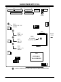
1
SERVICE MANUAL
Product Type:
Chassis:
Manual Series:
Manual Part #:
Model Line:
Product Year:
Model Series:
Projection TV
ZP94/ZP95
PV152
923-03439
C
2000
IQC60H94W
IQC50H94W
IQC60H95W
IQC50H95W
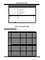
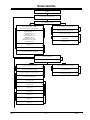
CONTENTS
General Information....................................... 1
Servicing/Troubleshooting.............................. 2
Circuit Description......................................... 3
Model Parts Lists .......................................... 4
Exploded Views ............................................. 5
PCB Layouts ................................................. 6
Schematics ................................................. 7
Published by Technical Publications
Zenith Electronics Corporation
201 James Record Road - Huntsville, Alabama 35824-1513
ÓCopyright
Printed in U.S.A.
ZP DG 4.3k
July 2000 by Zenith Electronics Corporation
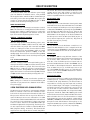
PRODUCT SAFETY SERVICING GUIDELINES FOR AUDIO-VIDEO PRODUCTS
IMPORTANT SAFETY NOTICE
This manual was prepared for use only by properly trained audio-visual service
technicians.
A.C. Voltmeter
When servicing this product, under no circumstances should the original
design be modified or altered without permission from Zenith Electronics
Corporation. All components should be replaced only with types identical to
those in the original circuit and their physical location, wiring and lead dress
must conform to original layout upon completion of repairs.
Special components are also used to prevent x-radiation, shock and fire hazard.
These components are indicated by the letter “x” included in their component
designators and are required to maintain safe performance. No deviations are
allowed without prior approval by Zenith Electronics Corporation.
0.15uF
Good Earth Ground
such as the Water
Pipe, Conduit, etc.
Circuit diagrams may occasionally differ from the actual circuit used. This way,
implementation of the latest safety and performance improvement changes into
the set is not delayed until the new service literature is printed.
1500 OHM
Place this probe
on each exposed
metal part.
10 WATT
X-RADIATION
CAUTION: Do not attempt to modify this product in any way. Never perform
customized installations without manufacturer’s approval. Unauthorized
modifications will not only void the warranty, but may lead to property damage
or user injury.
1.
Be sure procedures and instructions to all service personnel cover the
subject of x-radiation. The only potential source of x-rays in current TV
receivers is the picture tube. However, this tube does not emit x-rays when
the HV is at the factory-specified level. The proper value is given in the
applicable schematic. Operation at higher voltages may cause a failure of
the picture tube or high-voltage supply and, under certain circumstances
may produce radiation in excess of desirable levels.
2.
Only factory-specified CRT anode connectors must be used.
3.
It is essential that the service personnel have available an accurate and
reliable high-voltage meter.
4.
When the high-voltage circuitry is operating properly, there is no possibility
of an x-radiation problem. Every time a color Chassis is serviced, the
brightness should be run up and down while monitoring the high voltage
with a meter, to be certain that the high voltage does not exceed the
specified value and that it is regulating correctly.
5.
When troubleshooting and making test measurements in a product with a
problem of excessively high voltage, avoid being unnecessarily close to
the picture tube and the high voltage power supply. Do not operate the
product longer than necessary to locate the cause of excessive voltage.
6.
Refer to HV, B+, and shutdown adjustment procedures described in the
appropriate schematics and diagrams (where used).
Service work should be performed only after you are thoroughly familiar with
these safety checks and servicing guidelines.
GRAPHIC SYMBOLS
The exclamation point within an equilateral triangle is intended
to alert the service personnel to important safety information in
the service literature.
The lightning flash with arrowhead symbol within an equilateral
triangle is intended to alert the service personnel to the presence
of noninsulated “dangerous voltage” that may be of sufficient
magnitude to constitute a risk of electric shock.
The pictorial representation of a fuse and its rating within an
equilateral triangle is intended to convey to the service personnel
the following fuse replacement caution notice:
CAUTION: FOR CONTINUED PROTECTION AGAINST RISK OF FIRE,
REPLACE ALL FUSES WITH THE SAME TYPE AND RATING AS MARKED
NEAR EAch FUSE.
SERVICE INFORMATION
IMPLOSION
While servicing, use an isolation transformer for protection from AC line shock.
After the original service problem has been corrected, make a check of the
following:
FIRE AND SHOCK HAZARD
1. Be sure that all components are positioned to avoid a possibility of
adjacent component shorts. This is especially important on items transported to and from the repair shop.
1.
All direct view picture tubes are equipped with an integral implosion
protection system; take care to avoid damage during installation.
2.
Use only the recommended factory replacement tubes.
TIPS ON PROPER INSTALLATION
1.
Never install any receiver in a closed-in recess, cubbyhole, or closely
fitting shelf space over, or close to, a heat duct, or in the path of heated
air flow.
2.
Avoid conditions of high humidity such as: outdoor patio installations
where dew is a factor, near steam radiators where steam leakage is a factor,
etc.
3. Soldering must be inspected to discover possible cold solder joints, solder
splashes, or sharp solder points. Be certain to remove all loose foreign
particles.
3.
Avoid placement where draperies may obstruct venting. The customer
should also avoid the use of decorative scarves or other coverings that
might obstruct ventilation.
4. Check for physical evidence of damage or deterioration to parts and components, for frayed leads or damaged insulation (including the AC cord), and
replace if necessary.
4.
Wall- and shelf-mounted installations using a commercial mounting kit
must follow the factory-approved mounting instructions. A product mounted
to a shelf or platform must retain its original feet (or the equivalent
thickness in spacers) to provide adequate air flow across the bottom. Bolts
or screws used for fasteners must not touch any parts or wiring. Perform
leakage tests on customized installations.
5.
Caution customers against mounting a product on a sloping shelf or in a
tilted position, unless the receiver is properly secured.
6.
A product on a roll-about cart should be stable in its mounting to the cart.
Caution the customer on the hazards of trying to roll a cart with small
casters across thresholds or deep pile carpets.
7.
Caution customers against using a cart or stand that has not been listed
by Underwriters Laboratories, Inc. for use with its specific model of
television receiver or generically approved for use with TVs of the same or
larger screen size.
8.
Caution customers against using extension cords. Explain that a forest of
extensions, sprouting from a single outlet, can lead to disastrous
consequences to home and family.
2. Verify that all protective devices such as insulators, barriers, covers,
shields, strain reliefs, power supply cords, and other hardware have been
reinstalled per the original design. Be sure that the safety purpose of the
polarized line plug has not been defeated.
5. No lead or component should touch a receiving tube or a resistor rated at
1 watt or more. Lead tension around protruding metal surfaces must be
avoided.
6. After reassembly of the set, always perform an AC leakage test on all exposed
metallic parts of the cabinet (the channel selector knobs, antenna terminals,
handle and screws) to be sure that set is safe to operate without danger of
electrical shock. DO NOT USE A LINE ISOLATION TRANSFORMER DURING THIS
TEST. Use an AC voltmeter having 5000 ohms per volt or more sensitivity in
the following manner: Connect a 1500 ohm, 10 watt resistor, paralleled by
a .15 mfd 150V AC type capacitor between a known good earth ground
water pipe, conduit, etc.) and the exposed metallic parts, one at a time.
Measure the AC voltage across the combination of 1500 ohm resistor and
.15 mfd capacitor. Reverse the AC plug by using a non-polarized adaptor
and repeat AC voltage measurements for each exposed metallic part. Voltage
measured must not exceed 0.75 volts RMS. This corresponds to 0.5 milliamp
AC. Any value exceeding this limit constitutes a potential shock hazard and
must be corrected immediately.
PV152
i
PRO1200 - SAFETY
PRODUCT SAFETY SERVICING GUIDELINES FOR AUDIO-VIDEO PRODUCTS
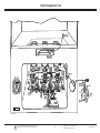
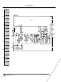
CHASSIS HIGH VOLTAGE ADJUSTMENT PROCEDURE
1. Connect High Voltage meter to FBT High Voltage output. Connect Ground of High Voltage meter to CRT
Ground or FBT Ground.
2.
3.
4.
+50V Pulse
Check that the High Voltage adjustment VR (RH44) is
set to it’s mechanical center on the Deflection PWB.
This VR is located just behind the Flyback transformer
as viewed from the Front of the set. (See diagram below)
DH24
CH30
Receive an NTSC generator signal. (Picture should be
stationary for this adjustment.
Video Controls should be set to Factor Settings.
5.
Adjust the High Voltage to the following specifications by turning RH44 slowly.
6.
Lock Paint the control. If available.
Add JIG to check Hi
Volt Limit Circuit
JIG = 1k ohm 1/8W
RH54
RH55
DH31
Checking Procedure :
TH01
1.
FBT
Check that the picture is turned off and the horizontal deflection circuit stops operation.
After Checking:
RH44
1.
Unplug set and Remove Jig. Allow set to remain in the
off condition for at least 15 seconds.
2.
Apply AC and confirm the set returns to normal operation.
High Voltage ADJ.
CHASSIS FLYBACK PROTECTION CIRCUIT CHECK
Check Preparation:
CHASSIS HIGH VOLTAGE LIMITER CHECK
Check Preparation:
1.
The set can face any direction.
2.
Receive the Cross-Hatch Signal
3.
VIDEO CONTROLS: Brightness to Maximum.
4.
5.
SCREEN FORMAT: Should be PROGRESSIVE mode.
Attach the JIG (1k ohm 1/8W resistor) to both ends
of DH31 as shown in the diagram below. (See Diagram
Below)
1.
The set can face any direction.
2.
Receive the Cross-Hatch Signal
3.
VIDEO CONTROLS: Factory Preset.
4.
SCREEN FORMAT: Should be PROGRESSIVE mode.
5.
Attach a 100 K ohm 1/16W ~ 1/8W resistor between
QP02 base and Gnd. (SD4 connector Pin 4) and check
operation.
After Checking:
1. Unplug set and Remove Jig. Allow set to remain in the
off condition for at least 15 seconds.
2.
PV151
ii
Apply AC and confirm the set returns to normal operation.
PROJO
PRODUCT SAFETY SERVICING GUIDELINES FOR AUDIO-VIDEO PRODUCTS
CHASSIS SWEEP LOSS DETECTION CIRCUIT CHECK
Check Preparation:
Check Number (1):
1.
2
The set can face any direction.
Receive the Cross-Hatch Signal
3.
VIDEO CONTROLS: Factory Preset.
4.
SCREEN FORMAT: Should be PROGRESSIVE mode.
5.
Attach the JIG (A) (100 ohm 1/8W resistor) to right
hand side of RN01 and to Ground as shown in the
diagram below.
Check Number (2):
1.
The set can face any direction.
2.
Receive the Cross-Hatch Signal
3.
4.
VIDEO CONTROLS: Factory Preset.
SCREEN FORMAT: Should be PROGRESSIVE mode.
5.
Attach the JIG (B) (100 ohm 1/8W resistor) to right
hand side of RN11 and to Ground as shown in the
diagram below.
Checking Procedure :
1.
Check that the picture is turned off in either check.
After Checking:
1. Remove Jig after each check.
2.
Confirm the set returns to normal operation.
CN01
PV151
CN04
iii
PROJO
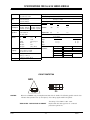
TABLE OF CONTENTS
SECTION 1
GENERAL INFO / REMOTE CONTROL
CAUTIONS FOR HV CONNECTOR ................................. 1-1
SPECIFICATIONS .................................................... 1-2
GENERAL INFORMATION ........................................... 1-3
REMOTE .............................................................. 1-4
REMOTE CODES ..................................................... 1-5
CUSTOMER AUDIO/VIDEO ADJUSTMENT ........................ 1-7
CUSTOMER CONVERGENCE ADJUSTMENT ....................... 1-9
SECTION 2
SERVICING
SERVICE MENUES ..............................................
SERVICE ADJUSTMENT ORDER ..................................
MEMORY INITIALIZATION ........................................
PRE HEAT
..............................................
CUT OFF ADJUSTMENT ............................................
PRE FOCUS ADJUSTMENT ........................................
DCU PHASE ADJUSTMENT (COARSE) ...........................
HORIZONTAL PHASE ADJUSTMENT ..............................
RASTER INCLINATION .............................................
BEAM ALIGNMENT ..............................................
VERT/HORIZ POSITION ADJUSTMENT ...........................
HORIZONTAL SIZE ADJUSTMENT ................................
VERTICAL SIZE ADJUSTMENT ....................................
BEAM FORM ADJUSTMENT .......................................
LENS FOCUS ADJUSTMENT .......................................
STATIC FOCUS ADJUSTMENT .....................................
BLUE DEFOCUS ADJUSTMENT ...................................
WHITE BALANCE ADJUSTMENT ..................................
SUB BRIGHT ADJUSTMENT .......................................
HORIZONTAL POSITION ADJUSTMENT (FINE)..................
DIGITAL CONVERGENCE ADJUSTMENT ..........................
DIGITAL CONVERGENCE REMOTE ................................
CONVERGENCE POINT ADJUSTMENT ............................
CONVERGENCE 3X3 ADJUSTMENT ...............................
CONVERGENCE 7X5 ADJUSTMENT ...............................
CONVERGENCE 13X9 ADJUSTMENT .............................
TROUBLE SHOOTING ..............................................
SECTION 3
MODEL PARTS
SECTION 5
SECTION 7
ZP
ZP
ZP
ZP
ZP
ZP
ZP
ZP
ZP
ZP
ZP
ZP
ZP
6-3
6-4
6-5
6-6
6-7
6-8
6-9
6-10
6-11
6-12
6-13
6-14
6-15
6-16
6-17
6-18
SCHEMATICS
94/95 MICRO PWB CIRCUIT ..................................
94/95 SIGNAL INTERCONNECT CIRCUIT ....................
94/95 TUNER IF CIRCUIT .....................................
94/95 POWER SUPPLY PWB CIRCUIT .......................
94/95 DEFLECTION CIRCUIT .................................
94/95 CONVERGENCE POWER SUPPLY ......................
94/95 REGISTRATION / CONVERGENCE CORRECT PWB ...
94/95 JACKPACK / TERMINAL DIAGRAM ...................
94/95 2 LINE COMB FILTER CIRCUIT .......................
94/95 CHROMA / LUMMA CIRCUIT .........................
94/95 VELOCITY MODULATOR PWB CIRCUIT ...............
94/95 CRT PWB CIRCUIT .....................................
94/95 AUDIO MATRIX / CONTROL PANEL PWB ............
6-1
6-2
6-3
6-4
6-5
6-6
6-7
6-8
6-9
6-10
6-11
6-12
6-13
3-1
3-2
3-3
3-4
3-5
PARTS LIST
.............................................. 4-1
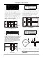
DIAGRAMS
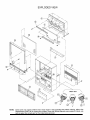
ZP 94/95 EXPLODED VIEW.......................................
ZP 94/95 EXPLODED VIEW FRONT ..............................
ZP 94/95 EXPLODED BACK ......................................
ZP 94/95 INTERCONNECT ........................................
ZP 94/95 WIRING DIAGRAM .....................................
SECTION 6
94/95 SIGNAL TOP PCB LAYOUT ............................
94/95 SIGNAL BOTTOM PCB LAYOUT .......................
94/95 SWITCH MODE POWER TOP PCB LAYOUT ...........
94/95 SWITCH MODE POWER BOTTOM PCB LAYOUT .....
94/95 CPT TOP PCB LAYOUT .................................
94/95 CPT BOTTOM PCB LAYOUT ...........................
94/95 SRS AUDIO TOP PCB LAYOUT .......................
94/95 SRS AUDIO BOTTOM PCB LAYOUT ..................
94/95 JACKPACK TOP PCB LAYOUT .........................
94/95 JACKPACK BOTTOM PCB LAYOUT ....................
94/95 CONTROL PANEL TOP PCB LAYOUT ..................
94/95 CONTROL PANEL BOTTOM PCB LAYOUT ...........
94/95 VELOCITY MODULATOR AND SUB TOP
PCB LAYOUT ...............................
ZP 94/95 VELOCITY MODULATOR AND SUB BOTTOM
PCB LAYOUT ...............................
ZP 94/95 YC & COMB FILTER TOP PCB LAYOUT ...............
ZP 94/95 YC & COMB FILTER BOTTOM PCB LAYOUT .........
CIRCUIT DESCRIPTION
POWER SUPPLY OPERATION ......................................
TURNING ON THE DEFLECTION POWER SUPPLY ...............
POWER SUPPLY SHUTDOWN EXPLANATION ....................
ABL CIRCUIT
..............................................
MICRO PROCESSOR DATA COMMUNICATION ...................
SECTION 4
2-1
2-6
2-7
2-7
2-7
2-7
2-9
2-9
2-9
2-10
2-10
2-11
2-11
2-11
2-12
2-12
2-12
2-13
2-14
2-14
2-14
2-15
2-16
2-17
2-17
2-17
2-19
ZP
ZP
ZP
ZP
ZP
ZP
ZP
ZP
ZP
ZP
ZP
ZP
ZP
5-1
5-2
5-3
5-4
5-5
PCB LAYOUTS
ZP 94/95 DEFLECTION TOP PCB LAYOUT ...................... 6-1
ZP 94/95 DEFLECTION BOTTOM PCB LAYOUT ................. 6-2
PV152
TOC
PROJO
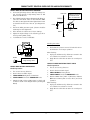
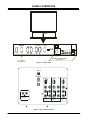
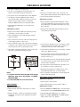
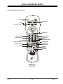
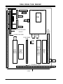
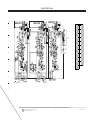
CAUTIONS WHEN CONNECTING / DISCONNECTING THE HV CONNECTOR
HV Cable
TAB
Flyback
POSITION
DEFLECTION
P.W.B
FBT
ANODE
CONNECTOR
FIG. B
Perform the following when the HV connector (anode
connector) is removed or inserted for CPT replacement,
etc.
3. Remove the connector slowly by pulling it away from the case.
HV Cable &
Boot Assembly
PUSH
LESS THAN 1mm
PUSH
Flyback
FIG. A
During Removal
1. Roll out silicon cover from FBT’s contact area slowly.
2. While turning the connector about 90 degrees following the arrow
(0 position). Push the connector slightly toward the case. (Fig. A)
During Insertion
1. Please refer to direction for insertion as shown in Fig. B (L position).
Insert connector until “CLICK” sound is heard.
2. Make sure the connector is pressed right in, so that it has a good
contact with the spring.
3. Confirm the contact by pulling the connector slightly. (Don’t pull
hard because it may damage the connector).
4. Cover the high voltage output by carefully pushing silicon boot
onto it. (Don’t turn the connector).
Note: Make sure the silicon boot is covering the high
voltage output.
PV151
1-1
PROJO
SECTION 1
TECHNICAL CAUTIONS
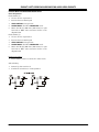
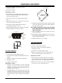
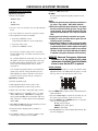
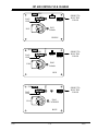
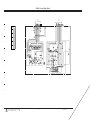
High Voltage limiter circuit check
1. Turn off TV and connect jig as shown in Figure 2.
Adjust jig fully counter clockwise for minimun
resistance.
2. Set the AC input to 120V AC and turn on TV.
3. Confirm test pattern on CRT is a usable picture, then
slowly adjust jig until the picture disappears and TV
shuts down.
4. When the limiter circuit is operating properly, Voltage
will be less than 36.5kV at 0.6mA when TV shuts down.
5. Turn off set immediately after checking circuit operations.
6. Unplug set for one minute to reset shutdown circuit.
Remove jig and voltmeter.
Chassis Ground
FBT
(TH01)
Defelection
P.W.B.
High Voltage
Connector
High Impedance
H.V. Meter
Figure 2. Deflection/Power PCB
Remove RH80 and connect 50K Ohm jig as shown
FBT
TP91
POWER/DEFLECTION PWB
PV151
50K Ohm VR
JIG
RH80
RH44
1-2
PROJO
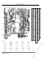
SPECIFICATIONS FOR 94 & 95 SERIES MODELS
Model:
Cathode-Ray
Tube:
Power Input
Power
Consumption:
Antenna
Impedence:
Receiving
Channel:
Intermediate
Frequency:
Video Input:
Video Output:
IQC60H95W IQC50H95W
IQC60H94W IQC50H94W
R=P16LFM00RFA(LU)
G=P16LFM00HHA(LU)
B=P16LFM00BMB(EU)
120 Volt AC, 6OHz
Audio Input:
Stereo Audio Output:
Audio Output Power:
Anode Voltage:
Brightness
ZP94
ZP95
224 Watts - Maximum 232 Watts - Maximum Full White
192 Watts - Operating 206 Watts - Operating
75ohm Unbalanced
Brightness Max
VHF / UHF / CATV
BAND
CH
VHF
2-13
UHF
14-69
EXT. Mid
(A-5)~(A-1), 4+
CATV Mid
A~I
CATV Super
J~W
CATV Hyper
(W+1) (W+28)
Picture I-F Carrier 45.75 MHz
Sound I-F Carrier 41.25 MHz
Color Sub Carrier 42.17 MHz
1 Volt p-p, 75 Ohm
1 Volt p-p, 75 Ohm (Y)
07. Volt p-p, 75 Ohm, (Cb, Cr)
1 Volt p-p, 75 Ohm
Speakers:
Dimension:
Height
Width
Depth
Weight
Circuit Board
Assemblies:
470 mVrms, 47 k Ohm
470 mVrms, 1 k Ohm
Front- 12 Watt at 10% distortion, 8 Ohm Imp.
Max Output - 15 Watt
30.0 + 1.5kv (1.27 + 0.2ma)
Size
ZP94
ZP95
50"
130
130
100
100
60"
2 woofers - 5 Inch
(12 cm) Round
50" Series Models
52
43 1/5
23 1/2
Power Supply P.W.B.
VM P.W.B.
Surround P.W.B.
Signal P.W.B.
Audio Out P.W.B.
2H P.W.B.
60" Series Models
60 1/2
51 1/2
26 1/2
C.P.T. (B) P.W.B
Control P.W.B
C.P.T. (G) P.W.B.
Sensor Dist. P.W.B.
C.P.T. (R) P.W.B.
Sub Deflect. P.W.B
Power/Deflection P.W.B.
Control P.W.B.
Terminal P.W.B.
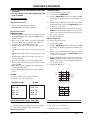
CIRCUIT PROTECTION
CAUTION:
Below is an EXAMPLE only. See Replacement Parts List for details. The following symbol near the fuse
indicates fast operation fuse (to be replaces). Fuse ratings appear within the symbol.
“RISK OF FIRE - REPLACE FUSE AS MARKED”
PV151
1-3
The rating of fuse F901 is 6.0A - 125V.
Replace with the same type fuse for continued
protection against fire.
PROJO
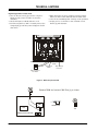
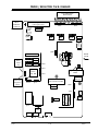
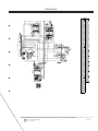
GENERAL INFORMATION
SOURCE
-VOLUME+
-CHANNEL+
POWER
DIGITAL
SETUP
MENU
65 65
EXIT
S-VIDEO
LEFT RIGHT
VIDEO AUDIO AUDIO
DIGITAL CONVERGENCE
SETS ONLY
TV / VIDEO
Source Selector
Figure 3. Control Panel
ANT A
To
Converter
S-VIDEO
S-VIDEO
S-VIDEO
ANT B
R
VIDEO
Y
VIDEO
Y
VIDEO
(MO NO)
PB
(MONO)
PB
(MONO)
L
L
L
PR
AUDIO
TO HI-FI
PR
R
AUDIO
R
AUDIO
R
AUDIO
INPUT 1
INPUT 2
MONITOR
OUT
Figure 4. Rear Connection Panel
PV151
1-4
PROJO
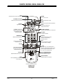
REMOTE CONTROL MODEL MBR3475Z
HELP
Activates the on-screen help feature.
POWER
Turns TV On or Off.
FLASHBK (Flashback)
Returns to previous Channel.
AUX
Auxilliary equipment control
MODE
Selects the remote's mode of operation
SOURCE
Signal Source
MUTE
Turns sound Off and On
while picture remains.
VOLUME (Left/Right)
Increases / Decreases TV’s sound level.
CHANNEL (Up/Down)
Selects next channel in
TV’s memory. Press
and hold to repeat.
PIP MODE
Changes PIP Mode
NUMBER PAD
Selects channels directly.
DISPLAY
Shows Channel/Time, enters
channel, or removes any
on-screen menus.
MENU
Displays menus for TV
and other options.
QUIT
Leaves programming menus
and clear screen of display.
SELECT
C. SKIP
Channel Skip. Tunes Entertainment
Machine to last channel viewed. Tunes
back to original channel after 30, 60,
90, 120, 150, or 180 seconds.
.
UP and DOWN ARROWS
Moves highlighted bar within
menu to select an option.
LEFT/RIGHT ARROWS
Chooses and shows the
desired menu option.
PIP KEYS
Special features of some TV’s
TV/VCR SOURCE
Steps through source options.
TIMER
Press repeatedly to set desired
TV shut-off time.
Remote Control Part Number.
MBR3475Z
924-10092
PV151
1-5
PROJO
PROGRAMMING CODES
VCRS
Adventura
Aiko
Aiwa
Akai
American High
Asha
Audiovox
Beaumark
Bell & Howell
Brandt
Broksonic
Calix
Canon
Capehart
Carver
CCE
Citizen
Colt
Craig
Curtis Mathis
Cybernex
Daewoo
Daytron
Dynatech
Electrohome
Electrophonic
Emerx
Emerson
Fisher
Fuji
Funai
Garrad
General Electric
Goldstar
Gradiente
Harley Davidson
Harman / Kardon
Harwood
Headquarter
Hi-Q
Hitachi
Jensen
JVC
KEC
Kenwood
KLH
Kodak
Lloyd
Lloyd’s
Logik
LXI
Magnavox
Magin
Marantz
Marta
Matsushita
MEI
Memorex
MGA
MGN Tech
Minolta
Mitsubishi
Motorola
MTC
Multitech
PV151
VCRS (continued)
00
08
00
01, 48, 49
22
45
23
45
32
43
33, 34, 42, 42, 52
23
22
06
31
08, 30
08, 23
30
18, 23, 30, 45
01, 22, 47
45
06, 08, 16, 38, 50
06
00
23
23
07
00, 08, 12, 15, 23, 27,
28, 33, 34, 37, 42, 48,
51, 52
18, 20, 32, 46
09, 22
00
00
03, 22, 41, 47
23, 24, 44
00
00
24
30
17
18
01, 02, 03, 04
01
01, 13, 26
08, 23
01, 24, 26
30
22, 23
00
27
30
23
14, 2, 29, 31, 35
45
22, 3
23
22
22
00, 14, 17, 18, 19, 22,
23, 32, 45
15, 48
45
02, 04
15, 26, 40, 48, 49
19, 22
00, 45
00, 30
NEC
Nikko
Noblex
Olympus
Optimus
Orion
Panasonic
Penny
01, 05, 24, 26, 32
23
45
11, 22
19, 23, 32
51
10, 11, 22, 39, 53
02, 05, 22, 23, 24, 45,
46
02, 03, 04
22
20, 29, 31
23
26
06
30
14
17
17
22
00, 23
23
23
02, 03, 04, 35, 41, 47
00, 17, 18, 19, 20, 22,
23, 32, 45
21
14
16, 45
14, 19
01, 26
17, 18, 32, 45
15, 16, 33, 34, 37, 42
02, 04, 17, 18, 20, 22,
23, 32, 46
19
30
45
30
07, 09, 21, 22
02
00, 15, 22, 29, 31
00
01
00, 01
22, 39
00, 22, 23
43
27, 45
15, 16, 20, 37
23, 45
45
16
05, 24
05, 16, 48
45
00, 02, 18, 19, 22, 30,
35, 37, 45, 47
00, 22, 30
24
09, 14, 21, 55
Pentax
Philco
Philips
Pilot
Pioneer
Portland
Protec
Pulsar
Quarter
Quartz
Quasar
Radio Shack
Radix
Randex
RCA
Realistic
Ricoh
Runco
Samsung
Sanky
Sansui
Sanyo
Scott
Sears
Sharp
Shintom
Shogun
Shinger
Sony
STS
Sylvania
Symphonic
Tatung
Teac
Technics
Teknika
Telefunken
THK
Toshiba
Totevision
Unitech
Vector
Vector Research
Video Concepts
Videosonic
Wards
XR 1000
Yamaha
Zenith
Cable Satelites
ABC
Antronixs
Archer
Belcor
Cable Star
00, 07, 08, 18, 19, 21,
37, 38, 53
40
12, 25, 40
33
33
1-6
Cable Satelites (continued)
Century
Citizen
Colour Voice
Contronics
Contec
Dae Ryung
Eastern
Electricord
Everquest
Focus
Garrard
GC Electronics
Gemini
Goldstar
General Insturments
Hamlin
Hitachi
Hytex
Jasco
Jerrold
Macom
Magnavox
Memorex
Movie Time
NSC
Oak
Panasonic
Paragon
Philips
Pioneer
Popular Mechanics
Pulsar
RCA
Realistic
Recoton
Regal
Regency
Rembrandt
Runco
Samsung
Scientific Atlanta
Signal
Signature
SL Marx
Sprucer
Starcom
Stargate
Starquest
Starsight
Sylvania
Teleview
Texscan
Tocom
Toshiba
Tusa
TV 86
Unika
United Artist
United Cable
Universal
Videoway
Viewstar
Zenith
Zentek
Hitachi (SAT)
RCA (SAT)
Sony (SAT)
12
12
31, 45
26, 29
22
21
15
32
56
57
12
33, 40
04, 39, 44, 56
11, 26
00, 13
03, 09, 14, 23, 24
00
37
12
00, 08, 13, 38, 53, 55,
56
36
16
02
30, 32, 34
30, 34, 39
22, 37, 50
02, 10, 49
02
12, 16, 17, 27, 31, 43,
44, 45, 47
06, 11, 20
57
02
49
40
57
03, 09, 23, 35
15
00, 39
02
11, 26
18, 21, 42, 48
26, 56
00
26
01, 49
38, 53, 56
26, 56
56
58, 59
19
26
19
07, 28, 55
02
56
30
12, 40
37
53
12, 25, 32, 33, 35, 40
51
16, 29, 30, 41
16, 29, 30, 41, 64
57
61
62
63
PROJO
PROGRAMMING CODES
Audio Amplifiers
DVD Players
Denon
Hitachi
JVC
Kenwood
Magnavox
Mitsubishi
Panasonic
Pioneer
Philips
RCA (ProScan)
Sony
Toshiba
Yamaha
Zenith
03
06
00
03
04
09
03
02
05
08
01
04
07
04, 10
CD Players
Adcom
Aiwa
California Audio
Carver
Denon
DKK
Emerson
Fisher
Genexxa
Hitachi
JVC
Kenwood
Krell
Magnavox
Marantz
MCS
Mission
NSM
Onkyo
Optimus
Panasonic
Philips
Pioneer
Proton
QED
Quasar
RCA
Realistic
Rotel
SAE
Sansui
Scott
Sony
Technics
Victor
11
12
13
12
14
15
11
16
17
11, 17, 18, 19, 20,
21, 22
23
16, 24, 25
12
12
12, 13
13
13
12
26
15, 17, 27
13
12
17, 27
12
12
13
11, 31
11
12
12
12
11
15, 28
13, 29, 30
23
Aiwa
Carver
Casio
Clarinette
Denon
Fisher
Hitachi
JVC
Kenwood
Lloyd’s
Magnavox
Marantz
MCS
Modulaire
Onkyo
Optimus
Panasonic
Penney
Philips
Pioneer
Quasar
Realistic
Sansui
Sanyo
Sharp
Sony
Technics
Victor
Ward
Yamaha
York
51, 52
47, 52, 53, 54
55
55
56
54, 57
58
59
60, 61, 63, 64
55
57, 63, 55
47, 52, 62
62
55
55
49, 50, 57, 61, 66
62
55
47, 52
49, 50, 66, 67, 68
62
55
52
57
61
51
48, 62, 69, 70, 71
59
49, 51, 52, 54, 66, 67
61, 72
55
Tape Players
Awia
Hitachi
Jerrold
JVC
Kenwood
Optimus
Panasonic
Pioneer
Scientific Atlanta
Sony
Starcom
Wards
PV151
42, 43
32, 33, 34, 35
44, 45
36
37
38
39
38
46
40, 52, 42, 43
44
38
1-7
PROJO
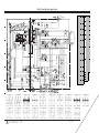
CUSTOMIZED VIDEO AND AUDIO ADJUSTMENTS
Select VIDEO to adjust picture settings and improve picture quality.
SETUP
SPECIAL
VIDEO
AUDIO THEATER
CONTRAST
75 %
BRIGHTNESS
50%
COLOR
50%
TINT
SHARPNESS
50%
RESET
ADVANCED
SETTINGS
MENU
TO MENU BAR
TO EXIT
QUIT
SETUP SPECIAL
VIDEO
Advanced Settings
View Rite
Auto Flesh
Video
Color Temperature
Cool
Warm
Aspect Ratio
4.3
16.9
V. Position
+10
MENU
Note: If contrast is selected, you are adjusting
CONTRAST. The additional menu items,
BRIGHTNESS, COLOR, TINT, and SHARPNESS
can be adjusted in the same manner.
TO MENU BAR
AUDIO THEATER
TO EXIT
QUIT
Use Cursor Up or Down to highlight the
function to be adjusted.
Press Cursor Left or Right to adjust function.
Press QUIT to exit menu.
Contrast and Brightness adjustmens will
effect only the main picture. These
adjustments will not affect the subpicture.
PV151
CONTRAST
TINT
Use this function to change the contrast
between black and white levels in the
picture. This adjustment will only affect the
picture when LIGHT SENTRY is OFF.
Use this function to adjust flesh tones so they
appear natural. (It may be necessary to adjust
TINT to abtain optimum picture quality when
using the COMPONENT:Y-CbCr Input 2 jacks).
BRIGHTNESS
SHARPNESS
Use this function to adjust overall picture
brightness.
Use this function to adjust the amount of
detail in the picture.
COLOR
RESET
Use this function to adjust the color level in
the picture.
When RESET is selected, press CURSOR RIGHT
to reset video settings to factory preset
conditions.
1-8
PROJO
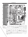
CUSTOMIZED VIDEO AND AUDIO ADJUSTMENTS
Select AUDIO SETTINGS to adjust the AUDIO to your preference and improve the sound quality.
SETUP
SPECIAL
VIDEO
AUDIO THEATER
SETUP
BASS
72 %
TREBLE
50%
VIDEO
AUDIO THEATER
Advanced Settings
Stereo
Mono
Second Audio Programming
BALANCE
RESET
Internal Speakers
Auto Noise Control
Loudness
SoundRite
ADVANCED
SETTINGS
MENU
SPECIAL
TO MENU BAR
TO EXIT
QUIT
Note: If BASS is selected you are adjusting BASS.
The additional menu items, TREBLE and
BALANCE can be selected and adjusted in
the same manner
MENU
TO MENU BAR
TO EXIT
QUIT
Use Cursor Up or Down to highlight the
function to be adjusted.
Press Cursor Left or Right to adjust function.
Press QUIT to exit menu.
BASS
This function controls the Low Frequency
audio to all speakers.
TREBLE
This function controls the High Frequency
audio to all speakers.
BALANCE
This function will control the left to right
balance of the TV internal speakers and the
VARIBLE AUDIO OUT output.
RESET
When RESET is selected, press CURSOR RIGHT
to return audio adjustments to factory preset
conditions.
PV151
1-9
PROJO
ZP94/95 CUSTOMER CONVERGENCE ADJUSTMENT
Flashes Blue
Flashes Red
Digital
Setup
MENU
MENU
Note:
CONVERGENCE ADJUSTMENT (DIGITAL SETUP)
To enter this adjustnment mode, press the front panel
DIGITAL SETUP button.
Only a momentary press of the DGITAL SETUP button is
necessary to enter DIGITAL SETUP convergence adjustment mode.
Press the ARROW buttons on the remote control to move
the displayed color up, down, left, or right. (Press the
QUIT button to toggle between red and blue)
Do not press the DIGITAL SETUP button for more than
three seconds.
To save your adjustment data into memory, press the
front panel DIGITAL SETUP button or the remote
control MENU button. If you do NOT wish to save your
adjustment data into memory, turn the TV off. When
the TV is ON again, your old convergence data will be
restored.
Press MENU on the remote control to change the color
you want to adjust.
Press the front panel DIGITAL SETUP button or the
remote comtrol MENU button when adjustment is done.
This will save your adjustment into memory.
To exit this function, press DIGITAL SETUP on the front
panel of your Entertainment machine.
PV151
1-10
PROJO
SERVICE MENUES
ITEM
P01
ADJUST MODE
SETTING
RANGE DESCRIPTION
ZP94/95
*Non-Adjustable Data
Version 704
SUB BRT
SERVICE
DEF RESET
V/P RESET
3DYC RESET
FLEX RESET
DSP RESET
CCD RESET
FACT RESET
MEMORY INITIAL
P02
ADJUST MODE
PV152
0
0
0
0
0
0
0
0
Resets Memory
Resets Memory
00-7F
Horizontal Position
00-7F
Vertical Position
00-0F
00-0F
00-07
00-1F
00-01
Y Motion Detection Gain
Chroma Motion Detection Gain
Vertical Aperture Controle Gain
Vertical Aperture Controle Invert
Y Output High Frequency Coring
00-7F
Horizontal Position
00-7F
Vertical Position
00-0F
00-0F
00-07
00-1F
00-01
Y Motion Detection Gain
Chroma Motion Detection Gain
Vertical Aperture Controle Gain
Vertical Aperture Controle Invert
Y Output High Frequency Coring
3C
00
00
0F
1B
ZP94/95
00-7F
00-07
00-07
00-1F
00-1F
Main NTSC Tint
Main NTSC TOF fO Peak Frequency Switch
Main NTSC TOFQ Switch
Main NTSC Contrast
Main NTSC Color
3C
00
00
0F
1B
00-7F
00-07
00-07
00-1F
00-1F
Main NTSC Tint
Main NTSC TOF fO Peak Frequency Switch
Main NTSC TOFQ Switch
Main NTSC Contrast
Main NTSC Color
TA1300 33.75khz Mode3375
H POSI
40
FLEX CONT
VD POS
3F
UPD64081
DYGA
09
DCGA
06
VAPGA
00
VAPIN
00
YHCOR
00
P03
ZP94/95
ADJUST MODE
TA1270-S
TINT (TV)
TOFFO (TV)
TOFQ (TV)
SUB CNT
SUB CLR
Sub Brightness
SERVICE
ZP94/95
TA1300 31.5khz Mode 315
H POSI
40
FLEX CONT
VD POS
3F
UPD64081
DYGA
09
DCGA
06
VAPGA
00
VAPIN
00
YHCOR
00
P02
ZP94/95
ADJUST MODE
TA1270-M
TINT (TV)
TOFFO (TV)
TOFQ (TV)
SUB CNT
SUB CL
P03
ADJUST MODE
3C-C3
0
2-1
PROJO
SERVICE MENUES CONT.
PV152
ITEM
P04
FLEX CONT
39 HHPF1
41 V-CRG
42 H-CRG
43 V-ENH
44 H-ENH
96 YVHENH
100 CVHENH
P04
FLEX CONT
39 HHPF1
41 V-CRG
42 H-CRG
43 V-ENH
44 H-ENH
96 YVHENH (720p)
100 CVHENH
SETTING
RANGE DESCRIPTION
ZP94/95
*Non-Adjustable Data
NTSC
00
00-01 Characteristic Switch 0 = Low Frequency, 1 = High Frequency
00
00-03 Vertical Enhance Coring
00
00-03 Horizontal Enhance Coring
00
00-03 Vertical Enhance
00
00-03 Horizontal Enhance
0B
00-1F Y Vertical & Horizontal Enhance Gain
12
00-1F Color Vertical & Horizontal Enhance Gain
ZP94/95
ATSC
(480i, 480p, 1080i, 720p)
00
00-01 Characteristic Switch 0 = Low Frequency, 1 = High Frequency
00
00-03 Vertical Enhance Coring
00
00-03 Horizontal Enhance Coring
00
00-03 Vertical Enhance
00
00-03 Horizontal Enhance
00 (10)
00-1F Y Vertical & Horizontal Enhance Gain
12
00-1F Color Vertical & Horizontal Enhance Gain
P05
FLEX CONT
71 YV-ENH
79 CV-ENH
87 YH-ENH
94 CH-ENH
66 YV-DSB
75 CV-DSB
82 YH-DSB
90 CH-DSB
69 YV-CLP
84 YH-CLP
P05
FLEX CONT
71 YV-ENH
79 CV-ENH
87 YH-ENH (1080i)
94 CH-ENH
66 YV-DSB
75 CV-DSB
82 YH-DSB
90 CH-DSB
69 YV-CLP
84 YH-CLP
ZP94/95
NTSC
00
00-0F Y Vertical Enhance Gain
00
00-0F Color Vertical Enhance Gain
07
00-0F Y Horizontal Enhance Gain
0F
00-0F Color Horizontal Enhance Gain
00
00-03 Y Vertical Dynamic Shoot Balance Gain
00
00-03 Color Vertical Dynamic Shoot Balance Gain
00
00-03 Y Horizontal Dynamic Shoot Balance Gain
00
00-03 Color Horizontal Dynamic Shoot Balance Gain
00
00-0F Y Vertical Enhance Clip Offset
00
00-0F Y Horizontal Enhance Clip Offset
ZP94/95
ATSC
(480i, 480p, 1080i, 720p)
00
00-0F Y Vertical Enhance Gain
00
00-0F Color Vertical Enhance Gain
07 (00)
00-0F Y Horizontal Enhance Gain
0F
00-0F Color Horizontal Enhance Gain
00
00-03 Y Vertical Dynamic Shoot Balance Gain
00
00-03 Color Vertical Dynamic Shoot Balance Gain
00
00-03 Y Horizontal Dynamic Shoot Balance Gain
00
00-03 Color Horizontal Dynamic Shoot Balance Gain
00
00-0F Y Vertical Enhance Clip Offset
00
00-0F Y Horizontal Enhance Clip Offset
P06
FLEX CONT
97 YV-NLP
98 YH-NLP
101 Y-LMT
83 YH-FRQ
91 CH-FRQ
70 YV-LTI
78 CV-CTI
86 YH-LTI
93 CH-CTI
ZP94/95
NTSC
00
0A
FF
00
02
00
00
01
01
00-3F
00-3F
00-FF
00-03
00-03
00-01
00-01
00-01
00-01
Y Vertical Nonlinear Peaking
Y Horizontal Nonlinear Peaking
Y Amplitude Limit
Y Horizontal HPF Peak Frequency Switch
Color Horizontal HPF Peak Frequency Switch
Y Vertical Enhance Clip 0 = Enhance, 1 = LTI
Color Vertical Enhance Clip 0 = CTI, 1 = Enhance
Y Horizontal Enhance Clip 0 = Enhance, 1 = LTI
Color Horizontal Enhance Clip 0 = CTI, 1 = Enhance
2-2
PROJO
SERVICE MENUES CONT.
ITEM
P06
FLEX CONT
97 YV-NLP
98 YH-NLP
101 Y-LMT
83 YH-FRQ
91 CH-FRQ
70 YV-LTI
78 CV-CTI
86 YH-LTI
93 CH-CTI
P07
FLEX CONT
69 YVDSBC
77 CVDSBC
85 YHDSBC
92 CHDSBC
95 Y-CRG
99 C-CRG
64 YNR-IN
73 CNR-IN
80 YNRPAS
88 CNRPAS
P07
FLEX CONT
69 YVDSBC
77 CVDSBC
85 YHDSBC
92 CHDSBC
95 Y-CRG
99 C-CRG
64 YNR-IN
73 CNR-IN
80 YNRPAS
88 CNRPAS
P08
FLEX CONT
65 YNRRDC
74 CNRRDC
67 YNR-DC
76 CNR-DC
81 YNR-O
89 CNR-O
45 CB-BLK
46 CR-BLK
27 FRMBRT*
102 CLPOUT
P09
FLEX CONT
10 MPLL-S
17 SPLL-S
12 MPLL-E
19 SPLL-E
11 MVW-PH
18 SVW-PH
14 MHS-HP
21 SHS-HP
13 MY-CLP
20 SY-CLP
PV152
SETTING
RANGE DESCRIPTION
ZP94/95
*Non-Adjustable Data
ATSC
(480i, 480p, 1080i, 720p)
00
00-3F Y Vertical Nonlinear Peaking
0A
00-3F Y Horizontal Nonlinear Peaking
FF
00-FF Y Amplitude Limit
00
00-03 Y Horizontal HPF Peak Frequency Switch
02
00-03 Color Horizontal HPF Peak Frequency Switch
00
00-01 Y Vertical Enhance Clip 0 = Enhance, 1 = LTI
00
00-01 Color Vertical Enhance Clip 0 = CTI, 1 = Enhance
01
00-01 Y Horizontal Enhance Clip 0 = Enhance, 1 = LTI
01
00-01 Color Horizontal Enhance Clip 0 = CTI, 1 = Enhance
ZP94/95
NTSC
00
00-07 Y Vertical Dynamic Shoot Balance Coring Amplitude
00
00-07 Color Vertical Dynamic Shoot Balance Coring Amplitude
00
00-07 Y Horizontal Dynamic Shoot Balance Coring Amplitude
00
00-07 Color Horizontal Dynamic Shoot Balance Coring Amplitude
00
00-07 Y Coring Amplitude
00
00-07 Color Coring Amplitude
04
00-07 YNR Input Level Gain
04
00-07 CNR Input Level Gain
00
00-07 YNR Passage Level Limit
02
00-07 CNR Passage Level Limit
ZP94/95
ATSC
(480i, 480p, 1080i, 720p)
00
00-07 Y Vertical Dynamic Shoot Balance Coring Amplitude
00
00-07 Color Vertical Dynamic Shoot Balance Coring Amplitude
00
00-07 Y Horizontal Dynamic Shoot Balance Coring Amplitude
00
00-07 Color Horizontal Dynamic Shoot Balance Coring Amplitude
00
00-07 Y Coring Amplitude
00
00-07 Color Coring Amplitude
04
00-07 YNR Input Level Gain
04
00-07 CNR Input Level Gain
00
00-07 YNR Passage Level Limit
02
00-07 CNR Passage Level Limit
ZP94/95
NTSC/ATSC (480i, 480p, 1080i, 720p)
00
00-07 YNR Reducing Gain
00
00-07 CNR Reducing Gain
00
00-03 YNR DC Shift
00
00-03 Color DC Shift
00
00-07 YNR 0 Point
00
00-0F CNR 0 Point
07
00-0F CB Blanking Level Offset
07
00-0F CR Blanking Level Offset
60
00-7F Y Frame Bright
7F
00-FF Clamp Output Offset
ZP94/95
NTSC/ATSC
0F
00-1F Main PLL Vertical Mask Pulse Start Position Offset
0F
00-1F Sub PLL Vertical Mask Pulse Start Position Offset
0F
00-1F Main PLL Vertical Mask Pulse End Position Offset
0F
00-1F Sub PLL Vertical Mask Pulse End Position Offset
05
00-07 Main Vertical Write Input Horizontal Phase Adjustment
05
00-07 Sub Vertical Write Input Horizontal Phase Adjustment
0F
00-1F Main Horizontal Sync Horizontal Phase Offset
0F
00-1F Sub Horizonyal Sync Horizontal Phase Offset
03
00-07 Main Y Clamp Refrence Offset
03
00-07 Sub Y Clamp Refrence Offset
2-3
PROJO
SERVICE MENUES CONT.
ITEM
P10
FLEX CONT
23 V-POS
24 V-SIZ
50 HD-POS
48 VBLK-T
49 VBLK-B
51 HBLK-R
52 HBLK-L
40 READ F
P11
FLEX CONT
35 FRMTOP-2
FRMTOP-L*
36 FRMBTM-2
FRMBTM-L*
37 FRMRGT
38 FRMLFT
59 BS-TOP
60 BS-BTM
61 BS-RGT
62 BS-LFT
P12
FLEX CONT
120 TV/CINE
121 T/C DET
122 T/C UNL
123 T/C LCK
126 T/C ARE
127 T/C CBR
128 T/C YBR
P13
TA1298
SHARP
APACON
YNR
P13
TA1298
SHARP
APACON
YNR
P13
TA1298
SHARP
APACON
YNR
P13
TA1298
SHARP
APACON
YNR
P13
TA1298
SHARP
APACON
YNR
PV152
SETTING
RANGE DESCRIPTION
ZP94/95
*Non-Adjustable Data
NTSC/ATSC (480i, 480p, 1080i, 720p)
3F
00-3F Wide Vertical Position
7F
00-FF Wide Vertical Size
3F
00-7F HD Position Offset
7F
00-FF Vertical Blanking Top Position Offset
7F
00-FF Vertical Blanking Bottom Position Offset
7F
00-FF Horizontal Blanking Right Position Offset
7F
00-FF Horizontal Blanking Left Position Offset
10
00-3F A/D Converter Clock Sampling Phase
ZP94/95
NTSC/ATSC (480i, 480p, 1080i, 720p)
07
00-0F Frame Top Position Offset (2Pix)
07
00-0F Frame Top Position Offset (Letter)
07
00-0F Frame Bottom Position Offset (2Pix)
07
00-0F Frame Bottom Position Offset (Letter)
07
00-0F Frame Right Position Offset
07
00-0F Frame Left Position Offset
07
00-0F Black Strech Stop Pulse Top Position Offset
07
00-0F Black Strech Stop Pulse Bottom Position Offset
07
00-0F Black Strech Stop Pulse Right Position Offset
07
00-0F Black Strech Stop Pulse Left Position Offset
ZP94/95
01
07
01
03
05
07
07
ZP94/95
NTSC
0C
06
00
ZP94/95
480I
0A
06
00
ZP94/95
480P
0A
06
00
ZP94/95
1080I
07
05
00
ZP94/95
720P
0A
06
00
00-01
00-0F
00-07
00-0F
00-FF
00-0F
00-0F
TV Cinema Detection
TV Cinema Detection Vertical Gate Area Start Position
TV Cinema Detection Unlock Protection Count
TV Cinema Detection Lock Protection Count
TV Cinema Detection Motion Area Border Volume Offset
TV Cinema Detection Color 2 Bit Border Volume Offset
TV Cinema Detection Y 2 Bit Border Volume
00-1F
00-07
00-03
Sharpness (Center Adjustment)
APACON Peak fO
YNR
00-1F
00-07
00-03
Sharpness (Center Adjustment)
APACON Peak fO
YNR
00-1F
00-07
00-03
Sharpness (Center Adjustment)
APACON Peak fO
YNR
00-1F
00-07
00-03
Sharpness (Center Adjustment)
APACON Peak fO
YNR
00-1F
00-07
00-03
Sharpness (Center Adjustment)
APACON Peak fO
YNR
2-4
PROJO
SERVICE MENUES CONT.
ITEM
P14
TA1298
COLOR
TINT
R-Y PH
R/B GA
G-Y PH
G/B GA
COLOR SYSTEM
P14
TA1298
COLOR
TINT
R-Y PH
R/B GA
G-Y PH
G/B GA
COLOR SYSTEM
P14
TA1298
COLOR
TINT
R-Y PH
R/B GA
G-Y PH
G/B GA
COLOR SYSTEM
P15
TA1298
RGB BRT
RGB CNT
G DRV (W)
B DRV (W)
SUB CLR
SUB CNT
VSM PH
VSM GA
OS ACL
RGB ACL
P16
TA1298
CLR G
CLT
YOUT G
YG PNT
S TRK
RGBG
DC PNT
DC RAT
DC LMT
PV152
SETTING
ZP94/95
NTSC
40
45
02
01
00
00
00
ZP94/95
SDTV
4F
3B
02
02
01
00
01
ZP94/95
HDTV
40
43
00
02
02
00
01
ZP94/95
RANGE DESCRIPTION
*Non-Adjustable Data
00-7F
00-7F
00-03
00-03
00-03
00-03
00-07
Color (Center Adjustment)
Tint (Center Adjustment)
R-Y Phase
R/B Gain
G-Y Phase
G/B Gain
COLOR SYSTEM
00-7F
00-7F
00-03
00-03
00-03
00-03
00-07
Color (Center Adjustment)
Tint (Center Adjustment)
R-Y Phase
R/B Gain
G-Y Phase
G/B Gain
COLOR SYSTEM
00-7F
00-7F
00-03
00-03
00-03
00-03
00-07
Color (Center Adjustment)
Tint (Center Adjustment)
R-Y Phase
R/B Gain
G-Y Phase
G/B Gain
COLOR SYSTEM
50
50
39
2D
10
1F
05
00
01
00
ZP94/95
00-7F
00-7F
00-7F
00-7F
00-1F
00-1F
00-07
00-03
00-01
00-01
RGB Brightness
RGB Contrast
Green Drive (WARM)
Blue Drive (WARM)
Sub Color (Demodulator)
Main NTSC Contrast
VM Phase
VM Gain
OSD Auto Contrast Limiter Switch
RGB Auto Contrast Limiter Switch
00
00
00
00
00
00
00
00
00
00-03
00-01
00-01
00-01
00-03
00-01
00-07
00-07
00-03
Color G Corection Piont
Color Limiter Level
Y G (After Contrast) Switch
Y G Point
Sharpness Tracking
RGB Switch
DC Restoration Point
DC Restoration Rate
DC Restoration Limit Point
2-5
PROJO
SERVICE MENUES CONT.
ITEM
P17
TA1298
BSP
APL/BS
B COR
B GA
B DET
DABL PN
DABL GA
ABL PN
ABL GA
P18
V CHIP RATING
POLLING
TIMEOUT
STATUS
SETTING
ZP94/95
RANGE DESCRIPTION
*Non-Adjustable Data
03
00
01
00
00
00
07
07
05
ZP94/95
00-07
00-03
00-01
00-01
00-01
00-07
00-07
00-07
00-07
Black Strech Point
APL / Black Strech Point
Black Level Correction
Black Strech Gain
Black Detect Level
Dynamic ABL Detection Point
Dynamic ABL Gain
ABL Detection Point
ABL Gain
0F
05
02
00-0F
00-0F
00-0F
0
0
0
AFC/CLOCK TEST
SERVICE ADJUSTMENTS ORDER
SERVICE ADJUSTMENT PROCEDURE ORDER
The following is the suggested order for adjustment
procedures.
ZP 94/95 SERVICE ADJUSTMENT ORDER “PREHEAT BEFORE BEGINNING”
Adjustment Item
Screen Format
Signal
DCU Data
Pre HEAT
N/A
NTSC
N/A
1
Cut Off
Progressive
NTSC
2
Pre Focus Lens and Static
Progressive
NTSC
3
DCU Phase Data Setting
Progressive
NTSC
4
DCU Phase Data Setting
HD
2.14H
5
Horz. Position Adj. (Coarse)
Progressive
NTSC
6
Horz. Position Adj. (Coarse)
HD
2.14H
7
Raster Tilt
Progressive
NTSC
CLEAR
8
Beam Alignment
Progressive
NTSC
9
Raster Position
Progressive
NTSC
CLEAR
Horz. Size Adjust
Progressive
NTSC
CLEAR
10
Horz. Size Adjust
HD
2.14
CLEAR
11
Vertical Size Adjust
Progressive
NTSC
CLEAR
12
Beam Form
Progressive
NTSC
13
Lens Focus Adjust
Progressive
NTSC
14
Static Focus Adjust
Progressive
NTSC
15
Blue Defocus
Progressive
NTSC
16
White Balance Adjustment
Progressive
NTSC
17
Sub Brightness Adjustment
Progressive
NTSC Color Bar
18
Horz. Position Adjustment
Progressive
NTSC
19
Horz. Position Adjustment
HD
2.14H
20
Convergence Alignment
Progressive
NTSC
CLEAR to start
21
Convergence Alignment
HD
2.14H
It is necessary to follow the order when performing an alignment on the ZP 94/95 chassis.
Order
PV152
2-6
PROJO
CONVERGENCE ADJUSTMENT
MEMORY INITIALIZATION PROCEDURE
WARNING: This should only be done in extreme cases. I2C
Data will be reset as well. Be sure and write down
all data values before continuing.
1. Disconnect Power to Television.
2. Remove the Back Cover.
3. Remove the two screws holding the Main chassis to
the Cabinet if necessary.
4. Disconnect wiring harness clips to free up the chassis
if necessary.
5. Reconnect Power to the Television and turn the set
ON.
6. Locate PP1 and add a jumper between pins 1 and 2 of
the PP1 connector.
7. Hold jumper in place for 5 seconds. (A beep will NOT
be heard).
8. Remove the jumper.
9. Confirm EEPROM reset, Input source is now set to Air
and not to Cable 1 or 2. No Child Lock, and only
channels 2 through 13 are in memory.
10.Reassemble Chassis and reinstall PTV back. Set is now
ready to operate.
NOTE: All customers' Auto Programming and Set-Ups are
returned to factory settings.
Pre HEAT
PRESET EACH ADJUSTMENT VR TO CONDITION AS SHOWN:
Red and Green Drive VR on the CRT PWB. (Not on Blue
CRT).
2.
Choose SERVICE item [2] of I2C ADJ. Mode. (Select
CURSOR RIGHT (right arrow key).
3.
Screen VR should be turned clockwise gradually and
set so that retrace lines begin to appear.
4.
Return to “normal” mode by using the “left arrow” key.
5.
Adjust focus VR’s so that focus is even all around the
screen.
PRE-FOCUS ADJUSTMENT
Adjustment preparation
1. The set can face in any direction: west, east, north or
south.
2. Receive the cross-hatch pattern signal.
CONTRAST : 60-70%
4. The centering DY inclination should have been
adjusted.
Adjustment procedure
DRIVE VR
Pre set between the 12 o’clock and 2 o’clock position.
1. Loosen the fixing screw on the lens cylinder so that
the lens cylinder can be turned. (Be careful not to
loosen too much. If the screw is loosened too
much, rattling when tightening becomes greater and
the focus may drift). After completing steps (5), (6),
and (7) below, tighten the fixing screws for each lens
with a torque of 12~17 Kgf cm.
2. Apply covers to 2 of R, G, and B lenses, and project a
single color on the screen and adjust in sequence.(The
adjustment order of R, G, and B is only an example.)
SCREEN VR ON FOCUS PACK.
3. For each of the R, G, and B lenses, observe the color
aberration generated on the outer circumference of
the cross-hatch bright line at the center section (3
pitches vertically and horizontally from the center.)
SCREEN VR
Pre Set fully counter clockwise.
3.
ADJUSTMENT PROCEDURE:
1. Go to I2C ADJ Mode. Press and hold the “Source” key
on the front panel and then POWER ON to access I2C
adjustment mode.
3. The electrical focus adjustment should have been
completed.
12~2
2.
A) Pre Heat Run should be finished.
BRIGHTNESS : 50%
A) Before Pre Heat Run.
1.
CUT OFF
ADJUSTMENT PREPARATION:
Focus VR on focus pack
4. If the lens adjustment knob is turned clockwise,
viewed from the front, the color aberration changes as
follows.
FOCUS VR
Pre Set fully clockwise.
PV152
2-7
PROJO
CONVERGENCE ADJUSTMENT
Lens
R Lens
G Lens
B Lens
Change of color aberration
Red
Crimson
Blue
Red
Purple
Green
Set Size
50"
60"
5. In case of G lens, set to the point where the chromatic aberration switches from blue to red. If the
chromatic aberration appearing all over the screen is
not the same, observe the vertical bright line at the
center of the screen and set to the position where red
chromatic aberration slightly appears inside and blue
outside (reference value: 1~3mm) within the crosshatch pitches specified in next table. When the red
chromatic aberration appearing at both sides of the
bright line is not equal, observe the side with larger
chromatic aberration when adjusting.
L1
Pitch between L
3.0 cross-hatch pitches
3.0 cross-hatch pitches
7. In case of B lens, set to the position where the
chromatic aberration changes from purple to green.
As shown below, observe the vertical bright line at the
center and set to the position where green chromatic
aberration slightly appears inside and purple outside
(reference value: 1~3mm) within the cross-hatch
pitches specified in next table.
L
L2
RED
CHROMATIC
ABERRATION
PURPLE CHROMATIC
ABERRATION
SLIGHTY BLUE CHROMATIC ABERRATION
OR NO COLOR
Set Size
50"
60"
Set Size
50"
60"
Pitch between L1 & L2
3.0 cross-hatch pitches
3.0 cross-hatch pitches
6. In case of R lens, set to the position where the
chromatic aberration changes from red to crimson. As
shown below, observe the vertical bright line at the
center and set to the position where the crimson
chromatic aberration slightly appears inside and red
outside (reference value: 1~3mm) within the crosshatch pitches specified in next
SLIGHTY GREEN
CHROMATIC ABERRATION
Pitch between L
3.0 cross-hatch pitches
3.0 cross-hatch pitches
NOTES:
1. Fixing screw
2. Color aberration
FIXING SCREW
COLOR
ABERRATION
LENS
L
CROSS-HATCH
RED
CHROMATIC
ABERRATION
atble.
NOTE: Be careful not to touch the lens with your fingers
when adjusting.
SLIGHTY CRIMSON
CHROMATIC ABERRATION
PV152
3. Since the G light is very important for picture quality
and performance, pay special attention in its
adjustment.
2-8
PROJO
CONVERGENCE ADJUSTMENT
4. For red, setting to the center between red and crimson
is optimum.
5. For blue, setting to the center between purple and
green is optimum.
DCU PHASE DATA SETTINGS
Adjustment Preparation
Adjustment procedure
PROGRESSIVE MODE
1. Receive any NTSC signal (Set is in Progressive mode)
2. Push “SERVICE ONLY” SW on Deflection PWB (Enter to
DCU ADJ. Mode)
3. Push (?) key on R/C. (Green cross hatch is displayed).
Then push (QUIT) key on R/C. (Character pattern is
displayed. This is the PHASE setting mode)
4. Set PH-H phase data as shown below using (4) and
(6) key.
5. Set PH-V phase data as shown below using (2) and (5)
key.
6. Set CR-H phase data as shown below using (<) and (>)
key.
7. Set CR-V phase data as shown below using (up) and
(down) arrow keys.
8. Push (?) key on R/C to exit from the PHASE mode.
9. Push (-)* key on R/C 2 time to write the phase data
to the E2PROM.
10.When Green dots are displayed, push (MUTE) key to
return to DCU ADJ. mode.
11. Push “SERIVCE ONLY” SW to return to RF or VIDEO
mode.
3) Press the SERVICE ONLY switch on the deflection PWB
and display the Digital Convergence Crosshatch pattern.
5) Enter the I2C Bus alignment menu and select Item [12]
H POSI and adjust the data so that the center of Video
matches the location of the Digital Crosshatch pattern noted in step {4}.
6) Exit from the I2C Menu.
HD Mode Adjustment
1) Receive any 2.14H signal.
2) Screen Format is HD.
3) Press the SERVICE ONLY switch on the deflection PWB
and display the Digital Convergence Crosshatch pattern.
4) Mark the center of the Digital Convergence Crosshatch
Pattern with finger and press the SERVICE ONLY switch
to return to normal mode.
5) Enter the I2C Bus alignment menu and select Item [12]
H POSI and adjust the data so that the center of Video
matches the location of the Digital Crosshatch pattern noted in step {4}.
6) Exit from the I2C Menu.
BEFORE
ACTIVE
VIDEO
CENTER
FROM
STEP (5)
HD MODE
12. Receive any HD signla (Set is in HD Mode)
13. Repeat (2)~(11) procedure again.
PHASE MODE:
PH-H: BB
PH-V: OC
CR-H: 4C
CR-V: 00
1) Receive any NTSC crosshair signal.
2) Screen Format is PROGRESSIVE.
4) Mark the center of the Digital Convergence Crosshatch
Pattern with finger and press the SERVICE ONLY switch
to return to normal mode.
1. Cut off adjustment should be finished
2. VIDEO CONTROL: Factory Preset Condition
PROGRESSIVE MODE
PROGRESSIVE MODE
HD MODE
USE CURSOR
KEYS TO MOVE
DOTTED LINES
BETWEEN BENT
LINES FIRST
THEN USE NUMBER KEYS TO MATCH INTERNAL
CROSSHATCH CENTER TO ACTIVE VIDEO CENTER
AFTER
PHASE MODE:
PH-H: BB
PH-V: O7
CR-H: 4C
CR-V: 0C
CHASSIS HORIZ PHASE (COARSE) ADJUSTMENT
Adjustment Preparation:
RASTER INCLINATION ADJUSTMENT (DEFLECTION YOKE)
Adjustment preparation
1) Cut Off, DCU Phase adjustments should be finished.
1. The set can face any direction.
2) Video Control: Brightness 90%, Contrast Max.
Adjustment Procedure
2. Input the single cross test signal.
PV152
2-9
PROJO
CONVERGENCE ADJUSTMENT
3. Set video conditions, Brightness to 90% and Contrast
MAX.
3. Set video conditions to factory reset.
4. The lens focus adjustment should have been completed, screen format should be progressive.
4. Receive cross-hatch signals. (Use of internal crosshatch signals allowed.) Raster Tilt should be finished.
5. The electric focus should have been coarse adjusted.
5. Screen format should be Progressive.
6. The digital convergence RAM should be cleared
(uncorrected state). With the TV set off, press and
hold the service switch located on the Power/
Deflection PWB and then press the power button.
Adjustment procedure
1. Green (G) tube beam alignment adjustment. Shortcircuit 2P subminiature connector plug pins of Red
(R) and Blue (B) on the CPT boards and project only
Green (G) tube.
7. Start adjustment 20 minutes or more after TV is
turned on.
2. Put Green (G) tube beam alignment magnet to the
cancel state as shown below.
Adjustment procedure
1. Apply covers to the R and B lenses and project only
green light or short 2P plug on R & B.
2. Turn the G deflection yoke and adjust the vertical
raster inclination.
3. Then, remove the cover of R or B lens and project red
or blue light together on the screen.
4. Turn the deflection yoke of R or B and set so that the
inclination of R or B with respect to the green light is
as shown below on the top and bottom sides.
3. Turn the Green (G) static focus (Focus Pack) counterclockwise all the way and make sure of position of
cross-hatch center on screen. (Halo state.)
5. After raster inclination adjustment, fixing screw of DY
should be screwed with 12+2kg-cm torque.
4. Turn the Green (G) static focus (Focus Pack) clockwise
all the way. (Blooming state.)
Green
5. Turn two magnets forming alignment magnet in any
desired direction and move cross-hatch center to
position found in (3).
E 1< +2 m m
E1
Red or
Blue
6. If image position does not shift when Green (G) static
focus (Focus Pack) is turned. Green (G) beam alignment has been completed.
E1
7. If image position shifts when Green (G) static focus
(Focus Pack) is turned, repeat (2)-(6).
E2
8. Conduct beam alignment for Red (R) focus: Focus
Pack UFPK, Blue (B) focus: Focus Pack UFPK.
Crosshatch (Green)
Notes:
1. If internal cross-hatch does not appear after clearing
RAM data, press service switch again, on POWER/
DEFLECTION PWB.
2. To restore old RAM data, turn TV off and on.
9. Upon completion of adjustment, fix beam alignment
magnets with white paint.
VERT & HORIZ PICTURE POSITION ADJUSTMENT
Adjustment preparation
1. Select signal on main picture.
BEAM ALIGNMENT
Adjustment preparation
2. Video settings have to be at normal condition.
1. Adjust at least 30 minutes after turning on power
switch.
1. Press the SOURCE and POWER button on Control Panel
at same time to access VIDEO CHROMA ADJUST mode.
2. Raster inclination, centering, horizontal and vertical
amplitudes, and optical focus adjustment should be
completed.
2. Select H POSI and V POSI using 56 buttons.
PV152
Adjustment procedure
3. Adjust the H POSI (HORIZONTAL) and VPOSI (VERTICAL) position using 34 buttons.
2-10
PROJO
CONVERGENCE ADJUSTMENT
4. Press MENU button to exit VIDEO CHROMA ADJUST
mode.
5. Select single PINP mode and move the sub picture,
using the MOVE button. Distance between PINP and
edge of screen should be equal when moved. If it is
not, repeat (1) ~ (5).
NOTE: For ZP94/95 Models check the position of MULTI
PINP mode. Check the right edge of the sub pictures
for MV-4 to make sure there is no separation between
the MULTI PINP and the edge of the screen.
l
HORIZONTAL SIZE
· Digital Convergence RAM should be cleared. With Power
Off, press and hold the Service Only Switch on the Deflection PWB, then press Power.
Adjustment Prerparation
1. The set can face east or west
VERTICAL SIZE
·
Digital Convergence RAM should be cleared. With Power
Off, press and hold the Service Only Switch on the
Deflection PWB, then press Power.
Adjustment Prerparation
1. The set can face east or west
2. Set video conditions to factory preset.
3. The electric focus should have been coarse adjusted.
4. Start adjustment 20 minutes or more after TV is turned
on.
2. Set video conditions to factory preset.
3. The electric focus should have been coarse adjusted.
Adjustment Procedure
4. Start adjustment 20 minutes or more after TV is turned
on.
PROGRESSIVE MODE
Adjustment Procedure
1. Receive any NTSC signal.
PROGRESSIVE MODE
1. Receive any NTSC signal.
2. Press the SERVICE ONLY SW on DEFLECTION PWB.
3. Locate the horizontal size VR (R683). Adjustable the
horizotal size to the table below.
HD MODE
1. Input 1080i (fH=33.75kHz) component signal to VIDEO
1 or 2.
2. Press the SERVICE ONLY SW on DEFLECTION PWB.
3. Locate the horizontal size VR (R686). Adjustable the
horizotal size to the following table.
Size
50"
60"
2. Press the SERVICE ONLY SW on DEFLECTION PWB.
3. Locate the vertical size VR (R630). Adjustable the vertical size according to the table below.
Size
50"
60"
l
670mm
775mm
Adjust Vertical Size until the size matches the chart below.
Progressive Mode HD Mode
1050mm
1050mm
1200mm
1200mm
l
Adjust Horizontal Size until the size matches the chart below.
BEAM FORM
Adjustment preparation
1. The beam alignment should have been completed.
2. The raster inclination, centering, horizontal/vertical
amplitude and optical focus adjustments should have
been completed.
PV152
2-11
PROJO
CONVERGENCE ADJUSTMENT
3. Set video conditions to Brightness to 90 %
andContrast to MAX.
FIXING SCREW
4. Input the dot signal.
Adjustment procedure
1. Green CRT beam shape adjustment. Short-circuit 2P
sub-mini connectors on Red and Blue CRT P.W.B.’s to
project only the Green beam.
LENS
2. Turn the green static focus fully clockwise. (Blooming.)
3. Make the dot at the screen center a true circle using
the 4-pole magnet as shown below.
8.
4. Also adjust the Red and Blue CRT beam shapes
according to the steps (1) to (3).
Hint: Located just below the screen are the two wooden
panels. Remove the panels to allow access to the focus
rings on the Lenses.
9. After completing optical focus, tighten the fixing
screws for each lens.
5. After the adjustment has been completed, return R,G
and B static VRs to the just focus point.
PRT Surface Side
10. When adjusting the Green Optical focus, be very careful. Green is the most dominant of the color guns and
any error will be easily seen.
4-Pole Beam
Alignment
Magnet
Zero Field
Spacer (No
Adjustment)
2-Pole Beam
Alignment
Magnet
11. Repeat Electrical Focus if necessary.
STATIC FOCUS ADJUSTMENT
Adjustment preparation
b
1. The lens focus should be finished.
True Circle Degree: a/b
Specification: .09-1.1
a
2. Set video conditions to Contrast to MAX and
birightness to 50%.
3. Receive the cross-hatch pattern signal.
LENS FOCUS ADJUSTMENT
Preparation for adjustment
4. Apply covers to the lenses of colors other than the
color to be adjusted and project a single color.
1.
Receive the Cross-hatch pattern signal.
2.
The electrical focus adjustment should have been completed.
3.
Deflection Yoke tilt should have been adjusted.
4.
Brightness = 50%
5.
Contrast = 60% to 70%
Adjustment procedure
6. Short the 2 pin sub-miniature connector on the CRT
P.W.B. TS, to produce only the color being adjusted
and adjust one at a time. (The adjustment order of R,
G and B is just an example.)
7.
Rotate the cylinder back and forth to obtain the best
focus point, while observing the Cross-Hatch. (Observe
the center of the screen).
Adjustment procedure
1. Red (R), Green (G) and Blue (B) static focus adjustment. Vary the static focus VR(focus pack UFPK) and
make the center of the cross-hatch pattern clearest.
2. Observe the corners of the picture and check that the
focus does not get conspicuously worse.
(See Figure below) Loosen the fixing screw on the lens
assembly so that the lens cylinder can be turned. (Be
careful not to loosen the screw too much, as this may
cause movement of the lens cylinder when tightening.)
PV152
2-12
PROJO
CONVERGENCE ADJUSTMENT
WHITE BALANCE ADJUSTMENT
1. Screen adjustment
OBSERVING POINTS OF THE
CORNER OF THE PICTURE
2. High brightness white balance
3. Low brightness balance
Screen Adjustment VRs
Red: on Focus Pack
Green: on Focus Pack
Blue: on Focus Pack
OBSERVING POINTS
Adjustment VRs:
Screen adjustment VRs on Focus Block
Drive adjustment VRs on CRT P.W.B.
Red Drive = R829R
Green Drive = R879G
Preparation for adjustment
1. Start adjustment 20 minutes or more after the power
is turned on.
2. Turn the brightness and black level OSD to minimum
by remote control.
3. Receive a tuner signal, (any channel, B/W would be
best).
4. Set the drive adjustment VRs (Red R829R and Green
R879G) to their mechanical centers.
BLUE DEFOCUS ADJUSTMENT
Adjustment preparation
1. Optical and electrical focus adjustment should have
been completed.
2. The convergence adjustment should have been
completed.
3. Set Video conditions to factory reset.
Adjustment procedure
1. Input a Crosshatch Signal to VIDEO input.
2. Short-circuit 2P sub-mini connectors on the red and
green CPT P.W.B.s to display only the blue beam.
Adjustment procedure
1. Go to I2C ADJ. Mode. (With power ON, press DTV/SAT
and Cursor Down buttons at the same time. Service
Menu is displayed.)
2. Choose SERVICE item Number [2] of I2C ADJ. Mode.
(Select ON by Cursor Right and the Vertical will
collapses).
3. Gradually turn the screen adjustment VRs (red, green,
blue) clockwise and set them where the red, green
and blue lines are equal and just barely visible.
4. Return Service item on I2C ADJ to Off by Cursor Right.
Number [2].
Adjust the Sub Brightness Number [1] SUBBRT using
I2C Bus alignment procedure so only the slightest
white portions of the raster can be seen.
5. Input a gray scale signal into any Video input and
select that input using the INPUT button on the
remote or front control panel.
6. Turn the Brightness and Contrast OSD all the way up.
7. Make the whites as white as possible using the drive
adjustment VRs (Red R829 and Green R879).
8. Set the Brightness and Contrast to minimum. (10800
Kelvin)
9. Adjust the low brightness areas to black and white,
using screen adjustment VRs (red, green, blue).
10. Check the high brightness whites again. If not OK,
repeat steps 6 through 9.
11. Press the MENU key on remote to Exit Service Menu.
3. Turn the B Focus VR(Focus Pack) fully clockwise.
4. Adjust BLUE defocus according to the following
specifications. 1mm on each side equaling 2mm total
See figure Below.
Blue Defocus “Sticking Out”
Center of Blue crosshatch line
Screen VR
R
R
G
Focus VR
G
Drive Adjustment VRs
Red:
R829R on CRT P.W.B.
Green: R879G on CRT P.W.B.
N/A
B
B
FOCUS PACK
PV152
2-13
PROJO
CONVERGENCE ADJUSTMENT PROCEDURE
SUB BRIGHTNESS ADJUSTMENT
Adjustment preparation
HD Mode Adjustment:
1.
Receive any 2.14H 33.75kHZ signal.
1. Start adjustment 20 minutes or more after the power
is turned ON. Receive the color bar signal.
2.
3.
Display Format is HD mode.
Enter the I2C Bus alignment menu and select Item [12]
HPOSI
4.
Adjust the data using the left and right cursor keys
and balance the Left and Right hand side.
Adjustment procedure
5.
1. Go to “Sub Brightness” adjustement in VIDEO CHROMA
ADJUST mode (press Source and Power button on
Control panel at the same time), using 56 buttons
and then 4 button.
Press the “MENU” button to exit from the Service
Menu.
DIGITAL CONVERGENCE ADJUSTMENT
Adjustment preparation
2. Set the contrast and color controls to minimum.
1. Receive an RF or video signal.
2. Then adjust “Sub Brightness” using 34 buttons to
increase or decrease the value, according to figure.
(Visually adjust).
2. Set controls to factory preset.
3. Install jig screen on the set.
3. After adjustment, press MENU button to exit VIDEO
CHROMA ADJUST mode. (Data is stored in memory).
NOTE: When selecting SUB-BRIGHTNESS mode, the
microprocessor sets the CONTRAST and COLOR to MIN.
automatically, but make sure that the other conditions
are center. Directly observe the screen by eye without
using a mirror.
4. Note the center of the video pattern displayed. This
is necessary to match dotted lines (adjustment point
viewed) and actual point that is adjusted and
displayed by the video signal.
5. Press the service only switch (on POWER/DEFLECTION
PWB). The pattern displayed is now the digital
convergence mode.
Fade to black
6. When performing a complete digital convergence
adjustment CLEAR DATA in RAM. See 2.6 (1)-(7).
7. To clear data turn TV set off. Press and hold the
service switch and then press POWER on.
18 HORIZONTAL POSITION (FINE)
Adjustment Preparation:
1.
ADJUSTMENT POINT
Video Control: Brightness 90%, Contrast Max.
Adjustment Procedure
PROGRESSIVE MODE:
1.
2.
Receive any NTSC crosshatch signal.
Screen Format is PROGRESSIVE
3.
Enter the I2C Bus alignment menu and select Item [12]
HPOSI
4.
Adjust the data so that the Left and Right hand side
are equal.
5.
Press the “MENU” button to exit from the Service
Menu.
PV152
2-14
NOTE: If only minor adjustments to convergence are
needed, the jig screen is not necessary. Use digital
data stored in memory and one color as a
reference(red,green or blue). DO NOT CLEAR DATA
and WRITE to ROM memory.
PROJO
DIGITAL CONVERGENCE REMOTE
DIGITAL CONVERGENCE REMOTE CONTROL
PHASE
AUXILLIARY
BLUE
(13X9 ADJUSTMENT)
CURSOR UP
CURSOR RIGHT
CURSOR LEFT
ROM WRITE
CURSOR DOWN
GREEN
(3X3 ADJUSTMENT)
RED
(7X5 ADJUSTMENT)
ADJUSTMENT
CROSSHATCH /
VIDEO MODE
REMOVE COLOR
INITIALIZE
RASTER
POSITION
ROM READ
MBR3475Z
924-10092
PV152
2-15
PROJO
CONVERGENCE ADJUSTMENT PROCEDURE
CONVERGENCE POINT ADJUSTMENT
Adjustment preparation
9. Press ”-” (ROM write) mode.
HD MODE
1. Select color to adjust.
Receive any HD signal and repeat progressize mode
procedure.
“DISPLAY”-Green
NOTES:
1. Display only green for easier adjustment and match to
jig screen. Press “MENU”, THEN PRESS “DISPLAY”.
2. Write Data to ROM after green adjustment. Once green
has been confirmed to match jig screen, the jig screen
can be removed. Do not readjust the green color after
jig screen has been removed. This is now your reference
color.
3. Display green and red only and match red to green.
4. Display all colors and match blue to green and red.
Touch-up red color if necessary.
5. Existing DATA in ROM can be read by pressing the SWAP
button 2 times. This data can be used after replacing
a component(CRT,DY,etc.) Where complete convergence
adjustment is not necessary be careful not to overwrite
this data. DO NOT write cleared RAM data into ROM or
a completec convergence adjustment will be necessary.
“O”-Red
“SOURCE”-Blue
2. Use 4,6,2, and 5 to move the cursor position(dotted
lines).
3. Use cursor buttons to move the convergence point.
4. Three adjustment modes are available:
1. (3x3) Press “DISPLAY” 5 times
(only works when DCU is in uncorrected state).
2. (7x5) Press “O” 5 times
3. (13x9) Press “SOURCE” 5 times
For touch-up, only the (13x9) mode is necessary.
This will adjust every cross-hatch intersection point
on the screen.
For complete adjustment, start with (3x3) mode. This
will adjust center point and eight edge points only,
but will greatly reduce adjustment time. Then use
(7x5) mode, and finally (13x9) mode to finish
convergence.
If “S” distortion appears between cross-hatch lines
repeat (7x5) mode to change calculation process
while adjusting to remove distortion, then return
to(13x9) mode to finish touch-up convergence.
WARNING: Advanced Convergence Adjustment
Procedure is to be performed only when
replacement of the Small Signal Main Module
or one or more the the CRT’s is replaced.
RASTER CENTERING
1. Press the FREEZE button to enter the Raster Phase
Adjustment Mode. Two additional lines appear, one near
the top, and one near the bottom of the screen.
Adjustment procedure
1. Recelive any NTSC signal.
2. Start adjustment at the center of the screen.
3. Continue adjustment at next closest position.
4. Adjust center area first, ending with edge sections.
5. When convergence is acceptable, press “-” to write
data to ROM memory. ROM WRITE? is displayed to
alarm system that ROM will be overwritten with new
data. Press the “-” button again to write displayed
data to ROM.
6. DATA WRITE TO ROM will take approximately 4 seconds
and no picture will be displayed.
7. Green dots will be displayed when operation is
completed.
Press the MENU button to see all colors if the center cross is
other than White.
2. Press the Cursor Keys to match the selected color to
the green at the geometric center of the screen.
3. Press the RECALL, 0, or SOURCE buttons to select the
next color to be adjusted.
0= Red / Green (Yellow)
SOURCE= Green / Blue (Cyan)
RECALL= Green Only
4. Press Freeze button to exit the Raster Phase Mode. (The
two lines disappear)
8. Press MUTE to return to convergence pattern, then
confirm again convergence is acceptable.
PV152
2-16
PROJO
CONVERGENCE ADJUSTMENT PROCEDURE
CONVERGENCE 3X3
Green 3x3 Mode Alignment
1. Start with power off, press the service button SKO1 and
hold, then press the front panel POWER button at the
same time. Set should come on with distored
convergence.
Note: Un-adjusted convergence will appear, DO NOT PRESS
ROM WRITE (“MOVE” button twice). If you do so, you
will save this un-adjusted convergence data.
2. Press DISPLAY button 5 times to access 3x3 Mode.
3. Press 2,3,4, and 6 keys to select the center adjustment
point (if not already selected).
5
1
7
PRT.
CONVERGENCE 7X5
Green 7X5 Mode Alignment
1. Press the 0 button 5 times to enter the 7X5 Adjustment
Mode.
2. Press the MENU button and then the RECALL button
again to project the Green color only.
3. Repeat the same 3X3 steps 3 to 5 for the GREEN 7X5
Mode Adjustment.
G-Only Screen
G-Only Screen
Starting Adjustment Point
4 Location (Intersection of
Blinking Cursor)
3
2
6
8
4. Press the CURSOR KEYS at the selected adjustment point
to match the Green horizontal and vertical lines to the
Screen Jig lines.
Lines symmetrically aligned at the
Adjustment Points
Red and Blue 3x3 Mode Alignment
1. Press the 0 key to project the RED + GREEN internal
cross-hatch colors.
Red 7X5 Mode Alignment
1. Press the 0 key to select the RED + GREEN internal crosshatch signal.
2. Repeat the 7X5 steps 2 to 3 for the Red 7X5 adjustment.
Blue 7X5 Mode Alignment
3. Press the AVX ket to select the BLUE + GREEN colors.
4. Repeat the 7x5 steps 2 to 3 for the Blue 7X5 mode
adjustments.
Red Alignment
Yellow Cross-hatch
Blue Alignment
Magenta Cross-hatch
CONVERGENCE 13X9
Green 13X9 Mode Alignment
1. Press the SOURCE button 5 times to enter the 13X9
Mode.
2. Press the MENU button and then the RECALL button
again to project the GREEN PRT only.
Cursor blinks
selected color
Internal cross-hatch is Yellow when the Red and Green lines
match, and Cyan when the Blue and Green Match
2. Press the CURSOR Keys at the selected adjustment point
to match the RED or BLUE horizontal/vertical lines tp
the Green cross-hatch lines.
3. Press the SOURCE key to select the BLUE and GREEN
cross-hatch colors. Perform step 2 and 3 for the BLUE
PV152
2-17
PROJO
CONVERGENCE ADJUSTMENT PROCEDURE
3. Repeat the same 3X3 steps 3 to 5, for the Green 13X9
Mode Adjustment.
Red 13X9 Mode Alignment
1. Press the 0 key to select the RED + GREEN internal crosshatch signals.
2. Repeat the 7x5 steps 2 to 3 for the Red 13X9 mode
adjustments.
Blue 13X9 Mode Alignment
3. Press the SOURCE key to select the BLUE + GREEN colors.
4. Repeat the 7x5 steps 2 to 3 for the Blue 13X9 mode
adjustment.
Red Alignment
Yellow Cross-hatch
Blue Alignment
Magenta Cross-hatch
ROM WRITE
Storing the New Data
Press the “-” button twice to store the convergence data
in the EPROM. (Screen goes blank for 4 seconds)
1. 1st press of “-”
2. 2nd press of “-”
3. Operation complete (Green Dots appear after completion
of operation).
PV152
2-18
PROJO
TROUBLESHOOTING
No Raster
Is Power LED on Control Panel on?
No
Is Red LED Blinking on SMPS?
Yes
No
Turn off power wait (3) seconds, turn ON carefully
inspect all Green LED's on SMPS.
Did all 5 LED's turn off at the same time?
Yes
Yes
Find which LED fails to light or dims first on SMPS.
D949-SMPS STBY +11v
Check D918,I906,I007,I009
D931-SMPS SW +5v
Check D918,I907,I011,I012
D927-SMPS STBY +7v
Check D918,I905,I008,I010
D912-SMPS SW +29v (Audio)
Check E992,D910,IC01
Is voltage at pin(4) of I901 14v-18v?
No
Yes
Check D904,R905,R906,C907,F901,R902
No
Has protector E991 blown?
Yes
Check I901,D961,R918,R919,Q901
Replace E991
No
Replace I901
Check R918,R919
Does raster appear with G and K of
Q905 shorted?
Yes
Replace Q905
No
Check Q905,D921,D908,I902,Q902,D923
Is Click of Relay heard
No
Is the voltage at pin(51) and (33) of I0013.3v?
Yes
No
Is Voltage at pin(53) of I001 low?
Is the voltage at PQS2 pin(1) 7volts?
Yes
Yes
Check Q003,Q004,D922,S901,Q002
No
Check Q029,D035,L004
No
Yes
D927-SMPS STBY +7v
Check D918,I905,I008,I010
Is voltage at pin(23) of I001"AC Clock" in?
No
Yes
Check Q008,Q009,I904,D909
Check I001 pin(54)
Does reset occur?
Yes
Check I001 pin(62)
is 4mhz present?
Yes
Check I002
Replace I001
No
Check I001 pin(63)
Is 1.6v present?
No
No
Yes
Replace I001
Replace X001
Replace I006
PV152
2-19
PROJO
TROUBLESHOOTING
Inspect Red LED (DP37) on Deflection, Blinking?
Yes
Turn off power wait (3) seconds, turn ON ,carefully
inspect Green LED.
Does the Green LED tun off at the same time?
Yes
No
Is voltage at pin(4) of IP01 14v-18v?
Yes
No
Check EP98,DP11,Q777,QH01,TH01,DH11, on
deflection module.
Has protector EP01 blown?
No
Does raster appear with G and K of
QP01 shorted?
Yes
Yes
Check QP01/ Replace QP01
No
Check IP01,DP04&5
RP10,RP11,RP12
Replace EP91
No
Is the base of Q751 normal?
Check PQD1 for 120vac
No
Yes
Check IP01,
RP10,RP11,RP12
Yes
Check I701 pin(15) H-out,pin(8) Hvcc,
QP04,DP35,DP36
Check DP04&5, Rp02&3,CP05
RP10,RP11,RP12
Are voltages of both ends of T751(primary side)
normal?
CheckVR923 on SMPS
No
Yes
Check Q777,QH01,T751,T752
No
Check T751,R754,R755
Poor Video Sync
Poor White Ballance
Is voltage on I601 pin (10) +28VDC?
Are Voltages on connector PZC pins (1,3,5,) normal?
Yes
Yes
Is waveform on I601 pin (3) as shown?
Refer to diag (1) below.
Yes
Yes
Replace CRT PCB assy.
Is waveform on PSD3 pin (8) as shown?
Refer to diag (2) below.
Replace Deflection PWB
No
No
Replace Small Signal PWB.
No
No
No Color
Replace Small Signal PWB
Is input signal RF or Composite?
No
Diag 1
Yes
Is waveform on I201 pins (7,9) normal?
Yes
Replace Small Signal PWB.
No
Replace 3 Line PWB.
4.00Vpp
Diag 2
3.20Vpp
PV152
2-20
PROJO
POWER / DEFLECTION P.W.B. DIAGRAM
CONVERGENCE
HEAT SINK
SK01:
SERVICE
SWITCH
Digital
Convergence Unit
IK04
IK05
PSD1
IK01
QK01
PCR
PCG
PCB
PDF
QF06
QH01
TH01
YOKE PLUGS
REAR
VIEW
PMR
R630
V.Size
Adj.
PMB
D752
D656
RH44
D657
R686
H.Size
Adj. HD
R683
H.Size Adj.
Progressive
Mode
FBT
PMG
High Voltage ADJ.
RH44
Q657
Q777
DP37
Red LED
DP29
+B 120V Green LED
DP01
PQD2
PDC1
TP91
IP01
PQD1
Q701
I601
PSD1
PV152
PSD2
PSD3
2-21
PROJO
SMALL SIGNAL P.W.B. DIAGRAM
MICROPROCESSOR
PFS
IC01
PR
I001
PP1
PL
2H
VIDEO
PWB
I011
SURROUND PWB
I012
DIGITAL BOARD
HC4051
I007
LINE COMB
PWB
I010
U201
Main
Tuner
U205
FLEX
Conv.
and
PinP
Unit
U202
PinP
Tuner
U204
3D/
YC
QS4
TERMINAL PWB
REAR
VIEW
PV152
2-22
PROJO
CRT AND CONTROL P.W.B. DIAGRAM
PGV
P851
R879
DAG
GND
PTSG
SHORT TO
KILL THE
COLOR
P852
Cathode
E831
GREEN
P801
W801
PRV
DAG
GND
R829
PTSR
SHORT TO
KILL THE
COLOR
P802
Cathode
E801
RED
P8A1
W801
PVB
DAG
GND
E8A1
PTSB
SHORT TO
KILL THE
COLOR
P8A2
CATHODE
BLUE
PV152
2-23
PROJO
CHASSIS POWER SUPPLY P.W.B.
10
PQU1
7
PQS1
PQS2
1
I905
1
1
D927
STBY +7V
GREEN
D931
SW +5V
GREEN
2
1
1
F901
6 Amp
8
D912
Audio F SW +29V
GREEN
I907
2
PQU2
11
PA
PQD1
PQD2
PQS4
9 1
1
S901
3
1
D901
REAR
VIEW
D903
IC POWER
MONITOR RED
D949
STBY +11V
GREEN
I901
I906
T901
SWITCHING
TRANSFORMER
S904
S903
S902
= RED or GREEN LED USED FOR VISUAL TROUBLESHOOTING
PV152
2-24
PROJO
CONTROL P.W.B.
MENU
PFJ
SOURCE
VOL VOL +
CH CH +
POWER
PFV
SM09
PV152
2-25
PROJO
CIRCUIT DESCRIPTION
POWER SUPPLY OPERATION EXPLANATION
POWER ON AND OFF
The power supply in the ZP94 & 95 chassis works very similar to the previous models, with only a few exceptions.
This power supply runs all the time when the AC is applied.
The use of the power supply creating Standby Voltage supplies eliminates the need for a Standby transformer. The
following explanation will describe the Turning ON and OFF
of the projection television. The Microprocessor I001 generates the ON-OFF control signal from pin (53). The logic
states of this pin are High = On and Low = Off. When the
set is turned On, the high from pin (53) is routed to the
Relay Driver Q002 base. This turns on Q002 and it’s collector goes low. This On/Off from the Relay Driver Q002 will
perform the following :
· Turns on the SW5+V I907 and SW+12V I908 regulators.
Which do not operate in Standby.
· Turns on the Shut Down “Power Shorted” detection circuit, Q908 and Q909.
· Turns on the Horizontal Vcc supply to the Horizontal and
Vertical drive IC, I701.
· Turns on the Relay providing AC to the Deflection Power
Supply on the Power/Deflection PWB.
B+ GENERATION FOR THE SUB POWER SUPPLY DRIVER IC:
Vcc for the Driver IC is first generated by the AC input.
This voltage is called Start Up Voltage. I901 requires 21V
DC to operate normal. However, it will begin operation at
14.5V DC on pin (4) of I901.When AC is applied, AC is
routed through the main fuse F901 (a 5 Amp fuse), then
through the Line filters L901, 902, 903 and 904 to prevent any internal high frequency radiation from radiating
back into the AC power line. After passing the filters it
arrives at the main full wave bridge rectifier D901 where it
is converted to DC voltage. One leg of the AC is routed to
a half wave rectifier D902 where it is rectified, routed
through R905 and R906 (both a 5.6K ohm resistor), filtered by C907, clamped by a 30V Zener D904 and made
available to pin (4) of I901 as start up voltage. The Red
LED D903 is illuminated by this power supply. When this
voltage reaches 14.4Vdc, the internal Regulator of I901 is
turned On and begins the operation of I901. The primary
control element of the power supply is I901 (the Switching Regulator IC), in conjunction with transformer T901.
These two components, along with the supporting circuitry,
comprise a closed loop regulation system. Unlike previous
Pulse Width Modulated (PWM) Switch Mode power supplies, the regulation system in the this chassis utilizes Frequency Control Modulation with an operational frequency
of 85KHZ to 100KHZ, corresponding to full load and no
load conditions, respectively. Primary regulation is provided by Q902, I902 and Q910, regulating the switching
frequency at pin (3) of I901 via pin 1, the regulation inPV152
3-1
put to the IC. Three primary voltages are developed that
are needed to sustain run, maintain regulation, and support shutdown circuitry; Run Voltage generated from pin
(8 and 9) of T901, +28V used for regulation, and STBY
+11V, respectively. The “STBY” represents “always on, designating a supply that is active whenrver the unit is connected to AC power. The Power Supply utilizes a Shutdown
circuit that can trigger Q905 from 16 input sources. (6 of
these are not operational in Standby mode). I903 is activated by Q905, applying gate voltage to Q901, which
grounds out the Vcc at pin (4) of I901, disabling the
power supply.
Audio Front 29V Regulator SW+29V indicated by D912:The
Audio Front 29V supply is generated from pin (17) of T901.
This output is protected by E992, rectified by D910 and
filtered by C918. This supply is routed to the Rear Audio
Output IC IC01. This voltage is what illuminates the Green
Visual Trouble Shooting LED, D912.
STBY+11V Regulator I906 indicated by D949: The STBY+11V
supply is generated from pin (11) of T901. This output is
rectified by D918 and filtered by C928. This supply is routed
to the Stand By +11 Regulator I906 pin (1). This voltage
is what illuminates the Green Visual Trouble Shooting LED,
D949.
STBY+7V Regulator I905 indicated by D927:The STBY+7V
supply is generated from pin (11) of T901. This output is
rectified by D918 and filtered by C928. This supply is routed
to the Stand By +7 Regulator I905 pin (1). This voltage is
what illuminates the Green Visual Trouble Shooting LED,
D927.
The sub power supply in theZP94 & 95 chassis works very
similar to the previous models, with some very significant
exceptions. This power supply runs at 50% efficiency when
the AC is applied with the set OFF. The use of the power
supply creating the STBY+11V supply eliminates the need
for a Standby transformer. The following explanation will
describe the Turning ON and OFF of the projection television.
POWER SUPPLY OPERATIONAL FREQUENCY DURING STANDBY:
When the Horizontal deflection is defeated, the power supply
no longer has a deflection load. This low current demand is
detected by the three resistors connected to the source of
the internal Switch MOS FET inside I901 via pin (2). Pin
(1) of I901 is the over current detection pin, however it is
also the current demand sensing pin. When the current
demand is low due to horizontal defeat, pin (1) will be less
than 1.4V and the internal frequency will switch to 200Khz.
This is caused by the Quasi Resonant circuit operation.
This reduction of power supply frequency will move the
frequency above the Bell of the power supply transformer
and all secondary voltages will reduce to approximately 1/
2 of their normal voltage.Due to the fact that the power
PROJO
CIRCUIT DESCRIPTION
supply is still operating at 1/2 voltage output, the Green
LEDs used for visual trouble sensing will reduce in intensity, however they will remain lit. With the exception of
the SW+12V and SW+5V regulator. Which are turned off in
Stand By.
POWER SUPPLY FREQUENCY OF OPERATION DURING RUN:
When the Horizontal deflection is in operation, the power
supply frequency fluctuates in accordance to screen brightness, causing differing demands for High Voltage replacement. The normal operational range for the power supply is
between 80 KHz to 100 KHz. The lower the frequency, the
higher the current supplied to the load. During Stand-By,
it operates at 200KHz.
AC LOSS DETECTION:
AC is monitored by the AC Loss detection circuit. The AC
input from PQS1 pin (10) is rectified by DN09. This charges
up C009 and through DN08 it charges C008. When AC is
first applied, C008 charges slightly be-hind C009 preventing activation of Q001. If AC is lost, C009 discharges rapidly pulling the base of Q001 low, however DN08 blocks
C008 from discharging and the emitter of Q001 is held
high. This action turns on Q001 and produces a high. This
high is routed through D029 to the base of Q022 turning
it ON. The collector goes low and pulls the base of Q023
low turning it ON. The emitter of Q023 is connected to
STBY +11V, so when it turns ON, its collector output goes
HIGH. This high is now called V Mute 1.
SW+9V AND SW+5V REGULATOR OPERATION IN STAND-BY:
Both of these ICs as well as the STBY+11V and the STBY+7V
regulators are DC to DC converters just like last year. This is
because of the wide range of input voltages from Stand-By
to Normal operation of the Power Supply. The SW+12V regulator (I908) and the SW+5V regulator (I907) are shut off
during Stand-By mode. This is accomplished by Q002 and
Q903. When the High for the power On/Off pin (53) of the
Microprocessor is inverted by the relay driver Q002, and
routed through the PQS1 connector pin (8). It is detected
by Q903, it’s collector will go low. This will pull pin (5) of
I907 and I908 low, turning off the two DC to DC converters.
SHUT DOWN CIRCUIT:
Shut down occurs when the shutdown SCR Q905 is activated by gate voltage. When Q905 receives gate voltage of
0.6V, the SCR fires and give a ground path for the emitter
of the LED inside I903. The light produced by turning on
this LED turns on the internal photo receiver and generates a high out of pin (3). This high is routed to the gate
of Q901 turning it on. This grounds pin (4) of I901 removing Vcc and the power supply stops working. The reason for the photo sensor I903 is to isolate hot and cold
ground.
PV152
3-2
SOME SHUT-DOWN DETECTION CIRCUITS SHUT OFF DURING STAND-BY:
During Stand-By, all of the secondary voltages are reduced
to approximately 50% of their normal voltage, except the
STBY voltages. This could cause a potential problem with
the Short Detection circuits for shutdown. To avoid accidental shut down, Q903 also controls the activity of Q908
and Q909. During Stand-By, Q903 is turned On. This allows
the Base of Q908 to be pulled through D945. This action
turns off Q908. When Q908 is off, it doesn’t supply emitter
voltage to the collector of Q909. The base of Q909 is connected to 6 Low Detection in-puts. When the power supply operates at 50%, the Short Detection circuit could
activate. By turning off Q909, no accidental shut down
operation can occur.
SUB POWER SUPPLY VISUAL LEDs:
ZP94 & 95 Chassis has 5 Green and 1 Red LED on Sub Power
Supply PWB. This chassis utilizes 5 Green LED’s in the power
supply cold side and a Red LED in the HOT side. The power
supply operates it two different modes, Standby and in
Projection On mode.
TURNING ON THE DEFLECTION POWER SUPPLY
When the Projection Television is turned on, the Microprocessor outputs a high for Pin (35) which is inverted by
Q002. This low is routed through the connector PQS1 pin
(8) on the signal PWB to the Sub Power Supply PWB. It is
then routed to Q903, its collector will go High. This will
pull up pin (5) of I907 and I908, turning ON the two DC to
DC converters. The output of both DC to DC converters
I907 and I908, are used by the relay which supplies AC
voltage to the Deflection Power Supply on the Power/Deflection PWB. The output of I907 SW+5V regulator supplies B+ for pin (3) of the relay S901. The output of I908
SW+12V drives the base of Q911 turning it On and grounding pin (4) of the relay S901. The relay now provides AC to
the bridge rectifier on the Deflection Power Supply.
HORIZONTAL B+ ON AND OFF CIRCUIT:
When the power supply goes into Stand-By mode (TV Off),
the Horizontal Drive signal for deflection is shut off This
is accomplished by Q002 and QP04. The Low out produced
from the Power On/Off pin 53 of the Microprocessor routed
through Q002 located on the Signal PWB. This Low is sent
through the PQS1 connector pin (8) to the Sub Power
Supply PWB and then through PQD2 connector pin (1) and
sent to the Deflection PWB. This Low is detected by the
base of QP04 turning it ON and the SBY +11V connected to
it’s emitter is made available at its collector. The collector
is connected to the Deflection B+ pin (22) of the Horizontal and Vertical Drive IC, I701 via pin (8). This action stop
I701 from producing a horizontal deflection drive signal.
PROJO
CIRCUIT DESCRIPTION
HIGH VOLTAGE DRIVE CIRCUIT:
When QN04 is turned on, the 11V standby will also be applied to the High Voltage Drive IC IH02 pin 14 via RN15
and DN13. When this occurs, the IC will stop generating
the drive signal that is used to produce High Voltage via
QH08, the High Voltage Driver. Again, this is done to prevent CRT burn, especially during sweep loss.
GREEN LED:
The Deflection B+ 120V supply is generated from pin (13)
of TP91. This output is rectified by DP11 and filtered by
CP17. This supply is routed to the Horizontal Drive Circuit
and the High Voltage generation circuit. This voltage is
what illuminates the Green Visual Trouble Shooting LED,
DP29
POWER SUPPLY SHUTDOWN EXPLANATION
This chassis utilizes IP01 as the Osc.\Driver \Switch for
the Deflection power supply, just as the previous chassis
have done. This IC is very similar to the previous versions,
however it does differ in Frequency (described previously).
The Shutdown circuit (cold ground side detection), is used
to turn off the Relay S901 via the following circuit, QP01
(the Shutdown SCR), Connector PQD2, Q911 the Relay Driver
and the Relay S901. The Power Supply utilizes a Shutdown
circuit that can trigger QP01 from 14 input sources. When
any of these inputs cause a high on the gate of QP01, the
relay disengages, disabling the deflection power supply.
All of the Power Supply Shutdown circuitry can be broken
down into the following five groups;
SHUT DOWN CIRCUIT:
Shut down occurs when the shutdown SCR QP01 is activated by gate voltage. When QP01 receives gate voltage of
0.6V, the SCR fires and give a ground path for the pin (5)
of Connector PQD2 called PROTECT. This Low is routed to
the Sub Power Supply PWB and is impressed on the base of
the Relay Driver Transistor Q911 turning it Off. When Q911
turns Off the Relay S901 will disengage and remove the AC
source from the Deflection Power Supply.
VOLTAGE LOSS DETECTION
1. Shorted 220V (DP31 and DP32) Inverted by QP03 then
through DP22 The cathode of DP31 is connected directly to the 220V line. If it shorts this circuit is activated and pulls the base of QP03 low. This output High
is routed through DP22 to the gate of the Shut Down
SCR QP01.
2. Shorted SW+8V (DP33) Inverted by QP03 then through
DP22 The cathode of DP33 is connected directly to the
SW+8V line. If it shorts this circuit is activated and
pulls the base of QP03 low. This output High is routed
through DP22 to the gate of the Shut Down SCR QP01.
3. Shorted 28V (DP30) Inverted by QP03 then through
PV152
3-3
DP22 The cathode of DP30 is connected directly to the
28V line. If it shorts this circuit is activated and pulls
the base of QP03 low. This output High is routed through
DP22 to the gate of the Shut Down SCR QP01.
4. Shorted Side Pin Cushion Circuit (D760 and Q754) then
through DP34 The Side Pin Cushion circuit is comprised
of I651, Q652 through Q657 If a problem occurred in
this circuit that creates a Low on the cathode of D760,
the low will be routed to the base of Q754, turning it
Off. This output High is routed through DP34 to the
gate of the Shut Down SCR QP01.
5. Shorted Deflection Transformer or Misoperation (D756
and Q754) then through DP34 The Deflection circuit
generates the actual Drive signal used in the High Voltage section. If a problem occurs in this circuit, the
CRTs could be damaged or burnt. D757 is connected to
D759 which is normally rectifying pulses off the Deflection Transformer T753. This rectified voltage is normally
sent through D757, D756 to the base of Q754 keeping
it On and it’s collector Low. If the Deflection circuit
fails to produce the pulses for rectification, the base
voltage of Q754 disappears and the transistor turns Off
generating a High on its collector. This output High is
routed through DP34 to the gate of the Shut Down SCR
QP01.
6. Heater Loss Detection (DH26, DH27,QH07 and DP34)
This voltage does not go to the CRTs.The Flyback Transformer TH01 generates a pulse called Heater. (Note: This
does not go to the CRTs as heater voltage, it’s used for
Excessive High Voltage Detection. If a problem occurs
in this circuit, the Ex-cessive High Voltage Detection
circuit wouldn’t operate. It would be possible for there
to be High Voltage but the circuit detecting Excessive
High Voltage couldn’t work. DH26 is connected to DH24
which is normally rectifying pulses off the Flyback Transformer TH01. This rectified voltage is nor-mally sent
through DH26, DH27 to the base of QH07 keeping it On
and its collector Low. If the Heater Pulse fails to produce the pulses for rectification, the base voltage of
Q754 disappears and the transistor turns Off generating
a High on its collector. This output High is routed
through DH30 to the anode of DP34 to the gate of the
Shut Down SCR QP01.
NEGATIVE VOLTAGE LOSS DETECTION:
7. -M28V Loss Detection (DP23, DP24) RP31 (18K ohm) is
connected to the negative –M28V line and RP30 (22K
ohm) is connected to the positive +29V line. The Cathode of DP23 monitors the neutral point where these
two resistors are connected. If the negative voltage disappears, the zener DP23 fires. This high is routed through
DP24 to the gate of the Shut Down SCR QP01 and Shut
Down occurs.
8. SW-8V Loss Detection (DP28, DP29) RP26 (3.3K ohm) is
PROJO
CIRCUIT DESCRIPTION
connected to the negative SW-8V line and RP25 (3.3K
ohm) is connected to the positive SW+8V line. The Cathode of DP28 monitors the neutral point where these
two resistors are connected. If the negative voltage disappears, the zener DP28 fires. This high is routed through
DP29 to the gate of the Shut Down SCR QP01 and Shut
Down occurs.
EXCESSIVE CURRENT DETECTION:
9. 120V Deflection Power Supply (RP17, QP02, DP15, DP16
and DP18) If an excessive current condition of the Deflection B+ is detected by RP17 a 0.47 ohm resistor, the
base of QP02 would drop. This would turn on QP02 and
the high produced at the collector would fire zener DP15.
This High would be routed through DP16 through DP18
to the gate of the Shut Down SCR QP01 and Shut Down
occurs.
10. 28V Vertical IC I601 Power Supply (R645, Q609, D615,
and DP34) If an excessive current condition of the Vertical B+ is detected by R645 a 0.68 ohm resistor, the
base of Q609 would drop. This would turn on Q609 and
the high produced at the collector would be routed
through D615 through DP34 to the gate of the Shut
Down SCR QP01 and Shut Down occurs.
VOLTAGE TOO HIGH DETECTION:
11. Excessive High Voltage Detection (DH31, RH54, RH55
and DH24). Sensed from the Heater Voltage generated
from pin (5) of the Flyback Transformer TH01. Also,
(DH42) sends a high command to the Horizontal Driver
IC IH02, to defeat Horizontal Drive Output The Flyback
Transformer TH01 generates a pulse called Heater. (Note:
This does not go to the CRTs as heater voltage, its used
for Excessive High Voltage Detection). If this voltage
goes too high indicating an excessive High Voltage
condition, the voltage divider comprised of RH54 and
RH55 would impress a high on the cathode of DH31.
This high is routed through DH34 to the gate of the
Shut Down SCR QP01 and a Shut Down occurs.
12. Side Pincushion failure generating a High. (D754, and
D753) The Side Pin Cushion circuit is comprised of I651,
Q652 through Q657 If a problem occurred in this circuit that creates a High on the cathode of D754, the
High will be routed through D753 to the gate of the
Shut Down SCR QP01.
13. Deflection B+ Too High. (DP17, RP21 and RP22 RP21
and RP22 form a voltage divider. The top side of RP22
is monitored by DP17. If this voltage goes too high,
zener DP17 will fire. This high is routed through DP18
to the gate of the Shut Down SCR QP01 and Shut Down
occurs.
14. Heater Voltage from the Deflection Power Supply Too
High Detection. (DP27 and DP28) The Heater Voltage
for the CRTs filament is generated in the Deflection Power
PV152
3-4
Supply. This voltage is monitored by DP27. If this voltage goes too high, zener DP27 will fire. This high is
routed through DP28 to the gate of the Shut Down SCR
QP01 and Shut Down occurs.
ABL CIRCIUT
The ABL voltage is generated from the ABL pin of the Flyback
transformer, TH01. The ABL pull-up resistors are RH58 and
RH59. They receive their pull up voltage from the B+
120V(V2 ) for Deflection line generated from the Power
Supply via TP91 pin 13, rectified by DP11, filtered by CP33
and then routed through the excessive current sensing
resistor RP17.
ABL VOLTAGE OPERATION:
The ABL voltage is determined by the current draw through
the Flyback transformer. As the picture brightness becomes
brighter or increases, the demand for replacement of the
High Voltage being consumed is greater. In this case, the
flyback will work harder and the current through the Flyback
increases. This in turn will decrease the ABL voltage. The
ABL voltage is inversely proportionate to screen brightness. Also connected to the ABL voltage line is DH33. This
zener diode acts as a clamp for the ABL voltage. If the ABL
voltage tries to increase above 12V due to a dark scene
which decreases the current demand on the flyback, the
ABL voltage will rise to the point that DH33 dumps the
excess voltage into the 12 line.
ACCL TRANSISTOR OPERATION:
The ABL voltage is routed through the PSD3 connector,
through the PSZ2 connector, to the base of QX13. Under
normal conditions, this transistor is nearly saturated. QX13
determines the voltage being supplied to the cathode of
DX05, which is connected to pin 45 of the Jungle IC, IX01.
During an ABL voltage decrease, due to an excessive bright
circumstance, the base of QX13 will go down, this will drop
the emitter voltage which in turn drops the cathode voltage of DX05. This in turn will pull voltage away from pin 45
of the jungle IC, IX01. Internally, this reduces the contrast
and brightness voltage which is being controlled by the I
C bus data communication from the Microprocessor arriving at pin 27 and 28 of the jungle IC and reduces the
overall brightness, preventing blooming.
SPOT CIRCUIT:
When QN04 is turned on, the 11V standby will be applied
to the anode of DN11, forward biasing it. This voltage will
then pass through DN11, get zenered by DN09, and go to
pin 2 of PSD3, where it will activate the Video Mute circuitry Q022 - Q024 on the Signal PWB. This is done to
prevent CRT burn. Another input to this circuit is the I701
DAC3 line. This will activate when accessing certain adjustment parameters in the service mode; i.e. turning off
vertical drive for making CRT drive or cut-off adjustments.
PROJO
CIRCUIT DESCRIPTION
SPOT PROTECT or SPOT KILLER:
As mentioned earlier, when the deflection power supply
goes into shutdown for whatever reason, a low potential
will be applied at the cathode of DN14, forward biasing it
and causing current flow through RN07. Once again, this
increase of current flow through RN07 will bias on QN04
and the events described previously will occur.
SWEEP LOSS DETECTION:
The key component in the Sweep Loss Detection circuit is
QN04. This transistor is normally biased off. When the base
becomes more negative, it will be turned on, causing the
Standby 11V to be applied to two different circuits, the
Spot circuit and the High Voltage Drive circuit.
VERTICAL / HORIZONTAL BLANKIN:
Loss of Vertical Blanking:
When the 24Vpp positive vertical blanking pulse is missing from the base of QN01, it will be turned off, which will
cause the collector to go high. This in turn will cause QN02
to turn on, creating an increase of current flow from emitter to collector and up through RN07, (which is located
across the emitter base junction of QN04), to the 11V
standby supply. This increase of current flow through RN07
will bias on QN04 and the events described previously will
occur.
Loss of Horizontal Blanking:
When the 11.6Vpp positive horizontal blanking pulse is
missing from the base of QN05, it will be turned off, which
will cause the collector to go high. This in turn will cause
QN03 to turn on, creating an increase of current flow from
emitter to collector, through RN06, and up through RN07.
Again, this increase of current flow through RN07 will bias
on QN04 and the events described previously will occur.
ON THE SIGNAL PWB:
Main Tuner U201:
The Microprocessor controls the Main Tuner by Clock, Data
and Enable lines. Clock, Data and Enable lines for the Main
Tuner are output from the Microprocessor at pins (20 Clock,
21 Data and 44 FEENABLE1) respectively. Pin (44) FEENABLE1
goes directly to the Main Tuner at pin (6), where as the
Clock and Data lines must be routed through the Level
Shift IC I014 to be brought up to 5V. Clock and Data from
the Microprocessor arrive at I014 (Level Shift) at pins (2
and 3) and are output at pins (18 and 17). They arrive at
the Main Tuner at pins (4 and 5).
PIP Tuner U202:
The only difference for the PinP tuner control lines is related to the PinP Enable line. This is output from the Microprocessor pin (43 FEENABLE2) to the PinP Tuner at pin
(17). Clock and Data are the same as for the Main Tuner.
EEPROM I002:
The EEPROM is ROM for many different functions of the
Microprocessor. Channel Scan or Memory List, Customer set
ups for Video, Audio, Surround etc… are memorized as
well. Also, some of the Microprocessors internal sub routines have variables that are stored in the EEPROM, such as
the window for Closed Caption detection. Data and Clock
lines are SDA1 from pin (2) of the Microprocessor to pin
(5) of the EEPROM and SCL2 from pin (3) of the Microprocessor to pin (6) of the EEPROM. Data travels in both directions on the Data line.
Flex Converter U205:
CONCERNING QN04:
There are several factors that can affect the operation of
QN04; namely loss of vertical or horizontal blanking and
spot killer or spot protect from a shutdown in the deflection power supply.
MICRO PROCESSOR DATA COMMUNICATION
The Microprocessor must keep in communication with the
Chassis to maintain control over the individual circuits.
Some of the circuits must return information as well so the
Microprocessor will know how to respond to different request. The Microprocessor uses a combination of I 2 C Bus
communication and the Standard Data, Clock and Load lines
for control. The I 2 C communication scheme only requires
2 lines for control. These lines are called SDA and SCL. System Data and System Clock respectively. The Microprocessor also requires the use of what are called Fan Out ICs or
DACs, (Digital to Analog Converters). This allows the Microprocessor to use only two lines to control many differPV152
ent circuits. Also, due to the fact that this Microprocessor
operates at the new 3.3Vdc voltage, it requires a Level
Shift IC to bring up the DC level of the control lines to
make it compatible with the connected ICs.
3-5
The projection television is capable of two different horizontal frequencies. 31.75Khz for everything except HD and
33.75Khz for HD. (High Definition). The Flex Converter is
responsible for receiving any video input and converting
it to the related output. This output is controlled by sync
and by the customer’s menu and how it is set up. The set
up can be 4X3 or 16X9, sometimes called letterbox. The
Flex Converter can take any NTSC, S-In, Component in NTSC,
Progressive, Interlaced, 480I, 720P, 1080I signal. Control
for the Flex Converter is Clock, Data and Enable lines. Clock,
Data and Enable lines for the Flex Converter are output
from the Microprocessor at pins (20 Clock, 21 Data and 46
FCENABLE). FCENABLE Clock and Data lines must be routed
through the Level Shift IC I014 to be brought up to 5V.
They arrive at I014 at pins (2 Clock, 3 Data and 4 FCENABLE)
and are output at pins (18, 17 and 16) respectively.
PROJO
CIRCUIT DESCRIPTION
DAC1 I003 and DAC2 I004:
These Digital to Analog converter acts as an extensions of
the Microprocessor( Sometimes called an Expansion ICs).
The purpose of these ICs are to reduce the number of pins,
(fan out) of the Main Microprocessor I001. The Main Microprocessor send Clock and Data via I2C bus to the DAC1
IC. The output from the Microprocessor is pin (2 SDA1 and
3 SCL1) which arrives at the DAC1 and DAC2 ICs at pins (5
and 6) respectively.
Level Shift I014:
The Microprocessor operates at 3.3VDC. Most of the Circuits controlled by the Microprocessor operate at 5VDC.
The Level Shift IC steps up the DC voltage to accommodate.
ON THE DEFLECTION PWB:
Sweep Control I701:
The Sweep Control IC is responsible for generating Horizontal Drive and Vertical Drive signals. The Microprocessor
must tell the IC when certain things are done in the Service Menu. When Cut Off is performed, the Vertical is collapsed. The Microprocessor tells I701 to stop producing
Vertical Drive. At the same time, I701 must stop the Spot
Killer circuit from operating. This is accomplished by placing pin (24 DAC3) high which activates QN07 which inhibits spot killer high. Also, when H.Phase is adjusted, the
Microprocessor controls the H. Drive signals phase in relationship to H.Blk which is timed with video sync. This
gives the appearance that the horizontal centering is being moved. Communication from the Microprocessor via
pins (59 SDA2 and 60 SCL2) to the PSD2 connector pins (2
and 3) and then to I701 pins (16 and 17) respectively.
ON THE SUB VIDEO PWB (2H VIDEO):
Jungle IX01:
The Video Processing IC is responsible for controlling video/
chroma processing before the signal is made available to
the CRTs. Some of the emphasis circuits are controlled by
the customer’s menu. As well as some of them being controlled by AI, (Artificial Intelligence). Communication from
the Microprocessor via pins (59 SDA2 and 60 SCL2) to the
PSZ2 connector pins (1 and 2) and then to IX01 pins (27
and 26) respectively.
MICROPROCESSOR AS THE SOURCE FOR OSD:
Green and QX09 Blue) and then sent to the Jungle IC IX01
pins (39 Red, 38 Green and 37 Blue) as OSD signals. When
the OSD signals are high, they turn on the output of the
Red or Green or Blue chroma amps inside the jungle IC and
output a pulse to the CRTs to generate that particular character in the particular color. HALF TONE PIN (40): This pin
is responsible for controlling the background transparency
of the Main Menu. When the customer calls up the Main
Menu, they can select the CUSTOM section. Within the
CUSTOM section is MENU BACK-GROUND. There are three
selections for this, GRAY, SHADED, and CLEAR. · CLEAR:
Selection turns off any background for the Menu and video
is clearly seen behind the Menu. · SHADED: Selection add a
transparent background which makes the Menu easier to
see and also some of the video behind the Menu. · GRAY:
Selection generates a GRAY background for the MENU blocking video behind the Menu. This is accomplished by outputting any one of three different pulses from pin (40) of
the Microprocessor. This signal is then routed through the
PSZ1 connector pin (20) to the jungle IC IX01 pin (47) as
YM signal which does the following: · CLEAR: No output
during the display of the Menu. · SHADED: 1/2 Vcc pulse
equal to the timing of the Menu background. · GRAY: Full
Vcc equal to the timing of the Menu background.
OSD BLANKING PIN (51):
This pin is responsible for muting the video behind each
character produced by the Microprocessor. This pulse is in
exact time with the character, however it is slightly longer.
In other words, just before any character is produced, this
pin goes high and just after any character turns off, this
pin turns off. This clears up the video behind the OSD
character to make it easier to read. OSD Blk is produced
from pin (51) of the Microprocessor. This signal is then
routed through Q013, then through Q007, through the
PSZ1 connector pin (19) to the jungle IC IX01 pin (36) as
YS1 signal which mutes the video.
P Blk PICTURE BLANKING PIN (56):
This pin is responsible for muting the video when the Microprocessor deems it necessary. This would be during power
up or power off, child lock, channel change, or selecting a
video input with no video input available. P Blk is produced from pin (56) of the Microprocessor. This signal is
then routed through Q007, through the PSZ1 connector
pin (19) to the Jungle IC IX01 pin (36) as YS1 signal which
mutes the video.
The Microprocessor receives information related to timing
for H. Blanking and V. Blanking. These arrive at pins (49
and 55) respectively. The Microprocessor determines the
position for each display using these signals as a timing
pulse. When it’s necessary, the Microprocessor generates
1uSec pulses from pins (37 Red, 38 Green and 39 Blue)
that are routed through the PSZ1 connector pins (14 Red,
16 Green and 18 Blue) and then through (QX07 Red, QX08
PV152
3-6
PROJO
MODEL PARTS LIST
The following information is for models in and
out of warranty. The ZP 94/95 models are module
level repair.
To Order Parts: call 1-888-3-ZENITH
fax 1-888-6-ZENITH
By Mail:
ZENITH NATIONAL PARTS
SALES AND DISTRIBUTION CENTER
P O Box 240007
Huntsville, AL 35824-6407
CM152
4-1
PROJO - MODEL PARTS
MODEL PARTS
IQC50M94W
ZPN
809-10543
809-10542
809-10548
809-10533
809-10532
809-10546
809-10547
809-10565
811-10034
814-10160
812-10529
849-10013
965-10001
857-10194
809-10545
NSP
992-10029
NSP
814-10150
NSP
NSP
814-10152
857-10194
992-10031
992-10032
874-10023
900-10045
900-10046
900-10047
924-10092
971-10015
895-10116
PV152
IQC60M94W
LOC
01
01A
02
03
04
05
06
07
08
09
10
11
12/13/14
15
16
17
900
18/19/20
21/22/23
DESC
POWER / DEFLECTION PWB
SIGNAL PWB ASSY
VIDEO CHROMA PWB
CRT / PRT PWB ASSY
AUDIO / MATRIX PWB
TERMINAL / JACKPACK PWB ASSY
STANDBY POWER SUPPLY
COMB FILTER, 3 LINE
A/C LINE
PANEL W/RF SWITCH
FOCUS BLOCK / BLEEDER ASSY
SPEAKER
CASTER
KEYBOARD PANEL/PLASTIC
REMOTE CONTROL PWB
LENS CRT METAL
MIRROR
BARRIER BOARD
REAR COVER, UPPER
FRONT COVER BOARD
BACK CENTER BAR
BACK COVER, LOWER
GRILLE
MIRROR METAL A
MIRROR METAL B
SCREEN ASSY
LIQUID COUPLER-RED
LIQUID COUPLER-GREEN
LIQUID COUPLER-BLUE
REMOTE
LENS & HOUSING ASSY (CPD78)
YOKE RED, BLUE, GREEN
ZPN
809-10543
809-10542
809-10548
809-10533
809-10532
809-10546
809-10547
809-10565
811-10034
814-10160
812-10529
849-10013
965-10001
857-10194
809-10545
NSP
992-10029
NSP
814-10149
NSP
NSP
814-10151
857-10196
992-10031
992-10032
874-10023
900-10045
900-10046
900-10047
924-10092
971-10015
895-10116
4-2
LOC
01
01A
02
03
04
05
06
07
08
09
10
11
12/13/14
15
16
17
900
18/19/20
21/22/23
DESC
POWER / DEFLECTION PWB
SIGNAL PWB ASSY
VIDEO CHROMA PWB
CRT / PRT PWB ASSY
AUDIO / MATRIX PWB
TERMINAL / JACKPACK PWB ASSY
STANDBY POWER SUPPLY
COMB FILTER, 3 LINE
A/C LINE
PANEL W/RF SWITCH
FOCUS BLOCK / BLEEDER ASSY
SPEAKER
CASTER
KEYBOARD PANEL/PLASTIC
REMOTE CONTROL PWB
LENS CRT METAL
MIRROR
BARRIER BOARD
REAR COVER, UPPER
FRONT COVER BOARD
BACK CENTER BAR
BACK COVER, LOWER
GRILLE
MIRROR METAL A
MIRROR METAL B
SCREEN ASSY
LIQUID COUPLER-RED
LIQUID COUPLER-GREEN
LIQUID COUPLER-BLUE
REMOTE
LENS & HOUSING ASSY (CPD78)
YOKE RED, BLUE, GREEN
PROJO
MODEL PARTS
IQC50H95W
ZPN
809-10543
809-10582
809-10548
809-10533
809-10567
809-10532
809-10546
809-10547
811-10034
814-10160
812-10529
849-10013
965-10001
857-10194
809-10545
NSP
992-10030
NSP
814-10150
NSP
NSP
814-10152
857-10194
992-10031
992-10032
874-10006
900-10045
900-10046
900-10047
924-10092
971-10015
895-10116
PV152
IQC60H95W
LOC
01
01A
02
03
04
05
06
07
08
09
10
11
12/13/14
15
16
17
900
18/19/20
21/22/23
DESC
POWER / DEFLECTION PWB
SIGNAL PWB ASSY
VIDEO CHROMA PWB
CRT / PRT PWB ASSY
VELOCITY MODULATOR PWB
AUDIO / MATRIX PWB
TERMINAL / JACKPACK PWB ASSY
STANDBY POWER SUPPLY
A/C LINE
PANEL W/RF SWITCH
FOCUS BLOCK / BLEEDER ASSY
SPEAKER
CASTER
KEYBOARD PANEL/PLASTIC
REMOTE CONTROL PWB
LENS CRT METAL
MIRROR
BARRIER BOARD
REAR COVER, UPPER
FRONT CONVERGENCE COVER
BACK CONTROL BAR
BACK COVER, LOWER
GRILLE
MIRROR METAL A
MIRROR METAL B
SCREEN ASSY
LIQUID COUPLER-RED
LIQUID COUPLER-GREEN
LIQUID COUPLER-BLUE
REMOTE
LENS & HOUSING ASSY (D78)
YOKE RED, BLUE, GREEN
ZPN
809-10543
809-10582
809-10548
809-10533
809-10567
809-10532
809-10546
809-10547
811-10034
814-10160
812-10529
849-10013
965-10001
857-10194
809-10545
NSP
992-10030
NSP
814-10149
NSP
NSP
814-10151
857-10196
992-10031
992-10032
874-10006
900-10045
900-10046
900-10047
924-10092
971-10015
895-10116
4-3
LOC
01
01A
02
03
04
05
06
07
08
09
10
11
12/13/14
15
16
17
900
18/19/20
21/22/23
DESC
POWER / DEFLECTION PWB
SIGNAL PWB ASSY
VIDEO CHROMA PWB
CRT / PRT PWB ASSY
VELOCITY MODULATOR PWB
AUDIO / MATRIX PWB
TERMINAL / JACKPACK PWB ASSY
STANDBY POWER SUPPLY
A/C LINE
PANEL W/RF SWITCH
FOCUS BLOCK / BLEEDER ASSY
SPEAKER
CASTER
KEYBOARD PANEL/PLASTIC
REMOTE CONTROL PWB
LENS CRT METAL
MIRROR
BARRIER BOARD
REAR COVER, UPPER
FRONT CONVERGENCE COVER
BACK CONTROL BAR
BACK COVER, LOWER
GRILLE
MIRROR METAL A
MIRROR METAL B
SCREEN ASSY
LIQUID COUPLER-RED
LIQUID COUPLER-GREEN
LIQUID COUPLER-BLUE
REMOTE
LENS & HOUSING ASSY (D78)
YOKE RED, BLUE, GREEN
PROJO
PV152
5-1
PROJO
ZP94/95 Exploded View Front
SECTION 6
ZP95 Only
CRITICAL SAFETY COMPONENTS ARE IDENTIFIED BY THE LETTER “X“ IN THEIR
COMPONENT DESIGNATORS. REPLACE ONLY WITH PART NUMBERS SPECIFIED.
5-3
ALL SYMBOLS WITH “M” ON END OF DESIGNATOR
INDICATE SURFACE MOUNTED COMPONENT
ZP94/94 SHEET 3
ZP94/95 Exploded View Back
CRITICAL SAFETY COMPONENTS ARE IDENTIFIED BY THE LETTER “X“ IN THEIR
COMPONENT DESIGNATORS. REPLACE ONLY WITH PART NUMBERS SPECIFIED.
5-4
ALL SYMBOLS WITH “M” ON END OF DESIGNATOR
INDICATE SURFACE MOUNTED COMPONENT
ZP94/94 SHEET 4
ZP94/95 Interconnect
ZP95 Only
CRITICAL SAFETY COMPONENTS ARE IDENTIFIED BY THE LETTER “X“ IN THEIR
COMPONENT DESIGNATORS. REPLACE ONLY WITH PART NUMBERS SPECIFIED.
5-5
ALL SYMBOLS WITH “M” ON END OF DESIGNATOR
INDICATE SURFACE MOUNTED COMPONENT
ZP94/94 SHEET 5
ZP94/95 Wiring Diagram
CRITICAL SAFETY COMPONENTS ARE IDENTIFIED BY THE LETTER “X“ IN THEIR
COMPONENT DESIGNATORS. REPLACE ONLY WITH PART NUMBERS SPECIFIED.
5-6
ALL SYMBOLS WITH “M” ON END OF DESIGNATOR
INDICATE SURFACE MOUNTED COMPONENT
ZP94/94 SHEET 6
SECTION 6
ZP94/95 Main Microprocessor Circuit
2
1
3
4
5
6
7
TO SHEET 12
TO SHEET 3
Power Supply
TO SHEET 8
Comb Filter
I001-63
TO SHEET 3
Power Supply
I001-62
I001-3
I001-55
I001-49
TO SHEET ?
I001-23
I001-2
TO SHEET 2
Tuner
TO SHEET ?
B
TO SHEET 7
Jackpack
C
TO SHEET 7
Jackpack
D
RUN
0
4.2
5.0
5.0
7.0
RUN
5.3
0
2.5
RUN
5.3
0
3.3
RUN
7.1
0
5.0
RUN
5.0
2.9
2.9
2.9
.1
0
.1
.1
0
0
0
0
0
0
0
*
4.9
4.9
0
5.0
RUN
3.3
3.8
5
TO SHEET 3 Power Supply
TO SHEET 5
Deflection
E
PIN
1
2
3
4
5
PIN
1
2
3
PIN
1
2
3
PIN
1
2
3
PIN
1
2
3
4
5
6
7
8
9
10
11
12
13
14
15
16
17
18
19
20
PIN
E
B
C
10
TO SHEET ?
F
TO SHEET 3
Power Supply
Main Micro Voltages
PIN RUN
PIN RUN
1
0
1
0
2
4.8
2
-.7
I010
3
4.9
3
-.7
4
3.4 I002 4
0
5
3.2
5
4.8
6
1.8
6
4.9
7
2.1
7
.1
I011
8
1.5
8
5.0
9
0
PIN RUN
10 3.6
1
.2
11 3.6
2
4.5
I012
12 1.6
3
4.6
13 1.6
4
4.0
14 1.6
5
4.0
15 3.2
6
4.6
I008
16 3.2
7
4.6
17
0 I003 8
0
18
0
9
0
19
0
10 5.0
20 3.0
11
0
21 3.0
12
0
22 3.8
13 4.9
23 1.3
14 4.9
24 2.7
15 4.9
25 3.2
16 5.0
26 2.2
PIN RUN
27 2.3
1
5.0
28 1.4
2
5.0 I014
29
0
3
.4
30 1.4
4
4.6
31 2.3
5
4.6
I001 32 1.5
6
.4
33 3.2
7
.4
34 1.8 I004 8
0
35 1.5
9
5.0
36 1.6
10
0
37
0
11
0
38
0
12
0
39
0
13 5.0
40
0
14 4.9
QO29
41 1.4
15 4.9
42 1.4
16 5.0
43
0
PIN RUN
44
.3
1
5.0
45
0
2
5.0
46 2.9
3
4.8
47 1.8
4
5.1
48 1.8
5
5.3
49 2.8
6
0
50 3.0
7
0
51
0 I005 8
0
52 3.0
9
0
53 2.8
10
0
54 3.2
11
0
55 3.1
12 2.6
56
0
13 2.3
57 3.2
14 2.6
58 3.2
15 5.0
59 4.8
16 9.1
60 4.8
PIN RUN
61 3.2
1
0
62 1.6
2
4.2
I009
63 1.6
3
9.3
64
0
4
9.1
5 11.1
Audio
9
TO SHEET 11
Control Panel
G
8
A
CRITICAL SAFETY COMPONENTS ARE IDENTIFIED BY THE SYMBOL
REPLACE ONLY WITH PART NUMBERS SPECIFIED.
.
7-1
ZP94/95 SHEET 1
ZP94/95 Small Signal/Tuner Circuit
1
2
3
4
5
6
7
8
G
TO SHEET 5
Deflection
TO SHEET 5
Deflection
I201-12
F
1201-3
PFC1-3,4,5
TO SHEET 5
Deflection
PFC1
10,11
E
PFC1
17,18,
19
TO SHEET 8
Comb Filter
D
TO SHEET 8
Comb Filter
C
TO SHEET 3
Power Supply
B
TO SHEET 3
Power Supply
TO SHEET 7
Jackpack
TO SHEET 7
Jackpack
TO SHEET 7
Jackpack
9
Small Signal Voltages
PIN RUN
PIN RUN
PIN RUN
PIN RUN
PIN
1
4.0
1
.2
1
4.8
1
0
1
2
4.0
2
4.9
2
4.8
2
0
2
3
4.0
3
4.9
3
4.1
3
3.9
3
PSD2
4
2.1
4
.1
4
.4
4
0
4
5
0
5
4.9
5
9.3
5
3.8
5
6
1.8
6
0
6
0
6
0
6
I203
7
6.3
7
0
7
0
7
3.9
7
8
2.8
8
5.0
PIN RUN
8
0
8
9
2.3
9
0
1
9.2
9
1.4
9
10 7.6
10
4.9
2
9.2 PST2 10
0
10
11
0
11
.2
3
0
11 2.5 PFC2 11
12 6.0
12
.1
4
5.1
12
0
12
13 4.9
13
4.9
5
5.1
13 2.5
13
14
.1
14
5.0
6
0
14
0
14
15 1.2
PIN RUN
7
0
15 4.8
15
16
0
1
9.2
8
0
16
0
16
17
.6
2
32.3
9
0
17 4.8
17
PSZ1 10
18 9.1
3
5.0
0
18
0
18
19 9.1
4
4.7
11
0
19 4.8
19
20 2.0
5
4.7
12
0
20
0
20
21 5.2
6
*
13
0
PIN RUN
21
22 5.4
7
3.08
14
0
1
4.9
22
23
0
8
0
15
0
2
4.9
PIN
I201 24
0
9
9.2
16
0
3
0
1
25 3.3
10
4.8
17
0
4
4.6
2
26 3.3
11
N/C
18
0
5
5
3
27 3.2
12
N/C
19 0.8
6
4.9
4
28
0
13
N/C
20
0
7
0
5
U201
29 3.3
14
N/C
PIN RUN
8
1.9
6
30 3.1
15
N/C
1
4.9
9
1.9
7
PYC1
31 3.2
16
N/C
2
4.9 PST1 10
0
8
32
0
17
N/C
3
0
11 4.6
9
33 4.8
18
4.8
4
4.7
12 4.5
10
34 4.9
19
0
5
11
13
0
11
35 1.5
20
1.0
6
0
14 6.4
12
36
0
21
0
7
0
15
0
13
37
.4
22
0
8
1.2
16 4.6
14
38 4.2
23
0
9
0
17 4.6
15
PSZ2 10 0.2
39 2.7
24
0
18
0
PIN
40 2.7
25
0
11
0
19 1.1
1
41 4.9
26
4.6
12 0.5
20
0
2
42 4.9
27
4.6
13 0.3
PIN RUN
3
43
0
PIN RUN
14
0
1
5.0
4
44 3.0
1
11.3
15 4.2
2
0
5
45
.9
2
-.1
16
0
3
5.7
6
46 4.2
3
-.9
17 4.2
4
5.8
7
47 2.2
4
3.6
18 0.1
5
5.7
8
48 2.5
5
0
19 4.2
6
0
9
PIN RUN
6
1.5
20
0
7
.1 PSU1 10
PSD3
1
4.9
7
0
PIN RUN
8
4.8
11
2
4.9
8
3.2
1
0.2
9
0
12
3
.2
9
0
2
0
10 4.7
13
4
.2
10
.6
3
0.1 PFC1 11 5.0
14
5
0
11
0
4
0
12
*
15
6
0
12
0
5
0
13 9.2
16
7
0
13 6.6vac
6
0
14
.1
17
I202 8
0
PIN RUN
7
0.1
15 4.9
18
9
4.2
1
0
8
0
16
0
19
10 4.2
2
0
9
9.1
17 5.8
20
PST3 10 9.2
11 4.2
3
0
18 5.8
PSD1
12 2.5
4
0
11
0
19 5.8
13 2.6
5
5.0
12
0
20
0
14 2.6
6
0
13 9.2
21 3.3
15 4.9
7
0
14 9.2
22 3.3
16 5.0
15
0
16
0
17 5.1
18 5.1
19
0
20
0
A
CRITICAL SAFETY COMPONENTS ARE IDENTIFIED BY THE SYMBOL
REPLACE ONLY WITH PART NUMBERS SPECIFIED.
.
7-2
10
ZP94/95 SHEET 2
RUN
2.4
2.4
0
.3
1.2
3.2
3.0
.1
0
0
0
.5
2.0
2.5
0
4.3
0
4.3
0
4.3
9.2
N-C
RUN
0
5.1
5.0
5.0
.5
9.3
2.5
0
2.4
0
4.3
0
3.8
0
2.4
RUN
4.7
4.8
4.8
-2
0
0
0
4.3
4.3
0
4.5
4.5
0
0
4.8
0
5.0
0
9.3
9.3
ZP94/95 Deflection Circuit
2
1
G
F
E
D
Power Supply Voltages
PIN
RUN
A
10.3
QP01
K
0
G
0.2
PIN
RUN
E
11.3
QP04
B
10.6
C
11.2
PIN
RUN
1
2
2
0
IP01
3
300.0vac
4
18.5
5
0
PIN
RUN
1
7.8
IP02
2
6.3
3
0
4
5.5
PIN
RUN
1
11.9
IP04
2
10.9
3
2
4
18.5
PIN
RUN
1
120.2
IP03
2
10.6
3
0
RUN
DP10
DP13
-9.3
RUN
DP09
DP12
8.9
RUN
DP08
227.0
PIN
STBY
1
10.4
2
0
3
0
PQD2
4
0
5
0
6
-2
7
0
3
4
5
6
7
8
9
10
TP91-10
TO SHEET 10
CRT
TP91-16
IP01-3
TP91-17
IP01-2
TP91-13
IP01-1
RUN
-28.5
RUN
27.8
TP91-14
RUN
8
0
11.34
0
10.35
1.03
12.35
TO SHEET 5
Deflection
TP91-15
QP01-PA
IP04-3
IP04-2
QP01-PG
anode
gate
cathode
C
B
To Power
TO SHEET 4
A
CRITICAL SAFETY COMPONENTS ARE IDENTIFIED BY THE SYMBOL
REPLACE ONLY WITH PART NUMBERS SPECIFIED.
.
7-3
ZP94/95 SHEET 3
ZP94/95 Stand By Power Supply Circuit
1
2
3
4
5
6
7
8
9
10
TO SHEET ?
G
TP91-17
I901
I902
TP91-14
I901-3
F
I903
I904
TP91-11
TO SHEET ?
I901-2
I901-1
I905
E
I906
I907
D
I908
I902-3
Q901
I903-3
C
Q910
Q902
I903-3
Q903
PQS1-10
B
TO SHEET ?
TO SHEET ?
TO SHEET 5
Deflection
A
CRITICAL SAFETY COMPONENTS ARE IDENTIFIED BY THE SYMBOL
REPLACE ONLY WITH PART NUMBERS SPECIFIED.
.
7-4
ZP94/95 SHEET 4
PIN
1
2
3
4
5
PIN
1
2
3
4
PIN
1
2
3
4
PIN
1
2
3
4
PIN
1
2
3
4
5
PIN
1
2
3
4
5
PIN
1
2
3
4
5
PIN
1
2
3
4
5
PIN
K
A
G
PIN
E
B
C
PIN
E
B
C
PIN
E
B
C
SMPS Voltages
STBY RUN
1.62
1.71
Q905
0
0.03
162 426 vac
12.87 13.7
0
0
Q908
STBY RUN
12.3
12.3
11.3 11.76
3.02
2.7
Q909
13.81 14.6
STBY RUN
12.3
12.3
12.7
13.5
Q911
0
0
13.8
14.6
STBY RUN
3.2
2.7
Q912
0.25
6.5
5.1
0.4
12.3
12.3
STBY RUN
2703
27.4
PQU1
7.8
7.8
0
0
5
5
1.4
1.6
STBY RUN
27.3
27.4
12.1
12.2
0
0
9.16
9.15
PQS1
1.4
1.5
STBY RUN
27.3
27.4
0
6.22
0
0
0
5
0
1.5
STBY RUN
27.3
27.4
0.3
13.6
0
0
0.3
12.1
PQS2
0
1.4
STBY RUN
0
0
12.87 13.7
0
0
STBY RUN
2.34
2.1
D910
3.02
2.7
13.81 14.6
D914
STBY RUN
5.8
5.9
D915
5.9
5.9
11.3
11.7
D918
STBY RUN
0
0
0.7
0
0
6.8
PIN
A
K
G
PIN
E
B
C
PIN
E
B
C
PIN
E
B
C
PIN
E
B
C
PIN
1
2
3
4
5
6
PIN
1
2
3
4
5
6
7
8
9
10
PIN
1
2
3
4
5
6
7
8
9
10
11
STBY
0
STBY
0
STBY
2.3
STBY
27.4
STBY
12.7
0
0
STBY
0.3
0.6
4.9
STBY
0.3
0.2
-2
STBY
0
0
0
STBY
4.8
4.8
-2.5
STBY
0
0
0
0
0
0
STBY
22.5
0
11.6
11.6
11.6
0
0
2.6
0
4.4
STBY
0
0
0
0
0
0
0
0
0
0
0
RUN
32
RUN
5.6
RUN
41.5
RUN
27.4
RUN
13.5
0
0
RUN
4.7
4.9
4.9
RUN
4.7
4.5
-3.1
RUN
0
0.86
0.77
RUN
4.9
4.9
-3.1
RUN
31.9
31.9
0
0
-2.14
-1.02
RUN
33.9
0
11.3
11.3
11.3
0
0
0
0
4.44
RUN
7.26
7.26
7.26
0
0
0
5.5
5.5
0
2.36
3.4
ZP94/95 Deflection Circuit
2
QF03
QF04
F
QF06
QF07
QF09
E
QF05
QF01
Q612
D
Q652
Q653
Q654
C
Q655
Q656
Q657
B
Q701
RUN
1.3
6.7
0.7
RUN
6.7
0.8
7.1
RUN
0.8
11.7
0.3
RUN
12.3
395
11.7
RUN
383
981.6
487.1
RUN
11.6
482.2
11.1
RUN
11.5
11.5
0
RUN
0.7
0
0
RUN
0.3
8.7
0
RUN
10.9
7
11.5
RUN
6.4
1
6.9
RUN
5.6
2.5
6.1
RUN
0.6
12.3
1
RUN
0.7
0
1
RUN
0
100
0
RUN
0.1
7
0
Q702
Q703
Q704
Q705
Q751
Q754
Q755
Q777
QH07
QH08
QH09
QH10
QH80
QH01
Q601
Q609
5
6
7
8
9
10
TO SHEET 6
Convergence
RUN
PIN RUN
15.6
1
0.7
27.1
2
1.3
4.9
3
0.9
I651
6.7
4
0
4.6
5
3.1
0
6
0.7
3.8
7
1.8
4.6
8
12.3
4.6
PIN RUN
27.4
1
6.4
1.1
2
12.4
RUN
3
0.9
0
4
2.5
12.1
5
1.6
0
6
0
RUN
7
0
11.2 IH02
8
0
-3
9
7.2
11.2
10
7.2
RUN
11
7.2
0
12
7.2
-2.7
13
2.7
0
14
1.9
RUN
15
4.9
11.4
16
0
-0.7
PIN RUN
11.4
1
11.3
RUN
2
-.1
1
3
-.9
0
4
3.6
0
5
0
RUN
6
1.5
PSD3
0
7
0
-0.1
8
3.2
0
9
0
RUN
10
.6
0.6
11
0
0
12
0
0
13 6.6vac
RUN
PIN RUN
0.1
1
4.8
0.1
2
4.8
3.1
3
4.1
PSD2
3.2
4
.4
0
5
9.3
7
6
0
5.7
7
0
9.7
PIN RUN
2.7
E
0
QF09
1.1
B
0
1.2
C
6.6
1.2
RUN
D656
0
27.8
0
RUN
D657
1.3
27.8
4.9
4.9
6.3
2.2
0.1
2.2
5.2
0.3
0.8
I601-3
I601-2
I601-7
I601-11
I601-1
TO SHEET 2
Signal
QF02
PIN
B
C
E
PIN
B
C
E
PIN
B
C
E
PIN
B
C
E
PIN
B
C
E
PIN
B
C
E
PIN
E
B
C
PIN
B
C
E
PIN
B
C
E
PIN
B
C
E
PIN
B
C
E
PIN
B
C
E
PIN
B
C
E
PIN
B
C
E
PIN
B
C
E
PIN
B
C
E
4
To Blue Yoke
To Green Yoke
To Red Yoke
To Focus Block
Assembly
TO SHEET 3
Power
G
Deflection Voltages
PIN RUN
PIN
B
7
1
C
9.7
2
E
6.3
3
PIN RUN
4
B
16.8
5
I601
C
0
6
E
0
7
PIN RUN
8
B
0.6
9
C
0
10
E
0
11
PIN RUN
PIN
B
0.7
B
QN01
C
0.1
C
E
0
E
PIN RUN
PIN
B
0.4
B
QN02
C
16.3
C
E
0
E
PIN RUN
PIN
B
9.2
B
QN03
C
0.8
C
E
8.1
E
PIN RUN
PIN
B
1.1
B
QN04
C
12.3
C
E
1.6
E
PIN RUN
PIN
B
0
B
QN05
C 116.9
C
E
0
E
PIN RUN
PIN
B
12
B
QN07
C
-0.2
C
E
10.5
E
PIN RUN
PIN
B
0.6
B
QN08
C
4
C
E
0
E
PIN RUN
PIN
B
4
1
C
12.3
2
E
3.9
3
PIN RUN
4
B
4
5
C
0
6
E
3.9
7
PIN RUN
8
B
12.2
9
C
12
10
E
12.3
11
PIN RUN I701 12
B
3.3
13
C 119.5
14
E
0.4
15
PIN RUN
16
B
0.3
17
C
2.5
18
E
0
19
PIN RUN
20
B
27.4
21
C
0
22
E
27.7
23
24
3
QFO1-PC
C
B
C
B
E
QFO9-PC
E
To Red CPT Anode
To Green CPT Anode
To Blue CPT Anode
TH01-5
QH01-PC
PSD3-1
QH01-PG
PSD3-2
Q777-PC
Q777-PB
PSD3-4
TO SHEET 2
Signal
1
QH01-PE
PSD3-8
TH01-3
Q751-PC
PSD3-10
Q751-PB
C
B
C778-PE
C
E
B
E
A
CRITICAL SAFETY COMPONENTS ARE IDENTIFIED BY THE SYMBOL
REPLACE ONLY WITH PART NUMBERS SPECIFIED.
.
7-5
ZP94/95 SHEET 5
ZP94/95 Convergence Power Supply
1
2
3
G
4
5
6
7
8
9
10
TO SHEET 5
Deflection
IK01
IK02
F
IK03
QK01
QK02
E
QK03
To Digital
Convergence Unit
QK71
QK06
D
QK07
To Red Yoke
QK08
C
To Green Yoke
B
To Blue Yoke
A
TO SHEET 2
Signal
CRITICAL SAFETY COMPONENTS ARE IDENTIFIED BY THE SYMBOL
REPLACE ONLY WITH PART NUMBERS SPECIFIED.
.
7-6
ZP94/95 SHEET 6
PDG
Convergence Voltages
PIN RUN
PIN
1
8.8
1
2
0
2
3
5
3
PIN RUN
4
PDC
1
3.6
5
2
5
6
3
0
7
PIN RUN
8
1
8.8
9
2
0
PIN
3
5
1
PIN RUN
2
E -9.3
3
B -8.7
4
C -5.3
5
PIN RUN
6
E
0.6
7
B
0
8
IK04
C
0
9
PIN RUN
10
E
0.6
11
B
0
12
C -8.0
13
PIN RUN
14
E
0
15
B
0
16
C
9.0
17
PIN RUN
18
E
0
PIN
B
0
1
C
5.0
2
PIN RUN
3
E
0
4
B
0
5
C
5.0
6
PIN RUN
7
E
0
8
IK05
B
0
9
C
5.0
10
PIN RUN
11
1 -5.3
12
2
0
13
3
5.5
14
4
4.8
15
5
0.6
16
6
0
17
7
0.1
18
8
0
9
5.0
10
0
11
0
12
0
13
0
14 5.0
15 5.0
RUN
0
.1
0
0
.5
4.2
0
.3
3.6
RUN
0
0
-31.3
-32.3
33
0
0
28.2
1.0
27.1
0
-28.3
0
0
.2
.3
-28.3
.3
RUN
0
0
-31.3
-32.3
33
0
0
28.2
1.0
27.1
0
-28.3
0
0
.2
.3
-28.3
.3
ZP94/95 Jackpack Terminal Circuit
1
G
F
E
D
C
B
A
PIN
1
2
3
4
5
6
7
8
9
10
11
12
13
14
15
16
17
18
19
20
21
22
23
24
25
26
27
28
29
30
31
I401 32
33
34
35
36
37
38
39
40
41
42
43
44
45
46
47
48
49
50
51
52
53
54
55
56
57
58
59
60
61
62
63
64
PIN
1
2
I402
3
4
5
Jackpack Voltages
RUN
PIN RUN
PIN
4
1
2.6
B
Q401
4.5
2
4.9
C
4
3
1.8
E
4.5
4
0
PIN
4.5
5
1.8
B
Q402
0.2
6
0.7
C
4.9
7
4.9
E
I406 8
4
2.1
PIN
4.5
9
2.1
B
Q403
4
10
0
C
4.5
11 2.5
E
4.5
12 4.9
PIN
0.2
13
5
B
Q406
4.9
14 2.6
C
4
15
0
E
4.5
16 2.5
PIN
4
PIN RUN
B
Q409
4.5
1
4
C
4.5
2
4
E
0.2
3
4
PIN
5
4
2.2
B
Q410
4
5
0
C
4.5
6
1.8
E
4.1
7
6.3
PIN
4.5
8
3
B
Q411
4.5
9
0.1
C
0.2
10 7.5
E
5
11
0
PIN
4.5
12 5.9
B
Q412
4
13
0
C
4.5
14 0.2
E
0.1
15 1.2
PIN
5
16
0
B
Q413
5
17
9
C
0
18 9.1
E
4.5
19 9.1
PIN
4.5
20 1.1
B
Q414
4.6
21 4.8
C
3.7
22 2.4
E
4.6
23 9.1
PIN
4.5 I403 24
0
B
Q416
9
25 0.5
C
4.6
26 0.3
E
0
27 0.4
PIN
3.9
28
0
B
Q417
3.7
29 1.4
C
4.5
30 1.3
E
0.1
31 1.4
PIN
5
32
0
B
Q418
4.6
33 4.9
C
4.5
34 4.9
E
4.6
35 0.3
PIN
4.6
36
0
B
Q419
4.6
37 0.1
C
3.7
38
5
E
4.3
39 4.9
PIN
0
40 2.7
B
Q420
4.5
41
5
C
4.5
42
5
E
4.4
43
0
PIN
4.5
44 3.2
B
Q421
4.5
45
0
C
4.4
46 3.8
E
4.5
47 2.4
PIN
RUN
48 2.5
B
Q422
6.5
C
0
E
4.1
5.1
9.1
2
3
4
5
6
TO SHEET 2
Signal
RUN
4.5
9
3.9
RUN
4.5
9
3.8
RUN
4.6
9
3.9
RUN
5.9
9.1
5.3
RUN
4.6
9
3.9
RUN
3.7
9
3.1
RUN
4.5
9.1
3.9
RUN
0
0
0.7
RUN
2.4
3
0
RUN
2.5
0
3.1
RUN
3.7
3.1
8.5
RUN
8.5
5.5
9.1
RUN
5.5
9.1
4.8
RUN
3.7
8.5
3.1
RUN
8.5
5.5
9.1
RUN
5.5
9.1
4.9
RUN
0
3.1
8.5
Q423
Q424
Q425
Q426
Q427
Q431
Q433
Q434
Q435
Q436
Q437
Q438
Q439
Q443
Q444
Q445
Q446
PIN
B
C
E
PIN
B
C
E
PIN
B
C
E
PIN
B
C
E
PIN
B
C
E
PIN
B
C
E
PIN
B
C
E
PIN
B
C
E
PIN
B
C
E
PIN
B
C
E
PIN
B
C
E
PIN
B
C
E
PIN
B
C
E
PIN
B
C
E
PIN
B
C
E
PIN
B
C
E
PIN
B
C
E
S1 In
Component In 1
Video 2 Out
8
S2 In
9
10
TO SHEET 2
Signal
TO SHEET 2
Signal
RUN
8.5
5.5
9.1
RUN
5.5
9.1
4.8
RUN
0.7
0
1.4
RUN
1.8
2.4
0
RUN
1.8
2.5
0
RUN
2.5
5
1.9
RUN
2.5
5
1.9
RUN
3.2
5
2.5
RUN
3.1
5
2.5
RUN
3.1
5
2.5
RUN
3.1
5
2.5
RUN
3.1
5
2.5
RUN
3.1
5
2.5
RUN
0.7
0.1
0
RUN
4.2
9.1
4.8
RUN
4.2
9.1
4.8
RUN
4.2
9.1
4.8
Video 1 Out
7
Component In 2
Monitor Out
S-Monitor Outl
TO SHEET 11
Control Panel
CRITICAL SAFETY COMPONENTS ARE IDENTIFIED BY THE SYMBOL
REPLACE ONLY WITH PART NUMBERS SPECIFIED.
.
7-7
ZP94/95 SHEET 7
ZP94/95 3 Line Comb Filter
1
2
3
4
5
6
7
8
9
G
QX01
TO SHEET 10
CRT
QX02
TO SHEET 2
Signal
F
QX03
QX07
QX08
QX09
E
QX13
QX15
QX16
D
TO SHEET 2
Signal
QX17
QX18
QX21
C
QX22
QX23
QX24
B
A
CRITICAL SAFETY COMPONENTS ARE IDENTIFIED BY THE SYMBOL
REPLACE ONLY WITH PART NUMBERS SPECIFIED.
.
7-8
ZP94/95 SHEET 8
PIN
B
C
E
PIN
B
C
E
PIN
B
C
E
PIN
B
C
E
PIN
B
C
E
PIN
B
C
E
PIN
B
C
E
PIN
B
C
E
PIN
B
C
E
PIN
B
C
E
PIN
B
C
E
PIN
B
C
E
PIN
B
C
E
PIN
B
C
E
PIN
B
C
E
RUN
0
0.1
0.7
RUN
0
0.7
0
RUN
0
0
0.7
RUN
0
0
0.2
RUN
0
0
0.7
RUN
0.1
0.1
0.2
RUN
7.3
9.2
6.6
RUN
0.2
9.1
0.2
RUN
9.1
0.3
9.1
RUN
1.2
0
1.7
RUN
0.6
0
1.3
RUN
0.8
1.6
0.7
RUN
5.3
9.1
4.6
RUN
5.3
9.1
4.6
RUN
7.7
9.1
7.1
QX25
QX26
QX27
QX31
QX32
QX36
QX37
QX41
QX42
QX46
QX52
QX53
QX54
QX55
10
Comb Filter Voltages
PIN RUN
PIN RUN
PIN RUN
B
0
1
1.6
1
2.6
C
4.9
2
4.4
2
4.7
E
0.9
3
4.1
3
1.9
PIN RUN
4
3.1
4
0.1
B
8.5
5
2.5
5
1.9
C
4.6
6
2.3
6
0.7
E
9.1
7
0.1
7
0
PIN RUN
8
4.1 IX02 8
2.2
B
8.5
9
4.1
9
2.2
C
0
10 4.1
10
0
E
9.2
11 1.6
11 2.6
PIN RUN
12
5
12
5
B
2.6
13 2.5
13 5.1
C
0.1
14
0
14 2.6
E
3.2
15 2.6
15
0
PIN RUN
16 0.1
16 2.6
B
6.9
17 0.1
PIN RUN
C
3.2
18 0.1
1
9.2
E
7.6
19 0.1
2
9.2
PIN RUN
20 6.7
3
0
B
2.7
21
0
4
5.1
C
0
22 9.1
5
5.1
E
3.3
23 9.1
6
0
PIN RUN
24 1.7
7
0
B
6.9
25 1.3
8
0
C
3.3
26
1
9
0
E
7.6
27 4.9 PSZ1 10
0
PIN RUN IX01 28 4.9
11
0
B
2.8
29
5
12
0
C
0.1
30
5
13
0
E
3.4
31 0.1
14
0
PIN RUN
32
0
15
0
B
1.3
33 3.7
16
0
C
0.6
34 3.7
17
0
E
1.3
35 3.7
18
0
PIN RUN
36 0.2
19 0.8
B
3.5
37 3.6
20
0
C
9.2
38 3.6
PIN RUN
E
2.8
39 3.6
1
4.9
PIN RUN
40 9.1
2
4.9
B
4.9
41 2.8
3
0
C
0.1
42 2.6
4
4.7
E
4.3
43 2.6
5
11
PIN RUN
44 0.1
6
0
B
4.6
45 5.7
7
0
C
9.1
46 9.1
8
1.2
E
3.9
47
0
9
0
PIN RUN
48 3.4 PSZ2 10 0.2
B
4.6
49 5.5
11
0
C
8.5
50 5.1
12 0.5
E
4
51 5.1
13 0.3
PIN RUN
52 5.1
14
0
B
4.9
53 6.6
15 4.2
C
8.5
54
7
16
0
E
4.3
55 5.2
17 4.2
56 0.2
18 0.1
19 4.2
20
0
ZP94/95 YC Circuit
1
2
3
4
5
6
7
8
9
10
G
F
PYC1-7
TO SHEET ?
PYC1-9
E
PYC1-11
PYC1-15
D
C
B
A
CRITICAL SAFETY COMPONENTS ARE IDENTIFIED BY THE SYMBOL
REPLACE ONLY WITH PART NUMBERS SPECIFIED.
.
7-9
ZP94/95 SHEET 9
ZP95 Velocity Modulator
2
1
3
4
5
6
7
8
Velocity Modulator
Voltages
G
PIN
QE01
QE02
F
QE03
QE04
QE05
E
QE07
QE08
D
QE10
QE11
QE22
C
QE23
QE24
B
QE25
QE26
QE35
A
QE36
RUN
B
3.4
C
12.7
E
2.7
PIN
RUN
B
12
C
27.9
E
12.7
PIN
RUN
B
13.4
C
22.3
E
12.7
PIN
RUN
B
22.3
C
27.9
E
21.6
PIN
RUN
B
2.3
C
15.4
E
1.6
PIN
RUN
B
15.6
C
0
E
16.2
PIN
RUN
B
16.1
C
27.9
E
15.5
PIN
RUN
B
15.5
C
27.9
E
14.9
PIN
RUN
B
14
C
0
E
14.6
PIN
RUN
B
211.6
C
10.7
E
212.1
PIN
RUN
B
210.2
C
187.7
E
210.7
PIN
RUN
B
187
C
0
E
187.8
PIN
RUN
B
25.1
C
117
E
24.6
PIN
RUN
B
1.4
C
24.6
E
0.9
PIN
RUN
B
12.4
C
139.5
E
11.9
PIN
RUN
B
12.5
C
27.9
E
11.9
CRITICAL SAFETY COMPONENTS ARE IDENTIFIED BY THE SYMBOL
REPLACE ONLY WITH PART NUMBERS SPECIFIED.
*ZP 95 Only*
.
7-10
ZP94/95 SHEET 10
9
10
ZP94/95 CRT/CPT Circuit
2
1
3
4
5
6
7
8
9
10
G
Q801
F
Q802
Q803
TO SHEET 3
Power Supply
Q804
E
Q812
Q851
TO SHEET5
Deflection
Q852
Test
Point
D
Q853
Q854
Q855
C
Q858
PIN
B
C
E
PIN
B
C
E
PIN
B
C
E
PIN
B
C
E
PIN
B
C
E
PIN
B
C
E
PIN
B
C
E
PIN
B
C
E
PIN
B
C
E
PIN
B
C
E
PIN
B
C
E
CRT Voltages
RUN
3.4
Q859
8.4
2.9
RUN
8.6
Q862
9.2
8.4
RUN
9.1
Q8A1
172
8.6
RUN
172
Q8A2
1
172.7
RUN
1.7
Q8A4
1
1
RUN
3.4
Q8A5
8.3
2.9
RUN
8.6
Q8A6
9.2
8.3
RUN
9.1
Q8A7
159.6
8.6
RUN
159.6
Q8C1
1.1
160.3
RUN
161.3
Q8C2
222
160.9
RUN
1.9
0
2.5
PIN
B
C
E
PIN
B
C
E
PIN
B
C
E
PIN
B
C
E
PIN
B
C
E
PIN
B
C
E
PIN
B
C
E
PIN
B
C
E
PIN
B
C
E
PIN
B
C
E
RUN
2.5
9.2
1.9
RUN
1.8
1.1
1.1
RUN
3.5
8.3
3
RUN
8.6
9.2
8.3
RUN
164.5
1.1
164.9
RUN
165.9
222
165.3
RUN
3.1
0
2.9
RUN
3.7
9.2
3.1
RUN
0
9.1
0
RUN
1.7
1.1
1
B
TO SHEET 8
Comb Filter
A
CRITICAL SAFETY COMPONENTS ARE IDENTIFIED BY THE SYMBOL
REPLACE ONLY WITH PART NUMBERS SPECIFIED.
.
7-11
ZP94/95 SHEET 11
ZP94/95 Control Panel Circuit
2
1
3
4
5
6
7
8
G
TO SHEET 2
Signal
TO SHEET 7
Jackpack
Control Panel
Voltages
F
QM01
QM02
QM03
E
QM04
QM05
PIN
B
C
E
PIN
1
2
-PIN
B
C
E
PIN
B
C
E
PIN
B
C
E
RUN
0.12
0
0
RUN
1.5
1.24
-RUN
0
0
0
RUN
0
0
0
RUN
0
0.8
0
D
C
B
A
CRITICAL SAFETY COMPONENTS ARE IDENTIFIED BY THE SYMBOL
REPLACE ONLY WITH PART NUMBERS SPECIFIED.
.
7-12
ZP94/95 SHEET 12
9
10
ZP94/95 Audio Circuit
2
1
3
4
5
6
7
8
9
G
10
SIS Voltages
PIN RUN
PIN RUN
F
IA01
E
TO SHEET 1
Micro
1
5.1
1
4.7
2
4.9
2
4.7
3
4.9
3
4.7
4
0.1
4
4.7
5
0.1
5
4.7
6
0.1
6
4.7
7
5.1
7
4.7
8
0
8
4.7
9.2
9
5.1
9
10
0
10
0
11
5.1
11
0.1
12
0.1
12
0.1
13
0.1
13
4.7
14
0.1
14
4.7
15
0.1
15
4.7
16
5.1
16
4.7
17
5.1
17
0
18
5.1
18
4.7
19
5.1
19
4.6
20
5.1
20
4.7
IA03
PIN RUN
1
D
IA05
C
0.1
2
0
3
4.2
4
4.2
5
4.2
6
4.2
7
0
8
0
9
0
10
4.9
11
4.9
12
0.1
13
0.1
14
3
15
2.7
16
8.5
17
4.2
18
4.2
19
4.2
20
0
21
4.2
22
0
PIN RUN
B
IA02
1
4.7
2
1.3
3
4.7
4
9.2
5
4.7
6
0
7
0.1
8
4.7
9
5.7
10
4.6
21
4.6
22
4.7
PIN RUN
QA07
B
1.1
C
8.6
E
0.4
PIN RUN
QA08
B
8.6
C
4.1
E
9.2
PIN RUN
QA09
B
1.1
C
8.6
E
0.4
PIN RUN
QA10
B
8.6
C
4.2
E
9.2
PIN RUN
QA11
B
0.1
C
0
E
0
PIN RUN
QA12
B
0
C
0.1
E
0
A
CRITICAL SAFETY COMPONENTS ARE IDENTIFIED BY THE SYMBOL
REPLACE ONLY WITH PART NUMBERS SPECIFIED.
.
7-13
ZP94/95 SHEET 13