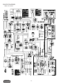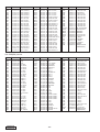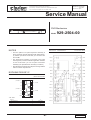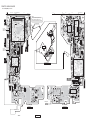
1
Clarion Co., Ltd. Published by Service Dept. 50 Kamitoda, Toda-shi, Saitama 335-8511 Japan Service Dept.: 5-66 Azuma , Kitamoto-shi, Saitama 364-0007 Japan Tel: +81-48-541-2335 / 2432 FAX: +81-48-541-2703 298-6351-00 Mar.2006 Printed in Japan Service Manual DVD Multmedia Station with Touch Panel Controller Model (QC-6823B-A) (NTSC/ Region No. "1") Model (QC-6823K-A) (PAL/ Region No. "3") Model (QC-6823K-B) (NTSC/ Region No. "3") Model (QC-6823K-C) (PAL/ Region No. "4") SPECIFICATIONS FM tuner section MP3 / WMA section Frequency range: MP3 Sampling rate: MP3 Bit rate: WMA Bit rate: Logical Format: 87.9MHz to 107.9MHz(B-A) 87.0MHz to 108.0MHz(K-A,B,C) Usable sensitivity: 9dBf 50dB quieting sensitivity: 15dBf Alternate channel selectivity: 70dB Stereo separation: 35dB(1kHz) Frequency response: 30Hz to 15kHz(+3/-3dB) Audio amplifier section AM tuner section Frequency range: Usable sensitivity: 530kHz to 1710kHz(B-A) 531kHz to 1629kHz(K-A,B,C) 28dBu DVD player section System: Usable discs: Frequency response: Dynamic range: Distortion: 11.025kHz to 48kHz 8kbps to 320kbps/VBR 48kbps to 192kbps ISO9660 level1, 2 JOLIET or Romeo Digital versatile disc system with CDDA capable DVD video disc,Compact disc 20Hz to 20kHz(CD)(+1/-1dB) 100dB(1kHz) 0.01% -1- Maximum power output: 200W(50W x 4ch) Rate power output: 14w X4ch at 20 Hz to 20kHz,1%,4 ohm (QC-6823K-A,B,C) Power output: 19W x 4 at 4 ohm and 1 % THD+N (CEA-2006) (QC-6823B-A) Speaker impedance: 4 ohm(4 to 8 ohm) VRX765VD VRX766VD Input section Video input: Audio input: 1.0V+0.2/-0.2Vp-p (input impedance 75 ohm) 130mV+60/-60mVrms(High) 600mV+80/-80mVrms(Mid) 840mV+100/-100mVrms(Low) (input impedance 10k ohm or greater) * Video output section Video output: 1.0V+0.2/-0.2Vp-p(output impedance 75 ohm) LCD monitor section Screen size: Display method: Drive method: Pixels: 7-inch wide type (152mm Width x 85mm Height) Transmission type TN liquid crystal display TFT(thin-film transistor) active matrix driving 336,960(1440x234) * * General Power source voltage: 14.4V DC (10.8 to 15.6V allowable) Ground: Negative Current consumption: 4.0A(1W) Auto antenna rated current: 500mA less Dimensions(mm): Main unit 178(W)x50(H)x165(D) Remote control unit 54(W)x28.8(H)x155(D) Weight: Main unit 2.4kg Remote control unit 100g (including battery) * Specifications comply with JEITA Standards. * CEA-2006:New standard of Consumer Electronics Association. * Specifications and design are subject to change without notice for further improvement. * * * COMPONENTS QC-6823B-A,K-A,K-B Main unit Remote control unit Batteries(AA.SUM-3) Universal mounting bracket DCP case Power supply lead(18P) Outer escutcheon Parts bag Electro tap Machine screw(M4 x3) Flat head screw(M5 x8) Sems hex. bolt(M5 x8) Parts bag Hook plate Cord clamp Rubber cap Screw(M5 x10) Parts bag Pad screw(M1.7 x5 Blk) Parts bag RCA CAP NOTES * * * * * * As for this model, the tuner of the DSP type is used.When you exchange it due to the tuner pack(BL1:880-2091C) trouble, it is necessary to adjust for S-meter etc.Special JIG is necessary for an accurate adjustment.The procedure document for the exclusive use jig is appended to it. This DSP IC SAF7730H(051-6706-10) of main PWB is exposed die soldering pad type. The middle of this IC package is soldered with the main PWB, and it cannot remove in an ordinary soldering iron. Please use special removal JIG at the time of IC exchange. We cannot supply PWB with component parts in principle. When a circuit on PWB has failure , please repair it by component parts base. Parts which are not mentioned in service manual are not supplied. This DVD player can play the following discs. DVD video discs,Video CDs,CD text,Audio CDs. This DVD video player cannot playback DVDAudio,DVD-RAM,Photo CDs,etc. This unit can play back CD-R/CD-RW,DVD-R/RW discs VRX765VD VRX766VD on which MP3/WMA music data have been recorded.. This unit is a ID3 Tag compatible model. This unit supports the title,artist and album display of the ID3 Tag versions 1 and 1.1. After disc loading,the play mode is automatically engaged. This product incorporates copyright protection technology that is protected by U.S. patents and other intellectual property rights . Use of this copyright protection tecnology must be authorized by Macrovision, and is intended for home and other limited viewing uses only unless otherwise authorized by Macrovision. Reverse engineering or disassembly is prohibited. The DVD video system assigns a region number to DVD video players and DVD discs by sales area. The DVD video region number is marked on the disc jacket. This product includes technology owned by Microsoft Corporation and cannot be used or distributed without a license from MSLGP. Manufactured under license from Dolby Laboratories. "Dolby" and the double-D symbol are trademarks of Dolby Laboratories. "DTS" and "DTS Digital Out" are trademarks of Digital Theater Systems,Inc. "iPod" is for legal or righthoder-authorized copying only.Do not steal music. -2- ----------1 RCB-177-200 1 ----------2 300-9035-01 1 335-6035-60 1 854-6420-50 1 940-8145-00 1 ----------060-0018-00 1 714-4003-8H 4 714-5008-4B 4 716-0496-501 5 ----------330-8216-01 2 335-0833-01 1 345-3653-01 1 716-0726-51 1 ----------716-0872-52 1 ----------345-3799-20 12 CAUTIONS Use of controls,adjustment or performance of procedures other than those specified herein,may result in hazardous radiation exposure. The compact disc player should not be adjusted or repaired by anyone except properly qualified service personnel. QC-6823B-A To engineers in charge of repair or inspection of our products. Before repair or inspection, make sure to follow the instructions so that customers and Engineers in charge of repair or inspection can avoid suffering any risk or injury. 1. Use specified parts. The system uses parts with special safety features against fire and voltage. Use only parts with equivalent characteristics when replacing them. The use of unspecified parts shall be regarded as remodeling for which we shall not be liable. The onus of product liability (PL) shall not be our responsibility in cases where an accident or failure is as a result of unspecified parts being used. 2. Place the parts and wiring back in their original positions after replacement or re-wiring. For proper circuit construction, use of insulation tubes, bonding, gaps to PWB, etc, is involved. The wiring connection and routing to the PWB are specially planned using clamps to keep away from heated and high voltage parts. Ensure that they are placed back in their original positions after repair or inspection. If extended damage is caused due to negligence during repair, the legal responsibility shall be with the repairing company. 3. Check for safety after repair. Check that the screws, parts and wires are put back securely in their original position after repair. Ensure for safety reasons there is no possibility of secondary ploblems around the repaired spots. If extended damage is caused due to negligence of repair, the legal responsibility shall be with the repairing company. -3- 4. Caution in removal and making wiring connection to the parts for the automobile. Disconnect the battery terminal after turning the ignition key off. If wrong wiring connections are made with the battery connected, a short circuit and/or fire may occur. If extensive damage is caused due to negligence of repair, the legal responsibility shall be with the repairing company. 5. Cautions in soldering Please do not spread liquid flux in soldering. Please do not wash the soldering point after soldering. 6. Cautions in soldering for chip capacitors Please solder the chip capacitors after pre-heating for replacement because they are very weak to heat. Please do not heat the chip capacitors with a soldering iron directly. 7. Cautions in handling for chip parts. Do not reuse removed chips even when no abnormality is observed in their appearance. Always replace them with new ones. (The chip parts include resistors, capacitors, diodes, transistors, etc). Please make an operation test after replacement. 8. Cautions in handling flexible PWB Before working with a soldering iron, make sure that the iron tip temperature is around 270 . Take care not to apply the iron tip repeatedly(more than three times)to the same patterns. Also take care not to apply the tip with force. 9. Turn the unit OFF during disassembly and parts replacement. Recheck all work before you apply power to the unit. 10. Cautions in checking that the optical pickup lights up. The laser is focused on the disc reflection surface through the lens of the optical pickup. When checking that the laser optical diode lights up, keep your eyes more than 30cms away from the lens. Prolonged viewing of the laser within 30cms may damage your eyesight. 11. Cautions in handling the optical pickup The laser diode of the optical pickup can be damaged by electrostatic charge caused by your clothes and body. Make sure to avoid electrostatic charges on your clothes or body, or discharge static electricity before handling the optical pickup. 11-1. Laser diode The laser diode terminals are shorted for transportation in order to prevent electrostatic damage. After replacement, open the shorted circuit. When removing the pickup from the mechanism, short the terminals by soldering them to prevent this damage. 11-2. Actuator The actuator has a powerful magnetic circuit. If a magnetic material is put close to it. Its characteristics will change. Ensure that no foreign substances enter through the ventilation slots in the cover. 11-3. Cleaning the lens Dust on the optical lens affects performance. To clean the lens, apply a small amount of isopropyl alcohol to lens paper and wipe the lens gently. VRX765VD VRX766VD ERROR DISPLAYS If an error occurs,one of the following displays is displayed.Take the measures described below to eliminate the problem. Cause A CD is caught inside the CD deck and is not ejected. A CD cannot be played due to scratches,etc. A CD is loaded upside-down inside the CD deck and does not play. A CD inside the CD changer is not loaded. A CD inside the CD changer cannot be played due to scratches,etc. A CD inside the CD changer cannot be played because it is loaded upside-down. Error display ERROR 2 DVD player ERROR 3 ERROR 6 ERROR 2 CD changer ERROR 3 ERROR 6 Measure This is a failure of CD deck's mechanism and cinsolt your store of purchase. Replace with a non-scratched,nonwarped disc. Eject the disc then reload it properly. This is a failure of CD changer's mechanism. Replace with a non-scratched,nonwarped disc. Eject the disc then reload it properly. Note:If an error display other than the ones described above appears, press the reset button. * When the reset button is pressed,frequencies of TV/radio stations,titles,etc. stored in memory are cleared. SYSTEM CONNCTION Yellow Video Selector Front Speakers RCA video cable (included the TV tuner) (Gray) Red Non fader output White Digital optical fiber cable (included the DVH940) CeNET cable (included the TV tuner) Purple RCA cable (sold separately) Rear Speakers 4-Channel Amplifier RCA cable (sold separately) TV Tuner Center speaker built-in amplifier (TTX7501z/TTX7504z) (SRK5) CeNET cable (included the SIRIUS) *XM ; sold separately RCA video cable (included the VCZ625) VRX765VD/VRX766VD Powered sub-woofer built-in amplifier (SRV303) Satellite Radio Receiver CeNET CD Changer RCA cable (included the DVH940) CeNET cable (included the DVH940) (Black) RCA cable (sold separately) 5.1 ch Surround Decoder (DCZ625) CeNET Y-adapter (CCA-519-601, sold separately) (DVH940) Ferrite clamp (Included the DVD changer) CeNET DVD Changer (VCZ625) CeNET Cable (included the Changer) (Gray) Set the [SLAVE/STAND ALONE] switch to the [SLAVE] position. SLAVE STAND ALONE Set the [CeNET/STAND ALONE] switch to the [CeNET] position. CeNET Digital optical fiber cable (DCA-005/008 , sold separately) VRX765VD VRX766VD -4- STAND ALONE WIRE CONNECTION Yellow Radio antenna jack Yellow BACK UP (+12V main power) Black Ground TV tuner input terminal or DVD changer input terminal Purple Rear r ight + Purple/Black CeNET terminal Red Gray Rear r ight +12V accessory Front right + Gray/Black Front right White Optical output connector No. 1 3 5 7 9 11 13 15 Description SP R/L(+) SP F/L(-) SP F/L(+) SP F/R(+) SP F/R(-) SP R/R(+) SP R/R(-) BACK UP J601 No. 2 4 6 8 10 12 14 16 Description SP R/L(-) PHONE MUTE ACC AUTO ANT REMOTE ILLUMI PARKING BRAKE GND White/Black 1 3 5 7 9 11 13 2 4 6 8 10 12 14 15 16 Green Green/Black Blue/White Orange/White Blue Front left Rear left + Rear left Amp. turn-on lead Illumination Auto antenna Brown Grass-green iPod Front left + Phone mute Parking brake lead Connector cab le (CCA-670-600) No. 1 2 3 4 5 6 7 8 9 10 P201 2 4 6 8 10 12 14 16 18 20 1 3 5 7 9 11 13 15 17 19 Gray Red White Black Gray Right left Front audio output terminal Right left Rear audio output terminal 4-Channel Amplifier Red White Purple Description Description No. 11 2ZONE LEFT LEFT REAR 12 2ZONE RIGHT RIGHT REAR 13 V OUT GND LEFT FRONT RIGHT FRONT 14 V IN GND 15 VIDEO OUT S-GND 16 VIVEO IN S-GND 17 V-AUDIO GND L NF LEFT 18 V-AUDIO GND R NF RIGHT 19 V-AUDIO LEFT S-GND 20 V-AUDIO RIGHT S-GND Red Right left Non fader output terminal White Yellow Rear monitor Video output terminal Yellow VTR etc. Video Black White Audio (left) Red Red Visual input terminal Audio (right) Wireless Head phone Red Right Green Left (2-ZONE output terminal) White -5- VRX765VD VRX766VD BLOCK DIAGRAM Main unit section VRX765VD VRX766VD -6- ADJUSTMENTS *Refer to the printed circut board(47,50 or 51 pages)for an adjustment point and VR. *The NTSC (K-A:PAL)composite output signal of the signal generators of adjustment is performed with the following output.Video input of visual mode. A image signal: 714mV A synchronized signal: 286mV Sub PWB section 1. Confirm the power supply voltage Input signal: 10-steps wave Measurement is performed by composite screen display.It measures by digitalbolt meter and DIMMER is 100%. 1-1.Adjust VR551 so that voltage of TP593 is 5.30 +0.02/0.02V. Caution: A LCD controller will be damaged if the voltage beyond 5.45V is added. 1-2.Confirm that TP556 is 3.3 +0.2/-0.2V 1-3.Confirm that TP558 is 7.5 +0.2/-0.2V 1-4.Confirm that TP559 is 18.5 +0.8/-0.8V 1-5.Confirm that TP555 is -12.0 +0.5/-0.5V LCD PWB section 2. Confirm the PLL lock Input signal: 10-steps wave 2-1.It checks that see a screen and 10 gradation display do not have a synchronous flow. After checking and uniting the freerun frequency of item 9.when the synchronoization cannot be taken. 3. BRIGHT voltage adjustment Input signal: 10-steps wave Mesurement is performed by composite screen display. It measures by digital bolt meter. 3-1.Adjust VR804(BRIGHT) so that the voltage of TP805(BRIGHT) will become 2.00 +0.02/-0.02V. 4. RGB-AMP adjustment (black-black) Input signal: 10-steps wave Measurement is performed by composite screen display. It measures with an oscilloscope. 4-1.Adjusts VR805 so that the black-black level (V B-B) of the waveform of TP861 (G) will become 4.0 +0.1/-0.1V. (Refer to Fig. 1) 5. Contrast adjustment (black-white) Input signa: 10-steps wave Measurement is performed by composite screen display. It measures with an oscilloscope. 5-1.Adjusts VR801 so that the black-black level (V B-w) of the waveform of TP861 (G) will become 3.8 +0.1/-0.1V. (Refer to Fig. 1) 6. Gamma voltage check Input signal: 10-steps wave Measurement is performed by composite screen display. It measures with an oscilloscope. 6-1.Confirm the waveform of TP861(LCD G) that ten gradation has come out. 6-2.It checks that it is the 3rd gradation is 2.3+0.2/-0.2V. 6-3.Confirm that TP806(Gamma 0) is 2.30 +0.20/-0.20V 6-4.Confirm that TP807(Gamma 2) is 2.13 +0.20/-0.20V 7. White balance adjustment Input signal: 10-steps wave Measurement is performed by composite screen display. It measures DC range of an oscilloscope. *Are careful in order to perform correctly white balance adjustment. *1. The range of CH1,CH2 of an oscilloscope is used as 1V range. *2. CH1,CH2 are indicated by GND and GND is united. (Refer to Fig. 2) CH1 CH2 (KI2 7-1.White balance red adjustment 7-1-1.The waveform of TP861 is displayed on CH1 of an oscilloscope, and the waveform of TP862(LCD-R) is displayed on CH2. 7-1-2.Adjust VR802(BRT-R) so that the waveform of TP862(LCD-R) will become the same as the waveform of TP861. 7-2.White balance blue adjustment 7-2-1.The waveform of TP861 is displayed on CH1 of an oscilloscope, and the waveform of TP860(LCD-B) is displayed on CH2. 7-2-2.Adjust VR803(BRT-B) so that the waveform of TP860(LCD-B) will become the same as the waveform of TP861. 8. VCOM AC adjustment Input signal: 10-steps wave Measurement is performed by composite screen display. It measures with an oscilloscope. 8-1.Adjust the VR806(VCOM AC) so that amplitude of a waveform of TP852(VCOM AC) is 7.0+0.1/-0.1V. There are no abnormalities, such as distortion, in a waveform. (KI1 -7- VRX765VD VRX766VD 9. Free run frequency adjustment Input signal: 10-steps wave Measurement is performed by composite screen display. It measures by frequency counter and DIMMER is 100%. 9-1.Adjust VR941 so that the frequency of TP949 will become to 15.734kHz+10/-10Hz. *TP804 is made to short-circuit to GND. It checks that the voltage of TP951 is 1.61+0.20/-0.20V at this time. And checks that the voltage of TP952 is same. Main PWB section 19.TV delay time adjustment Adjustment is performed in TV mode and the stable channel which does not have disorder in a screen is used. It acts as the monitor of the signal of TP329 (Normal horizontal synchronous input) and TP421 (Delay output synchronization). 19-1.To falling of the Horizontal Synchronizing signal of TP329, VR401 is adjusted so that falling of TP421 may be overdue 3.50 +0.1/-0.1 uS 19-2.Confirm that Low level time of TP421 is 4.7 +0.7/-0.7uS. 19-3.It checks whether there is any gap in the right-and-left balance of a superimposition display to TV image, or the character has not passed by the end after the adjustment. Recommends connected TV tuner :TTX7501Z(ZT4620B-A) for NTSC,:TTX7504Z(ZT-4610K-A) for PAL(s). 10.PAL burst cleaning coil adjustment Input signal:The color bar signal of PAL. It measures with an oscilloscope etc. 10-1.Adjust L803 coil so that change TP860(LCD-B) of a color waveform may be lost. 11.BRT/COL/HUE check Input signal: Split color bar signal 11-1.Comfirm that the color bar is normally displayed at state to begin. 11-2.Comfirm that the BRT/COL/HUE control is moved screen. 11-3.Comfirm the superimposition display is normally. 20.S-meter adjustment of BUS-tuner The adjustment data is written in the memory of EEPROM(IC502).The special jig and software are necessary for BUS-TUNER adjustment. * CeNET-analyzer * Windows installed Personal computer * SSG * Adjustment-Software(Ver.Y4-S009-513-20051111) 12.V-MUTE check Input signal:Split color bar signal 12-1.Comfirm a composite video screen is mute of VMUTE:"H" . a. Installation of software in the set-folder of the writing E2P. b Connect CeNET-analyzer to the unit with the CeNETcable. c Connect CeNET-analyzer(MASTER/SLAVE side) to the PC with the serial crossing cable. d Connect POWER-lead of CeNET-analyzer to the POWER-lead of the unit. e Connect the antenna to the unit.(FM-ANT for first adjustment) f Turn on CeNET-analyzer,and press the RESET-button of it. 13.Wide mode check Input signal:Split color bar signal 13-1. Comfirm a wide mode changed screen(Full wide /Wide /Cinema /Normal). 14.Screen position check Input signal: Mono-sucpeo signal. 14-1.Comfirm that the screen is displayed in the center by mono-scope display (Video mode). 14-2.Comfirm that the screen is displayed in the center by radio screen display (RGB mode). 15.Synchronicity condition check 15-1.Comfirm a normal display by DVD playback (main menu) of HITOMI. 20-1.Set up the software 20-1-1.Click [ADJ_DSP]. 20-1-2.Click [open Comm PORT].(To open the COM port of PC) 20-1-3.Click [Initialization of JIG].(The BUS-analyzer sounds) 20-1-4.Click [Incoming connection].(The unit is recognized to the BUS-analyzer) The data is displayed, and the display changes regularly. 16.Key sw operation/Illum check 16-1Comfirm that key operation can be performed. 16-2Comfirm the key illum lighting . 17.Back light check Power supply voltage: 13.2V DIMMER=100% 17-1.Comfirm the TP962 freqency is 63kHz +5/-5kHz. 17-2.Comfirm the TP961 voltage is 5.2V +0.5/-0.5V. 17-3.Comfirm the light on at the power supply voltage to 10V. 17-4.Comfirm check at DIMMER control changes so that brightness changes. 20-2.PRN data writing / Set up FM-IF-Offset data 20-2-1.Click [Initial EEPROM with CS 16], and select PRNFILE. The PRN-data is write in EEP-ROM of the unit. 20-2-2.Confirm "OK" display after writing of data. 20-2-3.Click [Setting-prn] under "FM IF-COUNT".(the written FM-IF-Offset data becomes effective.) 18.VCOM-DC check Input signal:10-steps wave Measurement is performed by composite screen display. 18-1.Adjust VR807(VCOM DC) so that a screen flicker may become the minimum. VRX765VD VRX766VD 20-3.Adjustments FM S-meter 20-3-1.Set SG output to 65dBuV.(FM) 20-3-2.Click [Adj,HI] of "FM S-Meter".(Wait until the value stops.) -8- 20-3-3.Set SG output to 55dBuV.(FM) 20-3-4.Click [Adj,LO] of "FM S-Meter".(Wait until the value stops.) 20-3-5.Click [Check].If the display is not within +/-0.5dBuV of ANT-output level of SG, readjust with "MODON"(22.5kHz 400Hz). Slide mechanism section 23 Horizontally position Calibration jig is used in order to memorize a horizontal level position. Please refer to an attached figure A. It is made to memorize horizontally among a figure in the position of points. It is performing giving about 3 degrees of angles intentionally. If the MUTE button and the ISR button are pushed, a beep sound will sound. A calibration begins at the time. Flow of operation a. Slide OPEN b. Tilt up: Memory of 110 degree position c. Tilt down: Memory of horizontally position (Jig used) d. Tilt up e. Tilt down f. Slide CLOSE g. Calibration end 20-4.Set up FM-IF-Offset data * Exchange the antenna for "AM-ANT-dummy" <!8>20-4-1.Click [Setting-prn] under "AM IF-COUNT".(The AM-IF-Offset data of EEPRON is effective.) 20-4-2.Click [Check], and confirm the display is within +/500.0. When computer continues to freeze, click [RESET] of "MENU", and readjust the lost adjustment point.IF not returning, press the RESET-button of CeNET-analyzer.and restart adjustment from the first step. 20-5.Adjustments AM S-meter 20-5-1.Set SG output to 70dBuV.(AM) 20-5-2.Click [Adj,HI] of "AM S-Meter".(Wait until the value stops.) 20-5-3.Set SG output to 40dBuV.(AM) 20-5-4.Click [Adj,LO].(Wait until the value stops.) 20-5-5.Click [Check]. If the display is not within +/-0.5dBV of ANT-output level of SG, readjust with "MOD-ON"(30% 400Hz). Finally, push the reset button of the unit. # 21.OSD dot adjustment An adjustment screen is performed on the "T-PNL" screen, or the 9th screen (five-step display) of "COLORBAR" in the test mode. Please choose the screen which is easy to adjust from either. 21-1.The hole has opened in the Lower case and it adjusts by VR451 mounted in the MAIN-PWB solder side. 21-2.In the case of adjustment in a T-PNL screen It adjusts so that the white line of a 1-dot display long may be vividly displayed. 21-3.In the case of adjustment by 9th COLOR-BAR It adjusts so that the white line of top, the bottom and inside may be displayed as clear white. -9- VRX765VD VRX766VD EXPLANATION OF IC + OSC Dead time Control R Q S High side Driver Low side Driver Over+ 16 GND 9 17 + Over - 15 OSC 10 Soft S 14 Boot strap Thermal shut down + Error Amp in- 13 26 1,2,22,23,24,25 3,4,5,6 P GND Vout VDD Error Amp out 12 7 V GH 8 VB CONTROL V GL 21 R/C (H-ON) 18 20 Vboot DC to DC Converter 11 Vref MD1424R 19 VCC 051-3924-90 pin 6: PLL CTL 4 : IN : PLL multiply select. pin 7: PLL CTL 3 : IN : PLL multiply select. pin 8: PLL CTL 2 : IN : PLL multiply select. pin 9: PLL CTL 1 : IN : PLL multiply select. pin 10: PLL CTL 0 : IN : PLL multiply select. pin 11: DT CK Sel_N : IN : Display clock select. pin 12: DT CK IN : IN : Display clock input. pin 13: VSS : - : Digital ground. pin 14: VDD : - : Digital power supply. pin 15: CPU D 0 :I/O: CUP interface. Data bus. pin 16: CPU D 1 :I/O: CUP interface. Data bus. pin 17: CPU D 2 :I/O: CUP interface. Data bus. pin 18: CPU D 3 :I/O: CUP interface. Data bus. pin 19: CPU D 4 :I/O: CUP interface. Data bus. pin 20: CPU D 5 :I/O: CUP interface. Data bus. pin 21: CPU D 6 :I/O: CUP interface. Data bus. pin 22: CPU D 7 :I/O: CUP interface. Data bus. pin 23: CPU WAIT_N : O : CUP interface. Wait. pin 24: CPU READY_N : O : CUP interface. Ready. OZ9910ISN-T2 Dual Forward PWM Controller 13 VIN 051-3925-90 Vref 12 GND A 4 Voltage Ref Current Bias LCT 6 ADJ 7 High-side Driver Buffer LF OSC Current Feedback Control I-SENSE 11 Output Driver Control Logic HF OSC Voltage Feedback 3V Control V-SENSE 9 Feedback Control LFCK CMP/SST 10 : - : Digital power supply. pin 27: VSS : - : Digital ground. : IN : CUP interface. Chip select. pin 29: CPU WR_N : IN : CUP interface. Write command. pin 30: CPU RD_N : IN : CUP interface. Read command. pin 31: CPU PS 2 : IN : CUP interface. Port select. pin 32: CPU PS 1 : IN : CUP interface. Port select. 3 N DRV 2 1 N DRV 4 pin 33: CPU PS 0 : IN : CUP interface. Port select. pin 34: CPU SD OUT : O : CUP interface. Serial data output. 2 P GND pin 35: CPU S D IN : IN : CUP interface. Serial data input. 5 CT pin 36: CPU S CS_N : IN : CUP interface. Serial chip select. 14 HSB 16 P DRV 1 15 P DRV 3 8 ENA pin 37: CPU S CLK : IN : CUP interface. Serial clock. pin 38: CPU SER_N : IN : CUP interface. Parallel/Serial select. pin 39: CPU RESET_N : IN : CUP interface. Reset. pin 40: VSS TerminalDescription pin 1: N DRV 4 : - : Digital power supply. pin 42: Memo A 0 : O : Pattern Memory interface. Address output. pin 43: Memo A 1 : O : Pattern Memory interface. Address output. pin 44: Memo A 2 : O : Pattern Memory interface. Address output. pin 45: Memo A 3 : O : Pattern Memory interface. Address output. pin 46: Memo A 4 : O : Pattern Memory interface. Address output. : Low-current signal ground. pin 47: Memo A 5 : O : Pattern Memory interface. Address output. : High frequency oscillator capacitor for operation and striking frequency. pin 48: VSS : - : Digital ground. pin 49: Memo A 6 : O : Pattern Memory interface. Address output. : Low frequency timing capacitor for LPWM dimming and striking timer. pin 50: Memo A 7 : O : Pattern Memory interface. Address output. pin 51: Memo A 8 : O : Pattern Memory interface. Address output. : Bottom MOSFET gate drive output in dual forward converter. 2: P GND : High-current power ground. pin 3: N DRV 2 : Bottom MOSFET gate drive output in dual forward converter. pin pin 4: GND A 5: CT 6: LCT : - : Digital ground. pin 41: VDD pin pin : O : CUP interface. Interrupt. pin 26: VDD pin 28: CPU CS_N HFCK Protection pin 25: CPU INT_N pin 7: ADJ : Signal input for LPWM/ analog dimming. pin 52: Memo A 9 : O : Pattern Memory interface. Address output. pin 8: ENA : Enable and reset. pin 53: Memo A 10 : O : Pattern Memory interface. Address output. pin 9: V-SENSE : Transformer output over-voltage and overcurrent detection. pin 54: Memo A 11 : O : Pattern Memory interface. Address output. pin 55: VDD : - : Digital power supply. pin 56: VSS : - : Digital ground. pin 10: CMP/SST : Soft start and loop compensation capacitor. pin 11: I-SENSE : Lamp current sensing and lamp “on” detection. pin 57: Memo A 12 : O : Pattern Memory interface. Address output. pin 12: Vref : Reference voltage output. pin 58: Memo A 13 : O : Pattern Memory interface. Address output. pin 13: VIN : Supply voltage for IC. pin 59: Memo A 14 : O : Pattern Memory interface. Address output. pin 14: HSB : High side driver buffer output. pin 60: Memo A 15 : O : Pattern Memory interface. Address output. : Top MOSFET gate drive output in dual forward converter. pin 61: Memo A 16 : O : Pattern Memory interface. Address output. pin 62: Memo A 17 : O : Pattern Memory interface. Address output. : Top MOSFET gate drive output in dual forward converter. pin 63: VSS : - : Digital ground. pin 64: Memo A 18 : O : Pattern Memory interface. Address output. pin 65: Memo A 19 : O : Pattern Memory interface. Address output. pin 66: Memo A 20 : O : Pattern Memory interface. Address output. pin 67: Memo A 21 : O : Pattern Memory interface. Address output. pin 15: P DRV 3 pin 16: P DRV 1 051-6456-00 YGV629-VZ TerminalDescription pin 1: PLL VDD Video display processor : - : PLL power supply. pin 2: PLL FILTER : - : PLL filter connection. pin 3: PLL VSS : - : PLL ground. pin 4: NC : - : Not in use. pin 5: PLL CTL 5 : IN : PLL multiply select. VRX765VD VRX766VD pin 68: Memo A 22 : O : Pattern Memory interface. Address output. pin 69: Memo A 23 : O : Pattern Memory interface. Address output. pin 70: Memo A 24 : O : Pattern Memory interface. Address output. pin 71: VDD : - : Digital power supply. pin 72: VSS : - : Digital ground. pin 73: Memo WE_N : O : Pattern Memory interface. Write command. - 10 - pin 74: Memo OE_N : O : Pattern Memory interface. Output enable. pin140: VDD : - : Digital power supply. pin 75: Memo D 15 :I/O: Pattern Memory interface. Data I/O. pin141: X IN : IN : Crystal connection. pin 76: Memo D 7 :I/O: Pattern Memory interface. Data I/O. pin142: X OUT : O : Crystal connection. pin 77: Memo D 14 :I/O: Pattern Memory interface. Data I/O. pin143: VSS : - : Digital ground. pin 78: Memo D 6 :I/O: Pattern Memory interface. Data I/O. pin144: NC : - : Not in use. pin 79: Memo D 13 :I/O: Pattern Memory interface. Data I/O. pin 80: Memo D 5 :I/O: Pattern Memory interface. Data I/O. pin 81: VSS : - : Digital ground. pin 82: VDD : - : Digital power supply. pin 83: Memo D 12 :I/O: Pattern Memory interface. Data I/O. 051-7221-18 TC7SH04FU Single Inverter pin 84: Memo D 4 :I/O: Pattern Memory interface. Data I/O. pin 85: Memo D 11 :I/O: Pattern Memory interface. Data I/O. NC 1 5 VCC pin 86: Memo D 3 :I/O: Pattern Memory interface. Data I/O. IN 2 GND 3 4 OUT pin 87: Memo D 10 :I/O: Pattern Memory interface. Data I/O. pin 88: Memo D 2 :I/O: Pattern Memory interface. Data I/O. pin 89: Memo D 9 :I/O: Pattern Memory interface. Data I/O. pin 90: Memo D 1 :I/O: Pattern Memory interface. Data I/O. pin 91: VSS : - : Digital ground. pin 92: VDD : - : Digital power supply. pin 93: Memo D 8 :I/O: Pattern Memory interface. Data I/O. pin 94: Memo D 0 :I/O: Pattern Memory interface. Data I/O. 051-7509-90 Terminal Description pin 1 : 1 A_ pin 95: Memo RAHZ_N : IN : Pattern Memory interface. High-impedance. pin 96: X TEST 2 : IN : For the test. Connect to VDD. pin 97: X TEST 1 : IN : For the test. Connect to VDD. pin 98: X TEST 0 : IN : For the test. Connect to VDD. pin 99: Moni V S IN_N : IN : Monitor interface. Vertical Sync input. pin100: Moni H S IN_N : IN : Monitor interface. Horizontal Sync input. pin101: NC : - : Not in use. pin102: A VDD : - : Analog power supply. pin103: Moni Red : O : Monitor interface. Analog Red output. pin104: Moni Green : O : Monitor interface. Analog Green output. pin105: Moni Blue : O : Monitor interface. Analog Blue output. pin106: Moni IREF : - : Monitor interface. DAC reference power supply. pin107: A VSS : - : Analog ground. pin108: NC : - : Not in use. pin109: VDD : - : Digital power supply. pin110: VSS : - : Digital ground. pin111: Moni D Red 0 : O : Monitor interface. Digital Red output. pin112: Moni D Red 1 : O : Monitor interface. Digital Red output. pin113: Moni D Red 2 : O : Monitor interface. Digital Red output. pin114: Moni D Red 3 : O : Monitor interface. Digital Red output. pin115: Moni D Red 4 : O : Monitor interface. Digital Red output. pin116: Moni D Red 5 : O : Monitor interface. Digital Red output. pin117: VSS : - : Digital ground. pin118: VDD SN74LV123APWR Dual Retriggerable Monostable Multivibrator : Channel 1 input A_. Ref. Table 1. : Channel 1 input B. Ref. Table 1. pin 3 : 1 CLR_ : Channel 1 Clear in. Ref. Table 1. pin 4 : 1 Q_ : Channel 1 Negative output. Ref. Table 1. pin 5 : 2 Q : Channel 2 Positive output. Ref. Table 1. pin 6 : 2 CX : Connect to RX/CX through a capacitor. pin 7 : 2 RX/CX : Connect to CX through a capacitor, and connect to VCC through a resistor. pin 2 : 1 B pin 8 : GND : Ground. pin 9 : 2 A_ : Channel 2 input A_. Ref. Table 1. pin 10: 2 B : Channel 2 input B. Ref. Table 1. pin 11: 2 CLR_ : Channel 2 Clear in. Ref. Table 1. pin 12: 2 Q_ : Channel 2 Negative output. Ref. Table 1. pin 13: 1 Q : Channel 1 Positive output. Ref. Table 1. pin 14: 1 CX : Connect to RX/CX through a capacitor. pin 15: 1 RX/CX : Connect to CX through a capacitor, and connect to VCC through a resistor. pin 16: VCC : Positive supply voltage. 1 2 3 4 : - : Digital power supply. 5 pin119: Moni D Green 0: O : Monitor interface. Digital Green output. 6 pin120: Moni D Green 1: O : Monitor interface. Digital Green output. pin121: Moni D Green 2: O : Monitor interface. Digital Green output. 7 pin122: Moni D Green 3: O : Monitor interface. Digital Green output. to VCC pin123: Moni D Green 4: O : Monitor interface. Digital Green output. 8 1A_ VCC CK 1B 1Rx/Cx 1Clear_ 1Cx Clear 1Q_ 1Q 16 15 14 13 2Q_ 2Q 12 2Cx 2Clear_ Clear 11 2B 2Rx/Cx 10 2A_ CK GND 9 pin124: Moni D Green 5: O : Monitor interface. Digital Green output. pin125: VSS : - : Digital ground. pin126: VDD : - : Digital power supply. Table 1. A_ in B in CLR_ in Q out Q_ out D-E H H U-P D-P Inhibit X L H L H Inhibit H X H L H Output enable L U-E H U-P D-P Output enable L H U-E U-P D-P Reset D-E D-P U-E U-P X X X L L H pin127: Moni D Blue 0 : O : Monitor interface. Digital Blue output. Output Enable pin128: Moni D Blue 1 : O : Monitor interface. Digital Blue output. pin129: Moni D Blue 2 : O : Monitor interface. Digital Blue output. pin130: Moni D Blue 3 : O : Monitor interface. Digital Blue output. pin131: Moni D Blue 4 : O : Monitor interface. Digital Blue output. pin132: Moni D Blue 5 : O : Monitor interface. Digital Blue output. pin133: VSS : - : Digital ground. pin134: Moni FSC : O : Monitor interface. Sub-carrier clock. pin135: Moni YS_N : O : Monitor interface. YS output. : : : : : Down-edge Down-pulse Up-edge Up-pulse Don't care. pin136: Moni V SYNC_N: O : Monitor interface. Vertical Sync output. pin137: Moni H/C SYN_N : O: Monitor interface. Horizontal/Composite Sync output. pin138: Moni BLANK_N : O : Monitor interface. Blank output. pin139: Moni DOT CLK : O : Monitor interface. Dot clock output. - 11 - VRX765VD VRX766VD 052-7078-01 uPD703276YGJ-512UENA System Controller pin 53: IRI : IN : The remote control signal input. pin 54: NU : IN : Not in use. pin 55: NU : IN : Not in use. music. pin 56: NU : IN : Not in use. iPod is a trademark of Apple Computer, Inc., registered in the U.S. and other countries. pin 57: NU : IN : Not in use. pin 58: OSD RST : O : The reset pulse output for the on screen display IC. pin 59: TP RX : IN : The serial data input from the touch panel micro computer. pin 60: TP TX : O : The serial data output to the touch panel micro computer. pin 61: DVD TX : O : The serial data output to the DVD mechanism. is for legal or rightholder-authorized copying only. Don't steal TerminalDescription pin 1: A Vref 0 : - : Reference voltage for the internal ADC. pin 2: A VSS : - : Negative voltage supply for analog section. pin 3: SYS ACC : O : ACC detect signal output. pin 4: SUB MUTE : O : Sub-zone audio mute signal output. pin 5: A Vref 1 : - : Reference voltage for the internal DAC. pin 6: RDS CLK : IN : Not in use. pin 62: DVD RX pin 7: AV ON : O : The ON command output to the power supply section. : IN : The serial data input from the DVD mechanism. pin 63: W REMCOM : IN : Wired remote controller signal input. pin 8: FLASH : IN : The signal input for the flash memory control. pin 64: BLKO : O : The blanking signal output. pin 65: VID / RGB : O : L = Video, H = RGB. : - : Positive voltage supply. pin 66: FL ON : O : The fluorescent light of the LCD ON signal output. pin 9: VDD pin 10: REG C : - : The capacitor connection. pin 11: GND : - : Ground. pin 67: BEEP : O : Beep out. pin 12: X in : IN : Crystal connection. Main 31.4MHz. pin 68: OSD RX pin 13: X out : O : Crystal connection. Main 31.4MHz. : IN : Serial data input from on-screen-display IC. pin 14: RESET : IN : Reset signal input. pin 69: OSD TX : O : Serial data output to on-screen-display IC. pin 70: OSD SCK : O : The clock pulse output to the on screen display IC. pin 71: OSD CE : O : Chip enable output to on-screen-display IC. pin 72: OSD INH : O : Inhibit pulse output to on-screen-display IC. pin 15: XT I : IN : Crystal connection. Sub 32.758kHz. pin 16: XT O : O : Crystal connection. Sub 32.758kHz. pin 17: POWER KEY : IN : Power key input. pin 18: BU 9V DET : IN : Backup 9V detection. pin 19: BU 6V DET : IN : Backup 6V detection. pin 20: NU : IN : Not in use. pin 73: Freq SEL : O : Frequency select. pin 21: OSD INT : IN : The interrupt signal input for the on screen display. pin 74: OPN/CL SW : IN : Open/Close switch signal input. pin 75: EJECT SW : IN : Eject switch signal input. pin 22: TUN SDA :I/O: I2BUS serial data input/output for the tuner pack. pin 76: CATS DET : IN : CATS or DCP detection input. pin 77: ROM EN : O : ROM enable signal output. L = OSD OFF. pin 23: TUN SCL : O : I2BUS serial clock output for the tuner pack. pin 24: TP REQ : IN : The request signal from the touch panel micro computer. pin 25: iPod/FLASH O : O : Serial data output to iPod or flash memory. pin 26: iPod/FLASH IN : IN : Serial data input from iPod or flash memory. pin 27: TP RST : O : The reset pulse output to the touch panel micro computer. pin 78: NU : O : Not in use. pin 79: NU : IN : Not in use. pin 80: iPod PWR ON : O : iPod power ON signal output. pin 81: Panel ON : O : LCD panel ON signal output. pin 82: FAN ON : O : The fan on signal output. pin 83: TV/OTHER : O : Horizontal sync select. H = TV. pin 84: FLASH READY : IN : Ready signal input from flash memory. pin 85: EEP DO : O : The serial data output to the EEP-ROM. : O : PWM output. pin 86: CLK OUT : O : SUB-CLOCK-PLUSE output. pin 29: Motor PLS : IN : Motor Pulse input. pin 87: EEP CK : O : The clock pulse output to the EEP-ROM. pin 30: NAVI ON : O : The image signal ON command output for the navigation. pin 88: EEP CE : O : The chip enable signal output to the EEPROM. pin 31: IE BUS TX : O : IE Bus serial data output. pin 89: EEP DI : IN : The serial data input from the EEP-ROM. pin 32: IE BUS RX : IN : IE Bus serial data input. pin 90: NU : IN : Not in use. pin 33: GND : - : Ground. pin 91: KI 0 : IN : Key scan signal input. pin 34: E VDD : - : Positive voltage supply. pin 92: KI 1 : IN : Key scan signal input. pin 35: DSP SDA :I/O: The serial data input/output for the digital signal processor. pin 93: KI 2 : IN : Key scan signal input. pin 94: KI 3 : IN : Key scan signal input. : O : SCL output to the digital signal processor. pin 95: KO 0 : O : Key scan signal output. pin 37: Motor 1 F : O : L = Open. pin 96: KO 1 : O : Key scan signal output. pin 38: Motor 1 R : O : L = Close. pin 97: KO 2 : O : Key scan signal output. pin 39: Motor 2 F : O : L = Tilt Up. pin 98: KO 3 : O : Key scan signal output. pin 40: Motor 2 R : O : L = Tilt Down. pin 99: USA/3rd : IN : L = Asia, H = North America. pin 41: OFFSET DET : IN : Offset-detection input. pin100: Mechanism : IN : L = Without the mechanism. pin 42: Amp Standby : O : The standby signal output to the amplifier. pin101: NTSC/PAL : IN : NTSC/PAL select signal input. L = NTSC. pin102: FLASH WR : IN : The write flag input for the flash memory. pin 43: NU : IN : Not in use. pin103: B VSS : - : Ground for the bus interface section. pin 44: NU : IN : Not in use. pin104: B VDD pin 45: NU : IN : Not in use. : - : Positive voltage supply for the bus interface section. pin 46: NU : IN : Not in use. pin105: ILL DET : IN : Illumination ON signal input. pin 47: NU : IN : Not in use. pin106: BUS ILL : O : Illumination-ON signal output for Ce-NET. pin 48: NU : IN : Not in use. pin107: ILL ON : O : The illumination ON signal output. pin 49: NU : IN : Not in use. pin108: Blink LED : O : LED Blinking signal output. pin 50: NU : IN : Not in use. pin109: DVD ON 2 : O : DVD ON signal output. pin 51: NU : IN : Not in use. pin110: NU : IN : Not in use. pin 52: NU : IN : Not in use. pin111: DVD RST : O : The reset signal output to the DVD mechanism. pin 28: DIMMER pin 36: DSP SCL VRX765VD VRX766VD - 12 - pin112: DSP RST : O : Reset pulse output to the DSP IC. pin 10: A 20 pin113: DSP INIT : IN : The initial finished signal input from the Radio-Audio-DSP. pin 11: WE : IN : Write enable signal input. pin 12: RESET : IN : Reset signal input. pin114: SAMPLE : IN : Not in use. pin 13: NU : - : Not in use. pin115: NU : - : Not in use. pin 14: WP/ACC : IN : The write protection signal input / The acceleration signal input. pin116: AM/FM 8V ON : O : AM/FM 8V ON signal output. pin117: RDS DATA : IN : RDS serial data input. : IN : Address signal input. pin 15: RY/BY : O : The ready/busy signal output. pin118: AM/FM 5V ON : O : AM/FM 5V ON signal output. pin 16: A 18 : IN : Address signal input. pin119: iPod DET : IN : H = iPod is connected. pin 17: A 17 : IN : Address signal input. pin120: NU : - : Not in use. pin 18: A 7 : IN : Address signal input. pin121: DAC RESET : O : The reset pulse output to DAC. pin 19: A 6 : IN : Address signal input. pin122: SYS MUTE : O : System muting signal output. pin 20: A 5 : IN : Address signal input. pin123: AMP MUTE : O : Muting signal output to the Audio Power Amplifier. pin 21: A 4 : IN : Address signal input. pin 22: A 3 : IN : Address signal input. pin124: NU : - : Not in use. pin 23: A 2 : IN : Address signal input. pin125: Motor PWR : O : L = High Speed. pin 24: A 1 : IN : Address signal input. pin126: Photo Sens : IN : Photo sensor signal input. pin 25: A 0 : IN : Address signal input. pin127: Rear Im Sel 4 : O : Rear image signal selection. Refer Table 2. pin 26: CE : IN : Chip enable signal input. pin128: Rear Im Sel 3 : O : Rear image signal selection. Refer Table 2. pin 27: VSS : - : Negative supply voltage. pin 28: OE : IN : Output enable signal input. pin129: TILT VR : IN : Input-terminal of internal ADC to read the value of tilt-volume. pin 29: D 0 :I/O: Data input/output. pin 30: D 8 :I/O: Data input/output. : IN : The input terminal of the internal ADC to detect the temperature. pin 31: D 1 :I/O: Data input/output. pin 32: D 9 :I/O: Data input/output. : O : Rear image signal selection. Refer Table 2. pin 33: D 2 :I/O: Data input/output. pin130: FAN TEMP pin131: Rear Im Sel 2 : O : Rear image signal selection. Refer Table 2. pin 34: D 10 :I/O: Data input/output. pin 35: D :I/O: Data input/output. : O : Front image signal selection. Refer Table 1. pin 36: D 11 :I/O: Data input/output. pin 37: VDD : - : Positive supply voltage. : O : Front image signal selection. Refer Table 1. pin 38: D :I/O: Data input/output. pin135: Frnt Im Sel 1 : O : Front image signal selection. Refer Table 1. pin 39: D 12 :I/O: Data input/output. pin 40: D :I/O: Data input/output. pin136: SEL 3 : IN : The selection signal input. pin 41: D 13 :I/O: Data input/output. pin137: SEL 2 : IN : The selection signal input. pin 42: D :I/O: Data input/output. pin138: PKB : IN : The parking brake signal input. pin 43: D 14 :I/O: Data input/output. pin139: PHONE INT : IN : The telephone interrupt signal input. pin 44: D :I/O: Data input/output. pin140: NU : - : Not in use. pin 45: D 15/A-1 :I/O: Data input/output. A-1 address input. pin141: AMP REM DT : IN : Remote controller wire short detection. pin 46: VSS : - : Negative supply voltage. pin142: AMP REM O : O : ON signal output to the amplifier. pin 47: BYTE/WORD : IN : Byte / Word selection. pin143: AUTO ANT : O : Auto antenna control signal output. pin 48: A 16 : IN : Address signal input. pin144: ACC IN : IN : ACC ON flag input. pin132: Rear Im Sel 1 pin133: Frnt Im Sel 3 pin134: Frnt Im Sel 2 3 4 5 6 7 Table 1. Front image signal selection Visual TV DVD Frnt Im Sel 1 ( pin 135 ) L H L CCD L Frnt Im Sel 2 ( pin 134 ) L L H L Frnt Im Sel 3 ( pin 133 ) H H H L Table 2. Rear image signal selection Visual TV DVD DVD A/C Rear Im Sel 1 ( pin 132 ) L H L L Rear Im Sel 2 ( pin 131 ) L L H L Rear Im Sel 3 ( pin 128 ) H H H L Rear Im Sel 4 ( pin 127 ) L L L H 052-7079-00 TC58FVM5B3AFTG65 Lower CMOS Flash Memory Terminal Description pin 1: A 15 : IN : Address signal input. pin 2: A 14 : IN : Address signal input. pin 3: A 13 : IN : Address signal input. pin 4: A 12 : IN : Address signal input. pin 5: A 11 : IN : Address signal input. pin 6: A 10 : IN : Address signal input. pin 7: A 9 : IN : Address signal input. pin 8: A 8 : IN : Address signal input. pin 9: A 19 : IN : Address signal input. - 13 - VRX765VD VRX766VD EXPLODED VIEW : PARTS LIST Main section 104 98 43 96 7 10 99 21 97 47 26 30 21 100 39 31 52 103 55 6 20 36 4 45 43 23 97 18 40 101 104 102 49 39 33 49 50 5 32 3 51 16 24 9 38 76 19 29 38 11 40 84 51 53 17 88 59 8 78 48 38 38 93 75 15 58 61 87 13 67 60 79 69 62 70 27 89 63 80 71 92 73 91 61 41 54 81 74 82 72 90 44 66 85 41 77 68 35 41 14 64 37 83 38 94 65 86 41 44 34 46 56 56 28 12 2 56 1 25 56 57 22 38 42 VRX765VD VRX766VD 95 - 14 - Note)Some parts depend on each model.The model name is specified in the descripion . (B-A;QC-6823B-A, K-A;PF-QC-6823K-A, K-B;QC-6823K-B , K-C;QC-6823K-C) NO. Q'TY NO. DCP-558-600 DCP-ASSY(B-A) DCP-559-800 DCP-ASSY(K-A,K-B,K-C) 1 49 781-1722-50 PLATE SCREW(M1.7x2.2) 4 2 ----------- 1 50 781-1750-50 SCREW(phi1.7x2.2) 4 3 335-7790-00 TOP-CVR 1 51 781-2002-50 PLATE SCREW(M2.0X2) 4 4 370-6925-00 PANEL-ES 1 52 750-3137-03 SPRING(R) 1 5 378-0553-00 BADGE(CLARION) 1 53 750-3137-02 SPRING(L) 1 6 948-0692-05 SLIDE-MECH-ASSY 1 54 929-2504-00 DIGITAL-MECH 1 7 013-9710-00 TOUCH PANEL 1 55 347-5867-00 DOUBLE FACE 1 8 020-3042-01 DC-MOTOR 1 56 714-2604-8B MACHINE SCREW(M2.6 x4) 13 9 039-2793-00 FPC(MAIN-LCD) 1 57 716-1468-01 SCREW (M2 x2.5) 2 10 039-2509-00 FPC(45P) 1 58 347-8033-00 INSULATOR 1 11 286-6827-01 276-0026-01 276-0027-01 276-0028-01 1 59 855-5436-50 RCA PIN CORD 1 60 353-0585-00 SHADE 2 61 ----------- 1 1 PART NO. DESCRIPTION INNER-ES-SECTION SETPLATE(B-A) SETPLATE(K-A) SETPLATE(K-B) SETPLATE(K-C) PART NO. DESCRIPTION Q'TY SUB PWB 12 311-1921-00 LOWER CASE 1 62 074-2001-64 OUTLET SOCKET 1 13 331-4174-00 MECH-CVR 1 63 074-2001-62 OUTLET SOCKET 1 14 331-4175-00 MECH-BRKT 1 64 880-2091D 1 15 331-4176-00 HEAT SINK CVR 1 65 347-7283-00 FILM 1 16 331-3884-01 LCD BRKT 1 66 074-1289-80 OUTLET SOCKET(30PDVD) 1 TUNER 17 335-7163-10 SIDE-CVR(L) 1 67 074-0881-17 OUTLET SOCKET 1 18 335-7164-10 SIDE-CVR(R) 1 68 060-0100-50 BUZZER 1 19 345-3799-20 RCA CAP 1 69 074-1194-00 OUTLET SOCKET 1 20 345-5470-00 RUBBER PART 1 70 074-1214-00 OUTLET SOCKET 1 21 347-6085-00 DOUBLE FACE 2 71 075-0385-00 JACK 1 22 331-4177-00 FPC-CVR(SIDE) 1 72 076-0349-02 PLUG 2 23 347-7038-00 SPACER 2 73 076-0353-17 PLUG 1 24 347-7260-00 INSULATOR 1 74 076-0714-20 PLUG 1 25 331-4173-00 FPC COVER 1 75 313-1970-00 HEAT SINK(TR) 1 26 347-7262-01 INSULATOR 1 76 313-1905-00 HEAT SINK(POWER IC) 1 27 347-7739-00 DOUBLE FACE 1 77 074-1205-93 OUTLET SOCKET 1 28 347-8029-00 INSULATOR 1 78 331-4178-00 IC-HOLDER 1 29 347-8028-00 SHADE 1 79 331-3850-00 CONECTOR HOLDER 1 30 347-7282-00 FILM 1 80 331-4179-00 IC HOLDER(POWER IC) 1 31 347-7300-00 INSULATOR 1 81 331-4180-00 CONNECTOR HOLD 1 32 347-7301-00 FILM 2 82 331-4182-00 SHIELD CVR 1 33 347-7302-00 DOUBLE FACE 1 83 074-2001-64 OUTLET SOCKET 1 34 347-8030-00 PROTECT SHEET 1 84 331-4311-00 BACK-CVR 1 35 347-8031-00 PROTECT SHEET 1 85 347-7285-00 SPACER(FPC) 1 36 379-0468-00 TFT 1 86 ----------- 1 37 347-8032-00 PROTECT SHEET 1 87 714-2606-8B MACHINE SCREW(M2.6 x6) 4 38 714-2605-8B MACHINE SCREW(M2.6 x5) 11 88 731-2612-8B TAPTIGHT 2 39 714-5008-4B MACHINE SCREW(M5 x8) 2 89 816-3013-50 FLAT WIRE(14P L65) 1 40 716-0872-61 PAD SCREW(M1.7 x6 BLK) 7 90 074-2011-70 OUTLET SOCKET(20P) 1 41 716-0878-50 IT SCREW(M2.6 x5) 4 91 714-3005-8B MACHINE SCREW(M3 x5) 1 MAIN PWB 42 331-4231-00 EARTH PLATE 2 92 074-1171-10 OUTLET SOCKET 1 43 716-1816-50 IT SCREW(M2 x4) 2 93 331-4181-00 SHIELD CVR(R) 1 44 731-2608-8A TAPTIGHT 4 94 074-4020-00 OUTLET SOCKET(ANT) 1 45 331-3946-00 COVER PLATE 1 95 092-2226-00 ANT-RECEPT 1 46 039-2792-00 FPC(DVD-MECH) 1 96 331-4199-00 SHIELD CVR 1 47 816-2650-00 FLAT WIRE(14P L39) 1 97 074-2001-95 OUTLET SOCKET(45) 2 48 780-2612-50 SCREW(M2.6 x12) 2 98 074-1138-54 OUTLET SOCKET(4P) 1 - 15 - VRX765VD VRX766VD NO. Q'TY NO. PART NO. 99 074-2001-80 OUTLET SOCKET PART NO. DESCRIPTION 1 102 074-2001-64 OUTLET SOCKET(14P) DESCRIPTION Q'TY 1 100 076-0568-00 PLUG(2P) 1 103 074-2001-70 OUTLET SOCKET(20P) 1 101 074-1189-85 OUTLET SOCKET(35P) 1 104 ----------- LCD PWB Inner Escutcheon section 6 8 15 23 16 16 9 1 16 11 21 3 14 12 26 27 7 28 25 29 27 17 1 27 18 24 26 4 10 17 1 20 5 14 22 17 13 19 2 NO. PART NO. DESCRIPTION Q'TY NO. 1 ----------- 2 3 PART NO. DESCRIPTION Q'TY SW PWB 1 16 716-0872-51 PAD SCREW(M1.7 x5) 13 370-6924-00 ESCUTCHEON(INNER) 1 17 716-0872-21 PAD SCREW(M1.7 x4) 3 382-7862-00 INNER-BUTTON(L) 1 18 624-0016-00 MAGNET 1 4 382-7863-00 INNER-BUTTON(M) 1 19 335-7787-00 IR PLATE 1 5 382-7864-00 INNER-BUTTON(R) 1 20 946-0088-00 MAGNET PLATE ASSY 1 6 335-7788-00 DISC GUIDE 1 21 331-4170-00 LED COVER(L) 1 7 346-0200-00 LEATHER SHEET 1 22 331-4171-00 LED COVER(R) 1 8 331-4168-00 DISCGUIDE PLATE 1 23 076-0708-02 PLUG(2P) 1 9 331-4169-00 ES-PLATE 1 24 076-2010-03 PLUG(3P) 1 10 382-7865-00 RESET BUTTON 1 25 013-7411-51 SWITCH 1 11 074-1289-70 OUTLET SOCKET(20P) 1 26 001-7097-90 DIODE(CL-194S-W) 7 12 335-7791-00 LED HOLDER(L) 1 27 013-6312-50 SWITCH 15 13 335-7789-00 LED HOLDER(R) 1 28 060-4017-90 IR-RECIEVER 1 14 347-7854-00 SLIDER 2 29 013-6513-50 LUMI-SWITCH 1 15 816-3012-50 FLAT WIRE(20P) 1 VRX765VD VRX766VD - 16 - DCP section 23 20 3 15 22 21 13 16 18 24 22 22 22 17 10 1 11 4 12 5 7 6 9 12 14 19 8 2 NO. PART NO. DESCRIPTION Q'TY NO. PART NO. DESCRIPTION Q'TY 1 370-6923-00 ESCUTCHEON(F) 1 13 347-8023-00 REFLECTOR(L) 1 2 373-1102-00 DIAL-CVR(B-A) 373-1102-01 DIAL-CVR(K-A,K-B,K-C) 1 14 347-8024-00 REFLECTOR(R) 1 3 335-7781-00 REAR-CVR 1 15 335-7782-00 BUTTON HOLDER(VOL) 2 4 382-7852-00 BUTTON(IPOD) 1 16 335-7783-00 RING PLATE 1 5 382-7853-00 BUTTON(TOP) 1 17 335-7784-00 RING COVER 1 6 382-7854-00 BUTTON(CONT) 1 18 335-7785-00 ILLUMI PLATE(L) 1 7 382-7855-00 BUTTON(SRC) 1 19 335-7786-00 ILLUMI PLATE(R) 1 8 382-7856-00 BUTTON(BND/ADJ/M) 1 9 382-7857-00 BUTTON(ISR/OP/EJ) 1 10 382-7858-00 BUTTON(MUTE/DOWN) 1 11 382-7859-00 BUTTON(T-UP) 1 12 382-7860-00 BUTTON(VOL) 2 - 17 - 20 750-6816-00 SPRING 2 21 347-8022-00 DOUBLE FACE(VOL) 2 22 716-0872-61 PAD SCREW(M1.7x6 BLK) 11 23 354-7593-00 MAGNET 1 24 335-7787-00 IR PLATE 1 VRX765VD VRX766VD ELECTRICAL PARTS LIST Main PWB(B1) section Note)Some parts depend on each model.The model name is specified in the descripion . (B-A;QC-6823B-A, K-A;PF-QC-6823K-A, K-B;QC-6823K-B , K-C;QC-6823K-C) Note) Several different parts of the same reference number are alternative parts. One of those parts is used in the set. REF No. PART No. DESCRIPTION REF No. PART No. DESCRIPTION REF No. PART No. DESCRIPTION ANT101 BL101 C101 C102 C104 C105 C106 C107 C108 C109 C110 C111 C112 C113 C114 C115 C116 C117 C118 C119 C120 C121 C122 C123 C126 C127 C128 C129 C130 C131 C132 C133 C134 C135 C136 C137 C138 C139 C140 C141 C142 C143 C144 C145 C146 C147 C148 C149 C150 C153 C154 C155 C156 C157 C158 C159 C160 C161 C162 C163 C164 C165 C166 C167 C168 C169 C170 C171 ANT-RECEPT AM/FM TUNER 22pF CH 150pF CH 0.01uF K 16V 100uF 0.022uF K 100pF CH 1000pF K 16V 0.1uF 16V 0.1uF 16V 470uF 6.3V 10uF 6.3V 10uF 6.3V 10uF 6.3V 10uF 16V 0.1uF 6.3V 10uF 6.3V 10uF 6.3V 10uF 100pF CH 100pF CH 1uF 16V 10uF 16V 0.1uF 16V 10uF 16V 0.1uF 10V 100uF 0.1uF Z 35V 4.7uF 470pF K 470pF K 470pF K 470pF K 16V 0.1uF 0.1uF Z 6.3V 100uF 16V 22uF 0.047uF Z 6.3V 10uF 6.3V 10uF 47pF CH 47pF CH 16V 0.1uF 100pF CH 6.3V 10uF 6.3V 10uF 6.3V 10uF 100pF CH 100pF CH 1uF 0.1uF Z 100pF CH 16V 0.1uF 16V 470uF 0.1uF Z 6.3V 56uF 0.1uF Z 10V 10uF 0.033uF Z 3300pF K 3300pF K 0.1uF Z 6.3V 100uF 3300pF K 3300pF K 0.022uF K 470pF K C173 C174 C175 C178 C181 C182 C184 C185 C186 C187 C188 C189 C190 C191 C192 C193 C194 C195 C196 C197 C198 C199 C201 C202 C203 C204 C205 C206 C207 C208 C209 C210 C211 C212 C213 C214 C215 C217 C218 C219 C221 C222 C223 C225 C226 C227 C229 C230 C231 C233 C234 C235 C237 C238 C239 C241 C242 C243 C244 C245 C246 C247 C249 C250 C251 C253 C254 C256 100pF CH 0.022uF K 0.022uF K 0.022uF K 10pF CH 10pF CH 1000pF K 1000pF K 16V 0.1uF 100pF CH 35V 4.7uF 16V 0.1uF 1000pF K 1000pF K 35V 4.7uF 16V 0.1uF 180pF CH 0.1uF Z 35V 4.7uF 6.3V 56uF 16V 0.1uF 16V 0.1uF 1000pF K 6.3V 10uF 1000pF K 1000pF K 6.3V 10uF 6.3V 10uF 1000pF K 1000pF K 6.3V 10uF 10V 220uF 6.3V 10uF 1000pF K 470pF K 470pF K 6.3V 10uF 470pF K 470pF K 6.3V 10uF 470pF K 470pF K 6.3V 10uF 470pF K 470pF K 6.3V 10uF 680pF K 680pF K 6.3V 10uF 680pF K 680pF K 6.3V 10uF 680pF K 680pF K 6.3V 10uF 680pF K 680pF K 16V 10uF 16V 0.1uF 16V 10uF 16V 0.1uF 6.3V 22uF 270pF 27pF CH 6.3V 22uF 270pF 27pF CH 6.3V 22uF C258 C259 C260 C262 C263 C265 C266 C267 C268 C269 C270 C271 C272 C273 C274 C275 C276 C277 C280 C281 C282 C283 C284 C285 C286 C287 C288 C301 C302 C304 C306 C307 C308 C310 C311 C312 C313 C314 C316 C317 C318 C319 C320 C322 043-0264-56 166-2701-50 043-0541-00 043-0264-56 166-2701-50 043-0541-00 043-0264-56 166-2701-50 043-0541-00 043-0264-56 166-2701-50 168-1032-55 043-0541-00 043-0264-56 166-2701-50 043-0541-00 043-0264-56 166-2701-50 168-1032-55 042-0592-58 042-0592-58 042-0592-58 042-0592-58 178-2242-78 178-2242-78 178-2242-78 178-2242-78 168-1042-78 168-1042-78 042-0592-58 168-1042-78 042-0423-97 168-1042-78 042-0423-20 168-1042-78 042-0423-20 168-1042-78 042-0423-20 168-1042-78 168-1045-56 042-0630-50 042-0630-50 168-1042-78 042-0643-51 C324 042-0643-51 C325 042-0643-51 C326 C327 C328 C329 C330 C331 C332 C333 C334 C335 C336 C337 C338 C339 C340 C341 C342 C343 C344 168-1045-56 178-1052-78 178-1052-78 178-1052-78 178-1052-78 178-1052-78 178-1052-78 168-1032-55 178-1052-78 168-1032-55 163-4763-35 163-4763-15 166-3096-50 163-4763-15 163-4763-15 168-1042-78 163-1073-35 042-0643-52 168-4712-55 270pF 27pF CH 6.3V 22uF 270pF 27pF CH 6.3V 22uF 270pF 27pF CH 6.3V 22uF 270pF 27pF CH 0.01uF K 6.3V 22uF 270pF 27pF CH 6.3V 22uF 270pF 27pF CH 0.01uF K 16V 10uF 16V 10uF 16V 10uF 16V 10uF 0.22uF 0.22uF 0.22uF 0.22uF 16V 0.1uF 16V 0.1uF 16V 10uF 16V 0.1uF 16V 10uF 16V 0.1uF 10V 10uF 16V 0.1uF 10V 10uF 16V 0.1uF 10V 10uF 16V 0.1uF 0.1uF Z 16V 100uF 16V 100uF 16V 0.1uF 16V 100uF LOWESR 16V 100uF LOWESR 16V 100uF LOWESR 0.1uF Z 1uF 1uF 1uF 1uF 1uF 1uF 0.01uF K 1uF 0.01uF K 16V 47uF 6.3V 47uF 3pF CJ 6.3V 47uF 6.3V 47uF 16V 0.1uF 16V 100uF 6.3V 1000uF 470pF K 092-2226-00 880-2091D 166-2201-50 166-1511-50 168-1032-55 042-0643-51 168-2232-55 166-1011-50 168-1022-55 168-1042-78 168-1042-78 042-0560-84 043-0540-00 043-0540-00 043-0540-00 043-0540-00 168-1042-78 043-0540-00 043-0540-00 043-0540-00 166-1011-50 166-1011-50 178-1052-78 042-0592-58 168-1042-78 042-0592-58 168-1042-78 042-0595-84 168-1045-56 163-4753-55 168-4712-55 168-4712-55 168-4712-55 168-4712-55 168-1042-78 168-1045-56 163-1073-15 163-2263-35 168-4735-56 043-0540-00 043-0540-00 166-4701-50 166-4701-50 168-1042-78 166-1011-50 043-0540-00 043-0540-00 043-0540-00 166-1011-50 166-1011-50 178-1052-78 168-1045-56 166-1011-50 168-1042-78 042-0560-84 168-1045-56 042-0619-51 168-1045-56 042-0423-20 168-3335-56 168-3322-55 168-3322-55 168-1045-56 163-1073-15 168-3322-55 168-3322-55 168-2232-55 168-4712-55 VRX765VD VRX766VD 166-1011-50 168-2232-55 168-2232-55 168-2232-55 166-1007-50 166-1007-50 168-1022-55 168-1022-55 168-1042-78 166-1011-50 163-4753-55 168-1042-78 168-1022-55 168-1022-55 163-4753-55 168-1042-78 166-1811-50 168-1045-56 163-4753-55 042-0619-51 168-1042-78 168-1042-78 168-1022-55 043-0540-00 168-1022-55 168-1022-55 043-0540-00 043-0540-00 168-1022-55 168-1022-55 043-0540-00 163-2273-25 043-0540-00 168-1022-55 168-4712-55 168-4712-55 043-0540-00 168-4712-55 168-4712-55 043-0540-00 168-4712-55 168-4712-55 043-0540-00 168-4712-55 168-4712-55 043-0540-00 168-6812-55 168-6812-55 043-0540-00 168-6812-55 168-6812-55 043-0540-00 168-6812-55 168-6812-55 043-0540-00 168-6812-55 168-6812-55 042-0592-58 168-1042-78 042-0592-58 168-1042-78 043-0541-00 043-0264-56 166-2701-50 043-0541-00 043-0264-56 166-2701-50 043-0541-00 - 18 - REF No. PART No. DESCRIPTION REF No. PART No. DESCRIPTION REF No. PART No. DESCRIPTION C345 C401 C402 C403 C404 C405 C406 C407 C408 C409 C410 C411 C412 C413 C414 C415 C416 C417 C418 C421 C422 C423 C424 C425 C426 C427 C428 C429 C430 C431 C432 C433 C434 C435 C436 C437 C438 C439 C441 C450 C451 C452 C454 C455 C456 C457 C458 C459 C460 C461 C462 C463 C464 C465 C466 C467 C468 C469 C470 C471 C472 C473 C474 C475 C476 C477 C478 C479 C480 C484 C485 C486 C487 C488 470pF K 16V 0.1uF 6.3V 10uF 6.3V 10uF 16V 0.1uF 16V 0.1uF 16V 0.1uF 4700pF K 220pF CH 16V 0.1uF 6.3V 10uF 16V 0.1uF 10pF CH 10pF CH 100pF CH 16V 0.1uF 16V 0.1uF 16V 0.1uF 16V 0.1uF 16V 0.1uF 16V 0.1uF 6.3V 10uF 16V 0.1uF 16V 0.1uF 16V 0.1uF 16V 0.1uF 6.3V 10uF 16V 0.1uF 6.3V 10uF 16V 0.1uF 16V 0.1uF 100pF CH 16V 0.1uF 100pF CH 6.3V 10uF 2200pF CH 2200pF K 16V 0.1uF 16V 0.1uF 16V 0.1uF 16V 0.1uF 56pF CH 16V 0.1uF 16V 0.1uF 16V 0.1uF 6.3V 10uF 16V 0.1uF 16V 0.1uF 16V 0.1uF 16V 0.1uF 16V 0.1uF 10V 10uF 10V 10uF 16V 0.1uF 12pF CH 16V 0.1uF 1uF 1uF 1uF 1uF 1uF 1uF 1uF 1uF 1uF 16V 0.1uF 16V 0.1uF 16V 0.1uF 16V 0.1uF 16V 0.1uF 16V 0.1uF 16V 0.1uF 56pF CH 1uF C490 C501 C502 C503 C504 C505 C506 C507 C508 C509 C510 C511 C512 C513 C514 C515 C516 C517 C518 C519 C521 C523 C605 C606 C607 C608 C609 C610 C611 C612 C613 C614 C615 C616 C617 C618 C619 C620 C621 C622 C623 C624 C625 C626 C627 C628 C629 C630 C631 C632 C633 C634 C635 C636 C637 C638 C639 C640 C641 C642 C643 C644 C645 C646 CCT403 CCT408 CCT411 CCT412 CCT413 CCT414 CCT415 CCT416 CCT417 CCT418 1000pF K 6.3V 10uF 16V 0.1uF 6.3V 10uF 16V 0.1uF 6.3V 4.7uF M 18pF CH 22pF CH 100pF CH 16V 0.1uF 16V 0.1uF 1uF 100pF CH 0.01uF K 0.01uF K 1000pF K 1uF 16V 0.1uF 1000pF K 1uF 5.5V0.33F 6.3V 47uF 0.47uF 16V 10uF 50V 1uF 1uF 16V2200uF 0.22uF 1000pF K 1000pF K 1000pF K 1000pF K 1000pF K 1000pF K 1000pF K 1000pF K 16V 0.1uF 16V2200uF 16V 100uF 16V 39uF 16V 0.1uF 16V 0.1uF 16V 100uF 0.01uF K 0.01uF K 16V 100uF 16V 470uF M 16V 470uF M 16V 47uF 10V 47uF M TAN 16V 0.1uF 0.33uF 0.1uF 25V 33uF 10V 100uF 16V 22uF 0.047uF K 100pF CH 100pF CH 100pF CH 0.1uF Z 0.47uF 1uF 0.22uF 1/32W 330 ohm X4j 1/32W 330 ohm X4j 1/32W 330 ohm X4j 1/32W 330 ohm X4j 1/32W 330 ohm X4j 1/32W 330 ohm X4j 1/32W 47k ohm x4J 1/32W 47k ohm x4J 1/32W 330 ohm X4j 1/32W 330 ohm X4j CCT419 CCT420 CCT421 CCT422 CCT505 CCT506 CCT507 CCT508 D101 D102 D103 D104 D201 D202 D203 D204 D301 D302 D303 D304 D305 D306 D501 D601 D602 D603 D604 D605 D606 D607 D608 D609 D610 D611 D612 D613 D614 D615 D616 D617 D618 D619 D620 D621 F602 IC101 IC102 IC103 IC104 IC105 IC201 IC202 IC203 IC204 IC205 IC206 IC301 IC302 IC303 IC304 IC305 IC306 IC307 IC308 IC401 IC402 IC403 IC405 IC451 IC452 IC454 IC455 IC456 IC457 1/32W 330 ohm X4j 1/32W 330 ohm X4j 1/32W 47k ohm x4J 1/32W 47k ohm x4J 1/32W 100 ohm x4J 1/32W 100 ohm x4J 1/32W 100 ohm x4J 1/32W 100 ohm x4J 1SS355 1SS355 1SS355 MA8039-H MA8051-M 1SS355 1SS355 MA8082-M 1SS355 1SS355 1SS355 DAN217U-T106 DAN217U-T106 DAN217U-T106 MA8082-L RM4Z 1SS355 1SS355 1SS355 1SS355 1SS355 M1F60 M1F60 M1F60 M1F60 1SS355 M1F60 1SS355 1SS355 1SS355 1SS355 MA8047-M HZS9B3L MA8082-L M1F60 1SS355 3A NJM4558M NJM4558M AN77L05M SAF7730H/N116F BA033FP AK4384VT AK4384VT NJM4580V NJM4580V NJM4580V NJM4580V SN74AHCT1G08DCKR LM1086IS-ADJ LM1086IS-ADJ BA09ST MM1117XF MM1117XF MM1227XFBE TK15420MTL YGV629-VZ SN74LV123APWR SN74AHC2G53HDCTR TC58FVM5B3AFTG65 TC7SH04FU TC7SH04FU MM1227XFBE TC7W32FU TE12L TC7SH04FU NJM2524V 168-4712-55 168-1042-78 043-0540-00 043-0540-00 168-1042-78 168-1042-78 168-1042-78 168-4722-55 166-2211-50 168-1042-78 043-0540-00 168-1042-78 166-1007-50 166-1007-50 166-1011-50 168-1042-78 168-1042-78 168-1042-78 168-1042-78 168-1042-78 168-1042-78 043-0540-00 168-1042-78 168-1042-78 168-1042-78 168-1042-78 043-0540-00 168-1042-78 043-0540-00 168-1042-78 168-1042-78 166-1011-50 168-1042-78 166-1011-50 043-0540-00 176-2221-50 168-2222-55 168-1042-78 168-1042-78 168-1042-78 168-1042-78 166-5601-50 168-1042-78 168-1042-78 168-1042-78 043-0540-00 168-1042-78 168-1042-78 168-1042-78 168-1042-78 168-1042-78 043-0532-50 043-0532-50 168-1042-78 166-1201-50 168-1042-78 178-1052-78 178-1052-78 178-1052-78 178-1052-78 178-1052-78 178-1052-78 178-1052-78 178-1052-78 178-1052-78 168-1042-78 168-1042-78 168-1042-78 168-1042-78 168-1042-78 168-1042-78 168-1042-78 166-5601-50 178-1052-78 168-1022-55 043-0540-00 168-1042-78 043-0540-00 168-1042-78 043-0551-90 166-1801-50 166-2201-50 166-1011-50 168-1042-78 168-1042-78 178-1052-78 166-1011-50 168-1032-55 168-1032-55 168-1022-55 178-1052-78 168-1042-78 168-1022-55 178-1052-78 042-1596-00 163-4763-15 178-4742-78 042-0592-58 163-1053-65 178-1052-78 042-1545-00 172-2241-11 168-1022-55 168-1022-55 168-1022-55 168-1022-55 168-1022-55 168-1022-55 168-1022-55 168-1022-55 168-1042-78 042-1545-00 042-0627-90 042-0635-51 168-1042-78 168-1042-78 042-0627-90 168-1032-55 168-1032-55 042-0643-51 042-0643-56 042-0643-56 163-4763-35 042-0416-57 168-1042-78 178-3342-78 043-0561-90 163-3363-45 042-0595-84 163-2263-35 168-4732-78 166-1011-50 166-1011-50 166-1011-50 168-1045-56 043-0561-92 178-1052-78 172-2241-11 050-0140-75 050-0140-75 050-0140-75 050-0140-75 050-0140-75 050-0140-75 050-0140-63 050-0140-63 050-0140-75 050-0140-75 - 19 - 050-0140-75 050-0140-75 050-0140-63 050-0140-63 050-0140-52 050-0140-52 050-0140-52 050-0140-52 001-0517-90 001-0517-90 001-0517-90 001-0529-21 001-0529-29 001-0517-90 001-0517-90 001-0529-44 001-0517-90 001-0517-90 001-0517-90 001-1305-90 001-1305-90 001-1305-90 001-0529-43 001-0592-00 001-0517-90 001-0517-90 001-0517-90 001-0517-90 001-0517-90 001-2403-90 001-2403-90 001-2403-90 001-2403-90 001-0517-90 001-2403-90 001-0517-90 001-0517-90 001-0517-90 001-0517-90 001-0529-26 001-0504-47 001-0529-43 001-2403-90 001-0517-90 060-8023-58 051-0350-93 051-0350-93 051-1905-91 051-6706-10 051-3246-90 051-6703-08 051-6703-08 051-3026-90 051-3026-90 051-3026-90 051-3026-90 051-7243-48 051-3317-90 051-3317-90 051-3289-00 051-5306-90 051-5306-90 051-5336-90 051-5326-90 051-6456-00 051-7509-90 051-7269-08 052-7079-00 051-7221-18 051-7221-18 051-5336-90 051-7275-08 051-7221-18 051-5342-90 VRX765VD VRX766VD REF No. PART No. IC458 IC501 IC502 IC503 IC504 IC505 IC601 IC602 IC603 IC604 IC605 J101 J301 J302 J303 J501 J502 J601 J602 J603 J604 L101 L102 L103 L104 L105 L106 L107 L108 L109 L110 L111 L112 L113 L201 L202 L203 L204 L205 L206 L207 L208 L209 L210 L211 L212 L213 L214 L301 L302 L303 L305 L306 L307 L308 L309 L310 L311 L312 L401 L402 L403 L404 L405 L406 L407 L501 L502 P201 P301 P601 Q102 Q103 DESCRIPTION 051-7275-08 TC7W32FU TE12L 052-7078-01 uPD703276YGJ512UENA 051-9402-68 BR93L56F-W 051-5440-08 S-80931CNMC-G81 051-3406-90 NJM2078M 051-5410-38 BU4820G-TR 051-2057-00 TB2906HQ 051-3294-90 TA78DS10F 051-3335-90 AN77L04M 051-1855-08 TC7W14F 051-6600-58 HA12187FP 074-4020-00 ANT 074-1289-80 30p 075-0385-00 JACK 074-1205-93 43P 074-2011-70 20p 074-2001-64 14P 074-1214-00 16P 076-0353-17 PLUG 17P 074-1171-10 10P DIN iPOD 074-1194-00 13P Ce-NET 010-2003-04 30uH COIL 010-2279-50 4.7uH 010-2279-50 4.7uH 010-3105-62 1k ohm/100MHz 010-3105-62 1k ohm/100MHz 010-3105-62 1k ohm/100MHz 010-3105-62 1k ohm/100MHz 010-3109-63 1k ohm/100MHz 010-3105-62 1k ohm/100MHz 010-3105-62 1k ohm/100MHz 010-3103-64 1.5k ohm/100MHz 010-3105-62 1k ohm/100MHz 010-3105-62 1k ohm/100MHz 010-2285-56 2.25k ohm/100MHz 010-2285-56 2.25k ohm/100MHz 010-2285-58 1k ohm/100MHz 010-2285-56 2.25k ohm/100MHz 010-2285-56 2.25k ohm/100MHz 010-2285-58 1k ohm/100MHz 010-3103-64 1.5k ohm/100MHz 010-3103-64 1.5k ohm/100MHz 010-3103-64 1.5k ohm/100MHz 010-3103-64 1.5k ohm/100MHz 010-3103-64 1.5k ohm/100MHz 010-3103-64 1.5k ohm/100MHz 010-3103-64 1.5k ohm/100MHz 010-3103-64 1.5k ohm/100MHz 010-3103-50 1500 ohm/100MHz 010-3103-50 1500 ohm/100MHz 010-3103-50 1500 ohm/100MHz 010-3104-50 30 ohm/100MHz 010-3104-50 30 ohm/100MHz 010-3104-50 30 ohm/100MHz 010-3104-50 30 ohm/100MHz 010-3104-50 30 ohm/100MHz 010-3104-50 30 ohm/100MHz 010-3104-50 30 ohm/100MHz 010-3406-66 NLV25 22uH J 010-3104-50 30 ohm/100MHz 010-2279-50 4.7uH 010-3104-50 30 ohm/100MHz 010-2279-50 4.7uH 010-3104-50 30 ohm/100MHz 010-3104-50 30 ohm/100MHz 010-3104-50 30 ohm/100MHz 010-2279-50 4.7uH 010-2279-50 4.7uH 076-0714-20 20P 076-0349-02 2P 076-0349-02 2P 190-1298-00 2SA1298 125-2026-95 UN521N VRX765VD VRX766VD REF No. PART No. DESCRIPTION REF No. PART No. DESCRIPTION Q104 Q105 Q106 Q201 Q202 Q203 Q204 Q205 Q206 Q207 Q208 Q209 Q210 Q211 Q212 Q213 Q214 Q301 Q302 Q303 Q304 Q305 Q306 Q401 Q501 Q504 Q505 Q506 Q601 Q602 Q603 Q604 Q605 Q606 Q607 Q608 Q609 Q610 Q611 Q612 Q613 Q614 Q615 Q616 Q617 Q618 Q619 Q620 Q621 Q622 Q623 Q624 Q625 Q626 Q627 Q628 Q629 Q630 Q631 R101 R102 R104 R105 R106 R107 R108 R109 R110 R111 R112 R113 R114 R115 R116 2SA1298 UN521N PHK04P02T 2SD1306 2SD1306 2SD1306 2SD1306 2SD1306 2SD1306 2SD1306 2SD1306 DTA143ZUA-T106 DTA143ZUA-T106 UN521N UN521N 2SC4081 2SC4081 2SA1736 UN521N 2SA1736 UN521N 2SA1736 UN521N HN1C01FU-TE85N UN5211 2SC4081 2SC4081 2SC4081 2SA1298 UN521N 2SB1143 2SA1736 UN521N DTA143ZUA-T106 DTA143ZUA-T106 2SA1736 UN521N 2SA1298 UN5211 2SB1143 2SA1736 UN521N 2SA1736 UN521N 2SC4081 2SA1576A 2SC4081 2SA1298 UN5212 2SC3420GR,BL 2SK302 Y,GR 2SA1576A UN5212 UN5212 UN5212 UN5212 2SA1736 UN521N UN5212 1/10W 100k ohm 1/10W 100 ohm 1/10W 0 ohm JW 1/10W 0 ohm JW 1/10W 10k ohm 1/10W 10k ohm 1/10W 10k ohm 1/10W 1k ohm 1/10W 10k ohm 1/10W 1k ohm 1/10W 22k ohm 1/10W 22k ohm 1/10W 100 ohm 1/10W 47k ohm 1/10W 18k ohm R117 R118 R119 R120 R121 R122 R125 R127 R128 R129 R130 R131 R132 R133 R134 R135 R136 R137 R138 R139 R140 R141 R142 R143 R144 R145 R146 R147 R148 R149 R150 R151 R152 R153 R155 R156 R157 R158 R159 R161 R162 R163 R164 R165 R166 R167 R168 R169 R170 R171 R172 R173 R174 R175 R176 R177 R178 R201 R202 R203 R204 R205 R206 R207 R208 R209 R210 R211 R212 R213 R214 R215 R216 R217 1/10W 47k ohm 1/10W 18k ohm 1/10W 47k ohm 1/10W 18k ohm 1/10W 47k ohm 1/10W 18k ohm 1/10W 10k ohm 1/10W 0 ohm JW 1/10W 1k ohm 1/10W 1.2k ohm 1/10W 100k ohm 1/10W 120k ohm 1/10W 10k ohm 1/10W 22k ohm 1/10W 10k ohm 1/10W 22k ohm 1/10W 22k ohm 1/10W 10k ohm 1/10W 22k ohm 1/10W 10k ohm 1/10W 10 ohm 1/10W 100k ohm 1/10W 82k ohm 1/10W 82k ohm 1/10W 100k ohm 1/10W 47k ohm F 1/10W 47k ohm F 1/10W 47k ohm F 1/10W 47k ohm F 1/10W 47k ohm F 1/10W 47k ohm F 1/10W 47k ohm F 1/10W 47k ohm F 1/10W 100k ohm 1/10W 100 ohm 1/10W 100 ohm 1/10W 100 ohm 1/10W 4.7k ohm 1/10W 4.7k ohm 1/10W 10 ohm 1/10W 100 ohm 1/10W 4.7k ohm 1/10W 100 ohm 1/10W 100 ohm 1/10W 10k ohm 1/10W 10k ohm 1/10W 10k ohm 1/10W 100 ohm 1/10W 4.7k ohm 1/10W 10k ohm 1/10W 100 ohm 1/10W 100 ohm 1/10W 10k ohm 1/10W 100 ohm 1/10W 100 ohm 1/10W 10k ohm 1/10W 1k ohm 1/10W 1k ohm 1/10W 100 ohm 1/10W 270 ohm 1/10W 270 ohm 1/10W 270 ohm 1/10W 100 ohm 1/10W 270 ohm 1/10W 270 ohm 1/10W 270 ohm 1/4W 68 ohm 1/10W 10k ohm 1/10W 10k ohm 1/10W 47k ohm 1/10W 18k ohm 1/10W 10k ohm 1/10W 10k ohm 1/10W 10k ohm 190-1298-00 125-2026-95 125-7005-90 193-1306-00 193-1306-00 193-1306-00 193-1306-00 193-1306-00 193-1306-00 193-1306-00 193-1306-00 125-0021-95 125-0021-95 125-2026-95 125-2026-95 192-4081-00 192-4081-00 190-1736-00 125-2026-95 190-1736-00 125-2026-95 190-1736-00 125-2026-95 125-9025-90 125-2026-91 192-4081-00 192-4081-00 192-4081-00 190-1298-00 125-2026-95 101-1143-00 190-1736-00 125-2026-95 125-0021-95 125-0021-95 190-1736-00 125-2026-95 190-1298-00 125-2026-91 101-1143-00 190-1736-00 125-2026-95 190-1736-00 125-2026-95 192-4081-00 190-1576-00 192-4081-00 190-1298-00 125-2026-92 102-3420-50 198-0302-50 190-1576-00 125-2026-92 125-2026-92 125-2026-92 125-2026-92 190-1736-00 125-2026-95 125-2026-92 119-1041-15 119-1011-15 119-0000-05 119-0000-05 119-1031-15 119-1031-15 119-1031-15 119-1021-15 119-1031-15 119-1021-15 119-2231-15 119-2231-15 119-1011-15 119-4731-15 119-1831-15 - 20 - 119-4731-15 119-1831-15 119-4731-15 119-1831-15 119-4731-15 119-1831-15 119-1031-15 119-0000-05 119-1021-15 119-1221-15 119-1041-15 119-1241-15 119-1031-15 119-2231-15 119-1031-15 119-2231-15 119-2231-15 119-1031-15 119-2231-15 119-1031-15 119-1001-15 119-1041-15 119-8231-15 119-8231-15 119-1041-15 032-0140-89 032-0140-89 032-0140-89 032-0140-89 032-0140-89 032-0140-89 032-0140-89 032-0140-89 119-1041-15 119-1011-15 119-1011-15 119-1011-15 119-4721-15 119-4721-15 119-1001-15 119-1011-15 119-4721-15 119-1011-15 119-1011-15 119-1031-15 119-1031-15 119-1031-15 119-1011-15 119-4721-15 119-1031-15 119-1011-15 119-1011-15 119-1031-15 119-1011-15 119-1011-15 119-1031-15 119-1021-15 119-1021-15 119-1011-15 119-2711-15 119-2711-15 119-2711-15 119-1011-15 119-2711-15 119-2711-15 119-2711-15 116-6801-15 119-1031-15 119-1031-15 119-4731-15 119-1831-15 119-1031-15 119-1031-15 119-1031-15 REF No. PART No. DESCRIPTION REF No. PART No. DESCRIPTION REF No. PART No. DESCRIPTION R218 R219 R220 R221 R222 R223 R224 R225 R226 R227 R228 R229 R230 R231 R232 R233 R234 R235 R236 R237 R238 R239 R240 R241 R242 R243 R244 R245 R246 R247 R248 R249 R250 R251 R252 R253 R254 R255 R256 R257 R258 R259 R260 R261 R262 R263 R264 R265 R266 R267 R268 R269 R270 R271 R272 R273 R274 R275 R276 R277 R278 R279 R280 R281 R282 R291 R292 R293 R294 R295 R296 R297 R298 R302 1/10W 47k ohm 1/10W 18k ohm 1/10W 10k ohm 1/10W 10k ohm 1/10W 10k ohm 1/10W 47k ohm 1/10W 18k ohm 1/10W 10k ohm 1/10W 10k ohm 1/10W 10k ohm 1/10W 47k ohm 1/10W 18k ohm 1/10W 10k ohm 1/10W 10k ohm 1/10W 10k ohm 1/10W 47k ohm 1/10W 12k ohm 1/10W 10k ohm 1/10W 10k ohm 1/10W 10k ohm 1/10W 47k ohm 1/10W 12k ohm 1/10W 10k ohm 1/10W 10k ohm 1/10W 10k ohm 1/10W 47k ohm 1/10W 12k ohm 1/10W 10k ohm 1/10W 10k ohm 1/10W 10k ohm 1/10W 47k ohm 1/10W 12k ohm 1/10W 10k ohm 1/10W 22k ohm 1/10W 330 ohm 1/10W 1k ohm 1/10W 100k ohm 1/10W 22k ohm 1/10W 330 ohm 1/10W 1k ohm 1/10W 100k ohm 1/10W 22k ohm 1/10W 330 ohm 1/10W 1k ohm 1/10W 100k ohm 1/10W 22k ohm 1/10W 330 ohm 1/10W 1k ohm 1/10W 100k ohm 1/10W 22k ohm 1/10W 330 ohm 1/10W 1k ohm 1/10W 100k ohm 1/10W 22k ohm 1/10W 330 ohm 1/10W 1k ohm 1/10W 100k ohm 1/10W 22k ohm 1/10W 330 ohm 1/10W 1k ohm 1/10W 100k ohm 1/10W 22k ohm 1/10W 330 ohm 1/10W 1k ohm 1/10W 100k ohm 1/10W 1k ohm 1/10W 8.2k ohm 1/10W 1k ohm 1/10W 8.2k ohm 1/10W 1k ohm 1/10W 22k ohm 1/10W 1k ohm 1/10W 22k ohm 1/10W 220 ohm R303 R304 R305 R306 R307 R308 R309 R310 R311 R312 R313 R314 R315 R316 R317 R318 R319 R320 R321 R322 R323 R324 R325 R326 R327 R328 R329 R330 R331 R332 R333 R334 R335 R401 R402 R403 R404 R406 R407 R414 R421 R423 R426 R427 R428 R429 R430 R431 R433 R435 R436 R437 R438 R439 R440 R441 R442 R445 R446 R450 R451 RR456 R463 R464 R465 R466 R467 R468 R469 R471 R473 R474 R475 R478 1/10W 10k ohm 1/10W 330 ohm 1/10W 330 ohm 1/10W 10k ohm 1/10W 330 ohm 1/10W 330 ohm 1/10W 330 ohm 1/10W 330 ohm 1/10W 220 ohm F 1/10W 330 ohm F 1/10W 33 ohm F 1/4W 220 ohm 1/10W 680 ohm F 1/10W 300 ohm F 1/10W 0 ohm JW 1/10W 10k ohm 1/10W 47k ohm 1/10W 75 ohm 1/10W 75 ohm 1/10W 75 ohm 1/10W 2.2k ohm 1/10W 4.7k ohm 1/10W 2.2k ohm 1/10W 100 ohm 1/10W 4.7k ohm 1/10W 10k ohm 1/10W 10k ohm 1/10W 39 ohm 1/10W 75 ohm 1/10W 47k ohm 1/10W 10k ohm 1/4W 1.2k ohm 1/4W 1.2k ohm 1/10W 47k ohm 1/10W 1k ohm 1/10W 2k ohm 1/10W 47k ohm 1/10W 47k ohm 1/10W 47k ohm 1/10W 2.7k ohm 1/10W 10k ohm 1/10W 1M ohm 1/10W 220 ohm 1/10W 330 ohm 1/10W 22k ohm 1/10W 22k ohm 1/10W 22k ohm 1/10W 22k ohm 1/10W 330 ohm 1/10W 47k ohm 1/10W 47k ohm 1/10W 330 ohm 1/10W 470 ohm F 1/10W 68 ohm F 1/10W 220 ohm 1/10W 220 ohm 1/10W 47k ohm 1/10W 68 ohm F 1/10W 47k ohm 1/10W 10k ohm 1/10W 10k ohm 1/10W 47k ohm 1/10W 47k ohm 1/10W 330 ohm 1/10W 0 ohm JW 1/10W 100 ohm 1/10W 1k ohm 1/10W 2.2k ohm 1/10W 47k ohm 1/10W 100 ohm 1/10W 75 ohm F 1/10W 75 ohm F 1/10W 75 ohm F 1/10W 75 ohm R479 R480 R481 R482 R483 R484 R486 R487 R489 R504 R505 R506 R507 R508 R509 R510 R511 R512 R513 R514 R515 R516 R518 R519 R520 R521 R522 R523 R524 R525 R529 R530 R531 119-7501-15 119-7501-15 119-7501-15 119-1011-15 119-1011-15 119-4731-15 119-1011-15 119-2201-15 119-1011-15 119-4721-15 119-4721-15 119-4721-15 119-4721-15 119-1021-15 119-1041-15 119-1031-15 119-1031-15 119-1031-15 119-1031-15 119-4711-15 119-1031-15 119-2231-15 119-1031-15 119-1031-15 119-1031-15 119-1021-15 119-1031-15 119-1031-15 119-1021-15 119-1041-15 119-1031-15 119-1031-15 119-1031-15 R532 119-1031-15 R533 R535 119-1031-15 119-1031-15 R536 119-1031-15 R537 R538 R539 R540 R541 R543 R544 R545 R546 R547 R548 R549 R550 R551 R552 R553 R554 R555 R556 R557 R558 R559 R560 R561 R562 R563 R564 R565 R566 R567 R568 R569 R570 119-1031-15 119-1011-15 119-1021-15 119-1021-15 119-1031-15 119-4731-15 119-2231-15 119-1031-15 119-1031-15 119-1031-15 119-1031-15 119-1031-15 119-1031-15 119-1031-15 119-1031-15 119-1031-15 119-4741-15 032-0140-03 032-0140-16 119-1041-15 119-1041-15 119-1031-15 119-1041-15 119-1031-15 119-1041-15 032-0140-66 032-0140-67 119-1051-15 032-0140-03 032-0140-52 032-0140-56 119-1041-15 119-1031-15 1/10W 75 ohm 1/10W 75 ohm 1/10W 75 ohm 1/10W 100 ohm 1/10W 100 ohm 1/10W 47k ohm 1/10W 100 ohm 1/10W 22 ohm 1/10W 100 ohm 1/10W 4.7k ohm 1/10W 4.7k ohm 1/10W 4.7k ohm 1/10W 4.7k ohm 1/10W 1k ohm 1/10W 100k ohm 1/10W 10k ohm 1/10W 10k ohm 1/10W 10k ohm 1/10W 10k ohm 1/10W 470 ohm 1/10W 10k ohm 1/10W 22k ohm 1/10W 10k ohm 1/10W 10k ohm 1/10W 10k ohm 1/10W 1k ohm 1/10W 10k ohm 1/10W 10k ohm 1/10W 1k ohm 1/10W 100k ohm 1/10W 10k ohm 1/10W 10k ohm 1/10W 10k ohm (B-A,K-B) 1/10W 10k ohm (K-A,C) 1/10W 10k ohm 1/10W 10k ohm (K-A,C) 1/10W 10k ohm (B-A,K-B) 1/10W 10k ohm 1/10W 100 ohm 1/10W 1k ohm 1/10W 1k ohm 1/10W 10k ohm 1/10W 47k ohm 1/10W 22k ohm 1/10W 10k ohm 1/10W 10k ohm 1/10W 10k ohm 1/10W 10k ohm 1/10W 10k ohm 1/10W 10k ohm 1/10W 10k ohm 1/10W 10k ohm 1/10W 10k ohm 1/10W 470k ohm 1/10W 220k ohmF 1/10W 180k ohm F 1/10W 100k ohm 1/10W 100k ohm 1/10W 10k ohm 1/10W 100k ohm 1/10W 10k ohm 1/10W 100k ohm 1/10W 220 ohm F 1/10W 3.3k ohm F 1/10W 1M ohm 1/10W 220k ohmF 1/10W 33k ohm F 1/10W 12k ohm F 1/10W 100k ohm 1/10W 10k ohm 119-4731-15 119-1831-15 119-1031-15 119-1031-15 119-1031-15 119-4731-15 119-1831-15 119-1031-15 119-1031-15 119-1031-15 119-4731-15 119-1831-15 119-1031-15 119-1031-15 119-1031-15 119-4731-15 119-1231-15 119-1031-15 119-1031-15 119-1031-15 119-4731-15 119-1231-15 119-1031-15 119-1031-15 119-1031-15 119-4731-15 119-1231-15 119-1031-15 119-1031-15 119-1031-15 119-4731-15 119-1231-15 119-1031-15 119-2231-15 119-3311-15 119-1021-15 119-1041-15 119-2231-15 119-3311-15 119-1021-15 119-1041-15 119-2231-15 119-3311-15 119-1021-15 119-1041-15 119-2231-15 119-3311-15 119-1021-15 119-1041-15 119-2231-15 119-3311-15 119-1021-15 119-1041-15 119-2231-15 119-3311-15 119-1021-15 119-1041-15 119-2231-15 119-3311-15 119-1021-15 119-1041-15 119-2231-15 119-3311-15 119-1021-15 119-1041-15 119-1021-15 119-8221-15 119-1021-15 119-8221-15 119-1021-15 119-2231-15 119-1021-15 119-2231-15 119-2211-15 119-1031-15 119-3311-15 119-3311-15 119-1031-15 119-3311-15 119-3311-15 119-3311-15 119-3311-15 032-0140-66 032-0140-98 032-0140-13 116-2211-15 032-0140-68 032-0140-11 119-0000-05 119-1031-15 119-4731-15 119-7501-15 119-7501-15 119-7501-15 119-2221-15 119-4721-15 119-2221-15 119-1011-15 119-4721-15 119-1031-15 119-1031-15 119-3901-15 119-7501-15 119-4731-15 119-1031-15 116-1221-15 116-1221-15 119-4731-15 119-1021-15 119-2021-15 119-4731-15 119-4731-15 119-4731-15 119-2721-15 119-1031-15 119-1051-15 119-2211-15 119-3311-15 119-2231-15 119-2231-15 119-2231-15 119-2231-15 119-3311-15 119-4731-15 119-4731-15 119-3311-15 032-0140-72 032-0140-23 119-2211-15 119-2211-15 119-4731-15 032-0140-23 119-4731-15 119-1031-15 119-1031-15 119-4731-15 119-4731-15 119-3311-15 119-0000-05 119-1011-15 119-1021-15 119-2221-15 119-4731-15 119-1011-15 032-0140-12 032-0140-12 032-0140-12 119-7501-15 - 21 - VRX765VD VRX766VD REF No. PART No. DESCRIPTION REF No. PART No. DESCRIPTION REF No. PART No. DESCRIPTION R571 R572 R573 R605 R606 R608 R609 R610 R611 R612 R613 R614 R615 R616 R617 R618 R619 R620 R621 R622 R623 R624 R625 R626 R627 R628 R629 1/10W 10k ohm 1/10W 100 ohm 1/10W 100 ohm 1/10W 10k ohm 1/10W 47k ohm 1/10W 10k ohm 1/4W 1.2k ohm 1/10W 10 ohm 1/10W 10k ohm 1/4W 1.2k ohm 1/4W 1.2k ohm 1/10W 10k ohm 1/10W 10k ohm 1/10W 10k ohm F 1/10W 10k ohm 1/4W 1.5k ohm 1/4W 1.5k ohm 1/10W 10k ohm 1/10W 560 ohm 1/10W 22 ohm 1/10W 10k ohm 1/3W 220 ohm J 1/4W 1.5k ohm 1/10W 10k ohm 1/3W 220 ohm J 1/10W 22k ohm 1/4W 1.5 ohm R630 R631 R632 R633 R634 R635 R636 R637 R638 R639 R640 R641 R642 R643 R644 R645 R646 R647 R648 R649 R650 R651 R652 R653 R654 R655 R656 1/4W 1.5 ohm 1/4W 1.5 ohm 1/4W 1.5 ohm 1/4W 1.5 ohm 1/4W 1.5 ohm 1/10W 3.3k ohm 1/10W 10k ohm 1/10W 3.3k ohm 1/4W 1.5 ohm 1/3W 220 ohm J 1/3W 220 ohm J 1/10W 10k ohm 1/10W 15k ohm 1/10W 4.7k ohm 1/10W 47k ohm 1/10W 100 ohm 1/10W 10k ohm 1/10W 4.7k ohm 1/10W 549k ohm F 1/10W 470 ohm 1/10W 1k ohm 1/10W 1k ohm 1/10W 10k ohm 1/10W 10k ohm 1/10W 1k ohm 1/10W 10k ohm 1/3W 220 ohm J R657 R659 R660 R661 R681 R682 R683 R684 R685 R686 R687 R688 SUP101 TH501 TM301 TM601 VR401 VR451 X101 X401 X501 X502 X503 PWB 1/3W 220 ohm J 1/10W 3.3k ohm 1/4W 68 ohm 1/10W 10 ohm 1/10W 10k ohm 1/10W 10k ohm 1/10W 10k ohm 1/10W 10k ohm 1/10W 22k ohm 1/10W 22k ohm 1/10W 22k ohm 1/10W 22k ohm DSP-201M-S00B TN10-3U153JT TERMINAL TERMINAL 2.2k ohm B VR 2.2k ohm B VR 41.6MHz 9.5979MHz 3.14MHz 32.768KHz BUZZER PWB(WITHOUT COMPONENT) 119-1031-15 119-1011-15 119-1011-15 119-1031-15 119-4731-15 119-1031-15 116-1221-15 119-1001-15 119-1031-15 116-1221-15 116-1221-15 119-1031-15 119-1031-15 032-0140-50 119-1031-15 116-1521-15 116-1521-15 119-1031-15 119-5611-15 119-2201-15 119-1031-15 032-0176-06 116-1521-15 119-1031-15 032-0176-06 119-2231-15 116-1591-15 116-1591-15 116-1591-15 116-1591-15 116-1591-15 116-1591-15 119-3321-15 119-1031-15 119-3321-15 116-1591-15 032-0176-06 032-0176-06 119-1031-15 119-1531-15 119-4721-15 119-4731-15 119-1011-15 119-1031-15 119-4721-15 032-0140-21 119-4711-15 119-1021-15 119-1021-15 119-1031-15 119-1031-15 119-1021-15 119-1031-15 032-0176-06 032-0176-06 119-3321-15 116-6801-15 119-1001-15 119-1031-15 119-1031-15 119-1031-15 119-1031-15 119-2231-15 119-2231-15 119-2231-15 119-2231-15 060-0122-10 002-0315-00 073-0768-90 073-0768-90 012-6009-53 012-6009-53 061-3537-90 061-3554-90 060-1541-90 061-3522-90 060-0100-51 039-2867-01 Sub PWB(B2) section REF No. PART No. DESCRIPTION REF No. PART No. DESCRIPTION REF No. PART No. DESCRIPTION C501 C502 C503 C551 C552 C553 C554 C555 C556 C557 C558 C559 C560 C561 C562 C563 C564 C565 C566 C567 C575 C576 C577 C578 C579 C580 C581 C582 C583 C584 C585 C586 C587 16V 100uF 0.1uF 0.1uF 35V 22uF 16V 100uF 16V 220uF 16V 100uF 35V 22uF 16V 0.1uF 16V 100uF 16V 10uF 35V 4.7uF 1000pF K 2200pF K 35V 22uF 16V 100uF 16V 100uF 35V 22uF 35V 22uF 35V 22uF 25V 10uF 16V 470uF M 1uF 16V 0.1uF 16V 0.1uF 0.047uF K 1000pF CH 16V 0.1uF 1000pF K 150pF CH 16V 0.1uF 0.022uF K 6.3V 1000uF C588 C589 C590 C591 D501 D502 D552 D553 D554 D555 D556 D575 D576 IC501 IC502 IC552 IC576 J502 J503 J551 L553 L554 L555 L556 L557 L558 L576 L579 Q501 Q552 Q575 Q576 Q577 1uF 1uF 6.3V 1000uF 16V 100uF MA8056-M MA8075-H MA111 MA111 RB160M-40 MA111 MA111 D1FS4 DAP202K TA7291P TA7291P NJM2368E MD1424R 12P 14P 17P 100uH 100uH NLV25 100uH J NLV25 100uH J NLV25 100uH J NLV25 100uH J 33uH 10uH RN1302 2SC2873 RN1303 2SA1586 O,Y,G RN1303 R501 R502 R555 R556 R557 R558 R559 R560 R561 R562 R575 R576 R577 R578 R579 R580 R581 R582 R583 R584 R585 R586 R587 R588 R589 R590 R591 R592 R598 T551 VR551 PWB 1/10W 470 ohm 1/10W 0 ohm JW 1/10W 10 ohm 1/10W 180k ohm 1/10W 680k ohm 1/10W 39k ohm 1/10W 330 ohm 1/10W 680k ohm 1/10W 22k ohm 1/10W 2.2k ohm 1/10W 10k ohm 1/10W 10k ohm 1/10W 10k ohm 1/10W 56k ohm 1/10W 1M ohm 1/10W 100k ohm 1/10W 10k ohm 1/10W 33 ohm 1/10W 10 ohm 1/10W 2.2k ohm F 0.1ohm F 0.1ohm F 1/10W 10k ohm 1/10W 12k ohm F 0.1ohm F 0.1ohm F 0.1ohm F 0.1ohm F 1/10W 0 ohm JW TR11-A-S 1k ohm B VR PWB(WITHOUT COMPONENT) 163-1073-35 043-0561-90 043-0561-90 042-0643-50 042-0630-50 042-0643-57 042-0630-50 042-0643-50 168-1042-78 042-0643-51 042-0560-58 042-0643-55 168-1022-55 168-2222-55 042-0643-50 042-0630-50 042-0630-50 042-0643-50 042-0643-50 042-0643-50 043-0510-51 042-0643-56 178-1052-78 168-1042-78 168-1042-78 168-4732-78 166-1021-50 168-1042-78 168-1022-55 166-1511-50 168-1042-78 168-2232-55 042-0643-52 VRX765VD VRX766VD 178-1052-78 178-1052-78 042-0643-52 042-0643-51 001-0529-32 001-0529-42 001-0516-90 001-0516-90 001-2628-90 001-0516-90 001-0516-90 001-0608-90 001-0507-90 051-1014-00 051-1014-00 051-3913-90 051-3924-90 074-2001-62 074-2001-64 074-0881-17 010-3057-90 010-3057-90 010-3406-74 010-3406-74 010-3406-74 010-3406-74 010-3404-53 010-3041-90 125-2032-92 192-2873-00 125-2032-93 190-1586-00 125-2032-93 - 22 - 119-4711-15 119-0000-05 119-1001-15 119-1841-15 119-6841-15 119-3931-15 119-3311-15 119-6841-15 119-2231-15 119-2221-15 119-1031-15 119-1031-15 119-1031-15 119-5631-15 119-1051-15 119-1041-15 119-1031-15 119-3301-15 119-1001-15 032-0140-53 032-0164-50 032-0164-50 119-1031-15 032-0140-56 032-0164-50 032-0164-50 032-0164-50 032-0164-50 119-0000-05 007-1168-90 012-6009-52 039-2862-00 LCD PWB(B3) section REF No. PART No. DESCRIPTION REF No. PART No. DESCRIPTION REF No. PART No. DESCRIPTION C701 C703 C704 C705 C706 C707 C708 C709 C710 C711 C712 C713 C714 C715 C716 C801 C802 C803 C804 C805 C806 C807 C808 C809 C810 C811 C812 C813 C814 C815 C816 C817 C818 C819 C820 C821 C822 C823 C824 C825 C826 C827 C828 C829 C830 C831 C832 C833 C834 C835 C836 C837 C838 C839 C840 C841 C842 C843 C844 C845 C846 C847 C848 C850 C851 C852 C853 C854 C855 C856 C857 C858 0.1uF 16V 0.1uF 10V 47uF M TAN 16V 0.1uF 10V 47uF M TAN 470pF K 16V 0.1uF 16V 0.1uF 1000pF K 1000pF K 1000pF K 1000pF K 0.1uF Z 16V 0.1uF 10V 47uF M TAN 1uF 1uF 1uF 1uF 0.1uF Z 0.1uF Z 6.3V 100uF 1uF 56pF CH 0.022uF K 1uF 1uF 10V 10uF 6.3V 3.3uF TAN 0.01uF K 0.01uF K 0.01uF K 0.01uF K 0.01uF K 0.01uF K 10V 47uF M TAN 10V 4.7uF 12pF CH 820pF 22pF CH 680pF 56pF CH 0.01uF K 0.1uF Z 0.01uF K 0.047uF K 0.01uF K 0.01uF K 0.01uF K 82pF CH 0.01uF K 1uF 0.01uF K 0.01uF K 1uF 1uF 1uF 0.01uF K 16V 15uF M TAN 1uF 25V 0.47uF TAN 0.01uF K 0.1uF Z 2pF CK 0.1uF Z 16V 10uF M TAN 0.01uF K 16V 10uF M TAN 1uF 1uF 0.01uF K 16V 10uF M TAN C859 C860 C901 C902 C903 C904 C905 C906 C907 C908 C909 C910 C911 C912 C913 C914 C915 C916 C917 C918 C919 C920 C921 C922 C923 C924 C925 C926 C927 C928 C929 C930 C931 C932 C933 C934 C935 C936 C937 C938 C939 C940 C941 C942 C943 C944 C945 C946 C947 C948 C949 C950 C951 C952 C953 C954 C958 960 C961 C962 C963 C964 C966 C991 C992 C993 C994 CCT701 CCT703 CCT704 CCT706 CCT707 1uF 1000pF CH 0.01uF K 16V 10uF M TAN 0.1uF Z 10pF CH 470pF CH 0.1uF Z 0.1uF Z 0.1uF Z 0.068uF K 0.01uF K 0.01uF K 0.01uF K 0.01uF K 0.01uF K 0.1uF Z 10V 47uF M TAN 0.01uF K 0.01uF K 0.01uF K 18pF CH 0.01uF K 0.01uF K 0.1uF Z 0.1uF Z 10V 47uF M TAN 10V 47uF M TAN 0.22uF B 0.22uF B 0.1uF Z 0.1uF Z 10V 47uF M TAN 10V 47uF M TAN 2.2uF 0.01uF K 180pF CH 4700pF K 0.022uF K 2.2uF 0.022uF K 1uF 0.1uF Z 0.1uF Z 16V 0.1uF 680pF 0.1uF Z 0.1uF Z 1000pF K 100pF CH 47pF CH 2pF CK 0.1uF Z 16V 22uF 3KV10PF 0.01uF K 1000pF K 0.01uF K 16V 47uF 0.1uF Z 16V 47uF 0.1uF Z 10V 47uF M TAN 470pF K 470pF K 470pF K 470pF K 1/32W 470 ohm x4J 1/32W 10k ohm x4J 1/32W 47k ohm x4J 1/32W 1k ohm x4J 1/32W 220 ohm x4J CCT801 CCT802 CCT901 CCT902 CCT903 D701 D702 D703 D704 D941 D943 D944 D945 D961 D964 D965 F701 FIL901 IC701 IC801 IC802 IC803 IC804 IC901 IC902 IC903 IC904 IC941 IC942 IC943 IC944 J701 J702 J703 J801 J901 J902 J903 L701 L801 L802 L803 L901 L902 L903 L904 L941 L961 P701 P961 Q701 Q702 Q703 Q704 Q801 Q802 Q803 Q804 Q805 Q806 Q807 Q808 Q809 Q810 Q811 Q901 Q902 Q903 Q941 Q942 Q961 R701 1/32W 470 ohm x4J 1/32W 100 ohm x4J 1/32W 470 ohm x4J 1/32W 100 ohm x4J 1/32W 100 ohm x4J DAN217U-T106 DAN217U-T106 DAN217U-T106 DAN217U-T106 HZU 5.1B2 MA111 HZU 5.1B2 1SV231 MA8051-M NSM123TL-E NSM123TL-E ERBSEOR75U FK2125T25 M30102M2-561FP SN74AHCT1G32DCKR IR3Y29BM SN74AHC2G53HDCTR NJM4565M-D SN74AHCT1G08DCKR TC7S14FU TC7S14FU TC200G02AF-0104Z NJM2107F TPCF8402TE85L,F TPCF8402TE85L,F OZ9910ISN-T2 35P 20P 14P 45P 45P 4P 30P 4.7uH NLV32 22uH J NLV32 56uH J R-12T621B NLV32 33uH J NLV32 10uH J NLV32 10uH J NLV32 10uH J NLV25 5.6uH J Choke 2P 2P UN521M UN521M UN511M UN511M 2SC3326 UN5211 2SC4116 UN5211 UN5111 UN5211 2SA1738 2SC3265 O,Y 2SA1298 2SA1298 2SC3265 O,Y UN521L UN521L UN5211 2SC4118 RN1302 RN2302 1/10W 22k ohm 043-0561-90 168-1042-78 042-0416-57 168-1042-78 042-0416-57 168-4712-55 168-1042-78 168-1042-78 168-1022-55 168-1022-55 168-1022-55 168-1022-55 168-1045-56 168-1042-78 042-0416-57 178-1055-79 178-1055-79 178-1055-79 178-1055-79 168-1045-56 168-1045-56 042-0636-50 178-1055-79 166-5601-50 168-2232-55 178-1055-79 178-1055-79 042-0423-20 042-0397-55 168-1032-55 168-1032-55 168-1032-55 168-1032-55 168-1032-55 168-1032-55 042-0416-57 043-0504-50 166-1201-50 166-8211-50 166-2201-50 166-6811-50 166-5601-50 168-1032-55 168-1045-56 168-1032-55 168-4732-78 168-1032-55 168-1032-55 168-1032-55 166-8201-50 168-1032-55 168-1052-78 168-1032-55 168-1032-55 178-1055-79 168-1052-78 168-1052-78 168-1032-55 042-0416-55 168-1052-78 042-0397-53 168-1032-55 168-1045-56 166-2096-50 168-1045-56 042-0416-54 168-1032-55 042-0416-54 178-1055-79 178-1055-79 168-1032-55 042-0416-54 178-1055-79 166-1021-50 168-1032-55 042-0416-54 168-1045-56 166-1007-50 166-4711-50 168-1045-56 168-1045-56 168-1045-56 168-6832-78 168-1032-55 168-1032-55 168-1032-55 168-1032-55 168-1032-55 168-1045-56 042-0416-57 168-1032-55 168-1032-55 168-1032-55 166-1801-50 168-1032-55 168-1032-55 168-1045-56 168-1045-56 042-0416-57 042-0416-57 168-2242-58 168-2242-58 168-1045-56 168-1045-56 042-0416-57 042-0416-57 178-2255-79 168-1032-55 166-1811-50 168-4722-55 168-2232-55 178-2255-79 168-2232-55 168-1052-78 168-1045-56 168-1045-56 168-1042-78 166-6811-50 168-1045-56 168-1045-56 168-1022-55 166-1011-50 166-4701-50 166-2096-50 168-1045-56 043-0510-50 043-0549-50 168-1032-55 168-1022-55 168-1032-55 042-0636-51 168-1045-56 042-0636-51 168-1045-56 042-0416-57 168-4712-55 168-4712-55 168-4712-55 168-4712-55 050-0140-58 050-0140-57 050-0140-63 050-0140-54 050-0140-67 - 23 - 050-0140-58 050-0140-52 050-0140-58 050-0140-52 050-0140-52 001-1305-90 001-1305-90 001-1305-90 001-1305-90 001-4301-29 001-0516-90 001-4301-29 001-3218-90 001-0529-29 001-1315-90 001-1315-90 060-8058-90 060-3118-50 052-7066-01 051-7256-08 051-5313-10 051-7269-08 051-1292-90 051-7243-48 051-1964-18 051-1964-18 051-6443-00 051-3025-90 125-9023-90 125-9023-90 051-3925-90 074-1189-85 074-2001-70 074-2001-64 074-2001-95 074-2001-95 074-1138-54 074-2001-80 010-2279-50 010-3407-66 010-3407-71 010-3200-90 010-3407-68 010-3407-62 010-3407-62 010-3407-62 010-3406-59 010-3059-90 076-0478-52 076-0568-00 125-2026-94 125-2026-94 125-0020-94 125-0020-94 192-3326-00 125-2026-91 192-4116-00 125-2026-91 125-0020-91 125-2026-91 190-1738-00 192-3265-00 190-1298-00 190-1298-00 192-3265-00 125-2026-90 125-2026-90 125-2026-91 192-4118-00 125-2032-92 125-0025-92 119-2231-15 VRX765VD VRX766VD REF No. PART No. DESCRIPTION REF No. PART No. DESCRIPTION REF No. PART No. R702 R705 R706 R707 R709 R710 R711 R712 R713 R801 R802 R803 R804 R805 R806 R807 R808 R809 R810 R811 R812 R813 R814 R815 R816 R817 R818 R819 R820 R821 R822 R823 R824 R825 R826 R827 R828 R829 R830 R831 R832 R833 R834 R835 1/10W 22k ohm 1/10W 470 ohm 1/10W 470 ohm 1/10W 680 ohm 1/10W 1M ohm 1/10W 3.3k ohm 1/10W 47k ohm 1/10W 220 ohm 1/10W 220 ohm 1/10W 4.7k ohm 1/10W 1k ohm 1/10W 470 ohm 1/10W 220 ohm 1/10W 1k ohm 1/10W 39k ohm F 1/10W 2.2k ohm 1/10W 22k ohm F 1/10W 47k ohm F 1/10W 22k ohm 1/10W 330k ohm 1/10W 5.6k ohm 1/10W 22k ohm 1/10W 22k ohm 1/10W 24k ohm 1/10W 27k ohm 1/10W 18k ohm F 1/10W 330k ohm 1/10W 1.5k ohm 1/10W 560 ohm 1/10W 560k ohm 1/10W 1k ohm 1/10W 3.3M ohm 1/10W 39k ohm 1/10W 27k ohm 1/10W 39k ohm 1/10W 27k ohm 1/10W 39k ohm 1/10W 22k ohm 1/10W 1M ohm 1/10W 6.8k ohm 1/10W 330 ohm 1/10W 47k ohm 1/10W 18k ohm 1/10W 5.6k ohm R836 R837 R838 R839 R840 R842 R843 R844 R845 R846 R847 R848 R849 R850 R853 R854 R855 R856 R859 R861 R862 R863 R864 R865 R866 R867 R868 R869 R901 R902 R903 R904 R905 R906 R907 R908 R909 R910 R911 R912 R913 R916 R917 R941 1/10W 1.5k ohm 1/10W 47k ohm F 1/10W 39k ohm F 1/10W 47k ohm F 1/10W 33k ohm F 1/10W 680 ohm 1/10W 100 ohm 1/10W 5.6k ohm 1/10W 2.2k ohm 1/10W 100 ohm 1/10W 100 ohm 1/10W 8.2k ohm 1/10W 47k ohm F 1/10W 10k ohm 1/10W 270k ohm F 1/10W 0 ohm JW 1/10W 0 ohm JW 1/10W 47k ohm F 1/10W 6.8k ohm 1/10W 5.6k ohm 1/10W 5.6k ohm 1/10W 6.8k ohm 1/10W 18k ohm 1/10W 100 ohm 1/10W 12k ohm 1/10W 4.3k ohm 1/10W 0 ohm JW 1/10W 0 ohm JW 1/10W 1k ohm 1/10W1.5k ohm F 1/10W 0 ohm JW 1/10W 100 ohm 1/10W 680 ohm 1/10W 100 ohm 1/10W 100 ohm 1/10W 1k ohm 1/10W 1k ohm 1/10W 1k ohm 1/10W 10k ohm 1/10W 0 ohm JW 1/10W 0 ohm JW 1/10W 33 ohm 1/10W 470 ohm 1/10W 4.7k ohm R942 R943 R944 R945 R946 R947 R948 R949 R950 R951 R952 R953 R954 R955 R956 R957 R961 R964 R965 R966 R967 R982 R983 R984 R985 R986 R987 R988 R992 T901 VR801 VR802 VR803 VR804 VR805 VR806 VR807 VR941 X701 119-2231-15 119-4711-15 119-4711-15 119-6811-15 119-1051-15 119-3321-15 119-4731-15 119-2211-15 119-2211-15 119-4721-15 119-1021-15 119-4711-15 119-2211-15 119-1021-15 032-0140-99 119-2221-15 032-0140-54 032-0140-89 119-2231-15 119-3341-15 119-5621-15 119-2231-15 119-2231-15 119-2431-15 119-2731-15 032-0140-80 119-3341-15 119-1521-15 119-5611-15 119-5641-15 119-1021-15 119-3351-15 119-3931-15 119-2731-15 119-3931-15 119-2731-15 119-3931-15 119-2231-15 119-1051-15 119-6821-15 119-3311-15 119-4731-15 119-1831-15 119-5621-15 119-1521-15 032-0140-89 032-0140-99 032-0140-89 032-0140-52 119-6811-15 119-1011-15 119-5621-15 119-2221-15 119-1011-15 119-1011-15 119-8221-15 032-0140-89 119-1031-15 032-0140-17 119-0000-05 119-0000-05 032-0140-89 119-6821-15 119-5621-15 119-5621-15 119-6821-15 119-1831-15 119-1011-15 119-1231-15 119-4321-15 119-0000-05 119-0000-05 119-1021-15 032-0140-75 119-0000-05 119-1011-15 119-6811-15 119-1011-15 119-1011-15 119-1021-15 119-1021-15 119-1021-15 119-1031-15 119-0000-05 119-0000-05 119-3301-15 119-4711-15 119-4721-15 X801 X802 PWB DESCRIPTION 032-0140-55 032-0140-79 119-4731-15 119-6831-15 119-1531-15 119-1051-15 119-6831-15 119-3621-15 119-2031-15 119-1531-15 119-1821-15 119-3321-15 119-1011-15 119-3311-15 119-3931-15 119-1031-15 119-1021-15 119-1021-15 119-1021-15 119-1021-15 119-1021-15 116-6811-15 119-8231-15 119-1031-15 119-3351-15 119-1041-15 119-1051-15 032-0140-90 119-6841-15 007-1165-00 012-6009-58 012-6009-58 012-6009-58 012-6009-57 012-6009-58 012-6009-57 012-6009-53 012-6009-56 060-1531-90 1/10W 4.7k ohm F 1/10W 2.7k ohm F 1/10W 47k ohm 1/10W 68k ohm 1/10W 15k ohm 1/10W 1M ohm 1/10W 68k ohm 1/10W 3.6k ohm 1/10W 20k ohm 1/10W 15k ohm 1/10W 1.8k ohm 1/10W 3.3k ohm 1/10W 100 ohm 1/10W 330 ohm 1/10W 39k ohm 1/10W 10k ohm 1/10W 1k ohm 1/10W 1k ohm 1/10W 1k ohm 1/10W 1k ohm 1/10W 1k ohm 1/4W 680 ohm 1/10W 82k ohm 1/10W 10k ohm 1/10W 3.3M ohm 1/10W 100k ohm 1/10W 1M ohm 1/10W 560 ohm F 1/10W 680k ohm CIUH7D45 TRANS 33k ohm B VR 33k ohm B VR 33k ohm B VR 22k ohm B VR 33k ohm B VR 22k ohm B VR 2.2k ohm B VR 10k ohm B VR CSTCR4M91G53RO 061-3520-95 3.57945MHz 061-3524-90 4.433618MHz 039-2863-00 PWB(WITHOUT COMPONENT) Switch PWB(B4) section REF No. PART No. DESCRIPTION REF No. PART No. DESCRIPTION REF No. PART No. DESCRIPTION C1101 D1101 D1102 D1103 D1106 D1107 D1108 D1111 IR1101 J1101 P1101 P1103 Q1101 Q1102 R1101 1uF CL194S-WM-D-T CL194S-WM-D-T CL194S-WM-D-T CL194S-WM-D-T CL194S-WM-D-T CL194S-WM-D-T CL194S-WM-D-T IR RECEIVER 20P 3P 2P RN1427 RN1306 1/10W 680 ohm R1102 R1103 R1106 R1107 R1108 R1109 R1112 R1113 R1114 R1115 R1116 S1101 S1102 S1103 S1104 1/10W 680 ohm 1/10W 470 ohm 1/10W 330 ohm 1/10W 820 ohm 1/10W 820 ohm 1/10W 470 ohm 1/10W 330 ohm 1/10W 330 ohm 1/10W 1k ohm 1/10W 47 ohm 1/10W 2.2k ohm SWITCH LS9J2M-1UR SKRP-ABE-010 SKRP-ABE-010 S1105 S1106 S1107 S1108 S1109 S1110 S1111 S1112 S1113 S1114 S1115 S1116 S1117 PWB SKRP-ABE-010 SKRP-ABE-010 SKRP-ABE-010 SKRP-ABE-010 SKRP-ABE-010 SKRP-ABE-010 SKRP-ABE-010 SKRP-ABE-010 SKRP-ABE-010 SKRP-ABE-010 SKRP-ABE-010 SKRP-ABE-010 SKRP-ABE-010 PWB(WITHOUT COMPONENT) 178-1055-79 001-7097-90 001-7097-90 001-7097-90 001-7097-90 001-7097-90 001-7097-90 001-7097-90 060-4017-90 074-1289-70 076-2010-03 076-0708-02 125-2017-97 125-2032-96 119-6811-15 VRX765VD VRX766VD 119-6811-15 119-4711-15 119-3311-15 119-8211-15 119-8211-15 119-4711-15 119-3311-15 119-3311-15 119-1021-15 119-4701-15 119-2221-15 013-7411-51 013-6513-50 013-6312-50 013-6312-50 - 24 - 013-6312-50 013-6312-50 013-6312-50 013-6312-50 013-6312-50 013-6312-50 013-6312-50 013-6312-50 013-6312-50 013-6312-50 013-6312-50 013-6312-50 013-6312-50 039-2866-00 CIRCUIT DIAGRAM Main PWB 1/7 section (B1) TO MAIN 6/7 PAGE 30 TO MAIN 2/7 PAGE 26 TO MAIN 2/7 PAGE 26 TO MAIN 3/7 PAGE 27 TO MAIN 7/7 PAGE 31 TO MAIN 6/7 PAGE 30 TO MAIN 2/7 PAGE 26 TO MAIN 7/7 PAGE 31 - 25 - VRX765VD VRX766VD CIRCUIT DIAGRAM Main PWB 2/7 section(ޓB1) TO MAIN 7/7 PAGE 31 TO MAIN 3/7 PAGE 27 TO MAIN 1/7 PAGE 25 TO MAIN 1/7 PAGE 25 4 Red Gray 3 P201 No. 1 2 3 4 5 6 7 8 9 10 TO MAIN 1/7 PAGE 25 Description Description No. 11 2ZONE LEFT LEFT REAR 12 2ZONE RIGHT RIGHT REAR 13 V OUT GND LEFT FRONT RIGHT FRONT 14 V IN GND 15 VIDEO OUT S-GND 16 VIVEO IN S-GND 17 V-AUDIO GND L NF LEFT 18 V-AUDIO GND R NF RIGHT 19 V-AUDIO LEFT S-GND 20 V-AUDIO RIGHT S-GND Black 1 Purple Gray White 2 Red White 8 Red 7 White Yellow 19 20 Red 12 11 (left) input Audio (right) Red Right (2-ZONE Left TO MAIN 7/7 PAGE 31 TO MAIN 6/7 PAGE 30 - 26 - VRX765VD VRX766VD Video White Audio Visual Red White Right Non fader output Left Yellow 16 Black Green Right Rear audio Left output Video output 15 2 4 6 8 10 12 14 16 18 20 1 3 5 7 9 11 13 15 17 19 Right Front audio Left output output) CIRCUIT DIAGRAM Main PWB 3/7 section (B1) TO MAIN 7/7 PAGE 31 Optical output TO MAIN 6/7 PAGE 30 To DVD mechanism To CN701 To 039-2793-00 FPC Page 33 TO MAIN 1/7 PAGE 25 To CN401 TO MAIN 5/7 PAGE 29 039-2792-00 TV input Yellow TO MAIN 7/7 PAGE 31 855-5436-50 Black TO MAIN 6/7 PAGE 30 TO MAIN 2/7 PAGE 26 - 27 - VRX765VD VRX766VD TO MAIN 6/7 PAGE 30 TO MAIN 4/7 PAGE 28 CIRCUIT DIAGRAM Main PWB 4/7 section(ޓB1) TO MAIN 7/7 PAGE 31 TO MAIN 5/7 PAGE 29 TO MAIN 6/7 PAGE 30 TO MAIN 3/7 PAGE 27 - 28 - VRX765VD VRX766VD Main PWB 5/7 section (B1) TO MAIN 7/7 PAGE 31 TO MAIN 4/7 PAGE 28 TO MAIN 6/7 PAGE 30 TO MAIN 3/7 PAGE 27 - 29 - VRX765VD VRX766VD Main PWB 6/7 section(ޓB1) TO J503 OF SUB PWB PAGE 32 TO MAIN 1/7 PAGE 25 TO MAIN 1/7 PAGE 25 TO MAIN 2/7 PAGE 26 TO MAIN 3/7 PAGE 27 TO MAIN 3/7 PAGE 27 TO MAIN 3/7 PAGE 27 TO MAIN 7/7 PAGE 34 TO MAIN 4/7 PAGE 28 TO MAIN 7/7 PAGE 34 TO J1101 OF SWITCH PWB PAGE 41 TO MAIN 5/7 PAGE 29 TO MAIN 7/7 PAGE 34 - 30 - VRX765VD VRX766VD (K-A,B,C) (B-A,K-B) (B-A) (K-A,K-C) Main PWB 7/7 section (B1) TO MAIN 2/7 PAGE 26 No. 1 2 3 4 5 6 7 8 9 10 11 12 13 14 15 16 FAN MOTOR Description SP R/L(+) SP R/L(-) SP F/L(-) PHONE MUTE SP F/L(+) ACC SP F/R(+) AUTO ANT SP F/R(-) REMOTE SP R/R(+) ILLUMI SP R/R(-) PARKING BRAKE BACK UP GND TO MAIN 6/7 PAGE 30 TO MAIN 2/7 PAGE 26 TO J551 OF SUB PWB PAGE 32 TO MAIN 6/7 PAGE 30 TO MAIN 3/7 PAGE 27 TO MAIN 4/7 PAGE 28 TO MAIN 5/7 PAGE 29 TO MAIN 3/7 PAGE 27 TO MAIN 1/7 PAGE 25 No. 1 2 3 4 5 6 7 8 9 10 No. 1 2 3 4 5 6 7 8 9 10 11 12 13 14 Description AUDIO-L AUDIO-R AUDIO-RETURN ACC IDENTIFY ACC DETECT RX (iPod OUT) TX (iPod IN) GND iPod DET IN CHARGE POWER TO MAIN 6/7 PAGE 34 - 31 - VRX765VD VRX766VD Description GND BACK UP L (+) NAVI (+) NAVI (-) BUS (+) R(+) R (-) SYS ACC BUS (-) L (-) ILLUMI SP R/R(-) SHIELD GND TO MAIN 1/7 PAGE 25 Sub PWB section(ޓB2) TO FPC FPC 039-2793-00 PAGE 33 TO J602 OF MAIN PWB PAGE 31 TO J502 OF MAIN PWB PAGE 30 - 32 - VRX765VD VRX766VD LCD PWB 1/3 section (B3) TO J502 OF SUB PWB PAGE 32 TO J303 OF MAIN PWB 3/7 PAGE 27 TO LCD 2/3 PAGE 34 (ACC-ON,ILL-OFF,VISUAL MODE-10STEP) - 33 - VRX765VD VRX766VD TO J901 OF LCD PWB 3/3 PAGE 35 LCD PWB 2/3 section(ޓB3) TO LCD 1/3 PAGE 33 - 34 - VRX765VD VRX766VD TO J801 OF LCD PWB 2/3 PAGE 34 FROM INDICATOR 379-0468-00 LCD PWB 3/3 section (B3) BACK LIGHT 63KHZ BACK LIGHT FROM INDICATOR 379-0468-00 FROM TOUCH PANEL 013-9710-00 - 35 - VRX765VD VRX766VD Q P O N M L K J I H G F E J601 J604 (CeNET) 1 A Description GND BACK UP L-CH(+) N.C. N.C. BUS(+) R-CH(+) R-CH(-) SYS-ACC BUS(-) L-CH(-) ILLUMI N.C. 2 13 16 1 6 5 4 3 10 9 8 7 12 11 15 14 12 10 8 6 4 2 13 11 9 7 5 3 1 No. 1 3 5 7 9 11 13 15 Description SP R/L(+) SP F/L(-) SP F/L(+) SP F/R(+) SP F/R(-) SP R/R(+) SP R/R(-) BACK UP No. 2 4 6 8 10 12 14 16 Description SP R/L(-) PHONE MUTE ACC AUTO ANT REMOTE ILLUMI PARKING BRAKE GND YELLOW J603 No. 1 2 3 4 5 6 7 8 9 10 Description AUDIO-L AUDIO-R AUDIO-RETURN ACC IDENTIFY ACC DETECT RX (iPod OUT) TX (iPod IN) GND iPod DET IN CHARGE POWER P201 10 9 Optical output connector 8 7 6 5 4 3 2 1 20 18 16 14 12 10 8 6 4 2 19 17 15 13 11 9 7 5 3 1 No. 1 2 3 4 5 6 7 8 9 10 Description Description No. 11 2ZONE LEFT LEFT REAR 12 2ZONE RIGHT RIGHT REAR 13 V OUT GND LEFT FRONT RIGHT FRONT 14 V IN GND 15 VIDEO OUT S-GND 16 VIVEO IN S-GND 17 V-AUDIO GND L NF LEFT 18 V-AUDIO GND R NF RIGHT 19 V-AUDIO LEFT S-GND 20 V-AUDIO RIGHT S-GND 3 3 2 B TV INPUT Main PWB(B1) section No. 1 2 3 4 5 6 7 8 9 10 11 12 13 C 0 PRINTED WIRING BOARD D 1 R 2 0 S 4 6 039-2792-00 FPC 6 5 FAN 5 To page M12 Servo PWB(BM1) CN2 (DVD mechanism) 4 020-3042-01 7 7 To J503 of Sub PWB(B2) page 40 VR401 10 10 9 To J551 of SUB PWB page 40 9 8 ANT101 8 Radio antenna Jack COMPONENT SIDE 11 12 To J701 of LCD PWB page 39 039-2793-00 FPC 13 13 12 11 J101 Caution: COMPONENT SIDE: Parts on the component side seen from the component side are indicated. Note)This PWB has the four-layer boaud. S R Q P O - 36 - N M VRX765VD VRX766VD J I H G F E D C B A B C D E F G H I J K L M N O P Q R S 0 0 A Main PWB(B1) section Optical output connector No. 2 4 6 8 10 12 14 16 J601 Description SP R/L(-) PHONE MUTE ACC AUTO ANT REMOTE ILLUMI PARKING BRAKE GND J604 (CeNET) 1 3 5 7 9 11 13 15 2 4 6 8 10 12 14 16 11 7 8 9 3 4 5 13 1 12 10 6 2 No. 1 2 3 4 5 6 7 8 9 10 11 12 13 Description GND BACK UP L-CH(+) N.C. N.C. BUS(+) R-CH(+) R-CH(-) SYS-ACC BUS(-) L-CH(-) ILLUMI N.C. 4 5 6 6 5 4 3 2 2 4 6 8 10 12 14 16 18 20 1 3 5 7 9 11 13 15 17 19 1 2 3 4 5 6 7 9 10 8 Description SP R/L(+) SP F/L(-) SP F/L(+) SP F/R(+) SP F/R(-) SP R/R(+) SP R/R(-) BACK UP 3 Description Description No. 11 2ZONE LEFT LEFT REAR 12 2ZONE RIGHT RIGHT REAR 13 V OUT GND LEFT FRONT RIGHT FRONT 14 V IN GND 15 VIDEO OUT S-GND 16 VIVEO IN S-GND 17 V-AUDIO GND L NF LEFT 18 V-AUDIO GND R NF RIGHT 19 V-AUDIO LEFT S-GND 20 V-AUDIO RIGHT S-GND No. 1 3 5 7 9 11 13 15 1 1 P201 No. 1 2 3 4 5 6 7 8 9 10 Description AUDIO-L AUDIO-R AUDIO-RETURN ACC IDENTIFY ACC DETECT RX (iPod OUT) TX (iPod IN) GND iPod DET IN CHARGE POWER 2 J603 No. 1 2 3 4 5 6 7 8 9 10 7 8 8 7 VR451 9 9 TP329 10 10 TP421 11 11 SOLDER SIDE B-A The parts of a dashed line express the parts on a component side. A B C D - 37 - F G H R536,R531 K-B K-A,K-C VRX765VD VRX766VD J 12 To J1101 of Switch PWB page 42 R536,R532 R535,R532 K L M 13 13 12 Caution: SOLDER SIDE: Parts on the solder side seen from the solder side are indicated. N O P Q R S R Q P O N M L K J I H G F E D C B A J I H G F E D C B A PRINTED WIRING BOARD 0 0 S 6 6 5 5 4 4 3 3 2 2 1 1 LCD PWB(B3) section 10 10 9 9 8 8 7 7 To TFT INDICATOR 379-0468-00 COMPONENT SIDE 12 12 11 11 To TOUCH PANEL 013-9710-00 Caution: COMPONENT SIDE: Parts on the component side seen from the component side are indicated. S R Q P 13 13 Note)This PWB has the four-layer boaud. O - 38 - N M VRX765VD VRX766VD B C D E F G H I J K L M N O P Q R S LCD PWB(B3) section 0 0 A 1 To J303 of Main PWB Page 36 1 To J502 of Sub PWB Page 40 2 2 FPC 039-2793-00 To SLIDE MECHANISM 948-0692-05 4 5 6 6 5 4 3 To SLIDE MECHANISM 948-0692-05 3 FLAT WIRE 816-2650-00 To INDICATOR 379-5006-00 7 8 9 10 10 9 8 7 FPC 039-2509-00 11 12 12 11 SOLDER SIDE A B C D - 39 - F G H VRX765VD VRX766VD J K L M N O P Q R 13 13 Caution: SOLDER SIDE: Parts on the solder side seen from the solder side are indicated. S SUB PWB(B2) section FPC 039-2793-00 FLAT WIRE 816-3013-50 To J702 of LCD PWB Page 39 To J502 of Main PWB Page 36 To J602 of Main PWB Page 36 COMPONENT SIDE COMPONENT SIDE SOLDER SIDE SOLDER SIDE Caution: COMPONENT SIDE: Parts on the component side seen from the component side are indicated. SOLDER SIDE: Parts on the solder side seen from the solder side are indicated. - 40 - VRX765VD VRX766VD CIRCUIT DIAGRAM Switch PWB section (B4) TO J501 OF MAIN PWB PAGE 30 - 41 - VRX765VD VRX766VD PRINTED WIRING BOARD Switch PWB(B4) section COMPONENT SIDE SOLDER SIDE To J501 of Main PWB Page 37 Caution: COMPONENT SIDE: Parts on the component side seen from the component side are indicated. SOLDER SIDE: Parts on the solder side seen from the solder side are indicated. - 42 - VRX765VD VRX766VD Clarion Co., Ltd. Published by Service Dept. Feb.2006 50 Kamitoda, Toda-shi, Saitama 335-8511 Japan Service Dept.: 5-66 Azuma , Kitamoto-shi, Saitama 364-0007 Japan Tel: +81-48-541-2335 / 2432 FAX: +81-48-541-2703 Printed in Japan Service Manual DVD Mechanism Model NOTES * * * 658-0237-08 929-2504-00 C0GBY0000012 Coil & Motor Driver The FPC pattern of a spare suspension assembly is short-circuited to prevent destruction with static electricity. Please open short-circuit after you connect it with servo PWB. The application software is recorded in the flash memory(IC621). Please install the application software of this model when you use a spare mechanism assembly.(The special disk is necessary to install it.) Specifications and design are subject to change without notice for further improvement. EXPLANATION OF IC 658-0244-01 C0JBAZ001014 (L=ON) 1 G_ 1 Quad Buffer with 3-state control (MC74VHC125DTR2) VDD 14 VCC 1 A 2 13 4 G_ (L=ON) 1 Y 3 12 4 A (L=ON) 2 G_ 4 11 4 Y 2 A 5 2 Y 6 10 3 G_ (L=ON) 3 A 9 3 Y GND 7 GROUND 8 Truth Table Output Y G_ A High impedance H don't care L L L H L H - M1 - 929-2504-00 658-0245-01 C1AB00001622 Terminal Description pin 1: VDD IO System Controller (NDV8602VWA) pin 65: /DQM 3 : O : SDRAM data byte enable (0V) pin 66: /CS 1 : - : Not used pin 67: VSS IO : - : I/O pad ground (0V) : - : I/O pad power (3.3V) pin 68: S/PDIF : O : S/PDIF digital audio output (1.3V) : - : Core ground (0V) pin 2: MD 10 :I/O: SDRAM data bus (0V) pin 69: VSS pin 3: MD 11 :I/O: SDRAM data bus (0.6V) pin 70: A IN : IN : Digital audio input for digital micro (3.3V) pin 4: VDD : - : Core power (1.8V) pin 71: A OUT 3 : O : Serial audio data (Left/Right CH) (0V) :I/O: SDRAM data bus (0V) pin 72: A OUT 2 : O : Serial audio data (Center/LFE CH) (0V) pin 73: A OUT 1 : O : Serial audio data (Sound Left/Right CH) (0V) pin 5: MD 12 pin 6: VSS IO : - : I/O pad ground (0V) pin 7: MD 13 :I/O: SDRAM data bus (0.7V) pin 8: MD 14 :I/O: SDRAM data bus (0.5V) pin 9: MD 15 :I/O: SDRAM data bus (0V) pin 10: VDD IO : - : I/O pad power (3.3V) pin 11: /DQM 1 : O : SDRAM data byte enable (0V) pin 12: MA 9 : O : SDRAM address bus (0V) pin 13: MA 8 : O : SDRAM address bus (0V) pin 14: VSS IO : - : I/O pad ground (0V) pin 15: MA 7 : O : SDRAM address bus (2.3V) pin 16: MA 6 : O : SDRAM address bus (1.9V) pin 17: VSS : - : Core ground (0V) pin 18: MA 5 : O : SDRAM address bus (1.1V) pin 19: VDD IO : - : I/O pad power (3.3V) pin 20: MA 4 : O : SDRAM address bus (2V) pin 21: MA 3 : O : SDRAM address bus (2.3V) pin 22: MCLK : O : SDRAM clock (1.7V) pin 23: VSS IO : - : I/O pad ground (0V) pin 24: CKE : O : SDRAM clock enable (3.3V) pin 25: MA 2 : O : SDRAM address bus (2.3V) pin 26: MA 1 : O : SDRAM address bus (1V) pin 27: VDD IO : - : I/O pad power (3.3V) pin 28: MA 0 : O : SDRAM address bus (1V) pin 29: MA 10 : O : SDRAM address bus (0V) pin 30: MA 11 : - : Not used pin 31: VSS IO : - : I/O pad ground (0V) pin 32: MA 12 : O : SDRAM address bus (2.1V) pin 33: MA 13 : O : SDRAM address bus (2.1V) pin 34: VDD : - : Core power (1.8V) pin 35: /CS 0 : O : SDRAM primary bank chip select (2.7V) pin 36: VDD IO : - : I/O pad power (3.3V) pin 37: /RAS : O : SDRAM command bit (3.1V) pin 38: /CAS : O : SDRAM command bit (2.9V) pin 39: /WE : O : SDRAM command bit (3.2V) pin 40: VSS IO : - : I/O pad ground (0V) pin 41: /DQM 0 : O : SDRAM data byte enable (0V) pin 74: A OUT 0 : O : Serial audio data (Left/Right CH) (0V) pin 75: VDD IO : - : I/O pad power (3.3V) pin 76: PCM CLK : O : Audio DAC PCM sampling clock (1.8V) pin 77: VDD : - : Core power (1.8V) pin 78: A CLK : O : Audio interface serial data clock (1.7V) pin 79: LR CLK : O : Left/Right channel clock (1.7V) pin 80: /SRST : O : Reset signal (3.3V) pin 81: /RSTP : IN : Power on reset (3.3V) pin 82: VSS IO : - : I/O pad ground (0V) pin 83: RXD 1 : - : Not used pin 84: SSP IN 1 :I/O: SSP1 data in / UART1 16X clock (1.5V) pin 85: VSS : - : Core ground (0V) pin 86: SSP OUT 1 :I/O: SSP1 sata out / UART1 DTR (0V) pin 87: SSP CLK 1 :I/O: SSP1 clock / UART1 CTS (3.3V) pin 88: SSP CLK 0 : - : Not used pin 89: VDD : - : Core power (1.8V) pin 90: SS IN0 : - : Not used pin 91: VDD IO : - : I/O pad power (3.3V) pin 92: SSP OUT 0 : - : Not used pin 93: TX DO : O : UART0 serial data (3.2V) pin 94: RXD 0 : IN : UART0 serial data (3V) pin 95: /CTS0 : - : Not used pin 96: /RTS0 : - : Not used pin 97: VSS IO : - : I/O pad ground (0V) pin 98: CXI : IN : Crystal Oscillator terminal (1.6V) pin 99: CXO : - : Not used pin100: OSC VSS : - : Oscillator ground (0V) pin101: OSC VDD : - : Oscillator power (1.8V) pin102: MVCK VDD : - : Main/Video clock PLL power (3.3V) pin103: SC EN : - : Not used pin104: MVCK VSS : - : Main/Video clock PLL Ground (0V) pin105: ACLK VSS : - : Audio clock PLL ground (0V) pin106: SC MD : - : Not used pin107: ACLK VDD : - : Audio clock PLL power (3.3V) pin108: VDD DAC : - : DAC digital power (1.8V) pin109: VSS DAC : - : DAC digital ground (0V) pin110: CVBS2/CR/R : O : Composite Cr/Component Cr/SCART Red (0.5V) pin 42: /DQM 2 : O : SDRAM data byte enable (0V) pin 43: MD 16 :I/O: SDRAM data bus (0.5V) pin 44: VDD IO : - : I/O pad power (3.3V) pin 45: MD 17 :I/O: SDRAM data bus (0.5V) pin111: IOM : O : Cascaded DAC differential output (1V) pin 46: MD 18 :I/O: SDRAM data bus (0.5V) pin112: C/CB/B : O : Chrominance/Component Cb/SCART Cb (0.7V) pin 47: VSS : - : Core ground (0V) pin 48: MD 19 :I/O: SDRAM data bus (0.7V) pin113: VAA3 : - : DAC analog power (3.3V) pin 49: VSS IO : - : I/O pad ground (0V) pin114: Y/G : O : Luminance/SCART G (0.4V) pin 50: MD 20 :I/O: SDRAM data bus (0V) pin115: VSS A : - : DAC analog ground (0V) pin 51: MD 21 :I/O: SDRAM data bus (1.5V) pin116: V REF : - : Not used pin 52: MD 22 :I/O: SDRAM data bus (1V) pin117: VAA : - : (1.8V) pin 53: VDD IO : - : I/O pad power (3.3V) pin118: CVBS/C : O : Composite/S-Video Chrominance (0.5V) pin 54: MD 23 :I/O: SDRAM data bus (0V) pin119: RSET : O : Current setting resistor connection (1.4V) pin 55: MD 24 :I/O: SDRAM data bus (0.5V) pin120: COMP : O : Compensation capacitor connection (2V) pin 56: MD 25 :I/O: SDRAM data bus (0.5V) pin121: VSS : - : Core ground (0V) pin 57: VSS IO : - : I/O pad ground (0V) pin122: VCLK : - : Not used pin 58: MD 26 :I/O: SDRAM data bus (0.5V) pin123: V SYNC : - : Not used pin 59: MD 27 :I/O: SDRAM data bus (0.8V) pin124: H SYNC : - : Not used pin 60: MD 28 :I/O: SDRAM data bus (0V) pin125: VDD IO : - : I/O pad power (3.4V) pin 61: MD 29 :I/O: SDRAM data bus (1V) pin126: V I/O 7 : - : Not used pin 62: VDD IO : - : I/O pad power (3.3V) pin127: V I/O 6 : - : Not used pin 63: MD 30 :I/O: SDRAM data bus (0.7V) pin128: V I/O 5 : - : Not used pin 64: MD 31 :I/O: SDRAM data bus (0.5V) pin129: V I/O 4 : - : Not used 929-2504-00 - M2 - pin130: V I/O 3 : - : Not used pin196: VDD IO : - : I/O pad power (3.4V) pin131: V I/O 2 : - : Not used pin197: DAC CS 1 : O : DAC output select 1 (3.4V) pin132: VSS IO : - : I/O pad ground (0V) pin198: NINT CPPM : - : Not used pin133: V I/O 1 : - : Not used pin199: CPPMCS : - : Not used pin134: V I/O 0 : - : Not used pin200: XI06 : - : Not used pin135: VDD : - : Core power (1.9V) pin201: VSS : - : Core ground (0V) pin136: AD 31 : - : Not used pin202: FRAM CS : O : FRAM chip selection (0V) pin137: AD 30 : - : Not used pin203: DAC RST : O : DAC reset (0V) pin138: AD 29 : - : Not used pin204: VSS IO : - : I/O pad ground (0V) pin139: AD 28 : - : Not used pin205: FEP CS : O : Front End Pro. LSI chip select (3.4V) pin140: VDD IO : - : I/O pad power (3.4V) pin206: FEP RST : O : Front End Pro. reset (3.4V) pin141: AD 27 : - : Not used pin207: SODC CS : O : SODC LSI chip selection (3.4V) pin142: AD 26 : - : Not used pin208: NINT HOST : IN : HOST interrupt (3.4V) pin143: AD 25 : - : Not used pin209: NINT DDC : IN : DDC interrupt (3.2V) pin144: AD 24 : - : Not used pin210: VDD IO : - : I/O pad power (3.4V) pin145: /PWE 3 : - : Not used pin211: NINT DSC : IN : DSC interrupt (3.5V) pin146: AD 23 : - : Not used pin212: VDD : - : Core power (1.9V) pin147: VSS IO : - : I/O pad ground (0V) pin213: D SYNC : IN : DVD parallel mode sector SYNC (3.4V) pin148: AD 22 : - : Not used pin214: D REQ : O : DVD parallel mode data request (3.4V) pin149: AD 21 : - : Not used pin215: D CLK : IN : Data sampling clock (3.4V) pin150: AD 20 : - : Not used pin216: D STB pin151: AD 19 :I/O: Address/Data bus (0V) : IN : Parallel mode data valid/Serial mode clock (0.7V) pin152: AD 18 :I/O: Address/Data bus (0V) pin217: DVD 0 : IN : DVD drive parallel data port (0V) pin153: AD 17 :I/O: Address/Data bus (0V) pin218: VSS IO : - : I/O pad ground (0V) pin154: VDD IO : - : I/O pad power (3.4V) pin219: DVD 1 : IN : DVD drive parallel data port (0V) pin155: AD 16 :I/O: Address/Data bus (0V) pin220: DVD 2 : IN : DVD drive parallel data port (0V) pin156: /PWE 2 : - : Not used pin221: DVD 3 : IN : DVD drive parallel data port (3.4V) :I/O: Address/Data bus (0V) pin222: DVD 4 : IN : DVD drive parallel data port (0.8V) :I/O: Address/Data bus (0V) pin223: DVD 5 : IN : DVD drive parallel data port (0.8V) : - : I/O pad power (3.4V) : IN : DVD drive parallel data port (3.4V) pin157: AD 15 pin158: AD 14 : - : Core power (1.9V) pin224: VDD IO pin160: S CLK : O : External bus clock (2.1V) pin225: DVD 6 pin161: ACK : IN : Programmable WAIT/ACK/RDY control (3.4V) pin226: DVD 7 : IN : DVD drive parallel data port (3.4V) pin227: MD 0 :I/O: SDRAM data bus (0.5V) pin162: VSS IO : - : I/O pad ground (0V) pin228: VSS IO : - : I/O pad ground (0V) pin163: AD 13 :I/O: Address/Data bus (0V) pin229: MD 1 :I/O: SDRAM data bus (0V) pin164: AD 12 :I/O: Address/Data bus (0V) pin230: VSS : - : Core ground (0V) pin165: AD 11 :I/O: Address/Data bus (0V) pin231: MD 2 :I/O: SDRAM data bus (0.8V) pin166: AD 10 :I/O: Address/Data bus (0V) pin232: MD 3 :I/O: SDRAM data bus (0.8V) pin167: AD 9 :I/O: Address/Data bus (0V) pin233: VDD IO : - : I/O pad power (3.3V) pin168: AD 8 :I/O: Address/Data bus (0V) pin234: MD 4 :I/O: SDRAM data bus (3.3V) pin169: VDD IO : - : I/O pad power (3.4V) pin235: MD 5 :I/O: SDRAM data bus (0V) pin170: /PWE 1 : - : Not used pin236: MD 6 :I/O: SDRAM data bus (0.8V) pin171: VSS : - : Core ground (0V) pin237: VSS IO : - : I/O pad ground (0V) pin172: AD 7 :I/O: Address/Data bus (0V) pin238: MD 7 :I/O: SDRAM data bus (0V) pin173: AD 6 :I/O: Address/Data bus (0V) pin239: MD 8 :I/O: SDRAM data bus (0V) pin174: AD 5 :I/O: Address/Data bus (0V) pin240: MD 9 :I/O: SDRAM data bus (0V) pin175: AD 4 :I/O: Address/Data bus (0V) pin159: VDD pin176: AD 3 :I/O: Address/Data bus (0V) pin177: VSS IO : - : I/O pad ground (0V) pin178: AD 2 :I/O: Address/Data bus (0V) pin179: AD 1 :I/O: Address/Data bus (0V) pin180: AD 0 :I/O: Address/Data bus (0V) pin181: VDD IO : - : I/O pad power (3.4V) pin182: /PWE 0 : O : Byte write enable (0V) pin183: ALE : O : Address latch enable (0V) pin184: LA 0 : O : Latch address (3.3V) pin185: LA 1 : O : Latch address (3.3V) pin186: LA 2 : O : Latch address (3.3V) pin187: LA 3 : O : Latch address (3.3V) pin188: VSS IO : - : I/O pad ground (0V) pin189: RD : O : Read signal (3.4V) pin190: LHLDA : - : Not used pin191: LHLD : - : Not used pin192: VDD : - : Core power (1.9V) pin193: /PCS 0 : O : Peripheral chip select 0 (3.4V) pin194: XI01 : - : Not used pin195: DAC CS 2 : O : DAC output select 2 (3.4V) - M3 - 929-2504-00 658-0244-03 C3ABPJ000072 Terminal Description pin 1: VDD 0 512K x 32 x 4 banks SDRAM (MT48LC2M32B2TG) : - : Positive supply voltage. pin 2: D :I/O: Data input/output. pin 3: VDD : - : Positive supply voltage. pin 4: D 1 :I/O: Data input/output. pin 5: D 2 :I/O: Data input/output. pin 6: VSS : - : Negative supply voltage. pin 7: D 3 :I/O: Data input/output. pin 8: D 4 :I/O: Data input/output. pin 9: VDD : - : Positive supply voltage. pin 10: D 5 :I/O: Data input/output. pin 11: D 6 :I/O: Data input/output. pin 12: VSS pin 13: D 7 pin 14: NU : - : Negative supply voltage. :I/O: Data input/output. pin 59: DQM 3 : IN : When DQM is sampled HIGH, input data is masked during a WRITE cycle, and the output buffers are placed in a High-Z state during a READ cycle. DQM 2 corresponds to D16-D23. pin 60: A 3 : IN : Address signal input. pin 61: A 4 : IN : Address signal input. pin 62: A 5 : IN : Address signal input. pin 63: A 6 : IN : Address signal input. pin 64: A 7 : IN : Address signal input. pin 65: A 8 : IN : Address signal input. pin 66: A 9 : IN : Address signal input. pin 67: CKE : IN : Clock enable signal input. pin 68: CLK : IN : The clock pulse input. pin 69: NU : - : Not in use. pin 70: NU : - : Not in use. pin 71: DQM 1 : IN : When DQM is sampled HIGH, input data is masked during a WRITE cycle, and the output buffers are placed in a High-Z state during a READ cycle. DQM 3 corresponds to D24-D31. : - : Not in use. pin 15: VDD : - : Positive supply voltage. pin 16: DQM 0 : IN : When DQM is sampled HIGH, input data is masked during a WRITE cycle, and the output buffers are placed in a High-Z state during a READ cycle. DQM 0 corresponds to D0-D7. pin 17: WE : IN : Write enable signal input. pin 18: CAS : IN : Column address strobe input. pin 19: RAS : IN : Raw address strobe input. pin 20: CS : IN : The chip select command input. pin 21: NU : - : Not in use. pin 22: BA 0 : IN : Bank address input. pin 23: BA 1 : IN : Bank address input. pin 24: A 10 : IN : Address signal input. pin 25: A 0 : IN : Address signal input. pin 26: A 1 : IN : Address signal input. pin 27: A 2 : IN : Address signal input. pin 28: DQM 2 : IN : When DQM is sampled HIGH, input data is masked during a WRITE cycle, and the output buffers are placed in a High-Z state during a READ cycle. DQM 1 corresponds to D8-D15. pin 29: VDD : - : Positive supply voltage. pin 30: NU : - : Not in use. pin 72: VSS : - : Negative supply voltage. pin 73: NU : - : Not in use. pin 74: D 8 :I/O: Data input/output. pin 75: VDD : - : Positive supply voltage. pin 76: D :I/O: Data input/output. 9 pin 77: D 10 :I/O: Data input/output. pin 78: VSS : - : Negative supply voltage. pin 79: D 11 :I/O: Data input/output. pin 80: D 12 :I/O: Data input/output. pin 81: VDD : - : Positive supply voltage. pin 82: D 13 :I/O: Data input/output. pin 83: D 14 :I/O: Data input/output. pin 84: VSS : - : Negative supply voltage. pin 85: D 15 :I/O: Data input/output. pin 86: VSS : - : Negative supply voltage. 658-0245-02 C0FBBK000048 24-bit 2-ch DA Converter (AK4381) pin 31: D 16 :I/O: Data input/output. pin 32: VSS : - : Negative supply voltage. pin 33: D 17 :I/O: Data input/output. pin 2: BICK pin 34: D 18 :I/O: Data input/output. pin 3: S DATA IN : IN : Audio serial data input. pin 35: VDD : - : Positive supply voltage. pin 4: LR CK IN : IN : Left/Right clock input. pin 36: D 19 :I/O: Data input/output. pin 5: PDN : IN : Power down & reset signal input. pin 37: D 20 :I/O: Data input/output. pin 6:CSN : IN : Chip selection. pin 38: VSS : - : Negative supply voltage. pin 7:C CLK : IN : Control data clock input. pin 39: D 21 :I/O: Data input/output. pin 8:C DTI : IN : Control data input. pin 40: D 22 :I/O: Data input/output. pin 9: A out R- : O : Audio signal right channel negative output. pin 41: VDD : - : Positive supply voltage. pin 10: A out R+ : O : Audio signal right channel positive output. pin 42: D 23 :I/O: Data input/output. pin 11: A out L- : O : Audio signal left channel negative output. pin 43: VDD : - : Positive supply voltage. pin 12: A out L+ : O : Audio signal left channel positive output. pin 44: VSS : - : Negative supply voltage. pin 13: VSS : - : Negative supply voltage. pin 45: D 24 :I/O: Data input/output. pin 14: VDD : - : Positive supply voltage. pin 46: VSS : - : Negative supply voltage. pin 15: DZF R : O : Zero detection flag output. pin 47: D 25 :I/O: Data input/output. pin 16: DZF L : O : Zero detection flag output. pin 48: D 26 :I/O: Data input/output. pin 49: VDD : - : Positive supply voltage. pin 50: D 27 :I/O: Data input/output. pin 51: D 28 :I/O: Data input/output. pin 52: VSS : - : Negative supply voltage. pin 53: D 29 :I/O: Data input/output. pin 54: D 30 :I/O: Data input/output. pin 55: VDD : - : Positive supply voltage. pin 56: D 31 :I/O: Data input/output. pin 57: NU : - : Not in use. pin 58: VSS : - : Negative supply voltage. 929-2504-00 Terminal Description pin 1: MASTER CLK 658-0244-02 : IN : Master clock input. : IN : Audio bit clock input. YEAM17805FP GROUND - M4 - Positive Voltage Regurator 5.0V (BA17805FP) 3 2 1 OUTPUT N.C. VCC DISASSEMBLY Remove SUSPENSION-ASSY Remove Servo-PWB 1. Solder two points of FPC to prevent destruction with static electricity. Servo PWB side 1. Remove EARTH-SPRING and OFFSET-SPRINGS. Earth-Spring Solder points Pick-up side Offset-Spring 2. Remove FCPs from PICK-UP-UNIT and SENSOR-FPCASSY. 3. Remove three SCREWS. 4. Remove the connector of LOADING-MOTOR-ASSY. FPC from Pick-Up-Unit Screw Screw Offset-Spring Suspension-ASSY 2. Remove LOADING-GEAR(1). 3. Move CLAMP-RACK to GEAR side(Point "A").Pull LOADING-GEAR(3) up, and rotate it until the lock is released(Point "B"). 4. Return LOADING-GEAR(1) to the original position. Clamp Rack Loading Gear(1) Loading-Motor-ASSY Sensor-FPC-ASSY 5. Remove FPC of SPINDLE-MOTOR-ASSY. Loading Gear(3) FPC from Spindle-Motor Loading Gear(2) Servo-PWB 5. R e m o v e S U S P E N S I O N - A S S Y , S U S P E N S I O N SPRINGS and SUSPENSION-SPRING(F). Suspension-ASSY Suspension -Spring Remove UPPER-CHASSIS Suspension Spring(F) 1. Remove four SCREWS and WORM-GEAR-HOUSINGSPRINGS. Screw Upper-Chassis Screw Screw Screw LoadingGear(1) Screw Worm-Gear-Housing-Spring [NOTE] When assembling,insert the shaft of LOADING-GEAR to the hole of UPPER-CHASSIS. - M5 - 929-2504-00 Remove LOADING-GEAR/LOADING-MOTOR [NOTE] When assembling, set the dot marks of LOCK-GEAR(1) and MAIN-CHASSIS. 1. Remove six LOADING-GEARS in the following order. (1) > (4) > (3) > (2) > (5) > (6) 2. Remove two SCREWS,and remove LOADING-MOTORASSY. 㪛㫆㫋㩷㫄㪸㫉㫂 Loading-Motor-ASSY 㪤㪸㫀㫅㩷㪺㪿㪸㫊㫊㫀㫊 Loading-Gear(1) Gear(1) Loading-Gear(6) Loading-Gear(5) Suspension-Lock-Lever(L) Screw Loading-Gear(2) Loading-Gear(3) Loading-Gear(4) 3. Remove SLIDE-LEVER-SPRING, and remove SLIDELEVER and CLAMP-RACK Slide-Lever-Spring Clamp-Rack Slide-Lever 4. Remove SUSPENSION-LOCK-LEVER(L)-SPRING and SUSPENSION-LOCK-LEVER(L) 5. Remove SUSPENSION-LOCK-LEVER(R) and UPPERSPRING. 6. Remove three DAMPERS. Suspension-Lock-Lever(L) Suspension-LockLever(R) Upper-Spring Suspension-Lock -Lever(L)-Spring Damper Damper Damper 929-2504-00 - M6 - EXPLODED VIEW / PARTS LIST 3 4 GREASE 2 6 33 5 7 34 GREASE 12 GREASE 11 9-1 GREASE GREASE 28 29 30 8 25 31 21 22 GREASE 9 35 18 7 8 23 19 GREASE 32 15 17 26 16 35 24 GREASE 14 8 26 20 13 35 10 27 35 10 GREASE : MOLYKOTE PG-641 10 1 NO. PART NO. DESCRIPTION Q'TY NO. 1 ----------- Servo PWB 2 3 4 5 PART NO. DESCRIPTION Q'TY 1 18 658-0244-15 Suspension Assy 1 19 658-0238-03 Laoding Gear (6) 1 658-0244-16 Upper Chassis 1 20 658-0238-04 Worm Gear Housing Spring 1 658-0244-17 Sensor FPC Assy 1 21 658-0238-05 Clamp Rack 1 658-0237-88 Earth Spring 1 22 658-0238-06 Clamp Rack Spring 1 6 658-0239-06 Suspension Lock Lever (L) 1 23 658-0244-18 Slide Lever 1 7 658-0237-90 Suspension Spring 2 24 658-0238-08 Suspension Spring (F) 1 8 658-0239-07 Damper 3 25 658-0238-09 Slide Lever Spring 1 9 658-0238-02 Laoding Gear (5) 1 658-0237-92 Loading Motor Assy 1 26 658-0238-10 Offset Spring 2 9-1 658-0237-93 Connector w/Lead Wire 1 27 658-0238-11 Main Chassis 1 10 658-0238-23 Screw 3 28 658-0238-12 Suspension Lock Lever (R) 1 11 658-0237-94 Lock Gear (1) 1 29 658-0238-13 Suspension Lock Lever L Spring 1 12 658-0237-95 Lock Gear (2) 1 30 658-0238-15 Feeder Spring (L) 1 13 658-0237-96 Loading Gear Shaft 1 31 658-0238-16 Feeder Spring (R) 1 14 658-0237-97 Laoding Gear (1) 1 32 658-0238-17 Upper Spring 1 15 658-0237-98 Laoding Gear (2) 1 33 658-0244-19 Feeder Arm Assy 1 16 658-0237-99 Laoding Gear (3) 1 34 658-0238-21 Screw 2 17 658-0238-01 Laoding Gear (4) 1 35 658-0244-20 Screw 4 - M7 - 929-2504-00 ELECTRICAL PARTS LIST Servo PWB(BM1) section REF No. PART No. DESCRIPTION REF No. PART No. DESCRIPTION REF No. PART No. DESCRIPTION C101 C102 C103 C104 C113 C114 C115 C116 C117 C121 C122 C124 C125 C126 C127 C128 C129 C131 C132 C133 C134 C136 C137 C141 C142 C143 C144 C145 C151 C152 C153 C154 C201 C202 C203 C204 C205 C206 C207 C208 C211 C213 C214 C215 C216 C221 C222 C223 C224 C225 C226 C231 C232 C234 C235 C236 C237 C239 C240 C241 C242 C243 C244 C245 C246 C247 C248 50V560pF 0.1uF 10WV 50V0.001uF 50V0.001uF 0.1uF 10WV 10uF 6.3WV 10uF 6.3WV 50V0.001uF 10uF 6.3WV 50V6pF 10uF 6.3WV 0.1uF 10WV 0.1uF 10WV 25V0.027uF 16V0.047uF 0.1uF 10WV 50V100pF 50V560pF 50V560pF 0.1uF 10WV 0.1uF 10WV 0.1uF 10WV 10uF 6.3WV 16V0.01uF 0.1uF 10WV 0.1uF 10WV 0.1uF 10WV 0.1uF 10WV 0.1uF 10WV 6.3V47uF Tan 0.1uF 10WV 6.3V47uF Tan 0.1uF 10WV 0.1uF 10WV 0.1uF 10WV 0.1uF 10WV 0.1uF 10WV 50V100pF 10uF 6.3WV 10uF 6.3WV 0.1uF 10WV 50V100pF 50V100pF 16V0.01uF 16V0.01uF Ceramic,50WV22PF Ceramic,50WV22PF 0.1uF 10WV 0.1uF 10WV 0.1uF 10WV 0.1uF 10WV 16V0.01uF 0.1uF 10WV 16V0.01uF 10uF 6.3WV 0.1uF 10WV 16V0.022uF 50V47pF 0.1uF 10WV 0.1uF 10WV 50V0.001uF 0.1uF 10WV 50V0.0056uF 50V0.001uF 50V0.001uF 50V0.001uF 50V560pF C249 C250 C251 C252 C253 C261 C262 C263 C264 C265 C266 C271 C272 C275 C311 C312 C313 C314 C315 C316 C321 C322 C323 C324 C325 C401 C402 C403 C404 C405 C406 C411 C412 C413 C414 C421 C422 C423 C431 C432 C433 C441 C501 C502 C503 C504 C505 C506 C507 C508 C509 C511 C512 C513 C514 C515 C516 C517 C518 C521 C522 C523 C524 C525 C526 C527 C528 50V560pF 0.1uF 10WV 50V0.0022uF 50V470pF 0.1uF 10WV 0.1uF 10WV 0.1uF 10WV 0.1uF 10WV 0.1uF 10WV 0.1uF 10WV 0.1uF 10WV 0.1uF 10WV 0.1uF 10WV 0.1uF 10WV 0.1uF 10WV Ceramic,50WV0.1uF 0.1uF 10WV Ceramic,50WV0.1uF 0.1uF 10WV 0.1uF 10WV 0.1uF 10WV Ceramic,50WV0.1uF 0.1uF 10WV 0.1uF 10WV 0.1uF 10WV 50V0.001uF 50V0.001uF 50V0.001uF 50V0.001uF 0.1uF 10WV 47uF 6.3WV Ceramic,50WV0.1uF 10uF 16WV 1uF 6.3WV 47uF 6.3WV Ceramic,50WV0.1uF 47uF 6.3WV 0.1uF 10WV 0.1uF 10WV 0.1uF 10WV 0.1uF 10WV 0.1uF 10WV 50V100pF 50V100pF 50V100pF 50V100pF 50V100pF 50V100pF 50V100pF 50V100pF 50V100pF 10uF 6.3WV 10uF 6.3WV 50V100pF 0.1uF 10WV 50V100pF 0.1uF 10WV 50V100pF 0.1uF 10WV 0.1uF 10WV 10uF 6.3WV 10uF 6.3WV 0.1uF 10WV 0.1uF 10WV 10uF 6.3WV 0.1uF 10WV 0.1uF 10WV C529 C530 C531 C532 C534 C541 C542 C543 C544 C545 C546 C547 C548 C551 C552 C553 C554 C555 C556 C557 C561 C601 C602 C603 C604 C605 C606 C607 C608 C609 C611 C612 C613 C614 C616 C621 C622 C623 C631 C641 C651 C652 C653 C701 C702 C703 658-0240-12 658-0240-13 658-0240-13 658-0240-12 658-0240-12 658-0240-13 658-0240-13 658-0240-12 658-0240-12 658-0240-12 658-0240-12 658-0240-12 658-0240-12 658-0240-12 658-0240-12 658-0240-12 658-0240-12 658-0240-12 658-0240-12 658-0237-25 658-0240-12 658-0240-42 658-0237-25 658-0237-25 658-0237-25 658-0237-25 658-0237-25 658-0237-25 658-0237-25 658-0237-25 658-0240-42 658-0237-25 658-0237-25 658-0237-25 658-0237-25 658-0240-12 658-0237-25 658-0240-12 658-0240-12 658-0240-12 658-0240-12 658-0240-13 658-0240-12 658-0240-44 658-0240-44 658-0244-08 C722 C723 CN101 CN201 CN301 CN302 CN303 CN401 CN701 D311 IC101 IC201 IC271 IC275 IC311 IC321 IC411 IC421 IC431 IC441 658-0240-13 658-0240-12 658-0237-47 658-0237-46 658-0237-50 658-0237-49 658-0237-48 658-0244-12 658-0237-47 658-0237-19 658-0237-01 658-0240-01 658-0237-04 658-0244-01 658-0237-08 658-0237-09 658-0240-41 658-0244-02 658-0240-02 658-0237-03 0.1uF 10WV 10uF 6.3WV 10uF 6.3WV 0.1uF 10WV 0.1uF 10WV 10uF 6.3WV 10uF 6.3WV 0.1uF 10WV 0.1uF 10WV 0.1uF 10WV 0.1uF 10WV 0.1uF 10WV 0.1uF 10WV 0.1uF 10WV 0.1uF 10WV 0.1uF 10WV 0.1uF 10WV 0.1uF 10WV 0.1uF 10WV 50V100pF 0.1uF 10WV 1uF 6.3WV 50V100pF 50V100pF 50V100pF 50V100pF 50V100pF 50V100pF 50V100pF 50V100pF 1uF 6.3WV 50V100pF 50V100pF 50V100pF 50V100pF 0.1uF 10WV 50V100pF 0.1uF 10WV 0.1uF 10WV 0.1uF 10WV 0.1uF 10WV 10uF 6.3WV 0.1uF 10WV 330PF 50WV 330PF 50WV Ceramic, 50WV120PF 10uF 6.3WV 0.1uF 10WV Connector 30P Connector 40P Connector 4P Connector 2P Connector 20P Connector,12P Connector 30P MA721TX AN8703FH-V MNZS26EDCUB YEAMT7ST08UL C0JBAZ001014 C0GBY0000012 C0GBH0000006 YEAMC78L05E2 YEAM17805FP C0JBAA000102 MN13821JP 658-0237-26 658-0240-12 658-0237-29 658-0237-29 658-0240-12 658-0240-13 658-0240-13 658-0237-29 658-0240-13 658-0237-30 658-0240-13 658-0240-12 658-0240-12 658-0237-28 658-0237-27 658-0240-12 658-0237-25 658-0237-26 658-0237-26 658-0240-12 658-0240-12 658-0240-12 658-0240-13 658-0237-24 658-0240-12 658-0240-12 658-0240-12 658-0240-12 658-0240-12 658-0237-21 658-0240-12 658-0237-21 658-0240-12 658-0240-12 658-0240-12 658-0240-12 658-0240-12 658-0237-25 658-0240-13 658-0240-13 658-0240-12 658-0237-25 658-0237-25 658-0237-24 658-0237-24 658-0244-06 658-0244-06 658-0240-12 658-0240-12 658-0240-12 658-0240-12 658-0237-24 658-0240-12 658-0237-24 658-0240-13 658-0240-12 658-0237-32 658-0237-33 658-0240-12 658-0240-12 658-0237-29 658-0240-12 658-0237-34 658-0237-29 658-0237-29 658-0237-29 658-0237-26 929-2504-00 658-0237-26 658-0240-12 658-0237-35 658-0237-36 658-0240-12 658-0240-12 658-0240-12 658-0240-12 658-0240-12 658-0240-12 658-0240-12 658-0240-12 658-0240-12 658-0240-12 658-0240-12 658-0244-07 658-0240-12 658-0244-07 658-0240-12 658-0240-12 658-0240-12 658-0244-07 658-0240-12 658-0240-12 658-0240-12 658-0237-29 658-0237-29 658-0237-29 658-0237-29 658-0240-12 658-0240-14 658-0244-07 658-0240-43 658-0240-42 658-0240-14 658-0244-07 658-0240-14 658-0240-12 658-0240-12 658-0240-12 658-0240-12 658-0240-12 658-0237-25 658-0237-25 658-0237-25 658-0237-25 658-0237-25 658-0237-25 658-0237-25 658-0237-25 658-0237-25 658-0240-13 658-0240-13 658-0237-25 658-0240-12 658-0237-25 658-0240-12 658-0237-25 658-0240-12 658-0240-12 658-0240-13 658-0240-13 658-0240-12 658-0240-12 658-0240-13 658-0240-12 658-0240-12 - M8 - REF No. PART No. DESCRIPTION REF No. PART No. DESCRIPTION REF No. PART No. DESCRIPTION IC501 IC561 IC601 IC621 IC631 IC641 IC651 IC652 IC721 L101 L102 L201 L401 L403 L404 L406 L511 L512 L513 L514 L515 L516 L541 L701 L702 L703 L704 L705 L721 L722 L723 L724 Q151 Q152 Q153 Q154 Q251 658-0245-01 658-0244-01 658-0244-03 658-0240-36 658-0240-37 658-0240-37 658-0240-38 658-0240-39 658-0245-02 658-0240-30 658-0240-30 658-0240-30 658-0240-32 658-0240-32 658-0240-32 658-0240-32 658-0240-52 658-0240-56 658-0240-30 658-0240-30 658-0240-30 658-0240-30 658-0240-30 658-0240-46 658-0240-46 658-0240-57 658-0240-57 658-0240-54 658-0240-53 658-0240-53 658-0240-53 658-0240-53 658-0237-14 658-0237-14 658-0240-10 658-0240-11 658-0244-04 Q252 658-0244-04 Q253 658-0244-04 Q301 Q321 658-0237-18 658-0244-05 R101 R102 R103 R104 033-1231-15 033-1231-15 658-0237-41 658-0237-42 R106 658-0237-43 R107 R110 R121 R131 R132 R141 R142 R151 R152 R153 R154 R155 R156 R157 R201 033-4721-15 033-2021-15 033-1221-15 033-1051-15 033-1051-15 033-1031-15 033-1031-15 033-2291-15 658-0237-40 033-2291-15 658-0237-40 033-1021-15 033-3331-15 033-2231-15 033-4711-15 C1AB00001622 C0JBAZ001014 C3ABPJ000072 C3FBMG000017 C0JBAH000082 C0JBAH000082 C3GBCC000001 C0JBAB000255 C0FBBK000048 J0JCC0000152 J0JCC0000152 J0JCC0000152 YELTBMHS800T YELTBMHS800T YELTBMHS800T YELTBMHS800T J0JCC0000042 J0MAB0000134 J0JCC0000152 J0JCC0000152 J0JCC0000152 J0JCC0000152 J0JCC0000152 470PF 50WV 470PF 50WV J0MAB0000015 J0MAB0000015 G1C2R2K00001 YELTBLM2A102 YELTBLM2A102 YELTBLM2A102 YELTBLM2A102 TR 2SB766ATX TR 2SB766ATX B1GDCFNN0007 B1GBCFNN0009 Transistor B3HB00000023 Transistor B3HB00000023 Transistor B3HB00000023 TR B1GBGEEA0001 Transistor B1GBGFGG0001 1/16W 12k ohm 1/16W 12k ohm 1/16W 24k ohm 1/16W 3.9k ohm Metal 1/16W 18k ohm Metal 1/16W 4.7k ohm 1/16W 2k ohm 1/16W 1.2k ohm 1/16W 1M ohm 1/16W 1M ohm 1/16W 10k ohm 1/16W 10k ohm 1/16W 2.2 ohm 1/2W 20 ohm 1/16W 2.2 ohm 1/2W 20 ohm 1/16W 1k ohm 1/16W 33k ohm 1/16W 22k ohm 1/16W 470 ohm R202 R203 R212 R214 R215 R216 R217 R218 R219 R220 R221 R222 R223 R227 R231 R232 R234 R235 R236 R251 R252 R253 R254 R255 R261 R262 R263 R264 R265 R266 R267 R268 R269 R270 R271 R272 R273 R274 R275 R276 R277 R278 R279 R280 R281 R282 R283 R284 R285 R286 R287 R288 R289 R290 R291 R292 R293 R294 R295 R296 R297 R298 R301 R302 R303 R311 R312 1/16W 10k ohm 1/16W 10k ohm 150 ohm 1/16W 1/16W 4.7k ohm 1/16W 4.7k ohm 1/16W 27k ohm 1/16W 27k ohm 1/16W 10k ohm 1/16W 3.3k ohm 1/16W 3.3k ohm 1/16W 1M ohm 1/16W 470 ohm 1/16W 39k ohm 1/16W 0 ohm 1/16W 1k ohm 1/16W 15k ohm 1/16W 1M ohm 1/16W 5.6k ohm 1/16W 5.6k ohm 1/16W 10k ohm 1/16W 47k ohm 1/16W 15k ohm 1/16W 15k ohm 1/16W 15k ohm Resistor Network NetworkResistor Chip,1/16W27 ohm 1/16W 22 ohm 1/16W 22 ohm 1/16W 0 ohm 1/16W 10k ohm 1/16W 1k ohm 1/16W 10k ohm 1/16W 39k ohm Resistor Network Resistor Network Resistor Network NetworkResistor 1/16W 22 ohm 1/16W 22 ohm 1/16W 22 ohm 1/16W 22 ohm 1/16W 22 ohm 1/16W 22 ohm 1/16W 22 ohm 1/16W 22 ohm 1/16W 22 ohm 1/16W 22 ohm 1/16W 22 ohm 1/16W 22 ohm 1/16W 22 ohm 1/16W 22 ohm 1/16W 22 ohm 1/16W 22 ohm 1/16W 39k ohm 1/16W 39k ohm 1/16W 39k ohm 1/16W 39k ohm 1/16W 39k ohm 1/16W 39k ohm 1/16W 39k ohm 1/16W 39k ohm 1/16W 180 ohm 1/16W 180 ohm 1/16W 180 ohm 1/16W 47k ohm 1/16W 180 ohm R313 R314 R315 R316 R317 R321 R322 R323 R324 R325 R327 R431 R441 R501 R511 R512 R513 R514 R515 R516 R517 R518 R519 R521 R522 R523 R524 R525 R526 R527 R528 R541 R543 R552 R553 R554 R555 R556 R557 R570 R571 R572 R573 R574 R575 R576 R577 R621 R623 R631 R651 R701 R702 R703 R704 R705 R706 R707 R708 R709 R711 R712 R713 R714 R715 R716 R717 1/16W 6.8k ohm 1/16W 5.6k ohm 1/16W 5.6k ohm 1/16W 10k ohm 1/16W 5.6k ohm 1/16W 4.7k ohm 1/16W 47k ohm Chip,1/8W0.51 ohm 1/16W 100 ohm 1/16W 100 ohm 0Ω 100k ohm 1/16W 1/16W 47k ohm 1/16W 100 ohm 33 ohm 1/16W 1/16W 100 ohm 1/16W 100 ohm 150 ohm 1/16W 1/16W 39k ohm 1/16W 47k ohm 1/16W 47k ohm 1/16W 22 ohm 1/16W 22 ohm 1/16W 100 ohm 33 ohm 1/16W 1/8W 10 ohm 33 ohm 1/16W 33 ohm 1/16W 150 ohm 1/16W Chip,1/16W1k ohm 75 ohm 1/10W 1/16W 3.3k ohm 1/16W 470 ohm 1/16W 10k ohm 1/16W 10k ohm 1/16W 2k ohm 1/16W 39k ohm 1/16W 39k ohm 1/16W 39k ohm 1/16W 470 ohm 1/16W 470 ohm 1/16W 470 ohm 1/16W 470 ohm 1/16W 470 ohm 1/16W 470 ohm 1/16W 470 ohm 1/16W 470 ohm 150 ohm 1/16W 1/16W 10k ohm 75 ohm 1/16W 1/16W 2k ohm 1/16W 100 ohm 1/16W 100 ohm 1/16W 100 ohm 1/16W 0 ohm 1/16W 0 ohm 1/16W 0 ohm 1/16W 100 ohm 1/16W 100 ohm 1/16W 220 ohm 0Ω 0Ω 1/16W 220 ohm 1/16W 220 ohm 1/16W 220 ohm 1/16W 220 ohm 1/16W 100 ohm 033-1031-15 033-1031-15 658-0240-18 033-4721-15 033-4721-15 033-2731-15 033-2731-15 033-1031-15 033-3321-15 033-3321-15 033-1051-15 033-4711-15 033-3931-15 033-0000-05 033-1021-15 033-1531-15 033-1051-15 033-5621-15 033-5621-15 033-1031-15 033-4731-15 033-1531-15 033-1531-15 033-1531-15 658-0237-56 658-0244-14 658-0244-09 033-2201-15 033-2201-15 033-0000-05 033-1031-15 033-1021-15 033-1031-15 033-3931-15 658-0237-56 658-0237-58 658-0237-58 658-0244-14 033-2201-15 033-2201-15 033-2201-15 033-2201-15 033-2201-15 033-2201-15 033-2201-15 033-2201-15 033-2201-15 033-2201-15 033-2201-15 033-2201-15 033-2201-15 033-2201-15 033-2201-15 033-2201-15 033-3931-15 033-3931-15 033-3931-15 033-3931-15 033-3931-15 033-3931-15 033-3931-15 033-3931-15 033-1811-15 033-1811-15 033-1811-15 033-4731-15 033-1811-15 - M9 - 033-6821-15 033-5621-15 033-5621-15 033-1031-15 033-5621-15 033-4721-15 033-4731-15 658-0244-10 033-1011-15 033-1011-15 117-0000-10 658-0240-23 033-4731-15 033-1011-15 658-0240-47 033-1011-15 033-1011-15 658-0240-18 033-3931-15 033-4731-15 033-4731-15 033-2201-15 033-2201-15 033-1011-15 658-0240-47 116-1001-10 658-0240-47 658-0240-47 658-0240-18 658-0244-11 658-0240-48 033-3321-15 033-4711-15 033-1031-15 033-1031-15 033-2021-15 033-3931-15 033-3931-15 033-3931-15 033-4711-15 033-4711-15 033-4711-15 033-4711-15 033-4711-15 033-4711-15 033-4711-15 033-4711-15 658-0240-18 033-1031-15 658-0240-50 033-2021-15 033-1011-15 033-1011-15 033-1011-15 033-0000-05 033-0000-05 033-0000-05 033-1011-15 033-1011-15 033-2211-15 118-0000-10 118-0000-10 033-2211-15 033-2211-15 033-2211-15 033-2211-15 033-1011-15 929-2504-00 REF No. PART No. DESCRIPTION REF No. PART No. R718 R721 R722 R723 1/16W 100 ohm 1/16W 100 ohm 1/16W 100 ohm 1/16W 100 ohm R724 R725 SW301 033-1011-15 033-1011-15 033-1011-15 033-1011-15 929-2504-00 DESCRIPTION 033-1011-15 1/16W 100 ohm 033-1011-15 1/16W 100 ohm 658-0244-13 Switch K0L1BA000104 - M10 - REF No. PART No. XL201 XL501 DESCRIPTION 658-0237-52 H0J168500003 658-0239-02 Crystal Oscillator BLOCK DIAGRAM IC101 RF AMP 57 VIN1 58 VIN2 59 VIN3 60 VIN4 Q152 DVD LDIN 7 16 28 22 24 Optical Pich up Assy 26 29 21 STOIO SCK SEN STANDBY DVD MON CD F1 CD F2 53 VIN9 54 VIN10 DFLTOP 31 DFLTON 30 111 ARF 110 NARF 2 LPCO1 FE OUT 22 F BAL 7 117 AD0 66 FBAL TE OUT 18 T BAL 6 118 AD1 65 TBAL AS OUT RFENV J LINE OFTR BDO HDTYPE TEST SG 62 VIN11 6 VIN12 Q151 CD LD+ 4 LPCO2 CD MON 3 11 6 49 VIN5 50 VIN6 CD E CD F 12 IC652 9 IC501 MEDIAMATICS DVD IC201 DVD SERVO/DSP 1 LPC1 3 LPC2 20 41 16 39 40 64 46 119 AD2 120 AD3 84 51 52 56 PWM4 82 10 IC651 FRAM 5 SI 6 SCK IC561 SO 2 12 BUF 13 XCS 1 NINT2 NINT0 NINT1 NSC WAIT ODC 86 SSPOUT1 87 SSPCLK1 11 IC652 202 XIO7 FEPCS 205 XIO9 FEPRST 206 XIO10 NINTDSC 211 XIO14 NINTHDST 208 XIO12 NINTODC 209 XIO13 SODCCS 207 XIO11 161 ACK 2 1 5 1 2 34 6 LA0–3 17 18 FOCUS COIL DRIVE 22 10 9 LOADING MOTOR DRIVE 7 64 PWM8 MUTE3 3 MUTE4,5 4 53 PWM1 CN303 Traverse Motor (Suspension Assy) 1 2 3 4 19 13 14 15 16 17 18 Spindle Motor (Suspension Assy) 11 10 9 8 7 6 5 12 TRV+ TRV- TRAVERSE MOTOR DRIVE 14 13 AD4–19 22–25 29–36 38–45 2–9 114 DAC0 23 C 11 V 5 W 4 C1 C2 XL201 16.89MHz PS 21 C3 8 9 BUF 9 10 10 11 12 HDD0–15 IC652 13 12 RWM5 61 INTRQ 141 VDDH 104 EC 20 68 SPDRV Q321 13 14 VH FG 22 69 FG 5V CN301 5V 1 3 4 Q301 PHOTO Q251 SENSOR PHOTO Q252 SENSOR Photo Sensor LED PHOTO Q253 SENSOR 62 PWM6 121 AD4 DA2 DA1 DA0 NIORD SDRAM MA0–10,12,13 CONTROL 5V 1.8V DREQ DSTB DCLK DSYNC IC441 VOLT CHECK 3.3V 28 26 30 14 11 25 CN201 DVD0–7 DD0–7 IC271 4 3 IC561 BUF BUF 2 3V To 5V 4 2 DIOW ODC SEL INTRQ 5 3 8 6 11 136 139 137 146 DD8–15 IC275 2 9 BUF 5 12 2 1 NHRESET AD2 AD1 AD0 DIOR NEJECT DMACK DMARQ CS0 CS2 IOCS16 IORDY PDIAG DASP RDCK DTM ON NSELFTEST IC421 A5V 123 AD6 929-2504-00 REG IC411 10V DAC5V REG 35 19 38 IC431 NTYCL 132 NDMACK 142 DMARQ 148 NCS1TX 135 NCS3FX 134 NIOCS16 140 IORDY 145 NPDIAG 138 NDASP 133 MONI2 129 MONI0 127 TILTP 70 122 AD5 21 1 4 Sensor FPC Assy - M11 - 5 3 4 To 30-pin connector of Main unit 1 2 11 12 To 12-pin 7 connector 8 of Main unit 5 6 10V IC561 6 72 TIL IN GAIN CONT 183 ALE 214 216 215 212 NRST 47 SW301 8 VH- 80 OSCO1 DRIVE AOUT0 AOUT2 AOUT1 SO DATA SI DATA DMUTE TEC958 NTSC NCSDAC NRESET 21 22 CN401 189 RD 81 RSTP 182 PWE0 IC561 79 OSCI1 AUDIO R+ AUDIO R- 17 18 IC601 71 TILT IC321 SPINDLE MOTOR DRIVE 6 XL501 27MHz MD0–31 193 PCS0 AVRTM 147 U AOUT0 74 AOUT1 73 AOUT2 72 TXD0 93 RXD0 94 A IN 70 SPDIF 68 CVBS/C 116 XIO2 195 10 9 AUDIO L+ AUDIO L- 3.3V NRD 36 NMRST 7 NER 35 57 TRS DRV INTER SW AOUT3 71 XIO3 197 XIO8 203 12 11 LA0–17 MASTER 176 5 4 2 1 8 7 3 6 12–19 28 12 11 26 115 DAC1 CN302 Loading Motor 1 2 AD0–15 63 PWM7 IC631,641 ADDRESS BUFFER LA4–19 15 16 FO+ FO- 1 4 TRACKING COIL DRIVE IC621 FLASH MEMORY LRCK BICK MCLK CDTI CCLK SDTI CSN 5 PON LRCK 79 ACLK 78 PCM CLK 76 98 AD0–14 RD RESET WE CE 2 3 IC311 COIL / MOTOR DRIVE AD0–7 LA0–3 TR+ TR- 55 PWM3 LA4–19 15 27 54 PWM2 3.3V 9–17 22–30 A5V + POWER SW 37–44 Q153 HFMW(3.3V) 5 84 SSPIN1 IC721 AUDIO DAC FRAMCS Q154 DVD SW 8 CN701 SO 9 SCK DACK 10 8 SRCK 6 LRCK 7 14 13 10–17 1–8 47 RF INP 48 RF INN 184–187 CN101 DVD RPF 11 DVD REN 12 DVD TA 20 DVD TB 19 DVD TC 18 DVD TD 17 DVD F1 10 DVD F2 9 10V 26 No Connection 25 24 22 36 31 30 28 29 34 20 32 33 40 39 37 PRINTED WIRING BOARD Servo PWB(BM1) section IC Q 501 621 641 631 431 652 561 275 651 301 321 311 411 154 60 153 101 321 151 152 252 When you release suspension assy, please solder two points of FPC to prevent destruction with static electricity. 240 1 SOLDER POINTS B 48 C E To 12-pin connector of Main unit B C Q C 86 32 64 17 1 16 Optical Pick Up C 44 BE BE 43 181 121 IC 253 33 49 E 120 601 201 721 441 271 NOTE 1 61 421 251 9 8 16 1 180 Spidle Motor 2 30 To 30-pin connector of Main unit 3 4 5 8 1 7 Taverse Motor 14 3 1 4 3 5 1 1 1 48 44 1 176 45 Suspension Ass'y 25 24 11 10 11 10 20 1 20 1 88 133 89 132 E B C 8 7 14 1 1 28 2 8 7 5 4 14 1 8 1 22 21 15 7 6 1 14 19 20 25 3 1 E B 7 8 14 1 C 2 3 Loading Motor Servo PWB (BM1) Servo PWB (BM1) SOLDER SIDE COMPONENT SIDE Sensor FPC Ass'y - M12 - 13 929-2504-00 CIRCUIT DIAGRAM Servo PWB(BM1) section 1/2 To 2/2 (g) To Sensor FPC Assy To Loading Motor To Suspension Assy To 2/2 (h) To 2/2 (i) To 2/2 (k) To 2/2 (l) To 2/2 (m) To 2/2 (n) To 2/2 (o) To 2/2 (p) To 2/2 (a) To 2/2 (b) To 2/2 (c) To 2/2 (d) To 2/2 (e) No Connection To 2/2 (f) To Optical Pick Up - M13 - 929-2504-00 Servo PWB(BM1) section 2/2 To 12-pin connector of Main unit C0FBBK000048 To 1/2 (g) To 30-pin connector of Main unit To 1/2 (a) To 1/2 (h) To 1/2 (k) To 1/2 (l) To 1/2 (o) To 1/2 (i) To 1/2 (p) To 1/2 (m) C1AB00001622 To 1/2 (n) To 1/2 (c) To 1/2 (e) To 1/2 (f) To 1/2 (b) To 1/2 (d) 929-2504-00 - M14 -