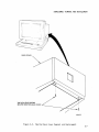
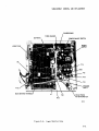
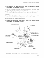
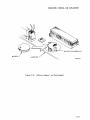
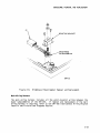
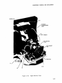
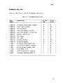
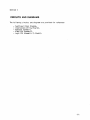
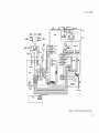
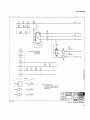
1
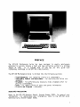
u
A Subsidiary of ITT
QVT-102 Maintenance Guide
July 1983
2350 Qume Drive
•
San Jose, California 95131
•
TWX 910-338-0232
•
(408) 942-dOOO
PREFACE
The QVT-I02 Maintenance Guide has been designed to enable maintenance
personnel to quickly isolate a fault and take corrective action in a minimum
amount of time.
It is assumed that all who may use this guide have
rudimentary knowledge of the QVT-I02 video terminal.
The QVT-I02 Maintenance Guide is divided into the following sections:
- Troubleshooting - for isolating a fault to a subassembly.
- Subassembly Removal and Replacement - for replacing the failed subassemb 1y.
- Alignment - for performing any necessary video alignment after replacing a subassembly.
.
- Parts - for identification of parts and spares information.
- Circuits and Diagrams - reference.
ASSOCIATED PUBLICATIONS
Refer to the QVT-I02 Operator Manual, Reorder Number 35003, for general user
information. For abbreviated user information, refer to the QVT-I02 Quick
Reference Card, Reorder Number 35008.
i
TABLE OF CONTENTS
Page
SECTION 1. TROUBLESHOOTING •••••••••••••••••••••••••••••••••••••••••••
I ntroduct ion ••••••••••••••••••••••••••••.•••••••••••••••
Troubleshooting Technique ••••••••••••••••••••••••••••••
Troubleshooting Flowcharts •••••••••••••••••••••••••••••
Tools and Equipment Required ••••••••••••••••••••••••
Fault Isolation Flowchart # 1•••••••••••••••••••••••
Fault Isolation Flowchart # 2•••••••••••••••••••••••
Fault Isolation Flowchart # 3•••••••••••••••••••••••
Fault Isolation Flowchart # 4•••••••••••••••••••••••
Fault Isolation Flowchart # 5•••••••••••••••••••••••
Error Codes Summary ••••••••••••••••••••••••••••••••••••
SECTION 2. SUBASSEMBLY REMOVAL AND REPLACEMENT •••••••••••••••••••••••
Introduction •••••••••••••••••••••••••••••••••••••••••••
Safety Summa ry •••••••••••••••••••••••••••••••••••••••••
Lower Monitor Area ••••••••••••••••••••••••••••••••••
Upper Monitor Area ••••••••••••••••••••••••••••••••••
Cover Sets ••••••• ~ •••••••••••• ~ ••••••••••••••••••••••••
Keyboard - Top Cover ••--• •••••••••••••••••••••••••••••
Keyboard - Bottom Cover (Keyboard PCB and Coiled ••••
Keyboard Cab 1e)
Key Caps ••••••••••••••••••••••••••••••••••••••••••••
Monitor - Back Cover ••••••••••••••••••••••••••••••••
Monitor - Bottom Cover ••••••••••••••••••••••••••••••
Lower Monitor Area Subassemblies •••••••••••••••••••••••
Logic PCB •••••••••••••••••••••••••••••••••••••••••••
Switching Power Supply ••••••••••••••••••••••••••••••
Power On/Off Switch •••••••••••••••••••••••••••••••••
Fuse ·Holder •••••••••••••••••••••••••••••••••••••••••
Batte ry •••••••••••••••••••••••••••••••••••••••••••••
Brightness Potentiometer ••••••••••••••••••••••••••••
Main Wiring Harness •••••••••••••••••••••••••••••••••
Upper Monitor Area Subassemblies •••••••••••••••••••••••
Video PCB •••••••••••••••••••••••••••••••••••••• ~ ••••
CRT •••••••••••••••••••••••••••••••••••••••••••••••••
SECTION 3. ALIGNMENT •••••••••••••••••••••••••••••••••••••••••••••••••
Introduction •••••••••••••••••••••••••••••••••••••••••••
Tools and Equipment Required •••••••••••••••••••••••••••
Alignment Conditions •••••••••••••••••••••••••••••••••••
Video Alignment Procedures •••••••••••••••••••••••••••••
Horizontal Display Width (Line Width) •••••••••••••••
Vertical Display Height •••••••••••••••••••••••••••••
Display Centering (Raster Tilt) •••••••••••••••••••••
Horizontal Linearity (Uniform Character Width) ••••••
Vertical Linearity (Uniform Character Height) •••••••
Brightness ••••••••••••••••••••••••••••••••••••••••••
FOCU S •••••••••••••••••••••••••••••••••••••••••••••••
1-1
1-1
1-1
1-1
1-1
1-2
1-4
1-6
1-7
1-8
1-9
2-1
2-1
2-1
2-1
2-1
2-2
2-2
2-2
2-5
2-6
2-8
2-10
2-12
2-13
2-14
2-14
2':'16
2-18
2-19
2-20
2-22
2-24
3-1
3-1
3-1
3-4
3-6
3-7
3-7
3-7
3-8
3-8
3-9
3-9
iii
TABLE OF CONTENTS (Cant)
Page
SECTION 4.
PARTS. • • • • • • • • • • • • • • • • • • • • • • • • • • • • • • • • • • • • • • • • • • • • • • • • • • • •
4-1
Recommended Spare Parts................................
4-7
SECTION 5. CIRCUITS AND DIAGRAMS. •.•••••••••••••••••••••••••• •••• •••••
5-1
LIST OF ILLUSTRATIONS
Fi gure
2-1
2-2
2-3
2-4
2-5
2-6
2-7
2-8
2-9
2-10
2-11
3-1a
3-1b
3-2
3-3
4-1
5-1
5-2
5-3
5-4
5-5
Page
KeybQard Top Cover Removed ••••••••••••••••••••••••••••••••
Keyboard PCB Removal and Replacement ••••••••••••••••••••••
Key Cap Removal and Replacement •••••••••••••••••••••••••••
Monitor Back Cover Removal and Replacement ••••••••••••••••
Monitor Bottom Cover Removal and Replacement ••••••••••••••
Lower Monitor Area ••••••••••••••••••••••••••••••••••••••••
Power ON/OFF Switch and Fuse Holder Removal and •••••••••••
Rep 1acement
Battery Removal and Replacement •••••••••••••••••••••••••••
Brightness Potentiometer Removal and Replacement ••••••••••
Upper Monitor Area ••••••••••••••••••••••••••••••••••••••••
Discharging the CRT Anode •••••••••••••••••••••••••••••••••
QVT Alignment Tools Set •••••••••••••••••••••••••••••••••••
QVT Alignment Tools Set •••••••••••••••••••••••••••••••••••
The "H" Test Pattern ••••••••••••••••••••••••••••••••••••••
Video Alignments ••••••••••••••••••••••••••••••••••••••••••
QVT-I02 Exploded View Diagram•••••••••••••••••••••••••••••
QVT-I02 Functional Block Diagram••••••••••••••••••••••••••
QVT-I02 Interconnect Wiring Diagram•••••••••••••••••••••••
QVT-I02 Keyboard Schematic ••••••••••••••••••••••••••••••••
QVT-I02 Video PCB Schematic •••••••••••••••••••••••••••••••
QVT-I02 Logic PCB Schematic •••••••••••••••••••••••••••••••
2-3
2-4
2-5
2-7
2-9
2-11
2-15
2-17
2-19
2-21
2-23
3-2
3-3
3-5
3-6
4-3
5-3
5-5
5-7
5-9
5-11
LIST OF TABLES
Page
Table
1-1
4-1
iv
Error Codes Summary •••••••••••••••••••••••••••••••••••••••
Recommended Spare Parts •••••••••••••••••••••••••••••••••••
1-9
4-7
SECTION 1
TROUBLESHOOTING
INTRODUCTION
This section provides a troubleshooting method for isolating most QVT-I02
failures to an easily replaced subassembly, by systematically advancing
through a series of troubleshooting flowcharts.
r
TROUBLESHOOTING TECHNIQUE
Effective troubleshooting technique should always begin with a thorough visual
inspection. Look for obvious things that may adversely effect the performance
of the terminal, such as:
-
Is the AC power source supplying adequate power,
Is the brightness potentiometer properly adjusted,
Are all connectors making good contact,
Is there a compatibility problem between the terminal and the host?
TROUBLESHOOTING FLOWCHARTS
When using the following troubleshooting flowcharts, always begin with Fault
Isolation Flowchart # 1. Although each flowchart is more or less tailored to
troubleshoot a general area, it should be noted that they have been purposefully arranged to quickly isolate a fault to a replaceable subassembly. It is
not recommended that the flowcharts be used out of sequence.
Refer to the Ci rcui ts and Di agrams Secti on for more specfi c i nformati on as
necessary.
Tools and Equipment Required
-
DB25 Loopback Connector,
Phillips Screwdriver,
Multimeter,
High Voltage Probe,
Interconnect Wiring Diagram and Schematics (refer to Section 5).
1-1
TROUBLESHOOTING
Fault Isolation Chart' 1
Powe rOn Un it.
I
Proceed to
Does Unit
Display an ---YES-----------> Faul t Codes
Summary (Page 2-9).
Error Code.
-NO
Perform Self-Test (ESC V).
I
Does Unit
Perform ---NO---------------> Proceed to Flowchart # 2.
Self-Test.
-YES
Exit Self-Test,
Enter Local Mode.
Press Each Key on
Keyboard.
I
Are Characters
Displayed as Keys ---NO-----> Proceed to Flowchart # 3.
Are Pressed.
-YES
Exit Local Mode, Enter On Line
Mode & Full Duplex Mode.
Install Loopback Connector to EIA Port.
Press Each Key on Keyboard.
I
I
Are Characters
Displayed as Keys ---NO-----> Logic PCB Defective.
Are Pressed
to Section 2).
-YES
Connect Printer to AUX Port.
Exit On Line Mode &Enter
Local Mode. Print.
I
1-2
Replace Logic PCB (refer
TROUBLESHOOTING
Fault Isolation Flowchart' 1 (Cont)
I s Screen
Data Printed. ---NO----------> Logic PCB Defective.
(refer to Section 2)
Replace Logic PCB
-YES
Unit Checks OK.
1-3
TROUBLESHOOTING
Fault Isolation Flowchart' 2
From Flowchart # 1.
I
I
Are AC Line
and Power Supply---NO--------> Replace Bad Fuse(s).
Fuses Good.
Continue.
-YES
Does Either Fuse Fail --NO---> Return.
Again at Power On.
Begin Flowchart # 1.
-YES
Verify Operation of
ON/OFF Switch. Is ---NO-----> Return.
Switch Defective.
Begin Flowchart # 1.
-YES
Replace Switch (refer to Section 2).
Continue.
I
Does Either Fuse Fail --NO---> Return.
Again at Power On.
Begin Flowchart # 1.
-YES
Replace Fuse(s). Disconnect P12, P13 and P14 to Isolate Power Supply.
On Unit and Verify Power Supply Voltages: (All voltages are de).
P12: Pin
Pin
Pin
Pin
1
2
3
4
+5 V
GND H
+12 V
NC
P13: Pin
Pin
Pin
Pin
1
2
3
4
+5 V
GND V
+12 V
NC
P14: Pin
Pin
Pin
Pin
1
2
3
4
Power
+5 V
GND
+12 V
-12 V
I
Are All Voltages ---NO-------> Power Supply is Defective.
Present.
Replace Power Supply (refer to Section 2).
-YES
Power Supply Checks OK. Power Off Unit and Reconnect Power Supply Connectors
P12, P13 and P14. Disconnect P6 and the Keyboard Telephone Jack from the
Logic PCB. Power On the Unit.
I
1-4
TROUBLESHOOTING
Fault Isolation Flowchart , 2 (Cant)
Does Either Fuse Fail --NO---> Logic PCB Checks OK. Keyboard or Video PCB
Again at Power On.
is Defective. Continue.
-YES
Replace Fuse(s).
Power On Unit.
Connect Keyboard Telephone Jack to the Logic PCB.
I
Does Either Fuse Fail --NO---> Keyboard Checks OK. Video PCB is Shorted.
Again at Power On.
Replace Video PCB (refer to Section 2).
Return to Flowchart # 1.
-YES
Keyboard or Coiled Keyboard Cable is Defective.
Return to Flowchart # 1.
1-5
TROUBLESHOOTING
Fault Isolation Flowchart , 3
From Flowchart # 1.
I
Is +12 Vdc and GND Present
at PIlon Keyboard PCB. ----NO---------> Coiled Keyboard Cable is Defective.
(Pin 1, GND/Pin 2, +12 Vdc)
Replace Coiled Keyboard Cable (refer
to Section 2).
-YES
Is 10 Vdc + 1 V Present at ---NO----> Logic PCB is Defective. Replace Logic
P10, Pin I-on Logic PCB.
PCB (refer to Section 2).
-YES
Depress Each Key on Keyboard For a Minimum
of 2 Seconds Each and Observe an AC RMS
Voltage at PIO, Pin 1 on Logic PCB.
I
Does This Voltage Increase
Approx. 200 mVac RMS While ---NO------> Keyboard is Defective. Replace
Each Key is Pressed
Keyboard Assembly (Refer to
I
Section 2).
-YES
Is The Correct
Character ------NO--------------------> Proceed to Flowchart # 4.
Displayed.
-YES
Unit Checks OK.
1-6
Proceed to System Test.
TROUBLESHOOTING
Fault Isolation Flowchart , 4
From Flowchart # 3.
I
Check the Following Voltages on the Logic PCB:
P5-1: Pin 1
Pin 2
+5 Vdc
+5 Vdc
P5-2: Pin
Pin
Pin
Pin
1
2
3
4
-12 Vdc
GND
+5 Vdc
+12 Vdc
Are All Voltages Present. --NO---> Defective Main Wiring Harness. Replace
Main Wiring Harness (refer to Section 2).
-YES
Verify Proper Operation of
the Brightness Potentiometer.
Rotate Pot Full CCW, Then Full
CW. Observe a 300 mVdc Voltage
Change Between Pins 1 and 2 of P7.
I
Does Voltage Change ---NO----> Brightness Potentiometer is Defective. Replace
Approx. 300mVdc.
Brightness Potentiometer (refer to Section 2).
-YES
Blank Screen (Shift-Home/Clear).
At P6, Pin 5 Note an AC RMS Voltage.
Display Self-Test (ESC V).
At P6, Pin 5 Note an AC RMS Voltage.
I
Did Voltag~ Increase
Approx. 400 mVac RMS When ---NO---> Logic PCB is Defective. Replace Logic
Self-Test Was Displayed.
PCB (refer to Section 2).
-YES
Proceed to Flowchart # 5.
1-7
TROUBLESHOOTING
Fault Isolation Flowchart # 5
From Flowchart #
I
4~
Display IIH Test Pattern (Ctrl/Shift/Setup-Zero).
II
I
Check Voltages on Video PCB, PI:
Pin 1
2
3
4
+12 Vdc
GND
+12 Vdc
GND
Are Voltages Present. ---NO---> Main Wiring Harness Defective. Replace Main
Main Wiring Harness (refer to Section 2).
I
I-YES
With Brightness Potentiometer
Full CW, Check P2, Pin 5 for
Approx. 400 mVac RMS.
I
Is Approx. 400 mVac RMS ---NO------> Main Wiring Harness Defective. Replace
Present.
Main Wiring Harness (refer to Section 2).
-YES
With a HIGH VOLTAGE Probe,
Check the CRT Anode Cap
for Approx. 13 kVdc.
I
Is Approx. 13 kVdc Present --NO----> Video PCB Defective. Replace Video PCB
at CRT Anode Cap.
(refer to Section 2).
-YES
Check the Following Voltages on the Video PCB (Tolerance
P3,
P3,
P4,
P4,
K1
Pin
Pin
Pin
Pin
-28
2
1
2·
1
Vdc
0.3 Vac RMS
1.3 Vac RMS
10 Vac RMS
25 Vac RMS
K2
K3
K4
K5
K6
-YES
1-8
25%):
550 Vdc
45 Vdc
175 Vdc
12 Vdc
0.1 Vac RMS
Are All Voltages ---NO-------> Video PCB Defective.
Present.
to Section 2).
CRT Defective.
~
Replace CRT (refer to Section 2).
Replace Video PCB (refer
TROUBLESHOOTING
ERROR CODES SUMMARY
As part of the termi na l' s power on sequence, it performs an i nterna 1 selftest, and signals that it has successfully completed this test by sounding the
audi b1e alarm. However, if a non-fatal error is detected, an error code wi 11
be displayed on the screen. For example, if the letter "0" is displayed, this
signifies that a fault has been isolated to the Logic PCB (i.e. IC U19). The
following table lists all possible error codes.
Table 1-1.
ERROR CODE
A
B
C
o
E
F
G
H
I
J
K
L
M
N
o
. Note:
Error Codes Summary
CORRECTIVE AcTION
Replace
Replace
Replace
Replace
Replace
Replace
Replace
Replace
Replace
Replace
Replace
Replace
Replace
Replace
Replace
U8, or the Logic PCB.
U6, U7, or the Logic PCB.
U6, U7, U8, or the Logic PCB.
U19, or the Logic PCB.
U8 and U19, or the Logic PCB.
U6, U7 and U19, or the Logic PCB.
U6, U7, U8 and U19, or the Logic PCB.
the Keyboard.
U8, or the Logic PCB, and the Keyboard.
U6 and U7, or the Logic PCB, and the Keyboard.
U6, U7 and U8, or the Logic PCB, and the Keyboard.
U19, or the Logic PCB and the Keyboard.
U8 and U19, or the Logic PCB and the Keyboard.
U6, U7 and U19, or the Logic PCB and the Keyboard.
U6, U7, U8 and U19, or the Logic PCB and the Keyboard •
U6, U7, U8 and U19 are located on the Logic PCB.
1-9
SECTION 2
SUBASSEMBLY REMOVAL AND REPLACEMENT
INTRODUCTION
Thi s sect ion descri bes how to remove and replace the major subassemb1i es of
the QVT -102. Before begi nni n9, pl ace the Power On/Off swi tch in the OFF
position and disconnect the power cord from the power source. Thoroughly read
each procedure before attempting any subassembly removal and replacement. A
medium size Phillips head screwdriver, a small adjustable wrench, and
soldering equipment are the only tools required.
SAFETY SUMMARY
In addition to the normal safety precautions that should always be practiced
during any maintenance procedure on electronic equipment, personnel should
also be aware of the following safety hazards.
Lower Moni tor Area
The lower monitor area contains the logic PCB and the power supply.
CAUTION
Upper Monitor Area
The upper monitor area contains the CRT and the video PCB.
CAUTION
2-1
SUBASSEMBLY REMOVAL AND REPLACEMENT
COVER SETS
The paragraphs be low descri be the remova 1 and rep 1acement of the cover sets
for the keyboard and monitor.
Thi s procedure prefaces the removal and
replacement of the other QVT-I02 subassemblies.
Keyboard - Top Cover
The top cover of the keyboard is secured from the underside of the keyboard
assemb ly by six screws.
REMOVAL
1. Disconnect the keyboard cable from the monitor.
2. Place the keyboard upside down on a level surface and remove the six
screws.L i ft the bottom cover with keyboard PCB away from the top cover.
REPLACEMENT
To replace the top cover, simply reverse the above procedure.
Keyboard - Bottom Cover (Keyboard PCB and Coiled Keyboard Cable)
To remove and replace the bottom keyboard cover, it is also necessary to
remove and replace the keyboard PCB and the keyboard cable.
REMOVAL
1. Remove the top cover from the keyboard assembly.
Top Cover Removal and Replacement procedure.
2. Remove
cover.
the ei ght screws that
Refer to Figure 2-1.
secu re
Refer to the Keyboard
the keyboard PCB
to
the
bottom
3. Lift the keyboard PCB up and 1ay it over the back edge of the bottom
cover.
Refer to Fi gure 2-2.
4. Disconnect the coiled keyboard cable from the keyboard PCB and remove the
cable from its retai ners on the i nsi de of the bottom cover. Be careful
not to damage the cable by overstressing its tensile strength. Remove the
keyboard cable, keyboard PCB, and bottom cover.
2-2
3 SCREWS
"
.,
(Q
c::
Cl>
N
I
......
A
~
r::r
o
.,
Q)
0..
-i
o
(/)
"'C
c:
n
):-
<
(/)
(/)
CXJ
o
.,
rn
C1>
~
CXJ
r-
;0
-<
I'D
3
o
;0
rn
<
Cl>
0..
~
0
NOTE: 8 SCREWS SECURE THE KEYBOARD PCB
<
):-
INSIDE THE KEYBOARD BOTTOM COVER
r-
):-
:z
0142
0
;0
rn
-0
r-
):-
n
N
I
W
rn
~
rn
:z
-i
N
I
~
_...
•
•
'"T1
.....
to
.,r::
I'D
N
.
I
N
............
KEYBOARD
CABLE
RETAINERS
r:::r
o
QI
-,
0..
"
-
....
•
R
.~.
[email protected]'l!,'jf*t%*&1ii}
• • • • • • • • • • • • • • • • • • • •_ • • •_ • • • •_ _.~
.•.~J.~.• ~~***\,$,.j
".1
• • • • • • • • • •-.-,·•
.
• • • • • • • • • • • • • • • • •11.£1
•.·.·.I. OCI.~.I!!\[I•.;.!. •
••••••••••••••I.liIMII)II·lilr~iI••...•.~.\I.'1.UUI"JL,I!,1l~jt;ll;ff)
1II1I111I1I11bl:~.·
1·11.···
7'
~
/KEYBOARD_BO~OMCOVE
COILED
KEYBOARD
CABLE
-0
("')
OJ
:::0
ro
3
o
<
QI
--'
QI
::J
0..
:::0
ro
'"0
QI
n
I'D
3
I'D
::J
M'
KEYBOARD
CABLE
CONNECTOR
( INSTALLED)
....
..
,
..
..,.. ,-. .-.. • ...••••. ..•••••••••••••••••••••••
.•
.. - • ..- .............. -. -... ... •
..• -• -. • • • • - - • • • •• • - • • • •
••
• •
•
•
-.
ft-
•
~
•
•
•
•
•
It
•
•
\
•
•
•
•
KEYBOARD PCB
0141
SUBA$SEMBLY REMOVAL AND REPLACEMENT
REPLACEMENT
1. Insert the coi led keyboard cable through its access hole in the bottom
cover and secure it to its retainers. Be careful not to damage the cable
by overstres~ing its tensile strength.
Connect the keyboard cable
connector to the keyboard PCB. Refer to Figure 2-1.
2. Install the keyboard PCB in the bottom cover and secure it in place with
eight screws. Ref~r to Figure 2-2.
3. Replace the top cover on the keyboard assembly.
Cover Removal and Replacement procedure.
Refer to the Keyboard Top
Key Caps
REMOVAL
A key cap can be easily removed by gripping it between index finger and thumb
and pulling up. Refer to Figure 2-3.
REPLACEMENT
To replace a key cap, position it over its location and press downward with
gentle pressure. Be sure to position the key cap so that its four alignment
tabs engage the key cap plunger. Refer to Figure 2-3.
KEY CAP
ALIGNMENT TAB
(4 TOTAL)
691·A.Q2
Figure 2-3.
Key Cap Removal and Replacement
2-5
SUBASSEMBLY REMOVAL AND REPLACEMENT
Monitor - Back Cover
REMOVAL
To remove the back cover for access to the upper monitor area (CRT and video
PCB), proceed as follows. Refer to Figure 2-4.
CAUTION
1. Orient the monitor to gain screwdriver access to the bottom edge of the
monitor back cover.
2. Remove the two screws that secure the back cover to the monitor, and slide
the back cover to the rear until it is free of its support tracks on the
display swivel support.
REPLACEMENT
1. Install the back cover on the monitor by sliding it into position on the
display swivel ?upport. Refer to Figure 2-4.
2. Secure the back cover to the monitor with two screws.
2-6
SUBASSEMBLY REMOVAL AND REPLACEMENT
---'-_-.c-
,
I
BACK COVER
TWO HEX HEAD SCREWS
SECURE MaN ITOR BACK COVER
I
----£
223·B..()2
Figure 2-4.
Monitor Back Cover Removal and Replacement
2-7
SUBASSEMBLY REMOVAL AND REPLACEMENT
Monitor - Bottom Cover
REMOVAL
To remove the bottom cover for access to the lower monitor area (logic PCB and
power supply), proceed as follows. Refer to Figure 2-5.
CAUTION
1. Remove the knob from the brightness potentiometer.
2. Lay the monitor on its side and loosen the four recessed screws at the
corners. These screws are capti ve screws, so it is not necessary to
remove them.
3. Remove the bottom cover from the monitor.
To remove any of the
subassemb 1i es mounted on the i nsi de of the bottom cover, refer to the
appropriate removal procedure.
REPLACEMENT
1. Install any subassemblies on the inside of the bottom cover that have been
previously removed. Refer to the appropriate replacement procedure.
2. Position the bottom cover on the monitor and tighten the four recessed
screws to secure it in place. Refer to Figure 2-5.
3. Install the knob on the stem of the brightness potentiometer.
2-8
SUBASSEMBLY REMOVAL AND REPLACEMENT
KNOB
CAPTIVE SCREWS
( 1 EACH CORNER)
222-8-01
Figure 2-5.
Monitor Bottom Cover Removal and Replacement
2-9
SUBASSEMBLY REMOVAL AND REPLACEMENT
LOWER MONITOR AREA SUBASSEMBLIES
The Lower Monitor Area contains the following subassemblies.
2-6.
- Logic PCB,
- Power Supply,
- Power On/Off Switch,
- Fuse Holder,
- Battery,
- Brightness Potentiometer,
- Main Wiring Harness.
2-10
Refer to Figure
SUBASSEMBLY REMOVAL AND REPLACEMENT
CHASSIS GND 1
POWER
SUPPLY
P6
P15
P12
____ P13
P14
CHASSIS
GND 2
P10
MAIN WIRING HARNESS
P5-2
BRIGHTNESS
POTENTIOMETER
0139
Figure 2-6.
Lower Monitor Area
2-11
SUBASSEMBLY REMOVAL AND REPLACEMENT
Logic PCB
REMOVAL
CAUTION
1. Gain access to the lower monitor area.
Cover Removal and Replacement procedure.
Refer to the Monitor - Bottom
2. Disconnect the following connectors from the logic PCB.
2-6.
P5-1
P5-2
P6
P7
PI0
Refer to Figure
+5 Vdc from the power supply,
+12 Vdc from the power supply,
Vi deo PCB,
Brightness potentiometer,
Keyboard input.
3. Remove the 8 screws that secu re the 1ogi c PCB (and the chass is ground
strap on the keyboard input jack) to the bottom cover.
from the bottom cover.
Lift the logic PCB
REPLACEMENT
1. Pos it i on the 1ogi c PCB over its mount i ng holes in the bottom cover and
secure it in place with 8 screws. Be sure to also install the chassis
ground strap from the keyboard input jack.
Refer to Fi gure 2-6.
2. Reconnect all connectors listed in the Removal procedure above.
3. Reinstall the bottom cover on the monitor.
Cover Removal
2-12
an~
Replacement procedure.
Refer to the Monitor - Bottom
SUBASSEMBLY REMOVAL AND REPLACEMENT
Switching Power Supply
REMOVAL
CAUTION
1. Gain access to the lower monitor area.
Cover Removal and Replacement 'procedure.
Refer to the Monitor - Bottom
2. Disconnect the following connectors from the power supply.
Figure 2-6.
P12
P13
P14
PIS
GND
Refer to
I
I
> +5 Vdc and +12 Vdc output connectors,
Source voltage input,
Power supply ground. (The ground lead on later model power
supplies is soldered to the power supply, but easily
removable from chassis ground 2.).
3. Remove the four screws that secure the power supply to the bottom cover.
Lift the power supply from the bottom cover.
REPLACEMENT
1. Position the power supply over its mounting holes in the bottom cover and
secure it in place with four screws. Refer to Figure 2-6.
2. Reconnect all the connectors listed in the Removal procedure above.
3. Reinstall the bottom cover on the monitor.
Cover Removal and Replacement procedure.
Refer to the Monitor - Bottom
2-13
SUBASSEMBLY REMOVAL AND REPLACEMENT
Power On/Off Switch
REMOVAL
CAUTION
1. Gain access to the lower monitor area.
Cover Removal and Replacement procedure.
Refer to the Monitor - Bottom
2. Remove the two screws that secure the filter PCB and the power switch with
bracket in the bottom cover. Refer to Figure 2-7.
3. Remove the filter
connecting leads.
PCB;
it
is
not
necessary to de-solder its
four
4. Note the arrangement of the four leads on the power switch. De-solder
these leads and remove the power switch with its mounting bracket.
5. Remove the two screws that secure the power switch to its mounti ng
bracket. Remove the power switch.
REPLACEMENT
1. Secu re the power swi tch to its mount i ng bracket wi th the two screws
removed in Step 5 above. Refer to Figure 2-7.
2. Re-solder the four leads to the power switch.
3. Position the power switch mounting bracket over its mounting holes in the
bottom cover. Position the line filter PCB over the power switch mounting
bracket so that all mounting holes are in line. Secure in place with the
two screws removed in Step 2 above.
4. Reinstall the bottom cover on the monitor.
Cover Removal and Replacement procedure.
Fuse Holder
REMOVAL
CAUTION
2-14
Refer to the Monitor - Bottom
SUBASSEMBLY REMOVAL AND REPLACEMENT
1. Gain access to the lower monitor area.
Cover Removal and Replacement procedure.
Refer to the Monitor - Bottom
2. Note the arrangement of the two leads on the fuse holder.
leads from the fuse holder. Refer to Figure 2-7.
De-solder these
3. With a small adjustable wrench, remove the nut and washer that secures the
fuse holder to the inside of the bottom cover. Remove the fuse holder.
REPLACEMENT
1. Install the fuse holder in the bottom cover and secure it in place with
the washer and nut removed in Step 3 above. Refer to Figure 2-7.
2. Re-solder the two leads to the fuse holder.
3. Reinstall the bottom cover on the monitor.
Cover Removal and Replacement procedure.
POWER SWITCH
MOUNTING BRACKET
Refer to the Monitor - Bottom
. 1/
~
FilTER PCB
~.i /l~
:/
Q'jj!
J Qp' ~u
~ ~I
FUSE HOLOER
RETAINER CAP
~1~
~"---,;"
POWER ON/OFF SWITCH
TO FilTER PCB (BlK)
TO FilTER PCB (WHT )
~ ~
FUSE
I
"
FUSE HOLDER NUT
AND WASHER
/,
1
///
FUSE HOLDER
Figure 2-7.
209-6-02
Power ON/OFF Switch and Fuse Holder Removal and Replacement
2-15
SUBASSEMBLY REMOVAL AND REPLACEMENT
Battery
REMOVAL AND REPLACEMENT
CAUTION
. . . uL
The battery is easily removed and replaced by sliding it in and out of its
retainer clip on the Logic PCB (refer to Figure 2-8).
As a reference, note
the status 1i ne set-up confi gurati on of the termi na 1 before removi ng the
battery.
Once the battery is replaced, if after power ON the status 1i ne
appears to be altered, execute a Shift-D and reconfigure the status line as
you have noted.
2-16
SUBASSEMBLY REMOVAL AND REPLACEMENT
BATTERY RETAINER CLIP
BATTERY
695-A-Q1
Figure 2-8.
Battery Removal and Replacement
2-17
SUBASSEMBLY REMOVAL AND REPLACEMENT
Brightness Potentiometer
REMOVAL
CAUTION
1. Gain access to the lower monitor area.
Cover Removal and Replacement procedure.
Refer to the Monitor - Bottom
2. Disconnect the brightness potentiometer connector (P7) from the Logic
PCB. Refer to Figure 2-6.
3. Remove the two screws that secure the brightness potnetiometer and
mounting bracket to the bottom cover. Refer to Figure 2-9.
4. With a small adjustable wrench, remove the nut that secures the brightness
potenti ometer to the mounti ng bracket.
Remove the bri ghtness
potent i ometer.
REPLACEMENT
1. Secure the brightness potentiometer to its mounting bracket with the nut
removed in Step 4 above. Refer to Figure 2-9.
2. Position the brightness potentiometer with mounting bracket over its
mounting holes in the bottom cover.
Be sure to orient the mounting
bracket so that the high side of its sloped top surface is toward the
rear. Secure in place with the two screws removed in Step 3 above.
3. Reconnect the bri ghtness potent i ometer connector (P7) to the Logi c PCB.
Refer to Figure 2-6.
4. Reinstall the bottom cover on the monitor.
Cover Removal and Replacement procedure.
2-18
Refer to the Monitor - Bottom
SUBASSEMBLY REMOVAL AND REPLACEMENT
P7
MOUNTING BRACKET
BRIGHTNESS
POTENTIOMETE R
694-A.Q2
Figure 2-9.
Brightness Potentiometer Removal and Replacement
Main Wiring Harness
The main wiring harness includes all the point-to-point wiring between the
major subassemblies of the QVT-I02. If removal and replacement of the main
wiring harness is required, refer to the QVT-102 Interconnect Wiring Diagram
found in the Circuits and Diagrams Section.
2-19
SUBASSEMBLY REMOVAL AND REPLACEMENT
UPPER MONITOR AREA SUBASSEMBLIES
The Upper Monitor Area contains the following subassemblies.
2-10.
- Video PCB,
- CRT.
2-20
Refer to Figure
SUBASSEMBLY REMOVAL AND REPLACEMENT
FLYBACK
TRANSFORMER
LEAD
P3
( NOT VISIBLE)
CRT GROUND
LEAD
VIDEO PCB
P1
0135
P4
Figure 2-10.
Upper Monitor Area
2-21
SUBASSEMBLY REMOVAL AND REPLACEMENT
Video PCB
REMOVAL
CAUTION
1. Gain access to the upper monitor area.
Removal and Replacement procedure.
Refer to the Monitor - Back Cover
2. Discharge the CRT high voltage circuit and remove the flyback transformer
anode cap. Figure 2-11 illustrates the proper method of discharging the
CRT anode by usi ng the shaft of an i nsu 1ated screwdri ver, to short the
anode to the metalized surface of the CRT.
3. Disconnect the following connectors from the video PCB.
2-10.
PI
P2
P3
P4
GND
Refer to Figure
+12 Vdc,
Horizontal and vertical sync,
Horizontal yoke deflection,
Vertical yoke deflection,
CRT grounding spring.
4. Remove the five screws that secure the video PCB in place, and remove the
CRT socket PCB from the neck of the CRT. Remove the video PCB from the
monitor.
REPLACEMENT
1. Place the video PCB over its mounting holes, and install the CRT socket
PCB on the neck of the CRT. Secure the video PCB with five screws.
2. Install the flyback transformer lead on the CRT.
3. Reconnect all connectors listed in the Removal procedure above.
4. Perform any video alignments necessary.
5. Reinstall the back cover on the monitor.
·Cover Removal and Replacement procedure.
2-22
Refer to the Monitor - Back
SUBASSEMBLY REMOVAL AND REPLACEMENT
METALIZED
INSULATED SCREWDRIVER
SURFACE OF CRT
FLYBACK
TRANSFORMER
LEAD ANODE CAP
0134
Figure 2-11.
Discharging the CRT Anode
2-23
SUBASSEMBLY REMOVAL AND REPLACEMENT
CRT
REMOVAL
CAUTION
1. Gain access to the upper monitor area.
Removal and Replacement procedure.
Refer to the Monitor - Back Cover
2. Discharge the CRT high voltage circuit and remove the flyback transformer
anode cap. Figure 2-11 illustrates the proper method of discharging the
CRT anode by us i ng the shaft of an i nsu 1ated screwdri ver, to short the
anode to the metalized surface of the CRT.
3. Disconnect connectors P3 and P4 (horizontal and vertical yoke deflection
leads) from the video PCB. Refer to Figure 2-10.
4. Di sconnect the CRT ground 1ead from the CRT socket PCB, and remove the
socket PCB from the neck of the CRT.
5. Support the CRT and remove the four screws that secure it in the display
swi vel support. Remove the CRT form the monitor cabi net. .Remove the
grounding spring from the CRT.
REPLACEMENT
1. I nsta 11 the groundi ng sp ri ng between the CRT upper 1eft and lower ri ght
mounting tabs.
Then position the CRT over its mounting holes in the
display swivel support and secure it with the four screws removed in Step
5 above.
2. Insta11 the CRT socket PCB on· the neck of the CRT. Connect the ground
lead from the CRT grounding spring to the CRT socket PCB. Refer to Figure
2-10.
3. Install connectors P3 and P4 on the video PCB.
4. Reconnect the f1yback transformer anode cap to the CRT.
5. Perform any video alignments necessary.
6. Rei nsta 11 the back cover on the mo.nitor.
Cover Removal and Replacement procedure.
2-24
Refer to the Monitor - Back
SECTION 3
ALIGNMENT
INTRODUCTION
The alignment parameters presented in this section are to be regarded as
guidelines only and not as specifications criteria.
Video alignment of the QVT-102 is divided into the following alignment
procedures. Note: These alignment procedures may be performed in any order.
.-
Horizontal Display Width,
Vertical Display Height,
Display Centering (Raster Tilt),
Horizontal Linearity (Uniform Character Width),
Vertical Linearity (Uniform Character Height),
Bri ghtness,
Focus.
TOOLS AND EQUIPMENT REQUIRED
The following tools are required to perform video alignment of the QVT-102:
- Phillips Screwdriver,
- Small, Slotted, Non-metallic Screwdriver,
- QVT Alignment Tools Set (Q.P.N. 84841-XX),
• Display Template (refer to Figure 3-1a, Q.P.N. 84841-01),
• Vertical Template (refer to Figure 3-1b, Q.P.N. 84841-02),
• Horizontal Template (refer to Figure 3-1b, Q.P.N. 84841-03),
(A metric rule may be used in place of the above three templates.)
.7/64 inch Alignment Tool (Q.P.N. 84841-04),
- Multimeter (for brightness and focus alignment procedures),
- Oscilloscope (for focus alignment procedure only).
3-1
W
I
N
//
."....
"",
/
'"
(,0
c:::
-,
I'D
W
I
t-'
OJ
.0
<
-l
;,:.
.....
~
(,0
::s
:3
I'D
::s
rt
-l
0
0
~
(I)
(/)
I'D
rt
C
(I)
'"C
~
OJ
Co<
-l
(1)
3
'"C
~
OJ
rt
I'D
.
."
.0
:z
00
5mm I--.
00
+
~
~
t-'
I
0
.....
'-
"',
DISPLAY SIZE: 155mm + 0- 5mm x 213mm + 4 - 3mm
V
786-A
ALIGNMENT
-N......I
>-0
.... ~s:
<t:a:
~~
-u
-I<t:
HORIZONTAL LINEARITY TEMPLATE
-I a:
<t:<t:
....Zu
~
oN
a:
o
~
" H" TEST PATTERN AS VIEWED
THROUGH TEMPLATE WINDOWS
VERTICAL LINEARITY: 4.65 "t O.4mm
(CHARACTER HEIGHT)
VERTICAL LINEARITY TEMPLATE
787·A
Figure 3-1b. QVT Alignment Tools Set
(Vertical Template, Q.P.N. 84841-02; Horizontal Template, Q.P.N. 84841-03)
3-3
ALIGNMENT
ALIGNMENT CONDITIONS
All alignment procedures should be thoroughly read and only performed under
the following conditions:
- Warm-up. Allow the terminal to stabilize at its operating temperature;
approximately ten minutes.
Refer to the Moni tor - Back Cover Remova 1 and
- Back cover removed.
Replacement procedure.
- Local Mode.
Configure the terminal for local mode operation.
- Standard Vi deo/Reverse Vi deo. Perform a11 ali gnment procedures in the
terminal IS normal operating display condition.
- "H" Test Pattern displayed. The terminal has a built-in test pattern
that displays a full screen of "Hs," and identifies the firmNare
revision level. To display the "H" test pattern, simultaneously depress
the Ctrl/Shift/Setup keys followed by the zero key. Refer to Figure
3-2.
CAUTION
3-4
ALIGNMENT
11 ± 3mm (EACH CORNER)
9± 3mm
FRONT BEZEL
213mm +4 -3mm
KEYBOARD
FIRMWARE
REVISION
LEVEL
155mm +0
·5mm
LOGIC PCB
FIRMWARE
REVISION
LEVEL
DISPLAY DIMENSIONS
4.65 ± OAmm - - - - '
H
~2.1±0.3mm
CHARACTER DIMENSIONS
Fi gure 3-2.
77S-A
The "H" Test Pattern
3-5
ALIGNMENT
VIDEO ALIGNMENT PROCEDURES
Video alignment of the QVT-I02 is accomplished by adjusting one or more of the
adjustments illustrated in Figure 3-3. Each alignment procedure is described
below. -
INDUCTANCE
YOKE CLAMP
LEGEND
VR50I
VR502
VRI5I
VRI52 and LI5I
LI03
LI02
KI and K4
Rings and Clamp
Fi gure 3-3.
3-6
Vertical Display Height
Vertical Linearity
Brightness
Focus
Horizontal Display Width
Horizontal Linearity
Test Points
Display Centering
Video Alignments
ALIGNMENT
Horizontal Display Width (line Width)
Horizontal display width is correctly adjusted when the width of a line of Hs
in the "H" test pattern measures 213 mm + 4 -3 mm. If adjustment is required,
proceed as follows:
1. Display the "H" test pattern (Ctrl/Shift/Setup-Zero).
2. Measure the first line of Hs with the Display Template (Q.P.N. 8484101). Tape the template to the front bezel so that it is securely held in
place over the display screen. A metric rule may be used if the template
is not available.
3. If adjustment is required, rotate inductor L103 on the Video PCB (refer to
Figure 3-3) with the 7/64 inch Alignment Tool (Q.P.N. 84841-04).
Clockwise rotation of L103 increases line width and counter-clockwise
rotation reduces line width.
Vertical Display Height
Vertical display height is correctly adjusted when a column of Hs in the IIH II
test pattern measures 155 mm + 0 - 5 mm from the bottom of the status 1i ne to
the top of a an H character on the fi rst 1; nee I f adjustment ; s requi red,
proceed as follows:
1.. Display the "H" test pattern (Ctrl/Shift/Setup-Zero).
2. Display the status line (Set 5 Status Line selection, or ESC}).
3. Measure the display height of a column with the Display Template (Q.P.N.
84841-01). Tape the template to the front bezel so that it is securely
held in place over the display screen. A metric rule may be used if the
template is not available.
4. If adjustment is required, rotate pot VR501 on the Video PCB (refer to
Figure 3-3) with a small non-metallic screwdriver. Clockwise rotation of
VR501 increases display height and counter-clockwise rotation reduces
display height.
5. If desired, blank the status line (Set 5 Status Line selection, or ESC {).
Display Centering (Raster Tilt)
The display is considered to be centered and not tilted when the bottom edge
of the status 1i ne and the top edge of the fi rst 1i ne of Hs in the IIH II test
pattern measures 9 + 3 mm from the bezel, and the left and right edges of the
pattern measures 11~ 3 mm from the bezel. If adjustment is required, proceed
as follows:
1. Display the "HII test pattern (Ctrl/Shift/Setup-Zero).
3-7
ALIGNMENT
2. Position the Display Template (Q.P.N. 84841-01) over the "H
test
pattern. Tape the template to the front bezel so that it is securely held
in place. A metric rule may be used if the template is not available.
II
3. If a display centering adjustment is required, rotate the centering rings
(refer to Figure 3-3) on the yoke of the CRT to center the display. If a
gross centeri ng adjustment of the di sp 1ay is requ ired, loosen the i nductance yoke clamp and verify that it is as far forward as possible on the
neck of the CRT. Re-tighten the clamp, being careful not to over tighten
it, and then repeat the centering adjustment with the centering rings.
Horizontal linearity (Uniform Character Width)
Horizontal linearity, or uniform character width, is considered to be properly
adjusted when a sampling of measurements taken at various locations of the "HI!
test pattern, reveals a character width of 2.1 + 0.3 mm. If adjustment is
requi red, proceed as follows:
1. Di spl ay the "H
II
test pattern (Ctrl /Shi ft/Setup-Zero).
2. Measure character width at five locations in the test pattern (near each
corner and the center). If the Vertica-l Template (Q.P.N. 84841-02) is
used, proper character width will appear too large for the Minimum window
and too small for the Maximum window. A metric rule may be used if the
template is not available.
3. If adjustment is required, locate inductor LI02 on the Video PCB (refer to
Figure 3-3).
Using a small non-metallic screwdriver, rotate LI02
clockwise to increase character width or counter-clockwise to reduce
character width.
Vertical linearity (Uniform Character Height)
Vertical linearity, or uniform character height, is considered to be properly
adjusted when a sampling of measurements taken at various locations of the "HI!
test pattern, reveals a character height of 4.65 + 0.4 mm. If adjustment is
required, proceed as follows:
1. Display the "HI! test pattern (Ctrl/Shift/Setup-Zero).
2. Measure character height at five locations in the test pattern (near each
corner and the center). If the Horizontal Template (Q.P.N. 84841-03) is
used, proper character height will appear too high for the Minimum window
and too low for the Maxi mum wi ndow. A met ri c rul e may be used if the
template is not available.
3. If adjustment is required, locate pot VR502 on the Video PCB (refer to
Figure 3-3).
Using a small non-metallic screwdriver, rotate VR502
cl ockwi se to increase character hei ght or counter-cl ockwi se to reduce
character height.
3-8
ALIGNMENT
Brightness
Display brightness can be adjusted as follows:
1. Clear the screen of all data by depressing the Shift and Clear/Home keys.
2. Rotate the external brightness control on the display module pedestal
fully counter-clockwise.
3. Locate pot VR151 on the Video PCB (refer to Figure 3-3), and with a small
non-meta 11 i c screwdri ver, rotate it unt i 1 the back ground raster is just
visible.
4. Locate test point K1 on the Video PCB (refer to Figue 3-3) and measure the
DC voltage between K1 and ground. Note: This voltage may be a positive
or negative voltage. Record the voltage observed.
5. Rotate pot VR151 to reduce the voltage observed between K1 and ground by 2
volts.
Focus
Display focus can be adjusted as follows:
1. Display the "H" test pattern (Ctrl/Shift/Setup-Zero).
2. Set the oscilloscope controls as follows:
- Vo1ts/Div •••••••••••
- Ms/Div ••••••••••••••
Coupling ••••••••••••
- Trigger•••••••••••••
100
10
DC
CHI
- Connect the signal probe to the junction of R154 and C156 (test point
K4) on the Video PCB (refer to Figure 3-3). Connect the probe ground
to ground.
3. Locate inductor L151 on the Video PCB (refer to Figure 3-3), and with the
7/64 inch Alignment Tool (Q.P.N. 84841-04), adjust LI51 for a sine wave
having an amplitude of approximately 250 volts peak-to-peak.
4. Locate pot VRI52 on the Video PCB (refer to Figure 3-3), and with a small
non-metallic screwdriver, adjust VR152 for optimum focus at the center of
the di sp1ay. Opt i mum focus occu rs when the i ndi vi dua 1 dots that form a
character are well defined and clear.
5. Observe the scope and record the voltage offset between the negative peak
of the sine wave and the ground reference. Record this value as amplitude
"A ".
6. Adjust pot VRI52 for optimum focus near the corners of the display.
3-9
ALIGNMENT
7. Observe the scope and record the voltage offset between the positive peak
of the sine wave and the ground reference. Record this value as amplitude
liB ".
8. Subtract amplitude uA" from amplitude uB" to obtain amplitude "C".
is: B - A = C.
That
9. Adjust ; nductor L151 unti 1 the peak-to-peak voltage of the sine wave
equals the value of amplitude IIC II •
10. Adjust pot VR152 until the negative peak of the sine wave is offset from
the ground reference by the value "A".
11. Observe the screen display and visually make any fine adjustments
necessary.
3-10
SECTION 4
PARTS
This section presents an overall exploded view diagram of the QVT-I02 for
parts identification, followed by a list of recommended spares.
4-1
!l
"~
~)~
,,
®
@2
4-3
PARTS
ITeM
FRONT PANil..
IC,OOI
Tuall
1000~
WA~MEI>.
(FI..AT\ 1'<14
IOIOO~
WA.....lR
(~pRIN,") ""4 x
10,004
S(;l>.ew 0014 XO.7X&
I~
I!
m
)(
f1'"
~UPpOP.T
x
07.10 XT I
vaNCOll'5o PIN
ITEM
Quo,E,PJIoI
I'Ae.T 1010004
Sa
10,044
&OTTOM
1..""&
m
lC
TL. ....OClJ..' ..........ao Go.~1·0Cl4
)(
MC.10000040~
'"
10,0'l!>
X
<00
10,0""
1~~UI..TIONFII.M (T/oJ)
)(
ILl. 300040000
Me. 10000010'"'
101
10,047
TJ3 c.ov.'"
v .... \/110 ...4- N'15... ,·e~K
'"
1..C.060000'l07
."TI0"11110Go
X
ee.TI0~11101
MAAaO<JO~100
"',
."101-01
W"'IoWi:,. (I'I..AT\ ... 4
l(
MC.10000040..
(0)
IO,04l!1
YR. !lupPOItT
lC
WA'IoWER (!>PR,NG,\ M4 x 07.10 XTI
X
Mc.l00000 10"
1.4
10,04"
)(
"5
w... ~ltll. ""',
10,050
NUT " " ,
IOlea.
NUTM~)(&5.5)(HZ.4
10)O:lU
.W''T"C:I-l Taoz.
IC,005
$U'&W M.)( 0.7)( 10
IC,OCIO
C.RT c.e74S1 110 31V R;t
)t
A"~OOOOo~o
10,007
G,RoUNC ~R'N'"
)<
£XOIOooO
X
001"10000040"
X
...." 300000 500
WA..... ~
IC,ooe
W''!Io~.'"
10,009
M4~
(~l...AT)
)(
Nt4
(IN C.OC.K)
OIll.S
~
VENCO"'.... 1'/i0oi
,.......TIO"l0007
)(
10.00~
....."%000710.
1~01
TO.4!>
"''''
D'010000'Z.01
e.I" 1&00 1100Z.
)I.
~&
..
)l
""0 ZOOOOOI 0 &
O."I'Z.OOO '01
10&
1005%
P.~. ~UPPOA.T
)I.
&'TIOZ.l!IIIO~
10,OlS"!!
10,oS4
$c..REW ...."!l)< 0.1II XGo
)(
.........'Z.0010.0'"
10
71
....
NuT \ ~U~& HOL..l:lIIA.)
10055
W"~I-4QP, (,,"ufo.. 1-\01..0.lt)
)l
10,010
uPpRR C.A&INIIT
"-
~"A.T
10ZOOOO
n.
10,054
... u~a NP
)(
m.1A.ClOOoz.004
10,011
1..0"'0 Np
)(
eJ~ooooqlOI
7S
'0.05 7
""u~. ,",01..0111: (I..)
X
0'-100000 107
10,012
TII..T NEe.K
x
F"'I..T 101000~
IO,05S
toMK .-NI"!lOI-~
)(
10.05"
.U~I-iIN'" tolave.01214
)(
.c.co~
~e.I>.&W
M4XO.7 x 10
... 100100 a0007 105
"
10013
51..10& al..oe.K
1&
IC I Ol4
IOI..'Oi: <: ..,,1'
>(
FC.OOOlooooz.
1'1
10,OlS
p~~SURe ~PRIN"
x
1£)(010000101.
IOC.OOOIIOOO&
74
7S
100<.0
$R"L.-I
/00 ..,
POW~R c.O....O
'00..1
!O_IAL.. N .....'".pl....T.
ac
10,01'"
w"SWER (!ll..loe F)
)(
I'e.000 1'000"
,,,
11
10,005
sc.R&W 0.14 XO.7 X 10
."
M"A.lOOO7Z05
77
10,OGo~
R,a. C.U!oHION
H
10,0';
SC.REW (Nee..... I"llI)
x
7&
100r.4
C.U:'H'ON
11
1°1°18
~.T
w"$wa",,
1i'-00TIIo110't
X
<:O...05001001'Z.
~
• .14000'0101
X
1..C.'OOO0040"l
)I.
.pRINe. ...00.... (NEC.....)
>(
""...... 8oo0110Cl
EXO!l00003Q7
10.0..S
~c."Ii.W "'~TP"" 10(e..:'UNK)
It
14
IO,OIct'
TIiNfiolON lltPRINe.
)(
&XOIOOOOI(o(o
7"
ao
1..'"0"0000'00
........000'1.0..
'0,0.....
.'"IlW M4XO.71114j(I-4"L.F\
)(
..." .. 10004Z0,",
2S
10,OZO
Tua. ~UPPO""T (I..)
)(
ec.T10111105
151
10.0"7
RATI~'"
1-
EJ40000QlO!o
MA ... ~000..10.
81.
10.0:&4
. " t a w ..... TPA x a
l(
M"81!OOO!>ZOIio
110
10,0'11
r.C."i:W...,3XO.5)(10
)(
aT
IO,02'Z.
1-4i:"T !OINK 1001..'5
)t,
I.. e.o 4 0000 (o0z.
u.
IO,02~
NUT .... 3 x • • :1 x 1-41.4
l(
""1:1&00000108
MA8 <OOo!>%oc.
,q
10,OZ'l
5C.R&W "'~T"">(e.
x
~c
'O,021!o
:lc.",.w..."XO.!>".
l(
;1
1002<-
Hi"T
aOTTo.... U e."8
~INK
12
10,027
~~
10,OZ!>
vR
~4
IO.OZ....
.~IO.
35
:!l>
10,030
1".-1
lalNc.
..... 4
X0."7 x 10
IC,C31
(C.'SIINK)
'0,03:1
NUT NO. 4.40 UNC-
....A.. i1.000n.0.
x
FaZTI010001
X
I"e.0000 "70001.
X
MA" 4000 110"1.
X
.... CZOOOO0701
37
e4~OI-O'
\/Ioao pe.a V8-oil. I>. Ii V /loB
0"" T 101 V 10~
64600·01
1..0Co'e.
OAZTIO"Z.L.IO!l
3'1
10)033
w".I-lER .... S (ex. 1..0l;K)
4C
·C,C;:.
~FU"W
IC,OZ,.4
~,,,.w
.0.0... .
0 1...·4 Rav",e
M5'T'1:l'A.}(IO
,."
.....&ZOOOl100
xa
>(
M"8'1000~0,"
M5"Tg..
;0,03~
&ATT&IlV 1001..& (-)
lC,O;ft;,
....T"'.RV POL.E
IC,C2~
NUT .... SXE!ll:i.5)( 1-42.4
4!1
1OC!?
Wtl'OU~D
4£,
CC.3e
"
4~
lCjO~e,
"
(~)
"
Pl..AT.
"'I;
Sooooo 101
i:I=OZTIO~
loe
i:I"OITIOZ'OS
MDZooooO/06
S'''llw M!TPA x II
)(
. "... W(C·TVP. e.ONN)
)(
""...... $000<104
10,040
IiSC (pl.. ...T£\
x
£.IOT 10Z"Z.01
..
IN~UI.."''''IONI''II..M IESC)
)(
£1..10005000"
IC.OZ4
~e.IIli:W M~TP""
x
M ...e 20005Z0,"
IO;O!:~
wA!t....
52
IO,OZ3
NUT M3)( 6S.5
5;1
IO,::'A'Z
SWITC.)··UNc.. PowlIR •
84&04·01
A!oIT&C. - Ac::.&I'S1
~.
IO,01.~
S~
10,0.1'
",
5"1
e" (EX 1..0"".....)
... &W
~c.
10.0'.3
Pc.~
-_ow.
xe.
)It ~
N1~
i.4
NuT "'-43 x as.s )( I-t 2 .•
""AS..... '1 (lEX 1..0e.><.) ..... !o
10 0.:1'-
..... :lTP'"' )( 10
"'81
x
'NC'C....Te.':l
~PE<:.IFIItC.
TO 1>URC.WA.Se. ,ROM VSNOOR(N:lT A
-::;.:",.a.
~A,I!:"'),
.....11OOI8Z0!
10.=41
'0
WOTES: UNL..==!o OT.... ERWI~.
m
el'IOTIOZI04
48
4.,
Rep lacement parts are limited to those listed
on the Recommended Spare Parts List.
F"MT 101.000.
KNoe
r.c........ w
N ...Mll
NOTE
1..e.04 0000 10,"
~a
43
_ _ _ _ GIl
C&!o'-",PTION
10,001
10,00'
'1
cae.c.p.IPTIO ....
QUMEPN
10,000
~I!VO
"X
MC.~OOOQQIOI
Nt 0 %00000 10&
)(
I:)~TIO'2 POOOI
l(
""0 ZOOOOOIO&
X
..... C.300oo0101
_
PAPTS LIST
MAe. Z.OOO 1Z0C
O..I..T 1020005
./........
l7
:
", .... _ -
0t
.J-2/
84826 -01 A
Figure 4-1. QVT-102 Exploded View Diagram (Cont)
4-5
PARTS
RECOMMENDED SPARE PARTS
Table 4-1 identifies all QVT-102 recommended spare parts.
Table 4-1.
PART
NUMBER
I
84807-01
84804-01
84805-01
84800-01
84800-02
84806-01
84803-01
84803-02
84811-01
84801-01
10028
10244
10281
10146
95855
95803
Recommended Spare Parts
DESCRIPTION
Brightness Potentiometer Assembly
Power Supply Assembly
AC Line Switch
Logic PCB Assembly, RS-232-C
Logic PCB Assembly, Current Loop
Battery, RAM Back-up
CRT, Green
CRT, Amber
Keyboard Assembly
Video PCB Assembly
Brightness Potentiometer Knob
Coiled Cable Assembly, Keyboard
Wiring Harness Assembly, Main
2764 EPROM, IC U8
8748 Microprocessor, Keybo~rd
Character Generator EPROM, US
QTY PER
1000
15
25
15
25
5
10
5
3
25
25
10
5
5
5
5
5
QTY PER
10,000
50
150
50
150
10
25
25
15
150
150
50
20
20
20
20
20
4-7
SECTION 5
CIRCUITS AND DIAGRAMS
The following circuits and diagrams are provided for reference:
-
Functional Block Diagram,
Interconnect Wiring Diagram,
Keyboard Schematic,
Video PCB Schematic,
Logic PCB Schematic (5 Sheets).
5-1
CIRCUITS AND
KEYBOARD PCB ASSY.
8748
~
I
A
IY
..
MICRO
PRO·
CESSOR
6116
SCREEN
RAM
~
II'
H
BUZZER
I
~
~
TC 5514
f~
BATTERY
J
NON·
VOLATILE
RAM
TC 5514
NON·
... VOLATILE
3V
RAM
~
L-..fL6845
CRT
CON·
TROLLER
1/4
I'c'
PERIPHERAL
~
r
~
I--
6850
UART
,
~
EIA
PORT
~~
~
CRT
>
t
I'GND
2764
PROGRAM
ROM
"
AUX
PORT
6800
MICRO
PROCESSOR
KEYBOARD
MATRIX
~
LOGIC PCB ASSY.
DATA
HOST
VIDEO PCB ASSY.
.J
2732
CHARACTER
GENERAT1R
I I
I J
HIGH
VOLTAGE
CIRCUITRY
VIDEO
SIGNAL
CIRCUITRY
Ll03
HORIZ.
SIZE
+
I<:--
...
Z 80
CTC
~
VIDEO
CONTROL
LOGIC
VIDEO
H. SYNI:
VsYN
I
BRIGHTNESS
CONTROL
HORIZONTAL
CONTROL
CIRCUITRY
J
t
I
VERTICAL
CONTROL
CIRCUITRY
J
L102
HORIZ.
LINEARITY
I---
+5V
POWER SUPPLY
-12V
DIAGKAM~
_II VERTICAL
VR502 (I
VR501
VERTICAL
SIZE
~
,
LINEARITY
VR151
BRIGHTNESS
-
I
VR152
STATIC
FOCUS
VIDEO DISPLAY ADJUSTMENTS
Figure 5-1.
I I
L1Sl
DYNAMIC
FOCUS
I
23108
QVT-1D2 Functional Block Diagram
5-3
~iKCUlrs
EIA
PORT
.1.
AUX
PORT
. ...!
.J.-
FUSE~.n
.1- -, BLAr:K
I
I
I
I
VERTICAL
DEFLECTION
TOP4
ON VI OEOPCB
CRT YOKE
{~ 0
BLUE
I
I
HORIZONTAL
DEFLECTION
ll..
RED
II
BROWN
}
CRT
SOCKET PCI
"'~
1<2
(
I
~
~
i
~
~
~
K4
i
...
~
I
't1 0-E!
I
K2
3
4 _
RED
I!!
if;
P2 LI"'I.
.:::
n
P3~
+:tv: + ;'v'
PI 021)3( 4 )\
VI
i
~
(
1<8 1<7 KS
rg~
TO CRT
YOKE
.~
IBROWN
TO CRT YOKE
~
SHIELD
'~
Ie') (~
II:
...,
~~
I
I
i .~.
1:1'1
I
I
BLACK
P13
«3) (4)/
P12
/6 l 01 /6 l
«2)
3)
01
I
+SVDC 1 ....
IvELL OW
SIG~~b 2:;
IBLACI(
BLUE
!!!2..
.
~':a !!!!m ··· .. .-
~
I
~
!.lo:S!:
--.
~
WHITE
I
I
r
i
I
I
I I
__ ..JI
I
~~ II
I
It
I
I
I
...
!:
I
I
I
I
I
I
-.
I
L_~~~ _________
~
:t:
m,~ II j
I
.J)
...
~
i i
RED
I-
GND
I
I
+12VDC 4 ~
+5VDC 3 -
WIPER
~ .. ft
,
POWER SUPPLY
WHITE
P14 GND
RED
.,2VDCG
I
feEL~~~~~~~
I'
'-.--I
'; ~
FIL TER PCB
I
n
~ Jf[;;g}~~"ow)
.1'\
f
if
+SVDC ~
,~
r-:::::::::::..
VIDEO PCB
(VIOEO)
iW
..g<
~
BROWN IGVI
4 .X-
l.-
~
IV SYNC)
p,o
i
/" !"'"
r
K3(
~
WHITE IH. SYNC I
8LUE (GH)
~Iol
WHITE
'-'-'
'--
1<1
REDI
,.....I
i
~
t
~
>-
j
BLUE
r
~
...-'
...
:
I
I
I
I
I
I
I
~I
~
.....
K3
~NR~~N
0
I
wmTeL--J)J
1<4
IBLAC:I
IWHITE
I
IV
CHASSIS
0
POWER ON/OFF SW
~~I1-------
q)ll
'-------t__ ~_[ __ J____-,. ;-
I
IT"
Q~
GND
V
BLACK
t
I
TOP3
ON VIDEO PCB
CRT
ANODE
CAP
TOCR T
GNDSPR ING
LDGICPCI
I
~WER CORO
ANU OIAGRAMS
~ASSIS
[
)~GND2
7U
BRIGHTNESS
POTENTIOMETER
WIRE
BRAID
TO CRT SUPPORT
I
227·8
KEYBOARD
Jtl!§J
~!1.~«ff
Figure 5-2.
QVT-I02 Interconnect Wiring Diagram
5-5
CIRCUITS AND DIAGRAMS
56
w308
R311
3.9K
R310
IK
PII
'--.....
R308
5.6K
Q304
25C9'15
+516.:0 4
R309
IK
\
\
·5V
+5V
:W31O
·5V
/
~"'7"E--""""'-'--------+-o4-<1·'
0301
IN4148
0305
Hi!4C-3
4.3V
C311
O.l"'50V
CAPS
CTRL
SHIFT
+5V
NCTIO"- , UNLESSjTHERWI'3E =F::CIFIEC
t5V
I.~LL ~ESISTORS
)
R310
10K
w310 N'T
~R:: ::XPI\::::~::[o
IN
Ct-<~,1C;,
1/4W,!S%',
IN~,TALLED.
6I
lD
(\j
OJ
""
0)
RP301 lOOK ,laX)
!20%
I
I
I
L
VI -:]0_0 _
~OMPgl~l,f; M~R.lXJ-8.Y.QIJ..T~
Figure 5-3. QVT-I02 Keyboard Schematic
5-7
CIRCUITS AND DIAGRAMS
CI07
470.u35V
+
0107
RIIO
0.2 IW
CI02
470'"
+ 16V AI02
RGP30G
18K:5~
AI04
2.7K
+
~¥.~
16V
7
.S;
+
CI05 'lOO.u
I6V
1r:.-3~
0~2
CIOI
V O~I
H
V
04
~~I
0103
IN4148
S_~-2
...
.Olu
SOy:
C501
.1... 50V
CI03
r2)..JJ
QIOI
~
AI03
10K
RIOI
820
Ff~
~
2SA733
r-A504
1.2
III
.
VR502
IK
CI04
C503
22.u.16V
ITANI
Y2 "'"
-.;:-
,
Z
It
fU,~
~
168~+
16V
P.SOS
0501
IN4148
P.509
47K
~~~~4S
rF
IK
R510
5.6
I
OS02
IN4148
Q~d
250882
,~S-2
1:
I
R5S4
2W
~
DO.
16V
,~ \Q504
~ 12S8
HS-3' /772
I
I
:
.08~
i' ~
R553
21
I
I
I
J2.w Y./...,.:
I
A551
330
SGI
Hi!7A-3
~
rn:
~
()j(
I
I
I
C553
0l.lt25O\l
rn
QS51
250666
I
I
10K
J2.l11
COIL
·'' ' tr"
K61K6'
I
I
rn
R558
0 '"' '
3.3.u1
I
I
l1]
R559
R556
100 Y,.w
I
~7.<.<
C552
47JJ63V
~:s55\""
I
I
I
•
820
I
I
I
I
K4
K4-:
I
I
I
r _____ JI
I
I
K2
K2'
KI
I
I
KS'K5
:F\552
I IK
I
r--------Kt----------I
0
~
7:3-G1IIH
630V
-~ YOKE:
A513 ... , FlSI4
470
0.6 2W
R5I5
0.6
2.w
CI53
.22...
K3
I
I
,~""" ,
P4
.J
RI54
lOOK
.liw
DYNAI.1I C FOCLE
N.t
I
L
_ ~ _ __ ..JI
Q
lID
IlJ
RI53
120K
I
.. 3.5loH
;J.M
25n.
r ------.,
I
A50S
41K
~~:~~T- .01'1.
-sov
0153
I
I
:
I
:x:
oJ
e_
::l:ll
R512
470
01
02
P3
2-:x:
I:
F\511
ISO
'-"
Claf,,1OOOV
CI55
22.u
~81
l
-¥
R155
4701<
STATIC
FOCUS
VAI52
.01~1000V
:3
liOv
e,
50V
A506
200
56K
0
CI54
RI52
330K
C152+
CIOS
12u
35V
0106
IN4
148
:~.047 ...
V.LIN.
C505+
22"
16V
I TAN,)
J
• CI51
; 47JJ
63V
lID
AGP5040
AI08
56.1!2w
RS07
8.2K
R501
2K A502
RGP
15J
400V
0154
~~40
0152
RGP5040
FIlS!'
NP.
0/05
+l c509
.1.'500~
16V
C504
033i i~
QI04
,Bu408
~~e-3
2~.u16V 820
CS02
47..... 35v
JQQK
.n"'l "i7nV
HS-I
J<.Iw
WVRSOI
20K
v, SIZE
+
~~3~
001
0109 0104
IN
4148 1N4I4E
FlS03
10K
,~
3:1
~
5.6
H
Gtt
V
GV
VIOE O~~
.~llr
IV' )
2SC~~~
R 16
P
01 f021--03
04
AI07
IK
: Ii
Ng~
CI()g
~
TI
PI
I
'--'
I
6
IN4007
AI09
56.5W
AI06
560
AIOS
IK
0101,
T2
4.
I
I
I
I
SG2f
f-f J
I
I
-!-~l.-:O;---:UQ552
2SC
1730
ill
R555
62
S'LYuv
:
I
I
H
:
I
I
CAT
12" 90·
-
I
I
I
I
I
I
I
I
I
I
K7L!<?' __________________ J
NOTES: UNLESS OTHERWISE SPECIFIED
I. ALL RESISTORS ARE EXPRESSED IN OHMS.I/4W.=/%.
l1]CARBON CQtAPOSITION OESISTOR.
Fi gure 5-4.
Schematic
5-9
CIRCUITS AND DIAGRAMS
A 48
IK
A 44
220
A 45
3'0
U 35
74lS04
,--"'V\/'lr-.,--JI/I".,.-.,--.J\I'V\r-_--..-.,5
YI
16.6698 UHz
OCT ClI<
f>
A49
47K
C 41
20 P, SOV
SH S
U38
74lS04
'----101-1-----ll~------'
3
EY
4
CATC Cll<
SH5
SH 3,4
U38
74lS04
I
l:l.
2
SH 4
+SY
A58
4.7K
+5Y
A59
680
.5Y
§
aVPASS CAPACITOA - .IIA/;ov: 37PLCS ITOTAll
+5Y
SH 31 4
22,u/16Y: 3 PLCSITOTAll
A60
680
101A/25Y; J PlCS fTOTAll
+5Y
+5Y
~
SH 2,3
U 23
7402
-12Y
-12V
SIG GNO
51G GNO
C24
.1
soy
+ 5Y
-=
+5Y
(5
I
... 12V
+12V
.n
C\J
CO
e:;t
CO
UNUSED GATES
'l
74lSIS7iUII
74LSOO
4
74LS32(U41~
1'4
74LS08 IU2'll
-=
~
2 5
74LS04
iU25~
74lS04
{U38~
3 G
•
(U411~
NOTES: UNLESS OTHEAWISE SPECIFIEO
I. ALL RESISTORS ARE EXPRESSED IN OHMS,1/4W,:!: 5';".
2. ALL CAPACITORS ARE EXPRESSED IN MICROFMlADS.
CONTINUEO ON PAGE 2
Figure 5-5. QVT-I02 Logic PCB Schematic
5-11
CIRCUITS AND
-
DO 07
SH ;,
TXC
RXC
SH 4
SH 4
A
SH ;,
SH ;,
SH
5H3
SH3
,
U2
1489 IZ
13
CT5
IT
R£o
4.7K
DCO
8·2 st+IC. L.OUT
......
~
......
D5R
~3(_IC
03
DZ
L+[
DO
f7
RIO
10K
21
01
IRQ
TloV
+1 C9
7
22
SOV
VCC
CS~T~
IRQ
7
'n
5
23
J9
AU x
.n o,n
6
2
J9-
+5\1
+t2V
~'2
"-( U;' 113
R16
·5v
4.7K
-
i··
+5V
@R17
240
v
ZOO
tIIZWI
0_-
·A--
\
nllT
1'... -
C
I
A
5
."'~"
IN414
C945
I
•I
@UII
4N33
I
4
(iRIS
12K
@WIO
@Q2
C945
2
)--
~
&
(i)R19
Z20 K
III
@R4
2.2K
TXD
3
I
~rd
10001',50
~~
330~
06
5H3
SH 3
2
U3
~o
1488
2
C4
330P,50V
~
D
[,
DTR
6
W3
-llV
SH 4
DTRI
@R9
~"2V
200
~:
03
'N4001
04
''"..;001
~
+
IZV
U3
I
1~5
7:1
(i)w
C;'-iC.L.IN
1>.W..2
.L
1
IW
f@05
IN414S
t
't:
HlSC-2 !@ RI!
f@D&
5.1 K
~
I
4N25
~
)2 6
@RII
220K
AUx"EN.
-=-
(i)R30
IK
4
I
1··~
r
10K
:-
:
t-
6
--
'-
lCI4
~330P,50V
6
J~-7
~
DTR ;!!:20
II">... 3
L-J2
~:S9
DTR2
R8
47K
-
SH 4
UNcESS OTHERWISE SPECIFIED.
'SV
3. FOR RSZ3ZC ONLY OMIT THE CURRENT
LOOP COMPONENTS (LABELED@1 AND ADO THREE ADDITIONAL
JUMPERS NUMBERED W24,WZ5,WZ&.
@Q4
C945
(!)R 28
IK
:~
~xO.:!2·3
74i:'S3Z
+ 5V
@W8
SH 4
I U4
NOTES,
@R12
270
;1
:A :
W:4~
U3
1488
1488
@R14
At
9
I
'V2WI
D(+IC,C.IN
'l""~.
~
*
@UI
74L5157
G:~
J9-1
74LS32
10_
y!19
@lUI
74LSI57
74L5157
GND
~
74L532
1..-....
I
,15
II
12) U4
'--
C 16
330P, SOV
r~
4.7K
UZ7
74LS74
5 "i,
0
W4
&-20
13_
'5V
wJ5
.~~~~
'=
4
rff!itJ
o
'6
l!15
3 CCK Q
YCATCH
RXD
~~4_
1..
411~EL (j)~~C
Al_!WII
~
(i) RS
4 7K
@R3
=. ..!K
+5V
I (i)W14
r
(i)w13
.....
.. S'V
+5V
EIA/el.
SH4
SH,3
V55h
r~
8
1
~
-
OSR
:.7K
f;r- ~
J9-'
CH.GNo
C5
RT5
D
04
UI&
6850
124
U2
1489
8-8
8
4.7 K
II
~1°P'SOi
.!;4
ttL
J8-7
.....
5IG.GNO
9
10 CSI
~~4
+5V
+5V
17
05
~5Z
%850
All
IA
......
1&
0&
14 RS
18.
J8
!:..5
15
4
TXC 07
3
13 -RXC
II R{W
RtW
AD
DIAGRA~S
.~J
U25
~~
4,~:~ :~:::; ~~~ ;:g~ ~:~; ~~~:
\W3 EIA'S DTR FROM TERMINALS DTR.
W4 EI .... S OTR FROW ACIA'S RTS.
S ACTIVE. CONNECT JUMPERS W5, W7,W8,WII,Wt2,WI4.
PASSIVE: CONNECT JUMPERS W&,W9,WIO,WI3.
CONTINUED ON PAGE 5
..
I
.,
c
0
"
. . _:.r.-:.=-
~
"-E}-...
_1",~""rauuIIlCIIMI:
Figure 5-5.
BAY TECH 2-'4-83
--
.. mIT
QVT-t02 SC
LOGIC B
QVT-I02 Logic PCB Schematic (Cont)
5~13
CIRCUITS ANU
~2
SHI
U24
2
I
~lS368
A
I~
2G
R2D
4.7K
2
+-
----i ~~LJ
--lI-
SHI )'J6
!e'IC--_ _
..l.f'11
R22
4.7K
6
8
~J~
+ 511
6800
U43
~
S
I
t--
SH4 KIRQ
SH2'1lm
U3D
74lS32
13
,..
4
28
211.
IYI
p"&i-_+-...-
--.:L;U2ll-__
All,,,,
V
~~~S~~
74lS139
~&
--'1c:t
;La
TP
~~~ p!~~~1---+-+--------------------!E:!:---t.
IY3
::~t~"3t:===:::::1:===_J~'i.!:~:--.2~.!:~~~;L-1
RS7
L~
~ _+-
2Y2
2
2YD 1)i:1lfi--
u9
NMT ";IS
11.14
r - _......._-J\j4·7K.;...-_ _ +SV
:~I..IIIAL2-----'"""I
111,L7------..
A81-1
Ur.;;:
t
11.6: ::
R21
4.7K
U34
~'»O..!JI~"---,- ......-..:!4dlRQ
7416
5V
11.510'+
11.4 I,~
:: I"
AI
'"
AO I
.i2c C~I
2
28
AI2
- ... DiE
RESET
RI'if
~~~
IISS
L
06 I..
18 06
17
05!Jr?:L..
.. ---.:I-__lI_-l..LI OS
U8
04!J,.o.z....
_---~__l1_~16 04 2764
02~[:\~~--_~~1__-~113
02
~0~O~-V:U2r.i41~r_....-~11 DO
AI
OE
22
~
A3
A2
Phl.L.. ---~~I__-~112 01
6",7
~
A81~:I
A7
A6
AS
A4
031--1:l.\jI'I\,L.-_ _~I--I-_I~S03
01
V~~DI:4
A9
07!Jr;OL.,---...--::t1-....!%.I19 07
4~~
~
23
10
!"
~ ~2
~
+
uIAbKAM~
AO
~
"~
Is
~
~
~
~
~>S~368~-.-II~~:iI"I';"~?~iZ7!!-.. .qwrl~;26;]
+SII
5V
•
RS6
R5S
2K
2.2M
.....£..j2 TR
~~~3K 1
u.o
-
~~ RIW
U3S
74lS04
,
OUTI"3
50[-; TH
-.L.f
9
."
CURSOR~I..I:~ Ci.9.-------------------------~ia2ia....
:~~ '"~'-------------------------.2JL---l
..
2& E
==:ii ~:
1-'1
~OS 6~~~
~04
7 DISC
CRTC
---;-; 03
I
C47
. -_ _-_-_D_.I,_5_0V
I
C46
-: D.I, 50V
SH I CRTC ClK
BYP
---J1
GNO
5
~
=:=li33 ~~
P
3
00
lPST8
I 1155
..!2JL!:!l:.--l. .
0ISPlAY·!-J1~8--------------------------Il~fl!lL.
....
t---~f----~'"CliRESET
U42
l
IISYNC 40
HSYNC !-'
13U-'l
~RS
VCC
RES
NES5S
C48
1=
I'I\~ CS
I..
R:l4
lOOK
......
::~ 1-'1~~87-------------------------....!!.~....
MA12~
flL
MAl I
14::....-----"
MAIOIol:
MAg ",,'~"-----'" •
MA8 ....
112~ _ __'".
Mil. 71J.""-----'".
MA61ol:ID~---,".
MAS ....
:-----"
MA4 '7
MA31-'---.../·
6
MA21.11- - - - " .
21 eLI(
H
I---'Ii"I---l
.-E]-
BAY TECH
2-'K>oB3
I
\..i!'----/".
QVT-I
c
MAl
4 _ _---"
MAO 1.:1
IICC 20
.r
._- j- ·· ·, ===.~.-- - -F
·-- ·· --
+SII
I"',
L
Figure 5-5. QVT-102 Logic PCB
5-15
~SV
SHli
,
VDO-V07
1123
4.7K
R/W
AD
IT~
IA
18
AI~ 2"
A2
I~
2T~
2B
3A
i>3~ 3B
4A
3Y~
UI8
74lS157
4Y
~ 4B~1
~
<[4
L-....Y
~
A.4
IY~
48
4A
IA
AS~ 2A
28
A"~ 3"
UIS
74lS157
~S
I
41UL-
~ 3B""
I
Aa~
I)t!!--J
,,9
AIO~
2Y~
3Y~
IB
r..
I
A7
IT~
IA
18
2A
2B
2Y\..L-..AM.t...
3A
UIO
38 74LSI57
4A
I~ 4B 5
G
~5
3yli
!!!i
12
AMID
41
VCC
!.'j AID
'~
~~
A9
A8
A7
A6
AS
1>4
A3
042
"I
'..AMI.-'
'.AYL.....J
~~
~
G
~15
I
.AY.Ill.
,,~
UI9
6116
Il"M
07 17
06 111;
un?
un..
05 ..
114
04
113
03
un..
un.
VM
un,
Vnn
0
.21
WE
DE
AD CS
8&~ ~i~
1:: ~;~
>'&
87
7 A7
86
.. "6
~ AS
BS~
U26
"4
B4~
4 A3 74 LS24S
, A2
,- "I
BI
, 011\
G
19
lin'
~~IIO
:~I:; ~~~
~
CNO
~8 ~2
SH5
nn_n?
SH 2
AO-AIO
SH3
SH3
MAO-MAIO
1-
~3
74lS32
SH I
SH I
r
CRTC CLK
:11
,
1_
?lU30)J"74LS32
SH3
5H I
ll57
~
9
10
741532
,. an
A
U30
74lS32
~
+SV--'24
00
Ln
'0'
1132
4.7K
'5V
o
elR PR 9
05
o
Q
U20
74lS74
~ ClK
R31
4.7K
d
'---
~~
2 PR
o
U24
7415368
SH3
5H2
SH3
SH3
SH3
yeTe
-:-m
. DTR2
00-07
Y lATCH
I
I
.J
02
03
04
05
06
07
.a
ClR
.12V
R36
1.2K
UI2
zeO-CTC
R35
IK
tSV
~CSI
+ 5V
R25
+
4.7K
6
';1~D9
R26
4.7K
10RQ
11I1
L
ZCITO liB
07
CSO
-r
...-n
0
~
VCGzClTO 7
~CE
5
U20
741574
~ClK
SH3
~
II
-;; DO
01
~7
02
'11 03
I 04
2 05
06
la
ClK/TRG I 23
R~< .frlcK~J~Go~
13
ji7¥
~
I
..QQ..
3 01
~
~
Clll
R52
IK
l
Q5
04733
Q6~_A
~:
110
12
7416
~J741504
+12V
~
oil:hIN4148 -
KB
SIG
1;W23
I
},CH
GNO
"'
TX'"
AX'"
5H 2
5H2
16u24
74LS368
VCC
-f>o-I!UV
':"
,?
L.
~~7 1:~~Jp ~ <b ~ I
U34
02
03
04
UI7
QI 2
05 74lS174 02 15
06
03
CLK
9
~12V
HZ4C-3
~
~5V
1".Jt~
15
KIRQ
SH3
-b
5tG
GNO
mxtR
RV
co ,..v
1'mSI
<IA/I'T
SH 2
SH5
5HS
5H2
5H2
1368
Figure 5-5. QVT-102 Logic PCB
5-17
SH 4
SH 3 "
SH
J
RV
CUAC;OR
P6
..Jk
~
07
nSp TMG
1'121
~:8
-
1'122
10
I
ClK
o UJ7
1
G
Q
u;
I..
o7~l3;377
I
'"
I
U46
~;ZSJ71 Q
o
,---
I
U46
74S86
...
f
U37 VCC Is
o 74lS377 Q
~
7;ir;?
.h
%6
o74lS377 Q
VIDEO
G)
VSYilC
GV
+0
-=
A43
~
CD
~~
74586
GH
G)
HSYNC
~
820
.SV
74586
~8
SH 4
U37
loa
o74lS377 Q
~
BLINK
SH I
r5
I
~.
5
I
31
10
6
U28
II
4 74LS II
74lS04
10
9
74lS04
GI
I
I....- r -
SH 3
n~1 n<~
'-,r
16
vn.,
~
~
~
~~
13
o
6
""~
VOS
~V04
14 DE
13 OS
6 03
~OZ
~VOO
H3
H3
H3
H3
C'i
RA3
RA2
RAI
RAO
3 01
q
."
CU(
-tSV
Q6
I
8
'}
U2S
I1
'; U28
T
8
74lS04
--;0;:
1
19
AID
22
A9
23 AS
/ A7
. , A6
Q3 7
~
~
27321
2716
741508
S A3
A2
21
AIIIV~C
u32
9-
J 1
42
DE
00
01
02
03
04
05
06
07
~4
~
U38
4 U24
V
~
X.!!_l
2 A
3
B
C
,~
I
vee
0
Cl'\/l ~
U39
74lS166
ClKI
f
I-=- .1SOV
1'115
vIDEO ~-I
R40
300
HSYNC ~.
9
E
F
12 G
14 H
NOrc:S: UNLESS
Q6
C.'730
~
RSO
4.7K
QH 13
~2
-,.
74LSIO
II
Ih
17
416
.sv
4
14
~l{
'---
1
tOO'-1
- -- -
I,,,>
CEn
I
- ---,
I
10
R38
100
CS2
330P
RPI I
10K. I
P6-3
C31
+SV
j ":"
I
II
13
yc;v.;;:
.IZV
•
II 7415
368
I
-
":"
ICS3
":" 330P
I
I
L
__
IC43
I
":" SOY
":"25V
T
1
~16
9
- -- - - - - - - - -
IC44
10
ASI
150
A42
330
Q
ClA
3
II
tSY
6-
7 A'
8 AD
1
4.7K
74lS04
-, 1'119
-
U41
'74i:Soo
~-., W20
3 AS
4 A4
02 5
wi Z
...2.2
'74LSII
lUS.t-~WI7
I~
'--...!..!. ClK
13
12
-.., 1'118
QS /2
Q4 10
U33
74lS174
U27
74LS74
74lS08
74lS.P
4.7K
ClR
~O4
~\02
10 U22
UZ3
7402
[,
m··n7
SHl'
10
~M'''~
Q
S
L..
U22"
12
HI
l~
~
°74lS37~
Q1
C945
3.9K
74LsOO
R33
VSYN~
~
~
A%
3
21U41
.. ~y .. 1'
II
C4S
.1
":"SUV
":"SOV
74lS173
14 olr..,
1
@-I
.h
VIO~
SH 3
10
3
74lS04
OJls
04
12
13~;
I
5
r
~
74lS00
U38
13
QI
U31
11
S U41
ClR
4
Q2
7 ClK
DOT ClK
.
11
r&' I
P7
IS
c;~lK 7
I
~
U46
U40
10
74LSIO
U3S "
5
3
74586
U40
6
741510
~~pl
IfJ6p
":" SOV
SOV ":"
13
74lS04
r
C56
330P
50v
OTHERWISE SPECIFIED.
6. ;1'121. ATTRIBUTE COOE IN HALF INTENSITY.
(1'122. ATTRIBUTE CODE IN FULL INTENSITY
'WI7: SELECT US CHARACTER SET. \
\WI8: SELECT G.... CHARACTER SET.I IF C.G. IS 2732
(1119: SELECT U.K. CHARACTER SET.)
1'120: IF C.G. IS 2716. CONNECT THIS JUMPER
7. (58 MUST 8< CLOSE TO U46.
C~6 & CS7 MUST 8E ClOSE TO U40.
Figure 5-5.
QVT.I02 Logic PCB Schematic
5-19
I
QVT-102 Maintenance Guide
Reorder Number 35007, July 1983
REQUEST FOR READER'S COMMENTS
Qume Corporation attempts to provide documents that meet the needs of all Qume product users. This form
lets you participate directly in the documentation process.
Please restrict your comments to the usability, accuracy, readability, organization, and completeness of
this document.
1. Please specify by page any errors you found in this manual.
2. Does the document cover the information you expected or required? Please make suggestions for
improvement.
3. Is this the right type of document for your needs? Is it at the right level? What other types of documents
are needed?
4. Did you have any difficulty understanding descriptions or wording? Where?
5. Please rate this document on a scale of 1 to 10 with 10 being the best rating
6.
Deale~Distributorwhere
product purchased:
_
~
~
NAME
DATE
_
TITLE
COMPANY NAME/DEPARTMENT
ADDRESS
CITY
Please check here if you require a written reply.
STATE
ZIP CODE
_
WE'D LIKE YOUR COMMENTS . . .
This document is one of a series describing Qume products. Your comments on the back of this
form will help us produce better manuals. Each reply will be carefully reviewed by the responsible person. All comments and suggestions become the property of Qume Corporation.
PLACE
POSTAGE
HERE
Qume Corporation
Attn: Technical Publications
2350 Qume Drive
San Jose, CA 95131