1
MTX Service Manual
MTX 500/512 SERVICE MANUAL
&
TECHNICAL INFORMATION
Memotech Limited
Witney
Oxon OX8 6BX
Tel: (0993) 2997
Tlx: UK83372 MEMTEC G
MTX Service Manual
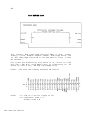
CONTENTS
Page
Overall Description...................................1
Internal Expansions compatibility.....................4
Z80 CPU...............................................6
Z80 Pin Description.................................7
Z80 CTC..............................................10
Z80 CTC Pin Description............................11
Z80 DART.............................................13
Z80 DART Pin Description...........................14
TMS 9929 VDP.........................................17
PAL VDP Horizontal Timing..........................18
9929 Signal Waveforms..............................19
MTX Series System Bus................................20
System Block Diagram...............................21
MTX Disassembly Instructions.........................22
Trouble Shooting Guide...............................25
Symptom 1
No Display/Black and white display............26
Symptom 2
Blank screen/no humming/power on..............28
Symptom 3
Corrupt Video Display or characters...........30
Symptom 4
Bad hum bars..................................31
Symptom 5
Green screen and hum..........................32
Symptom 6
Load and save problems........................35
Symptom 7
Sound problems................................37
Symptom 8
Keyboard......................................38
Symptom 9
Memory Exps, ROM Exps, RS232, Printer.........40
UM1286 Modulator.....................................42
Testing and Setting up........................43
Mother board Links and PAL Colour coding.............44
PROM Codes for memory expansion boards...............45
MTX Service Manual
Timing Chain.........................................46
Rear Plastic moulding................................48
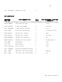
PARTS LIST...........................................49
MTX500/512....................................50
PAL Video Board...............................54
Keyboard/Keytops..............................56
Power Supply..................................59
Plastic Rear Panel............................60
Packing.......................................60
RS232 Board...................................62
32K Memory Expansion..........................64
ROM Expansion.................................65
Schematic Diagrams
MTX 4000-04...................................66
PAL Video Board...............................68
NTSC Video Board..............................69
Memory Expansion Board........................70
RS232 Communications Board....................71
MTX Service Manual
1
INTRODUCTION
Overall Description
The MTX Series personal computer systems are high
performance 8-bit computers uniquely designed to
operate in memory intensive ROM-based or DISCbased environments.
The choice of the Z80 A
Microprocessor and the TMS 9929A series video
processor as the key components of the hardware
architecture is consistent with a low cost ROMbased system with colour TV output plus the
capability to expand to accommodate a fully RAMbased
Disc operating system such
as
CP/M,
utilising a high quality 80 column colour monitor
output.
The memory size can be either 32K or 64K Bytes as
standard, expandable to 512K Bytes. There is a
separate 16K Byte dedicated video memory. A 24K
Byte ROM contains MTX - BASIC, the
systems
monitor, supplementary languages and utilities.
The standard interfaces included are tape cassette
(Read/Write to 2400 baud), Keyboard, Cartridge
Port, Twin Joysticks, Parallel Centronics type
printer port, uncommitted Parallel Input/Output
port, colour TV output with sound, composite video
output - monochrome or colour, and audio output.
Optional
interfaces
include
a
completely
independent
twin
RS232C with
buffered
bus
extension, Colour 80 Column Board, Floppy Disc
System, Silicon disc fast access RAM boards, and a
Winchester Disc System.
The Keyboard consists of 79 full travel typewriter
style keys mounted on a steel base plate which is
fitted to the Aluminium enclosure. Aluminium was
chosen for good heat dissipation, durability and
RFI shielding.
MTX Service Manual
2
CPU Board
Mounted
in
accommodates:
the
lower
chassis,
the
CPU
board
Z80A CPU operating at 4Mhz.
24K of ROM which contains:
MTX BASIC - incorporating sophisticated MTX
graphics commands.
LOGO-type
MTX NODDY - Interactive screen manipulation routines.
FRONT
PANEL
DISPLAY
incorporating
Assembler/Disassembler plus Z80 Register, Memory
Program display and manipulation routines.
Z80
and
VIDEO DISPLAY PROCESSOR - with 16K dedicated video-RAM.
USER-RAM - 32K on the MTX500 and 64K on the MTX512.
User RAM size is constant under all display formats.
VIDEO BOARD - for television and sound signal encoding.
REAL TIME CLOCK
CHARACTER SETS - Numeric, upper case, lower case,
user-definable characters and user-definable sprites.
Resident international character sets and appropriate
keyboard layouts for UK, USA, Finland, France, Germany,
Spain,Denmark and Sweden.
Display
Colour TV and/or Video Monitor
40 column x 24 line display as standard, with
optional Colour 80 column board. (FDX or HDX disc
based system required).
Display Facilities:
FULL SCREEN HANDLING
EIGHT USER DEFINABLE VIRTUAL SCREENS
SCREEN FORMATS
Text: 40 x 24 characters
Text with graphics: 32 x 24 text with 256 x
pixels in 16 colours
MTX Service Manual
192
3
Graphics Facilities
Up to 32 independently controllable user definable
sprites, plus pattern plane and backdrop plane.
High level sprite-orientated graphics commands.
Input/Output
Provided as standard:
1. CASSETTE PORT (variable rate, up to 2 400 baud)
2. UNCOMMITTED PARALLEL INPUT/OUTPUT PORT
3. TWO JOYSTICK PORTS with industry standard pinouts
4. FOUR CHANNEL SOUND UNDER SOFTWARE CONTROL three independent voices plus pink noise output
through TV speaker, or through separate Hi-Fi
output
5. MONITOR
OUTPUT - composite video signal (1V
peak to peak) CARTRIDGE PORT
6. PARALLEL
PRINTER
PORT
(compatible
with
Centronics-type printers)
Expansions
Up
to
two expansion boards may
be
added
internally.
These may be Memory (RAM) Boards or
the Communications Board.
MEMORY BOARDS
RAM may be increased by the addition of boards
which provide 32K, 64K, 128K or 256K of memory, up
to a maximum of 512K.
COMMUNICATIONS BOARD
Available as an internal expansion, this board
carries
two
completely
independent
RS232
interfaces (running at up to 19 200 baud) with
full handshaking and modem communication lines,
and also the disc drive bus. The Communications
Board is required to run the FDX and HDX disc
based systems and the MTX Node/Ring System.
MTX Service Manual
4
NODE/RING
SYSTEM
Communications software and interfacing enabling
construction of MTX Ring Systems. The system is
interrupt driven and runs in conjunction with the
twin RS232 Communications Board.
Compatibility of the memory boards and
Board is given below.
Communications
Compatibility table of internal expansion boards
RAM BOARDS
32k
32k
64k
128k
256k
Comms Board
*
*
*
*
64k
*
*
*
*
*
128k
*
*
*
*
*
256k
*
*
*
*
*
Comms
Board
*
*
*
*
ROM Expansions
Via the cartridge port or disc drive bus these provide:
MTX PASCAL
NODE SYSTEM software
Business, Education and Games software
Suitable Printers
Centronics-type parallel printers
RS232 serial printers (requires
Board)
Communications
Power Supply Unit
Input: 220/240 VAC 50/60 Hz. or 110/115 VAC 50/60
Hz.
Output: 22.5 VAC, 1A tapped at 18V and 9V.
Dimensions in millimetres: Width 92
Depth 110
Height 70 Weight: 1.0 kilogram
The PSU is double insulated and has a side mounted
rocker switch which is internally illuminated when
the unit is on. The mains transformer is located
between two groups of four anti-vibration noise
absorbing rubber mount. Extensive strain relief
MTX Service Manual
5
mouldings are incorporated in the PSU casing to
support the input and output cables. The output
cable terminates in a 240 degree, six pin DIN
connector. The PSU is supplied as a sealed unit.
MTX Service Manual
6
Z80 CPU
The instruction set contains 158 instructions. The 78
instructions of the 8080A are included as a subset;
8080A software compatibility is maintained.
Eight MHz, 6 MHz, 4MHz and 2.5 MHz clocks for the Z80H,
Z80B, Z80A and Z80 CPU result in rapid instruction
execution with consequent high data throughput.
The extensive instruction set includes string, bit,
byte and word operations. Block searches and block
transfers together with indexed and relative addressing
result in the most powerful data handling capabilities
in the microcomputer industry.
The Z80 microprocessors and associated family
of
peripheral
controllers are linked by a
vectored
interrupt system. This system may be daisy-chained to
allow implementation of a priority interrupt scheme.
Little, if any, additional logic is required for daisychaining.
Duplicate
sets of both general-purpose and
flag
registers are provided, easing the design and operation
of system software through single-context switching,
background-foreground
programming and
single-level
interrupt processing.
In addition, two 16-bit index
registers facilitate program processing of tables and
arrays.
There
are
three modes of
high-Speed
interrupt
processing:
8080 similar, non-Z80 peripheral device
and Z80 Family peripheral with or without daisy chain.
On-chip dynamic memory refresh counter.
MTX Service Manual
7
Pin description
A0-A15.
Address Bus (output, active High,·3-state).
A0A15 form a 16-bit address bus. The Address Bus
provides the address for memory data bus exchanges
(up to 64K bytes) and for I/O device exchanges.
BUSACK.
Bus
Acknowledge (output, active
Low).
Bus
Acknowledge indicates to the requesting device
that the CPU address bus, data bus and control
Signals MREQ, IORQ, RD and WR have entered their
high-impedance states. The external circuitry can
now control these lines.
BUSREQ.
Bus Request (input, active Low). Bus Request has
a
higher priority than NMI and
is
always
recognized at the end of the current machine
cycle.
BUSREQ forces the CPU address bus, data
bus, and control signals MREQ, IORQ, RD, and WR to
go to a high-impedance state so that other devices
can control these lines. BUSREQ is normally wireORed and requires an external pull up for these
applications.
Extended BUSREQ periods due to
extensive DMA operations can prevent the CPU from
properly refreshing dynamic RAMs.
D0-D7.
Data Bus (input/output, active High 3-state). D0D7 constitute an 8-bit bidirectional data bus,
used for data exchanges with memory and I/O.
HALT.
Halt State (output, active Low). HALT indicates
that the CPU has executed a Halt instruction and
is awaiting either a non-maskable or a maskable
interrupt (with the mask enabled) before operation
can resume. While halted, the CPU executes NOPs
to maintain memory refresh.
INT.
Interrupt Request (input, active Low).
Interrupt
Request is generated by I/O devices.
The CPU
honors a request at the end of the current
instruction if the internal software-controlled
interrupt enable flip-flop (IFF) is enabled.
INT
is normally wire-ORed and requires an external
pull up for these applications.
MTX Service Manual
8
IORQ.
Input/Output Request (output, active Low,
3state). IORQ indicates that the lower half of the
address bus holds a valid I/O address for an I/O
read or write operation. IORQ is also generated
concurrently
with
M1
during
an
interrupt
acknowledge cycle to indicate that an interrupt
response vector can be placed on the data bus.
M1.
Machine Cycle One (output, active Low).
M1,
together with MREQ, indicates that the current
machine cycle is the opcode fetch cycle of an
instruction execution. M1, together with IORQ,
indicates an interrupt acknowledge cycle.
MREQ.
Memory Request (output, active Low, 3-state).
MREQ indicates that the address bus holds a valid
address for a memory read or
memory
write
operation.
NMI.
Non-Maskable Interrupt (input, negative
edgetriggered).
NMI has a higher priority than INT.
NMI is always recognized at the end of the current
instruction, independent of the status of the
interrupt enable flip-flop, and
automatically
forces the CPU to restart at location 0066H.
RD.
Read (output, active Low, 3-state). RD indicates
that the CPU wants to read data from memory or an
I/O device. The addressed I/O device or memory
should use this signal to gate data onto the CPU
data bus.
RESET.
Reset (input, active Low). RESET initialises the
CPU as follows: it resets the interrupt enable
flip-flop, clears the PC and Registers I and R,
and sets the interrupt status to Mode 0.
During
reset time, the address and data bus go to a highimpedance state, and all control output Signals go
to the inactive state. Note that RESET must be
active
for a minimum of three full clock cycles
before the reset operation is complete.
MTX Service Manual
9
RFSH.
Refresh (output, active Low). RFSH, together with
MREQ, indicates that the lower seven bits of the
system's address bus can be used as a refresh
address to the system's dynamic memories.
WAIT.
Wait (input, active Low). WAIT indicates to the
CPU that the addressed memory or I/O devices are
not ready for a data transfer. The CPU continues
to enter a Wait state as long as this signal is
active. Extended WAIT periods can prevent the CPU
from refreshing dynamic memory properly.
WR.
Write (output, active Low, 3-state). WR indicates
that the CPU data bus holds valid data to be
stored at the addressed memory or I/O location.
MTX Service Manual
10
Z80 CTC
The
Z-80 CTC four-channel counter/timer
can
be
programmed by system software for a broad range of
counting
and
timing
applications.
The
four
independently programmable channels of the Z-80 CTC
satisfy common microcomputer system requirements for
event counting, interrupt and interval timing, and
general clock rate generation.
System design is simplified because the CTC connects
directly to both the Z-80 CPU and the Z-80 SIO with no
additional logic. In larger systems, address decoders
and buffers may be required.
Programming the CTC is straightforward: each channel
is programmed with two bytes; a third is necessary when
interrupts are enabled. Once started, the CTC counts
down, reloads its time constant automatically, and
resumes counting. Software timing loops are completely
eliminated. Interrupt processing is simplified because
only one vector need be specified; the CTC internally
generates a unique vector for each channel.
The Z-80 CTC requires a single + 5 V power supply and
the standard Z-80 single-phrase system clock.
It is
fabricated with n-channel silicon-gate depletion-load
technology, and packaged in a 28-pin plastic or ceramic
DIP.
MTX Service Manual
11
Pin Description
CE.
Chip Enable (input, active Low). When enabled the
CTC accepts control words, interrupt vectors, or
time constant data words from the data bus during
an I/O write cycle; or transmits the contents of
the down-counter to the CPU during an I/O read
cycle.
In most applications this signal
is
decoded from the eight least significant-bits of
the address bus for any of the four I/O port
addresses that are mapped to the four countertimer channels.
CLK.
System Clock (input).
system clock.
Standard Single-phase
Z-80
CLK/TRG0-CLK/TRG3.
External
Clock/Timer
Trigger
(input,
userselectable
active High or Low).
Four
pins
corresponding to the four Z-80 CTC channels.
In
counter mode, every active edge on this pin
decrements the down-counter. In timer mode, an
active edge starts the timer.
CS0-CS1.
Channel Select (inputs active High).
Two-bit
binary address code selects one of the four CTC
channels for an I/O write or read
(usually
connected to A0 and A1).
D0-D7.
System
Data
Bus
(bidirectional,
3-state).
Transfers all data and commands between the Z-80
CPU and the Z-80 CTC.
IEI.
Interrupt Enable In (input, active High). A High
indicates that no other interrupting devices of
higher priority in the daisy chain are being
serviced by the Z-80 CPU.
IEO.
Interrupt Enable Out (output, active High).
High
only if IEI is High and the Z-80 CPU is not
servicing an interrupt from any Z-80 CTC channel.
IEO
blocks
lower
priority
devices
from
interrupting while a higher priority interrupting
device is being serviced.
MTX Service Manual
12
INT.
Interrupt Request (output, open drain, active
Low). Low when any Z-80 CTC channel that has been
programmed to enable interrupts has a zero-count
condition in its down-counter.
IORQ.
Input/Output Request (input from CPU, active Low).
Used with CE and RD to transfer data and channel
control words between the Z-80 CPU and the Z-80
CTC. During a write cycle, IORQ and CE are active
and RD inactive. The Z-80 CTC does not receive a
specific write signal; rather, it
internally
generates its own from the inverse of an active RD
signal.
In a read cycle, IORQ, CE and RD are
active; the contents of the down-counter are read
by the Z-80 CPU. If IORQ and M1 are both true,
the CPU is acknowledging an interrupt request, and
the highest priority interrupting channel places
its interrupt vector on the Z-SO data bus.
M1.
Machine Cycle One (input from CPU, active Low).
When M1 and IORQ are active, the Z-80 CPU is
acknowledging an interrupt. The Z-80 CTC then
places an interrupt vector on the data bus if it
has highest priority, and if a channel
has
requested an interrupt (INT).
RD.
Read Cycle Status (input, active Low).
Used in
conjunction with IORQ and CE to transfer data and
channel control words between the Z-80 CPU
and
the Z-80 CTC.
RESET.
Reset (input active Low). Terminates all downcounts and disables all interrupts by resetting
the interrupt bits in all control registers;
the
ZC/TO and the Interrupt outputs go inactive;
IEO
reflects IEI;
D0-D7 go to the high-impedance
state.
ZC/TO0-ZC/TO2.
Zero Count/Timeout (output, active High).
Three
ZC/TO pins corresponding to Z-80 CTC channels 2
through 0 (Channel 3 has no ZC/TP pin). In both
counter and timer modes the output is an active
High pulse when the down-counter decrements to
zero.
MTX Service Manual
13
Z80 DART
The
Z-80
DART
(Dual-Channel
Asynchronous
Receiver/Transmitter) is a dual-channel multi-function
peripheral component that satisfies a wide variety of
asynchronous serial data communications requirements in
micro-computer systems.
The Z-80 DART is used as a
serial-to-parallel,
parallel-to-serial converter
/
controller in asynchronous applications. In addition,
the device also provides modem controls for both
channels. In applications where modem controls are not
needed, these lines can be used for general-purpose
I/O.
Zilog also offers the Z-80 SIO, a more versatile device
that provides synchronous (Bisync, HDLC and SDLC) as
well as asynchronous operation.
The Z-80 DART is fabricated with n-channel silicon-gate
depletion-load technology, and is packaged in a 40-pin
plastic or ceramic DIP.
MTX Service Manual
14
Pin Description
B/A.
Channel A Or B Select (input, High selects channel
B). This input defines which channel is accessed
during a data transfer between the CPU and the Z80 DART.
C/D.
Control Or Data Select (input, High
selects
Control).
This input specifies the type
of
information (control or data) transferred on the
data bus between the CPU and the Z-SO DART.
CE.
Chip Enable(input, active Low). A Low at this
input enables the Z-80 DART to accept command or
data input from the CPU during a write cycle, or
to transmit data to the CPU during a read cycle.
CLK.
System Clock (input). The Z-80 DART uses
standard
Z-80 single-phase system
clock
synchronize internal signals.
the
to
CTSA, CTSB.
Clear
To Send (inputs, active Low).
When
programmed as Auto Enables, a Low on these inputs
enables
the respective transmitter.
If
not
programmed as Auto Enables, these inputs may be
programmed as general-purpose inputs. Both inputs
are Schmitt-trigger buffered to accommodate slowrisetime signals.
D0-D7.
System Data Bus (bidirectional, 3-state) transfers
data and commands between the CPU and the Z-80
DART.
DCDA, DCDB.
Data Carrier Detect (inputs, active Low).
These
pins function as receiver enables if the Z-80 DART
is programmed for Auto Enables; otherwise they may
be used as general-purpose input pins. Both pins
are Schmitt-trigger buffered.
DTRA, DTRB.
Data Terminal Ready (outputs, active Low).
These
outputs follow the state programmed into the DTR
bit.
They can also be programmed as generalpurpose outputs.
MTX Service Manual
15
IEI.
Interrupt Enable In (input, active High) is used
with IEO to form a priority daisy chain when there
is more than one interrupt-driven device. A High
on this line indicates that no other device of
higher priority is being serviced by a
CPU
interrupt service routine.
IEO.
Interrupt Enable Out (output, active High).
IEO
is High only if IEI is High and the CPU is not
servicing an interrupt from this Z-80 DART. Thus,
this signal blocks lower priority devices from
interrupting while a higher priority device is
being serviced by its CPU interrupt
service
routine.
INT.
Interrupt Request (output, open drain, active
Low).
When the Z-80 DART is requesting
an
interrupt, it pulls INT Low.
M1.
Machine Cycle One (input from Z-80 CPU, active
Low).
When M1 and RD are both active, the Z-80
CPU is fetching an instruction from memory; when
M1 is active while IORQ is active, the Z-80 DART
accepts M1 and IORQ as an interrupt acknowledge if
the Z-80 DART is the highest priority device that
has interrupted the Z-80 CPU.
IORQ.
Input/Output Request (input from CPU,
active
Low). IORQ is used in conjunction with B/A, C/D,
CE and RD to transfer commands and data between
the CPU and the Z-80 DART. When CE, RD and IORQ
are all active, the channel selected by B/A
transfers data to the CPU (a read operation).
When CE and IORQ are active. but RD is inactive,
the channel selected by B/A is written to by the
CPU with either data or control information as
specified by C/D.
RxCA, RxCB.
Receiver Clocks (inputs). Receive data is sampled
on the rising edge of RxC. The Receive Clocks may
be 1, 16, 32 or 64 times the data rate.
RD.
Read Cycle Status. (input from CPU, active Low).
If RD is active, a memory or I/O read operation is
in progress.
MTX Service Manual
16
RxDA, RxDB.
Receive Data (inputs, active High).
RESET.
Reset
(input,
active Low).
Disables
receivers and transmitters, forces TxDA and
marking, forces the modem controls High
disables all interrupts.
both
TxDB
and
RIA, RIB.
Ring Indicator (inputs, Active Low). These inputs
are similar to CTS and DCD. The Z-80 DART detects
both logic level transitions and interrupts the
CPU. When not used in switched-line applications,
these inputs can be used as
general-purpose
inputs.
RTSA, RTSB.
Request to Send (outputs, active Low). When the
RTS bit is set, the RTS output goes Low. When the
RTS bit is reset, the output goes High after the
transmitter empties.
TxCA, TxCB.
Transmitter Clocks (inputs). TxD changes on the
falling edge of TxC. The Transmitter Clocks may
be 1, 16, 32 or 64 times the data rate; however,
the clock multiplier for the transmitter and the
receiver must be the same. The Transmit Clock
inputs are Schmitt-trigger buffered.
Both the
Receiver and Transmitter Clocks may be driven by
the Z-80 CTC Counter Time Circuit for programmable
baud rate generation.
TxDA, TxDB.
Transmit Data (outputs, active High).
W/RDYA, W/RDYB.
Wait/Ready (outputs,open drain when programmed for
Wait function, driven High and Low when programmed
for Ready function). These dual-purpose outputs
may be programmed as Ready lines for a DMA
controller or as Wait lines that synchronize. the
CPU to the Z-80 DART data rate. The reset state
is open drain.
MTX Service Manual
17
TMS 9929 VDP (Video Display Processor)
Introduction
This Preliminary Specification of the TMS 9929 is to be
considered as an "ADD ON" to the basic TMS 9918
specification.
The TMS 9929 is effectively identical
to the TMS 9918 functionally and only has the color
video section that is different.
The TMS 9918 provides a composite color video signal
output that if driven by a suitable amplifier can go
directly into any color video monitor. The color burst
frequency is the VDP oscillator input frequency divided
by three.
External video mixing with an external
reference source can also be achieved by inputting this
external source directly into the TMS 9918.
In
the
TMS 9929 the color
and
luminance/sync
information is provided on three pins rather
than a
single pin in the form of two color difference signals
and one luminance signal with all the vertical and
horizontal timing included. So we have R-Y, B-Y, and Y
respectively.
The two color difference signals are
used then by an external quadrature modulator video
encoder.
It is outside the Video Display Processor
that the composite color video signal is generated into
a PAL or Secam compatible TV signal.
The external
video mixing is also done outside and it is the TMS
9929 to decide when this mode is entered.
This is
achieved by a special level distinction made by the R-Y
and B-Y VDP outputs. When external video is entered
these two outputs go to the equivalent of the sync
percentage level of the black-white swing in the
luminance output, i.e. the color difference outputs are
normally swinging between the luminance black-white
voltage levels and it is only in the external video
mode that these outputs go to the reserved " sync"
level.
Phase locking of the VDP to the external PAL burst
frequency is desirable if inter-hum or crawl effects
want to be minimized. The TMS 9929 oscillator clock
must
still,
however, be maintained
within
its
prescribed limits of oscillator operation.
CPUCLK
signal is no longer available in the European TMS 9929.
MTX Service Manual
18
4116
VRAM
PIN NAMES
A0-A6
Address Inputs
CAS
Column Address Strobe
DIN
Data Input
DOUT
Data Output
RAS
Row Address Strobe
WRITE
Read/Write Input
VBB
-5V Power Supply
VCC
+5V Power Supply
VDD
+12V Power Supply
VSS
Ground
19
MTX Service Manual
19
MTX Service Manual
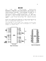
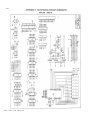
20
MTX SERIES BUS
The system Bus comprises the full Z80 A bus, power
supply rails, ROMpak enable (GROM), ROM page ports R0
to R2, RAM page ports P0 to P3 and serial clock lines
01 and 02.
All lines are externally available on J1, which is a 60
way (30 + 30) 0.1" card edge plug, or internally on J0
which is also a 0.1" 60 way card edge plug.
Note:- J10 also has keyway between 26 and 27
Note:
(1) Jl0 is a mirror image of J0
(2) Component side = A
Solder side = B
MTX Service Manual
21
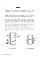
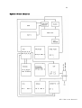
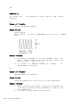
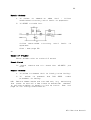
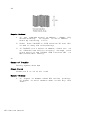
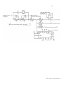
System Block Diagram
MTX Service Manual
22
DISASSEMBLY INSTRUCTIONS
1.
Using an Allen key, remove the three dome head
screws from the right & left hand ends of the
MTX.
2.
Lift the MTX keyboard at the rear just above
plastic panel. Be careful not to damage
keyboard interconnecting cable.
3.
Gently ease the KBD (keyboard) interconnecting
cable from the mother board and slide the top KBD
to the left or right until detached.
4.
Remove the video monitor cable (fig 3) and tape it
to the plastic panel to prevent any unnecessary
damage.
MTX Service Manual
the
the
23
The under side of the MTX reveals a single screw
which secures the MTX mother board to the bottom
chassis. By removing the main screw and earth strap
the MTX Mother Board and Rear Plug panel will
slide from the case bottom.
Faults are rarely complained about but nonetheless
faults, include I/O ports that are insecurely soldered
or not 'flush' with the main P.C.B. i.e. Power Supply
socket, Printer port, cassette ear and mic and joy
stick ports.
Any competent initial check of a returned MTX should
include these ports. It should also include checking
for the nylon washers on the solder side of the board
(esp under the tip 2955 power transistor and the
joystick port sockets ) which stops RE/CPM shorting to
earth - see Page 48 of assembly instructions of Power
Transistor.
Also check power supply voltage....ideally about 22.5v
to 24.5v and check to see that c56 and c51 - 4700 uf
16v capacitors are secure.
MTX Service Manual
24
MTX Service Manual
25
Introduction To Trouble
Shooting Guide
Memotech products are all given a vigorous series of
tests before despatch to the end user.
These tests
include:- Loading and saving functions, sound channel
checks, compatibility with printers and other add ons,
etc etc.
Once the units have passed this stage of
tests they are given 24 hour soak test, (burning in
process).
Any component that is faulty is generally
weeded out at this stage. The units are then given a
final check over before they are packed and despatched
to the end user.
Occasionally you may find less serious faults occurring
possibly due to heavy handling during transit.
The following trouble shooting guide is designed to
give you a starting reference at which to start the
fault finding procedure. After several weeks you will
become confident enough to delve deeper into the MTX
Circuitry. We hope that this guide will assist you to
meet this end.
MTX Service Manual
26
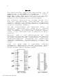
SYMPTOM 1
On power up:display.
No display or only a black
and
white
a)
Cause of Trouble
Black and White output.
Check Point
Video Board
Oscillation
IC47.
of Xtal 4.433619Mhz or pin 17 of
LM1889
Repair Method
1
If pulse is present on P17 of LM1889
until oscillation is at its optimum
peek to peek. See fig no 1.
2
If pulse is absent LM1889
associated circuitry.
is
turn CVI
pitch 3v
faulty
-
or
b)
Cause of Trouble
Rapid Fading of colours.
Check Point
Tantalum Capacitor on 5v pin 2 of the modulator
Repair Method
1
2
Check Tantalum is a 22uf -Ve leg is earthed and
+ Ve leg is sufficiently soldered to the 5v pin
2 of Modulator.
If still faulty replace pal board.
MTX Service Manual
27
3
If still faulty replace the Modulator.
c)
Cause of Trouble
No video output, i.e. 'fuzzy screen'
Check Point
Pal board J11 and or Modulator
Repair Method
1
Check for
Modulator.
pulse on pin 3 of J11 or Pin
3
2
Check for short to
3
Check +12v - if absent replace 12v Regulator.
of
5v...or replace Modulator.
d)
Cause of Trouble
Monitor display faulty
Check Point
Pal board monitor connection cable
Repair Method
NB:
1
Check for pulse on Q6 - (2N3906 transistor)
absent Q6 is faulty.
2
Check for loose connections on monitor cable.
3
Is 47pf
panel?
present
on monitor
output
on
if
back
BEFORE YOU START
Always check your monitor and or TV.
Always check your monitor leads and aerial leads.
MTX Service Manual
28
SYMPTOM 2
When power is switched on:
sound.
Blank screen - no
humming
a)
Cause of Trouble
Faulty video board
Check Point
Check to see if you have control G note
Repair Method
1
If control G note is present video
faulty-Replace video board.
board
is
b)
Cause of Trouble
Blank screen with no control G sound
Check Point
Check +5v -5v +12v 0v
Repair Method
1
If the +5 voltage is absent,
fuse has blown.
2nd
stage
2
If +12v and +5v are absent check
regulators and associated circuitry.
both
c)
Cause of Trouble
Blank screen with no control G sound
Check Point
If above voltages are present check 4Mhz
Also check RESET circuit
MTX Service Manual
Xtal
-
29
Repair Method
1
If pulse is absent on 4Mhz Xtal - follow
associated circuitry until fault is apparent.
2
If RESET is held low-
follow associated
apparent.
circuitry
until
fault
is
Also - see page 33.
d)
Cause of Trouble
Blank screen with no control G sound
Check Point
If
above
Xtal
checks are o.k. check the
10.6875
;hz
Repair Method
1
If pulse is absent Xtal is likely to be faulty.
2
If
pulse is present
processor is faulty.
the
TMS
9929
video
NB: Before these tests are carried out, try switching
the power on and off a few times to establish whether
or not the problem is merely a fire up fault. See ref
page 47 for timing modification.
MTX Service Manual
30
SYMPTOM 3
Corrupt video display or characters
a)
Cause of Trouble
- 5v absent
Check Point
1
If -5v is absent - check for short at J12
(monitor o/p) of video board - or repair open
circuit. The -5v is generally shorted to 0v at
this point.
b)
Cause of Trouble
Faulty Video Ram
Check Point
Check for pulse on pin 2 of Video Ram.
Check for signal on P14 of any Video Ram.
Repair Method
1
Systematically
disable the Video Rams
by
earthing pin 14. Continue with this process
until
corruption
has
reduced.
The
IC
with the least corruption when earthing, is
likely to be faulty...replace.
See warning on
page 31.
2
If
MTX Service Manual
the corruption is very bad scopeing pin
14
31
may pick out the faulty component.
c)
Cause of Trouble
Faulty TMS 9929
Check Point
Check pins 3 to 10 and pins 25 to 32
Repair Method
1
If signal
processor.
is absent replace
TMS
9929
video
WARNING:When you earth the Video Rams - make sure
earth them via a 10 OHM - 15 OHM Resistor.
not earth them directly as this may damage
components.
you
Do
the
SYMPTOM 4
When power is switched on:
corruption of display.
Very bad hum bars
causing
a)
Cause of Trouble
Faulty P.S.U.
Check Point
Check input
Meter.
voltage
at J9.
with Digital
Volt
Repair Method
1
Voltage should read between 23v and 24.5v not change P.S.U.
if
MTX Service Manual
32
b)
Cause of Trouble
Faulty Bridge Rectifier
Check Point
Check your +5v and +12v
Repair Method
1
If signal is poor trace fault from either the
7805 or 7812 Regulators to faulty component.
SYMPTOM 5
When power is switched on:- Green screen
noise.
and
humming
Whilst testing the MTX during Manufacture the most
common fault we find is:- On fire up - Blank screen
and humming sound. Quite frankly these are the most
difficult faults to repair due to the fact that just
about any component can cause these symptoms. We find
that solder shorts are responsible for the majority of
these problems, but occasionally we do find
faulty
components.
Since all
the MTX's are thoroughly tested before
despatch, faults occurring such as green screen and
humming, after despatch are more than likely going to
be component break down.
The biggest problem is whether or not the ram chips are
functioning correctly or not. The Memotech Ram Test
Rig can pin point a fault either on the data bus or the
memory page address lines. Whether or not the Rig
detects a faulty Ram the fact remains that it will
eliminate eight key components which is a great help.
Without a Ram Rig Test the chances of finding a faulty
Ram with only an oscilloscope are very slim indeed.
However, green screen and humming faults are not
necessarily due
to faulty Rams. When you have the
symptom of green screen and humming there is a strict
procedure to follow.......
MTX Service Manual
33
a)
Cause of Trouble
Faulty voltages
Check Point
Check all your voltages 0v, 5v, 12v, -5v, -12v
Repair Method
1
If any signal is absent follow
circuitry from source and repair.
offending
b)
Cause of Trouble
Faulty RESET circuit - also see page 29.
Check Point
Check Points are:- Pin 3 of IC18 BCN4070 CMOS
Pin 26 of C.P.U.
Pin 34 of V.D.P.
NB.
1
If signal is low - trace fault back from Pin 3
of IC18 4070CMOS (pay particular attention to
C11 10uf cap).
2
If signal is high RESET circuitry is o.k.
Signal should go low when shorting pins 19 and
of J1 - keyboard interconnection header plug.
20
c)
Cause of Trouble
Fault on address bus
Check Point
Probe system address bus of C.P.U.
MTX Service Manual
34
Repair Method
1
If any address signal is absent - Reset MTX
whilst probing.
If signal is still absent start by replacing C.P.U.
2
Check both 74LS157's (PCB Location 6C and
to see if they are multiplexing.
3
If 74LS157 pin 1 pulse is absent, check pin 14
of PAL14L4 and follow circuitry through pins
3,4,5 and 6 of the 74LS04 (PCB Location 2B) to
REF points MPX. faulty.
6D)
d)
Cause of Trouble
Faulty system data bus
Check Point
Probe pin 2 or 14 of all rams
Repair Method
1
If signal is absent reset MTX whilst probing.
If signal is still absent refer to MTX Rig Ram
Test.
MTX Service Manual
35
NB:
We find it helpful to replace all the socketed
IC's with a known good set before attempting to
rectify this fault.
*
The fact that a signal is absent from the system
data bus does not
necessarily mean that there
is a fault in Ram. It is very difficult to
determine Ram faults with an oscilloscope alone.
You really do need the Memotech Ram Rig Tester.
SYMPTOM 6
Problems with the load and saving functions
a)
Cause of Trouble
Faulty jack socket
Check Point
J2 Ear jack socket
Repair Method
1
Jack socket J2 may be loose or worn, also buzz
across the socket is 0v - CSTT out - to check
for shorts - replace socket.
b)
Cause of Trouble
Faulty IC BCN4070 CMOS or associated circuitry
MTX Service Manual
36
Check Point
By typing LO."" (RET) and loading in a long
playing cassette tape start probing at J2 CSST out.
Repair Method
1
You can easily follow the signals from J2
through opamp 10E 314. (Remember pin 6 is
normally -12v) and in to 4070 CMOS out at pin
4. - Replace faulty component.
2
If no fault found change CPU or CTC.
c)
Cause of Trouble
Incorrect PAL14L4 value link arrangement or timing
Check Point
Link 6 and link 7 + PAL14L4
Repair Method
1
See page 45 for link variations and pal colour
codes
MTX Service Manual
37
d)
Cause of Trouble
MTX 512 with internal expansions only
Check Point
Check right hand bus connector
Repair Method
1
NB:
Either make sure the bus connector is clean
or...ideally hard solder the expansion board to
the mother board.
Before these tests are carried out always check
that you have a good tape recorder that is set
at the correct volume (between level 7 and 10).
Check your cassette leads (remember ear to ear
and mic to mic). Check that the cassette tape
itself is working - and not damaged.
SYMPTOM 7
Problems with sound (Depress control key
together for note).
and
G
key
a)
Cause of Trouble
Faulty SN 76489 AN (5E)
Check Point
Start by probing I/O of (4E) 74LS374N
Repair Method
1
Press control G - you should be getting pulses
from 4E 74LS374N outputs. If absent disable
offending output from 5E SN76489.
2
If still absent 74LS374N is faulty.
3
If pulse is present on 74LS374N the
faulty.
76489
is
MTX Service Manual
38
4
If pulse is present on both 4E (374) and
(SN76489AN) check for pulse on pin 1 of J13
pal board and pin 3 of J11 on pal board.
either are absent check for open circuit
replace pal board.
5
If pulse is present on J11 and J13 check
tuning of modulator. See ref Page 42.
5E
on
If
or
the
b)
Cause of Trouble
Faulty SN76489AN or 74LS374N
Check Point
As above
Repair Method
1
NB:
Often the sound channels become
the components have reached
temperature.
You can heat the
74LS374N systematically with a
(whilst
checking pulses on
recreate several hours of use.
distorted once
their
optimum
SN76489AN and
soldering iron
SN76489AN)
to
For further information on
modulator
video board fine tuning see page 42.
SYMPTOM 8
Faulty keyboard response
a)
Cause of Trouble
Key bounce
Check Point
Upper keyboard chassis
MTX Service Manual
and
39
Repair Method
Generally key bounce is caused by faulty key board
switches.
Simply de-solder and replace
the
offending key(s).
b)
Cause of Trouble
Key(s) u/s
Check Point
J1-keyboard interconnection header plug
Repair Method
1
Check that the keyboard interconnection
is secure and not torn.
cable
2
Check that the offending keys work by buzzing
across the terminals whilst depressing the
switch.
3
Check for pulses on diodes DR0-DR7 (4148) Anode
-> 74LS273N (3A) -> LCD lines.
c)
Cause of Trouble
Incorrect character displays
Repair Method
1
Check for correct language switch
PCB location - SWA.
2
Ensure
only).
3
Check links
only).
4
Replace PAL14L4 chip.
setting
GROM line is connected (piggyback
at
Roms
1, 2, 4, 5 and 13 (4000/04 boards
MTX Service Manual
40
SYMPTOM 9
Add on faults - e.g. Memory expansions,
RS232, Printers etc.
Rom
boards,
a)
Cause of Trouble
Memory upgrade not obtaining Ram top
Check Point
Check for correct prom coding, see page 45, check
rams in sockets (if any) for poor connection
Repair Method
1
If prom is o.k. make sure that both
connector and upgrade connector is clean.
are
edge
2
Check links on the upgrade
soldered in the LO position.
correctly
3
R1 = 330 OHM.
4
R2 = 680 OHM.
5
If green screen fault refer to Rig Ram Test.
b)
Cause of Trouble
Rom Boards
Check Point
RE/CPM pin 9, 5A, 74LS273N of MTX
Repair Method
1
Type Rom 2 whilst probing pin 9 of main
location SA. Look for pulse
2
If pulse is absent, check foe washer
underside of board - under TIP 2955
3
Check pal chip on MTX.
MTX Service Manual
PCB
on
41
4
Check links 6 and 7 on MTX.
5
Look closely at the 273 (5A) on
and associated circuitry.
mother
board
c)
Cause of Trouble
RS232
Check Points
As above.
Repair Methods
As above ->
1
If intermittent fire up modify timing chain
see page 46.
->
d)
Cause of Trouble
Printer
Check Point
J6 Printer o/p
Repair Method
1
Be sure
that the fault is not
itself or the interface cable.
the
printer
2
STROBE should be Hi.
3
Check Printer data lines (PRD0-PRD7)
374 and on J6.
4
Also check
74LS244.
5
Less likely-check the 74LS74 for STROBE.
on
pins 11, 13, 15 and 17 of
1D
74LS
the
MTX Service Manual
42
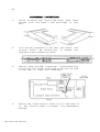
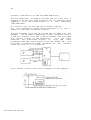
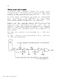
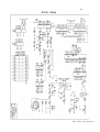
Further information on the UM 1286 Modulator.
The Pal-Modulator is used to encode the R-Y, B-Y and Y
signals from the MTX home computer and to modulate them
together with the sound signal to a high frequency
(591.250 MHz).
R-Y and B-Y are called the Chrominance signals.
All the information about the brightness is in
signal called the Luminance signal.
the
Y
The Pal Encoder is built up around the LM 1889 and the
UM1286. The LM 1889 integrated circuit receives the RY and B-Y signals from the video processor and provides
the colour signal to the Modulator.
This one also
receives the Luminance signal (Y) from the video
processor and the audio signal from the 76489 (SE) and
provides a composite signal suitable for the antenna
input terminal of a TV receiver.
Fig i shows a functional block diagram of the system.
MTX Service Manual
43
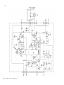
Test and setting procedure of UM 1286 and video board
1
Be sure that your TV set, MTX computer and any
other test equipment is switched on at least half
an hour before beginning the test.
2
Connect the MTX computer to the TV
aerial cable.
3
Set the TV set to channel 36 of the 1V band (UHF)
to obtain the best combination of sound and
colour.
4
With the aid of a frequency meter, check the audio
carrier; if (for PAL A units) it is not 6 MHz
(values allowed: 5.99 - 6.01 Mhz) turn the sound
frequency
adjustment coil (Fig ii)
of
the
Modulator to set it.
5
The video carrier is now set by 2 resistors
running in series at RV1 (a 10K OHM and 1K OHM).
These resistors can be replaced with a 1K MHz
variable resistor.
6
The two brass screws in the modulator (fig ii) are
cable
compensators and shouldn't
really
be
tampered with.
set
by
the
FOOTNOTE
Whilst carrying out any tests on the MTX it is
advisable to detach the Mother P.C.B. from the bottom
chassis. If after following the trouble shooting guide
you still have problems - Replace the Mother Board and
refer to Manufacturers.
NB:
Any
channel adjustments carried out on
the
Modulator should be done with the
automatic
frequency switch of the TV turned off.
In the event of a TV not having an AFT switch
disregard this footnote.
MTX Service Manual
44
Link arrangements and PAL colour coding
1.
MTX 500 - 4000/04 with 32k H Ram chips.
2.
MTX 500 4000/04 with 32k L Ram chips
3.
MTX 500 4000/05 with 32k H Ram chips. Links 6 and
7 as point 1.
4.
MTX 500 4000/05 with 32k L Ram chips. Links 6 and
7 as point 2.
5.
MTX 512 4000/04 - 64k
6.
MTX 512 4000/05.
7.
MTX 500 4000/06 - 32k.
3 and 4.
Links 6 and 7 as points
8.
MTX 512 4000/06 - 64k.
Links 6 and 7 as point 6.
MTX Service Manual
_
|
|
|
|
|
|
|
|
|--BLUE PAL
| 212 FUSES
| BLOWN
|
|
|
|
_|
_
|
|
|-WHITE PAL
| 194 FUSES
| BLOWN
_|
_
|
|
|
|-YELLOW PAL
| 212 FUSES
| BLOWN
_|
Links 6 and 7 as point 5.
_
|
|-RED PAL
_| 212 FUSES
_
| WHITE PAL
| FOR MTX500
|| RED PAL
_| FOR MTX512
45
PROM CODE FOR MEMORY EXPANSION BOARDS
MTX 500
CODE DESCRIPTION
OLL
(MAX 96K)
1 ROW OF 32K L OR
2 ROWS OF 32K L
OLH
(MAX 96K)
1 ROW OF 32K L
1 ROW OF 32K L AND 1 ROW OF 32K H
OHH
(MAX 96K)
1 ROW OF 32K H OR
2 ROWS OF 32K H
OL64
(MAX 128K)
1 ROW 32K L AND
1 ROW 64K
00128
(MAX 160K)
2 ROWS OF 64K
04128
(MAX 288K)
TO RUN IN CONJUNCTION WITH 00128
2 ROWS OF 64K
08128
(MAX 416K)
TO RUN IN CONJUNCTION WITH 00128
AND 04128
2 ROWS 64K
MTX 512
CODE DESCRIPTION
1LL
(MAX 128K)
1 ROW OF 32K L OR
2 ROWS OF 32K L
1LH
(MAX 128K)
1 ROW OF 32K L
1 ROW OF 32K L AND 1 ROW OF 32K H
1HH
(MAX 128K)
1 ROW OF 32K H OR
2 ROWS OF 32K H
10128
(MAX 192K)
2 ROWS OF 64K
14128
(MAX 320K)
TO RUN IN CONJUNCTION WITH 10128
2 ROWS OF 64K
18128
TO RUN IN CONJUNCTION WITH 10128
AND 14128
2 ROWS OF 64K
(MAX 448K)
1C128
(MAX 512K)
TO RUN IN CONJUNCTION WITH 10128
AND 14128 AND 18128
1 ROW OF 64K
MTX Service Manual
46
Timing chain modification
In October 1984
Memotech altered the timing chain
circuitry due to occasional faults occurring after about
2 hours of use - and poor fire up response.
(esp; when
running in conjunction with F.D.X.)
We have since up-dated all our units to incorporate
this 'modification'.
MTX 4000/06 P.C.B.'s are exempt
from
this
modification due
to
the
fact
that
multilayered boards are generally not affected.
However you may feel the need to replace the timing
chain with the modified circuit if
your MTX
is
suffering from intermittent fire ups (e.g. 1 fire up
failure in less than 5 attempts constitutes a possible
fault in the timing chain circuitry).
The diagram
below shows what components have to be changed and to
what values:R14 680 Ohm
resistor.
resistor to be replaced
by
a
C6 68pf capacitor to be replaced by a 33 pf
(or left out completely).
MTX Service Manual
330
Ohm
capacitor
47
MTX Service Manual
48
Plastic back panel.
You will find that your TV/Monitor picture will tear or
wobble if your plastic back panel does not have:
a
b
Earth straps
47pf capacitor
Illustration of assembly of power transistor.
MTX Service Manual
49
PARTS LIST FOR THE:
MTX 512 04
RS232 I/F
32K MEMORY EXPANSION
ROM EXPANSION
MTX Service Manual
50
MTX LOADING STAGE 1.
MEMOTECH
ITEM DESCRIPTION
NO./
PCB COMPONENT LOCATION
PART NO.
UNIT
/ COMMENTS
-----------------------------------------------------------------------CONS CNOND9P
9 Way Canon D Type
2
J4,J5
HS
Heat Sink
1
HS01
INSU BUSH
Insulating Bush
1
Q4
INSU PAD
Insulating Pad
1
Q4
NUT
M3HEXH
M3 Hex Nut
3
Q4,RG1,RG2
NUT
M3HEXN
M3 Nylon Nut
4
J4,J5
PCB
4000-04
4000-04 PCB
1
REG
UA7805
UA7805CKC 5v Regulator
1
RG2
REG
UA7812
UA7812CKC 12v Regulator
1
RG1
SCRW M38BH
M38 Dome Head Screw
3
Q4,RG1,RG2
SCRW M38N
M38 Nylon Pan Head Screw
4
J4,J5
TRL
TIP2955
TIP2955 Transistor
1
Q4
WSH
M3N
M3 Nylon Washer
1
Q4
HS01
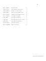
MTX LOADING STAGE 2.
MEMOTECH
ITEM DESCRIPTION
NO./
PCB COMPONENT LOCATION
PART NO.
UNIT
/ COMMENTS
-----------------------------------------------------------------------CAP
PF0027
27pf Ceramic Plate Cap
1
C13
CAP
PF0033
33pf Ceramic Plate Cap
1
C6
CAP
PF0047
47pf Ceramic Plate Cap
1
C5
CAP
PF0068
68pf Ceramic Plate Cap
1
C12
CAP
NF0022
22pf Ceramic Disc Cap
4
C1-C4
MTX Service Manual
51
CAPC NF0047
47pf Ceramic Disc Cap
1
C14
CAPE A470016
4700uf 16v Axial Cap
1
C56
CAPE R001016
10uf 16v Radial Cap
6
CAPE R010025
100uf 25v Radial Cap
1
C11,C38-C40,
C49,C57
C53
CAPE R470016
4700uf 16v Radial Cap 10mm 1
C51
CAPP NF0100
100nf Polyester Cap
8
CAPS NF0047
47nf Sibitat Cap
4
C17,C52,C54,C55,
C58-C61
C7-C10
CAPS NF0100
100nf Sibitat Cap
15
CAPT UF2216
22uf Tantalum 16v Cap
C?????,+MOD 17,MOD21
3
CONL SHUNT02
2 Way Shunt (Jumper)
1
CONL WIRE
Wire Link 39/24 SWG
11
C16,C18,C21,C23,
C24-C27
LK9
LK1c,2c,3h,4c,5c,
6(2r4c)
7(4),10,11,R28
CONP DIN6
6 Way DIN PCB MT
1
J9
CONP HDILR34
34 Way DIL R/A Header
1
J6
CONP HSIL02
2 Way SIL Header Tin
1
LK9
CONP HSIL06
6 Way SIL Header Tin
1
J11
CONP HSIL20
20 Way SIL Header Tin
1
J1
CONP HSILR05
5 Way SIL R/A Header
1
J13
CONS DIL20
20 Way DIL Socket
2
J7,IC4
CONS DIL28
28 Way DIL Socket
2
IC6,IC46
CONS DIL28L
28 Way DIL Socket L/P
1
IC45
CONS DIL40
40 Way DIL Socket
1
IC40
CONS DIL40L
40 Way DIL Socket L/P
1
IC7
CONS JK3.5
3.5mm PCB Mounting
2
J2,J3
CRXL 10.6875
10.6875 MHz Crystal
1
XTAL2
MTX Service Manual
52
CRXL 4.000
4.000 MHz Crystal
1
XTAL1
DODE IN4004
IN4004 Silicon Diode
4
D14,D16,D18,D19
DODE IN4148
IN4148 Silicon Diode
12
DODE IN5402
IN5402 Silicon Diode
2
D15,D17
DODE Z4V7
4V7 Zener Diode
1
ZD1
DODE Z5V1
5V1 Zener Diode
1
ZD3
DODE Z5V6
5V6 Zener Diode
1
ZD2
FB
Ferrite Bead
2
LK10,LK11
FUSE HLD5229
20mm Fuse holder PC MT
1
FS1
ICLS 000
SN74LS00N
1
IC9
ICLS 004
SN74LS04N
2
IC8,IC10
ICLS 008
SN74LS08N
1
IC32
ICLS 027
SN74LS27N
1
IC5
ICLS 074A
SN74LS74AN
1
IC31
ICLS 138
SN74LS138N
2
IC17,IC25
ICLS 157
SN74LS157N
2
IC16,IC24
ICLS 193
SN74LS193N
1
IC34
ICLS 244
SN74LS244N
3
IC1,IC19,IC28
ICLS 273
SN74LS273N
2
IC2,IC3
ICLS 373
SN74LS373N
1
IC11
ICLS 374
SN74LS374N
3
IC27,IC29,IC33
ICMC 4070B
CD407 BCN CMOS
1
IC18
ICMO SN76489AN SN76489AN (Sound)
1
IC30
ICRA 164116
4116-3N 16K D RAM
8
ICRA 643764
3764-20 64K D RAM
8
ICS
74HC04 CMOS
1
IC36-IC39,
IC41-IC44
IC12-IC15,
IC20-IC23
IC26
01
74HC04
MTX Service Manual
D1-D11,D13
53
MDOR UM1286
UM1286 Modulator
1
MODULATOR
RES
033R
33 OHM 1/4W C/FILM RES
1
R17
RES
330R
330 OHM 1/4W C/FILM RES
2
R14,R15
RES
560R
560 OHM 1/4W C/FILM RES
2
R34,R40
RES
K001
1K OHM 1/4W C/FILM RES
6
RES
K002.2
2K2 OHM 1/4W C/FILM RES
1
R10,R11,R19,R20,
R21,R60
R41
RES
K003.3
3K3 OHM 1/4W C/FILM RES
2
R32,R33
RES
K004.7
4K7 OHM 1/4W C/FILM RES
4
R9,R13,R26,R31
RES
K010
10K OHM 1/4W C/FILM RES
16
RES
K047
47K OHM 1/4W C/FILM RES
1
R1-R8,R18,R22R25,R37-R39
R28a
RES
K100
100K OHM 1/4W C/FILM RES
2
R16,R30
RES
K820
820K OHM 1/4W C/FILM RES
1
R29
RESW 010W2.5
10R 1/2E C/FILM RES
1
R62
SCRW 4407/8
440 7/8 Nylon Screw
1
PAL BOARD SUPPORT
SLV
Rubber Sleeving 3/4"
4
C51,C56
SPCR 4401/2
440 1/2" Nylon Spacer
1
PAL BOARD SUPPORT
SWT
2WONOFF
2 Way on - off Switch
1
SWA
TRL
TL081CP
TL081CP
1
IC35
RUB
MTX LOADING STAGE 3.
MEMOTECH
ITEM DESCRIPTION
NO./
PCB COMPONENT LOCATION
PART NO.
UNIT
/ COMMENTS
-----------------------------------------------------------------------FUSE CVR5201
20mm Fuse Cover
1
FS1
FUSE QB3.15A
3.15 AMP 20mm QBF
1
FS1
ICMO TMS9929
TMS 9929 ANL VDP
1
IC40
ICMO Z80ACPU
Z80A CPU
1
IC7
MTX Service Manual
54
ICMO Z80ACTC
Z80A CTC
1
IC6
ICPA 14L4
PAL 14L4-2CN
1
IC4
ICRO 38128A
ROM 16B MSM38128A
1
IC46
ICRO 3864
ROM 8B MSM3864
1
IC45
MTX PAL VIDEO BOARD
MEMOTECH
ITEM DESCRIPTION
NO./
PCB COMPONENT LOCATION
PART NO.
UNIT
/ COMMENTS
-----------------------------------------------------------------------CAP
PF0033
33pf Ceramic Plate Cap
3
C45,C46,C50
CAP
PF0039
39pf Ceramic Plate Cap
1
C44
CAPC NF0022
22nf Ceramic Plate Cap
1
MOD 15
CAPE R001016
10uf 16v Radial Cap
3
C42,C62
CAPE R002235
22uf 35v Radial Cap
1
C34
CAPE R004716
47uf 16v Radial Cap
1
C43
CAPE R010025
100uf 25v Radial Cap
2
C41,C63
CAPP NF0100
100nf Polyester Cap
7
C29-C33,C35,C47
CAPT PF05540
5.5-40pf Trimmer Cap
1
CV1
CONL WIRE
Wire Link 39/24 SWG
2
LKa,R66
CONP HSILR04
4 Way SIL R/A Header
1
J12
CONS DIL181L
18 Way DIL Socket L/P
1
IC3
CONS DRA2596
6 Way R/A PCB MT Header
1
J11
CONS HSIL05R
5 Way SIL R/A Socket
1
J13
CRXL 4.433619
4.433619 MHz Crystal
1
XTAL3
DODE Z5V1
5V1 Zener Diode
1
ZD4
ICMC 4013B
CD4013BCN CMOS
1
IC1
ICMC 4016B
CD4016BCN CMOS
2
IC2,IC4
MTX Service Manual
55
ICMO LM1889
LM1889
1
IC3
IDTA UH004.7
4.7UH Axial Inductor
1
L1
IDTA UH022
22UH Axial Inductor
1
L3
IDTA UH033
33UH Axial Inductor
1
L2
IDTA UH100
100UH Axial Inductor
1
L4
NUT
440HEXN
440 Nylon Nut
1
PAL BOARD SUPPORT
PCB
PAL
MTX PAL VIDEO Board
1
RES
220R
220 OHM 1/4W C/FILM RES
1
R56
RES
330R
330 OHM 1/4W C/FILM RES
3
R45,R47,R54
RES
390R
390 OHM 1/4W C/FILM RES
2
R55,R67
RES
430RM
430 OHM 1/4W C/FILM RES
1
RV1
RES
560R
560 OHM 1/4W C/FILM RES
2
R59,R63
RES
K001
1K OHM 1/4W C/FILM RES
4
R41,R51,R52,
RES
K001.5
1K5 OHM 1/4W C/FILM RES
1
R44
RES
K001.8
1K8 OHM 1/4W C/FILM RES
1
R57
RES
K001M
1K OHM 1/4W M/FILM RES
1
R61
RES
K002.2
2K2 OHM 1/4W C/FILM RES
1
R58
RES
K002.7
2K7 OHM 1/4W C/FILM RES
3
R50,R53,R60
RES
K004.7
4K7 OHM 1/4W C/FILM RES
1
R43
RES
K010
10K OHM 1/4W C/FILM RES
2
RV1,R68
RES
K027
27K OHM 1/4W C/FILM RES
1
R48
RES
K120
120K OHM 1/4W C/FILM RES
1
R49
TRL
2N3904
2N3904 Transistor
2
Q1,Q3
TRL
2N3906
2N3906 Transistor
3
Q2,Q5,Q6
WSH
440WASH
440 Nylon Washer
1
PAL BOARD SUPPORT
MTX Service Manual
56
MTX KEYBOARD
MEMOTECH
ITEM DESCRIPTION
NO./
PCB COMPONENT LOCATION
PART NO.
UNIT
/ COMMENTS
-----------------------------------------------------------------------CONL WIRE
Wire Link 39/24 SWG
29
CONP HSILR20
20 Way SIL R/A Header
1
CONS SIL20AS
20 Way SIL KBD Assembly
1
KBNT PNLMTX
KBD Switch Mounting Plate
1
PCB
MKBD104
KBD 01-04 PCB
1
SWT
ML-3-CM
ML-3-CM Keyboard Switch
79
MTX KEYBOARD
MEMOTECH
ITEM DESCRIPTION
NO./
PCB COMPONENT LOCATION
PART NO.
UNIT
/ COMMENTS
-----------------------------------------------------------------------KYTP 0011F
0
1
KYTP 0186F
0 - INS
1
KYTP 1014F
! - 1
1
KYTP 1138F
1 - ARROW LEFT
1
KYTP 2014F
" - 2
1
KYTP 2136F
2 - HOME
1
KYTP 3017F
£ - 3
1
KYTP 3173F
3 - ARROW RIGHT
1
KYTP 4011F
$ - 4
1
KYTP 4163F
4 - TAB
1
KYTP 5011F
% - 5
1
KYTP 5165F
5 - ARROW UP
1
MTX Service Manual
57
KYTP 6011F
& - 6
1
KYTP 6153F
6 - DEL
1
KYTP 7011F
´ - 7
1
KYTP 7163F
7 - PAGE
1
KYTP 8011F
( - 8
1
KYTP 8163F
8 - EOL
1
KYTP 9012F
) - 9
1
KYTP 9163F
9 - BRK
1
KYTP A000F
A
1
KYTP A0033F
ALPHA LOCK
1
KYTP AA127F
. - ARROW DOWN
1
KYTP B000F
B
1
KYTP B033F
BS
1
KYTP BB00F
> - .
1
KYTP BB01F
< - ,
1
KYTP BLANKF
BLANK KEYTOP
2
KYTP C000F
C
1
KYTP C021F
CTRL
1
KYTP D000F
D
1
KYTP DD00F
+ - ;
1
KYTP E000F
E
1
KYTP E020F
ESC
1
KYTP E834F
ENT - CLS
1
KYTP F000F
F
1
KYTP F661F
F1
1
KYTP F662F
F2
1
MTX Service Manual
58
KYTP F663F
F3
1
KYTP F664F
F4
1
KYTP F665F
F5
1
KYTP F666F
F6
1
KYTP F667F
F7
1
KYTP F668F
F8
1
KYTP FF00F
* - :
1
KYTP G000F
G
1
KYTP GG00F
? - /
1
KYTP H000F
H
1
KYTP HH000F
_
1
KYTP HH05F
= - -
1
KYTP I000F
I
1
KYTP J000F
J
1
KYTP JJ00F
{ - [
1
KYTP JJ03F
} - ]
1
KYTP K000F
K
1
KYTP KK00F
~ - ^
1
KYTP KK16F
| - \
1
KYTP L000F
L
1
KYTP L054F
LINEFEED
1
KYTP LL00F
` - @
1
KYTP M000F
M
1
KYTP N000F
N
1
KYTP O000F
O
1
KYTP P000F
P
1
MTX Service Manual
59
KYTP Q000F
Q
1
KYTP R000F
R
1
KYTP R031F
RET
1
KYTP S000F
S
1
KYTP S020F
SHIFT
2
KYTP SPACBRF
SPACE BAR
1
KYTP T000F
T
1
KYTP U000F
U
1
KYTP V000F
V
1
KYTP W000F
W
1
KYTP X000F
X
1
KYTP Y000F
Y
1
KYTP Z000F
Z
1
SBK
SPACE BAR KIT
1
GT8C
MTX POWER SUPPLY UNIT
MEMOTECH
ITEM DESCRIPTION
NO./
PCB COMPONENT LOCATION
PART NO.
UNIT
/ COMMENTS
-----------------------------------------------------------------------CBL
2M
2M Mains Cable UK
1
CBL
100MM
10cm Mains Lead
1
CBL
DIN6
6 Pin DIN Plug 1M Cable
1
NPTE PSU
PSU 220/240V Label
1
PSU
CASE
Power Supply Case T & B
1
RBR
FT
1/2" 3/8" Rubber Feet
4
SWT
5296
Mains Switch
1
TSF
220VMTX
220V MTX Transformer
1
TSR
SPT
Rubber Transformer Support 8
MTX Service Manual
60
MTX REAR PLUG ASSEMBLY
MEMOTECH
ITEM DESCRIPTION
NO./
PCB COMPONENT LOCATION
PART NO.
UNIT
/ COMMENTS
-----------------------------------------------------------------------CAP
PF0047
47pf Ceramic Plate Cap
1
CONP EYE4BA
4BA Crimped Eyelets
1
CONP BNCONT
BNC Chassis MT Socket
1
CONP HIFIC
Phono Socket Nut Fixing
1
CONS SIL04AS
4 Way Cable ASSY
1
FACC WIR.5B
.5mm Black Wire
1
MLD
RPPMTX
MTX Rear Plug Moulding
1
MLD
RS232CV
RS232 Plastic Cover
2
MTX FINAL ASSEMBLY/PACKING
MEMOTECH
ITEM DESCRIPTION
NO./
PCB COMPONENT LOCATION
PART NO.
UNIT
/ COMMENTS
-----------------------------------------------------------------------EPLH MTX
Left Hand End Plate
1
EPRH MTX
Right Hand End Plate
1
EXTB MTX
Base Section MTX
1
EXTT MTX
Top Section MTX
1
FOOT RUBSM
Moulded Rubber Feet MTX
4
NUT
M3HEX
M3 Nut
7
RBR
FT
1/2" 3/8" Rubber Feet
3
SCRW M38BH
M38 Dome Head Screw
6
SCRW M310HX
M310 Hex - Head Screw
6
SCRW M316PH
M316 Pan - Head Screw
1
MTX Service Manual
61
BOX
MTX512
MTX 512 Box
1
CONP J23.5
23.5 Cable Jack Plug
1
CONP PNOCAX
Phono to Coax Cable
1
GUAR 512UK
512 UK Guarantee Card
1
MLD
MTXCVR
Plastic Cartridge Cover
1
PPK
MTX512
MTX 512 Polypack
1
STNP 029
MTX Series Manual
1
STNP 078
MTX 512 Serial No. Label
1
STNP 236
MTX Series Brochure
1
NPTE MTX512
MTX 512 Label
1
NPTE MTXREAR
Rear ID Label
1
MTX Service Manual
62
MTX RS232 I/F
MEMOTECH
ITEM DESCRIPTION
NO./
PCB COMPONENT LOCATION
PART NO.
UNIT
/ COMMENTS
-----------------------------------------------------------------------CAP
PF560
560pf Ceramic Plate Cap
4
C1,C2,C12,C13
CAPE R001016
10uf 16v Radial Cap
2
C3,C4
CAPS NF0047
47nf Sibitat Cap
7
C5-C11
CONL SHUNT02
2 Way Shunt (Jumper)
1
Ja
CONP HSIL13
13 Way SIL Header
1
Jb
CONS EDGE60
30+30 Way Connector Key5
1
J0
CONS DIL14
14 Way DIL Socket
3
IC12-IC14
CONS DIL20
20 Way DIL Socket
1
IC8
CONS DIL40
40 Way DIL Socket
1
IC1
CONS HDIL60
60 Way DIL Header
1
J1
CONS HDIL02
2 Way DIL Header
1
Ja
DODE IN4148
IN4148 Silicon Diode
5
D1-D5
ICLS 004
SN74LS04N
1
IC10
ICLS 020
SN74LS20N
1
IC9
ICLS 241
SN74LS241N
1
IC6
ICLS 244
SN74LS244N
2
IC5,IC7
ICLS 245
SN74LS245N
3
IC2,IC4
PCB
RS232
RS232 PCB
1
RES
K001
1KOHM 1/4 C/FILM RES
4
RES
NETK001
1KOHM Resistor Network 9*8 1
MTX Service Manual
R1-R4
RN1
63
RS232 I/F TESTING
MEMOTECH
ITEM DESCRIPTION
NO./
PCB COMPONENT LOCATION
PART NO.
UNIT
/ COMMENTS
-----------------------------------------------------------------------IC
75188
SN75188N
1
IC13
IC
75189
SN75189N
2
IC12,IC14
IC
Z80DART
Z80A DART
1
IC1
PAL 14L4-2CN
1
IC8
ICPA 14L4
RS232 I/F PACKING
MEMOTECH
ITEM DESCRIPTION
NO./
PCB COMPONENT LOCATION
PART NO.
UNIT
/ COMMENTS
-----------------------------------------------------------------------ASSY CBL5WAY
5 Way Cable Assembly
1
ASSY CBL8WAY
8 Way Cable Assembly
1
BOX
RS 232 Box
1
RS232
FACC BAG21/4
Mini Grip Poly Bag 2 1/4sq 1
NUT
M3HEXH
M3 Hex Head Nut
4
PPK
RS232
RS 232 Poly Pack Pair
1
SCRW M38DH
M3 8MM Dome Head Screw
4
STNP 111
RS 232 I/F -02 Book
1
STNP 208
Serial No. Label
1
TLS
ALLK2MM
2MM Allen Key
1
WSH
M3WSH
M3 Spring Washer
4
MTX Service Manual
64
32K MEMORY EXPANSION
MEMOTECH
ITEM DESCRIPTION
NO./
PCB COMPONENT LOCATION
PART NO.
UNIT
/ COMMENTS
-----------------------------------------------------------------------CAP PF0047
47pf Ceramic Plate Cap
1
C1
CAP
PF0068
68pf Ceramic Plate Cap
1
13
C2
CAPS NF0047
47nf Sibitat Cap
C1-C5,C15-C22
CONL WIRE
Wire Link
2
2Lo
CONS EDGE60
30+30 Way Connector
1
J1
CONS DIL16
16 Pin DIL Socket
9
IC15-IC22
ICLS 004
SN74LS04N
1
IC3
ICLS 157
SN74LS157N
2
IC5,IC6
ICLS 244
SN74LS244N
1
IC4
ICPR 6301
6301-1N PROM
1
IC1
ICRA 323732
32K Partial D Rams
8
IC7-IC14
ICS
74S37
SN74S37N
1
IC2
PCB
MEMEXT
MTX Memory Expansion PCB
1
RES
330R
330 OHM 1/4W C/FILM RES
1
R1
RES
680R
680 OHM 1/4W C/FILM RES
1
R2
32K MEMORY EXPANSION
MEMOTECH
ITEM DESCRIPTION
NO./
PCB COMPONENT LOCATION
PART NO.
UNIT
/ COMMENTS
-----------------------------------------------------------------------BOX
RS232
RS232 Box
1
FACC BAG21/4
Mini Grip Poly 2 1/4 sq
1
PPK
RS232 Polypack
1
Memory Expansion Booklet
1
RS232
STNP 164
MTX Service Manual
65
TLS
ALLK2MM
2MM Allen Key
1
ROM EXPANSION
MEMOTECH
ITEM DESCRIPTION
NO./
PCB COMPONENT LOCATION
PART NO.
UNIT
/ COMMENTS
-----------------------------------------------------------------------CAPS NF0047
47nf Sibitat Cap
7
C1-C7
CONP HSIL03
3 Way SIL Header
2
LK2,LK3
CONL SHUNT02
2 Way Shunt (Jumper)
2
Lo,Lo
CONL WIRE
Wire Link 39/24 SWG
5
41,51,61,71,16
CONS DIL20
20 Way DIL Socket
1
IC5
CONS DIL28
28 Way DIL Socket
4
IC1-IC4
CONS EDGE60
30+30 Way Connector
1
J0
DODE IN4148
IN4148 Silicon Diode
8
D1-D6,MOD 18
ICLS 004
SN74LS04N
1
IC7
ICLS 273
SN74LS273N
1
IC6
ICPA 14L4-2N
PAL 14L4-2N
1
IC5
PCB
ROM0201
PCB ROM EXPANSION 02-01
1
RES
330R
330 OHM 1/4W C/FILM RES
1
MOD 18
RES
K047
47K OHM 1/4W C/FILM RES
1
R1
MTX Service Manual
66
MTX Service Manual
67
MTX Service Manual
68
MTX Service Manual
69
MTX Service Manual
70
MTX Service Manual
71
RING SYSTEM
The MTX ring uses channel A of the dart. If the ring is installed, the baud command must not be
used for either channel as the dart is initialised differently for the ring. Channel B is not used by the
ring and is available as serial I/O port. Node commands are provided to set the baud rate and data
format for channel B.
COMMUNICATIONS BOARD CIRCUIT DIAGRAM
MTX Service Manual
72
MTX Service Manual
This manual was brought to you by ROBCFG
MTX Service Manual
MTX Service Manual