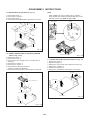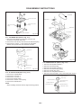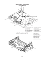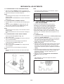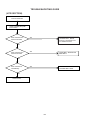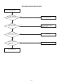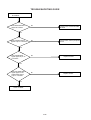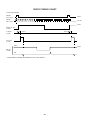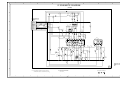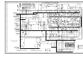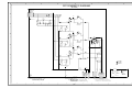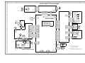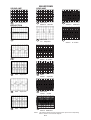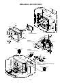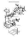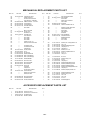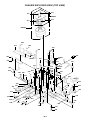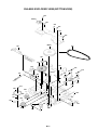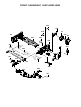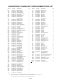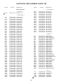
1
VX-T2170 PH
SERVICE MANUAL
INTEGRATED COLOR TV/VIDEO
CASSETTE RECORDER
BASIC TAPE MECHANISM : OVD-5
SPECIFICATIONS
110-240V AC, 50/60Hz
65W
25 kg (55 lbs.)
574 mm (W) x 365 mm (D) x
384.5 mm (H)
(17 1/4 x 14 3/8 x 15 1/4 in.)
TV SECTION
PICTURE TUBE .................................. 406 mm (W) x 305 mm (H)
(16 x 12 1/8 in.)
508 mm (diagonal) (20 in.)
TUNER SYSTEM ................................ Voltage synthesized tuner
CHANNEL COVERAGE ...................... VHF-L (low): E2 to S7
VHF-H (high): S8 to S36
UHF: S37 to 69
TV SYSTEM ........................................ B/G, D/K, I
HORIZONTAL RESOLUTION ............ 240 lines
VCR SECTION
OPERATING TEMPERATURE ........... 5°C to 40°C
VIDEO RECORDING SYSTEM .......... Rotary 2 head helical
scanning system
VIDEO SIGNAL SYSTEM ................ PAL/MESECAM color system,
625 lines, 50 fields
VIDEO HEAD ................................... Azimuth 2 head
USABLE CASSETTES ..................... VHS video cassette
TAPE SPEED ................................... PAL/MESECAM
SP: 23.39 mm/sec
LP: 11.69 mm/sec
NTSC (Playback SP only)
33.35 mm/sec
RECORDING/PLAYBACK TIME ..... PAL/MESECAM
SP: 4 hours 20 minutes max.
with E-260 tape
LP: 8 hours 40 minutes max.
with E-260 tape
NTSC (Playback SP only)
3 hours with T-180 tape
VIDEO INPUT ................................... 1.0Vp-p, 75 ohm, unbalanced
VIDEO OUTPUT .............................. 1.0Vp-p, 75 ohm, unbalanced
VIDEO S/N ....................................... 53dB (nominal)
AUDIO INPUT .................................. –3.8dBs, 50K ohm
AUDIO OUTPUT .............................. –3.8dBs, less than 50K ohm
and specifications are subject to change without
• Design
notice.
S/M Code No. 09-994-324-9O1
DA
TA
GENERAL
POWER REQUIREMENTS .................
POWER CONSUMPTION ...................
WEIGHT ..............................................
DIMENSIONS ......................................
TABLE OF CONTENTS
SPECIFICATIONS .............................................................................................................................................................. COVER
TABLE OF CONTENTS ..................................................................................................................................................... A-1
SERVICING NOTICES ON CHECKING ............................................................................................................................. A-2
VCR TEST TAPE INTERCHANGEABILITY TABLE ........................................................................................................... A-3
DISASSEMBLY INSTRUCTIONS
REMOVAL OF MECHANICAL PARTS AND P.C. BOARDS ........................................................................................... B1-1, B1-2
REMOVAL OF DECK PARTS .......................................................................................................................................... B2-1~B2-5
REMOVAL OF ANODE CAP ............................................................................................................................................ B3-1
KEY TO ABBREVIATIONS ................................................................................................................................................. C1-1, C1-2
PREVENTIVE CHECKS AND SERVICE INTERVALS ....................................................................................................... C2-1
NOTE FOR THE REPLACING OF MEMORY IC ................................................................................................................ C3-1
DECK PARTS LOCATIONS ................................................................................................................................................ C4-1, C4-2
SERVICING FIXTURES AND TOOLS ................................................................................................................................ C5-1
PREPARATION FOR SERVICING ..................................................................................................................................... C5-2
ADJUSTMENTS
MECHANICAL ADJUSTMENTS ...................................................................................................................................... D1-1~D1-3
MAJOR COMPONENTS LOCATION GUIDE (VCR) ....................................................................................................... D2-1
ELECTRICAL ADJUSTMENTS (VCR) ............................................................................................................................ D2-2, D2-3
MAJOR COMPONENTS LOCATION GUIDE (TV) .......................................................................................................... D3-1
ELECTRICAL ADJUSTMENTS (TV) ............................................................................................................................... D3-2~D3-5
TROUBLESHOOTING GUIDES .......................................................................................................................................... E-1~E-27
IC DESCRIPTIONS ............................................................................................................................................................ F-1~F-5
SERVO TIMING CHART .................................................................................................................................................... G-1
SYSTEM SWITCH MODE ................................................................................................................................................... G-2
SEMICONDUCTOR BASE CONNECTIONS ...................................................................................................................... H-1
BLOCK DIAGRAMS
TV .................................................................................................................................................................................... I-1
Y/C/HEAD AMP ............................................................................................................................................................... I-2
SYSTEM CONTROL/OPERATION/POWER/IN/OUT ...................................................................................................... I-3
TUNER/AUDIO/IF ............................................................................................................................................................ I-4
PRINTED CIRCUIT BOARDS (OPERATION/LED/HEAD AMP/IF) .................................................................................... J-1~J-3
OPERATION SCHEMATIC DIAGRAM ............................................................................................................................... J-4
HEAD AMP SCHEMATIC DIAGRAM .................................................................................................................................. J-5
IF SCHEMATIC DIAGRAM ................................................................................................................................................. J-6
PRINTED CIRCUIT BOARDS (SYSCON) .......................................................................................................................... J-7~J-9
Y/C SCHEMATIC DIAGRAM ............................................................................................................................................... J-10
SYSTEM CONTROL SCHEMATIC DIAGRAM ................................................................................................................... J-11
TUNER/AUDIO SCHEMATIC DIAGRAM ............................................................................................................................ J-12
POWER/IN/OUT SCHEMATIC DIAGRAM .......................................................................................................................... J-13
MICON SCHEMATIC DIAGRAM ......................................................................................................................................... J-14
CHROMA SCHEMATIC DIAGRAM .................................................................................................................................... J-15
SOUND AMP SCHEMATIC DIAGRAM ............................................................................................................................... J-16
OPERATION 1 SCHEMATIC DIAGRAM ............................................................................................................................ J-17
DELAY SCHEMATIC DIAGRAM ......................................................................................................................................... J-18
PRINTED CIRCUIT BOARDS (MAIN/CRT/POWER SW) .................................................................................................. J-19
DEFLECTION SCHEMATIC DIAGRAM .............................................................................................................................. J-20
TV POWER SCHEMATIC DIAGRAM ................................................................................................................................. J-21
CRT SCHEMATIC DIAGRAM ............................................................................................................................................. J-22
INTERCONNECTION DIAGRAM ........................................................................................................................................ J-23
WAVEFORMS .................................................................................................................................................................... K-1, K-2
MECHANICAL EXPLODED VIEW ...................................................................................................................................... L1-1, L1-2
MECHANICAL REPLACEMENT PARTS LIST ................................................................................................................... L2-1
ACCESSORY REPLACEMENT PARTS LIST .................................................................................................................... L2-1
CHASSIS EXPLODED VIEW (TOP VIEW) ......................................................................................................................... M1-1
CHASSIS EXPLODED VIEW (BOTTOM VIEW) ................................................................................................................. M1-2
FRONT LOADING UNIT 15 EXPLODED VIEW ................................................................................................................. M1-3
CHASSIS/FRONT LOADING UNIT 15 REPLACEMENT PARTS LIST .............................................................................. M2-1
ELECTRICAL REPLACEMENT PARTS LIST ..................................................................................................................... N-1~N-5
A-1
SERVICING NOTICES ON CHECKING
1. KEEP THE NOTICES
6. AVOID AN X-RAY
As for the places which need special attentions, they are
indicated with the labels or seals on the cabinet, chassis
and parts. Make sure to keep the indications and notices
in the operation manual.
Safety is secured against an X-ray by considering about
the cathode-ray tube and the high voltage
peripheral circuit, etc.
Therefore, when repairing the high voltage peripheral
circuit, use the designated parts and make sure not
modify the circuit.
Repairing except indicates causes rising of high
voltage, and it emits an X-ray from the cathode-ray tube.
2. AVOID AN ELECTRIC SHOCK
There is a high voltage part inside. Avoid an electric
shock while the electric current is flowing.
7. PERFORM A SAFETY CHECK AFTER
SERVICING
3. USE THE DESIGNATED PARTS
The parts in this equipment have the specific
characters of incombustibility and withstand voltage for
safety. Therefore, the part which is replaced should be
used the part which has the same character.
Especially as to the important parts for safety which is
indicated in the circuit diagram or the table of parts as
a
mark, the designated parts must be used.
Confirm that the screws, parts and wiring which were
removed in order to service are put in the original
positions, or whether there are the
portions which are deteriorated around the serviced
places serviced or not. Check the insulation between the
antenna terminal or external metal and the AC cord plug
blades. And be sure the safety of that.
4. PUT PARTS AND WIRES IN THE ORIGINAL
POSITION AFTER ASSEMBLING OR WIRING
(INSULATION CHECK PROCEDURE)
1. Unplug the plug from the AC outlet.
2. Remove the antenna terminal on TV and turn on the
TV.
3. Insulation resistance between the cord plug terminals
and the eternal exposure metal [Note 2] should be
more than 1M ohm by using the 500V insulation resistance meter [Note 1].
4. If the insulation resistance is less than 1M ohm, the
inspection repair should be required.
There are parts which use the insulation material such
as a tube or tape for safety, or which are assembled in
the condition that these do not contact with the printed
board. The inside wiring is designed not to get closer to
the pyrogenic parts and high voltage parts. Therefore,
put these parts in the original positions.
5. TAKE CARE TO DEAL WITH THE
CATHODE-RAY TUBE
[Note 1]
In the condition that an explosion-proof cathode-ray
tube is set in this equipment, safety is secured against
implosion. However, when removing it or serving from
backward, it is dangerous to give a shock. Take
enough care to deal with it.
If you have not the 500V insulation resistance meter,
use a Tester.
[Note 2]
External exposure metal: Antenna terminal
Earphone jack
A-2
VCR TEST TAPE INTERCHANGEABILITY TABLE
There are two types of the new alignment tape CH-1B (for NTSC) and CH-2 (for PAL). On each tape four signals (1) - (4) are
recorded for the times and in the order shown below.
(1) : 8min. ---> (2) : 2min. ---> (3) : 5min. ---> (4) : 5min.
The TTV-MP1 (for M-PAL), TTV-MS1 (for MESECAM) and TTV-S1 (for SECAM) alignment tapes have the same contents as
the previous tapes.
Now in use TYPE
New TYPE
Application
Method
Model
Contents*1
Model
Contents*1
TTV-N1
NTSC, Color,
1kHz, SP
CH-1B(2) NTSC, Stairsteps,
1kHz, SP
TTV-N1E
NTSC, Color,
1kHz, EP
CH-1B(4)
*2
NTSC, Color,
1kHz, EP
PB-Y Level/General electrical ADJ.
Head ACE Height/Tilt ADJ.
Switching position ADJ.
NTSC
TTV-N2
TTV-N12
(SCV-1998)
TTV-N7A
NTSC, Stairsteps,
NTSC, Stairsteps,
CH-1B(1)
Head ACE Azimuth ADJ.
7kHz, SP
7kHz, SP
NTSC, Color,
1kHz, SP
CH-1B(4)
NTSC, Color,
1kHz, EP
NTSC, Color, No
NTSC, Stairsteps,
CH-1B(3) sound SP, HiFi
1kHz, SP, HiFi
400Hz
400Hz
TTV-P1
PAL, Color,
1kHz, SP
CH-2(2)
*3
TTV-P1L
PAL, Color,
1kHz, LP
CH-2(4)
PAL, Stairsteps,
1kHz, SP
PAL, Color,
1kHz, LP
FM envelope ADJ.
X-Value ADJ.
HiFi Audio PB Level ADJ.
Switching position ADJ.
PB-Y Level/General electrical ADJ.
Head ACE Height/Tilt ADJ.
Switching position. (LP Model)
FM Envelope ADJ. (LP Model)
X-Value ADJ. (LP Model)
PAL
TTV-P2
PAL, Stairsteps,
6kHz, SP
CH-2(1)
PAL, Stairsteps,
6kHz, SP
Head ACE Azimuth ADJ.
FM Envelope ADJ. (SP Model)
X-Value ADJ. (SP Model)
TTV-P7
PAL, Stairsteps,
1kHZ, SP, HiFi,
1kHz
CH-2(3)
PAL, Color, No
sound SP, HiFi
400Hz
HiFi Audio PB Level ADJ.
TTV-P16
PAL, Color, 400Hz,
SP, HiFi 1kHz
No Changed.
FM Filter ADJ.
*1. Described in the order of color format. Video signal. Linear audio. Tape speed and Hi-Fi audio.
*2. Use CH-1B (1) - (3) with models used exclusively in the SP mode.
*3. Use CH-2 (3) and (4) when it is necessary to observe the chroma signal.
A-3
DISASSEMBLY INSTRUCTIONS
1-3: TV/VCR BLOCK (Refer to Fig. 1-3)
1. REMOVAL OF MECHANICAL PARTS
AND P.C. BOARDS
1. Remove the 2 screws 1.
2. Disconnect the following connectors:
(CY757, CP353, CP503, CP502 and CP301).
3. Unlock the support 2.
4. Remove the TV/VCR Block in the direction of arrow.
1-1: BACK CABINET (Refer to Fig. 1-1)
1. Remove the 2 screws 1 and 4 screws 2.
2. Remove the 2 screws 3 which are used for holding the
Back Cabinet.
3. Remove the AC cord from the AC cord hook 4.
4. Remove the Back Cabinet in the direction of arrow.
1
Front Cabinet
Front Cabinet
1
1
2
UP TO
RELEASE
2
1
TV/VCR Block
Fig. 1-3
2
2
1-4: MAIN PCB (Refer to Fig. 1-4)
3
3
1. Remove the screw 1.
2. Remove the Main PCB Holder.
3. Remove the 2 screws 2.
4. Remove the 3 screws 3.
5. Disconnect the following connectors:
(CP810 and CP820).
6. Remove the Main PCB in the direction of arrow.
4
2
Back Cabinet
Fig. 1-1
1-2: CRT PCB (Refer to Fig. 1-2)
CAUTION: BEFORE REMOVING THE ANODE CAP,
DISCHARGE ELECTRICITY BECAUSE IT
CONTAINS HIGH VOLTAGE.
BEFORE ATTEMPTING TO REMOVE OR
REPAIR ANY PCB, UNPLUG THE POWER
CORD FROM THE AC SOURCE.
2
2
Main PCB
1. Remove the Anode Cap.
(Refer to REMOVAL OF ANODE CAP on PAGE 12)
2. Disconnect the following connectors:
(CP801, CP804 and CP850).
3. Remove the CRT PCB in the direction of arrow.
3 3
3
Main PCB Holder
1
Front Cabinet
CRT PCB
VCR Block
Fig. 1-4
Fig. 1-2
B1-1
DISASSEMBLY INSTRUCTIONS
1-5: DECK SHIELD PLATE (Refer to Fig. 1-5)
NOTE
1. Remove the screw 1.
2. Remove the 3 screws 2.
3. Remove the screw 3.
4. Remove the Deck Shield Plate in the direction of arrow.
When installing the Front Loading Unit 15, align the
timing marker and pull the Cassette Holder Ass'y in the
direction of arrow (C). (Refer to Fig. 1-6-B)
Marker
Deck Chassis
2
Deck Shield Plate
1
2
2
3
VCR Block
Fig. 1-5
(C)
1-6: FRONT LOADING UNIT 15 AND DECK CHASSIS
(Refer to Fig. 1-6-A)
Cassette Holder Ass'y
Fig. 1-6-B
1. Remove the screw 1.
2. Remove the screw 2.
3. Remove the Front Loading Unit 15 in the direction of
arrow (A).
4. Remove the 3 screws 3.
5. Remove the 2 screws 4.
6. Disconnect the following connectors:
(CP4001, CD1002 and CP4002).
7. Remove the Deck Chassis in the direction of arrow (B).
1-7: JACK PLATE AND SYSCON PCB (Refer to Fig. 1-7)
1. Remove the screw 1.
2. Unlock the support 2.
3. Remove the Syscon PCB in the direction of arrow (A).
4. Remove the 2 screws 3.
5. Unlock the 2 supports 4.
6. Remove the Jack Plate in the direction of arrow (B).
1
Jack Plate
2
(B)
3
3
4
Syscon PCB
Front Loading Unit 15
4
(A)
4
1
3
3
(A)
4
2
3
Deck Chassis
Deck Holder
(B)
Fig. 1-7
Syscon PCB
Fig. 1-6-A
B1-2
DISASSEMBLY INSTRUCTIONS
2. REMOVAL OF DECK PARTS
2-1: LINK GEAR (R) / CAM GEAR (Refer to Fig. 2-1)
1.
2.
3.
4.
5.
Top Bracket
Unlock the support 1.
Remove the BOT Sensor Cover and BOT Reflector.
Unlock the 3 supports 2.
Remove the Side Bracket R2 and Spring Earth.
Remove the Flap Lever, Link Gear (R) , Cam Gear
Ass'y and BOT Lever.
2
2
Bracket R Spring
Joint Gear
Side Bracket L
2
1
NOTE
3
2
Lever Rec
Spring
1. When installing the BOT Lever, insert the BOSS into
the hole of Linl Gear (R).
2. When installing the Link Ass'y 3 and Link Gear (R),
align the timing Marks.
Tape Piece
Guide
1
Cassette
Holder Ass'y
Side Bracket R1
Fig. 2-2
Spring Earth
BOT Reflector
Side Bracket R1
2-3: LINK ASS'Y 3 (Refer to Fig. 2-3)
BOT Sensor
Cover
BOT Lever
1. After removing in the direction (A) of Link Ass'y 3,
remove the Link Ass'y 3 in the direction (B).
1
NOTE
Cam Gear Ass'y
Install the (B) first, then install the (A).
2
2
2
Cassette Holder Ass'y
Link Gear (R)
Side Bracket R2
(A)
Flap Lever
Cam Gear Ass'y
(B)
Link Gear (R)
Link Ass'y 3
Joint Gear
Link Ass'y 3
Fig. 2-3
Marker
2-4: CASSETTE SIDE R (Refer to Fig. 2-4)
Marker
Marker
Fig. 2-1
1. Unlock the 2 supports 1.
2. Remove the Cassette Side R.
3. Remove the Pack Spring.
4. Remove the Locker Spring.
5. Unlock support 2.
6. Remove the Locker R.
2-2: TOP BRACKET / TAPE PIECE GUIDE
(Refer to Fig. 2-2)
1. Remove the Lever Rec Spring.
2. Unlock the 2 supports 1.
3. Remove the Tape Piece Guide.
4. Unlock the 4 supports 2.
5. Remove the Top Bracket.
6. Remove the Side Bracket R1 and Side Bracket L.
7. Unlock the support 3.
8. Remove the Joint Gear.
9. Remove the Bracket R Spring.
Cassette Side L
Cassette Side R
Pack Spring
2
1
1
Locker R
Locker Spring
Cassette Holder Ass'y
Fig. 2-4
B2-1
DISASSEMBLY INSTRUCTIONS
2-5: CASSETTE SIDE L (Refer to Fig. 2-5)
2-7: TENSION BAND (Refer to Fig. 2-7)
1. Unlock the 2 supports 1.
2. Remove the Cassette Side L.
3. Remove the Pack Spring.
4. Remove the Locker Spring.
5. Unlock the support 2.
6. Remove the Locker L.
1. Remove the Tension Arm Spring 1.
2. Remove the Tension Arm Spring 2.
3. Remove the Tension Adjust.
4. Remove the Tension Arm Ass'y.
5. Remove the Tension Band Ass'y.
6. Remove the Tension Lever 2 Ass'y.
Tension Adjust
Locker Spring
Tension Band Ass'y
2
Tension Arm Spring 2
Pack Spring
Locker L
1
Tension Arm Ass'y
1 Cassette Side L
Tension Arm Spring 1
(A)
Cassette Holder Ass'y
Tension Lever 2 Ass'y
Fig. 2-7
Fig. 2-5
NOTES
2-6: BRAKE BRACKET (Refer to Fig. 2-6)
1. Install the Tension Band Ass'y without twisting it.
2. Turbine Oil the area marked with A in Fig. 2-7.
1. Remove the Main Brake Spring, S-S Brake Spring,
Joint Arm Spring and T-S Brake Spring.
2. Remove the 2 screws 1.
3. Remove the screw 2.
4. Remove the Brake Bracket.
5. Remove the Sub Brake S, Sub Brake T , Main Brake S
Ass'y and Main Brake T Ass'y.
6. Remove the Joint Arm.
7. Remove the Reflector LED 2.
1
2-8: REEL DISK (Refer to Fig. 2-8)
1. Remove the Reel Disk S and Reel Disk T.
2. Remove the 2 polyslider washers.
NOTES
1. Installation of Reel Disk after performing step 1, 2 and 3 in
section 2-7 of DISASSEMBLY INSTRUCTIONS.
2. The Height Adjustment washers are sometimes
attached to the back of the Reel Disk.
3. Clean the Reel Disk Shaft and put in height adjusting
washers.
4. Be careful not to damage the Tension Band Ass'y at the
time of removal and installation.
5. Be careful not to scratch the Reel Disk Shaft with the
polyslider washer or the tool at the time of removal and
installation.
6. After oiling the Reel Disk Shaft, install the new Reel Disk S
and Reel Disk T again.
7. After installation, adjust the height of the Reel Disk.
(Refer to item 1-1 of MECHANICAL ADJUSTMENTS)
8. After installation, adjust and confirm the tension post position.
(Refer to item 1-2 of MECHANICAL ADJUSTMENTS)
1
Brake Bracket
2
Main Brake S Ass'y
Reflector LED 2
S-S Brake Spring
Main Brake Spring
Main Brake T Ass'y
Sub Brake S
Joint Arm
Joint Arm Spring
T-S Brake Spring
Sub Brake T
Fig. 2-6
B2-2
DISASSEMBLY INSTRUCTIONS
Reel Disk S
Pinch Roller
Polyslider Washer
2
Reel Disk T
Cassette Opener
3
Polyslider Washer
1
Spring Cam Pinch
Polyslider Washer 4
3
(A)
Spring P5
Polyslider Washer 5
(A)
Cam Pinch Roller
Fig. 2-8
Cam P5
Cam Gear
2-9: PINCH ROLLER / CASSETTE OPENER
(Refer to Fig. 2-9)
Arm P5 Ass'y
1. Unlock the support 1.
2. Remove the Pinch Roller.
3. Remove the screw 2.
4. Unlock the 2 supports 3.
5. Remove the Cassette Opener.
6. Remove the Spring P5 and Arm P5 Ass'y.
7. Remove the Cam Gear, Polyslider Washer 4, Spring
Cam Pinch and Cam Pinch Roller.
8. Remove the Polyslider Washer 5 and Cam P5.
Cam Pinch Roller
Cam P5
NOTES
1. Do not touch the Pinch Roller. (Use gloves.)
2. When installing the Cam P5, Cam Pinch Roller and
Cam Gear, align the timing marks.
Cam Gear
Marker
Fig. 2-9
2-10: AUDIO CONTROL HEAD (Refer to Fig. 2-10)
1. Disconnect the following connector: (CP4106) on the
Head Amp PCB.
2. Remove the 3 screws 1.
3. Remove the 3 Audio Control Head Springs.
4. Remove the Audio Control Head.
NOTES
1. Do not touch the head by any means when replacing
the Audio Control Head. (Use gloves.)
2. After replacement, confirm the following adjustments.
a. MECHANICAL ADJUSTMENTS: ITEM 2-2
b. MECHANICAL ADJUSTMENTS: ITEM 2-3
B2-3
DISASSEMBLY INSTRUCTIONS
1
1
Capstan Belt
1
2
2
Audio Control Head
Mode Switch
2
1
1
Audio Control Head
Spring
Audio Control Head
Spring
Tension Lever
Spring
Plate Bottom
Deck Chassis
Audio Control Head Base
Fig. 2-10
2-11: CYLINDER UNIT (Refer to Fig. 2-11)
1. Disconnect the following connectors: (CP4101 and
CP4102) on the Head Amp PCB.
2. Remove the Joint Screw, then remove the Azimuth Spring.
3. Remove the 2 screws 1, then remove the Polyslider
Washer and Cylinder Unit from the Main Chassis.
Marker
Position
Cylinder Unit
Polyslider Washer
Main Chassis
Fig. 2-12
2-13: CENTER PULLEY (Refer to Fig. 2-13)
1. Remove the Polyslider Washer 1.
2. Remove the Center Pulley.
3. Remove the Polyslider Washer 2.
4. Remove the Center Pulley Spring.
5. Remove the Idler Arm Ass'y.
6. Remove the 2 Polyslider Washers 3.
7. Remove the Clutch Gear T Ass'y and Clutch Gear S Ass'y.
Azimuth Spring
1
1
Joint Screw
Fig. 2-11
2-12: PLATE BOTTOM (Refer to Fig. 2-12)
1. Remove the Capstan Belt.
2. Remove the 2 screws 1.
3. Remove the 3 screws 2.
4. Remove the Mode Switch.
5. Remove the Tension Lever Spring.
6. Remove the Plate Bottom.
Polyslider Washer 1
Center Pulley
Polyslider Washer 2
Polyslider Washer 3
NOTE
Clutch Gear S Ass'y
When installing the Mode Switch, align the timing position.
Center Pulley Spring
Idler Arm Ass'y
Polyslider Washer 3
Clutch Gear T Ass'y
Fig. 2-13
B2-4
DISASSEMBLY INSTRUCTIONS
2-14: MAIN CAM (Refer to Fig. 2-14)
2-15: CAPSTAN DD UNIT (Refer to Fig. 2-15)
1. Remove the Loading Lever.
2. Remove the Main Brake Lever.
3. Remove the Capstan Brake Spring.
4. Remove the Capstan Brake Ass'y.
5. Remove the Main Rod Spring.
6. Remove the Tension Holder.
7. Remove the Tension Lever.
8. Remove the Main Cam.
9. Remove the Middle Gear.
10. Remove the Main Rod Ass'y.
1. Remove the 3 screws 1.
2. Disconnect the CP4105.
3. Remove the Capstan DD Unit.
NOTE
Use the specified screw to hold the Capstan DD Unit.
Capstan DD Unit
NOTES
1. When installing the Main Rod Ass'y, install side (B) first,
then install side (A).
2. When installing the Loading Lever, align the timing marks.
Loading Lever
1
Capstan Brake Ass'y
Main Brake Lever
Capstan Brake Spring
1 1
Fig. 2-15
Main Cam
Middle Gear
2-16: INCLINED T ASS'Y / INCLINED S ASS'Y
(Refer to Fig. 2-16)
Tension Lever
Main Rod Spring
Tension Holder
(B)
1.
2.
3.
4.
5.
6.
Main Rod Ass'y
(A)
Remove the 4 screws 1.
Remove the Catcher S and Catcher T.
Remove the 2 CS Rings.
Remove the Inclined T Ass'y and Inclined S Ass'y.
Remove the Loading Gear T Ass'y.
Remove the Loading Gear S Ass'y.
NOTE
When installing the Inclined T Ass'y and Inclined S Ass'y,
align the timing marks.
Loading Gear T
Inclined S Ass'y
Loading Lever
Inclined T Ass'y
1
1
Catcher S
1
1
Catcher T
Marker
Loading Arm S Ass'y
Loading Arm Spring
Loading Gear T
Loading Arm Spring
Loading Arm T Ass'y
Middle Gear
Main Cam
Loading Gear S
Marker
CS Ring
CS Ring
Marker
Marker
Fig. 2-14
Loading Gear T
Loading Gear S
Marker
B2-5
Fig. 2-16
DISASSEMBLY INSTRUCTIONS
3. After one side is removed, pull in the opposite direction to
remove the other.
3. REMOVAL OF ANODE CAP
Read the following NOTED items before starting work.
NOTE
* After turning the power off there might still be a potential
voltage that is very dangerous. When removing the
Anode Cap, make sure to discharge the Anode Cap's
potential voltage.
* Do not use pliers to loosen or tighten the Anode Cap
terminal, this may cause the spring to be damaged.
Take care not to damage the Rubber Cap.
INSTALLATION
1. Clean the spot where the cap was located with a small
amount of alcohol. (Refer to Fig. 3-3.)
REMOVAL
Location of Anode Cap
1. Follow the steps as follows to discharge the Anode Cap.
(Refer to Fig. 3-1.)
Connect one end of an Alligator Clip to the metal part of a
flat-blade screwdriver and the other end to ground.
While holding the plastic part of the insulated Screwdriver,
touch the support of the Anode with the tip of the
Screwdriver.
A cracking noise will be heard as the voltage is discharged.
Fig. 3-3
GND on the CRT
NOTE
Confirm that there is no dirt, dust, etc. at the spot where
the cap was located.
2. Arrange the wire of the Anode Cap and make sure the
wire is not twisted.
3. Turn over the Rubber Cap. (Refer to Fig. 3-4.)
CRT
Screwdriver
Support
Alligator Clip
GND on the CRT
Fig. 3-4
Fig. 3-1
4. Insert one end of the Anode Support into the anode button,
then the other as shown in Fig. 3-5.
2. Flip up the sides of the Rubber Cap in the direction of the
arrow and remove one side of the support.
(Refer to Fig. 3-2.)
Rubber Cap
CRT
CRT
Support
Support
Fig. 3-5
Fig. 3-2
5. Confirm that the Support is securely connected.
6. Put on the Rubber Cap without moving any parts.
B3-1
KEY TO ABBREVIATIONS
A A/C
ACC
AE
AFC
AFT
AFT DET
AGC
AMP
ANT
A.PB
APC
ASS'Y
AT
AUTO
A/V
B BGP
BOT
BPF
BRAKE SOL
BUFF
B/W
C C
CASE
CAP
CARR
CH
CLK
CLOCK (SY-SE)
COMB
CONV
CPM
CTL
CYL
CYL-M
CYL SENS
D DATA (SY-CE)
dB
DC
DD Unit
DEMOD
DET
DEV
E E
EF
EMPH
ENC
ENV
EOT
EQ
EXT
F F
FBC
FE
FF
FG
FL SW
FM
FSC
FWD
G GEN
GND
H H.P.F
:
:
:
:
:
:
:
:
:
:
:
:
:
:
:
:
:
:
:
:
:
:
:
:
:
:
:
:
:
:
:
:
:
:
:
:
:
:
:
:
:
:
:
:
:
:
:
:
:
:
:
:
:
:
:
:
:
:
:
:
:
:
H.SW
Hz
I IC
IF
IND
INV
K KIL
L L
LED
LIMIT AMP
LM, LDM
LP
L.P.F
LUMI.
M M
MAX
MINI
MIX
MM
MOD
MPX
MS SW
N NC
NR
O OSC
OPE
P PB
PB CTL
PB-C
PB-Y
PCB
P. CON
PD
PG
P-P
R R
REC
REC-C
REC-Y
REEL BRK
REEL S
REF
REG
REW
REV, RVS
RF
RMC
RY
S S. CLK
S. COM
S. DATA
SEG
SEL
SENS
SER
SI
SIF
SO
SOL
SP
STB
SW
Audio/Control
Automatic Color Control
Audio Erase
Automatic Frequency Control
Automatic Fine Tuning
Automatic Fine Tuning Detect
Automatic Gain Control
Amplifier
Antenna
Audio Playback
Automatic Phase Control
Assembly
All Time
Automatic
Audio/Video
Burst Gate Pulse
Beginning of Tape
Bandpass Filter
Brake Solenoid
Buffer
Black and White
Capacitance, Collector
Cassette
Capstan
Carrier
Channel
Clock
Clock (Syscon to Servo)
Combination, Comb Filter
Converter
Capstan Motor
Control
Cylinder
Cylinder-Motor
Cylinder-Sensor
Data (Syscon to Servo)
Decibel
Direct Current
Direct Drive Motor Unit
Demodulator
Detector
Deviation
Emitter
Emitter Follower
Emphasis
Encoder
Envelope
End of Tape
Equalizer
External
Fuse
Feed Back Clamp
Full Erase
Fast Forward, Flipflop
Frequency Generator
Front Loading Switch
Frequency Modulation
Frequency Sub Carrier
Forward
Generator
Ground
High Pass Filter
C1-1
:
:
:
:
:
:
:
:
:
:
:
:
:
:
:
:
:
:
:
:
:
:
:
:
:
:
:
:
:
:
:
:
:
:
:
:
:
:
:
:
:
:
:
:
:
:
:
:
:
:
:
:
:
:
:
:
:
:
:
:
:
:
Head Switch
Hertz
Integrated Circuit
Intermediate Frequency
Indicator
Inverter
Killer
Left
Light Emitting Diode
Limiter Amplifier
Loading Motor
Long Play
Low Pass Filter
Luminance
Motor
Maximum
Minimum
Mixer, mixing
Monostable Multivibrator
Modulator, Modulation
Multiplexer, Multiplex
Mech State Switch
Non Connection
Noise Reduction
Oscillator
Operation
Playback
Playback Control
Playback-Chrominance
Playback-Luminance
Printed Circuit Board
Power Control
Phase Detector
Pulse Generator
Peak-to Peak
Right
Recording
Recording-Chrominance
Recording-Luminance
Reel Brake
Reel Sensor
Reference
Regulated, Regulator
Rewind
Reverse
Radio Frequency
Remote Control
Relay
Serial Clock
Sensor Common
Serial Data
Segment
Select, Selector
Sensor
Search Mode
Serial Input
Sound Intermediate Frequency
Serial Output
Solenoid
Standard Play
Serial Strobe
Switch
KEY TO ABBREVIATIONS
S SYNC
SYNC SEP
T TR
TRAC
TRICK PB
TP
U UNREG
V V
VCO
VIF
VP
V.PB
VR
V.REC
VSF
VSR
VSS
V-SYNC
VT
X X'TAL
Y Y/C
:
:
:
:
:
:
:
:
:
:
:
:
:
:
:
:
:
:
:
:
:
Synchronization
Sync Separator, Separation
Transistor
Tracking
Trick Playback
Test Point
Unregulated
Volt
Voltage Controlled Oscillator
Video Intermediate Frequency
Vertical Pulse, Voltage Display
Video Playback
Variable Resistor
Video Recording
Visual Search Fast Forward
Visual Search Rewind
Voltage Super Source
Vertical-Synchronization
Voltage Tuning
Crystal
Luminance/Chrominance
C1-2
PREVENTIVE CHECKS AND SERVICE INTERVALS
The following standard table depends on environmental conditions and usage. Unless maintenance is properly
carried out, the following service intervals may be quite shortened as harmful effects may be had on other parts.
Also, long term storage or misuse may cause transformation and aging of rubber parts.
Time
Parts Name
Audio Control Head
500
hours
1,000
hours
1,500
hours
2,000
hours
3,000
hours
Notes
Clean those parts in
contact with the tape.
Full Erase Head
Loading Motor Belt
Clean the rubber, and
parts which the rubber
touches.
Reel Belt
Pinch Roller
Capstan DD Unit
Loading Motor
Tension Band
Capstan Shaft
Tape Running
Guide Post
Replace when rolling
becomes abnormal.
Cylinder Unit
Clean the Head.
: Replace
: Clean
CLEANING
NOTE
3. CYLINDER
After cleaning the heads with isopropyl alcohol, do not
run a tape until the heads dry completely. If the heads
are not completely dry and alcohol gets on the tape,
damage may occur.
Wrap a piece of chamois around your finger. Dip it in
isopropyl alcohol. Hold it to the cylinder head softly.
Turn the cylinder head counterclockwise to clean it (in
the direction of the arrow). (Refer to the figure below)
1. AUDIO CONTROL HEAD
NOTE
Wrap a piece of chamois around your finger. Dip it in
isopropyl alcohol and clean the audio control head by
wiping it horizontally. Clean the full erase head in the
same manner. (Refer to the figure below)
Do not exert force against the cylinder head. Do not move
the chamois up or down since this can damage the head.
Always use a piece of chamois for cleaning.
Cylinder Head
Audio Control Head
2. TAPE RUNNING SYSTEM
When cleaning the tape transport system, use the
gauze moistened with isopropyl alcohol.
C2-1
NOTE FOR THE REPLACING OF MEMORY IC
If a service repair is undertaken where it has been required to change the MEMORY IC, the following steps should be taken to
ensure correct data settings while making reference to TABLE 1.
NOTE
• Initial Data setting will not be possible if clock has been set. To reset clock, either unplug AC cord and allow
at least 30 minutes before Power On or alternatively, discharge backup capacitor.
• No need the setting for after INI 6.
ADDRESS
INI
01
INI
02
INI
03
INI
04
INI
05
INI
06
DATA
0B
11
1D
02
84
B8
Table 1
1. Enter DATA SET mode by setting VOLUME to minimum.
2. While holding down VOLUME button on front cabinet, press key 6 on remote control simultaneously.
3. ADDRESS and DATA should appear as FIG 1.
INIT 01 EB
ADDRESS DATA
Fig. 1
4. ADDRESS is now selected and should "blink". Using the SET + or - keys on the remote, step through the ADDRESS until
required ADDRESS to be changed is reached.
5. Press ENTER to select DATA. When DATA is selected, it will "blink".
6. Again, step through the DATA using SET + or - until required DATA value has been selected.
7. Pressing ENTER will take you back to ADDRESS for further selection if necessary.
8. Repeat steps 4 to 7 until all data has been checked.
9. When satisfied correct DATA has been entered, turn POWER off (return to STANDBY MODE) to finish DATA input.
The unit will now have the correct DATA for the new MEMORY IC.
C3-1
DECK PARTS LOCATIONS
(TOP VIEW)
9
8
10
7
6
5
11
4
3
2
12
1
21
20
19
13
18
15
17
16
1.
2.
3.
4.
5.
6.
7.
8.
9.
10.
11.
Main Chassis
Tension Arm Ass'y
EOT Reflector
Guide Roller S Ass'y
P0 Post
P1 Post
FE Head
Cylinder Unit
Auto Head Cleaning
Head Amp PCB
Audio/Control Head
C4-1
12.
13.
14.
15.
16.
17.
18.
19.
20.
21.
Loading Motor
Pinch Roller Block
Cam Gear
Cassette Opener
Brake Bracket
Reel T
LED Reflector
Guide Roller T Ass'y
Reel S
Tension Band Ass'y
14
DECK PARTS LOCATIONS
(BOTTOM VIEW)
26
27
25
24
23
28
22
32
33
31
29
30
22.
23.
24.
25.
26.
27.
Worm Bracket F Ass'y
Mode Switch
Worm Ass'y
Worm Bracket R Ass'y
Loading Motor Belt
Capstan DD Unit
28 Capstan Brake Ass'y
29. Bottom Plate
30. Clutch Gear S Ass'y
31. Idler Arm Ass'y
32. Center Pulley
33. Clutch Gear T Ass'y
(FRONT LOADING UNIT 15)
1. Side Bracket L
2. Top Bracket Ass'y
3. Side Bracket R Ass'y
4. Cam Gear Ass'y
5. Bot Sensor Cover
6. Side Bracket R2
7. Tape Piece Guide
8. Cassette Holder Ass'y
1
2
3
4
8
5
6
7
C4-2
SERVICING FIXTURES AND TOOLS
VHS Alignment Tape
JG001C (TTV-P2 or CH-2)
JG001D (TTV-P1 or CH-2)
JG002B Adapter
JG002F Dial Torque Gauge
(60~600gf•cm)
JG002G (100~1200gf•cm)
JG005 Post Adjustment
Screwdriver
Part No. SV-TG0-030-000
(small)
JG153 X Value Adjustment
Screwdriver
JG022 Master Plane
JG024 Reel Disk Height
Adjustment Jig
JG100A Torque Tape
(VHT-063)
JG154 Cable
Part No. SJ-G15-400-000
JG162A Cable (8 pins)
Part No. SJ-G16-2A0-000
JG162H Cable (15 pins)
Part No. SJ-G16-2H0-000
JG162Y Cable (5 pins)
Part No. SJ-G16-2Y0-000
Tentelometer
Part No.
Remarks
JG001C
Stair Steps, 6KHz
JG001D
Color Bar, 1KHz
JG002F
Playback Take Up Torque
JG002G
Fast Forward Torque, Rewind Torque, Brake Torque (Take up Reel/Supply Reel)
JG005
Guide Roller Adjustment
JG153
X-Value Adjustment
JG022/JG024
JG100A
JG154
Reel Disk Height Adjustment
Playback Back Tension Torque
Used to connect the test point of SERVICE and GROUND
JG162A/JG162H
Used to connect the SYSCON PCB and MAIN PCB
JG162Y
Used to connect the SYSCON PCB and CRT PCB
C5-1
PREPARATION FOR SERVICING
Basic Servicing Position (In case of needing to check on all blocks)
1. Unplug the connector CP301, CP353 and CY757, then remove the TV/VCR Block from the set.
2. Unplug the connector CP810, CP820 and CP850, then remove the Main PCB from the VCR Block.
3. Connect as shown in the below figure using the Service Fixture.
• Connect the Syscon PCB to the Main PCB with the cable JG162A and JG162H.
• Connect the Syscon PCB to the CRT PCB with the cable JG162Y.
4. Remove the Operation PCB from the set, then connect it with the Syscon PCB.
If necessary, connect CP353 (Earphone Input Terminal)
5. Short circuit between TP1001 and Ground with the cable JG154.
(Refer to MAJOR COMPONENTS LOCATION GUIDE)
The EOT, BOT and Reel Sensor do not work at this moment.
6. At that time, the STOP/EJECT button is available to insert and eject the Cassette Tape.
Head Amp PCB
IF PCB
JG162A
Deck Chassis
CP810
JG162H
To Main PCB
(CD810)
Syscon PCB
CP850
To Main PCB
(CD820)
TP1001
CP820
JG162Y
Operation PCB
To CRT PCB
(CD850)
JG154
To Ground
Servicing Position for Main PCB (In case of needing to check on Main PCB)
• It's possible to get the Servicing Position without the extension Jig if you arrange the unit as shown below.
(But L503 connection can not be done, Degause circuit will not operate.)
L503 (2 Pin)
• Be careful for the short circuit.
Main PCB
VHS Tape
(Put the Tape under the FBT.)
C5-2
MECHANICAL ADJUSTMENTS
1-2: CONFIRMATION AND ADJUSTMENT OF
TENSION POST POSITION
1. CONFIRMATION AND ADJUSTMENT
Read the following NOTED items before starting work.
1. Turn on the power and set to the PLAY mode adjust the
Tension so that the Tension Post is at the position of
0.3mm~0.5mm from the Rib. (Refer to Fig. 1-2)
2. Confirm that the video tape is not curling at the flange of
P1 post or is not running on flanges.
• Place an object which weighs between 350g and 500g on
the Cassette Tape to keep it steady when you want to
make the tape run without the Front Loading Unit 15. (Do
not place an object which weighs over 500g.)
• When you activate the deck without the Front Loading
Unit 15, short circuit between TP1001 and Ground. In
this condition the BOT/EOT/Reel Sensor will not function.
P1 Post
Tension Arm
Tension Post
1-1: CONFIRMATION AND ADJUSTMENT OF
REEL DISK HEIGHT
1. Turn on the power and set to the STOP mode.
2. Set the master plane (JG022) and reel disk height
adjustment jig (JG024) on mechanism framework, taking
care not to scratch the drum, as shown in Fig. 1-1-A.
3. Confirm that the reel disk is lower than "A" of the reel disk
height adjustment jig (JG024) on the master plane and
higher than "B" as shown in Fig. 1-1-B. If it is not, adjust to
less than 7.5mm±0.2mm with the height adjustment washer.
4. Perform the same adjustment for other reel.
P0 Post
Rib
Reel Disk (S)
Tension Adjust
Fig. 1-2
1-3: CONFIRMATION AND ADJUSTMENT OF BACK
TENSION ON PLAYBACK
Master Plane
(JG022)
1. Load a video tape recorded in standard speed mode.
Set the unit to the PLAY mode.
2. Install the tentelometer as shown in Fig. 1-3.
Confirm the value is within 20~27gf•cm at this time.
Reel Disk Height
Adjustment Jig
(JG024)
• IN CASE OF USING A CASSETTE TYPE TORQUE TAPE.
1. After adjustment, confirm and adjust the tension post
position (Refer to item 1-2) for the tension arm, install
the cassette type torque tape (JG100A) and set to the
PLAY mode.
2. Confirm that the left hand side tension value of the
torque tape is 25~38gf•cm for the standard mode tape.
Fig. 1-1-A
Tentelometer
Reel Disk
Master Plane
(JG022)
Video Tape
Reel Disk Height
Adjustment Jig
(JG024)
A
P1 Post
7.5mm±0.2
Fig. 1-3
B
Height Adjustment Washer
3.1x5.4xT0.13
3.1x5.4xT0.3
Guide Roller
Fig. 1-1-B
D1-1
MECHANICAL ADJUSTMENTS
1-4: CONFIRMATION OF FAST FORWARD TORQUE
NOTE
If the torque value checked is out of tolerance, replace
the appropriate parts as follows.
1. Set torque gauge (JG002G) on take-up reel disk, and
place unit in FAST FORWARD mode. (Refer to Fig. 1-4)
2. Confirm that torque is more than 400gf•cm.
Check Items
NOTE
After setting the torque gauge on the reel disk, hold the
gauge in place.
Push the FAST FORWARD button and the reel disk will
begin to turn.
1-5: CONFIRMATION OF REWIND TORQUE
Replace Parts
1-4
Idler Ass'y or Clutch ASS'Y
1-5
Idler Ass'y or Clutch ASS'Y
1-6
Main Brake T Ass'y or Main Brake
S Ass'y
2. TAPE RUNNING CONFIRMATION
AND ADJUSTMENT
1. Operate within 4 or 5 seconds after the reel disk begins
to turn.
2. Set torque gauge (JG002G) on supply reel disk, and
place the unit in REWIND mode. (Refer to Fig. 1-4).
3. Confirm that torque is more than 400gf•cm.
• Tape running is adjusted precisely at the factory.
Normally, it is not necessary to make adjustments.
It is necessary to confirm and make adjustments
when the parts of the tape running mechanism are
replaced because of extensive usage or failure.
• When adjusting P2, P3 and Value X, be careful to the
Primary side of Main PCB on the Video Block for a electric
shock. So, use a insulator material such as plastic for JIG
driver grip.
NOTE
After setting the torque gauge on the reel disk, hold the
gauge in place.
Push the REWIND button and the reel disk will begin to
turn.
1-6: CONFIRMATION OF REEL BRAKE TORQUE
2-1: GUIDE ROLLER
(Take-Up Reel Brake) (Refer to Fig. 1-4)
1. Connect CH-1 on the oscilloscope to TP4002 (PB Envelope)
and CH-2 to TP4001 (SW Pulse).
2. Set the tracking to manual center position in the following
way. Press and hold the tracking auto button more than 2
seconds to set the tracking to center position.
3. Trigger with SW pulse and observe the envelope.
(Refer to Fig. 2-1-A)
4. Adjust the guide roller height while observing the envelope,
and make the envelope flat. Adjust the envelope so that
the flatness will not be affected even when the tracking
control button is pressed. (Use the adjustment screwdriver
JG005).
5. Press and hold the tracking control button and (at the point
that the envelope waveform starts to reduce) adjust the
envelope so that the A : B ratio is better than 3 : 2.
(Refer to Fig. 2-1-B)
6. Adjust the PG shifter (ELECTRICAL ADJUSTMENTS :
ITEM 3-1) in the PLAY mode.
1. Set to STOP mode.
2. Set the torque gauge (JG002G) to the take-up reel and
turn it counterclockwise.
3. Confirm that it is more than 200gf•cm at that time.
(Supply Reel Brake) (Refer to Fig. 1-4)
1. Set to STOP mode.
2. Set the torque gauge (JG002G) to the supply reel and
turn it clockwise.
3. Confirm that it is more than 200gf•cm at that time.
NOTE
Separate the idler from the reel and confirm the brake
torque.
NOTE
Torque Gauge
After adjustment, confirm and adjust A/C head tilt.
(Refer to item 2-2)
CH-1
PB Envelope
(TP4002)
CH-2
SW Pulse
(TP4001)
CH-1
Track
CH-2
Track
Fig. 2-1-A
Fig. 1-4
D1-2
MECHANICAL ADJUSTMENTS
Beginning
Ending
Audio/Control Head
Maximum
A
Maximum
B
A:B=3:2
Fig. 2-1-B
0.25mm
2-2: CONFIRMATION AND ADJUSTMENT OF A/C
HEAD TILT
Video Tape
Video Tape
When the tape is running abnormally, perform the
following adjustments.
1. Insert a new tape and play it back.
2. Confirm that there is no crease on the tape between the P4
post and guide roller (R) and the tape is running smoothly.
(It is absolutely impossible to get satisfactory sound if the
tape is distorted between the A/C head and P4 post.)
3. If the tape still does not run smoothly, turn the screw 1 and
adjust the tilt of the A/C head. (Refer to Fig. 2-2)
Drum
1
Guide Roller R
Tape
2
Audio/Control Head
P4 Post
3
X Value Adjustment Driver Hole
Fig.2-2
2-3: ADJUSTMENT OF A/C HEAD HEIGHT AND
AZIMUTH
1. Playback a VHS alignment tape (JG001C) and observe
the waveform at the audio output terminal.
2. Turn the screw 2 slowly to change the azimuth of the A/C
head. Adjust the height so that the audio output becomes
maximum. (Refer to Fig. 2-2)
3. Adjust the screw 3, (Refer to Fig. 2-2) until the height of
the A/C head reaches the position against the tape as
shown in Fig. 2-3.
4. When the control head height is not correct. (When you
must turn the screw more than 45 degrees), Turn all of the
screws 1, 2 and 3 to the same degrees.
Then confirm the angle of the audio/control head and
adjust again.
D1-3
Fig. 2-3
2-4: TAPE RUNNING ADJUSTMENT
1. Adjust the height of reel disk.
(Refer to item 1-1)
2. Confirm and adjust tension post position.
(Refer to item 1-2)
3. Adjust the guide roller.
(Refer to item 2-1)
4. Adjust the A/C head tilt.
(Refer to item 2-2)
5. Adjust the A/C head height and azimuth.
(Refer to item 2-3)
6. Connect CH-1 on the oscilloscope to TP4001 and CH-2 to
TP4002. Playback the VHS alignment tape (JG001C).
Set the tracking to manual center. Adjust X with the screw
driver for X (JG153) as the Fig. 2-1-A and Fig. 2-1-B.
(Refer to No. 2 of the item 2-1).
MAJOR COMPONENTS LOCATION GUIDE
(VCR SECTION)
TP4001
TP4002
TP1001
IC4001
IC601
J4501
J4502
TU6001
IC101
C101
CP6115
SYSCON
CP6001
L6011
IC6001
L6012
IF
D2-1
TP4501
ELECTRICAL ADJUSTMENTS
3-2: VCO COIL
(VCR SECTION)
3. ADJUSTMENT PROCEDURE
NOTE
For adjusting of VCO, connect input and output terminals
of sweepmarker generator to the circuit as shown below,
then adjust it.
Read and perform these adjustments when repairing the
circuits or replacing electrical parts or PCB assemblies.
CAUTION
Sweepmarker
Generator
When replacing IC's or transistors, use a silicon grease.
(To prevent the damage to IC's and transistors.)
Output
0.022µF
TP
75K
3-1: PG SHIFTER (HEAD SWITCHING) ADJUSTMENT
GND
CONDITIONS
47K
1N60
45P
TP
MODE-PLAYBACK
Input Signal-Alignment Tape (JG001D) or Similar
Input
100P
INSTRUCTIONS
1N60
GND
1. Unplug the AC plug for more than 30 minutes to set the
clock to the non-setting state. (To release the Back-Up
immediately, take the short circuit between C101 and
GND at the Power Off.) Then, set the volume level to
minimum.
2. Connect CH-1 on the oscilloscope to TP4001 and CH-2
to TP4501.
3. Playback the alignment tape. (JG001D)
4. Press and hold the Tracking Auto button more than 2
seconds to set the tracking to center position.
5. Press the VOL. DOWN button on the set and the
channel button (3) on the remote control simultaneously
until the indicator REC disappears. If the indicator REC
disappears, adjustment is completed.
CONDITION
MODE-STOP
INSTRUCTIONS
1. Connect the output of sweepmarker generator to pin 5
of IC6001.
2. Connect the input of sweepmarker generator to pin 17
of IC6001.
3. Connect a 10K ohm variable resistor to IF AGC terminal
(pin 4 of IC6001), 9V line and ground, then adjust to
make the waveform of the oscilloscope readable.
4. Adjust the L6011 until the waveform marker (38.9MHz)
becomes as shown in Fig. 3-2.
(If the above adjustments doesn't work well:)
38.9MHz
6. Press the VOL. DOWN button on the set and the
channel button (3) on the remote control simultaneously
until the indicator REC disappears.
7. When the REC indicator is blinking, press both VOL.
DOWN key on the set and the channel button (4) on the
remote control simultaneously and adjust the Tracking
+/- button until the arising to the down of the Head
Switching Pulse becomes 6.5 ± 0.5H.
8. Press the Tracking Auto button.
Fig. 3-2
3-3: AFT COIL
CH-2
CONDITION
MODE-STOP
INSTRUCTIONS
6.5H
1. Connect the output of sweepmarker generator to pin 5
of IC6001.
2. Connect the input of sweepmarker generator to pin 3 of
CP6115.
3. Adjust L6012 until the waveform marker (38.9MHz)
becomes as shown in Fig. 3-3.
4. Disconnect the sweepmarker generator and the
oscilloscope.
5. Connect the generator (38.9MHz) to the pin 4 of
CP6115 through 100 ohm and connect the DC voltmeter
to pin 3 of CP6115.
6. Adjust the L6012 until the DC voltmeter is 4.0 ± 0.2V.
CH-1
Fig. 3-1-A
CH-2
CH-1
6.5H
Fig. 3-1-B
D2-2
ELECTRICAL ADJUSTMENTS
38.9MHz
Fig. 3-3
D2-3
MAJOR COMPONENTS LOCATION GUIDE
(TV SECTION)
FB401
T501
SCREEN VOLUME
FOCUS VOLUME
TP401
VR502
MAIN
TP801
TP803
J801
CRT
D3-1
ELECTRICAL ADJUSTMENTS
(TV SECTION)
4. BASIC ADJUSTMENTS
ADJUSTMENT MODE4
1. R-Y B OFFSET
2. B-Y B OFFSET
3.
4.
5.
6.
On-Screen Display Adjustment
Unplug the AC plug for more than 30 minutes to set the
clock to the non-setting state. (To release the Back-Up
immediately, take the short circuit between C101 and GND
at the Power Off.) Then, set the volume level to minimum.
Press the VOL. DOWN button on the set and the Channel
button (9) on the remote control simultaneously to appear
the adjustment mode on the screen as shown in Fig. 4-1,
Fig. 4-2, Fig. 4-3, Fig. 4-4, Fig. 4-5 and Fig. 4-6.
7. NEXT
Fig. 4-4
NOTE
ADJUSTMENT MODE5
1. WIDE V SART
2. WIDE V STOP
3. WIDE P SART
4. WIDE P STOP
5. V S-COR
6. V LINEA
Use the Channel buttons (1-7) on the remote control to
select the options shown in Fig. 4-1, Fig. 4-2, Fig. 4-3,
Fig. 4-4, Fig. 4-5 and Fig. 4-6.
Press the Channel button (8) to end the adjustments.
ADJUSTMENT MODE1
1. H PHASE
2. V DC
3. V SIZE
4. AGC
5. CUT OFF
6. OSD H
7. NEXT
7. NEXT
ADJUSTMENT MODE6
1. H PHASE 60
2. WIDE V STOP 60
3. V LINEA 60
4.
5.
6.
8. END
Fig. 4-1
ADJUSTMENT MODE2
1.
2. RED BIAS
3. GREEN BIAS
4. BLUE BIAS
5. GREEN DRIVE
6. BLUE DRIVE
7. NEXT
8. END
"The adjustment item 2 is not used for this model."
Fig. 4-6
4-1: CUT OFF
8. END
1. Activate the adjustment mode display of Fig. 4-1 and
press the channel button (5) on the remote control.
2. Adjust the Screen Volume until picture is distinct.
Fig. 4-2
4-2: WHITE BALANCE
ADJUSTMENT MODE3
1. BRIGHT
2. CONTRAST
3. COLOR
4. TINT
5. SHARPNESS
6. E-RGB CONT
7. NEXT
8. END
"The adjustment items 1, 2, 3 and 4 are not used
for this model."
Fig. 4-5
"The adjustment item 4 is not used for this model."
7. NEXT
8. END
1. Receive the color bar pattern.
2. Adjust the adjustment mode display of Fig. 4-2 until the
white color is looked like a white.
4-3: FOCUS
1. Receive the broadcasting signal.
2. Adjust the Focus Volume until picture is distinct.
8. END
"The adjustment item 6 are not used for this model."
Fig. 4-3
D3-2
ELECTRICAL ADJUSTMENTS
4-4: HORIZONTAL PHASE (TV)
4-10: OSD HORIZONTAL
1. Receive the color bar pattern (RF Input).
2. Using the remote control, set the brightness and
contrast to normal position.
3. Activate the adjustment mode display of Fig. 4-1 and
press the channel button (1) on the remote control.
4. Press the VOL. UP/DOWN button on the remote control
until the SHIFT quantity of the OVER SCAN on right
and left becomes minimum.
1. Using the remote control, set the brightness and
contrast to normal position.
2. Activate the adjustment mode display of Fig. 4-1 and
press the channel button (6) on the remote control.
3. Press the VOL. UP/DOWN button on the remote control
until the difference of A and B becomes minimum.
(Refer to Fig. 4-7)
[ TV ]
4-5: VERTICAL POSITION (TV)
1. Receive the color bar pattern (RF Input).
2. Using the remote control, set the brightness and
contrast to normal position.
3. Activate the adjustment mode display of Fig. 4-1 and
press the channel button (2) on the remote control.
4. Press the VOL. UP/DOWN button on the remote control
until the horizontal line of the color bar comes to
approximate center of the CRT.
OSD H
A
B
Fig. 4-7
4-6: VERTICAL SIZE (TV)
4-11: SUB CONTRAST (TV)
1. Receive the monochrome pattern (RF Input).
2. Using the remote control, set the brightness and
contrast to normal position.
3. Activate the adjustment mode display of Fig. 4-1 and
press the channel button (3) on the remote control.
4. Press the VOL. UP/DOWN button on the remote control
until the horizontal overscan is equal to the vertical
overscan.
1. Receive the monochrome pattern (RF Input).
2. Activate the adjustment mode display of Fig. 4-3 and
press the channel button (2) on the remote control.
3. Press the VOL. UP/DOWN button on the remote control
until the CONTRAST level is set to the "15".
4-12: SUB CONTRAST (AV)
1. Receive the monochrome pattern (Audio Video Input).
2. Activate the adjustment mode display of Fig. 4-3 and
press the channel button (2) on the remote control.
3. Press the VOL. UP/DOWN button on the remote control
until the CONTRAST level is set to the "15".
4-7: VERTICAL LINEA (TV)
1. Receive the monochrome pattern (RF Input).
2. Using the remote control, set the brightness and
contrast to normal position.
3. Activate the adjustment mode display of Fig. 4-5 and
press the channel button (6) on the remote control.
4. Press the VOL. UP/DOWN button on the remote control
until the SHIFT quantity of the OVER SCAN on upside
and downside becomes minimum.
4-13: SUB BRIGHTNESS (TV)
1. Receive the monochrome pattern (RF Input).
2. Using the remote control, set the brightness and
contrast to minimum position.
3. Activate the adjustment mode display of Fig. 4-3 and
press the channel button (1) on the remote control.
4. Press the VOL. UP/DOWN button on the remote control
until the white 75% becomes black.
4-8: HORIZONTAL PHASE 60 (AV)
1. Receive the monochrome pattern (Audio Video Input).
2. Using the remote control, set the brightness and
contrast to normal position.
3. Activate the adjustment mode display of Fig. 4-6 and
press the channel button (1) on the remote control.
4. Press the VOL. UP/DOWN button on the remote control
until the SHIFT quantity of the OVER SCAN on right
and left becomes minimum.
4-14: SUB BRIGHTNESS (AV)
1. Receive the monochrome pattern (Audio Video Input).
2. Using the remote control, set the brightness and
contrast to minimum position.
3. Activate the adjustment mode display of Fig. 4-3 and
press the channel button (1) on the remote control.
4. Press the VOL. UP/DOWN button on the remote control
until the white 75% becomes black.
4-9: VERTICAL LINEA 60 (AV)
1. Receive the monochrome pattern (Audio Video Input).
2. Using the remote control, set the brightness and
contrast to normal position.
3. Activate the adjustment mode display of Fig. 4-6 and
press the channel button (3) on the remote control.
4. Press the VOL. UP/DOWN button on the remote control
until the SHIFT quantity of the OVER SCAN on upside
and downside becomes minimum.
D3-3
ELECTRICAL ADJUSTMENTS
4-15: SUB COLOR (TV)
4-18: CONSTANT VOLTAGE
1. Receive the color bar pattern (RF Input).
2. Connect the oscilloscope to TP801.
3. Activate the adjustment mode display of Fig. 4-3 and
press the channel button (3) on the remote control.
4. Adjust the VOLTS RANGE VARIABLE knob of the
oscilloscope until the range between white 100% and
0% is set to 4 scales on the screen of the oscilloscope.
5. Press the VOL. UP/DOWN button on the remote control
until the red color level is adjusted to 80% of the white
level. (Refer to Fig. 4-8)
1. Set to the AV mode. (No input for AV)
2. Connect the DC voltmeter to TP401.
3. Adjust the VR502 until the DC voltmeter is 119 ± 0.5V.
4-19: V. S-COR
1. Receive the monochrome pattern.
2. Activate the adjustment mode display of Fig. 4-5 and
press the channel button (5) on the remote control.
3. Press the VOL. UP/DOWN button on the remote control
until the V. S-COR level is set to the "70".
4-20: SUB SHARPNESS (TV)
1. Receive the monochrome pattern (RF Input).
2. Activate the adjustment mode display of Fig. 4-3 and
press the channel button (5) on the remote control.
3. Press the VOL. UP/DOWN button on the remote control
until the SHARPNESS level is set to the "15".
0%
80%
4-21: SUB SHARPNESS (AV)
100%
1. Receive the monochrome pattern (Audio Video Input).
2. Activate the adjustment mode display of Fig. 4-3 and
press the channel button (5) on the remote control.
3. Press the VOL. UP/DOWN button on the remote control
until the SHARPNESS level is set to the "15".
Fig. 4-8
4-16: SUB COLOR (AV)
1. Receive the color bar pattern (Audio Video Input).
2. Connect the oscilloscope to TP801.
3. Activate the adjustment mode display of Fig. 4-3 and
press the channel button (3) on the remote control.
4. Adjust the VOLTS RANGE VARIABLE knob of the
oscilloscope until the range between white 100% and
0% is set to 4 scales on the screen of the oscilloscope.
5. Press the VOL. UP/DOWN button on the remote control
until the red color level is adjusted to 80% of the white
level. (Refer to Fig. 4-8)
4-22: SECAM DET
1. Receive the SECAM color bar pattern.
2. Set the color system to SECAM position.
3. Adjust the items 1 and 2 of Fig. 4-4 until the white part
of the pattern is not changed even though you turn color
control from minimum to maximum.
4-17: SUB TINT (AV)
1. Receive the NTSC rainbow pattern (Audio Video Input).
2. Connect the oscilloscope to TP803.
3. Activate the adjustment mode display of Fig. 4-3 and
press the channel button (4) on the remote control.
4. Press the VOL. UP/DOWN button on the remote control
until the waveform becomes as shown in Fig. 4-9.
Fig. 4-9
D3-4
ELECTRICAL ADJUSTMENTS
5-3: STATIC CONVERGENCE
5. PURITY AND CONVERGENCE
ADJUSTMENTS
NOTE
Adjust after performing adjustments in section 5-2.
NOTE
1. Receive the crosshatch pattern from the color bar
generator.
2. Combine red and blue of the 3 color crosshatch pattern
on the center of the screen by adjusting the pair of
4 pole magnets.
3. Combine red/blue (magenta) and green by adjusting the
pair of 6 pole magnets.
1. Turn the unit on and let it warm up for at least 30
minutes before performing the following adjustments.
2. Place the CRT surface facing east or west to reduce the
terrestrial magnetism.
3. Turn ON the unit and demagnetize with a Degauss Coil.
5-1: STATIC CONVERGENCE (ROUGH ADJUSTMENT)
1. Tighten the screw for the magnet. Refer to the adjusted
CRT for the position. (Refer to Fig. 5-1)
If the deflection yoke and magnet are in one body,
untighten the screw for the body.
2. Receive the green raster pattern from the color bar
generator.
3. Slide the deflection yoke until it touches the funnel
side of the CRT.
4. Adjust center of screen to green, with red and blue on the
sides, using the pair of purity magnets.
5. Switch the color bar generator from the green raster
pattern to the crosshatch pattern.
6. Combine red and blue of the 3 color crosshatch pattern
on the center of the screen by adjusting the pair of
4 pole magnets.
7. Combine red/blue (magenta) and green by adjusting the
pair of 6 pole magnets.
8. Adjust the crosshatch pattern to change to white
by repeating steps 6 and 7.
5-4: DYNAMIC CONVERGENCE
NOTE
Adjust after performing adjustments in section 5-3.
1. Adjust the differences around the screen by moving
the deflection yoke upward/downward and right/left.
(Refer to Fig. 5-2-a)
2. Insert three wedges between the deflection yoke and
CRT funnel to fix the deflection yoke.
(Refer to Fig. 5-2-b)
RGB
R
G
B
RGB
R
G
B
5-2: PURITY
UPWARD/DOWNWARD SLANT
NOTE
RIGHT/LEFT SLANT
Fig. 5-2-a
Adjust after performing adjustments in section 5-1.
1. Receive the green raster pattern from color bar
generator.
2. Adjust the pair of purity magnets to center the
color on the screen.
Adjust the pair of purity magnets so the color at the
ends are equally wide.
3. Move the deflection yoke backward (to neck side)
slowly, and stop it at the position when the whole
screen is green.
4. Confirm red and blue colors.
5. Adjust the slant of the deflection yoke while watching the
screen, then tighten the fixing screw.
WEDGE
WEDGE
WEDGE
DEFLECTION YOKE
DEFLECTION YOKE SCREW
MAGNET SCREW
PURITY MAGNETS
6 POLE MAGNETS
4 POLE MAGNETS
Fig. 5-1
D3-5
WEDGE POSITION
Fig. 5-2-b
TROUBLESHOOTING GUIDE
(TV SECTION)
POWER DOES NOT TURN ON (1)
When turning on the
Power Switch, does the
LED light ?
No
Check P.CON 5V line.
Yes
Is the voltage at pin 1
of IC502 DC7.7V ?
No
Check ICP502, D511 and D512.
Yes
Is the voltage at pin 3 of
IC502 DC5.6V ?
No
Check IC502.
Yes
Does RY501 work ?
No
Does the BASE voltage of
Q501 turn ON or OFF ?
Yes
Yes
Check Q510, Q507 and the
peripheral circuit.
Check Q504, RY501 and the
peripheral circuit.
E-1
No
Check pins 62 and 63 of IC101 and
peripheral circuit.
TROUBLESHOOTING GUIDE
POWER DOES NOT TURN ON (2)
Is CP810 inserted ?
No
Insert CD810.
Yes
Is F501 broken ?
Yes
No
Is the voltage at C507
about 180~360V ?
Check the circuit between
F501, C507 and R501.
Yes
IC501 bad ?
Yes
Replace F501.
No
Replace IC501.
E-2
No
Check IC501 and the
peripheral circuit.
TROUBLESHOOTING GUIDE
GOOD PICTURE BUT NO SOUND
Is the voltage at CP301
changed with the volume
up or down key ?
No
Check speaker and the
peripheral circuit.
Yes
Is the voltage at EMITTER
of Q357 DC15V ?
No
Is FUSE RESISTOR
(R517) broken ?
No
Check Sound +B line.
Yes
Yes
Replace FUSE RESISTOR (R517).
Is the voltage at pin
1 corrector of Q351
DC12V ?
No
Check Q357, Q358 and the
peripheral circuit.
Yes
Check Q351, Q352 and the
peripheral circuit.
E-3
TROUBLESHOOTING GUIDE
NO PICTURE
Are the Brightness and
Contrast set to minimum ?
No
Adjust Brightness and Contrast.
Yes
Is the voltage at pin 3 of
IC601 DC9V ?
No
Check P.CON 9.6V line.
Yes
Is the voltage at pin
17 of IC601 DC9V ?
No
Check CHROMA 9V line.
Yes
Is the voltage at pin 41 of
IC601 DC5V ?
No
Check D607.
Yes
Is the voltage at pin 8,
38 of IC601 DC5V ?
No
Check D604.
Yes
Is the signal at pin 12, 13
and 14 of IC601 output ?
No
Yes
Is the waveform at pin 47
of IC601 normal ?
No
Check Q602 and Video Out Line.
Yes
Check IC601.
Is the waveform at TP801,
TP802 and TP803 of CRT
PCB output ?
No
Check Q804, Q805, Q806 and CD850.
Yes
Check J801 and CRT.
E-4
TROUBLESHOOTING GUIDE
NO COLOR
Is the color set to
minimum ?
No
Adjust the color.
Yes
Is the color signal
received ?
No
Receive the color signal.
Yes
Is the waveform at pin
40 of IC601 normal ?
No
Check peripheral circuit of X601.
Yes
Is the waveform at pin 42
of IC601 normal ?
No
Check peripheral circuit of VIDEO
Out line and Q602.
Yes
Is the waveform 12, 13
and 14 of IC601 normal ?
No
Check IC601.
Yes
Is the waveform at TP801,
TP802 and TP803 of CRT
PCB output.
No
Check Q804, Q805, Q806 and
CD850.
Yes
Check J801 and CRT.
E-5
TROUBLESHOOTING GUIDE
ONLY A LINE APPEARS
Is the normal signal at
pin 4 of IC 401 input ?
No
Check peripheral circuit of IC601.
Yes
Is the voltage at pin 6 of
IC402 DC25V ?
No
Check R452 and FB401.
Yes
Check peripheral circuit of IC401
and DY401.
OSD SCREEN DOES NOT APPEAR
Is there a waveform at pins
33, 34 and 35 of IC101 ?
No
Check pin 36 of IC101 and the
peripheral circuit.
No
Check pins 18, 19 and 20 of
IC601 and the peripheral circuit.
Yes
Is there a waveform at
pins 18, 19 and 20 of
IC601 ?
Yes
Check peripheral circuit of IC601.
E-6
TROUBLESHOOTING GUIDE
(VCR SECTION)
PLAY SHUTS OFF
Insert a cassette and push
PLAY button.
Does it Power off in
about 3 seconds?
Check
TAPE
LOADING,
Check
TAPE
LOADIG,
LOADING
BELT,MODE
SWITCH,
LOADING
BELT, MODE
DD
MOTORDD
andMOTOR
CYLINDER
SWITCH,
and
MOTOR.
CYLINDER MOTOR.
Yes
No
Does it Power off in
about 6 seconds?
Yes
Check REEL SENSOR and
REEL BELT.
Yes
Check REEL SENSOR,IC1001
and REEL BELT slack.
No
Does it Power off
intermittently
No
Check IC1001.
E-7
TROUBLESHOOTING GUIDE
CYLINDER NOT ROTATING
DURING PLAYBACK AND
RECORDING
Is the voltage at pin 6 of
CP1002 about DC13V ?
No
Check UNREG 12V line
of Main PCB.
Yes
In playback, is the
voltage at pin 3 of
CP1002 about DC1.2V ?
Yes
Replace CYLINDER MOTOR.
No
In playback, is the
voltage at pin 44 of
IC1001 DC5V Pulse and
is the voltage at pin 46 of
IC1001 about DC1.5V ?
No
Check R1059, R1080 and R1058.
Yes
Replace IC1001.
E-8
TROUBLESHOOTING GUIDE
AUDIO SHAKES
Is AUDIO HEAD
scratched ?
Yes
Replace AUDIO HEAD.
No
Does pin 15 of IC1001
output a 3.0Vp-p square
wave ?
3.0V
No
Replace CAPSTAN DD.
Yes
In playback, is the voltage
at pin 14 of CP1002 2.8V ?
Is the voltage at pin 14 of
CP1002 3.3V when you
stop the CAPSTAN DD
MOTOR manually ?
No
Check peripheral components
of IC1001.
Yes
In playback, is the
voltage at pin 17 of
CP1002 about DC1.6V ?
Yes
No
In playback, is the voltage at
pin 50 of IC1001 3.8V ?
Yes
Check AUDIO BLOCK.
E-9
No
Replace IC1001.
TROUBLESHOOTING GUIDE
CASSETTE TAPE IS NOT
ACCEPTED
Does WORM GEAR
of FRONT LOADING
UNIT activate ?
No
Check WORM GEAR of
FRONT LOADING UNIT.
No
Check EOT, BOT, PHOTO
SENSOR, pins 2 and 4 of IC1001.
Yes
When cassette is not
inserted, is EOT BOT
PULSE at EMITTER of
Q1055, Q1056 5V ?
Yes
When a cassette is inserted,
is the voltage between pins
1 and 2 of CP1002 ?
Yes
Replace LOADING MOTOR.
No
When a cassette is
inserted, is the voltage at
pin 49 of IC1001 5V ?
Yes
Check circuit of FRONT LOADING
MOTOR.
No
Does 8 MHz Clock
oscillate ?
Yes
Replace IC1001.
E-10
No
Replace X1001.
TROUBLESHOOTING GUIDE
WHEN INSERTING CASSETTE,
IT EJECTS IMMEDIATELY
In another cassette tape
does the same problem
appear ?
No
Defective CASSETTE or
FRONT LOADING UNIT.
No
Replace EOT/BOT PHOTO
TRANSISTORS.
Yes
In covering the infrared
sensor, is pin 2 and 4 of
IC1001 5V ?
Yes
When inserting cassette,
is pin 4 of IC1001 low ?
No
Check R1010.
Yes
Is EJECT position of
FRONT LOADING
GEAR OK ?
No
Check FRONT LOADING GEARS.
Yes
Check IC1001 circuit.
E-11
TROUBLESHOOTING GUIDE
FF/REW DO NOT WORK
When the FF/REW is pushed,
does the PULSE appear at
pin 51 of IC1001 ?
No
Check pin 74 of IC1001 lines change
IC1001.
No
Check pin 12 of CP1002 and
peripheal circuit.
No
Check pin 45 of IC1001 lines change
IC1001.
Yes
Is the voltage changing at
pin 12 of CP1002 when
you press FF/REW ?
Yes
Is the voltage changing
at pin 14 of CP1002 ?
Yes
Check DECK MECHANISM.
E-12
TROUBLESHOOTING GUIDE
TAPE LOADING IS OK, BUT
UNLOADS IMMEDIATELY
Does CYLINDER rotate ?
No
Yes
Is the voltage at pin
6 of CP1002 UNREG
12V ?
No
Check Power circuit.
Yes
In playback, is the
voltage at pin 3 of
CP1002 1.2V ?
No
Does DC5V PULSE signal
appear at pin 44 of IC1001 ?
Is the voltage at pin 46 of
IC1001 DC2.5V ?
Yes
Yes
Replace CYLINDER UNIT.
No
Does TP4001 feed HEAD
SWITCHING PULSE
30 Hz
signal ?
No
Yes
Does REEL SENSOR
PULSE signal appear at
pins 69 and 70 of IC1001 ?
Does PG PULSE
signal appear at pin
13 of IC1001 ?
Yes
Yes
Replace IC1001.
No
Check REEL SENSOR.
E-13
Check R1059, R1080, R1058 and
D1003.
No
TROUBLESHOOTING GUIDE
PLAYBACK PICTURE JITTERS
HORIZONTALLY
No
Is FG output level at pin 5
of CP1002 about 5V?
5V
Replace CYLINDER MOTOR.
Yes
Is the voltage at pin 3 of
CP1002 1.2V?
No
Replace IC1001.
Yes
Replace CYLINDER MOTOR.
PLAYBACK
PICTURE SHAKES
PLAYBACKPICTURE
SHAKES
No
Is FG Pulse output level at
pin 5 of CP1002 about 5V?
5V
Replace CYLINDER MOTOR.
Yes
Does pin 11 of IC1001
output a 4.4Vp-p square
wave?
No
Replace IC1001.
Yes
In playback, is the voltage at pin 3
In playback, is the voltage
of CP1002
about
1.2V about
?
at pin 3 of
CP1002
1.2V?
When
slowing
is the
When
sloeingCYLINDER,
CYLINDER,is
voltage
3.8V?
the
voltage 3.8V?
No
Yes
Replace CYLINDER MOTOR.
E-14
TROUBLESHOOTING GUIDE
AUTO TRACKING DOES NOT
OPERATE
By manual tracking,
does the DC level at pin 6
of CP4001 change?
No
Check IC4101 and
CYLINDER UNIT.
Yes
In auto tracking, is the
voltage at pin 5 of IC1001
more than DC1.85V?
No
Does the CTL PULSE
(about 1.0Vp-p) appear
at pin 19 of IC1001?
1.0Vp-p
Yes
Yes
Replace IC1001.
E-15
No
Check CONTROL HEAD.
TROUBLESHOOTING GUIDE
WHEN PLAYBACK,FAST
FORWARD OR REWIND MODE
IS ACTIVATED, UNIT STOPS
IMMEDIATELY
Does CAPSTAN DD
MOTOR rotate?
No
Refer to section "CAPSTAN
DD MOTOR NOT ROTATING"
Yes
Is CAPSTAN BELT OK?
No
Replace CAPSTAN BELT
Yes
Does REEL SENSOR PULSE
signal appear at pin 69
of IC1001?
Check
and that
CheckREEL
if theSENSOR
REEL SENSOR
the voltage at pin 10 of CX1003
receives the Pulse.
is DC5V.
No
Yes
Does REEL SENSOR PULSE
signal appear at pin 70
of IC1001?
No
Check around pin 4 of IC1001.
Yes
Replace IC1001.
E-16
TROUBLESHOOTING GUIDE
PLAYBACK PICTURE JITTERS
VERTICALLY
No
Does tracking noise appear
in the picture?
Yes
By adjusting the manual tracking
UP/DOWN buttons,will the
noise disappear in the
picture?
No
Check P/B ENVELOPE.
Yes
Are GUIDE POSTS
the right height?
No
Adjust GUIDE POST height.
Yes
Is PG SHIFTER
Adjustment 6.5H?
No
Adjust PG SHIFTER.
Yes
Check PB-Y circuit.
E-17
TROUBLESHOOTING GUIDE
NO PLAYBACK PICTURE
Is E-E appearing on the
Monitor TV?
No
Yes
Is the voltage at pins 12,28
and 54 of IC4001 5V?
No
Check Power circuit.
Yes
Check 5V line.
Is there PB Y/C signal at
TP4002?
No
Check IC4101 and the
connection of the CYLINDER.
No
Check Q4001,Q4016,Q4004 and
the peripheral circuit.
Yes
Is there FM Y signal at
pin 11 of IC4001and there
CHROMA signal at pin
27 of IC4001?
Yes
Is there Y signal at
pin 27 of IC4001 and there
CHROMA signal at pin
31 of IC4001?
No
Replace IC4001.
Yes
Is there Y signal at
pin 9 of IC4002 and there
CHROMA signal at pin
16 of IC4002?
No
Check IC4002 and the
peripheral cicuit.
Yes
Is there VIDEO signal at
pin 2 of IC4001?
No
Replace IC4001.
Yes
Check J4501
E-18
TROUBLESHOOTING GUIDE
NO COLOR DURING
PLAYBACK
Does FM ENVELOPE
appear at TP4002?
No
Check IC4101 and HEAD AMP
BLOCK.
No
Check C4067 and the peripheral
circuit.
Yes
Does CHROMA signal
appear at pin 27 of IC4001?
Yes
Does COMPOSITE
signal appear at pin 16
of IC4002?
No
Replace IC4002
Yes
Does COLOR BURST
signal appear in the
COMPOSITE signal
at pin 2 of IC4001?
No
Replace IC4001.
Yes
Check TV Block.
E-19
TROUBLESHOOTING GUIDE
PLAYBACK PICTURE NOISY
(EVEN AFTER CLEANING HEADS)
Is FM signal at TP4002
more than 200mVp-p?
No
Replace CYLINDER MOTOR.
Yes
Is there FM signal at pin 11 of
IC4001 140mVp-p?
No
Check Q4001,Q4016,Q4004
and the peripheral circuit.
No
Check pins 6 and 8 of IC4002
and the peripheral circuit.
Yes
Is VIDEO waveform at
pin 6 of IC4001 over
500mVp-p and are
there any noise?
Yes
Is VIDEO waveform at
pin 37 of IC4001 400mVp-p
are there CHROMA signal
at pins 31 of IC4001 200mVp-p
and are there any noises?
No
Replace IC4001.
Yes
Is VIDEO waveform at
pin 9 of IC4002 600mVp-p,
are there CHROMA signal
at pin 16 of IC4002 300mVp-p
and are there any noises?
No
Replace IC4002.
Yes
Check J4501
E-20
TROUBLESHOOTING GUIDE
NO COLOR DURING SELF
RECORDING AND PLAYBACK
Does VCR signal
appear at pin 53 of
IC4001 ?
No
Replace J4501.
Check VIDEO input circuit.
Yes
Does CHROMA
signal appear at pin 29
of IC4001 ?
No
Replace IC4001
Yes
Does FM signal
appear at pin 8 of
CP4001 ?
No
Check Q4005, Q4006 and peripheral
circuit.
Yes
Does FM signal
appear at pin 8 of
IC4101 ?
No
Check IC4101 and peripheral circuit.
Yes
Replace IC4101.
E-21
TROUBLESHOOTING GUIDE
NO NORMAL AUDIO
ON PLAYBACK
Does audio appear on E-E ?
No
Refer to section "NO E-E".
Yes
Is the voltage at pin 17
of IC5001 High ?
No
If the pin 52 of IC1001 is not High,
replace the IC1001.
No
Check R5013, R5014 and peripheral
circuit.
Yes
Does AUDIO signal
appear at pin 7 of
IC5001 ?
Yes
Check AUDIO HEAD for debris of
stains.
Check that the connector from AUDIO
HEAD is fully inserted to CP4106.
Replace IC 5001.
E-22
TROUBLESHOOTING GUIDE
CAPSTAN DD MOTOR NOT
ROTATION
In playback, is the
voltage at pin 13 of
CP1002 13V ?
No
Check POWER circuit.
Yes
Is the voltage at pin
15 of CP1002 5V ?
No
Yes
In playback, check the
voltage at pin 17 of
CP1002 is 2V or at pin
50 of IC1001 is 0V ?
No
Replace IC1001.
Yes
In playback, is the
voltage at pin 14 of
CP1002 2.5V ?
No
Check pins between 45 and 47 of
IC1001 and peripheral circuit.
Yes
Replace IC1001.
Does DD MOTOR rotate now ?
If not, replace DD MOTOR.
E-23
TROUBLESHOOTING GUIDE
AUDIO CAN NOT BE
RECORDED
Is BIAS level O.K at
T5001 ?
60V
No
Is the voltage at pin 20
of IC5001 9.2V ?
No
Check POWER circuit.
Yes
Yes
T5001 is broken or shorted.
Check T5001 and peripheral circuit.
Is there AUDIO
signal at pin 10 or 12
of IC5001 ?
No
Check the circuit between audio
out of Tuner and pin 10 of IC5001.
No
Check IC5001 and peripheral
circuit.
Yes
Is there AUDIO signal
at pin 14 of IC5001 ?
Yes
Is there signal
at pin 22 of IC5001 ?
No
Replace IC5001.
Yes
Check the lead wire and
connector to A/C HEAD.
E-24
TROUBLESHOOTING GUIDE
CASSETTE IN AND DOWN,
UNIT HAS NO FUNCTIONS
Does mode indicator
appear in Display ?
Yes
Check LOADING MOTOR, MODE
SWITCH and the peripheral parts.
No
Does VCR operate with
the remote control ?
No
Check IC1001.
Yes
Check Operation PCB.
E-25
TROUBLESHOOTING GUIDE
RECORDING MECHANISM WORKS,
BUT NO VIDEO RECORDED FROM
INPUT JACK OR TUNER
Does VIDEO signal
appear at pin 51 or 53
of IC4001 ?
Check the circuit from VIDEO input
jack to IC4001, from Tuner Pack to
IC4001.
No
Yes
Is there VIDEO signal at
pin 6 of IC4002 and
does VIDEO signal appear at
pin 8 of IC4001 ?
No
Check the peripheral circuit of Q4007,
Q4009.
Yes
Does FM signal appear
at pin 8 to CP4001 ?
No
Replace IC4001.
Yes
Does the FM current
appear at pin 8 of IC4101
during the REC.
No
Replace IC4101.
Yes
Check CYLINDER UNIT
and IC4101 circuit.
E-26
TROUBLESHOOTING GUIDE
NO E-E (NO VIDEO AND AUDIO
FROM TUNER)
Is the voltage at pin 6 of
TU6001 9V ?
No
Check TV Main PCB.
Yes
Is defect present when
replacing the IF PCB ?
No
Is defect present when
replacing the TU6001.
No
Check TU6001 and the peripheral
circuit.
Yes
Yes
Replace TU6001.
Is the voltage at pin 13 of
IC6001 5V and the voltage
at pin 18 of IC6001 9V ?
No
Check 9V and 5V line.
Yes
Is there VIDEO signal at
pin 20 of IC6001?
No
Replace IC6001 and check peripheral
circuits.
Yes
Check Q6002.
E-27
IC DESCRIPTIONS
OEC6052A
Pin No.
1
2
3
4
5
6
7
8
9
10
11
12
13
14
15
16
17
18
19
20
21
22
23
24
25
26
27
28
29
30
31
32
33
34
35
36
37
38
39
40
41
42
43
44
45
46
47
48
49
50
51
52
53
54
55
56
57
58
59
60
61
62
63
64
Pin Name
VSS
PAL/SEC
HALF TONE
—
I2C OFF
H. SW
—
DEGAUSS
TEXT RESET
—
TV MUTE
VT
VOLUME
P. B. LED
—
—
TRICK PB
AGC
V. POSI/V. SIZE
AV2
AV1
AGC DET
COL SYS IN
DV-SYNC
AFT
KEY A
KEY B
VL
VH
FORTHED VH
—
VSS
RED
GREEN
BLUE
Y
HD
VD
SCL
SDA
B.B HI
OSC1
OSC2
TEST
XIN
XOUT
RESET
POWER FAIL
XTIN
XTOUT
REMOCON
SD
TU MUTE
VCR MUTE
SST
STS
SCLK
STRB
SIF
AUDIO A
AUDIO B
TV POWER
VCR POWER
VDD
I/O
—
O
O
—
I
I
—
O
O
—
O
O
O
O
—
—
I
—
O
O
O
I
I
O
I
I
I
O
O
O
—
—
O
O
O
O
I
I
O
I/O
O
I
O
O
I
O
I
I
I
O
I
I
O
O
I
O
O
O
O
O
O
O
O
—
Description
Ground.
PAL/SECAM Selection.
HALF TONE terminal for T'TEXT.
Not used.
I2C BUS OFF input for the adjustment.
H. SW input.
Not used.
DEGAUSS output.
T'TEXT IC RESET output.
Not used.
MUTE output.
PWM output for tuning.
PWM output for volume.
OTPB (One-Touch Playback button) call LED output.
Not used.
Not used.
Mode selector for special playback.
AGC PWM output.
V. POSI/V. SIZE PWM output.
External select output 2.
External select output 1.
AGC voltage input for AUTO SETUP.
COLOR SYSTEM input from Y/C, SECAM CHROMA IC.
DV-SYNC output for Y/C IC.
AFT S. CURVE input.
KEY A input.
KEY B input.
Band output.
Band output.
Forced VH.
Not used.
Ground.
Color signal red output.
Color signal green output.
Color signal blue output.
Y-signal output.
H. pulse input.
V. pulse input.
I2C bus interface.
I2C bus interface.
B.B HI output.
Terminal to connect the OSD circuit.
Terminal to connect the OSD circuit.
Ground.
Terminal to connect the oscillator (8.000MHz).
Terminal to connect the oscillator (8.000MHz).
Reset signal input.
Input for the detection of power interruption.
Terminal to connect the oscillator (32KHz).
Terminal to connect the oscillator (32KHz).
Remocon pulse input.
SD signal input.
Tuner mute output.
VCR mute output.
Serial data input.
Serial data output.
Serial clock output.
Strob output.
SIF selection.
Switching output of HI-FI/STEREO. (Open)
Switching output of HI-FI/STEREO. (Open)
TV power output.
VCR power output.
+5V.
F-1
IC DESCRIPTION
OEC9032B
Pin No.
1
2
3
4
5
6
7
8
9
10
11
12
13
14
15
16
17
18
19
20
21
22
23
24
25
26
27
28
29
30
31
32
33
34
35
36
37
38
39
40
41
42
43
44
45
46
47
48
49
50
Pin Name
I/O
Description
VSAD
— Ground.
BOT
I Tape start sensor input signal.
CASS DOWN/SERVICE
I Input of CASS DOWN, TAB switch and setting of service mode.
EOT
I Tape end sensor input signal.
VIDEO ENV DET
I Input terminal of video RF envelope.
HI-FI ENV DET
I Input terminal of HI-FI RF envelope.
DEW
I Dew sensor input.
SLOW TRACK OFFSET
I Slow tracking offset adjustment.
CYL/CAP MOTOR SELECT I CYL/CAP motor select input.
VDAD
— 5V.
DFG OUT
O Output terminal of DFG AMP.
DFG IN
I Input terminal of DFG AMP.
DPG IN
I Input terminal of DPG comparator.
CFG IN
I Input terminal of CFG AMP.
CFG OUT
O Output terminal of CFG AMP.
VSSA
— Ground.
VREF
— Power on reset signal.
CTL AMP I Input terminal of CTL AMP.
CTL AMP +
O Output terminal of CTL AMP.
CTL I Input terminal of CTL AMP negative.
CTL +
I/O Input terminal of CTL AMP positive.
VDDA
— 5V.
RESET B
— Power reset.
TEST
I Ground.
SYSTEM 1
O Open.
V-PB H
O Open.
HI-FI L
I Input selection of audio type.
AUTO DET IN
I Ground.
BILINGUAL L
I Input selection of audio type.
STEREO L
I Input selection of audio type.
2HEAD/4HEAD
I Input terminal for heads selecting 2 head/4 head.
SEARCH SPEED SW
I Input terminal for the speed selection of CUE/REV.
TRICK PB-L
O During special playback, this pin will output HIGH.
LP-H
O Output HIGH at tape speed LP.
SP-H
O Output HIGH at tape speed SP.
After the tape loading, when the REC key is activated, HIGH will be
REC-H
O
output.
When the recording current flows through the head during the
V. REC ST H
O
recording, this pin will output HIGH.
VIDEO H. SW
O Output terminal of VIDEO HEAD SW.
AUDIO H. SW
O Open.
H. AMP SW
O Open.
COLOR ROTARY
O Open.
DUMMY-V
O Imitation vertical signal output.
VDD
— 5V.
PWM0
O PWM output for error signal of drum motor.
PWM1
O PWM output for error signal of capstan motor.
DRM ON
I/O Control the drum motor rotation direction.
CAP ON
I/O Control the capstan motor rotation direction.
LDM REV.
O Control the loading motor rotation direction.
LDM FWD.
O Control the loading motor rotation direction.
CAP LIMIT
I/O 3 State C-MOS output.
F-2
IC DESCRIPTION
OEC9032B
Pin No.
Pin Name
I/O
51
CAP F/R
O
52
VV-H
O
53
54
55
56
57
58
59
60
61
62
63
64
65
66
67
68
69
70
71
72
73
74
75
76
77
78
79
80
EXT IN-L
EXT H
MS SW3
MS SW2
MS SW1
MS SW0
TAPE IN LED
REC LED
T-REC LED
CLOCK 0
CLOCK 1
VSS
ATR LED
PLAY LED
REPEAT LED
SYSTEM 2
REEL S
REEL T
SENS LED
CE
COUNTP IN
S. DATA IN
S. DATA OUT
S. CLK
COMP
SYNC IN
COUNTP OUT
CTL OUT
I
O
I
I
I
I
O
O
O
—
—
—
O
I
O
O
I
O
O
I
I
I
O
I
O
I
O
O
Description
Output the LOW signal while the capstan motor is rotation in the
direction of PB.
Control output to select the output of PLAYBACK picture or EE
picture.
Input of external input signal.
Control the external input signal.
Mecha state switch terminal.
Mecha state switch terminal.
Mecha state switch terminal.
Mecha state switch terminal.
Lights when a tape is inserted.
Lights at REC mode.
Lights at T-REC mode.
Terminal to connect the oscillator.
Terminal to connect the oscillator.
Ground.
Lights at ATR mode.
Lights at PLAY mode.
Lights at REPEAT mode.
Open.
Input terminal of reel sensor.
Input terminal of reel sensor.
Tape end sensor LED.
Timer output signal.
1 second pulse input for tape counter.
Serial data input signal.
Serial data output signal.
Serial clock input signal.
Open.
Vertical synchronization signal input.
1 second pulse input for tape counter.
Open.
F-3
SERVO TIMING CHART
IC1001 (OEC9032B)
DRUM
PG !3 PIN
30 Hz
DRUM
FG !1 PIN
720 Hz
30 Hz
VIDEO H. SW
#8 PIN
6.5 H
V-SYNC
$2 PIN
6.5 H
CTL OUT
*0 PIN
REC
30 Hz
PB CTL
!9 PIN
PB
• WAVEFORM CHANGES DEPENDED ON THE TAPE SPEED
G-1
SYSTEM SWITCH MODE
SWITCH PATTERN
SWITCH
COMPOSITION
SW (0)
SW (1)
SW (2)
SW (3)
SIGNAL CONDITIONS
OF SWITCHES
SW 0
SW 1
SW 2
SW 3
SW 3
1
1
1
1
0
0
0
0
0
0
0
0
0
1 0
0 0
0
1
0
1
0
0
0
1
0 0
1 1
1
1
1
1
0
0
0
0
MODE SWITCH
SW 2 SW 1
0
0
1
1
0
0
0
1
1
1
0
1
1
0
0
0
0
0
1
1
1
1
0
0
0
0
SW 0
1
0
0
1
0
1
0
0
1
1
1
1
0
0
0
1
0
1
1
0
0
1
1
1
0
1
1
0
1
0
0
1
0
0
0
1
MODE SWITCH
DECK MODE
SW 3 SW 2 SW 1 SW 0
EJECT
CASSETTE UP
CASSETTE DOWN
IDLE
*1
UL START
VSR
RVS STILL
FWD STILL
PLAY/REC/STOP 1
STOP 2
FF / REW
0
5
5
5
5
5
5
5
5
5
5
0
0
5
5
0
5
5
0
0
5
5
0
5
0
0
5
5
5
5
5
5
5
5
0
0
5
5
5
0
0
0
0
0
5
5
0
5
0
0
0
0
OUTPUT LIST OF MECHANICAL SWITCHES
*1: IT IS ONLY PASSING POINT, THERE IS NO DECK MODE.
0
0
0
1
0
DECK MODE
EJECT
STOP(Right after)
STOP(After 1 minute)
PLAY
REC (After selecting the Cassette)
FF (After selecting the Cassette)
REW
VSF
VSR
STILL(PLAY)
PAUSE(REC)
POWER OFF (TAPE IN)
POWER ON (TAPE IN)
VOLTAGE (V)
MODE SEPARATION
CASS.IN
COMPLETE
EJECT
COMPLETE
UL
START
RVS
STILL/SLOW
VSR
FWD
STILL/SLOW
POWER OFF
EJECT
STILL
PLAY
FF/REW
STOP 2
STOP 1
REC
PAUSE
PLAY, REC(After leaving the set in the STOP mode)
After leaving the STOP mode 1 minute
VSR
PLAY
REC, PAUSE
FF/REW
STOP
EJECT(STOP 1)
EJECT(STOP 2)
CASS. IN
G-2
SEMICONDUCTOR BASE CONNECTIONS
DIODE
IC
CATHODE
CATHODE
ANODE
ANODE
1SS133T-77
HZ6A3L TD
MTZJ12B T-77
MTZJ13B T-77
MTZJ13C T-77
MTZJ5.1B T-77
MTZJ5.1C T-77
MTZJ5.6B T-77
MTZJ6.8C T-77
11E1N-TA1B2
11E2N-TA1B2
11EQS04N-TA1B2
11ES1N-TA1B2
1
1
20PIN
M52313SP
1
2
LFB-01L
24PIN
LA7289
1
80PIN
OEC9032B
1
2
3
1
3PIN
PST600H
7PIN
LA7832
10ELS2N-TA1B2 SLR-938C-4-AB
10ELS6TA1B2
1R5NU41
21DQ09N-TA2B1
EG01Z-V0
RM11C
RU2AM V1
1
1
24PIN
LA7411M-TP-T
8PIN
LA6358T
1
8PIN
M24C04-BN6
2PIN
UPC574J-T
8PIN
LA7105M-TP-T1
1
4
3
1
64PIN
OEC6052A
56PIN
TB1226CN
54PIN
TA1232AN
16PIN
TL8850AP
1
1
1
3PIN
KIA7805PI
KIA7812PI
EM-553-F1T
EM-553-F9T
SLZ-936C-07-S-T1
4PIN
PQ09RD08
1
5
10PIN
OEC9029A
5PIN
STR-F6654
TRANSISTOR
E
5
1
5PIN
LA7975
E
CB
I
O
B
CE
E
C
G
2SA1371(D,E)-AE DTC114TSTP DTC114ESTP
2SA733(C)-T(P,Q)
2SB698-AA
2SB892(S,T)-AE
2SB926(S,T)-AA
2SC1317(Q,R,S)-T
2SC1815Y(TPE2)
2SC2001(C)-T_L
2SC2872S
2SC2909(S,T)-AA
2SC3000-AA
2SC945(C)-T(P,Q)
B
E
C
G
C
B
CE
2SD2499
E
RPT-38PB113
ACE
GP1S94
K
B
2SC4217(D,E)-RAC 2SC2621(D,E)-RAC 2SA1037AKT146R,S
2SA1037KT147(R,S)
2SC2412KT146 R,S
2SC2412KT147(R,S)
DTC114TKAT146
A
K
C
B
C
E
ON3171R
E
CB
2SA1356_Y
2SC3419_Y
H-1
O
I
DTA124EKAT146
DTC114EKAT146
DTC124EKAT146
DTC143EKAT146
DTC143TKAT146
DTC143TKT147
DTC144EKAT146
B
CE
2SC4160-OEC-YAC11
TV BLOCK DIAGRAM
VIDEO CHROMA DEFLECTION
IC601 TB1226CN
TIMER MICON
IC101 OEC6052A
SYNC
SEPA
51
Q6503,Q6502,Q6504
BUFFER
TU. VIDEO (B)
TUNER/AUDIO/IF
PWM VT
12
VT
18
19
OSD B 35
20
DV_SYNC
AFT
VD 38
SW.
B.B HI 41
KEY-A
26
KEY A
KEY-B
27
KEY B
REMOTE
51
REMOTE
63
VCR POWER
Q111
SW.
Q110
SW.
62
Q102
SW.
48
Q602
2ND
CHROMA
12
X102 8MHz
13
X. OUT 46
P.B.LED
VCR POWER-H
SHARPNESS 37
SW.
X. IN 45
14
SW
BLK
40
32KHz OSC 49
CLAMP
32KHz OSC 50
VCO
IIC
DECODER
DAC
53
MUTE-H 11
Q354
SW.
HD 37
Q106
SW.
BUFFER
47
BLACK
ADJ
36
Y/C/
HEAD AMP
VCR AUDIO OUT
TUNER/
AUDIO/IF
35
4
H.OUT
AFC 2
29
27
ATT
Q405
6
TV POWER
H. DRIVE
POWER FAIL
EE/VV VIDEO OUT
45
V AMP
X601 16.2MHZ
X101
32.768KHz
Q406
H. OUTPUT
4
V. OUTPUT
BUFFER
Q353
SOUND
OUTPUT
FB401
Q612
DY
2
IC401
LA7832
CRT
2
BUFFER
HV
J801
1
EF
F
5
G2
7
EAR. JACK
Q611
BUFFER
Q501
Q352
SOUND
OUTPUT
Q502,Q503
100V SW.
100V DR.
4
3
+ 100V
Q358
Q357
SOUND
+B SW.
+B SW.
IC502 KIA7805PI
5V
1 POWER 3
REG.
Q806
B. AMP
SPEAKER
Q801
CUT OFF
AT + 5.6V
T501
Q507
FEED BACK
SW
+B SW.
VR502
CONSTANT
VOLTAGE
11
7
IC501 STR-F6654
Q505
6
Q805
G. AMP
6
Q351
SOUND
OUTPUT
8
Q804
R. AMP
2
5V SW.
ACC 42
14
Q604
Q513
33
TV/NEXT
Q107,Q605
21 AV-H
PB LED
31
34
Y-ADD
Q105
24 DV SYNC
AV-H
CLAMP
SMOOTH
OSD
INTERF
RGB SW
53 TUNER MUTE
TU. MUTE
SYSCON/OPE./
POWER/IN/OUT
SD
25
AFT S.CURVE
Y/C/HEAD AMP
52
OSD R 33
OSD G 34
Q510
FEED BACK
13
SWITCHING
REG.
1
3
3
Q509
ST. BY
15
3 12V REG. 1
IC503 PQ09RD08
Q508
ST. BY SW.
4
9V REG.
1
2
P. CON 9V
I-1
RECTIFIER
SW501
AC IN
16
IC504 KIA7812PI
AT 12V
D501~D504
1
DEGAUSS
COIL
+ 9V
F501
TUNER VIDEO SIGNAL
LUMINANCE SIGNAL
R. SIGNAL
G. SIGNAL
B. SIGNAL
DEFLECTION SIGNAL
AUDIO SIGNAL
Y/C/HEAD AMP BLOCK DIAGRAM
Q4007
BUFFER
CP4106
1
AUDIO PB
2
6
AUDIO REC
AE HEAD (+)
Q4009
Q4012
SW
AMP
Q4015
BUFFER
Q4004
CP4103
3
CYL DRIVE
SYSCON/OPE./
POWER/IN/OUT
5
CYL FG
7
CYL PG
16
FG
18
V. REF
19
AUDIO PB
20
AUDIO REC
Q4024
X4001
BUFFER
SW
NC
16
Q4001
Q4017
BUFFER
Q4019
40
2
PULSE
GENE
OSD
PV/PH
5
6
8
9
11
EQ
REC
FM
AGC
Q4016
Q4006
BUFFER
AMP
Q4101
NTSC-H
Q4005
BUFFER
R
P
R
9
FM
DEMOD
ACC
R
3
4
P
INT
IC4101
LA7411M
CYL PG
CYL FG
CYL DRIVE
5
7
8
20
17
AGC
R
NG
AP
CONT.
R
HEAD AMP
FG
V. REF
P
VCO
LPF
MAIN
P
NT
FM
MOD
BURST
EMPH/
DEEMPH
MAIN
CONV
Y-CONV
NTSC
PAL
14
N
CP4101
2
CH2 (L) F
CYL.
PB C
LPF
PAL Y/C SIGNAL
PROCESS
IC4001
TA1232AN
ENT
CP4102
1
CAP. DD UNIT
VXO
/XO
PB
FM
EQ
ENV. DET
CP4105
7
27
FM
MOD
P
BUFFER
NT
22
PAL
MAIN
EMPH
H. SW
3
5
NC
20
18
BUFFER
TRICK PB SW
TRICK PB-H
CYL.
BUFFER
4.433619MHz
MESEC
A/C HEAD
Q4018
19
CH1/2 S
CH1 (R) F
53
51
REC G
LPF
R
DOC
47
44
46
37
38
33
P
31
30
29
NC
TU. VIDEO (B)
TUNER/AUDIO/IF
SWD_ VIDEO_IN
16
AE/FE HEAD
EE/VV V. OUT
CCD
PAL/
4.43NT/
SECAM
Q4020, Q4021
DV_SYNC
SW
CLOCK
DRIVER
Q4023
AV-H
SYSCON/OPE./
POWER/IN/OUT
7
CCD
BUFFER
TV
14
Q4010
PAL/
4.43NT/
SECAM
S/N
11
9
MUTE SW
CCD DELAY LINE
IC4002 TL8850AP
VCR VIDEO OUT
Q4013
BUFFER
Q4011
BUFFER
I-2
RECORD LUMINANCE SIGNAL
PLAYBACK LUMINANCE SIGNAL
RECORD COLOR SIGNAL
PLAYBACK COLOR SIGNAL
TUNER VIDEO SIGNAL
AUDIO SIGNAL (REC)
AUDIO SIGNAL (PB)
CYLINDER AFC SIGNAL
CYLINDER APC SIGNAL
CAPSTAN AFC SIGNAL
SYSTEM CONTROL/OPERATION/POWER/IN/OUT BLOCK DIAGRAM
SYSCON/SERVO
IC1001
OEC9032B
SW1010
3
TAB SW
Q1053
SUPPLY REEL
SENS.
Q1054
TAKE UP
REEL SENS.
CAS. DOWN/SERVICE
VIDEO H. SW 38
H. SW
Q1002
NTSC SW
69 REEL S
VIDEO ENV. DET
70 REEL T
ENV. DET
5
Q1010
TRICK PB
5V DRIVER
TRICK PB L 33
Y/C/HEAD AMP
TRICK PB H
Q1055
Q1018
P. CON 5V
SW
Q1017
EOT SENSOR
V. REF CTL
4
EOT
NTSC-H 68
2
BOT
SENS LED 71
NTSC-H
Q1051
Q1056
BOT SENSOR
CP1002
3 CYL DRIVE
5 CYL FG
7 CYL PG
Y/C/HEAD AMP 16 FG
18 V. REF
19 AUDIO PB
20 AUDIO REC
X1001
8MHz
63
CLOCK 1
62
CLOCK 0
44
PWM 0
12
DFG IN
13
DPG IN
14
CFG IN
Q1052
SENSOR
LED DRIVER
BUFFER
D793
REC LED 60
D792
D791
T-REC LED 61
D795
2
AV SW AUDIO IN
4
TUNER/AUDIO/IF
VCR AUDIO OUT
PB LED
Q1028
Q1029
AV SW VIDEO IN
VCR VIDEO OUT
Q751
PLAY BACK
LED SW
P. CON 5V
J4501
TUNER/AUDIO/IF
Y/C/HEAD AMP
Q752
POWER LED
SW
Q756
STAND BY
LED SW
D794
AUDIO REC
AUDIO PB
D1001
Q4502
BUFFER
AT 5.6V
DRIVER
VCR POWER H
P. ON SW
REMOTE
J4502
KEY A
OS753
1
2
TV
2
3
KEY B
4
PLAY BACK
VOL. DOWN
VOL. UP
CH. UP
POWER
ON/OFF
REW
FF/CUE
PLAY
STOP/EJECT
REC/OTR
CH. DOWN
TUNER VIDEO SIGNAL
AUDIO SIGNAL (REC)
AUDIO SIGNAL (PB)
CYLINDER AFC SIGNAL
CYLINDER APC SIGNAL
CAPSTAN AFC SIGNAL
I-3
TUNER/AUDIO/IF BLOCK DIAGRAM
IC6302 LA6358T
VT DRIVER
8
7
6
Q6304
VOLTAGE
CONVERTER
IC6303
UPC574J
TU6001
11
TEST POINT
2
PF5001
CP6115
4 IF
2
3
VCR AUDIO OUT
AV SW AUDIO IN
AUDIO REC
PWM VT
AV SW VIDEO IN
VCR AUDIO OUT
AUDIO REC/PB AMP
IC5001
LA7289
14
AUDIO PB
22 23
15
REC
SYSCON/
OPE./POWER/
IN/OUT
+ REC
TU MUTE
+
Q6101
T. AUDIO
MUTE
-
-
TV
Q6003
ADI AUTO
BIAS AC
MUTE
AMP
Q6104
AFT S. CURVE
ALC
BUFFER
4
5
2
CF6004
SAW FILTER
LINE
5
6
2
IF AMP
FM DET
IF AGC
LIM
VIDEO
AMP
EQ AMP
12
17
19 20
+
REC
PB
REC
12
10
EQ
TUNER
10
8
7
5
VIF/SIF
IC6001
M52313SP
4
3
2
1
T5001
4
1
5
2
6
3
Q5004
BIAS OSC
AE/FE HEAD
Y/C/HEAD AMP
SWD VIDEO IN
Q6002
BUFFER
TU VIDEO (B)
TU VIDEO (B)
TV
RECORD LUMINANCE SIGNAL
RECORD COLOR SIGNAL
TUNER VIDEO SIGNAL
AUDIO SIGNAL (REC)
AUDIO SIGNAL (PB)
I-4
PRINTED CIRCUIT BOARDS
OPERATION
CP702
C781
R6014 R6015
24
JP09
C6029 C6027
C6009
R6009 C6015
C6011
R6011
R6008
C6014
R6010
JP6003
R6012
C6035
JP6011
JP6016
J-1
JP17
R6016
Q6002
R6004
C6006 C6004
R6018
C6028
C6007
C4103
R6029
R6001
C6010
JP14
C6008
JP06
C6017
C6001
C6030
C4120 C4114
C6020_1
C4115
C4119
R6013
C6003
R6003
Q6004
IC4101_2
C6022
C6024
C6023
JP07
C4104
R6019
1
C4110 13
R4111
C4112
C4113
C4106
C4105
R4104
C4127
R4109
C4108
R4113
W801
R4103
JP6005
12
JP15
IF
Q4101
C4102
R4102
D794
SW751
SW750
R780
W001
SW792
SW791
SW794
R773
SW793
R774
Q751
R758
D795
R772
CP701_A
W810
W003
W002
W004
CP701_B
SW795
SW799
D793
OS753
Q752
D792
D791
R754
Q756
R771
C751
W021
C779
W020
R760
CD703
HEAD AMP
W808
R761
R794
W008
W010
SW798
SW797
SW796
LED
R793
R766
R759
R776
R777
J351
W009
CD757
W811
W812
W814
R6025
C755
R355
C6005_1
Q03
CF04
L04
L05
CF6005
R07
R05
C6019
CP4105
CP01
L12
CP4103
CP4104
JP04
JP03 R06
JP6002
IC01
W02
W05
L11
W14
CP4101_2
CF01
JP01
R24
R20
C25
JP6004
VE6773A
L4101
W01
CF02
C4107
C6002_1
W03
W04
W08
IC02
CP4102_1
CP4106
JP05
X01
L08
L02
CF03
C6021_1
L10
L16
L09
J-2
W13
L07
IF
CD4102
HEAD AMP
PRINTED CIRCUIT BOARDS
PRINTED CIRCUIT BOARDS
OPERATION
D795
CP702
C781
L11
Q6002
JP17
C6028
C6003
R6003
C6035
JP6011
C6001
CF04
R6011
R6016
R6001
C6020_1
CF6005
R6004
R6008
L04
R6010
R6018
CP4103
CP4105
JP6016
J-3
CF01
R20
JP09
JP01
R24
JP04
C6010
JP03 R06
R07
C6019
JP6003
R6014CF02
R6015
C6024
C6023
C25
R6019
W01
JP6002
R6025
CF03
C6002_1
C6021_1
L02
C4112
C4113
C4115
C4119
C4106
C4127
R4109
C4108
C4105
C4107
R4113
W801
W08
W05
W02
CP4104
C6014
C6009
R6009 C6015
C6011
Q03
CP4102_1
W14
CP01
R6029
C6006 C6004
R6012
C6008
C6005_1
C6007
L05
VE6773A
W03
W04
C4103
R05
CD4102
L4101
JP14
JP06
C6017
IC01
CP4101_2
CP4106
R4102
C6029 C6027
L12
C6030
L10
JP6004
C4120 C4114
R6013
L16
JP05
Q6004
24
JP6005
C6022
IC02
IC4101_2
C4110 13
R4111
JP07
C4104
X01
1
L09
W13
R4104
L07
D794
R4103
12
JP15
IF
Q4101
C4102
SW751
SW750
R780
W001
CP701_B
SW793
D793
OS753
Q752
D792
D791
R754
Q756
C751
W021
R773
SW792
W020
R774
Q751
R758
HEAD AMP
W808
R761
R794
R772
SW791
SW795
SW799
C779
SW798
SW797
SW796
LED
R793
R771
CP701_A
SW794
R760
CD703
W810
W003
W002
W004
W008
W010
R766
R759
R776
R777
J351
W009
CD757
W811
W812
W814
L08
C755
R355
A
B
C
D
E
F
G
H
OPERATION SCHEMATIC DIAGRAM
8
8
7
7
(OPERATION PCB)
(LED PCB)
FROM/TO OPERATION 1
1
REMOCON OUT
AT 5V
REMOCON +B
2
2
REMOCON +B
4
POWER ON L
POWER ON L
3
3
POWER ON L
5
PLAY LED
REC LED
4
4
REC LED
6
KEY A
T-REC LED
5
5
T-REC LED
GND
6
6
GND
7
7
GND
8
8
9
9
NC
NC
10
10
NC
W808
270
EM-553-F1T
ST.BY/ON TIMER
D794
R794
SLZ-936C-07-S-T1
270
POWER
D792
R761
T-REC
D791
REC/OTR
D793
C755
6.3V 220 KS
SKHVBED010
1 Vout
SLZ-936C-07-S-T1
2.7K
2 B+
270
1.5K
3 GND
R754
1K
OS753
PIC-28143TH5
SLZ-936C-07-S-T1
R780
AT 5V
R766
100
POWER LED SW
Q752
DTC114TS
1.0
270
R777
5.1
C751
R776
REW
SW794
5.6K
SKHVBED010
2.7K
FF/CUE
SW793
1.5K
SKHVBED010
1K
PLAY
SW792
SKHVBED010
820
REC/OTR
SW795
R760
820
R759
SKHVBED010
R774
0
NC
SKHVBED010
4
R773
PLAY BACK
SW750
GND
R772
SKHVBED010
3
SKHVBED010
GND
CH UP
SW798
2
CH DOWN
SW799
GND
C779
CP702
IMSA-9272B-204A-T
1
POWER ON/OFF
SW751
C781
EM-553-F9T
PLAY BACK
LED SW
Q751
DTC114TS
0.001 B
R758
5
0
270
PLAY BACK
D795
3.1
0.001 B
0
R771
6
NC
AT 5V
NC
SKHVBED010
KEY B
VOL DOWN
SW797
9
10
NC
SKHVBED010
REC LED
STOP/EJECT
SW791
T-REC LED
8
VOL UP
SW796
7
REMOCON OUT 1
CP701_B
IMSA-9162S-10C-T
3
SKHVBED010
6
CP701_A
IMSA-9272B-210A-T
REMOCON OUT
GND
100P B
1
2
R793
CD757(CY757)
CH2A013A
5
STAND BY LED SW
Q756
DTC114TS
0
5.1
0
PCB200
TE9973
4
4
W812
3
3
EAR.JACK
J351
HSJ2630-010070
R355
1
120
1/2W
NC 5
NC 4
NC 3
L353
HF57T18.5*10*10
2
6
W814
CD703(CP353)
CH23060A
1
SOUND GND
3
SP OUT MONO
7
W810
SOUND OUT MONO
2
2
2
FROM/TO SOUND AMP
W811
PCB030
TE9972
CAUTION: DIGITAL TRANSISTOR
1
NOTE: THE DC VOLTAGE AT EACH PART WAS MEASURED
WITH THE DIGITAL TESTER WHEN THE COLOR BROADCAST
WAS RECEIVED IN GOOD CONDITION AND PICTURE IS NORMAL.
A
B
C
1
NOTE: THIS SCHEMATIC DIAGRAM IS THE LATEST AT THE TIME
OF PRINTING AND SUBJECT TO CHANGE WITHOUT NOTICE
D
E
J-4
AUDIO SIGNAL
F
G
H
A
B
C
D
E
F
G
H
3
2
CH2(L)F
8
1
4
CH1/2 S
52492-0420
CP4101_2
FROM TO CYL
(HEAD AMP PCB)
CH1(R)F
HEAD AMP SCHEMATIC DIAGRAM
8
C4104
15P CH
NC
7
7
C4110
0.01 B
R4111
20K
C4119
33P CH
0.001 B
C4113
0.001 B
C4112
0.001 B
C4115
0.001 B
C4114
C4120
33P CH
46
6
45
0
0.7
2.1 4.99 NC
18
17
16
15
5
2
1
0.1
3
1.2
0.2
4
0
5
PB OFF
REC ON
PB OFF
REC ON
PB OFF
REC ON
24
23
EP/SP
A1
A1
EP
(LP)
VCC A2
VCC A2
1.5
HL
SP
SW30
SW 30 REC MUTE
BUF
ON
REC/PB
H CH
3.2
ENVELOPE PB
REC
REC
1.0
2.0
DET
OFF
L CH
PB
6
0.45
0
7
2.2
0
0.9
14
13
VCC2
REC
CURRENT AMP
AGC
8
9
1.1
5K
AGC
DET
0
10
2.9
H.SYNC
11
5.0
12
44
LA7411M
HEAD AMP
0
0.7 2.16
21
20
19
IC4101_2
0
22
PB OFF
REC ON
NC
1K
0.2
PB OFF
REC ON
NC
BUF
0.2
5
5.0
42
L4101
43
39
6
CAPSTAN AFC SIGNAL
RECORD LUMINANCE SIGNAL
PLAYBACK LUMINANCE SIGNAL
RECORD COLOR SIGNAL
PLAYBACK COLOR SIGNAL
AUDIO SIGNAL(REC)
AUDIO SIGNAL(PB)
CYLINDER AFC SIGNAL
CYLINDER APC SIGNAL
44
R4109
40
100uH
C4107
C4127
0.01 B
F
330
F
CP4102_1
52492-0520
1
C4108
1
C4106
FROM TO CYL
4
R4113
6.3V 220 KA
1.5K
41
CYL_PG-A
CYL PG
1
CYL+B-A
CYL +B
2
CYL_FG-A
CYL FG
3
GND_B
CYL GND
4
CYL DRIVE
5
2.2
CYL_DRIVE_A
4
R4104
CAP-M F/R
MOTOR GND
A
B
C
D
1K
AUDIO PB
2
AUDIO REC
CTL+
CTL-
5
AE HEAD(-)
6
AE HEAD(+)
PCB330
VE6773
16
AE HEAD(+)
14
1
NOTE: THIS SCHEMATIC DIAGRAM IS THE LATEST AT THE TIME
OF PRINTING AND SUBJECT TO CHANGE WITHOUT NOTICE
15
AE HEAD(-)
13
GND
P.CON 5V
11
12
COMP OUT
TRICK PB-H
9
10
GND
ENV.DET
REC-Y/C
8
7
6
V.REC ST-H
E
I-5
4
2
NC NC
NC NC
5
PB Y/C
1
CP4104(CP4001)
TMC-W16X-A1
FROM/TO Y/C
AUDIO REC
20
V.REF
AUDIO PB
19
18
FG
VCC
I LIMIT
17
16
15
VCO
CTL
13
14
CAP-M_F/R
12
CTL+
MOTOR GND
11
9
CTL-
NC
10
CYL PG
8
7
CYL +B
6
CYL FG
5
LDM+
CYL DRIVE
LDM-
CYL GND
4
3
2
MEASURED WITH THE DIGITAL TESTER
DURING PLAYBACK
1
NOTE: THE DC VOLTAGE AT EACH PART WAS
CP4103(CP1002)
TMC-W20X-A1
FROM/TO SYSCON
NC
1
1
3
H.SYNC
LDM-
CD4102 8283_0212_00_000
4
2
0.1 B
H.SW
LDM+
CP4106
52044-0645
C4102
CYL_DRIVE_A
1
R4103
FROM/TO A/C HEAD
3
V.REF
H.AMP SW
9
2
I LIMIT
CYL_PG-A
FG
8
TO LOADING MOTOR
2
120K
VCC
7
CYL+B-A
6
R4102
CTL
C4105
VCO
4
5
3
GND
3
GND_B
2
CYL_FG-A
1
C4103
CP4105
TKC-F09X-L1
1.5K
0.33 F
3
1.6
10P CH
5.0
BUFFER
Q4101
2SC2412K
FROM/TO CAPSTAN DD UNIT
F
G
H
A
B
C
D
E
F
G
H
IF SCHEMATIC DIAGRAM
8
8
0.9
C6011
56
R6011
R6010
4.7K
P.CON 9V
C6010
0.033
VCC2
2.6
8.9
17
2.5
5.0
12uH
L6004
2.2K
680
R6006
R6005
1
15
3.6
14
13
3.6
5.0
12
2.3
2.6
R6020
C6022
5
7.9
4
R6024
C6030
50V 4.7 KA
B
3
330
3600038
R6025
2
1
NC
3
CF6002
TPS6.0MB
TPWA02B
5.6K
100uH
L6016
R6016
1K
2.6
BUFFER
Q6002
0
2SA1037K
CF6001
R6029
VCO
L6011
3
3.2
0.022
16V 47
KA
C6021_1
820
R6014
F
0.1
C6017
JP6005
3P CH
4
7.9
C6024
68P SL
0.1 B
C6029
10uH
C6023
47P CH
220
R6015
L6008
10uH
3
0
C6025
C6027
560
R6018
L6009
33uH
9.2
11
270
L6010
HPF
AMP
2
2.9
VCC1
16
MIX
500KHz
OSC
LIM
VCO
VCC1
18
SIF SW
LA7975
IC6002
JP6004
19
10
0.8
150
R6013
B
SFE6.0MB
0
SIF SW
Q6004
DTC124EKA
0.1
C6020_1
6.3V 330 KA
C6019
CF6003
4
C6008
6P CH
6
0
2
10K
VIDEO
DET.
1.5
9
FM
DET.
APC
VIDEO
AMP
EQ AMP
2.6
2.6
8
LOCK
DET.
IF AMP
AFT
20
1.7
7
R6019
IF
AGC
0
6
220
RF
AGC
1.3
5
X6001
1.3
4
CSB503E5
503KHz
3.6
3
680P SL
L6007
VIF/SIF
IC6001 M52313SP
4
8.7
2
5
CDSH6.0ME44K
4.1
1
CF6005
82K
0.01 B
0.01 B
C6006
R6001
B
C6009
0.0012 B
C6007
1.6
(JP11)
JP6016
1.5K
50V0.47 KA
C6004
5
3
SIF SW
R6004
NC
JP6011
12
AFT
L6012
3600037
C6005_1
IF
GND
2
11
6
4
GND
1
AGC
C6002_1
9
10
6
AGC CONTROL
3P CH
100K
8
C6028
62P PH
C6001
R6003
AT 5V
C6003
7
JP6002
0.01 B
TU.AUDIO
SAW FILTER
CF6004
TSF5344
IN IN G OUTOUT
1 2 3 4 5
6.8uH
NC
6
16V 100 KA
AFT S.CURVE
B
4
0.01
TU.VIDEO
100uH
GND
3
L6002
2
5
6
7
0.01 B
75
R6012
0.2
CP6001
6035B-12Z002-T
1
L6005
AMP
Q6003
2SC3000
0.0022 B
FROM/TO TUNER/AUDIO
0.56uH
6.8K
2.6
C6014
7
560
JP6003
R6009
R6008
C6015
0.001 SL
150
R6007
(IF PCB)
2
TUNER VIDEO SIGNAL
AUDIO SIGNAL(REC)
PCB350
VE4666
NOTE: THIS SCHEMATIC DIAGRAM IS THE LATEST AT THE TIME
OF PRINTING AND SUBJECT TO CHANGE WITHOUT NOTICE
1
A
B
C
CAUTION: DIGITAL TRANSISTOR
NOTE: THE DC VOLTAGE AT EACH PART WAS
MEASURED WITH THE DIGITAL TESTER
DURING PLAYBACK
D
1
E
J-6
F
G
H
IC6301
C6101
R6109
Q6304
C6319
R6312
W178
C1022
R6103 C6123
J-7
C113
C1012
R110
C102
W298
Q6504
C130
R171
W262
C111
W475
R6508
Q6502
Q6503
W956
W264
R141
R1002
C175
R4069
C176
R183
R155
C110
Q105
Q106
R118
C178
R1094
W291
C1008
R1058
Q4020
C1002
R1046
W423
W938
Q1051
R1007
Q4010
R1045
R4077
C4043
C4058
R1090
R1070
Q4011
R4048
C4057
R1039
R4022
C4056
C4045
R4044
R4068
R4043
R4047
C4033
C4041
C4040_1
C4046_1
C4024
C4047
R4045
C4051_1
R4034
C4050
R4028
C4053
R4049
C4059
C4074
C4065 C4067
C4068
R4032
W345
R4042
C4034
W810
W346
W344
R1052
R1071
W857
R1057
C1003
R1011
R1077
R4064
R4063 C4085
C4049 C4055
C4061
C4064
C4060 R4050
C4030
W375
W440
Q4018
W859
W374
Q1010
W969
R1095
W832
R1059
R1066
W470
W962
R1093R1092
R1005 R4065
R1081
25
IC
10
01
R1047
W376
W278
W891
R166
W349
W350
Q4021
W381
R1016
C1051
W894
R1036
C1027
C1053
R1035
R1034
R1078
R1029
R172
R1028
R1091
W330
R1083
C4084
Q4024
Q4019
W308
R1023
C1050 C1046
R1031 C1017
C1047
C1024
R1025
C4022
R4033
C4036
C4038 C4091
C4092
R4026
C4011_1 R4075
R4067
R4076
R4074
R4019
C4012_1
R4009
R4007 R4010
R4055 C4073 C4026 R4013
R4016
C4015
C1014
R1010
W004
C4081_1
R4046
C612
R631
R634
W050
W051 R636
R4062
R117
R128
R116
C131
C117
C132
W892
R125
R131
R126
R157
W322
R156
W490
C5007
W909
W080
R4030
Q4026
R190
Q354
R4078
D131 R189
R1033
R4052
W266
C107
C108
R121
R122 C161 R146
R123 C160 R147
R114 R150
R115 R151
C134
C133
W336
R124
Q4023
R1038
C1030
W966
R4029
R4027
R4023
Q4015
C109
C125
D102
R4021 R4037
C4019 R4039
W435
R4070
W812
C6510
C6512
C6511
R163 R6504
R6514
R6515
R6517
W437
C1048
R4071
C151
Q102
R4025
W081
R165
R6509
R6106
R168 W706
Q361
R6503
W323 R4018
Q4001
R4001
W484
W242
R4012
C145_1
Q6101
W283
C4093
Q4016R4053
W827
W438
C4007
R134
R135
R133
W297
W489
Q4007
R181
R101
R108
R102
R103
R104
R105
R106
C114
R4002
R4054
R4020
R4003
Q4009
Q110
C6104
Q4005
R140
R6502
W007
R4036
D4002
W716
W483
W847
C1032
W482
R666
C4072
Q605
C150
Q1017 Q1018
C4010
C4006R4006
R4008 R4056
C4002
C4001
W129
W347
R187
C1001
R1004
R136
W724
R669
Q4004
W906
R5010
W069
W132
Q4006
Q111
W125
W431
R6401
W019
W254
Q4012
W356
W432
C4096
R4011
C119
C170
R6309
R129
R5026
W805
R5006
R1075
S807Y
W197
R5021
C5009
C5002 C5004
R5008
R5001
R5002
W924
W912
R5017
R5013
C5014
R5016
R5015
R5005
R5011
R5014
W398
R5003
C5011_1
W419
R5004 C5008_1
W705
R613
C657
C608
W472
R132
W896
W880
W110
W991
W493
W196
C5031
C656
R5007
R5020
C5018_1
C5019
S807X
W873 R5018_1
R1015
C4077_1
C653
C4076
R674
R656
W975
R638
W957
C104
W020
C1004
C5020
W719
R1003
C5029
R5022
R623
W818
W485
W717
R643
W135
C1036
R6305
C5022
W090
W700
C166 R6311
W109
C5025
W930
W124
R641
W918
W086
C1019
R1101
C6317
R6310
W972
C5005_1
R639
C634
R6308
W963
W104
W056
R624
W718
Q602
W834
W140
C630
W813
Q6104
W114 W903
R663
C5028
R5027
W720
W722
W130
W133
R627
C629
R6110
W887
R4505
W031
Q358
R6306
C6314
C6313
R6307
R5023
C5021
W902 W917
R351
W498
R630
W057
W925 W886
W860
B1002
C4089
C632
C615
R629
W977 W941
R162
Q107
W270
W012
W985
W487 W499
W849
R628
W915
C6141
R1089
W835
R616
W075
W879
W807
R658
C617
W045
C605
C609
C613
R622
W945
W052 Q604
D611
R667
R649
R6116
R6115
C606
W047
W096
R671
W828
C607
D610
W844
W058
W913
R610
W833
R635
R652 Q611
Q612
D609
C6108
W006
Q1028
C6111
B6105
W910
R4518
W852
R670
W855
C6117
W908
W359
R657
R654
W078
W935
W971
C6002_1
C4513
W039
W861
Q1030
W070
C6114 W882
W005
W884
Q4502
W054
R4512
B6102
R4514 C4502
W993
R1099
W970
R1098
W843
W842
R1100
C1033
R1096
W943
C4511
W897
W077 D608
B6101
C6113
C4510
W838
R4504
W927
R662
C6124
C6121
W907
W064
PRINTED CIRCUIT BOARDS
SYSCON
Q4017
C4052
W082
Q4013
W107
W822
W396
C1039
W821
Q1002
W997
C1040
W996
1
R1080
C1005
R1044
W365
W492
W491
R169
W806
R1012
W995
W984 W385
64
41
W389
C1006
W364
PRINTED CIRCUIT BOARDS
SYSCON
TP351
W271
W269
Q1056
D120
W268
CD6101
J4502
R4519
C4514
L4502_1
C1061
W043
W481
W126
C358_2
S815X
J4501
W037
W033
W123
W076
C1064
W027
CP4001
D117
W034
R370
W122
W121
W035
W476
R367
B4004
W023
67
W141
W203
W024
C3
W117
W207
W208
W209
W989
Q357
S828Y
CP301
CP802
C651_1
S805X
C1013_1
C618
X601
C603
C624
C635
W038
W934
C652
C622
W136
IC601
W417
W486
C602
S821Y
C604
L606
R617
S805Y
CC002
C662
R621
C611
W068
W065
W149
CP820
W143
W147
W148
W249
TP4001_1
W444
W445
W968
W049
TP4002_1
W252
W874
W338
CP4002_1
W721
W152
W151
Q1029
R614
C626
L602
R620
L604
R645
W949
C614
C601
C643
W083
D606
C627
C640
C3016
R4080
W348
L4008
R4083
L4005
W321
C4025_1
R4015
C648
C639
W155
W255
W967
C631
C644
C646
W156
CP810
R642
R164
L4013
W233
L4006
W259 C4099
W046
R1097
W820
L603
C4020
W134
W231
S804X
C655
C4027
C638
C645
D607
L605
C637
C620
C625
C628_1
W055
Q1031
R625
D612
W332
C647 C636
CP353
C633
D604
C610
C623_1
W059
R366
S828X
W053
W232
W230
J-8
C4505
S821X
S820X
R355
HS351
L5005
W128
W923
W102
W103
C5010
W222
W137
W235
W229
D4503
C4515
HS352
R360
Q351
R356_1
R368
C5026
C5027_1
C6402_2
W029
W238
S811Y
TP4501
W003
R358
R359
Q352
D352
W947
T5001
W105
W106
W814
R369
C352_1
W425
W002
W113
DL601
L4001
L6103
W088
W084
D351
C357
R1008
W108
C5023
W111
W112
C5006
C5017
C5013_1
C354
C4507
W017
W015
W118
S811X
C4094
C6119
W091
W931
C6316
W089
W920
S804Y
CP1002
W165
C356
W921
D6402
C353_1
C366_1
L6101
W480
L601
C4014
C6110
C6315
C1011
W170
W164
Q353
W139
R4082
C4016_1
C4017_1
W343
Q1055
R362
Q5004
W236
W342
W339
W340
C4082
R4061
R4079
W334
W333
C4044
W424
L4002
W410
B4002
W412
PF5001
C6105
C6312
W032
S815Y
W802
W341
C4075
W217
W218
C5015
W325
C4037
TU6001
S820Y
W246
W245
W243
L4012
C4039
C106
S819Y
W248
W442
C1021
W337
C4090
W420
C6126
W085
C355
L4017
C4048
L4004_1
W414
TP1001
X4001
IC4002
W413
D5001
W204
C4069
SW1010
W421
R1040
D1007
W225
W214
W474
W205
W394
C4062
W010
W008
C6403
C1018
W961
D708
W167
W182
W181
W212
W980
IC4001
W395
W180
W183
W184
W223
W215
W309
C4031_1
W399
W187
W310
C4021
W397
W071
D121
W319
D4003
Q1052
W315
D1009
W479
C4032_1
D706
CY757
W289
W293
W284
R4041
W320
W959
W279
R1051
W314
R1022
W328
W219
W216
W011
C6149_1
W221
C1025
W331
L4011
W950
W402
W929
D703
W224
W213
W477
W404
R1043
W400
C4097
C5016
W228
W312
C1026
W994
L5001
W227
C6102
W092
W919
C5024
IC5001
W429
W313
D1001
W335
W478
W401
D1004
R1041
W406
C5030
W189
W185
W411
W280
W285
W318
W311
W408
C1020
W407
W191
W192
W188
W186
W294
W287
W286
W292
W317
W282
W275
W277
W274
W276
C1009
W281
W422
W409
W384
W386
W382
R1018
R1019
R1020
R1017
Q1053
W168
W922
CC004
W403
W173
W194
W120
W296
W367
Q1054
W388
D1003
W093
IC6302
C1060
W428
X1001
W383
W195
R185
W303
W473
W372
W371
W373
W368
W369
W370
W390
R1009
R170
W288
W316
W405
W175
W199
W198
R186
C112
W067
W377
W378
W379
W380
W362
W392
W393
W201
W200
W901
D1008
W363
R1006
W263
C118
R159
CP1001
W260
W261
R184
W030
W295
CC003
W161
W306
IC101
W427
D118
C128
W352
W936
W169
W166
W354
W353
C5012_1
R1042_1
D119
L102
IC102
CP6115
W964
W176
C101
IC103
W265
D1005
IC6303
C124
C103
W355
D6007
W900
W013
CP6001_2
W099
W098
L101
X102
X101
D705
S819X
C6127
W101
C127_2
IC1002
W272
W273
W361
CC001
CP850
W061
W063
C663
W270
R6116
W844
W099
W925 W886
W860
W930
W273
W272
C1036
C145_1
W827
C119
C170
L101
R156
W909
C6108
C1011
C6315
R6308
R6306
C6314
C6313
R6307
R129
C6111
B6105
C6141
W091
C6110
C6119
C6317
R6310
W098
C166 R6311
W271
C6117
C6114 W882
W884
C6124
W020
C109
C125
R181
R101
R108
R102
R103
R104
R105
R106
R117
R128
R116
C131
C117
C132
W892
R125
R131
R126
W266
C107
C108
R121
R122 C161 R146
R123 C160 R147
R114 R150
R115 R151
C134
C133
R124
C151
W081
R134
Q110
L102
W906
D119W356
D118
Q111
R132
C104
W359
C4515
W168
R172
R166
W349
W350
Q4021
W381
W483
R136
R6509
R190
D131 R189
CP1001
R1095
W375
W374
R1094
W377
W378
W379
W380
R1093R1092
W376
R360
S821X
W947
R358
R359
J4502
W912
W372
W104
C5028
R5027
R5011
C5013_1
C5011_1
R5014
W370
W369
W368
W371
W373
W275
W277
Q1054
R1059
R1071
R1052
W388
W225
R6401
W318
D4003
W894
R1083
C1002
C1003
W857
D117
R1016
C1051
W122
W852
W024
C3
67
W833
W207
W208
W117
W818
B4004
W474
R4079
W203
C623_1
W442
C1048
W337
C1021
C4090
W334
W724
W090
IC
10
01
R1091
W382
W423
R1017
R1020
R1018
R1019
W386
W409
R1011
R1077
W384
W470
R625
R624
W718
W141
D612
W705
R1045
W717
R4002
R4054
R642
R629
C646
C4012_1
C4011_1 R4075
R4067
R4076
R4074
R4019
R1090
R1070
W346W348
C4033
C4044
R4047
R4043
SW1010
L4004_1
R1039
W252
W063
R162
W445
W444
TP4001_1
W004
C1014
R1010
W338
C4081_1
C4082
R4046
W340
B4002
W147
W148
W249
W149
W343
L4002
C663
C612
W061
R631
R634
W050
W051 R636
W143
W968
W339
W342
W874
R4022
C4056
C4045
R4044
R4068
W345
R4042
C4034
C607
W049
TP4002_1
R4016
C4015
R4015
W810
C4025_1R4032
W321
C657
C611
R621
C608
R4027
R4023
C4041
C4040_1
C4046_1
C4024
C4047
R4045
C4051_1
R4034
C4050
R4028
C4053
R4049
C4059
C4074
C4065 C4067
C4068
C4069
R4063 C4085
C4049 C4055
C4061
C4064
C4060 R4050
R4033
C4036
C4038 C4091
C4092
R4030
R1043
R4003
L4005
C662
R4080
R4009
R4007 R4010
C4020
C4026 R4013
L4008
L4006
R4055
C4073
W233
C4010
C4006R4006
R4008 R4056
C4002
C4001 L4013
W975
R620
R638
R4083
Q612
R652 Q611
R617
L604
R657
R654
L606
W879
C604
R613
C3016
W259 C4099
R164
C640
R656
C639
R4026
W402
R635
C602
R616C601
C4027
W404
W950
L603
W485W136
C655
R669
W130
W133
R627
CP810
C1033
C605
C609
C613
R622
IC601
R658
C617
C606
W047
R639
C4031_1
C4022
R1097
S804X
R4020
R4029
R4064
R1041
W408
R1007
C638
R641
C645
D607
C4017_1
D1004
C632
R674
W966
C4016_1
R4082
C4093
W332
W039
W861
Q1030
R628
C618
L605
C4072
W069
W333
C603
C624
C620
W835
R671
C1013_1
W828
W913
C610
R630
W834
W140
W114 W903
W019
W209
R670
CP353
Q1031
CP802
R1100
W310
W308
R1023
D1009
C1030
C1050 C1046
R1022
R1031 C1017
W311C1047 C1024
R1025
W335
W314
R370
W722
D4002
Q1052
W315
R367
W989
W487 W499
W121
W214
W218
W217
W222
W432
W970
C4077_1
CP4001
C4076
W991
W123
W124
W031
W223
R4041
W317
W282
C1053
C1009
W279
W320
W959
W319
R1051
W274
W276
W281
W422
R1078
W367
W490
W296
W120
W292
W286
W287
W280
W411
W285
W284
W289
W293
W847
C106
C5010
W102
W103
W033
C4089
W126
W923
W181
W481
W128
W180
W183
W184
R1075
W182
C5002 C5004
R5008
R5001
R5002
W187
R351
L5005
C5027_1
C5017
C5020
R5022
W105
C5022
W294
W283
W297
W473
HS351
T5001
C4513
L4502_1
S820X
R355
C5026
W106
R5003
W482
C4514
W993
Q351
R356_1
R368
C5018_1
C5019
C5023
R5005
D121
W812
C6510
C6512
C6511
R163 R6504
R6514
R6515 W067
R6517
W260
R184
C112
W843
W897
C4511
W842
C4505
W943
R4519
R5004 C5008_1
R5007
D5001
R140
R6502
R159 R6503
W484
R187
C118
W261
W435
W197
W196
W165
C150
W263
W112
R4504
W927
W838
C5005_1
R1008
W108
W111
R1015
HS352
Q352
W109
CP1002
C5006
R1003
W086
S804Y
C1019
W054
C357
D352
R5023
D351
C5021
W006
W003
W084
W088
W880
R1006
W427
W164
W089
W920
D1007
W170
W175
W173
W167
C6316
W931
W971
C6002_1
B6101
C6113
D4503
W907
C4507
W017
J4501
W037
W064
W053
W027
W480
C6121
W425
TP4501
B6102
L6103
C6102
W935
R6110
W813
W269
D1005
S819X
W013
W101
C6127
CP6115
D6007
IC1002
TP351
X102
IC103
W093
W092
IC6303
IC6302
W964
W919
C5012_1
W015
W011
W169
W994
S828Y
C6126
W010
W008
C6149_1
W166
CP6001_2
C178
W361
C127_2
C101
W176
C124
C103
W900
X101
Q106
R118
IC102
W194
W085
W161
W306
R1042_1
W265
Q1056
D120
W268
Q105
W355
R183
D705
C128
L6101
R169
W354
W030
C1060
C6105
C6312
C176
W353
IC101
W352
PF5001
W922
W814
D6402
R362
W002
C5024
TU6001
W201
W200
R1009
W199
W198
C5030
W189
W192
IC5001
W185
W921
R185
W303
W195
R170
R186
W429
W191
W901
W295
W227
C355
W188
W186
Q353
Q5004
C1061
W043
R369
C366_1
C6402_2
C353_1
L5001
C358_2
C352_1
C354
W034
W029
W076
W221
C1064
W219
W216
C5016
W228
W316
W428
W288
Q4020
W936
C110
C1006
W492
W491
CC003
R4069
D1008
R155
R1080
C1005
R1044
W365
W363
R141
W390
C6403
W215
W313
C356
D1003
W213
W023
W113
S815X
W224
X1001
W394
W032
W312
W035
W476
C1018
W212
C1025
D1001
CP301
C5015
W248
S828X
S815Y
Q357
W059
R366
W139
W246
L601
C651_1
S805X
W137
W245
W243
S820Y
S819Y
W420
C625
C647 C636
W055
C633
D604
S811X
DL601
W802
W118
W204
C1026
W205
W309
CC004
W264
R1058
W362
W392
W956
C1008
W393
C175
W383
Q6503
C1020
C130
R6508
R1002
Q1053
W475
W440
Q4018
W859
R1057
W406
C111
Q1010
D703
C4097
C628_1
C637
W238
W477
C1012
W331
R110
Q6502
W832
W407
R1066
W478
W262
R1029
Q1002
W403
C113
W291
25
R1046
C1040
W405
W038
C635
W325
W065
W934
C652
X601
W236
W820
W134
W231
C622
W235
C4014
L4017
W980
C102
R171
W328
W080
R157
W479
D102
Q6504
R1047
L4011
Q102
R1005 R4065
R1081
W891
C1039
W401
R165
W298
C4021
R6106
R168 W706
Q361
C4032_1
C1022
R135
R133
R1035
R1034
W969
W929
J-9
W438
R1033
R1028
Q1051
W400
W178
C114
R1036
C1027
IC4001
C6319
R6312
Q4023
R1038
W397
Q6304
R5006
R4070
R4077
C4043
C4058
W399
R6309
Q1017 Q1018
W232
W230
W896
C1001
R1004
W336
W938
W395
C1004
R5010
C5009
W330
C4030
D706
W110
R5026
W805
C5007
Q4011
W396
W806
R1012
CY757
C5031
S811Y
W967
W046
C631
C644
W156
W486
W417
W125
R5021
Q354
R4071
W322
W961
C6104
R5020
Q4026
W071
W972
S807X
W873 R5018_1
R5017
R5013
C5014
R5016
R5015
W278
W437
Q4010
C4062
C5025
C5029
W431
W962
X4001
W398
S807Y
W489
R4025
W421
W419
W924
W007
R4036
W229
Q1029
W255
C626
L602
W083
D606
W155
C614
C627
S821Y
R614
C643
R6103 C6123
W493
C4084
Q4024
Q4019
C4037
R6109
W716
W242
R4021 R4037
C4019 R4039
IC4002
C6101
R623
C1032
W323 R4018
Q4001
R4001
C4048
Q6101
C653
Q4016R4053
R4078
R4048
C4057
R1040
Q6104
Q602
C648
CC002
S805Y
W721
W012
IC6301
W152
R6115
R645
W005
R6305
W719
C656
Q4005
R4012
W344
D708
W056
W949
Q4502
B1002
W720
R666
C4094
R4512
W963
Q358
W918
Q605
C4007
W341
W902 W917
W498
R663
R643
W135
Q4004
W347
L4012
R1099
W849
W057
C634
W129
Q4006
C4039
W855
W985
W132
W254
Q4012
R4052
W414
W058
W700
C630
C4096
C4052
W413
R1101
W068
W910
R4518
W915
C629
W151
W908
W045
W977 W941
L4001
C4510
W945
C615
W957
Q4007
C4075
R4514 C4502
W075
Q4009
W424
W070
R4011
Q4015
W412
W887
R4505
R610
W472
R4062
W410
Q1028
W807
Q107
TP1001
R1098
CC001
R1089
W078
CP820
R1096
W096
D610
W052 Q604
D611
R667
R649
Q1055
W077 D608
D609
R4061
R662
CP850
CD6101
PRINTED CIRCUIT BOARDS
SYSCON
Q4017
W082
Q4013
W107
W822
W821
1
W997
W996
W995
W984 W385
64
41
W389
W364
CP4002_1
6.3V 100 KS
9
NC2.2
2.8
20
21
R4052
4.7K
L4012
68uH
180P CH
DV_SYNC
COLOR_SYSTEM
C4074
4.7
23
NTSC
2.9
24
R
0.015 B
C4067
22K
C4064
C4062
50V 0.47 KS
15P CH
R4050
C4061
2.3
22
2.8
25
220P CH
AT+5V
R4069
0.018 B
6.3V 22 KS
C4055
C4048
22K
C4056
0.1 F
3.9K
0.01 B
R4068
1K
2.2K
R4044
C4085
4.433619MHz
4.7M
C4044
X4001
2.8
1.8
18
19
JUDGE
PAL
IIC
5
0.9
26
3.1
27
6
APC
VXO
/XO
B-ID
PB C
LPF
P
VCO
PB FM EQ
ACC
SUB CONV.
LPF
MAIN
MAIN
BPF
30
2.5
29
2.3
VCC2
28
5.0
6
6.3V 47 KS
C4069
0.1 F
C4068
4
4
6
1/2FH_TANK
L4011
TP284XHS1502CYS
31
1.7
C4065
0.12 B
32
1.8
C4060 0.33 F
390K
3
2
1
NC
R4065
W859
33
3.0
C4058 0.01 F
0.056 B
SW
Q4018
DTC124EKA
34
2.6
16V 4.7 KS
35
3.0
C4021
10K
C4049
2.4
0
1M
36
3.0
47K
R4041
2.2
R4063
C4038
47P CH
0.33 F
7
16V 10 KS
16V 4.7 KS
1.2K
1K
R4025
NC
37
38
NC1.9 NC 2.3 2.1
39
C4022
1.4
33P CH
0
BUFFER
Q4010
2.1 2SA1037AK
REC-C_OUT
W980
W966
40
0.9
41
5
REC C
LPF
R P
AT+5V
0
42
0.5
H.SW
0
43
2.5
C4036
C4031_1
R4030
C4027
44
3.4
R4033
45
2.6
C4032_1
46
3.4
SYNC
0
390 10V 100 KS
MUTE SW
Q4023
DTC143TKA
SWD_VIDEO_IN
56
16V 4.7 KS
C4090
R4070
390
MESECAM
JUDGE
HD
PLL
16V10 KSNP
47
3.6
R4026
50V
16V
C4020
39uH
50
49
48
3.3 NC1.5 NC2.8
50V
51
2.8
MAIN CONV.
NTSC
PAL
ON PAL
0.1 KS
C4097
2.2 KS
52
2.5
C4017_1
4.7 KS
53
2.8
BURST
EMPH./
DEEMPH
NT
PULSE
GENE
DOC
ACC
R4077
SYNC
SEP.
Y-COMB
P
MESEC
R
NC
AP CONT.
AGC
VCC3
54
4.9
L4006
R4055
3.9
17
INT
FM
DEMOD
R
0.001 CH
1K
27P CH
R4043
C4045
15
GND
1.8
6.8K
50V 0.47 KS
R4078
150P CH
NC2.1
16
0
4
ENT
P
REC-C_OUT
NTSC-H
3
R4037
C4091
FM
AGC
3.7
14
3.2
SW
Q4020
0
DTC144EKA
7
R P
R4071
TRICK_PB-H
NTSC-H
3.6
13
0
0
FM MOD
P
TU.VIDEO[B]
2.4
TRICK
PB SW
Q4019
DTC143TK
4.9
12
VCC1
SW
Q4021
DTC144EKA
3.2
0.1
PAL
C4016_1
SW
Q4024
DTC143TK 2.5
0
8.2K
R4042
EQ
REC
P
3
3.1
11
10
SCL
SDA
0
8
2.2K
R4032
0.1 F
6.3V 100 KS
C4033
1.4
8
N
R4007
0.01 F
R4008
C4034
0.01 F
C4025_1
6
2.7
4.9
BUFFER
Q4015
1.6
2SC2412K
10K
C4007
12K
0.0015 CH
1K
PAL Y/C SIGNAL PROCESS
IC4001
TA1232AN
R4012
R4009
NC1.8
7
2.3
1.8K
C4006
2.2K
R4006
2.4
W810
C4037
5
16V 10 KS
R4019 C4019
LFB-01L
D4002
1K 240P CH
2.3
1M
1.8
R4010
1.5K
2.4
R
620
R4023
DV_SYNC[S]
NC0.2
4
MAIN
EMPH
AV-H
GND
3
C4073
W802
2.4
2
150P CH
20P CH
2.3
SYNC
1.9
2
C4093
TRICK PB SW
Q4026
DTC124EKA
0
BUFFER
Q4006
2SC2412K 4.9
BUFFER
Q4005
2SA1037AK
0
0.001 B
15P CH
C4002
0
H.AMP_SW
1.8
100uH
22uH
L4005
L4013
C4001
820
R4002
100uH
220
180P CH
L4017
C4096
S811Y
820
R4054
0
C4084 R4082
TRICK_PB-H
10K
2.7
S811X
H.SW
DV_SYNC[S]
R4020
270P B
FROM/TO SYSCON
1.4
R4080
270
R4083
2.0
C4099
COLOR_SYSTEM
4
2.4
1.8K
AMP
Q4016
2SC2412K 3.0
4.9
12K
C4010
SCL
ENV.DET
BUFFER
Q4004
2SC2412K
R4003
2.4
R4056
4.9
SDA
AV-H
0.01 B
0.1 F
C4014
1.2K
BUFFER
Q4001
2SC2412K
1.5K
DV_SYNC
1.8
OSD
PV/PH
R4001 3.0
FROM/TO MICON
DV_SYNC[T]
NC2.7
1
R
0.1 F
R4053
R4018
C4012_1
GND
(V.IN-GND)
GND
(V.OUT-GND)
GND
(AE/FE-HEAD)
AE/FE_HEAD
15K
C4011_1
TU.VIDEO[B]
V.REC_ST-H
R4075
W950
L4001
R4021
4.7K
330K
FROM/TO TUNER/AUDIO
1SS133
82K
D4003
R4067
R4076
15K
5
V.OUT1
DV_SYNC[T]
560
R4016
R4074
150K
W962
AT+5V
1
270
680
R4011
GND
0.1 F
C4077_1
68P CH
C4076
0.01 B
C4072
W968
BL01RN1-A63
1.6
1.2K
B4004
100uH
0607
H
270P CH
2.3
2.2 BUFFER
Q4012
2SA1037AK
0
R4027
270
R4039
0
1.5K
GND
SWD_VIDEO_IN
56uH 100P CH
AMP
Q4009
2SC2412K
C4026
150P CH
C4092
C4015
R4013
P.CON+5V[B]
6
4.1
L4008
0
W961
VCR_VIDEO_OUT
560
100
ENV
TP4002_1
P.CON+9V
G
C4094
R4022
(SYSCON PCB)
R4015
620P CH
1
FE HEAD(GND)
TO FE HEAD
2
FE HEAD(HOT)
16
CH22070A
14
13
12
15
CP4002_1
BUFFER 4.9
Q4007
2.3
2SC2412K
1.6
7
FROM/TO POWER I/O
F
Y/C SCHEMATIC DIAGRAM
AE/FE_HEAD
TRICK_PB-H
ENV.DET
V.REC_ST-H
H.AMP_SW
H.SW R4036
4.7K
SYNC
W991
E
NC NC
NC
W818
D
AE HEAD(+)
AE HEAD(-)
11
GND
P.CON+5V
9
10
TRICK PB-H
8
7
REC-Y/C
6
ENV.DET
GND
5
4
V.REC ST-H
H.SYNC
H.SW
PB Y/C
H.AMP SW
CP4001(CP4104)
TMC-W16P-A1
H.SW
TP4001_1
FROM/TO HEAD AMP
8
3
C
2
B
1
A
3
A
B
3.2
2.5
BUFFER
Q4013
2SC2412K
1.2K
4.9
F
820
2
VOB
S/N
S/N
C4053
10
1.9
0.01 B
R4049
1 F
0
RECORD LUMINANCE SIGNAL
PLAYBACK LUMINANCE SIGNAL
9
3.3
2.2K
PAL/4.43NT
/SECAM
12
11
10.6 2.4
13
NC
68
8
1/3
C4047
14
2.5
0.01 B
15
1.8
R4046
2.2
7
COMP VCO
VGG
C4052
0.01 B
0.0047 B
C4057
R4048
E
J-10
0.01 B
C4059
120K
R4045
0.01 F
C4050
CLOCK
DRIVER
2.5
6
SHAPER
DC FB
S/N
C4041
D
0
2.7
0.022 F
NOTE: THIS SCHEMATIC DIAGRAM IS THE LATEST AT THE TIME
OF PRINTING AND SUBJECT TO CHANGE WITHOUT NOTICE
5
CCD
INPUT
PAL/4.43NT
BIAS
/SECAM
+ CCD
LIMITER
VOB
2.8
0
4
C4051_1
R4034
2.1
5.0
0
3
0.01 B
C4043
CCD DELAY LINE
IC4002
TL8850AP
1.5K
R4028
6.3V 47 KS
C4046_1
F
BUFFER
Q4011
2SA1037AK
CAUTION: DIGITAL TRANSISTOR
C4030
C4082
6.3V 220 KS
0.1 F
NOTE: THE RESISTOR MARKED F IS FUSE RESISTOR.
THE ALUMI ELECTROLYTIC CAPACITOR MARKED NP
IS NON POLAR ONE.
C
2
16
3.2
82P CH
NOTE: THE RESISTOR MARKED F IS FUSE RESISTOR.
THE ALUMI ELECTROLYTIC CAPACITOR MARKED NP
IS NON POLAR ONE.
2.1
0
C4024
V V:THE PICTURE ON SCREEN APPEARS DURING PLAYBACK.
1
C4081_1
EE/VV_VIDEO_OUT
0.1 B
C4089
TO CHROMA
C4039
100
1mH
0607
0.1
R4061
5.0
1
L4004_1
68
P.CON+9V
6.3V 100 KS
C4075
0.1 F
0
BUFFER 2.8
Q4017
2SA1037AK
EE/VV_VIDEO_OUT
82K
1mH
R4062
B4002
180
R4079
LFP3A-M3R2TA
L4002
2
R4047
330
NOTE: THE DC VOLTAGE AT EACH PART WAS
MEASURED WITH THE DIGITAL TESTER
DURING PLAYBACK (PAL MODE)
680
R4064
C4040_1
W724
W874
VCR_VIDEO_OUT
V.OUT1
R4029
RECORD COLOR SIGNAL
PLAYBACK COLOR SIGNAL
TUNER VIDEO SIGNAL
0.1 F
PCB010
VM8158
G
H
1
A
B
C
D
C1019
CP1002(CP4103)
TMC-W20P-A1
CTL+
11
MOTOR GND
12
CAP/M F/R
13
VCO
14
CTL
15
VCC
CTLCTL+
10
11.8
0
W994
11ES1N
R1042_1
2.7
1W MOTOR_GND
7
1
F
TO TUNER/AUDIO
R1071
CAP_FG
1K
R1009
11 DFG OUT
51 CAP F/R
1.9
S.DATA S-T
S.CLK
5.1
77
COMP
0
78
SYNC IN
79
COUNT P OUT
80
0
CTL OUT
R1081
5.6K
56 MS SW1
17 VREF
57 MS SW2
18 CTL AMP-
58 MS SW3
19 CTL AMP OUT
59 TAPE IN LED
20 CTL -
60 REC LED
21 CTL +
61 T-REC LED
63 CLOCK 1
64 VSS
BILINGAL-L
STEREO L
AUDIO DET IN
Hi-Fi L
0
NC
5.2
NC
0
100P CH
R1031
100K
R1029
C1021
CAP_FG
C1047
120P CH
C1024
10K
R1038
W730
AV-HI
27K
B
TRICK_PB-H
FROM POWER I/O
MOTOR_GND
AT+12V
14
C1032
AT+5.6V
P.CON+5V
0.1
KSNP 10K
4.7K
R1028
CYL_FG
C1017
ENV.DET
EOT
BOT
REEL-S
56K
REEL-T
R1044
3
0
17
18
19
20
21
22
23
24
0
2.6 2.6 2.6 2.6 2.6 5.3 5.3
B
C1030
AT+5V
GND
0.1 B
R1036
2
R1047
10K
NOTE: THE DC VOLTAGE AT EACH PART WAS
100K
C1027
MEASURED WITH THE DIGITAL TESTER
DURING PLAYBACK
D1009
50V 1
10K
R1025
0.001 B
47K
W969
R1041
4.7K 1/4W
10K
R1040
1
R1023
2
3
NOTE: THE RESISTOR MARKED F IS FUSE RESISTOR.
THE ALUMI ELECTROLYTIC CAPACITOR MARKED NP
IS NON POLAR ONE.
13
14
15
16
2.6 2.6 2.6
0
R1091
4.7K
TAB SW
SW1010
MPU20460MLB0
1.5K
R1039
22K R1045
56K
0
SERVICE
TP1001
R1046
ARE
12
560
10
11
5.3
0
NC
R1034
0
TRICK_PB-L
TRICK_PB_5V
DRIVER
Q1010
DTA124EKA
4.9
4.9
0.001
B
1SS133
CTL+
9
0
560
8
0
R1035
7
0
CTL-
6
0
8
0
22K
5.2
16V 22 KS
5
4
0
R1066
0
13
3
5.3
4
5.2
R1033
2
0
ENV.DET
W832
0
C1026
1
(W490)
R1007
40
39
37
35
34
2HEAD/4HEAD
12
1K
11
SYNC
STR-B
S.DATA-T-S
S.DATA-S-T
S.CLK
TRICK_PB-L
H.SW
AV-HI
CYL_PG
27K
NC
0
V.REC_ST-H
0
55 MS SW0
16 VSSA
24 TEST
18K
W894
SEARCH SPEED SW
15 CFG OUT
5.2
R1022
NTSC-H
4.9
54 EXT-H
23 RESET B
1SS133
B
0.1
LP-H
TRICK PB L
53 EXT IN-L
62 CLOCK 0
GND
NC
5.3
0
22 VDPA
SYNC
0
SP-H
52 VV-H
SYSCON/SERVO
OEC9032B
R1077
50 CAP LIMIT
H.SW
1K
V.REC_ST-H
C1053
10 VDAD
REC-H
36
49 LDM FWD
R1002
R1083
5.2 1K
48 LDM REV
H.AMP_SW
NC
2.6 15
2.7
9 CYLICAP MOTOR SELECT
IC1001
TRICK_PB-H
0
V.REC START-H
8 SLOW TRACK OFF SET
DV_SYNC[S]
H.AMP_SW
38
46 DRM ON
NC
VIDEO H.SW
47 CAP ON
VV-H
D1008
R1016
10K
0.01 B
C1051
45 PWM 1
6 HI-FI ENV DET
14 CFG IN
0
100
EOT
R1010
33K
S.DATA T-S
75
100
BOT
FROM/TO MICON
COUNT P IN
76
390
R1019
5 VIDEO ENV DET
13 DPG IN
5.2
R1018
100
CE
5.2
73
0
44 PWM 0
12 DFG IN
74
100
R1020
0
0
72
R1017
SENS LED
4 EOT
5
H.SW
H.AMP SW
33
71
BUFFER
Q1051
5.2
2SC2412K
0
R1011
5.0
SENSER
LED DRIVER
0
Q1052
2SC2872S
0.001 B
C1014
0
D1001
SLR-938C
-4-AB
C1020
BOT SENSER EOT SENSER
Q1056
Q1055
RPT-38PB113 RPT-38PB113
5.2
5.2
10V 100 KS
0
43 VDD
FROM/TO Y/C
32
REEL-T
42 DUMMY-V SYNC
3 CAS DOWN/SERVICE
7 DEW
10K
R1052
C1009
6.3V 100 KS
DV_SYNC[S]
CYL_DRIVE
20K
C1008
R1080
27K
R1059
R1078
C1006
0.1 B
10K
MS-SW0
D1003
1SS133
17
16
ENV.DET
31
REEL-S
0
REEL-T
2 BOT
NTSC-H
0
30
NTSC-H
41 COLOR ROTARY
10
T-REC_LED
V.REC_ST-H
0.001 B
2.7 1.8 5.2 2.5 5.3
0 NC2.6
47
46
45
44
43
42
41
0
48
29
REEL-S
R1012
0
49
28
REPEAT LED
0
C1012
0
50
27
NC
5.2
NTSC-H
CAUTION: SINCE THESE PARTS MARKED BY
CRITICAL FOR SAFETY,USE ONES
DESCRIBED IN PARTS LIST ONLY
0
51
26
PLAY LED
4.9
22K
REC_LED
3
0
52
1 VSAD
9
TO OPERATION 1
ATR LED
5.2
R1090
1SS133
D1004
1/2W
47
R1051
22K
0
0
53
39K
25
16V 470 YK
4
MS-SW1
REC_LED
W857
2.1 2.0 5.2 5.2 NC0
5.3 5.3 5.3 5.3 NC0
63
62
61
60
59
58
57
56
55
54
0
64
0
NTSC SW
Q1002
DTC124EKA
0
R1005
R1070
65
FROM MODE SW
V.REC_ST-H
NA_PB/LINE/TU
LP-H
6
0.1
MS-SW0
C1018
66
MS SW0
8MHz
67
5
MS-SW1
R1006
MS SW1
22P CH
T-REC_LED
C1002
MS SW COM
4
22P CH
C1003
4.7K
4.7K
R1095
4.7K
R1094
MS-SW2
68
MS SW2
X1001
69
2
MS-SW3
70
MS SW3
470 1/2W
1
4.7K
R1093
S804Y
MOTOR GND
CP1001
TAS-X05X-D1
R1092
FROM POWER I/O
MS-SW2
MS-SW3
AUDIO_PB
R1057
R1058
22K
330K
0.1 B
C1005
0.1 B
C1040
0.022 B
C1039
1K
AUDIO PB
AUDIO REC
47K
AUDIO_REC
2
9
11.5
C1004
V.REF
FROM/TO TUNER/AUDIO
5
8
0
D1005
W920
FG
20
3
7
0
I LIMIT
19
6
6
0
W964
VV-H
18
5
0
27K
17
4
11.5
CYL_PG
R1075
16
3
0
W921
CTL-
2
0
W970
9
10
1
F
GND
4.9
1
CYL PG
8
0
SW
Q1018
DTC124EKA 0
5.6K
1 F
C1036
7
5.3
8
TSD
C1022
CYL +B
POWER
SAVE
C1011
6
CYL_FG
COTROL LOGIC
(SYSCON PCB)
R1015
H
LOADING MOTOR DRIVE
IC1002
OEC9029A
16V 100 KA
CYL FG
6.2K
5
R1003
CYL GND
G
1K
R1004
0.022
B
4
0
CYL_DRIVE
C1001
CYL DRIVE
33K
7
LDM+
3
5.3
2SA1037AK
R1008
2
V.REF CTL
Q1017
0.1 B
LDM-
W896
1
F
SYSTEM CONTROL SCHEMATIC DIAGRAM
FROM/TO HEAD AMP
8
E
1
2
CAUTION: DIGITAL TRANSISTOR CAUTION: DIGITAL TRANSISTOR
16V 47 KS
2
0
C1025
1
1
1.2
100P CH
0
TAKE UP
REEL SENS
Q1054
GP1S94
C1046
2.3
SUPPLY
REEL SENS
Q1053
GP1S94
0.0082 B
270
W891
R1043
C1048
AUDIO SIGNAL(REC)
NOTE: THIS SCHEMATIC DIAGRAM IS THE LATEST AT THE TIME
OF PRINTING AND SUBJECT TO CHANGE WITHOUT NOTICE
AUDIO SIGNAL(PB)
C1050
0.1 B
CAPSTAN AFC SIGNAL
CYLINDER AFC SIGNAL
PCB010
4
1.2
A
B
C
3
4
0
0
3
VM8158
0
D
E
J-11
F
G
CYLINDER APC SIGNAL
H
1
A
B
C
D
E
F
G
H
GND
2
AGC
3
AFT S.CURVE
4
IF
8
1 F
(SYSCON PCB)
C6101
12
9
10
GND
11
8
AGC
IF
7
AGC CONTROL
SIF SW
6
4
AFT S.CURVE
P.CON+5V
3
TU.VIDEO
5
2
GND
R6115
TU.AUDIO
1
P.CON+9V
CP6001_2
6035B-12Z002-T
FROM/TO IF
C6119
16V 470 YK
171826-4
FROM/TO Y/C
NC
470K
ATS.LEVEL
W930
BUFFER
Q6104
2SC2412K
3.9
W860
R6109
R6103
0.33 MMTS
C6127
R6110
W925
C6149_2
AUDIO_REC
NA_PB/LINE/TU
V.REC_ST-H
GND[A]
W923
C5016
16V 47 KA
C5022
0.0012 B
R5021
L5005
D5001
1SS133
1K
1.8K
+-1%
0.7
24
LP.EP REC
EP PB
BIAS OSC
Q5004
2SC1317
ADI
AUTO
BIAS
AC
3.8
3.8
R5015
9.1
C5029
REC
PB
3.8
3.8
2
0
0
PWM_VT
VL
VH
C5028
TU_MUTE
R5027 0.01 B
0.01 B
1
9.2
4
4.7K
560
6
1
5
2
100V 0.022 PP
4
C5024
68
C5017
330K
R5020
16V 22 KS
AE/FE_HEAD
C5023
0.01 B
R5017
TU.VIDEO[B]
GND[A]
C5027_1
AUDIO_REC
2.2K
3
9.1
9.1
ATS.LEVEL
VCR_MUTE
AFT_S.CURVE
AGC_CONTROL
5.5/6.0MHZ
W873
C5014
R5013
4
50V 4.7 KS
8.2K
22K
R5018_1
C5011_1
5
R5016
10K
3.8
6
16V 22 KA
AUDIO_PB
7
C5013_1
50V 1 KS
0
18K
8.2K
W813
3
BIAS OSC COIL
T5001
3626010
0.1 F
16V 10 KS
C5012_1
W722
3
C5031
SWD_AUDIO_IN
10K
R5002
8
0.1 F
0
9
1mH
0.1 F
C5030
16V 10 KA
C5018_1
V.REC_ST-H
VCR_MUTE
16V 10 KS
C5019
0.1 B
3.8
23
REC
REC
PB SP. LP
10
3.8
1.8M
R5014
TU_AUDIO_OUT
16V 2200 YK
C6403
D6402
MTZJ6.8C
W814
100
16V 10
KS
3.8
22
EQ
TUNER
11
C5010
33K
R6401
RIPPLE
FILTER
9.2
21
REC
470P B 470P B
R5001 R5006 R5008
SWD_AUDIO_IN
S807Y S807X
CAUTION: DIGITAL TRANSISTOR
W912
CAUTION: DIGITAL TRANSISTOR
P.CON+9V
SWD_VIDEO_IN
REC
/EE
ALC
50V 3.3 KA
R5011
C5002
VCR_AUDIO_OUT
C6402_2
9.2
20
0.022 B
LINE
PB/
LINE/
TUNER MUTE
0
19
C5026
PB
0
18
5
FROM/TO MICON
16V 47 KA
C5025
EP/
LP/
SP
REC
PB
4.9
17
W924
100uH
0607
0.0012 B
R5022
33K
R5026
0
16
C5004 C5007
W945 P.CON+5V[C]
C5015
0.1 F
C5008_1
3.8
15
C5020
GND
TO CHROMA
NOTE: THE DC VOLTAGE AT EACH PART WAS
AUDIO SIGNAL(PB)
NOTE: THIS SCHEMATIC DIAGRAM IS THE LATEST AT THE TIME
OF PRINTING AND SUBJECT TO CHANGE WITHOUT NOTICE
0.01 B
C5005_1
1
6
2
3
4
0.027 B
C5021
NC
2
AUDIO SIGNAL(REC)
MEASURED WITH THE DIGITAL TESTER
DURING PLAYBACK
15.6KHz TRAP
PF5001
2623003
1.2K
10V 100 KA
VCR_AUDIO_OUT
C1060
R5023
6.3V 470
P.CON+5V
TUNER VIDEO SIGNAL
C662
2
MTZJ5.1C
W900
LP-H
PWM_VT
DET
ALC
P.CON+5V[C]
W963
NA_PB/LINE/TU
4.7K
W805
R5010
680
R5007
0
12
3.8
3
10V 1000YK
1 F
W931
3.7
14
F
150K
0
13
1
0.022 B
150K
15K
C5009
AT+30V
P.CON+5V
VOLTAGE
CONVERTER
Q6304
2SC2412K
9.1
0.4
R6307 R6308
R6309
C6317
1K
15K
8.2K
C5006
VCC
8
7
6
5
32.0 12.6 12.6 1.1
R6310
50V 4.7 KS
IC6303
UPC574J
C6312
P.CON+9V
AUDIO_PB
6
L5001
50V 4.7 KA
0.001 B
R5005 R5004
+
-
R6305
GND
5.6K
+
LINE
1 F
0
4
MUTE
C6141
FROM POWER/I/O
4
C6123
R5003
50V 3.3 KA
0
3
GND
C6121
100P CH
C6126
FROM/TO CRT
CD6101(CD6102)
8101411A
C6110
0
2
F
BLM31A601SPT
5
0
1
1
12
1 F
C6113 0.022 B
C6124
13
3.7
B6101
AUDIO REC/PB AMP
IC5001
LA7289
AGC 1
C6114
VL
W884
470P CH
9.2
VH
W882
9.2
2
1 F
0
GND[A]
10K
C6319
TU
C6111
NC 0
10K
R6312
UHF 3
1 F
R6311
0
1 F
C6108
W844
NC
4
0.015 M
4
C6104
0
0
LP-H
150K
0
B6105
BLM31A601SPT
S819X
F3
CTL1 CTL2 GND
1
2
3
0.1
0
0
0.033 B
R6306
TELE4-072A
TU6001
VH
9.2
5
F2
0.015 M
6
VL
S819Y
TU.VIDEO[B]
0.033 B
C6314
NC
0.1 B
0
5
CTL LOGIC
C6313
7
+B
16V 220 YK
0
6
390K
C6315
NC
W971
8
C6002_1
0.022 B
6
NC
9.2
7
VCC F1
AFT_S.CURVE
FROM/TO SYSCON
5.5/6.0MHZ
C6105
100uH 0607
9
BAND SW IC
IC6301 LA7105M
NC
VT DRIVER
IC6302
LA6358T
10
8
P.CON+5V
9.3
L6101
TU_MUTE
11
AGC_CONTROL
0
C6316
14
7
TU.VIDEO[B]
AE/FE_HEAD
1K
6.8K
TU_AUDIO_OUT
T.AUDIO
MUTE
Q6101
DTC143EKA
IF
15
15K
4.5
R6106
9.2
W935
R6116
100K
2.2K
7
D6007
W919
W886
GND
(V.IN-GND)
GND
(V.OUT-GND)
GND
(AE/FE-HEAD)
SWD_VIDEO_IN
P.CON+9V
1
0.1 B
TEST POINT
CP6115
C6117
C6102
AGC
AFT
16V 470 YK L6103
TO POWER/ I/O
8
100uH
0607
TUNER/AUDIO SCHEMATIC DIAGRAM
B6102
BLM31A601SPT
W972
A
B
C
CAUTION: SINCE THESE PARTS MARKED BY
CRITICAL FOR SAFETY,USE ONES
DESCRIBED IN PARTS LIST ONLY
AV_SW_AUDIO_IN
GND
VCR_AUDIO_OUT
1
AV_SW_VIDEO_IN
FROM/TO POWER/I/O
NC
ARE
1
PCB010
VM8158
D
E
J-12
F
G
H
A
B
C
D
E
F
G
H
POWER/IN/OUT SCHEMATIC DIAGRAM
8
8
(SYSCON PCB)
3
AT+12V
4
P.CON+9V
AT+12V
MOTOR GND
7
AT+30V
8
POWER FAIL(DC)
POWER_FAIL[DC]
TO SYSCON
8.9
P.CON+5V
MOTOR_GND
AT+5V
R1099
0.7
0
GND
10K
P.ON SW
Q1030
2SC2412K
C1061
16V 22
6
TO TUNER/AUDIO
KA
4.5
R1097
10K
6
11EQS04N
B1002
P.CON+5V[C]
GND
BLM31A601SPT
FROM/TO MICON
220 1/4W
R1096
P.CON+9V
P.CON+5V
AT+30V
D1007
W967
5.3
DRIVER
Q1029
2SB926
or T
5.2
0
P.ON SW
Q1028
2SC2412K 0
AT+5.6V
POWER_FAIL[DC]
GND
VCR_POWER-H
P.CON+5V[B]
SCL
SDA
I2C_OFF
P.CON+9V
R1098
0.7
10K
5
R4519
W993
GND
AT+12V
POWER_FAIL[DC]
P.CON+9V
S805X
P.CON+9V[B]
P.CON+9V[B]
R4518
C4515
68
10V 470 YK
GND
1
A
4
3
1
AGC
W887
0.1 B
C4514
2.5 100
C4513
AFT
16V100 KA
MTZJ13C
D4503
0
I2C_OFF
1mH
2
V
GND
1
I2C_SCL
2
I2C_SDA
3
I2C_OFF
4
AGC
5
AFT
6
VIDEO OUT
7
AUDIO OUT
8
4
9
NC
TEST POINT
R4512
C4507
C4505
1K
16V 10
KANP
16V 10
KANP
W838
W842
C4510
3
TO OPERATION 1
W843
AT+5.6V
GND
W943
W908
W907
VCR_VIDEO_OUT
75
W927
FROM/TO TUNER/AUDIO
AGC
AFT
470P CH
100K
C4511
R4514
R4504
W902
W897
3
BUFFER
Q4502
2SA1037AK
3.2
R4505
470P CH
3
OUT
W917
A
4
SDA
L4502_1
J4502
JPJ2042-01-430
2
V
CP802 8283_0912_00_000
(W025)
SCL
TP4501
V.OUT
J4501
JPJ2042-01-430
W989
P.CON+9V
W910
4
5
TO CHROMA
270 1/2W
IN
7
AT+12V
0
S804X
MOTOR GND
C1064
AT+5V
P.CON+5V
P.CON+5V[B]
P.CON+5V[C]
VCR_POWER-H
AT+5V
AT+5.6V
10K
AT+30V
6.3V 470 YK
VCR_VIDEO_OUT
R1101
MOTOR_GND
TO SYSCON
P.CON+9V
2.4
AT+5.6V
AT+5.6V
6
8.9
P.CON+9V
0.001 B
5
P.CON+5V[B]
1K
AT+12V
1K
R1089
2
GND
DRIVER
Q1031
2SB698 or T
GND
R1100
GND
C1033
7
1
W934
C1013_1
CP810(CD810)
8283_0812_00_003
CC002
TP-1S-05
10V 470 YK
FROM TV POWER
P.CON+9V[B]
FROM/TO Y/C
VCR_AUDIO_OUT
AV_SW_VIDEO_IN
C4502
AV_SW_AUDIO_IN
2
1 F
2
GND
C3016
W949
GND
TO DELAY
TUNER VIDEO SIGNAL
AUDIO SIGNAL(REC)
AUDIO SIGNAL(PB)
1
GND
1
NOTE: THE RESISTOR MARKED F IS FUSE RESISTOR.
THE ALUMI ELECTROLYTIC CAPACITOR MARKED NP
IS NON POLAR ONE.
A
6.3V 220
KA
P.CON+5V[B]
B
C
NOTE: THE DC VOLTAGE AT EACH PART WAS
MEASURED WITH THE DIGITAL TESTER
DURING PLAYBACK
D
NOTE: THIS SCHEMATIC DIAGRAM IS THE LATEST AT THE TIME
OF PRINTING AND SUBJECT TO CHANGE WITHOUT NOTICE
E
J-13
F
PCB010
VM8158
G
H
A
B
C
D
E
F
G
H
MICON SCHEMATIC DIAGRAM
(SYSCON PCB)
SD
REMOTE
32KHz OSC
32KHz OSC
POWER FAIL
4.0
1.5K
18
18P CH 32.768
KHz
C125 X101
0.1 F
C130
2.5
1.0
0
12
13
P.B.LED
TRICK PB L
MTZJ5.6B
C106
270P CH
C166
10K
R135
PWM_VT
FROM/TO TUNER/AUDIO
R124
0
NC
0
NC
5
R141
0
5.5/6.0MHZ
10K
C150
10K
R184
4.9
15K
270
R156 4.5
4.7K
KEY A
W959
R140
21
22
SCL
23
AFT
W956
18
19
20
47
SDA
DV SYNC
AV-HI
R190
SDA
SCL
4.9
0
2.5
5.1
R146
5.1
4.7K
R147
7
6
0
27
IC102
0
4.7K
R151
34
OSDG
OSDR
VH
29
36
35
OSDB
33
FROM/TO OPERATION 1
REMOTE
PB_LED
KEY-A
KEY-B
TV_POWER-H
C161
VL
KEY-B
KEY-A
C175
0.001 B
C176
VH
0.001 B
OSDR
OSDG
OSDB
OSDBLK.
HD
VD
TV_POWER-H
SDA
SCL
B.B-H
B
C160
330
R164
1K
1K
R166
0
R169
30
0.1
NC
1K
R128
OSDR
R126
C131 100P CH
VSS
0.2
NC
31
1K
C132 100P CH
W892
R125
0
SECAM_VL
32
1K
C133 100P CH
0
OSDG
SWITCHING
4.5
Q106
DTC114TKA
0.6
0
R131
R117
4.7K
C110_1
0.015 B
0
OSDBLK
4.7K
0
W806
C178
100P
CH
5.0
FROM/TO CHROMA
B
R150
0.0068
28
0
TUNER VIDEO SIGNAL
2
R.SIGNAL
G.SIGNAL
B.SIGNAL
DEFLECTION SIGNAL
5
3.7
4.5
CAUTION: DIGITAL TRANSISTOR
C103
6.3V 220 KA
A
VL
OSDB
4
SDA
SCL
3
MEMORY
M24C04-BN6
2
SDA
1
5.1
R118
47K
0
GND
0
A2
0
0.6
0
OSDBLK.
HD
0
8
1
0.0039
M
1SS133
VCC
C124
50V 4.7 KS
SCL
11EQS04N 11EQS04N 10K
0
D120 5.1
C127_1
5.0
1F
3
C145_1
OUT
2
10K
R183
GND
1
A1
R129
Vcc
TEST
D119
HD
3
4.7K
4.5
C134 100P CH
390
SWITCHING
Q105
2SC2412K RS
0.0047
R116
VD
B
22K
A0
D118
KEY B
10K
C117
2
38
RESET
IC103 PST600H
VD
37
5.0
10K
R115
AV-H
COLOR_SYSTEM
DV_SYNC[T]
DV_SYNC
R172
4.7K
270
R114
4
FROM/TO Y/C
AV-H
10K ATS.LEVEL
PB_LED
SCL
B.B HI
COLOR SYSTEM
0
1.0
ATS.LEVEL
TU.VIDEO[B]
GND[A]
0.0068
3
R155 3.7
4.7K
R123
SDA
OSC1
ATS LEVEL
24
R122
1K
OSC2
25
0
R162
0
NC
26
5.1
43
10P CH
B.B-H
AV-H
42
10P CH
C108
4.7K
TEST
41
R121
33uH
0
0
5.1
L101
5.1
SWITCHING
Q107
2SC2412K 0
AV2
W880
0.2
2.6
NC
2.1
EFOEC
8004T4 8MHz
C107
P.CON+5V[B]
X.IN
V.SIZE/V.POSI
40
W909
X.OUT
AGC
39
4
46
X102
RESET
45
2.4
44
TRICK_PB-L
5.1
PWM_VT
VL
VH
VCR_MUTE
AGC_CONTROL
AFT_S.CURVE
TU_MUTE
330P CH
50V 4.7
KS
5.0
14
R106
MUTE-H
LFB-01L
0.2
NC
15
0.9
1.8K
18P CH
D121
6
6.3V 330 KS
R171
D102
16
R105
VT
17
0
TU_MUTE
H.SW
STR-B
S.CLK
S.DATA-T-S
S.DATA-S-T
TRICK_PB-L
AV-HI
C112
0
18K
MUTE H
0
NC
FROM/TO SYSCON
R163
2.2K
C118
0
H.BLK CUT
0
NC
R187
10K
T’TEXT RESET
D131
VCR_MUTE
6
LFB-01L
4.3
STOP
VCR_POWER-H
(W207)
0
6.8K
22K
R104
W706
R189
S.DATA-S-T
10K
0
NC
5.6K
4.8
W723
C151
4.7K
R103
FROM/TO CHROMA
R159
560P B
S.DATA-T-S
C.ON/OFF
7
5.1
C109
I2C_OFF
AT+5.6V
22K
8
4.7K
R102
10K
R110
R136
10K
2.2
9
S.CLK
H.SW
10
4.7
REMOTE
C114
R170
R134
5.1
11
4.7K
R108
5
100K 1/4W
1
0
7
P.CON+5V[B]
VCR_POWER-H
GND
SCL
SDA
1K
0
STR-B
W901
R186
TUNER MUTE
POWER_FAIL[DC]
P.CON+9V
150 1/4W
10K
GND
MUTE-H
220 1/4W
VCR MUTE
FROM/TO POWER I/O
R185
1F
55
SST
IIC OFF
10K
R157
0
NC
C111
56
STS
SINEMA/4:3
2
57
SCLK
HALF TONE
3
58
STRB
PAL/SEC.A
R133
0.5
0
4
59
SIF
VSS
0
SWITCHING
Q102
2SC2412K
5
60
AUDIO A
54
64
63
62
61
AUDIO B
53
0
NC
TV POWER
52
0.022 F
0
NC
VCR POWER
51
10V220
KS
C113
10K
R101
4.9
50
W906
C128
0.001 B
C170
C102
0.1 F
C119
1K
R181
TO SOUND AMP
TV_POWER-H
4.9
OEC6052A
0
VDD
49
5.5/6.0MHZ
5.5V 0.1F
R165
TV_POWER-H
TU.VIDEO[B]
5.6K
R6515
12K
W847
1F
8.9
2.5
R6517
12K
270
4.9
5.1
48
1 F
R6504
C6510_1
0
R6508 C6512
SWITCHING
Q110
2SC2412K
4.9
5.1
R168
0.5
W812
6
C6511 R6514
1M
3.3K
5.0
BUFFER
Q6502
2SC2412K
BUFFER
Q6503
2SA1037AK 9.1
0.001 CH
R6509
4.7K
R6503
0
22uH
4.9
4.9
VCR_POWER-H
L102
0.001 B
5.1
0.7
TIMER MICON
IC101
SWITCHING
Q111
2SC2412K
C101_1
0.9
BUFFER
Q6504
2SC2412K
1K
7
10K
R6502
0
1SS133
1.5K
C104
R132
W827
0.01 B
W922
50V 3.3 KS
D117
8
0.001 B
8
CAUTION: SINCE THESE PARTS MARKED BY
CRITICAL FOR SAFETY,USE ONES
DESCRIBED IN PARTS LIST ONLY
B
C
ARE
NOTE: THIS SCHEMATIC DIAGRAM IS THE LATEST AT THE TIME
OF PRINTING AND SUBJECT TO CHANGE WITHOUT NOTICE
D
E
J-14
PCB010
1
VM8158
NOTE: THE DC VOLTAGE AT EACH PART WAS MEASURED
WITH THE DIGITAL TESTER WHEN THE COLOR BROADCAST
WAS RECEIVED IN GOOD CONDITION AND PICTURE IS NORMAL.
F
G
H
A
B
C
D
E
F
G
CHROMA SCHEMATIC DIAGRAM
H
FROM/TO DEFLECTION
FROM/TO MICON
R652
L604
W975
W807
10uH
VCR_POWER-H
C607
0.001 B
C612
0.001 B
OSDBLK.
OSDB
15
SOUND GND
14
CHROMA+9V
13
VCR POWER H
12
TV POWER H
11
GND
10
H.OUT
9
8
V.OUT
7
ACL
6
AFC
5
RELAY_H
4
V.NF
3
ABCL
2
R635
1.8K
LFB-01L
SOUND+B
NC
B.OUT
0
LFB-01L
D611
D609
BUFFER
Q612
2SC2412K
R.OUT
4.7K
R662
4.7K
5.0
G.OUT
R657
LFB-01L
D610
LFB-01L
BUFFER
Q611
0
DTC114EKA
5.0
OSDG
SCL
5.0
OSDBLK.
OSDB
OSDG
OSDR
B.B-H
7
D608
OSDR
5.0
SDA
TV_POWER-H
SDA
SCL
STOP
FROM TUNER/AUDIO
0.001 B
C656
R.OUT
G.OUT
B.OUT
820P B
56P CH
C657
W879
10K
C611
7
1
NC
R621
8
CP820(CD820)
8283_1512_00_000
(SYSCON PCB)
4.7K
R654
TV_POWER-H
STOP
TV_POWER-H
VCR_POWER-H
HD
VD
2.4K
8
VCR_AUDIO_OUT
22K
R638
D606
42
3.4
41
40
4.9
4.0
39
38
2.3
16V 10 KA
50V 4.7 KA
C646
24
Color Limit
Ys
Ys/Ym
2.4
PAL ID
SW
System
Gain Cont
R-Y in
Black Adj
B-Y
out
37
5.0
Cont
Cont
Harf tone
Clamp
Smooth
Clamp
Smooth
36
1.7
35
1.7
B-Y in
34
2.3
APC Fil
33
2.3
32
0
31
2.2
30
2.9
0.1 TF
C637
16V 10 KA
C635
X601
29
4.5
25
C636
10K
4
Harf tone
Fsc GND
R-Y
out
VD
R649
S821Y
LPF
BUFFER
Q604
2SC2412K
S821X
43
0
S/H
NTSC ID
9.0
0
C663
44
2.4
0.1 TF
C638
C628_1
0.1 TF
W918
MTZJ13B
22K
R641
R642
18 1/2W
D612
5.6M
C647
R666
10M
50V 0.22 KA
R643
6.8K
W719
R663
10uH
L605
13P CH
L603
10uH
C632
50V 4.7 KA
C624
W835
C645 0.0027 M
W718
0.01 B
3
GND
0.01 B
1 TF
C634
6.3V 100 YK
50V 1 KA
C620
7.5K
1.5K
R625
R671
1K
R613
2.2K
TUNER VIDEO SIGNAL
R645
18 1/2W
TO DELAY
V.OUT
CHROMA_Y
R630
820
1.0
1.5
W834
8.6
1.1K
R624
R623
EE/VV_VIDEO_OUT
LUMINANCE SIGNAL
R.SIGNAL
G.SIGNAL
1K
R670
FROM Y/C
R667
Color
D607
MTZJ5.1B
2
2
Audio
in
Y.in
Y.out
C629
0.0033 B
50V 0.1 KANP
C644
VCO
Fsc Vcc
C633
C618
DDS
Y/C Vcc
Y/C GND
W828
C606
28
6.3V 100YK
APL
45
2.2
2.7
27
1
4.0
DL Cell
P/N DEWO
5
0.01 M
Audio-out
VCXO
820K
46
C648
2.7
26
B
100
Y-add
SW
APC
CW-Tint
1/4
SW
1.6
50V 0.1 KANP
C643
C639
270
R636
270
TOF/BPF
16.2MHz
R639
47
2.7
2.3
25
TV/NEXT
2nd
Chroma
Clamp
TV in
48
5.0
3.1
24
G
Clamp
Bright
ACC
26
49
4.7
3.1
23
R
W957
G-Y WATR
Chroma Trap
Compo
Video
50V 0.1 KANP
C640
23
22
21
270
R634
R631
50
4.8
W913
32
3
31
2.2
0.047 M
B
3.1
22
OSD Interf
RGB SW
Sharpness
C-in
TB1226CN
270
Phase
DET
Sync
out
51
2.5
0
21
Cont
C625
52
4.3
G
Black STRETCR
Sync
in
W941
1SS133
L602
100K
R622
20
53
0.9
0
20
DC RESTORE
28
54
4.2
R
ABCL
27
Video in
V.AGC
Fil
55
0
19
Y-DL
V.Ramp
V.Ramp
0
18
BLK
Sync Sepa
DEF GND
0
17
RGB Vcc
r
V.C/D
9.0
16
Drive Cut off
Phase
Digi-DET
V.Sepa
V AMP
5.5
15
RGB GND
R
0.01 M
V.invider
HVCO
DAC
0
14
0.022 M
1.5K
C655
2.8
13
G
Sharpness DL
AFC 1
0
2.8
12
B
29
SWITCHING
Q605
DTC114EKA
2.8
11
Digi
GND
1M
R669
0
10
IIC
Decoder
DAC
C651_1
MMTV
2.5
3.7
9
2/3
56
3.8 NC
0
0
H.Ramp
4.6
8
VDD
AFC2
6MHz
HVCO
Video out
4
H.out
5.0
7
Coinc
Det
H.C/D
IC601
VIDEO CHROMA DEFLECTION
CC001
TP-1S-05
4.5
6
C622
B.OUT
3.3
5
AFC 1
B
4.3
4
0.01 B
C631
15K
1
2.8
3
H.Vcc
R628
R.OUT
8.5
2
0.01 B
R658
R
2.5
1
50V 3.3
KA
2
2.6
C617
G.OUT
W915
G
V.Sepa
3
6
SOUND_GND
SOUND+B
AUDIO_OUT
R656
0.01 B
C652
1 TF
P.CON+9V
30
GND
4
TO SOUND AMP
HD
W977
C627
10V 470 YK
C610
0.1 TF
5
TF
50V 10
KA C630
SDA
0.68 MMTS
CP850(CD850) 8283_0512_00_000
C614
10V 47 KA
C615
W721
470
C604_1
19
TO CRT
1
MMTS
R616
C602
0.01 M
C601
5
100K
0.01 B
16V 1000 YK
0.022
SCL
C603
C613
C605
0.01 B
C608
R610
GND
C626
68
1/2W
390
C609
10uH0607
P.CON+9V
270
R629
R627
R620
68
1/2W
L606
220P CH
R614
POWER_FAIL[DC]
S805Y
P.CON+9V[B]
R617
AT+12V
W820
10uH
FROM POWER I/O
0.01 B
D604
6
MTZJ5.1B
VCR_AUDIO_OUT
W700
1K
B.SIGNAL
2
DEFLECTION SIGNAL
AUDIO SIGNAL
BUFFER
Q602
2SC2412K
W717
1
NOTE: THE RESISTOR MARKED F IS FUSE RESISTOR.
THE ALUMI ELECTROLYTIC CAPACITOR MARKED NP
IS NON POLAR ONE.
NOTE: THE DC VOLTAGE AT EACH PART WAS MEASURED
NOTE: THIS SCHEMATIC DIAGRAM IS THE LATEST AT THE TIME
OF PRINTING AND SUBJECT TO CHANGE WITHOUT NOTICE
CAUTION: DIGITAL TRANSISTOR
CAUTION: DIGITAL TRANSISTOR
WITH THE DIGITAL TESTER WHEN THE COLOR BROADCAST
WAS RECEIVED IN GOOD CONDITION AND PICTURE IS NORMAL.
PCB010
VM8158
V V:THE PICTURE ON SCREEN APPEARS DURING PLAYBACK.
A
B
C
D
E
J-15
1
F
G
H
A
B
C
D
E
F
G
H
SOUND AMP SCHEMATIC DIAGRAM
8
8
7
7
(SYSCON PCB)
FROM/TO OPERATION
CP353(CD703)
8283_0312_00_000
TO OPERATION 1
SOUND_OUT
2.2K
W985 R366
15.0
15.6
9.0
8.4
SOUND OUTPUT
Q351
2SC3419_Y
CD301_1
8D12414A
1/2W
R359
SP352_1
S0410J05A
4_OHM
2
5
SPEAKER
1
R360
1
SP351
S0410J05A
4_OHM
16V 470 YK
HS351
SOUND OUTPUT
Q353
2SC1815Y
SOUND OUTPUT
Q352
2SA1356_Y
W947
0
8.6
C357
HS352
0.1 TF
0
SPEAKER
1
C356
1/2W
D351
180
R358
0.068 TF
C366_1
3.9K
R368
C354
2
8.1
8.6
1K
0.7
R355
C358_2
25V 1000 YK
SOUND_GND
16V 33 KA
100
W861
SOUND+B
C353_1
0.0012
M
R351
16V 33 KA
AUDIO_OUT
R369
S820Y
C352_1
FROM CHROMA
4
S820X
SWITCHING 0
Q354
2SC2412K
1
GND
W855
R362
150
4.7K
6.3
SP OUT
15.6
GND
0
CP301 TID-X02P-B2
33
1SS133
MUTE-H
3
6
SOUND+B SW
Q357
2SB892
D352
C355
5
W903
TV_POWER-H
2
SP OUT
15.6
1SS133
C367
W720
FROM MICON
6.3V 47 KS
0
S828Y S828X
1
SOUND GND
W852
1/2W
4.5
2.2K
+B SW
Q358
DTC114TKA
W833
R356_1
27K
0
W849
16V 47 KA
6
R367
180
R370
SOUND OUT
4
PCB010
VM8158
AUDIO SIGNAL
3
2
3
2
CAUTION: DIGITAL TRANSISTOR
CAUTION: SINCE THESE PARTS MARKED BY
CRITICAL FOR SAFETY,USE ONES
DESCRIBED IN PARTS LIST ONLY
ARE
NOTE: THIS SCHEMATIC DIAGRAM IS THE LATEST AT THE TIME
OF PRINTING AND SUBJECT TO CHANGE WITHOUT NOTICE
NOTE: THE DC VOLTAGE AT EACH PART WAS MEASURED
WITH THE DIGITAL TESTER WHEN THE COLOR BROADCAST
WAS RECEIVED IN GOOD CONDITION AND PICTURE IS NORMAL.
1
1
A
B
C
D
E
J-16
F
G
H
A
B
C
D
E
F
G
H
OPERATION 1 SCHEMATIC DIAGRAM
8
8
8
7
6
5
4
3
2
T-REC LED
KEY A
PLAY BACK LED
P.C 5V/TV PWR-H
AT+5V
GND
REMOCON OUT 1
9
REC LED
10
CY757(CD757)
CH1A002A
TO OPERATION
KEY B
(SYSCON PCB)
NC
W997
7
7
W821
W822
6
6
FROM SYSCON
T-REC_LED
D706
11E1N
REC_LED
V.REC_ST-H
5
5
D703
W938
W929
1SS133
D708
MTZJ6.8C
4
4
FROM POWER I/O
AT+5.6V
W936
GND
FROM/TO MICON
REMOTE
PB_LED
3
KEY-A
W984
KEY-B
W995
3
W996
D705
TV_POWER-H
1SS133
CC004
8990006024
CC003
8990006024
FROM SOUND AMP
AUDIO SIGNAL
2
2
SOUND_OUT
TP351
PCB010
VM8158
CAUTION: DIGITAL TRANSISTOR
NOTE: THE DC VOLTAGE AT EACH PART WAS MEASURED
NOTE: THIS SCHEMATIC DIAGRAM IS THE LATEST AT THE TIME
OF PRINTING AND SUBJECT TO CHANGE WITHOUT NOTICE
1
A
B
C
WITH THE DIGITAL TESTER WHEN THE COLOR BROADCAST
WAS RECEIVED IN GOOD CONDITION AND PICTURE IS NORMAL.
D
E
J-17
1
F
G
H
A
B
C
D
E
F
G
H
DELAY SCHEMATIC DIAGRAM
8
8
(SYSCON PCB)
FROM CHROMA
V.OUT
CHROMA_Y
FROM POWER/I/O
7
7
GND
6
6
5
5
L601
10uH
C653
150P CH
4
4
3
3
DL601
1
SDL-4104
2
3
1K
R674
2
W716
TUNER VIDEO SIGNAL
S815X
2
0.068 TF
S815Y
C623_1
W705
CAUTION: DIGITAL TRANSISTOR
NOTE: THIS SCHEMATIC DIAGRAM IS THE LATEST AT THE TIME
OF PRINTING AND SUBJECT TO CHANGE WITHOUT NOTICE
PCB010
1
1
VM8158
A
B
C
D
E
J-18
F
G
H
PRINTED CIRCUIT BOARDS
MAIN/CRT/POWER SW
CD804
C413
W049
CD810
W027
W069
W008
FH501
W829
D511
C525
W002
D508
C518
F501
D512
R520
IC503
W001
C527
ICP502_1
C531
FH502
Q502
C
P5
03
W028
C537
L401
W011
W812
R518
C418_1
T401
C422
W050
W029
C519
R537_1
C516
W031
W851
R521
Q503
D509
HS402
W020
W032
D517
C524
D519_2
ICP504
R517
R447
W021
B401
D510
W831
W041
C423
FB401_1
W042
B504
W022
W023
C523_1
IC502
B505
W024
W834
B403
FH504
W043
IC504
R534
C521_2
F502
Q406
W044
HS503
B402
C532
B502
C520
C522
C509
W825
W014
C517 W026
R423
W045
C425
FH503
C424
W833
W012
HS502
W808
D402
W046
W071
C528
R512
W047
S002
C526_1
CD820_2
R519
Q501
C505
8
53
C
C511
R502
W017
D526
L502_1
W019
C514
R506
R505
W818
Q509
TH501
CC1
C402
R522
D502
D503
D501
R501
VR502
C502
C819
Q513
D504
Q505
R536
RY501_1
R514
SW501
W810
C503
C549
D529
R552
C407
C801
01
J8
W068
TP802
R418_1
CP502
Q507
W040
Q805_1
L501_1
C513
D522
B509
W018
W016
D528
R411
S801
W819
D520
R511
C504
R416
R420
C409
W038
R414
C405
C821
W067
C804
R815
R821
C810
C809
R812
W813
R814
R811
CC5
R807_1
C812
W066
S001
W842
W065
R816
D521
C408
CD803
W839
W058
R80
5
R80
2
W855
R808_1
Q804_1
R806
C811
R813
R820_1
03
D801
HS501
R404
W052
W051
W060
D401
C421
R81
0
TP8
R803
D802
R804
C536
46
R409
R507
W053
C411
D411
C429
C431
R532
R413
0
3
C5
W006
C507_1
D525
R530
33
C501
R510
D505
C554
TP801
Q806_1
W835
R4
W056
W057
C430
D413
C802
R809
Q801
R503
W039
C412
W015
C510
IC401
C5
C506
W814
R553
W828
CC3
IC501
D507
C512
W033
CP803B
C820
R533
R456
C417
R452
R406
TP401
CP504
W063
D527
R554
S803Y
C515
B501
Q510
W070
D530
C529
HS401
S802X
CP803A
W035
W034
C406
W009
R445
C450
W850
W811
C432
R417
1
R460
R448_2
L402
R490
R450
R454
W820
C541
W036
R4
49
R419
Q508
W010
Q405
CP401
R453
C540
T501
C416
W055
R53
R535
C438
R524
R529
CP804
S803X
Q504
C805
CP
CD850
1
80
CP
S802Y
50
R523
W007
1_
1
CD6102
CD502
J-19
D516
CD503
A
B
C
D
E
F
G
H
DEFLECTION SCHEMATIC DIAGRAM
8
8
(MAIN PCB)
PUMP UP
V.OUTPUT
IC401
LA7832
V-OUT
V-DRIVE
GND
7
1
0
VCC
2
14.2
3
23.5
4
0.9
5
6
1.1
7
7
22.8
4.9
D401
11E1N
C412
500V 680P B
C409
35V 100 VZ
C406
4.7K
C411
0.1 TF
680 1/2W
1
1/4W 100V 0.01 TF
C408
FB401_1
3221007A
CC3
TP-1S-05
248.0
5
L402
127.3
C431
ELH5L4112
250V 10 YK
1K
NC
330P B
R447
68 1/2W
C450
4
C430
D413
1W
W811
C423
200V0.39 DHS
C422
250V 1 VZ
W828
R448_2
10ELS6
L401
4.7mH
9
0
2KV 0.001 BP
HS401
C413
10
127.3
4.7
5
2
CP401
TS-80P-04-V1
1/4W
R420
R418_1
34
6
3
2.2
R417
C405
C407
33K
50V 1 YK 3K
2.7K
R414
R416
20K
1K
R411
R404
R413
680 1/2W
R419
4
6
25V2200 YK
R409
C402
0.001 M
100P B
COL
HV
+180
V801
A51KSV43X06(MU)
+B
5
EF
AFC
HEA
0
1 TER
2
G2
NC 6 NC
0
GND
3
+14
NC 7
0
8
9
10
8
6
11
R
G
B
5 7 1
GND 0
11
ABL
+25
4
CD001
CP01425A
4.8
2
2KV 0.001 BP
CD002
CP01425A
1
CD801(CP801)
CP82035A
4
TO CRT
8
V.PULSE
7
V.OUT
6
ACL
C425
2KV
0.0012 BP
5.6
7W
R452_2
C429
AFC
V.NF
2
ABCL
1
GND
3
1W
D411
R450
10ELS6
C421
3
2.2
TP401
D402
3.3
1W
35V 1000 VZ
RELAY_H
2.2K 3W
R445
2KV470P B
4
180V
GND
GND
MTZJ12B
FROM/TO TV POWER
HEATER
CP803A
51052-0400
TV.POWER_H
VCR.POWER_H
3
2
1
180V
GND
68K 1/4W
1/4W
R453
R454
+100V
120K 1/2W
RELAY_H
22K 1/4W
GND
NOTE: THE DC VOLTAGE AT EACH PART WAS MEASURED
WITH THE DIGITAL TESTER WHEN THE COLOR BROADCAST
WAS RECEIVED IN GOOD CONDITION AND PICTURE IS NORMAL.
A
B
NOTE: THIS SCHEMATIC DIAGRAM IS THE LATEST AT THE TIME
OF PRINTING AND SUBJECT TO CHANGE WITHOUT NOTICE
C
NOTE: THE RESISTOR MARKED F IS FUSE RESISTOR.
THE ALUMI ELECTROLYTIC CAPACITOR MARKED NP
IS NON POLAR ONE.
D
CAUTION: SINCE THESE PARTS MARKED BY
CRITICAL FOR SAFETY,USE ONES
DESCRIBED IN PARTS LIST ONLY
E
J-20
ARE
R490
5.6K
TO CRT
GND
HEATER
CD803(CP803B)
2U044901
2
CD804(CP804)
CP01806A
68K 1/4W
R423
SOUND+B
C432
SOUND_GND
1
4
R406
100V0.027
TF
2
TO CRT
SCREEN
0.01 DKR
C424
FOCUS
R449
HS402
2.2K 3W
5
W850
1.6KV
H.OUT
6
1.3
0
H.OUTPUT
Q406
2SD2499
BL01RN1-A63
GND
9
247.6
B402
10
0
1
22.3
100 1/4W
TV POWER H
1.3
C438
VCR POWER H
11
R446
3
12
0
4
500V 680P B
R460
31.0
0.5
3
B401
BL01RN1-A63
NC 2
160V 1 VZ
SOUND GND
13
31.0
C418_1
35
R456
14
C416
500V 22P SL
4.7K 1/2W 500V560P B
CD820_2(CP820)
CH2F011A
15
SOUND +B
T401
305Y002
H-DRIVE
Q405
2SC2621
C417
FROM/TO CHROMA
B403
BL01RN1-A63
1
S002
PCB070
TM8395
CAUTION: DIGITAL TRANSISTOR
1
DEFLECTION SIGNAL
F
G
H
A
B
C
D
E
F
G
H
TV POWER SCHEMATIC DIAGRAM
(MAIN PCB)
8
8
FROM/TO DEFLECTION
R507
S802Y
+B 100V DRIVE
Q503
2SC4160-OEC-YAC11
2
4
3
4
3
2
1
2
1
1
3
C505
C506
250V 0.22 MMCA
4
0
15.5
56
1/2W
RU2AM
10K
6.0
0.033 M
6.3
C
D
E
J-21
F
1
2
1
CD501_3
0T650804
AC110-240V 50/60Hz
NOTE: THIS SCHEMATIC DIAGRAM IS THE LATEST AT THE TIME
OF PRINTING AND SUBJECT TO CHANGE WITHOUT NOTICE
+B SWITCHING
Q505
4.8
DTC114ES
0
2
0
0
4.5
+103V
B
BROWN
2
W818
5.4
(POWER SW PCB)
0
PCB070
TM8395
A
3
BLUE
CP501_1
PCB340 2-173270-3
TE8941
2
1
4
3
IS THE LIVE CONNECTION
W835
EG01Z
D525
1
EG01Z
D526
1.8K 1/2W
R506
10ELS6
C504
CAUTION:
C549
D528
HZ6A3L
D519_2
POWER_FAIL
R552
CAUTION: SINCE THESE PARTS MARKED BY
CRITICAL FOR SAFETY,USE ONES
DESCRIBED IN PARTS LIST ONLY
ARE
NOTE: THE DC VOLTAGE AT EACH PART WAS MEASURED
5V SWITCHING
Q513
DTC114ES
WITH THE DIGITAL TESTER WHEN THE COLOR BROADCAST
WAS RECEIVED IN GOOD CONDITION AND PICTURE IS NORMAL.
TV.POWER_H
0
R534
25V 470 VZ
POWER FAIL(DC)
12.1
AT+30V
C524
AT+30V
16V 470 VZ
7
6.3
FEED BACK
SWITCHING
Q507
2SC945
D527
10ELS6
0.01 M
10K
500V 0.001 B
6.4
BROWN
C554
7.3
R533
390
1
10.1
ST.BY SW
Q508
DTC114ES
R532
330
IN
2
250V 0.0022
KX
GND
3
C529
OUT
AT+5.6V
MOTOR GND
GND1
1W
50V 4.7 YK
D505
D520
10ELS6
11E2N
50V47 YK
W814
R502
1.8
R503
3.3K
C510
21DQ09N
FEED BACK
Q510
ON3171R
C512
0.056 M
11EQS04N
BL01RN1-A63
D522
B509
680
1/2W
16V2200 YK
C519
AT+5.6V
L811 HF57T18.5*10*10
1
0.001 M
R537_1
6
8
W820
C514
22 1/4W
C532
P.CON+9V
R511
251005
5A125V
0
D507
C525
C523_2
W825
AT+12V
4
ICP504
W819
AT+12V
3
5
C527
D508
12V REG.
IC504
KIA7812PI
(1TURN)
CD810(CP810)
CH28107A
GND
1
2
1
9.5
500V 0.001 B
TO POWER I/O
2
IN
2
9.0
0.15
1W
0
16V 470 VZ
HS503
3
4.5
R510
4
S803Y
OUT
GND
STOP
3
B505
BL01RN1-A63
SW501
SDDFC30200
4.5
470P B
S803X
2
0
C513
2KV 150P BP
1
2
BULE
5
15.0
1.3
1
3
0.4
0
22K 1/4W
2
0.5
VCC
3
D
820
C511
LFP3A-M3R2TA
S
1.3
R524
1
B502
250V 470P KX
C533
FB/
OCP
2.1
R522
0
2.1
2.7K
1/4W
8
DRIVER
4
390
R514
9
HS501
1.5
CAUTION: DIGITAL TRANSISTOR
CD502
CPU2012A
R530
CONSTANT
VOLTAGE
7
STANDBY
Q509
ON3171R
1SS133
10
CONT
39K 1/2W
6
SW REG.
IC501
STR-F6654
0
27K 1/2W
11
1.5
R529
5
FH501
EYF-52BC
T4A_L_250V
232004
CP503
B2P3-VH
VR502
220
12
D529
0
4
1R5NU41
R553
9V REG.
IC503
PQ09RD08
0
13
365.0
NC
R554
C522
POWER_FAIL
0
0.7
1 TF
1A125V
D511
W829
10ELS2N
C531
16V 1000 YK
1SS133
D517
C526_1
6.3V 220 MHE
W808
3
1
251004RT
4A125V
14
2
21DQ09N
0
D530
4
ICP502_1
CAUTION: DIGITAL TRANSISTOR
F501
3
D512
AT+5.6V
4
0
1
7.7
W810
FH502
EYF-52BC
7W
R505
500V 470P B
IN
2
0.6
15
2.2
L512
KR16TT281807D
5
47K 3W
GND
3
R501
1
289.0 630V
0.018 PP
D521 500V220P B
OUT
5.6
0
C518
16
10ELS6
1.2
5V POWER REG
IC502
KIA7805PI
C515
B501
EXCELS24T
HS502
47K 3W
8142054W
C536
T501
W831
R531
GND
1
GND
CP504
005P-2100
C521_2
160V 220 PR
C528
FROM/TO
DEFLECTION
0.022 F
5
C517
2KV
0.001 BN
6
L511
KR16TT281807D
2
D504
250V 0.1 MMCA
C502
2
TH501
PTH451C262BF140M
C538
L501_1
LFZ28V07
1
2
L502_1
LFZ28V07
1
2
CP502
TV-50P-02-A1
BL01RN1-A63
W851
DEGAUSS
COIL
L503
8H210005
3
4
250V 220P KX
C530
D501
RM11C
1
R536
RM11C
D503
B504
ALKS325
1.5M 1/2W
2KV 0.0022 B 2KV 0.0022 B
RM11C
RU2AM
250V470P KX
RY501_1
D510
W834
W833
22K 1W
CD503 CP01810A
10K
R523
C540
C537
C507_1
10ELS6
0
TO TOP SHIELD
RELAY DRIVE
Q504
2SC2001_L
4
C541_1
10K
100.0
R520
R519
100K 1/2W
4.7K
W812
AT+30V
0
0.7
100V SWITCHING
Q501
2SC2909
C503
R512
7
1SS133
C501
1 1W
D516
100.0
500V0.0022 B
C509
C520
1 TF 25V 1000
YK
SOUND+B
100.2
500V 470P B
D509
R517
6
10K 1/4W
R518
C516
0
99.6
400V 330 USR
+103V
0
0.6
R535
FH503
EYF-52BC
F502
T1.6A_L_250V
FH504
EYF-52BC
7
100V DRIVE
Q502
2SA1371
200V 22 BXA
99.5
100.2
SOUND_GND
R521
RELAY_H
VCR.POWER_H
10K
TV.POWER_H
+100V
160V 3.3 VZ
TV.POWER_H
S802X
1/4W
D502
10K
RM11C
RELAY_H
250V 0.001 KX
+100V
SOUND+B
NOTE: THE DC VOLTAGE AT EACH PART WAS MEASURED
WITH THE DIGITAL TESTER WHEN THE COLOR BROADCAST
WAS RECEIVED IN GOOD CONDITION AND PICTURE IS NORMAL.
G
H
1
A
B
C
D
E
F
G
H
CRT SCHEMATIC DIAGRAM
(CRT PCB)
8
8
FROM CHROMA
GND
4
P.CON+9V
3
G
2
R
1
B
4.7K
5
R821
CD850(CP850)
CH25086A
R802
TP801
12K
7
2W
7
36
R806
1/4W
132.5
0
2.5
CUT OFF
Q801
2SA733
RED AMP
Q804_1
2SC4217
R807_1
2.7K
1/4W
6
680P B
C809
6
240
R814
W813
1SS133
0
1K
1SS133
2.8
0.9
D802
R809
D801
C802
R803
470
50V10 YK
470
R804
2.2K 1/4W
L850 HF57T18.5*10*10
R811
4.7K
R805
TP802
12K 2W
37
132.1
132.9
5
2.9
2.5
GREEN AMP
Q805_1
2SC4217
104.1
9
0.0012 B
C812
11
5
1/4W
0
68P SL
C804
0.0012 B
C810
1/4W
240
R815
R812
4.7K
2.7K
0
10
6
0
R808_1
5
0
8
7
132.5
1
F
132.8
J801
CVT3275-5102
C821
1/4W
R810
68P SL
TP803
12K
2W
4
4
38
C819
R820_1
132.3
2.5
2KV 0.0022 B
1/4W
BLUE AMP
Q806_1
2SC4217
C820
3
W839
2.8
2.7K
W855
3
C801
2KV
0.0022 B
820P B
C811
240
R816
W842
250V 1 VZ
R.SIGNAL
G.SIGNAL
B.SIGNAL
R813
4.7K
CC5
TP-1S-05
CC1
TP-1S-05
C805
1
1
CAUTION: SINCE THESE PARTS MARKED BY
CRITICAL FOR SAFETY,USE ONES
DESCRIBED IN PARTS LIST ONLY
A
B
D
HEATER
GND
GND
GND
HEATER
4
3
2
1
180V
SCREEN
CP803B(CD803)
51052-0400
180V
FROM DEFLECTION
GND
GND
GND
BT102
UM-3DAIWA/2S
J001
CCT5902-0701
1
E
J-22
TM101
ANT001
T4-216BP-BK
NOTE: THE DC VOLTAGE AT EACH PART WAS MEASURED
NOTE: THIS SCHEMATIC DIAGRAM IS THE LATEST AT THE TIME
OF PRINTING AND SUBJECT TO CHANGE WITHOUT NOTICE
C
BT101
UM-3DAIWA/2S
S801
FROM/TO TUNER/AUDIO
ARE
2
GND
CD6102(CD6101)
8101410A
1
S001
CP801(CD801)
TS-80P-02-V1
GND
FROM DEFLECTION
PCB110
TC8254
2
ACCESSORY
100P B
CP804(CD804)
005P-2100
1
GND
2
WITH THE DIGITAL TESTER WHEN THE COLOR BROADCAST
WAS RECEIVED IN GOOD CONDITION AND PICTURE IS NORMAL.
F
G
H
A
B
C
D
E
F
G
H
INTERCONNECTION DIAGRAM
8
CP701_B
1
3
POWER ON L
3
5
4
REC LED
4
4
5
T-REC LED
5
3
6
GND
6
7
DECK MECHA ASS’Y
CAPSTAN DD UNIT
1
1
LM
M2001
HALL
VCC
CD4102
LDM+
1
LDM-
2
2
2
LOADING MOTOR
M101
SOUND OUT
SOUND GND
7
PCB030
TE9972
1
2
CD703
3
SP OUT
3
CP353
2
3
4
5
6
REMOCON OUT 1
1
GND
2
AT 5V
3
4 P.C 5V/TV PWR-H
8
9
10
CY757
PLAY BACK LED
10
5
10
KEY B
REMOTE CONTROLLER
9
7
PCB200
TE9973
FROM TM101
6
OPERATION
9
KEY A
LED
2
8
AT 5V
6
V.OUT
8
7
8
7
T-REC LED
+B
7
7
2
9
TM101
REMOCON +B
REC LED
GND
REMOCON OUT 1
2
CD757
REMOCON SENSOR
OS753
CP701_A
1
10
TO OS753
8
EAR.JACK
J351
IF
U IN
SPEAKER
SP351
CP4001
4_OHM
POWER SW
1
SIF SW/VL-B
12
11
IF
AGC
9
AGC CTL
8
P.CON+5V
7
6
5
TU.AUDIO
AFT S.CURVE
4
TU.VIDEO
3
H.AMP SW
2
7
FG
7
3
H.SW
3
8
I LIMIT
8
4
H.SYNC
4
9
CTL REF
9
5
V.REC ST-H
5
G
ENV.DET
6
GND
7
8
REC-Y/C
8
9
A/C HEAD
TRICK PB-H
10
H5001
GND
CD2001
CP4106
11
AUDIO (PB)
1
1
AUDIO (PB)
P.CON+5V
12
AUDIO REC
2
2
AUDIO REC
4
RELAY_H
RELAY_H
4
13
AE HEAD(-)
13
CTL
(+)
3
3
CTL
(+)
5
AFC
ACL
AFC
5
14
AE HEAD(+)
14
CTL
(-)
4
4
CTL
(-)
6
ACL
6
15
15
AE HEAD +
5
5
AE HEAD -
7
V.OUT
V.OUT
7
16
16
AE HEAD -
6
6
AE HEAD +
FFC
MR
FG SENSOR
O
12
5
AUDIO
CONTROL
AE
8
9
H.OUT
H.OUT
9
10
GND
GND
10
11
11
TV POWER H
TV POWER H
12
VCR POWER H
VCR POWER H 12
CP1002
13
14
SOUND GND
SOUND GND
14
15
SOUND +B
SOUND+B
15
CP810
GND
GND
1
2
AT+12V
AT+12V
2
3
AT+12V
AT+12V
3
4
P.CON+9V
P.CON+9V
4
5
AT+5.6V
AT+5.6V
5
6
MOTOR GND
MOTOR GND
6
7
AT+30V
AT+30V
7
POWER FAIL(DC) 8
POWER FAIL(DC)
ANODE
B
H.V
V801
CRT
1
CP803B
2
3
4
VCC
7
11
1
2
3
6
2
3
GND
HEATER
GND
180V
6
7
8
5
VCC
2
5
9
10
MOTOR GND
V.NF
MICRO MOTOR
CP4103
1
LDM-
1
2
LDM+
2
3
CYL DRIVE
3
4
CYL GND
4
5
CYL FG
5
6
CYL +B
6
7
CYL PG
7
8
GND
8
9
CTL-
9
10
CTL+
10
11
MOTOR GND
11
12
CAP/M F/R
12
13
VCO
13
14
CTL
14
15
VCC
15
FG
16
17
I LIMIT
17
18
V.REF
18
19
AUDIO PB
19
20
AUDIO REC
20
CP4102 CD5001
CYL DRIVE
5
CYL GND
4
CYL FG
3
CYL +B
CYL PG
M2003
5
CYL DRIVE
4
DRIVE CONTROL
4
CYL GND
GND
3
CYL FG
FG
2
2
CYL +B
FG.PG GND
1
1
CYL PG
PG
FFC
GND
VCC
CYLINDER UNIT
CP4101
CH1
1
CH-2(L)F
2
CH1/2S
3
CH1(R)F
4
VCC DRV
UN4001
FPC
3
CH2
HEAD AMP
PCB330
VE6773
CP850
1
R
2
G
3
P.CON+9V
4
GND
5
F/E HEAD
H5002
1
B-Y
2
R-Y
5
ABCL
4
CRT SOCKET
J801
3
1
4
3
G-Y
+9V
CD850
5
GND
4
CP4104
6
ABCL
8
4
1
2
3
CP803A
CP401
HEATER
GND
4
GND
180V
1
4
FBT
FB401
SCREEN
FOCUS
1
GND
CP801
2
GND
GND
CP804
1
3
CTL
6
16
CD804
VCO
4
MAIN
COIL
ROTOR
MAGNET
V.NF
CD803
2
FE HEAD (GND)
CP4002
FE HEAD (GND)
1
1
FE HEAD (HOT)
2
FE HEAD (HOT)
2
FE
CRT
PCB110
TC8254
CP1001
1
CD801
1
A
4
B
3
1
10
FOCUS SCREEN
A
2
3
CD810
1
2
1
IC GND
PB Y/C
9
PCB350
VE4666
CAP-M F/R
2
1
6
IF
1
2
13
3
10
1
BULE
2
1
CP820
1
8
2
CD502
BROWN
1
CD820
1
CP503
2
1
DEGAUSS COIL
4
2
DEGAUSS COIL
CP502
DEGAUSS
COIL
L503
SW501
PCB070
TM8395
2
3
5
GND
MAIN
2
1
2
CP6001
1
BROWN
CP501
2
BLUE
PCB340
TE8941
P.CON+9V
AC110-240V 50/60Hz
CD501
OUT
SWITCH
LOGIC
CP4105
1
2
3
4
5
6
+B
VL
VH
7
8
GND
UHF
SP OUT
2
9
1
2
TU
1
10
4_OHM
TUNER
PACK
TU6001
11
SP352
6
CP301
CD301
AGC
CD1001
SPEAKER
HALL
SENSOR
HALL
IN
C
J4501
J4502
IN
OUT
3
1
2
V
A
4
3
D
1
2
V
SYSCON
2
MS SW2
3
MS SW COM
4
MS SW1
5
MS SW0
CAUTION: SINCE THESE PARTS MARKED BY
CRITICAL FOR SAFETY,USE ONES
DESCRIBED IN PARTS LIST ONLY
3
2
C
1
0
MODE SW
SW101
ARE
NOTE: THIS INTERCONNECTION DIAGRAM IS THE LATEST AT THE TIME
OF PRINTING AND SUBJECT TO CHANGE WITHOUT NOTICE
1
PCB010
VM8158
E
J-23
MS SW3
F
G
H
WAVEFORMS
Y/C
1
MICON
REC
200mV. 10U/div
7
REC
2V. 10U/div
13
REC/PB
0.5V 5V/div
18
SYSCON
1V 10U/div
22 1V 20U/div color
27
1V 20U/div
28
1V 20U/div
CHROMA
2 REC
200mV. 0.5V/div
8
REC/PB
0.5V. 0.5V/div
14
REC/PB
20mV 5V/div
19
1V 20U/div
23
3 PB
200mV. 0.5V/div
9
REC/PB
20mV. 0.5V/div
14
REC/PB
2V 5V/div
20
2V 20U/div
23 1V 20U/div color
29
1V 20U/div
2V 20U/div
24
1V 500U/div
30
1V 20U/div
2V 20U/div
4 REC
200mV. 0.2U/div
10 REC/PB
200mV. 10V/div
15
REC/PB
0.5V 5V/div
21
5
PB
50mV 10U/div
11 REC/PB
20mV. 0.5V/div
16
REC/PB
1V 2U/div
21 1V 20U/div color
25
1V 1V/div
31
1V 20U/div
6
REC
100mV. 20U/div
12 REC/PB
0.5V 0.2V/div
17
REC/PB
1V 2U/div
22
26
1V 5U/div
32
1V 10V/div
2V 20U/div
NOTE: The following waveforms were measured at the point of the corresponding
balloon number in the schematic diagram.
K-1
WAVEFORMS
SOUND AMP
HEAD AMP
33
39
REC/PB
500mV. 5V/div
45 REC
500mV. 50V/div
40
REC/PB
1V. 20U/div
46 PB
50mV. 0.1s/div
5V. 500U/div
DEFLECTION
34
2V. 5V/div
35
5V. 20U/div
CRT
41 PB
500V. 0.1s/div
36
50V. 20U/div
42
REC
50mV. 10U/div
37
50V. 20U/div
43
REC/PB
10mV. 1s/div
38
50V. 20U/div
44
PB
50mV 50V/div
NOTE:
The following waveforms were measured at the point of the corresponding
balloon number in the schematic diagram.
K-2
MECHANICAL EXPLODED VIEW
153
139
217
217
218
218
221
218
153
114
211
211
138
135
154
147
J801
221
141
221
153
156
PCB110
(CRT PCB ASS'Y)
L503
148
154 138
143
216
146
152
116
145 117
110
225
115
221
V801
148
PCB070
(MAIN PCB ASS'Y)
207
118
215
FB401
158
146
102
218
214
214
114
SP352
213
PCB340
(POWER SW PCB ASS'Y)
211
142
220
140
220
211
157
207
203
207
144
B
208
118
105
208
134
PCB030
(OPERATION PCB ASS'Y)
208
127
129
208
131
209
209
130
126 125
124 133
208
132
SP351
A
208
122
PCB200
(LED PCB ASS'Y)
128
101
123
L1-1
213
MECHANICAL EXPLODED VIEW
118
201
155
137
B
118
104
118
210
210
210
223
211
222
210
149
150
151
216
224
136
119
213
204
224
212
204
PCB330
(HEAD AMP PCB ASS'Y)
213
204
111
202
120
114
219
112
106
103
214
113
159
109
121
206
159
PCB350
(IF PCB ASS'Y)
219
107
205
PCB010
(SYSCON PCB ASS'Y)
108
A
L1-2
210
MECHANICAL REPLACEMENT PARTS LIST
REF. NO.
PART NO.
101
102
103
104
105
106
107
108
109
S5-520-1B7-200
------------S0-0WB-0A0-020
S5-4WP-AA0-030
S5-4WP-AA0-040
S6-1WP-A01-430
-----
110
111
112
113
114
115
116
117
118
119
DESCRIPTION
Q'TY
REF. NO.
PART NO.
CABI,FRONT ASS'Y
LABEL,POP(NO. 1)
PLATE,EARTH SYSCON
COATING CLIP EFB0692
FIBER WASHER 7x3.2xT0.5
COVER,LED(L)
COVER,LED(R)
HOLDER DECK #2
HEAT SINK
1
1
1
1
1
1
1
1
2
143
144
145
146
147
148
149
----S6-1WP-A01-450
------------S6-9WS-AA0-030
S5-OA9-002-070
HOLDER,ANODE WIRE
HOLDER,FBT
HEAT SINK
SHEET,CRT SUPPORT
POP LABEL
WASHER
FRONT LOADING UNIT 15
1
1
1
2
1
2
1
----S7-1WP-AA0-320
----S5-OP7-000-310
-------------------------
METAL SPACER
PLATE,JACK
SPACER,P.C.B.
HOLDER,LED
COATING CLIP
HEAT SINK
HEAT SINK
HEAT SINK
CORD CLIP UL CO.
SHIELD,CASE HEAD AMP
2
1
1
1
4
1
1
1
5
1
150
151
152
153
154
155
156
157
158
159
--------------------S6-1WP-A01-510
S5-520-1B7-400
-------------
SHIELD,COVER HEAD AMP
ANGLE,DECK BACK
HEAT SINK
FELT SHEET
WASHER
HOLDER,M/PCB
CABI,BACK ASS'Y
RUBBER,SILCON
HEAT SINK
STYLE PIN
1
1
1
3
2
1
1
2
1
2
120
121
122
123
124
125
126
127
128
129
------------S1-2WP-J05-950
S1-2WP-J05-960
S1-3WP-A00-810
S1-3WP-A00-820
S1-4WS-B00-060
S1-4WS-B00-070
S2-344-900-890
IF SHIELD CASE
IF SHIELD BOTTOM
CABI,FRONT
PLATE,FRONT
FLAP
GLASS,LED
GUIDE,REMOCON
GRILL,SPEAKER(L)
GRILL,SPEAKER(R)
BADGE,BRAND
1
1
1
1
1
1
1
1
1
1
201
202
203
204
205
206
207
208
209
87-751-096-410
S1-102-30A-020
S1-0B1-308-040
S1-171-40A-240
S1-173-30A-040
87-343-172-010
87-753-095-410
S1-106-30A-040
S1-106-308-040
SCREW,TAP TITE(S) BIND 3x10
VT2+3-10
SCREW/WASHER(B) M3x8
TAP(B0)V+4-12
TAP(B0)3-10
SCREW,VT2+4-12
SCREW,TT(B)BRAZIER 3-8
UIT+3-10
TAP(P)3-8
1
2
1
3
1
1
7
14
2
130
131
132
133
134
135
136
137
138
139
S3-5WP-D05-570
S3-5WP-J00-960
S3-5WP-J00-970
S4-3WK-A00-320
------------S9-0PS-701-000
---------
BUTTON,OTPB
BUTTON,FRAME
BUTTON,REC
SPR,FLAP
CUSHION
CABI,BACK
PLATE,DECK SHIELD
PUSH SPACER
SHEET,CRT SUPPORT
SHEET,RATING
1
1
1
1
1
1
1
3
2
1
210
211
212
213
214
215
216
217
218
219
S1-076-306-040
S1-106-30A-240
S1-106-306-040
S1-17D-30A-040
S1-0B1-30A-040
S1-0A1-30B-040
S1-0A1-306-040
S1-172-40C-540
S1-175-40A-640
S1-175-40B-040
BVTT+3-6
SCREW,TAP(P)3-12
UIT+3-6
TAP(B0)3-10
SCREW/WASHER(B) M3x10
SCREW,WASHER(A) M3x20
SCREW,WASHER(A)M3-6
SCREW,TAPPING(B0) BIND 4x35
TAP(B0)4-16
SCREW,TAP(B0)TRUSS 4-20
5
5
1
10
4
3
3
2
4
2
140
141
142
S3-5WP-B00-300 BUTTON,POWER
S4-1WU-A00-010 SPRING,EARTH
S5-2WS-A01-090 PLATE,POWER SW.
220
221
222
223
224
225
S1-0A1-305-040
S1-11J-50D-040
87-751-074-410
87-743-073-010
S1-072-308-040
S1-0A1-308-040
SCREW/WASHER(A) M3-5
SCREW TAP(A)5-40
VT2+2.6-8
VT2+2.6-6
UT2+3-8
WASHER(A)M3-8
2
4
1
1
2
2
1
1
1
DESCRIPTION
ACCESSORY REPLACEMENT PARTS LIST
REF. NO.
PART NO.
1
2
3
4
S2-5C1-080-280
S6-4Q0-000-040
S7-660-CN0-100
S5-380-501-000
DESCRIPTION
ANT,ROD T4-216
SOCKET,AC CCT5902-0701
TRANSMITTER
INSTRUC,BOOK
Q'TY
1
1
1
1
L2-1
Q'TY
CHASSIS EXPLODED VIEW (TOP VIEW)
513
513
M2003
514
514
UN4001
504
301
504
512
503
505
302
H5002
310
303
334
H5001
510
510
311
315
312
316
503
304
319
305
360 308
309
508
313
368
501
316
508
318
503
321
306
519
M101
307
317
322
320
323
330
332
511
331
504
327
324
516
515
335
516
339
336
338
325
333
326
337
329
340
509
314
328
M1-1
CHASSIS EXPLODED VIEW (BOTTOM VIEW)
504
SW101
504
504
502
342
502
M2001
343
369
344
345
346
351
504
518
348
518
357
503
350
347
357
354
349
352
353
355
341
356
515
359
506
358
517
361
364
370
506
362
366
365
367
507
363
M1-2
FRONT LOADING UNIT 15 EXPLODED VIEW
420
425
415
416
417
402
401
406
405
404
421
410
419
403
418
407
411
414
409
426
423
421
422
408
422
412
413
411
424
M1-3
CHASSIS/FRONT LOADING UNIT 15 REPLACEMENT PARTS LIST
REF.NO.
PART NO.
DESCRIPTION
Q'TY
REF.NO.
PART NO.
DESCRIPTION
Q'TY
# 301
302
303
304
305
306
# 307
# 308
309
S5-OP6-004-710
S5-OP4-003-580
S5-OA4-001-220
S5-OA4-001-240
S5-OA4-001-230
S5-OP6-004-860
S5-OA6-001-560
S5-OP8-002-520
S5-OP9-005-640
BRACKET,BRAKE
ADJUST,TENSION
TENSION BAND ASS'Y
TENSION ARM ASS'Y
TENSION LEVER 2 ASS'Y
PULLEY,LDM 5
MAIN BRAKE T ASS'Y
SPR,MAIN BRAKE
REFLECTOR,EOT
1
1
1
1
1
1
1
1
1
401
402
403
404
405
406
407
408
409
S5-OP9-007-000
S5-OP9-006-750
S5-OA9-002-100
S5-OP9-006-150
S5-OP9-006-010
S5-OP9-006-020
S5-OP9-006-090
S5-OP9-006-720
S5-OP9-006-160
BRACKET,TOP(2)
BRACKET SIDE L
LINK ASS'Y 3
BRKET,SIDE R
GEAR,JOINT
GEAR,CAM
GEAR,LINK R
LEVER,FLAP 2
BRKET,SIDE R2
1
1
1
1
1
1
1
1
1
310
311
312
313
314
# 315
316
317
318
319
----S5-OP8-003-150
S5-OP5-000-600
S5-OP0-003-940
S5-OP8-002-450
S5-OA5-000-200
S5-OA4-001-020
S5-OA4-001-610
S5-OA4-001-620
S5-OP4-004-390
REFLECTOR,LED 2
SPRING,AC HEAD 2
BASE,AC HEAD
POST,CASS GUIDE L
SPRING,AZIMUTH 2
AHC ASS'Y(2)
G-ROLLER ASS'Y
BASE,S INCLINED ASS'Y
BASE,T INCLINED ASS'Y
CATCHER,S
1
3
1
1
1
1
2
1
1
1
410
411
412
413
414
415
416
417
418
419
----S5-OP8-002-960
S5-OP9-006-110
S5-OP9-006-130
S5-OP9-006-680
S5-OP8-002-980
S5-OP9-006-080
S5-OP8-002-970
S5-OP8-003-170
S5-OP9-006-200
REFLECTOR,BOT
SPR,LOCKER
CASS,HOLDER
CASS,SIDE R
CASS,SIDE L
SPR,BRACKET R
GEAR,CLUTCH
SPR,CLUTCH
SPRING,LEVER REC(2)
COVER,SENSOR BOT
1
2
1
1
1
1
1
1
1
1
320
# 321
322
# 323
324
325
# 326
327
328
# 329
S5-OP4-004-400
S5-OP4-004-300
S5-OP6-004-870
S5-OA4-001-570
S5-OP9-005-410
S5-OP8-002-640
S5-OA4-001-680
S5-OP4-003-420
S1-462-30A-140
S5-OP4-004-500
CATCHER,T
CAM,PINCH ROLLER (PB)
BELT,LOADING
PINCH ROLLER (PB) BLOCK
CASS,OPENER
SPR,P5
P5 ARM ASS'Y(PB)
CAM,GEAR
VT2+3-11
CAM,P5
1
1
1
1
1
1
1
1
1
1
420
421
422
423
424
425
426
S5-OP8-002-900
S5-OP8-002-940
S5-OP8-002-990
S5-OP9-006-050
S5-OP9-006-060
S5-OP9-006-100
S5-OP9-006-770
SPR,EARTH
SPR,LINK
SPR,PACK
LOCKER,L
LOCKER,R
LEVER,BOT
TAPE GUIDE PIECE(2)
1
2
2
1
1
1
1
330
# 331
332
333
# 334
335
336
337
338
339
S5-OP4-003-560
S5-OP4-003-570
S5-OP2-002-160
S5-OP2-002-170
S5-OP4-004-460
S5-OP6-004-650
S5-OP8-002-530
S5-OP2-002-470
S5-OP8-002-620
S5-OA6-001-570
SPR,TENSION ARM 2
SPR,TENSION ARM 1
REEL S
REEL T
CATCHER,P5 (VP)
SUB BRAKE S
SPR,S-S BRAKE
ARM,JOINT
SPR,JOINT ARM
SUB BRAKE T ASS'Y
1
1
1
1
1
1
1
1
1
1
501
502
503
504
505
506
507
508
509
S2-Q40-70C-5N0
S1-092-26A-640
S1-072-268-040
87-743-073-010
S1-071-236-040
S2-P16-600-5N0
87-264-074-410
S1-5DJ-203-020
S1-0A1-306-040
PW,4.1-7-0.25
VT2+2.6-16
VT2+2.6-8
VT2+2.6-6
SCREW,TAP 2.3-6 PAN
POLY,W(CUT)1.6-6-0.5
SCREW,TAP(B)PAN 2.6-8
SCREW,M2-3
SCREW,WASHER(A)M3-6
1
2
6
7
1
2
3
2
2
340
341
342
343
344
345
346
347
348
349
S5-OP8-002-540
S5-OP8-002-550
----S5-OA6-001-760
S5-OP4-003-410
S5-OP6-005-350
S5-OP6-004-680
S5-OA6-001-590
S5-OP6-004-830
S5-OP6-004-740
SPR,T-S BRAKE
SPR,CAP BRAKE
PLATE,BOTTOM
ROD,MAIN ASS'Y
GEAR,MIDDLE
CAM,MAIN
LEVER,MAIN BRAKE
WORM ASS'Y
BRACKET,WORM F
LEVER,RATCHET
1
1
1
1
1
1
1
1
1
1
510
511
512
513
514
515
516
517
518
519
S1-0B1-266-040
87-258-091-010
87-253-075-010
S1-0A1-235-040
87-261-093-410
S2-P26-600-5N0
S2-Q26-471-3N0
S2-P26-A00-5N0
S3-CST-400-000
S2-Q31-54B-3N0
UFT2+M2.6-6
U+M3-3
U+M2.6-10
SEMS A M2.3-5
SCREW,M3-5
POLY,W(CUT)2.6-6-0.5
POLY,W 2.6-4.7-0.13
POLY,W(CUT)2.6-10-0.5
CS,RING 4.0
PW,3.1-5.4-T0.13
2
2
3
2
2
2
2
1
2
1
CD1001
CD2001
CD5001
S6-872-205-8A0
---------
CORD CONN 8722058A
JUMPER 2W06080
CORD,JUMPER 2L05150
1
1
1
350
351
352
353
354
355
356
357
# 358
359
S5-OP6-004-840
S5-OP3-001-510
----S5-OP3-001-520
S5-OP3-001-530
S5-OA3-000-530
S5-OA3-000-540
S5-OP8-002-630
----S5-OP2-002-130
BRACKET,WORM R
LEVER,LOADING
CAPSTAN BRAKE ASS'Y (M.J)
GEAR,LOADING S
GEAR,LOADING T
LOADING ARM S ASS'Y
LOADING ARM T ASS'Y
SPR,LOADING GEAR
MAIN CHASSIS ASS'Y
CENTER,PULLEY
1
1
1
1
1
1
1
2
1
1
H5001
H5002
S5-23D-910-320
S5-43D-020-100
HEAD(AUDIO CONTROL)HVMXA103
HEAD,FULL ERASE HVFHF00
1
1
M101
M2001
M2003
S5-96P-480-010
S5-94J-980-040
S5-89V-110-040
MOTOR,LOAD(1)
CAPSTAN DD UNIT SP39BD
MICRO MOTOR EP14BA
1
1
1
# SW101
S5-202-440-060
MODE SWITCH
1
! UN4001
S5-380-5Q5-000
CYLINDER UNIT ASS'Y
1
360
361
362
363
364
365
366
367
368
369
S5-OA6-001-550
S5-OP8-002-610
S5-OA2-000-650
S5-OP8-002-700
S5-OA2-000-640
S5-OA2-000-630
S5-OP4-003-600
S5-OP4-003-590
S5-OP8-003-100
S5-OP2-002-150
MAIN BRAKE S ASS'Y
SPR,C-PULLEY
ARM,IDLER,ASS'Y
SPR,LEVER TENSION
CLUTCH GEAR T ASS'Y
CLUTCH GEAR S ASS'Y
LEVER,TENSION
HOLDER,TENSION
SPRING,CAM PINCH
BELT,CAPSTAN
1
1
1
1
1
1
1
1
1
1
370
S5-OP8-002-560 SPR,MAIN ROD
#
#
#
#
#
#
#
#
1
Note: Some parts labeled # are not compatible, but they are very similar before servicing,
be sure to check the parts in the INFORMATION FOR USING THE DECK PARTS (OVD-5): 09-986-269-20O
for the repair. Because if you use wrong parts, the deck or tape will be damaged.
M2-1
ELECTRICAL REPLACEMENT PARTS LIST
REF.NO.
PART NO.
DESCRIPTION
REF.NO.
PART NO.
SYSCON PCB ASS'Y
*** CAPACITORS ***
*** RESISTOR ***
! R1042
C4507
C4514
C4515
C5006
C5010
C5012
C5013
C5015
C5016
C5017
C5023
C5026
C5027
C5030
C6102
C6105
C6110
C6119
C6149
C6312
C6402
C6403
S6-558-12R-7J0 RES,M/F 2.7-1W
*** CAPACITORS ***
C101
C103
C106
C112
C118
C124
C128
C352
C353
C355
C356
C358
C367
C603
C614
C618
C620
C624
C627
C628
C631
C635
C639
C640
C643
C644
C646
C647
C662
C663
C1009
C1011
C1013
C1018
C1020
C1021
C1025
C1026
C1060
C1061
C1064
C3016
C4014
C4016
C4017
C4020
C4021
C4025
C4027
C4031
C4032
C4037
C4039
C4044
C4048
C4062
C4069
C4075
C4082
C4090
C4097
C4505
S0-001-937-600
87-016-088-040
87-010-403-080
87-010-370-080
87-010-404-080
87-010-404-080
87-010-248-010
87-015-683-080
87-015-683-080
87-010-380-080
87-010-235-080
87-010-388-090
87-010-549-040
87-010-271-080
87-015-680-010
87-010-403-080
87-010-071-080
87-010-404-080
87-010-560-080
87-015-677-080
87-010-221-080
87-010-378-080
87-016-629-080
87-016-629-080
87-016-629-080
87-010-404-080
87-015-075-040
87-016-630-080
87-010-371-080
87-015-677-080
87-015-677-080
87-010-112-080
87-010-221-080
87-010-235-080
87-010-263-080
87-010-401-080
87-010-380-080
87-010-379-080
87-010-263-080
87-016-053-080
87-010-371-080
87-016-088-040
87-015-677-080
87-015-419-080
87-015-419-080
87-010-067-010
87-015-419-080
87-010-378-080
87-010-378-080
87-015-419-080
87-010-378-080
87-015-677-080
87-010-549-010
87-010-400-080
87-010-499-080
87-010-400-080
87-010-549-010
87-015-677-080
87-015-975-080
87-010-263-080
87-015-696-080
87-010-498-080
DESCRIPTION
CAP,E 0.1F-5.5V
CAP,E 220-6.3V
CAP,E 3.3-50V
CAP,E 330-6.3V
CAP,E 4.7-50V
CAP,E 4.7-50V
CAP,E 220-10V
CAP,E 33-16V
CAP,E 33-16V
CAP,E 47-16V
CAP,E 470-16V
CAP,E 1000-25V
CAP,E 47-6.3V
CAP,E 1000-16V
CAP,E 47-10V
CAP,E 3.3-50V
CAP,E 1-50V
CAP,E 4.7-50V
CAP,E 10-50V
CAP,E 100-6.3V
CAP,E 470-10V
CAP,E 10-16V
CAP,E 0.1-50V
CAP,E 0.1-50V
CAP,E 0.1-50V
CAP,E 4.7-50V
CAP,E 10-16V
CAP,E 0.22-50V
CAP,E 470-6.3V
CAP,E 100-6.3V
CAP,E 100-6.3V
CAP,E 100-16V
CAP,E 470-10V
CAP,E 470-16V
CAP,E 100-10V
CAP,E 1-50V
CAP,E 47-16V
CAP,E 22-16V
CAP,E 100-10V
CAP,E 22-16V
CAP,E 470-6.3V
CAP,E 220-6.3V
CAP,E 100-6.3V
CAP,E 4.7-16V
CAP,E 4.7-16V
CAP,E 0.1-50V
CAP,E 4.7-16V
CAP,E 10-16V
CAP,E 10-16V
CAP,E 4.7-16V
CAP,E 10-16V
CAP,E 100-6.3V
CAP,E 47-6.3V
CAP,E 0.47-50V
CAP,E 22-6.3V
CAP,E 0.47-50V
CAP,E 47-6.3V
CAP,E 100-6.3V
CAP,E 220-6.3V
CAP,E 100-10V
CAP,E 2.2-50V
CAP,E 10-16V
87-010-378-010
87-010-112-080
87-010-221-080
87-010-404-080
87-010-403-080
87-010-378-080
87-010-401-080
87-010-075-040
87-010-380-080
87-016-053-080
87-010-404-080
87-010-380-080
87-010-379-080
87-015-075-040
87-010-235-080
87-010-548-010
87-010-403-080
87-010-235-080
87-016-623-080
87-010-404-080
87-010-378-080
87-015-997-080
CAP,E 10-16V
CAP,E 100-16V
CAP,E 470-10V
CAP,E 4.7-50V
CAP,E 3.3-50V
CAP,E 10-16V
CAP,E 1-50V
CAP,E 10-16V
CAP,E 47-16V
CAP,E 22-16V
CAP,E 4.7-50V
CAP,E 47-16V
CAP,E 22-16V
CAP,E 10-16V
CAP,E 470-16V
CAP,E 220-16V
CAP,E 3.3-50V
CAP,E 470-16V
CAP,E 1000-10V
CAP,E 4.7-50V
CAP,E 10-16V
CAP,E 2200 16V
*** DIODES ***
D102
D117
D118
D119
D120
D121
D131
D351
D352
D604
D606
D607
D608
D609
D610
D611
D612
D703
D705
D706
D708
D1001
D1003
D1004
D1005
D1007
D1008
D1009
D4002
D4003
D4503
D5001
D6007
D6402
SD-3RL-FB0-1L0
87-017-931-010
S2-8TE-QS0-400
S2-8TE-QS0-400
87-020-465-010
87-020-465-010
SD-3RL-FB0-1L0
87-020-465-010
87-020-465-010
S9-7U0-5R1-1B0
87-020-465-010
S9-7U0-5R1-1B0
SD-3RL-FB0-1L0
SD-3RL-FB0-1L0
SD-3RL-FB0-1L0
SD-3RL-FB0-1L0
S9-7U0-130-1B0
87-020-465-010
87-020-465-010
S2-8T1-1E1-N10
S9-7U0-6R8-1C0
S0-013-000-300
87-020-465-010
87-020-465-010
S2-8T1-1ES-N10
S2-8TE-QS0-400
87-020-465-010
87-020-465-010
SD-3RL-FB0-1L0
87-020-465-010
S9-7U0-130-1C0
87-020-465-010
87-070-136-010
S9-7U0-6R8-1C0
DIODE,LFB-01L
ZENER,MTZJ5.6B
DIODE,11EQS04N-TA
DIODE,11EQS04N-TA
DIODE,1SS133T
DIODE,1SS133T
DIODE,LFB-01L
DIODE,1SS133T
DIODE,1SS133T
ZENER,MTZJ5.1B
DIODE,1SS133T
ZENER,MTZJ5.1B
DIODE,LFB-01L
DIODE,LFB-01L
DIODE,LFB-01L
DIODE,LFB-01L
ZENER,MTZJ13B
DIODE,1SS133T
DIODE,1SS133T
DIODE,11E1N-TA1B2
ZENER,MTZJ6.8C(D)
PHOTO,DIODE SLR-938C
DIODE,1SS133T
DIODE,1SS133T
DIODE,11ES1N-TA1B2
DIODE,11EQS04N-TA
DIODE,1SS133T
DIODE,1SS133T
DIODE,LFB-01L
DIODE,1SS133T
ZENER,MTZJ13C
DIODE,1SS133T
ZENER,MTZJ5.1C T
ZENER,MTZJ6.8C(D)
*** ICS ***
IC101
IC102
IC103
IC601
IC1001
! IC1002
N-1
S5-5D0-605-2A0
S5-3D0-04B-N60
S9-UJ0-T60-0H0
S0-5DE-122-6C0
S5-7F5-903-2B0
S0-7S0-902-9A0
IC,OEC6052A
IC,M24C04-BN6
IC,PST600H
IC,TB1226CN
IC,OEC9032B
IC,OEC9029A
ELECTRICAL REPLACEMENT PARTS LIST
REF.NO.
PART NO.
DESCRIPTION
REF.NO.
PART NO.
*** ICS ***
IC4001
IC4002
IC5001
IC6301
IC6302
IC6303
!
!
!
!
Q102
Q105
Q106
Q107
Q110
Q111
Q351
Q352
Q353
Q354
Q357
Q358
Q602
Q604
Q605
Q611
Q612
Q1002
Q1010
Q1017
Q1018
Q1028
Q1029
Q1030
Q1031
Q1051
Q1052
Q1053
Q1054
Q1055
Q1056
Q4001
Q4004
Q4005
Q4006
Q4007
Q4009
Q4010
Q4011
Q4012
Q4013
Q4015
Q4016
Q4017
Q4018
Q4019
Q4020
Q4021
Q4023
Q4024
Q4026
Q4502
Q5004
Q6101
Q6104
Q6304
Q6502
Q6503
Q6504
S0-5D3-232-AN0
S0-5D0-885-0A0
S0-3D7-728-900
S0-3F0-710-500
S0-3D0-635-8T0
87-027-327-010
89-324-122-080
89-324-122-080
87-026-239-080
89-324-122-080
89-324-122-080
89-324-122-080
89-334-194-010
89-113-564-010
89-318-154-080
89-324-122-080
SB-3T0-089-200
87-026-239-080
89-324-122-080
98-729-920-750
87-026-235-010
87-026-235-010
89-324-122-080
87-026-236-080
87-026-228-080
89-110-372-080
87-026-236-080
89-324-122-080
SB-WT0-092-600
89-324-122-080
SB-3T0-069-800
89-324-122-080
SC-YT2-872-S00
S0-02G-004-900
S0-02G-004-900
S0-007-003-200
S0-007-003-200
89-324-122-080
89-324-122-080
89-110-372-080
89-324-122-080
89-324-122-080
89-324-122-080
89-110-372-080
89-110-372-080
89-110-372-080
89-324-122-080
89-324-122-080
89-324-122-080
89-110-372-080
87-026-236-080
SN-7TM-050-010
87-026-411-080
87-026-411-080
86-NFZ-664-040
SN-7TM-050-010
87-026-236-080
89-110-372-080
89-313-172-010
87-026-287-080
89-324-122-080
89-324-122-080
89-324-122-080
89-110-372-080
89-324-122-080
DESCRIPTION
*** COILS ***
IC,TA1232AN
IC,TL8850AP
IC,LA7289
IC,LA7105M
IC,LA6358T
IC,UPC574J-T
B1002
B4002
B4004
B6101
B6102
B6105
S2-4AC-140-150
S2-4DT-035-810
S2-4AT-036-550
S2-4AC-140-150
S2-4AC-140-150
S2-4AC-140-150
CORE,BEADS(0) BLM31A601SPT
CORE,BEADS LFP3A-M3R2TA
CORE,BEADS BL01RN1-A63T6
CORE,BEADS(0) BLM31A601SPT
CORE,BEADS(0) BLM31A601SPT
CORE,BEADS(0) BLM31A601SPT
*** TRANSISTORS ***
L101
L102
L601
L602
L603
L604
L605
L606
L4001
L4002
L4004
L4005
L4006
L4008
L4011
L4012
L4013
L4017
L4502
L5001
L5005
L6101
L6103
87-003-148-010
87-003-147-010
87-003-102-010
87-003-102-010
87-003-102-010
87-003-102-010
87-003-102-010
S2-167-D10-0K0
S2-167-D10-1K0
87-003-112-010
87-003-112-010
87-003-152-010
87-005-480-080
87-003-286-010
S3-269-700-1L0
87-003-150-010
87-003-147-010
87-005-696-080
87-003-112-010
S2-167-D10-1K0
87-003-112-010
S2-167-D10-1K0
S2-167-D10-1K0
COIL,33UH
COIL,22UH
COIL,10UH
COIL,10UH
COIL,10UH
COIL,10UH
COIL,10UH
COIL,10UH
COIL,100UH
COIL,1MH
COIL,1MH
COIL,100UH
COIL,39UH
COIL,56UH
COIL,TRAP TP284XHS-15
COIL,68UH
COIL,22UH
COIL,100UH
COIL,1MH
COIL,100UH
COIL,1MH
COIL,100UH
COIL,100UH
PF5001
S3-262-300-380
COIL,TRAP 2623003
T5001
S3-362-601-0R0
COIL,BIAS OSC 3626010
TR,2SC2412KT
TR,2SC2412KT
TR,DTC114TKAT14
TR,2SC2412KT
TR,2SC2412KT
TR,2SC2412KT
TR,2SC3419_Y
TR,2SA1356_Y
TR,2SC1815Y
TR,2SC2412KT
TR,2SB892
TR,DTC114TKAT14
TR,2SC2412KT
TR,2SC2412KT146 R,S
TR,DTC114EK
TR,DTC114EK
TR,2SC2412KT
TR,DTC124EK
TR,DTA124EK
TR,2SA1037AK
TR,DTC124EK
TR,2SC2412KT
TR,2SB926(S,T)
TR,2SC2412KT
TR,2SB698(E,F)(T)
TR,2SC2412KT
TR,2SC2872S
PHOTO,COUPLER GP1S94
PHOTO,COUPLER GP1S94
PHOTO,TR RPT-38PB113
PHOTO,TR RPT-38PB113
TR,2SC2412KT
TR,2SC2412KT
TR,2SA1037AK
TR,2SC2412KT
TR,2SC2412KT
TR,2SC2412KT
TR,2SA1037AK
TR,2SA1037AK
TR,2SA1037AK
TR,2SC2412KT
TR,2SC2412KT
TR,2SC2412KT
TR,2SA1037AK
TR,DTC124EK
TR,DTC143TK
TR,DTC144EKAT146
TR,DTC144EKAT146
TR,DTC143TKAT14
TR,DTC143TK
TR,DTC124EK
TR,2SA1037AK
TR,2SC1317
TR,DTC143EKAT146
TR,2SC2412KT
TR,2SC2412KT
TR,2SC2412KT
TR,2SA1037AK
TR,2SC2412KT
*** JACKS ***
J4501
J4502
S6-320-000-650
S6-320-000-650
JACK,PLATE JPJ2042-01-4
JACK,PLATE JPJ2042-01-4
*** SWITCH ***
SW1010
S5-01W-020-050 PUSH SW MPU20460MLB0
*** CONNECTORS ***
CP301
CP802
CP820
CP850
CD6101
S6-9W1-200-190
S6-9E2-901-290
S6-9E2-F01-290
S6-9E2-501-290
S6-810-141-1A0
CONN,PCB SIDE TID-X02P-B2
CONN,PCB SIDE 8283_0912_00_000
CONN,PCB SIDE 8283_1512_00_000
CONN,PCB SIDE 8283_0512_00_000
CORD,CONN 8101411A
*** DELAY LINE ***
DL601
S0-340-2R5-010
DELAY LINE SDL-4104
*** CRYSTAL & CERAMIC OSCILLATORS ***
X101
X102
X601
X1001
X4001
S0-0D3-2R8-010
S0-01T-8R0-040
S0-0WA-016-010
S0-0CA-8R0-050
S0-0CA-4R4-040
X'TAL,32.768KHz
CER,OSC EFOEC8004T4 8MHz
CRYSTAL,HC-49 16.2MHz
X'TAL,8.0MHz
X'TAL,4.433619MHz
*** TUNER ***
! TU6001
N-2
S1-456-010-330
TUNER,TELE4-072A
ELECTRICAL REPLACEMENT PARTS LIST
REF.NO.
PART NO.
DESCRIPTION
REF.NO.
PART NO.
*** OTHERS ***
CY757
S6-CH1-A00-2A0 CORD,CONN CH1A002A
CP4002
S6-CH2-207-0A0 CORD,CONN CH22070A
*** CAPACITORS ***
OPERATION PCB ASS'Y
*** CAPACITOR ***
C755
87-015-975-080
CAP,E 220-6.3V
*** DIODE ***
D795
S0-21M-5Q1-300 LED,EM-553-F9T
*** TRANSISTOR ***
Q751
87-026-464-080
TR,DTC114TS
!
!
*** JACK ***
J351
S6-021-310-120 JACK,RCA,3.5 HSJ2630-0100
*** SWITCHES ***
SW750
SW751
SW791
SW792
SW793
SW794
SW795
SW796
SW797
SW798
SW799
S5-042-01T-310
S5-042-01T-310
S5-042-01T-310
S5-042-01T-310
S5-042-01T-310
S5-042-01T-310
S5-042-01T-310
S5-042-01T-310
S5-042-01T-310
S5-042-01T-310
S5-042-01T-310
SW,TACT SKHVBED010
SW,TACT SKHVBED010
SW,TACT SKHVBED010
SW,TACT SKHVBED010
SW,TACT SKHVBED010
SW,TACT SKHVBED010
SW,TACT SKHVBED010
SW,TACT SKHVBED010
SW,TACT SKHVBED010
SW,TACT SKHVBED010
SW,TACT SKHVBED010
!
!
*** CONNECTOR ***
CP702
S6-9J2-405-390
DESCRIPTION
C405
C406
C407
C412
C417
C418
C421
C422
C423
C424
C425
C429
C430
C431
C438
C450
C502
C503
C504
C507
C510
C511
C515
C516
C517
C518
C520
C521
C523
C524
C525
C526
C530
C531
C532
C533
C540
C541
87-015-695-080
87-010-393-010
87-016-588-080
87-010-977-010
S0-JTB-05S-2K0
S0-E7T-B01-0M0
87-010-397-010
87-016-322-010
87-016-487-010
S4-42A-910-3H0
S0-34B-N7B-3K0
87-012-386-080
S0-34B-N71-3K0
87-010-373-080
87-010-977-010
S0-34B-N71-3K0
S1-3VB-07H-3K0
S1-3VB-07H-3K0
87-016-636-080
S5-2D0-H33-1M0
87-010-408-010
S0-1BB-P7E-2K0
S3-N1F-518-3J0
87-012-376-010
S0-34B-N71-3K0
87-012-376-010
87-010-388-090
S5-3J0-B22-1M0
87-016-579-080
87-070-387-040
87-010-235-910
87-A10-373-080
SB-3LB-0MQ-2K0
87-010-271-080
87-010-235-910
SB-3LB-0MQ-2K0
S0-E7T-B3R-3M0
87-016-294-080
CAP,E 1-50V
CAP,E 100-35V
CAP,E 2200-25V
CAP,CER 680PF-500V
CAP,CER 560PF-500V
CAP,E 1-160V
CAP,E 1000-35V
CAP,E 1-250V
CMPP 0.39-200V
CAP,MPP 0.01-1600V
CAP,CER 0.0012-2KV
CAP,CER 470PF-2KV
CAP,CER 0.001-2KV BP
CAP,E 10-250V
CAP,CER 680PF-500V
CAP,CER 0.001-2KV BP
CAP,CER 2200PF-2KV
CAP,CER 2200PF-2KV
CAP,E 4.7-50V
CAP,E 330-400V
CAP,E 47-50V
CAP,150PF-2KV
CPP 0.018-630V
CAP,CER 470PF-500V
CAP,001-2KV
CAP,CER 470PF-500V
CAP,E 1000-25V
CAP,E 220-160V
CAP,E 2200-16V
CAP,E 470-25V V
CAP,E 470-16V V
CAP E,220-6.3V
CAP,CER 470PF 250V
CAP,E 1000-16V
CAP,E 470-16V V
CAP,CER 470PF 250V
CAP,E 3.3-160V
CAP,E 22-200V
CONN,IMSA-9272B-2
*** DIODES ***
*** OTHERS ***
CD703
CD757
S6-CH2-306-0A0 CORD,CONN CH23060A
S6-CH2-A01-3A0 CORD,CONN CH2A013A
!
!
!
!
!
!
MAIN PCB ASS'Y
*** RESISTORS ***
!
!
!
!
!
!
!
!
!
!
!
!
!
!
!
!
R445
R446
R447
R448
R449
R450
R452
R501
R502
R505
R510
R512
R517
R531
R534
R537
S3-U20-B22-2J0
S3-U20-B22-2J0
87-A00-100-060
SF-F01-02J-B10
S5-K2C-E5R-6K0
87-A00-106-060
87-022-547-090
S5-K2C-E2R-2K0
87-029-124-010
S3-U28-B47-3J0
87-A00-091-080
S3-U18-122-3J0
87-029-131-010
S3-X28-B47-3J0
87-029-033-090
87-A00-140-060
RES,M/O 2.2K-3W
RES,M/O 2.2K-3W
RES,FUSE 68-1/2W
RES,METAL 1K-1W
RES,CEM 5.6-7W
RES,FUSE 3.3-1W
RES,M 2.2-1W
RES,CEM 2.2-7W
RES,FUSE 22-1/4W
RES,M/O 47K-3W
RES,M/O 0.15-1W
RES,M/O 22K-1W
RES,FUSE 1-1W
RES,METAL 47K-3W
RES,FUSE 56-1/2W
RES,FUSE 1.8-1W
!
!
!
!
!
!
N-3
D401
D402
D411
D413
D501
D502
D503
D504
D505
D507
D508
D509
D510
D511
D512
D516
D517
D519
D520
D521
D522
D525
D526
D527
S2-8T1-1E1-N10
S9-7U0-120-1B0
S2-8T1-0EL-S60
S2-8T1-0EL-S60
S2-BTR-M11-C00
S2-BTR-M11-C00
S2-BTR-M11-C00
S2-BTR-M11-C00
S2-8T1-0EL-S60
S2-8T1-1E2-N20
S2-8T2-1DQ-N90
S2-8T1-0EL-S60
S2-BTR-U2A-M00
S2-8T1-0EL-S20
S2-8T2-1DQ-N90
87-020-465-010
87-020-465-010
S2-BTR-U2A-M00
S2-8T1-0EL-S60
S2-8T1-0EL-S60
S2-8TE-QS0-400
87-A40-172-080
87-A40-172-080
S2-8T1-0EL-S60
DIODE,11E1N-TA1B2
ZENER,MTZJ12B T-77
DIODE,10ELS6TA1
DIODE,10ELS6TA1
DIODE,RM11C
DIODE,RM11C
DIODE,RM11C
DIODE,RM11C
DIODE,10ELS6TA1
DIODE,11E2N-TA1B2
DIODE,21DQ09N-TA2B
DIODE,10ELS6TA1
DIODE,RU2AM V1
DIODE,10ELS2N-TA1
DIODE,21DQ09N-TA2B
DIODE,1SS133T
DIODE,1SS133T
DIODE,RU2AM V1
DIODE,10ELS6TA1
DIODE,10ELS6TA1
DIODE,11EQS04N-TA
DIODE,EG01Z-V0
DIODE,EG01Z-V0
DIODE,10ELS6TA1
ELECTRICAL REPLACEMENT PARTS LIST
REF.NO.
PART NO.
DESCRIPTION
REF.NO.
PART NO.
*** DIODES ***
D528
D529
D530
S9-4TA-6RA-130 ZENER,HZ6A3L TD
87-020-465-010 DIODE,1SS133T
S2-5T1-R5N-U00 DIODE,1R5NU41
TH501
S8-R0F-140-M00 DEGAUSS PTH451C26
*** RELAY ***
! RY501
IC401
IC501
IC502
IC503
IC504
87-070-237-010
S2-BT0-665-400
87-A20-527-010
S0-GA9-09R-D00
87-A20-525-010
S5-60V-101-180
IC,LA7832
IC,STR-F6654
IC,KIA7805PI
IC,PQ09RD08
IC,KIA7812PI
CD503
CD804
CD810
CD820
S6-CP0-181-0A0
S6-CP0-180-6A0
S6-CH2-810-7A0
S6-CH2-F01-1A0
CORD,CONN CP01810A
CORD,CONN CP01806A
CORD,CONN CH28107A
CORD,CONN CH2F011A
! ICP502
! ICP504
S8-3PC-040-030
S8-3PC-050-020
MICRO FUSE 251004RT
MICRO FUSE,251005
CRT PCB ASS'Y
*** TRANSISTORS ***
Q405
! Q406
Q501
! Q502
! Q503
Q504
Q505
Q507
Q508
! Q509
! Q510
Q513
S2-SC2-621-D00
SD-UQ0-259-900
SC-3T0-290-900
SA-3T1-371-A00
SC-300-416-000
89-320-011-210
SN-YTB-030-010
89-309-458-010
SN-YTB-030-010
S0-021-000-1R0
S0-021-000-1R0
SN-YTB-030-010
*** RESISTORS ***
TR,2SC2621(D,E)
TR,2SD2599
TR,2SC2909
TR,2SA1371
TR,2SC4160-OEC
TR,2SC2001(C)-T
TR,DTC114E
TR,2SC945(C)
TR,DTC114E
PHOTO COUPLER,ON3171R
PHOTO COUPLER,ON3171R
TR,DTC114E
! R802
! R805
! R810
S2-4AT-036-550
S2-4AT-036-550
S2-4AT-036-550
S2-41T-025-310
S2-4DT-035-810
S2-4AT-036-550
S2-4AT-036-550
S2-4AT-036-550
CORE,BEADS BL01RN1-A63T6
CORE,BEADS BL01RN1-A63T6
CORE,BEADS BL01RN1-A63T6
CORE,BEADS EXCELS24T
CORE,BEADS LFP3A-M3R2TA
CORE,BEADS BL01RN1-A63T6
CORE,BEADS BL01RN1-A63T6
CORE,BEADS BL01RN1-A63T6
L401
L402
! L501
! L502
L811
87-003-143-010
S2-210-000-130
S2-970-005-000
S2-970-005-000
S2-A6A-8A0-A10
COIL,4.7MH
COIL,LINEARITY ELH5L4112
COIL,LINE FILTER LFZ28V07
COIL,LINE FILTER LFZ28V07
CORE,FERRITE HF57T18.5-10-10
87-A00-164-090
87-A00-164-090
87-A00-164-090
RES,M/O 12K-2W
RES,M/O 12K-2W
RES,M/O 12K-2W
*** CAPACITORS ***
C802
C819
C820
87-010-560-080 CAP,E 10-50V
S1-3VB-07H-3K0 CAP,CER 2200PF-2KV
87-016-322-010 CAP,E 1-250V
*** DIODES ***
D801
D802
*** COILS ***
B401
B402
B403
B501
B502
B504
B505
B509
RELAY,ALKS325
*** OTHERS ***
*** ICS ***
!
!
!
!
!
DESCRIPTION
87-020-465-010
87-020-465-010
DIODE,1SS133T
DIODE,1SS133T
*** TRANSISTORS ***
Q801
! Q804
! Q805
! Q806
84-LB2-698-080
SC-3F0-421-700
SC-3F0-421-700
SC-3F0-421-700
TR,2SA733(C)-T
TR,2SC4217(D,E)
TR,2SC4217(D,E)
TR,2SC4217(D,E)
*** CONNECTOR ***
CD6102
S6-810-141-0A0
CORD,CONN 8101410A
*** CRT SOCKET ***
! J801
S6-6C1-300-150
*** TRANSFORMERS ***
SOCKET,CRT CVT3275-510
*** OTHER ***
! FB401
S4-322-100-7A0 TRANSFORMER,FLYBACK 3221007A
T401
! T501
S3-305-Y00-2S0 TRANS,H DRIVE 305Y002S
S4-814-205-4W0 TRANSFORMER,SWITCHING 8142054W
CD850
S6-CH2-508-6A0 CORD,CONN CH25086A
LED PCB ASS'Y
*** DIODES ***
*** VARIABLE RESISTOR ***
VR502
D791
D792
D793
D794
S1-263-H2B-TC0 SFR,RH063MCJ2R07
*** FUSES ***
! F501
! F502
FH501
FH502
FH503
FH504
S8-0PT-040-020
S8-08T-1R6-020
S6-710-T00-060
S6-710-T00-060
S6-710-T00-060
S6-710-T00-060
FUSE,4A-250V T
FUSE,1.6A-1.25V T
HOLDER,FUSE EYF-52BC
HOLDER,FUSE EYF-52BC
HOLDER,FUSE EYF-52BC
HOLDER,FUSE EYF-52BC
S0-213-2Q1-300
S0-213-2Q1-300
S0-213-2Q1-300
S0-21M-5Q1-500
LED,SLZ-936C-07-S-T1
LED,SLZ-936C-07-S-T1
LED,SLZ-936C-07-S-T1
LED,EM-553-F1T
*** TRANSISTORS ***
Q752
Q756
87-026-464-080
87-026-464-080
TR,DTC114TS
TR,DTC114TS
*** CONNECTOR ***
CP701B
N-4
S6-9J2-A05-490
CONN,IMSA-9162S-10
ELECTRICAL REPLACEMENT PARTS LIST
REF.NO.
PART NO.
DESCRIPTION
REF.NO.
PART NO.
*** OTHER ***
OS753
*** FILTERS ***
S7-7Q0-000-170 REMOTE RECEIVER PIC-28143TH5
CF6001
CF6002
CF6003
CF6004
CF6005
HEAD AMP PCB ASS'Y
*** CAPACITOR ***
C4107
87-016-088-040
CAP,E 220-6.3V
S0-12T-5R5-070
S0-12T-6R0-030
S0-12T-6R0-020
S0-292-38R-950
S0-12T-6R0-050
X6001
S0-02R-503-060
S0-3FG-741-1M0 IC,LA7411M
89-324-122-010
*** CONNECTOR ***
TR,2SC2412
CD801
S6-CP8-203-5A0 CORD,CONN CP82035A
*** COIL ***
L4101
*** COILS ***
S2-166-310-1K0 COIL,100UH
L353
! L503
L511
L512
L850
POWER SW PCB ASS'Y
*** SWITCH ***
! SW501
CORE,FERRITE HF57T18.5*10*10
COIL,DEGAUSS 8H21000
CORE,TRIDAL KR16TT281807
CORE,TRIDAL KR16TT281807
CORE,FERRITE HF57T18.5*10*10
*** CONNECTOR ***
CD301
S6-8D1-241-4A0
S6-944-301-000 CORD,CONN 2-173270-3
CORD,CONN 8D12414A
*** AC CORD ***
*** OTHER ***
CD502
S2-A6A-8A0-A10
S2-8H2-100-050
S2-A12-818-720
S2-A12-818-720
S2-A6A-8A0-A10
S5-302-050-010 SW,PLUS SDDFC3056A
*** CONNECTOR ***
CP501
CER,OSC CSB503E5
AND OTHERS
*** TRANSISTOR ***
Q4101
FLTR,CER TPWA02B
CER,FIL TPS6.0M
CER,FIL SFE6.0M
FILT,SAW TSF5344
CER,FIL CDSH6.0ME44K
*** CRYSTAL & CERAMIC OSCILLATOR ***
*** IC ***
IC4101
DESCRIPTION
! CD501
S2-0T6-508-040
S6-CPU-201-2A0 CORD,CONN CPU2012A
CORD,AC 0T650804
*** OTHERS ***
IF PCB ASS'Y
CD001
CD002
S6-CP0-142-5A0 CORD,CONN CP01425A
S6-CP0-142-5A0 CORD,CONN CP01425A
SP351
SP352
S7-0V0-420-010
S7-0V0-420-010
*** CAPACITORS ***
C6002
C6005
C6019
C6021
C6025
87-010-112-080
87-010-493-080
87-010-370-080
87-010-404-080
87-010-380-080
CAP,E 100UF-16V
CAP,E 0.47-50V
CAP,E 330-6.3V
CAP,E 4.7-50V
CAP,E 47-16V
! V801
*** ICS ***
IC6001
IC6002
S0-6DA-523-130 IC,M52313SP
S0-3SB-797-500 IC,LA7975
*** TRANSISTORS ***
Q6002
Q6003
Q6004
89-110-372-010 TR,2SA1037
SC-3T0-300-000 TR,2SC3000
87-026-236-080 TR,DTC124EK
*** COILS ***
L6002
L6004
L6005
L6007
L6008
L6009
L6010
L6011
L6012
L6016
87-003-152-010
87-003-282-010
87-003-039-080
87-003-144-010
87-003-102-010
87-003-102-010
87-003-148-010
S3-360-003-8R0
S3-360-003-7R0
87-005-696-080
COIL,100UH
COIL,12UH
COIL,0.56UH
COIL,6.8UH
COIL,10UH
COIL,10UH
COIL,33UH
COIL,IFT 3600038
COIL,IFT 3600037
COIL,100UH
N-5
SPEAKER S0410J05A
SPEAKER S0410J05A
S9-8W2-104-130 CRT W/DY A51KSV43X06(MU)
2–11, IKENOHATA 1–CHOME, TAITO-KU, TOKYO 110-8710, JAPAN TEL:03 (3827) 3111
920074
Printed in Japan