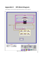
1
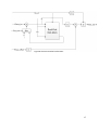
FPGA - DX7
EDA385 - Project Report
Andreas Irestål
( [email protected] )
Rajanarayana Priyanka, Marigi
( [email protected] )
Shadi Abdu-Rahman
( [email protected] )
28th November 2011 (version 1.1)
1
Abstract
The project closely recreates a Yamaha DX7, a FM synthesizer using a Nexys 2 FPGA board,
I2S pmod, MIDI keyboard, VST plugin and a MIDI & VST interface board. The final prototype
is also capable of handling higher resolution parameters than the conventional DX7.
Important features like polyphony, rate scaling, sustain, velocity sensitivity etc are
supported. Initial goal of being able to load real DX7 patches into the synthesizer and play it
with an external MIDI keyboard and also control it from computer installed music
sequencing software has been successfully achieved in the final prototype.
2
Table of Contents
FPGA - DX7 ............................................................................................................................ 1
EDA385 - Project Report ........................................................................................................ 1
1 Introduction ................................................................................................................... 5
2 Background .................................................................................................................... 6
2.1 FM Synthesis ........................................................................................................... 6
2.2 The structure of the DX7 ......................................................................................... 7
2.3 The MIDI protocol ................................................................................................... 9
2.4 Music Production Software & Plug-ins .................................................................... 9
3 FPGA Hardware ............................................................................................................ 11
3.1 EGS ....................................................................................................................... 11
3.2 OPS ....................................................................................................................... 13
3.3 Mixer .................................................................................................................... 14
3.4 I2S Controller ........................................................................................................ 14
3.5 FSL Controller ........................................................................................................ 14
3.6 Communication Hardware .................................................................................... 14
4 MicroBlaze Software .................................................................................................... 18
4.1 MicroBlaze OS ....................................................................................................... 18
4.2 The Interrupt System ............................................................................................ 19
4.3 MIDI Message Decoding ........................................................................................ 20
4.4 VST Message Decoding ......................................................................................... 20
4.5 Synthesizer Software............................................................................................. 21
4.6 DX7 Patch Conversion ........................................................................................... 21
5 External hardware and software .................................................................................. 22
5.1 MIDI & USB Connector Board ................................................................................ 22
5.2 Plugin Software ..................................................................................................... 22
6 Implementation Problems............................................................................................ 24
6.1 Value Representation ............................................................................................ 24
6.2 The XPS Interrupt System ...................................................................................... 25
6.3 Steinberg VST SDK Documentation ....................................................................... 25
6.4 Importing FPGA hardware into XPS project ........................................................... 25
6.5 Hardware limitation .............................................................................................. 25
7 Results ......................................................................................................................... 26
7.1 DX7 Parameters .................................................................................................... 26
7.2 Communication Functionality ............................................................................... 26
7.3 Memory Usage...................................................................................................... 27
7.4 Device Occupancy ................................................................................................. 27
8 In hindsight ... .............................................................................................................. 28
9 Possible extensions ...................................................................................................... 29
3
10
Lessons Learned ....................................................................................................... 30
11
Contributions ........................................................................................................... 31
12
References ............................................................................................................... 32
Appendix A: Tools used ...................................................................................................... 33
Appendix B: Installation ..................................................................................................... 34
Appendix C: User Manual .................................................................................................. 35
Appendix D: FSL-DX7 Protocol ............................................................................................ 36
Appendix E: XPS Block Diagram ......................................................................................... 40
4
1 Introduction
In this project, a FM synthesizer is created using the Nexys2 FPGA board. This type of sound
synthesis was popular in the 1980's and early 1990's. Outside the world of synthesizers, sound chips
with FM synthesis were additionally used in various arcade games as well as in computer audio cards
to generate sounds. In those days sample-based music and sounds were taking up too much of
precious memory, so FM was a cheap and efficient way to synthesize different instruments. In
addition it could also create some unique, complex and interesting new sounds.
The main goal was to recreate a Yamaha DX7, one of the most successful commercial synthesizers
ever made to date. The features of Yamaha DX7 like polyphony, real time patch loading and wide
range of controls and parameters made it very attractive to produce musical sounds. Since our final
result is a prototype of original DX7, it is referred to as DX7 from here on.
Other goals included the abilities to play the synthesizer from a MIDI keyboard, to load original DX7
sound patches into it (sets of configurations parameters) and to play back sequenced melodies and
parameter automation from music software packages using a so called VST Plugin. To this end, an
external board with MIDI-in port circuitry and a USB-RS232 converter module had to be assembled.
This report is structured as follows: Section 2 gives some background on the technologies involved in
the project. In section 3 the FPGA hardware is detailed. Section 4 talks about how the MicroBlaze
software is implemented. Section 5 deals with external hardware and software. Implementation
issues experienced in this project are the topic of section 6. Results are given in section 7. Sections 8
and 9 discuss things that could have been done differently and possible extensions to the project.
Valuable lessons learned are listed in section 10. Finally the contributions of the team members are
detailed in section 11.
5
2 Background
In this section background information on the technologies used is provided: In section 2.1 the
basics of FM synthesis are described, section 2.2 explains the inner working of the original DX7
synthesizer, information about the MIDI protocol is provided in section 2.3, and finally VST plugin
technology is explained in section 2.4.
2.1 FM Synthesis
In simple terms, frequency modulation is the change of instantaneous frequency of one signal
(carrier) in accordance with another signal (modulator). FM signal can be expressed with the below
equation.
Y = Ac sin(2πfct - Δf/fm cos(2πfmt))
Ac : Peak carrier amplitude
fc : Carrier frequency
fm : Modulator frequency
Δf : Peak carrier frequency deviation
FM is the conventional technique used in Radio broadcast. However the carrier frequencies used
here are of the order of MHz. The basis of sound synthesis using FM is to use carriers in the audiofrequency range. Simply put, use one audio-frequency signal to modulate the frequency of another
audio-frequency signal to produce musically interesting sounds. When the modulator frequency is of
the order of carrier frequency, we will not notice a cyclically squeezing and stretching of carrier but a
form of distortion within the individual cycles of the carrier, figure 1. Different distortion produces
different unique sounds.
Figure 1: FM wave examples
6
FM generates frequency components in the output waveform that are not necessarily harmonically
related to the carrier or modulator frequency which in turn affects the sound produced . FM
produces an infinite number of side bands (brighter sounds) at frequencies fsb = fc ± nfm.
We observe from the above equation that the modulator frequency influences the position of the
side bands. We define modulation index I = Δf/fm , a ratio of the peak frequency deviation of carrier
from its unmodulated frequency to the modulator frequency. I is the amount of modulation that we
want to apply to the carrier. And is directly proportional to the peak amplitude of the modulator
(amount by which the carrier frequency deviates is determined by the amplitude). For a given
modulator frequency, amplitude of the modulator determines the amplitudes of the side bands in
the output FM signal and thus the sound itself (timbre / brightness). The rule of thumb is that the
more modulation is applied the brighter the sound gets, resulting in noise if the modulation index is
very high. The change into noise is quite sudden and this can be used in many creative ways.
Interesting point to note is that for some values of I the carrier component completely disappears
from the output signal. When using a keyboard where frequency doubles every octave the
amplitude of the modulator also should double to maintain same I and thus same tone. Thus we
note that both amplitude and frequency of the modulating signal affects the resulting FM waveform.
Conventionally any change in the tone of a sound is determined by the changes in the cutoff
frequency of a filter. However, in FM synthesis there is no requirement for a filter to modify tone as
for a given modulator frequency, the modulator amplitude determines the spectral components of
the output sound.
Although theoretically the FM signal has infinite frequency components, mathematical analysis
shows that side bands whose order is greater than (I + 1) have amplitude 5% or less of unmodulated
carrier amplitude. Thus, for all practical purposes bandwidth requirement is
B = 2fm(I+1)
One might question that other modulation techniques like AM also produces side bands. Uniqueness
of FM comes from the fact that the bandwidth occupied by the FM signal is far less than that of AM
signal (any other modulation technique) considering the richness of sound it produces. Sometimes
they are also referred to as constant-bandwidth systems.
Although different signals like saw tooth, triangular, square etc. can be used both as a carrier and/or
modulator, we will only use sine waves for sound synthesis to keep it simple and also it gives more
control over the spectral components of the output.
2.2 The structure of the DX7
DX7’s sound generating engine consists of 6 oscillators per voice/channel, arranged in one of the
available predefined pattern, or algorithms [2]. The oscillators are sine wave digital oscillators which
are implemented using phase accumulators and Cosine wave LUTs (look-up-table). DX7 supports 16
voices of polyphony. The oscillators whose outputs are fed as inputs to other oscillators are called
Modulators and oscillators whose outputs are fed to the outside world are called Carriers. The
amount of Modulator’s output that is fed as input is known as Modulation index. It controls the
brightness of the sound (timbre - no. of harmonic components). Different instrument sounds can be
produced by varying the spectral components and loudness of the output sound. These two
parameters are controlled by the engine called envelope generator that generates an envelope that
7
defines the instantaneous values of these parameters applied. When applied to a carrier however, it
defines the loudness. The envelope closely follows a ADSR (Attack-Decay-Sustain-Release) envelope.
The envelope is defined by 4 level (L1-L4) and 4 rate (R1-R4) parameters. When a key is pressed R1
defines the rate at which envelope ‘attacks’ to level L1, immediately after it ‘decays’ to level L2 at
rate R2. Then again after it immediately raises to level L3 at rate R3 and ‘sustain’ there until key is
released, after which it ‘release’ to level L4 (which is usually zero level) at rate R4. An example of an
envelope is shown in figure 2 [1]. Conceptually an oscillator can be thought of having its own
envelope generator. The combination of these two is called an ‘Operator’ in original DX7
terminology, a block structure of which is shown in figure 3 [1].
Figure 2: An example envelope
Figure 3: Original DX7 Operator
The frequency of each oscillator can be ratio scaled with regards to carrier frequency [7] giving a
control over the position of the spectral components i.e. brightness. Also the frequencies fed to the
oscillators are controlled by another envelope generator for pitch. This again improves the timbre of
the sound. LFO (low frequency oscillator) usually 1-50Hz is used to produce rhythmic effects like
vibrato, tremolo in the output sound.
8
The output of sound generating engine is fed to the mixer which applies the global volume and
panning parameters. Then it is applied to an I2S (Inter-IC sound) controller that serializes the data
and outputs to I2S pmod which consists of a DAC.
The components, sound generator (referred as OPS here after), envelope generator (referred as EGS
here after), mixer and I2S controller are implemented in hardware in order to satisfy the high
computational demands of a musical sound.
The parameters are communicated to these components through FSL bus from Microblaze software.
A FSL controller handles delivery of these messages to destination component. A protocol is
designed for this purpose as explained in Appendix D.
2.3 The MIDI protocol
MIDI is a protocol that has been around since 1982, and is still implemented in every new
commercially developed synthesizer. There are also a lots of MIDI keyboards and controllers on the
market. In MIDI capable units, the protocol is used to send or receive note key presses, parameter
changes, patch changes, as well as other data by means of special MIDI messages called SysEx
(System Exclusive) messages. More information about the MIDI specification can be found here.
MIDI keyboards do not generate any sound by themselves but instead send messages over their
MIDI port. Messages include Note On and Note Off, which are sent when a key is pressed and
depressed respectively along with information about what key was pressed/depressed and how
hard (velocity). For more expressive playing some keyboards also have pitch bend and/or
modulation wheels or levers that also send data controlling note pitch and some other freely
assignable synthesizer parameter.
2.4 Music Production Software & Plug-ins
There are different commercial software packages which are frequently utilized to record, rearrange,
and playback musical sequences or phrases. These sequences are either performances recorded as
audio or MIDI, or notes simply input directly into the software sequencer.
Typically, a project (‘song’) in such a software package consists of several tracks of two types: Audio
and MIDI tracks (see figure 4 below). Audio tracks usually contain material such as recorded vocals
while MIDI tracks contains arranged melodies or musical phrases that are played back using either
the software’s own built-in virtual instruments or third party plug-ins. In addition, MIDI tracks also
contain automation lanes, which contain recorded or manually drawn instrument parameter
changes that occur when the song is played back. These typically include volume, stereo pan but
could be any other parameter the instrument plug-in developer chooses to expose to the host
software.
Several plug-in standards exist such as Microsoft’s DirectX, Apple’s Audio Units and Steinberg’s
Virtual Studio Technology (VST) with the latter being the most widely supported and developed for.
9
Figure 4: A Project in the Ableton Live music software with a VST plugin inserted.
10
3 FPGA Hardware
The architecture of the FPGA hardware is shown in figure 5. This architecture is the same as the one
initially proposed with the mixer and communication hardware added. The implementation consists
of the following main components:
●
●
●
●
●
●
●
●
●
MicroBlaze CPU (microblaze)
EGS (custom amplitude and frequency generator)
OPS (custom sound generator)
Mixer (custom)
I2S Controller (custom)
FSL Controller (custom)
Interrupt Controller (xps_intc)
MIDI UART Controller (xps_uart16550)
USB UART Controller (xps_uart16550)
The names EGS and OPS are in consistent with the terminologies used in original DX7. The hardware
components are explained in more detail in the following sections.
3.1 EGS
The EGS is implemented in a structural manner since it contains a lot of different components. It
consists of 2 memories: OP RAM and Global RAM, which are simple dual port RAMs (one read port
and one write port).
The Op RAM contains all operator specific parameter data. It contains rates and levels for the
operators dedicated envelope, information about how sensitive the operator is to the envelope
generator, basic frequency and amplitude as well as information whether the operator is turned on
or off. It also contains state information for the envelope, which gets updated every sample. It also
function as a settings memory for global parameters like if a key is pressed or not, pitch modulation
amount as well as pitch envelope parameters. The global parameters are mapped to "Operator 7"
address space.
Besides the Op RAM is the global RAM, which contains all global state parameters, like the current
pitch envelope state and its value, the LFO phase, whether a key is pressed or not and so on. The
reason for this two-memory solution is that when the operator data is generated, global state data is
also required. For instance, we must know the value of the pitch envelope generator so it can affect
the frequency of an operator. Because of that, we cannot store such parameters in the operator
memory since it would either require 6 copies of the global state data (1 copy for each operator) or
some other complicated solution.
The state machine inside EGS controls the memory addresses and write signals. It has four states:
Wait, Globals Update, Operator Update, Reset. The Reset state is only used when a reset signal is
received. The memories are then cleared and everything is set to an initial state.
After the modulation application stage, the amplitude and frequency for the current operator is
output. Note that the wiring is the same when calculating globals and operators. The main
11
difference between those two states is that the write signal for globals ram is disabled when
calculating operators.
Figure 5: Overview of FPGA hardware
Figure 6: Overview of the EGS pipeline
12
3.2 OPS
This hardware block generates the musical sound with the frequency and amplitude provided by the
EGS, and the algorithm from the software. The block diagram is shown in figure 7. A 16-voice
polyphony with 6 operators per voice require a total of 96 oscillators. Hence a multiplexed
architectural approach has been used to minimize FPGA utilization. The main inspiration to the
design is provided by the OPS block diagram in the service manual of the original DX7 [2].
The phase accumulator and cosine lut together produce pure tones (sine waves) of different
frequencies as determined by EGS. The cosine lut stores samples of a sinusoid and provides values
corresponding to the phase input. It is instantiated from DDS (Direct Digital Synthesizer) IP core. This
IP core is already provided in ISE project navigator. It can be instantiated using ‘Core Generator and
Architecture Wizard’ under ‘Digital signal processing - Waveform synthesis’ category. Only ‘SIN/COS
Lookup Table’ part of the IP core is used. Though ‘Phase Generator’ part of the IP core could have
been used which can also be configured to support 16 independent time-multiplexed channels, we
decided to design our own phase accumulator / generator to minimize hardware. A DDS IP core has
a phase generator and a lut with 16 voices. Six instances of these need to be instantiated for 6
operators. As a result, a redundancy of 5 luts wasted FPGA hardware. Also a feature, ‘key sync’
required that it should be possible to reset individual channels without affecting others so that the
oscillator can start with zero phase. However, this is not possible in the DDS IP core. Hence a custom
designed phase accumulator.
The phase accumulator is essentially an adder and a register per voice per operator. Again the
advantage of multiplexed architecture is utilized with one adder and a Distributed Memory IP core of
size 96 to support 96 oscillators conceptually. This block also has facility for phase offset input
resulting in a frequency modulated tone. A schematic is shown in figure 8.
The output of one operator has to be fed as an input to another with a latency of 16 as each
operator supports 16 voices and the operators are time-multiplexed. In order to have a consistent
max output level, the carrier outputs are compensated depending on the number of carriers in the
algorithm for the channel. The M-Reg file provides the modulation phase offset while the F-Reg file
provides the feedback information for each voice. The feedback amount can be controlled using the
Shifter block. Every algorithm change for a channel causes the corresponding feedback to be reset
for that channel. The O-Reg accumulates the carriers output for all channels and provide a final
sample value. The Normalizer’s function is to normalize the registers output value from ±1 to ±0.5
corresponding to ±𝝿 radians.
Alg-Reg file stores the current algorithm for each channel. The register enable signals, compensation
amount and the phase offset source are all algorithm dependent and hence a set of fixed values. A
ROM stores all these values.
Every sample data is calculated after OPS has received ‘sync’ signal from EGS. After a latency of 2
system clock cycles from the reception of ‘sync’ signal the frequency and amplitude values for each
channel and each operator on the input ports are processed by OPS in order of operator 6-1 and
channel 1-16 for each operator. A controller (Oscillator SM) has been designed to read correct values
for each channel of each operator and enable corresponding oscillator in the phase accumulator.
13
The OPS sample data output has a latency of 114 system clock cycles after the ‘sync’ signal is
received from EGS.
3.3 Mixer
Mixer is a combinational block that extracts data for the left and right channel of stereo using
volume and pan parameters, and the OPS output data. This block has high demands on the number
of Multipliers because of wide data widths and also increases the critical path, lowering the
operating frequency. The final hardware synthesized to very low frequency of 20MHz, and an output
register had to be added to solve this problem. In the final phase of the project some problems were
encountered in this block. The panning made the multiplier usage on the hardware too high. Since
panning was not a very important feature it has been disabled in the final implementation. In the
final implementation output of 24 bits depth is used.
3.4 I2S Controller
This block is designed to convert the parallel output from Mixer to serial format of the I2S standard
bus protocol which is implemented in the I2S pmod housing a Cirrus Logic 4344 DAC. The I2S
controller is a combinational logic that serializes left and right stereo channel data, according to a
predetermined clock frequency that the DAC can handle. Final implementation uses approximately
52.08 KHz sampling frequency that is derived by dividing a 40MHz clock by 768.
3.5 FSL Controller
This controller is designed to read data from the FSL bus according to FSL bus protocol. No support
to write data to FSL bus is provided in the final implementation. However, this is not a limiting factor
and can easily be extended. The functionality of the block is to forward the hardware messages
received to their respective destination blocks which may be one of these; EGS, OPS, Mixer-Volume
and Mixer-Pan according to a protocol discussed in appendix D.
The choice of FSL bus was motivated by the use experience from Embedded Systems course. Due to
the amount of work and time constraint, decision to use something that we are already familiar with
was made. The possibility of using PLB for this purpose was not explored. However, this can be one
area of possible extension.
3.6 Communication Hardware
To enable MIDI and USB serial communication with MIDI keyboards and Computers, MIDI UART and
USB UART controllers were instantiated using the XPS UART (16550 Style) IP Core (xps_uart16550).
Each of the serial inputs of the UART controllers (*_UART_sin) was then connected to a PMOD pin
on the FPGA board (G13 for MIDI and J16 for USB). Additionally, the serial output of the USB UART
component (USB_UART_sout) was also connected to a PMOD pin (G15). However this was only used
for debugging purposes during development and is not used for any of the features in the final
prototype.
14
The UART controllers above work in such a way that they generate an interrupt on data reception
that could be treated differently if the received data is valid, invalid or has timed out. To enable
handling of these interrupts each of the UART controllers interrupt output was connected to an
instance of the XPS interrupt controller IP core (xps_intc), which in turn had its interrupt output
connected to the interrupt input of the MicroBlaze CPU instance.
All three controllers use the PLB bus for communication with MicroBlaze CPU.
15
Figure 7: Sound Generator (OPS) block diagram
16
Figure 8: Phase Accumulator Schematic
17
4 MicroBlaze Software
The Microblaze software, explained in section 4.1, interfaces with the MIDI and VST Control inputs
by way of an interrupt system, detailed in section 4.2. These inputs provide data about amongst
other things notes played and parameter changes in real-time, which is decoded according to their
respective protocol. This is explained in sections 4.3 and 4.4.
The software processes in some cases these parameters before they are sent to the synthesizer
hardware. (eg: note frequency, pitch bend, coarse and fine frequency settings and detune, all
determine final frequency value input to the hardware), and converts the input messages to
hardware compatible FSL message format. This is described in section 4.5
The software also has facility to store 128 patches, where a patch is a set of parameters that define
the final output sound. Software has capability to create a synthesizer for each MIDI connection with
a maximum of 16 synthesizers (MIDI specification supports 16 channels for each connection).
However, in the final prototype only MIDI channel 0 is used. Software can also load original DX7
patches sent by SysEx messages by decoding them [5] and converting the values to a format
compatible with our synthesizer [6]. This is detailed in section 4.6.
4.1 MicroBlaze OS
The MicroBlaze OS is configured as a interrupt driven single-threaded OS. Once the interrupt system
is setup and started, as described in the section 4.2, and the UART controllers are configured and
start listening to the inputs, the main loop just checks if new messages have been delivered to the
USB or MIDI buffers. If one of the conditions is true, a call is made to the corresponding decode
method:
while(1) {
if (MidiReadItr != MidiWriteItr)
decodeMidi();
if (usbInReadItr != usbInWriteItr)
decodeUsb();
}
This approach was chosen for several reasons:
● It consumes less hardware than a multi-threaded OS such as Xilkernel, and we had a feeling
we would need a lot of hardware.
● We wanted the decoding of messages to be fast enough so as not to affect playability, and
we were not sure how much context switching overhead would affect decoding speed.
● It seemed a lot less involved to develop with this approach, freeing us to develop other
functionality.
● With two mutually unsynchronized message streams, we could just switch between them as
described above, while any running decoding work could be interrupted as needed.
18
The main function can be found in the dx7main.c source file.
4.2 The Interrupt System
As mentioned earlier the software takes care of incoming interrupts that occur whenever a message
is received on the USB or MIDI port. The following is description of how this is setup in the main
thread before the main loop starts running.
First the interrupt controller is initialized and the interrupt handlers of the UART controllers are
registered with it:
XIntc_Initialize(&xps_intc_0, XPAR_INTC_0_DEVICE_ID);
XIntc_Connect(&xps_intc_0, XPAR_XPS_INTC_0_MIDI_UART_IP2INTC_IRPT_INTR, (XInterruptHandler)
XUartNs550_InterruptHandler, &MIDI_UART);
XIntc_Connect(&xps_intc_0, XPAR_XPS_INTC_0_USB_UART_IP2INTC_IRPT_INTR, (XInterruptHandler)
XUartNs550_InterruptHandler, &USB_UART);
This is a source of confusion in many tutorials on the XPS interrupt system. The
XUartNs550_InterruptHandler in the code is not where the interrupt handling code should go. This is
only a low level handler that takes care of things like context switching, and acknowledging and
clearing interrupt. It in turn calls the interrupt handler you write and register with the UART
controller (the same applies to all factory IP Cores that use interrupts). This is a good thing, since all
the context switching and register manipulation is done for you by the MicroBlaze operating system.
Next the interrupt controller is started and its hardwired interrupt lines enabled:
XIntc_Start(&xps_intc_0, XIN_REAL_MODE);
XIntc_Enable(&xps_intc_0, XPAR_XPS_INTC_0_MIDI_UART_IP2INTC_IRPT_INTR);
XIntc_Enable(&xps_intc_0, XPAR_XPS_INTC_0_USB_UART_IP2INTC_IRPT_INTR);
Following that, the Interrupt handler of the interrupt controller itself is registered with the
MicroBlaze and the MicroBlaze interrupts are enabled.
microblaze_register_handler((XInterruptHandler) XIntc_InterruptHandler, &xps_intc_0);
microblaze_enable_interrupts();
Finally, in the initialization code for each UART controller, the high-level interrupt handlers are set,
the data received interrupts are enabled, and a request for data reception is issued. E.g. for the USB
UART controller:
XUartNs550_SetHandler(InstancePtr, (XUartNs550_Handler)usbin_int_handler, InstancePtr);
XUartNs550_SetOptions(InstancePtr, XUN_OPTION_DATA_INTR | XUN_OPTION_FIFOS_ENABLE);
.
.
.
XUartNs550_Recv(InstancePtr, RecvUsbBuffer[usbInWriteItr].data, RECV_SIZE);
19
where usbin_int_handler is the high-level interrupt handler where the actual interrupt handling is
done.
As interrupts stop the normal execution and turn of other interrupts, it is recommended that this
high-level interrupt handler is kept as short as possible. Our handler only increments the incoming
data buffer iterator on valid data reception and reinitiates another request for reception of more
data whatever the condition of the data received:
void usbin_int_handler(void *CallBackRef, u32 Event, unsigned int EventData) {
if (Event == XUN_EVENT_RECV_DATA) {
usbInWriteItr = incIt(usbInWriteItr);
XUartNs550_Recv(CallBackRef, RecvUsbBuffer[usbInWriteItr].data, RECV_SIZE);
} else if (Event == XUN_EVENT_RECV_TIMEOUT | Event == XUN_EVENT_RECV_ERROR) {
XUartNs550_Recv(CallBackRef, RecvUsbBuffer[usbInWriteItr].data, RECV_SIZE);
}
}
Code related to the interrupt system is present in the dx7main.c, usbio.*, and midiin.* source files.
4.3 MIDI Message Decoding
Decoding incoming MIDI messages was a straightforward process, although the MIDI protocol uses
variable message sizes.
When a MIDI message has been decoded, its type identified and data extracted, the corresponding
function is called to communicate it to the hardware or other parts of the software to set the correct
parameter or for further processing before transmitting the final values to the synthesizer hardware.
For example, Note On/Off messages have their MIDI note values converted to pitch frequency values
before being sent over the FSL bus to the hardware.
Code for MIDI message decoding and handling is present in the mididec.* and midi.* source files.
4.4 VST Message Decoding
For transmission of VST messages a fixed message length protocol was devised to enable faster
decoding. This is especially needed since the symbol rate of the USB RS232 serial connection is 50
times faster than its MIDI equivalent (1.562.500 Baud compared to 31.250).
The protocol is as follows: Each message consists of six bytes. The leftmost byte specifies event type,
either Note Event or Destination Parameter Event (Global, Operators 1 to 6). The next byte is Note
Event Type (On or Off) or Parameter Type. For note events the next two bytes are Note Pitch and
Velocity in that order while the last two are unused. For parameters changes the last four bytes
contain the new parameter value encoded from LSB to MSB. Different parameters have different
value resolutions so not all four bytes are always used. Toggle or bistate parameters for example
only use the third leftmost byte while the last three are empty.
20
Following the same principle as MIDI decoding, once a VST message has been decoded a call is made
to the corresponding function to set a parameter in the software or transmit the correct values to
the synthesizer hardware, sometimes with some additional processing inbetween.
Code for serial message decoding and handling is present in the usbdec.* and midi.* source files.
4.5 Synthesizer Software
To handle polyphony, pitch bend wheel as well as setting of any arbitrary parameter, the synthesizer
code is needed. The MIDI messages are forwarded to this layer and decoded here. With this
structure, multitimbrality is supported since the midi.* layer can decode just the channel and act as
a packet switch to forward the MIDI message to the correct synthesizer.
The synthesizer is used for mapping the hardware to a software representation. It is used for holding
all parameter values, both hardware and software. It also does the actual decoding of the midi
message. The synthesizer is also used to assign notes to a hardware channel. It also keeps track of
which note is playing on which channel. When a note off message is received it can look up the
corresponding channel and set its "key pressed" to off.
Some software parameters like velocity sensitivity and rate scaling are implemented here. Since
velocity sensitivity is a very basic thing, reducing the output level from max depending on velocity
value, such parameters do not need hardware calculation. Therefore, when a key is pressed, the
basic output volume is calculated with the velocity to create a new basic amplitude that is used by
the EGS hardware. A few more parameters, like rate scaling, are implemented like this. To do these
calculations easily, as well as mapping notes to frequencies, some math functions are provided.
Most of them are based on interpolations of measurements used in the open source hexter software
synthesizer [13]. This data has been converted in Matlab with the system parameters (clock
frequency and parameter width) in mind.
Synthesizer code is present in the synth.*, synth_math.* and hardware.*
4.6 DX7 Patch Conversion
As mentioned in other parts of this document, the specialized hardware in this project uses wider
data widths than used in the original DX7. This is mainly to avoid the exponential nature of many
DX7 parameters and also to have the possibility of adjusting parameters on an almost continuous
scale. This way, if some parameter were estimated wrong according to DX7 measurements, a minor
software change can adjust this. The high resolution also enables the hardware to be constructed in
a linear fashion, which make many HW blocks simpler to create.
All this conversion is handled by software, assisted by interpolating functions and look-up tables as
well as some function approximations. To explain this in detail, the reader must have a lot of DX7
measurement data available. The tables are created by using data from [13] run through Matlab
adjusting for system properties.
The conversion code is found in dx7_converter.*
21
5 External hardware and software
In this section we describe any hardware and software external to the FPGA. These consist of a MIDI
& USB connector board (section 5.1) and plugin software (section 5.2).
5.1 MIDI & USB Connector Board
To connect the FPGA to MIDI keyboards and computers we soldered designed a daughter board that
connects to a PMOD header of the FPGA. The board consists of two sections: A MIDI In circuit as
specified by the MIDI Manufacturers Association and a FTDI UM232H module used to connect the
FPGA to a USB Port of a computer running VST plugin compatible music software. This module can
be configured and controlled programmatically (a programmer’s guide is available here).
Both TX and RX pins of the module were connected to the PMOD pins of the FPGA. The RX pin has
however only been used for debugging purposes during development, and is unused in the final
iteration.
5.2 Plugin Software
A plugin was developed for the sake of integrating the FPGA synthesizer hardware into the workflow
of music production software (hereafter referred to as ‘host’).
Steinberg’s VST 3.5 technology was chosen for the development of the plugin as it is widely
supported by music software and can also be used as the basis for generating Apple’s Audio Unit
plugins.
While a plug-in instrument is typically used to generate sound according with incoming notes and
parameter messages from the host software, our plug-in will instead forward those messages to the
FPGA via a USB connection, thus making the parameters of the synthesizer controllable from within
the host software using sequenced parameter automation or by simply changing the parameter
values directly in the plugins graphical user interface. In addition melodies can be sequenced or
played directly from within the host software.
The following describes the communication flow between the host software, the plugin, and the
FPGA synthesizer:
● Upon plugin instantiation on a track, the host asks the plugin for instances of a controller
(graphical user interface) and processor (parameter data model). These are object instances
of the classes defined in the dx7processor.h and dx7ctrlr.h header files. The plugin looks for
a FPGA connected to USB and sets up a connection object, an instance of the class defined in
dx7uart.h.
● Upon successful completion of the first step, the initial state of the plugin parameters is sent
to the FPGA for synchronization.
22
●
●
●
As long as the plugin stays instantiated and enabled, the host communicates any automation
changes, note events and changes in the plugin controller to the plugin processor instance.
A call is made by the host to the process() function in the processor object periodically with
the frequency value set in the host (defined in number of samples).
The process() function checks for any new events it has received since last call. Note events
are sent directly to the FPGA synthesizer. For parameter changes the parameter data model
is updated before the change is sent.
23
6 Implementation Problems
This section elaborates on the main implementation issues we experienced. Section 6.1 discusses
the problem with different value representation. Section 6.2 talks about the lack of good examples
on how to setup the XPS interrupt system. Section 6.3 is a call for more extensive documentation for
Steinberg’s VST 3.5 SDK. Sections 6.4 and 6.5 mention the difficulties importing the FPGA hardware
into the XPS project and hardware limitations respectively.
6.1 Value Representation
This project is composed of many different parts, using or emulating technologies from different
times and for different purposes. The Yamaha DX7 synthesizer is an embedded system that was
designed in the beginning of the 1980’s, a time when digital memory was small and expensive, while
the latest VST specification is from the beginning of 2011 (although the technology first appeared in
1996) [8] designed to run on general purpose computers with access to huge amounts of memory
and processing power in comparison. One unexpected difficulty of combining these different
technologies was handling the different parameter value representations used throughout the
system.
As an example let’s look at the Transpose parameter, which is used to offset the frequency of the
generated tones by semi note values:
The parameter has a range of -24 to 24 (two octaves in each direction). The value shown in the VST
Plugin GUI is one of the discrete steps in this range. However internally in the VST plugin all
parameter values are represented as discrete or continuous float values between 0.0 and 1.0. For
Transpose 0.0 means transpose to the left by two octaves, 0.5 means no transposition, and so on.
Before being sent to the FPGA this value is converted by multiplying it with its number of steps - 1 to
simplify decoding on the FPGA. The byte representation of the Transpose parameter now translates
into a range of 0 to 48, where 0 means transpose to the left by two octaves, 24 means no transpose,
and so on.
In addition, most parameters needed some kind of decoding when they were finally received at the
FPGA end. Most of those conversions were just bit shifting though. Another problem related to this
area is that in manual, operators are numbered 1-6 but in the actual DX7 hardware, operator 6 are
given index 0 and so on. This mapping is also needed when treating USB communication.
For a few parameters and a couple of different value representations, this is not a big issue.
However, the VST controls 127 of the FPGA synthesizer parameters several different value
representations. Apart from giving rise to some hard to find bugs (“What does this value represent
here?”), it also meant a lot of value conversion code had to be written. In the VST Plugin source,
refer to the initialize() function in the dx7ctrlr.c file and the parameter classes in
processParameter.c and controlParameter.c files for some hair raising examples.
24
As mentioned earlier, all exponential representations have caused a lot of problems as well. This has
been the case in hardware, since it is extra hard to calculate such values there. After some thought,
it was discovered that a relatively small look-up-table could be used for the range 2^(n) to 2^(n+1).
All other values could then be derived by shifting one value in the table. The amplitude and pitch
calculation parts of the hardware use this approach. When faced with this problem in software,
problems could occur as well since there is no floating point unit in the MicroBlaze CPU. Tables were
also used to some extent and interpolated to mimic parameters that had an exponential nature.
Rate scaling is one example.
6.2 The XPS Interrupt System
As described in section 4.2 the interrupt system is simple and elegant. However, this is not how it is
documented. The relevant documents provided by Xilinx, [9], [10], and [11], only provide pieces of
the puzzle while none describe the entire system.
Searching the Internet for tutorials and usage examples provided little help. Some examples confuse
interrupts with exceptions and used them interchangeably, others were evidently written without an
understanding of the distinction between the low-level and high-level interrupt handlers, and most
commonly, examples used a lot of code to set bits in configuration registers without any real need
to. Not one example we read provided a description similar to the one given in this document.
It is hard to believe this to be the fault of the people behind the examples. A couple of well-written
examples in the official documentation would have easily cleared up a lot of confusion.
6.3 Steinberg VST SDK Documentation
The Steinberg VST SDK documentation, although clear and well-written, is by no means complete.
As an example, we had the idea to have a periodic thread check the state of the USB connection to
the FPGA. This was soon abandoned though as any attempts to start a thread from the VST plugin
crashed the plugin and the host software with it. In this case, it would have been nice if the VST SDK
documentation provided some pointers on where and how to start threads, or at least mention if it
was possible or not.
6.4 Importing FPGA hardware into XPS project
The import wizard did not recognize the master and slave clock defined in the FSL port definition. As
such we could not build the entire project with imported hardware. A day and a half was wasted
because of this issue. After the help from supervisor this was resolved. Bottom line is Create and
Import Wizard is not so user-friendly!
6.5 Hardware limitation
One issue had been the amount of multipliers available on the FPGA hardware. Since a lot of mixing
occurs at different hardware paths, a multiplier shortage was realized. The only solution to this
problem was to remove the least useful hardware from the project. If another FPGA is used, one can
simply re-enable some parts of the mixer code to implement panning again.
25
7 Results
In this section we list the features that have been implemented and are working correctly. While
section 7.1 deals with features related to the original DX7, section 7.2 describes the added
communication features. In section 7.3 we show the resultant memory usage, while figures for
device occupancy are available in section 7.4.
7.1 DX7 Parameters
With a few exceptions, all voice parameters in the original DX7 specification [1] have been mapped
to our structure. There are two exceptions: "Keyboard Level Scaling" and LFO. The LFO are fully
implemented in hardware with a few minor bugs. Unfortunately, there was not enough time at the
end of the project to implement the LFO in software. The level scaling is a software parameter which
is very hard to calculate correctly. It has always been last priority in our work, but it could be
implemented without modifying the hardware.
The resulting sound of many original DX7 patches loaded into our design was in many cases close to
the original. The cheesy DX7 Rhodes sound is just one example. The category of sounds that were far
from the original was various sound effects, since many of them rely on LFOs with very exact values.
The DX7 patch conversion worked very well and was instantaneous. The parameters also benefited
from having a higher resolution when modified from the VST interface. A few extensions from the
DX7 design were also implemented, e.g. individual operator sync and channel LFO.
7.2 Communication Functionality
Sending messages to the FPGA board from MIDI keyboards and VST Plugin hosts is working as
expected without any noticeable latency. No dropped messages could be registered during our
testing.
The communication related functionality that has been implemented successfully is described
below:
The following MIDI protocol message types are decoded and supported correctly:
● Note On/Off
● Control Change (Volume, Pan and Sustain)
● Program Change
● Pitch Wheel Change
● System Exclusive (SysEx) (for DX7 patch transfer)
Unimplemented message types include the rarely used Polyphonic and Monophonic Aftertouch
messages as well as non-applicable SysEx real-time messages related to timing and song position.
26
The FPGA synthesizer synchronizes its set of parameter values with the VST plugin and subsequently
decodes and processes any parameter changes received from the VST plugin. It also receives and
decodes note events from the same.
7.3 Memory Usage
Program memory is 32KB and “Size Optimize” option was used for compilation. Final software
memory occupancy is:
Text
Data
BSS
Total (Dec)
Total (Hex)
23354
1540
1984
26878
68FE
Synthesizer data structures, MIDI and SysEx buffers, and 128 internal patches are all stored in
Micron-RAM to save memory space for functionality and instructions in the Microblaze software.
7.4 Device Occupancy
Logic Utilization summary is shown below.
Resources
Usage
Utilization
Slice Flip Flops
4,189 out of 17,344
24%
4 input LUTs
7,408 out of 17,344
42%
Logic Distribution summary is as follows with Peak Memory Usage: 315 MB.
Resources
Usage
Utilization
Occupied Slices
6,590 out of 8,672
75%
Total 4 input LUTs
10,176 out of 17,344
58%
Bonded IOBs
57 out of 250
22%
RAM16s
28 out of 28
100%
BUFGMUXs
3 out of 24
12%
DCMs
1 out of 8
12%
BSCANs
1 out of 1
100%
MULT18X18SIOs
17 out of 28
60%
27
8 In hindsight ...
In this section we list things we could have done differently. Most of these were not explored further
or tried out due to the time constraints of the project.
After work started using the RS232 protocol for communication between computer and FPGA we
discovered that there was already an IP Core implementation of a USB peripheral controller,
something which we would have simplified the work involved with direct USB communication.
However, a lot of progress had already been made using the USB-to-RS232 Converter and none of us
had any experience of programming for USB Communication anyway.
There was really no need to use XPS UART (16550 Style) controller instead of the XPS UART Lite
controller for MIDI and USB Communication. The former did not provide any additional features that
we used and takes about three times as much hardware as the latter [11], [12]. The intention was to
replace the two instances with the latter but in the end there was simply not enough time to make
the replacement and test it as thoroughly as we would have liked.
The high resolution of many parameters could in some cases be reduced to increase hardware speed
and reduce memory usage. Some parameters had an unnecessary high resolution. Most of the
decisions on hardware values were made with the DX7 extreme values in mind and the desire of
having a linear representation in the hardware flow. Another thing we could have done is to have
exponential values everywhere and just do a simple final conversion at the end. A lot of
multiplications could be avoided this way since it would just be a simple addition.
Still, a lot of right decisions were made. Some of these include using a single-threaded OS, pressing
on with understanding the interrupt system instead of reverting to polling, using a VST
communication protocol with fixed size, time-multiplexed architecture to save on hardware, tablebased computation to simplify complex calculations and pipelining the synthesizer hardware to save
on multipliers and reduce critical path.
28
9 Possible extensions
In this section we list possible extensions that could be made to the project given enough time.
SysEx Patch Bank Transfer: An attempt was made to extend the patch transfer functionality to
decode a SysEx message containing data from a bank of 32 patches. However, this did not work and
there was not enough time to debug the functionality. The extension functionality was therefore
disabled in the final implementation. Transfer and decoding of single SysEx patches still works
though.
Physical interface for setting parameters and/or selecting patch : Connecting an LCD, some knobs
and buttons to enable direct manipulation of the synthesizer parameters and the selection of
patches from stored patch bank.
Windows version of VST plugin: The VST plugin build project was only built for the Apple OSX
platform, with the intention of building a Windows version after the OSX version was completed.
Again, we ran out of time.
Sending Audio back to VST plugin: This would mean that the VST plugin would, just like any other
virtual instrument, output audio to the host software for recording without the need for any other
cables than the USB cable.
Polyphony of 64 voices: This is possible provided there is more memory available on FPGA.
Multiple VST plugins: As of now, the VST Plugin can only be instantiated on one channel. It could be
extended to several instances controlling different voices of the FPGA Synthesizer.
DX7 LFO: The DX7 LFO could be measured and implemented to support vibratos and tremolos.
Multitimbrality: The possibility of having several different synthesizer engines within the system,
mapped to different MIDI channels. This is already realized in and fully supported by the hardware.
Only a small software change is needed to enable this. This would enable a musician to synthesize an
entire orchestra (with a polyphony limit of 16 voices, of course)
29
10 Lessons Learned
Shadi Abdu-Rahman: Working on this project included many ‘first times’ for me: Developing with
Apple’s Xcode, coding a VST plugin, using the XPS interrupt system, so I gained a lot of valuable
knowledge that I’m sure I will use in the future. I also gained a lot of insight with regards to hw/sw
design and where it makes most sense to implement functionality.
However, the lesson I value most is that I realized how two factors made working with this project
feel like much less of a burden: Choosing an interesting project that inspires you to put the extra
effort and being lucky enough to have dedicated and knowledgeable team members.
Priyanka: Having absolutely no background in music or synthesizer, the whole concept was very new
to me. The scope of the project daunted me initially. But as I like to try out new things it was very
exciting as well. A lot of studying was done to understand the concept, use and working of a
synthesizer. With the help of team members I quickly picked up enough knowledge to work
independently.
I also learned how an implementation never follows design unless elaborate time has been
dedicated to design alone. They are intertwined, always leading to an iterative process. At the end a
valuable knowledge of Synthesizer, to some extent music and Hardware-Software Co-design was
gained which I am sure will go a long way.
Andreas: I've learned several things from this project. It has involved a lot of planning, and one thing
I've learnt is important is planning. Since the size of the project has been enormous and the different
parts need to communicate with each other, we have done a lot of planning and my inbox have been
flooded during the course of the project. This has paid off in the later parts of the project, even
though it may have been time consuming at first. I tend to be very hasty with the planning phase
and this project has helped me get the experience I need to plan ahead in future projects.
One knowledge that has been very fun to discover is the inner workings of the DX7. Since many
hours have been spent analyzing, measuring and programming a real DX7 to derive the different
behaviors, I've learnt how to program the DX7. Before this project, I could only create very simple
sounds and FM synthesis in general was magic to me.
Of course, this project has also made me gain a lot of experience in VHDL and C development, and
some skills along the way with experience.
30
11 Contributions
Shadi Abdu-Rahman:
● Project Report: Layout, writing or contributing to sections 2.3, 2.4, 3.6 , 4.1 - 4.6, 5.1 - 5.2,
6.1 - 6.3, 7.2, 8, 9, 10, 11, and appendices A, B, C, and F
● FPGA communication hardware: Research, development, test & debugging
● MicroBlaze Software: Interrupt system setup, main, USB/MIDI communication & decoding
● External MIDI & USB Connector board: Research, ordering parts, soldering
● VST Plugin: Idea, research, development, test & debugging
Priyanka:
● Project Report: Writing or contributing to sections 1, 2.1, 2.2, 3 (opening), 3.2 - 3.5, 4
(opening), 6.1, 7.3, 7.4, 8, 10, 11, abstract and appendices A, B, C, D, E, F
● FPGA Hardware: OPS, FSL Controller, Top Hardware structure with FSL interface
● DDS IP core: Research and suggestion as it was used in both OPS and EGS
● Study on the feasibility of using Micron-RAM and Flash-Memory
● Integrating FPGA hardware p_cores into the XPS project
● MicroBlaze Software: Contributing to Midi message decoding and FSL message construction
Andreas:
● Project Report: Writing or contributing to sections 3.1, 3.3, 3.4, 4.5, 4.6, 6.1, 6.5, 7.1, 7.2, 8,
9 and appendices A, C, F
● FPGA Hardware: EGS, mixer, I2s controller
● Initial background and feasibility study
● DX7 research and measurements
● HW/SW Partitioning of parameters
● All DX7 conversion software except Sysex decoding
● Synthesizer software along with all mathematical functions.
● Midi decoding & handling
● Management
31
12 References
1. http://www.abdn.ac.uk/~mth192/dx7/manuals/dx7-man.pdf
2. http://www.abdn.ac.uk/~mth192/dx7/manuals/dx7-9_service_manual_1.pdf
3. http://www.soundonsound.com/sos/apr00/articles/synthsecrets.htm
4. http://www.clavia.se/nordmodular/modularzone/fmsynthesis.html
5. http://www.abdn.ac.uk/~mth192/dx7/sysex-format.txt
6. http://www.angelfire.com/in2/yala/t2dx-fm.htm
7. http://www.angelfire.com/in2/yala/2fmsynth.htm
8. http://en.wikipedia.org/wiki/Virtual_Studio_Technology
9. http://www.xilinx.com/support/documentation/application_notes/xapp778.pdf
10. http://www.xilinx.com/support/documentation/ip_documentation/xps_intc.pdf
11. http://www.xilinx.com/support/documentation/ip_documentation/xps_uart16550.pdf
12. http://www.xilinx.com/support/documentation/ip_documentation/xps_uartlite.pdf
13. http://dssi.sourceforge.net/hexter.html
14. http://www.fm-alive.com
32
Appendix A: Tools used
●
●
●
●
●
●
●
●
●
●
●
●
●
●
●
●
Xilinx Platform Studio 12.2
ISE Project Navigator
Digilent Adept
Apple Xcode 4.2
Notepad++ 5.9.3
PuTTY 0.61
Steinberg VST SDK 3.5
FTDI FTD2XX API 1.04 (Mac OS X)
Matlab 2009b
FM-Alive DX Manager
ISim
Solder Iron
Multimeter
Wire Cutter and Peeler
Yamaha TX802 FM Tone generator (DX7 Rack mount version)
Audacity
33
Appendix B: Installation
Entire system setup:
1. Connect an I2S pmod and a MIDI & USB connector board with pmod connector to Pmod
connectors JA and JC (top pin rows) respectively of a Nexys2-1200 FPGA board.
2. Connect a stereo headphone/speaker to the audio jack of the I2S pmod.
3. Connect a MIDI keyboard to the MIDI-IN connector on the custom board.
4. Connect a Mac-OS installed computer with VST Plugin to the USB connector of the custom
board via an USB cable.
5. Connect the FPGA board to a computer using USB cable to download bit file.
Building and installing the VST Plugin Xcode 4.2 Project on OSX 10.6 and later:
1. Download and Install Steinberg's VST 3.5 SDK from:
http://www.steinberg.net/en/company/developer.html (registration required)
2. Copy the contents of the dx7ctrl.zip to
<installation dir>/VST3 SDK/public.sdk/samples/vst
3. Download the FTDI d2xx drivers for OSX from
http://www.ftdichip.com/Drivers/D2XX.htm
4. Install the FTDI API library according to the provided instructions.
5. Open the Xcode project and build it as an 32- or 64 bit app.
6. Do one/both of the following:
a. Move the built dx7ctrl.vst to the /Library/Audio/Plug-Ins/VST plugin folder if you're
using a host that only support VST 2.4 (and earlier)
b. Rename the vst to dx7ctrl.vst3 and move it to /Library/Audio/Plug-Ins/VST3 if your
host supports VST 3 (and later)
34
Appendix C:
User Manual
Using Digilent Adept download the bit file to FPGA board. And now just start playing your heart on
MIDI keyboard! The synthesizer is initialized to produce bell sounds. To obtain different sounds,
different settings have to be programmed by downloading patches, modifying parameters on MIDI
keyboard or via VST plugin.
Downloading Patches:
Sysex patches could be downloaded to the FPGA board through MIDI. To do this, download DX
manager [14], install it, launch it and configure it to use your connected MIDI port. You should then
be able to open a bank and send single patches by clicking on them.
VST Plugin:
1. Build and install the VST plugin according to the instructions in Appendix B.
2. Connect the External USB module to a USB port.
3. Open your host, rescan your plugin folder if needed, add the dx7ctrl VST to track, and start
playing and tweaking parameters!
35
Appendix D: FSL-DX7 Protocol
The messages are 32 bits wide. The fields definition and width changes depending on the destination
component except the operator field as shown below.
31-28
27-25 (3)
24-0
Operator
Operator field determines the id of the hardware component at the higher level.
Operator Field
Hardware Component
“000” - “110”
EGS
“111”
OPS/Volume/Pan
Messages with operator field set to “111” can be one of these:
● OPS message (“01”)
● Mixer-Volume message (“10”)
● Mixer-Pan message (“11”)
The distinction is made by another field called Component as shown below. Messages with this field
set to “00” are ignored.
31-28
27-25 (3)
24-23 (2)
“111”
Component
22-0
OPS message determines the algorithm for a channel (CH1 - CH16 encoded as “0000” - “1111”). Its
format is defined as below.
31-28 (4)
27-25 (3)
24-23 (2)
22-8 (15)
7-3 (5)
2-0 (3)
Channel
“111”
“01”
Don’t care
Algorithm
Feedback
level
Mixer-Volume and Mixer-Pan messages have the following format respectively. The volume and pan
parameters are right adjusted and are currently 8-bits. However their widths can easily be adjusted
with some moderate changes to the software.
31-28 (4)
27-25 (3)
24-23 (2)
22-8 (15)
7-0 (8)
Don’t care
“111”
“10”
Don’t care
Volume
36
31-28 (4)
27-25 (3)
24-25 (2)
22-8 (15)
7-0 (8)
Don’t care
“111”
“11”
Don’t care
Pan
Messages to EGS can be global (Pitch Envelope Generator - PEG) or operator specific (Envelope
Generator - EG) scope:
Operator field for EGS
Scope
“000” - “101”
Operator
“110”
Global
EGS messages are also distinguished as:
● Rate setting messages (“1”)
● Parameter setting messages (“0”)
using a Type field as defined below. Also all EGS messages are channel specific.
31-28 (4)
27-25 (3)
24 (1)
Channel
Scope (Global /
Operator)
Type
23-0
EGS - PEG rate message is defined as below. Exponent and Mantissa together represent the rate
values of 22 bits precision. The parameter is actually 32 bits wide in software but compressed before
sending to hardware. The Stage field indicates one of the rates between R1 - R4 encoded as “00” “11”.
31-28 (4)
27-25 (3)
24 (1)
23-22 (2)
21-18 (4)
17-0 (18)
Channel
“110”
“1”
Stage
Exponent
Mantissa
EGS - PEG parameter message has the following format. The Value field has a Parameter dependent
width. However, it is always right adjusted. So its maximum width can be 21 bits. Note that
Parameter Id “110” is not defined for global messages.
31-28 (4)
27-25 (3)
24 (1)
23-21 (3)
20-0
Channel
“110”
“0”
Parameter Id
Value (Right
adjusted)
Parameter Id
Parameter Definition
Parameter Value Width
“000”
PEG level 1
12
“001”
PEG level 2
12
37
“010”
PEG level 3
12
“011”
PEG level 4
12
“100”
LFO delay
20
“101”
Pitch Modulation Sensitivity
12
“111”
LFO parameters (Speed + Sync
+ Wave + Key on)
17
EGS - PEG - LFO parameter message is represented as below.
31-28 (4)
27-25 (3)
24 (1)
23-21 (3)
20-5 (12)
4 (1)
3-1 (3)
0 (1)
Channel
“110”
“0”
“111”
Speed
Sync
Wave
Key on
In an operator specific message operator field defines one of the 6 operators OP1 - OP6 encoded as
“000” - “101”. An operator rate message looks like below. The definition of the fields is the same as
explained for PEG rate message except that these are defined for every operator.
31-28 (4)
27-25 (3)
24 (1)
23-22 (2)
21-18 (4)
17-0 (18)
Channel
Operator
“1”
Stage
Exponent
Mantissa
EGS - Operator specific parameter message has the same format as that of PEG parameter message
except for the parameter definitions and widths. Note again that Parameter Id “111” is not defined
for operator specific messages.
31-28 (4)
27-25 (3)
24 (1)
23-21 (3)
20-0
Channel
Operator
“0”
Parameter Id
Value (Right
adjusted)
Parameter Id
Parameter Definition
Parameter Value Width
“000”
EG level 1
12
“001”
EG level 2
12
“010”
EG level 3
12
“011”
EG level 4
12
“100”
Base frequency
20
“101”
Amplitude Modulation
Sensitivity
12
38
Op parameters (Base
amplitude + Sync on +
Operator on)
“110”
14
31-28 (4)
27-25 (3)
24 (1)
23-21 (3)
20-5 (12)
4 (1)
0 (1)
Channel
Operator
“0”
“110”
Base
amplitude
Sync on
Operator
on
39
Appendix E:
XPS Block Diagram
A block diagram of entire system as generated by EDK XPS is shown in figure 9.
Figure 9: XPS block diagram
40