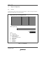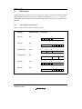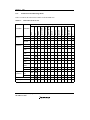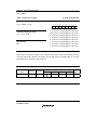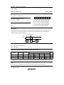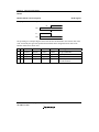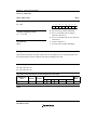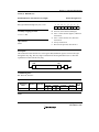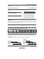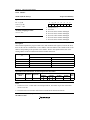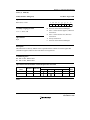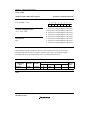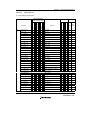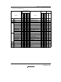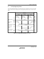
1
To our customers, Old Company Name in Catalogs and Other Documents On April 1st, 2010, NEC Electronics Corporation merged with Renesas Technology Corporation, and Renesas Electronics Corporation took over all the business of both companies. Therefore, although the old company name remains in this document, it is a valid Renesas Electronics document. We appreciate your understanding. Renesas Electronics website: http://www.renesas.com April 1st, 2010 Renesas Electronics Corporation Issued by: Renesas Electronics Corporation (http://www.renesas.com) Send any inquiries to http://www.renesas.com/inquiry. Notice 1. 2. 3. 4. 5. 6. 7. All information included in this document is current as of the date this document is issued. Such information, however, is subject to change without any prior notice. Before purchasing or using any Renesas Electronics products listed herein, please confirm the latest product information with a Renesas Electronics sales office. Also, please pay regular and careful attention to additional and different information to be disclosed by Renesas Electronics such as that disclosed through our website. Renesas Electronics does not assume any liability for infringement of patents, copyrights, or other intellectual property rights of third parties by or arising from the use of Renesas Electronics products or technical information described in this document. No license, express, implied or otherwise, is granted hereby under any patents, copyrights or other intellectual property rights of Renesas Electronics or others. You should not alter, modify, copy, or otherwise misappropriate any Renesas Electronics product, whether in whole or in part. Descriptions of circuits, software and other related information in this document are provided only to illustrate the operation of semiconductor products and application examples. You are fully responsible for the incorporation of these circuits, software, and information in the design of your equipment. Renesas Electronics assumes no responsibility for any losses incurred by you or third parties arising from the use of these circuits, software, or information. When exporting the products or technology described in this document, you should comply with the applicable export control laws and regulations and follow the procedures required by such laws and regulations. You should not use Renesas Electronics products or the technology described in this document for any purpose relating to military applications or use by the military, including but not limited to the development of weapons of mass destruction. Renesas Electronics products and technology may not be used for or incorporated into any products or systems whose manufacture, use, or sale is prohibited under any applicable domestic or foreign laws or regulations. Renesas Electronics has used reasonable care in preparing the information included in this document, but Renesas Electronics does not warrant that such information is error free. Renesas Electronics assumes no liability whatsoever for any damages incurred by you resulting from errors in or omissions from the information included herein. Renesas Electronics products are classified according to the following three quality grades: “Standard”, “High Quality”, and “Specific”. The recommended applications for each Renesas Electronics product depends on the product’s quality grade, as indicated below. You must check the quality grade of each Renesas Electronics product before using it in a particular application. You may not use any Renesas Electronics product for any application categorized as “Specific” without the prior written consent of Renesas Electronics. Further, you may not use any Renesas Electronics product for any application for which it is not intended without the prior written consent of Renesas Electronics. Renesas Electronics shall not be in any way liable for any damages or losses incurred by you or third parties arising from the use of any Renesas Electronics product for an application categorized as “Specific” or for which the product is not intended where you have failed to obtain the prior written consent of Renesas Electronics. The quality grade of each Renesas Electronics product is “Standard” unless otherwise expressly specified in a Renesas Electronics data sheets or data books, etc. “Standard”: 8. 9. 10. 11. 12. Computers; office equipment; communications equipment; test and measurement equipment; audio and visual equipment; home electronic appliances; machine tools; personal electronic equipment; and industrial robots. “High Quality”: Transportation equipment (automobiles, trains, ships, etc.); traffic control systems; anti-disaster systems; anticrime systems; safety equipment; and medical equipment not specifically designed for life support. “Specific”: Aircraft; aerospace equipment; submersible repeaters; nuclear reactor control systems; medical equipment or systems for life support (e.g. artificial life support devices or systems), surgical implantations, or healthcare intervention (e.g. excision, etc.), and any other applications or purposes that pose a direct threat to human life. You should use the Renesas Electronics products described in this document within the range specified by Renesas Electronics, especially with respect to the maximum rating, operating supply voltage range, movement power voltage range, heat radiation characteristics, installation and other product characteristics. Renesas Electronics shall have no liability for malfunctions or damages arising out of the use of Renesas Electronics products beyond such specified ranges. Although Renesas Electronics endeavors to improve the quality and reliability of its products, semiconductor products have specific characteristics such as the occurrence of failure at a certain rate and malfunctions under certain use conditions. Further, Renesas Electronics products are not subject to radiation resistance design. Please be sure to implement safety measures to guard them against the possibility of physical injury, and injury or damage caused by fire in the event of the failure of a Renesas Electronics product, such as safety design for hardware and software including but not limited to redundancy, fire control and malfunction prevention, appropriate treatment for aging degradation or any other appropriate measures. Because the evaluation of microcomputer software alone is very difficult, please evaluate the safety of the final products or system manufactured by you. Please contact a Renesas Electronics sales office for details as to environmental matters such as the environmental compatibility of each Renesas Electronics product. Please use Renesas Electronics products in compliance with all applicable laws and regulations that regulate the inclusion or use of controlled substances, including without limitation, the EU RoHS Directive. Renesas Electronics assumes no liability for damages or losses occurring as a result of your noncompliance with applicable laws and regulations. This document may not be reproduced or duplicated, in any form, in whole or in part, without prior written consent of Renesas Electronics. Please contact a Renesas Electronics sales office if you have any questions regarding the information contained in this document or Renesas Electronics products, or if you have any other inquiries. (Note 1) “Renesas Electronics” as used in this document means Renesas Electronics Corporation and also includes its majorityowned subsidiaries. (Note 2) “Renesas Electronics product(s)” means any product developed or manufactured by or for Renesas Electronics. User’s Manual The revision list can be viewed directly by clicking the title page. The revision list summarizes the locations of revisions and additions. Details should always be checked by referring to the relevant text. H8/300H Series 16 Software Manual Renesas 16-Bit Single-Chip Microcomputer H8 Family/H8/300H Series Rev. 3.00 2004.12 Keep safety first in your circuit designs! 1. Renesas Technology Corp. puts the maximum effort into making semiconductor products better and more reliable, but there is always the possibility that trouble may occur with them. Trouble with semiconductors may lead to personal injury, fire or property damage. Remember to give due consideration to safety when making your circuit designs, with appropriate measures such as (i) placement of substitutive, auxiliary circuits, (ii) use of nonflammable material or (iii) prevention against any malfunction or mishap. Notes regarding these materials 1. These materials are intended as a reference to assist our customers in the selection of the Renesas Technology Corp. product best suited to the customer's application; they do not convey any license under any intellectual property rights, or any other rights, belonging to Renesas Technology Corp. or a third party. 2. Renesas Technology Corp. assumes no responsibility for any damage, or infringement of any thirdparty's rights, originating in the use of any product data, diagrams, charts, programs, algorithms, or circuit application examples contained in these materials. 3. All information contained in these materials, including product data, diagrams, charts, programs and algorithms represents information on products at the time of publication of these materials, and are subject to change by Renesas Technology Corp. without notice due to product improvements or other reasons. It is therefore recommended that customers contact Renesas Technology Corp. or an authorized Renesas Technology Corp. product distributor for the latest product information before purchasing a product listed herein. The information described here may contain technical inaccuracies or typographical errors. Renesas Technology Corp. assumes no responsibility for any damage, liability, or other loss rising from these inaccuracies or errors. Please also pay attention to information published by Renesas Technology Corp. by various means, including the Renesas Technology Corp. Semiconductor home page (http://www.renesas.com). 4. When using any or all of the information contained in these materials, including product data, diagrams, charts, programs, and algorithms, please be sure to evaluate all information as a total system before making a final decision on the applicability of the information and products. Renesas Technology Corp. assumes no responsibility for any damage, liability or other loss resulting from the information contained herein. 5. Renesas Technology Corp. semiconductors are not designed or manufactured for use in a device or system that is used under circumstances in which human life is potentially at stake. Please contact Renesas Technology Corp. or an authorized Renesas Technology Corp. product distributor when considering the use of a product contained herein for any specific purposes, such as apparatus or systems for transportation, vehicular, medical, aerospace, nuclear, or undersea repeater use. 6. The prior written approval of Renesas Technology Corp. is necessary to reprint or reproduce in whole or in part these materials. 7. If these products or technologies are subject to the Japanese export control restrictions, they must be exported under a license from the Japanese government and cannot be imported into a country other than the approved destination. Any diversion or reexport contrary to the export control laws and regulations of Japan and/or the country of destination is prohibited. 8. Please contact Renesas Technology Corp. for further details on these materials or the products contained therein. Rev. 3.00 Dec 13, 2004 page ii of xiv General Precautions on Handling of Product 1. Treatment of NC Pins Note: Do not connect anything to the NC pins. The NC (not connected) pins are either not connected to any of the internal circuitry or are used as test pins or to reduce noise. If something is connected to the NC pins, the operation of the LSI is not guaranteed. 2. Treatment of Unused Input Pins Note: Fix all unused input pins to high or low level. Generally, the input pins of CMOS products are high-impedance input pins. If unused pins are in their open states, intermediate levels are induced by noise in the vicinity, a passthrough current flows internally, and a malfunction may occur. 3. Processing before Initialization Note: When power is first supplied, the product’s state is undefined. The states of internal circuits are undefined until full power is supplied throughout the chip and a low level is input on the reset pin. During the period where the states are undefined, the register settings and the output state of each pin are also undefined. Design your system so that it does not malfunction because of processing while it is in this undefined state. For those products which have a reset function, reset the LSI immediately after the power supply has been turned on. 4. Prohibition of Access to Undefined or Reserved Address Note: Access to undefined or reserved addresses is prohibited. The undefined or reserved addresses may be used to expand functions, or test registers may have been be allocated to these address. Do not access these registers; the system’s operation is not guaranteed if they are accessed. Rev. 3.00 Dec 13, 2004 page iii of xiv Rev. 3.00 Dec 13, 2004 page iv of xiv Preface The H8/300H Series is built around a 32-bit H8/300H CPU core with sixteen 16-bit registers, a concise, optimized instruction set designed for high-speed operation, and a 16-Mbyte linear address space. For easy migration from the H8/300 Series, the instruction set is upwardcompatible with the H8/300 Series at the object-code level. Programs coded in the high-level language C can be compiled to high-speed executable code. This manual gives details of the H8/300H CPU instructions and can be used with all microcontrollers in the H8/300H Series. For hardware details, refer to the relevant microcontroller hardware manual. Rev. 3.00 Dec 13, 2004 page v of xiv Rev. 3.00 Dec 13, 2004 page vi of xiv Main Revisions for this Edition Item Page Revisions (See Manual for Details) All All references to Hitachi, Hitachi, Ltd., Hitachi Semiconductors, and other Hitachi brand names changed to Renesas Technology Corp. Designation for categories changed from “series” to “group” Rev. 3.00 Dec 13, 2004 page vii of xiv Rev. 3.00 Dec 13, 2004 page viii of xiv Contents Section 1 1.1 1.2 1.3 1.4 1.5 1.6 CPU .................................................................................................................... Overview ........................................................................................................................... 1.1.1 Features ................................................................................................................ 1.1.2 Differences from H8/300 CPU............................................................................. CPU Operating Modes ...................................................................................................... Address Space ................................................................................................................... Register Configuration ...................................................................................................... 1.4.1 Overview .............................................................................................................. 1.4.2 General Registers ................................................................................................. 1.4.3 Control Registers.................................................................................................. 1.4.4 Initial Register Values .......................................................................................... Data Formats ..................................................................................................................... 1.5.1 General Register Data Formats ............................................................................ 1.5.2 Memory Data Formats ......................................................................................... Instruction Set ................................................................................................................... 1.6.1 Overview .............................................................................................................. 1.6.2 Instructions and Addressing Modes ..................................................................... 1.6.3 Tables of Instructions Classified by Function ...................................................... 1.6.4 Basic Instruction Formats..................................................................................... 1.6.5 Addressing Modes and Effective Address Calculation ........................................ Section 2 2.1 2.2 Instruction Descriptions ................................................................................ Tables and Symbols........................................................................................................... 2.1.1 Assembler Format ................................................................................................ 2.1.2 Operation.............................................................................................................. 2.1.3 Condition Code .................................................................................................... 2.1.4 Instruction Format ................................................................................................ 2.1.5 Register Specification........................................................................................... 2.1.6 Bit Data Access in Bit Manipulation Instructions ................................................ Instruction Descriptions .................................................................................................... 2.2.1 (1) ADD (B) .......................................................................................................... 2.2.1 (2) ADD (W) ......................................................................................................... 2.2.1 (3) ADD (L) .......................................................................................................... 2.2.2 ADDS .............................................................................................................. 2.2.3 ADDX ............................................................................................................. 2.2.4 (1) AND (B) .......................................................................................................... 2.2.4 (2) AND (W) ......................................................................................................... 1 1 1 2 3 7 8 8 9 10 11 12 12 14 15 15 16 18 26 28 35 35 36 37 38 38 39 40 41 42 43 44 45 46 47 48 Rev. 3.00 Dec 13, 2004 page ix of xiv 2.2.4 (3) 2.2.5 2.2.6 2.2.7 2.2.8 2.2.9 2.2.10 2.2.11 2.2.12 2.2.13 2.2.14 2.2.15 2.2.16 2.2.17 2.2.18 2.2.19 2.2.20 2.2.21 2.2.22 (1) 2.2.22 (2) 2.2.22 (3) 2.2.23 2.2.24 2.2.25 (1) 2.2.25 (2) 2.2.25 (3) 2.2.26 (1) 2.2.26 (2) 2.2.26 (3) 2.2.27 (1) 2.2.27 (2) 2.2.28 (1) 2.2.28 (2) 2.2.29 (1) 2.2.29 (2) 2.2.30 (1) 2.2.30 (2) 2.2.31 (1) 2.2.31 (2) 2.2.31 (3) AND (L) .......................................................................................................... 49 ANDC.............................................................................................................. 50 BAND.............................................................................................................. 51 Bcc................................................................................................................... 52 BCLR............................................................................................................... 54 BIAND ............................................................................................................ 56 BILD................................................................................................................ 57 BIOR ............................................................................................................... 58 BIST ................................................................................................................ 59 BIXOR............................................................................................................. 60 BLD ................................................................................................................. 61 BNOT .............................................................................................................. 62 BOR................................................................................................................. 64 BSET ............................................................................................................... 65 BSR ................................................................................................................. 67 BST.................................................................................................................. 69 BTST ............................................................................................................... 70 BXOR.............................................................................................................. 72 CMP (B) .......................................................................................................... 73 CMP (W) ......................................................................................................... 74 CMP (L) .......................................................................................................... 75 DAA ................................................................................................................ 76 DAS ................................................................................................................. 78 DEC (B)........................................................................................................... 80 DEC (W).......................................................................................................... 81 DEC (L) ........................................................................................................... 82 DIVXS (B)....................................................................................................... 83 DIVXS (W) ..................................................................................................... 85 DIVXS............................................................................................................. 87 DIVXU (B)...................................................................................................... 91 DIVXU (W)..................................................................................................... 92 EEPMOV (B) .................................................................................................. 97 EEPMOV (W) ................................................................................................. 98 EXTS (W)........................................................................................................ 100 EXTS (L) ......................................................................................................... 101 EXTU (W) ....................................................................................................... 102 EXTU (L) ........................................................................................................ 103 INC (B)............................................................................................................ 104 INC (W)........................................................................................................... 105 INC (L) ............................................................................................................ 106 Rev. 3.00 Dec 13, 2004 page x of xiv 2.2.32 2.2.33 2.2.34 (1) 2.2.34 (2) 2.2.35 (1) 2.2.35 (2) 2.2.35 (3) 2.2.35 (4) 2.2.35 (5) 2.2.35 (6) 2.2.35 (7) 2.2.35 (8) 2.2.35 (9) 2.2.36 2.2.37 2.2.38 (1) 2.2.38 (2) 2.2.39 (1) 2.2.39 (2) 2.2.40 (1) 2.2.40 (2) 2.2.40 (3) 2.2.41 2.2.42 (1) 2.2.42 (2) 2.2.42 (3) 2.2.43 (1) 2.2.43 (2) 2.2.43 (3) 2.2.44 2.2.45 (1) 2.2.45 (2) 2.2.46 (1) 2.2.46 (2) 2.2.47 (1) 2.2.47 (2) 2.2.47 (3) 2.2.48 (1) 2.2.48 (2) 2.2.48 (3) JMP.................................................................................................................. 107 JSR................................................................................................................... 108 LDC (B)........................................................................................................... 110 LDC (W).......................................................................................................... 111 MOV (B) ......................................................................................................... 113 MOV (W) ........................................................................................................ 114 MOV (L).......................................................................................................... 115 MOV (B) ......................................................................................................... 116 MOV (W) ........................................................................................................ 118 MOV (L).......................................................................................................... 120 MOV (B) ......................................................................................................... 122 MOV (W) ........................................................................................................ 124 MOV (L).......................................................................................................... 126 MOVFPE......................................................................................................... 128 MOVTPE......................................................................................................... 129 MULXS (B)..................................................................................................... 130 MULXS (W).................................................................................................... 131 MULXU (B) .................................................................................................... 132 MULXU (W) ................................................................................................... 133 NEG (B) .......................................................................................................... 134 NEG (W) ......................................................................................................... 135 NEG (L)........................................................................................................... 136 NOP ................................................................................................................. 137 NOT (B) .......................................................................................................... 138 NOT (W) ......................................................................................................... 139 NOT (L)........................................................................................................... 140 OR (B) ............................................................................................................. 141 OR (W) ............................................................................................................ 142 OR (L) ............................................................................................................. 143 ORC................................................................................................................. 144 POP (W) .......................................................................................................... 145 POP (L)............................................................................................................ 146 PUSH (W) ....................................................................................................... 147 PUSH (L)......................................................................................................... 148 ROTL (B) ........................................................................................................ 149 ROTL (W) ....................................................................................................... 150 ROTL (L) ........................................................................................................ 151 ROTR (B) ........................................................................................................ 152 ROTR (W) ....................................................................................................... 153 ROTR (L) ........................................................................................................ 154 Rev. 3.00 Dec 13, 2004 page xi of xiv 2.3 2.4 2.5 2.6 2.7 2.8 2.2.49 (1) ROTXL (B) ..................................................................................................... 155 2.2.49 (2) ROTXL (W) .................................................................................................... 156 2.2.49 (3) ROTXL (L)...................................................................................................... 157 2.2.50 (1) ROTXR (B) ..................................................................................................... 158 2.2.50 (2) ROTXR (W) .................................................................................................... 159 2.2.50 (3) ROTXR (L) ..................................................................................................... 160 2.2.51 RTE ................................................................................................................. 161 2.2.52 RTS.................................................................................................................. 163 2.2.53 (1) SHAL (B) ........................................................................................................ 164 2.2.53 (2) SHAL (W) ....................................................................................................... 165 2.2.53 (3) SHAL (L) ........................................................................................................ 166 2.2.54 (1) SHAR (B) ........................................................................................................ 167 2.2.54 (2) SHAR (W) ....................................................................................................... 168 2.2.54 (3) SHAR (L) ........................................................................................................ 169 2.2.55 (1) SHLL (B)......................................................................................................... 170 2.2.55 (2) SHLL (W)........................................................................................................ 171 2.2.55 (3) SHLL (L) ......................................................................................................... 172 2.2.56 (1) SHLR (B)......................................................................................................... 173 2.2.56 (2) SHLR (W) ....................................................................................................... 174 2.2.56 (3) SHLR (L)......................................................................................................... 175 2.2.57 SLEEP ............................................................................................................. 176 2.2.58 (1) STC (B) ........................................................................................................... 177 2.2.58 (2) STC (W) .......................................................................................................... 178 2.2.59 (1) SUB (B) ........................................................................................................... 180 2.2.59 (2) SUB (W).......................................................................................................... 182 2.2.59 (3) SUB (L) ........................................................................................................... 183 2.2.60 SUBS ............................................................................................................... 184 2.2.61 SUBX .............................................................................................................. 185 2.2.62 TRAPA ............................................................................................................ 186 2.2.63 (1) XOR (B) .......................................................................................................... 187 2.2.63 (2) XOR (W) ......................................................................................................... 188 2.2.63 (3) XOR (L) .......................................................................................................... 189 2.2.64 XORC.............................................................................................................. 190 Instruction Set Summary ................................................................................................... 191 Instruction Codes............................................................................................................... 205 Operation Code Map ......................................................................................................... 213 Number of States Required for Instruction Execution....................................................... 217 Condition Code Modification............................................................................................ 228 Bus Cycles During Instruction Execution ......................................................................... 233 Rev. 3.00 Dec 13, 2004 page xii of xiv Section 3 3.1 3.2 3.3 3.4 3.5 3.6 Processing States ............................................................................................ 245 Overview ........................................................................................................................... 245 Program Execution State ................................................................................................... 246 Exception-Handling State.................................................................................................. 246 3.3.1 Types of Exception Handling and Their Priority ................................................. 247 3.3.2 Exception-Handling Sequences............................................................................ 248 Bus-Released State ............................................................................................................ 250 Reset State ......................................................................................................................... 250 Power-Down State............................................................................................................. 250 3.6.1 Sleep Mode........................................................................................................... 250 3.6.2 Software Standby Mode ....................................................................................... 250 3.6.3 Hardware Standby Mode...................................................................................... 251 Section 4 4.1 4.2 4.3 4.4 Basic Timing .................................................................................................... 253 Overview ........................................................................................................................... 253 On-Chip Memory (RAM, ROM)....................................................................................... 253 On-Chip Supporting Modules ........................................................................................... 255 External Data Bus.............................................................................................................. 256 Rev. 3.00 Dec 13, 2004 page xiii of xiv Rev. 3.00 Dec 13, 2004 page xiv of xiv Section 1 CPU Section 1 CPU 1.1 Overview The H8/300H CPU is a high-speed central processing unit with an internal 32-bit architecture that is upward-compatible with the H8/300 CPU. The H8/300H CPU has sixteen 16-bit general registers, can address a 16-Mbyte linear address space, and is ideal for realtime control. 1.1.1 Features The H8/300H CPU has the following features. • Upward-compatible with H8/300 CPU Can execute H8/300 object programs • General-register architecture Sixteen 16-bit general registers (also usable as sixteen 8-bit registers or eight 32-bit registers) • Sixty-two basic instructions 8/16/32-bit arithmetic and logic instructions Multiply and divide instructions Powerful bit-manipulation instructions • Eight addressing modes Register direct [Rn] Register indirect [@ERn] Register indirect with displacement [@(d:16,ERn) or @(d:24,ERn)] Register indirect with post-increment or pre-decrement [@ERn+ or @–ERn] Absolute address [@aa:8, @aa:16, or @aa:24] Immediate [#xx:8, #xx:16, or #xx:32] Program-counter relative [@(d:8,PC) or @(d:16,PC)] Memory indirect [@@aa:8] • 16-Mbyte address space • High-speed operation All frequently-used instructions execute in two to four states Maximum clock frequency: 16 MHz 8/16/32-bit register-register add/subtract: 125 ns 8 × 8-bit register-register multiply: 875 ns Rev. 3.00 Dec 13, 2004 page 1 of 258 REJ09B0213-0300 Section 1 CPU 16 ÷ 8-bit register-register divide: 875 ns 16 × 16-bit register-register multiply: 1375 ns 32 ÷ 16-bit register-register divide: 1375 ns • Two CPU operating modes Normal mode Advanced mode • Low-power mode Transition to power-down state by SLEEP instruction 1.1.2 Differences from H8/300 CPU In comparison to the H8/300 CPU, the H8/300H CPU has the following enhancements. • More general registers Eight 16-bit registers have been added. • Expanded address space Normal mode supports the same 64-kbyte address space as the H8/300 CPU. Advanced mode supports a maximum 16-Mbyte address space. • Enhanced addressing The addressing modes have been enhanced to make effective use of the 16-Mbyte address space. • Enhanced instructions Signed multiply/divide instructions and other instructions have been added. Rev. 3.00 Dec 13, 2004 page 2 of 258 REJ09B0213-0300 Section 1 CPU 1.2 CPU Operating Modes The H8/300H CPU has two operating modes: normal and advanced. Normal mode supports a maximum 64-kbyte address space. Advanced mode supports up to 16 Mbytes. The mode is selected at the mode pins of the microcontroller. For further information, refer to the relevant hardware manual. Normal mode Maximum 64 kbytes, program and data areas combined Advanced mode Maximum 16 Mbytes, program and data areas combined CPU operating modes Figure 1.1 CPU Operating Modes (1) Normal Mode The exception vector table and stack have the same structure as in the H8/300 CPU. Address Space: A maximum address space of 64 kbytes can be accessed, as in the H8/300 CPU. Extended Registers (En): The extended registers (E0 to E7) can be used as 16-bit data registers, or they can be combined with the general registers (R0 to R7) for use as 32-bit data registers. When En is used as a 16-bit register it can contain any value, even when the corresponding general register (R0 to R7) is used as an address register. If the general register is referenced in the register indirect addressing mode with pre-decrement (@–Rn) or post-increment (@Rn+) and a carry or borrow occurs, however, the value in the corresponding extended register will be affected. Instruction Set: All additional instructions and addressing modes of the H8/300 CPU can be used. If a 24-bit effective address (EA) is specified, only the lower 16 bits are used. Exception Vector Table and Memory Indirect Branch Addresses: In normal mode the top area starting at H'0000 is allocated to the exception vector table. One branch address is stored per 16 bits (figure 1.2). The exception vector table differs depending on the microcontroller, so see the microcontroller hardware manual for further information. Rev. 3.00 Dec 13, 2004 page 3 of 258 REJ09B0213-0300 Section 1 CPU H'0000 H'0001 H'0002 H'0003 H'0004 H'0005 H'0006 H'0007 H'0008 H'0009 Reset exception vector Reserved for system use Exception vector table Exception vector 1 Exception vector 2 Figure 1.2 Exception Vector Table (normal mode) The memory indirect addressing mode (@@aa:8) employed in the JMP and JSR instructions uses an 8-bit absolute address to specify a memory operand that contains a branch address. In normal mode the operand is a 16-bit word operand, providing a 16-bit branch address. Branch addresses can be stored in the top area from H'0000 to H'00FF. Note that this area is also used for the exception vector table. Stack Structure: When the program counter (PC) is pushed on the stack in a subroutine call, and the PC and condition-code register (CCR) are pushed on the stack in exception handling, they are stored in the same way as in the H8/300 CPU. See figure 1.3. (a) Subroutine branch SP PC (16 bits) (b) Exception handling SP CCR CCR* PC (16 bits) Note: * Ignored at return. Figure 1.3 Stack Structure (normal mode) Rev. 3.00 Dec 13, 2004 page 4 of 258 REJ09B0213-0300 Section 1 CPU (2) Advanced Mode In advanced mode the exception vector table and stack structure differ from the H8/300 CPU. Address Space: Up to 16 Mbytes can be accessed linearly. Extended Registers (En): The extended registers (E0 to E7) can be used as 16-bit data registers, or they can be combined with the general registers (R0 to R7) for use as 32-bit data registers. When a 32-bit register is used as an address register, the upper 8 bits are ignored. Instruction Set: All additional instructions and addressing modes of the H8/300H can be used. Exception Vector Table and Memory Indirect Branch Addresses: In advanced mode the top area starting at H'000000 is allocated to the exception vector table in units of 32 bits. In each 32 bits, the upper 8 bits are ignored and a branch address is stored in the lower 24 bits (figure 1.4). The exception vector table differs depending on the microcontroller, so see the relevant hardware manual for further information. H'000000 Don’t care Reset exception vector H'000003 H'000004 Exception vector table Reserved for system use H'00000B H'00000C Don’t care Exception vector Figure 1.4 Exception Vector Table (advanced mode) Rev. 3.00 Dec 13, 2004 page 5 of 258 REJ09B0213-0300 Section 1 CPU The memory indirect addressing mode (@@aa:8) employed in the JMP and JSR instructions uses an 8-bit absolute address to specify a memory operand that contains a branch address. In advanced mode the operand is a 32-bit longword operand, of which the lower 24 bits are the branch address. Branch addresses can be stored in the top area from H'000000 to H'0000FF. Note that this area is also used for the exception vector table. Stack Structure:When the program counter (PC) is pushed on the stack in a subroutine call, and the PC and condition-code register (CCR) are pushed on the stack in exception handling, they are stored as shown in figure 1.5. (a) Subroutine branch SP Reserved PC (24 bits) (b) Exception handling SP CCR PC (24 bits) Figure 1.5 Stack Structure (advanced mode) Rev. 3.00 Dec 13, 2004 page 6 of 258 REJ09B0213-0300 Section 1 CPU 1.3 Address Space Figure 1.6 shows a memory map of the H8/300H CPU. (a) Normal mode H'0000 (b) Advanced mode H'000000 H'FFFF H'FFFFFF Figure 1.6 Memory Map Rev. 3.00 Dec 13, 2004 page 7 of 258 REJ09B0213-0300 Section 1 CPU 1.4 Register Configuration 1.4.1 Overview The H8/300H CPU has the internal registers shown in figure 1.7. There are two types of registers: general and extended registers, and control registers. General registers (Rn) and extended registers (En) 15 SP 07 07 0 E0 R0H R0L E1 R1H R1L E2 R2H R2L E3 R3H R3L E4 R4H R4L E5 R5H R5L E6 R6H R6L E7 R7H R7L Control registers (CR) 23 0 PC 7 6 5 4 3 2 1 0 CCR I U H U N Z V C Legend: SP: Stack pointer PC: Program counter CCR: Condition code register Interrupt mask bit I: User bit or interrupt mask bit U: Half-carry flag H: Negative flag N: Zero flag Z: Overflow flag V: Carry flag C: Figure 1.7 CPU Registers Rev. 3.00 Dec 13, 2004 page 8 of 258 REJ09B0213-0300 Section 1 CPU 1.4.2 General Registers The H8/300H CPU has eight 32-bit general registers. These general registers are all functionally alike and can be used without distinction between data registers and address registers. When a general register is used as a data register, it can be accessed as a 32-bit, 16-bit, or 8-bit register. When the general registers are used as 32-bit registers or as address registers, they are designated by the letters ER (ER0 to ER7). The ER registers divide into 16-bit general registers designated by the letters E (E0 to E7) and R (R0 to R7). These registers are functionally equivalent, providing a maximum sixteen 16-bit registers. The E registers (E0 to E7) are also referred to as extended registers. The R registers divide into 8-bit general registers designated by the letters RH (R0H to R7H) and RL (R0L to R7L). These registers are functionally equivalent, providing a maximum sixteen 8-bit registers. Figure 1.8 illustrates the usage of the general registers. The usage of each register can be selected independently. Address registers • 32-bit registers • 16-bit registers • 8-bit registers E registers (extended registers) (E0 to E7) RH registers (R0H to R7H) ER registers (ER0 to ER7) R registers (R0 to R7) RL registers (R0L to R7L) Figure 1.8 Usage of General Registers General register ER7 has the function of stack pointer (SP) in addition to its general-register function, and is used implicitly in exception handling and subroutine calls. Figure 1.9 shows the stack. Rev. 3.00 Dec 13, 2004 page 9 of 258 REJ09B0213-0300 Section 1 CPU Free area SP (ER7) Stack area Figure 1.9 Stack 1.4.3 Control Registers The control registers are the 24-bit program counter (PC) and the 8-bit condition-code register (CCR). (1) Program Counter (PC) This 24-bit counter indicates the address of the next instruction the CPU will execute. The length of all CPU instructions is 16 bits (one word) or a multiple of 16 bits, so the least significant PC bit is ignored. When an instruction is fetched, the least significant PC bit is regarded as 0. (2) Condition Code Register (CCR) This 8-bit register contains internal CPU status information, including the interrupt mask bit (I) and half-carry (H), negative (N), zero (Z), overflow (V), and carry (C) flags. Bit 7—Interrupt Mask Bit (I): Masks interrupts other than NMI when set to 1. (NMI is accepted regardless of the I bit setting.) The I bit is set to 1 by hardware at the start of an exceptionhandling sequence. Bit 6—User Bit (U): Can be written and read by software using the LDC, STC, ANDC, ORC, and XORC instructions. This bit can also be used as an interrupt mask bit. For details see the relevant microcontroller hardware manual. Rev. 3.00 Dec 13, 2004 page 10 of 258 REJ09B0213-0300 Section 1 CPU Bit 5—Half-Carry Flag (H): When the ADD.B, ADDX.B, SUB.B, SUBX.B, CMP.B, or NEG.B instruction is executed, this flag is set to 1 if there is a carry or borrow at bit 3, and cleared to 0 otherwise. When the ADD.W, SUB.W, CMP.W, or NEG.W instruction is executed, the H flag is set to 1 if there is a carry or borrow at bit 11, and cleared to 0 otherwise. When the ADD.L, SUB.L, CMP.L, or NEG.L instruction is executed, the H flag is set to 1 if there is a carry or borrow at bit 27, and cleared to 0 otherwise. Bit 4—User Bit (U): Can be written and read by software using the LDC, STC, ANDC, ORC, and XORC instructions. Bit 3—Negative Flag (N): Indicates the most significant bit (sign bit) of the result of an instruction. Bit 2—Zero Flag (Z): Set to 1 to indicate a zero result, and cleared to 0 to indicate a non-zero result. Bit 1—Overflow Flag (V): Set to 1 when an arithmetic overflow occurs, and cleared to 0 at other times. Bit 0—Carry Flag (C): Set to 1 when a carry occurs, and cleared to 0 otherwise. Used by: • Add instructions, to indicate a carry • Subtract instructions, to indicate a borrow • Shift and rotate instructions, to store the value shifted out of the end bit The carry flag is also used as a bit accumulator by bit manipulation instructions. Some instructions leave some or all of the flag bits unchanged. For the action of each instruction on the flag bits, refer to the detailed descriptions of the instructions starting in section 2.2.1. Operations can be performed on the CCR bits by the LDC, STC, ANDC, ORC, and XORC instructions. The N, Z, V, and C flags are used as branching conditions for conditional branch (Bcc) instructions. 1.4.4 Initial Register Values When the CPU is reset, the program counter (PC) is loaded from the vector table and the I bit in the condition-code register (CCR) is set to 1. The other CCR bits and the general registers and extended registers are not initialized. In particular, the stack pointer (extended register E7 and general register R7) is not initialized. The stack pointer must therefore be initialized by an MOV.L instruction executed immediately after a reset. Rev. 3.00 Dec 13, 2004 page 11 of 258 REJ09B0213-0300 Section 1 CPU 1.5 Data Formats The H8/300H CPU can process 1-bit, 4-bit, 8-bit (byte), 16-bit (word), and 32-bit (longword) data. Bit-manipulation instructions operate on 1-bit data by accessing bit n (n = 0, 1, 2, …, 7) of byte operand data. The DAA and DAS decimal-adjust instructions treat byte data as two digits of 4-bit BCD data. 1.5.1 General Register Data Formats Figure 1.10 shows the data formats in general registers. Data type Register number Data format 1-bit data RnH 7 0 7 6 5 4 3 2 1 0 Don’t care Don’t care 7 0 7 6 5 4 3 2 1 0 1-bit data 4-bit BCD data RnL RnH 4 3 7 Upper 4-bit BCD data 0 Lower Don’t care RnL Byte data RnH 4 3 7 Upper Don’t care 7 0 Lower 0 Don’t care MSB Byte data LSB RnL 7 0 Don’t care MSB Figure 1.10 General Register Data Formats Rev. 3.00 Dec 13, 2004 page 12 of 258 REJ09B0213-0300 LSB Section 1 CPU Word data Rn Word data En 15 0 MSB 15 0 MSB Longword data LSB ERn 31 MSB LSB 16 15 En 0 Rn LSB Legend: ERn: General register ER En: General register E Rn: General register R RnH: General register RH RnL: General register RL MSB: Most significant bit LSB: Least significant bit Figure 1.10 General Register Data Formats (cont) Rev. 3.00 Dec 13, 2004 page 13 of 258 REJ09B0213-0300 Section 1 CPU 1.5.2 Memory Data Formats Figure 1.11 shows the data formats on memory. The H8/300H CPU can access word data and longword data on memory, but word or longword data must begin at an even address. If an attempt is made to access word or longword data at an odd address, no address error occurs but the least significant bit of the address is regarded as 0, so the access starts at the preceding address. This also applies to instruction fetches. Data type Data format Address 7 1-bit data Address L Byte data Address L MSB Word data 7 0 6 5 4 2 1 0 LSB Address 2M MSB Address 2M + 1 Longword data 3 LSB Address 2N MSB Address 2N + 1 Address 2N + 2 Address 2N + 3 LSB Figure 1.11 Memory Data Formats When ER7 is used as an address register to access the stack, the operand size should be word size or longword size. Rev. 3.00 Dec 13, 2004 page 14 of 258 REJ09B0213-0300 Section 1 CPU 1.6 Instruction Set 1.6.1 Overview The H8/300H CPU has 62 types of instructions, which are classified by function in table 1.1. For a detailed description of each instruction see section 2.2, Instruction Descriptions. Table 1.1 Instruction Classification Function Instructions Number Data transfer 1 2 MOV, PUSH* , POP* , MOVTPE, MOVFPE 3 Arithmetic operations ADD, SUB, ADDX, SUBX, INC, DEC, ADDS, SUBS, DAA, DAS, MULXU, MULXS, DIVXU, DIVXS, CMP, NEG, EXTS, EXTU 18 Logic operations AND, OR, XOR, NOT 4 Shift SHAL, SHAR, SHLL, SHLR, ROTL, ROTR, ROTXL, ROTXR 8 Bit manipulation 14 Branch BSET, BCLR, BNOT, BTST, BAND, BIAND, BOR, BIOR, BXOR, BIXOR, BLD, BILD, BST, BIST 2 Bcc* , JMP, BSR, JSR, RTS System control TRAPA, RTE, SLEEP, LDC, STC, ANDC, ORC, XORC, NOP 9 Block data transfer EEPMOV 5 1 Total 62 types Notes: The shaded instructions are not present in the H8/300 instruction set. 1. POP.W Rn and PUSH.W Rn are identical to MOV.W @SP+, Rn and MOV.W Rn, @–SP. POP.L ERn and PUSH.L ERn are identical to MOV.L @SP+, ERn and MOV.L ERn, @–SP. 2. Bcc is the generic designation of a conditional branch instruction. Rev. 3.00 Dec 13, 2004 page 15 of 258 REJ09B0213-0300 Section 1 CPU 1.6.2 Instructions and Addressing Modes Table 1.2 indicates the instructions available in the H8/300H CPU. Table 1.2 Instruction Set Overview — — — — — — — — — WL MOVFPE, MOVTPE — — — — — — — B — — — — — — — — — — — — — — — Logic operations ADD, CMP SUB @ERn Rn BWL BWL B BWL BWL — @@aa:8 — — @aa:24 — — BWL BWL BWL BWL BWL BWL @aa:16 — — MOV @aa:8 @(d:16,PC) Arithmetic operations @ERn+/@–ERn @(d:8,PC) Data transfer @(d:24,ERn) — POP, PUSH Instruction #xx Function @(d:16,ERn) Addressing Modes WL BWL — — — — — — — — — — — ADDX, SUBX B B — — — — — — — — — — — ADDS, SUBS — L*1 — — — — — — — — — — — INC, DEC — BWL — — — — — — — — — — — DAA, DAS — B — — — — — — — — — — — MULXU, DIVXU — BW — — — — — — — — — — — MULXS, DIVXS — BW — — — — — — — — — — — NEG — BWL — — — — — — — — — — — EXTU, EXTS — WL — — — — — — — — — — — — — — — — — — — — — — AND, OR, XOR NOT BWL BWL — BWL — — — — — — — — — — — Shift — BWL — — — — — — — — — — — Bit manipulation — B B — — — B — — — — — — Rev. 3.00 Dec 13, 2004 page 16 of 258 REJ09B0213-0300 Section 1 CPU System control Block data transfer @aa:8 @aa:16 @aa:24 — — — — — — — JMP, JSR — — RTS — — — — — — — — — — — — — *2 — — — — — — @ERn+/@–ERn — @@aa:8 @(d:24,ERn) Bcc, BSR @(d:16,PC) @(d:16,ERn) — Instruction @(d:8,PC) @ERn Branch Rn Function #xx Addressing Modes — — — — TRAPA — — — — — — — — — — — — RTE — — — — — — — — — — — — SLEEP — — — — — — — — — — — — LDC B B W W W W — W W — — — — STC — B W W W W — W W — — — — ANDC, ORC, XORC B — — — — — — — — — — — — NOP — — — — — — — — — — — — EEPMOV.B — — — — — — — — — — — — EEPMOV.W — — — — — — — — — — — — Legend: B: Byte W: Word L: Longword : Newly added instruction in H8/300H CPU Notes: 1. The operand size of the ADDS and SUBS instructions of the H8/300H CPU has been changed to longword size. (In the H8/300 CPU it was word size.) 2. Because of its larger address space, the H8/300H CPU uses a 24-bit absolute address for the JMP and JSR instructions. (The H8/300 CPU used 16 bits.) Rev. 3.00 Dec 13, 2004 page 17 of 258 REJ09B0213-0300 Section 1 CPU 1.6.3 Tables of Instructions Classified by Function Table 1.3 summarizes the instructions in each functional category. The notation used in table 1.3 is defined next. Operation Notation Rd General register (destination)* Rs General register (source)* Rn General register* ERn General register (32-bit register) (EAd) Destination operand (EAs) Source operand CCR Condition code register N N (negative) bit of CCR Z Z (zero) bit of CCR V V (overflow) bit of CCR C C (carry) bit of CCR PC Program counter SP Stack pointer #IMM Immediate data disp Displacement + Addition – Subtraction × Multiplication ÷ Division ∧ AND logical ∨ OR logical ⊕ Exclusive OR logical → Move ¬ Not :3/:8/:16/:24 3-, 8-, 16-, or 24-bit length Note: * General registers include 8-bit registers (R0H/R0L to R7H/R7L), 16-bit registers (R0 to R7, E0 to E7), and 32-bit registers (ER0 to ER7). Rev. 3.00 Dec 13, 2004 page 18 of 258 REJ09B0213-0300 Section 1 CPU Table 1.3 Instructions Classified by Function Type Instruction Size* Function Data transfer MOV B/W/L (EAs) → Rd, Rs → (EAd) Moves data between two general registers or between a general register and memory, or moves immediate data to a general register. MOVFPE B (EAs) → Rd Moves external memory contents (addressed by @aa:16) to a general register in synchronization with an E clock. MOVTPE B Rs → (EAd) Moves general register contents to an external memory location (addressed by @aa:16) in synchronization with an E clock. POP W/L @SP+ → Rn Pops a register from the stack. POP.W Rn is identical to MOV.W @SP+, Rn. POP.L ERn is identical to MOV.L @SP+, ERn. PUSH W/L Rn → @–SP Pushes a register onto the stack. PUSH.W Rn is identical to MOV.W Rn, @–SP. PUSH.L ERn is identical to MOV.L ERn, @–SP. Arithmetic operations ADD B/W/L SUB ADDX B SUBX INC DEC Rd ± Rs → Rd, Rd ± #IMM → Rd Performs addition or subtraction on data in two general registers, or on immediate data and data in a general register. (Immediate byte data cannot be subtracted from data in a general register. Use the SUBX or ADD instruction.) Rd ± Rs ± C → Rd, Rd ± #IMM ± C → Rd Performs addition or subtraction with carry or borrow on byte data in two general registers, or on immediate data and data in a general register. B/W/L Rd ± 1 → Rd, Rd ± 2 → Rd Increments or decrements a general register by 1 or 2. (Byte operands can be incremented or decremented by 1 only.) Rev. 3.00 Dec 13, 2004 page 19 of 258 REJ09B0213-0300 Section 1 CPU Type Instruction Size* Function Arithmetic operations ADDS L Rd ± 1 → Rd, Rd ± 2 → Rd, Rd ± 4 → Rd SUBS DAA Adds or subtracts the value 1, 2, or 4 to or from data in a 32-bit register. B DAS MULXS Rd decimal adjust → Rd Decimal-adjusts an addition or subtraction result in a general register by referring to the CCR to produce 4bit BCD data. B/W Rd × Rs → Rd Performs signed multiplication on data in two general registers: either 8 bits × 8 bits → 16 bits or 16 bits × 16 bits → 32 bits. MULXU B/W Rd × Rs → Rd Performs unsigned multiplication on data in two general registers: either 8 bits × 8 bits → 16 bits or 16 bits × 16 bits → 32 bits. DIVXS B/W Rd ÷ Rs → Rd Performs signed division on data in two general registers: either 16 bits ÷ 8 bits → 8-bit quotient and 8bit remainder or 32 bits ÷ 16 bits → 16-bit quotient and 16-bit remainder. DIVXU B/W Rd ÷ Rs → Rd Performs unsigned division on data in two general registers: either 16 bits ÷ 8 bits → 8-bit quotient and 8bit remainder or 32 bits ÷ 16 bits → 16-bit quotient and 16-bit remainder. CMP B/W/L Rd – Rs, Rd – #IMM Compares data in a general register with data in another general register or with immediate data, and sets the CCR according to the result. NEG B/W/L 0 – Rd → Rd Takes the two’s complement (arithmetic complement) of data in a general register. Rev. 3.00 Dec 13, 2004 page 20 of 258 REJ09B0213-0300 Section 1 CPU Type Instruction Size* Function Arithmetic operations EXTS W/L Rd (sign extension) → Rd Extends byte data in the lower 8 bits of a 16-bit register to word data, or extends word data in the lower 16 bits of a 32-bit register to longword data, by extending the sign bit. EXTU W/L Rd (zero extension) → Rd Extends byte data in the lower 8 bits of a 16-bit register to word data, or extends word data in the lower 16 bits of a 32-bit register to longword data, by padding with zeros. Logic operations AND B/W/L Rd ∧ Rs → Rd, Rd ∧ #IMM → Rd Performs a logical AND operation on a general register and another general register or immediate data. OR B/W/L Rd ∨ Rs → Rd, Rd ∨ #IMM → Rd Performs a logical OR operation on a general register and another general register or immediate data. XOR B/W/L Rd ⊕ Rs → Rd, Rd ⊕ #IMM → Rd Performs a logical exclusive OR operation on a general register and another general register or immediate data. NOT B/W/L ¬ (Rd) → (Rd) Takes the one’s complement of general register contents. Shift operations SHAL B/W/L SHAR SHLL B/W/L SHLR ROTL ROTXR Rd (shift) → Rd Performs a logical shift on general register contents. B/W/L ROTR ROTXL Rd (shift) → Rd Performs an arithmetic shift on general register contents. Rd (rotate) → Rd Rotates general register contents. B/W/L Rd (rotate) → Rd Rotates general register contents through the carry bit. Rev. 3.00 Dec 13, 2004 page 21 of 258 REJ09B0213-0300 Section 1 CPU Type Instruction Size* Function Bit-manipulation instructions BSET B 1 → (<bit-No.> of <EAd>) Sets a specified bit in a general register or memory operand to 1. The bit number is specified by 3-bit immediate data or the lower three bits of a general register. BCLR B 0 → (<bit-No.> of <EAd>) Clears a specified bit in a general register or memory operand to 0. The bit number is specified by 3-bit immediate data or the lower three bits of a general register. BNOT B ¬ (<bit-No.> of <EAd>) → (<bit-No.> of <EAd>) Inverts a specified bit in a general register or memory operand. The bit number is specified by 3-bit immediate data or the lower three bits of a general register. BTST B ¬ (<bit-No.> of <EAd>) → Z Tests a specified bit in a general register or memory operand and sets or clears the Z flag accordingly. The bit number is specified by 3-bit immediate data or the lower three bits of a general register. BAND B C ∧ (<bit-No.> of <EAd>) → C ANDs the carry flag with a specified bit in a general register or memory operand and stores the result in the carry flag. BIAND B C ∧ ¬ (<bit-No.> of <EAd>) → C ANDs the carry flag with the inverse of a specified bit in a general register or memory operand and stores the result in the carry flag. The bit number is specified by 3-bit immediate data. Rev. 3.00 Dec 13, 2004 page 22 of 258 REJ09B0213-0300 Section 1 CPU Type Instruction Size* Function Bit-manipulation instructions BOR B C ∨ (<bit-No.> of <EAd>) → C ORs the carry flag with a specified bit in a general register or memory operand and stores the result in the carry flag. BIOR B C ∨ [¬ (<bit-No.> of <EAd>)] → C ORs the carry flag with the inverse of a specified bit in a general register or memory operand and stores the result in the carry flag. The bit number is specified by 3-bit immediate data. BXOR B C ⊕ (<bit-No.> of <EAd>) → C Exclusive-ORs the carry flag with a specified bit in a general register or memory operand and stores the result in the carry flag. BIXOR B C ⊕ [¬ (<bit-No.> of <EAd>)] → C Exclusive-ORs the carry flag with the inverse of a specified bit in a general register or memory operand and stores the result in the carry flag. The bit number is specified by 3-bit immediate data. BLD B (<bit-No.> of <EAd>) → C Transfers a specified bit in a general register or memory operand to the carry flag. BILD B ¬ (<bit-No.> of <EAd>) → C Transfers the inverse of a specified bit in a general register or memory operand to the carry flag. The bit number is specified by 3-bit immediate data. BST B C → (<bit-No.> of <EAd>) Transfers the carry flag value to a specified bit in a general register or memory operand. BIST B ¬ C → (<bit-No.> of <EAd>) Transfers the inverse of the carry flag value to a specified bit in a general register or memory operand. The bit number is specified by 3-bit immediate data. Rev. 3.00 Dec 13, 2004 page 23 of 258 REJ09B0213-0300 Section 1 CPU Type Instruction Size* Function Branching instructions Bcc — Branches to a specified address if a specified condition is true. The branching conditions are listed below. Mnemonic Description Condition BRA(BT) Always (true) Always BRN(BF) Never (false) Never BHI High C∨Z=0 BLS Low or same C∨Z=1 Bcc(BHS) Carry clear (high or same) C=0 BCS(BLO) Carry set (low) C=1 BNE Not equal Z=0 BEQ Equal Z=1 BVC Overflow clear V=0 BVS Overflow set V=1 BPL Plus N=0 BMI Minus N=1 BGE Greater or equal N⊕V=0 BLT Less than N⊕V=1 BGT Greater than Z ∨ (N ⊕ V) = 0 BLE Less or equal Z ∨ (N ⊕ V) = 1 JMP — Branches unconditionally to a specified address. BSR — Branches to a subroutine at a specified address. JSR — Branches to a subroutine at a specified address. RTS — Returns from a subroutine. Rev. 3.00 Dec 13, 2004 page 24 of 258 REJ09B0213-0300 Section 1 CPU Type Instruction Size* Function System control instructions TRAPA — Starts trap-instruction exception handling. RTE — Returns from an exception-handling routine. SLEEP — Causes a transition to the power-down state. LDC B/W (EAs) → CCR Moves the source operand contents to the condition code register. Byte transfer is performed in the #xx:8, Rs addressing mode and word transfer in other addressing modes. STC B/W CCR → (EAd) Transfers the CCR contents to a destination location. Byte transfer is performed in the Rd addressing mode and word transfer in other addressing modes. ANDC B CCR ∧ #IMM → CCR Logically ANDs the condition code register with immediate data. ORC B CCR ∨ #IMM → CCR Logically ORs the condition code register with immediate data. XORC B CCR ⊕ #IMM → CCR Logically exclusive-ORs the condition code register with immediate data. NOP — PC + 2 → PC Only increments the program counter. Rev. 3.00 Dec 13, 2004 page 25 of 258 REJ09B0213-0300 Section 1 CPU Type Instruction Size* Function Block data transfer instruction EEPMOV.B — if R4L ≠ 0 then Repeat @ER5 +→ @ER6 + R4L – 1→R4L Until R4L = 0 else next; EEPMOV.W — if R4 ≠ 0 then Repeat @ER5 +→ @ER6 + R4 – 1→R4L Until R4 = 0 else next; Transfers a data block according to parameters set in general registers R4L or R4, ER5, and R6. R4L or R4: size of block (bytes) ER5: starting source address R6: starting destination address Execution of the next instruction begins as soon as the transfer is completed. Note: 1.6.4 * Size refers to the operand size. B: Byte W: Word L: Longword Basic Instruction Formats The H8/300H instructions consist of 2-byte (1-word) units. An instruction consists of an operation field (OP field), a register field (r field), an effective address extension (EA field), and a condition field (cc). Operation Field: Indicates the function of the instruction, the effective address, and the operation to be carried out on the operand. The operation field always includes the first four bits of the instruction. Some instructions have two operation fields. Register Field: Specifies a general register. Address registers are specified by 3 bits, data registers by 3 bits or 4 bits. Some instructions have two register fields. Some have no register field. Effective Address Extension: Eight, 16, or 32 bits specifying immediate data, an absolute address, or a displacement. A 24-bit address or a displacement is treated as 32-bit data in which the first 8 bits are 0. Rev. 3.00 Dec 13, 2004 page 26 of 258 REJ09B0213-0300 Section 1 CPU Condition Field: Specifies the branching condition of Bcc instructions. Figure 1.12 shows examples of instruction formats. (1) Operation field only op NOP, RTS, etc. (2) Operation field and register fields op rm rn ADD. Rn, Rm, etc. (3) Operation field, register fields, and effective address extension op rn rm EA (disp) MOV @(d:16, Rn), Rm (4) Operation field, effective address extension, and condition field op cc EA (disp) BRA @(d:8, PC) Figure 1.12 Instruction Formats Rev. 3.00 Dec 13, 2004 page 27 of 258 REJ09B0213-0300 Section 1 CPU 1.6.5 Addressing Modes and Effective Address Calculation (1) Addressing Modes The H8/300H CPU supports the eight addressing modes listed in table 1.4. Each instruction uses a subset of these addressing modes. Arithmetic and logic instructions can use the register direct and immediate modes. Data transfer instructions can use all addressing modes except program-counter relative and memory indirect. Bit manipulation instructions use register direct, register indirect, or absolute (8-bit) addressing mode to specify an operand, and register direct (BSET, BCLR, BNOT, and BTST instructions) or immediate (3-bit) addressing mode to specify a bit number in the operand. Table 1.4 Addressing Modes No. Addressing Mode Symbol 1 Register direct Rn 2 Register indirect @ERn 3 Register indirect with displacement @(d:16,ERn)/@(d:24,ERn) 4 Register indirect with post-increment @ERn+ Register indirect with pre-decrement @–ERn 5 Absolute address @aa:8/@aa:16/@aa:24 6 Immediate #xx:8/#xx:16/#xx:32 7 Program-counter relative @(d:8,PC)/@(d:16,PC) 8 Memory indirect @@aa:8 1 Register Direct—Rn: The register field of the instruction specifies an 8-, 16-, or 32-bit general register containing the operand. R0H to R7H and R0L to R7L can be specified as 8-bit registers. R0 to R7 and E0 to E7 can be specified as 16-bit registers. ER0 to ER7 can be specified as 32-bit registers. 2 Register Indirect—@ERn: The register field of the instruction code specifies an address register (ERn), the lower 24 bits of which contain the address of a memory operand. 3 Register Indirect with Displacement—@(d:16, ERn) or @(d:24, ERn): A 16-bit or 24-bit displacement contained in the instruction is added to an address register (an extended register paired with a general register) specified by the register field of the instruction, and the lower 24 bits of the sum specify the address of a memory operand. A 16-bit displacement is sign-extended when added. Rev. 3.00 Dec 13, 2004 page 28 of 258 REJ09B0213-0300 Section 1 CPU 4 Register Indirect with Post-Increment or Pre-Decrement—@ERn+ or @–ERn: • Register indirect with post-increment—@ERn+ The register field of the instruction code specifies an address register (ERn), the lower 24 bits of which contain the address of a memory operand. After the operand is accessed, 1, 2, or 4 is added to the address register contents (32 bits) and the sum is stored in the address register. The value added is 1 for byte access, 2 for word access, or 4 for longword access. For word or longword access, the register value should be even. • Register indirect with pre-decrement—@–ERn The value 1, 2, or 4 is subtracted from an address register (ERn) specified by the register field in the instruction code, and the lower 24 bits of the result becomes the address of a memory operand. The result is also stored in the address register. The value subtracted is 1 for byte access, 2 for word access, or 4 for longword access. For word or longword access, the resulting register value should be even. 5 Absolute Address—@aa:8, @aa:16, or @aa:24: The instruction code contains the absolute address of a memory operand. The absolute address may be 8 bits long (@aa:8), 16 bits long (@aa:16), or 24 bits long (@aa:24). For an 8-bit absolute address, the upper 16 bits are all assumed to be 1 (H'FFFF). For a 16-bit absolute address the upper 8 bits are a sign extension. A 24-bit absolute address can access the entire address space. Table 1.5 indicates the accessible address ranges. Table 1.5 Absolute Address Access Ranges Normal Mode Advanced Mode 8 bits (@aa:8) H'FF00 to H'FFFF (65,280 to 65,535) H'FFFF00 to H'FFFFF (16,776,960 to 16,777,215) 16 bits (@aa:16) H'0000 to H'FFFF (0 to 65,535) H'000000 to H'007FFF, H'FF8000 to H'FFFFFF (0 to 32,767, 16,744,448 to 16,777,215) 24 bits (@aa:24) H'0000 to H'FFFF (0 to 65,535) H'00000 to H'FFFFF (0 to 16,777,215) For further details on the accessible range, see the relevant microcontroller hardware manual. 6 Immediate—#xx:8, #xx:16, or #xx:32: The instruction contains 8-bit (#xx:8), 16-bit (#xx:16), or 32-bit (#xx:32) immediate data as an operand. The ADDS, SUBS, INC, and DEC instructions contain immediate data implicitly. Some bit manipulation instructions contain 3-bit immediate data in the second or fourth byte of the instruction, specifying a bit number. The TRAPA instruction contains 2-bit immediate data in the second byte of the instruction, specifying a vector address. Rev. 3.00 Dec 13, 2004 page 29 of 258 REJ09B0213-0300 Section 1 CPU 7 Program-Counter Relative—@(d:8, PC) or @(d:16, PC): This mode is used in the Bcc and BSR instructions. An 8-bit or 16-bit displacement contained in the instruction is sign-extended and added to the 24-bit program counter (PC) contents to generate a branch address. The PC value to which the displacement is added is the address of the first byte of the next instruction, so the possible branching range is –126 to +128 bytes (–63 to +64 words) or –32766 to +32768 bytes (–16383 to +16384 words) from the branch instruction. The resulting value should be an even number. 8 Memory Indirect—@@aa:8: This mode can be used by the JMP and JSR instructions. The second byte of the instruction specifies a memory operand by an 8-bit absolute address. This memory operand contains a branch address. The upper 8 bits of the absolute address are assumed to be 0 (H'00), so the address range is 0 to 255 (H’0000 to H’00FF in normal mode, H'000000 to H'0000FF in advanced mode). In normal mode the memory operand is a word operand and the branch address is 16 bits long. In advanced mode the memory operand is a longword operand. The first byte is ignored and the branch address is 24 bits long. Note that the first part of the address range is also the exception vector area. For further details see the relevant microcontroller hardware manual. Specified by @aa:8 Branch address Specified by @aa:8 Reserved Branch address (a) Normal mode (b) Advanced mode Figure 1.13 Branch Address Specification in Memory Indirect Mode If an odd address is specified in word or longword memory access, or as a branch address, the least significant bit is regarded as 0, causing access to be performed at the address preceding the specified address. [See (2) Memory Data Formats in section 1.5.2 for further information.] (2) Effective Address Calculation Table 1.6 indicates how effective addresses are calculated in each addressing mode. In normal mode the upper 8 bits of the effective address are ignored in order to generate a 16-bit address. Rev. 3.00 Dec 13, 2004 page 30 of 258 REJ09B0213-0300 (4) (3) (2) (1) No. reg @ERn reg disp reg op reg • Register indirect with pre-decrement @–ERn op Register indirect with post-increment or pre-decrement • Register indirect with post-increment @ERn+ op Register indirect with displacement @(d:16, ERn) op Rn Regm Regn Register indirect op Register direct Addressing Mode and Instruction Format Table 1.6 Effective Address Calculation Register contents Register contents Sign extension Register contents Register contents Byte Word Longword 1 2 4 Operand Size Added Value 31 31 31 31 31 1, 2, or 4 1, 2, or 4 disp Effective Address Calculation 0 0 0 0 0 23 23 23 23 0 0 0 0 Operands are contents of regm and regn Effective Address (EA) Section 1 CPU Rev. 3.00 Dec 13, 2004 page 31 of 258 REJ09B0213-0300 Rev. 3.00 Dec 13, 2004 page 32 of 258 REJ09B0213-0300 (6) (5) No. op op abs abs op Immediate #xx:8/#xx:16/#xx:32 @aa:24 @aa:16 op @aa:8 Absolute address IMM abs Addressing Mode and Instruction Format Effective Address Calculation H'FFFF 23 8 7 Operand is immediate data. 16 15 Sign extension 23 23 Effective Address (EA) 0 0 0 Section 1 CPU op abs abs General registers Operation field Displacement Absolute address Immediate data Advanced mode op Normal mode Memory indirect @@aa:8 op @(d:8, PC)/@(d:16, PC) Program-counter relative disp Addressing Mode and Instruction Format Legend: reg, regm, regn: op: disp: abs: IMM: (8) (7) No. 31 8 7 abs disp 8 7 abs Memory contents H'0000 15 H'0000 Sign extension PC contents Memory contents 23 23 23 23 Effective Address Calculation 0 0 0 0 0 0 23 23 23 H'00 16 15 Effective Address (EA) 0 0 0 Section 1 CPU Rev. 3.00 Dec 13, 2004 page 33 of 258 REJ09B0213-0300 Section 1 CPU Rev. 3.00 Dec 13, 2004 page 34 of 258 REJ09B0213-0300 Section 2 Instruction Descriptions Section 2 Instruction Descriptions 2.1 Tables and Symbols This section explains how to read the tables describing each instruction. Note that the descriptions of some instructions extend over two pages or more. Mnemonic (full name): Gives the full and mnemonic names of the instruction. Type: Indicates the type of instruction. Operation: Describes the instruction in symbolic notation. (See section 2.1.2, Operation.) Assembly-Language Format: Indicates the assembly-language format of the instruction. (See section 2.1.1, Assembler Format.) Operand Size: Indicates the available operand sizes. Condition Code: Indicates the effect of instruction execution on the flag bits in the CCR. (See section 2.1.3, Condition Code.) Description: Describes the operation of the instruction in detail. Available Registers: Indicates which registers can be specified in the register field of the instruction. Operand Format and Number of States Required for Execution: Shows the addressing modes and instruction format together with the number of states required for execution. Notes: Gives notes concerning execution of the instruction. Rev. 3.00 Dec 13, 2004 page 35 of 258 REJ09B0213-0300 Section 2 Instruction Descriptions 2.1.1 Assembler Format Example: ADD. B <EAs>, Rd Destination operand Source operand Size Mnemonic The operand size is byte (B), word (W), or longword (L). Some instructions are restricted to a limited set of operand sizes. The symbol <EA> indicates that two or more addressing modes can be used. The H8/300H CPU supports the eight addressing modes listed next. Effective address calculation is described in section 1.7, Effective Address Calculation. Symbol Addressing Mode Rn Register direct @ERn Register indirect @(d:16, ERn)/@(d:24, ERn) Register indirect with displacement (16-bit or 24-bit) @ERn+, @–ERn Register indirect with post-increment or pre-decrement @aa:8/16/24 Absolute address (8-bit, 16-bit, or 24-bit) #xx:8/16/32 Immediate (8-bit, 16-bit, or 32-bit) @(d:8, PC)/@(d:16, PC) Program-counter relative (8-bit or 16-bit) @@aa:8 Memory indirect Rev. 3.00 Dec 13, 2004 page 36 of 258 REJ09B0213-0300 Section 2 Instruction Descriptions 2.1.2 Operation The symbols used in the operation descriptions are defined as follows. Symbol Meaning Rd Rs General destination register* General source register* Rn General register* ERd General destination register (address register or 32-bit register) ERs General source register (address register or 32-bit register) ERn General register (32-bit register) (EAd) Destination operand (EAs) Source operand PC Program counter SP Stack pointer CCR Condition-code register N N (negative) flag in CCR Z Z (zero) flag in CCR V V (overflow) flag in CCR C C (carry) flag in CCR disp Displacement → Transfer from the operand on the left to the operand on the right, or transition from the state on the left to the state on the right + Addition of the operands on both sides – Subtraction of the operand on the right from the operand on the left × Multiplication of the operands on both sides ÷ Division of the operand on the left by the operand on the right ∧ Logical AND of the operands on both sides ∨ Logical OR of the operands on both sides ⊕ Logical exclusive OR of the operands on both sides ¬ Logical NOT (logical complement) ( ) < > Contents of effective address of the operand Note: * General registers include 8-bit registers (R0H to R7H and R0L to R7L), 16-bit registers (R0 to R7 ad E0 to E7) and 32-bit registers. Rev. 3.00 Dec 13, 2004 page 37 of 258 REJ09B0213-0300 Section 2 Instruction Descriptions 2.1.3 Condition Code Symbol Meaning ↔ The symbols used in the condition-code description are defined as follows. Changes according to the result of the instruction * Undetermined (no guaranteed value) 0 Always cleared to 0 — Not affected by execution of the instruction ∆ Varies depending on conditions; see the notes. 2.1.4 Instruction Format The symbols used in the instruction format descriptions are listed below. Symbol Meaning IMM Immediate data (2, 3, 8, 16, or 32 bits) abs Absolute address (8, 16, or 24 bits) disp Displacement (8, 16, or 24 bits) rs, rd, rn Register number (4 bits. The symbol rs corresponds to operand symbols such as Rs. The symbol rd corresponds to operand symbols such as Rd. The symbol rn corresponds to the operand symbol Rn.) ers, erd, ern Register number (3 bits. The symbol ers corresponds to operand symbols such as ERs. The symbol erd corresponds to operand symbols such as ERd and @ERd. The symbol ern corresponds to the operand symbol ERn.) Rev. 3.00 Dec 13, 2004 page 38 of 258 REJ09B0213-0300 Section 2 Instruction Descriptions 2.1.5 Register Specification Address Register Specification: When a general register is used as an address register [@ERn, @(d:16, ERn), @(d:24, ERn), @ERn+, or @–ERn], the register is specified by a 3-bit register field (ers or erd). The lower 24 bits of the register are valid. Data Register Specification: A general register can be used as a 32-bit, 16-bit, or 8-bit data register, which is specified by a 3-bit register number. When a 32-bit register (ERn) is used as a longword data register, it is specified by a 3-bit register field (ers, erd, or ern). When a 16-bit register is used as a word data register, it is specified by a 4-bit register field (rs, rd, or rn). The lower 3 bits specify the register number. The upper bit is set to 1 to specify an extended register (En) or cleared to 0 to specify a general register (Rn). When an 8-bit register is used as a byte data register, it is specified by a 4-bit register field (rs, rd, or rn). The lower 3 bits specify the register number. The upper bit is set to 1 to specify a low register (RnL) or cleared to 0 to specify a high register (RnH). This is shown next. Address Register 32-bit Register 16-bit Register 8-bit Register Register Field General Register Register Field General Register Register Field General Register 000 ER0 0000 R0 0000 R0H 001 ER1 0001 R1 0001 R1H 111 ER7 0111 R7 0111 R7H 1000 E0 1000 E0L 1001 E1 1001 E1L 1111 E7 1111 E7L Rev. 3.00 Dec 13, 2004 page 39 of 258 REJ09B0213-0300 Section 2 Instruction Descriptions 2.1.6 Bit Data Access in Bit Manipulation Instructions Bit data is accessed as the n-th bit (n = 0, 1, 2, 3, …, 7) of a byte operand in a general register or memory. The bit number is given by 3-bit immediate data, or by the lower 3 bits of a general register value. Example 1: To set bit 3 in R2H to 1 BSET R1L, R2H R1L 0 Don’t care 1 1 Bit number R2H 0 1 1 0 0 1 0 1 Set to 1 Example 2: To load bit 5 at address H'FFFF02 into the bit accumulator BLD #5, @FFFF02 #5 H'FF02 1 0 1 0 0 1 1 0 C Load The operand size and addressing mode are as indicated for register or memory operand data. Rev. 3.00 Dec 13, 2004 page 40 of 258 REJ09B0213-0300 Section 2 Instruction Descriptions 2.2 Instruction Descriptions The instructions are described starting in section 2.2.1. Rev. 3.00 Dec 13, 2004 page 41 of 258 REJ09B0213-0300 Section 2 Instruction Descriptions 2.2.1 (1) ADD (B) ADD (ADD binary) Add Binary Operation U — N Z V C ↔ H ↔ UI — ↔ I — ↔ Rd + (EAs) → Rd ↔ Condition Code H: Set to 1 if there is a carry at bit 3; otherwise cleared to 0. N: Set to 1 if the result is negative; otherwise cleared to 0. Z: Set to 1 if the result is zero; otherwise cleared to 0. V: Set to 1 if an overflow occurs; otherwise cleared to 0. C: Set to 1 if there is a carry at bit 7; otherwise cleared to 0. Assembly-Language Format ADD.B <EAs>, Rd Operand Size Byte Description This instruction adds the source operand to the contents of an 8-bit register Rd (destination operand) and stores the result in the 8-bit register Rd. Available Registers Rd: R0L to R7L, R0H to R7H Rs: R0L to R7L, R0H to R7H Operand Format and Number of States Required for Execution Addressing Mode Mnemonic Operands Instruction Format 1st byte Immediate ADD.B #xx:8, Rd 8 rd Register direct ADD.B Rs, Rd 0 8 Notes Rev. 3.00 Dec 13, 2004 page 42 of 258 REJ09B0213-0300 2nd byte IMM rs 3rd byte 4th byte No. of States 2 rd 2 Section 2 Instruction Descriptions 2.2.1 (2) ADD (W) ADD (ADD binary) Add Binary Operation U — N Z V C ↔ H ↔ UI — ↔ I — ↔ Rd + (EAs) → Rd ↔ Condition Code H: Set to 1 if there is a carry at bit 11; otherwise cleared to 0. N: Set to 1 if the result is negative; otherwise cleared to 0. Z: Set to 1 if the result is zero; otherwise cleared to 0. V: Set to 1 if an overflow occurs; otherwise cleared to 0. C: Set to 1 if there is a carry at bit 15; otherwise cleared to 0. Assembly-Language Format ADD.W <EAs>, Rd Operand Size Word Description This instruction adds the source operand to the contents of a 16-bit register Rd (destination operand) and stores the result in the 16-bit register Rd. Available Registers Rd: R0 to R7, E0 to E7 Rs: R0 to R7, E0 to E7 Operand Format and Number of States Required for Execution Addressing Mode Mnemonic Operands Immediate ADD.W Register direct ADD.W Instruction Format 1st byte 2nd byte #xx:16, Rd 7 9 1 rd Rs, Rd 0 9 rs rd 3rd byte 4th byte IMM No. of States 4 2 Notes Rev. 3.00 Dec 13, 2004 page 43 of 258 REJ09B0213-0300 Section 2 Instruction Descriptions 2.2.1 (3) ADD (L) ADD (ADD binary) Add Binary Operation U — N Z V C ↔ H ↔ UI — ↔ I — ↔ ERd + (EAs) → ERd ↔ Condition Code H: Set to 1 if there is a carry at bit 27; otherwise cleared to 0. N: Set to 1 if the result is negative; otherwise cleared to 0. Z: Set to 1 if the result is zero; otherwise cleared to 0. V: Set to 1 if an overflow occurs; otherwise cleared to 0. C: Set to 1 if there is a carry at bit 31; otherwise cleared to 0. Assembly-Language Format ADD.L <EAs>, ERd Operand Size Longword Description This instruction adds the source operand to the contents of a 32-bit register ERd (destination operand) and stores the result in the 32-bit register ERd. Available Registers ERd: ER0 to ER7 ERs: ER0 to ER7 Operand Format and Number of States Required for Execution Addressing Mode Instruction Format Mnemonic Operands 1st byte Immediate ADD.L #xx:32, ERd 7 A Register direct ADD.L Rs, ERd 0 A Notes Rev. 3.00 Dec 13, 2004 page 44 of 258 REJ09B0213-0300 2nd byte 1 0 erd 1 ers 0 erd 3rd byte 4th byte 5th byte IMM 6th byte No. of States 6 2 Section 2 Instruction Descriptions 2.2.2 ADDS ADDS (ADD with Sign extension) Add Binary Address Data Operation Condition Code Rd + 1 → ERd Rd + 2 → ERd Rd + 4 → ERd I — H: N: Z: V: C: Assembly-Language Format ADDS #1, ERd ADDS #2, ERd ADDS #4, ERd UI — H — U — N — Z — V — C — Previous value remains unchanged. Previous value remains unchanged. Previous value remains unchanged. Previous value remains unchanged. Previous value remains unchanged. Operand Size Longword Description This instruction adds the immediate value 1, 2, or 4 to the contents of a 32-bit register ERd. Differing from the ADD instruction, it does not affect the condition code flags. Available Registers ERd: ER0 to ER7 Operand Format and Number of States Required for Execution Addressing Mode Mnemonic Operands Register direct ADDS Register direct ADDS Register direct ADDS Instruction Format 3rd byte 4th byte No. of States 1st byte 2nd byte #1, ERd 0 B 0 0 erd 2 #2, ERd 0 B 8 0 erd 2 #4, ERd 0 B 9 0 erd 2 Notes Rev. 3.00 Dec 13, 2004 page 45 of 258 REJ09B0213-0300 Section 2 Instruction Descriptions 2.2.3 ADDX ADDX (ADD with eXtend carry) Add with Carry Operation U — N Z V C ↔ H ↔ UI — ↔ I — ↔ Rd + (EAs) + C → Rd ↔ Condition Code H: Set to 1 if there is a carry at bit 3; otherwise cleared to 0. N: Set to 1 if the result is negative; otherwise cleared to 0. Z: Previous value remains unchanged if the result is zero; otherwise cleared to 0. V: Set to 1 if an overflow occurs; otherwise cleared to 0. C: Set to 1 if there is a carry at bit 7; otherwise cleared to 0. Assembly-Language Format ADDX <EAs>, Rd Operand Size Byte Description This instruction adds the source operand and carry flag to the contents of an 8-bit register Rd (destination register) and stores the result in the 8-bit register Rd. Available Registers Rd: R0L to R7L, R0H to R7H Rs: R0L to R7L, R0H to R7H Operand Format and Number of States Required for Execution Addressing Mode Mnemonic Operands Instruction Format 1st byte Immediate ADDX #xx:8, Rd 9 rd Register direct ADDX Rs, Rd 0 E Notes Rev. 3.00 Dec 13, 2004 page 46 of 258 REJ09B0213-0300 2nd byte IMM rs 3rd byte 4th byte No. of States 2 rd 2 Section 2 Instruction Descriptions 2.2.4 (1) AND (B) AND (AND logical) Logical AND Operation Condition Code UI — H — U — N Z ↔ I — ↔ Rd ∧ (EAs) → Rd V 0 C — H: Previous value remains unchanged. N: Set to 1 if the result is negative; otherwise cleared to 0. Z: Set to 1 if the result is zero; otherwise cleared to 0. V: Always cleared to 0. C: Previous value remains unchanged. Assembly-Language Format AND.B <EAs>, Rd Operand Size Byte Description This instruction ANDs the source operand with the contents of an 8-bit register Rd (destination register) and stores the result in the 8-bit register Rd. Available Registers Rd: R0L to R7L, R0H to R7H Rs: R0L to R7L, R0H to R7H Operand Format and Number of States Required for Execution Addressing Mode Instruction Format Mnemonic Operands Immediate AND.B #xx:8, Rd E rd Register direct AND.B Rs, Rd 1 6 1st byte 2nd byte IMM rs rd 3rd byte 4th byte No. of States 2 2 Notes Rev. 3.00 Dec 13, 2004 page 47 of 258 REJ09B0213-0300 Section 2 Instruction Descriptions 2.2.4 (2) AND (W) AND (AND logical) Logical AND Operation Condition Code UI — H — U — N Z ↔ I — ↔ Rd ∧ (EAs) → Rd V 0 C — H: Previous value remains unchanged. N: Set to 1 if the result is negative; otherwise cleared to 0. Z: Set to 1 if the result is zero; otherwise cleared to 0. V: Always cleared to 0. C: Previous value remains unchanged. Assembly-Language Format AND.W <EAs>, Rd Operand Size Word Description This instruction ANDs the source operand with the contents of a 16-bit register Rd (destination register) and stores the result in the 16-bit register Rd. Available Registers Rd: R0 to R7, E0 to E7 Rs: R0 to R7, E0 to E7 Operand Format and Number of States Required for Execution Addressing Mode Mnemonic Operands Immediate AND.W Register direct AND.W Instruction Format 1st byte 2nd byte #xx:16, Rd 7 9 6 rd Rs, Rd 6 6 rs rd Notes Rev. 3.00 Dec 13, 2004 page 48 of 258 REJ09B0213-0300 3rd byte 4th byte IMM No. of States 4 2 Section 2 Instruction Descriptions 2.2.4 (3) AND (L) AND (AND logical) Logical AND Operation I — UI — H — U — N Z ↔ ERd ∧ (EAs) → ERd ↔ Condition Code V 0 C — H: Previous value remains unchanged. N: Set to 1 if the result is negative; otherwise cleared to 0. Z: Set to 1 if the result is zero; otherwise cleared to 0. V: Always cleared to 0. C: Previous value remains unchanged. Assembly-Language Format AND.L <EAs>, ERd Operand Size Longword Description This instruction ANDs the source operand with the contents of a 32-bit register ERd (destination register) and stores the result in the 32-bit register ERd. Available Registers ERd: ER0 to ER7 ERs: ER0 to ER7 Operand Format and Number of States Required for Execution Addressing Mode Instruction Format Mnemonic Operands 1st byte 2nd byte Immediate AND.L #xx:32, ERd 7 A 6 0 erd Register direct AND.L Rs, ERd 0 1 F 0 3rd byte 4th byte 5th byte IMM 6 6 0 ers 0 erd 6th byte No. of States 6 4 Notes Rev. 3.00 Dec 13, 2004 page 49 of 258 REJ09B0213-0300 Section 2 Instruction Descriptions 2.2.5 ANDC ANDC (AND Control register) Logical AND with CCR Operation U N ↔ ↔ ↔ Z V C ↔ H ↔ UI ↔ I ↔ CCR ∧ #IMM → CCR ↔ Condition Code I: Stores the corresponding bit of the result. UI: Stores the corresponding bit of the result H: Stores the corresponding bit of the result. U: Stores the corresponding bit of the result N: Stores the corresponding bit of the result. Z: Stores the corresponding bit of the result. V: Stores the corresponding bit of the result. C: Stores the corresponding bit of the result. Assembly-Language Format ANDC #xx:8, CCR Operand Size Byte Description This instruction ANDs the contents of the condition-code register (CCR) with immediate data and stores the result in the condition-code register. No interrupt requests, including NMI, are accepted immediately after execution of this instruction. Operand Format and Number of States Required for Execution Addressing Mode Immediate Mnemonic Operands ANDC #xx:8, CCR Notes Rev. 3.00 Dec 13, 2004 page 50 of 258 REJ09B0213-0300 Instruction Format 1st byte 0 6 2nd byte IMM 3rd byte 4th byte No. of States 2 Section 2 Instruction Descriptions 2.2.6 BAND BAND (Bit AND) Bit Logical AND Condition Code C ∧ (<bit No.> of <EAd>) → C I — UI — H — U — N — Z — V — C ↔ Operation Assembly-Language Format H: N: Z: V: C: BAND #xx:3, <EAd> Operand Size Byte Previous value remains unchanged. Previous value remains unchanged. Previous value remains unchanged. Previous value remains unchanged. Stores the result of the operation. Description This instruction ANDs a specified bit in the destination operand with the carry bit and stores the result in the carry bit. The bit number is specified by 3-bit immediate data. The destination operand contents remain unchanged. Specified by #xx:3 Bit No. 7 0 <EAd> C ∧ C Available Registers Rd: R0L to R7L, R0H to R7H ERd: ER0 to ER7 Operand Format and Number of States Required for Execution Addressing Mode* Mnemonic Operands Instruction Format 1st byte 2nd byte Register direct BAND #xx:3.Rd 7 6 0 IMM rd Register indirect BAND #xx:3.@ERd 7 C 0 erd 0 Absolute address BAND #xx:3.@aa:8 7 E abs 3rd byte 4th byte No. of States 2 7 6 0 IMM 0 6 7 6 0 IMM 0 6 Note: * The addressing mode is the addressing mode of the destination operand <EAd>. Notes See the corresponding LSI hardware manual for details on the access range for @aa : 8. Rev. 3.00 Dec 13, 2004 page 51 of 258 REJ09B0213-0300 Section 2 Instruction Descriptions 2.2.7 Bcc Bcc (Branch conditionally) Conditional Branch Operation Condition Code If condition is true, then PC + disp → PC else next; I — H: N: Z: V: C: Assembly-Language Format Bcc disp → Condition field UI — H — U — N — Z — V — C — Previous value remains unchanged. Previous value remains unchanged. Previous value remains unchanged. Previous value remains unchanged. Previous value remains unchanged. Operand Size — Description If the condition specified in the condition field (cc) is true, a displacement is added to the program counter (PC) and execution branches to the resulting address. The PC value used in the address calculation is the starting address of the instruction immediately following the Bcc instruction. The displacement is a signed 8-bit or 16-bit value. The branch destination address can be located in the range from –126 to +128 bytes or –32766 to +32768 bytes from the Bcc instruction. Mnemonic BRA (BT) BRn (BF) BHI BLS BCC (BHS) BCS (BLO) BNE BEQ BVC BVS BPL BMI BGE BLT BGT BLE Meaning Always (true) Never (false) HIgh Low or Same Carry Clear (High or Same) Carry Set (LOw) Not Equal EQual oVerflow Clear oVerflow Set PLus Minus Greater or Equal Less Than Greater Than Less or Equal cc Condition 0000 0001 0010 0011 0100 0101 0110 0111 1000 1001 1010 1011 1100 1101 1110 1111 True False C∨Z=0 C∨Z=1 C=0 C=1 Z=0 Z=1 V=0 V=1 N=0 N=1 N⊕V=0 N⊕V=1 Z ∨ (N ⊕ V) = 0 Z ∨ (N ⊕ V) = 1 Signed/Unsigned* X > Y (unsigned) X ≤ Y (unsigned) X ≥ Y (unsigned) X < Y (unsigned) X ≠ Y (unsigned or signed) X > Y (unsigned or signed) X ≥ Y (signed) X < Y (signed) X > Y (signed) X ≤ Y (signed) Note: * If the immediately preceding instruction is a CMP instruction, X is the destination operand and Y is the source operand. Rev. 3.00 Dec 13, 2004 page 52 of 258 REJ09B0213-0300 Section 2 Instruction Descriptions Bcc Bcc (Branch conditionally) Conditional Branch Operand Format and Number of States Required for Execution Addressing Mnemonic Mode Program-counter BRA (BT) relative Program-counter BRN (BF) relative Program-counter BHI relative Program-counter BLS relative Program-counter Bcc (BHS) relative Program-counter BCS (BLO) relative Program-counter BNE relative Program-counter BEQ relative Program-counter BVC relative Program-counter BVS relative Program-counter BPL relative Program-counter BMI relative Program-counter BGE relative Program-counter BLT relative Program-counter BGT relative Program-counter BLE relative Operands d:8 d:16 d:8 d:16 d:8 d:16 d:8 d:16 d:8 d:16 d:8 d:16 d:8 d:16 d:8 d:16 d:8 d:16 d:8 d:16 d:8 d:16 d:8 d:16 d:8 d:16 d:8 d:16 d:8 d:16 d:8 d:16 1st byte 4 0 5 8 4 1 5 8 4 2 5 8 4 3 5 8 4 4 5 8 4 5 5 8 4 6 5 8 4 7 5 8 4 8 5 8 4 9 5 8 4 A 5 8 4 B 5 8 4 C 5 8 4 D 5 8 4 E 5 8 4 F 5 8 Instruction Format 2nd byte 3rd byte 4th byte disp 0 0 disp disp 1 0 disp disp 2 0 disp disp 3 0 disp disp 4 0 disp disp 5 0 disp disp 6 0 disp disp 7 0 disp disp 8 0 disp disp 9 0 disp disp A 0 disp disp B 0 disp disp C 0 disp disp D 0 disp disp E 0 disp disp F 0 disp No. of States 4 6 4 6 4 6 4 6 4 6 4 6 4 6 4 6 4 6 4 6 4 6 4 6 4 6 4 6 4 6 4 6 Notes 1. The branch destination address must be even. 2. In machine language BRA, BRN, BCC, and BCS are identical to BT, BF, BHS, and BLO, respectively. The number of execution states for BRn (BF) is the same as for two NOP instructions. Rev. 3.00 Dec 13, 2004 page 53 of 258 REJ09B0213-0300 Section 2 Instruction Descriptions 2.2.8 BCLR BCLR (Bit CLeaR) Bit Clear Operation Condition Code 0 → (<bit No.> of <EAd>) I — Assembly-Language Format H: N: Z: V: C: BCLR #xx:3, <EAd> BCLR Rn, <EAd> Operand Size UI — H — U — N — Z — V — Previous value remains unchanged. Previous value remains unchanged. Previous value remains unchanged. Previous value remains unchanged. Previous value remains unchanged. Byte Description This instruction clears a specified bit in the destination operand to 0. The bit number can be specified by 3-bit immediate data, or by the lower three bits of a general register (Rn). The specified bit is not tested. The condition-code flags are not altered. Specified by #xx:3 or Rn Bit No. 7 0 <EAd> 0 Available Registers Rd: R0L to R7L, R0H to R7H Rn: R0L to R7L, R0H to R7H ERd: ER0 to ER7 Rev. 3.00 Dec 13, 2004 page 54 of 258 REJ09B0213-0300 C — Section 2 Instruction Descriptions BCLR BCLR (Bit CLeaR) Bit Clear Operand Format and Number of States Required for Execution Addressing Mode* Mnemonic Operands Instruction Format 1st byte 2nd byte Register direct BCLR #xx:3, Rd 7 2 0 IMM rd Register indirect BCLR #xx:3, @ERd 7 D 0 erd 0 Absolute address BCLR #xx:3, @aa:8 7 F Register direct BCLR Rn, Rd 6 2 rn abs Register indirect BCLR Rn, @ERd 7 D 0 erd Absolute address BCLR Rn, @aa:8 7 F 3rd byte 4th byte 2 7 2 0 IMM 0 8 7 2 0 IMM 0 8 rd abs 0 No. of States 2 6 2 rn 0 8 6 2 rn 0 8 Note: * The addressing mode is the addressing mode of the destination operand <EAd>. Notes For the @aa:8 access range, refer to the relevant microcontroller hardware manual. Rev. 3.00 Dec 13, 2004 page 55 of 258 REJ09B0213-0300 Section 2 Instruction Descriptions 2.2.9 BIAND BIAND (Bit Invert AND) Bit Logical AND Condition Code C ∧ [¬ (<bit No.> of <EAd>)] → C I — UI — H — U — N — Z — V — C ↔ Operation Assembly-Language Format H: N: Z: V: C: BIAND #xx:3, <EAd> Operand Size Byte Previous value remains unchanged. Previous value remains unchanged. Previous value remains unchanged. Previous value remains unchanged. Stores the result of the operation. Description This instruction ANDs the inverse of a specified bit in the destination operand with the carry bit and stores the result in the carry bit. The bit number is specified by 3-bit immediate data. The destination operand contents remain unchanged. Specified by #xx:3 Bit No. 7 0 <EAd> Invert C ∧ C Available Registers Rd: R0L to R7L, R0H to R7H ERd: ER0 to ER7 Operand Format and Number of States Required for Execution Addressing Mode* Mnemonic Operands Instruction Format 1st byte 2nd byte Register direct BIAND #xx:3.Rd 7 6 1 IMM rd Register indirect BIAND #xx:3.@ERd 7 C 0 erd 0 Absolute address BIAND #xx:3.@aa:8 7 E abs 3rd byte 4th byte 2 7 6 1 IMM 0 6 7 6 1 IMM 0 6 Note: * The addressing mode is the addressing mode of the destination operand <EAd>. Notes For the @aa:8 access range, refer to the relevant microcontroller hardware manual. Rev. 3.00 Dec 13, 2004 page 56 of 258 REJ09B0213-0300 No. of States Section 2 Instruction Descriptions 2.2.10 BILD BILD (Bit Invert LoaD) Bit Load Condition Code ¬ (<bit No.> of <EAd>) → C I — Assembly-Language Format H: N: Z: V: C: BILD #xx:3, <EAd> Operand Size Byte UI — H — U — N — Z — V — C ↔ Operation Previous value remains unchanged. Previous value remains unchanged. Previous value remains unchanged. Previous value remains unchanged. Loaded with the inverse of the specified bit. Description This instruction loads the inverse of a specified bit from the destination operand into the carry bit. The bit number is specified by 3-bit immediate data. The destination operand contents remain unchanged. Specified by #xx:3 Bit No. 7 0 <EAd> Invert C Available Registers Rd: R0L to R7L, R0H to R7H ERd: ER0 to ER7 Operand Format and Number of States Required for Execution Addressing Mode* Mnemonic Operands Instruction Format 1st byte 2nd byte Register direct BILD #xx:3.Rd 7 7 1 IMM rd Register indirect BILD #xx:3.@ERd 7 C 0 erd 0 Absolute address BILD #xx:3.@aa:8 7 E abs 3rd byte 4th byte No. of States 2 7 7 1 IMM 0 6 7 7 1 IMM 0 6 Note: * The addressing mode is the addressing mode of the destination operand <EAd>. Notes For the @aa:8 access range, refer to the relevant microcontroller hardware manual. Rev. 3.00 Dec 13, 2004 page 57 of 258 REJ09B0213-0300 Section 2 Instruction Descriptions 2.2.11 BIOR BIOR (Bit Invert inclusive OR) Bit Logical OR Condition Code C ∨ [¬ (<bit No.> of <EAd>)] → C I — UI — H — U — N — Z — V — C ↔ Operation Assembly-Language Format H: N: Z: V: C: BIOR #xx:3, <EAd> Operand Size Byte Previous value remains unchanged. Previous value remains unchanged. Previous value remains unchanged. Previous value remains unchanged. Stores the result of the operation. Description This instruction ORs the inverse of a specified bit in the destination operand with the carry bit and stores the result in the carry bit. The bit number is specified by 3-bit immediate data. The destination operand contents remain unchanged. Specified by #xx:3 Bit No. 7 0 <EAd> Invert C ∨ C Available Registers Rd: R0L to R7L, R0H to R7H ERd: ER0 to ER7 Operand Format and Number of States Required for Execution Addressing Mode* Mnemonic Operands Instruction Format 1st byte 2nd byte Register direct BIOR #xx:3.Rd 7 4 1 IMM rd Register indirect BIOR #xx:3.@ERd 7 C 0 erd 0 Absolute address BIOR #xx:3.@aa:8 7 E abs 3rd byte 4th byte 2 7 4 1 IMM 0 6 7 4 1 IMM 0 6 Note: * The addressing mode is the addressing mode of the destination operand <EAd>. Notes For the @aa:8 access range, refer to the relevant microcontroller hardware manual. Rev. 3.00 Dec 13, 2004 page 58 of 258 REJ09B0213-0300 No. of States Section 2 Instruction Descriptions 2.2.12 BIST BIST (Bit Invert STore) Bit Store Condition Code Operation ¬ C → (<bit No.> of <EAd>) I — UI — H — U — N — Z — V — C — Assembly-Language Format H: N: Z: V: C: BIST #xx:3, <EAd> Operand Size Byte Previous value remains unchanged. Previous value remains unchanged. Previous value remains unchanged. Previous value remains unchanged. Previous value remains unchanged. Description This instruction stores the inverse of the carry bit in a specified bit location in the destination operand. The bit number is specified by 3-bit immediate data. Other bits in the destination operand remain unchanged. Specified by #xx:3 Bit No. 7 0 <EAd> C Invert Available Registers Rd: R0L to R7L, R0H to R7H ERd: ER0 to ER7 Operand Format and Number of States Required for Execution Addressing Mode* Mnemonic Operands Register direct BIST #xx:3,Rd Register indirect BIST Absolute address BIST Instruction Format 1st byte 2nd byte 6 7 1 IMM rd #xx:3,@ERd 7 D 0 erd 0 #xx:3,@aa:8 7 F abs 3rd byte 4th byte No. of States 2 6 7 1 IMM 0 8 6 7 1 IMM 0 8 Note: * The addressing mode is the addressing mode of the destination operand <EAd>. Notes For the @aa:8 access range, refer to the relevant microcontroller hardware manual. Rev. 3.00 Dec 13, 2004 page 59 of 258 REJ09B0213-0300 Section 2 Instruction Descriptions 2.2.13 BIXOR BIXOR (Bit Invert eXclusive OR) Bit Exclusive Logical OR Condition Code C ⊕ [¬ (<bit No.> of <EAd>)] → C I — UI — H — U — N — Z — V — C ↔ Operation Assembly-Language Format H: N: Z: V: C: BIXOR #xx:3, <EAd> Operand Size Byte Previous value remains unchanged. Previous value remains unchanged. Previous value remains unchanged. Previous value remains unchanged. Stores the result of the operation. Description This instruction exclusively ORs the inverse of a specified bit in the destination operand with the carry bit and stores the result in the carry bit. The bit number is specified by 3-bit immediate data. The destination operand contents remain unchanged. Specified by #xx:3 Bit No. 7 0 <EAd> Invert C ⊕ C Available Registers Rd: R0L to R7L, R0H to R7H ERd: ER0 to ER7 Operand Format and Number of States Required for Execution Addressing Mode* Mnemonic Operands Instruction Format 1st byte 2nd byte Register direct BIXOR #xx:3,Rd 7 5 1 IMM rd Register indirect BIXOR #xx:3,@ERd 7 C 0 erd 0 Absolute address BIXOR #xx:3,@aa:8 7 E abs 3rd byte 4th byte 2 7 5 1 IMM 0 6 7 5 1 IMM 0 6 Note: * The addressing mode is the addressing mode of the destination operand <EAd>. Notes For the @aa:8 access range, refer to the relevant microcontroller hardware manual. Rev. 3.00 Dec 13, 2004 page 60 of 258 REJ09B0213-0300 No. of States Section 2 Instruction Descriptions 2.2.14 BLD BLD (Bit LoaD) Bit Load Condition Code (<Bit No.> of <EAd>) → C I — UI — H — U — N — Z — V — C ↔ Operation Assembly-Language Format H: N: Z: V: C: BLD #xx:3, <EAd> Operand Size Byte Previous value remains unchanged. Previous value remains unchanged. Previous value remains unchanged. Previous value remains unchanged. Loaded from the specified bit. Description This instruction loads a specified bit from the destination operand into the carry bit. The bit number is specified by 3-bit immediate data. The destination operand contents remain unchanged. Specified by #xx:3 Bit No. 7 0 <EAd> C Available Registers Rd: R0L to R7L, R0H to R7H ERd: ER0 to ER7 Operand Format and Number of States Required for Execution Addressing Mode* Mnemonic Operands Instruction Format 1st byte 2nd byte Register direct BLD #xx:3,Rd 7 7 0 IMM rd Register indirect BLD #xx:3,@ERd 7 C 0 erd 0 Absolute address BLD #xx:3,@aa:8 7 E abs 3rd byte 4th byte No. of States 2 7 7 0 IMM 0 6 7 7 0 IMM 0 6 Note: * The addressing mode is the addressing mode of the destination operand <EAd>. Notes For the @aa:8 access range, refer to the relevant microcontroller hardware manual. Rev. 3.00 Dec 13, 2004 page 61 of 258 REJ09B0213-0300 Section 2 Instruction Descriptions 2.2.15 BNOT BNOT (Bit NOT) Bit NOT Operation Condition Code ¬ (<bit No.> of <EAd>) → (<bit No.> of <EAd>) I — Assembly-Language Format H: N: Z: V: C: BNOT #xx:3, <EAd> BNOT Rn, <EAd> Operand Size UI — H — U — N — Z — V — C — Previous value remains unchanged. Previous value remains unchanged. Previous value remains unchanged. Previous value remains unchanged. Previous value remains unchanged. Byte Description This instruction inverts a specified bit in the destination operand. The bit number is specified by 3bit immediate data or by the lower 3 bits of a general register. The specified bit is not tested. The condition code remains unchanged. Specified by #xx:3 or Rn Bit No. 7 0 <EAd> Invert Available Registers Rd: R0L to R7L, R0H to R7H Rn: R0L to R7L, R0H to R7H ERd: ER0 to ER7 Rev. 3.00 Dec 13, 2004 page 62 of 258 REJ09B0213-0300 Section 2 Instruction Descriptions BNOT BNOT (Bit NOT) Bit NOT Operand Format and Number of States Required for Execution Addressing Mode* Mnemonic Operands Instruction Format 1st byte 2nd byte Register direct BNOT #xx:3, Rd 7 1 0 IMM rd Register indirect BNOT #xx:3, @ERd 7 D 0 erd 0 Absolute address BNOT #xx:3, @aa:8 7 F Register direct BNOT Rn, Rd 6 1 rn abs Register indirect BNOT Rn, @ERd 7 D 0 erd Absolute address BNOT Rn, @aa:8 7 F 3rd byte 4th byte 2 7 1 0 IMM 0 7 1 0 IMM 0 0 8 8 2 rd abs No. of States 6 1 rn 0 8 6 1 rn 0 8 Note: * The addressing mode is the addressing mode of the destination operand <EAd>. Notes For the @aa:8 access range, refer to the relevant microcontroller hardware manual. Rev. 3.00 Dec 13, 2004 page 63 of 258 REJ09B0213-0300 Section 2 Instruction Descriptions 2.2.16 BOR BOR (bit inclusive OR) Bit Logical OR Condition Code C ∨ [(<bit No.> of <EAd>)] → C I — UI — H — U — N — Z — V — C ↔ Operation Assembly-Language Format H: N: Z: V: C: BOR #xx:3, <EAd> Operand Size Byte Previous value remains unchanged. Previous value remains unchanged. Previous value remains unchanged. Previous value remains unchanged. Stores the result of the operation. Description This instruction ORs a specified bit in the destination operand with the carry bit and stores the result in the carry bit. The bit number is specified by 3-bit immediate data. The destination operand contents remain unchanged. Specified by #xx:3 Bit No. 7 0 <EAd> C ∨ C Available Registers Rd: R0L to R7L, R0H to R7H ERd: ER0 to ER7 Operand Format and Number of States Required for Execution Addressing Mode* Mnemonic Operands Instruction Format 1st byte 2nd byte Register direct BOR #xx:3,Rd 7 4 0 IMM rd Register indirect BOR #xx:3,@ERd 7 C 0 erd 0 Absolute address BOR #xx:3,@aa:8 7 E abs 3rd byte 4th byte 2 7 4 0 IMM 0 6 7 4 0 IMM 0 6 Note: * The addressing mode is the addressing mode of the destination operand <EAd>. Notes For the @aa:8 access range, refer to the relevant microcontroller hardware manual. Rev. 3.00 Dec 13, 2004 page 64 of 258 REJ09B0213-0300 No. of States Section 2 Instruction Descriptions 2.2.17 BSET BSET (Bit SET) Bit Set Condition Code Operation 1 → (<bit No.> of <EAd>) I — UI — H — U — N — Z — V — C — Assembly-Language Format H: N: Z: V: C: BSET #xx:3, <EAd> BSET Rn, <EAd> Operand Size Byte Previous value remains unchanged. Previous value remains unchanged. Previous value remains unchanged. Previous value remains unchanged. Previous value remains unchanged. Description This instruction sets a specified bit in the destination operand to 1. The bit number can be specified by 3-bit immediate data, or by the lower three bits of a general register. The specified bit is not tested. The condition code flags are not altered. Specified by #xx:3 or Rn Bit No. 7 0 <EAd> 1 Available Registers Rd: R0L to R7L, R0H to R7H Rn: R0L to R7L, R0H to R7H ERd: ER0 to ER7 Rev. 3.00 Dec 13, 2004 page 65 of 258 REJ09B0213-0300 Section 2 Instruction Descriptions BSET BSET (Bit SET) Bit Set Operand Format and Number of States Required for Execution Addressing Mode* Mnemonic Operands Instruction Format 1st byte 2nd byte Register direct BSET #xx:3, Rd 7 0 0 IMM rd Register indirect BSET #xx:3, @ERd 7 D 0 erd 0 Absolute address BSET #xx:3, @aa:8 7 F Register direct BSET Rn, Rd 6 0 rn abs Register indirect BSET Rn, @ERd 7 D 0 erd Absolute address BSET Rn, @aa:8 7 F 3rd byte 4th byte 2 7 0 0 IMM 0 8 7 0 0 IMM 0 8 2 rd abs 0 6 0 rn 0 8 6 0 rn 0 8 Note: * The addressing mode is the addressing mode of the destination operand <EAd>. Notes For the @aa:8 access range, refer to the relevant microcontroller hardware manual. <EAd> is byte data in a register or on memory. Rev. 3.00 Dec 13, 2004 page 66 of 258 REJ09B0213-0300 No. of States Section 2 Instruction Descriptions 2.2.18 BSR BSR (Branch to SubRoutine) Branch to Subroutine Operation Condition Code PC → @–SP PC + disp → PC I — Assembly-Language Format H: N: Z: V: C: BSR disp Operand Size UI — H — U — N — Z — V — C — Previous value remains unchanged. Previous value remains unchanged. Previous value remains unchanged. Previous value remains unchanged. Previous value remains unchanged. — Description This instruction branches to a subroutine at a specified address. It pushes the program counter (PC) value onto the stack as a restart address, then adds a specified displacement to the PC value and branches to the resulting address. The PC value pushed onto the stack is the address of the instruction following the BSR instruction. The displacement is a signed 8-bit or 16-bit value, so the possible branching range is –126 to +128 bytes or –32766 to +32768 bytes from the address of the BSR instruction. Operand Format and Number of States Required for Execution Addressing Mode Program-counter relative Instruction Format No. of States Mnemonic Operands 1st byte BSR d:8 5 5 d:16 5 C 2nd byte 3rd byte 4th byte Normal Advanced disp 0 0 disp 6 8 8 10 Rev. 3.00 Dec 13, 2004 page 67 of 258 REJ09B0213-0300 Section 2 Instruction Descriptions BSR BSR (Branch to SubRoutine) Branch to Subroutine Notes The stack structure differs between normal mode and advanced mode. In normal mode only the lower 16 bits of the program counter are pushed on the stack. Reserved PC PC 23 16 15 87 0 23 Normal mode The branch address must be even. Rev. 3.00 Dec 13, 2004 page 68 of 258 REJ09B0213-0300 16 15 87 0 Advanced mode Section 2 Instruction Descriptions 2.2.19 BST BST (Bit STore) Bit Store Condition Code Operation C → (<bit No.> of <EAd>) I — UI — H — U — N — Z — V — C — Assembly-Language Format H: N: Z: V: C: BST #xx:3, <EAd> Operand Size Byte Previous value remains unchanged. Previous value remains unchanged. Previous value remains unchanged. Previous value remains unchanged. Previous value remains unchanged. Description This instruction stores the carry bit in a specified bit location in the destination operand. The bit number is specified by 3-bit immediate data. Other bits in the destination operand remain unchanged. Specified by #xx:3 Bit No. 7 0 <EAd> C Available Registers Rd: R0L to R7L, R0H to R7H ERd: ER0 to ER7 Operand Format and Number of States Required for Execution Addressing Mode* Mnemonic Operands Register direct BST #xx:3,Rd Register indirect BST Absolute address BST Instruction Format 1st byte 2nd byte 6 7 0 IMM rd #xx:3,@ERd 7 D 0 erd 0 #xx:3,@aa:8 7 F abs 3rd byte 4th byte No. of States 2 6 7 0 IMM 0 8 6 7 0 IMM 0 8 Note: * The addressing mode is the addressing mode of the destination operand <EAd>. Notes For the @aa:8 access range, refer to the relevant microcontroller hardware manual. Rev. 3.00 Dec 13, 2004 page 69 of 258 REJ09B0213-0300 Section 2 Instruction Descriptions 2.2.20 BTST BTST (Bit TeST) Bit Test Operation Condition Code I — Assembly-Language Format UI — H — U — N — Z ↔ ¬ (<Bit No.> of <EAd>) → Z V — C — H: Previous value remains unchanged. N: Previous value remains unchanged. Z: Set to 1 if the specified bit is zero; otherwise cleared to 0. V: Previous value remains unchanged. C: Previous value remains unchanged. BTST #xx:3, <EAd> BTST Rn, <EAd> Operand Size Byte Description This instruction tests a specified bit in the destination operand and sets or clears the Z flag according to the result. The bit number can be specified by 3-bit immediate data, or by the lower three bits of a general register. The destination operand remains unchanged. Specified by #xx:3 or Rn Bit No. 7 0 <EAd> Test Available Registers Rd: R0L to R7L, R0H to R7H Rn: R0L to R7L, R0H to R7H ERd: ER0 to ER7 Rev. 3.00 Dec 13, 2004 page 70 of 258 REJ09B0213-0300 Section 2 Instruction Descriptions BTST BTST (Bit TeST) Bit Test Operand Format and Number of States Required for Execution Addressing Mode* Mnemonic Operands Instruction Format 1st byte 2nd byte Register direct BTST #xx:3, Rd 7 3 0 IMM rd Register indirect BTST #xx:3, @ERd 7 C 0 erd 0 Absolute address BTST #xx:3, @aa:8 7 E Register direct BTST Rn, Rd 6 3 rn abs Register indirect BTST Rn, @ERd 7 C 0 erd Absolute address BTST Rn, @aa:8 7 E 3rd byte 4th byte 2 7 3 0 IMM 0 7 3 0 IMM 0 0 6 6 2 rd abs No. of States 6 3 rn 0 6 6 3 rn 0 6 Note: * The addressing mode is the addressing mode of the destination operand <EAd>. Notes For the @aa:8 access range, refer to the relevant microcontroller hardware manual. Rev. 3.00 Dec 13, 2004 page 71 of 258 REJ09B0213-0300 Section 2 Instruction Descriptions 2.2.21 BXOR BXOR (Bit eXclusive OR) Bit Exclusive Logical OR Condition Code C ⊕ (<bit No.> of <EAd>) → C I — UI — H — U — N — Z — V — C ↔ Operation Assembly-Language Format H: N: Z: V: C: BXOR #xx:3, <EAd> Operand Size Byte Previous value remains unchanged. Previous value remains unchanged. Previous value remains unchanged. Previous value remains unchanged. Stores the result of the operation. Description This instruction exclusively ORs a specified bit in the destination operand with the carry bit and stores the result in the carry bit. The bit number is specified by 3-bit immediate data. The destination operand contents remain unchanged. Specified by #xx:3 Bit No. 7 0 <EAd> C ⊕ C Available Registers Rd: R0L to R7L, R0H to R7H ERd: ER0 to ER7 Operand Format and Number of States Required for Execution Addressing Mode* Mnemonic Operands Instruction Format 1st byte 2nd byte Register direct BXOR #xx:3,Rd 7 5 0 IMM rd Register indirect BXOR #xx:3,@ERd 7 C 0 erd 0 Absolute address BXOR #xx:3,@aa:8 7 E abs 3rd byte 4th byte 2 7 5 0 IMM 0 6 7 5 0 IMM 0 6 Note: * The addressing mode is the addressing mode of the destination operand <EAd>. Notes For the @aa:8 access range, refer to the relevant microcontroller hardware manual. Rev. 3.00 Dec 13, 2004 page 72 of 258 REJ09B0213-0300 No. of States Section 2 Instruction Descriptions 2.2.22 (1) CMP (B) CMP (CoMPare) Compare Operation U — N Z V C ↔ H ↔ UI — ↔ I — ↔ Rd – (EAs), set or clear CCR ↔ Condition Code H: Set to 1 if there is a borrow at bit 3; otherwise cleared to 0. N: Set to 1 if the result is negative; otherwise cleared to 0. Z: Set to 1 if the result is zero; otherwise cleared to 0. V: Set to 1 if an overflow occurs; otherwise cleared to 0. C: Set to 1 if there is a borrow at bit 7; otherwise cleared to 0. Assembly-Language Format CMP.B <EAs>, Rd Operand Size Byte Description This instruction subtracts the source operand from the contents of an 8-bit register Rd (destination register) and sets or clears the CCR bits according to the result. The destination register contents remain unchanged. Available Registers Rd: R0L to R7L, R0H to R7H Rs: R0L to R7L, R0H to R7H Operand Format and Number of States Required for Execution Addressing Mode Mnemonic Operands Instruction Format 1st byte Immediate CMP.B #xx:8, Rd A rd Register direct CMP.B Rs, Rd 1 C 2nd byte IMM rs 3rd byte 4th byte No. of States 2 rd 2 Notes Rev. 3.00 Dec 13, 2004 page 73 of 258 REJ09B0213-0300 Section 2 Instruction Descriptions 2.2.22 (2) CMP (W) CMP (CoMPare) Compare Operation U — N Z V C ↔ H ↔ UI — ↔ I — ↔ Rd – (EAs), set CCR ↔ Condition Code H: Set to 1 if there is a borrow at bit 11; otherwise cleared to 0. N: Set to 1 if the result is negative; otherwise cleared to 0. Z: Set to 1 if the result is zero; otherwise cleared to 0. V: Set to 1 if an overflow occurs; otherwise cleared to 0. C: Set to 1 if there is a borrow at bit 15; otherwise cleared to 0. Assembly-Language Format CMP.W <EAs>, Rd Operand Size Word Description This instruction subtracts the source operand from the contents of a 16-bit register Rd (destination register) and sets or clears the CCR bits according to the result. The contents of the 16-bit register Rd remain unchanged. Available Registers Rd: R0 to R7, E0 to E7 Rs: R0 to R7, E0 to E7 Operand Format and Number of States Required for Execution Addressing Mode Mnemonic Operands Immediate CMP.W Register direct CMP.W Instruction Format 1st byte 2nd byte #xx:16, Rd 7 9 2 rd Rs, Rd 1 D rs rd Notes Rev. 3.00 Dec 13, 2004 page 74 of 258 REJ09B0213-0300 3rd byte 4th byte IMM No. of States 4 2 Section 2 Instruction Descriptions 2.2.22 (3) CMP (L) CMP (CoMPare) Compare Operation U — N Z V C ↔ H ↔ UI — ↔ I — ↔ ERd – (EAs), set CCR ↔ Condition Code I: Previous value remains unchanged. H: Set to 1 if there is a borrow at bit 27; otherwise cleared to 0. N: Set to 1 if the result is negative; otherwise cleared to 0. Z: Set to 1 if the result is zero; otherwise cleared to 0. V: Set to 1 if an overflow occurs; otherwise cleared to 0. C: Set to 1 if there is a borrow at bit 31; otherwise cleared to 0. Assembly-Language Format CMP.L <EAs>, ERd Operand Size Longword Description This instruction subtracts the source operand from the contents of a 32-bit register ERd (destination register) and sets or clears the CCR bits according to the result. The contents of the 32-bit register ERd remain unchanged. Available Registers ERd: ER0 to ER7 ERs: ER0 to ER7 Operand Format and Number of States Required for Execution Addressing Mode Instruction Format Mnemonic Operands 1st byte Immediate CMP.L #xx:32, ERd 7 A Register direct CMP.L ERs, ERd 1 F 2nd byte 2 0 erd 1 ers 0 erd 3rd byte 4th byte 5th byte IMM 6th byte No. of States 6 2 Notes Rev. 3.00 Dec 13, 2004 page 75 of 258 REJ09B0213-0300 Section 2 Instruction Descriptions 2.2.23 DAA DAA (Decimal Adjust Add) Decimal Adjust Operation UI — H * U — N Z V * C ↔ I — ↔ Rd (decimal adjust) → Rd ↔ Condition Code H: Undetermined (no guaranteed value). N: Set to 1 if the adjusted result is negative; otherwise cleared to 0. Z: Set to 1 if the adjusted result is zero; otherwise cleared to 0. V: Undetermined (no guaranteed value). C: Set to 1 if there is a carry at bit 7; otherwise left unchanged. Assembly-Language Format DAA Rd Operand Size Byte Description Given that the result of an addition operation performed by an ADD.B or ADDX instruction on 4-bit BCD data is contained in an 8-bit register Rd (destination register) and the carry and halfcarry flags, the DAA instruction adjusts the general register contents by adding H'00, H'06, H'60, or H'66 according to the table below. C Flag before Adjustment Upper 4 Bits before Adjustment H Flag before Adjustment Lower 4 Bits before Adjustment Value Added (hexadecimal) C Flag after Adjustment 0 0 0 0 0 0 1 1 1 0 to 9 0 to 8 0 to 9 A to F 9 to F A to F 1 to 2 1 to 2 1 to 3 0 0 1 0 0 1 0 0 1 0 to 9 A to F 0 to 3 0 to 9 A to F 0 to 3 0 to 9 A to F 0 to 3 00 06 06 60 66 66 60 66 66 0 0 0 1 1 1 1 1 1 Available Registers Rd: R0L to R7L, R0H to R7H Rev. 3.00 Dec 13, 2004 page 76 of 258 REJ09B0213-0300 Section 2 Instruction Descriptions DAA DAA (Decimal Adjust Add) Decimal Adjust Operand Format and Number of States Required for Execution Addressing Mode Register direct Mnemonic DAA Operands Rd Instruction Format 1st byte 2nd byte 0 0 F 3rd byte 4th byte rd No. of States 2 Notes Valid results (8-bit register Rd contents and C, V, Z, N, and H flags) are not assured if this instruction is executed under conditions other than those described above. Rev. 3.00 Dec 13, 2004 page 77 of 258 REJ09B0213-0300 Section 2 Instruction Descriptions 2.2.24 DAS DAS (Decimal Adjust Subtract) Decimal Adjust Operation I — UI — H * U — N Z ↔ Rd (decimal adjust) → Rd ↔ Condition Code V * C — H: Undetermined (no guaranteed value). N: Set to 1 if the adjusted result is negative; otherwise cleared to 0. Z: Set to 1 if the adjusted result is zero; otherwise cleared to 0. V: Undetermined (no guaranteed value). C: Previous value remains unchanged. Assembly-Language Format DAS Rd Operand Size Byte Description Given that the result of a subtraction operation performed by a SUB.B, SUBX.B, or NEG.B instruction on 4-bit BCD data is contained in an 8-bit register Rd (destination register) and the carry and half-carry flags, the DAS instruction adjusts the general register contents by adding H'00, H'FA, H'A0, or H'9A according to the table below. C Flag before Adjustment Upper 4 Bits before Adjustment H Flag before Adjustment Lower 4 Bits before Adjustment Value Added (hexadecimal) C Flag after Adjustment 0 0 1 1 0 to 9 0 to 8 7 to F 6 to F 0 1 0 1 0 to 9 6 to F 0 to 9 6 to F 00 FA A0 9A 0 0 1 1 Available Registers Rd: R0L to R7L, R0H to R7H Rev. 3.00 Dec 13, 2004 page 78 of 258 REJ09B0213-0300 Section 2 Instruction Descriptions DAS DAS (Decimal Adjust Subtract) Decimal Adjust Operand Format and Number of States Required for Execution Addressing Mode Register direct Mnemonic Operands DAS Rd Instruction Format 1st byte 2nd byte 1 0 F 3rd byte 4th byte rd No. of States 2 Notes Valid results (8-bit register Rd contents and C, V, Z, N, and H flags) are not assured if this instruction is executed under conditions other than those described above. Rev. 3.00 Dec 13, 2004 page 79 of 258 REJ09B0213-0300 Section 2 Instruction Descriptions 2.2.25 (1) DEC (B) DEC (DECrement) Decrement Operation UI — H U — — N Z V ↔ I — ↔ Rd – 1 → Rd ↔ Condition Code C — H: Previous value remains unchanged. N: Set to 1 if the result is negative; otherwise cleared to 0. Z: Set to 1 if the result is zero; otherwise cleared to 0. V: Set to 1 if an overflow occurs (the previous value in Rd was H'80); otherwise cleared to 0. C: Previous value remains unchanged. Assembly-Language Format DEC.B Rd Operand Size Byte Description This instruction decrements an 8-bit register Rd (destination register) and stores the result in the 8bit register Rd. Available Registers Rd: R0L to R7L, R0H to R7H Operand Format and Number of States Required for Execution Addressing Mode Register direct Mnemonic Operands DEC.B Rd Instruction Format 1st byte 2nd byte 1 0 A Notes An overflow is caused by the operation H'80 – 1 → H'7F. Rev. 3.00 Dec 13, 2004 page 80 of 258 REJ09B0213-0300 rd 3rd byte 4th byte No. of States 2 Section 2 Instruction Descriptions 2.2.25 (2) DEC (W) DEC (DECrement) Decrement Operation UI — H U — — N Z V ↔ I — ↔ Rd – 1 → Rd Rd – 2 → Rd ↔ Condition Code C — H: Previous value remains unchanged. N: Set to 1 if the result is negative; otherwise cleared to 0. Z: Set to 1 if the result is zero; otherwise cleared to 0. V: Set to 1 if an overflow occurs (the previous value in Rd was H'8000); otherwise cleared to 0. C: Previous value remains unchanged. Assembly-Language Format DEC.W #1, Rd DEC.W #2, Rd Operand Size Word Description This instruction subtracts the immediate value 1 or 2 from the contents of a 16-bit register Rd (destination register) and stores the result in the 16-bit register Rd. Available Registers Rd: R0 to R7, E0 to E7 Operand Format and Number of States Required for Execution Addressing Mode Instruction Format Mnemonic Operands Register direct DEC.W #1, Rd 1 B 5 rd Register direct DEC.W #2, Rd 1 B D rd 1st byte 2nd byte 3rd byte 4th byte No. of States I 2 2 Notes An overflow is caused by the operations H'8000 – 1 → H'7FFF, H'8000 – 2 → H'7FFE, and H'8001 – 2 → H'7FFF. Rev. 3.00 Dec 13, 2004 page 81 of 258 REJ09B0213-0300 Section 2 Instruction Descriptions 2.2.25 (3) DEC (L) DEC (DECrement) Decrement Operation UI — H U — — N Z V ↔ I — ↔ ERd – 1 → ERd ERd – 2 → ERd ↔ Condition Code C — H: Previous value remains unchanged. N: Set to 1 if the result is negative; otherwise cleared to 0. Z: Set to 1 if the result is zero; otherwise cleared to 0. V: Set to 1 if an overflow occurs; otherwise cleared to 0. C: Previous value remains unchanged. Assembly-Language Format DEC.L #1, ERd DEC.L #2, ERd Operand Size Longword Description This instruction subtracts the immediate value 1 or 2 from the contents of a 32-bit register ERd (destination register) and stores the result in the 32-bit register ERd. Available Registers ERd: ER0 to ER7 Operand Format and Number of States Required for Execution Addressing Mode Instruction Format No. of States Mnemonic Operands Register direct DEC.L #1, ERd 1 B 7 0 erd 2 Register direct DEC.L #2, ERd 1 B F 0 erd 2 1st byte 2nd byte 3rd byte 4th byte Notes An overflow is caused by the operations H'80000000 – 1 → H'7FFFFFFF, H'80000000 – 2 → H'7FFFFFFE, and H'80000001 – 2 → H'7FFFFFFF. Rev. 3.00 Dec 13, 2004 page 82 of 258 REJ09B0213-0300 Section 2 Instruction Descriptions 2.2.26 (1) DIVXS (B) DIVXS (DIVide eXtend as Signed) Divide Signed Operation I — UI — H U — — N Z ↔ Rd ÷ Rs → Rd ↔ Condition Code V — C — H: Previous value remains unchanged. N: Set to 1 if the quotient is negative; otherwise cleared to 0. Z: Set to 1 if the divisor is zero; otherwise cleared to 0. V: Previous value remains unchanged. C: Previous value remains unchanged. Assembly-Language Format DIVXS.B Rs, Rd Operand Size Byte Description This instruction divides the contents of a 16-bit register Rd (destination register) by the contents of an 8-bit register Rs (source register) and stores the result in the 16-bit register Rd. The division is signed. The operation performed is 16 bits ÷ 8 bits → 8-bit quotient and 8-bit remainder. The quotient is placed in the lower 8 bits of Rd. The remainder is placed in the upper 8 bits of Rd. Rd Dividend 16 bits Rs ÷ Divisor 8 bits Rd → Remainder Quotient 8 bits 8 bits Valid results are not assured if division by zero is attempted or an overflow occurs. For information on avoiding overflow, see DIVXS Instruction, Zero Divide, and Overflow. Available Registers Rd: R0 to R7, E0 to E7 Rs: R0L to R7L, R0H to R7H Rev. 3.00 Dec 13, 2004 page 83 of 258 REJ09B0213-0300 Section 2 Instruction Descriptions DIVXS (B) DIVXS (DIVide eXtend as Signed) Divide Signed Operand Format and Number of States Required for Execution Addressing Mode Register direct Mnemonic Operands DIVXS.B Rs, Rd Instruction Format 1st byte 2nd byte 3rd byte 4th byte 0 D 5 rs 1 0 1 rd No. of States 16 Notes The N flag is set to 1 if the dividend and divisor have different signs, and cleared to 0 if they have the same sign. The N flag may therefore be set to 1 when the quotient is zero. Rev. 3.00 Dec 13, 2004 page 84 of 258 REJ09B0213-0300 Section 2 Instruction Descriptions 2.2.26 (2) DIVXS (W) DIVXS (DIVide eXtend as Signed) Divide Signed Operation I — UI — H U — — N Z ↔ ERd ÷ Rs → ERd ↔ Condition Code V — C — H: Previous value remains unchanged. N: Set to 1 if the quotient is negative; otherwise cleared to 0. Z: Set to 1 if the divisor is zero; otherwise cleared to 0. V: Previous value remains unchanged. C: Previous value remains unchanged. Assembly-Language Format DIVXS.W Rs, ERd Operand Size Word Description This instruction divides the contents of a 32-bit register ERd (destination register) by the contents of a 16-bit register Rs (source register) and stores the result in the 32-bit register ERd. The division is signed. The operation performed is 32 bits ÷ 16 bits → 16-bit quotient and 16-bit remainder. The quotient is placed in the lower 16 bits (Rd) of the 32-bit register ERd. The remainder is placed in the upper 16 bits (Ed). ERd Dividend 32 bits Rs ÷ Divisor 16 bits ERd → Remainder Quotient 16 bits 16 bits Valid results are not assured if division by zero is attempted or an overflow occurs. For information on avoiding overflow, see DIVXS Instruction, Zero Divide, and Overflow. Available Registers ERd: ER0 to ER7 Rs: R0 to R7, E0 to E7 Rev. 3.00 Dec 13, 2004 page 85 of 258 REJ09B0213-0300 Section 2 Instruction Descriptions DIVXS (W) DIVXS (DIVide eXtend as Signed) Divide Signed Operand Format and Number of States Required for Execution Addressing Mode Register direct Mnemonic Operands DIVXS.W Rs, ERd Instruction Format 1st byte 2nd byte 3rd byte 4th byte 0 D 5 rs 1 0 3 0 erd No. of States 24 Notes The N flag is set to 1 if the dividend and divisor have different signs, and cleared to 0 if they have the same sign. The N flag may therefore be set to 1 when the quotient is zero. Rev. 3.00 Dec 13, 2004 page 86 of 258 REJ09B0213-0300 Section 2 Instruction Descriptions 2.2.26 (3) DIVXS DIVXS (DIVide eXtend as Signed) Divide Signed DIVXS instruction, Division by Zero, and Overflow Since the DIVXS instruction does not detect division by zero or overflow, applications should detect and handle division by zero and overflow using techniques similar to those used in the following program. 1. Programming solution for DIVXS.B R0L, R1 Example 1: Convert dividend and divisor to non-negative numbers, then use DIVXU programming solution for zero divide and overflow MOV.B BEQ ANDC BPL NEG.B ORC L1: MOV.W BPL NEG.W XORC L2: MOV.B EXTU.W DIVXU.B MOV.B DIVXU.B MOV.B MOV.B STC BTST BEQ NEG.B L3: BTST BEQ NEG.W L4: RTS ZERODIV: R0L, R0L ZERODIV #AF, CCR L1 R0L #10, CCR R1.R1 L2 R1 #50, CCR R1H, R2L R2 R0L, R2 R2H, R1H R0L, R1 R2L, R2H R1L, R2L CCR, R1L #6, R1L L3 R1H #4, R1L L4 R2 ; Test divisor ; Branch to ZERODIV if R0L = 0 ; Clear CCR user bits (bits 6 and 4) to 0 ; Branch to L1 if N flag = 0 (positive divisor) ; Take 2’s complement of R0L to make sign positive ; Set CCR bit 4 to 1 ; Test dividend ; Branch to L2 if N flag = 0 (positive dividend) ; Take 2’s complement of R1 to make sign positive ; Invert CCR bits 6 and 4 ; ; ; Use DIVXU.B instruction to divide non-negative dividend ; by positive divisor ; 16 bits ÷ 8 bits → quotient (16 bits) and remainder (8 bits) ; (See DIVXU Instruction, Zero Divide, and Overflow) ; ; Copy CCR contents to R1L ; Test CCR bit 6 ; Branch to L3 if bit 6 = 1 ; Take 2’s complement of R1H to make sign of remainder negative ; Test CCR bit 4 ; Branch to L4 if bit 4 = 1 ; Take 2’s complement of R2 to make sign of quotient negative ; Zero-divide handling routine Rev. 3.00 Dec 13, 2004 page 87 of 258 REJ09B0213-0300 Section 2 Instruction Descriptions DIVXS DIVXS (DIVide eXtend as Signed) Divide Signed This program leaves a 16-bit quotient in R2 and an 8-bit remainder in R1H. R0L R1 R1H Divisor Dividend Remainder Quotient R2 Example 2: Sign extend the 8-bit divisor to 16 bits, sign extend the 16-bit dividend to 32 bits, and then use DIVXS to divide EXTS.W R0 BEQ ZERODIV EXTS.L ER1 DIVXS.L R0,ER1 RTS ZERODIV: This program leaves the 16-bit quotient in R1 and the 8-bit remainder in E1 (in a 16-bit sign extended format). R0L R1 ROL Divisor Dividend Sign extension Divisor ER1 Sign extension Dividend ER1 Remainder Quotient Rev. 3.00 Dec 13, 2004 page 88 of 258 REJ09B0213-0300 Section 2 Instruction Descriptions DIVXS DIVXS (DIVide eXtend as Signed) Divide Signed 2. Programming solution for DIVXS.W R0, ER1 Example: Convert dividend and divisor to non-negative numbers, then use DIVXU programming solution for zero divide and overflow MOV.W BEQ ANDC BPL NEG.W ORC L1: MOV.L BPL NEG.L XORC L2: MOV.W EXTU.L DIVXU.W MOV.W DIVXU.W MOV.W MOV.W STC BTST BEQ NEG.W L3: BTST BEQ NEG.L L4: RTS ZERODIV: R0, R0 ZERODIV #AF, CCR L1 R0 #10, CCR ER1,ER1 L2 ER1 #50,CCR E1, R2 ER2 R0, E2 E2, R1 R0, ER1 R2, E2 R1, R2 CCR, R1L #6, R1L L3 E1 #4, R1L L4 ER2 ; ; ; ; ; ; ; ; ; ; ; ; ; ; ; Test divisor Branch to ZERODIV if R0 = 0 Clear CCR user bits (bits 6 and 4) to 0 Branch to L1 if N flag = 0 (positive divisor) Take 2’s complement of R0 to make sign positive Set CCR bit 4 to 1 Test dividend Branch to L2 if N flag = 0 (positive dividend) Take 2’s complement of ER1 to make sign positive Invert CCR bits 6 and 4 Use DIVXU.W instruction to divide non-negative dividend by positive divisor 32 bits ÷ 16 bits → quotient (32 bits) and remainder (16 bits) (See DIVXU Instruction, Zero Divide, and Overflow) ; ; ; ; ; ; ; Copy CCR contents to R1L Test CCR bit 6 Branch to L3 if bit 6 = 1 Take 2’s complement of E1 to make sign of remainder negative Test CCR bit 4 Branch to L4 if bit 4 = 1 Take 2’s complement of ER2 to make sign of quotient negative ; Zero-divide handling routine Rev. 3.00 Dec 13, 2004 page 89 of 258 REJ09B0213-0300 Section 2 Instruction Descriptions DIVXS DIVXS (DIVide eXtend as Signed) Divide Signed This program leaves a 32-bit quotient in ER2 and a 16-bit remainder in E1. Divisor R0 ER1 E1 Dividend Remainder Quotient ER2 The preceding two examples flag the status of the divisor and dividend in the UI and U bits in the CCR, and modify the sign of the quotient and remainder in the unsigned division result of the DIVXU instruction as shown next. UI U Divisor Dividend Remainder 0 0 Positive Positive Positive Positive No sign modification 0 1 Negative Positive Positive Negative Sign of quotient is reversed 1 0 Negative Negative Negative Positive Sign of remainder is reversed 1 1 Positive Negative Negative Negative Signs of quotient and remainder are both reversed Rev. 3.00 Dec 13, 2004 page 90 of 258 REJ09B0213-0300 Quotient Sign Modification Section 2 Instruction Descriptions 2.2.27 (1) DIVXU (B) DIVXU (DIVide eXtend as Unsigned) Divide Condition Code I — Assembly-Language Format UI — H U — — N Z ↔ Rd ÷ Rs → Rd ↔ Operation V — C — H: Previous value remains unchanged. N: Set to 1 if the divisor is negative; otherwise cleared to 0. Z: Set to 1 if the divisor is zero; otherwise cleared to 0. V: Previous value remains unchanged. C: Previous value remains unchanged. DIVXU.B Rs, Rd Operand Size Byte Description This instruction divides the contents of a 16-bit register Rd (destination register) by the contents of an 8-bit register Rs (source register) and stores the result in the 16-bit register Rd. The division is unsigned. The operation performed is 16 bits ÷ 8 bits → 8-bit quotient and 8-bit remainder. The quotient is placed in the lower 8 bits of Rd. The remainder is placed in the upper 8 bits of Rd. Rd Rs ÷ Dividend 16 bits Rd → Divisor 8 bits Remainder Quotient 8 bits 8 bits Valid results are not assured if division by zero is attempted or an overflow occurs. For information on avoiding overflow, see DIVXU Instruction, Zero Divide, and Overflow. Available Registers Rd: R0 to R7, E0 to E7 Rs: R0L to R7L, R0H to R7H Operand Format and Number of States Required for Execution Addressing Mode Register direct Mnemonic Operands DIVXU.B Rs, Rd Instruction Format 1st byte 2nd byte 5 rs 1 rd 3rd byte 4th byte No. of States 14 Notes Rev. 3.00 Dec 13, 2004 page 91 of 258 REJ09B0213-0300 Section 2 Instruction Descriptions 2.2.27 (2) DIVXU (W) DIVXU (DIVide eXtend as Unsigned) Divide Operation Condition Code Assembly-Language Format UI — H U — — N Z ↔ I — ↔ ERd ÷ Rs → ERd V — C — H: Previous value remains unchanged. N: Set to 1 if the divisor is negative; otherwise cleared to 0. Z: Set to 1 if the divisor is zero; otherwise cleared to 0. V: Previous value remains unchanged. C: Previous value remains unchanged. DIVXU.W Rs, ERd Operand Size Word Description This instruction divides the contents of a 32-bit register ERd (destination register) by the contents of a 16-bit register Rs (source register) and stores the result in the 32-bit register ERd. The division is unsigned. The operation performed is 32 bits ÷ 16 bits → 16-bit quotient and 16-bit remainder. The quotient is placed in the lower 16 bits (Rd) of the 32-bit register ERd. The remainder is placed in the upper 8 bits of (Ed). ERd Dividend Rs ÷ ERd → Divisor 16 bits 32 bits Remainder Quotient 16 bits 16 bits Valid results are not assured if division by zero is attempted or an overflow occurs. For information on avoiding overflow, see DIVXU Instruction, Zero Divide, and Overflow. Available Registers ERd: ER0 to ER7 Rs: R0 to R7, E0 to E7 Operand Format and Number of States Required for Execution Addressing Mode Register direct Mnemonic Operands DIVXU.W Rs, ERd Notes Rev. 3.00 Dec 13, 2004 page 92 of 258 REJ09B0213-0300 Instruction Format 1st byte 2nd byte 5 rs 3 0 ERd 3rd byte 4th byte No. of States 22 Section 2 Instruction Descriptions DIVXU DIVXU (DIVide eXtend as Unsigned) Divide DIVXU Instruction, Zero Divide, and Overflow Zero divide and overflow are not detected in the DIVXU instruction. A program like the following can detect zero divisors and avoid overflow. 1. Programming solutions for DIVXU.B R0L, R1 Example 1: Divide upper 8 bits and lower 8 bits of 16-bit dividend separately and obtain 16-bit quotient CMP.B #0, R0L ; R0L = 0? (Zero divisor?) BEQ ZERODIV ; Branch to ZERODIV if R0L = 0 MOV.B R1H,R2L ; Copy upper 8 bits of dividend to R2L and EXTU.W R2 (*1). ; zero-extend to 16 bits DIVXU.B R0L, R2 (*2) ; Divide upper 8 bits of dividend MOV.B R2H, R1H (*3) ; R2H → R1H (store partial remainder in R1H) DIVXU.B R0L, R1 (*4) ; Divide lower 8 bits of dividend (including repeated division of upper 8 bits) MOV.B R2L, R2H ; Store upper part of quotient in R2H MOV.B R1L, R2L (*5) ; Store lower part of quotient in R2L RTS ZERODIV: ; Zero-divide handling routine Rev. 3.00 Dec 13, 2004 page 93 of 258 REJ09B0213-0300 Section 2 Instruction Descriptions DIVXU DIVXU (DIVide eXtend as Unsigned) Divide The resulting operation is 16 bits ÷ 8 bits → quotient (16 bits) and remainder (8 bits), and no overflow occurs. The 16-bit quotient is stored in R2, the 8-bit remainder in R1H. R0L R1 R2 Divisor Dividend Dividend (high) ( *1) R2 Remainder (part) Quotient (high) ( *2) R1 Remainder (part) Dividend (low) ( *3) R1 Remainder Quotient (low) ( *4) R1 Remainder Quotient (low) Sign extension R2 Rev. 3.00 Dec 13, 2004 page 94 of 258 REJ09B0213-0300 Quotient ( *5) Section 2 Instruction Descriptions DIVXU DIVXU (DIVide eXtend as Unsigned) Divide Example 2: Zero-extend divisor from 8 to 16 bits and dividend from 16 to 32 bits before dividing EXTU.W R0 ; Zero-extend 8-bit divisor to 16 bits BEQ ZERODIV ; Branch to ZERODIV if R0 = 0 EXTU.L ER1 ; Zero-extend 16-bit dividend to 32 bits EXTU.W R0, ER1 ; Divide using DIVXU.W RTS ; Zero-divide handling routine ZERODIV: Instead of 16 bits ÷ 8 bits, the operation performed is 32 bits ÷ 16 bits → quotient (16 bits) and remainder (16 bits), and no overflow occurs. The 16-bit quotient is stored in R1 and the 8-bit remainder in the lower 8 bits of E1. The upper 8 bits of E1 are all 0. R0L R1 R0L Divisor Dividend Sign extension ER1 Sign extension Dividend ER1 Remainder Quotient Divisor Rev. 3.00 Dec 13, 2004 page 95 of 258 REJ09B0213-0300 Section 2 Instruction Descriptions DIVXU DIVXU (DIVide eXtend as Unsigned) Divide 2. Programming solution for DIVXU.W R0, ER1 Example 1: Divide upper 16 bits and lower 16 bits of 32-bit dividend separately and obtain 32-bit quotient MOV.W R0, R0 ; R0 = 0? (Zero divisor?) BEQ ZERODIV ; Branch to ZERODIV if R0 = 0 MOV.W E1,E2 EXTU.L ER2 (*1) ; zero-extend to 32 bits DIVXU.W R0, ER2 (*2) ; Divide upper 16 bits of dividend MOV.W E2, E1 (*3) ; E2 → E1 (store partial remainder in E1) DIVXU.W R0, ER1 (*4) ; Divide lower 16 bits of dividend (including repeated ; Copy upper 16 bits of dividend to R2 and division of upper 16 bits) MOV.W R2, E2 MOV.W R1, R2 ; Store upper part of quotient in E2 (*5) ; Store lower part of quotient in R2 RTS ; Zero-divide handling routine ZERODIV: The resulting operation is 32 bits ÷ 16 bits → quotient (32 bits) and remainder (16 bits), and no overflow occurs. The 32-bit quotient is stored in ER2, the 16-bit remainder in E1. R0 ER1 ER2 Divisor Dividend Dividend (high) ( *1) ER2 Remainder (part) Quotient (high) ( *2) ER1 Remainder (part) Dividend (low) ( *3) ER1 Remainder Quotient (low) ( *4) ER1 Remainder Quotient (low) Sign extension ( *5) ER2 Rev. 3.00 Dec 13, 2004 page 96 of 258 REJ09B0213-0300 Quotient Section 2 Instruction Descriptions 2.2.28 (1) EEPMOV (B) EEPMOV (MOVe data to EEPROM) Block Data Transfer Operation Condition Code if R4L ≠ 0 then repeat I — @ER5+ → @ER6+ R4L – 1 → R4L until R4L = 0 else next; H: N: Z: V: C: Assembly-Language Format EEPMOV.B UI — H — U — N — Z — V — C — Previous value remains unchanged. Previous value remains unchanged. Previous value remains unchanged. Previous value remains unchanged. Previous value remains unchanged. Operand Size — Description This instruction performs a block memory transfer. It moves data from the memory location specified in ER5 to the memory location specified in ER6, increments ER5 and ER6, decrements R4L, and repeats these operations until R4L reaches zero. Execution then proceeds to the next instruction. No interrupts are detected while the block transfer is in progress. When the EEPMOV instruction ends, R4L contains 0, and ER5 and ER6 contain the last transfer address + 1. The data transfer is performed a byte at a time, with R4L indicating the number of bytes to be transferred. The byte symbol in the assembly-language format designates the size of R4L (and limits the maximum number of bytes that can be transferred to 255). Operand Format and Number of States Required for Execution Addressing Mode Mnemonic — EEPMOV.B Operands Instruction Format 1st byte 2nd byte 3rd byte 4th byte No. of States 7 5 5 8 8+4n* B C 9 F Note: * n is the initial value of R4L. Although n bytes of data are transferred, memory is accessed 2(n + 1) times, requiring 4(n + 1) states. (n = 0, 1, 2, …, 255). Notes This instruction first reads the memory locations indicated by ER5 and ER6, then performs the data transfer. The number of states required for execution differs from the H8/300 CPU. Rev. 3.00 Dec 13, 2004 page 97 of 258 REJ09B0213-0300 Section 2 Instruction Descriptions 2.2.28 (2) EEPMOV (W) EEPMOV (MOVe data to EEPROM) Block Data Transfer Operation Condition Code if R4 ≠ 0 then repeat I — @ER5+ → @ER6+ R4 – 1 → R4 until R4 = 0 else next; H: N: Z: V: C: Assembly-Language Format EEPMOV.W UI — H — U — N — Z — V — C — Previous value remains unchanged. Previous value remains unchanged. Previous value remains unchanged. Previous value remains unchanged. Previous value remains unchanged. Operand Size — Description This instruction performs a block memory transfer. It moves data from the memory location specified in ER5 to the memory location specified in ER6, increments ER5 and ER6, decrements R4, and repeats these operations until R4 reaches zero. Execution then proceeds to the next instruction. No interrupts except NMI are detected while the block transfer is in progress. When the EEPMOV instruction ends, R4 contains 0, and ER5 and ER6 contain the last transfer address + 1. The data transfer is performed a byte at a time, with R4 indicating the number of bytes to be transferred. The word symbol in the assembly-language format designates the size of R4 (allowing a maximum 65535 bytes to be transferred). Operand Format and Number of States Required for Execution Addressing Mode Mnemonic — EEPMOV.W Operands Instruction Format 1st byte 2nd byte 3rd byte 4th byte 7 D 5 8 B 4 9 F No. of States 8+4n Note: n is the initial value of R4. Although n bytes of data are transferred, memory is accessed 2(n + 1) times, requiring 4(n + 1) states. (n = 0, 1, 2, …, 65535). Notes This instruction first reads memory at the addresses indicated by ER5 and ER6, then carries out the block data transfer. Rev. 3.00 Dec 13, 2004 page 98 of 258 REJ09B0213-0300 Section 2 Instruction Descriptions EEPMOV (W) EEPMOV (MOVe data to EEPROM) Block Data Transfer EEPMOV.W Instruction and NMI Interrupt If an NMI request occurs while the EEPMOV.W instruction is being executed, NMI interrupt exception handling is carried out at the end of the current read-write cycle. Register contents are then as follows: ER5: address of the next byte to be transferred ER6: destination address of the next byte R4: number of bytes remaining to be transferred The program counter value pushed on the stack in NMI interrupt exception handling is the address of the next instruction after the EEPMOV.W instruction. Programs should be coded as follows to allow for NMI interrupts during execution of the EEPMOV.W instruction. Example: L1: EEPMOV.W MOV.W R4, R4 BNE L1 During execution of the EEPMOV.B instruction no interrupts are accepted, including NMI. Rev. 3.00 Dec 13, 2004 page 99 of 258 REJ09B0213-0300 Section 2 Instruction Descriptions 2.2.29 (1) EXTS (W) EXTS (EXTend as Signed) Sign Extension Operation Condition Code UI — H U — — N Z ↔ I — ↔ (<Bit 7> of Rd) → (<bits 15 to 8> of Rd> V 0 C — H: Previous value remains unchanged. N: Set to 1 if the result is negative; otherwise cleared to 0. Z: Set to 1 if the result is zero; otherwise cleared to 0. V: Always cleared to 0. C: Previous value remains unchanged. Assembly-Language Format EXTS.W Rd Operand Size Word Description This instruction copies the sign of the lower 8 bits in a 16-bit register Rd in the upward direction (copies Rd bit 7 to bits 15 to 8) to extend the data to signed word data. Rd Rd Don’t care 8 bits Sign extension 8 bits 8 bits 8 bits Sign bit Available Registers Rd: R0 to R7, E0 to E7 Operand Format and Number of States Required for Execution Addressing Mode Register direct Mnemonic Operands EXTS.W Rd Notes Rev. 3.00 Dec 13, 2004 page 100 of 258 REJ09B0213-0300 Instruction Format 1st byte 2nd byte 1 D 7 rd 3rd byte 4th byte No. of States 2 Section 2 Instruction Descriptions 2.2.29 (2) EXTS (L) EXTS (EXTend as Signed) Sign Extension Operation Condition Code UI — H U — — N Z ↔ I — ↔ (<Bit 15> of ERd) → (<bits 31 to 16> of ERd>) V 0 C — I: Previous value remains unchanged. H: Previous value remains unchanged. N: Set to 1 if the result is negative; otherwise cleared to 0. Z: Set to 1 if the result is zero; otherwise cleared to 0. V: Always cleared to 0. C: Previous value remains unchanged. Assembly-Language Format EXTS.L ERd Operand Size Longword Description This instruction copies the sign of the lower 16 bits (general register Rd) in a 32-bit register ERd in the upward direction (copies ERd bit 15 to bits 31 to 16) to extend the data to signed longword data. ERd ERd Don’t care 16 bits Sign extension 16 bits 16 bits 16 bits Sign bit Available Registers ERd: ER0 to ER7 Operand Format and Number of States Required for Execution Addressing Mode Register direct Mnemonic Operands EXTS.L ERd Instruction Format 1st byte 2nd byte 1 F 7 0 erd 3rd byte 4th byte No. of States 2 Notes Rev. 3.00 Dec 13, 2004 page 101 of 258 REJ09B0213-0300 Section 2 Instruction Descriptions 2.2.30 (1) EXTU (W) EXTU (EXTend as Unsigned) Zero Extension Operation Condition Code I — Assembly-Language Format UI — H U — — N 0 Z ↔ 0 → (<bits 15 to 8> of Rd>) Zero extend V 0 C — H: Previous value remains unchanged. N: Always cleared to 0. Z: Set to 1 if the result is zero; otherwise cleared to 0. V: Always cleared to 0. C: Previous value remains unchanged. EXTU.W Rd Operand Size Word Description This instruction extends the lower 8 bits in a 16-bit register Rd to word data by padding with zeros. That is, it clears the upper 8 bits of Rd (bits 15 to 8) to 0. Rd Rd Don’t care 8 bits Zero extension 8 bits 8 bits 8 bits Available Registers Rd: R0 to R7, E0 to E7 Operand Format and Number of States Required for Execution Addressing Mode Register direct Mnemonic Operands EXTU.W Rd Notes Rev. 3.00 Dec 13, 2004 page 102 of 258 REJ09B0213-0300 Instruction Format 1st byte 2nd byte 1 5 7 rd 3rd byte 4th byte No. of States 2 Section 2 Instruction Descriptions 2.2.30 (2) EXTU (L) EXTU (EXTend as Unsigned) Zero Extension Operation Condition Code I — Assembly-Language Format UI — H U — — N 0 Z ↔ 0 → (<bits 31 to 16> of ERd>) Zero extend V 0 C — H: Previous value remains unchanged. N: Always cleared to 0. Z: Set to 1 if the result is zero; otherwise cleared to 0. V: Always cleared to 0. C: Previous value remains unchanged. EXTU.L ERd Operand Size Longword Description This instruction extends the lower 16 bits (general register Rd) in a 32-bit register ERd to longword data by padding with zeros. That is, it clears the upper 16 bits of ERd (bits 31 to 16) to 0. ERd ERd Don’t care 16 bits Zero extension 16 bits 16 bits 16 bits Available Registers ERd: ER0 to ER7 Operand Format and Number of States Required for Execution Addressing Mode Register direct Mnemonic Operands EXTU.L ERd Instruction Format 1st byte 2nd byte 1 7 7 0 erd 3rd byte 4th byte No. of States 2 Notes Rev. 3.00 Dec 13, 2004 page 103 of 258 REJ09B0213-0300 Section 2 Instruction Descriptions 2.2.31 (1) INC (B) INC (INCrement) Increment Operation UI — H U — — N Z V ↔ I — ↔ Rd + 1 → Rd ↔ Condition Code C — H: Previous value remains unchanged. N: Set to 1 if the result is negative; otherwise cleared to 0. Z: Set to 1 if the result is zero; otherwise cleared to 0. V: Set to 1 if an overflow occurs; otherwise cleared to 0. C: Previous value remains unchanged. Assembly-Language Format INC.B Rd Operand Size Byte Description This instruction increments an 8-bit register Rd (destination register) and stores the result in the 8-bit register Rd. Available Registers Rd: R0L to R7L, R0H to R7H Operand Format and Number of States Required for Execution Addressing Mode Register direct Mnemonic Operands INC.B Rd Instruction Format 1st byte 2nd byte 0 0 A Notes An overflow is caused by the operation H'7F + 1 → H'80. Rev. 3.00 Dec 13, 2004 page 104 of 258 REJ09B0213-0300 rd 3rd byte 4th byte No. of States 2 Section 2 Instruction Descriptions 2.2.31 (2) INC (W) INC (INCrement) Increment Operation UI — H U — — N Z V ↔ I — ↔ Rd + 1 → Rd Rd + 2 → Rd ↔ Condition Code C — H: Previous value remains unchanged. N: Set to 1 if the result is negative; otherwise cleared to 0. Z: Set to 1 if the result is zero; otherwise cleared to 0. V: Set to 1 if an overflow occurs; otherwise cleared to 0. C: Previous value remains unchanged. Assembly-Language Format INC.W #1, Rd INC.W #2, Rd Operand Size Word Description This instruction adds the immediate value 1 or 2 to the contents of a 16-bit register Rd (destination register) and stores the result in the 16-bit register Rd. Available Registers Rd: R0 to R7, E0 to E7 Operand Format and Number of States Required for Execution Addressing Mode Instruction Format No. of States Mnemonic Operands Register direct INC.W #1, Rd 0 B 5 rd 2 Register direct INC.W #2, Rd 0 B D rd 2 1st byte 2nd byte 3rd byte 4th byte Notes An overflow is caused by the operations H'7FFF + 1 → H'8000, H'7FFF + 2 → H'8001, and H'7FFE + 2 → H'8000. Rev. 3.00 Dec 13, 2004 page 105 of 258 REJ09B0213-0300 Section 2 Instruction Descriptions 2.2.31 (3) INC (L) INC (INCrement) Increment Operation UI — H U — — N Z V ↔ I — ↔ ERd + 1 → ERd ERd + 2 → ERd ↔ Condition Code C — H: Previous value remains unchanged. N: Set to 1 if the result is negative; otherwise cleared to 0. Z: Set to 1 if the result is zero; otherwise cleared to 0. V: Set to 1 if an overflow occurs; otherwise cleared to 0. C: Previous value remains unchanged. Assembly-Language Format INC.L #1, ERd INC.L #2, ERd Operand Size Longword Description This instruction adds the immediate value 1 or 2 to the contents of a 32-bit register ERd (destination register) and stores the result in the 32-bit register ERd. Available Registers ERd: ER0 to ER7 Operand Format and Number of States Required for Execution Addressing Mode Instruction Format No. of States Mnemonic Operands Register direct INC.L #1, ERd 0 B 7 0 erd 2 Register direct INC.L #2, ERd 0 B F 0 erd 2 1st byte 2nd byte 3rd byte 4th byte Notes An overflow is caused by the operations H'7FFFFFFF + 1 → H'80000000, H'7FFFFFFF + 2 → H'80000001, and H'7FFFFFFE + 2 → H'80000000. Rev. 3.00 Dec 13, 2004 page 106 of 258 REJ09B0213-0300 Section 2 Instruction Descriptions 2.2.32 JMP JMP (JuMP) Unconditional Branch Operation Condition Code Effective address → PC I — Assembly-Language Format H: N: Z: V: C: JMP <EA> Operand Size UI — H — U — N — Z — V — C — Previous value remains unchanged. Previous value remains unchanged. Previous value remains unchanged. Previous value remains unchanged. Previous value remains unchanged. — Description This instruction branches unconditionally to a specified address Available Registers ERn: ER0 to ER7 Operand Format and Number of States Required for Execution Addressing Mode Instruction Format Mnemonic No. of States Operands 1st byte Register indirect JMP @ERn 5 9 Absolute address JMP @aa:24 5 A Memory indirect JMP @@aa:8 5 B 2nd byte 0 ern 3rd byte 4th byte Normal 0 abs abs Advanced 4 6 8 10 Notes The structure of the branch address and the number of states required for execution differ between normal mode and advanced mode. The branch address must be even. Rev. 3.00 Dec 13, 2004 page 107 of 258 REJ09B0213-0300 Section 2 Instruction Descriptions 2.2.33 JSR JSR (Jump to SubRoutine) Jump to Subroutine Operation Condition Code PC → @–SP Effective address → PC I — Assembly-Language Format H: N: Z: V: C: JSR <EA> Operand Size UI — H — U — N — Z — V — C — Previous value remains unchanged. Previous value remains unchanged. Previous value remains unchanged. Previous value remains unchanged. Previous value remains unchanged. — Description This instruction pushes the program counter on the stack as a return address, then branches to a specified effective address. The program counter value pushed on the stack is the address of the instruction following the JSR instruction. Available Registers ERn: ER0 to ER7 Operand Format and Number of States Required for Execution Addressing Mode Instruction Format Mnemonic No. of States Operands 1st byte Register indirect JSR @ERn 5 D Absolute address JSR @aa:24 5 E Memory indirect JSR @@aa:8 5 F Rev. 3.00 Dec 13, 2004 page 108 of 258 REJ09B0213-0300 2nd byte 0 ern 3rd byte 0 abs abs 4th byte Normal Advanced 6 8 8 10 8 12 Section 2 Instruction Descriptions JSR JSR (Jump to SubRoutine) Jump to Subroutine Notes Note that the structures of the stack and branch addresses differ between normal and advanced mode. Only the lower 16 bits of the PC are saved in normal mode. The branch address must be even. Reserved PC PC 23 16 15 87 0 23 Normal mode 16 15 87 0 Advanced mode Rev. 3.00 Dec 13, 2004 page 109 of 258 REJ09B0213-0300 Section 2 Instruction Descriptions 2.2.34 (1) LDC (B) LDC (LoaD to Control register) Load CCR Operation H U N ↔ ↔ ↔ ↔ Z V C ↔ UI ↔ I ↔ (EAs) → CCR ↔ Condition Code I: Loaded from the corresponding bit in the source operand. H: Loaded from the corresponding bit in the source operand. N: Loaded from the corresponding bit in the source operand. Z: Loaded from the corresponding bit in the source operand. V: Loaded from the corresponding bit in the source operand. C: Loaded from the corresponding bit in the source operand. Assembly-Language Format LDC.B <EAs>, CCR Operand Size Byte Description This instruction loads the source operand into the CCR. Note that no interrupts, even NMI interrupts, will be accepted at the point that this instruction completes. Available Registers Rs: R0L to R7L, R0H to R7H Operand Format and Number of States Required for Execution Addressing Mode Instruction Format Mnemonic Operands Immediate LDC.B #xx:8, CCR 0 7 Register direct LDC.B Rs, CCR 0 3 Notes Rev. 3.00 Dec 13, 2004 page 110 of 258 REJ09B0213-0300 1st byte 2nd byte IMM 0 3rd byte 4th byte No. of States 2 rs 2 Section 2 Instruction Descriptions 2.2.34 (2) LDC (W) LDC (LoaD to Control register) Assembly-Language Format LDC.W <EAs>, CCR Operand Size Word I UI H U N Z V C ↔ ↔ ↔ ↔ ↔ ↔ ↔ (EAs) → CCR Condition Code ↔ Operation Load CCR I: Loaded from the corresponding bit in the source operand. H: Loaded from the corresponding bit in the source operand. N: Loaded from the corresponding bit in the source operand. Z: Loaded from the corresponding bit in the source operand. V: Loaded from the corresponding bit in the source operand. C: Loaded from the corresponding bit in the source operand. Description This instruction loads the source operand contents into the condition-code register (CCR). Although CCR is a byte register, the source operand is word size. The contents of the even address are loaded into CCR. No interrupt requests, including NMI, are accepted immediately after execution of this instruction. Available Registers ERs: ER0 to ER7 Rev. 3.00 Dec 13, 2004 page 111 of 258 REJ09B0213-0300 Rev. 3.00 Dec 13, 2004 page 112 of 258 REJ09B0213-0300 Notes Absolute address Register indirect with post-increment Register indirect with displacement Register indirect Addressing Mode @aa:24,CCR @aa:16,CCR LDC.W LDC.W @ERs+,CCR LDC.W @(d:24,ERs),CCR 0 0 0 0 0 @(d:16,ERs),CCR LDC.W LDC.W 0 1 1 1 1 4 4 4 4 0 0 0 0 6 6 6 7 B B D 8 2 0 0 ers 0 ers 0 0 0 0 2 0 0 abs 0 disp 0 0 abs 10 8 8 12 8 0 0 ers F 6 0 4 No. of States 1 10th byte 6 B 9th byte 0 8th byte 0 ers 6 7th byte 9 disp 6th byte Instruction Format 5th byte 6 4th byte 0 3rd byte 4 2nd byte 1 1st byte @ERs,CCR Operands LDC.W Mnemonic Operand Format and Number of States Required for Execution Section 2 Instruction Descriptions LDC (W) LDC (LoaD to Control register) Load CCR Section 2 Instruction Descriptions 2.2.35 (1) MOV (B) MOV (MOVe data) Move Operation Condition Code UI — H U — — N Z ↔ I — ↔ Rs → Rd V 0 C — H: Previous value remains unchanged. N: Set to 1 if the data value is negative; otherwise cleared to 0. Z: Set to 1 if the data value is zero; otherwise cleared to 0. V: Always cleared to 0. C: Previous value remains unchanged. Assembly-Language Format MOV.B Rs, Rd Operand Size Byte Description This instruction transfers one byte of data from an 8-bit register Rs to an 8-bit register Rd, tests the transferred data, and sets condition-code flags according to the result. Available Registers Rd: R0L to R7L, R0H to R7H Rs: R0L to R7L, R0H to R7H Operand Format and Number of States Required for Execution Addressing Mode Register direct Mnemonic Operands MOV.B Rs, Rd Instruction Format 1st byte 2nd byte 0 rs C rd 3rd byte 4th byte No. of States 2 Notes Rev. 3.00 Dec 13, 2004 page 113 of 258 REJ09B0213-0300 Section 2 Instruction Descriptions 2.2.35 (2) MOV (W) MOV (MOVe data) Move Operation Condition Code UI — H U — — N Z ↔ I — ↔ Rs → Rd V 0 C — H: Previous value remains unchanged. N: Set to 1 if the data value is negative; otherwise cleared to 0. Z: Set to 1 if the data value is zero; otherwise cleared to 0. V: Always cleared to 0. C: Previous value remains unchanged. Assembly-Language Format MOV.W Rs, Rd Operand Size Word Description This instruction transfers one word of data from a 16-bit register Rs to a 16-bit register Rd, tests the transferred data, and sets condition-code flags according to the result. Available Registers Rd: R0 to R7, E0 to E7 Rs: R0 to R7, E0 to E7 Operand Format and Number of States Required for Execution Addressing Mode Register direct Mnemonic Operands MOV.W Rs, Rd Notes Rev. 3.00 Dec 13, 2004 page 114 of 258 REJ09B0213-0300 Instruction Format 1st byte 2nd byte 0 rs D rd 3rd byte 4th byte No. of States 2 Section 2 Instruction Descriptions 2.2.35 (3) MOV (L) MOV (MOVe data) Move Operation Condition Code UI — H U — — N Z ↔ I — ↔ ERs → ERd V 0 C — H: Previous value remains unchanged. N: Set to 1 if the data value is negative; otherwise cleared to 0. Z: Set to 1 if the data value is zero; otherwise cleared to 0. V: Always cleared to 0. C: Previous value remains unchanged. Assembly-Language Format MOV.L ERs, ERd Operand Size Longword Description This instruction transfers one longword of data from a 32-bit register ERs to a 32-bit register ERd, tests the transferred data, and sets condition-code flags according to the result. Available Registers ERd: ER0 to ER7 ERs: ER0 to ER7 Operand Format and Number of States Required for Execution Addressing Mode Register direct Mnemonic Operands MOV.L ERs, ERd Instruction Format 1st byte 0 F 2nd byte 1 ers 0 erd 3rd byte 4th byte No. of States 2 Notes Rev. 3.00 Dec 13, 2004 page 115 of 258 REJ09B0213-0300 Section 2 Instruction Descriptions 2.2.35 (4) MOV (B) MOV (MOVe data) Assembly-Language Format MOV.B <EAs>, Rd Operand Size Byte I — UI — H U — — N Z ↔ (EAs) → Rd Condition Code ↔ Operation Move V 0 C — H: Previous value remains unchanged. N: Set to 1 if the data value is negative; otherwise cleared to 0. Z: Set to 1 if the data value is zero; otherwise cleared to 0. V: Always cleared to 0. C: Previous value remains unchanged. Description This instruction transfers the source operand contents to an 8-bit register Rs, tests the transferred data, and sets condition-code flags according to the result. Available Registers Rd: R0L to R7L, R0H to R7H ERs: ER0 to ER7 Rev. 3.00 Dec 13, 2004 page 116 of 258 REJ09B0213-0300 MOV.B @aa:24,Rd @aa:16,Rd @aa:8,Rd MOV.B MOV.B @ERs+,Rd MOV.B @(d:24,ERs),Rd 6 6 2 6 A A rd C 8 2 0 abs 0 ers 0 ers rd rd rd 0 rd 0 ers E 6 7 rd 0 ers IMM 8 rd 2nd byte 6 F 1st byte 0 6 0 A abs disp 2 rd 4th byte Instruction Format 3rd byte 0 abs 0 5th byte 6th byte disp 7th byte 8th byte 8 6 4 6 10 6 4 2 No. of States For the @aa:8 access range, refer to the relevant microcontroller hardware manual. Notes The MOV.B @ER7+, Rd instruction should never be used, because it leaves an odd value in the stack pointer (ER7). For details refer to section 3.3.2, Exception Processing, or to the hardware manual. Absolute address Register indirect with post-increment MOV.B @(d:16,ERs),Rd MOV.B Register indirect with displacement @ERs,Rd MOV.B Register indirect #xx:8,Rd Operands MOV.B Mnemonic Immediate Addressing Mode Operand Format and Number of States Required for Execution Section 2 Instruction Descriptions MOV (B) MOV (MOVe data) Move Rev. 3.00 Dec 13, 2004 page 117 of 258 REJ09B0213-0300 Section 2 Instruction Descriptions 2.2.35 (5) MOV (W) MOV (MOVe data) Assembly-Language Format MOV.W <EAs>, Rd Operand Size Word I — UI — H U — — N Z ↔ (EAs) → Rd Condition Code ↔ Operation Move V 0 C — H: Previous value remains unchanged. N: Set to 1 if the data value is negative; otherwise cleared to 0. Z: Set to 1 if the data value is zero; otherwise cleared to 0. V: Always cleared to 0. C: Previous value remains unchanged. Description This instruction transfers the source operand contents to a 16-bit register Rd, tests the transferred data, and sets condition-code flags according to the result. Available Registers Rd: R0 to R7, E0 to E7 ERs: ER0 to ER7 Rev. 3.00 Dec 13, 2004 page 118 of 258 REJ09B0213-0300 @aa:24,Rd @aa:16,Rd MOV.W MOV.W @ERs+,Rd MOV.W @(d:24,ERs),Rd 6 6 6 B B D 8 2 0 0 ers 0 ers 0 ers F 6 7 0 ers 0 9 9 B 2 rd 0 abs 0 disp 8th byte 4 No. of States rd rd rd 0 0 0 abs 8 6 6 10 6 6 7th byte rd 6th byte 4 disp 5th byte Instruction Format 4th byte IMM 3rd byte rd rd 2nd byte 6 7 1st byte Notes 1. The source operand <EAs> must be located at an even address. 2. In machine language, MOV.W @R7+, Rd is identical to POP.W Rd. Absolute address Register indirect with post-increment MOV.W @(d:16,ERs),Rd MOV.W Register indirect with displacement @ERs,Rd MOV.W Register indirect #xx:16,Rd Operands MOV.W Mnemonic Immediate Addressing Mode Operand Format and Number of States Required for Execution Section 2 Instruction Descriptions MOV (W) MOV (MOVe data) Move Rev. 3.00 Dec 13, 2004 page 119 of 258 REJ09B0213-0300 Section 2 Instruction Descriptions 2.2.35 (6) MOV (L) MOV (MOVe data) Move Operation I — UI — H U — — N Z ↔ (EAs) → ERd ↔ Condition Code V 0 C — H: Previous value remains unchanged. N: Set to 1 if the data value is negative; otherwise cleared to 0. Z: Set to 1 if the data value is zero; otherwise cleared to 0. V: Always cleared to 0. C: Previous value remains unchanged. Assembly-Language Format MOV.L <EAs>, ERd Operand Size Longword Description This instruction transfers the source operand contents to a specified 32-bit register (ERd), tests the transferred data, and sets condition-code flags according to the result. The first memory word located at the effective address is stored in extended register Ed. The next word is stored in general register Rd. MSB EA LSB ERd Ed Available Registers ERd: ER0 to ER7 ERs: ER0 to ER7 Rev. 3.00 Dec 13, 2004 page 120 of 258 REJ09B0213-0300 RdH RdL @aa:24,ERd 0 1 0 0 0 0 1 0 @aa:16,ERd MOV.L MOV.L 0 0 0 1 0 0 1 @ERs+,ERd 0 MOV.L @(d:24,ERs),ERd 6 6 6 7 B B D 8 F 9 0 2 0 0 erd 0 erd 0 ers 0 erd 0 ers 0 ers 0 erd 0 ers 0 erd 0 6 0 B abs disp 2 0 erd 6th byte Instruction Format 5th byte IMM 4th byte Notes 1. The source operand <EAs> must be located at an even address. 2. In machine language, MOV.L @ER7+, ERd is identical to POP.L ERd. Absolute address Register indirect with post-increment MOV.L 6 0 0 1 0 @(d:16,ERs),ERd MOV.L Register indirect with displacement 6 0 0 1 0 ers 0 0 3rd byte @ERs,ERd A 2nd byte MOV.L 7 1st byte Register indirect #xx:32,Rd Operands MOV.L Mnemonic Immediate Addressing Mode Operand Format and Number of States Required for Execution 0 abs 0 7th byte 8th byte disp 9th byte 10th byte 12 10 10 14 10 8 6 No. of States Section 2 Instruction Descriptions MOV (L) MOV (MOVe data) Move Rev. 3.00 Dec 13, 2004 page 121 of 258 REJ09B0213-0300 Section 2 Instruction Descriptions 2.2.35 (7) MOV (B) MOV (MOVe data) Assembly-Language Format MOV.B Rs, <EAd> Operand Size Byte I — UI — H U — — N Z ↔ Rs → (EAd) Condition Code ↔ Operation Move V 0 C — H: Previous value remains unchanged. N: Set to 1 if the data value is negative; otherwise cleared to 0. Z: Set to 1 if the data value is zero; otherwise cleared to 0. V: Always cleared to 0. C: Previous value remains unchanged. Description This instruction transfers the contents of an 8-bit register Rs (source operand) to a destination location, tests the transferred data, and sets condition-code flags according to the result. Available Registers Rs: R0L to R7L, R0H to R7H ERd: ER0 to ER7 Rev. 3.00 Dec 13, 2004 page 122 of 258 REJ09B0213-0300 6 6 Rs,@aa:24 MOV.B 3 Rs,@aa:16 Rs,@aa:8 MOV.B 6 7 6 6 A A rs C A 8 abs 1 erd 0 erd rs rs rs 0 rs 1 erd E 8 rs 1 erd 2nd byte 8 1st byte MOV.B Rs,@–ERd MOV.B Rs,@(d:24,ERd) Rs,@(d:16,ERd) MOV.B MOV.B Rs,@ERd Operands MOV.B Mnemonic 0 6 0 A abs disp A rs 4th byte Instruction Format 3rd byte 0 abs 0 5th byte 6th byte disp 7th byte 8th byte 8 6 4 6 10 6 4 No. of States 1. The MOV.B Rs, @–ER7 instruction should never be used, because it leaves an odd value in the stack pointer (ER7). For details refer to section 3.3.2, Exception Processing, or to the hardware manual. 2. Execution of MOV.B RnL, @–ERn or MOV.B RnH, @–ERn first decrements ERn by one, then transfers the designated part (RnL or RnH) of the resulting ERn value. Notes Absolute address Register indirect with pre-decrement Register indirect with displacement Register indirect Addressing Mode Operand Format and Number of States Required for Execution Section 2 Instruction Descriptions MOV (B) MOV (MOVe data) Move Rev. 3.00 Dec 13, 2004 page 123 of 258 REJ09B0213-0300 Section 2 Instruction Descriptions 2.2.35 (8) MOV (W) MOV (MOVe data) Assembly-Language Format MOV.W Rs, <EAd> Operand Size Word I — UI — H U — — N Z ↔ Rs → (EAd) Condition Code ↔ Operation Move V 0 C — H: Previous value remains unchanged. N: Set to 1 if the data value is negative; otherwise cleared to 0. Z: Set to 1 if the data value is zero; otherwise cleared to 0. V: Always cleared to 0. C: Previous value remains unchanged. Description This instruction transfers the contents of a 16-bit register Rs (source operand) to a destination location, tests the transferred data, and sets condition-code flags according to the result. Available Registers Rs: R0 to R7, E0 to E7 ERd: ER0 to ER7 Rev. 3.00 Dec 13, 2004 page 124 of 258 REJ09B0213-0300 Rs,@aa:24 Rs,@aa:16 MOV.W MOV.W Rs,@–ERd MOV.W Rs,@(d:24,ERd) Rs,@(d:16,ERd) MOV.W MOV.W Rs,@ERd Operands MOV.W Mnemonic 6 6 6 7 6 6 B B D A 8 1 erd 0 erd rs rs rs 0 rs 1 erd F 8 rs 1 erd 2nd byte 9 1st byte 0 6 0 B abs disp A rs 4th byte Instruction Format 3rd byte 0 abs 0 5th byte 6th byte disp 7th byte 8th byte 8 6 6 10 6 4 No. of States Notes 1. The destination operand <EAd> must be located at an even address. 2. In machine language, MOV.W Rs, @–R7 is identical to PUSH.W Rs. 3. Execution of MOV.W Rn, @–ERn first decrements ERn by 2, then transfers the resulting value. Absolute address Register indirect with post-increment Register indirect with displacement Register indirect Addressing Mode Operand Format and Number of States Required for Execution Section 2 Instruction Descriptions MOV (W) MOV (MOVe data) Move Rev. 3.00 Dec 13, 2004 page 125 of 258 REJ09B0213-0300 Section 2 Instruction Descriptions 2.2.35 (9) MOV (L) MOV (MOVe data) Move Operation I — UI — H U — — N Z ↔ ERs → (EAd) ↔ Condition Code V 0 C — H: Previous value remains unchanged. N: Set to 1 if the data value is negative; otherwise cleared to 0. Z: Set to 1 if the data value is zero; otherwise cleared to 0. V: Always cleared to 0. C: Previous value remains unchanged. Assembly-Language Format MOV.L ERs, <EAd> Operand Size Longword Description This instruction transfers the contents of a 32-bit register ERs (source operand) to a destination location, tests the transferred data, and sets condition-code flags according to the result. The extended register (Es) contents are stored at the first word indicated by the effective address. The general register (Rs) contents are stored at the next word. MSB EA LSB ERs Es Available Registers ERs: ER0 to ER7 ERd: ER0 to ER7 Rev. 3.00 Dec 13, 2004 page 126 of 258 REJ09B0213-0300 RsH RsL ERs,@aa:24 ERs,@aa:16 MOV.L MOV.L ERs,@–ERd MOV.L ERs,@(d:24,ERd) ERs,@(d:16,ERd) MOV.L MOV.L ERs,@ERd Operands MOV.L Mnemonic 0 0 0 0 1 1 1 1 0 0 0 0 0 0 0 0 6 6 6 7 B B D 8 0 A 8 0 ers 0 ers 1 erd 0 ers 1 erd A 0 ers 0 abs 0 disp 0 0 abs 12 10 10 14 10 1 erd 0 ers F 6 0 0 1 No. of States 0 10th byte 8 B 9th byte 1 erd 0 ers 8th byte 9 6 7th byte 6 disp 6th byte Instruction Format 5th byte 0 4th byte 0 3rd byte 1 2nd byte 0 1st byte Notes 1. The destination operand <EAd> must be located at an even address. 2. In machine language, MOV.L ERs, @–ER7 is identical to PUSH.L ERs. 3. Execution of MOV.L ERn, @–ERn first decrements ERn by 4, then transfers the resulting value. Absolute address Register indirect with pre-decrement Register indirect with displacement Register indirect Addressing Mode Operand Format and Number of States Required for Execution Section 2 Instruction Descriptions MOV (L) MOV (MOVe data) Move Rev. 3.00 Dec 13, 2004 page 127 of 258 REJ09B0213-0300 Section 2 Instruction Descriptions 2.2.36 MOVFPE MOVFPE (MOVe From Peripheral with E clock) Move Data with E Clock Condition Code I — Assembly-Language Format UI — H U — — N Z ↔ (EAs) → Rd Synchronized with E clock ↔ Operation V 0 C — H: Previous value remains unchanged. N: Set to 1 if the data value is negative; otherwise cleared to 0. Z: Set to 1 if the data value is zero; otherwise cleared to 0. V: Always cleared to 0. C: Previous value remains unchanged. MOVFPE @aa:16, Rd Operand Size Byte Description This instruction transfers memory contents specified by a 16-bit absolute address to a general register Rd in synchronization with an E clock, tests the transferred data, and sets condition-code flags according to the result. Note: Avoid using this instruction in microcontrollers not having an E clock output pin, or in single-chip mode. Available Registers Rd: R0L to R7L, R0H to R7H Operand Format and Number of States Required for Execution Addressing Mode Mnemonic Operands Absolute address MOVFPE @aa:16, Rd Instruction Format 1st byte 2nd byte 6 4 A rd 3rd byte 4th byte No. of States abs * Notes 1. This instruction cannot be used with addressing modes other than the above, and cannot transfer word data or longword data. 2. Data transfer by this instruction requires 9 to 16 states, so the execution time is variable. For details, refer to the relevant microcontroller hardware manual. Rev. 3.00 Dec 13, 2004 page 128 of 258 REJ09B0213-0300 Section 2 Instruction Descriptions 2.2.37 MOVTPE MOVTPE (MOVe To Peripheral with E clock) Operation Move Data with E Clock Condition Code Assembly-Language Format UI — H U — — N Z ↔ I — ↔ Rs → (EAd) Synchronized with E clock V 0 C — H: Previous value remains unchanged. N: Set to 1 if the data value is negative; otherwise cleared to 0. Z: Set to 1 if the data value is zero; otherwise cleared to 0. V: Always cleared to 0. C: Previous value remains unchanged. MOVTPE Rs, @aa:16 Operand Size Byte Description This instruction transfers the contents of a general register Rs (source operand) to a destination location specified by a 16-bit absolute address in synchronization with an E clock, tests the transferred data, and sets condition-code flags according to the result. Note: Avoid using this instruction in microcontrollers not having an E clock output pin, or in single-chip mode. Available Registers Rs: R0L to R7L, R0H to R7H Operand Format and Number of States Required for Execution Addressing Mode Mnemonic Operands Absolute address MOVTPE Rs, @aa:16 Instruction Format 1st byte 2nd byte 6 C A rs 3rd byte 4th byte No. of States abs * Notes 1. This instruction cannot be used with addressing modes other than the above, and cannot transfer word data or longword data. 2. Data transfer by this instruction requires 9 to 16 states, so the execution time is variable. For details, refer to the relevant microcontroller hardware manual. Rev. 3.00 Dec 13, 2004 page 129 of 258 REJ09B0213-0300 Section 2 Instruction Descriptions 2.2.38 (1) MULXS (B) MULXS (MULtiply eXtend as Signed) Multiply Signed I — Assembly-Language Format UI — H — U — N Z ↔ Rd × Rs → Rd ↔ Condition Code Operation V — C — H: Previous value remains unchanged. N: Set to 1 if the result is negative; otherwise cleared to 0. Z: Set to 1 if the result is zero; otherwise cleared to 0. V: Previous value remains unchanged. C: Previous value remains unchanged. MULXS.B Rs, Rd Operand Size Byte Description This instruction multiplies the lower 8 bits of a 16-bit register Rd (destination operand) by the contents of an 8-bit register Rs (source operand) as signed data and stores the result in the 16-bit register Rd. If Rd is a general register, Rs can be the upper part (RdH) or lower part (RdL) of Rd. The operation performed is 8-bit × 8-bit → 16-bit signed multiplication. Rd Rs Don’t care Multiplicand × Rd → Multiplier 8 bits Product 8 bits 16 bits Available Registers Rd: R0 to R7, E0 to E7 Rs: R0L to R7L, R0H to R7H Operand Format and Number of States Required for Execution Addressing Mode Mnemonic Operands Register direct MULXS.B Rs, Rd Notes Rev. 3.00 Dec 13, 2004 page 130 of 258 REJ09B0213-0300 Instruction Format 1st byte 2nd byte 3rd byte 4th byte 0 C 5 rs 1 0 0 rd No. of States 16 Section 2 Instruction Descriptions 2.2.38 (2) MULXS (W) MULXS (MULtiply eXtend as Signed) Multiply Signed I — Assembly-Language Format UI — H — U — N Z ↔ ERd × Rs → ERd ↔ Condition Code Operation V — C — H: Previous value remains unchanged. N: Set to 1 if the result is negative; otherwise cleared to 0. Z: Set to 1 if the result is zero; otherwise cleared to 0. V: Previous value remains unchanged. C: Previous value remains unchanged. MULXS.W Rs, ERd Operand Size Word Description This instruction multiplies the lower 16 bits of a 32-bit register ERd (destination operand) by the contents of a 16-bit register Rs (source operand) as signed data and stores the result in the 32-bit register ERd. Rs can be the upper part (Ed) or lower part (Rd) of ERd. The operation performed is 16-bit × 16-bit → 32-bit signed multiplication. ERd Rs Don’t care Multiplicand × 16 bits ERd → Multiplier Product 16 bits 32 bits Available Registers ERd: ER0 to ER7 Rs: R0 to R7, E0 to E7 Operand Format and Number of States Required for Execution Addressing Mode Mnemonic Operands Register direct MULXS.W Rs, ERd Instruction Format 1st byte 2nd byte 3rd byte 4th byte 0 C 5 rs 1 0 2 0 erd No. of States 24 Notes Rev. 3.00 Dec 13, 2004 page 131 of 258 REJ09B0213-0300 Section 2 Instruction Descriptions 2.2.39 (1) MULXU (B) MULXU (MULtiply eXtend as Unsigned) Multiply Operation Condition Code Rd × Rs → Rd I — Assembly-Language Format H: N: Z: V: C: MULXU.B Rs, Rd Operand Size Byte UI — H — U — N — Z — V — C — Previous value remains unchanged. Previous value remains unchanged. Previous value remains unchanged. Previous value remains unchanged. Previous value remains unchanged. Description This instruction multiplies the lower 8 bits of a 16-bit register Rd (destination operand) by the contents of an 8-bit register Rs (source operand) and stores the result in the 16-bit register Rd. If Rd is a general register, Rs can be the upper part (RdH) or lower part (RdL) of Rd. The operation performed is 8-bit × 8-bit → 16-bit multiplication. Rd Rs Don’t care Multiplicand × Rd → Multiplier 8 bits Product 8 bits 16 bits Available Registers Rd: R0 to R7, E0 to E7 Rs: R0L to R7L, R0H to R7H Operand Format and Number of States Required for Execution Addressing Mode Mnemonic Operands Register direct MULXU.B Rs, Rd Notes Rev. 3.00 Dec 13, 2004 page 132 of 258 REJ09B0213-0300 Instruction Format 1st byte 2nd byte 5 rs 0 rd 3rd byte 4th byte No. of States 14 Section 2 Instruction Descriptions 2.2.39 (2) MULXU (W) MULXU (MULtiply eXtend as Unsigned) Multiply Operation Condition Code ERd × Rs → ERd I — Assembly-Language Format H: N: Z: V: C: MULXU.W Rs, ERd Operand Size Word UI — H — U — N — Z — V — C — Previous value remains unchanged. Previous value remains unchanged. Previous value remains unchanged. Previous value remains unchanged. Previous value remains unchanged. Description This instruction multiplies the lower 16 bits of a 32-bit register ERd (destination operand) by the contents of a 16-bit register Rs (source operand) and stores the result in the 32-bit register ERd. Rs can be the upper part (Ed) or lower part (Rd) of ERd. The operation performed is 16-bit × 16-bit → 32-bit multiplication. ERd Rs Don’t care Multiplicand × 16 bits ERd → Multiplier Product 16 bits 32 bits Available Registers ERd: ER0 to ER7 Rs: R0 to R7, E0 to E7 Operand Format and Number of States Required for Execution Addressing Mode Mnemonic Operands Register direct MULXU.W Rs, ERd Instruction Format 1st byte 2nd byte 5 rs 2 0 erd 3rd byte 4th byte No. of States 22 Notes Rev. 3.00 Dec 13, 2004 page 133 of 258 REJ09B0213-0300 Section 2 Instruction Descriptions 2.2.40 (1) NEG (B) NEG (NEGate) Negate Binary Signed Operation U — N Z V C ↔ H ↔ UI — ↔ I — ↔ 0 – Rd → Rd ↔ Condition Code H: Set to 1 if there is a borrow at bit 3; otherwise cleared to 0. N: Set to 1 if the result is negative; otherwise cleared to 0. Z: Set to 1 if the result is zero; otherwise cleared to 0. V: Set to 1 if an overflow occurs; otherwise cleared to 0. C: Set to 1 if there is a borrow at bit 7; otherwise cleared to 0. Assembly-Language Format NEG.B Rd Operand Size Byte Description This instruction takes the two’s complement of the contents of an 8-bit register Rd (destination operand) and stores the result in the 8-bit register Rd (subtracting the register contents from H'00). If the original contents of Rd was H'80, however, the result remains H'80. Available Registers Rd: R0L to R7L, R0H to R7H Operand Format and Number of States Required for Execution Addressing Mode Register direct Mnemonic Operands NEG.B Rd Instruction Format 1st byte 2nd byte 1 8 7 Notes An overflow occurs if the previous contents of Rd was H'80. Rev. 3.00 Dec 13, 2004 page 134 of 258 REJ09B0213-0300 rd 3rd byte 4th byte No. of States 2 Section 2 Instruction Descriptions 2.2.40 (2) NEG (W) NEG (NEGate) Negate Binary Signed Operation U — N Z V C ↔ H ↔ UI — ↔ I — ↔ 0 – Rd → Rd ↔ Condition Code H: Set to 1 if there is a borrow at bit 11; otherwise cleared to 0. N: Set to 1 if the result is negative; otherwise cleared to 0. Z: Set to 1 if the result is zero; otherwise cleared to 0. V: Set to 1 if an overflow occurs; otherwise cleared to 0. C: Set to 1 if there is a borrow at bit 15; otherwise cleared to 0. Assembly-Language Format NEG.W Rd Operand Size Word Description This instruction takes the two’s complement of the contents of a 16-bit register Rd (destination operand) and stores the result in the 16-bit register Rd (subtracting the register contents from H'0000). If the original contents of Rd was H'8000, however, the result remains H'8000. Available Registers Rd: R0 to R7, E0 to E7 Operand Format and Number of States Required for Execution Addressing Mode Register direct Mnemonic Operands NEG.W Rd Instruction Format 1st byte 2nd byte 1 9 7 rd 3rd byte 4th byte No. of States 2 Notes An overflow occurs if the previous contents of Rd was H'8000. Rev. 3.00 Dec 13, 2004 page 135 of 258 REJ09B0213-0300 Section 2 Instruction Descriptions 2.2.40 (3) NEG (L) NEG (NEGate) Negate Binary Signed Operation U — N Z V C ↔ H ↔ UI — ↔ I — ↔ 0 – ERd → ERd ↔ Condition Code H: Set to 1 if there is a borrow at bit 27; otherwise cleared to 0. N: Set to 1 if the result is negative; otherwise cleared to 0. Z: Set to 1 if the result is zero; otherwise cleared to 0. V: Set to 1 if an overflow occurs; otherwise cleared to 0. C: Set to 1 if there is a borrow at bit 31; otherwise cleared to 0. Assembly-Language Format NEG.L ERd Operand Size Longword Description This instruction takes the two’s complement of the contents of a 32-bit register ERd (destination operand) and stores the result in the 32-bit register ERd (subtracting the register contents from H'00000000). If the original contents of ERd was H'80000000, however, the result remains H'80000000. Available Registers ERd: ER0 to ER7 Operand Format and Number of States Required for Execution Addressing Mode Register direct Mnemonic Operands NEG.L ERd Instruction Format 1st byte 2nd byte 1 B 7 3rd byte 0 erd Notes An overflow occurs if the previous contents of ERd was H'80000000. Rev. 3.00 Dec 13, 2004 page 136 of 258 REJ09B0213-0300 4th byte No. of States 2 Section 2 Instruction Descriptions 2.2.41 NOP NOP (No OPeration) No Operation Operation Condition Code PC + 2 → PC I — Assembly-Language Format H: N: Z: V: C: NOP Operand Size UI — H — U — N — Z — V — C — Previous value remains unchanged. Previous value remains unchanged. Previous value remains unchanged. Previous value remains unchanged. Previous value remains unchanged. — Description This instruction only increments the program counter, causing the next instruction to be executed. The internal state of the CPU does not change. Available Registers — Operand Format and Number of States Required for Execution Addressing Mode Mnemonic — NOP Operands Instruction Format 1st byte 2nd byte 0 0 0 0 3rd byte 4th byte No. of States 2 Notes Rev. 3.00 Dec 13, 2004 page 137 of 258 REJ09B0213-0300 Section 2 Instruction Descriptions 2.2.42 (1) NOT (B) NOT (NOT = logical complement) Logical Complement Operation Condition Code UI — H U — — N Z ↔ I — ↔ ¬ Rd → Rd V 0 C — H: Previous value remains unchanged. N: Set to 1 if the result is negative; otherwise cleared to 0. Z: Set to 1 if the result is zero; otherwise cleared to 0. V: Always cleared to 0. C: Previous value remains unchanged. Assembly-Language Format NOT.B Rd Operand Size Byte Description This instruction takes the one’s complement of the contents of an 8-bit register Rd (destination operand) and stores the result in the 8-bit register Rd. Available Registers Rd: R0L to R7L, R0H to R7H Operand Format and Number of States Required for Execution Addressing Mode Register direct Mnemonic Operands NOT.B Rd Notes Rev. 3.00 Dec 13, 2004 page 138 of 258 REJ09B0213-0300 Instruction Format 1st byte 2nd byte 1 0 7 rd 3rd byte 4th byte No. of States 2 Section 2 Instruction Descriptions 2.2.42 (2) NOT (W) NOT (NOT = logical complement) Logical Complement Operation Condition Code UI — H U — — N Z ↔ I — ↔ ¬ Rd → Rd V 0 C — H: Previous value remains unchanged. N: Set to 1 if the result is negative; otherwise cleared to 0. Z: Set to 1 if the result is zero (the previous Rd value was H'FFFF); otherwise cleared to 0. V: Always cleared to 0. C: Previous value remains unchanged. Assembly-Language Format NOT.W Rd Operand Size Word Description This instruction takes the one’s complement of the contents of a 16-bit register Rd (destination operand) and stores the result in the 16-bit register Rd. Available Registers Rd: R0 to R7, E0 to E7 Operand Format and Number of States Required for Execution Addressing Mode Register direct Mnemonic Operands NOT.W Rd Instruction Format 1st byte 2nd byte 1 1 7 rd 3rd byte 4th byte No. of States 2 Notes Rev. 3.00 Dec 13, 2004 page 139 of 258 REJ09B0213-0300 Section 2 Instruction Descriptions 2.2.42 (3) NOT (L) NOT (NOT = logical complement) Logical Complement Operation Condition Code UI — H U — — N Z ↔ I — ↔ ¬ ERd → ERd V 0 C — I: Previous value remains unchanged. H: Previous value remains unchanged. N: Set to 1 if the result is negative; otherwise cleared to 0. Z: Set to 1 if the result is zero; otherwise cleared to 0. V: Always cleared to 0. C: Previous value remains unchanged. Assembly-Language Format NOT.L ERd Operand Size Longword Description This instruction takes the one’s complement of the contents of a 32-bit register ERd (destination operand) and stores the result in the 32-bit register ERd. Available Registers ERd: ER0 to ER7 Operand Format and Number of States Required for Execution Addressing Mode Register direct Mnemonic Operands NOT.L ERd Notes Rev. 3.00 Dec 13, 2004 page 140 of 258 REJ09B0213-0300 Instruction Format 1st byte 2nd byte 1 3 7 0 erd 3rd byte 4th byte No. of States 2 Section 2 Instruction Descriptions 2.2.43 (1) OR (B) OR (inclusive OR logical) Logical OR Operation Condition Code UI — H U — — N Z ↔ I — ↔ Rd ∨ (EAs) → Rd V 0 C — H: Previous value remains unchanged. N: Set to 1 if the result is negative; otherwise cleared to 0. Z: Set to 1 if the result is zero; otherwise cleared to 0. V: Always cleared to 0. C: Previous value remains unchanged. Assembly-Language Format OR.B <EAs>, Rd Operand Size Byte Description This instruction ORs the source operand with the contents of an 8-bit register Rd (destination register) and stores the result in the 8-bit register Rd. Available Registers Rd: R0L to R7L, R0H to R7H Rs: R0L to R7L, R0H to R7H Operand Format and Number of States Required for Execution Addressing Mode Mnemonic Operands Instruction Format 1st byte Immediate OR.B #xx:8, Rd C rd Register direct OR.B Rs, Rd 1 4 2nd byte IMM rs rd 3rd byte 4th byte No. of States 2 2 Notes Rev. 3.00 Dec 13, 2004 page 141 of 258 REJ09B0213-0300 Section 2 Instruction Descriptions 2.2.43 (2) OR (W) OR (inclusive OR logical) Logical OR Operation Condition Code UI — H U — — N Z ↔ I — ↔ Rd ∨ (EAs) → Rd V 0 C — H: Previous value remains unchanged. N: Set to 1 if the result is negative; otherwise cleared to 0. Z: Set to 1 if the result is zero; otherwise cleared to 0. V: Always cleared to 0. C: Previous value remains unchanged. Assembly-Language Format OR.W <EAs>, Rd Operand Size Word Description This instruction ORs the source operand with the contents of a 16-bit register Rd (destination register) and stores the result in the 16-bit register Rd. Available Registers Rd: R0 to R7, E0 to E7 Rs: R0 to R7, E0 to E7 Operand Format and Number of States Required for Execution Addressing Mode Mnemonic Operands Immediate OR.W Register direct OR.W Instruction Format 1st byte 2nd byte #xx:16, Rd 7 9 4 rd Rs, Rd 6 4 rs rd Notes Rev. 3.00 Dec 13, 2004 page 142 of 258 REJ09B0213-0300 3rd byte 4th byte IMM No. of States 4 2 Section 2 Instruction Descriptions 2.2.43 (3) OR (L) OR (inclusive OR logical) Logical OR Operation I — UI — H U — — N Z ↔ ERd ∨ (EAs) → ERd ↔ Condition Code V 0 C — H: Previous value remains unchanged. N: Set to 1 if the result is negative; otherwise cleared to 0. Z: Set to 1 if the result is zero; otherwise cleared to 0. V: Always cleared to 0. C: Previous value remains unchanged. Assembly-Language Format OR.L <EAs>, ERd Operand Size Longword Description This instruction ORs the source operand with the contents of a 32-bit register ERd (destination register) and stores the result in the 32-bit register ERd. Available Registers ERd: ER0 to ER7 ERs: ER0 to ER7 Operand Format and Number of States Required for Execution Addressing Mode Instruction Format Mnemonic Operands 1st byte 2nd byte Immediate OR.L #xx:32,ERd 7 A 4 0 erd Register direct OR.L ERs, ERd 0 1 F 0 3rd byte 4th byte 5th byte IMM 6 4 0 ers 0 erd 6th byte No. of States 6 4 Notes Rev. 3.00 Dec 13, 2004 page 143 of 258 REJ09B0213-0300 Section 2 Instruction Descriptions 2.2.44 ORC ORC (inclusive OR Control register) Logical OR with CCR Operation U N ↔ ↔ ↔ Z V C ↔ H ↔ UI ↔ I ↔ CCR ∨ #IMM → CCR ↔ Condition Code I: Stores the corresponding bit of the result. UI: Stores the corresponding bit of the result. H: Stores the corresponding bit of the result. U: Stores the corresponding bit of the result. N: Stores the corresponding bit of the result. Z: Stores the corresponding bit of the result. V: Stores the corresponding bit of the result. C: Stores the corresponding bit of the result. Assembly-Language Format ORC #xx:8, CCR Operand Size Byte Description This instruction ORs the contents of the condition-code register (CCR) with immediate data and stores the result in the condition-code register. No interrupt requests, including NMI, are accepted immediately after execution of this instruction. Operand Format and Number of States Required for Execution Addressing Mode Immediate Mnemonic Operands ORC #xx:8, CCR Notes Rev. 3.00 Dec 13, 2004 page 144 of 258 REJ09B0213-0300 Instruction Format 1st byte 0 4 2nd byte IMM 3rd byte 4th byte No. of States 2 Section 2 Instruction Descriptions 2.2.45 (1) POP (W) POP (POP data) Pop Data from Stack Operation Condition Code UI — H U — — N Z ↔ I — ↔ @SP+ → Rn V 0 C — H: Previous value remains unchanged. N: Set to 1 if the data value is negative; otherwise cleared to 0. Z: Set to 1 if the data value is zero; otherwise cleared to 0. V: Always cleared to 0. C: Previous value remains unchanged. Assembly-Language Format POP.W Rn Operand Size Word Description This instruction restores data from the stack to a 16-bit general register Rn, tests the restored data, and sets condition-code flags according to the result. Available Registers Rn: R0 to R7, E0 to E7 Operand Format and Number of States Required for Execution Addressing Mode Mnemonic Operands — POP.W Rn Instruction Format 1st byte 2nd byte 6 7 D rn 3rd byte 4th byte No. of States 6 Notes POP.W Rn is identical to MOV.W @SP+, Rn. Rev. 3.00 Dec 13, 2004 page 145 of 258 REJ09B0213-0300 Section 2 Instruction Descriptions 2.2.45 (2) POP (L) POP (POP data) Pop Data from Stack Operation Condition Code UI — H U — — N Z ↔ I — ↔ @SP+ → ERn V 0 C — H: Previous value remains unchanged. N: Set to 1 if the data value is negative; otherwise cleared to 0. Z: Set to 1 if the data value is zero; otherwise cleared to 0. V: Always cleared to 0. C: Previous value remains unchanged. Assembly-Language Format POP.L ERn Operand Size Longword Description This instruction restores data from the stack to a 32-bit general register ERn, tests the restored data, and sets condition-code flags according to the result. Available Registers ERn: ER0 to ER7 Operand Format and Number of States Required for Execution Addressing Mode Mnemonic Operands — POP.L ERn Instruction Format 1st byte 2nd byte 3rd byte 4th byte 0 0 6 7 Notes POP.L ERn is identical to MOV.L @SP+, ERn. Rev. 3.00 Dec 13, 2004 page 146 of 258 REJ09B0213-0300 1 0 D 0 ern No. of States 10 Section 2 Instruction Descriptions 2.2.46 (1) PUSH (W) PUSH (PUSH data) Push Data on Stack Operation Condition Code UI — H U — — N Z ↔ I — ↔ Rn → @–SP V 0 C — H: Previous value remains unchanged. N: Set to 1 if the data value is negative; otherwise cleared to 0. Z: Set to 1 if the data value is zero; otherwise cleared to 0. V: Always cleared to 0. C: Previous value remains unchanged. Assembly-Language Format PUSH.W Rn Operand Size Word Description This instruction saves data from a 16-bit register Rn onto the stack, tests the saved data, and sets condition-code flags according to the result. Available Registers Rn: R0 to R7, E0 to E7 Operand Format and Number of States Required for Execution Addressing Mode Mnemonic Operands — PUSH.W Rn Instruction Format 1st byte 2nd byte 6 F D rn 3rd byte 4th byte No. of States 6 Notes 1. PUSH.W Rn is identical to MOV.W Rn, @–SP. 2. When PUSH.W R7 or PUSH.W E7 is executed, the value saved on the stack is the lower part (R7) or upper part (E7) of the value of ER7 before execution minus two. Rev. 3.00 Dec 13, 2004 page 147 of 258 REJ09B0213-0300 Section 2 Instruction Descriptions 2.2.46 (2) PUSH (L) PUSH (PUSH data) Push Data on Stack Operation Condition Code UI — H U — — N Z ↔ I — ↔ ERn → @–SP V 0 C — H: Previous value remains unchanged. N: Set to 1 if the data value is negative; otherwise cleared to 0. Z: Set to 1 if the data value is zero; otherwise cleared to 0. V: Always cleared to 0. C: Previous value remains unchanged. Assembly-Language Format PUSH.L ERn Operand Size Longword Description This instruction pushes data from a 32-bit register ERn onto the stack, tests the saved data, and sets condition-code flags according to the result. Available Registers ERn: ER0 to ER7 Operand Format and Number of States Required for Execution Addressing Mode Mnemonic Operands — PUSH.L ERn Instruction Format 1st byte 2nd byte 3rd byte 4th byte 0 0 6 F 1 0 D No. of States 0 ern Notes 1. PUSH.L ERn is identical to MOV.L ERn, @–SP. 2. When PUSH.L ER7 is executed, the value saved on the stack is the value of ER7 before execution minus four. Rev. 3.00 Dec 13, 2004 page 148 of 258 REJ09B0213-0300 10 Section 2 Instruction Descriptions 2.2.47 (1) ROTL (B) ROTL (ROTate Left) Rotate Operation Condition Code H U — — N Z V 0 C ↔ UI — ↔ I — ↔ Rd (left rotation) → Rd H: Previous value remains unchanged. N: Set to 1 if the result is negative; otherwise cleared to 0. Z: Set to 1 if the result is zero; otherwise cleared to 0. V: Always cleared to 0. C: Receives the previous value in bit 7. Assembly-Language Format ROTL.B Rd Operand Size Byte Description This instruction rotates the bits in an 8-bit register Rd (destination register) one bit to the left. The most significant bit is rotated to the least significant bit (bit 0), and also copied to the carry flag. MSB LSB . . . . . . C b7 b0 Available Registers Rd: R0L to R7L, R0H to R7H Operand Format and Number of States Required for Execution Addressing Mode Register direct Mnemonic Operands ROTL.B Rd Instruction Format 1st byte 2nd byte 1 8 2 rd 3rd byte 4th byte No. of States 2 Notes Rev. 3.00 Dec 13, 2004 page 149 of 258 REJ09B0213-0300 Section 2 Instruction Descriptions 2.2.47 (2) ROTL (W) ROTL (ROTate Left) Rotate Operation Condition Code H U — — N Z V 0 C ↔ UI — ↔ I — ↔ Rd (left rotation) → Rd H: Previous value remains unchanged. N: Set to 1 if the result is negative; otherwise cleared to 0. Z: Set to 1 if the result is zero; otherwise cleared to 0. V: Always cleared to 0. C: Receives the previous value in bit 15. Assembly-Language Format ROTL.W Rd Operand Size Word Description This instruction rotates the bits in a 16-bit register Rd (destination register) one bit to the left. The most significant bit is rotated to the least significant bit (bit 0), and also copied to the carry flag. MSB LSB . . . . . . C b15 b0 Available Registers Rd: R0 to R7, E0 to E7 Operand Format and Number of States Required for Execution Addressing Mode Register direct Mnemonic Operands ROTL.W Rd Notes Rev. 3.00 Dec 13, 2004 page 150 of 258 REJ09B0213-0300 Instruction Format 1st byte 2nd byte 1 9 2 rd 3rd byte 4th byte No. of States 2 Section 2 Instruction Descriptions 2.2.47 (3) ROTL (L) ROTL (ROTate Left) Rotate Operation Condition Code UI — H U — — N Z ↔ I — ↔ ERd (left rotation) → ERd V 0 C — H: Previous value remains unchanged. N: Set to 1 if the result is negative; otherwise cleared to 0. Z: Set to 1 if the result is zero; otherwise cleared to 0. V: Always cleared to 0. C: Receives the previous value in bit 31. Assembly-Language Format ROTL.L ERd Operand Size Longword Description This instruction rotates the bits in a 32-bit register ERd (destination register) one bit to the left. The most significant bit is rotated to the least significant bit (bit 0), and also copied to the carry flag. MSB LSB . . . . . . C b31 b0 Available Registers ERd: ER0 to ER7 Operand Format and Number of States Required for Execution Addressing Mode Register direct Mnemonic Operands ROTL.L ERd Instruction Format 1st byte 2nd byte 1 B 2 0 erd 3rd byte 4th byte No. of States 2 Notes Rev. 3.00 Dec 13, 2004 page 151 of 258 REJ09B0213-0300 Section 2 Instruction Descriptions 2.2.48 (1) ROTR (B) ROTR (ROTate Right) Rotate Operation Condition Code H U — — N Z V 0 C ↔ UI — ↔ I — ↔ Rd (right rotation) → Rd H: Previous value remains unchanged. N: Set to 1 if the result is negative; otherwise cleared to 0. Z: Set to 1 if the result is zero; otherwise cleared to 0. V: Always cleared to 0. C: Receives the previous value in bit 0. Assembly-Language Format ROTR.B Rd Operand Size Byte Description This instruction rotates the bits in an 8-bit register Rd (destination register) one bit to the right. The least significant bit is rotated to the most significant bit (bit 7), and also copied to the carry flag. MSB LSB . . . . . . b7 b0 C Available Registers Rd: R0L to R7L, R0H to R7H Operand Format and Number of States Required for Execution Addressing Mode Register direct Mnemonic Operands ROTR.B Rd Notes Rev. 3.00 Dec 13, 2004 page 152 of 258 REJ09B0213-0300 Instruction Format 1st byte 2nd byte 1 8 3 rd 3rd byte 4th byte No. of States 2 Section 2 Instruction Descriptions 2.2.48 (2) ROTR (W) ROTR (ROTate Right) Rotate Operation Condition Code H U — — N Z V 0 C ↔ UI — ↔ I — ↔ Rd (right rotation) → Rd H: Previous value remains unchanged. N: Set to 1 if the result is negative; otherwise cleared to 0. Z: Set to 1 if the result is zero; otherwise cleared to 0. V: Always cleared to 0. C: Receives the previous value in bit 0. Assembly-Language Format ROTR.W Rd Operand Size Word Description This instruction rotates the bits in a 16-bit register Rd (destination register) one bit to the right. The least significant bit is rotated to the most significant bit (bit 15), and also copied to the carry flag. MSB LSB . . . . . . b15 b0 C Available Registers Rd: R0 to R7, E0 to E7 Operand Format and Number of States Required for Execution Addressing Mode Register direct Mnemonic Operands ROTR.W Rd Instruction Format 1st byte 2nd byte 1 9 3 rd 3rd byte 4th byte No. of States 2 Notes Rev. 3.00 Dec 13, 2004 page 153 of 258 REJ09B0213-0300 Section 2 Instruction Descriptions 2.2.48 (3) ROTR (L) ROTR (ROTate Right) Rotate Operation Condition Code H U — — N Z V 0 C ↔ UI — ↔ I — ↔ ERd (right rotation) → ERd H: Previous value remains unchanged. N: Set to 1 if the result is negative; otherwise cleared to 0. Z: Set to 1 if the result is zero; otherwise cleared to 0. V: Always cleared to 0. C: Receives the previous value in bit 0. Assembly-Language Format ROTR.L ERd Operand Size Longword Description This instruction rotates the bits in a 32-bit register ERd (destination register) one bit to the right. The least significant bit is rotated to the most significant bit (bit 31), and also copied to the carry flag. MSB LSB . . . . . . b31 b0 C Available Registers ERd: ER0 to ER7 Operand Format and Number of States Required for Execution Addressing Mode Register direct Mnemonic Operands ROTR.L ERd Notes Rev. 3.00 Dec 13, 2004 page 154 of 258 REJ09B0213-0300 Instruction Format 1st byte 2nd byte 1 B 3 0 erd 3rd byte 4th byte No. of States 2 Section 2 Instruction Descriptions 2.2.49 (1) ROTXL (B) ROTXL (ROTate with eXtend carry Left) Rotate through Carry Operation Condition Code H U — — N Z V 0 C ↔ UI — ↔ I — ↔ Rd (left rotation through carry bit) → Rd H: Previous value remains unchanged. N: Set to 1 if the result is negative; otherwise cleared to 0. Z: Set to 1 if the result is zero; otherwise cleared to 0. V: Always cleared to 0. C: Receives the previous value in bit 7. Assembly-Language Format ROTXL.B Rd Operand Size Byte Description This instruction rotates the bits in an 8-bit register Rd (destination register) one bit to the left through the carry flag. The carry flag is rotated into the least significant bit (bit 0). The most significant bit rotates into the carry flag. MSB LSB . . . . . . C b7 b0 Available Registers Rd: R0L to R7L, R0H to R7H Operand Format and Number of States Required for Execution Addressing Mode Register direct Mnemonic Operands ROTXL.B Rd Instruction Format 1st byte 2nd byte 1 0 2 rd 3rd byte 4th byte No. of States 2 Notes Rev. 3.00 Dec 13, 2004 page 155 of 258 REJ09B0213-0300 Section 2 Instruction Descriptions 2.2.49 (2) ROTXL (W) ROTXL (ROTate with eXtend carry Left) Rotate through Carry Operation Condition Code H U — — N Z V 0 C ↔ UI — ↔ I — ↔ Rd (left rotation through carry bit) → Rd H: Previous value remains unchanged. N: Set to 1 if the result is negative; otherwise cleared to 0. Z: Set to 1 if the result is zero; otherwise cleared to 0. V: Always cleared to 0. C: Receives the previous value in bit 15. Assembly-Language Format ROTXL.W Rd Operand Size Word Description This instruction rotates the bits in a 16-bit register Rd (destination register) one bit to the left through the carry flag. The carry flag is rotated into the least significant bit (bit 0). The most significant bit rotates into the carry flag. MSB LSB . . . . . . C b15 b0 Available Registers Rd: R0 to R7, E0 to E7 Operand Format and Number of States Required for Execution Addressing Mode Mnemonic Operands Register direct ROTXL.W Rd Notes Rev. 3.00 Dec 13, 2004 page 156 of 258 REJ09B0213-0300 Instruction Format 1st byte 2nd byte 1 1 2 rd 3rd byte 4th byte No. of States 2 Section 2 Instruction Descriptions 2.2.49 (3) ROTXL (L) ROTXL (ROTate with eXtend carry Left) Rotate through Carry Operation Condition Code H U — — N Z V 0 C ↔ UI — ↔ I — ↔ ERd (left rotation through carry bit) → ERd H: Previous value remains unchanged. N: Set to 1 if the result is negative; otherwise cleared to 0. Z: Set to 1 if the result is zero; otherwise cleared to 0. V: Always cleared to 0. C: Receives the previous value in bit 31. Assembly-Language Format ROTXL.L ERd Operand Size Longword Description This instruction rotates the bits in a 32-bit register ERd (destination register) one bit to the left through the carry flag. The carry flag is rotated into the least significant bit (bit 0). The most significant bit rotates into the carry flag. MSB LSB . . . . . . C b31 b0 Available Registers ERd: ER0 to ER7 Operand Format and Number of States Required for Execution Addressing Mode Register direct Mnemonic Operands ROTXL.L ERd Instruction Format 1st byte 2nd byte 1 3 2 0 erd 3rd byte 4th byte No. of States 2 Notes Rev. 3.00 Dec 13, 2004 page 157 of 258 REJ09B0213-0300 Section 2 Instruction Descriptions 2.2.50 (1) ROTXR (B) ROTXR (ROTate with eXtend carry Right) Rotate through Carry Operation Condition Code H U — — N Z V 0 C ↔ UI — ↔ I — ↔ Rd (right rotation through carry bit) → Rd H: Previous value remains unchanged. N: Set to 1 if the result is negative; otherwise cleared to 0. Z: Set to 1 if the result is zero; otherwise cleared to 0. V: Always cleared to 0. C: Receives the previous value in bit 0. Assembly-Language Format ROTXR.B Rd Operand Size Byte Description This instruction rotates the bits in an 8-bit register Rd (destination register) one bit to the right through the carry flag. The carry flag is rotated into the most significant bit (bit 7). The least significant bit rotates into the carry flag. MSB LSB . . . . . . b7 b0 C Available Registers Rd: R0L to R7L, R0H to R7H Operand Format and Number of States Required for Execution Addressing Mode Mnemonic Operands Register direct ROTXR.B Rd Notes Rev. 3.00 Dec 13, 2004 page 158 of 258 REJ09B0213-0300 Instruction Format 1st byte 2nd byte 1 0 3 rd 3rd byte 4th byte No. of States 2 Section 2 Instruction Descriptions 2.2.50 (2) ROTXR (W) ROTXR (ROTate with eXtend carry Right) Rotate through Carry Operation Condition Code H U — — N Z V 0 C ↔ UI — ↔ I — ↔ Rd (right rotation through carry bit) → Rd H: Previous value remains unchanged. N: Set to 1 if the result is negative; otherwise cleared to 0. Z: Set to 1 if the result is zero; otherwise cleared to 0. V: Always cleared to 0. C: Receives the previous value in bit 0. Assembly-Language Format ROTXR.W Rd Operand Size Word Description This instruction rotates the bits in a 16-bit register Rd (destination register) one bit to the right through the carry flag. The carry flag is rotated into the most significant bit (bit 15). The least significant bit rotates into the carry flag. MSB LSB . . . . . . b15 b0 C Available Registers Rd: R0 to R7, E0 to E7 Operand Format and Number of States Required for Execution Addressing Mode Mnemonic Operands Register direct ROTXR.W Rd Instruction Format 1st byte 2nd byte 1 1 3 rd 3rd byte 4th byte No. of States 2 Notes Rev. 3.00 Dec 13, 2004 page 159 of 258 REJ09B0213-0300 Section 2 Instruction Descriptions 2.2.50 (3) ROTXR (L) ROTXR (ROTate with eXtend carry Right) Rotate through Carry Operation Condition Code H U — — N Z V 0 C ↔ UI — ↔ I — ↔ ERd (right rotation through carry bit) → ERd H: Previous value remains unchanged. N: Set to 1 if the result is negative; otherwise cleared to 0. Z: Set to 1 if the result is zero; otherwise cleared to 0. V: Always cleared to 0. C: Receives the previous value in bit 0. Assembly-Language Format ROTXR.L ERd Operand Size Longword Description This instruction rotates the bits in a 32-bit register ERd (destination register) one bit to the right through the carry flag. The carry flag is rotated into the most significant bit (bit 31). The least significant bit rotates into the carry flag. MSB LSB . . . . . . b31 b0 C Available Registers ERd: ER0 to ER7 Operand Format and Number of States Required for Execution Addressing Mode Mnemonic Operands Register direct ROTXR.L ERd Notes Rev. 3.00 Dec 13, 2004 page 160 of 258 REJ09B0213-0300 Instruction Format 1st byte 2nd byte 1 3 3 0 erd 3rd byte 4th byte No. of States 2 Section 2 Instruction Descriptions 2.2.51 RTE RTE (ReTurn from Exception) Return from Exception Handling Operation U N ↔ ↔ ↔ Z V C ↔ H ↔ UI ↔ I ↔ @SP+ → CCR @SP+ → PC ↔ Condition Code I: Restored from the corresponding bit on the stack. UI: Restored from the corresponding bit on the stack. H: Restored from the corresponding bit on the stack. U: Restored from the corresponding bit on the stack. N: Restored from the corresponding bit on the stack. Z: Restored from the corresponding bit on the stack. V: Restored from the corresponding bit on the stack. C: Restored from the corresponding bit on the stack. Assembly-Language Format RTE Operand Size — Description This instruction returns from an exception-handling routine by restoring the condition-code register (CCR) and program counter (PC) from the stack. Program execution continues from the address restored to the program counter. The CCR and PC contents at the time of execution of this instruction are lost. Operand Format and Number of States Required for Execution Addressing Mode Mnemonic — RTE Operands Instruction Format 1st byte 2nd byte 5 7 6 0 3rd byte 4th byte No. of States 10 Rev. 3.00 Dec 13, 2004 page 161 of 258 REJ09B0213-0300 Section 2 Instruction Descriptions RTE RTE (ReTurn from Exception) Return from Exception Handling Notes The stack structure differs between normal mode and advanced mode. Don’t care PC Normal mode CCR CCR 23 Undet. 16 15 PC 87 Rev. 3.00 Dec 13, 2004 page 162 of 258 REJ09B0213-0300 0 Advanced mode 23 16 15 87 0 Section 2 Instruction Descriptions 2.2.52 RTS RTS (ReTurn from Subroutine) Return from Subroutine Condition Code Operation @SP+ → PC I — UI — H — U — N — Z — V — C — Assembly-Language Format H: N: Z: V: C: RTS Operand Size — Previous value remains unchanged. Previous value remains unchanged. Previous value remains unchanged. Previous value remains unchanged. Previous value remains unchanged. Description This instruction returns from a subroutine by restoring the program counter (PC) from the stack. Program execution continues from the address restored to the program counter. The PC contents at the time of execution of this instruction are lost. Available Registers — Operand Format and Number of States Required for Execution Addressing Mode Instruction Format No. of States Mnemonic Operands 1st byte — RTS 5 4 2nd byte 3rd byte 7 4th byte Normal Advanced 0 8 10 Notes The stack structure and number of states required for execution differ between normal mode and advanced mode. In normal mode, only the lower 16 bits of the program counter are restored. Don’t care PC Normal mode 23 Undet. 16 15 PC 87 0 Advanced mode 23 16 15 87 0 Rev. 3.00 Dec 13, 2004 page 163 of 258 REJ09B0213-0300 Section 2 Instruction Descriptions 2.2.53 (1) SHAL (B) SHAL (SHift Arithmetic Left) Shift Arithmetic Operation H — U — N Z V C ↔ UI — ↔ I — ↔ Rd (left arithmetic shift) → Rd ↔ Condition Code H: Previous value remains unchanged. N: Set to 1 if the result is negative; otherwise cleared to 0. Z: Set to 1 if the result is zero; otherwise cleared to 0. V: Set to 1 if an overflow occurs; otherwise cleared to 0. C: Receives the previous value in bit 7. Assembly-Language Format SHAL.B Rd Operand Size Byte Description This instruction shifts the bits in an 8-bit register Rd (destination operand) one bit to the left. The most significant bit shifts into the carry flag. The least significant bit (bit 0) is cleared to 0. MSB LSB . . . . . . C 0 b0 b7 Available Registers Rd: R0L to R7L, R0H to R7H Operand Format and Number of States Required for Execution Addressing Mode Register direct Mnemonic Operands SHAL.B Rd Instruction Format 1st byte 2nd byte 1 8 0 3rd byte 4th byte rd Notes The SHAL instruction differs from the SHLL instruction in its effect on the overflow flag. Rev. 3.00 Dec 13, 2004 page 164 of 258 REJ09B0213-0300 No. of States 2 Section 2 Instruction Descriptions 2.2.53 (2) SHAL (W) SHAL (SHift Arithmetic Left) Shift Arithmetic Operation Assembly-Language Format H — U — N Z V C ↔ UI — ↔ I — ↔ Rd (left arithmetic shift) → Rd ↔ Condition Code H: Previous value remains unchanged. N: Set to 1 if the result is negative; otherwise cleared to 0. Z: Set to 1 if the result is zero; otherwise cleared to 0. V: Set to 1 if an overflow occurs; otherwise cleared to 0. C: Receives the previous value in bit 15. SHAL.W Rd Operand Size Word Description This instruction shifts the bits in a 16-bit register Rd (destination operand) one bit to the left. The most significant bit shifts into the carry flag. The least significant bit (bit 0) is cleared to 0. MSB LSB . . . . . . C 0 b0 b15 Available Registers Rd: R0 to R7, E0 to E7 Operand Format and Number of States Required for Execution Addressing Mode Register direct Mnemonic Operands SHAL.W Rd Instruction Format 1st byte 2nd byte 1 9 0 3rd byte 4th byte rd No. of States 2 Notes The SHAL instruction differs from the SHLL instruction in its effect on the overflow flag. Rev. 3.00 Dec 13, 2004 page 165 of 258 REJ09B0213-0300 Section 2 Instruction Descriptions 2.2.53 (3) SHAL (L) SHAL (SHift Arithmetic Left) Shift Arithmetic Operation H — U — N Z V C ↔ UI — ↔ I — ↔ ERd (left arithmetic shift) → ERd ↔ Condition Code H: Previous value remains unchanged. N: Set to 1 if the result is negative; otherwise cleared to 0. Z: Set to 1 if the result is zero; otherwise cleared to 0. V: Set to 1 if an overflow occurs; otherwise cleared to 0. C: Receives the previous value in bit 31. Assembly-Language Format SHAL.L ERd Operand Size Longword Description This instruction shifts the bits in a 32-bit register ERd (destination operand) one bit to the left. The most significant bit shifts into the carry flag. The least significant bit (bit 0) is cleared to 0. MSB LSB . . . . . . C 0 b0 b31 Available Registers ERd: ER0 to ER7 Operand Format and Number of States Required for Execution Addressing Mode Register direct Mnemonic Operands SHAL.L ERd Instruction Format 1st byte 2nd byte 1 B 0 3rd byte 4th byte 0 erd Notes The SHAL instruction differs from the SHLL instruction in its effect on the overflow flag. Rev. 3.00 Dec 13, 2004 page 166 of 258 REJ09B0213-0300 No. of States 2 Section 2 Instruction Descriptions 2.2.54 (1) SHAR (B) SHAR (SHift Arithmetic Right) Shift Arithmetic Operation Condition Code H U — — N Z V 0 C ↔ UI — ↔ I — ↔ Rd (right arithmetic shift) → Rd H: Previous value remains unchanged. N: Set to 1 if the result is negative; otherwise cleared to 0. Z: Set to 1 if the result is zero; otherwise cleared to 0. V: Set to 1 if an overflow occurs; otherwise cleared to 0. C: Receives the previous value in bit 0. Assembly-Language Format SHAR.B Rd Operand Size Byte Description This instruction shifts the bits in an 8-bit register Rd (destination operand) one bit to the right. Bit 0 shifts into the carry flag. Bit 7 shifts into itself. Since bit 7 remains unaltered, the sign does not change. MSB LSB . . . . . . b7 b0 C Available Registers Rd: R0L to R7L, R0H to R7H Operand Format and Number of States Required for Execution Addressing Mode Register direct Mnemonic Operands SHAR.B Rd Instruction Format 1st byte 2nd byte 1 8 1 rd 3rd byte 4th byte No. of States 2 Notes Rev. 3.00 Dec 13, 2004 page 167 of 258 REJ09B0213-0300 Section 2 Instruction Descriptions 2.2.54 (2) SHAR (W) SHAR (SHift Arithmetic Right) Shift Arithmetic Operation Condition Code UI — H U — — N Z ↔ I — ↔ Rd (right arithmetic shift) → Rd V 0 C — H: Previous value remains unchanged. N: Set to 1 if the result is negative; otherwise cleared to 0. Z: Set to 1 if the result is zero; otherwise cleared to 0. V: Set to 1 if an overflow occurs; otherwise cleared to 0. C: Receives the previous value in bit 0. Assembly-Language Format SHAR.W Rd Operand Size Word Description This instruction shifts the bits in a 16-bit register Rd (destination operand) one bit to the right. Bit 0 shifts into the carry flag. Bit 15 shifts into itself. Since bit 15 remains unaltered, the sign does not change. MSB LSB . . . . . . b15 b0 C Available Registers Rd: R0 to R7, E0 to E7 Operand Format and Number of States Required for Execution Addressing Mode Register direct Mnemonic Operands SHAR.W Rd Notes Rev. 3.00 Dec 13, 2004 page 168 of 258 REJ09B0213-0300 Instruction Format 1st byte 2nd byte 1 9 1 rd 3rd byte 4th byte No. of States 2 Section 2 Instruction Descriptions 2.2.54 (3) SHAR (L) SHAR (SHift Arithmetic Right) Shift Arithmetic Operation Condition Code H U — — N Z V 0 C ↔ UI — ↔ I — ↔ ERd (right arithmetic shift) → ERd H: Previous value remains unchanged. N: Set to 1 if the result is negative; otherwise cleared to 0. Z: Set to 1 if the result is zero; otherwise cleared to 0. V: Set to 1 if an overflow occurs; otherwise cleared to 0. C: Receives the previous value in bit 0. Assembly-Language Format SHAR.L ERd Operand Size Longword Description This instruction shifts the bits in a 32-bit register ERd (destination operand) one bit to the right. Bit 0 shifts into the carry flag. Bit 31 shifts into itself. Since bit 31 remains unaltered, the sign does not change. MSB LSB . . . . . . b31 b0 C Available Registers ERd: ER0 to ER7 Operand Format and Number of States Required for Execution Addressing Mode Register direct Mnemonic Operands SHAR.L ERd Instruction Format 1st byte 2nd byte 1 B 1 0 erd 3rd byte 4th byte No. of States 2 Notes Rev. 3.00 Dec 13, 2004 page 169 of 258 REJ09B0213-0300 Section 2 Instruction Descriptions 2.2.55 (1) SHLL (B) SHLL (SHift Logical Left) Shift Logical Condition Code I — Assembly-Language Format UI — H U — — N Z ↔ Rd (left logical shift) → Rd ↔ Operation V 0 C — H: Previous value remains unchanged. N: Set to 1 if the result is negative; otherwise cleared to 0. Z: Set to 1 if the result is zero; otherwise cleared to 0. V: Always cleared to 0. C: Receives the previous value in bit 7. SHLL.B Rd Operand Size Byte Description This instruction shifts the bits in an 8-bit register Rd (destination operand) one bit to the left. The most significant bit shifts into the carry flag. The least significant bit (bit 0) is cleared to 0. MSB LSB . . . . . . C 0 b0 b7 Available Registers Rd: R0L to R7L, R0H to R7H Operand Format and Number of States Required for Execution Addressing Mode Register direct Mnemonic Operands SHLL.B Rd Instruction Format 1st byte 2nd byte 1 0 0 3rd byte 4th byte rd Notes The SHLL instruction differs from the SHAL instruction in its effect on the overflow flag. Rev. 3.00 Dec 13, 2004 page 170 of 258 REJ09B0213-0300 No. of States 2 Section 2 Instruction Descriptions 2.2.55 (2) SHLL (W) SHLL (SHift Logical Left) Shift Logical Condition Code Assembly-Language Format UI — H U — — N Z V 0 C ↔ I — ↔ Rd (left logical shift) → Rd ↔ Operation H: Previous value remains unchanged. N: Set to 1 if the result is negative; otherwise cleared to 0. Z: Set to 1 if the result is zero; otherwise cleared to 0. V: Always cleared to 0. C: Receives the previous value in bit 15. SHLL.W Rd Operand Size Word Description This instruction shifts the bits in a 16-bit register Rd (destination operand) one bit to the left. The most significant bit shifts into the carry flag. The least significant bit (bit 0) is cleared to 0. MSB LSB . . . . . . C 0 b0 b15 Available Registers Rd: R0 to R7, E0 to E7 Operand Format and Number of States Required for Execution Addressing Mode Register direct Mnemonic Operands SHLL.W Rd Instruction Format 1st byte 2nd byte 1 1 0 3rd byte 4th byte rd No. of States 2 Notes The SHLL instruction differs from the SHAL instruction in its effect on the overflow flag. Rev. 3.00 Dec 13, 2004 page 171 of 258 REJ09B0213-0300 Section 2 Instruction Descriptions 2.2.55 (3) SHLL (L) SHLL (SHift Logical Left) Shift Logical Condition Code Assembly-Language Format UI — H U — — N Z V 0 C ↔ I — ↔ ERd (left logical shift) → ERd ↔ Operation H: Previous value remains unchanged. N: Set to 1 if the result is negative; otherwise cleared to 0. Z: Set to 1 if the result is zero; otherwise cleared to 0. V: Always cleared to 0. C: Receives the previous value in bit 31. SHLL.L ERd Operand Size Longword Description This instruction shifts the bits in a 32-bit register ERd (destination operand) one bit to the left. The most significant bit shifts into the carry flag. The least significant bit (bit 0) is cleared to 0. MSB LSB . . . . . . C 0 b0 b31 Available Registers ERd: ER0 to ER7 Operand Format and Number of States Required for Execution Addressing Mode Register direct Mnemonic Operands SHLL.L ERd Instruction Format 1st byte 2nd byte 1 3 0 3rd byte 4th byte 0 erd Notes The SHLL instruction differs from the SHAL instruction in its effect on the overflow flag. Rev. 3.00 Dec 13, 2004 page 172 of 258 REJ09B0213-0300 No. of States 2 Section 2 Instruction Descriptions 2.2.56 (1) SHLR (B) SHLR (SHift Logical Right) Shift Logical Operation Condition Code UI — H U — — N 0 Z V 0 C ↔ I — ↔ Rd (right logical shift) → Rd H: Previous value remains unchanged. N: Set to 1 if the result is negative; otherwise cleared to 0. Z: Set to 1 if the result is zero; otherwise cleared to 0. V: Always cleared to 0. C: Receives the previous value in bit 0. Assembly-Language Format SHLR.B Rd Operand Size Byte Description This instruction shifts the bits in an 8-bit register Rd (destination operand) one bit to the right. The least significant bit shifts into the carry flag. The most significant bit (bit 7) is cleared to 0. MSB LSB . . . . . . 0 b0 b7 C Available Registers Rd: R0L to R7L, R0H to R7H Operand Format and Number of States Required for Execution Addressing Mode Register direct Mnemonic Operands SHLR.B Rd Instruction Format 1st byte 2nd byte 1 0 1 rd 3rd byte 4th byte No. of States 2 Notes Rev. 3.00 Dec 13, 2004 page 173 of 258 REJ09B0213-0300 Section 2 Instruction Descriptions 2.2.56 (2) SHLR (W) SHLR (SHift Logical Right) Shift Logical Operation Condition Code Assembly-Language Format UI — H U — — N 0 Z V 0 C ↔ I — ↔ Rd (right logical shift) → Rd H: Previous value remains unchanged. N: Always cleared to 0. Z: Set to 1 if the result is zero; otherwise cleared to 0. V: Always cleared to 0. C: Receives the previous value in bit 0. SHLR.W Rd Operand Size Word Description This instruction shifts the bits in a 16-bit register Rd (destination operand) one bit to the right. The least significant bit shifts into the carry flag. The most significant bit (bit 15) is cleared to 0. MSB LSB . . . . . . 0 b0 b15 C Available Registers Rd: R0 to R7, E0 to E7 Operand Format and Number of States Required for Execution Addressing Mode Register direct Mnemonic Operands SHLR.W Rd Notes Rev. 3.00 Dec 13, 2004 page 174 of 258 REJ09B0213-0300 Instruction Format 1st byte 2nd byte 1 1 1 rd 3rd byte 4th byte No. of States 2 Section 2 Instruction Descriptions 2.2.56 (3) SHLR (L) SHLR (SHift Logical Right) Shift Logical Operation Condition Code Assembly-Language Format UI — H U — — N 0 Z V 0 C ↔ I — ↔ ERd (right logical shift) → ERd H: Previous value remains unchanged. N: Always cleared to 0. Z: Set to 1 if the result is zero; otherwise cleared to 0. V: Always cleared to 0. C: Receives the previous value in bit 0. SHLR.L ERd Operand Size Longword Description This instruction shifts the bits in a 32-bit register ERd (destination operand) one bit to the right. The least significant bit shifts into the carry flag. The most significant bit (bit 31) is cleared to 0. MSB LSB . . . . . . 0 b0 b31 C Available Registers ERd: ER0 to ER7 Operand Format and Number of States Required for Execution Addressing Mode Register direct Mnemonic Operands SHLR.L ERd Instruction Format 1st byte 2nd byte 1 3 1 0 erd 3rd byte 4th byte No. of States 2 Notes Rev. 3.00 Dec 13, 2004 page 175 of 258 REJ09B0213-0300 Section 2 Instruction Descriptions 2.2.57 SLEEP SLEEP (SLEEP) Power-Down Mode Operation Condition Code Program execution state → power-down mode I — Assembly-Language Format H: N: Z: V: C: SLEEP Operand Size — UI — H — U — N — Z — V — C — Previous value remains unchanged. Previous value remains unchanged. Previous value remains unchanged. Previous value remains unchanged. Previous value remains unchanged. Description When the SLEEP instruction is executed, the CPU enters a power-down state. Its internal state remains unchanged, but the CPU stops executing instructions and waits for an exception-handling request. When it receives an exception-handling request, the CPU exits the power-down state and begins the exception-handling sequence. Interrupt requests other than NMI cannot end the powerdown state if they are masked in the CPU. Available Registers — Operand Format and Number of States Required for Execution Addressing Mode Mnemonic — SLEEP Operands Instruction Format 1st byte 2nd byte 0 8 1 0 3rd byte 4th byte No. of States 2 Notes For information about the power-down state, see the relevant microcontroller hardware manual. Rev. 3.00 Dec 13, 2004 page 176 of 258 REJ09B0213-0300 Section 2 Instruction Descriptions 2.2.58 (1) STC (B) STC (STore from Control register) Store CCR Operation Condition Code CCR → Rd I — Assembly-Language Format H: N: Z: V: C: STC.B CCR, Rd Operand Size UI — H — U — N — Z — V — C — Previous value remains unchanged. Previous value remains unchanged. Previous value remains unchanged. Previous value remains unchanged. Previous value remains unchanged. Byte Description This instruction copies the CCR contents to an 8-bit register Rd. Available Registers Rd: R0L to R7L, R0H to R7H Operand Format and Number of States Required for Execution Addressing Mode Register direct Mnemonic Operands STC.B CCR, Rd Instruction Format 1st byte 2nd byte 0 0 2 rd 3rd byte 4th byte No. of States 2 Notes Rev. 3.00 Dec 13, 2004 page 177 of 258 REJ09B0213-0300 Section 2 Instruction Descriptions 2.2.58 (2) STC (W) STC (STore from Control register) Operation Store CCR Condition Code CCR → (EAd) Assembly-Language Format STC.W CCR, <EAd> Operand Size I — H: N: Z: V: C: UI — H — U — N — Z — V — C — Previous value remains unchanged. Previous value remains unchanged. Previous value remains unchanged. Previous value remains unchanged. Previous value remains unchanged. Word Description This instruction copies the CCR contents to a destination location. Although CCR is a byte register, the destination operand is a word operand. The CCR contents are stored at the even address. Available Registers ERd: ER0 to ER7 Rev. 3.00 Dec 13, 2004 page 178 of 258 REJ09B0213-0300 Notes Absolute address Register indirect with pre-decrement Register indirect with displacement Register indirect Addressing Mode CCR,@aa:24 CCR,@aa:16 STC.W STC.W CCR,@–ERd STC.W CCR,@(d:24,ERd) 0 0 0 0 0 CCR,@(d:16,ERd) STC.W STC.W 0 1 1 1 1 4 4 4 4 0 0 0 0 6 6 6 7 B B D 8 A 8 1 erd 0 erd 0 0 0 0 A 0 0 abs 0 disp 0 0 abs 10 8 8 12 8 0 1 erd F 6 0 4 No. of States 1 10th byte 6 B 9th byte 0 8th byte 1 erd 6 7th byte 9 disp 6th byte Instruction Format 5th byte 6 4th byte 0 3rd byte 4 2nd byte 1 1st byte CCR,@ERd Operands STC.W Mnemonic Operand Format and Number of States Required for Execution Section 2 Instruction Descriptions STC (W) STC (STore from Control register) Store CCR Rev. 3.00 Dec 13, 2004 page 179 of 258 REJ09B0213-0300 Section 2 Instruction Descriptions 2.2.59 (1) SUB (B) SUB (SUBtract binary) Subtract Binary Operation Assembly-Language Format U — N Z V C ↔ H ↔ UI — ↔ I — ↔ Rd – Rs → Rd ↔ Condition Code H: Set to 1 if there is a borrow at bit 3; otherwise cleared to 0. N: Set to 1 if the result is negative; otherwise cleared to 0. Z: Set to 1 if the result is zero; otherwise cleared to 0. V: Set to 1 if an overflow occurs; otherwise cleared to 0. C: Set to 1 if there is a borrow at bit 7; otherwise cleared to 0. SUB.B Rs, Rd Operand Size Byte Description This instruction subtracts the contents of an 8-bit register Rs (source operand) from the contents of an 8-bit register Rd (destination operand) and stores the result in the 8-bit register Rd. Available Registers Rd: R0L to R7L, R0H to R7H Rs: R0L to R7L, R0H to R7H Operand Format and Number of States Required for Execution Addressing Mode Register direct Mnemonic Operands SUB.B Rs, Rd Rev. 3.00 Dec 13, 2004 page 180 of 258 REJ09B0213-0300 Instruction Format 1st byte 2nd byte 1 rs 8 rd 3rd byte 4th byte No. of States 2 Section 2 Instruction Descriptions SUB (B) SUB (SUBtract binary) Subtract Binary Notes The SUB.B instruction can operate only on general registers. Immediate data can be subtracted from general register contents by using the SUBX instruction. Before executing SUBX #xx:8, Rd, first set the Z flag to 1 and clear the C flag to 0. The following coding examples can also be used to subtract nonzero immediate data #IMM. (1) ORC #H'05, CCR SUBX #(IMM–1), Rd (2) ADD #(0–IMM), Rd XORC #H'01, CCR Rev. 3.00 Dec 13, 2004 page 181 of 258 REJ09B0213-0300 Section 2 Instruction Descriptions 2.2.59 (2) SUB (W) SUB (SUBtract binary) Subtract Binary Operation Assembly-Language Format U — N Z V C ↔ H ↔ UI — ↔ I — ↔ Rd – (EAs) → Rd ↔ Condition Code H: Set to 1 if there is a borrow at bit 11; otherwise cleared to 0. N: Set to 1 if the result is negative; otherwise cleared to 0. Z: Set to 1 if the result is zero; otherwise cleared to 0. V: Set to 1 if an overflow occurs; otherwise cleared to 0. C: Set to 1 if there is a borrow at bit 15; otherwise cleared to 0. SUB.W <EAs>, Rd Operand Size Word Description This instruction subtracts a source operand from the contents of a 16-bit register Rd (destination operand) and stores the result in the 16-bit register Rd. Available Registers Rd: R0 to R7, E0 to E7 Rs: R0 to R7, E0 to E7 Operand Format and Number of States Required for Execution Addressing Mode Mnemonic Operands Instruction Format 1st byte 2nd byte Immediate SUB.W #xx:16, Rd 7 9 3 rd Register direct SUB.W Rs, Rd 1 9 rs rd Notes Rev. 3.00 Dec 13, 2004 page 182 of 258 REJ09B0213-0300 3rd byte 4th byte IMM No. of States 4 2 Section 2 Instruction Descriptions 2.2.59 (3) SUB (L) SUB (SUBtract binary) Subtract Binary Operation Assembly-Language Format U — N Z V C ↔ H ↔ UI — ↔ I — ↔ ERd – <EAs> → ERd ↔ Condition Code H: Set to 1 if there is a borrow at bit 27; otherwise cleared to 0. N: Set to 1 if the result is negative; otherwise cleared to 0. Z: Set to 1 if the result is zero; otherwise cleared to 0. V: Set to 1 if an overflow occurs; otherwise cleared to 0. C: Set to 1 if there is a borrow at bit 31; otherwise cleared to 0. SUB.L <EAs>, ERd Operand Size Longword Description This instruction subtracts a source operand from the contents of a 32-bit register ERd (destination operand) and stores the result in the 32-bit register ERd. Available Registers ERd: ER0 to ER7 ERs: ER0 to ER7 Operand Format and Number of States Required for Execution Addressing Mode Instruction Format Mnemonic Operands 1st byte Immediate SUB.L #xx:32, ERd 7 A Register direct SUB.L ERs, ERd 1 A 2nd byte 3 0 erd 1 ers 0 erd 3rd byte 4th byte 5th byte IMM 6th byte No. of States 6 2 Notes Rev. 3.00 Dec 13, 2004 page 183 of 258 REJ09B0213-0300 Section 2 Instruction Descriptions 2.2.60 SUBS SUBS (SUBtract with Sign extension) Subtract Binary Address Data Operation Condition Code ERd – 1 → ERd ERd – 2 → ERd ERd – 4 → ERd I — H: N: Z: V: C: Assembly-Language Format SUBS #1, ERd SUBS #2, ERd SUBS #4, ERd UI — H — U — N — Z — V — C — Previous value remains unchanged. Previous value remains unchanged. Previous value remains unchanged. Previous value remains unchanged. Previous value remains unchanged. Operand Size Longword Description This instruction subtracts the immediate value 1, 2, or 4 from the contents of a 32-bit register ERd (destination register). Differing from the SUB instruction, it does not affect the condition-code flags. Available Registers ERd: ER0 to ER7 Operand Format and Number of States Required for Execution Addressing Mode Mnemonic Operands Instruction Format 1st byte 2nd byte 3rd byte 4th byte No. of States Register direct SUBS #1, ERd 1 B 0 0 erd 2 Register direct SUBS #2, ERd 1 B 8 0 erd 2 Register direct SUBS #4, ERd 1 B 9 0 erd 2 Notes Rev. 3.00 Dec 13, 2004 page 184 of 258 REJ09B0213-0300 Section 2 Instruction Descriptions 2.2.61 SUBX SUBX (SUBtract with eXtend carry) Subtract with Borrow Operation U — N Z V C ↔ H ↔ UI — ↔ I — ↔ Rd – (EAs) – C → Rd ↔ Condition Code H: Set to 1 if there is a borrow from bit 3; otherwise cleared to 0. N: Set to 1 if the result is negative; otherwise cleared to 0. Z: Set to 1 if the result is zero; otherwise cleared to 0. V: Set to 1 if an overflow occurs; otherwise cleared to 0. C: Set to 1 if there is a borrow from bit 7; otherwise cleared to 0. Assembly-Language Format SUBX <EAs>, Rd Operand Size Byte Description This instruction subtracts the source operand and carry flag from the contents of an 8-bit register Rd (destination operand) and stores the result in the 8-bit register Rd. Available Registers Rd: R0L to R7L, R0H to R7H Operand Format and Number of States Required for Execution Addressing Mode Mnemonic Operands Instruction Format 1st byte Immediate SUBX #xx:8, Rd B rd Register direct SUBX Rs, Rd 1 E 2nd byte IMM rs 3rd byte 4th byte No. of States 2 rd 2 Notes Rev. 3.00 Dec 13, 2004 page 185 of 258 REJ09B0213-0300 Section 2 Instruction Descriptions 2.2.62 TRAPA TRAPA (TRAP Always) Trap Unconditionally Operation Condition Code PC → @–SP CCR → @–SP <Vector> → PC I 1 I: U: H: N: Z: V: C: Assembly-Language Format TRAPA #x:2 Operand Size — UI H ∆*1 — U — N — Z — V — C — Always set to 1. See notes. Previous value remains unchanged. Previous value remains unchanged. Previous value remains unchanged. Previous value remains unchanged. Previous value remains unchanged. Description This instruction pushes the program counter (PC) and condition-code register (CCR) on the stack, then sets the I bit to 1 and branches to a new address. The new address is the contents of the vector address corresponding to the specified vector number. The PC value pushed on the stack is the starting address of the next instruction after the TRAPA instruction. Vector Address #x Normal Mode Advanced Mode 0 H'0010 to H'0011 H'000020 to H'000023 1 H'0012 to H'0013 H'000024 to H'000027 2 H'0014 to H'0015 H'000028 to H'00002B 3 H'0016 to H'0017 H'00002C to H'00002F Operand Format and Number of States Required for Execution Addressing Mode Register direct Mnemonic TRAPA Operands #x:2 Instruction Format 1st byte 5 7 2nd byte 00 IMM 3rd byte 4th byte 0 No. of States 14 Notes 1. CCR bit 6 is set to 1 when used as an interrupt mask bit, but retains its previous value when used as a user bit. 2. The stack and vector structure differ between normal mode and advanced mode. Rev. 3.00 Dec 13, 2004 page 186 of 258 REJ09B0213-0300 Section 2 Instruction Descriptions 2.2.63 (1) XOR (B) XOR (eXclusive OR logical) Exclusive Logical OR Operation Condition Code UI — H U — — N Z ↔ I — ↔ Rd ⊕ (EAs) → Rd V 0 C — H: Previous value remains unchanged. N: Set to 1 if the result is negative; otherwise cleared to 0. Z: Set to 1 if the result is zero; otherwise cleared to 0. V: Always cleared to 0. C: Previous value remains unchanged. Assembly-Language Format XOR.B <EAs>, Rd Operand Size Byte Description This instruction exclusively ORs the source operand with the contents of an 8-bit register Rd (destination register) and stores the result in the 8-bit register Rd. Available Registers Rd: R0L to R7L, R0H to R7H Rs: R0L to R7L, R0H to R7H Operand Format and Number of States Required for Execution Addressing Mode Mnemonic Operands Instruction Format 1st byte Immediate XOR.B #xx:8, Rd D rd Register direct XOR.B Rs, Rd 1 5 2nd byte IMM rs 3rd byte 4th byte No. of States 2 rd 2 Notes Rev. 3.00 Dec 13, 2004 page 187 of 258 REJ09B0213-0300 Section 2 Instruction Descriptions 2.2.63 (2) XOR (W) XOR (eXclusive OR logical) Exclusive Logical OR Operation Condition Code UI — H U — — N Z ↔ I — ↔ Rd ⊕ (EAs) → Rd V 0 C — H: Previous value remains unchanged. N: Set to 1 if the result is negative; otherwise cleared to 0. Z: Set to 1 if the result is zero; otherwise cleared to 0. V: Always cleared to 0. C: Previous value remains unchanged. Assembly-Language Format XOR.W <EAs>, Rd Operand Size Word Description This instruction exclusively ORs the source operand with the contents of a 16-bit register Rd (destination register) and stores the result in the 16-bit register Rd. Available Registers Rd: R0 to R7, E0 to E7 Rs: R0 to R7, E0 to E7 Operand Format and Number of States Required for Execution Addressing Mode Mnemonic Operands Immediate XOR.W Register direct XOR.W Instruction Format 1st byte 2nd byte #xx:16, Rd 7 9 5 rd Rs, Rd 6 5 rs rd Notes Rev. 3.00 Dec 13, 2004 page 188 of 258 REJ09B0213-0300 3rd byte 4th byte IMM No. of States 4 2 Section 2 Instruction Descriptions 2.2.63 (3) XOR (L) XOR (eXclusive OR logical) Exclusive Logical OR Operation I — UI — H U — — N Z ↔ ERd ⊕ (EAs) → ERd ↔ Condition Code V 0 C — H: Previous value remains unchanged. N: Set to 1 if the result is negative; otherwise cleared to 0. Z: Set to 1 if the result is zero; otherwise cleared to 0. V: Always cleared to 0. C: Previous value remains unchanged. Assembly-Language Format XOR.L <EAs>, ERd Operand Size Longword Description This instruction exclusively ORs the source operand with the contents of a 32-bit register ERd (destination register) and stores the result in the 32-bit register ERd. Available Registers ERd: ER0 to ER7 ERs: ER0 to ER7 Operand Format and Number of States Required for Execution Addressing Mode Instruction Format Mnemonic Operands 1st byte 2nd byte Immediate XOR.L #xx:32, ERd 7 A 5 0 erd Register direct XOR.L ERs, ERd 0 1 F 0 3rd byte 4th byte 5th byte IMM 6 5 0 ers 0 erd 6th byte No. of States 6 4 Notes Rev. 3.00 Dec 13, 2004 page 189 of 258 REJ09B0213-0300 Section 2 Instruction Descriptions 2.2.64 XORC XORC (eXclusive OR Control register) Exclusive Logical OR with CCR Operation U N ↔ ↔ ↔ Z V C ↔ H ↔ UI ↔ I ↔ CCR ⊕ #IMM → CCR ↔ Condition Code I: Stores the corresponding bit of the result. UI: Stores the corresponding bit of the result. H: Stores the corresponding bit of the result. U: Stores the corresponding bit of the result. N: Stores the corresponding bit of the result. Z: Stores the corresponding bit of the result. V: Stores the corresponding bit of the result. C: Stores the corresponding bit of the result. Assembly-Language Format XORC #xx:8, CCR Operand Size Byte Description This instruction exclusively ORs the contents of the condition-code register (CCR) with immediate data and stores the result in the condition-code register. No interrupt requests, including NMI, are accepted immediately after execution of this instruction. Operand Format and Number of States Required for Execution Addressing Mode Immediate Mnemonic Operands XORC #xx:8, CCR Notes Rev. 3.00 Dec 13, 2004 page 190 of 258 REJ09B0213-0300 Instruction Format 1st byte 0 5 2nd byte IMM 3rd byte 4th byte No. of States 2 Section 2 Instruction Descriptions 2.3 Instruction Set Summary Table 2.1 Instruction Set Summary Arithmetic operations Logic operations — @aa:24 BWL BWL @@aa:8 B @aa:16 @aa:8 @ERn+/@–ERn @(d:24,ERn) @ERn BWL BWL BWL BWL BWL BWL @(d:16,PC) MOV @(d:8,PC) Data transfer Rn Instruction #xx Function @(d:16,ERn) Addressing Modes — — — — POP, PUSH — — — — — — — — — — — — WL MOVFPE, MOVTPE — — — — — — — B — — — — — — — — — — — — — — — — ADD, CMP SUB BWL BWL WL BWL — — — — — — — — — — — ADDX, SUBX B B — — — — — — — — — — — ADDS, SUBS — L — — — — — — — — — — — INC, DEC — BWL — — — — — — — — — — — DAA, DAS — B — — — — — — — — — — — MULXU, DIVXU, MULXS, DIVXS — BW — — — — — — — — — — — NEG — BWL — — — — — — — — — — — EXTU, EXTS — WL — — — — — — — — — — — — — — — — — — — — — — AND, OR, XOR NOT BWL BWL — BWL — — — — — — — — — — — Shift operations — BWL — — — — — — — — — — — Bit manipulation — B B — — — B — — — — — — Rev. 3.00 Dec 13, 2004 page 191 of 258 REJ09B0213-0300 Section 2 Instruction Descriptions @aa:8 @aa:16 @aa:24 — — — — — — — — @ERn+/@–ERn — @@aa:8 @(d:24,ERn) Bcc, BSR @(d:16,PC) @(d:16,ERn) — Instruction @(d:8,PC) @ERn Branch Rn Function #xx Addressing Modes — — JMP, JSR — — — — — — — — — RTS — — — — — — — — — — — — TRAPA, RTE, SLEEP — — — — — — — — — — — — LDC B B W W W W — W W — — — — STC — B W W W W — W W — — — — ANDC, ORC, XORC B — — — — — — — — — — — — NOP — — — — — — — — — — — — Block data transfer — — — — — — — — — — — — System control Legend: B: Byte W: Word L: Longword Rev. 3.00 Dec 13, 2004 page 192 of 258 REJ09B0213-0300 — B Section 2 Instruction Descriptions Table 2.2 Instruction Set (1) Data Transfer Instructions Addressing Mode and Instruction Length (bytes) B MOV.B @ERs,Rd B 2 2 AdH N Z V C Normal vanced #xx:8→Rd8 — — Rs8→Rd8 — — @ERs→Rd8 — — MOV.B @(d:16, ERs), Rd B 4 @(d:16,ERs)→Rd8 — — MOV.B @(d:24,ERs),Rd B 8 @(d24:,ERs24)→Rd8 — — MOV.B @ERs+,Rd B @ERs→Rd8,ERs32+1→ERs32 — — MOV.B @aa:8,Rd B 2 @aa:8→Rd8 — — MOV.B @aa:16,Rd B 4 @aa:16→Rd8 — — MOV.B @aa:24,Rd B 6 @aa:24→Rd8 — — MOV.B Rs,@ERd B Rs8→@ERd24 — — MOV.B Rs,@(d:16,ERd) B 4 Rd8→@(d:16,ERd) — — MOV.B Rs,@(d:24,ERd) B 8 Rd8→@(d:24,ERd) — — 2 2 MOV.B Rs,@–ERd B ERd32-1→ERd32,Rs8→@ERd — — MOV.B Rs,@aa:8 B 2 2 Rs8→@aa:8 — — MOV.B Rs,@aa:16 B 4 Rs8→@aa:16 — — MOV.B Rs,@aa:24 B 6 Rs8→@aa:24 — — MOV.W #xx:16,Rd W 4 #xx:16→Rd16 — — MOV.W Rs,Rd W Rs16→Rd16 — — MOV.W @ERs,Rd W @ERs24→Rd16 — — 2 2 MOV.W @(d:16,ERs),Rd W 4 @(d:16,ERs)→Rd16 — — MOV.W @(d:24,ERs),Rd W 8 @(d:24,ERs)→Rd16 — — MOV.W @ERs+,Rd W @ERs→Rd16,ERs32+2→@ERd — — MOV.W @aa:16,Rd W 2 4 @aa:16→Rd16 — — MOV.W @aa:24,Rd W 6 @aa:24→Rd16 — — MOV.W Rs,@ERd W Rs16→@ERd — — 2 MOV.W Rs,@(d:16,ERd) W 4 Rs16→@(d:16,ERd) — — MOV.W Rs,@(d:24,ERd) W 8 Rs16→@(d:24,ERd) — — MOV.W Rs,@–ERd W ERd32-2→ERd32,Rs16→@ERd24 — — MOV.W Rs,@aa:16 W 4 Rs16→@aa:16 — — MOV.W Rs,@aa:24 W 6 Rs16→@aa:24 — — MOV.L #xx:32,ERd L 6 #xx:32→ERd32 — — MOV.L ERs,ERd L MOV.L @ERs,ERd L 2 2 4 ERs32→ERd32 — — @ERs→ERd32 — — ↔ ↔ ↔ ↔ ↔ ↔ ↔ ↔ ↔ ↔ ↔ ↔ ↔ ↔ ↔ ↔ ↔ ↔ ↔ ↔ ↔ ↔ B 2 I 0 — 2 2 0 — 2 2 0 — 4 4 0 — 6 6 0 — 10 10 0 — 6 6 0 — 4 4 0 — 6 6 0 — 8 8 0 — 4 4 0 — 6 6 ↔ ↔ ↔ ↔ ↔ ↔ ↔ ↔ ↔ ↔ ↔ ↔ ↔ ↔ ↔ ↔ ↔ ↔ ↔ ↔ ↔ ↔ ↔ ↔ MOV.B #xx:8,Rd MOV.B Rs,Rd Operation No. of States 0 — 10 10 0 — 6 6 0 — 4 4 0 — 6 6 0 — 8 8 0 — 4 4 0 — 2 2 0 — 4 4 0 — 6 6 0 — 10 10 0 — 6 6 0 — 6 6 ↔ ↔ ↔ ↔ ↔ ↔ ↔ ↔ ↔ ↔ ↔ ↔ ↔ ↔ ↔ ↔ ↔ ↔ ↔ ↔ MOV Size #xx Rn @ERn @(d,ERn) @ERn+/@–ERn @aa @(d,PC) @@aa — Mnemonic Condition Code 0 — 8 8 0 — 4 4 0 — 6 6 0 — 8 10 0 — 6 6 0 — 6 6 0 — 8 8 0 — 8 6 0 — 2 2 0 — 8 8 Rev. 3.00 Dec 13, 2004 page 193 of 258 REJ09B0213-0300 Section 2 Instruction Descriptions Condition Code 0 — 0 — MOVFPE MOVFPE@aa:16,Rd B 4 @aa:16→Rd (synchronized with E clock) — — MOVTPE MOVTPE Rs,@aa:16 B 4 Rs→@aa:16 (synchronized with E clock)R — — 0 — MOV POP PUSH MOV.L @(d:16,ERs),ERd L 6 @(d:16,ERs)→ERd32 — — MOV.L @(d:24,ERs),ERd L 10 @(d:24,ERs)→ERd32 — — ERs→ERd32,ERs32+4→@ERs32 — — 4 MOV.L @ERs+,ERd L MOV.L @aa:16,ERd L 6 @aa:16→ERd32 — — MOV.L @aa:24,ERd L 8 @aa:24→ERd32 — — MOV.L ERs,@ERd L ERs32→@ERd24 — — ERs32→@(d:16,ERd) — — 4 MOV.L ERs,@(d:16,ERd) L 6 MOV.L ERs,@(d:24,ERd) L 10 ERs32→@(d:24,ERd) — — ERd32-4→ERd32,ERs32→@ERd — — 6 ERs32→@aa:16 — — 8 ERs32→@aa:24 — — 4 MOV.L ERs,@–ERd L MOV.L ERs,@aa:16 L MOV.L ERs,@aa:24 L POP.W Rn W 2 @SP→Rn16,SP+2→SP — — POP.L ERn L 4 @SP→ERn32,SP+4→SP — — PUSH.W Rn W 2 SP-2→SP,Rn16→@SP — — PUSH.L ERn L 4 SP-4→SP,ERn32→@SP — — Rev. 3.00 Dec 13, 2004 page 194 of 258 REJ09B0213-0300 No. of States AdH N Z V C Normal vanced ↔ ↔ ↔ ↔ ↔ ↔ ↔ ↔ ↔ ↔ ↔ ↔ ↔ ↔ I ↔ ↔ ↔ ↔ ↔ ↔ ↔ ↔ ↔ ↔ ↔ ↔ ↔ ↔ ↔ ↔ ↔ ↔ Operation ↔ ↔ Mnemonic Size #xx Rn @ERn @(d,ERn) @ERn+/@–ERn @aa @(d,PC) @@aa — Addressing Mode and Instruction Length (bytes) 10 10 0 — 14 14 0 — 10 10 0 — 10 10 0 — 12 12 0 — 8 8 0 — 10 10 14 14 0 — 10 10 0 — 10 10 0 — 12 12 0 — 6 6 0 — 8 10 0 — 6 6 0 — 8 10 0 — (6) (6) (6) (6) Section 2 Instruction Descriptions (2) Arithmetic Operation Instructions Addressing Mode and Instruction Length (bytes) Size #xx Rn @ERn @(d,ERn) @ERn+/@–ERn @aa @(d,PC) @@aa — ↔ ↔ ↔ ↔ ↔ 2 ↔ ↔ ↔ ↔ ↔ 2 ADD.W #xx:16,Rd W 4 ↔ ↔ ↔ ↔ 4 ADD.W Rs,Rd W ↔ ↔ ↔ ↔ 2 ADD.L #xx:32,ERd L 6 ↔ ↔ ↔ ↔ 6 ADD.L ERs,ERd L ADDX #xx:8,Rd B 2 ADDX Rs,Rd B 2 Rd8+Rs8+C→Rd8 — ↔ ↔ ↔ ↔ ↔ ↔ ↔ ↔ ↔ ↔ ↔ ↔ 2 ADDS.L #1,ERd L 2 ERd32+1→ERd32 — — — — — — 2 2 ADDS.L #2,ERd L 2 ERd32+2→ERd32 — — — — — — 2 2 ADDS.L #4,ERd L 2 ERd32+4→ERd32 — — — — — — 2 2 INC.B Rd B 2 Rd8+1→Rd8 — — — 2 INC.W #1,Rd W 2 Rd16+1→Rd16 — — — 2 2 INC.W #2,Rd W 2 Rd16+2→Rd16 — — — 2 2 INC.L #1,ERd L 2 ERd32+1→ERd32 — — — 2 2 INC.L #2,ERd L 2 ERd32+2→ERd32 — — — 2 2 DAA DAA Rd B 2 Rd8 decimal adjust →Rd8 — * 2 2 SUB SUB.B Rs,Rd B 2 Rd8–Rs8→Rd8 — ↔ ↔ ↔ ↔ ↔ ↔ ↔ ↔ ↔ ↔ ↔ ↔ ↔ ↔ ↔ ↔ * ↔ ↔ ↔ ↔ ↔ ↔ ↔ 2 2 2 SUB.W #xx:16,Rd W 4 Rd16–#xx:16→Rd16 — (1) ↔ ↔ ↔ ↔ 4 4 SUB.W Rs,Rd W Rd16–Rs16→Rd16 — (1) ↔ ↔ ↔ ↔ 2 2 SUB.L #xx:32,ERd L 6 ERd32–#xx:32→ERd32 — (2) 6 6 SUB.L ERs,ERd L ERd32–ERs32→ERd32 — (2) 2 2 SUBX.B #xx:8,Rd B 2 Rd8–#xx:8–C→Rd8 — 2 2 SUBX.B Rs,Rd B 2 Rd8–Rs8–C→Rd8 — ↔ ↔ AdH N Z V C Normal vanced ↔ ↔ ↔ ↔ I ↔ ↔ ↔ ↔ ↔ ↔ ↔ ↔ Operation No. of States ↔ ↔ Mnemonic Condition Code 2 2 SUBS.L #1,ERd L 2 Erd32–1→ERd32 — — — — — — 2 2 SUBS.L #2,ERd L 2 ERd32–2→ERd32 — — — — — — 2 2 ADDX ADDS INC SUBX SUBS DEC DAS ADD.B #xx:8,Rd B 2 ADD.B Rs,Rd B Rd8+#xx:8→Rd8 — 2 Rd8+Rs8→Rd8 — Rd16+#xx:16→Rd16 — (1) 2 Rd16+Rs16→Rd16 — (1) ERd32+#xx:32→ERd32 — (2) ERd32+ERs32→ERd32 — (2) Rd8+#xx:8+C→Rd8 — 2 2 2 2 2 4 2 6 2 (3) 2 2 (3) 2 2 (3) (3) SUBS.L #4,ERd L 2 ERd32–4→ERd32 — — — — — — DEC.B Rd B 2 Rd8–1→Rd8 — — 2 2 — 2 2 DEC.W #1,Rd W 2 Rd16–1→Rd16 — — DEC.W #2,Rd W 2 Rd16–2→Rd16 — — — 2 2 — 2 DEC.L #1,ERd L 2 ERd32–1→ERd32 — — 2 — 2 DEC.L #2,ERd L 2 ERd32–2→ERd32 — — 2 — 2 DAS Rd B 2 Rd8 decimal adjust →Rd8 — * 2 * — 2 2 ↔ ↔ ↔ ↔ ↔ ↔ ↔ ↔ ↔ ↔ ↔ ↔ ↔ ↔ ↔ ↔ ↔ ADD Rev. 3.00 Dec 13, 2004 page 195 of 258 REJ09B0213-0300 Section 2 Instruction Descriptions Addressing Mode and Instruction Length (bytes) EXTU EXTS ↔ ↔ ↔ ↔ ↔ ↔ ↔ ↔ ↔ ↔ ↔ ↔ ↔ ↔ ↔ 2 ↔ ↔ ↔ ↔ ↔ 2 ↔ ↔ ↔ ↔ ↔ 2 ↔ ↔ ↔ ↔ 4 ↔ ↔ ↔ ↔ 2 ↔ ↔ ↔ ↔ DIVXS 2 4 ↔ ↔ ↔ ↔ DIVXU 2 2 2 — — — — — — 14 14 Rd16 × Rs16→ERd32 (unsigned operation) — — — — — — 22 22 4 Rd8 × Rs8 → Rd16 (signed operation) — — — — 16 16 W 4 Rd16 × Rs16 → ERd32 (signed operation) — — — — 24 24 DIVXU.B Rs,Rd B 2 Rd16 ÷ Rs8 → Rd16 (RdH: remainder, — — (6) (7) — — RdL: quotient) (unsigned operation) 14 14 DIVXU.W Rs,ERd W 2 ERd32 ÷ Rs16 → ERd32 — — (6) (7) — — (Ed: remainder, Rd: quotient) (unsigned operation) 22 22 DIVXS.B Rs,Rd B 4 Rd16 ÷ Rs8 → Rd16 (RdH: remainder, — — (8) (7) — — RdL: quotient) (signed operation) 16 16 DIVXS.W Rs,ERd W 4 ERd32 ÷ Rs16 → ERd32 (Ed: remainder, Rd: quotient) (signed operation) — — (8) (7) — — 24 24 NEG.B Rd B 2 0–Rd8→Rd8 — NEG.W Rd W 2 0–Rd16→Rd16 — NEG.L ERd L 2 0–ERd32-ERd32 — CMP.B #xx:8,Rd B 2 Rd8–#xx:8 — CMP.B Rs,Rd B Rd8–Rs8 — CMP.W #xx:16,Rd W 4 Rd16–#xx:16 — (1) CMP.W Rs,Rd W Rd16–Rs16 — (1) CMP.L #xx:32,ERd L 6 ERd32–#xx:32 — (2) CMP.L ERs,ERd L 2 ERd32–ERs32 — (2) MULXU.B Rs,Rd B 2 Rd8 × Rs8→Rd16 (unsigned operation) MULXU.W Rs,ERd W 2 MULXS.B Rs,Rd B MULXS.W Rs,ERd 2 2 ↔ ↔ MULXS AdH N Z V C Normal vanced ↔ ↔ MULXU I 2 2 2 2 2 4 2 6 EXTU.W Rd W 2 0 → (<bits 15 to 8> of Rd16) — — 0 0 — 2 2 EXTU.L ERd L 2 0 → (<bits 31 to 16> of ERd32) — — 0 0 — 2 2 EXTS.W Rd W 2 (<bit 7> of Rd16) → (<bits 15 to 8> of Rd16) — — ↔ ↔ ↔ ↔ CMP Operation No. of States 0 — 2 2 EXTS.L ERd L 2 (<bit 15> of ERd32) → (<bits 31 to 16> — — of ERd32) ↔ ↔ NEG Size #xx Rn @ERn @(d,ERn) @ERn+/@–ERn @aa @(d,PC) @@aa — Mnemonic Condition Code 0 — 2 2 Rev. 3.00 Dec 13, 2004 page 196 of 258 REJ09B0213-0300 Section 2 Instruction Descriptions (3) Logic Operation Instructions Addressing Mode and Instruction Length (bytes) XOR NOT B 2 B I AdH N Z V C Normal vanced Rd8 ∧ #xx:8→Rd8 — — 2 Rd8 ∧ Rs8→Rd8 — — Rd16 ∧ #xx:16→Rd16 — — 2 Rd16 ∧ Rs16→Rd16 — — ERd32 ∧ #xx:32→ERd32 — — ERd32 ∧ ERs32→ERd32 — — Rd8 ∨ #xx:8→Rd8 — — Rd8 ∨ Rs8→Rd8 — — Rd16 ∨ #xx:16→Rd16 — — Rd16 ∨ Rs16→Rd16 — — ERd32 ∨ #xx:32→ERd32 — — ERd32 ∨ ERs32→ERd32 — — Rd8⊕#xx:8→Rd8 — — Rd8⊕Rs8→Rd8 — — Rd16⊕#xx:16→Rd16 — — Rd16⊕Rs16→Rd16 — — ERd32⊕#xx:32→ERd32 — — AND.W #xx:16,Rd W 4 AND.W Rs,Rd W AND.L #xx:32,ERd L 6 AND.L ERs,ERd L OR.B #xx:8,Rd B 2 OR.B Rs,Rd B OR.W #xx:16,Rd W 4 OR.W Rs,Rd W OR.L #xx:32,ERd L 6 OR.L ERs,ERd L XOR.B #xx:8,Rd B 2 XOR.B Rs,Rd B XOR.W #xx:16,Rd W 4 XOR.W Rs,Rd W XOR.L #xx:32,ERd L 6 XOR.L ERs,ERd L 4 ERd32⊕ERs32→ERd32 — — NOT.B Rd B 2 ¬ Rd8→Rd8 — — NOT.W Rd W 2 ¬ Rd16→Rd16 — — NOT.L ERd L 2 ¬ Rd32→Rd32 — — 4 2 2 4 2 2 ↔ ↔ ↔ ↔ ↔ ↔ ↔ ↔ ↔ ↔ ↔ ↔ ↔ ↔ ↔ ↔ ↔ ↔ ↔ ↔ ↔ ↔ OR AND.B #xx:8,Rd AND.B Rs,Rd Operation No. of States 0 — 2 2 0 — 2 2 0 — 4 4 0 — 2 2 0 — 6 6 0 — 4 4 0 — 2 2 0 — 2 2 0 — 4 4 0 — 2 2 0 — 6 6 ↔ ↔ ↔ ↔ ↔ ↔ ↔ ↔ ↔ ↔ ↔ ↔ ↔ ↔ ↔ ↔ ↔ ↔ ↔ ↔ AND Size #xx Rn @ERn @(d,ERn) @ERn+/@–ERn @aa @(d,PC) @@aa — Mnemonic Condition Code 0 — 4 4 0 — 2 2 0 — 2 2 0 — 4 4 0 — 2 2 0 — 6 6 0 — 4 4 0 — 2 2 0 — 2 2 0 — 2 2 Rev. 3.00 Dec 13, 2004 page 197 of 258 REJ09B0213-0300 Section 2 Instruction Descriptions (4) Shift Instructions Addressing Mode and Instruction Length (bytes) SHAL.L ERd L SHAR.B Rd B 2 — — 2 — — SHAR.W Rd W 2 — — SHAR.L ERd L 2 SHLL.B Rd B 2 SHLL.W Rd W 2 SHLL.L ERd L 2 — — SHLR.B Rd B 2 — — SHLR.W Rd W 2 SHLR.L ERd L 2 — — ROTXL.B Rd B 2 — — ROTXL.W Rd W 2 — — ROTXL.L ERd L 2 ROTXR.B Rd B 2 — — ROTXR.W Rd W 2 — — ROTXR.L ERd L 2 ROTL.B Rd B 2 ROTL.W Rd W 2 ROTL.L ERd L 2 ROTR.B Rd B 2 — — ROTR.W Rd W 2 — — ROTR.L ERd L 2 — — 2 2 2 0 2 0 ↔ ↔ ↔ ↔ ↔ ↔ ↔ ↔ ↔ ↔ ↔ ↔ — — 0 ↔ — — ↔ ↔ ↔ ↔ 2 ↔ ↔ ↔ ↔ 2 AdH N Z V C Normal vanced ↔ ↔ ↔ ↔ ↔ ↔ ↔ ↔ ↔ ↔ ↔ ↔ ↔ ↔ ↔ ↔ ↔ ↔ ↔ ↔ ↔ ↔ ↔ ↔ ↔ ↔ ↔ ↔ B W I ↔ ↔ ↔ ↔ ↔ ↔ ↔ ↔ ↔ ↔ ↔ ↔ ↔ ↔ ↔ ↔ ↔ ↔ ↔ ↔ ↔ ↔ ↔ ↔ SHAL.B Rd SHAL.W Rd Operation No. of States ↔ ↔ SHAL Size #xx Rn @ERn @(d,ERn) @ERn+/@–ERn @aa @(d,PC) @@aa — Mnemonic Condition Code 2 2 2 0 SHAR SHLL C MSB MSB LSB LSB C — — — — 0 SHLR C MSB — — LSB 0 ROTXL ROTXR ROTL ROTR Rev. 3.00 Dec 13, 2004 page 198 of 258 REJ09B0213-0300 MSB C MSB MSB LSB C LSB LSB — — — — C — — — — — — C MSB MSB LSB LSB — — C 2 0 2 2 0 2 2 0 2 2 0 2 2 0 2 2 0 2 2 0 2 2 0 2 2 2 2 2 2 2 2 2 2 2 2 2 2 2 2 2 2 2 2 2 2 2 2 2 2 0 0 0 0 0 0 0 0 0 0 Section 2 Instruction Descriptions (5) Bit Manipulation Instructions BNOT BTST BLD BILD B B BSET #xx:3,@aa:8 B BSET Rn,Rd B BSET Rn,@ERd B BSET Rn,@aa:8 B BCLR #xx:3,Rd B BCLR #xx:3,@ERd B BCLR #xx:3,@aa:8 B BCLR Rn,Rd B BCLR Rn,@ERd B BCLR Rn,@aa:8 B BNOT #xx:3,Rd B BNOT #xx:3,@ERd B BNOT #xx:3,@aa:8 B BNOT Rn,Rd B BNOT Rn,@ERd B BNOT Rn,@aa:8 B BTST #xx:3,Rd B BTST #xx:3,@ERd B BTST #xx:3,@aa:8 B BTST Rn,Rd B BTST Rn,@ERd B BTST Rn,@aa:8 B BLD #xx:3,Rd B BLD #xx:3,@ERd B BLD #xx:3,@aa:8 B BILD #xx:3,Rd B BILD #xx:3,@ERd B BILD #xx:3,@aa:8 B 2 4 4 2 4 4 2 4 4 2 4 4 2 4 4 2 4 4 2 4 4 2 4 4 2 4 4 2 4 4 I No. of States AdH N Z V C Normal vanced (#xx:3 of Rd8)←1 — — — — — — 2 2 (#xx:3 of @ERd)←1 — — — — — — 8 8 (#xx:3 of @aa:8)←1 — — — — — — 8 8 (Rn8 of Rd8)←1 — — — — — — 2 2 (Rn8 of @ERd)←1 — — — — — — 8 8 8 (Rn8 of @aa:8)←1 — — — — — — 8 (#xx:3 of Rd8)←0 — — — — — — 2 2 (#xx:3 of @ERd)←0 — — — — — — 8 8 8 (#xx:3 of @aa:8)←0 — — — — — — 8 (Rn8 of Rd8)←0 — — — — — — 2 2 (Rn8 of @ERd)←0 — — — — — — 8 8 (Rn8 of @aa:8)←0 — — — — — — 8 8 (#xx:3 of Rd8)←¬ (#xx:3 of Rd8) — — — — — — 2 2 (#xx:3 of @ERd)←¬ (#xx:3 of @ERd) — — — — — — 8 8 (#xx:3 of @aa:8)←¬ (#xx:3 of @aa:8) — — — — — — 8 8 (Rn8 of Rd8)←¬ (Rn8 of Rd8) — — — — — — 2 2 (Rn8 of @ERd)←¬ (Rn8 of @ERd) — — — — — — 8 8 (Rn8 of @aa:8)←¬ (Rn8 of @aa:8) — — — — — — (#xx:3 of Rd8)→Z — — — 8 8 2 2 — — 6 6 — — 6 6 — — 2 2 — — 6 6 6 6 ↔ ↔ ↔ ↔ ↔ ↔ BCLR BSET #xx:3,Rd BSET #xx:3,@ERd Operation 2 2 6 6 6 6 2 2 6 6 6 6 — — (#xx:3 of @ERd)→Z — — — (#xx:3 of @aa:8)→Z — — — (Rn8 of Rd8)→Z — — — (Rn8 of @ERd)→Z — — — ↔ ↔ ↔ ↔ ↔ BSET Condition Code (Rn8 of @aa:8)→Z — — — ↔ Mnemonic Size #xx Rn @ERn @(d,ERn) @ERn+/@–ERn @aa @(d,PC) @@aa — Addressing Mode and Instruction Length (bytes) — — (#xx:3 of Rd8)→C — — — — — (#xx:3 of @ERd)→C — — — — — (#xx:3 of @aa:8)→C — — — — — ¬ (#xx:3 of Rd8)→C — — — — — ¬ (#xx:3 of @ERd24)→C — — — — — ¬ (#xx:3 of @aa:8)→C — — — — — Rev. 3.00 Dec 13, 2004 page 199 of 258 REJ09B0213-0300 Section 2 Instruction Descriptions BAND BIAND BOR BIOR BXOR BIXOR B B BST #xx:3,@aa:8 B BIST #xx:3,Rd B BIST #xx:3,@ERd B BIST #xx:3,@aa:8 B BAND #xx:3,Rd B BAND #xx:3,@ERd B BAND #xx:3,@aa:8 B BIAND #xx:3,Rd B BIAND #xx:3,@ERd B BIAND #xx:3,@aa:8 B BOR #xx:3,Rd B BOR #xx:3,@ERd B BOR #xx:3,@aa:8 B BIOR #xx:3,Rd B BIOR #xx:3,@ERd B BIOR #xx:3,@aa:8 B BXOR #xx:3,Rd B BXOR #xx:3,@ERd B BXOR #xx:3,@aa:8 B BIXOR #xx:3,Rd B BIXOR #xx:3,@ERd B BIXOR #xx:3,@aa:8 B 2 4 4 2 4 4 2 4 4 2 4 4 2 4 4 2 4 4 2 4 4 2 4 4 Rev. 3.00 Dec 13, 2004 page 200 of 258 REJ09B0213-0300 I AdH N Z V C Normal vanced C→(#xx:3 of Rd8) — — — — — — 2 2 C→(#xx:3 of @ERd24) — — — — — — 8 8 C→(#xx:3 of @aa:8) — — — — — — 8 8 /C→(#xx:3 of Rd8) — — — — — — 2 2 /C→(#xx:3 of @ERd24) — — — — — — 8 8 /C→(#xx:3 of @aa:8) — — — — — — 8 8 C∧(#xx:3 of Rd8)→C — — — — — ↔ BIST BST #xx:3,Rd BST #xx:3,@ERd Operation No. of States 2 2 ↔ ↔ ↔ ↔ ↔ ↔ ↔ ↔ ↔ ↔ ↔ ↔ BST Condition Code 6 6 6 6 2 2 6 6 6 6 2 2 6 6 6 6 2 2 6 6 6 6 2 2 ↔ ↔ ↔ ↔ ↔ Mnemonic Size #xx Rn @ERn @(d,ERn) @ERn+/@–ERn @aa @(d,PC) @@aa — Addressing Mode and Instruction Length (bytes) 6 6 6 6 2 2 6 6 6 6 C∧(#xx:3 of @ERd24)→C — — — — — C∧(#xx:3 of @aa:8)→C — — — — — C∧¬ (/#xx:3 of Rd8)→C — — — — — C∧¬ (/#xx:3 of @ERd24)→C — — — — — C∧¬ (/#xx:3 of @aa:8)→C — — — — — C ∨ (#xx:3 of Rd8)→C — — — — — C ∨ (#xx:3 of @ERd24)→C — — — — — C ∨ (#xx:3 of @aa:8)→C — — — — — C ∨ ~(#xx:3 of Rd8)→C — — — — — C ∨ ~(#xx:3 of @ERd24)→C — — — — — C ∨ ~(#xx:3 of @aa:8)→C — — — — — C ⊕ (#xx:3 of Rd8)→C — — — — — C ⊕ (#xx:3 of @ERd24)→C — — — — — C ⊕ (#xx:3 of @aa:8)→C — — — — — C ⊕ ~(#xx:3 of Rd8)→C — — — — — C ⊕ ~(#xx:3 of @ERd24)→C — — — — — C ⊕ ~(#xx:3 of @aa:8)→C — — — — — Section 2 Instruction Descriptions (6) Branch Instructions Mnemonic Bcc Size #xx Rn @ERn @(d,ERn) @ERn+/@–ERn @aa @(d,PC) @@aa — Addressing Mode and Instruction Length (bytes) BRA d:8(BTd:8) — 2 BRA d:16(BTd:16) — 4 BRN d:8(BFd:8) — 2 BRN d:16(BFd:16) — 4 BHI d:8 — 2 BHI d:16 — 4 BLS d:8 — 2 BLS d:16 — 4 BCC d:8(BHS d:8) — 2 BCC d:16(BHS d:16) — 4 BCS d:8(BLO d:8) — 2 BCS d:16(BLO d:16) — 4 BNE d:8 — 2 BNE d:16 — 4 BEQ d:8 — 2 BEQ d:16 — 4 BVC d:8 — 2 BVC d:16 — 4 BVS d:8 — 2 BVS d:16 — 4 BPL d:8 — 2 BPL d:16 — 4 BMI d:8 — 2 BMI d:16 — 4 BGE d:8 — 2 BGE d:16 — 4 BLT d:8 — 2 BLT d:16 — BGT d:8 Condition Code Operation Branch condition if condition is true then Always PC←PC+d else next; Never I No. of States AdH N Z V C Normal vanced — — — — — — 4 4 — — — — — — 6 6 — — — — — — 4 4 — — — — — — 6 6 C∨Z=0 — — — — — — 4 4 — — — — — — 6 6 C∨Z=1 — — — — — — 4 4 — — — — — — 6 6 — — — — — — 4 4 — — — — — — 6 6 — — — — — — 4 4 — — — — — — 6 6 — — — — — — 4 4 — — — — — — 6 6 — — — — — — 4 4 — — — — — — 6 6 — — — — — — 4 4 — — — — — — 6 6 — — — — — — 4 4 — — — — — — 6 6 — — — — — — 4 4 — — — — — — 6 6 C=0 C=1 Z=0 Z=1 V=0 V=1 N=0 N=1 — — — — — — 4 4 — — — — — — 6 6 — — — — — — 4 4 — — — — — — 6 6 — — — — — — 4 4 4 — — — — — — 6 6 — 2 Z ∨ (N ⊕ V) = 0 — — — — — — 4 4 BGT d:16 — 4 — — — — — — 6 6 BLE d:8 — 2 Z ∨ (N ⊕ V) = 1 — — — — — — 4 4 BLE d:16 — 4 — — — — — — 6 6 N⊕V=0 N⊕V=1 Rev. 3.00 Dec 13, 2004 page 201 of 258 REJ09B0213-0300 Section 2 Instruction Descriptions Mnemonic JMP BSR JSR RTS Size #xx Rn @ERn @(d,ERn) @ERn+/@–ERn @aa @(d,PC) @@aa — Addressing Mode and Instruction Length (bytes) JMP @ERn — JMP @aa:24 — JMP @@aa:8 — BSR d:8 — BSR d:16 — JSR @ERn — JSR @aa:24 — JSR @@aa:8 — RTS — 2 Condition Code Operation Branch condition I No. of States AdH N Z V C Normal vanced PC←ERn — — — — — — 4 PC←aa:24 — — — — — — 6 6 PC←@aa:8 — — — — — — 8 10 2 PC→@-SP, PC←PC+d:8 — — — — — — 6 8 4 PC→@-SP, PC←PC+d:16 — — — — — — 8 10 PC→@-SP, PC←ERn — — — — — — 6 8 PC→@-SP, PC←aa:24 — — — — — — 8 10 PC→@-SP, PC←@aa:8 — — — — — — 8 12 2 PC←@SP+ — — — — — — 8 10 4 2 2 4 Rev. 3.00 Dec 13, 2004 page 202 of 258 REJ09B0213-0300 2 4 Section 2 Instruction Descriptions (7) System Control Instructions Addressing Mode and Instruction Length (bytes) Size #xx Rn @ERn @(d,ERn) @ERn+/@–ERn @aa @(d,PC) @@aa — LDC #xx:8,CCR B 2 LDC Rs,CCR B LDC @ERs,CCR W LDC @(d:16,ERs),CCR W LDC @(d:16,ERs),CCR W LDC @ERs+,CCR W LDC @aa:16,CCR W 6 LDC @aa:24,CCR W 8 STC CCR,@(d:16,ERs) W STC CCR,@(d:24,ERs) W 10 10 Transition to power-down state — — — — — — 2 2 #xx:8→CCR 2 Rs8→CCR 2 @ERs→CCR 6 6 @(d:16,ERs)→CCR 10 @(d:24,ERs)→CCR @ERs→CCR,ERs32+2→ERs32 @aa:16→CCR @aa:24→CCR ↔ ↔ ↔ ↔ ↔ ↔ LDC B CCR←@SP+,PC←@SP+ 2 ↔ ↔ ↔ ↔ ↔ ↔ — W 14 2 ↔ ↔ ↔ ↔ ↔ ↔ — SLEEP STC CCR,Rd 14 6 ↔ ↔ ↔ ↔ ↔ ↔ RTE SLEEP STC CCR,@ERd (1) — — — — — 8 ↔ ↔ ↔ ↔ ↔ ↔ RTE 12 8 8 10 CCR→Rd8 — — — — — — 2 2 CCR→@ERd — — — — — — 6 6 6 CCR→@(d:16,ERs24) — — — — — — 8 8 10 CCR→@(d:24,ERs24) — — — — — — 12 12 8 2 4 4 2 4 8 8 10 W ERd32-2→ERd24,CCR→@ERd24 — — — — — — 8 STC CCR,@aa:16 W 6 CCR→@aa:16 — — — — — — 8 8 STC CCR,@aa:24 W 8 CCR→@aa:24 — — — — — — 10 10 2 2 ANDC ANDC #xx:8,CCR B 2 CCR ∧#xx:8→CCR ORC ORC #xx:8,CCR B 2 CCR V#xx:8→CCR XORC XORC #xx:8,CCR B 2 CCR⊕#xx:8→CCR NOP NOP — 2 PC←PC+2 ↔ ↔ ↔ ↔ ↔ ↔ STC CCR,@–ERs 2 ↔ ↔ ↔ ↔ ↔ ↔ 4 8 12 2 ↔ ↔ ↔ ↔ ↔ ↔ ↔ STC 2 PC→ @–SP, CCR→@–SP, <vector> → PC ↔ ↔ ↔ ↔ ↔ ↔ — AdH N Z V C Normal vanced ↔ ↔ ↔ ↔ ↔ ↔ TRAPA #x:2 I ↔ ↔ ↔ ↔ ↔ ↔ TRAPA Operation No. of States ↔ ↔ ↔ ↔ ↔ ↔ Mnemonic Condition Code 2 2 2 2 — — — — — Rev. 3.00 Dec 13, 2004 page 203 of 258 REJ09B0213-0300 Section 2 Instruction Descriptions (8) Block Transfer Instructions Mnemonic Size #xx Rn @ERn @(d,ERn) @ERn+/@–ERn @aa @(d,PC) @@aa — Addressing Mode and Instruction Length (bytes) Condition Code Operation I No. of States AdH N Z V C Normal vanced EEPMOV EEPMOV.B — 4 if R4L ≠ 0 Repeat @R5→@R6 R5+1→R5 R6+1→R6 R4L–1→R4L Until R4L = 0 else next; — — — — — — 8+4n*2 8+4n*2 EEPMOV.W — 4 if R4 ≠ 0 Repeat @R5→@R6 R5+1→R5 R6+1→R6 R4L–1→R4L Until R4 = 0 else next; — — — — — — 8+4n*2 8+4n*2 Notes: 1. 2. (1) (2) (3) (4) (5) (6) (7) (8) The number of states is the number of states required for execution when the instruction and its operands are located in on-chip memory. For other cases see section 2.6, Number of States Required for Execution. n is the value set in register R4L or R4. Set to 1 when a carry or borrow occurs at bit 11; otherwise cleared to 0. Set to 1 when a carry or borrow occurs at bit 27; otherwise cleared to 0. Retains its previous value when the result is zero; otherwise cleared to 0. Set to 1 when the adjustment produces a carry; otherwise retains its previous value. The number of states required for execution of an instruction that transfers data in synchronization with the E clock is variable. Set to 1 when the divisor is negative; otherwise cleared to 0. Set to 1 when the divisor is zero; otherwise cleared to 0. Set to 1 when the quotient is negative; otherwise cleared to 0. Rev. 3.00 Dec 13, 2004 page 204 of 258 REJ09B0213-0300 L AND.L #xx:32,ERd AND.L ERs,ERd — — BCC d:16 (BHS d:16) BCS d:8 (BLO d:8) — BLS d:8 — 4 — BHI d:16 — 5 — BHI d:8 BCC d:8 (BHS d:8) 4 — BRN d:16 (BF d:16) BLS d:16 5 — BRN d:8 (BF d:8) 4 5 4 5 4 5 — BRA d:16 (BT d:16) 4 7 — B BAND #xx:3,@aa:8 7 7 0 0 7 6 7 BRA d:8 (BT d:8) B BAND #xx:3,@ERd Bcc B ANDC #xx:8,CCR BAND #xx:3,Rd BAND B L AND.W #xx:16,Rd AND.W Rs,Rd B W W AND.B Rs,Rd 1 0 E B B AND.B #xx:8,Rd ADDX Rs,Rd 0 9 L ADDS #4,ERd 0 0 B L 0 ADDX #xx:8,Rd L ADDS #2,ERd ADD.L ERs,ERd ADDS #1,ERd L ADD.L #xx:32,ERd ANDC AND ADDX ADDS L ADD.W Rs,Rd 7 0 W ADD.W #xx:16,Rd 0 7 B W ADD.B Rs,Rd 8 5 8 4 8 3 8 2 8 1 8 0 E C 6 6 1 A 6 9 6 rd E rd B B B A A 9 9 8 rd 1st byte B Size ADD.B #xx:8,Rd Mnemonic rs 4 3 2 1 0 rd IMM disp disp disp disp disp disp abs 0 0 0 0 0 0 rd 0 0 erd rd rd rd rd 0 erd 0 erd 0 erd 0 erd IMM 0 erd rd rd 0 erd IMM 0 IMM F 6 rs 6 rs rs 9 8 0 1 ers 1 rs 1 IMM 2nd byte 7 7 6 6 6 6 3rd byte disp disp disp disp disp 0 IMM 0 IMM 0 ers IMM IMM 0 0 0 erd IMM IMM 5th byte Instruction Format 4th byte 6th byte 7th byte 8th byte 9th byte 10th byte 2.4 ADD Instruction Table 2.3 Instruction Codes Section 2 Instruction Descriptions Instruction Codes Rev. 3.00 Dec 13, 2004 page 205 of 258 REJ09B0213-0300 Rev. 3.00 Dec 13, 2004 page 206 of 258 REJ09B0213-0300 BILD BIAND BCLR Bcc Instruction — — — — BGE d:16 B B B BILD #xx:3,@ERd BILD #xx:3,@aa:8 B BILD #xx:3,Rd B B BCLR Rn,@aa:8 BIAND #xx:3,@aa:8 B BCLR Rn,@ERd BIAND #xx:3,@ERd B BCLR Rn,Rd B B BCLR #xx:3,@aa:8 BIAND #xx:3,Rd B BCLR #xx:3,@ERd 7 7 7 7 7 7 7 7 6 7 7 7 5 — BLE d:16 B 4 BCLR #xx:3,Rd 5 — — BLE d:8 4 BGT d:16 5 — — BGT d:8 4 5 4 5 BLT d:16 BLT d:8 BGE d:8 4 5 BMI d:16 BMI d:8 — — — BVS d:8 BPL d:16 4 — BVC d:16 4 5 — BVC d:8 5 4 — BEQ d:16 — 5 — BEQ d:8 — 4 — BNE d:16 BPL d:8 4 5 — BNE d:8 BVS d:16 5 E C 7 E C 6 F D 2 F D 2 8 F 8 E 8 D 8 C 8 B 8 A 8 9 8 8 8 7 8 6 8 1st byte — Size BCS d:16 (BLO d:16) Mnemonic disp disp disp disp disp disp disp disp disp disp abs 0 erd 1 IMM abs 0 erd 1 IMM abs 0 erd rn abs 0 erd 0 IMM F E D C B A 9 8 7 6 5 0 rd 0 rd 0 rd 0 rd 0 0 0 0 0 0 0 0 0 0 0 2nd byte 7 7 7 7 6 6 7 7 7 7 6 6 2 2 2 2 3rd byte 1 IMM 1 IMM 1 IMM 1 IMM rn rn 0 IMM 0 IMM disp disp disp disp disp disp disp disp disp disp disp 0 0 0 0 0 0 0 0 5th byte Instruction Format 4th byte 6th byte 7th byte 8th byte 9th byte 10th byte Section 2 Instruction Descriptions BST BSR BSET BOR BNOT BLD BIXOR BIST BIOR Instruction 7 7 5 B B B B — BSET #xx:3,@aa:8 BSET Rn,Rd BSET Rn,@ERd BSET Rn,@aa:8 BSR d:8 BSR d:16 B B B BST #xx:3,@ERd BST #xx:3,@aa:8 7 7 5 6 — BST #xx:3,Rd 7 6 7 7 B BSET #xx:3,@ERd 7 7 B B BOR #xx:3,@aa:8 7 7 7 7 6 7 7 7 7 7 BSET #xx:3,Rd B B BOR #xx:3,@ERd B BNOT Rn,@aa:8 BOR #xx:3,Rd B B BNOT Rn,@ERd B BNOT Rn,Rd B BNOT #xx:3,@aa:8 B BLD #xx:3,@aa:8 BNOT #xx:3,@ERd B BLD #xx:3,@ERd B 7 B BLD #xx:3,Rd BNOT #xx:3,Rd 7 B BIXOR #xx:3,@aa:8 7 7 B B 7 BIXOR #xx:3,Rd B BIST #xx:3,@aa:8 6 7 7 7 F D 7 C 5 F D 0 F D 0 E C 4 F D 1 F D 1 E C 7 E C 5 F D 7 E C 4 1st byte BIXOR #xx:3,@ERd B BIST #xx:3,@ERd B BIOR #xx:3,@aa:8 B B BIOR #xx:3,@ERd BIST #xx:3,Rd B Size BIOR #xx:3,Rd Mnemonic rn 0 abs 0 erd 0 IMM disp abs 0 erd rn abs 0 erd 0 IMM abs 0 erd 0 IMM abs 0 erd abs 0 erd 0 IMM abs 0 erd 0 IMM abs 0 erd 1 IMM abs 0 erd 1 IMM abs 0 erd 1 IMM 0 rd 0 0 rd 0 rd 0 rd 0 rd 0 rd 0 rd 0 rd 0 rd 0 rd 2nd byte 6 6 6 6 7 7 7 7 6 6 7 7 7 7 7 7 6 6 7 7 7 7 0 0 0 0 4 4 1 1 1 1 7 7 5 5 7 7 4 4 3rd byte 0 IMM 0 IMM disp rn rn 0 IMM 0 IMM 0 IMM 0 IMM rn rn 0 IMM 0 IMM 0 IMM 0 IMM 1 IMM 1 IMM 1 IMM 1 IMM 1 IMM 1 IMM 0 0 0 0 0 0 0 0 0 0 0 0 0 0 0 0 0 0 0 0 5th byte Instruction Format 4th byte 6th byte 7th byte 8th byte 9th byte 10th byte Section 2 Instruction Descriptions Rev. 3.00 Dec 13, 2004 page 207 of 258 REJ09B0213-0300 7 Rev. 3.00 Dec 13, 2004 page 208 of 258 REJ09B0213-0300 1 1 1 1 W W L L DEC.W #1,Rd DEC.W #2,Rd DEC.L #1,ERd DEC.L #2,ERd INC EXTU EXTS EEPMOV DIVXU DIVXS 1 B B W W INC.W #1,Rd INC.W #2,Rd L INC.B Rd W EXTU.L ERd L EXTU.W Rd W EXTS.L ERd — EXTS.W Rd — EEPMOV.B EEPMOV.W B W DIVXU.B Rs,Rd W DIVXS.W Rs,ERd DIVXU.W Rs,ERd B DIVXS.B Rs,Rd 0 0 0 1 1 1 1 7 7 5 5 0 0 1 DEC.B Rd B 0 1 DEC CMP.L ERs,ERd B CMP.L #xx:32,ERd 1 DAS Rd L L CMP.W Rs,Rd 7 DAA Rd W CMP.W #xx:16,Rd DAS B W CMP.B Rs,Rd 1 7 A B BXOR #xx:3,@aa:8 7 7 B B 7 CMP.B #xx:8,Rd B BXOR #xx:3,Rd B BTST Rn,@aa:8 BXOR #xx:3,@ERd B BTST Rn,@ERd 7 6 B BTST Rn,Rd 7 7 B B BTST #xx:3,@aa:8 7 B B A 7 7 7 7 B B 3 1 1 1 B B B B A F F F A D 9 C rd E C 5 E C 3 E C 3 1st byte BTST #xx:3,@ERd B Size BTST #xx:3,Rd Mnemonic DAA CMP BXOR BTST Instruction rn rs D 5 0 7 5 F D D 5 rs rs D D F 7 D 5 0 0 0 1 ers 2 rs 2 rd rd rd 0 rd 0 rd 0 rd rd rd rd 0 erd rd 0 erd rd 4 C 0 erd rd 0 0 0 erd 0 erd rd rd rd rd rd 0 erd 0 erd IMM abs 0 erd 0 IMM abs 0 erd abs 0 erd 0 IMM 2nd byte 5 5 5 5 7 7 6 6 7 7 9 9 3 1 5 5 3 3 3 3 3rd byte 0 IMM IMM 8 8 rs rs 0 IMM 0 IMM rn rn 0 IMM 0 IMM F F 0 erd rd 0 0 0 0 0 5th byte Instruction Format 4th byte 6th byte 7th byte 8th byte 9th byte 10th byte Section 2 Instruction Descriptions MOV LDC JSR JMP INC Instruction — — W W W W LDC @(d:24,ERs),CCR LDC @ERs+,CCR LDC @aa:16,CCR LDC @aa:24,CCR 0 0 0 0 0 B B B B B B B B B B B B B B B W W W MOV.B Rs,Rd MOV.B @ERs,Rd MOV.B @(d:16,ERs),Rd MOV.B @(d:24,ERs),Rd MOV.B @ERs+,Rd MOV.B @aa:8,Rd MOV.B @aa:16,Rd MOV.B @aa:24,Rd MOV.B Rs,@ERd MOV.B Rs,@(d:16,ERd) MOV.B Rs,@(d:24,ERd) MOV.B Rs,@–ERd MOV.B Rs,@aa:8 MOV.B Rs,@aa:16 MOV.B Rs,@aa:24 MOV.W #xx:16,Rd MOV.W Rs,Rd MOV.W @ERs,Rd 6 0 7 6 6 3 6 7 6 6 6 6 2 6 7 6 6 0 W LDC @(d:16,ERs),CCR 0 F W LDC @ERs,CCR 0 0 B B LDC Rs,CCR 5 5 5 5 5 5 0 0 9 D 9 A A rs C 8 E 8 A A rd C 8 E 8 C rd 1 1 1 1 1 1 3 7 F E D B A 9 B B 1st byte MOV.B #xx:8,Rd B LDC #xx:8,CCR JSR @@aa:8 — JSR @aa:24 — JMP @@aa:8 JSR @ERn — JMP @aa:24 L — INC.L #2,ERd JMP @ERn L Size INC.L #1,ERd Mnemonic IMM IMM abs abs 0 ers rs 0 A 8 1 erd 0 erd 1 erd 1 erd 2 0 0 ers 0 ers 0 ers 0 ers rs 4 4 4 4 4 4 0 abs 0 ern rd rd rd rs rs rs 0 rs rs rd rd rd 0 rd rd rd 0 0 0 0 0 0 rs 0 0 0 erd 0 erd abs 0 ern F 7 2nd byte 0 6 0 6 6 6 6 7 6 6 0 A 0 A B B D 8 F 9 abs abs 3rd byte IMM abs disp abs disp A 2 2 0 0 ers 0 ers 0 ers 0 ers rs rd 0 0 0 0 0 0 0 0 0 6 abs abs 0 0 0 B 5th byte abs disp Instruction Format 4th byte 2 0 6th byte 0 disp disp abs 0 7th byte 8th byte disp 9th byte 10th byte Section 2 Instruction Descriptions Rev. 3.00 Dec 13, 2004 page 209 of 258 REJ09B0213-0300 Rev. 3.00 Dec 13, 2004 page 210 of 258 REJ09B0213-0300 L L L L L L L L L L L L L L MOV.W Rs,@aa:24 MOV.L #xx:32,Rd MOV.L ERs,ERd MOV.L @ERs,ERd MOV.L @(d:16,ERs),ERd MOV.L @(d:24,ERs),ERd MOV.L @ERs+,ERd MOV.L @aa:16,ERd MOV.L @aa:24,ERd MOV.L ERs,@ERd MOV.L ERs,@(d:16,ERd) MOV.L ERs,@(d:24,ERd) MOV.L ERs,@–ERd MOV.L ERs,@aa:16 MOV.L ERs,@aa:24 NOP NEG MULXU NEG.L ERd — L NEG.W Rd NOP B W NEG.B Rd B W MULXU.B Rs,Rd MULXU.W Rs,ERd B W W MOV.W Rs,@aa:16 MULXS.W Rs,ERd W MOV.W Rs,@–ERd B W MOV.W Rs,@(d:24,ERd) MOVTPE Rs,@aa:16 W MOV.W Rs,@(d:16,ERd) MULXS.B Rs,Rd W MOV.W Rs,@ERd MULXS W MOV.W @aa:24,Rd MOVTPE W MOV.W @aa:16,Rd B W MOV.W @ERs+,Rd MOVFPE @aa:16,Rd W W MOV.W @(d:24,ERs),Rd W Size MOV.W @(d:16,ERs),Rd Mnemonic MOVFPE MOV Instruction 0 1 1 1 5 5 0 0 6 6 0 0 0 0 0 0 0 0 0 0 0 0 0 7 6 6 6 7 6 6 6 6 6 7 6 0 7 7 7 2 0 1 1 A A 1 1 1 1 1 1 1 1 1 1 1 1 F A B B D 8 F 9 B B D 8 F 1st byte 0 B 9 8 rs rs C C C 4 0 0 0 0 0 0 0 0 0 0 0 0 1 ers 0 A 8 1 erd 1 erd 1 erd 1 erd 2 0 0 ers 0 ers 0 ers 0 0 erd rd rd 0 erd rd 0 0 rs rd 0 0 0 0 0 0 0 0 0 0 0 0 0 erd 0 erd rs rs rs 0 rs rs rd rd rd 0 rd 2nd byte 5 5 6 6 6 7 6 6 6 6 6 7 6 6 0 6 0 6 2 0 B B D 8 F 9 B B D 8 F 9 0 B 0 B 3rd byte A 2 rs rd IMM 0 0 erd 0 erd 0 abs abs rs rs A 8 0 erd rd 0 ers 0 ers 1 erd 0 ers 0 erd 1 erd 0 ers 1 erd 0 ers 2 0 0 ers 0 erd 0 ers 0 ers 0 erd 0 ers 0 erd abs disp abs disp 0 6 0 6 0 0 abs abs 0 abs disp disp abs B 0 B 0 0 5th byte Instruction Format 4th byte A 2 0 ers 0 erd 6th byte 0 0 abs abs disp disp 0 0 7th byte 8th byte disp disp 9th byte 10th byte Section 2 Instruction Descriptions W L SHAL.W Rd SHAL.L ERd SHAR B SHAL.B Rd SHAL B W L SHAR.B Rd SHAR.W Rd SHAR.L ERd — RTS RTS L — ROTXR.L ERd RTE W ROTXR.W Rd L B ROTXL.L ERd ROTXR.B Rd W ROTXL.W Rd L B ROTR.L ERd ROTXL.B Rd B W ROTR.W Rd L ROTL.L ERd ROTR.B Rd W ROTL.W Rd L B PUSH.L ERn ROTL.B Rd W PUSH.W Rn RTE ROTXR ROTXL ROTR ROTL PUSH L POP.L ERn B W OR.L ERs,ERd ORC #xx:8,CCR L L OR.L #xx:32,ERd POP.W Rn 6 W OR.W Rs,Rd POP 7 W OR.W #xx:16,Rd 1 1 1 1 1 1 5 5 1 1 1 1 1 1 1 1 1 1 1 1 0 6 0 6 0 0 7 1 C B 1 1 B L NOT.L ERd OR.B Rs,Rd W NOT.W Rd 1 1 1 1 0 0 0 4 6 3 3 3 2 2 2 3 3 3 2 2 2 1 D 1 D 4 1 A 4 9 4 rd 7 7 7 1st byte OR.B #xx:8,Rd B Size NOT.B Rd Mnemonic ORC OR NOT Instruction B 9 8 B 9 8 7 7 3 1 0 3 1 0 B 9 8 B 9 8 0 F 0 7 F 4 rs 4 rs 3 1 0 rd rd rd rd rd 0 rn 0 rn 0 erd rd rd 0 erd rd rd 0 0 0 erd rd rd 0 erd rd rd 0 erd rd rd 0 erd IMM 0 0 erd IMM 0 erd rd rd 2nd byte 6 6 6 D D 4 3rd byte IMM F 7 0 ern 0 ern 0 ers 0 ers IMM 5th byte Instruction Format 4th byte 6th byte 7th byte 8th byte 9th byte 10th byte Section 2 Instruction Descriptions Rev. 3.00 Dec 13, 2004 page 211 of 258 REJ09B0213-0300 Rev. 3.00 Dec 13, 2004 page 212 of 258 REJ09B0213-0300 W W L L SUB.W #xx:16,Rd SUB.W Rs,Rd SUB.L #xx:32,ERd SUB.L ERs,ERd XORC 6 W L L XOR.W Rs,Rd XOR.L #xx:32,ERd XOR.L ERs,ERd B 7 W XOR.W #xx:16,Rd XORC #xx:8,CCR 1 0 0 7 D B B XOR.B Rs,Rd 5 1 B 1 1 1 1 7 0 0 0 0 0 XOR.B #xx:8,Rd XOR B — SUBX Rs,Rd TRAPA #x:2 B SUBX #xx:8,Rd TRAPA SUBX SUBS L B SUB.B Rs,Rd SUBS #4,ERd W STC CCR,@aa:24R L W STC CCR,@aa:16 L 1 W STC CCR,@–ERd SUBS #1,ERd 7 W STC CCR,@(d:24,ERd) SUBS #2,ERd 1 W STC CCR,@(d:16,ERd) SUB 0 W STC CCR,@ERd 0 0 B — SLEEP 1 STC CCR,Rd L SHLR.L ERd 1 1 1 1 1 5 1 A 5 9 5 rd 7 E rd B B B A A 9 9 8 1 1 1 1 1 1 2 1 1 1 1 0 0 0 1st byte STC B W L SHLL.L ERd SHLR.W Rd W SHLL.W Rd SHLR.B Rd B Size SHLL.B Rd Mnemonic SLEEP SHLR SHLL Instruction F 4 rs 5 rs rd rd rd rd rd IMM 0 0 erd IMM 0 rd 0 erd 0 erd 0 erd 0 erd 0 erd rd rd rd 0 0 0 0 0 0 rd 0 0 erd rd rd 0 erd IMM 00 IMM rs 9 8 0 1 ers 3 rs 3 rs 4 4 4 4 4 4 0 8 3 1 0 3 1 0 2nd byte 6 6 6 6 7 6 6 5 B B D 8 F 9 3rd byte 0 0 0 0 0 0 IMM IMM 0 ers 0 erd IMM IMM A 8 1 erd 0 erd 1 erd 1 erd 0 6 0 B 5th byte abs disp Instruction Format 4th byte A 0 6th byte 0 abs 0 7th byte 8th byte disp 9th byte 10th byte Section 2 Instruction Descriptions Section 2 Instruction Descriptions Legend: IMM: abs: disp: rs, rd, rn: Immediate data (2, 3, 8, 16, or 32 bits) Absolute address (8, 16, or 24 bits) Displacement (8, 16, or 24 bits) Register field (4 bits specifying an 8-bit or 16-bit register. rs corresponds to operand symbols such as Rs, rd corresponds to operand symbols such as Rd, and rn corresponds to the operand symbol Rn.) ers, erd, ern: Register field (3 bits specifying a 32-bit register. ers corresponds to operand symbols such as ERs, erd corresponds to operand symbols such as ERd, and ern corresponds to the operand symbol ERn.) The register fields specify general registers as follows. Address Register 32-bit Register 16-bit Register 8-bit Register Register Field General Register Register Field General Register Register Field General Register 000 ER0 0000 R0 0000 R0H 001 ER1 0001 R1 0001 R1H 111 ER7 0111 R7 0111 R7H 1000 E0 1000 R0L 1001 E1 1001 R1L 1111 E7 1111 R7L 2.5 Operation Code Map Tables 2.4 to 2.6 show an operation code map. Rev. 3.00 Dec 13, 2004 page 213 of 258 REJ09B0213-0300 AH Table 2.5 1 Rev. 3.00 Dec 13, 2004 page 214 of 258 REJ09B0213-0300 2 LDC 3 BL RTE BNE AND.B ANDC 6 BST TRAPA BEQ 8 OR XOR AND MOV D E F SUBX B C CMP MOV BVS SUB.W 9 Table 2.5 ADD Table 2.5 BVC SUB.B MOV.B Table 2.5 LDC 7 AND.W XOR.W BIST BLD BXOR BAND BILD BIOR BIXOR BIAND BSR BCS XOR.B XORG 5 A BOR OR.W RTS BCC OR.B ORG 4 Table 2.5 JMP BPL Table 2.5 Table 2.5 A MOV EEPMOV BMI Table 2.5 Table 2.5 B Instruction when most significant bit of BH is 1. ADDX BTST DIVXU BLS Table 2.5 BH Instruction when most significant bit of BH is 0. 9 BCLR MULXU BHI Table 2.5 STC AL 2nd byte ADD BNOT DIVXU BRN Table 2.5 Table 2.5 1 AH 1st byte 8 7 BSET MULXU 5 6 BRA 4 3 2 NOP 0 0 AL Operation Code: Table 2.4 Operation Code Map (1) BSR BGE C CMP MOV E JSR BGT SUBX ADDX Table 2.6 BLT D BLE Table 2.5 Table 2.5 F Section 2 Instruction Descriptions DEC SUBS DAS BRA MOV MOV 1B 1F 58 79 7A ADD ADD BRN NOT 17 1A ROTXL ROTXR 13 SHLR 12 SHLL 0F 11 DAA 0B 1 AL 1st byte AH 10 INC ADDS 0A MOV 0 AH AL 01 BH Operation Code: CMP CMP BHI 2 BH SUB SUB BLS NOT ROTXR ROTXL SHLR SHLL 3 BL 2nd byte Table 2.5 Operation Code Map (2) 4 STC OR OR BCC LDC XOR XOR BCS DEC EXTU INC 5 AND AND BNE 6 BEQ DEC EXTU INC 7 BVC ADDS ROTR ROTL SHAR SUB NEG 9 BVS ADDS SHAL SLEEP 8 BPL A BMI NEG ROTR ROTL SHAR SHAL B CMP SUB MOV ADD BGE Table 2.6 C BLT DEC EXTS INC Table 2.6 D BGT E BLE DEC EXTS INC Table 2.6 F Section 2 Instruction Descriptions Rev. 3.00 Dec 13, 2004 page 215 of 258 REJ09B0213-0300 BCLR MULXS 2 3 Rev. 3.00 Dec 13, 2004 page 216 of 258 REJ09B0213-0300 BSET BSET BNOT BNOT BCLR BCLR Notes: 1. r is a register field. 2. aa is an absolute address field. 7Faa7 *2 7Faa6*2 BTST BCLR BTST BNOT 7Eaa7*2 BSET 7Eaa6*2 7Dr07 *1 7Dr06 *1 BOR BOR BIOR BIOR OR 4 CL 3rd byte CH DIVXS BL BTST BNOT DIVXS 1 BH 7Cr07 *1 BSET MULXS 0 AL 2nd byte BTST CL AH 1st byte 7Cr06 *1 01F06 01D05 01C05 AHALBHBLCH Operation Code: Table 2.6 Operation Code Map (3) AND 6 DL 7 BXOR BAND BID BILD BIXOR BIAND BST BIST BXOR BAND BID BILD BIXOR BIAND BST BIST XOR 5 DH 4th byte 8 9 A B C D E F Instruction when most significant bit of DH is 0. Instruction when most significant bit of DH is 1. Section 2 Instruction Descriptions Section 2 Instruction Descriptions 2.6 Number of States Required for Instruction Execution The tables in this section can be used to calculate the number of states required for instruction execution by the H8/300H CPU. Table 2.8 indicates the number of instruction fetch, data read/write, and other cycles occurring in each instruction. Table 2.7 indicates the number of states required for each size. The number of states required for execution of an instruction can be calculated from these two tables as follows: Execution states = I × SI + J × SJ + K × SK + L × SK + M × SM + N × SN Examples: Advanced mode, stack located in external memory, on-chip supporting modules accessed with 8-bit bus width, external devices accessed in three states with one wait state and 16bit bus width. 1. BSET #0, @FFFFC7:8 From table 2.8: I = L = 2, J = K = M = N= 0 From table 2.7: SI = 4, SL = 3 Number of states required for execution = 2 × 4 + 2 × 3 = 14 2. JSR @@30 From table 2.8: I = J = K = 2, L=M=N=0 From table 2.7: SI = SJ = SK = 4 Number of states required for execution = 2 × 4 + 2 × 4 + 2 × 4 = 24 Rev. 3.00 Dec 13, 2004 page 217 of 258 REJ09B0213-0300 Section 2 Instruction Descriptions Table 2.7 Number of States per Cycle Access Conditions On-Chip Memory Cycle Instruction fetch SI Branch address read SJ Stack operation SK On-Chip Supporting Module 2 8-Bit Bus 16-Bit Bus 8-Bit Bus 16-Bit Bus 2-State Access 3-State Access 2-State Access 3-State Access 6 3 4 6+2m 2 3 + m* 1 1 Byte data access SL 3 2 3+m Word data access SM 6 4 6+2m Internal operation SN 1 1 1 1 1 Note: * For the MOVFPE and MOVTPE instructions, refer to the relevant microcontroller hardware manual. Legend: m: Number of wait states inserted into external device access Rev. 3.00 Dec 13, 2004 page 218 of 258 REJ09B0213-0300 Section 2 Instruction Descriptions Table 2.8 Number of Cycles in Instruction Execution Instruction Fetch Branch Address Read Stack Operation Byte Data Access Word Data Access Internal Operation J K L M N Instruction Mnemonic I ADD ADD.B #xx:8,Rd 1 ADD.B Rs,Rd 1 ADD.W #xx:16,Rd 2 ADD.W Rs,Rd 1 ADD.L #xx:32,ERd 3 ADD.L ERs,ERd 1 ADDS ADDS #1/2/4,ERd 1 ADDX ADDX #xx:8,Rd 1 ADDX Rs,Rd 1 AND AND.B #xx:8,Rd 1 AND.B Rs,Rd 1 AND.W #xx:16,Rd 2 AND.W Rs,Rd 1 AND.L #xx:32,ERd 3 AND.L ERs,ERd 2 ANDC ANDC #xx:8,CCR 1 BAND BAND #xx:3,Rd 1 BAND #xx:3,@ERd 2 1 BAND #xx:3,@aa:8 2 1 BRA d:8 (BT d:8) 2 Bcc BRN d:8 (BF d:8) 2 BHI d:8 2 BLS d:8 2 BCC d:8 (BHS d:8) 2 BCS d:8 (BLO d:8) 2 BNE d:8 2 BEQ d:8 2 BVC d:8 2 BVS d:8 2 BPL d:8 2 BMI d:8 2 BGE d:8 2 BLT d:8 2 Rev. 3.00 Dec 13, 2004 page 219 of 258 REJ09B0213-0300 Section 2 Instruction Descriptions Instruction Fetch Branch Address Read Stack Operation Byte Data Access Word Data Access Internal Operation J K L M N Instruction Mnemonic I Bcc BGT d:8 2 BLE d:8 2 BCLR BIAND BILD BIOR BRA d:16 (BT d:16) 2 2 BRN d:16 (BF d:16) 2 2 BHI d:16 2 2 BLS d:16 2 2 BCC d:16 (BHS d:16) 2 2 BCS d:16 (BLO d:16) 2 2 BNE d:16 2 2 BEQ d:16 2 2 BVC d:16 2 2 BVS d:16 2 2 BPL d:16 2 2 BMI d:16 2 2 BGE d:16 2 2 BLT d:16 2 2 BGT d:16 2 2 BLE d:16 2 2 BCLR #xx:3,Rd 1 BCLR #xx:3,@ERd 2 2 BCLR #xx:3,@aa:8 2 2 BCLR Rn,Rd 1 BCLR Rn,@ERd 2 2 BCLR Rn,@aa:8 2 2 BIAND #xx:3,Rd 1 BIAND #xx:3,@ERd 2 1 BIAND #xx:3,@aa:8 2 1 BILD #xx:3,Rd 1 BILD #xx:3,@ERd 2 1 BILD #xx:3,@aa:8 2 1 BIOR #xx:8,Rd 1 BIOR #xx:8,@ERd 2 1 BIOR #xx:8,@aa:8 2 1 Rev. 3.00 Dec 13, 2004 page 220 of 258 REJ09B0213-0300 Section 2 Instruction Descriptions Instruction Fetch Branch Address Read Stack Operation Byte Data Access Word Data Access Internal Operation J K L M N Instruction Mnemonic I BIST BIST #xx:3,Rd 1 BIST #xx:3,@ERd 2 2 BIST #xx:3,@aa:8 2 2 BIXOR #xx:3,Rd 1 BIXOR #xx:3,@ERd 2 1 1 BIXOR BLD BNOT BOR BSET BSR BIXOR #xx:3,@aa:8 2 BLD #xx:3,Rd 1 BLD #xx:3,@ERd 2 1 BLD #xx:3,@aa:8 2 1 BNOT #xx:3,Rd 1 BNOT #xx:3,@ERd 2 2 BNOT #xx:3,@aa:8 2 2 BNOT Rn,Rd 1 BNOT Rn,@ERd 2 2 BNOT Rn,@aa:8 2 2 BOR #xx:3,Rd 1 BOR #xx:3,@ERd 2 1 1 BOR #xx:3,@aa:8 2 BSET #xx:3,Rd 1 BSET #xx:3,@ERd 2 2 BSET #xx:3,@aa:8 2 2 BSET Rn,Rd 1 BSET Rn,@ERd 2 2 BSET Rn,@aa:8 2 2 BSR d:8 BSR d:16 BST Advanced 2 2 Normal 2 1 Advanced 2 2 2 Normal 2 1 2 BST #xx:3,Rd 1 BST #xx:3,@ERd 2 2 BST #xx:3,@aa:8 2 2 Rev. 3.00 Dec 13, 2004 page 221 of 258 REJ09B0213-0300 Section 2 Instruction Descriptions Instruction Fetch Branch Address Read Stack Operation Byte Data Access Word Data Access Internal Operation J K L M N Instruction Mnemonic I BTST BTST #xx:3,Rd 1 BTST #xx:3,@ERd 2 1 BTST #xx:3,@aa:8 2 1 BTST Rn,Rd 1 BTST Rn,@ERd 2 1 BTST Rn,@aa:8 2 1 BXOR #xx:3,Rd 1 BXOR CMP BXOR #xx:3,@ERd 2 1 BXOR #xx:3,@aa:8 2 1 CMP.B #xx:8,Rd 1 CMP.B Rs,Rd 1 CMP.W #xx:16,Rd 2 CMP.W Rs,Rd 1 CMP.L #xx:32,ERd 3 CMP.L ERs,ERd 1 DAA DAA Rd 1 DAS DAS Rd 1 DEC DEC.B Rd 1 DEC.W #1/2,Rd 1 DEC.L #1/2,ERd 1 DIVXS.B Rs,Rd 2 DIVXS.W Rs,ERd 2 20 DIVXU.B Rs,Rd 1 12 DIVXU.W Rs,ERd 1 DIVXS DIVXU 12 20 EEPMOV.B 2 2n + 2*1 EEPMOV.W 2 2n + 2*1 EXTS EXTS.W Rd 1 EXTS.L ERd 1 EXTU EXTU.W Rd 1 EXTU.L ERd 1 INC.B Rd 1 EEPMOV INC INC.W #1/2,Rd 1 INC.L #1/2,ERd 1 Rev. 3.00 Dec 13, 2004 page 222 of 258 REJ09B0213-0300 Section 2 Instruction Descriptions Instruction Fetch Branch Address Read Stack Operation Byte Data Access Word Data Access Internal Operation J K L M N Instruction Mnemonic I JMP JMP @ERn 2 JMP @aa:24 JMP @@aa:8 JSR JSR @ERn JSR @aa:24 JSR @@aa:8 LDC MOV 2 2 Advanced 2 2 2 Normal 2 1 Advanced 2 2 Normal 2 1 Advanced 2 2 2 Normal 2 1 2 2 Advanced 2 2 2 Normal 2 1 1 LDC #xx:8,CCR 1 LDC Rs,CCR 1 LDC @ERs,CCR 2 1 LDC @(d:16,ERs),CCR 3 1 LDC @(d:24,ERs),CCR 5 1 LDC @ERs+,CCR 2 1 LDC @aa:16,CCR 3 1 LDC @aa:24,CCR 4 1 MOV.B #xx:8,Rd 1 MOV.B Rs,Rd 1 MOV.B @ERs,Rd 1 1 MOV.B @(d:16,ERs),Rd 2 1 MOV.B @(d:24,ERs),Rd 4 1 MOV.B @ERs+,Rd 1 1 MOV.B @aa:8,Rd 1 1 MOV.B @aa:16,Rd 2 1 MOV.B @aa:24,Rd 3 1 MOV.B Rs,@ERd 1 1 MOV.B Rs,@(d:16,ERd) 2 1 MOV.B Rs,@(d:24,ERd) 4 1 MOV.B Rs,@–ERd 1 1 MOV.B Rs,@aa:8 1 1 MOV.B Rs,@aa:16 2 1 MOV.B Rs,@aa:24 3 1 2 2 2 Rev. 3.00 Dec 13, 2004 page 223 of 258 REJ09B0213-0300 Section 2 Instruction Descriptions Instruction Fetch Branch Address Read Stack Operation Byte Data Access Word Data Access Internal Operation J K L M N Instruction Mnemonic I MOV MOV.W #xx:16,Rd 2 MOV.W Rs,Rd 1 MOV.W @ERs,Rd 1 1 MOV.W @(d:16,ERs),Rd 2 1 MOV.W @(d:24,ERs),Rd 4 1 MOV.W @ERs+,Rd 1 1 MOV.W @aa:16,Rd 2 1 MOV.W @aa:24,Rd 3 1 MOV.W Rs,@ERd 1 1 MOV.W Rs,@(d:16,ERd) 2 1 MOV.W Rs,@(d:24,ERd) 4 1 MOV.W Rs,@–ERd 1 1 MOV.W Rs,@aa:16 2 1 MOV.W Rs,@aa:24 3 1 MOV.L #xx:32,ERd 3 MOV.L ERs,ERd 1 MOV.L @ERs,ERd 2 2 MOV.L @(d:16,ERs),ERd 3 2 MOV.L @(d:24,ERs),ERd 5 2 MOV.L @ERs+,ERd 2 2 MOV.L @aa:16,ERd 3 2 MOV.L @aa:24,ERd 4 2 MOV.L ERs,@ERd 2 2 MOV.L ERs,@(d:16,ERd) 3 2 MOV.L ERs,@(d:24,ERd) 5 2 MOV.L ERs,@–ERd 2 2 MOV.L ERs,@aa:16 3 2 2 2 2 2 MOV.L ERs,@aa:24 4 MOVFPE MOVFPE @:aa:16,Rd 2 1*2 MOVTPE MOVTPE Rs,@:aa:16 2 1*2 MULXS MULXS.B Rs,Rd 2 MULXS.W Rs,ERd 2 20 MULXU.B Rs,Rd 1 12 MULXU.W Rs,ERd 1 20 MULXU Rev. 3.00 Dec 13, 2004 page 224 of 258 REJ09B0213-0300 2 12 Section 2 Instruction Descriptions Instruction Fetch Branch Address Read Stack Operation Byte Data Access Word Data Access Internal Operation J K L M N Instruction Mnemonic I NEG NEG.B Rd 1 NEG.W Rd 1 NEG.L ERd 1 NOP NOP 1 NOT NOT.B Rd 1 OR NOT.W Rd 1 NOT.L ERd 1 OR.B #xx:8,Rd 1 OR.B Rs,Rd 1 OR.W #xx:16,Rd 2 OR.W Rs,Rd 1 OR.L #xx:32,ERd 3 OR.L ERs,ERd 2 ORC ORC #xx:8,CCR 1 POP POP.W Rn 1 1 2 POP.L ERn 2 2 2 PUSH.W Rn 1 1 2 PUSH.L ERn 1 2 2 ROTL.B Rd 1 ROTL.W Rd 1 PUSH ROTL ROTR ROTXL ROTXR ROTL.L ERd 1 ROTR.B Rd 1 ROTR.W Rd 1 ROTR.L ERd 1 ROTXL.B Rd 1 ROTXL.W Rd 1 ROTXL.L ERd 1 ROTXR.B Rd 1 ROTXR.W Rd 1 ROTXR.L ERd 1 RTE RTE 2 RTS RTS 2 2 Advanced 2 2 2 Normal 2 1 2 Rev. 3.00 Dec 13, 2004 page 225 of 258 REJ09B0213-0300 Section 2 Instruction Descriptions Instruction Fetch Branch Address Read Stack Operation Byte Data Access Word Data Access Internal Operation J K L M N Instruction Mnemonic I SHAL SHAL.B Rd 1 SHAL.W Rd 1 SHAR SHLL SHLR SHAL.L ERd 1 SHAR.B Rd 1 SHAR.W Rd 1 SHAR.L ERd 1 SHLL.B Rd 1 SHLL.W Rd 1 SHLL.L ERd 1 SHLR.B Rd 1 SHLR.W Rd 1 SHLR.L ERd 1 SLEEP SLEEP 1 STC STC CCR,Rd 1 STC CCR,@ERd 2 1 STC CCR,@(d:16,ERd) 3 1 SUB STC CCR,@(d:24,ERd) 5 1 STC CCR,@–ERd 2 1 STC CCR,@aa:16 3 1 STC CCR,@aa:24 4 1 SUB.B Rs,Rd 1 SUB.W #xx:16,Rd 2 SUB.W Rs,Rd 1 SUB.L #xx:32,ERd 3 SUB.L ERs,ERd 1 SUBS SUBS #1/2/4,ERd 1 SUBX SUBX #xx:8,Rd 1 SUBX Rs,Rd 1 TRAPA TRAPA #x:2 2 Advanced 2 2 2 4 Normal 2 1 2 4 Rev. 3.00 Dec 13, 2004 page 226 of 258 REJ09B0213-0300 Section 2 Instruction Descriptions Instruction Fetch Branch Address Read Stack Operation Byte Data Access Word Data Access Internal Operation J K L M N Instruction Mnemonic I XOR XOR.B #xx:8,Rd 1 XOR.B Rs,Rd 1 XOR.W #xx:16,Rd 2 XORC XOR.W Rs,Rd 1 XOR.L #xx:32,ERd 3 XOR.L ERs,ERd 2 XORC #xx:8,CCR 1 Notes: 1. When n bytes of data are transferred. Rev. 3.00 Dec 13, 2004 page 227 of 258 REJ09B0213-0300 Section 2 Instruction Descriptions 2.7 Condition Code Modification This section indicates the effect of each CPU instruction on the condition code. The notation used in the table is defined below. 31 for longword operands, 15 for word operands, 7 for byte operands Si The i-th bit of the source operand Di The i-th bit of the destination operand Ri The i-th bit of the result Dn The specified bit in the destination operand — Not affected ↔ m Modified according to the result of the instruction (see definition) 0 Always cleared to 0 1 Always set to 1 * Undetermined (no guaranteed value) Z' Z flag before instruction execution C' C flag before instruction execution Rev. 3.00 Dec 13, 2004 page 228 of 258 REJ09B0213-0300 Section 2 Instruction Descriptions N Z V C ↔ ↔ ↔ ADD H ↔ Instruction Condition Code Modification ↔ Table 2.9 Definition H=Sm–4·Dm–4+Dm–4·/Rm–4+Sm–4·/Rm–4 N=Rm Z = / R m · / R m – 1 · ... · / R 0 V=Sm·Dm·/Rm+/Sm·/Dm·Rm ↔ ↔ ADDX ↔ — — — ↔ — — ↔ C=Sm·Dm+Dm·/Rm+Sm·/Rm ADDS H=Sm–4·Dm–4+Dm–4·/Rm–4+Sm–4·/Rm–4 N=Rm Z = Z ' · / R m · ... · / R 0 V=Sm·Dm·/Rm+/Sm·/Dm·Rm ↔ — ↔ C=Sm·Dm+Dm·/Rm+Sm·/Rm AND O — N=Rm — — ↔ ↔ — — ↔ BAND ↔ ↔ ↔ Z = / R m · / R m – 1 · ... · / R 0 ANDC — — — — — BCLR — — — — — BIAND — — — — BILD — — — — BIOR — — — — BIST — — — — — BIXOR — — — — ↔ ↔ ↔ ↔ ↔ Bcc — — — — BNOT — — — — — ↔ BLD — — — — BSET — — — — — BSR — — — — — BST — — — — — BTST — — ↔ BOR BXOR — — — — Stores the corresponding bits of the result C=C'·Dn C=C'·/Dn C=/Dn C=C'+/Dn C=C'·/Dn+/C'·/Dn C=Dn C=C'+Dn ↔ — — Z=/Dn C=C'·/Dn+/C'·Dn Rev. 3.00 Dec 13, 2004 page 229 of 258 REJ09B0213-0300 H N Z V C ↔ ↔ ↔ ↔ Instruction CMP ↔ Section 2 Instruction Descriptions Definition H=Sm–4·/Dm–4+/Dm–4·Rm–4+Sm–4·Rm–4 N=Rm Z = / R m · / R m – 1 · ... · / R 0 V=/Sm·Dm·/Rm+Sm·/Dm·Rm * ↔ * ↔ DAA ↔ C=Sm·/Dm+/Dm·Rm+Sm·Rm N=Rm Z = / R m · / R m – 1 · ... · / R 0 * ↔ * ↔ DAS ↔ C: decimal arithmetic carry N=Rm Z = / R m · / R m – 1 · ... · / R 0 ↔ ↔ — ↔ C: decimal arithmetic borrow DEC — N=Rm Z = / R m· / R m – 1 · ... · / R 0 — ↔ DIVXS ↔ V=Dm·/Rm — — N=Sm·/Dm+/Sm·Dm — ↔ DIVXU ↔ Z = / S m · / S m – 1 · ... · / S 0 — — N=Sm — ↔ EXTU — O INC — — — — ↔ — — EXTS O — N=Rm ↔ ↔ EEPMOV ↔ Z = / S m · / S m – 1 · ... · / S 0 O — Z = / R m · / R m – 1 · ... · / R 0 ↔ Z = / R m · / R m – 1 · ... · / R 0 — N=Rm Z = / R m · / R m – 1 · ... · / R 0 MOV — ↔ ↔ MOVFPE — ↔ MOVTPE — ↔ ↔ LDC ↔ — — — ↔ ↔ — — — — — O — N=Rm ↔ — — JSR O — N=Rm ↔ JMP ↔ V=Dm·/Rm O — N=Rm Stores the corresponding bits of the result Z = / R m · / R m – 1 · ... · / R 0 Z = / R m · / R m – 1 · ... · / R 0 Z = / R m · / R m – 1 · ... · / R 0 Rev. 3.00 Dec 13, 2004 page 230 of 258 REJ09B0213-0300 H N Z — ↔ Instruction MULXS ↔ Section 2 Instruction Descriptions V C Definition — — N=R2m ↔ ↔ — — — ↔ — — NEG ↔ MULXU ↔ Z = R 2 m · R 2 m – 1 · ... · / R 0 H=Dm–4+Rm–4 N=Rm Z = / R m · / R m – 1 · ... · R 0 V=Dm·Rm — ↔ OR — — — — ↔ — — NOT O — N=Rm ↔ NOP ↔ C=Dm+Rm O — N=Rm Z = / R m · / R m – 1 · ... · / R 0 O ↔ ↔ — ↔ ↔ POP ↔ ↔ ↔ Z = / R m · / R m – 1 · .... · / R 0 ORC Stores the corresponding bits of the result — N=Rm — ↔ PUSH ↔ Z = / R m · / R m – 1 · ... · / R 0 O — N=Rm O ↔ — ↔ ROTL ↔ Z = / R m · / R m – 1 · ... · / R 0 N=Rm Z = / R m · / R m – 1 · ... · / R 0 O ↔ — ↔ ROTR ↔ C=Dm N=Rm Z = / R m · / R m – 1 · ... · / R 0 O ↔ ↔ — ↔ C=D0 ROTXL N=Rm Z = / R m · / R m – 1 · ... · / R 0 O ↔ — ↔ ROTXR ↔ C=Dm N=Rm Z = / R m · / R m – 1 · ... · / R 0 ↔ ↔ RTE ↔ — — — ↔ — — ↔ C=D0 RTS Stores the corresponding bits of the result Rev. 3.00 Dec 13, 2004 page 231 of 258 REJ09B0213-0300 H N Z V C — ↔ ↔ ↔ Instruction SHAL ↔ Section 2 Instruction Descriptions Definition N=Rm Z = / R m · / R m – 1 · ... · / R 0 V=Dm·/Dm–1+/Dm·Dm–1 O ↔ — ↔ SHAR ↔ C=Dm N=Rm Z = / R m · / R m – 1 · ... · / R 0 O ↔ ↔ — ↔ C=D0 SHLL N=Rm Z = / R m · / R m – 1 · ... · / R 0 O ↔ — ↔ SHLR ↔ C=Dm N=Rm Z = / R m · / R m – 1 · ... · / R 0 — — — — — SUB ↔ ↔ STC ↔ — — — ↔ — — ↔ C=D0 SLEEP H=Sm–4·/Dm–4+/Dm–4·Rm–4+Sm–4·Rm–4 N=Rm Z = / R m · / R m – 1 · ... · / R 0 V=/Sm·Dm·/Rm+Sm·/Dm·Rm ↔ ↔ — — — ↔ — — SUBX ↔ SUBS ↔ C=Sm·/Dm+/Dm·Rm+Sm·Rm H=Sm–4·/Dm–4+/Dm–4·Rm–4+Sm–4·Rm–4 N=Rm Z = Z ' · / R m · ... · / R 0 V=/Sm·Dm·/Rm+Sm·/Dm·Rm C=Sm·/Dm+/Dm·Rm+Sm·Rm XOR — — — — ↔ — — ↔ TRAPA O — N=Rm ↔ ↔ ↔ ↔ XORC ↔ Z = / R m · / R m – 1 · ... · / R 0 Stores the corresponding bits of the result Rev. 3.00 Dec 13, 2004 page 232 of 258 REJ09B0213-0300 Section 2 Instruction Descriptions 2.8 Bus Cycles During Instruction Execution Table 2.10 indicates the bus cycles during instruction execution by the H8/300H CPU. For the number of states per bus cycle, see table 2.7, Number of States per Cycle. How to read the table: Order of bus cycles Instruction JMP @aa:24 1 R:W 2nd 2 Internal operation (2 states) 3 4 5 6 7 8 R:W EA End of instruction Read effective address (word-size read) No read or write Read 2nd word of current instruction (word-size read) Legend R:B Byte-size read R:W Word-size read W:B Byte-size write W:W Word-size write 2nd Address of 2nd word (3rd and 4th bytes) 3rd Address of 3rd word (5th and 6th bytes) 4th Address of 4th word (7th and 8th bytes) 5th Address of 5th word (9th and 10th bytes) NEXT Address of next instruction EA Effective address VEC Vector address Rev. 3.00 Dec 13, 2004 page 233 of 258 REJ09B0213-0300 Section 2 Instruction Descriptions Figure 2.1 shows timing waveforms for the address bus and the RD and WR (HWR or LWR) signals during execution of the above instruction with an 8-bit bus, using 3-state access with no wait states. φ Address bus RD WR (HWR or LWR) High level R:W 2nd Fetching 3rd byte of instruction Fetching 4th byte of instruction Internal operation R:W EA Fetching 1st byte of jump address Fetching 2nd byte of jump address HWR or LWR) Figure 2.1 Address Bus, RD, RD and WR (HWR LWR Timing (8-bit bus, 3-state access, no wait states) Rev. 3.00 Dec 13, 2004 page 234 of 258 REJ09B0213-0300 1 R:W EA R:W EA R:W EA R:W EA R:W EA R:W EA R:W EA R:W EA R:W EA R:W EA R:W NEXT R:W NEXT R:W NEXT R:W NEXT R:W NEXT R:W NEXT R:W NEXT R:W NEXT R:W NEXT R:W NEXT R:W NEXT R:W NEXT BRN d:8 (BF d;8) BHI d:8 BLS d:8 BCC d:8 (BHS d;8) BCS d:8 (BLO d;8) BNE d:8 BEQ d:8 BVC d:8 BVS d:8 BPL d:8 BMI d:8 R:W EA R:W EA R:B EA BRA d:8 (BT d;8) R:B EA R:W 2nd ANDC #xx:8,CCR R:W NEXT R:W 3rd BAND #xx:3,@aa:8 R:W NEXT AND.L ERs,ERd R:W NEXT R:W 2nd AND.L #xx:32,ERd R:W NEXT R:W 2nd R:W 2nd AND.W Rs,Rd BAND #xx:3,@ERd R:W NEXT AND.W #xx:16,Rd R:W 3rd R:W NEXT 2 BAND #xx:3,Rd R:W NEXT R:W 2nd AND.B Rs,Rd R:W NEXT ADDS #1/2/4,ERd AND.B #xx:8,Rd R:W NEXT ADD.L ERs,ERd R:W NEXT R:W NEXT ADD.L #xx:32,ERd R:W NEXT R:W 2nd ADD.W Rs,Rd ADDX Rs,Rd R:W NEXT ADD.W #xx:16,Rd ADDX #xx:8,Rd R:W NEXT R:W 2nd ADD.B Rs,Rd R:W NEXT ADD.B #xx:8,Rd Instruction Table 2.10 Bus States R:W NEXT R:W NEXT R:W NEXT R:W NEXT 3 4 5 6 7 8 Section 2 Instruction Descriptions Rev. 3.00 Dec 13, 2004 page 235 of 258 REJ09B0213-0300 R:W EA R:W EA R:W NEXT R:W NEXT R:W 2nd R:W 2nd R:W 2nd R:W 2nd R:W 2nd R:W 2nd R:W 2nd R:W 2nd R:W 2nd R:W 2nd R:W 2nd R:W 2nd R:W 2nd R:W 2nd R:W 2nd R:W 2nd BGT d:8 BLE d:8 BRA d:16 (BT d;16) BRN d:16 (BF d;16) BHI d:16 BLS d:16 BCC d:16 (BHS d;16) BCS d:16 (BLO d;16) BNE d:16 BEQ d:16 Rev. 3.00 Dec 13, 2004 page 236 of 258 REJ09B0213-0300 BVC d:16 BVS d:16 BPL d:16 BMI d:16 BGE d:16 BLT d:16 BGT d:16 BLE d:16 Internal operation, 2 states Internal operation, 2 states Internal operation, 2 states Internal operation, 2 states Internal operation, 2 states Internal operation, 2 states Internal operation, 2 states Internal operation, 2 states Internal operation, 2 states Internal operation, 2 states Internal operation, 2 states Internal operation, 2 states Internal operation, 2 states Internal operation, 2 states Internal operation, 2 states Internal operation, 2 states R:W EA R:W NEXT BLT d:8 2 R:W EA 1 R:W NEXT Instruction BGE d:8 R:W EA R:W EA R:W EA R:W EA R:W EA R:W EA R:W EA R:W EA R:W EA R:W EA R:W EA R:W EA R:W EA R:W EA R:W EA R:W EA 3 4 5 6 7 8 Section 2 Instruction Descriptions R:W 2nd R:W 2nd R:W NEXT R:W 2nd R:W 2nd R:W NEXT R:W 2nd R:W 2nd R:W NEXT R:W 2nd R:W 2nd R:W NEXT R:W 2nd R:W 2nd R:W NEXT R:W 2nd R:W 2nd R:W NEXT R:W 2nd R:W 2nd R:W NEXT R:W 2nd R:W 2nd R:W NEXT R:W 2nd R:W 2nd R:W NEXT R:W 2nd R:W 2nd R:W NEXT R:W 2nd R:W 2nd R:W NEXT R:W 2nd R:W 2nd BCLR #xx:3,@ERd BCLR #xx:3,@aa:8 BCLR Rn,Rd BCLR Rn,@ERd BCLR Rn,@aa:8 BIAND #xx:3,Rd BIAND #xx:3,@ERd BIAND #xx:3,@aa:8 BILD #xx:3,Rd BILD #xx:3,@ERd BILD #xx:3,@aa:8 BIOR #xx:8,Rd BIOR #xx:8,@ERd BIOR #xx:8,@aa:8 BIST #xx:3,Rd BIST #xx:3,@ERd BIST #xx:3,@aa:8 BIXOR #xx:3,Rd BIXOR #xx:3,@ERd BIXOR #xx:3,@aa:8 BLD #xx:3,Rd BLD #xx:3,@ERd BLD #xx:3,@aa:8 BNOT #xx:3,Rd BNOT #xx:3,@ERd BNOT #xx:3,@aa:8 BNOT Rn,Rd BNOT Rn,@ERd BNOT Rn,@aa:8 BOR #xx:3,Rd BOR #xx:3,@ERd BOR #xx:3,@aa:8 BSET #xx:3,Rd BSET #xx:3,@ERd BSET #xx:3,@aa:8 1 R:W NEXT Instruction BCLR #xx:3,Rd R:B EA R:B EA R:B EA R:B EA R:B EA R:B EA R:B EA R:B EA R:B EA R:B EA R:B EA R:B EA R:B EA R:B EA R:B EA R:B EA R:B EA R:B EA R:B EA R:B EA R:B EA R:B EA R:B EA R:B EA 2 R:W NEXT R:W NEXT R:W NEXT R:W NEXT R:W NEXT R:W NEXT R:W NEXT R:W NEXT R:W NEXT R:W NEXT R:W NEXT R:W NEXT R:W NEXT R:W NEXT R:W NEXT R:W NEXT R:W NEXT R:W NEXT R:W NEXT R:W NEXT R:W NEXT R:W NEXT R:W NEXT R:W NEXT 3 W:B EA W:B EA W:B EA W:B EA W:B EA W:B EA W:B EA W:B EA W:B EA W:B EA W:B EA W:B EA 4 5 6 7 8 Section 2 Instruction Descriptions Rev. 3.00 Dec 13, 2004 page 237 of 258 REJ09B0213-0300 Rev. 3.00 Dec 13, 2004 page 238 of 258 REJ09B0213-0300 R:W 2nd R:W NEXT R:W 2nd R:W 2nd R:W NEXT R:W 2nd R:W 2nd BTST #xx:3,@aa:8 BTST Rn,Rd BTST Rn,@ERd BTST Rn,@aa:8 BXOR #xx:3,Rd BXOR #xx:3,@ERd BXOR #xx:3,@aa:8 R:W 2nd R:W 2nd EEPMOV.B EEPMOV.W R:W NEXT R:W NEXT DIVXU.W Rs,ERd R:W NEXT DEC.L #1/2,ERd DIVXU.B Rs,Rd R:W NEXT DEC.W #1/2,Rd R:W 2nd R:W NEXT DEC.B Rd R:W 2nd R:W NEXT DAS Rd DIVXS.W Rs,ERd R:W NEXT DAA Rd DIVXS.B Rs,Rd R:W 2nd R:W NEXT CMP.L ERs,ERd CMP.W Rs,Rd CMP.L #xx:32,ERd R:W 2nd R:W NEXT CMP.W #xx:16,Rd R:W NEXT R:W 2nd BTST #xx:3,@ERd R:W NEXT R:W NEXT BTST #xx:3,Rd CMP.B Rs,Rd R:W 2nd BST #xx:3,@aa:8 CMP.B #xx:8,Rd R:W 2nd BST #xx:3,@ERd R:W 2nd R:W NEXT BST #xx:3,Rd Advanced R:W NEXT Advanced R:W 2nd R:W NEXT Normal BRS d:8 Normal R:W 2nd BSET Rn,@aa:8 BRS d:16 R:W 2nd BSET Rn,@ERd 1 R:W NEXT Instruction BSET Rn,Rd R:B EAd *1 R:B EAd *1 R:B EAs *1 R:W NEXT R:W NEXT R:W NEXT R:W NEXT R:W NEXT R:W NEXT R:W NEXT R:W NEXT R:B EAs *1 R:W NEXT R:W NEXT R:W 3rd R:W NEXT R:B EA R:B EA R:B EA R:B EA R:B EA R:B EA R:B EA R:W NEXT R:W EA Internal operation, 2 states R:B EA R:W EA W:W Stack (H) W:W Stack R:W NEXT R:W NEXT 3 Internal operation, 2 states R:W EA R:W EA R:B EA R:B EA 2 Internal operation, 12 states R:B EAs *2 W:B EAd *2 W:B EAd *2 6 R:W NEXT R:W NEXT Internal operation, 20 states Internal operation, 12 states W:W Stack (L) 5 Internal operation, 20 states R:B EAs *2 W:B EA W:B EA W:W Stack (H) W:W Stack W:W Stack (L) W:B EA W:B EA 4 7 8 Section 2 Instruction Descriptions 1 R:W NEXT MOV.B #xx:8,Rd R:W 2nd R:W 2nd LDC @aa:24,CCR MOV.B @(d:24,ERs),Rd R:W 2nd LDC @aa:16,CCR R:W 2nd R:W 2nd LDC @ERs+,CCR MOV.B @(d:16,ERs),Rd R:W 2nd LDC @(d:24,ERs),CCR R:W NEXT R:W 2nd LDC @(d:16,ERs),CCR R:W NEXT R:W 2nd LDC @ERs,CCR MOV.B @ERs,Rd R:W NEXT LDC Rs,CCR MOV.B Rs,Rd R:W NEXT R:W NEXT R:W NEXT Normal R:W 2nd Advanced Advanced R:W 2nd Normal LDC #xx:8,CCR JSR @@aa:8 JSR @aa:24 R:W NEXT R:W NEXT R:W NEXT Advanced Normal R:W NEXT Normal JMP @@aa:8 Advanced R:W 2nd JMP @aa:24 JSR @ERn R:W NEXT R:W NEXT JMP @ERn R:W NEXT INC.W #1/2,Rd INC.L #1/2,ERd R:W NEXT R:W NEXT INC.B Rd EXTU.W Rd EXTU.L ERd R:W NEXT R:W NEXT EXTS.L ERd R:W NEXT Instruction EXTS.W Rd R:W 3rd R:W NEXT R:B EA R:W 3rd R:W 3rd R:W NEXT R:W 3rd R:W 3rd R:W NEXT R:W aa:8 R:W aa:8 Internal operation, 2 states Internal operation, 2 states R:W EA R:W EA R:W aa:8 R:W aa:8 Internal operation, 2 states R:W EA 2 R:W 4th R:B EA R:W 4th R:W NEXT Internal operation, 2 states R:W 4th R:W NEXT R:W EA R:W aa:8 W:W Stack R:W EA R:W EA W:W Stack (H) W:W Stack R:W aa:8 Internal operation, 2 states R:W EA 3 R:W NEXT R:W NEXT R:W EA R:W EA R:W 5th R:W EA W:W Stack (H) R:W EA W:W Stack (H) W:W Stack W:W Stack (L) Internal operation, 2 states R:W EA 4 R:B EA R:W EA R:W NEXT W:W Stack (L) W:W Stack (L) R:W EA 5 R:W EA R:W EA 6 7 8 Section 2 Instruction Descriptions Rev. 3.00 Dec 13, 2004 page 239 of 258 REJ09B0213-0300 R:W NEXT R:W NEXT R:W 2nd R:W 2nd R:W NEXT R:W 2nd R:W 2nd R:W NEXT R:W 2nd R:W 2nd R:W NEXT R:W 2nd R:W 2nd R:W 2nd R:W NEXT R:W 2nd R:W 2nd R:W 2nd R:W 2nd MOV.W Rs,Rd MOV.W @ERs,Rd MOV.W @(d:16,ERs),Rd MOV.W @(d:24,ERs),Rd MOV.W @ERs+,Rd MOV.W @aa:16,Rd MOV.W @aa:24,Rd MOV.W Rs,@ERd MOV.W Rs,@(d:16,ERd) MOV.W Rs,@(d:24,ERd) MOV.W Rs,@–ERd MOV.W Rs,@aa:16 MOV.W Rs,@aa:24 MOV.L #xx:32,ERd MOV.L ERs,ERd MOV.L @ERs,ERd MOV.L @(d:16,ERs),ERd MOV.L @(d:24,ERs),ERd MOV.L @ERs+,ERd R:W 2nd MOV.W #xx:16,Rd R:W NEXT MOV.B Rs,@–ERd R:W 2nd R:W 2nd MOV.B Rs,@(d:24,ERd) MOV.B Rs,@aa:24 R:W 2nd MOV.B Rs,@(d:16,ERd) R:W NEXT R:W NEXT MOV.B Rs,@ERd R:W 2nd R:W 2nd MOV.B @aa:24,Rd MOV.B Rs,@aa:16 R:W 2nd MOV.B @aa:16,Rd MOV.B Rs,@aa:8 R:W NEXT MOV.B @aa:8,Rd 1 R:W NEXT Instruction MOV.B @ERs+,Rd 2 Rev. 3.00 Dec 13, 2004 page 240 of 258 REJ09B0213-0300 R:W NEXT R:W 3rd R:W 3rd R:W NEXT R:W 3rd R:W 3rd R:W NEXT Internal operation, 2 states R:W 3rd R:W NEXT W:W EA R:W 3rd R:W NEXT Internal operation, 2 states R:W 3rd R:W NEXT R:W EA R:W NEXT R:W 3rd R:W NEXT W:B EA Internal operation, 2 states R:W 3rd R:W NEXT W:B EA R:W 3rd R:W NEXT R:B EA Internal operation, 2 states 3 Internal operation, 2 states R:W 4th R:W NEXT R:W EA R:W NEXT R:W NEXT W:W EA W:W EA R:E 4th W:W EA R:W NEXT R:W EA R:W EA R:W 4th R:W EA R:W NEXT W:B EA W:B EA R:W 4th W:B EA R:W NEXT R:B EA R:B EA R:W EA R:W 5th R:W EA R:W EA+2 W:W EA R:W NEXT R:B EA R:W NEXT W:B EA R:W NEXT R:B EA 4 R:W EA+2 R:W NEXT R:W EA+2 W:W EA R:W EA W:B EA 5 R:W EA 6 R:W EA+2 7 8 Section 2 Instruction Descriptions R:W 2nd R:W 2nd R:W 2nd R:W 2nd R:W 2nd R:W 2nd MOV.L ERs,@(d:24,ERd) MOV.L ERs,@–ERd MOV.L ERs,@aa:16 MOV.L ERs,@aa:24 MOVFPE @aa:16,Rd MOVTPE Rs,@aa:16 R:W NEXT R:W NEXT R:W 2nd ORC #xx:8,CCR POP.W Rn POP.L ERn R:W 2nd R:W 2nd OR.L ERs,ERd OR.W Rs,Rd OR.L #xx:32,ERd R:W 2nd R:W NEXT OR.W #xx:16,Rd R:W NEXT R:W NEXT NOT.L ERd R:W NEXT R:W NEXT NOT.W Rd OR.B Rs,Rd R:W NEXT NOT.B Rd OR.B #xx:8,Rd R:W NEXT NEG.W Rd R:W NEXT R:W NEXT NEG.B Rd NOP R:W NEXT MULXU.W Rs,ERd NEG.L ERd R:W NEXT R:W NEXT MULXU.B Rs,Rd R:W 2nd R:W 2nd MOV.L ERs,@(d:16,ERd) R:W 2nd R:W 2nd MOV.L ERs,@ERd MULXS.W Rs,ERd R:W 2nd MOV.L @aa:24,ERd MULXS.B Rs,Rd 1 R:W 2nd Instruction MOV.L @aa:16,ERd 2 R:W NEXT Internal operation, 2 states R:W NEXT R:W rd R:W NEXT R:W NEXT R:W NEXT Internal operation, 2 states Internal operation, 2 states R:W 3rd R:W 3rd R:W NEXT R:W 3rd R:W 3rd R:W NEXT R:W 3rd R:W 3rd 3 Internal operation, 2 states R:W Stack R:W NEXT W:B *3 EA R:W *3 EA R:W 4th R:W NEXT Internal operation, 2 states R:W 4th R:W NEXT W:W EA R:W 4th R:W NEXT 4 5 Internal operation, 20 states R:W Stack (L) Internal operation, 20 states R:W Stack (H) W:W EA+2 W:W EA R:W EA+2 6 Internal operation, 12 states W:W EA W:W EA+2 W:W EA+2 R:W NEXT W:W EA+2 R:W EA R:W EA+2 Internal operation, 12 states R:W NEXT W:W EA W:W EA R:W 5th W:W EA W:W EA+2 R:W NEXT R:W EA W:W EA+2 7 8 Section 2 Instruction Descriptions Rev. 3.00 Dec 13, 2004 page 241 of 258 REJ09B0213-0300 Rev. 3.00 Dec 13, 2004 page 242 of 258 REJ09B0213-0300 R:W NEXT R:W NEXT R:W NEXT STC CCR,Rd SHLR.W Rd SLEEP R:W NEXT SHLR.B Rd SHLR.L ERd R:W NEXT R:W NEXT SHLL.L ERd R:W NEXT SHAR.L ERd R:W NEXT R:W NEXT SHAR.W Rd SHLL.W Rd R:W NEXT SHAR.B Rd SHLL.B Rd R:W NEXT R:W NEXT SHAL.L ERd R:W NEXT R:W NEXT R:W NEXT Advanced SHAL.W Rd R:W NEXT Normal RTS SHAL.B Rd R:W NEXT R:W NEXT ROTXR.W Rd RTE R:W NEXT ROTXR.B Rd ROTXR.L ERd R:W NEXT R:W NEXT ROTXL.L ERd R:W NEXT R:W NEXT R:W NEXT ROTR.L ERd ROTXL.W Rd R:W NEXT ROTR.W Rd ROTXL.B Rd R:W NEXT R:W NEXT R:W NEXT ROTL.W Rd ROTR.B Rd R:W NEXT ROTL.B Rd ROTL.L ERd R:W 2nd PUSH.L ERn 1 R:W NEXT Instruction PUSH.W Rn 2 R:W Stack (H) R:W Stack R:W Stack (H) R:W NEXT Internal operation, 2 states 3 R:W Stack (L) Internal operation, 2 states R:W Stack (L) Internal operation, 2 states W:W Stack Internal operation, 2 states R:W (*4) Internal operation, 2 states W:W Stack (L) 4 R:W (*4) R:W (*4) W:W Stack (H) 5 6 7 8 Section 2 Instruction Descriptions R:W 2nd R:W NEXT STC CCR,@aa:24 SUB.B Rs,Rd R:W (*6) Advanced R:W VEC Advanced R:W (*6) R:W VEC Reset exception handling Normal R:W NEXT Normal XORC #xx:8,CCR Interrupt exception handling R:W 2nd R:W 2nd XOR.W Rs,Rd XOR.L ERs,ERd R:W NEXT XOR.W #xx:16,Rd XOR.L #xx:32,ERd R:W NEXT R:W 2nd XOR.B Rs,Rd R:W NEXT R:W NEXT Advanced XOR.B #xx8,Rd R:W NEXT R:W NEXT SUBX #xx:8,Rd Normal R:W NEXT SUBS #1/2/4,ERd TRAPA #x:2 R:W NEXT SUB.L ERs,ERd SUBX Rs,Rd R:W 2nd R:W NEXT SUB.L #xx:32,ERd R:W 2nd R:W 2nd STC CCR,@aa:16 R:W NEXT R:W 2nd STC CCR,@–ERd SUB.W Rs,Rd R:W 2nd STC CCR,@(d:24,ERd) SUB.W #xx:16,Rd R:W 2nd STC CCR,@(d:16,ERd) 1 R:W 2nd Instruction STC CCR,@ERd 2 Internal operation, 2 states Internal operation, 2 states R:W VEC+2 Internal operation, 2 states R:W NEXT R:W 3rd R:W NEXT Internal operation, 2 states Internal operation, 2 states R:W 3rd R:W NEXT R:W 3rd R:W 3rd R:W NEXT R:W 3rd R:W 3rd R:W NEXT 3 W:W stack (L) W:W stack (L) Internal operation, 2 states R:W (*5) R:W NEXT W:W Stack (L) W:W Stack (L) R:W NEXT R:W 4th R:W NEXT Internal operation, 2 states R:W 4th R:W NEXT W:W EA W:W stack (H) W:W stack (H) R:W (*5) W:W Stack (H) W:W Stack (H) R:W NEXT W:W EA W:W EA R:W 5th W:W EA 4 R:W VEC R:W VEC R:W VEC R:W VEC W:W EA R:W NEXT 5 R:W VEC+2 Internal operation, 2 states R:W VEC+2 Internal operation, 2 states W:W EA 6 Internal operation, 2 states R:W (*7) Internal operation, 2 states R:W (*7) 7 R:W (*7) R:W (*7) 8 Section 2 Instruction Descriptions Rev. 3.00 Dec 13, 2004 page 243 of 258 REJ09B0213-0300 Section 2 Instruction Descriptions Notes: 1. EAs is the contents of ER5. EAd is the contents of R6. 2. EAs is the contents of ER5. EAd is the contents of R6. Both registers are incremented by 1 after execution of the instruction. n is the initial value of R4L or R4. If n = 0, these bus cycles are not executed. 3. The number of states required for byte read or write varies from 9 to 16. 4. Starting address after return. 5. Starting address of the program. 6. Prefetch address, equal to two plus the PC value pushed on the stack. In recovery from sleep mode or software standby mode the read operation is replaced by an internal operation. 7. Starting address of the interrupt-handling routine. 8. NEXT: Next address after the current instruction. 2nd: Address of the second word of the current instruction. 3rd: Address of the third word of the current instruction. 4th: Address of the fourth word of the current instruction. 5th: Address of the fifth word of the current instruction. EA: Effective address. VEC: Vector address. Rev. 3.00 Dec 13, 2004 page 244 of 258 REJ09B0213-0300 Section 3 Processing States Section 3 Processing States 3.1 Overview The CPU has five main processing states: the program execution state, exception handling state, power-down state, reset state, and bus-released state. The power-down state includes sleep mode, software standby mode, and hardware standby mode. Figure 3.1 shows a diagram of the processing states. Figure 3.2 indicates the state transitions. For details, refer to the relevant microcontroller hardware manual. Processing states Program execution state The CPU executes program instructions in sequence. Exception-handling state A transient state in which the CPU executes a hardware sequence (saving the program counter and condition-code register, fetching a vector, etc.) in response to a reset, interrupt, or other exception. Bus-released state The external bus has been released in response to an external or internal bus request signal. Reset state The CPU and all on-chip supporting modules have been initialized and are stopped. Power-down state Sleep mode Some or all clock signals are stopped to conserve power. Software standby mode Hardware standby mode Figure 3.1 Processing States Rev. 3.00 Dec 13, 2004 page 245 of 258 REJ09B0213-0300 Section 3 Processing States End of bus-released state Bus request do r En Bus request Bus request completion est equ r t rup EE Bus-released state Inte P ith =1 EE w BY SL ion 0 t SS c = ith tru Y nw ins SB S ctio stru P in SL re End lea o fe se f b xc u ep Bu d st sRe t at i s o qu e n r eq es t fo hand ue st re lin g xc ep tio nh an dli ng Program execution state External interrupt Software standby mode RES high Exception-handling state Sleep mode Reset state*1 STBY high, RES low Hardware standby mode Power-down state Notes: 1. From any state except hardware standby mode, a transition to the reset state occurs whenever RES goes low. 2. From any state, a transition to hardware standby mode occurs when STBY goes low. Figure 3.2 State Transitions 3.2 Program Execution State In this state the CPU executes program instructions in normal sequence. 3.3 Exception-Handling State The exception-handling state is a transient state that occurs when the CPU alters the normal program flow due to a reset, interrupt, or trap instruction. The CPU fetches a starting address from the exception vector table and branches to that address. In interrupt exception handling the CPU references the stack pointer (ER7) and saves the program counter and condition-code register. Rev. 3.00 Dec 13, 2004 page 246 of 258 REJ09B0213-0300 Section 3 Processing States 3.3.1 Types of Exception Handling and Their Priority Exception handling is performed for resets, interrupts, and trap instructions. Table 3.1 indicates the types of exception handling and their priority. Table 3.1 Exception Handling Types and Priority Priority Type of Exception Detection Timing Start of Exception Handling High Reset Synchronized with clock Exception handling starts immediately when RES changes from low to high Interrupt End of instruction execution (see note) When an interrupt is requested, exception handling starts at the end of the current instruction or current exception-handling sequence Trap instruction When TRAPA instruction is executed Exception handling starts when a trap (TRAPA) instruction is executed Low Note: Interrupts are not detected at the end of the ANDC, ORC, XORC, and LDC instructions, or immediately after reset exception handling. Figure 3.3 classifies the exception sources. For further details about exception sources, vector numbers, and vector addresses refer to the relevant microcontroller hardware manual. Reset External interrupts Exception sources Interrupt Internal interrupts (from on-chip supporting modules) Trap instruction Figure 3.3 Classification of Exception Sources Rev. 3.00 Dec 13, 2004 page 247 of 258 REJ09B0213-0300 Section 3 Processing States 3.3.2 Exception-Handling Sequences Reset Exception Handling: Reset exception handling has the highest priority. The reset state is entered when the RES signal goes low. Then, if RES goes high again, reset exception handling starts when the reset condition is satisfied. Refer to the relevant microcontroller hardware manual for details about the reset condition. When reset exception handling starts the CPU fetches a start address from the exception vector table and starts program execution from that address. All interrupts, including NMI, are disabled during the reset exception-handling sequence and immediately after it ends. Interrupt Exception Handling and Trap Instruction Exception Handling: When these exceptionhandling sequences begin, the CPU references the stack pointer (ER7) and pushes the program counter and condition-code register on the stack. Next, if the UE bit in the system control register (SYSCR) is set to 1, the CPU sets the I bit in the condition-code register to 1. If the UE bit is cleared to 0, the CPU sets both the I bit and the UI bit in the condition-code register to 1. Then the CPU fetches a start address from the exception vector table and execution branches to that address. The program-counter value pushed on the stack and the start address fetched from the vector table are 16 bits long in normal mode and 24 bits long in advanced mode. Figure 3.4 shows the stack after the exception-handling sequence. Rev. 3.00 Dec 13, 2004 page 248 of 258 REJ09B0213-0300 Section 3 Processing States SP – 4 SP – 3 SP – 2 SP – 1 SP (ER7) Stack area SP (ER7) SP + 1 SP + 2 SP + 3 SP + 4 Before exception handling starts Pushed on stack CCR CCR* PCH PCL Even address After exception handling ends (a) Stack structure in normal mode SP – 4 SP – 3 SP – 2 SP – 1 SP (ER7) Stack area SP (ER7) SP + 1 SP + 2 SP + 3 SP + 4 Before exception handling starts Pushed on stack CCR PCE PCH PCL Even address After exception handling ends (b) Stack structure in advanced mode Legend: PCE: Program counter (PC) bits 23 to 16 PCH: Program counter (PC) bits 15 to 8 PCL: Program counter (PC) bits 7 to 0 CCR: Condition code register SP: Stack pointer Notes: * Ignored at return. 1. PC is the address of the first instruction executed after the return from the exception-handling routine. 2. Registers must be saved and restored by word access or longword access, starting at an even address. Figure 3.4 Stack Structure after Exception Handling Rev. 3.00 Dec 13, 2004 page 249 of 258 REJ09B0213-0300 Section 3 Processing States 3.4 Bus-Released State This is a state in which the bus has been released in response to a bus request from a bus master other than the CPU. While the bus is released, the CPU halts except for internal operations. For further details, refer to the relevant microcontroller hardware manual. For further details, refer to the relevant microcontroller hardware manual. 3.5 Reset State When the RES input goes low all current processing stops and the CPU enters the reset state. The I bit in the condition-code register is set to 1 by a reset. All interrupts are masked in the reset state. Reset exception handling starts when the RES signal changes from low to high. 3.6 Power-Down State In the power-down state the CPU stops operating to conserve power. There are three modes: sleep mode, software standby mode, and hardware standby mode. For details, refer to the relevant microcontroller hardware manual. 3.6.1 Sleep Mode A transition to sleep mode is made if the SLEEP instruction is executed while the software standby bit (SSBY) is cleared to 0. CPU operations stop immediately after execution of the SLEEP instruction. The contents of CPU registers are retained. 3.6.2 Software Standby Mode A transition to software standby mode is made if the SLEEP instruction is executed while the SSBY bit is set to 1. The CPU and clock halt and all on-chip supporting modules stop operating. The on-chip supporting modules are reset, but as long as a specified voltage is supplied the contents of CPU registers and on-chip RAM are retained. The I/O ports also remain in their existing states. Rev. 3.00 Dec 13, 2004 page 250 of 258 REJ09B0213-0300 Section 3 Processing States 3.6.3 Hardware Standby Mode A transition to hardware standby mode is made when the STBY input goes low. As in software standby mode, the CPU and clock halt and the on-chip supporting modules are reset, but as long as a specified voltage is supplied, on-chip RAM contents are retained. Rev. 3.00 Dec 13, 2004 page 251 of 258 REJ09B0213-0300 Section 3 Processing States Rev. 3.00 Dec 13, 2004 page 252 of 258 REJ09B0213-0300 Section 4 Basic Timing Section 4 Basic Timing 4.1 Overview The CPU is driven by a clock, denoted by the symbol φ. One cycle of the clock is referred to as a “state.” The memory cycle or bus cycle consists of two or three states. Different methods are used to access on-chip memory, on-chip supporting modules, and external devices. Refer to the relevant microcontroller hardware manual for details. 4.2 On-Chip Memory (RAM, ROM) For high-speed processing, on-chip memory is accessed in two states. The data bus is 16 bits wide, permitting both byte and word access. Figure 4.1 shows the on-chip memory access cycle. Figure 4.2 shows the pin states. Bus cycle T1 state T2 state φ Internal address bus Address Internal read signal Internal data bus (read access) Read data Internal write signal Internal data bus (write access) Write data Figure 4.1 On-Chip Memory Access Cycle Rev. 3.00 Dec 13, 2004 page 253 of 258 REJ09B0213-0300 Section 4 Basic Timing Bus cycle T1 state T2 state φ Address bus Address AS High RD High WR (HWR or LWR) High Data bus high-impedance state Figure 4.2 Pin States during On-Chip Memory Access Rev. 3.00 Dec 13, 2004 page 254 of 258 REJ09B0213-0300 Section 4 Basic Timing 4.3 On-Chip Supporting Modules The on-chip supporting modules are accessed in three states. The data bus is 8 bits or 16 bits wide. Figure 4.3 shows the access timing for the on-chip supporting modules. Figure 4.4 shows the pin states. Bus cycle T1 state T2 state T3 state φ Internal address bus Address Internal read signal Internal data bus (read access) Read data Internal write signal Internal data bus (write access) Write data Figure 4.3 On-Chip Supporting Module Access Cycle Rev. 3.00 Dec 13, 2004 page 255 of 258 REJ09B0213-0300 Section 4 Basic Timing Bus cycle T1 state T2 state T3 state φ Address Address bus AS High RD High WR (HWR or LWR) High Data bus high-impedance state Figure 4.4 Pin States during On-Chip Supporting Module Access 4.4 External Data Bus The external data bus is accessed with 8-bit or 16-bit bus width in two or three states. Figure 4.5 shows the read timing for two-state or three-state access. Figure 4.6 shows the write timing for two-state or three-state access. In three-state access, wait states can be inserted by the wait-state controller or other means. For further details refer to the relevant microcontroller hardware manual. Rev. 3.00 Dec 13, 2004 page 256 of 258 REJ09B0213-0300 Section 4 Basic Timing Read cycle T1 state T2 state φ Address bus Address AS RD Data bus Read data (two-state access) Read cycle T1 state T2 state T3 state φ Address bus Address AS RD Data bus Read data (three-state access) Figure 4.5 External Device Access Timing (1) Read Timing Rev. 3.00 Dec 13, 2004 page 257 of 258 REJ09B0213-0300 Section 4 Basic Timing Write cycle T1 state T2 state φ Address bus Address AS WR (HWR or LWR) Data bus Write data (a) Two-state access Write cycle T1 state T2 state T3 state φ Address bus Address AS WR (HWR or LWR) Data bus Write data (b) Three-state access Figure 4.6 External Device Access Timing (2) Write Timing Rev. 3.00 Dec 13, 2004 page 258 of 258 REJ09B0213-0300 Renesas 16-Bit Single-Chip Microcomputer Software Manual H8/300H Series Publication Date: 1st Edition, August 1993 Rev.3.00, December 13, 2004 Published by: Sales Strategic Planning Div. Renesas Technology Corp. Edited by: Technical Documentation & Information Department Renesas Kodaira Semiconductor Co., Ltd. © 2004. Renesas Technology Corp. All rights reserved. Printed in Japan. Sales Strategic Planning Div. Nippon Bldg., 2-6-2, Ohte-machi, Chiyoda-ku, Tokyo 100-0004, Japan RENESAS SALES OFFICES http://www.renesas.com Refer to "http://www.renesas.com/en/network" for the latest and detailed information. Renesas Technology America, Inc. 450 Holger Way, San Jose, CA 95134-1368, U.S.A Tel: <1> (408) 382-7500, Fax: <1> (408) 382-7501 Renesas Technology Europe Limited Dukes Meadow, Millboard Road, Bourne End, Buckinghamshire, SL8 5FH, U.K. Tel: <44> (1628) 585-100, Fax: <44> (1628) 585-900 Renesas Technology Hong Kong Ltd. 7th Floor, North Tower, World Finance Centre, Harbour City, 1 Canton Road, Tsimshatsui, Kowloon, Hong Kong Tel: <852> 2265-6688, Fax: <852> 2730-6071 Renesas Technology Taiwan Co., Ltd. 10th Floor, No.99, Fushing North Road, Taipei, Taiwan Tel: <886> (2) 2715-2888, Fax: <886> (2) 2713-2999 Renesas Technology (Shanghai) Co., Ltd. Unit2607 Ruijing Building, No.205 Maoming Road (S), Shanghai 200020, China Tel: <86> (21) 6472-1001, Fax: <86> (21) 6415-2952 Renesas Technology Singapore Pte. Ltd. 1 Harbour Front Avenue, #06-10, Keppel Bay Tower, Singapore 098632 Tel: <65> 6213-0200, Fax: <65> 6278-8001 Colophon 2.0 H8/300H Series Software Manual 1753, Shimonumabe, Nakahara-ku, Kawasaki-shi, Kanagawa 211-8668 Japan REJ09B0213-0300