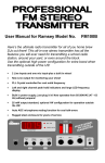
1
SYNTHESIZED FM
STEREO TRANSMITTER
Ramsey Electronics Model No.
FM25B
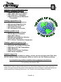
Own and operate your own FM Stereo broadcast station. The
FM25B has an exceptional synthesized transmission range and
improved audio quality that puts your favorite radio station to
shame.
•
Synthesized 88 to 108 MHz for no frequency drift!
•
No annoying Hum with even better stereo separation than the
original!
•
New design features ‘Line In’ and ‘Loop Out’ 1/8” Stereo jacks!
•
‘F’ style RF output connector for easy connection to an external
antenna
•
Fully adjustable RF output level for custom coverage capabilities!
•
Kit includes case, AC adapter, 1/8” Stereo to RCA patch cable, and
whip antenna
•
Great for schools, health clubs, realtors… or your back yard!
•
The ideal campus or school radio station
•
Clear, concise instructions guide you step-by-step to a finished
product that works FIRST time.
FM25B • 1
PARTIAL LIST OF AVAILABLE KITS
RAMSEY TRANSMITTER KITS
• FM25B FM Stereo Transmitter
• AM1, AM25 AM Transmitters
• TV6 Television Transmitter
• FM100 Professional FM Stereo
Transmitter
RAMSEY RECEIVER KITS
• FR1 FM Broadcast Receiver
• AR1 Aircraft Band Receiver
• SR2 Shortwave Receiver
• AA7 Active Antenna
• SC1 Shortwave Converter
RAMSEY HOBBY KITS
• SG7 Personal Speed Radar
• SS70A Speech Scrambler
• MX5, MX10 Mixers
• MD3 Microwave Motion Detector
• PH10 Peak hold Meter
• STC1 Stereo Transmitter Companion
RAMSEY AMATEUR RADIO KITS
• DDF1 Doppler Direction Finder
• HR Series HF All Mode Receivers
• QRP Series HF CW Transmitters
• CW7 CW Keyer
• CPO3 Code Practice Oscillator
• QRP Power Amplifiers
RAMSEY MINI-KITS
Many other kits are available for hobby, school, scouts and just plain FUN. New
kits are always under development. Write or call for our free Ramsey catalog.
SYNTHESIZED FM STEREO TRANSMITTER KIT INSTRUCTION MANUAL
Ramsey Electronics publication No. FM25B Rev 1.2a
First printing: November 2001
COPYRIGHT 2001 by Ramsey Electronics, Inc. 590 Fishers Station Drive, Victor, New York
14564. All rights reserved. No portion of this publication may be copied or duplicated without the
written permission of Ramsey Electronics, Inc. Printed in the United States of America.
FM25B • 2
Ramsey Publication No. MFM25B
Price $5.00
KIT ASSEMBLY
AND INSTRUCTION MANUAL FOR
SYNTHESIZED FM
STEREO TRANSMITTER
KIT
TABLE OF CONTENTS
Introduction ...................................... 4
Circuit Description ............................ 5
Parts Layout Diagram ...................... 9
FM25B Parts List ............................. 10
FM25B Assembly ............................ 12
Custom Case Assembly................... 20
Choosing an Operating Frequency .. 20
Adjusting .......................................... 21
Home Use ........................................ 23
Projects ............................................ 23
Antenna Ideas .................................. 24
Troubleshooting ............................... 25
FCC Rules and Information ............. 26
Understanding Field Strength .......... 29
Summary.......................................... 30
Schematic Diagram.......................... 35
Warranty .......................................... 35
RAMSEY ELECTRONICS, INC.
590 Fishers Station Drive
Victor, New York 14564
Phone (585) 924-4560
Fax (585) 924-4555
www.ramseykits.com
FM25B • 3
INTRODUCTION
The Ramsey FM25B is a true SYNTHESIZED STEREO FM broadcast transmitter, which any person may build and use in accordance with the rules of your
nation’s telecommunications authority. For U.S. residents, that authority is the
Federal Communications Commission (FCC). The FM25B’s low-power broadcasting capability and other practical uses can be fun and interesting for people
of all ages, but the FM25B is not a toy. We will refer to the FCC regulations frequently in this manual and provide you with some information necessary to enjoy the FM25B's capabilities in accordance with the law.
Typical uses for the FM25B include the following:
•
Extension of home stereo system - without wires.
•
Listening aid for auditoriums, churches.
•
Student-operated school radio station.
•
College dorm favorite music broadcast service.
•
Short-range, two-channel experiments and demonstrations.
We think you will be very pleased with the transmitting range, audio quality, frequency stability and stereo channel separation of this build-it-yourself synthesized FM stereo transmitter. If you follow our assembly directions carefully and
use your FM25B in accordance with applicable FCC rules, a whole new world
of sharing music, news and views with friends and neighbors awaits you.
Since the sharing of music and information is vital to the culture of our 21st century global community, we realized that our FM25B low-power Synthesized FM
Stereo Transmitter Kit was certain to attract worldwide interest among hobbyists, students and "pioneers." While the use of the FM25B may need to be limited to "wireless stereo extensions" in some USA households (to comply with
FCC Rules, Part 15), we have seen it serve very well as a serious, though simple, broadcast station for remote villages throughout the world where low cost
AM-FM receivers are available to people of all economic levels. After you're
done building your kit, sitting back and listening to your handiwork, consider
this: many other FM25B's just like yours are faithfully relaying news and information to listeners in remote areas around the world. The FM25B is most definitely not a toy!
FM25B • 4
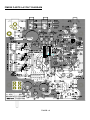
CIRCUIT DESCRIPTION
We will begin by talking about the power supply of your new FM25B. While a
DC power source is provided with the kit, its DC output isn’t ‘clean’ enough to
provide us with the low-noise, stable supply that we would like for good audio
quality. We wouldn’t want our FM transmitter ‘Humming’ with the music now
would we! I mean… it should know the words!
Special care has been taken to filter the input DC signal to maximize our working voltage while still offering a clean, stable supply. Take a look at the schematic as we cover the kit’s circuit description. Right off the bat our input DC
voltage is channeled through an RF filter network composed of bypass caps
C35 & C36 and RF chokes L3 & L5. This filter isolates the plus and minus supply feeds coming from the wall transformer and helps to remove any unwanted
RF that might be coupled into your transmitter. The large electrolytic capacitor
(C32) that follows the RF filter stores energy so instantaneous peaks in demand for power do not cause dips in the supply voltage.
The final parts of the FM25B’s power supply section are composed of a 12 Volt
ripple filter and a 5 Volt regulator to obtain a clean well-filtered power source.
The capacitive multiplier formed by Q1, R4, and C4 together make a handy low
loss ripple filter by in effect multiplying C4’s capacitive value by the DC current
gain of Q1. This increases C4’s ripple filtering capability to roughly that of a
10,000uF capacitor without the typical 2 to 3 volt overhead loss you would get
with a 12 Volt regulator! Now that we have a clean power source, let’s dive into
the rest of the kit!
The custom FM stereo IC (U3) is the heart of the FM25B. U3 is a microprocessor controlled FM stereo generator with lots of built-in performance features.
The surrounding support circuitry configures U3 for proper operation under a
variety of conditions.
Potentiometers R27 and R28 allow for adjustment of the input audio levels to
match a wide sampling of audio sources for the best possible sound.
Capacitors C24 and C27 set the pre-emphasis characteristics for that of the region you intend to operate in (75 µs for USA, 50 µs for Europe).
Capacitors C22 and C25 are part of the 15kHz audio low-pass filter (LPF) that
is internal to the chip. The Bessel filter has flat delay characteristics and removes the higher frequency elements that would interfere with the stereo signal.
Capacitor C29 acts as a ripple filter for U3’s internal audio reference voltage.
This reduces any chance of audio distortion due to internal demands on its
power buss.
FM25B • 5
Crystal X1 along with C9 and C12 form the timing reference of the transmitter.
The signal from the crystal network is divided down and used to generate the
stereo components of the transmitted signal as well as by the chip’s Phase
Lock Loop (PLL) circuitry to provide ‘rock solid’ frequency stability. More on the
PLL side of U3 in a moment.
Inductor L1, C13, and D8 form the Voltage Controlled Oscillator (VCO) stage.
The RF oscillator is a tuned circuit formed by these elements that sets the base
frequency of our RF transmitter. The DC voltage applied to varactor D8 causes
its capacitive value to change up or down as needed. This allows us to vary the
frequency output of the circuit up or down simply by changing the DC voltage
feed to D8.
Transistors Q2 and Q3 work in conjunction with C6, C8, and R17 to filter the
PLL correction pulses coming from U3 pin 7. The inverting LPF they form pass
a DC voltage component, as a function of the correction pulses, to the VCO to
vary the final operating frequency of the RF oscillator.
Varactor D7 is used to ‘wiggle’ the VCO voltage in accordance with the applied
audio signal. The resistor network around D7 serves a multitude of functions. In
a nutshell, D7’s capacitive value changes slightly with a given applied AC signal
(the processed composite audio signal) causing the VCO to deviate from its
base frequency. This is how we get our FM (Frequency Modulation) signal. By
using a dual varactor diode modulation scheme, we can achieve a very tight
deviation tolerance across the entire FM band and improve the overall performance of the system greatly!
Resistor R25 varies the combined modulated RF signal from U3 before its final
amplification stage. R25 gives the user full control to vary the final output level
to match their custom applications and coverage.
Amplifier U4 (the Gal-5 is phenomenally rated from DC to 4GHz operation!)
boosts the output level of U3 in one super clean stage without introducing harmonics or other spurious signals even before the signal goes through a low
pass filter!
The low pass RF filter consisting of C34, L2, C37, L4, and C38 allows the fundamental (operating) frequency to pass through while rejecting any unwanted
harmonics. Harmonics are multiples of the desired fundamental frequency and
in this case, they can cause unwanted emissions in critical areas of the RF
spectrum. A cleaner RF output means happier neighbors and the ‘piece of
mind’ that you are not causing unwanted interference.
U1 is an LM358 opamp. This little work-horse can be found in use for all types
of different applications. Our application for this circuit gives the user feedback
about the operating status of the unit. The combined stages used with their
support components act as a dual purpose pulse detector. The opamp (U1) cirFM25B • 6
cuit tells the user when their transmitter has locked on frequency and when an
applied audio signal is being transmitted. U1:A takes the PLL correction
pulses and amplifies them. The feedback resistor network formed by R6 and
R8 set the gain of the amplifier (remember that classic formula ‘G=1+Rf/Ri’ =
1+1 MegΩ / 10KΩ). The output of U1:A is then rectified by D2 and the peak
voltage is stored by C2. R2 is used as a discharge ‘Bleeder’ resistor so that
the sampled peak-hold voltage on C2 will vary up and down fast enough to
give the reliable dual indication features we need. U1:B monitors the peak
voltage stored on C2 and turns on or off the D1 LED Frequency Lock / Audio
Modulation indicator. When a large number of correction pulses are present
on the PLL output, due to the user changing frequency or the unit become
unlocked, the resulting voltage on C2 will be high enough on the inverting input of U1:B to swing the output Low. When the output of U1:B is low, the LED
(D1) is turned off indicating that the unit is unlocked. The similar scenario applies when audio is being transmitted. The audio being transmitted varies the
frequency up and down (FM – Frequency Modulation) in accordance with the
music. The PLL tries to correct for these deviations from the center transmission frequency by sending out short pulses. The positive feedback provided by
R9 adds a bit of hysteresis to U1:B’s response by changing the crossover trigger point switching the output back and forth from High to Low. The resulting
effect is to smooth the response of the LED (D1) indicator making it more
pleasant to the eye. The detection circuit formed by U1 will indicate when audio is being transmitted by flashing D1 along with the music. Not bad…two for
the price of one!
U2 acts as the brains of the whole circuit. This microcontroller looks at the settings of each of the dip switches S1 through S3 one at a time and from these it
calculates the desired frequency. The switches allow you add up the closed
(down) positions 1, 2, 4, and 8 to make any number between 0 and 9. For example closing position 1 and 8 on S3 (10 MHz switch) is equal to 90 MHz.
Closing 1 and 4 on S2 (1 MHz switch) is equal to 5 MHz. Closing 2 and 1 on
S1 (0.1 MHz switch) is equal to 0.3 MHz. This makes the final frequency equal
to 95.3 MHz. These switches may be set to any frequency between 88 and
108 MHz. To set the frequency above 100 MHz, the S3 positions must add up
to ten. Any switch setting greater than 9, with the exception of S3, is invalid
and will be read as 0.
Once this frequency is determined, the information needed to control U3 is
sent serially from U2. This information is a string of binary data, (1's and 0's).
In this way data is sent one bit at a time to U3. The frequency information
takes 10 bits of data along with an additional 6 bits sent for the internal control
and transmission mode (stereo / mono) selection. You may think that all this
would take a long time but in fact the whole process of sending the data takes
less than 1/100th of a second!
U3’s internal phase locked loop (PLL) synthesizer requires a 7.6 MHz referFM25B • 7
ence crystal (X1) as we discussed before. All the internal operations of U3 are
truly amazing! The reference signal of X1 is divided by 4 and then again by 19
to obtain a stable reference frequency of 100KHz that will be used to keep our
transmitter on frequency. U3 then internally samples the RF output and divides it by a number (N). N is the frequency data that was sent by U2 and is
always equal to the desired frequency in Megahertz times 10. Using the previous example, a frequency of 95.3 MHz gives an N of 953. This means the
sampled RF output signal will be divided by 953 by U3 and then compared
with the reference frequency of 100 KHz. If the desired RF output frequency
happens to be too low (lower than the calculated reference frequency), U1
sends a series of controlled pulses close to the chip’s 0 Volt rail from a 1/2
VCC midpoint on pin 7. The inverting LPF (Q2, Q3 in conjunction with C6, C8,
and R17) in turn raises the DC control voltage on D8. As the voltage across
the varactor increases, it causes a decrease in capacitance (Increasing reverse bias essentially increases the distance between the capacitor’s plates
by increasing the depletion region in the diode (C = kA/d). The decrease in
capacitance causes an increase in U3’s RF oscillator (fo = 1/[2π(LC)½]), bringing the FM25B’s output frequency back on frequency to match that of the reference. If the desired frequency is higher than the reference, U1 does just the
reverse and sends a series of controlled pulses close to the chip’s 5 Volt rail
from a 1/2 VCC midpoint on pin 7. If the frequency is just right then pin 7 floats
at a constant DC level, keeping the VCO voltage constant on D8. In this way
the output frequency of U3 is "locked" to that desired by U2. When the frequency is locked, U1 will cause led D1 to be brightly lit. If D1 is dim or off,
there is a problem and the frequency is not locked (assuming of course that
no audio is being applied). If the frequency starts to drift for any reason (such
as a temperature change) then U3 instantly corrects the tuning voltage to
bring it back to the proper frequency.
FM25B • 8
FM25B PARTS LAYOUT DIAGRAM
FM25B • 9
PARTS SUPPLIED WITH FM25B: Note the extra chip capacitors included.
Capacitors
7 .001 µF disc capacitors (marked .001, 102 or 1nF)
[C13,14,18,31,33,35,36]
3 .01 µF disc capacitors (marked .01 or 103 or 10 nF) [C2,5,26]
3 .1 µF disc capacitors (marked .1 or 104 or 100 nF) [C7,21,23]
1 .047 uF ceramic capacitor (marked .047 or 473) [C6]
2 10 pF disc capacitors (marked 10 or 10K) [C11,15]
2 33 pF disc capacitors (marked 33 or 33K) [C9,12]
2 47 pF disc capacitors (marked 47) [C34,38]
1 75 pF disc capacitor (marked 75 or 75K) [C37]
2 100 pF disc capacitors (marked 100 or 101) [C39,40]
2 150 pF disc capacitors (marked 150 or 151) [C22,25]
2 2200 pF disc capacitors (marked 222 or .0022) [C24*27*] see text
2 3300 pF disc capacitors (marked 332 or 0.0033) [C24*,27*] see text
6 10 µF electrolytic capacitors [C1,10,20,28,29,30]
1 47 uF electrolytic capacitor [C8]
2 100 µF electrolytic capacitor [C3,4]
1 1000 µF electrolytic capacitor [C32]
4 .1 uF SMT capacitors [C16,17] Preinstalled!
Resistors
1 10 ohm (brown-black-black) [R1]
1 100 ohms (brown-black-brown) [R17]
1 120 ohms, larger, 1 watt (brown-red-brown) [R26]
1 270 ohms (red-violet-brown) [R15]
2 470 ohms (yellow-violet-brown) [R3,4]
2 4.7k ohms (yellow-violet-red) [R9,16]
8 10k ohms (brown-black-orange) [R7,8,10,11,12,14,19,22]
2 22k ohms (red-red-orange) [R5,18]
1 47k ohms (yellow-violet-orange) [R24]
3 100k ohms (brown-black-yellow) [R2,13,20]
1 220k ohms (red-red-yellow) [R23]
1 470k ohms (yellow-violet-yellow) [R21]
1 1M ohms (brown-black-green) [R6]
1 1k ohm trimmer potentiometer [R25]
2 10k ohm trimmer potentiometers [R27,28]
Semiconductors
3 2N3904 NPN transistors [Q1,2,3]
13 1N4148 diodes (small glass diodes) [D2, D3 - 6, D9 - 16]
1 1N4000 series diode (can be any number from 1N4002 to 1N4007
(black with white band) [D17]
2 Varactor diodes (transistor shape, two leads, marked MV2105)[D7,8]
1 LED [D1]
FM25B • 10
Inductors
1 Shielded can inductor, 0.18 uH [L1]
2 Pre-wound spring style inductors, 44 nH [L2,4]
2 1 µH axial inductors (brown-black-gold) [L3,5]
Hardware, Misc.
1 PIC 16C505 microcontroller IC (marked with white sticker) [U2]
1 BH1415F Stereo generator IC [U3] Preinstalled!
NOTE: These surface mount parts may be pre-installed on your circuit board.
Check the solder side of the PC board for these parts.
1 7.6 MHz crystal (thin shiny rectangle marked 7.600000) [X1]
1 78L05 +5 volt voltage regulator [VR1]
1 14-pin socket for U2
1 LM358 Low Power Dual Operational Amplifier IC [U1]
1 GAL5 SMT Amplifier IC (surface mount chip with 4 leads, 3 on one
side) [U4] Preinstalled!
1 Two pin jumper and jumper block [J1]
1 ‘F’ type board mount connector [J3]
2 3.5mm stereo jacks [J4,5]
1 2.1mm DC power jack [J2]
1 DPDT push-button switch [S4]
3 DIP switches (8 pin dip with 4 sliding tabs) [S1,2,3]
1 Whip antenna [ANT1]
1 FM25B printed circuit board
1 1/8” stereo to RCA cable
1 AC125 12 volt DC power transformer
Required, not supplied
Line level audio source (such as a tape deck or CD player)
Case and Knob Parts
Top cover with drilled antenna hole
Bottom base tray
4 - Short Phillips Head Screws
2 - Long Phillips Screws
Front and Rear Plastic Panels
Front and Rear Labels
4 - Rubber Feet
Appropriate Knobs for Kit
Required Tools
Small Phillips Head Screwdriver
Pen or Pencil
Sharp hobby knife or hand held paper punch
Ruler at least 6 inches long
Multimeter for voltage adjustment
FM25B • 11
RAMSEY "LEARN-AS-YOU-BUILD" ASSEMBLY STRATEGY
As you can see in examining the circuit board and components, there is a bit
more to this kit than just soldering a few parts. So that you don't spend extra
time "troubleshooting" instead of getting on the air, we strongly recommend
that you follow the assembly strategy and step-by-step procedures we provide.
Our strategy in installing parts on our PC board is to install the larger and
more obvious parts such as the ICs and connectors first. These parts will then
act as "landmarks" so that each additional device installed is seen in relationship to them, or to others previously installed.
In addition, we'll discuss the purpose of most of the components or groups of
components as we go along. If you are new to the idea of building your own
transmitter, perhaps our explanations will help you understand and learn as
we go along. The assembly sequence will follow the circuit flow from input
jacks to antenna as faithfully as is practical, as part of Ramsey's "Learn-AsYou-Build" kit assembly philosophy.
FM25B ASSEMBLY
Use the boxes to check off your progress.
Check all received parts against the Parts list on page 10 and 11. The parts
list describes the various markings that may be found on the kit parts.
Important Note! The surface mount parts in your kit have been preinstalled for you. Please don’t call the factory for your “missing” parts;
simply flip the PC board over and you’ll find them soldered into place.
Since you may appreciate some "warm-up" soldering practice as well as a
chance to put some "landmarks" on the FM25B PC board, we'll first install
some "hardware" components, to make the up-down, left-right orientation of
the PC board as clear as possible.
In ALL the following instruction steps, our word "INSTALL" means this:
•
Insert the part, oriented correctly, into its correct holes in the PC board.
•
If helpful, gently BEND the part's wire leads or tabs to hold it in place, with
the body of the part snugly against the top "component side" of the PC
board.
•
SOLDER ALL wires or pins of the part, whether the two wires of a resistor
or all pins of an IC socket.
FM25B • 12
•
Nip or "trim" all excess wires extending beyond each solder connection,
taking care that wire trimmings do not become lodged in PC board solder
connections.
Enough said. . . Let's get building!
We’ll start with the surface mount parts on the “solder” side of the PC board.
That will get the tiniest, most easily lost parts “out of the way” . . . before you
have a chance to sneeze and blow them off the table! However, your PC
board may come with the parts pre-mounted for you, in which case skip ahead
to step 7. If they are not already in place flip the PC board over so that you
can see the side opposite the silkscreen. This is the side that has all the solder
pads and traces on it. Near the middle of the board is where our first part will
go. You’ll need tweezers for the next few parts, and possibly a magnifying lens
or eye loupe to see these tiny components. If you’re over 40, make sure you
have that magnifier! You know what I’m talking about; your arms just don’t get
long enough to read the writing on these babies. (Can you tell I might have
some personal experience with this?!)
1. Locate the BH1415F stereo generator IC, U3, by flipping the PC board
over. Note that it has already been installed for you, as has U4 and the
two surface mount capacitors. Makes things a little easier, doesn’t it?
C16
J3
U3
U4
PIN 1
C17
We’ll install the ICs so that you can get them nice and flat on the board, then
we’ll place some of the larger components as landmarks.
2. Install the socket for U2, the PIC 16C505 microcontroller IC. It doesn’t
matter which way the socket is oriented, as long as the chip is placed in
the socket correctly. We’re installing this part now to make it easier for you
to get it nice and flat on the board. You can bend two of the corner leads
out slightly to hold the socket in place when you flip the board over to solder it in. Be sure to solder all 14 pins.
3. Now insert U2 into the socket. Orient the notched end as shown on
the PC board silkscreen, toward R12. Before you push it down into the
FM25B • 13
socket check to be sure that none of the pins are bent under or outside of
the socket. When you’re sure the pins are where they belong, press it
down so that it is seated flat within the socket.
4. Install U1, the LM358 dual op-amp. Again, orient the dotted or
notched end as shown on the silkscreen and be sure to solder all 8 pins.
5. Install S4, the DPDT push-button switch. You’ll want this part to be
seated correctly so that the power button moves freely when in the case.
Set it flush to the PC board before soldering all six pins.
6. Install J2, the 2.1mm DC power jack. You can gently bend the leads
to keep this part from falling out of the board when you flip the board over
to solder it.
7. Install J3, the PC mount “F” connector. This is another part that you’ll
want to seat correctly before soldering or it won’t fit through the back
panel properly. Be sure to solder the ground connections well. They may
require more heat but when working with RF, a good ground is essential.
Progress Note: The preceding steps have secured a sufficient number of components to your PC board to make general orientation around the board much
clearer for installing additional parts.
Most of the resistors will be installed in a stand up fashion. That is, one lead
will go straight into the board while the other is bent around to go back down
into the other hole. The straight lead goes into the hole with the circle around
it.
8. Install D17, the 1N4000 series diode (4001 - 4007)(black with white
band). The body of the part should be placed in the hole with the circle
around it and the band or stripe should be up when oriented properly.
9. Install L3, 1µH axial inductor (looks like a fat resistor with brownblack-gold bands).
10. Install C36, .001 µF disc capacitor (marked .001, 102 or 1nF).
11. Install L5, the other 1µH axial inductor (looks like a fat resistor with
brown-black-gold bands).
12. Install C35, .001 µF disc capacitor (marked .001, 102 or 1nF).
13. Install R28, one of the 10k ohm trimmer potentiometers (marked 103).
There are two of these parts; don’t confuse either one with the 1k trimmer
marked 102. Seat it flat before soldering.
14. Install the other 10k trimmer pot, R27 (marked 103).
15. Install J5, one of the stereo jacks. Proper positioning of this part will
help you later with case-up so be sure it’s where you want it before soldering.
FM25B • 14
16. Install J4, the other stereo jack.
Now we’ll install some electrolytic caps. Electrolytic capacitors have a right and
wrong way to be installed. Usually, capacitors have a wide black stripe which
indicates their negative lead and the PC board or Parts Layout Diagram will
show the positive side of the capacitor's installation hole. Be sure to place the
( + ) capacitor lead into the PC board ( + ) hole and the ( - ) lead into the ( - )
hole. Observe correct polarity when installing the electrolytic capacitors.
17. Install C32, 1000 µF electrolytic capacitor. Remember polarity!
18. Install C30, 10 µF electrolytic capacitor. The next two parts will be
identical, and will have the same polarity so be careful with this first one.
19. Install C29, another 10 µF electrolytic capacitor.
20. Install C28, yet another 10 µF electrolytic capacitor.
21. Install C40, 100 pF disc capacitor (marked 100 or 101).
22. Install C39, 100 pF disc capacitor (marked 100 or 101).
23. Install C37, 75 pF disc capacitor (marked 75 or 75K).
24. Install C38, 47 pF disc capacitor (marked 47).
25. Install L4, a prewound spring style inductor.
26. Install L2, the other prewound spring style inductor.
27. Install C34, 47 pF disc capacitor (marked 47).
28. Install C33, .001 µF disc capacitor (marked .001, 102 or 1nF).
29. Install C24 and C27, 3300 pF (marked 332 or 0.0033). For use in
Europe, use 2200 pF capacitors (marked 222 or .0022). These capacitors
set the pre-emphasis characteristics for the FM25B. Pre-emphasis is a
technique used in FM transmitters to increase the high frequency signal to
noise ratio.
30. Install C25, 150 pF (marked 150 or 151).
31. Install C22, 150 pF (marked 150 or 151).
32. Install R25, 1k ohm trimmer pot (marked 102). This potentiometer adjusts the final RF output.
33. Install C31, .001 µF disc capacitor (marked .001, 102 or 1nF).
34. Install R26, 120 ohms (large, 1 watt, brown-red-brown). You’ll notice
that this part is quite a bit bigger than the other resistors in your kit. This is
a 1 watt resistor and the others are 1/4 watt. That means this resistor can
dissipate 1 watt of power if needed.
35. Install C26, .01 µF disc capacitor (marked .01 or 103 or 10 nF).
FM25B • 15
36. Install C23, .1 µF disc capacitor (marked .1 or 104 or 100 nF).
37. You’ll notice a silkscreen position for C19. This part is not used; don’t
install any component at that position.
38. Install C20, 10 µF electrolytic capacitor. This part was changed from
a disc capacitor to improve the low frequency response so you’ll have to fit
the electrolytic in where the disc would have gone. The positive lead
should be placed toward C13 and the negative or striped lead should be
placed toward R25. As with all the other components in this kit, keep the
lead lengths as short as possible.
39. Install C18, .001 µF disc capacitor (marked .001, 102 or 1nF).
40. Install R24, 47k ohms (yellow-violet-orange). Be careful! This part is
easily confused with the 4.7k resistors since the last color band is orange
and the 4.7k is red.
41. Install C21, another .1 µF disc capacitor (marked .1 or 104 or 100 nF).
42. Install R23, 220k ohms (red-red-yellow).
43. Install C15, 10 pF disc capacitor (marked 10 or 10K).
44. Install C13, .001 µF disc capacitor (marked .001, 102 or 1nF).
45. Install D8, MV2105 varactor diode (transistor shape with two leads,
marked MV2105). Follow the PC board silkscreen for proper placement.
46. Install R22, 10k ohms (brown-black-orange).
47. Install R21, 470k ohms (yellow-violet-yellow).
48. Install C11, 10 pF disc capacitor (marked 10 or 10K).
49. Install R20, 100k ohms (brown-black-yellow).
50. Install D7, the other MV2105 varactor diode (transistor shape with two
leads, marked MV2105). Again, be sure you place this part correctly.
51. Install C14, .001 µF disc capacitor (marked .001, 102 or 1nF).
52. Install R19, 10k ohms (brown-black-orange).
53. Install R16, 4.7k ohms (yellow-violet-red).
54. Install C8, 47 µF electrolytic capacitor. Remember to orient this part
as shown on the silkscreen and parts layout diagram. Bad things can happen when electrolytics are installed backwards!
55. Install R18, 22k ohms (red-red-orange).
56. Install R17, 100 ohms (brown-black-brown).
57. Install R14, 10k ohms (brown-black-orange).
FM25B • 16
58. Install C6, .047 uF ceramic capacitor (marked .047 or 473).
59. Install R13, 100k ohms (brown-black-yellow).
60. Install Q3, the transistor marked 2N3904. The flat side must be placed
as shown on the PC board. Mount it as close to the board as possible
without forcing it.
61. Install Q2, another 2N3904 transistor. If you can’t remember how you
just did it, reread the step above!
62. Install L1, the shielded can inductor. It only fits in the board one way;
just be sure to seat it flat on the board before soldering.
63. Install C10, 10 µF electrolytic capacitor. Watch polarity when installing.
64. Install R15, 270 ohms (red-violet-brown).
65. Install R12, 10k ohms (brown-black-orange).
66. Install C7, the last .1 µF disc capacitor (marked .1 or 104 or 100 nF).
67. Install C12, 33 pF ceramic capacitor (marked 33).
68. Install C9, the other 33 pF ceramic capacitor (marked 33).
69. Install X1, 7.6 MHz crystal (thin shiny rectangle marked 7.600000).
The next group of parts are all the same and all must be oriented the same
way. Be careful with this step! One diode installed backwards will make it impossible to transmit on some frequencies while having no effect on others.
Makes for interesting troubleshooting! Don’t worry, hardly anyone messes this
one up so we’re sure you’ll have no trouble installing these parts. Do a double
check before soldering.
70. Install diodes D3 through D6, and D9 through D16, all 1N4148 diodes
(small glass diodes). There are 12 installed in this step so you should
have 1 left over when you’re through. Be gentle when bending the leads
down to fit them in the board; these can be fragile. Orient the banded end
as shown on the PC board silkscreen. Solder them all in when you’re sure
they’re oriented correctly.
71. Install S3, one of the 8 pin DIP switches. Place the part so that it is flat
to the board and the switches (little white tabs) are toward the outside of
the circuit board. That will place them next to the numbers running along
the outside of the board and they should make it easier for you to tune
your FM25B. Also, if you decide to cut a hole in the side of the enclosure
so that you can reach the DIP switches without taking the cover off, you’ll
be glad they’re placed that way!
72. In the same way, install S2. As with the other parts, be sure this one is
FM25B • 17
flat to the board before soldering.
73. Ok, you know the drill by now. Install S1, the last switch. If you have a
short memory, read the previous two steps. You didn’t think I was going to
type all that again, did you?
We’re getting there, aren’t we? Just a few more parts to install and you’ll be
finished! Take a break if you need to. Stretch your fingers and arms, get the
crick out of your neck and let’s keep going.
74. Install R8, 10k ohms (brown-black-orange).
75. Install R7, also 10k ohms (brown-black-orange).
76. Install R6, 1 Meg ohms (brown-black-green). As you probably already
know, “Meg” is another way of saying “million”. That resistor you just installed is a million ohms!
77. Install R3, 470 ohms (yellow-violet-brown).
78. Install D1, the red LED. Being a diode, this part has a polarity and
must be installed properly to work. You’ll see that it has a flat side and so
does the PC board silkscreen picture of the diode. The flat side indicates
the negative lead and you’ll see that this lead is shorter than the other one
too. Place the part so that the flat side lines up as shown on the silkscreen. Leave the leads long; the part should sit up about an inch off the
board so that you can bend it over to fit through the front panel. This LED
indicates frequency lock, as well as the presence of an audio signal.
79. Install C5, .01 µF disc capacitor (marked .01 or 103 or 10 nF).
80. Install R9, 4.7k ohms (yellow-violet-red).
81. Install R5, 22k ohms (red-red-orange).
82. Install R10, 10k ohms (brown-black-orange).
83. Install R2, 100k ohms (brown-black-yellow).
84. Install D2, 1N4148 diode (small glass diode) following the silkscreen
for correct orientation.
85. Install C2, .01 µF disc capacitor (marked .01 or 103 or 10 nF).
86. Install J1, the two pin jumper. This is the stereo jumper and should be
left off if you want to operate in stereo and installed if you want to operate
in mono mode. If operating in stereo, simply place the jumper block on
one of the pins of the jumper so that you don’t lose it. That way you won’t
have to search for it if you ever want to operate in mono.
87. Install R11, 10k ohms (brown-black-orange).
88. Install C3, 100 µF electrolytic capacitor. Watch your orientation.
FM25B • 18
89. Install VR1, the 78L05 +5 volt regulator. This part looks like a transistor and like a transistor, it must be place correctly to work. Follow the parts
layout diagram and PC board silkscreen for orientation. Solder all three
pins.
90. Install C1, the last 10 µF electrolytic capacitor. Check polarity before
soldering.
91. Install C4, the other 100 µF electrolytic capacitor. Do I have to remind
you about polarity again?
92. Install R4, 470 ohms (yellow-violet-brown).
93. Install R1, 10 ohms (brown-black-black).
94. Install Q1, the last 2N3904 transistor. Again, be sure it is placed correctly before soldering.
That’s it! But before you grab the power supply and fire up the FM25B, take a
moment to check over your work. Check to be sure that all the parts are installed and the polarity sensitive ones are placed properly. Look for solder
joints that could be questionable and need a quick touch-up. Also look for potential solder bridges; the parts layout diagram can help with that. You may
want to hurry and get the kit powered up but anything you find now will save
you a lot more trouble later. Unless you like the smell of smoke and the sound
of things exploding! It’s worth the few extra minutes. Looking over the PC
board is the first step our Ramsey technicians complete when testing units
here at the shop.
ASSEMBLY INSTRUCTIONS FOR CUSTOM CASE
1. Note that the case halves fit together only one way. Be sure you’re installing the board so that the case halves will fit together and the antenna
hole will be in the right spot. Insert the board into the case with the knobs
and LED extending through the holes in the front panel.
2. Raise the rear portion of the PC board and extend the jacks through the
rear plastic plate. Insert the plate into the grooves on the base tray.
3. Secure the PC board to the bottom base tray with 4 short Phillips head
screws.
CHOOSING AN OPERATING FREQUENCY
(A) It really is NOT sufficient to just "check" the FM band for an empty frequency, using the FM portable radio closest at hand. It is your responsibility to
carefully research what FM stations can be listened to with a good system
within the transmitting range of your FM25B. This is especially important in the
low end of the FM broadcast band (88-92 MHz), where there are numerous
medium power National Public Radio stations. You may not be aware of these
FM25B • 19
stations but your neighbors may be receiving them, using a good receiver and
outdoor antenna. Interfering with such reception is a direct violation of federal
law. The most reliable way of finding a truly open frequency on the FM band is
to check the band with a very good FM receiving system using an external antenna. If you do not have access to such a radio, most modern car radios (with
exterior antenna) are very sensitive and usable to help you know what stations
your neighbors really can be receiving on a particular frequency.
(B) In choosing an operating frequency, remember that most "digital-tuning"
receivers, whether portable, mobile or hi-fi, are designed to tune in 200 KHz
increments and therefore might not receive well a signal operating between
these pre-tuned standard broadcasting frequencies. In order to comply with
Part 15 of FCC regulations, it is your responsibility to determine carefully that
your operation will not cause interference to broadcast reception. Please study
Appendix A of this manual before using your FM25B.
ADJUSTING YOUR FM25B TRANSMITTER
Keep all tests very brief until you have carefully chosen an open operating frequency in the FM broadcast band.
1. Transmitting Frequency
After finding a suitable "open" frequency in the 88-108 MHz FM band, program DIP switches S3, S2, and S1 for the frequency desired. The DIP
switches are programmed in BCD, a form of binary that is very easy to use.
Look at your circuit board or parts layout diagram; you’ll see the numbers 1, 2,
4, 8 printed next to each DIP switch. On these switches you add up the closed
positions to make to make any number between 0 and 9. For example: closing
position 1 and 8 on S3 (10 MHz switch) is equal to 90 MHz (1+8=9, 9x10 MHz
= 90 MHz), closing 2 and 4 on S2 (1MHz switch) is equal to 6 MHz (2+4=6,
6x1 MHz = 6 MHz), closing 4, 2 and 1 on S1 (0.1 MHz switch) is equal to 0.7
MHz (4+2+1=7, 7x .1 MHz = .7 MHz). This makes the final frequency equal to
96.7 MHz (90+6+.7=96.7). These switches may be set to any frequency between 88 and 108 MHz. To set the frequency above 100 MHz, the S3 positions must add up to ten. To do this you would close positions 8 and 2
(8+2=10). Any switch setting greater than 9, with the exception of S3, is invalid
and will be read as 0.
After setting your DIP switches, recheck your ‘math’ and listen on a nearby FM
radio for the carrier frequency. No audio input should be applied while making
this first adjustment. You can simply listen for a "quieting" on an unused channel instead of the normal background "static" you would normally find. If you
don’t hear anything yet, don’t worry. We need to adjust L1 for the correct tuning voltage at TP1 to ensuring proper operation across the band. TP1 is located just off the exposed lead of R21 that is closest to the outside of the
FM25B • 20
board. With an operating frequency of 107.9 MHz programmed into the DIP
switches, there should be around 9.0 volts (+- 0.2 volts or so) at TP1. If there
isn’t, adjust L1 until you read 9.0 volts. The LED lock indicator (D1) should
now glow brightly. If not, you may need to SLIGHTLY tune the control voltage
up or down from the expected standard in order to compensate for building
tolerances.
Now let’s verify the other end of the band at 88.1 MHz. Set the DIP switches
for 88.1 MHz and you should see the tuning voltage drop to about 0.8 volt (+0.3 volts or so) at TP1. Do not readjust L1 if the tuning voltage varies from that
of the expected value. The most important setting is at 107.9 MHz.
Remember that if you have adjusted the FM25B outside of 88 MHz to 108
MHz range it will default to 88.1 MHz. This means that if you can’t hear anything on the radio near the frequency you are trying to transmit at, go to 88.1
MHz and see if it is there.
If you can’t get either reading even close, see the troubleshooting section.
2. Audio Connection
Adjust both Left and Right level potentiometers (R27, R28) to about half of
their rotation. This is a good starting position. The best audio input for both
testing and general operation are the stereo "line-level outputs" of a cassette
deck or CD player. Most stereo systems have a variety of auxiliary output
jacks of which one or more are line-level outputs.
Hooking up an audio source to your FM25B is really quite simple. However,
there are some general rules:
•
A terribly distorted sound is a sign of too much audio level. Simply rotate
the level potentiometers R27 and R28, CCW to reduce the level. Make
sure you rotate each one about the same amount to maintain proper stereo balance.
•
NEVER connect the FM25B audio inputs to speaker outputs of a high
power stereo system; such a connection will destroy the IC chip.
•
Consider using a mike mixer for professional "radio station" sound. It will
allow you to easily fade, mix and switch between various audio sources.
USING THE FM25B WITHIN THE HOME
Typical use for the FM25B would be to connect it to a personal computer
within a large home so that whatever MP3 or other audio files are playing can
also be tuned-in on portable FM radios in other rooms, the garage or out in the
yard. The provided whip antenna should cover a typical home’s boundaries
FM25B • 21
quite well. An external antenna can be used for a larger coverage area if desired. Use the RF adjustment control (R25) to fine tune the RF output level to
just reach the area you intend to cover.
The audio connection consists of using shielded audio cables to connect the
line or speaker level output to the audio inputs of the FM25B. Consult the literature that came with your stereo equipment.
Even if you intend use of the FM25B for your own home and family, it is still
your responsibility, in accordance with Part 15 of the FCC Rules, to ensure
that this operation does not cause interference to your neighbors.
EXPERIMENTAL "BROADCASTING" PROJECTS
To use the FM25B successfully as a "broadcasting" service to interested listeners in a school or immediate neighborhood, most of your effort will be concentrated on smoothly "managing" or mixing the audio signals fed into the
transmitter input. Operation of the transmitter itself consists simply of the following:
1. Correct construction and adjustment.
2. Carefully checking for an open frequency between 88-108 MHz in accordance with FCC Rules, Part 15.
3. Setting up a suitable antenna.
4. Connecting the audio source to the input jack.
5. Turning on the transmitter while you intend to be "on the air" and turning it
off when you are finished.
The more home-built your complete setup, the more it is in conformity with the
spirit of FCC Part 15 regulations.
You can greatly add to the versatility and professionalism of your transmitting
station by adding one of our audio mixers and processor. Mixers allow you to
smoothly ‘blend’ from one audio source to another just like the commercial
stations do. Our STC1, Stereo Transmitter Companion provides full audio
processing in one easy package. The STC1 allows you to ‘sweeten’ the audio
for more impact and punch. Plus, it has brick-wall low pass filtering on the stereo inputs to prevent that bothersome ‘swishing’ and squealing sound that is
often found when using lower quality CD players as the audio source! Check
out our free catalog for all the details.
ANTENNA IDEAS
A simple, yet very effective, antenna for the FM25B consists of a "dipole", set
up either horizontally or vertically, and connected to the transmitter output jack
FM25B • 22
through a few feet of coaxial cable (either RG-58, RG-59 or miniature RG-174,
available at Radio Shack and other sources). Correct dipole lengths for major
sections of the 88-108 MHz band are:
88 MHz, each side: 2.7 feet; 5.4 feet total
98 MHz, each side: 2.4 feet; 4.8 feet total
108 MHz, each side: 2.2 feet; 4.4 feet total
You can see that there’s not a great difference in antenna length from 88 to
107 MHz. Some antenna designers have the view that an "approximate" dipole such as 2.5 ft. on a side will do fine, while others believe it is worth the
effort to calculate the length for your exact frequency, using the simple formula
of Length (of one side, in feet) = 234/Frequency in MHz.
If the dipole is installed vertically, the end connected to the center conductor of
the coax should be the upper (higher) end. If young children will be around the
set-up, a flexible wire antenna is preferable, rather than rigid tubing.
A "ground plane" antenna can be quite effective. A ground plane consists of
one vertical element, the same length as one side of a dipole, connected to
the center conductor of the coax. Four "radials" are connected to the shielded
side of the coax at a 90 to 135 degree angle to the vertical element. The dipole formula is also used to calculate the length of the radial; since radials
should be slightly longer than the main element, use 240 rather than 234 in
your calculations.
If you are equipped to make the field strength measurements required by Part
15 FCC rules, and if you think it would be best to aim or "focus" your signal in
a narrower direction, you can consult an antenna handbook and design a suitable gain antenna. See Appendix A concerning FCC field strength limitations.
An FM- VHF TV receiving antenna could be modified for such a purpose.
Ham radio books and magazines are filled with antenna principles and ideas
which can be adapted to your application. Also, you may wish to look at Radio
Shack book No. 62-1083 on antennas. Our new TM-100 Tru-match FM antenna is an ideal mate to your transmitter. It features proper impedance
matching for optimum power transfer and range. See our catalog for details.
ANTENNA ALTERNATIVES
If your situation involves a single large building or multi-level home where reception from the FM25B antenna may tend to be uneven because of walls and
other VHF path obstacles, you might set up the FM25B's output in a "carriercurrent" configuration. If you know how, then do so - safely. If not, you can
show your FM25B and this book to a licensed radio engineer and negotiate
with that person for a safe installation which will feed your signal through inteFM25B • 23
rior wiring of your home or building. Do not attempt such an installation unless
you know exactly what to do and not to do. Also, because such an installation
is beyond the original purpose of this kit and the safety standards intended for
all Ramsey kits, and because we have not tested the FM25B in such an installation, we cannot provide further details.
TROUBLESHOOTING GUIDE
If your FM25B does not work at all, re-check the following:
•
correct orientation of U1, U2, U3, and U4 (see PC board layout diagram)
•
correct polarity of all electrolytic capacitors
•
correct orientation of diodes D1 – D17
•
correct orientation of Q1, Q2, and Q3 transistors
•
all parts are installed as close to the printed circuit board (PCB) as possible without stressing their leads
•
Q1 output is close to 12 VDC +- 2VDC
•
No shorted traces on the pins of J4 or J5
•
No shorted traces on U4, the main RF output amplifier.
•
all solder connections.
Hints
•
Erratic or unstable operation is caused by faulty solder joints or cable connections.
•
Replacement IC chips (including the stereo transmitter IC) may be ordered directly from Ramsey Electronics, Inc. but records show that IC failure rates for these parts are extremely low.
FM25B • 24
APPENDIX A: FCC RULES AND INFORMATION
The Rules of the FCC (Federal Communications Commission) and your kit
built FM Stereo Transmitter.
An interim explanation of applicable FCC regulations supplied as a personal
assistance to FM25B builders, by Dan F. Onley (K4ZRA)
It is the policy of Ramsey Electronics, Inc., that knowing and observing the
lawful use of all kits is a first responsibility of our kit user/builders. We do not
endorse any unlawful use of any of our kits, and we try to give you as much
common sense help about normal and lawful use as we can. Further, it is the
policy of Ramsey Electronics, Inc., to cooperate with all applicable federal
regulations in the design and marketing of our electronics kit products. Finally,
we urge all of our overseas customers to observe the regulations of their own
national telecommunications authorities.
In all instances, compliance with FCC rules in the operation of what the FCC
terms an "intentional radiator" is always the responsibility of the user of such
an "intentional radiator".
To order your copy of FCC rules part 15, call the US Government, Superintendent of Documents, at 202-512-1800, or fax at 202-512-2250. To order the
correct document, ask for “CFR Title 17: Parts 1 to 199.” The cost is $24.00.
Master Card and Visa are accepted.
In the United States, this is how the FCC regards your transmitter kit
Licensed FM broadcast stations and their listeners have ALL the rights! Your
use of a device such as the FM25B kit MAY have some limited privileges in
locally-unused band space, but your non-licensed use of the FM25B has absolutely NO rights at all over the rights of licensed broadcast operators and
the rights of their listeners to interference-free reception. If your operation of a
device such as the FM25B interferes with ANYBODY'S use or enjoyment of
an FCC licensed transmission of any kind, your only choice is to IMMEDIATELY terminate or change the operation of your low-power transmitting device so as to cause no more interference. That's it! No discussion, no exceptions.
Unlicensed operation of small transmitting devices is discussed in "Part 15" of
the FCC Rules. These Rules are published in 100 "Parts," covering everything
imaginable concerning the topic of "Telecommunications." The six books containing the FCC Rules are section 47 of the complete Code of Federal Regulations, which you are likely to find in the Reference section of your Public Library. If you have questions about the legal operation of your FM25B or any
other kit or home-built device which emits RF energy, it is your responsibility
to study the FCC regulations. It is best if YOU read (and consult with a lawyer
FM25B • 25
if you are in doubt) the rules and do not bother the understaffed and busy FCC
employees with questions that are clearly answered in the rules.
Here are the primary "dos and don'ts" picked from the current FCC Rules, as
of May, 1990. This is only a brief look at the rules and should not be construed to be the absolute complete legal interpretation! It is up to you to operate within the proper FCC rules and Ramsey Electronics, Inc. cannot be held
responsible for any violation thereof.
1. In the past, no "two-way communications" use of the 88-108 MHz FM
broadcast band was permitted. This prohibition does not appear in the
current edition of Part 15. Previous editions of Part 15 discussed
"wireless microphones" (such as Ramsey FM-1, FM-4, etc.), while the
June 23, 1989, revision eliminates this discussion in favor of more detail
regarding computer and TV peripherals and other modern electronic conveniences. However, it is not immediately clear that the 1989 revision of
the FCC Rules Part 15 necessarily "cancels" previous regulations. Laws
and rules tend to remain in force unless they are specifically repealed.
Also, FCC Rule 15.37 discusses "Transitional Provisions for Compliance
with the Rules," and states in item (c): "There are no restrictions on the
operation or marketing of equipment complying with the regulations in effect prior to June 23, 1989."
2. It is the sole responsibility of the builder-user of any FM broadcast-band
device to research and fully avoid any and all interference to licensed FM
broadcast transmission and reception. This instruction manual gives you
practical advice on how to do a good job of finding a clear frequency, if
one is available.
3. For some frequency bands, the FCC sets 100 milliwatts (0.1 watt) as the
maximum permitted power output for unlicensed, home-built transmitting
devices, and that the combined length of your antenna and feedline
(coaxial cable or other) must not exceed 10 feet. The technical standards
for 88-108 MHz are very different, primarily concerned with band width
and RF field strength.
4. FCC Rules do not differ for "stereo" or "monaural" transmissions.
5. Broadcasting on the grounds of a school (AM emissions only) is specifically permitted and encouraged between 525 and 1705 KHz under Part
15.221. Use our AM-1 AM radio broadcast kit for this use.
6. FCC Rule No. 15.239 specifically addresses operation in the 88-108 MHz
FM broadcast band for which your FM25B transmitter kit is designed.
However, this Rule does not, by itself, tell you everything you need to
know about using a device of this kind. Therefore, we are noting a series
of Part 15 regulations which should be observed:
FM25B • 26
•
a. The "bandwidth" of your transmission is limited to 200 KHz, centered
on the actual operating frequency. Since 200 KHz is enough spectrum
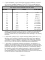
space for several different FM stations, this is a "generous" limitation deDISTANCE FROM TRANSMITTER ANTENNA
METERS
FEET
FIELD
TOTAL AREA
3
10
250
314 FT
6
20
125
1256 FT
12
39
63
4800 FT
24
78
31
19113 FT
48
157
15
1.8 ACRES
96
315
7.5
7.2 ACRES
192
630
3.8
28.6 ACRES
384
1.9
11.4 ACRES
768
1260
2520
.95
458 ACRES
1536
5036
.5
1830 ACRES
signed to accommodate cruder FM devices. Properly built and adjusted,
the FM25B kit operates well within this limit. In fact, its signal should
sound no "wider" than any other FM station when listening on an ordinary
FM radio.
•
b. FCC Rule 15.215(a) says: "Unless otherwise stated, there are no restrictions as to the types of operations permitted under these sections."
This general provision appears to leave you free to use your FM stereo
transmitter in a manner similar to operations of an FM broadcasting station, or to use it for any other non-interfering, practical application.
•
c. FCC Rule 15.5: General conditions of operation: "(b) Operation...is
subject to the conditions that no harmful interference is caused and that
interference must be accepted that may be caused by the operation of an
authorized radio station, by another intentional or unintentional radiator,
by industrial, scientific and medical equipment, or by an incidental radiator. (c) The operator of a radio frequency device shall be required to
cease operating the device upon notification by a Commission representative that the device is causing harmful interference."
FM25B • 27
•
d. The most specific FCC regulation of 88-108 MHz FM Broadcast band
unlicensed operation is that the "field strength" of the signal must not exceed 250 microvolts/meter at a distance of 3 meters from the transmitter
(FCC rule 15.239). If you have any concern about this emission limit,
have your device checked by a technician with accurate measuring equipment. Remember that the "field strength" of a signal is determined as
much by the antenna as by the RF output of the transmitter itself.
APPENDIX B: UNDERSTANDING LEGAL "FIELD STRENGTH"
The new FCC Part 15 Rules specify a maximum "Field Strength" of your
transmitted signal. Since it is unlikely that you have the equipment to carry out
accurate field strength measurements in microvolts, it is useful to understand
at least the theory of field strength so that you can understand both what you
can expect from such transmitters, and what limits the FCC intends.
Previous limits on non-licensed FM-broadcast band devices were defined as a
maximum field strength of 40µV per meter measured at a distance of 15 meters. The June 1989 revised rule specifies a maximum of 250 µV per meter,
but measured at 3 meters from your antenna. Both limitations are the same in
practice. "250µV per meter" means that an accurate field-strength meter with
a 1-meter antenna may indicate a maximum signal field strength of 250µV (In
contrast, non-licensed operation from 26.96 to 27.28 MHz is limited to a field
strength of 10,000 µV per meter at 3 meters).
In all cases, the field strength of a signal decreases in direct proportion to the
distance away from the antenna. Power decreases by the square of distance:
for every doubling in distance, the signal power is quartered, but the field
strength voltage is only halved. Using this theory, we can construct a simple
chart to show the maximum permitted performance of a non-licensed FM band
transmitter. The theoretical figures assume a simple 1 meter receiving antenna in all cases and do not take into consideration that reception can be
greatly enhanced with larger, multi-element antennas and preamplifiers. In the
following chart, the field strength (theoretical minimum) gets even stronger as
you move from the edge of these circular boundaries toward the antenna:
This "exercise in meters and microvolts" demonstrates that the FCC clearly
intends to limit the theoretical range of non-licensed devices operating in this
band. It also shows the potential for causing interference at a home down the
street from you. But it also shows that you can legally put out quite a good signal over wider areas than you might have imagined.
For other kinds of radio services, the FCC restricts such factors as transmitter
power or antenna height, which cannot really limit the possible "range" of a
transmission under good conditions. By restricting the maximum field strength
at a specific distance from your antenna, the FCC clearly plans for your signal
FM25B • 28
to "die out" at a specific distance from your antenna, no matter what kind of
transmitter power or extra-gain antenna you are using. On the other hand, the
FCC standards do make it legal and possible for you to broadcast on a school
campus, campground or local neighborhood, as long as you do not cause interference to broadcast reception.
“Why talk about acres"?
There are three reasons to translate our look at "field strength" into "acres".
1. The first one is easy: the numbers would get too cumbersome if we discussed your possible signal coverage in terms of square feet or square
meters.
2. It's very easy to see that your signal can easily and legally serve a school
campus or wilderness campground.
3. And, if we remember that typical urban single-family home sites run from
1/4 to 1/2 acre on the average, it should become extremely clear that your
obligation to avoid interfering with broadcast reception can easily involve
hundreds of homes, before adding apartments!
In fact, the most significant distance in the above chart is the 1.9 µV signal
strength permissible at 1260 feet (about 1/4 mile), covering a circular area of
about 114 acres. A quick glance at stereo FM receiver specifications shows
typical sensitivity of 1.7 µV before considering high-gain antennas or preamplifiers. Your non-licensed signal can provide serious competition to a public
broadcast station fifty miles away, a station which someone in your neighborhood may have set up a special antenna to enjoy.
Calibrated "field strength meters" such as described in the ARRL Radio Amateur's Handbook can detect signals down to about 100 microvolts. To measure
RF field strength below such a level, professional or laboratory equipment and
sensitive receivers are required. A "sensitive" receiver responds to a signal of
1 or even .5 microvolts "delivered" to the receiver input by antenna. If the antenna is not good, the receiver cannot respond to the presence of fractions of
a microvolt of RF energy.
FM25B • 29
SUMMARY
The present edition of Part 15 of the FCC rules does not provide detailed
guidance on ALL aspects of using a low-power transmitter such as the
FM25B. The main point is that you may not cause any interference whatsoever to licensed broadcast services and that you must be willing to put up with
any interference that you may experience.
In addition to operations not requiring authorization, you also have the option
of writing a clear and polite letter to the FCC Engineer-in-Charge of your local
district, describing your intended operation. Mention the operating frequency
and planned hours of operation. This could be a good step to take if your project is in behalf of a school, Scout or community group.
If you become further fascinated with the service rendered by low-power
broadcasting, other FCC regulations explain how to apply for a license or
other authorization which may permit you to upgrade your FM25B or other
equipment to accomplish any objective which the FCC sees to be in the public
interest and not interfering with other authorized uses of the radio spectrum.
Lawful use suggestions
1. Build and adjust this kit strictly according to the published instructions.
2. Use the whip antenna supplied with the Ramsey case set, CFM.
3. Do not modify your kit in any way.
4. Check your intended operating frequency very carefully, as clearly explained in this instruction manual, to ensure you will not cause interference to reception of licensed broadcasting.
5. If you receive ANY complaint about your transmissions interfering with
broadcast reception, stop or change your operation IMMEDIATELY.
6. If you are contacted by the FCC regarding use of this device, cooperate
fully and promptly.
7. Do your own homework and research to understand and comply with present and future FCC rulings concerning devices of this kind.
8. Do not use made-up "station call signs" to identify your transmissions.
Only the FCC has the authority to issue such call signs. Use some other
way to identify your transmitting activity, such as "This is Stereo 90.5,
Seabreeze School Student Music Radio," and so forth.
9. Identify the location and purpose of your transmissions from time to time.
This is common courtesy toward other persons who may hear your signal.
The FCC is toughest about clandestine transmission which cost time and
money to track down.
FM25B • 30
10. Do not assume that the mere fact that you purchased this kit gives you
any specific right to use it for any purpose beyond generating a low-level
RF signal which is barely detectable beyond the perimeter of your personal dwelling space.
Finally, the FCC Rules call for the posting of printed notices on devices intended for non-licensed operation under Part 15 Rules. You will find such notices written up for the front or back of the instruction manual for nearly any
computer or video accessory that you have seen in recent months. Consult
the Part 15 Rules for the exact wording of such notices. Following is a text for
such a notice which responds to FCC rule making intentions:
NOTICE:
The radio-frequency "intentional radiator" device which may be constructed
from kit parts supplied by us is intended and designed by Ramsey Electronics, Inc. to conform to applicable provisions of Part 15 of FCC Rules. The individual kit-builder and all users of this device assume responsibility for lawful
uses conforming to FCC Part 15 Rules. Operation is subject to the following
two conditions:
1. This device may not cause harmful interference, and
2. This device must accept any interference received, including interference
that may cause undesired operation.
Final comment
A well-informed person will see today's FCC Rules to be evolving and progressively less-restrictive. Even though today's technology is far more complex than what was possible at the time of the Communications Act of 1934,
the FCC rules are becoming more relaxed, giving radio experimenters more
and more opportunities to explore many frequency bands, using many communications modes, with no need for a formal license of any kind. A thorough
study of Part 15 of the FCC Rules, which is completely beyond the purpose of
this kit manual, will show you many legal uses of radio transmitting devices
which do not require licensing, either amateur or commercial.
To provide more personal and club radio-learning opportunities, and to cut
down on administrative costs, today's FCC permits far more non-licensed activity than at any time in previous history. On the other hand, today's FCC enforcement actions get bigger fines and real prison terms for scofflaws! From
CB (now 3 bands of it, for varying applications) to easy entry-level Amateur
Radio with long-term licensing, to numerous unlicensed Part 15 operations,
the FCC is beginning to look out for the interest and good plans and intentions
FM25B • 31
of private citizens and school-community groups as never before in radio communications history. Learn the rules...observe them...and have fun in radio!
If you enjoyed this Ramsey kit, there’re plenty more to choose from in our
catalog - write or call today!
FM25B • 32
FM25B • 33
FM25B • 34
The Ramsey Kit Warranty
Please read carefully BEFORE calling or writing in about your kit. Most problems can be
solved without contacting the factory.
Notice that this is not a "fine print" warranty. We want you to understand your rights and ours too!
All Ramsey kits will work if assembled properly. The very fact that your kit includes this new manual
is your assurance that a team of knowledgeable people have field-tested several "copies" of this kit
straight from the Ramsey Inventory. If you need help, please read through your manual carefully.
All information required to properly build and test your kit is contained within the pages!
1. DEFECTIVE PARTS: It's always easy to blame a part for a problem in your kit, Before you
conclude that a part may be bad, thoroughly check your work. Today's semiconductors and passive
components have reached incredibly high reliability levels, and it’s sad to say that our human
construction skills have not! But on rare occasions a sour component can slip through. All our kit
parts carry the Ramsey Electronics Warranty that they are free from defects for a full ninety (90)
days from the date of purchase. Defective parts will be replaced promptly at our expense. If you
suspect any part to be defective, please mail it to our factory for testing and replacement. Please
send only the defective part(s), not the entire kit. The part(s) MUST be returned to us in suitable
condition for testing. Please be aware that testing can usually determine if the part was truly
defective or damaged by assembly or usage. Don't be afraid of telling us that you 'blew-it', we're all
human and in most cases, replacement parts are very reasonably priced.
2. MISSING PARTS: Before assuming a part value is incorrect, check the parts listing carefully to
see if it is a critical value such as a specific coil or IC, or whether a RANGE of values is suitable
(such as "100 to 500 uF"). Often times, common sense will solve a mysterious missing part
problem. If you're missing five 10K ohm resistors and received five extra 1K resistors, you can
pretty much be assured that the '1K ohm' resistors are actually the 'missing' 10 K parts ("Hum-m-m,
I guess the 'red' band really does look orange!") Ramsey Electronics project kits are packed with
pride in the USA. If you believe we packed an incorrect part or omitted a part clearly indicated in
your assembly manual as supplied with the basic kit by Ramsey, please write or call us with
information on the part you need and proof of kit purchase.
3. FACTORY REPAIR OF ASSEMBLED KITS:
To qualify for Ramsey Electronics factory repair, kits MUST:
1. NOT be assembled with acid core solder or flux.
2. NOT be modified in any manner.
3. BE returned in fully-assembled form, not partially assembled.
4. BE accompanied by the proper repair fee. No repair will be undertaken until we have received
the MINIMUM repair fee (1/2 hour labor) of $25.00, or authorization to charge it to your
credit card account.
5. INCLUDE a description of the problem and legible return address. DO NOT send a separate
letter; include all correspondence with the unit. Please do not include your own hardware
such as non-Ramsey cabinets, knobs, cables, external battery packs and the like. Ramsey
Electronics, Inc., reserves the right to refuse repair on ANY item in which we find excessive
problems or damage due to construction methods. To assist customers in such situations,
Ramsey Electronics, Inc., reserves the right to solve their needs on a case-by-case basis.
The repair is $50.00 per hour, regardless of the cost of the kit. Please understand that our
technicians are not volunteers and that set-up, testing, diagnosis, repair and repacking and
paperwork can take nearly an hour of paid employee time on even a simple kit. Of course, if we find
that a part was defective in manufacture, there will be no charge to repair your kit (But please
realize that our technicians know the difference between a defective part and parts burned out or
damaged through improper use or assembly).
4. REFUNDS: You are given ten (10) days to examine our products. If you are not satisfied, you
may return your unassembled kit with all the parts and instructions and proof of purchase to the
factory for a full refund. The return package should be packed securely. Insurance is
recommended. Please do not cause needless delays, read all information carefully.
FM25B • 35
SYNTHESIZED STEREO TRANSMITTER KIT
Quick Reference Page Guide
Introduction ..................................... 4
Circuit Description ............................ 5
Parts Layout Diagram ...................... 9
FM25B Parts List ............................. 10
FM25B Assembly ............................. 12
Troubleshooting ............................... 25
FCC Rules and Information ............. 26
Understanding Field Strength .......... 29
Summary ......................................... 30
Schematic Diagram ......................... 33
Warranty .......................................... 35
REQUIRED TOOLS
• Soldering Iron Ramsey WLC100
• Thin Rosin Core Solder Ramsey RTS12
• Needle Nose Pliers Ramsey MPP4 or RTS05
• Small Diagonal Cutters Ramsey RTS04
<OR> Technician’s Tool Kit TK405
ADDITIONAL SUGGESTED ITEMS
•
•
•
Holder for PC Board/Parts Ramsey HH3
Desoldering Braid Ramsey RTS08
Digital Multimeter Ramsey M133
Price: $5.00
Ramsey Publication No. MFM25B
Assembly and Instruction manual for:
RAMSEY MODEL NO. FM25B
RAMSEY ELECTRONICS, INC.
590 Fishers Station Drive
Victor, New York 14564
Phone (585) 924-4560
Fax (585) 924-4555
www.ramseykits.com
FM25B • 36
TOTAL SOLDER POINTS
326
ESTIMATED ASSEMBLY
TIME
Beginner .............. 10 hrs
Intermediate ........ 6 hrs
Advanced............. 4 hrs