1
Installation Instructions
(Catalog Number 1771-IL Series C)
()2 )#.- )2 42%$ 6(%!$$)3).-!+ )-&.1,!3).- )2
!5!)+!"+% )- 3(% /4"+)#!3).- 9
& 8.4 -%%$ ! #./8 .& 3()2
,!-4!+ &!7 3(% %-#+.2%$ 2%1
!-4!+ %04%23 !1$ 3.
99
9 & 8.4 !1%
.432)$% 3(% &!7 3(% #!1$ 3.
999
Use this document as a guide when installing the catalog number
1771-IL/C analog input module.
1%5%-3 +%#31.23!3)# )2#(!1'%
-$%123!-$ .,/+)!-#% 3. 41./%!- -).- )1%#3)5%2
-$%123!-$ 1.$4#3 .,/!3)")+)38
!+#4+!3% .6%1 %04)1%,%-32
%3%1,)-% .$4+% +!#%,%-3
%+.6
%3 3(% .-&)'41!3).- 4,/%12
%8 3(% !#*/+!-% .--%#3.1
-23!++ 3(% .$4+% !-$ )%+$
)1)-' 1,
.--%#3
)1)-' 1,
)1)-' 3. 3(% )%+$
1.4-$ 3(% (!22)2 !-$ .$4+%
.-&)'41% 3(% .$4+%
3!342 -$)#!3.12
1.4"+%2(..3)-'
/%#)&)#!3).-2
The isolated analog input module is sensitive to electrostatic
discharge.
!
ATTENTION: Electrostatic discharge can damage
integrated circuits or semiconductors if you touch
backplane connector pins. Follow these guidelines
when you handle the module:
• Touch a grounded object to discharge static potential
• Wear an approved wrist-strap grounding device
• Do not touch the backplane connector or
connector pins
• Do not touch circuit components inside the module
• If available, use a static-safe work station
• When not in use, keep the module in its
static-shield bag
4"+)#!3).- 9
#3."%1 2
Isolated Analog Input Module
Understand Compliance to
European Union Directives
This product has the CE mark and is approved for installation within
the European Union and EEA regions. It has been designed and
tested to meet the following directives.
EMC Directive
This product is tested to meet Council Directive 89/336/EEC
Electromagnetic Compatibility (EMC) and the following standards,
in whole or in part, documented in a technical construction file:
• EN 50081-2EMC – Generic Emission Standard,
Part 2 – Industrial Environment
• EN 50082-2EMC – Generic Immunity Standard,
Part 2 – Industrial Environment
This product is intended for use in an industrial environment.
Low Voltage Directive
This product is tested to meet Council Directive 73/23/EEC
Low Voltage, by applying the safety requirements of EN 61131–2
Programmable Controllers, Part 2 – Equipment Requirements and
Tests.
For specific information required by EN 61131-2, see the appropriate
sections in this publication, as well as these Allen-Bradley
publications:
Publication
Industrial Automation Wiring and Grounding Guidelines
For Noise Immunity
Guidelines for Handling Lithium Batteries
Automation Systems Catalog
Publication number
Isolated Analog Input Module
Understand Product
Compatibility
3
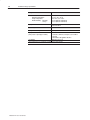
The 1771-IL/C module can be used with any 1771 I/O chassis.
Compatibility and data table use is listed below.
Use of Data Table
C
Catalog
Number
Compatibility
Input
Image
Bits
Output
Image
Bits
Read
Block
Words
Write
Block
Words
1/2ĆSlot
1ĆSlot
2ĆSlot
Chassis
S i
Series
'
'
'
,
Addressing
$"%( ! * ( , , ,
$"%( ! * ( , , , ,
$"%( ! * ($)( &'(& ( $#
$ '(& ( ($ $"%!"#(&+ "$)! %!"#(
Calculate Power
Requirements
The module receives its power through the 1771 I/O power supply
and requires 1.1A at 5V (5.5 Watts) from the backplane.
Add this current to the requirements of all other modules in the I/O
chassis to prevent overloading the chassis backplane and/or
backplane power supply.
Determine Module
Placement in the I/O
Chassis
You can place your module in any I/O module slot of the I/O chassis
except for the extreme left slot. This slot is reserved for PC
processors or adapter modules.
!
ATTENTION: Do not insert or remove modules from
the I/O chassis while system power is ON. Failure to
observe this rule could result in damage to module
circuitry.
Group your modules to minimize adverse affects from radiated
electrical noise and heat. We recommend the following.
• Group analog input and low voltage dc modules away from ac
modules or high voltage dc modules to minimize electrical noise
interference.
• Do not place this module in the same I/O group with a discrete
high-density I/O module when using 2-slot addressing. This
module uses a byte in both the input and output image tables for
block transfer.
)! ( $# ,
($& 4
Isolated Analog Input Module
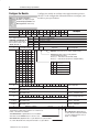
Setting the Configuration
Jumpers
1
The module has configuration jumpers for determining the input type
(voltage or current) for each input. The module is shipped with the
configuration jumpers positioned for voltage mode. You can
select either voltage or current for each input.
#+-4# 2&# $-30 1!0#51 1#!30',% 2&# 1'"# !-4#0 22&# +-"3*# ," 0#+-4# 2&# !-4#01
2
#.-1'2'-, 2&# !-,$'%302'-, (3+.#01 11-!'2#" 5'2& #!& ',.32
!&,,#* !!-0"',% 2- 7-30 0#/3'0#+#,21
&# +-"3*# '1 1&'..#" 5'2& #!& !&,,#* 1#2 $-0 4-*2%# +-"# $
!300#,2 +-"# '1 "#1'0#" 7-3 +312 1#2 (3+.#0 -, 2&# $3,!2'-,*
,*-% *-!) -, 2&# +-"3*# -3 !, +'6 4-*2%# +-"# ,"
!300#,2 +-"# 1#22',%1
-,$'%302'-,
3+.#0
Enlarged View
&,,#* &,,#* &,,#* 3
#.-1'2'-, 2&# !-4#0 ," 1#!30# 5'2& 2&# $-30
1!0#51 0#+-4#" ', 12#. -.
Current
Mode
&,,#* &,,#* &,,#* Voltage
Mode
&,,#* &,,#* 0-,2 4'#5
-$ +-"3*#
!'0!3'2 -0"
Key the Backplane
Connector
-1'2'-, 2&# )#7',% ,"1 ', 2&# !).*,# !-,,#!2-01 2- !-00#1.-," 22&# )#7 1*-21 -, 2&# +-"3*#
*!# 2&# )#7',% ,"1
#25##, ," #25##, ," Place your module in any slot in the chassis
except the leftmost slot which is reserved for
processors or adapters.
!
ATTENTION: Observe the
following precautions when
inserting or removing keys:
• insert or remove keys with
!&11'1
..#0
-,,#!2-0
your fingers
• make sure that key placement
is correct
Incorrect keying or the use of a
tool can result in damage to the
backplane connector and possible
system faults.
3 *'!2'-, 8 !2- #0 -3 !, !&,%# 2&# .-1'2'-, -$ 2# ,"1 '$
13 1#/3#,2 1712#+ "#1'%, ," 0#5'0',% +)#1
',1#02'-, -$ "'$$#0#,2 27.# -$ +-"3*# ,#!#1107
8
Isolated Analog Input Module
Install the Module and
Field Wiring Arm
!
5
ATTENTION: Remove power from the 1771 I/O
chassis backplane before you install the module.
Failure to remove power from the backplane
could cause:
• module damage
• degradation of performance
• injury or equipment damage due to possible
unexpected operation
1
& "' ! & $ '% "! & &"# ! "&&" " & %%%
&& ' & "' !&" #"%&"!
Important: ##* $ (! #$%%'$ "! & "' &" %& & !&" &%
#! "!!&"$
1771ĆA1B, ĆA2B, ĆA3B, ĆA4B I/O chassis
!# & %%% & "($ &
&"# " & "' &" %'$ &
2
1771ĆA1B, ĆA2B, ĆA4B Series B I/O chassis
)! & %%% "! $
")! !&" # &" %'$ &
"'% %'$ & "!
#!% !
&& & )$! $ , &" & "$+"!& $ & &
"&&" " & %%%
)$! $ #("&% '#)$ ! "!!&% )& &
"' %" *"' ! !%& "$ $ "( & "' )&"'&
%"!!&! & )$%
,
'&"! , &"$ 6
Isolated Analog Input Module
Connect Wiring to the
Field Wiring Arm
Connect your I/O devices to the field wiring arm (cat. no. 1771-WF)
shipped with the module.
!
ATTENTION: Remove power from the 1771 I/O
chassis backplane and field wiring arm before
removing or installing an I/O module.
• Failure to remove power from the backplane or
wiring arm could cause module damage, degradation
of performance, or injury.
• Failure to remove power from the backplane could
cause injury or equipment damage due to possible
unexpected operation.
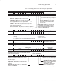
Connection Diagram for the Isolated Analog Input Module
(cat. no. 1771ĆIL/C)
+
)'*$ */, "
,*/)!
–
+
)'*$ */, "
–
,*/)!
%))"' %))"' %))"' %))"' %))"' %))"' %))"' %))"' NOTE: %" 2 (*!/'" !*"- )*. -/++'1 '**+ +*0", #*, '**+ +*0","!
)'*$ -*/, "- .,)-(&..",- .,)-!/ ",- ". **+ +*0", (/-. "
-/++'&"! 1 .%" /-",
2
&"'! &,&)$ ,(
. * 2
/'& .&*) 2 .*", Isolated Analog Input Module
Use the following diagrams to ground your
I/O chassis and isolated analog input module.
Follow these steps to prepare the cable:
&#, 7-3 !-,,#!2 %0-3,"',% !-,"3!2-01 2- 2&# !&11'1
%0-3,"',% 123" .*!# 120 51� 3,"#0 2&# $'012 *3% 2&#,
.*!# ,32 5'2& !.2'4# *-!) 51� -, 2-. -$ #!& %0-3," *3%
#+-4# *#,%2& -$ ! *#
(!)#2 $0-+ 2&# #*"#, ! *#
0-3," 3%
32
#*"#, *#
3** 2&# $-'* 1&'#*" ," 0#
"0', 5'0# $0-+ 2&# ',13*2#" 5'0#1
0-3,"',% 23"
0# "0',
5'0#
,13*2#"
5'0#1
-'*
1&'#*"
5'12 2&# $-'* 1&'#*" ," "0',
5'0# 2-%#2� 2- $-0+ 1',%*# 120,"
22!& %0-3," *3%
32 ," .2'4#
1�
20
1�
&11'1
'"# *2#
0-3," 3%
&'#*" ," 0',
25'12#" 2-%#2�
1# 2&# !3. 51� '$ !0'+.8-, *3%1 0# ,-2 31#"
62#," 1&'#*" 2- 2#0+',2'-, .-',2
6.-1# (312 #,-3%& ! *# 2- "#/32#*7
2#0+',2# ',,#0 !-,"3!2-01
1#  1&0',) 23 ',%
-0 -2� 13'2 *#
',13*2'-, 5�# 5'0#
#6'21 ! *# (!)#2
&#, 31',% 1&'#*"#" ! *# 5'0# %0-3," 2&# $-'*
1&'#*" ," "0', 5'0# -,*7 2 -,# #," -$ 2&# ! *#
# 0#!-++#," 2&2 7-3 50. 2&# $-'* 1&'#*" ,"
"0', 5'0# 2-%#2� ," !-,,#!2 2&#+ 2- !&11'1
+-3,2',% -*2
2 2&# -..-1'2# #," -$ 2&# ! *# 2.# #6.-1#"
1&'#*" ," "0', 5'0# 5'2& #*#!20'!* 2.# 2- ',13*2#
'2 $0-+ #*#!20'!* !-,2!2
Refer to Wiring and Grounding Guidelines,
publication 1770-4.1 for additional
information.
&'#*" ," 0',
25'12#" 2-%#2�
&0#"8$-0+',% 1!0#5
62#0,*82--2&
1
3 *'!2'-, 8 !2- #0 7
8
Isolated Analog Input Module
Configure the Module
Configure the module to conform to the application that you have
chosen. Use the configuration information below to configure your
module to your specifications.
For detailed configuration
information, see chapter 5 of your
(publication 1771Ć6.5.91).
Dec. Bits
Octal Bits
15
17
Word 1
14
16
13
15
8
12
14
7
Input
p range
g selections allow the
user to configure the inputs for any of
ranges Two
7 input voltage or current ranges.
bits are required for each channel.
Bits 00 and 01 for channel 1, bits 02
andd 03 ffor channel
h
l 2,
2 etc.
t
2
11 10 09
13 12 11
6
1 to 5V DC, 4 to 20mA (default)
0 to 5V DC, 0 to 20mA
1
0
Ć5 to +5V DC, Ć20 to +20mA
1
1
Ć10 to +10V DC, 0 to 10V DC
0
0
0
0
1
200ms 0
0
0
1
0
300ms 0
0
400ms 0
500ms 0
600ms 0
0
0
0
1
1
0
1
0
1
0
1
0
0
1
1
1
1
0
1
1
0
0
0
900ms 0
1.0s 0
1
0
1
1
0
1.5s
0
1
0
1
0
1
1
1
2.0s
1
1
0
1
1
0
0
0
0
1
1
1
1
1
1
1
1
1
0
1
7
6
5
4
8
02
02
01
01
2
1
Data
Format
03
03
3
0
0
3
4
04
04
0
0
3.0s
05
05
0
0
3.1s
5
06
06
Bit 00
No RTS 0
100ms 0
2.5s
07
07
Bit 01
Real Time Sampling
700ms 0
800ms 0
08
10
00
00
1
Description
Range Selection Ć Channels 1 - 8
Voltage or Current Input
BTW
Format
Real time sampling, data format, BTW
format, and digital filter
Digital Filter
Digital filter reduces effect of noise on input. (Default is no filter.)
BTW format, determines format for scaling, digital filter
constant, and high and low alarms.
Bit 08 (10) = 0 Ć values must be entered in BCD (default)
Bit 08 (10) = 1 Ć values must be entered in Two's Complement Binary
Bit Bit Data format - set to match
10 09 your processor.
3
2
1
Sign bits, maximum negative scaling values
8
7
0
0
BCD (default)
0
1
Not Used
1
0
Two's complement binary
1
1
Signed magnitude binary
6
5
4
3
2
1
Sign bits, minimum negative scaling values
Sign
g bits, minimum, and maximum
negative scaling values
4, 6, 8, 10, 12, 14,
16, 18
Minimum scaling values for each channel (word 4 to channel 1, word 6 to channel 2, etc.).
Enter in BCD format.
Channels 1 - 8 minimum scaling
5, 7, 9, 11, 13, 15,
17, 19
Maximum scaling values for each channel (word 5 to channel 1, word 7 to channel 2, etc.).
Enter in BCD format.
Channels 1 - 8 maximum scaling
20
8
7
6
5
4
3
2
1
8
Sign bits, high alarm values
7
6
5
4
3
2
1
Sign bits, low alarm values
Sign bits,
bits low and high alarm values
21, 23, 25, 27, 29,
31, 33, 35
Low alarm values for each channel (word 21 to channel 1, word 23 to channel 2, etc.).
Enter in BCD format.
Channels 1 - 8 low alarm
22, 24, 26, 28, 30,
32, 34, 36
High alarm values for each channel (word 22 to channel 1, word 24 to channel 2, etc.).
Enter in BCD format.
Channels 1 - 8 high alarm
37
Inhibit bits for calibration
Inhibit Channel Calibration Bits - (8-15) When this bit is set, that particular
channel will not be calibrated. Bit 8 to channel 1, bit 9 to channel 2, etc.
Default = 0, all channels to be calibrated.
Not Used
Save Calibration Values - (S) When this bit is set, new calibration
values will be saved in EEPROM. Default = 0, values not saved.
Gain Calibration Bit - (G) When this bit is set, gain calibration is to be performed. When
set, no other calibration functions can be performed. Default = 0, no gain calibration.
Publication 1771Ć5.51 - October 1996
S
G
O
Calibration bits
Offset Calibration Bit - (O) When this bit is
set, offset calibration is to be performed. When
set, no other calibration functions can be set.
Default = 0, no calibration.
Isolated Analog Input Module
9
Use the following table to read data from your input module.
Dec. Bits
Octal Bits
Word 1
15
17
14
16
13
15
12 11 10
14 13 12
Not Used
09
11
08
10
07
07
A
06
06
HF
05
05
IA
04
04
IF
03
03
RTS
02
02
IS
01
01
OR
Alarm violation status bit - (A) This bit is set if one or
more channels are in an alarm condition.
Invalid filter bit - (IF) This bit is set if the filter parameters are not correct.
The value must be between 00 and 99 (0.00 and 0.99 seconds) in BCD, or
between 0 and 255 (0 to 2.55) in binary.
Invalid scaling bit - (IS) This bit reports that the scaling
is somehow invalid. Usually, both values are equal or
minimum is greater than maximum when this bit comes
on. Can also be an invalid filter value.
Real time sample fault bit - (RTS) This bit is set if the module is configured for
RTS and a block transfer read has not occurred within the user-programmed period.
16
15
14 13 12
Not Used
Not Used
11
10
07
8
8
06
7
7
05
6
6
04
5
5
03
4
4
Underrange bits for each channel. Bit 00 for channel 1, bit 01 for channel
2, etc. These bits are set (1) at approximately the input range limits shown
on the right.
Overrange bits for each channel. Bit 00 for channel 1, bit 01 for channel
2, etc. These bits are set (1) at approximately the input range limits shown
on the right.
4
5
6
Not Used
8
7
Polarity bits - Set when input is less than zero.
Channel 1 Input
Channel 2 Input
⇓
⇓
12
13
14
⇓
Channel 8 Input
8
7
8
7
Not Used
Not Used
8
7
6
5
4
3
2
1
Calibration Inhibited. Bits 8 (10) through 15 (17) represent a
channel that was not calibrated, either due to an error or a user
request. If the channel was requested not to be calibrated, these
bits confirm that request.
Calibration Fault - (CF) When this bit is set, the module could
not perform offset or gain calibration. This bit is set when a save
is requested.
EEPROM Fault - (EF) When this bit is set, the calibration values
could not be saved to EEPROM.
CF
6
5
02
3
3
01
2
2
00
1
1
1 to 5V dc, 4 to 20mA (default)
0 to 5V dc, 0 to 20mA
Ć5 to +5V dc, Ć20 to +20mA
Ć10 to +10V dc, 0 to 10V dc
4
3
2
1
Data polarity for channels 1-8
1 8
Channel 1 Input
Channel 2 Input
⇓
6
6
Description
Data underrange for channels 1-8
Data overrange for channels 1-8
5
5
4
4
3
3
2
2
1
1
Channel 8 Input
Low Alarm Bits
High Alarm Bits
High Alarm bits for channels 1 through 8 respectively. Each bit represents an
alarm indicator for that channel. When the bit is set, the value of that channel is
above the high alarm value.
Low Alarm bits for channels 1 through 8 respectively. Each bit represents
an alarm indicator for that channel. When the bit is set, the value of that
channel is below the low alarm value.
15
Diagnostics
Out of range bit - (OR) This bit is sent to tell the
processor that one or more channels are either
over or under range.
Invalid alarm bit - (IA) This bit is set if any alarm value is unusable,
such as expecting BCD and value is in 2's complement binary.
17
Description
Power up bit - (PU) Used by the module to tell the
processor that it is alive but not yet configured. It is
a key element in the application program.
Hardware fault - (HF) When this bit is set, the dc/dc converter
fuse has blown. Digital logic will continue to operate.
Octal Bits
2
3
00
00
PU
EF
Not Used
S
G
O
Calibration Status Bits
Offset Calibration Complete - (O) When
this bit is set, the offset calibration request
was successfully completed.
Gain Calibration Complete - (G) When
this bit is set, the gain calibration request
was successfully completed.
Save Complete - (S) When this bit is
set, the save calibration values to
EEPROM" was successfully completed.
Publication 1771Ć5.51 - October 1996
10
Isolated Analog Input Module
If a write block of with all zeroes is sent to the module, the default
selections will be:
• 1 to 5V dc or 4 to 20mA (depends on voltage/current selection
•
•
•
•
•
The front panel of the isolated analog input module contains a green
RUN indicator and a red FAULT indicator. At power-up, the module
momentarily turns on both indicators as a lamp test, then checks for:
•
•
•
•
#! !$"#
!$"#
&
% $"! & $"# jumper setting)
BCD data format
no real time sampling (RTS)
no digital filter
no scaling
no alarms
correct RAM operation
EPROM operation
EEPROM operation
a valid write block transfer with configuration data
If there is no fault, the red indicator turns off.
The green indicator comes on when the module is powered. It will
flash until the module is programmed. If a fault is found initially or
occurs later, the red fault indicator lights. The module also reports
status and specific faults (if they occur) in every transfer of data
(BTR) to the PC processor. Monitor the green and red indicators and
status bits in word 1 of the BTR file when troubleshooting your
module.
Isolated Analog Input Module
11
Possible module fault causes and corrective action are described in
the following table.
,. "#0')#" 0.,1 )#/&,,0'+%
'+$,.*0',+ /## !&-0#. ,$ 4,1.
-1 )'!0',+ 5
%.##+ ,$$
.#" ,$$
, -,3#. 0, *,"1)#
&#!( -,3#. 0, !&//'/
#!4)# / +#!#//.4
,//' )# /&,.0 ,+ *,"1)#
#-)!# *,"1)#
".'2#. $')1.#
%.##+ ,+
.#" ,+
'!.,-.,!#//,. ,/!'))0,. ,. $')1.#
$ '**#"'0#)4 $0#. -,3#.51- '+"'!0#/ ,. $')1.#
%.##+ ,$$
.#" ,+
$ "1.'+% ,-#.0',+ '+"'!0#/ -,//' )# *'!.,-.,!#//,. ,.
!(-)+# '+0#.$!# $')1.#
."3.# $')1.# ),3+ $1/# #0!
%.##+ )'+('+%
.#" ,$$
%.##+ ,+
.#" ,$$
,3#.1- "'%+,/0'! /1!!#//$1))4 !,*-)#0#"
,.*) ,-#.0',+
$ '+"'!0,. !,+0'+1#/ 0, $)/& +" 3.'0# ),!( 0.+/$#./ !++,0 # !!,*-)'/&#" 4,1 &2# -,//' )# '+0#.$!# $')1.#
#-)!# *,"1)#
,.*) ,-#.0',+
,+#
&#+ .#" '/ ,+ 0&# 30!&",% 0'*#. &/ 0'*#" ,10 +"
!,**1+'!0',+
!(-)+# !,**1+'!0',+/ .# 0#.*'+0#" ,1. 1/#. -.,%.* /&,1)" *,+'0,.
1 )'!0',+ 5 !0, #. 12
Isolated Analog Input Module
CSA Hazardous Location Approval
Approbation d'utilisation dans des emplacements dangereux par la
CSA
"/1&#&"0 -/,!2 10 #,/ $"+"/) 20" 0 4")) 0 #,/ 20" &+ %7/!,20 ), 1&,+0
Actual CSA certification is indicated by the product label 0 0%,4+ "),4 +!
+,1 6 011"*"+10 &+ +6 20"/ !, 2*"+11&,+
"/1&#&" )"0 -/,!2&10 !21&)&01&,+ $:+:/)" 200& &"+ .2" "25 .2&
021&)&0"+1 !+0 !"0 "*-) "*"+10 !+$"/"25 La certification CSA en vigueur
est indiquée par l'étiquette du produit "1 +,+ -/ !"0 ##&/*1&,+0 !+0 )
!, 2*"+11&,+ 8 )20$" !"0 21&)&01"2/0
5*-)" ,# 1%" "/1&#& 1&,+ -/,!2 1 )")
5"*-)" !:1&.2"11" !" "/1&#& 1&,+ !2+ -/,!2&1 -/ ) , ,*-)6 4&1% "/1&#& 1&,+ #,/ 20" &+ %7/!,20 ), 1&,+0 1%" #,)),4&+$
&+#,/*1&,+ " ,*"0 -/1 ,# 1%" -/,!2 1 )&1"/12/" #,/ = "/1&#&"! ))"+=/!)"6
&+!201/&) ,+1/,) -/,!2 10
• %&0 ".2&-*"+1 &0 02&1)" #,/ 20" &+ )00 &3&0&,+ /,2-0 ,/ +,+=%7/!,20 ), 1&,+0 ,+)6
• %" -/,!2 10 %3&+$ 1%" --/,-/&1" */(&+$0 1%1 &0 )00 &3&0&,+ /,2-0 /" "/1&#&"! #,/ 20" &+ ,1%"/ ".2&-*"+1 4%"/" 1%" 02&1&)&16
,# ,*&+1&,+ 1%1 &0 --)& 1&,+ ,/ 20" &0 !"1"/*&+"! 6 1%" ,/ 1%" ), )
&+0-" 1&,+ ,##& " %3&+$ '2/&0!& 1&,+
,2/ 01&0#&/" 8 ) "/1&#& 1&,+ !" ) !+0 !"0 "+!/,&10 !+$"/"25 )"0
&+#,/*1&,+0 02&3+1"0 #,+1 -/1&" &+1:$/+1" !" ) !, 2*"+11&,+ !"0 -/,!2&10
&+!201/&")0 !" ,+1/;)" ))"+=/!)"6 "/1&#&:0 -/ ) • "1 :.2&-"*"+1 ,+3&"+1 8 )21&)&01&,+ !+0 !"0 "*-) "*"+10 !" )00" &3&0&,+ /,2-"0 ,2 +" ,+3&"+1 .28 )21&)&01&,+ !+0 !"0
"+!/,&10 +,+ !+$"/"25
• "0 -/,!2&10 -,/1+1 )" */.2$" --/,-/&: !" ) "01 8 !&/" )00" &3&0&,+ /,2-"0 0,+1 "/1&#&:0 8 )21&)&01&,+ -,2/ !21/"0
:.2&-"*"+10 ,< ) ,+3"++ " !" ,*&+&0,+ --)& 1&,+ ,2 21&)&01&,+ "01
!:1"/*&+:" -/ ) ,2 )" 2/"2 ), ) !&+0-" 1&,+ .2)&#&:
Important: 2" 1, 1%" *,!2)/ +12/" ,# ,+1/,) 0601"* 1%" -/,!2 1 4&1%
1%" %&$%"01 1"*-"/12/" /1&+$ !"1"/*&+"0 1%" ,3"/)) 1"*-"/12/" ,!" /1&+$ ,# ,+1/,) 0601"* &+ )00 &3&0&,+ ), 1&,+ %" 1"*-"/12/" ,!" /1&+$ &0
*/("! ,+ 1%" -/,!2 1 )")
0 0%,4+
Important: / 02&1" !" ) +12/" *,!2)&/" !2 06019*" !" ,+1/;)" )"
-/,!2&1 6+1 )" 125 )" -)20 :)"3: !" 1"*-:/12/" !:1"/*&+" )" 125 !"+0"*)"
!2 ,!" !" 1"*-:/12/" !2 06019*" !" ,+1/;)" !2+ !+0 2+ "*-) "*"+1
!" )00" &3&0&,+ " 125 !2 ,!" !" 1"*-:/12/" "01 &+!&.2: 02/ ):1&.2"11"
!2 -/,!2&1
"*-"/12/" ,!" /1&+$
25 !2 ,!" !" 1"*-:/12/"
,,( #,/ 1"*-"/12/" ,!"
/1&+$ %"/"
%" #,)),4&+$ 4/+&+$0 --)6 1, -/,!2 10 %3&+$ "/1&#& 1&,+ #,/ 20" &+
%7/!,20 ), 1&,+0
!
ATTENTION: 5-),0&,+ %7/! >
• 201&121&,+ ,# ,*-,+"+10 *6 &*-&/ 02&1&)&16 #,/ )00 &3&0&,+ • , +,1 /"-) " ,*-,+"+10 2+)"00 -,4"/ %0 ""+ 04&1 %"!
,## ,/ 1%" /" &0 (+,4+ 1, " +,+=%7/!,20
• , +,1 !&0 ,++" 1 ".2&-*"+1 2+)"00 -,4"/ %0 ""+ 04&1 %"!
,## ,/ 1%" /" &0 (+,4+ 1, " +,+=%7/!,20
• , +,1 !&0 ,++" 1 ,++" 1,/0 2+)"00 -,4"/ %0 ""+ 04&1 %"!
,## ,/ 1%" /" &0 (+,4+ 1, " +,+=%7/!,20 " 2/" +6
20"/=02--)&"! ,++" 1,/0 1%1 *1" 1, "51"/+) &/ 2&10 ,+ +
))"+=/!)"6 -/,!2 1 20&+$ 0 /"40 0)&!&+$ )1 %"0 1%/"!"!
,++" 1,/0 ,/ ,1%"/ *"+0 02 % 1%1 +6 ,++" 1&,+ +
4&1%01+! "41,+ ) 0"-/1&+$ #,/ " --)&"! #,/ *&+&*2* ,# ,+" *&+21"
" 0&$)" "01 ) */.2" !:-,0:" !" )00, &1&,+ !"0 1+!/!0 -,2/ )" +!
"01 2+" */.2" !:-,0:" !" ))"+=/!)"6 ,*-+6 + ),$, &0 /"$&01"/"! 1/!"*/( ,# 1%" +!&+ 1+!/!0 00, &1&,+
&0 /"$&01"/"! 1/!"*/( ,# ))"+=/!)"6 ,*-+6 + 2)& 1&,+ = 1,"/ " 125 !2 ,!" !"
1"*-:/12/" "01 &+!&.2: & &
"0 3"/1&00"*"+10 02&3+10 0--)&.2"+1 25 -/,!2&10 6+1 ) "/1&#& 1&,+ -,2/ )"2/ 21&)&01&,+ !+0 !"0 "*-) "*"+10 !+$"/"25
!
AVERTISSEMENT: &0.2" !"5-),0&,+ >
• 0201&121&,+ !" ,*-,0+10 -"21 /"+!/" " *1:/&")
&+ "-1)" -,2/ )"0"*-) "*"+10 !" )00" &3&0&,+ • ,2-"/ )" ,2/+1 ,2 0002/"/ .2")"*-) "*"+1 "01 !:0&$+:
+,+ !+$"/"25 3+1 !" /"*-) "/ )"0 ,*-,0+10
• 3+1 !" !:/+ %"/ ):.2&-"*"+1 ,2-"/ )" ,2/+1 ,2
0002/"/ .2" )"*-) "*"+1 "01 !:0&$+: +,+ !+$"/"25
• 3+1 !" !:/+ %"/ )"0 ,++" 1"2/0 ,2-"/ )" ,2/+1 ,2
0002/"/ .2" )"*-) "*"+1 "01 /" ,++2 +,+ !+$"/"25
11 %"/ 1,20 ,++" 1"2/0 #,2/+&0 -/ )21&)&01"2/ "1 /")&:0 25
&/ 2&10 "51"/+"0 !2+ --/"&) ))"+=/!)"6 8 ) &!" !" 3&0
),.2"10 ,2)&00+10 ,++" 1"2/0 #&)"1:0 ,2 21/"0 *,6"+0
-"/*"11+1 25 ,++"5&,+0 !" /:0&01"/ 8 2+" #,/ " !"
0:-/1&,+ !" +"41,+0 ) = ($ --)&.2:" -"+!+1
2 *,&+0 2+" *&+21"
Isolated Analog Input Module
Number of Inputs
8 fully isolated differential
Module Location
1771 I/O rack Ć 1 slot
Input voltage ranges (nominal)
+1 to +5V DC
0 to 5V DC
Ć5 to +5V DC
Ć10 to +10V DC
Input current ranges (nominal)
+4 to +20mA
0 to +20mA
Ć20 to +20mA
Resolution
16Ćbit binary over full range
Accuracy
Voltage
Current
13
Typical Ć 0.01% of full scale range @ 25oC
Maximum Ć 0.05% of full scale range @ 25oC
Typical Ć 0.06% of full scale range @ 25oC
Maximum Ć 0.1% of full scale range @ 25oC
(Includes 0.05% when using internal current resistor)
Linearity
+1 LSB
Repeatability
+1 LSB
Isolation Voltage
This isolation meets or exceeds the requirements of UL
standard 508, and CSA standard C22.2 No. 142.
Input overvoltage protection
voltage mode: 140V ac (rms) continuous;
current mode: 8V dc continuous
Unscaled BCD and binary output
data to the processor
0000 to +409510 for unipolar ranges
(0 to 5V, +1 to +5V, 0 to +20mA, and +4 to +20mA)
Ć409510 to 409510 for bipolar ranges
+5V, +10V, +20mA input ranges
Input impedance
>10 megohms for voltage ranges; 250 ohms for current
ranges
Common mode rejection
>120 db @ 60Hz and 1K ohm source imbalance
Common mode impedence
>50 megohms shunted by <5 nF
Normal mode rejection
>60 db @ 60Hz
Open Circuit Detection
Voltage mode
Current mode
Open input produces upscale reading.
Open input produces zero reading.
Time to Detect Open Circuit
10s maximum
Calibration
AutoĆcalibration (offset and gain)
Zero offset and gain adjustment for each channel via
programming terminal
Verify every six months to maintain specified accuracy
Engineering units sent to
processor
+9999 BCD with selectable scaling
+32767 binary
Internal scan rate
50ms for 8 channels
Backplane Current
1.1A @ +5V
Power Dissipation
5.5 Watts maximum
Thermal Dissipation
18.8 BTU/hr maximum
Conductors
Wiring
Category
14 gauge (2mm2) stranded (max.)
3/64 inch (1.2mm) insulation (max.)
Category 21
Publication 1771Ć5.51 - October 1996
14
Isolated Analog Input Module
Environmental Conditions
Operational Temperature:
Storage Temperature:
Relative Humidity: Operating
Storage
0 to 60_C (32 to 140_F)
Ć40 to 85_C (Ć40 to 185_F
5 to 95% (without condensation)
5 to 80% (without condensation)
Keying
between 10 and 12
between 32 and 34
Field Wiring Arm
Cat. No. 1771ĆWF
Wiring Arm Screw Torque
7Ć9 inchĆpounds
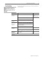
Agency Certification
(when product or packaging is marked)
•
•
•
•
User Manual
Publication 1771Ć6.5.91
CSA certified
CSA Class I, Division 2, Groups A, B, C, D certified
UL listed
CE marked for all applicable directives
1 Refer to publication 1770Ć4.1, Programmable Controller Wiring and Grounding Guidelines."
Publication 1771Ć5.51 - October 1996
Isolated Analog Input Module
15
The following are major differences between series levels of the
1771-IL isolated analog input module.
Data Table Usage
8 in/8 out/12 read words/19 write
words
8 in/8 out/15 read words/37 write words
Resolution
12Ćbit binary
16Ćbit binary
Sample Time
No RTS, Default 500ms; range
500ms to 3.1s in 100ms increments
No RTS, Default 50ms; range 50ms to 3.1s in 100ms increments
Calibration
Mechanical adjustments for gain,
offset and zero offset.
AutoĆcalibration (offset and gain)
Zero offset and gain adjustment for each channel via programming
terminal
Accuracy
0.1% of full scale range @ 25oC
Voltage:
Current:
Typical Ć 0.01% of full scale range @ 25oC
Maximum Ć 0.05% of full scale range @ 25oC
Typical Ć 0.06% of full scale range @ 25oC
Maximum Ć 0.1% of full scale range @ 25oC
(Includes 0.05% when using internal current resistor)
Common Mode Rejection
>120 db @ 60Hz and 1K ohm source
imbalance
>150 db @ 60Hz and 1K ohm source imbalance
Normal mode rejection
>120 db @ 60Hz
>60 db @ 60Hz
Input Overvoltage Protection
+40V peak, continuous
voltage mode: 140V ac (rms) continuous;
current mode: 8V dc continuous
Backplane Current
1.3A @ +5V
1.0A @ +5V
1.1A @ +5V
Power Dissipation
6.5 Watts maximum
5.0 Watts maximum
5.5 Watts maximum
Thermal Dissipation
22.2 BTU/hr maximum
17.1 BTU/hr maximum
18.8 BTU/hr maximum
Insternal Scan Rate
500ms for 8 channels (no scaling or
digital filtering)
50ms for 8 channels (no scaling or digital filtering)
Engineering Units sent to
Processor
+9999 BCD with selectable scaling
+9999 BCD with selectable scaling
+32767 binary
Agency Cerfification
CSA certified,
CSA Class I, Division 2, Groups A, B, C, D certified;
UL listed
CSA certified,
CSA Class I, Division 2, Groups
A, B, C, D certified;
UL listed;
CE marked for all applicable
directives
Publication 1771Ć5.51 - October 1996
16
Isolated Analog Input Module
PLC is a registered trademark of AllenĆBradley Company, Inc.
CSA logo is a registered trademark of the Canadian Standards Association.
AllenĆBradley, a Rockwell Automation Business, has been helping its customers improve
productivity and quality for more than 90 years. We design, manufacture and support a broad
range of automation products worldwide. They include logic processors, power and motion
control devices, operator interfaces, sensors and a variety of software. Rockwell is one of the
world's leading technology companies.
Worldwide representation.
Argentina • Australia • Austria • Bahrain • Belgium • Brazil • Bulgaria • Canada • Chile • China, PRC • Colombia • Costa Rica • Croatia • Cyprus • Czech Republic • Denmark •
Ecuador • Egypt • El Salvador • Finland • France • Germany • Greece • Guatemala • Honduras • Hong Kong • Hungary • Iceland • India • Indonesia • Ireland • Israel • Italy •
Jamaica • Japan • Jordan • Korea • Kuwait • Lebanon • Malaysia • Mexico • Netherlands • New Zealand • Norway • Pakistan • Peru • Philippines • Poland • Portugal • Puerto
Rico • Qatar • Romania • Russia-CIS • Saudi Arabia • Singapore • Slovakia • Slovenia • South Africa, Republic • Spain • Sweden • Switzerland • Taiwan • Thailand • Turkey •
United Arab Emirates • United Kingdom • United States • Uruguay • Venezuela • Yugoslavia
AllenĆBradley Headquarters, 1201 South Second Street, Milwaukee, WI 53204 USA, Tel: (1) 414 382Ć2000 Fax: (1) 414 382Ć4444
Publication 1771Ć5.51 - October 1996
Publication 1771Ć5.51 - October 1996
PN 955126Ć09
Copyright 1996 AllenĆBradley Company, Inc. Printed in USA