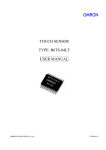
1
B6TS-16LF
TYPE: B6TS-16LF
TOUCH-SENSING IC
USER MANUAL
OMRON KURAYOSHI Co., Ltd.
1
Ver. 071211 rev. 12.14
B6TS-16LF
Ver. 071211 rev. 12.14
Introduction
Thank you very much for purchasing the touch sensor.
The touch sensor is a product that has been developed based on our advanced technology and rich experience.
This user manual describes the information necessary for use of the sensor, such as its functions, capabilities and proper
usage.
When using the touch sensor, please keep the following in mind:
・ Only specialists with knowledge of electricity must handle the touch sensor.
・ Please read and understand the contents of this manual thoroughly to use the touch sensor appropriately.
・ Keep this manual handy to refer to at any time you need it.
Points to note when using the touch sensor
Although OMRON makes constant efforts to improve the quality and reliability of its semiconductor products, products
such as this touch sensor may malfunction or break.
Before using the touch sensor, please contact OMRON’s business development personnel, if necessary, to confirm
product specifications, while also paying attention to using the sensor with a sufficient margin allowed for its ratings
and capabilities, and taking safety measures such as installing safety circuits to minimize hazards in the unlikely
event that a failure of the sensor might occur.
x Basically, this product is not designed and manufactured for use in equipment or systems operated under potentially
hazardous conditions. If you intend to use the touch sensor with any of the following systems, facilities or equipment, be
sure to consult OMRON sales personnel or an agent or dealership first:
(A) Atomic power control equipment, incineration facilities, railroads, aircraft, vehicle equipment, medical
appliances, amusement machines, safety devices, and facilities that must comply with the regulations of
administrative agencies and their respective industries.
(B) Systems, machines and devices that are potentially hazardous to humans and property.
(C) Other usages that require a high degree of safety.
The technical information contained in this manual is prepared only to describe typical performances and application
examples of the product. Application of the products based on the information does not infer the grant of any OMRON or
third party intellectual property, right or license.
x
1. Preventing malfunction caused by contact with an electric conductor other than a human finger with the touch electrode
Because this product measures the electrostatic capacitance of the detector (electrode), the product may operate
if something other than a human finger is brought into contact with the electrode. Therefore, a fail-safe design is
required for use of the product so that it does not cause any functional or safety problem even on such occasions.
Substances, etc., that may cause a malfunction if they are present near to or on the detector are:
・ Water, metal, animals, other conductive materials
2. Preventing operational error
Because this product detects human touch, it may operate if the detector (electrode) is touched only lightly or if
somebody remains nearby. When incorporating this product into a device, check the detection range thoroughly,
and employ measures to prevent the device from malfunctioning caused by operational error.
Especially, if the device is used where children may come into contact with it, provide some safety measure such
as a child safety lock.
3. Preventing the entry of water or corrosive gases
If water or a corrosive gas enters the operating part of the sensor (electrode), in the event of a short circuit or
corrosion of the electrode, the sensor may malfunction or its detection sensitivity may be lowered. If the product is
supposed to be used in an environment where this may occur, employ some structure to prevent the entry of
water or gas, and check to be sure in actual operation that the device is protected securely against such an event.
4. Preventing malfunction caused by noise
The product may malfunction if subjected to excessive noise.
Check to be sure that no safety problems are caused by excessive noise.
5. Preventing direct touching of the electrode
Do not employ any structure that exposes the surface of the touch electrode to the air and allows somebody to
touch the metal part of the touch electrode directly. Otherwise, the safety of the product may be impaired,
accumulated electrostatic charges may damage the product, or the electrode may corrode. Adopt a structure that
covers the surface of the touch electrode with nonconductive material and does not allow anybody to touch the
metal part of the electrode directly.
The recommended thickness for the nonconductive material is:
Resin material (dielectric constant of 2 to 3): no more than 2mm
Glass material (dielectric constant of about 5): no more than 4mm
2
B6TS-16LF
6.
Ver. 071211 rev. 12.14
Configurable data
When setting data with commands, consider the environment and conditions for using the touch sensor (e.g.,
location and circuit configuration) to determine proper values which may not cause functional or safety problems.
3
B6TS-16LF
Ver. 071211 rev. 12.14
Proper usage
1. Method of transportation and storage
(1)
Do not drop or apply any shock to the touch sensor because it is a precision device.
If the sensor is thrown or dropped, it may break.
(2)
When carrying or storing the touch sensor, keep its packaging properly oriented.
If the packaging is placed upside down or tilted, the sensor may be subjected to some undue force and may break.
(3)
Store the touch sensor under the following conditions to prevent the package from absorbing moisture:
Otherwise, the sensor may break when the package is mounted.
<Storage conditions>
A. Before opening the moisture-proof pack (aluminum laminate pack):
[Temperature, humidity]
-65 - 150°C, -80% or less RH
[Term of validity]
One year
When the sensor is used after a long period of storage, make sure that no damage, dirt, or rust is
present on the pack.
B. After opening the moisture-proof pack (aluminum laminate pack):
Until the package is mounted, the following conditions are recommended for storage of the package:
(In accordance with MSL3/JEDEC-STD-020)
[Temperature, humidity]
30°C 60% RH
[Term of validity]
168 hours
C. Temporary storage after opening the moisture-proof pack:
After opening the moisture-proof pack, it is recommended to store any parts remaining in the same
package after mounting due to your manufacturing quantity reason in a desicator (device to keep
temperature constant and humidity as low as 20% or less RH), or return them into the moisture-proof
pack then seal the pack immediately after using them.
Do not use or store the touch sensor where it will be subject to corrosive gases such as hydro sulfuric
gas or salt air, or exposed to oil or direct sunlight.
(4) Do not use or store the touch sensor where it will be subject to corrosive gases such as hydro sulfuric gas or salt air,
or exposed to oil or direct sunlight.
(5)
Where either of the following conditions [1] or [2] is applicable, baking the sensor package in the following manner
is recommended in order to remove moisture:
The tray used in the moisture-proof pack can be stored in a high-temperature chamber because it is heat-resistant.
However, place the tray on a flat base such as a level block, and then cool it down on the base to prevent
deformation after baking.
[1] The above storage conditions A-C are exceeded.
[2] The color of the 30% RH detection part of the indicator changes to lavender or pink.
<Baking method>
[Temperature]
[Time]
[Number of times]
125°C
6 hours
Up to three (Cumulative time limit: 72 hours)
2. Measures against electrostatic charges during handling
Keep the relevant electric equipment, work-bench and worker at the same potential.
Lay a conductive mat with a surface resistance of 10 kΩ- 10 MΩ on the work-bench, and ground the mat.
The user must make sure that there is no electric leakage from the electric equipment to ground. The electric leakage
must be limited by the use of a resistor of about 1 MΩ for safety. All safety regulations must be observed.
Any electric leakage from the electric equipment is undesirable from the viewpoint of worker safety.
Check to be sure that there is no electric leakage from the tester, curve tracer, oscilloscope, or the like, and then
ground the equipment. Any electric leakage can break the CMOS IC.
The same precautions apply to soldering irons.
4
B6TS-16LF
Ver. 071211 rev. 12.14
3. Recommended soldering Conditions
Recommended soldering conditions (Pb free)
Temperature conditions for mounting the IC chip
When mounting the IC chip at a high temperature by using reflow soldering, the melting temperature of the solder
depends on the mounting board and paste adhesive materials of the mounting board and the paste adhesive.
Referring to the mounting temperature profile shown in the following figure, choose the optimum soldering
temperature within the profile.
(1)
Reflow method (infrared light reflow and air reflow)
260°C (max)
250°C or higher for 10 Package surface
temperature (°C)
125°C
220°C or higher for 60 - 90 sec.
150 - 210 sec.
Figure: Reflow Method - Temperature Profile
Tsu(SETUP)
(2) Wave soldering method (called known as flow soldering or dip soldering)
Wave soldering method using Pb-free solder is not recommended.
(3) Soldering iron (manual soldering)
Solder using a soldering iron for semiconductor devices under the following conditions:
[Iron tip temperature]
350 ± 5°C
[Soldering time]
No longer than 5 sec/pin
4. Recommended wash conditions
The wash conditions compliant to MIL-STD-883C are recommended.
When using rosin flux wash, check the following items:
(1) Amount of contamination containing residual ions (or no ions)
(2) Administrative directions and regulations
(3) Melting resistance of parts
5. Handling after mounting parts on PCB
When dividing a PCB on which ICs are mounted, do not apply any excessive force to the ICs. Otherwise, the internal IC
chips may be broken.
6. Applied voltages and currents
(1)
Do not apply to any pin any voltage or current that exceeds the absolute maximum ratings.
(2)
Use the device within the recommended specifications to enhance the quality of the device.
(3)
Do not apply any forward bias to any of the pins.
Otherwise, excessive forward current may cause thermal breakdown of the IC.
(4)
Do not connect any output pin directly to power. If any output pin is directly connected to low-impedance
power, the internal wiring may melt down or break thermally due to excessive current.
5
B6TS-16LF
CONTENT
1. Overview
2. Pin connections
3. Operation mode
4. Measurement
5. Serial communication
6. Commands
7. Teaching
8. Electrical characteristics
9. Appearance and dimensions
6
Ver. 071211 rev. 12.14
B6TS-16LF
1.
Ver. 071211 rev. 12.14
Overview
This chip is a touch-sensing IC to detect micro capacitances and can be used in touch sensors.
Internally, the chip employs the CMOS process and is contained in a 52-pin TQFP plastic package.
The IC has 16 independent measurement pins, of which each can measure capacitance independently.
On/Off (only 2CH) and serial communication output can be selected as the output mode.
The IC is provided with an EEPROM that can store operation mode and other parameters.
Pin arrangement diagram
52
51
50
49
48
47
46
45
44
43
42
41
40
MOSI(SD)
2.1
Pin connections
CH0A
COM01
CH1A
NC
CH2A
COM23
CH3A
NC
CH4A
COM45
CH5A
NC
2.
NC
SCK
MISO
39
38
37
36
35
34
33
32
31
30
29
28
27
NC
NC
CH6A
COM67
CH7A
NC
NC
CH8A
COM89
CH9A
RxD
TxD
SETUP
NC
NC
CH15A
COMEF
CH14A
NC
CH13A
COMCD
CH12A
NC
CH11A
COMAB
CH10A
14
15
16
17
18
19
20
21
22
23
24
25
26
SCS
TEST
OUT_A
OUT_B
RESET
MEAS
Vss2
I
FSEL
Vdd2
CHG
1
2
3
4
5
6
7
8
9
10
11
12
13
Note: TEST terminal (5pin) is used for testing during manufacture of the IC.
During normal operation of the IC, connect it to Vdd through a pull-up resistor.
2.2
Pin functions
Pin
No.
Designation
Input/
Output
Function
51
49
47
45
43
41
37
35
32
30
24
22
20
18
16
14
CH0A
CH1A
CH2A
CH3A
CH4A
CH5A
CH6A
CH7A
CH8A
CH9A
CH10A
CH11A
CH12A
CH13A
CH14A
CH15A
I/O
Measurement pins (channels 15 - 0)
Connect these pins to the touch electrode through resistors.
50
46
42
36
31
23
19
15
COM01
COM23
COM45
COM67
COM89
COMAB
COMCD
COMEF
I/O
Common-use measurement pins (channels 15 - 0)
Common-use measurement pins for two channels each
Connect these pins to charge capacitors through resistors.
7
B6TS-16LF
Pin
No.
Designation
Input/
Output
Ver. 071211 rev. 12.14
Function
12
Vdd
I
Power Supply Input (3.0 - 5.5V)
10
Vss
I
Ground
11
IFSEL
I
Select pin for SPI interface mode
Pull-up is for 4-wire SPI / Pull-down is for 3-wire SPI
6
───
OUT_A
O
Any channel can be specified for this output pin (logic switching is
available).
7
───
OUT_B
O
Any channel can be specified for this output pin (logic switching is
available).
An output pin which indicates the operation status.
[Normal measurement mode]
Outputs measurement results.
[Serial communication mode] Measurement termination output
Two output modes are available:
1. High-signal output every time a measurement finishes.
2. High-signal output when the condition changes in any one of
the channels (touch→no touch, no touch→touch).
[Setup mode]
When setup mode is entered, CHG pin goes high.
However, when EEPROM write command is received and data is
being written in EEPROM, CHG pin remains low.
13
CHG
O
52
MOSI
(SD)
I
(I/O)
3
MISO
O
In using 4-wire SPI : Serial communication data output
2
SCK
I
Serial communication clock input
4
SCS
I
Serial communication mode chip select input
27
───
SETUP
I
Setup mode. Low input to this pin moves the chip into setup mode.
(To suppress noise, connect to Vss via a bypass capacitor of 0.01 µF
in addition to resistor.)
28
TxD
O
UART serial communication data output
RxD
I
UART serial communication data input
29
In using 4-wire SPI : Serial communication data input
(In using 3-wire SPI : Serial communication data I/O)
9
MEAS
I
Initiation of measurement. Capacitance measurement is initiated by
inputting high to this pin.
While low is input to this pin, the chip is held in standby status.
5
TEST
I
(Connect to Vdd through a pull-up resistor)
8
───
RESET
I
Reset signal input.
Inputting low to this pin resets the chip.
Built-in power-on reset can work with around 5kΩpull-up resistor (no
need external reset circuit)
8
B6TS-16LF
2.3
Ver. 071211 rev. 12.14
Example of circuit
Note 1: Connect Rr, Cr, Rc, and Cc to each touch electrode, as shown in the diagram below.
Refer to the design tool (B6Tworkbench – Circuit Constants) for recommended values.
* Reference values: Rr=10kΩ, Cr=22pF, Rc=4.7kΩ, Cc=0.1μF
VDD VDD VDD VDD VDD VDD VDD
Deleted: <sp>
<sp>
VDD
12
2
3
52
8
9
27
4
13
6
7
29
28
11
CH1
5
CH1
4
CH1
3
CH1
2
20
19
18
16
15
14
SCK
MISO
CH0
A
COM01
MOSI
CH1
A
CH2
A
COM23
RESET
MEAS
SCS
SETUP
CHG
OUT _A
OUT _B
CH
3A
CH4
A
COM45
RxD
TxD
CH5A
CH6A
IFSEL
COM67
CH15A
CH7
A
CH8A
COMEF
COM89
CH14A
CH9A
CH13A
CH10A
COMCD
COMAB
CH12A
CH11A
VS
S 10
51
CH0
50
49
47
CH1
CH2
46
45
43
CH3
CH4
42
41
37
CH5
CH6
36
35
32
CH7
CH8
31
30
24
23
22
CH9
CH1
0
CH1
1
Note 2: Connect a bypass capacitor of about 0.1 µF between Vdd and Vss using wires as short as possible.
Note 3: Connect a bypass capacitor of about 0.01 µF between /SETUP pin and Vss.
Note 4: When UART is not used, connecting RxD pin (29pin) to VDD through a pull-up resistor as possible as
near from this IC.
Note 5: When 3-wire SPI is used (pull-down at IFSEL), MOSI pin operates as SD(I/O) and MISO has no
function (floating – not connected).
Note 6: IFSEL terminal (11pin) is for selecting pin for SPI interface mode.
Pull-up is for 4-wire SPI / pull-down is for 3-wire SPI.
9
B6TS-16LF
3.
Ver. 071211 rev. 12.14
Operation mode
This chip has three operating modes. Each mode is selected by the MEAS pin and /SETUP pin.
(1)
Normal measurement mode -------------
Normal operation mode to detect touch/no-touch.
Serial communication and On/Off output mode can be used.
(1-1) On/off output mode ------------------------
OUT_A and OUT_B pins are used. (Only 2ch can be used)
Touch/no-touch detection results are output from the respective
channels with low/high signal.
* Output logic can be set with BPOL command.
(1-2) Serial communication output -----------
Measured results are transmitted in serial below.
1. 4-wire SPI using SCK, /SCS, MOSI, MISO signals.
2. 3-wire SPI using SCK, /SCS, SD signals.
3. UART using RxD, TxD signals.
(2)
Setup mode ---------------------------------
Chip operation is set to serial communication.
(3)
Standby mode ------------------------------
Mode to non-measurement.
This can be used for measurement synchronous among multiple B6TS
/SETUP pin
MEAS pin
HIGH
HIGH
Normal measurement mode
HIGH
LOW
Standby - without executing measurements
LOW
Operation mode
HIGH or LOW Setup mode
Setup mode
Standby status
/SETUP pin = HIGH
MEAS pin = LOW
/SETUP pin = LOW
MEAS pin = HIGH or LOW
/SETUP pin = HIGH
MEAS pin = HIGH
Normal measurement mode
On/Off output
OUT_A / OUT_B
Serial communication
SPI / UART
/S
E
T
10
/SETUP pin = HIGH
MEAS pin = HIGH
B6TS-16LF
4.
Ver. 071211 rev. 12.14
Measurement
The chip measures the discharge of the charge stored in the charge capacitor. When a finger is placed close to the
touch electrode, the electrostatic capacitance of the electrode increases and the discharge time for the charge
becomes shorter. The chip has a built-in counter to measure the discharge period. Whether the sensor has been
touched or not is judged according to whether the length of the discharge period exceeds a specified value or not.
Hereafter, the length of the discharge period is referred to as the measured value.
The measured value when the sensor is not touched is called the reference value. The change of the measured value
which allows a judgment that the sensor is touched is called judging change and the change of the measured value
when returning from on status is called hysteresis. These 3 parameters define the switching characteristics of each
touch channel and can be set for each channel independently.
The relationships between the measured value and the above values are as follows:
[Measured value] < [Reference value]-[judging change]
[Measured value] > [Reference value]-[Judging change]+Hysteresis
→ Touch
→ Touch to no touch
Measured
value
Touch on
electrode
Reference
value
judging change
Hysteresis
Time
Judged as "touched"
Even in the no-touched state, the measured value changes according to variation in the environment (output drift).
The chip is provided with an automatic drift compensation function, which can cancel mild changes of the measured
value due to variation in the environment. The drift compensation function can be enabled or disabled in setup mode.
11
B6TS-16LF
5.
Ver. 071211 rev. 12.14
Serial communication
It is possible to read out measured values and set the operation mode by sending/receiving data to/from this chip
through serial communication.
Serial communication is performed with the three-wire SPI or UART using SCS (chip select), SCK (transfer clock), and
SD (data transmission and reception: host -> B6TS, B6TS -> host).
* Be sure to use only SPI or UART with your design.
If you use both of SPI and UART, communication errors may occur due to out of synchronization.
5.1
SPI communication
The SPI communication method works as follows:
(Refer to “8. Electrical specifications” for specific communication timing, etc.)
・
・
・
Operation in SPI slave mode
Supply SCS (chip select) and SCK (transfer clock) from an external source.
SCK (transfer clock) is set to high during idling. The data is latched at the rising edge of the clock.
The data (SD) is in MSB first format.
This chip sends/receives data using 4 bytes, consisting of a command byte, dummy bytes, and 2 data bytes.
Command: 1 byte (MSB 1 bit is used for the read/write flag.)
Bank data: 1 byte (0x00 or 0x80 is set when accessing to commands 0x00 - 0x7F or 0x80 - 0xFF respectively.)
Data: 2 bytes
5.1.1
4-wire SPI outline
(Data direction: B6T→Host)
Dummy data
BANK(8bit)
Dummy data
Dummy data
Data (upper 8bit)
Dummy data
Data (lower 8bit)
(Data direction: Host→B6T)
Dummy data
BANK(8bit)
Data (upper 8bit)
Data (lower 8bit)
Dummy data
Dummy data
Dummy data
12
B6TS-16LF
Ver. 071211 rev. 12.14
5.1.2 3-wire SPI outline
(Data direction: B6T→Host)
BANK (8 bits)
Data (upper 8 bits)
Data (lower 8 bits)
BANK (8 bits)
Data (upper 8 bits)
Data (lower 8 bits)
(Data direction: Host→ B6T)
If data communication is performed during normal measurement mode, the measurement operation stops while the
data is communicated.
Measurement will restart after communication completes (when measurement has been interrupted, values from the
last measurement are read).
* If SCS is disabled while data is being transmitted or received, data transmitted or received by B6T up to that moment
is lost.
* I/O of the SD pin toggles according to the data direction. Be sure to change the host pin I/O according to the SD pin
direction.
13
B6TS-16LF
5.2
5.3
Ver. 071211 rev. 12.14
UART communication
The UART communication method works as follows:
Bit rate
:
38400 bps
Data length
:
8 bits
Parity
:
None
Number of stop bits
:
1
Command access
z Access to commands 0x00 - 0x7F. (BANK data=0x00, refer to 5.1 SPI communication)
z For read operation:
z For write operation:
Command Code. + 0x00 (BANK)
Command Code. | 0x80+ 0x00 (BANK) + data (upper 8 bits) + data (lower 8 bits)
z Access to commands 0x80 - 0xFF. (BANK data=0x80, refer to 5.1 SPI communication)
z For read operation:
Command Code. & 0x7F + 0x80 (BANK)
z For write operation: Command Code. & 0x7F| 0x80+ 0x80 (BANK) + data (upper 8 bits) + data (lower 8 bits)
* In accessing to commands 0x80 - 0xFF, be sure to excute AND operation with Command code & 0x7F.
* For write accesses, transmit each command ORed with 0x80.
6.
Commands
The commands and data used in serial communication are listed below:
The data comprises read only data (read) and read/write data (read/write). If a write command is applied to read only
data, the operation will be invalid.
Some data is not accessible in some operation modes. If inaccessible data is read out, the read data is indefinite. If
inaccessible data is written, the data is ignored.
Command code (Designation)
Main function
Read/write
restriction
Access limit
Normal measurement Setup mode
mode (in serial
communication
mode)
0x00(ID) - 0x31(CHYS11)
0x82(DCH12) - 0x85(DCH15)
Measured data
Read only
Accessible
0x8E(CREF12) - 0x99(CHYS15)
Accessible
0x39(CHEN) - 0x7B(ACDN11)
0xBB(OUTSEL)
0xC0(REF12) - 0xD3(ACDN15)
Parameter
setting
Read/write
Inaccessible
When writable data are written in this chip, the built-in register corresponding to each command is rewritten. Then, if
the normal measurement mode is entered, the chip can be operated with the written parameters (mode, etc.). In this
case, because only the built-in register is rewritten, the value in each register returns to its original value (value stored
in EEPROM) when power is turned off and on again.
To store the built-in register value in EEPROM, an EEPROM write command (0x3F) must be received. When an
EEPROM write command is received, the content of the register is stored in EEPROM.
* In actual writing procedure, transmit the command 0xBF(=0x80+0x3F) + 0x00 + 0x53 + 0x54
after transition to SETUP mode.
14
B6TS-16LF
List of commands
BANK0: (Bank data=0x00)
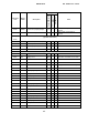
0x00
ID
Chip ID
R
○
○ 0x0101 for this chip.
0x01
BDATA
Detected result of each channel
R
○
○ 1 channel 1 bit
0x02
DCH0
Ch0 measured value
R
○
○
0x03
DCH1
Ch1 measured value
R
○
○
0x04
DCH2
Ch2 measured value
R
○
○
0x05
DCH3
Ch3 measured value
R
○
○
0x06
DCH4
Ch4 measured value
R
○
○
0x07
DCH5
Ch5 measured value
R
○
○
0x08
DCH6
Ch6 measured value
R
○
○
0x09
DCH7
Ch7 measured value
R
○
○
0x0A
DCH8
Ch8 measured value
R
○
○
0x1B
DCH9
Ch9 measured value
R
○
○
0x1C
DCH10
Ch10 measured value
R
○
○
0x0D
DCH11
Ch11 measured value
R
○
○
0x0E
CREF0
Current Ch0 reference value
R
○
○
Result of drift compensation is
reflected.
0x0F
CTHR0
Current Ch0 judging change
R
○
○
Result of drift compensation is
reflected.
0x10
CHYS0
Current Ch0 hysteresis value
R
○
○
Result of drift compensation is
reflected.
0x11
CREF1
Current Ch1 reference value
R
○
○
Result of drift compensation is
reflected.
0x12
CTHR1
Current Ch1 judging change
R
○
○
Result of drift compensation is
reflected.
0x13
CHYS1
Current Ch1 hysteresis value
R
○
○
Result of drift compensation is
reflected.
0x14
CREF2
Current Ch2 reference value
R
○
○
Result of drift compensation is
reflected.
0x15
CTHR2
Current Ch2 judging change
R
○
○
Result of drift compensation is
reflected.
0x16
CHYS2
Current Ch2 hysteresis value
R
○
○
Result of drift compensation is
reflected.
0x17
CREF3
Current Ch3 reference value
R
○
○
Result of drift compensation is
reflected.
0x18
CTHR3
Current Ch3 judging change
R
○
○
Result of drift compensation is
reflected.
Command
code
Designation
Description
15
Setup mode
Normal measurement
mode
Access limit
Read (R)/Write (W)
6.1
Ver. 071211 rev. 12.14
Note
B6TS-16LF
Ver. 071211 rev. 12.14
Read (R)/Write (W)
Normal measurement
mode
Setup mode
Access limit
0x19
CHYS3
Current Ch3 hysteresis value
R
○
○
Result of drift compensation is
reflected.
0x1A
CREF4
Current Ch4 reference value
R
○
○
Result of drift compensation is
reflected.
0x1B
CTHR4
Current Ch4 judging change
R
○
○
Result of drift compensation is
reflected.
0x1C
CHYS4
Current Ch4 hysteresis value
R
○
○
Result of drift compensation is
reflected.
0x1D
CREF5
Current Ch5 reference value
R
○
○
Result of drift compensation is
reflected.
0x1E
CTHR5
Current Ch5 judging change
R
○
○ Result of drift compensation is
reflected.
0x1F
CHYS5
Current Ch5 hysteresis value
R
○
○ Result of drift compensation is
reflected.
0x20
CREF6
Current Ch6 reference value
R
○
○ Result of drift compensation is
reflected.
0x21
CTHR6
Current Ch6 judging change
R
○
○ Result of drift compensation is
reflected.
0x22
CHYS6
Current Ch6 hysteresis value
R
○
○ Result of drift compensation is
reflected.
0x23
CREF7
Current Ch7 reference value
R
○
○ Result of drift compensation is
reflected.
0x24
CTHR7
Current Ch7 judging change
R
○
○ Result of drift compensation is
reflected.
0x25
CHYS7
Current Ch7 hysteresis value
R
○
○ Result of drift compensation is
reflected.
0x26
CREF8
Current Ch8 reference value
R
○
○ Result of drift compensation is
reflected.
0x27
CTHR8
Current Ch8 judging change
R
○
○
Result of drift compensation is
reflected.
0x28
CHYS8
Current Ch8 hysteresis value
R
○
○
Result of drift compensation is
reflected.
0x29
CREF9
Current Ch9 reference value
R
○
○
Result of drift compensation is
reflected.
0x2A
CTHR9
Current Ch9 judging change
R
○
○
Result of drift compensation is
reflected.
0x2B
CHYS9
Current Ch9 hysteresis value
R
○
○
Result of drift compensation is
reflected.
0x2C
CREF10
Current Ch10 reference value
R
○
○
Result of drift compensation is
reflected.
0x2D
CTHR10
Current Ch10 judging change
R
○
○
Result of drift compensation is
reflected.
0x2E
CHYS10
Current Ch10 hysteresis value
R
○
○
Result of drift compensation is
reflected.
0x2F
CREF11
Current Ch11 reference value
R
○
○
Result of drift compensation is
reflected.
Command
code
Designation
Description
16
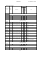
Note
B6TS-16LF
Ver. 071211 rev. 12.14
Command
code
Designation
Read (R)/Write (W)
Normal measurement
mode
Setup mode
Access limit
0x30
CTHR11
Current Ch11 judging change
R
○
○
Result of drift compensation is
reflected.
0x31
CHYS11
Current Ch11 hysteresis value
R
○
○
Result of drift compensation is
reflected.
Description
0x32
:
0x35
Note
(System reservation)
0x36
MSA
Maximum sequential ON input.
R/W
○
0x37
DCI
Drift compensation interval
R/W
○
0x38
BPOL
On/off output polarity select
R/W
○
0x39
CHEN
Channel measurement enable
R/W
○
0x3B
TOG
Toggle action
R/W
○
0x3C
ACD
judging count
R/W
○
0x3D
SLP
Sleep time
R/W
○
0x3E
MODE
Operation mode
R/W
○
0x3F
ROMSTR EEPROM write
R/W
○ Writing into ROM with dummy write
0x40
REF0
Ch0 reference value
R/W
○
0x41
THR0
Ch0 judging change
R/W
○
0x42
HYS0
Ch0 hysteresis
R/W
○
0x43
RTHR0
Ch0 On-judgment ratio
R/W
○
0x44
RHYS0
Ch0 hysteresis ratio
R/W
○
0x45
REF1
Ch1 reference value
R/W
○
0x46
THR1
Ch1 judging change
R/W
○
0x47
HYS1
Ch1 hysteresis
R/W
○
0x48
RTHR1
Ch1 On-judgment ratio
R/W
○
0x3A
(System reservation)
0x49
RHYS1
Ch1 hysteresis ratio
R/W
○
0x4A
REF2
Ch2 reference value
R/W
○
0x4B
THR2
Ch2 judging change
R/W
○
0x4C
HYS2
Ch2 hysteresis
R/W
○
0x4D
RTHR2
Ch2 On-judgment ratio
R/W
○
0x4E
RHYS2
Ch2 hysteresis ratio
R/W
○
0x4F
REF3
Ch3 reference value
R/W
○
17
Lower 8bit : cumulative count in ON
Upper 8bit : cumulative count in OFF
B6TS-16LF
Ver. 071211 rev. 12.14
0x50
Description
Setup mode
Designation
Normal measurement
mode
Command
code
Read (R)/Write (W)
Access limit
THR3
Ch3 judging change
R/W
○
0x51
HYS3
Ch3 hysteresis
R/W
○
0x52
RTHR3
Ch3 On-judgment ratio
R/W
○
0x53
RHYS3
Ch3 hysteresis ratio
R/W
○
0x54
REF4
Ch4 reference value
R/W
○
0x55
THR4
Ch4 judging change
R/W
○
0x56
HYS4
Ch4 hysteresis
R/W
○
0x57
RTHR4
Ch4 On-judgment ratio
R/W
○
0x58
RHYS4
Ch4 hysteresis ratio
R/W
○
0x59
REF5
Ch5 reference value
R/W
○
0x5A
THR5
Ch5 judging change
R/W
○
0x5B
HYS5
Ch5 hysteresis
R/W
○
0x5C
RTHR5
Ch5 On-judgment ratio
R/W
○
0x5D
RHYS5
Ch5 hysteresis ratio
R/W
○
0x5E
REF6
Ch6 reference value
R/W
○
0x5F
THR6
Ch6 judging change
R/W
○
0x60
HYS6
Ch6 hysteresis
R/W
○
0x61
RTHR6
Ch6 On-judgment ratio
R/W
○
0x62
RHYS6
Ch6 hysteresis ratio
R/W
○
0x63
REF7
Ch7 reference value
R/W
○
0x64
THR7
Ch7 judging change
R/W
○
0x65
HYS7
Ch7 hysteresis
R/W
○
0x66
RTHR7
Ch7 On-judgment ratio
R/W
○
0x67
RHYS7
Ch7 hysteresis ratio
R/W
○
0x68
REF8
Ch8 reference value
R/W
○
0x69
THR8
Ch8 judging change
R/W
○
0x6A
HYS8
Ch8 hysteresis
R/W
○
0x6B
RTHR8
Ch8 On-judgment ratio
R/W
○
0x6C
RHYS0
Ch8 hysteresis ratio
R/W
○
0x6D
REF9
Ch9 reference value
R/W
○
0x6E
THR9
Ch9 judging change
R/W
○
0x6F
HYS9
Ch9 hysteresis
R/W
○
0x70
RTHR9
Ch9 On-judgment ratio
R/W
○
18
Note
B6TS-16LF
Ver. 071211 rev. 12.14
Description
Setup mode
Designation
Normal measurement
mode
Command
code
Read (R)/Write (W)
Access limit
RHYS9
Ch9 hysteresis ratio
R/W
○
0x72
REF10
Ch10 reference value
R/W
○
0x73
THR10
Ch10 judging change
R/W
○
0x74
HYS10
Ch10 hysteresis
R/W
○
RTHR10
Ch10 On-judgment ratio
R/W
○
0x76
RHYS10
Ch10 hysteresis ratio
R/W
○
0x77
REF11
Ch11 reference value
R/W
○
0x78
THR11
Ch11 judging change
R/W
○
0x79
HYS11
Ch11 hysteresis
R/W
○
0x7A
RTHR11
Ch11 On-judgment ratio
R/W
○
0x7B
RHYS11
Ch11 hysteresis ratio
R/W
○
0x71
0x75
0x7C
:
0x7F
(System reservation)
19
Note
B6TS-16LF
Ver. 071211 rev. 12.14
BANK1: (Bank data=0x80)
Description
0x80
Setup mode
Designation
Normal measurement
mode
Command
code
Read (R)/Write (W)
Access limit
Note
(System reservation)
0x81
0x82
DCH12
Ch12 measured value
R
○
○
0x83
DCH13
Ch13 measured value
R
○
○
0x84
DCH14
Ch14 measured value
R
○
○
0x85
DCH15
Ch15 measured value
R
○
○
0x86
:
0x8D
(System reservation)
0x8E
CREF12
Current Ch12 reference value
R
○
○
Result of drift compensation is
reflected.
0x8F
CTHR12
Current Ch12 judging change
R
○
○
Result of drift compensation is
reflected.
0x90
CHYS12
Current Ch12 hysteresis value
R
○
○
Result of drift compensation is
reflected.
0x91
CREF13
Current Ch13 reference value
R
○
○
Result of drift compensation is
reflected.
0x92
CTHR13
Current Ch3 judging change
R
○
○
Result of drift compensation is
reflected.
0x93
CHYS13
Current Ch13 hysteresis value
R
○
○
Result of drift compensation is
reflected.
0x94
CREF14
Current Ch14 reference value
R
○
○
Result of drift compensation is
reflected.
0x95
CTHR14
Current Ch14 judging change
R
○
○
Result of drift compensation is
reflected.
0x96
CHYS14
Current Ch14 hysteresis value
R
○
○
Result of drift compensation is
reflected.
0x97
CREF15
Current Ch15 reference value
R
○
○
Result of drift compensation is
reflected.
0x98
CTHR15
Current Ch15 judging change
R
○
○
Result of drift compensation is
reflected.
0x99
CHYS15
Current Ch15 hysteresis value
R
○
○
Result of drift compensation is
reflected.
0x9A
:
0xBA
0xBB
(System reservation)
OUTSEL Channel setting for OUT pins
0xBC
:
0xBF
R/W
○
(System reservation)
0xC0
REF12
Ch12 reference value
R/W
○
0xC1
THR12
Ch12 judging change
R/W
○
20
B6TS-16LF
Ver. 071211 rev. 12.14
Description
Setup mode
Designation
Normal measurement
mode
Command
code
Read (R)/Write (W)
Access limit
0xC2
HYS12
Ch12 hysteresis
R/W
○
0xC3
RTHR12
Ch12 On-judgment ratio
R/W
○
0xC4
RHYS12
Ch12 hysteresis ratio
R/W
○
0xC5
REF13
Ch13 reference value
R/W
○
0xC6
THR13
Ch13 judging change
R/W
○
0xC7
HYS13
Ch13 hysteresis
R/W
○
0xC8
RTHR13
Ch13 On-judgment ratio
R/W
○
0xC9
RHYS13
Ch13 hysteresis ratio
R/W
○
0xCA
REF14
Ch14 reference value
R/W
○
0xCB
THR14
Ch14 judging change
R/W
○
0xCC
HYS14
Ch14 hysteresis
R/W
○
0xCD
RTHR14
Ch14 On-judgment ratio
R/W
○
0xCE
RHYS14
Ch14 hysteresis ratio
R/W
○
0xCF
REF15
Ch15 reference value
R/W
○
0xD0
THR15
Ch15 judging change
R/W
○
0xD1
HYS15
Ch15 hysteresis
R/W
○
RTHR15
Ch15 On-judgment ratio
R/W
○
RHYS15
Ch15 hysteresis ratio
R/W
○
0xD2
0xD3
0xD4
:
0xFF
(System reservation)
21
Note
B6TS-16LF
Ver. 071211 rev. 12.14
6.2
Description of commands
6.2.1 ID: Chip ID (read only)
Used as ID of the chip. The data is fixed to 0x0101
Command code
0x00
15
14
13
12
11
10
0
0
0
0
0
0
9
0
8
7
1
0
6
0
5
0
4
0
3
0
2
0
1
0
0
1
6.2.2 BDATA: Detection result of touch/no-touch for each channel (read only)
Measured value for each channel is indicated by 1/0.
1: Off (no-touch), 0: On (touch) ; however; this is indicated, as stated per the BPOL command, stated in 6.2.9
Command code
0x01
15
14
13
12
11
10
CH15 CH14 CH13 CH12 CH11 CH10
9
CH9
8
CH8
7
CH7
6
CH6
5
CH5
4
CH4
3
CH3
2
CH2
1
CH1
0
CH0
6.2.3 DCHx: Measured value for each channel (read only)
Measured value for each channel is indicated by an unsigned 16-bit integer.
Command code
15
14
13
12
11
10
9
8
7
6
5
4
3
2
1
0
D15
D14
D13
D12
D11
D10
D9
D8
D7
D6
D5
D4
D3
D2
D1
D0
0x02..0x0D
0x82..0x85
Channel 0 (DCH0)
Channel 1 (DCH1)
Channel 2 (DCH2)
Channel 3 (DCH3)
Channel 4 (DCH4)
Channel 5 (DCH5)
Channel 6 (DCH6)
Channel 7 (DCH7)
Channel 8 (DCH8)
Channel 9 (DCH9)
Channel 10 (DCH10)
Channel 11 (DCH11)
Channel 10 (DCH12)
Channel 11 (DCH13)
Channel 10 (DCH14)
Channel 11 (DCH15)
Command code 0x02
Command code 0x03
Command code 0x04
Command code 0x05
Command code 0x06
Command code 0x07
Command code 0x08
Command code 0x09
Command code 0x0A
Command code 0x0B
Command code 0x0C
Command code 0x0D
Command code 0x82
Command code 0x83
Command code 0x84
Command code 0x85
22
B6TS-16LF
Ver. 071211 rev. 12.14
6.2.4 CREFx: Current reference value for each channel (read only)
Current reference value for each channel is indicated by an unsigned 16-bit integer.
Command code
15
14
13
12
11
10
9
8
7
6
5
4
3
2
1
0
D15
D14
D13
D12
D11
D10
D9
D8
D7
D6
D5
D4
D3
D2
D1
D0
0x0E..0x2F
0x8E..0x97
Channel 0 (CREF0)
Channel 1 (CREF1)
Channel 2 (CREF2)
Channel 3 (CREF3)
Channel 4 (CREF4)
Channel 5 (CREF5)
Channel 6 (CREF6)
Channel 7 (CREF7)
Channel 8 (CREF8)
Channel 9 (CREF9)
Channel 10 (CREF10)
Channel 11 (CREF11)
Channel 12 (CREF12)
Channel 13 (CREF13)
Channel 14 (CREF14)
Channel 15 (CREF15)
6.2.5
Command code 0x0E
Command code 0x11
Command code 0x14
Command code 0x17
Command code 0x1A
Command code 0x1D
Command code 0x20
Command code 0x23
Command code 0x26
Command code 0x29
Command code 0x2C
Command code 0x2F
Command code 0x8E
Command code 0x91
Command code 0x94
Command code 0x97
CTHRx: Current variation for each channel judging change (read only)
Current variation for each channel judging change is indicated by an unsigned 16-bit integer.
Command code
15
14
13
12
11
10
9
8
7
6
5
4
3
2
1
0
D15
D14
D13
D12
D11
D10
D9
D8
D7
D6
D5
D4
D3
D2
D1
D0
0x0F..0x30
0xC1..0xD0
Channel 0 (CTHR0)
Channel 1 (CTHR1)
Channel 2 (CTHR2)
Channel 3 (CTHR3)
Channel 4 (CTHR4)
Channel 5 (CTHR5)
Channel 6 (CTHR6)
Channel 7 (CTHR7)
Channel 8 (CTHR8)
Channel 9 (CTHR9)
Channel 10 (CTHR10)
Channel 11 (CTHR11)
Channel 12 (CTHR12)
Channel 13 (CTHR13)
Channel 14 (CTHR14)
Channel 15 (CTHR15)
Command code 0x0F
Command code 0x12
Command code 0x15
Command code 0x18
Command code 0x1B
Command code 0x1E
Command code 0x21
Command code 0x24
Command code 0x27
Command code 0x2A
Command code 0x2D
Command code 0x30
Command code 0xC1
Command code 0xC6
Command code 0xCB
Command code 0xD0
23
B6TS-16LF
Ver. 071211 rev. 12.14
6.2.6 CHYSx: Current hysteresis for each channel (read only)
Current hysteresis for each channel is indicated by an unsigned 16-bit integer.
Command code
15
14
13
12
11
10
9
8
7
6
5
4
3
2
1
0
D15
D14
D13
D12
D11
D10
D9
D8
D7
D6
D5
D4
D3
D2
D1
D0
0x10..0x31
0x90..0x99
Channel 0 (CHYS0)
Channel 1 (CHYS1)
Channel 2 (CHYS2)
Channel 3 (CHYS3)
Channel 4 (CHYS4)
Channel 5 (CHYS5)
Channel 6 (CHYS6)
Channel 7 (CHYS7)
Channel 8 (CHYS8)
Channel 9 (CHYS9)
Channel 10 (CHYS10)
Channel 11 (CHYS11)
Channel 12 (CHYS12)
Channel 13 (CHYS13)
Channel 14 (CHYS14)
Channel 15 (CHYS15)
Command code 0x10
Command code 0x13
Command code 0x16
Command code 0x19
Command code 0x1C
Command code 0x1F
Command code 0x22
Command code 0x25
Command code 0x28
Command code 0x2B
Command code 0x2E
Command code 0x31
Command code 0x90
Command code 0x93
Command code 0x96
Command code 0x99
6.2.7 MSA Teaching measurement count (read/write enabled only in setup mode)
When a sequence of MSA x 64 On is detected, the Off status is assumed and the drift compensation is
forcibly executed. When MSA=0x00, this function is disabled (i.e., no forced drift compensation occurs).
This function allows canceling continuous ON status caused by an object placed over the electrode.
Default = 0 (no forced drift compensation) 8-bit unsigned integer representation
Command code
0x36
15
14
13
12
11
10
1
1
1
1
1
1
9
1
8
1
7
6
5
4
3
2
1
0
D7
D6
D5
D4
D3
D2
D1
D0
4
3
2
1
0
D2
D1
D0
2
1
0
6.2.8 DCI Teaching measurement count (read/write enabled only in setup mode)
(DCI)
Drift compensation per 2
is not executed. 3-bit unsigned integer.
5
Default = 5 (drift compensation occurs once per 2 =32 times.)
Command code
0x37
15
14
13
12
11
10
1
1
1
1
1
1
9
1
8
1
7
1
6
1
5
1
1
1
6.2.9 BPOL: On/Off output polarity (read/write enabled only in setup mode)
Sets the output polarity logic for the OUT_A and OUT_B pins.
0: Active Low (OUTx pins go Low for On) (Default)
1: Active High (OUTx pins go High for On)
*BPOL setting has an effect on output logic at OUT_A and OUT_B terminal, set in OUTSEL.
Command code
0x38
15
14
13
12
11
10
CH15 CH14 CH13 CH12 CH11 CH10
9
CH9
24
8
CH8
7
CH7
6
CH6
5
CH5
4
CH4
3
CH3
CH2
CH1
CH0
B6TS-16LF
6.2.10
CHEN: Measurement enable for each channel (read/write enabled only in setup mode)
Enable / Disbale measurement per channel
1: measurement executed, 0: not executed
Command code
0x39
6.2.11
15
14
13
12
11
10
CH15 CH14 CH13 CH12 CH11 CH10
9
CH9
8
CH8
7
CH7
6
CH6
5
CH5
4
CH4
3
CH3
2
CH2
1
CH1
0
CH0
TOG: Toggle action (read/write enabled only in setup mode)
Selects momentary or latching output mode. This output takes effect on the signals output from OUT_A or
Out_B and BDATA command data.
1: Toggle mode off (momentary action: turned on only during a touch event)
0: Toggle mode on (alternate action: turned on with the first touch event and off with the next touch event)
Command code
0x3B
6.2.12
Ver. 071211 rev. 12.14
15
14
13
12
11
10
CH15 CH14 CH13 CH12 CH11 CH10
9
CH9
8
CH8
7
CH7
6
CH6
5
CH5
4
CH4
3
CH3
2
CH2
1
CH1
0
CH0
ACD: Judging count (read/write enabled only in setup mode)
Only after consecutive measurement ACD value + 1{one times, a touch (or no-touch) is judged and this output
is varied. This takes effect on the output signals from OUT0 - 15 and BDATA command data.
For example, with ACD = 2, after three consecutive measurements are judged as a touch event (or no-touch
event), the output state changes.
The lower 8 bits are used to set the cumulative judgment count for Off to On transition (ACDon) and the upper
8 bits are used to set the cumulative judgment count for On to Off transition (ACDoff).
Command code
0x3C
15
14
13
12
11
10
9
8
7
6
5
4
3
2
1
0
D15
D14
D13
D12
D11
D10
D9
D8
D7
D6
D5
D4
D3
D2
D1
D0
D7 - D0
D15 - D8
: ACDon (Default: 0010b)
Sets the cumulative judgment count for touch Off to On transition.
: ACDoff (Default: 0010b)
Sets the cumulative judgment count for touch On to Off transition.
The set cumulative judgment count values are applied to the results from all the channels.
6.2.13
SLP: Sleep time (read/write enabled only in setup mode)
Defines the duty cycle between one measurement and the next measurement (operate time and sleep time).
Sleep mode is activated for SLP value × 10mS (Typ)
When SLP is set to “0”, measurements are made consecutively without sleep time.
Only the lower-order 8 bits are valid. If the other bits are written to, they are ignored.
Command code
0x3D
15
14
13
12
11
10
1
1
1
1
1
1
9
1
25
8
1
7
6
5
4
3
2
1
0
D7
D6
D5
D4
D3
D2
D1
D0
B6TS-16LF
6.2.14
Ver. 071211 rev. 12.14
MODE: Operation mode (read/write enabled only in setup mode)
Select active mode.
Only the bits described are valid.
If the other bits are written to, they are ignored.
Command code
0x3E
DC:
15
14
13
12
11
10
1
1
1
1
1
1
9
1
8
1
7
1
6
5
1
1
4
1
3
DCF
2
DC
1
0
CHG
1
Drift compensation
Enable/disable the drift compensation function.
1: Drift compensation is enabled. 0: Drift compensation is disabled.
DCF: Drift compensation type
Sets the target for drift compensation.
0: Only the reference value is corrected. The On-judgment variation quantity and hysteresis are not
corrected.
1: All values are corrected (default).
CHG: CHG pin function
Defines the signal from the CHG pin in the normal measurement mode.
1: when on/off changes in any channel (when any channel is touched (comes into on state) or changes
from touch to no-touch (goes to off state), the signal is high.
0: the signal is high every time a measurement finishes.
6.2.15
ROMSTR: EEPROM write (only write is enabled in setup mode)
When this command is issued by setting the data to 0x5354, all the parameter data are written to the build in
EEPROM.
(The command set 0xBF+0x00+0x53+0x54 is sent from the host.)
If the data is different than 0x5354, this command is ignored.
Until this command is issued, the written data is stored in RAM. The content stored in RAM is referred during
operation.)
Data will be lost when the power is turned off.
During write to the EEPROM, the CHG pin remains low.
Command code
0x3F
6.2.16
15
14
13
12
11
10
0
1
0
1
0
0
9
1
8
1
7
0
6
1
5
0
4
1
3
0
2
1
1
0
0
0
OUTSEL: Out pins output CH setting (read/write enabled only in setup mode)
Capacity measurement result at any Ch will be output from /OUT_A and /OUT_B pins.
Each /OUT pins is negative logic output at the default status. (possible to change positive logic at the
command of BPOL)
Command code
0xBB
15
14
13
12
11
10
1
1
1
1
1
1
OB3-OB0
OA3-OA0
9
1
8
1
: /OUT_B pin output CH setting(0-Fh)
: /OUT_A pin output CH setting(0-Fh)
26
7
OB3
6
OB2
5
OB1
: default is CH1
: default is CH0
4
OB0
3
OA3
2
OA2
1
OA1
0
OA0
B6TS-16LF
6.2.17
Ver. 071211 rev. 12.14
REFx: Reference value for each channel (read/write enabled only in setup mode)
The reference value for each channel can be set with an unsigned 16-bit integer.
Can only be changed in setup mode or rewrite automatically by teaching.
It is not changed by drift compensation.
Command code
15
14
13
12
11
10
9
8
7
6
5
4
3
2
1
0
D15
D14
D13
D12
D11
D10
D9
D8
D7
D6
D5
D4
D3
D2
D1
D0
0x40..0x77
0xC0..0xCF
Channel 0 (REF0)
Channel 1 (REF1)
Channel 2 (REF2)
Channel 3 (REF3)
Channel 4 (REF4)
Channel 5 (REF5)
Channel 6 (REF6)
Channel 7 (REF7)
Channel 8 (REF8)
Channel 9 (REF9)
Channel 10 (REF10)
Channel 11 (REF11)
Channel 12 (REF12)
Channel 13 (REF13)
Channel 14 (REF14)
Channel 15 (REF15)
6.2.18
Command code 0x40
Command code 0x45
Command code 0x4A
Command code 0x4F
Command code 0x54
Command code 0x59
Command code 0x5E
Command code 0x63
Command code 0x68
Command code 0x6D
Command code 0x72
Command code 0x77
Command code 0xC0
Command code 0xC5
Command code 0xCA
Command code 0xCF
THRx: Defines the signal change or threshold to judge a touch event(read/write enabled only in setup
mode)
signal change or Threshold to judge a touch event for each channel can be set with an unsigned 16-bit integer.
Can only be changed in setup mode or rewrite automatically by teaching.
It is not changed by drift compensation.
Command code
15
14
13
12
11
10
9
8
7
6
5
4
3
2
1
0
D15
D14
D13
D12
D11
D10
D9
D8
D7
D6
D5
D4
D3
D2
D1
D0
0x41..0x78
0xC1..0xD0
Channel 0 (THR0)
Channel 1 (THR1)
Channel 2 (THR2)
Channel 3 (THR3)
Channel 4 (THR4)
Channel 5 (THR5)
Channel 6 (THR6)
Channel 7 (THR7)
Channel 8 (THR8)
Channel 9 (THR9)
Channel 10 (THR10)
Channel 11 (THR11)
Channel 12 (THR12)
Channel 13 (THR13)
Channel 14 (THR14)
Channel 15 (THR15)
Command code 0x41
Command code 0x46
Command code 0x4B
Command code 0x50
Command code 0x55
Command code 0x5A
Command code 0x5F
Command code 0x64
Command code 0x69
Command code 0x6E
Command code 0x73
Command code 0x78
Command code 0xC1
Command code 0xC6
Command code 0xCB
Command code 0xD0
27
B6TS-16LF
6.2.19
Ver. 071211 rev. 12.14
HYSx: Hysteresis for each channel (read/write enabled only in setup mode)
Hysteresis for each channel can be set with an unsigned 16-bit integer.
Can only be changed in setup mode or rewrite automatically by teaching.
It is not changed by drift compensation.
Command code
15
14
13
12
11
10
9
8
7
6
5
4
3
2
1
0
D15
D14
D13
D12
D11
D10
D9
D8
D7
D6
D5
D4
D3
D2
D1
D0
0x42..0x79
0xC2..0xD1
Channel 0 (HYS0)
Channel 1 (HYS1)
Channel 2 (HYS2)
Channel 3 (HYS3)
Channel 4 (HYS4)
Channel 5 (HYS5)
Channel 6 (HYS6)
Channel 7 (HYS7)
Channel 8 (HYS8)
Channel 9 (HYS9)
Channel 10 (HYS10)
Channel 11 (HYS11)
Channel 12 (HYS12)
Channel 13 (HYS13)
Channel 14 (HYS14)
Channel 15 (HYS15)
6.2.20
Command code 0x42
Command code 0x47
Command code 0x4C
Command code 0x51
Command code 0x56
Command code 0x5B
Command code 0x60
Command code 0x65
Command code 0x6A
Command code 0x6F
Command code 0x74
Command code 0x79
Command code 0xC2
Command code 0xC7
Command code 0xCC
Command code 0xD1
RTHRx: On-judgment ratio of each channel
Used in teaching.
Sets the ratio of the quantity of judging change (THRx) to the measured value observed in teaching with an
unsigned 4-bit integer. (Refer to “7. Teaching” for details)
Only the lower-order 4 bits are valid. If the other bits are written to, they are ignored.
If the measured value changes by ΔA due to a touch during teaching, the quantity of judging change that is
newly set in teaching (THRx) is calculated as:
Quantity of judging change (THRx) = ΔA × (on-judgment ratio (RTHRx)+1)/16
For example, if RTHRx = 10, the quantity of judging change (THRx) is:
THRx = ΔA × (10 + 1)/16 ≅ ΔA × 0.69 (about 70% of Δa)
Command code
0x43..0xD2
15
14
13
12
11
10
1
1
1
1
1
1
9
1
8
1
7
1
6
1
5
1
4
1
3
2
1
0
D3
D2
D1
D0
* Refer to "6.1 List of commands" for the command code corresponding to each channel.
6.2.21
RHYSx: Hysteresis ratio for each channel
Used in teaching.
Sets the ratio of hysteresis (HYSx) to the measured value observed in teaching with an unsigned 4-bit integer.
(Refer to “7. Teaching” for details)
Only the lower-order 4 bits are valid. If the other bits are written to, they are ignored.
If the measured value changes only by ΔA due to a touch during teaching, the new hysteresis that is set in
teaching (HYSx) is calculated as:
Hysteresis (HYSx) = ΔA × (Hysteresis ratio (RHYSx))/16
For example, if RHYSx = 2, hysteresis (HYSx) is:
HYSx = ΔA × 2/16 ≅ ΔA × 0.13 (about 13% of Δa)
Command code
0x44..0xD3
15
14
13
12
11
10
1
1
1
1
1
1
9
1
8
1
7
1
6
1
5
1
4
1
3
2
1
0
D3
D2
D1
D0
* Refer to "6.1 List of commands" for the command code corresponding to each channel.
28
B6TS-16LF
7.
7.1
Ver. 071211 rev. 12.14
Teaching
Outline of teaching
Such parameters as the quantity of judging change can be set automatically through actual touches on the
electrode. This operation is called "Teaching".
When teaching, the reference value (REFx), quantity of judging change (THRx) and hysteresis (HYSx) are updated
appropriately, and stored in the EEPROM built into the chip.
Teaching is executed with the B6T Development Tool Workbench.
7.2
Preparation for teaching
See the new B6T Workbench manual
7.3
Performing teaching
See the new B6T Workbench manual
7.4
Checking the result of teaching
See the new B6T Workbench manual
29
B6TS-16LF
Ver. 071211 rev. 12.14
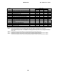
8. Electrical characteristics
8.1
Absolute maximum ratings
Designation
Vdd
VI
VO
Pd
Topr
Tstg
8.2
Condition
Rated value
Unit
Topr=25°C
-0.3 - 6.5
-0.3 - Vdd +0.3
-0.3 - Vdd +0.3
300
V
V
V
mW
-40 - 85
°C
-65 - 150
°C
Recommended operating conditions
Note 1: Unless otherwise specified, Vdd = 4.5 - 5.5V, Topr = -20 - 85°C
Designation
Vdd
VIH
VIL
IOH
IOL
8.3
Item
Supply voltage
Input voltage
Output voltage
Power dissipation
Ambient operating
temperature
Storage temperature
Item
Condition
Supply voltage
High input voltage
Low input voltage
High output current
Low output current
Minimum
Rated value
Standard
3.0
0.7Vdd
0
Maximum
5.5
Vdd
0.3Vdd
25
-25
Unit
V
V
V
mA
mA
Electrical characteristics (*for reference only)
Designation
VOH
VOL
IIH
IIL
ICC
-
Item
High Output voltage
Low Output voltage
High Input current
Low Input current
Supply current
Number of times of
EEPROM write
-
EEPROM write time
-
EEPROM data retention
period
Condition
(Note 1)
Minimum
IOH=-5mA
IOL=5mA
VI=5V
VI=0V
Normal measurement mode
Vdd –1.6
TOPR=0-60°C
300,000
Maximum
Vdd
1.3
5
-5
12
Vdd=5V,TOPR=25°C
(Note 2)
TOPR=55°C
Standard
V
V
µA
µA
mA
Times
100
20
Unit
9000
mS
Years
Note 1: Unless otherwise specified, Vdd = 4.5 - 5.5V, Topr = -20 - 85°C
Note 2: The period following receipt of the EEPROM write command in setup mode until the data write finishes.
30
B6TS-16LF
Necessary Timing Conditions
/ SCS
t h(SCS)
t c(SCK)
t su(SCS)
SCK
t w(SCKH)
t w(SCKL)
t h(SO)
t d(SO)
MISO
BIT6 OUT
MSB OUT
t su(SI)
LSB OUT
t h(SI)
MSB IN
MOSI
BIT1 IN
LSB IN
SCS
t w1(BD)
t c(SCK)
1
SCK
MOSI,
MISO
2
3
4
5
6
7
8
9
COMMAND
D7 D6 D5 D4 D3 D2 D1 D0
t w1(BD)
t w2(BD)
10 11 12 13 14 15 16
17 18 19 20
21 22 23 24
25
t w(CD)
26 27 28
D7 D6 D5 D4 D3 D2 D1 D0
D7 D6 D5 D4 D3 D2 D1 D0
Power ON・
/ RESET
/ SETUP
ROMSTR command
transmitting
CHG
t w(PWON)
29 30 31 32
1
2
DATA BYTE(In READ, DUMMY DATA)
BANK DATA
D7 D6 D5 D4 D3 D2 D1 D0
~
~
8.4
Ver. 071211 rev. 12.14
t su(SETUP)
31
t w(EEP)
t hd(SETUP)
D7 D6
B6TS-16LF
Designation
Item
tc(SCK)
tw(SCKH)
tw(SCKL)
Serial communication clock cycle time
Serial communication clock high pulse width
Serial communication clock low pulse width
/SCS setup time to CLK
/SCS hold time to CLK
Serial communication output delay time
Serial communication output hold time
Serial communication input setup time
Serial communication input hold time
Serial communication byte to byte interval1
Serial communication byte to byte interval2
Serial communication command reception
interval
CHG pulse width
Measurement start delay time
Mode shift delay time (Setup)
Mode shift delay time (Hold)
Reset pulse width
tsu(SETUP)
tw(SCKH)
td(SO)
th(SO)
tsu(SI)
th(SI)
tw1(BD)
tw2(BD)
tw(CD)
tw(CHG)
tw(PWON)
tsu(SETUP)
thd(SETUP)
tw(RESET)
Ver. 071211 rev. 12.14
Condition
Rated value
Minimum
Standard
Maximum
16
8
8
120
120
120
0
120
120
15
50
Unit
µS
µS
µS
nS
nS
nS
nS
nS
nS
µS
µS
400
µS
(Note 2)
28
(Note 3)
(Note 4)
120
mS
mS
µS
mS
µS
20
100
200
50
Note 1 Unless otherwise specified, Vdd = 5.0V, Topr = 25°C.
Note 2 This is the time period when the condition that CHG pulse width is at its minimum in the serial
communication mode of normal measurement mode is set. (CHG pin function is set to output at the end of
every measurement [CHG bit = 0 with MODE command]) and the sleep time is set to zero [SLP command
value = 0]).
Note 3 The delay time for the mode shift from normal measurement mode to setup mode.
*This time is possible to vary in case of inserting large capacitor between /SETUP terminal and GND.
Note4 The delay time for the mode shift from setup mode to normal measurement mode.
*This time is possible to vary in case of inserting large capacitor between /SETUP terminal and GND.
32
B6TS-16LF
Ver. 071211 rev. 12.14
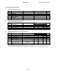
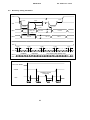
8.5 Measurement characteristics (typical example)
8.5.1 Power supply characteristic
* Only Ch0 count value is described
as representative one.
200
180
160
C ount value
140
120
R EF
100
Touch
80
delta
60
40
20
0
2.5
3.0
3.5
4.0
4.5
5.0
5.5
6.0
V oltage
8.5.2 Temperature characteristic
Count value in non-touch
Variation between non-touch and touch condition
900
900
800
800
700
ch6
ch7
ch8
500
ch9
400
ch10
300
ch11
C ount value
C ount value
600
700
ch6
600
ch7
ch8
500
ch9
400
ch10
300
ch11
200
200
100
100
0
-60
-40
-20
0
20
40
60
80
0
-60
100
-40
-20
Tem perature (
℃)
8.5.3
0
20
40
Tem perature (℃)
60
80
100
Humidity characteristic
ch0
ch0
ch1
C ount value in non-touch
ch2
500
ch2
120
ch3
ch3
450
ch4
ch4
400
100
ch5
ch5
ch6
300
250
ch7
200
ch8
150
ch9
100
ch10
50
ch11
0
ch12
0.9
0.8
0.7
0.6
0.5
0.4
0.5
Hum idity (%)
0.6
0.7
0.8
0.9
ch13
ch14
ch15
33
ch6
80
C ount value
350
C ount value
ch1
V ariation betw een non-touch and touch condition
ch7
ch8
60
ch9
ch10
40
ch11
ch12
20
ch13
ch14
0
0.9
0.8
0.7
0.6
0.5
0.4
0.5
H um idity (%)
0.6
0.7
0.8
0.9
ch15
B6TS-16LF
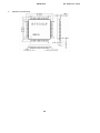
9.
Appearance and dimensions
34
Ver. 071211 rev. 12.14
B6TS-16LF
Ver. 071211 rev. 12.14
Warranty Details
1. Warranty period
The warranty period for an OMRON product is one year from purchase or delivery to a customer-specified place.
2. Scope of warranty
If any OMRON product fails under OMRON liability within the above warranty period, OMRON shall supply a
replacement or repair the product free of charge at the place of purchase. However, if the reason for the product
failure falls into any of the following categories, the warranty will not apply:
a) The product has been used or handled under conditions or in an environment not listed in the product’s
specifications, catalog, or operation manual (hereinafter referred to as the “catalog and the like”).
b) The failure has been caused by a non-OMRON product.
c) The product has been modified or repaired by somebody or corporation other than OMRON.
d) The product has been used for other than its intended use.
e) The failure could not have been predicted based on the level of science or technology at the time of shipment.
f) The failure has been caused by a natural or other disaster, an accident or the like that is not OMRON’s liability.
This warranty applies only to the OMRON product itself, and any damage induced by a failed OMRON product is
excluded from this warranty.
3. Scope of service
The price of an OMRON product does not include service expenses such as the cost of sending out technicians.
If you wish to request non-inclusive services, please consult OMRON sales personnel.
4. Scope of application
The above apply only to business and usage in Japan.
Please consult OMRON sales personnel about business and usage in other countries.
35