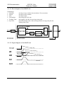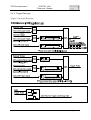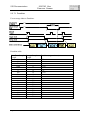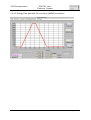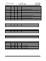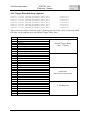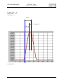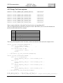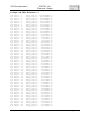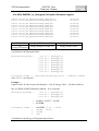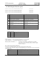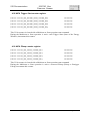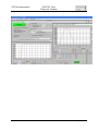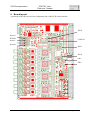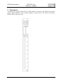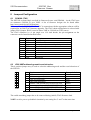
1
SIS Documentation
SIS3302 14xx
Firmware Gamma
SIS3302
14xx Firmware - Gamma
User Manual
SIS GmbH
Harksheider Str. 102A
22399 Hamburg
Germany
Phone: ++49 (0) 40 60 87 305 0
Fax:
++49 (0) 40 60 87 305 20
email: [email protected]
http://www.struck.de
Version: sis3302-M-1408-1-V132-gamma.doc as of 04.12.2009
Page 1 of 97
SIS Documentation
SIS3302 14xx
Firmware Gamma
Revision Table:
Revision
0.01
1.00
1.01
1.02
Date
27.11.07
21.01.08
12.02.08
29.07.08
1.03
1.04
1.05
07.11.08
12.11.08
16.03.09
1.10
18.05.09
1.11
1.12
1.20
29.05.09
10.07.09
02.09.09
Modification
Generation from SIS9300 Gamma
First official release
Add VME Addressing
Design Version: 1203
New Clock source: Second internal 100 MHz
Extend 0x410 key explanation
Change in Gamma logic block diagram, bug fixes
Design Version: 1205
- add Next Neighbor Trigger feature
- add external Veto/Gate
- add internal Trigger or Gate mode
- Acquisition control register: add new bits
Design Version: 1405
- Add MCA Mode
- Fir Filter maximum Peaking time and Gap time values
expanded from 16 x clock to 64 x clock
Change in documentation
Bug fix in broadcast setup
Design Version: 1406
- Fir Filter maximum Peaking time and Gap time values
expanded from 64 x clock to 1023 x clock and add
Decimation of 2, 4 or 8
- Energy Filter maximum Peaking time value expanded
from 255 x clock to 1023 x clock
- maximum Raw Data sample length expanded from 1024
samples to 65532 samples
- maximum Pretrigger Delay expanded from 511 clocks to
1023 clocks
- maximum Trigger Gate length expanded from
1024 clocks to 65536 clocks
- maximum Energy Gate length expanded from
1024 clocks to 131072 clocks
- maximum Energy Sample Start Index X values expanded
from 1023 to 65535
- maximum Trigger Output Pulse length expanded from
63 clocks to 255 clocks
- changed Trigger/Gate logic
add Event Extended Configuration registers
add Trigger Extended Setup registers
Page 2 of 97
SIS Documentation
SIS3302 14xx
Firmware Gamma
1.30
11.09.09
Design Version: F407
- add adc value histogramming in MCA Mode
add ADCx Trigger-50KHz Enable bits in Event
Extended configuration registers
add MCA ADCx histogramming Enable bits in MCA
Histogram Parameter registers
1.31
28.09.09
Design Version: 1407
- Timestamp-freeze logic modified
1.32
04.12.09
Design Version: 1408
- change Fir Trigger Filter
reduced maximum Peaking time and Gap time values
to 511 clocks
expanded decimation: 1/2/4/8/16
add Trigger Extended Threshold registers
Page 3 of 97
SIS Documentation
SIS3302 14xx
Firmware Gamma
1 Table of contents
1
TABLE OF CONTENTS ........................................................................................................................ 4
2
INTRODUCTION................................................................................................................................... 7
2.1
FUNCTIONALITY ................................................................................................................................. 8
2.2
GAMMA LOGIC IMPLEMENTATION ...................................................................................................... 9
2.2.1
General block diagram of one ADC channel and the full module................................................. 9
2.2.2
Trapezoidal Trigger Filter (Fast FIR Filter)............................................................................. 10
2.2.2.1
2.2.2.2
2.2.3
Trapezoidal Energy Filter (Slow FIR Filter)............................................................................. 12
2.2.3.1
2.2.3.2
2.2.3.3
2.2.3.4
2.2.3.5
2.2.4
2.2.5
2.2.6
2.2.7
2.2.7.1
Deadtime ............................................................................................................................................ 22
MCA Mode .............................................................................................................................. 23
2.2.8.1
2.2.8.2
2.2.8.3
2.2.8.4
2.2.9
MCA Scan Enable............................................................................................................................... 23
MCA Scan Arm .................................................................................................................................. 23
MCA Multiscan Arm Scan Enable....................................................................................................... 24
MCA Multiscan Arm Scan Arm........................................................................................................... 24
CVI plots.................................................................................................................................. 25
2.2.9.1
2.2.9.2
2.2.9.3
2.2.9.4
2.2.9.5
Sampling and Energy Filter Parameter screenshot ................................................................................ 25
Raw signal screenshot ......................................................................................................................... 25
Raw signal with Pileup screenshot ....................................................................................................... 26
Energy Filter data without Tau correction (MAW) screenshot............................................................... 26
Energy Filter data with Tau correction (MAWD) screenshot................................................................. 27
VME ADDRESSING............................................................................................................................. 28
3.1
4
Slow FIR Filter Energy sample logic.................................................................................................... 12
Block diagram of the MAWD unit ....................................................................................................... 13
Signal diagram of the MAWD unit ...................................................................................................... 13
Block diagram of the moving average (MA) unit.................................................................................. 14
Block diagram of the Deconvolution (Tau correction) unit.................................................................... 14
Gamma Logic Parameter illustration........................................................................................ 15
Trigger/Gate logic ................................................................................................................... 17
Next Neighbor Trigger/Gate logic ........................................................................................... 19
Sample Logic (with MCA Mode = 0) ........................................................................................ 21
2.2.8
3
Block diagram of the Trigger MAW unit.............................................................................................. 11
Signal diagram of the Trigger MAW unit............................................................................................. 12
ADDRESS MAP ................................................................................................................................. 29
REGISTER/RESOURCE DESCRIPTION .......................................................................................... 32
4.1
CONTROL/STATUS REGISTER............................................................................................................. 32
4.2
MODULE ID. AND FIRMWARE REVISION REGISTER ............................................................................. 33
4.2.1
Major revision numbers ........................................................................................................... 33
4.3
INTERRUPT CONFIGURATION REGISTER .............................................................................................. 34
4.3.1
IRQ mode................................................................................................................................. 34
4.4
INTERRUPT CONTROL REGISTER ........................................................................................................ 35
4.5
ACQUISITION CONTROL REGISTER ..................................................................................................... 36
4.6
BROADCAST SETUP REGISTER ........................................................................................................... 40
4.7
ADC MEMORY PAGE REGISTER ........................................................................................................ 42
4.8
DAC CONTROL REGISTERS............................................................................................................... 43
4.8.1
DAC Control/Status register (read/write) ................................................................................. 43
4.8.2
DAC Data register ................................................................................................................... 44
4.8.3
DAC load sequence.................................................................................................................. 44
4.9
MCA SCAN NOF HISTOGRAMS PRESET REGISTER .............................................................................. 46
4.10 MCA SCAN HISTOGRAM COUNTER REGISTER .................................................................................... 46
4.11 MCA SCAN LNE SETUP AND PRESCALER FACTOR REGISTER ............................................................. 46
4.12 MCA SCAN CONTROL REGISTER ....................................................................................................... 47
4.13 MCA MULTISCAN NOF SCANS PRESET REGISTER ............................................................................... 48
4.14 MCA MULTISCAN SCAN COUNTER REGISTER .................................................................................... 48
4.15 MCA MULTISCAN LAST SCAN HISTOGRAM COUNTER REGISTER ........................................................ 48
4.16 KEY ADDRESS GENERAL RESET (0X400) ............................................................................................ 49
Page 4 of 97
SIS Documentation
SIS3302 14xx
Firmware Gamma
4.17 KEY ADDRESS SAMPLE LOGIC RESET (0X404).................................................................................... 49
4.18 KEY ADDRESSES WITH MCA MODE = 0 ............................................................................................. 49
4.18.1 Key address Sample Logic reset (0x410).................................................................................. 49
4.18.2 Key address VME Disarm Sample logic (0x414)...................................................................... 49
4.18.3 Key address VME Trigger (0x418) .......................................................................................... 49
4.18.4 Key address Timestamp Clear (0x41C).................................................................................... 49
4.18.5 Key address Disarm Sample Logic and Arm sampling on Bank 1 (0x420)............................... 50
4.18.6 Key address Disarm Sample Logic and Arm sampling on Bank 2 (0x424)............................... 50
4.19 KEY ADDRESSES WITH MCA MODE = 1 ............................................................................................. 50
4.19.1 Key address MCA Scan LNE pulse (0x410)............................................................................. 50
4.19.2 Key address MCA Scan Operation Arm (0x414)...................................................................... 50
4.19.3 Key address MCA Scan Enable (0x418) .................................................................................. 51
4.19.4 Key address MCA Scan Disable (0x41C)................................................................................. 51
4.19.5 Key address MCA Multiscan Start/Reset pulse (0x420) ........................................................... 51
4.19.6 Key address MCA Multiscan Arm with Scan operation Arm (0x424) ...................................... 51
4.19.7 Key address MCA Multiscan Arm with Scan operation Enable (0x428) .................................. 51
4.19.8 Key address MCA Multiscan Disable (0x42C)......................................................................... 51
4.20 EVENT CONFIGURATION REGISTERS................................................................................................... 52
4.21 EVENT EXTENDED CONFIGURATION REGISTERS ................................................................................. 53
4.22 END ADDRESS THRESHOLD REGISTERS .............................................................................................. 54
4.23 PRETRIGGER DELAY AND TRIGGER GATE LENGTH REGISTERS............................................................ 55
4.24 RAW DATA BUFFER CONFIGURATION REGISTERS .............................................................................. 56
4.25 ADC1-8 NEXT SAMPLE ADDRESS REGISTER ...................................................................................... 57
4.26 ADC1-8 PREVIOUS BANK SAMPLE ADDRESS REGISTER ...................................................................... 57
4.27 ACTUAL SAMPLE REGISTERS ............................................................................................................. 58
4.28 TRIGGER SETUP REGISTERS ............................................................................................................... 59
4.29 TRIGGER EXTENDED SETUP REGISTERS ............................................................................................. 60
4.30 TRIGGER THRESHOLD REGISTERS ...................................................................................................... 62
4.30.1 Extended Threshold Mode = 0................................................................................................. 63
4.30.2 Extended Threshold Mode = 1................................................................................................. 63
4.30.3 Trigger example ...................................................................................................................... 64
4.31 TRIGGER EXTENDED THRESHOLD REGISTERS .................................................................................... 66
4.32 ENERGY SETUP GP REGISTERS .......................................................................................................... 67
4.33 ENERGY GATE LENGTH REGISTERS ................................................................................................... 68
4.34 ENERGY SAMPLE REGISTERS ............................................................................................................. 68
4.34.1 Energy Sample Length registers ........................................................................................... 69
4.34.2 Energy Sample Start Index1 registers ................................................................................... 69
4.34.3 Energy Sample Start Index2 registers ................................................................................... 69
4.34.4 Energy Sample Start Index3 registers ................................................................................... 69
4.35 ENERGY TAU FACTOR REGISTERS ..................................................................................................... 70
4.36 MCA ENERGY_TO_HISTOGRAM CALCULATION PARAMETER REGISTER ........................................... 72
4.37 MCA HISTOGRAM PARAMETER REGISTER ......................................................................................... 74
4.38 MCA TRIGGER START COUNTER REGISTER ....................................................................................... 75
4.39 MCA PILEUP COUNTER REGISTER ..................................................................................................... 75
4.40 MCA ENERGY_TO_HIGH COUNTER REGISTER................................................................................. 76
4.41 MCA ENERGY_TO_LOW COUNTER REGISTER ................................................................................. 76
4.42 ADC MEMORY ................................................................................................................................. 77
4.42.1 Event Buffer Data Format (with MCA Mode = 0) ..................................................................... 77
5
MODES OF ACQUISITION OF CURRENT SOFTWARE................................................................ 80
5.1
5.2
SINGLE EVENT ACQUISITION ............................................................................................................. 80
MULTI E VENT DOUBLE BUFFER ACQUISITION .................................................................................... 80
6
BOARD LAYOUT ................................................................................................................................ 81
7
FRONT PANEL .................................................................................................................................... 82
7.1
7.2
7.3
CONTROL IN/OUTPUTS ..................................................................................................................... 83
LED'S .............................................................................................................................................. 84
CHANNEL LED'S .............................................................................................................................. 84
Page 5 of 97
SIS Documentation
7.4
8
SIS3302 14xx
Firmware Gamma
PCB LEDS....................................................................................................................................... 84
JUMPERS/CONFIGURATION ........................................................................................................... 85
8.1
8.2
8.3
8.4
8.5
8.6
9
CON100 JTAG................................................................................................................................ 85
JP80 VME ADDRESSING MODE/RESET BEHAVIOUR ............................................................................ 85
JP101 JTAG CHAIN .......................................................................................................................... 86
JP102 JTAG SOURCE........................................................................................................................ 87
JP120A-JP120D CONTROL INPUT TERMINATION ................................................................................ 88
SW1 AND SW2, VME BASE ADDRESS ............................................................................................... 88
SOFTWARE/GETTING STARTED.................................................................................................... 89
9.1
9.2
10
HEADER FILES .................................................................................................................................. 89
C CODE ............................................................................................................................................ 90
APPENDIX........................................................................................................................................ 91
10.1 POWER CONSUMPTION ...................................................................................................................... 91
10.2 OPERATING CONDITIONS................................................................................................................... 91
10.2.1 Cooling.................................................................................................................................... 91
10.2.2 Hot swap/live insertion............................................................................................................. 91
10.3 CONNECTOR TYPES........................................................................................................................... 92
10.4 P2 ROW A/C PIN ASSIGNMENTS ......................................................................................................... 92
10.5 ROW D AND Z PIN ASSIGNMENTS....................................................................................................... 93
10.6 FIRMWARE UPGRADE ........................................................................................................................ 94
10.6.1 Upgrade over CON100 ............................................................................................................ 94
10.6.2 Upgrade over VME .................................................................................................................. 94
11
INDEX ............................................................................................................................................... 95
Page 6 of 97
SIS Documentation
SIS3302 14xx
Firmware Gamma
2 Introduction
This firmware manual/addendum describes the functionality and implementation of the
SIS3302 firmware major revision 0x14. Besides finite response filter (FIR) based triggering
this version supports asynchronous readout of a programmable set of features of raw (i.e.
digitized wave form) and/or computed (like signal height/energy e.g.) digitizer information.
No hardware modification to the SIS3302 is required for installation of this firmware.
This firmware implementation should be of particular interest for detector studies with
Gamma ray tracking and strip detectors.
Page 7 of 97
SIS Documentation
SIS3302 14xx
Firmware Gamma
2.1 Functionality
The main functions of the firmware are listed below and illustrated in the Gamma logic block
diagram.
8 channel asynchronous and synchronous operation
Decimation
Trapezoidal Energy filter
Trigger FIR filter
Trigger or output
48-bit Timestamp
Flexible event storage
MCA Histogramming in the ADC Memory
Page 8 of 97
SIS Documentation
SIS3302 14xx
Firmware Gamma
2.2 Gamma Logic Implementation
2.2.1 General block diagram of one ADC channel and the full module
SIS3302-Gamma V_1406
External Gate/Veto (depends on „Lemo Input Mode“ and „Enable front panel Lemo In x“)
External Gate
XOR
External Gate mode *
VME Key Trigger
External Trigger In
(depends on „Lemo Input Mode“ and „Enable front panel Lemo In x“)
OR
External Trigger
Enable ored Internal Trigger to External Trigger In
Acquisition Reg bit 6 (Feedback)
AND
ADCx external gate enable
Trigger Out
Event conf. Reg bit 5 / 13
OR
ADCx internal gate enable
Event conf. Reg bit 4 / 12
ADCx external trigger enable
ADC 8
ADC 8
Event conf. Reg bit 3 / 11
ADCx internal trigger enable
Event conf. Reg bit 2 / 10
Int. Trigger ADC N+1
ADC 2
ADC 2
Int. Trigger ADC N-1
Next Neighbor
Trigger Logic
Int. Trigger ADC N
AND
Internal Trigger
Disable Trigger Out
Trigger / Gate Logic
INV
Start Pulse
ADC 1
Fast Trapezoidal FIR
Filter (Trigger)
Decimation = 1,2,4 or 8
P <= 1023
(P + G) <= 1023
Energy Window
and
Sampling Logic
Internal Trigger
Trigger
Counter
Raw data
Buffer
65532 x 16
Pretrigger
Delay
(max. 1023
Clocks)
min./max.
Values
Decimation
1/2/4/8
Timestamp Clear In
Energy Filter
P <= 1023
G <= 255
48-bit Timestamp
counter
Energy
Value
Buffer
510 x 32
M
u
x
ADC 1
Event
Memory
48-bit Timestamp
latch
Page 9 of 97
SIS Documentation
SIS3302 14xx
Firmware Gamma
2.2.2 Trapezoidal Trigger Filter (Fast FIR Filter)
A trapezoidal FIR filter is implemented for each ADC Channel to generate a trigger signal.
This Trigger Signal can be used to trigger the sample logic immediately or it can be routed to
SIS3302 Lemo Output.
This Trigger Signal will be also used to store the “Fast Filter trigger” information.
Features for each ADC channel:
Programmable decimation (1 / 2 / 4 / 8 / 16 Clocks)
Programmable Peaking Time (max. 511 Clocks)
Programmable SumGap Time (max. 511 Clocks)
Programmable Trigger pulse out length (max. 255 Clocks)
Programmable Trigger Threshold
Programmable Trigger Extended Threshold (finer granularity)
Programmable Trigger Mode (GT,Disable)
Programmable Trigger OUT (Enable,Disable)
see Trigger Setup ADCx registers, Trigger Extended Setup ADCx registers, Trigger
Threshold ADCx registers and Trigger Extended Threshold ADCx registers.
Page 10 of 97
SIS Documentation
SIS3302 14xx
Firmware Gamma
2.2.2.1 Block diagram of the Trigger MAW unit
Explanation:
MAW:
MA:
Decimation:
Peaking Time:
SumGap Time:
moving average window
moving average
decreasing the clock rate
the length of the MA for moving average unit
the differentiation time of the mowing window average unit
Page 11 of 97
SIS Documentation
SIS3302 14xx
Firmware Gamma
2.2.2.2 Signal diagram of the Trigger MAW unit
2.2.3 Trapezoidal Energy Filter (Slow FIR Filter)
A trapezoidal FIR filter is implemented for each ADC Channel to generate a “moving
window average” stream (MWA) .
A decimation logic (average, integration) is also implemented.
Features of the Slow FIR Filter:
Programmable decimation (1 / 2 / 4 / 8 Clocks)
Programmable Peaking Time (max. 1023 Clocks)
Programmable Gap Time (max. 255 Clocks)
2.2.3.1 Slow FIR Filter Energy sample logic
Five registers are implemented to control the sampling of the MWD.
Energy Gate Length
Energy Sample Length register
Energy Sample Start Index1 register
Energy Sample Start Index2 register
Energy Sample Start Index3 register
The “Slow FIR Filter Energy sample” logic starts with the Energy Gate and executes
following steps:
1. Clears an internal Energy Index counter and starts this Index counter.
The logic is busy until the Index counter reaches the value of the Energy Gate Length
register (busy with the Energy Gate).
2. Compares the Index counter with the Energy Sample Start Index x registers.
If the result is equal the logic writes N (Energy Sample Length register) values into the
Energy Buffer.
3. The logic saves the Energy at the beginning of the Energy Gate.
4. The logic saves the maximum Energy inside the Energy Gate.
Page 12 of 97
SIS Documentation
SIS3302 14xx
Firmware Gamma
2.2.3.2 Block diagram of the MAWD unit
Explanation:
MAWD:
MAW:
MA:
Decimation:
Peaking Time:
Gap Time:
moving average window deconvolution (Tau correction)
moving average window
moving average
decreasing the clock rate
the length of the MA for moving average unit
the differentiation time of the mowing window average unit plus the
Peaking time (Flat)
2.2.3.3 Signal diagram of the MAWD unit
Page 13 of 97
SIS Documentation
SIS3302 14xx
Firmware Gamma
2.2.3.4 Block diagram of the moving average (MA) unit
2.2.3.5 Block diagram of the Deconvolution (Tau correction) unit
Page 14 of 97
SIS Documentation
SIS3302 14xx
Firmware Gamma
2.2.4 Gamma Logic Parameter illustration
Page 15 of 97
SIS Documentation
SIS3302 14xx
Firmware Gamma
The Gamma Logic parameters are:
*P1:
*P2:
Fast FIR Filter (Trigger) parameters: see Trigger Setup ADCx registers
Fast FIR Filter (Trigger) Threshold: see Trigger Threshold ADCx registers
*P3:
*P4:
Trigger Gate Length: see Pretrigger Delay and Trigger Gate Length registers
Pretrigger Delay: see Pretrigger Delay and Trigger Gate Length registers
*P5:
*P6:
Raw Data Sample Length: see Raw Data Buffer Configuration registers
Raw Data Sample Start Index: see Raw Data Buffer Configuration registers
*P7:
Energy Gate Length: see Energy Gate Length registers
*P8:
*P9:
*P10:
*P11:
Energy Sample Length: see Energy Sample Length registers
Energy Sample Start Index1: see Energy Sample Start Index1 registers
Energy Sample Start Index2: see Energy Sample Start Index2 registers
Energy Sample Start Index3: see Energy Sample Start Index3 registers
*P12:
Energy Tau correction Factor: see Tau Factor registers
*P13:
*P14:
Energy Filter Peaking Time: see Energy Setup GP registers
Energy Filter GapTime: see Energy Setup GP registers
Page 16 of 97
SIS Documentation
SIS3302 14xx
Firmware Gamma
2.2.5 Trigger/Gate logic
Trigger / Gate logic illustration:
Page 17 of 97
SIS Documentation
SIS3302 14xx
Firmware Gamma
Example1: Internal Trigger / External Gate
- “Lemo Input Mode” = 1 and “Lemo Output Mode” = 0
- Lemo In 1 connected with Lemo Out 1 and “Enable front panel Lemo In 1”= 1
- “ADCx internal trigger enable” = 1 and “ADCx external gate enable” = 1
- “Internal Trigger Pulse Length” = 30
- “Internal Trigger Delay/ Internal Gate Length” = 20
Example 2: External Trigger / Internal Gate
- “Lemo Input Mode” = 0 and “Lemo Output Mode” = 0
- Lemo In 3 connected with Lemo Out 1 and “Enable front panel Lemo In 3”= 1
or “Enable ored Internal Trigger to External Trigger In” = 1 (Feedback)
- “ADCx external trigger enable” = 1 and “ADCx internal gate enable” = 1
- “Internal Trigger Pulse Length” = 6
- “Internal Trigger Delay/ Internal Gate Length” = 20
Internal Trigger Pulse Length
Internal Delay
Legend
fir_trigger_out_pulse:
Internal Delay:
External Delay:
Page 18 of 97
Internal Gate Length
generated from the internal Fast Fir Filter (internal Trigger) with
the programmed Trigger Pulse Length.
4 clocks
8 clocks + external Logic (Cable, external user logic)
SIS Documentation
SIS3302 14xx
Firmware Gamma
2.2.6 Next Neighbor Trigger/Gate logic
Next Neighbor Trigger logic illustration:
Attention:
Next Neighbor Trigger logic is not implemented on the SIS3302 4-channel
version.
Page 19 of 97
SIS Documentation
SIS3302 14xx
Firmware Gamma
Next Neighbor Gate logic illustration:
Attention:
Page 20 of 97
Next Neighbor Gate logic is not implemented on the SIS3302 4-channel
version.
SIS Documentation
SIS3302 14xx
Firmware Gamma
2.2.7 Sample Logic (with MCA Mode = 0)
The sample logic starts with a trigger signal (Start Pulse for Trigger and Energy Gate) and
executes following steps:
1. starts the Trigger and Energy Gate and stores the 48-bit timestamp.
2. writes the 16-bit programmable ADC Header and the stored 48-bit Timestamp into the
Event Memory.
3. writes a programmable number of ADC Raw Values into the Event Memory.
4. writes at the end of the Energy Gate a programmable number of Slow FIR Values
(MAWD) into the Event Memory.
5. writes the maximum and minimum (first value of Energy Gate) MAWD value into the
Event Memory.
6. writes the Fast Filter Information register into the Event Memory.
7. writes a Trailer into the Event Memory.
Page 21 of 97
SIS Documentation
SIS3302 14xx
Firmware Gamma
2.2.7.1 Deadtime
Event storage induces Deadtime.
Deadtime table
Raw Data Sample
Length
0
100
500
1000
Energy Sample
Length
0
0
0
0
Deadtime (approximate)
150 ns
560 ns
2 us
3.9 us
0
100
500
1000
12
12
12
12
1 us
1.2 us
3 us
7 us
0
100
500
1000
256
256
256
256
5.4 us
5.6 us
8.0 us
10.6 us
0
100
500
1000
512
512
512
512
9.6 ns
9.8 us
10.8 us
14 us
Page 22 of 97
SIS Documentation
SIS3302 14xx
Firmware Gamma
2.2.8 MCA Mode
1/2/4/8K Histogram Bins (histogram page size)
Page Clear Time table
Page Size
1K
2K
4K
8K
Page Clear Time (approximate)
11 us
22 us
44 us
88 us
2.2.8.1 MCA Scan Enable
Scan Disable (Stop) with
Key MCA Disable or with
Number of Histograms == NofHistogramPresetRegister (=N)
Key MCA Scan Enable
Internal Scan Enable
LNE
(Key MCA LNE Pulse
or external LNE)
1.
Fifo
Histogramming in Memory
Clear
Page 0
Page 0
(0x0)
2.
Fifo
Clear
Page 1
Page 1
(0x0 + 1xSize)
3.
Fifo
Clear
Page 2
Page 2
(0x0 + 2xSize)
N-1.
N.
Fifo
Clear
Page
N-1
Page N-1
(0x0 + (N-1)xSize)
Page
clear
time
2.2.8.2 MCA Scan Arm
Page 23 of 97
SIS Documentation
SIS3302 14xx
Firmware Gamma
2.2.8.3 MCA Multiscan Arm Scan Enable
2.2.8.4 MCA Multiscan Arm Scan Arm
Page 24 of 97
SIS Documentation
SIS3302 14xx
Firmware Gamma
2.2.9 CVI plots
2.2.9.1 Sampling and Energy Filter Parameter screenshot
2.2.9.2 Raw signal screenshot
Page 25 of 97
SIS Documentation
SIS3302 14xx
Firmware Gamma
2.2.9.3 Raw signal with Pileup screenshot
2.2.9.4 Energy Filter data without Tau correction (MAW) screenshot
Page 26 of 97
SIS Documentation
SIS3302 14xx
Firmware Gamma
2.2.9.5 Energy Filter data with Tau correction (MAWD) screenshot
Page 27 of 97
SIS Documentation
SIS3302 14xx
Firmware Gamma
3 VME Addressing
As the SIS3302 VME FADC features memory options with up to 8 times 32 MSamples, A32
addressing was implemented as the only option. The module occupies an address space of
0x7FFFFFF Bytes, i.e. 128 MBytes are used by the module.
The base address is defined by the selected addressing mode, which is selected by jumper
array JP80 and SW1 and SW2 (in non geographical mode).
The table below summarises the possible base address settings.
J1 Setting
Bits
A32 GEO VIPA 31 30 29 28 27
x
SW1
SW2=0...7
Bit 27=0
x
SW1
SW2=8...F
Bit 27=1
x
x
Not implemented in this design
x
Shorthand
SW1/SW2
Not implemented in this design
Explanation
Setting of rotary switch SW1 or SW2 respective
Notes:
This concept allows the use of the SIS3302 in standard VME as well as in VME64x
environments, i.e. the user does not need to use a VME64x backplane.
The factory default setting is EN_A32 closed, SW1=3, SW2=0 (i.e. the module will react
to A32 addressing under address 0x30000000). With more than one unit shipped in one
batch a set of addresses (like 0x10000000, 0x20000000, 0x30000000,...) may be used
also.
Page 28 of 97
SIS Documentation
SIS3302 14xx
Firmware Gamma
3.1 Address Map
The 0x120x firmware specific SIS3302 resources and their locations are listed with function
in the table below. The header file (sis3302_v1405.h or equivalent) provides the define
statements.
Offset
0x00000000
0x00000004
0x00000008
0x0000000C
Size in BLT Access
Bytes
4
W/R
4
R
4
R/W
4
R/W
Function
Control/Status Register (J-K register)
Module Id. and Firmware Revision register
Interrupt configuration register
Interrupt control register
0x00000010
4
-
R/W
Acquisition control/status register (J-K register)
0x00000030
0x00000034
4
4
-
R/W
R/W
Broadcast Setup register
ADC Memory Page register
0x00000050
0x00000054
4
4
-
R/W
R/W
DAC Control Status register
DAC Data register
0x00000060
0x00000064
R/W
W
XILINX JTAG_TEST/JTAG_DATA_IN
XILINX JTAG_CONTROL
0x00000080
0x00000084
0x00000088
0x0000008C
R/W
R
R/W
R/W
MCA Scan Nof Histograms preset register
MCA Scan Histogram counter register
MCA Scan LNE Setup and Prescaler Factor register
MCA Scan Control register
0x00000090
0x00000094
0x00000098
R/W
R
R
MCA Multiscan Nof Scans preset register
MCA Multiscan Scan counter register
MCA Multiscan last Scan Histogram count register
0x00000400
0x00000404
4
4
-
KA W
KA W
Key address Reset
Key address Sample Logic Reset
MCA mode = 0
0x00000410
0x00000414
0x00000418
0x0000041C
4
4
4
4
-
KA W
KA W
KA W
KA W
Key address Sample Logic Reset
Key address Disarm Sample Logic
Key address Trigger
Key address Timestamp Clear
0x00000420
0x00000424
0x00000428
4
4
4
-
KA W
KA W
KA W
Key address Disarm Sample Logic and Arm sampling on Bank 1
Key address Disarm Sample Logic and Arm sampling on Bank 2
Key address Reset DDR2 Memory Logic
MCA mode = 1
0x00000410
0x00000414
0x00000418
0x0000041C
4
4
4
4
-
KA W
KA W
KA W
KA W
Key MCA Scan LNE Pulse
Key MCA Scan operation Arm (start with next LNE)
Key MCA Scan Enable (start immediately)
Key MCA Scan Disable
0x00000420
0x00000424
4
4
KA W
KA W
0x00000428
0x0000042C
4
4
Key MCA Multiscan Start/Reset pulse
Key MCA Multiscan Arm with Scan operation Arm (start scan with
next LNE)
Key MCA Multiscan Arm with Scan operation Enable
Key MCA Multiscan disable
-
KA W
KA W
Page 29 of 97
SIS Documentation
SIS3302 14xx
Firmware Gamma
Event information all ADC groups
0x01000000
4
0x01000004
4
0x01000008
4
0x0100000C
4
-
W only
W only
W only
W only
Event configuration (all ADCs)
End Address Threshold (all ADCs)
Pretrigger Delay and Trigger Gate Length (all ADCs)
Raw Data Buffer Configuration (all ADCs)
0x01000040
0x01000044
0x01000048
0x0100004C
4
4
4
4
W only
W only
W only
W only
Energy Setup GP (all ADCs)
Energy Gate Length (all ADCs)
Energy Sample Length (all ADCs)
Energy Sample Start Index1 (all ADCs)
0x01000050
0x01000054
0x01000058
0x0100005C
4
4
4
4
W only
W only
W only
W only
Energy Sample Start Index2 (all ADCs)
Energy Sample Start Index3 (all ADCs)
Energy Tau Factor ADC1/3/5/7
Energy Tau Factor ADC2/4/6/8
0x01000060
0x01000064
0x01000068
0x01000070
4
4
4
4
W only
W only
W only
W only
MCA Energy to Histogram Calculation Parameter ADC1357
MCA Energy to Histogram Calculation Parameter ADC2468
MCA Histogram Parameters (all ADCs)
Event Extended configuration (all ADCs)
-
Event information ADC group 1
0x02000000
4
0x02000004
4
0x02000008
4
0x0200000C
4
-
R/W
R/W
R/W
R/W
Event configuration (ADC1, ADC2)
End Address Threshold (ADC1, ADC2)
Pretrigger Delay and Trigger Gate Length (ADC1, ADC2)
Raw Data Buffer Configuration (ADC1, ADC2)
0x02000010
0x02000014
0x02000018
0x0200001C
4
4
4
4
-
R
R
R
R
Actual Sample address ADC1
Actual Next Sample address ADC2
Previous Bank Sample address ADC1
Previous Bank Sample address ADC2
0x02000020
0x02000024
0x02000028
4
4
4
-
R
R
R
Actual Sample Value (ADC1, ADC2)
internal Test
DDR2 Memory Logic Verification (ADC1, ADC2)
0x02000030
0x02000034
0x02000038
0x0200003C
4
4
4
4
R/W
R/W
R/W
R/W
Trigger Setup ADC1
Trigger Threshold ADC1
Trigger Setup ADC2
Trigger Threshold ADC2
0x02000040
0x02000044
0x02000048
0x0200004C
4
4
4
4
R/W
R/W
R/W
R/W
Energy Setup GP (ADC1, ADC2)
Energy Gate Length (ADC1, ADC2)
Energy Sample Length (ADC1, ADC2)
Energy Sample Start Index1 (ADC1, ADC2)
0x02000050
0x02000054
0x02000058
0x0200005C
4
4
4
4
R/W
R/W
R/W
R/W
Energy Sample Start Index2 (ADC1, ADC2)
Energy Sample Start Index3 (ADC1, ADC2)
Energy Tau Factor ADC1
Energy Tau Factor ADC2
0x02000060
0x02000064
0x02000068
4
4
4
R/W
R/W
R/W
MCA Energy to Histogram Calculation Parameter ADC1
MCA Energy to Histogram Calculation Parameter ADC2
MCA Histogram Parameters (ADC1, ADC2)
Page 30 of 97
SIS Documentation
SIS3302 14xx
Firmware Gamma
0x02000070
0x02000078
0x0200007C
4
4
4
R/W
R/W
R/W
0x02000080
0x02000084
0x02000088
0x0200008C
4
4
4
4
R
R
R
R
MCA Trigger Start Counter ADC1
MCA Pileup Counter ADC1
MCA “Energy to high” counter ADC1
MCA “Energy to low” counter ADC1
0x02000090
0x02000094
0x02000098
0x0200009C
4
4
4
4
R
R
R
R
MCA Trigger Start Counter ADC2
MCA Pileup Counter ADC2
MCA “Energy to high” counter ADC2
MCA “Energy to low” counter ADC2
0x020000A0
0x020000A4
4
4
R/W
R/W
Trigger Extended Threshold ADC1
Trigger Extended Threshold ADC2
Event information ADC group 2
0x02800000
4
And so on (as for ADC group 1)
R/W
Event configuration (ADC3, ADC4)
Event information ADC group 3
0x03000000
4
And so on (as for ADC group 1)
R/W
Event configuration (ADC5, ADC6)
Event information ADC group 4
0x03800000
4
And so on (as for ADC group 1)
R/W
Event configuration (ADC7, ADC8)
ADC memory pages
0x04000000
8 MByte
0x04800000
8 MByte
0x05000000
8 MByte
0x05800000
8 MByte
0x06000000
8 MByte
0x06800000
8 MByte
0x07000000
8 MByte
0x07800000
8 MByte
X
X
X
X
X
X
X
X
R
R
R
R
R
R
R
R
Event Extended configuration (ADC1, ADC2)
Trigger Extended Setup ADC1
Trigger Extended Setup ADC2
ADC 1 memory page
ADC 2 memory page
ADC 3 memory page
ADC 4 memory page
ADC 5 memory page
ADC 6 memory page
ADC 7 memory page
ADC 8 memory page
Page 31 of 97
SIS Documentation
SIS3302 14xx
Firmware Gamma
4 Register/Resource Description
The 0x12xx firmware related registers are described in this section. The define statements
were taken from the sis3302_v1201.h header file. Examples refer to the C code which is
underlying the sis3150_3302_gamma CVI project.
4.1 Control/Status register
#define SIS3302_CONTROL_STATUS
0x0
/* read/write; D32 */
The control register is implemented as a selective J/K register, a specific function is enabled
by writing a 1 into the set/enable bit, the function is disabled by writing a 1 into the
clear/disable bit (which location is 16-bit higher in the register). An undefined toggle status
will result from setting both the enable and disable bits for a specific function at the same
time. The only function at this point in time is user LED on/off.
On read access the same register represents the status register.
Bit
31
30
29
28
27
26
25
24
23
22
21
20
19
18
17
16
15
14
13
12
11
10
9
8
7
6
5
4
3
2
1
0
write Function
Clear reserved 15 (*)
Clear reserved 14 (*)
Clear reserved 13 (*)
Clear reserved 12 (*)
Clear reserved 11 (*)
Clear reserved 10 (*)
Clear reserved 9 (*)
Clear reserved 8 (*)
Clear reserved 7 (*)
Clear reserved 6 (*)
Clear reserved 5 (*)
Clear reserved 4 (*)
Clear reserved 3 (*)
Clear reserved 2 (*)
Clear reserved 1 (*)
Switch off user LED (*)
Set reserved 15
Set reserved 14
Set reserved 13
Set reserved 12
Set reserved 11
Set reserved 10
Set reserved 9
Set reserved 8
Set reserved 7
Set reserved 7
Set reserved 7
Set reserved 7
Set reserved 3
Set reserved 2
Set reserved 1
Switch on user LED
(*) denotes power up default setting
Page 32 of 97
read Function
0
0
0
0
0
0
0
0
0
0
0
0
0
0
0
0
Status reserved 15
Status reserved 14
Status reserved 13
Status reserved 12
Status reserved 11
Status reserved 10
Status reserved 9
Status reserved 8
Status reserved 7
Status reserved 6
Status reserved 4
Status reserved 4
Status reserved 3
Status reserved 2
Status reserved 1
Status User LED (1=LED on, 0=LED off)
SIS Documentation
4.2
SIS3302 14xx
Firmware Gamma
Module Id. and Firmware Revision register
#define SIS3302_MODID
0x4
/* read only; D32 */
This register reflects the module identification of the SIS3302 and its minor and major
firmware revision levels. The major revision level will be used to distinguish between
substantial design differences and experiment specific designs, while the minor revision level
will be used to mark user specific adaptations.
Bit
31
30
29
28
27
26
25
24
23
22
21
20
19
18
17
16
15
14
13
12
11
10
9
8
7
6
5
4
3
2
1
0
Function
Module Id. Bit 15
Module Id. Bit 14
Module Id. Bit 13
Module Id. Bit 12
Module Id. Bit 11
Module Id. Bit 10
Module Id. Bit 9
Module Id. Bit 8
Module Id. Bit 7
Module Id. Bit 6
Module Id. Bit 5
Module Id. Bit 4
Module Id. Bit 3
Module Id. Bit 2
Module Id. Bit 1
Module Id. Bit 0
Major Revision Bit 7
Major Revision Bit 6
Major Revision Bit 5
Major Revision Bit 4
Major Revision Bit 3
Major Revision Bit 2
Major Revision Bit 1
Major Revision Bit 0
Minor Revision Bit 7
Minor Revision Bit 6
Minor Revision Bit 5
Minor Revision Bit 4
Minor Revision Bit 3
Minor Revision Bit 2
Minor Revision Bit 1
Minor Revision Bit 0
Reading
3
3
0
2
4.2.1 Major revision numbers
Find below a table with major revision numbers used to date
Major revision number
0x01
0x12
0x14
Application/user
Generic designs
Gamma
Gamma (add MCA Mode)
Page 33 of 97
SIS Documentation
4.3
SIS3302 14xx
Firmware Gamma
Interrupt configuration register
#define SIS3302_IRQ_CONFIG
0x8
/* read/write; D32 */
This read/write register controls the VME interrupt behaviour of the SIS3302 ADC. Four
interrupt sources are foreseen, for the time being two of them are associated with an interrupt
condition, two condition are reserved for future use.
The interrupter type is DO8 .
4.3.1 IRQ mode
In RORA (release on register access) mode the interrupt will be pending until the IRQ
source is cleared by specific access to the corresponding disable VME IRQ source bit. After
the interrupt is serviced the source has to be activated with the enable VME IRQ source bit
again.
In ROAK (release on acknowledge) mode , the interrupt condition will be cleared (and the
IRQ source disabled) as soon as the interrupt is acknowledged by the CPU. After the interrupt
is serviced the source has to be activated with the enable VME IRQ source bit again.
Bit
31
...
16
15
14
13
12
11
10
9
8
7
6
5
4
3
2
1
0
Function
RORA/ROAK Mode (0: RORA; 1: ROAK)
VME IRQ Enable (0=IRQ disabled, 1=IRQ enabled)
VME IRQ Level Bit 2
VME IRQ Level Bit 1
VME IRQ Level Bit 0 (0 always)
IRQ Vector Bit 7; placed on D7 during VME IRQ ACK cycle
IRQ Vector Bit 6; placed on D6 during VME IRQ ACK cycle
IRQ Vector Bit 5; placed on D5 during VME IRQ ACK cycle
IRQ Vector Bit 4; placed on D4 during VME IRQ ACK cycle
IRQ Vector Bit 3; placed on D3 during VME IRQ ACK cycle
IRQ Vector Bit 2; placed on D2 during VME IRQ ACK cycle
IRQ Vector Bit 1; placed on D1 during VME IRQ ACK cycle
IRQ Vector Bit 0; placed on D0 during VME IRQ ACK cycle
The power up default value reads 0x 00000000
Page 34 of 97
Default
0
0
0
0
0
0
0
0
0
0
0
0
0
0
0
0
0
0
0
SIS Documentation
4.4
SIS3302 14xx
Firmware Gamma
Interrupt control register
#define SIS3302_IRQ_CONTROL
0xC
/* read/write; D32 */
This register controls the VME interrupt behaviour of the SIS3302 ADC. Four interrupt
sources are foreseen, for the time being two of them are associated with an interrupt
condition, two condition are reserved for future use.
Bit
31
30
29
28
27
26
25
24
23
22
21
20
19
18
17
16
15
14
13
12
11
10
9
8
7
6
5
4
3
2
1
0
Function (w)
Update IRQ Pulse
Unused
Unused
Unused
Unused
Unused
Unused
Unused
Disable/Clear IRQ source 7
Disable/Clear IRQ source 6
Disable/Clear IRQ source 5
Disable/Clear IRQ source 4
Disable/Clear IRQ source 3
Disable/Clear IRQ source 2
Disable/Clear IRQ source 1
Disable/Clear IRQ source 0
Unused
Unused
Unused
Unused
Unused
Unused
Unused
Unused
Enable IRQ source 7
Enable IRQ source 6
Enable IRQ source 5
Enable IRQ source 4
Enable IRQ source 3
Enable IRQ source 2
Enable IRQ source 1
Enable IRQ source 0
(r)
Status IRQ source 7 (reserved)
Status IRQ source 6 (reserved)
Status IRQ source 5 (reserved)
Status IRQ source 4 (reserved)
Status IRQ source 3 (reserved)
Status IRQ source 2 (reserved)
Status IRQ source 1 (End Address Threshold Flag; level sensitive)
Status IRQ source 0 (End Address Threshold Flag; edge sensitive)
Status flag source 7
Status flag source 6
Status flag source 5
Status flag source 4
Status flag source 3
Status flag source 2
Status flag source 1
Status flag source 0
Status VME IRQ
Status internal IRQ
0
0
0
0
0
0
Status enable source 7 (read as 1 if enabled, 0 if disabled)
Status enable source 6 (read as 1 if enabled, 0 if disabled)
Status enable source 5 (read as 1 if enabled, 0 if disabled)
Status enable source 4 (read as 1 if enabled, 0 if disabled)
Status enable source 3 (read as 1 if enabled, 0 if disabled)
Status enable source 2 (read as 1 if enabled, 0 if disabled)
Status enable source 1 (read as 1 if enabled, 0 if disabled)
Status enable source 0 (read as 1 if enabled, 0 if disabled)
Default
0
0
0
0
0
0
0
0
0
0
0
0
0
0
0
0
0
0
0
0
0
0
0
0
0
0
0
0
0
0
0
0
The power up default value reads 0x 00000000
IRQ source 3:
IRQ source 2:
IRQ source 1:
IRQ source 0:
reserved
reserved
reached Address Threshold (level sensitive)
reached Address Threshold (edge sensitive)
Page 35 of 97
SIS Documentation
4.5
SIS3302 14xx
Firmware Gamma
Acquisition control register
#define SIS3302_ACQUISTION_CONTROL
#define SIS3302_ACQUISITION_CONTROL
0x10
0x10
/* read/write; D32 */
/* read/write; D32 */
Note: missing I in ACQUISITION in older header files
The acquisition control register is in charge of most of the settings related to the actual
configuration of the digitization process.
Like the control register it is implemented in a J/K fashion.
Bit
31
30
29
28
27
26
25
24
23
22
21
20
19
18
17
16
15
14
13
12
11
10
9
8
7
6
5
4
3
2
1
0
Write Function
Clear reserved 15 (*)
Clear Clock Source bit2 (*)
Clear Clock Source bit1 (*)
Clear Clock Source bit0 (*)
Clear reserved 11 (*)
Disable front panel LEMO In 1 (*)
Disable front panel LEMO In 2 (*)
Disable front panel LEMO In 3 (*)
Clear reserved 7 (*)
Disable ored Internal Trigger to External Trigger In (*)
Clear LEMO OUT Mode bit 1 (*)
Clear LEMO OUT Mode bit 0 (*)
Clear MCA Mode bit (*)
Clear LEMO IN Mode bit 2 (*)
Clear LEMO IN Mode bit 1 (*)
Clear LEMO IN Mode bit 0 (*)
Set reserved 15
Set clock source bit 2
Set clock source bit 1
Set clock source bit 0
Set reserved 11
Enable front panel LEMO In 1
Enable front panel LEMO In 2
Enable front panel LEMO In 3
Set reserved 7
Enable ored Internal Trigger to External Trigger In
(Feedback)
Set LEMO OUT Mode bit 1
Set LEMO OUT Mode bit 0
Set MCA Mode bit
Set LEMO IN Mode bit 2
Set LEMO IN Mode bit 1
Set LEMO IN Mode bit 0
(*) The power up default value reads 0x0
Page 36 of 97
Read
0
0
0
0
0
0
0
0
0
0
Status of MCA Multiscan Busy
Status of MCA Scan Busy
Status of End Address Threshold Flag
Status of ADC-Sample-Logic Busy (Armed)
Status of ADC-Sample-Logic Armed Bank2
Status of ADC-Sample-Logic Armed Bank1
Status reserved 15
Status clock source bit 2
Status clock source bit 1
Status clock source bit 0
Status reserved 11
Status front panel LEMO In 1 Enable bit
Status front panel LEMO In 2 Enable bit
Status front panel LEMO In 3 Enable bit
Status reserved 7
Status ored Internal Trigger to External Trigger In
(Feedback)
Status LEMO OUT Mode bit 1
Status LEMO OUT Mode bit 0
Status MCA Mode bit
Status LEMO IN Mode bit 2
Status LEMO IN Mode bit 1
Status LEMO IN Mode bit 0
SIS Documentation
SIS3302 14xx
Firmware Gamma
Clock source bit setting table:
Clock Source
Bit2
0
0
0
0
1
1
1
1
Clock Source
Bit1
0
0
1
1
0
0
1
1
Clock Source
Bit0
0
1
0
1
0
1
0
1
Clock Source
internal 100 MHz
internal 50 MHz
internal 25 MHz
internal 10 MHz
internal 1 MHz
internal 100 MHz
external clock (LEMO front panel) ; min. 1 MHz
Second internal 100 MHz
Note:
The internal 100 MHz is generated with a DLL in the FPGA from the internal 50 MHz.
To get a better resolution use the “Second internal 100 MHz” instead of “internal 100 MHz”.
(U212 must be assembled with a 100 MHz 3.3 V oscillator)
LEMO OUT Mode bit setting table:
Lemo Output Mode
Lemo Output assignment
with MCA Mode = 0
Mode 0
(bit1=0, bit0=0)
output 3 -> ADC sample logic armed
output 2 -> ADCx event sampling busy
output 1 -> Trigger output
Mode 1
(bit1=0, bit0=1)
output 3 -> ADC sample logic armed
output 2 -> ADCx event sampling busy or ADC sample logic not armed (Veto)
output 1 -> Trigger output
Mode 2
(bit1=1, bit0=0)
output 3 -> ADC N+1 Neighbor Trigger/Gate Out
output 2 -> Trigger output
output 1 -> ADC N-1 Neighbor Trigger/Gate Out
Mode 3
(bit1=1, bit0=1)
output 3 -> ADC N+1 Neighbor Trigger/Gate Out
output 2 -> ADC sampling busy or ADC sample logic not armed (Veto)
output 1 -> ADC N-1 Neighbor Trigger/Gate Out
Page 37 of 97
SIS Documentation
SIS3302 14xx
Firmware Gamma
Lemo Output Mode
with MCA Mode = 1
Lemo Output assignment
Mode 0
(bit1=0, bit0=0)
output 3 -> ADC sample logic armed
output 2 -> ADCx event sampling busy
output 1 -> Trigger output
Mode 1
(bit1=0, bit0=1)
output 3 -> Multiscan first scan signal
output 2 -> LNE
output 1 -> Scan enable
Mode 2
(bit1=1, bit0=0)
output 3 -> Scan enable
output 2 -> LNE
output 1 -> Trigger output
Mode 3
(bit1=1, bit0=1)
output 3 -> reserved
output 2 -> reserved
output 1 -> reserved
MCA Mode bit= 0:
MCA Mode is disabled
MCA Mode bit= 1: MCA Mode is enabled
The Energy Histograms are build in the ADCx memories.
Page 38 of 97
SIS Documentation
SIS3302 14xx
Firmware Gamma
LEMO IN Mode bit setting table:
Lemo Input Mode
with MCA Mode = 0
Lemo Input assignment
Mode 0
(bit2=0, bit1=0, bit0=0)
input 3 -> Trigger
input 2 -> Timestamp Clear
input 1 -> Veto
Mode 1
(bit2=0, bit1=0, bit0=1)
input 3 -> Trigger
input 2 -> Timestamp Clear
input 1 -> Gate
Mode 2
(bit2=0, bit1=1, bit0=0)
input 3 -> reserved
input 2 -> reserved
input 1 -> reserved
Mode 3
(bit2=0, bit1=1, bit0=1)
input 3 -> reserved
input 2 -> reserved
input 1 -> reserved
Mode 4
(bit2=0, bit1=1, bit0=0)
input 3 -> ADC N+1 Neighbor Trigger/Gate In
input 2 -> Trigger
input 1 -> ADC N-1 Neighbor Trigger/Gate In
Mode 5
(bit2=1, bit1=0, bit0=1)
input 3 -> ADC N+1 Neighbor Trigger/Gate In
input 2 -> Timestamp Clear
input 1 -> ADC N-1 Neighbor Trigger/Gate In
Mode 6
(bit2=1, bit1=1, bit0=0)
input 3 -> ADC N+1 Neighbor Trigger/Gate In
input 2 -> Veto
input 1 -> ADC N-1 Neighbor Trigger/Gate In
Mode 7
(bit2=1, bit1=1, bit0=1)
input 3 -> ADC N+1 Neighbor Trigger/Gate In
input 2 -> Gate
input 1 -> ADC N-1 Neighbor Trigger/Gate In
Lemo Input Mode
with MCA Mode = 1
Lemo Input assignment
Mode 0
(bit2=0, bit1=0, bit0=0)
input 3 -> reserved
input 2 -> external MCA_Start (histogram ptr reset/start pulse)
input 1 -> external next pulse (LNE)
Mode 1
(bit2=0, bit1=0, bit0=1)
input 3 -> Trigger
input 2 -> external MCA_Start (histogram ptr reset/start pulse)
input 1 -> external next pulse (LNE)
Mode 2
(bit2=0, bit1=1, bit0=0)
input 3 -> Veto
input 2 -> external MCA_Start (histogram ptr reset/start pulse)
input 1 -> external next pulse (LNE)
Mode 3
(bit2=0, bit1=1, bit0=1)
input 3 -> Gate
input 2 -> external MCA_Start (histogram ptr reset/start pulse)
input 1 -> external next pulse (LNE)
Mode 4 to 7
reserved
Page 39 of 97
SIS Documentation
SIS3302 14xx
Firmware Gamma
4.6 Broadcast setup register
#define SIS3302_CBLT_BROADCAST_SETUP
0x30
/* read/write; D32 */
This read/write register defines, whether the SIS3302 will participate in a Broadcast. The
configuration of this register and the registers of other participating modules is essential for
proper Broadcast behaviour.
Bit
31
30
29
28
27
26
25
24
23
22
21
20
19
18
17
16
15
14
13
12
11
10
9
8
7
6
5
4
3
2
1
0
Function
Broadcast address bit 31
Broadcast address bit 30
Broadcast address bit 29
Broadcast address bit 28
Broadcast address bit 27
reserved
reserved
reserved
reserved
reserved
reserved
reserved
reserved
reserved
reserved
reserved
reserved
reserved
reserved
reserved
reserved
0
0
0
0
0
Enable Broadcast Master
Enable Broadcast
0
reserved
reserved
reserved
Page 40 of 97
SIS Documentation
SIS3302 14xx
Firmware Gamma
Broadcast enable
Broadcast enable
Broadcast enable
Broadcast Master
CPU
Broadcast functionality is implemented for all Key address cycles.
Modules which are supposed to participate in a broadcast have to get the same broadcast
address. The broadcast address is defined by the upper 5 bits of the broadcast setup register.
One module has to be configured as broadcast master, the enable broadcast bit has to be set
for all modules as illustrated below.
Broadcast setup example (broadcast address 0x38000000):
Module
1
2
3
4
Broadcast Setup Register
0x38000030
0x38000010
0x38000010
0x38000010
Comment
Broadcast Master
Broadcast enable
Broadcast enable
Broadcast enable
All 4 modules will participate in a key reset (A32/D32 write) to address 0x38000400.
Note: Do not use a broadcast address that is an existing VME address of a VME card in the
crate.
Page 41 of 97
SIS Documentation
4.7
SIS3302 14xx
Firmware Gamma
ADC Memory Page register
#define SIS3302_ADC_MEMORY_PAGE_REGISTER 0x34
/* read/write; D32 */
The SIS3302 default memory size per channel is 64 MByte (i.e. 32 MSample).
The VME address space window per ADC is limited to 8 MByte (4 MSample) however. The
read/write ADC memory page register is used to select one of the 8 memory subdivisions
(pages).
Bit
31
..
..
4
3
2
1
0
Function
reserved
reserved
Page register bit 3 (reserved)
Page register bit 2
Page register bit 1
Page register bit 0
Example: dual 1/2 memory buffer acquisition scheme
(see sis3150_gamma_running.c)
data = 0x0 ; //Bank2 is armed and Bank1 (page 0) has to be readout
if (bank1_armed_flag == 1) { // Bank1 is armed and Bank2 (page 4) has to be readout
data = 0x4 ;
}
addr = gl_uint_ModAddrRun[module_index] + SIS3302_ADC_MEMORY_PAGE_REGISTER ;
if ((error = sub_vme_A32D32_write(addr,data )) != 0) {
sisVME_ErrorHandling(error, gl_uint_ModAddrRun[module_index],
"sub_vme_A32D32_write");
return -1;
}
Page 42 of 97
SIS Documentation
4.8
SIS3302 14xx
Firmware Gamma
DAC Control Registers
#define SIS3302_DAC_CONTROL_STATUS
0x50
/* read/write; D32 */
This set of registers is used to program the 16-bit offset DACs for the 8 ADC channels. Refer
to the documentation of the AD5570 DAC chip for details also and have a look to the
configuration example in sis3302_adc_test1.c (CVI directory)
Example routine:
int sis3302_write_dac_offset( unsigned int module_addr,
unsigned int *offset_value_array)
4.8.1 DAC Control/Status register (read/write)
#define SIS3302_DAC_CONTROL_STATUS 0x50
Bit
31
..
..
16
15
14
...
8
7
6
5
4
3
2
1
0
Write Function
None
..
..
None
None
None
None
None
DAC selection Bit 2
DAC selection Bit 1
DAC selection Bit 0
..
none
DAC Command Bit 1
DAC Command Bit 0
/* read/write; D32 */
Read Function
0
..
..
0
DAC Read/Write/Clear Cycle BUSY
0
...
0
0
status of DAC selection Bit 2
status of DAC selection Bit 1
status of DAC selection Bit 0
..
0
DAC Command Bit 1 Status
DAC Command Bit 0 Status
DAC Command Bit
Bit 1
0
0
1
1
Bit 0
0
1
0
1
Function
No function
Load shift register of selected DAC
Load selected DAC
Clear all DACs
A “Clear DAC” command sets the value of all DACs to analog ground
Page 43 of 97
SIS Documentation
SIS3302 14xx
Firmware Gamma
4.8.2 DAC Data register
#define SIS3302_DAC_DATA
Bit
31
..
..
16
15
..
..
0
Write Function
none
..
..
none
DAC Output Register Bit 15
..
..
DAC Output Register Bit 0
0x54
/* read/write; D32 */
Read Function
DAC Input Register Bit 15 (from DAC)
..
..
DAC Input Register Bit 0
DAC Output Register Bit 15
0
0
DAC Output Register Bit 0
4.8.3 DAC load sequence
The sequence to load the DAC of a single channel is shown below.
The example routine sis3302_write_dac_offset loads the 8 DACs of a SIS3302 module
at base address module_
offset in a loop.
Sequence to load offset of channel N, N=[0,…,7]
dacdata=dacdatum[N]
daccontrol=1 (shift) + N << 4
read dacstatus
until busy==0
daccontrol=2 (load) + N << 4
read dacstatus
until busy==0
Page 44 of 97
SIS Documentation
SIS3302 14xx
Firmware Gamma
Find below a DAC scan that was acquired with the DAC test function of the SIS3302 ADC
Labwindows application. The SIS3302 under test was configured for an input span of some 2
Vpkpk. It can be seen, that a DAC offset of some 37000 counts is required to accomplish an
input range of -1...+1V on this particular channel.
Note: The actual sample value registers can be used to monitor the influence of the DAC
settings on the ADC values.
Page 45 of 97
SIS Documentation
SIS3302 14xx
Firmware Gamma
4.9 MCA Scan Nof Histograms preset register
#define SIS3302_MCA_SCAN_NOF_HISTOGRAMS_PRESET
0x80
The number of histograms in a MCA Scan operation can be preset/limited with this 32-bit
deep register.
The entry of 0x0 (power up default) results in disabling the preset/limited function .
Histogram filling wraps at the 64 MByte Page Boundary while the Histogram counter
continues incrementing.
4.10 MCA Scan Histogram counter register
#define SIS3302_MCA_SCAN_HISTOGRAM_COUNTER
0x84
This 32-bit deep register holds the actual number of histograms in MCA Scan operation.
Histogram numbering starts with 0.
4.11 MCA Scan LNE Setup and Prescaler Factor register
#define SIS3302_MCA_SCAN_SETUP_PRESCALE_FACTOR
D31:29
Reserved
LNE source bit
0
1
D28
LNE source bit
0x88
D27:0
LNE prescale factor
LNE source
external next pulse (LNE); see Lemo Input Mode
internal 10 MHz
The LNE prescale factor register allows you to prescale the LNE pulse (external next pulse or
internal 10MHz). The prescale factor is a 28-bit value.
in MCA Scan operation.
LNE prescale factor
0
1
2
3
..
Page 46 of 97
LNE pulse
(internal 10 MHz or external LNE)
(internal 10 MHz or external LNE) / 2
(internal 10 MHz or external LNE) / 3
(internal 10 MHz or external LNE) / 4
..
SIS Documentation
SIS3302 14xx
Firmware Gamma
4.12 MCA Scan Control register
#define SIS3302_MCA_SCAN_CONTROL
Bit
31
..
16
15
..
8
7
6
5
4
3
2
1
0
0x8C
Function
None
..
None
None
..
None
None
None
None
Start Scan on Bank 2 bit
None
None
None
Scan Histogram Autoclear disable bit
Scan Histogram Autoclear disable bit = 0:
Scan Mode:
Autoclear is enabled
Multiscan Mode:
Autoclear is enabled for 1. Scan and disabled
for the following Scans.
Scan Histogram Autoclear disable bit = 1:
Scan Mode:
Autoclear is disabled
Multiscan Mode:
Autoclear is disabled
Start Scan on Bank 2 bit = 0: start address of 1. histogram is 0x0 (first page)
Start Scan on Bank 2 bit = 1: start address of 1. histogram is 0x0040 0000 (4 Mbyte offset)
Write to this register only if MCA Multiscan or Scan is not Busy.
Page 47 of 97
SIS Documentation
SIS3302 14xx
Firmware Gamma
4.13 MCA Multiscan Nof Scans preset register
#define SIS3302_MCA_MULTISCAN_NOF_SCANS_PRESET
0x90
The number of scans in a MCA Multiscan operation can be preset/limited with this 32-bit
deep register.
The entry of 0x0 (power up default) results in disabling the preset/limited function.
4.14 MCA Multiscan Scan counter register
#define SIS3302_MCA_MULTISCAN_SCAN_COUNTER
0x94
This 32-bit deep register holds the actual number of scans in MCA Multiscan operation. The
register content is updated with the start signal/pulse.
4.15 MCA Multiscan Last Scan Histogram counter register
#define SIS3302_MCA_MULTISCAN_LAST_SCAN_HISTOGRAM_COUNTER
0x98
This 32-bit deep register holds the number of histograms of the last (earlier) scan in MCA
Multiscan operation. It is updated with the start in MCA Multiscan operation.
Page 48 of 97
SIS Documentation
SIS3302 14xx
Firmware Gamma
4.16 Key address general reset (0x400)
#define SIS3302_KEY_RESET
0x400
/* write only; D32 */
A write with arbitrary data to this register (key address) resets the SIS3302 to it’s power up
state.
4.17 Key address Sample Logic reset (0x404)
#define SIS3302_KEY_0x404_SAMPLE_LOGIC_RESET
0x404
/* write only; D32 */
A write with arbitrary data to this register (key address) resets the sampling logic. The moving
average sums are cleared at the same time.
This key write has to be used after the P and G parameters are updated and before a key arm
is issued. Undefined behavior (negative sign e.g.) may result otherwise.
4.18 Key addresses with MCA mode = 0
4.18.1 Key address Sample Logic reset (0x410)
#define SIS3302_KEY_SAMPLE_LOGIC_RESET
0x410
/* write only; D32 */
A write with arbitrary data to this register (key address) resets the sampling logic. The moving
average sums are cleared at the same time.
This key write has to be used after the P and G parameters are updated and before a key arm
is issued. Undefined behavior (negative sign e.g.) may result otherwise.
4.18.2 Key address VME Disarm Sample logic (0x414)
#define SIS3302_KEY_DISARM
0x414
/* write only; D32 */
A write with arbitrary data to this register (key address) will disarm the sampling logic.
4.18.3 Key address VME Trigger (0x418)
#define SIS3302_KEY_Trigger
0x418
/* write only; D32 */
A write with arbitrary data to this register (key address) will trigger the sampling logic if
“external trigger” is enabled (see Event configuration registers).
4.18.4 Key address Timestamp Clear (0x41C)
#define SIS3302_KEY_TIMESTAMP_CLEAR
0x41C
/* write only; D32 */
A write with arbitrary data to this register (key address) clears the 48-bit Timestamp counter.
Page 49 of 97
SIS Documentation
SIS3302 14xx
Firmware Gamma
4.18.5 Key address Disarm Sample Logic and Arm sampling on Bank 1 (0x420)
#define SIS3302_KEY_DISARM_AND_ARM_BANK1
0x420
/* write only; D32 */
Disarms sampling on current bank and arms bank 1.
4.18.6 Key address Disarm Sample Logic and Arm sampling on Bank 2 (0x424)
#define SIS3302_KEY_DISARM_AND_ARM_BANK2
0x424
/* write only; D32 */
Disarms sampling on current bank and arms bank 2. Used in dual bank acquisition as
illustrated in the example below.
Example (from sis3150_gamma_running.c):
if (bank1_armed_flag == 1) {
addr = gl_uint_ModAddrRun[0] + SIS3302_KEY_DISARM_AND_ARM_BANK2 ;
bank1_armed_flag = 0; // bank 2 is armed
}
else {
addr = gl_uint_ModAddrRun[0] + SIS3302_KEY_DISARM_AND_ARM_BANK1 ;
bank1_armed_flag = 1; // bank 2 is armed
}
if ((error = sub_vme_A32D32_write(addr,0x0 )) != 0) {
sisVME_ErrorHandling (error, addr, "sub_vme_A32D32_write")
;
}
4.19 Key addresses with MCA mode = 1
4.19.1 Key address MCA Scan LNE pulse (0x410)
#define SIS3302_KEY_MCA_SCAN_LNE_PULSE
0x410
/* write only; D32 */
A write with arbitrary data to this address issues a LNE (load next event, advance to next
histogram) in MCA mode.
4.19.2 Key address MCA Scan Operation Arm (0x414)
#define SIS3302_KEY_MCA_SCAN_ARM
0x414
/* write only; D32 */
A write with arbitrary data to this address arms the module in MCA mode. The MCA Scan
operation will start with next LNE signal or Key MCA Scan LNE pulse the MCA Scan
operation..
Page 50 of 97
SIS Documentation
SIS3302 14xx
Firmware Gamma
4.19.3 Key address MCA Scan Enable (0x418)
#define SIS3302_KEY_MCA_SCAN_START
0x418
/* write only; D32 */
A write with arbitrary data to this address enables (starts) the MCA Scan operation.
4.19.4 Key address MCA Scan Disable (0x41C)
#define SIS3302_KEY_MCA_SCAN_DISABLE
0x41C
/* write only; D32 */
A write with arbitrary data to this address disables the MCA Scan operation.
4.19.5 Key address MCA Multiscan Start/Reset pulse (0x420)
#define SIS3302_KEY_MCA_MULTISCAN_START_RESET_PULSE
0x420
/* wr; D32 */
A write with arbitrary data to this address issues a start pulse in MCA Multiscan mode.
4.19.6 Key address MCA Multiscan Arm with Scan operation Arm (0x424)
#define SIS3302_KEY_MCA_MULTISCAN_ARM_SCAN_ARM
0x424
/* wr; D32 */
A write with arbitrary data to this address arms the MCA Muliscan operation (it starts with
Start/Reset pulse) . After the MCA Multiscan operation is started the logic arms the MCA
Scan operation (the Scan operation starts with next LNE).
4.19.7 Key address MCA Multiscan Arm with Scan operation Enable (0x428)
#define SIS3302_KEY_MCA_MULTISCAN_ARM_SCAN_ENABLE
0x428
/* wr; D32 */
A write with arbitrary data to this address arms the MCA Muliscan operation (it starts with
Start/Reset pulse) . After the MCA Multiscan operation is started the logic enables (starts) the
MCA Scan operation.
4.19.8 Key address MCA Multiscan Disable (0x42C)
#define SIS3302_KEY_MCA_MULTISCAN_DISABLE
0x42C
/* wr; D32 */
A write with arbitrary data to this address disables MCA Multiscan operation.
Page 51 of 97
SIS Documentation
SIS3302 14xx
Firmware Gamma
4.20 Event configuration registers
#define SIS3302_EVENT_CONFIG_ALL_ADC
0x01000000
/* write only;D32 */
#define
#define
#define
#define
0x02000000
0x02800000
0x03000000
0x03800000
/*
/*
/*
/*
SIS3302_EVENT_CONFIG_ADC12
SIS3302_EVENT_CONFIG_ADC34
SIS3302_EVENT_CONFIG_ADC56
SIS3302_EVENT_CONFIG_ADC78
read/write;D32
read/write;D32
read/write;D32
read/write;D32
*/
*/
*/
*/
This register is implemented for each channel group. The SIS3302_EVENT_CONFIG_ALL_ADC
register can be used to write the same setting to the registers of all channel groups
simultaneously.
Bit
31
30
..
21
20
19
18
17
16
15
14
13
12
11
10
9
8
7
6
5
4
3
2
1
0
Function
HEADER_ADC_ID bit 15
..
..
..
HEADER_ADC_ID bit 4
HEADER_ADC_ID bit 3
Channel Group ID Bit 1 (read only), used as HEADER_ADC_ID bit 2
Channel Group ID Bit 0 (read only), used as HEADER_ADC_ID bit 1
Unused
ADC 2 ADC N+1 Next Neighbor gate enable
ADC 2 ADC N-1 Next Neighbor gate enable
ADC 2 external gate enable
ADC 2 internal gate enable
ADC 2 external trigger enable
ADC 2 internal trigger enable
reserved
ADC 2 input invert bit
ADC 1 ADC N+1 Next Neighbor gate enable
ADC 1 ADC N-1 Next Neighbor gate enable
ADC 1 external gate enable
ADC 1 internal gate enable
ADC 1 external trigger enable (synchronous mode)
ADC 1 internal trigger enable (asynchronous mode)
Reserved
ADC 1 input invert bit
ADCx input invert bit = 0:
ADCx input invert bit = 1:
Page 52 of 97
use for positive signals
use for negative signals
SIS Documentation
SIS3302 14xx
Firmware Gamma
4.21 Event Extended configuration registers
#define SIS3302_EVENT_EXTENDED_CONFIG_ALL_ADC
0x01000070
/* write; D32 */
#define
#define
#define
#define
SIS3302_EVENT_EXTENDED_CONFIG_ADC12
SIS3302_EVENT_EXTENDED_CONFIG_ADC34
SIS3302_EVENT_EXTENDED_CONFIG_ADC56
SIS3302_EVENT_EXTENDED_CONFIG_ADC78
0x02000070
0x02800070
0x03000070
0x03800070
/*
/*
/*
/*
This
register
implemented
for
each
*/
*/
*/
*/
group.
The
SIS3302_EVENT_EXTENDED_CONFIG_ALL_ADC register can be used to write the same
setting to the registers of all channel groups simultaneously.
Bit
31
30
..
21
20
19
18
17
16
15
14
13
12
11
10
9
8
7
6
5
4
3
2
1
0
is
read/write
read/write
read/write
read/write
channel
Function
Reserved
..
..
..
Reserved
Reserved
Reserved
Reserved
Reserved
ADC 2 ADC N+1 Next Neighbor trigger enable
ADC 2 ADC N-1 Next Neighbor trigger enable
Reserved
Reserved
Reserved
Reserved
reserved
ADC2 Trigger-50KHz Enable bit
ADC 1 ADC N+1 Next Neighbor trigger enable
ADC 1 ADC N-1 Next Neighbor trigger enable
Reserved
Reserved
Reserved
Reserved
Reserved
ADC1 Trigger-50KHz Enable bit
ADCx Trigger-50KHz Enable bit:
if set then triggers are generated with 50KHz (with ADC clock = 100MHz).
This feature is useful for ADC value histogramming in MCA mode.
Page 53 of 97
SIS Documentation
SIS3302 14xx
Firmware Gamma
4.22 End Address Threshold registers
#define SIS3302_END_ADDRESS_THRESHOLD_ALL_ADC
0x01000004
#define
#define
#define
#define
0x02000004
0x02800004
0x03000004
0x03800004
SIS3302_END_ADDRESS_THRESHOLD_ADC12
SIS3302_END_ADDRESS_THRESHOLD_ADC34
SIS3302_END_ADDRESS_THRESHOLD_ADC56
SIS3302_END_ADDRESS_THRESHOLD_ADC78
These registers define the “End Address Threshold” values for the ADC channel groups.
The value of the Actual Next Sample address counter will be compared with value of the End
Address Threshold register.
The value is given in samples (i.e. number of 16-bit words)
Bit
31
...
24
23
..
2
1
0
unused, read as 0
unused, read as 0
End Address Threshold Bit 23
End Address Threshold Bit 2
unused, read as 0
unused, read as 0
The power up default value is 0
Page 54 of 97
SIS Documentation
SIS3302 14xx
Firmware Gamma
4.23 Pretrigger Delay and Trigger Gate Length registers
#define SIS3302_PRETRIGGER_DELAY_TRIGGERGATE_LENGTH_ALL_ADC
0x01000008
#define
#define
#define
#define
0x02000008
0x02800008
0x03000008
0x03800008
SIS3302_PRETRIGGER_DELAY_TRIGGERGATE_LENGTH_ADC12
SIS3302_PRETRIGGER_DELAY_TRIGGERGATE_LENGTH_ADC34
SIS3302_PRETRIGGER_DELAY_TRIGGERGATE_LENGTH_ADC56
SIS3302_PRETRIGGER_DELAY_TRIGGERGATE_LENGTH_ADC78
This register defines the length of the Trigger Gate (1 to 65536) and the Pretrigger Delay (0 to
1023). The used value for the Pretrigger Delay is the set value – 2 (with a wrap behaviour as
illustrated in the table below.
Written value
Trigger Gate Length
0
1
2
3
4
1
2
3
4
2
65535
65536
Written value
Pretrigger Delay
0
1
2
3
4
1022
1023
0
1
2
510
511
508
509
1022
1023
1020
1021
Register bit assignments:
D31:25
0
D24:16
Pretrigger Delay (-2)
D15:0
Trigger Gate Length (+1)
The power up default value is 0
Example:
Desired Trigger Gate Length of 1024 clocks and a Pretrigger Delay of 256 clocks (samples) > set the register to 0x 0102 03FF
Note: The Trigger Gate Length is independent from the Trigger Decimation Mode !
Page 55 of 97
SIS Documentation
SIS3302 14xx
Firmware Gamma
4.24 Raw Data Buffer Configuration registers
#define SIS3302_RAW_DATA_BUFFER_CONFIG_ALL_ADC
0x0100000C
#define
#define
#define
#define
0x0200000C
0x0280000C
0x0300000C
0x0380000C
SIS3302_RAW_DATA_BUFFER_CONFIG_ADC12
SIS3302_RAW_DATA_BUFFER_CONFIG_ADC34
SIS3302_RAW_DATA_BUFFER_CONFIG_ADC56
SIS3302_RAW_DATA_BUFFER_CONFIG_ADC78
This register is used to configure the number of samples of raw data to be acquired and to
define the number of pre trigger samples (combination of “Raw Data Sample Start Index” and
“Pretrigger Delay”).
While the Trigger Gate is active the logic compares the value of the Trigger Gate Index (an
internal counter, which is cleared at the beginning of the event and incremented by each
clock)
with the value of the “Raw Data Sample Start Index” register. If the result of the compare is
equal then the logic writes N values (“Raw Data Sample Length”) into the Raw Data Buffer.
Both values are 16-bit deep. The number of samples has to be quad sample aligned and the
number of pre trigger samples has to be even.
The number of “Raw Data Sample Length” is limited to 65532 samples!
Note: The register is implemented on the FPGA group level also.
Bit
31
…
18
17
16
15
…
1
0
Function
Bit 15 of Raw Data Sample Length
…
Bit 2 of Raw Data Sample Length
0 (quad sample aligned values only)
0 (quad sample aligned values only)
Bit 15 of Raw Data Sample Start Index
…
Bit 1 of Raw Data Sample Start Index
0 (even values only)
Example:
data =
(gl_uint_RawPreSampleStart_index & 0xfffe)
+ ((gl_uint_RawSampleLength & 0xfffc) << 16) ;
addr = module_addr + SIS3302_RAW_DATA_BUFFER_CONFIG_ALL_ADC ;
if ((error = sub_vme_A32D32_write(addr,data )) != 0) {
sisVME_ErrorHandling (error, addr, "sub_vme_A32D32_write")
}
Page 56 of 97
;
SIS Documentation
SIS3302 14xx
Firmware Gamma
4.25 ADC1-8 Next Sample address register
#define
#define
#define
#define
#define
#define
#define
#define
SIS3302_ACTUAL_NEXT_SAMPLE_ADDRESS_ADC1
SIS3302_ACTUAL_NEXT_SAMPLE_ADDRESS_ADC2
SIS3302_ACTUAL_NEXT_SAMPLE_ADDRESS_ADC3
SIS3302_ACTUAL_NEXT_SAMPLE_ADDRESS_ADC4
SIS3302_ACTUAL_NEXT_SAMPLE_ADDRESS_ADC5
SIS3302_ACTUAL_NEXT_SAMPLE_ADDRESS_ADC6
SIS3302_ACTUAL_NEXT_SAMPLE_ADDRESS_ADC7
SIS3302_ACTUAL_NEXT_SAMPLE_ADDRESS_ADC8
0x02000010
0x02000014
0x02800010
0x02800014
0x03000010
0x03000014
0x03800010
0x03800014
These 8 read only registers hold the current next sampling address for the given channel.
Note: the Next Sample Address points to 16-bit words (samples).
Bit
31
...
25
24
..
2
1
0
Function
unused, read as 0
unused, read as 0
Next Sample Address Bit 24 (Bank flag)
Next Sample Address Bit 2
Next Sample Address Bit 1*
Next Sample Address Bit 0*
* Sample address bits 1 and 0 are always “0”.
Data are stored to memory in packets of 4 consecutive samples by the sample logic.
4.26
ADC1-8 Previous Bank Sample address register
#define
#define
#define
#define
#define
#define
#define
#define
SIS3302_PREVIOUS_BANK_SAMPLE_ADDRESS_ADC1
SIS3302_PREVIOUS_BANK_SAMPLE_ADDRESS_ADC2
SIS3302_PREVIOUS_BANK_SAMPLE_ADDRESS_ADC3
SIS3302_PREVIOUS_BANK_SAMPLE_ADDRESS_ADC4
SIS3302_PREVIOUS_BANK_SAMPLE_ADDRESS_ADC5
SIS3302_PREVIOUS_BANK_SAMPLE_ADDRESS_ADC6
SIS3302_PREVIOUS_BANK_SAMPLE_ADDRESS_ADC7
SIS3302_PREVIOUS_BANK_SAMPLE_ADDRESS_ADC8
0x02000018
0x0200001C
0x02800018
0x0280001C
0x03000018
0x0300001C
0x03800018
0x0380001C
These 8 read only registers hold the stored next sampling address of the previous bank. It is
the stop address + 1;
Note: the Next Sample Address points to 16-bit words (samples).
Bit
31
...
25
24
..
2
1
0
Function
unused, read as 0
unused, read as 0
Next Sample Address Bit 24 (Bank flag)
Next Sample Address Bit 2
Next Sample Address Bit 1*
Next Sample Address Bit 0*
Page 57 of 97
SIS Documentation
SIS3302 14xx
Firmware Gamma
4.27 Actual Sample registers
#define
#define
#define
#define
SIS3302_ACTUAL_SAMPLE_VALUE_ADC12
SIS3302_ACTUAL_SAMPLE_VALUE_ADC34
SIS3302_ACTUAL_SAMPLE_VALUE_ADC56
SIS3302_ACTUAL_SAMPLE_VALUE_ADC56
0x02000020
0x02800020
0x03000020
0x03000020
Read “on the fly” of the actual converted ADC values.
The read only registers are updated with every ADC clock, unless a concurrent VME read
access is pending.
The register contents is refreshed and can be read any time (i.e. they are updated independent
of the unarmed, armed, sampling state) as long as a sampling clock is distributed on the ADC
board (internal clock or active/clocking external clock)
ADC 1 / 3 / 5 / 7
D31:16
16-bit data
Page 58 of 97
ADC 2 / 4 / 6 / 8
D15:0
16-bit data
SIS Documentation
SIS3302 14xx
Firmware Gamma
4.28 Trigger Setup registers
#define
#define
#define
#define
#define
#define
#define
#define
SIS3302_TRIGGER_SETUP_ADC1
SIS3302_TRIGGER_SETUP_ADC2
SIS3302_TRIGGER_SETUP_ADC3
SIS3302_TRIGGER_SETUP_ADC4
SIS3302_TRIGGER_SETUP_ADC5
SIS3302_TRIGGER_SETUP_ADC6
SIS3302_TRIGGER_SETUP_ADC7
SIS3302_TRIGGER_SETUP_ADC8
0x02000030
0x02000038
0x02800030
0x02800038
0x03000030
0x03000038
0x03800030
0x03800038
These read/write registers hold the (lower) Peaking and Gap Time values of the trapezoidal
FIR filter, Trigger Pulse Length value and Internal Gate Length value.
(Flat Time = SumG time – Peaking Time)
Bit
31
30
29
28
27
26
25
24
23
22
21
20
19
18
17
16
15
14
13
12
11
10
9
8
7
6
5
4
3
2
1
0
Function
Reserved
Reserved
Internal Gate Length bit 5
Internal Gate Length bit 4
Internal Gate Length bit 3
Internal Gate Length bit 2
Internal Gate Length bit 1
Internal Gate Length bit 0
Pulse Length bit 7
Pulse Length bit 6
Pulse Length bit 5
Pulse Length bit 4
Pulse Length bit 3
Pulse Length bit 2
Pulse Length bit 1
Pulse Length bit 0
SumG bit 7
SumG bit 6
SumG bit 5
SumG bit 4
SumG bit 3
SumG bit 2
SumG bit 1
SumG bit 0
P bit 7
P bit 6
P bit 5
P bit 4
P bit 3
P bit 2
P bit 1
P bit 0
Internal Gate Length
(max. 63 clocks)
Internal Trigger Pulse Length
(max. 255 clocks)
SumG time
(time between both sums)
Note:
definition of SumG bit 8 can be found in
“Trigger Extended Setup registers”.
P : Peaking time
x+P
Si
i=x
Note:
definition of P bit 8 can be found in
“Trigger Extended Setup registers”.
The power up default value reads 0x0
Si:
P:
SumG:
Sum of ADC input sample stream from x to x+P
Peaking time (number of values to sum)
SumGap time (distance in clock ticks of the two running sums)
Page 59 of 97
SIS Documentation
SIS3302 14xx
Firmware Gamma
4.29 Trigger Extended Setup registers
#define
#define
#define
#define
#define
#define
#define
#define
SIS3302_TRIGGER_EXTENTED_SETUP_ADC1
SIS3302_TRIGGER_EXTENTED_SETUP_ADC2
SIS3302_TRIGGER_EXTENTED_SETUP_ADC3
SIS3302_TRIGGER_EXTENTED_SETUP_ADC4
SIS3302_TRIGGER_EXTENTED_SETUP_ADC5
SIS3302_TRIGGER_EXTENTED_SETUP_ADC6
SIS3302_TRIGGER_EXTENTED_SETUP_ADC7
SIS3302_TRIGGER_EXTENTED_SETUP_ADC8
0x02000078
0x0200007C
0x02800078
0x0280007C
0x03000078
0x0300007C
0x03800078
0x0380007C
These read/write registers hold the (upper) Peaking and Gap Time values of the trapezoidal
FIR filter, the decimation value and Internal Trigger Delay value.
Bit
Function
31
Reserved
30
Reserved
29
Reserved
28
Internal Trigger Delay
27
Internal Trigger Delay
26
Internal Trigger Delay
25
Internal Trigger Delay
24
Internal Trigger Delay
23
Reserved
22
Reserved
21
Reserved
20
Reserved
19
Reserved
18
Trigger Decimation Mode bit 2
17
Trigger Decimation Mode bit 1
16
Trigger Decimation Mode bit 0
15
Reserved
14
Reserved
13
Reserved
12
Reserved
11
Reserved
10
Reserved
9
Reserved
8
SumG bit 8
7
Reserved
6
Reserved
5
Reserved
4
Reserved
3
Reserved
2
Reserved
1
Reserved
0
P bit 8
The power up default value reads 0x0
Page 60 of 97
Internal Trigger Delay
(max. 31 clocks)
SumG time
(time between both sums)
P : Peaking time
SIS Documentation
SIS3302 14xx
Firmware Gamma
Note:
The maximum SumG time: 511 (clocks)
The minimun SumG time:
1 (clocks)
Value = 0 will be set to 1
The maximum Peaking time: 511 (clocks)
The minimun Peaking time: 1 (clocks)
Value = 0 will be set to 1
Trigger Decimation Mode bit setting table:
Bit2
0
0
0
0
1
1
1
1
Bit1
0
0
1
1
0
0
1
1
Bit0
0
1
0
1
0
1
0
1
Trigger Decimation (in clocks)
1 (no decimation)
2 clocks
4 clocks
8 clocks
16 clocks
reserved
reserved
reserved
Only the Peaking and Gap Time dependent on the Trigger Decimation Mode !
Page 61 of 97
SIS Documentation
SIS3302 14xx
Firmware Gamma
4.30 Trigger Threshold registers
#define
#define
#define
#define
#define
#define
#define
#define
SIS3302_TRIGGER_THRESHOLD_ADC1
SIS3302_TRIGGER_THRESHOLD_ADC2
SIS3302_TRIGGER_THRESHOLD_ADC3
SIS3302_TRIGGER_THRESHOLD_ADC4
SIS3302_TRIGGER_THRESHOLD_ADC5
SIS3302_TRIGGER_THRESHOLD_ADC6
SIS3302_TRIGGER_THRESHOLD_ADC7
SIS3302_TRIGGER_THRESHOLD_ADC8
0x02000034
0x0200003C
0x02800034
0x0280003C
0x03000034
0x0300003C
0x03800034
0x0380003C
These read/write registers hold the threshold values for the ADC channels.
Bit
Function
31-27 26
25
24
none Disable Trigger Trigger Mode none
Out
GT
default after Reset:
23
22-17
Extended none
Threshold
Mode
16-0
Trapezoidal
threshold value
0x0
The value of the Sum (trapezoidal value) depends on the peaking time P. Therefore the
selection of the value of the Trapezoidal threshold depends on P also.
The running sum is build with full accuracy.
Trigger Extended Mode is cleared:
a shifted 16-bit running sum + 0x1 0000 is compared with the threshold value of the
Trigger Threshold register.
Trigger Extended Mode is set:
the full 25-bit running sum + 0x200 0000 is compared with the value of the Trigger
Extended Threshold register to generate the Trigger.
GT is set:
the Trigger Out Pulse will be issued if the actual trapezoidal value goes above the
programmable trapezoidal threshold value
Note 1: The trigger is disabled if GT is cleared
Note 2: use “ADCx input invert bit” for negative signals (see Event configuration registers)
Page 62 of 97
SIS Documentation
SIS3302 14xx
Firmware Gamma
4.30.1 Extended Threshold Mode = 0
The running sum is build with full accuracy before the result is shifted to a 16-bit wide sum
value (SUM1). SUM2 is SUM1 delayed by G clocks.
if P = 1 to 15:
if P = 16 to 31:
if P = 32 to 63:
if P = 64 to 127:
if P = 128 to 255:
if P = 256 to 511:
25 bit running sum is shifted to the right by 4 (N)
25 bit running sum is shifted to the right by 5
25 bit running sum is shifted to the right by 6
25 bit running sum is shifted to the right by 7
25 bit running sum is shifted to the right by 8
25 bit running sum is shifted to the right by 9
See “int calculateFirTriggerAdcCounts (void)” in sis3302_configuraton.c
and Trigger Example.
Trapezoidal value calculation:
Trapezoidal value = (SUM2 – SUM1) + 0x10000
Where
x+P
SUM1 = shift right by N
(
Si )
i=x
x+P+sumG
SUM2 =
shift right by N
(
Sj
)
j = x+sumG
The FIR Filter logic adds 0x10000 to the result of the subtraction of the two running sums.
This implies, that the internal value of the trapezoid is on average 0x10000.
A Trigger Output pulse is generated if the Trapezoidal value exceeds the trigger threshold
value.
4.30.2 Extended Threshold Mode = 1
The FIR Filter logic adds 0x200 0000 to the result of the subtraction of the two running 25-bit
sums. This implies, that the internal value of the trapezoid is on average 0x200 0000.
Trapezoidal value = (SUM2 – SUM1) + 0x200 0000
A Trigger Output pulse is generated if the 26-bit Trapezoidal value exceeds the trigger
extended threshold value.
Page 63 of 97
SIS Documentation
SIS3302 14xx
Firmware Gamma
4.30.3 Trigger example
Screen shot 1 below shows a triggered signal on ADC channel 1 and the resulting FIR. The
Peaking Time P is set to 10 and sumG Time is set to 16 (Flat Time = 6).
The trigger condition is set to GT, the trapezoidal trigger threshold is set to 100 (trigger
threshold reg = 0x10000 + 100), what results in a decimal threshold of 160 ADC counts.
Trigger Threshold = 100 -> ((100 * 16) / 10) = 160 adc counts (corresponds to approx. 5mV)
- * 16: because data are shifted right by 4
- / 10: because P = 10 (sum over 10 counts)
ADC Raw data: (36481 – 34936 = 1545 corresponds to 50mV ) .
Screen shot 1
Page 64 of 97
SIS Documentation
SIS3302 14xx
Firmware Gamma
Peaking Time = 10
SumG Time = 16
Gap Time = 6
sumG
G = sumG - P
P
Screen shot 2
Page 65 of 97
SIS Documentation
SIS3302 14xx
Firmware Gamma
4.31 Trigger Extended Threshold registers
#define
#define
#define
#define
#define
#define
#define
#define
SIS3302_TRIGGER_THRESHOLD_ADC1
SIS3302_TRIGGER_THRESHOLD_ADC2
SIS3302_TRIGGER_THRESHOLD_ADC3
SIS3302_TRIGGER_THRESHOLD_ADC4
SIS3302_TRIGGER_THRESHOLD_ADC5
SIS3302_TRIGGER_THRESHOLD_ADC6
SIS3302_TRIGGER_THRESHOLD_ADC7
SIS3302_TRIGGER_THRESHOLD_ADC8
0x020000A0
0x020000A4
0x028000A0
0x028000A4
0x030000A0
0x030000A4
0x038000A0
0x038000A4
These read/write registers hold the extended threshold values for the ADC channels.
Bit
Function
31-26
none
default after Reset:
Page 66 of 97
25-0
Trapezoidal
Extended threshold value
0x0
SIS Documentation
SIS3302 14xx
Firmware Gamma
4.32 Energy Setup GP registers
#define SIS3302_ENERGY_SETUP_GP_ALL_ADC
0x01000040
#define
#define
#define
#define
0x02000040
0x02800040
0x03000040
0x03800040
SIS3302_ENERGY_SETUP_GP_ADC12
SIS3302_ENERGY_SETUP_GP_ADC34
SIS3302_ENERGY_SETUP_GP_ADC56
SIS3302_ENERGY_SETUP_GP_ADC78
This read/write register holds the Decimation, Peaking (max. 1023) and Gap (max. 255) Time
values of the trapezoidal FIR Energy filter.
Bit
31
30
29
28
27
26
25
24
23
reserved
Extra Filter
Decimation mode bit 1
Decimation mode bit 0
reserved
reserved
reserved
reserved
reserved
..
..
17
Peaking Time bit 9
16
Peaking Time bit 8
15
Gap Time bit 7
..
..
..
..
8
Gap Time bit 0
7
Peaking Time bit 7
..
..
..
..
0
Peaking Time bit 0
Peaking time P bits 9 to 8
Gap time
(time between both sums)
Peaking time P bits 7 to 0
x+P
Si
i=x
The power up default value reads 0x 00000000
Decimation Mode bit setting table:
Bit1
0
0
1
1
Bit0
0
1
0
1
Decimation (in clocks)
1 (no decimation)
2 clocks
4 clocks
8 clocks
Page 67 of 97
SIS Documentation
SIS3302 14xx
Firmware Gamma
4.33 Energy Gate Length registers
#define SIS3302_ENERGY_GATE_LENGTH_ALL_ADC
0x01000044
#define
#define
#define
#define
0x02000044
0x02800044
0x03000044
0x03800044
SIS3302_ENERGY_GATE_LENGTH_ADC12
SIS3302_ENERGY_GATE_LENGTH_ADC34
SIS3302_ENERGY_GATE_LENGTH_ADC56
SIS3302_ENERGY_GATE_LENGTH_ADC78
This 17-bit register (bits 16:0) defines the length of the energy gate and defines test modes
(bits 29:28) of the Energy Data. The Energy Gate starts with begin of sampling and stops after
(“value” * decimation factor) clocks.
Bits
Function
31-30
0
29-28
Test Mode bits[1 :0]
27-17
0
16 :0
Energy Gate Length
Test Mode bit setting table:
Bit1
0
0
1
1
Bit0
0
1
0
1
meaning of ADC Energy Data
Energy MWD-MA, Trapez
Energy MW-MA, Trapez (test mode)
Trigger Trapez (test mode)
reserved
Test Mode: Trigger Trapez
The Trigger Trapez is delayed by 32 clocks and it is stored with the Energy Decimation
factor !!!
4.34 Energy Sample registers
This
register
set
(ENERGY_SAMPLE_LENGTH,
ENERGY_SAMPLE_START_INDEX1,
ENERGY_SAMPLE_START_INDEX2 and ENERGY_SAMPLE_START_INDEX3) controls the storage
of the energy filter values.
While the Energy Gate is active the logic compares the value of the Energy Gate Index (an
internal counter, which is cleared at the beginning of the event and incremented by each
decimated clock) with the values of the “ENERGY_SAMPLE_START_INDEX” registers. If the
result of the compare is equal then the logic writes N values (“ENERGY_SAMPLE_LENGTH”) into
the Energy Buffer.
The number of values is limited to 510 values in total !
Page 68 of 97
SIS Documentation
4.34.1
#define
#define
#define
#define
#define
Energy Sample Length registers
SIS3302_ENERGY_SAMPLE_LENGTH_ALL_ADC
SIS3302_ENERGY_SAMPLE_LENGTH_ADC12
SIS3302_ENERGY_SAMPLE_LENGTH_ADC34
SIS3302_ENERGY_SAMPLE_LENGTH_ADC56
SIS3302_ENERGY_SAMPLE_LENGTH_ADC78
Bits
Function
4.34.2
#define
#define
#define
#define
#define
SIS3302 14xx
Firmware Gamma
31-11
0
0x01000048
0x02000048
0x02800048
0x03000048
0x03800048
10 :0
Energy Sample Length
valid values : 0,2,4, …….508, 510
Energy Sample Start Index1 registers
SIS3302_ENERGY_SAMPLE_START_INDEX1_ALL_ADC
SIS3302_ENERGY_SAMPLE_START_INDEX1_ADC12
SIS3302_ENERGY_SAMPLE_START_INDEX1_ADC34
SIS3302_ENERGY_SAMPLE_START_INDEX1_ADC56
SIS3302_ENERGY_SAMPLE_START_INDEX1_ADC78
Bits
Function
31-16
0
0x0100004C
0x0200004C
0x0280004C
0x0300004C
0x0380004C
15 :0
Energy Sample Start Index1
Energy Sample Start Index1 = 0 : disable Start
4.34.3
#define
#define
#define
#define
#define
Energy Sample Start Index2 registers
SIS3302_ENERGY_SAMPLE_START_INDEX2_ALL_ADC
SIS3302_ENERGY_SAMPLE_START_INDEX2_ADC12
SIS3302_ENERGY_SAMPLE_START_INDEX2_ADC34
SIS3302_ENERGY_SAMPLE_START_INDEX2_ADC56
SIS3302_ENERGY_SAMPLE_START_INDEX2_ADC78
Bits
Function
31-16
0
0x01000050
0x02000050
0x02800050
0x03000050
0x03800050
15 :0
Energy Sample Start Index2
Energy Sample Start Index2 = 0 : disable Start
4.34.4
#define
#define
#define
#define
#define
Energy Sample Start Index3 registers
SIS3302_ENERGY_SAMPLE_START_INDEX3_ALL_ADC
SIS3302_ENERGY_SAMPLE_START_INDEX3_ADC12
SIS3302_ENERGY_SAMPLE_START_INDEX3_ADC34
SIS3302_ENERGY_SAMPLE_START_INDEX3_ADC56
SIS3302_ENERGY_SAMPLE_START_INDEX3_ADC78
Bits
Function
31-16
0
0x01000054
0x02000054
0x02800054
0x03000054
0x03800054
15 :0
Energy Sample Start Index3
Energy Sample Start Index3 = 0 : disable Start
Page 69 of 97
SIS Documentation
SIS3302 14xx
Firmware Gamma
4.35 Energy Tau Factor registers
#define SIS3302_ENERGY_TAU_FACTOR_ADC1357
#define SIS3302_ENERGY_TAU_FACTOR_ADC2468
0x01000058
0x0100005C
#define
#define
#define
#define
#define
#define
#define
#define
0x02000058
0x0200005C
0x02800058
0x0280005C
0x03000058
0x0300005C
0x03800058
0x0380005C
SIS3302_ENERGY_TAU_FACTOR_ADC1
SIS3302_ENERGY_TAU_FACTOR_ADC2
SIS3302_ENERGY_TAU_FACTOR_ADC3
SIS3302_ENERGY_TAU_FACTOR_ADC4
SIS3302_ENERGY_TAU_FACTOR_ADC5
SIS3302_ENERGY_TAU_FACTOR_ADC6
SIS3302_ENERGY_TAU_FACTOR_ADC7
SIS3302_ENERGY_TAU_FACTOR_ADC8
Those registers hold the 6-bit wide Tau factor for the corresponding ADC .
They are implemented on the FPGA group level also what allows you to run all 8 channels on
the board with individual Tau settings.
Bit
31
…
6
5
…
0
Function
unused
…
unused
Bit 5 of Tau factor
…
Bit 0 of Tau factor
The decay time depends on the Tau factor, on the decimation mode and on the sample clock :
switch (gl_uint_SIS3302ClockModeConf) {
case 0: // intern 100 MHz
*sample_clock = 100000 ;
//
break;
case 1: // intern 50 MHz
*sample_clock = 50000 ;
//
break;
.....
} // end switch (gl_uint_SIS3302ClockModeConf)
switch (gl_uint_FirDecimationMode) {
case 0: // no decimation
float_sampling_time_us = 1000.0/sample_clock
break;
case 1: //
float_sampling_time_us = 2000.0/sample_clock
break;
case 2: //
float_sampling_time_us = 4000.0/sample_clock
break;
case 3: //
float_sampling_time_us = 8000.0/sample_clock
break;
} // end switch (gl_uint_FirDecimationMode)
;
;
;
;
float_decay_factor = (Tau factor / 32768.0 ) ;
float_decay_time_us = -(float_sampling_time_us / (log(1.0-float_decay_factor)));
Page 70 of 97
SIS Documentation
SIS3302 14xx
Firmware Gamma
Example: 100 MHz; Decimation = 4
Tau
Tau
Tau
Tau
Tau
Tau
Tau
Tau
Tau
Tau
Tau
Tau
Tau
Tau
Tau
Tau
Tau
Tau
Tau
Tau
Tau
Tau
Tau
Tau
Tau
Tau
Tau
Tau
Tau
Tau
Tau
Tau
Tau
Tau
Tau
Tau
Tau
Tau
Tau
Tau
Tau
Tau
Tau
Tau
Tau
Tau
Tau
Tau
Tau
Tau
Tau
Tau
Tau
Tau
Tau
Tau
Tau
Tau
Tau
Tau
Tau
Tau
Tau
Factor
Factor
Factor
Factor
Factor
Factor
Factor
Factor
Factor
Factor
Factor
Factor
Factor
Factor
Factor
Factor
Factor
Factor
Factor
Factor
Factor
Factor
Factor
Factor
Factor
Factor
Factor
Factor
Factor
Factor
Factor
Factor
Factor
Factor
Factor
Factor
Factor
Factor
Factor
Factor
Factor
Factor
Factor
Factor
Factor
Factor
Factor
Factor
Factor
Factor
Factor
Factor
Factor
Factor
Factor
Factor
Factor
Factor
Factor
Factor
Factor
Factor
Factor
=
=
=
=
=
=
=
=
=
=
=
=
=
=
=
=
=
=
=
=
=
=
=
=
=
=
=
=
=
=
=
=
=
=
=
=
=
=
=
=
=
=
=
=
=
=
=
=
=
=
=
=
=
=
=
=
=
=
=
=
=
=
=
1
2
3
4
5
6
7
8
9
10
11
12
13
14
15
16
17
18
19
20
21
22
23
24
25
26
27
28
29
30
31
32
33
34
35
36
37
38
39
40
41
42
43
44
45
46
47
48
49
50
51
52
53
54
55
56
57
58
59
60
61
62
63
decay_time_us
decay_time_us
decay_time_us
decay_time_us
decay_time_us
decay_time_us
decay_time_us
decay_time_us
decay_time_us
decay_time_us
decay_time_us
decay_time_us
decay_time_us
decay_time_us
decay_time_us
decay_time_us
decay_time_us
decay_time_us
decay_time_us
decay_time_us
decay_time_us
decay_time_us
decay_time_us
decay_time_us
decay_time_us
decay_time_us
decay_time_us
decay_time_us
decay_time_us
decay_time_us
decay_time_us
decay_time_us
decay_time_us
decay_time_us
decay_time_us
decay_time_us
decay_time_us
decay_time_us
decay_time_us
decay_time_us
decay_time_us
decay_time_us
decay_time_us
decay_time_us
decay_time_us
decay_time_us
decay_time_us
decay_time_us
decay_time_us
decay_time_us
decay_time_us
decay_time_us
decay_time_us
decay_time_us
decay_time_us
decay_time_us
decay_time_us
decay_time_us
decay_time_us
decay_time_us
decay_time_us
decay_time_us
decay_time_us
= 1310.69999990 us
= 655.33999980 us
= 436.88666636 us
= 327.65999959 us
= 262.12399949 us
= 218.43333272 us
= 187.22571357 us
= 163.81999919 us
= 145.61555464 us
= 131.05199898 us
= 119.13636252 us
= 109.20666545 us
= 100.80461406 us
=
93.60285572 us
=
87.36133181 us
=
81.89999837 us
=
77.08117474 us
=
72.79777595 us
=
68.96526122 us
=
65.51599796 us
=
62.39523596 us
=
59.55817958 us
=
56.96782375 us
=
54.59333089 us
=
52.40879746 us
=
50.39230505 us
=
48.52518244 us
=
46.79142572 us
=
45.17723843 us
=
43.67066361 us
=
42.26128717 us
=
40.93999674 us
=
39.69878452 us
=
38.53058477 us
=
37.42913929 us
=
36.38888522 us
=
35.40486110 us
=
34.47262771 us
=
33.58820116 us
=
32.74799593 us
=
31.94877631 us
=
31.18761477 us
=
30.46185609 us
=
29.76908643 us
=
29.10710653 us
=
28.47390836 us
=
27.86765479 us
=
27.28666178 us
=
26.72938277 us
=
26.19439491 us
=
25.68038696 us
=
25.18614855 us
=
24.71056064 us
=
24.25258709 us
=
23.81126713 us
=
23.38570858 us
=
22.97508192 us
=
22.57861478 us
=
22.19558721 us
=
21.82532722 us
=
21.46720690 us
=
21.12063885 us
=
20.78507295 us
Page 71 of 97
SIS Documentation
SIS3302 14xx
Firmware Gamma
4.36 MCA ENERGY_to_Histogram Calculation Parameter register
#define SIS3302_MCA_ENERGY2HISTOGRAM_PARAM_ADC1357
#define SIS3302_MCA_ENERGY2HISTOGRAM_PARAM_ADC2468
0x01000060
0x01000064
#define
#define
#define
#define
SIS3302_MCA_ENERGY2HISTOGRAM_PARAM_ADC1
SIS3302_MCA_ENERGY2HISTOGRAM_PARAM_ADC3
SIS3302_MCA_ENERGY2HISTOGRAM_PARAM_ADC5
SIS3302_MCA_ENERGY2HISTOGRAM_PARAM_ADC7
0x02000060
0x02800060
0x02000060
0x03800060
#define
#define
#define
#define
SIS3302_MCA_ENERGY2HISTOGRAM_PARAM_ADC2
SIS3302_MCA_ENERGY2HISTOGRAM_PARAM_ADC4
SIS3302_MCA_ENERGY2HISTOGRAM_PARAM_ADC6
SIS3302_MCA_ENERGY2HISTOGRAM_PARAM_ADC8
0x02000064
0x02800064
0x02000064
0x03800064
D31:28
N
(Energy 2N Divider)
D27:20
Energy Multiplier Enable bits
D19:0
Energy Subract Offset
Calculation of the Histogram Index:
Multiplied_Energy =
+
+
+
+
+
+
+
bit
bit
bit
bit
bit
bit
bit
bit
27
26
25
24
23
22
21
20
*
*
*
*
*
*
*
*
(Energy>>1)
(Energy>>2)
(Energy>>3)
(Energy>>4)
(Energy>>5)
(Energy>>6)
(Energy>>7)
(Energy>>8)
Histogram_index = (Multiplied_Energy>>(N-1) - Subract Offset
Note: N = 0 -> not allowed !
Example :
Signal 100mV
3000 counts with Peaktime = 100
Energy Value = 300.000 (0x493e0)
MCA_ENERGY2HISTOGRAM_PARAM = 0x 9 A4 00100
Multiplied_Energy =
=
=
Histogram_index
=
=
=
=
bit 27 * (Energy>>1)
+ bit 25 * (Energy>>3)
+ bit 22 * (Energy>>6)
0x249F0 + 0x927C + 0x124F
0x2EEBB
(0x2EEBB >> 8) – 0x100
0x2EE – 0x100
0x1EE
494
Calculation of the Energy to Histogram Index Factor:
Page 72 of 97
SIS Documentation
SIS3302 14xx
Firmware Gamma
int MCA_Energy_to_Histogram_factor_calculation (void)
{
unsigned int i;
int temp;
unsigned int value, div, multi, subtract;
double multiplier_factor1, multiplier_factor2 ;
// Energy to Histogram calculation parameters
div
= (gl_uint_McaEnergy2HistogramParameter >> 28) & 0xf ;
multi
= (gl_uint_McaEnergy2HistogramParameter >> 20) & 0xff ;
subtract = (gl_uint_McaEnergy2HistogramParameter ) & 0xfffff ;
multiplier_factor1 = 1.0 ;
if (div != 0) {
//multiplier_factor1 = multiplier_factor / pow(2,div) ;
multiplier_factor1 = 0.0 ;
for (i=0;i<8;i++) {
temp = ((multi >> (8-i)) & 0x1 ) ;
if (temp == 1) {
multiplier_factor2 = 1.0 / pow(2,i) ;
multiplier_factor1 =
multiplier_factor1
+ multiplier_factor2 ;
}
}
multiplier_factor1 = multiplier_factor1 / pow(2,(div-1)) ; ;
}
SetCtrlVal (Panels[RUN_MCA_MENUE], RUN_MCA_RUN_MCA_FACTOR, multiplier_factor1);
return 0;
}
Page 73 of 97
SIS Documentation
SIS3302 14xx
Firmware Gamma
4.37 MCA Histogram Parameter register
#define SIS3302_MCA_HISTOGRAM_PARAM_ALL_ADC
0x01000068
#define
#define
#define
#define
0x02000068
0x02800068
0x03000068
0x03800068
SIS3302_MCA_HISTOGRAM_PARAM_ADC12
SIS3302_MCA_HISTOGRAM_PARAM_ADC34
SIS3302_MCA_HISTOGRAM_PARAM_AD56
SIS3302_MCA_HISTOGRAM_PARAM_ADC78
Bit
31
..
8
7
6
5
Write Function
None
..
None
Memory Write Test Mode
None
MCA ADC2,4,6,8 histogramming
Enable bit
4
MCA ADC1,3,5,7 histogramming
Enable bit
3
Pileup Enable bit
2
None
1
Histogam Size bit 1
0
Histogam Size bit 0
The power up default value is 0
Read Function
0
..
0
Memory Write Test Mode
0
MCA ADC2,4,6,8 histogramming
Enable bit
MCA ADC1,3,5,7 histogramming
Enable bit
Pileup Enable bit
0
Histogam Size bit 1
Histogam Size bit 0
Histogam Size bit:
bit 1
bit 0
Histogram Size
0
0
1K (1024)
0
1
2K
1
0
4K
1
1
8K
Pileup Enable bit = 0: don’t increment histogram in case of pileup
Pileup Enable bit = 1: increment histogram in case of pileup
Memory Write Test Mode = 1:
Test Write to the Memory with BLT32 is possible.
(start must on 8-byte boundary address and the length
must be Nx8 byte )
MCA ADCx histogramming Enable bit:
If this bit is set then the ADC value will be histogramed in MCA mode.
To map the full 16-bit ADC range to the histogram page you will want to use the value listed
in the table below.
Histogram Size
MCA ENERGY_to_Histogram Calculation Parameter
1K (1024)
0x68000000
2K
0x58000000
4K
0x48000000
8K
0x38000000
Page 74 of 97
SIS Documentation
SIS3302 14xx
Firmware Gamma
4.38 MCA Trigger Start counter register
#define
#define
#define
#define
#define
#define
#define
#define
SIS3302_MCA_TRIGGER_START_COUNTER_ADC1
SIS3302_MCA_TRIGGER_START_COUNTER_ADC2
SIS3302_MCA_TRIGGER_START_COUNTER_ADC3
SIS3302_MCA_TRIGGER_START_COUNTER_ADC4
SIS3302_MCA_TRIGGER_START_COUNTER_ADC5
SIS3302_MCA_TRIGGER_START_COUNTER_ADC6
SIS3302_MCA_TRIGGER_START_COUNTER_ADC7
SIS3302_MCA_TRIGGER_START_COUNTER_ADC8
0x02000080
0x02000090
0x02800080
0x02800090
0x03000080
0x03000090
0x03800080
0x03800090
This 32-bit counter is cleared with a Multiscan or Scan operation start command.
During the Multiscan or Scan operation is active each Trigger Start (Start of the Energy
Window) increments this counter.
4.39 MCA Pileup counter register
#define
#define
#define
#define
#define
#define
#define
#define
SIS3302_MCA_PILEUP_COUNTER_ADC1
SIS3302_MCA_PILEUP_COUNTER_ADC2
SIS3302_MCA_PILEUP_COUNTER_ADC3
SIS3302_MCA_PILEUP_COUNTER_ADC4
SIS3302_MCA_PILEUP_COUNTER_ADC5
SIS3302_MCA_PILEUP_COUNTER_ADC6
SIS3302_MCA_PILEUP_COUNTER_ADC7
SIS3302_MCA_PILEUP_COUNTER_ADC8
0x02000084
0x02000094
0x02800084
0x02800094
0x03000084
0x03000094
0x03800084
0x03800094
This 32-bit counter is cleared with a Multiscan or Scan operation start command.
During the Multiscan or Scan operation is active a detected Pileup (Pileup or Retrigger
Pileup) increments this counter.
Page 75 of 97
SIS Documentation
SIS3302 14xx
Firmware Gamma
4.40 MCA ENERGY_to_High counter register
#define
#define
#define
#define
#define
#define
#define
#define
SIS3302_MCA_ENERGY2HIGH_COUNTER_ADC1
SIS3302_MCA_ENERGY2HIGH_COUNTER_ADC2
SIS3302_MCA_ENERGY2HIGH_COUNTER_ADC3
SIS3302_MCA_ENERGY2HIGH_COUNTER_ADC4
SIS3302_MCA_ENERGY2HIGH_COUNTER_ADC5
SIS3302_MCA_ENERGY2HIGH_COUNTER_ADC6
SIS3302_MCA_ENERGY2HIGH_COUNTER_ADC7
SIS3302_MCA_ENERGY2HIGH_COUNTER_ADC8
#define SIS3302_MCA_ENERGY2LOW_COUNTER_ADC1
0x02000088
0x02000098
0x02800088
0x02800098
0x03000088
0x03000098
0x03800088
0x03800098
0x0200008C
This 32-bit counter is cleared with a Multiscan or Scan operation start command.
During the Multiscan or Scan operation is active this counter will be incremented if the
calculated Histogram Index is higher than the histogram size.
4.41 MCA ENERGY_to_Low counter register
#define
#define
#define
#define
#define
#define
#define
#define
SIS3302_MCA_ENERGY2LOW_COUNTER_ADC1
SIS3302_MCA_ENERGY2LOW_COUNTER_ADC2
SIS3302_MCA_ENERGY2LOW_COUNTER_ADC3
SIS3302_MCA_ENERGY2LOW_COUNTER_ADC4
SIS3302_MCA_ENERGY2LOW_COUNTER_ADC5
SIS3302_MCA_ENERGY2LOW_COUNTER_ADC6
SIS3302_MCA_ENERGY2LOW_COUNTER_ADC7
SIS3302_MCA_ENERGY2LOW_COUNTER_ADC8
0x0200008C
0x0200009C
0x0280008C
0x0280009C
0x0300008C
0x0300009C
0x0380008C
0x0380009C
This 32-bit counter is cleared with a Multiscan or Scan operation start command.
During the Multiscan or Scan operation is active this counter will be incremented if the
calculated Histogram Index is negative.
Page 76 of 97
SIS Documentation
4.42
SIS3302 14xx
Firmware Gamma
ADC memory
#define
#define
#define
#define
#define
#define
#define
#define
SIS3302_ADC1_OFFSET
SIS3302_ADC2_OFFSET
SIS3302_ADC3_OFFSET
SIS3302_ADC4_OFFSET
SIS3302_ADC5_OFFSET
SIS3302_ADC6_OFFSET
SIS3302_ADC7_OFFSET
SIS3302_ADC8_OFFSET
0x04000000
0x04800000
0x05000000
0x05800000
0x06000000
0x06800000
0x07000000
0x07800000
The 64 MByte ADC memory per channel can be address in pages of 8 MByte. The page is
selected with the ADC Memory page register. One 32-bit word holds 2 ADC samples as
shown in the table below.
4.42.1 Event Buffer Data Format (with MCA Mode = 0)
Event Header: see Event configuration registers
Pileup Flag and Trigger Counter:
Bits
31
30
function
Pileup
Retrigger
Flag
Flag
29
ADC N+1
Neighbor
Trigger
Flag
28
ADC N-1
Neighbor
Trigger
Flag
27 :24
Fast
Trigger
Counter
23:1
0
0
Trigger
Flag
While the Trigger Gate is active the Trigger Counter is incremented with each delayed
Trigger (up to 0xf).
- Pileup Flag is set if Fast Trigger Counter > 1
- Retrigger Flag is set if an earlier Fast Trigger was ((P+G)*Decimation) Clocks before the
actual Fast Trigger. In this case the Energy Filter contains also the “Energy” of the earlier
Fast Trigger.
Page 77 of 97
SIS Documentation
SIS3302 14xx
Firmware Gamma
Example:
-
Raw Data Sample Length = 64
Energy Sample Length = 280 (Start Index1 = 1; Start Index2 = 0; Start Index3 = 0 )
Energy: Peaking Time = 100 , Gap = 40, Decimation = 0
ADC_ID = 4000
i
i
i
i
i
i
i
i
=
=
=
=
=
=
=
=
0
8
16
24
32
40
48
56
i
i
i
i
i
i
i
i
i
i
i
i
i
i
i
i
i
i
i
i
i
i
i
i
i
i
i
i
i
i
i
i
i
i
i
=
=
=
=
=
=
=
=
=
=
=
=
=
=
=
=
=
=
=
=
=
=
=
=
=
=
=
=
=
=
=
=
=
=
=
0
8
16
24
32
40
48
56
64
72
80
88
96
104
112
120
128
136
144
152
160
168
176
184
192
200
208
216
224
232
240
248
256
264
272
max Energy =
Flags
=
Page 78 of 97
upper Timestamp =
869c
86a4
9269
926c
926d
926c
9266
9263
86a1
86a6
9267
926a
926c
9269
926b
9262
11
28
4d
47
4fc8
ae18
10c98
16ae4
1c91a
22728
28515
2e2f3
340d3
39ea2
3fc78
45a55
49758
4971e
49683
495d7
49554
47ffd
421bf
3c31f
36493
3063f
2a7f9
249d0
1ebd3
18de8
1300e
d24f
7472
16ab
fffffcc5
4976e
1000001
86a2
8869
926a
926c
9272
926d
9266
9262
19
34
44
217
5b8b
b9ec
1185d
176b5
1d4db
232ed
290d5
2eeb6
34c92
3aa65
40832
4660e
49768
49704
4966f
495c8
49547
4743c
415eb
3b74e
358c1
2fa70
29c2e
23e0a
1e016
1822f
1244f
c693
68bd
afd
fffffcce
0
86a3
8e75
9267
9267
926b
9269
9264
9264
lower Timestamp = 2b1b45ca
869f
91f1
926b
926e
926b
9265
926a
9264
18
34
44
9eb
6752
c5b9
12428
18271
1e09f
23ea0
29c8e
2fa78
35851
3b61e
413ea
471bc
4976e
49700
49660
495b0
4953e
4688b
40a10
3ab73
34cf6
2eeaa
29065
2324a
1d459
1766f
11896
bad8
5d0f
116
fffffcdd
869e
9254
9269
9276
926f
926b
9263
9263
86a0
9247
9270
926d
926a
926b
9268
9260
23
3d
44
153b
731a
d182
12ff8
18e2b
1ec60
24a5f
2a852
30631
36408
3c1d9
41fa8
47d6d
49768
496f0
49647
49599
49524
45ccd
3fe3d
39fa3
34124
2e2ea
284a6
22687
1c8a0
16ab0
10cdd
af26
5154
fffffd32
fffffce3
min Energy =
11
trailer
= deadbeef
86a7
925a
926a
926b
926f
9268
9262
9261
20
45
3e
20ec
7ee9
dd60
13bc9
199fa
1f82a
2561e
2b409
311f1
36fc1
3cd94
42b66
4891a
49761
496e3
4962d
4958f
49519
450fa
3f26c
393d4
33555
2d723
278e2
21abf
1bce8
15ef4
1012b
a362
4594
fffffccf
fffffcfa
1f
4c
3f
2c90
8ab8
e929
14791
1a5bd
203ed
261de
2bfc6
31db0
37b7b
3d951
43721
49302
49751
496ce
4961a
49578
4950d
4452e
3e698
387fc
32991
2cb52
26d20
20f01
1b12e
1533f
f575
97ac
39d3
fffffcce
fffffd04
25
52
46
3842
9680
f4f6
15359
1b180
20fa3
26d9d
2cb82
32966
38733
3e509
442d8
496ea
49742
496bd
49602
49567
49338
4395f
3dac1
37c29
31dc8
2bf8a
2615a
20343
1a56b
1477f
e9ba
8bf6
2e14
fffffcbd
fffffd1d
29
4c
47
4409
a24a
100c6
15f1e
1bd4e
21b64
2795f
2d740
3351c
392e5
3f0c0
44e93
49752
4972e
496a8
495ef
4955f
48b59
42d94
3cef1
37060
31207
2b3c6
25595
1f78c
199a2
13bc2
de06
8037
2269
fffffcbb
fffffd2c
SIS Documentation
SIS3302 14xx
Firmware Gamma
Page 79 of 97
SIS Documentation
SIS3302 14xx
Firmware Gamma
5 Modes of acquisition of current software
The current software illustrates two data acquisition modes. Single event and multi event
double buffer acquisition. They can be found in sis3150_gamma_running.c as routines:
RunPC_SingleEventAquisition();
RunPC_SIS3302Gamma_MultiEvent_DoubleBuffer_Aquisition();
5.1 Single event acquisition
Events are read out one by one in single event acquisition. This mode is most straightforward
to implement but not suited for throughput.
5.2 Multi Event Double Buffer acquisition
Dual bank acquisition with two memory sections of 8 MBytes each is implemented as
illustrated below.
Typically events are acquired into one buffer until the end address threshold is reached. At
this point in time acquisition is passed to the alternate bank/buffer with the key disarm and
arm bank N command and data are readout from the inactive bank.
The key disarm and arm bank N registers position the memory pointer to the beginning of the
corresponding buffer.
Bank 1
Page 0
Page 1
Buffer 1
KEY disarm and
arm bank 1
Page 80 of 97
Page 2
unused
Bank 2
Page 3
Page 4
Page 5
Buffer 2
KEY disarm and
arm bank 2
Page 6
unused
Page 7
SIS Documentation
SIS3302 14xx
Firmware Gamma
6 Board layout
A printout of the silk screen of the component side of the PCB is shown below.
JP102
JP120A
JP120B
JP120C
JP120D
CON100
JP80
JP101
SW1
SW2
Page 81 of 97
SIS Documentation
SIS3302 14xx
Firmware Gamma
7 Front panel
The SIS3302 is a single width (4TE) 6U VME module. A sketch of the SIS3302 front panel
(single ended LEMO00 version without handles) is shown below. The IN/OUT breakouts
hold 4 LEMO connectors each.
Page 82 of 97
SIS Documentation
SIS3302 14xx
Firmware Gamma
7.1 Control In/Outputs
The control I/O section features 8 LEMO00 connectors with NIM levels.
The assignment of the functions of the LEMO Inputs 1-3 and of the LEMO Outputs 1-3
depends on the programmed LEMO IN Mode and LEMO OUT Mode.
Example for LEMO IN Mode = 0 and LEMO OUT Mode = 0:
Designation
4
3
2
1
Inputs
Clock In
Trigger In
Timestamp Clear
Veto
Outputs
Clock Out
ADC sample logic armed
ADC event sampling busy
Trigger out
Designation
4
3
2
1
The external clock must be a symmetric .
The width of Trigger In /Timestamp Clear pulse must be greater or equal two sampling clock
periods.
Page 83 of 97
SIS Documentation
SIS3302 14xx
Firmware Gamma
7.2 LED's
The SIS3302 has 8 front panel LEDs to visualise part of the modules status. The user (and
access) LED are a good way to check first time communication/addressing with the module.
Color
Red
Yellow
Green
Green
Red
Yellow
Green
Designator
A
P
R
U
SAM
SRT
STP
Function
Access to SIS3302 VME slave port
Power
Ready, on board logic configured
User, to be set/cleared under program control
Sampling busy on Bank 1
Sampling busy on Bank 2
Lit if the lower Timestamp counter bits 27 to 0
are equal 0x0FFFFFFF (or of all four timestamp
counters) .
(100MHz -> lit every 2.6 sec)
Green
TRG
Trigger, lit if one or more channels are triggered
The on duration of the access, sampling, start, stop and trigger LEDs is stretched to guarantee
visibility even under low rate conditions.
7.3 Channel LED's
The 8 card edge surface mounted LEDs L1, ..., L8 can be seen through the corresponding
holes in the front panel. They visualize the trigger status of the corresponding channel. The on
duration is stretched for better visibility of short pulses.
7.4 PCB LEDs
The 8 surface mounted red LEDs D141A to D141G on the top left corner of the component
side of the SIS3302 are routed to the control FPGA, their use may depend on the firmware
design.
Page 84 of 97
SIS Documentation
SIS3302 14xx
Firmware Gamma
8 Jumpers/Configuration
8.1 CON100 JTAG
The SIS3302 on board logic can load its firmware from a serial PROMs , via the JTAG port
on connector CON100 or over VME. A list of firmware designs can be found under
http://www.struck.de/sis3302firm.htm.
Hardware like the XILINX HW-JTAG-PC in connection with the appropriate software will be
required for in field JTAG firmware upgrades. The JTAG chain configuration is selected with
jumper JP101,jumper JP102 is used to chose VME or CON100 as JTAG source.
The JTAG connector is a 9 pin single row 1/10 inch header, the pin assignment on the
connector can be found in the table below.
Pin
1
2
3
4
5
6
7
8
9
Short hand
VCC
GND
nc
TCK
nc
TDO
TDI
nc
TMS
Description
Supply voltage
Ground
not connected, cut to avoid polarity mismatch
test clock
not connected
test data out
test data in
not connected
test modus
8.2 JP80 VME addressing mode/reset behaviour
This 8 position jumper array is used to select the addressing mode and the reset behaviour of
the SIS3302.
JP80
Pos
1
2
3
4
5
6
7
8
Function
A32
A16 (not supported)
GEO (not supported)
VIPA (not supported)
connect VME SYSRESET IN to FPGA reset
connect watchdog to VME SYSRESET OUT
connect FPGA reset VME SYSRESET OUT
connect VME SYSRESET to board reset
Factory default
closed
open
open
open
closed
open
open
closed
The enable watchdog jumper has to be removed during (initial) JTAG firmware load.
NOTE: avoid a power up deadlock situation by not setting Pos. 5 and 7 at the same time
Page 85 of 97
SIS Documentation
SIS3302 14xx
Firmware Gamma
8.3 JP101 JTAG chain
The JTAG chain on the SIS3302 can be configured to comprise the serial PROM only (short
JTAG chain) or to comprise the serial PROM and the 5 Spartan III FPGAs (long chain). The
configuration is selected with the 6-pin array JP101 as sketched below:
Long Chain (1-3 and 2-4 closed):
JP101
Short Chain (3-5 and 4-6 closed, factory default):
JP101
Page 86 of 97
SIS Documentation
SIS3302 14xx
Firmware Gamma
8.4 JP102 JTAG source
The JTAG chain can be connected to VME or to the JTAG connector CON...via the 4 pin
jumper array JP102 as sketched below:
JTAG connected to VME (1-2 closed)
JTAG connected to connector CON100 (3-4 closed, factory default)
Page 87 of 97
SIS Documentation
SIS3302 14xx
Firmware Gamma
8.5 JP120A-JP120D control input termination
The contact pair 1-2 of these 4 jumper arrays is used to connect the termination resistor to the
4 control inputs as illustrated with the schematic for JP120A below.
Jumper
JP120A
JP120B
JP120C
JP120D
Control Input
Clock In
Start In
Stop In
User In
Factory Default
Closed
Closed
Closed
Closed
8.6 SW1 and SW2, VME base address
These 2 rotary switches are used to define 2 nibbles of the VME base address in non
geographical addressing (refer to section base address also).
Switch
SW1
SW2
Page 88 of 97
Function
ADR_UP
ADR_LO
SIS Documentation
SIS3302 14xx
Firmware Gamma
9 Software/getting started
The original Gamma implementation was developed for a setup consisting of several SIS3150
CMC carrier boards with SIS9300 digitizer CMCs, a SIS3820 clock distributor and a SIS PCI
or USB to VME interface. It was adopted for SIS3302 boards in combination with a
SIS1100/3100 PCI to VME or SIS3150 USB to VME interface later on. The graphical user
interface (GUI) is based on National Instruments CVI. As CVI applications are based on
underlying C code you can use the code as basis or examples for adaptations to your
environment and application.
The required files are kept in three directories as shown below.
9.1 Header files
The registers of the SIS3302 gamma firmware can be found in:
sis3302_v1201.h
If you want to use the routines unchanged you may have to include header files for the
SIS3820 clock distributor, for the sis3150 card and for the SIS9300 ADC board.
An overview of all header files of the project can be seen in the screen dump below.
Page 89 of 97
SIS Documentation
SIS3302 14xx
Firmware Gamma
9.2 C code
Following C files are part of the software:
Following files are most important to get started with your own project:
sis3302_configuration.c holds the configuration for the digitizer.
sis3150_gamma_running.c holds the readout code
Page 90 of 97
SIS Documentation
SIS3302 14xx
Firmware Gamma
10 Appendix
10.1 Power consumption
The SIS3302 uses standard VME voltages only.
Voltage
+ 5V
+12 V
- 12 V
Current
8A
115 mA
340 mA
10.2 Operating conditions
10.2.1 Cooling
Although the SIS3302 is mainly a 2.5 and 3.3 V design, substantial power is consumed by the
Analog to Digital converter chips and linear regulators however. Hence forced air flow is
required for the operation of the board. An air capacity in excess of 160 m3/h is required.
Unoccupied adjacent slots of the VME crate have to be equipped with filler modules to ensure
proper air flow. The board may be operated in a non condensing environment at an ambient
temperature between 10 and 25 Celsius. A power up warm up time of some 10 minutes is
recommended to ensure equilibrium on board temperature conditions.
10.2.2 Hot swap/live insertion
Please note, that the VME standard does not support hot swap by default. The SIS3302 is
configured for hot swap in conjunction with a VME64x backplane. In non VME64x
backplane environments the crate has to be powered down for module insertion and removal.
Page 91 of 97
SIS Documentation
SIS3302 14xx
Firmware Gamma
10.3 Connector types
The VME connectors and the different types of front panel connectors used on the SIS3302
are:
Connector
160 pin zabcd
LEMO PCB
90o PCB LEMO
90o PCB
90o PCB LEMO
Purpose
VME P1/P2
Coax. control connector
Analog input connector
Analog input connector
(SMA option)
Analog input connector
(3302 differential input version)
Part Number
Harting 02 01 160 2101
LEMO EPB.00.250.NTN
LEMO EPL.00.250.NTN
SMA
LEMO EPL.0S.302.HLN
10.4 P2 row A/C pin assignments
The P2 connector of the SIS3302 has several connections on rows A and C for the F1002
compatible use at the DESY H1 FNC subdetector. This implies, that the module can not be
operated in a VME slot with a special A/C backplane, like VSB e.g.. The pin assignments of
P2 rows A/C of the SIS3302 is shown below:
P2A
1
2
3
4
5
6
7
8
9
10
11
12
13
14
15
16
...
31
Function
-5.2 V
-5.2 V
-5.2 V
not connected
not connected
DGND
P2_CLOCK_H
DGND
P2_START_H
P2_STOP_H
P2_TEST_H
DGND
DGND
DGND
DGND
not connected
...
not connected
P2C
1
2
3
4
5
6
7
8
9
10
11
12
13
14
15
16
17
18
Function
-5.2 V
-5.2 V
-5.2 V
not connected
not connected
DGND
P2_CLOCK_L
DGND
P2_START_L
P2_STOP_L
P2_TEST_L
DGND
DGND
DGND
DGND
not connected
...
not connected
Note: The P2 ECL signals are bussed and terminated on the backplane of F1002 crates. The
user has to insure proper termination if a cable backplane or add on backplane is used.
Page 92 of 97
SIS Documentation
SIS3302 14xx
Firmware Gamma
10.5 Row d and z Pin Assignments
The SIS3302 is prepared for the use with VME64x and VME64xP backplanes. Foreseen
features include geographical addressing (PCB revisions V2 and higher) and live insertion
(hot swap). The prepared pins on the d and z rows of the P1 and P2 connectors are listed
below.
Position
P1/J1
Row z
1
2
3
4
5
6
7
8
9
10
11
12
13
14
15
16
17
18
19
20
21
22
23
24
25
26
27
28
29
30
31
32
GND
P2/J2
Row d
VPC (1)
GND (1)
Row z
GND
GND
GND
GND
GND
GND
GND
RESP*
GND
Row d
GND
GAP*
GA0*
GA1*
GND
GND
GA2*
GND
GND
GA3*
GND
GND
GA4*
GND
GND
GND
GND
GND
GND
GND
GND
GND
GND
GND
GND
GND
GND
GND
GND (1)
VPC (1)
GND
GND (1)
VPC (1)
Note: Pins designated with (1) are so called MFBL (mate first-break last) pins on the installed 160 pin
connectors, VPC(1) pins are connected via inductors.
Page 93 of 97
SIS Documentation
SIS3302 14xx
Firmware Gamma
10.6 Firmware upgrade
The firmware of the SIS3302 can be upgraded over JTAG. The upgrade options are VME (on
units that have intact firmware) and the JTAG connector CON100. The VME upgrade option
is not tested for the current 01 02 firmware release yet.
10.6.1 Upgrade over CON100
The firmware can be upgraded with the Xilinx Impact software, which is part of the Webpack
that can be downloaded from the Xilinx web page for free. A version of the Webpack
software (which may not be up to date and not compatible with your JTAG hardware) can be
found in the xilinx_webpack directory of the Struck Innovative Systeme CDROM also. A
Xilinx JTAG parallel cable or USB (Xilinx part number HW-USB) cable can be used to roll
in the firmware.
Configure the SIS3302 for short JTAG chain (refer to section 8.3 JP101) and set the unit to
JTAG over CON100 (refer to section 8.4 JP102 JTAG source).
With your hard- and software properly set up you should see a screen as illustrated below
after executing the initialize chain command.
Load the mcs file to the serial PROM (shown as xcf16p).
10.6.2 Upgrade over VME
not tested with SIS3302 firmware 12 02 yet
Page 94 of 97
SIS Documentation
SIS3302 14xx
Firmware Gamma
11 Index
00...................................................................... 92
0S...................................................................... 92
0x140x .............................................................. 29
4TE ................................................................... 82
6U ..................................................................... 82
A32 ................................................................... 28
AD5570............................................................. 43
Address Map ..................................................... 29
address space ..................................................... 28
air capacity ........................................................ 91
arm ................................................................... 49
backplane .......................................................... 91
board layout....................................................... 81
broadcast
address........................................................... 41
enable............................................................ 40
master............................................................ 40
C code ............................................................... 90
CBLT ................................................................ 40
clock
doubling ........................................................ 37
exernal........................................................... 37
external.......................................................... 37
clock source..................................................36, 37
CMC ................................................................. 89
CON100 .......................................................85, 94
configuration ..................................................... 85
connector types.................................................. 92
control
output ............................................................ 83
control input ...................................................... 83
control register................................................... 32
cooling .............................................................. 91
CVI ................................................................... 32
CVI plots........................................................... 25
D141A............................................................... 84
DAC.................................................................. 43
DAC load sequence ........................................... 44
deadtime............................................................ 22
table............................................................... 22
deconvolution .................................................... 14
DESY................................................................ 92
disarm and arm bank 1....................................... 50
DO8 .................................................................. 34
double buffer acquisition.................................... 80
Energy filter ...................................................... 27
FAST FIR Filter ................................................ 10
FIR.................................................................7, 10
firmware............................................................ 85
firmware upgrade............................................... 94
FNC .................................................................. 92
FPGA
control ........................................................... 84
front panel ......................................................... 82
G 49
GA .................................................................... 28
gamma logic implementation ............................... 9
gate
external .......................................................... 52
internal........................................................... 52
geographical addressing ..................................... 93
getting started .................................................... 89
GND.................................................................. 85
H1 ..................................................................... 92
Harting .............................................................. 92
header files ........................................................ 89
hot swap ...................................................... 91, 93
HPGe................................................................... 7
HW-USB ........................................................... 94
input
clock ........................................................ 83, 88
control ........................................................... 83
start.......................................................... 83, 88
stop.......................................................... 83, 88
user in ...................................................... 83, 88
internal 100MHz ................................................ 37
interrupter mode................................................. 34
interrupter type................................................... 34
introduction ......................................................... 7
invert ................................................................. 52
IRQ
bank full......................................................... 35
end of event ................................................... 35
user input ....................................................... 35
IRQ mode .......................................................... 34
ROAK ........................................................... 34
RORA............................................................ 34
J/K..................................................................... 36
J1P20B .............................................................. 88
JP101......................................................85, 86, 87
JP102................................................................. 85
JP120A.............................................................. 88
JP120C .............................................................. 88
JP120D.............................................................. 88
JP80............................................................. 28, 85
JTAG........................................................... 85, 94
JTAG chain........................................................ 86
JTAG source...................................................... 87
jumper
reset ............................................................... 85
KA
disarm sample logic....................................... 49
general reset ................................................... 49
MCA Multiscan Arm with Scan operation Arm
.................................................................. 51
MCA Multiscan Arm with Scan operation
Enable ....................................................... 51
MCA Multiscan Disable ................................ 51
MCA Multiscan Start/Reset pulse.................. 51
MCA Scan Disable ........................................ 51
MCA Scan Enable......................................... 51
MCA Scan LNE pulse ................................... 50
MCA Scan Operation Arm ............................ 50
sample logic reset........................................... 49
Page 95 of 97
SIS Documentation
SIS3302 14xx
Firmware Gamma
timestamp clear ............................................. 49
VME trigger.................................................. 49
KEY
disarm and arm bank 1 ..............................50, 80
disarm and arm bank 2 ..............................50, 80
general reset................................................... 49
key address........................................................ 41
L1...................................................................... 84
Labwindows ...................................................... 45
LED
A 84
access ............................................................ 84
P 84
R 84
SAM.............................................................. 84
SRT ............................................................... 84
STP ............................................................... 84
TRG .............................................................. 84
U 84
user...........................................................32, 84
LEDs
channel .......................................................... 84
front panel ..................................................... 84
LEMO ............................................................... 92
LEMO IN Mode ................................................ 39
LEMO IN Mode ................................................ 36
LEMO OUT Mode ............................................ 37
LEMO OUT Mode ............................................ 36
live insertion.................................................91, 93
M 59, 60, 67
MA...............................................................14, 25
MAW ................................................................ 26
MAWD ........................................................13, 27
MCA ENERGY_to_Histogram Calculation
Parameter....................................................... 72
MCA Histogram Parameter................................ 74
MCA Mode ....................................................... 36
MCA Mode ....................................................... 23
MCA Multiscan Arm Scan Arm......................... 24
MCA Multiscan Arm Scan Enable ..................... 24
MCA Scan Arm................................................. 23
MCA Scan Enable ............................................. 23
memory ........................................................31, 77
modes of acquisition .......................................... 80
moving average ............................................14, 25
Next Neigbor gate enable................................... 52
Next Neighbor trigger enable ............................. 53
Next Neighbor Trigger/Gate logic ..................... 19
operating conditions........................................... 91
output
bank full ........................................................ 83
clock.............................................................. 83
trigger............................................................ 83
user................................................................ 83
P 49, 59, 60, 67
P1...................................................................... 93
P2...................................................................... 93
pin assignments.............................................. 92
termination .................................................... 92
Page Clear Time table........................................ 23
Page 96 of 97
parameter illustration.......................................... 15
parameters ......................................................... 16
PCB................................................................... 93
power consumption ............................................ 91
PROM ......................................................... 85, 94
raw pre sample length ........................................ 56
raw sample length .............................................. 56
raw signal .......................................................... 26
register
acquisition control.......................................... 36
actual sample ................................................. 58
actual sample value ........................................ 45
ADC memory page................................... 42, 77
broadcast setup......................................... 40, 41
control ........................................................... 33
DAC control................................................... 43
dac data.......................................................... 44
DAC status..................................................... 43
description ..................................................... 32
end address threshold ..................................... 54
energy gate length .......................................... 68
energy sample ................................................ 68
energy sample length...................................... 69
energy sample start index 1............................. 69
energy sample start index 2............................. 69
energy sample start index 3............................. 69
energy setup GP ............................................. 67
energy tau factor............................................. 70
event configuration......................................... 52
event extended configuration .......................... 53
firmware revision ........................................... 33
interrupt configuration.................................... 34
interrupt control ............................................. 35
MCA ENERGY_to_High counter................... 76
MCA ENERGY_to_Low counter ................... 76
MCA histogram counter ................................. 46
MCA LNE Setup and Prescaler Factor............ 46
MCA Multiscan Last Scan Histogram counter 48
MCA Multiscan Nof Scans preset................... 48
MCA Multiscan Scan counter......................... 48
MCA Pileup counter....................................... 75
MCA Scan Control......................................... 47
MCA Scan nof histograms preset.................... 46
MCA Trigger Start counter............................. 75
module Id....................................................... 33
next sample address........................................ 57
pretrigger delay and trigger gate length ........... 55
previous bank sample address......................... 57
raw data buffer config all ADC....................... 56
trigger extended setup..................................... 60
trigger setup ................................................... 59
trigger threshold ....................................... 62, 66
reset............................................................. 49, 85
ROAK ............................................................... 34
RORA ............................................................... 34
sample logic....................................................... 21
Second internal 100MHz .................................... 37
single event acquisition ...................................... 80
SIS1100/3100 .................................................... 89
SIS3150............................................................. 89
SIS Documentation
SIS3302 14xx
Firmware Gamma
sis3150_3302_gamma........................................ 32
sis3302_v1201.h................................................ 32
SIS3320............................................................. 89
SIS9300............................................................. 89
SMA.................................................................. 92
Software ............................................................ 89
status register..................................................... 32
SW1 .............................................................28, 88
SW2 .............................................................28, 88
Tau correction...............................................26, 27
TCK .................................................................. 85
TDI ................................................................... 85
TDO.................................................................. 85
termination
P2.................................................................. 92
TMS.................................................................. 85
trapezoidal energy filter ..................................... 12
trapezoidal trigger filter...................................... 10
trigger
disabled.......................................................... 62
external .......................................................... 52
internal........................................................... 52
trigger example ................................................. 64
trigger generation ............................................... 10
Trigger MAW .................................................... 11
Trigger/Gate logic.............................................. 17
user
LED............................................................... 32
VCC .................................................................. 85
VME.................................................................. 91
connector ....................................................... 92
VME addressing ................................................ 28
VME64x...................................................... 91, 93
VME64xP.......................................................... 93
VSB................................................................... 92
Page 97 of 97