1
Securing Scan Design Using Lock & Key Technique
Jeremy Lee, Mohammed Tehranipoor, Chintan Patel, and Jim Plusquellic
CSEE Department
University of Maryland Baltimore County
1000 Hilltop Circle, Baltimore, MD 21250
{jlee36,tehrani,cpatel2,plusquel}@umbc.edu
Abstract
Scan test has been a common and useful method for testing VLSI designs due to the high controllability and observability it provides. These same properties have recently been shown to also be a
security threat to the intellectual property on a chip [1]. In order to defend from scan based attacks,
we present the Lock & Key technique. Our proposed technique provides security while not negatively
impacting the design’s fault coverage. This technique requires only that a small area overhead penalty
is incurred for a significant return in security. Lock & Key divides the already present scan chain
into smaller subchains of equal length that are controlled by an internal test security controller.
When a malicious user attempts to manipulate the scan chain, the test security controller goes into
insecure mode and enables each subchain in an unpredictable sequence making controllability and
observability of the circuit under test very difficult. We will present and analyze the design of the
Lock & Key technique to show that this is a flexible option to secure scan designs for various levels
of security.
1. Introduction
Scan has been generally accepted as the standard method of testing chips due to the high fault
coverage and low overhead. Including scan while designing the chip requires one additional pin to
the primary I/O for the test control pin (TC) [2]. Internally, there is little impact on the design
since the standard flip-flops (FFs) are exchanged with scan flip-flops (SFFs), which are then linked
to one another creating a scan chain. TC selects between functional and test mode operation. SFFs
carry the additional overhead of a single two-to-one multiplexer when compared to the standard
flip-flop. TC controls each multiplexer choosing between the normal mode input of the flip-flop or
the output of the previous scan flip-flop in the chain. Due to the additional multiplexer, normal
mode performance could potentially be hindered since the output of the combinational logic blocks
are not directly connected to the input of the FFs.
The flip-flop registers make up the I/O to the combinational logic blocks in the chip, so test
engineers are able to manipulate the values that are input (controllability) and view the output
(observability) of each block. This is performed by multiplexing one primary input pin and one
primary output pin as the scan in (SI) pin and scan out (SO) pin, respectively. Using the SI pin
while TC is enabled, a test pattern is scanned in to the scan chain as dictated by the system clock
[2]. When the entire pattern is scanned in, TC is disabled and the chip is run in normal mode for
one cycle storing the responses back into the SFFs. TC is again enabled to scan out the response
while at the same time scanning in a new test pattern to check for new faults the previous pattern
was not able to detect. Using this method of test, sequential logic essentially becomes combinational
logic during test. Creating test patterns that achieve high fault coverage is a much easier task for
combinational logic than it is for sequential logic significantly speeding up the test pattern generation
process [2].
Security has become a concern in the design and test of chips within recent years [3][4][5]. This
has become more apparent with the advent of cryptochips [6]. Cryptochips perform encryption and
decryption algorithms at the circuit level. Many researchers have been able to show that these chips
are highly vulnerable to various power analysis [7], timing [8], and fault injection [9][10] attacks if not
specifically designed with countermeasures in mind. If not considered carefully, strong encryption
algorithms that would take years to crack by brute force can otherwise be crippled in a manner of
weeks, days, or even hours through these side channel attacks.
Currently, the main objective in testing has been to control and observe a chip as much as possible
in order to achieve high fault coverage on the CUT. As useful as these properties are for testing,
they are completely contradictory to the objectives of security on a chip. In order to protect a chip
from malicious users, a chip must reveal as little as possible while still be usable by the end-user
and give a test engineer as much access to the chip as possible.
Recently, scan test has been proven a security risk to the intellectual property on the chip
[1][11][12][13]. Yang et al. [1] were able to simulate an attack on the scan chain of a DES cryptochip
to reveal the secret key with using only three plaintexts. Although the scan chains have only been
exploited to find the secret key of a cryptochip, it is just as easy to uncover proprietary intellectual
property (IP) through scan chains. Scan chains allow high controllability and observability to vital
registers revealing a lot more than the fabrication defects in a chip.
In order to prevent IP theft, security measures must be implemented during the design phase
of the manufacturing process. In this paper, we propose Lock & Key security in order to prevent
aggressive users from maliciously attacking the scan chains to reveal vital information about the
chip. Our low overhead security solution against scan chain side-channel attacks minimizes the
controllability and observability of the scan chain when an unauthorized user makes an attempt to
access them by switching into insecure mode. We divide the scan chain into smaller subchains of
equal length and randomly select the subchain when an unwanted user attempts to manipulate the
scan chains. This prevents malicious users from predicting where in the scan chain the stimuli on
SI goes and where the response from SO comes from.
This paper is organized as follows: In Section 2, we will discuss the differences and the potential
compromises that are necessary for testability and security and how these two relate to hacking.
Section 3 will discuss some prior work performed in the field of chip security. We will then propose
and discuss our method of Lock & Key security in Section 4. Finally, we will conclude our discussion
in Section 5.
2. Testability, security and hacking
Testability and security inherently contradict each other. The testability of a chip can be defined
by the amount of controllability and observability the test engineer is granted. The higher degree
of controllability and observability allowed, the easier it is to test the CUT. The test is not only
easier to perform, but the result of the test becomes more reliable due to a higher fault coverage.
Security ensures that anything in a circuit is safely stored within it. The most common manner
of providing security is to hide the information behind some form of recognition that would be able
to tell a valid user from an attacker. Modern day security in all realms use this method to protect
vital belongings, whether it is a security code for a home, retinal scanner for a lab, or encryption
key for information. Security relies on making information obscure and difficult to figure out.
When trying to relate testability and security together in chip design, security is clearly contradicted by testability. By designing for testability, a designer is essentially leaking all information
about the chip through the use of scan test. If the aim of designing a chip is security, it is very
difficult to justify the amount of controllability and observability that testability aims to provide because of these leaks. It is also necessary, however, to ensure the chip will function properly through
testing in a fast and reliable manner. The only truly system secure from any leaks is one without
any controllable inputs nor observable outputs keeping it a completely black box, but this is absurd
from both a testability and a usability standpoint.
Much of this concern over chip security would not be necessary unless the IP needed to be
protected from malicious users and hackers. There are many hackers in the world with many
different motivations. They range from the noble, attempting make their fellow developers aware
of their pitfalls, the malicious, stealing information that does not rightfully belong to them, and
simply the curious [14].
The skill-set of hackers vary as much as their intentions. We have categorized hackers into the
following classes:
1) The Beginner is as the name suggests. This class is just getting started, possibly out of
curiosity.
2) The Independent class is more serious about what they do. The amount of knowledge available
is great and the amount of resources is fairly large. This class may be more of a threat than
some may give them credit.
3) The Business class hackers are essentially performing business espionage. They are trying to
get a step ahead of their competition even if it is unethical behavior.
4) Government hackers for the most part participate in these actions out of the security of their
nation. If there is a system claiming to be unbreakable, they intend to break it for their own
security.
The different classes of hackers tend to correlate with the amount of effort they are willing to put
into a job and the amount of effort that is necessary to secure the device under attack. If the hacker
is only a beginner, it can be assumed that unless the attack is available online or in a book the
hacker will give up with little effort. The chip designer then has little to worry about when designing
a circuit. A simple encoding scheme may suffice. The next level of the hacker hierarchy may require
much more effort to deter the hacker. A strong encryption algorithm must be used. Protecting
IP from the business hacker is very difficult due to the high availability of money and knowledge,
but if the hacking process takes too long, their product will be released too late to compete with
other businesses. It is next to impossible to secure a system against government hacking due to
the almost unlimited resources at their disposal. The amount of overhead is quite different when
trying to protect a chip from the many hacker classes. With each step up the hierarchy the cost
and amount of overhead continues to increase just to obscure the side-channel leaks a little more.
We will mainly focus our efforts on securing the scan chains that make the lives of test engineers
considerably easier. This is not an easy task since the testability of a CUT is dependent on the
amount of controllability and observability allowed through the scan chains. It is quite likely hackers
have a fair amount of knowledge of the chip they are attacking. It is not difficult to learn the pin-outs
and high level timing of the circuit under attack since these are often provided in the specifications
from the chip manufacturer [1].
Testability and security have what appears to be a mutually exclusive relationship. It is very
difficult to satisfactorily meet the needs of both specifications. A middle ground must be met
between the fully controllable and observable CUT and a black box. If one considers the hacker
during design, a clearer relationship between testability and security can more easily be concluded.
If the designer can target specifically which class he would like to prevent access to, it may be easier
to make design compromises between testability and security.
3. Prior work
Implementing encryption algorithms in hardware have revealed quite a few methods to discover
the secret keys through side channels. These side channel attacks include differential power analysis
[7], timing analysis [8], fault injection [9][10], and most recently scan chain hijacking as demonstrated
in [1]. It is also possible to reveal proprietary information through these side channel attacks making
these a particularly large concern to companies.
Due to the side channel attacks, a lot of attention has begun to be paid toward the inclusion
of security during design. [3] and [4] discuss the importance of using tamper resistant design to
prevent such side channel attacks. A VLSI design flow was proposed by [5] that included designing
tamper resistant circuits beginning as early as the RTL stage.
Traditional side-channel leaks have often been secured with the use of additional circuitry. Power
analysis attacks can be prevented with noise inducing circuitry [7] or applying additional circuitry
to hide supply variations [15]. Timing attacks can be prevented by adding additional gates so all
operations are performed in the same amount of time or to add random delays to processing time
[16]. Finally fault-injection attacks can be detected with additional logic that performs the inverse
operation of the original logic to check if the result reproduces the input [17][18].
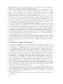
Figure 1. Architecture of lock & key security measure
There has not been much work done that is directly related to the security of scan chains.
Most have gotten around the concern by using BIST. In [6], Hafner et al. used BIST to test the
entire cryptochip they designed. It provided high fault coverage for both the standard cells and
memories, but did not fair nearly as well on the custom designed portions of the chip. Both BIST
and boundary scan were used in [19]. The fault coverage still was not nearly as high as what could
have been achieved with automatic test pattern generation (ATPG) for scan-based design. Any
security sensitive I/O were excluded from the boundary scan.
Work to secure scan designs has only begun recently. An encoding/decoding security scheme
has been proposed [12][13], but another more developed method has been presented by [11]. They
present a method to modify the scan chains that would internally scramble the values if the test
mode was not properly secured. By using an unpredictable random number generator to choose the
segment to scan out, it makes comparing the output after each scan out very difficult. Although
this will make the output very difficult to interpret for an unauthorized user, it will also create
significant delay, routing, and logic overhead since each segment is connected to all other segments
in the chain.
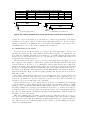
4. Lock & key technique
The Lock & Key security measure we are proposing can be used to secure both single and
multiple-scan designs. For either case, the scan chain can be divided into smaller equal length
subchains. Test vectors are not sequentially shifted into each subchain but rather a linear feedback
shift register (LFSR) randomly selects a subchain to be filled. Figure 1 shows a general architecture
for the Lock & Key method for single-scan design.
The goal of this method is to prevent those who do not hold the test key from manipulating
the scan chain and revealing vital information about the chip. This is ensured by the test security
controller (TSC), which consists of a finite state machine (FSM), test key comparator, LFSR, and
decoder. There are two states the TSC can be in: secure and insecure modes. When the CUT
is initially reset, the FSM sets the TSC into insecure mode and will remain in this insecure state
until TC is enabled. It is only after TC has been enabled for the first time and a test key has been
entered that the TSC may exit the insecure state. When a test key is entered and a user has been
ensured to be a trusted user, the FSM allows the TSC to enter secure mode.
There are two steps the FSM must take before scanning in a test vector for the first time. When
TC is initially enabled, the FSM will first need to check for a correct test key. It will feed the first k
bits of the test pattern, which makes up the test key, to the test key comparator. The comparator
will then return a pass or fail response to the FSM, which will then decide the next state. If the
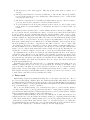
Figure 2. LFSR and decoder in TSC for Lock & Key security
key passes, the FSM will switch the TSC to secure mode allowing predictable operation of the scan
chains and will remain in this state until the CUT is reset. Otherwise, the TSC will remain in
insecure mode and the behavior of the scan chain will not longer be predictable.
Assuming the test key comparator returned a pass response to the FSM, the next q = log2 (m+ 1)
bits will then be fed to the LFSR and used as an initial seed, where q is the size of the LFSR and
m is the number of subchains being implemented. The seeded LFSR will then use a decoder as
an interface to the subchains for a one-hot output, which individually enables each subchain. We
will discuss in detail the concept of an enable signal and how it is generated to control subchains
in Section 4.3. Assuming l is the length of each subchain, the LFSR/decoder generates the next
one-hot output after l clock cycles. Finally, the FSM connects SI to the inputs of the subchains and
the test pattern can be shifted into the scan chain. Once the scanning in process is finished for the
first round, TC goes low and the CUT will function in normal mode capturing the response in the
SFFs. Once the CUT returns to test mode, a new test vector is scanned into the subchains in the
same or a new random order, depending on the design, as the previous vector was scanned in. The
response is shifted-out at the same time the new pattern is shifted-in.
If the entered key fails, the TSC remains in insecure mode and will seed the LFSR with an
unpredictable random seed, essentially locking the scan chains from being used correctly. Since the
choice of subchain is pseudo-random due to the LFSR, it is difficult to predict the response on SO
if both the seed and the configuration of the LFSR are unknown. Even if the configuration of the
LFSR taps are known, if the LFSR is large enough, it is difficult to know the subchain order without
first realizing the initial seed. The need for a test key also compounds any attempt made by an
unauthorized party to use the scan chain.
Although conceptually similar to scan chain scrambling proposed in [11], this method does not
have the requirement of connecting the output of each subchain to the input of all other subchains,
which will significantly reduce area overhead. Also, the response shifted out from SO is dependent
on the seed and LFSR configuration adding an additional obstacle for the hacker. The possibility
of using this method with multiple scan test also provides the advantage of conforming to many
design for test tools used in industry.
4.1. Design of lock & key
There are many possible configurations for the LFSR. Although we want the ability to ensure
security of the scan chain, we also want the design of the Lock & Key method to be design independent. To prevent the decoder from becoming design dependent, an LFSR with a primitive
polynomial configuration will allow the selection of m = 2q − 1 subchains without choosing the same
subchain twice before all subchains have been selected once. If subchains are allowed to repeat, the
test application time will become significantly longer. Figure 2 shows the LFSR and decoder. Since
there is at least one primitive polynomial for all values of q, the LFSR is guaranteed to choose each
subchain once before repeating for any length of the LFSR [2].
The choice of a primitive polynomial significantly simplifies the design of the decoder. The
decoder can directly translate the output of the LFSR into a run of zeros and single one to directly
control each subchain. This method not only shortens design time, but also reduces the area
overhead of the TSC as a whole.
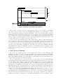
Figure 3. Modifiable LFSR determined by security mode of TSC.
The problem with using a primitive polynomial configuration LFSR is the predictability of its
behavior. If the LFSR were to remain unchanged for insecure mode operation, it would not take
long to find the order since the order is always the same, only the start and end points would
differ. To avoid this predictability, the LFSR configuration must be altered when set to insecure
mode. An additional r-bits to the LFSR that are only active when the TSC is insecure easily serve
this purpose. Figure 3 shows the LFSR with the additional bits that are only active for insecure
mode operation. As can be seen in Figure 3, the additional bits are hidden behind a multiplexer.
The output from the LFSR to the input of the decoder does not change. Since the original LFSR
only makes up a smaller part of the insecure mode LFSR, repetitively selecting the same subchain
multiple times during one test cycle becomes possible, which results in a more complex output.
Unlike in secure mode, repetition is not a large concern since we want the output on SO to confuse
and obscure the order of the scan chains. To further complicate an attack and to make each test
round unique when the TSC is insecure, the FSM can create a new random seed every round.
Another design option when using the LFSR/decoder control in the test security controller is
to use an LFSR with a non-primitive polynomial configuration. It is a more design intensive and
circuit dependent solution, but provides more security since it does not have the same predictability
as the primitive polynomial configured LFSR. The design would use an LFSR of length r + q but
only use q = log2 (m + 1) bits when in a secure state to select a subchain. Unlike the advantage
of using a primitive polynomial LFSR, this design does not guarantee each subchain will only be
chosen without repetition during a scan-in series and results in an increased test time. A memory
element could be used in the decoder that will recall which subchains have been selected during the
current scan-in series and use this to make a decision to choose another subchain. Upon entering
normal mode to run the test pattern, these memory elements would then be cleared for the next
pattern. If the CUT is in insecure mode, the remaining r bits of the LFSR can be used to further
randomize the selection made by the decoder. Again, repeating subchains is not a concern since we
are trying to confuse and obscure the response being placed on SO.
When applying our Lock & Key technique to multiple scan chain designs, essentially the same
principles as single scan designs hold. If the length of the scan chain is long enough, each scan chain
is broken down into m subchains, but rather than use a separate TSC for each chain, a single TSC
can be used to control all chains. Since each scan chain in multiple scan design would normally be
controlled by the same TC, there is no reason for each chain to be controlled by a separate TSC. No
more information about the scan design is given away by using multiple scan as opposed to single
scan, the only actual difference is in the parallelism for faster testing. If the length of each scan
chain is short, they will not be divided into subchains and the Lock & Key technique is used to
access and control all chains.
4.2. Analysis of lock & key
The number of subchains needed is completely dependent upon the amount of complexity required
to deter hackers. If there are m subchains in the design, the response scanned out on SO can be
one of m! possible combinations when in secure mode or up to mm combinations when in insecure
mode. With as few as 15 subchains, an untrusted user that does not have knowledge of the LFSR
configuration nor the seed would have more than one trillion unique combinations to choose from in
secure mode and more than 1515 possible combinations to choose from in insecure mode. A brute
force attempt at resolving the pattern to the location in the chain becomes extremely difficult and
continues to increase in difficulty as m increases.
Overall, this method significantly increases the amount of work necessary to mount an attack on
the scan chains. The following tasks need to be done by a hacker in order for them to perform a
successful attack:
1) Hackers must first learn of what security strategy is being used.
2) If they figure out the strategy used, then they must find the secret test key for the operation
of the chains to be predictable.
3) Even if hackers were to be able to discover the test key, hackers must also determine the
pseudo-random order that patterns will be scanned in and out.
4) If hackers are able to find all this information, an attack can finally be mounted against the
CUT while still having to manage with the pseudo-random selection of the subchains.
As discussed in Section 2, it is easier to design a chip when a specific hacker class is targeted. The
benefit of Lock & Key security is that it scales easily to the amount of security the designer would
like to include. A small TSC with a 4-bit LFSR would be more than suitable to stop a beginner, but
increasing the LFSR to 8-bits would potentially be sufficient to prevent some independent hackers
from intrusion. As the granularity of each subchain becomes smaller and the number of bits in the
LFSR becomes greater, the TSC becomes larger.
We synthesized our Lock & Key technique in Verilog using Synopsys and the Design Analyzer
tool [20]. Table 1 shows the number of equivalent gates returned by Design Analyzer for the FSM,
test key comparator, LFSR, and decoder with 4-bit, 8-bit, and 12-bit LFSRs. The Lock & Key test
security controller grows fairly slowly for a large increase in the number of subchains. The FSM
and test key comparator remain a fairly constant size. FSM operation is mostly independent of
size of the LFSR. The test key comparator is only dependent upon the size of the test key. For a
minimally secure test key length, a length of k ≥ 40-bits should be used. For our implementation,
we used a 64-bit test key. The size of the test key comparator in Table 1 does not include the
additional overhead for on-chip key storage, but we did include it in the final size of the TSC. Only
the growth of the LFSR and decoder is of any significance in terms of size, but the number of
subchains that can be used exponentially increases with each additional bit. The total size of each
LFSR includes the r-bits used for insecure mode operation. We chose to use a constant r value of
4 for all implementations and the primitive polynomials used were from [2].
A 4-bit LFSR can control 15 subchains placing any one of 1515 different subchain combinations
on SO while insecure. Without prior knowledge, a beginner would have little chance of hacking any
vital information from the chip using the scan chain alone. By doubling the size of the LFSR to 8bits, most independent hackers should be deterred. Increasing the LFSR size again greatly increases
the amount of security, but at the cost of a much larger area overhead due to the exponential growth
of the decoder. Increasing the size beyond 10-bits should suffice for some businesses, but if they
have enough resources to open the package and reverse engineer the layout, any effort to secure
the scan chain is inadequate. The same can be said for government hackers attempting to reverse
engineer the chip. If the IP is important enough for them to attempt to hack, they will easily be
able to pool together the appropriate resources to perform a brute force attack if no other solution
is viable. However, we suggest that design engineers use multiple design security techniques to force
both business and government hackers to spend more time, money, and other resources.
The components for the TSC are fairly standard and testing it with BIST can provide a fairly
high coverage. Testing the TSC would defeat the purpose of the security feature since BIST would
only return a pass or fail result as opposed to a pattern response that could potentially be used to
expose either the test key or random seed. The other option would be to simply not test the TSC
logic at all since it is part of the testing logic for the CUT. This option is similar in nature to the
choice of ignoring to test BIST logic due to the fact that if the CUT returns an incorrect result, the
chip is faulty regardless of whether the CUT is faulty or the TSC is faulty [2].
The effect of including Lock & Key security on a chip is fairly minimal when used in modern
Table 1. Number of gates in TSC for 4-bit, 8-bit, and 12-bit.
Number of LFSR
Bits (q)
4-bit LFSR
8-bit LFSR
12-bit LFSR
Size of FSM
113
133
153
(a) Clock gating method.
Size of
Test Key Comparator
54
54
54
Size of LFSR
(q + r)
48
71
91
Size of
Decoder
25
307
5432
Total Size
of TSC
327
652
5817
(b) Subchain feedback method.
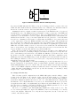
Figure 4. Two subchain modifications to prevent simultaneous normal and test mode operation.
designs. Not only does the TSC logic provide little area overhead, but performance of the chip in
normal mode is not affected any more than a circuit with standard scan test. In case of using a
primitive polynomial for the LFSR, the affect on test time is also minimal because only a test key
and LFSR seed need to be added to the beginning of the test pattern.
4.3. Modification to scan chains
In order for the Lock & Key technique to be effective, an enable signal must be used for each
subchain. We cannot treat the enable signal as TC since that would place one subchain into test
mode while the remaining subchains are in normal mode, potentially changing all registers that
had already been loaded with a new test vector. We introduce two potential solutions that avoid
modification of the standard scan cell.
The Clock Gating method has been proposed for low power testing in the past [21][22]. We would
like to apply the same principle to halt normal operation of the subchains when the enable signal
from the TSC is low. In order to do so, this method adds an additional gate that combines the
system clock and the enable signals from the TSC to the subchain clock. When the enable signal
is high for a particular subchain, the subchain will behave as a normal scan chain with respect to
the system clock. When the enable signal is low, the subchain will ignore the system clock and not
shift when TC is high. Figure 4(a) shows a gating technique that uses the system clock and the
TSC enable signal.
Since this is a small addition, chip area is not severely impacted. It does however affect clock
skew and chip performance. This solution is not suited for high performance applications, but does
provide the opportunity for low power testing since at most l scan cells would be in transition at
any time as opposed to the full length of the scan chain.
Subchain Feedback is the second technique that can be used to avoid simultaneous normal and
test mode subchain operation. Figure 4(b) shows an example of the subchain feedback loop. Unlike
gating the clock, each subchain still shifts the SFF registers regardless of whether enable is high.
By adding a multiplexer to the input of the subchain, the next value to be scanned in can either be
from the new test vector if enable is high or from the last register of the subchain when enable is
low. Since we assume that the subchains are the same length, maintaining consistent data in each
subchain does not become an issue.
This option eliminates the performance problem created by gating the clock, but does not reduce the potential maximum number of transitions when shifting. Since all subchains are shifting
regardless of the enable signal, there will still be as many transitions as if one continuous chain were
used. There is the need for additional routing for the feedback loop and the multiplexer, but these
additions are still fairly small.
5. Conclusion
Scan based designs have been proven to be a significant security risk to the contents of a chip.
Without proper security in place, encryption algorithms can be weakened and IP can be stolen. We
have proposed the Lock & Key technique as a countermeasure to the method that has been used
to expose vital information through the scan chain. Unless the the user is trusted, our technique
will cause the scan chain to operate unpredictably and make exploitation very difficult. Design of
the technique is flexible and straight forward to implement for varying degrees of security. Until
another method of testing a chip can yield the similar coverage as scan based designs with better
security, flexible, low-overhead solutions must be included in the design of scan.
References
[1] B. Yang, K. Wu, and R. Karri, “Scan Based Side Channel Attack on Dedicated Hardware Implementations of
Data Encryption Standard,” in Proc. of the IEEE Int. Test Conf. (ITC), 2004, pp. 339–344.
[2] M. L. Bushnell and V. D. Agrawal, Essentials of Electronic Testing. Kluwer Academic Publishers, 2000.
[3] S. Ravi, A. Raghunathan, and S. Chakradhar, “Tamper Resistance Mechanisms for Secure Embedded Systems,”
in Proc. of the 17th Intl. Conf. on VLSI Design, 2004, pp. 605–611.
[4] P. Kocher, R. Lee, G. McGraw, A. Raghunathan, and S. Ravi, “Security as a New Dimension in Embedded
System Design,” in Proc. of the 41st Annual Conference on Design Automation, June 2004, pp. 753–760.
[5] K. Tiri and I. Verbauwhede, “A VLSI Design Flow for Secure Side-Channel Attack Resistant ICs,” in Proc. of
Design, Automation and Test in Europe, Mar. 2005, pp. 58–63.
[6] K. Hafner, H. C. Ritter, T. M. Schwair, S. Wallstab, M. Deppermann, J. Gessner, S. Koesters, W.-D. Moeller,
and G. Sandweg, “Design and Test of an Integrated Cryptochip,” IEEE Design and Test of Computers, pp.
6–17, Dec. 1991.
[7] P. Kocher, J. Jaffe, and B. Jun, “Differential Power Analysis,” Lecture Notes in Computer Science, vol. 1666,
pp. 388–397, 1999.
[8] J. Kelsey, B. Schneier, D. Wagner, and C. Hall, “Side Channel Cryptanalysis of Product Ciphers,” in Proc. of
the European Symposium on Research in Computer Security, Sept. 1998, pp. 97–110.
[9] D. Boneh, R. A. Demillo, and R. J. Lipton, “On the Importance of Checking Cryptographic Protocols for Faults,”
Lecture Notes in Computer Science, vol. 1233, pp. 37–51, 1997.
[10] E. Biham and A. Shamir, “Differential Fault Analysis of Secret Key Cryptosystems,” Lecture Notes in Computer
Science, vol. 1294, pp. 513–527, 1997.
[11] D. Hély, M.-L. Flottes, F. Bancel, B. Rouzeyre, N. Bérard, and M. Renovell, “Scan Design and Secure Chip,”
in Proc. of the 10th IEEE Intl. On-Line Testing Symposium, 2004.
[12] R. Goering,
“Scan Design Called Portal for Hackers,”
Oct. 2004. [Online]. Available:
http://www.eetimes.com/news/design/showArticle.jhtml?articleID=51200154
[13] S. Scheiber,
“The Best-Laid Boards,”
electronics.com/tmworld/article/CA513261.html
Apr.
2005.
[Online].
Available:
http://www.reed-
[14] P. Ludlow, Ed., High Noon on the Electronic Frontier: Conceptual Issues in Cyberspace, 1st ed. MIT Press,
1996.
[15] G. B. Ratanpal, R. D. Williams, and T. N. Blalock, “An On-Chip Signal Suppression Countermeasure to Power
Analysis Attacks,” IEEE Transactions on Dependable and Secure Computing, vol. 1, no. 3, pp. 179–188, 2004.
[16] P. C. Kocher, “Timing Attacks on Implementations of Diffie-Hellman, RSA, DSS, and Other Systems,” Lecture
Notes in Computer Science, vol. 1109, pp. 104–113, 1996.
[17] R. Karri, K. Wu, and P. Mishra, “Fault-Based Side-Channel Cryptanalysis Tolerant Architecture for Rijndael
Symmetric Block Cipher,” in IEEE Intl. Symposium on Defect and Fault Tolerance in VLSI Systems, 2001, pp.
427–435.
[18] R. Karri, K. Wu, P. Mishra, and Y. Kim, “Concurrent Error Detection Schemes for Fault-Based Side-Channel
Cryptanalysis of Symmetric Block Ciphers,” IEEE Transactions on Computer-Aided Design of Integrated Circuits and Systems, vol. 21, no. 12, pp. 1509–1517, Dec. 2002.
[19] R. Zimmermann, A. Curiger, H. Bonnenberg, H. Kaeslin, N. Felber, and W. Fichtner, “A 177 Mbit/s VLSI
Implementation of the International Data Encryption Algorithm,” IEEE Journal of Solid-State Circuits, vol. 29,
no. 3, Mar. 1994.
[20] Synopsys DFT Compiler, “User Manual for Synopsys Toolset Version 2004.06,” Synopsys Inc., 2004.
[21] R. Sanakaralingam, B. Pouya, and N. A. Touba, “Reducing Power Dissipation During Test Using Scan Chain
Disable,” in Proc. of VLSI Test Symposium, 2001, pp. 319–234.
[22] J. Saxena, K. M. Butler, and L. Whetsel, “An Analysis of Power Reduction Techniques in Scan Testing,” in
Proc. Intl. Test Conf., 2001, pp. 670–677.