1
Voltage and Current Based Fault Simulation for Interconnect Open Defects
Haluk Konuk
Abstract
This paper describes a highly accurate and ecient fault simulator for interconnect opens in combinational
or full-scan digital CMOS circuits. The analog behavior of the wires with interconnect opens are modeled
very eciently in the vicinity of the defect in order to predict what logic levels the fanout gates will interpret,
and whether a sucient IDDQ current will be owing inside the fanout gates. The fault simulation method
is based on characterizing the standard cell library with SPICE; using transistor charge equations for the
site of the open; using logic simulation for the rest of the circuit; taking four dierent factors that can
aect the voltage of an open into account; and considering the potential oscillation and sequential behavior
of interconnect opens. The tool can simulate test vectors for both voltage and current measurements.
Simulation results of ISCAS85 layouts using stuck-at and IDDQ test sets are presented.
1 Introduction
Breaks are a common type of defects that occur during an IC manufacturing process [1]. Breaks in a digital
CMOS circuit fall into dierent categories depending on their location. A break can occur inside a CMOS
cell aecting transistor drain and source connections [2, 3, 4, 5], disconnect a single transistor gate from
its driver [6, 7], or disconnect a set of logic-gate inputs from their drivers; thus causing these inputs to
electrically oat. In order for a break to disconnect a set of logic-gate inputs from their drivers, the break
must occur in the interconnect wiring. In today's CMOS ICs with up to ve metal layers, interconnect wiring
is probably the most likely place for a break to occur. This is well supported by the critical area analysis by
Xue, et al. [8]. Also, vias are especially susceptible to breaks [9], and the number of vias exceeds the number
of transistors in some microprocessor designs [10].
We call the fault created by a break in the interconnect wiring an interconnect open. In order to
make our terminology more specic, a break refers to a discontinuity caused by a manufacturing defect
in the physical layout of a design, and an open refers to the corresponding discontinuity defect in the
electrical circuit of that design. In this paper we describe a fault simulation algorithm for interconnect opens
1
in combinational or full-scan circuits that take into account all known factors aecting the voltage of an
electrically oating wire created by an interconnect open. The end result is the prediction of the analog
behavior of the oating wire such that the logic level that is seen by each gate driven by the oating wire is
determined. Moreover, for a given vector whether sucient IDDQ current will ow inside the gates driven
by the oating wire is also determined.
This paper is an extended version of the work described at ICCAD-97 [11]. To the best of our knowledge,
this is the rst fault simulator reported for interconnect opens; therefore, comparison to prior work is not
applicable. Note that the fault simulator reported in [2] targets network breaks, which aect only the
transistor drain and source connections inside a CMOS cell. By denition, a set formed by network breaks
is disjoint from a set formed by interconnect opens. Therefore, the two fault simulators have disjoint fault
spaces. In the following section, we discuss the factors aecting the voltage of a oating wire. Section 3
describes the pre-processing of the standard-cell library, whose results are used during fault simulation.
Section 4 describes the fault simulation algorithm, and nally Section 5 presents the results of our experiments
with ISCAS85 circuits using stuck-at and IDDQ test sets.
2 The Determining Factors for the Floating Wire Voltage
Knowing the factors that determine the voltage of a oating wire is a basic requirement for building a fault
simulator for interconnect opens. We consider the factors discussed in the following subsections as the most
important ones, and we assume that any other factor, such as conduction through the silicon-dioxide between
metal lines is negligible [12]. We do not cover here due to lack of space how the eect of charge collector
diodes can be handled, which can be found in Chapter 4 in [13].
2.1 Capacitances between the oating wire and its neighboring wires
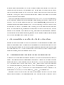
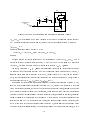
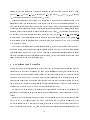
We illustrate the types of wiring capacitances that contribute to the voltage of a oating wire with the help of
Figure 1. In this gure an example of an interconnect open is shown. C5 denotes the total wiring capacitance
from oating wire FW to the n-wells and to the VDD supply wires. C6 is the total wiring capacitance from
FW to the substrate and to the GND supply wires. C3 and C4 denote the wire-to-wire capacitances from
FW to neighboring signal wires, which are created by metal tracks running next to, over, or under FW .
The sizes of C3 , C4 , C5 , and C6 together with the voltages on signal lines S 3 and S 4 contribute to the
determination of the voltage on FW . The meanings of Vsurf and Csurf are discussed later.
One needs to know the exact location of an open in the interconnect in order to obtain the list and
sizes of wiring capacitances to the corresponding oating wire. If an open is going to occur on a piece of
2
AOI21
Vdd
S1
out1
S2
Vsurf
S4
C4
Interconnect
Open
X
Vdd
Csurf
GND
C5
FW
Vdd
C3
INV
C6
S3
out2
GND
GND
Figure 1: A oating wire created by an interconnect open.
straight metal track, we are not aware of any way of predicting where the open defect will land on this metal
track. Besides, contacts are much more susceptible to opens than metal tracks are, according to the defect
distribution statistics by Feltham and Maly [9]. Also, the increasing number of metal layers in IC processes
tends to increase the number of vias per metal layer. In this work, each via, that produces a oating wire
when broken, is considered to be a potential interconnect open defect site. The fault list for our simulator
is produced by considering each such via.
Accuracy in wiring capacitance estimation is another important issue. There are two sources of inaccuracy
for wiring capacitances: (1) computation of the capacitances from the layout, which is called capacitance
extraction, and (2) manufacturing process variations.
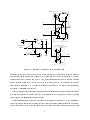
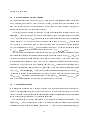
In our experiments we used Magic for capacitance extraction, which can perform a 2-D (two-dimensional)
extraction, based on the area and the perimeter of the overlap between two conducting surfaces. As an example for the inaccuracy of 2-D extraction, consider the capacitance between two parallel metal-2 wires A and
3
A
B
A
B
CA-B = 3.45fF
(a)
CA-B = 2.87fF
metal-1
metal-2
(b)
Figure 2: Wire-to-wire capacitance variation due to surrounding topology.
B in Figure 2. Both wires are 0.9 by 60.0 separated by 0.9. Using a 3-D (three-dimensional) capacitance
extraction program, called SPACE3D [14], and wire height and silicon-dioxide thickness parameters for an
HP 0.6 process, we obtained 3.45fF when there are no other wires in the surroundings, as shown in part (a)
of Figure 2. However, when there are many other metal-1 and metal-2 wires in the surroundings interfering
with the electric eld lines between A and B as shown in part (b), the capacitance goes down to 2.87fF.
Magic extracts 2.88fF for both cases, while the actual capacitance in part (a) is about 20% larger than the
one in part (b). Our additional experiments with a metal-2 wire crossing a metal-1 wire at a right angle
showed about 70% variation for the cross-over capacitance depending on the surrounding topology.
Variations in the thickness of the inter-metal dielectric and the thickness of the metal will cause variations
in the actual wiring capacitances. Even though manufacturing techniques, such as CMP (chemical mechanical
polishing), reduce these variations, they still need to be taken into account. Furthermore, the line width
variation will cause signicant capacitance variation since with high aspect ratios, the bulk of the capacitance
will be to adjacent lines.
One way to deal with the variations in the wiring capacitances is to assume that the actual capacitance is
within +/- x% of the extracted capacitance, where the value of x is determined by the type of extraction tool
used and the manufacturing process. This way, our fault simulator uses a range for each wiring capacitance
in order to compute a voltage range for a given open.
2.2 Transistor capacitances to the oating wire
These capacitances are in the cells driven by FW in Figure 1. They are gate/drain, gate/source, and
gate/bulk capacitances, which are connected to transistor terminals with dotted lines to emphasize that
they are not additionally inserted, but they are part of any CMOS transistor. The bulk terminals of pand n-channel transistors are connected to VDD and GND, respectively. Values of transistor capacitances
4
signicantly vary depending on the transistor terminal voltages. For this reason, we use transistor gate charge
equations expressed as functions of transistor terminal voltages [15, 2] and transistor geometry, rather than
using xed worst case capacitance values to compute the charge stored on transistor gates.
Even though transistor geometries can vary due to process variations causing some variation in transistor
capacitances, theses capacitances are much less aected by surrounding structures than wiring capacitances
are, because gate-oxide thickness is on the order of 100A( = 0.01) while metal wires are separated by
about 1 or so in a 0.6 technology. In this paper, we do not use a value range for a transistor capacitance
as we do for a wiring capacitance.
2.3 Trapped charge deposited on the oating wire
Experiments by Johnson [16] and Konuk and Ferguson [12] showed that the trapped charge deposited during
fabrication can build up a voltage from -4.0V to 2.3V on oating gates with poly extensions, and -1.0V to
1.0V on oating gates connected to metal wires. We are not aware of any technique to predict the amount
of trapped charge on a particular interconnect open. Therefore, our fault simulator makes no assumptions
for the amount of the actual trapped charge. However, if the trapped charge is known to be within a range
for any interconnect open, then this range can be given to our fault simulator as an input.
2.4 The RC interconnect behavior of the die surface
Konuk and Ferguson [12] reported an experimental observation that the die surface acted as an RC interconnect, capacitively coupling the oating wire to almost all other signals in a chip. The die surface resistance
for this phenomenon to occur is in the tera-Ohms range. When coupled with wiring capacitances in the
femto-Farads range in a chip, a time constant of one second or less is produced. Therefore, Csurf in Figure 1
might need to be taken into account when determining the voltage of FW by using a worst case value for
the surface voltage Vsurf . Csurf in Figure 1 denotes the capacitance between the oating wire and the die
surface, and Vsurf denotes the voltage at the portion of the die surface right above the oating wire.
3 Processing the Standard-Cell Library
Before performing fault simulation on a particular standard-cell based design, the standard-cell library needs
to be processed. We assume that each cell in the library is either a basic cell or is composed of basic cells,
where we dene a basic cell as a network of p-channel transistors and a complementary network of n-channel
transistors, where each cell input drives the gates of one p- and one n-channel transistor, such as the AOI21
and INV cells in Figure 1. All the MCNC [17] cells used in the ISCAS85 circuit layouts satisfy this condition.
5
Our fault simulator will require some modication in order to support non-basic cells.
During the library preprocessing, we rst determine the L0 th and L1 th values, which denote the
maximum voltage that is still logic-0 and the minimum voltage that is still logic-1 for the cell library,
respectively [2], which we computed as 1.05V and 1.90V for the MCNC library using HP 0.6 HSPICE [18]
level-13 parameters (the BSIM model) from MOSIS [19], and setting VDD to 3.3V.
We dene a composite input or a c-input for a cell as either a single cell input or multiple input ports
of the same cell tied together. VL0;g;ci denotes the voltage on the c-input ci of cell g such that the output
of g is at L1 th, and is sensitized to ci. For instance; 1.302V on the a input of the 2-input NAND gate in
the MCNC library creates 1.90V (the L1 th voltage) on the NAND gate's output when the b input is 3.3V.
Therefore, VL0 is 1.302V for the c-input consisting of only the a input of the NAND gate. QL0;g;ci denotes
the total electrical charge on the transistor gates that are driven by ci, when the voltage on ci is VL0;g;ci .
VL1;g;ci and QL1;g;ci are similarly dened.
Note that the voltage levels on other inputs of g can aect the threshold values VL0;g;ci and VL1;g;ci in
case of complex cells. For instance; the output of the OAI22 cell shown in Figure 5 will be sensitized to its
b2 input when b1 = 0, a1 = 0, and a2 = 1. However, the output will still be sensitized to b2 even when a1
changes from 0 to 1. The dierence is that in the rst case there is only one current path, which goes through
the nMOS transistor driven by a2. In the second case, when a1 becomes 1, there are two current paths going
through the bottom two nMOS transistors. The VL0 and VL1 values will slightly change depending on which
sensitization case is used. In our processing of the MCNC standard cell library, we used the sensitization
conditions for each complex cell such that the VL0 values are minimized and the VL1 values are maximized.
For IDDQ testing [20] the traditional approach has been to determine a threshold current IDDQ;th
such that a quiescent power supply current larger than IDDQ;th indicates a defective chip. As the number of
transistors on a chip is increasing together with the increasing leakage current per transistor and its variation
from die to die, it is becoming very dicult to nd a single IDDQ threshold that can dierentiate a defective
chip from a defect-free one. One attempt to overcome this problem is the current signatures method [21]. In
this method the dierence in the IDDQ currents between dierent IDDQ vectors is important rather than
the magnitudes of the currents only. If a large step in IDDQ is observed with some of the vectors, that will
be the indication of a defective chip. In the rest of this paper, IDDQ;th can be interpreted as the minimum
amount of additional IDDQ current caused by an interconnect open such that this open will be detected by
the particular IDDQ technique used, that is, either the single threshold method or the current signatures
method.
Let VIDDQ 0;g;ci denote the logic-0 voltage on c-input ci such that IDDQ;th ows through cell g. Let
QIDDQ0;g;ci denote the total electrical charge on the transistor gates that are driven by ci, when the voltage
6
Panel 1
Charge on input a (C)
30f
20f
10f
0
-10f
-20f
Voltage on
input a (V)
-30f
0
1
Viddq0
2
VL1
VL0
3
Viddq1
Figure 3: Charge versus voltage plot for the a input of a NAND gate.
on ci is VIDDQ 0;g;ci , and IDDQ;th ows through g. VIDDQ 1;g;ci and QIDDQ 1;g;ci are similarly dened.
For every cell g and c-input ci in the library, VL0;g;ci , VL1;g;ci , VIDDQ 0;g;ci , VIDDQ 1;g;ci , QL0;g;ci , QL1;g;ci ,
QIDDQ 0;g;ci , and QIDDQ 1;g;ci are computed and recorded using HSPICE. In addition, the slope and the yintercept values for the straight line dened by points (VIDDQ 0;g;ci , QIDDQ 0;g;ci ) and (VL0;g;ci , QL0;g;ci) are
recorded to be used for charge interpolation in our fault simulation algorithm. Similarly, the slope and
the y-intercept for the straight line dened by points (VL1;g;ci , QL1;g;ci ) and (VIDDQ 1;g;ci , QIDDQ 1;g;ci ) are
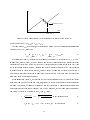
recorded. For example; consider the HSPICE charge-voltage plot in Figure 3 for the a input of the 2-input
NAND gate in the MCNC library using HP 0.6 process parameters. The VIDDQ 0 , VL0 , VL1 , and VIDDQ 1
points are marked using IDDQ;th = 50A.
4 Fault Simulation Algorithm
Figure 4 shows the very top level structure of our algorithm. After all the vectors and opens are processed,
an interconnect open is marked detected if the detection range for the trapped charge spans from ?1 to
+1 if the trapped charge cannot be bounded.
Let VQtrapped ;FW denote the voltage created by the trapped charge on interconnect open FW when the
chip is unpowered, that is, when all other circuit nodes are at GND voltage. Our program lets the user
7
FOREACH 32-vector DO
FOREACH interconnect open DO
Perform PPSFP (parallel pattern single fault propagation) [22] using the 32 vectors
after ipping the fault-free logic values on the oating wire created by the interconnect open.
FOR vector 1 THROUGH 32 DO
IF vector can detect the open THEN
Compute the range of trapped charge for this vector to detect the open, and
add this range to the detection ranges computed from previous vectors.
ENDFOR; ENDFOR; ENDFOR
Figure 4: Top level structure of the fault simulation algorithm
specify a voltage range bounding the trapped charge, such that VQtrapped ;FW for any FW is guaranteed to
be within this range. In order to be able to give this range, the user will need to have some knowledge about
the manufacturing process. If specied, in order to decide whether an open is detected or not this range will
be compared against the trapped charge ranges computed by our program that are necessary for detection.
Detection of a defect can be accomplished by either voltage sensing or current sensing (IDDQ testing) or
both. If voltage sensing is used when a test set is applied, then an interconnect open will be detected if it
behaves like a stuck-at fault for at least one vector of the test set, which covers this stuck-at fault. If current
sensing is used, then an interconnect open will be detected by a vector if at least one of the cells driven by
the oating wire draws an IDDQ current larger than IDDQ;th . The following four subsections describe how
the detection range for trapped charge is computed in cases of voltage sensing, current sensing, and both.
4.1 Voltage sensing (stuck-at detection)
For a given vector and a given logic value on oating wire FW , let us rst describe how we split a c-input of
a cell driven by FW into sensitized and unsensitized parts. A sensitized c-input is formed by those input
ports of a c-input, which drive those transistors through which an IDDQ current ows if the c-input voltage
turns both p- and n-channel transistors on, while all other inputs of the cell are kept at VDD or GND voltage.
The remaining part of the c-input is called an unsensitized c-input. For a simple gate, such as a 2-input
NAND gate, the c-input formed by tying its both input together is also a sensitized c-input, because if the
voltage on this c-input can turn both p- and n-channel transistors on, then a static current will be owing
through all its transistors. However, the c-input formed by only the a input of this NAND gate would also
8
OAI22
b1 = 0
a1 = 1
out
b2
b1 = 0
n1
a1 = 1
FW
(a2, b2) is a c-input, but
a2
(b2) is a sensitized c-input
for OAI22.
Figure 5: An example for a sensitized c-input
be a sensitized c-input only if the b input has the VDD voltage on it, otherwise it would be an unsensitized
c-input.
A more complicated example, where only a part of a c-input forms a sensitized c-input is illustrated by
Figure 5. In this gure oating wire FW is driving a c-input that is formed by tieing the a2 and b2 ports of
an OAI22 gate. We denote this c-input as (a2, b2). In this case with a1 = 1 and b1 = 0, (b2) is the sensitized,
and (a2) is the unsensitized c-input portions, because the p- and n-channel transistors driven by a2 will not
have a static current through them when both are turned on. Actually, the n-channel transistor driven by a2
will have a tiny amount of current, but this is negligible because of the parallel by-pass n-channel transistor
that is fully turned on by a1 = 1.
If an applied vector detects a stuck-at-0 or a stuck-at-1 fault on the oating wire FW , then the rst step
to determine the trapped charge range for this vector to detect the open is to nd the maximum FW voltage
that is still logic-0 in case of stuck-at-0, or the minimum FW voltage that is still logic-1 in case of stuck-at-1.
We assume the stuck-at-0 case for the rest of this subsection without loss of generality. We determine the
maximum logic-0 voltage on FW for the applied vector vec, VL0;FW;vec , as the minimum logic-0 threshold
voltage over all the sensitized c-inputs driven by FW . The following describes this more formally, where g
is the cell the sensitized c-input ci belongs to. Recall that the VL0;g;ci values are pre-computed during the
library processing step.
VL0;FW;vec = 1
FOREACH sensitized c-input ci driven by FW DO
IF VL0;g;ci < VL0;FW;vec THEN VL0;FW;vec = VL0;g;ci
9
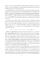
Qs
3
2
1
a
b
c
a vector line
non-linear curve
VFW
VFW,0 VFW,1
Figure 6: Sequential behavior caused by an interconnect open.
ENDFOR
Then, we compute the trapped charge on FW , that corresponds to a voltage of VL0;FW;vec on FW with
vec applied to the circuit. Let us call this computed charge Q0 . We defer the description of the charge
computation to Section 4.4. Intuitively, if the actual trapped charge is smaller than Q0 , then the FW
voltage will be smaller than VL0;FW;vec , that is, the interconnect open will be detected as a stuck-at-0 fault
by vec when the actual trapped charge is less than or equal to Q0 . We will next show that this is not always
true.
Let us consider the case where there is a non-inverting combinational path from FW to S 3 through out1
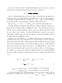
or out2 in Figure 1, and this path is sensitized by vector vec. Let Qs denote the sum of the charges on
transistor gates driven by FW and the charge on the FW plate of capacitor C3. The solid line in Figure 6
shows a typical HSPICE plot of Qs versus VFW [23, 13], which we call the non-linear curve. The reason
for the steep drop in Qs is as follows: When VFW is equal to VL0;FW;vec , a small increase in VFW will push
it over to logic-1 state, which in turn will cause a GND to VDD transition on S 3. This transition will push
positive charge away from the FW plate of C3. The amount of this displaced charge is (VDD * C3) if we
ignore the small increase in VFW . This is causing the drop in Figure 6. From the law of charge conservation:
10
Qtrapped = Qs + C 0 VFW + C 1 (VFW ? VDD ) + Csurf (VFW ? Vsurf )
(1)
where C0 is the sum of capacitances from FW to the nodes at GND, and C1 is the sum of capacitances
from FW to the nodes at VDD . Also, the voltages on these nodes are not dependent on VFW . Thus, if S 4
is at logic-1, then C0 = C6, and C1 = C4 + C5. Equation 1 can be rewritten as
Qs = A ? B VFW ; where
(2)
A = Qtrapped + Csurf Vsurf + C 1 VDD ; B = C 0 + C 1 + Csurf
For a given interconnect open, the value of B is xed, that is, the slope of the straight line dened by
Equation 2 is xed. The value of A depends on C1 and Qtrapped if we assume a xed Vsurf value. For a
given vector, C1 is xed; therefore, only Qtrapped determines the oset of the straight line of Equation 2.
This straight line is called vector line by Konuk [13], because the value of C1 can change with every vector
applied to the circuit, which in turn changes the value of A, thus moving the straight line up or down. For
a given open, a given vector, and a xed Vsurf value, vector lines 1, 2 and 3 in Figure 6 correspond to three
dierent Qtrapped values. The Qtrapped for line 1 is smaller than the one for line 2, which is smaller than the
one for line 3.
For a given VFW , the Qtrapped computation in Section 4.4 eectively nds the intersection between the
non-linear curve and a vector line in Figure 6. For instance, for VFW;0 , which is a logic-0 state, the computed
Qtrapped corresponds to the one for line 2, called Q0 . Note that for VFW;1 , which is a logic-1 state, the
non-linear curve intersects line 1, which is lower than line 2, thus has a smaller Qtrapped value than line
2. This means that the oating wire can be at a logic-1 state with an actual trapped charge smaller than
Q0 . Only when the actual trapped charge is smaller than the one for line 1, the open is guaranteed to be
at logic-0 state. Therefore, the goal is to nd the Qtrapped value that corresponds to the vector line, which
intersects the downward pointing elbow of the non-linear curve in Figure 6.
To achieve this goal, we recompute Qtrapped again by using VL0;FW;vec with vec applied to the circuit,
but this time with logic-1 on FW propagated to all circuit nodes that are sensitized to FW . We call this
computed charge Q1 . Conceptually, we could use VFW;1 instead of VL0;FW;vec , but it is not feasible to
compute the value of VFW;1 , and using VL0;FW;vec , which is expected to be close to VFW;1 , results in even a
smaller trapped charge value.
Then, the maximum actual trapped charge with which vec is guaranteed to detect the open as a stuckat-0 fault is Qtrapped;max;sa0 = min(Q0 ; Q1 ). In other words, the detection range for vector vec is (?1,
Qtrapped;max;sa0 ). The fact that a vector line can intersect the non-linear curve in Figure 6 at three points,
11
as line 2 does, shows that an interconnect open can have two stable states (points a and c), one at logic-0
and the other at logic-1; and one meta-stable state (point b) as explained in [23] and [13]. Therefore, the
logic state of the interconnect open for line 2 can be either 0 or 1 for a given vector depending on the state
of this open for the previous vector applied to the circuit. We call this sequential behavior, because the
logic state of the open not only depends on the present input vector but also on history. As described above,
the Qtrapped;max;sa0 value found corresponds to the vector line that intersects the downward pointing elbow
of the non-linear curve in Figure 6, which is line 1. If the actual trapped charge is below this value, then
the corresponding vector line will also be below line 1, which will intersect the non-linear curve at only one
point. This guarantees that the logic state of the open will be 0 irrespective of the past history; thus avoiding
sequential behavior.
In addition to the sequential behavior, an interconnect open can also oscillate under certain conditions as
explained in more detail in [23, 13]. Oscillation can occur due to capacitance from a signal S to the oating
wire FW , such that there is an inverting combinational path from FW to S , and that path is enabled by
the given vector. Consider the case when a 0-to-1 or a 1-to-0 transition on S causes the voltage of FW move
such that the same logic transition happens on FW due to the mutual capacitance. This will in turn cause
a transition on S because of the enabled inverting path; thus, oscillation.
In the computation of Q0 above, logic values at all signal nodes are found by placing logic-0 on FW .
Therefore, any node that has an enabled inverting path from FW to it, such as S , will have a logic-1 on it.
A logic transition on such a node can only be a 1-to-0 transition, which will push the voltage on FW more
towards GND because of the mutual capacitance, which is the opposite direction for an oscillation to occur.
Therefore, the computation of Q0 is such that oscillation will not occur. The same reasoning is valid for
the computation of Q1 , which is described earlier in this section. Thus, the computation of Qtrapped;max;sa0
guarantees that oscillation will not occur if the actual trapped charge is below this value.
4.2 Current sensing (IDDQ detection)
First, we would like to demonstrate how a change in the logic value of the oating wire can change the set
of sensitized c-inputs. When FW in Figure 7 is logic-1, the oating input of G3 is a sensitized c-input.
However, it is an unsensitized c-input when FW is logic-0. The oating input of G1 is a sensitized c-input
in both cases.
For IDDQ detection, we rst check whether the given vector vec and a logic-0 on FW create any sensitized
c-input driven by FW . If so, we determine the minimum voltage on FW , VIDDQ 0;FW;vec , such that an
IDDQ that is larger than or equal to IDDQ;th still ows through a cell driven by FW . Note that VIDDQ 0 is
less than VL0 , and VIDDQ 1 is greater than VL1 for a basic cell, as illustrated in Figure 3. So, we determine
12
G3
1
interconnect
open
X
G1
G2
1
FW
NAND
Figure 7: The eect of the oating wire's logic value on sensitized c-inputs
VIDDQ 0;FW;vec as the minimum logic-0 IDDQ threshold voltage over all the sensitized c-inputs driven by
FW . The following describes this more formally, where g is the cell the sensitized c-input ci belongs to.
VIDDQ 0;FW;vec = 1
FOREACH sensitized c-input ci driven by FW DO
IF VIDDQ 0;g;ci < VIDDQ 0;FW;vec THEN VIDDQ 0;FW;vec = VIDDQ 0;g;ci
ENDFOR
Then, we compute the trapped charge on FW that corresponds to a voltage of VIDDQ 0;FW;vec . We will
explain the details of the computation in Section 4.4. Note that the FW voltage needs to be larger than
VIDDQ 0;FW;vec for IDDQ detection. Let us call this computed charge Qtrapped;min;IDDQ 0 .
Similarly, we compute Qtrapped;max;IDDQ 1 that corresponds to the maximum trapped charge with which
vec can detect the open as an IDDQ fault. Note that if a sensitized c-input exists when FW is logic-0, a
sensitized c-input must also exist when FW is logic-1, because there will be at least one cell driven by
FW , whose other inputs do not have any combinational path to them starting from FW . Then, the IDDQ
detection range for vec is (Qtrapped;min;IDDQ 0 , Qtrapped;max;IDDQ 1 ).
Oscillation might occur within this detection range due to possible capacitance from a signal S to FW ,
such that there is an inverting combinational path from FW to S , and that path is enabled by the given
vector. When oscillation occurs, the voltage of FW oscillates with a small amplitude, crossing the logic-0 and
logic-1 threshold voltages of a fanout gate back and forth, as demonstrated in [23]. Since the logic threshold
voltages will be inside the range dened by the IDDQ threshold voltages, as illustrated in Figure 3, signicant
amount of current will be drawn from the power supply. At least three CMOS stages are necessary for the
inverting path from FW to S for an oscillation to occur, only one stage cannot oscillate. Therefore, there
will be at least two more gates other than the fanout gate from FW , whose inputs will be oscillating. These
gates will be drawing signicant current, too. Therefore, we assume that even if oscillation occurs, it will be
13
detected as an IDDQ fault.
4.3 Both voltage and current sensing
Due to usage of hardware IDDQ monitors [24, 25], it is now feasible to use hundreds of IDDQ vectors on a
tester. Therefore, while a stuck-at vector is applied to a circuit, its IDDQ might also be measured at the
same time. In this case, either a voltage discrepancy or a high IDDQ will detect the defect. Again, we will
describe the case for stuck-at-0 without loss of generality.
If a vector vec detects the stuck-at-0 fault on FW , then we determine the maximum voltage on FW ,
VIDDQ 1;FW;vec, such that an IDDQ that is larger than or equal to IDDQ;th still ows through a cell driven
by FW . We determine VIDDQ 1;FW;vec as the maximum logic-1 IDDQ threshold voltage over all the sensitized
c-inputs driven by FW . If the voltage on FW is smaller than or equal to VIDDQ 1;FW;vec , then the open
will be detected by vec as either a stuck-at-0 fault or an IDDQ fault. We compute the trapped charge on
FW , that corresponds to VIDDQ 1;FW;vec , as we will describe in Section 4.4. Let us call this computed charge
Qtrapped;max;IDDQ1. Then, the detection range for vector vec is (?1, Qtrapped;max;IDDQ1 ).
Unlike the "stuck-at detection only" case described in Section 4.1, an explicit check for sequential behavior
is not needed here because of the following reasons: The rst observation we make is that VIDDQ 1;FW;vec will
be beyond the last drop in the non-linear curve going from left to right on the Qs -VFW plane. Since a drop
in the non-linear curve occurs every time a logic-0 to logic-1 transition happens on a circuit node that has a
capacitance to FW , as the voltage of FW increases, and VIDDQ 1;FW;vec is larger than the maximum logic-1
threshold of any sensitized c-input driven by FW , there cannot be any drop in the non-linear curve beyond
VIDDQ 1;FW;vec . Let LineIDDQ1;FW;vec denote the vector line crossing the non-linear curve at VIDDQ 1;FW;vec ,
as illustrated in Figure 8 for a non-linear curve that makes two drops. Then, any other vector line below
LineIDDQ 1;FW;vec will intersect the non-linear curve at points where VFW is less than VIDDQ 1;FW;vec , and
these voltage points correspond to either IDDQ detection or stuck-at-0 detection.
4.4 Charge computation
In this subsection we describe how to eciently compute the total electrical charge on a oating wire FW
created by an interconnect open, for a given voltage level VFW on the oating wire and a test vector vec
applied to the circuit. The computed charge values are used to dene the boundaries of the detection ranges
for the trapped charge, as described by the preceding subsections.
The total charge on FW has two components: (i) the charge on the transistor gates driven by FW ,
denoted as Qgate , and (ii) the charge on FW due to the wiring capacitances between FW and other nodes
(including the substrate and the die surface), denoted as Qwire . From the law of charge conservation, the
14
Qs
Lineiddq1,FW,vec
VFW
Viddq1,FW,vec
Figure 8: A non-linear curve with two drops due to a fanout of two from F W .
trapped charge on FW is Qtrapped = Qgate + Qwire .
The equation for Qgate is as follows, where SCI and UCI denote the sets of sensitized and unsensitized
c-inputs driven by FW , respectively.
Qgate =
X
ci2SCI
(aci + bci VFW ) +
X
ci2UCI
Qeqn (ci; VFW ; vec)
(3)
For a sensitized c-input ci, the charge on the transistor gates driven by ci is computed by (aci + bci VFW )
in Equation 3, where aci and bci are the y-intercept and the slope values recorded for ci during our library
processing step in Section 3. Recall that two sets of y-intercept and slope values are computed per ci; one
for the line passing through the IDDQ threshold and the logic threshold points on the Q-V curve as shown
in Figure 3 when the c-input voltage is logic-0, and the other for the line when the c-input voltage is logic-1.
This interpolation-based computation in Equation 3 is an ecient way of approximating the charge on a
sensitized c-input with reasonable accuracy.
For an unsensitized c-input ci, the charge on the gate of each transistor driven by ci is computed by using
Equations 4 and 5, which are taken from Sheu, Hsu, and Ko [15] where the derivations of these equations are
explained. Additionally, we included the sensitivity of model parameters to transistor lengths and widths.
These equations are for an nMOS transistor. For a pMOS transistor, the right hand sides of Equations 4
and 5 need to be negated together with the Vgb and Vgs terms.
r
2
Qg = cap 2zk1 (?1 + 1 + 4 (Vgbzk?12zvfb) ) in subthreshold region
(4)
Qg = cap (Vgs ? zvfb ? zphi) with Vds = 0 in triode region
(5)
15
Any term that starts with \z" in the preceding equations such as zk1 or zvfb is a BSIM [18] electrical
parameter taking the transistor size into account, and we compute it as follows [26]:
PW
zP = P + L ?PLDL + W ?
DW
where P is a process parameter such as vfb or phi, PL and PW are the length and width sensitivities of
parameter P, W and L are the drawn transistor width and length, and DW and DL are the size changes to
W and L due to various fabrication steps. The values of P , PL , PW , DL, and DW are all determined by
the fabrication process. We obtained the values of all the BSIM parameters from MOSIS.
Finally, cap = Cox (W ? DW ) (L ? DL) where Cox is the gate-oxide capacitance per unit area.
The saturation region is not included in Equations 4 and 5, because, by denition, no current will be
owing through the transistors driven by an unsensitized c-input. For the same reason, Vds is zero in
Equation 5. These gate charges are added up to nd Qeqn (ci; VFW ; vec) in Equation 3, where vec stands
for the test vector applied to the circuit. We could not use interpolation to compute Qeqn (ci; VFW ; vec);
because, unlike a sensitized c-input, VFW alone is not sucient to determine the drain/source voltages of
the transistors driven by an unsensitized c-input.
Equation 6 shows the expression for Qwire . C 0 and C 1 denote the sets of capacitances from FW to
other nodes that are at logic-0 and at logic-1, respectively. Recall from Section 2.1 that our algorithm uses a
range for each wiring capacitance due to process variations and possible accuracy limitations of capacitance
extraction tools. Equation 7 shows how to pick the worst case values for Cw0 and Cw1 in order to guarantee
detection. The detection of the open might occur below VFW , for instance, when VFW is the maximum
logic-0 voltage for the oating wire, and the vector applied is a test for FW stuck-at-0. In this case, Cw1;max
will be used for Cw1 as the worst case, because the corresponding wire w1 is at logic-1, thus, pulling the
oating wire voltage up towards logic-1 (non-detection of the open) with a strength proportional to the size
of Cw1 .
Qwire =
X
Cw0 2C 0
Cw0 VFW +
X
Cw1 2C 1
CFW surf (VFW ? Vsurf )
8
<C
(C
)
Cw0 (Cw1 ) = : w0;min w1;max
Cw0;max(Cw1;min )
Cw1 (VFW ? VDD ) +
(6)
if FW voltage needs to be < VFW for detection
(7)
if FW voltage needs to be > VFW for detection
If the die surface does not have a large enough resistivity, then the capacitance between FW and the
surface needs to be considered, also. Given a voltage range Vsurf;min and Vsurf;max the die surface can
16
acquire, the last term in Equation 6 is used for modeling the worst case eect of the die surface. Again,
either CFW surf;min or CFW surf;max is used for CFW surf , and either Vsurf;min or Vsurf;max is used for
Vsurf depending on whether VFW is larger than Vsurf or not.
Transistor drain/source voltages need to be determined to decide whether a transistor driven by an
unsensitized c-input is in subthreshold or triode region to compute its gate charge using Equation 4 or 5.
Also, a oating wire will sometimes go over cells in a layout; thus, it will have capacitances to internal nodes
of these cells, such as node n1 in Figure 5. These internal nodes are also connected to transistor drain/source
terminals, whose voltages are used in Equation 6 instead of GND and VDD voltages used for signal wires.
We use four voltage levels for an internal node, which are GND, VDD , max n, and min p, where max n
is the maximum voltage an internal node in an n-network can achieve through a path to VDD , and min p
is the minimum voltage an internal node in a p-network can achieve through a path to GND, as also used
by [2] for network breaks.
The voltage of an internal node is determined as done in [2], details of which are not repeated here to
save space. Briey, sum-of-products Boolean expressions are used to specify the cell input conditions for
each internal node to have a path to VDD or GND. These sum-of-products expressions are computed during
our library processing step for each internal node in the library, but they are evaluated for every new vector
during the fault simulation of an interconnect open.
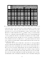
5 Experiments and Results
We used the two metal layer channel routed layouts of the ISCAS85 circuits for our experiments. Since we
consider each via (the contact between metal 1 and 2) as an interconnect open site, we process each layout
with a program that is an extended version of Carafe [27] in order to analyze each via to nd out whether
a oating wire is created if the via is broken. There are some redundant vias in the layouts, which do not
create an open when broken. The program removes each via that can create a oating wire from the layout,
and labels the wire pieces in a systematic fashion. Then, we run Magic using the HP 0.6 parameters in the
technology le 8.2.8 from MOSIS to extract the capacitances from the layout.
We would like to emphasize that the main purpose of our results in this section is to demonstrate the
functionality of our simulator, rather than coming up with conclusions that can be generalized to all VLSI
circuits.
There is a metal-2 wire across the height of each MCNC cell used in the ISCAS85 layouts for every input
port of the cell. A via connects this metal-2 wire to a small piece of metal-1, which is connected to poly
that drives transistor gates. When this via is broken, the oating poly together with a small piece of metal-1
form a very short oating wire (s-FW ), which have very small capacitances to neighboring nodes and to the
17
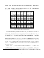
die surface. The numbers of breaks corresponding to these vias are listed in the second column of Table 1.
The remaining via-breaks are considered to create "long" oating wires (l-FW ), and are listed in the third
column. The IDDQ and stuck-at vectors are generated by Nemesis [28]. The IDDQ coverages in the fth
column are based on the pseudo-stuck-at fault model.
Ct.
c432
c499
c880
c1355
c1908
c2670
c3540
c5315
c6288
c7552
# of
# of
# of
s-F W
l-F W
IDDQ
via-breaks via-breaks vectors
322
386
510
884
720
1286
1854
2938
4232
3464
717
856
1144
1528
1551
3141
4420
7652
8260
9054
30
52
36
81
77
42
67
60
34
86
IDDQ
cov.
# of
stuck-at
vectors
stuck-at
cov.
98.78 %
100.00 %
100.00 %
100.00 %
99.73 %
97.78 %
97.71 %
99.62 %
99.40 %
99.62 %
55
53
63
85
99
117
175
137
33
221
97.16 %
98.98 %
100.00 %
99.57 %
99.28 %
96.33 %
96.58 %
98.79 %
99.42 %
98.89 %
Table 1: Via-break and test vector statistics
For a given manufactured die, the wiring capacitances are xed, even though their values may not be
accurately known due to limitations of extraction tools and process variations. So, we decided to use the
Magic extracted capacitance values as the real values, and assume that it is theoretically possible to modify
the given circuit layout to exactly match these capacitance values, and the actual design is this modied
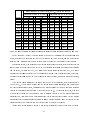
layout. We also assumed that the die surface eect of Section 2.4 does not apply. Table 2 shows our
simulation results. Columns 2 to 5 show the % of s-FW and l-FW opens guaranteed to be detected no
matter what the actual trapped charge is1 , when stuck-at (SA) vectors are used alone or in combination
with IDDQ vectors. In columns 2 through 5, if an open is declared as detected, it means that the open will
be detected by the test set independent of the amount and the polarity of the trapped charge on the oating
wire created by that open.
SA vectors are good at detecting interconnect opens when the magnitude of the actual trapped charge
is large, forcing the oating wire to behave as stuck-at-0 or stuck-at-1. In contrast, IDDQ vectors tend to
detect opens when the trapped charge magnitude is small, resulting in oating wire voltages being pulled to
Note that excessive trapped charge may create a dangerous voltage level such that a gate-oxide punch through may occur,
creating a gate-oxide short coupled with an interconnect open. We do not consider this case and leave it to future research.
1
18
the vicinity of VDD /2 by wiring and transistor capacitances when the chip is powered up. This is why SA
and IDDQ vectors together produce much better guaranteed coverages in columns 4 and 5, where detection
is guaranteed no matter what the actual trapped charge is.
In all our experiments, the two IDDQ threshold voltages for each standard cell c-input were computed as
described in Section 3, which correspond to 50A of IDDQ current owing through the standard cell being
processed. If IDDQ;th = 50A additional current in either the single threshold or the current signatures [21]
IDDQ test technique, which is described in Section 3, does not provide enough resolution to dierentiate a
defective chip, then IDDQ;th needs to be increased. Note that this will make the IDDQ detection range dened
by the two IDDQ threshold voltages for each c-input narrower, which will in turn reduce the eectiveness of
IDDQ vectors.
If the initial voltage on a oating wire due to the trapped charge can be bounded, then the detection
ranges our algorithm computes, as explained in Section 4, can be compared to the size of the total possible
range to give a probabilistic range coverage number. For example; if the trapped charge voltage can be
guaranteed to fall in the [-1.0V, 1.0V] range for any interconnect open, and the detection ranges computed
by our fault simulator are (?1, -0.3V) and (0.25V, 1) for a particular open, then the trapped charge range
coverage for that open will be
[(?0:3V ? (?1:0V )) + (1:0V ? 0:25V )] (1:0V ? (?1:0V )) = 0:725 = 72:5%
assuming a homogeneous distribution of actual trapped charge voltages in the [-1.0V, 1.0V] range. We
dene the range coverage for a chip as the average value of range coverages over all the interconnect
opens. This is what we did for the rest of Table 2. Konuk and Ferguson [12] reported that trapped charge
on oating metal wires connected to transistor gates can create voltages in the range between -1V to 1V,
but 75% of the measurements were between -0.5V and 0.5V for a set of experimental chips fabricated with
an HP 0.8 process. Therefore, assuming that the actual trapped charge voltages are bounded by [-1.0V,
1.0V], we obtained the range coverage numbers in columns 6 and 7. Using the [-0.5V, 0.5V] range decreased
the coverage numbers, as we expected, because we used only the SA vectors, and SA vectors get worse in
detection when the trapped charge magnitude gets smaller around 0V. Still, these range coverage numbers
are much better than the guaranteed coverage numbers in columns 2 and 3.
In order to be certain of the coverage of a set of test vectors, one needs to take into account the variation
in the capacitance values due to extraction tool inaccuracies and process variations, plus the eect of the
die surface. Assuming that the trapped charge voltage is bounded by [-0.5V, 0.5V], and using either VDD
or GND for the die surface voltage depending on which one being the worst case, we obtained the range
coverage percentages in Table 3. VDD is 3.3V for all our experiments. This table shows the sensitivity of
coverage to capacitance variation and to dierent sets of tests. +/-30% variation in capacitance means that
19
% opens guaranteed to be detected
with no bound on the trapped charge
SA and IDDQ
s-F W l-F W
Trapped charge range cov. (%)
SA only,
SA only,
-1.0V to 1.0V
-0.5V to 0.5V
trapped Q volt.
trapped Q volt.
s-F W l-F W
s-F W l-F W
95.03
97.93
100.00
99.10
98.75
93.86
93.91
98.03
99.13
97.89
87.21
88.53
89.43
88.74
89.29
86.52
86.85
88.78
88.35
88.89
Circuit
SA only
s-F W l-F W
c432
c499
c880
c1355
c1908
c2670
c3540
c5315
c6288
c7552
0.00
0.00
0.00
0.00
0.00
0.00
0.00
0.00
0.00
0.00
4.46
3.04
17.92
10.14
6.77
5.19
16.99
11.43
18.67
6.57
98.19
98.83
99.83
99.80
99.48
97.33
97.22
97.28
99.84
99.14
87.44
86.98
92.61
91.50
89.97
89.89
91.04
92.06
91.51
90.80
79.65
79.50
80.12
78.49
80.96
77.46
79.26
80.06
77.71
80.32
76.93
74.96
86.12
84.53
81.06
83.61
85.27
86.76
84.44
85.57
Table 2: Via-break coverages assuming no surface eect and using extracted capacitance values.
the actual value for a wiring capacitance is within the range from 0:7 Cextracted to 1:3 Cextracted .
Note that the coverage numbers in column 3 for l-FW opens is particularly low. The reason is the eect
of the die surface, because the same column in Table 4 has coverages that are about three times as large.
The only dierence in the preparation of Table 4 is that Vsurf is assumed to be bounded by [0.25VDD ,
0.75VDD ] rather than [0V, VDD ]. The observation that the die surface has an extremely signicant eect
on the coverage numbers for long wires is not surprising, because long oating wires are aected by the die
surface more than the short oating wires are. However, this result should not be generalized, because the
ISCAS85 layouts use only 2 metal layers, whereas modern designs have up to 6 layers of metal, which can
easily hide oating wires in layers 1 and 2 from the die surface.
Comparing column 3 to column 5 in Table 3 shows that decreasing the capacitance variation from 30%
to 15% did not have a large eect on the coverage numbers, at all.
Using IDDQ vectors in addition to SA vectors boosts the coverage numbers as listed in columns 6 through
9. The l-FW opens get the largest boost in coverage from adding the IDDQ vectors, which compensate
the adverse eect of the die surface on the l-FW opens. Decreasing the capacitance variation from 30% to
15% helps coverage about 12 percentage points as shown in columns 7 and 9. Again, this is a smaller eect
compared to the eect of adding IDDQ vectors or reducing the voltage variation of the die surface. The
s-FW opens achieve almost full coverage even with 30% capacitance variation as shown in column 6.
20
Circuit
c432
c499
c880
c1355
c1908
c2670
c3540
c5315
c6288
c7552
Range coverage %'s for trapped charge, with Vsurf between VDD and GND
Capacitance variation (SA tests only)
Capacitance variation (SA and IDDQ)
+/-30%
+/-15%
+/-30%
+/-15%
s-F W l-F W
s-F W l-F W
s-F W l-F W
s-F W
l-F W
67.21
66.42
66.67
64.84
67.84
64.21
67.06
67.08
64.02
66.97
20.30
20.34
23.62
23.54
19.57
17.74
19.47
18.99
22.24
17.35
71.32
71.02
71.08
69.29
72.31
68.57
71.10
71.37
68.47
71.44
27.23
27.62
32.11
31.50
27.50
25.59
27.66
27.58
30.49
25.51
100.00
99.56
100.00
100.00
99.95
99.63
99.63
99.97
99.62
99.99
80.76
75.88
81.66
78.55
72.85
66.28
70.48
64.89
75.85
61.57
100.00
99.81
100.00
100.00
99.98
99.65
99.67
99.97
99.62
100.00
91.44
87.30
90.85
90.06
85.98
79.64
84.12
78.20
87.31
76.43
Table 3: Range coverages for trapped charge with surface voltage varying betweenVDD and GND
Table 4 shows that the eect of the die surface voltage is pretty signicant on the coverage numbers.
Again, we would like to emphasize that ISCAS85 layouts have only 2 metal layers, and this is an expected
result for them. Designs with more metal layers will not be as sensitive to die surface voltage variation.
As described earlier, if the magnitude of the trapped charge range gets larger, then the coverage of this
range by stuck-at vectors is expected to get better. We ran our simulator using the parameters for column 6
and 7 in Table 3, but using the [-1.0V, 1.0V] range for the trapped charge instead of the [-0.5V, 0.5V] range.
The range coverage numbers for the l-FW opens increased between 4 and 9 percentage points, as expected.
The range coverage numbers for the s-FW opens stayed almost the same, which were almost full coverage,
anyway.
If the trapped charge bounds stay the same while the VDD voltage decreases, then the net eect will
be as if the VDD voltage stayed the same and the trapped charge bounds increased, which actually helps
the trapped charge range coverage, as discussed above. Here we assume that the logic and IDDQ threshold
voltages of the standard cells scale down at the same rate as the VDD voltage does. However, if the ratio
of the distance between the logic-0 and logic-1 IDDQ threshold voltages to the VDD value decreases with
decreasing VDD , then this will have a diminishing eect on the range coverage of IDDQ vectors. Further
experiments can be performed using our simulator using a process technology and a cell library that are
designed for lower VDD to nd out how the coverage of IDDQ vectors will be aected.
In case IDDQ vectors cannot be applied at high speed, the number of IDDQ vectors might be limited.
21
Circuit
c432
c499
c880
c1355
c1908
c2670
c3540
c5315
c6288
c7552
Range coverage %'s for trapped charge, with Vsurf between 0.75VDD and 0.25VDD
Capacitance variation (SA tests only)
Capacitance variation (SA and IDDQ)
+/-30%
+/-15%
+/-30%
+/-15%
s-F W l-F W
s-F W l-F W
s-F W l-F W
s-F W
l-F W
72.13
70.91
72.15
70.53
72.74
69.65
71.89
72.33
69.66
72.26
60.37
58.70
69.09
67.52
63.64
63.59
66.48
67.04
67.16
64.72
75.82
75.13
76.10
74.48
76.80
73.54
75.51
76.17
73.63
76.25
68.70
67.28
77.71
76.29
72.52
72.94
75.82
76.63
75.91
74.30
100.00 100.00
99.76 99.72
100.00 100.00
100.00 100.00
99.97 99.91
99.65 99.76
99.66 99.73
99.97 99.93
99.62 99.85
100.00 99.95
100.00
100.00
100.00
100.00
100.00
99.66
99.69
99.97
99.62
100.00
100.00
99.94
100.00
100.00
99.99
99.83
99.81
99.99
99.85
100.00
Table 4: Range coverages for trapped charge with surface voltage varying between 0.825V and 2.475V
In order to nd the impact of this at least on the ISCAS85 circuits, we used only 10% of the IDDQ vectors
available for each circuit. For simplicity, we just picked the rst 10% from each IDDQ test set, rather
than picking the 10% that will give the largest pseudo-stuck-at coverage. We used the stuck-at test sets
unmodied. We obtained the results in Table 5 with Vsurf bounded by [0.25VDD , 0.75VDD ] and capacitance
variation +/-30%. Interestingly, the range coverage numbers are pretty close to the ones in columns 6 and
7 of Table 4, where full IDDQ and stuck-at tests were used. The second row in Table 5 shows the pseudostuck-at fault coverages of the IDDQ vectors used. They are pretty low compared to the ones from full
IDDQ tests shown in the "IDDQ cov." column of Table 1. Still, the range coverages are pretty high in
Table 5. There are two factors contributing to achieving high range coverage with IDDQ vectors that have
low pseudo-stuck-at coverage.
First, an IDDQ vector that covers the pseudo-stuck-at-0 fault at input a of a basic cell, as dened in
Section 3, will cause high IDDQ current inside that cell if input a acquires a voltage between the IDDQ
threshold voltages of a due to an interconnect open. An IDDQ vector that covers the pseudo-stuck-at-1
fault at a will be able to do the same. Therefore, one IDDQ vector that covers either the pseudo-stuck-at-0
or pseudo-stuck-at-1 can be sucient; covering both faults will not be necessary. Second, if a oating wire
created by an interconnect open has a fanout of more than one, then an IDDQ vector that covers a pseudostuck-at fault at any of the fanout branches can create high IDDQ, and thus causes that open to be detected,
even though none of the IDDQ vectors used cover a pseudo-stuck-at fault at other branches. Therefore, even
22
a small set of IDDQ vectors can be very useful in achieving high coverage for interconnect-opens.
c432 c499 c880 c1355 c1908 c2670 c3540 c5315 c6288 c7552
IDDQ cov. 55.78 73.68 67.82 78.88 70.40 54.67 69.51 71.10 65.96 71.84
s-F W
l-F W
93.99 95.20 97.19 97.71 95.07 90.98 96.08 96.77 96.30 96.13
94.02 96.76 98.09 99.49 96.88 92.50 97.26 97.96 98.25 96.56
Table 5: Range coverage percentages with stuck-at vectors and using only the rst 10% of the IDDQ vectors
with Vsurf between 0.825V and 2.475V, and capacitance variation +/-30%
We used an HP-735 99MHz workstation with 180MB memory for our fault simulations. The maximum
wall clock time in our experiments was 4 minutes 24 seconds for circuit c7552, which shows us promise for
the feasibility of a fault simulator for real world chips.
6 Conclusion
We presented a highly accurate and ecient fault simulator for interconnect opens, which take almost all
factors that can aect the voltage of an open into account. Our results from ISCAS85 circuit layouts show
that combination of high coverage stuck-at and IDDQ test sets can result in high coverage of interconnect
opens, especially when the die surface voltage is bounded, while stuck-at tests alone may not always guarantee
such high coverage.
References
[1] C.F. Hawkins, J.M. Soden, A.W. Righter, and F.J. Ferguson. Defect classes - an overdue paradigm for
CMOS IC testing. In Proceedings of ITC, Oct. 1994.
[2] H. Konuk, F.J. Ferguson, and T. Larrabee. Charge-based fault simulation for CMOS network breaks. IEEE Transactions on Computer-Aided Design, pages 1555{67, Dec. 1996
(http://sctest.cse.ucsc.edu/papers/publications.html).
[3] C. Di and J.A.G. Jess. On accurate modeling and ecient simulation of CMOS opens. In Proceedings
of International Test Conference, pages 875{882, October 1993.
[4] M. Favalli, M. Dalpasso, P. Olivo, and B. Ricco. Modeling of broken connections faults in CMOS ICs.
In Proceedings of European Design and Test Conference, 1994.
23
[5] W.M. Maly, P.K. Nag, and P. Nigh. Testing oriented analysis of CMOS ICs with opens. In Proceedings
of International Conference on Computer-Aided Design, Nov. 1988.
[6] V.H. Champac, A. Rubio, and J. Figueras. Electrical model of the oating gate defect in CMOS IC's:
Implications on IDDQ testing. IEEE Transactions on Computer-Aided Design, March 1994.
[7] M. Renovell and G. Cambon. Electrical analysis and modeling of oating-gate fault. IEEE Transactions
on Computer-Aided Design, pages 1450{1458, November 1992.
[8] H. Xue, C. Di, and J.A.G. Jess. Probability analysis for CMOS oating gate faults. In Proceedings of
European Design and Test Conference, 1994.
[9] D.B.I. Feltham and W. Maly. Physically realistic fault models for analog CMOS neural networks. IEEE
Journal of Solid-State Circuits, Sep. 1991.
[10] K.M. Thompson. Intel and the myths of test. In The Keynote Address of International Test Conference,
October 1995.
[11] H. Konuk. Fault simulation of interconnect opens in digital CMOS circuits. In Proceedings of International Conference on Computer-Aided Design, November 1997.
[12] H. Konuk and F.J. Ferguson. An unexpected factor in testing for CMOS opens: The die surface. In
IEEE VLSI Test Symposium, 1996 (http://sctest.cse.ucsc.edu/papers/publications.html).
[13] H. Konuk. Testing for opens in digital CMOS circuits. Ph.D. Thesis, Computer Eng. Dept., UC Santa
Cruz, Dec. 96 (http://sctest.cse.ucsc.edu/papers/publications.html).
[14] A.J. van Genderen and N.P. van der Meijs. Space3d Capacitance Extraction User's Manual. Delft
University of Technology, 1997 (http://cas.et.tudelft.nl/ space).
[15] B.J. Sheu, W.-J. Hsu, and P.K. Ko. An MOS transistor charge model for VLSI design. IEEE Transactions on Computer-Aided Design, pages 520{527, April 1988.
[16] S. Johnson. Residual charge on the faulty oating gate MOS transistors. In Proceedings of International
Test Conference, October 1994.
[17] MCNC. http://www.mcnc.org.
[18] Meta-Software. HSPICE User's Manual: Elements and Models. 1992.
[19] MOSIS. http://www.mosis.org.
[20] A.D. Singh, H. Rasheed, and W.W. Weber. IDDQ testing of CMOS opens: An experimental study. In
Proceedings of International Test Conference, 1995.
[21] A.E. Gattiker and W. Maly. Current signatures: Aplication. In Proceedings of International Test
Conference, November 1997.
24
[22] J.A. Waicukauski, E.B. Eichelberger, D.O. Forlenza, E. Lindbloom, and Th. McCarthy. Fault simulation
for structured VLSI. In VLSI Systems Design, pages 20{32, Dec. 1985.
[23] H. Konuk and F.J. Ferguson. Oscillation and sequential behavior caused by opens in the routing
in digital CMOS circuits. IEEE Transactions on Computer-Aided Design, pages 1200{10, Nov. 1998
(http://alumni.cse.ucsc.edu/ haluk/publications.html).
[24] P.C. Maxwell, R.C. Aitken, K.R. Kollitz, and A.C. Brown. IDDQ and AC scan: The war against
unmodelled defects. In Proceedings of International Test Conference, 1996.
[25] H.A.R. Manhaeve, P.L. Wrighton, J. van Sas, and U. Swerts. An o-chip IDDQ current measurement
unit for telecommunication asics. In Proceedings of ITC, 1994.
[26] G. Massobrio and P. Antognetti. Semiconductor Device Modeling with SPICE. McGraw-Hill, 1993.
[27] A. Jee and F.J. Ferguson. Carafe: An inductive fault analysis tool for CMOS VLSI circuits. In
Proceedings of the IEEE VLSI Test Symposium, 1993.
[28] T. Larrabee. Test pattern generation using Boolean satisability. IEEE Transactions on ComputerAided Design, pages 6{22, January 1992.
25