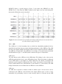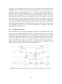
1
Developing a LEON3 template design for the Altera Cyclone-II DE2 board Master of Science Thesis in Integrated Electronic System Design DANIEL BENGTSSON RICHARD FÅNG Chalmers University of Technology University of Gothenburg Department of Computer Science and Engineering Göteborg, Sweden, August 2011 The Authors grants to Chalmers University of Technology and University of Gothenburg the non-exclusive right to publish the Work electronically and in a non-commercial purpose make it accessible on the Internet. The Authors warrants that they are the authors to the Work, and warrants that the Work does not contain text, pictures or other material that violates copyright law. The Authors shall, when transferring the rights of the Work to a third party (for example a publisher or a company), acknowledge the third party about this agreement. If the Authors has signed a copyright agreement with a third party regarding the Work, the Authors warrants hereby that they have obtained any necessary permission from this third party to let Chalmers University of Technology and University of Gothenburg store the Work electronically and make it accessible on the Internet. Developing a LEON3 template design for the Altera Cyclone-II DE2 board DANIEL BENGTSSON RICHARD FÅNG © DANIEL BENGTSSON, August 2011. © RICHARD FÅNG, August 2011. Examiner: SVEN KNUTSSON Chalmers University of Technology University of Gothenburg Department of Computer Science and Engineering SE-412 96 Göteborg Sweden Telephone + 46 (0)31-772 1000 Cover: The cover shows the Altera DE2 development board. Department of Computer Science and Engineering Göteborg, Sweden August 2011 Abstract This Master of Science thesis describes the development of a LEON3 template design for the Altera Cyclone-II DE2 board. A template design is mainly a LEON3 processor system modified to suit a specific board. An existing template design was modified, supporting most of the components on the board. However, the on-board SDRAM circuit has a data bus width of 16-bits and existing SDRAM memory controllers did not support this data bus width. An existing SDRAM memory controller was therefore modified to support memories with a data bus width of 16-bits. Furthermore, no IP core was available for the LCD module on the Altera Cyclone-II DE2 board. An IP core was therefore implemented for this display. A software package, written in C code, was implemented for communicating with the LCD IP core. The purpose of this software package was to give users of the template design an easy way to communicate with the display. The project was carried out at Aeroflex Gaisler AB and all implementations were successfully verified. Keywords: LEON3, FPGA, HD44780, SDRAM, memory controller, LCD module, GRLIB, IP core, VHDL i ii Contents 1 2 Introduction .............................................................................................................. 1 1.1 Background ........................................................................................................ 1 1.2 Purpose of the project ........................................................................................ 1 1.3 Outline of the thesis ........................................................................................... 1 Technical background............................................................................................... 3 2.1 2.1.1 Template design .......................................................................................... 3 2.1.2 Plug & Play capability ................................................................................ 4 2.2 AHB ............................................................................................................ 5 2.2.2 APB ............................................................................................................ 9 2.3 Altera Cyclone-II DE2 Development Board ................................................... 12 2.4 SDRAM ........................................................................................................... 14 2.4.1 General functionality ................................................................................ 14 2.4.2 Signal Descriptions ................................................................................... 15 2.4.3 Commands ................................................................................................ 16 LCD ................................................................................................................. 19 2.5.1 General functionality ................................................................................ 19 2.5.2 Signal Descriptions ................................................................................... 21 2.5.3 Instructions ............................................................................................... 22 2.5.4 Initialization .............................................................................................. 25 2.5.5 Timing characteristics............................................................................... 26 2.6 Two-process method ........................................................................................ 27 2.6.1 Design rules .............................................................................................. 28 2.6.2 Two processes per entity .......................................................................... 28 Implemented template design ................................................................................. 31 3.1 Analysis of original functionality .................................................................... 31 3.1.1 Top-level design entity ............................................................................. 31 3.1.2 Test bench ................................................................................................. 32 3.2 4 AMBA ............................................................................................................... 4 2.2.1 2.5 3 GRLIB ............................................................................................................... 3 Modifications and considerations .................................................................... 33 3.2.1 Top-level design entity (leon3mp.vhd) .................................................... 33 3.2.2 Test bench (testbench.vhd) ....................................................................... 35 Implemented SDRAM memory controller (sdctrl16.vhd) ..................................... 37 4.1 Introduction ...................................................................................................... 37 iii 5 4.2 Interface ........................................................................................................... 37 4.3 Configuration options ...................................................................................... 38 4.4 Functionality of the original controller (sdctrl.vhd) ........................................ 40 4.4.1 Sampling ................................................................................................... 41 4.4.2 Memory addressing .................................................................................. 41 4.4.3 Data handling............................................................................................ 42 4.4.4 Communication ........................................................................................ 43 4.5 Design choices ................................................................................................. 46 4.6 Modifications ................................................................................................... 47 4.6.1 Memory addressing .................................................................................. 47 4.6.2 Data handling............................................................................................ 48 4.6.3 Communication ........................................................................................ 50 4.6.4 Burst interruption ...................................................................................... 54 Implementations for the LCD module .................................................................... 57 5.1 5.1.1 Introduction .............................................................................................. 57 5.1.2 Design choices .......................................................................................... 57 5.1.3 Interface .................................................................................................... 58 5.1.4 Configuration register ............................................................................... 58 5.1.5 General functionality of the IP core ......................................................... 59 5.2 6 IP core (apblcd.vhd) ......................................................................................... 57 Software package (apblcd.c, apblcd.h) ............................................................ 61 5.2.1 Design choices .......................................................................................... 61 5.2.2 Description of easy-to-use functions ........................................................ 61 5.2.3 Description of available sub-functions ..................................................... 62 Testing .................................................................................................................... 65 6.1 Implemented SDRAM memory controller ...................................................... 65 6.2 Implementations for the LCD module ............................................................. 66 7 Conclusion .............................................................................................................. 67 8 Discussion............................................................................................................... 69 References ...................................................................................................................... 71 iv List of tables Table 1: AHB slave inputs [3].......................................................................................... 6 Table 2: AHB slave outputs [3]........................................................................................ 6 Table 3: APB slave inputs [3]. ....................................................................................... 10 Table 4: APB slave output [3]........................................................................................ 10 Table 5: The signals of the SDRAM circuit on the Altera Cyclone-II DE2 board [5] [6]. ........................................................................................................................................ 16 Table 6: Important SDRAM commands. CKE is assumed to be HIGH for all commands [6]. .................................................................................................................................. 17 Table 7: The signals of the HD44780 controller that are used by external devices for issuing instructions [8]. .................................................................................................. 22 Table 8: The instructions that can be issued to the HD44780 controller [8]. ............... 22 Table 9: Description of the symbols in the timing characteristics figures [8]............... 27 Table 10: The generics of the implemented and the original memory controller [10]. . 39 Table 11: Relevant configurations in the SDRAM configuration register [10]. ............ 40 Table 12: The active bus byte lanes for a big-endian system (page 60 of [3]). ............. 43 Table 13: Placement of read or write data, depending on address offset, for transfers of byte size. Note that x is dependent on the size of the memory. ....................................... 49 Table 14: Placement of read or write data, depending on address offset, for transfers of halfword size. Note that x is dependent on the size of the memory. ............................... 50 Table 15: Placement of read or write data, depending on address offset, for transfers of word size. Note that x is dependent on the size of the memory. ..................................... 50 Table 16: The amount of data contained in each row, depending on the number of columns in a memory and the data bus width of a memory. .......................................... 54 Table 17: List of available easy-to-use functions. .......................................................... 62 Table 18: List of available sub-functions. ...................................................................... 63 v List of figures Figure 1: An example of a LEON3 processor system (page 5 of [2]). ............................ 4 Figure 2: The AMBA buses (from Figure 1-1 in [3]). ..................................................... 5 Figure 3: AHB slave interface (from Figure 3-23 in [3])................................................ 6 Figure 4: A transfer with wait states (page 41 of [3]). .................................................... 8 Figure 5: An incremental burst of halfword transfers followed by an incremental burst of word transfers (page 50 of [3]). ................................................................................... 9 Figure 6: APB slave interface (from Figure 5-7 in [3]). ............................................... 10 Figure 7: State diagram describing the activity of the APB bus (page 170 of [3]). ...... 11 Figure 8: An APB write transfer (page 171 of [3]). ...................................................... 12 Figure 9: An APB read transfer (page 172 of [3]). ....................................................... 12 Figure 10: Hardware available on the Altera DE2 board (page 7 of [4]). ................... 13 Figure 11: 8-bit mode initialization procedure for a HD44780 controller (from Figure 23 in [8])......................................................................................................................... 25 Figure 12: Timing characteristics for a write instruction (from Figure 25 in [8]). ...... 26 Figure 13: Timing characteristics for a read instruction (from Figure 26 in [8]). ....... 27 Figure 14: Design approach used in the two-process method (page 3 of [9]). ............. 29 Figure 15: Input and output signals of the implemented and the original memory controller. ....................................................................................................................... 37 Figure 16: Selection of bank address (BA), row address (RA) and column address (CA) for an 8 Mb memory with two bank address bits, 12 row address bits, 8 column address bits. ................................................................................................................................. 48 Figure 17: Interface between the APB bus and the LCD device. .................................. 58 Figure 18: Contents of PRDATA. .................................................................................. 60 Figure 19: An illustration of the state machine found in the LCD IP core. .................. 61 vi Preface We would like to thank our supervisor Jiri Gaisler for giving us valuable feedback during our work. We would also like to thank the rest of the staff at Aeroflex Gaisler AB for their support, especially Jan Andersson and Magnus Hjort. They have provided invaluable help and support during our work. Several implementation issues would have taken a considerably longer amount of time to solve without them. We would also like to thank our examiner Sven Knutsson for his feedback on our report. vii Abbreviations AC AHB AMBA APB BF CAN CAS CGRAM CGROM DAC DDRAM DR FPGA FSM GPIO GRLIB GRMON GUI IP IR JTAG kB LCD SDRAM SRAM SPARC SVGA UART VGA VHDL VHSIC Address Counter Advanced High-performance Bus Advanced Microcontroller Bus Architecture Advanced Peripheral Bus Busy Flag Controller Area Network Column Address Strobe Character Generator Random-Access Memory Character Generator Read-Only Memory Digital-to-Analog Converter Display Data Random-Access Memory Data Register Field Programmable Gate Array Finite-State Machine General Purpose Input/Output Gaisler Research Library Gaisler Research Debug Monitor Graphical User Interface Intellectual Property Instruction Register Joint Test Action Group Kilobyte, bytes Liquid Crystal Display Synchronous Dynamic Random-Access Memory Static Random-Access Memory Scalable Processor Architecture Super Video Graphics Array Universal Asynchronous Receiver/Transmitter Video Graphics Array VHSIC Hardware Description Language Very-High-Speed Integrated Circuit viii 1 Introduction This section contains a description of the background and purpose of the project. The outline of the thesis will also be described. 1.1 Background GRLIB is an open source VHDL IP library developed and supported by Aeroflex Gaisler AB. The GRLIB IP library contains support for many different FPGA technologies and offers template designs for standard development boards, from a range of third-party suppliers. The GRLIB IP library contains IP cores such as the LEON3 SPARC V8 processor, PCI, USB host/device controllers, CAN, DDR and Ethernet interfaces. The AMBA on-chip bus is used as the standard communication interface between the IP cores in GRLIB [1]. 1.2 Purpose of the project The purpose of this thesis is to develop a LEON3 template design for the Altera Cyclone-II DE2 board. The GRLIB IP library has IP cores that support most of the components found on the Altera Cyclone-II DE2 board. An existing template design will therefore be modified, supporting most of the components on the board. However, the on-board SDRAM circuit has a data bus width of 16-bits and this is not supported by the SDRAM memory controllers in the GRLIB IP library. Furthermore, no IP core is available for the on-board LCD module. Hence, to fully utilize the board, IP cores for the SDRAM and the LCD module will be developed. The IP core for the SDRAM will be developed by modifying an existing SDRAM memory controller, in the GRLIB IP library, to support memories with a data bus width of 16-bits [1]. Furthermore, users of the template design should be able to communicate with the display in an easy way. Therefore, a software package for communicating with the LCD IP core will be developed. This hardware and software development defines the core of the thesis work. 1.3 Outline of the thesis A technical background will be given in section 2, describing the existing technologies that were used during this thesis. This section should prepare a reader unfamiliar with these technologies for the coming sections that describes the technical implementations. Section 3, 4 and 5 describes the technical implementations. The test methodology used to verify the functionality of these implementations is described in section 6. Sections 7 and 8 finally rounds off the report with a conclusion and a discussion. 1 2 2 Technical background This section describes the existing technologies used during this thesis. Section 2.1 describes GRLIB, Aeroflex Gaisler AB’s open source VHDL IP library. The following section describes the AMBA on-chip bus, which is important for understanding the implemented IP cores. Section 2.3 describes the board used during this thesis. Section 2.4 gives an overview of the functionality of a SDRAM circuit and section 2.5 describes the functionality of a LCD module that uses a Hitachi HD44780 controller. Section 2.6 describes the two-process method, the VHDL design style used during this thesis. 2.1 GRLIB This section describes the GRLIB IP library that is developed and supported by Aeroflex Gaisler AB. The GRLIB IP Library is an integrated set of IP cores, designed for System-on-a-Chip development. The IP cores communicate through the on-chip AMBA-2.0 AHB/APB bus and are connected using Plug & Play methodology. The GRLIB cores are written in VHDL and are organized in libraries where each major IP vendor has their own unique library name. Simulation and synthesis scripts are automatically generated by a global makefile [2]. 2.1.1 Template design The GRLIB IP library offers template designs for standard development boards from a range of third-party suppliers. A template design is based on three files: leon3mp.vhd, config.vhd and testbench.vhd. The file named leon3mp.vhd is the top-level design entity and instantiates IP cores from the GRLIB IP library. These IP cores form a processor system with the LEON3 processor as the central part of the design, which is illustrated in Figure 1. The file named config.vhd is a VHDL package containing design configuration parameters and is automatically generated when running a GUI tool named xconfig. The file named testbench.vhd is the test bench for the design and models the development board, for which the design is intended [2]. 3 Figure 1: An example of a LEON3 processor system (page 5 of [2]). 2.1.2 Plug & Play capability Plug & Play is the ability to detect system hardware configuration using software. The hardware configuration information in GRLIB consists of 3 things: an IP core ID, AHB/APB memory mapping, and used interrupt vector. This information is sent from each IP core to the bus arbiter/decoder as a constant vector, were it is mapped to a small read-only area at the top of the address space. Each IP core in the library has its own unique IP core identity. Any AHB master can read the information and thus a Plug & Play operating system can be supported [2]. 2.2 AMBA This section describes the Advanced Microcontroller Bus Architecture (AMBA) specification, developed by ARM. This specification defines an on-chip communication standard for designing embedded microcontrollers of high performance. The AMBA specification defines three buses: the Advanced High-performance Bus (AHB) the Advanced System Bus (ASB) the Advanced Peripheral Bus (APB) These buses are illustrated in Figure 2. The AHB and ASB buses are system backbone buses to which components such as memory controllers and processors are connected. The ASB bus is an older bus than the AHB bus and provides less bandwidth. The ASB 4 bus was not used during this thesis and will not be further explained. The APB bus is a local secondary bus of less complexity than the AHB and ASB buses and it is connected to the AHB or the ASB bus via a bridge. Most of the peripheral components in a system are connected to the APB bus [3]. The AHB and APB buses will be further explained in the following sections. Figure 2: The AMBA buses (from Figure 1-1 in [3]). 2.2.1 AHB The AHB bus is a high-performance system backbone bus that provides high-bandwidth operation. The use of several bus masters is supported by the AHB bus. An AHB system contains components of the following types: AHB master An AHB master initiates transfers after it has been granted the bus. Only one master can use the bus at any given time, but a system can contain multiple masters. AHB slave An AHB slave responds to transfers within its address space. The slave signals the status of the transfer to the active master. A system can contain several slaves, but each has its own unique address space. Hence, only one slave responds to a specific transfer. The AHB slave interface is illustrated in Figure 3 and its signals are explained in Table 1 and Table 2 [3]. Note that the illustration and the signal explanations do not cover all signals of an AHB slave, but those used during this thesis. 5 Figure 3: AHB slave interface (from Figure 3-23 in [3]). Input HSELx HADDR[31:0] HWRITE HTRANS[1:0] HSIZE[2:0] HBURST[2:0] HREADY HWDATA[31:0] HRESETn HCLK Description Slave select. The byte-address of a transfer. Indicates if the transfer is a read transfer (LOW) or a write transfer (HIGH). Indicates the type of a transfer. The possible transfer types are: NONSEQ, SEQ, IDLE and BUSY. Indicates the size of a transfer, usually byte, halfword or word. Indicates if the transfer forms part of a burst and provides information about the burst type. Indicates a finished bus transfer (HIGH) or an extended transfer (LOW). Write data bus. The data is provided by a master to a slave. Only used for write transfers. Bus reset. Bus clock. Table 1: AHB slave inputs [3]. Output HREADY HRESP[1:0] HRDATA[31:0] Description Indicates a finished bus transfer (HIGH) or an extended transfer (LOW). Response signal that provides additional information of a transfer. The possible responses are: OKAY, ERROR, RETRY and SPLIT. Read data bus. The data is provided by a slave to a master. Only used for read transfers. Table 2: AHB slave outputs [3]. 6 AHB arbiter The arbiter ensures that only one master is granted access to the bus at any given time. AHB decoder The decoder is used to decode the address, given by a master, of each transfer. The decoder identifies to which slave address space a transfer address maps and asserts the select signal for that specific slave. It has been mentioned that masters initiate transfers and that slaves respond to these transfers. However, the details of these transfers have not been discussed. A transfer consists of two phases, an address phase and a data phase. The address phase lasts one clock cycle and a slave samples the address (HADDR) and control signals during this phase. The control signals are a set of signals that consists of: HWRITE, HTRANS, HSIZE and HBURST. An important detail regarding the HADDR and HSIZE signals is that a transfer must be aligned to the address boundary equal to the size (HSIZE) of the transfer. For example, a halfword transfer would have HADDR[0] = 0 and a word transfer would have HADDR[1:0] = “00”. The data phase lasts one or more cycles and read or write data is provided during this phase, depending on if the transfer is a read or write transfer. The control signal HWRITE determines if a transfer is a read or a write transfer, as previously illustrated in Table 1. The data phase lasts more than one cycle if a slave extends this phase, because it is incapable of completing the read or write transfer in one data phase cycle. This extension is done by the insertion of wait states. A slave inserts a wait state by driving the HREADY signal LOW and the HRESP signal OKAY. The extension of the data phase of a transfer also extends the address phase of the next transfer, since AHB transfers are pipelined. A transfer is completed when the slave drives HREADY as HIGH and HRESP as OKAY. A transfer, either a read or a write transfer, with wait states is illustrated in Figure 4. As previously mentioned, the control signal HWRITE determines if a transfer is a read or a write transfer. The only difference between a read and a write transfer is which data bus, HRDATA or HWDATA, that is used. In the case of a read transfer, a slave provides the read data on HRDATA when it completes the transfer. However, in the case of a write transfer, a master provides the write data on HWDATA during all data phase cycles. Hence, a specific transfer never uses both HRDATA and HWDATA. 7 Figure 4: A transfer with wait states (page 41 of [3]). A transfer can either be a single transfer or part of a burst, a set of transfers. A single transfer simply follows the above procedure and has transfer type (HTRANS) NONSEQ and HBURST indicates a single transfer. Figure 4 can be interpreted as illustrating either a single read transfer or a single write transfer. As mentioned before, the only difference is which data bus that is used, determined by HWRITE. The AHB bus supports bursts of different types and sizes. The first transfer in a burst has transfer type (HTRANS) NONSEQ and the remaining transfers have the transfer type SEQ. All other control signals have identical values for all transfers in a burst. This implies that a burst consists of only read or only write transfers and that all transfers in a burst must be of identical size, since HWRITE and HSIZE are control signals. A burst can be of either incremental or wrapping type, indicated by HBURST. The wrapping burst type was not used during this thesis and will therefore not be described. An incremental burst is a set of transfers where the transfer address (HADDR) of each transfer is an increment of the address of the previous transfer in the burst. This increment is dependent on the size of the transfers in the burst. For example, in the case of a burst of word transfers, a specific transfer address would be the previous transfer address incremented by four, since transfer addresses are byte-addresses. An important detail regarding bursts is that they may not cross a 1 kB address boundary. Hence, this puts a constraint on the implementation of a master. Two incremental bursts of transfers are illustrated in Figure 5. As previously mentioned, a burst consists of only read or only write transfers, determined by 8 HWRITE. Hence, a specific burst in Figure 5 uses either only HRDATA or only HWDATA [3]. Note that the HPROT signal in this figure was not used during this thesis and will therefore not be described. Figure 5: An incremental burst of halfword transfers followed by an incremental burst of word transfers (page 50 of [3]). 2.2.2 APB The APB bus is a local secondary bus on which low bandwidth peripheral devices should be located, that does not require the high-performance of the AHB bus. The APB bus does not support multiple bus masters and is of less complexity than the AHB bus. An APB bus is connected to the AHB bus via a bridge, as was previously mentioned and illustrated in Figure 2. An APB system contains two types of components: APB master The only master on the APB bus is the APB bridge. This bridge is also a slave on the AHB bus and therefore has its own AHB address space. When the bridge is addressed by an AHB master it investigates to which APB slave the transfer is intended and generates a select signal for that specific slave. Hence, the purpose of this bridge is to convert AHB transfers into APB transfers. If the transfer is a read transfer, the APB bridge forwards the received data from an APB slave to the AHB bus. APB slave An APB slave responds to transfers within its address space. Several slaves can be connected to the APB bus, each with their own unique address space. A slave is only responsible for performing a write or read correctly when it is selected by the APB 9 bridge and it does not signal any status of the transfer. The APB slave interface is shown in Figure 6 and its signals are explained in Table 3 and Table 4. Figure 6: APB slave interface (from Figure 5-7 in [3]). Input PSELx PENABLE PADDR[31:0] PWRITE PRESETn PCLK PWDATA[31:0] Description Slave select. Enable signal used to indicate the second cycle of an APB transfer. The byte-address of a transfer. Indicates if the transfer is a read transfer (LOW) or a write transfer (HIGH). Bus reset. Bus clock. Write data bus. The data is provided by the master to a slave. Only used for write transfers. Table 3: APB slave inputs [3]. Output PRDATA[31:0] Description Read data bus. The data is provided by a slave to the master. Only used for read transfers. Table 4: APB slave output [3]. The ABP bus can be in three different states: IDLE, SETUP and ENABLE. The IDLE state can last an arbitrary number of cycles and is the default state of the bus, where no transfers are performed. The bus moves into the SETUP state when a transfer is started, the transition is made because the APB master asserts the appropriate slave select 10 signal. The SETUP state lasts only one clock cycle and the APB master will put the bus in the ENABLE state, by asserting PENABLE, on the next rising edge of the clock. The enable state lasts only for a single clock cycle and the next state will be either SETUP, if a transfer follows immediately, or IDLE, if no transfer follows. Figure 7 illustrates this concept. Figure 7: State diagram describing the activity of the APB bus (page 170 of [3]). Both read and write transfers go through these states. Write data is provided on PWDATA by the APB master during the SETUP and ENABLE states and a slave must provide read data on PRDATA during the ENABLE state. The APB bus only supports transfers of word size and APB slaves are not able to extend a transfer in any way. Figure 8 illustrates a write transfer and Figure 9 illustrates a read transfer [3]. 11 Figure 8: An APB write transfer (page 171 of [3]). Figure 9: An APB read transfer (page 172 of [3]). 2.3 Altera Cyclone-II DE2 Development Board The template design that was implemented during this thesis was designed for the Altera Cyclone-II DE2 board. The following hardware is the most important hardware provided by the board. The board is illustrated in Figure 10 [4]. 12 Cyclone II 2C35 FPGA device 512-Kbyte SRAM 8-Mbyte SDRAM 4-Mbyte Flash memory SD Card socket 4 pushbutton switches 18 toggle switches 18 red user LEDs 9 green user LEDs 50-MHz oscillator and 27-MHz oscillator for clock sources 24-bit CD-quality audio CODEC with line-in, line-out, and microphone-in jacks VGA DAC with VGA-out connector TV Decoder and TV-in connector 10/100 Ethernet Controller with a connector USB Host/Slave Controller with USB type A and type B connectors RS-232 transceiver and 9-pin connector PS/2 connector IrDA transceiver Two 40-pin GPIO Expansion Headers 16x2 LCD module Figure 10: Hardware available on the Altera DE2 board (page 7 of [4]). 13 2.4 SDRAM This section describes the functionality of a Synchronous Dynamic Random Access Memory (SDRAM) with a data bus width of 16-bits. Such memories can be of different sizes and therefore have different number of address bits. The description will therefore focus on the SDRAM circuit on the Altera Cyclone-II DE2 board, since it was used during this thesis. This SDRAM circuit is described in [5]. However, this description has limitations and some information in this section is therefore based on a similar SDRAM circuit described in [6]. These SDRAM circuits differ in size, signal notations and command names. Furthermore, there might be differences in timing values and electrical characteristics. However, the general functionality is equivalent. 2.4.1 General functionality The SDRAM used during this thesis has a complex internal structure. The most important parts are the four internal banks, command decoder and mode register. Each bank is an array based structure with rows and columns. A memory location is uniquely defined by its bank, row and column. The command decoder decodes a given command to the circuit and the mode register is a programmable register that defines how the SDRAM operates. The SDRAM circuit needs to go through an initialization procedure in order to be in normal operating mode. This procedure involves applying power and a stable clock while issuing a sequence of commands. Several timing constraints have to be fulfilled while issuing these commands. The mode register is programmed, by a specific command, at the end of the initialization [5]. The most important part of the functionality of an SDRAM is to read data from or write data to the SDRAM, i.e. to make read or write accesses. Read and write accesses are done in separate bursts and each of these two types of bursts must be initiated. A burst of read or write accesses start at a specific column and it is only allowed to start at a column in an open row. Therefore, a row in a specific bank needs to be opened before initiating a burst of read or write accesses at a column in this row. Only one row can be open in a specific bank. This implies that an open row needs to be closed before opening another row in the same bank. A burst of read or write accesses continue for a programmed number of columns in a programmed sequence, after starting at a specific column. The programmed number of columns is defined as the burst length and is determined by the content of the mode register. The possible burst lengths are 1, 2, 4, 8 and full page. A full page burst length is equivalent to all columns in a row being accessed. 14 The sequence is defined as the burst type and can be either sequential or interleaved. The used burst type is defined by the content of the mode register. All combinations of burst lengths and burst types are allowed, except full page burst length together with the interleaved burst type. The interleaved burst type was not used during this thesis and will therefore not be further explained. The order of the columns accessed during a burst is determined by the burst length, burst type and the starting column. A block of consecutive columns is selected in an open row when a command for initiating a burst is issued to the SDRAM. All accesses for this burst will be made to the columns in this block. The selected block is a block in the open row that contains the starting column of the burst, defined by the column address provided with the command that initiates the burst. The selected block always contains a burst length number of columns. The first column, in the selected block, is always a column that has a column address with zeroes at the number of least significant address bits required to address a set of columns with a burst length number of elements. This number of bits is zero when a burst length of one is used and all column address bits when full page length is used. The starting column can be anywhere in the selected block, depending on its column address. The block will be accessed in a sequential way when the sequential burst type is used. The burst will start at the starting column and continue at consecutive columns in the block until the column that constitutes the block boundary is reached. At this stage the burst wraps, continuing at the first column in the block and at consecutive columns. Write data will be provided together with each write access in a write burst. Read data will be available two or three clock cycles after each read access in a read burst. This latency is referred to as Column Address Strobe (CAS) latency and its value of two or three clock cycles is determined by the content of the mode register [6]. 2.4.2 Signal Descriptions This section describes the signals of the SDRAM circuit on the Altera Cyclone-II DE2 board. These signals are illustrated in Table 5 together with a description for each signal. 15 Signal name CLK Type Input CKE Input Input Description Master Clock: All other inputs signals are sampled on the rising edge of CLK. Clock Enable: Activates (HIGH) or deactivates (LOW) the CLK signal. Chip Select: Enables (LOW) or disables (HIGH) the command decoder. All commands are masked when the command decoder is disabled. , , Input A0-A11 Input BA0, BA1 Input UDQM Input LDQM Input DQ0-DQ15 I/O is considered a command input. Command inputs: , , defines a command together with . Address inputs: Provides the row address when issuing the command for opening a row and the column address when issuing a command for initiating a burst. These bits are also used for specifying values to be programmed into the mode register. Bit A10 is used for other purposes than addressing, when issuing a command for initiating a burst and when issuing the command for closing an open row or all open rows. All address inputs are not always used and further details regarding these inputs will be provided in the next section. Bank address: Defines to which bank a command using the bank address is applied. Input/output mask: UDQM is an input mask signal for write accesses and an output enable signal for read accesses. The signal masks or disables DQ8-DQ15 if registered HIGH. Note that UDQM has zero clock cycle latency for write accesses and two clock cycle latency for read accesses. Input/output Mask: LDQM is an input mask signal for write accesses and an output enable signal for read accesses. The signal masks or disables DQ0-DQ7 if registered HIGH. Note that LDQM has zero clock cycle latency for write accesses and two clock cycle latency for read accesses. Data Input/output: Data bus. Table 5: The signals of the SDRAM circuit on the Altera Cyclone-II DE2 board [5] [6]. 2.4.3 Commands This section describes commands that can be issued to the SDRAM circuit on the Altera Cyclone-II DE2 board. The commands described are not all commands that can be issued, but the most important commands for this thesis and for providing an overview of the functionality. The command names used in this section are those used in [6]. However, their functionality is equivalent to the corresponding commands mentioned in [5]. The commands are illustrated in Table 6 and a description of the commands follows the table. 16 Command COMMAND INHIBIT(NOP) NO OPERATON (NOP) ACTIVE PRECHARGE READ WRITE LOAD MODE REGISTER H L L L L L L X H L L H H L X H H H L L L X H H L H L L Table 6: Important SDRAM commands. CKE is assumed to be HIGH for all commands [6]. COMMAND INHIBIT (NOP) This command prevents the SDRAM from executing new commands by deselecting the SDRAM. This command does not affect operations that are already in progress. NO OPERATION (NOP) This command is used to perform a NOP when the SDRAM is selected, preventing unwanted commands from being registered. This command does not affect operations that are already in progress. ACTIVE This command is used to open a row in a specific bank. The bank is specified by the bank address provided on BA0 and BA1. The row address provided on A0-A11 specifies the row. Only one row can be open in a specific bank. Hence, it is not allowed to open a row in a bank that already has an open row. PRECHARGE This command is used to close the open row in a specific bank or the open row in all banks. The open row in all banks will be closed if A10 is HIGH, otherwise the open row in the bank specified by BA0 and BA1 will be closed. The BA0 and BA1 signals are treated as don’t care if A10 is HIGH. A PRECHARGE command may follow or truncate a burst of read or write accesses, provided that automatic precharge is disabled. Automatic precharge is related to READ and WRITE commands and will be explained when describing these commands. The PRECHARGE command truncates a burst if it is closing the open row that is being accessed in a specific bank. Hence, both a PRECHARGE command that closes the row being accessed in a specific bank and a PRECHARGE command that closes the open row in all banks will truncate the burst. 17 READ This command initiates a burst of read accesses to the open row in a specific bank. The bank is specified by the bank address provided on BA0 and BA1. The starting column is specified by the column address provided on A0-A7. The value of A10 determines if the row will be automatically precharged (closed) at the end of the burst. The row will be automatically precharged at the end of the burst if A10 is HIGH, otherwise the row remains open. Note that automatic precharge is not compatible with full page bursts. The data from the starting column will be provided on DQ0-DQ15 two or three clock cycles after the READ command was registered, depending on the programmed CAS latency. Subsequent data from the other columns in the burst will be provided on DQ0DQ15 during each consecutive clock cycle. However, this is under the assumption that the DQM signals (LDQM and UDQM) enable DQ0-DQ15 during each of the above mentioned clock cycles. As mentioned in section 2.4.2, the DQM signals have a latency of two clock cycles for read accesses. This implies that a DQM signal being HIGH would prevent data from appearing on its corresponding data bus byte lane two clock cycles later. A burst of read accesses, that was initiated without auto precharge, may be truncated or followed by a new READ command to any bank with an open row. This new READ command can be issued at any clock cycle following the previous READ command. The data from the burst initiated by the new READ command will be provided on DQ0DQ15 a CAS latency amount of time after the command was registered. Hence, the previous burst is truncated a CAS latency amount of time after the new READ command was registered. Note that it was assumed that automatic precharge was not used for the previous burst and that burst of read accesses may also be truncated or followed by a WRITE command. These features were not used during this thesis and will therefore not be explained. WRITE This command initiates a burst of write accesses to the open row in a specific bank. The bank is specified by the bank address provided on BA0 and BA1. The starting column is specified by the column address provided on A0-A7. The value of A10 determines if the row will be automatically precharged (closed) at the end of the burst. The row will be automatically precharged at the end of the burst if A10 is HIGH, otherwise the row remains open. Note that automatic precharge is not compatible with full page bursts. The values of LDQM, UDQM and DQ0-DQ15 coincident with the WRITE command define the data written into the starting column. A DQM signal (LDQM or UDQM) being HIGH will prevent its corresponding data bus byte lane from being written to the column, otherwise the data bus byte lane will be written to the column. The values of LDQM, UDQM and DQ0-DQ15 during each consecutive clock cycle will define the data written into each column in the burst. 18 A burst of write accesses, that was initiated without auto precharge, may be truncated or followed by a WRITE command to any bank with an open row. This new WRITE command can be issued at any clock cycle following the previous WRITE command. The previous burst is truncated immediately when the new WRITE command is registered and the data provided at DQ0-DQ15 applies to the new command. Note that it was assumed that automatic precharge was not used for the previous burst and that burst of write accesses may also be truncated or followed by a READ command. These features were not used during this thesis and will therefore not be explained. LOAD MODE REGISTER This command programs the mode register with values from the address inputs and can only be issued when no bank contains an open row and no other operation is in progress. The burst length used for read accesses, and eventually for write accesses, is specified by A0-A2 and the possible settings are 1, 2, 4, 8 and full page. The burst type used for read and write accesses is specified by A3. A sequential burst type is used if A3 is LOW and an interleaved burst type is used if A3 is HIGH. The CAS latency is specified by A4-A6 and the possible settings are two or three clock cycles. The value of A9 specifies if the burst length specified by A0-A2 is used for write accesses. The burst length specified by A0-A2 is used for write accesses if A9 is LOW and a burst length of one, a single location access, is used if A9 is HIGH. Note that the number of address bits specifying the burst length and CAS latency provides more possible combinations of values than needed to represent all the possible settings. The unnecessary combinations are reserved and should not be used. Furthermore, only the address bits used to specify settings has been mentioned. The other address bits and BA0-BA1 are not relevant to any functionality of the SDRAM and should in general be driven LOW, when programming the mode register [5] [6]. 2.5 LCD The Liquid Crystal Display (LCD) module on the Altera Cyclone-II DE2 board uses a Hitachi HD44780 equivalent controller [7]. Devices communicate with the LCD by issuing instructions to this controller. Hence, the controller defines the functionality of the LCD. This section will therefore give an overview of a Hitachi HD44780 controller, which is described in [8]. 2.5.1 General functionality It is the intention of this section to describe the general functionality of a Hitachi HD44780 controller. The most important parts of the Hitachi HD44780 controller are: the Data Register (DR), the Instruction Register (IR), the Busy Flag (BF), the Address Counter (AC), the Display Data RAM (DDRAM), the Character Generator ROM (CGROM) and the Character Generator RAM (CGRAM). 19 A device communicates with the controller by issuing instructions to the controller. An issued instruction results in either the DR being read or written, the IR being written or the BF and the AC being read. The DR is a register that temporally stores data that should be read from or written to the DDRAM or CGRAM and the IR is written with parts of the instruction code. The relation between these registers and the other parts of the controller is not important for understanding the general functionality of the controller. The reader should therefore view an instruction that reads or writes the DR as an instruction that reads or writes the DDRAM or CGRAM. Furthermore, an instruction that writes the IR should be viewed as an instruction that directly affects other parts or the controller. The BF is used to indicate if the controller is in internal operating mode, i.e. processing an issued instruction. The BF is HIGH if the controller is processing an issued instruction and is otherwise LOW. Instructions should only be issued to the controller when BF is LOW. The AC assigns addresses to the DDRAM or CGRAM, i.e. it determines a location in the DDRAM or CGRAM that is read or written if an issued instruction reads or writes the DDRAM or CGRAM. The AC is either incremented or decremented by one, depending on the present configuration of the controller, when an issued instruction reads or writes one of these memories. The address in the AC determines the position of cursor on the LCD and these can for simplicity be interpreted as synonymous. The contents of the DDRAM determine the character patterns shown on the LCD. Hence, the reason for writing the DDRAM is to change the character patterns shown on the LCD. The relation between the contents of the DDRAM and the character patterns shown on the LCD depends on the number of lines and the number of character positions in each line of the LCD. This relation will be described assuming a 16x2 LCD, since this type of LCD is used on the Altera Cyclone-II DE2 board. The DDRAM has 80 memory locations, each storing an 8-bit character code. The character code in a specific memory location determines the character pattern shown in a specific position on the LCD. These locations are divided into two address spaces: 0x00-0x27 and 0x40-0x67. A window of 16 addresses in the 0x00-0x27 address space and a window of 16 addresses in the 0x40-0x67 address space always determine the character patterns shown in the first and second line, respectively. A shift of the LCD results in these windows being simultaneously shifted one address to the left or to the right, i.e. the memory locations that determine the character patterns shown on the LCD are changed. A left shift of the LCD would shift each window one address to the right and a right shift would shift each window one address to the left. Each window is only shifted within its address space, implying that one line will never shift into the other. Furthermore, each window will wrap when it reaches an address boundary in its address 20 space, continuing at the other address boundary in its address space. Hence, constantly shifting the LCD in one direction would have the effect of scrolling both lines of the LCD simultaneously and independent of each other. If the LCD is in its original position, i.e. it has not been shifted, then the window for the first line consists of the addresses 0x00-0x0F and the window for the second line consists of the addresses 0x40-0x4F. Hence, the character codes stored at 0x00-0x0F and 0x40-0x4F determine the character patterns shown in the first and second line of the LCD, respectively. More specifically, the character code stored at 0x00 determines the character pattern shown in the leftmost position of the first line and character codes at consecutive memory locations up to 0x0F determine the character patterns shown in the remaining positions, from left to right, of the first line. The same concept applies to the 0x40-0x4F address space and the second line. A left shift from the original position would cause the window for the first line to consist of the addresses 0x01-0x10 and the window for the second line to consist of the addresses 0x41-0x50. Hence, the character codes stored at 0x01-0x10 and 0x41-0x50 determine the character patterns shown in the first line and second line, respectively. A right shift from the original position would cause the window for the first line to consist of the addresses 0x27-0x0E and the window for the second line to consist of the addresses 0x67-0x4E. Hence, the character codes stored at 0x27-0x0E and 0x67-0x4E determine the character patterns shown in the first line and second line, respectively. The CGROM and CGRAM stores the character patterns. Each stored character code in the DDRAM is a reference to a character pattern in either the CGROM or CGRAM, which memory and pattern depends on the character code. Hence, a character code determines which character pattern stored in the CGROM or CGRAM that is shown in a specific position on the LCD. The CGROM contains predefined character patterns while the CGRAM is used for defining custom character patterns. Hence, the reason for writing the CGRAM is to define custom character patterns [8]. 2.5.2 Signal Descriptions This section describes the signals of the HD44780 controller that are used by external devices for issuing instructions. These signals are illustrated in Table 7. There are two modes of operation for the controller, 4-bit and 8-bit. The difference between these two modes of operation is the number of data bus bits that are used when issuing instructions. The 4-bit mode only uses DB4-DB7 when issuing instructions, while the 8bit mode uses DB0-DB7 [8]. The 4-bit mode was not used during this thesis and will therefore not be further explained. 21 Signal name Type RS Input Input R/ E DB0 – DB7 Input I/O Description Register Select: RS = 1 selects the DR. RS = 0 selects the IR if R/ = 0, otherwise RS = 0 selects the BF and the AC. Read or Write: R/ = 1 corresponds to a read and R/ = 0 corresponds to a write. Enable: Used for starting a read or write. Data input/output: Data bus. Table 7: The signals of the HD44780 controller that are used by external devices for issuing instructions [8]. 2.5.3 Instructions This section describes the instructions that can be issued to the HD44780 controller. These instructions are illustrated in Table 8 and a description of each instruction follows the table. Instruction Code Instruction Clear display Return home Entry mode set Display on/off control Cursor or display shift Function set Set CGRAM address Set DDRAM address Read busy flag and address Write data to RAM Read data from RAM RS R/ DB7 DB6 DB5 DB4 DB3 DB2 DB1 DB0 0 0 0 0 0 0 0 0 0 1 0 0 0 0 0 0 0 0 1 - 0 0 0 0 0 0 0 1 I/D S 0 0 0 0 0 0 1 D C B 0 0 0 0 0 1 S/C R/L - - 0 0 0 0 1 DL N F - - 0 0 0 1 AC5 AC4 AC3 AC2 AC1 AC0 0 0 1 AC6 AC5 AC4 AC3 AC2 AC1 AC0 0 1 B AC6 AC5 AC4 AC3 AC2 AC1 AC0 1 0 D7 D6 D5 D4 D3 D2 D1 D0 1 1 D7 D6 D5 D4 D3 D2 D1 D0 Table 8: The instructions that can be issued to the HD44780 controller [8]. 22 Clear display This instruction clears the LCD by writing the character code for a blank space to all of the DDRAM addresses. It also sets the DDRAM address 0x00 into AC and returns the LCD to its original position, if it was shifted. In other words, the cursor moves to the leftmost position of the first line and the character codes stored at the DDRAM addresses 0x00-0x0F and 0x40-0x4F determine the character patterns shown on the LCD. Return home This instruction sets the DDRAM address 0x00 into the AC, resulting in the cursor moving to leftmost position of the first line, and returns a shifted LCD to its original position, in the same way as described for the Clear display instruction. The contents of the DDRAM remain unchanged. Note that DB0 is considered a don’t care bit for this instruction. Entry mode set This instruction configures if the AC is incremented (I/D = 1) or decremented (I/D = 0) by one when reading data from or writing data to the DDRAM or CGRAM. Hence, the cursor moves one position to the right (I/D = 1) or left (I/D = 0) when reading or writing data. However, the cursor position should be interpreted as meaningless when reading data from or writing data to the CGRAM. This instruction also configures if the LCD is shifted when writing data to the DDRAM. Note that the LCD is never shifted when reading data from the DDRAM or when reading data from or writing data to the CGRAM. The LCD is shifted to the right (I/D = 0) or to the left (I/D = 1) when S = 1. The LCD does not shift when S = 0. Display on/off control This instruction turns the LCD on (D = 1) or off (D = 0), the cursor on (C = 1) or off (C = 0) and the blinking of the character at the position of the cursor on (B = 1) or off (B =0). Note that turning the LCD off will not change the contents of the DDRAM and that turning the cursor off will not change the behavior of the AC in any way. Hence, the effects of this instruction are only visual. Cursor or display shift This instruction shifts the LCD (S/C = 1) or the position of the cursor (S/C = 0). The direction of the shift is either right (R/L = 1) or left (R/L = 0). Both lines of the LCD are shifted when a LCD shift is performed. A LCD shift changes the memory locations in the DDRAM that determine the character patterns shown on the LCD, as mentioned in section 2.5.1. A LCD shift always shifts both lines simultaneously and they are independent of each other, i.e. one line will never shift into the other. A cursor shift is the result of an increment or decrement of the AC by one, where an increment corresponds to a right shift and a decrement corresponds to a left shift. The AC will 23 automatically jump between the DDRAM addresses 0x27 and 0x40 in either direction, depending on the direction of the shift. The same concept applies to the DDRAM addresses 0x67 and 0x00. Note that DB0 and DB1 are considered don’t care bits for this instruction. Function set This instruction sets the operation mode to 8-bit (DL = 1) or 4-bit (DL = 0), the number of LCD lines to two (N = 1) or one (N = 0) and the character font to 5x10 dots (F = 1) or 5x8 dots (F = 0). Note that DB0 and DB1 are considered don’t care bits for this instruction. Set CGRAM address This instruction sets a CGRAM address, specified by AC0 – AC5, into the AC. Note that AC0 is the least significant address bit and that AC5 is the most significant. Set DDRAM address This instruction sets a DDRAM address, specified by AC0 – AC6, into the AC. Note that AC0 is the least significant address bit and that AC6 is the most significant. Read busy flag and address This instruction reads the BF (B) and the AC (AC0 – AC6). Note that AC0 is the least significant address bit and that AC6 is the most significant. Write data to RAM This instruction writes data (D0 – D7) into a memory location in the DDRAM or CGRAM. The memory and location being written are determined by the address in the AC. Hence, the DDRAM will be written if the AC contains a DDRAM address and the CGRAM will be written if the AC contains a CGRAM address. The AC is automatically incremented or decremented by one after the data has been written, according to the configuration made by the previously issued Entry mode set instruction. This increment or decrement of the AC by one moves the cursor one position to the right or left, respectively. There may also be a shift of the LCD after the data has been written. The configuration made by the previously issued Entry mode set instruction determines if a shift is performed or not. Read data from RAM This instruction reads data (D0 – D7) from a memory location in the DDRAM or CGRAM. The memory and location being read are determined by the address in the AC. Hence, the DDRAM will be read if the AC contains a DDRAM address and the CGRAM will be read if the AC contains a CGRAM address. The AC is automatically incremented or decremented by one after the data has been read, according to the configuration made by the previously issued Entry mode set instruction. This increment 24 or decrement of the AC by one moves the cursor one position to the right or left, respectively. A LCD shift will never be performed when reading data, regardless of the configuration made by the previously issued Entry mode set instruction [8]. 2.5.4 Initialization The HD44780 controller has to be initialized before it can be used and this section describes this procedure. There is an internal reset circuit that automatically initializes the controller if certain power supply conditions are met. It is also possible to initialize the controller manually. The manual initialization is done differently depending on if the controller should be initialized to operate in 4-bit or 8-bit mode [8]. The controller was manually initialized to operate in the 8-bit mode during this thesis and this procedure is therefore illustrated in Figure 11. Figure 11: 8-bit mode initialization procedure for a HD44780 controller (from Figure 23 in [8]). 25 It can be seen from the figure that four Function set instructions should be issued, where DB0-DB3 is treated as don’t care bits for the first three Function set instructions. Note that all Function set instructions have DL = 1, i.e. DB4 =1. This sets the controller to operate in 8-bit mode, as mentioned in section 2.5.3. Furthermore, the last Function set instruction sets the number of LCD lines (N) and the character font (F). The next instruction that should be issued is the Display on/off control instruction. Note that, according to Figure 11, this instruction should be issued so that it turns the LCD off, the cursor off and the blinking of the character at the position of the cursor off. Finally, the Clear display instruction should be issued followed by the Entry mode set instruction. The configurations determined by I/D and S when issuing the Entry mode set instruction was explained in section 2.5.3. The manual initialization is complete after these instructions have been issued [8]. 2.5.5 Timing characteristics This section describes the timing characteristics that need to be fulfilled when issuing instructions to the Hitachi HD44780 controller. The timing characteristics for write and read instructions are illustrated in Figure 12 and Figure 13, respectively. The symbols in these two figures are described in Table 9. The amount of time represented by a symbol sometimes differs between the Hitachi HD44780 controller and a controller denoted as HD44780 equivalent. Furthermore, the amount of time represented by a symbol depends on the voltage of the power supply driving the controller [8]. The explicit values of these symbols are therefore not illustrated. Figure 12: Timing characteristics for a write instruction (from Figure 25 in [8]). 26 Figure 13: Timing characteristics for a read instruction (from Figure 26 in [8]). Symbol Item Enable cycle time Enable pulse width (high level) Enable rise time Enable fall time Address set-up time (RS, R/ to E) Address hold time Data set-up time Data delay time Data hold time Table 9: Description of the symbols in the timing characteristics figures [8]. 2.6 Two-process method The VHDL code constructed in this thesis has been written using a design style called the two-process method. This is a more structured approach of writing code than the traditional “dataflow” design method. Some of the benefits of using this method are that it improves the readability of the code and that it increases the abstraction level and by doing so greatly simplifies debugging. Other benefits are that simulation speed is improved and that it is easier to identify sequential logic. Only a short summary of the two-process method is described in this section. The interested reader is encouraged to read [9] for a more thorough description. 27 2.6.1 Design rules The two-process method consists of three design rules [9]: Use record types in all port and signal declarations Use two processes per entity Use high-level sequential statements to code the algorithm 2.6.2 Two processes per entity The two-process method only uses two processes per entity, one that contains all combinational asynchronous logic and one that contains all the sequential logic. All of the registers are updated in the sequential process. By using this approach the algorithm can be written in the combinatorial process while still having a sequential behavior through the fact that the registers are updated in the sequential process. This design method is illustrated in a block diagram in Figure 14. In this figure, D and r denotes the records containing inputs to the combinational process and rin is the record containing inputs to the sequential process. The rin inputs are driven by the combinational process. In the sequential process the registers denoted r are assigned the value of rin on the clock edge. These r registers are then fed back as inputs to the combinational process. The combinational process updates its two output records Q and rin according to the following two equations: From these equations it is clear that the only inputs that should be read in the combinational process, in order to assign values to the outputs Q and rin, are the ones denoted D and r. There may be some exceptions from these equations but in general this is the approach that should be used [9]. 28 Figure 14: Design approach used in the two-process method (page 3 of [9]). 29 30 3 Implemented template design The implemented template design for the Altera Cyclone-II DE2 board was based on an existing template design in the GRLIB IP library for the Terasic Cyclone-IV DE2-115 board. Using an existing design simplified the development process significantly. The aim of this section is to give the reader an overview of the original template design, the modifications made and the considerations made while doing these modifications. The VHDL package config.vhd, that contains configuration parameters, will not be mentioned in this section. The modification of this file implied modifications to the xconfig GUI, which was performed by the staff at Aeroflex Gaisler AB. 3.1 Analysis of original functionality A template design was briefly described in section 2.1.1. However, an analysis of the original design was needed in order to modify the design to suit the Altera Cyclone-II DE2 board. This section describes the analysis made of the original design. 3.1.1 Top-level design entity The top-level design entity contained several IP cores necessary for building a processor system. The most important of these were the LEON3 processor, the AMBA bus structure and a memory controller. The AMBA bus structure was built by a combined AHB arbiter and decoder and an AHB/APB bridge. All AHB masters and slaves in the design were connected to the AHB arbiter and decoder. This includes the AHB/APB bridge, since it is both an AHB slave and an APB master. All APB slaves were connected to this bridge. It was observed that the instantiated memory controller, which has support for several types of memory circuits, was used as a controller both for the flash memory and for the SDRAM circuit on the Terasic Cyclone-IV DE2-115 board. The original design also contained three IP cores with the purpose of giving the processor system the possibility to interact with the components on the Terasic Cyclone-IV DE2-115 board. This included an IP core to communicate with the 40-pin GPIO expansion header on the Terasic Cyclone-IV DE2-115 board. Furthermore, an Ethernet controller IP core that communicated with the on-board Ethernet transceiver was found. An UART IP core was also found. The purpose of this core is to communicate with the RS-232 transceiver on the Terasic Cyclone-IV DE2-115 board. The original design also contained several IP cores for debug purposes, such as a Debug Support Unit (DSU) and several debug interfaces. These cores will not be explained, since the goal with the modification of the template design was not to gain information about IP cores that are standard procedure to include for debug purposes. 31 3.1.2 Test bench The original test bench contained the top-level design entity instantiated as a component. Furthermore, it contained two instantiated components that behave as physical SDRAM circuits with a data bus width of 16-bits and one component that behaves as a physical PROM circuit. These memory circuits were connected to the memory ports of the top-level design entity. Hence, they were controlled by the memory controller in the top-level design entity. The component that behaves as a PROM circuit was connected to the ports for the flash memory and the two components behaving as SDRAM circuits were connected to the ports for the SDRAM. The connections showed that the SDRAM components were used in parallel to represent a single physical SDRAM with a data bus width of 32-bits. This was the case since the Terasic CycloneIV DE2-115 board has an SDRAM circuit with a data bus width of 32-bits. A component behaving as an Ethernet transceiver was also instantiated in the test bench, representing the transceiver on the Terasic Cyclone-IV DE2-115 board. This component was connected to the Ethernet interface of the top-level design entity, thereby communicating with the Ethernet controller IP core. At this stage it was necessary to identify the general functionality of the test bench, otherwise it would be impossible to understand the modifications needed. It was discovered that the instantiated PROM component were preloaded with a boot loader and the instantiated SDRAM components were preloaded with a test program. Note that the boot loader and the test program were loaded from files consisting of character strings, containing a representation of the binary data to be loaded. The purpose of the boot loader is to initialize IP cores in the top-level design entity, such as the LEON3 processor, and to start the execution of the test program when the test bench is simulated. Hence, the main purpose of the test bench is to execute the test program on the processor system represented by the top-level design entity component. A simulation of the test bench was performed to gain information about the tests performed. This revealed that the IP cores in the top-level design entity contained nonsynthesizable VHDL code with the purpose of printing core specific information during simulation. All information was printed immediately when the simulation of the test bench starts. Examples of the printed information are the version numbers of the cores and their names, which is not very relevant for test purposes. However, the AHB arbiter and decoder and the AHB/APB bridge printed information about all IP cores connected to them, such as if an IP core is a master or slave and its occupied address space. This information is relevant for testing purposes because it verifies that all IP cores are connected properly to the AMBA bus structure. This printed information is unrelated to the actual test program being executed, since VHDL code contained in the IP cores print this information. 32 The test program, loaded into the two instantiated components behaving as SDRAM memories, performs various tests on the LEON3 processor and the IP cores in the design. It is important to note that the test program can never test the full functionality of an IP core, unless a component is instantiated in the test bench that behaves as the physical device the core is intended to communicate with. Hence, this was the purpose of the instantiated component representing an Ethernet transceiver. It was discovered that the test program executed several tests for the LEON3 processor, testing the cache system, register file, multiplier and divider. Furthermore, the test program executed a test for the Ethernet controller IP core. Some other tests were also performed by the test program, for example a test for the UART IP core. The reason for executing this test remains unclear since the test bench did not instantiate a component behaving as a RS232 transceiver. No further research was made regarding the remaining tests or the already mentioned tests, since they test already verified IP cores. Furthermore, these cores would need to be analyzed in order to understand the purpose of the tests, which was not in the scope of this thesis. 3.2 Modifications and considerations The original template design needed modifications since some of the components on the Terasic Cyclone-IV DE2-115 board differs from the components on the Altera CycloneII DE2 board. This section describes these modifications and the considerations made while doing these. 3.2.1 Top-level design entity (leon3mp.vhd) Some IP cores needed no modification whatsoever when modifying the top-level design entity. This includes the LEON3 processor, the AMBA bus structure, a Debug Support Unit (DSU), several debug interfaces and more. The connections between the original memory controller and the ports for the SDRAM circuit were removed, since it does not support the 16-bit data bus width of the SDRAM on the Altera Cyclone-II DE2 board. However, the controller was kept instantiated in order to control the flash memory on the Altera Cyclone-II DE2 board. It was observed that the flash memory on the Altera Cyclone-II DE2 was half the size of the flash memory on the Terasic Cyclone-IV DE2-115 board. This implied that the address bits used by the memory controller needed to be changed. However, the data bus width was equivalent and needed no modification. The implemented SDRAM memory controller, described in section 4, was instantiated when the implementation of this design was completed. This required a change of the data bus width and number of address bits used by the controller. It was discovered that the Altera Cyclone-II DE2 board has two 40-pin GPIO expansion headers. The existing IP core, with the purpose if communicating with a 40-pin GPIO 33 expansion header, was therefore duplicated in order to provide support for both expansion headers. As mentioned in section 2.3, the Altera Cyclone-II DE2 board has an RS-232 transceiver. The UART IP core was therefore kept unchanged during the modifications, in order for the modified design to support communication with this device. The Altera Cyclone-II DE2 board has an on-board Ethernet controller circuit and not a transceiver, as opposed to the Terasic Cyclone-IV DE2-115 board. This implied that the existing Ethernet controller IP core needed to be removed or exchanged for another IP core, compatible with the on-board Ethernet controller. Research showed that no such IP core existed in the GRLIB IP library. Therefore, it was concluded that the modified template design would not be able to support Ethernet. At this stage, the original design contained no more instantiated IP cores with the purpose of communicating with on-board components. Therefore, the GRLIB IP library was searched for IP cores compatible with the remaining components on the Altera Cyclone-II DE2 board. First, an IP core for the PS/2 connector was found and instantiated. Furthermore, two IP cores compatible with the on-board VGA DAC were found and therefore instantiated. The reason for using both of these IP cores was that they have different capabilities. One is a pixel based video controller and the other is a text-only video controller. At this stage an extensive search was made to find more IP cores in the GRLIB IP library, supporting the other features of the board. However, no IP cores were found and the staff at Aeroflex Gaisler AB confirmed that no further support could be added without implementing new IP cores. Finally, when the design was completed, the implemented IP core for the LCD module was instantiated. The modifications made created a complete processor system that interacts with the following hardware on the Altera Cyclone-II DE2 board. 4-Mbyte Flash memory 8-Mbyte SDRAM Two 40-pin GPIO expansion headers RS-232 transceiver and 9-pin connector PS/2 connector VGA DAC with VGA-out connector 16x2 LCD module 34 3.2.2 Test bench (testbench.vhd) The first modification of the test bench was to remove the instantiated component behaving as an Ethernet transceiver, since the Ethernet controller IP core was removed from the top level design entity. This implied that the test for the Ethernet controller IP core had to be removed from the test program. However, the staff at Aeroflex Gaisler AB assisted with the removal of this test. The major change challenge when modifying the test bench was to understand that the instantiated components behaving as SDRAM circuits had to be exchanged for a new component. As mentioned in section 3.1.2, these components were used in parallel to represent a memory with a data bus width of 32-bits. Trivially, this required modifications since the data bus width of the SDRAM circuit on the Altera Cyclone-II DE2 board is 16-bits. However, it was not enough to simply solve this problem by removing one of these components. The reason for this was that they load data, representing the test program, from the file that contains the test program in a special way, because they are used in parallel. Each memory component load two bytes each of every word stored in the file. This implies that one such circuit would never load the whole test program, but rather two bytes of every word that constitutes the test program. Hence, a component that loads consecutive byte pairs of the test program at consecutive addresses was needed. No such design was available and a modification of the VHDL code for the instantiated components had to be made. This modification was done, but will not be further explained. The modified design was instantiated as a component and connected to the SDRAM ports of the top-level design entity. No new tests were added to the test program, even if several IP cores were added to the top-level design entity. One reason for this was that these IP cores were already verified designs and the only relevant testing would be to test that they were properly connected to the AMBA bus. However, as mentioned in section 3.1.2, this testing is achieved automatically by printed information from the IP cores that constitute the AMBA bus structure and is not a part of the test program. Furthermore, a major reason for modifying the test bench was to provide an initial testing environment for the implemented memory controller. The content of the test program is not relevant for providing this environment, since the execution of the test program verifies that the controller gives the processor memory access. Hence, this testing environment was already provided by having instantiated a memory component to be controlled by the implemented memory controller. 35 36 4 Implemented SDRAM memory controller (sdctrl16.vhd) The implemented SDRAM memory controller, sdctrl16.vhd, was based on an existing SDRAM memory controller in the GRLIB IP library, sdctrl.vhd. Using an existing design simplified the development process by providing a foundation for the developed memory controller. The aim of this section is to give the reader an overview of the original controllers functionality and the modifications made. 4.1 Introduction A memory controller manages the flow of data from and to the memory and is a central component in the top-level design entity of a template design. This is because the toplevel design entity is a processor system and a memory controller is needed for the processor to make memory accesses. The reason for implementing a new memory controller was that the Altera Cyclone-II DE2 board has an on-board SDRAM circuit with a data bus width of 16-bits. This imposed a problem since the existing memory controllers in the GRLIB IP library only supported SDRAM circuits with a data bus width of 32- and 64-bits. Hence, the purpouse of implementing a new memory controller was to enable support for memories with a data bus witdh of 16-bits. 4.2 Interface The implemented memory controller and the original controller are slaves on the AHB bus and have identical input and output signals. Therefore, no distinction between the designs will be made in this section. Figure 15 illustrates these input and output signals. Figure 15: Input and output signals of the implemented and the original memory controller. 37 Both memory controllers have four signals defining their inputs and outputs: AHBSI, AHBSO, SDI and SDO. These signals are of record type and are therefore a collection of signals. The most important signals contained in the AHBSI and AHBSO records roughly correspond to the AHB slave inputs and outputs described in section 2.2.1, respectively. However, there are some naming differences and extra signals added due to capabilities of the cores in the GRLIB IP Library, such as the Plug & Play capability. The signals contained in the SDI and SDO records roughly correspond to the outputs and inputs of the SDRAM circuit described in section 2.4.2, respectively. However, there are some naming differences and extra signals added for SDRAM circuits with additional features, such as write protection. 4.3 Configuration options The implemented memory controller and the original controller have almost identical configuration options. Therefore, no distinction between the designs will be made in this section. The only difference between the designs is the allowed range for a specific generic, illustrated further in this section. The controllers can be configured by generics, upon instantiation, and by two configuration registers, the SDRAM configuration register and the SDRAM Power-Saving configuration register. The generics are illustrated in Table 10. 38 Generic: hindex haddr hmask ioaddr iomask wprot invclk pwron sdbits oepol pageburst mobile Description: AHB Slave index. Starting address of the SDRAM address space. Address mask defining the size of the SDRAM address space. Starting address of the I/O address space. Address mask defining the size of the I/O address space. Write protect. 0: disable 1: enable Specifies if inverted clock is used for the SDRAM. 0: disable 1: enable Specifies if the SDRAM is initialized when reset is released. 0: disable 1: enable Specifies the data bus width of the SDRAM. Specifies the polarity of drive signals. 0: active low 1: active high Specifies the burst length used for read accesses. 0: burst length of eight 1: full page burst length 2: bit in configuration register decides if a burst length of eight or full page burst length is used. Enable Mobile SDRAM support Allowed range: 1-NAHBSLV-1 0-16#FFF# 0-16#FFF# 0-16#FFF# 0-16 #FFF# 0-1 0-1 0-1 161,32, 64 0-1 0-2 0-3 Table 10: The generics of the implemented and the original memory controller [10]. 1 This value is only available for the implemented controller. The I/O address space, defined by the ioaddr and iomask generics, specifies the addresses of the two configuration registers, which can be read or written during operation. It is important to note that the pageburst generic only affects SDRAM read accesses. The configuration registers are each 32-bit wide and subsets of these bits define different configurations. The relevant configurations for this thesis are located in the SDRAM configuration register and these are illustrated in Table 11. The reader is encouraged to study the GRLIB IP Core User’s Manual [10] for information about the other configurations located in the configuration registers. 39 Bit index: [26] [25:23] [22:21] [17] Configuration: Selects two or three cycle CAS latency. 0: two cycle CAS latency 1: three cycle CAS latency Specifies the size of the SDRAM. “000”: 4 Mbyte “001”: 8 Mbyte …. “111”: 512 Mbyte Specifies the number of columns in the SDRAM. “00”: 256, “01”: 512 “10”: 1024 “11”: 4096 when bits [25:23] equals “111”, 2048 otherwise. Specifies the burst length used for read accesses. This configuration is only available if the pageburst generic is set to 2. 0: burst length of eight 1: full page burst length Table 11: Relevant configurations in the SDRAM configuration register [10]. A wide range of configurations have been mentioned. Some of these are independent on the type of SDRAM circuit and some depend on the features or the type of the specific SDRAM circuit that will be controlled. Furthermore, some configurations determine how the memory controllers program the SDRAM circuit that will be controlled, using the LOAD MODE REGISTER command. These configurations are those for the CAS latency and the burst length used for read accesses. The controllers always program the SDRAM circuit to use a burst length of one for write accesses, a single location access, and to use the sequential burst type, described in section 2.4.1. 4.4 Functionality of the original controller (sdctrl.vhd) The memory controller is a design based on the two-process design method, described in section 2.6. The design contains four FSM’s that are located in the combinatorial process, each with different purposes. One of these FSM’s manages the initialization of the SDRAM circuit. This SDRAM initialization FSM uses an SDRAM command FSM for issuing household commands, such as the LOAD MODE REGISTER command, to the SDRAM circuit. There is also a main FSM that basically just starts the most important FSM in the design, the SDRAM access FSM. This FSM is responsible for the process of writing data to and reading data from the SDRAM circuit, while communicating with the AHB bus. 40 The memory controller receives read and write transfers from AHB masters, since it is an AHB slave. These transfers can be either single transfers or part of a burst of transfers. The controller supports single transfers of byte, halfword and word size. However, it only supports incremental bursts where each transfer in such a burst is of word size. The whole purpose of the controller is to write data to the memory, for each received write transfer, and read data from the memory, for each received read transfer. It is the intention of the following sections to highlight the most important aspects of how the controller operates. 4.4.1 Sampling The controller needs to sample information about a transfer, in order to determine the appropriate action for that transfer. The controller samples all information on the positive edge of the clock. Some sampling is done on every clock edge and some is done only when the controller is selected and the previous transfer has completed, indicated by the HSEL and HREADY signals being HIGH. The most important signals that are sampled, when the controller is selected and the previous transfer has completed, are the address (HADDR), size (HSIZE), and read/write (HWRITE) signals. The address and size of the transfer will decide exactly where in the memory the controller will read or write data. The read/write signal indicates if the transfer is a read or a write transfer. The write data (HWDATA) is sampled on every clock edge. However, it is only used when the sampled data corresponds to the write data of a write transfer received by the controller. It is important to note that the memory controller itself can complete a transfer by driving HREADY HIGH and HRESP OKAY. This implies that it can control when it samples information about the next transfer. However, this requires that the memory controller is selected. The above mentioned sampling is done for every transfer. However, all sampled information is not always needed. 4.4.2 Memory addressing The controller needs to address the memory, for a specific transfer, in order to be able to write data to or read data from the correct memory location. A portion of the sampled 32-bit transfer address (HADDR), which is a byte address, is therefore selected for addressing the memory. More specifically, the controller selects which bits of the sampled transfer address that correspond to the bank address, row address and the column address of the memory. This selection is done based on the size of the memory and the number of columns in the memory. As shown in section 4.3 (Table 11), these values are defined by the [25:23] and [22:21] bits in the SDRAM configuration register. The size of the memory selects which two bits of the transfer address that correspond to the bank address, leaving less significant bits for row and column addressing. The number of columns selects which bits of the transfer address that correspond to the row address, leaving the remaining bits of less significance for column addressing. The 41 column address does not use HADDR[1:0], since the memory must be addressed with a word address. This is because the controller supports memories with a data bus width of 32-bits and this implies that the locations addressed in the memory stores 32-bits of data. 4.4.3 Data handling The data needs to be handled correctly when writing data to the memory, for each received write transfer, or reading data from the memory, for each received read transfer. The important decisions the controller has to make, for a write transfer, is on which write data bus (HWDATA) byte lanes the data is present and where it should be placed in memory. The reverse concept is applied for a read transfer, which data should be read from memory and on which read data bus (HRDATA) byte lanes should the data be placed. These decisions are trivial for a transfer of word size, since the data that should be written to or read from the memory equals the portion of data being addressed in the memory. Hence, in the case of a write transfer, the four byte lanes of the 32-bit write data bus (HWDATA) are driven on the 32-bit memory data bus and are therefore written to the addressed 32-bit memory location. In the case of a read transfer, the 32bits of data read from the addressed memory location are sampled and driven on the four byte lanes of the 32-bit read data bus (HRDATA). However, these decisions are complex when dealing with a write transfer of halfword or byte size. This is because all four byte lanes of HWDATA are still driven on the 32-bit memory data bus, but all of them should not be written to the addressed 32-bit memory location. Therefore, some of the DQM signals2 must mask undesired data from being written to the memory, otherwise the data in the addressed 32-bit memory location will be corrupt. The assignment of the DQM signals is irrelevant for a read transfer, as long as a DQM signal does not disable a desired portion of the data read from the addressed 32-bit memory location. This is because AHB slaves are only responsible for providing valid data on the active byte lanes of the HRDATA bus. The endianness of the system defines the active data bus byte lanes for a specific transfer and will therefore determine the assignment of the DQM signals. The cores in the GRLIB IP library are big-endian, illustrated in Table 12. The data bus (DATA) in this table should be interpreted as representing both HWDATA and HRDATA. 2 In this section, this notation refers to a vector of four signals: DQM[3:0]. These signals are inputs to a SDRAM circuit with a data bus width of 32-bits. Each signal is an input mask signal for write accesses and an output enable signal for read accesses. The DQM[0] signal masks or disables the least significant memory data bus byte lane, if driven HIGH, and the DQM[3] signal masks or disables the most significant memory data bus byte lane, if driven HIGH. Hence, each of the DQM[3:0] signals has the same purpose as the UDQM signal and the LDQM signal, which were mentioned in section 2.4. 42 Table 12: The active bus byte lanes for a big-endian system (page 60 of [3]). Notice that the address offset and the size of a transfer defines the data bus byte lanes that contain the data of that specific transfer, the active data bus byte lanes. Because of this, the controller decides the assignment of the DQM signals based on the sampled size (HSIZE) and address (HADDR) of a transfer. For example, a write transfer of byte size with no address offset causes the DQM[2:0] signals to mask HWDATA[23:0] from being written to the addressed 32-bit memory location. The assignment of the DQM signals is the same for a read and a write transfer, since it is only based on the size and the address of a transfer. This does not impose a problem because, for a read transfer, a DQM signal will only disable an undesired portion of the data read from the addressed 32-bit memory location. 4.4.4 Communication The previously described sampling, memory addressing and data handling describes important details regarding the operation of the controller. However, another important detail is how single transfers and burst of transfers are handled with respect to the AHB bus and the memory. More specifically, how the controller communicates with the AHB bus and how it communicates with the memory when it receives a transfer. The reader should revise the material in section 2.2.1 and 2.4 before reading this section. Let’s assume that the controller receives a transfer, indicated by the signals HSEL and HREADY being HIGH. This could be a single transfer or the first transfer in a burst of transfers. At this point, the controller drives HREADY LOW and HRESP OKAY, thereby inserting wait states on the AHB bus, and samples information about the transfer. At this stage the controller issues an ACTIVE command to the memory. This command opens a row in a specific bank. The bank and row address provided with the command is the selected bank and row address from the sampled transfer address. After sufficient delay, the controller issues a READ command, if the transfer is a read 43 transfer, or a WRITE command, if the transfer is a write transfer, to the memory. This initiates a burst of read accesses, starting at a column in the previously opened row, or a single location write access, to a column in the previously opened row. The bank and column address provided with the READ or WRITE command is the selected bank and column address from the sampled transfer address. The controller handles read and write transfers separately at this stage. If the transfer is a single write transfer, the controller drives HREADY HIGH and HRESP OKAY, thereby completing the transfer, when the WRITE command is issued to the memory. A different approach is used for the received write transfer and the following write transfers, if it is the first transfer in a burst of write transfers. In this case, it is not sufficient to issue a single WRITE command to the memory. The reason for this is that the memory is programmed to use a burst length of one for write accesses, a single location access, as described in section 4.3. This implies that the controller must issue a WRITE command for each transfer in the burst of write transfers, using the selected bank and column address from the sampled transfer address of each transfer. The controller issues a new WRITE command to the memory every clock cycle. This implies that every transfer in the burst of write transfers can be completed in one clock cycle each, except the first transfer because an ACTIVE command was issued to the memory. Hence, the controller drives HREADY HIGH and HRESP OKAY during as many clock cycles as there are transfers in the burst. However, during bursts, HREADY is driven HIGH and HRESP is driven OKAY one cycle before each WRITE command is issued to the memory. The reason for this is that the controller must have the address of the next write transfer in its register when issuing the WRITE command for that transfer. Driving HREADY HIGH and HRESP OKAY one cycle earlier makes this possible, since the controller samples information about a transfer when HREADY is HIGH and it is selected. The controller is selected since it is in the middle of an AHB burst. Read transfers are more complex to handle. This is because there is a CAS latency before receiving the read data from the memory, as mentioned in section 2.4, and because the memory may be configured to use a burst length of eight for read accesses, as mentioned in section 4.3. The complexity due to the CAS latency is solved by waiting two or three clock cycles for the read data, after the READ command was issued. Whether the controller waits two or three clock cycles depends on the configured CAS latency. The read data is sampled when it is available from the memory and the controller drives HREADY HIGH, HRESP OKAY and HRDATA with the read data, thereby completing the 44 transfer. This procedure is done for a single read transfer or the first transfer in a burst of read transfers. More transfers will immediately follow if the received transfer is the first transfer in a burst of read transfers. Section 4.3 (Table 11) illustrated that 256 is the minimum number of columns, in a memory, supported by the controller. Each row in such a memory contains 1 kB of data, since a row contains 256 columns and the data bus width of the memory is 32-bits. An initiated burst of read accesses, to the memory, will wrap at a column address boundary corresponding to the length of the burst, i.e. it will wrap at the boundary of the selected block of columns in the memory. This implies that the memory will wrap after reaching the last column in the open row, when the memory is configured to use full page burst length for read accesses. The fact that the memory wraps does not impose a problem in this case, since a burst on the AHB bus may not cross 1 kB address boundary. Hence, in the worst case, the last transfer in a burst of read transfers requests read data from the last column in the open row. An initiated burst of read accesses is therefore sufficient for accessing the columns that contain data for a burst of read transfers in a sequential order. Because of this, the initial READ command is sufficient for the memory to provide read data to all transfers in a burst of read transfers. Note that, in this case, the memory provides read data from a column during every clock cycle. However, the fact that the memory wraps imposes complexity when the memory is configured to use a burst length of eight for read accesses. An initiated burst of read accesses will, in this case, wrap at a column address boundary corresponding to eight columns, i.e. it will wrap at the boundary of the selected block of eight columns in the memory. A burst of read transfers may be longer than eight transfers and the first transfer in a burst, of any length, might not request read data from the first column in the selected block. This implies that all the columns that contain data for a burst of read transfers might not be accessed. Therefore, the initial READ command may not be sufficient for the memory to provide read data to all transfers in a burst of read transfers. This implies that the controller might have to issue new READ commands to prevent the memory from wrapping. The bank address provided with each of these commands is of course the same as for the initial READ command. The different column addresses are calculated to be such addresses that all the columns that contain data for a burst of read transfers will be accessed, provided that each command is issued at the correct point in time. The issuing of new READ commands and calculation of column addresses involves complex conditional checks, for example on the word address part of sampled transfer addresses, in different parts of the code. A detailed description of these matters will therefore not be given. However, if needed, the controller issues these commands with such timing that the columns that contain data for a burst of read transfers are accessed in a sequential order and that the memory provides read data from 45 such a column during every clock cycle. Therefore, whether the memory is configured to use a burst length of eight or full page burst length, a read transfer can be completed every clock cycle. Hence, the controller drives HREADY HIGH, HRESP OKAY and HRDATA with sampled read data during as many clock cycles as there are remaining transfers in the burst of read transfers. The controller detects the end of a burst of transfers or the case of a single transfer when the type, the HTRANS signal, of the next transfer has a different value than SEQ. The reason for this is that all transfers in a burst, except the first transfer, have SEQ as transfer type, as described in section 2.2.1. In the case of a single write transfer or a burst of write transfers, a PRECHARGE command is issued to the memory when the data for the single transfer or the data for all transfers in the burst of transfers has been written to the memory. In the case of a single read transfer or a burst of read transfers, a PRECHARGE command is issued to the memory when the single transfer or all transfers in the burst of transfers have been completed. The PRECHARGE command closes the open row that has been accessed. The controller can receive a new transfer as soon as a single transfer or the last transfer in a burst of transfers is completed. However, some delay will be added before this transfer can be completed. This is because both the above mentioned PRECHARGE command and an ACTIVE command must be issued to the memory. 4.5 Design choices Several design choices had to be made before starting to modify the original memory controller. The first choice was whether the modification should be done in such a way that the implemented controller only supported memories with a data bus width of 16bits. After some consideration, it was decided that it would be better to extend the functionality of the original controller. Hence, the goal would be to maintain the original functionality and to add support for memories with a data bus width of 16-bits. The next step was to decide how to make this extension of functionality. It was decided that the modification should not add extra complexity to existing sections of the code, which would most likely result in more complex logic being generated after synthesis. It would be better to add new sections of code and use a generic to decide which sections of the code that should be used. The sdbits generic, illustrated in section 4.3 (Table 10), suited this purpose. It was therefore decided to extend its allowed range to: 16-, 32- and 64-bits. Another choice was whether the implemented controller should support bursts of wrapping type, incremental bursts of halfword transfers, incremental bursts of byte transfers and other features of the AHB bus that was not supported by the original controller. It was decided only to maintain the original support, not extending the functionality in this aspect. Hence, the implemented controller should support: single 46 transfers of byte, halfword and word size and incremental bursts where each transfer in such a burst is of word size. This decision was based on the requirements of Aeroflex Gaisler AB. Finally, the parts that needed modification had to be identified. A data bus width of 16bits implies that each location in the memory stores 16-bits of data and such a memory must be addressed using halfword addresses. Hence, the memory addressing would need to be modified. The data handling would need a significant modification, due to the decreased data bus width. The endianness of the system is of course unchanged and the DQM signals would still need to mask undesired data from being written to the memory. However, the method to handle the data would need a significant change. The decreased data bus width implied that the communication with the AHB bus and the memory needed to be modified, mainly for transfers of word size. The reason for this was that it is not possible to complete such transfers with one memory access each, since a memory location stores 16-bits of data. Furthermore, the decrease in data bus width created a problem related to burst of transfers that needed to be solved. 4.6 Modifications This section describes the most important modifications made to the original controller. Explanations and clarifications will be provided when needed. Note that the modifications described in this section are only used if the sdbits generic, illustrated in section 4.3 (Table 10), is assigned a value of 16 upon instantiation of the implemented controller. 4.6.1 Memory addressing The portion of the sampled 32-bit transfer address (HADDR) that is selected for addressing the memory needed to be changed, since memories with a data bus width of 16-bits must be addressed using halfword addresses. As specified in section 4.4.2, the original controller selects which bits of this address that correspond to the bank address, row address and the column address of the memory. The selection of these bits was modified so that the column address does not use HADDR[0], thereby selecting a halfword address from the sampled transfer address. The selection is still based on the size of the memory and the number of columns in the memory, defined by the [25:23] and [22:21] bits in the SDRAM configuration register. Figure 16 gives an example of a selection. 47 Figure 16: Selection of bank address (BA), row address (RA) and column address (CA) for an 8 Mb memory with two bank address bits, 12 row address bits, 8 column address bits. It turned out that software used at Aeroflex Gaisler AB probes the size of the memory and the number of columns in the memory. The results of the probing determine the values that are written into the SDRAM configuration register. Hence, the [25:23] and [22:21] bits are written with values corresponding to the result of the probing. This implies that all software uses the values illustrated in section 4.3 (Table 11) for different sizes and number of columns. Therefore, the modification had to preserve the meaning of the values in the SDRAM configuration register. For example, an 8 Mbyte SDRAM still corresponds to the [25:23] bits in the SDRAM configuration register having the value “001”. Another option would have been to modify all the software, which was not in the scope of this thesis work and would have implied a considerable amount of work. 4.6.2 Data handling The data handling for a memory with a data bus width of 32-bits only required the DQM signals to be assigned correctly, as mentioned in section 4.4.3. The data handling is more complicated for memories with a data bus width of 16-bits. This is because the width of the AHB data buses, HWDATA and HRDATA, is in this case twice the size of the memory data bus width. This implies that, in the case of a write transfer, it is no longer sufficient to solve the data handling only by assigning the DQM signals3 correctly. Instead, the key is to select a halfword of HWDATA to be written to an addressed 16-bit memory location, while masking eventual undesired data with one of the DQM signals. The reverse concept is applied for a read transfer, the controller must select a halfword of HRDATA that should be driven with the halfword read from an addressed 16-bit memory location. Note that the assignment of the DQM signals is irrelevant for a read transfer, as long as a DQM signal does not disable a desired portion of the data read from an addressed memory location. The above described procedures, for a write and a read transfer, needs to be done twice if a transfer is of word size, which will be further explained. 3 In this section, this notation refers to a vector of two signals: DQM[1:0]. The DQM[1] signal is equivalent to the UDQM signal that was mentioned in section 2.4 and the DQM[0] signal is equivalent to the LDQM signal that was mentioned in section 2.4. 48 The implemented controller decides the assignment of the DQM signals based on the sampled size (HSIZE) and address (HADDR) of a transfer. Hence, the assignment of the DQM signals is the same for a read and a write transfer. This does not impose a problem because, for a read transfer, a DQM signal will only disable an undesired portion of the data read from an addressed 16-bit memory location. The implemented data handling for each supported transfer size will be described separately below and it is based on the endianness of the cores in the GRLIB IP library, illustrated in section 4.4.3 (Table 12). The authors encourage the reader to compare the implemented data handling with this table. Read or write transfers of byte size were implemented as described in Table 13. This table shows several important aspects. Notice that the transfer address is the sampled byte address of a transfer and the address of the halfword memory location beeing read or written is a halfword address derived from this address, as descibed in section 4.6.1. A transfer of byte size with no address offset has the data bus bits [31:24] as active data bus byte lane, as illustrated in section 4.4.3 (Table 12). This corresponds to the first row in Table 13, where the transfer address equals “A31A30…A3A200”. This case illustrates both a read and a write transfer. In the case of a write transfer, HWDATA[31:16] is driven on the 16-bit memory data bus and the DQM[0] signal masks HWDATA[23:16]. Hence, only HWDATA[31:24] is written to the memory location with address “AxAx-1 …A3A20”. In the case of a read transfer, the data in the memory location with address “AxAx-1…A3A20” is read and the DQM[0] signal disables the bits of the memory data bus that corresponds to HRDATA[23:16]. Hence, relevant data is only driven on HRDATA[31:24]. An interesting observation is that the A1 bit of the transfer address determines the selected halfword of HWDATA or HRDATA and the assignment of the DQM signals is determined by the A0 bit of the transfer address. Transfer address HADDR[31:0]: Assignment of DQM[1:0]: Selected halfword of HRDATA or HWDATA: Address of the halfword memory location beeing read or written: “A31A30…A3A200”: “01” [31:16] “AxAx-1…A3A20” “A31A30…A3A201”: “10” [31:16] “AxAx-1…A3A20” “A31A30…A3A210”: “01” [15:0] “AxAx-1…A3A21” “A31A30…A3A211”: “10” [15:0] “AxAx-1…A3A21” Table 13: Placement of read or write data, depending on address offset, for transfers of byte size. Note that x is dependent on the size of the memory. Read or write transfers of halfword size follow the same concept as read or write transfers of byte size, but are less complicated. The reason for this is that none of the DQM signals need to mask data, simply because the size of such a transfer equals the data contained in a memory location. In the case of a write transfer, the selected 49 halfword of HWDATA is driven on the 16-bit memory data bus and is therfore written to the addressed memory location. In the case of a read transfer, the halfword read from the addressed memory location is driven on the selected halfword of HRDATA. Transfers of halfword size are illustrated in Table 14. Transfer address HADDR[31:0]: Assignment of DQM[1:0]: Selected halfword of HRDATA or HWDATA: Address of the halfword memory location beeing read or written: “A31A30…A3A200”: “00” [31:16] “AxAx-1…A3A20” “A31A30…A3A210”: “00” [15:0] “AxAx-1…A3A21” Table 14: Placement of read or write data, depending on address offset, for transfers of halfword size. Note that x is dependent on the size of the memory. Read or write tranfers of word size needed special treatment since the size of such a transfer is twice the size of the data contained in a memory location. This implies that two memory accesses are needed for every read or write transfer. None of the DQM signals need to mask data, since all the data of both halfword accesses are needed. For example, consider the case of a write transfer with the transfer address “A31A30…A3A200”. First, HWDATA[31:16] is driven on the 16-bit memory data bus and is therefore written to the memory location with address “AxAx-1…A3A20”. After this, HWDATA[15:0] is driven on the 16-bit memory data bus and is therefore written to the memory location with address “AxAx-1…A3A21”. Trivially, a read transfer would be treated equivalently but the data would be read from the two memory locations and driven on HRDATA. Transfers of word size are illustrated in Table 15. Transfer address HADDR[31:0]: “A31A30…A3A200”: Assignment of DQM[1:0]: Selected halfword of HRDATA or HWDATA: Address of the halfword memory location beeing read or written: “00” [31:16] “AxAx-1…A3A20” “00” [15:0] “AxAx-1…A3A21” Table 15: Placement of read or write data, depending on address offset, for transfers of word size. Note that x is dependent on the size of the memory. 4.6.3 Communication The communication with the AHB bus and the memory needed to be modified to support memories with a data bus width of 16-bits. However, some parts of this communication needed no modification at all. For example, when a transfer is received, the implemented controller drives HREADY LOW and HRESP OKAY and samples information about the transfer. Furthermore, just as the original controller, the implemented controller issues an ACTIVE command to the memory, before issuing 50 READ or WRITE commands. The implemented controller also detects the end of a burst of transfers or the case of a single transfer in the same way as the original controller. The implemented controller issues a PRECHARGE command to the memory, after it has issued READ or WRITE commands, in the same way as the original controller issues this command. However, the issuing of READ or WRITE commands and the communication with the AHB bus, while issuing these commands, needed to be modified. It is the intention of this section to describe the result of these modifications. Note that, for all commands in this section, the addresses provided with a specific command will not be mentioned. However, the concepts mentioned in section 4.6.1 and section 4.6.2 should provide the reader with an understanding of the provided addresses with each command. A single write transfer of byte or halfword size could be handled in the same way as the original controller handled a single write transfer, described in section 4.4.4. Hence, the controller drives HREADY HIGH and HRESP OKAY, thereby completing the transfer, when issuing a WRITE command to the memory. The difficulties with single write transfers of byte or halfword size was mainly the data handling, described in section 4.6.2. A single write transfer of word size needs two memory accesses, as explained in section 4.6.2. The implemented controller solves this by driving HREADY LOW and HRESP OKAY during one clock cycle, while issuing a first WRITE command to the memory. This inserts a wait state on the AHB bus and therefore extends the data phase of the transfer. During the next clock cycle, the controller drives HREADY HIGH and HRESP OKAY, thereby completing the transfer, while issuing a second WRITE command to the memory. The first of these WRITE commands writes HWDATA[31:16] to the memory location with address “AxAx-1…A3A20” and the second writes HWDATA[15:0] to the memory location with address “AxAx-1…A3A21”, as explained in section 4.6.2. The only supported bursts of write transfers, by the implemented controller, is incremental bursts where each transfer in such a burst is of word size. Therefore, the controller uses a similar approach for each transfer in a burst of write transfers as for a single write transfer of word size. Two WRITE commands are issued to the memory for each transfer in the burst and the data is handled in the same way as during a single write transfer of word size. The difference lies in how the controller communicates with the AHB bus. The behaviour of the HREADY and HRESP signals is shifted one clock cycle compared to a single write transfer of word size. More specifically, the controller drives HREADY HIGH and HRESP OKAY, thereby completing the transfer, when it issues the first WRITE command to the memory and it drives HREADY LOW and HRESP OKAY when it issues the second WRITE command to the memory. The reason for this is the same as mentioned in section 4.4.4, to sample the information about the 51 next transfer. More specifically, the controller must have the address of the next write transfer in its register when issuing the WRITE commands for that transfer. This behaviour of the HREADY and HRESP signals makes it possible to spend two clock cycles on each write transfer in the burst, with the exception of the first transfer and possibly one other transfer. The first transfer takes more that two clock cycles because an ACTIVE command was issued. One other transfer transfer in the burst takes more than two clock cycles if the above mentioned procedure needs to be interrupted. This will be explained in section 4.6.4. Whether a read transfer is a single read transfer or the first transfer in a burst of read transfers, the controller waits two or three clock cycles for the read data after issuing an initial READ command to the memory. As mentioned in section 4.4.4, whether the controller waits two or three clock cycles depends on the configured CAS latency. However, the actions that follow depend on the size of the transfer and if it is a single read transfer or the first transfer in a burst of read transfers. A single read transfer of byte or halfword size could be handled in the same way as the original controller handled a single read transfer, described in section 4.4.4. Hence, the read data is sampled when it is available from memory and the controller drives HREADY HIGH, HRESP OKAY and HRDATA with the read data, thereby completing the transfer. The difficulties with single read transfers of byte or halfword size was mainly the data handling, described in section 4.6.2. A single read transfer of word size needs two memory accesses, as explained in section 4.6.2. The controller solves this by first sampling the read data from the memory location with address “AxAx-1…A3A20” and driving it on HRDATA[31:16]. After this, the controller samples the read data from the memory location with address “AxAx-1 …A3A21” and drives it on HRDATA[15:0]. The controller drives HREADY LOW and HRESP OKAY during one clock cycle, inserting a wait state on the AHB bus, to give the controller time to sample read data twice from the memory. During the next clock cycle, the controller drives HREADY HIGH and HRESP OKAY to complete the transfer. This is done on the clock edge when the last part of the word is sampled and driven on HRDATA. Note that the initial READ command is sufficient for the memory to provide read data for a single read transfer of word size. For the original controller, the initial READ command was sufficient for the memory to provide read data to all transfers in a burst of read transfers, when the memory was configured to use full page burst length for read accesses. The reason for this was that an initiated burst of read accesses, by this command, was sufficient for accessing the columns that contain data for a burst of read transfers in a sequential order. In this case, the memory provided read data from a column during every clock cycle. When the memory was configured to use a burst length of eight for read accesses, the original 52 controller might had to issue new READ commands. If needed, these where issued with such timing that the columns that contain data for a burst of read transfers where accessed in a sequential order and that the memory provided read data from such a column during every clock cycle. Hence, also in this case, the memory provided read data to all transfers in a burst of read transfers. For the implemented controller, when the memory is configured to use full page burst length for read accesses, the initial READ command may not be sufficient for the memory to provide read data to all transfers in a burst of read transfers. The reason for this is that a row in the memory might not contain enough data for a burst of transfers, which will be further explained in section 4.6.4. However, in this case, an initiated burst of read accesses still access columns that contain data for a burst of read transfers in a sequential order and the memory provides read data from such a column during every clock cycle. The problem is that it may not be possible for it to access all columns that contain data for a burst of read transfers. Of course, the fact that a row in the memory might not contain enough data for a burst of transfers also imposes a problem when the memory is configured to use a burst length of eight for read accesses. If needed, the controller can issue new READ commands with such timing that columns that contain data for a burst of read transfers are accessed in a sequential order and that the memory provides read data from such a column during every clock cycle. However, it may not be possible to access all columns that contain data for a burst of read transfers, only by issuing READ commands. Hence, these commands may not be sufficient for the memory to provide read data to all transfers in a burst of read transfers. Of course, the memory must provide read data to all transfers in a burst of read transfers and a solution that achieves this will be presented section 4.6.4. However, the issuing of new READ commands needed to be modified when adding support for memories with a data bus width of 16-bits. The reason for this was that, as mentioned in section 4.4.4, the issuing of new read commands involved conditional checks on the word address part of sampled transfer addresses. It turned out that the implemented controller had to make these conditional checks on the halfword address part of sampled transfer addresses. No details regarding this modification will be mentioned, since these conditional checks are complex and located in different parts of the code. The result of the modification was that columns that contain data for a burst of read transfers are accessed in a sequential order and that the memory provides read data from such a column during every clock cycle. This applies, both when the memory is configured to use a burst length of eight and when it is configured to use full page burst length. 53 The controller can use the same approach for each transfer in a burst of read transfers as for a single read transfer of word size. This is due to the fact that the implemented controller only supports incremental bursts of read transfers where each transfer in such a burst is of word size and that the memory provides read data from a column during every clock cycle. Each read transfer in the burst takes two clock cycles, with the exception of the first transfer and possibly one other transfer. The first transfer takes more that two clock cycles because of the CAS latency and the fact that an ACTIVE command was issued. One other transfer in the burst takes more than two clock cycles if the procedure for handling the burst needs to be interrupted. This will be explained in section 4.6.4. However, for all transfers in the burst, controller drives HREADY LOW and HRESP OKAY during one clock cycle and it drives HREADY HIGH and HRESP OKAY during the the next clock cycle, thereby completing the transfer. The read data is sampled and driven on HRDATA in the same way as for a single read transfer of word size. Hence, for the last part of the word, this is done on the clock edge when the controller drives HREADY HIGH and HRESP OKAY. 4.6.4 Burst interruption It was mentioned in section 4.6.1 that software used at Aeroflex Gaisler AB probes the size of the memory and the number of columns in the memory. It was also mentioned that the results of the probing determine the values that are written into the SDRAM configuration register and that all software uses the values illustrated in section 4.3 (Table 11) for different sizes and number of columns. It was therefore concluded that the meaning of the values in the SDRAM configuration register had to be preserved. This implies that the numbers of columns supported by the implemented controller must equal the numbers of columns supported by the original controller, since the [22:21] bits in the SDRAM configuration register specifies the number of columns in the memory. Hence, the implemented controller supports memories with 256, 512, 1024, 2048 and 4096 columns. The number of columns in a memory and the data bus width of a memory define the amount of data contained in each row. This is illustrated in Table 16, with respect to the supported numbers of columns. Number of columns in a memory: 256: 512: 1024: 2048: 4096: Data contained in each row for a memory with a data bus width of 16-bits: 512 byte 1 kB 2 kB 4 kB 8 kB Data contained in each row for a memory with a data bus width of 32-bits: 1kB 2 kB 4 kB 8 kB 16 kB Table 16: The amount of data contained in each row, depending on the number of columns in a memory and the data bus width of a memory. 54 The original controller supported memories with a data bus width of 32-bits. This implies that the data contained in a row is 1kB or more, depending on the number of columns in the memory. The data contained in a row is therefore sufficient for providing any burst of transfers with data, since a burst on the AHB bus may not cross a 1 kB address boundary. This might not be the case for the implemented controller, since it supports memories with a data bus width of 16-bits. A row contains 512 bytes of data, when a memory has 256 columns and a data bus width of 16-bits. Such a row might not contain enough data for a burst of transfers, since a burst on the AHB bus may cross a 512 byte address boundary. After receiving a transfer, the original controller issued an ACTIVE command to open a row in a specific bank. If this transfer was the first transfer in a burst of transfers, the controller issued one or several READ or several WRITE commands to access data in this row until all transfers in the burst could be completed. The implemented controller could not use this approach, since a row in a memory supported by this controller might not contain enough data for a burst of transfers The implemented controller compares the sampled transfer address of the current transfer in a burst of transfers with the transfer address of the next transfer. A 512 byte address boundary would be crossed by the AHB burst if the tenth bit of these addresses would differ in value. Of course, this comparison is only done if the [22:21] bits in the SDRAM configuration register indicate that the memory has 256 columns and the sdbits generic indicate that the memory has a data bus width of 16-bits. Several actions are performed if the controller detects a 512 byte address boundary being crossed. The current transfer in the burst of transfers can be completed, since it does an access to the last column in the open row. Hence, the controller drives HREADY HIGH and HRESP OKAY during one clock cycle. The controller immediately drives HREADY LOW and HRESP OKAY after this clock cycle, thereby inserting wait states on the AHB bus. During these wait states, the open row needs to be closed and the following row needs to be opened. Hence, the controller issues a PRECHARGE command followed by an ACTIVE command. The bank and row address provided with the ACTIVE command is the selected bank and row address from the sampled transfer address of the transfer that crossed the 512 byte address boundary. At this stage, the controller handles the burst of transfers as described in section 4.6.3. 55 56 5 Implementations for the LCD module In this section the LCD implementation is described. This includes the LCD IP core and the software package that was developed. 5.1 IP core (apblcd.vhd) In this section the LCD IP core is described. A short introduction will be given to explain the purpose of the LCD IP core. In the following section the design choices made for the implementation is described. There is also a section showing the interface for the IP core and a section explaining the general functionality of the IP core. 5.1.1 Introduction The purpose of the IP core is to pass on read and write transfers received from the LEON3 processor to the LCD device. It should do this while fulfilling a number of timing requirements, which are shown in Figure 12 and Figure 13 in section 2.5.5. 5.1.2 Design choices The first design issue to resolve considering the LCD IP core was whether to place it on the APB or the AHB bus. It was quickly decided that the IP core would be placed as an APB slave. The reason for this is that the interface is much simpler to use and that there is no need for a high performance bus when communicating with the LCD device. Furthermore, it had to be decided how much of the functionality available for the LCD device that would be implemented into the design. In order not to limit the programmer when it comes to the functionality of the device, it was decided that all of the available instructions would be implemented. This decision meant that the implementation would result in an IP core which supports both read and write instructions to the LCD device. However, placing the IP core on the APB bus could lead to some potential problems. These problems could especially occur when reading data from the LCD. The reason for this is that the APB bus does not support wait states. This leads to a problem because an APB bus read transfer would be able to sample the read data before the LCD device would be able to supply the correct read data. An example of a read transfer on the APB bus can be seen in Figure 9 in section 2.2.2. The solution to the problem was to introduce a busy flag in the IP core which the processor can poll in order to decide whenever the read data from the read instruction is valid. This busy flag is also used to indicate whenever the LCD IP core has finished passing an instruction to the LCD device and therefore is ready to process the next instruction. After studying datasheets for different LCD modules it was observed that the timing characteristics that can be seen in Figure 12 and Figure 13 in section 2.5.5 differed 57 between LCD modules. Because of this it was decided that a configuration register would be implemented into the design. This register contains configurable generics that are used to fulfill the timing characteristics and is explained further in section 5.1.4. 5.1.3 Interface The implemented LCD IP core has four signals defining its inputs and outputs, which can be seen in Figure 17. These four signals are record types containing several other signals. APBI and APBO are the input and output interface of the APB slave which corresponds to the signals found in Table 3 and Table 4 in section 2.2.2. LCDI and LCDO are the signals that are the interface to the LCD device. These correspond to the inputs and outputs described in Table 7 of section 2.5.2. Figure 17: Interface between the APB bus and the LCD device. 5.1.4 Configuration register The configuration register contains the timings parameters that are used as counters in the state machine in order to change states. These timing parameters are named tas and epw, where tas is the address set-up time and epw is the enable pulse width time . However, epw serves two purposes, it is used to fulfill both the pulse width enable high time and also the enable cycle time . These timing parameters can be seen in Figure 12 and Figure 13 in section 2.5.5. From the figures with timing characteristics it was observed that all of the timing requirements left to fulfill after , would be automatically fulfilled if the enable cycle time was met. This was accomplished by using epw once more as the pulse width enable low time. The use of these parameters to fulfill the timing is illustrated in Figure 19 which depicts the state machine used in the implementation. 58 5.1.5 General functionality of the IP core The LCD IP core is able to receive read and write transfers from the LEON3 processor through the APB bus. The read and write transfers have to be addressed to the address space of the LCD IP core in order for the transfers to have an effect. A write transfer is passed on to the LCD device and interpreted as an instruction, while a read transfer simply reads the contents of PRDATA. The write transfer to the LCD device is passed on using a finite-state machine which fulfills a number of critical timing requirements. This state machine is explained later in this section. APB write transfer A write transfer on the APB bus to the IP core is identified by checking the APB slave inputs PSEL, PENABLE and PWRITE described in section 2.2.2. If all of these inputs are asserted it means that the IP core is selected, the APB bus is enabled for a bus transfer and the requested transfer is a write. If PADDR[3:2] = “11” during the write transfer, this indicates that the processor wants to write to the configuration register. In this case, PWDATA[3:0] corresponds to tas and PWDATA[10:4] corresponds to epw. For a write transfer to any other address of the LCD device address space, the received transfer is interpreted as an instruction code given to the LCD device according to Table 8 in section 2.5.3. When interpreting this instruction, PWDATA[7:0] is translated to DB7-DB0, PWDATA[8] is the R/W signal and PWDATA[9] is the RS signal. As was explained in section 5.1.2 there is a potential problem if the instruction written to the LCD device is a read instruction. This problem was solved by introducing an internal busy flag in the LCD IP core that can be polled by the processor. The purpose of this flag is to prevent the processor from reading the contents of PRDATA before it has been updated with valid data for the current read operation. By doing so the busy flag acts as a valid bit for the PRDATA register content. The correct read data to return is sampled to PRDATA on the falling edge of the enable signal, as can be seen in Figure 13 in section 2.5.5. APB read transfer Whenever a read transfer on the APB bus is done to the IP core, the content of PRDATA is read. As can be seen in Figure 18, this register consists of the read data retrieved from the last read instruction performed, the internal busy flag of the IP core, tas and epw. In order to trust that the read data is valid, PRDATA[8], which is the valid bit for the read data, has to be checked after performing a read instruction. When this bit is low it is an indication that the read data is valid. 59 Figure 18: Contents of PRDATA. Finite-State Machine The operation of communicating the received instruction from the processor to the LCD device while fulfilling the timing requirements is, as previously mentioned, realized through the use of a state machine. There are four states in this state machine which is shown in Figure 19. In this figure the transition arrows indicate the conditions that have to be met in order to change state. It also indicates the signals that will be set when these conditions are met. In general it can be said that the idle state is responsible for starting the communication with the LCD device when it has identified an incoming APB write transfer as an instruction. When leaving the idle state the internal IP core busy flag is set to high, indicating that the core is busy with an instruction. The counter will also be given the new value tas which is the address set-up time that is needed in the next state as. In the as state the counter for is decremented by one every clock cycle until it reaches zero. When this happens, the condition for a transaction to the next state is fulfilled. Because of this the enable signal to the LCD device will be set to high. The counter will also be given the new value epw which is the time that is needed in the next state pwh. In the pwh state the counter for is decremented by one every clock cycle until it reaches zero. When this happens, the condition for the transaction to the next state is fulfilled. When this happen the enable signal to the LCD device will be set to low. The counter will also be given the value epw once again since this value is needed in the next state pwl. The reason for this is explained earlier in section 5.1.4. In the pwl state the counter is decremented by one each clock cycle until it reaches zero. When this happens the state machine will return to the idle state and the busy flag will be reset to low, indicating that the state machine is not busy with an instruction anymore. 60 Figure 19: An illustration of the state machine found in the LCD IP core. 5.2 Software package (apblcd.c, apblcd.h) In order to easily be able to write text on the display, certain functions had to be implemented with the purpose of hiding unnecessary implementation details from the user. In doing so, it will not be necessary to understand the exact operation of the display to be able to use it. The functions implemented are then put into a software package called apblcd.h which can be then imported wherever the functions are needed. In these functions there are also some sub-functions that take care of the issue of timing between instructions by checking the busy flag of the device and the busy flag that is internal in the IP core for the display. 5.2.1 Design choices It was decided that easy-to-use functions had to be implemented to relieve the matter of checking the IP core busy flag and the LCD device busy flag from the user. Since it seemed improbable that it would be of interest to read data from the LCD device, there were no easy-to-use functions implemented for this. If, by all means, the programmer would like to perform a read from the display, there is still the sub-function lcd_read which in conjunction with an lcd_busy function would perform this operation. 5.2.2 Description of easy-to-use functions The functions listed in Table 17 below are the easy-to-use functions that are recommended for normal utilization of the display. When using these functions it is not 61 relevant to use any specific functions to check the busy flag or to worry about any timing issues since this handled automatically by the implemented functions. All that is needed to know in order to use the functions is the APB address of the LCD device that the functions are supposed to operate on. Function name and arguments lcd_init(APB address) Return type void lcd_putchar(character, APB address) void lcd_clear(APB address) void lcd_onoff(i, APB address) void lcd_home(i, APB address) void lcd_shiftc(i, APB address) void lcd_shiftd(i, APB address) void Description Performs an initialization of the LCD module. This function takes a given character represented as an ASCII character, an integer or a hexadecimal value in the range 0 - 255 and puts it on the display. This function clears the entire display and sets the cursor to the first position of the first row. With this function the display is turned on or off depending on the integer variable i. If i >= 1 the display is turned on and if i = 0 it is turned off. This function sets the cursor to point on the first position of a row specified by the argument i. If i >= 1 the cursor is set to the second row and if i = 0 it is set to the first row. This function is used for shifting the cursor on the display. If i >= 1 the cursor is shifted one step to the right and if i = 0 it is shifted one step to the left. This function is used for shifting the entire display-window. If i >= 1 the window is shifted one step right and if i = 0 it is shifted one step left. Table 17: List of available easy-to-use functions. 5.2.3 Description of available sub-functions The functions that are listed in Table 18 below are the sub-functions that are available. These functions are not needed for normal use since they are used inside the easy-to-use functions described in the previous section. To use these sub-functions it is needed to understand some technical details about how the LCD operates. An important note is that these read and write functions do not handle the issue of waiting for the busy flag of 62 the LCD device. Because of this, the lcd_busy function should be used after each read and write function. Function name and arguments read_apb_bf(*ptr) Return type unsigned int lcd_write(write_instruction, APB address) void lcd_read(read_instruction, APB address) unsigned int lcd_busy(APB address) void Description This function is used to read the internal busy flag used in the IP core. The argument *ptr is a pointer to the APB address of the LCD device. The function finishes its execution when the busy flag goes low and returns an APB read. This function writes a valid write instruction to the LCD device. This function uses the read_apb_bf function to check the APB IP core busy flag to finish its execution. A valid read instruction and the APB address of the LCD device is taken as arguments and a read from the device is performed and returned. This function uses the read_apb_bf function to check the APB IP core busy flag to finish execution. Before a new instruction can be issued, the busy flag of the LCD device have to go low. This flag is checked using the lcd_busy function. Table 18: List of available sub-functions. 63 64 6 Testing The testing and verification that was done for the implemented SDRAM memory controller and the implementations for the LCD module are described in this section. Note that the implemented template design was implicitly verified when performing the testing and verification described in this section. 6.1 Implemented SDRAM memory controller It was decided that the initial testing of the implemented SDRAM memory controller should be done by simulation in ModelSim [11]. The goal of this testing was to, as much as possible, verify that the memory controller handles read and write transfers correctly. Therefore, an AHB master was needed to initiate several read and write transfers to the memory controller. This was already achieved by having instantiated the implemented memory controller in the modified top-level design entity, thereby using it as memory controller for the LEON3 processor and other AHB masters in this processor system. The next step would be to get the LEON3 processor to execute a test program, thereby initiating read and write transfers to the memory controller. This did not impose a problem since the already modified test bench instantiates the top-level design entity and executes a test program on this processor system. A simulation of this test bench was performed in ModelSim. The result of this simulation was verified by monitoring that the test bench successfully executed the test program by printing a “Test passed” message. The generated wave form was observed to verify that the memory controller handled read and write transfers as expected. Several read and write transfers were observed and the behavior towards the AHB bus and towards the memory was compared with the intended functionality. The next step, after passing the test bench, was to test the memory controller on the Altera Cyclone-II DE2 board. In order to do this, the template design was synthesized and programmed to the FPGA using Altera Quartus [12]. The FPGA was programmed through a JTAG interface. The testing was performed by using a debug monitor named GRMON [13], which is intended to debug designs based on the LEON processor. GRMON communicates with the Debug Support Unit (DSU), that is present in the template design, through for example JTAG or UART. This makes it possible to initiate single AHB read or write transfers, load test programs into the on-board SDRAM circuit and execute them on the LEON3 processor. Several tests were performed by running GRMON on a computer. The first step was to make sure that accesses could be made to the boundaries of the address space occupied by the memory controller. This was done by initiating write transfers, writing data to the first and last address of the address space. The data at these addresses were then read, by initiating read transfers, to verify correspondence with the written data. The next step was to load the memory with benchmark programs, to be executed by the processor. 65 The following benchmark programs were used: Dhrystone [14], Whetstone [15], Paranoia [16] and Coremark [17]. A small Linux kernel was also loaded into the memory and executed. These tests were performed for all possible configurations of CAS latency and burst length used for read accesses, these configurations where illustrated in section 4.3. A shortcoming of only executing benchmark programs was that the LEON3 processor never initiated any long bursts of transfers to the memory controller. Furthermore, the execution of these benchmark programs did not test the case when several AHB masters are initiating transfers to the memory controller. The pixel based video controller IP core, mentioned in section 3.2.1, was used to observe the behavior of the memory controller under these circumstances. This IP core made it possible to draw a test screen on a display connected to the board, by giving a command using GRMON. When drawing this test screen, the IP core initiates long bursts of transfers. Therefore, a properly drawn test screen verified that the memory controller could handle long burst of transfers. However, the memory controller’s ability to handle several AHB masters initiating transfers simultaneously needed to be tested. This was tested by drawing a test screen on the display, thereby initiating long bursts of transfers to the memory controller, while simultaneously executing a benchmark program on the LEON3 processor. The successful execution of the benchmark program, while drawing a correct test screen, verified that the memory controller behaved as intended when several AHB masters initiate transfers. 6.2 Implementations for the LCD module It was considered out of the scope of this thesis to perform any testing of the implementations for the LCD module by modifying the test bench and its test program. The testing of the LCD IP core and the software package was therefore only performed on the Altera Cyclone-II DE2 board, using GRMON. The first part of this testing was done by initiating write transfers to an address in the address space occupied by the LCD IP core, thereby issuing instructions to the LCD module, and observing the display for the expected behavior. However, this manual form of debugging did not test that the LCD IP core fulfilled the timing requirements between different instructions. A test program was written in order to test this together with the software package. This test program used the implemented software package. It was designed so that all of the easy-to-use functions were tested, implicitly testing that the LCD IP core fulfilled the timing requirements between different instructions. The program was loaded into the memory, using GRMON and the implemented memory controller, and executed on the processor. The display was observed to verify that the test program resulted in an expected behavior. An expected behavior verified that all of the easy-to-use functions worked as intended and that the LCD IP core fulfilled the timing requirements between different instructions. 66 7 Conclusion The purpose of this thesis was to develop a LEON3 template design for the Altera Cyclone-II DE2 board. This should include the modification of an existing template design and the development of a memory controller. The memory controller should be developed by modifying an existing SDRAM memory controller, in the GRLIB IP library, to support memories with a data bus width of 16-bits. Furthermore, an IP core for the on-board LCD module should be developed together with a software package for communicating with this IP core. This purpose was achieved through a number of steps. The first step was to modify an existing template design, as described in section 3. The implemented template design was implicitly verified when performing the testing and verification described in section 6. The second step was to implement a memory controller by modifying an existing SDRAM memory controller in the GRLIB IP library, which supported SDRAM circuits with a data bus with of 32- and 64-bits. This modification was made by extending the functionality of the existing controller to support memories with a data bus width of 16bits, as described in section 4. The next step was to verify the implemented memory controller. This was performed both by simulation in ModelSim and by on-board verification, as described in section 6.1. It was concluded that the implementation was successful, since none of the tests indicated any errors. At this stage an IP core was implemented for the LCD module on the Altera Cyclone-II DE2 board together with a software package for communicating with this LCD IP core, as described in section 5. The last step was to verify the functionality of the implemented LCD IP core and software package, as described in section 6.2. On-board verification was performed, which mainly consisted of executing a test program that was implemented using the software package. This verification proved successful, since no sign of any errors in the implementations were found. It can be concluded, with the highest degree of certainty, that the outcome of this thesis was a success, since all the above steps imply that all requested designs were implemented and successfully verified. 67 68 8 Discussion It is the purpose of this section to reflect the authors’ opinions regarding if some of the implementations could have been optimized or done differently. The implemented template design does not have much room for improvements. This is mainly because it was quite simple to modify the existing template design and the standard procedure for making such a modification was followed. It can also be stated that it should not be possible to make modifications that affects the performance of the template design in a significant way, since the top-level design entity only contains instantiations of IP cores in the GRLIB IP library. Trivially, any optimizations must be made to these IP cores. The implemented memory controller is a large design and the authors’ main goal was to produce a correct design. Therefore, the implemented memory controller can most likely be optimized in several ways. However, since it is a large and complex design, it would be difficult to do optimizations only by analyzing the code. Several implementations would need to be made and their synthesis results would need to be compared. However, this was considered out of the scope of this thesis. Nevertheless, one could argue that this should be done for all digital designs. It is the authors’ opinion that it is more difficult to consider optimizations when modifying a large design. It is much easier to consider optimizations when implementing a completely new design. This is because designers always have to focus on maintaining the original functionality when making modifications. However, implementing a completely new memory controller would have been very time consuming and was considered out of the scope of this thesis. The LCD IP core is a quite small design and was therefore easy to implement in an optimum way. However, the values in the configuration register of the IP core can be set with generics upon instantiation and by making a write transfer to the IP core. The possibility to be able to write the configuration register by making a write transfer could have been omitted, since it would still be possible to set its values with generics. However, it is the authors’ opinion that this functionality has a negligible effect on the area and power consumption of the design and this functionality was therefore kept. The implemented software package has very little room for improvement. This is mainly because its functions consist of a small amount of code and they do not contain any complex calculations or algorithms. 69 70 References [1] Gaisler, J. Master Thesis proposal: Developing a LEON3 template design for the Altera Cyclone-II DE2 board. Aeroflex Gaisler AB. February 10, 2011. [2] GRLIB IP Library User’s Manual. Version 1.1.0 B4100. Gaisler Research. October 1, 2010. [3] AMBA Specification Revision 2.0. ARM Limited. 1999. [4] DE2 development and education board User Manual. Version 1.42. Altera Corporation. 2008. [5] Datasheet for IS42S16400. Integrated Circuit Solution Inc. 2000. [6] Datasheet for MT48LC16M16A2 Revision K 6/06 EN. Micron Technology, Inc. 1999. [7] Datasheet for CFAH1602B-TMC-JP. Crystalfontz America, Inc. [8] Datasheet for HD44780U (LCD-II) Dot Matrix Liquid Crystal Display Controller/Driver Revision 0.0. Hitachi, Ltd. 1998. [9] Gaisler, J. Fault-tolerant Microprocessors for Space Applications. Gaisler Research. [10] GRLIB IP Core User’s Manual. Version 1.1.0 - B4104. Aeroflex Gaisler AB. November, 2010. [11] Mentor.com – ModelSim ASIC and FPGA design. Available at URL: http://www.mentor.com/products/fv/modelsim/ Accessed July 4, 2011. [12] Altera.com – Quartus II Subscription Edition Software. Available at URL: http://www.altera.com/products/software/quartus-ii/subscription-edition/qts-seindex.html Accessed July 4, 2011. [13] GRMON User’s Manual. Version 1.1.49. Aeroflex Gaisler AB. April, 2011. 71 [14] Weiss, A. Dhrystone Benchmark – History, Analysis, “Scores” and Recommendations. November 1, 2002. Available at URL: http://www.johnloomis.org/NiosII/dhrystone/ECLDhrystoneWhitePaper.pdf [15] Cse.scitech.ac.uk – DisCo. Available at URL: http://www.cse.scitech.ac.uk/disco/Benchmarks/whetstone.shtml Accessed August 6, 2011. [16] Cs.unc.edu – GPU Floating-Point Paranoia. Available at URL: http://www.cs.unc.edu/~ibr/projects/paranoia/ Accessed August 6, 2011. [17] Coremark.org – CoreMark an EEMBC Benchmark. Available at URL: http://coremark.org/home.php Accessed August 6, 2011. 72