1
GRLIB IP Core User’s Manual
Version 1.4.1 - b4156, May 2015
Copyright Cobham Gaisler, 2015
AEROFLEX GAISLER
2
GRIP
Table of contents
1
Introduction.............................................................................................................................. 6
2
AHB2AHB - Uni-directional AHB/AHB bridge................................................................... 17
3
AHBBRIDGE - Bi-directional AHB/AHB bridge ................................................................ 35
4
AHBCTRL - AMBA AHB controller with plug&play support............................................. 40
5
AHBJTAG - JTAG Debug Link with AHB Master Interface ................................................ 47
6
AHBRAM - Single-port RAM with AHB interface .............................................................. 53
7
AHBDPRAM - Dual-port RAM with AHB interface ........................................................... 55
8
AHBROM - Single-port ROM with AHB interface .............................................................. 57
9
AHBSTAT - AHB Status Registers........................................................................................ 59
10
AHBTRACE - AHB Trace buffer.......................................................................................... 63
11
AHBUART- AMBA AHB Serial Debug Interface ................................................................ 71
12
AMBAMON - AMBA Bus Monitor...................................................................................... 75
13
APBCTRL - AMBA AHB/APB bridge with plug&play support.......................................... 81
14
APBPS2 - PS/2 host controller with APB interface .............................................................. 85
15
APBUART - AMBA APB UART Serial Interface ................................................................ 95
16
APBVGA - VGA controller with APB interface................................................................. 103
17
CAN_OC - GRLIB wrapper for OpenCores CAN Interface core ....................................... 107
18
CLKGEN - Clock generation............................................................................................... 126
19
DDRSPA - 16-, 32- and 64-bit DDR266 Controller ............................................................ 149
20
DDR2SPA - 16-, 32- and 64-bit Single-Port Asynchronous DDR2 Controller................... 162
21
DIV32 - Signed/unsigned 64/32 divider module ................................................................. 180
22
DSU3 - LEON3 Hardware Debug Support Unit.................................................................. 183
23
DSU4 - LEON4 Hardware Debug Support Unit.................................................................. 196
24
FTAHBRAM - On-chip SRAM with EDAC and AHB interface ....................................... 212
25
FTMCTRL - 8/16/32-bit Memory Controller with EDAC ................................................. 217
26
FTSDCTRL - 32/64-bit PC133 SDRAM Controller with EDAC ...................................... 243
27
FTSDCTRL64 - 64-bit PC133 SDRAM Controller with EDAC ........................................ 252
28
FTSRCTRL - Fault Tolerant 32-bit PROM/SRAM/IO Controller ..................................... 262
29
FTSRCTRL8 - 8-bit SRAM/16-bit IO Memory Controller with EDAC............................. 278
30
GPTIMER - General Purpose Timer Unit ........................................................................... 290
31
GR1553B - MIL-STD-1553B / AS15531 Interface ............................................................ 298
32
GRTIMER - General Purpose Timer Unit ........................................................................... 322
33
GRACECTRL - AMBA System ACE Interface Controller................................................. 323
34
GRAES - Advanced Encryption Standard ........................................................................... 327
AEROFLEX GAISLER
3
GRIP
35
GRAES_DMA - Advanced Encryption Standard with DMA ............................................. 334
36
GRCAN - CAN 2.0 Controller with DMA .......................................................................... 339
37
GRCLKGATE / GRCLKGATE2X - Clock gating unit ....................................................... 362
38
GRDMAC - DMA Controller with internal AHB/APB bridge ........................................... 368
39
GRECC - Elliptic Curve Cryptography ............................................................................... 383
40
GRETH - Ethernet Media Access Controller (MAC) with EDCL support ......................... 394
41
GRETH_GBIT - Gigabit Ethernet Media Access Controller (MAC) w. EDCL ................. 412
42
GRFIFO - FIFO Interface .................................................................................................... 432
43
GRADCDAC - ADC / DAC Interface ................................................................................. 455
44
GRFPU - High-performance IEEE-754 Floating-point unit................................................ 468
45
GRFPC - GRFPU Control Unit ........................................................................................... 475
46
GRFPU Lite - IEEE-754 Floating-Point Unit...................................................................... 477
47
GRLFPC - GRFPU Lite Floating-point unit Controller ...................................................... 480
48
GRGPIO - General Purpose I/O Port................................................................................... 482
49
GRGPREG - General Purpose Register............................................................................... 490
50
GRIOMMU - AHB/AHB bridge with access protection and address translation ............... 494
51
GRPCI - 32-bit PCI Master/Target with configurable FIFOs and AHB back end............... 535
52
GRPCI2 - 32-bit PCI(Initiator/Target) / AHB(Master/Slave) bridge................................... 554
53
GRPULSE - General Purpose Input Output ........................................................................ 582
54
GRPWM - Pulse Width Modulation Generator ................................................................... 588
55
GRRT - MIL-STD-1553B / AS15531 Remote Terminal Back-End.................................... 600
56
GRSPW - SpaceWire codec with AHB host Interface and RMAP target ........................... 607
57
GRSPW2 - SpaceWire codec with AHB host Interface and RMAP target ......................... 650
58
GRSYSMON - AMBA Wrapper for Xilinx System Monitor ............................................. 711
59
GRUSBDC - USB Device controller ................................................................................... 718
60
GRUSB_DCL - USB Debug Communication Link ............................................................ 742
61
GRUSBHC - USB 2.0 Host Controller................................................................................ 748
62
GRVERSION - Version and Revision information register................................................. 764
63
I2C2AHB - I2C to AHB bridge ........................................................................................... 766
64
I2CMST - I2C-master .......................................................................................................... 775
65
I2CSLV - I2C slave .............................................................................................................. 784
66
IRQMP - Multiprocessor Interrupt Controller ..................................................................... 791
67
IRQ(A)MP - Multiprocessor Interrupt Controller with extended ASMP support ............... 798
68
L2C - Level 2 Cache controller............................................................................................ 812
69
L3STAT - LEON3 Statistics Unit ........................................................................................ 828
AEROFLEX GAISLER
4
GRIP
70
L4STAT - LEON4 Statistics Unit ........................................................................................ 836
71
LEON3/FT - High-performance SPARC V8 32-bit Processor ............................................ 843
72
LEON4 - High-performance SPARC V8 32-bit Processor.................................................. 884
73
LOGAN - On-chip Logic Analyzer ..................................................................................... 922
74
MCTRL - Combined PROM/IO/SRAM/SDRAM Memory Controller .............................. 929
75
MEMSCRUB - AHB Memory Scrubber and Status Register ............................................. 948
76
MMA - Memory Mapped AMBA bridge ............................................................................ 958
77
MUL32 - Signed/unsigned 32x32 multiplier module .......................................................... 963
78
MULTLIB - High-performance multipliers ......................................................................... 967
79
NANDFCTRL - NAND Flash Memory Controller ............................................................. 970
80
PCIDMA - DMA Controller for the GRPCI interface......................................................... 992
81
PCITB_MASTER_SCRIPT - Scriptable PCI testbench master .......................................... 996
82
PCITARGET - Simple 32-bit PCI target with AHB interface ........................................... 1001
83
PCITRACE - PCI Trace Buffer.......................................................................................... 1004
84
PHY - Ethernet PHY simulation model............................................................................. 1010
85
RGMII - Reduced Ethernet Media Access Controller ....................................................... 1014
86
REGFILE_3P 3-port RAM generator (2 read, 1 write) ..................................................... 1023
87
RSTGEN - Reset generation .............................................................................................. 1025
88
GR(2^4)(68, 60, 8, T=1) - QEC/QED error correction code encoder/decoder.................. 1028
89
RS(24, 16, 8, E=1) - Reed-Solomon encoder/decoder....................................................... 1032
90
RS(48, 32, 16, E=1+1) - Reed-Solomon encoder/decoder - interleaved ........................... 1036
91
RS(40, 32, 8, E=1) - Reed-Solomon encoder/decoder....................................................... 1038
92
RS(48, 32, 16, E=2) - Reed-Solomon encoder/decoder..................................................... 1042
93
SDCTRL - 32/64-bit PC133 SDRAM Controller.............................................................. 1045
94
SPI2AHB - SPI to AHB bridge ......................................................................................... 1056
95
SPICTRL - SPI Controller ................................................................................................. 1064
96
SPIMCTRL - SPI Memory Controller............................................................................... 1079
97
SRCTRL- 8/32-bit PROM/SRAM Controller ................................................................... 1086
98
SSRCTRL- 32-bit SSRAM/PROM Controller .................................................................. 1093
99
SVGACTRL - VGA Controller Core................................................................................. 1102
100
SYNCIOTEST - Test block for synchronous I/O interfaces.............................................. 1108
101
SYNCRAM - Single-port RAM generator ........................................................................ 1110
102
SYNCRAMBW - Single-port RAM generator with byte enables..................................... 1114
103
SYNCRAM_2P - Two-port RAM generator ..................................................................... 1118
104
SYNCRAM_DP - Dual-port RAM generator.................................................................... 1122
AEROFLEX GAISLER
105
5
GRIP
TAP - JTAG TAP Controller .............................................................................................. 1125
COBHAM GAISLER
1
Introduction
1.1
Scope
6
GRIP
This document describes specific IP cores provided with the GRLIB IP library. When applicable, the
cores use the GRLIP plug&play configuration method as described in the ‘GRLIB User’s Manual’.
1.2
Other resources
There are several documents that together describe the GRLIB IP Library and Cobham Gaisler’s IP
cores:
•
GRLIB IP Library User’s Manual (grlib.pdf) - Main GRLIB document that describes the library
infrastructure, organization, tool support and on-chip bus.
1.3
•
GRLIB IP Core User’s Manual (grip.pdf) - Describes specific IP cores provided with the GRLIB
IP library. Also specifices which cores that are included in each type of GRLIB distribution.
•
GRLIB FT-FPGA User’s Manual (grlib-ft-fpga.pdf) - Describes the FT-FPGA version of the
GRLIB IP library, intended to implement the LEON3FT system on Actel and Xilinx FPGAs. The
document is an addendum to the GRLIB IP Library User’s Manual. This document is only available in the FT-FPGA distributions of GRLIB.
•
GRLIB FT-FPGA Virtex5-QV Add-on User’s Manual (grlib-ft-fpga-xqr5v.pdf) - Describes functionality of the Virtex5-QV add-on package to the FT-FPGA version of the GRLIP IP library,
intended to implement LEON3FT systems on Xilinx Virtex-5QV FPGAs. The document should
be read as an addendum to the ‘GRLIB IP Library User’s Manual’ and to the GRLIB FT-FPGA
User’s Manual. This document is only available as part of the add-on package for FT-FPGA.
•
LEON/GRLIB Configuration and Development Guide (guide.pdf) - This configuration and
development guide is intended to aid designers when developing systems based on LEON/
GRLIB. The guide complements the GRLIB IP Library User’s Manual and the GRLIB IP Core
User’s Manual. While the IP Library user’s manual is suited for RTL designs and the IP Core
user’s manual is suited for instantiation and usage of specific cores, this guide aims to help
designers make decisions in the specification stage.
•
SpaceWire IP Cores User’s Manual (spacewire.pdf) - Contains documentation for SpaceWire IP
cores such as the SpaceWire router and GRSPW2_PHY that is not included in the GRLIB IP
Core User’s Manual. Typically not included in GRLIB distributions.
•
CCSDS/ECSS Spacecraft Data Handling IP Core User’s Manual (tmtc.pdf) - Contains IP core
documentation for spacecraft data handling IP cores that is not present in the GRLIB IP Core
User’s Manual. Document delivered together with TM/TC IP cores.
IP core overview
The tables below lists the provided IP cores and their AMBA plug&play device ID. The columns on
the right indicate in which GRLIB distributions a core is available. GPL is the GRLIB GNU GPL
(free) distribution, COM is the commercial distribution, FT the full fault-tolerant distribution and FTFPGA is the GRLIB release targeted for raditation-tolerant programmable devices. Some cores can
only be licensed separately or as additions to existing releases, this is marked in the Notes column.
Contact Cobham Gaisler for licensing details.
Note: The open-source version of GRLIB includes only cores marked with “Yes” in the GPL column.
Note: IP core FT features are only supported in FT or FT-FPGA distributions. This includes protection of Level-1 cache and register files for the LEON3 and LEON4 processors and fault-tolerance features for other IP cores such as the PCI, Ethernet and SpaceWire controllers.
Note: For encrypted RTL, contact Cobham Gaisler to ensure that your EDA tool is supported by
GRLIB for encrypted RTL. Supported tools are listed in the GRLIB IP Library user’s manual.
COBHAM GAISLER
7
GRIP
Notes
FT-FPGA
Vendor:Device
FT
Function
COM
Name
GPL
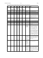
Table 1. Processors and support functions
LEON3
SPARC V8 32-bit processor
0x01 : 0x003
Yes Yes Yes Yes 6)
LEON3FT
Fault-tolerant SPARC V8 32-bit Processor
0x01 : 0x053
No
DSU3
Multi-processor Debug support unit (LEON3)
0x01 : 0x004
Yes Yes Yes Yes
L3STAT
LEON3 statistics unit
0x01 : 0x098
Yes Yes Yes Yes
LEON4
SPARC V8 32-bit processor
0x01 : 0x048
No
No
No
No
1,
5),
6)
L4STAT
LEON4 statistics unit
0x01 : 0x047
No
No
No
No
1),
3)
DSU4
Multi-processor Debug support unit (LEON4)
0x01 : 0x049
No
No
No
No
1),
3)
LEON3/4
CLK2x
LEON processor double clocking (includes special
LEON entity, interrupt controller and qualifier unit)
-
No
Yes Yes Yes
CLKGEN
Clock generation
-
Yes Yes Yes Yes
DIV32
Divider module
-
Yes Yes Yes Yes
GPTIMER
General purpose timer unit
0x01 : 0x011
Yes Yes Yes Yes
GRCLKGATE
Clock gate unit
0x01 : 0x02C
No
Yes Yes Yes
GRDMAC
DMA controller with AHB/APB bridge
0x01 : 0x095
No
No
GRTIMER
General purpose timer unit
0x01 : 0x038
No
Yes Yes Yes
GRFPU /
GRFPC
High-performance IEEE-754 Floating-point unit
with floating-point controller to interface LEON
-
No
No
No
No
1),
2)
GRFPU-Lite /
GRFPC-lite
Low-area IEEE-754 Floating-point unit with floating
point controller to interface LEON
-
No
No
No
No
1),
2)
No
Yes Yes 2),
6)
No
No
IRQMP
Multi-processor Interrupt controller
0x01 : 0x00D
Yes Yes Yes Yes
IRQ(A)MP
Multi-processor Interrupt controller
0x01 : 0x00D
No
MUL32
32x32 multiplier module
-
Yes Yes Yes Yes
MULTLIB
High-performance multipliers
-
Yes Yes Yes Yes
1)
Yes Yes Yes
1) Available as separate package or as addition to existing releases.
2) Only available as netlist or encrypted RTL
3) Always included with LEON4 license
4) Requires PHY for selected target technology. Please see IP core documentation for supported technologies.
5) Fault-tolerance (LEON4-FT functionality) is only supported in GRLIB-FT distributions.
6) The LEON3 and LEON3FT cores are functionally equivalent with the addition that fault-tolerance features can be
enabled for the LEON3FT core. The functional behaviour of the LEON4 core is the same in all distributions wiht the addition that fault-tolerance features for the LEON4 core can be enabled in GRLIB FT distributions.
COBHAM GAISLER
8
GRIP
Note
FT-FPGA
FT
COM
GPL
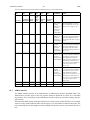
Table 2. Memory controllers and supporting cores
Name
Function
Vendor:Device
DDRSPA
Single-port 16/32/64 bit DDR controller
0x01 : 0x025
Yes Yes Yes Yes 4)
DDR2SPA
Single-port 16/32/64-bit DDR2 controller
0x01 : 0x02E
Yes Yes Yes Yes 4)
MCTRL
8/16/32-bit PROM/SRAM/SDRAM controller
0x04 : 0x00F
Yes Yes Yes Yes
SDCTRL
32-bit PC133 SDRAM controller
0x01 : 0x009
Yes Yes Yes Yes
SRCTRL
8/32-bit PROM/SRAM controller
0x01 : 0x008
Yes Yes Yes Yes
SSRCTRL
32-bit Synchronous SRAM (SSRAM) controller
0x01 : 0x00A
No
Yes Yes Yes
FTMCTRL
8//32-bit PROM/SRAM/SDRAM controller w. RS/
BCH EDAC
0x01 : 0x054
No
No
Yes Yes
FTSDCTRL
32/64-bit PC133 SDRAM Controller with EDAC
0x01 : 0x055
No
No
Yes Yes
FTSDCTRL64
64-bit PC133 SDRAM controller with EDAC
0x01 : 0x058
No
No
Yes Yes
FTSRCTRL
8/32-bit PROM/SRAM/IO Controller w. BCH
EDAC
0x01 : 0x051
No
No
Yes Yes
FTSRCTRL8
8-bit SRAM / 16-bit IO Memory Controller with
EDAC
0x01 : 0x056
No
No
Yes Yes
NANDFCTRL
NAND Flash memory controller
0x01 : 0x059
No
Yes Yes Yes
SPIMCTRL
SPI Memory controller
0x01 : 0x045
Yes Yes Yes Yes
AHBSTAT
AHB status register
0x01 : 0x052
Yes Yes Yes Yes
MEMSCRUB
Memory scrubber
0x01 : 0x057
No
No
Yes Yes
1) Available as separate package or as addition to existing releases.
2) Only available as netlist or encrypted RTL
3) Always included with LEON4 license
4) Requires PHY for selected target technology. Please see IP core documentation for supported technologies.
Name
Function
Vendor:Device
AHB2AHB
Uni-directional AHB/AHB Bridge
0x01 : 0x020
No
AHB2AVLA
Asynchronous AHB to Avalon Bridge
0x01 : 0x096
Yes Yes No
AHBBRIDGE
Bi-directional AHB/AHB Bridge
0x01 : 0x020
No
AHBCTRL
AMBA AHB bus controller with plug&play
-
Yes Yes Yes Yes
APBCTRL
AMBA APB Bridge with plug&play
0x01 : 0x006
Yes Yes Yes Yes
AHBTRACE
AMBA AHB Trace buffer
0x01 : 0x017
Yes Yes Yes Yes
GRIOMMU
I/O Memory management unit
0x01 : 0x04F
No
Note
FT-FPGA
FT
COM
GPL
Table 3. AMBA Bus control
Yes Yes Yes
No
Yes Yes Yes
No
No
1) Available as separate package or as addition to existing releases.
2) Only available as netlist or encrypted RTL
3) Always included with LEON4 license
4) Requires PHY for selected target technology. Please see IP core documentation for supported technologies.
No
1),
3)
COBHAM GAISLER
9
GRIP
Name
Function
GRPCI2
Advanced 32-bit PCI bridge
0x01 : 0x07C
Yes Yes Yes Yes
PCITARGET
32-bit target-only PCI interface (deprecated)
0x01 : 0x012
No
Yes Yes Yes
PCIMTF/GRPCI
32-bit PCI master/target interface with FIFO (deprecated)
0x01 : 0x014
No
Yes Yes Yes
PCITRACE
32-bit PCI trace buffer
0x01 : 0x015
Yes Yes Yes Yes
PCIDMA
DMA controller for PCIMTF (deprecated)
0x01 : 0x016
No
PCIARB
PCI Bus arbiter
0x04 : 0x010
Yes Yes Yes Yes
Note
FT-FPGA
FT
COM
Vendor:Device
GPL
Table 4. PCI interface
Yes Yes Yes
Name
Function
Vendor:Device
AHBRAM
Single-port RAM with AHB interface
0x01 : 0x00E
Yes Yes Yes Yes
AHBDPRAM
Dual-port RAM with AHB and user back-end interface
0x01 : 0x00F
Yes Yes Yes Yes
AHBROM
ROM generator with AHB interface
0x01 : 0x01B
Yes Yes Yes Yes
FTAHBRAM
RAM with AHB interface and EDAC protection
0x01 : 0x050
No
No
Yes Yes
L2CACHE
Level-2 cache controller
0x01 : 0x04B
No
No
No
REGFILE_3P
Parametrizable 3-port register file
-
Yes Yes Yes Yes
SYNCRAM
Parametrizable 1-port RAM
-
Yes Yes Yes Yes
SYNCRAM_2P
Parametrizable 2-port RAM
-
Yes Yes Yes Yes
SYNCRAM_DP
Parametrizable dual-port RAM
-
Yes Yes Yes Yes
1) Available as separate package or as addition to existing releases.
2) Only available as netlist or encrypted RTL
3) Always included with LEON4 license
4) Requires PHY for selected target technology. Please see IP core documentation for supported technologies.
No
Note
FT-FPGA
FT
COM
GPL
Table 5. On-chip memory functions
1),
3)
COBHAM GAISLER
10
GRIP
Note
FT-FPGA
FT
COM
Vendor:Device
GPL
Table 6. Serial communication
Name
Function
AHBUART
Serial/AHB debug interface
0x01 : 0x007
Yes Yes Yes Yes
AHBJTAG
JTAG/AHB debug interface
0x01 : 0x01C
Yes Yes Yes Yes
APBPS2
PS/2 host controller with APB interface
0x01 : 0x060
Yes Yes Yes Yes
APBUART
Programmable UART with APB interface
0x01 : 0x00C
Yes Yes Yes Yes
CAN_OC
Opencores CAN 2.0 MAC with AHB interface
0x01 : 0x019
Yes Yes Yes Yes
GRCAN
CAN 2.0 Controller with DMA
0x01 : 0x03D
No
Yes Yes Yes
GRSPW
SpaceWire link with RMAP and AHB interface
0x01 : 0x01F
No
No
No
No
1),
2)
GRSPW2
SpaceWire link with RMAP and AHB interface
0x01 : 0x029
No
No
No
No
1),
2)
I2C2AHB
I2C (slave) to AHB bridge
0x01 : 0x00B
Yes Yes Yes Yes
I2CMST
I2C Master with APB interface
0x01 : 0x028
Yes Yes Yes Yes
I2CSLV
I2C Slave with APB interface
0x01 : 0x03E
Yes Yes Yes Yes
SPI2AHB
SPI (slave) to AHB bridge
0x01 : 0x05C
Yes Yes Yes Yes
SPICTRL
SPI Controller with APB interface
0x01 : 0x02D
Yes Yes Yes Yes
TAP
JTAG TAP controller
-
No
Yes Yes Yes
1) Available as separate package or as addition to existing releases.
2) Only available as netlist or encrypted RTL
3) Always included with LEON4 license
4) Requires PHY for selected target technology. Please see IP core documentation for supported technologies
Name
Function
Vendor:Device
GRETH
Cobham Gaisler 10/100 Mbit Ethernet MAC with
AHB I/F
0x01 : 0x01D
Yes Yes Yes Yes
GRETH_GBIT
Cobham Gaisler 10/100/1000 Mbit Ethernet MAC
with AHB
0x01 : 0x01D
No
RGMII
Cobham Gaisler RGMII<-> GMII adapter
0x01 : 0x093
Yes Yes Yes Yes
Note
FT-FPGA
FT
COM
GPL
Table 7. Ethernet interface
Yes Yes Yes
Note
FT-FPGA
FT
COM
Vendor:Device
GPL
Table 8. USB interface
Name
Function
GRUSBHC
USB-2.0 Host controller (UHCI/EHCI) with AHB I/F
0x01 : 0x027
No
No
No
No
1)
GRUSBDC /
GRUSB_DCL
USB-2.0 device controller / AHB debug communication link
0x01 : 0x022
No
No
No
No
1)
1) Available as separate package or as addition to existing releases.
2) Only available as netlist or encrypted RTL
3) Always included with LEON4 license
4) Requires PHY for selected target technology. Please see IP core documentation for supported technologies.
COBHAM GAISLER
11
GRIP
Note
FT-FPGA
FT
COM
Device ID
GPL
Table 9. MIL-STD-1553 Bus interface
Name
Function
GR1553B
Advanced MIL-ST-1553B / AS15551 Interface
0x01 : 0x04D
No
No
No
No
1)
GRRT
MIL-STD-1553B / AS15531 Remote Terminal
Back-End
-
No
No
No
No
1)
1) Available as separate package or as addition to existing releases.
2) Only available as netlist or encrypted RTL
3) Always included with LEON4 license
4) Requires PHY for selected target technology. Please see IP core documentation for supported technologies.
Function
Vendor:Device
COM
FT
FT-FPGA
GRAES
128-bit AES Encryption/Decryption Core
0x01 : 0x073
No
No
No
No
1)
GRAES_DMA
Advanced Encryption Standard with DMA
0x01 : 0x07B
No
No
No
No
1)
GRECC
Elliptic Curve Cryptography Core
0x01 : 0x074
No
No
No
No
1)
Note
Name
GPL
Table 10. Encryption
1) Available as separate package or as addition to existing releases.
2) Only available as netlist or encrypted RTL
3) Always included with LEON4 license
4) Requires PHY for selected target technology. Please see IP core documentation for supported technologies.
Name
Function
Vendor:Device
SRAM
SRAM simulation model with srecord pre-load
-
Yes Yes Yes Yes
MT48LC16M16
Micron SDRAM model with srecord pre-load
-
Yes Yes Yes Yes
MT46V16M16
Micron DDR model
-
Yes Yes Yes Yes
CY7C1354B
Cypress ZBT SSRAM model with srecord pre-load
-
AHBMSTEM
AHB master simulation model with scripting (depre- 0x01 : 0x040
cated)
Yes Yes Yes Yes
AHBSLVEM
AHB slave simulation model with scripting (deprecated)
0x01 : 0x041
Yes Yes Yes Yes
AMBAMON
AHB and APB protocol monitor
-
No
Yes Yes Yes
ATF
AMBA test framework consisting of master, slave
and arbiter.
0x01 :
0x068 - 0x06A
No
Yes Yes Yes
LOGAN
On-chip Logic Analyzer
0x01 : 0x062
Yes Yes Yes Yes
Yes Yes Yes Yes
Note
FT-FPGA
FT
COM
GPL
Table 11. Simulation and debugging
COBHAM GAISLER
12
GRIP
Name
Function
APBVGA
VGA controller with APB interface
0x01 : 0x061
Yes Yes Yes Yes
SVGACTRL
VGA controller core with DMA
0x01 : 0x063
Yes Yes Yes Yes
Note
FT-FPGA
FT
COM
Vendor:Device
GPL
Table 12. Graphics functions
Name
Function
Vendor:Device
GRACECTRL
AMBA SystemACE interface controller
0x01 : 0x067
GRADCDAC
Combined ADC / DAC Interface
0x01 : 0x036
No
Yes Yes Yes
GRFIFO
External FIFO Interface with DMA
0x01 : 0x035
No
Yes Yes Yes
GRGPIO
General purpose I/O port
0x01 : 0x01A
Yes Yes Yes Yes
GRGPREG
General purpose Register
0x01 : 0x087
Yes Yes Yes Yes
GRPULSE
General purpose I/O with pulses
0x01 : 0x037
No
Yes Yes Yes
GRPWM
PWM generator
0x01 : 0x04A
No
Yes Yes Yes
GRSYSMON
AMBA Wrapper for Xilinx System Monitor
0x01 : 0x066
Yes Yes Yes Yes
GRVERSION
Version and revision register
0x01 : 0x03A
No
Note
FT-FPGA
FT
COM
GPL
Table 13. Auxiliary functions
Yes Yes Yes Yes
Yes Yes Yes
Name
Function
RS(24, 16, 8, E=1)
16 bit data, 8 check bits, corrects 4-bit error in 1 nibble
No
No
Yes Yes
RS(40, 32, 8, E=1)
32 bit data, 8 check bits, corrects 4-bit error in 1 nibble
No
No
Yes Yes
RS(48, 32, 16, E=1+1)
32 bit data, 16 check bits, corrects 4-bit error in 2 nibbles
No
No
Yes Yes
RS(48, 32, 16, E=2)
32 bit data, 16 check bits, corrects 4-bit error in 2 nibbles
No
No
Yes Yes
GR(2^4)(68, 60, 8, T=1)
QEC/QED error correction code encoder/decoder
No
No
Yes Yes
Note
FT-FPGA
FT
COM
GPL
Table 14. Error detection and correction functions
Yes Yes Yes Yes
Note
FT-FPGA
Test block for synchronous I/O interfaces
FT
Function
SYNCIOTEST
COM
Name
GPL
Table 15. Test functions
COBHAM GAISLER
GRIP
Supported technologies
Vendor
Technology
Actel
ProASIC3, ProASIC3e, ProASIC3l,
Axcelerator, Axcelerator DSP, Fusion
No
Altera
Cyclone2 - 4, Statix - Stratix3
Yes Yes No
No
Lattice
-
Yes Yes No
No
Xilinx
Unisim (Virtex2 - Virtex7)
Yes Yes Yes Yes
Other ASIC
-
No
Comment
FT-FPGA
FT
COM
Technology support and instructions for extending GRLIB with support for additional technologies is
documented in the ‘GRLIB User’s Manual’. The table below shows the technology maps available
from Cobham Gaisler for GRLIB and in which GRLIB distributions these techology maps are
included.
GPL
1.4
13
Yes Yes Yes
-
-
No
Contact Cobham Gaisler for details.
See also GRLIB IP Library User’s
Manual.
COBHAM GAISLER
1.5
14
GRIP
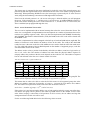
Implementation characteristics
The table below shows the approximate area for some of the GRLIP IP blocks mapped on Virtex2,
Actel-AX and typical ASIC technologies. The area depends strongly on configuration options (generics), optimization constraints and used synthesis tools. The data in the table should therefore be seen
as an indication only. The tools used to obtain the area was Synplify-8.1 for FPGA and Synopsys DC
for ASIC. The LUT area for Altera Stratix devices is roughly the same as for Virtex2. Using XST
instead of Synplify for Xilinx FPGAs gives typically 15% larger area.
Table 16. Approximate area consumption for some standard GRLIB IP cores
Virtex2
AX/RTAX
RAM16
Cells
ASIC
Block
LUT
RAM64
AHBCTRL
200
500
1,000
AHBJTAG
120
350
1,000
AHBUART (DSU UART)
450
800
2,000
APBCTRL
150
200
800
APBPS2
450
800
2,000
APBUART
200
300
1,000
APBVGA
250
4
-
1,400
CAN_OC (CAN-2.0 core with AHB I/F)
1,600
2
2,800
2
Gates
8,000
GRCAN (CAN 2.0 Controller with DMA)
2,300
4,800
20,000
DDRCTRL
1,600
2
-
10,000
DDRSPA (32-bit)
900
2
-
-
DIV32 (64/32-bit iterative divider)
400
500
2,000
COBHAM GAISLER
15
GRIP
Table 16. Approximate area consumption for some standard GRLIB IP cores
Virtex2
AX/RTAX
RAM16
Cells
ASIC
Block
LUT
GPTIMER (16-bit scaler + 2x32-bit timers)
250
400
RAM64
Gates
GRETH 10/100 Mbit Ethernet MAC
1,500
2,500
2
8,000
GRETH 10/100 Mbit Ethernet MAC with EDCL
2,600
1
4,000
4
15,000
GRFPU-Lite including LEON3 controller
4,000
6
7,000
4
35,000
GRFPU IEEE-754 floating-point unit
8,500
2
-
100,000
GRFPC for LEON3
5,000
4
-
25,000
GRGPIO, 16-bit configuration
100
150
800
1,300
GRSPW Spacewire link
1,900
3
2,800
3
15,000
GRSPW Spacewire link with RMAP
3,000
4
4,500
4
25,000
GRTC CCSDS telecommad decoder front-end
2,000
GRTM CCSDS telemetry Generator
4,500
3,000
2
15,000
6,000
4
30,000
I2CMST I2C Master
200
300
1,500
I2CSLV I2C Slave
150
250
1,000
IRQMP (1 processor)
300
350
1,500
LEON3, 8 + 8 Kbyte cache
4,300
12
6,500
40
20,000
LEON3, 8 + 8 Kbyte cache + DSU3
5,000
12
7,500
40
25,000
LOGAN, 32 channels, 1024 traces, 1 trigger
300
2
-
-
MCTRL
350
1,000
1,500
MCTRL including SDRAM support
600
1,400
2,000
MUL32 (32x32 multiplier, 4-cycle iterative)
200
1,400
5,500
PCI_TARGET, simple PCI target
150
500
800
PCI_MTF, master/target PCI with FIFO
1,100
4
2,000
4
6,000
PCIDMA, master/target PCI with FIFO/DMA
1,800
4
3,000
4
9,000
PCITRACE
300
2
600
4
SRCTRL
100
200
500
SDCTRL
300
600
1,200
SPICTRL
450
900
2,500
SPIMCTRL
300
SVGACTRL
1,200
USBDCL
2,000
600
2
1,400
1,200
1,600
2
-
8,000
12,000
Table 17. Approximate area consumption for some FT GRLIB IP cores
Block
RTAX2000 (Cells)
ASIC (gates)
GRFPU-Lite-FT including LEON3 controller
7,100 + 4 RAM64K36
36,000
GRFPCFT for LEON3
-
30,000 + RAM
LEON3FT, 8 + 4 Kbyte cache
7,500 + 40 RAM64K36
22,000 + RAM
LEON3FT, 8 + 4 Kbyte cache + DSU3
8,500 + 44 RAM64K36
27,000 + RAM
LEON3FT, 8 + 4 Kbyte cache with FPU + DSU3
16,000 + 48 RAM64K36
60,000 + RAM
FTSRCTRL
700
2,500
FTSRCTRL8
750
-
FTSDCTRL
1,000
3,500
FTAHBRAM (2 Kbyte with EDAC)
300 + 5 RAM64K36
2,000 + RAM
COBHAM GAISLER
16
GRIP
The table below show the area resources for some common FPGA devices. It can be used to quickly
estimate if a certain GRLIB design will fit the target device.
Table 18. Area resources for some common FPGA devices
FPGA
Logic
Memory
Actel AX1000
18,144 Cells
32 RAM64K36
Actel AX2000
32,248 Cells
64 RAM64K36
Xilinx Spartan3-1500
33,248 LUT
64 RAMB16
Xilinx Virtex2-3000
28,672 LUT
96 RAMB16
Xilinx Virtex2-6000
67,584 LUT
144 RAMB16
COBHAM GAISLER
17
GRIP
2
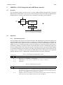
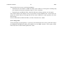
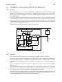
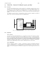
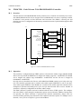
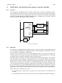
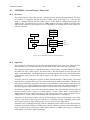
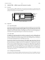
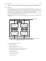
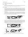
AHB2AHB - Uni-directional AHB/AHB bridge
2.1
Overview
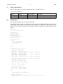
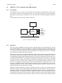
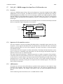
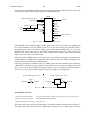
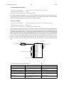
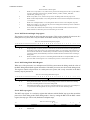
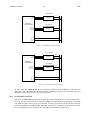
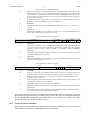
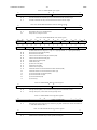
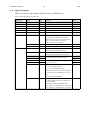
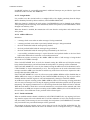
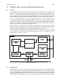
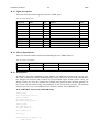
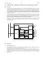
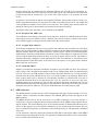
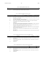
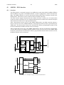
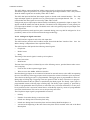
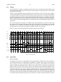
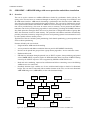
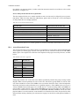
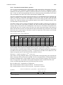
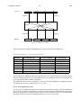
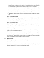
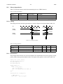
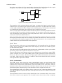
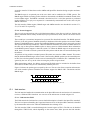
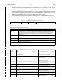
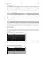
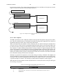
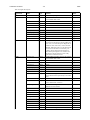
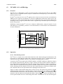
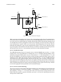
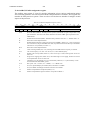
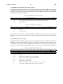
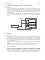
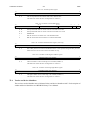
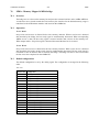
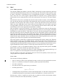
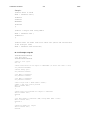
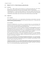
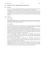
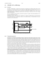
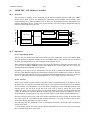
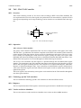
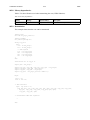
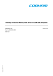
The uni-directional AHB/AHB bridge is used to connect two AMBA AHB buses clocked by synchronous clocks with any frequency ratio. The bridge is connected through a pair consisting of an AHB
slave and an AHB master interface. AHB transfer forwarding is performed in one direction, where
AHB transfers to the slave interface are forwarded to the master interface. Applications of the unidirectional bridge include system partitioning, clock domain partitioning and system expansion.
Features offered by the uni-directional AHB to AHB bridge are:
•
Single and burst AHB transfers
•
Data buffering in internal FIFOs
•
Efficient bus utilization through (optional) use of SPLIT response and data prefetching. NOTE:
SPLIT responses require an AHB arbiter that allows assertion of HSPLIT during second cycle of
SPLIT response. This is supported by GRLIB’s AHBCTRL IP core.
•
Posted writes
•
Read and write combining, improves bus utilization and allows connecting cores with differing
AMBA access size restrictions.
•
Deadlock detection logic enables use of two uni-directional bridges to build a bi-directional
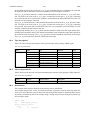
bridge (one example is the bi-directional AHB/AHB bridge core (AHBBRIDGE))
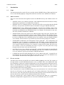
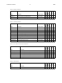
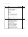
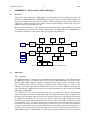
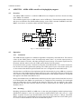
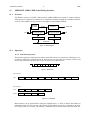
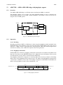
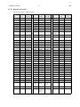
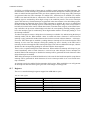
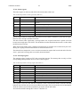
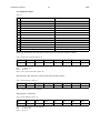
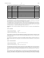
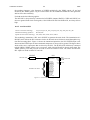
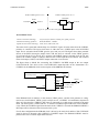
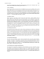
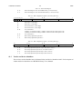
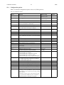
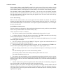
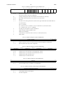
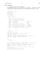
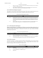
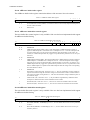
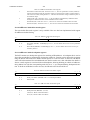
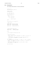
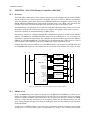
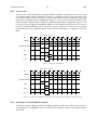
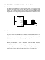
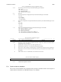
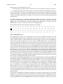
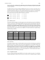
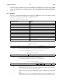
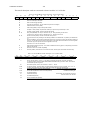
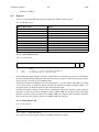
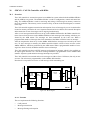
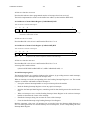
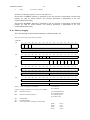
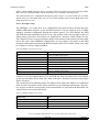
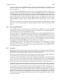
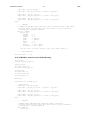
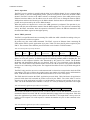
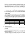
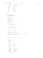
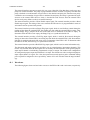
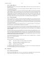
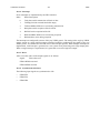
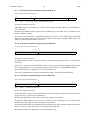
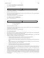
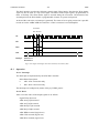
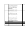
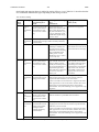
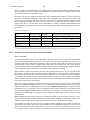
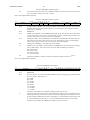
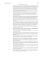
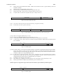
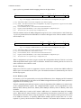
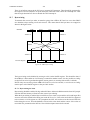
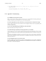
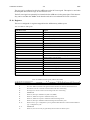
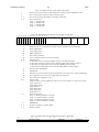
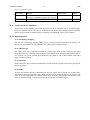
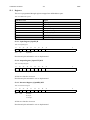
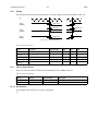
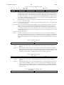
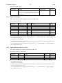
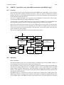
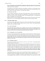
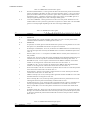
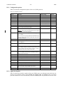
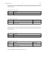
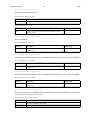
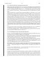
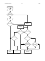
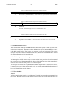
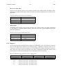
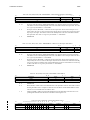
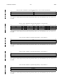
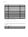
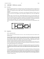
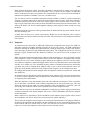
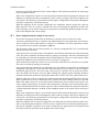
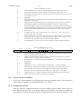
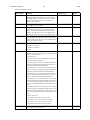
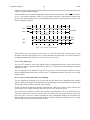
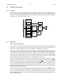
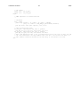
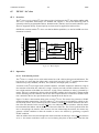
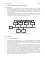
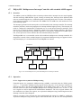
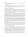
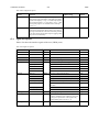
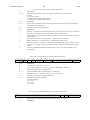
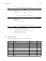
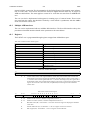
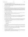
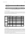
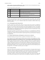
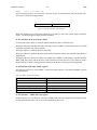
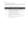
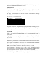
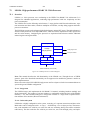
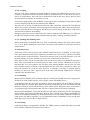
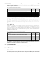
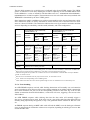
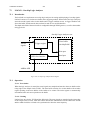
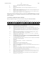
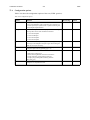
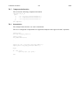
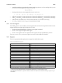
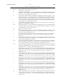
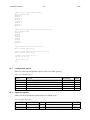
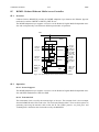
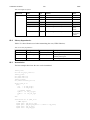
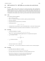
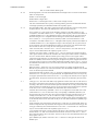
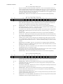
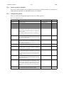
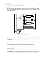
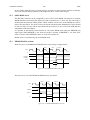
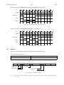
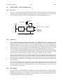
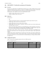
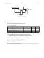
MASTER 1
MASTER 2
MASTER N
AHB Bus 0
BUS
CONTROL
SLAVE 1
SLAVE 2
SLAVE I/F
AHB/AHB
BRIDGE
MASTER I/F
MASTER 1
MASTER N
AHB Bus 1
BUS
CONTROL
SLAVE 1
SLAVE 2
Figure 1. Two AHB buses connected with (uni-directional) AHB/AHB bridge
2.2
Operation
2.2.1
General
The address space occupied by the AHB/AHB bridge on the slave bus is configurable and determined
by Bank Address Registers in the slave interface’s AHB Plug&Play configuration record.
The bridge is capable of handling single and burst transfers of all burst types. Supported transfer sizes
(HSIZE) are BYTE, HALF-WORD, WORD, DWORD, 4WORD and 8WORD.
COBHAM GAISLER
18
GRIP
For AHB write transfers write data is always buffered in an internal FIFO implementing posted
writes. For AHB read transfers the bridge uses GRLIB’s AMBA Plug&Play information to determine
whether the read data will be prefetched and buffered in an internal FIFO. If the target address for an
AHB read burst transfer is a prefetchable location the read data will be prefetched and buffered.
The bridge can be implemented to use SPLIT responses or to insert wait states when handling an
access. With SPLIT responses enabled, an AHB master initiating a read transfer to the bridge is
always splitted on the first transfer attempt to allow other masters to use the slave bus while the bridge
performs read transfer on the master bus.The descriptions of operation in the sections below assume
that the bridge has been implemented with support for AMBA SPLIT responses. The effects of disabling support for AMBA SPLIT responses are described in section 2.2.11.
If interrupt forwarding is enabled the interrupts on the slave bus interrupt lines will be forwarded to
the master bus and vice versa.
2.2.2
AHB read transfers
When a read transfer is registered on the slave interface the bridge gives a SPLIT response. The master that initiated the transfer will be de-granted allowing other bus masters to use the slave bus while
the bridge performs a read transfer on the master side. The master interface then requests the bus and
starts the read transfer on the master side. Single transfers on the slave side are normally translated to
single transfers with the same AHB address and control signals on the master side, however read combining can translate one access into several smaller accesses. Translation of burst transfers from the
slave to the master side depends on the burst type, burst length, access size and the AHB/AHB bridge
configuration.
If the read FIFO is enabled and the transfer is a burst transfer to a prefetchable location, the master
interface will prefetch data in the internal read FIFO. If the splitted burst on the slave side was an
incremental burst of unspecified length (INCR), the length of the burst is unknown. In this case the
master interface performs an incremental burst up to a specified address boundary (determined by the
VHDL generic rburst). The bridge can be configured to recognize an INCR read burst marked as
instruction fetch (indicated on HPROT signal). In this case the prefetching on the master side is completed at the end of a cache line (the cache line size is configurable through the VHDL generic iburst).
When the burst transfer is completed on the master side, the splitted master that initiated the transfer
(on the slave side) is allowed in bus arbitration by asserting the appropriate HSPLIT signal to the
AHB controller. The splitted master re-attempts the transfer and the bridge will return data with zero
wait states.
If the read FIFO is disabled, or the burst is to non-prefetchable area, the burst transfer on the master
side is performed using sequence of NONSEQ, BUSY and SEQ transfers. The first access in the burst
on the master side is of NONSEQ type. Since the master interface can not decide whether the splitted
burst will continue on the slave side or not, the master bus is held by performing BUSY transfers. On
the slave side the splitted master that initiated the transfer is allowed in bus arbitration by asserting the
HSPLIT signal to the AHB controller. The first access in the transfer is completed by returning read
data. The next access in the transfer on the slave side is extended by asserting HREADY low. On the
master side the next access is started by performing a SEQ transfer (and then holding the bus using
BUSY transfers). This sequence is repeated until the transfer is ended on the slave side.
In case of an ERROR response on the master side the ERROR response will be given for the same
access (address) on the slave side. SPLIT and RETRY responses on the master side are re-attempted
until an OKAY or ERROR response is received.
2.2.3
AHB write transfers
The AHB/AHB bridge implements posted writes. During the AHB write transfer on the slave side the
data is buffered in the internal write FIFO and the transfer is completed on the slave side by always
giving an OKAY response. The master interface requests the bus and performs the write transfer when
the master bus is granted. If the burst transfer crosses the write burst boundary (defined by VHDL
COBHAM GAISLER
19
GRIP
generic wburst), a SPLIT response is given. When the bridge has written the contents of the FIFO out
on the master side, the bridge will allow the master on the slave side to perform the remaining
accesses of the write burst transfer.
Writes are accepted with zero wait states if the bridge is idle and the incoming access is not locked. If
the incoming access is locked, each access will have one wait state. If write combining is disabled a
non-locked BUSY cycle will lead to a flush of the write FIFO. If write combining is enabled or if the
incoming access is locked, the bridge will not flush the write FIFO during the BUSY cycle.
2.2.4
Deadlock conditions
When two bridges are used to form a bi-drectional bridge, a deadlock situation can occur if the
bridges are simultaneously accessed from both buses. The bridge that has been configured as a slave
contains deadlock detection logic which will resolve a deadlock condition by giving a RETRY
response, or by issuing SPLIT complete followed by a new SPLIT response. When the core resolves a
deadlock while prefetching data, any data in the prefetch buffer will be dropped when the core’s slave
interface issues the AMBA RETRY response. When the access is retried it may lead to the same
memory locations being read twice.
Deadlock detection logic for bi-directional configurations may lead to deadlocks in other parts of the
system. Consider the case where a processor on bus A on one side of the bidirectional bridge needs to
perform an instruction fetch over the bridge before it can release a semaphore located in memory on
bus A. Another processor on bus B, on the other side of the bridge, may spin on the semaphore wating
for its release. In this scenario, the accesses from the processor on bus B could, depending on system
configuration, continuously trigger a deadlock condition where the core will drop data in, or be prevented from initiating, the instruction fetch for the processor on bus A. Due to scenarios of this kind
the bridge should not be used in bi-directional configurations where dependencies as the one
described above exist between the buses connected by the bridge.
Other deadlock conditions exist with locked transfers, see section 2.2.5.
2.2.5
Locked transfers
The AHB/AHB bridge supports locked transfers. The master bus will be locked when the bus is
granted and remain locked until the transfer completes on the slave side. Locked transfers can lead to
deadlock conditions, the core’s VHDL generic lckdac determines if and how the deadlock conditions
are resolved.
With the VHDL generic lckdac set to 0, locked transfers may not be made after another read access
which received SPLIT until the first read access has received split complete. This is because the
bridge will return split complete for the first access first and wait for the first master to return. This
will cause deadlock since the arbiter is not allowed to change master until a locked transfer has been
completed. The AMBA specification requires that the locked transfer is handled before the previous
transfer, which received a SPLIT response, is completed.
With lckdac set to 1, the core will respond with an AMBA ERROR response to locked access that is
made while an ongoing read access has received a SPLIT response. With lckdac set to 2 the bridge
will save state for the read access that received a SPLIT response, allow the locked access to complete, and then complete the first access. All non-locked accesses from other masters will receive
SPLIT responses until the saved data has been read out.
If the core is used to create a bi-directional bridge there is one more deadlock condition that may arise
when locked accesses are made simultaneously in both directions. If the VHDL generic lckdac is set
to 0 the core will deadlock. If lckdac is set to a non-zero value the slave bridge will resolve the deadlock condition by issuing an AMBA ERROR response to the incoming locked access.
COBHAM GAISLER
2.2.6
20
GRIP
Read and write combining
Read and write combining allows the bridge to assemble or split AMBA accesses on the bridge’s
slave interface into one or several accesses on the master interface. This functionality can improve bus
utilization and also allows cores that have differing AMBA access size restrictions to communicate
with each other. The functionality attained by read and write combining depends on the VHDL generics rdcomb (defines type of read combining), wrcomb (defines type of write combining), slvmstaccsz
(defines maximum AHB access size supported by the bridge’s slave interface) and mstmaccsz (defines
maximum AHB access size that can be used by bridge’s master interface). These VHDL generics are
described in section 2.6. The table below shows the effect of different settings. BYTE and HALFWORD accesses are special cases. The table does not list illegal combinations, for instance mstmaccsz /= slvmaccsz requires that wrcomb /= 0 and rdcomb /= 0.
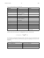
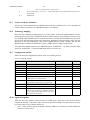
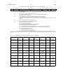
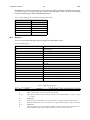
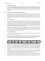
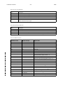
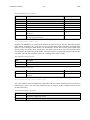
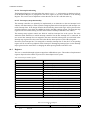
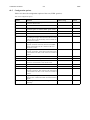
Table 19. Read and write combining
Access on slave interface
Access size
wrcomb
rdcomb
Resulting access(es) on master interface
BYTE or HALF-WORD sin- gle read access to any area
-
-
Single access of same size
BYTE or HALF-WORD
read burst to prefetchable
area
-
-
-
Incremental read burst of same access size as on
slave interface, the length is the same as the
number of 32-bit words in the read buffer, but
will not cross the read burst boundary.
BYTE or HALF-WORD
read burst to non-prefetchable area
-
-
-
Incremental read burst of same access size as on
slave interface, the length is the same as the
length of the incoming burst. The master interface will insert BUSY cycles between the
sequential accesses.
BYTE or HALF-WORD sin- gle write
-
-
Single access of same size
BYTE or HALF-WORD
write burst
-
-
-
Incremental write burst of same size and length,
the maximum length is the number of 32-bit
words in the write FIFO.
Single read access to any
area
Access size <=
mstmaccsz
-
-
Single access of same size
Single read access to any
area
Access size >
mstmaccsz
-
1
Sequence of single accesses of mstmaccsz.
Number of accesses: (access size)/mstmaccsz
Single read access to any
area
Access size >
mstmaccsz
-
2
Burst of accesses of size mstmaccsz. Length of
burst: (access size)/mstmaccsz
Read burst to prefetchable
area
-
-
0
Burst of accesses of incoming access size up to
address boundary defined by rburst.
Read burst to prefetchable
area
-
-
1 or 2
Burst of accesses of size mstmaccsz up to
address boundary defined by rburst.
Read burst to non-prefetchable area
Access size <=
mstmaccsz
-
-
Incremental read burst of same access size as on
slave interface, the length is the same as the
length of the incoming burst. The master interface will insert BUSY cycles between the
sequential accesses.
Read burst to non-prefetchable area
Access size >
mstmaccsz
-
1 or 2
Burst of accesses of size mstmaccsz. Length of
burst:
(incoming burst length)*(access size)/mstmaccsz
Single write
Access size <=
mstmaccsz
-
-
Single write access of same size
Single write
Access size >
mstmaccsz
1
-
Sequence of single access of mstmaccsz. Number of accesses: (access size)/mstmaccsz.
Single write
Access size >
mstmaccsz
2
-
Burst of accesses of mstmaccsz. Length of burst:
(access size)/mstmaccsz.
COBHAM GAISLER
21
GRIP
Table 19. Read and write combining
Access on slave interface
Access size
wrcomb
rdcomb
Resulting access(es) on master interface
Write burst
-
0
-
Burst of same size as incoming burst, up to
address boundary defined by VHDL generic
wburst.
Write burst
-
1 or 2
-
Burst write of maximum possible size. The
bridge will use the maximum size (up to mstmaccsz) that it can use to empty the writebuffer.
Read and write combining prevents the bridge from propagating fixed length bursts and wrapping
bursts. See section 2.2.7 for a discussion on burst operation.
Read and write combining with VHDL generics wrcomb/rdcomb set to 1 cause the bridge to use single accesses when divding an incoming access into several smaller accesses. This means that another
master on the bus may write or read parts of the memory area to be accessed by the bridge before the
bridge has read or written all the data. In bi-directional configurations, an incoming access on the
master bridge may cause a collision that aborts the operation on the slave bridge. This may cause the
bridge to read the same memory locations twice. This is normally not a problem when accessing
memory areas. The same issues apply when using an AHB arbiter that performs early burst termination. The standard GRLIB AHBCTRL core does not perform early burst termination.
To ensure that the bridge does not re-read an address, and that all data in an access from the bridge’s
slave interface is propagated out on the master interface without interruption the VHDL generics
rdcomb and wrcomb should both be set to 0 or 2. In addition to this, the AHB arbiter may not perform
early burst termination (early burst termination is not performed by the GRLIB AHBCTRL arbiter).
Read and write combining can be limited to specified address ranges. See description of the combmask VHDL generic for more information. Note that if the core is implemented with support for
prefetch and read combining, it will not obey combmask for prefetch operations (burst read to
prefetchable areas). Prefetch operations will always be performed with the maximum allowed size on
the master interface.
2.2.7
Burst operation
The core can be configured to support all AMBA 2.0 burst types (single access, incrementing burst of
unspecified length, fixed length incrementing bursts and wrapping bursts). Single accesses and incrementing bursts of unspecified length have previously been discussed in this document. An incoming
single access will lead to one access, or multiple accesses for some cases with read/write combining,
on the other side of the bridge. An incoming incrementing burst of unspecified length to a prefetchable area will lead to the prefetch buffer (if available) being filled using the same access size, or the
maximum allowed access size if read/write combining is enabled, on the master interface.
If the core is used in a system where no fixed length bursts or incremental bursts will be used in
accesses to the bridge, then set the allbrst generic to 0 and skip the remainder of this section.
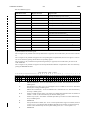
The VHDL generic allbrst controls if the core will support fixed length and wrapping burst accesses.
If allbrst is set to 0, the core will treat all burst accesses as incrementing of unspecified length. For
fixed length and wrapping bursts this can lead to performance penalties and malfunctions. Support for
fixed length and wrapping bursts is enabled by setting allbrst to 1 or 2. Table 20 describes how the
core will handle different burst types depending on the setting of allbrst.
COBHAM GAISLER
22
GRIP
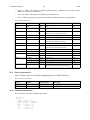
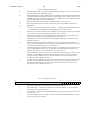
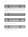
Table 20. Burst handling
Value of
allbrst
generic
Access type* Undefined length
incrementing burst
INCR
Fixed length incrementing
burst
INCR{4,8,16}
Wrapping burst
WRAP{4,8,16}
0
Reads to
nonprefetchable
area
Incrementing burst with
BUSY cycles inserted.
Same behaviour with
read and write combining.
Fixed length burst with
BUSY cycles inserted. If the
burst is short then the burst
may end with a BUSY cycle.
If access combining is used
the HBURST signal will get
incorrect values.
Malfunction. Not supported
Reads to
prefetchable
area
Incrementing burst of maximum allowed size, filling
prefetch buffer, starting at address boundary defined by
prefetch buffer.
Malfunction. Not supported
Write burst
Incrementing burst
Incrementing burst, if write
combining is enabled, and
triggered, the burst will be
translated to an incrementing
burst of undefined length.
VHDL generic wrcomb
should not be set to 1 (but to
0 or 2) in this case
Write combining is not supported. Same access size will be
used on both sides of the bridge.
Reads to
nonprefetchable
area
Incrementing burst with
BUSY cycles inserted.
Same behaviour with
read and write combining.
Same burst type with BUSY
cycles inserted. If read combining is enabled, and triggered by the incoming access
size, an incremental burst of
unspecified length will be
used. If the burst is short then
the burst may end with a
BUSY cycle.
Same burst type with BUSY
cycles inserted. If read combining is enabled, and triggered by
the incoming access size, an
incremental burst of unspecified
length will be used. This will
cause AMBA violations if the
wrapping burst does not start
from offset 0.
Reads to
prefetchable
area
Incrementing burst of
maximum allowed size,
filling prefetch buffer.
For reads, the core will perform full (or part that fits in prefetch
buffer) fixed/wrapping burst on master interface and then
respond with data. No BUSY cycles are inserted.
1
If the access made to the slave interface is larger than the maximum supported access size on the master interface then a incrementing burst of unspecified length will be used to fill the
prefetch buffer. This (read combining) is not supported for wrapping bursts.
Write burst
2
Same as for allbrst = 0
Reads to
nonprefetchable
area
Incrementing burst with
BUSY cycles inserted.
Same behaviour with
read and write combining.
Reads to
prefetchable
area
Incrementing burst of
maximum allowed size,
filling prefetch buffer,
starting at address
boundary defined by
prefetch buffer.
Write burst
Reads are treated as a prefetchable burst. See below.
Core will perform full (or part that fits in prefetch buffer) fixed/
wrapping burst on master interface and then respond with data.
No BUSY cycles are inserted.
If the access made to the slave interface is larger than the maximum supported access size on the master interface then a incrementing burst of unspecified length will be used to fill the
prefetch buffer. This (read combining) is not supported for wrapping bursts.
Same as for allbrst = 0
* Access to prefetchable area where the core’s prefetch buffer is ised (VHDL generic pfen /= 0).
COBHAM GAISLER
2.2.8
23
GRIP
Transaction ordering, starvation and AMBA arbitration schemes
The bridge is configured at implementation to use one of two available schemes to handle incoming
accesses. The bridge will issue SPLIT responses when it is busy and on incoming read accesses. If the
bridge has been configured to use first-come, first-served ordering it will keep track of the order of
incoming accesses and serve the requests in the same order. If first-come, first-served ordering is disabled the bridge will give some advantage to the master it has a response for and then allow all masters in to arbitration simultaneously, moving the decision on which master that should be allowed to
access the bridge to the bus arbitration.
When designing a system containing a bridge the expected traffic patterns should be analyzed. The
designer must be aware how SPLIT responses affect arbitration and how the selected transaction
ordering in the bridge will affect the system. The two different schemes are further described in sections 2.2.9 and 2.2.10.
2.2.9
First-come, first-served ordering
First-come, first served ordering is used when the VHDL generic fcfs is non-zero.
With first-come, first-served ordering the bridge will keep track of the order of incoming accesses.
The accesses will then be served in the same order. For instance, if master 0 initiates an access to the
bridge, followed by master 3 and then master 5, the bridge will propagate the access from master 0
(and respond with SPLIT on a read access) and then respond with SPLIT to the other masters. When
the bridge has a response for master 0, this master will be allowed in arbitration again by the bridge
asserting HSPLIT. When the bridge has finished serving master 0 it will allow the next queued master
in arbitration, in this case master 3. Other incoming masters will receive SPLIT responses and will not
be allowed in arbitration until all previous masters have been served.
An incoming locked access will always be given precedence over any other masters in the queue.
A burst that has initiated a pre-fetch operation will receive SPLIT and be inserted last in the master
queue if the burst is longer than the maximum burst length that the bridge has been configured for.
It should be noted that first-come, first-served ordering may not work well in systems where an AHB
master needs to have higher priority compared to the other masters. The bridge will not prioritize any
master, except for masters performing locked accesses.
2.2.10 Bus arbiter ordering
Bus arbiter ordering is used when VHDL generic fcfs is set to zero.
When several masters have received SPLIT and the bridge has a response for one of these masters, the
master with the queued response will be allowed in to bus arbitration by the bridge asserting the corresponding HSPLIT signal. In the following clock cycle, all other masters that have received SPLIT
responses will also be allowed in bus arbitration as the bridge asserts their HSPLIT signals simultaneously. By doing this the bridge defers the decision on the master to be granted next to the AHB arbiter. The bridge does not show any preference based on the order in which it issued SPLIT responses to
masters, except to the master that initially started a read or write operation. Care has been taken so
that the bridge shows a consistent behavior when issuing SPLIT responses. For instance, the bridge
could be simplified if it could issue a SPLIT response just to be able to change state, and not initiate a
new operation, to an access coming after an access that read out prefetched data. When the bridge
entered its idle state it could then allow all masters in bus arbitration and resume normal operation.
That solution could lead to starvation issues such as:
T0: Master 1 and Master 2 have received SPLIT responses, the bridge is prefetching data for Master 1
T1: Master 1 is allowed in bus arbitration by setting the corresponding HSPLIT
T2: Master 1 reads out prefetch data, Master 2 HSPLIT is asserted to let Master 2 in to bus arbitration
COBHAM GAISLER
24
GRIP
T3: Master 2 performs an access, receives SPLIT, however the bridge does not initiate an access, it
just stalls in order to enter its idle state.
T4: Master 2 is allowed in to bus arbitration, Master 1 initiates an access that leads to a prefetch and
Master 1 receives a SPLIT response
T5: Master 2 performs an access, receives SPLIT since the bridge is prefetching data for master 1
T6: Go back to T0
This pattern will repeat until Master 1 backs away from the bus and Master 2 is able to make an access
that starts an operation over the bridge. In most systems it is unlikely that this behavior would introduce a bus lock. However, the case above could lead to an unexpectedly long time for Master 2 to
complete its access. Please note that the example above is illustrative and the problem does not exist
in the core as the core does not issue SPLIT responses to (non-locked) accesses in order to just change
state but a similar pattern could appear as a result of decisions taken by the AHB arbiter if Master 1 is
given higher priority than Master 2.
In the case of write operations the scenario is slightly different. The bridge will accept a write immediately and will not issue a SPLIT response. While the bridge is busy performing the write on the
master side it will issue SPLIT responses to all incoming accesses. When the bridge has completed
the write operation on the master side it will continue to issue SPLIT responses to any incoming
access until there is a cycle where the bridge does not receive an access. In this cycle the bridge will
assert HSPLIT for all masters that have received a SPLIT response and return to its idle state. The first
master to access the bridge in the idle state will be able to start a new operation. This can lead to the
following behavior:
T0: Master 1 performs a write operation, does NOT receive a SPLIT response
T1: Master 2 accesses the bridge and receives a SPLIT response
T2: The bridge now switches state to idle since the write completed and asserts HSPLIT for Master 2.
T3: Master 1 is before Master 2 in the arbitration order and we are back at T0.
In order to avoid this last pattern the bridge would have to keep track of the order in which it has
issued SPLIT responses and then assert HSPLIT in the same order. This is done with first-come, firstserved ordering described in section 2.2.9.
2.2.11 AMBA SPLIT support
Support for AMBA SPLIT responses is enabled/disabled through the VHDL generic split. SPLIT support should be enabled in most systems. The benefits of using SPLIT responses is that the bus on the
bridge’s slave interface side can be free while the bridge is performing an operation on the master
side. This will allow other masters to access the bus and generally improve system performance. The
use of SPLIT responses also allows First-come, first-served transaction ordering.
For configurations where the bridge is the only slave interface on a bus, it can be beneficial to implement the bridge without support for AMBA SPLIT responses. Removing support for SPLIT responses
reduces the area used by the bridge and may also reduce the time required to perform accesses that
traverse the bridge. It should be noted that building a bi-directional bridge without support for SPLIT
responses will increase the risk of access collisions.
If SPLIT support is disabled the bridge will insert wait states where it would otherwise issue a SPLIT
response to a master initiating an access. This means that the arbitration ordering will be left to the
bus arbiter and the bridge cannot be implemented with the First-come, first-served transaction ordering scheme. The bridge will still issue RETRY responses to resolve dead lock conditions, to split up
long burst and also when the bridge is busy emptying it’s write buffer on the master side.
COBHAM GAISLER
25
GRIP
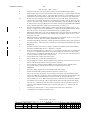
2.2.12 Core latency
The delay incurred when performing an access over the core depends on several parameters such as
core configuration, the operating frequency of the AMBA buses, AMBA bus widths and memory
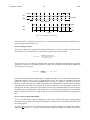
access patterns. Table 21 below shows core behavior in a system where both AMBA buses are running
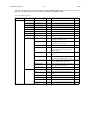
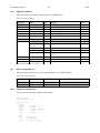
at the same frequency and the core has been configured to use AMBA SPLIT responses. Table 22 further down shows core behavior in the same system without support for SPLIT responses.
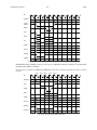
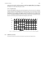
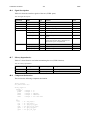
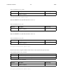
Table 21. Example of single read with FFACT = 1, and SPLIT support
Clock cycle
Core slave side activity
Core master side activity
0
Discovers access and transitions from idle state
Idle
1
Slave side waits for master side, SPLIT response
is given to incoming access, any new incoming
accesses also receive SPLIT responses.
Discovers slave side transition. Master interface output
signals are assigned.
4
Discovers that read data is ready, assign read
data output and assign SPLIT complete
Idle
5
SPLIT complete output is HIGH
6
Typically a wait cycle for the SPLIT:ed master to
be allowed into arbitration. Core waits for master
to return. Other masters receive SPLIT
responses.
7
Master has been allowed into arbitration and performs address phase. Core keeps HREADY high
8
Access data phase. Core has returned to idle
state.
2
3
If bus access is granted, perform address phase. Otherwise wait for bus grant.
Register read data and transition to data ready state.
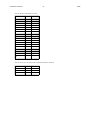
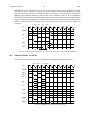
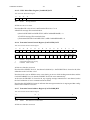
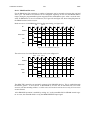
Table 22. Example of single read with FFACT = 1, without SPLIT support
Clock cycle
Core slave side activity
Core master side activity
0
Discovers access and transitions from idle state
Idle
1
Slave side waits for master side, wait states are
inserted on the AMBA bus.
Discovers slave side transition. Master interface output
signals are assigned.
2
Bus access is granted, perform address phase.
3
Register read data and transition to data ready state.
4
Discovers that read data is ready, assign
HREADY output register and data output register.
5
HREADY is driven on AMBA bus. Core has
returned to idle state
Idle
While the transitions shown in tables 21 and 22 are simplified they give an accurate view of the core
delay. If the master interface needs to wait for a bus grant or if the read operation receives wait states,
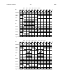
these cycles must be added to to the cycle count in the tables. The behavior of the core with a fre-
COBHAM GAISLER
26
GRIP
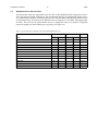
quency factor of two between the buses is shown in tables 23 and 24 (best case, delay may be larger
depending on on which slave clock cycle an access is made to the core).
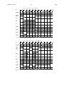
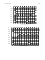
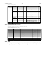
Table 23. Example of single read with FFACT = 2, Master freq. > Slave freq, without SPLIT support
Slave side
clock cycle
Core slave side activity
0
Discovers access and transitions from idle
state
1
Slave side waits for master side, wait states
are inserted on the AMBA bus.
2
Master side
clock cycle
0
Discovers slave side transition. Master interface output signals are assigned.
1
Bus access is granted, perform address
phase.
2
Register read data and transition to data
ready state.
3
Idle
3
4
5
6
Discovers that read data is ready, assign
HREADY output register and data output
register.
7
HREADY is driven on AMBA bus. Core
has returned to idle state
Core master side activity
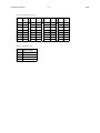
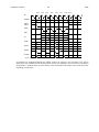
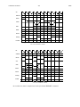
Table 24. Example of single read with FFACT = 2, Master freq. > Slave freq, without SPLIT support
Slave side
clock cycle
0
1
Core slave side activity
Master side
clock cycle
Core master side activity
Discovers access and transitions from idle
state
0
Idle
Slave side waits for master side, wait states
are inserted on the AMBA bus.
2
Discovers slave side transition. Master interface output signals are assigned.
3
Bus access is granted, perform address
phase.
1
2
Discovers that read data is ready, assign
HREADY output register and data output
register.
4
Register read data and transition to data
ready state.
5
Idle
3
HREADY is driven on AMBA bus. Core
has returned to idle state
6
7
Table 25 below lists the delays incurred for single operations that traverse the bridge while the bridge
is in its idle state. The second column shows the number of cycles it takes the master side to perform
the requested access, this column assumes that the master slave gets access to the bus immediately
and that each access is completed with zero wait states. The table only includes the delay incurred by
traversing the core. For instance, when the access initiating master reads the core’s prefetch buffer,
each additional read will consume one clock cycle. However, this delay would also have been present
if the master accessed any other slave.
Write accesses are accepted with zero wait states if the bridge is idle, this means that performing a
write to the idle core does not incur any extra latency. However, the core must complete the write
operation on the master side before it can handle a new access on the slave side. If the core has not
transitioned into its idle state, pending the completion of an earlier access, the delay suffered by an
access be longer than what is shown in the tables in this section. Accesses may also suffer increased
delays during collisions when the core has been instantiated to form a bi-directional bridge. Locked
accesses that abort on-going read operations will also mean additional delays.
COBHAM GAISLER
27
GRIP
If the core has been implemented to use AMBA SPLIT responses there will be an additional delay
where, typically, one cycle is required for the arbiter to react to the assertion of HSPLIT and one clock
cycle for the repetition of the address phase.
Note that if the core has support for read and/or write combining, the number of cycles required for
the master will change depending on the access size and length of the incoming burst access. For
instance, in a system where the bus in the core’s master side is wider than the bus on the slave side,
write combining will allow the core to accept writes with zero wait states and then combine several
accesses into one or several larger access. Depending on memory controller implementation this
could reduce the time required to move data to external memory, and will reduce the load on the master side bus.
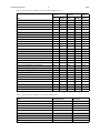
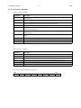
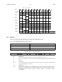
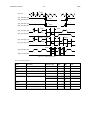
Table 25. Access latencies
Access
Master acc. cycles Slave cycles
Delay incurred by performing access over core
Single read
3
1
1 * clkslv + 3 * clkmst
Burst read with prefetch
2 + (burst length)x
2
2 * clkslv + (2 + burst length)* clkmst
Single writexx
(2)
0
0
Burst writexx
(2 + (burst length))
0
0
x
A prefetch operation ends at the address boundary defined by the prefetch buffer’s size
The core implements posted writes, the number of cycles taken by the master side can only affect the next access.
xx
2.3
Registers
The core does not implement any registers.
2.4
Vendor and device identifiers
The core has vendor identifier 0x01 (Cobham Gaisler) and device identifier 0x020. For description of
vendor and device identifiers see GRLIB IP Library User’s Manual.
2.5
Implementation
2.5.1
Technology mapping
The uni-directional AHB to AHB bridge has two technology mapping generics memtech and fcfsmtech. memtech selects which memory technology that will be used to implement the FIFO memories. fcfsmtech selects the memory technology to be used to implement the First-come, first-served
buffer, if FCFS is enaled.
2.5.2
RAM usage
The uni-directional AHB to AHB bridge instantiates one or several syncram_2p blocks from the technology mapping library (TECHMAP). If prefetching is enabled max(mstmaccsz, slvaccsz)/32
syncram_2p block(s) with organization (max(rburst,iburst)-max(mstmaccsz, slvaccsz)/32) x 32 is
used to implement read FIFO (max(rburst,iburst) is the size of the read FIFO in 32-bit words).
max(mstmaccsz, slvaccsz)/32 syncram_2p block(s) with organization (wburst - max(mstmaccsz,
slvaccsz)/32) x 32, is always used to implement the write FIFO (where wburst is the size of the write
FIFO in 32-bit words).
If the core has support for first-come, first-served ordering then one fcfs x 4 syncram_2p block will be
instantiated, using the technology specified by the VHDL generic fcfsmtech.
COBHAM GAISLER
2.6
28
GRIP
Configuration options
Table 26 shows the configuration options of the core (VHDL generics).
Table 26. Configuration options (VHDL generics)
Generic
Function
memtech
Memory technology
hsindex
Slave I/F AHB index
Allowed range
Default
0 to NAHBMAX-1
0
hmindex
Master I/F AHB index
0 to NAHBMAX-1
0
dir
0 - clock frequency on the master bus is lower than or
equal to the frequency on the slave bus
1 - clock frequency on the master bus is higher than or
equal to the frequency on the slave bus
0-1
0
(for VHDL generic ffact = 1 the value of dir does not
matter)
ffact
Frequency scaling factor between AHB clocks on master
and slave buses.
1 - 15
2
slv
Slave bridge. Used in bi-directional bridge configuration
where slv is set to 0 for master bridge and 1 for slave
bridge. When a deadlock condition is detected slave
bridge (slv=1) will give RETRY response to current
access, effectively resolving the deadlock situation.
0-1
0
This generic must only be set to 1 for a bridge where the
frequency of the bus connecting the master interface is
higher or equal to the frequency of the AHB bus connecting to the bridge’s slave interface. Otherwise a race
condition during access collisions may cause the bridge
to deadlock.
pfen
Prefetch enable. Enables read FIFO.
0-1
0
irqsync
Interrupt forwarding. Forward interrupts from slave
interface to master interface and vice versa.
0 - no interrupt forwarding, 1 - forward interrupts 1 - 15,
2 - forward interrupts 0 - 31.
Since interrupts are forwarded in both directions, interrupt forwarding should be enabled for one bridge only in
a bi-directional AHB/AHB bridge.
0-2
0
wburst
Length of write bursts in 32-bit words. Determines write 2 - 32
FIFO size and write burst address boundary. If the
wburst generic is set to 2 the bridge will not perform
write bursts over a 2x4=8 byte boundary. This generic
must be set so that the buffer can contain two of the maximum sized accesses that the bridge can handle.
8
iburst
Instruction fetch burst length. This value is only used if
the generic ibrsten is set to 1. Determines the length of
prefetching instruction read bursts on the master side.
The maximum of (iburst,rburst) determines the size of
the core’s read buffer FIFO.
8
4-8
COBHAM GAISLER
29
GRIP
Table 26. Configuration options (VHDL generics)
Generic
Function
Allowed range
Default
rburst
Incremental read burst length. Determines the maximum
length of incremental read burst of unspecified length
(INCR) on the master interface. The maximum of rburst
and iburst determine the read burst boundary. As an
example, if the maximum value of these generics is 8 the
bridge will not perform read bursts over a 8x4=32 byte
boundary.
4 - 32
8
This generic must be set so that the buffer can contain
two of the maximum sized accesses that the bridge can
handle.
For systems where AHB masters perform fixed length
burst (INCRx , WRAPx) rburst should not be less than
the length of the longest fixed length burst.
bar0
Address area 0 decoded by the bridge’s slave interface.
Appears as memory address register (BAR0) on the slave
interface. The generic has the same bit layout as bank
address registers with bits [19:18] suppressed (use functions ahb2ahb_membar and ahb2ahb_iobar in
gaisler.misc package to generate this generic).
0 - 1073741823
0
bar1
Address area 1 (BAR1)
0 - 1073741823
0
bar2
Address area 2 (BAR2)
0 - 1073741823
0
bar3
Address area 3 (BAR2)
0 - 1073741823
0
sbus
The number of the AHB bus to which the slave interface
is connected. The value appears in bits [1:0] of the userdefined register 0 in the slave interface configuration
record and master configuration record.
0-3
0
mbus
The number of the AHB bus to which the master interface is connected. The value appears in bits [3:2] of the
user-defined register 0 in the slave interface configuration record and master configuration record.
0-3
0
ioarea
Address of the I/O area containing the configuration area
for AHB bus connected to the bridge’s master interface.
This address appears in the bridge’s slave interface userdefined register 1. In order for a master on the slave
interface’s bus to access the configuration area on the bus
connected to the bridge’s master interface, the I/O area
must be mapped on one of the bridge’s BARs.
0 - 16#FFF#
0
0-1
0
If this generic is set to 0, some tools, such as Cobham
Gaisler’s GRMON debug monitor, will not perform
Plug’n’Play scanning over the bridge.
ibrsten
Instruction fetch burst enable. If set, the bridge will perform bursts of iburst length for opcode access
(HPROT[0] = ‘0’), otherwise bursts of rburst length will
be used for both data and opcode accesses.
COBHAM GAISLER
30
GRIP
Table 26. Configuration options (VHDL generics)
Generic
Function
Allowed range
Default
lckdac
Locked access error detection and correction. Locked
accesses may lead to deadlock if a locked access is made
while an ongoing read access has received a SPLIT
response. The value of lckdac determines how the core
handles this scenario:
0-2
0
0: Core will deadlock
1: Core will issue an AMBA ERROR response to the
locked access
2: Core will allow both accesses to complete.
If the core is used to create a bidirectional bridge, a deadlock condition may arise when locked accesses are made
simultaneously in both directions. With lckdac set to 0
the core will deadlock. With lckdac set to a non-zero
value the slave bridge will issue an ERROR response to
the incoming locked access.
slvmaccsz
The maximum size of accesses that will be made to the
bridge’s slave interface. This value must equal mstmaccsz unless rdcomb /= 0 and wrcomb /= 0.
32 - 256
32
mstmaccsz
The maximum size of accesses that will be performed by
the bridge’s master interface. This value must equal mstmaccsz unless rdcomb /= 0 and wrcomb /= 0.
32 - 256
32
rdcomb
Read combining. If this generic is set to a non-zero value
the core will use the master interface’s maximum AHB
access size when prefetching data and allow data to be
read out using any other access size supported by the
slave interface.
0-2
0
0-2
0
If slvmaccsz > 32 and mstmaccsz > 32 and an incoming
single access, or access to a non-prefetchable area, is
larger than the size supported by the master interface the
bridge will perform a series of small accesses in order to
fetch all the data. If this generic is set to 2 the core will
use a burst of small fetches. If this generic is set to 1 the
bridge will not use a burst unless the incoming access
was a burst.
Read combining is only supported for single accesses
and incremental bursts of unspecified length.
wrcomb
Write combining. If this generic is set to a non-zero
value the core may assemble several small write accesses
(that are part of a burst) into one or more larger accesses
or assemble one or more accesses into several smaller
accesses. The settings are as follows:
0: No write combining
1: Combine if burst can be preserved
2: Combine if burst can be preserved and allow single
accesses to be converted to bursts (only applicable if slvmaccsz > 32)
Only supported for single accesses and incremental
bursts of unspecified length
COBHAM GAISLER
31
GRIP
Table 26. Configuration options (VHDL generics)
Generic
Function
Allowed range
Default
combmask
Read/write combining mask. This generic determines
which ranges that the core can perform read/write combining to (only available when rdcomb respectively
wrcomb are non-zero). The value given for combmask is
treated as a 16-bit vector with LSB bit (right-most) indicating address 0x0 - 0x10000000. Making an access to
an address in an area marked as ‘0’ in combmask is
equivalent to making an access over a bridge with
rdcomb = 0 and wrcomb = 0. However, combmask is not
taken into account when the core performs a prefetch
operation (see pfen generic). When a prefetch operation
is initiated, the core will always use the maximum supported access size (when rdcomb /= 0).
0 - 16#FFFF#
16#FFFF#
allbrst
Support all burst types
0-2
0
0-1
0
0 - NAHBMST
0
2: Support all types of burst and always prefetch for
wrapping and fixed length bursts.
1: Support all types of bursts
0: Only support incremental bursts of unspecified length
See section 2.2.7 for more information.
When allbrst is enabled, the core’s read buffer (size set
via rburst/iburst generics) must have at least 16 slots.
ifctrlen
Interface control enable. When this generic is set to 1 the
input signals ifctrl.mstifen and ifctrl.slvifen can be used
to force the AMBA slave respectively master interface
into an idle state. This functionality is intended to be
used when the clock of one interface has been gated-off
and any stimuli on one side of the bridge should not be
propagated to the interface on the other side of the
bridge.
When this generic is set to 0, the ifctrl.* input signals are
unused.
fcfs
First-come, first-served operation. When this generic is
set to a non-zero value, the core will keep track of the
order of incoming accesses and handle the requests in
the same order. If this generic is set to zero the bridge
will not preserve the order and leave this up to bus arbitration. If FCFS is enabled the value of this generic must
be higher or equal to the number of masters that may
perform accesses over the bridge.
fcfsmtech
Memory technology to use for FCFS buffer. When
0 - NTECH
VHDL generic fcfs is set to a non-zero value, the core
will instantiate a 4 bit x fcfs buffer to keep track of the
incoming master indexes. This generic decides the memory technology to use for the buffer.
0 (inferred)
scantest
Enable scan support
0-1
0
split
Use AMBA SPLIT responses. When this generic is set to
1 the core will issue AMBA SPLIT responses. When this
generic is set to 0 the core will insert waitstates instead
and may also issue AMBA RETRY responses. If this
generic is set to 0, the fcfs generic must also be set to 0,
otherwise a simulation failure will be asserted.
0-1
1
COBHAM GAISLER
32
GRIP
Table 26. Configuration options (VHDL generics)
Generic
Function
Allowed range
pipe
This setting controls the insertion of pipeline registers
between the master and slave side of the bridge.
0, 1, 128
pipe set to 0 does not include any extra pipeline registers
and the incurred delays for accesses over the bridge is as
described in this documentation.
pipe set to 1 includes extra registers on all signals
between the master and slave side.
pipe set to 2 includes pipeline registers on all signals
going from the slave interface to the master interface and
does NOT insert extra registers on signals going from the
master interface to the slave interface.
pipe set to 3 includes pipeline registers on all signals
going from the master interface to the slave interface and
does NOT insert extra registers on signals going from the
slave interface to the master interface.
pipe set to 128 includes signals on a subset of the signals
to prevent direct paths from the slave clock to the master
side bus and from the master clock to the slave side bus.
Default
COBHAM GAISLER
2.7
33
GRIP
Signal descriptions
Table 27 shows the interface signals of the core (VHDL ports).
Table 27. Signal descriptions (VHDL ports)
Signal name
Field
Type
Function
Active
RST
Input
Reset
Low
HCLKM
Input
AHB master bus clock
-
HCLKS
Input
AHB slave bus clock
-
AHBSI
*
Input
AHB slave input signals
-
AHBSO
*
Output
AHB slave output signals
-
AHBMI
*
Input
AHB master input signals
-
AHBMO
*
Output
AHB master output signals
-
AHBSO2
*
Input
AHB slave input vector signals (on master i/f
side). Used to decode cachability and prefetchability Plug&Play information on bus connected
to the bridge’s master interface.
-
LCKI
slck
blck
mlck
Input
Used in systems with multiple AHB/AHB
bridges (e.g. bi-directional AHB/AHB bridge) to
detect deadlock conditions. Tie to “000” in systems with only uni-directional AHB/AHB bus.
High
LCKO
slck
blck
mlck
Output
Indicates possible deadlock condition
High
IFCTRL
mstifen
Input
Enable master interface. This input signal is
High
unused if the VHDL generic ifctrlen is 0. If
VHDL generic ifctrlen is 1 this signal must be
set to ‘1’ in order to enable the core’s AMBA
master interface, otherwise the master interface
will always be idle and will not respond to stimuli on the core’s AMBA slave interface. This signal is intended to be used to keep the core’s
master interface in a good state when the core’s
slave interface clock has been gated off. Care
should be taken to ensure that the bridge is idle
when the master interface is disabled.
slvifen
Input
Enable slave interface. This input signal is
unused if the VHDL generic ifctrlen is 0. If
VHDL generic ifctrlen is 1 this signal must be
set to ‘1’ in order to enable the core’s AMBA
slave interface, otherwise the interface will
always be ready and the bridge will not propagate stimuli on the core’s AMBA slave interface
to the core’s AMBA master interface. This signal
is intended to be used to keep the slave interface
in a good state when the core’s master interface
clock has been gated off. Care should be taken to
ensure that the bridge is idle when the slave
interface is disabled.
* see GRLIB IP Library User’s Manual
High
COBHAM GAISLER
2.8
34
GRIP
Library dependencies
Table 28 shows the libraries used when instantiating the core (VHDL libraries).
Table 28. Library dependencies
2.9
Library
Package
Imported unit(s)
Description
GRLIB
AMBA
Signals
AMBA signal definitions
GAISLER
MISC
Component
Component declaration
Instantiation
GRLIB contains two example designs with AHB2AHB and LEON processors: designs/leon3ahb2ahb (only available in commercial distributions) and designs/leon4-ahb2ahb (only in distributions that include LEON4 processor). The LEON/GRLIB Configuration and Development Guide contains more information on how to use the bridge to create multi-bus systems.
COBHAM GAISLER
35
GRIP
3
AHBBRIDGE - Bi-directional AHB/AHB bridge
3.1
Overview
A pair of uni-directional bridges (AHB2AHB) can be instantiated to form a bi-directional bridge. The
bi-directional AHB/AHB bridge (AHBBRIDGE) instantiates two uni-directional bridges that are configured to suit the bus architecture shown in figure 2. The bus architecture consists of two AHB buses:
a high-speed AHB bus hosting LEON3 CPU(s) and an external memory controller and a low-speed
AHB bus hosting communication IP-cores.
Note: For other architectures, a more general bi-directional bridge that is more suitable can be created
by instantiating two uni-directional AHB to AHB bridges (see AHB2AHB core). AHBBRIDGE is
not suitable for LEON4 systems and for other systems with wide AHB buses.
LEON3
SDRAM
SDRAM
Controller
SRAM
DSU3
AHB
CTRL
High-speed bus
AHB/AHB
Bridge
PROM
LEON3
Async Mem
Controller
Serial
Dbg Link
JTAG
Dbg Link
AHB
CTRL
Low-speed bus
AHB/APB
Bridge
PCI
Ethernet
MAC
I/O
UARTS
Timers
IrqCtrl
Figure 2. LEON3 system with a bi-directional AHB/AHB bridge
3.2
Operation
3.2.1
General
The AHB/AHB bridge is connected to each AHB bus through a pair consisting of an AHB master and
an AHB slave interface. The address space occupied by the AHB/AHB bridge on each bus is determined by Bank Address Registers which are configured through VHDL generics. The bridge is capable of handling single and burst transfers in both directions. Internal FIFOs are used for data
buffering. The bridge implements the AMBA SPLIT response to improve AHB bus utilization. For
more information on AHB transfers please refer to the documentation for the uni-directional AHB/
AHB bridge (AHB2AHB).
The requirements on the two bus clocks are that they are synchronous. The two uni-directional
bridges forming the bi-directional AHB/AHB bridge are configured asymmetrically. Configuration of
the bridge connecting high-speed bus with the low-speed bus (down bus) is optimized for the bus traffic generated by the LEON3 CPU since the CPU is the only master on the high-speed bus (except for
the bridge itself). Read transfers generated by the CPU are single read transfers generated by single
load instructions (LD), read bursts of length two generated by double load instructions (LDD) or
incremental read bursts of maximal length equal to cache line size (4 or 8 words) generated during
instruction cache line fill. The size of the read FIFO for the down bridge is therefore configurable to 4
or 8 entries which is the maximal read burst length. If a read burst is an instruction fetch (indicated on
AHB HPROT signal) to a prefetchable area the bridge will prefetch data to the end of a instruction
COBHAM GAISLER
36
GRIP
cache line. If a read burst to a prefetchable area is a data access, two words will be prefetched (this
transfer is generated by the LDD instruction). The write FIFO has two entries capable of buffering the
longest write burst (generated by the STD instruction). The down bridge also performs interrupt forwarding, interrupt lines 1-15 on both buses are monitored and an interrupt on one bus is forwarded to
the other one.
Since the low-speed bus does not host a LEON3 CPU, all AHB transfers forwarded by the uni-directional bridge connecting the low-speed bus and the high-speed bus (up bridge) are data transfers.
Therefore the bridge does not make a distinction between instruction and data transfers. The size of
the read and write FIFOs for this bridge is configurable and should be set by the user to suite burst
transfers generated by the cores on the low-speed bus.
Note that the bridge has been optimized for a LEON3 system with a specific set of masters and a specific bus topology. Therefore the core may not be suitable for a design containing later versions of the
LEON processor or other masters. In general it is not recommended instantiate the AHBBRIDGE
core and instead instantiate two uni-directional AHB to AHB bridges (AHB2AHB cores) with configurations tailored for a specific design.
3.2.2
Deadlock conditions
A deadlock situation can occur if the bridge is simultaneously accessed from both buses. The bridge
contains deadlock detection logic which will resolve a deadlock condition by giving a RETRY
response on the low-speed bus.
There are several deadlock conditions that can occur with locked accesses. If the VHDL generic lckdac is 0, the bridge will deadlock if two simultaneous accesses from both buses are locked, or if a
locked access is made while the bridge has issued a SPLIT response to a read access and the splitted
access has not completed. If lckdac is greater than 0, the bridge will resolve the deadlock condition
from two simultaneous locked accesses by giving an ERROR response on the low-speed bus. If lckdac
is 1 and a locked access is made while the bridge has issued a SPLIT response to a read access, the
bridge will respond with ERROR to the incoming locked access. If lckdac is 2 the bridge will allow
both the locked access and the splitted read access to complete. Note that with lckdac set to 2 and two
incoming locked accesses, the access on the low-speed bus will still receive an ERROR response.
3.2.3
Read and write combining
The bridge can be configured to support read and write combining so that prefetch operations and
write bursts are always performed with the maximum access size possible on the master interface.
Please see the documentation for the uni-directional AHB/AHB bridge (AHB2AHB) for a description
of read and write combining and note that the same VHDL generics are used to specify both the maximum master and maximum slave access size on the bi-directional AHB/AHB bridge.
3.3
Registers
The core does not implement any registers.
3.4
Vendor and device identifiers
The core has vendor identifier 0x01 (Cobham Gaisler) and device identifier 0x020. For description of
vendor and device identifiers see GRLIB IP Library User’s Manual.
COBHAM GAISLER
3.5
37
GRIP
Configuration options
Table 29 shows the configuration options of the core (VHDL generics).
Table 29. Configuration options
Generic
Function
Allowed range
Default
memtech
Memory technology
-
0
ffact
Frequency ratio
1-
2
hsb_hsindex
AHB slave index on the high-speed bus
0 to NAHBMAX-1
0
hsb_hmindex
AHB master index on the high-speed bus
0 to NAHBMAX-1
0
hsb_iclsize
Cache line size (in number of 32-bit words) for CPUs on
the high-speed bus. Determines the number of the words
that are prefetched by the bridge when CPU performs
instruction bursts.
4, 8
8
hsb_bank0
Address area 0 mapped on the high-speed bus and
decoded by the bridge’s slave interface on the low-speed
bus. Appears as memory address register (BAR0) on the
bridge’s low-speed bus slave interface. The generic has
the same bit layout as bank address registers with bits
[19:18] suppressed (use functions ahb2ahb_membar and
ahb2ahb_iobar in gaisler.misc package to generate this
generic).
0 - 1073741823
0
hsb_bank1
Address area 1 mapped on the high-speed bus
0 - 1073741823
0
hsb_bank2
Address area 2 mapped on the high-speed bus
0 - 1073741823
0
hsb_bank3
Address area 3 mapped on the high-speed bus
0 - 1073741823
0
hsb_ioarea
Address of high-speed bus I/O area that contains the
high-speed bus configuration area. Will appear in the
bridge’s user-defined register 1 on the low-speed bus.
Note that to allow low-speed bus masters to read the
high-speed bus configuration area, the area must be
mapped on one of the hsb_bank generics.
0 - 16#FFF#
0
lsb_hsindex
AHB slave index on the low-speed bus
0 to NAHBMAX-1
0
lsb_hmindex
AHB master index on the low-speed bus
0 to NAHBMAX-1
0
lsb_rburst
Size of the prefetch buffer for read transfers initiated on
the low-speed-bus and crossing the bridge.
16, 32
16
lsb_wburst
Size of the write buffer for write transfers initiated on the
low-speed bus and crossing the bridge.
16, 32
16
lsb_bank0
Address area 0 mapped on the low-speed bus and
decoded by the bridge’s slave interface on the high-speed
bus. Appears as memory address register (BAR0) on the
bridge’s high-speed bus slave interface. The generic has
the same bit layout as bank address registers with bits
[19:18] suppressed (use functions ahb2ahb_membar and
ahb2ahb_iobar in gaisler.misc package to generate this
generic).
0 - 1073741823
0
lsb_bank1
Address area 1 mapped on the low-speed bus
0 - 1073741823
0
lsb_bank2
Address area 2 mapped on the low-speed bus
0 - 1073741823
0
lsb_bank3
Address area 3 mapped on the low-speed bus
0 - 1073741823
0
lsb_ioarea
Address of low-speed bus I/O area that contains the low- 0 - 16#FFF#
speed bus configuration area. Will appear in the bridge’s
user-defined register 1 on the high-speed bus. Note that
to allow high-speed bus masters to read the low-speed
bus configuration area, the area must be mapped on one
of the lsb_bank generics.
0
COBHAM GAISLER
38
GRIP
Table 29. Configuration options
Generic
Function
Allowed range
Default
lckdac
Locked access error detection and correction. This
generic is mapped to the generic with the same name on
the two AHB2AHB cores instantiated by AHBBRIDGE.
Please see the documentation for the AHB2AHB core’s
VHDL generics for more information.
0-2
0
maccsz
This generic is propagated to the slvmaccsz and mstmaccsz VHDL generics on the two AHB2AHB cores
instantiated by AHBBRIDGE. The generic determines
the maximum AHB access size supported by the bridge.
Please see the documentation for the AHB2AHB core’s
VHDL generics for more information.
32 - 256
32
rdcomb
Read combining, this generic is mapped to the generic
0-2
with the same name on the two AHB2AHB cores instantiated by AHBBRIDGE. Please see the documentation
for the AHB2AHB core’s VHDL generics for more
information.
0
wrcomb
Write combining, this generic is mapped to the generic
0-2
with the same name on the two AHB2AHB cores instantiated by AHBBRIDGE. Please see the documentation
for the AHB2AHB core’s VHDL generics for more
information.
0
combmask
Read/Write combining mask, this generic is mapped to
0 - 16#FFFF#
the generic with the same name on the two AHB2AHB
cores instantiated by AHBBRIDGE. Please see the documentation for the AHB2AHB core’s VHDL generics for
more information.
16#FFFF#
allbrst
Support all burst types, this generic is mapped to the
generic with the same name on the two AHB2AHB cores
instantiated by AHBBRIDGE. Please see the documentation for the AHB2AHB core’s VHDL generics for
more information.
0-2
0
fcfs
First-come, first-served operation, this generic is mapped
to the generic with the same name on the two
AHB2AHB cores instantiated by AHBBRIDGE. Please
see the documentation for the AHB2AHB core’s VHDL
generics for more information.
0 - NAHBMST
0
scantest
Enable scan support
0-1
0
COBHAM GAISLER
3.6
39
GRIP
Signal descriptions
Table 30 shows the interface signals of the core (VHDL ports).
Table 30. Signal descriptions
3.7
Signal name
Type
Function
Active
RST
Input
Reset
Low
HSB_HCLK
Input
High-speed AHB clock
-
LSB_HCLK
Input
Low-speed AHB clock
-
HSB_AHBSI
Input
High-speed bus AHB slave input signals
-
HSB_AHBSO
Output
High-speed bus AHB slave output signals
-
HSB_AHBSOV
Input
High-speed bus AHB slave input signals
-
HSB_AHBMI
Input
High-speed bus AHB master input signals
-
HSB_AHBMO
Output
High-speed bus AHB master output signals
-
LSB_AHBSI
Input
Low-speed bus AHB slave input signals
-
LSB_AHBSO
Output
Low-speed bus AHB slave output signals
-
LSB_AHBSOV
Input
Low-speed bus AHB slave input signals
-
LSB_AHBMI
Input
Low-speed bus AHB master input signals
-
LSB_AHBMO
Output
Low-speed bus AHB master output signals
-
Library dependencies
Table 31 shows the libraries used when instantiating the core (VHDL libraries).
Table 31. Library dependencies
Library
Package
Imported unit(s)
Description
GRLIB
AMBA
Signals
AMBA signal definitions
GAISLER
MISC
Component
Component declaration
COBHAM GAISLER
40
GRIP
4
AHBCTRL - AMBA AHB controller with plug&play support
4.1
Overview
The AMBA AHB controller is a combined AHB arbiter, bus multiplexer and slave decoder according
to the AMBA 2.0 standard.
The controller supports up to 16 AHB masters, and 16 AHB slaves. The maximum number of masters
and slaves are defined in the GRLIB.AMBA package, in the VHDL constants NAHBSLV and NAHBMST. It can also be set with the nahbm and nahbs VHDL generics.
MASTER
MASTER
AHBCTRL
ARBITER/
DECODER
SLAVE
SLAVE
Figure 3. AHB controller block diagram
4.2
Operation
4.2.1
Arbitration
The AHB controller supports two arbitration algorithms: fixed-priority and round-robin. The selection
is done by the VHDL generic rrobin. In fixed-priority mode (rrobin = 0), the bus request priority is
equal to the master’s bus index, with index 0 being the lowest priority. If no master requests the bus,
the master with bus index 0 (set by the VHDL generic defmast) will be granted.
In round-robin mode, priority is rotated one step after each AHB transfer. If no master requests the
bus, the last owner will be granted (bus parking). The VHDL generic mprio can be used to specify one
or more masters that should be prioritized when the core is configured for round-robin mode.
Note that there are AHB slaves that implement split-like functionality by giving AHB retry responses
until the access has finished and the original master tries again. All masters on the bus accessing such
slaves must be round-robin arbitrated without prioritization to avoid deadlock situations. For GRLIB
this applies to the GRPCI and GRPCI2 cores.
During incremental bursts, the AHB master should keep the bus request asserted until the last access
as recommended in the AMBA 2.0 specification, or it might loose bus ownership. For fixed-length
burst, the AHB master will be granted the bus during the full burst, and can release the bus request
immediately after the first access has started. For this to work however, the VHDL generic fixbrst
should be set to 1.
4.2.2
Decoding
Decoding (generation of HSEL) of AHB slaves is done using the plug&play method explained in the
GRLIB User’s Manual. A slave can occupy any binary aligned address space with a size of 1 - 4096
Mbyte. A specific I/O area is also decoded, where slaves can occupy 256 byte - 1 Mbyte. The default
address of the I/O area is 0xFFF00000, but can be changed with the ioaddr and iomask VHDL generics. Access to unused addresses will cause an AHB error response.
COBHAM GAISLER
41
GRIP
The I/O area can be placed within a memory area occupied by a slave. The slave will not be selected
when the I/O area is accessed.
4.2.3
Plug&play information
GRLIB devices contain a number of plug&play information words which are included in the AHB
records they drive on the bus (see the GRLIB user’s manual for more information). These records are
combined into an array which is connected to the AHB controller unit.
The plug&play information is mapped on a read-only address area, defined by the cfgaddr and cfgmask VHDL generics, in combination with the ioaddr and iomask VHDL generics. By default, the
area is mapped on address 0xFFFFF000 - 0xFFFFFFFF. The master information is placed on the first
2 kbyte of the block (0xFFFFF000 - 0xFFFFF800), while the slave information is placed on the second 2 kbyte block. Each unit occupies 32 bytes, which means that the area has place for 64 masters
and 64 slaves. The address of the plug&play information for a certain unit is defined by its bus index.
The address for masters is thus 0xFFFFF000 + n*32, and 0xFFFFF800 + n*32 for slaves.
31
Identification Register
00
12 11 10 9
24 23
VENDOR ID
DEVICE ID
04
USER-DEFINED
08
USER-DEFINED
0C
USER-DEFINED
00
5 4
VERSION
0
IRQ
BAR0 10
HADDR
ADDR
00
P C
MASK
MASK
TYPE
BAR1 14
ADDR
00
P C
MASK
TYPE
BAR2 18
ADDR
00
P C
MASK
TYPE
BAR3 1C
ADDR
00
P C
MASK
TYPE
Bank Address Registers
31
20 19 18 17 16 15
P = Prefetchable
C = Cacheable
4 3
0
TYPE
0001 = APB I/O space
0010 = AHB Memory space
0011 = AHB I/O space
Figure 4. AHB plug&play information record
4.3
AHB split support
AHB SPLIT functionality is supported if the split VHDL generic is set to 1. In this case, all slaves
must drive the AHB SPLIT signal.
It is important to implement the split functionality in slaves carefully since locked splits can otherwise
easily lead to deadlocks. A locked access to a slave which is currently processing (it has returned a
split response but not yet split complete) an access which it returned split for to another master must
be handled first. This means that the slave must either be able to return an OKAY response to the
locked access immediately or it has to split it but return split complete to the master performing the
locked transfer before it has finished the first access which received split.
4.4
Locked accesses
The GRLIB AHB controller treats HLOCK as coupled to a specific access. If a previous access by a
master received a SPLIT/RETRY response then the arbiter will disregard the current value of
HLOCK. This is done as opposed to always treating HLOCK as being valid for the next access which
can result in a previously non-locked access being treated as locked when it is retried. Consider the
following sequence:
COBHAM GAISLER
42
GRIP
T0: MSTx write 0
T1: MSTx write 1, HLOCK asserted as next access performed by master will be locked
T2: MSTx locked read
If (the non-locked) write 0 access at T0 receives a RETRY or SPLIT response (given at time T1), then
the next access to be performed may be a retry of write 0. In this case the arbiter will disregard the
HLOCK setting and the retried access will not have HMASTLOCK set.
4.5
AHB bus monitor
An AHB bus monitor is integrated into the core. It is enabled with the enbusmon generic. It has the
same functionality as the AHB and arbiter parts in the AMBA monitor core (AMBAMON). For more
information on which rules are checked se the AMBAMON documentation.
4.6
Registers
The core does not implement any registers.
4.7
Configuration options
Table 32 shows the configuration options of the core (VHDL generics).
Table 32. Configuration options
Generic
Function
Allowed range
Default
ioaddr
The MSB address of the I/O area. Sets the 12 most significant bits in the 32-bit AHB address (i.e. 31 downto
20)
0 - 16#FFF#
16#FFF#
iomask
The I/O area address mask. Sets the size of the I/O area
and the start address together with ioaddr.
0 - 16#FFF#
16#FFF#
cfgaddr
The MSB address of the configuration area. Sets 12 bits
in the 32-bit AHB address (i.e. 19 downto 8).
0 - 16#FFF#
16#FF0#
cfgmask
The address mask of the configuration area. Sets the size
of the configuration area and the start address together
with cfgaddr. If set to 0, the configuration will be disabled.
0 - 16#FFF#
16#FF0#
rrobin
Selects between round-robin (1) or fixed-priority (0) bus
arbitration algorithm.
0-1
0
split
Enable support for AHB SPLIT response
0-1
0
defmast
Default AHB master
0 - NAHBMST-1
0
ioen
AHB I/O area enable. Set to 0 to disable the I/O area
0-1
1
disirq
Set to 1 to disable interrupt routing
0-1
0
nahbm
Number of AHB masters
1 - NAHBMST
NAHBMST
nahbs
Number of AHB slaves
1 - NAHBSLV
NAHBSLV
timeout
Perform bus timeout checks (NOT IMPLEMENTED).
0-1
0
fixbrst
Enable support for fixed-length bursts
0-1
0
debug
Print configuration (0=none, 1=short, 2=all cores)
0-2
2
fpnpen
Enables full decoding of the PnP configuration records. 0 - 1
When disabled the user-defined registers in the PnP configuration records are not mapped in the configuration
area.
0
icheck
Check bus index
0-1
1
devid
Assign unique device identifier readable from plug and
play area.
N/A
0
enbusmon
Enable AHB bus monitor
0-1
0
COBHAM GAISLER
43
GRIP
Table 32. Configuration options
Generic
Function
Allowed range
Default
assertwarn
Enable assertions for AMBA recommendations. Violations are asserted with severity warning.
0-1
0
asserterr
Enable assertions for AMBA requirements. Violations
are asserted with severity error.
0-1
0
hmstdisable
Disable AHB master rule check. To disable a master rule
check a value is assigned so that the binary representation contains a one at the position corresponding to the
rule number, e.g 0x80 disables rule 7.
N/A
0
hslvdisable
Disable AHB slave tests. Values are assigned as for
hmstdisable.
N/A
0
arbdisable
Disable Arbiter tests. Values are assigned as for hmstdis- N/A
able.
0
mprio
Master(s) with highest priority. This value is converted
to a vector where each position corresponds to a master.
To prioritize masters x and y set this generic to 2x + 2y.
N/A
0
mcheck
Check if there are any intersections between core mem- 0 - 2
ory areas. If two areas intersect an assert with level failure will be triggered (in simulation). mcheck = 1 does
not report intersects between AHB IO areas and AHB
memory areas (as IO areas are allowed to override memory areas). mcheck = 2 triggers on all overlaps.
1
ccheck
Perform sanity checks on PnP configuration records (in
simulation).
0-1
1
acdm
AMBA compliant data multiplexing (for HSIZE >
word). If this generic is set to 1, and the AMBA bus data
width in the system exceeds 32-bits, the core will ensure
AMBA compliant data multiplexing for access sizes
(HSIZE) over 32-bits. GRLIB cores have an optimization where they drive the same data on all lanes. Read
data is always taken from the lowest lanes. If an AMBA
compliant core from another vendor is introduced in the
design, that core may not always place valid data on the
low part of the bus. By setting this generic to 1, the
AHBCTRL core will replicate the data, allowing the
non-GRLIB cores to be instantiated without modification.
0-1
0
index
AHB index for trace print-out, currently unused
N/A
0
ahbtrace
AHB trace print-out to simulator console in simulation.
0-1
0
hwdebug
Enable hardware debug registers. If this generic is set to
1 the configuration area will include to diagnostic registers at offsets 0xFF4 and 0xFF8.
0-1
0
Offset 0xFF4 will show a 32-bit register where bit n
shows the current status of AHB master n’s HBUSREQ
signal.
Offset 0xFF8 will show a 32-bit register where bit n
shows the current SPLIT status of AHB master n. The bit
will be set when AHB master n receives a SPLIT reply
and will be re-set to ‘0’ when HSPLIT for AHB master n
has been asserted.
This functionality is not intended to be used in production systems but can provide valuable information while
debugging systems with cores that have problems with
AMBA SPLIT replies.
COBHAM GAISLER
4.8
44
GRIP
Signal descriptions
Table 33 shows the interface signals of the core (VHDL ports).
Table 33. Signal descriptions
Signal name
Field
Type
Function
Active
RST
N/A
Input
AHB reset
Low
CLK
N/A
Input
AHB clock
-
MSTI
*
Output
AMBA AHB master interface record array
-
MSTO
*
Input
AMBA AHB master interface record array
-
SLVI
*
Output
AMBA AHB slave interface record array
-
SLVO
*
Input
AMBA AHB slave interface record array
-
* see GRLIB IP Library User’s Manual
4.9
Library dependencies
Table 34 shows libraries used when instantiating the core (VHDL libraries).
Table 34. Library dependencies
4.10
Library
Package
Imported unit(s)
Description
GRLIB
AMBA
Types
AMBA signal type definitions
Component declaration
library grlib;
use grlib.amba.all;
component ahbctrl
generic (
defmast : integer := 0;-- default master
split
: integer := 0;-- split support
rrobin : integer := 0;-- round-robin arbitration
timeout : integer range 0 to 255 := 0; -- HREADY timeout
ioaddr : ahb_addr_type := 16#fff#; -- I/O area MSB address
iomask : ahb_addr_type := 16#fff#;
-- I/O area address mask
cfgaddr : ahb_addr_type := 16#ff0#; -- config area MSB address
cfgmask : ahb_addr_type := 16#ff0#; -- config area address maskk
nahbm
: integer range 1 to NAHBMST := NAHBMST; -- number of masters
nahbs
: integer range 1 to NAHBSLV := NAHBSLV; -- number of slaves
ioen
: integer range 0 to 15 := 1;
-- enable I/O area
disirq : integer range 0 to 1 := 0; -- disable interrupt routing
fixbrst : integer range 0 to 1 := 0; -- support fix-length bursts
debug : integer range 0 to 2 := 2; -- print configuration to consolee
fpnpen : integer range 0 to 1 := 0;
-- full PnP configuration decoding
icheck : integer range 0 to 1 := 1
devid
: integer := 0;
-- unique device ID
enbusmon
: integer range 0 to 1 := 0; --enable bus monitor
assertwarn : integer range 0 to 1 := 0; --enable assertions for warnings
asserterr
: integer range 0 to 1 := 0; --enable assertions for errors
hmstdisable : integer := 0; --disable master checks
hslvdisable : integer := 0; --disable slave checks
arbdisable : integer := 0; --disable arbiter checks
mprio
: integer := 0; --master with highest priority
enebterm
: integer range 0 to 1 := 0 --enable early burst termination
);
port (
rst
: in std_ulogic;
clk
: in std_ulogic;
msti
: out ahb_mst_in_type;
msto
: in ahb_mst_out_vector;
slvi
: out ahb_slv_in_type;
COBHAM GAISLER
slvo
testen
testrst
scanen
testoen
45
:
:
:
:
:
in
in
in
in
in
GRIP
ahb_slv_out_vector;
std_ulogic := ’0’;
std_ulogic := ’1’;
std_ulogic := ’0’;
std_ulogic := ’1’
);
end component;
4.11
Instantiation
This example shows the core can be instantiated.
library ieee;
use ieee.std_logic_1164.all;
library grlib;
use grlib.amba.all;
.
.
-- AMBA signals
signal ahbsi : ahb_slv_in_type;
signal ahbso : ahb_slv_out_vector := (others => ahbs_none);
signal ahbmi : ahb_mst_in_type;
signal ahbmo : ahb_mst_out_vector := (others => ahbm_none);
begin
-- ARBITER
ahb0 : ahbctrl -- AHB arbiter/multiplexer
generic map (defmast => CFG_DEFMST, split => CFG_SPLIT,
rrobin => CFG_RROBIN, ioaddr => CFG_AHBIO, nahbm => 8, nahbs => 8)
port map (rstn, clkm, ahbmi, ahbmo, ahbsi, ahbso);
-- AHB slave
sr0 : srctrl generic map (hindex => 3)
port map (rstn, clkm, ahbsi, ahbso(3), memi, memo, sdo3);
-- AHB master
e1 : eth_oc
generic map (mstndx => 2, slvndx => 5, ioaddr => CFG_ETHIO, irq => 12, memtech =>
memtech)
port map (rstn, clkm, ahbsi, ahbso(5), ahbmi => ahbmi,
ahbmo => ahbmo(2), ethi1, etho1);
...
end;
4.12
Debug print-out
If the debug generic is set to 2, the plug&play information of all attached AHB units are printed to the
console during the start of simulation. Reporting starts by scanning the master interface array from 0
to NAHBMST - 1 (defined in the grlib.amba package). It checks each entry in the array for a valid
vendor-id (all nonzero ids are considered valid) and if one is found, it also retrieves the device-id. The
descriptions for these ids are obtained from the GRLIB.DEVICES package, and are then printed on
standard out together with the master number. If the index check is enabled (done with a VHDL
generic), the report module also checks if the hindex number returned in the record matches the array
number of the record currently checked (the array index). If they do not match, the simulation is
aborted and an error message is printed.
COBHAM GAISLER
46
GRIP
This procedure is repeated for slave interfaces found in the slave interface array. It is scanned from 0
to NAHBSLV - 1 and the same information is printed and the same checks are done as for the master
interfaces. In addition, the address range and memory type is checked and printed. The address information includes type, address, mask, cacheable and pre-fetchable fields. From this information, the
report module calculates the start address of the device and the size of the range. The information
finally printed is type, start address, size, cacheability and pre-fetchability. The address ranges currently defined are AHB memory, AHB I/O and APB I/O. APB I/O ranges are ignored by this module.
# vsim -c -quiet leon3mp
VSIM 1> run
# LEON3 MP Demonstration design
# GRLIB Version 1.0.7
# Target technology: inferred, memory library: inferred
# ahbctrl: AHB arbiter/multiplexer rev 1
# ahbctrl: Common I/O area disabled
# ahbctrl: Configuration area at 0xfffff000, 4 kbyte
# ahbctrl: mst0: Aeroflex Gaisler
Leon3 SPARC V8 Processor
# ahbctrl: mst1: Aeroflex Gaisler
AHB Debug UART
# ahbctrl: slv0: European Space Agency
Leon2 Memory Controller
# ahbctrl:
memory at 0x00000000, size 512 Mbyte, cacheable, prefetch
# ahbctrl:
memory at 0x20000000, size 512 Mbyte
# ahbctrl:
memory at 0x40000000, size 1024 Mbyte, cacheable, prefetch
# ahbctrl: slv1: Aeroflex Gaisler
AHB/APB Bridge
# ahbctrl:
memory at 0x80000000, size 1 Mbyte
# apbctrl: APB Bridge at 0x80000000 rev 1
# apbctrl: slv0: European Space Agency
Leon2 Memory Controller
# apbctrl:
I/O ports at 0x80000000, size 256 byte
# apbctrl: slv1: Aeroflex Gaisler
Generic UART
# apbctrl:
I/O ports at 0x80000100, size 256 byte
# apbctrl: slv2: Aeroflex Gaisler
Multi-processor Interrupt Ctrl.
# apbctrl:
I/O ports at 0x80000200, size 256 byte
# apbctrl: slv3: Aeroflex Gaisler
Modular Timer Unit
# apbctrl:
I/O ports at 0x80000300, size 256 byte
# apbctrl: slv7: Aeroflex Gaisler
AHB Debug UART
# apbctrl:
I/O ports at 0x80000700, size 256 byte
# apbctrl: slv11: Aeroflex Gaisler
General Purpose I/O port
# apbctrl:
I/O ports at 0x80000b00, size 256 byte
# grgpio11: 8-bit GPIO Unit rev 0
# gptimer3: GR Timer Unit rev 0, 8-bit scaler, 2 32-bit timers, irq 8
# irqmp: Multi-processor Interrupt Controller rev 3, #cpu 1
# apbuart1: Generic UART rev 1, fifo 4, irq 2
# ahbuart7: AHB Debug UART rev 0
# leon3_0: LEON3 SPARC V8 processor rev 0
# leon3_0: icache 1*8 kbyte, dcache 1*8 kbyte
VSIM 2>
COBHAM GAISLER
47
GRIP
5
AHBJTAG - JTAG Debug Link with AHB Master Interface
5.1
Overview
The JTAG debug interface provides access to on-chip AMBA AHB bus through JTAG. The JTAG
debug interface implements a simple protocol which translates JTAG instructions to AHB transfers.
Through this link, a read or write transfer can be generated to any address on the AHB bus.
TDI
TCK
TMS
JTAG TAP
Controller
TDO
JTAG Communication
Interface
AHB master interface
AMBA AHB
Figure 5. JTAG Debug link block diagram
5.2
Operation
5.2.1
Transmission protocol
The JTAG Debug link decodes two JTAG instructions and implements two JTAG data registers: the
command/address register and data register. A read access is initiated by shifting in a command consisting of read/write bit, AHB access size and AHB address into the command/address register. The
AHB read access is performed and data is ready to be shifted out of the data register. Write access is
performed by shifting in command, AHB size and AHB address into the command/data register followed by shifting in write data into the data register. Sequential transfers can be performed by shifting
in command and address for the transfer start address and shifting in SEQ bit in data register for following accesses. The SEQ bit will increment the AHB address for the subsequent access. Sequential
transfers should not cross a 1 kB boundary. Sequential transfers are always word based.
Table 35. JTAG debug link Command/Address register
34 33 32 31
W
0
SIZE
AHB ADDRESS
34
Write (W) - ‘0’ - read transfer, ‘1’ - write transfer
33 32
AHB transfer size - “00” - byte, “01” - half-word, “10” - word, “11”- reserved
31 30
AHB address
Table 36. JTAG debug link Data register
32
31
SEQ
0
AHB DATA
32
Sequential transfer (SEQ) - If ‘1’ is shifted in this bit position when read data is shifted out or write
data shifted in, the subsequent transfer will be to next word address. When read out from the device,
this bit is ‘1’ if the AHB access has completed and ‘0’ otherwise.
31 30
AHB Data - AHB write/read data. For byte and half-word transfers data is aligned according to bigendian order where data with address offset 0 data is placed in MSB bits.
COBHAM GAISLER
48
GRIP
As of version 1 of the JTAG debug link the core will signal AHB access completion by setting bit 32
of the data register. In previous versions the debug host could not determine if an AHB accesses had
finished when the read data was shifted out of the JTAG debug link data register. As of version 1 a
debug host can look at bit 32 of the received data to determine if the access was successful. If bit 32 is
‘1’ the access completed and the data is valid. If bit 32 is ‘0’, the AHB access was not finished when
the host started to read data. In this case the host can repeat the read of the data register until bit 32 is
set to ‘1’, signaling that the data is valid and that the AMBA AHB access has completed.
It should be noted that while bit 32 returns ‘0’, new data will not be shifted into the data register. The
debug host should therefore inspect bit 32 when shifting in data for a sequential AHB access to see if
the previous command has completed. If bit 32 is ‘0’, the read data is not valid and the command just
shifted in has been dropped by the core.
Inspection of bit 32 should not be done for JTAG Debug links with version number 0.
5.3
Implementation
5.3.1
Clocking
Except for the TAP state machine and instruction register, the JTAG debug link operates in the AMBA
clock domain. To detect when to shift the address/data register, the JTAG clock and TDI are resynchronized to the AMBA domain. The JTAG clock must be less than 1/3 of the AHB clock frequency
for the debug link commands to work when nsync=2, and less than 1/2 of the AHB frequency when
nsync=1.
5.4
Registers
The core does not implement any registers mapped in the AMBA AHB or APB address space.
5.5
Vendor and device identifiers
The core has vendor identifier 0x01 (Cobham Gaisler) and device identifier 0x01C. For description of
vendor and device identifiers see GRLIB IP Library User’s Manual.
COBHAM GAISLER
5.6
49
GRIP
Configuration options
Table 37 shows the configuration options of the core (VHDL generics).
Table 37. Configuration options
Generic
Function
Allowed range
Default
tech
Target technology
0 - NTECH
0
hindex
AHB master index
0 - NAHBMST-1
0
nsync
Number of synchronization registers between clock
regions
1-2
1
idcode
JTAG IDCODE instruction code (generic tech only)
0 - 255
9
manf
Manufacturer id. Appears as bits 11-1 in TAP controllers 0 - 2047
device identification register. Used only for generic technology. Default is Cobham Gaisler manufacturer id.
804
part
Part number (generic tech only). Bits 27-12 in device id.
reg.
0 - 65535
0
ver
Version number (generic tech only). Bits 31-28 in device
id. reg.
0 - 15
0
ainst
Code of the JTAG instruction used to access JTAG
Debug link command/address register.
For Actel TAPs (tech VHDL generic is set to an Actel
technology) this generic should be set to 16, for all other
technologies the default value (2) can be used.
0 - 255
2
dinst
Code of the JTAG instruction used to access JTAG
Debug link data register
For Actel TAPs (tech VHDL generic is set to an Actel
technology) this generic should be set to 17, for all other
technologies the default value (3) can be used.
0 - 255
3
scantest
Enable scan test support
0-1
0
oepol
Output enable polarity for TDOEN
0-1
1
tcknen
Support externally inverted TCK (generic tech only)
0-1
0
COBHAM GAISLER
5.7
50
GRIP
Signal descriptions
Table 38 shows the interface signals of the core (VHDL ports).
Table 38. Signal descriptions
Signal name
Field
Type
Function
Active
RST
N/A
Input
Reset
Low
CLK
N/A
Input
System clock (AHB clock domain)
-
TCK
N/A
Input
JTAG clock*
-
TMS
N/A
Input
JTAG TMS signal*
High
TDI
N/A
Input
JTAG TDI signal*
High
TDO
N/A
Output
JTAG TDO signal*
High
AHBI
***
Input
AHB Master interface input
-
AHBO
***
Output
AHB Master interface output
-
TAPO_TCK
N/A
Output
TAP Controller User interface TCK signal**
High
TAPO_TDI
N/A
Output
TAP Controller User interface TDI signal**
High
TAPO_INST[7:0]
N/A
Output
TAP Controller User interface INSTsignal**
High
TAPO_RST
N/A
Output
TAP Controller User interface RST signal**
High
TAPO_CAPT
N/A
Output
TAP Controller User interface CAPT signal**
High
TAPO_SHFT
N/A
Output
TAP Controller User interface SHFT signal**
High
TAPO_UPD
N/A
Output
TAP Controller User interface UPD signal**
High
TAPI_TDO
N/A
Input
TAP Controller User interface TDO signal**
High
TRST
N/A
Input
JTAG TRST signal
Low
TDOEN
N/A
Output
Output-enable for TDO
See oepol
TCKN
N/A
Input
Inverted JTAG clock* (if tcknen is set)
-
TAPO_TCKN
N/A
Output
TAP Controller User interface TCKN signal**
High
TAPO_NINST
N/A
Output
TAP Controller User interface NINSTsignal**
High
TAPO_IUPD
N/A
Output
TAP Controller User interface IUPD signal**
High
*) If the target technology is Xilinx or Altera the cores JTAG signals TCK, TCKN, TMS, TDI and TDO are not used.
Instead the dedicated FPGA JTAG pins are used. These pins are implicitly made visible to the core through TAP controller
instantiation.
**) User interface signals from the JTAG TAP controller. These signals are used to interface additional user defined JTAG
data registers such as boundary-scan register. For more information on the JTAG TAP controller user interface see JTAG
TAP Controller IP-core documentation. If not used tie TAPI_TDO to ground and leave TAPO_* outputs unconnected.
***) see GRLIB IP Library User’s Manual
5.8
Signal definitions and reset values
The signals and their reset values are described in table 39.
Table 39. Signal definitions and reset values
Signal name
Type
Function
Active
Reset value
dsutck
Input
JTAG clock
-
-
dsutms
Input
JTAG TMS
High
-
dsutdi
Input
JTAG TDI
High
-
dsutdo
Output
JTAG TDO
High
undefined
COBHAM GAISLER
5.9
51
GRIP
Timing
The timing waveforms and timing parameters are shown in figure 6 and are defined in table 40.
tAHBJTAG0
tAHBJTAG1
dsutck
tAHBJTAG2
dsutdi, dsutms
tAHBJTAG4
tAHBJTAG3
dsutdo
Figure 6. Timing waveforms
Table 40. Timing parameters
5.10
Name
Parameter
Reference edge
Min
Max
Unit
tAHBJTAG0
clock period
-
100
-
ns
tAHBJTAG1
clock low/high period
-
40
-
ns
tAHBJTAG2
data input to clock setup
rising dsutck edge
15
-
ns
tAHBJTAG3
data input from clock hold
rising dsutck edge
0
-
ns
tAHBJTAG4
clock to data output delay
falling dsutck edge
-
25
ns
Library dependencies
Table 41 shows libraries used when instantiating the core (VHDL libraries).
Table 41. Library dependencies
5.11
Library
Package
Imported unit(s)
Description
GRLIB
AMBA
Signals
AMBA signal definitions
GAISLER
JTAG
Signals, component
Signals and component declaration
Instantiation
This example shows how the core can be instantiated.
library ieee;
use ieee.std_logic_1164.all;
library grlib;
use grlib.amba.all;
library gaisler;
use gaisler.jtag.all;
entity ahbjtag_ex is
port (
clk : in std_ulogic;
rstn : in std_ulogic;
-- JTAG signals
tck : in std_ulogic;
tms : in std_ulogic;
tdi : in std_ulogic;
tdo : out std_ulogic
);
end;
architecture rtl of ahbjtag_ex is
COBHAM GAISLER
52
GRIP
-- AMBA signals
signal ahbmi : ahb_mst_in_type;
signal ahbmo : ahb_mst_out_vector := (others => ahbm_none);
signal gnd : std_ulogic;
constant clkperiod : integer := 100;
begin
gnd <= ‘0’;
-- AMBA Components are instantiated here
...
-- AHB JTAG
ahbjtag0 : ahbjtag generic map(tech => 0, hindex => 1)
port map(rstn, clkm, tck, tckn, tms, tdi, tdo, ahbmi, ahbmo(1),
open, open, open, open, open, open, open, gnd);
jtagproc : process
begin
wait;
jtagcom(tdo, tck, tms, tdi, 100, 20, 16#40000000#, true);
wait;
end process;
end;
5.12
Simulation
DSU communication over the JTAG debug link can be simulated using jtagcom procedure. The jtagcom procedure sends JTAG commands to the AHBJTAG on JTAG signals TCK, TMS, TDI and TDO.
The commands read out and report the device identification code, optionally put the CPU(s) in debug
mode, perform three write operations to the memory and read out the data from the memory. The
JTAG test works if the generic JTAG tap controller is used and will not work with built-in TAP macros (such as Altera and Xilinx JTAG macros) since these macros don’t have visible JTAG pins. The
jtagcom procedure is part of jtagtst package in gaisler library and has following declaration:
procedure jtagcom(signal tdo
: in std_ulogic;
signal tck, tms, tdi : out std_ulogic;
cp, start, addr
: in integer;
-- cp - TCK clock period in ns
-- start - time in us when JTAG test is started
-- addr - read/write operation destination address
haltcpu
: in boolean);
COBHAM GAISLER
53
6
AHBRAM - Single-port RAM with AHB interface
6.1
Overview
GRIP
AHBRAM implements on-chip RAM with an AHB slave interface. Memory size is configurable in
binary steps through a VHDL generic. Minimum size is 1KiB and maximum size is dependent on target technology and physical resources. Read accesses have zero or one waitstate (configured at implementation time), write access have one waitstate. The RAM supports byte- and half-word accesses, as
well as all types of AHB burst accesses.
Internally, the AHBRAM instantiates a SYNCRAM block with byte writes. Depending on the target
technology map, this will translate into memory with byte enables or to multiple 8-bit wide SYNCRAM blocks.
The size of the RAM implemented within AHBRAM can be read via the core’s AMBA plug&play
version field. The version field will display log2(number of bytes), for a 1 KiB SYNCRAM the version field will have the value 10, where 210 = 1024 bytes = 1 KiB.
6.2
Vendor and device identifiers
The core has vendor identifier 0x01 (Cobham Gaisler) and device identifier 0x00E. For description of
vendor and device identifiers see GRLIB IP Library User’s Manual.
6.3
Configuration options
Table 42 shows the configuration options of the core (VHDL generics).
Table 42. Configuration options
Generic
Function
Allowed range
Default
hindex
AHB slave bus index
0 - NAHBSLV-1
0
haddr
The MSB address of the AHB area. Sets the 12 most sig- 0 - 16#FFF#
nificant bits in the 32-bit AHB address.
16#FFF#
hmask
The AHB area address mask. Sets the size of the AHB
area and the start address together with haddr.
0 - 16#FFF#
16#FF0#
tech
Technology to implement on-chip RAM
0 - NTECH
0
kbytes
RAM size in KiB. The size of the RAM implemented
will be the minumum size that will hold the size specified by kbytes. A value of 1 here will instantiate a 1 KiB
SYNCRAM, a value of 3 will instantiate a 4 KiB SYNCRAM. The actual RAM usage on the target technology
then depends on the available RAM resources and the
technology map.
target-dependent
1
pipe
Add registers on data outputs. If set to 0 the AMBA data
outputs will be connected directly to the core’s internal
RAM. If set to 1 the core will include registers on the
data outputs. Settings this generic to 1 makes read
accesses have one waitstate, otherwise the core will
respond to read accesses with zero waitstates.
0-1
0
maccsz
Maximum access size supported. This generic restricts
the maximum AMBA access size supported by the core
and selects the width of the SYNCRAMBW RAM used
internally. The default value is assigned from AHBDW,
which sets the maximum bus width for the GRLIB
design.
32, 64, 128, 256
AHBDW
scantest
Enable scan test support (passed on to syncram)
0-1
0
COBHAM GAISLER
6.4
54
GRIP
Signal descriptions
Table 43 shows the interface signals of the core (VHDL ports).
Table 43. Signal descriptions
Signal name
Field
Type
Function
Active
RST
N/A
Input
Reset
Low
CLK
N/A
Input
Clock
-
AHBSI
*
Input
AMB slave input signals
-
AHBSO
*
Output
AHB slave output signals
-
* see GRLIB IP Library User’s Manual
6.5
Library dependencies
Table 44 shows libraries used when instantiating the core (VHDL libraries).
Table 44. Library dependencies
6.6
Library
Package
Imported unit(s)
Description
GRLIB
AMBA
Types
AMBA signal type definitions
GAISLER
MISC
Component
Component declaration
Component declaration
library grlib;
use grlib.amba.all;
library gaisler;
use gaisler.misc.all;
component ahbram
generic ( hindex : integer := 0; haddr : integer := 0; hmask : integer := 16#fff#;
tech : integer := 0; kbytes : integer := 1);
port (
rst : in std_ulogic;
clk : in std_ulogic;
ahbsi : in ahb_slv_in_type;
ahbso : out ahb_slv_out_type
);
end component;
6.7
Instantiation
This example shows how the core can be instantiated.
library grlib;
use grlib.amba.all;
library gaisler;
use gaisler.misc.all;
.
.
ahbram0 : ahbram generic map (hindex => 7, haddr => CFG_AHBRADDR,
tech => CFG_MEMTECH, kbytes => 8)
port map ( rstn, clkm, ahbsi, ahbso(7));
COBHAM GAISLER
55
7
AHBDPRAM - Dual-port RAM with AHB interface
7.1
Overview
GRIP
AHBDPRAM implements a 32-bit wide on-chip RAM with one AHB slave interface port and one
back-end port for a user application. The AHBDPRAM is therefore useful as a buffer memory
between the AHB bus and a custom IP core with a RAM interface
The memory size is configurable in binary steps through the abits VHDL generic. The minimum size
is 1kB while maximum size is dependent on target technology and physical resources. Read accesses
are zero-waitstate, write access have one waitstate. The RAM optionally supports byte- and half-word
accesses, as well as all types of AHB burst accesses. Internally, the AHBRAM instantiates one 32-bit
or four 8-bit wide SYNCRAM_DP blocks. The target technology must have support for dual-port
RAM cells.
The back-end port consists of separate clock, address, datain, dataout, enable and write signals. All
these signals are sampled on the rising edge of the back-end clock (CLKDP), implementing a synchronous RAM interface. Read-write collisions between the AHB port and the back-end port are not
handled and must be prevented by the user. If byte write is enabled, the WRITE(0:3) signal controls
the writing of each byte lane in big-endian fashion. WRITE(0) controls the writing of DATAIN(31:24)
and so on. If byte write is disabled, WRITE(0) controls writing to the complete 32-bit word.
7.2
Vendor and device identifiers
The core has vendor identifier 0x01 (Cobham Gaisler) and device identifier 0x00F. For description of
vendor and device identifiers see GRLIB IP Library User’s Manual.
7.3
Configuration options
Table 45 shows the configuration options of the core (VHDL generics).
Table 45. Configuration options
Generic
Function
Allowed range
Default
hindex
AHB slave bus index
0 - NAHBSLV-1
0
haddr
The MSB address of the AHB area. Sets the 12 most sig- 0 - 16#FFF#
nificant bits in the 32-bit AHB address.
16#FFF#
hmask
The AHB area address mask. Sets the size of the AHB
area and the start address together with haddr.
0 - 16#FFF#
16#FF0#
tech
Technology to implement on-chip RAM
0 - NTECH
2
abits
Address bits. The RAM size in Kbytes is equal to
2**(abits +2)
8 - 19
8
bytewrite
If set to 1, enabled support for byte and half-word writes 0 - 1
0
COBHAM GAISLER
7.4
56
GRIP
Signal descriptions
Table 46 shows the interface signals of the core (VHDL ports).
Table 46. Signal descriptions
Signal name
Field
Type
Function
Active
RST
N/A
Input
AHB Reset
Low
CLK
N/A
Input
AHB Clock
-
AHBSI
*
Input
AMB slave input signals
-
AHBSO
*
Output
AHB slave output signals
-
CLKDP
Input
Clock for back-end port
-
ADDRESS(abits-1:0)
Input
Address for back-end port
-
DATAIN(31 : 0)
Input
Write data for back-end port
-
DATAOUT(31 : 0)
Output
Read data from back-end port
-
ENABLE
Input
Chip select for back-end port
High
WRITE(0 : 3)
Input
Write-enable byte select for back-end port
High
* see GRLIB IP Library User’s Manual
7.5
Library dependencies
Table 47 shows libraries used when instantiating the core (VHDL libraries).
Table 47. Library dependencies
7.6
Library
Package
Imported unit(s)
Description
GRLIB
AMBA
Types
AMBA signal type definitions
GAISLER
MISC
Component
Component declaration
Component declaration
library grlib;
use grlib.amba.all;
library gaisler;
use gaisler.misc.all;
component ahbdpram
generic (
hindex : integer := 0;
haddr
: integer := 0;
hmask
: integer := 16#fff#;
tech
: integer := 2;
abits
: integer range 8 to 19 := 8;
bytewrite : integer range 0 to 1 := 0
);
port (
rst
: in std_ulogic;
clk
: in std_ulogic;
ahbsi
: in ahb_slv_in_type;
ahbso
: out ahb_slv_out_type;
clkdp
: in std_ulogic;
address : in std_logic_vector((abits -1) downto 0);
datain : in std_logic_vector(31 downto 0);
dataout : out std_logic_vector(31 downto 0);
enable : in std_ulogic;-- active high chip select
write : in std_logic_vector(0 to 3)-- active high byte write enable
);
end component;
COBHAM GAISLER
57
8
AHBROM - Single-port ROM with AHB interface
8.1
Overview
GRIP
The AHBROM core implements a 32-bit wide on-chip ROM with an AHB slave interface. Read
accesses take zero waitstates, or one waitstate if the pipeline option is enabled. The ROM supports
byte- and half-word accesses, as well as all types of AHB burst accesses.
8.2
PROM generation
The AHBPROM is automatically generated by the make utility in GRLIB. The input format is a
sparc-elf binary file, produced by the BCC cross-compiler (sparc-elf-gcc). To create a PROM, first
compile a suitable binary and the run the make utility:
bash$ sparc-elf-gcc prom.S -o prom.exe
bash$ make ahbrom.vhd
Creating ahbrom.vhd : file size 272 bytes, address bits 9
The default binary file for creating a PROM is prom.exe. To use a different file, run make with the
FILE parameter set to the input file:
bash$ make ahbrom.vhd FILE=myfile.exe
The created PROM is realized in synthesizable VHDL code, using a CASE statement. For FPGA targets, most synthesis tools will map the CASE statement on a block RAM/ROM if available. For ASIC
implementations, the ROM will be synthesized as gates. It is then recommended to use the pipe option
to improve the timing.
8.3
Vendor and device identifiers
The core has vendor identifier 0x01 (Cobham Gaisler) and device identifier 0x01B. For description of
vendor and device identifiers see GRLIB IP Library User’s Manual.
8.4
Configuration options
Table 48 shows the configuration options of the core (VHDL generics).
Table 48. Configuration options
Generic
Function
Allowed range
Default
hindex
AHB slave bus index
0 - NAHBSLV-1
0
haddr
The MSB address of the AHB area. Sets the 12 most sig- 0 - 16#FFF#
nificant bits in the 32-bit AHB address.
16#FFF#
hmask
The AHB area address mask. Sets the size of the AHB
area and the start address together with haddr.
0 - 16#FFF#
16#FF0#
tech
Not used
pipe
Add a pipeline stage on read data
0
0
kbytes
Not used
COBHAM GAISLER
8.5
58
GRIP
Signal descriptions
Table 49 shows the interface signals of the core (VHDL ports).
Table 49. Signal descriptions
Signal name
Field
Type
Function
Active
RST
N/A
Input
Reset
Low
CLK
N/A
Input
Clock
-
AHBSI
*
Input
AMB slave input signals
-
AHBSO
*
Output
AHB slave output signals
-
* see GRLIB IP Library User’s Manual
8.6
Library dependencies
Table 50 shows libraries used when instantiating the core (VHDL libraries).
Table 50. Library dependencies
8.7
Library
Package
Imported unit(s)
Description
GRLIB
AMBA
Types
AMBA signal type definitions
Component declaration
component ahbrom
generic ( hindex : integer := 0; haddr : integer := 0; hmask : integer := 16#fff#;
pipe : integer := 0; tech : integer := 0);
port (
rst : in std_ulogic;
clk : in std_ulogic;
ahbsi : in ahb_slv_in_type;
ahbso : out ahb_slv_out_type
);
end component;
8.8
Instantiation
This example shows how the core can be instantiated.
library grlib;
use grlib.amba.all;
.
.
brom : entity work.ahbrom
generic map (hindex => 8, haddr => CFG_AHBRODDR, pipe => CFG_AHBROPIP)
port map ( rstn, clkm, ahbsi, ahbso(8));
COBHAM GAISLER
9
AHBSTAT - AHB Status Registers
9.1
Overview
59
GRIP
The status registers store information about AMBA AHB accesses triggering an error response. There
is a status register and a failing address register capturing the control and address signal values of a
failing AMBA bus transaction, or the occurence of a correctable error being signaled from a fault tolerant core.
The status register and the failing address register are accessed from the AMBA APB bus.
9.2
Operation
9.2.1
Errors
The registers monitor AMBA AHB bus transactions and store the current HADDR, HWRITE,
HMASTER and HSIZE internally. The monitoring are always active after startup and reset until an
error response (HRESP = “01”) is detected. When the error is detected, the status and address register
contents are frozen and the New Error (NE) bit is set to one. At the same time an interrupt is generated, as described hereunder.
Note that many of the fault tolerant units containing EDAC signal an un-correctable error as an
AMBA error response, so that it can be detected by the processor as described above.
9.2.2
Correctable errors
Not only error responses on the AHB bus can be detected. Many of the fault tolerant units containing
EDAC have a correctable error signal which is asserted each time a correctable error is detected.
When such an error is detected, the effect will be the same as for an AHB error response. The only
difference is that the Correctable Error (CE) bit in the status register is set to one when a correctable
error is detected.
When the CE bit is set the interrupt routine can acquire the address containing the correctable error
from the failing address register and correct it. When it is finished it resets the NE bit and the monitoring becomes active again. Interrupt handling is described in detail hereunder.
The correctable error signals from the fault tolerant units should be connected to the stati.cerror input
signal vector of the AHB status register core, which is or-ed internally and if the resulting signal is
asserted, it will have the same effect as an AHB error response.
9.2.3
Interrupts
The interrupt is generated on the line selected by the pirq VHDL generic.
The interrupt is connected to the interrupt controller to inform the processor of the error condition.
The normal procedure is that an interrupt routine handles the error with the aid of the information in
the status registers. When it is finished it resets the NE bit and the monitoring becomes active again.
Interrupts are generated for both AMBA error responses and correctable errors as described above.
9.3
Registers
The core is programmed through registers mapped into APB address space.
Table 51. AHB Status registers
APB address offset
Registers
0x0
AHB Status register
0x4
AHB Failing address register
COBHAM GAISLER
60
GRIP
Table 52. AHB Status register
31
10
RESERVED
9
8
CE NE
7
HWRITE
6
3
2
HMASTER
0
HSIZE
31: 10
RESERVED
9
CE: Correctable Error. Set if the detected error was caused by a correctable error and zero otherwise.
8
NE: New Error. Deasserted at start-up and after reset. Asserted when an error is detected. Reset by
writing a zero to it.
7
The HWRITE signal of the AHB transaction that caused the error.
6: 3
The HMASTER signal of the AHB transaction that caused the error.
2: 0
The HSIZE signal of the AHB transaction that caused the error
Table 53. AHB Failing address register
31
0
AHB FAILING ADDRESS
31: 0
9.4
The HADDR signal of the AHB transaction that caused the error.
Vendor and device identifiers
The core has vendor identifier 0x01 (Cobham Gaisler) and device identifier 0x052. For description of
vendor and device identifiers see GRLIB IP Library User’s Manual.
9.5
Configuration options
Table 54 shows the configuration options of the core (VHDL generics).
Table 54. Configuration options
9.6
Generic
Function
Allowed range
Default
pindex
APB slave index
0 - NAHBSLV-1
0
paddr
APB address
0 - 16#FFF#
0
pmask
APB address mask
0 - 16#FFF#
16#FFF#
pirq
Interrupt line driven by the core
0 - 16#FFF#
0
nftslv
Number of FT slaves connected to the cerror vector
1 - NAHBSLV-1
3
Signal descriptions
Table 55 shows the interface signals of the core (VHDL ports).
Table 55. Signal descriptions
Signal name
Field
Type
Function
Active
RST
N/A
Input
Reset
Low
CLK
N/A
Input
Clock
-
AHBMI
*
Input
AHB slave input signals
-
AHBSI
*
Input
AHB slave output signals
-
STATI
CERROR
Input
Correctable Error Signals
High
APBI
*
Input
APB slave input signals
-
APBO
*
Output
APB slave output signals
-
* see GRLIB IP Library User’s Manual
COBHAM GAISLER
9.7
61
GRIP
Library dependencies
Table 56 shows libraries used when instantiating the core (VHDL libraries).
Table 56. Library dependencies
9.8
Library
Package
Imported unit(s)
Description
GRLIB
AMBA
Signals
AHB signal definitions
GAISLER
MISC
Component
Component declaration
Instantiation
This example shows how the core can be instantiated.
The example design contains an AMBA bus with a number of AHB components connected to it
including the status register. There are three Fault Tolerant units with EDAC connected to the status
register cerror vector. The connection of the different memory controllers to external memory is not
shown.
library ieee;
use ieee.std_logic_1164.all;
library grlib;
use grlib.amba.all;
use grlib.tech.all;
library gaisler;
use gaisler.memctrl.all;
use gaisler.misc.all;
entity mctrl_ex is
port (
clk : in std_ulogic;
rstn : in std_ulogic;
--other signals
....
);
end;
architecture rtl of mctrl_ex is
-- AMBA bus (AHB and APB)
signal apbi : apb_slv_in_type;
signal apbo : apb_slv_out_vector := (others => apb_none);
signal ahbsi : ahb_slv_in_type;
signal ahbso : ahb_slv_out_vector := (others => ahbs_none);
signal ahbmi : ahb_mst_in_type;
signal ahbmo : ahb_mst_out_vector := (others => ahbm_none);
-- signals used to connect memory controller and memory bus
signal memi : memory_in_type;
signal memo : memory_out_type;
signal sdo, sdo2: sdctrl_out_type;
signal sdi : sdctrl_in_type;
-- correctable error vector
signal stati : ahbstat_in_type;
signal aramo : ahbram_out_type;
begin
-- AMBA Components are defined here ...
-- AHB Status Register
astat0 : ahbstat generic map(pindex => 13, paddr => 13, pirq => 11,
nftslv => 3)
COBHAM GAISLER
62
port map(rstn, clkm, ahbmi, ahbsi, stati, apbi, apbo(13));
stati.cerror(3 to NAHBSLV-1) <= (others => ‘0’);
--FT AHB RAM
a0 : ftahbram generic map(hindex => 1, haddr => 1, tech => inferred,
kbytes => 64, pindex => 4, paddr => 4, edacen => 1, autoscrub => 0,
errcnt => 1, cntbits => 4)
port map(rst, clk, ahbsi, ahbso, apbi, apbo(4), aramo);
stati.cerror(0) <= aramo.ce;
-- SDRAM controller
sdc : ftsdctrl generic map (hindex => 3, haddr => 16#600#, hmask => 16#F00#,
ioaddr => 1, fast => 0, pwron => 1, invclk => 0, edacen => 1, errcnt => 1,
cntbits => 4)
port map (rstn, clk, ahbsi, ahbso(3), sdi, sdo);
stati.cerror(1) <= sdo.ce;
-- Memory controller
mctrl0 : ftsrctrl generic map (rmw => 1, pindex => 10, paddr => 10,
edacen => 1, errcnt => 1, cntbits => 4)
port map (rstn, clk, ahbsi, ahbso(0), apbi, apbo(10), memi, memo, sdo2);
stati.cerror(2) <= memo.ce;
end;
GRIP
COBHAM GAISLER
63
10
AHBTRACE - AHB Trace buffer
10.1
Overview
GRIP
The trace buffer consists of a circular buffer that stores AMBA AHB data transfers. The address, data
and various control signals of the AHB bus are stored and can be read out for later analysis.
AHB Trace Buffer
Trace buffer RAM
Trace control
AHB slave interface
IRQ
AMBA AHB
Figure 7. Block diagram
When the trace buffer is configured in 32-bit bus mode, it is 128 bits wide. The information stored is
indicated in the table below:
Table 57. AHB Trace buffer data allocation
Bits
Name
Definition
127:96
Time tag
The value of the time tag counter
95
AHB breakpoint hit
Set to ‘1’ if a DSU AHB breakpoint hit occurred.
94:80
-
Not used
79
Hwrite
AHB HWRITE
78:77
Htrans
AHB HTRANS
76:74
Hsize
AHB HSIZE
73:71
Hburst
AHB HBURST
70:67
Hmaster
AHB HMASTER
66
Hmastlock
AHB HMASTLOCK
65:64
Hresp
AHB HRESP
63:32
Load/Store data
AHB HRDATA[31:0] or HWDATA[31:0]
31:0
Load/Store address
AHB HADDR
In addition to the AHB signals, a 32-bit counter is also stored in the trace as time tag.
When the trace buffer is configured in 64-bit or 128-bit bus mode, its contents are extended according
to the table below.
Bits
Name
Definition
223:160
128-bit extended load/store data
AHB HRDATA[127:64] or HWDATA[127:64]
159:128
64-bit extended load/store data
AHB HRDATA[63:32] or HWDATA[63:32]
COBHAM GAISLER
10.2
64
GRIP
Operation
10.2.1 Overview
The trace buffer is enabled by setting the enable bit (EN) in the trace control register. Each AMBA
AHB transfer is then stored in the buffer in a circular manner. The address to which the next transfer is
written is held in the trace buffer index register, and is automatically incremented after each transfer.
Tracing is stopped when the EN bit is reset, or when a AHB breakpoint is hit. An interrupt is generated when a breakpoint is hit.
Note: the LEON3 and LEON4 Debug Support Units (DSU3/DSU4) also includes an AHB trace
buffer. The standalone trace buffer is intended to be used in system without a processor or when the
DSU3 is not present.
The size of the trace buffer is configured by means of the kbytes VHDL generic, defining the size of the
complete buffer in kbytes.
The number of lines in the trace buffer is kbytes * 1024 / 16 bytes.
The total size of the trace buffer depends on the bwidth generic. When the ahb trace buffer is in 32-bit
bus mode, the size of the buffer is simply kbytes kbytes.
When the ahb trace buffer is configured in 64-bit or 128-bit bus mode, the kbytes generic will not
reflect the exact amount of memory used in the core. You will have to multiply each line, calculated as
above, for 20 bytes or 28 bytes, for 64-bit bus mode or 128-bit bus mode respectively. Therefore the
total size for the buffer when in 64-bit mode is kbytes * 1.25 kbytes, and for the buffer in 128-bit bus
mode it is kbytes * 1.75 kbytes.
10.2.2 AHB statistics
The core can be implemented to generate statistics from the traced AHB bus. When statistics collection is enabled the core will assert outputs that are suitable to connect to a LEON statistics unit
(L3STAT and L4STAT). The statistical outputs can be filtered by the AHB trace buffer filters, this is
controlled by the Performance counter Filter bit (PF) in the AHB trace buffer control register. The
core can collect data for the events listed in table 58 below.
Table 58. AHB events
Event
Description
Note
idle
HTRANS=IDLE
Active when HTRANS IDLE is driven on the AHB slave inputs and
slave has asserted HREADY.
busy
HTRANS=BUSY
Active when HTRANS BUSY is driven on the AHB slave inputs and
slave has asserted HREADY.
nseq
HTRANS=NONSEQ
Active when HTRANS NONSEQ is driven on the AHB slave inputs
and slave has asserted HREADY.
seq
HTRANS=SEQ
Active when HTRANS SEQUENTIAL is driven on the AHB slave
inputs and slave has asserted HREADY.
read
Read access
Active when HTRANS is SEQUENTIAL or NON-SEQUENTIAL,
slave has asserted HREADY and the HWRITE input is low.
write
Write access
Active when HTRANS is SEQUENTIAL or NON-SEQUENTIAL,
slave has asserted HREADY and the HWRITE input is high.
hsize[5:0]
Transfer size
Active when HTRANS is SEQUENTIAL or NON-SEQUENTIAL,
slave has asserted HREADY and HSIZE is BYTE (hsize[0]),
HWORD (HSIZE[1]), WORD (hsize[2]), DWORD (hsize[3]),
4WORD hsize[4], or 8WORD (hsize[5]).
ws
Wait state
Active when HREADY input to AHB slaves is low and AMBA
response is OKAY.
retry
RETRY response
Active when master receives RETRY response
COBHAM GAISLER
65
GRIP
Table 58. AHB events
Event
Description
Note
split
SPLIT response
Active when master receives SPLIT response
spdel
SPLIT delay
Active during the time a master waits to be granted access to the bus
after reception of a SPLIT response. The core will only keep track of
one master at a time. This means that when a SPLIT response is
detected, the core will save the master index. This event will then be
active until the same master is re-allowed into bus arbitration and is
granted access to the bus. This also means that the delay measured
will include the time for re-arbitration, delays from other ongoing
transfers and delays resulting from other masters being granted
access to the bus before the SPLIT:ed master is granted again after
receiving SPLIT complete.
If another master receives a SPLIT response while this event is
active, the SPLIT delay for the second master will not be measured.
locked
10.3
Locked access
Active while the HMASTLOCK signal is asserted on the AHB slave
inputs. (Currently not used by L3STATand L4STAT)
Registers
10.3.1 Register address map
The trace buffer occupies 128 KiB of address space in the AHB I/O area. The address mapping in
parentheses is only available when the core is in 64-bit or 128-bit bus mode. The following register
addresses are decoded:
Table 59. Trace buffer address space
Address
Register
0x000000
Trace buffer control register
0x000004
Trace buffer index register
0x000008
Time tag counter
0x00000C
Trace buffer master/slave filter register
0x000010
AHB break address 1
0x000014
AHB mask 1
0x000018
AHB break address 2
0x00001C
AHB mask 2
0x010000 - 0x020000
Trace buffer
...0
Trace bits 127 - 96
...4
Trace bits 95 - 64
...8
Trace bits 63 - 32
...C
Trace bits 31 - 0
(...10)
Trace bits 159 - 128, when in 64- or 128-bit bus mode
(...14)
Trace bits 223 - 192, when in 128-bit bus mode
(...18)
Trace bits 191 - 160, when in 128-bit bus mode
(...1C)
Zero
COBHAM GAISLER
66
GRIP
10.3.2 Trace buffer control register
The trace buffer is controlled by the trace buffer control register:
Table 60. Trace buffer control register
31
16 15 14
DCNT
BA
12 11
BSEL
9
8
RESERVED PF
7
6
BW
5
4
3
2
1
0
RF AF FR FW DM EN
31: 16
Trace buffer delay counter (DCNT) - Note that the number of bits actually implemented depends on
the size of the trace buffer.
15
Bus select Available (BA) - If this field is set to ‘1’, the core has several buses connected. The bus to
trace is selected via the BSEL field. If this field is ‘0’, the core is only capable of tracing one AHB
bus.
14: 12
Bus select (BSEL) - If the BA field is ‘1’ this field selects the bus to trace. If the BA field is ‘0’, this
field is not writable.
11: 9
RESERVED
8
Performance counter Filter (PF) - If this bit is set to ‘1’, the cores performance counter (statistical)
outputs will be filtered using the same filter settings as used for the trace buffer. If a filter inhibits a
write to the trace buffer, setting this bit to ‘1’ will cause the same filter setting to inhibit the pulse on
the statistical output.
7: 6
Bus width (BW) - This value corresponds to log2(Supported bus width / 32)
5
Retry filter (RF) - If this bit is set to ‘1’, AHB retry responses will not be included in the trace buffer.
This bit can only be set of the core has been implemented with support for filtering
4
Address Filter (AF) - If this bit is set to ‘1’, only the address range defined by AHB trace buffer
breakpoint 2’s address and mask will be included in the trace buffer. This bit can only be set of the
core has been implemented with support for filtering
3
Filter Reads (FR) - If this bit is set to ‘1’, read accesses will not be included in the trace buffer. This
bit can only be set of the core has been implemented with support for filtering.
2
Filter Writes (FW) - If this bit is set to ‘1’, write accesses will not be included in the trace buffer.
This bit can only be set of the core has been implemented with support for filtering.
1
Delay counter mode (DM) - Indicates that the trace buffer is in delay counter mode.
0
Trace enable (EN) - Enables the trace buffer
10.3.3 Trace buffer index register
The trace buffer index register indicates the address of the next 128-bit line to be written.
Table 61. Trace buffer index register
31
4
INDEX
3
0
0x0
31: 4
Trace buffer index counter (INDEX). Note that the number of bits actually implemented depends on
the size of the trace buffer
3: 0
Read as 0x0
10.3.4 Trace buffer time tag register
The time tag register contains a 32-bit counter that increments each clock when the trace buffer is
enabled. The value of the counter is stored in the trace to provide a time tag.
Table 62. Trace buffer time tag counter
31
0
TIME TAG VALUE
COBHAM GAISLER
67
GRIP
10.3.5 Trace buffer master/slave filter register
The master/slave filter register allows filtering out specified master and slaves from the trace. This
register can only be assigned if the trace buffer has been implemented with support for filtering.
Table 63. Trace buffer master/slave filter register
31
16 15
SMASK[15:0]
0
MMASK[15:0]
31: 16
Slave Mask (SMASK) - If SMASK[n] is set to ‘1’, the trace buffer will not save accesses performed
to slave n.
15: 0
Master Mask (MMASK) - If MMASK[n] is set to ‘1’, the trace buffer will not save accesses performed by master n.
10.3.6 Trace buffer breakpoint registers
The DSU contains two breakpoint registers for matching AHB addresses. A breakpoint hit is used to
freeze the trace buffer by clearing the enable bit. Freezing can be delayed by programming the DCNT
field in the trace buffer control register to a non-zero value. In this case, the DCNT value will be decremented for each additional trace until it reaches zero and after two additional entries, the trace
buffer is frozen. A mask register is associated with each breakpoint, allowing breaking on a block of
addresses. Only address bits with the corresponding mask bit set to ‘1’ are compared during breakpoint detection. To break on AHB load or store accesses, the LD and/or ST bits should be set.
Table 64. Trace buffer AHB breakpoint address register
31
2
BADDR[31:2]
31: 2
Breakpoint address (BADDR) - Bits 31:2 of breakpoint address
1: 0
Reserved, read as 0
1
0
0b00
Table 65. Trace buffer AHB breakpoint mask register
31
2
BMASK[31:2]
10.4
31: 2
Breakpoint mask (BMASK) - Bits 31:2 of breakpoint mask
1
Load (LD) - Break on data load address
0
Store (ST) - Break on data store address
1
0
LD ST
Vendor and device identifiers
The core has vendor identifier 0x01 (Cobham Gaisler) and device identifier 0x017. For description of
vendor and device identifiers see GRLIB IP Library User’s Manual.
COBHAM GAISLER
10.5
68
GRIP
Configuration options
Table 66 shows the configuration options of the core (VHDL generics).
Table 66. Configuration options
10.6
Generic
Function
Allowed range
Default
hindex
AHB slave bus index
0 - NAHBSLV-1
0
ioaddr
The MSB address of the I/O area. Sets the 12 most significant bits in the 20-bit I/O address.
0 - 16#FFF#
16#000#
iomask
The I/O area address mask. Sets the size of the I/O area
and the start address together with ioaddr.
0 - 16#FFF#
16#E00#
irq
Interrupt number
0 - NAHBIRQ-1
0
tech
Technology to implement on-chip RAM
0 - NTECH
0
kbytes
Trace buffer size in kbytes
1 - 64
1
bwidth
Traced AHB bus width
32, 64, 128
64
ahbfilt
If this generic is set to 1 the core will be implemented
with support for AHB trace buffer filters. If ahbpf is
larger than 1 then the core’s statistical outputs will be
enabled.
0-2
0
ntrace
Number of buses to trace. This generic is only available
if the entity ahbtrace_mmb is instantiated.
1-8
1
scantest
Support scan test and memory BIST
0-1
0
exttimer
If set to 1 then the time tag value will be taken from the
core’s timer signal input. Otherwise the core will use an
internal timer.
0-1
0
Signal descriptions
Table 67 shows the interface signals of the core (VHDL ports).
Table 67. Signal descriptions
Signal name
Field
Type
Function
Active
RST
N/A
Input
Reset
Low
CLK
N/A
Input
Clock
-
AHBMI
*
Input
AHB master input signals
-
AHBSI
*
Input
AHB slave input signals
-
AHBSO
*
Output
AHB slave output signals
-
TIMER[30:0]
N/A
Input
External timestamp (only used when VHDL
generic exttimer is nonzero). Suitable for connection to dbgo.timer signal from debug support
unit (DSU IP Core)
-
ASTAT
*
Output
AHB statistics outputs. Intended to be connected
to L3STAT and L4STAT core.
-
* see GRLIB IP Library User’s Manual
COBHAM GAISLER
10.7
69
GRIP
Library dependencies
Table 68 shows libraries used when instantiating the core (VHDL libraries).
Table 68. Library dependencies
10.8
Library
Package
Imported unit(s)
Description
GRLIB
AMBA
Types
AMBA signal type definitions
GAISLER
MISC
Component
Component declaration
Component declaration
library grlib;
use grlib.amba.all;
library gaisler;
use gaisler.misc.all;
component ahbtrace is
generic (
hindex : integer := 0;
ioaddr : integer := 16#000#;
iomask : integer := 16#E00#;
tech
: integer := 0;
irq
: integer := 0;
kbytes : integer := 1;
exttimer : integer range 0 to 1 := 0);
port (
rst
: in std_ulogic;
clk
: in std_ulogic;
ahbmi : in ahb_mst_in_type;
ahbsi : in ahb_slv_in_type;
ahbso : out ahb_slv_out_type;
timer : in std_logic_vector(30 downto 0) := (others => ‘0’));
end component;
-- Tracebuffer that can trace separate bus:
component ahbtrace_mb is
generic (
hindex : integer := 0;
ioaddr
: integer := 16#000#;
iomask
: integer := 16#E00#;
tech
: integer := DEFMEMTECH;
irq
: integer := 0;
kbytes : integer := 1;
exttimer : integer range 0 to 1 := 0);
port (
rst
: in std_ulogic; clk
: in std_ulogic;
ahbsi : in ahb_slv_in_type;
-- Register interface
ahbso : out ahb_slv_out_type;
tahbmi : in ahb_mst_in_type; tahbsi : in ahb_slv_in_type -- Trace
timer : in std_logic_vector(30 downto 0) := (others => ‘0’));
end component;
-- Tracebuffer that can trace several separate buses:
component ahbtrace_mmb is
generic (
hindex : integer := 0;
ioaddr
: integer := 16#000#;
iomask
: integer := 16#E00#;
tech
: integer := DEFMEMTECH;
irq
: integer := 0;
kbytes : integer := 1;
ntrace : integer range 1 to 8 := 1;
exttimer : integer range 0 to 1 := 0);
port (
rst
: in std_ulogic; clk
: in std_ulogic;
ahbsi
: in ahb_slv_in_type;
-- Register interface
ahbso
: out ahb_slv_out_type;
COBHAM GAISLER
tahbmiv : in
tahbsiv : in
timer
: in
end component;
70
ahb_mst_in_vector_type(0 to ntrace-1);
ahb_slv_in_vector_type(0 to ntrace-1) -- Trace
std_logic_vector(30 downto 0) := (others => ‘0’));
GRIP
COBHAM GAISLER
71
GRIP
11
AHBUART- AMBA AHB Serial Debug Interface
11.1
Overview
The interface consists of a UART connected to the AMBA AHB bus as a master. A simple communication protocol is supported to transmit access parameters and data. Through the communication link,
a read or write transfer can be generated to any address on the AMBA AHB bus.
Baud-rate
generator
RX
Serial port
Controller
8*bitclk
AMBA APB
Receiver shift register
Transmitter shift register
AHB master interface
AHB data/response
TX
AMBA AHB
Figure 8. Block diagram
11.2
Operation
11.2.1 Transmission protocol
The interface supports a simple protocol where commands consist of a control byte, followed by a 32bit address, followed by optional write data. Write access does not return any response, while a read
access only returns the read data. Data is sent on 8-bit basis as shown below.
Start D0
D1
D2
D3
D4
D5
D6
D7 Stop
Figure 9. Data frame
Write Command
Send
11 Length -1
Addr[31:24]
Addr[23:16]
Addr[15:8]
Addr[7:0]
Addr[7:0]
Data[31:24]
Data[23:16]
Data[15:8]
Data[7:0]
Read command
Send
10 Length -1
Addr[31:24]
Addr[23:16]
Addr[15:8]
Receive
Data[31:24]
Data[23:16]
Data[15:8]
Data[7:0]
Figure 10. Commands
Block transfers can be performed be setting the length field to n-1, where n denotes the number of
transferred words. For write accesses, the control byte and address is sent once, followed by the number of data words to be written. The address is automatically incremented after each data word. For
COBHAM GAISLER
72
GRIP
read accesses, the control byte and address is sent once and the corresponding number of data words
is returned.
11.2.2 Baud rate generation
The UART contains a 18-bit down-counting scaler to generate the desired baud-rate. The scaler is
clocked by the system clock and generates a UART tick each time it underflows. The scaler is
reloaded with the value of the UART scaler reload register after each underflow. The resulting UART
tick frequency should be 8 times the desired baud-rate.
If not programmed by software, the baud rate will be automatically discovered. This is done by
searching for the shortest period between two falling edges of the received data (corresponding to two
bit periods). When three identical two-bit periods has been found, the corresponding scaler reload
value is latched into the reload register, and the BL bit is set in the UART control register. If the BL bit
is reset by software, the baud rate discovery process is restarted. The baud-rate discovery is also
restarted when a ‘break’ or framing error is detected by the receiver, allowing to change to baudrate
from the external transmitter. For proper baudrate detection, the value 0x55 should be transmitted to
the receiver after reset or after sending break.
The best scaler value for manually programming the baudrate can be calculated as follows:
scaler = (((system_clk*10)/(baudrate*8))-5)/10
11.3
Registers
The core is programmed through registers mapped into APB address space.
Table 69. AHB UART registers
APB address offset
Register
0x4
AHB UART status register
0x8
AHB UART control register
0xC
AHB UART scaler register
31
2
RESERVED
1
0
BL EN
Figure 11. AHB UART control register
0:
1:
Receiver enable (EN) - if set, enables both the transmitter and receiver. Reset value: ‘0’.
Baud rate locked (BL) - is automatically set when the baud rate is locked. Reset value: ‘0’.
31
7
RESERVED
6
FE
5
4
3
2
1
0
OV BR TH TS DR
Figure 12. AHB UART status register
0:
1:
2:
3:
4:
6:
Data ready (DR) - indicates that new data has been received by the AMBA AHB master interface. Read only. Reset
value: ‘0’.
Transmitter shift register empty (TS) - indicates that the transmitter shift register is empty. Read only. Reset value:
‘1’
Transmitter hold register empty (TH) - indicates that the transmitter hold register is empty. Read only. Reset value:
‘1’
Break (BR) - indicates that a BREAKE has been received. Reset value: ‘0’
Overflow (OV) - indicates that one or more character have been lost due to receiver overflow. Reset value: ‘0’
Frame error (FE) - indicates that a framing error was detected. Reset value: ‘0’
COBHAM GAISLER
73
GRIP
18 17
31
0
SCALER RELOAD VALUE
RESERVED
Figure 13. AHB UART scaler reload register
17:0
11.4
Baudrate scaler reload value = (((system_clk*10)/(baudrate*8))-5)/10. Reset value: “3FFFF“.
Vendor and device identifiers
The core has vendor identifier 0x01 (Cobham Gaisler) and device identifier 0x007. For description of
vendor and device identifiers see GRLIB IP Library User’s Manual.
11.5
Configuration options
Table 70 shows the configuration options of the core (VHDL generics).
Table 70. Configuration options
11.6
Generic
Function
Allowed range
Default
hindex
AHB master index
0 - NAHBMST-1
0
pindex
APB slave index
0 - NAPBSLV-1
0
paddr
ADDR field of the APB BAR.
0 - 16#FFF#
0
pmask
MASK field of the APB BAR.
0 - 16#FFF#
16#FFF#
Signal descriptions
Table 71 shows the interface signals of the core (VHDL ports)..
Table 71. Signal descriptions
Signal name
Field
Type
Function
Active
RST
N/A
Input
Reset
Low
CLK
N/A
Input
Clock
-
UARTI
RXD
Input
UART receiver data
High
CTSN
Input
UART clear-to-send
High
EXTCLK
Input
Use as alternative UART clock
-
UARTO
RTSN
Output
UART request-to-send
High
TXD
Output
UART transmit data
High
APBI
*
Input
APB slave input signals
-
APBO
*
Output
APB slave output signals
-
AHBI
*
Input
AMB master input signals
-
AHBO
*
Output
AHB master output signals
-
* see GRLIB IP Library User’s Manual
COBHAM GAISLER
11.7
74
GRIP
Library dependencies
Table 72 shows libraries used when instantiating the core (VHDL libraries).
Table 72. Library dependencies
11.8
Library
Package
Imported unit(s)
Description
GRLIB
AMBA
Signals
AMBA signal definitions
GAISLER
UART
Signals, component
Signals and component declaration
Instantiation
This example shows how the core can be instantiated.
library ieee;
use ieee.std_logic_1164.all;
library grlib;
use grlib.amba.all;
library gaisler;
use gaisler.uart.all;
entity ahbuart_ex is
port (
clk : in std_ulogic;
rstn : in std_ulogic;
-- UART signals
ahbrxd
: in std_ulogic;
ahbtxd
: out std_ulogic
);
end;
architecture rtl of ahbuart_ex is
-- AMBA signals
signal apbi : apb_slv_in_type;
signal apbo : apb_slv_out_vector := (others => apb_none);
signal ahbmi : ahb_mst_in_type;
signal ahbmo : ahb_mst_out_vector := (others => ahbm_none);
-- UART signals
signal ahbuarti : uart_in_type;
signal ahbuarto : uart_out_type;
begin
-- AMBA Components are instantiated here
...
-- AHB UART
ahbuart0 : ahbuart
generic map (hindex => 5, pindex => 7, paddr => 7)
port map (rstn, clk, ahbuarti, ahbuarto, apbi, apbo(7), ahbmi, ahbmo(5));
-- AHB UART input data
ahbuarti.rxd <= ahbrxd;
-- connect AHB UART output to entity output signal
ahbtxd <= ahbuarto.txd;
end;
COBHAM GAISLER
75
12
AMBAMON - AMBA Bus Monitor
12.1
Overview
GRIP
The AMBA bus monitor checks the AHB and APB buses for violations against a set of rules. When
an error is detected a signal is asserted and error message is (optionally) printed.
12.2
Rules
This section lists all rules checked by the AMBA monitor. The rules are divided into four different
tables depending on which type of device they apply to.
Some requirements of the AMBA specification are not adopted by the GRLIB implementation (on a
system level). These requirements are listed in the table below.
Table 73. Requirements not checked in GRLIB
Rule
Number
1
Description
References
A slave which issues RETRY must only be accessed by one master at a
time.
AMBA Spec. Rev 2.0 3-38.
Table 74. AHB master rules.
Rule
Number
Description
References
1
Busy can only occur in the middle of bursts. That is only after a NON- AMBA Spec. Rev 2.0 3-9.
SEQ, SEQ or BUSY.
http://www.arm.com/support/faqip/
492.html
2
Busy can only occur in the middle of bursts. It can be the last access of
a burst but only for INCR bursts.
AMBA Spec. Rev 2.0 3-9.
3
The address and control signals must reflect the next transfer in the
burst during busy cycles.
AMBA Spec. Rev 2.0 3-9.
4
The first transfer of a single access or a burst must be NONSEQ (this is
ensured together with rule 1).
AMBA Spec. Rev 2.0 3-9.
5
HSIZE must never be larger than the bus width.
AMBA Spec. Rev 2.0 3-43.
6
HADDR must be aligned to the transfer size.
AMBA Spec. Rev 2.0 3-12, 3-25.
http://www.arm.com/support/faqip/
492.html
http://www.arm.com/support/faqip/
582.html
7
Address and controls signals can only change when hready is low if
the previous HTRANS value was IDLE, BUSY or if an ERROR,
SPLIT or RETRY response is given.
http://www.arm.com/support/faqip/
487.html
8
Address and control signals cannot change between consecutive
BUSY cycles.
AMBA Spec. Rev 2.0 3-9.
9
Address must be related to the previous access according to HBURST
and HSIZE and control signals must be identical for SEQUENTIAL
accesses.
AMBA Spec. Rev 2.0 3-9.
10
Master must cancel the following transfer when receiving an RETRY
response.
AMBA Spec. Rev 2.0 3-22.
11
Master must cancel the following transfer when receiving an SPLIT
response.
AMBA Spec. Rev 2.0 3-22.
http://www.arm.com/support/faqip/
579.html
COBHAM GAISLER
76
GRIP
Table 74. AHB master rules.
Rule
Number
Description
12
Master must reattempt the transfer which received a RETRY response. AMBA Spec. Rev 2.0 3-21.
References
http://www.arm.com/support/faqip/
603.html.
13
Master must reattempt the transfer which received a SPLIT response.
AMBA Spec. Rev 2.0 3-21.
http://www.arm.com/support/faqip/
603.html.
14
Master can optionally cancel the following transfer when receiving an
ERROR response. Only a warning is given if assertions are enabled if
it does not cancel the following transfer.
AMBA Spec. Rev 2.0 3-23.
15
Master must hold HWDATA stable for the whole data phase when wait
states are inserted. Only the appropriate byte lanes need to be driven
for subword transfers.
AMBA Spec. Rev 2.0 3-7. AMBA
Spec. Rev 2.0 3-25.
16
Bursts must not cross a 1 kB address boundary.
AMBA Spec. Rev 2.0 3-11.
17
HMASTLOCK indicates that the current transfer is part of a locked
sequence. It must have the same timing as address/control.
AMBA Spec. Rev 2.0 3-28.
18
HLOCK must be asserted at least one clock cycle before the address
phase to which it refers.
AMBA Spec. Rev 2.0 3-28.
19
HLOCK must be asserted for the duration of a burst and can only be
deasserted so that HMASTLOCK is deasserted after the final address
phase.
http://www.arm.com/support/faqip/
597.html
20
HLOCK must be deasserted in the last address phase of a burst.
http://www.arm.com/support/faqip/
588.html
21
HTRANS must be driven to IDLE during reset.
http://www.arm.com/support/faqip/
495.html
22
HTRANS can only change from IDLE to NONSEQ or stay IDLE
when HREADY is deasserted.
http://www.arm.com/support/faqip/
579.html
Table 75. AHB slave rules.
Rule
Number
Description
References
1
AHB slave must respond with a zero wait state OKAY response to
BUSY cycles in the same way as for IDLE.
AMBA Spec. Rev 2.0 3-9.
2
AHB slave must respond with a zero wait state OKAY response to
IDLE.
AMBA Spec. Rev 2.0 3-9.
3
HRESP should be set to ERROR, SPLIT or RETRY only one cycle
before HREADY is driven high.
AMBA Spec. Rev 2.0 3-22.
4
Two-cycle ERROR response must be given.
AMBA Spec. Rev 2.0 3-22.
5
Two-cycle SPLIT response must be given.
AMBA Spec. Rev 2.0 3-22.
6
Two-cycle RETRY response must be given.
AMBA Spec. Rev 2.0 3-22.
7
SPLIT complete signalled to master which did not have pending
access.
AMBA Spec. Rev 2.0 3-36.
8
Split complete must not be signalled during same cycle as SPLIT.
http://www.arm.com/support/faqip/
616.html
9
It is recommended that slaves drive HREADY high and HRESP to
OKAY when not selected. A warning will be given if this is not followed.
http://www.arm.com/support/faqip/
476.html
COBHAM GAISLER
77
GRIP
Table 75. AHB slave rules.
Rule
Number
Description
References
10
It is recommended that slaves do not insert more than 16 wait states. If
this is violated a warning will be given if assertions are enabled.
AMBA Spec. Rev 2.0 3-20.
11
Slaves should not assert the HSPLIT (Split complete) signal for more
than one cycle for each SPLIT response. If a slave asserts HSPLIT for
more than one cycle it will not cause the system to malfunction. It can
however be a indication that a core does not perform as expected.
Therefore assertion of HSPLIT during more than one cycle for a
SPLIT response is reported as a warning.
No reference
Table 76. APB slave rules.
Rule
Number
Description
References
1
The bus must move to the SETUP state or remain in the IDLE state
when in the IDLE state.
AMBA Spec. Rev 2.0 5-4.
2
The bus must move from SETUP to ENABLE in one cycle.
AMBA Spec. Rev 2.0 5-4.
3
The bus must move from ENABLE to SETUP or IDLE in one cycle.
AMBA Spec. Rev 2.0 5-5.
4
The bus must never be in another state than IDLE, SETUP, ENABLE.
AMBA Spec. Rev 2.0 5-4.
5
PADDR must be stable during transition from SETUP to ENABLE.
AMBA Spec. Rev 2.0 5-5.
6
PWRITE must be stable during transition from SETUP to ENABLE.
AMBA Spec. Rev 2.0 5-5.
7
PWDATA must be stable during transition from SETUP to ENABLE.
AMBA Spec. Rev 2.0 5-5.
8
Only one PSEL must be enabled at a time.
AMBA Spec. Rev 2.0 5-4.
9
PSEL must be stable during transition from SETUP to ENABLE.
AMBA Spec. Rev 2.0 5-5.
Table 77. Arbiter rules
Rule
Number
Description
References
1
HreadyIn to slaves and master must be driven by the currently selected
device.
http://www.arm.com/support/faqip/
482.html
2
A master which received a SPLIT response must not be granted the
bus until the slave has set the corresponding HSPLIT line.
AMBA Spec. Rev 2.0 3-35.
3
The dummy master must be selected when a SPLIT response is
received for a locked transfer.
http://www.arm.com/support/faqip/
14307.html
COBHAM GAISLER
12.3
78
GRIP
Configuration options
Table 78 shows the configuration options of the core (VHDL generics).
Table 78. Configuration options
12.4
Generic
Function
Allowed range
Default
asserterr
Enable assertions for AMBA requirements. Violations
are asserted with severity error.
0-1
1
assertwarn
Enable assertions for AMBA recommendations. Violations are asserted with severity warning.
0-1
1
hmstdisable
Disable AHB master rule check. To disable a master rule
check a value is assigned so that the binary representation contains a one at the position corresponding to the
rule number, e.g 0x80 disables rule 7.
-
0
hslvdisable
Disable AHB slave tests. Values are assigned as for
hmstdisable.
-
0
pslvdisable
Disable APB slave tests. Values are assigned as for hmst- disable.
0
arbdisable
Disable Arbiter tests. Values are assigned as for hmstdis- able.
0
nahbm
Number of AHB masters in the system.
0 - NAHBMST
NAHBMST
nahbs
Number of AHB slaves in the system.
0 - NAHBSLV
NAHBSLV
napb
Number of APB slaves in the system.
0 - NAPBSLV
NAPBSLV
ebterm
Relax rule checks to allow use in systems with early
0-1
burst termination. This generic should be set to 0 for systems that use GRLIB’s AHBCTRL core.
0
Signal descriptions
Table 79 shows the interface signals of the core (VHDL ports).
Table 79. Signal descriptions
Signal name
Field
Type
Function
Active
RST
N/A
Input
AHB reset
Low
CLK
N/A
Input
AHB clock
-
AHBMI
*
Input
AHB master interface input record
-
AHBMO
*
Input
AHB master interface output record array
-
AHBSI
*
Input
AHB slave interface input record
-
AHBSO
*
Input
AHB slave interface output record array
-
APBI
*
Input
APB slave interface input record
APBO
*
Input
APB slave interface output record array
ERR
N/A
Output
Error signal (error detected)
* see GRLIB IP Library User’s Manual
High
COBHAM GAISLER
12.5
79
GRIP
Library dependencies
Table 80 shows libraries used when instantiating the core (VHDL libraries).
Table 80. Library dependencies
12.6
Library
Package
Imported unit(s)
Description
GRLIB
AMBA
Types
AMBA signal type definitions
GAISLER
SIM
Component
Component declaration
Instantiation
This example shows how the core can be instantiated.
library ieee;
use ieee.std_logic_1164.all;
library grlib;
use grlib.amba.all;
library gaisler;
use gaisler.sim.all;
entity ambamon_ex is
port (
clk : in std_ulogic;
rst : in std_ulogic
end;
architecture rtl of ambamon_ex is
-- APB signals
signal apbi : apb_slv_in_type;
signal apbo : apb_slv_out_vector := (others => apb_none);
-- APB signals
signal apbi : apb_slv_in_type;
signal apbo : apb_slv_out_vector := (others => apb_none);
begin
-- AMBA Components are instantiated here
...
library ieee;
use ieee.std_logic_1164.all;
library grlib;
use grlib.amba.all;
library gaisler;
use gaisler.sim.all;
entity ambamon_ex is
port (
clk : in std_ulogic;
rst : in std_ulogic;
err : out std_ulogic
end;
architecture rtl of ambamon_ex is
-- AHB signals
signal ahbmi : ahb_mst_in_type;
signal ahbmo : ahb_mst_out_vector := (others => apb_none);
-- AHB signals
signal ahbsi : ahb_slv_in_type;
signal ahbso : ahb_slv_out_vector := (others => apb_none);
-- APB signals
COBHAM GAISLER
signal apbi
signal apbo
80
: apb_slv_in_type;
: apb_slv_out_vector := (others => apb_none);
begin
mon0 : ambamon
generic map(
assert_err =>
assert_war =>
nahbm
=>
nahbs
=>
napb
=>
)
port map(
rst
=>
clk
=>
ahbmi
=>
ahbmo
=>
ahbsi
=>
ahbso
=>
apbi
=>
apbo
=>
err
=>
end;
1,
0,
2,
2,
1
rst,
clk,
ahbmi,
ahbmo,
ahbsi,
ahbso,
apbi,
apbo,
err);
GRIP
COBHAM GAISLER
81
GRIP
13
APBCTRL - AMBA AHB/APB bridge with plug&play support
13.1
Overview
The AMBA AHB/APB bridge is a APB bus master according the AMBA 2.0 standard.
The controller supports up to 16 slaves. The actual maximum number of slaves is defined in the
GRLIB.AMBA package, in the VHDL constant NAPBSLV. The number of slaves can also be set
using the nslaves VHDL generic.
AHB/APB Bridge
AHB BUS
APBO[0]
APB SLAVE
AHBSI
APBO[n]
AHB Slave
Interface
AHBSO[n]
APB SLAVE
•••
APBI
Figure 14. AHB/APB bridge block diagram
13.2
Operation
13.2.1 Decoding
Decoding (generation of PSEL) of APB slaves is done using the plug&play method explained in the
GRLIB IP Library User’s Manual. A slave can occupy any binary aligned address space with a size of
256 bytes - 1 Mbyte. Writes to unassigned areas will be ignored, while reads from unassigned areas
will return an arbitrary value. AHB error response will never be generated.
13.2.2 Plug&play information
GRLIB APB slaves contain two plug&play information words which are included in the APB records
they drive on the bus (see the GRLIB IP Library User’s Manual for more information). These records
are combined into an array which is connected to the APB bridge.
The plug&play information is mapped on a read-only address area at the top 4 kbytes of the bridge
address space. Each plug&play block occupies 8 bytes. The address of the plug&play information for
a certain unit is defined by its bus index. If the bridge is mapped on AHB address 0x80000000, the
address for the plug&play records is thus 0x800FF000 + n*8.
31
APB Plug&play record
24 23
VENDOR ID
0x00
12 11 10 9
DEVICE ID
ADDR
0x04
31
C/P
20 19
00
5
VERSION
Figure 15. APB plug&play information
Configuration word
IRQ
MASK
16 15
0
4
BAR
TYPE
4 3
0
COBHAM GAISLER
13.3
82
GRIP
APB bus monitor
An APB bus monitor is integrated into the core. It is enabled with the enbusmon generic. It has the
same functionality as the APB parts in the AMBA monitor core (AMBAMON). For more information
on which rules are checked se the AMBAMON documentation.
13.4
Vendor and device identifiers
The core has vendor identifier 0x01 (Cobham Gaisler) and device identifier 0x006. For description of
vendor and device identifiers see GRLIB IP Library User’s Manual.
13.5
Configuration options
Table 81 shows the configuration options of the core (VHDL generics).
Table 81. Configuration options
Generic
Function
Allowed range
Default
hindex
AHB slave index
0 - NAHBSLV-1
0
haddr
The MSB address of the AHB area. Sets the 12 most sig- 0 - 16#FFF#
nificant bits in the 32-bit AHB address.
0
hmask
The AHB area address mask. Sets the size of the AHB
area and the start address together with haddr.
0 - 16#FFF#
16#FFF#
nslaves
The maximum number of slaves
1 - NAPBSLV
NAPBSLV
debug
Print debug information during simulation
0-2
2
icheck
Enable bus index checking (PINDEX)
0-1
1
enbusmon
Enable APB bus monitor
0-1
0
asserterr
Enable assertions for AMBA requirements. Violations
are asserted with severity error.
0-1
0
assertwarn
Enable assertions for AMBA recommendations. Violations are asserted with severity warning.
0-1
0
pslvdisable
Disable APB slave rule check. To disable a slave rule
check a value is assigned so that the binary representation contains a one at the position corresponding to the
rule number, e.g 0x80 disables rule 7.
N/A
0
mcheck
Check if there are any intersections between APB slave
memory areas. If two areas intersect an assert with level
failure will be triggered (in simulation).
0-1
1
ccheck
Perform sanity checks on PnP configuration records (in
simulation).
0-1
1
COBHAM GAISLER
13.6
83
GRIP
Signal descriptions
Table 82 shows the interface signals of the core (VHDL ports).
Table 82. Signal descriptions
Signal name
Field
Type
Function
Active
RST
N/A
Input
AHB reset
Low
CLK
N/A
Input
AHB clock
-
AHBI
*
Input
AHB slave input
-
AHBO
*
Output
AHB slave output
-
APBI
*
Output
APB slave inputs
-
APBO
*
Input
APB slave outputs
-
* see GRLIB IP Library User’s Manual
13.7
Library dependencies
Table 83 shows libraries used when instantiating the core (VHDL libraries).
Table 83. Library dependencies
13.8
Library
Package
Imported unit(s)
Description
GRLIB
AMBA
Types
AMBA signal type definitions
Component declaration
library grlib;
use grlib.amba.all;
component apbctrl
generic (
hindex : integer := 0;
haddr
: integer := 0;
hmask
: integer := 16#fff#;
nslaves : integer range 1 to NAPBSLV := NAPBSLV;
debug
: integer range 0 to 2 := 2;
-- print config to console
icheck : integer range 0 to 1 := 1
);
port (
rst
: in std_ulogic;
clk
: in std_ulogic;
ahbi
: in ahb_slv_in_type;
ahbo
: out ahb_slv_out_type;
apbi
: out apb_slv_in_type;
apbo
: in apb_slv_out_vector
);
end component;
13.9
Instantiation
This example shows how an APB bridge can be instantiated.
library ieee;
use ieee.std_logic_1164.all;
library grlib;
use grlib.amba.all;
use work.debug.all;
.
.
COBHAM GAISLER
84
GRIP
-- AMBA signals
signal ahbsi : ahb_slv_in_type;
signal ahbso : ahb_slv_out_vector := (others => ahbs_none);
signal apbi
signal apbo
: apb_slv_in_type;
: apb_slv_out_vector := (others => apb_none);
begin
-- APB bridge
apb0 : apbctrl-- AHB/APB bridge
generic map (hindex => 1, haddr => CFG_APBADDR)
port map (rstn, clk, ahbsi, ahbso(1), apbi, apbo );
-- APB slaves
uart1 : apbuart
generic map (pindex => 1, paddr => 1, pirq => 2)
port map (rstn, clk, apbi, apbo(1), u1i, u1o);
irqctrl0 : irqmp
generic map (pindex => 2, paddr => 2)
port map (rstn, clk, apbi, apbo(2), irqo, irqi);
...
end;
13.10 Debug print-out
The APB bridge can print-out the plug-play information from the attached during simulation. This is
enabled by setting the debug VHDL generic to 2. Reporting starts by scanning the array from 0 to
NAPBSLV - 1 (defined in the grlib.amba package). It checks each entry in the array for a valid vendor-id (all nonzero ids are considered valid) and if one is found, it also retrieves the device-id. The
description for these ids are obtained from the GRLIB.DEVICES package, and is printed on standard
out together with the slave number. If the index check is enabled (done with a VHDL generic), the
report module also checks if the pindex number returned in the record matches the array number of
the record currently checked (the array index). If they do not match, the simulation is aborted and an
error message is printed.
The address range and memory type is also checked and printed. The address information includes
type, address and mask. The address ranges currently defined are AHB memory, AHB I/O and APB I/
O. All APB devices are in the APB I/O range so the type does not have to be checked. From this information, the report module calculates the start address of the device and the size of the range. The
information finally printed is start address and size.
COBHAM GAISLER
85
GRIP
14
APBPS2 - PS/2 host controller with APB interface
14.1
Introduction
The PS/2 interface is a bidirectional synchronous serial bus primarily used for keyboard and mouse
communications. The APBPS2 core implements the PS2 protocol with a APB back-end. Figure 16
shows a model of APBPS2 and the electrical interface.
Vcc
FPGA/ASIC
PS2Data_out
0
Data
Keyboard
PS2Data
APBPS2
Clock
PS2Clk_out
0
PS2Clk
Figure 16. APBPS2 electrical interface
PS/2 data is sent in 11 bits frames. The first bit is a start bit followed by eight data bits, one odd parity
bit and finally one stop bit. Figure 17 shows a typical PS/2 data frame.
Data frame with parity:
Start D0
D1
D2
D3
D4
D5
D6
D7 Parity Stop
Figure 17. PS/2 data frame
14.2
Receiver operation
The receiver of APBPS2 receives the data from the keyboard or mouse, and converts it to 8-bit data
frames to be read out via the APB bus. It is enabled through the receiver enable (RE) bit in the PS/2
control register. If a parity error or framing error occurs, the data frame will be discarded. Correctly
received data will be transferred to a 16 byte FIFO. The data ready (DR) bit in the PS/2 status register
will be set, and retained as long as the FIFO contains at least one data frame. When the FIFO is full,
the receiver buffer full (RF) bit in the status register is set. The keyboard will be inhibited and buffer
data until the FIFO gets read again. Interrupt is sent when a correct stop bit is received then it’s up to
the software to handle any resend operations if the parity bit is wrong. Figure 18 shows a flow chart
for the operations of the receiver state machine.
COBHAM GAISLER
86
GRIP
Idle
Stop
Data
0
rx_en
0
ps2_clk_fall
0
ps2_clk_fall
1
ps2_data_sync
1
1
1
1
update shift register
ps2_data_sync
0
1
shift_reg = 1111 1111
0
shift_reg(0)
rx_irq = 1
Frame_error = 1
0
Start
Parity
ps2_clk_fall
1
output buffer full
0
0
ps2_clk_fall
0
1
parity_error
1
1
1
0
ps2_data_sync
update parity flag
update FIFO
0
Idle
Figure 18. Flow chart for the receiver state machine
14.3
Transmitter operations
The transmitter part of APBPS2 is enabled for through the transmitter enable (TE) bit in the PS/2 control register. The PS/2 interface has a 16 byte transmission FIFO that stores commands sent by the
CPU. Commands are used to set the LEDs on the keyboard, and the typematic rate and delay. Typematic rate is the repeat rate of a key that is held down, while the delay controls for how long a key has
to be held down before it begins automatically repeating. Typematic repeat rates, delays and possible
other commands are listed in table 91.
If the TE bit is set and the transmission FIFO is not empty a transmission of the command will start.
The host will pull the clock line low for at least 100 us and then transmit a start bit, the eight bit command, an odd parity bit, a stop bit and wait for an acknowledgement bit by the device. When this happens an interrupt is generated. Figure 19 shows the flow chart for the transmission state machine.
14.4
Clock generation
A PS/2 interface should generate a clock of 10.0 - 16.7 kHz. To transmit data, a PS/2 host must inhibit
communication by pulling the clock low for at least 100 microseconds. To do this, APBPS2 divides
the APB clock with either a fixed or programmable division factor. The divider consist of a 17-bit
down-counter and can divide the APB clock with a factor of 1 - 131071. The division rate, and the
reset value of the timer reload register, is set to the fKHz generic divided by 10 in order to generate the
100 microsecond clock low time. If the VHDL generic fixed is 0, the division rate can be programmed
through the timer reload register and should be programmed with the system frequency in kHz
divided by ten. The reset value of the reload register is always set to the fKHz value divided by ten.
However, the register will not be readable via the APB interface unless the fixed VHDL generic has
been set to 0.
COBHAM GAISLER
87
Idle
0
tx_en
1
fifo_empty
GRIP
Start
Stop
ps2clkoe = 1
read FIFO
ps2_clk_fall
0
1
Data
1
ps2data = 1
0
ps2_clk_fall
0
Ack
ps2clk = 0
ps2clkoe = 0
1
ps2data = shift_reg(0)
update shift_reg
ps2data = 1
ps2dataoe = 0
shift_reg empty
Waitrequest
ps2dataoe = 1
0
1
timer = timer + 1
0
ps2_clk_fall
1
Parity
1
ps2_data_sync
timer < 5000
1
ps2_clk_fall
0
0
tx_irq = 1, ps2data = 1
ps2dataoe = 1,
0
1
ps2clk = 1, ps2data = 0
timer = 0
ps2data = parity bit
Idle
Figure 19. Flow chart for the transmitter state machine
14.5
Registers
The core is controlled through registers mapped into APB address space.
Table 84. APB PS/2 registers
APB address offset
Register
0x00
PS/2 Data register
0x04
PS/2 Status register
0x08
PS/2 Control register
0x0C
PS/2 Timer reload register
14.5.1 PS/2 Data Register
31
8
RESERVED
7
0
DATA
Figure 20. PS/2 data register
[7:0]:
Receiver holding FIFO (read access) and Transmitter holding FIFO (write access). If the receiver FIFO is not empty,
read accesses retrieve the next byte from the FIFO. Bytes written to this field are stored in the transmitter holding
FIFO if it is not full.
COBHAM GAISLER
88
GRIP
14.5.2 PS/2 Status Register
31
27 26
RCNT
22
5
TCNT
4
3
2
1
0
TF RF KI FE PE DR
RESERVED
Figure 21. PS/2 status register
0:
1:
2:
3:
4:
5:
[26:22]:
[31:27]:
Data ready (DR) - indicates that new data is available in the receiver holding register (read only).
Parity error (PE) - indicates that a parity error was detected.
Framing error (FE) - indicates that a framing error was detected.
Keyboard inhibit (KI) - indicates that the keyboard is inhibited.
Receiver buffer full (RF) - indicates that the output buffer (FIFO) is full (read only).
Transmitter buffer full (TF) - indicates that the input buffer (FIFO) is full (read only).
Transmit FIFO count (TCNT) - shows the number of data frames in the transmit FIFO (read only).
Receiver FIFO count (RCNT) - shows the number of data frames in the receiver FIFO (read only).
14.5.3 PS/2 Control Register
31
3
RESERVED
2
1
0
TI RI TE RE
Figure 22. PS/2 control register
0:
1:
2:
3:
Receiver enable (RE) - if set, enables the receiver.
Transmitter enable (TE) - if set, enables the transmitter.
Keyboard interrupt enable (RI) - if set, interrupts are generated when a frame is received
Host interrupt enable (TI) - if set, interrupts are generated when a frame is transmitted
14.5.4 PS/2 Timer Reload Register
17 16
31
RESERVED
0
TIMER RELOAD REG
Figure 23. PS/2 timer register
[16:0]:
14.6
PS/2 timer reload register
Vendor and device identifiers
The core has vendor identifier 0x01 (Cobham Gaisler) and device identifier 0x060. For a description
of vendor and device identifiers see GRLIB IP Library User’s Manual.
COBHAM GAISLER
14.7
89
GRIP
Configuration options
Table 85 shows the configuration options of the core (VHDL generics).
Table 85. Configuration options
14.8
Generic
Function
Allowed range
Default
pindex
APB slave index
0 - NAPBSLV-1
0
paddr
ADDR field of the APB BAR.
0 - 16#FFF#
0
pmask
MASK field of the APB BAR.
0 - 16#FFF#
16#FFF#
pirq
Index of the interrupt line.
0 - NAHBIRQ-1
0
fKHz
Frequency of APB clock in KHz. This value divided by
10 is the reset value of the timer reload register.
1 - 1310710
50000
fixed
Used fixed clock divider to generate PS/2 clock.
0-1
0
oepol
Output enable polarity
0-1
0
Signal descriptions
Table 86 shows the interface signals of the core (VHDL ports).
Table 86. Signal descriptions
Signal name
Field
Type
Function
Active
RST
N/A
Input
Reset
Low
CLK
N/A
Input
Clock
-
APBI
*
Input
APB slave input signals
-
APBO
*
Output
APB slave output signals
-
PS2I
PS2_CLK_I
Input
PS/2 clock input
-
PS2_DATA_I
Input
PS/2 data input
-
PS2_CLK_O
Output
PS/2 clock output
-
PS2_CLK_OE
Output
PS/2 clock output enable
Low
PS2_DATA_O
Output
PS/2 data output
-
PS2_DATA_OE
Output
PS/2 data output enable
Low
PS2O
* see GRLIB IP Library User’s Manual
14.9
Library dependencies
Table 87 shows libraries used when instantiating the core (VHDL libraries).
Table 87. Library dependencies
Library
Package
Imported unit(s)
Description
GRLIB
AMBA
Signals
APB signal definitions
GAISLER
MISC
Signals, component
PS/2 signal and component declaration
14.10 Instantiation
This example shows how the core can be instantiated.
library ieee;
use ieee.std_logic_1164.all;
library grlib;
COBHAM GAISLER
90
use grlib.amba.all;
use grlib.gencomp.all;
library gaisler;
use gaisler.misc.all;
entity apbps2_ex is
port (
rstn : in std_ulogic;
clk : in std_ulogic;
-- PS/2 signals
ps2clk : inout std_ulogic;
ps2data : inout std_ulogic
);
end;
architecture rtl of apbuart_ex is
-- APB signals
signal apbi : apb_slv_in_type;
signal apbo : apb_slv_out_vector := (others => apb_none);
-- PS/2 signals
signal kbdi : ps2_in_type;
signal kbdo : ps2_out_type;
begin
ps20 : apbps2 generic map(pindex => 5, paddr => 5, pirq => 4)
port map(rstn, clkm, apbi, apbo(5), kbdi, kbdo);
kbdclk_pad : iopad generic map (tech => padtech)
port map (ps2clk,kbdo.ps2_clk_o, kbdo.ps2_clk_oe, kbdi.ps2_clk_i);
kbdata_pad : iopad generic map (tech => padtech)
port map (ps2data, kbdo.ps2_data_o, kbdo.ps2_data_oe, kbdi.ps2_data_i);
end;
GRIP
COBHAM GAISLER
91
GRIP
14.11 Keboard scan codes
Table 88. Scan code set 2, 104-key keyboard
KEY
MAKE
BREAK
A
1C
F0,1C
B
32
F0,32
C
21
F0,21
D
23
E
F
- KEY
9
MAKE
BREAK
- KEY
MAKE
BREAK
46
F0,46
[
54
FO,54
`0E
F0,0E
INSERT
E0,70
E0,F0,70
-
4E
F0,4E
HOME
E0,6C
E0,F0,6C
F0,23
=
55
FO,55
PG UP
E0,7D
E0,F0,7D
24
F0,24
\
5D
F0,5D
DELETE
E0,71
E0,F0,71
2B
F0,2B
BKSP
66
F0,66
END
E0,69
E0,F0,69
G
34
F0,34
SPACE
29
F0,29
PG DN
E0,7A
E0,F0,7A
H
33
F0,33
TAB
0D
F0,0D
U
ARROW
E0,75
E0,F0,75
I
43
F0,43
CAPS
58
F0,58
L ARROW E0,6B
E0,F0,6B
J
3B
F0,3B
L SHFT
12
FO,12
D
ARROW
E0,72
E0,F0,72
K
42
F0,42
L CTRL
14
FO,14
R ARROW E0,74
E0,F0,74
L
4B
F0,4B
L GUI
E0,1F
E0,F0,1F
NUM
77
F0,77
M
3A
F0,3A
L ALT
11
F0,11
KP /
E0,4A
E0,F0,4A
N
31
F0,31
R SHFT
59
F0,59
KP *
7C
F0,7C
O
44
F0,44
R CTRL
E0,14
E0,F0,14
KP -
7B
F0,7B
P
4D
F0,4D
R GUI
E0,27
E0,F0,27
KP +
79
F0,79
Q
15
F0,15
R ALT
E0,11
E0,F0,11
KP EN
E0,5A
E0,F0,5A
R
2D
F0,2D
APPS
E0,2F
E0,F0,2F
KP .
71
F0,71
S
1B
F0,1B
ENTER
5A
F0,5A
KP 0
70
F0,70
T
2C
F0,2C
ESC
76
F0,76
KP 1
69
F0,69
U
3C
F0,3C
F1
5
F0,05
KP 2
72
F0,72
V
2A
F0,2A
F2
6
F0,06
KP 3
7A
F0,7A
W
1D
F0,1D
F3
4
F0,04
KP 4
6B
F0,6B
X
22
F0,22
F4
0C
F0,0C
KP 5
73
F0,73
Y
35
F0,35
F5
3
F0,03
KP 6
74
F0,74
Z
1A
F0,1A
F6
0B
F0,0B
KP 7
6C
F0,6C
0
45
F0,45
F7
83
F0,83
KP 8
75
F0,75
1
16
F0,16
F8
0A
F0,0A
KP 9
7D
F0,7D
2
1E
F0,1E
F9
1
F0,01
]
5B
F0,5B
3
26
F0,26
F10
9
F0,09
;
4C
F0,4C
4
25
F0,25
F11
78
F0,78
52
F0,52
5
2E
F0,2E
F12
7
F0,07
,
41
F0,41
6
36
F0,36
PRNT
SCRN
E0,12,
E0,7C
E0,F0,
7C,E0,
F0,12
.
49
F0,49
7
3D
F0,3D
SCROLL
7E
F0,7E
/
4A
F0,4A
8
3E
F0,3E
PAUSE
E1,14,77,
E1,F0,14,
F0,77
-NONE-
COBHAM GAISLER
92
Table 89. Windows multimedia scan codes
KEY
MAKE
BREAK
Next Track
E0, 4D
E0, F0, 4D
Previous Track
E0, 15
E0, F0, 15
Stop
E0, 3B
E0, F0, 3B
Play/Pause
E0, 34
E0, F0, 34
Mute
E0, 23
E0, F0, 23
Volume Up
E0, 32
E0, F0, 32
Volume Down
E0, 21
E0, F0, 21
Media Select
E0, 50
E0, F0, 50
E-Mail
E0, 48
E0, F0, 48
Calculator
E0, 2B
E0, F0, 2B
My Computer
E0, 40
E0, F0, 40
WWW Search
E0, 10
E0, F0, 10
WWW Home
E0, 3A
E0, F0, 3A
WWW Back
E0, 38
E0, F0, 38
WWW Forward
E0, 30
E0, F0, 30
WWW Stop
E0, 28
E0, F0, 28
WWW Refresh
E0, 20
E0, F0, 20
WWW Favorites
E0, 18
E0, F0, 18
Table 90. ACPI scan codes (Advanced Configuration and Power Interface)
KEY
MAKE
BREAK
Power
E0, 37
E0, F0, 37
Sleep
E0, 3F
E0, F0, 3F
Wake
E0, 5E
E0, F0, 5E
GRIP
COBHAM GAISLER
93
GRIP
14.12 Keyboard commands
Table 91. Transmit commands:
Command
Description
0xED
Set status LED’s - keyboard will reply with ACK (0xFA). The host follows this command with an
argument byte*
0xEE
Echo command - expects an echo response
0xF0
Set scan code set - keyboard will reply with ACK (0xFA) and wait for another byte. 0x01-0x03
which determines the scan code set to use. 0x00 returns the current set.
0xF2
Read ID - the keyboard responds by sending a two byte device ID of 0xAB 0x83
0xF3
Set typematic repeat rate - keyboard will reply with ACK (0xFA) and wait for another byte which
determines the typematic rate.
0xF4
Keyboard enable - clears the keyboards output buffer, enables keyboard scanning and returns an
acknowledgement.
0xF5
Keyboard disable - resets the keyboard, disables keyboard scanning and returns an acknowledgement.
0xF6
Set default - load default typematic rate/delay (10.9cps/500ms) and scan code set 2
0xFE
Resend - upon receipt of the resend command the keyboard will retransmit the last byte
0xFF
Reset - resets the keyboard
* bit 0 controls the scroll lock, bit 1 the num lock, bit 2 the caps lock, bit 3-7 are ignored
Table 92. Receive commands:
Command
Description
0xFA
Acknowledge
0xAA
Power on self test passed (BAT completed)
0xEE
Echo respond
0xFE
Resend - upon receipt of the resend command the host should retransmit the last byte
0x00
Error or buffer overflow
0xFF
Error of buffer overflow
Table 93. The typematic rate/delay argument byte
MSB
0
LSB
DELAY
DELAY
RATE
RATE
RATE
RATE
RATE
COBHAM GAISLER
94
GRIP
Table 94. Typematic repeat rates
Bits 04
Rate
(cps)
Bits 04
Rate
(cps)
Bits 04
Rate
(cps)
Bits 04
Rate
(cps)
00h
30
08h
15
10h
7.5
18h
3.7
01h
26.7
09h
13.3
11h
6.7
19h
3.3
02h
24
0Ah
12
12h
6
1Ah
3
03h
21.8
0Bh
10.9
13h
5.5
1Bh
2.7
04h
20.7
0Ch
10
14h
5
1Ch
2.5
05h
18.5
0Dh
9.2
15h
4.6
1Dh
2.3
06h
17.1
0Eh
8.6
16h
4.3
1Eh
2.1
07h
16
0Fh
8
17h
4
1Fh
2
Table 95. Typematic delays
Bits 5-6 Delay (seconds)
00b
0.25
01b
0.5
10b
0.75
11b
1
COBHAM GAISLER
95
GRIP
15
APBUART - AMBA APB UART Serial Interface
15.1
Overview
The interface is provided for serial communications. The UART supports data frames with 8 data bits,
one optional parity bit and one stop bit. To generate the bit-rate, each UART has a programmable 12bit clock divider. Two FIFOs are used for data transfer between the APB bus and UART, when fifosize
VHDL generic > 1. Two holding registers are used data transfer between the APB bus and UART,
when fifosize VHDL generic = 1. Hardware flow-control is supported through the RTSN/CTSN handshake signals, when flow VHDL generic is set. Parity is supported, when parity VHDL generic is set.
CTSN
Baud-rate
generator
RXD
8*bitclk
Serial port
Controller
Receiver shift register
Transmitter shift register
Receiver FIFO or
holding register
Transmitter FIFO or
holding register
RTSN
TXD
APB
Figure 24. Block diagram
15.2
Operation
15.2.1 Transmitter operation
The transmitter is enabled through the TE bit in the UART control register. Data that is to be transferred is stored in the FIFO/holding register by writing to the data register. This FIFO is configurable
to different sizes via the fifosize VHDL generic. When the size is 1, only a single holding register is
used but in the following discussion both will be referred to as FIFOs. When ready to transmit, data is
transferred from the transmitter FIFO/holding register to the transmitter shift register and converted to
a serial stream on the transmitter serial output pin (TXD). It automatically sends a start bit followed
by eight data bits, an optional parity bit, and one stop bit (figure 25). The least significant bit of the
data is sent first.
COBHAM GAISLER
96
GRIP
Data frame, no parity:
Start D0
D1
D2
D3
D4
D5
D6
D7 Stop
Data frame with parity:
Start D0
D1
D2
D3
D4
D5
D6
D7 Parity Stop
Figure 25. UART data frames
Following the transmission of the stop bit, if a new character is not available in the transmitter FIFO,
the transmitter serial data output remains high and the transmitter shift register empty bit (TS) will be
set in the UART status register. Transmission resumes and the TS is cleared when a new character is
loaded into the transmitter FIFO. When the FIFO is empty the TE bit is set in the status register. If the
transmitter is disabled, it will immediately stop any active transmissions including the character currently being shifted out from the transmitter shift register. The transmitter holding register may not be
loaded when the transmitter is disabled or when the FIFO (or holding register) is full. If this is done,
data might be overwritten and one or more frames are lost.
The discussion above applies to any FIFO configurations including the special case with a holding
register (VHDL generic fifosize = 1). If FIFOs are used (VHDL generic fifosize > 1) some additional
status and control bits are available. The TF status bit (not to be confused with the TF control bit) is
set if the transmitter FIFO is currently full and the TH bit is set as long as the FIFO is less than halffull (less than half of entries in the FIFO contain data). The TF control bit enables FIFO interrupts
when set. The status register also contains a counter (TCNT) showing the current number of data
entries in the FIFO.
When flow control is enabled, the CTSN input must be low in order for the character to be transmitted. If it is deasserted in the middle of a transmission, the character in the shift register is transmitted
and the transmitter serial output then remains inactive until CTSN is asserted again. If the CTSN is
connected to a receivers RTSN, overrun can effectively be prevented.
15.2.2 Receiver operation
The receiver is enabled for data reception through the receiver enable (RE) bit in the UART control
register. The receiver looks for a high to low transition of a start bit on the receiver serial data input
pin. If a transition is detected, the state of the serial input is sampled a half bit clocks later. If the serial
input is sampled high the start bit is invalid and the search for a valid start bit continues. If the serial
input is still low, a valid start bit is assumed and the receiver continues to sample the serial input at
one bit time intervals (at the theoretical centre of the bit) until the proper number of data bits and the
parity bit have been assembled and one stop bit has been detected. The serial input is shifted through
an 8-bit shift register where all bits have to have the same value before the new value is taken into
account, effectively forming a low-pass filter with a cut-off frequency of 1/8 system clock.
The receiver also has a configurable FIFO which is identical to the one in the transmitter. As mentioned in the transmitter part, both the holding register and FIFO will be referred to as FIFO.
During reception, the least significant bit is received first. The data is then transferred to the receiver
FIFO and the data ready (DR) bit is set in the UART status register as soon as the FIFO contains at
least one data frame. The parity, framing and overrun error bits are set at the received byte boundary,
at the same time as the receiver ready bit is set. The data frame is not stored in the FIFO if an error is
detected. Also, the new error status bits are or:ed with the old values before they are stored into the
status register. Thus, they are not cleared until written to with zeros from the AMBA APB bus. If both
the receiver FIFO and shift registers are full when a new start bit is detected, then the character held in
COBHAM GAISLER
97
GRIP
the receiver shift register will be lost and the overrun bit will be set in the UART status register. A
break received (BR) is indicated when a BREAK has been received, which is a framing error with all
data received being zero.
If flow control is enabled, then the RTSN will be negated (high) when a valid start bit is detected and
the receiver FIFO is full. When the holding register is read, the RTSN will automatically be reasserted
again.
When the VHDL generic fifosize > 1, which means that holding registers are not considered here,
some additional status and control bits are available. The RF status bit (not to be confused with the RF
control bit) is set when the receiver FIFO is full. The RH status bit is set when the receiver FIFO is
half-full (at least half of the entries in the FIFO contain data frames). The RF control bit enables
receiver FIFO interrupts when set. A RCNT field is also available showing the current number of data
frames in the FIFO.
15.3
Baud-rate generation
Each UART contains a 12-bit down-counting scaler to generate the desired baud-rate, the number of
scaler bits can be increased with VHDL generic sbits. The scaler is clocked by the system clock and
generates a UART tick each time it underflows. It is reloaded with the value of the UART scaler
reload register after each underflow. The resulting UART tick frequency should be 8 times the desired
baud-rate. One appropriate formula to calculate the scaler value for a desired baud rate, using integer
division where the remainder is discarded, is:
scaler value = (system_clock_frequency) / (baud_rate * 8 + 7).
To calculate the exact required scaler value use:
scaler value = (system_clock_frequency) / (baud_rate * 8) - 1
If the EC bit is set, the ticks will be generated with the same frequency as the external clock input
instead of at the scaler underflow rate. In this case, the frequency of external clock must be less than
half the frequency of the system clock.
15.4
Loop back mode
If the LB bit in the UART control register is set, the UART will be in loop back mode. In this mode,
the transmitter output is internally connected to the receiver input and the RTSN is connected to the
CTSN. It is then possible to perform loop back tests to verify operation of receiver, transmitter and
associated software routines. In this mode, the outputs remain in the inactive state, in order to avoid
sending out data.
15.5
FIFO debug mode
FIFO debug mode is entered by setting the debug mode bit in the control register. In this mode it is
possible to read the transmitter FIFO and write the receiver FIFO through the FIFO debug register.
The transmitter output is held inactive when in debug mode. A write to the receiver FIFO generates an
interrupt if receiver interrupts are enabled.
15.6
Interrupt generation
Interrupts are generated differently when a holding register is used (VHDL generic fifosize = 1) and
when FIFOs are used (VHDL generic fifosize > 1). When holding registers are used, the UART will
generate an interrupt under the following conditions: when the transmitter is enabled, the transmitter
interrupt is enabled and the transmitter holding register moves from full to empty; when the receiver is
enabled, the receiver interrupt is enabled and the receiver holding register moves from empty to full;
when the receiver is enabled, the receiver interrupt is enabled and a character with either parity, framing or overrun error is received.
COBHAM GAISLER
98
GRIP
For FIFOs, two different kinds of interrupts are available: normal interrupts and FIFO interrupts. For
the transmitter, normal interrupts are generated when transmitter interrupts are enabled (TI), the transmitter is enabled and the transmitter FIFO goes from containing data to being empty. FIFO interrupts
are generated when the FIFO interrupts are enabled (TF), transmissions are enabled (TE) and the
UART is less than half-full (that is, whenever the TH status bit is set). This is a level interrupt and the
interrupt signal is continuously driven high as long as the condition prevails. The receiver interrupts
work in the same way. Normal interrupts are generated in the same manner as for the holding register.
FIFO interrupts are generated when receiver FIFO interrupts are enabled, the receiver is enabled and
the FIFO is half-full. The interrupt signal is continuously driven high as long as the receiver FIFO is
half-full (at least half of the entries contain data frames). Note that when using any of the LEON interrupt controllers, the processor acknowledges and clears the corresponding interrupt pending register
but as the interrupt signal is continuously driven high another instance of interrupt pending is set in
the interrupt controller.
To reduce interrupt occurrence a delayed receiver interrupt is available. It is enabled using the delayed
interrupt enable (DI) bit. When enabled a timer is started each time a character is received and an
interrupt is only generated if another character has not been received within 4 character + 4 bit times.
If receiver FIFO interrupts are enabled a pending character interrupt will be cleared when the FIFO
interrupt is active since the character causing the pending irq state is already in the FIFO and is
noticed by the driver through the FIFO interrupt.In order to not take one additional interrupt, software
should clear the corresponding pending bit after the FIFO has been emptied.
There is also a separate interrupt for break characters. When enabled an interrupt will always be generated immediately when a break character is received even when delayed receiver interrupts are
enabled. When break interrupts are disabled no interrupt will be generated for break characters when
delayed interrupts are enabled.
When delayed interrupts are disabled the behavior is the same for the break interrupt bit except that an
interrupt will be generated for break characters if receiver interrupt enable is set even if break interrupt is disabled.
An interrupt can also be enabled for the transmitter shift register. When enabled the core will generate
an interrupt each time the shift register goes from a non-empty to an empty state.
15.7
Registers
The core is controlled through registers mapped into APB address space.
Table 96. UART registers
APB address offset
Register
0x0
UART Data register
0x4
UART Status register
0x8
UART Control register
0xC
UART Scaler register
0x10
UART FIFO debug register
COBHAM GAISLER
99
GRIP
15.7.1 UART Data Register
Table 97. UART data register
31
8
7
0
RESERVED
DATA
7: 0
Receiver holding register or FIFO (read access)
7: 0
Transmitter holding register or FIFO (write access)
15.7.2 UART Status Register
Table 98. UART status register
31
26 25
RCNT
31: 26
20 19
TCNT
11 10
RESERVED
9
8
7
6
5
4
3
2
1
0
RF TF RH TH FE PE OV BR TE TS DR
Receiver FIFO count (RCNT) - shows the number of data frames in the receiver FIFO. Reset: 0
25: 20
Transmitter FIFO count (TCNT) - shows the number of data frames in the transmitter FIFO. Reset: 0
10
Receiver FIFO full (RF) - indicates that the Receiver FIFO is full. Reset: 0
9
Transmitter FIFO full (TF) - indicates that the Transmitter FIFO is full. Reset: 0
8
Receiver FIFO half-full (RH) -indicates that at least half of the FIFO is holding data. Reset: 0
7
Transmitter FIFO half-full (TH) - indicates that the FIFO is less than half-full. Reset: 0
6
Framing error (FE) - indicates that a framing error was detected. Reset: 0
5
Parity error (PE) - indicates that a parity error was detected. Reset: 0
4
Overrun (OV) - indicates that one or more character have been lost due to overrun. Reset: 0
3
Break received (BR) - indicates that a BREAK has been received. Reset: 0
2
Transmitter FIFO empty (TE) - indicates that the transmitter FIFO is empty. Reset: 1
1
Transmitter shift register empty (TS) - indicates that the transmitter shift register is empty. Reset: 1
0
Data ready (DR) - indicates that new data is available in the receiver holding register. Reset: 0
COBHAM GAISLER
100
GRIP
15.7.3 UART Control Register
Table 99. UART control register
31 30
15 14 13 12 11 10
FA
RESERVED
SI
DI
9
8
7
6
5
4
3
BI DB RF TF EC LB FL PE PS TI
2
1
0
RI TE RE
31
FIFOs available (FA) - Set to 1 when receiver and transmitter FIFOs are available. When 0, only
holding register are available. Read only.
30: 15
RESERVED
14
Transmitter shift register empty interrupt enable (SI) - When set, an interrupt will be generated when
the transmitter shift register becomes empty. See section 15.6 for more details.
13
Delayed interrupt enable (DI) - When set, delayed receiver interrupts will be enabled and an interrupt will only be generated for received characters after a delay of 4 character times + 4 bits if no
new character has been received during that interval. This is only applicable if receiver interrupt
enable is set. See section 15.6 for more details. Not Reset.
12
Break interrupt enable (BI) - When set, an interrupt will be generated each time a break character is
received. See section 16.6 for more details. Not Reset.
11
FIFO debug mode enable (DB) - when set, it is possible to read and write the FIFO debug register.
Not Reset.
10
Receiver FIFO interrupt enable (RF) - when set, Receiver FIFO level interrupts are enabled. Not
Reset.
9
Transmitter FIFO interrupt enable (TF) - when set, Transmitter FIFO level interrupts are enabled.
Not Reset.
8
External Clock (EC) - if set, the UART scaler will be clocked by UARTI.EXTCLK. Reset: 0
7
Loop back (LB) - if set, loop back mode will be enabled. Not Reset.
6
Flow control (FL) - if set, enables flow control using CTS/RTS (when implemented). Reset: 0
5
Parity enable (PE) - if set, enables parity generation and checking (when implemented). Not Reset.
4
Parity select (PS) - selects parity polarity (0 = even parity, 1 = odd parity) (when implemented). Not
Reset.
3
Transmitter interrupt enable (TI) - if set, interrupts are generated when characters are transmitted
(see section 15.6 for details). Not Reset.
2
Receiver interrupt enable (RI) - if set, interrupts are generated when characters are received (see section 15.6 for details). Not Reset.
1
Transmitter enable (TE) - if set, enables the transmitter. Reset: 0
0
Receiver enable (RE) - if set, enables the receiver. Reset: 0
15.7.4 UART Scaler Register
Table 100. UART scaler reload register
31
sbits
sbits-1
RESERVED
sbits-1:0
0
SCALER RELOAD VALUE
Scaler reload value
15.7.5 UART FIFO Debug Register
Table 101. UART FIFO debug register
31
8
RESERVED
7: 0
Transmitter holding register or FIFO (read access)
7: 0
Receiver holding register or FIFO (write access)
7
0
DATA
COBHAM GAISLER
15.8
101
GRIP
Vendor and device identifiers
The core has vendor identifier 0x01 (Cobham Gaisler) and device identifier 0x00C. For a description
of vendor and device identifiers see GRLIB IP Library User’s Manual.
15.9
Configuration options
Table 102 shows the configuration options of the core (VHDL generics).
Table 102.Configuration options
Generic
Function
Allowed range
Default
pindex
APB slave index
0 - NAPBSLV-1
0
paddr
ADDR field of the APB BAR.
0 - 16#FFF#
0
pmask
MASK field of the APB BAR.
0 - 16#FFF#
16#FFF#
console
Prints output from the UART on console during VHDL
simulation and speeds up simulation by always returning
‘1’ for Data Ready bit of UART Status register. Does not
affect synthesis.
0-1
0
pirq
Index of the interrupt line.
0 - NAHBIRQ-1
0
parity
Enables parity
0-1
1
flow
Enables flow control. Flow control must be implemented
for FIFO debug mode to be supported. Setting this
generic to 0 also disables FIFO debug mode.
0-1
1
fifosize
Selects the size of the Receiver and Transmitter FIFOs
1, 2, 4, 8, 16, 32
1
abits
Selects the number of APB address bits used to decode
the register addresses
3-8
8
sbits
Selects the number of bits in the scaler
12-32
12
15.10 Signal descriptions
Table 103 shows the interface signals of the core (VHDL ports).
Table 103.Signal descriptions
Signal name
Field
Type
Function
Active
RST
N/A
Input
Reset
Low
CLK
N/A
Input
Clock
-
APBI
*
Input
APB slave input signals
-
APBO
*
Output
APB slave output signals
-
UARTI
RXD
Input
UART receiver data
-
CTSN
Input
UART clear-to-send
Low
UARTO
EXTCLK
Input
Use as alternative UART clock
-
RTSN
Output
UART request-to-send
Low
TXD
Output
UART transmit data
-
SCALER
Output
UART scaler value
-
TXEN
Output
Output enable for transmitter
High
FLOW
Output
Unused
-
RXEN
Output
Receiver enable
High
* see GRLIB IP Library User’s Manual
COBHAM GAISLER
102
GRIP
15.11 Library dependencies
Table 104 shows libraries that should be used when instantiating the core.
Table 104.Library dependencies
Library
Package
Imported unit(s)
Description
GRLIB
AMBA
Signals
APB signal definitions
GAISLER
UART
Signals, component
Signal and component declaration
15.12 Instantiation
This example shows how the core can be instantiated.
library ieee;
use ieee.std_logic_1164.all;
library grlib;
use grlib.amba.all;
library gaisler;
use gaisler.uart.all;
entity apbuart_ex is
port (
clk : in std_ulogic;
rstn : in std_ulogic;
-- UART signals
rxd
: in std_ulogic;
txd
: out std_ulogic
);
end;
architecture rtl of apbuart_ex is
-- APB signals
signal apbi : apb_slv_in_type;
signal apbo : apb_slv_out_vector := (others => apb_none);
-- UART signals
signal uarti : uart_in_type;
signal uarto : uart_out_type;
begin
-- AMBA Components are instantiated here
...
-- APB UART
uart0 : apbuart
generic map (pindex => 1, paddr => 1, pirq => 2,
console => 1, fifosize => 1)
port map (rstn, clk, apbi, apbo(1), uarti, uarto);
-- UART input data
uarti.rxd <= rxd;
-- APB UART inputs not used in this configuration
uarti.ctsn <= ’0’; uarti.extclk <= ’0’;
-- connect APB UART output to entity output signal
txd <= uarto.txd;
end;
COBHAM GAISLER
103
GRIP
16
APBVGA - VGA controller with APB interface
16.1
Introduction
The APBVGA core is a text-only video controller with a resolution of 640x480 pixels, creating a display of 80x37 characters. The controller consists of a video signal generator, a 4 Kbyte text buffer,
and a ROM for character pixel information. The video controller is controlled through an APB interface.
A block diagram for the data path is shown in figure 26.
Character ROM
Video
Generator
Video memory
HSYNC
VSYNC
COMP_SYNC
BLANK
RED[7:0]
GREEN[7:0]
BLUE[7:0]
APB
Figure 26. APBVGA block diagram
16.2
Operation
The video timing of APBVGA is fixed to generate a 640x480 display with 60 Hz refresh rate. The text
font is encoded using 8x13 pixels. The display is created by scanning a segment of 2960 characters of
the 4 Kbyte text buffer, rasterizing the characters using the character ROM, and sending the pixel data
to an external video DAC using three 8-bit color channels. The required pixel clock is 25.175 MHz,
which should be provided on the VGACLK input.
Writing to the video memory is made through the VGA data register. Bits [7:0] contains the character
to be written, while bits [19:8] defines the text buffer address. Foreground and background colours are
set through the background and foreground registers. These 24 bits corresponds to the three pixel colors, RED, GREEN and BLUE. The eight most significant bits defines the red intensity, the next eight
bits defines the green intensity and the eight least significant bits defines the blue intensity. Maximum
intensity for a color is received when all eight bits are set and minimum intensity when none of the
bits are set. Changing the foreground color results in that all characters change their color, it is not
possible to just change the color of one character. In addition to the color channels, the video controller generates HSYNC, VSYNC, CSYNC and BLANK. Togetherm the signals are suitable to drive an
external video DAC such as ADV7125 or similar.
APBVGA implements hardware scrolling to minimize processor overhead. The controller monitors
maintains a reference pointer containing the buffer address of the first character on the top-most line.
When the text buffer is written with an address larger than the reference pointer + 2960, the pointer is
incremented with 80. The 4 Kbyte text buffer is sufficient to buffer 51 lines of 80 characters. To simplify hardware design, the last 16 bytes (4080 - 4095) should not be written. When address 4079 has
been written, the software driver should wrap to address 0. Sofware scrolling can be implemented by
COBHAM GAISLER
104
GRIP
only using the first 2960 address in the text buffer, thereby never activating the hardware scolling
mechanism.
16.3
Registers
The APB VGA is controlled through three registers mapped into APB address space.
Table 105.APB VGA registers
APB address offset
Register
0x0
VGA Data register (write-only, reads will return 0x00000000).
0x4
VGA Background color (write-only, reads will return 0x00000000).
0x8
VGA Foreground color (write-only, reads will return 0x00000000).
16.3.1 VGA Data Register
19
31
8
RESERVED
7
0
DATA
ADDRESS
Figure 27. VGA data register
[19:8]:
[7:0]:
Video memory address (write access)
Video memory data (write access)
16.3.2 VGA Background Color
31
24 23
RESERVED
BLUE
GREEN
RED
0
8 7
16 15
Figure 28. VGA Background color
[23:16]: Video background color red.
[15:8]: Video background color green.
[7:0]:
Video background color blue.
16.3.3 VGA Foreground Color
31
24 23
RESERVED
0
8 7
16 15
RED
GREEN
BLUE
Figure 29. VGA Foreground color
[23:16]: Video foreground color red.
[15:8]: Video foreground color green.
[7:0]:
Video foreground color blue.
16.4
Vendor and device identifiers
The core has vendor identifier 0x01 (Cobham Gaisler) and device identifier 0x061. For a description
of vendor and device identifiers see GRLIB IP Library User’s Manual.
COBHAM GAISLER
16.5
105
GRIP
Configuration options
Table 106 shows the configuration options of the core (VHDL generics).
Table 106.Configuration options
16.6
Generic
Function
Allowed range
Default
memtech
Technology to implement on-chip RAM
0 - NTECH
2
pindex
APB slave index
0 - NAPBSLV-1
0
paddr
ADDR field of the APB BAR.
0 - 16#FFF#
0
pmask
MASK field of the APB BAR.
0 - 16#FFF#
16#FFF#
Signal descriptions
Table 107 shows the interface signals of the core (VHDL ports).
Table 107.Signal descriptions
Signal name
Field
Type
Function
Active
RST
N/A
Input
Reset
Low
CLK
N/A
Input
Clock
-
VGACLK
N/A
Input
VGA Clock
-
APBI
*
Input
APB slave input signals
-
APBO
*
Output
APB slave output signals
-
VGAO
HSYNC
Output
Horizontal synchronization
High
VSYNC
Vertical synchronization
High
COMP_SYNC
Composite synchronization
Low
BLANK
Blanking
Low
VIDEO_OUT_R[7:0]
Video out, color red
-
VIDEO_OUT_G[7:0]
Video out, color green
-
VIDEO_OUT_B[7:0]
Video out, color blue
-
BITDEPTH[1:0]
Constant High
-
* see GRLIB IP Library User’s Manual
16.7
Library dependencies
Table 108 shows libraries used when instantiating the core (VHDL libraries).
Table 108.Library dependencies
Library
16.8
Package
Imported unit(s)
Description
GRLIB
AMBA
Signals
APB signal definitions
GAISLER
MISC
Signals, component
VGA signal and component declaration
Instantiation
This example shows how the core can be instantiated.
library ieee;
use ieee.std_logic_1164.all;
library grlib;
use grlib.amba.all;
COBHAM GAISLER
106
library gaisler;
use gaisler.misc.all;
.
.
architecture rtl of apbuart_ex is
signal apbi : apb_slv_in_type;
signal apbo : apb_slv_out_vector := (others => apb_none);
signal vgao : apbvga_out_type;
begin
-- AMBA Components are instantiated here
...
-- APB VGA
vga0 : apbvga
generic map (memtech => 2, pindex => 6, paddr => 6)
port map (rstn, clk, vgaclk, apbi, apbo(6), vgao);
end;
GRIP
COBHAM GAISLER
107
GRIP
17
CAN_OC - GRLIB wrapper for OpenCores CAN Interface core
17.1
Overview
CAN_OC is GRLIB wrapper for the CAN core from Opencores. It provides a bridge between AMBA
AHB and the CAN Core registers. The AHB slave interface is mapped in the AHB I/O space using the
GRLIB plug&play functionality. The CAN core interrupt is routed to the AHB interrupt bus, and the
interrupt number is selected through the irq generic. The FIFO RAM in the CAN core is implemented
using the GRLIB parametrizable SYNCRAM_2P memories, assuring portability to all supported
technologies.
This CAN interface implements the CAN 20.A and 2.0B protocols. It is based on the Philips SJA1000
and has a compatible register map with a few exceptions.
CAN_OC Wrapper
CAN_TXO
CAN Core
Syncram_2p
CAN_RXI
AHB slave interface
IRQ
AMBA AHB
Figure 30. Block diagram
17.2
Opencores CAN controller overview
This CAN controller is based on the Philips SJA1000 and has a compatible register map with a few
exceptions. It also supports both BasicCAN (PCA82C200 like) and PeliCAN mode. In PeliCAN
mode the extended features of CAN 2.0B is supported. The mode of operation is chosen through the
Clock Divider register.
This document will list the registers and their functionality. The Philips SJA1000 data sheet can be
used as a reference if something needs clarification. See also the Design considerations chapter for
differences between this core and the SJA1000.
The register map and functionality is different between the two modes of operation. First the BasicCAN mode will be described followed by PeliCAN. Common registers (clock divisor and bus timing)
are described in a separate chapter. The register map also differs depending on whether the core is in
operating mode or in reset mode. When reset the core starts in reset mode awaiting configuration.
Operating mode is entered by clearing the reset request bit in the command register. To re-enter reset
mode set this bit high again.
17.3
AHB interface
All registers are one byte wide and the addresses specified in this document are byte addresses. Byte
reads and writes should be used when interfacing with this core. The read byte is duplicated on all
byte lanes of the AHB bus. The wrapper is big endian so the core expects the MSB at the lowest
address.
The bit numbering in this document uses bit 7 as MSB and bit 0 as LSB.
COBHAM GAISLER
17.4
108
GRIP
BasicCAN mode
17.4.1 BasicCAN register map
Table 109.BasicCAN address allocation
Address
Operating mode
Reset mode
Read
Write
Read
Write
0
Control
Control
Control
Control
1
(0xFF)
Command
(0xFF)
Command
2
Status
-
Status
-
3
Interrupt
-
Interrupt
-
4
(0xFF)
-
Acceptance code
Acceptance code
5
(0xFF)
-
Acceptance mask
Acceptance mask
6
(0xFF)
-
Bus timing 0
Bus timing 0
7
(0xFF)
-
Bus timing 1
Bus timing 1
8
(0x00)
-
(0x00)
-
9
(0x00)
-
(0x00)
-
10
TX id1
TX id1
(0xFF)
-
11
TX id2, rtr, dlc
TX id2, rtr, dlc
(0xFF)
-
12
TX data byte 1
TX data byte 1
(0xFF)
-
13
TX data byte 2
TX data byte 2
(0xFF)
-
14
TX data byte 3
TX data byte 3
(0xFF)
-
15
TX data byte 4
TX data byte 4
(0xFF)
-
16
TX data byte 5
TX data byte 5
(0xFF)
-
17
TX data byte 6
TX data byte 6
(0xFF)
-
18
TX data byte 7
TX data byte 7
(0xFF)
-
19
TX data byte 8
TX data byte 8
(0xFF)
-
20
RX id1
-
RX id1
-
21
RX id2, rtr, dlc
-
RX id2, rtr, dlc
-
22
RX data byte 1
-
RX data byte 1
-
23
RX data byte 2
-
RX data byte 2
-
24
RX data byte 3
-
RX data byte 3
-
25
RX data byte 4
-
RX data byte 4
-
26
RX data byte 5
-
RX data byte 5
-
27
RX data byte 6
-
RX data byte 6
-
28
RX data byte 7
-
RX data byte 7
-
29
RX data byte 8
-
RX data byte 8
-
30
(0x00)
-
(0x00)
-
31
Clock divider
Clock divider
Clock divider
Clock divider
COBHAM GAISLER
109
GRIP
17.4.2 Control register
The control register contains interrupt enable bits as well as the reset request bit.
Table 110.Bit interpretation of control register (CR) (address 0)
Bit
Name
Description
CR.7
-
reserved
CR.6
-
reserved
CR.5
-
reserved
CR.4
Overrun Interrupt Enable
1 - enabled, 0 - disabled
CR.3
Error Interrupt Enable
1 - enabled, 0 - disabled
CR.2
Transmit Interrupt Enable
1 - enabled, 0 - disabled
CR.1
Receive Interrupt Enable
1 - enabled, 0 - disabled
CR.0
Reset request
Writing 1 to this bit aborts any ongoing transfer and enters reset mode. Writing 0 returns to operating mode.
17.4.3 Command register
Writing a one to the corresponding bit in this register initiates an action supported by the core.
Table 111.Bit interpretation of command register (CMR) (address 1)
Bit
Name
Description
CMR.7
-
reserved
CMR.6
-
reserved
CMR.5
-
reserved
CMR.4
-
not used (go to sleep in SJA1000 core)
CMR.3
Clear data overrun
Clear the data overrun status bit
CMR.2
Release receive buffer
Free the current receive buffer for new reception
CMR.1
Abort transmission
Aborts a not yet started transmission.
CMR.0
Transmission request
Starts the transfer of the message in the TX buffer
A transmission is started by writing 1 to CMR.0. It can only be aborted by writing 1 to CMR.1 and
only if the transfer has not yet started. If the transmission has started it will not be aborted when setting CMR.1 but it will not be retransmitted if an error occurs.
Giving the Release receive buffer command should be done after reading the contents of the receive
buffer in order to release this memory. If there is another message waiting in the FIFO a new receive
interrupt will be generated (if enabled) and the receive buffer status bit will be set again.
To clear the Data overrun status bit CMR.3 must be written with 1.
COBHAM GAISLER
110
GRIP
17.4.4 Status register
The status register is read only and reflects the current status of the core.
Table 112.Bit interpretation of status register (SR) (address 2)
Bit
Name
Description
SR.7
Bus status
1 when the core is in bus-off and not involved in bus activities
SR.6
Error status
At least one of the error counters have reached or exceeded the CPU warning
limit (96).
SR.5
Transmit status
1 when transmitting a message
SR.4
Receive status
1 when receiving a message
SR.3
Transmission complete
1 indicates the last message was successfully transferred.
SR.2
Transmit buffer status
1 means CPU can write into the transmit buffer
SR.1
Data overrun status
1 if a message was lost because no space in fifo.
SR.0
Receive buffer status
1 if messages available in the receive fifo.
Receive buffer status is cleared when the Release receive buffer command is given and set high if
there are more messages available in the fifo.
The data overrun status signals that a message which was accepted could not be placed in the fifo
because not enough space left. NOTE: This bit differs from the SJA1000 behavior and is set first when
the fifo has been read out.
When the transmit buffer status is high the transmit buffer is available to be written into by the CPU.
During an on-going transmission the buffer is locked and this bit is 0.
The transmission complete bit is set to 0 when a transmission request has been issued and will not be
set to 1 again until a message has successfully been transmitted.
17.4.5 Interrupt register
The interrupt register signals to CPU what caused the interrupt. The interrupt bits are only set if the
corresponding interrupt enable bit is set in the control register.
Table 113.Bit interpretation of interrupt register (IR) (address 3)
Bit
Name
Description
IR.7
-
reserved
IR.6
-
reserved
IR.5
-
reserved
IR.4
-
not used (wake-up interrupt of SJA1000)
IR.3
Data overrun interrupt
Set when SR.1 goes from 0 to 1.
IR.2
Error interrupt
Set when the error status or bus status are changed.
IR.1
Transmit interrupt
Set when the transmit buffer is released (status bit 0->1)
IR.0
Receive interrupt
This bit is set while there are more messages in the fifo.
This register is reset on read with the exception of IR.0. Note that this differs from the SJA1000
behavior where all bits are reset on read in BasicCAN mode. This core resets the receive interrupt bit
when the release receive buffer command is given (like in PeliCAN mode).
Also note that bit IR.5 through IR.7 reads as 1 but IR.4 is 0.
COBHAM GAISLER
111
GRIP
17.4.6 Transmit buffer
The table below shows the layout of the transmit buffer. In BasicCAN only standard frame messages
can be transmitted and received (EFF messages on the bus are ignored).
Table 114.Transmit buffer layout
Addr
Name
Bits
7
6
5
4
3
2
1
0
10
ID byte 1
ID.10
ID.9
ID.8
ID.7
ID.6
ID.5
ID.4
ID.3
11
ID byte 2
ID.2
ID.1
ID.0
RTR
DLC.3
DLC.2
DLC.1
DLC.0
12
TX data 1
TX byte 1
13
TX data 2
TX byte 2
14
TX data 3
TX byte 3
15
TX data 4
TX byte 4
16
TX data 5
TX byte 5
17
TX data 6
TX byte 6
18
TX data 7
TX byte 7
19
TX data 8
TX byte 8
If the RTR bit is set no data bytes will be sent but DLC is still part of the frame and must be specified
according to the requested frame. Note that it is possible to specify a DLC larger than 8 bytes but
should not be done for compatibility reasons. If DLC > 8 still only 8 bytes can be sent.
17.4.7 Receive buffer
The receive buffer on address 20 through 29 is the visible part of the 64 byte RX FIFO. Its layout is
identical to that of the transmit buffer.
17.4.8 Acceptance filter
Messages can be filtered based on their identifiers using the acceptance code and acceptance mask
registers. The top 8 bits of the 11 bit identifier are compared with the acceptance code register only
comparing the bits set to zero in the acceptance mask register. If a match is detected the message is
stored to the fifo.
COBHAM GAISLER
17.5
112
GRIP
PeliCAN mode
17.5.1 PeliCAN register map
Table 115.PeliCAN address allocation
Operating mode
Reset mode
#
Read
Write
Read
Write
0
Mode
Mode
Mode
Mode
1
(0x00)
Command
(0x00)
Command
2
Status
-
Status
-
3
Interrupt
-
Interrupt
-
4
Interrupt enable
Interrupt enable
Interrupt enable
Interrupt enable
5
reserved (0x00)
-
reserved (0x00)
-
6
Bus timing 0
-
Bus timing 0
Bus timing 0
7
Bus timing 1
-
Bus timing 1
Bus timing 1
8
(0x00)
-
(0x00)
-
9
(0x00)
-
(0x00)
-
10
reserved (0x00)
-
reserved (0x00)
-
11
Arbitration lost capture
-
Arbitration lost capture -
12
Error code capture
-
Error code capture
-
13
Error warning limit
-
Error warning limit
Error warning limit
14
RX error counter
-
RX error counter
RX error counter
15
TX error counter
-
TX error counter
TX error counter
16
RX FI SFF
RX FI EFF
TX FI SFF
TX FI EFF
Acceptance code 0
Acceptance code 0
17
RX ID 1
RX ID 1
TX ID 1
TX ID 1
Acceptance code 1
Acceptance code 1
18
RX ID 2
RX ID 2
TX ID 2
TX ID 2
Acceptance code 2
Acceptance code 2
19
RX data 1
RX ID 3
TX data 1
TX ID 3
Acceptance code 3
Acceptance code 3
20
RX data 2
RX ID 4
TX data 2
TX ID 4
Acceptance mask 0
Acceptance mask 0
21
RX data 3
RX data 1
TX data 3
TX data 1
Acceptance mask 1
Acceptance mask 1
22
RX data 4
RX data 2
TX data 4
TX data 2
Acceptance mask 2
Acceptance mask 2
23
RX data 5
RX data 3
TX data 5
TX data 3
Acceptance mask 3
Acceptance mask 3
24
RX data 6
RX data 4
TX data 6
TX data 4
reserved (0x00)
-
25
RX data 7
RX data 5
TX data 7
TX data 5
reserved (0x00)
-
26
RX data 8
RX data 6
TX data 8
TX data 6
reserved (0x00)
-
27
FIFO
RX data 7
-
TX data 7
reserved (0x00)
-
28
FIFO
RX data 8
-
TX data 8
reserved (0x00)
-
29
RX message counter
RX msg counter
-
30
(0x00)
-
(0x00)
-
31
Clock divider
Clock divider
Clock divider
Clock divider
-
The transmit and receive buffers have different layout depending on if standard frame format (SFF) or
extended frame format (EFF) is to be transmitted/received. See the specific section below.
COBHAM GAISLER
113
GRIP
17.5.2 Mode register
Table 116.Bit interpretation of mode register (MOD) (address 0)
Bit
Name
Description
MOD.7
-
reserved
MOD.6
-
reserved
MOD.5
-
reserved
MOD.4
-
not used (sleep mode in SJA1000)
MOD.3
Acceptance filter mode
1 - single filter mode, 0 - dual filter mode
MOD.2
Self test mode
If set the controller is in self test mode
MOD.1
Listen only mode
If set the controller is in listen only mode
MOD.0
Reset mode
Writing 1 to this bit aborts any ongoing transfer and enters reset mode. Writing 0 returns to operating mode
Writing to MOD.1-3 can only be done when reset mode has been entered previously.
In Listen only mode the core will not send any acknowledgements. Note that unlike the SJA1000 the
Opencores core does not become error passive and active error frames are still sent!
When in Self test mode the core can complete a successful transmission without getting an acknowledgement if given the Self reception request command. Note that the core must still be connected to a
real bus, it does not do an internal loopback.
17.5.3 Command register
Writing a one to the corresponding bit in this register initiates an action supported by the core.
Table 117.Bit interpretation of command register (CMR) (address 1)
Bit
Name
Description
CMR.7
-
reserved
CMR.6
-
reserved
CMR.5
-
reserved
CMR.4
Self reception request
Transmits and simultaneously receives a message
CMR.3
Clear data overrun
Clears the data overrun status bit
CMR.2
Release receive buffer
Free the current receive buffer for new reception
CMR.1
Abort transmission
Aborts a not yet started transmission.
CMR.0
Transmission request
Starts the transfer of the message in the TX buffer
A transmission is started by writing 1 to CMR.0. It can only be aborted by writing 1 to CMR.1 and
only if the transfer has not yet started. Setting CMR.0 and CMR.1 simultaneously will result in a so
called single shot transfer, i.e. the core will not try to retransmit the message if not successful the first
time.
Giving the Release receive buffer command should be done after reading the contents of the receive
buffer in order to release this memory. If there is another message waiting in the FIFO a new receive
interrupt will be generated (if enabled) and the receive buffer status bit will be set again.
The Self reception request bit together with the self test mode makes it possible to do a self test of the
core without any other cores on the bus. A message will simultaneously be transmitted and received
and both receive and transmit interrupt will be generated.
COBHAM GAISLER
114
GRIP
17.5.4 Status register
The status register is read only and reflects the current status of the core.
Table 118.Bit interpretation of command register (SR) (address 2)
Bit
Name
Description
SR.7
Bus status
1 when the core is in bus-off and not involved in bus activities
SR.6
Error status
At least one of the error counters have reached or exceeded the error warning
limit.
SR.5
Transmit status
1 when transmitting a message
SR.4
Receive status
1 when receiving a message
SR.3
Transmission complete
1 indicates the last message was successfully transferred.
SR.2
Transmit buffer status
1 means CPU can write into the transmit buffer
SR.1
Data overrun status
1 if a message was lost because no space in fifo.
SR.0
Receive buffer status
1 if messages available in the receive fifo.
Receive buffer status is cleared when there are no more messages in the fifo. The data overrun status
signals that a message which was accepted could not be placed in the fifo because not enough space
left. NOTE: This bit differs from the SJA1000 behavior and is set first when the fifo has been read out.
When the transmit buffer status is high the transmit buffer is available to be written into by the CPU.
During an on-going transmission the buffer is locked and this bit is 0.
The transmission complete bit is set to 0 when a transmission request or self reception request has
been issued and will not be set to 1 again until a message has successfully been transmitted.
17.5.5 Interrupt register
The interrupt register signals to CPU what caused the interrupt. The interrupt bits are only set if the
corresponding interrupt enable bit is set in the interrupt enable register.
Table 119.Bit interpretation of interrupt register (IR) (address 3)
Bit
Name
Description
IR.7
Bus error interrupt
Set if an error on the bus has been detected
IR.6
Arbitration lost interrupt
Set when the core has lost arbitration
IR.5
Error passive interrupt
Set when the core goes between error active and error passive
IR.4
-
not used (wake-up interrupt of SJA1000)
IR.3
Data overrun interrupt
Set when data overrun status bit is set
IR.2
Error warning interrupt
Set on every change of the error status or bus status
IR.1
Transmit interrupt
Set when the transmit buffer is released
IR.0
Receive interrupt
Set while the fifo is not empty.
This register is reset on read with the exception of IR.0 which is reset when the fifo has been emptied.
COBHAM GAISLER
115
GRIP
17.5.6 Interrupt enable register
In the interrupt enable register the separate interrupt sources can be enabled/disabled. If enabled the
corresponding bit in the interrupt register can be set and an interrupt generated.
Table 120.Bit interpretation of interrupt enable register (IER) (address 4)
Bit
Name
Description
IR.7
Bus error interrupt
1 - enabled, 0 - disabled
IR.6
Arbitration lost interrupt
1 - enabled, 0 - disabled
IR.5
Error passive interrupt
1 - enabled, 0 - disabled
IR.4
-
not used (wake-up interrupt of SJA1000)
IR.3
Data overrun interrupt
1 - enabled, 0 - disabled
IR.2
Error warning interrupt
1 - enabled, 0 - disabled.
IR.1
Transmit interrupt
1 - enabled, 0 - disabled
IR.0
Receive interrupt
1 - enabled, 0 - disabled
17.5.7 Arbitration lost capture register
Table 121.Bit interpretation of arbitration lost capture register (ALC) (address 11)
Bit
Name
Description
ALC.7-5
-
reserved
ALC.4-0
Bit number
Bit where arbitration is lost
When the core loses arbitration the bit position of the bit stream processor is captured into arbitration
lost capture register. The register will not change content again until read out.
17.5.8 Error code capture register
Table 122.Bit interpretation of error code capture register (ECC) (address 12)
Bit
Name
Description
ECC.7-6
Error code
Error code number
ECC.5
Direction
1 - Reception, 0 - transmission error
ECC.4-0
Segment
Where in the frame the error occurred
When a bus error occurs the error code capture register is set according to what kind of error occurred,
if it was while transmitting or receiving and where in the frame it happened. As with the ALC register
the ECC register will not change value until it has been read out. The table below shows how to interpret bit 7-6 of ECC.
Table 123.Error code interpretation
ECC.7-6
Description
0
Bit error
1
Form error
2
Stuff error
3
Other
COBHAM GAISLER
116
GRIP
Bit 4 downto 0 of the ECC register is interpreted as below
Table 124.Bit interpretation of ECC.4-0
ECC.4-0
Description
0x03
Start of frame
0x02
ID.28 - ID.21
0x06
ID.20 - ID.18
0x04
Bit SRTR
0x05
Bit IDE
0x07
ID.17 - ID.13
0x0F
ID.12 - ID.5
0x0E
ID.4 - ID.0
0x0C
Bit RTR
0x0D
Reserved bit 1
0x09
Reserved bit 0
0x0B
Data length code
0x0A
Data field
0x08
CRC sequence
0x18
CRC delimiter
0x19
Acknowledge slot
0x1B
Acknowledge delimiter
0x1A
End of frame
0x12
Intermission
0x11
Active error flag
0x16
Passive error flag
0x13
Tolerate dominant bits
0x17
Error delimiter
0x1C
Overload flag
17.5.9 Error warning limit register
This registers allows for setting the CPU error warning limit. It defaults to 96. Note that this register is
only writable in reset mode.
17.5.10 RX error counter register (address 14)
This register shows the value of the rx error counter. It is writable in reset mode. A bus-off event resets
this counter to 0.
17.5.11 TX error counter register (address 15)
This register shows the value of the tx error counter. It is writable in reset mode. If a bus-off event
occurs this register is initialized as to count down the protocol defined 128 occurrences of the bus-free
signal and the status of the bus-off recovery can be read out from this register. The CPU can force a
bus-off by writing 255 to this register. Note that unlike the SJA1000 this core will signal bus-off
immediately and not first when entering operating mode. The bus-off recovery sequence starts when
entering operating mode after writing 255 to this register in reset mode.
COBHAM GAISLER
117
GRIP
17.5.12 Transmit buffer
The transmit buffer is write-only and mapped on address 16 to 28. Reading of this area is mapped to
the receive buffer described in the next section. The layout of the transmit buffer depends on whether
a standard frame (SFF) or an extended frame (EFF) is to be sent as seen below.
Table 125.
#
Write (SFF)
Write(EFF)
16
TX frame information
TX frame information
17
TX ID 1
TX ID 1
18
TX ID 2
TX ID 2
19
TX data 1
TX ID 3
20
TX data 2
TX ID 4
21
TX data 3
TX data 1
22
TX data 4
TX data 2
23
TX data 5
TX data 3
24
TX data 6
TX data 4
25
TX data 7
TX data 5
26
TX data 8
TX data 6
27
-
TX data 7
28
-
TX data 8
TX frame information (this field has the same layout for both SFF and EFF frames)
Table 126.TX frame information address 16
Bit 7
Bit 6
Bit 5
Bit 4
Bit 3
Bit 2
Bit 1
Bit 0
FF
RTR
-
-
DLC.3
DLC.2
DLC.1
DLC.0
Bit 7 Bit 6 Bit 5:4 Bit 3:0 -
FF selects the frame format, i.e. whether this is to be interpreted as an extended or standard frame. 1 = EFF, 0 = SFF.
RTR should be set to 1 for an remote transmission request frame.
are don’t care.
DLC specifies the Data Length Code and should be a value between 0 and 8. If a value greater than 8 is used 8 bytes
will be transmitted.
TX identifier 1 (this field is the same for both SFF and EFF frames)
Table 127.TX identifier 1 address 17
Bit 7
Bit 6
Bit 5
Bit 4
Bit 3
Bit 2
Bit 1
Bit 0
ID.28
ID.27
ID.26
ID.25
ID.24
ID.23
ID.22
ID.21
Bit 7:0 - The top eight bits of the identifier.
TX identifier 2, SFF frame
Table 128.TX identifier 2 address 18
Bit 7
Bit 6
Bit 5
Bit 4
Bit 3
Bit 2
Bit 1
Bit 0
ID.20
ID.19
ID.18
-
-
-
-
-
Bit 7:5 - Bottom three bits of an SFF identifier.
Bit 4:0 - Don’t care.
COBHAM GAISLER
118
GRIP
TX identifier 2, EFF frame
Table 129.TX identifier 2 address 18
Bit 7
Bit 6
Bit 5
Bit 4
Bit 3
Bit 2
Bit 1
Bit 0
ID.20
ID.19
ID.18
ID.17
ID.16
ID.15
ID.14
ID.13
Bit 7:0 - Bit 20 downto 13 of 29 bit EFF identifier.
TX identifier 3, EFF frame
Table 130.TX identifier 3 address 19
Bit 7
Bit 6
Bit 5
Bit 4
Bit 3
Bit 2
Bit 1
Bit 0
ID.12
ID.11
ID.10
ID.9
ID.8
ID.7
ID.6
ID.5
Bit 7:0 - Bit 12 downto 5 of 29 bit EFF identifier.
TX identifier 4, EFF frame
Table 131.TX identifier 4 address 20
Bit 7
Bit 6
Bit 5
Bit 4
Bit 3
Bit 2
Bit 1
Bit 0
ID.4
ID.3
ID.2
ID.1
ID.0
-
-
-
Bit 7:3 - Bit 4 downto 0 of 29 bit EFF identifier
Bit 2:0 - Don’t care
Data field
For SFF frames the data field is located at address 19 to 26 and for EFF frames at 21 to 28. The data is
transmitted starting from the MSB at the lowest address.
COBHAM GAISLER
119
GRIP
17.5.13 Receive buffer
Table 132.
#
Read (SFF)
Read (EFF)
16
RX frame information
RX frame information
17
RX ID 1
RX ID 1
18
RX ID 2
RX ID 2
19
RX data 1
RX ID 3
20
RX data 2
RX ID 4
21
RX data 3
RX data 1
22
RX data 4
RX data 2
23
RX data 5
RX data 3
24
RX data 6
RX data 4
25
RX data 7
RX data 5
26
RX data 8
RX data 6
27
RX FI of next message in fifo
RX data 7
28
RX ID1 of next message in fifo
RX data 8
RX frame information (this field has the same layout for both SFF and EFF frames)
Table 133.RX frame information address 16
Bit 7
Bit 6
Bit 5
Bit 4
Bit 3
Bit 2
Bit 1
Bit 0
FF
RTR
0
0
DLC.3
DLC.2
DLC.1
DLC.0
Bit 7 Bit 6 Bit 5:4 Bit 3:0 -
Frame format of received message. 1 = EFF, 0 = SFF.
1 if RTR frame.
Always 0.
DLC specifies the Data Length Code.
RX identifier 1(this field is the same for both SFF and EFF frames)
Table 134.RX identifier 1 address 17
Bit 7
Bit 6
Bit 5
Bit 4
Bit 3
Bit 2
Bit 1
Bit 0
ID.28
ID.27
ID.26
ID.25
ID.24
ID.23
ID.22
ID.21
Bit 7:0 - The top eight bits of the identifier.
RX identifier 2, SFF frame
Table 135.RX identifier 2 address 18
Bit 7
Bit 6
Bit 5
Bit 4
Bit 3
Bit 2
Bit 1
Bit 0
ID.20
ID.19
ID.18
RTR
0
0
0
0
Bit 7:5 - Bottom three bits of an SFF identifier.
Bit 4 - 1 if RTR frame.
Bit 3:0 - Always 0.
COBHAM GAISLER
120
GRIP
RX identifier 2, EFF frame
Table 136.RX identifier 2 address 18
Bit 7
Bit 6
Bit 5
Bit 4
Bit 3
Bit 2
Bit 1
Bit 0
ID.20
ID.19
ID.18
ID.17
ID.16
ID.15
ID.14
ID.13
Bit 7:0 - Bit 20 downto 13 of 29 bit EFF identifier.
RX identifier 3, EFF frame
Table 137.RX identifier 3 address 19
Bit 7
Bit 6
Bit 5
Bit 4
Bit 3
Bit 2
Bit 1
Bit 0
ID.12
ID.11
ID.10
ID.9
ID.8
ID.7
ID.6
ID.5
Bit 7:0 - Bit 12 downto 5 of 29 bit EFF identifier.
RX identifier 4, EFF frame
Table 138.RX identifier 4 address 20
Bit 7
Bit 6
Bit 5
Bit 4
Bit 3
Bit 2
Bit 1
Bit 0
ID.4
ID.3
ID.2
ID.1
ID.0
RTR
0
0
Bit 7:3 - Bit 4 downto 0 of 29 bit EFF identifier
Bit 21 if RTR frame
Bit 1:0 - Don’t care
Data field
For received SFF frames the data field is located at address 19 to 26 and for EFF frames at 21 to 28.
17.5.14 Acceptance filter
The acceptance filter can be used to filter out messages not meeting certain demands. If a message is
filtered out it will not be put into the receive fifo and the CPU will not have to deal with it.
There are two different filtering modes, single and dual filter. Which one is used is controlled by bit 3
in the mode register. In single filter mode only one 4 byte filter is used. In dual filter two smaller filters
are used and if either of these signals a match the message is accepted. Each filter consists of two parts
the acceptance code and the acceptance mask. The code registers are used for specifying the pattern to
match and the mask registers specify don’t care bits. In total eight registers are used for the acceptance
filter as shown in the table below. Note that they are only read/writable in reset mode.
COBHAM GAISLER
121
GRIP
Table 139.Acceptance filter registers
Address
Description
16
Acceptance code 0 (ACR0)
17
Acceptance code 1 (ACR1)
18
Acceptance code 2 (ACR2)
19
Acceptance code 3 (ACR3)
20
Acceptance mask 0 (AMR0)
21
Acceptance mask 1 (AMR1)
22
Acceptance mask 2 (AMR2)
23
Acceptance mask 3 (AMR3)
Single filter mode, standard frame
When receiving a standard frame in single filter mode the registers ACR0-3 are compared against the
incoming message in the following way:
ACR0.7-0 & ACR1.7-5 are compared to ID.28-18
ACR1.4 is compared to the RTR bit.
ACR1.3-0 are unused.
ACR2 & ACR3 are compared to data byte 1 & 2.
The corresponding bits in the AMR registers selects if the results of the comparison doesn’t matter. A
set bit in the mask register means don’t care.
Single filter mode, extended frame
When receiving an extended frame in single filter mode the registers ACR0-3 are compared against
the incoming message in the following way:
ACR0.7-0 & ACR1.7-0 are compared to ID.28-13
ACR2.7-0 & ACR3.7-3 are compared to ID.12-0
ACR3.2 are compared to the RTR bit
ACR3.1-0 are unused.
The corresponding bits in the AMR registers selects if the results of the comparison doesn’t matter. A
set bit in the mask register means don’t care.
Dual filter mode, standard frame
When receiving a standard frame in dual filter mode the registers ACR0-3 are compared against the
incoming message in the following way:
Filter 1
ACR0.7-0 & ACR1.7-5 are compared to ID.28-18
ACR1.4 is compared to the RTR bit.
ACR1.3-0 are compared against upper nibble of data byte 1
ACR3.3-0 are compared against lower nibble of data byte 1
Filter 2
ACR2.7-0 & ACR3.7-5 are compared to ID.28-18
ACR3.4 is compared to the RTR bit.
The corresponding bits in the AMR registers selects if the results of the comparison doesn’t matter. A
set bit in the mask register means don’t care.
Dual filter mode, extended frame
When receiving a standard frame in dual filter mode the registers ACR0-3 are compared against the
incoming message in the following way:
COBHAM GAISLER
122
GRIP
Filter 1
ACR0.7-0 & ACR1.7-0 are compared to ID.28-13
Filter 2
ACR2.7-0 & ACR3.7-0 are compared to ID.28-13
The corresponding bits in the AMR registers selects if the results of the comparison doesn’t matter. A
set bit in the mask register means don’t care.
17.5.15 RX message counter
The RX message counter register at address 29 holds the number of messages currently stored in the
receive fifo. The top three bits are always 0.
17.6
Common registers
There are three common registers with the same addresses and the same functionality in both BasiCAN and PeliCAN mode. These are the clock divider register and bus timing register 0 and 1.
17.6.1 Clock divider register
The only real function of this register in the GRLIB version of the Opencores CAN is to choose
between PeliCAN and BasiCAN. The clkout output of the Opencore CAN core is not connected and it
is its frequency that can be controlled with this register.
Table 140.Bit interpretation of clock divider register (CDR) (address 31)
Bit
Name
Description
CDR.7
CAN mode
1 - PeliCAN, 0 - BasiCAN
CDR.6
-
unused (cbp bit of SJA1000)
CDR.5
-
unused (rxinten bit of SJA1000)
CDR.4
-
reserved
CDR.3
Clock off
Disable the clkout output
CDR.2-0
Clock divisor
Frequency selector
17.6.2 Bus timing 0
Table 141.Bit interpretation of bus timing 0 register (BTR0) (address 6)
Bit
Name
Description
BTR0.7-6
SJW
Synchronization jump width
BTR0.5-0
BRP
Baud rate prescaler
The CAN core system clock is calculated as:
tscl = 2*tclk*(BRP+1)
where tclk is the system clock.
The sync jump width defines how many clock cycles (tscl) a bit period may be adjusted with by one
re-synchronization.
COBHAM GAISLER
123
GRIP
17.6.3 Bus timing 1
Table 142.Bit interpretation of bus timing 1 register (BTR1) (address 7)
Bit
Name
Description
BTR1.7
SAM
1 - The bus is sampled three times, 0 - single sample point
BTR1.6-4
TSEG2
Time segment 2
BTR1.3-0
TSEG1
Time segment 1
The CAN bus bit period is determined by the CAN system clock and time segment 1 and 2 as shown
in the equations below:
ttseg1 = tscl * ( TSEG1+1)
ttseg2 = tscl * ( TSEG2+1)
tbit = ttseg1 + ttseg2 + tscl
The additional tscl term comes from the initial sync segment. Sampling is done between TSEG1 and
TSEG2 in the bit period.
17.7
Design considerations
This section lists known differences between this CAN controller and SJA1000 on which is it based:
•
All bits related to sleep mode are unavailable
•
Output control and test registers do not exist (reads 0x00)
•
Clock divisor register bit 6 (CBP) and 5 (RXINTEN) are not implemented
•
Overrun irq and status not set until fifo is read out
BasicCAN specific differences:
•
The receive irq bit is not reset on read, works like in PeliCAN mode
•
Bit CR.6 always reads 0 and is not a flip flop with no effect as in SJA1000
PeliCAN specific differences:
17.8
•
Writing 256 to tx error counter gives immediate bus-off when still in reset mode
•
Read Buffer Start Address register does not exist
•
Addresses above 31 are not implemented (i.e. the internal RAM/FIFO access)
•
The core transmits active error frames in Listen only mode
Vendor and device identifiers
The core has vendor identifier 0x01 (Cobham Gaisler) and device identifier 0x019. For description of
vendor and device identifiers see GRLIB IP Library User’s Manual.
COBHAM GAISLER
17.9
124
GRIP
Configuration options
Table 143 shows the configuration options of the core (VHDL generics).
Table 143.Configuration options
Generic
Function
Allowed range
Default
slvndx
AHB slave bus index
0 - NAHBSLV-1
0
ioaddr
The AHB I/O area base address. Compared with bit 19-8
of the 32-bit AHB address.
0 - 16#FFF#
16#FFF#
iomask
The I/O area address mask. Sets the size of the I/O area
and the start address together with ioaddr.
0 - 16#FFF#
16#FF0#
irq
Interrupt number
0 - NAHBIRQ-1
0
memtech
Technology to implement on-chip RAM
0
0 - NTECH
17.10 Signal descriptions
Table 144 shows the interface signals of the core (VHDL ports).
Table 144.Signal descriptions
Signal name
Field
CLK
RESETN
Type
Function
Input
AHB clock
Active
Input
Reset
Low
AHBSI
*
Input
AMBA AHB slave inputs
-
AHBSO
*
Input
AMBA AHB slave outputs
CAN_RXI
Input
CAN receiver input
High
CAN_TXO
Output
CAN transmitter output
High
*1) see AMBA specification
17.11 Library dependencies
Table 145 shows libraries that should be used when instantiating the core.
Table 145.Library dependencies
Library
Package
Imported unit(s)
Description
GRLIB
AMBA
Types
AMBA signal type definitions
GAISLER
CAN
Component
Component declaration
17.12 Component declaration
library grlib;
use grlib.amba.all;
use gaisler.can.all;
component can_oc
generic (
slvndx
: integer := 0;
ioaddr
: integer := 16#000#;
iomask
: integer := 16#FF0#;
irq
: integer := 0;
memtech
: integer := 0);
port (
resetn : in std_logic;
clk
: in std_logic;
COBHAM GAISLER
ahbsi
ahbso
can_rxi
can_txo
125
:
:
:
:
in
out
in
out
);
end component;
ahb_slv_in_type;
ahb_slv_out_type;
std_logic;
std_logic
GRIP
COBHAM GAISLER
126
18
CLKGEN - Clock generation
18.1
Overview
GRIP
The CLKGEN clock generator implements internal clock generation and buffering.
18.2
Technology specific clock generators
18.2.1 Overview
The core is a wrapper that instantiates technology specific primitives depending on the value of the
tech VHDL generic. Each supported technology has its own subsection below. Table 146 lists the subsection applicable for each technology setting. The table is arranged after the technology’s numerical
value in GRLIB. The subsections are ordered in alphabetical order after technology vendor.
Table 146.Overview of technology specific clock generator sections
Technology
Numerical value
Comment
Section
inferred
0
Default when no technology specific generator is available.
18.2.2
virtex
1
virtex2
2
memvirage
3
axcel
4
18.2.3
proasic
5
18.2.3
18.2.12
18.2.13
No technology specific clock generator available.
No technology specific clock generator available.
18.2.2
atc18s
6
altera
7
18.2.2
umc
8
rhumc
9
18.2.10
apa3
10
18.2.5
spartan3
11
18.2.11
ihp25
12
rhlib18t
13
virtex4
14
lattice
15
No technology specific clock generator available.
18.2.2
ut25
16
No technology specific clock generator available.
18.2.2
spartan3e
17
peregrine
18
No technology specific clock generator available.
18.2.2
memartisan
19
No technology specific clock generator available.
18.2.2
virtex5
20
custom1
21
No technology specific clock generator available.
ihp25rh
22
No technology specific clock generator available.
stratix1
23
18.2.7
stratix2
24
18.2.7
eclipse
25
18.2.7
No technology specific clock generator available.
No technology specific clock generator available.
18.2.2
18.2.2
18.2.9
18.2.13
18.2.11
18.2.14
No technology specific clock generator available.
18.2.2
18.2.2
18.2.2
stratix3
26
18.2.8
cyclone3
27
18.2.6
memvirage90
28
No technology specific clock generator available.
18.2.2
tsmc90
29
No technology specific clock generator available.
18.2.2
easic90
30
atc18rha
31
18.2.15
No technology specific clock generator available.
18.2.2
COBHAM GAISLER
127
GRIP
Table 146.Overview of technology specific clock generator sections
Technology
Numerical value
Comment
Section
smic013
32
No technology specific clock generator available.
18.2.2
tm65gpl
33
No technology specific clock generator available.
18.2.2
axdsp
34
18.2.3
spartan6
35
18.2.11
virtex6
36
18.2.14
actfus
37
18.2.17
stratix4
38
18.2.18
st65lp
39
No technology specific clock generator available.
st65gp
40
No technology specific clock generator available.
easic45
41
18.2.2
18.2.2
18.2.16
18.2.2 Generic technology
This implementation is used when the clock generator does not support instantiation of technology
specific primitives or when the inferred technology has been selected.
This implementation connects the input clock, CLKIN or PCICLKIN depending on the pcien and pcisysclk VHDL generic, to the SDCLK, CLK1XU, and CLK outputs. The CLKN output is driven by the
inverted input clock. The PCICLK output is directly driven by PCICLKIN. Both clock lock signals
are always driven to ‘1’ and the CLK2X output is always driven to ‘0’.
In simulation, CLK, CLKN and CLK1XU transitions are skewed 1 ns relative to the SDRAM clock
output.
18.2.3 ProASIC
Generics used in this technology:
pcisysclk
Instantiated technology primitives:
None
Signals not driven in this technology: clk4x, clk1xu, clk2xu, clkb, clkc
This technology selection does not instantiate any technology specific primitives. The core’s clock
output, CLK, is driven by the CLKIN or PCICLKIN input depending on the value of VHDL generics
pcien and pcisysclk.
The PCICLK is always directly connected to PCICLKIN. Outputs SDCLK, CLKN and CLK2X, are
driven to ground. Both clock lock signals, CGO.CLKLOCK and CGO.PCILOCK, are always driven
high.
18.2.4 Actel Axcelerator
Generics used in this technology:
pcisysclk, clk_mul, clk_div, pcien, freq
Instantiated technology primitives:
PLL
Signals not driven in this technology: clk4x, clk1xu, clk2xu, clkb, clkc
This technology selection has two modes. The first one is used if VHDL generics clk_mul and clk_div
are equal and does not instantiate any technology specific primitives. The core’s clock output, CLK, is
driven by the CLKIN or PCICLKIN input depending on the value of VHDL generics pcien and pcisysclk.
The second mode is used if VHDL generics clk_mul and clk_div are different and instantiates a PLL.
The core’s clock output CLK is either driven by the pciclkin input or the main output from the PLL
depending on the values of VHDL generics pcien and pcisysclk. When the PLL drives the CLK output
COBHAM GAISLER
128
GRIP
the resulting frequency is the frequency of CLKIN multiplied by the VHDL generic clk_mul and
divided by the VHDL generic clk_div. Clock buffers are not instantiated within the clock generator
and has to be done externally.
For both modes the following applies:
The PCICLK is always directly connected to PCICLKIN. Outputs SDCLK, CLKN and CLK2X, are
driven to ground. Both clock lock signals, CGO.CLKLOCK and CGO.PCILOCK, are always driven
high.
18.2.5 Actel ProASIC3
Generics used in this technology:
clk_mul, clk_div, clk_odiv, pcisysclk, pcien, freq, clkb_odiv, clkc_odiv
Instantiated technology primitives:
PLLINT, PLL
Signals not driven in this technology: clkn, sdclk, clk2x, clk4x, clk1xu, clk2xu
This technology instantiates a PLL and a PLLINT to generate the main clock. The instantiation of a
PLLINT macro allows the PLL reference clock to be driven from an I/O that is routed through the regular FPGA routing fabric. Figure 31 shows the instantiated primitives, the PLL EXTFB input is not
shown and the EXTFB port on the instantiated component is always tied to ground. The figure shows
which of the core’s output ports that are driven by the PLL. The PCICLOCK will directly connected
to PCICLKIN if VHDL generic pcien is non-zero, while CGO.PCILOCK is always driven high. The
VHDL generics pcien and pcisysclk are used to select the reference clock. The values driven on the
PLL inputs are listed in tables 147 and 148.
PLL
PLLINT
Selected clock
A
Y
CLKA
POWERDOWN
{
See tables for values
OADIV[4:0]
OAMUX[2:0]
DLYGLA[4:0]
OBDIV[4:0]
OBMUX[2:0]
DLYYB[4:0]
DLYGLB[4:0]
OCDIV[4:0]
OCMUX[2:0]
DLYYC[4:0]
DLYGLC[4:0]
FINDIV[6:0]
FBDIV[6:0]
FBDLY[4:0]
FBSEL[1:0]
XDLYSEL
VCOSEL[2:0]
GLA
LOCK
GLB
YB
GLC
YC
Figure 31. Actel ProASIC3 clock generation
CLK
CGO.CLKLOCK
CLKB
CLKC
COBHAM GAISLER
129
GRIP
Table 147.Constant input signals on Actel ProASIC3 PLL
Signal name
Value
Comment
OADIV[4:0]
VHDL generic clk_odiv - 1
Output divider
OAMUX[2:0]
0b100
Post-PLL MUXA
DLYGLA[4:0]
0
Delay on Global A
OBDIV[4:0]
VHDL generic clkb_odiv - 1 when
clkb_odiv > 0, otherwise 0
Output divider
OBMUX[2:0]
0 when VHDL generic clkb_odiv = 0,
otherwise 0b100
Post-PLL MUXB
DLYYB[4:0]
0
Delay on YB
DLYGLB[4:0]
0
Delay on Global B
OCDIV[4:0]
VHDL generic clkc_odiv - 1 when
clkc_odiv > 0, otherwise 0
Output divider
OCMUX[2:0]
0 when VHDL generic clkc_odiv = 0,
otherwise 0b100
Post-PLL MUXC
DLYYC[4:0]
0
Delay on YC
DLYGLC[4:0]
0
Delay on Global C
FINDIV[6:0]
VHDL generic clk_div - 1
Input divider
FBDIV[6:0]
VHDL generic clk_mul - 1
Feedback divider
FBDLY[4:0]
0
Feedback delay
FBSEL[1:0]
0b01
2-bit PLL feedback MUX
XDLYSEL
0
1-bit PLL feedback MUX
VCOSEL[2:0]
See table 148 below
VCO gear control. Selects one of four
frequency ranges.
The PLL primitive has one parameter, VCOFREQUENCY, which is calculated with:
freq ⋅ clkmul
VCOFREQUENCY = --------------------------------- ⁄ 1000
clkdiv
The calculations are performed with integer precision. This value is also used to determine the value
driven on PLL input VCOSEL[2:0]. Table 148 lists the signal value depending on the value of VCOFREQUENCY.
Table 148.VCOSEL[2:0] on Actel ProASIC3 PLL
Value of VCOFREQUENCY
Value driven on VCOSEL[2:0]
< 44
0b000
< 88
0b010
< 175
0b100
>= 175
0b110
COBHAM GAISLER
130
GRIP
18.2.6 Altera Cyclone III
Generics used in this technology:
clk_mul, clk_div, sdramen, pcien, pcisysclk, freq, clk2xen
Instantiated technology primitives:
ALTPLL
Signals not driven in this technology: clk4x, clk1xu, clk2xu, clkb, clkc
This technology instantiates an ALTPLL primitive to generate the required clocks, see figure 32. The
ALTPLL attributes are listed in table 149. As can be seen in this table the attributes
OPERATION_MODE and COMPENSATE_CLOCK depend on the VHDL generic sdramen.
Table 149.Altera Cyclone III ALTPLL attributes
Attribute name*
Value with sdramen = 1
Value with sdramen = 0
INTENDED_DEVICE_FAMILY
“Cyclone III”
“Cyclone III”
OPERATION_MODE
“ZERO_DELAY_BUFFER”
“NORMAL”
COMPENSATE_CLOCK
“CLK1”
“clock0”
INCLK0_INPUT_FREQUENCY
1000000000 / (VHDL generic freq)
1000000000 / (VHDL generic freq)
WIDTH_CLOCK
5
5
CLK0_MULTIPLY_BY
VHDL generic clk_mul
VHDL generic clk_mul
CLK0_DIVIDE_BY
VHDL generic clk_div
VHDL generic clk_div
CLK1_MULTIPLY_BY
VHDL generic clk_mul
VHDL generic clk_mul
CLK1_DIVIDE_BY
VHDL generic clk_div
VHDL generic clk_div
CLK2_MULTIPLY_BY
VHDL generic clk_mul * 2
VHDL generic clk_mul * 2
CLK2_DIVIDE_BY
VHDL generic clk_div
VHDL generic clk_div
*Any attributes not listed are assumed to have their default value
GND
INCLK[1]
CLKENA[5:0]
See text
INCLK[1:0]
Selected clock
ALTPLL
CLK[5:0]
LOCKED
See text
CGO.CLKLOCK
INCLK[0]
Figure 32. Altera Cyclone III ALTPLL
The value driven on the ALTPLL clock enable signal is dependent on the VHDL generics clk2xen and
sdramen, table 150 lists the effect of these generics.
Table 150.Effect of VHDL generics clk2xen and sdramen on ALTPLL clock enable input
Value of sdramen
Value of clk2xen
Value of CLKENA[5:0]
0
0
0b000001
0
1
0b000101
1
0
0b000011
1
1
0b000111
COBHAM GAISLER
131
GRIP
Table 151 lists the connections of the core’s input and outputs to the ALTPLL ports.
Table 151.Connections between core ports and ALTPLL ports
Core signal
Core direction
ALTPLL signal
CLKIN/PCICLKIN*
Input
INCLK[0]
CLK
Output
CLK[0]
CLKN
Output
CLK[0] (CLK[0] through an inverter)
CLK2X
Output
CLK[2]
SDCLK
Output
CLK[1]
CGO.CLKLOCK
Output
LOCKED
* Depending on VHDL generics PCIEN and PCISYSCLK, as described below.
The clocks can be generated using either the CLKIN input or the PCICLKIN input. This is selected
with the VHDL generics pcien and pcisysclk. If pcien is 0 or pcisysclk is 0 the input clock to the ALTPLL will be CLKIN. If pcien is non-zero and pcisysclk is 1 the input to the ALTPLL will be PCICLKIN.
The PCICLK output will connected to the PCICLKIN input if VHDL generic pcien is non-zero. Otherwise the PCICLK output will be driven to ground. The CGO.PCILOCK signal is always driven
high.
18.2.7 Altera Stratix 1/2
Generics used in this technology:
clk_mul, clk_div, sdramen, pcien, pcisysclk, freq, clk2xen
Instantiated technology primitives:
ALTPLL
Signals not driven in this technology: clk4x, clk1xu, clk2xu, clkb, clkc
This technology instantiates an ALTPLL primitive to generate the required clocks, see figure 33. The
ALTPLL attributes are listed in table 152. As can be seen in this table the OPERATION_MODE
attribute depends on the VHDL generic sdramen.
Table 152.Altera Stratix 1/2 ALTPLL attributes
Attribute name*
Value with sdramen = 1
Value with sdramen = 0
OPERATION_MODE
“ZERO_DELAY_BUFFER”
“NORMAL”
INCLK0_INPUT_FREQUENCY
1000000000 / (VHDL generic freq)
1000000000 / (VHDL generic freq)
WIDTH_CLOCK
6
6
CLK0_MULTIPLY_BY
VHDL generic clk_mul
VHDL generic clk_mul
CLK0_DIVIDE_BY
VHDL generic clk_div
VHDL generic clk_div
CLK1_MULTIPLY_BY
VHDL generic clk_mul * 2
VHDL generic clk_mul * 2
CLK1_DIVIDE_BY
VHDL generic clk_div
VHDL generic clk_div
EXTCLK0_MULTIPLY_BY
VHDL generic clk_mul
VHDL generic clk_mul
EXTCLK0_DIVIDE_BY
VHDL generic clk_div
VHDL generic clk_div
*Any attributes not listed are assumed to have their default value
GND
INCLK[1]
See text
CLKENA[5:0]
INCLK[1:0]
Selected clock
INCLK[0] See text
EXTCLKENA[3:0]
ALTPLL
CLK[5:0]
See text
LOCKED
CGO.CLKLOCK
EXTCLK[3:0]
See text
Figure 33. Altera Stratix 1/2 ALTPLL
COBHAM GAISLER
132
GRIP
The values driven on the ALTPLL clock enable signals are dependent on the VHDL generic clk2xen,
table 153 lists the effect of clk2xen.
Table 153.Effect of VHDL generic clk2xen on ALTPLL clock enable inputs
Signal
Value with clk2xen = 0
Value with clk2xen /= 0
CLKENA[5:0]
0b000001
0b000011
EXTCLKENA[3:0]
0b0001
0b0011
Table 154 lists the connections of the core’s input and outputs to the ALTPLL ports.
Table 154.Connections between core ports and ALTPLL ports
Core signal
Core direction
ALTPLL signal
CLKIN/PCICLKIN*
Input
INCLK[0]
CLK
Output
CLK[0]
CLKN
Output
CLK[0] (CLK[0] through an inverter)
CLK2X
Output
CLK[1]
SDCLK
Output
EXTCLK[0]
CGO.CLKLOCK
Output
LOCKED
* Depending on VHDL generics PCIEN and PCISYSCLK, as described below.
The clocks can be generated using either the CLKIN input or the PCICLKIN input. This is selected
with the VHDL generics pcien and pcisysclk. If pcien is 0 or pcisysclk is 0 the input clock to the ALTPLL will be CLKIN. If pcien is non-zero and pcisysclk is 1 the input to the ALTPLL will be PCICLKIN.
The PCICLK output will connected to the PCICLKIN input if VHDL generic pcien is non-zero. Otherwise the PCICLK output will be driven to ground. The CGO.PCILOCK signal is always driven
high.
18.2.8 Altera Stratix 3
This technology is not fully supported at this time.
18.2.9 RHLIB18t
Generics used in this technology:
clk_mul, clk_div
Instantiated technology primitives:
lfdll_top
Signals not driven in this technology: -
Please contact Cobham Gaisler for information concerning the use of this clock generator.
18.2.10 RHUMC
Generics used in this technology:
None
Instantiated technology primitives:
pll_ip
Signals not driven in this technology: -
Please contact Cobham Gaisler for information concerning the use of this clock generator.
COBHAM GAISLER
133
GRIP
18.2.11 Xilinx Spartan 3/3e/6
Generics used in this technology:
clk_mul, clk_div, sdramen, noclkfb, pcien, pcidll, pcisysclk, freq, clk2xen, clksel
Instantiated technology primitives:
BUFG, BUFMUX, DCM, BUFGDLL
Signals not driven in this technology: clk4x, clkb, clkc
The main clock is generated with a DCM which is instantiated with the attributes listed in table 155.
The input clock source connected to the CLKIN input is either the core’s CLKIN input or the PCICLKIN input. This is selected with the VHDL generics pcien and pcisysclk. The main DCM’s connections is shown in figure 34.
Table 155.Spartan 3/e DCM attributes
Attribute name*
Value
CLKDV_DIVIDE
2.0
CLKFX_DIVIDE
Determined by core’s VHDL generic clk_div
CLKFX_MULTIPLY
Determined by core’s VHDL generic clk_mul
CLKIN_DIVIDE_BY_2
false
CLKIN_PERIOD
10.0
CLKOUT_PHASE_SHIFT
“NONE”
CLK_FEEDBACK
“2X”
DESKEW_ADJUST
“SYSTEM_SYNCHRONOUS”
DFS_FREQUENCY_MODE
“LOW”
DLL_FREQUENCY_MODE
“LOW”
DSS_MODE
“NONE”
DUTY_CYCLE_CORRECTION
true
FACTORY_JF
X”C080”
PHASE_SHIFT
0
STARTUP_WAIT
false
*Any attributes not listed are assumed to have their default value
DCM
Selected input clock
CGI.PLLRST
CLKIN
CLKFB
RST
DSSEN
PSINCDEC
PSEN
PSCLK
CLK0
CLK90
CLK180
CLK270
CLK2X
CLK2X180
CLKDV
CLKFX
CLKFX180
BUFG
CLK1XU
BUFG
CLK2XU
BUFG
LOCKED
clk_i
dll0lock
STATUS[7:0]
PSDONE
Figure 34. Spartan 3/e generation of main clock
If the VHDL generic clk2xen is non-zero the DCM shown in figure 35 is instantiated. The attributes of
this DCM are the same as in table 155, except that the CLKFX_MULTIPLY and CLKFX_DIVIDE
attributes are both set to 2 and the CLK_FEEDBACK attribute is set to “1X”. The dll0lock signal is
connected to the LOCKED output of the main clock DCM. When this signal is low all the bits in the
COBHAM GAISLER
134
GRIP
shift register connected to the CLK2X DCM’s RST input are set to ‘1’. When the dll0lock signal is
asserted it will take four main clock cycles until the RST input is deasserted. Depending on the value
of the clksel VHDL generic the core’s CLK2X output is either driven by a BUFG or a BUFGMUX.
Figure 36 shows the two alternatives and how the CGI.CLKSEL(0) input is used to selected between
the CLK0 and CLK2X output of the CLK2X DCM.
DCM
CLK
dll0lock
CLK
GND
CLKIN
CLKFB
RST
SHIFTREG
DSSEN
PSINCDEC
PSEN
PSCLK
CLK0 clk_o
CLK90
CLK180
CLK270
CLK2X
CLK2X180
CLKDV
CLKFX
CLKFX180
BUFG
LOCKED
clk_p
clk_n
dll2xlock
STATUS[7:0]
PSDONE
Figure 35. Spartan 3/e generation of CLK2X clock when VHDL generic clk2xen is non-zero
CLK2X driver when VHDL generic
clksel = 0
BUFG
CLK2X
clk_n
CLK2X driver when VHDL generic
clksel /= 0
BUFGMUX
clk_o
I0
O
clk_n
I1 S
CLK2X
CGI.CLKSEL(0)
Figure 36. Spartan 3/e selection of CLK2X clock when VHDL generic clk2xen is non-zero
The value of the clk2xen VHDL generic also decides which output that drives the core’s CLK output.
If the VHDL generic is non-zero the CLK output is driven by the clk_p signal originating from the
CLK2X DCM. Otherwise the CLK output is connected to the clk_i signal originating from the main
clock DCM. The core’s CLKN output is driven by the selected signal through an inverter. Figure 37
illustrates the connections.
CLK/CLKN drivers when VHDL generic
clk2xen = 0
CLK/CLKN drivers when VHDL generic
clk2xen /= 0
clk_i
CLK
clk_p
CLK
clk_i
CLKN
clk_p
CLKN
Figure 37. Spartan 3/e clock generator outputs CLK and CLKN
If the VHDL generic clk2xen is zero the dll0lock signal from the main clock DCM is either connected
to the SDRAM DCM, described below, or if the SDRAM DCM is non-existent, to the core’s
CGO.CLKLOCK output. This setting also leads to the core’s CLK2X output being driven by the main
clock DCM’s CLK2X output via a BUFG, please see figure 38.
COBHAM GAISLER
135
GRIP
BUFG
clk_x
CLK2X
Figure 38. Spartan 3/e generation of CLK2X clock when VHDL generic clk2xen is zero
If the SDRAM clock is enabled, via the sdramen VHDL generic, and the clock generator is configured to use clock feedback the DCM shown in figure 39 is instantiated. This DCM has the same
attributes as the CLK2X DCM. The input to the SDRAM DCM input clock is determined via the
clk2xen VHDL generic. If the VHDL generic is set to 0 the input is the main CLK, if the generic is set
to 1 the input is the clk_p out of the CLK2X DCM shown in figure 36. If the clk2xen VHDL generic is
set to 2 the clock input to the SDRAM DCM depends on the clksel VHDL generic. The input in this
last case is the CLK2X output shown in figure 38.
If the CLK2X DCM has been instantiated the SDRAM DCM RST input depends on the LOCKED
output of the CLK2X DCM. If the CLK2X DCM has not been instantiated the SDRAM DCM RST
input depends on the LOCKED output from the main clock DCM. The applicable LOCKED signal is
utilized to keep the SDRAM DCM in reset until its input clock has been stabilized. This is done with
a shift register with the same method used for the CLK2X DCM RST.
DCM
Selected SDRAM input clock
CGI.PLLREF
CLKIN
CLKFB
RST
dll0lock or dll2xlock
CLK
GND
SHIFTREG
DSSEN
PSINCDEC
PSEN
PSCLK
CLK0
CLK90
CLK180
CLK270
CLK2X
CLK2X180
CLKDV
CLKFX
CLKFX180
LOCKED
SDCLK
CGO.CLKLOCK
STATUS[7:0]
PSDONE
Figure 39. Spartan 3/e generation of SDRAM clock
If the SDRAM clock is disabled (sdramen VHDL generic set to 0) or the core has been configured not
to use clock feedback (noclockfb VHDL generic set to 1) the driver of the core’s SDCLK output is
determined by the value of the clk2xen VHDL generic. If the clk2xen VHDL generic is set to 2, the
SDRAM clock output is the same as the CLK2X output shown in figure 36, in other words it also
depends on the clksel VHDL generic. If the clk2xen VHDL generic has any other value the SDCLK
output is the same as the core’s CLK output.
When the sdramen VHDL generic is set to 0 the core’s CGO.CLKLOCK output is connected to the
CLK2X DCM’s LOCKED output, if the DCM exists, otherwise the CGO.CLKLOCK output is connected to the main clock DCM’s LOCKED output.
If PCI clock generation is enabled via the pcien VHDL generic the core instantiates either a BUFG or
a BUFGDLL as depicted in figure 40 below. Note that the PCI clock must be enabled if the main
clock is to be driven by the PCICLKIN input. If the PCI clock is disabled the PCICLK output is
driven to zero. The CGO.PCILOCK output is always driven high in all configurations.
COBHAM GAISLER
136
GRIP
PCIDLL VHDL generic set to 0
PCIDLL VHDL generic set to 1
BUFGDLL
BUFG
PCICLKIN
PCICLKIN
PCICLK
PCICLK
Figure 40. Spartan 3/e PCI clock generation
18.2.12 Xilinx Virtex
Generics used in this technology:
clk_mul, clk_div, sdramen, noclkfb, pcien, pcidll, pcisysclk
Instantiated technology primitives:
BUFG, BUFGDLL, CLKDLL
Signals not driven in this technology: clk4x, clk1xu, clk2xu, clkb, clkc
The main clock is generated with the help of a CLKDLL. Figure 41 below shows how the CLKDLL
primitive is connected. The input clock source is either the core’s CLKIN input or the PCICLKIN
input. This is selected with the VHDL generics pcien and pcisysclk. The figure shows three potential
drivers of the BUFG driving the output clock CLK, the driver is selected via the VHDL generics
clk_mul and clk_div. If clk_mul/clk_div is equal to 2 the CLK2X output is selected, if clk_div/clk_mul
equals 2 the CLKDV output is selected, otherwise the CLK0 output drives the BUFG. The inverted
main clock output, CLKN, is the BUFG output connected via an inverter.
The figure shows a dashed line connecting the CLKDLL’s LOCKED output to the core output
CGO.CLKLOCK. The driver of the CGO.CLKLOCK output depends on the instantiation of a
CLKDLL for the SDRAM clock. See description of the SDRAM clock below.
CLKDLL
Selected input clock
CGI.PLLRST
CLKIN
CLKFB
RST
CLK0
CLK90
CLK180
CLK270
CLK2X
CLKDV
LOCKED
BUFG
BUFG
CLK
Source selected
via VHDL generics
CGO.CLKLOCK
Figure 41. Virtex generation of main clock
If the SDRAM clock is enabled, via the sdramen VHDL generic, and the clock generator is configured to use clock feedback, VHDL generic noclkfb set to 0, a CLKDLL is instantiated as depicted in
figure 42. Note how the CLKDLL’s RST input is connected via a shift register clocked by the main
clock. The shift register is loaded with all ‘1’ when the LOCKED signal of the main clock CLKDLL
is low. When the LOCKED signal from the main clock CLKDLL is asserted the SDRAM CLKDLL’s
RST input will be deasserted after four main clock cycles.
For all other configurations the SDRAM clock is driven by the main clock and the CGO.CLKLOCK
signal is driven by the main clock CLKDLL’s LOCKED output. The SDRAM CLKDLL must be
present if the core’s CLK2X output shall be driven.
COBHAM GAISLER
137
GRIP
CLKDLL
CLKIN
CLKFB
CLK
CGI.PLLREF
CLK0
CLK90
CLK180
CLK270
CLK2X
CLKDV
LOCKED
Main CLKDLL LOCK
CLK
GND
RST
SHIFTREG
SDCLK
CLK2X
CGO.CLKLOCK
Figure 42. Virtex generation of SDRAM clock with feedback clock enabled
If PCI clock generation is enabled via the pcien VHDL generic the core instantiates either a BUFG or
a BUFGDLL as depicted in figure 43 below. Note that the PCI clock must be enabled if the main
clock is to be driven by the PCICLKIN input. If the PCI clock is disabled the PCICLK output is
driven to zero. The CGO.PCILOCK output is always driven high in all configurations.
PCIDLL VHDL generic set to 0
PCIDLL VHDL generic set to 1
BUFGDLL
BUFG
PCICLKIN
PCICLK
PCICLKIN
PCICLK
Figure 43. Virtex PCI clock generation
18.2.13 Xilinx Virtex 2/4
Generics used in this technology:
clk_mul, clk_div, sdramen, noclkfb, pcien, pcidll, pcisysclk, freq, clk2xen, clksel
Instantiated technology primitives:
BUFG, BUFMUX, DCM, BUFGDLL
Signals not driven in this technology: clk4x, clkb, clkc
The main clock is generated with a DCM which is instantiated with the attributes listed in table 156.
The input clock source connected to the CLKIN input is either the core’s CLKIN input or the PCICLKIN input. This is selected with the VHDL generics pcien and pcisysclk. The main DCM’s connections is shown in figure 44.
COBHAM GAISLER
138
GRIP
Table 156.Virtex 2/4 DCM attributes
Attribute name*
Value
CLKDV_DIVIDE
2.0
CLKFX_DIVIDE
Determined by core’s VHDL generic clk_div
CLKFX_MULTIPLY
Determined by core’s VHDL generic clk_mul
CLKIN_DIVIDE_BY_2
false
CLKIN_PERIOD
10.0
CLKOUT_PHASE_SHIFT
“NONE”
CLK_FEEDBACK
“1X”
DESKEW_ADJUST
“SYSTEM_SYNCHRONOUS”
DFS_FREQUENCY_MODE
“LOW”
DLL_FREQUENCY_MODE
“LOW”
DSS_MODE
“NONE”
DUTY_CYCLE_CORRECTION
true
FACTORY_JF
X”C080”
PHASE_SHIFT
0
STARTUP_WAIT
false
*Any attributes not listed are assumed to have their default value
DCM
Selected input clock
CGI.PLLRST
CLKIN
CLKFB
RST
DSSEN
PSINCDEC
PSEN
PSCLK
CLK0
CLK90
CLK180
CLK270
CLK2X
CLK2X180
CLKDV
CLKFX
CLKFX180
BUFG
LOCKED
CLK1XU
clk_x
CLK2XU
BUFG
clk_i
BUFG
CLKN
dll0lock
STATUS[7:0]
PSDONE
Figure 44. Virtex 2/4 generation of main clock
If the VHDL generic clk2xen is non-zero the DCM shown in figure 45 is instantiated. The attributes of
this DCM are the same as in table 156, except that the CLKFX_MULTIPLY and CLKFX_DIVIDE
attributes are both set to 2. The dll0lock signal is connected to the LOCKED output of the main clock
DCM. When this signal is low all the bits in the shift register connected to the CLK2X DCM’s RST
input are set to ‘1’. When the dll0lock signal is asserted it will take four main clock cycles until the
RST input is deasserted. Depending on the value of the clksel VHDL generic the core’s CLK2X output is either driven by a BUFG or a BUFGMUX. Figure 46 shows the two alternatives and how the
CGI.CLKSEL(0) input is used to selected between the CLK0 and CLK2X output of the CLK2X
DCM.
COBHAM GAISLER
139
GRIP
DCM
CLK
dll0lock
CLK
GND
CLKIN
CLKFB
RST
SHIFTREG
DSSEN
PSINCDEC
PSEN
PSCLK
CLK0 clk_o
CLK90
CLK180
CLK270
CLK2X
CLK2X180
CLKDV
CLKFX
CLKFX180
BUFG
LOCKED
clk_p
clk_n
dll2xlock
STATUS[7:0]
PSDONE
Figure 45. Virtex 2/4 generation of CLK2X clock when VHDL generic clk2xen is non-zero
The value of the clk2xen VHDL generic also decides which output that drives the core’s CLK output.
If the VHDL generic is non-zero the CLK output is driven by the clk_p signal originating from the
CLK2X DCM. Otherwise the CLK output is connected to the clk_i signal originating from the main
clock DCM. Note that the CLKN output always originates from the main clock DCM, as shown in
figure 44.
CLK2X driver when VHDL generic
clksel = 0
CLK2X driver when VHDL generic
clksel /= 0
BUFGMUX
clk_o
I0
O
clk_n
I1 S
BUFG
clk_n
CLK2X
CLK2X
CGI.CLKSEL(0)
Figure 46. Virtex 2/4 selection of CLK2X clock when VHDL generic clk2xen is non-zero
If the VHDL generic clk2xen is zero the dll0lock signal from the main clock DCM is either connected
to the SDRAM DCM, described below, or if the SDRAM DCM is non-existent, to the core’s
CGO.CLKLOCK output. This setting also leads to the core’s CLK2X output being driven by the main
clock DCM’s CLK2X output via a BUFG, please see figure 47.
BUFG
clk_x
CLK2X
Figure 47. Virtex 2/4 generation of CLK2X clock when VHDL generic clk2xen is zero
If the SDRAM clock is enabled, via the sdramen VHDL generic, and the clock generator is configured to use clock feedback the DCM shown in figure 48. The input to the SDRAM DCM input clock
is determined via the clk2xen VHDL generic. If the VHDL generic is set to 0 the input is the main
CLK, if the generic is set to 1 the input is the clk_p out of the CLK2X DCM shown in figure 45. If the
clk2xen VHDL generic is set to 2 the clock input to the SDRAM DCM depends on the clksel VHDL
generic. The input in this last case is the CLK2X output shown in figure 46.
If the CLK2X DCM has been instantiated the SDRAM DCM RST input depends on the LOCKED
output of the CLK2X DCM. If the CLK2X DCM has not been instantiated the SDRAM DCM RST
input depends on the LOCKED output from the main clock DCM. The applicable LOCKED signal is
COBHAM GAISLER
140
GRIP
utilized to keep the SDRAM DCM in reset until its input clock has been stabilized. This is done with
a shift register with the same method used for the CLK2X DCM RST.
DCM
CLKIN
CLKFB
Selected SDRAM input clock
CGI.PLLREF
CLK0
CLK90
CLK180
CLK270
CLK2X
CLK2X180
CLKDV
CLKFX
CLKFX180
RST
dll0lock or dll2xlock
CLK
GND
SHIFTREG
DSSEN
PSINCDEC
PSEN
PSCLK
LOCKED
SDCLK
CGO.CLKLOCK
STATUS[7:0]
PSDONE
Figure 48. Virtex 2/4 generation of SDRAM clock
If the SDRAM clock is disabled (sdramen VHDL generic set to 0) or the core has been configured not
to use clock feedback (noclockfb VHDL generic set to 1) the driver of the core’s SDCLK output is
determined by the value of the clk2xen VHDL generic. If the clk2xen VHDL generic is set to 2, the
SDRAM clock output is the same as the CLK2X output shown in figure 46, in other words it also
depends on the clksel VHDL generic. If the clk2xen VHDL generic has any other value the SDCLK
output is the same as the core’s CLK output.
When the sdramen VHDL generic is set to 0 the core’s CGO.CLKLOCK output is connected to the
CLK2X DCM’s LOCKED output, if the DCM exists, otherwise the CGO.CLKLOCK output is connected to the main clock DCM’s LOCKED output.
If PCI clock generation is enabled via the pcien VHDL generic the core instantiates either a BUFG or
a BUFGDLL as depicted in figure 49 below. Note that the PCI clock must be enabled if the main
clock is to be driven by the PCICLKIN input. If the PCI clock is disabled the PCICLK output is
driven to zero. The CGO.PCILOCK output is always driven high in all configurations.
PCIDLL VHDL generic set to 0
PCIDLL VHDL generic set to 1
BUFGDLL
BUFG
PCICLKIN
PCICLK
PCICLKIN
PCICLK
Figure 49. Virtex 2/4 PCI clock generation
18.2.14 Xilinx Virtex 5/6
Generics used in this technology:
clk_mul, clk_div, sdramen, noclkfb, pcien, pcidll, pcisysclk, freq, clk2xen, clksel
Instantiated technology primitives:
BUFG, BUFMUX, DCM, BUFGDLL
Signals not driven in this technology: clk4x, clkb, clkc
The main clock is generated with a DCM which is instantiated with the attributes listed in table 157.
The input clock source connected to the CLKIN input is either the core’s CLKIN input or the PCI-
COBHAM GAISLER
141
GRIP
CLKIN input. This is selected with the VHDL generics pcien and pcisysclk. The main DCM’s connections is shown in figure 50.
Table 157.Virtex 5 DCM attributes
Attribute name*
Value
CLKDV_DIVIDE
2.0
CLKFX_DIVIDE
Determined by core’s VHDL generic clk_div
CLKFX_MULTIPLY
Determined by core’s VHDL generic clk_mul
CLKIN_DIVIDE_BY_2
false
CLKIN_PERIOD
10.0
CLKOUT_PHASE_SHIFT
“NONE”
CLK_FEEDBACK
“1X”
DESKEW_ADJUST
“SYSTEM_SYNCHRONOUS”
DFS_FREQUENCY_MODE
“LOW”
DLL_FREQUENCY_MODE
“LOW”
DSS_MODE
“NONE”
DUTY_CYCLE_CORRECTION
true
FACTORY_JF
X”C080”
PHASE_SHIFT
0
STARTUP_WAIT
false
*Any attributes not listed are assumed to have their default value
DCM
Selected input clock
CGI.PLLRST
CLKIN
CLKFB
RST
DSSEN
PSINCDEC
PSEN
PSCLK
CLK0
CLK90
CLK180
CLK270
CLK2X
CLK2X180
CLKDV
CLKFX
CLKFX180
BUFG
LOCKED
CLK1XU
CLK2XU
BUFG
clk_i
BUFG
CLKN
dll0lock
STATUS[7:0]
PSDONE
Figure 50. Virtex 5 generation of main clock
If the VHDL generic clk2xen is non-zero the DCM shown in figure 51 is instantiated. The attributes of
this DCM are the same as in table 157, except that the CLKFX_MULTIPLY and CLKFX_DIVIDE
attributes are both set to 2. The dll0lock signal is connected to the LOCKED output of the main clock
DCM. When this signal is low all the bits in the shift register connected to the CLK2X DCM’s RST
input are set to ‘1’. When the dll0lock signal is asserted it will take four main clock cycles until the
RST input is deasserted. Depending on the value of the clksel VHDL generic the core’s CLK2X output is either driven by a BUFG or a BUFGMUX. Figure 52 shows the two alternatives and how the
CGI.CLKSEL(0) input is used to selected between the CLK0 and CLK2X output of the CLK2X
DCM.
COBHAM GAISLER
142
GRIP
DCM
CLK
dll0lock
CLK
GND
CLKIN
CLKFB
RST
SHIFTREG
DSSEN
PSINCDEC
PSEN
PSCLK
CLK0 clk_o
CLK90
CLK180
CLK270
CLK2X
CLK2X180
CLKDV
CLKFX
CLKFX180
LOCKED
BUFG
clk_p
clk_n
dll2xlock
STATUS[7:0]
PSDONE
Figure 51. Virtex 5 generation of CLK2X clock when VHDL generic clk2xen is non-zero
The value of the clk2xen VHDL generic also decides which output that drives the core’s CLK output.
If the VHDL generic is non-zero the CLK output is driven by the clk_p signal originating from the
CLK2X DCM. Otherwise the CLK output is connected to the clk_i signal originating from the main
clock DCM. Note that the CLKN output always originates from the main clock DCM, as shown in
figure 50.
CLK2X driver when VHDL generic
clksel = 0
BUFG
clk_n
CLK2X
CLK2X driver when VHDL generic
clksel /= 0
BUFGMUX
clk_o
I0
O
clk_n
I1 S
CLK2X
CGI.CLKSEL(0)
Figure 52. Virtex 5 selection of CLK2X clock when VHDL generic clk2xen is non-zero
If the VHDL generic clk2xen is zero the dll0lock signal from the main clock DCM is either connected
to the SDRAM DCM, described below, or if the SDRAM DCM is non-existent, to the core’s
CGO.CLKLOCK output. This setting also leads to the core’s CLK2X output being driven directly by
the main clock DCM’s CLK2X output.
If the SDRAM clock is enabled, via the sdramen VHDL generic, and the clock generator is configured to use clock feedback the DCM shown in figure 53. This DCM has the same attributes as the
main clock DCM described in table 157, with the exceptions that CLKFX_MULTIPLY and
CLKFX_DIVIDE are both set to 2 and DESKEW_ADJUST is set to “SOURCE_SYNCHRONOUS”.
The input to the SDRAM DCM input clock is determined via the clk2xen VHDL generic. If the
VHDL generic is set to 0 the input is the main CLK, if the generic is set to 1 the input is the clk_p out
of the CLK2X DCM shown in figure 45. If the clk2xen VHDL generic is set to 2 the clock input to the
SDRAM DCM depends on the clksel VHDL generic. The input in this last case is the CLK2X output
shown in figure 52.
If the CLK2X DCM has been instantiated the SDRAM DCM RST input depends on the LOCKED
output of the CLK2X DCM. If the CLK2X DCM has not been instantiated the SDRAM DCM RST
input depends on the LOCKED output from the main clock DCM. The applicable LOCKED signal is
utilized to keep the SDRAM DCM in reset until its input clock has been stabilized. This is done with
a shift register with the same method used for the CLK2X DCM RST.
COBHAM GAISLER
143
GRIP
DCM
CLKIN
CLKFB
Selected SDRAM input clock
CGI.PLLREF
CLK0
CLK90
CLK180
CLK270
CLK2X
CLK2X180
CLKDV
CLKFX
CLKFX180
RST
dll0lock or dll2xlock
CLK
GND
SHIFTREG
DSSEN
PSINCDEC
PSEN
PSCLK
BUFG
LOCKED
SDCLK
CGO.CLKLOCK
STATUS[7:0]
PSDONE
Figure 53. Virtex 5 generation of SDRAM clock
If the SDRAM clock is disabled (sdramen VHDL generic set to 0) or the core has been configured not
to use clock feedback (noclockfb VHDL generic set to 1) the driver of the core’s SDCLK output is
determined by the value of the clk2xen VHDL generic. If the clk2xen VHDL generic is set to 2, the
SDRAM clock output is the same as the CLK2X output shown in figure 52, in other words it also
depends on the clksel VHDL generic. If the clk2xen VHDL generic has any other value the SDCLK
output is the same as the core’s CLK output.
When the sdramen VHDL generic is set to 0 the core’s CGO.CLKLOCK output is connected to the
CLK2X DCM’s LOCKED output, if the DCM exists, otherwise the CGO.CLKLOCK output is connected to the main clock DCM’s LOCKED output.
If PCI clock generation is enabled via the pcien VHDL generic the core instantiates either a BUFG or
a BUFGDLL as depicted in figure 54 below. Note that the PCI clock must be enabled if the main
clock is to be driven by the PCICLKIN input. If the PCI clock is disabled the PCICLK output is
driven to zero. The CGO.PCILOCK output is always driven high in all configurations.
PCIDLL VHDL generic set to 0
PCIDLL VHDL generic set to 1
BUFGDLL
BUFG
PCICLKIN
PCICLK
PCICLKIN
PCICLK
Figure 54. Virtex 5 PCI clock generation
18.2.15 eASIC90 (Nextreme)
Generics used in this technology:
clk_mul, clk_div, freq, pcisysclk, pcien
Instantiated technology primitives:
eclkgen
Signals not driven in this technology: sdclk, pciclk, clk1xu, clk2xu, clkb, clkc
Please contact Cobham Gaisler for information concerning the use of this clock generator.
COBHAM GAISLER
144
GRIP
18.2.16 eASIC45 (Nextreme2)
Generics used in this technology:
clk_mul, clk_div, freq, pcisysclk, pcien, sdramen, clk2xen
Instantiated technology primitives:
eclkgen
Signals not driven in this technology: clk1xu, clk2xu, clkb, clkc
An example instantiating eASIC’s clock generator wrapper that generates clk, clkn and clk2x is provided. Note that the example does not instantiate buffers on the clock outputs. Please contact Cobham
Gaisler for information concerning the use of this clock generator.
18.2.17 Actel Fusion
Generics used in this technology:
clk_mul, clk_div, clk_odiv, pcisysclk, pcien, freq, clkb_odiv, clkc_odiv
Instantiated technology primitives:
PLLINT, PLL
Signals not driven in this technology: clkn, sdclk, clk2x, clk4x, clk1xu, clk2xu
This technology instantiates a PLL and a PLLINT to generate the main clock. The instantiation of a
PLLINT macro allows the PLL reference clock to be driven from an I/O that is routed through the regular FPGA routing fabric. Figure 55 shows the instantiated primitives, the PLL EXTFB input is not
shown and the EXTFB port on the instantiated component is always tied to ground. The OADIVRST
port on the PLL is driven by CGI.PLLRST. The figure shows which of the core’s output ports that are
driven by the PLL. The PCICLOCK will directly connected to PCICLKIN if VHDL generic pcien is
non-zero, while CGO.PCILOCK is always driven high. The VHDL generics pcien and pcisysclk are
used to select the reference clock. The values driven on the PLL inputs are listed in tables 158 and
159.
PLL
PLLINT
Selected clock
A
Y
CLKA
POWERDOWN
{
See tables for values
OADIVHALF
OADIV[4:0]
OAMUX[2:0]
DLYGLA[4:0]
OBDIV[4:0]
OBMUX[2:0]
DLYYB[4:0]
DLYGLB[4:0]
OCDIV[4:0]
OCMUX[2:0]
DLYYC[4:0]
DLYGLC[4:0]
FINDIV[6:0]
FBDIV[6:0]
FBDLY[4:0]
FBSEL[1:0]
XDLYSEL
VCOSEL[2:0]
GLA
LOCK
GLB
YB
GLC
YC
CLK
CGO.CLKLOCK
CLKB
CLKC
Figure 55. Actel Fusion clock generation
Table 158.Constant input signals on Actel Fusion PLL
Signal name
Value
Comment
OADIVHALF
0
Division by half
OADIV[4:0]
VHDL generic clk_odiv - 1
Output divider
OAMUX[2:0]
0b100
Post-PLL MUXA
DLYGLA[4:0]
0
Delay on Global A
OBDIV[4:0]
VHDL generic clkb_odiv - 1 when
clkb_odiv > 0, otherwise 0
Output divider
OBMUX[2:0]
0 when VHDL generic clkb_odiv = 0,
otherwise 0b100
Post-PLL MUXB
COBHAM GAISLER
145
GRIP
Table 158.Constant input signals on Actel Fusion PLL
Signal name
Value
Comment
DLYYB[4:0]
0
Delay on YB
DLYGLB[4:0]
0
Delay on Global B
OCDIV[4:0]
VHDL generic clkc_odiv - 1 when
clkc_odiv > 0, otherwise 0
Output divider
OCMUX[2:0]
0 when VHDL generic clkc_odiv = 0,
otherwise 0b100
Post-PLL MUXC
DLYYC[4:0]
0
Delay on YC
DLYGLC[4:0]
0
Delay on Global C
FINDIV[6:0]
VHDL generic clk_div - 1
Input divider
FBDIV[6:0]
VHDL generic clk_mul - 1
Feedback divider
FBDLY[4:0]
0
Feedback delay
FBSEL[1:0]
0b01
2-bit PLL feedback MUX
XDLYSEL
0
1-bit PLL feedback MUX
VCOSEL[2:0]
See table 148 below
VCO gear control. Selects one of four
frequency ranges.
The PLL primitive has one parameter, VCOFREQUENCY, which is calculated with:
freq ⋅ clkmul
VCOFREQUENCY = --------------------------------- ⁄ 1000
clkdiv
The calculations are performed with integer precision. This value is also used to determine the value
driven on PLL input VCOSEL[2:0]. Table 148 lists the signal value depending on the value of VCOFREQUENCY.
Table 159.VCOSEL[2:0] on Actel Fusion PLL
Value of VCOFREQUENCY
Value driven on VCOSEL[2:0]
< 44
0b000
< 88
0b010
< 175
0b100
>= 175
0b110
18.2.18 Altera Stratix 4
This technology is not fully supported at this time.
COBHAM GAISLER
18.3
146
GRIP
Configuration options
Table 160 shows the configuration options of the core (VHDL generics).
Table 160.Configuration options
Generic name
Function
Allowed range
Default
tech
Target technology
0 - NTECH
inferred
clk_mul
Clock multiplier, used in clock scaling. Not all techbologies support clock scaling.
1
clk_div
Clock divisor, used in clock scaling. Not all technologies
support clock scaling.
1
sdramen
When this generic is set to 1 the core will generate a
clock on the SDCLK. Not supported by all technologies.
See technology specific description.
0
noclkfb
When this generic is set to 0 the core will use the
CGI.PLLREF input as feedback clock for some technologies. See technology specific description.
1
pcien
When this generic is set to 1 the PCI clock is activated.
Otherwise the PCICLKIN input is typically unused. See
technology specific descriptions.
0
pcidll
When this generic is set to 1, a DLL will be instantiated
for the PCI input clock for some technologies. See the
technology specific descriptions.
0
pcisysclk
When this generic is set to 1 the clock generator will use
the pciclkin input as the main clock reference. This also
requires generic pcien to be set to 1.
0
freq
Clock frequency in kHz
25000
clk2xen
Enables 2x clock output. Not available in all technolgies
and may have additional options. See technology specific
description.
0
clksel
Enable clock select. Not available in all technologies.
0
clk_odiv
ProASIC3/Fusion output divider for GLA. Only used in
ProASIC3/Fusion technology.
1 - 32
1
clkb_odiv
ProASIC3/Fusion output divider for GLB. Only used in
ProASIC3/Fusion technology. Set this value to 0 to disable generation of GLB.
0 - 32
0
clkc_odiv
ProASIC3/Fusion output divider for GLC. Only used in
ProASIC3/Fusion technology. Set this value to 0 to disable generation of GLC.
0 - 32
0
COBHAM GAISLER
18.4
147
GRIP
Signal descriptions
Table 161 shows the interface signals of the core (VHDL ports).
Table 161.Signal descriptions
Signal name
Field
Type
Function
Active
CLKIN
N/A
Input
Reference clock input
-
PCICLKIN
N/A
Input
PCI clock input
CLK
N/A
Output
Main clock
-
CLKN
N/A
Output
Inverted main clock
-
CLK2X
N/A
Output
2x clock
-
SDCLK
N/A
Output
SDRAM clock
-
PCICLK
N/A
Output
PCI clock
-
CGI
PLLREF
Input
Optional reference for PLL
-
PLLRST
Input
Optional reset for PLL
PLLCTRL
Input
Optional control for PLL
CLKSEL
Input
Optional clock select
CLKLOCK
Output
Lock signal for main clock
PCILOCK
Output
Lock signal for PCI clock
CLK4X
N/A
Output
4x clock
CLK1XU
N/A
Output
Unscaled 1x clock
CLK2XU
N/A
Output
Unscaled 2x clock
CLKB
N/A
Output
GLB output from ProASIC3/Fusion PLL
CLKC
N/A
Output
GLC output from ProASIC3/Fusion PLL
CGO
18.5
-
Library dependencies
Table 162 shows the libraries used when instantiating the core (VHDL libraries).
Table 162.Library dependencies
18.6
Library
Package
Imported unit(s)
Description
TECHMAP
GENCOMP
Component, signals
Core signal definitions
TECHMAP
ALLCLKGEN
Component
Technology specific CLKGEN components
Instantiation
This example shows how the core can be instantiated together with the GRLIB reset generator.
library ieee;
use ieee.std_logic_1164.all;
library techmap;
use techmap.gencomp.all;
library gaisler;
use gaisler.misc.all;
entity clkgen_ex is
port (
resetn : in std_ulogic;
clk : in std_ulogic; -- 50 MHz main clock
pllref
: in std_ulogic
);
end;
architecture example of clkgen_ex is
COBHAM GAISLER
148
signal lclk, clkm, rstn, rstraw, sdclkl, clk50: std_ulogic;
signal cgi
: clkgen_in_type;
signal cgo
: clkgen_out_type;
begin
cgi.pllctrl <= "00"; cgi.pllrst <= rstraw;
pllref_pad : clkpad generic map (tech => padtech) port map (pllref, cgi.pllref);
clk_pad : clkpad generic map (tech => padtech) port map (clk, lclk);
clkgen0 : clkgen -- clock generator
generic map (clktech, CFG_CLKMUL, CFG_CLKDIV, CFG_MCTRL_SDEN,
CFG_CLK_NOFB, 0, 0, 0, BOARD_FREQ)
port map (lclk, lclk, clkm, open, open, sdclkl, open, cgi, cgo, open, clk50);
sdclk_pad : outpad generic map (tech => padtech, slew => 1, strength => 24)
port map (sdclk, sdclkl);
resetn_pad : inpad generic map (tech => padtech) port map (resetn, rst);
rst0 : rstgen -- reset generator
port map (rst, clkm, cgo.clklock, rstn, rstraw);
end;
GRIP
COBHAM GAISLER
149
GRIP
19
DDRSPA - 16-, 32- and 64-bit DDR266 Controller
19.1
Overview
DDRSPA is a DDR266 SDRAM controller with AMBA AHB back-end. The controller can interface
two 16-, 32- or 64-bit DDR266 memory banks to a 32-bit AHB bus. The controller acts as a slave on
the AHB bus where it occupies a configurable amount of address space for DDR SDRAM access. The
DDR controller is programmed by writing to a configuration register mapped located in AHB I/O
address space. Internally, DDRSPA consists of a ABH/DDR controller and a technology specific
DDR PHY. For currently supported technologies for the PHY see section 19.5.2. The modular design
of DDRSPA allows to add support for other target technologies in a simple manner.
DDRSPA
AHB
DDR CLOCK
DDR266
CONTROLLER
AHB SLAVE
CLK
SDCSN[1:0]
SDRASN
SDCASN
SDWEN
SDDQM[15:0]
SDCKE
ADDRESS[16:2]
D[127:0]
16/32/64-bit DDR
Memory
CLK
CSN
RAS
CAS
WE
DQM
CKE
CLK
CLKN
CSN
RAS
CAS
WE
DQM
CKE
ADDR[13:0]
BA[1:0]
DQ[63:0]
DDR
PHY
CLK
CLKN
CSN
RAS
CAS
WE
DQM
CKE
ADDR[13:0]
BA[1:0]
DQ[63:0]
Figure 56. DDRSPA Memory controller conected to AMBA bus and DDR SDRAM
19.2
Operation
19.2.1 General
Double data-rate SDRAM (DDR RAM) access is supported to two banks of 16-, 32- or 64-bit
DDR266 compatible memory devices. The controller supports 64M, 128M, 256M, 512M and 1G
devices with 9- 12 column-address bits, up to 14 row-address bits, and 4 internal banks. The size of
each of each chip select can be programmed in binary steps between 8 Mbyte and 1024 Mbyte. The
DDR data width is set by the ddrbits VHDL generic, and will affect the width of DM, DQS and DQ
signals. The DDR data width does not change the behavior of the AHB interface, except for data
latency. When the VHDL generic mobile is set to a value not equal to 0, the controller supports mobile
DDR SDRAM (LPDDR).
19.2.2 Read cycles
An AHB read access to the controller will cause a corresponding access to the external DDR RAM.
The read cycle is started by performing an ACTIVATE command to the desired bank and row, followed by a READ command. CAS latency of 2 (CL=2) or 3 (CL=3) can be used. Byte, half-word (16bit) and word (32-bit) AHB accesses are supported. Incremental AHB burst access are supported for
32-bit words only. The read cycle(s) are always terminated with a PRE-CHARGE command, no
banks are left open between two accesses. DDR read cycles are always performed in (aligned) 8-word
COBHAM GAISLER
150
GRIP
bursts, which are stored in a FIFO. After an initial latency, the data is then read out on the AHB bus
with zero waitstates.
19.2.3 Write cycles
Write cycles are performed similarly to read cycles, with the difference that WRITE commands are
issued after activation. An AHB write burst will store up to 8 words in a FIFO, before writing the data
to the DDR memory. As in the read case, only word bursts are supported
19.2.4 Initialization
If the pwron VHDL generic is 1, then the DDR controller will automatically perform the DDR initialization sequence as described in the JEDEC DDR266 standard: PRE-CHARGE, LOAD-EXTMODEREG, LOAD-MODE-REG, PRE-CHARGE, 2xREFRESH and LOAD-MODE-REG; or as described
in the JEDEC LPDDR standard when mobile DDR is enabled: PRE-CHARGE, 2xREFRESH,
LOAD-MODE-REG and LOAD-EXTMODE-REG. The VHDL generics col and Mbyte can be used
to also set the correct address decoding after reset. In this case, no further software initialization is
needed. The DDR initialization can be performed at a later stage by setting bit 15 in the DDR control
register.
19.2.5 Configurable DDR SDRAM timing parameters
To provide optimum access cycles for different DDR devices (and at different frequencies), three timing parameters can be programmed through the memory configuration register (SDCFG): TRCD,
TRP and TRFCD. The value of these field affects the SDRAM timing as described in table 163.
Table 163.DDR SDRAM programmable minimum timing parameters
SDRAM timing parameter
Minimum timing (clocks)
Precharge to activate (tRP)
TRP + 2
Auto-refresh command period (tRFC)
TRFC + 3
Activate to read/write (tRCD)
TRCD + 2
Activate to Activate (tRC)
TRCD + 8
Activate to Precharge (tRAS)
TRCD + 6
If the TCD, TRP and TRFC are programmed such that the DDR200/266 specifications are fulfilled,
the remaining SDRAM timing parameters will also be met. The table below shows typical settings for
100 and 133 MHz operation and the resulting SDRAM timing (in ns):
Table 164.DDR SDRAM example programming
DDR SDRAM settings
tRCD
tRC
tRP
tRFC
tRAS
100 MHz: CL=2, TRP=0, TRFC=4, TRCD=0
20
80
20
70
60
133 MHz: CL=2, TRP=1, TRFC=6, TRCD=1
22.5
75
22.5
67.5
52.5
When the DDRSPA controller uses CAS latency (CL) of two cycles a DDR SDRAM speed grade of 75Z or better is needed to meet 133 MHz timing.
COBHAM GAISLER
151
GRIP
When mobile DDR support is enabled, two additional timing parameters can be programmed though
the Power-Saving configuration register.
Table 165.Mobile DDR SDRAM programmable minimum timing parameters
SDRAM timing parameter
Minimum timing (clocks)
Exit Power-down mode to first valid command (tXP)
TXP + 1
Exit Self Refresh mode to first valid command (tXSR)
TXSR + 1
CKE minimum pulse width (tCKE)
TCKE + 1
19.2.6 Extended timing fields
The DDRSPA controller can be configured with extended timing fields to provide support for
DDR333 and DDR400. These fields can be detected by checking the XTF bit in the SDCFG register.
When the extended timing fields are enabled, extra upper bits are added to increase the range of the
TRP, TRFC, TXSR and TXP fields. A new TWR field allow increasing the write recovery time. A
new TRAS field to directly control the Active to Precharge period has been added.
Table 166.DDR SDRAM extended timing parameters
SDRAM timing parameter
Minimum timing (clocks)
Activate to Activate (tRC)
TRAS+TRCD + 2
Activate to Precharge (tRAS)
TRAS + 6
Write recovery time (tWR)
TWR+2
Table 167.DDR SDRAM extended timing example programming
DDR SDRAM settings
tRCD
tRC
tRP
tRFC
tRAS
tWR
166 MHz: CL=2, TRP=1, TRFC=9, TRCD=1, TRAS=1, TWR=1
18
60
18
72
42
18
200 MHz: CL=3, TRP=1, TRFC=11, TRCD=1, TRAS=2, TWR=1
15
55
15
70
40
15
19.2.7 Refresh
The DDRSPA controller contains a refresh function that periodically issues an AUTO-REFRESH
command to both SDRAM banks. The period between the commands (in clock periods) is programmed in the refresh counter reload field in the SDCFG register. Depending on SDRAM type, the
required period is typically 7.8 us (corresponding to 780 at 100 MHz). The generated refresh period is
calculated as (reload value+1)/sysclk. The refresh function is enabled by bit 31 in SDCTRL register.
19.2.8 Self Refresh
The self refresh mode can be used to retain data in the SDRAM even when the rest of the system is
powered down. When in the self refresh mode, the SDRAM retains data without external clocking and
refresh are handled internally. The memory array that is refreshed during the self refresh operation is
defined in the extended mode register. These settings can be changed by setting the PASR bits in the
Power-Saving configuration register. The extended mode register is automatically updated when the
PASR bits are changed. The supported “Partial Array Self Refresh” modes are: Full, Half, Quarter,
Eighth, and Sixteenth array. “Partial Array Self Refresh” is only supported when mobile DDR functionality is enabled. To enable the self refresh mode, set the PMODE bits in the Power-Saving configuration register to “010” (Self Refresh). The controller will enter self refresh mode after every
memory access (when the controller has been idle for 16 clock cycles), until the PMODE bits are
cleared. When exiting this mode and mobile DDR is disabled, the controller introduce a delay of 200
clock cycles and a AUTO REFRESH command before any other memory access is allowed. When
mobile DDR is enabled the delay before the AUTO REFRESH command is defined by tXSR in the
COBHAM GAISLER
152
GRIP
Power-Saving configuration register. The minimum duration of this mode is defined by tRFC. This
mode is only available when the VHDL generic mobile is >= 1.
19.2.9 Clock Stop
In the clock stop mode, the external clock to the SDRAM is stop at a low level (DDR_CLK is low and
DDR_CLKB is high). This reduce the power consumption of the SDRAM while retaining the data. To
enable the clock stop mode, set the PMODE bits in the Power-Saving configuration register to “100”
(Clock Stop). The controller will enter clock stop mode after every memory access (when the controller has been idle for 16 clock cycles), until the PMODE bits are cleared. The REFRESH command
will still be issued by the controller in this mode. This mode is only available when the VHDL generic
mobile is >= 1 and mobile DDR functionality is enabled.
19.2.10 Power-Down
When entering the power-down mode all input and output buffers, including DDR_CLK and
DDR_CLKB and excluding DDR_CKE, are deactivated. This is a more efficient power saving mode
then clock stop mode, with a grater reduction of the SDRAM’s power consumption. All data in the
SDRAM is retained during this operation. To enable the power-down mode, set the PMODE bits in
the Power-Saving configuration register to “001” (Power-Down). The controller will enter powerdown mode after every memory access (when the controller has been idle for 16 clock cycles), until
the PMODE bits is cleared. The REFRESH command will still be issued by the controller in this
mode. When exiting this mode a delay of one or two (when tXP in the Power-Saving configuration
register is ‘1’) clock cycles are added before issue any command to the memory. This mode is only
available when the VHDL generic mobile is >= 1.
19.2.11 Deep Power-Down
The deep power-down operating mode is used to achieve maximum power reduction by eliminating
the power of the memory array. Data will not be retained after the device enters deep power-down
mode. To enable the deep power-down mode, set the PMODE bits in the Power-Saving configuration
register to “101” (Deep Power-Down). To exit the deep power-down mode the PMODE bits in the
Power-Saving configuration register must be cleared followed by the mobile SDRAM initialization
sequence. The mobile SDRAM initialization sequence can be performed by setting bit 15 in the DDR
control register. This mode is only available when the VHDL generic mobile is >= 1 and mobile DDR
functionality is enabled.
19.2.12 Status Read Register
The status read register (SRR) is used to read the manufacturer ID, revision ID, refresh multiplier,
width type, and density of the SDRAM. To Read the SSR a LOAD MODE REGISTER command
with BA0 = 1 and BA1 = 0 must be issued followed by a READ command with the address set to 0.
This command sequence is executed then the Status Read Register is read. This register is only available when the VHDL generic mobile is >= 1 and mobile DDR functionality is enabled. Only
DDR_CSB[0] is enabled during this operation.
19.2.13 Temperature-Compensated Self Refresh
The settings for the temperature-compensation of the Self Refresh rate can be controlled by setting
the TCSR bits in the Power-Saving configuration register. The extended mode register is automatically updated when the TCSR bits are changed. Note that some vendors implements a Internal Temperature-Compensated Self Refresh feature, which makes the memory to ignore the TCSR bits. This
functionality is only available when the VHDL generic mobile >= 1 and mobile DDR functionality is
enabled.
COBHAM GAISLER
153
GRIP
19.2.14 Drive Strength
The drive strength of the output buffers can be controlled by setting the DS bits in the Power-Saving
configuration register. The extended mode register is automatically updated when the DS bits are
changed. The available options are: full, three-quarter, one-half, and one-quarter drive strengths. This
functionality is only available when the VHDL generic mobile is >= 1 and mobile DDR functionality
is enabled.
19.2.15 SDRAM commands
The controller can issue four SDRAM commands by writing to the SDRAM command field in
SDCFG: PRE-CHARGE, LOAD-EXTMODE-REG, LOAD-MODE-REG and REFRESH. If the
LEMR command is issued, the PLL Reset bit as programmed in SDCFG will be used, when mobile
DDR support is enabled the DS, TCSR and PASR as programmed in Power-Saving configuration register will be used. If the LMR command is issued, the CAS latency as programmed in the Power-Saving configuration register will be used and remaining fields are fixed: 8 word sequential burst. The
command field will be cleared after a command has been executed.
19.2.16 Clocking
The DDR controller is designed to operate with two clock domains, one for the DDR memory clock
and one for the AHB clock. The two clock domains do not have to be the same or be phase-aligned.
The DDR input clock (CLK_DDR) can be multiplied and divided by the DDR PHY to form the final
DDR clock frequency. The final DDR clock is driven on one output (CLKDDRO), which should
always be connected to the CLKDDRI input. If the AHB clock and DDR clock area generated from
the same clock source, a timing-ignore constraint should be placed between the CLK_AHB and
CLKDDRI to avoid optimization of false-paths during synthesis and place&route.
The Xilinx version of the PHY generates the internal DDR read clock using an external clock feedback. The feed-back should have the same delay as DDR signals to and from the DDR memories. The
feed-back should be driven by DDR_CLK_FB_OUT, and returned on DDR_CLK_FB. Most Xilinx
FPGA boards with DDR provides clock feed-backs of this sort. The supported frequencies for the Xilinx PHY depends on the clock-to-output delay of the DDR output registers, and the internal delay
from the DDR input registers to the read data FIFO. Virtex2 and Virtex4 can typically run at 120
MHz, while Spartan3e can run at 100 MHz.
The read data clock in the Xilinx version of the PHY is generated using a DCM to offset internal
delay of the DDR clock feed back. If the automatic DCM phase adjustment does not work due to
unsuitable pin selection, extra delay can be added through the RSKEW VHDL generic. The VHDL
generic can be between -255 and 255, and is passed directly to the PHASE_SHIFT generic of the
DCM.
The Altera version of the PHY use the DQS signals and an internal PLL to generate the DDR read
clock. No external clock feed-back is needed and the DDR_CLK_FB_OUT/DDR_CLK_FB signals
are not used. The supported frequencies for the Altera PHY are 100, 110, 120 and 130 MHz. For
Altera CycloneIII, the read data clock is generated by the PLL. The phase shift of the read data clock
is set be the VHDL generic RSKEW in ps (e.g. a value of 2500 equals 90’ phase for a 100MHz system).
19.2.17 Pads
The DDRSPA core has technology-specific pads inside the core. The external DDR signals should
therefore be connected directly the top-level ports, without any logic in between.
COBHAM GAISLER
154
GRIP
19.2.18 Registers
The DDRSPA core implements two control registers. The registers are mapped into AHB I/O address
space defined by the AHB BAR1 of the core.
Table 168.DDR controller registers
Address offset - AHB I/O - BAR1
Register
0x00
SDRAM control register
0x04
SDRAM configuration register (read-only)
0x08
SDRAM Power-Saving configuration register
0x0C
Reserved
0x10
Status Read Register (Only available when mobile DDR support is
enabled)
0x14
PHY configuration register 0 (Only available when VHDL generic
confapi = 1, TCI RTL_PHY)
0x18
PHY configuration register 1 (Only available when VHDL generic
confapi = 1, TCI TRL_PHY)
Table 169. SDRAM control register (SDCTRL)
31
30 29
Refresh tRP
27
tRFC
26
25
tRCD
23 22
SDRAM
bank size
21 20
SDRAM
col. size
18 17 16 15 14
SDRAM
command
PR IN CE
0
SDRAM refresh load value
31
SDRAM refresh. If set, the SDRAM refresh will be enabled. This register bit is read only when
Power-Saving mode is other then none.
30
SDRAM tRP timing. tRP will be equal to 2 or 3 system clocks (0/1). When mobile DDR support is
enabled, this bit also represent the MSB in the tRFC timing.
29: 27
SDRAM tRFC timing. tRFC will be equal to 3 + field-value system clocks. When mobile DDR support is enabled, this field is extended with the bit 30.
26
SDRAM tRCD delay. Sets tRCD to 2 + field value clocks.
25: 23
SDRAM banks size. Defines the decoded memory size for each SDRAM chip select: “000”= 8
Mbyte, “001”= 16 Mbyte, “010”= 32 Mbyte .... “111”= 1024 Mbyte.
22: 21
SDRAM column size. “00”=512, “01”=1024, “10”=2048, “11”=4096
20: 18
SDRAM command. Writing a non-zero value will generate an SDRAM command: “010”=PRECHARGE, “100”=AUTO-REFRESH, “110”=LOAD-COMMAND-REGISTER, “111”=LOADEXTENDED-COMMAND-REGISTER. The field is reset after command has been executed.
17
PLL Reset. This bit is used to set the PLL RESET bit during LOAD-CONFIG-REG commands.
16
Initialize (IN). Set to ‘1’ to perform power-on DDR RAM initialisation. Is automatically cleared
when initialisation is completed. This register bit is read only when Power-Saving mode is other then
none.
15
Clock enable (CE). This value is driven on the CKE inputs of the DDR RAM. Should be set to ‘1’
for correct operation. This register bit is read only when Power-Saving mode is other then none.
14: 0
The period between each AUTO-REFRESH command - Calculated as follows: tREFRESH =
((reload value) + 1) / DDRCLOCK
Table 170. SDRAM configuration register (SDCFG)
31
21
Reserved
31: 21
20
19: 16
20
XTF
19
16 15 14
CONFAPI
Reserved
Extended timing fields for DDR400 available
Register API configuration.
0 = Standard register API.
1 = TCI TSMC90 PHY register API.
12 11
MD Data width
0
DDR Clock frequency
COBHAM GAISLER
155
GRIP
15
Table 170. SDRAM configuration register (SDCFG)
Mobile DDR support enabled. ‘1’ = Enabled, ‘0’ = Disabled (read-only)
14: 12
DDR data width: “001” = 16 bits, “010” = 32 bits, “011” = 64 bits (read-only)
11: 0
Frequency of the (external) DDR clock (read-only)
Table 171. SDRAM Power-Saving configuration register
31 30 29 28 27 26
ME CL
TRAS
xXS*
25
xXP
24 23
tC
20 19 18 16 15
tXSR
tXP PMODE
12
Reserved
11
10
TWR
xTRP
9
8
7
xTRFC
5
DS
4
3
2
TCSR
0
PASR
31
Mobile DDR functionality enabled. ‘1’ = Enabled (support for Mobile DDR SDRAM), ‘0’ = disabled (support for standard DDR SDRAM)
30
CAS latency; ‘0’ => CL = 2, ‘1’ => CL = 3
29: 28
SDRAM extended tRAS timing, tRAS will be equal to field-value + 6 system clocks. (Reserved
when extended timing fields are disabled)
27: 26
SDRAM extended tXSR field, extend tXSR with field-value * 16 clocks (Reserved when extended
timing fields are disabled)
25
SDRAM extended tXP field, extend tXP with 2*field-value clocks (Reserved when extended timing
fields are disabled)
24
SDRAM tCKE timing, tCKE will be equal to 1 or 2 clocks (0/1). (Read only when Mobile DDR
support is disabled).
23: 20
SDRAM tXSR timing. tXSR will be equal to field-value system clocks. (Read only when Mobile
DDR support is disabled).
19
SDRAM tXP timing. tXP will be equal to 2 or 3 system clocks (0/1). (Read only when Mobile DDR
support is disabled).
18: 16
Power-Saving mode (Read only when Mobile DDR support is disabled).
“000”: none
“001”: Power-Down (PD)
“010”: Self-Refresh (SR)
“100”: Clock-Stop (CKS)
“101”: Deep Power-Down (DPD)
15: 12
Reserved
11
SDRAM extended tWR timing, tWR will be equal to field-value + 2 clocks (Reserved when
extended timing fields are disabled)
10
SDRAM extended tRP timing, extend tRP with field-value * 2 clocks
9: 8
SDRAM extended tRFC timing, extend tRFC with field-value * 8 clocks
7: 5
Selectable output drive strength (Read only when Mobile DDR support is disabled).
“000”: Full
“001”: One-half
“010”: One-quarter
“011”: Three-quarter
4: 3
Reserved for Temperature-Compensated Self Refresh (Read only when Mobile DDR support is disabled).
“00”: 70ªC
“01”: 45ªC
“10”: 15ªC
“11”: 85ªC
2: 0
Partial Array Self Refresh (Read only when Mobile DDR support is disabled).
“000”: Full array (Banks 0, 1, 2 and 3)
“001”: Half array (Banks 0 and 1)
“010”: Quarter array (Bank 0)
“101”: One-eighth array (Bank 0 with row MSB = 0)
“110”: One-sixteenth array (Bank 0 with row MSB = 00)
Table 172. Status Read Register
31
16 15
SRR_16
0
SRR
COBHAM GAISLER
156
GRIP
31: 16
Table 172. Status Read Register
Status Read Register when 16-bit DDR memory is used (read only)
15: 0
Status Read Register when 32/64-bit DDR memory is used (read only)
Table 173. PHY configuration register 0 (TCI RTL_PHY only)
31 30 29 28 27
R1 R0 P1 P0
22 21
TSTCTRL1
16 15
TSTCTRL0
8
7
MDAJ_DLL1
0
MDAJ_DLL0
31
Reset DLL 1 (active high)
30
Reset DLL 1 (active high)
29
Power Down DLL 1 (active high)
28
Power Down DLL 1 (active high)
27: 22
Test control DLL 1
tstclkin(1) is connected to SIGI_1 on DDL 1 when bit 26:25 is NOT equal to “00“.
tstclkin(0) is connected to SIGI_0 on DDL 1 when bit 23:22 is NOT equal to “00“.
21: 16
Test control DLL 0
15: 8
Master delay adjustment input DLL 1
7: 0
Master delay adjustment input DLL 0
Table 174. PHY configuration register 1 (TCI RTL_PHY only)
31
24 23
ADJ_RSYNC
19.3
16 15
ADJ_90
8
ADJ_DQS1
31: 24
Slave delay adjustment input for resync clock (Slave 1 DLL 1)
23: 16
Slave delay adjustment input for 90’ clock (Slave 0 DLL 1)
15: 8
Slave delay adjustment input for DQS 1 (Slave 1 DLL 0)
7: 0
Slave delay adjustment input for DQS 0 (Slave 0 DLL 0)
7
0
ADJ_DQS0
Vendor and device identifiers
The core has vendor identifier 0x01 (Cobham Gaisler) and device identifier 0x025. For description of
vendor and device identifiers see GRLIB IP Library User’s Manual.
COBHAM GAISLER
19.4
157
GRIP
Configuration options
Table 175 shows the configuration options of the core (VHDL generics).
Table 175.Configuration options
Generic
Function
Allowed range
Default
fabtech
PHY technology selection
virtex2, virtex4,
spartan3e, altera
virtex2
memtech
Technology selection for DDR FIFOs
infered, virtex2, virtex4,
spartan3e, altera
infered
hindex
AHB slave index
0 - NAHBSLV-1
0
haddr
ADDR field of the AHB BAR0 defining SDRAM area.
Default is 0xF0000000 - 0xFFFFFFFF.
0 - 16#FFF#
16#000#
hmask
MASK field of the AHB BAR0 defining SDRAM area.
0 - 16#FFF#
16#F00#
ioaddr
ADDR field of the AHB BAR1 defining I/O address
space where DDR control register is mapped.
0 - 16#FFF#
16#000#
iomask
MASK field of the AHB BAR1 defining I/O address
space
0 - 16#FFF#
16#FFF#
ddrbits
Data bus width of external DDR memory
16, 32, 64
16
MHz
DDR clock input frequency in MHz.
10 - 200
100
clkmul, clkdiv
The DDR input clock is multiplied with the clkmul
generic and divided with clkdiv to create the final DDR
clock
2 - 32
2
rstdel
Clock reset delay in micro-seconds.
1 - 1023
200
col
Default number of column address bits
9 - 12
9
Mbyte
Default memory chip select bank size in Mbyte
8 - 1024
16
pwron
Enable SDRAM at power-on initialization
0-1
0
oepol
Polarity of bdrive and vbdrive signals. 0=active low,
1=active high
0-1
0
ahbfreq
Frequency in MHz of the AHB clock domain
1 - 1023
50
rskew
Additional read data clock skew
Read data clock phase for Altera CycloneIII
-255 - 255.
0 - 9999
0
mobile
Enable Mobile DDR support
0: Mobile DDR support disabled
1: Mobile DDR support enabled but not default
2: Mobile DDR support enabled by default
3: Mobile DDR support only (no regular DDR support)
0-3
0
confapi
Set the PHY configuration register API:
0 = standard register API (conf0 and conf1 disabled).
1 = TCI RTL_PHY register API.
conf0
Reset value for PHY register 0, conf[31:0]
0 - 16#FFFFFFFF#
0
conf1
Reset value for PHY register1, conf[63:32]
0 - 16#FFFFFFFF#
0
regoutput
Enables registers on signal going from controller to PHY 0 - 1
0
ddr400
Enables extended timing fields for DDR400 support
0-1
1
scantest
Enable scan test support
0-1
0
phyiconf
PHY implementation configuration. This generic sets
technology specific implementation options for the DDR
PHY. Meaning of values depend on the setting of VHDL
generic fabtech.
0 - 16#FFFFFFFF#
0
For fabtech:s virtex4, virtex5, virtex6: phyiconf selects
type of pads used for DDR clock pairs. 0 instantiates a
differiental pad and 1 instantiates two outpads.
COBHAM GAISLER
19.5
158
GRIP
Implementation
19.5.1 Technology mapping
The core has two technology mapping VHDL generics: memtech and fabtech. The VHDL generic
memtech controls the technology used for memory cell implementation. The VHDL generic fabtech
controls the technology used in the PHY implementation. See the GRLIB Users’s Manual for available settings.
19.5.2 FPGA support
Complete PHY:s for a number FPGA technologies are included in the distribution, see table below.
Unless otherwise noted these have been only functionally tested on evaluation board in lab environment and detailed timing analysis has not been performed. Note also that some of the FPGA phy:s use
simplified sampling approaches which may require the memory timing to be better than the JEDEC
standard specifies.
Scripts for post-layout static timing analysis are not included. Because these PHY:s are based on dedicated hard macros with fixed placement in the FPGA:s pad structure, just a minimal set of constraints
are normally neccessary for synthesis purposes.
Table 176.FPGA DDR PHYs included in GRLIB
Technology
fabtech
Virtex4,5,6
virtex4, virtex5, virtex6 Clock feedback loop + static shift Yes
Virtex2, Spartan3 virtex2, spartan3
Read clock method
Built-in pads
Clock feedback loop + static shift Yes
Spartan3E,6
spartan3
Clock feedback loop + static shift Yes
Stratix II
stratix2
Tech intrinsics (DQS based)
Yes
Cyclone 3
cyclone3
Static shift
Yes
19.5.3 RAM usage
The FIFOs in the core are implemented with the syncram_2p (with separate clock for each port) component found in the technology mapping library (TECHMAP). The number of RAMs used for the
FIFO implementation depends on the DDR data width, set by the ddrbits VHDL generic.
Table 177.RAM usage
RAM dimension
(depth x width)
Number of RAMs
(DDR data width 64)
4 x 128
1
4 x 32
4
Number of RAMs
(DDR data width 32)
5 x 64
1
5 x 32
2
6 x 32
Number of RAMs
(DDR data width 16)
2
COBHAM GAISLER
19.6
159
GRIP
Signal descriptions
Table 178 shows the interface signals of the core (VHDL ports).
Table 178.Signal descriptions
Signal name
Type
Function
Active
RST_DDR
Input
Reset input for DDR clock domain
Low
RST_AHB
Input
Reset input for AHB clock domain
Low
CLK_DDR
Input
DDR input Clock
-
CLK_AHB
Input
AHB clock
-
LOCK
Output
DDR clock generator locked
High
CLKDDRO
Internal DDR clock output after clock multiplication
CLKDDRI
Clock input for the internal DDR clock domain.
Must be connected to CLKDDRO.
AHBSI
Input
AHB slave input signals
-
AHBSO
Output
AHB slave output signals
-
DDR_CLK[2:0]
Output
DDR memory clocks (positive)
High
DDR_CLKB[2:0]
Output
DDR memory clocks (negative)
Low
DDR_CLK_FB_OUT
Output
Same a DDR_CLK, but used to drive an external
clock feedback.
-
DDR_CLK_FB
Input
Clock input for the DDR clock feed-back
-
DDR_CKE[1:0]
Output
DDR memory clock enable
High
DDR_CSB[1:0]
Output
DDR memory chip select
Low
DDR_WEB
Output
DDR memory write enable
Low
DDR_RASB
Output
DDR memory row address strobe
Low
DDR_CASB
Output
DDR memory column address strobe
Low
DDR_DM[DDRBITS/8-1:0]
Output
DDR memory data mask
Low
DDR_DQS[DDRBITS/8-1:0]
Bidir
DDR memory data strobe
Low
DDR_AD[13:0]
Output
DDR memory address bus
Low
DDR_BA[1:0]
Output
DDR memory bank address
Low
DDR_DQ[DDRBITS-1:0]
BiDir
DDR memory data bus
-
1) see GRLIB IP Library User’s Manual 2) Polarity selected with the oepol generic
19.7
Library dependencies
Table 179 shows libraries used when instantiating the core (VHDL libraries).
Table 179.Library dependencies
Library
Package
Imported unit(s)
Description
GRLIB
AMBA
Signals
AHB signal definitions
GAISLER
MEMCTRL
Signals, component
Memory bus signals definitions, component declaration
COBHAM GAISLER
19.8
160
Component declaration
component ddrspa
generic (
fabtech : integer := 0;
memtech : integer := 0;
hindex : integer := 0;
haddr
: integer := 0;
hmask
: integer := 16#f00#;
ioaddr : integer := 16#000#;
iomask : integer := 16#fff#;
MHz
: integer := 100;
clkmul : integer := 2;
clkdiv : integer := 2;
col
: integer := 9;
Mbyte
: integer := 16;
rstdel : integer := 200;
pwron
: integer := 0;
oepol
: integer := 0;
ddrbits : integer := 16;
ahbfreq : integer := 50
);
port (
rst_ddr : in std_ulogic;
rst_ahb : in std_ulogic;
clk_ddr : in std_ulogic;
clk_ahb : in std_ulogic;
lock
: out std_ulogic;-- DCM locked
clkddro : out std_ulogic;-- DCM locked
clkddri : in std_ulogic;
ahbsi
: in ahb_slv_in_type;
ahbso
: out ahb_slv_out_type;
ddr_clk : out std_logic_vector(2 downto 0);
ddr_clkb: out std_logic_vector(2 downto 0);
ddr_clk_fb_out : out std_logic;
ddr_clk_fb : in std_logic;
ddr_cke : out std_logic_vector(1 downto 0);
ddr_csb : out std_logic_vector(1 downto 0);
ddr_web : out std_ulogic;
-- ddr write enable
ddr_rasb : out std_ulogic;
-- ddr ras
ddr_casb : out std_ulogic;
-- ddr cas
ddr_dm
: out std_logic_vector (ddrbits/8-1 downto 0);
-- ddr dm
ddr_dqs : inout std_logic_vector (ddrbits/8-1 downto 0);
-- ddr dqs
ddr_ad
: out std_logic_vector (13 downto 0);
-- ddr address
ddr_ba
: out std_logic_vector (1 downto 0);
-- ddr bank address
ddr_dq
: inout std_logic_vector (ddrbits-1 downto 0) -- ddr data
);
end component;
GRIP
COBHAM GAISLER
19.9
161
GRIP
Instantiation
This examples shows how the core can be instantiated.
The DDR SDRAM controller decodes SDRAM area at 0x40000000 - 0x7FFFFFFF. The SDRAM
registers are mapped into AHB I/O space on address (AHB I/O base address + 0x100).
library ieee;
use ieee.std_logic_1164.all;
library grlib;
use grlib.amba.all;
use grlib.tech.all;
library gaisler;
use gaisler.memctrl.all;
entity ddr_Interface is
port ( ddr_clk : out std_logic_vector(2 downto 0);
ddr_clkb : out std_logic_vector(2 downto 0);
ddr_clk_fb : in std_logic;
ddr_clk_fb_out : out std_logic;
ddr_cke : out std_logic_vector(1 downto 0);
ddr_csb : out std_logic_vector(1 downto 0);
ddr_web : out std_ulogic;
-- ddr write enable
ddr_rasb : out std_ulogic;
-- ddr ras
ddr_casb : out std_ulogic;
-- ddr cas
ddr_dm
: out std_logic_vector (7 downto 0);
-- ddr dm
ddr_dqs : inout std_logic_vector (7 downto 0);
-- ddr dqs
ddr_ad
: out std_logic_vector (13 downto 0);
-- ddr address
ddr_ba
: out std_logic_vector (1 downto 0);
-- ddr bank address
ddr_dq : inout std_logic_vector (63 downto 0); -- ddr data
);
end;
architecture rtl of mctrl_ex is
-- AMBA bus
signal ahbsi : ahb_slv_in_type;
signal ahbso : ahb_slv_out_vector := (others => ahbs_none);
signal clkml, lock : std_ulogic;
begin
-- DDR controller
ddrc : ddrspa generic map ( fabtech => virtex4, ddrbits => 64, memtech => memtech,
hindex => 4, haddr => 16#400#, hmask => 16#F00#, ioaddr => 1,
pwron => 1, MHz => 100, col => 9, Mbyte => 32, ahbfreq => 50, ddrbits => 64)
port map (
rstneg, rstn, lclk, clkm, lock, clkml, clkml, ahbsi, ahbso(4),
ddr_clk, ddr_clkb, ddr_clk_fb_out, ddr_clk_fb,
ddr_cke, ddr_csb, ddr_web, ddr_rasb, ddr_casb,
ddr_dm, ddr_dqs, ddr_adl, ddr_ba, ddr_dq);
COBHAM GAISLER
162
GRIP
20
DDR2SPA - 16-, 32- and 64-bit Single-Port Asynchronous DDR2 Controller
20.1
Overview
DDR2SPA is a DDR2 SDRAM controller with AMBA AHB back-end. The controller can interface
16-, 32- or 64-bit wide DDR2 memory with one or two chip selects. The controller acts as a slave on
the AHB bus where it occupies a configurable amount of address space for DDR2 SDRAM access.
The DDR2 controller is programmed by writing to configuration registers mapped located in AHB I/
O address space.
Internally, DDR2SPA consists of a ABH/DDR2 controller and a technology specific DDR2 PHY. For
currently supported technologies for the PHY, see section 20.7.2. The modular design of DDR2SPA
allows to add support for other target technologies in a simple manner.
DDR2SPA
AHB
DDR CLOCK
DDR2
CONTROLLER
AHB SLAVE
CLK
SDCSN[1:0]
SDRASN
SDCASN
SDWEN
SDDQM[15:0]
SDCKE
ADDRESS[16:2]
DATA[127:0]
CALl
16/32/64-bit DDR2
Memory
CLK
CSN
RAS
CAS
WE
DQM
CKE
CLK
CLKN
CSN
RAS
CAS
WE
DQM
CKE
ADDR[13:0]
BA[1:0]
DQ[63:0]
DQS[7:0]
DQSN[7:0]
DDR2
PHY
CLK
CLKN
CSN
RAS
CAS
WE
DQM
CKE
ADDR[13:0]
BA[1:0]
DQ[63:0]
DQS[7:0]
DQSN[7:0]
Figure 57. DDR2SPA Memory controller connected to AMBA bus and DDR2 SDRAM
20.2
Operation
20.2.1 General
Single DDR2 SDRAM chips are typically 4,8 or 16 data bits wide. By putting multiple identical chips
side by side, wider SDRAM memory banks can be built. Since the command signals are common for
all chips, the memories behave as one single wide memory chip.
This memory controller supports one or two (identical) such 16/32/64-bit wide DDR2 SDRAM memory banks. The size of the memory can be programmed in binary steps between 8 Mbyte and 1024
Mbyte, or between 32 Mbyte and 4096 Mbyte. The DDR data width is set by the DDRBITS generic,
and will affect the width of DM, DQS and DQ signals. The DDR data width does not change the
behavior of the AHB interface, except for data latency.
20.2.2 Data transfers
An AHB read or write access to the controller will cause a corresponding access cycle to the external
DDR2 RAM. The cycle is started by performing an ACTIVATE command to the desired bank and
row, followed by a sequence of READ or WRITE commands (the count depending on memory width
and burst length setting). After the sequence, a PRECHARGE command is performed to deactivate
the SDRAM bank.
All access types are supported, but only incremental bursts of 32 bit width and incremental bursts of
maximum width (if wider than 32) are handled efficiently. All other bursts are handled as single-
COBHAM GAISLER
163
GRIP
accesses. For maximum throughput, incremental bursts of full AHB width with both alignment and
length corresponding to the burstlen generic should be performed.
The maximum supported access size can be limited by using the ahbbits generic, which is set to the
full AHB bus size by default. Accesses larger than this size are not supported.
The memory controller’s FIFO has room for two write bursts which improves throughput, since the
second write can be written into the FIFO while the first write is being written to the DDR memory.
In systems with high DDR clock frequencies, the controller may have to insert wait states for the minimum activate-to-precharge time (tRAS) to expire before performing the precharge command. If a new
AHB access to the same memory row is performed during this time, the controller will perform the
access in the same access cycle.
20.2.3 Initialization
If the pwron VHDL generic is 1, then the DDR2 controller will automatically on start-up perform the
DDR2 initialization sequence as described in the JEDEC DDR2 standard. The VHDL generics col
and Mbyte can be used to also set the correct address decoding after reset. In this case, no further
software initialization is needed except for enabling the auto-refresh function. If power-on initialization is not enabled, the DDR2 initialization can be started at a later stage by setting bit 16 in the DDR2
control register DDR2CFG1.
20.2.4 Big memory support
The total memory size for each chip select is set through the 3-bit wide SDRAM banks size field,
which can be set in binary steps between 8 Mbyte and 1024 Mbyte. To support setting even larger
memory sizes of 2048 and 4096 Mbyte, a fourth bit has been added to this configuration field.
Only 8 different sizes are supported by the controller, either the lower range of 8 MB - 1 GB, or the
higher range of 32 MB - 4 GB. Which range is determined by the bigmem generic, and can be read by
software through the DDR2CFG2 register.
20.2.5 Configurable DDR2 SDRAM timing parameters
To provide optimum access cycles for different DDR2 devices (and at different frequencies), six timing parameters can be programmed through the memory configuration registers: TRCD, TCL, TRTP,
TWR, TRP and TRFC. For faster memories (DDR2-533 and higher), the TRAS setting also needs to
be configured to satisfy timing. The value of these fields affects the DDR2RAM timing as described
in table 180. Note that if the CAS latency setting is changed after initialization, this change needs also
to be programmed into the memory chips by executing the Load Mode Register command.
Table 180.DDR2 SDRAM programmable minimum timing parameters
DDR2 SDRAM timing parameter
Minimum timing (clocks)
CAS latency, CL
TCL + 3
Activate to read/write command (tRCD)
TRCD + 2
Read to precharge (tRTP)
TRTP + 2
Write recovery time (tWR)
TWR-2
Precharge to activate (tRP)
TRP + 2
Activate to precharge (tRAS)
TRAS + 1
Auto-refresh command period (tRFC)
TRFC + 3
COBHAM GAISLER
164
GRIP
If TRCD, TCL, TRTP, TWR, TRP, TRFC and TRAS are programmed such that the DDR2 specifications are full filled, the remaining SDRAM timing parameters will also be met. The table below shows
typical settings for 130, 200 and 400 MHz operation and the resulting DDR2 SDRAM timing (in ns):
Table 181.DDR2 SDRAM example programming
DDR2 SDRAM settings
CL tRCD
tRC
tRP tRFC
tRAS
130 MHz: TCL=0,TRCD=0,TRTP=0,TRP=0,TRAS=0,TRFC=7
3
15
76
15
76
61
200 MHz: TCL=0,TRCD=1,TRTP=0,TRP=1,TRAS=1,TRFC=13
3
15
60
15
80
45
400 MHz: TCL=2,TRCD=4,TRTP=1,TRP=4,TRAS=10,TRFC=29
5
15
60
15
80
45
20.2.6 Refresh
The DDR2SPA controller contains a refresh function that periodically issues an AUTO-REFRESH
command to both SDRAM banks. The period between the commands (in clock periods) is programmed in the refresh counter reload field in the DDR2CFG1 register. Depending on SDRAM type,
the required period is typically 7.8 us (corresponding to 780 at 100 MHz). The generated refresh
period is calculated as (reload value+1)/sysclk. The refresh function is enabled by bit 31 in
DDR2CFG1 register.
20.2.7 DDR2 SDRAM commands
The controller can issue four SDRAM commands by writing to the SDRAM command field in
SDCFG1: PRE-CHARGE, LOAD-EXTMODE-REG, LOAD-MODE-REG and REFRESH. If the
LMR command is issued, the PLL Reset bit as programmed in DDR2CFG1, CAS Latency setting as
programmed in DDR2CFG4 and the WR setting from DDR2CFG3 will be used, remaining fields are
fixed: 4 word sequential burst. If the LEMR command is issued, the OCD bits will be used as programmed in the DDR2CFG1 register, and all other bits are set to zero. The command field will be
cleared after a command has been executed.
20.2.8 Registered SDRAM
Registered memory modules (RDIMM:s) have one cycle extra latency on the control signals due to
the external register. They can be supported with this core by setting the REG bit in the DDR2CFG4
register.
This should not be confused with Fully-Buffered DDR2 memory, which uses a different protocol and
is not supported by this controller.
20.2.9 Clocking
The DDR2 controller operates in two separate clock domains, one domain synchronous to the DDR2
memory and one domain synchronous to the AHB bus. The two clock domains do not have to be the
same or be phase-aligned.
The clock for the DDR2 memory domain is generated from the controller’s ddr_clk input via a technology-specific PLL component. The multiplication and division factor can be selected via the clkmul/clkdiv configuration options. The final DDR2 clock is driven on one output (CLKDDRO), which
should always be connected to the CLKDDRI input.
The ddr_rst input asynchronously resets the PHY layer and the built-in PLL. The ahb_rst input should
be reset simultaneously and then kept in reset until the PLL has locked (indicated by the lock output).
If the AHB and DDR2 clocks are based on the same source clock and are kept phase-aligned by the
PLL, the clock domain transition is synchronous to the least common multiple of the two clock frequencies. In this case, the nosync configuration option can be used to remove the synchronization and
handshaking between the two clock domains, which saves a few cycles of memory access latency. If
COBHAM GAISLER
165
GRIP
nosync is not set in this case, a timing-ignore constraint should be placed between the CLK_AHB and
CLKDDRI to avoid optimization of false-paths during synthesis and place&route.
The supported DDR2 frequencies depends on the clock-to-output delay of the DDR output registers,
and the internal delay from the DDR input registers to the read data FIFO. Virtex5 can typically run at
200 MHz.
When reading data, the data bus (DQ) signals should ideally be sampled 1/4 cycle after each data
strobe (DQS) edge. How this is achieved is technology-specific as described in the following sections.
20.2.10 Read data clock calibration on Xilinx Virtex
On Xilinx Virtex4/5 the data signal inputs are delayed via the I/O pad IDELAY feature to get the
required 1/4 cycle shift. The delay of each byte lane is tuned independently between 0-63 tap delays,
each tap giving 78 ps delay, and the initial value on startup is set via the generics ddelayb[7:0].
The delays can be tuned at runtime by using the DDR2CFG3 control register. There are two bits in the
control register for each byte. One bit determines if the delay should be increased or decreased and the
other bit is set to perform the update. Setting bit 31 in the DDR2CFG3 register resets the delays to the
initial value.
To increase the calibration range, the controller can add additional read latency cycles. The number of
additional read latency cycles is set by the RD bits in the DDR2CFG3 register.
20.2.11 Read data clock calibration on Altera Stratix
On Altera StratixIII, the technology’s delay chain feature is used to delay bytes of input data in a similar fashion as the Virtex case above. The delay of each byte lane is tuned between 0-15 tap delays,
each tap giving 50 ps delay, and the initial value on startup is 0.
The delays are tuned at runtime using the DDR2CFG3 register, and extra read cycles can be added
using DDR2CFG3, the same way as described for Virtex.
The data sampling clock can also be skewed on Stratix to increase the calibration range. This is done
writing the PLL_SKEW bits in the DDR2CFG3 register.
20.2.12 Read data clock calibration on Xilinx Spartan-3
On Spartan3, a clock loop is utilized for sampling of incoming data. The DDR_CLK_FB_OUT port
should therefore be connected to a signal path of equal length as the DDR_CLK + DDR_DQS signal
path. The other end of the signal path is to be connected to the DDR_CLK_FB port. The fed back
clock can then be skewed for alignment with incoming data using the rskew generic. The rskew
generic can be set between +/-255 resulting in a linear +/-360 degree change of the clock skew. Bits
29 and 30 in the DDR2CFG3 register can be used for altering the skew at runtime.
20.2.13 Pads
The DDR2SPA core has technology-specific pads inside the core. The external DDR2 signals should
therefore be connected directly the top-level ports, without any logic in between.
20.3
Fault-tolerant operation (preliminary)
20.3.1 Overview
The memory controller can be configured to support bit-error tolerant operation by setting the ft
generic (not supported in all versions of GRLIB). In this mode, the DDR data bus is widened and the
extra bits are used to store 16 or 32 checkbits corresponding to each 64 bit data word. The variant to
be used can be configured at run-time depending on the connected DDR2 data width and the desired
level of fault tolerance.
COBHAM GAISLER
166
GRIP
When writing, the controller generates the check bits and stores them along with the data. When reading, the controller will transparently correct any correctable bit errors and provide the corrected data
on the AHB bus. However, the corrected bits are not written back to the memory so external scrubbing
is necessary to avoid uncorrectable errors accumulating over time.
An extra corrected error output signal is asserted when a correctable read error occurs, at the same
cycle as the corrected data is delivered. This can be connected to an interrupt input or to a memory
scrubber. In case of uncorrectable error, this is signaled by giving an AHB error response to the master.
20.3.2 Memory setup
In order to support error-correction, the DDR2 data bus needs to be expanded. The different possible
physical configurations are tabulated below. For software, there is no noticeable difference between
these configurations.
If the hardware is built for the wider code, it is still possible to leave the upper half of the checkbit
data bus unconnected and use it for code B.
Table 182.Configurations of FT DDR2 memory banks
Data bits (DDRBITS)
Checkbits (FTBITS)
Interleaving
modes supported
64
32
A and B
64
16
B only
32
16
A and B
32
8
B only
16
8
A only
20.3.3 Error-correction properties
The memory controller uses an interleaved error correcting code which works on nibble (4-bit) units
of data. The codec can be used in two interleaving modes, mode A and mode B.
In mode A, the basic code has 16 data bits, 8 check bits and can correct one nibble error. This code is
interleaved by 4 using the pattern in table 183 to create a code with 64 data bits and 32 check bits.
This code can tolerate one nibble error in each of the A,B,C,D groups shown below. This means that
we can correct 100% of single errors in two adjacent nibbles, or in any 8/16-bit wide data bus lane,
that would correspond to a physical DDR2 chip. The code can also correct 18/23=78% of all possible
random two-nibble errors.
This interleaving pattern was designed to also provide good protection in case of reduced (32/16-bit)
DDR bus width with the same data-checkbit relation, so software will see the exact same checkbits on
diagnostic reads.
In mode B, the basic code has 32 data bits, 8 check bits and can correct one nibble error. This code is
then interleaved by a factor of two to create a code with 64 data bits and 16 check bits.
Note that when configured for a 16-bit wide DDR data bus, code A must be used to get protection
from multi-column errors since each data bus nibbles holds four code word nibbles.
Table 183. Mode Ax4 interleaving pattern (64-bit data width)
63:60
59:56
55:52
51:48
47:44
43:40
39:36
35:32
31:28
27:24
23:20
19:16
15:12
11:8
7:4
C
D
A
B
A
B
C
D
B
A
D
C
D
C
B
A
95:88
87:80
79:72
71:64
Ccb
Dcb
Acb
Bcb
127:120 119:112 111:104 103:96
Ccb
Dcb
Acb
Bcb
3:0
COBHAM GAISLER
167
GRIP
Table 184. Mode Bx2 interleaving pattern (64-bit data width)
63:60
59:56
55:52
51:48
47:44
43:40
39:36
35:32
31:28
27:24
23:20
19:16
15:12
11:8
7:4
A
B
A
B
A
B
A
B
B
A
B
A
B
A
B
3:0
A
95:88
87:80
79:72
71:64
Acb
Bcb
Acb
Bcb
20.3.4 Data transfers
The read case behaves the same way as the non-FT counterpart, except a few cycles extra are needed
for error detection and correction. There is no extra time penalty in the case data is corrected compared to the error-free case.
Only writes of 64 bit width or higher will translate directly into write cycles to the DDR memory.
Other types of write accesses will generate a read-modify-write cycle in order to correctly update the
check-bits. In the special case where an uncorrectable error is detected while performing the RMW
cycle, the write is aborted and the incorrect checkbits are left unchanged so they will be detected upon
the next read.
Only bursts of maximum AHB width is supported, other bursts will be treated as single accesses.
The write FIFO only has room for one write (single or burst).
20.3.5 DDR2 behavior
The behavior over the DDR2 interface is largely unchanged, the same timing parameters and setup
applies as for the non-FT case. The checkbit data and data-mask signals follow the same timing as the
corresponding signals for regular data.
20.3.6 Configuration
Whether the memory controller is the FT or the non-FT version can be detected by looking at the FTV
bit in the DDR2CFG2 register.
Checkbits are always written out to memory when writing even if EDACEN is disabled. Which type
of code, A or B, that is used for both read and write is controlled by the CODE field in the
DDR2FTCFG register.
Code checking on read is disabled on reset and is enabled by setting the EDACEN bit in the
DDR2FTCFG register. Before enabling this, the code to be used should be set in the CODE field and
the memory contents should be (re-)initialized.
20.3.7 Diagnostic checkbit access
The checkbits and data can be accessed directly for testing and fault injection. This is done by writing
the address of into the DDR2FTDA register. The check-bits and data can then be read and written via
the DDR2FTDC and DDR2FTDD register. Note that for checkbits the DDR2FTDA address is 64-bit
aligned, while for data it is 32-bit aligned.
After the diagnostic data register has been read, the FT control register bits 31:19 can be read out to
see if there were any correctable or uncorrectable errors detected, and where the correctable errors
were located. For the 64 databit wide version, there is one bit per byte lane describing whether a correctable error occurred.
20.3.8 Code boundary
The code boundary feature allows you to gradually switch the memory from one interleaving mode to
the other and regenerate the checkbits without stopping normal operation. This can be used when
recovering from memory faults, as explained further below.
COBHAM GAISLER
168
GRIP
If the boundary address enable (BAEN) control bit is set, the core will look at the address of each
access, and use the interleaving mode selected in the CODE field for memory accesses above or equal
to the boundary address, and the opposite code for memory accesses below to the boundary address.
If the boundary address update (BAUPD) control bit is also set, the core will shift the boundary
upwards whenever the the address directly above the boundary is written to. Since the written data is
now below the boundary, it will be written using the opposite code. The write can be done with any
size supported by the controller.
20.3.9 Data muxing
When code B is used instead of code A, the upper half of the checkbits are unused. The controller
supports switching in this part of the data bus to replace another faulty part of the bus. To do this, one
sets the DATAMUX field to a value between 1-4 to replace a quarter of the data bus, or to 5 to replace
the active checkbit half.
20.3.10 Memory fault recovery
The above features are designed to, when combined and integrated correctly, make the system cabable
to deal with a permanent fault in an external memory chip.
A basic sequence of events is as follows:
1.
The system is running correctly with EDAC enabled and the larger code A is used.
2. A memory chip gets a fault and delivers incorrect data. The DDR2 controller keeps delivering
error-free data but reports a correctable error on every read access.
3. A logging device (such as the memory scrubber core) registers the high frequency of correctable
errors and signals an interrupt.
4. The CPU performs a probe using the DDR2 FT diagnostic registers to confirm that the error is
permanent and on which physical lane the error is.
5. After determining that a permanent fault has occurred, the CPU reconfigures the FTDDR2 controller as follows (all configuration register fields changed with a single register write):
The data muxing control field is set so the top checkbit half replaces the failed part of the data
bus.
The code boundary register is set to the lowest memory address.
The boundary address enable and boundary address update enable bits are set.
The mask correctable error bit is set
6. The memory data and checkbits are now regenerated using locked read-write cycles to use the
smaller code and replace the broken data with the upper half of the checkbit bus. This can be done in
hardware using an IP core, such as the AHB memory scrubber, or by some other means depending on
system design.
7. After the whole memory has been regenerated, the CPU disables the code boundary, changes the
code selection field to code B, and unsets the mask correctable error bit.
After this sequence, the system is now again fully operational, but running with the smaller code and
replacement chip and can again recover from any single-nibble error. Note that during this sequence,
it is possible for the system to operate and other masters can both read and write to memory while the
regeneration is ongoing.
COBHAM GAISLER
20.4
169
GRIP
Registers
The DDR2SPA core implements between 5 and 12 control registers, depending on the FT generic and
target technology. The registers are mapped into AHB I/O address space defined by the AHB BAR1
of the core. Only 32-bit single-accesses are supported to the registers.
Older revisions of the core only have registers DDRCFG1-4, which are aliased on the following
addresses. For that reason, check the REG5 bit in DDR2CFG2 before using these bits for backward
compatibility.
For backward compatibility, some of the bits in DDR2CFG5 are mirrored in other registers. Writing
to these bits will affect the contents of DDR2CFG5 and vice versa.
Table 185.DDR2 controller registers
Address offset - AHB I/O - BAR1
Register
0x00
DDR2 SDRAM control register (DDR2CFG1)
0x04
DDR2 SDRAM configuration register (DDR2CFG2)
0x08
DDR2 SDRAM control register (DDR2CFG3)
0x0C
DDR2 SDRAM control register (DDR2CFG4)
0x10*
DDR2 SDRAM control register (DDR2CFG5)
0x14*
Reserved
0x18
DDR2 Technology specific register (DDR2TSR1)
0x1C*
DDR2 Technology specific register (DDR2TSR2)
0x20
DDR2 FT Configuration Register (FT only) (DDR2FTCFG)
0x24
DDR2 FT Diagnostic Address register (FT only) (DDR2FTDA)
0x28
DDR2 FT Diagnostic Checkbit register (FT only) (DDR2FTDC)
0x2C
DDR2 FT Diagnostic Data register (FT only) (DDR2FTDD)
0x30
DDR2 FT Code Boundary Register (FT only) (DDR2FTBND)
* Older DDR2SPA versions contain aliases of DDR2CFG1-4 at these addresses. Therefore, check bit 15 of DDR2CFG2
before using these registers.
COBHAM GAISLER
170
GRIP
Table 186. DDR2 SRAM control register 1 (DDR2CFG1)
31
Refresh
30
29 28
OCD
EMR
27
26
25
bank (TRCD)
size 3
23 22
SDRAM bank
size2:0
21 20
SDRAM col.
size
18 17 16 15 14
SDRAM
command
0
PR IN CE
SDRAM refresh load value
31
SDRAM refresh. If set, the SDRAM refresh will be enabled.
30
OCD operation
29: 28
Selects Extended mode register (1,2,3)
27
SDRAM banks size bit 3. By enabling this bit the memory size can be set to “1000” = 2048 Mbyte
and “1001” = 4096 Mbyte. See the section on big-memory support.
26
Lowest bit of TRCD field in DDR2CFG4, for backward compatibility
25: 23
SDRAM banks size. Defines the decoded memory size for each SDRAM chip select: “000”= 8
Mbyte, “001”= 16 Mbyte, “010”= 32 Mbyte.... “111”= 1024 Mbyte.
22: 21
SDRAM column size. “00”=512, “01”=1024, “10”=2048, “11”=4096
20: 18
SDRAM command. Writing a non-zero value will generate an SDRAM command: “010”=PRECHARGE, “100”=AUTO-REFRESH, “110”=LOAD-COMMAND-REGISTER, “111”=LOADEXTENDED-COMMAND-REGISTER. The field is reset after command has been executed.
17
PLL Reset. This bit is used to set the PLL RESET bit during LOAD-CONFIG-REG commands.
16
Initialize (IN). Set to ‘1’ to perform power-on DDR RAM initialisation. Is automatically cleared
when initialisation is completed.
15
Clock enable (CE). This value is driven on the CKE inputs of the DDR RAM. Should be set to ‘1’
for correct operation.
14: 0
The period between each AUTO-REFRESH command - Calculated as follows: tREFRESH =
((reload value) + 1) / DDRCLOCK
Table 187. DDR2 SDRAM configuration register 2 (DDR2CFG2) (read-only)
31
26 25
18
RESERVED
PHY Tech
31: 26
17
16
15
BIG
FTV
REG5
14
12 11
0
Data width
DDR Clock frequency
Reserved
25: 18
PHY technology identifier (read-only), value 0 is for generic/unknown
17
Big memory support, if ‘1’ then memory can be set between 32 Mbyte and 4 Gbyte, if ‘0’ then memory size can be set between 8 Mbyte and 1 Gbyte (read-only).
16
Reads ‘1’ if the controller is fault-tolerant version and EDAC registers exist (read-only)
15
Reads ‘1’ if DDR2CFG5 register exists (read-only)
14: 12
SDRAM data width: “001” = 16 bits, “010” = 32 bits, “011” = 64 bits (read-only)
11: 0
Frequency of the (external) DDR clock (read-only)
Table 188. DDR2 SDRAM configuration register 3 (DDR2CFG3)
31 30 29
PLL
28
(TRP)
27
23 22
tWR
18 17 16 15
(TRFC)
RD
8
inc/dec delay
7
0
Update delay
31
Reset byte delay
30: 29
PLL_SKEW
Bit 29: Update clock phase
Bit 30: 1 = Inc / 0 = Dec clock phase
28
Lowest bit of DDR2CFG4 TRP field for backward compatibility
27: 23
SDRAM write recovery time. tWR will be equal to field value - 2DDR clock cycles
22: 18
Lower 5 bits of DDR2CFG4 TRFC field for backward compatibility.
17: 16
Number of added read delay cycles, default = 1
15: 8
Set to ‘1’ to increment byte delay, set to ‘0’ to decrement delay
7: 0
Set to ‘1’ to update byte delay
COBHAM GAISLER
171
GRIP
Table 189. DDR2 SDRAM configuration register 4 (DDR2CFG4)
31
28 27
24 23 22
inc/dec CB delay Update CB delay
RDH
21
REG
20
14
RESERVED
13
TRTP
12 11 10
RES
9
TCL
8
7
0
B8
DQS gating offset
31: 28
Set to ‘1’ to increment checkbits byte delay, set to ‘0’ to decrement delay
27: 24
Set to ‘1’ to update checkbits byte delay
23: 22
Read delay high bits, setting this field to N adds 4 x N read delay cycles
21
Registered memory (1 cycle extra latency on control signals)
20: 14
Reserved
13
SDRAM read-to-precharge timing, tRTP will be equal to field value + 2 DDR-clock cycles.
12: 11
Reserved
10: 9
SDRAM CAS latency timing. CL will be equal to field value + 3 DDR-clock cycles.
Note: You must reprogram the memory’s MR register after changing this value
8
Enables address generation for DDR2 chips with eight banks
1=addressess generation for eight banks 0=address generation for four banks
7: 0
Number of half clock cycles for which the DQS input signal will be active after a read command is
given. After this time the DQS signal will be gated off to prevent latching of faulty data. Only valid
if the dqsgating generic is enabled.
Table 190. DDR2 SDRAM configuration register 5 (DDR2CFG5)
31 30
R
28 27 26 25
TRP
RES
18 17 16 15 14 13 12 11 10
TRFC
ODT
DS
RESERVED
9
TRCD
8
7
6
5
RESERVED
4
0
TRAS
31
Reserved
30: 28
SDRAM tRP timing. tRP will be equal to 2 + field value DDR-clock cycles
27: 26
Reserved
25: 18
SDRAM tRFC timing. tRFC will be equal to 3 + field-value DDR-clock cycles.
17: 16
SDRAM-side on-die termination setting (0=disabled, 1-3=75/150/50 ohm)
Note: You must reprogram the EMR1 register after changing this value.
15
SDRAM-side output drive strength control (0=full strength, 1=half strength)
Note: You must reprogram the EMR1 register after changing this value
14: 11
Reserved
10: 8
SDRAM RAS-to-CAS delay (TRCD). tRCD will be equal to field value + 2 DDR-clock cycles
7: 5
Reserved
4: 0
SDRAM RAS to precharge timing. TRAS will be equal to 2+ field value DDR-clock cycles
COBHAM GAISLER
172
GRIP
Table 191. DDR2 FT configuration register (DDR2FTCFG)
31
20
Diag data read error location
31: 20
19
18 16 15
8
DDERR RE
SE
RV
ED
7
5
DATAMUX
4
3
CEM
2
BAUPD BAEN
1
0
CODE
EDEN
Bit field describing location of corrected errors for last diagnostic data read (read-only)
One bit per byte lane in 64+32-bit configuration
19
Set high if last diagnostic data read contained an uncorrectable error (read-only)
18: 16
Data width, read-only field. 001=16+8, 010=32+16, 011=64+32 bits
15: 8
Reserved
7: 5
Data mux control, setting this nonzero switchess in the upper checkbit half with another data lane.
For 64-bit interface
000 = no switching
001 = Data bits 15:0, 010 = Data bits 31:16, 011: Data bits 47:32, 100: Data bits 63:48,
101 = Checkbits 79:64, 110,111 = Undefined
4
If set high, the correctable error signal is masked out.
3
Enable automatic boundary shifting on write
2
Enable the code boundary
1
Code selection, 0=Code A (64+32/32+16/16+8), 1=Code B (64+16/32+8)
0
EDAC Enable
Table 192. DDR2 FT Diagnostic Address (DDR2FTDA)
31
2
MEMORY ADDRESS
1
0
RESERVED
31: 3
Address to memory location for checkbit read/write, 64/32-bit aligned for checkbits/data
1: 0
Reserved (address bits always 0 due to alignment)
Table 193. DDR2 FT Diagnostic Checkbits (DDR2FTDC)
31
24 23
CHECKBITS D
16 15
CHECKBITS C
8
7
CHECKBITS B
31: 24
Checkbits for part D of 64-bit data word (undefined for code B)
23: 16
Checkbits for part C of 64-bit data word (undefined for code B)
15: 8
Checkbits for part B of 64-bit data word
7: 0
Checkbits for part A of 64-it data word.
0
CHECKBITS A
Table 194. DDR2 FT Diagnostic Data (DDR2FTDD)
31
0
DATA BITS
31: 0
Uncorrected data bits for 32-bit address set in DDR2FTDA
Table 195. DDR2 FT Boundary Address Registre (DDR2FTBND)
31
3
CHECKBIT CODE BOUNDARY ADDRESS
31: 3
Code boundary address, 64-bit aligned
2: 0
Zero due to alignment
2
0
0
COBHAM GAISLER
20.5
173
GRIP
Vendor and device identifiers
The core has vendor identifier 0x01 (Cobham Gaisler) and device identifier 0x02E. The revision
decribed in this document is revision 1. For description of vendor and device identifiers see GRLIB IP
Library User’s Manual.
20.6
Configuration options
Table 196 shows the configuration options of the core (VHDL generics).
Table 196.Configuration options
Generic
Function
Allowed range
Default
fabtech
PHY technology selection
virtex4, virtex5, stratix3
virtex4
memtech
Technology selection for DDR FIFOs
inferred, virtex2, virtex4,
spartan3e, altera
inferred
hindex
AHB slave index
0 - NAHBSLV-1
0
haddr
ADDR field of the AHB BAR0 defining SDRAM area.
Default is 0xF0000000 - 0xFFFFFFFF.
0 - 16#FFF#
16#000#
hmask
MASK field of the AHB BAR0 defining SDRAM area.
0 - 16#FFF#
16#F00#
ioaddr
ADDR field of the AHB BAR1 defining I/O address
space where DDR control register is mapped.
0 - 16#FFF#
16#000#
iomask
MASK field of the AHB BAR1 defining I/O address
space
0 - 16#FFF#
16#FFF#
ddrbits
Data bus width of external DDR memory
16, 32, 64
16
MHz
DDR clock input frequency in MHz.
10 - 200
100
clkmul, clkdiv
The DDR input clock is multiplied with the clkmul
generic and divided with clkdiv to create the final DDR
clock
2 - 32
2
rstdel
Clock reset delay in micro-seconds.
1 - 1023
200
col
Default number of column address bits
9 - 12
9
Mbyte
Default memory chip select bank size in Mbyte
8 - 1024
16
pwron
Enable SDRAM at power-on initialization
0-1
0
oepol
Polarity of bdrive and vbdrive signals. 0=active low,
1=active high
0-1
0
ahbfreq
Frequency in MHz of the AHB clock domain
1 - 1023
50
readdly
Additional read latency cycles (used to increase calibration range)
0-3
1
TRFC
Reset value for the tRFC timing parameter in ns.
75-155
130
ddelayb0*
Input data delay for bit[7:0]
0-63
0
ddelayb1*
Input data delay for bit[15:8]
0-63
0
ddelayb2*
Input data delay for bit[23:16]
0-63
0
ddelayb3*
Input data delay for bit[31:24]
0-63
0
ddelayb4*
Input data delay for bit[39:32]
0-63
0
ddelayb5*
Input data delay for bit[47:40]
0-63
0
ddelayb6*
Input data delay for bit[55:48]
0-63
0
ddelayb7*
Input data delay for bit[63:56]
0-63
0
cbdelayb0*
Input data delay for checkbit[7:0]
0-63
0
cbdelayb1*
Input data delay for checkbit[15:8]
0-63
0
cbdelayb2*
Input data delay for checkbit[23:16]
0-63
0
cbdelayb3*
Input data delay for checkbit[31:24]
0-63
0
COBHAM GAISLER
174
GRIP
Table 196.Configuration options
Generic
Function
Allowed range
Default
numidelctrl*
Number of IDELAYCTRL the core will instantiate
-
4
norefclk*
Set to 1 if no 200 MHz reference clock is connected to
clkref200 input.
0-1
0
odten
Enable odt: 0 = Disabled, 1 = 75Ohm, 2 =150Ohm, 3 =
50Ohm
0-3
0
rskew**
Set the phase relationship between the DDR controller
clock and the input data sampling clock. Sets the phase
in ps.
0 - 9999
0
octen**
Enable on chip termination: 1 = enabled, 0 = disabled
0-1
0
dqsgating***
Enable gating of DQS signals when doing reads. 1 =
enable, 0 = disable
0-1
0
nosync
Disable insertion of synchronization registers between
0-1
AHB clock domain and DDR clock domain. This can be
done if the AHB clock’s rising edges always are in phase
with a rising edge on the DDR clock. If this generic is set
to 1 the clkmul and clkdiv generics should be equal. Otherwise the DDR controller may scale the incoming clock
and loose the clocks’ edge alignment in the process.
0
eightbanks
Enables address generation for DDR2 chips with eight
banks. The DDR_BA is extended to 3 bits if set to 1.
0-1
0
dqsse
Single-ended DQS. The value of this generic is written
to bit 10 in the memory’s Extended Mode register. If this
bit is 1 DQS is used in a single-ended mode. Currently
this bit should only, and must be, set to 1 when the
Stratix2 DDR2 PHY is used. This is the only PHY that
supports single ended DQS without modification.
0-1
0
burstlen
DDR access burst length in 32-bit words
8,16,32,..,256
8
ahbbits
AHB bus width
32,64,128,256
AHBDW
ft
Enable fault-tolerant version
0-1
0
ftbits
Extra DDR data bits used for checkbits
0,8,16,32
0
bigmem
Big memory support, changes the range of supported
total memory bank sizes from 8MB-1GB to 32MB-4GB
0-1
0
raspipe
Enables an extra pipeline stage in the address decoding
to improve timing at the cost of one DDR-cycle latency
0-1
0
* only available in Virtex4/5 implementation.
** only available in Altera and Spartan3 implementations.
*** only available on Nextreme/eASIC implementations
20.7
Implementation
20.7.1 Technology mapping
The core has two technology mapping VHDL generics: memtech and fabtech. The VHDL generic
memtech controls the technology used for memory cell implementation. The VHDL generic fabtech
controls the technology used in the PHY implementation. See the GRLIB Users’s Manual for available settings.
20.7.2 FPGA support
Complete PHY:s for a number of FPGA technologies are included in the distribution, see table below.
Unless otherwise noted these have been only functionally tested on evaluation board in lab environment and detailed timing analysis has not been performed. Note also that some of the FPGA phy:s use
COBHAM GAISLER
175
GRIP
simplified sampling approaches which may require the memory timing to be better than the JEDEC
standard specifies.
Scripts for post-layout static timing analysis are not included. Because these PHY:s are based on dedicated hard macros with fixed placement in the FPGA:s pad structure, just a minimal set of constraints
are normally neccessary for synthesis purposes.
Some PHY:s support instantiation without built-in pads, to separate the pads from the PHY the internal ddr2spax entity and the phy must be instantiated manually.
Table 197.FPGA DDR2 PHYs included in GRLIB
Technology
fabtech
Read clock method
Built-in pads
Stratix 2
stratix2
Tech intrinsics (DQS based)
Yes
Stratix 3
stratix3
Tunable static shift
Yes
Spartan 3
spartan3
Clock feedback loop + static shift Yes
Virtex4,5,6
virtex4, virtex5, virtex6 Fixed clock, DQ shifted using
IDELAY
Yes or No
Spartan6
spartan6
Yes or No
Fixed clock, DQ shifted using
IDELAY
20.7.3 RAM usage
The FIFOs in the core are implemented with the syncram_2p (with separate clock for each port) component found in the technology mapping library (TECHMAP). The number of RAMs used for the
FIFO implementation depends om the DDR data width, set by the ddrbits VHDL generic, and the
AHB bus width in the system.
The RAM block usage is tabulated below for the default burst length of 8 words. If the burst length is
doubled, the depths for all the RAMs double as well but the count and width remain the same.
Table 198.Block-RAM usage for default burst length
Write FIFO block-RAM usage
Read-FIFO block-RAM usage
Count
Depth
Width
Count
Depth
Width
Total RAM
count
32
1
16
32
1
8
32
2
16
64
2
8
32
2
4
32
4
16
128
4
4
32
4
2
32
8
16
256
8
2
32
8
1
32
16
32
32
2
8
32
1
4
64
3
32
64
2
8
32
1
4
64
3
32
128
4
4
32
2
2
64
6
32
256
8
2
32
4
1
64
12
64
32
4
4
32
1
2
128
5
64
64
4
4
32
1
2
128
5
64
128
4
4
32
1
2
128
5
64
256
8
2
32
2
1
128
10
DDR
width
AHB
width
16
20.7.4 Xilinx Virtex-specific issues
The Xilinx tools require one IDELAYCTRL macro to be instantiated in every region where the IDELAY feature is used. Since the DDR2 PHY uses the IDELAY on every data (DQ) pin, this affects the
DDR2 core. For this purpose, the core has a numidelctrl generic, controlling how many IDELAYCTRL’s get instantiated in the PHY.
COBHAM GAISLER
176
GRIP
The tools allow for two ways to do this instantiation:
•
Instantiate the same number of IDELAYCTRL as the number of clock regions containing DQ
pins and place the instances manually using UCF LOC constraints.
•
Instantiate just one IDELAYCTRL, which the ISE tools will then replicate over all regions.
The second solution is the simplest, since you just need to set the numidelctrl to 1 and no extra constraints are needed. However, this approach will not work if IDELAY is used anywhere else in the
FPGA design.
For more information on IDELAYCTRL, see Xilinx Virtex4/5 User’s Guide.
20.7.5 Design tools
To run the design in Altera Quartus 7.2 you have to uncomment the lines in the .qsf file that assigns
the MEMORY_INTERFACE_DATA_PIN_GROUP for the DDR2 interface. These group assignments result in error when Altera Quartus 8.0 is used.
COBHAM GAISLER
20.8
177
GRIP
Signal descriptions
Table 199 shows the interface signals of the core (VHDL ports).
Table 199.Signal descriptions
Signal name
Type
Function
Active
RST_DDR
Input
Reset input for the DDR PHY
Low
RST_AHB
Input
Reset input for AHB clock domain
Low
CLK_DDR
Input
DDR input Clock
-
CLK_AHB
Input
AHB clock
-
CLKREF200
Input
200 MHz reference clock
-
LOCK
Output
DDR clock generator locked
High
CLKDDRO
Internal DDR clock output after clock multiplication
CLKDDRI
Clock input for the internal DDR clock domain.
Must be connected to CLKDDRO.
AHBSI
Input
AHB slave input signals
-
AHBSO
Output
AHB slave output signals
-
DDR_CLK[2:0]
Output
DDR memory clocks (positive)
High
DDR_CLKB[2:0]
Output
DDR memory clocks (negative)
Low
DDR_CLK_FB_OUT
Output
DDR data synchronization clock, connect this to a
signal path with equal length of the DDR_CLK trace
+ DDR_DQS trace
-
DDR_CLK_FB
Input
DDR data synchronization clock, connect this to the
other end of the signal path connected to
DDR_CLK_FB_OUT
-
DDR_CKE[1:0]
Output
DDR memory clock enable
High
DDR_CSB[1:0]
Output
DDR memory chip select
Low
DDR_WEB
Output
DDR memory write enable
Low
DDR_RASB
Output
DDR memory row address strobe
Low
DDR_CASB
Output
DDR memory column address strobe
Low
DDR_DM[(DDRBITS+FTBITS)/8-1:0]
Output
DDR memory data mask
Low
DDR_DQS[(DDRBITS+FTBITS)/8-1:0]
Bidir
DDR memory data strobe
Low
DDR_DQSN[(DDRBITS+FTBITS)/8-1:0]
Bidir
DDR memory data strobe (inverted)
High
DDR_AD[13:0]
Output
DDR memory address bus
Low
DDR_BA[2 or 1:0] 3)
Output
DDR memory bank address
Low
DDR_DQ[DDRBITS+FTBITS-1:0]
BiDir
DDR memory data bus
-
DDR_ODT[1:0]
Output
DDR memory odt
Low
1) see GRLIB IP Library User’s Manual
2) Polarity selected with the oepol generic
3) DDR_BA[2:0] if the eightbanks generic is set to 1 else DDR_BA[1:0]
4) Only used on Virtex4/5
5) Only used on Spartan3
COBHAM GAISLER
20.9
178
GRIP
Library dependencies
Table 200 shows libraries used when instantiating the core (VHDL libraries).
Table 200.Library dependencies
Library
Package
Imported unit(s)
Description
GRLIB
AMBA
Signals
AHB signal definitions
GAISLER
MEMCTRL
Signals, component
Memory bus signals definitions, component declaration
20.10 Component declaration
component ddr2spa
generic (
fabtech : integer := 0;
memtech : integer := 0;
hindex : integer := 0;
haddr
: integer := 0;
hmask
: integer := 16#f00#;
ioaddr : integer := 16#000#;
iomask : integer := 16#fff#;
MHz
: integer := 100;
clkmul : integer := 2;
clkdiv : integer := 2;
col
: integer := 9;
Mbyte
: integer := 16;
rstdel : integer := 200;
pwron
: integer := 0;
oepol
: integer := 0;
ddrbits : integer := 16;
ahbfreq : integer := 50;
readdly : integer := 1;
ddelayb0: integer := 0;
ddelayb1: integer := 0;
ddelayb2: integer := 0;
ddelayb3: integer := 0;
ddelayb4: integer := 0;
ddelayb5: integer := 0;
ddelayb6: integer := 0;
ddelayb7: integer := 0
);
port (
rst_ddr
: in std_ulogic;
rst_ahb
: in std_ulogic;
clk_ddr
: in std_ulogic;
clk_ahb
: in std_ulogic;
clkref200 : in std_ulogic;
lock
: out std_ulogic;-- DCM locked
clkddro
: out std_ulogic;-- DCM locked
clkddri
: in std_ulogic;
ahbsi
: in ahb_slv_in_type;
ahbso
: out ahb_slv_out_type;
ddr_clk
: out std_logic_vector(2 downto 0);
ddr_clkb
: out std_logic_vector(2 downto 0);
ddr_cke
: out std_logic_vector(1 downto 0);
ddr_csb
: out std_logic_vector(1 downto 0);
ddr_web
: out std_ulogic;
-- ddr write enable
ddr_rasb
: out std_ulogic;
-- ddr ras
ddr_casb
: out std_ulogic;
-- ddr cas
ddr_dm
: out std_logic_vector (ddrbits/8-1 downto 0);
-- ddr dm
ddr_dqs
: inout std_logic_vector (ddrbits/8-1 downto 0);
-- ddr dqs
ddr_dqsn
: inout std_logic_vector (ddrbits/8-1 downto 0);
-- ddr dqs
ddr_ad
: out std_logic_vector (13 downto 0);
-- ddr address
ddr_ba
: out std_logic_vector (1 downto 0);
-- ddr bank address
ddr_dq
: inout std_logic_vector (ddrbits-1 downto 0); -- ddr data
ddr_odt
: out std_logic_vector(1 downto 0) -- odt
);
end component;
COBHAM GAISLER
179
GRIP
20.11 Instantiation
This example shows how the core can be instantiated.
The DDR SDRAM controller decodes SDRAM area at 0x40000000 - 0x7FFFFFFF. The DDR2
SDRAM registers are mapped into AHB I/O space on address (AHB I/O base address + 0x100).
library ieee;
use ieee.std_logic_1164.all;
library grlib;
use grlib.amba.all;
use grlib.tech.all;
library gaisler;
use gaisler.memctrl.all;
entity ddr_Interface is
port (
ddr_clk : out std_logic_vector(2 downto 0);
ddr_clkb : out std_logic_vector(2 downto 0);
ddr_cke : out std_logic_vector(1 downto 0);
ddr_csb : out std_logic_vector(1 downto 0);
ddr_web : out std_ulogic;
-- ddr write enable
ddr_rasb : out std_ulogic;
-- ddr ras
ddr_casb : out std_ulogic;
-- ddr cas
ddr_dm
: out std_logic_vector (7 downto 0);
-- ddr dm
ddr_dqs : inout std_logic_vector (7 downto 0);
-- ddr dqs
ddr_dqsn : inout std_logic_vector (7 downto 0);
-- ddr dqsn
ddr_ad
: out std_logic_vector (13 downto 0);
-- ddr address
ddr_ba
: out std_logic_vector (1 downto 0);
-- ddr bank address
ddr_dq
: inout std_logic_vector (63 downto 0); -- ddr data
ddr_odt : out std_logic_vector (1 downto 0) -- ddr odt
);
end;
architecture rtl of mctrl_ex is
-- AMBA bus
signal ahbsi : ahb_slv_in_type;
signal ahbso : ahb_slv_out_vector := (others => ahbs_none);
signal clkml, lock, clk_200,
signal clk_200 : std_ulogic; -- 200 MHz reference clock
signal ddrclkin, ahbclk : std_ulogic; -- DDR input clock and AMBA sys clock
signal rstn : std_ulogic; -- Synchronous reset signal
signal reset : std_ulogic; -- Asynchronous reset signal
begin
-- DDR controller
ddrc : ddr2spa generic map ( fabtech => virtex4, ddrbits => 64, memtech => memtech,
hindex => 4, haddr => 16#400#, hmask => 16#F00#, ioaddr => 1,
pwron => 1, MHz => 100, col => 9, Mbyte => 32, ahbfreq => 50, ddrbits => 64,
readdly => 1, ddelayb0 => 0, ddelayb1 => 0, ddelayb2 => 0, ddelayb3 => 0,
ddelayb4 => 0, ddelayb5 => 0, ddelayb6 => 0, ddelayb7 => 0)
port map (
reset, rstn, ddrclkin, ahbclk, clk_200, lock, clkml, clkml, ahbsi, ahbso(4),
ddr_clk, ddr_clkb,
ddr_cke, ddr_csb, ddr_web, ddr_rasb, ddr_casb,
ddr_dm, ddr_dqs, ddr_adl, ddr_ba, ddr_dq, ddr_odt);
COBHAM GAISLER
180
21
DIV32 - Signed/unsigned 64/32 divider module
21.1
Overview
GRIP
The divider module performs signed/unsigned 64-bit by 32-bit division. It implements the radix-2
non-restoring iterative division algorithm. The division operation takes 36 clock cycles. The divider
leaves no remainder. The result is rounded towards zero. Negative result, zero result and overflow
(according to the overflow detection method B of SPARC V8 Architecture manual) are detected.
21.2
Operation
The division is started when ‘1’ is samples on DIVI.START on positive clock edge. Operands are
latched externally and provided on inputs DIVI.Y, DIVI.OP1 and DIVI.OP2 during the whole operation. The result appears on the outputs during the clock cycle following the clock cycle after the
DIVO.READY was asserted. Asserting the HOLD input at any time will freeze the operation, until
HOLDN is de-asserted.
21.3
Configurations options
Core has only one VHDL generic, scantest, that should be set to 1 if GRLIB has been configured to
use asynchronous reset.
COBHAM GAISLER
21.4
181
GRIP
Signal descriptions
Table 201 shows the interface signals of the core (VHDL ports).
Table 201.Signal declarations
Signal name
Field
Type
Function
Active
RST
N/A
Input
Reset
Low
CLK
N/A
Input
Clock
-
HOLDN
N/A
Input
Hold
Low
DIVI
Y[32:0]
Input
Dividend - MSB part
High
Y[32] - Sign bit
Y[31:0] - Dividend MSB part in 2’s complement
format
OP1[32:0]
Dividend - LSB part
High
OP1[32] - Sign bit
OP1[31:0] - Dividend LSB part in 2’s complement format
DIVO
FLUSH
Flush current operation
High
SIGNED
Signed division
High
START
Start division
High
The result is available one clock after the ready
signal is asserted.
High
READY
Output
NREADY
The result is available three clock cycles, assum- High
ing hold=HIGH, after the nready signal is
asserted.
ICC[3:0]
Condition codes
High
ICC[3] - Negative result
ICC[2] - Zero result
ICC[1] - Overflow
ICC[0] - Not used. Always ‘0’.
RESULT[31:0]
21.5
Result
High
TESTEN
N/A
Input
Test enable (only used together with async.
reset)
High
TESTRST
N/A
Input
Test reset (only used together with async. reset)
Low
Library dependencies
Table 202 shows libraries used when instantiating the core (VHDL libraries).
Table 202.Library dependencies
21.6
Library
Package
Imported unit(s)
Description
GAISLER
ARITH
Signals, component
Divider module signals, component declaration
Component declaration
The core has the following component declaration.
component div32
port (
rst
: in
clk
: in
std_ulogic;
std_ulogic;
COBHAM GAISLER
holdn
divi
divo
182
: in std_ulogic;
: in div32_in_type;
: out div32_out_type
);
end component;
21.7
Instantiation
This example shows how the core can be instantiated.
library ieee;
use ieee.std_logic_1164.all;
library grlib;
use gaisler.arith.all;
.
.
.
signal divi
signal divo
: div32_in_type;
: div32_out_type;
begin
div0 : div32 port map (rst, clk, holdn, divi, divo);
end;
GRIP
COBHAM GAISLER
183
GRIP
22
DSU3 - LEON3 Hardware Debug Support Unit
22.1
Overview
To simplify debugging on target hardware, the LEON3 processor implements a debug mode during
which the pipeline is idle and the processor is controlled through a special debug interface. The
LEON3 Debug Support Unit (DSU) is used to control the processor during debug mode. The DSU
acts as an AHB slave and can be accessed by any AHB master. An external debug host can therefore
access the DSU through several different interfaces. Such an interface can be a serial UART (RS232),
JTAG, PCI, USB or ethernet. The DSU supports multi-processor systems and can handle up to 16 processors.
LEON3
LEON3
Processor(s)
LEON3
Processor
LEON3
Processor(s)
Processor(s)
Debug I/F
Debug Support
Unit
AHB Slave I/F
AHB Master I/F
AMBA AHB BUS
RS232
PCI
Ethernet
JTAG
USB
DEBUG HOST
Figure 58. LEON3/DSU Connection
22.2
Operation
Through the DSU AHB slave interface, any AHB master can access the processor registers and the
contents of the instruction trace buffer. The DSU control registers can be accessed at any time, while
the processor registers, caches and trace buffer can only be accessed when the processor has entered
debug mode. In debug mode, the processor pipeline is held and the processor state can be accessed by
the DSU. Entering the debug mode can occur on the following events:
•
executing a breakpoint instruction (ta 1)
•
integer unit hardware breakpoint/watchpoint hit (trap 0xb)
•
rising edge of the external break signal (DSUBRE)
•
setting the break-now (BN) bit in the DSU control register
•
a trap that would cause the processor to enter error mode
•
occurrence of any, or a selection of traps as defined in the DSU control register
•
after a single-step operation
•
one of the processors in a multiprocessor system has entered the debug mode
•
DSU AHB breakpoint or watchpoint hit
COBHAM GAISLER
184
GRIP
The debug mode can only be entered when the debug support unit is enabled through an external signal (DSUEN). For DSU break (DSUBRE), and the break-now BN bit, to have effect the Break-on-IUwatchpoint (BW) bit must be set in the DSU control register. This bit is set when DSUBRE is active
after reset and should also be set by debug monitor software (like Cobham Gaisler’s GRMON) when
initializing the DSU. When the debug mode is entered, the following actions are taken:
•
PC and nPC are saved in temporary registers (accessible by the debug unit)
•
an output signal (DSUACT) is asserted to indicate the debug state
•
the timer unit is (optionally) stopped to freeze the LEON timers and watchdog
The instruction that caused the processor to enter debug mode is not executed, and the processor state
is kept unmodified. Execution is resumed by clearing the BN bit in the DSU control register or by deasserting DSUEN. The timer unit will be re-enabled and execution will continue from the saved PC
and nPC. Debug mode can also be entered after the processor has entered error mode, for instance
when an application has terminated and halted the processor. The error mode can be reset and the processor restarted at any address.
When a processor is in the debug mode, an access to ASI diagnostic area is forwarded to the IU which
performs access with ASI equal to value in the DSU ASI register and address consisting of 20 LSB
bits of the original address.
22.3
AHB trace buffer
The AHB trace buffer consists of a circular buffer that stores AHB data transfers, the monitored AHB
bus is either the same bus as the DSU AHB slave interface is connected to, or a completely separate
bus. The address, data and various control signals of the AHB bus are stored and can be read out for
later analysis. The trace buffer is 128, 160 or 224 bits wide, depending on the AHB bus width. The
way information stored is indicated in the table below:
Table 203.AHB Trace buffer data allocation
Bits
Name
Definition
223:160
Load/Store data
AHB HRDATA/HWDATA(127:64)
159:129
Load/Store data
AHB HRDATA/HWDATA(63:32)
127
AHB breakpoint hit
Set to ‘1’ if a DSU AHB breakpoint hit occurred.
126
-
Not used
125:96
Time tag
DSU time tag counter
95:80
-
Not used
79
Hwrite
AHB HWRITE
78:77
Htrans
AHB HTRANS
76:74
Hsize
AHB HSIZE
73:71
Hburst
AHB HBURST
70:67
Hmaster
AHB HMASTER
66
Hmastlock
AHB HMASTLOCK
65:64
Hresp
AHB HRESP
63:32
Load/Store data
AHB HRDATA/HWDATA(31:0)
31:0
Load/Store address
AHB HADDR
In addition to the AHB signals, the DSU time tag counter is also stored in the trace.
The trace buffer is enabled by setting the enable bit (EN) in the trace control register. Each AHB
transfer is then stored in the buffer in a circular manner. The address to which the next transfer is written is held in the trace buffer index register, and is automatically incremented after each transfer. Trac-
COBHAM GAISLER
185
GRIP
ing is stopped when the EN bit is reset, or when a AHB breakpoint is hit. Tracing is temporarily
suspended when the processor enters debug mode, unless the trace force bit (TF) in the trace control
register is set. If the trace force bit is set, the trace buffer is activated as long as the enable bit is set.
The force bit is reset if an AHB breakpoint is hit and can also be cleared by software. Note that neither
the trace buffer memory nor the breakpoint registers (see below) can be read/written by software
when the trace buffer is enabled.
The DSU has an internal time tag counter and this counter is frozen when the processor enters debug
mode. When AHB tracing is performed in debug mode (using the trace force bit) it may be desirable
to also enable the time tag counter. This can be done using the timer enable bit (TE). Note that the
time tag is also used for the instruction trace buffer and the timer enable bit should only be set when
using the DSU as an AHB trace buffer only, and not when performing profiling or software debugging. The timer enable bit is reset on the same events as the trace force bit.
22.3.1 AHB trace buffer filters
The DSU can be implemented with filters that can be applied to the AHB trace buffer, breakpoints and
watchpoints. If implemented, these filters are controlled via the AHB trace buffer filter control and
AHB trace buffer filter mask registers. The fields in these registers allows masking access characteristics such as master, slave, read, write and address range so that accesses that correspond to the specified mask are not written into the trace buffer. Address range masking is done using the second AHB
breakpoint register set. The values of the LD and ST fields of this register has no effect on filtering.
22.3.2 AHB statistics
The DSU can be implemented to generate statistics from the traced AHB bus. When statistics collection is enabled the DSU will assert outputs that are suitable to connect to a LEON3 statistics unit
(L3STAT). The statistical outputs can be filtered by the AHB trace buffer filters, this is controlled by
the Performance counter Filter bit (PF) in the AHB trace buffer filter control register. The DSU can
collect data for the events listed in table 204 below.
Table 204.AHB events
Event
Description
Note
idle
HTRANS=IDLE
Active when HTRANS IDLE is driven on the AHB slave inputs and
slave has asserted HREADY.
busy
HTRANS=BUSY
Active when HTRANS BUSY is driven on the AHB slave inputs and
slave has asserted HREADY.
nseq
HTRANS=NONSEQ
Active when HTRANS NONSEQ is driven on the AHB slave inputs
and slave has asserted HREADY.
seq
HTRANS=SEQ
Active when HTRANS SEQUENTIAL is driven on the AHB slave
inputs and slave has asserted HREADY.
read
Read access
Active when HTRANS is SEQUENTIAL or NON-SEQUENTIAL,
slave has asserted HREADY and the HWRITE input is low.
write
Write access
Active when HTRANS is SEQUENTIAL or NON-SEQUENTIAL,
slave has asserted HREADY and the HWRITE input is high.
hsize[5:0]
Transfer size
Active when HTRANS is SEQUENTIAL or NON-SEQUENTIAL,
slave has asserted HREADY and HSIZE is BYTE (hsize[0]),
HWORD (HSIZE[1]), WORD (hsize[2]), DWORD (hsize[3]),
4WORD hsize[4], or 8WORD (hsize[5]).
ws
Wait state
Active when HREADY input to AHB slaves is low and AMBA
response is OKAY.
retry
RETRY response
Active when master receives RETRY response
split
SPLIT response
Active when master receives SPLIT response
COBHAM GAISLER
186
GRIP
Table 204.AHB events
Event
Description
Note
spdel
SPLIT delay
Active during the time a master waits to be granted access to the bus
after reception of a SPLIT response. The core will only keep track of
one master at a time. This means that when a SPLIT response is
detected, the core will save the master index. This event will then be
active until the same master is re-allowed into bus arbitration and is
granted access to the bus. This also means that the delay measured
will include the time for re-arbitration, delays from other ongoing
transfers and delays resulting from other masters being granted
access to the bus before the SPLIT:ed master is granted again after
receiving SPLIT complete.
If another master receives a SPLIT response while this event is
active, the SPLIT delay for the second master will not be measured.
locked
22.4
Locked access
Active while the HMASTLOCK signal is asserted on the AHB slave
inputs.
Instruction trace buffer
The instruction trace buffer consists of a circular buffer that stores executed instructions. The instruction trace buffer is located in the processor, and read out via the DSU. The trace buffer is 128 bits
wide, the information stored is indicated in the table below:
Table 205.Instruction trace buffer data allocation
Bits
Name
Definition
127
-
Unused
126
Multi-cycle instruction
Set to ‘1’ on the second and third instance of a multi-cycle instruction (LDD, ST or FPOP)
125:96
Time tag
The value of the DSU time tag counter
95:64
Load/Store parameters
Instruction result, Store address or Store data
63:34
Program counter
Program counter (2 lsb bits removed since they are always zero)
33
Instruction trap
Set to ‘1’ if traced instruction trapped
32
Processor error mode
Set to ‘1’ if the traced instruction caused processor error mode
31:0
Opcode
Instruction opcode
During tracing, one instruction is stored per line in the trace buffer with the exception of multi-cycle
instructions. Multi-cycle instructions are entered two or three times in the trace buffer. For store
instructions, bits [95:64] correspond to the store address on the first entry and to the stored data on the
second entry (and third in case of STD). Bit 126 is set on the second and third entry to indicate this. A
double load (LDD) is entered twice in the trace buffer, with bits [95:64] containing the loaded data.
Bit 126 is set for the second entry.
When the processor enters debug mode, tracing is suspended. The trace buffer and the trace buffer
control register can be read and written while the processor is in the debug mode. During the instruction tracing (processor in normal mode) the trace buffer and trace buffer control register 0 can not be
written. If the two-port trace buffer is enabled (refer to the tbuf generic in section 71.16), then the
trace buffer can be read contextually to the instruction tracing (processor in normal mode). The traced
instructions can optionally be filtered on instruction types. Which instructions are traced is defined in
the instruction trace register [31:28], as defined in the table below:
COBHAM GAISLER
187
GRIP
Table 206.Trace filter operation
22.5
Trace filter
Instructions traced
0x0
All instructions
0x1
SPARC Fomat 2 instructions
0x2
Control-flow changes. All Call, branch and trap instructions including branch targets
0x4
SPARC Format 1 instructions (CALL)
0x8
SPARC Format 3 instructions except LOAD or STORE
0xC
SPARC Format 3 LOAD or STORE instructions
0xD
SPARC Format 3 LOAD or STORE instructions to alternate space
0xE
SPARC Format 3 LOAD or STORE instructions to alternate space 0x80 - 0xFF
DSU memory map
The DSU memory map can be seen in table 207 below. In a multiprocessor systems, the register map
is duplicated and address bits 27 - 24 are used to index the processor.
Note: The DSU memory interface is intended to be accessed by a debug monitor. Software running on
the LEON processors should not access the DSU interface. Registers, such as ASR registers, may not
have all fields available via the DSU interface
Table 207.DSU memory map
Address offset
Register
0x000000
DSU control register
0x000008
Time tag counter
0x000020
Break and Single Step register
0x000024
Debug Mode Mask register
0x000040
AHB trace buffer control register
0x000044
AHB trace buffer index register
0x000048
AHB trace buffer filter control register
0x00004c
AHB trace buffer filter mask register
0x000050
AHB breakpoint address 1
0x000054
AHB mask register 1
0x000058
AHB breakpoint address 2
0x00005c
AHB mask register 2
0x100000 - 0x10FFFF
Instruction trace buffer (..0: Trace bits 127 - 96, ..4: Trace bits 95 - 64,
..8: Trace bits 63 - 32, ..C : Trace bits 31 - 0)
0x110000
Instruction Trace buffer control register 0
0x110004
Instruction Trace buffer control register 1
0x200000 - 0x210000
AHB trace buffer (..0: Trace bits 127 - 96, ..4: Trace bits 95 - 64,
..8: Trace bits 63 - 32, ..C : Trace bits 31 - 0)
0x300000 - 0x3007FC
IU register file, port1 (%asr16.dpsel = 0)
IU register file, port 2 (%asr16.dpsel = 1)
0x300800 - 0x300FFC
IU register file check bits (LEON3FT only)
0x301000 - 0x30107C
FPU register file
0x301800 - 0x30187C
FPU register file check bits (LEON3FT only)
0x400000 - 0x4FFFFC
IU special purpose registers
0x400000
Y register
0x400004
PSR register
COBHAM GAISLER
188
GRIP
Table 207.DSU memory map
Address offset
Register
0x400008
WIM register
0x40000C
TBR register
0x400010
PC register
0x400014
NPC register
0x400018
FSR register
0x40001C
CPSR register
0x400020
DSU trap register
0x400024
DSU ASI register
0x400040 - 0x40007C
ASR16 - ASR31 (when implemented)
0x700000 - 0x7FFFFC
ASI diagnostic access (ASI = value in DSU ASI register, address = address[19:0])
ASI = 0x9 : Local instruction RAM, ASI = 0xB : Local data RAM
ASI = 0xC : Instruction cache tags, ASI = 0xD : Instruction cache data
ASI = 0xE : Data cache tags, ASI = 0xF : Data cache data
ASI = 0x1E : Separate snoop tags
The addresses of the IU registers depends on how many register windows has been implemented:
22.6
•
%on : 0x300000 + (((psr.cwp * 64) + 32 + n*4) mod (NWINDOWS*64))
•
%ln : 0x300000 + (((psr.cwp * 64) + 64 + n*4) mod (NWINDOWS*64))
•
%in : 0x300000 + (((psr.cwp * 64) + 96 + n*4) mod (NWINDOWS*64))
•
%gn : 0x300000 + (NWINDOWS*64) + n*4
•
%fn : 0x301000 + n*4
DSU registers
22.6.1 DSU control register
The DSU is controlled by the DSU control register:
Table 208. DSU control register
31
12 11 10
RESERVED
9
8
7
6
5
4
3
2
1
0
PW HL PE EB EE DM BZ BX BS BW BE TE
31: 12
Reserved
11
Power down (PW) - Returns ‘1’ when processor is in power-down mode.
10
Processor halt (HL) - Returns ‘1’ on read when processor is halted. If the processor is in debug
mode, setting this bit will put the processor in halt mode.
9
Processor error mode (PE) - returns ‘1’ on read when processor is in error mode, else ‘0’. If written
with ‘1’, it will clear the error and halt mode.
8
External Break (EB) - Value of the external DSUBRE signal (read-only)
7
External Enable (EE) - Value of the external DSUEN signal (read-only)
6
Debug mode (DM) - Indicates when the processor has entered debug mode (read-only).
5
Break on error traps (BZ) - if set, will force the processor into debug mode on all except the following traps: priviledged_instruction, fpu_disabled, window_overflow, window_underflow,
asynchronous_interrupt, ticc_trap.
4
Break on trap (BX) - if set, will force the processor into debug mode when any trap occurs.
3
Break on S/W breakpoint (BS) - if set, debug mode will be forced when an breakpoint instruction (ta
1) is executed.
2
Break on IU watchpoint (BW) - if set, debug mode will be forced on a IU watchpoint (trap 0xb).
COBHAM GAISLER
1
0
189
GRIP
Table 208. DSU control register
Break on error (BE) - if set, will force the processor to debug mode when the processor would have
entered error condition (trap in trap).
Trace enable (TE) - Enables instruction tracing. If set the instructions will be stored in the trace
buffer. Remains set when then processor enters debug or error mode
22.6.2 DSU Break and Single Step register
This register is used to break or single step the processor(s). This register controls all processors in a
multi-processor system, and is only accessible in the DSU memory map of processor 0.
Table 209. DSU Break and Single Step register
31 30 29 28 27 26 25 24 23 22 21 20 19 18 17 16 15 14 13 12 11 10
9
SS[15:0]
8
7
6
5
4
3
2
1
0
BN[15:0]
31: 16
Single step (SSx) - if set, the processor x will execute one instruction and return to debug mode. The
bit remains set after the processor goes into the debug mode. As an exception, if the instruction is a
branch with the annul bit set, and if the delay instruction is effectively annulled, the processor will
execute the branch, the annulled delay instruction and the instruction thereafter before returning to
debug mode.
15: 0
Break now (BNx) -Force processor x into debug mode if the Break on watchpoint (BW) bit in the
processors DSU control register is set. If cleared, the processor x will resume execution.
22.6.3 DSU Debug Mode Mask Register
When one of the processors in a multiprocessor LEON3 system enters the debug mode the value of
the DSU Debug Mode Mask register determines if the other processors are forced in the debug mode.
This register controls all processors in a multi-processor system, and is only accessible in the DSU
memory map of processor 0.
Table 210. DSU Debug Mode Mask register
31 30 29 28 27 26 25 24 23 22 21 20 19 18 17 16 15 14 13 12 11 10
DM[15:0]
9
8
7
6
5
4
3
2
1
0
ED[15:0]
31: 16
Debug mode mask (DMx) - If set, the corresponding processor will not be able to force running
processors into debug mode even if it enters debug mode.
15: 0
Enter debug mode (EDx) - Force processor x into debug mode if any of processors in a multiprocessor system enters the debug mode. If 0, the processor x will not enter the debug mode.
22.6.4 DSU trap register
The DSU trap register is a read-only register that indicates which SPARC trap type that caused the
processor to enter debug mode. When debug mode is force by setting the BN bit in the DSU control
register, the trap type will be 0xb (hardware watchpoint trap).
Table 211. DSU Trap register
31
13 12 11
RESERVED
EM
4
TRAPTYPE
31: 13
RESERVED
12
Error mode (EM) - Set if the trap would have cause the processor to enter error mode.
11: 4
Trap type (TRAPTYPE) - 8-bit SPARC trap type
3: 0
Read as 0x0
3
0
0000
COBHAM GAISLER
190
GRIP
22.6.5 Trace buffer time tag counter
The trace buffer time tag counter is incremented each clock as long as the processor is running. The
counter is stopped when the processor enters debug mode and when the DSU is disabled (unless the
timer enable bit in the AHB trace buffer control register is set), and restarted when execution is
resumed.
Table 212. Trace buffer time tag counter
31 30 29
0
0b00
TIMETAG
31: 30
Read as 0b00
29: 0
DSU Time Tag Value (TIMETAG)
The value is used as time tag in the instruction and AHB trace buffer.
The width of the timer (up to 30 bits) is configurable at implementation time.
22.6.6 DSU ASI register
The DSU can perform diagnostic accesses to different ASI areas. The value in the ASI diagnostic
access register is used as ASI while the address is supplied from the DSU.
Table 213. ASI diagnostic access register
31
8
7
0
RESERVED
ASI
31: 8
RESERVED
7: 0
ASI (ASI) - ASI to be used on diagnostic ASI access
22.6.7 AHB Trace buffer control register
The AHB trace buffer is controlled by the AHB trace buffer control register:
Table 214. AHB trace buffer control register
31
16 15
DCNT
8
RESERVED
7
6
5
SF TE TF
4
3
BW
2
1
0
BR DM EN
31: 16
Trace buffer delay counter (DCNT) - Note that the number of bits actually implemented depends on
the size of the trace buffer.
15: 8
RESERVED
7
Sample Force (SF) - If this bit is written to ‘1’ it will have the same effect on the AHB trace buffer as
if HREADY was asserted on the bus at the same time as a sequential or non-sequential transfer is
made. This means that setting this bit to ‘1’ will cause the values in the trace buffer’s sample registers to be written into the trace buffer, and new values will be sampled into the registers. This bit will
automatically be cleared after one clock cycle.
Writing to the trace buffer still requires that the trace buffer is enabled (EN bit set to ‘1’) and that the
CPU is not in debug mode or that tracing is forced (TF bit set to ‘1’). This functionality is primarily
of interest when the trace buffer is tracing a separate bus and the traced bus appears to have frozen.
6
Timer enable (TE) - Activates time tag counter also in debug mode.
5
Trace force (TF) - Activates trace buffer also in debug mode. Note that the trace buffer must be disabled when reading out trace buffer data via the core’s register interface.
4: 3
Bus width (BW) - This value corresponds to log2(Supported bus width / 32)
2
Break (BR) - If set, the processor will be put in debug mode when AHB trace buffer stops due to
AHB breakpoint hit.
1
Delay counter mode (DM) - Indicates that the trace buffer is in delay counter mode.
0
Trace enable (EN) - Enables the trace buffer.
COBHAM GAISLER
191
GRIP
22.6.8 AHB trace buffer index register
The AHB trace buffer index register contains the address of the next trace line to be written.
Table 215. AHB trace buffer index register
31
4
3
INDEX
2
1
0
0x0
31: 4
Trace buffer index counter (INDEX) - Note that the number of bits actually implemented depends on
the size of the trace buffer.
3: 0
Read as 0x0
22.6.9 AHB trace buffer filter control register
The trace buffer filter control register is only available if the core has been implemented with support
for AHB trace buffer filtering.
Table 216. AHB trace buffer filter control register
31
14 13 12 11 10
RESERVED
WPF
R
9
8
BPF
7
4
RESERVED
3
2
1
0
PF AF FR FW
31: 14
RESERVED
13: 12
AHB watchpoint filtering (WPF) - Bit 13 of this field applies to AHB watchpoint 2 and bit 12
applies to AHB watchpoint 1. If the WPF bit for a watchpoint is set to ‘1’ then the watchpoint will
not trigger unless the access also passes through the filter. This functionality can be used to, for
instance, set a AHB watchpoint that only triggers if a specified master performs an access to a specified slave.
11: 10
RESERVED
9: 8
AHB breakpoint filtering (BPF) - Bit 9 of this field applies to AHB breakpoint 2 and bit 8 applies to
AHB breakpoint 1. If the BPF bit for a breakpoint is set to ‘1’ then the breakpoint will not trigger
unless the access also passes through the filter. This functionality can be used to, for instance, set a
AHB breakpoint that only triggers if a specified master performs an access to a specified slave. Note
that if a AHB breakpoint is coupled with an AHB watchpoint then the setting of the corresponding
bit in this field has no effect.
7: 4
RESERVED
3
Performance counter Filter (PF) - If this bit is set to ‘1’, the cores performance counter (statistical)
outputs will be filtered using the same filter settings as used for the trace buffer. If a filter inhibits a
write to the trace buffer, setting this bit to ‘1’ will cause the same filter setting to inhibit the pulse on
the statistical output.
2
Address Filter (AF) - If this bit is set to ‘1’, only the address range defined by AHB trace buffer
breakpoint 2’s address and mask will be included in the trace buffer.
1
Filter Reads (FR) - If this bit is set to ‘1’, read accesses will not be included in the trace buffer.
0
Filter Writes (FW) - If this bit is set to ‘1’, write accesses will not be included in the trace buffer.
22.6.10 AHB trace buffer filter mask register
The trace buffer filter mask register is only available if the core has been implemented with support
for AHB trace buffer filtering.
Table 217. AHB trace buffer filter mask register
31
16 15
SMASK[15:0]
0
MMASK[15:0]
31: 16
Slave Mask (SMASK) - If SMASK[n] is set to ‘1’, the trace buffer will not save accesses performed
to slave n.
15: 0
Master Mask (MMASK) - If MMASK[n] is set to ‘1’, the trace buffer will not save accesses performed by master n.
COBHAM GAISLER
192
GRIP
22.6.11 AHB trace buffer breakpoint registers
The DSU contains two breakpoint registers for matching AHB addresses. A breakpoint hit is used to
freeze the trace buffer by automatically clearing the enable bit. Freezing can be delayed by programming the DCNT field in the trace buffer control register to a non-zero value. In this case, the DCNT
value will be decremented for each additional trace until it reaches zero, after which the trace buffer is
frozen. A mask register is associated with each breakpoint, allowing breaking on a block of addresses.
Only address bits with the corresponding mask bit set to ‘1’ are compared during breakpoint detection. To break on AHB load or store accesses, the LD and/or ST bits should be set.
Table 218. AHB trace buffer break address register
31
2
BADDR[31:2]
1
0
0b00
31: 2
Break point address (BADDR) - Bits 31:2 of breakpoint address
1: 0
Read as 0b00
Table 219. AHB trace buffer break mask register
31
2
BMASK[31:2]
31: 2
Breakpoint mask (BMASK) - (see text)
1
Load (LD) - Break on data load address
0
Store (ST) - Break on data store address
1
0
LD ST
22.6.12 Instruction trace control register 0
The instruction trace control register 0 contains a pointer that indicates the next line of the instruction
trace buffer to be written.
Table 220. Instruction trace control register 0
31
16 15
0
RESERVED
ITPOINTER
31: 28
Trace filter configuration
27: 16
RESERVED
15: 0
Instruction trace pointer (ITPOINTER) - Note that the number of bits actually implemented depends
on the size of the trace buffer
22.6.13 Instruction trace control register 1
The instruction trace control register 1 contains settings used for trace buffer overflow detection. This
register can be written while the processor is running.
Table 221. Instruction trace control register 1
31
28 27 26
RESERVED
WO
24 23 22
TLIM
OV
0
RESERVED
31: 28
RESERVED
27
Watchpoint on overflow (WO) - If this bit is set, and Break on iu watchpoint (BW) is enabled in the
DSU control register, then a watchpoint will be inserted when a trace overflow is detected (TOV
field in this register gets set).
26: 24
Trace Limit (TLIM) - TLIM is compared with the top bits of ITPOINTER in Instruction trace control register 0 to generate the value in the TOV field below.
COBHAM GAISLER
22.7
193
GRIP
23
Table 221. Instruction trace control register 1
Trace Overflow (TOV) - Gets set to ‘1’ when the DSU detects that TLIM equals the top three bits of
ITPOINTER.
22: 0
RESERVED
Vendor and device identifiers
The core has vendor identifier 0x01 (Cobham Gaisler) and device identifier 0x017. For a description of
vendor and device identifiers see GRLIB IP Library User’s Manual.
22.8
Technology mapping
DSU3 has one technology mapping generic, tech. This generic controls the implementation of which
technology that will be used to implement the trace buffer memories. The AHB trace buffer will use
two identical SYNCRAM64 blocks to implement the buffer memory (SYNCRAM64 may then result
in two 32-bit wide memories on the target technology, depending on the technology map), with one
additional 32-bit wide SYNCRAM if the system’s AMBA data bus width is 64-bits, and also one
additional 64-bit wide SYNCRAM if the system’s AMBA data bus width exceeds 64 bits.
The depth of the RAMs depends on the KBYTES generic. If KBYTES = 1 (1 Kbyte), then the depth
will be 64. If KBYTES = 2, then the RAM depth will be 128 and so on.
22.9
Configuration options
Table 222 shows the configuration options of the core (VHDL generics).
Table 222.Configuration options
Generic
Function
Allowed range
Default
hindex
AHB slave index
0 - NAHBSLV-1
0
haddr
AHB slave address (AHB[31:20])
0 - 16#FFF#
16#900#
hmask
AHB slave address mask
0 - 16#FFF#
16#F00#
ncpu
Number of attached processors
1 - 16
1
tbits
Number of bits in the time tag counter
2 - 30
30
tech
Memory technology for trace buffer RAM
0 - NTECH-1
0 (inferred)
kbytes
Size of trace buffer memory in Kbytes. A value of 0
will disable the trace buffer function.
0 - 64
0 (disabled)
clk2x
Support for LEON3 double-clocking (this generic is
only available on dsu3x entity), see next section.
0-1
0 (disabled)
testen
Scan test support enable
0-1
0
bwidth
Traced AHB bus width
32, 64, 128
32
ahbpf
AHB performance counters and filtering. If ahbpf is
non-zero the core will support AHB trace buffer filtering. If ahbpf is larger than 1 then the core’s statistical outputs will be enabled.
0-2
0
22.10 Signal descriptions
Table 223 shows the interface signals of the core (VHDL ports). There are several top-level entities
available for the DSU3. The dsu3x entity contains all signals and settings. The other entities are wrappers around dsu3x. The available entities are:
•
dsu3 - Entity without support for double clocking. AHB trace of same bus as DSU AHB slave
interface is connected to.
COBHAM GAISLER
194
GRIP
•
dsu3_2x - Entity with support for LEON3 double-clocking. AHB trace of same bus as DSU
AHB slave interface is connected to.
•
dsu3_mb - Entity with support for AHB tracing of separate bus
•
dsu3x - Entity with support for all features (double-clocking and tracing of separate bus)
Table 223.Signal descriptions
Signal name
Field
Type
Function
Active
RST
N/A
Input
Reset
Low
CLK
N/A
Input
CPU and bus clock, on dsu3 and dsu3_mb entites
-
HCLK
N/A
Input
Bus clock, on dsu3_2x and dsu3x entities. Only
used when double-clocking is enabled.
-
CPUCLK
N/A
Input
CPU clock, on dsu3_2x and dsu3x entities
-
AHBMI
*
Input
AHB master input signals, used for AHB tracing -
AHBSI
*
Input
AHB slave input signals, used for AHB tracing
when using dsu3 and dsu3_2x entities
-
AHBSO
*
Output
AHB slave output signals
-
TAHBSI
*
Input
AHB slave input signals, used for AHB tracing
when using dsu3_mb and dsu3x entities
-
DBGI
-
Input
Debug signals from LEON3
-
DBGO
-
Output
Debug signals to LEON3
-
DSUI
ENABLE
Input
DSU enable
High
BREAK
Input
DSU break
High
ACTIVE
Output
Debug mode
High
DSUO
HCLKEN
PWD[n-1 : 0]
Output
Clock gating enable for processor [n]
High
ASTAT (record)
Output
AHB statistic/performance counter events
-
N/A
Input
Double-clocking qualifier signal. Only used with
double-clocking on dsu4_2x and dsu4x entities
High
* see GRLIB IP Library User’s Manual
22.11 Library dependencies
Table 224 shows libraries used when instantiating the core (VHDL libraries).
Table 224.Library dependencies
Library
Package
Imported unit(s)
Description
GRLIB
AMBA
Signals
AHB signal definitions
GAISLER
LEON3
Component, signals
Component declaration, signals declaration
22.12 Component declaration
The core has the following component declaration.
component dsu3
generic (
hindex : integer := 0;
haddr : integer := 16#900#;
hmask : integer := 16#f00#;
ncpu
: integer := 1;
tbits
: integer := 30;
tech
: integer := 0;
irq
: integer := 0;
COBHAM GAISLER
195
GRIP
kbytes : integer := 0
);
port (
rst
: in std_ulogic;
clk
: in std_ulogic;
ahbmi : in ahb_mst_in_type;
ahbsi : in ahb_slv_in_type;
ahbso : out ahb_slv_out_type;
dbgi
: in l3_debug_out_vector(0 to NCPU-1);
dbgo
: out l3_debug_in_vector(0 to NCPU-1);
dsui
: in dsu_in_type;
dsuo
: out dsu_out_type
);
end component;
22.13 Instantiation
This example shows how the core can be instantiated.
The DSU is always instantiated with at least one LEON3 processor. It is suitable to use a generate
loop for the instantiation of the processors and DSU and showed below.
library ieee;
use ieee.std_logic_1164.all;
library grlib;
use grlib.amba.all;
library gaisler;
use gaisler.leon3.all;
constant NCPU : integer := 1; -- select number of processors
signal
signal
signal
signal
leon3i
leon3o
irqi
irqo
:
:
:
:
l3_in_vector(0 to NCPU-1);
l3_out_vector(0 to NCPU-1);
irq_in_vector(0 to NCPU-1);
irq_out_vector(0 to NCPU-1);
signal dbgi : l3_debug_in_vector(0 to NCPU-1);
signal dbgo : l3_debug_out_vector(0 to NCPU-1);
signal dsui
signal dsuo
: dsu_in_type;
: dsu_out_type;
.
begin
cpu : for i in 0 to NCPU-1 generate
u0 : leon3s-- LEON3 processor
generic map (ahbndx => i, fabtech => FABTECH, memtech => MEMTECH)
port map (clkm, rstn, ahbmi, ahbmo(i), ahbsi, ahbsi, ahbso,
irqi(i), irqo(i), dbgi(i), dbgo(i));
irqi(i) <= leon3o(i).irq; leon3i(i).irq <= irqo(i);
end generate;
dsu0 : dsu3-- LEON3 Debug Support Unit
generic map (ahbndx => 2, ncpu => NCPU, tech => memtech, kbytes => 2)
port map (rstn, clkm, ahbmi, ahbsi, ahbso(2), dbgo, dbgi, dsui, dsuo);
dsui.enable <= dsuen; dsui.break <= dsubre; dsuact <= dsuo.active;
COBHAM GAISLER
196
GRIP
23
DSU4 - LEON4 Hardware Debug Support Unit
23.1
Overview
To simplify debugging on target hardware, the LEON4 processor implements a debug mode during
which the pipeline is idle and the processor is controlled through a special debug interface. The
LEON4 Debug Support Unit (DSU) is used to control the processor during debug mode. The DSU
acts as an AHB slave and can be accessed by any AHB master. An external debug host can therefore
access the DSU through several different interfaces. Such an interface can be a serial UART (RS232),
JTAG, PCI, USB or ethernet. The DSU supports multi-processor systems and can handle up to 16 processors.
LEON4
LEON3
Processor(s)
LEON3
Processor
LEON3
Processor(s)
Processor(s)
Debug I/F
Debug Support
Unit
AHB Slave I/F
AHB Master I/F
AMBA AHB BUS
RS232
PCI
Ethernet
JTAG
USB
DEBUG HOST
Figure 59. LEON4/DSU Connection
23.2
Operation
Through the DSU AHB slave interface, any AHB master can access the processor registers and the
contents of the instruction trace buffer. The DSU control registers can be accessed at any time, while
the processor registers, caches and trace buffer can only be accessed when the processor has entered
debug mode. In debug mode, the processor pipeline is held and the processor state can be accessed by
the DSU. Entering the debug mode can occur on the following events:
•
executing a breakpoint instruction (ta 1)
•
integer unit hardware breakpoint/watchpoint hit (trap 0xb)
•
rising edge of the external break signal (DSUBRE)
•
setting the break-now (BN) bit in the DSU control register
•
a trap that would cause the processor to enter error mode
•
occurrence of any, or a selection of traps as defined in the DSU control register
•
after a single-step operation
•
one of the processors in a multiprocessor system has entered the debug mode
•
DSU AHB breakpoint or watchpoint hit
COBHAM GAISLER
197
GRIP
The debug mode can only be entered when the debug support unit is enabled through an external signal (DSUEN). For DSU break, and the break-now BN bit, to have effect the Break-on-IU-watchpoint
(BW) bit must be set in the DSU control register. This bit is set when DSUBRE is active after reset
and should also be set by debug monitor software (like Aerofle Gaisler’s GRMON) when initializing
the DSU. When the debug mode is entered, the following actions are taken:
•
PC and nPC are saved in temporary registers (accessible by the debug unit)
•
an output signal (DSUACT) is asserted to indicate the debug state
•
the timer unit is (optionally) stopped to freeze the LEON timers and watchdog
The instruction that caused the processor to enter debug mode is not executed, and the processor state
is kept unmodified. Execution is resumed by clearing the BN bit in the DSU control register or by deasserting DSUEN. The timer unit will be re-enabled and execution will continue from the saved PC
and nPC. Debug mode can also be entered after the processor has entered error mode, for instance
when an application has terminated and halted the processor. The error mode can be reset and the processor restarted at any address.
When a processor is in the debug mode, an access to ASI diagnostic area is forwarded to the IU which
performs access with ASI equal to value in the DSU ASI register and address consisting of 20 LSB
bits of the original address.
23.3
AHB trace buffer
The AHB trace buffer consists of a circular buffer that stores AHB data transfers, the monitored AHB
bus is either the same bus as the DSU AHB slave interface is connected to, or a completely separate
bus. The address, data and various control signals of the AHB bus are stored and can be read out for
later analysis. The trace buffer is 128, 160 or 224 bits wide, depending on the AHB bus width. The
way information stored is indicated in the table below:
Table 225.AHB Trace buffer data allocation
Bits
Name
Definition
223:160
Load/Store data
AHB HRDATA/HWDATA(127:64)
159:129
Load/Store data
AHB HRDATA/HWDATA(63:32)
127
AHB breakpoint hit
Set to ‘1’ if a DSU AHB breakpoint hit occurred.
126
-
Not used
125:96
Time tag
DSU time tag counter
95:80
-
Not used
79
Hwrite
AHB HWRITE
78:77
Htrans
AHB HTRANS
76:74
Hsize
AHB HSIZE
73:71
Hburst
AHB HBURST
70:67
Hmaster
AHB HMASTER
66
Hmastlock
AHB HMASTLOCK
65:64
Hresp
AHB HRESP
63:32
Load/Store data
AHB HRDATA/HWDATA(31:0)
31:0
Load/Store address
AHB HADDR
In addition to the AHB signals, the DSU time tag counter is also stored in the trace.
The trace buffer is enabled by setting the enable bit (EN) in the trace control register. Each AHB
transfer is then stored in the buffer in a circular manner. The address to which the next transfer is written is held in the trace buffer index register, and is automatically incremented after each transfer. Trac-
COBHAM GAISLER
198
GRIP
ing is stopped when the EN bit is reset, or when a AHB breakpoint is hit. Tracing is temporarily
suspended when the processor enters debug mode, unless the trace force bit (TF) in the trace control
register is set. If the trace force bit is set, the trace buffer is activated as long as the enable bit is set.
The force bit is reset if an AHB breakpoint is hit and can also be cleared by software. Note that neither
the trace buffer memory nor the breakpoint registers (see below) can be read/written by software
when the trace buffer is enabled.
The DSU has an internal time tag counter and this counter is frozen when the processor enters debug
mode. When AHB tracing is performed in debug mode (using the trace force bit) it may be desirable
to also enable the time tag counter. This can be done using the timer enable bit (TE). Note that the
time tag is also used for the instruction trace buffer and the timer enable bit should only be set when
using the DSU as an AHB trace buffer only, and not when performing profiling or software debugging. The timer enable bit is reset on the same events as the trace force bit.
23.3.1 AHB trace buffer filters
The DSU can be implemented with filters that can be applied to the AHB trace buffer, breakpoints and
watchpoints. If implemented, these filters are controlled via the AHB trace buffer filter control and
AHB trace buffer filter mask registers. The fields in these registers allows masking access characteristics such as master, slave, read, write and address range so that accesses that correspond to the specified mask are not written into the trace buffer. Address range masking is done using the second AHB
breakpoint register set. The values of the LD and ST fields of this register has no effect on filtering.
23.3.2 AHB statistics
The DSU can be implemented to generate statistics from the traced AHB bus. When statistics collection is enabled the DSU will assert outputs that are suitable to connect to a LEON4 statistics unit
(L4STAT). The statistical outputs can be filtered by the AHB trace buffer filters, this is controlled by
the Performance counter Filter bit (PF) in the AHB trace buffer filter control register. The DSU can
collect data for the events listed in table 226 below.
Table 226.AHB events
Event
Description
Note
idle
HTRANS=IDLE
Active when HTRANS IDLE is driven on the AHB slave inputs and
slave has asserted HREADY.
busy
HTRANS=BUSY
Active when HTRANS BUSY is driven on the AHB slave inputs and
slave has asserted HREADY.
nseq
HTRANS=NONSEQ
Active when HTRANS NONSEQ is driven on the AHB slave inputs
and slave has asserted HREADY.
seq
HTRANS=SEQ
Active when HTRANS SEQUENTIAL is driven on the AHB slave
inputs and slave has asserted HREADY.
read
Read access
Active when HTRANS is SEQUENTIAL or NON-SEQUENTIAL,
slave has asserted HREADY and the HWRITE input is low.
write
Write access
Active when HTRANS is SEQUENTIAL or NON-SEQUENTIAL,
slave has asserted HREADY and the HWRITE input is high.
hsize[5:0]
Transfer size
Active when HTRANS is SEQUENTIAL or NON-SEQUENTIAL,
slave has asserted HREADY and HSIZE is BYTE (hsize[0]),
HWORD (HSIZE[1]), WORD (hsize[2]), DWORD (hsize[3]),
4WORD hsize[4], or 8WORD (hsize[5]).
ws
Wait state
Active when HREADY input to AHB slaves is low and AMBA
response is OKAY.
retry
RETRY response
Active when master receives RETRY response
split
SPLIT response
Active when master receives SPLIT response
COBHAM GAISLER
199
GRIP
Table 226.AHB events
Event
Description
Note
spdel
SPLIT delay
Active during the time a master waits to be granted access to the bus
after reception of a SPLIT response. The core will only keep track of
one master at a time. This means that when a SPLIT response is
detected, the core will save the master index. This event will then be
active until the same master is re-allowed into bus arbitration and is
granted access to the bus. This also means that the delay measured
will include the time for re-arbitration, delays from other ongoing
transfers and delays resulting from other masters being granted
access to the bus before the SPLIT:ed master is granted again after
receiving SPLIT complete.
If another master receives a SPLIT response while this event is
active, the SPLIT delay for the second master will not be measured.
locked
23.4
Locked access
Active while the HMASTLOCK signal is asserted on the AHB slave
inputs.
Instruction trace buffer
The instruction trace buffer consists of a circular buffer that stores executed instructions. The instruction trace buffer is located in the processor, and read out via the DSU. The trace buffer is 128 bits
wide, the information stored is indicated in the table below:
Table 227.Instruction trace buffer data allocation
Bits
Name
Definition
126
Multi-cycle instruction
Set to ‘1’ on the second instance of a multi-cycle instruction
125:96
Time tag
The value of the DSU time tag counter
95:64
Result or Store address/data
Instruction result, Store address or Store data
63:34
Program counter
Program counter (2 lsb bits removed since they are always zero)
33
Instruction trap
Set to ‘1’ if traced instruction trapped
32
Processor error mode
Set to ‘1’ if the traced instruction caused processor error mode
31:0
Opcode
Instruction opcode
During tracing, one instruction is stored per line in the trace buffer with the exception of atomic load/
store instructions, which are entered twice (one for the load and one for the store operation). Bits
[95:64] in the buffer correspond to the store address and the loaded data for load instructions. Bit 126
is set for the second entry.
When the processor enters debug mode, tracing is suspended. The trace buffer and the trace buffer
control register can be read and written while the processor is in the debug mode. During the instruction tracing (processor in normal mode) the trace buffer and trace buffer control register 0 can not be
written. If the two-port trace buffer is enabled (refer to the tbuf generic in section 72.14), then the
trace buffer can be read contextually to the instruction tracing (processor in normal mode). The traced
instructions can optionally be filtered on instruction types. Which instructions are traced is defined in
the instruction trace register [31:28], as defined in the table below:
COBHAM GAISLER
200
GRIP
Table 228.Trace filter operation
23.5
Trace filter
Instructions traced
0x0
All instructions
0x1
SPARC Format 2 instructions
0x2
Control-flow changes. All Call, branch and trap instructions including branch targets
0x4
SPARC Format 1 instructions (CALL)
0x8
SPARC Format 3 instructions except LOAD or STORE
0xC
SPARC Format 3 LOAD or STORE instructions
0xD
SPARC Format 3 LOAD or STORE instructions to alternate space
0xE
SPARC Format 3 LOAD or STORE instructions to alternate space 0x80 - 0xFF
DSU memory map
The DSU memory map can be seen in table 229 below. In a multiprocessor systems, the register map
is duplicated and address bits 27 - 24 are used to index the processor.
Note: The DSU memory interface is intended to be accessed by a debug monitor. Software running on
the LEON processors should not access the DSU interface. Registers, such as ASR registers, may not
have all fields available via the DSU interface.
Table 229.DSU memory map
Address offset
Register
0x000000
DSU control register
0x000008
Time tag counter
0x000020
Break and Single Step register
0x000024
Debug Mode Mask register
0x000040
AHB trace buffer control register
0x000044
AHB trace buffer index register
0x000048
AHB trace buffer filter control register
0x00004c
AHB trace buffer filter mask register
0x000050
AHB breakpoint address 1
0x000054
AHB mask register 1
0x000058
AHB breakpoint address 2
0x00005c
AHB mask register 2
0x000070
Instruction count register
0x000080
AHB watchpoint control register
0x000090 - 0x00009C
AHB watchpoint 1 data registers
0x0000A0 - 0x0000AC
AHB watchpoint 1 mask registers
0x0000B0 - 0x0000BC
AHB watchpoint 2 data registers
0x0000C0 - 0x0000CC
AHB watchpoint 2 mask registers
0x100000 - 0x10FFFF
Instruction trace buffer (..0: Trace bits 127 - 96, ..4: Trace bits 95 - 64,
..8: Trace bits 63 - 32, ..C : Trace bits 31 - 0)
0x110000
Instruction Trace buffer control register 0
0x110004
Instruction Trace buffer control register 1
0x200000 - 0x210000
AHB trace buffer (..0: Trace bits 127 - 96, ..4: Trace bits 95 - 64,
..8: Trace bits 63 - 32, ..C : Trace bits 31 - 0)
COBHAM GAISLER
201
GRIP
Table 229.DSU memory map
Address offset
Register
0x300000 - 0x3007FC
IU register file.
The addresses of the IU registers depends on how many register windows has been
implemented:
%on: 0x300000 + (((psr.cwp * 64) + 32 + n*4) mod (NWINDOWS*64))
%ln: 0x300000 + (((psr.cwp * 64) + 64 + n*4) mod (NWINDOWS*64))
%in: 0x300000 + (((psr.cwp * 64) + 96 + n*4) mod (NWINDOWS*64))
%gn: 0x300000 + (NWINDOWS*64) + n*4
%fn: 0x301000 + n*4
0x300800 - 0x300FFC
23.6
IU register file check bits (LEON4FT only)
0x301000 - 0x30107C
FPU register file
0x400000
Y register
0x400004
PSR register
0x400008
WIM register
0x40000C
TBR register
0x400010
PC register
0x400014
NPC register
0x400018
FSR register
0x40001C
CPSR register
0x400020
DSU trap register
0x400024
DSU ASI register
0x400040 - 0x40007C
ASR16 - ASR31 (when implemented)
0x700000 - 0x7FFFFC
ASI diagnostic access (ASI = value in DSU ASI register, address = address[19:0])
ASI = 0x9 : Local instruction RAM
ASI = 0xB : Local data RAM
ASI = 0xC : Instruction cache tags
ASI = 0xD : Instruction cache data
ASI = 0xE : Data cache tags
ASI = 0xF : Data cache data
ASI = 0x1E : Separate snoop tags
DSU registers
23.6.1 DSU control register
The DSU is controlled by the DSU control register:
Table 230. DSU control register
31
12 11 10
RESERVED
9
8
7
6
5
4
3
2
1
0
PW HL PE EB EE DM BZ BX BS BW BE TE
31: 12
Reserved
11
Power down (PW) - Returns ‘1’ when processor is in power-down mode.
10
Processor halt (HL) - Returns ‘1’ on read when processor is halted. If the processor is in debug
mode, setting this bit will put the processor in halt mode.
9
Processor error mode (PE) - returns ‘1’ on read when processor is in error mode, else ‘0’. If written
with ‘1’, it will clear the error and halt mode.
8
External Break (EB) - Value of the external DSUBRE signal (read-only)
7
External Enable (EE) - Value of the external DSUEN signal (read-only)
6
Debug mode (DM) - Indicates when the processor has entered debug mode (read-only).
COBHAM GAISLER
5
202
GRIP
Table 230. DSU control register
Break on error traps (BZ) - if set, will force the processor into debug mode on all except the following traps: priviledged_instruction, fpu_disabled, window_overflow, window_underflow,
asynchronous_interrupt, ticc_trap.
4
Break on trap (BX) - if set, will force the processor into debug mode when any trap occurs.
3
Break on S/W breakpoint (BS) - if set, debug mode will be forced when an breakpoint instruction (ta
1) is executed.
2
Break on IU watchpoint (BW) - if set, debug mode will be forced on a IU watchpoint (trap 0xb).
1
Break on error (BE) - if set, will force the processor to debug mode when the processor would have
entered error condition (trap in trap).
0
Trace enable (TE) - Enables instruction tracing. If set the instructions will be stored in the trace
buffer. Remains set when then processor enters debug or error mode
23.6.2 DSU Break and Single Step register
This register is used to break or single step the processor(s). This register controls all processors in a
multi-processor system, and is only accessible in the DSU memory map of processor 0.
Table 231. DSU Break and Single Step register
31 30 29 28 27 26 25 24 23 22 21 20 19 18 17 16 15 14 13 12 11 10
9
SS[15:0]
8
7
6
5
4
3
2
1
0
BN[15:0]
31: 16
Single step (SSx) - if set, the processor x will execute one instruction and return to debug mode. The
bit remains set after the processor goes into the debug mode. As an exception, if the instruction is a
branch with the annul bit set, and if the delay instruction is effectively annulled, the processor will
execute the branch, the annulled delay instruction and the instruction thereafter before returning to
debug mode.
15: 0
Break now (BNx) -Force processor x into debug mode if the Break on watchpoint (BW) bit in the
processors DSU control register is set. If cleared, the processor x will resume execution.
23.6.3 DSU Debug Mode Mask Register
When one of the processors in a multiprocessor LEON4 system enters the debug mode the value of
the DSU Debug Mode Mask register determines if the other processors are forced in the debug mode.
This register controls all processors in a multi-processor system, and is only accessible in the DSU
memory map of processor 0.
Table 232. DSU Debug Mode Mask register
31 30 29 28 27 26 25 24 23 22 21 20 19 18 17 16 15 14 13 12 11 10
DM[15:0]
9
8
7
6
5
4
3
2
1
0
ED[15:0]
31: 16
Debug mode mask (DMx) - If set, the corresponding processor will not be able to force running
processors into debug mode even if it enters debug mode.
15: 0
Enter debug mode (EDx) - Force processor x into debug mode if any of processors in a multiprocessor system enters the debug mode. If 0, the processor x will not enter the debug mode.
23.6.4 DSU trap register
The DSU trap register is a read-only register that indicates which SPARC trap type that caused the
processor to enter debug mode. When debug mode is force by setting the BN bit in the DSU control
register, the trap type will be 0xb (hardware watchpoint trap).
Table 233. DSU Trap register
31
13 12 11
RESERVED
31: 13
RESERVED
EM
4
TRAPTYPE
3
0
0000
COBHAM GAISLER
203
GRIP
12
Table 233. DSU Trap register
Error mode (EM) - Set if the trap would have cause the processor to enter error mode.
11: 4
Trap type (TRAPTYPE) - 8-bit SPARC trap type
3: 0
Read as 0x0
23.6.5 Trace buffer time tag counter
The trace buffer time tag counter is incremented each clock as long as the processor is running. The
counter is stopped when the processor enters debug mode and when the DSU is disabled (unless the
timer enable bit in the AHB trace buffer control register is set), and restarted when execution is
resumed.
Table 234. Trace buffer time tag counter
31 30 29
0
0b00
TIMETAG
31: 30
Read as 0b00
29: 0
DSU Time Tag Value (TIMETAG)
The value is used as time tag in the instruction and AHB trace buffer.
The width of the timer (up to 30 bits) is configurable at implementation time.
23.6.6 DSU ASI register
The DSU can perform diagnostic accesses to different ASI areas. The value in the ASI diagnostic
access register is used as ASI while the address is supplied from the DSU.
Table 235. ASI diagnostic access register
31
8
7
0
RESERVED
ASI
31: 8
RESERVED
7: 0
ASI (ASI) - ASI to be used on diagnostic ASI access
23.6.7 AHB Trace buffer control register
The AHB trace buffer is controlled by the AHB trace buffer control register:
Table 236. AHB trace buffer control register
31
16 15
DCNT
11 10
RESERVED
9
8
7
6
5
DS DT DF SF TE TF
4
3
BW
2
1
0
BR DM EN
31: 16
Trace buffer delay counter (DCNT) - Note that the number of bits actually implemented depends on
the size of the trace buffer.
15: 11
RESERVED
10
Delay status (DS) - This bit is ‘1’ when the DSU is waiting for all processors to go into idle state
before deactivating the AHB trace buffer. See description of DT bit below.
9
Delay Tracebuffer deactivation (DT) - The AHB trace buffer is deactivated, unless the trace force
(TF) bit is set, and tracing is stopped when the processors enter debug mode. The processor cache
controllers may have ongoing transactions on the AHB bus that have not completed when the processor enters debug mode, and these transactions will then not be written to the AHB trace buffer. If
this field is set to ‘1’ then the AHB trace buffer will not be deactived until all processors are idle. The
default value is ‘0’ to preserve legacy behaviour. The DS field in this register is set while the DSU is
waiting for processors to go into idle mode.
COBHAM GAISLER
8
7
204
GRIP
Table 236. AHB trace buffer control register
Enable Debug Mode Timer Freeze (DF) - The time tag counter keeps counting in debug mode when
at least one of the processors has the internal timer enabled. If this bit is set to ‘1’ then the time tag
counter is frozen when the processors have entered debug mode.
Sample Force (SF) - If this bit is written to ‘1’ it will have the same effect on the AHB trace buffer as
if HREADY was asserted on the bus at the same time as a sequential or non-sequential transfer is
made. This means that setting this bit to ‘1’ will cause the values in the trace buffer’s sample registers to be written into the trace buffer, and new values will be sampled into the registers. This bit will
automatically be cleared after one clock cycle.
Writing to the trace buffer still requires that the trace buffer is enabled (EN bit set to ‘1’) and that the
CPU is not in debug mode or that tracing is forced (TF bit set to ‘1’). This functionality is primarily
of interest when the trace buffer is tracing a separate bus and the traced bus appears to have frozen.
6
Timer enable (TE) - Activates time tag counter also in debug mode.
5
Trace force (TF) - Activates trace buffer also in debug mode. Note that the trace buffer must be disabled when reading out trace buffer data via the core’s register interface.
4: 3
Bus width (BW) - This value corresponds to log2(Supported bus width / 32)
2
Break (BR) - If set, the processor will be put in debug mode when AHB trace buffer stops due to
AHB breakpoint hit.
1
Delay counter mode (DM) - Indicates that the trace buffer is in delay counter mode.
0
Trace enable (EN) - Enables the trace buffer.
23.6.8 AHB trace buffer index register
The AHB trace buffer index register contains the address of the next trace line to be written.
Table 237. AHB trace buffer index register
31
4
3
INDEX
2
1
0
0x0
31: 4
Trace buffer index counter (INDEX) - Note that the number of bits actually implemented depends on
the size of the trace buffer.
3: 0
Read as 0x0
23.6.9 AHB trace buffer filter control register
The trace buffer filter control register is only available if the core has been implemented with support
for AHB trace buffer filtering.
Table 238. AHB trace buffer filter control register
31
14 13 12 11 10
RESERVED
WPF
R
9
8
BPF
7
4
RESERVED
3
2
1
0
PF AF FR FW
31: 14
RESERVED
13: 12
AHB watchpoint filtering (WPF) - Bit 13 of this field applies to AHB watchpoint 2 and bit 12
applies to AHB watchpoint 1. If the WPF bit for a watchpoint is set to ‘1’ then the watchpoint will
not trigger unless the access also passes through the filter. This functionality can be used to, for
instance, set a AHB watchpoint that only triggers if a specified master performs an access to a specified slave.
11: 10
RESERVED
9: 8
AHB breakpoint filtering (BPF) - Bit 9 of this field applies to AHB breakpoint 2 and bit 8 applies to
AHB breakpoint 1. If the BPF bit for a breakpoint is set to ‘1’ then the breakpoint will not trigger
unless the access also passes through the filter. This functionality can be used to, for instance, set a
AHB breakpoint that only triggers if a specified master performs an access to a specified slave. Note
that if a AHB breakpoint is coupled with an AHB watchpoint then the setting of the corresponding
bit in this field has no effect.
7: 4
RESERVED
COBHAM GAISLER
3
205
GRIP
Table 238. AHB trace buffer filter control register
Performance counter Filter (PF) - If this bit is set to ‘1’, the cores performance counter (statistical)
outputs will be filtered using the same filter settings as used for the trace buffer. If a filter inhibits a
write to the trace buffer, setting this bit to ‘1’ will cause the same filter setting to inhibit the pulse on
the statistical output.
2
Address Filter (AF) - If this bit is set to ‘1’, only the address range defined by AHB trace buffer
breakpoint 2’s address and mask will be included in the trace buffer.
1
Filter Reads (FR) - If this bit is set to ‘1’, read accesses will not be included in the trace buffer.
0
Filter Writes (FW) - If this bit is set to ‘1’, write accesses will not be included in the trace buffer.
23.6.10 AHB trace buffer filter mask register
The trace buffer filter mask register is only available if the core has been implemented with support
for AHB trace buffer filtering.
Table 239. AHB trace buffer filter mask register
31
16 15
SMASK[15:0]
0
MMASK[15:0]
31: 16
Slave Mask (SMASK) - If SMASK[n] is set to ‘1’, the trace buffer will not save accesses performed
to slave n.
15: 0
Master Mask (MMASK) - If MMASK[n] is set to ‘1’, the trace buffer will not save accesses performed by master n.
23.6.11 AHB trace buffer breakpoint registers
The DSU contains two breakpoint registers for matching AHB addresses. A breakpoint hit is used to
freeze the trace buffer by automatically clearing the enable bit. Freezing can be delayed by programming the DCNT field in the trace buffer control register to a non-zero value. In this case, the DCNT
value will be decremented for each additional trace until it reaches zero, after which the trace buffer is
frozen. A mask register is associated with each breakpoint, allowing breaking on a block of addresses.
Only address bits with the corresponding mask bit set to ‘1’ are compared during breakpoint detection. To break on AHB load or store accesses, the LD and/or ST bits should be set.
Table 240. AHB trace buffer break address register
31
2
BADDR[31:2]
31: 2
Break point address (BADDR) - Bits 31:2 of breakpoint address
1: 0
Read as 0b00
1
0
0b00
Table 241. AHB trace buffer break mask register
31
2
BMASK[31:2]
31: 2
Breakpoint mask (BMASK) - (see text)
1
Load (LD) - Break on data load address
0
Store (ST) - Break on data store address
1
0
LD ST
COBHAM GAISLER
206
GRIP
23.6.12 Instruction trace control register 0
The instruction trace control register 0 contains a pointer that indicates the next line of the instruction
trace buffer to be written.
Table 242. Instruction trace control register 0
31
16 15
ITRACE CFG
0
RESERVED
ITPOINTER
31: 28
Trace filter configuration
27: 16
RESERVED
15: 0
Instruction trace pointer (ITPOINTER) - Note that the number of bits actually implemented depends
on the size of the trace buffer
23.6.13 Instruction trace control register 1
The instruction trace control register 1 contains settings used for trace buffer overflow detection. This
register can be written while the processor is running.
Table 243. Instruction trace control register 1
31
28 27 26
RESERVED
WO
24 23 22
TLIM
0
OV
RESERVED
31: 28
RESERVED
27
Watchpoint on overflow (WO) - If this bit is set, and Break on iu watchpoint (BW) is enabled in the
DSU control register, then a watchpoint will be inserted when a trace overflow is detected (TOV
field in this register gets set).
26: 24
Trace Limit (TLIM) - TLIM is compared with the top bits of ITPOINTER in Instruction trace control register 0 to generate the value in the TOV field below.
23
Trace Overflow (TOV) - Gets set to ‘1’ when the DSU detects that TLIM equals the top three bits of
ITPOINTER.
22: 0
RESERVED
23.6.14 Instruction count register
The DSU contains an instruction count register to allow profiling of application, or generation of
debug mode after a certain clocks or instructions. The instruction count register consists of a 29-bit
down-counter, which is decremented on either each clock (IC=0) or on each executed instruction
(IC=1). In profiling mode (PE=1), the counter will set to all ones after an underflow without generating a processor break. In this mode, the counter can be periodically polled and statistics can be formed
on CPI (clocks per instructions). In non-profiling mode (PE=0), the processor will be put in debug
mode when the counter underflows. This allows a debug tool such as GRMON to execute a defined
number of instructions, or for a defined number of clocks.
Table 244. Instruction count register
31 30 29 28
0
CE IC PE
ICOUNT[28:0]
31
Counter Enable (CE) - Counter enable
30
Instruction Count (IC) - Instruction (1) or clock (0) counting
29
Profiling Enable (PE) - Profiling enable
28: 0
Instruction count (ICOUNT) - Instruction count
COBHAM GAISLER
207
GRIP
23.6.15 AHB watchpoint control register
The DSU has two AHB watchpoints that can be used to freeze the AHB tracebuffer, or put the processor in debug mode, when a specified data pattern occurs on the AMBA bus. These watchpoints can
also be coupled with the two AHB breakpoints so that a watchpoint will not trigger unless the AHB
breakpoint is triggered. This also means that when a watchpoint is coupled with an AHB breakpoint,
the breakpoint will not cause an AHB tracebuffer freeze, or put the processor(s), in debug mode
unless also the watchpoint is triggered.
Table 245. AHB watchpoint control register
31
7
RESERVED
6
5
4
3
IN CP EN R
2
1
0
IN CP EN
31: 7
RESERVED
6
Invert (IN) - Invert AHB watchpoint 2. If this bit is set the watchpoint will trigger if data on the AHB
bus does NOT match the specified data pattern (typically only usable if the watchpoint has been coupled with an address by setting the CP field).
5
Couple (CP) - Couple AHB watchpoint 2 with AHB breakpoint 1
4
Enable (EN) - Enable AHB watchpoint 2
3
RESERVED
2
Invert (IN) - Invert AHB watchpoint 1. If this bit is set the watchpoint will trigger if data on the AHB
bus does NOT match the specified data pattern (typically only usable if the watchpoint has been coupled with an address by setting the CP field).
1
Couple (CP) - Couple AHB watchpoint 1 with AHB breakpoint 1
0
Enable (EN) - Enable AHB watchpoint 1
23.6.16 AHB watchpoint data and mask registers
The AHB watchpoint data and mask registers specify the data pattern for an AHB watchpoint. A
watchpoint hit is used to freeze the trace buffer by automatically clearing the enable bit. A watchpoint
hit can also be used to force the processor(s) to debug mode.
A mask register is associated with each data register. Only data bits with the corresponding mask bit
set to ‘1’ are compared during watchpoint detection.
Table 246. AHB watchpoint data register
31
0
DATA[127-n*32 : 96-n*32]
31: 0
AHB watchpoint data (DATA) - Specifies the data pattern of one word for an AHB watchpoint. The
lower part of the register address specifies with part of the bus that the register value will be compared against: Offset 0x0 specifies the data value for AHB bus bits 127:96, 0x4 for bits 95:64, 0x8
for 63:32 and offset 0xC for bits 31:0.
Table 247. AHB watchpoint mask register
31
0
MASK[127-n*32 : 96-n*32]
31: 0
AHB watchpoint mask (MASK) - Specifies the mask to select bits for comparison out of one word
for an AHB watchpoint. The lower part of the register address specifies with part of the bus that the
register value will be compared against: Offset 0x0 specifies the data value for AHB bus bits 127:96,
0x4 for bits 95:64, 0x8 for 63:32 and offset 0xC for bits 31:0.
In a system with 64-bit bus width only half of the data and mask registers must be written. For AHB
watchpoint 1, a data value with 64-bits would be written to the AHB watchpoint data registers at off-
COBHAM GAISLER
208
GRIP
sets 0x98 and 0x9C. The corresponding mask bits would be set in mask registers at offsets 0xA8 and
0xAC.
In most GRLIB systems with wide AMBA buses, the data for an access size that is less than the full
bus width will be replicated over the full bus. For instance, a 32-bit write access from a LEON processor on a 64-bit bus will place the same data on bus bits 64:32 and 31:0.
23.7
Vendor and device identifiers
The core has vendor identifier 0x01 (Cobham Gaisler) and device identifier 0x017. For a description of
vendor and device identifiers see GRLIB IP Library User’s Manual.
23.8
Technology mapping
DSU4 has one technology mapping generic, tech. This generic controls the implementation of which
technology that will be used to implement the trace buffer memories. The AHB trace buffer will use
two identical SYNCRAM64 blocks to implement the buffer memory (SYNCRAM64 may then result
in two 32-bit wide memories on the target technology, depending on the technology map), with one
additional 32-bit wide SYNCRAM if the system’s AMBA data bus width is 64-bits, and also one
additional 64-bit wide SYNCRAM if the system’s AMBA data bus width exceeds 64 bits.
The depth of the RAMs depends on the KBYTES generic. If KBYTES = 1 (1 Kbyte), then the depth
will be 64. If KBYTES = 2, then the RAM depth will be 128 and so on.
COBHAM GAISLER
23.9
209
GRIP
Configuration options
Table 248 shows the configuration options of the core (VHDL generics).
Table 248.Configuration options
Generic
Function
Allowed range
Default
hindex
AHB slave index
0 - NAHBSLV-1
0
haddr
AHB slave address (AHB[31:20])
0 - 16#FFF#
16#900#
hmask
AHB slave address mask
0 - 16#FFF#
16#F00#
ncpu
Number of attached processors
1 - 16
1
tbits
Number of bits in the time tag counter
2 - 30
30
tech
Memory technology for trace buffer RAM
0 - NTECH-1
0 (inferred)
kbytes
Size of trace buffer memory in KiB. A value of 0 will
disable the trace buffer function.
0 - 64
0 (disabled)
clk2x
Enable LEON4 double-clocking (generic is only
available on dsu4_2x and dsu4x entities, see next
section)
0-1
0
bwidth
Traced AHB bus width
32, 64, 128
64
ahbpf
AHB performance counters and filtering. If ahbpf is
non-zero the core will support AHB trace buffer filtering. If ahbpf is larger than 1 then the core’s statistical outputs will be enabled.
0-2
0
ahbwp
AHB watchpoint enable. If ahbwp is non-zero
0-2
(default) then the core will support AHB watchpoints (also referred to as AHB data breakpoints).
Pipeline registers will be added when ahbwp is set to
2 (default value), one register for each bit on the
AMBA data bus. This setting is recommended in
order to improve timing but has a cost in area. The
pipeline registers will also lead to the AHB watchpoint being triggered one cycle later.
It is recommended to leave this functionality
enabled. However, the added logic can create critical
timing paths from the AMBA data vectors and so
AHB watchpoints can be completely disabled by setting this generic to 0.
2
scantest
Scan test support enable
0-1
0
pipedbg
Add pipeline registers on signals from LEON4. If
critical timing paths show between, or through, the
DSU4 and LEON4 then this value can be set to 1 to
add pipeline registers on the dbgi input vector. This
adds one additional wait state on some DSU register
accesses.
0-1
0
pipeahbt
Add pipeline registers on AMBA signals to AHB
trace buffer. If there are critical timing paths between
the AMBA AHB bus and the DSU AHB trace buffer
memory then this value can be set to 1 to add one
stage of pipelining between the AHB bus and the
trace buffer RAM.
0-1
0
23.10 Signal descriptions
Table 249 shows the interface signals of the core (VHDL ports). There are several top-level entities
available for the DSU4. The dsu4x entity contains all signals and settings. The other entities are wrappers around dsu4x. The available entities are:
COBHAM GAISLER
210
GRIP
•
dsu4 - Entity without support for double clocking. AHB trace of same bus as DSU AHB slave
interface is connected to.
•
dsu4_2x - Entity with support for LEON4 double-clocking. AHB trace of same bus as DSU
AHB slave interface is connected to.
•
dsu4_mb - Entity with support for AHB tracing of separate bus
•
dsu4x - Entity with support for all features (tracing of separate bus and LEON4 double-clocking).
Table 249.Signal descriptions
Signal name
Field
Type
Function
Active
RST
N/A
Input
Reset
Low
CLK
N/A
Input
Clock, used in dsu4_mb and dsu4 entities
-
HCLK
N/A
Input
Bus clock, used in dsu4_2x and dsu4x entites,
only used when double-clocking is enabled
-
CPUCLK
N/A
Input
CPU clock, used in dsu4x and dsu4_2x entities
-
FCPUCLK
N/A
Input
Free running (never gated) CPU clock, only used
on dsu4x entity.
-
AHBMI
*
Input
AHB master input signals, used for AHB tracing -
AHBSI
*
Input
AHB slave input signals, used for AHB tracing
when using dsu4 and dsu4_2x entities
-
AHBSO
*
Output
AHB slave output signals
-
TAHBSI
*
Input
AHB slave input signals, used for AHB tracing
when using dsu4_mb and dsu4x entities.
-
DBGI
-
Input
Debug signals from LEON4
-
DBGO
-
Output
Debug signals to LEON4
-
DSUI
ENABLE
Input
DSU enable
High
BREAK
Input
DSU break
High
ACTIVE
Output
Debug mode
High
PWD[n-1 : 0]
Output
Clock gating enable for processor [n]
High
ASTAT (record)
Output
AHB statistic/performance counter events
-
N/A
Input
Double-clocking qualifier signal. Only used with
double-clocking on dsu4_2x and dsu4x entities
High
DSUO
HCLKEN
* see GRLIB IP Library User’s Manual
23.11 Library dependencies
Table 250 shows libraries used when instantiating the core (VHDL libraries).
Table 250.Library dependencies
Library
Package
Imported unit(s)
Description
GRLIB
AMBA
Signals
AHB signal definitions
GAISLER
LEON4
Component, signals
Component declaration, signals declaration
23.12 Component declaration
The core has the following component declaration.
component dsu4
COBHAM GAISLER
211
GRIP
generic (
hindex : integer := 0;
haddr : integer := 16#900#;
hmask : integer := 16#f00#;
ncpu
: integer := 1;
tbits
: integer := 30;
tech
: integer := 0;
irq
: integer := 0;
kbytes : integer := 0
);
port (
rst
: in std_ulogic;
clk
: in std_ulogic;
ahbmi : in ahb_mst_in_type;
ahbsi : in ahb_slv_in_type;
ahbso : out ahb_slv_out_type;
dbgi
: in l4_debug_out_vector(0 to NCPU-1);
dbgo
: out l4_debug_in_vector(0 to NCPU-1);
dsui
: in dsu4_in_type;
dsuo
: out dsu4_out_type
);
end component;
23.13 Instantiation
This example shows how the core can be instantiated.
The DSU is always instantiated with at least one LEON4 processor. It is suitable to use a generate
loop for the instantiation of the processors and DSU and showed below.
library ieee;
use ieee.std_logic_1164.all;
library grlib;
use grlib.amba.all;
library gaisler;
use gaisler.leon4.all;
constant NCPU : integer := 1; -- select number of processors
signal
signal
signal
signal
leon4i
leon4o
irqi
irqo
:
:
:
:
l4_in_vector(0 to NCPU-1);
l4_out_vector(0 to NCPU-1);
irq_in_vector(0 to NCPU-1);
irq_out_vector(0 to NCPU-1);
signal dbgi : l4_debug_in_vector(0 to NCPU-1);
signal dbgo : l4_debug_out_vector(0 to NCPU-1);
signal dsui
signal dsuo
: dsu4_in_type;
: dsu4_out_type;
.
begin
cpu : for i in 0 to NCPU-1 generate
u0 : leon4s
-- LEON4 processor
generic map (ahbndx => i, fabtech => FABTECH, memtech => MEMTECH)
port map (clkm, rstn, ahbmi, ahbmo(i), ahbsi, ahbsi, ahbso,
irqi(i), irqo(i), dbgi(i), dbgo(i));
irqi(i) <= leon4o(i).irq; leon4i(i).irq <= irqo(i);
end generate;
dsu0 : dsu4
-- LEON4 Debug Support Unit
generic map (ahbndx => 2, ncpu => NCPU, tech => memtech, kbytes => 2)
port map (rstn, clkm, ahbmi, ahbsi, ahbso(2), dbgo, dbgi, dsui, dsuo);
dsui.enable <= dsuen; dsui.break <= dsubre; dsuact <= dsuo.active;
COBHAM GAISLER
212
GRIP
24
FTAHBRAM - On-chip SRAM with EDAC and AHB interface
24.1
Overview
The FTAHBRAM core is a version of the AHBRAM core with added Error Detection And Correction
(EDAC). The on-chip memory is accessed via an AMBA AHB slave interface. The memory implements 2 kbytes of data (configured via the kbytes VHDL generics). Registers are accessed via an
AMB APB interface.
The on-chip memory implements volatile memory that is protected by means of Error Detection And
Correction (EDAC). One error can be corrected and two errors can be detected, which is performed by
using a (32, 7) BCH code. Some of the optional features available are single error counter, diagnostic
reads and writes and autoscrubbing (automatic correction of single errors during reads). Configuration
is performed via a configuration register.
Figure 60 shows a block diagram of the internals of the memory.
AHB Bus
AHB Slave
Interface
FTAHBRAM
data
Mux
AHB/APB
Bridge
error Configuration Register
Mux
Encoding
Config bits
TCB
cb
APB Bus
Decoding
Mux
data
cb
Syncram
Figure 60. Block diagram
24.2
Operation
The on-chip fault tolerant memory is accessed through an AMBA AHB slave interface.
The memory address range is configurable with VHDL generics. As for the standard AHB RAM, the
memory technology and size is configurable through the tech and kbytes VHDL generics. The minimum size is 1 KiB and the maximum is technology dependent but the values can only be increased in
binary steps.
Run-time configuration is done by writing to a configuration register accessed through an AMBA
APB interface.
The address of the interface and the available options are configured with VHDL generics. The EDAC
functionality can be completely removed by setting the edacen VHDL generic to zero during synthesis. The APB interface is also removed since it is redundant without EDAC.
The following can be configured during run-time: EDAC can be enabled and disabled. When it is disabled, reads and writes will behave as the standard memory. Read and write diagnostics can be controlled through separate bits. The single error counter can be reset.
COBHAM GAISLER
213
GRIP
If EDAC is disabled (EN bit in configuration register set to 0) write data is passed directly to the memory area and read data will appear on the AHB bus immediately after it arrives from memory. If
EDAC is enabled write data is passed to an encoder which outputs a 7-bit checksum. The checksum is
stored together with the data in memory and the whole operation is performed without any added
waitstates. This applies to word stores (32-bit). If a byte or halfword store is performed, the whole
word to which the byte or halfword belongs must first be read from memory (read - modify - write). A
new checksum is calculated when the new data is placed in the word and both data and checksum are
stored in memory. This is done with 1 - 2 additional waitstates compared to the non EDAC case.
Reads with EDAC disabled are performed with 0 or 1 waitstates while there could also be 2 waitstates
when EDAC is enabled. There is no difference between word and subword reads. Table 251 shows a
summary of the number of waitstates for the different operations with and without EDAC.
Table 251.Summary of the number of waitstates for the different operations for the memory.
Operation
Waitstates with EDAC Disabled
Waitstates with EDAC Enabled
Read
0-1
0-2
Word write
0
0
Subword write
0
1-2
When EDAC is used, the data is decoded the first cycle after it arrives from the memory and appears
on the bus the next cycle if no uncorrectable error is detected. The decoding is done by comparing the
stored checksum with a new one which is calculated from the stored data. This decoding is also done
during the read phase for a subword write. A so-called syndrome is generated from the comparison
between the checksum and it determines the number of errors that occured. One error is automatically
corrected and this situation is not visible on the bus. Two or more detected errors cannot be corrected
so the operation is aborted and the required two cycle error response is given on the AHB bus (see the
AMBA manual for more details). If no errors are detected data is passed through the decoder unaltered.
As mentioned earlier the memory provides read and write diagnostics when EDAC is enabled. When
write diagnostics are enabled, the calculated checksum is not stored in memory during the write
phase. Instead, the TCB field from the configuration register is used. In the same manner, if read diagnostics are enabled, the stored checksum from memory is stored in the TCB field during a read (and
also during a subword write). This way, the EDAC functionality can be tested during run-time. Note
that checkbits are stored in TCB during reads and subword writes even if a multiple error is detected.
An additional feature is the single error counter which can be enabled with the errcnten VHDL
generic. A single error counter (SEC) field is present in the configuration register, and is incremented
each time a single databit error is encountered (reads or subword writes). The number of bits of this
counter is 8, set with the cntbits VHDL generic. It is accessed through the configuration register. Each
counter bit can be reset to zero by writing a one to it. The counter saturates at the value 28 - 1 (2cntbits
- 1). Each time a single error is detected the aramo.ce signal will be driven high for one cycle. This
signal should be connected to an AHB status register which stores information and generates interrupts (see the AHB Status register documentation for more information).
Autoscrubbing is an error handling feature which is enabled with the autoscrub VHDL generic and
cannot be controlled through the configuration register. If enabled, every single error encountered during a read results in the word being written back with the error corrected and new checkbits generated.
It is not visible externally except for that it can generate an extra waitstate. This happens if the read is
followed by an odd numbered read in a burst sequence of reads or if a subword write follows. These
situations are very rare during normal operation so the total timing impact is negligible. The aramo.ce
signal is normally used to generate interrupts which starts an interrupt routine that corrects errors.
Since this is not necessary when autoscrubbing is enabled, aramo.ce should not be connected to an
AHB status register or the interrupt should be disabled in the interrupt controller.
COBHAM GAISLER
24.3
214
GRIP
Registers
The core is programmed through registers mapped into APB address space.
Table 252.FTAHBRAM registers
APB Address offset
Register
0x0
Configuration Register
Table 253. Configuration Register
31
13+8
12+8
13 12
SEC
10
9
8
7
MEMSIZE WB RB EN
6
0
TCB
12+8: 13
Single error counter (SEC): Incremented each time a single error is corrected (includes errors on
checkbits). Each bit can be set to zero by writing a one to it. This feature is only available if the errcnten VHDL generic is set.
12:
Log2 of the current memory size
10
9
Write Bypass (WB): When set, the TCB field is stored as check bits when a write is performed to the
memory.
8
Read Bypass (RB) : When set during a read or subword write, the check bits loaded from memory
are stored in the TCB field.
7
EDAC Enable (EN): When set, the EDAC is used otherwise it is bypassed during read and write
operations.
6: 0
Test Check Bits (TCB) : Used as checkbits when the WB bit is set during writes and loaded with the
check bits during a read operation when the RB bit is set.
Any unused most significant bits are reserved. Always read as ‘000...0’.
All fields except TCB are initialised at reset. The EDAC is initally disabled (EN = 0), which also applies to diagnostics fiels (RB and WB are zero).
When available, the single error counter (SEC) field is cleared to zero.
24.4
Vendor and device identifiers
The core has vendor identifier 0x01 (Cobham Gaisler) and device identifier 0x050. For description of
vendor and device identifiers see GRLIB IP Library User’s Manual.
COBHAM GAISLER
24.5
215
GRIP
Configuration options
Table 254 shows the configuration options of the core (VHDL generics).
Table 254.Configuration options
24.6
Generic
Function
Allowed range
Default
hindex
Selects which AHB select signal (HSEL) will be used to
access the memory.
0 to NAHBMAX-1
0
haddr
ADDR field of the AHB BAR
0 to 16#FFF#
0
hmask
MASK field of the AHB BAR
0 to 16#FFF#
16#FFF#
tech
Memory technology
0 to NTECH
0
kbytes
SRAM size in kbytes
1 to targetdep.
1
pindex
Selects which APB select signal (PSEL) will be used to
access the memory configuration registers
0 to NAPBMAX-1
0
paddr
The 12-bit MSB APB address
0 to 16#FFF#
0
pmask
The APB address mask
0 to 16#FFF#
16#FFF#
edacen
Enable (1)/Disable (0) on-chip EDAC
0 to 1
0
autoscrub
Automatically store back corrected data with new check- 0 to 1
bits during a read when a single error is detected. Is
ignored when edacen is deasserted.
0
errcnten
Enables a single error counter
0 to 1
0
cntbits
number of bits in the single error counter
1 to 8
1
ahbpipe
Unused. For improved (F_max) timing, use
FTAHBRAM2 instead.
0 to 1
0
Signal descriptions
Table 255 shows the interface signals of the core (VHDL ports).
Table 255.Signal descriptions
Signal name
Field
Type
Function
Active
RST
N/A
Input
Reset
Low
CLK
N/A
Input
Clock
-
AHBSI
*
Input
AHB slave input signals
-
AHBSO
*
Output
AHB slave output signals
-
APBI
*
Input
APB slave input signals
-
APBO
*
Output
APB slave output signals
-
ARAMO
CE
Output
Single error detected
High
* see GRLIB IP Library User’s Manual
24.7
Library dependencies
Tabel 256 shows libraries used when instantiating the core (VHDL libraries).
Table 256.Library dependencies
Library
Package
Imported unit(s)
Description
GRLIB
AMBA
Signals
AMBA signal definitions
GAISLER
MISC
Component
Signals and component declaration
COBHAM GAISLER
24.8
216
Instantiation
This example shows how the core can be instantiated.
library ieee;
use ieee.std_logic_1164.all;
library grlib;
library gaisler;
use grlib.amba.all;
use gaisler.misc.all;
entity ftram_ex is
port(
rst : std_ulogic;
clk : std_ulogic;
.... --others signals
);
end;
architecture rtl of ftram_ex is
--AMBA
signal
signal
signal
signal
signals
ahbsi :
ahbso :
apbi :
apbo :
ahb_slv_in_type;
ahb_slv_out_type;
apb_slv_in_type;
apb_slv_out_vector;
--other needed signals here
signal stati
: ahbstat_in_type;
signal aramo
: ahbram_out_type;
begin
--other component instantiations here
...
-- AHB Status Register
astat0 : ahbstat generic map(pindex => 13, paddr => 13, pirq => 11,
nftslv => 3)
port map(rstn, clkm, ahbmi, ahbso, stati, apbi, apbo(13));
stati.cerror(1 to NAHBSLV-1) <= (others => ‘0’);
--FT AHB RAM
a0 : ftahbram generic map(hindex => 1, haddr => 1, tech => inferred,
kbytes => 64, pindex => 4, paddr => 4, edacen => 1, autoscrub => 0,
errcnt => 1, cntbits => 4)
port map(rst, clk, ahbsi, ahbso(1), apbi, apbo(4), aramo);
stati.cerror(0) <= aramo.ce;
end architecture;
GRIP
COBHAM GAISLER
217
GRIP
25
FTMCTRL - 8/16/32-bit Memory Controller with EDAC
25.1
Overview
The FTMCTRL combined 8/16/32-bit memory controller provides a bridge between external memory
and the AHB bus. The memory controller can handle four types of devices: PROM, asynchronous
static ram (SRAM), synchronous dynamic ram (SDRAM) and memory mapped I/O devices (IO). The
PROM, SRAM and SDRAM areas can be EDAC-protected using a (39,7) BCH code. The BCH code
provides single-error correction and double-error detection for each 32-bit memory word.
The SDRAM area can optionally also be protected using Reed-Solomon coding. In this case a 16-bit
checksum is used for each 32-bit word, and any two adjacent 4-bit (nibble) errors can be corrected.
The EDAC capability is determined through a VHDL generic.
The memory controller is configured through three configuration registers accessible via an APB bus
interface. The PROM, IO, and SRAM external data bus can be configured in 8-, 16-, or 32-bit mode,
depending on application requirements. The controller decodes three address spaces on the AHB bus
(PROM, IO, and SRAM/SDRAM). The addresses are determined through VHDL generics. The IO
area is marked as non-cacheable in the core’s AMBA plug’n’play information record.
External chip-selects are provided for up to four PROM banks, one IO bank, five SRAM banks and
two SDRAM banks. Figure 61 below shows how the connection to the different device types is made.
APB
A
AHB
APB
ROMSN[3 :0]
OEN
WRITEN
CS
OE
WE
PROM
IOSN
CS
OE
WE
I/O
FTMCTRL
RAMSN[4:0]
RAMOEN[4:0]
RWEN[3:0]
MBEN[3:0]
AHB
SDCSN[1:0]
SDRASN
SDCASN
SDWEN
SDDQM[3:0]
CS
OE
WE
MBEN
CSN
RAS
CAS
WE
DQM
SRAM
SDRAM
D
CB
A
D
CB
A
D
A
D
CB
A
D
CB
A[27:0]
D[31:0]
CB[15:0]
Figure 61. FTMCTRL connected to different types of memory devices
25.2
PROM access
Up to four PROM chip-select signals are provided for the PROM area, ROMSN[3:0]. There are two
modes: one with two chip-select signals and one with four. The size of the banks can be set in binary
steps from 16KiB to 256MiB. If the AHB memory area assigned to the memory controller for PROM
accesses is larger than the combined size of the memory banks then the PROM memory area will
wrap, starting with the first chip-select being asserted again when accessing addresses higher than the
last decoded bank.
A read access to PROM consists of two data cycles and between 0 and 30 waitstates (in the default
configuration, see wsshift VHDL generic documentation for details). The read data (and optional
COBHAM GAISLER
218
GRIP
EDAC check-bits) are latched on the rising edge of the clock on the last data cycle. On non-consecutive accesses, a idle cycle is placed between the read cycles to prevent bus contention due to slow turnoff time of PROM devices. Figure 62 shows the basic read cycle waveform (zero waitstate) for nonconsecutive PROM reads. Note that the address is undefined in the idle cycle. Figure 63 shows the
timing for consecutive cycles (zero waitstate). Waitstates are added by extending the data2 phase.
This is shown in figure 64 and applies to both consecutive and non-consecutive cycles. Only an even
number of waitstates can be assigned to the PROM area.
data1
data2
data1
data2
clk
address
A2
A1
romsn
oen
data
cb
D1
D2
CB1
CB2
Figure 62. Prom non-consecutive read cyclecs.
data1
data2
data1
data
data2
clk
address
A2
A1
romsn
oen
data
cb
D1
D2
CB1
CB2
Figure 63. Prom consecutive read cyclecs.
COBHAM GAISLER
219
data1
data2
data2
GRIP
data
data2
clk
address
A1
romsn
oen
data
D1
cb
CB1
Figure 64. Prom read access with two waitstates.
lead-in
data
lead-out
clk
address
A1
romsn
rwen
data
D1
cb
CB1
Figure 65. Prom write cycle (0-waitstates)
lead-in
data
data
data lead-out
clk
address
A1
romsn
rwen
data
cb
D1
CB1
Figure 66. Prom write cycle (2-waitstates)
COBHAM GAISLER
25.3
220
GRIP
Memory mapped IO
Accesses to IO have similar timing as PROM accesses. The IO select (IOSN) and output enable
(OEN) signals are delayed one clock to provide stable address before IOSN is asserted. All accesses
are performed as non-consecutive accesses as shown in figure 67. The data2 phase is extended when
waitstates are added.
lead-in
data1
data2
lead-out
clk
address
A1
iosn
oen
data
D1
cb
CB1
Figure 67. I/O read cycle (0-waitstates)
lead-in
lead-out
data
clk
address
A1
iosn
writen
data
cb
D1
CB1
Figure 68. I/O write cycle (0-waitstates)
25.4
SRAM access
The SRAM area is divided on up to five RAM banks. The size of banks 1-4 (RAMSN[3:0]) is programmed in the RAM bank-size field (MCFG2[12:9]) and can be set in binary steps from 8KiB to
256MiB. The fifth bank (RAMSN[4]) decodes the upper 512MiB (controlled by means of the sdrasel
VHDL generic) and cannot be used simultaneously with SDRAM memory. A read access to SRAM
consists of two data cycles and between zero and three waitstates (in the default configuration, see
wsshift VHDL generic documentation for details). The read data (and optional EDAC check-bits) are
latched on the rising edge of the clock on the last data cycle. Accesses to RAMSN[4] can further be
stretched by de-asserting BRDYN until the data is available. On non-consecutive accesses, a idle
cycle is added after a read cycle to prevent bus contention due to slow turn-off time of memories. Fig-
COBHAM GAISLER
221
GRIP
ure 69 shows the basic read cycle waveform (zero waitstate). Waitstates are added in the same way as
for PROM in figure 64.
data1
data2
data1
data2
clk
address
A2
A1
ramsn
oen,
ramoen
data
cb
D1
D2
CB1
CB2
Figure 69. Sram non-consecutive read cyclecs.
For read accesses to RAMSN[4:0], a separate output enable signal (RAMOEN[n]) is provided for
each RAM bank and only asserted when that bank is selected. A write access is similar to the read
access but takes a minimum of three cycles. Waitstates are added in the same way as for PROM.
Each byte lane has an individual write strobe to allow efficient byte and half-word writes. If the memory uses a common write strobe for the full 16- or 32-bit data, the read-modify-write bit MCFG2
should be set to enable read-modify-write cycles for sub-word writes.
lead-in
data
lead-out
clk
address
A1
ramsn
rwen
data
cb
D1
CB1
Figure 70. Sram write cycle (0-waitstates)
COBHAM GAISLER
222
rdata1
rdata2
modify
GRIP
wdata lead-out
clk
address
A1
ramsn
oen,
ramoen
rwen
data
cb
D1
nD1
CB1
nCB1
read
Figure 71. Sram read-modify-write cycle (0-waitstates)
25.5
8-bit and 16-bit PROM and SRAM access
To support applications with low memory and performance requirements efficiently, the SRAM and
PROM areas can be individually configured for 8- or 16-bit operation by programming the ROM and
RAM width fields in the memory configuration registers. Since reads to memory are always done on
32-bit word basis, read access to 8-bit memory will be transformed in a burst of four read cycles while
access to 16-bit memory will generate a burst of two 16-bit reads. During writes, only the necessary
bytes will be written. Figure 72 shows an interface example with 8-bit PROM and 8-bit SRAM. Figure 73 shows an example of a 16-bit memory interface.
All possible combinations of width, EDAC, and RMW are not supported. The supported combinations are given in table 257, and the behavior of setting an unsupported combination is undefined. It is
not allowed to set the ROM or RAM width fields to 8-bit or 16-bit width if the core does not implement support for these widths.
Table 257.FTMCTRL supported SRAM and PROM configurations
PROM/SRAM
bus width
RWEN resolution
(SRAM)
RMW bit
EDAC (SRAM)
Core configuration
8
Bus width
None
0
8-bit support
8
Bus width
BCH
1
8-bit support, EDAC
16
Byte
None
0
16-bit support
16
Bus width
None
1
16-bit support
32
Byte
None
0
32
Bus width
None
1
32+7
Bus width
BCH
1
EDAC support
8-bit width support is set with ram8 VHDL generic and 16-bit width support is set with ram16 VHDL
genericis.
COBHAM GAISLER
223
GRIP
8-bit PROM
ROMSN[0]
OEN
WRITEN
CS
OE
WE
MEMORY
CONTROLLER
RAMSN[0]
RAMOEN[0]
RWEN[0]
A
D
A[25:0]
PROM
A
D
D[31:24]
8-bit RAM
CS
OE
RWE[0] WE
SRAM
A
D
A[25:0]
D[31:24]
A[27:0]
D[31:24]/
D[31:24]
Figure 72. 8-bit memory interface example
16-bit PROM
ROMSN[0]
OEN
WRITEN
CS
OE
WE
MEMORY
CONTROLLER
RAMSN[0]
RAMOEN[0]
RWEN[0:1]
A
D
A[26:1]
PROM
A
D
D[31:16]
16-bit RAM
RWE[1:0]
CS
OE
WE
A[26:1]
SRAM
A
D
D[31:16]
A[27:0]
D[31:16]/
D[31:16]
Figure 73. 16-bit memory interface example
In 8-bit mode, the PROM/SRAM devices should be connected to the MSB byte of the data bus
(D[31:24]). The LSB address bus should be used for addressing (A[25:0]). In 16-bit mode, D[31:16]
should be used as data bus, and A[26:1] as address bus.
25.6
8- and 16-bit I/O access
Similar to the PROM/SRAM areas, the IO area can also be configured to 8- or 16-bits mode. However, the I/O device will NOT be accessed by multiple 8/16 bits accesses as the memory areas, but
only with one single access just as in 32-bit mode. To access an IO device on an 8-bit bus, only byte
accesses should be used (LDUB/STB instructions for the CPU). To accesses an IO device on a 16-bit
bus, only halfword accesses should be used (LDUH/STH instructions for the CPU).
COBHAM GAISLER
224
GRIP
To access the I/O-area in 8- or 16-bit mode, ram8 VHDL generic or ram16 VHDL generic must be set
respectively.
25.7
Burst cycles
To improve the bandwidth of the memory bus, accesses to consecutive addresses can be performed in
burst mode. Burst transfers will be generated when the memory controller is accessed using an AHB
burst request. These includes instruction cache-line fills, double loads and double stores. The timing
of a burst cycle is identical to the programmed basic cycle with the exception that during read cycles,
the idle cycle will only occurs after the last transfer. Burst cycles will not be generated to the IO area.
Only word (HSIZE = “010”) bursts of incremental type (HBURST=INCR, INCR4, INCR8 or
INCR16) are supported.
25.8
SDRAM access
25.8.1 General
Synchronous dynamic RAM (SDRAM) access is supported to two banks of PC100/PC133 compatible devices. This is implemented by a special version of the SDCTRL SDRAM controller core from
Cobham Gaisler, which is optionally instantiated as a sub-block. The SDRAM controller supports
64M, 256M and 512M devices with 8 - 12 column-address bits, and up to 13 row-address bits. The
size of the two banks can be programmed in binary steps between 4MiB and 512MiB. The operation
of the SDRAM controller is controlled through MCFG2 and MCFG3 (see below). Both 32- and 64-bit
data bus width is supported, allowing the interface of 64-bit DIMM modules. The memory controller
can be configured to use either a shared or separate bus connecting the controller and SDRAM
devices.
25.8.2 Address mapping
The two SDRAM chip-select signals are decoded. SDRAM area is mapped into the upper half of the
RAM area defined by BAR2 register, and cannot be used simultaneously with fifth SRAM bank
(RAMSN[4]). When the SDRAM enable bit is set in MCFG2, the controller is enabled and mapped
into upper half of the RAM area as long as the SRAM disable bit is not set. If the SRAM disable bit is
set, all access to SRAM is disabled and the SDRAM banks are mapped into the lower half of the
RAM area.
25.8.3 Initialisation
When the SDRAM controller is enabled, it automatically performs the SDRAM initialisation
sequence of PRECHARGE, 8x AUTO-REFRESH and LOAD-MODE-REG on both banks simultaneously. The controller programs the SDRAM to use single location access on write. The controller
programs the SDRAM to use line burst of length 8 when pageburst VHDL generic is 0. The controller
programs the SDRAM to use page burst when pageburst VHDL generic is 1. The controller programs
the SDRAM to use page burst or line burst of length 8, selectable via the MCFG2 register, when pageburst VHDL generic is 2.
25.8.4 Configurable SDRAM timing parameters
To provide optimum access cycles for different SDRAM devices (and at different frequencies), three
SDRAM parameters can be programmed through memory configuration register 2 (MCFG2): TCAS,
TRP and TRFCD. The value of these field affects the SDRAM timing as described in table 258.
COBHAM GAISLER
225
GRIP
Table 258.SDRAM programmable minimum timing parameters
SDRAM timing parameter
Minimum timing (clocks)
CAS latency, RAS/CAS delay (tCAS, tRCD)
TCAS + 2
Precharge to activate (tRP)
TRP + 2
Auto-refresh command period (tRFC)
TRFC + 3
Activate to precharge (tRAS)
TRFC + 1
Activate to Activate (tRC)
TRP + TRFC + 4
If the TCAS, TRP and TRFC are programmed such that the PC100/133 specifications are fulfilled, the
remaining SDRAM timing parameters will also be met. The table below shows typical settings for
100 and 133 MHz operation and the resulting SDRAM timing (in ns):
Table 259.SDRAM example programming
SDRAM settings
tCAS
tRC
tRP
tRFC
tRAS
100 MHz, CL=2; TRP=0, TCAS=0, TRFC=4
20
80
20
70
50
100 MHz, CL=3; TRP=0, TCAS=1, TRFC=4
30
80
20
70
50
133 MHz, CL=2; TRP=1, TCAS=0, TRFC=6
15
82
22
67
52
133 MHz, CL=3; TRP=1, TCAS=1, TRFC=6
22
82
22
67
52
25.8.5 Refresh
The SDRAM controller contains a refresh function that periodically issues an AUTO-REFRESH
command to both SDRAM banks. The period between the commands (in clock periods) is programmed in the refresh counter reload field in the MCFG3 register. Depending on SDRAM type, the
required period is typically 7.8 or 15.6 µs (corresponding to 780 or 1560 clocks at 100 MHz). The
generated refresh period is calculated as (reload value+1)/sysclk. The refresh function is enabled by
setting bit 31 in MCFG2.
25.8.6 SDRAM commands
The controller can issue three SDRAM commands by writing to the SDRAM command field in
MCFG2: PRE-CHARGE, AUTO-REFRESH and LOAD-MODE-REG (LMR). If the LMR command
is issued, the CAS delay as programmed in MCFG2 will be used. Line burst of length 8 will be set for
read when pageburst VHDL generic is 0. Page burst will be set for read when pageburst VHDL
generic is 1. Page burst or line burst of length 8, selectable via the MCFG2 register will be set, when
pageburst VHDL generic is 2. Remaining fields are fixed: single location write, sequential burst. The
command field will be cleared after a command has been executed. When changing the value of the
CAS delay, a LOAD-MODE-REGISTER command should be generated at the same time. NOTE:
when issuing SDRAM commands, the SDRAM refresh must be disabled.
25.8.7 Read cycles
A read cycle is started by performing an ACTIVATE command to the desired bank and row, followed
by a READ command after the programmed CAS delay. A read burst is performed if a burst access
has been requested on the AHB bus. The read cycle is terminated with a PRE-CHARGE command,
no banks are left open between two accesses.
COBHAM GAISLER
226
GRIP
25.8.8 Write cycles
Write cycles are performed similarly to read cycles, with the difference that WRITE commands are
issued after activation. A write burst on the AHB bus will generate a burst of write commands without
idle cycles in-between.
After the WRITE command has completed, if there is an immediately following read or write access
(not RMW) to the same 1KiB page on the AHB bus, this access is performed during the same access
cycle without closing and re-opening the row.
25.8.9 Read-modify-write cycles
If EDAC is enabled and a byte or half-word write is performed, the controller will perform a readmodify-write cycle to update the checkbits correctly. This is done by performing an ACTIVATE command, followed by READ, WRITE and PRE-CHARGE. The write command interrupts the read burst
and the data mask signals will be raised two cycles before this happens as required by the SDRAM
standard.
25.8.10 Address bus
The memory controller can be configured to either share the address and data buses with the SRAM,
or to use separate address and data buses. When the buses are shared, the address bus of the SDRAMs
should be connected to A[14:2], the bank address to A[16:15]. The MSB part of A[14:2] can be left
unconnected if not used. When separate buses are used, the SDRAM address bus should be connected
to SA[12:0] and the bank address to SA[14:13].
25.8.11 Data bus
SDRAM can be connected to the memory controller through the common or separate data bus. If the
separate bus is used the width is configurable to 32 or 64 bits. 64-bit data bus allows the 64-bit
SDRAM devices to be connected using the full data capacity of the devices. 64-bit SDRAM devices
can be connected to 32-bit data bus if 64-bit data bus is not available but in this case only half the full
data capacity will be used. There is a drive signal vector and separate data vector available for
SDRAM. The drive vector has one drive signal for each data bit. These signals can be used to remove
timing problems with the output delay when a separate SDRAM bus is used.
25.8.12 Clocking
The SDRAM controller is designed for an external SDRAM clock that is in phase or slightly earlier
than the internal AHB clock. This provides the maximum margin for setup and hold on the external
signals, and allows highest possible frequency. For Xilinx and Altera device, the GRLIB Clock Generator (CLKGEN) can be configured to produce a properly synchronized SDRAM clock. For other
FPGA targets, the custom clock synchronization must be designed. For ASIC targets, the SDRAM
clock can be derived from the AHB clock with proper delay adjustments during place&route.
25.8.13 Initialisation
Each time the SDRAM is enabled (bit 14 in MCFG2), an SDRAM initialisation sequence will be sent
to both SDRAM banks. The sequence consists of one PRECHARGE, eight AUTO-REFRESH and
one LOAD-COMMAND-REGISTER command.
25.9
Memory EDAC
25.9.1 BCH EDAC
The FTMCTRL is provided with an BCH EDAC that can correct one error and detect two errors in a
32-bit word. For each word, a 7-bit checksum is generated according to the equations below. A cor-
COBHAM GAISLER
227
GRIP
rectable error will be handled transparently by the memory controller, but adding one waitstate to the
access. If an un-correctable error (double-error) is detected, the current AHB cycle will end with an
error response. The EDAC can be used during access to PROM, SRAM and SDRAM areas by setting
the corresponding EDAC enable bits in the MCFG3 register. The equations below show how the
EDAC checkbits are generated:
CB0
CB1
CB2
CB3
CB4
CB5
CB6
=
=
=
=
=
=
=
D0
D0
D0
D0
D2
D8
D0
^
^
^
^
^
^
^
D4
D1
D3
D1
D3
D9
D1
^
^
^
^
^
^
^
D6 ^ D7 ^
D2 ^ D4 ^
D4 ^ D7 ^
D5 ^ D6 ^
D4 ^ D5 ^
D10 ^ D11
D2 ^ D3 ^
D8 ^ D9 ^ D11 ^ D14 ^ D17 ^ D18 ^ D19 ^ D21 ^ D26 ^ D28 ^ D29 ^ D31
D6 ^ D8 ^ D10 ^ D12 ^ D16 ^ D17 ^ D18 ^ D20 ^ D22 ^ D24 ^ D26 ^ D28
D9 ^ D10 ^ D13 ^ D15 ^ D16 ^ D19 ^ D20 ^ D23 ^ D25 ^ D26 ^ D29 ^ D31
D7 ^ D11 ^ D12 ^ D13 ^ D16 ^ D17 ^ D21 ^ D22 ^ D23 ^ D27 ^ D28 ^ D29
D6 ^ D7 ^ D14 ^ D15 ^ D18 ^ D19 ^ D20 ^ D21 ^ D22 ^ D23 ^ D30 ^ D31
^ D12 ^ D13 ^ D14 ^ D15 ^ D24 ^ D25 ^ D26 ^ D27 ^ D28 ^ D29 ^ D30 ^ D31
D4 ^ D5 ^ D6 ^ D7 ^ D24 ^ D25 ^ D26 ^ D27 ^ D28 ^ D29 ^ D30 ^ D31
If the SRAM is configured in 8-bit mode, the EDAC checkbit bus (CB[7:0]) is not used but it is still
possible to use EDAC protection. Data is always accessed as words (4 bytes at a time) and the corresponding checkbits are located at the address acquired by inverting the word address (bits 2 to 27) and
using it as a byte address. The same chip-select is kept active. A word written as four bytes to
addresses 0, 1, 2, 3 will have its checkbits at address 0xFFFFFFF, addresses 4, 5, 6, 7 at 0xFFFFFFE
and so on. All the bits up to the maximum bank size will be inverted while the same chip-select is
always asserted. This way all the bank sizes can be supported and no memory will be unused (except
for a maximum of 4 byte in the gap between the data and checkbit area). A read access will automatically read the four data bytes individually from the nominal addresses and the EDAC checkbit byte
from the top part of the bank. A write cycle is performed the same way. Byte or half-word write
accesses will result in an automatic read-modify-write access where 4 data bytes and the checkbit byte
are firstly read, and then 4 data bytes and the newly calculated checkbit byte are writen back to the
memory. This 8-bit mode applies to SRAM while SDRAM always uses 32-bit accesses. The size of
the memory bank is determined from the settings in MCFG2. The EDAC cannot be used on memory
areas configured in 16-bit mode.
If the ROM is configured in 8-bit mode, EDAC protection is provided in a similar way as for the
SRAM memory described above. The difference is that write accesses are not being handled automatically. Instead, write accesses must only be performed as individual byte accesses by the software,
writing one byte at a time, and the corresponding checkbit byte must be calculated and be written to
the correct location by the software.
NOTE: when the EDAC is enabled in 8-bit bus mode, only the first bank select (RAMSN[0],
PROMSN[0]) can be used.
The operation of the EDAC can be tested trough the MCFG3 register. If the WB (write bypass) bit is
set, the value in the TCB field will replace the normal checkbits during memory write cycles. If the
RB (read bypass) is set, the memory checkbits of the loaded data will be stored in the TCB field during memory read cycles. NOTE: when the EDAC is enabled, the RMW bit in memory configuration
register 2 must be set.
Data access timing with EDAC enabled is identical to access without EDAC, if the edac VHDL
generic is set to 1. To improve timing of the HREADY output, a pipeline stage can be inserted in the
EDAC error detection by setting the edac VHDL generic to 2. One clock extra latency will then occur
on single word reads, or on the first data word in a burst.
EDAC is not supported for 64-bit wide SDRAM data buses.
25.9.2 Reed-Solomon EDAC
The Reed-Solomon EDAC provides block error correction, and is capable of correcting up to two 4bit nibble errors in a 32-bit data word or 16-bit checksum. The Reed-Solomon EDAC can be enabled
for the SDRAM area only, and uses a 16-bit checksum. Operation and timing is identical to the BCH
EDAC with the pipeline option enabled. The Reed-Solomon EDAC is enabled by setting the RSE and
COBHAM GAISLER
228
GRIP
RE bits in MCFG3, and the RMW bit in MCFG2. The Reed-Solomon EDAC is not supported for 64bit wide SDRAM buses.
The Reed-Solomon data symbols are 4-bit wide, represented as GF(2^4). The basic Reed-Solomon
code is a shortened RS(15, 13, 2) code, represented as RS(6, 4, 2). It has the capability to detect and
correct a single symbol error anywhere in the codeword. The EDAC implements an interleaved RS(6,
4, 2) code where the overall data is represented as 32 bits and the overall checksum is represented as
16 bits. The codewords are interleaved nibble-wise. The interleaved code can correct two 4-bit errors
when each error is located in a nibble and not in the same original RS(6, 4, 2) codeword.
The Reed-Solomon RS(15, 13, 2) code has the following definition:
•
there are 4 bits per symbol;
•
there are 15 symbols per codeword;
•
the code is systematic;
•
the code can correct one symbol error per codeword;
•
the field polynomial is
4
f ( x) = x + x + 1
•
the code generator polynomial is
2
1
g( x) =
∏ (x + α )
i
=
i=0
∑ gj ⋅ x
j
j=0
for which the highest power of x is stored first;
•
a codeword is defined as 15 symbols:
c0, c1, c2, c3, c4, c5, c6, c7, c8, c9, c10, c11, c12, c13, c14
where c0 to c12 represent information symbols and c13 to c14 represent check symbols.
The shortened and interleaved RS(6, 4, 2) code has the following definition:
•
the codeword length is shortened to 4 information symbols and 2 check symbols and as follows:
c0 = c1 = c2 = c3 = c4 = c5 = c6 = c7 = c8 = 0
where the above information symbols are suppressed or virtually filled with zeros;
•
two codewords are interleaved (i.e. interleaved depth I=2) with the following mapping to the 32bit data and 16-bit checksum, were ci,j is a symbol with codeword index i and symbol index j:
c0,9 = sd[31:28]
c1,9 = sd[27:24]
c0,10 = sd[23:20]
c1,10 = sd[19:16]
c0,11 = sd[15:12]
c1,11 = sd[11:8]
c0,12 = sd[7:4]
c1,12 = sd[3:0]
c0,13 = scb[15:12]
c1,13 = scb[11:8]
COBHAM GAISLER
229
GRIP
c0,14 = scb[7:4]
c1,14 = scb[3:0]
where SD[ ] is interchanable with DATA[] and SCB[ ] is interchangable with CB[ ]
Note that the FTMCTRL must have the edac VHDL generic set to 3 to enable the RS EDAC functionality. The Reed-Solomon EDAC is not supported for 64-bit wide SDRAM buses.
25.9.3 EDAC Error reporting
As mentioned above an un-correctable error results in an AHB error response which can be monitored
on the bus. Correctable errors however are handled transparently and are not visible on the AHB bus.
A sideband signal is provided which is asserted during one clock cycle for each access for which a
correctable error is detected. This can be used for providing an external scrubbing mechanism and/or
statistics. The correctable error signal is most commonly connected to the AHB status register which
monitors both this signal and error responses on the bus. Please see the AHB status register section for
more information.
25.10 Bus Ready signalling
The BRDYN signal can be used to stretch all types of access cycles to the PROM, I/O area and the
SRAM area decoded by RAMSN[4]. This covers read and write accesses in general, and additionally
read-modify-write accesses to the SRAM area. The accesses will always have at least the pre-programmed number of waitstates as defined in memory configuration registers 1 & 2, but will be further
stretched until BRDYN is asserted. BRDYN should be asserted in the cycle preceding the last one. If
bit 29 in MCFG1 is set, BRDYN can be asserted asynchronously with the system clock. In this case,
the read data must be kept stable until the de-assertion of OEN/RAMOEN and BRDYN must be
asserted for at least 1.5 clock cycle. The use of BRDYN can be enabled separately for the PROM, I/O
and RAMSN[4] areas. It is recommended that BRDYN is asserted until the corresponding chip select
signal is de-asserted, to ensure that the access has been properly completed and avoiding the system to
stall.
data1
data2
data2
lead-out
clk
address
A1
romsn/iosn/ramsn[4]
oen
data
D1
brdyn
Figure 74. READ cycle with one extra data2 cycle added with BRDYN (synchronous sampling). Lead-out cycle is only
applicable for I/O accesses.
Figure 75 shows the use of BRDYN with asynchronous sampling. BRDYN is kept asserted for more
than 1.5 clock-cycle. Two synchronization registers are used so it will take at least one additional
cycle from when BRDYN is first asserted until it is visible internally. In figure 75 one cycle is added
to the data2 phase.
COBHAM GAISLER
230
data1
data2
data2
GRIP
lead-out
clk
address
A1
romsn/iosn/ramsn[4]
oen
data
D1
brdyn
bexcn
Figure 75. BRDYN (asynchronous) sampling and BEXCN timing. Lead-out cycle is only applicable for I/O-accesses.
data1
clk
address
data2
data2
ws
data2
brdyn
lead-out
A1
romsn/iosn/ramsn[4]
oen
data
D1
brdyn
Figure 76. Read cycle with one waitstate (configured) and one BRDYN generated waitstate (synchronous sampling).
If burst accesses and BRDYN signaling are to be used together, special care needs to be taken to make
sure BRDYN is raised between the separate accesses of the burst. The controller does not raise the
select and OEN signal (in the read case) between accesses during the burst so if BRDYN is kept
asserted until the select signal is raised, all remaining accesses in the burst will finish with the configured fixed number of wait states.
The core can optionally be implemented with a bus ready timeout counter. The counter value and
counter reload value are then available in MCFG7. The counter will be reloaded whenever the bus
ready signal is low (asserted). If the reload value is nonzero, then the counter will decrement with one
each clock cycle the core is waiting for bus ready to be asserted. If the counter reaches zero, the action
taken depends on the state of Bus Error Enable (BEXCN) in MCFG1. If BEXCN is ‘1’, then an
AMBA ERROR response will be generated and the counter will be reloaded. If BEXCN is ‘0’, then
the bus ready enable for the accessed memory area will be disabled and the core will ignore bus ready
for the accessed area.
Bus ready timeout functionality is disabled when the bus ready counter reload value is zero
(MCFG7.BRDYCNTRLD = 0).
COBHAM GAISLER
231
GRIP
25.11 Access errors
An access error can be signalled by asserting the BEXCN signal for read and write accesses. For reads
it is sampled together with the read data. For writes it is sampled on the last rising edge before chip
select is de-asserted, which is controlled by means of waitstates or bus ready signalling. If the usage
of BEXCN is enabled in memory configuration register 1, an error response will be generated on the
internal AHB bus. BEXCN can be enabled or disabled through memory configuration register 1, and
is active for all areas (PROM, IO and RAM). BEXCN is only sampled in the last access for 8- and 16bit mode for RAM and PROM. That is, when four bytes are written for a word access to 8-bit wide
memory BEXCN is only sampled in the last access with the same timing as a single access in 32-bit
mode.
data1
data2
lead-out
clk
address
A1
romsn/iosn/ramsn
oen
data
D1
bexcn
Figure 77. Read cycle with BEXCN.
lead-in
data2
lead-out
clk
address
A1
romsn/iosn/ramsn
rwen
data
D1
bexcn
Figure 78. Write cycle with BEXCN. Chip-select (iosn) is not asserted in lead-in cycle for io-accesses.
25.12 Attaching an external DRAM controller
To attach an external DRAM controller, RAMSN[4] should be used since it allows the cycle time to
vary through the use of BRDYN. In this way, delays can be inserted as required for opening of banks
and refresh.
COBHAM GAISLER
232
GRIP
25.13 Output enable timing
A drive signal vector for the data I/O-pads is provided which has one drive signal for each data bit. It
can be used if the synthesis tool does not generate separate registers automatically for the current
technology. This can remove timing problems with output delay. An additional vector is used for the
separate SDRAM bus.
25.14 Read strobe
The READ signal indicates the direction of the current PROM,SRAM,IO or SDRAM transfer, and it
can be used to drive external bi-directional buffers on the data bus. It always is valid at least one cycle
before and after the bus is driven, at other times it is held either constant high or low.
25.15 Registers
The core is programmed through registers mapped into APB address space.
Table 260.FTMCTRL memory controller registers
APB Address offset
Register
0x0
Memory configuration register 1 (MCFG1)
0x4
Memory configuration register 2 (MCFG2)
0x8
Memory configuration register 3 (MCFG3)
0xC
Memory configuration register 4 (MCFG4)
0x10
Memory configuration register 5 (MCFG5)
0x14
Memory configuration register 6 (MCFG6)
0x18
Memory configuration register 7 (MCFG7)
25.15.1 Memory configuration register 1 (MCFG1)
Memory configuration register 1 is used to program the timing of rom and IO accesses.
Table 261. Memory configuration register 1
31
30
29
PBRDY ABRDY
14
13
28
27
IOBUSW
12
RESERVED
11
PWEN
26
25
24
23
IBRDY BEXCN
10
9
20
IO WAITSTATES
8
PROM WIDTH
7
19
18
IOEN
4
PROM WRITE WS
17
ROMBANKSZ
3
0
PROM READ WS
31
RESERVED
30
PROM area bus ready enable (PBRDY) - Enables bus ready (BRDYN) signalling for the PROM
area. Reset to ‘0’.
29
Asynchronous bus ready (ABRDY) - Enables asynchronous bus ready.
28 : 27
I/O bus width (IOBUSW) - Sets the data width of the I/O area (“00”=8, “01”=16, “10” =32).
26
I/O bus ready enable (IBRDY) - Enables bus ready (BRDYN) signalling for the I/O area. Reset to
‘0’.
25
Bus error enable (BEXCN) - Enables bus error signalling for all areas. Reset to ‘0’.
24
RESERVED
23 : 20
I/O waitstates (IO WAITSTATES) - Sets the number of waitstates during I/O accesses (“0000”=0,
“0001”=1, “0010”=2,..., “1111”=15).
The values above describe the default configuration The core can be configred at implementation to
extend the number of waitstates. The number of wait states inserted will be (IO WAITSTATES)*2wsshift, where wsshift can be read from the first user-defined register in the core’s
plug&play area (default is wsshift = 0).
19
I/O enable (IOEN) - Enables accesses to the memory bus I/O area.
18
RESERVED
COBHAM GAISLER
233
GRIP
Table 261. Memory configuration register 1
PROM bank size (ROMBANKSZ) - Returns current PROM bank size when read. “0000” is a special
case and corresponds to a bank size of 256MiB. All other values give the bank size in binary steps:
“0001”=16KiB, “0010”=32KiB, “0011”=64KiB,... , “1111”=256MiB (i.e. 8KiB * 2**ROMBANKSZ). For value “0000” or “1111” only two chip selects are available. For other values, two
chip select signals are available for fixed bank sizes. For other values, four chip select signals are
available for programmable bank sizes.
17: 14
Programmable bank sizes can be changed by writing to this register field. The written values correspond to the bank sizes and number of chip-selects as above. Reset to “0000” when programmable.
Programmable ROMBANKSZ is only available when romasel VHDL generic is 0. For other values
this is a read-only register field containing the fixed bank size value.
13:12
RESERVED
11
PROM write enable (PWEN) - Enables write cycles to the PROM area.
10
RESERVED
9:8
PROM width (PROM WIDTH) - Sets the data width of the PROM area (“00”=8, “01”=16,
“10”=32).
7:4
PROM write waitstates (PROM WRITE WS) - Sets the number of wait states for PROM write cycles
(“0000”=0, “0001”=2, “0010”=4,..., “1111”=30).
The values above describe the default configuration The core can be configred at implementation to
extend the number of waitstates. The number of wait states inserted will be (PROM WRITE
WS)*2*2wsshift, where wsshift can be read from the first user-defined register in the core’s
plug&play area (default is wsshift = 0).
3:0
PROM read waitstates (PROM READ WS) - Sets the number of wait states for PROM read cycles
(“0000”=0, “0001”=2, “0010”=4,...,”1111”=30). Reset to “1111”.
The values above describe the default configuration The core can be configred at implementation to
extend the number of waitstates. The number of wait states inserted will be (PROM READ
WS)*2*2wsshift, where wsshift can be read from the first user-defined register in the core’s
plug&play area (default is wsshift = 0).
During reset, the prom width (bits [9:8]) are set with value on BWIDTH inputs. The prom waitstates
fields are set to 15 (maximum). External bus error and bus ready are disabled. All other fields are
undefined.
25.15.2 Memory configuration register 2 (MCFG2)
Memory configuration register 2 is used to control the timing of the SRAM and SDRAM.
Table 262. Memory configuration register 2
31
30
SDRF
TRP
15
29
28
27
SDRAM TRFC
14
13
SE
SI
26
TCAS
12
25
9
RAM BANK SIZE
24
23
SDRAM BANKSZ
8
22
21
SDRAM COLSZ
7
6
RBRDY
RMW
5
20
19
SDRAM CMD
4
RAM WIDTH
3
18
17
D64
SDPB
2
1
16
0
RAM WRITE WS RAM READ WS
31
SDRAM refresh (SDRF) - Enables SDRAM refresh.
30
SRAM TRP parameter (TRP) - tRP will be equal to 2 or 3 system clocks (0/1).
29 : 27
SDRAM TRFC parameter (SDRAM TRFC) - tRFC will be equal to 3+field-value system clocks.
26
SDRAM TCAS parameter (TCAS) - Selects 2 or 3 cycle CAS delay (0/1). When changed, a LOADCOMMAND-REGISTER command must be issued at the same time. Also sets RAS/CAS delay
(tRCD).
25 : 23
SDRAM bank size (SDRAM BANKSZ) - Sets the bank size for SDRAM chip selects (“000”=4MiB,
“001”=8MiB, “010”=16MiB,...,. “111”=512MiB).
22 : 21
SDRAM column size (SDRAM COLSZ) - “00”=256, “01”=512, “10”=1024, “11”=2048 except
when bit[25:23]=˘111˘ then ˘11˘=4096
20 : 19
SDRAM command (SDRAM CMD) - Writing a non-zero value will generate a SDRAM command.
“01”=PRECHARGE, “10”=AUTO-REFRESH, “11”=LOAD-COMMAND-REGISTER. The field is
reset after the command has been executed.
COBHAM GAISLER
18
17
234
GRIP
Table 262. Memory configuration register 2
64-bit SDRAM data bus (D64) - Reads ‘1’ if the memory controller is configured for 64-bit SDRAM
data bus width, ‘0’ otherwise. Read-only.
SDRAM Page Burst (SDPB) - SDRAM programmed for page bursts on read when set, else programmed for line burst lengths of 8 on read. Programmable when pageburst VHDL generic is 2, else
read-only.
16 : 15
RESERVED
14
SDRAM enable (SE) - Enables the SDRAM controller and disables fifth SRAM bank (RAMSN[4]).
13
SRAM disable (SI) - Disables accesses to SRAM bank if bit 14 (SE) is set to ‘1’.
12 : 9
RAM bank size (RAM BANK SIZE) - Sets the size of each RAM bank (“0000”=8KiB,
“0001”=16KiB, “0010”=32KiB, “0011”= 64KiB,.., “1111”=256MiB)(i.e. 8KiB * 2**RAM BANK
SIZE).
8
RESERVED
7
RAM bus ready enable (RBRDY) - Enables bus ready signalling for the RAM area.
6
Read-modify-write enable (RMW) - Enables read-modify-write cycles for sub-word writes to 16- bit
32-bit areas with common write strobe (no byte write strobe).
5:4
RAM width (RAM WIDTH) - Sets the data width of the RAM area (“00”=8, “01”=16, “1X”=32).
3:2
RAM write waitstates (RAM WRITE WS) - Sets the number of wait states for RAM write cycles
(“00”=0, “01”=1, “10”=2, “11”=3).
The values above describe the default configuration The core can be configred at implementation to
extend the number of waitstates. The number of wait states inserted will be (RAM WRITE
WS)*2wsshift, where wsshift can be read from the first user-defined register in the core’s plug&play
area (default is wsshift = 0).
1:0
RAM read waitstates (RAM READ WS) - Sets the number of wait states for RAM read cycles
(“00”=0, “01”=1, “10”=2, “11”=3).
The values above describe the default configuration The core can be configred at implementation to
extend the number of waitstates. The number of wait states inserted will be (RAM READ
WS)*2wsshift, where wsshift can be read from the first user-defined register in the core’s plug&play
area (default is wsshift = 0).
25.15.3 Memory configuration register 3 (MCFG3)
MCFG3 contains the reload value for the SDRAM refresh counter and to control and monitor the
memory EDAC.
Table 263. Memory configuration register 3
31
RESERVED
28
27
RSE
ME
26
12
11
10
9
8
WB
RB
RE
PE
SDRAM REFRESH COUNTER
7
0
TCB
31 : 29
RESERVED
28
Reed-Solomon EDAC enable (RSE) - if set, will enable Reed-Solomon protection of SDRAM area
when implemented
27
Memory EDAC (ME) - Indicates if memory EDAC is present. (read-only)
26 : 12
SDRAM refresh counter reload value (SDRAM REFRESH COUNTER)
11
EDAC diagnostic write bypass (WB) - Enables EDAC write bypass.
10
EDAC diagnostic read bypass (RB) - Enables EDAC read bypass.
9
RAM EDAC enable (RE) - Enable EDAC checking of the RAM area (including SDRAM).
8
PROM EDAC enable (PE) - Enable EDAC checking of the PROM area. Ar reset, this bit is initialized with the value of MEMI.EDAC.
7:0
Test checkbits (TCB) - This field replaces the normal checkbits during write cycles when WB is set.
It is also loaded with the memory checkbits during read cycles when RB is set.
The period between each AUTO-REFRESH command is calculated as follows:
COBHAM GAISLER
235
GRIP
tREFRESH = ((reload value) + 1) / SYSCLK
25.15.4 Memory configuration register 4 (MCFG4)
MCFG4 is only present if the Reed-Solomon EDAC has been enabled with the edac VHDL generic.
MCFG4 provides means to insert Reed-Solomon EDAC errors into memory for diagnostic purposes.
Table 264. Memory configuration register 4
31
16
RESERVED
15
WB
0
TCB[15:0]
31 : 17
RESERVED
16
EDAC diagnostic write bypass (WB) - Enables EDAC write bypass. Identical to WB in MCFG3.
15 : 0
Test checkbits (TCB) - This field replaces the normal checkbits during write cycles when WB is set.
It is also loaded with the memory checkbits during read cycles when RB is set. Note that TCB[7:0]
are identical to TCB[7:0] in MCFG3
25.15.5 Memory configuration register 7 (MCFG7)
MCFG7 contains fields to control bus ready timeout.
Table 265. Memory configuration register 7
31
16
BRDYNCNT
15
0
BRDYNRLD
31 : 16
Bus ready count (BRDYNCOUNT) - Counter value. If this register is written then the counter shall
be written with the same value as BRDYNRLD.
15: 0
Bus ready reload value (BRDYNRLD) - Reload value for BRDYNCNT
25.16 Vendor and device identifiers
The core has vendor identifier 0x01 (GAISLER) and device identifier 0x054. For description of vendor and device identifiers, see GRLIB IP Library User’s Manual.
COBHAM GAISLER
236
GRIP
25.17 Configuration options
Table 266 shows the configuration options of the core (VHDL generics).
Table 266.Configuration options
Generic
Function
Allowed range
Default
hindex
AHB slave index
1 - NAHBSLV-1
0
pindex
APB slave index
0 - NAPBSLV-1
0
romaddr
ADDR field of the AHB BAR0 defining PROM address space.
Default PROM area is 0x0 - 0x1FFFFFFF.
Also see documentation of romasel VHDL generic below.
0 - 16#FFF#
16#000#
rommask
MASK field of the AHB BAR0 defining PROM address space..
Also see documentation of romasel VHDL generic below.
0 - 16#FFF#
16#E00#
ioaddr
ADDR field of the AHB BAR1 defining I/O address space.
Default I/O area is 0x20000000 - 0x2FFFFFFF.
0 - 16#FFF#
16#200#
iomask
MASK field of the AHB BAR1 defining I/O address space.
0 - 16#FFF#
16#E00#
ramaddr
ADDR field of the AHB BAR2 defining RAM address space.
Default RAM area is 0x40000000-0x7FFFFFFF.
0 - 16#FFF#
16#400#
rammask
MASK field of the AHB BAR2 defining RAM address space.
0 -16#FFF#
16#C00#
paddr
ADDR field of the APB BAR configuration registers address
space.
0 - 16#FFF#
0
pmask
MASK field of the APB BAR configuration registers address
space.
0 - 16#FFF#
16#FFF#
wprot
RAM write protection.
0-1
0
invclk
unused
N/A
0
fast
Enable fast SDRAM address decoding.
0-1
0
COBHAM GAISLER
237
GRIP
Table 266.Configuration options
Generic
Function
Allowed range
Default
romasel
Sets the PROM bank size.
romasel 0: selects a programmable mode where the ROMBANKSZ field in the MCFG1 register sets the bank size. When
romasel is 0 and the bank size is configured (MCFG1 register,
ROMBANKSZ field, via the core’s register interface) to 0b000
or 0b1111 then address bit 28 is used to decode the banks. This
means that the core must be mapped at a 512 MiB address
boundary (0x0, 0x20000000, 0x40000000, .. see romaddr and
rommask VHDL generics) for address decoding to work correctly.
0 - 28
28
romasel 1 - 14: Values 1 - 14 sets the size in binary steps (1 =
16KiB, 2 = 32KiB, 3=64KiB, ...., 14=128MiB). Four chipselects are available for these values. 15 sets the bank size to
256MiB with two chip-selects.
romasel 16 - 28: Values 16 - 28 sets the bank size in binary steps
(16 = 64 KiB, 17 = 128KiB, ... 28 = 256MiB). Two chip-selects
are available for this range. The selected bank size is readable
from the rombanksz field in the MCFG1 register for the non-programmable modes.
The PROM area will wrap back to the first bank after the end of
the last decoded bank. As an example, if romasel is set to 14 the
following banks will be decoded:
bank 0: 0x00000000 - 0x07FFFFFFF
bank 1: 0x08000000 - 0x0FFFFFFF
bank 2: 0x10000000 - 0x17FFFFFFF
bank 3: 0x18000000 - 0x1FFFFFFF
...bank 0 starting again at 0x20000000 (the same pattern applies
for other values less than 14, addresses will wrap after the last
decoded bank).
If romasel is 15 then the address decoding will result in the following:
bank 0: 0x00000000 - 0x0FFFFFFFF
bank 1: 0x10000000 - 0x1FFFFFFF
.. bank 0 starting again at offset 0x20000000
When instantiating the core care must be taken to see how many
chip-selects that will be used as a result of the setting of romasel.
This affects the base address at which the core can be placed
(setting of romaddr and rommask VHDL generics). As an example, placing the PROM area at a 256 MiB address boundry, like
the base address 0x10000000 and using romasel = 0, 14, 15 or 28
will NOT result in ROM chip-select 0 getting asserted for an
access to the PROM base address as the address decoding
requires that the core has been placed on a 512 MiB address
boundary.
sdrasel
log2(RAM address space size) - 1. E.g if size of the RAM
address space is 0x40000000 sdrasel is log2(2^30)-1= 29.
0 - 31
29
srbanks
Number of SRAM banks.
0-5
4
ram8
Enable 8-bit PROM, SRAM and I/O access.
0-1
0
ram16
Enable 16-bit PROM, SRAM and I/O access.
0-1
0
sden
Enable SDRAM controller.
0-1
0
sepbus
SDRAM is located on separate bus.
0-1
1
sdbits
32 or 64 -bit SDRAM data bus.
32, 64
32
oepol
Select polarity of drive signals for data pads. 0 = active low, 1 =
active high.
0-1
0
COBHAM GAISLER
238
GRIP
Table 266.Configuration options
Generic
Function
Allowed range
Default
edac
Enable EDAC. 0 = No EDAC; 1 = BCH EDAC; 2 = BCH EDAC
with pipelining; 3 = BCH + RS EDAC
0-3
0
sdlsb
Select least significant bit of the address bus that is connected to
SDRAM.
-
2
syncrst
Choose between synchronous and asynchronous reset for chipselect, oen and drive signals.
0-1
0
pageburst
Line burst read of length 8 when 0, page burst read when 1, programmable read burst type when 2.
0-2
0
scantest
Enable scan test support
0-1
0
netlist
Use technology specific netlist instead of RTL code
0-1
0
tech
Technology to use for netlists
0 - NTECH
0
rahold
Add additional lead-out cycles for holding the address bus after
PROM writes. This is used when a PROM device needs extra
hold time on the address bus during write cycles.
0 - 16
0
wsshift
Wait state counter shift. This value defines the number of steps to
shift the wait state counter. The number of waitstates that the
core can generate is limited by 2wsshift. See the wait state fields
in the core’s APB register descriptions to see the effect of this
generic. The value of this generic can be read out in the first
user-defined register of the core’s plug&play area. This means
that if wsshift is non-zero then the AHB controller must have full
plug&play decoding enabled.
-
0
brdynto
Bus ready timeout conunter enable. If this generic is non-zero
then the core will be implemented with a bus ready timeout
counter (see MCFG7).
0-1
0
25.18 Scan support
Scan support is enabled by setting the SCANTEST generic to 1. When enabled, the asynchronous
reset of any flip-flop will be connected to AHBI.testrst during when AHBI.testen = ‘1’.
25.19 Signal descriptions
Table 267 shows the interface signals of the core (VHDL ports).
Table 267.Signal descriptions
Signal name
Field
Type
Function
Active
CLK
N/A
Input
Clock
-
RST
N/A
Input
Reset
Low
MEMI
DATA[31:0]
Input
Memory data
High
BRDYN
Input
Bus ready strobe
Low
BEXCN
Input
Bus exception
Low
CB[15:0]
Input
EDAC checkbits
High
WRN[3:0]
Input
SRAM write enable feedback signal
Low
BWIDTH[1:0]
Input
Sets the reset value of the PROM data bus width
field in the MCFG1 register
High
EDAC
Input
The reset value for the PROM EDAC enable bit
High
SD[31:0]
Input
SDRAM separate data bus
High
SCB[15:0]
Input
SDRAM separate checkbit bus
High
COBHAM GAISLER
239
GRIP
Table 267.Signal descriptions
Signal name
Field
Type
Function
Active
MEMO
ADDRESS[31:0]
CB[15:0]
Output
Memory address
High
Output
EDAC Checkbit
DATA[31:0]
Output
Memory data
-
SDDATA[63:0]
Output
Sdram memory data
-
RAMSN[4:0]
Output
SRAM chip-select
Low
RAMOEN[4:0]
Output
SRAM output enable
Low
IOSN
Output
Local I/O select
Low
ROMSN[3:0]
Output
PROM chip-select
Low
OEN
Output
Output enable
Low
WRITEN
Output
Write strobe
Low
WRN[3:0]
Output
SRAM write enable:
Low
WRN[0] corresponds to DATA[31:24],
WRN[1] corresponds to DATA[23:16],
WRN[2] corresponds to DATA[15:8],
WRN[3] corresponds to DATA[7:0].
Any WRN[ ] signal can be used for CB[ ].
MBEN[3:0]
Output
Read/write byte enable:
Low
MBEN[0] corresponds to DATA[31:24],
MBEN[1] corresponds to DATA[23:16],
MBEN[2] corresponds to DATA[15:8],
MBEN[3] corresponds to DATA[7:0].
Any MBEN[ ] signal can be used for CB[ ].
BDRIVE[3:0]
Output
Drive byte lanes on external memory bus. Controls I/O-pads connected to external memory
bus:
Low/High
BDRIVE[0] corresponds to DATA[31:24],
BDRIVE[1] corresponds to DATA[23:16],
BDRIVE[2] corresponds to DATA[15:8],
BDRIVE[3] corresponds to DATA[7:0].
Any BDRIVE[ ] signal can be used for CB[ ].
VBDRIVE[31:0]
Output
Vectored I/O-pad drive signals.
Low/High
SVBDRIVE[63:0]
Output
Vectored I/O-pad drive signals for separate
sdram bus.
Low/High
READ
Output
Read strobe
High
SA[14:0]
Output
SDRAM separate address bus
High
CE
Output
Single error detected
High
AHBSI
*
Input
AHB slave input signals
-
AHBSO
*
Output
AHB slave output signals
-
APBI
*
Input
APB slave input signals
-
APBO
*
Output
APB slave output signals
-
WPROT
WPROTHIT
Input
Unused
-
COBHAM GAISLER
240
GRIP
Table 267.Signal descriptions
Signal name
Field
Type
Function
Active
SDO
SDCASN
Output
SDRAM column address strobe
Low
SDCKE[1:0]
Output
SDRAM clock enable
High
SDCSN[1:0]
Output
SDRAM chip select
Low
SDDQM[7:0]
Output
SDRAM data mask:
Low
SDDQM[7] corresponds to SD[63:56],
SDDQM[6] corresponds to SD[55:48],
SDDQM[5] corresponds to SD[47:40],
SDDQM[4] corresponds to SD[39:32],
SDDQM[3] corresponds to SD[31:24],
SDDQM[2] corresponds to SD[23:16],
SDDQM[1] corresponds to SD[15:8],
SDDQM[0] corresponds to SD[7:0].
Any SDDQM[ ] signal can be used for CB[ ].
SDRASN
Output
SDRAM row address strobe
Low
SDWEN
Output
SDRAM write enable
Low
* see GRLIB IP Library User’s Manual
25.20 Library dependencies
Table 268 shows libraries used when instantiating the core (VHDL libraries).
Table 268.Library dependencies
Library
Package
Imported unit(s)
Description
GRLIB
AMBA
Signals
AHB signal definitions
GAISLER
MEMCTRL
Signals
Memory bus signals definitions
Components
FTMCTRL component
25.21 Instantiation
This example shows how the core can be instantiated.
The example design contains an AMBA bus with a number of AHB components connected to it
including the memory controller. The external memory bus is defined on the example designs port
map and connected to the memory controller. System clock and reset are generated by GR Clock Generator and Reset Generator.
Memory controller decodes default memory areas: PROM area is 0x0 - 0x1FFFFFFF, I/O-area is
0x20000000-0x3FFFFFFF and RAM area is 0x40000000 - 0x7FFFFFFF. SDRAM controller is
enabled. SDRAM clock is synchronized with system clock by clock generator.
library ieee;
use ieee.std_logic_1164.all;
library grlib;
use grlib.amba.all;
use grlib.tech.all;
library gaisler;
use gaisler.memctrl.all;
use gaisler.pads.all;
-- used for I/O pads
entity mctrl_ex is
port (
clk : in std_ulogic;
COBHAM GAISLER
241
resetn : in std_ulogic;
pllref : in std_ulogic;
-- memory bus
address : out
std_logic_vector(27 downto 0); -- memory bus
data
: inout std_logic_vector(31 downto 0);
ramsn
: out
std_logic_vector(4 downto 0);
ramoen
: out
std_logic_vector(4 downto 0);
rwen
: inout std_logic_vector(3 downto 0);
romsn
: out
std_logic_vector(3 downto 0);
iosn
: out
std_logic;
oen
: out
std_logic;
read
: out
std_logic;
writen
: inout std_logic;
brdyn
: in
std_logic;
bexcn
: in
std_logic;
-- sdram i/f
sdcke
: out std_logic_vector ( 1 downto 0); -- clk en
sdcsn
: out std_logic_vector ( 1 downto 0); -- chip sel
sdwen
: out std_logic;
-- write en
sdrasn
: out std_logic;
-- row addr stb
sdcasn
: out std_logic;
-- col addr stb
sddqm
: out std_logic_vector (7 downto 0); -- data i/o mask
sdclk
: out std_logic;
-- sdram clk output
sa
: out std_logic_vector(14 downto 0); -- optional sdram address
sd
: inout std_logic_vector(63 downto 0) -- optional sdram data
);
end;
architecture rtl of mctrl_ex is
-- AMBA bus (AHB and APB)
signal apbi : apb_slv_in_type;
signal apbo : apb_slv_out_vector := (others => apb_none);
signal ahbsi : ahb_slv_in_type;
signal ahbso : ahb_slv_out_vector := (others => ahbs_none);
signal ahbmi : ahb_mst_in_type;
signal ahbmo : ahb_mst_out_vector := (others => ahbm_none);
-- signals used to connect memory controller and memory bus
signal memi : memory_in_type;
signal memo : memory_out_type;
signal sdo : sdram_out_type;
signal wprot : wprot_out_type; -- dummy signal, not used
signal clkm, rstn : std_ulogic; -- system clock and reset
-- signals used by clock and reset generators
signal cgi : clkgen_in_type;
signal cgo : clkgen_out_type;
signal gnd : std_ulogic;
begin
-- Clock and reset generators
clkgen0 : clkgen generic map (clk_mul => 2, clk_div => 2, sdramen => 1,
tech => virtex2, sdinvclk => 0)
port map (clk, gnd, clkm, open, open, sdclk, open, cgi, cgo);
cgi.pllctrl <= "00"; cgi.pllrst <= resetn; cgi.pllref <= pllref;
-- Memory controller
ftmctrl0 : ftmctrl generic map (srbanks => 1, sden => 1, edac => 1)
port map (rstn, clkm, memi, memo, ahbsi, ahbso(0), apbi, apbo(0), wprot, sdo);
-- memory controller inputs not used in this configuration
memi.brdyn <= ’1’; memi.bexcn <= ’1’; memi.wrn <= "1111";
memi.sd <= sd;
GRIP
COBHAM GAISLER
242
-- prom width at reset
memi.bwidth <= "10";
-- I/O pads driving data memory bus data signals
datapads : for i in 0 to 3 generate
data_pad : iopadv generic map (width => 8)
port map (pad => memi.data(31-i*8 downto 24-i*8),
o => memi.data(31-i*8 downto 24-i*8),
en => memo.bdrive(i),
i => memo.data(31-i*8 downto 24-i*8));
end generate;
-- connect memory controller outputs to entity output signals
address <= memo.address; ramsn <= memo.ramsn; romsn <= memo.romsn;
oen <= memo.oen; rwen <= memo.wrn; ramoen <= "1111" & memo.ramoen(0);
sa <= memo.sa;
writen <= memo.writen; read <= memo.read; iosn <= memo.iosn;
sdcke <= sdo.sdcke; sdwen <= sdo.sdwen; sdcsn <= sdo.sdcsn;
sdrasn <= sdo.rasn; sdcasn <= sdo.casn; sddqm <= sdo.dqm;
end;
GRIP
COBHAM GAISLER
243
GRIP
26
FTSDCTRL - 32/64-bit PC133 SDRAM Controller with EDAC
26.1
Overview
The fault tolerant SDRAM memory interface handles PC133 SDRAM compatible memory devices
attached to a 32- or 64-bit wide data bus. The interface acts as a slave on the AHB bus where it occupies configurable amount of address space for SDRAM access. An optional Error Detection And
Correction Unit (EDAC) logic (only for the 32 - bit bus) corrects one bit error and detects two bit
errors.
The SDRAM controller function is programmed by means of register(s) mapped into AHB I/O
address space. Chip-select decoding is done for two SDRAM banks.
AHB
A
D
CB
FT SDRAM
CONTROLLER
SDO.SDCLK
SDO.SDCSN[1:0]
SDO.SDRASN
SDO.SDCASN
SDO.SDWEN
SDO.SDDQM[7:0]
SDO.SDCLK
A[16:15]
CLK
BA
CSN
RAS
CAS
WE
DQM
CKE
SDRAM
A[14:2]
A
D
CB
SDO.ADDRESS[16:2]
SDI.D[63:0]/
SDO.D[31:0]
CB[6:0]
Figure 79. FT SDRAM memory controller connected to AMBA bus and SDRAM
26.2
Operation
26.2.1 General
Synchronous Dynamic RAM (SDRAM) access is supported to two banks of PC100/PC133 compatible devices. The controller supports 64, 256 and 512 Mbyte devices with 8 - 12 column-address bits,
up to 13 row-address bits, and 4 banks. The size of each of the two banks can be programmed in
binary steps between 4 Mbyte and 512 Mbyte. The operation of the SDRAM controller is controlled
through the configuration register SDCFG. A second register, ECFG, is available for configuring the
EDAC functions. SDRAM banks data bus width is configurable between 32 and 64 bits.
26.2.2 Initialisation
When the SDRAM controller is enabled, it automatically performs the SDRAM initialisation
sequence of PRECHARGE, 8x AUTO-REFRESH and LOAD-MODE-REG on both banks simultaneously. The controller programs the SDRAM to use page burst on read and single location access on
write.
COBHAM GAISLER
244
GRIP
26.2.3 Configurable SDRAM timing parameters
To provide optimum access cycles for different SDRAM devices (and at different frequencies), some
SDRAM parameters can be programmed through SDRAM configuration register (SDCFG) The programmable SDRAM parameters can be seen in table below:
Table 269.SDRAM programmable timing parameters
Function
Parameter
range
unit
CAS latency, RAS/CAS delay
tCAS, tRCD
2-3
clocks
Precharge to activate
tRP
2-3
clocks
Auto-refresh command period
tRFC
3 - 11
clocks
10 - 32768
clocks
Auto-refresh interval
Remaining SDRAM timing parameters are according the PC100/PC133 specification.
26.2.4 Refresh
The SDRAM controller contains a refresh function that periodically issues an AUTO-REFRESH
command to both SDRAM banks. The period between the commands (in clock periods) is programmed in the refresh counter reload field in the SDCFG register. Depending on SDRAM type, the
required period is typically 7.8 or 15.6 µs (corresponding to 780 or 1560 clocks at 100 MHz). The
generated refresh period is calculated as (reload value+1)/sysclk. The refresh function is enabled by
setting bit 31 in SDCFG register.
26.2.5 SDRAM commands
The controller can issue three SDRAM commands by writing to the SDRAM command field in
SDCFG: PRE-CHARGE, AUTO-REFRESH and LOAD-MODE-REG (LMR). If the LMR command
is issued, the CAS delay as programmed in SDCFG will be used, remaining fields are fixed: page read
burst, single location write, sequential burst. The command field will be cleared after a command has
been executed. Note that when changing the value of the CAS delay, a LOAD-MODE-REGISTER
command should be generated at the same time.
26.2.6 Read cycles
A read cycle is started by performing an ACTIVATE command to the desired bank and row, followed
by a READ command after the programmed CAS delay. A read burst is performed if a burst access
has been requested on the AHB bus. The read cycle is terminated with a PRE-CHARGE command,
no banks are left open between two accesses. Note that only word bursts are supported by the
SDRAM controller. The AHB bus supports bursts of different sizes such as bytes and halfwords but
they cannot be used.
26.2.7 Write cycles
Write cycles are performed similarly to read cycles, with the difference that WRITE commands are
issued after activation. A write burst on the AHB bus will generate a burst of write commands without
idle cycles in-between. As in the read case, only word bursts are supported.
26.2.8 Address bus connection
The SDRAM address bus should be connected to SA[12:0], the bank address to SA[14:13], and the
data bus to SD[31:0] or SD[63:0] if 64-bit data bus is used.
COBHAM GAISLER
245
GRIP
26.2.9 Data bus
Data bus width is configurable to 32 or 64 bits. 64-bit data bus allows the 64-bit SDRAM devices to
be connected using the full data capacity of the devices. 64-bit SDRAM devices can be connected to
32-bit data bus if 64-bit data bus is not available but in this case only half the full data capacity will be
used.
26.2.10 Clocking
The SDRAM clock typically requires special synchronisation at layout level. For Virtex targets, GR
Clock Generator can be configured to produce a properly synchronised SDRAM clock. For other
FPGA targets, the GR Clock Generator can produce an inverted clock.
26.2.11 EDAC
The controller optionally contains Error Detection And Correction (EDAC) logic, using a BCH(32, 7)
code. It is capable of correcting one bit error and detecting two bit errors. The EDAC logic does not
add any additional waitstates during normal operation. Detected errors will cause additional waitstates
for correction (single errors) or error reporting (multiple errors). Single errors are automatically corrected and generally not visible externally unless explicitly checked.
This checking is done by monitoring the ce signal and single error counter. This counter holds the
number of detected single errors. The ce signal is asserted one clock cycle when a single error is
detected and should be connected to the AHB status register. This module stores the AHB status of
the instruction causing the single error and generates interrupts (see the AHB status register documentation for more information).
The EDAC functionality can be enabled/disabled during run-time from the ECFG register (and the
logic can also be completely removed during synthesis with VHDL generics. The ECFG register also
contains control bits and checkbit fields for diagnostic reads. These diagnostic functions are used for
testing the EDAC functions on-chip and allows one to store arbitrary checkbits with each written
word. Checkbits read from memory can also be controlled.
64-bit bus support is not provided when EDAC is enabled. Thus, the sd64 and edacen VHDL generics
should never be set to one at the same time.
The equations below show how the EDAC checkbits are generated:
CB0
CB1
CB2
CB3
CB4
CB5
CB6
26.3
=
=
=
=
=
=
=
D0
D0
D0
D0
D2
D8
D0
^
^
^
^
^
^
^
D4
D1
D3
D1
D3
D9
D1
^
^
^
^
^
^
^
D6 ^ D7 ^
D2 ^ D4 ^
D4 ^ D7 ^
D5 ^ D6 ^
D4 ^ D5 ^
D10 ^ D11
D2 ^ D3 ^
D8 ^ D9 ^ D11 ^ D14 ^ D17 ^ D18 ^ D19 ^ D21 ^ D26 ^ D28 ^ D29 ^ D31
D6 ^ D8 ^ D10 ^ D12 ^ D16 ^ D17 ^ D18 ^ D20 ^ D22 ^ D24 ^ D26 ^ D28
D9 ^ D10 ^ D13 ^ D15 ^ D16 ^ D19 ^ D20 ^ D23 ^ D25 ^ D26 ^ D29 ^ D31
D7 ^ D11 ^ D12 ^ D13 ^ D16 ^ D17 ^ D21 ^ D22 ^ D23 ^ D27 ^ D28 ^ D29
D6 ^ D7 ^ D14 ^ D15 ^ D18 ^ D19 ^ D20 ^ D21 ^ D22 ^ D23 ^ D30 ^ D31
^ D12 ^ D13 ^ D14 ^ D15 ^ D24 ^ D25 ^ D26 ^ D27 ^ D28 ^ D29 ^ D30 ^ D31
D4 ^ D5 ^ D6 ^ D7 ^ D24 ^ D25 ^ D26 ^ D27 ^ D28 ^ D29 ^ D30 ^ D31
Registers
The memory controller is programmed through register(s) mapped into the AHB I/O space defined by
the controllers AHB BAR1.
If EDAC is enabled through the use of the edacen VHDL generic, an EDAC configuration register
will be available.
Table 270.FT SDRAM controller registers
AHB address offset
Register
0x0
SDRAM Configuration register
0x4
EDAC Configuration register
COBHAM GAISLER
246
GRIP
26.3.1 SDRAM configuration register (SDCFG)
SDRAM configuration register is used to control the timing of the SDRAM.
31 30 29 27 26 25
15 14
23 22 21 20 19
0
D64
SDRAM refresh reload value
SDRAM command
SDRAM Col. size
SDRAM Bank size
CAS delay, tRCD
tRFC
tRP
Refresh enable
Figure 80. SDRAM configuration register
[14:0]:
[15]:
[20:19]:
[22:21]:
[25:23]:
[26]:
[29:27]:
[30]:
[31]:
The period between each AUTO-REFRESH command - Calculated as follows:tREFRESH = ((reload value) + 1) /
SYSCLK
64-bit data bus (D64) - Reads ‘1’ if memory controller is configured for 64-bit data bus, otherwise ‘0’. Read-only.
SDRAM command. Writing a non-zero value will generate an SDRAM command: “01”=PRECHARGE,
“10”=AUTO-REFRESH, “11”=LOAD-COMMAND-REGISTER. The field is reset after command has been
executed.
SDRAM column size. “00”=256, “01”=512, “10”=1024, “11”=2048 except when bit[25:23]=˘111˘ then ˘11˘=4096
SDRAM banks size. Defines the banks size for SDRAM chip selects: “000”=4 Mbyte, “001”=8 Mbyte, “010”=16
Mbyte .... “111”=512 Mbyte.
SDRAM CAS delay. Selects 2 or 3 cycle CAS delay (0/1). When changed, a LOAD-COMMAND-REGISTER
command must be issued at the same time. Also sets RAS/CAS delay (tRCD).
SDRAM tRFC timing. tRFC will be equal to 3 + field-value system clocks.
SDRAM tRP timing. tRP will be equal to 2 or 3 system clocks (0/1).
SDRAM refresh. If set, the SDRAM refresh will be enabled.
26.3.2 EDAC Configuration register (ECFG)
The EDAC configuration register controls the EDAC functions of the SDRAM controller during run
time.
31
EAV
cntbits + 10
30
RESERVED
cnbits + 9
10
SEC
9
8
7
WB RB EN
6
0
TCB
Figure 81. EDAC configuration register
[6:0]
TCB : Test checkbits. These bits are written as checkbits into memory during a write operation when the WB bit in
the ECFG register is set. Checkbits read from memory during a read operation are written to this field when the RB
bit is set.
[7]
EN : EDAC enable. Run time enable/disable of the EDAC functions. If EDAC is disabled no error detection will be
done during reads and subword writes. Checkbits will still be written to memory during write operations.
[8]
RB : Read bypass. Store the checkbits read from memory during a read operation into the TCB field.
[9]
WB : Write bypass. Write the TCB field as checkbits into memory for all write operations.
[cntbits + 9:10] SEC : Single error counter. This field is available when the errcnt VHDL generic is set to one during synthesis.
It increments each time a single error is detected. It saturates when the maximum value is reached. The maximum
value is the largest number representable in the number of bits used, which in turn is determined by the cntbits
VHDL generic. Each bit in the counter can be reset by writing a one to it.
[30:cntbits + 10] Reserved.
[31]
EAV : EDAC available. This bit is always one if the SDRAM controller contains EDAC.
COBHAM GAISLER
26.4
247
GRIP
Vendor and device identifiers
The module has vendor identifier 0x01 (Cobham Gaisler) and device identifier 0x055. For a description of vendor and device identifiers see GRLIB IP Library User’s Manual.
26.5
Configuration options
Table 271 shows the configuration options of the core (VHDL generics).
Table 271.Configuration options
Generic
Function
Allowed range
Default
hindex
AHB slave index
1 - NAHBSLV-1
0
haddr
ADDR field of the AHB BAR0 defining SDRAM area.
Default is 0xF0000000 - 0xFFFFFFFF.
0 - 16#FFF#
16#000#
hmask
MASK field of the AHB BAR0 defining SDRAM area.
0 - 16#FFF#
16#F00#
ioaddr
ADDR field of the AHB BAR1 defining I/O address
space where SDCFG register is mapped.
0 - 16#FFF#
16#000#
iomask
MASK field of the AHB BAR1 defining I/O address
space.
0 - 16#FFF#
16#FFF#
wprot
Write protection.
0-1
0
invclk
Inverted clock is used for the SDRAM.
0-1
0
fast
Enable fast SDRAM address decoding.
0-1
0
pwron
Enable SDRAM at power-on.
0-1
0
sdbits
32 or 64 -bit data bus width.
32, 64
32
edacen
EDAC enable. If set to one, EDAC logic will be included 0 - 1
in the synthesized design. An EDAC configuration register will also be available.
0
errcnt
Include an single error counter which is accessible from
the EDAC configuration register.
0-1
0
cntbits
Number of bits used in the single error counter
1-8
1
COBHAM GAISLER
26.6
248
GRIP
Signal descriptions
Table 272 shows the interface signals of the core (VHDL ports).
Table 272.Signals declarations
Signal name
Field
Type
Function
Active
CLK
N/A
Input
Clock
-
RST
N/A
Input
Reset
Low
AHBSI
*
Input
AHB slave input signals
-
AHBSO
*
Output
AHB slave output signals
-
SDI
WPROT
Input
Not used
-
DATA[63:0]
Input
Data
-
SDO
CB[7:0]
Input
Checkbits
-
SDCKE[1:0]
Output
SDRAM clock enable
High
SDCSN[1:0]
Output
SDRAM chip select
Low
SDWEN
Output
SDRAM write enable
Low
RASN
Output
SDRAM row address strobe
Low
CASN
Output
SDRAM column address strobe
Low
DQM[7:0]
Output
SDRAM data mask:
Low
DQM[7] corresponds to DATA[63:56],
DQM[6] corresponds to DATA[55:48],
DQM[5] corresponds to DATA[47:40],
DQM[4] corresponds to DATA[39:32],
DQM[3] corresponds to DATA[31:24],
DQM[2] corresponds to DATA[23:16],
DQM[1] corresponds to DATA[15:8],
DQM[0] corresponds to DATA[7:0].
Any DQM[ ] signal can be used for CB[ ].
CE
BDRIVE
Output
Drive SDRAM data bus
Low
ADDRESS[16:2]
Output
SDRAM address
-
DATA[31:0]
Output
SDRAM data
-
CB[7:0]
Output
Checkbits
-
N/A
Output
Correctable Error
High
* see GRLIB IP Library User’s Manual
26.7
Library dependencies
Table 5 shows libraries used when instantiating the core (VHDL libraries).
Table 273.Library dependencies
Library
26.8
Package
Imported unit(s)
Description
GRLIB
AMBA
Signals
AHB signal definitions
GAISLER
MEMCTRL
Signals, component
Memory bus signals definitions, component declaration
Instantiation
This example shows how the core can be instantiated.
COBHAM GAISLER
249
GRIP
The example design contains an AMBA bus with a number of AHB components connected to it
including the FT SDRAM controller. The external SDRAM bus is defined in the example designs port
map and connected to the SDRAM controller. System clock and reset are generated by GR Clock
Generator and Reset Generator. It is also shown how the correctable error (CE) signal is connected to
the ahb status register. It is not mandatory to connect this signal. In this example, 3 units can be connected to the status register.
The SDRAM controller decodes SDRAM area: 0x60000000 - 0x6FFFFFFF. SDRAM Configuration
and EDAC configuration registers are mapped into AHB I/O space on address (AHB I/O base address
+ 0x100).
library ieee;
use ieee.std_logic_1164.all;
library grlib;
use grlib.amba.all;
use grlib.tech.all;
library gaisler;
use gaisler.memctrl.all;
use gaisler.pads.all;
-- used for I/O pads
use gaisler.misc.all;
entity mctrl_ex is
port (
clk : in std_ulogic;
resetn : in std_ulogic;
pllref : in std_ulogic;
... -- other signals
-- sdram memory bus
sdcke
: out std_logic_vector ( 1 downto 0); -- clk en
sdcsn
: out std_logic_vector ( 1 downto 0); -- chip sel
sdwen
: out std_logic;
-- write en
sdrasn
: out std_logic;
-- row addr stb
sdcasn
: out std_logic;
-- col addr stb
sddqm
: out std_logic_vector (7 downto 0); -- data i/o mask
sdclk
: out std_logic;
-- sdram clk output
sa
: out std_logic_vector(14 downto 0); -- optional sdram address
sd
: inout std_logic_vector(63 downto 0); -- optional sdram data
cb
: inout std_logic_vector(7 downto 0) --EDAC checkbits
);
end;
architecture rtl of mctrl_ex is
-- AMBA bus (AHB and APB)
signal apbi : apb_slv_in_type;
signal apbo : apb_slv_out_vector := (others => apb_none);
signal ahbsi : ahb_slv_in_type;
signal ahbso : ahb_slv_out_vector := (others => ahbs_none);
signal ahbmi : ahb_mst_in_type;
signal ahbmo : ahb_mst_out_vector := (others => ahbm_none);
-- signals used to connect SDRAM controller and SDRAM memory bus
signal sdi
: sdctrl_in_type;
signal sdo
: sdctrl_out_type;
signal clkm, rstn : std_ulogic; -- system clock and reset
signal ce : std_logic_vector(0 to 2); --correctable error signal vector
-- signals used by clock and reset generators
signal cgi : clkgen_in_type;
signal cgo : clkgen_out_type;
signal gnd : std_ulogic;
begin
-- AMBA Components are defined here ...
COBHAM GAISLER
250
...
-- Clock and reset generators
clkgen0 : clkgen generic map (clk_mul => 2, clk_div => 2, sdramen => 1,
tech => virtex2, sdinvclk => 0)
port map (clk, gnd, clkm, open, open, sdclk, open, cgi, cgo);
cgi.pllctrl <= "00"; cgi.pllrst <= resetn; cgi.pllref <= pllref;
rst0 : rstgen
port map (resetn, clkm, cgo.clklock, rstn);
-- AHB Status Register
astat0 : ahbstat generic map(pindex => 13, paddr => 13, pirq => 11,
nftslv => 3)
port map(rstn, clkm, ahbmi, ahbsi, ce, apbi, apbo(13));
-- SDRAM controller
sdc : ftsdctrl generic map (hindex => 3, haddr => 16#600#, hmask => 16#F00#,
ioaddr => 1, fast => 0, pwron => 1, invclk => 0, edacen => 1, errcnt => 1,
cntbits => 4)
port map (rstn, clkm, ahbsi, ahbso(3), sdi, sdo, ce(0));
-- input signals
sdi.data(31 downto 0) <= sd(31 downto 0);
-- connect SDRAM controller outputs to entity output signals
sa <= sdo.address; sdcke <= sdo.sdcke; sdwen <= sdo.sdwen;
sdcsn <= sdo.sdcsn; sdrasn <= sdo.rasn; sdcasn <= sdo.casn;
sddqm <= sdo.dqm;
-- I/O pads driving data bus signals
sd_pad : iopadv generic map (width => 32)
port map (sd(31 downto 0), sdo.data, sdo.bdrive, sdi.data(31 downto 0));
-- I/O pads driving checkbit signals
cb_pad : iopadv generic map (width => 8)
port map (cb, sdo.cb, sdo.bdrive, sdi.cb);
end;
GRIP
COBHAM GAISLER
251
GRIP
COBHAM GAISLER
252
GRIP
27
FTSDCTRL64 - 64-bit PC133 SDRAM Controller with EDAC
27.1
Overview
The SDRAM controller handles PC133 SDRAM compatible memory devices attached to a 64 bit
wide data bus. The controller acts as a slave on the AHB bus where it occupies a configurable amount
of address space for SDRAM access. Error correction is optionally implemented using BCH or ReedSolomon codes. The SDRAM controller function is programmed by writing to configuration registers
mapped into AHB I/O address space. Chip-select decoding is provided for two SDRAM banks.
AHB
A
D
CB
SDRAM
CONTROLLER
SDCLK
SDCSN[1:0]
SDRASN
SDCASN
SDWEN
SDDQM[7:0]
SDCKE
CLK
CSN
RAS
CAS
WE
DQM
CKE
A[14:13]
BA
SDRAM
A[12:0]
A
D
D[63:0]
CB[31:0]
ADDRESS[14:0]
D[63:0]
CB[31:0]
Figure 82. SDRAM Memory controller connected to AMBA bus and SDRAM
27.2
Operation
27.2.1 General
Synchronous dynamic RAM (SDRAM) access is supported to two memory banks of PC100/PC133
compatible devices. The controller supports 64M, 256M and 512M devices with 8 - 12 columnaddress bits, up to 13 row-address bits, and 4 internal banks. The size of each of the two memory
banks can be programmed in binary steps between 4 Mbyte and 512 Mbyte. The operation of the
SDRAM controller is controlled through four configuration registers (see section 27.3). The
FTSDCTRL64 controller also supports mobile SDRAM if required.
27.2.2 Initialization
When the SDRAM controller is enabled, it automatically performs the SDRAM initialization
sequence of PRECHARGE, 8x AUTO-REFRESH and LOAD-MODE-REG on both banks simultaneously. When mobile SDRAM functionality is enabled, the initialization sequence is appended with
a LOAD-EXTMODE-REG command. The controller programs the SDRAM to use page burst on read
accesses and single location access on write accesses. If the pwron VHDL generic is 1, the initialization sequence is also sent automatically when reset is released. Note that some SDRAM devices
require a stable clock of 100 us before any commands might be sent. When using on-chip PLL, this
might not always be the case and the pwron VHDL generic should be set to 0 in such cases.
COBHAM GAISLER
253
GRIP
27.2.3 Configurable SDRAM timing parameters
To provide optimum access cycles for different SDRAM devices (and at different frequencies), three
SDRAM parameters can be programmed through memory configuration register 2 (MCFG2): TCAS,
TRP and TRFCD. The value of these fields affect the SDRAM timing as described in table 274.
Table 274.SDRAM programmable minimum timing parameters
SDRAM timing parameter
Minimum timing (clocks)
CAS latency, RAS/CAS delay (tCAS, tRCD)
TCAS + 2
Precharge to activate (tRP)
TRP + 2
Auto-refresh command period (tRFC)
TRFC + 3
Activate to precharge (tRAS)
TRFC + 1
Activate to Activate (tRC)
TRP + TRFC + 4
If the TCAS, TRP and TRFC are programmed such that the PC100/133 specifications are fulfilled, the
remaining SDRAM timing parameters will also be met. The table below shows typical settings for
100 and 133 MHz operation and the resulting SDRAM timing (in ns):
Table 275.SDRAM example programming
SDRAM settings
tCAS
tRC
tRP
tRFC
tRAS
100 MHz, CL=2; TRP=0, TCAS=0, TRFC=4
20
80
20
70
50
100 MHz, CL=3; TRP=0, TCAS=1, TRFC=4
30
80
20
70
50
133 MHz, CL=2; TRP=1, TCAS=0, TRFC=6
15
82
22
67
52
133 MHz, CL=3; TRP=1, TCAS=1, TRFC=6
22
82
22
67
52
When mobile SDRAM support is enabled, one additional timing parameter (TXSR) can be programmed though the Power-Saving configuration register.
Table 276.Mobile SDRAM programmable minimum timing parameters
SDRAM timing parameter
Minimum timing (clocks)
Exit Self Refresh mode to first valid command (tXSR)
tXSR
27.2.4 Refresh
The SDRAM controller contains a refresh function that periodically issues an AUTO-REFRESH
command to both SDRAM banks. The period between the commands (in clock periods) is programmed in the refresh counter reload field in the SDCFG register. Depending on SDRAM type, the
required period is typically 7.8 or 15.6 µs (corresponding to 780 or 1560 clocks at 100 MHz). The
generated refresh period is calculated as (reload value+1)/sysclk. The refresh function is enabled by
setting bit 31 in SDCFG register.
27.2.5 Self Refresh
The self refresh mode can be used to retain data in the SDRAM even when the rest of the system is
powered down. When in the self refresh mode, the SDRAM retains data without external clocking and
refresh are handled internally. The memory array that is refreshed during the self refresh operation is
defined in the extended mode register. These settings can be changed by setting the PASR bits in the
Power-Saving configuration register. The extended mode register is automatically updated when the
PASR bits are changed. The supported “Partial Array Self Refresh” modes are: Full, Half, Quarter,
Eighth, and Sixteenth array. “Partial Array Self Refresh” is only supported when mobile SDRAM
functionality is enabled. To enable the self refresh mode, set the PMODE bits in the Power-Saving
configuration register to “010” (Self Refresh). The controller will enter self refresh mode after every
COBHAM GAISLER
254
GRIP
memory access (when the controller has been idle for 16 clock cycles), until the PMODE bits are
cleared. When exiting this mode the controller introduce a delay defined by tXSR in the Power-Saving configuration register and a AUTO REFRESH command before any other memory access is
allowed. The minimum duration of this mode is defined by tRAS. This mode is only available when
the VHDL generic mobile is >= 1.
27.2.6 Power-Down
When entering the power-down mode all input and output buffers, excluding SDCKE, are deactivated.
All data in the SDRAM is retained during this operation. To enable the power-down mode, set the
PMODE bits in the Power-Saving configuration register to “001” (Power-Down). The controller will
enter power-down mode after every memory access (when the controller has been idle for 16 clock
cycles), until the PMODE bits is cleared. The REFRESH command will still be issued by the controller in this mode. When exiting this mode a delay of one clock cycles are added before issue any command to the memory. This mode is only available when the VHDL generic mobile is >= 1.
27.2.7 Deep Power-Down
The deep power-down operating mode is used to achieve maximum power reduction by eliminating
the power of the memory array. Data will not be retained after the device enters deep power-down
mode. To enable the deep power-down mode, set the PMODE bits in the Power-Saving configuration
register to “101” (Deep Power-Down). To exit the deep power-down mode the PMODE bits in the
Power-Saving configuration register must be cleared. The controller will respond with an AMBA
ERROR response to an AMBA access, that will result in a memory access, during Deep Power-Down
mode. This mode is only available when the VHDL generic mobile is >= 1 and mobile SDRAM functionality is enabled.
27.2.8 Temperature-Compensated Self Refresh
The settings for the temperature-compensation of the Self Refresh rate can be controlled by setting
the TCSR bits in the Power-Saving configuration register. The extended mode register is automatically updated when the TCSR bits are changed. Note that some vendors implements a Internal Temperature-Compensated Self Refresh feature, which makes the memory ignore the TCSR bits. This
functionality is only available when the VHDL generic mobile is >= 1 and mobile SDRAM functionality is enabled.
27.2.9 Drive Strength
The drive strength of the output buffers can be controlled by setting the DS bits in the Power-Saving
configuration register. The extended mode register is automatically updated when the DS bits are
changed. The available options are: full, three-quarter, one-half, and one-quarter drive strengths. This
functionality is only available when the VHDL generic mobile is >= 1 and mobile SDRAM functionality is enabled.
27.2.10 SDRAM commands
The controller can issue four SDRAM commands by writing to the SDRAM command field in the
SDRAM Configuration register: PRE-CHARGE, AUTO-REFRESH, LOAD-MODE-REG (LMR)
and LOAD-EXTMODE-REG (EMR). If the LMR command is issued, the CAS delay as programmed
in SDCFG will be used, remaining fields are fixed: page read burst, single location write, sequential
burst. If the EMR command is issued, the DS, TCSR and PASR as programmed in Power-Saving configuration register will be used. The command field will be cleared after a command has been executed. Note that when changing the value of the CAS delay, a LOAD-MODE-REGISTER command
should be generated at the same time.
COBHAM GAISLER
255
GRIP
27.2.11 Read cycles
A read cycle is started by performing an ACTIVATE command to the desired bank and row, followed
by a READ command with data read after the programmed CAS delay. A read burst is performed if a
burst access has been requested on the AHB bus. The read cycle is terminated with a PRE-CHARGE
command, no banks are left open between two accesses. Note that only 64-bit AHB bursts are supported by the SDRAM controller. The AHB bus supports bursts of different sizes such as bytes and
half-words but they cannot be used.
27.2.12 Write cycles
Write cycles are performed similarly to read cycles, with the difference that WRITE commands are
issued after activation. A write burst on the AHB bus will generate a burst of write commands without
idle cycles in-between. As in the read case, only 64-bit bursts are supported.
27.2.13 Address bus connection
The SDRAM address bus should be connected to SA[12:0], the bank address to SA[14:13].
27.2.14 Data bus
The external SDRAM data bus should be connected to SD[63:0]. The polarity of the output enable
signal to the data pads can be selected with the oepol generic. Sometimes it is difficult to fulfil the output delay requirements of the output enable signal. In this case, the vbdrive signal can be used instead
of bdrive. Each bit in this vector is driven by a separate register.
27.2.15 Clocking
The SDRAM controller is designed for an external SDRAM clock that is in phase or slightly earlier
than the internal AHB clock. This provides the maximum margin for setup and hold on the external
signals, and allows highest possible frequency. For Xilinx and Altera devices, the GRLIB Clock Generator (CLKGEN) can be configured to produce a properly synchronized SDRAM clock. For other
FPGA targets, the custom clock synchronization must be designed. For ASIC targets, the SDRAM
clock can be derived from the AHB clock with proper delay adjustments during place&route.
27.2.16 EDAC
The controller optionally contains Error Detection And Correction (EDAC) logic, using a BCH(64, 8)
or a Reed-Solomon (64, 32) code. The BCH code It is capable of correcting one bit error and detecting two bit errors, while the RS code can correct four nibble errors. Correctable errors are automatically corrected and generally not visible externally unless explicitly checked. This checking is done
by monitoring the ce signal and single error counter. This counter holds the number of detected single
errors. The ce signal is asserted one clock cycle when a single error is detected and should be connected to the AHB status register. This module stores the AHB status of the instruction causing the
single error and generates interrupts (see the AHB status register documentation for more information).
The EDAC functionality can be enabled/disabled during run-time from the EDAC configuration register (and the logic can also be completely removed during synthesis with VHDL generics). The EDAC
checkbits register also contains checkbit fields for diagnostic reads and writes. These diagnostic functions are used for testing the EDAC functions on-chip and allows one to store arbitrary checkbits with
each written word. Checkbits read from memory can also be controlled.
COBHAM GAISLER
27.3
256
GRIP
Registers
The memory controller is programmed through register(s) mapped into the AHB I/O space defined by
the controllers AHB BAR1.
Table 277.SDRAM controller registers
AHB address offset
Register
0x0
SDRAM Configuration register
0x4
SDRAM Power-Saving configuration register
0x8
EDAC Configuration register
0xC
EDAC checkbits registers
Table 278. SDRAM configuration register
31
30 29
Refresh tRP
27
26
tRFC
tCD
25
23
SDRAM
bank size
22 21 20
18
SDRAM SDRAM
col. size command
17
16
Page- MS
Burst
15
14
D64
0
SDRAM refresh load value
31
SDRAM refresh. If set, the SDRAM refresh will be enabled.
30
SDRAM tRP timing. tRP will be equal to 2 or 3 system clocks (0/1). When mobile SDRAM support
is enabled, this bit also represent the MSB in the tRFC timing.
29: 27
SDRAM tRFC timing. tRFC will be equal to 3 + field-value system clocks. When mobile SDRAM
support is enabled, this field is extended with the bit 30.
26
SDRAM CAS delay. Selects 2 or 3 cycle CAS delay (0/1). When changed, a LOAD-COMMANDREGISTER command must be issued at the same time. Also sets RAS/CAS delay (tRCD).
25: 23
SDRAM banks size. Defines the decoded memory size for each SDRAM chip select: “000”= 4
Mbyte, “001”= 8 Mbyte, “010”= 16 Mbyte .... “111”= 512 Mbyte.
22: 21
SDRAM column size. “00”=256, “01”=512, “10”=1024, “11”=4096 when bit[25:23]= “111”, 2048
otherwise.
20: 18
SDRAM command. Writing a non-zero value will generate an SDRAM command: “010”=PRECHARGE, “100”=AUTO-REFRESH, “110”=LOAD-COMMAND-REGISTER, “111”=LOADEXTENDED-COMMAND-REGISTER. The field is reset after command has been executed.
17
1 = pageburst is used for read operations, 0 = line burst of length 8 is used for read operations. (Only
available when VHDL generic pageburst i set to 2)
16
Mobile SDR support enabled. ‘1’ = Enabled, ‘0’ = Disabled (read-only)
15
64-bit data bus (D64) - Reads ‘1’ to indicate 64-bit data bus. Read-only.
14: 0
The period between each AUTO-REFRESH command - Calculated as follows: tREFRESH =
((reload value) + 1) / SYSCLK
Table 279. SDRAM Power-Saving configuration register
31 30 29
ME CE
24 23
Reserved
20 19 18
tXSR
res
16 15
PMODE
7
Reserved
6
5
DS
4
3
TCSR
2
0
PASR
31
Mobile SDRAM functionality enabled. ‘1’ = Enabled (support for Mobile SDRAM), ‘0’ = disabled
(support for standard SDRAM)
30
Clock enable (CE). This value is driven on the CKE inputs of the SDRAM. Should be set to ‘1’ for
correct operation. This register bit is read only when Power-Saving mode is other then none.
29: 24
Reserved
23: 20
SDRAM tXSR timing. tXSR will be equal to field-value system clocks. (Read only when Mobile
SDR support is disabled).
19
Reserved
COBHAM GAISLER
18: 16
15: 7
257
GRIP
Table 279. SDRAM Power-Saving configuration register
Power-Saving mode (Read only when Mobile SDR support is disabled).
“000”: none
“001”: Power-Down (PD)
“010”: Self-Refresh (SR)
“101”: Deep Power-Down (DPD)
Reserved
6: 5
Selectable output drive strength (Read only when Mobile SDR support is disabled).
“00”: Full
“01”: One-half
“10”: One-quarter
“11”: Three-quarter
4: 3
Reserved for Temperature-Compensated Self Refresh (Read only when Mobile SDR support is disabled).
“00”: 70ªC
“01”: 45ªC
“10”: 15ªC
“11”: 85ªC
2: 0
Partial Array Self Refresh (Read only when Mobile SDR support is disabled).
“000”: Full array (Banks 0, 1, 2 and 3)
“001”: Half array (Banks 0 and 1)
“010”: Quarter array (Bank 0)
“101”: One-eighth array (Bank 0 with row MSB = 0)
“110”: One-sixteenth array (Bank 0 with row MSB = 00)
Table 280. EDAC Configuration register
31 30 29
25 24 23 22 21 20 19 18 17 16 15
Reserved
25: 24
SEC
Reserved
ED RS WB RB EN
7
6
5
4
3
2
0
Reserved
Single error counter. This field is increments each time a single error is detected. It saturates when
the maximum value is reached (3).
20
Disable EDAC checking. EDAC errors will be ignored if set to 1
19
Reed-Solomon enable. Set to 1 to enable RS coding instead of BCH.
18
Write bypass. Write the EDAC checkbits register as checkbits into memory for all write operations.
17
Read bypass. Store the checkbits read from memory during a read operation into the EDAC checkbits register.
16
EDAC enable. Set to 1 to enable EDAC error detection and correction.
Table 281. EDAC checkbits register
31
0
EDAC Test Checkbits
31 0
27.4
Checkbits for diagnostic read/write
Vendor and device identifiers
The core has vendor identifier 0x01 (Cobham Gaisler) and device identifier 0x058. For description of
vendor and device identifiers see GRLIB IP Library User’s Manual.
COBHAM GAISLER
27.5
258
GRIP
Configuration options
Table 282 shows the configuration options of the core (VHDL generics).
Table 282.Configuration options
Generic
Function
Allowed range
Default
hindex
AHB slave index
1 - NAHBSLV-1
0
haddr
ADDR field of the AHB BAR0 defining SDRAM area. Default
is 0xF0000000 - 0xFFFFFFFF.
0 - 16#FFF#
16#000#
hmask
MASK field of the AHB BAR0 defining SDRAM area.
0 - 16#FFF#
16#F00#
ioaddr
ADDR field of the AHB BAR1 defining I/O address space where
SDCFG register is mapped.
0 - 16#FFF#
16#000#
iomask
MASK field of the AHB BAR1 defining I/O address space.
0 - 16#FFF#
16#FFF#
wprot
Write protection.
0-1
0
invclk
Inverted clock is used for the SDRAM.
0-1
0
pwron
Enable SDRAM at power-on initialization
0-1
0
sdbits
32 or 64-bit data bus width.
32, 64
32
oepol
Polarity of bdrive and vbdrive signals. 0=active low, 1=active
high
0-1
0
pageburst
Enable SDRAM page burst operation.
0: Controller uses line burst of length 8 for read operations.
1: Controller uses pageburst for read operations.
2: Controller uses pageburst/line burst depending on PageBurst
bit in SDRAM configuration register.
0-2
0
mobile
Enable Mobile SDRAM support
0: Mobile SDRAM support disabled
1: Mobile SDRAM support enabled but not default
2: Mobile SDRAM support enabled by default
3: Mobile SDRAM support only (no regular SDR support)
0-3
0
edac
Enable EDAC
0: No EDAC
1: BCH EDAC
2: RS EDAC
3: BCH and RS EDAC
0-3
0
COBHAM GAISLER
27.6
259
GRIP
Signal descriptions
Table 283 shows the interface signals of the core (VHDL ports).
Table 283.Signal descriptions
Signal name
Field
Type
Function
Active
CLK
N/A
Input
Clock
-
RST
N/A
Input
Reset
Low
AHBSI
1)
Input
AHB slave input signals
-
AHBSO
1)
Output
AHB slave output signals
-
SDI
WPROT
Input
Not used
-
DATA[63:0]
Input
Data
High
SDO
SDCKE[1:0]
Output
SDRAM clock enable
High
SDCSN[1:0]
Output
SDRAM chip select
Low
SDWEN
Output
SDRAM write enable
Low
RASN
Output
SDRAM row address strobe
Low
CASN
Output
SDRAM column address strobe
Low
DQM[7:0]
Output
SDRAM data mask:
Low
DQM[7] corresponds to DATA[63:56],
DQM[6] corresponds to DATA[55:48],
DQM[5] corresponds to DATA[47:40],
DQM[4] corresponds to DATA[39:32],
DQM[3] corresponds to DATA[31:24],
DQM[2] corresponds to DATA[23:16],
DQM[1] corresponds to DATA[15:8],
DQM[0] corresponds to DATA[7:0].
BDRIVE
Output
Drive SDRAM data bus
Low/High2
VBDRIVE[63:0]
Output
Identical to BDRIVE but has one signal for each
data bit. Every index is driven by its own register.
This can be used to reduce the output delay.
Low/High2
VCBDRIVE[31:0]
Output
Identical to BDRIVE but has one signal for each Low/High2
check bit. Every index is driven by its own register. This can be used to reduce the output delay.
ADDRESS[14:0]
Output
SDRAM address
-
DATA[63:0]
Output
SDRAM data
-
CB[31:0]
Outputs
EDAC checkbits. BCH uses [7:0] only.
1) see GRLIB IP Library User’s Manual
2) Polarity selected with the oepol generic
27.7
Library dependencies
Table 284 shows libraries used when instantiating the core (VHDL libraries).
Table 284.Library dependencies
Library
Package
Imported unit(s)
Description
GRLIB
AMBA
Signals
AHB signal definitions
GAISLER
MEMCTRL
Signals, component
Memory bus signals definitions, component declaration
COBHAM GAISLER
27.8
260
GRIP
Instantiation
This example shows how the core can be instantiated.
The example design contains an AMBA bus with a number of AHB components connected to it
including the SDRAM controller. The external SDRAM bus is defined on the example designs port
map and connected to the SDRAM controller. System clock and reset are generated by GR Clock
Generator and Reset Generator.
SDRAM controller decodes SDRAM area:0x60000000 - 0x6FFFFFFF. SDRAM Configuration register is mapped into AHB I/O space on address (AHB I/O base address + 0x100).
library ieee;
use ieee.std_logic_1164.all;
library grlib;
use grlib.amba.all;
use grlib.tech.all;
library gaisler;
use gaisler.memctrl.all;
use gaisler.pads.all;
-- used for I/O pads
use gaisler.misc.all;
entity mctrl_ex is
port (
clk : in std_ulogic;
resetn : in std_ulogic;
pllref : in std_ulogic;
sdcke
: out std_logic_vector ( 1 downto 0); -- clk en
sdcsn
: out std_logic_vector ( 1 downto 0); -- chip sel
sdwen
: out std_logic;
-- write en
sdrasn
: out std_logic;
-- row addr stb
sdcasn
: out std_logic;
-- col addr stb
sddqm
: out std_logic_vector (7 downto 0); -- data i/o mask
sdclk
: out std_logic;
-- sdram clk output
sa
: out std_logic_vector(14 downto 0); -- optional sdram address
sd
: inout std_logic_vector(63 downto 0) -- optional sdram data
);
end;
architecture rtl of mctrl_ex is
-- AMBA bus (AHB and APB)
signal apbi : apb_slv_in_type;
signal apbo : apb_slv_out_vector := (others => apb_none);
signal ahbsi : ahb_slv_in_type;
signal ahbso : ahb_slv_out_vector := (others => ahbs_none);
signal ahbmi : ahb_mst_in_type;
signal ahbmo : ahb_mst_out_vector := (others => ahbm_none);
signal sdi
: sdctrl_in_type;
signal sdo
: sdctrl_out_type;
signal clkm, rstn : std_ulogic;
signal cgi : clkgen_in_type;
signal cgo : clkgen_out_type;
signal gnd : std_ulogic;
begin
-- Clock and reset generators
clkgen0 : clkgen generic map (clk_mul => 2, clk_div => 2, sdramen => 1,
tech => virtex2, sdinvclk => 0)
port map (clk, gnd, clkm, open, open, sdclk, open, cgi, cgo);
cgi.pllctrl <= "00"; cgi.pllrst <= resetn; cgi.pllref <= pllref;
rst0 : rstgen
port map (resetn, clkm, cgo.clklock, rstn);
COBHAM GAISLER
261
-- SDRAM controller
sdc : ftsdctrl64 generic map (hindex => 3, haddr => 16#600#, hmask => 16#F00#,
ioaddr => 1, pwron => 0, invclk => 0)
port map (rstn, clkm, ahbsi, ahbso(3), sdi, sdo);
-- connect SDRAM controller outputs to entity output signals
sa <= sdo.address; sdcke <= sdo.sdcke; sdwen <= sdo.sdwen;
sdcsn <= sdo.sdcsn; sdrasn <= sdo.rasn; sdcasn <= sdo.casn;
sddqm <= sdo.dqm;
--Data pad instantiation with scalar bdrive
sd_pad : iopadv generic map (width => 32)
port map (sd(63 downto 0), sdo.data(63 downto 0), sdo.bdrive, sdi.data(63 downto 0));
end;
--Alternative data pad instantiation with vectored bdrive
sd_pad : iopadvv generic map (width => 32)
port map (sd(63 downto 0), sdo.data(63 downto 0), sdo.vbdrive(63 downto 0), sdi.data(63
downto 0));
end;
GRIP
COBHAM GAISLER
262
GRIP
28
FTSRCTRL - Fault Tolerant 32-bit PROM/SRAM/IO Controller
28.1
Overview
The fault tolerant 32-bit PROM/SRAM memory interface uses a common 32-bit memory bus to interface PROM, SRAM and I/O devices. Support for 8-bit PROM banks can also be separately enabled.
In addition it also provides an Error Detection And Correction Unit (EDAC), correcting one and
detecting two errors. Configuration of the memory controller functions is performed through the APB
bus interface.
A
AHB
PROM
SRO.RAMSN
SRO.RAMOEN
SRO.RWEN[3:0]
CS
OE
WE
SRAM
SRO.IOSN
CS
OE
WE
IO
SRO.OEN
SRO.WRITEN
CB
A
CS
OE
WE
SRO.ROMSN
D
D
CB
MEMORY
CONTROLLER
A
D
CB
A
D
SRI.A[27:0]
SRI.D[31:0]
SRO.D[31:0]
CB[7:0]
AHB/APB
APB
Bridge
Figure 83. 32-bit FT PROM/SRAM/IO controller
28.2
Operation
The controller is configured through VHDL generics to decode three address ranges: PROM, SRAM
and I/O area. By default the PROM area is mapped into address range 0x0 - 0x00FFFFFF, the SRAM
area is mapped into address range 0x40000000 - 0x40FFFFFF, and the I/O area is mapped to
0x20000000 - 0x20FFFFFF.
One chip select is decoded for the I/O area, while SRAM and PROM can have up to 8 chip select signals. The controller generates both a common write-enable signal (WRITEN) as well as four bytewrite enable signals (WREN). If the SRAM uses a common write enable signal the controller can be
configured to perform read-modify-write cycles for byte and half-word write accesses. Number of
waitstates is separately configurable for the three address ranges.
The EDAC function is optional, and can be enabled with the edacen VHDL generic. The configuration of the EDAC is done through a configuration register accessed from the APB bus. During nominal operation, the EDAC checksum is generated and checked automatically. Single errors are
corrected without generating any indication of this condition in the bus response. If a multiple error is
detected, a two cycle error response is given on the AHB bus.
COBHAM GAISLER
263
GRIP
Single errors can be monitored in two ways:
•
by monitoring the CE signal which is asserted for one cycle each time a single error is detected.
•
by checking the single error counter which is accessed from the MCFG3 configuration register.
The CE signal can be connected to the AHB status register which stores information of the AHB
instruction causing the error and also generates interrupts. See the AHB status register documentation
for more information. When EDAC is enabled, one extra latency cycle is generated during reads and
subword writes.
The EDAC function can be enabled for SRAM and PROM area accesses, but not for I/O area
accesses. For the SRAM area, the EDAC functionality is only supported for accessing 32-bit wide
SRAM banks. For the PROM area, the EDAC functionality is supported for accessing 32-bit wide
PROM banks, as well as for read accesses to 8-bit wide PROM banks.
The equations below show how the EDAC checkbits are generated:
CB0
CB1
CB2
CB3
CB4
CB5
CB6
=
=
=
=
=
=
=
D0
D0
D0
D0
D2
D8
D0
^
^
^
^
^
^
^
D4
D1
D3
D1
D3
D9
D1
^
^
^
^
^
^
^
D6 ^ D7 ^
D2 ^ D4 ^
D4 ^ D7 ^
D5 ^ D6 ^
D4 ^ D5 ^
D10 ^ D11
D2 ^ D3 ^
D8 ^ D9 ^ D11 ^ D14 ^ D17 ^ D18 ^ D19 ^ D21 ^ D26 ^ D28 ^ D29 ^ D31
D6 ^ D8 ^ D10 ^ D12 ^ D16 ^ D17 ^ D18 ^ D20 ^ D22 ^ D24 ^ D26 ^ D28
D9 ^ D10 ^ D13 ^ D15 ^ D16 ^ D19 ^ D20 ^ D23 ^ D25 ^ D26 ^ D29 ^ D31
D7 ^ D11 ^ D12 ^ D13 ^ D16 ^ D17 ^ D21 ^ D22 ^ D23 ^ D27 ^ D28 ^ D29
D6 ^ D7 ^ D14 ^ D15 ^ D18 ^ D19 ^ D20 ^ D21 ^ D22 ^ D23 ^ D30 ^ D31
^ D12 ^ D13 ^ D14 ^ D15 ^ D24 ^ D25 ^ D26 ^ D27 ^ D28 ^ D29 ^ D30 ^ D31
D4 ^ D5 ^ D6 ^ D7 ^ D24 ^ D25 ^ D26 ^ D27 ^ D28 ^ D29 ^ D30 ^ D31
28.2.1 8-bit PROM access
The FTSRCTRL controller can be configured to access an 8-bit wide PROM. The data bus of the
external PROM should be connected to the upper byte of the 32-bit data bus, i.e. D[31:24]. The 8-bit
mode is enabled with the prom8en VHDL generic. When enabled, read accesses to the PROM area
will be done in four-byte bursts for all 32-, 16- and 8-bit AMBA AHB accesses. The whole 32-bit
word is then output on the AHB data bus, allowing the master to chose the bytes needed (big-endian).
Writes should be done one byte at a time. For correct word aligned 32-bit word write accesses, the
byte should always be driven on bits 31 to 24 on the AHB data bus. For non-aligned 32-bit word write
accesses, the byte should be driven on the bits of the AHB data bus that correspond to the byte address
(big-endian). For correct half-word aligned 16-bit half-word write accesses, the byte should always be
driven on bits 31 to 24, or 15 to 8, on the AHB data bus. For non-aligned 16-bit half-word write
accesses, the byte should be driven on the bits of the AHB data bus that correspond to the byte address
(big-endian). For 8-bit word write accesses the byte should always be driven on the AHB data bus bits
that corresponds to the byte address (big-endian). To summarize, all legal AMBA AHB write accesses
are supported according to the AMBA standard, additional illegal accesses are supported as described
above, and it is always the addressed byte that is output.
It is possible to dynamically switch between 8- and 32-bit PROM mode by writing to the RBW field
of the MCFG1 register. The BWIDTH[1:0] input signal determines the reset value of this RBW register field. When RBW is “00” then 8-bit mode is selected. If RBW is “10” then 32-bit mode is selected.
Other RBW values are reserved for future use. SRAM access is not affected by the 8-bit PROM mode.
It is also possible to use the EDAC in the 8-bit PROM mode, configured by the edacen VHDL
generic, and enabled via the MCFG3 register. Read accesses to the 8-bit PROM area will be done in
five-byte bursts for all 32-, 16- and 8-bit AMBA AHB accesses. After a potential correction, the
whole 32-bit word is output on the AHB data bus, allowing the master to chose the bytes needed (bigendian). EDAC support is not provided for write accesses, they are instead performed in the same way
as without the EDAC enabled. The checksum byte must be written by the user into the correct byte
address location.
The fifth byte corresponds to the EDAC checksum and is located in the upper part of the effective
memory area, as explained in detail in the definition of the MCFG1 memory configuration register.
The EDAC checksums are located in the upper quarter of what is defined as available EDAC area by
means of the EBSZ field and the ROMBSZ field or rombanksz VHDL generic. When set to 0, the size
COBHAM GAISLER
264
GRIP
of the available EDAC area is defined as the PROM bank size. When set to 1, as twice the PROM
bank size. When set to 2, as four times the PROM bank size. And when set to 3, as eight times the
PROM bank size. For any other value than 0, the use of multiple PROM banks is required.
Example, if ROMBSZ=10 and EBSZ=1, the EDAC area is 8KiB*2^ROMBSZ*2^EBSZ=
16MiB=0x01000000. The checksum byte for the first word located at address 0x00000000 to
0x00000003 is located at 0x00C00000. The checksum byte for the second word located at address
0x00000004 to 0x00000007 is located at 0x00C00001, and so on. Since EBSZ=1, two PROM banks
are required for implementing the EDAC area, each bank with size 8MiB=0x00800000.
28.2.2 Access errors
The active low Bus Exception signal (BEXCN) can be used to signal access errors. It is enabled by
setting the BEXCEN bit in MCFG1 and is active for all types of accesses to all areas (PROM, SRAM
and I/O). The BEXCN signal is sampled on the same cycle as read data is sampled. For writes it is
sampled on the last rising edge before writen/rwen is de-asserted (writen and rwen are clocked on the
falling edge). When a bus exception is detected an error response will be generated for the access.
data
lead-out
clk
address
A1
romsn/iosn/ramsn
oen
data
D1
bexcn
Figure 84. Read cycle with BEXCN.
lead-in
data1
data2
data3 lead-out
clk
address
A1
romsn/iosn/ramsn
rwen
data
D1
bexcn
Figure 85. Write cycle with BEXCN.
28.2.3 Using bus ready signalling
The Bus Ready (BRDYN) signal can be used to add waitstates to I/O-area accesses, covering the complete memory area and both read and write accesses. It is enabled by setting the Bus Ready Enable
COBHAM GAISLER
265
GRIP
(BRDYEN) bit in the MCFG1 register. An access will have at least the amount of waitstates set with
the VHDL generic or through the register, but will be further stretched until BRDYN is asserted.
Additional waitstates can thus be inserted after the pre-set number of waitstates by de-asserting the
BRDYN signal. BRDYN should be asserted in the cycle preceding the last one. It is recommended
that BRDYN remains asserted until the IOSN signal is de-asserted, to ensure that the access has been
properly completed and avoiding the system to stall. Read accesses will have the same timing as when
EDAC is enabled while write accesses will have the timing as for single accesses even if bursts are
performed.
lead-in
wait
data
data
clk
address
A1
iosn
oen
data
D1
brdyn
first
sample
Figure 86. I/O READ cycle, programmed with 1 wait state, and with an extra data cycle added with BRDYN.
28.3
PROM/SRAM/IO waveforms
The internal and external waveforms of the interface are presented in the figures hereafter.
data1
lead-out
data1 lead-out
clk
address
A1
A2
romsn
ramsn
oen
data
cb
haddr
htrans
D1
D2
CB1
CB2
A1
A2
A3
10
10
00
hready
hrdata
D1
D2
Figure 87. PROM/SRAM non-consecutive read cyclecs.
COBHAM GAISLER
266
data1
data1
data1
GRIP
data1
lead-out
clk
address
A1
A2
A3
A4
romsn
ramsn
oen
data
cb
haddr
htrans
D1
D2
D3
D4
CB1
CB2
CB3
CB4
A3
A4
A1
A2
A5
00
11
10
hready
hrdata
D1
D2
D3
D4
Figure 88. 32-bit PROM/SRAM sequential read access with 0 wait-states and EDAC disabled.
data1
unused lead-out data1
unused lead-out
clk
address
A1
A2
romsn
ramsn
oen
data
cb
haddr
htrans
D1
D2
CB1
CB2
A1
A2
A3
10
10
00
hready
hrdata
D1
D2
Figure 89. 32-bit PROM/SRAM non-sequential read access with 0 wait-states and EDAC enabled.
COBHAM GAISLER
267
data1
data1
data1
GRIP
data1
unused
lead-out
clk
address
A1
A2
A3
A4
romsn
ramsn
oen
data
cb
haddr
htrans
D1
D2
D3
D4
CB1
CB2
CB3
CB4
A1
A3
A2
A5
A4
00
11
10
hready
hrdata
D1
D3
D2
D4
Figure 90. 32-bit PROM/SRAM sequential read access with 0 wait-states and EDAC enabled..
lead-in
data1
data2
lead-out lead-in
data1
data2
lead-out
clk
address
A1
A2
romsn
ramsn
writen
data
cb
haddr
htrans
D1
D2
CB1
CB2
A1
A2
A3
10
10
00
hready
hwdata
D1
D2
Figure 91. 32-bit PROM/SRAM non-sequential write access with 0 wait-states and EDAC disabled.
COBHAM GAISLER
268
lead-in
data1
data2
GRIP
data1
data2
data1
data2 lead-out
clk
address
A1
A2
A3
romsn
ramsn
writen
data
cb
haddr
htrans
A1
D1
D2
D3
CB1
CB2
CB3
A2
10
A3
A4
11
00
hready
hwdata
D1
D2
D3
Figure 92. 32-bit PROM/SRAM sequential write access with 0 wait-states and EDAC disabled.
If waitstates are configured through the VHDL generics or registers, one extra data cycle will be
inserted for each waitstate in both read and write cycles. The timing for write accesses is not affected
when EDAC is enabled while one extra latency cycle is introduced for single access reads and at the
beginning of read bursts.
COBHAM GAISLER
269
GRIP
clk
address
A1
romsn
ramsn
writen
oen
data
D1
cb
D1/M1
CM1
CB1
haddr
htrans
A1
A2
10
00
hready
hwdata
M1
Figure 93. 32-bit PROM/SRAM rmw access with 0 wait-states and EDAC disabled.
Read-Modify-Write (RMW) accesses will have an additional waitstate inserted to accommodate
decoding when EDAC is enabled.
I/O accesses are similar to PROM and SRAM accesses but a lead-in and lead-out cycle is always
present.
lead-in
data1
data2
data3 lead-out
clk
address
A1
iosn
writen
data
haddr
htrans
D1
A1
A2
10
00
hready
hwdata
D1
Figure 94. I/O write access with 0 wait-states.
COBHAM GAISLER
270
lead-in
data
GRIP
lead-out
clk
address
A1
iosn
oen
data
D1
haddr
htrans
A1
A2
10
00
hready
hrdata
D1
Figure 95. I/O read access with 0 wait-states
28.4
Registers
The core is programmed through registers mapped into APB address space.
Table 285.FT
PROM/SRAM/IO controller registers
APB Address offset
Register
0x0
Memory configuration register 1
0x4
Memory configuration register 2
0x8
Memory configuration register 3
Table 286. Memory configuration register 1.
31
27 26 25 24 23
RESERVED
BR BE
20 19 18 17
IOWS
14 13 12 11 10
ROMBSZ
EBSZ RW
9
8
RBW
7
4
RESERVED
3
0
ROMWS
31: 27
RESERVED
26
Bus ready enable (BR) - Enables the bus ready signal (BRDYN) for I/O-area.
25
Bus exception enable (BE) - Enables the bus exception signal (BEXCEN) for PROM, SRAM and I/
O areas
24
RESERVED
23: 20
I/O wait states (IOWS) - Sets the number of waitstates for accesses to the I/O-area. Only available if
the wsreg VHDL generic is set to one.
19: 18
RESERVED
17: 14
ROM bank size (ROMBSZ) - Sets the PROM bank size. Only available if the rombanksz VHDL
generic is set to zero. Otherwise, the rombanksz VHDL generic sets the bank size and the value can
be read from this field. 0 = 8KiB, 1 = 16KiB, 2 = 32KiB, 3 = 64KiB, ..., 15=256 MiB (i.e. 8 KiB *
2**ROMBSZ).
COBHAM GAISLER
13: 12
271
GRIP
Table 286. Memory configuration register 1.
EDAC bank size (EBSZ) - Sets the EDAC bank size for 8-bit PROM support. Only available if the
rombanksz VHDL generic is zero, and edacen and prom8en VHDL generics are one. Otherwise, the
value is fixed to 0. The resulting EDAC bank size is 2^EBSZ * 2^ROMBSZ * 8KiB. Note that only
the three lower quarters of the bank can be used for user data. The EDAC checksums are placed in
the upper quarter of the bank.
11
ROM write enable (RW) - Enables writes to the PROM memory area. When disabled, writes to the
PROM area will generate an ERROR response on the AHB bus.
10
RESERVED
9: 8
ROM data bus width (RBW) - Sets the PROM data bus width. “00” = 8-bit, “10” = 32-bit, others
reserved.
7: 4
RESERVED
3: 0
ROM waitstates (ROMWS) - Sets the number of waitstates for accesses to the PROM area. Reset to
all-ones. Only available if the wsreg generic is set to one.
Table 287. Memory configuration register 2.
31
13 12
RESERVED
9
8
7
RAMBSZ
6
RW
5
4
3
2
RESERVED
1
0
RAMW
31: 13
RESERVED
12: 9
RAM bank size (RAMBSZ) - Sets the RAM bank size. Only available if the banksz VHDL generic
is set to zero. Otherwise, the banksz VHDL generic sets the bank size and the value can be read from
this field. 0 = 8KiB, 1 = 16KiB, 2 = 32KiB, 3 = 64KiB, ..., 15=256 MiB (i.e. 8 KiB * 2**RAMBSZ)
8: 7
RESERVED
6
Read-modify-write enable (RW) - Enables read-modify-write cycles for write accesses. Only available if the rmw VHDL generic is set to one.
5: 2
RESERVED
1: 0
RAM waitstates (RAMW) - Sets the number of waitstates for accesses to the RAM area. Only available if the wsreg VHDL generic is set to one.
Table 288. Memory configuration register 3.
31
20 19
RESERVED
12 11 10
SEC
9
8
WB RB SE PE
7
6
5
4
3
2
1
0
TCB
31: 20
RESERVED
19: 12
Single error counter.(SEC) - This field increments each time a single error is detected until the maximum value that can be stored in the field is reached. Each bit can be reset by writing a one to it.
11
Write bypass (WB) - Enables EDAC write bypass. When enabled the TCB field will be used as
checkbits in all write operations.
10
Read bypass (RB) - Enables EDAC read bypass. When enabled checkbits read from memory in all
read operations will be stored in the TCB field.
9
SRAM EDAC enable (SE) - Enables EDAC for the SRAM area.
8
PROM EDAC enable (PE) - Enables EDAC for the PROM area. Reset value is taken from the input
signal sri.edac.
7: 0
Test checkbits (TCB) - Used as checkbits in write operations when WB is activated and checkbits
from read operations are stored here when RB is activated.
All the fields in MCFG3 register are available if the edacen VHDL generic is set to one except SEC
field which also requires that the errcnt VHDL generic is set to one. The exact breakpoint between the
SEC and RESERVED field depends on the cntbits generic. The breakpoint is 11+cntbits. The values
shown in the table is for maximum cntbits value 8.
28.5
Vendor and device identifiers
The core has vendor identifier 0x01 (Cobham Gaisler) and device identifier 0x051. For description of
vendor and device identifiers see GRLIB IP Library User’s Manual.
COBHAM GAISLER
28.6
272
GRIP
Configuration options
Table 285 shows the configuration options of the core (VHDL generics).
Table 289. Controller configuration options
28.7
Generic
Function
Allowed range
Default
hindex
AHB slave index.
1 - NAHBSLV-1
0
romaddr
ADDR field of the AHB BAR0 defining PROM address space.
Default PROM area is 0x0 - 0xFFFFFF.
0 - 16#FFF#
16#000#
rommask
MASK field of the AHB BAR0 defining PROM address space.
0 - 16#FFF#
16#FF0#
ramaddr
ADDR field of the AHB BAR1 defining RAM address space.
Default RAM area is 0x40000000-0x40FFFFFF.
0 - 16#FFF#
16#400#
rammask
MASK field of the AHB BAR1 defining RAM address space.
0 -16#FFF#
16#FF0#
ioaddr
ADDR field of the AHB BAR2 defining IO address space.
Default RAM area is 0x20000000-0x20FFFFFF.
0 - 16#FFF#
16#200#
iomask
MASK field of the AHB BAR2 defining IO address space.
0 - 16#FFF#
16#FF0#
ramws
Number of waitstates during access to SRAM area.
0 - 15
0
romws
Number of waitstates during access to PROM area.
0 - 15
2
iows
Number of waitstates during access to IO area.
0 - 15
2
rmw
Enable read-modify-write cycles.
0-1
0
srbanks
Set the number of RAM banks.
1-8
1
banksz
Set the size of bank 1 - 4. 1 = 16KiB, 2 = 32KiB, 3 = 64KiB, ... ,
15 = 256 MiB (i.e. 8 KiB * 2**banksz). If set to zero, the bank
size is set with the rambsz field in the MCFG2 register.
0 - 15
15
rombanks
Sets the number of PROM banks available.
1-8
1
rombanksz
Sets the size of one PROM bank. 1 = 16KiB, 2 = 32KiB, 3 =
64KiB, ... , 15 = 256 MiB (i.e. 8 KiB * 2**rombanksz). If set to
zero, the bank size is set with the rombsz field in the MCFG1
register.
0 - 15
15
rombankszdef
Sets the reset value of the rombsz register field in MCFG1 if
available.
0 - 15
15
pindex
APB slave index.
1 - NAPBSLV-1
0
paddr
APB address.
1 - 16#FFF#
0
pmask
APB address mask.
1 - 16#FFF#
16#FFF#
edacen
EDAC enable. If set to one, EDAC logic is synthesized.
0-1
0
errcnt
If one, a single error counter is added.
0-1
0
cntbits
Number of bits in the single error counter.
1-8
1
wsreg
Enable programmable waitstate generation.
0-1
0
prom8en
Enable 8-bit PROM mode.
0-1
0
oepol
Select polarity of output enable signals. 0 = active low, 1 =
active high.
0-1
0
Signal descriptions
Table 290 shows the interface signals of the core (VHDL ports).
Table 290.Signal descriptions
Signal name
Field
Type
Function
Active
CLK
N/A
Input
Clock
-
RST
N/A
Input
Reset
Low
COBHAM GAISLER
273
GRIP
Table 290.Signal descriptions
Signal name
Field
Type
Function
Active
SRI
DATA[31:0]
Input
Memory data
High
BRDYN
Input
Bus ready strobe
Low
BEXCN
Input
Bus exception
Low
WRN[3:0]
Input
Not used
-
BWIDTH[1:0]
Input
Sets the reset value of the PROM data bus width
field in the MCFG1 register
-
SD[31:0]
Input
Not used
-
CB[7:0]
Input
Checkbits
-
PROMDATA[31:0]
Input
Not used
-
EDAC
Input
The reset value for the PROM EDAC enable bit
High
COBHAM GAISLER
274
GRIP
Table 290.Signal descriptions
Signal name
SRO
Field
Type
Function
Active
ADDRESS[31:0]
Output
Memory address
High
DATA[31:0]
Output
Memory data
High
RAMSN[7:0]
Output
SRAM chip-select
Low
RAMOEN[7:0]
Output
SRAM output enable
Low
IOSN
Output
IO area chip select
Low
ROMSN[7:0]
Output
PROM chip-select
Low
OEN
Output
Output enable
Low
WRITEN
Output
Write strobe
Low
WRN[3:0]
Output
SRAM write enable:
Low
WRN[0] corresponds to DATA[31:24],
WRN[1] corresponds to DATA[23:16],
WRN[2] corresponds to DATA[15:8],
WRN[3] corresponds to DATA[7:0].
Any WRN[ ] signal can be used for CB[ ].
MBEN[3:0]
Output
Byte enable:
MBEN[0] corresponds to DATA[31:24],
MBEN[1] corresponds to DATA[23:16],
MBEN[2] corresponds to DATA[15:8],
MBEN[3] corresponds to DATA[7:0].
Any MBEN[ ] signal can be used for CB[ ].
BDRIVE[3:0]
Output
Drive byte lanes on external memory bus.Controls I/O-pads connected to external memory
bus:
Low
BDRIVE[0] corresponds to DATA[31:24],
BDRIVE[1] corresponds to DATA[23:16],
BDRIVE[2] corresponds to DATA[15:8],
BDRIVE[3] corresponds to DATA[7:0].
Any BDRIVE[ ] signal can be used for CB[ ].
READ
Output
Read strobe
High
RAMN
Output
Common SRAM Chip Select. Always asserted
when one of the 8 RAMSN signals is asserted.
Low
ROMN
Output
Common PROM Chip Select. Always asserted
when one of the 8 ROMSN signals is asserted.
Low
SA[14:0]
Output
Not used
-
CB[7:0]
Output
Checkbits
-
PSEL
Output
Not used
-
CE
Output
Single error detected.
High
AHBSI
*
Input
AHB slave input signals
-
AHBSO
*
Output
AHB slave output signals
-
SDO
SDCASN
Output
Not used. All signals are drive to inactive state.
Low
* see GRLIB IP Library User’s Manual
COBHAM GAISLER
28.8
275
GRIP
Library dependencies
Table 291 shows libraries used when instantiating the core (VHDL libraries).
Table 291.Library dependencies
28.9
Library
Package
Imported unit(s)
Description
GRLIB
AMBA
Signals
AHB signal definitions
GAISLER
MEMCTRL
Signals, component
Memory bus signals definitions, component declaration
Component declaration
The core has the following component declaration.
component ftsrctrl
generic (
hindex
:
romaddr
:
rommask
:
ramaddr
:
rammask
:
ioaddr
:
iomask
:
ramws
:
romws
:
iows
:
rmw
:
srbanks
:
banksz
:
rombanks
:
rombanksz
:
rombankszdef :
pindex
:
paddr
:
pmask
:
edacen
:
errcnt
:
cntbits
:
wsreg
:
oepol
:
prom8en
:
);
port (
rst
:
clk
:
ahbsi
:
ahbso
:
apbi
:
apbo
:
sri
:
sro
:
sdo
:
);
end component;
is
integer
integer
integer
integer
integer
integer
integer
integer
integer
integer
integer
integer
integer
integer
integer
integer
integer
integer
integer
integer
integer
integer
integer
integer
integer
in
in
in
out
in
out
in
out
out
:= 0;
:= 0;
:= 16#ff0#;
:= 16#400#;
:= 16#ff0#;
:= 16#200#;
:= 16#ff0#;
:= 0;
:= 2;
:= 2;
:= 0;
range 1 to 8 := 1;
range 0 to 15 := 15;
range 1 to 8 := 1;
range 0 to 15 := 15;
range 0 to 15 := 15;
:= 0;
:= 0;
:= 16#fff#;
range 0 to 1 := 1;
range 0 to 1 := 0;
range 1 to 8 := 1;
:= 0;
:= 0;
:= 0
std_ulogic;
std_ulogic;
ahb_slv_in_type;
ahb_slv_out_type;
apb_slv_in_type;
apb_slv_out_type;
memory_in_type;
memory_out_type;
sdctrl_out_type
28.10 Instantiation
This example shows how the core can be instantiated.
The example design contains an AMBA bus with a number of AHB components connected to it
including the memory controller. The external memory bus is defined in the example design’s port
map and connected to the memory controller. System clock and reset are generated by GR Clock Generator and Reset Generator. The CE signal of the memory controller is also connected to the AHB status register.
COBHAM GAISLER
276
GRIP
Memory controller decodes default memory areas: PROM area is 0x0 - 0xFFFFFF and RAM area is
0x40000000 - 0x40FFFFF.
library ieee;
use ieee.std_logic_1164.all;
library grlib;
use grlib.amba.all;
use grlib.tech.all;
library gaisler;
use gaisler.memctrl.all;
use gaisler.pads.all;
-- used for I/O pads
use gaisler.misc.all;
entity mctrl_ex is
port (
clk : in std_ulogic;
resetn : in std_ulogic;
pllref : in std_ulogic;
-- memory bus
address : out
std_logic_vector(27 downto 0); -- memory bus
data
: inout std_logic_vector(31 downto 0);
ramsn
: out
std_logic_vector(4 downto 0);
ramoen
: out
std_logic_vector(4 downto 0);
rwen
: inout std_logic_vector(3 downto 0);
romsn
: out
std_logic_vector(1 downto 0);
iosn
: out
std_logic;
oen
: out
std_logic;
read
: out
std_logic;
writen
: inout std_logic;
brdyn
: in
std_logic;
bexcn
: in
std_logic;
-- sdram i/f
sdcke
: out std_logic_vector ( 1 downto 0); -- clk en
sdcsn
: out std_logic_vector ( 1 downto 0); -- chip sel
sdwen
: out std_logic;
-- write en
sdrasn
: out std_logic;
-- row addr stb
sdcasn
: out std_logic;
-- col addr stb
sddqm
: out std_logic_vector (7 downto 0); -- data i/o mask
sdclk
: out std_logic;
-- sdram clk output
sa
: out std_logic_vector(14 downto 0); -- optional sdram address
sd
: inout std_logic_vector(63 downto 0); -- optional sdram data
cb
: inout std_logic_vector(7 downto 0); --checkbits
);
end;
architecture rtl of mctrl_ex is
-- AMBA bus (AHB and APB)
signal apbi : apb_slv_in_type;
signal apbo : apb_slv_out_vector := (others => apb_none);
signal ahbsi : ahb_slv_in_type;
signal ahbso : ahb_slv_out_vector := (others => ahbs_none);
signal ahbmi : ahb_mst_in_type;
signal ahbmo : ahb_mst_out_vector := (others => ahbm_none);
-- signals used to connect memory controller and memory bus
signal memi : memory_in_type;
signal memo : memory_out_type;
signal sdo : sdctrl_out_type;
signal wprot : wprot_out_type; -- dummy signal, not used
signal clkm, rstn : std_ulogic; -- system clock and reset
-- signals used by clock and reset generators
signal cgi : clkgen_in_type;
signal cgo : clkgen_out_type;
COBHAM GAISLER
277
signal gnd : std_ulogic;
signal stati : ahbstat_in_type; --correctable error vector
begin
-- AMBA Components are defined here ...
-- Clock and reset generators
clkgen0 : clkgen generic map (clk_mul => 2, clk_div => 2, sdramen => 1,
tech => virtex2, sdinvclk => 0)
port map (clk, gnd, clkm, open, open, sdclk, open, cgi, cgo);
cgi.pllctrl <= "00"; cgi.pllrst <= resetn; cgi.pllref <= pllref;
rst0 : rstgen
port map (resetn, clkm, cgo.clklock, rstn);
-- AHB Status Register
astat0 : ahbstat generic map(pindex => 13, paddr => 13, pirq => 11,
nftslv => 1)
port map(rstn, clkm, ahbmi, ahbsi, stati, apbi, apbo(13));
stati.cerror(0) <= memo.ce;
-- Memory controller
mctrl0 : ftsrctrl generic map (rmw => 1, pindex => 10, paddr => 10,
edacen => 1, errcnt => 1, cntbits => 4)
port map (rstn, clkm, ahbsi, ahbso(0), apbi, apbo(10), memi, memo,
sdo);
-- I/O pads driving data memory bus data signals
datapads : for i in 0 to 3 generate
data_pad : iopadv generic map (width => 8)
port map (pad => data(31-i*8 downto 24-i*8),
o => memi.data(31-i*8 downto 24-i*8),
en => memo.bdrive(i),
i => memo.data(31-i*8 downto 24-i*8));
end generate;
--I/O pads driving checkbit signals
cb_pad : iopadv generic map (width => 8)
port map (pad => cb,
o => memi.cb,
en => memo.bdrive(0),
i => memo.cb;
-- connect memory controller outputs to entity output signals
address <= memo.address; ramsn <= memo.ramsn; romsn <= memo.romsn;
oen <= memo.oen; rwen <= memo.wrn; ramoen <= memo.ramoen;
writen <= memo.writen; read <= memo.read; iosn <= memo.iosn;
sdcke <= sdo.sdcke; sdwen <= sdo.sdwen; sdcsn <= sdo.sdcsn;
sdrasn <= sdo.rasn; sdcasn <= sdo.casn; sddqm <= sdo.dqm;
end;
GRIP
COBHAM GAISLER
278
GRIP
29
FTSRCTRL8 - 8-bit SRAM/16-bit IO Memory Controller with EDAC
29.1
Overview
The fault tolerant 8-bit SRAM/16-bit I/O memory interface uses a common 16-bit data bus to interface 8-bit SRAM and 16-bit I/O devices. It provides an Error Detection And Correction unit (EDAC),
correcting up to two errors and detecting up to four errors in a data byte. The EDAC eight checkbits
are stored in parallel with the 8-bit data in SRAM memory. Configuration of the memory controller
functions is performed through the APB bus interface.
A
AHB
SRO.RAMSN
SRO.OEN
SRO.WRITEN
D
A
CS
OE
WE
SRAM
CS
OE
WE
IO
D
MEMORY
CONTROLLER
SRO.IOSN
A
D
SRI.A[27:0]
SRI.D[15:0]
SRO.D[15:0]
AHB/APB
APB
Bridge
Figure 96. Block diagram
29.2
Operation
The controller is configured through VHDL generics to decode two address ranges: SRAM and I/O
area. By default the SRAM area is mapped into address range 0x40000000 - 0x40FFFFFF, and the I/
O area is mapped to 0x20000000 - 0x20FFFFFF.
One chip select is decoded for the I/O area, while SRAM can have up to 8 chip select signals. The
controller generates a common write-enable signal (WRITEN) for both SRAM and I/O. The number
of waitstates may be separately configured for the two address ranges.
The EDAC function is optional, and can be enabled with the edacen VHDL generic. The configuration of the EDAC is done through a configuration register accessed from the APB bus. During nominal operation, the EDAC checksum is generated and checked automatically. The 8-bit input to the
EDAC function is split into two 4-bit nibbles. A modified hamming(8,4,4) coding featuring a single
error correction and double error detection is applied to each 4-bit nibble. This makes the EDAC capable of correcting up to two errors and detecting up to four errors per 8-bit data. Single errors (correctable errors) are corrected without generating any indication of this condition in the bus response. If a
multiple error (uncorrectable errors) is detected, a two cycle error response is given on the AHB bus.
Single errors may be monitored in two ways:
•
by monitoring the CE signal which is asserted for one cycle each time a correctable error is
detected.
•
by checking the single error counter which is accessed from the MCFG3 configuration register.
COBHAM GAISLER
279
GRIP
The CE signal can be connected to the AHB status register which stores information of the AHB
instruction causing the error and also generates interrupts. See the AHB status register documentation
for more information.
The EDAC function can only be enabled for SRAM area accesses. If a 16-bit or 32-bit bus access is
performed, the memory controller calculates the EDAC checksum for each byte read from the memory but the indication of single error is only signaled when the access is done. (I.e. if more than one
byte in a 32-bit access has a single error, only one error is indicated for the hole 32-bit access.)
The equations below show how the EDAC checkbits are generated:
CB7
CB6
CB5
CB4
CB3
CB2
CB1
CB0
=
=
=
=
=
=
=
=
Data[15]
Data[15]
Data[15]
Data[14]
Data[11]
Data[11]
Data[11]
Data[10]
^
^
^
^
^
^
^
^
Data[14]
Data[14]
Data[13]
Data[13]
Data[10]
Data[10]
Data[ 9]
Data[ 9]
^
^
^
^
^
^
^
^
Data[13]
Data[12]
Data[12]
Data[12]
Data[ 9]
Data[ 8]
Data[ 8]
Data[ 8]
//
//
//
//
//
//
//
//
i.e.
i.e.
i.e.
i.e.
i.e.
i.e.
i.e.
i.e.
Data[7]
Data[6]
Data[5]
Data[4]
Data[3]
Data[2]
Data[1]
Data[0]
29.2.1 Memory access
The memory controller supports 32/16/8-bit single accesses and 32-bit burst accesses to the SRAM. A
32-bit or a 16-bit access is performed as multiple 8-bit accesses on the 16-bit memory bus, where data
is transferred on data lines 8 to 15 (Data[15:8]). The eight checkbits generated/used by the EDAC are
transferred on the eight first data lines (Data[7:0]). For 32-bit and 16-bit accesses, the bytes read from
the memory are arranged according to the big-endian order (i.e. for a 32-bit read access, the bytes read
from memory address A, A+1, A+2, and A+3 correspond to the bit[31:24], bit[23:16], bit[15:8], and
bit[7:0] in the 32-bit word transferred to the AMBA bus. The table 299 shows the expected latency
from the memory controller.
Table 292.FTSCTRL8 access latency
Accesses
Single data
First data (burst) Middle data (burst)
Last data (burst)
32-bit write
10
8
8
10
32-bit read
6
6
4
4
16-bit write
4 (+1)
-
-
-
16-bit read
4
-
-
-
8-bit write
4
-
-
-
8-bit read
3
-
-
-
One extra cycle is added for 16-bit burst accesses when Bus Exception is enabled.
29.2.2 I/O access
The memory controller accepts 32/16/8-bit single accesses to the I/O area, but the access generated
towards the I/O device is always 16-bit. The two least significant bits of the AMBA address (byte
address) determine which half word that should be transferred to the I/O device. (i.e. If the byte
address is 0 and it is a 32-bit access, bits 16 to 31 on the AHB bus is transferred on the 16-bit memory
bus. If the byte address is 2 and it is a 16-bit access, bit 0 to 15 on the AHB bus is transferred on the
16-bit memory bus.) If the access is an 8-bit access, the data is transferred on data lines 8 to 15
(Data[15:8]) on the memory bus. In case of a write, data lines 0 to 7 is also written to the I/O device
but these data lines do not transfer any valid data.
29.2.3 Using Bus Exception
The active low Bus Exception signal (BEXCN) can be used to signal access errors. It is enabled by
setting the BEXCEN bit in MCFG1 and is only active for the I/O area. The BEXCN signal is sampled
COBHAM GAISLER
280
GRIP
on the same cycle as data is written to memory or read data is sampled. When a bus exception is
detected an error response will be generated for the access. One additional latency cycle is added to
the AMBA access when the Bus Exception is enable.
29.2.4 Using Bus Ready
The Bus Ready (BRDYN) signal can be used to add waitstates to I/O-area accesses. It is enabled by
setting the Bus Ready Enable (BRDYEN) bit in the MCFG1 register. An access will have at least the
amount of waitstates set with the VHDL generic or through the register, but will be further stretched
until BRDYN is asserted. Additional waitstates can thus be inserted after the pre-set number of waitstates by deasserting the BRDYN signal. BRDYN should be asserted in the cycle preceding the last
one. It is recommended that BRDY remains asserted until the IOSN signal is de-asserted, to ensure
that the access has been properly completed and avoiding the system to stall.
lead-in
wait
data
data
clk
address
A1
iosn
oen
data
D1
brdyn
first
sample
Figure 97. I/O READ cycle, programmed with 1 wait state, and with an extra data cycle added with BRDYN.
29.3
SRAM/IO waveforms
The internal and external waveforms of the interface are presented in the figures below.
COBHAM GAISLER
281
GRIP
clk
address
A0
A1
A2
A3
A4
A5
A6
A7
ramsn
oen
data
B3
haddr
htrans
B2
A0
A4
10
11
B1
B0
B7
B6
B5
B4
A8
00
hready
hrdata
D0
D1
Figure 98. 32-bit SRAM sequential read accesses with 0
wait-states and EDAC enabled.
clk
address
A0
A1
A2
A3
A4
ramsn
writen
data
haddr
htrans
B3
B2
B1
B0
A0
A4
A8
10
11
00
hready
hwdata
D1
D0
Figure 99. 32-bit SRAM sequential writeaccess with 0
wait-states and EDAC enabled.
B4
COBHAM GAISLER
282
GRIP
clk
address
A0
A1
ramsn
writen
data
haddr
htrans
B3
B2
A0
A1
A2
10
11
00
hready
hwdata
D1
D0
Figure 100. 8-bit SRAM non-sequential write access with 0
wait-states and EDAC enabled.
clk
address
A0
A1
ramsn
oen
data
haddr
htrans
B3
A0
10
B2
A1
A2
10
00
hready
hrdata
D[31:24]
D[23:16]
Figure 101. 8-bit SRAM non-sequential read access with 0
wait-states and EDAC enabled.
On a read access, data is sampled one clock cycle before HREADY is asserted.
COBHAM GAISLER
283
GRIP
clk
address
A0
iosn
writen
data
haddr
htrans
H1
A0
A1
10
00
hready
hwdata
D[31:16]
Figure 102. 16-bit I/O non-sequential write access with 0
wait-states.
clk
address
A2
A4
ramsn
oen
data
haddr
htrans
H1
A2
10
H3
A4
00
10
hready
hrdata
D[15:0]
D[31:16]
Figure 103. 16-bit I/O non-sequential read access with 0
wait-states.
I/O write accesses are extended with one extra latency cycle if the bus exception is enabled.
If waitstates are configured through the VHDL generics or registers, one extra data cycle will be
inserted for each waitstate in both read and write cycles.
COBHAM GAISLER
29.4
284
GRIP
Registers
The core is programmed through registers mapped into APB address space.
Table 293.FT SRAM/IO controller registers
APB Address offset
Register
0x0
Memory configuration register 1
0x4
Memory configuration register 2
0x8
Memory configuration register 3
Table 294. MCFG1 register
31
27
RESERVED
26
25
BRDY
BEXC
24
23
20
19
0
IOWS
RESERVED
31 : 27
RESERVED
26
BRDYEN: Enables the BRDYN signal.
25
BEXCEN: Enables the BEXCN signal.
24
RESERVED
23 : 20
IOWS: Sets the number of waitstates for accesses to the IO area. Only available if the wsreg VHDL
generic is set to one.
19 : 0
RESERVED
Table 295. MCFG2 register
31
13
RESERVED
12
9
8
2
RAMBSZ
1
RESERVED
0
RAMWS
31 : 12
RESERVED
12 : 9
RAMBSZ: Sets the SRAM bank size. Only available if the banksz VHDL generic is set to zero. Otherwise the banksz VHDL generic sets the bank size. 0 = 8 kB, 15 = 256 MB.
8:2
RESERVED
1:0
RAMWS: Sets the number of waitstates for accesses to the RAM area. Only available if the wsreg
VHDL generic is set to one.
Table 296. MCFG3 register
31
cnt + 13 cnt + 12
RESERVED
12
SEC
11
10
9
WB
RB
SEN
8
7
0
TCB
31 :
cnt+13
RESERVED
cnt+12
: 12
SEC. Single error counter. This field increments each time a single error is detected. It saturates at
the maximum value that can be stored in this field. Each bit can be reset by writing a one to it. cnt =
the number of counter bits.
11
WB: Write bypass. If set, the TCB field will be used as checkbits in all write operations.
10
RB: Read bypass. If set, checkbits read from memory in all read operations will be stored in the TCB
field.
9
SEN: SRAM EDAC enable. If set, EDAC will be active for the SRAM area.
COBHAM GAISLER
285
GRIP
Table 296. MCFG3 register
8
RESERVED
7:0
TCB: Used as checkbits in write operations when WB is one and checkbits from read operations are
stored here when RB is one.
All the fields in the MCFG3 register are available if the edacen VHDL generic is set to one except for
the SEC field which also requires that the errcnt VHDL generic is set to one.
29.5
Vendor and device identifiers
The core has vendor identifier 0x01 (Cobham Gaisler) and device identifier 0x056. For description of
vendor and device identifiers see the GRLIB IP Library User’s Manual.
29.6
Configuration options
Table 293 shows the configuration options of the core (VHDL generics).
Table 297. Controller configuration options
Generic
29.7
Function
Allowed range
Default
hindex
AHB slave index.
1 - NAHBSLV-1
0
ramaddr
ADDR field of the AHB BAR1 defining RAM address space.
Default RAM area is 0x40000000-0x40FFFFFF.
0 - 16#FFF#
16#400#
rammask
MASK field of the AHB BAR1 defining RAM address space.
0 -16#FFF#
16#FF0#
ioaddr
ADDR field of the AHB BAR2 defining IO address space.
Default RAM area is 0x20000000-0x20FFFFFF.
0 - 16#FFF#
16#200#
iomask
MASK field of the AHB BAR2 defining IO address space.
0 - 16#FFF#
16#FF0#
ramws
Number of waitstates during access to SRAM area.
0 - 15
0
iows
Number of waitstates during access to IO area.
0 - 15
2
srbanks
Set the number of RAM banks.
1-8
1
banksz
Set the size of bank 1 - 4. 1 = 16 kB, ... , 15 = 256 MB. If set to
zero, the bank size is set with the rambsz field in the MCFG2
register.
0 - 15
15
pindex
APB slave index.
1 - NAPBSLV-1
0
paddr
APB address.
1 - 16#FFF#
0
pmask
APB address mask.
1 - 16#FFF#
16#FFF#
edacen
EDAC enable. If set to one, EDAC logic is synthesized.
0-1
0
errcnt
If one, a single error counter is added.
0-1
0
cntbits
Number of bits in the single error counter.
1-8
1
wsreg
Enable programmable waitstate generation.
0-1
0
Signal descriptions
Table 298 shows the interface signals of the core (VHDL ports).
Table 298.Signal descriptions
Signal name
Field
Type
Function
Active
CLK
N/A
Input
Clock
-
RST
N/A
Input
Reset
Low
COBHAM GAISLER
286
GRIP
Table 298.Signal descriptions
Signal name
Field
Type
SRI
DATA[31:0]
Input
Function
Active
Memory data:
High
[15:0] used for IO accesses
[7:0] used for checkbits for SRAM accesses
[15:8] use for data for SRAM accesses
SRO
BRDYN
Input
Bus ready strobe
Low
BEXCN
Input
Bus exception
Low
WRN[3:0]
Input
Not used
-
BWIDTH[1:0]
Input
Not used
-
SD[31:0]
Input
Not used
-
CB[7:0]
Input
Not used
-
PROMDATA[31:0]
Input
Not used
-
EDAC
Input
Not used
-
ADDRESS[31:0]
Output
Memory address
High
DATA[31:0]
Output
Memory data:
High
[15:0] used for IO accesses
[7:0] used for checkbits for SRAM accesses
[15:8] use for data for SRAM accesses
RAMSN[7:0]
Output
SRAM chip-select
Low
RAMOEN[7:0]
Output
SRAM output enable
Low
IOSN
Output
IO area chip select
Low
ROMSN[7:0]
Output
Not used
Low
OEN
Output
Output enable
Low
WRITEN
Output
Write strobe
Low
WRN[3:0]
Output
SRAM write enable:
Low
WRN[0] corresponds to DATA[15:8],
WRN[1] corresponds to DATA[7:0],
WRN[3:2] Not used
BDRIVE[3:0]
Output
Drive byte lanes on external memory bus. Controls I/O-pads connected to external memory
bus:
Low
BDRIVE[0] corresponds to DATA[15:8],
BDRIVE[1] corresponds to DATA[7:0],
BDRIVE[3:2] Not used
VBDRIVE[31:0]
Output
Vectored I/O-pad drive signal.
Low
READ
Output
Read strobe
High
RAMN
Output
Common SRAM Chip Select. Always asserted
when one of the 8 RAMSN signals is asserted.
Low
ROMN
Output
Not used
-
SA[14:0]
Output
Not used
-
CB[7:0]
Output
Not used
-
PSEL
Output
Not used
-
CE
Output
Single error detected.
High
AHBSI
*
Input
AHB slave input signals
-
AHBSO
*
Output
AHB slave output signals
-
* see GRLIB IP Library User’s Manual
COBHAM GAISLER
29.8
287
GRIP
Library dependencies
Table 299 shows libraries used when instantiating the core (VHDL libraries).
Table 299.Library dependencies
29.9
Library
Package
Imported unit(s)
Description
GRLIB
AMBA
Signals
AHB signal definitions
GAISLER
MEMCTRL
Signals, component
Memory bus signals definitions, component declaration
Component declaration
The core has the following component declaration.
component ftsrctrl8 is
generic (
hindex
: integer := 0;
ramaddr
: integer := 16#400#;
rammask
: integer := 16#ff0#;
ioaddr
: integer := 16#200#;
iomask
: integer := 16#ff0#;
ramws
: integer := 0;
iows
: integer := 2;
srbanks
: integer range 1 to 8 := 1;
banksz
: integer range 0 to 15 := 15;
pindex
: integer := 0;
paddr
: integer := 0;
pmask
: integer := 16#fff#;
edacen
: integer range 0 to 1 := 1;
errcnt
: integer range 0 to 1 := 0;
cntbits
: integer range 1 to 8 := 1;
wsreg
: integer := 0;
oepol
: integer := 0
);
port (
rst
: in std_ulogic;
clk
: in std_ulogic;
ahbsi
: in ahb_slv_in_type;
ahbso
: out ahb_slv_out_type;
apbi
: in apb_slv_in_type;
apbo
: out apb_slv_out_type;
sri
: in memory_in_type;
sro
: out memory_out_type
);
end component;
29.10 Instantiation
This example shows how the core can be instantiated.
The example design contains an AMBA bus with a number of AHB components connected to it
including the memory controller. The external memory bus is defined in the example design’s port
map and connected to the memory controller. The system clock and reset are generated by GR Clock
Generator and Reset Generator. The CE signal of the memory controller is also connected to the AHB
status register.
The memory controller decodes default memory areas: I/O area is 0x20000000 - 0x20FFFFFF and
RAM area is 0x40000000 - 0x40FFFFF.
library ieee;
use ieee.std_logic_1164.all;
COBHAM GAISLER
288
GRIP
library grlib;
use grlib.amba.all;
library techmap;
use techmap.gencomp.all;
library gaisler;
use gaisler.memctrl.all;
use gaisler.misc.all;
entity ftsrctrl8_ex is
port (
resetn
: in std_ulogic;
clk
: in std_ulogic;
address
data
ramsn
ramoen
rwen
oen
writen
read
iosn
brdyn
bexcn
);
end;
:
:
:
:
:
:
:
:
:
:
:
out std_logic_vector(27 downto 0);
inout std_logic_vector(31 downto 0);
out std_logic_vector (3 downto 0);
out std_logic_vector (3 downto 0);
out std_logic_vector (3 downto 0);
out std_ulogic;
out std_ulogic;
out std_ulogic;
out std_ulogic;
in std_ulogic; -- Bus ready
in std_ulogic -- Bus exception
architecture rtl of ftsrctrl8_ex is
signal memi : memory_in_type;
signal memo : memory_out_type;
signal
signal
signal
signal
signal
signal
apbi
apbo
ahbsi
ahbso
ahbmi
ahbmo
:
:
:
:
:
:
apb_slv_in_type;
apb_slv_out_vector := (others => apb_none);
ahb_slv_in_type;
ahb_slv_out_vector := (others => ahbs_none);
ahb_mst_in_type;
ahb_mst_out_vector := (others => ahbm_none);
signal clkm, rstn, rstraw : std_ulogic;
signal cgi
: clkgen_in_type;
signal cgo
: clkgen_out_type;
signal stati : ahbstat_in_type;
begin
-- clock and reset
cgi.pllctrl <= "00"; cgi.pllrst <= rstraw; cgi.pllref
clk_pad : clkpad port map (clk, clkm);
rst0 : rstgen
-- reset generator
port map (resetn, clkm, ’1’, rstn, rstraw);
<= ’0’;
-- AHB controller
ahb0 : ahbctrl
-- AHB arbiter/multiplexer
generic map (rrobin => 1, ioaddr => 16#fff#, devid => 16#201#)
port map (rstn, clkm, ahbmi, ahbmo, ahbsi, ahbso);
-- Memory controller
sr0 : ftsrctrl8 generic map (hindex => 0, pindex => 0, edacen => 1)
port map (rstn, clkm, ahbsi, ahbso(0), apbi, apbo(0), memi, memo);
brdyn_pad : inpad port map (brdyn, memi.brdyn);
bexcn_pad : inpad port map (bexcn, memi.bexcn);
addr_pad :
port map
rams_pad :
port map
oen_pad :
port map
rwen_pad :
outpadv generic map (width => 28 )
(address, memo.address(27 downto 0));
outpadv generic map (width => 4)
(ramsn, memo.ramsn(3 downto 0));
outpad
(oen, memo.oen);
outpadv generic map (width => 4)
COBHAM GAISLER
289
port map (rwen, memo.wrn);
roen_pad : outpadv generic map (width => 4)
port map (ramoen, memo.ramoen(3 downto 0));
wri_pad : outpad
port map (writen, memo.writen);
read_pad : outpad
port map (read, memo.read);
iosn_pad : outpad
port map (iosn, memo.iosn);
data_pad : iopadvv generic map (width => 8) -- SRAM and I/O Data
port map (data(15 downto 8), memo.data(15 downto 8),
memo.vbdrive(15 downto 8), memi.data(15 downto 8));
cbdata_pad : iopadvv generic map (width => 8) -- SRAM checkbits and I/O Data
port map (data(7 downto 0), memo.data(7 downto 0),
memo.vbdrive(7 downto 0), memi.data(7 downto 0));
-- APB bridge and AHB stat
apb0 : apbctrl
-- AHB/APB bridge
generic map (hindex => 1, haddr => 16#800#)
port map (rstn, clkm, ahbsi, ahbso(1), apbi, apbo );
stati.cerror(0) <= memo.ce;
ahbstat0 : ahbstat generic map (pindex => 15, paddr => 15, pirq => 1)
port map (rstn, clkm, ahbmi, ahbsi, stati, apbi, apbo(15));
end;
GRIP
COBHAM GAISLER
290
30
GPTIMER - General Purpose Timer Unit
30.1
Overview
GRIP
The General Purpose Timer Unit provides a common prescaler and decrementing timer(s). The number of timers is configurable through the ntimers VHDL generic in the range 1 to 7. The prescaler
width is configured through the sbits VHDL generic. Timer width is configured through the tbits
VHDL generic. The timer unit acts a slave on AMBA APB bus. The unit is capable of asserting interrupts on timer underflow. The interrupt to use is configurable to be common for the whole unit or separate for each timer.
timer 1 reload
timer 2 reload
prescaler reload
timer n reload
prescaler value
timer 1 value
pirq
timer 2 value
pirq+1
timer n value
pirqn+(n-1)
-1
tick
-1
Figure 104. General Purpose Timer Unit block diagram
30.2
Operation
The prescaler is clocked by the system clock and decremented on each clock cycle. When the prescaler underflows, it is reloaded from the prescaler reload register and a timer tick is generated.
The operation of each timers is controlled through its control register. A timer is enabled by setting
the enable bit in the control register. The timer value is then decremented on each prescaler tick.
When a timer underflows, it will automatically be reloaded with the value of the corresponding timer
reload register if the restart bit in the control register is set, otherwise it will stop at -1 and reset the
enable bit.
The timer unit can be configured to generate common interrupt through a VHDL-generic. The shared
interrupt will be signalled when any of the timers with interrupt enable bit underflows. The timer unit
will signal an interrupt on appropriate line when a timer underflows (if the interrupt enable bit for the
current timer is set), when configured to signal interrupt for each timer. The interrupt pending bit in
the control register of the underflown timer will be set and remain set until cleared by writing ‘1’.
To minimize complexity, timers share the same decrementer. This means that the minimum allowed
prescaler division factor is ntimers+1 (reload register = ntimers) where ntimers is the number of
implemented timers. By setting the chain bit in the control register timer n can be chained with preceding timer n-1. Timer n will be decremented each time when timer n-1 underflows.
Each timer can be reloaded with the value in its reload register at any time by writing a ‘one’ to the
load bit in the control register. The last timer acts as a watchdog, driving a watchdog output signal
when expired, when the wdog VHDL generic is set to a time-out value larger than 0.
Each timer can be configured to latch its value to a dedicated register when an event is detected on the
interrupt (functionality enabled via VHDL generic glatch). All timers can be forced to reload when an
event is detected on the interrupt bus (functionality enabled via VHDL generic gset). A dedicated
mask register is provided to filter the interrupts.
COBHAM GAISLER
291
GRIP
At reset, all timer are disabled except the watchdog timer (if enabled by the generics). The prescaler
value and reload registers are set to all ones, while the watchdog timer is set to the wdog VHDL
generic. All other registers are uninitialized except for the WDOGDIS and WDOGNMI fields that are
reset to ‘0’.
30.3
Registers
The core is programmed through registers mapped into APB address space. The number of implemented registers depend on the number of implemented timers.
Table 300.General Purpose Timer Unit registers
APB address offset
Register
0x00
Scaler value
0x04
Scaler reload value
0x08
Configuration register
0x0C
Timer latch configuration register
0x10
Timer 1 counter value register
0x14
Timer 1 reload value register
0x18
Timer 1 control register
0x1C
Timer 1 latch register
0xn0
Timer n counter value register
0xn4
Timer n reload value register
0xn8
Timer n control register
0xnC
Timer n latch register
Table 301. Scaler value
31
16
16-1
0
“000..0”
16-1: 0
SCALER VALUE
Scaler value. This value will also be set by writes to the Scaler reload value register.
Any unused most significant bits are reserved. Always reads as ‘000...0’.
Table 302. Scaler reload value
31
16
16-1
“000..0”
16-1: 0
0
SCALER RELOAD VALUE
Scaler reload value. Writes to this register also set the scaler value.
Any unused most significant bits are reserved. Always read as ‘000...0’.
Table 303. Configuration register
31
14 13 12 11 10
“000..0”
9
8
EV ES EL EE DF SI
7
3
IRQ
2
0
TIMERS
31: 14
Reserved. Always reads as ‘000...0’.
13
External Events (EV). If set then the latch events are taken from the secondary input. If this field is
zero then the source of the latch events is the interrupt bus.
12
Enable set (ES). If set, on the next matching interrupt, the timers will be loaded with the corresponding timer reload values. The bit is then automatically cleared, not to reload the timer values until set
again.
11
Enable latching (EL). If set, on the next matching interrupt, the latches will be loaded with the corresponding timer values. The bit is then automatically cleared, not to load a timer value until set again.
COBHAM GAISLER
10
292
GRIP
Table 303. Configuration register
Enable external clock source (EE). If set the prescaler is clocked from the external clock source.
9
Disable timer freeze (DF). If set the timer unit can not be freezed, otherwise signal GPTI.DHALT
freezes the timer unit.
8
Separate interrupts (SI). Reads ‘1’ if the timer unit generates separate interrupts for each timer, otherwise ‘0’. Read-only.
7: 3
APB Interrupt: If configured to use common interrupt all timers will drive APB interrupt nr. IRQ,
otherwise timer n will drive APB Interrupt IRQ+n (has to be less the MAXIRQ). Read-only.
2: 0
Number of implemented timers. Read-only.
Table 304. Timer latch configuration register
31
0
LATCHSEL
31: 0
Specifies what bits of the interrupt bus, or external latch vector, bus that shall cause the Timer Latch
Registers to latch the timer values. If the configuration register EV field is zero then latching is done
based on events on the interrupt bus. If the EV field is ‘1’ then the external latch vecor is used.
Table 305. Timer counter value register
32-1
0
TIMER COUNTER VALUE
32-1: 0
Timer Counter value. Decremented by 1 for each prescaler tick.
Any unused most significant bits are reserved. Always reads as ‘000...0’.
Table 306. Timer reload value register
32-1
0
TIMER RELOAD VALUE
32-1: 0
Timer Reload value. This value is loaded into the timer counter value register when ‘1’ is written to
load bit in the timers control register or when the RS bit is set in the control register and the timer
underflows.
Any unused most significant bits are reserved. Always reads as ‘000...0’.
Table 307. Timer control register
31
9
“000..0”
8
7
6
5
4
WS WN DH CH IP
3
2
1
0
IE LD RS EN
31: 7
Reserved. Always reads as ‘000...0’.
8
Disable Watchdog Output (WS/WDOGDIS): If this field is set to ‘1’ then the GPTO.WDOG and
GPTO.WDOGN outputs are disabled (fixed to ‘0’ and ‘1’ respectively). This functionality is only
available when the core has been implemented with VHDL generic wdog /= 0 and only for the last
timer. If wdog = 0 then this register is read-only and always ‘0’.
7
Enable Watchdog NMI (WN/WDOGNMI): If this field is set to ‘1’ then the watchdog timer will also
generate a non-maskable interrupt (interrupt 15) when an interrupt is signalled. This functionality is
only available when the core has been implemented with VHDL generic wdog /= 0 and only for the
last timer. If wdog = 0 then this register is read-only and always ‘0’.
6
Debug Halt (DH): Value of GPTI.DHALT signal which is used to freeze counters (e.g. when a system is in debug mode). Read-only.
5
Chain (CH): Chain with preceding timer. If set for timer n, timer n will be decremented each time
when timer (n-1) underflows.
4
Interrupt Pending (IP): The core sets this bit to ‘1’ when an interrupt is signalled. This bit remains
‘1’ until cleared by writing ‘1’ to this bit, writes of ‘0’ have no effect.
3
Interrupt Enable (IE): If set the timer signals interrupt when it underflows.
2
Load (LD): Load value from the timer reload register to the timer counter value register.
COBHAM GAISLER
293
GRIP
1
Table 307. Timer control register
Restart (RS): If set, the timer counter value register is reloaded with the value of the reload register
when the timer underflows
0
Enable (EN): Enable the timer.
Table 308. Timer latch register
31
0
LTCV
31: 0
30.4
Latched timer counter value (LTCV): Valued latched from corresponding timer. Read-only.
Vendor and device identifiers
The core has vendor identifier 0x01 (Cobham Gaisler) and device identifier 0x011. For description of
vendor and device identifiers see GRLIB IP Library User’s Manual.
COBHAM GAISLER
30.5
294
GRIP
Configuration options
Table 309 shows the configuration options of the core (VHDL generics).
Table 309.Configuration options
Generic
Function
Allowed range
Default
pindex
Selects which APB select signal (PSEL) will be used to
access the timer unit
0 to NAPBSLV-1
0
paddr
The 12-bit MSB APB address
0 to 4095
0
pmask
The APB address mask
0 to 4095
4095
nbits
Defines the number of bits in the timers
1 to 32
32
ntimers
Defines the number of timers in the unit
1 to 7
1
pirq
Defines which APB interrupt the timers will generate
0 to NAHBIRQ-1
0
sepirq
If set to 1, each timer will drive an individual interrupt
line, starting with interrupt pirq. If set to 0, all timers will
drive the same interrupt line (pirq).
0 to 1
0
sbits
Defines the number of bits in the scaler
1 to 32
wdog
Watchdog reset value. When set to a non-zero value, the 0 to 2nbits - 1
last timer will be enabled and pre-loaded with this value
at reset. When the timer value reaches 0, the WDOG output is driven active.
0
ewdogen
External watchdog enable. When set to a non-zero value,
the enable bit of the watchdog timer will be set during
core reset via the signal gpti.wdogen.Otherwise the
enable bit will be set to ‘1’ during core reset.
0-1
0
glatch
Enable external timer latch (via interrupt or external vec- 0 - 1
tor)
0
gextclk
Enable external timer clock input
0-1
0
gset
Enable external timer reload (via interrupt or external
vector)
0-1
0
gelatch
Enable support for external latch events
0-2
0
0: Timer latch/set is only support for interrupt bus (if
enabled via glatch and gset generics)
1: Timer latch/set is disabled after an, unmasked, event
on GPTI.LATCHV
2: Timer latch/set is performed on an, unmasked, event
on GPTI.LATCHV and timer latch/set is disabled on
GPTI.LATCHD events.
(note: ntimers + pirq
must be less than or
equal to NAHBIRQ if
sepirq is set to 1)
16
COBHAM GAISLER
30.6
295
GRIP
Signal descriptions
Table 310 shows the interface signals of the core (VHDL ports).
Table 310.Signal descriptions
Signal name
Field
Type
Function
Active
RST
N/A
Input
Reset
Low
CLK
N/A
Input
Clock
-
APBI
*
Input
APB slave input signals
-
APBO
*
Output
APB slave output signals
-
GPTI
DHALT
Input
Freeze timers
High
EXTCLK
Input
Use as alternative clock
-
WDOGEN
Input
Sets enable bit of the watchdog timer if VHDL
generics wdog and ewdogen are set to non-zero
values.
-
LATCHV[31:0]
Input
External latch/set vector, used if VHDLgeneric
gelatch /=0
High
LATCHD[31:0]
Input
External latch/set disable vector, used if VHDL
generic gelatch = 2.
High
TICK[0:7]
Output
Timer ticks. TICK[0] is high for one clock each
time the scaler underflows. TICK[1-n] are high
for one clock each time the corresponding timer
underflows.
High
WDOG
Output
Watchdog output. Equivalent to interrupt pending bit of last timer.
High
WDOGN
Output
Watchdog output. Equivalent to interrupt pending bit of last timer.
Low
GPTO
* see GRLIB IP Library User’s Manual
30.7
Library dependencies
Table 311 shows libraries used when instantiating the core (VHDL libraries).
Table 311.Library dependencies
Library
30.8
Package
Imported unit(s)
Description
GRLIB
AMBA
Signals
AMBA signal definitions
GAISLER
MISC
Signals, component
Component declaration
Instantiation
This example shows how the core can be instantiated.
library ieee;
use ieee.std_logic_1164.all;
library grlib;
use grlib.amba.all;
library gaisler;
use gaisler.misc.all;
entity gptimer_ex is
port (
clk : in std_ulogic;
COBHAM GAISLER
296
rstn : in std_ulogic;
... -- other signals
);
end;
architecture rtl of gptimer_ex is
-- AMBA signals
signal apbi : apb_slv_in_type;
signal apbo : apb_slv_out_vector := (others => apb_none);
-- GP Timer Unit input signals
signal gpti : gptimer_in_type;
begin
-- AMBA Components are instantiated here
...
-- General Purpose Timer Unit
timer0 : gptimer
generic map (pindex => 3, paddr => 3, pirq => 8, sepirq => 1)
port map (rstn, clk, apbi, apbo(3), gpti, open);
gpti.dhalt <= ’0’; gpti.extclk <= ’0’; -- unused inputs
end;
GRIP
COBHAM GAISLER
297
GRIP
COBHAM GAISLER
298
31
GR1553B - MIL-STD-1553B / AS15531 Interface
31.1
Overview
GRIP
This interface core connects the AMBA AHB/APB bus to a single- or dual redundant MIL-STD1553B bus, and can act as either Bus Controller, Remote Terminal or Bus Monitor.
MIL-STD-1553B (and derived standard SAE AS15531) is a bus standard for transferring data
between up to 32 devices over a shared (typically dual-redundant) differential wire. The bus is
designed for predictable real-time behavior and fault-tolerance. The raw bus data rate is fixed at 1
Mbit/s, giving a maximum of around 770 kbit/s payload data rate.
One of the terminals on the bus is the Bus Controller (BC), which controls all traffic on the bus. The
other terminals are Remote Terminals (RTs), which act on commands issued by the bus controller.
Each RT is assigned a unique address between 0-30. In addition, the bus may have passive Bus Monitors (BM:s) connected.
There are 5 possible data transfer types on the MIL-STD-1553 bus:
•
BC-to-RT transfer (“receive”)
•
RT-to-BC transfer (“transmit”)
•
RT-to-RT transfer
•
Broadcast BC-to-RTs
•
Broadcast RT-to-RTs
Each transfer can contain 1-32 data words of 16 bits each.
The bus controller can also send “mode codes” to the RTs to perform administrative tasks such as
time synchronization, and reading out terminal status.
31.2
Electrical interface
The core is connected to the MIL-STD-1553B bus wire through single or dual transceivers, isolation
transformers and transformer or stub couplers as shown in figure 105. If single-redundancy is used,
the unused bus receive P/N signals should be tied both-high or both-low. The transmitter enables are
typically inverted and therefore called transmitter inibit (txinh). See the standard and the respective
component’s data sheets for more information on the electrical connection.
Bus A
txinhA
txA_P
txA_N
rxA_P
rxA_N
rxenA
GR1553B
Bus B
txinhB
txB_P
txB_N
rxB_P
rxB_N
rxenB
Terminal boundary
Figure 105. Interface between core and MIL-STD-1553B bus (dual-redundant, transformer coupled)
COBHAM GAISLER
31.3
299
GRIP
Operation
31.3.1 Operating modes
The core contains three separate control units for the Bus Controller, Remote Terminal and Bus Monitor handling, with a shared 1553 codec. All parts may not be present in the hardware, which parts are
available can be checked from software by looking at the BCSUP/RTSUP/BMSUP register bits.
The operating mode of the core is controlled by starting and stopping of the BC/RT/BM units via register writes. At start-up, none of the parts are enabled, and the core is completely passive on both the
1553 and AMBA bus.
The BC and RT parts of the core can not be active on the 1553 bus at the same time. While the BC is
running or suspended, only the BC (and possibly BM) has access to the 1553 bus, and the RT can only
receive and respond to commands when both the BC schedules are completely stopped (not running
or even suspended).
The Bus Monitor, however, is only listening on the codec receivers and can therefore operate regardless of the enabled/disabled state of the other two parts.
31.3.2 Register interface
The core is configured and controlled through control registers accessed over the APB bus. Each of
the BC,RT,BM parts has a separate set of registers, plus there is a small set of shared registers.
Some of the control register fields for the BC and RT are protected using a ‘key’, a field in the same
register that has to be written with a certain value for the write to take effect. The purpose of the keys
are to give RT/BM designers a way to ensure that the software can not interfere with the bus traffic by
enabling the BC or changing the RT address. If the software is built without knowledge of the key to a
certain register, it is very unlikely that it will accidentally perform a write with the correct key to that
control register.
31.3.3 Interrupting
The core has one interrupt output, which can be generated from several different source events. Which
events should cause an interrupt can be controlled through the IRQ Enable Mask register.
31.3.4 MIL-STD-1553 Codec
The core’s internal codec receives and transmits data words on the 1553 bus, and generates and
checks sync patterns and parity.
Loop-back checking logic checks that each transmitted word is also seen on the receive inputs. If the
transmitted word is not echoed back, the transmitter stops and signals an error condition, which is
then reported back to the user.
COBHAM GAISLER
31.4
300
GRIP
Bus Controller Operation
31.4.1 Overview
When operating as Bus Controller, the core acts as master on the MIL-STD-1553 bus, initiates and
performs transfers.
This mode works based on a scheduled transfer list concept. The software sets up in memory a
sequence of transfer descriptors and branches, data buffers for sent and received data, and an IRQ
pointer ring buffer. When the schedule is started (through a BC action register write), the core processes the list, performs the transfers one after another and writes resulting status into the transfer list
and incoming data into the corresponding buffers.
31.4.2 Timing control
In each transfer descriptor in the schedule is a “slot time” field. If the scheduled transfer finishes
sooner than its slot time, the core will pause the remaining time before scheduling the next command.
This allows the user to accurately control the message timing during a communication frame.
If the transfer uses more than its slot time, the overshooting time will be subtracted from the following
command’s time slot. The following command may in turn borrow time from the following command
and so on. The core can keep track of up to one second of borrowed time, and will not insert pauses
again until the balance is positive, except for intermessage gaps and pauses that the standard requires.
If you wish to execute the schedule as fast as possible you can set all slot times in the schedule to zero.
If you want to group a number of transfers you can move all the slot time to the last transfer.
The schedule can be stopped or suspended by writing into the BC action register. When suspended,
the schedule’s time will still be accounted, so that the schedule timing will still be correct when the
schedule is resumed. When stopped, on the other hand, the schedule’s timers will be reset.
When the extsync bit is set in the schedule’s next transfer descriptor, the core will wait for a positive
edge on the external sync input before starting the command. The schedule timer and the time slot
balance will then be reset and the command is started. If the sync pulse arrives before the transfer is
reached, it is stored so the command will begin immediately. The trigger memory is cleared when
stopping (but not when suspending) the schedule. Also, the trigger can be set/cleared by software
through the BC action register.
31.4.3 Bus selection
Each transfer descriptor has a bus selection bit that allows you to control on which one of the two
redundant buses (‘0’ for bus A, ‘1’ for bus B) the transfer will occur.
Another way to control the bus usage is through the per-RT bus swap register, which has one register
bit for each RT address. The bus swap register is an optional feature, software can check the BCFEAT
read-only register field to see if it is available.
Writing a ‘1’ to a bit in the per-RT Bus Swap register inverts the meaning of the bus selection bit for
all transfers to the corresponding RT, so ‘0’ now means bus ‘B’ and ‘1’ means bus ‘A’. This allows
you to switch all transfers to one or a set of RT:s over to the other bus with a single register write and
without having to modify any descriptors.
The hardware determines which bus to use by taking the exclusive-or of the bus swap register bit and
the bus selection bit. Normally it only makes sense to use one of these two methods for each RT,
either the bus selection bit is always zero and the swap register is used, or the swap register bit is
always zero and the bus selection bit is used.
If the bus swap register is used for bus selection, the store-bus descriptor bit can be enabled to automatically update the register depending on transfer outcome. If the transfer succeeded on bus A, the
bus swap register bit is set to ‘0’, if it succeeds on bus B, the swap register bit is set to ‘1’. If the transfer fails, the bus swap register is set to the opposite value.
COBHAM GAISLER
301
GRIP
31.4.4 Secondary transfer list
The core can be set up with a secondary “asynchronous” transfer list with the same format as the ordinary schedule. This transfer list can be commanded to start at any time during the ordinary schedule.
While the core is waiting for a scheduled command’s slot time to finish, it will check if the next asynchronous transfer’s slot time is lower than the remaining sleep time. In that case, the asynchronous
command will be scheduled.
If the asynchronous command doesn’t finish in time, time will be borrowed from the next command in
the ordinary schedule. In order to not disturb the ordinary schedule, the slot time for the asynchronous
messages must therefore be set to pessimistic values.
The exclusive bit in the transfer descriptor can be set if one does not want an asynchronous command
scheduled during the sleep time following the transfer.
Asynchronous messages will not be scheduled while the schedule is waiting for a sync pulse or the
schedule is suspended and the current slot time has expired, since it is then not known when the next
scheduled command will start.
31.4.5 Interrupt generation
Each command in the transfer schedule can be set to generate an interrupt after certain transfers have
completed, with or without error. Invalid command descriptors always generate interrupts and stop the
schedule. Before a transfer-triggered interrupt is generated, the address to the corresponding descriptor is written into the BC transfer-triggered IRQ ring buffer and the BC Transfer-triggered IRQ Ring
Position Register is incremented.
A separate error interrupt signals DMA errors. If a DMA error occurs when reading/writing descriptors, the executing schedule will be suspended. DMA errors in data buffers will cause the corresponding transfer to fail with an error code (see table 315).
Whether any of these interrupt events actually cause an interrupt request on the AMBA bus is controlled by the IRQ Mask Register setting.
31.4.6 Transfer list format
The BC:s transfer list is an array of transfer descriptors mixed with branches as shown in table 312.
Each entry has to be aligned to start on a 128-bit (16-byte) boundary. The two unused words in the
branch case are free to be used by software to store arbitrary data.
Table 312.GR1553B transfer descriptor format
Offset
Value for transfer descriptor
DMA R/W Value for branch
0x00
Transfer descriptor word 0 (see table 313)
R
Condition word (see table 317) R
DMA R/W
0x04
Transfer descriptor word 1 (see table 314)
R
Jump address, 128-bit aligned
R
0x08
Data buffer pointer, 16-bit aligned.
R
Unused
-
W
Unused
-
For write buffers, if bit 0 is set the received
data is discarded and the pointer is ignored.
This can be used for RT-to-RT transfers where
the BC is not interested in the data transferred.
0x0C
Result word, written by core (see table 315)
COBHAM GAISLER
302
GRIP
The transfer descriptor words are structured as shown in tables 313-315 below.
Table 313. GR1553B BC transfer descriptor word 0 (offset 0x00)
31
30
29
28
27
26
25
0
WTRIG
EXCL
IRQE
IRQN
SUSE
SUSN
24
23
22
RETMD
20
NRET
19
18
STBUS
GAP
17
16
RESERVED
31
Must be 0 to identify as descriptor
30
Wait for external trigger (WTRIG)
29
Exclusive time slot (EXCL) - Do not schedule asynchronous messages
28
IRQ after transfer on Error (IRQE)
27
IRQ normally (IRQN) - Always interrupts after transfer
26
Suspend on Error (SUSE) - Suspends the schedule (or stops the async transfer list) on error
15
0
STIME
25
Suspend normally (SUSN) - Always suspends after transfer
24 : 23
Retry mode (RETMD). 00 - Retry on same bus only. 01 - Retry alternating on both buses
10: Retry first on same bus, then on alternating bus. 11 - Reserved, do not use
22 : 20
Number of retries (NRET) - Number of automatic retries per bus
The total number of tries (including the first attempt) is NRET+1 for RETMD=00, 2 x (NRET+1) for RETMD=01/
10
19
Store bus (STBUS) - If the transfer succeeds and this bit is set, store the bus on which the transfer succeeded (0
for bus A, 1 for bus B) into the per-RT bus swap register. If the transfer fails and this bit is set, store the opposite
bus instead. (only if the per-RT bus mask is supported in the core)
See section 31.4.3 for more information.
18
Extended intermessage gap (GAP) - If set, adds an additional amount of gap time, corresponding to the RTTO
field, after the transfer
17 : 16
Reserved - Set to 0 for forward compatibility
15 : 0
Slot time (STIME) - Allocated time in 4 microsecond units, remaining time after transfer will insert delay
Table 314. GR1553B BC transfer descriptor word 1 (offset 0x04)
31
30
DUM
BUS
29
26
RTTO
25
21
RTAD2
20
16
RTSA2
15
11
RTAD1
10
TR
9
5
RTSA1
4
0
WCMC
31
Dummy transfer (DUM) - If set to ‘1’ no bus traffic is generated and transfer “succeeds” immediately
For dummy transfers, the EXCL,IRQN,SUSN,STBUS,GAP,STIME settings are still in effect, other bits and
the data buffer pointer are ignored.
30
Bus selection (BUS) - Bus to use for transfer, 0 - Bus A, 1 - Bus B
29:26
RT Timeout (RTTO) - Extra RT status word timeout above nominal in units of 4 us (0000 -14 us, 1111 -74
us). Note: This extra time is also used as extra intermessage gap time if the GAP bit is set.
25:21
Second RT Address for RT-to-RT transfer (RTAD2)
20:16
Second RT Subaddress for RT-to-RT transfer (RTSA2)
15:11
RT Address (RTAD1)
10
Transmit/receive (TR)
9:5
RT Subaddress (RTSA1)
4:0
Word count/Mode code (WCMC)
See table 316 for details on how to setup
RTAD1,RTSA1,RTAD2,RTSA2,WCMC,TR
for different transfer types.
Note that bits 15:0 correspond to the (first)
command word on the 1553 bus
COBHAM GAISLER
303
GRIP
Table 315. GR1553B transfer descriptor result word (offset 0x0C)
31
0
30
24
23
Reserved
16
15
8
RT2ST
31
RTST
7
4
RETCNT
3
2
RES
0
TFRST
Always written as 0
30:24
Reserved - Mask away on read for forward compatibility
23:16
RT 2 Status Bits (RT2ST) - Status bits from receiving RT in RT-to-RT transfer, otherwise 0
Same bit pattern as for RTST below
15:8
RT Status Bits (RTST) - Status bits from RT (transmitting RT in RT-to-RT transfer)
15 - Message error, 14 - Instrumentation bit or reserved bit set, 13 - Service request,
12 - Broadcast command received, 11 - Busy bit, 10 - Subsystem flag, 9 - Dynamic bus control acceptance, 8 - Terminal flag
7:4
Retry count (RETCNT) - Number of retries performed
3
Reserved - Mask away on read for forward compatibility
2:0
Transfer status (TFRST) - Outcome of last try
000 - Success (or dummy bit was set)
001 - RT did not respond (transmitting RT in RT-to-RT transfer)
010 - Receiving RT of RT-to-RT transfer did not respond
011 - A responding RT:s status word had message error, busy, instrumentation or reserved bit set (*)
100 - Protocol error (improperly timed data words, decoder error, wrong number of data words)
101 - The transfer descriptor was invalid
110 - Data buffer DMA timeout or error response
111 - Transfer aborted due to loop back check failure
* Error code 011 is issued only when the number of data words match the success case, otherwise code 100 is used. Error code 011 can be
issued for a correctly executed “transmit last command” or “transmit last status word” mode code since these commands do not reset the status
word.
Table 316.GR1553B BC Transfer configuration bits for different transfer types
RTAD1
(15:11)
RTSA1
(9:5)
RTAD2
(25:21)
RTSA2
(20:16)
WCMC
(4:0)
TR
(10)
Data buffer
direction
Data, BC-to-RT
RT address
(0-30)
RT subaddr
(1-30)
Don’t care
0
Word count
(0 for 32)
0
Read
(2-64 bytes)
Data, RT-to-BC
RT address
(0-30)
RT subaddr
(1-30)
Don’t care
0
Word count
(0 for 32)
1
Write
(2-64 bytes)
Data, RT-to-RT
Recv-RT
addr (0-30)
Recv-RT
subad. (1-30)
Xmit-RT
Xmit-RT
Word count
addr (0-30) subad. (1-30) (0 for 32)
0
Write
(2-64 bytes)
Mode, no data
RT address
(0-30)
0 or 31 (*)
Don’t care
Don’t care
Mode code
(0-8)
1
Unused
Mode, RT-to-BC
RT address
(0-30)
0 or 31 (*)
Don’t care
Don’t care
Mode code
(16/18/19)
1
Write
(2 bytes)
Mode, BC-to-RT RT address
(0-30)
0 or 31 (*)
Don’t care
Don’t care
Mode code
(17/20/21)
0
Read
(2 bytes)
Broadcast
Data, BC-to-RTs
31
RTs subaddr
(1-30)
Don’t care
0
Word count
(0 for 32)
0
Read
(2-64 bytes)
Broadcast
Data, RT-to-RTs
31
Recv-RTs
subad. (1-30)
Xmit-RT
Xmit-RT
Word count
addr (0-30) subad. (1-30) (0 for 32)
0
Write
(2-64 bytes)
Broadcast
Mode, no data
31
0 or 31 (*)
Don’t care
Don’t care
Mode code
(1, 3-8)
1
Unused
Broadcast
31
Mode, BC-to-RT
0 or 31 (*)
Don’t care
Don’t care
Mode code
(17/20/21)
0
Read
(2 bytes)
Transfer type
(*) The standard allows using either of subaddress 0 or 31 for mode commands.
COBHAM GAISLER
304
GRIP
The branch condition word is formed as shown in table 317.
Table 317. GR1553B branch condition word (offset 0x00)
31
1
30
27
Reserved (0)
26
25
24
IRQC
ACT
MODE
23
16
RT2CC
15
8
RTCC
7
0
STCC
31
Must be 1 to identify as branch
30 : 27
Reserved - Set to 0
26
Interrupt if condition met (IRQC)
25
Action (ACT) - What to do if condition is met, 0 - Suspend schedule, 1 - Jump
24
Logic mode (MODE):
0 = Or mode (any bit set in RT2CC, RTCC is set in RT2ST,RTST, or result is in STCC mask)
1 - And mode (all bits set in RT2CC,RTCC are set in RT2ST,RTST and result is in STCC mask)
23:16
RT 2 Condition Code (RT2CC) - Mask with bits corresponding to RT2ST in result word of last transfer
15:8
RT Condition Code (RTCC) - Mask with bits corresponding to RTST in result word of last transfer
7:0
Status Condition Code (STCC) - Mask with bits corresponding to status value of last transfer
Note that you can get a constant true condition by setting MODE=0 and STCC=0xFF, and a constant
false condition by setting STCC=0x00. 0x800000FF can thus be used as an end-of-list marker.
COBHAM GAISLER
31.5
305
GRIP
Remote Terminal Operation
31.5.1 Overview
When operating as Remote Terminal, the core acts as a slave on the MIL-STD-1553B bus. It listens
for requests to its own RT address (or broadcast transfers), checks whether they are configured as
legal and, if legal, performs the corresponding transfer or, if illegal, sets the message error flag in the
status word. Legality is controlled by the subaddress control word for data transfers and by the mode
code control register for mode codes.
To start the RT, set up the subaddress table and log ring buffer, and then write the address and RT
enable bit is into the RT Config Register.
31.5.2 Data transfer handling
The Remote Terminal mode uses a three-level structure to handle data transfer DMA. The top level is
a subaddress table, where each subaddress has a subaddress control word, and pointers to a transmit
descriptor and a receive descriptor. Each descriptor in turn contains a descriptor control/status word,
pointer to a data buffer, and a pointer to a next descriptor, forming a linked list or ring of descriptors.
Data buffers can reside anywhere in memory with 16-bit alignment.
When the RT receives a data transfer request, it checks in the subaddress table that the request is legal.
If it is legal, the transfer is then performed with DMA to or from the corresponding data buffer. After
a data transfer, the descriptor’s control/status word is updated with success or failure status and the
subaddress table pointer is changed to point to the next descriptor.
If logging is enabled, a log entry will be written into a log ring buffer area. A transfer-triggered IRQ
may also be enabled. To identify which transfer caused the interrupt, the RT Event Log IRQ Position
points to the corresponding log entry. For that reason, logging must be enabled in order to enable
interrupts.
If a request is legal but can not be fulfilled, either because there is no valid descriptor ready or because
the data can not be accessed within the required response time, the core will signal a RT table access
error interrupt and not respond to the request. Optionally, the terminal flag status bit can be automatically set on these error conditions.
Descriptor ctrl/stat
SA N-1
Data buffer ptr.
Transmit data
Next pointer
SA ctrl word
SA N
Transmit descr. ptr
Descriptor ctrl/stat
Receive descr. ptr
Data buffer ptr.
Receive buffer
Next pointer
Descriptor ctrl/stat
SA N+1
Receive buffer
Data buffer ptr.
Next pointer
0x3
Subaddress table
Figure 106. RT subaddress data structure example diagram
COBHAM GAISLER
306
GRIP
31.5.3 Mode Codes
Which of the MIL-STD-1553B mode codes that are legal and should be logged and interrupted are
controlled by the RT Mode Code Control register. As for data transfers, to enable interrupts you must
also enable logging. Inhibit mode codes are controlled by the same fields as their non-inhibit counterpart and mode codes that can be broadcast have two separate fields to control the broadcast and nonbroadcast variants.
The different mode codes and the corresponding action taken by the RT are tabulated below. Some
mode codes do not have a built-in action, so they will need to be implemented in software if desired.
The relation between each mode code to the fields in the RT Mode Code control register is also
shown.
Table 318.RT Mode Codes
Can
log/
IRQ
Enabled
after
reset
Ctrl.
reg
bits
Mode code
Description
Built-in action, if mode code is enabled
0
00000
Dynamic bus control
If the DBCA bit is set in the RT Bus Status register, a Dynamic Bus Control Acceptance response
is sent.
Yes
No
17:16
1
00001
Synchronize
The time field in the RT sync register is updated.
Yes
Yes
3:0
2
00010
Transmit status word
No
Yes
-
The output rtsync is pulsed high one AMBA cycle.
Transmits the RT:s status word
Enabled always, can not be logged or disabled.
3
00011
Initiate self test
No built-in action
Yes
No
21:18
4
00100
Transmitter shutdown
The RT will stop responding to commands on the
other bus (not the bus on which this command was
given).
Yes
Yes
11:8
5
00101
Override transmitter
shutdown
Removes the effect of an earlier transmitter shutdown mode code received on the same bus
Yes
Yes
11:8
6
00110
Inhibit terminal flag
Masks the terminal flag of the sent RT status words Yes
No
25:22
7
00111
Override inhibit terminal flag
Removes the effect of an earlier inhibit terminal
flag mode code.
Yes
No
25:22
8
01000
Reset remote terminal
The fail-safe timers, transmitter shutdown and
inhibit terminal flag inhibit status are reset.
Yes
No
29:26
The Terminal Flag and Service Request bits in the
RT Bus Status register are cleared.
The extreset output is pulsed high one AMBA
cycle.
16
10000
Transmit vector word
Responds with vector word from RT Status Words
Register
Yes
No
13:12
17
10001
Synchronize with data
word
The time and data fields in the RT sync register are
updated. The rtsync output is pulsed high one
AMBA cycle
Yes
Yes
7:4
18
10010
Transmit last command
Transmits the last command sent to the RT.
No
Yes
-
19
10011
Transmit BIT word
Responds with BIT word from RT Status Words
Register
Yes
No
15:14
20
10100
Selected transmitter
shutdown
No built-in action
No
No
-
21
10101
Override selected
transmitter shutdown
No built-in action
No
No
-
Enabled always, can not be logged or disabled.
COBHAM GAISLER
307
GRIP
31.5.4 Event Log
The event log is a ring of 32-bit entries, each entry having the format given in table 319. Note that for
data transfers, bits 23-0 in the event log are identical to bits 23-0 in the descriptor status word.
Table 319. GR1553B RT Event Log entry format
31
30
IRQSR
29
28
TYPE
24
23
10
SAMC
9
TIMEL
8
3
BC
2
SZ
0
TRES
31
IRQ Source (IRQSRC) - Set to ‘1’ if this transfer caused an interrupt
30 : 29
Transfer type (TYPE) - 00 - Transmit data, 01 - Receive data, 10 - Mode code
28 : 24
Subaddress / Mode code (SAMC) - If TYPE=00/01 this is the transfer subaddress, If TYPE=10, this is the
mode code
23 : 10
TIMEL - Low 14 bits of time tag counter.
9
Broadcast (BC) - Set to 1 if request was to the broadcast address
8:3
Transfer size (SZ) - Count in 16-bit words (0-32)
2:0
Transfer result (TRES)
000 = Success
001 = Superseded (canceled because a new command was given on the other bus)
010 = DMA error or memory timeout occurred
011 = Protocol error (improperly timed data words or decoder error)
100 = The busy bit or message error bit was set in the transmitted status word and no data was sent
101 = Transfer aborted due to loop back checker error
31.5.5 Subaddress table format
Table 320.GR1553B RT Subaddress table entry for subaddress number N, 0<N<31
Offset
Value
DMA R/W
0x10*N + 0x00
Subaddress N control word (table 321)
R
0x10*N + 0x04
Transmit descriptor pointer, 16-byte aligned (0x3 to indicate invalid pointer)
R/W
0x10*N + 0x08
Receive descriptor pointer, 16-byte aligned (0x3 to indicate invalid pointer)
R/W
0x10*N + 0x0C
Unused
-
Note: The table entries for mode code subaddresses 0 and 31 are never accessed by the core.
Table 321. GR1553B RT Subaddress table control word (offset 0x00)
31
19
0 (reserved)
18
WRAP
17
16
IGNDV BCRXE
15
RXEN
14
13
RXLOG RXIRQ
12
8
RXSZ
7
6
5
TXEN
TXLOG
TXIRQ
4
0
TXSZ
31 : 19
Reserved - set to 0 for forward compatibility
18
Auto-wraparound enable (WRAP) - Enables a test mode for this subaddress, where transmit transfers send back the
last received data. This is done by copying the finished transfer’s descriptor pointer to the transmit descriptor pointer
address after each successful transfer.
Note: If WRAP=1, you should not set TXSZ > RXSZ as this might cause reading beyond buffer end
17
Ignore data valid bit (IGNDV) - If this is ‘1’ then receive transfers will proceed (and overwrite the buffer) if the receive
descriptor has the data valid bit set, instead of not responding to the request.
This can be used for descriptor rings where you don’t care if the oldest data is overwritten.
16
Broadcast receive enable (BCRXEN) - Allow broadcast receive transfers to this subaddress
15
Receive enable (RXEN) - Allow receive transfers to this subaddress
14
Log receive transfers (RXLOG) - Log all receive transfers in event log ring (only used if RXEN=1)
13
Interrupt on receive transfers (RXIRQ) - Each receive transfer will cause an interrupt (only if also RXEN,RXLOG=1)
12 : 8
Maximum legal receive size (RXSZ) to this subaddress - in16-bit words, 0 means 32
7
Transmit enable (TXEN) - Allow transmit transfers from this subaddress
6
Log transmit transfers (TXLOG) - Log all transmit transfers in event log ring (only if also TXEN=1)
5
Interrupt on transmit transfers (TXIRQ) - Each transmit transfer will cause an interrupt (only if TXEN,TXLOG=1)
4:0
Maximum legal transmit size (TXSZ) from this subaddress - in 16-bit words, 0 means 32
COBHAM GAISLER
308
GRIP
Table 322.GR1553B RT Descriptor format
Offset
Value
DMA R/W
0x00
Control and status word, see table 323
R/W
0x04
Data buffer pointer, 16-bit aligned
R
0x08
Pointer to next descriptor, 16-byte aligned
R
or 0x0000003 to indicate end of list
Table 323. GR1553B RT Descriptor control/status word (offset 0x00)
31
30
DV
IRQEN
29
26
Reserved (0)
25
10
TIME
9
8
BC
3
SZ
2
0
TRES
31
Data valid (DV) - Should be set to 0 by software before and set to 1 by hardware after transfer.
If DV=1 in the current receive descriptor before the receive transfer begins then a descriptor table error will
be triggered. You can override this by setting the IGNDV bit in the subaddress table.
30
IRQ Enable override (IRQEN) - Log and IRQ after transfer regardless of SA control word settings
Can be used for getting an interrupt when nearing the end of a descriptor list.
29 : 26
Reserved - Write 0 and mask out on read for forward compatibility
25 : 10
Transmission time tag (TTIME) - Set by the core to the value of the RT timer when the transfer finished.
9
Broadcast (BC) - Set by the core if the transfer was a broadcast transfer
8:3
Transfer size (SZ) - Count in 16-bit words (0-32)
2:0
Transfer result (TRES)
000 = Success
001 = Superseded (canceled because a new command was given on the other bus)
010 = DMA error or memory timeout occurred
011 = Protocol error (improperly timed data words or decoder error)
100 = The busy bit or message error bit was set in the transmitted status word and no data was sent
101 = Transfer aborted due to loop back checker error
COBHAM GAISLER
31.6
309
GRIP
Bus Monitor Operation
31.6.1 Overview
The Bus Monitor (BM) can be enabled by itself, or in parallel to the BC or RT. The BM acts as a passive logging device, writing received data with time stamps to a ring buffer.
31.6.2 Filtering
The Bus Monitor can also support filtering. This is an optional feature, software can check for this by
testing whether the BM filter registers are writable.
Transfers can be filtered per RT address and per subaddress or mode code, and the filter conditions are
logically AND:ed. If all bits of the three filter registers and bits 2-3 of the control register are set to
’1’, the BM core will log all words that are received on the bus.
In order to filter on subaddress/mode code, the BM has logic to track 1553 words belonging to the
same message. All 10 message types are supported. If an unexpected word appears, the filter logic
will restart. Data words not appearing to belong to any message can be logged by setting a bit in the
control register.
The filter logic can be manually restarted by setting the BM enable bit low and then back to high. This
feature is mainly to improve testability of the BM itself.
The filtering capability can be configured out of the BM to save area. If this is done, all words seen are
logged and the filter control registers become read-only and always read out as all-ones. You can,
however, still control whether Manchester/parity errors are logged.
31.6.3 No-response handling
In the MIL-STD-1553B protocol, a command word for a mode code using indicator 0 or a regular
transfer to subaddress 8 has the same structure as a legal status word. Therefore ambiguity can arise
when the subaddress or mode code filters are used, an RT is not responding on a subaddress, and the
BC then commands the same RT again on subaddress 8 or mode code indicator 0 on the same bus.
This can lead to the second command word being interpreted as a status word and filtered out.
The BM can use the instrumentation bit and reserved bits to disambiguate, which means that this case
will never occur when subaddresses 1-7, 9-30 and mode code indicator 31 are used. Also, this case
does not occur when the subaddress/mode code filters are unused and only the RT address filter is
used.
31.6.4 Log entry format
Each log entry is two 32-bit words.
Table 324. GR1553B BM Log entry word 0 (offset 0x00)
31
30
1
24
23
0
Reserved
TIME
31
Always written as 1
30 : 24
Reserved - Mask out on read for forward compatibility
23 : 0
Time tag (TIME)
Table 325. GR1553B BM Log entry word 1 (offset 0x04)
31
30
0
20
Reserved
19
BUS
18
17
WST
16
15
WTP
31
Always written as 0
30 : 20
Reserved - Mask out on read for forward compatibility
0
WD
COBHAM GAISLER
310
GRIP
Table 325. GR1553B BM Log entry word 1 (offset 0x04)
31.7
19
Receive data bus (BUS) - 0:A, 1:B
18 : 17
Word status (WST) - 00=word OK, 01=Manchester error, 10=Parity error
16
Word type (WTP) - 0:Data, 1:Command/status
15 : 0
Word data (WD)
Clocking
The core operates in two clock domains, the AMBA clock domain and the 1553 codec clock domain,
with synchronization and handshaking between the domains. The AMBA clock can be at any frequency but must be at a minimum of 10 MHz. A propagation delay of up to one codec clock cycle (50
ns) can be tolerated in each clock-domain crossing signal.
The core has two separate reset inputs for the two clock domains. They should be reset simultaneously, for instance by using two Reset generator cores connected to the same reset input but clocked
by the respective clocks.
31.8
Registers
The core is programmed through registers mapped into APB address space. If the RT, BC or BM parts
of the core have been configured out, the corresponding registers will become unimplemented and
return zero when read. Reserved register fields should be written as zeroes and masked out on read.
Table 326.MIL-STD-1553B interface registers
APB address offset
Register
R/W
Reset value
0x00
IRQ Register
RW (write ‘1’ to clear)
0x00000000
0x04
IRQ Enable
RW
0x00000000
0x08...0x0F
(Reserved)
0x10
Hardware config register
R (constant)
0x00000000*
0x14...0x3F
(Reserved)
0x40...0x7F
BC Register area (see table 327)
0x80...0xBF
RT Register area (see table 328)
0xC0...0xFF
BM Register area (see table 329)
(*) May differ depending on core configuration
Table 327.MIL-STD-1553B interface BC-specific registers
APB address offset
Register
R/W
Reset value
0x40
BC Status and Config register
RW
0xf0000000*
0x44
BC Action register
W
0x48
BC Transfer list next pointer
RW
0x00000000
0x4C
BC Asynchronous list next pointer
RW
0x00000000
0x50
BC Timer register
R
0x00000000
0x54
BC Timer wake-up register
RW
0x00000000
0x58
BC Transfer-triggered IRQ ring position
RW
0x00000000
0x5C
BC Per-RT bus swap register
RW
0x00000000
0x60...0x67
(Reserved)
0x68
BC Transfer list current slot pointer
R
0x00000000
0x6C
BC Asynchronous list current slot pointer
R
0x00000000
0x70...0x7F
(Reserved)
(*) May differ depending on core configuration
COBHAM GAISLER
311
GRIP
Table 328.MIL-STD-1553B interface RT-specific registers
APB address offset
Register
R/W
Reset value
0x80
RT Status register
R
0x80000000*
0x84
RT Config register
RW
0x0000e03e***
0x88
RT Bus status bits register
RW
0x00000000
0x8C
RT Status words register
RW
0x00000000
0x90
RT Sync register
R
0x00000000
0x94
RT Subaddress table base address
RW
0x00000000
0x98
RT Mode code control register
RW
0x00000555
0x9C...0xA3
(Reserved)
0xA4
RT Time tag control register
RW
0x00000000
0xA8
(Reserved)
0xAC
RT Event log size mask
RW
0xfffffffc
0xB0
RT Event log position
RW
0x00000000
0xB4
RT Event log interrupt position
R
0x00000000
0xB8.. 0xBF
(Reserved)
(*) May differ depending on core configuration
(***) Reset value is affected by the external RTADDR/RTPAR input signals
Table 329.MIL-STD-1553B interface BM-specific registers
APB address offset
Register
R/W
Reset value
0xC0
BM Status register
R
0x80000000*
0xC4
BM Control register
RW
0x00000000
0xC8
BM RT Address filter register
RW
0xffffffff
0xCC
BM RT Subaddress filter register
RW
0xffffffff
0xD0
BM RT Mode code filter register
RW
0xffffffff
0xD4
BM Log buffer start
RW
0x00000000
0xD8
BM Log buffer end
RW
0x00000007
0xDC
BM Log buffer position
RW
0x00000000
0xE0
BM Time tag control register
RW
0x00000000
0xE4...0xFF
(Reserved)
(*) May differ depending on core configuration
Table 330. GR1553B IRQ Register
31
18
RESERVED
17
16
BMTOF
BMD
15
11
RESERVED
10
9
8
RTTE
RTD
RTEV
Bits read ‘1’ if interrupt occurred, write back ‘1’ to acknowledge
17
BM Timer overflow (BMTOF)
16
BM DMA Error (BMD)
10
RT Table access error (RTTE)
9
RT DMA Error (RTD)
8
RT transfer-triggered event interrupt (RTEV)
2
BC Wake-up timer interrupt (BCWK)
1
BC DMA Error (BCD)
0
BC Transfer-triggered event interrupt (BCEV)
7
3
RESERVED
2
1
0
BCWK
BCD
BCEV
COBHAM GAISLER
312
GRIP
Table 331. GR1553B IRQ Enable Register
31
18
RESERVED
17
16
15
BMTOE BMDE
11
RESERVED
10
RTTEE
9
8
7
RTDE RTEVE
17
BM Timer overflow interrupt enable (BMTOE)
16
BM DMA error interrupt enable (BMDE)
10
RT Table access error interrupt enable (RTTEE)
9
RT DMA error interrupt enable (RTDE)
8
RT Transfer-triggered event interrupt enable (RTEVE)
2
BC Wake up timer interrupt (BCWKE)
1
BC DMA Error Enable (BCDE)
0
BC Transfer-triggered event interrupt (BCEVE)
3
2
RESERVED
1
0
BCWKE BCDE BCEVE
Table 332. GR1553B Hardware Configuration Register
31
30
12
MOD
RESERVED
11
XKEYS
10
9
ENDIAN
8
7
SCLK
0
CCFREQ
Note: This register reads 0x0000 for the standard configuration of the core
31
Modified (MOD) - Reserved to indicate that the core has been modified / customized in an unspecified manner
11
Set if safety keys are enabled for the BM Control Register and for all RT Control Register fields.
10 : 9
AHB Endianness - 00=Big-endian, 01=Little-endian, 10/11=Reserved
8
Same clock (SCLK) - Reserved for future versions to indicate that the core has been modified to run with a
single clock
7:0
Codec clock frequency (CCFREQ) - Reserved for future versions of the core to indicate that the core runs at
a different codec clock frequency. Frequency value in MHz, a value of 0 means 20 MHz.
Table 333. GR1553B BC Status and Config Register
31
30
BCSUP
28
BCFEAT
27
17
RESERVED
16
15
BCCHK
11
ASADL
10
9
0
8
7
ASST
3
0
SCST
31
BC Supported (BCSUP) - Reads ‘1’ if core supports BC mode
30 : 28
BC Features (BCFEAT) - Bit field describing supported optional features (‘1’=supported):
30
29
28
2
SCADL
BC Schedule timer supported
BC Schedule time wake-up interrupt supported
BC per-RT bus swap register and STBUS descriptor bit supported
16
Check broadcasts (BCCHK) - Writable bit, if set to ‘1’ enables waiting and checking for (unexpected)
responses to all broadcasts.
15 : 11
Asynchronous list address low bits (ASADL) - Bit 8-4 of currently executing (if ASST=01) or next asynchronous command descriptor address
9:8
Asynchronous list state (ASST) - 00=Stopped, 01=Executing command, 10=Waiting for time slot
7:3
Schedule address low bits (SCADL) - Bit 8-4 of currently executing (if SCST=001) or next schedule descriptor address
2:0
Schedule state (SCST) - 000=Stopped, 001=Executing command, 010=Waiting for time slot, 011=Suspended, 100=Waiting for external trigger
Table 334. GR1553B BC Action Register
31
16
BCKEY
15
10
RESERVED
9
8
ASSTP ASSRT
7
5
RESERVED
4
3
CLRT
SETT
2
1
0
SCSTP SCSUS SCSRT
31 : 16
Safety code (BCKEY) - Must be 0x1552 when writing, otherwise register write is ignored
9
Asynchronous list stop (ASSTP) - Write ‘1’ to stop asynchronous list (after current transfer, if executing)
8
Asynchronous list start (ASSRT) - Write ‘1’ to start asynchronous list
4
Clear external trigger (CLRT) - Write ‘1’ to clear trigger memory
3
Set external trigger (SETT) - Write ‘1’ to force the trigger memory to set
2
Schedule stop (SCSTP) - Write ‘1’ to stop schedule (after current transfer, if executing)
1
Schedule suspend (SCSUS) - Write ‘1’ to suspend schedule (after current transfer, if executing)
0
Schedule start (SCSRT) - Write ‘1’ to start schedule
COBHAM GAISLER
313
GRIP
Table 335. GR1553B BC Transfer list next pointer register
31
0
SCHEDULE TRANSFER LIST POINTER
31 : 0
Read: Currently executing (if SCST=001) or next transfer to be executed in regular schedule.
Write: Change address. If running, this will cause a jump after the current transfer has finished.
Table 336. GR1553B BC Asynchronous list next pointer register
31
0
ASYNCHRONOUS LIST POINTER
31 :0
Read: Currently executing (if ASST=01) or next transfer to be executed in asynchronous schedule.
Write: Change address. If running, this will cause a jump after the current transfer has finished.
Table 337. GR1553B BC Timer register
31
24
23
0
RESERVED
23 : 0
SCHEDULE TIME (SCTM)
Elapsed “transfer list” time in microseconds (read-only)
Set to zero when schedule is stopped or on external sync.
Note: This register is an optional feature, see BC Status and Config Register, bit 30
Table 338. GR1553B BC Timer Wake-up register
31
30
WKEN
24
23
0
RESERVED
31
23 : 0
WAKE-UP TIME (WKTM)
Wake-up timer enable (WKEN) - If set, an interrupt will be triggered when WKTM=SCTM
Wake-up time (WKTM).
Note: This register is an optional feature, see BC Status and Config Register, bit 29
Table 339. GR1553B BC Transfer-triggered IRQ ring position register
31
0
BC IRQ SOURCE POINTER RING POSITION
31 : 0
The current write pointer into the transfer-tirggered IRQ descriptor pointer ring.
Bits 1:0 are constant zero (4-byte aligned)
The ring wraps at the 64-byte boundary, so bits 31:6 are only changed by user
Table 340. GR1553B BC per-RT Bus swap register
31
0
BC PER-RT BUS SWAP
31 : 0
The bus selection value will be logically exclusive-or:ed with the bit in this mask corresponding to the
addressed RT (the receiving RT for RT-to-RT transfers). This register gets updated by the core if the STBUS
descriptor bit is used.
For more information on how to use this feature, see section 31.4.3.
Note: This register is an optional feature, see BC Status and Config Register, bit 28
Table 341. GR1553B BC Transfer list current slot pointer
31
0
BC TRANSFER SLOT POINTER
31 : 0
Points to the transfer descriptor corresponding to the current time slot (read-only, only valid while transfer list
is running).
Bits 3:0 are constant zero (128-bit/16-byte aligned)
COBHAM GAISLER
314
GRIP
Table 342. GR1553B BC Asynchronous list current slot pointer
31
0
BC TRANSFER SLOT POINTER
31 : 0
Points to the transfer descriptor corresponding to the current asynchronous schedule time slot (read-only,
only valid while asynchronous list is running).
Bits 3:0 are constant zero (128-bit/16-byte aligned)
Table 343. GR1553B RT Status register (read-only)
31
30
4
RTSUP
RESERVED
3
2
1
0
ACT
SHDA
SHDB
RUN
31
RT Supported (RTSUP) - Reads ‘1’ if core supports RT mode
3
RT Active (ACT) - ‘1’ if RT is currently processing a transfer
2
Bus A shutdown (SHDA) - Reads ‘1’ if bus A has been shut down by the BC (using the transmitter shutdown
mode command on bus B)
1
Bus B shutdown (SHDB) - Reads ‘1’ if bus B has been shut down by the BC (using the transmitter shutdown
mode command on bus A)
0
RT Running (RUN) - ‘1’ if the RT is listening to commands.
Table 344. GR1553B RT Config register
31
16
RTKEY
15
14
13
SYS
SYDS
BRS
12
7
RESERVED
6
5
RTEIS
1
RTADDR
0
RTEN
31 : 16
Safety code (RTKEY) - Must be written as 0x1553 when changing the RT address, otherwise the address
field is unaffected by the write. When reading the register, this field reads 0x0000.
If extra safety keys are enabled (see Hardware Config Register), the lower half of the key is used to also protect the other fields in this register.
15
Sync signal enable (SYS) - Set to ‘1’ to pulse the rtsync output when a synchronize mode code (without
data) has been received
14
Sync with data signal enable (SYDS) - Set to ‘1’ to pulse the rtsync output when a synchronize with data
word mode code has been received
13
Bus reset signal enable (BRS) - Set to ‘1’ to pulse the busreset output when a reset remote terminal mode
code has been received.
6
Reads ‘1’ if current address was set through external inputs.
After setting the address from software this field is set to ‘0’
5:1
RT Address (RTADDR) - This RT:s address (0-30)
0
RT Enable (RTEN) - Set to ‘1’ to enable listening for requests
Table 345. GR1553B RT Bus status register
31
9
RESERVED
8
TFDE
7
5
RESERVED
4
3
2
1
0
SREQ
BUSY
SSF
DBCA
TFLG
8
Set Terminal flag automatically on DMA and descriptor table errors (TFDE)
4:0
These bits will be sent in the RT:s status responses over the 1553 bus.
4
Service request (SREQ)
3
Busy bit (BUSY)
Note: If the busy bit is set, the RT will respond with only the status word and the transfer “fails”
2
Subsystem Flag (SSF)
1
Dynamic Bus Control Acceptance (DBCA)
Note: This bit is only sent in response to the Dynamic Bus Control mode code
0
Terminal Flag (TFLG)
The BC can mask this flag using the “inhibit terminal flag” mode command, if legal
Table 346. GR1553B RT Status words register
31
16
BIT WORD (BITW)
15
0
VECTOR WORD (VECW)
31 : 16
BIT Word - Transmitted in response to the “Transmit BIT Word” mode command, if legal
15 : 0
Vector word - Transmitted in response to the “Transmit vector word” mode command, if legal.
COBHAM GAISLER
315
GRIP
Table 347. GR1553B RT Sync register
31
16
15
0
SYNC TIME (SYTM)
SYNC DATA (SYD)
31 : 16
The value of the RT timer at the last sync or sync with data word mode command, if legal.
15 : 0
The data received with the last synchronize with data word mode command, if legal
Table 348. GR1553B RT Subaddress table base address register
31
9
8
0
SUBADDRESS TABLE BASE (SATB)
31 : 9
Base address, bits 31-9 for subaddress table
8:0
Always read ‘0’, writing has no effect
0
Table 349. GR1553B RT Mode code control register
31
30
29
RESERVED
15
14
TBW
28
27
RRTB
13
12
TVW
26
25
RRT
11
24
23
ITFB
10
9
TSB
22
21
ITF
8
7
TS
20
19
ISTB
6
5
SDB
18
17
IST
4
3
SD
16
DBC
2
1
SB
For each mode code: “00” - Illegal, “01” - Legal, “10” - Legal, log enabled, “11” - Legal, log and interrupt
29 : 28
Reset remote terminal broadcast (RRTB)
27 : 26
Reset remote terminal (RRT)
25 : 24
Inhibit & override inhibit terminal flag bit broadcast (ITFB)
23 : 22
Inhibit & override inhibit terminal flag (ITF)
21 : 20
Initiate self test broadcast (ISTB)
19 : 18
Initiate self test (IST)
17 : 16
Dynamic bus control (DBC)
15 : 14
Transmit BIT word (TBW)
13 : 12
Transmit vector word (TVW)
11 : 10
Transmitter shutdown & override transmitter shutdown broadcast (TSB)
9:8
Transmitter shutdown & override transmitter shutdown (TS)
7:6
Synchronize with data word broadcast (SDB)
5:4
Synchronize with data word (SD)
3:2
Synchronize broadcast (SB)
1:0
Synchronize (S)
Table 350. GR1553B RT Time tag control register
31
16
15
TIME RESOLUTION (TRES)
0
TIME TAG VALUE (TVAL)
31 : 16
Time tag resolution (TRES) - Time unit of RT:s time tag counter in microseconds, minus 1
15 : 0
Time tag value (TVAL) - Current value of running time tag counter
Table 351. GR1553B RT Event Log mask register
31
21
1
31 : 0
20
2
EVENT LOG SIZE MASK
1
0
0
Mask determining size and alignment of the RT event log ring buffer. All bits “above” the size should be set to
‘1’, all bits below should be set to ‘0’
Table 352. GR1553B RT Event Log position register
31
0
EVENT LOG WRITE POINTER
31 : 0
Address to first unused/oldest entry of event log buffer, 32-bit aligned
0
S
COBHAM GAISLER
316
GRIP
Table 353. GR1553B RT Event Log interrupt position register
31
0
EVENT LOG IRQ POINTER
31 : 0
Address to event log entry corresponding to interrupt, 32-bit aligned
The register is set for the first interrupt and not set again until the interrupt has been acknowledged.
Table 354. GR1553B BM Status register
31
30
29
0
BMSUP KEYEN
RESERVED
31
BM Supported (BMSUP) - Reads ‘1’ if BM support is in the core.
30
Key Enabled (KEYEN) - Reads ‘1’ if the BM validates the BMKEY field when the control register is written.
Table 355. GR1553B BM Control register
31
16
BMKEY
15
6
RESERVED
5
4
WRSTP EXST
3
2
1
0
IMCL
UDWL
MANL
BMEN
31 : 16
Safety key - If extra safety keys are enabled (see KEYEN), this field must be 0x1543 for a write to be
accepted. Is 0x0000 when read.
5
Wrap stop (WRSTP) - If set to ‘1’, BMEN will be set to ‘0’ and stop the BM when the BM log position wraps
around from buffer end to buffer start
4
External sync start (EXST) - If set to ‘1’,BMEN will be set to ‘1’ and the BM is started when an external BC
sync pulse is received
3
Invalid mode code log (IMCL) - Set to ‘1’ to log invalid or reserved mode codes.
2
Unexpected data word logging (UDWL) - Set to ‘1’ to log data words not seeming to be part of any command
1
Manchester/parity error logging (MANL) - Set to ‘1’ to log bit decoding errors
0
BM Enable (BMEN) - Must be set to ‘1’ to enable any BM logging
Table 356. GR1553B BM RT Address filter register
31
0
ADDRESS FILTER MASK
31
Enables logging of broadcast transfers
30 : 0
Each bit position set to ‘1’ enables logging of transfers with the corresponding RT address
Table 357. GR1553B BM RT Subaddress filter register
31
0
SUBADDRESS FILTER MASK
31
Enables logging of mode commands on subaddress 31
30 : 1
Each bit position set to ‘1’ enables logging of transfers with the corresponding RT subaddress
0
Enables logging of mode commands on subaddress 0
COBHAM GAISLER
317
GRIP
Table 358. GR1553B BM RT Mode code filter register
31
19
RESERVED
18
17
16
STSB
STS
TLC
15
14
13
12
11
10
9
8
7
6
5
4
3
2
1
0
TSW
RRTB
RRT
ITFB
ITF
ISTB
IST
DBC
TBW
TVW
TSB
TS
SDB
SD
SB
S
Each bit set to ‘1’ enables logging of a mode code:
18
Selected transmitter shutdown broadcast & override selected transmitter shutdown broadcast (STSB)
17
Selected transmitter shutdown & override selected transmitter shutdown (STS)
16
Transmit last command (TLC)
15
Transmit status word (TSW)
14
Reset remote terminal broadcast (RRTB)
13
Reset remote terminal (RRT)
12
Inhibit & override inhibit terminal flag bit broadcast (ITFB)
11
Inhibit & override inhibit terminal flag (ITF)
10
Initiate self test broadcast (ISTB)
9
Initiate self test (IST)
8
Dynamic bus control (DBC)
7
Transmit BIT word (TBW)
6
Transmit vector word (TVW)
5
Transmitter shutdown & override transmitter shutdown broadcast (TSB)
4
Transmitter shutdown & override transmitter shutdown (TS)
3
Synchronize with data word broadcast (SDB)
2
Synchronize with data word (SD)
1
Synchronize broadcast (SB)
0
Synchronize (S)
Table 359. GR1553B BM Log buffer start
31
0
BM LOG BUFFER START
31 : 0
Pointer to the lowest address of the BM log buffer (8-byte aligned)
Due to alignment, bits 2:0 are always 0.
Table 360. GR1553B BM Log buffer end
31
22
21
0
BM LOG BUFFER END
31 : 0
Pointer to the highest address of the BM log buffer
Only bits 21:3 are settable, i.e. the buffer can not cross a 4 MB boundary Bits 31:22 read the same as the
buffer start address.Due to alignment, bits 2:0 are always equal to 1
Table 361. GR1553B BM Log buffer position
31
22
21
0
BM LOG BUFFER POSITION
31 : 0
Pointer to the next position that will be written to in the BM log buffer
Only bits 21:3 are settable, i.e. the buffer can not cross a 4 MB boundary Bits 31:22 read the same as the
buffer start address.Due to alignment, bits 2:0 are always equal to 0
Table 362. GR1553B BM Time tag control register
31
24
TIME TAG RESOLUTION
23
0
TIME TAG VALUE
31 : 24
Time tag resolution (TRES) - Time unit of BM:s time tag counter in microseconds, minus 1
23 : 0
Time tag value (TVAL) - Current value of running time tag counter
COBHAM GAISLER
31.9
318
GRIP
Vendor and device identifiers
The core has vendor identifier 0x01 (Cobham Gaisler) and device identifier 0x04D. For a description
of vendor and device identifiers see GRLIB IP Library User’s Manual.
31.10 Configuration options
Table 363 shows the configuration options of the core (VHDL generics).
Table 363.Configuration options
Generic
Function
Allowed range
Default
hindex
AHB master index
0 - NAHBMST-1
0
pindex
APB slave index
0 - NAPBSLV-1
0
paddr
ADDR field of the APB BAR.
0 - 16#FFF#
0
pmask
MASK field of the APB BAR.
0 - 16#FFF#
16#FFF#
pirq
Index of the interrupt line.
0 - NAHBIRQ-1
0
bc_enable
Selects whether BC support is built into the core
0-1
1
rt_enable
Selects whether RT support is built into the core
0-1
1
bm_enable
Selects whether BM support is built into the core
0-1
1
bc_timer
Selects whether the BC timer and wake-up interrupt features are built into the core.
0-2
1
0=None, 1=Timer, 2=Timer and wake-up
bc_rtbusmask
Selects whether the BC per-RT bus swap register is built
into the core.
0-1
1
extra_regkeys
Enables extra safety keys for the BM control register and
for all fields in the RT control registers
0-1
0
syncrst
Selects reset configuration:
0-2
1
0: Asynchronous reset, all registers in core are reset
1: Synchronous, minimal set of registers are reset
2: Synchronous, most registers reset (increases area
slightly to simplify netlist simulation)
ahbendian
Selects AHB bus endianness (for use in non-GRLIB sys- 0 - 1
tems), 0=Big endian, 1=Little endian
0
bm_filters
Enable BM filtering capability
0-1
1
codecfreq
Codec clock domain frequency in MHz
20 or 24
20
sameclk
AMBA clock and reset is same as codec (removes internal synchronization)
0-1
0
COBHAM GAISLER
319
GRIP
31.11 Signal descriptions
Tables 364-365 shows the interface signals of the core (VHDL ports).
Table 364.Signal descriptions on AMBA side
Signal name
Field
Type
Function
Active
CLK
N/A
Input
Clock, AMBA clock domain
-
RST
N/A
Input
Reset for registers in CLK clock domain
Low
AHBMI
*
Input
AHB master input signals
-
AHBMO
*
Output
AHB master output signals
-
APBSI
*
Input
APB slave input signals
-
APBSO
*
Output
APB slave output signals
-
AUXIN
EXTSYNC
Input
External sync input for Bus Controller
Pos. edge
Re-synchronized to AMBA clk internally.
Edge-detection checks for the sampled pattern
“01”, i.e. pulses should be at least one
CLK cycle to always get detected.
AUXOUT
RTADDR
Input
Reset value for RT address, if parity matches.
-
RTPAR
Input
RT address odd parity
-
RTSYNC
Output
Pulsed for one CLK cycle after receiving a synchronize mode command in RT mode
High
BUSRESET
Output
Pulsed for one CLK cycle after receiving a reset
remote terminal mode command in RT mode
High
VALIDCMDA
Output
High
VALIDCMDB
Output
Pulsed for one CLK cycle after receiving a valid
command word on bus A/B in RT mode
TIMEDOUTA
Output
High
TIMEDOUTB
Output
Asserted when the terminal fail-safe timer has
triggered on bus A/B.
BADREG
Output
Pulsed for one CLK cycle when an invalid register access is performed, either:
High
High
High
- an access to an undefined register,
- read/write from a write-only/read-only register,
- a read/write to a non-implemented part of the
core
- an incorrect BCKEY/BMKEY
IRQVEC
Output
Auxiliary IRQ vector. Pulsed at the same time as
the ordinary PIRQ line, but with a separate line
for each interrupt:
7: BM Timer overflow, 6: BM DMA Error,
5: RT Table error, 4: RT DMA Error, 3: RT Event
2: BC Wake-up, 1: BC DMA Error, 0: BC Event
* see GRLIB IP Library User’s Manual
High
COBHAM GAISLER
320
GRIP
Table 365.Signal descriptions on 1553 side
Signal name
Field
Type
Function
Active
CODEC_CLK
N/A
Input
Codec clock
-
CODEC_RST
N/A
Input
Reset for registers in CODEC_CLK domain
Low
TXOUT
BUSA_TXP
Output
Bus A transmitter, positive output
High **
BUSA_TXN
Output
Bus A transmitter, negative output
High **
BUSA_TXEN
Output
Bus A transmitter enable
High
BUSA_RXEN
Output
Bus A receiver enable
High
BUSB_TXP
Output
Bus B transmitter, positive output
High **
BUSB_TXN
Output
Bus B transmitter, negative output
High **
BUSB_TXEN
Output
Bus B transmitter enable
High
BUSB_RXEN
Output
Bus B receiver enable
High
BUSA_TXIN
Output
Inverted version of BUSA_TXEN
High
(for VHDL coding convenience)
TXOUT_FB
BUSB_TXIN
Output
Inverted version of BUSB_TXEN
High
See TXOUT
Input
Feedback input to the terminal fail-safe timers.
See TXOUT
Should be tied directly to TXOUT, but are
exposed to allow testing the fail-safe timer function.
This input is re synchronized to CODEC_CLK
so it can be asynchronous.
RXIN
BUSA_RXP
Input
Bus A receiver, positive input
High **
BUSA_RXN
Input
Bus A receiver, negative input
High **
BUSB_RXP
Input
Bus B receiver, positive input
High **
BUSB_RXN
Input
Bus B receiver, negative input
High **
** The core will put both P/N outputs low when not transmitting. For input, it accepts either both-low or both-high idle.
31.12 Library dependencies
Table 366 shows libraries used when instantiating the core (VHDL libraries).
Table 366.Library dependencies
Library
Package
Imported unit(s)
Description
GRLIB
AMBA
Signals
AHB/APB signal definitions
GAISLER
GR1553B_PKG
Signals, component
signal and component declaration
31.13 Instantiation
This example shows how the core can be instantiated in a GRLIB design.
library ieee;
use ieee.std_logic_1164.all;
library grlib, gaisler;
use grlib.amba.all;
use gaisler.gr1553b_pkg.all;
use gaisler.misc.rstgen;
entity gr1553b_ex is
generic (
padtech
: integer
);
port (
COBHAM GAISLER
rstn
clk
codec_clk
321
: in std_ulogic;
: in std_ulogic;
: in std_ulogic;
-- MIL-STD-1553 signals
txAen
: out std_ulogic;
txAP
: out std_ulogic;
txAN
: out std_ulogic;
rxAen
: out std_ulogic;
rxAP
: in std_ulogic;
rxAN
: in std_ulogic;
txAen
: out std_ulogic;
txAP
: out std_ulogic;
txAN
: out std_ulogic;
rxAen
: out std_ulogic;
rxAP
: in std_ulogic;
rxAN
: in std_ulogic
);
end;
architecture rtl of gr1553b_ex is
-- System-wide synchronous reset
signal rst
: std_logic;
-- AMBA signals
signal apbi
signal apbo
signal ahbi
signal ahbo
:
:
:
:
-- GR1553B signals
signal codec_rst :
signal txout
:
signal rxin
:
signal auxin
:
signal auxout
:
apb_slv_in_type;
apb_slv_out_vector := (others => apb_none);
ahb_mst_in_type;
ahb_mst_out_vector := (others => apb_none);
std_ulogic;
gr1553b_txout_type;
gr1553b_rxin_type;
gr1553b_auxin_type;
gr1553b_auxout_type;
begin
rg0: rstgen port map (rstn, clk, ’1’, rst, open);
-- AMBA Components are instantiated here
...
-- Reset generation for 1553 codec
rgc: rstgen port map (rstn, codec_clk, ’1’, codec_rst, open);
-- GR1553B
gr1553b0: gr1553b
generic map (hindex => 4, pindex => 7, paddr => 7, pirq => 13, syncrst => 1,
bc_enable => 1, rt_enable => 1, bm_enable => 1)
port map (clk, rst, ahbi, ahbo(4), apbi, apbo(7), auxin, auxout,
codec_clk, codec_rst, txout, txout, rxin);
p: gr1553b_pads
generic map (padtech => padtech, outen_pol => 0)
port map (txout,rxin,
rxAen,rxAP,rxAN,txAen,txAP,txAN,
rxBen,rxBP,rxBN,txBen,txBP,txBN);
auxin
end;
<= gr1553b_auxin_zero;
GRIP
COBHAM GAISLER
322
32
GRTIMER - General Purpose Timer Unit
32.1
Overview
The GRTIMER IP core’s functionality for latching timer values, external clocking and reload on
external events has been merged into the GPTIMER core. All new designs should instantiate the
GPTIMER IP core.
A GRTIMER entity exists that is a wrapper around the GPTIMER IP core for backward
compatibility.
GRIP
COBHAM GAISLER
323
33
GRACECTRL - AMBA System ACE Interface Controller
33.1
Overview
GRIP
The core provides an AMBA AHB interface to the microprocessor interface of a Xilinx System ACE
Compact Flash Solution. Accesses to the core’s memory space are directly translated to accesses on
the System ACE microprocessor interface (MPU).
A
M
B
A
System ACE
control
AHB control
A
H
B
MPD[15 / 7:0]
MPA[6:0]
MPCEN
MPWEN
MPOEN
MPIRQ
Figure 107. Block diagram
33.2
Operation
33.2.1 Operational model
The core has one AHB I/O area, accesses to this area are directly translated to accesses on the Xilinx
System ACE’s Microprocessor Interface (MPU). When an access is made to the I/O area, the core first
checks if there already is an ongoing access on the MPU. If an access is currently active, the core will
respond with an AMBA SPLIT response. If the MPU bus is available, the core will start an access on
the MPU bus and issue a SPLIT response to the AMBA master. If the core has been configured for a
system that does not support SPLIT responses, it will insert wait states instead.
33.2.2 Bus widths
The AMBA access is directly translated to an MPU access where bits 6:0 of the AMBA address bus
are connected to the MPU address bus. The core can be configured to connect to a 16-bit MPU interface or a 8-bit MPU interface. When the core is connected to a 8-bit MPU interface it can emulate 16bit mode by translating 16-bit (half-word) AMBA accesses into two 8-bit MPU accesses. The mode to
use is decided at implementation time via the VHDL generic mode.
The core does not perform any checks on the size of the AMBA access and software should only
make half-word (16-bit), or byte (8-bit) depending on the setting of VHDL generic mode, accesses to
the core’s memory area. Any other access size will be accepted by the core but the operation may not
have the desired result. On AMBA writes the core uses address bit 1 (or address bits 1:0 for 8-bit
mode) to select if it should propagate the high or the low part of the AMBA data bus to the MPU data
bus. On read operations the core will propagate the read MPU data to all parts of the AMBA data bus.
It is recommended to set the mode VHDL generic to 2 for 8-bit MPU interfaces, and to 0 for 16-bit
MPU interfaces. This way software can always assume that it communicates via a 16-bit MPU interface (accesses to the System ACE BUSMODEREG register are overriden by the core with suitable
values when mode is set to 2).
33.2.3 Clocking and synchronization
The core has two clock inputs; the AMBA clock and the System ACE clock. The AMBA clock drives
the AHB slave interface and the System ACE clock drives the System ACE interface state machine.
COBHAM GAISLER
324
GRIP
All signals crossing between the two clock domains are synchronized to prevent meta-stability. The
system clock should have a higher frequency than the System ACE clock.
33.3
Registers
The core does implement any registers accessible via AMBA.
33.4
Vendor and device identifier
The core has vendor identifier 0x01 (Cobham Gaisler) and device identifier 0x067. For description of
vendor and device identifiers see GRLIB IP Library User’s Manual.
33.5
Implementation
33.5.1 Technology mapping
The core does not instantiate any technology specific primitives.
33.5.2 RAM usage
The core does not use any RAM components.
33.6
Configuration options
Table 367 shows the configuration options of the core (VHDL generics).
Table 367.Configuration options
Generic name
Function
Allowed range
Default
hindex
AHB slave index
0 - (NAHBSLV-1)
0
hirq
Interrupt line
0 - (NAHBIRQ-1)
0
haddr
ADDR field of the AHB BAR0
0 - 16#FFF#
16#000#
hmask
MASK field of the AHB BAR0
0 - 16#FFF#
16#FFF#
split
If this generic is set to 1 the core will issue AMBA
SPLIT responses when it is busy performing an access to
the System ACE. Otherwise the core will insert wait
states until the operation completes.
0-1
0
Note that SPLIT support on the AHBCTRL core MUST
be enabled if this generic is set to 1.
swap
If this generic is set to 0 the core will connect the System
ACE data(15:0) to AMBA data(15:0). If this generic is
set to 1, the core will swap the System ACE data line and
connect:
System ACE data(15:8) <-> AMBA data(7:0)
System ACE data(7 :0) <-> AMBA data(15:8).
This generic only has effect for mode = 0.
0-1
0
oepol
Polarity of pad output enable signal
0-1
0
mode
Bus width mode
0-2
0
0: Core is connected to 16-bit MPU. Only half-word
AMBA accesses should be made to the core.
1: Core is connected to 8-bit MPU. Only byte AMBA
accesses should be made to the core.
2: Core is connected to 8-bit MPU but will emulate a 16bit MPU interface. Only half-word AMBA accesses
should be made to the core (recommended setting for 8bit MPU interfaces).
COBHAM GAISLER
33.7
325
GRIP
Signal descriptions
Table 368 shows the interface signals of the core (VHDL ports).
Table 368.Signal descriptions
Signal name
Field
Type
Function
Active
RSTN
N/A
Input
Reset
Low
CLK
N/A
Input
Clock
-
CLKACE
N/A
Input
System ACE clock
-
AHBSI
*
Input
AHB slave input signals
-
AHBSO
*
Output
AHB slave output signals
-
ACEI
DI(15:0)
Input
Data line
-
IRQ
Input
System ACE interrupt request
High
ACEO
ADDR(6:0)
Output
System ACE address
-
DO(15:0)
Output
Data line
-
CEN
Output
System ACE chip enable
Low
WEN
Output
System ACE write enable
Low
OEN
Output
System ACE output enable
Low
DOEN
Output
Data line output enable
-
* see GRLIB IP Library User’s Manual
33.8
Library dependencies
Table 369 shows the libraries used when instantiating the core (VHDL libraries).
Table 369.Library dependencies
33.9
Library
Package
Imported unit(s)
Description
GAISLER
MISC
Component, signals
Component and signal definitions
GRLIB
AMBA
Signals
AMBA signal definitions
Instantiation
This example shows how the core can be instantiated.
library ieee;
use ieee.std_logic_1164.all;
library grlib, techmap;
use grlib.amba.all;
use techmap.gencomp.all;
library gaisler;
use gaisler.misc.all;
entity gracectrl_ex is
port (
clk
: in std_ulogic;
clkace
: in std_ulogic;
rstn
: in std_ulogic;
sace_a
: out std_logic_vector(6 downto 0);
sace_mpce : out std_ulogic;
sace_d
: inout std_logic_vector(15 downto 0);
sace_oen
: out std_ulogic;
sace_wen
: out std_ulogic;
sace_mpirq : in std_ulogic;
);
end;
COBHAM GAISLER
326
architecture rtl of gracectrl_ex is
-- AMBA signals
signal ahbsi : ahb_slv_in_type;
signal ahbso : ahb_slv_out_vector := (others => ahbs_none);
...
-- GRACECTRL signals
signal acei : gracectrl_in_type;
signal aceo : gracectrl_out_type;
begin
-- AMBA Components are instantiated here
...
-- GRACECTRL core is instantiated below
grace0 : gracectrl generic map (hindex => 4, hirq => 4, haddr => 16#002#,
hmask => 16#fff#, split => 1)
port map (rstn, clk, ahbsi, ahbso(4), acei, acoo);
sace_a_pads : outpadv generic map (width => 7, tech => padtech)
port map (sace_a, aceo.addr);
sace_mpce_pad : outpad generic map(tech => padtech)
port map (sace_mpce, aceo.cen);
sace_d_pads : iopadv generic map (tech => padtech, width => 16)
port map (sace_d, aceo.do, aceo.doen, aceo.di);
sace_oen_pad : outpad generic map (tech => padtech)
port map (sace_oen, aceo.oen);
sace_wen_pad : outpad generic map (tech => padtech)
port map (sace_wen, aceo.wen);
sace_mpirq_pad : inpad generic map (tech => padtech)
port map (sace_mpirq, acei.irq);
end;
GRIP
COBHAM GAISLER
327
34
GRAES - Advanced Encryption Standard
34.1
Overview
GRIP
The Advanced Encryption Standard (AES) is a symmetric encryption algorithm for high throughput
application (like audio or video streams). The GRAES core implements the AES-128 algorithm, supporting the Electronic Codebook (ECB) method. The AES-128 algorithm is specified in the
“Advanced Encryption Standard (AES)” document, Federal Information Processing Standards (FIPS)
Publication 197. The document is established by the National Institute of Standards and Technology
(NIST).
The core provides the following internal AMBA AHB slave interface, with sideband signals as per
[GRLIB] including:
•
interrupt bus
•
configuration information
•
diagnostic information
The core can be partition in the following hierarchical elements:
•
Advanced Encryption Standard (AES) core
•
AMBA AHB slave
•
GRLIB plug&play wrapper
Note that the core can also be used without the GRLIB plug&play information.
34.2
Operation
The input and output for the AES algorithm each consist of sequences of 128 bits (digits with values
of 0 or 1). These sequences will sometimes be referred to as blocks and the number of bits they contain will be referred to as their length. The cipher key for the AES-128 algorithm is a sequence of 128
bits (can also be 192 or 256 bits for other algorithms).
To transfer a 128 bit key or data block four write operations are necessary since the bus interface is 32
bit wide. After supplying a “key will be input” command to the control register, the key is input via
four registers. After supplying a “data will be input” command to the control register, the input data is
written via four registers. After the last input data register is written, the encryption or decryption is
started. The progress can be observed via the debug register. When the operation is completed, an
interrupt is generated. The output data is then read out via four registers. Note that the above sequence
must be respected. It is not required to write a new key between each data input. There is no command
needed for reading out the result.
The implementation requires around 89 clock cycles for a 128 bit data block in encryption direction
and around 90 clock cycles for decryption direction. For decryption an initial key calculation is
required. This takes around 10 additional clock cycles per every new key. Typically large amounts of
data are decrypted (and also encrypted) with the same key. The key initialization for the decryption
round does not influence the throughput.
34.3
Background
The Federal Information Processing Standards (FIPS) Publication Series of the National Institute of
Standards and Technology (NIST) is the official series of publications relating to standards and guidelines adopted and promulgated under the provisions of the Information Technology Management
Reform Act.
COBHAM GAISLER
328
GRIP
The Advanced Encryption Standard (AES) standard specifies the Rijndael algorithm, a symmetric
block cipher that can process data blocks of 128 bits, using cipher keys with lengths of 128, 192, and
256 bits. Rijndael was designed to handle additional block sizes and key lengths, however they are not
adopted in this standard.
34.4
AES-128 parameters
The GRAES core implements AES-128. An AES algorithm is defined by the following parameters
according to FIPS-197:
•
Nk
number of 32-bit words comprising the cipher key
•
Nr
number of rounds
The AES-128 algorithm is specified as Nk=4 and Nr=10.
The GRAES core has been verified against the complete set of Known Answer Test vectors included
in the AES Algorithm Validation Suite (AESAVS) from National Institute of Standards and Technology (NIST), Information Technology Laboratory, Computer Security Division.
34.5
Throughput
The data throughput for the GRAES core is around 128/90 bits per clock cycle, i.e. approximately 1.4
Mbits per MHz.
The underlaying AES core has been implemented in a dual crypto chip on 250 nm technology as
depicted in the figure below. The throughput at 33 MHz operating frequency was 42 Mbit/s, the power
consumption was 9,6 mW, and the size was 14,5 kgates.
Figure 108. Dual Crypto Chip
34.6
Characteristics
The GRAES core has been synthesized for a Xilinx Virtex-2 XC2V6000-4 devices with the following
results:
•
LUTs: 5040 (7%)
•
256x1 ROMs (ROM256X1): 128
COBHAM GAISLER
•
34.7
329
GRIP
Frequency:125 MHz
Registers
The core is programmed through registers mapped into AHB I/O address space.
Table 370.GRAES registers
AHB I/O address offset
Register
16#000#
Control Register
16#010#
Data Input 0 Register
16#014#
Data Input 1 Register
16#018#
Data Input 2 Register
16#01C#
Data Input 3 Register
16#020#
Data Output 0 Register
16#024#
Data Output 1 Register
16#028#
Data Output 2 Register
16#02C#
Data Output 3 Register
16#03C#
Debug Register
34.7.1 Control Register (W)
Table 371.Control Register
31
2
-
31-2:
1:
0:
DEC
KEY
1
0
DE
C
KE
Y
Unused
0 = “encrypt”, 1 = “decrypt” (only relevant when KEY=1)
0 = “data will be input”, 1 = “key will be input”
Note that the Data Input Registers cannot be written before a command is given to the Control Register. Note that the Data Input Registers must then be written in sequence, and all four registers must be
written else the core ends up in an undefined state.
The KEY bit determines whether a key will be input (KEY=1), or data will be input (KEY=0). When
a “key will be input” command is written, the DEC bit determines whether decryption (DEC=1) or
encryption (DEC=0) should be applied to the subsequent data input.
Note that the register cannot be written after a command has been given, until the specific operation
completes. A write access will be terminated with an AMBA AHB error response till the Data Input
Register 3 has been written, and the with an AMBA AHB retry response till the operation completes.
Any read access to this register results in an AMBA AHB error response.
34.7.2 Debug Register (R)
Table 372.Debug Register
31
0
FSM
31-0:
FSM
Finite State Machine
Any write access to this register results in an AMBA AHB error response.
COBHAM GAISLER
330
GRIP
34.7.3 Data Input Registers (W)
Table 373.Data Input 0 Register
31
0
Data/Key(127 downto 96)
Table 374.Data Input 1 Register
31
0
Data/Key(95 downto 64)
Table 375.Data Input 2 Register
31
0
Data/Key(63 downto 32)
Table 376.Data Input 3 Register
31
0
Data/Key(31 downto 0)
Note that these registers can only be written with a key after a “key will be input” command has been
written to the control register. Note that the registers must then be written in sequence, and all four
registers must be written else the core ends up in an undefined state.
Note that these registers can only be written with data after a “data will be input” command has been
written to the control register, else an AMBA AHB error response is given. Note that the registers
must then be written in sequence and all four registers must be written else the core ends up in an
undefined state. The encryption or decryption operation is started when the Data Input 3 Register is
written to with data.
34.7.4 Data Output Registers (R)
Table 377.Data Output 0 Register
31
0
Data(127 downto 96)
Table 378.Data Output 1 Register
31
0
Data(95 downto 64)
Table 379.Data Output 2 Register
31
0
Data(63 downto 32)
Table 380.Data Output 3 Register
31
0
Data(31 downto 0)
Note that these registers can only be read after encryption or decryption has been completed. An
AMBA AHB retry response is given to read accesses that occur while the encryption or decryption is
in progress. If a read access is attempted before an encryption or decryption has even been initiated,
COBHAM GAISLER
331
GRIP
then an AMBA AHB erro response is given. Write accesses to these registers result in an AMBA
AHB error response.
34.8
Vendor and device identifiers
The core has vendor identifier 0x01 (Cobham Gaisler) and device identifier 0x073. For description of
vendor and device identifiers see GRLIB IP Library User’s Manual.
34.9
Configuration options
Table 381 shows the configuration options of the core (VHDL generics).
Table 381.Configuration options
Generic
Function
Allowed range
Default
hindex
AHB slave index
0 - NAHBSLV-1
0
ioaddr
Addr field of the AHB I/O BAR
0 - 16#FFF#
0
iomask
Mask field of the AHB I/O BAR
0 - 16#FFF#
16#FFC#
hirq
Interrupt line used by the GRAES
0 - NAHBIRQ-1
0
34.10 Signal descriptions
Table 382 shows the interface signals of the core (VHDL ports).
Table 382.Signal descriptions
Signal name
Field
Type
Function
Active
RSTN
N/A
Input
Reset
Low
CLK
N/A
Input
Clock
-
AHBI
*
Input
AHB slave input signals
-
AHBO
*
Output
AHB slave output signals
-
DEBUG[0:4]
N/A
Output
Debug information
-
* see GRLIB IP Library User’s Manual
Note that the AES core can also be used without the GRLIB plug&play information. The AMBA
AHB signals are then provided as IEEE Std_Logic_1164 compatible scalars and vectors.
34.11 Library dependencies
Table 383 shows libraries used when instantiating the core (VHDL libraries).
Table 383.Library dependencies
Library
Package
Imported unit(s)
Description
GRLIB
AMBA
Signals
AMBA signal definitions
GAISLER
CRYPTO
Component
GRAES component declarations
34.12 Instantiation
This example shows how the core can be instantiated.
library
use
ieee;
ieee.std_logic_1164.all;
COBHAM GAISLER
library
use
332
grlib;
grlib.amba.all;
library gaisler;
use
gaisler.crypto.all;
...
...
signal debug: std_logic_vector(0 to 4);
..
..
GRAES0: graes
generic map (
hindex
=> hindex,
ioaddr
=> ioaddr,
iomask
=> iomask,
hirq
=> hirq)
port map (
rstn
=> rstn,
clk
=> clk,
ahbi
=> ahbsi,
ahbo
=> ahbso(hindex),
debug
=> debug);
GRIP
COBHAM GAISLER
333
GRIP
COBHAM GAISLER
334
GRIP
35
GRAES_DMA - Advanced Encryption Standard with DMA
35.1
Overview
The Advanced Encryption Standard (AES) is a symmetric encryption algorithm for high throughput
applications (like audio or video streams). The GRAES_DMA core implements the AES algorithm
with 256-bit key length using CTR mode of operation. The AES algorithm is specified in the
“Advanced Encryption Standard (AES)” document, Federal Information Processing Standards (FIPS)
Publication 197. The document is established by the National Institute of Standards and Technology
(NIST). DMA is used for efficiently transferring plaintext and ciphertext to the cryptographic core
with minimum CPU involvement.
The core provides an AMBA AHB master interface, with sideband signals as per [GRLIB] including:
•
interrupt bus
•
configuration information
•
diagnostic information
The core can be partition in the following hierarchical elements:
35.2
•
Advanced Encryption Standard (AES) core
•
AMBA AHB master
Operation
The input and output for the AES algorithm each consist of sequences of 128 bits (digits with values
of 0 or 1). These sequences will sometimes be referred to as blocks and the number of bits they contain will be referred to as their length. The cipher key for the AES algorithm supported in this core is
a sequence of 256 bits.
To encrypt a message a descriptor must be setup. It contains pointers to memory locations where the
key, initialization vector and plaintext are located. The memory addresses for the key and initialization vector must be word aligned while the plaintext can start at any address. If the previous key and/
or init vector are to be reused there are control bits in the descriptor which can be used to make the
core skip the fetching of the respective pointers and also subsequently skip the fetching of the actual
key and initvector. Currently the initvector and key always have to be loaded for the core to operate
correctly.
When one or more descriptors have been enabled the core can be enabled and it will automatically
start fetching the necessary values from memory, split the data into the required blocks, encrypt/
decrypt and finally write back the result to memory. When each descriptor is finished the core will set
the enable bit to 0. An interrupt can also optionally be generated. The result of the encryption or
decryption can be either written back to the same memory address from where the plain or ciphertext
was read or to a different location specified in an additional pointer. The layout of the descriptor is
shown in the tables below.
Table 384. GRAES_DMA descriptor word 0 (address offset 0x0)
31
21 20
LEN
9
RESERVED
8
7
6
5
4
3
2
SP KE IV DO ED MD
31: 21
Length (LEN) - Length in bytes of message to process
20: 9
RESERVED
8
Stop (SP) - When asserted descriptor processing is stopped when the current descriptor is finished i.e. the descriptor processing is stopped even if the next descriptor is enabled.
1
0
IE EN
COBHAM GAISLER
7
335
GRIP
Table 384. GRAES_DMA descriptor word 0 (address offset 0x0)
Key (KE) - When set a new key will be fetched and used from the memory address set in the key
address descriptor word. If not set the currently stored key is used and the key adddress word should
not be included in the descriptor.
6
Initialization vector (IV) - When set a new initialization vectir will be fetched and used from the
memory address set in the initialization vector address descriptor word. If not set the currently stored
initialization vector is used and the initialization vector adddress word should not be included in the
descriptor.
5
Dataout (DO) - When set the encrypted/decrypted output will be written to the memory address
specified in the dataout descriptor word. Otherwise data is written to the same memory address from
where the original plaintext/ciphertext was fetched and the dataout address word should not be
included in the descriptor.
4
Encrypt-decrypt (ED) - If set to one encryption will be performed otherwise decryption
3
Mode (MD) - If set to 1 CTR mode is selected otherwise the core will use CBC. Currently this bit is
unused and the core always uses CTR mode.
2
RESERVED
1
Interrupt enable (IE) - When set an interrupt will be generated when the orocessing of the current
descriptor is finished and the interrupt enable bit in the control register is set.
0
Enable (EN) -
Table 385. GRAES_DMA descriptor word 1 (address offset 0x4)
31
0
Data input address
31: 0
Data input address - Memory address pointer where plaintext/ciphertext for encryption/descryption
is located.
Table 386. GRAES_DMA descriptor word 2 (address offset 0x10)
31
2
1
0
Dataout address
31: 2
Dataout address - Memory address where encrypted/decrypted data shall be stored. If the data
should be stored at the same location as the input data (DO bit in word 0 is 0) then this word shall not
be included in the descriptor.
1: 0
Reserved
Table 387. GRAES_DMA descriptor word 3(address offset 0xC)
31
2
1
0
IV address
31: 2
Initialization vector address - Memory address where initialization vector is located. If a new
initvector is not ueeded (IV bit in word 0 is 0) then this word shall not be included in the descriptor.
1: 0
Reserved
Table 388. GRAES_DMA descriptor word 4 (address offset 0x8)
31
2
Key address
1
0
COBHAM GAISLER
336
GRIP
31: 2
Table 388. GRAES_DMA descriptor word 4 (address offset 0x8)
Key address - Memory address where key is located. If a new key is not ueeded (KE bit in word 0 is
0) then this word shall not be included in the descriptor.
1: 0
Reserved
Table 389. GRAES_DMA descriptor word 5 (address offset 0x14)
31
2
1
0
Next descriptor
31: 2
Next descriptor address - Memory address to the next descriptor.
1: 0
Reserved
The words in the descriptor should always be written in the order listed above. If one or more words
are not included the offsets of the following words should be adjusted accordingly.
35.3
Background
The Federal Information Processing Standards (FIPS) Publication Series of the National Institute of
Standards and Technology (NIST) is the official series of publications relating to standards and guidelines adopted and promulgated under the provisions of the Information Technology Management
Reform Act.
The Advanced Encryption Standard (AES) standard specifies the Rijndael algorithm, a symmetric
block cipher that can process data blocks of 128 bits, using cipher keys with lengths of 128, 192, and
256 bits. Rijndael was designed to handle additional block sizes and key lengths, however they are not
adopted in this standard.
35.4
Characteristics
The GRAES_DMA core has been synthesized for a Actel AX2000-std device with the following
results:
35.5
•
Combinational Cells:
9364 of 21504 (44%)
•
Sequential Cells:
•
Total Cells: 11738 of 32256 (37%)
•
Block Rams : 0 of 64 (0%)
•
Frequency:60 MHz
2374 of 10752 (22%)
Registers
The core is programmed through registers mapped into APB address space.
Table 390.GRSPW registers
APB address offset
Register
0x0
Control
0x4
Status
0x8
Descriptor address
COBHAM GAISLER
337
GRIP
Table 391. GRAES_DMA control register
31
2
RESERVED
1
0
IE EN
31: 2
RESERVED
1
Interrupt Enable (IE) - If set, an interrupt is generated each time a message has been decrypted .
Reset value: ‘0’.
0
Enable (EN) - Write a one to this bit each time new descriptors are activated in the list. Writing a one
will cause the core to read a new descriptor and perform the requested operation. This bit is automatically cleared when the core encounters a descriptor which is disabled. Reset value: ‘0’
Table 392. GRSPW status register
31 30 29 28 27 26 25 24 23 22 21 20 19 18 17 16 15 14 13 12 11 10
9
8
7
6
5
4
3
2
1
0
2
1
0
RESERVED
31: 0
RESERVED
Table 393. GRSPW Descriptor address
31
Descriptor address
35.6
31: 2
Current descriptor address - Points to current descriptor. Can be initialized with a new pointer when
the core is disabled. Is updated by the core while it is progressing through the list of descriptors.
1: 0
RESERVED
Vendor and device identifiers
The core has vendor identifier 0x01 (Cobham Gaisler) and device identifier 0x07B. For description of
vendor and device identifiers see GRLIB IP Library User’s Manual.
35.7
Configuration options
Table 394 shows the configuration options of the core (VHDL generics).
Table 394.Configuration options
Generic
Function
Allowed range
Default
hindex
AHB master index
0 - NAHBMST-1
0
pindex
APB slave index
0 - NAPBSLV-1
0
paddr
Addr field of the APB BAR
0 - 16#FFF#
0
pmask
Mask field of the APB BAR
0 - 16#FFF#
16#FFF#
pirq
Interrupt line used by the GRAES
0 - NAHBIRQ-1
0
COBHAM GAISLER
35.8
338
GRIP
Signal descriptions
Table 395 shows the interface signals of the core (VHDL ports).
Table 395.Signal descriptions
Signal name
Field
Type
Function
Active
RSTN
N/A
Input
Reset
Low
CLK
N/A
Input
Clock
-
AHBI
*
Input
AHB master input signals
-
AHBO
*
Output
AHB master output signals
-
APBI
*
Input
APB slave input signals
-
APBO
*
Output
APB slave output signals
-
* see GRLIB IP Library User’s Manual
35.9
Library dependencies
Table 396 shows libraries used when instantiating the core (VHDL libraries).
Table 396.Library dependencies
Library
Package
Imported unit(s)
Description
GRLIB
AMBA
Signals
AMBA signal definitions
GAISLER
CRYPTO
Component
GRAES component declarations
35.10 Instantiation
This example shows how the core can be instantiated.
entity graes_dma_tb is
generic(
hindex:
in
pindex:
in
paddr:
in
pmask:
in
pirq:
in
Integer
Integer
Integer
Integer
Integer
:=
:=
:=
:=
:=
0;
0;
0;
16#fff#;
1);
end entity graes_dma_tb;
signal
signal
signal
signal
signal
signal
rstn:
clk:
apbi:
apbo:
ahbmi:
ahbmo:
graes0: graes_dma
generic map(
hindex
pindex
paddr
pmask
pirq
port map(
rstn
clk
ahbi
ahbo
apbi
apbo
std_ulogic := ’0’;
std_ulogic := ’0’;
apb_slv_in_type;
apb_slv_out_vector := (others => apb_none);
ahb_mst_in_type;
ahb_mst_out_vector := (others => ahbm_none);
=>
=>
=>
=>
=>
hindex,
pindex,
paddr,
pmask,
pirq)
=>
=>
=>
=>
=>
=>
rstn,
clk,
ahbmi,
ahbmo(hindex),
apbi,
apbo(pindex));
COBHAM GAISLER
339
36
GRCAN - CAN 2.0 Controller with DMA
36.1
Overview
GRIP
The CAN controller is assumed to operate in an AMBA bus system where both the AMBA AHB bus
and the APB bus are present. The AMBA APB bus is used for configuration, control and status handling. The AMBA AHB bus is used for retrieving and storing CAN messages in memory external to
the CAN controller. This memory can be located on-chip, as shown in the block diagram, or external
to the chip.
The CAN controller supports transmission and reception of sets of messages by use of circular buffers
located in memory external to the core. Separate transmit and receive buffers are assumed. Reception
and transmission of sets of messages can be ongoing simultaneously.
After a set of message transfers has been set up via the AMBA APB interface the DMA controller initiates a burst of read accesses on the AMBA AHB bus to fetch messages from memory, which are performed by the AHB master. The messages are then transmitted by the CAN core. When a
programmable number of messages have been transmitted, the DMA controller issues an interrupt.
After the reception has been set up via the AMBA APB interface, messages are received by the CAN
core. To store messages to memory, the DMA controller initiates a burst of write accesses on the
AMBA AHB bus, which are performed by the AHB master. When a programmable number of messages have been received, the DMA controller issues an interrupt.
The CAN controller can detect a SYNC message and generate an interrupt, which is also available as
an output signal from the core. The SYNC message identifier is programmable via the AMBA APB
interface. Separate synchronisation message interrupts are provided.
The CAN controller can transmit and receive messages on either of two CAN busses, but only on one
at a time. The selection is programmable via the AMBA APB interface.
DMA
Controller
FIFO
CAN 2.0
Codec
Physical Layer
AMBA
APB
Slave
GRCAN
Figure 109. Block diagram
36.1.1 Function
The core implements the following functions:
•
CAN protocol
•
Message transmission
•
Message filtering and reception
Redundant CAN bus
AMBA APB
AMBA
AHB
Master
Coding Layer
Nominal CAN bus
AMBA Layer
Mux / DeMux
AMBA AHB
Note that it is not possible to receive a CAN message while transmitting one.
COBHAM GAISLER
•
SYNC message reception
•
Status and monitoring
•
Interrupt generation
•
Redundancy selection
340
GRIP
36.1.2 Interfaces
The core provides the following external and internal interfaces:
•
CAN interface
•
AMBA AHB master interface, with sideband signals as per [GRLIB] including:
•
cacheability information
•
interrupt bus
•
configuration information
•
diagnostic information
•
AMBA APB slave interface, with sideband signals as per [GRLIB] including:
•
interrupt bus
•
configuration information
•
diagnostic information
36.1.3 Hierarchy
The CAN controller core can be partitioned in the following hierarchical elements:
36.2
•
CAN 2.0 Core
•
Redundancy Multiplexer / De-multiplexer
•
Direct Memory Access controller
•
AMBA APB slave
•
AMBA AHB master
Interface
The external interface towards the CAN bus features two redundant pairs of transmit output and
receive input (i.e. 0 and 1).
The active pair (i.e. 0 or 1) is selectable by means of a configuration register bit. Note that all reception and transmission is made over the active pair.
For each pair, there is one enable output (i.e. 0 and 1), each being individually programmable. Note
that the enable outputs can be used for enabling an external physical driver. Note that both pairs can
be enabled simultaneously. Note that the polarity for the enable/inhibit inputs on physical interface
drivers differs, thus the meaning of the enable output is undefined.
Redundancy is implemented by means of Selective Bus Access. Note that the active pair selection
above provides means to meet this requirement.
36.3
Protocol
The CAN protocol is based on a CAN 2.0 controller VHDL core. The CAN controller complies with
CAN Specification Version 2.0 Part B, except for the overload frame generation.
Note that there are three different CAN types generally defined:
•
2.0A, which considers 29 bit ID messages as an error
COBHAM GAISLER
341
•
2.0B Passive, which ignores 29 bit ID messages
•
2.0B Active, which handles 11 and 29 bit ID messages
GRIP
Only 2.0B Active is implemented.
36.4
Status and monitoring
The CAN interface incorporates status and monitoring functionalities. This includes:
•
Transmitter active indicator
•
Bus-Off condition indicator
•
Error-Passive condition indicator
•
Over-run indicator
•
8-bit Transmission error counter
•
8-bit Reception error counter
The status is available via a register and is also stored in a circular buffer for each received message.
36.5
Transmission
The transmit channel is defined by the following parameters:
•
base address
•
buffer size
•
write pointer
•
read pointer
The transmit channel can be enabled or disabled.
36.5.1 Circular buffer
The transmit channel operates on a circular buffer located in memory external to the CAN controller.
The circular buffer can also be used as a straight buffer. The buffer memory is accessed via the AMBA
AHB master interface.
Each CAN message occupies 4 consecutive 32-bit words in memory. Each CAN message is aligned to
4 words address boundaries (i.e. the 4 least significant byte address bits are zero for the first word in a
CAN message).
The size of the buffer is defined by the CanTxSIZE.SIZE field, specifying the number of CAN messages * 4 that fit in the buffer.
E.g. CanTxSIZE.SIZE =2 means 8 CAN messages fit in the buffer.
Note however that it is not possible to fill the buffer completely, leaving at least one message position
in the buffer empty. This is to simplify wrap-around condition checking.
E.g. CanTxSIZE.SIZE =2 means that 7 CAN messages fit in the buffer at any given time.
36.5.2 Write and read pointers
The write pointer (CanTxWR.WRITE) indicates the position+1 of the last CAN message written to
the buffer. The write pointer operates on number of CAN messages, not on absolute or relative
addresses.
The read pointer (CanTxRD.READ) indicates the position+1 of the last CAN message read from the
buffer. The read pointer operates on number of CAN messages, not on absolute or relative addresses.
COBHAM GAISLER
342
GRIP
The difference between the write and the read pointers is the number of CAN messages available in
the buffer for transmission. The difference is calculated using the buffer size, specified by the CanTxSIZE.SIZE field, taking wrap around effects of the circular buffer into account.
Examples:
•
There are 2 CAN messages available
CanTxWR.WRITE=2 and CanTxRD.READ=0.
for
transmit
when
CanTxSIZE.SIZE=2,
•
There are 2 CAN messages available for transmit when CanTxSIZE.SIZE=2, CanTxWR.WRITE
=0 and CanTxRD.READ =6.
•
There are 2 CAN messages available for transmit when CanTxSIZE.SIZE=2, CanTxWR.WRITE
=1 and CanTxRD.READ =7.
•
There are 2 CAN messages available for transmit when CanTxSIZE.SIZE=2, CanTxWR.WRITE
=5 and CanTxRD.READ =3.
When a CAN message has been successfully transmitted, the read pointer (CanTxRD.READ) is automatically incremented, taking wrap around effects of the circular buffer into account. Whenever the
write pointer CanTxWR.WRITE and read pointer CanTxRD.READ are equal, there are no CAN messages available for transmission.
36.5.3 Location
The location of the circular buffer is defined by a base address (CanTxADDR.ADDR), which is an
absolute address. The location of a circular buffer is aligned on a 1kbyte address boundary.
36.5.4 Transmission procedure
When the channel is enabled (CanTxCTRL.ENABLE=1), as soon as there is a difference between the
write and read pointer, a message transmission will be started. Note that the channel should not be
enabled if a potential difference between the write and read pointers could be created, to avoid the
message transmission to start prematurely.
A message transmission will begin with a fetch of the complete CAN message from the circular
buffer to a local fetch-buffer in the CAN controller. After a successful data fetch, a transmission
request will be forwarded to the CAN core. If there is at least an additional CAN message available in
the circular buffer, a prefetch of this CAN message from the circular buffer to a local prefetch-buffer
in the CAN controller will be performed. The CAN controller can thus hold two CAN messages for
transmission: one in the fetch buffer, which is fed to the CAN core, and one in the prefetch buffer.
After a message has been successfully transmitted, the prefetch-buffer contents are moved to the fetch
buffer (provided that there is message ready). The read pointer (CanTxRD.READ) is automatically
incremented after a successful transmission, i.e. after the fetch-buffer contents have been transmitted,
taking wrap around effects of the circular buffer into account. If there is at least an additional CAN
message available in the circular buffer, a new prefetch will be performed.
If the write and read pointers are equal, no more prefetches and fetches will be performed, and transmission will stop.
If the single shot mode is enabled for the transmit channel (CanTxCTRL.SINGLE=1), any message
for which the arbitration is lost, or failed for some other reason, will lead to the disabling of the channel (CanTxCTRL.ENABLE=0), and the message will not be put up for re-arbitration.
Interrupts are provided to aid the user during transmission, as described in detail later in this section.
The main interrupts are the Tx, TxEmpty and TxIrq which are issued on the successful transmission
of a message, when all messages have been transmitted successfully and when a predefined number of
messages have been transmitted successfully. The TxLoss interrupt is issued whenever transmission
arbitration has been lost, could also be caused by a communications error. The TxSync interrupt is
issued when a message matching the SYNC Code Filter Register.SYNC and SYNC Mask Filter Reg-
COBHAM GAISLER
343
GRIP
ister.MASK registers is successfully transmitted. Additional interrupts are provided to signal error
conditions on the CAN bus and AMBA bus.
36.5.5 Straight buffer
It is possible to use the circular buffer as a straight buffer, with a higher granularity than the 1kbyte
address boundary limited by the base address (CanTxADDR.ADDR) field.
While the channel is disabled, the read pointer (CanTxRD.READ) can be changed to an arbitrary
value pointing to the first message to be transmitted, and the write pointer (CanTxWR.WRITE) can be
changed to an arbitrary value.
When the channel is enabled, the transmission will start from the read pointer and continue to the
write pointer.
36.5.6 AMBA AHB error
Definition:
•
a message fetch occurs when no other messages is being transmitted
•
a message prefetch occurs when a previously fetched message is being transmitted
•
the local fetch buffer holds the message being fetched
•
the local prefetch buffer holds the message being prefetched
•
the local fetch buffer holds the message being transmitted by the CAN core
•
a successfully prefetched message is copied from the local prefetch buffer to the local fetch
buffer when that buffer is freed after a successful transmission.
An AHB error response occurring on the AMBA AHB bus while a CAN message is being fetched
will result in a TxAHBErr interrupt.
If the CanCONF.ABORT bit is set to 0b, the channel causing the AHB error will skip the message
being fetched from memory and will increment the read pointer. No message will be transmitted.
If the CanCONF.ABORT bit is set to 1b, the channel causing the AHB error will be disabled (CanTxCTRL.ENABLE is cleared automatically to 0 b). The read pointer can be used to determine which
message caused the AHB error. Note that it could be any of the four word accesses required to read a
message that caused the AHB error.
If the CanCONF.ABORT bit is set to 1b, all accesses to the AMBA AHB bus will be disabled after an
AMBA AHB error occurs, as indicated by the CanSTAT.AHBErr bit being 1b. The accesses will be
disabled until the CanSTAT register is read, and automatically clearing bit CanSTAT.AHBErr.
An AHB error response occurring on the AMBA AHB bus while a CAN message is being prefetched
will not cause an interrupt, but will stop the ongoing prefetch and further prefetch will be prevented
temporarily. The ongoing transmission of a CAN message from the fetch buffer will not be affected.
When the fetch buffer is freed after a successful transmission, a new fetch will be initiated, and if this
fetch results in an AHB error response occurring on the AMBA AHB bus, this will be handled as for
the case above. If no AHB error occurs, prefetch will be allowed again.
36.5.7 Enable and disable
When an enabled transmit channel is disabled (CanTxCTRL.ENABLE=0b), any ongoing CAN message transfer request will not be aborted until a CAN bus arbitration is lost or the message has been
sent successfully. If the message is sent successfully, the read pointer (CanTxRD.READ) is automatically incremented. Any associated interrupts will be generated.
The progress of the any ongoing access can be observed via the CanTxCTRL.ONGOING bit. The
CanTxCTRL.ONGOING must be 0b before the channel can be re-configured safely (i.e. changing
COBHAM GAISLER
344
GRIP
address, size or read pointer). It is also possible to wait for the Tx and TxLoss interrupts described
hereafter.
The channel can be re-enabled again without the need to re-configure the address, size and pointers.
Priority inversion is handled by disabling the transmitting channel, i.e. setting CanTxCTRL.ENABLE=0b as described above, and observing the progress, i.e. reading via the CanTxCTRL.ONGOING bit as described above. When the transmit channel is disabled, it can be reconfigured and a higher priority message can be transmitted. Note that the single shot mode does not
require the channel to be disabled, but the progress should still be observed as above.
No message transmission is started while the channel is not enabled.
36.5.8 Interrupts
During transmission several interrupts can be generated:
•
TxLoss:
Message arbitration lost for transmit (could be caused by
communications error, as indicated by other interrupts as well)
•
TxErrCntr: Error counter incremented for transmit
•
TxSync:
Synchronization message transmitted
•
Tx:
Successful transmission of one message
•
TxEmpty:
Successful transmission of all messages in buffer
•
TxIrq:
Successful transmission of a predefined number of messages
•
TxAHBErr: AHB access error during transmission
•
Off:
Bus-off condition
•
Pass:
Error-passive condition
The Tx, TxEmpty and TxIrq interrupts are only generated as the result of a successful message transmission, after the CanTxRD.READ pointer has been incremented.
36.6
Reception
The receive channel is defined by the following parameters:
•
base address
•
buffer size
•
write pointer
•
read pointer
The receive channel can be enabled or disabled.
36.6.1 Circular buffer
The receive channel operates on a circular buffer located in memory external to the CAN controller.
The circular buffer can also be used as a straight buffer. The buffer memory is accessed via the AMBA
AHB master interface.
Each CAN message occupies 4 consecutive 32-bit words in memory. Each CAN message is aligned to
4 words address boundaries (i.e. the 4 least significant byte address bits are zero for the first word in a
CAN message).
The size of the buffer is defined by the CanRxSIZE.SIZE field, specifying the number of CAN messages * 4 that fit in the buffer.
E.g. CanRxSIZE.SIZE=2 means 8 CAN messages fit in the buffer.
COBHAM GAISLER
345
GRIP
Note however that it is not possible to fill the buffer completely, leaving at least one message position
in the buffer empty. This is to simplify wrap-around condition checking.
E.g. CanRxSIZE.SIZE=2 means that 7 CAN messages fit in the buffer at any given time.
36.6.2 Write and read pointers
The write pointer (CanRxWR.WRITE) indicates the position+1 of the last CAN message written to
the buffer. The write pointer operates on number of CAN messages, not on absolute or relative
addresses.
The read pointer (CanRxRD.READ) indicates the position+1 of the last CAN message read from the
buffer. The read pointer operates on number of CAN messages, not on absolute or relative addresses.
The difference between the write and the read pointers is the number of CAN message positions available in the buffer for reception. The difference is calculated using the buffer size, specified by the
CanRxSIZE.SIZE field, taking wrap around effects of the circular buffer into account.
Examples:
•
There are 2 CAN messages available for read-out when CanRxSIZE.SIZE=2, CanRxWR.WRITE=2 and CanRxRD.READ=0.
•
There are 2 CAN messages available for read-out when CanRxSIZE.SIZE=2, CanRxWR.WRITE =0 and CanRxRD.READ=6.
•
There are 2 CAN messages available for read-out when CanRxSIZE.SIZE=2, CanRxWR.WRITE =1 and CanRxRD.READ=7.
•
There are 2 CAN messages available for read-out when CanRxSIZE.SIZE=2, CanRxWR.WRITE =5 and CanRxRD.READ=3.
When a CAN message has been successfully received and stored, the write pointer (CanRxWR.WRITE) is automatically incremented, taking wrap around effects of the circular buffer into
account. Whenever the read pointer CanRxRD.READ equals (CanRxWR.WRITE+1) modulo (CanRxSIZE.SIZE*4), there is no space available for receiving another CAN message.
The error behavior of the CAN core is according to the CAN standard, which applies to the error
counter, buss-off condition and error-passive condition.
36.6.3 Location
The location of the circular buffer is defined by a base address (CanRxADDR.ADDR), which is an
absolute address. The location of a circular buffer is aligned on a 1kbyte address boundary.
36.6.4 Reception procedure
When the channel is enabled (CanRxCTRL.ENABLE=1), and there is space available for a message
in the circular buffer (as defined by the write and read pointer), as soon as a message is received by the
CAN core, an AMBA AHB store access will be started. The received message will be temporarily
stored in a local store-buffer in the CAN controller. Note that the channel should not be enabled until
the write and read pointers are configured, to avoid the message reception to start prematurely
After a message has been successfully stored the CAN controller is ready to receive a new message.
The write pointer (CanRxWR.WRITE) is automatically incremented, taking wrap around effects of
the circular buffer into account.
Interrupts are provided to aid the user during reception, as described in detail later in this section. The
main interrupts are the Rx, RxFull and RxIrq which are issued on the successful reception of a message, when the message buffer has been successfully filled and when a predefined number of messages have been received successfully. The RxMiss interrupt is issued whenever a message has been
received but does not match a message filtering setting, i.e. neither for the receive channel nor for the
SYNC message described hereafter.
COBHAM GAISLER
346
GRIP
The RxSync interrupt is issued when a message matching the SYNC Code Filter Register.SYNC and
SYNC Mask Filter Register.MASK registers has been successfully received. Additional interrupts are
provided to signal error conditions on the CAN bus and AMBA bus.
36.6.5 Straight buffer
It is possible to use the circular buffer as a straight buffer, with a higher granularity than the 1kbyte
address boundary limited by the base address (CanRxADDR.ADDR) field.
While the channel is disabled, the write pointer (CanRxWR.WRITE) can be changed to an arbitrary
value pointing to the first message to be received, and the read pointer (CanRxRD.READ) can be
changed to an arbitrary value.
When the channel is enabled, the reception will start from the write pointer and continue to the read
pointer.
36.6.6 AMBA AHB error
An AHB error response occurring on the AMBA AHB bus while a CAN message is being stored will
result in an RxAHBErr interrupt.
If the CanCONF.ABORT bit is set to 0b, the channel causing the AHB error will skip the received
message, not storing it to memory. The write pointer will be incremented.
If the CanCONF.ABORT bit is set to 1b, the channel causing the AHB error will be disabled (CanRxCTRL.ENABLE is cleared automatically to 0b). The write pointer can be used to determine which
message caused the AHB error. Note that it could be any of the four word accesses required to writ a
message that caused the AHB error.
If the CanCONF.ABORT bit is set to 1b, all accesses to the AMBA AHB bus will be disabled after an
AMBA AHB error occurs, as indicated by the CanSTAT.AHBErr bit being 1b. The accesses will be
disabled until the CanSTAT register is read, and automatically clearing bit CanSTAT.AHBErr.
36.6.7 Enable and disable
When an enabled receive channel is disabled (CanRxCTRL.ENABLE=0b), any ongoing CAN message storage on the AHB bus will not be aborted, and no new message storage will be started. Note
that only complete messages can be received from the CAN core. If the message is stored successfully, the write pointer (CanRxWR.WRITE) is automatically incremented. Any associated interrupts
will be generated.
The progress of the any ongoing access can be observed via the CanRxCTRL.ONGOING bit. The
CanRxCTRL.ONGOING must be 0b before the channel can be re-configured safely (i.e. changing
address, size or write pointer). It is also possible to wait for the Rx and RxMiss interrupts described
hereafter.
The channel can be re-enabled again without the need to re-configure the address, size and pointers.
No message reception is performed while the channel is not enabled
36.6.8 Interrupts
During reception several interrupts can be generated:
•
RxMiss:
Message filtered away for receive
•
RxErrCntr: Error counter incremented for receive
•
RxSync:
Synchronization message received
•
Rx:
Successful reception of one message
•
RxFull:
Successful reception of all messages possible to store in buffer
COBHAM GAISLER
347
•
RxIrq:
•
RxAHBErr: AHB access error during reception
•
OR:
Over-run during reception
•
OFF:
Bus-off condition
•
PASS:
Error-passive condition
GRIP
Successful reception of a predefined number of messages
The Rx, RxFull and RxIrq interrupts are only generated as the result of a successful message reception, after the CanRxWR.WRITE pointer has been incremented.
The OR interrupt is generated when a message is received while a previously received message is still
being stored. A full circular buffer will lead to OR interrupts for any subsequently received messages.
Note that the last message stored which fills the circular buffer will not generate an OR interrupt. The
overrun is also reported with the CanSTAT.OR bit, which is cleared when reading the register.
The error behavior of the CAN core is according to the CAN standard, which applies to the error
counter, buss-off condition and error-passive condition.
36.7
Global reset and enable
When the CanCTRL.RESET bit is set to 1b, a reset of the core is performed. The reset clears all the
register fields to their default values. Any ongoing CAN message transfer request will be aborted,
potentially violating the CAN protocol.
When the CanCTRL.ENABLE bit is cleared to 0b, the CAN core is reset and the configuration bits
CanCONF.SCALER, CanCONF.PS1, CanCONF.PS2, CanCONF.RSJ and CanCONF.BPR may be
modified. When disabled, the CAN controller will be in sleep mode not affecting the CAN bus by
only sending recessive bits. Note that the CAN core requires that 10 recessive bits are received before
any reception or transmission can be initiated. This can be caused either by no unit sending on the
CAN bus, or by random bits in message transfers.
36.8
Interrupt
Three interrupts are implemented by the CAN interface:
Index:
Name:
Description:
0
IRQ
Common output from interrupt handler
1
TxSYNC
Synchronization message transmitted (optional)
2
RxSYNC
Synchronization message received (optional)
The interrupts are configured by means of the pirq VHDL generic and the singleirq VHDL generic.
COBHAM GAISLER
36.9
348
GRIP
Registers
The core is programmed through registers mapped into APB address space.
Table 397.GRCAN registers
APB address offset
Register
16#000#
Configuration Register
16#004#
Status Register
16#008#
Control Register
16#018#
SYNC Mask Filter Register
16#01C#
SYNC Code Filter Register
16#100#
Pending Interrupt Masked Status Register
16#104#
Pending Interrupt Masked Register
16#108#
Pending Interrupt Status Register
16#10C#
Pending Interrupt Register
16#110#
Interrupt Mask Register
16#114#
Pending Interrupt Clear Register
16#200#
Transmit Channel Control Register
16#204#
Transmit Channel Address Register
16#208#
Transmit Channel Size Register
16#20C#
Transmit Channel Write Register
16#210#
Transmit Channel Read Register
16#214#
Transmit Channel Interrupt Register
16#300#
Receive Channel Control Register
16#304#
Receive Channel Address Register
16#308#
Receive Channel Size Register
16#30C#
Receive Channel Write Register
16#310#
Receive Channel Read Register
16#314#
Receive Channel Interrupt Register
16#318#
Receive Channel Mask Register
16#31C#
Receive Channel Code Register
36.9.1 Configuration Register [CanCONF] R/W
Table 398.Configuration Register
31
30
29
28
27
26
25
24
13
12
11
10
9
8
SCALER
15
14
22
21
20
19
6
5
4
SAM
Sile
nt
PS1
RSJ
31-24:
23-20:
19-16:
14-12:
9:8:
23
SCALER
PS1
PS2
RSJ
BPR
BPR
7
18
17
16
3
2
1
0
Sele
ct
Ena
ble1
Ena
ble0
Abo
rt
PS2
Prescaler setting, 8-bit: system clock / (SCALER +1)
Phase Segment 1, 4-bit: (valid range 1 to 15)
Phase Segment 2, 4-bit: (valid range 2 to 8)
ReSynchronization Jumps, 3-bit: (valid range 1 to 4)
Baud rate, 2-bit:
00b = system clock / (SCALER +1) / 1
01b = system clock / (SCALER +1) / 2
10b = system clock / (SCALER +1) / 4
11b = system clock / (SCALER +1) / 8
COBHAM GAISLER
5:
4:
3:
349
GRIP
SAM
SILENT
SELECT
Single sample when 0b. Triple sample when 1b.
Listen only to the CAN bus, send recessive bits.
Selection receiver input and transmitter output:
Select receive input 0 as active when 0b,
Select receive input 1 as active when 1b
Select transmit output 0 as active when 0b,
Select transmit output 1 as active when 1b
ENABLE1 Set value of output 1 enable
ENABLE0 Set value of output 0 enable
ABORT Abort transfer on AHB ERROR
2:
1:
0:
All bits are cleared to 0 at reset.
Note that constraints on PS1, PS2 and RSJ are defined as:
•
PS1 +1 >= PS2
•
PS1 > PS2
•
PS2
>= RSJ
Note that CAN standard TSEG1 is defined by PS1+1.
Note that CAN standard TSEG2 is defined by PS2.
Note that the SCALER setting defines the CAN time quantum, together with the BPR setting:
system clock / ((SCALER+1) * BPR)
where SCALER is in range 0 to 255, and the resulting division factor due to BPR is 1, 2, 4 or 8.
For a quantum equal to one system clock period, an additional quantum is added to the node delay.
Note that for minimizing the node delay, then set either SCALER > 0 or BRP > 0.
Note that the resulting bit rate is:
system clock / ((SCALER+1) * BPR * (1+ PS1+1 + PS2))
where PS1 is in the range 1 to 15, and PS2 is in the range 2 to 8.
Note that RSJ defines the number of allowed re-synchronization jumps according to the CAN standard, being in the range 1 to 4.
For SAM = 0b (single), the bus is sampled once; recommended for high speed buses (SAE class C).
For SAM = 1b (triple), the bus is sampled three times; recommended for low/medium speed buses
(SAE class A and B) where filtering spikes on the bus line is beneficial.
Note that the transmit or receive channel active during the AMBA AHB error is disabled if the
ABORT bit is set to 1b. Note that all accesses to the AMBA AHB bus will be disabled after an AMBA
AHB error occurs while the ABORT bit is set to 1b. The accesses will be disabled until the CanSTAT
register is read.
36.9.2 Status Register [CanSTAT] R
Table 399.Status register
31
30
29
28
TxChannels
15
14
27
26
25
24
RxChannels
13
12
11
10
22
21
20
19
18
17
16
5
4
3
2
1
0
Acti
ve
AH
B
Err
OR
Off
Pass
TxErrCntr
9
8
RxErrCntr
31-28:
27-24:
23
TxChannelsNumber of TxChannels -1, 4-bit
RxChannelsNumber of RxChannels -1, 4-bit
7
6
COBHAM GAISLER
23-16:
15-8:
4:
3:
2:
1:
0:
350
TxErrCntr
RxErrCntr
ACTIVE
AHBErr
OR
OFF
PASS
GRIP
Transmission error counter, 8-bit
Reception error counter, 8-bit
Transmission ongoing
AMBA AHB master interface blocked due to previous AHB error
Overrun during reception
Bus-off condition
Error-passive condition
All bits are cleared to 0 at reset.
The OR bit is set if a message with a matching ID is received and cannot be stored via the AMBA
AHB bus, this can be caused by bandwidth limitations or when the circular buffer for reception is
already full.
The OR and AHBErr status bits are cleared when the register has been read.
Note that TxErrCntr and RxErrCntr are defined according to CAN protocol.
Note that the AHBErr bit is only set to 1b if an AMBA AHB error occurs while the CanCONF.ABORT bit is set to 1b.
36.9.3 Control Register [CanCTRL] R/W
Table 400.Control Register
31
30
29
28
27
26
25
24
23
22
21
20
19
18
17
16
15
14
13
12
11
10
9
8
7
6
5
4
3
2
1
0
Rese Ena
t
ble
1:
0:
RESET
Reset complete core when 1
ENABLE Enable CAN controller, when 1. Reset CAN controller, when 0
All bits are cleared to 0 at reset.
Note that RESET is read back as 0b.
Note that ENABLE should be cleared to 0b to while other settings are modified, ensuring that the
CAN core is properly synchronized.
Note that when ENABLE is cleared to 0b, the CAN interface is in sleep mode, only outputting recessive bits.
Note that the CAN core requires that 10 recessive bits be received before receive and transmit operations can begin.
36.9.4 SYNC Code Filter Register [CanCODE] R/W
Table 401.SYNC Code Filter Register
31
30
29
28
SYNC
28-0:
SYNC
Message Identifier
All bits are cleared to 0 at reset.
Note that Base ID is bits 28 to 18 and Extended ID is bits 17 to 0.
0
COBHAM GAISLER
351
GRIP
36.9.5 SYNC Mask Filter Register [CanMASK] R/W
Table 402.SYNC Mask Filter Register
31
30
29
28
0
MASK
28-0:
MASK
Message Identifier
All bits are set to 1 at reset.
Note that Base ID is bits 28 to 18 and Extended ID is bits 17 to 0.
A RxSYNC message ID is matched when:
((Received-ID XOR CanCODE.SYNC) AND CanMASK.MASK) = 0
A TxSYNC message ID is matched when:
((Transmitted-ID XOR CanCODE.SYNC) AND CanMASK.MASK) = 0
36.9.6 Transmit Channel Control Register [CanTxCTRL] R/W
Table 403.Transmit Channel Control Register
31
30
29
28
27
26
25
24
23
22
21
20
19
18
17
16
15
14
13
12
11
10
9
8
7
6
5
4
3
2
1
0
Single
Ong
oing
Ena
ble
2:
1:
0:
SINGLE Single shot mode
ONGOINGTransmission ongoing
ENABLE Enable channel
All bits are cleared to 0 at reset.
Note that if the SINGLE bit is 1b, the channel is disabled (i.e. the ENABLE bit is cleared to 0b) if the
arbitration on the CAN bus is lost.
Note that in the case an AHB bus error occurs during an access while fetching transmit data, and the
CanCONF.ABORT bit is 1b, then the ENABLE bit will be reset automatically.
At the time the ENABLE is cleared to 0b, any ongoing message transmission is not aborted, unless
the CAN arbitration is lost or communication has failed.
Note that the ONGOING bit being 1b indicates that message transmission is ongoing and that configuration of the channel is not safe.
36.9.7 Transmit Channel Address Register [CanTxADDR] R/W
Table 404.Transmit Channel Address Register
31
10
9
ADDR
31-10:
ADDR
Base address for circular buffer
All bits are cleared to 0 at reset.
0
COBHAM GAISLER
352
GRIP
36.9.8 Transmit Channel Size Register [CanTxSIZE] R/W
Table 405.Transmit Channel Size Register
31
21
20
6
5
0
SIZE
20-6:
SIZE
The size of the circular buffer is SIZE*4 messages
All bits are cleared to 0 at reset.
Valid SIZE values are between 0 and 16384.
Note that each message occupies four 32-bit words.
Note that the resulting behavior of invalid SIZE values is undefined.
Note that only (SIZE*4)-1 messages can be stored simultaneously in the buffer. This is to simplify
wrap-around condition checking.
The width of the SIZE field may be made configurable by means of a VHDL generic. In this case it
should be set to 16-1 bits width.
36.9.9 Transmit Channel Write Register [CanTxWR] R/W
Table 406.Transmit Channel Write Register
31
20
19
4
3
0
WRITE
19-4:
WRITE
Pointer to last written message +1
All bits are cleared to 0 at reset.
The WRITE field is written to in order to initiate a transfer, indicating the position +1 of the last message to transmit.
Note that it is not possible to fill the buffer. There is always one message position in buffer unused.
Software is responsible for not over-writing the buffer on wrap around (i.e. setting WRITE=READ).
The field is implemented as relative to the buffer base address (scaled with the SIZE field).
36.9.10 Transmit Channel Read Register [CanTxRD] R/W
Table 407.Transmit Channel Read Register
31
20
19
4
3
0
READ
19-4:
READ
Pointer to last read message +1
All bits are cleared to 0 at reset.
The READ field is written to automatically when a transfer has been completed successfully, indicating the position +1 of the last message transmitted.
Note that the READ field can be use to read out the progress of a transfer.
Note that the READ field can be written to in order to set up the starting point of a transfer. This
should only be done while the transmit channel is not enabled.
Note that the READ field can be automatically incremented even if the transmit channel has been disabled, since the last requested transfer is not aborted until CAN bus arbitration is lost.
COBHAM GAISLER
353
GRIP
When the Transmit Channel Read Pointer catches up with the Transmit Channel Write Register, an
interrupt is generated (TxEmpty). Note that this indicates that all messages in the buffer have been
transmitted.
The field is implemented as relative to the buffer base address (scaled with the SIZE field).
36.9.11 Transmit Channel Interrupt Register [CanTxIRQ] R/W
Table 408.Transmit Channel Interrupt Register
31
20
19
4
3
0
IRQ
19-4:
IRQ
Interrupt is generated when CanTxRD.READ=IRQ, as a consequence of a message transmission
All bits are cleared to 0 at reset.
Note that this indicates that a programmed number of messages have been transmitted.
The field is implemented as relative to the buffer base address (scaled with the SIZE field).
36.9.12 Receive Channel Control Register [CanRxCTRL] R/W
Table 409.Receive Channel Control Register
31
2
1
0
OnG Ena
oing ble
1:
0:
ONGOINGReception ongoing (read-only)
ENABLE Enable channel
All bits are cleared to 0 at reset.
Note that in the case an AHB bus error occurs during an access while fetching transmit data, and the
CanCONF.ABORT bit is 1b, then the ENALBE bit will be reset automatically.
At the time the ENABLE is cleared to 0b, any ongoing message reception is not aborted
Note that the ONGOING bit being 1b indicates that message reception is ongoing and that configuration of the channel is not safe.
36.9.13 Receive Channel Address Register [CanRxADDR] R/W
Table 410.Receive Channel Address Register
31
10
9
0
ADDR
31-10:
ADDR
Base address for circular buffer
All bits are cleared to 0 at reset.
36.9.14 Receive Channel Size Register [CanRxSIZE] R/W
Table 411.Receive Channel Size Register
31
21
20
6
SIZE
20-6:
SIZE
The size of the circular buffer is SIZE*4 messages
5
0
COBHAM GAISLER
354
GRIP
All bits are cleared to 0 at reset.
Valid SIZE values are between 0 and 16384.
Note that each message occupies four 32-bit words.
Note that the resulting behavior of invalid SIZE values is undefined.
Note that only (SIZE*4)-1 messages can be stored simultaneously in the buffer. This is to simplify
wrap-around condition checking.
The width of the SIZE field may be made configurable by means of a VHDL generic. In this case it
should be set to 16-1 bits width.
36.9.15 Receive Channel Write Register [CanRxWR] R/W
Table 412.Receive Channel Write Register
31
20
19
4
3
0
WRITE
19-4:
WRITE
Pointer to last written message +1
All bits are cleared to 0 at reset.
The field is implemented as relative to the buffer base address (scaled with the SIZE field).
The WRITE field is written to automatically when a transfer has been completed successfully, indicating the position +1 of the last message received.
Note that the WRITE field can be use to read out the progress of a transfer.
Note that the WRITE field can be written to in order to set up the starting point of a transfer. This
should only be done while the receive channel is not enabled.
36.9.16 Receive Channel Read Register [CanRxRD] R/W
Table 413.Receive Channel Read Register
31
20
19
4
3
0
READ
19-4:
READ
Pointer to last read message +1
All bits are cleared to 0 at reset.
The field is implemented as relative to the buffer base address (scaled with the SIZE field).
The READ field is written to in order to release the receive buffer, indicating the position +1 of the
last message that has been read out.
Note that it is not possible to fill the buffer. There is always one message position in buffer unused.
Software is responsible for not over-reading the buffer on wrap around (i.e. setting WRITE=READ).
36.9.17 Receive Channel Interrupt Register [CanRxIRQ] R/W
Table 414.Receive Channel Interrupt Register
31
20
19
4
3
0
IRQ
19-4:
IRQ
Interrupt is generated when CanRxWR.WRITE=IRQ, as a consequence of a message reception
COBHAM GAISLER
355
GRIP
All bits are cleared to 0 at reset.
Note that this indicates that a programmed number of messages have been received.
The field is implemented as relative to the buffer base address (scaled with the SIZE field).
36.9.18 Receive Channel Mask Register [CanRxMASK] R/W
Table 415.Receive Channel Mask Register
31
30
29
28
0
AM
28-0:
AM
Acceptance Mask, bits set to 1b are taken into account in the comparison between the received message
ID and the CanRxCODE.AC field
All bits are set to 1 at reset.
Note that Base ID is bits 28 to 18 and Extended ID is bits 17 to 0.
36.9.19 Receive Channel Code Register [CanRxCODE] R/W
Table 416.Receive Channel Code Register
31
30
29
28
0
AC
28-0:
AC
Acceptance Code, used in comparison with the received message
All bits are cleared to 0at reset.
Note that Base ID is bits 28 to 18 and Extended ID is bits 17 to 0.
A message ID is matched when:
((Received-ID XOR CanRxCODE.AC) AND CanRxMASS.AM) = 0
36.9.20 Interrupt registers
The interrupt registers give complete freedom to the software, by providing means to mask interrupts,
clear interrupts, force interrupts and read interrupt status.
When an interrupt occurs the corresponding bit in the Pending Interrupt Register is set. The normal
sequence to initialize and handle a module interrupt is:
•
Set up the software interrupt-handler to accept an interrupt from the module.
•
Read the Pending Interrupt Register to clear any spurious interrupts.
•
Initialize the Interrupt Mask Register, unmasking each bit that should generate the module interrupt.
•
When an interrupt occurs, read the Pending Interrupt Status Register in the software interrupthandler to determine the causes of the interrupt.
•
Handle the interrupt, taking into account all causes of the interrupt.
•
Clear the handled interrupt using Pending Interrupt Clear Register.
Masking interrupts: After reset, all interrupt bits are masked, since the Interrupt Mask Register is
zero. To enable generation of a module interrupt for an interrupt bit, set the corresponding bit in the
Interrupt Mask Register.
COBHAM GAISLER
356
GRIP
Clearing interrupts: All bits of the Pending Interrupt Register are cleared when it is read or when the
Pending Interrupt Masked Register is read. Reading the Pending Interrupt Masked Register yields the
contents of the Pending Interrupt Register masked with the contents of the Interrupt Mask Register.
Selected bits can be cleared by writing ones to the bits that shall be cleared to the Pending Interrupt
Clear Register.
Forcing interrupts: When the Pending Interrupt Register is written, the resulting value is the original
contents of the register logically OR-ed with the write data. This means that writing the register can
force (set) an interrupt bit, but never clear it.
Reading interrupt status: Reading the Pending Interrupt Status Register yields the same data as a read
of the Pending Interrupt Register, but without clearing the contents.
Reading interrupt status of unmasked bits: Reading the Pending Interrupt Masked Status Register
yields the contents of the Pending Interrupt Register masked with the contents of the Interrupt Mask
Register, but without clearing the contents.
The interrupt registers comprise the following:
•
Pending Interrupt Masked Status Register
[CanPIMSR]
R
•
Pending Interrupt Masked Register
[CanPIMR]
R
•
Pending Interrupt Status Register
[CanPISR]
R
•
Pending Interrupt Register
[CanPIR]
R/W
•
Interrupt Mask Register
[CanIMR]
R/W
•
Pending Interrupt Clear Register
[CanPICR]
W
Table 417.Interrupt registers
31
30
29
28
27
26
25
24
23
22
21
20
19
18
17
16
Tx
Loss
15
Rx
14
Tx
Miss Err
Cntr
13
12
11
10
9
8
Rx
Err
Cntr
Tx
Syn
c
Rx
Syn
c
Tx
Rx
Tx
Rx
Emp Full
ty
16:
TxLoss
15:
14:
13:
12:
11:
10:
9:
8:
7:
6:
5:
4:
3:
2:
1:
RxMiss
TxErrCntr
RxErrCntr
TxSync
RxSync
Tx
Rx
TxEmpty
RxFull
TxIRQ
RxIRQ
TxAHBErr
RxAHBErr
OR
OFF
7
6
5
4
3
2
1
0
Tx
IRQ
Rx
IRQ
Tx
AH
B
Err
Rx
AH
B
Err
OR
Off
Pass
Message arbitration lost during transmission (could be caused by
communications error, as indicated by other interrupts as well)
Message filtered away during reception
Transmission error counter incremented
Reception error counter incremented
Synchronization message transmitted
Synchronization message received
Successful transmission of message
Successful reception of message
Successful transmission of all messages in buffer
Successful reception of all messages possible to store in buffer
Successful transmission of a predefined number of messages
Successful reception of a predefined number of messages
AHB error during transmission
AHB error during reception
Over-run during reception
Bus-off condition
COBHAM GAISLER
0:
357
PASS
GRIP
Error-passive condition
All bits in all interrupt registers are reset to 0b after reset.
Note that the TxAHBErr interrupt is generated in such way that the corresponding read and write
pointers are valid for failure analysis. The interrupt generation is independent of the CanCONF.ABORT field setting.
Note that the RxAHBErr interrupt is generated in such way that the corresponding read and write
pointers are valid for failure analysis. The interrupt generation is independent of the CanCONF.ABORT field setting.
36.10 Memory mapping
The CAN message is represented in memory as shown in table 418.
Table 418.CAN message representation in memory.
AHB addr
0x0
31
30
29
28
IDE
RT
R
-
bID
15
14
13
12
30
29
28
27
26
25
24
23
22
21
20
19
18
17
16
eID
11
10
9
8
7
6
5
4
3
2
1
0
22
21
20
19
18
17
16
2
1
0
eID
0x4
31
DLC
15
14
13
12
27
26
25
24
23
-
-
-
-
TxErrCntr
11
10
9
8
7
6
5
4
3
-
-
-
-
Ahb OR
Err
Off
Pass
23
22
21
20
19
18
17
16
6
5
4
3
2
1
0
22
21
20
19
18
17
16
6
5
4
3
2
1
0
RxErrCntr
0x8
31
30
29
28
27
26
25
24
Byte 0 (first transmitted)
15
14
13
12
Byte 1
11
10
9
8
Byte 2
0xC
31
30
29
28
27
26
25
24
14
13
12
11
10
9
8
Byte 4
15
7
Byte 3
23
Byte 5
Byte 6
Values: Levels according to CAN standard:
Legend: Naming and number in according to CAN standard
IDE
Identifier Extension:
RTR
Remote Transmission Request:
bID
eID
DLC
Base Identifier
Extended Identifier
Data Length Code, according to CAN standard:
7
Byte 7 (last transmitted)
1b is recessive,
0b is dominant
1b for Extended Format,
0b for Standard Format
1b for Remote Frame,
0b for Data Frame
0000b
0001b
0010b
0011b
0 bytes
1 byte
2 bytes
3 bytes
COBHAM GAISLER
358
GRIP
0100b
0101b
0110b
0111b
1000b
OTHERS
TxErrCntr
RxErrCntr
AHBErr
OR
OFF
PASS
Byte 00 to 07
4 bytes
5 bytes
6 bytes
7 bytes
8 bytes
illegal
Transmission Error Counter
Reception Error Counter
AHB interface blocked due to AHB Error when 1b
Reception Over run when 1b
Bus Off mode when 1b
Error Passive mode when 1b
Transmit/Receive data, Byte 00 first Byte 07 last
36.11 Vendor and device identifiers
The module has vendor identifier 0x01 (Cobham Gaisler) and device identifier 0x03D. For description
of vendor and device identifiers see GRLIB IP Library User’s Manual.
36.12 Configuration options
Table 419 shows the configuration options of the core (VHDL generics).
Table 419.Configuration options
Generic name
Function
Allowed range
Default
hindex
AHB master index.
0 - NAHBMST-1
0
pindex
APB slave index
0 - NAPBSLV-1
0
paddr
Addr field of the APB bar.
0 - 16#FFF#
0
pmask
Mask field of the APB bar.
0 - 16#FFF#
16#FFC#
pirq
Interrupt line used by the GRCAN.
0 - NAHBIRQ-1
0
singleirq
Implement only one common interrupt
0-1
0
txchannels
Number of transmit channels
1-1
1
rxchannels
Number of receive channels
1-1
1
ptrwidth
Width of message pointers
16 - 16
16
36.13 Signal descriptions
Table 420 shows the interface signals of the core (VHDL ports).
Table 420.Signal descriptions
Signal name
Field
Type
Function
Active
RSTN
N/A
Input
Reset
Low
CLK
N/A
Input
Clock
-
APBI
*
Input
APB slave input signals
-
APBO
*
Output
APB slave output signals
-
AHBI
*
Input
AMB master input signals
-
AHBO
*
Output
AHB master output signals
-
CANI
Rx[1:0]
Input
Receive lines
-
CANO
Tx[1:0]
Output
Transmit lines
-
Transmit enables
-
En[1:0]
* see GRLIB IP Library User’s Manual
COBHAM GAISLER
359
GRIP
36.14 Library dependencies
Table 421 shows the libraries used when instantiating the core (VHDL libraries).
Table 421.Library dependencies
Library
Package
Imported unit(s)
Description
GRLIB
AMBA
Signals
AMBA signal definitions
GAISLER
CAN
Signals, component
GRCAN component and signal declarations.
36.15 Instantiation
This example shows how the core can be instantiated.
library
use
ieee;
ieee.std_logic_1164.all;
library
use
gaisler;
gaisler.can.all;
entity example is
generic (
padtech:
in
port (
-- CAN interface
cantx:
out
canrx:
in
canen:
out
integer := 0);
std_logic_vector(1 downto 0);
std_logic_vector(1 downto 0);
std_logic_vector(1 downto 0);
...
-- Signal declarations
signal
rstn:
signal
clk:
std_ulogic;
std_ulogic;
signal
signal
ahbmo:
ahbmi:
ahb_mst_out_vector := (others => ahbm_none);
ahb_mst_in_type;
signal
signal
apbi:
apbo:
apb_slv_in_type;
apb_slv_out_vector := (others => apb_none);
signal
signal
cani0:
cano0:
can_in_type;
can_out_type;
...
-- Component instantiation
grcan0: grcan
generic map (
hindex
=> 1,
pindex
=> 1,
paddr
=> 16#00C",
pmask
=> 16#FFC",
pirq
=> 1,
txchannels
=> 1,
rxchannels
=> 1,
ptrwidth
=> 16)
port map (
rstn
=> rstn,
clk
=> clk,
apbi
=> apbi,
apbo
=> apbo(1),
ahbi
=> ahbmi,
ahbo
=> ahbmo(1),
cani
=> cani0,
cano
=> cano0);
COBHAM GAISLER
360
cantx0_pad : outpad
generic map (tech => padtech) port map (cantx(0), cani0.tx(0));
canrx0_pad : inpad
generic map (tech => padtech) port map (canrx(0), cani0.rx(0));
canen0_pad : outpad
generic map (tech => padtech) port map (canen(0), cani0.en(0));
cantx1_pad : outpad
generic map (tech => padtech) port map (cantx(1), cani0.tx(1));
canrx1_pad : inpad
generic map (tech => padtech) port map (canrx(1), cani0.rx(1));
canen1_pad : outpad
generic map (tech => padtech) port map (canen(1), cani0.en(1));
GRIP
COBHAM GAISLER
361
GRIP
COBHAM GAISLER
362
37
GRCLKGATE / GRCLKGATE2X - Clock gating unit
37.1
Overview
GRIP
The clock gating unit provides a mean to save power by disabling the clock to unused functional
blocks. The core provides a mechanism to automatically disabling the clock to LEON processors in
power-down mode, and optionally also to disable the clock for floating-point units.
The core provides a register interface via its APB slave bus interface.
The clock gate unit has two main top-level units, GRCLKGATE and GRCLKGATE2X.
GRCLKGATE2X exposes the full functionality and is the recommended top-level for new designs.
37.2
Operation
The operation of the clock gating unit is controlled through four registers: the unlock, clock enable,
core reset and CPU/FPU override registers. The clock enable register defines if a clock is enabled or
disabled. A ‘1’ in a bit location will enable the corresponding clock, while a ‘0’ will disable the clock.
The core reset register allows to generate a reset signal for each generated clock. A reset will be generated as long as the corresponding bit is set to ‘1’. The bits in clock enable and core reset registers
can only be written when the corresponding bit in the unlock register is 1. If a bit in the unlock register is 0, the corresponding bits in the clock enable and core reset registers cannot be written.
To gate the clock for a core, the following procedure should be applied:
1. Disable the core through software to make sure it does not initialize any AHB accesses
2. Write a 1 to the corresponding bit in the unlock register
3. Write a 0 to the corresponding bit in the clock enable register
4. Write a 0 to the corresponding bit in the unlock register
To enable the clock for a core, the following procedure should be applied
1. Write a 1 to the corresponding bit in the unlock register
2. Write a 1 to the corresponding bit in the core reset register
3. Write a 1 to the corresponding bit in the clock enable register
4. Write a 0 to the corresponding bit in the clock enable register
5. Write a 0 to the corresponding bit in the core reset register
6. Write a 1 to the corresponding bit in the clock enable register
7. Write a 0 to the corresponding bit in the unlock register
The clock gating unit also provides gating for the processor core and, optionally, floating-point units.
A processor core will be automatically gated off when it enters power-down mode.
With the GRCLKGATE and GRCLKGATE2X units, any shared FPU will be gated off when all processor cores connected to the FPU have floating-point disabled or when all connected processor cores
are in power-down mode.
With the GRCLKGATE2X unit it is also possible to support dedicated FPU clock gating. In this case
a FPU will be gated off when processor core connected to the FPU has floating-point disabled or
when the processor core is in power down mode.
Processor/FPU clock gating can be disabled by writing ‘1’ to bit 0 of the CPU/FPU override register.
37.2.1 Shared FPU
For systems with shared FPU, a processor may be clock gated off while the connected FPU continues
to be clocked. The power-down instruction may overtake a previously issued floating-point instruc-
COBHAM GAISLER
363
GRIP
tion and cause the processor to be gated off before the floating-point operation has completed. This
can in turn lead to the processor not reacting to the completion of the floating-point operation and to a
subsequent processor freeze after the processor wakes up and continues to wait for the completion of
the floating-point operation.
In order to avoid this, software must make sure that all floating-point operations have completed
before the processor enters power-down. This is generally not a problem in real-world applications as
the power-down instruction is typically used in a idle loop and floating-point results have been stored
to memory before entering the idle loop. To make sure that there are no floating-point operations
pending, software should perform a store of the %fsr register before the power-down instruction.
37.2.2 Scan test support
When scan test support is configured into the core and the scanen signal is active, all clock gates are
set to pass-through. Also, all registers in the core are clocked on the rising edge of the clock. The
scan-enable signal is provided via the APB input record.
A separate ungate active-high input signal that also sets all clock gates to pass-through can be enabled
in the core.
37.2.3 Simulation
Both the GRCLKGATE and GRCLKGATE2X entites internally make use of a GRCLKGATEX unit.
The clock outputs from this unit are delayed in simulation with 5 ps to avoid simulator problems with
delta delays and have all clocks aligned with zero delta delay difference.
37.3
Registers
The core’s registers are mapped into APB address space.
Table 422. Clock gate unit registers
APB address offset
Register
0x00
Unlock register
0x04
Clock enable register
0x08
Core reset register
0x0C
CPU/FPU override register
0x10 - 0xFF
Reserved
COBHAM GAISLER
364
GRIP
37.3.1 Unlock register
Table 423.0x00 - UNLOCK - Unlock register
31
x+1 x
RESERVED
0
UNLOCK
31: x+1
RESERVED
x: 0
Unlock clock enable and reset registers (UNLOCK) - The bits in clock enable and core reset registers can only be written when the corresponding bit in this field is 1.
37.3.2 Clock enable register
Table 424.0x04 - CLKEN - Clock enable register
31
x+1 x
RESERVED
0
ENABLE
31: x+1
RESERVED
x: 0
Cock enable (ENABLE) - A ‘1’ in a bit location will enable the corresponding clock, while a ‘0’ will
disable the clock.
37.3.3 Core reset register
Table 425. 0x08 - RESET - Reset register
31
x+1 x
RESERVED
0
RESET
31: x+1
RESERVED
x: 0
Reset (RESET) - A reset will be generated as long as the corresponding bit is set to ‘1’.
37.3.4 CPU/FPU override register
Table 426. 0x0c - OVERRIDE - CPU/FPU override register
31
y+1 y
RESERVED
37.4
16 15
FOVERRIDE
x+1 x
RESERVED
0
OVERRIDE
31: y+1
RESERVED
y: 16
Override FPU clock gating (FOVERRIDE) - If bit n of this field is set to ’1’ then the clock for FPU n
will be active regardless of the value of %PSR.EF. Only available if FPU clock is enabled at implementation.
15: x+1
RESERVED
x: 0
Override CPU clock gating (OVERRIDE) - If bit n of this field is set to ’1’ then the clock for processor n and FPU n will always be active.
Vendor and device identifiers
The core has vendor identifier 0x01 (Cobham Gaisler) and device identifier 0x02C. For description of
vendor and device identifiers see GRLIB IP Library User’s Manual.
COBHAM GAISLER
37.5
365
GRIP
Configuration options
Table 427 shows the configuration options of the core (VHDL generics).
Table 427.Configuration options
Generic
Function
Allowed range
Default
tech
Clock/fabrication technology
0 to NTECH-1
0
pindex
Selects which APB select signal (PSEL) will be used to
access the unit
paddr
The 12-bit MSB APB address
0 to 16#FFF#
0
pmask
The APB address mask
0 to 16#FFF#
16#FFF#
ncpu
Number of processors that will connect to the unit
-
1
nclks
Number of peripheral units (clock/reset pairs) in addition
to any processors and floating-point units that will connect to the unit.
0 - 31
8
emask
Bit mask where bit n (0 is the least significant bit)
decides if a unit should be enabled (1) or disabled (0)
after system reset.
0 - 16#FFFFFFFF#
0
extemask
If this generic is set to a non-zero value then the afterreset-enable-mask will be taken from the input signal
epwen.
0-1
0
scantest
Enable scan test support
0-1
0
edges
Extra clock edges provided by the clock gate unit after
reset completes. CPUs get edges + 3 rising edges after
reset and other cores get edges + 1 rising edges after system reset.
0
noinv
Do not use inverted clock for clock gate enable register.
This generic can be set to one for technologies that have
glitch free clock gates.
0-1
0
fpush
Selects FPU configuration
0-2
0
0-1
1
0: System has processors without, or with dedicated,
FPUs
1: System has one FPU shared between all processors
3: System has one FPU for each parir of processors.
(FPU0 is connected to CPU0 and CPU1, FPU1 is connected to CPU2 and CPU3, ...)
clk2xen
Enable double clocking.
Only available on GRCLKGATE2X entity
ungateen
Enable separate ungate input for asynchronous un-gating
of all clocks.
0 - 16#FFFFFFFF#
0
fpuclken
Enable separate clocks for FPU. Requires that generic
fpush is set to 0.
0-1
0
0 - 16#FFFFFFFF#
1
0 - 16#FFFFFFFF#
1
0-1
1
Only available on GRCLKGATE2X entity
nahbclk
Length of clkahb output vector
nahbclk2x
Length of clkahb2x output vector
Only available on GRCLKGATE2X entity
Only available on GRCLKGATE2X entity
balance
If balance is set to 1 then an always-enabled clock gate is
inserted on each clkahb output. This option can be used
to avoid having one clock gate driving the full AMBA
subsystem
COBHAM GAISLER
37.6
366
GRIP
Signal descriptions
Table 428 shows the interface signals of the core (VHDL ports).
Table 428.Signal descriptions
Signal name
Field
Type
Function
Active
RST
N/A
Input
Reset
Low
CLKIN
N/A
Input
Clock
-
CLKIN2X
N/A
Input
Clock with higher frequency.
-
Only present on GRCLKGATE2X entity.
PWD
N/A
Input
Power-down signal from processor cores
High
FPEN
N/A
Input
Floating-point enable signal from processor
cores, only used in configurations with shared
FPU when using the GRCLKGATE entity. For
GRCLKGATE2X this input is also used when
VHDL generic fpuclken is set to 1.
High
APBI
*
Input
APB slave input signals
-
APBO
*
Output
APB slave output signals
-
GCLK[nclks-1:0]
N/A
Output
Clock(s) to peripheral unit
-
RESET[nclks-1:0]
N/A
Output
Reset(s) to peripheral units
Low
CLKAHB[nahbclk-1:0]
N/A
Output
Clock to non-gated units
-
CLKAHB2X[nahbclk2x**-1:0]
N/A
Output
2x Clock to non-gated units
-
CLKCPU[ncpu-1:0]
N/A
Output
Clock to processor cores
-
ENABLE[nclks-1:0]
N/A
Output
Enable signal(s) for peripheral units
High
CLKFPU[nfpu***:0]
N/A
Output
Clock to shared floating-point units, only used in
configurations with shared FPU.
-
EPWEN
N/A
Input
External enable reset vector
High
UNGATE
N/A
Input
Ungate all clocks for test mode (only used if
enabled in configuration)
High
* see GRLIB IP Library User’s Manual
** Single output on GRCLKGATE entity, vector on GRCLKGATE2X entity.
*** where nfpu = (fpush/2)*(ncpu/2-1) for GRCLKGATE and (fpush/2+fpuclken)*(ncpu/(2-fpuclken)-1) for
GRCLKGATE2X
37.7
Library dependencies
Table 429 shows libraries used when instantiating the core (VHDL libraries).
Table 429.Library dependencies
Library
Package
Imported unit(s)
Description
GRLIB
AMBA
Signals
AMBA signal definitions
GAISLER
MISC
Component
Component declaration
COBHAM GAISLER
37.8
367
GRIP
Instantiation
This example shows how the core can be instantiated.
clkg0: grclkgate
generic map (
tech
=>
pindex
=>
paddr
=>
pmask
=>
ncpu
=>
nclks
=>
emask
=>
extemask =>
scantest =>
edges
=>
noinv
=>
fpush
=>
port map(
rst
=>
clkin
=>
pwd
=>
fpen
=>
apbi
=>
apbo
=>
gclk
=>
reset
=>
clkahb
=>
clkcpu
=>
enable
=>
clkfpu
=>
epwen
=>
ungate
=>
fabtech,
4,
16#040#,
16#fff#,
CFG_NCPU,
NCLKS,
0,
1,
scantest,
CG_EDGES,
CG_NOINV,
CFG_GRFPUSH)
rstn,
-ahb_clk,
-pwd, -- from
fpen, -- from
apbi,
apbo(4),
gclk,
-grst,
-clkm,
-cpuclk,
-clkenable, -fpuclk,
-pwenmask, -gnd);
-- Don’t care
-- Reset value defined by input vector (epwen below)
from reset generator
from clock generator
processors, typically dsuo.pwd(CFG_NCPU-1 downto 0)
processors, if shared FPU is used
clock to (gated) peripheral cores
reset to (gated) peripheral cores
clock to AMBA system (not gated)
clock to processor cores
enable(n) signals that peripheral n is enabled
clock to any shared FPU cores
signal to set enable-after-reset
COBHAM GAISLER
368
38
GRDMAC - DMA Controller with internal AHB/APB bridge
38.1
Overview
GRIP
The GRDMAC core provides a flexible direct memory access controller. The core can perform burst
transfers of data between AHB and APB peripherals at aligned or unaligned memory addresses. Furthermore, it instantiates an internal AHB/APB bridge that can be accessed transparently by any AHB
master in the system. The internal bridge enables the GRDMAC core to perform internal transfers to
and from APB peripherals bypassing the AHB bus, therefore decreasing the congestion on said bus.
The core’s configuration registers are accessible through an APB interface. Up to 16 DMA channels
are supported. Each channel can be configured flexibly by means of two descriptor chains residing in
main memory: a Memory to Buffer (M2B) chain and a Buffer to Memory (B2M) chain. Each chain is
composed of a linked list of descriptors, where each descriptor specifies an AHB address and the size
of the data to read/write, supporting a scatter/gather behavior.
Once enabled, the core will proceed in reading the descriptor chains, then reading memory mapped
addresses specified by the M2B chain and filling its internal buffer. It will then write the content of the
buffer back to memory mapped addresses by elaborating the B2M descriptor chain.
The core supports a simplified mode of operation, with only one channel. In this mode of operation
only one descriptor is present for each of the M2B and B2M chains. These two descriptors are written
directly in the core’s register via APB.
Figure 110. Block diagram
38.2
Configuration
The GRDMAC core consists of four main components: the DMA control unit, the AHB Master interface, the internal buffer with realignment support and the AHB/APB bridge. The core only supports
32-bit wide data buses. For every DMA channel the core will perform two type of DMA transfers
through the AMBA AHB Master interface: from memory to the internal buffer (M2B) and from the
internal buffer to memory (B2M). The core will read data from memory until its internal buffer is
COBHAM GAISLER
369
GRIP
filled or until the M2B descriptor chain is completed. When one of these two events is detected, GRDMAC will start writing the buffer content into memory, by switching to the B2M chain.
The internal buffer size is configurable through the generic bufsize. In case the buffer size is smaller
that the total size of the M2B chain, the core will switch multiple times from the M2B chain to the
B2M chain and vice versa.
38.2.1 Descriptor setup
The GRDMAC core reads most of its configuration from main memory through the same
AMBA AHB Master interface it uses for DMA transfers. The core supports up to 16 DMA
channels, a number configurable through the ndmach generic. For each channel, the M2B
and B2M descriptor linked lists must be set up, and a pointer to the first descriptor in the two
chains must be provided. The pointers are organized in a structure called Channel Vector.
The Channel Vector is an array of pointers kept in main memory and organized as in the table
below. For each of the GRDMAC channels there are two pointers: one pointer to the M2B
descriptor chain and one pointer to the B2M descriptor chain. The Channel Vector array must
be created at a 128-byte-aligned address.
Table 430.GRDMAC Channel Vector format
Address offset
Field
0x00
Channel 0: M2B descriptor pointer
0x04
Channel 0: B2M descriptor pointer
0x08
Channel 1: M2B descriptor pointer
0x0C
Channel 1: B2M descriptor pointer
...
...
...
...
0x78
Channel 15: M2B descriptor pointer
0x7C
Channel 15: B2M descriptor pointer
Each descriptor consists of a four-field structure as provided in the tables below and must be
created at a 16-byte-aligned address. The first field, the next_descriptor field, is the address
of the next descriptor in the chain. The chain ends with a descriptor whose next_descriptor
field is all zeroes.
The second field of an M2B descriptor, the address field, defines the address to read the data
from. It can be any address in the system, and there are no alignment requirements. The number of bytes to transfer from memory to the internal buffer is specified in the third field, the
control field, as seen in the table below.
Table 431.GRDMAC M2B descriptor format
Address offset
Field
0x0
M2B next_descriptor
0x4
M2B address
0x8
M2B control
0xC
M2B status
Table 432. GRDMAC M2B descriptor next_descriptor field (address offset 0x00)
31
4
NEXT_PTR
3
0
RESERVED
COBHAM GAISLER
370
GRIP
Table 432. GRDMAC M2B descriptor next_descriptor field (address offset 0x00)
31: 0
M2B Next descriptor pointer address (NEXT_PTR) - 16 Byte aligned address of the next descriptor
in the M2B descriptor chain or NULL.
Table 433. GRDMAC M2B descriptor address field (address offset 0x04)
31
0
ADDR
31: 0
M2B Address (ADDR) - Starting address the core will read data from.
Table 434. GRDMAC M2B descriptor control field (address offset 0x08)
31
16 15
SIZE
31: 16
3
RESERVED
2
1
0
IE WB EN
M2B descriptor size (SIZE) - Size in Bytes of the data that will be fetched from the address specified
in the M2B address register.
2
M2B descriptor Interrupt Enable (IE) - If set to one, an interrupt will be generated when the M2B
descriptor is completed. Descriptor interrupt generation also depends on interrupt mask for channel
0 and global interrupt enable.
1
M2B descriptor write-back (WB) - If set to one, the descriptor’s status field will be written back in
main memory after completion.
0
M2B descriptor Enable (EN) - If set to one, the descriptor will be enabled, otherwise it will be
skipped and the next descriptor fetched from memory.
Table 435. GRDMAC M2B descriptor status field (address offset 0x0C)
31
3
DT
RESERVED
2
1
0
E
S
C
31
M2B Destination type (DT) - If set to zero, descriptor’s address points to an AHB address. If set to
one, it points to an APB address.
2
M2B descriptor error - If set to one, an error was generated during execution of the M2B descriptor.
See error register for more information.
1
M2B descriptor status (S) - If set to one, the descriptor is being executed and running. Otherwise set
to zero.
0
M2B descriptor completetion (C) - If set to one, the descriptor was completed successfully.
For the B2M chain, the same holds true, with the exception of the address field, which specifies the address in main memory to write to.
Table 436.GRDMAC B2M descriptor format
Address offset
Field
0x0
B2M next_descriptor
0x4
B2M address
0x8
B2M control
0xC
B2M status
COBHAM GAISLER
371
GRIP
Table 437. GRDMAC B2M descriptor next_descriptor field (address offset 0x00)
31
4
NEXT_PTR
31: 0
3
0
RESERVED
B2M Next descriptor pointer address (NEXT_PTR) - Address of the next descriptor in the B2M
descriptor chain or NULL.
Table 438. GRDMAC B2M descriptor address field (address offset 0x04)
31
0
ADDR
31: 0
B2M Address (ADDR) - Starting address the core will write data to.
Table 439. GRDMAC B2M descriptor control field (address offset 0x08)
31
16 15
SIZE
31: 16
3
RESERVED
2
1
IE
R EN
0
B2M descriptor size (SIZE) - Size in Bytes of the data that will be written to the address specified in
the B2M address register.
2
B2M descriptor Interrupt Enable (IE) - If set to one, an interrupt will be generated when the B2M
descriptor is completed. Descriptor interrupt generation also depends on interrupt mask for channel
0 and global interrupt enable.
1
B2M descriptor write-back (WB) - If set to one, the descriptor’s status field will be written back in
main memory after completion.
0
B2M descriptor Enable (EN) - If set to one, the descriptor will be enabled, otherwise it will be
skipped and the next descriptor fetched from memory.
Table 440. GRDMAC B2M descriptor status field (address offset 0x0C)
31
3
DT
RESERVED
2
1
0
E
S
C
31
B2M Destination type (DT) - If set to zero, descriptor’s address points to an AHB address. If set to
one, it points to an APB address.
2
B2M descriptor error - If set to one, an error was generated during execution of the B2M descriptor.
See error register for more information.
1
B2M descriptor status (S) - If set to one, the descriptor is being executed and running. Otherwise set
to zero.
0
B2M descriptor completetion (C) - If set to one, the descriptor was completed successfully.
If a descriptor’s write-back bit in its control field is set to one, the descriptor’s status field will be written back to memory after completion. The transfer uses the AMBA AHB Master interface of the core.
38.2.2 Register setup
Once the channel vector and the relative descriptor chains are setup in main memory, the GRDMAC
register must be also setup. The 128-byte-aligned address, where the Channel Vector resides, must be
written in the Channel Vector Pointer register. The control register must also be setup. Once the
COBHAM GAISLER
372
GRIP
enable bit of the control register is set to one, the core will start running and will execute all the channels which are enabled.
38.3
Operation
38.3.1 Normal mode of operation
In normal mode of execution, GRDMAC will start executing all the enabled channels until they are
complete or an error is generated.
When executing a DMA channel the core will initially fetch the descriptor pointers from the address
provided in the CVP register. It will then fetch the first M2B and B2M descriptors from main memory.
The M2B descriptor chain is then executed until either the internal buffer is full, or the M2B chain is
completed. If one of this events happen, the core will switch to the B2M descriptor chain. The B2M
chain will switch back to the M2B chain when the buffer is empty. The DMA channel is marked complete when the last descriptor in the B2M chain is executed, finally emptying the buffer.
During the execution of a chain, the core will fetch a new descriptor after the successful completion of
the previous one, following the pointers in the linked list. When the core reaches a NULL pointer in
the M2B chain, it will switch to the B2M chain. When it reaches a NULL pointer in the B2M chain,
the core will update the DMA channel status and switch to the next enabled DMA channel, until all
the channels are completed.
38.3.2 Simplified mode of operation
In Simplified Mode of Operation, the GRDMAC core configuration resides entirely in its configuration registers and the Channel Vector structure is not used. The core will not perform any memory
access to fetch configuration data. This mode of operation makes use of only two descriptors, respectively one descriptor for M2B transfers and one for B2M transfers. The descriptors are written directly
onto GRDMAC via APB at offsets 0x20 and 0x30. Their next_descriptor field is hardwired to zeroes.
Their status is always written-back to their relative descriptor status register.
When the core is configured in Simplified mode of operation, the relative bit (SM) must be set to one
in its control register. The core will execute the two internal descriptors on channel zero. Channel zero
must therefore be enabled, and the core status can be read on channel zero’s status bits in the status
register.
38.4
AHB transfers
For every descriptor executed, GRDMAC will make an AHB data transfer at the address and size
specified. The AHB accesses that it can perform have a size of up to 32-bit wide and can be at aligned
or unaligned memory addresses. In case of an unaligned memory access, the core will perform byte (8
bit) or half-word (16 bit) accesses, whichever is more suited, until it will reach an aligned memory
address. It will thereafter perform burst transfers of word (32 bit) size until possible. In some cases,
the transfer size might require GRDMAC to perform additional half-word and/or byte accesses at the
end of the transfer. The burst accesses performed by GRDMAC are of type incrementing burst of
unspecified length. These bursts will never cross a 1KB memory boundary, or a smaller boundary that
can be set with the generic burstbound. At the specified memory boundary, the burst will be interrupted, an idle cycle will be inserted and the incrementing burst of unspecified length will restart from
the next address. This generic can be used to limit the maximum burst length performed by the core,
making re-arbitration on the AHB bus more frequent.
38.5
APB transfers and Bypass
Both AHB and APB transfers are supported transparently by the GRDMAC core. There are no special
requirements for APB transfers but to have them at 32-bit-aligned memory addresses. If the internal
AHB/APB bridge is not enabled, the core will use the AMBA AHB Master interface to perform APB
COBHAM GAISLER
373
GRIP
transfers towards the system’s AHB/APB bridge. If the internal AHB/APB bridge is enabled, the core
will not use the system’s AHB bus to perform APB transfers. This setting is controlled via the
enable_apb generic.
In case the internal AHB/APB bridge is enabled, the core will decode the descriptors’ addresses and
recognize eventual APB addresses directed to its internal AHB/APB bridge. In case an APB address
is detected, the core will route the transfer internally from its AMBA AHB Master interface, directly
to its AHB/APB bridge, through the bypass. By routing the transfer through the bypass, traffic on the
system’s AHB bus will be reduced. When the bypass is active and another master in the system
requires an APB address mapped to the internal AHB/APB bridge, the GRDMAC core will respond
with AHB RETRY responses, until the internal DMA transfer is complete and the bypass is deactivated.
It is worth to note that there is no limitation on the source and destination of a DMA transfer, meaning
that the core can read data from AHB or APB and write data to AHB or APB, in any possible combination.
38.6
Data realignment buffer
The realignment buffer is the data buffer used internally by the GRDMAC core. The component
allows the core to store the data in a tightly packed way, being optimized to store AMBA AHB transfer data of different size and at different address offsets.
The internal buffer uses RAM implemented using GRLIB parametrizable SYNCRAMBW memories,
assuring portability to all supported technologies. Internally two SYNCRAMBW are used, one for
even words and one for odd words. The total number of RAMs used depends on the bufsize generic,
and its minimum size is two words, 8 bytes. To control the implementation technology of the internal
RAMs, the technology mapping generic memtech may be used. Additionally, the generic testen will
be propagated to the SYNCRAMBW and is used to enable scan test support.
Fault tolerance can be added to the RAM by setting the ft generic to a value different than 0. To obtain
byte parity DMR memories, set the ft generic to 1. To use TMR set it to 2. Note that the ft generic
needs to be set to 0 unless the core is used together with the fault tolerant version of GRLIB, which is
not available under the terms of the GPL.
38.7
Interrupts
GRDMAC provides fine-grained control of interrupt generation. At the highest level, the global Interrupt Enable bit (IE) in the control register can be set to zero to mask every other interrupt setting in the
system. If set to one, interrupt generation depends on the following settings.
The Interrupt on Error Enable bit (IEE) in the control register provides a way to generate interrupts in
the event of errors. Error generation is discussed further in the next paragraph.
An interrupt can be also generated by the successful completion of a descriptor, if the Interrupt Enable
(IE) bit is set to one in the descriptor’s control field. The Interrupt Mask bit (Ix) in the Interrupt Mask
register can be set to zero to mask all the descriptor completion interrupts. If descriptor write-back is
enabled, the interrupt will be generated after writing back the descriptor’s status in main memory.
For both interrupts on error and interrupts on descriptor completion events, a flag will be raised in the
interrupt flag register at the bit corresponding to the channel where the interrupt event happened (IFx).
As an example of interrupt generation setup, one can enable interrupt on channel completion by performing the following steps. The Interrupt Enable (IE) bit in GRDMAC control register must be set to
one, as must be the relevant channel’s interrupt mask bit in the Interrupt mask register. Finally the
Interrupt Enable (IE) bit in the control field of the last descriptor in the B2M chain of the channel
must be set to one, while the same field must be set to zero in every other descriptor in the channel.
This way, when the last descriptor in the buffer to memory chain is completed successfully, an interrupt will be generated.
COBHAM GAISLER
38.8
374
GRIP
Wide Data Bus support
The size of AMBA accesses supported through GRDMAC’s AHB master interface depends on the
maximum bus width and if the accessed memory area has been marked as being on the wide bus.
The generic wbmask is treated as a 16 bit mask where every bit represents a 256 MiB block of memory, with the least significative bit representing the range 0 - 0x10000000. If the corresponding bit is
set to one, GRDMAC with perform wide accesses to that memory area. The size of the accesses is
controlled with the busw generic. If the generic is set to 0, only 32 bit accesses will be performed.
Furthermore, the size of the AHB accesses can be limited with the Transfer Size Limit (TSL) field in
the control register of GRDMAC. If the field is set to 1, the core will limit its maximum AHB transfer
size to 32 bits. If it is set to 2, the limit will be 64 bits, and if it is set to 3, the limit will be 128 bits.
The field must be interpreted as an upper limit on the transfer size and is subject to the wbmask and
busw generic.
38.9
Errors
Three types of errors can be generated by GRDMAC. Transfer errors, descriptor errors, and Channel
Vector Pointer errors.
Transfer errors are generated when the core is accessing DMA data from and to memory and it
encounters an AMBA AHB ERROR response. When a transfer error occurs on a descriptor which has
the write-back flag enabled, the descriptor status will be written back to main memory with the error
field set to one. An eventual interrupt will be generated only after the write back.
Descriptor errors are generated when an ERROR response is received while reading or writing back a
descriptor in main memory.
Finally Channel Vector Pointer errors are generated when the core receives an ERROR response when
accessing the Channel Vector data structure in main memory.
The core will enable the corresponding error type bit in the error register in addition to the error flag
bit (E). The channel number where the error happened can be also read directly from the channel error
field (CHERR) of the error register. Additionally an interrupt will be generated if the Interrupt on
Error Enable bit (IEE) and the global Interrupt Enable (IE) bit in GRDMAC control register are set to
one, and a flag will be raised in the interrupt flag register bit corresponding to the channel where the
error event occurred (IFx).
COBHAM GAISLER
375
GRIP
38.10 Registers
The core is programmed through registers mapped into APB address space. The APB address is configured with the paddr and pmask generics. If the core is instantiated with the internal AHB/APB
bridge, the haddr and hmask generics will configure the APB address space.
Table 441.SPI controller registers
APB address offset
Register
0x00
Control register
0x04
Status register
0x08
Interrupt mask register
0x0C
Error register
0x10
Channel Vector Pointer
0x14
Reserved
0x18
Capability register
0x1C
Interrupt flag register
0x20
Reserved
0x24
M2B Descriptor Address register*
0x28
M2B Descriptor Control register*
0x2C
M2B Descriptor Status register*
0x30
Reserved
0x34
B2M Descriptor Address register*
0x38
B2M Descriptor Control register*
0x3C
B2M Descriptor Status register*
*Only used in Simplified Mode of Operation
Table 442. GRDMAC control register
31 30 29 28 27 26 25 24 23 22 21 20 19 18 17 16 15
EF EE ED EC EB EA E9 E8 E7 E6 E5 E4 E3 E2 E1 E0
12 11
TSL
5
RESERVED
4
3
2
1
0
SM IEE IE RS EN
31: 16
Enable channel x (Ex) - Set to one to enable DMAchannel x, from 0 to 15.
15 12
Transfer Size limit (TSL) - If set to 1, the GRDMAC core will limit its maximum transfer size to 32b
accesses. If set to 2, it will limit the transfer size to 64 bits. If set to 3, it will limit the maximum
transfer size to 128 bit. If set to 0 no limit is imposed. The maximum transfer size is controlleb by
the wbmask and busw generics.
4
Simplified mode (SM) - Set to one to use the core in simplified mode of operation
3
Interrupt enable for Errors (IEE) - Set to one to enable interrupt generation on error. Interrupt generation on error depends on the global Interrupt Enable (IE).
2
Interrupt Enable (IE) - Global Interrupt Enable. If set to zero, no interrupt will be generated. If set to
one, interrupts from errors, descriptor completion, won’t be masked.
1
Reset (RS) - Resets the core register if set to one.
0
Enable/Run (EN) - When set to one, the core will be enabled and start running.
Table 443. GRDMAC status register
31 30 29 28 27 26 25 24 23 22 21 20 19 18 17 16 15 14 13 12 11 10
9
8
7
6
5
4
3
2
1
0
SF SE SD SC SB SA S9 S8 S7 S6 S5 S4 S3 S2 S1 S0 CF CE CD CC CB CA C9 C8 C7 C6 C5 C4 C3 C2 C1 C0
31: 16
Status of channel x (Sx) - Set to one if DMA channel x is running, set to zero otherwise.
15: 0
Completion of channel x(Cx) - Set to one if DMA channel x has completed successfully, zero otherwise.
COBHAM GAISLER
376
GRIP
Table 444. GRDMAC Interrupt Mask
31 30 29 28 27 26 25 24 23 22 21 20 19 18 17 16 15 14 13 12 11 10
IF
15: 0
IE
ID IC
IB
IA
9
8
7
6
5
4
3
2
1
0
I9
I8
I7
I6
I5
I4
I3
I2
I1
I0
Interrupt Mask for channel x (Ix) - Set to 0 to mask descriptor interrupt generation from channel x.
Interrupt generation depends on the global Interrupt Enable in the control register.
Table 445. GRDMAC error register
31
20 19
RESERVED
16 15
4
CHERR
RESERVED
3
2
1
0
TE DE CE E
19: 16
Channel error (CHERR) - Channel number where last error was generated.
3
Transfer Error (TE) - One if the last generated error was of type transfer error. This field is cleared by
writing a one to it.
2
Descriptor Error (DE) - One if the last generated error was of type descriptor error. This field is
cleared by writing a one to it.
1
CVP Error (CE) - One if thelast generated error was of type CVP error. This field is cleared by writing a one to it.
0
Error (E) - If set to one, an error was generated by the entity. This field is cleared by writing a one to
it.
Table 446. GRDMAC Channel Vector Pointer
31
7
6
0
CVP
31: 7
RESERVED
Channel Vector Pointer (CVP) - 128 Byte aligned memory address pointing to the vector of up to 16
couples of descriptor chain pointers.
Table 447. GRDMAC capability register
31
16 15
BUFSZ
11 10
RESERVED
9
FT
8
7
AE
4
3
NCH
0
VER
31: 16
Buffer size (BUFSZ) - Binary logarithm of the internal buffer size of the entity.
10: 9
Fault Tolerant buffer (FT) - These bits indicate if the internal buffers in the core is implemented with
fault tolerance. When 0, no fault tolerance, when 1, byte parity DMR, when 2, TMR. Reflects the
VHDL generic ft.
8
APB Enabled (AE) - If set to one, the internal AHB/APB bridge with bypass is enabled.
7: 4
Channel Number (NCH) - Maximum number of supported DMA channels in the entity.
3: 0
Version (VER) - GRDMAC version number.
Table 448. GRDMAC interrupt flag register
31
16 15 14 13 12 11 10
RESERVED
9
8
7
6
5
4
3
2
1
0
IFF IFE IFD IFC IFB IFA IF9 IF8 IF7 IF6 IF5 IF4 IF3 IF2 IF1 IF0
COBHAM GAISLER
377
GRIP
Table 448. GRDMAC interrupt flag register
15: 0
Interrupt flag for channel x (IFx) - When set to one, an interrupt event (descriptor completion or
error) was generated on channel x. This field is cleared by writing a one to it.
Table 449. GRDMAC M2B descriptor address register*
31
0
ADDR
31: 0
M2B Address (ADDR) - Starting address the core will read data from.
Table 450. GRDMAC M2B descriptor control register*
31
16 15
SIZE
31: 16
3
RESERVED
2
1
IE
R EN
0
M2B descriptor size (SIZE) - Size in Bytes of the data that will be fetched from the address specified
in the M2B address register.
2
M2B descriptor Interrupt Enable (IE) - If set to one, an interrupt will be generated when the M2B
descriptor is completed. Descriptor interrupt generation also depends on interrupt mask for channel
0 and global interrupt enable.
0
M2B descriptor Enable (EN) - If set to one, the descriptor will be enabled
Table 451. GRDMAC M2B descriptor status register*
31
3
DT
RESERVED
2
1
0
E
S
C
31
M2B Destination type (DT) - If set to zero, descriptor’s address points to an AHB address. If set to
one, it points to an APB address.
2
M2B descriptor error - If set to one, an error was generated during execution of the M2B descriptor.
See error register for more information.
1
M2B descriptor status (S) - If set to one, the descriptor is being executed and running. Otherwise set
to zero.
0
M2B descriptor completetion (C) - If set to one, the descriptor was completed successfully.
Table 452. GRDMAC B2M descriptor address register*
31
0
ADDR
31: 0
B2M Address (ADDR) - Starting address the core will write data to.
Table 453. GRDMAC B2M descriptor control register*
31
16 15
SIZE
3
RESERVED
2
1
IE
R EN
0
COBHAM GAISLER
31: 16
378
GRIP
Table 453. GRDMAC B2M descriptor control register*
B2M descriptor size (SIZE) - Size in Bytes of the data that will be written to the address specified in
the B2M address register.
2
B2M descriptor Interrupt Enable (IE) - If set to one, an interrupt will be generated when the B2M
descriptor is completed. Descriptor interrupt generation also depends on interrupt mask for channel
0 and global interrupt enable.
0
B2M descriptor Enable (EN) - If set to one, the descriptor will be enabled
Table 454. GRDMAC B2M descriptor status register*
31
3
DT
RESERVED
2
1
0
E
S
C
31
B2M Destination type (DT) - If set to zero, descriptor’s address points to an AHB address. If set to
one, it points to an APB address.
2
B2M descriptor error - If set to one, an error was generated during execution of the B2M descriptor.
See error register for more information.
1
B2M descriptor status (S) - If set to one, the descriptor is being executed and running. Otherwise set
to zero.
0
B2M descriptor completetion (C) - If set to one, the descriptor was completed successfully.
*Register used only when the core is set to work in Simplified mode of operation.
38.11 Vendor and device identifier
The core has vendor identifier 0x01 (Cobham Gaisler) and device identifier 0x095. For description of
vendor and device identifiers see GRLIB IP Library User’s Manual.
38.12 Configuration options
Table 455 shows the configuration options of the GRDMAC core (VHDL generics). These options are
specific to the more generic entity grdmacx. See the chapter Instantiation for more details on specialized versions of GRDMAC.
Table 455.Configuration options
Generic
Function
Allowed range
Default
hsindex*
AHB slave index
0 - NAHBSLV-1
0
hmindex
AHB master index
0 - NAHBMST-1
0
haddr*
The MSB address of the AHB area. Sets the 12 most sig- 0 - 16#FFF#
nificant bits in the 32-bit AHB address.
16#FFF#
hmask*
The AHB area address mask. Sets the size of the AHB
area and the start address together with haddr.
0 - 16#FFF#
16#FFF#
hirq
IRQ line used by GRDMAC
0 - NAHBIRQ-1
0
pindex
APB slave index
0 - NAPBSLV-1
0
paddress
Addr field of the APB bar.
0 - 16#FFF#
1
pmask
Mask field of the APB bar.
0 - 16#FFF#
16#FFF#
nslaves*
The maximum number of slaves
1 - NAPBSLV
NAPBSLV
debug*
Print debug information during simulation
0-2
2
icheck*
Enable bus index checking (PINDEX)
0-1
1
COBHAM GAISLER
379
GRIP
Table 455.Configuration options
Generic
Function
Allowed range
Default
enbusmon*
Enable APB bus monitor
0-1
0
asserterr*
Enable assertions for AMBA requirements. Violations
are asserted with severity error.
0-1
0
assertwarn*
Enable assertions for AMBA recommendations. Violations are asserted with severity warning.
0-1
0
pslvdisable*
Disable APB slave rule check. To disable a slave rule
check a value is assigned so that the binary representation contains a one at the position corresponding to the
rule number, e.g 0x80 disables rule 7.
N/A
0
mcheck*
Check if there are any intersections between APB slave
memory areas. If two areas intersect an assert with level
failure will be triggered (in simulation).
0-1
1
ccheck*
Perform sanity checks on PnP configuration records (in
simulation).
0-1
1
ndmach
Number of available DMA channels.
1 - 16
1
bufsize
Internal buffer size. Must be a power of 2.
8 - 65536
256
burstbound
Boundary that the burst will never cross. Maximum is
1KB as per the AMBA AHB standard. Could be set to
smaller values to ease re-arbitration. Must be a multiple
of 2.
4 - 1024
512
enable_apb
Enable internal AHB/APB bridge. If set to 1 the core
will use an internal bypass to an internally istantiated
AHB/APB bridge for DMA APB transfers.
0-1
1
memtech
Internal buffer’s memory technology selection
0 - NTECH
0
testen
Enable bypass logic for scan testing
0-1
0
ft
This generic determines if fault tolerance should be
added to the internal data realignment buffer. 0 = no fault
tolerance, 1 = byte parity DMR, 2 = TMR. Note that this
generic needs to be set to 0 if the core is used together
with the GPL verison of GRLIB, since that version does
not include any fault tolerance capability.
0-2
0
wbmask
Wide-bus mask. Indicates which address ranges are 64/
0 - 16#FFFF#
128 bit capable. Treated as a 16-bit vector with LSB bit
(right-most) indicating address 0 - 0x10000000. See section 38.8 for more information.
0
busw
Bus width of the wide bus area (64 or 128). See section
38.8 for more information.
64
64, 128
* This generic is propagated down to the internal AHB/APB bridge. See APBCTRL for more information.
COBHAM GAISLER
380
GRIP
38.13 Signal descriptions
Table 456 shows the interface signals of the core (VHDL ports).
Table 456.Signal descriptions
Signal name
Field
Type
Function
Active
RST
N/A
Input
AHB reset
Low
CLK
N/A
Input
AHB clock
-
AHBSI
*
Input
AHB slave input
-
AHBSO
*
Output
AHB slave output
-
APBI
*
Output
APB slave inputs
-
APBO
*
Input
APB slave outputs
-
CFG_APBI
*
Input
APB slave input
-
CFG_APBO
*
Output
APB slave output
-
AHBMI
*
Input
AHB master input
-
AHBMO
*
Output
AHB master output
-
* see GRLIB IP Library User’s Manual
38.14 Library dependencies
Table 457 shows the libraries used when instantiating the core (VHDL libraries).
Table 457.Library dependencies
Library
Package
Imported unit(s)
Description
GRLIB
AMBA
Signals
AMBA signal definitions
GAISLER
GRDMAC_PKG
Components, signals
GRDMAC internal components and signals.
38.15 Instantiation
In addition to the generic GRDMAC version, grdmacx, two additional versions of the core are available, with or without the internal AHB/APB bridge. For the sake of convenience during instantiation,
two wrappers are provided, with a reduced set of input/output signals and the generic enable_apb
already correctly set. These two wrappers are available in the gaisler lib under the name grdmacb, for
the version with the internal bridge, and grdmacnb, for the version with no bridge. The following
examples provide a way to instantiate these two different versions of the GRDMAC core.
38.15.1 GRDMAC with internal AHB/APB bridge
library ieee;
use ieee.std_logic_1164.all;
library gaisler;
use gaisler.misc.all;
use gaisler.grdmac_pkg.all;
library grlib;
use grlib.amba.all;
use grlib.stdlib.all;
entity grdmac_ex is
end entity;
architecture rtl of grdmac_ex is
-- AMBA signals
COBHAM GAISLER
381
signal apbi : apb_slv_in_type;
signal apbo : apb_slv_out_vector := (others => apb_none);
signal ahbsi : ahb_slv_in_type;
signal ahbso : ahb_slv_out_vector := (others => ahbs_none);
signal ahbmi : ahb_mst_in_type;
signal ahbmo : ahb_mst_out_vector := (others => ahbm_none);
begin
-- ... AHBCTRL
-- GRDMAC with AHB/APB bridge, AHB slave index 2, AHB master index 1, APB index 0
-- internal buffer size 1024 bytes, will break bursts at 512 byte boundaries
-- APB registers at address 0xCCC00200
dma_apb : grdmacb
generic map (
hsindex
=> 2,
hmindex
=> 1,
pindex
=> 0,
haddr
=> 16#CCC#,
paddr
=> 16#002#,
ndmach
=> 2,
hirq
=> 1,
bufsize
=> 1024, --bytes
burstbound => 512 -- bytes
)
port map (rstn, clk, ahbsi, ahbso(2), apbi, apbo, ahbmi, ahbmo(1));
-- ... APB peripherals
end architecture ; -- rtl
38.15.2 GRDMAC without internal AHB/APB bridge
library ieee;
use ieee.std_logic_1164.all;
library gaisler;
use gaisler.misc.all;
use gaisler.grdmac_pkg.all;
library grlib;
use grlib.amba.all;
use grlib.stdlib.all;
entity grdmac_ex is
end entity;
architecture rtl of grdmac_ex is
-- AMBA signals
signal apbi : apb_slv_in_type;
signal apbo : apb_slv_out_vector := (others => apb_none);
signal ahbsi : ahb_slv_in_type;
signal ahbso : ahb_slv_out_vector := (others => ahbs_none);
signal ahbmi : ahb_mst_in_type;
signal ahbmo : ahb_mst_out_vector := (others => ahbm_none);
begin
-- ... AHBCTRL
-- GRDMAC without AHB/APB bridge, AHB master index 1, APB index 0
-- internal buffer size 1024 bytes, will break bursts at 512 byte boundaries
-- APB registers at address 0xCCC00200
dma : grdmacnb
generic map (
GRIP
COBHAM GAISLER
382
hindex
pindex
paddr
hirq
ndmach
bufsize
burstbound
=>
=>
=>
=>
=>
=>
=>
1,
0,
16#002#,
1,
2,
1024, --bytes
1024 -- bytes
)
port map (rstn, clk, apbi, apbo(0), ahbmi, ahbmo(1));
-- AHB/APB bridge, AHB slave index 2
apb_bridge: apbctrl
generic map (hindex => 2, haddr => 16#CCC#)
port map (rstn, clk, ahbsi, ahbso(2), apbi, apbo);
-- ... APB peripherals
end architecture ; -- rtl
GRIP
COBHAM GAISLER
383
39
GRECC - Elliptic Curve Cryptography
39.1
Overview
GRIP
Elliptic Curve Cryptography (ECC) is used as a public key mechanism. The computational burden
that is inhibited by ECC is less than the one of RSA. ECC provides the same level of security as RSA
but with a significantly shorter key length. ECC is well suited for application in mobile communication.
The GRECC core implements encryption and decryption for an elliptic curve based on 233-bit key
and point lengths. The implemented curve is denoted as sect233r1 or B-233.
The sect233r1 elliptic curve domain parameters are specified in the “Standards for Efficient Cryptography (SEC) - SEC2: Recommended Elliptic Curve Domain Parameters” document. The document is
established by the Standards for Efficient Cryptography Group (SECG).
The B-233 elliptic curve domain parameters are specified in the “Digital Signature Standard (DSS)”
document, Federal Information Processing Standards (FIPS) Publication 186-2. The document is
established by the National Institute of Standards and Technology (NIST).
The GRECC can be used with algorithms such as:
•
Elliptic Curve Digital Signature Algorithm DSA (ECDSA), which appears in FIPS 186-2, IEEE
1363-2000 and ISO/IEC 15946-2
•
Elliptic Curve El Gamal Method (key exchange protocol)
•
Elliptic Curve Diffie-Hellman (ECDH) (key agreement protocol)
The core provides the following internal AMBA APB slave interface, with sideband signals as per
[GRLIB] including:
•
interrupt bus
•
configuration information
•
diagnostic information
The core can be partition in the following hierarchical elements:
•
Elliptic Curve Cryptography (ECC) core
•
AMBA APB slave
•
GRLIB plug&play wrapper
Note that the core can also be used without the GRLIB plug&play information.
39.2
Operation
Elliptic Curve Cryptography (ECC) is an asymmetric cryptographic approach (also known as public
key cryptography) that applies different keys for encryption and decryption. The most expensive operation during both encryption and decryption is the elliptic curve point multiplication. Hereby, a point
on the elliptic curve is multiplied with a long integer (k*P multiplication). The bit sizes of the coordinates of the point P=(x, y) and the factor k have a length of hundreds of bits.
In this implementation the key and the point lengths are 233 bit, so that for every key there are 8 write
cycles necessary and for every point (consisting of x and y) there are 16 write cycles necessary. After
at least 16700 clock cycles the result can be read out.
COBHAM GAISLER
384
GRIP
The key is input via eight registers. The input point Pin=(x, y) is written via eight registers for x and
eight registers for y. After the last y input register is written, the encryption or decryption is started.
The progress can be observed via the status register. When the operation is completed, an interrupt is
generated. The output point Pout=(x, y) is then read out via eight registers for x and eight registers for
y.
39.3
Advantages
The main operation in ECC is the k*P multiplication. One k*P multiplication requires about 1500
field multiplications in the base field, which is the most expensive base operation. The complexity of a
field multiplication can be reduced by applying the Karatsuba method. Normally the Karatsuba
approach is applied recursively. The GRECC core includes an iterative implementation of the Karatsuba method which allows to realize area efficient hardware accelerators for the k*P multiplication.
Hardware accelerators which are realized applying an iterative approach need up to 60 per cent less
area and about 30 per cent less energy per multiplication than the recursive variants.
39.4
Background
The Standards for Efficient Cryptography Group (SECG) was initiated by Certicom Corporation to
address the difficulty vendors and users face when building and deploying interoperable security solutions. The SECG is a broad international coalition comprised of leading technology companies and
key industry players in the information security industry. One of the goals is to enable the effective
incorporation of Elliptic Curve Cryptographic (ECC) technology into these various cryptographic
solutions.
The Standards for Efficient Cryptography Group (SECG) has develop two sets of documents. The first
set, under the name SEC, specifies interoperable cryptographic technologies and solutions. The second set, Guidelines for Efficient Cryptography (GEC), provides background information on elliptic
curve cryptography and recommendations for ECC parameter and curve selection.
The Federal Information Processing Standards Publication Series of the National Institute of Standards and Technology (NIST) is the official series of publications relating to standards and guidelines
adopted under the provisions of the Information Technology Management Reform Act.
This Digital Signature Standard (DSS) specifies a suite of algorithms which can be used to generate a
digital signature. Digital signatures are used to detect unauthorized modifications to data and to
authenticate the identity of the signatory. In addition, the recipient of signed data can use a digital signature in proving to a third party that the signature was in fact generated by the signatory. This is
known as nonrepudiation since the signatory cannot, at a later time, repudiate the signature.
39.5
233-bit elliptic curve domain parameters
The core implements the 233-bit elliptic curve domain parameters sect233r1, or the equivalent B-233,
which are verifiably random parameters. The following specification is established in “Standards for
Efficient Cryptography (SEC) - SEC 2: Recommended Elliptic Curve Domain Parameters”. The verifiably random elliptic curve domain parameters over F2m are specified by the septuple T = (m; f (x); a;
b; G; n; h) where m = 233 and the representation of F2233 is defined by:
f (x) = x233+x74 +1
The curve E: y2+xy = x3+ax2+b over F2m is defined by:
a = 0000 00000000 00000000 00000000 00000000 00000000 00000000 00000001
b = 0066 647EDE6C 332C7F8C 0923BB58 213B333B 20E9CE42 81FE115F 7D8F90AD
The base point G in compressed form is:
G = 0300FA C9DFCBAC 8313BB21 39F1BB75 5FEF65BC 391F8B36 F8F8EB73 71FD558B
and in uncompressed form is:
COBHAM GAISLER
385
GRIP
G = 04 00FAC9DF CBAC8313 BB2139F1 BB755FEF 65BC391F 8B36F8F8
EB7371FD 558B0100 6A08A419 03350678 E58528BE BF8A0BEF F867A7CA
36716F7E 01F81052
Finally the order n of G and the cofactor are:
n = 0100 00000000 00000000 00000000 0013E974 E72F8A69 22031D26 03CFE0D7
h = 02
39.6
Throughput
The data throughput for the GRECC core is around 233/16700 bits per clock cycle, i.e. approximately
13.9 kbits per MHz.
The underlaying EEC core has been implemented in a dual crypto chip on 250 nm technology as
depicted in the figure below. The throughput at 33 MHz operating frequency was 850 kbit/s, the
power consumption was 56,8 mW, and the size was 48,5 kgates.
Figure 111. Dual Crypto Chip
39.7
Characteristics
The GRECC core has been synthesized for a Xilinx Virtex-2 XC2V6000-4 devices with the following
results:
•
LUTs: 12850 (19%)
•
Frequency:93 MHz
COBHAM GAISLER
39.8
386
Registers
The core is programmed through registers mapped into APB address space.
Table 458.GRECC registers
APB address offset
Register
16#020#
Key 0 Register
16#024#
Key 1 Register
16#028#
Key 2 Register
16#02C#
Key 3 Register
16#030#
Key 4 Register
16#034#
Key 5 Register
16#038#
Key 6 Register
16#03C#
Key 7 Register
16#040#
Point X Input 0 Register
16#044#
Point X Input 1 Register
16#048#
Point X Input 2 Register
16#04C#
Point X Input 3 Register
16#050#
Point X Input 4 Register
16#054#
Point X Input 5 Register
16#058#
Point X Input 6 Register
16#05C#
Point X Input 7 Register
16#060#
Point Y Input 0 Register
16#064#
Point Y Input 1 Register
16#068#
Point Y Input 2 Register
16#06C#
Point Y Input 3 Register
16#070#
Point Y Input 4 Register
16#074#
Point Y Input 5 Register
16#078#
Point Y Input 6 Register
16#07C#
Point Y Input 7 Register
16#0A0#
Point X Output 0 Register
16#0A4#
Point X Output 1 Register
16#0A8#
Point X Output 2 Register
16#0AC#
Point X Output 3 Register
16#0B0#
Point X Output 4 Register
16#0B4#
Point X Output 5 Register
16#0B8#
Point X Output 6 Register
16#0BC#
Point X Output 7 Register
16#0C0#
Point Y Output 0 Register
16#0C4#
Point Y Output 1 Register
16#0C8#
Point Y Output 2 Register
16#0CC#
Point Y Output 3 Register
16#0D0#
Point Y Output 4 Register
16#0D4#
Point Y Output 5 Register
16#0D8#
Point Y Output 6 Register
16#0DC#
Point Y Output 7 Register
16#0FC#
Status Register
GRIP
COBHAM GAISLER
387
GRIP
39.8.1 Key 0 to 7 Registers (W)
Table 459.Key 0 Register (least significant)
31
0
KEY(31 downto 0)
Table 460.Key 1 Register
31
0
KEY(63 downto32)
Table 461.Key 2 Register
31
0
KEY(95 downto 64)
Table 462.Key 3 Register
31
0
KEY(127 downto 96)
Table 463.Key 4 Register
31
0
KEY(159 downto 128)
Table 464.Key 5 Register
31
0
KEY(191 downto 160)
Table 465.Key 6 Register
31
0
KEY(223 downto 192)
Table 466.Key 7 Register (most significant)
31
-
9
8
0
KEY(232 downto 224)
39.8.2 Point X Input 0 to 7 Registers (W)
Table 467.Point X Input 0 Register (least significant)
31
0
X(31 downto 0)
Table 468.Point X Input 1 Register
31
0
X(63 downto32)
Table 469.Point X Input 2 Register
31
X(95 downto 64)
0
COBHAM GAISLER
388
GRIP
Table 470.Point X Input 3 Register
31
0
X(127 downto 96)
Table 471.Point X Input 4 Register
31
0
X(159 downto 128)
Table 472.Point X Input 5 Register
31
0
X(191 downto 160)
Table 473.Point X Input 6 Register
31
0
X(223 downto 192)
Table 474.Point X Input 7 Register (most significant)
31
-
9
8
X(232 downto 224)
0
COBHAM GAISLER
389
GRIP
39.8.3 Point Y Input 0 to 7 Registers (W)
Table 475.Point Y Input 0 Register (least significant)
31
0
Y(31 downto 0)
Table 476.Point Y Input 1 Register
31
0
Y(63 downto32)
Table 477.Point Y Input 2 Register
31
0
Y(95 downto 64)
Table 478.Point Y Input 3 Register
31
0
Y(127 downto 96)
Table 479.Point Y Input 4 Register
31
0
Y(159 downto 128)
Table 480.Point Y Input 5 Register
31
0
Y(191 downto 160)
Table 481.Point Y Input 6 Register
31
0
Y(223 downto 192)
Table 482.Point Y Input 7 Register (most significant)
31
-
9
8
0
Y(232 downto 224)
The encryption or decryption operation is started when the Point Y Input 7 Register is written.
COBHAM GAISLER
390
GRIP
39.8.4 Point X Output 0 to 7 Registers (R)
Table 483.Point X Output 0 Register (least significant)
31
0
X(31 downto 0)
Table 484.Point X Output 1 Register
31
0
X(63 downto32)
Table 485.Point X Output 2 Register
31
0
X(95 downto 64)
Table 486.Point X Output 3 Register
31
0
X(127 downto 96)
Table 487.Point X Output 4 Register
31
0
X(159 downto 128)
Table 488.Point X Output 5 Register
31
0
X(191 downto 160)
Table 489.Point X Output 6 Register
31
0
X(223 downto 192)
Table 490.Point X Output 7 Register (most significant)
31
-
9
8
X(232 downto 224)
0
COBHAM GAISLER
391
GRIP
39.8.5 Point Y Output 0 to 7 Registers (R)
Table 491.Point Y Output 0 Register (least significant)
31
0
Y(31 downto 0)
Table 492.Point Y Output 1 Register
31
0
Y(63 downto32)
Table 493.Point Y Output 2 Register
31
0
Y(95 downto 64)
Table 494.Point Y Output 3 Register
31
0
Y(127 downto 96)
Table 495.Point Y Output 4 Register
31
0
Y(159 downto 128)
Table 496.Point Y Output 5 Register
31
0
Y(191 downto 160)
Table 497.Point Y Output 6 Register
31
0
Y(223 downto 192)
Table 498.Point Y Output 7 Register (most significant)
31
9
-
8
0
Y(232 downto 224)
39.8.6 Status Register (R)
Table 499.Status Register
31
1
.
31-1:
0:
39.9
0
FS
M
FSM
Unused
0 when ongoing, 1 when idle or ready
Vendor and device identifiers
The core has vendor identifier 0x01 (Cobham Gaisler) and device identifier 0x074. For description of
vendor and device identifiers see GRLIB IP Library User’s Manual.
COBHAM GAISLER
392
GRIP
39.10 Configuration options
Table 500 shows the configuration options of the core (VHDL generics).
Table 500.Configuration options
Generic
Function
Allowed range
Default
pindex
APB slave index
0 - NAPBSLV-1
0
paddr
Addr field of the APB BAR
0 - 16#FFF#
0
pmask
Mask field of the APB BAR
0 - 16#FFF#
16#FFC#
pirq
Interrupt line used by the GRECC
0 - NAHBIRQ-1
0
39.11 Signal descriptions
Table 501 shows the interface signals of the core (VHDL ports).
Table 501.Signal descriptions
Signal name
Field
Type
Function
Active
RSTN
N/A
Input
Reset
Low
CLK
N/A
Input
Clock
-
APBI
*
Input
APB slave input signals
-
APBO
*
Output
APB slave output signals
-
DEBUG[10:0]
N/A
Output
Debug information
-
* see GRLIB IP Library User’s Manual
Note that the ECC core can also be used without the GRLIB plug&play information. The AMBA
APB signals are then provided as IEEE Std_Logic_1164 compatible scalars and vectors.
39.12 Library dependencies
Table 502 shows libraries used when instantiating the core (VHDL libraries).
Table 502.Library dependencies
Library
Package
Imported unit(s)
Description
GRLIB
AMBA
Signals
AMBA signal definitions
GAISLER
CRYPTO
Component
GRECC component declarations
39.13 Instantiation
This example shows how the core can be instantiated.
library
use
ieee;
ieee.std_logic_1164.all;
library
use
grlib;
grlib.amba.all;
library gaisler;
use
gaisler.crypto.all;
...
...
signal debug: std_logic_vector(10 downto 0);
..
COBHAM GAISLER
393
..
grecc0: grecc
generic map (
pindex
paddr
pmask
pirq
port map (
rstn
clk
apbi
apbo
debug
=>
=>
=>
=>
pindex,
paddr,
pmask,
pirq)
=>
=>
=>
=>
=>
rstn,
clk,
apbi,
apbo(pindex),
debug);
GRIP
COBHAM GAISLER
394
GRIP
40
GRETH - Ethernet Media Access Controller (MAC) with EDCL support
40.1
Overview
Cobham Gaisler’s Ethernet Media Access Controller (GRETH) provides an interface between an
AMBA-AHB bus and an Ethernet network. It supports 10/100 Mbit speed in both full- and halfduplex. The AMBA interface consists of an APB interface for configuration and control and an AHB
master interface which handles the dataflow. The dataflow is handled through DMA channels. There
is one DMA engine for the transmitter and one for the receiver. Both share the same AHB master
interface. The ethernet interface supports both the MII and RMII interfaces which should be connected to an external PHY. The GRETH also provides access to the MII Management interface which
is used to configure the PHY.
Optional hardware support for the Ethernet Debug Communication Link (EDCL) protocol is also provided. This is an UDP/IP based protocol used for remote debugging.
APB
AHB
Ethernet MAC
MDIO_OE
MDIO_O
Registers
MDIO
MDIO_I
MDC
Transmitter
DMA Engine
AHB Master
Interface
FIFO
Transmitter
EDCL
Transmitter
EDCL
Receiver
Receiver
DMA Engine
Receiver
FIFO
TX_EN
TX_ER
TXD(3:0)
TX_CLK
RX_CRS
RX_COL
RX_DV
RX_ER
RXD(3:0)
RX_CLK
Figure 112. Block diagram of the internal structure of the GRETH.
40.2
Operation
40.2.1 System overview
The GRETH consists of 3 functional units: The DMA channels, MDIO interface and the optional
Ethernet Debug Communication Link (EDCL).
The main functionality consists of the DMA channels which are used to transfer data between an
AHB bus and an Ethernet network. There is one transmitter DMA channel and one Receiver DMA
channel. The operation of the DMA channels is controlled through registers accessible through the
APB interface.
The MDIO interface is used for accessing configuration and status registers in one or more PHYs connected to the MAC. The operation of this interface is also controlled through the APB interface.
The optional EDCL provides read and write access to an AHB bus through Ethernet. It uses the UDP,
IP, ARP protocols together with a custom application layer protocol to accomplish this. The EDCL
contains no user accessible registers and always runs in parallel with the DMA channels.
COBHAM GAISLER
395
GRIP
The Media Independent Interface (MII) is used for communicating with the PHY. There is an Ethernet
transmitter which sends all data from the AHB domain on the Ethernet using the MII interface. Correspondingly, there is an Ethernet receiver which stores all data from the Ethernet on the AHB bus. Both
of these interfaces use FIFOs when transferring the data streams. The GRETH also supports the RMII
which uses a subset of the MII signals.
The EDCL and the DMA channels share the Ethernet receiver and transmitter.
40.2.2 Protocol support
The GRETH is implemented according to IEEE standard 802.3-2002 and IEEE standard 802.3Q2003. There is no support for the optional control sublayer. This means that packets with type 0x8808
(the only currently defined ctrl packets) are discarded. The support for 802.3Q is optional and need to
be enabled via generics.
40.2.3 Clocking
GRETH has three clock domains: The AHB clock, Ethernet receiver clock and the Ethernet transmitter clock. The ethernet transmitter and receiver clocks are generated by the external ethernet PHY, and
are inputs to the core through the MII interface. The three clock domains are unrelated to each other
and all signals crossing the clock regions are fully synchronized inside the core.
Both full-duplex and half-duplex operating modes are supported and both can be run in either 10 or
100 Mbit. The minimum AHB clock for 10 Mbit operation is 2.5 MHz, while 18 MHz is needed for
100 Mbit. Using a lower AHB clock than specified will lead to excessive packet loss.
40.2.4 RAM debug support
Support for debug accesses the core’s internal RAM blocks can be optionally enabled using the ramdebug VHDL generic. Setting it to 1 enables accesses to the transmitter and receiver RAM buffers and
setting it to 2 enables accesses to the EDCL buffer in addition to the previous two buffers.
The transmitter RAM buffer is accessed starting from APB address offset 0x10000 which corresponds
to location 0 in the RAM. There are 512 32-bit wide locations in the RAM which results in the last
address being 0x107FC corresponding to RAM location 511 (byte addressing used on the APB bus).
Correspondingly the receiver RAM buffer is accessed starting from APB address offset 0x20000. The
addresses, width and depth is the same.
The EDCL buffers are accessed starting from address 0x30000. The number of locations depend on
the configuration and can be from 256 to 16384. Each location is 32-bits wide so the maximum
address is 0x3FC and 0xFFFC correspondingly.
Before any debug accesses can be made the ramdebugen bit in the control register has to be set. During this time the debug interface controls the RAM blocks and normal operations is stopped. EDCL
packets are not received. The MAC transmitter and receiver could still operate if enabled but the RAM
buffers would be corrupt if debug accces are made simultaneously. Thus they MUST be disabled
before the RAM debug mode is enabled.
40.2.5 Multibus version
There is a version of the core which has an additional master interface that can be used for the EDCL.
Otherwise this version is identical to the basic version. The additional master interface is enabled with
the edclsepahb VHDL generic. Then the ethi.edclsepahb signal control whether EDCL accesses are
done on the standard master interface or the additional interface. Setting the signal to ‘0’ makes the
EDCL use the standard master interface while ‘1’ selects the additional master. This signal is only
sampled at reset and changes to this signal have no effect until the next reset.
COBHAM GAISLER
40.3
396
GRIP
Tx DMA interface
The transmitter DMA interface is used for transmitting data on an Ethernet network. The transmission
is done using descriptors located in memory.
40.3.1 Setting up a descriptor.
A single descriptor is shown in table 503 and 504. The number of bytes to be sent should be set in the
length field and the address field should point to the data. The address must be word-aligned. If the
interrupt enable (IE) bit is set, an interrupt will be generated when the packet has been sent (this
requires that the transmitter interrupt bit in the control register is also set). The interrupt will be generated regardless of whether the packet was transmitted successfully or not. The Wrap (WR) bit is also
a control bit that should be set before transmission and it will be explained later in this section.
Table 503. GRETH transmit descriptor word 0 (address offset 0x0)
31
16 15 14 13 12 11 10
RESERVED
AL UE IE WR EN
0
LENGTH
31: 16
RESERVED
15
Attempt Limit Error (AL) - The packet was not transmitted because the maximum number of
attempts was reached.
14
Underrun Error (UE) - The packet was incorrectly transmitted due to a FIFO underrun error.
13
Interrupt Enable (IE) - Enable Interrupts. An interrupt will be generated when the packet from this
descriptor has been sent provided that the transmitter interrupt enable bit in the control register is set.
The interrupt is generated regardless if the packet was transmitted successfully or if it terminated
with an error.
12
Wrap (WR) - Set to one to make the descriptor pointer wrap to zero after this descriptor has been
used. If this bit is not set the pointer will increment by 8. The pointer automatically wraps to zero
when the 1 kB boundary of the descriptor table is reached.
11
Enable (EN) - Set to one to enable the descriptor. Should always be set last of all the descriptor
fields.
10: 0
LENGTH - The number of bytes to be transmitted.
Table 504. GRETH transmit descriptor word 1 (address offset 0x4)
31
2
ADDRESS
31: 2
Address (ADDRESS) - Pointer to the buffer area from where the packet data will be loaded.
1: 0
RESERVED
1
0
RES
To enable a descriptor the enable (EN) bit should be set and after this is done, the descriptor should
not be touched until the enable bit has been cleared by the GRETH.
40.3.2 Starting transmissions
Enabling a descriptor is not enough to start a transmission. A pointer to the memory area holding the
descriptors must first be set in the GRETH. This is done in the transmitter descriptor pointer register.
The address must be aligned to a 1 kB boundary. Bits 31 to 10 hold the base address of descriptor area
while bits 9 to 3 form a pointer to an individual descriptor.The first descriptor should be located at the
base address and when it has been used by the GRETH the pointer field is incremented by 8 to point at
the next descriptor. The pointer will automatically wrap back to zero when the next 1 kB boundary
has been reached (the descriptor at address offset 0x3F8 has been used). The WR bit in the descriptors
can be set to make the pointer wrap back to zero before the 1 kB boundary.
COBHAM GAISLER
397
GRIP
The pointer field has also been made writable for maximum flexibility but care should be taken when
writing to the descriptor pointer register. It should never be touched when a transmission is active.
The final step to activate the transmission is to set the transmit enable bit in the control register. This
tells the GRETH that there are more active descriptors in the descriptor table. This bit should always
be set when new descriptors are enabled, even if transmissions are already active. The descriptors
must always be enabled before the transmit enable bit is set.
40.3.3 Descriptor handling after transmission
When a transmission of a packet has finished, status is written to the first word in the corresponding
descriptor. The Underrun Error bit is set if the FIFO became empty before the packet was completely
transmitted while the Attempt Limit Error bit is set if more collisions occurred than allowed. The
packet was successfully transmitted only if both of these bits are zero. The other bits in the first
descriptor word are set to zero after transmission while the second word is left untouched.
The enable bit should be used as the indicator when a descriptor can be used again, which is when it
has been cleared by the GRETH. There are three bits in the GRETH status register that hold transmission status. The Transmitter Error (TE) bit is set each time an transmission ended with an error (when
at least one of the two status bits in the transmit descriptor has been set). The Transmitter Interrupt
(TI) is set each time a transmission ended successfully.
The transmitter AHB error (TA) bit is set when an AHB error was encountered either when reading a
descriptor or when reading packet data. Any active transmissions were aborted and the transmitter
was disabled. The transmitter can be activated again by setting the transmit enable register.
40.3.4 Setting up the data for transmission
The data to be transmitted should be placed beginning at the address pointed by the descriptor address
field. The GRETH does not add the Ethernet address and type fields so they must also be stored in the
data buffer. The 4 B Ethernet CRC is automatically appended at the end of each packet. Each descriptor will be sent as a single Ethernet packet. If the size field in a descriptor is greater than defined by
maxsize generic + header size bytes, the packet will not be sent.
40.4
Rx DMA interface
The receiver DMA interface is used for receiving data from an Ethernet network. The reception is
done using descriptors located in memory.
40.4.1 Setting up descriptors
A single descriptor is shown in table 505 and 506. The address field should point to a word-aligned
buffer where the received data should be stored. The GRETH will never store more than defined by
the maxisize generic + header size bytes to the buffer. If the interrupt enable (IE) bit is set, an interrupt
will be generated when a packet has been received to this buffer (this requires that the receiver interrupt bit in the control register is also set). The interrupt will be generated regardless of whether the
packet was received successfully or not. The Wrap (WR) bit is also a control bit that should be set
before the descriptor is enabled and it will be explained later in this section.
Table 505. GRETH receive descriptor word 0 (address offset 0x0)
31
27 26 25
RESERVED
MC
19 18 17 16 15 14 13 12 11 10
RESERVED
LE OE CE FT AE IE WR EN
0
LENGTH
31: 27
RESERVED
26
Multicast address (MC) - The destination address of the packet was a multicast address (not broadcast).
25: 19
RESERVED
COBHAM GAISLER
398
GRIP
18
Table 505. GRETH receive descriptor word 0 (address offset 0x0)
Length error (LE) - The length/type field of the packet did not match the actual number of received
bytes.
17
Overrun error (OE) - The frame was incorrectly received due to a FIFO overrun.
16
CRC error (CE) - A CRC error was detected in this frame.
15
Frame too long (FT) - A frame larger than the maximum size was received. The excessive part
was truncated.
14
Alignment error (AE) - An odd number of nibbles were received.
13
Interrupt Enable (IE) - Enable Interrupts. An interrupt will be generated when a packet has been
received to this descriptor provided that the receiver interrupt enable bit in the control register is set.
The interrupt is generated regardless if the packet was received successfully or if it terminated with
an error.
12
Wrap (WR) - Set to one to make the descriptor pointer wrap to zero after this descriptor has been
used. If this bit is not set the pointer will increment by 8. The pointer automatically wraps to zero
when the 1 kB boundary of the descriptor table is reached.
11
Enable (EN) - Set to one to enable the descriptor. Should always be set last of all the descriptor
fields.
10: 0
LENGTH - The number of bytes received to this descriptor.
Table 506. GRETH receive descriptor word 1 (address offset 0x4)
31
2
ADDRESS
31: 2
Address (ADDRESS) - Pointer to the buffer area from where the packet data will be loaded.
1: 0
RESERVED
1
0
RES
40.4.2 Starting reception
Enabling a descriptor is not enough to start reception. A pointer to the memory area holding the
descriptors must first be set in the GRETH. This is done in the receiver descriptor pointer register. The
address must be aligned to a 1 kB boundary. Bits 31 to 10 hold the base address of descriptor area
while bits 9 to 3 form a pointer to an individual descriptor. The first descriptor should be located at the
base address and when it has been used by the GRETH the pointer field is incremented by 8 to point at
the next descriptor. The pointer will automatically wrap back to zero when the next 1 kB boundary
has been reached (the descriptor at address offset 0x3F8 has been used). The WR bit in the descriptors
can be set to make the pointer wrap back to zero before the 1 kB boundary.
The pointer field has also been made writable for maximum flexibility but care should be taken when
writing to the descriptor pointer register. It should never be touched when reception is active.
The final step to activate reception is to set the receiver enable bit in the control register. This will
make the GRETH read the first descriptor and wait for an incoming packet.
40.4.3 Descriptor handling after reception
The GRETH indicates a completed reception by clearing the descriptor enable bit. The other control
bits (WR, IE) are also cleared. The number of received bytes is shown in the length field. The parts of
the Ethernet frame stored are the destination address, source address, type and data fields. Bits 17-14
in the first descriptor word are status bits indicating different receive errors. All four bits are zero after
a reception without errors. The status bits are described in table 505.
Packets arriving that are smaller than the minimum Ethernet size of 64 B are not considered as a
reception and are discarded. The current receive descriptor will be left untouched an used for the first
packet arriving with an accepted size. The TS bit in the status register is set each time this event
occurs.
If a packet is received with an address not accepted by the MAC, the IA status register bit will be set.
COBHAM GAISLER
399
GRIP
Packets larger than maximum size cause the FT bit in the receive descriptor to be set. The length field
is not guaranteed to hold the correct value of received bytes. The counting stops after the word containing the last byte up to the maximum size limit has been written to memory.
The address word of the descriptor is never touched by the GRETH.
40.4.4 Reception with AHB errors
If an AHB error occurs during a descriptor read or data store, the Receiver AHB Error (RA) bit in the
status register will be set and the receiver is disabled. The current reception is aborted. The receiver
can be enabled again by setting the Receive Enable bit in the control register.
40.4.5 Accepted MAC addresses
In the default configuration the core receives packets with either the unicast address set in the MAC
address register or the broadcast address. Multicast support can also be enabled and in that case a hash
function is used to filter received multicast packets. A 64-bit register, which is accessible through the
APB interface, determines which addresses should be received. Each address is mapped to one of the
64 bits using the hash function and if the bit is set to one the packet will be received. The address is
mapped to the table by taking the 6 least significant bits of the 32-bit Ethernet crc calculated over the
destination address of the MAC frame. A bit in the receive descriptor is set if a packet with a multicast
address has been received to it.
40.5
MDIO Interface
The MDIO interface provides access to PHY configuration and status registers through a two-wire
interface which is included in the MII interface. The GRETH provided full support for the MDIO
interface. If it is not needed in a design it can be removed with a VHDL generic.
The MDIO interface can be used to access from 1 to 32 PHY containing 1 to 32 16-bit registers. A
read transfer i set up by writing the PHY and register addresses to the MDIO Control register and setting the read bit. This caused the Busy bit to be set and the operation is finished when the Busy bit is
cleared. If the operation was successful the Linkfail bit is zero and the data field contains the read
data. An unsuccessful operation is indicated by the Linkfail bit being set. The data field is undefined
in this case.
A write operation is started by writing the 16-bit data, PHY address and register address to the MDIO
Control register and setting the write bit. The operation is finished when the busy bit is cleared and it
was successful if the Linkfail bit is zero.
40.5.1 PHY interrupts
The core also supports status change interrupts from the PHY. A level sensitive interrupt signal can be
connected on the mdint input. The mdint_pol vhdl generic can be used to select the polarity. The PHY
status change bit in the status register is set each time an event is detected in this signal. If the PHY
status interrupt enable bit is set at the time of the event the core will also generate an interrupt on the
AHB bus.
40.6
Ethernet Debug Communication Link (EDCL)
The EDCL provides access to an on-chip AHB bus through Ethernet. It uses the UDP, IP and ARP
protocols together with a custom application layer protocol. The application layer protocol uses an
ARQ algorithm to provide reliable AHB instruction transfers. Through this link, a read or write transfer can be generated to any address on the AHB bus. The EDCL is optional and must be enabled with
a generic.
COBHAM GAISLER
400
GRIP
40.6.1 Operation
The EDCL receives packets in parallel with the MAC receive DMA channel. It uses a separate MAC
address which is used for distinguishing EDCL packets from packets destined to the MAC DMA
channel. The EDCL also has an IP address which is set through generics. Since ARP packets use the
Ethernet broadcast address, the IP-address must be used in this case to distinguish between EDCL
ARP packets and those that should go to the DMA-channel. Packets that are determined to be EDCL
packets are not processed by the receive DMA channel.
When the packets are checked to be correct, the AHB operation is performed. The operation is performed with the same AHB master interface that the DMA-engines use. The replies are automatically
sent by the EDCL transmitter when the operation is finished. It shares the Ethernet transmitter with
the transmitter DMA-engine but has higher priority.
40.6.2 EDCL protocols
The EDCL accepts Ethernet frames containing IP or ARP data. ARP is handled according to the protocol specification with no exceptions.
IP packets carry the actual AHB commands. The EDCL expects an Ethernet frame containing IP,
UDP and the EDCL specific application layer parts. Table 507 shows the IP packet required by the
EDCL. The contents of the different protocol headers can be found in TCP/IP literature.
Table 507.The IP packet expected by the EDCL.
Ethernet
IP
UDP
2B
4B
4B
Data 0 - 242
Ethernet
Header
Header
Header
Offset
Control word
Address
4B Words
CRC
The following is required for successful communication with the EDCL: A correct destination MAC
address as set by the generics, an Ethernet type field containing 0x0806 (ARP) or 0x0800 (IP). The
IP-address is then compared with the value determined by the generics for a match. The IP-header
checksum and identification fields are not checked. There are a few restrictions on the IP-header
fields. The version must be four and the header size must be 5 B (no options). The protocol field must
always be 0x11 indicating a UDP packet. The length and checksum are the only IP fields changed for
the reply.
The EDCL only provides one service at the moment and it is therefore not required to check the UDP
port number. The reply will have the original source port number in both the source and destination
fields. UDP checksum are not used and the checksum field is set to zero in the replies.
The UDP data field contains the EDCL application protocol fields. Table 508 shows the application
protocol fields (data field excluded) in packets received by the EDCL. The 16-bit offset is used to
align the rest of the application layer data to word boundaries in memory and can thus be set to any
value. The R/W field determines whether a read (0) or a write(1) should be performed. The length
Table 508.The EDCL application layer fields in received frames.
16-bit Offset
14-bit Sequence number
1-bit R/W
10-bit Length
7-bit Unused
field contains the number of bytes to be read or written. If R/W is one the data field shown in table 507
contains the data to be written. If R/W is zero the data field is empty in the received packets. Table 509
shows the application layer fields of the replies from the EDCL. The length field is always zero for
replies to write requests. For read requests it contains the number of bytes of data contained in the
data field.
Table 509.The EDCL application layer fields in transmitted frames.
16-bit Offset
14-bit sequence number
1-bit ACK/NAK
10-bit Length
7-bit Unused
COBHAM GAISLER
401
GRIP
The EDCL implements a Go-Back-N algorithm providing reliable transfers. The 14-bit sequence
number in received packets are checked against an internal counter for a match. If they do not match,
no operation is performed and the ACK/NAK field is set to 1 in the reply frame. The reply frame contains the internal counter value in the sequence number field. If the sequence number matches, the
operation is performed, the internal counter value is stored in the sequence number field, the ACK/
NAK field is set to 0 in the reply and the internal counter is incremented, . The length field is always
set to 0 for ACK/NAK=1 frames. The unused field is not checked and is copied to the reply. It can
thus be set to hold for example some extra identifier bits if needed.
40.6.3 EDCL IP and Ethernet address settings
The default value of the EDCL IP and MAC addresses are set by ipaddrh, ipaddrl, macaddrh and macaddrl generics. The IP address can later be changed by software, but the MAC
address is fixed. To allow several EDCL enabled GRETH controllers on the same sub-net, the 4 LSB
bits of the IP and MAC address can optionally be set by an input signal. This is enabled by setting the
edcl generic = 2, and driving the 4-bit LSB value on ethi.edcladdr.
40.6.4 EDCL buffer size
The EDCL has a dedicated internal buffer memory which stores the received packets during processing. The size of this buffer is configurable with a VHDL generic to be able to obtain a suitable compromise between throughput and resource utilization in the hardware. Table 510 lists the different
buffer configurations. For each size the table shows how many concurrent packets the EDCL can handle, the maximum size of each packet including headers and the maximum size of the data payload.
Sending more packets before receiving a reply than specified for the selected buffer size will lead to
dropped packets. The behavior is unspecified if sending larger packets than the maximum allowed.
Table 510.EDCL buffer sizes
40.7
Total buffer size (kB)
Number of packet buffers
Packet buffer size (B)
Maximum data payload (B)
1
4
256
200
2
4
512
456
4
8
512
456
8
8
1024
968
16
16
1024
968
32
32
1024
968
64
64
1024
968
Media Independent Interfaces
There are several interfaces defined between the MAC sublayer and the Physical layer. The GRETH
supports two of them: The Media Independent Interface (MII) and the Reduced Media Independent
Interface (RMII).
The MII was defined in the 802.3 standard and is most commonly supported. The ethernet interface
have been implemented according to this specification. It uses 16 signals.
To support lower speed where the operation and clock frequency of the core and phy remains
unchanged i.e. running at 10Mb/s when the IP is configured for 100Mb/s speed enable signals should
be created to mimic the desired bit rate.
When operating at 10Mb/s, every byte of the MAC frame is repeated 10 clock periods to achieve the
correct bit rate. The GRETH_GBIT core does not take care of this operation and enable signals with
toggling frequency of the correct bit rate needs to be created.
COBHAM GAISLER
402
GRIP
The RMII was developed to meet the need for an interface allowing Ethernet controllers with smaller
pin counts. It uses 6 (7) signals which are a subset of the MII signals. Table 511 shows the mapping
between the RMII signals and the GRLIB MII interface.
Table 511.Signal mappings between RMII and the GRLIB MII interface.
40.8
RMII
MII
txd[1:0]
txd[1:0]
tx_en
tx_en
crs_dv
rx_crs
rxd[1:0]
rxd[1:0]
ref_clk
rmii_clk
rx_er
not used
Registers
The core is programmed through registers mapped into APB address space.
Table 512.GRETH registers
APB address offset
Register
0x0
Control register
0x4
Status/Interrupt-source register
0x8
MAC Address MSB
0xC
MAC Address LSB
0x10
MDIO Control/Status
0x14
Transmit descriptor pointer
0x18
Receiver descriptor pointer
0x1C
EDCL IP
0x20
Hash table msb
0x24
Hash table lsb
0x28
EDCL MAC address MSB
0x2C
EDCL MAC address LSB
0x10000 - 0x107FC
Transmit RAM buffer debug access
0x20000 - 0x207FC
Receiver RAM buffer debug access
0x30000 - 0x3FFFC
EDCL buffer debug access
Table 513. GRETH control register
31 30
ED
28 27 26 25 24
BS
MA MC
15 14 13 12 11 10
RESERVED
ED RD DD ME PI
9
8
RES
7
6
5
4
3
SP RS PM FD RI
2
1
0
TI RE TE
31
EDCL available (ED) - Set to one if the EDCL is available.
30: 28
EDCL buffer size (BS) - Shows the amount of memory used for EDCL buffers. 0 = 1 kB, 1 = 2 kB,
...., 6 = 64 kB.
27
RESERVED
26
MDIO interrupts available (MA) - Set to one when the core supports mdio interrupts. Read only.
25
Multicast available (MC) - Set to one when the core supports multicast address reception. Read only.
24: 15
RESERVED
14
EDCL Disable (ED) - Set to one to disable the EDCL and zero to enable it. Reset value taken from
the ethi.edcldisable signal. Only available if the EDCL hardware is present in the core.
COBHAM GAISLER
13
403
GRIP
Table 513. GRETH control register
RAM debug enable (RD) - Set to one to enable the RAM debug mode. Reset value: ‘0’. Only available if the VHDL generic ramdebug is nonzero.
12
Disable duplex detection (DD) - Disable the EDCL speed/duplex detection FSM. If the FSM cannot
complete the detection the MDIO interface will be locked in busy mode. If software needs to access
the MDIO the FSM can be disabled here and as soon as the MDIO busy bit is 0 the interface is available. Note that the FSM cannot be reenabled again.
11
Multicast enable (ME) - Enable reception of multicast addresses. Reset value: ‘0’.
10
PHY status change interrupt enable (PI) - Enables interrupts for detected PHY status changes.
9: 8
RESERVED
7
Speed (SP) - Sets the current speed mode. 0 = 10 Mbit, 1 = 100 Mbit. Only used in RMII mode (rmii
= 1). A default value is automatically read from the PHY after reset. Reset value: ‘1’.
6
Reset (RS) - A one written to this bit resets the GRETH core. Self clearing. No other accesses should
be done .to the slave interface other than polling this bit until it is cleared.
5
Promiscuous mode (PM) - If set, the GRETH operates in promiscuous mode which means it will
receive all packets regardless of the destination address. Reset value: ‘0’.
4
Full duplex (FD) - If set, the GRETH operates in full-duplex mode otherwise it operates in halfduplex. Reset value: ‘0’.
3
Receiver interrupt (RI) - Enable Receiver Interrupts. An interrupt will be generated each time a
packet is received when this bit is set. The interrupt is generated regardless if the packet was received
successfully or if it terminated with an error. Reset value: ‘0’.
2
Transmitter interrupt (TI) - Enable Transmitter Interrupts. An interrupt will be generated each time a
packet is transmitted when this bit is set. The interrupt is generated regardless if the packet was
transmitted successfully or if it terminated with an error. Reset value: ‘0’.
1
Receive enable (RE) - Should be written with a one each time new descriptors are enabled. As long
as this bit is one the GRETH will read new descriptors and as soon as it encounters a disabled
descriptor it will stop until RE is set again. This bit should be written with a one after the new
descriptors have been enabled. Reset value: ‘0’.
0
Transmit enable (TE) - Should be written with a one each time new descriptors are enabled. As long
as this bit is one the GRETH will read new descriptors and as soon as it encounters a disabled
descriptor it will stop until TE is set again. This bit should be written with a one after the new
descriptors have been enabled. Reset value: ‘0’.
Table 514. GRETH status register
31
9
RESERVED
8
7
6
5
4
3
PS IA TS TA RA TI
2
1
0
RI TE RE
8
PHY status changes (PS) - Set each time a PHY status change is detected.
7
Invalid address (IA) - A packet with an address not accepted by the MAC was received. Cleared
when written with a one. Reset value: ‘0’.
6
Too small (TS) - A packet smaller than the minimum size was received. Cleared when written with a
one. Reset value: ‘0’.
5
Transmitter AHB error (TA) - An AHB error was encountered in transmitter DMA engine. Cleared
when written with a one. Not Reset.
COBHAM GAISLER
4
404
GRIP
Table 514. GRETH status register
Receiver AHB error (RA) - An AHB error was encountered in receiver DMA engine. Cleared when
written with a one. Not Reset.
3
Transmitter interrupt (TI) - A packet was transmitted without errors. Cleared when written with a
one. Not Reset.
2
Receiver interrupt (RI) - A packet was received without errors. Cleared when written with a one. Not
Reset.
1
Transmitter error (TE) - A packet was transmitted which terminated with an error. Cleared when
written with a one. Not Reset.
0
Receiver error (RE) - A packet has been received which terminated with an error. Cleared when written with a one. Not Reset.
Table 515. GRETH MAC address MSB.
31
16 15
RESERVED
0
Bit 47 downto 32 of the MAC address
31: 16
RESERVED
15: 0
The two most significant bytes of the MAC Address. Not Reset.
Table 516. GRETH MAC address LSB.
31
0
Bit 31 downto 0 of the MAC address
31: 0
The four least significant bytes of the MAC Address. Not Reset.
Table 517. GRETH MDIO ctrl/status register.
31
16 15
DATA
11 10
PHYADDR
6
5
REGADDR
4
3
2
1
0
NV BU LF RD WR
31: 16
Data (DATA) - Contains data read during a read operation and data that is transmitted is taken from
this field. Reset value: 0x0000.
15: 11
PHY address (PHYADDR) - This field contains the address of the PHY that should be accessed during a write or read operation. Reset value: “00000”.
10: 6
Register address (REGADDR) - This field contains the address of the register that should be accessed
during a write or read operation. Reset value: “00000”.
5
RESERVED
4
Not valid (NV) - When an operation is finished (BUSY = 0) this bit indicates whether valid data has
been received that is, the data field contains correct data. Reset value: ‘0’.
3
Busy (BU) - When an operation is performed this bit is set to one. As soon as the operation is finished
and the management link is idle this bit is cleared. Reset value: ‘0’.
2
Linkfail (LF) - When an operation completes (BUSY = 0) this bit is set if a functional management
link was not detected. Reset value: ‘1’.
1
Read (RD) - Start a read operation on the management interface. Data is stored in the data field. Reset
value: ‘0’.
0
Write (WR) - Start a write operation on the management interface. Data is taken from the Data field.
Reset value: ‘0’.
Table 518. GRETH transmitter descriptor table base address register.
31
10
BASEADDR
9
3
DESCPNT
2
0
RES
COBHAM GAISLER
31: 10
405
GRIP
Table 518. GRETH transmitter descriptor table base address register.
Transmitter descriptor table base address (BASEADDR) - Base address to the transmitter descriptor
table.Not Reset.
9: 3
Descriptor pointer (DESCPNT) - Pointer to individual descriptors. Automatically incremented by
the Ethernet MAC.
2: 0
RESERVED
Table 519. GRETH receiver descriptor table base address register.
31
10
BASEADDR
9
3
DESCPNT
2
0
RES
31: 10
Receiver descriptor table base address (BASEADDR) - Base address to the receiver descriptor
table.Not Reset.
9: 3
Descriptor pointer (DESCPNT) - Pointer to individual descriptors. Automatically incremented by
the Ethernet MAC.
2: 0
RESERVED
Table 520. GRETH EDCL IP register
31
0
EDCL IP ADDRESS
31: 0
EDCL IP address. Reset value is set with the ipaddrh and ipaddrl generics.
Table 521. GRETH Hash table msb register
31
0
Hash table (64:32)
31: 0
Hash table msb. Bits 64 downto 32 of the hash table.
Table 522. GRETH Hash table lsb register
31
0
Hash table (64:32)
31: 0
Hash table lsb. Bits 31downto 0 of the hash table.
Table 523. GRETH EDCL MAC address MSB.
31
16 15
RESERVED
0
Bit 47 downto 32 of the EDCL MAC Address
31: 16
RESERVED
15: 0
The two most significant bytes of the EDCL MAC Address. Hardcoded reset value set with the
VHDL generic macaddrh.
COBHAM GAISLER
406
GRIP
Table 524. GRETH EDCL MAC address LSB.
31
0
Bit 31 downto 0 of the EDCL MAC Address
31: 0
40.9
The 4 least significant bytes of the EDCL MAC Address. Hardcoded reset value set with the VHDL
generics macaddrh and macaddrl. If the VHDL generic edcl is set to 2 bits 3 downto 0 are set with
the edcladdr input signal.
Vendor and device identifiers
The core has vendor identifier 0x01 (Cobham Gaisler) and device identifier 0x1D. For description of
vendor and device identifiers see GRLIB IP Library User’s Manual.
40.10 Configuration options
Table 525 shows the configuration options of the core (VHDL generics).
Table 525.Configuration options
Generic
Function
Allowed range
Default
hindex
AHB master index.
0 - NAHBMST-1
0
pindex
APB slave index
0 - NAPBSLV-1
0
paddr
Addr field of the APB bar.
0 - 16#FFF#
0
pmask
Mask field of the APB bar.
0 - 16#FFF#
16#FFF#
pirq
Interrupt line used by the GRETH.
0 - NAHBIRQ-1
0
memtech
Memory technology used for the FIFOs.
0 - NTECH
inferred
ifg_gap
Number of ethernet clock cycles used for one interframe
gap. Default value as required by the standard. Do not
change unless you know what you are doing.
1 - 255
24
attempt_limit
Maximum number of transmission attempts for one
packet. Default value as required by the standard.
1 - 255
16
backoff_limit
Limit on the backoff size of the backoff time. Default
value as required by the standard. Sets the number of bits
used for the random value. Do not change unless you
know what your doing.
1 - 10
10
slot_time
Number of ethernet clock cycles used for one slot- time.
Default value as required by the ethernet standard. Do
not change unless you know what you are doing.
1 - 255
128
mdcscaler
Sets the divisor value use to generate the mdio clock
(mdc). The mdc frequency will be clk/(2*(mdcscaler+1)).
0 - 255
25
enable_mdio
Enable the Management interface,
0-1
0
fifosize
Sets the size in 32-bit words of the receiver and transmit- 4 - 32
ter FIFOs.
8
nsync
Number of synchronization registers used.
1-2
2
edcl
Enable EDCL. 0 = disabled. 1 = enabled. 2 = enabled
and 4-bit LSB of IP and ethernet MAC address programmed by ethi.edcladdr, 3=in addition to features for
value 2 the reset value for the EDCL disable bit is taken
from the ethi.edcldisable signal instead of being hardcoded to 0.
0-3
0
edclbufsz
Select the size of the EDCL buffer in kB.
1 - 64
1
COBHAM GAISLER
407
GRIP
Table 525.Configuration options
Generic
Function
Allowed range
Default
macaddrh
Sets the upper 24 bits of the EDCL MAC address.
Not all addresses are allowed and most NICs and protocol implementations will discard frames with illegal
addresses silently. Consult network literature if unsure
about the addresses.
0 - 16#FFFFFF#
16#00005E#
macaddrl
Sets the lower 24 bits of the EDCL MAC address.
Not all addresses are allowed and most NICs and protocol implementations will discard frames with illegal
addresses silently. Consult network literature if unsure
about the addresses.
0 - 16#FFFFFF#
16#000000#
ipaddrh
Sets the upper 16 bits of the EDCL IP address reset
value.
0 - 16#FFFF#
16#C0A8#
ipaddrl
Sets the lower 16 bits of the EDCL IP address reset
value.
0 - 16#FFFF#
16#0035#
phyrstadr
Sets the reset value of the PHY address field in the
MDIO register.
0 - 31
0
rmii
Selects the desired PHY interface. 0 = MII, 1 = RMII.
0-1
0
oepol
Selects polarity on output enable (ETHO.MDIO_OE).
0-1
0
0 = active low, 1 = active high
mdint_pol
Selects polarity for level sensitive PHY interrupt line. 0
= active low, 1 = active high
0-1
0
enable_mdint
Enable mdio interrupts
0-1
0
multicast
Enable multicast support
0-1
0
ramdebug
Enables debug access to the core’s RAM blocks through
the APB interface. 1=enables access to the receiver and
transmitter RAM buffers, 2=enables access to the EDCL
buffers in addition to the functionality of value 1. Setting
this generic to 2 will have no effect if the edcl generic is
0.
0-2
0
ehindex
AHB master index for the separate EDCL master interface. Only used if edclsepahb is 1.
0 - NAHBMST-1
0
edclsepahb
Enables separate EDCL AHB master interface. A signal 0 - 1
determines if the separate interface or the common interface is used. Only available in the GRETH_GBIT_MB
version of the core.
0
mdiohold
Set output hold time for MDIO in number of AHB
cycles. Should be 10 ns or more.
1 - 30
1
maxsize
Set maximum length of the data field of Ethernet 802.3
frame. Values of ‘maxsize’ and below for this field indicate that the ethernet type field is used as the size of the
payload of the Ethernet Frame while values of above
‘maxsize’ indicate that the field is used to represent
EtherType. For 802.3q support set the length of the payload to 1504
64 - 2047
1500
gmiimode
Enable the use of receive and transmit valid signals to
enter data to/from the PHY at the correct rate.
0-1
0
COBHAM GAISLER
408
GRIP
40.11 Signal descriptions
Table 526 shows the interface signals of the core (VHDL ports).
Table 526.Signal descriptions
Signal name
Field
Type
Function
Active
RST
N/A
Input
Reset
Low
CLK
N/A
Input
Clock
-
AHBMI
*
Input
AMB master input signals
-
AHBMO
*
Output
AHB master output signals
-
APBI
*
Input
APB slave input signals
-
APBO
*
Output
APB slave output signals
-
ETHI
gtx_clk
Input
Ethernet gigabit transmit clock.
-
rmii_clk
Input
Ethernet RMII clock.
-
tx_clk
Input
Ethernet transmit clock.
-
tx_dv
Input
Ethernet transmitter enable
-
ETHO
rx_clk
Input
Ethernet receive clock.
-
rxd
Input
Ethernet receive data.
-
rx_dv
Input
Ethernet receive data valid.
High
rx_er
Input
Ethernet receive error.
High
rx_col
Input
Ethernet collision detected. (Asynchronous,
sampled with tx_clk)
High
rx_crs
Input
Ethernet carrier sense. (Asynchronous, sampled
with tx_clk)
High
rx_en
Input
Ethernet receiver enable.
-
mdio_i
Input
Ethernet management data input
-
mdint
Input
Ethernet management interrupt
-
phyrstaddr
Input
Reset address for GRETH PHY address field.
-
edcladdr
Input
Sets the four least significant bits of the EDCL
MAC address and the EDCL IP address when
the edcl generic is set to 2.
-
edclsepahb
Input
Selects AHB master interface for the EDCL. ‘0’
selects the common interface and ‘1’ selects the
separate interface. Only available in the
GRETH_GBIT_MB version of the core when
the VHDL generic edclsepahb is set to 1.
-
edcldisable
Input
Reset value for edcl disable register bit. Setting
the signal to 1 disables the EDCL at reset and 0
enables it.
-
reset
Output
Ethernet reset (asserted when the MAC is reset).
Low
txd
Output
Ethernet transmit data.
-
tx_en
Output
Ethernet transmit enable.
High
tx_er
Output
Ethernet transmit error.
High
mdc
Output
Ethernet management data clock.
-
mdio_o
Output
Ethernet management data output.
-
mdio_oe
Output
Ethernet management data output enable.
Set by the
oepol
generic.
* see GRLIB IP Library User’s Manual
COBHAM GAISLER
409
GRIP
40.12 Library dependencies
Table 527 shows libraries used when instantiating the core (VHDL libraries).
Table 527.Library dependencies
Library
Package
Imported unit(s)
Description
GRLIB
AMBA
Signals
AMBA signal definitions
GAISLER
NET
Signals, components
GRETH component declaration
40.13 Instantiation
The first example shows how the non-mb version of the core can be instantiated and the second one
show the mb version.
40.13.1 Non-MB version
library ieee;
use ieee.std_logic_1164.all;
library grlib;
use grlib.amba.all;
use grlib.tech.all;
library gaisler;
use gaisler.ethernet_mac.all;
entity greth_ex is
port (
clk : in std_ulogic;
rstn : in std_ulogic;
-- ethernet signals
ethi :: in eth_in_type;
etho : in eth_out_type
);
end;
architecture rtl of greth_ex is
-- AMBA signals
signal apbi : apb_slv_in_type;
signal apbo : apb_slv_out_vector := (others => apb_none);
signal ahbmi : ahb_mst_in_type;
signal ahbmo : ahb_mst_out_vector := (others => ahbm_none);
begin
-- AMBA Components are instantiated here
...
-- GRETH
e1 : greth
generic map(
hindex
pindex
paddr
pirq
memtech
mdcscaler
enable_mdio
fifosize
nsync
edcl
edclbufsz
macaddrh
=>
=>
=>
=>
=>
=>
=>
=>
=>
=>
=>
=>
0,
12,
12,
12,
inferred,
50,
1,
32,
1,
1,
8,
16#00005E#,
COBHAM GAISLER
macaddrl
ipaddrh
ipaddrl
port map(
rst
clk
ahbmi
ahbmo
apbi
apbo
ethi
etho
);
end;
410
=> 16#00005D#,
=> 16#c0a8#,
=> 16#0035#)
=>
=>
=>
=>
=>
=>
=>
=>
rstn,
clk,
ahbmi,
ahbmo(0),
apbi,
apbo(12),
ethi,
etho
40.13.2 MB version
library ieee;
use ieee.std_logic_1164.all;
library grlib;
use grlib.amba.all;
use grlib.tech.all;
library gaisler;
use gaisler.ethernet_mac.all;
entity greth_ex is
port (
clk : in std_ulogic;
rstn : in std_ulogic;
-- ethernet signals
ethi :: in eth_in_type;
etho : in eth_out_type
);
end;
architecture rtl of greth_ex is
-- AMBA signals
signal apbi : apb_slv_in_type;
signal apbo : apb_slv_out_vector := (others => apb_none);
signal ahbmi : ahb_mst_in_type;
signal ahbmo : ahb_mst_out_vector := (others => ahbm_none);
begin
-- AMBA Components are instantiated here
...
-- GRETH
e1 : greth_mb
generic map(
hindex
pindex
paddr
pirq
memtech
mdcscaler
enable_mdio
fifosize
nsync
edcl
edclbufsz
macaddrh
macaddrl
ipaddrh
ipaddrl
ehindex
edclsepahb
=>
=>
=>
=>
=>
=>
=>
=>
=>
=>
=>
=>
=>
=>
=>
=>
=>
0,
12,
12,
12,
inferred,
50,
1,
32,
1,
1,
8,
16#00005E#,
16#00005D#,
16#c0a8#,
16#0035#,
1,
1)
GRIP
COBHAM GAISLER
port map(
rst
clk
ahbmi
ahbmo
ahbmi2
ahbmo2
apbi
apbo
ethi
etho
);
end;
411
=>
=>
=>
=>
=>
=>
=>
=>
=>
=>
rstn,
clk,
ahbmi,
ahbmo(0),
ahbmi,
ahbmo(1),
apbi,
apbo(12),
ethi,
etho
GRIP
COBHAM GAISLER
412
GRIP
41
GRETH_GBIT - Gigabit Ethernet Media Access Controller (MAC) w. EDCL
41.1
Overview
Cobham Gaisler’s Gigabit Ethernet Media Access Controller (GRETH_GBIT) provides an interface
between an AMBA-AHB bus and an Ethernet network. It supports 10/100/1000 Mbit speed in both
full- and half-duplex. The AMBA interface consists of an APB interface for configuration and control
and an AHB master interface which handles the dataflow. The dataflow is handled through DMA
channels. There is one DMA engine for the transmitter and one for the receiver. Both share the same
AHB master interface.
The ethernet interface supports the MII and GMII interfaces which should be connected to an external
PHY. The GRETH also provides access to the MII Management interface which is used to configure
the PHY. Optional hardware support for the Ethernet Debug Communication Link (EDCL) protocol is
also provided. This is an UDP/IP based protocol used for remote debugging.
Supported features for the DMA channels are Scatter Gather I/O and TCP/UDP over IPv4 checksum
offloading for both receiver and transmitter. Software Drivers are provided for RTEMS, eCos,
uClinux and Linux 2.6.
APB
AHB
Ethernet MAC
Registers
MDIO
Transmitter
DMA Engine
AHB Master
Interface
RAM
Transmitter
EDCL
Transmitter
EDCL
Receiver
Receiver
DMA Engine
Receiver
RAM
MDIO_OE
MDIO_O
MDIO_I
MDC
TX_EN
TX_ER
TXD(7:0)
TX_CLK
RX_CRS
RX_COL
GTX_CLK
RX_DV
RX_ER
RXD(7:0)
RX_CLK
Figure 113. Block diagram of the internal structure of the GRETH_GBIT.
41.2
Operation
41.2.1 System overview
The GRETH_GBIT consists of 3 functional units: The DMA channels, MDIO interface and the
optional Ethernet Debug Communication Link (EDCL).
The main functionality consists of the DMA channels which are used for transferring data between an
AHB bus and an Ethernet network. There is one transmitter DMA channel and one Receiver DMA
channel. The operation of the DMA channels is controlled through registers accessible through the
APB interface.
COBHAM GAISLER
413
GRIP
The MDIO interface is used for accessing configuration and status registers in one or more PHYs connected to the MAC. The operation of this interface is also controlled through the APB interface.
The optional EDCL provides read and write access to an AHB bus through Ethernet. It uses the UDP,
IP and ARP protocols together with a custom application layer protocol to accomplish this. The
EDCL contains no user accessible registers and always runs in parallel with the DMA channels.
The Media Independent Interface (MII) and Gigabit Media Independent Interface (GMII) are used for
communicating with the PHY. More information can be found in section 41.7.
The EDCL and the DMA channels share the Ethernet receiver and transmitter. More information on
these functional units is provided in sections 41.3 - 41.6.
41.2.2 Protocol support
The GRETH_GBIT is implemented according to IEEE standard 802.3-2002. There is no support for
the optional control sublayer. This means that packets with type 0x8808 (the only currently defined
ctrl packets) are discarded.
41.2.3 Hardware requirements
The GRETH_GBIT is synthesisable with most Synthesis tools. There are three or four clock domains
depending on if the gigabit mode is used. The three domains always present are the AHB clock,
Ethernet Receiver clock (RX_CLK) and the 10/100 Ethernet transmitter clock (TX_CLK). If the gigabit mode is also used the fourth clock domain is the gigabit transmitter clock (GTX_CLK). Both fullduplex and half-duplex operating modes are supported and both can be run in either 10/100 or 1000
Mbit. The system frequency requirement (AHB clock) for 10 Mbit operation is 2.5 MHz, 18 MHz for
100 Mbit and 40 MHz for 1000 Mbit mode. The 18 MHz limit was tested on a Xilinx board with a
DCM that did not support lower frequencies so it might be possible to run it on lower frequencies. It
might also be possible to run the 10 Mbit mode on lower frequencies.
RX_CLK and TX_CLK are sourced by the PHY while GTX_CLK is sourced by the MAC according
to the 802.3-2002 standard. The GRETH_GBIT does not contain an internal clock generator so
GTX_CLK should either be generated in the FPGA (with a PLL/DLL) or with an external oscillator.
41.2.4 RAM debug support
Support for debug accesses the core’s internal RAM blocks can be optionally enabled using the ramdebug VHDL generic. Setting it to 1 enables accesses to the transmitter and receiver RAM buffers and
setting it to 2 enables accesses to the EDCL buffer in addition to the previous two buffers.
The transmitter RAM buffer is accessed starting from APB address offset 0x10000 which corresponds
to location 0 in the RAM. There are 512 32-bit wide locations in the RAM which results in the last
address being 0x107FC corresponding to RAM location 511 (byte addressing used on the APB bus).
Correspondingly the receiver RAM buffer is accessed starting from APB address offset 0x20000. The
addresses, width and depth is the same.
The EDCL buffers are accessed starting from address 0x30000. The number of locations depend on
the configuration and can be from 256 to 16384. Each location is 32-bits wide so the maximum
address is 0x3FC and 0xFFFC correspondingly.
Before any debug accesses can be made the ramdebugen bit in the control register has to be set. During this time the debug interface controls the RAM blocks and normal operations is stopped. EDCL
packets are not received. The MAC transmitter and receiver could still operate if enabled but the RAM
buffers would be corrupt if debug accces are made simultaneously. Thus they MUST be disabled
before the RAM debug mode is enabled.
COBHAM GAISLER
414
GRIP
41.2.5 Multibus version
There is a version of the core which has an additional master interface that can be used for the EDCL.
Otherwise this version is identical to the basic version. The additional master interface is enabled with
the edclsepahb VHDL generic. Then the ethi.edclsepahb signal control whether EDCL accesses are
done on the standard master interface or the additional interface. Setting the signal to ‘0’ makes the
EDCL use the standard master interface while ‘1’ selects the additional master. This signal is only
sampled at reset and changes to this signal have no effect until the next reset.
41.3
Tx DMA interface
The transmitter DMA interface is used for transmitting data on an Ethernet network. The transmission
is done using descriptors located in memory.
41.3.1 Setting up a descriptor.
A single descriptor is shown in table 528 and 529. The number of bytes to be sent should be set in the
length field and the address field should point to the data. There are no alignment restrictions on the
address field. If the interrupt enable (IE) bit is set, an interrupt will be generated when the packet has
been sent (this requires that the transmitter interrupt bit in the control register is also set). The interrupt will be generated regardless of whether the packet was transmitted successfully or not.
Table 528. GRETH_GBIT transmit descriptor word 0 (address offset 0x0)
31
21 20 19 18 17 16 15 14 13 12 11 10
RESERVED
UC TC IC MO LC AL UE IE WR EN
0
LENGTH
31: 21
RESERVED
20
UDP checksum (UC) - Calculate and insert the UDP checksum for this packet. The checksum is
only inserted if an UDP packet is detected.
19
TCP checksum (TC) - Calculate and insert the TCP checksum for this packet. The checksum is only
inserted if an TCP packet is detected.
18
IP checksum (IC) - Calculate and insert the IP header checksum for this packet. The checksum is
only inserted if an IP packet is detected.
17
More (MO) - More descriptors should be fetched for this packet (Scatter Gather I/O).
16
Late collision (LC) - A late collision occurred during the transmission (1000 Mbit mode only).
15
Attempt limit error (AL) - The packet was not transmitted because the maximum number of
attempts was reached.
14
Underrun error (UE) - The packet was incorrectly transmitted due to a FIFO underrun error.
13
Interrupt enable (IE) - Enable Interrupts. An interrupt will be generated when the packet from this
descriptor has been sent provided that the transmitter interrupt enable bit in the control register is set.
The interrupt is generated regardless if the packet was transmitted successfully or if it terminated
with an error.
12
Wrap (WR) - Set to one to make the descriptor pointer wrap to zero after this descriptor has been
used. If this bit is not set the pointer will increment by 8. The pointer automatically wraps to zero
when the 1 kB boundary of the descriptor table is reached.
11
Enable (EN) - Set to one to enable the descriptor. Should always be set last of all the descriptor
fields.
10: 0
LENGTH - The number of bytes to be transmitted.
Table 529. GRETH_GBIT transmit descriptor word 1 (address offset 0x4)
31
0
ADDRESS
31: 0
Address (ADDRESS) - Pointer to the buffer area from where the packet data will be loaded.
COBHAM GAISLER
415
GRIP
To enable a descriptor the enable (EN) bit should be set and after this is done, the descriptor should
not be touched until the enable bit has been cleared by the GRETH_GBIT. The rest of the fields in the
descriptor are explained later in this section.
41.3.2 Starting transmissions
Enabling a descriptor is not enough to start a transmission. A pointer to the memory area holding the
descriptors must first be set in the GRETH_GBIT. This is done in the transmitter descriptor pointer
register. The address must be aligned to a 1 kB boundary. Bits 31 to 10 hold the base address of
descriptor area while bits 9 to 3 form a pointer to an individual descriptor. The first descriptor should
be located at the base address and when it has been used by the GRETH_GBIT the pointer field is
incremented by 8 to point at the next descriptor. The pointer will automatically wrap back to zero
when the next 1 kB boundary has been reached (the descriptor at address offset 0x3F8 has been used).
The WR bit in the descriptors can be set to make the pointer wrap back to zero before the 1 kB boundary.
The pointer field has also been made writable for maximum flexibility but care should be taken when
writing to the descriptor pointer register. It should never be touched when a transmission is active.
The final step to activate the transmission is to set the transmit enable bit in the control register. This
tells the GRETH_GBIT that there are more active descriptors in the descriptor table. This bit should
always be set when new descriptors are enabled, even if transmissions are already active. The descriptors must always be enabled before the transmit enable bit is set.
41.3.3 Descriptor handling after transmission
When a transmission of a packet has finished, status is written to the first word in the corresponding
descriptor. The Underrun Error bit is set if the transmitter RAM was not able to provide data at a sufficient rate. This indicates a synchronization problem most probably caused by a low clock rate on the
AHB clock. The whole packet is buffered in the transmitter RAM before transmission so underruns
cannot be caused by bus congestion. The Attempt Limit Error bit is set if more collisions occurred
than allowed. When running in 1000 Mbit mode the Late Collision bit indicates that a collision
occurred after the slottime boundary was passed.
The packet was successfully transmitted only if these three bits are zero. The other bits in the first
descriptor word are set to zero after transmission while the second word is left untouched.
The enable bit should be used as the indicator when a descriptor can be used again, which is when it
has been cleared by the GRETH_GBIT. There are three bits in the GRETH_GBIT status register that
hold transmission status. The Transmit Error (TE) bit is set each time an transmission ended with an
error (when at least one of the three status bits in the transmit descriptor has been set). The Transmit
Successful (TI) is set each time a transmission ended successfully.
The Transmit AHB Error (TA) bit is set when an AHB error was encountered either when reading a
descriptor, reading packet data or writing status to the descriptor. Any active transmissions are aborted
and the transmitter is disabled. The transmitter can be activated again by setting the transmit enable
register.
41.3.4 Setting up the data for transmission
The data to be transmitted should be placed beginning at the address pointed by the descriptor address
field. The GRETH_GBIT does not add the Ethernet address and type fields so they must also be
stored in the data buffer. The 4 B Ethernet CRC is automatically appended at the end of each packet.
Each descriptor will be sent as a single Ethernet packet. If the size field in a descriptor is greater than
1514 B, the packet will not be sent.
COBHAM GAISLER
416
GRIP
41.3.5 Scatter Gather I/O
A packet can be generated from data fetched from several descriptors. This is called Scatter Gather I/
O. The More (MO) bit should be set to 1 to indicate that more descriptors should be used to generate
the current packet. When data from the current descriptor has been read to the RAM the next descriptor is fetched and the new data is appended to the previous data. This continues until a descriptor with
the MO bit set to 0 is encountered. The packet will then be transmitted.
Status is written immediately when data has been read to RAM for descriptors with MO set to 1. The
status bits are always set to 0 since no transmission has occurred. The status bits will be written to the
last descriptor for the packet (which had MO set to 0) when the transmission has finished.
No interrupts are generated for descriptors with MO set to 1 so the IE bit is don’t care in this case.
The checksum offload control bits (explained in section 41.3.6) must be set to the same values for all
descriptors used for a single packet.
41.3.6 Checksum offloading
Support is provided for correct checksum calculations in hardware for TCP and UDP over IPv4 for
non-fragmented packets with data length less or equal to maximum transmission unit. The checksum
calculations are enabled in each descriptor and applies only to that packet (when the MO bit is set all
descriptors used for a single packet must have the checksum control bits set in the same way).
The IP Checksum bit (IC) enables IP header checksum calculations. If an IPv4 packet is detected
when transmitting the packet associated with the descriptor the header checksum is calculated and
inserted. If TCP Checksum (TC) is set the TCP checksum is calculated and inserted if an TCP/IPv4
packet is detected. Finally, if the UDP Checksum bit is set the UDP checksum is calculated and
inserted if a UDP/IPv4 packet is detected. In the case of fragmented IP packets, incorrect checksums
for TCP and UDP are inserted for the first fragment (which contains the TCP or UDP header).
41.4
Rx DMA interface
The receiver DMA interface is used for receiving data from an Ethernet network. The reception is
done using descriptors located in memory.
41.4.1 Setting up descriptors
A single descriptor is shown in table 530 and 531. The address field points at the location where the
received data should be stored. There are no restrictions on alignment. The GRETH_GBIT will never
store more than 1518 B to the buffer (the tagged maximum frame size excluding CRC). The CRC
field (4 B) is never stored to memory so it is not included in this number. If the interrupt enable (IE)
bit is set, an interrupt will be generated when a packet has been received to this buffer (this requires
that the receiver interrupt bit in the control register is also set). The interrupt will be generated regardless of whether the packet was received successfully or not.
The enable bit is set to indicate that the descriptor is valid which means it can be used by the to store a
packet. After it is set the descriptor should not be touched until the EN bit has been cleared by the
GRETH_GBIT.
The rest of the fields in the descriptor are explained later in this section..
Table 530. GRETH_GBIT receive descriptor word 0 (address offset 0x0)
31
27 26 25 24 23 22 21 20 19 18 17 16 15 14 13 12 11 10
RESERVED
MC IF TR TD UR UD IR ID LE OE CE FT AE IE WR EN
0
LENGTH
31: 27
RESERVED
26
Multicast address (MC) - The destination address of the packet was a multicast address (not broadcast).
COBHAM GAISLER
417
GRIP
25
Table 530. GRETH_GBIT receive descriptor word 0 (address offset 0x0)
IP fragment (IF) - Fragmented IP packet detected.
24
TCP error (TR) - TCP checksum error detected.
23
TCP detected (TD) - TCP packet detected.
22
UDP error (UR) - UDP checksum error detected.
21
UDP detected (UD) - UDP packet detected.
20
IP error (IR) - IP checksum error detected.
19
IP detected (ID) - IP packet detected.
18
Length error (LE) - The length/type field of the packet did not match the actual number of received
bytes.
17
Overrun error (OE) - The frame was incorrectly received due to a FIFO overrun.
16
CRC error (CE) - A CRC error was detected in this frame.
15
Frame too long (FT) - A frame larger than the maximum size was received. The excessive part
was truncated.
14
Alignment error (AE) - An odd number of nibbles were received.
13
Interrupt Enable (IE) - Enable Interrupts. An interrupt will be generated when a packet has been
received to this descriptor provided that the receiver interrupt enable bit in the control register is set.
The interrupt is generated regardless if the packet was received successfully or if it terminated with
an error.
12
Wrap (WR) - Set to one to make the descriptor pointer wrap to zero after this descriptor has been
used. If this bit is not set the pointer will increment by 8. The pointer automatically wraps to zero
when the 1 kB boundary of the descriptor table is reached.
11
Enable (EN) - Set to one to enable the descriptor. Should always be set last of all the descriptor
fields.
10: 0
LENGTH - The number of bytes received to this descriptor.
Table 531. GRETH_GBIT receive descriptor word 1 (address offset 0x4)
31
0
ADDRESS
31: 0
Address (ADDRESS) - Pointer to the buffer area from where the packet data will be loaded.
41.4.2 Starting reception
Enabling a descriptor is not enough to start reception. A pointer to the memory area holding the
descriptors must first be set in the GRETH_GBIT. This is done in the receiver descriptor pointer register. The address must be aligned to a 1 kB boundary. Bits 31 to 10 hold the base address of descriptor area while bits 9 to 3 form a pointer to an individual descriptor. The first descriptor should be
located at the base address and when it has been used by the GRETH_GBIT the pointer field is incremented by 8 to point at the next descriptor. The pointer will automatically wrap back to zero when the
next 1 kB boundary has been reached (the descriptor at address offset 0x3F8 has been used). The WR
bit in the descriptors can be set to make the pointer wrap back to zero before the 1 kB boundary.
The pointer field has also been made writable for maximum flexibility but care should be taken when
writing to the descriptor pointer register. It should never be touched when reception is active.
The final step to activate reception is to set the receiver enable bit in the control register. This will
make the GRETH_GBIT read the first descriptor and wait for an incoming packet.
41.4.3 Descriptor handling after reception
The GRETH indicates a completed reception by clearing the descriptor enable bit. The other control
bits (WR, IE) are also cleared. The number of received bytes is shown in the length field. The parts of
the Ethernet frame stored are the destination address, source address, type and data fields. Bits 24-14
in the first descriptor word are status bits indicating different receive errors. Bits 18 - 14 are zero after
a reception without link layer errors. The status bits are described in table 530 (except the checksum
offload bits which are also described in section 41.4.6).
COBHAM GAISLER
418
GRIP
Packets arriving that are smaller than the minimum Ethernet size of 64 B are not considered as a
reception and are discarded. The current receive descriptor will be left untouched an used for the first
packet arriving with an accepted size. The TS bit in the status register is set each time this event
occurs.
If a packet is received with an address not accepted by the MAC, the IA status register bit will be set.
Packets larger than maximum size cause the FT bit in the receive descriptor to be set. The length field
is not guaranteed to hold the correct value of received bytes. The counting stops after the word containing the last byte up to the maximum size limit has been written to memory.
The address word of the descriptor is never touched by the GRETH.
41.4.4 Reception with AHB errors
If an AHB error occurs during a descriptor read or data store, the Receiver AHB Error (RA) bit in the
status register will be set and the receiver is disabled. The current reception is aborted. The receiver
can be enabled again by setting the Receive Enable bit in the control register.
41.4.5 Accepted MAC addresses
In the default configuration the core receives packets with either the unicast address set in the MAC
address register or the broadcast address. Multicast support can also be enabled and in that case a hash
function is used to filter received multicast packets. A 64-bit register, which is accessible through the
APB interface, determines which addresses should be received. Each address is mapped to one of the
64 bits using the hash function and if the bit is set to one the packet will be received. The address is
mapped to the table by taking the 6 least significant bits of the 32-bit Ethernet crc calculated over the
destination address of the MAC frame. A bit in the receive descriptor is set if a packet with a multicast
address has been received to it.
41.4.6 Checksum offload
Support is provided for checksum calculations in hardware for TCP/UDP over IPv4. The checksum
logic is always active and detects IPv4 packets with TCP or UDP payloads. If IPv4 is detected the ID
bit is set, UD is set if an UDP payload is detected in the IP packet and TD is set if a TCP payload is
detected in the IP packet (TD and UD are never set if an IPv4 packet is not detected). When one or
more of these packet types is detected its corresponding checksum is calculated and if an error is
detected the checksum error bit for that packet type is set. The error bits are never set if the corresponding packet type is not detected. The core does not support checksum calculations for TCP and
UDP when the IP packet has been fragmented. This condition is indicated by the IF bit in the receiver
descriptor and when set neither the TCP nor the UDP checksum error indications are valid.
41.5
MDIO Interface
The MDIO interface provides access to PHY configuration and status registers through a two-wire
interface which is included in the MII interface. The GRETH_GBIT provides full support for the
MDIO interface.
The MDIO interface can be used to access from 1 to 32 PHY containing 1 to 32 16-bit registers. A
read transfer i set up by writing the PHY and register addresses to the MDIO Control register and setting the read bit. This caused the Busy bit to be set and the operation is finished when the Busy bit is
cleared. If the operation was successful the Linkfail bit is zero and the data field contains the read
data. An unsuccessful operation is indicated by the Linkfail bit being set. The data field is undefined
in this case.
A write operation is started by writing the 16-bit data, PHY address and register address to the MDIO
Control register and setting the write bit. The operation is finished when the busy bit is cleared and it
was successful if the Linkfail bit is zero.
COBHAM GAISLER
419
GRIP
41.5.1 PHY interrupts
The core also supports status change interrupts from the PHY. A level sensitive interrupt signal can be
connected on the mdint input. The mdint_pol vhdl generic can be used to select the polarity. The PHY
status change bit in the status register is set each time an event is detected in this signal. If the PHY
status interrupt enable bit is set at the time of the event the core will also generate an interrupt on the
AHB bus.
41.6
Ethernet Debug Communication Link (EDCL)
The EDCL provides access to an on-chip AHB bus through Ethernet. It uses the UDP, IP and ARP
protocols together with a custom application layer protocol. The application layer protocol uses an
ARQ algorithm to provide reliable AHB instruction transfers. Through this link, a read or write transfer can be generated to any address on the AHB bus. The EDCL is optional and must be enabled with
a generic.
41.6.1 Operation
The EDCL receives packets in parallel with the MAC receive DMA channel. It uses a separate MAC
address which is used for distinguishing EDCL packets from packets destined to the MAC DMA
channel. The EDCL also has an IP address which is set through generics. Since ARP packets use the
Ethernet broadcast address, the IP-address must be used in this case to distinguish between EDCL
ARP packets and those that should go to the DMA-channel. Packets that are determined to be EDCL
packets are not processed by the receive DMA channel.
When the packets are checked to be correct, the AHB operation is performed. The operation is performed with the same AHB master interface that the DMA-engines use. The replies are automatically
sent by the EDCL transmitter when the operation is finished. It shares the Ethernet transmitter with
the transmitter DMA-engine but has higher priority.
41.6.2 EDCL protocols
The EDCL accepts Ethernet frames containing IP or ARP data. ARP is handled according to the protocol specification with no exceptions.
IP packets carry the actual AHB commands. The EDCL expects an Ethernet frame containing IP,
UDP and the EDCL specific application layer parts. Table 532 shows the IP packet required by the
EDCL. The contents of the different protocol headers can be found in TCP/IP literature.
Table 532.The IP packet expected by the EDCL.
Ethernet
IP
UDP
2B
4B
4B
Data 0 - 242
Ethernet
Header
Header
Header
Offset
Control word
Address
4B Words
CRC
The following is required for successful communication with the EDCL: A correct destination MAC
address as set by the generics, an Ethernet type field containing 0x0806 (ARP) or 0x0800 (IP). The
IP-address is then compared with the value determined by the generics for a match. The IP-header
checksum and identification fields are not checked. There are a few restrictions on the IP-header
fields. The version must be four and the header size must be 5 B (no options). The protocol field must
always be 0x11 indicating a UDP packet. The length and checksum are the only IP fields changed for
the reply.
The EDCL only provides one service at the moment and it is therefore not required to check the UDP
port number. The reply will have the original source port number in both the source and destination
fields. UDP checksum are not used and the checksum field is set to zero in the replies.
The UDP data field contains the EDCL application protocol fields. Table 533 shows the application
protocol fields (data field excluded) in packets received by the EDCL. The 16-bit offset is used to
align the rest of the application layer data to word boundaries in memory and can thus be set to any
COBHAM GAISLER
420
GRIP
value. The R/W field determines whether a read (0) or a write(1) should be performed. The length
Table 533.The EDCL application layer fields in received frames.
16-bit Offset
14-bit Sequence number
1-bit R/W
10-bit Length
7-bit Unused
field contains the number of bytes to be read or written. If R/W is one the data field shown in Table
532 contains the data to be written. If R/W is zero the data field is empty in the received packets. Table
534 shows the application layer fields of the replies from the EDCL. The length field is always zero
for replies to write requests. For read requests it contains the number of bytes of data contained in the
data field.
Table 534.The EDCL application layer fields in transmitted frames.
16-bit Offset
14-bit sequence number
1-bit ACK/NAK
10-bit Length
7-bit Unused
The EDCL implements a Go-Back-N algorithm providing reliable transfers. The 14-bit sequence
number in received packets are checked against an internal counter for a match. If they do not match,
no operation is performed and the ACK/NAK field is set to 1 in the reply frame. The reply frame contains the internal counter value in the sequence number field. If the sequence number matches, the
operation is performed, the internal counter is incremented, the internal counter value is stored in the
sequence number field and the ACK/NAK field is set to 0 in the reply. The length field is always set to
0 for ACK/NAK=1 frames. The unused field is not checked and is copied to the reply. It can thus be
set to hold for example some extra id bits if needed.
41.6.3 EDCL IP and Ethernet address settings
The default value of the EDCL IP and MAC addresses are set by ipaddrh, ipaddrl, macaddrh and macaddrl generics. The IP address can later be changed by software, but the MAC
address is fixed. To allow several EDCL enabled GRETH controllers on the same sub-net, the 4 LSB
bits of the IP and MAC address can optionally be set by an input signal. This is enabled by setting the
edcl generic = 2, and driving the 4-bit LSB value on ethi.edcladdr.
41.6.4 EDCL buffer size
The EDCL has a dedicated internal buffer memory which stores the received packets during processing. The size of this buffer is configurable with a VHDL generic to be able to obtain a suitable compromise between throughput and resource utilization in the hardware. Table 535 lists the different
buffer configurations. For each size the table shows how many concurrent packets the EDCL can handle, the maximum size of each packet including headers and the maximum size of the data payload.
Sending more packets before receiving a reply than specified for the selected buffer size will lead to
dropped packets. The behavior is unspecified if sending larger packets than the maximum allowed.
Table 535.EDCL buffer sizes
Total buffer size (kB)
Number of packet buffers
Packet buffer size (B)
Maximum data payload (B)
1
4
256
200
2
4
512
456
4
8
512
456
8
8
1024
968
16
16
1024
968
32
32
1024
968
64
64
1024
968
COBHAM GAISLER
41.7
421
GRIP
Media Independent Interfaces
There are several interfaces defined between the MAC sublayer and the Physical layer. The
GRETH_GBIT supports the Media Independent Interface (MII) and the Gigabit Media Independent
Interface (GMII).
The GMII is used in 1000 Mbit mode and the MII in 10 and 100 Mbit. These interfaces are defined
separately in the 802.3-2002 standard but in practice they share most of the signals. The GMII has 9
additional signals compared to the MII. Four data signals are added to the receiver and transmitter
data interfaces respectively and a new transmit clock for the gigabit mode is also introduced.
To support lower speed where the operation and clock frequency of the core and phy remains
unchanged i.e. running at 100Mb/s when the IP is configured for 1000Mb/s speed enable signals
should be created to mimic the desired bit rate.
When operating at 100Mb/s, every byte of the MAC frame is repeated 10 clock periods to achieve the
correct bit rate. The GRETH_GBIT core does not take care of this operation and enable signals with
toggling frequency of the correct bit rate needs to be created.
When operating at 10Mb/s, every byte of the MAC frame is repeated 100 clock periods to achieve the
correct bit rate. The GRETH_GBIT core does not take care of this operation and enable signals with
toggling frequency of the correct bit rate needs to be created.
Table 536.Signals in GMII and MII.
MII and GMII
GMII Only
txd[3:0]
txd[7:4]
tx_en
rxd[7:4]
tx_er
gtx_clk
rx_col
rx_crs
rxd[3:0]
rx_clk
rx_er
rx_dv
rx_en
tx_dv
COBHAM GAISLER
41.8
422
GRIP
Registers
The core is programmed through registers mapped into APB address space.
Table 537.GRETH_GBIT registers
APB address offset
Register
0x0
Control register
0x4
Status/Interrupt-source register
0x8
MAC Address MSB
0xC
MAC Address LSB
0x10
MDIO Control/Status
0x14
Transmit descriptor pointer
0x18
Receiver descriptor pointer
0x1C
EDCL IP
0x20
Hash table msb
0x24
Hash table lsb
0x28
EDCL MAC address MSB
0x2C
EDCL MAC address LSB
0x10000 - 0x107FC
Transmit RAM buffer debug access
0x20000 - 0x207FC
Receiver RAM buffer debug access
0x30000 - 0x3FFFC
EDCL buffer debug access
Table 538. GRETH control register
31 30
ED
28 27 26 25 24
BS
GA MA MC
15 14 13 12 11 10
RESERVED
9
8
7
6
5
4
3
ED RD DD ME PI BM GB SP RS PR FD RI
2
1
0
TI RE TE
31
EDCL available (ED) - Set to one if the EDCL is available.
30: 28
EDCL buffer size (BS) - Shows the amount of memory used for EDCL buffers. 0 = 1 kB, 1 = 2 kB,
...., 6 = 64 kB.
27
Gigabit MAC available (GA) - This bit always reads as a 1 and indicates that the MAC has 1000
Mbit capability.
26
Mdio interrupts enabled (ME) - Set to one when the core supports mdio interrupts. Read only.
25
Multicast available (MC) - Set to one when the core supports multicast address reception. Read only.
24: 15
RESERVED
14
EDCL Disable(ED) - Set to one to disablethe EDCL and zero to enable it. Reset value taken from the
ethi.edcldisable signal. Only available if the EDCL hardware is present in the core.
13
RAM debug enable (RD) - Set to one to enable the RAM debug mode. Reset value: ‘0’. Only available if the VHDL generic ramdebug is nonzero.
12
Disable duplex detection (DD) - Disable the EDCL speed/duplex detection FSM. If the FSM cannot
complete the detection the MDIO interface will be locked in busy mode. If software needs to access
the MDIO the FSM can be disabled here and as soon as the MDIO busy bit is 0 the interface is available. Note that the FSM cannot be reenabled again.
11
Multicast enable (ME) - Enable reception of multicast addresses. Reset value: ‘0’.
10
PHY status change interrupt enable (PI) - Enables interrupts for detected PHY status changes.
9
Burstmode (BM) - When set to 1, transmissions use burstmode in 1000 Mbit Half-duplex mode
(GB=1, FD = 0). When 0 in this speed mode normal transmissions are always used with extension
inserted. Operation is undefined when set to 1 in other speed modes. Reset value: ‘0’.
8
Gigabit (GB) - 1 sets the current speed mode to 1000 Mbit and when set to 0, the speed mode is
selected with bit 7 (SP). Reset value: ‘0’.
COBHAM GAISLER
7
423
GRIP
Table 538. GRETH control register
Speed (SP) - Sets the current speed mode. 0 = 10 Mbit, 1 = 100 Mbit. Must not be set to 1 at the
same time as bit 8 (GB). Reset valuie: ‘0’.
6
Reset (RS) - A one written to this bit resets the GRETH_GBIT core. Self clearing. No other accesses
should be done .to the slave interface other than polling this bit until it is cleared.
5
Promiscuous mode (PM) - If set, the GRETH_GBIT operates in promiscuous mode which means it
will receive all packets regardless of the destination address. Reset value: ‘0’.
4
Full duplex (FD) - If set, the GRETH_GBIT operates in full-duplex mode otherwise it operates in
half-duplex. Reset value: ‘0’.
3
Receiver interrupt (RI) - Enable Receiver Interrupts. An interrupt will be generated each time a
packet is received when this bit is set. The interrupt is generated regardless if the packet was received
successfully or if it terminated with an error. Reset value: ‘0’.
2
Transmitter interrupt (TI) - Enable Transmitter Interrupts. An interrupt will be generated each time a
packet is transmitted when this bit is set. The interrupt is generated regardless if the packet was
transmitted successfully or if it terminated with an error. Reset value: ‘0’.
1
Receive enable (RE) - Should be written with a one each time new descriptors are enabled. As long
as this bit is one the GRETH_GBIT will read new descriptors and as soon as it encounters a disabled
descriptor it will stop until RE is set again. This bit should be written with a one after the new
descriptors have been enabled. Reset value: ‘0’.
0
Transmit enable (TE) - Should be written with a one each time new descriptors are enabled. As long
as this bit is one the GRETH_GBIT will read new descriptors and as soon as it encounters a disabled
descriptor it will stop until TE is set again. This bit should be written with a one after the new
descriptors have been enabled. Reset value: ‘0’.
Table 539. GRETH_GBIT status register.
31
9
RESERVED
8
7
6
5
4
3
PS IA TS TA RA TI
2
1
0
RI TE RE
31: 9
RESERVED
8
PHY status changes (PS) - Set each time a PHY status change is detected.
7
Invalid address (IA) - A packet with an address not accepted by the MAC was received. Cleared
when written with a one. Reset value: ‘0’.
6
Too small (TS) - A packet smaller than the minimum size was received. Cleared when written with a
one. Reset value: ‘0’.
5
Transmitter AHB error (TA) - An AHB error was encountered in transmitter DMA engine. Cleared
when written with a one. Not Reset.
4
Receiver AHB error (RA) - An AHB error was encountered in receiver DMA engine. Cleared when
written with a one. Not Reset.
3
Transmit successful (TI) - A packet was transmitted without errors. Cleared when written with a one.
Not Reset.
2
Receive successful (RI) - A packet was received without errors. Cleared when written with a one.
Not Reset.
1
Transmitter error (TE) - A packet was transmitted which terminated with an error. Cleared when
written with a one. Not Reset.
0
Receiver error (RE) - A packet has been received which terminated with an error. Cleared when written with a one. Not Reset.
Table 540. GRETH_GBIT MAC address MSB.
31
16 15
RESERVED
0
Bit 47 downto 32 of the MAC Address
31: 16
RESERVED
15: 0
The two most significant bytes of the MAC Address. Not Reset.
COBHAM GAISLER
424
GRIP
Table 541. GRETH_GBIT MAC address LSB.
31
0
Bit 31 downto 0 of the MAC Address
31: 0
The 4 least significant bytes of the MAC Address. Not Reset.
Table 542. GRETH_GBIT MDIO control/status register.
31
16 15
DATA
11 10
PHYADDR
6
5
REGADDR
4
3
2
1
0
NV BU LF RD WR
31: 16
Data (DATA) - Contains data read during a read operation and data that is transmitted is taken from
this field. Reset value: 0x0000.
15: 11
PHY address (PHYADDR) - This field contains the address of the PHY that should be accessed during a write or read operation. Reset value: “00000”.
10: 6
Register address (REGADDR) - This field contains the address of the register that should be
accessed during a write or read operation. Reset value: ‘”00000”.
5
RESERVED
4
Not valid (NV) - When an operation is finished (BUSY = 0) this bit indicates whether valid data has
been received that is, the data field contains correct data. Reset value: ‘0’.
3
Busy (BU) - When an operation is performed this bit is set to one. As soon as the operation is finished and the management link is idle this bit is cleared. Reset value: ‘0’.
2
Linkfail (LF) - When an operation completes (BUSY = 0) this bit is set if a functional management
link was not detected. Reset value: ‘1’.
1
Read (RD) - Start a read operation on the management interface. Data is stored in the data field.
Reset value: ‘0’.
0
Write (WR) - Start a write operation on the management interface. Data is taken from the Data field.
Reset value: ‘0’.
Table 543. GRETH_GBIT transmitter descriptor table base address register.
31
10
9
BASEADDR
3
2
DESCPNT
0
RES
31: 10
Transmitter descriptor table base address (BASEADDR) - Base address to the transmitter descriptor
table.Not Reset.
9: 3
Descriptor pointer (DESCPNT) - Pointer to individual descriptors. Automatically incremented by
the Ethernet MAC.
2: 0
RESERVED
Table 544. GRETH_GBIT receiver descriptor table base address register.
31
10
BASEADDR
9
3
DESCPNT
2
0
RES
31: 10
Receiver descriptor table base address (BASEADDR) - Base address to the receiver descriptor
table.Not Reset.
9: 3
Descriptor pointer (DESCPNT) - Pointer to individual descriptors. Automatically incremented by
the Ethernet MAC.
2: 0
RESERVED
COBHAM GAISLER
425
GRIP
Table 545. GRETH_GBIT EDCL IP register
31
0
EDCL IP ADDRESS
31: 0
EDCL IP address. Reset value is set with the ipaddrh and ipaddrl generics.
Table 546. GRETH Hash table msb register
31
0
Hash table (64:32)
31: 0
Hash table msb. Bits 64 downto 32 of the hash table.
Table 547. GRETH Hash table lsb register
31
0
Hash table (64:32)
31: 0
Hash table lsb. Bits 31downto 0 of the hash table.
Table 548. GRETH_GBIT EDCL MAC address MSB.
31
16 15
RESERVED
0
Bit 47 downto 32 of the EDCL MAC Address
31: 16
RESERVED
15: 0
The two most significant bytes of the EDCL MAC Address. Hardcoded reset value set with the
VHDL generic macaddrh.
Table 549. GRETH_GBIT EDCL MAC address LSB.
31
0
Bit 31 downto 0 of the EDCL MAC Address
31: 0
41.9
The 4 least significant bytes of the EDCL MAC Address. Hardcoded reset value set with the VHDL
generics macaddrh and macaddrl. If the VHDL generic edcl is set to 2 bits 3 downto 0 are set with
the edcladdr input signal.
Vendor and device identifier
The core has vendor identifier 0x01 (Cobham Gaisler) and device identifier 0x01D. For description of
vendor and device identifiers see GRLIB IP Library User’s Manual.
COBHAM GAISLER
426
GRIP
41.10 Configuration options
Table 550 shows the configuration options of the core (VHDL generics).*) Not all addresses are
allowed and most NICs and protocol implementations will discard frames with illegal addresses
silently. Consult network literature if unsure about the addresses.
Table 550.Configuration options
Generic
Function
Allowed range
hindex
AHB master index.
0 - NAHBMST-1 0
pindex
APB slave index
0 - NAPBSLV-1
0
paddr
Addr field of the APB bar.
0 - 16#FFF#
0
pmask
Mask field of the APB bar.
0 - 16#FFF#
16#FFF#
pirq
Interrupt line used by the GRETH.
0 - NAHBIRQ-1
0
memtech
Memory technology used for the FIFOs.
0 - NTECH
inferred
ifg_gap
Number of ethernet clock cycles used for one interframe gap.
Default value as required by the standard. Do not change unless
you know what your doing.
1 - 255
24
attempt_limit
Maximum number of transmission attempts for one packet.
Default value as required by the standard.
1 - 255
16
backoff_limit
Limit on the backoff size of the backoff time. Default value as
1 - 10
required by the standard. Sets the number of bits used for the
random value. Do not change unless you know what your doing.
10
slot_time
Number of ethernet clock cycles used for one slot- time. Default
value as required by the ethernet standard. Do not change unless
you know what you are doing.
1 - 255
128
mdcscaler
Sets the divisor value use to generate the mdio clock (mdc). The
mdc frequency will be clk/(2*(mdcscaler+1)).
0 - 255
25
nsync
Number of synchronization registers used.
1-2
2
edcl
Enable EDCL. 0 = disabled. 1 = enabled. 2 = enabled and 4-bit
LSB of IP and ethernet MAC address programmed by
ethi.edcladdr, 3=in addition to features for value 2 the reset value
for the EDCL disable bit is taken from the ethi.edcldisable signal
instead of being hardcoded to 0.
0-3
0
edclbufsz
Select the size of the EDCL buffer in kB.
1 - 64
1
burstlength
Sets the maximum burstlength used during DMA
4 - 128
32
macaddrh
Sets the upper 24 bits of the EDCL MAC address.
0 - 16#FFFFFF#
Not all addresses are allowed and most NICs and protocol implementations will discard frames with illegal addresses silently.
Consult network literature if unsure about the addresses.
16#00005E#
macaddrl
Sets the lower 24 bits of the EDCL MAC address.
0 - 16#FFFFFF#
Not all addresses are allowed and most NICs and protocol implementations will discard frames with illegal addresses silently.
Consult network literature if unsure about the addresses.
16#000000#
ipaddrh
Sets the upper 16 bits of the EDCL IP address reset value.
16#C0A8#
ipaddrl
Sets the lower 16 bits of the EDCL IP address reset value.
0 - 16#FFFF#
16#0035#
phyrstadr
Sets the reset value of the PHY address field in the MDIO register. When set to 32, the address is taken from the ethi.phyrstaddr
signal.
0 - 32
0
sim
Set to 1 for simulations and 0 for synthesis. 1 selects a faster mdc
clock to speed up simulations.
0-1
0
mdint_pol
Selects polarity for level sensitive PHY interrupt line. 0 = active
low, 1 = active high
0-1
0
enable_mdint
Enables mdio interrupts.
0-1
0
0 - 16#FFFF#
Default
COBHAM GAISLER
427
GRIP
Table 550.Configuration options
Generic
Function
Allowed range
Default
multicast
Enables multicast support.
0-1
0
ramdebug
Enables debug access to the core’s RAM blocks through the
APB interface. 1=enables access to the receiver and transmitter
RAM buffers, 2=enables access to the EDCL buffers in addition
to the functionality of value 1. Setting this generic to 2 will have
no effect if the edcl generic is 0.
0-2
0
ehindex
AHB master index for the separate EDCL master interface. Only
used if edclsepahb is 1.
0 - NAHBMST-1 0
edclsepahb
Enables separate EDCL AHB master interface. A signal determines if the separate interface or the common interface is used.
Only available in the GRETH_GBIT_MB version of the core.
0-1
0
mdiohold
Set output hold time for MDIO in number of AHB cycles.
Should be 10 ns or more.
1 - 30
1
gmiimode
Enable the use of receive and transmit valid signals to enter data
to/from the PHY at the correct rate.
0-1
0
COBHAM GAISLER
428
GRIP
41.11 Signal descriptions
Table 551 shows the interface signals of the core (VHDL ports).
Table 551.Signal descriptions
Signal name
Field
Type
Function
Active
RST
N/A
Input
Reset
Low
CLK
N/A
Input
Clock
-
AHBMI
*
Input
AMB master input signals
-
AHBMO
*
Output
AHB master output signals
-
APBI
*
Input
APB slave input signals
-
APBO
*
Output
APB slave output signals
-
ETHI
gtx_clk
Input
Ethernet gigabit transmit clock.
-
rmii_clk
Input
Ethernet RMII clock.
-
tx_clk
Input
Ethernet transmit clock.
-
tx_dv
Input
Ethernet transmitter enable
-
ETHO
rx_clk
Input
Ethernet receive clock.
-
rxd
Input
Ethernet receive data.
-
rx_dv
Input
Ethernet receive data valid.
High
rx_er
Input
Ethernet receive error.
High
rx_col
Input
Ethernet collision detected. (Asynchronous,
sampled with tx_clk)
High
rx_crs
Input
Ethernet carrier sense. (Asynchronous, sampled
with tx_clk)
High
rx_en
Input
Ethernet receiver enable.
-
mdio_i
Input
Ethernet management data input
-
mdint
Input
Ethernet management interrupt
-
phyrstaddr
Input
Reset address for GRETH PHY address field.
-
edcladdr
Input
Sets the four least significant bits of the EDCL
MAC address and the EDCL IP address when
the edcl generic is set to 2.
-
edclsepahb
Input
Selects AHB master interface for the EDCL. ‘0’
selects the common interface and ‘1’ selects the
separate interface. Only available in the
GRETH_GBIT_MB version of the core when
the VHDL generic edclsepahb is set to 1.
-
edcldisable
Input
Reset value for edcl disable register bit. Setting
the signal to 1 disables the EDCL at reset and 0
enables it.
-
reset
Output
Ethernet reset (asserted when the MAC is reset).
Low
txd
Output
Ethernet transmit data.
-
tx_en
Output
Ethernet transmit enable.
High
tx_er
Output
Ethernet transmit error.
High
mdc
Output
Ethernet management data clock.
-
mdio_o
Output
Ethernet management data output.
-
mdio_oe
Output
Ethernet management data output enable.
Set by the
oepol
generic.
* see GRLIB IP Library User’s Manual
COBHAM GAISLER
429
GRIP
41.12 Library dependencies
Table 552 shows libraries used when instantiating the core (VHDL libraries).
Table 552.Library dependencies
Library
Package
Imported unit(s)
Description
GRLIB
AMBA
Signals
AMBA signal definitions
GAISLER
ETHERNET_MAC
Signals, component
GRETH_GBIT component declarations,
GRETH_GBIT signals.
GAISLER
NET
Signals
Ethernet signals
41.13 Instantiation
The first example shows how the non-mb version of the core can be instantiated and the second one
show the mb version.
41.13.1 Non-MB version
library ieee;
use ieee.std_logic_1164.all;
library grlib;
use grlib.amba.all;
use grlib.tech.all;
library gaisler;
use gaisler.ethernet_mac.all;
entity greth_ex is
port (
clk : in std_ulogic;
rstn : in std_ulogic;
-- ethernet signals
ethi : in eth_in_type;
etho : in eth_out_type
);
end;
architecture rtl of greth_ex is
-- AMBA signals
signal apbi : apb_slv_in_type;
signal apbo : apb_slv_out_vector := (others => apb_none);
signal ahbmi : ahb_mst_in_type;
signal ahbmo : ahb_mst_out_vector := (others => ahbm_none);
begin
-- AMBA Components are instantiated here
...
-- GRETH
e1 : greth_gbit
generic map(
hindex
pindex
paddr
pirq
memtech
mdcscaler
burstlength
nsync
edcl
=>
=>
=>
=>
=>
=>
=>
=>
=>
0,
12,
12,
12,
inferred,
50,
32,
1,
1,
COBHAM GAISLER
edclbufsz
macaddrh
macaddrl
ipaddrh
ipaddrl
port map(
rst
clk
ahbmi
ahbmo
apbi
apbo
ethi
etho
);
end;
430
=>
=>
=>
=>
=>
=>
=>
=>
=>
=>
=>
=>
=>
8,
16#00005E#,
16#00005D#,
16#c0a8#,
16#0035#)
rstn,
clk,
ahbmi,
ahbmo(0),
apbi,
apbo(12),
ethi,
etho
41.13.2 MB version
library ieee;
use ieee.std_logic_1164.all;
library grlib;
use grlib.amba.all;
use grlib.tech.all;
library gaisler;
use gaisler.ethernet_mac.all;
entity greth_ex is
port (
clk : in std_ulogic;
rstn : in std_ulogic;
-- ethernet signals
ethi : in eth_in_type;
etho : in eth_out_type
);
end;
architecture rtl of greth_ex is
-- AMBA signals
signal apbi : apb_slv_in_type;
signal apbo : apb_slv_out_vector := (others => apb_none);
signal ahbmi : ahb_mst_in_type;
signal ahbmo : ahb_mst_out_vector := (others => ahbm_none);
begin
-- AMBA Components are instantiated here
...
-- GRETH
e1 : greth_gbit_mb
generic map(
hindex
=>
pindex
=>
paddr
=>
pirq
=>
memtech
=>
mdcscaler
=>
burstlength =>
nsync
=>
edcl
=>
edclbufsz
=>
macaddrh
=>
macaddrl
=>
ipaddrh
=>
ipaddrl
=>
ehindex
=>
0,
12,
12,
12,
inferred,
50,
32,
1,
1,
8,
16#00005E#,
16#00005D#,
16#c0a8#,
16#0035#,
1
GRIP
COBHAM GAISLER
edclsepahb
port map(
rst
clk
ahbmi
ahbmo
ahbmi2
ahbmo2
apbi
apbo
ethi
etho
);
end;
431
=> 1)
=>
=>
=>
=>
=>
=>
=>
=>
=>
=>
rstn,
clk,
ahbmi,
ahbmo(0),
ahbmi,
ahbmo(1),
apbi,
apbo(12),
ethi,
etho
GRIP
COBHAM GAISLER
432
42
GRFIFO - FIFO Interface
42.1
Overview
GRIP
The FIFO interface is assumed to operate in an AMBA bus system where both the AMBA AHB bus
and the APB bus are present. The AMBA APB bus is used for configuration, control and status handling. The AMBA AHB bus is used for retrieving and storing FIFO data in memory external to the
FIFO interface. This memory can be located on-chip or external to the chip.
The FIFO interface supports transmission and reception of blocks of data by use of circular buffers
located in memory external to the core. Separate transmit and receive buffers are assumed. Reception
and transmission of data can be ongoing simultaneously.
After a data transfer has been set up via the AMBA APB interface, the DMA controller initiates a
burst of read accesses on the AMBA AHB bus to fetch data from memory that are performed by the
AHB master. The data are then written to the external FIFO. When a programmable amount of data
has been transmitted, the DMA controller issues an interrupt.
AMBA Layer
AMBA APB
DMA
Controller
TX FIFO
Mux / DeMux
AMBA
AHB
Master
Physical Layer
RX FIFO
AMBA
APB
Slave
GRFIFO
Figure 114. Block diagram
AMBA AHB
WR*
FULL*
ATMEL
M6720X
GRFIFO
AMBA APB
D[8:0]
ATMEL
M6720X
RD*
EMPTY*
HALF*
Figure 115. Example of usage, with shared external data bus
External FIFO device(s)
AMBA AHB
After reception has been set up via the AMBA APB interface, data are read from the external FIFO.
To store data to memory, the DMA controller initiates a burst of write accesses on the AMBA AHB
bus that are performed by the AHB master. When a programmable amount of data has been received,
the DMA controller issues an interrupt.
COBHAM GAISLER
433
GRIP
42.1.1 Function
The core implements the following functions:
•
data transmission to external FIFO
•
circular transmit buffer
•
direct memory access for transmitter
•
data reception from external FIFO
•
circular receive buffer for receiver
•
direct memory access
•
automatic 8- and 16-bit data width conversion
•
general purpose input output
42.1.2 Transmission
Data to be transferred via the FIFO interface are fetched via the AMBA AHB master interface from
on-chip or off-chip memory. This is performed by means of direct memory access (DMA), implementing a circular transmit buffer in the memory. The transmit channel is programmable via the
AMBA APB slave interface, which is also used for the monitoring of the FIFO and DMA status.
The transmit channel is programmed in terms of a base address and size of the circular transmit buffer.
The outgoing data are stored in the circular transmit buffer by the system. A write address pointer register is then set by the system to indicate the last byte written to the circular transmit buffer. An interrupt address pointer register is used by the system to specify a location in the circular transmit buffer
from which a data read should cause an interrupt to be generated.
The FIFO interface automatically indicates with a read address pointer register the location of the last
fetched byte from the circular transmit buffer. Read accesses are performed as incremental bursts,
except when close to the location specified by the interrupt pointer register at which point the last
bytes might be fetched by means of single accesses.
Data transferred via the FIFO interface can be either 8- or 16-bit wide. The handling of the transmit
channel is however the same. All transfers performed by the AMBA AHB master are 32-bit word
based. No byte or half-word transfers are performed.
To handle the 8- and 16-bit FIFO data width, a 32-bit read access might carry less than four valid
bytes. In such a case, the remaining bytes are ignored. When additional data are available in the circular transmit buffer, the previously fetched bytes will be re-read together with the newly written bytes
to form the 32-bit data. Only the new bytes will be transmitted to the FIFO, not to transmit the same
byte more than once. The aforementioned write address pointer indicates what bytes are valid.
An interrupt is generated when the circular transmit buffer is empty. The status of the external FIFO is
observed via the AMBA APB slave interface, indicating Full Flag and Half-Full Flag.
42.1.3 Reception
Data received via the FIFO interface are stored via the AMBA AHB master interface to on-chip or
off-chip memory. This is performed by means of direct memory access (DMA), implementing a circular receive buffer in the memory. The receive channel is programmable via the AMBA APB slave
interface, which is also used for the monitoring of the FIFO and DMA status.
The receive channel is programmed in terms of a base address and size of the circular receive buffer.
The incoming data are stored in the circular receive buffer. The interface automatically indicates with
a write address pointer register the location of the last stored byte. A read address pointer register is
used by the system to indicate the last byte read from the circular receive buffer. An interrupt address
pointer register is used by the system to specify a location in the circular receive buffer to which a data
write should cause an interrupt to be generated.
COBHAM GAISLER
434
GRIP
Write accesses are performed as incremental bursts, except when close to the location specified by the
interrupt pointer register at which point the last bytes might be stored by means of single accesses.
Data transferred via the FIFO interface can be either 8- or 16-bit wide. The handling of the receive
channel is however the same. All transfers performed by the AMBA AHB master are 32-bit word
based. No byte or half-word transfers are performed.
To handle the 8- and 16-bit FIFO data width, a 32-bit write access might carry less than four valid
bytes. In such a case, the remaining bytes will all be zero. When additional data are received from the
FIFO interface, the previously stored bytes will be re-written together with the newly received bytes
to form the 32-bit data. In this way, the previously written bytes are never overwritten. The aforementioned write address pointer indicates what bytes are valid.
An interrupt is generated when the circular receive buffer is full. If more FIFO data are available, they
will not be moved to the circular receive buffer. The status of the external FIFO is observed via the
AMBA APB slave interface, indicating Empty Flag and Half-Full Flag.
42.1.4 General purpose input output
Data input and output signals unused by the FIFO interface can be used as general purpose input output, providing 0, 8 or 16 individually programmable channels.
42.1.5 Interfaces
The core provides the following external and internal interfaces:
•
FIFO interface
•
AMBA AHB master interface, with sideband signals as per [GLRIB] including:
•
cachability information
•
interrupt bus
•
configuration information
•
diagnostic information
•
AMBA APB slave interface, with sideband signals as per [GLRIB] including:
•
interrupt bus
•
configuration information
•
diagnostic information
The interface is intended to be used with the following FIFO devices from ATMEL:
Name:Type:
M67204H4K x 9 FIFOESA/SCC 9301/049, SMD/5962-89568
M67206H16K x 9 FIFOESA/SCC 9301/048, SMD/5962-93177
M672061H16K x 9 FIFO ESA/SCC 9301/048, SMD/5962-93177
42.2
Interface
The external interface supports one or more FIFO devices for data output (transmission) and/or one or
more FIFO devices for data input (reception). The external interface supports FIFO devices with 8and 16-bit data width. Note that one device is used when 8-bit and two devices are used when 16-bit
data width is needed. The data width is programmable. Note that this is performed commonly for both
directions.
COBHAM GAISLER
435
GRIP
The external interface supports one parity bit over every 8 data bits. Note that there can be up to two
parity bits in either direction. The parity is programmable in terms of odd or even parity. Note that odd
parity is defined as an odd number of logical ones in the data bits and parity bit. Note that even parity
is defined as an even number of logical ones in the data bits and parity bit. Parity is generated for write
accesses to the external FIFO devices. Parity is checked for read accesses from the external FIFO
devices and a parity failure results in an internal interrupt.
The external interface provides a Write Enable output signal. The external interface provides a Read
Enable output signal. The timing of the access towards the FIFO devices is programmable in terms of
wait states based on system clock periods.
The external interface provides an Empty Flag input signal, which is used for flow-control during the
reading of data from the external FIFO, not reading any data while the external FIFO is empty. Note
that the Empty Flag is sampled at the end of the read access to determine if the FIFO is empty. To
determine when the FIFO is not empty, the Empty Flag is re-synchronized with Clk.
The external interface provides a Full Flag input signal, which is used for flow-control during the
writing of data to the external FIFO, not writing any data while the external FIFO is full. Note that the
Full Flag is sampled at the end of the write access to determine if the FIFO is full. To determine when
the FIFO is not full, the Full Flag is re-synchronized with Clk.
The external interface provides a Half-Full Flag input signal, which is used as status information only.
The data input and output signals are possible to use as general purpose input output channels. This
need is only realized when the data signals are not used by the FIFO interface. Each general purpose
input output channel is individually programmed as input or output. The default reset configuration
for each general purpose input output channel is as input. The default reset value each general purpose
input output channel is logical zero. Note that protection toward spurious pulse commands during
power up shall be mitigated as far as possible by means of I/O cell selection from the target technology.
42.3
Waveforms
The following figures show read and write accesses to the FIFO with 0 and 4 wait states, respectively.
COBHAM GAISLER
436
Write
Write
Read
GRIP
Read
WS
WS
Write
Write
Idle
Idle
WS
WS
Read
Read
WS
WS
Idle
WS
WS
Clk
WEn
REn
D, P
EFn
FFn
HFn
Sample
FFn
Settings:
Sample
FFn
Sample
EFn
Sample
EFn
Sample
FFn
Sample
FFn
WS=0
Figure 116. FIFO read and write access waveform, 0 wait states (WS)
Sample
EFn
Sample
EFn
COBHAM GAISLER
437
GRIP
Gap Idle Read
Write
Gap Idle Write
WS WS WS WS WS
WS WS WS WS WS
WS WS WS
Clk
WEn
REn
D, P
EFn
FFn
HFn
Sample
FFn
Settings:
Sample
EFn
WS=4 (with additional gap between accesses)
Figure 117. FIFO read and write access waveform, 4 wait states (WS)
COBHAM GAISLER
42.4
438
GRIP
Transmission
The transmit channel is defined by the following parameters:
•
base address
•
buffer size
•
write pointer
•
read pointer
The transmit channel can be enabled or disabled.
42.4.1 Circular buffer
The transmit channel operates on a circular buffer located in memory external to the FIFO controller.
The circular buffer can also be used as a straight buffer. The buffer memory is accessed via the AMBA
AHB master interface.
The size of the buffer is defined by the FifoTxSIZE.SIZE field, specifying the number of 64 byte
blocks that fit in the buffer.
E.g. FifoTxSIZE.SIZE = 1 means 64 bytes fit in the buffer.
Note however that it is not possible to fill the buffer completely, leaving at least one word in the buffer
empty. This is to simplify wrap-around condition checking.
E.g. FifoTxSIZE.SIZE = 1 means that 60 bytes fit in the buffer at any given time.
42.4.2 Write and read pointers
The write pointer (FifoTxWR.WRITE) indicates the position+1 of the last byte written to the buffer.
The write pointer operates on number of bytes, not on absolute or relative addresses.
The read pointer (FifoTxRD.READ) indicates the position+1 of the last byte read from the buffer. The
read pointer operates on number of bytes, not on absolute or relative addresses.
The difference between the write and the read pointers is the number of bytes available in the buffer
for transmission. The difference is calculated using the buffer size, specified by the FifoTxSIZE.SIZE
field, taking wrap around effects of the circular buffer into account.
Examples:
•
There are 2 bytes available for transmit when FifoTxSIZE.SIZE=1, FifoTxWR.WRITE=2 and
FifoTxRD.READ=0.
•
There are 2 bytes available for transmit when FifoTxSIZE.SIZE=1, FifoTxWR.WRITE =0 and
FifoTxRD.READ =62.
•
There are 2 bytes available for transmit when FifoTxSIZE.SIZE=1, FifoTxWR.WRITE =1 and
FifoTxRD.READ =63.
•
There are 2 bytes available for transmit when FifoTxSIZE.SIZE=1, FifoTxWR.WRITE =5 and
FifoTxRD.READ =3.
When a byte has been successfully written to the FIFO, the read pointer (FifoTxRD.READ) is automatically incremented, taking wrap around effects of the circular buffer into account. Whenever the
write pointer FifoTxWR.WRITE and read pointer FifoTxRD.READ are equal, there are no bytes
available for transmission.
42.4.3 Location
The location of the circular buffer is defined by a base address (FifoTxADDR.ADDR), which is an
absolute address. The location of a circular buffer is aligned on a 1kbyte address boundary.
COBHAM GAISLER
439
GRIP
42.4.4 Transmission procedure
When the channel is enabled (FifoTxCTRL.ENABLE=1), as soon as there is a difference between the
write and read pointer, a transmission will be started. Note that the channel should not be enabled if a
potential difference between the write and read pointers could be created, to avoid the data transmission to start prematurely.
A data transmission will begin with a fetch of the data from the circular buffer to a local buffer in the
FIFO controller. After a successful fetch, a write access will be performed to the FIFO.
The read pointer (FifoTxRD.READ) is automatically incremented after a successful transmission,
taking wrap around effects of the circular buffer into account. If there is at least one byte available in
the circular buffer, a new fetch will be performed.
If the write and read pointers are equal, no more prefetches and fetches will be performed, and transmission will stop.
Interrupts are provided to aid the user during transmission, as described in detail later in this section.
The main interrupts are the TxError, TxEmpty and TxIrq which are issued on the unsuccessful transmission of a byte due to an error condition on the AMBA bus, when all bytes have been transmitted
successfully and when a predefined number of bytes have been transmitted successfully.
Note that 32-bit wide read accesses past the address of the last byte or halfword available for transmission can be performed as part of a burst operation, although no read accesses are made beyond the
circular buffer size.
All accesses to the AMBA AHB bus are performed as two consecutive 32-bit accesses in a burst, or as
a single 32-bit access in case of an AMBA AHB bus error.
42.4.5 Straight buffer
It is possible to use the circular buffer as a straight buffer, with a higher granularity than the 1kbyte
address boundary limited by the base address (FifoTxADDR.ADDR) field.
While the channel is disabled, the read pointer (FifoTxRD.READ) can be changed to an arbitrary
value pointing to the first byte to be transmitted, and the write pointer (FifoTxWR.WRITE) can be
changed to an arbitrary value.
When the channel is enabled, the transmission will start from the read pointer and continue to the
write pointer.
42.4.6 AMBA AHB error
An AHB error response occurring on the AMBA AHB bus while data is being fetched will result in a
TxError interrupt.
If the FifoCONF.ABORT bit is set to 0b, the channel causing the AHB error will re-try to read the
data being fetched from memory till successful.
If the FifoCONF.ABORT bit is set to 1b, the channel causing the AHB error will be disabled (FifoTxCTRL.ENABLE is cleared automatically to 0 b). The read pointer can be used to determine which
data caused the AHB error. The interface will not start any new write accesses to the FIFO. Any ongoing FIFO access will be completed and the FifoTxSTAT.TxOnGoing bit will be cleared. When the
channel is re-enabled, the fetch and transmission of data will resume at the position where it was disabled, without losing any data.
42.4.7 Enable and disable
When an enabled transmit channel is disabled (FifoTxCTRL.ENABLE=0b), the interface will not
start any new read accesses to the circular buffer by means of DMA over the AMBA AHB bus. No
new write accesses to the FIFO will be started. Any ongoing FIFO access will be completed. If the
COBHAM GAISLER
440
GRIP
data is written successfully, the read pointer (FifoTxRD.READ) is automatically incremented and the
FifoTxSTAT.TxOnGoing bit will be cleared. Any associated interrupts will be generated.
Any other fetched or pre-fetched data from the circular buffer which is temporarily stored in the local
buffer will be discarded, and will be fetched again when the transmit channel is re-enabled.
The progress of the any ongoing access can be observed via the FifoTxSTAT.TxOnGoing bit. The
FifoTxSTAT.TxOnGoing must be 0b before the channel can be re-configured safely (i.e. changing
address, size or read/write pointers). It is also possible to wait for the TxEmpty interrupt described
hereafter.
The channel can be re-enabled again without the need to re-configure the address, size and pointers.
No data transmission is started while the channel is not enabled.
42.4.8 Interrupts
During transmission several interrupts can be generated:
•
TxEmpty:
Successful transmission of all data in buffer
•
TxIrq:
Successful transmission of a predefined number of data
•
TxError:
AHB access error during transmission
The TxEmpty and TxIrq interrupts are only generated as the result of a successful data transmission,
after the FifoTxRD.READ pointer has been incremented.
42.5
Reception
The receive channel is defined by the following parameters:
•
base address
•
buffer size
•
write pointer
•
read pointer
The receive channel can be enabled or disabled.
42.5.1 Circular buffer
The receive channel operates on a circular buffer located in memory external to the FIFO controller.
The circular buffer can also be used as a straight buffer. The buffer memory is accessed via the AMBA
AHB master interface.
The size of the buffer is defined by the FifoRxSIZE.SIZE field, specifying the number 64 byte blocks
that fit in the buffer.
E.g. FifoRxSIZE.SIZE=1 means 64 bytes fit in the buffer.
Note however that it is not possible for the hardware to fill the buffer completely, leaving at least two
words in the buffer empty. This is to simplify wrap-around condition checking.
E.g. FifoRxSIZE.SIZE=1 means that 56 bytes fit in the buffer at any given time.
42.5.2 Write and read pointers
The write pointer (FifoRxWR.WRITE) indicates the position+1 of the last byte written to the buffer.
The write pointer operates on number of bytes, not on absolute or relative addresses.
The read pointer (FifoRxRD.READ) indicates the position+1 of the last byte read from the buffer.
The read pointer operates on number of bytes, not on absolute or relative addresses.
COBHAM GAISLER
441
GRIP
The difference between the write and the read pointers is the number of bytes available in the buffer
for reception. The difference is calculated using the buffer size, specified by the FifoRxSIZE.SIZE
field, taking wrap around effects of the circular buffer into account.
Examples:
•
There are 2 bytes available for read-out when FifoRxSIZE.SIZE=1, FifoRxWR.WRITE =2 and
FifoRxRD.READ=0.
•
There are 2 bytes available for read-out when FifoRxSIZE.SIZE=1, FifoRxWR.WRITE =0 and
FifoRxRD.READ=62.
•
There are 2 bytes available for read-out when FifoRxSIZE.SIZE=1, FifoRxWR.WRITE =1 and
FifoRxRD.READ=63.
•
There are 2 bytes available for read-out when FifoRxSIZE.SIZE=1, FifoRxWR.WRITE =5 and
FifoRxRD.READ=3.
When a byte has been successfully received and stored, the write pointer (FifoRxWR.WRITE) is
automatically incremented, taking wrap around effects of the circular buffer into account.
42.5.3 Location
The location of the circular buffer is defined by a base address (FifoRxADDR.ADDR), which is an
absolute address. The location of a circular buffer is aligned on a 1kbyte address boundary.
42.5.4 Reception procedure
When the channel is enabled (FifoRxCTRL.ENABLE=1), and there is space available for data in the
circular buffer (as defined by the write and read pointer), a read access will be started towards the
FIFO, and then an AMBA AHB store access will be started. The received data will be temporarily
stored in a local store-buffer in the FIFO controller. Note that the channel should not be enabled until
the write and read pointers are configured, to avoid the data reception to start prematurely
After a datum has been successfully stored the FIFO controller is ready to receive new data. The write
pointer (FifoRxWR.WRITE) is automatically incremented, taking wrap around effects of the circular
buffer into account.
Interrupts are provided to aid the user during reception, as described in detail later in this section. The
main interrupts are the RxError, RxParity, RxFull and RxIrq which are issued on the unsuccessful
reception of data due to an AMBA AHB error or parity error, when the buffer has been successfully
filled and when a predefined number of data have been received successfully.
All accesses to the AMBA AHB bus are performed as two consecutive 32-bit accesses in a burst, or as
a single 32-bit access in case of an AMBA AHB bus error.
42.5.5 Straight buffer
It is possible to use the circular buffer as a straight buffer, with a higher granularity than the 1kbyte
address boundary limited by the base address (FifoRxADDR.ADDR) field.
While the channel is disabled, the write pointer (FifoRxWR.WRITE) can be changed to an arbitrary
value pointing to the first data to be received, and the read pointer (FifoRxRD.READ) can be changed
to an arbitrary value.
When the channel is enabled, the reception will start from the write pointer and continue to the read
pointer.
COBHAM GAISLER
442
GRIP
42.5.6 AMBA AHB error
An AHB error response occurring on the AMBA AHB bus while data is being stored will result in an
RxError interrupt.
If the FifoCONF.ABORT bit is set to 0b, the channel causing the AHB error will retry to store the
received data till successful
If the FifoCONF.ABORT bit is set to 1b, the channel causing the AHB error will be disabled (FifoRxCTRL.ENABLE is cleared automatically to 0b). The write pointer can be used to determine which
address caused the AHB error. The interface will not start any new read accesses to the FIFO. Any
ongoing FIFO access will be completed and the data will be stored in the local receive buffer. The
FifoRxSTAT.ONGOING bit will be cleared. When the receive channel is re-enabled, the reception
and storage of data will resume at the position where it was disabled, without losing any data.
42.5.7 Enable and disable
When an enabled receive channel is disabled (FifoRxCTRL.ENABLE=0b), any ongoing data storage
on the AHB bus will not be aborted, and no new storage will be started. If the data is stored successfully, the write pointer (FifoRxWR.WRITE) is automatically incremented. Any associated interrupts
will be generated. The interface will not start any new read accesses to the FIFO. Any ongoing FIFO
access will be completed.
The channel can be re-enabled again without the need to re-configure the address, size and pointers.
No data reception is performed while the channel is not enabled.
The progress of the any ongoing access can be observed via the FifoRxSTAT.ONGOING bit. Note
that the there might be data left in the local store-buffer in the FIFO controller. This can be observed
via the FifoRxSTAT.RxByteCntr field. The data will not be lost if the channel is not reconfigured
before re-enabled.
To empty this data from the local store-buffer to the external memory, the channel needs to be renabled. By setting the FifoRxIRQ.IRQ field to match the value of the FifoRxWR.WRITE field plus the
value of the FifoRxSTAT.RxByteCntr field, an emptying to the external memory is forced of any data
temporarily stored in the local store-buffer. Note however that additional data could be received in the
local store-buffer when the channel is re-enabled.
The FifoRxSTAT.ONGOING must be 0b before the channel can be re-configured safely (i.e. changing
address, size or read/write pointers).
42.5.8 Interrupts
During reception several interrupts can be generated:
•
RxFull:
Successful reception of all data possible to store in buffer
•
RxIrq:
Successful reception of a predefined number of data
•
RxError:
AHB access error during reception
•
RxParity:
Parity error during reception
The RxFull and RxIrq interrupts are only generated as the result of a successful data reception, after
the FifoRxWR.WRITE pointer has been incremented.
42.6
Operation
42.6.1 Global reset and enable
When the FifoCTRL.RESET bit is set to 1b, a reset of the core is performed. The reset clears all the
register fields to their default values. Any ongoing data transfers will be aborted.
COBHAM GAISLER
443
GRIP
42.6.2 Interrupt
Seven interrupts are implemented by the FIFO interface:
Index:
Name:Description:
0
TxIrq Successful transmission of block of data
1
TxEmptyCircular transmission buffer empty
2
TxErrorAMBA AHB access error during transmission
3
RxIrq Successful reception of block of data
4
RxFullCircular reception buffer full
5
RxErrorAMBA AHB access error during reception
6
RxParityParity error during reception
The interrupts are configured by means of the pirq VHDL generic. The setting of the singleirq VHDL
generic results in a single interrupt output, instead of multiple, configured by the means of the pirq
VHDL generic, and enables the read and write of the interrupt registers. When multiple interrupts are
implemented, each interrupt is generated as a one system clock period long active high output pulse.
When a single interrupt is implemented, it is generated as an active high level output.
42.6.3 Reset
After a reset the values of the output signals are as follows:
Signal:
Value after reset:
FIFOO.WEnde-asserted
FIFOO.REnde-asserted
42.6.4 Asynchronous interfaces
The following input signals are synchronized to Clk:
•
FIFOI.EFn
•
FIFOI.FFn
•
FIFOI.HFn
COBHAM GAISLER
42.7
444
GRIP
Registers
The core is programmed through registers mapped into APB address space.
Table 553.GRFIFO registers
APB address offset
Register
0x000
Configuration Register
0x004
Status Register
0x008
Control Register
0x020
Transmit Channel Control Register
0x024
Transmit Channel Status Register
0x028
Transmit Channel Address Register
0x02C
Transmit Channel Size Register
0x030
Transmit Channel Write Register
0x034
Transmit Channel Read Register
0x038
Transmit Channel Interrupt Register
0x040
Receive Channel Control Register
0x044
Receive Channel Status Register
0x048
Receive Channel Address Register
0x04C
Receive Channel Size Register
0x050
Receive Channel Write Register
0x054
Receive Channel Read Register
0x058
Receive Channel Interrupt Register
0x060
Data Input Register
0x064
Data Output Register
0x068
Data Direction Register
0x100
Pending Interrupt Masked Status Register
0x104
Pending Interrupt Masked Register
0x108
Pending Interrupt Status Register
0x10C
Pending Interrupt Register
0x110
Interrupt Mask Register
0x114
Pending Interrupt Clear Register
42.7.1 Configuration Register [FifoCONF] R/W
Table 554.Configuration Register
31
30
29
28
27
26
25
24
23
22
21
20
19
18
17
16
15
14
13
12
11
10
9
8
7
6
5
4
3
2
1
0
Abo
rt
DW
Parity
WS
Field:
6:
5-4:
Description:
ABORT Abort transfer on AHB ERROR
DW
Data width:
00b = none
01b = 8 bitFIFOO.Dout[7:0],
FIFOI.Din[7:0]
10b = 16 bitFIFOO.Dout[15:0]
FIFOI.Din[15:0]
COBHAM GAISLER
445
3:
PARITY
2-0:
WS
GRIP
11b = spare/none
Parity type:
0b = even
1b = odd
Number of wait states, 0 to 7
All bits are cleared to 0 at reset.
Note that the transmit or receive channel active during the AMBA AHB error is disabled if the
ABORT bit is set to 1b. Note that all accesses on the affected channel will be disabled after an AMBA
AHB error occurs while the ABORT bit is set to 1b. The accesses will be disabled until the affected
channel is re-enabled setting the FifoTxCTRL.ENABLE or FifoRxCTRL.ENABLE bit, respectively.
Note that a wait states corresponds to an additional clock cycle added to the period when the read or
write strobe is asserted. The default asserted width is one clock period for the read or write strobe
when WS=0. Note that an idle gap of one clock cycle is always inserted between read and write
accesses, with neither the read nor the write strobe being asserted.
Note that an additional gap of one clock cycle with the read or write strobe de-asserted is inserted
between two accesses when WS is equal to or larger than 100b.
42.7.2 Status Register [FifoSTAT] R
Table 555.Status register
31
28
TxChannels
27
24
23
RxChannels
-
15
6
-
31-28:
27-24:
5:
16
TxChannels
RxChannels
SingleIrq
5
4
0
SingleIrq
-
Number of TxChannels -1, 4-bit
Number of RxChannels -1, 4-bit
Single interrupt output and interrupt registers when set to 1
42.7.3 Control Register [FifoCTRL] R/W
Table 556.Control Register
31
30
29
28
27
26
25
24
23
22
21
20
19
18
17
16
15
14
13
12
11
10
9
8
7
6
5
4
3
2
1
0
Rese
t
1:
RESET
Reset complete FIFO interface, all registers
All bits are cleared to 0 at reset.
Note that RESET is read back as 0b.
COBHAM GAISLER
446
GRIP
42.7.4 Transmit Channel Control Register [FifoTxCTRL] R/W
Table 557.Transmit Channel Control Register
31
30
29
28
27
26
25
24
23
22
21
20
19
18
17
16
15
14
13
12
11
10
9
8
7
6
5
4
3
2
1
0
Ena
ble
0:
ENABLE Enable channel
All bits are cleared to 0 at reset.
Note that in the case of an AHB bus error during an access while fetching transmit data, and the FifoConf.ABORT bit is 1b, then the ENABLE bit will be reset automatically.
At the time the ENABLE is cleared to 0b, any ongoing data writes to the FIFO are not aborted.
42.7.5 Transmit Channel Status Register [FifoTxSTAT] R
Table 558.Transmit Channel Status Register
31
30
29
28
27
26
25
24
23
22
21
20
19
18
17
16
15
14
13
12
11
10
9
8
7
6
5
4
3
2
1
0
TxIr
q
TxE
mpt
y
TxE
rror
FF
HF
TxO
nGo
ing
6:
4:
3:
2:
1:
0:
TxOnGoingAccess ongoing
TxIrq
Successful transmission of block of data
TxEmpty Transmission buffer has been emptied
TxError
AMB AHB access error during transmission
FF
FIFO Full Flag
HF
FIFO Half-Full Flag
All bits are cleared to 0 at reset.
The following sticky status bits are cleared when the register has been read:
•
TxIrq, TxEmpty and TxError.
42.7.6 Transmit Channel Address Register [FifoTxADDR] R/W
Table 559.Transmit Channel Address Register
31
10
9
ADDR
31-10:
ADDR
Base address for circular buffer
All bits are cleared to 0 at reset.
0
COBHAM GAISLER
447
GRIP
42.7.7 Transmit Channel Size Register [FifoTxSIZE] R/W
Table 560.Transmit Channel Size Register
31
17
16
6
5
0
SIZE
16-6:
SIZE
Size of circular buffer, in number of 64 bytes block
All bits are cleared to 0 at reset.
Valid SIZE values are 0, and between 1 and 1024. Note that the resulting behavior of invalid SIZE values is undefined.
Note that only SIZE*64-4 bytes can be stored simultaneously in the buffer. This is to simplify wraparound condition checking.
The width of the SIZE field is configurable indirectly by means of the VHDL generic (ptrwidth)
which sets the width of the read and write data pointers. In the above example VHDL generic ptrwidth=16, making the SIZE field 11 bits wide.
42.7.8 Transmit Channel Write Register [FifoTxWR] R/W
Table 561.Transmit Channel Write Register
31
16
15
0
WRITE
15-0:
WRITE
Pointer to last written byte + 1
All bits are cleared to 0 at reset.
The WRITE field is written to in order to initiate a transfer, indicating the position +1 of the last byte
to transmit.
Note that it is not possible to fill the buffer. There is always one word position in buffer unused. Software is responsible for not over-writing the buffer on wrap around (i.e. setting WRITE=READ).
Note that the LSB may be ignored for 16-bit wide FIFO devices.
The field is implemented as relative to the buffer base address (scaled with the SIZE field).
42.7.9 Transmit Channel Read Register [FifoTxRD] R/W
Table 562.Transmit Channel Read Register
31
16
15
0
READ
15-0:
READ
Pointer to last read byte + 1
All bits are cleared to 0 at reset.
The READ field is written to automatically when a transfer has been completed successfully, indicating the position +1 of the last byte transmitted.
Note that the READ field can be used to read out the progress of a transfer.
Note that the READ field can be written to in order to set up the starting point of a transfer. This
should only be done while the transmit channel is not enabled.
Note that the READ field can be automatically incremented even if the transmit channel has been disabled, since the last requested transfer is not aborted until completed.
Note that the LSB may be ignored for 16-bit wide FIFO devices.
COBHAM GAISLER
448
GRIP
The field is implemented as relative to the buffer base address (scaled with the SIZE field).
42.7.10 Transmit Channel Interrupt Register [FifoTxIRQ] R/W
Table 563.Transmit Channel Interrupt Register
31
16
15
0
IRQ
15-0:
IRQ
Pointer+1 to a byte address from which the read of transmitted data shall result in an interrupt
All bits are cleared to 0 at reset.
Note that this indicates that a programmed amount of data has been sent. Note that the LSB may be
ignored for 16-bit wide FIFO devices.
The field is implemented as relative to the buffer base address (scaled with the SIZE field).
42.7.11 Receive Channel Control Register [FifoRxCTRL] R/W
Table 564.Receive Channel Control Register
31
2
1
0
Ena
ble
0:
ENABLE Enable channel
All bits are cleared to 0 at reset.
Note that in the case of an AHB bus error during an access while storing receive data, and the FifoConf.ABORT bit is 1b, then the ENABLE bit will be reset automatically.
At the time the ENABLE is cleared to 0b, any ongoing data reads from the FIFO are not aborted.
42.7.12 Receive Channel Status Register [FifoRxSTAT] R
Table 565.Receive Channel Status Register
31
30
29
28
27
15
14
13
12
11
26
25
24
23
10
9
8
7
RxByteCntr
10-8:
6:
5:
4:
3:
2:
1:
0:
22
21
6
5
RxO RxP
nGo arity
ing
20
19
18
17
16
4
3
2
1
0
RxIr
q
RxF
ull
RxE
rror
EF
HF
RxByteCntrNumber of bytes in local buffer
RxOnGoingAccess ongoing
RxParity Parity error during reception
RxIrq
Successful reception of block of data
RxFull
Reception buffer has been filled
RxError AMB AHB access error during reception
EF
FIFO Empty Flag
HF
FIFO Half-Full Flag
All bits are cleared to 0 at reset.
The following sticky status bits are cleared when the register has been read:
•
RxParity, RxIrq, RxFull and RxError.
The circular buffer is considered as full when there are two words or less left in the buffer.
COBHAM GAISLER
449
GRIP
42.7.13 Receive Channel Address Register [FifoRxADDR] R/W
Table 566.Receive Channel Address Register
31
10
9
0
ADDR
31-10:
ADDR
Base address for circular buffer
All bits are cleared to 0 at reset.
42.7.14 Receive Channel Size Register [FifoRxSIZE] R/W
Table 567.Receive Channel Size Register
31
17
16
6
5
0
SIZE
16-6:
SIZE
Size of circular buffer, in number of 64 byte blocks
All bits are cleared to 0 at reset.
Valid SIZE values are 0, and between 1 and 1024. Note that the resulting behavior of invalid SIZE values is undefined.
Note that only SIZE*64-8 bytes can be stored simultaneously in the buffer. This is to simplify wraparound condition checking.
The width of the SIZE field is configurable indirectly by means of the VHDL generic (ptrwidth)
which sets the width of the read and write data pointers. In the above example VHDL generic ptrwidth=16, making the SIZE field 11 bits wide.
42.7.15 Receive Channel Write Register [FifoRxWR] R/W
Table 568.Receive Channel Write Register
31
16
15
0
WRITE
15-0:
WRITE
Pointer to last written byte +1
All bits are cleared to 0 at reset.
The field is implemented as relative to the buffer base address (scaled with SIZE field).
The WRITE field is written to automatically when a transfer has been completed successfully, indicating the position +1 of the last byte received.
Note that the WRITE field can be used to read out the progress of a transfer.
Note that the WRITE field can be written to in order to set up the starting point of a transfer. This
should only be done while the transmit channel is not enabled.
Note that the LSB may be ignored for 16-bit wide FIFO devices.
COBHAM GAISLER
450
GRIP
42.7.16 Receive Channel Read Register [FifoRxRD] R/W
Table 569.Receive Channel Read Register
31
16
15
0
READ
15-0:
READ
Pointer to last read byte +1
All bits are cleared to 0 at reset.
The field is implemented as relative to the buffer base address (scaled with SIZE field).
The READ field is written to in order to release the receive buffer, indicating the position +1 of the
last byte that has been read out.
Note that it is not possible to fill the buffer. There is always one word position unused in the buffer.
Software is responsible for not over-reading the buffer on wrap around (i.e. setting WRITE=READ).
Note that the LSB may be ignored for 16-bit wide FIFO devices
42.7.17 Receive Channel Interrupt Register [FifoRxIRQ] R/W
Table 570.Receive Channel Interrupt Register
31
16
15
0
IRQ
15-0:
IRQ
Pointer+1 to a byte address to which the write of received data shall result in an interrupt
All bits are cleared to 0 at reset.
Note that this indicates that a programmed amount of data has been received.
The field is implemented as relative to the buffer base address (scaled with SIZE field).
Note that the LSB may be ignored for 16-bit wide FIFO devices.
Note that by setting the IRQ field to match the value of the Receive Channel Write Register.WRITE
field plus the value of the Receive Channel Status Register.RxByteCntr field, an emptying to the
external memory is forced of any data temporarily stored in the local buffer.
42.7.18 Data Input Register [FifoDIN] R
Table 571.Data Input Register
31
16
15
0
DIN
15-0:
DIN
Input data
FIFOI.Din[15:0]
All bits are cleared to 0 at reset.
Note that only the part of FIFOI.Din[15:0] not used by the FIFO can be used as general purpose input
output, see FifoCONF.DW.
Note that only bits dwidth-1 to 0 are implemented.
COBHAM GAISLER
451
GRIP
42.7.19 Data Output Register [FifoDOUT] R/W
Table 572.Data Output Register
31
16
15
0
DOUT
15-0:
DOUT
Output data
FIFOO.Dout[15:0]
All bits are cleared to 0 at reset.
Note that only the part of FIFOO.Dout[15:0] not used by the FIFO can be used as general purpose
input output, see FifoCONF.DW.
Note that only bits dwidth-1 to 0 are implemented.
42.7.20 Data Register [FifoDDIR] R/W
Table 573.Data Direction Register
31
16
15
0
DDIR
15-0:
DDIR
Direction:
FIFOO.Dout[15:0]
0b = input = high impedance,
1b = output = driven
All bits are cleared to 0 at reset.
Note that only the part of FIFOO.Dout[15:0] not used by the FIFO can be used as general purpose
input output, see FifoCONF.DW.
Note that only bits dwidth-1 to 0 are implemented.
42.7.21 Interrupt registers
The interrupt registers give complete freedom to the software, by providing means to mask interrupts,
clear interrupts, force interrupts and read interrupt status.
When an interrupt occurs the corresponding bit in the Pending Interrupt Register is set. The normal
sequence to initialize and handle a module interrupt is:
•
Set up the software interrupt-handler to accept an interrupt from the module.
•
Read the Pending Interrupt Register to clear any spurious interrupts.
•
Initialize the Interrupt Mask Register, unmasking each bit that should generate the module interrupt.
•
When an interrupt occurs, read the Pending Interrupt Status Register in the software interrupthandler to determine the causes of the interrupt.
•
Handle the interrupt, taking into account all causes of the interrupt.
•
Clear the handled interrupt using Pending Interrupt Clear Register.
Masking interrupts: After reset, all interrupt bits are masked, since the Interrupt Mask Register is
zero. To enable generation of a module interrupt for an interrupt bit, set the corresponding bit in the
Interrupt Mask Register.
Clearing interrupts: All bits of the Pending Interrupt Register are cleared when it is read or when the
Pending Interrupt Masked Register is read. Reading the Pending Interrupt Masked Register yields the
contents of the Pending Interrupt Register masked with the contents of the Interrupt Mask Register.
Selected bits can be cleared by writing ones to the bits that shall be cleared to the Pending Interrupt
Clear Register.
COBHAM GAISLER
452
GRIP
Forcing interrupts: When the Pending Interrupt Register is written, the resulting value is the original
contents of the register logically OR-ed with the write data. This means that writing the register can
force (set) an interrupt bit, but never clear it.
Reading interrupt status: Reading the Pending Interrupt Status Register yields the same data as a read
of the Pending Interrupt Register, but without clearing the contents.
Reading interrupt status of unmasked bits: Reading the Pending Interrupt Masked Status Register
yields the contents of the Pending Interrupt Register masked with the contents of the Interrupt Mask
Register, but without clearing the contents.
The interrupt registers comprise the following:
•
Pending Interrupt Masked Status Register[FifoPIMSR]R
•
Pending Interrupt Masked Register[FifoPIMR]R
•
Pending Interrupt Status Register[FifoPISR]R
•
Pending Interrupt Register[FifoPIR]R/W
•
Interrupt Mask Register[FifoIMR]R/W
•
Pending Interrupt Clear Register[FifoPICR]W
Table 574.Interrupt registers
31
7
-
6:
5:
4:
3:
2:
1:
0:
6
5
4
3
2
1
0
RxParity
RxError
RxFull
RxIrq
TxError
TxEmpty
TxIrq
RxParity
RxError
RxFull
RxIrq
TxError
TxEmpty
TxIrq
Parity error during reception
AMBA AHB access error during reception
Circular reception buffer full
Successful reception of block of data
AMBA AHB access error during transmission
Circular transmission buffer empty
Successful transmission of block of data
All bits in all interrupt registers are reset to 0b after reset.
42.8
Vendor and device identifiers
The module has vendor identifier 0x01 (Cobham Gaisler) and device identifier 0x035. For description
of vendor and device identifiers see GRLIB IP Library User’s Manual.
COBHAM GAISLER
42.9
453
GRIP
Configuration options
Table 575 shows the configuration options of the core (VHDL generics).
Table 575.Configuration options
Generic name
Function
Allowed range
Default
hindex
AHB master index.
0 - NAHBMST-1
0
pindex
APB slave index
0 - NAPBSLV-1
0
paddr
Addr field of the APB bar.
0 - 16#FFF#
0
pmask
Mask field of the APB bar.
0 - 16#FFF#
16#FFF#
pirq
Interrupt line used by the GRFIFO.
0 - NAHBIRQ-1
0
dwidth
Data width
16
16
ptrwidth
Width of data pointers
16 - 16
16
singleirq
Single interrupt output. A single interrupt is assigned to
the AMBA APB interrupt bus instead of multiple separate ones. The single interrupt output is controlled by the
interrupt registers which are also enabled with this
VHDL generic.
0, 1
0
oepol
Output enable polarity
0, 1
1
42.10 Signal descriptions
Table 576 shows the interface signals of the core (VHDL ports).
Table 576.Signal descriptions
Signal name
Field
Type
Function
Active
RSTN
N/A
Input
Reset
Low
CLK
N/A
Input
Clock
-
APBI
*
Input
APB slave input signals
-
APBO
*
Output
APB slave output signals
-
AHBI
*
Input
AMB master input signals
-
AHBO
*
Output
AHB master output signals
-
FIFOI
DIN[31:0]
Input
Data input
-
FIFOO
PIN[3:0]
Parity input
-
EFN
Empty flag
Low
FFN
Full flag
Low
HFN
Half flag
Low
DOUT[31:0]
Data output
-
DEN[31:0]
Data output enable
-
POUT[3:0]
Parity output
-
PEN[3:0]
Parity output enable
-
WEN
Write enable
Low
REN
Read enable
Low
* see GRLIB IP Library User’s Manual
Output
COBHAM GAISLER
454
GRIP
42.11 Library dependencies
Table 577 shows the libraries used when instantiating the core (VHDL libraries).
Table 577.Library dependencies
Library
Package
Imported unit(s)
Description
GRLIB
AMBA
Signals
AMBA signal definitions
GRLIB
AMBA
Signals, component
DMA2AHB definitions
GAISLER
MISC
Signals, component
Component declarations, signals.
42.12 Instantiation
This example shows how the core can be instantiated.
TBD
COBHAM GAISLER
455
43
GRADCDAC - ADC / DAC Interface
43.1
Overview
GRIP
The block diagram shows a possible partitioning of the combined analogue-to-digital converter
(ADC) and digital-to-analogue converter (DAC) interface.
The combined analogue-to-digital converter (ADC) and digital-to-analogue converter (DAC) interface is assumed to operate in an AMBA bus system where an APB bus is present. The AMBA APB
bus is used for data access, control and status handling.
The ADC/DAC interface provides a combined signal interface to parallel ADC and DAC devices. The
two interfaces are merged both at the pin/pad level as well as at the interface towards the AMBA bus.
The interface supports simultaneously one ADC device and one DAC device in parallel.
Address and data signals unused by the ADC and the DAC can be used for general purpose input output, providing 0, 8, 16 or 24 channels.
The ADC interface supports 8 and 16 bit data widths. It provides chip select, read/convert and ready
signals. The timing is programmable. It also provides an 8-bit address output. The ADC conversion
can be initiated either via the AMBA interface or by internal or external triggers. An interrupt is generated when a conversion is completed.
The DAC interface supports 8 and 16 bit data widths. It provides a write strobe signal. The timing is
programmable. It also provides an 8-bit address output. The DAC conversion is initiated via the
AMBA interface. An interrupt is generated when a conversion is completed.
AMBA APB
AMBA Layer
AMBA
APB
Slave
Control
ADC FSM
DAC FSM
GPIO
WR*
CS*
A[7:0]
A[3:0]
AD667
DB[11:0]
D[15:0]
DB[11:0]
A0
GRADCDAC
CS*
CS*
R/C*
R/C*
STS
STS
AD774
TRIG*
Figure 118. Block diagram and usage example
43.1.1 Function
The core implements the following functions:
•
ADC interface conversion:
•
ready feed-back, or
•
timed open-loop
•
DAC interface conversion:
•
timed open-loop
•
General purpose input output:
•
unused data bus, and
COBHAM GAISLER
•
•
456
GRIP
unused address bus
Status and monitoring:
•
on-going conversion
•
completed conversion
•
timed-out conversion
Note that it is not possible to perform ADC and DAC conversions simultaneously. On only one conversion can be performed at a time.
43.1.2 Interfaces
The core provides the following external and internal interfaces:
•
Combined ADC/DAC interface
•
programmable timing
•
programmable signal polarity
•
programmable conversion modes
•
AMBA APB slave interface
The ADC interface is intended for amongst others the following devices:
Name:Width:Type:
AD574 12-bit
R/C*, CE, CS*, RDY*, tri-state
AD674 12-bit
R/C*, CE, CS*, RDY*, tri-state
AD774 12-bit
R/C*, CE, CS*, RDY*, tri-state
AD670 8-bit
R/W*, CE*, CS*, RDY, tri-state
AD571 10-bit
Blank/Convert*, RDY*, tri-state
AD1671 12-bit Encode, RDY*, non-tri-state
LTC141414-bitConvert*, RDY, non-tri-state
The DAC interface is intended for amongst others the following devices:
Name:Width:Type:
AD56110-bitParallel-Data-in-Analogue-out
AD56512-bitParallel-Data-in-Analogue-out
AD66712-bitParallel-Data-in-Analogue-out, CS*
AD76712-bitParallel-Data-in-Analogue-out, CS*
DAC08 8-bit Parallel-Data-in-Analogue-out
43.2
Operation
43.2.1 Interfaces
The internal interface on the on-chip bus towards the core is a common AMBA APB slave for data
access, configuration and status monitoring, used by both the ADC interface and the DAC interface.
COBHAM GAISLER
457
GRIP
The ADC address output and the DAC address output signals are shared on the external interface.
The address signals are possible to use as general purpose input output channels. This is only realized
when the address signals are not used by either ADC or DAC.
The ADC data input and the DAC data output signals are shared on the external interface. The data
input and output signals are possible to use as general purpose input output channels. This is only
realized when the data signals are not used by either ADC or DAC.
Each general purpose input output channel shall be individually programmed as input or output. This
applies to both the address bus and the data bus. The default reset configuration for each general purpose input output channel is as input. The default reset value each general purpose input output channel is logical zero.
Note that protection toward spurious pulse commands during power up shall be mitigated as far as
possible by means of I/O cell selection from the target technology.
43.2.2 Analogue to digital conversion
The ADC interface supports 8 and 16 bit wide input data.
The ADC interface provides an 8-bit address output, shared with the DAC interface. Note
address timing is independent of the acquisition timing.
that
the
The ADC interface shall provide the following control signals:
•
Chip Select
•
Read/Convert
•
Ready
The timing of the control signals is made up of two phases:
•
Start Conversion
•
Read Result
The Start Conversion phase is initiated by one of the following sources, provided that no other conversion is ongoing:
•
Event on one of three separate trigger inputs
•
Write access to the AMBA APB slave interface
Note that the trigger inputs can be connected to internal or external sources to the ASIC incorporating
the core. Note that any of the trigger inputs can be connected to a timer to facilitate cyclic acquisition.
The selection of the trigger source is programmable. The trigger inputs is programmable in terms of:
Rising edge or Falling edge. Triggering events are ignored if ADC or DAC conversion is in progress.
The transition between the two phases is controlled by the Ready signal. The Ready input signal is
programmable in terms of: Rising edge or Falling edge. The Ready input signaling is protected by
means of a programmable time-out period, to assure that every conversion terminates. It is also possible to perform an ADC conversion without the use of the Ready signal, by means of a programmable
conversion time duration. This can be seen as an open-loop conversion.
The Chip Select output signal is programmable in terms of:
•
Polarity
•
Number of assertions during a conversion, either
•
Pulsed once during Start Conversion phase only,
•
Pulsed once during Start Conversion phase and once during Read Result phase, or
•
Asserted at the beginning of the Start Conversion phase and de-asserted at the end of the Read
Result phase
COBHAM GAISLER
458
GRIP
The duration of the asserted period is programmable, in terms of system clock periods, for the Chip
Select signal when pulsed in either of two phases.
The Read/Convert signal is de-asserted during the Start Conversion phase, and asserted during the
Read Result phase. The Read/Convert output signal is programmable in terms of: Polarity. The setup
timing from Read/Convert signal being asserted till the Chip Select signal is asserted is programmable, in terms of system clock periods. Note that the programming of Chip Select and Read/Convert
timing is implemented as a common parameter.
At the end of the Read Result phase, an interrupt is generated, indicating that data is ready for readout
via the AMBA APB slave interface. The status of an on-going conversion is possible to read out via
the AMBA APB slave interface. The result of a conversion is read out via the AMBA APB slave interface. Note that this is independent of what trigger started the conversion.
An ADC conversion is non-interruptible. It is possible to perform at least 1000 conversions per second.
Start conversion
Read result
WS WS
WS WS
Clk
CS
RC
Trig
Rdy
Data
Addr
Settings:
RCPOL=0
CSPOL=0
RDYPOL=1
TRIGPOL=1
RDYMODE=1
CSMODE=00
ADCWS=0
Sample data
Figure 119. Analogue to digital conversion waveform, 0 wait states (WS)
43.2.3 Digital to analogue conversion
The DAC interface supports 8 and 16 bit wide output data. The data output signal is driven during the
conversion and is placed in high impedance state after the conversion.
The DAC interface provides an 8-bit address output, shared with the ADC interface. Note that the
address timing is independent of the acquisition timing.
COBHAM GAISLER
459
GRIP
The DAC interface provides the following control signal: Write Strobe. Note that the Write Strobe
signal can also be used as a chip select signal. The Write Strobe output signal is programmable in
terms of: Polarity. The Write Strobe signal is asserted during the conversion. The duration of the
asserted period of the Write Strobe is programmable in terms of system clock periods.
At the end the conversion, an interrupt is generated. The status of an on-going conversion is possible
to read out via the AMBA APB slave interface. A DAC conversion is non-interruptible.
Conversion
WS WS WS
Clk
WR
Data
Addr
Settings:
WRPOL=0
DACWS=0
Figure 120. Digital to analogue conversion waveform, 0 wait states (WS)
43.3
Operation
43.3.1 Interrupt
Two interrupts are implemented by the ADC/DAC interface:
Index:Name:Description:
0
ADC ADC conversion ready
1
DAC DAC conversion ready
The interrupts are configured by means of the pirq VHDL generic.
43.3.2 Reset
After a reset the values of the output signals are as follows:
Signal:Value after reset:
ADO.Aout[7:0]de-asserted
ADO.Aen[7:0]de-asserted
ADO.Dout[15:0]de-asserted
ADO.Den[15:0]de-asserted
ADO.WRde-asserted (logical one)
ADO.CSde-asserted (logical one)
ADO.RCde-asserted (logical one)
COBHAM GAISLER
460
GRIP
43.3.3 Asynchronous interfaces
The following input signals are synchronized to Clk:
43.4
•
ADI.Ain[7:0]
•
ADI.Din[15:0]
•
ADI.RDY
•
ADI.TRIG[2:0]
Registers
The core is programmed through registers mapped into APB address space.
Table 578.GRADCDAC registers
APB address offset
Register
16#000#
Configuration Register
16#004#
Status Register
16#010#
ADC Data Input Register
16#014#
DAC Data Output Register
16#020#
Address Input Register
16#024#
Address Output Register
16#028#
Address Direction Register
16#030#
Data Input Register
16#034#
Data Output Register
16#038#
Data Direction Register
43.4.1 Configuration Register [ADCONF] R/W
Table 579.Configuration register
31
30
29
28
27
26
25
24
23
22
21
20
19
DACWS
15
14
13
ADCWS
23-19:
18:
17-16:
15-11:
10:
9-8:
DACWS
WRPOL
12
11
10
9
8
RCP CSMODE
OL
18
7
6
5
4
3
CSP
OL
RD
YM
OD
E
RD
YP
OL
TRI
GP
OL
TRIGMODE
Number of DAC wait states, 0 to 31 [5 bits]
Polarity of DAC write strobe:
0b = active low
1b = active high
DACDW DAC data width
00b = none
01b = 8 bit
ADO.Dout[7:0]
10b = 16 bit ADO.Dout[15:0]
11b = none/spare
ADCWS Number of ADC wait states, 0 to 31 [5 bits]
RCPOL
Polarity of ADC read convert:
0b = active low read
1b = active high read
CSMODE Mode of ADC chip select:
00b = asserted during conversion and read phases
17
16
WR DACDW
POL
2
1
0
ADCDW
COBHAM GAISLER
7:
6:
5:
4:
3-2:
1-0:
461
GRIP
01b = asserted during conversion phase
10b = asserted during read phase
11b = asserted continuously during both phases
CSPOL
Polarity of ADC chip select:0b = active low
1b = active high
RDYMODE:Mode of ADC ready:
0b = unused, i.e. open-loop
1b = used, with time-out
RDYPOL Polarity of ADC ready:
0b = falling edge
1b = rising edge
TRIGPOL Polarity of ADC triggers:
0b = falling edge
1b = rising edge
TRIGMODEADC trigger source:
00b = none
01b = ADI.TRIG[0]
10b = ADI.TRIG[1]
11b = ADI.TRIG[2]
ADCDW ADC data width:
00b = none
01b = 8 bit
ADI.Din[7:0]
10b = 16 bit ADI.Din[15:0]
11b = none/spare
The ADCDW field defines what part of ADI.Din[15:0] is read by the ADC.
The DACDW field defines what part of ADO.Dout[15:0] is written by the DAC.
Parts of the data input/output signals used neither by ADC nor by DAC are available for the general
purpose input output functionality.
Note that an ADC conversion can be initiated by means of a write access via the AMBA APB slave
interface, thus not requiring an explicit ADC trigger source setting.
The ADCONF.ADCWS field defines the number of system clock periods, ranging from 1 to 32, for
the following timing relationships between the ADC control signals:
•
ADO.RC stable before ADO.CS period
•
ADO.CS asserted period, when pulsed
•
ADO.TRIG[2:0] event until ADO.CS asserted period
•
Time-out period for ADO.RDY: 2048 * (1+ADCONF.ADCWS)
•
Open-loop conversion timing: 512 * (1+ADCONF.ADCWS)
The ADCONF.DACWS field defines the number of system clock periods, ranging from 1 to 32, for
the following timing relationships between the DAC control signals:
•
ADO.Dout[15:0] stable before ADO.WR period
•
ADO.WR asserted period
•
ADO.Dout[15:0] stable after ADO.WR period
COBHAM GAISLER
462
GRIP
43.4.2 Status Register [ADSTAT] R
Table 580.Status register
31
30
29
28
27
26
25
24
23
22
21
20
19
18
17
16
15
14
13
12
11
10
9
8
7
6
5
4
3
2
1
0
DA
CN
O
DA
CR
DY
DA
CO
N
AD AD
CTO CN
O
AD
CR
DY
AD
CO
N
6:
5:
4:
3:
2:
1:
0:
DACNO
DACRDY
DACON
ADCTO
ADCNO
ADCRDY
ADCON
DAC conversion request rejected (due to ongoing DAC or ADC conversion)
DAC conversion completed
DAC conversion ongoing
ADC conversion timeout
ADC conversion request rejected (due to ongoing ADC or DAC conversion)
ADC conversion completed
ADC conversion ongoing
When the register is read, the following sticky bit fields are cleared:
•
DACNO, DACRDY,
•
ADCTO, ADCNO, and ADCRDY.
Note that the status bits can be used for monitoring the progress of a conversion or to ascertain that the
interface is free for usage.
43.4.3 ADC Data Input Register [ADIN] R/W
Table 581.ADC Data Input Register
31
16
15
0
ADCIN
15-0:
ADCIN
ADC input data
ADI.Din[15:0]
A write access to the register initiates an analogue to digital conversion, provided that no other ADC
or DAC conversion is ongoing (otherwise the request is rejected).
A read access that occurs before an ADC conversion has been completed returns the result from a previous conversion.
Note that any data can be written and that it cannot be read back, since not relevant to the initiation of
the conversion.
Note that only the part of ADI.Din[15:0] that is specified by means of bit ADCONF.ADCDW is used
by the ADC. The rest of the bits are read as zeros.
Note that only bits dwidth-1 to 0 are implemented.
43.4.4 DAC Data Output Register [ADOUT] R/W
Table 582.DAC Data Output Register
31
16
15
DACOUT
15-0:
DACOUT DAC output data
ADO.Dout[15:0]
0
COBHAM GAISLER
463
GRIP
A write access to the register initiates a digital to analogue conversion, provided that no other DAC or
ADC conversion is ongoing (otherwise the request is rejected).
Note that only the part of ADO.Dout[15:0] that is specified by means of ADCONF.DACDW is driven
by the DAC. The rest of the bits are not driven by the DAC during a conversion.
Note that only the part of ADO.Dout[15:0] which is specified by means of ADCONF.DACDW can be
read back, whilst the rest of the bits are read as zeros.
Note that only bits dwidth-1 to 0 are implemented.
43.4.5 Address Input Register [ADAIN] R
Table 583.Address Input Register
31
8
7
0
AIN
7-0:
AIN
Input address
ADI.Ain[7:0]
All bits are cleared to 0 at reset.
Note that only bits awidth-1 to 0 are implemented.
43.4.6 Address Output Register [ADAOUT] R/W
Table 584.Address Output Register
31
8
7
0
AOUT
7-0:
AOUT
Output address
ADO.Aout[7:0]
All bits are cleared to 0 at reset.
Note that only bits awidth-1 to 0 are implemented.
43.4.7 Address Direction Register [ADADIR] R/W
Table 585.Address Direction Register
31
8
7
0
ADIR
7-0:
ADIR
Direction:
0b = input = high impedance,
1b = output = driven
ADO.Aout[7:0]
All bits are cleared to 0 at reset.
Note that only bits awidth-1 to 0 are implemented.
43.4.8 Data Input Register [ADDIN] R
Table 586.Data Input Register
31
16
15
DIN
15-0:
DIN
Input data
ADI.Din[15:0]
0
COBHAM GAISLER
464
GRIP
All bits are cleared to 0 at reset.
Note that only the part of ADI.Din[15:0] not used by the ADC can be used as general purpose input
output, see ADCONF.ADCDW.
Note that only bits dwidth-1 to 0 are implemented.
43.4.9 Data Output Register [ADDOUT] R/W
Table 587.Data Output Register
31
16
15
0
DOUT
15-0:
DOUT
Output data
ADO.Dout[15:0]
All bits are cleared to 0 at reset.
Note that only the part of ADO.Dout[15:0] neither used by the DAC nor the ADC can be used as general purpose input output, see ADCONF.DACDW and ADCONF. ADCDW.
Note that only bits dwidth-1 to 0 are implemented.
43.4.10 Data Register [ADDDIR] R/W
Table 588.Data Direction Register
31
16
15
0
DDIR
15-0:
DDIR
Direction:
0b = input = high impedance,
1b = output = driven
ADO.Dout[15:0]
All bits are cleared to 0 at reset.
Note that only the part of ADO.Dout[15:0] not used by the DAC can be used as general purpose input
output, see ADCONF.DACDW.
Note that only bits dwidth-1 to 0 are implemented.
43.5
Vendor and device identifiers
The module has vendor identifier 0x01 (Cobham Gaisler) and device identifier 0x036. For description
of vendor and device identifiers see GRLIB IP Library User’s Manual.
COBHAM GAISLER
43.6
465
GRIP
Configuration options
Table 589 shows the configuration options of the core (VHDL generics).
Table 589.Configuration options
43.7
Generic
Function
Allowed range
Default
pindex
APB slave index
0 - NAPBSLV-1
0
paddr
Addr field of the APB bar.
0 - 16#FFF#
0
pmask
Mask field of the APB bar.
0 - 16#FFF#
16#FFF#
pirq
Interrupt line used by the GRADCDAC.
0 - NAHBIRQ-1
1
nchannel
Number of input/outputs
1 - 32
24
npulse
Number of pulses
1 - 32
8
invertpulse
Invert pulse output when set
1 - 32
0
cntrwidth
Pulse counter width
4 to 32
20
oepol
Output enable polarity
0, 1
1
Signal descriptions
Table 590 shows the interface signals of the core (VHDL ports).
Table 590.Signal descriptions
Signal name
Field
Type
Function
Active
RSTN
N/A
Input
Reset
Low
CLK
N/A
Input
Clock
-
APBI
*
Input
APB slave input signals
-
APBO
*
Output
APB slave output signals
-
ADI
ADI.Ain[7:0]
Input
Common Address input
-
ADI.Din[15:0]
ADC Data input
ADI.RDY
ADC Ready input
ADI.TRIG[2:0]
ADO
ADO.Aout[7:0]
ADC Trigger inputs
Output
Common Address output
ADO.Aen[7:0]
Common Address output enable
ADO.Dout[15:0]
DAC Data output
ADO.Den[15:0]
DAC Data output enable
ADO.WRDAC
Write Strobe
ADO.CSADC
Chip Select
ADO.RCADC
Read/Convert
-
* see GRLIB IP Library User’s Manual
Note that the VHDL generic oepol is used for configuring the logical level of ADO.Den and ADO.Aen while asserted.
COBHAM GAISLER
43.8
466
GRIP
Signal definitions and reset values
The signals and their reset values are described in table 591.
Table 591.Signal definitions and reset values
43.9
Signal name
Type
Function
Active
Reset value
a[]
Input/Output
Address
High
Tri-state
d[]
Input/Output
Data
High
Tri-state
wr
Output
DAC Write Strobe
-
Logical 0
cs
Output
ADC Chip Select
-
Logical 0
rc
Output
ADC Read/Convert
-
Logical 0
rdy
Input
ADC Ready
-
-
trig[]
Input
ADC Trigger
-
-
Timing
The timing waveforms and timing parameters are shown in figure 121 and are defined in table 592.
Note that the input and output polarities of control and response signals are programmable. The figures shows operation where there are zero wait states. Note also that the address timing has no direct
correlation with the ADC and DAC accesses, since controlled by a separate set of registers.
clk
tGRAD0
a[]
tGRAD1
tGRAD1
wr
tGRAD0
d[]
(output)
tGRAD3
tGRAD2
clk
tGRAD2
tGRAD3
a[]
tGRAD1
tGRAD1
cs
tGRAD1
rc
tGRAD4
data[]
(input)
tGRAD6
tGRAD7
rdy
tGRAD6
tGRAD7
trig[]
tGRAD8
tGRAD8
Figure 121. Timing waveforms
tGRAD1
tGRAD5
COBHAM GAISLER
467
GRIP
Table 592.Timing parameters
Name
Parameter
Reference edge
Min
Max
Unit
tGRAD0
a/d clock to output delay
rising clk edge
-
TBD
ns
tGRAD1
clock to output delay
rising clk edge
-
TBD
ns
tGRAD2
clock to a/d non-tri-state delay
rising clk edge
TBD
-
ns
tGRAD3
a/d clock to data tri-state delay
rising clk edge
-
TBD
ns
tGRAD4
a/d input to clock setup
rising clk edge
TBD
-
ns
tGRAD5
a/d input from clock hold
rising clk edge
TBD
-
ns
tGRAD6
input to clock setup
rising clk edge
-
TBD
ns
tGRAD7
input from clock hold
rising clk edge
TBD
-
ns
tGRAD8
input assertion duration
-
TBD
-
clk periods
43.10 Library dependencies
Table 593 shows the libraries used when instantiating the core (VHDL libraries).
Table 593.Library dependencies
Library
Package
Imported unit(s)
Description
GRLIB
AMBA
Signals
AMBA signal definitions
GAISLER
MISC
Signals
GRADCDAC component declaration
43.11 Instantiation
This example shows how the core can be instantiated.
TBD
COBHAM GAISLER
468
GRIP
44
GRFPU - High-performance IEEE-754 Floating-point unit
44.1
Overview
GRFPU is a high-performance FPU implementing floating-point operations as defined in the IEEE
Standard for Binary Floating-Point Arithmetic (IEEE-754) and the SPARC V8 standard (IEEE-1754).
Supported formats are single and double precision floating-point numbers. The advanced design combines two execution units, a fully pipelined unit for execution of the most common FP operations and
a non-blocking unit for execution of divide and square-root operations.
The logical view of the GRFPU is shown in figure 122.
clk
Pipelined execution
unit
reset
GRFPU
start
flop
9
rdy
opid
8
allow
3
op1
64
idout
8
op2
64
res
64
rndmode
2
exc
6
Iteration unit
cc
flush
flushid
2
6
nonstd
Figure 122. GRFPU Logical View
This document describes GRFPU from functional point of view. Chapter “Functional description”
gives details about GRFPU’s implementation of the IEEE-754 standard including FP formats, operations, opcodes, operation timing, rounding and exceptions. “Signals and timing” describes the
GRFPU interface and its signals. “GRFPU Control Unit” describes the software aspects of the
GRFPU integration into a LEON processor through the GRFPU Control Unit - GRFPC. For implementation details refer to the white paper, “GRFPU - High Performance IEEE-754 Floating-Point
Unit” (available at www.gaisler.com).
44.2
Functional description
44.2.1 Floating-point number formats
GRFPU handles floating-point numbers in single or double precision format as defined in the IEEE754 standard with exception for denormalized numbers. See section 44.2.5 for more information on
denormalized numbers.
44.2.2 FP operations
GRFPU supports four types of floating-point operations: arithmetic, compare, convert and move. The
operations implement all FP instructions specified by SPARC V8 instruction set, and most of the
operations defined in IEEE-754. All operations are summarized in table 594, with their opcodes, operands, results and exception codes. Throughputs and latencies and are shown in table 594.
COBHAM GAISLER
469
GRIP
Table 594.: GRFPU operations
Operation
OpCode[8:0]
Op1
Op2
Result
Exceptions
Description
SP
DP
SP
DP
SP
DP
UNF, NV,
OF, UF, NX
Addition
SP
DP
SP
DP
SP
DP
UNF, NV,
OF, UF, NX
Subtraction
SP
DP
SP
SP
DP
SP
SP
DP
DP
UNF, NV,
OF, UF, NX
Multiplication, FSMULD gives
exact double-precision product of
two single-precision operands.
SP
DP
SP
DP
SP
DP
UNF, NV,
OF, UF, NX,
DZ
Division
-
SP
DP
SP
DP
UNF, NV,
NX
Square-root
-
INT
SP
DP
NX
-
Integer to floating-point conversion
-
SP
DP
INT
UNF, NV,
NX
Floating-point to integer conversion.
The result is rounded in round-tozero mode.
-
SP
DP
INT
UNF, NV,
NX
Floating-point to integer conversion.
Rounding according to RND input.
-
SP
DP
DP
SP
UNF, NV
UNF, NV,
OF, UF, NX
Conversion between floating-point
formats
SP
DP
SP
DP
CC
NV
Floating-point compare. Invalid
exception is generated if either operand is a signaling NaN.
SP
DP
SP
DP
CC
NV
Floating point compare. Invalid
exception is generated if either operand is a NaN (quiet or signaling).
000001001
-
SP
SP
-
Absolute value.
FNEGS
000000101
-
FMOVS
000000001
Arithmetic operations
FADDS
FADDD
001000001
FSUBS
FSUBD
001000101
FMULS
FMULD
FSMULD
001001001
FDIVS
FDIVD
001001101
FSQRTS
FSQRTD
000101001
001000010
001000110
001001010
001101001
001001110
000101010
UNF, NV,
OF, UF, NX
UNF, NV,
OF, UF
Conversion operations
FITOS
FITOD
011000100
FSTOI
FDTOI
011010001
FSTOI_RND
FDTOI_RND
111010001
FSTOD
FDTOS
011001001
011001000
011010010
111010010
011000110
Comparison operations
FCMPS
FCMPD
001010001
FCMPES
FCMPED
001010101
001010010
001010110
Negate, Absolute value and Move
FABSS
SP
SP
-
Negate.
SP
SP
-
Move. Copies operand to result output.
SP - single precision floating-point number
CC - condition codes, see table 597
DP - double precision floating-point number
UNF, NV, OF, UF, NX - floating-point exceptions, see section 44.2.3
INT - 32 bit integer
Arithmetic operations include addition, subtraction, multiplication, division and square-root. Each
arithmetic operation can be performed in single or double precision formats. Arithmetic operations
have one clock cycle throughput and a latency of four clock cycles, except for divide and square-root
operations, which have a throughput of 16 - 25 clock cycles and latency of 16 - 25 clock cycles (see
COBHAM GAISLER
470
GRIP
table 595). Add, sub and multiply can be started on every clock cycle, providing high throughput for
these common operations. Divide and square-root operations have lower throughput and higher
latency due to complexity of the algorithms, but are executed in parallel with all other FP operations
in a non-blocking iteration unit. Out-of-order execution of operations with different latencies is easily
handled through the GRFPU interface by assigning an id to every operation which appears with the
result on the output once the operation is completed (see section 44.4).
Table 595.: Throughput and latency
Operation
Throughput
Latency
FADDS, FADDD, FSUBS, FSUBD, FMULS, FMULD, FSMULD
1
4
FITOS, FITOD, FSTOI, FSTOI_RND, FDTOI, FDTOI_RND, FSTOD,
FDTOS
1
4
FCMPS, FCMPD, FCMPES, FCMPED
1
4
FDIVS
16
16
FDIVD
16.5 (15/18)*
16.5 (15/18)*
FSQRTS
24
24
FSQRTD
24.5 (23/26)*
24.5 (23/26)*
* Throughput and latency are data dependant with two possible cases with equal statistical possibility.
Conversion operations execute in a pipelined execution unit and have throughput of one clock cycle
and latency of four clock cycles. Conversion operations provide conversion between different floating-point numbers and between floating-point numbers and integers.
Comparison functions offering two different types of quiet Not-a-Numbers (QNaNs) handling are
provided. Move, negate and absolute value are also provided. These operations do not ever generate
unfinished exception (unfinished exception is never signaled since compare, negate, absolute value
and move handle denormalized numbers).
44.2.3 Exceptions
GRFPU detects all exceptions defined by the IEEE-754 standard. This includes detection of Invalid
Operation (NV), Overflow (OF), Underflow (UF), Division-by-Zero (DZ) and Inexact (NX) exception
conditions. Generation of special results such as NaNs and infinity is also implemented. Overflow
(OF) and underflow (UF) are detected before rounding. If an operation underflows the result is flushed
to zero (GRFPU does not support denormalized numbers or gradual underflow). A special Unfinished
exception (UNF) is signaled when one of the operands is a denormalized number which is not handled
by the arithmetic and conversion operations.
44.2.4 Rounding
All four rounding modes defined in the IEEE-754 standard are supported: round-to-nearest, round-to+inf, round-to--inf and round-to-zero.
44.2.5 Denormalized numbers
Denormalized numbers are not handled by the GRFPU arithmetic and conversion operations. A system (microprocessor) with the GRFPU could emulate rare cases of operations on denormals in software using non-FPU operations. A special Unfinished exception (UNF) is used to signal an arithmetic
or conversion operation on the denormalized numbers. Compare, move, negate and absolute value
operations can handle denormalized numbers and do not raise the unfinished exception. GRFPU does
not generate any denormalized numbers during arithmetic and conversion operations on normalized
numbers. If the infinitely precise result of an operation is a tiny number (smaller than minimum value
representable in normal format) the result is flushed to zero (with underflow and inexact flags set).
COBHAM GAISLER
471
GRIP
44.2.6 Non-standard Mode
GRFPU can operate in a non-standard mode where all denormalized operands to arithmetic and conversion operations are treated as (correctly signed) zeroes. Calculations are performed on zero operands instead of the denormalized numbers obeying all rules of the floating-point arithmetics including
rounding of the results and detecting exceptions.
44.2.7 NaNs
GRFPU supports handling of Not-a-Numbers (NaNs) as defined in the IEEE-754 standard. Operations on signaling NaNs (SNaNs) and invalid operations (e.g. inf/inf) generate the Invalid exception
and deliver QNaN_GEN as result. Operations on Quiet NaNs (QNaNs), except for FCMPES and
FCMPED, do not raise any exceptions and propagate QNaNs through the FP operations by delivering
NaN-results according to table 596. QNaN_GEN is 0x7fffe00000000000 for double precision results
and 0x7fff0000 for single precision results.
Table 596.: Operations on NaNs
Operand 2
Operand 1
FP
QNaN2
SNaN2
none
FP
QNaN2
QNaN_GEN
FP
FP
QNaN2
QNaN_GEN
QNaN1
QNaN1
QNaN2
QNaN_GEN
SNaN1
QNaN_GEN
QNaN_GEN
QNaN_GEN
COBHAM GAISLER
44.3
472
GRIP
Signal descriptions
Table 597 shows the interface signals of the core (VHDL ports). All signals are active high except for
RST which is active low.
Table 597.: Signal descriptions
Signal
I/O
Description
CLK
I
Clock
RESET
I
Reset
START
I
Start an FP operation on the next rising clock edge
NONSTD
I
Nonstandard mode. Denormalized operands are converted to zero.
FLOP[8:0]
I
FP operation. For codes see table 594.
OP1[63:0]
I
FP operation operands are provided on these one or both of these inputs. All 64 bits are used
for IEEE-754 double precision floating-point numbers, bits [63:32] are used for IEEE-754
single precision floating-point numbers and 32-bit integers.
OPID[7:0]
I
FP operation id. Every operation is associated with an id which will appear on the RESID
output when the FP operation is completed. This value shall be incremented by 1 (with
wrap-around) for every started FP operation. If flushing is used, FP operation id is 6 -bits
wide (OPID[5:0] are used for id, OPID[7:6] are tied to “00”). If flushing is not used (input
signal FLUSH is tied to ‘0’), all 8-bits (OPID[7:0]) are used.
FLUSH
I
Flush FP operation with FLUSHID.
FLUSHID[5:0]
I
Id of the FP operation to be flushed.
RNDMODE[1:0]
I
Rounding mode. 00 - rounding-to-nearest, 01 - round-to-zero, 10 - round-to-+inf, 11 round-to--inf.
RES[63:0]
O
Result of an FP operation. If the result is double precision floating-point number all 64 bits
are used, otherwise single precision or integer result appears on RESULT[63:32].
EXC[5:0]
O
Floating-point exceptions generated by an FP operation.
OP2[63:0]
EXC[5] - Unfinished FP operation. Generated by an arithmetic or conversion operation with
denormalized input(s).
EXC[4] - Invalid exception.
EXC[3] - Overflow.
EXC[2] - Underflow.
EXC[1] - Division by zero.
EXC[0] - Inexact.
ALLOW[2:0]
O
Indicates allowed FP operations during the next clock cycle.
ALLOW[0] - FDIVS, FDIVD, FSQRTS and FSQRTD allowed
ALLOW[1] - FMULS, FMULD, FSMULD allowed
ALLOW[2] - all other FP operations allowed
RDY
O
The result of a FP operation will be available at the end of the next clock cycle.
CC[1:0]
O
Result (condition code) of an FP compare operation.
00 - equal
01 - operand1 < operand2
10 - operand1 > operand2
11 - unordered
IDOUT[7:0]
O
Id of the FP operation whose result appears at the end of the next clock cycle.
TESTEN
I
Test enable. When GRLIB has been configured to use asynchronous reset then TESTEN
selects if the internal reset signal should come from RESET or TESTRST.
TESTRST
I
Reset signal in test mode (TESTEN = High). Only used when GRLIB has been configured to
use asynchronous reset,
COBHAM GAISLER
44.4
473
GRIP
Timing
An FP operation is started by providing the operands, opcode, rounding mode and id before rising
edge. The operands need to be provided a small set-up time before a rising edge while all other signals
are latched on rising edge.
The FPU is fully pipelined and a new operation can be started every clock cycle. The only exceptions
are divide and square-root operations which require 16 to 26 clock cycles to complete, and which are
not pipelined. Division and square-root are implemented through iterative series expansion algorithm.
Since the algorithms basic step is multiplication the floating-point multiplier is shared between multiplication, division and square-root. Division and square-root do not occupy the multiplier during the
whole operation and allow multiplication to be interleaved and executed parallelly with division or
square-root.
One clock cycle before an operation is completed, the output signal RDY is asserted to indicate that
the result of an FPU operation will appear on the output signals at the end of the next cycle. The id of
the operation to be completed and allowed operations are reported on signals RESID and ALLOW.
During the next clock cycle the result appears on RES, EXCEPT and CC outputs.
Figure 123 shows signal timing during four arithmetic operations on GRFPU.
CLK
START
FLOP
FADDS
FADDS
FDIVS
FSUBS
0
1
2
3
OP1,
OP2
OPID
RDY
IDOUT
0
1
3
2
RES
ALLOW[2]
ALLOW[1]
ALLOW[0]
Figure 123. Signal timing
44.5
Shared FPU
44.5.1 Overview
In multi-processor systems, a single GRFPU can be shared between multiple CPU cores providing an
area efficient solution. In this configuration, the GRFPU is extended with a wrapper. Each CPU core
issues a request to execute a specific FP operation to the wrapper, which performs fair arbitration
using the round-robin algorithm. When a CPU core has started a divide or square-root operation, the
FPU is not able to accept a new division or square-root until the current operation has finished. Also,
during the execution of a division or square-root, other operations cannot be accepted during certain
cycles. This can lead to the, currently, highest prioritized CPU core being prevented from issuing an
operation to the FPU. If this happens, the next CPU core that has a operation that can be started will
be allowed to access the FPU and the current arbitration order will be saved. The arbitration order will
be restored when the operation type that was prevented can be started. This allows the FPU resource
COBHAM GAISLER
474
GRIP
the be fairly shared between several CPU cores while at the same time allowing maximum utilization
of the FPU.
In shared FPU configuration, GRFPU uses an 8 bit wide id for each operation. The three high-order
bits are used to identify the CPU core which issued the FP operation, while the five low-order bits are
used to enumerate FP operations issued by one core. FP operation flushing is not possible in shared
FPU configuration.
44.5.2 Shared FPU and clock gating
Clock gating of LEON processors is typically implemented so that the clock for a processor core is
gated off when the processor is idle. The clock for a shared FPU is typically gated off when the connected processors are all idle or have floating-point disabled.
This means that, in a shared FPU configuration, a processor may be clock gated off while the connected FPU continues to be clocked. The power-down instruction may overtake a previously issued
floating-point instruction and cause the processor to be gated off before the floating-point operation
has completed. This can in turn lead to the processor not reacting to the completion of the floatingpoint operation and to a subsequent processor freeze after the processor wakes up and continues to
wait for the completion of the floating-point operation.
In order to avoid this, software must make sure that all floating-point operations have completed
before the processor enters power-down. This is generally not a problem in real-world applications as
the power-down instruction is typically used in a idle loop and floating-point results have been stored
to memory before entering the idle loop. To make sure that there are no floating-point operations
pending, software should perform a store of the %fsr register before the power-down instruction.
COBHAM GAISLER
45
475
GRIP
GRFPC - GRFPU Control Unit
The GRFPU Control Unit (GRFPC) is used to attach the GRFPU to the LEON integer unit (IU).
GRFPC performs scheduling, decoding and dispatching of the FP operations to the GRFPU as well as
managing the floating-point register file, the floating-point state register (FSR) and the floating-point
deferred-trap queue (FQ). Floating-point operations are executed in parallel with other integer instructions, the LEON integer pipeline is only stalled in case of operand or resource conflicts.
In the FT-version, all registers are protected with TMR and the floating-point register file is protected
using parity coding.
45.1
Floating-Point register file
The GRFPU floating-point register file contains 32 32-bit floating-point registers (%f0-%f31). The
register file is accessed by floating-point load and store instructions (LDF, LDDF, STD, STDF) and
floating-point operate instructions (FPop).
45.2
Floating-Point State Register (FSR)
The GRFPC manages the floating-point state register (FSR) containing FPU mode and status information. All fields of the FSR register as defined in SPARC V8 specification are implemented and managed by the GRFPU conforming to the SPARC V8 specification and the IEEE-754 standard.
Implementation-specific parts of the FSR managing are the NS (non-standard) bit and ftt field.
If the NS (non-standard) bit of the FSR register is set, all floating-point operations will be performed
in non-standard mode as described in section 44.2.6. When the NS bit is cleared all operations are performed in standard IEEE-compliant mode.
Following floating-point trap types never occur and are therefore never set in the ftt field:
- unimplemented_FPop: all FPop operations are implemented
- hardware_error: non-resumable hardware error
- invalid_fp_register: no check that double-precision register is 0 mod 2 is performed
GRFPU implements the qne bit of the FSR register which reads 0 if the floating-point deferred-queue
(FQ) is empty and 1 otherwise.
The FSR is accessed using LDFSR and STFSR instructions.
45.3
Floating-Point Exceptions and Floating-Point Deferred-Queue
GRFPU implements the SPARC deferred trap model for floating-point exceptions (fp_exception). A
floating-point exception is caused by a floating-point instruction performing an operation resulting in
one of following conditions:
•
an operation raises IEEE floating-point exception (ftt = IEEE_754_exception) e.g. executing
invalid operation such as 0/0 while the NVM bit of the TEM field id set (invalid exception
enabled).
•
an operation on denormalized floating-point numbers (in standard IEEE-mode) raises
unfinished_FPop floating-point exception
•
sequence error: abnormal error condition in the FPU due to the erroneous use of the floatingpoint instructions in the supervisor software.
The trap is deferred to one of the floating-point instructions (FPop, FP load/store, FP branch) following the trap-inducing instruction (note that this may not be next floating-point instruction in the program order due to exception-detecting mechanism and out-of-order instruction execution in the
GRFPC). When the trap is taken the floating-point deferred-queue (FQ) contains the trap-inducing
instruction and up to seven FPop instructions that were dispatched in the GRFPC but did not complete.
COBHAM GAISLER
476
GRIP
After the trap is taken the qne bit of the FSR is set and remains set until the FQ is emptied. The
STDFQ instruction reads a double-word from the floating-point deferred queue, the first word is the
address of the instruction and the second word is the instruction code. All instructions in the FQ are
FPop type instructions. The first access to the FQ gives a double-word with the trap-inducing instruction, following double-words contain pending floating-point instructions. Supervisor software should
emulate FPops from the FQ in the same order as they were read from the FQ.
Note that instructions in the FQ may not appear in the same order as the program order since GRFPU
executes floating-point instructions out-of-order. A floating-point trap is never deferred past an
instruction specifying source registers, destination registers or condition codes that could be modified
by the trap-inducing instruction. Execution or emulation of instructions in the FQ by the supervisor
software gives therefore the same FPU state as if the instructions were executed in the program order.
COBHAM GAISLER
477
46
GRFPU Lite - IEEE-754 Floating-Point Unit
46.1
Overview
GRIP
The GRFPU Lite floating-point unit implements floating-point operations as defined in IEEE Standard for Binary Floating-Point Arithmetic (IEEE-754) and SPARC V8 standard (IEEE-1754).
Supported formats are single and double precision floating-point numbers. The floating-point unit is
not pipelined and executes one floating-point operation at a time.
GRFPU
Lite
clk
reset
ctrl_out
Unpack
opcode
operand1
Iteration unit
(Add/Sub/Mul/Div)
operand2
Pack
result
except
cc
round
ctrl_in
Control
unit
46.2
Functional Description
46.2.1 Floating-point number formats
The floating-point unit handles floating-point numbers in single or double precision format as defined
in IEEE-754 standard.
COBHAM GAISLER
478
GRIP
46.2.2 FP operations
The floating-point unit supports four types of floating-point operations: arithmetic, compare, convert
and move. The operations, summarised in the table below, implement all FP instructions specified by
the SPARC V8 instruction set except FSMULD and instructions with quadruple precision.
Table 598.:Floating-point operations
Operation
Op1
Op2
Result
Exceptions
Description
Arithmetic operations
FADDS
FADDD
SP
DP
SP
DP
SP
DP
NV, OF, UF, NX
Addition
FSUBS
FSUBD
SP
DP
SP
DP
SP
DP
NV, OF, UF, NX
Subtraction
FMULS
FMULD
SP
DP
SP
DP
SP
DP
NV, OF, UF, NX
Multiplication
FDIVS
FDIVD
SP
DP
SP
DP
SP
DP
NV, OF, UF, NX,
DZ
Division
FSQRTS
FSQRTD
-
SP
DP
SP
DP
NV, NX
Square-root
NV, OF, UF, NX
Conversion operations
FITOS
FITOD
-
INT
SP
DP
NX
-
Integer to floating-point conversion
FSTOI
FDTOI
-
SP
DP
INT
NV, NX
Floating-point to integer conversion. The result is
rounded in round-to-zero mode.
FSTOD
FDTOS
-
SP
DP
DP
SP
NV
NV, OF, UF, NX
Conversion between floating-point formats
Comparison operations
FCMPS
FCMPD
SP
DP
SP
DP
CC
NV
Floating-point compare. Invalid exception is generated if either operand is a signaling NaN.
FCMPES
FCMPED
SP
DP
SP
DP
CC
NV
Floating point compare. Invalid exception is generated if either operand is a NaN (quiet or signaling).
Negate, Absolute value and Move
FABSS
-
SP
SP
-
Absolute value.
FNEGS
-
SP
SP
-
Negate.
FMOVS
SP
SP
-
Move. Copies operand to result output.
SP - single precision floating-point number
CC - condition codes
NV, OF, UF, NX - floating-point exceptions, see section 46.2.3
DP - double precision
floating-point number
INT - 32 bit integer
Below is a table of worst-case throughput of the floating point unit.
Table 599.Worst-case instruction timing
Instruction
Throughput
Latency
FADDS, FADDD, FSUBS, FSUBD,FMULS, FMULD, FITOS, FITOD,
FSTOI, FDTOI, FSTOD, FDTOS, FCMPS, FCMPD, FCMPES. FCMPED
8
8
FDIVS
31
31
FDIVD
57
57
FSQRTS
46
46
FSQRTD
65
65
COBHAM GAISLER
479
GRIP
46.2.3 Exceptions
The floating-point unit detects all exceptions defined by the IEEE-754 standard. This includes detection of Invalid Operation (NV), Overflow (OF), Underflow (UF), Division-by-Zero (DZ) and Inexact
(NX) exception conditions. Generation of special results such as NaNs and infinity is also implemented.
46.2.4 Rounding
All four rounding modes defined in the IEEE-754 standard are supported: round-to-nearest, round-to+inf, round-to--inf and round-to-zero.
COBHAM GAISLER
480
47
GRLFPC - GRFPU Lite Floating-point unit Controller
47.1
Overview
GRIP
The GRFPU Lite Floating-Point Unit Controller (GRLFPC) is used to attach the GRFPU Lite floating-point unit (FPU) to the LEON integer unit (IU). It performs decoding and dispatching of the floating-point (FP) operations to the floating-point unit as well as managing the floating-point register file,
the floating-point state register (FSR) and the floating-point deferred-trap queue (FQ).
The GRFPU Lite floating-point unit is not pipelined and executes only one instruction at a time. To
improve performance, the controller (GRLFPC) allows the GRFPU Lite floating-point unit to execute
in parallel with the processor pipeline as long as no new floating-point instructions are pending.
47.2
Floating-Point register file
The floating-point register file contains 32 32-bit floating-point registers (%f0-%f31). The register file
is accessed by floating-point load and store instructions (LDF, LDDF, STD, STDF) and floating-point
operate instructions (FPop).
In the FT-version, the floating-point register file is protected using 4-bit parity per 32-bit word. The
controller is capable of detecting and correcting one bit error per byte. Errors are corrected using the
instruction restart function in the IU.
47.3
Floating-Point State Register (FSR)
The controller manages the floating-point state register (FSR) containing FPU mode and status information. All fields of the FSR register as defined in SPARC V8 specification are implemented and
managed by the controller conform to the SPARC V8 specification and IEEE-754 standard.
The non-standard bit of the FSR register is not used, all floating-point operations are performed in
standard IEEE-compliant mode.
Following floating-point trap types never occur and are therefore never set in the ftt field:
- unimplemented_FPop: all FPop operations are implemented
- unfinished_FPop: all FPop operation complete with valid result
- invalid_fp_register: no check that double-precision register is 0 mod 2 is performed
The controller implements the qne bit of the FSR register which reads 0 if the floating-point deferredqueue (FQ) is empty and 1 otherwise. The FSR is accessed using LDFSR and STFSR instructions.
47.4
Floating-Point Exceptions and Floating-Point Deferred-Queue
The floating-point unit implements the SPARC deferred trap model for floating-point exceptions
(fp_exception). A floating-point exception is caused by a floating-point instruction performing an
operation resulting in one of following conditions:
•
an operation raises IEEE floating-point exception (ftt = IEEE_754_exception) e.g. executing
invalid operation such as 0/0 while the NVM bit of the TEM field id set (invalid exception
enabled).
•
sequence error: abnormal error condition in the FPU due to the erroneous use of the floatingpoint instructions in the supervisor software.
•
hardware_error: uncorrectable parity error is detected in the FP register file
The trap is deferred to the next floating-point instruction (FPop, FP load/store, FP branch) following
the trap-inducing instruction. When the trap is taken the floating-point deferred-queue (FQ) contains
the trap-inducing instruction.
COBHAM GAISLER
481
GRIP
After the trap is taken the qne bit of the FSR is set and remains set until the FQ is emptied. STDFQ
instruction reads a double-word from the floating-point deferred queue, the first word is the address of
the instruction and the second word is the instruction code.
COBHAM GAISLER
482
48
GRGPIO - General Purpose I/O Port
48.1
Overview
GRIP
The general purpose input output port core is a scalable and provides optional interrupt support. The
port width can be set to 2 - 32 bits through the nbits VHDL generic. Interrupt generation and shaping
is only available for those I/O lines where the corresponding bit in the imask VHDL generic has been
set to 1.
Each bit in the general purpose input output port can be individually set to input or output, and can
optionally generate an interrupt. For interrupt generation, the input can be filtered for polarity and
level/edge detection.
It is possible to share GPIO pins with other signals. The output register can then be bypassed through
the bypass register.
The figure 124 shows a diagram for one I/O line.
Alternate enable
(GPIOI.SIG_EN)
Direction
D
Q
Alternate
(GPIOI.SIG_IN)
Output
Value
Output
Value
D
PAD
Q
Input
Value
(GPIOO.VAL)
Input D
Q
Value
Input
Value
(GPIOO.SIG_OUT)
Q
D
Figure 124. General Purpose I/O Port diagram
48.2
Operation
The I/O ports are implemented as bi-directional buffers with programmable output enable. The input
from each buffer is synchronized by two flip-flops in series to remove potential meta-stability. The
synchronized values can be read-out from the I/O port data register. They are also available on the
GPIOO.VAL signals. The output enable is controlled by the I/O port direction register. A ‘1’ in a bit
position will enable the output buffer for the corresponding I/O line. The output value driven is taken
from the I/O port output register.
The core can be implemented with one of three different alternatives for interrupt generation. Either
each I/O line can drive a separate interrupt line on the APB interrupt bus, the interrupt line to use can
be assigned dynamically for each I/O line, or one interrupt line can be shared for all I/O lines. In the
fixed mapping with a separate interrupt line for each I/O line, the interrupt number is equal to the I/O
line index plus an offset given by the first interrupt line assigned to the core, pirq, (PIO[1] = interrupt
pirq+1, etc.). If the core has been implemented to support dynamic mapping of interrupts, each I/O
line can be mapped using the Interrupt map register(s) to an interrupt line starting at interrupt pirq.
When the core is implemented to drive one, fixed, shared interrupt line for all I/O lines, the core will
drive interrupt line pirq only. The value of pirq can be read out from the core’s AMBA plug’n’play
information.
Interrupt generation is controlled by three registers: interrupt mask, polarity and edge registers. To
enable an interrupt, the corresponding bit in the interrupt mask register must be set. If the edge register is ‘0’, the interrupt is treated as level sensitive. If the polarity register is ‘0’, the interrupt is active
COBHAM GAISLER
483
GRIP
low. If the polarity register is ‘1’, the interrupt is active high. If the edge register is ‘1’, the interrupt is
edge-triggered. The polarity register then selects between rising edge (‘1’) or falling edge (‘0’).
The core can be implemented with a Interrupt flag register that can be used to determine if, and which,
GPIO pine that caused an interrupt to be assered. The core implements the Interrupt flag register, and
the Interrupt available register, if the IFL field in the core’s capability register is non-zero.
A GPIO pin can be shared with other signals. The ports that should have the capability to be shared
are specified with the bypass generic (the corresponding bit in the generic must be 1). The unfiltered
inputs are available through GPIOO.SIG_OUT and the alternate output value must be provided in
GPIOI.SIG_IN. The bypass register then controls whether the alternate output is chosen. The direction of the GPIO pin can also be shared, if the corresponding bit is set in the bpdir generic. In such
case, the output buffer is enabled when GPIOI.SIG_EN is active. The direction of the pin can also be
made to depend on the bypass register. See the documentation of the bpmode VHDL generic for
details.
A GPIO pin can also be toggled when a pulse is detected on an internal signal. If the pulse VHDL
generic is nonzero, then the Pulse register is available in the core.
48.3
Registers
The core is programmed through registers mapped into APB address space.
Table 600. General Purpose I/O Port registers
APB address offset
Register
0x00
I/O port data register
0x04
I/O port output register
0x08
I/O port direction register
0x0C
Interrupt mask register
0x10
Interrupt polarity register
0x14
Interrupt edge register
0x18
Bypass register
0x1C
Capability register
0x20 - 0x3C
Interrupt map register(s). Address 0x20 + 4*n contains interrupt map
registers for IO[4*n : 3+4+n], if implemented.
0x40
Interrupt available register, if implemented
0x44
Interrupt flag register, if implemented
0x48
Input enable register, if implemented
0x4C
Pulse register, if implemented
0x50
Input enable register, if implemented, logical-OR
0x54
I/O port output register, logical-OR
0x58
I/O port direction register, logical-OR
0x5C
Interrupt mask register, logical-OR
0x60
Input enable register, if implemented, logical-AND
0x64
I/O port output register, logical-AND
0x68
I/O port direction register, logical-AND
0x6C
Interrupt mask register, logical-AND
0x70
Input enable register, if implemented, logical-XOR
0x74
I/O port output register, logical-XOR
0x78
I/O port direction register, logical-XOR
0x7C
Interrupt mask register, logical-XOR
COBHAM GAISLER
484
GRIP
Table 601. I/O port data register
31
nbits
nbits-1
0
“000..0”
nbits-1:
0
I/O port input value
I/O port input value
Table 602. I/O port output register
31
nbits
nbits-1
0
“000..0”
nbits-1:
0
I/O port output value
I/O port output value
Table 603. I/O port direction register
31
nbits
nbits-1
0
“000..0”
nbits-1:
0
I/O port direction value
I/O port direction value (0=output disabled, 1=output enabled)
Table 604. Interrupt mask register
31
nbits
nbits-1
0
“000..0”
nbits-1:
0
Interrupt mask
Interrupt mask (0=interrupt masked, 1=intrrupt enabled)
Table 605. Interrupt polarity register
31
nbits
nbits-1
0
“000..0”
nbits-1:
0
Interrupt polarity
Interrupt polarity (0=low/falling, 1=high/rising)
Table 606. Interrupt edge register
31
nbits
nbits-1
0
“000..0”
nbits-1:
0
Interrupt edge
Interrupt edge (0=level, 1=edge)
Table 607. Bypass register
31
nbits
nbits-1
0
“000..0”
nbits-1:
0
Bypass
Bypass. (0=normal output, 1=alternate output)
Table 608. Capability register
31
18 17 16 15
“000..0”
18
PU IER IFL
13 12
“000”
8
7
5
4
IRQGEN
0
NLINES
PU: Pulse register implemented: If this field is ‘1’ then the core implements the Pulse register.
This field is available in revision 2 and above of the GPIO port. This field is read-only.
17
IER: Input Enable register implemented. If this field is ‘1’ then the core implements the Input enable
register.
This field is available in revision 2 and above of the GPIO port. This field is read-only.
16
IFL: Interrupt flag register implemented. If this field is ‘1’ then the core implements the Interrrupt
available and Interrupt flag registers (registers at offsets 0x40 and 0x44).
This field is available in revision 2 and above of the GPIO port. This field is read-only.
COBHAM GAISLER
12
485
8
GRIP
Table 608. Capability register
IRQGEN: Interrupt generation setting: If irqgen = 0, I/O line n will drive interrupt line pirq + n, up to
NAHBIRQ-1. No Interrupt map registers will be implemented. This is the default, and traditional,
implementation of the core.
If irqgen = 1, all I/O lines capable of generating interrupts will use interrupt pirq and no Interrupt
map registers are implemented.
If irqgen > 1, the core will include Interrupt map registers allowing software to dynamically map
which lines that should drive interrupt lines [pirq : pirq+irqgen-1].
The value of pirq can be read out from the core’s plug&play information.
This field is available in revision 2 and above of the GPIO port. This field is read-only.
4:
0
NLINES. Number of pins in GPIO port - 1. Compatibility note: This field is available in revision 2
and above of the GPIO port. This field is read-only.
Table 609. Interrupt map register(s)
31
29 28
“000..0”
31:
24 23
IRQMAP[4*n]
0
21 20
“000..0”
16 15
IRQMAP[4*n+1]
13 12
“000..0”
IRQMAP[4*n+2]
8
7
6
“000..0”
4
0
IRQMAP[4*n+3]
IRQMAP[i] : The field IRQMAP[i] determines to which interrupt I/O line i is connected. If IRQMAP[i] is set to x, IO[i] will drive interrupt pirq+x. Where pirq is the first interrupt assigned to the
core. Several I/O can be mapped to the same interrupt.
The core has one IRQMAP field per I/O line. The Interrupt map register at offset 0x20+4*n contains
the IRQMAP fields for IO[4*n : 4*n+3]. This means that the fields for IO[0:3] are located on offset
0x20, IO[4:7] on offset 0x24, IO[8:11] on offset 0x28, and so on. An I/O line’s interrupt generation
must be enabled in the Interrupt mask register in order for the I/O line to drive the interrupt specified
by the IRQMAP field. The Interrupt map register(s) can only be written if the core was implemented
with support for interrupt mapping.
Table 610. Interrupt available register
31
0
IMASK
31:
0
IMASK: Interrupt mask bit field. If IMASK[n] is 1 then GPIO line n can generate interrupts.
This register is not available in all implementations. See capability register.
Table 611. Interrupt flag register
31
0
IFLAG
31:
0
IFLAG : If IFLAG[n] is set to ‘1’ then GPIO line n has generated an interrupt. Write ‘1’ to the orresponding bit to clear. Writes of ‘0’ have no effect.
This register is not available in all implementations, see capability register.
Table 612. Input enable register
31
0
IPEN
31:
0
IPEN : If IPEN[n] is set to ‘1’ then values from GPIO line n will be visible in the data register. Otherwise the GPIO line input is gated-off to disable input signal propagation.
This register is not available in all implementations, see capability register.
Table 613. Pulse register
31
0
PULSE
COBHAM GAISLER
486
GRIP
Table 613. Pulse register
31:
0
PULSE : If PULSE[n] is set to ‘1’ then I/O port output register bit n will be inverted whenever
GPIOI.SIG_IN[n] is high.
This register is not available in all implementations, see capability register.
Table 614. Logical-OR/AND/XOR registers
31
0
VALUE
31:
0
The logical-OR/AND/XOR registers will update the corresponding register according to:
New value = <Old value> logical-op <Write data>
There exists logical-OR, AND and XOR registers for the Input enable, I/O port output, I/O port
direction and Interrupt mask registers.
48.4
Vendor and device identifiers
The core has vendor identifier 0x01 (Cobham Gaisler) and device identifier 0x01A. For description of
vendor and device identifiers see GRLIB IP Library User’s Manual.
48.5
Configuration options
Table 615 shows the configuration options of the core (VHDL generics).
Table 615.Configuration options
Generic
Function
Allowed range
Default
pindex
Selects which APB select signal (PSEL) will be used to
access the GPIO unit
0 to NAHBIRQ-1
0
paddr
The 12-bit MSB APB address
0 to 16#FFF#
0
pmask
The APB address mask
0 to 16#FFF#
16#FFF#
nbits
Defines the number of bits in the I/O port
1 to 32
8
imask
Defines which I/O lines are provided with interrupt generation and shaping. Note that line 31 (out of lines 0 to
31 in a 32-bit GPIO port) cannot be configured to assert
interrupts.
0 - 16#7FFFFFFF#
0
oepol
Select polarity of output enable signals. 0 = active low, 1
= active high.
0-1
0
syncrst
Selects between synchronous (1) or asynchronous (0)
reset during power-up.
0-1
0
bypass
Defines which I/O lines are provided bypass capabilities.
Note that line 31 (out of lines 0 to 31 in a 32-bit GPIO
port) cannot be configured for bypass.
0 - 16#7FFFFFFF#
0
scantest
Enable scan support for asyncronous-reset flip-flops
0-1
0
bpdir
Defines which I/O lines are provided output enable
bypass capabilities. Note that line 31 (out of lines 0 to 31
in a 32-bit GPIO port) cannot be configured for bypass.
0 - 16#7FFFFFFF#
0
pirq
First interrupt line that the core will drive. The core will
only drive interrupt lines up to line NAHBIRQ-1. If
NAHBIRQ is set to 32 and pirq is set to 16, the core will
only be able to generate interrupts for I/O lines 0 - 15.
0 - NAHBIRQ-1
0
COBHAM GAISLER
487
GRIP
Table 615.Configuration options
Generic
Function
Allowed range
Default
irqgen
This generic configures interrupt generation.
0 - NAHBIRQ-1
0
If irqgen = 0, I/O line n will drive interrupt line pirq + n,
up to NAHBIRQ-1. No Interrupt map registers will be
implemented. This is the default, and traditional, implementation of the core.
If irqgen = 1, all I/O lines capable of generating interrupts will use interrupt pirq and no Interrupt map registers will be implemented.
If irqgen > 1, the core will include Interrupt map registers allowing software to dynamically map which lines
that should drive interrupt lines [pirq : pirq+irqgen-1]
iflagreg
If this generic is set to 1 then the core will be implemented with the Interrupt available and Interrupt flag
registers. If this generic is set to 1 then the IFL field in
the core’s capability register is also set.
0-1
0
bpmode
Controls if output enable bypass depends on the bypass
register and the behaviour of the gpioi.sig_en inputs.
0-1
0
0-1
0
If bpmode = 0 then gpioi.sig_en(i) enables GPIO line i
and connects gpioi.sig_in(i) to the output, regardless of
the value in the bypass register.
If bpmode = 1 then the corresponding bit in the bypass
register must be set to ‘1’ for the output enable bypass to
be active. When the bypass register is active then the
gpioi.sig_en(i) controls the output enable of the corresponding GPIO line and gpioi.sig_in(i) is connected to
the the corresponding output.
In both cases, bit i in the bpdir VHDL generic must be
set for the gpioi.sig_en(i) signal to have any effect.
inpen
If this generic is non-zero, then the core will be implemented with the Input enable register that can be used to
prevent input signal propagation.
doutresv
Reset value for output register
0
dirresv
Reset value for direction register
0
bpresv
Reset value for bypass register
0
inpresv
Reset value for input enable register (if implemented)
0
pulse
If this generic is non-zero, then the core will be implemented with the Pulse register and corresponding functionality.
0-1
0
COBHAM GAISLER
48.6
488
GRIP
Signal descriptions
Table 616 shows the interface signals of the core (VHDL ports).
Table 616.Signal descriptions
Signal name
Field
Type
Function
Active
RST
N/A
Input
Reset
Low
CLK
N/A
Input
Clock
-
APBI
*
Input
APB slave input signals
-
APBO
*
Output
APB slave output signals
-
GPIOO
OEN[31:0]
Output
I/O port output enable
see oepol
DOUT[31:0]
Output
I/O port outputs
-
VAL[31:0]
Output
The current (synchronized) value of the GPIO
signals
-
SIG_OUT[31:0]
Output
The current (unsynchronized) value of the GPIO
signals. Note that this value is affected by the
Input enable register, if implemented.
DIN[31:0]
Input
I/O port inputs
-
SIG_IN[31:0]
Input
Alternative output
-
SIG_EN[31:0]
Input
Alternative output enable
High
GPIOI
* see GRLIB IP Library User’s Manual
48.7
Library dependencies
Table 617 shows libraries used when instantiating the core (VHDL libraries).
Table 617.Library dependencies
48.8
Library
Package
Imported unit(s)
Description
GRLIB
AMBA
Signals
AMBA signal definitions
GAISLER
MISC
Signals, component
Component declaration
Component declaration
The core has the following component declaration.
ibrary gaisler;
use gaisler.misc.all;
entity grgpio is
generic (
pindex
: integer
paddr
: integer
pmask
: integer
imask
: integer
nbits
: integer
);
port (
rst
clk
apbi
apbo
gpioi
gpioo
:
:
:
:
:
:
in
in
in
out
in
out
:=
:=
:=
:=
:=
0;
0;
16#fff#;
16#0000#;
16-- GPIO bits
std_ulogic;
std_ulogic;
apb_slv_in_type;
apb_slv_out_type;
gpio_in_type;
gpio_out_type
COBHAM GAISLER
489
);
end;
48.9
Instantiation
This example shows how the core can be instantiated.
library grlib;
use grlib.amba.all;
library gaisler;
use gaisler.misc.all;
signal gpti : gptimer_in_type;
begin
gpio0 : if CFG_GRGPIO_EN /= 0 generate
-- GR GPIO unit
grgpio0: grgpio
generic map( pindex => 11, paddr => 11, imask => CFG_GRGPIO_IMASK, nbits => 8)
port map( rstn, clkm, apbi, apbo(11), gpioi, gpioo);
pio_pads : for i in 0 to 7 generate
pio_pad : iopad generic map (tech => padtech)
port map (gpio(i), gpioo.dout(i), gpioo.oen(i), gpioi.din(i));
end generate;
end generate;
GRIP
COBHAM GAISLER
490
49
GRGPREG - General Purpose Register
49.1
Overview
GRIP
The core provides a programmable register that drives an output vector that can be used to control
miscellaneous options in a design.
49.2
Operation
The core contains one register of configurable length that is mapped into APB address space. The
value of this register is propagated to an output vector. The reset value of the register can be specified
via VHDL generics, or via an input vector.
49.3
Registers
The core is programmed through registers mapped into APB address space.
Table 618.General purpose register registers
APB address offset
Register
0x00
General purpose register bits 31:0
0x04
General purpose register bits 63:0
Table 619. General purpose register
31
nbits
nbits-1
RESERVED
0
REGISTER BITS
31:nbits
RESERVED (not present if nbits >= 32)
nbits-1:0
Register bits. Position i corresponds to bit i in the core’s output vector
Table 620. General purpose register (extended)
31
nbits-32 nbits-33
RESERVED
49.4
0
REGISTER BITS
31:nbits-32
RESERVED (not present if nbits = 64 or nbits <= 32)
nbits-33:0
Register bits. Position i corresponds to bit 31+i in the core’s output vector (not present if nbits < 33)
Vendor and device identifier
The core has vendor identifier 0x01 (Cobham Gaisler) and device identifier 0x087. For description of
vendor and device identifiers see GRLIB IP Library User’s Manual.
COBHAM GAISLER
49.5
491
GRIP
Configuration options
Table 621 shows the configuration options of the core (VHDL generics).
Table 621.Configuration options
49.6
Generic name
Function
Allowed range
Default
pindex
APB slave index
0 - NAPBSLV-1
0
paddr
ADDR field of the APB BAR.
0 - 16#FFF#
0
pmask
MASK field of the APB BAR.
0 - 16#FFF#
16#FFF#
nbits
Number of register bits
1 - 64
16
rstval
Reset value for bits 31:0
0 - 16#FFFFFFFF#
0
rstval2
Reset value for bits 63:32
0 - 16#FFFFFFFF#
0
extrst
Use input vector resval to specify reset value. If this
generic is 0 the register reset value is determined by
VHDL generics rstval and rstval2. If this generic is 1,
the reset value is specified by the input vector resval.
0-1
0
Signal descriptions
Table 622 shows the interface signals of the core (VHDL ports).
Table 622.Signal descriptions
Signal name
Field
Type
Function
Active
RST
N/A
Input
Reset
Low
CLK
N/A
Input
Clock
-
APBI
*
Input
APB slave input signals
-
APBO
*
Output
APB slave output signals
-
GRGPREGO
N/A
Output
Value of register mapped into APB address space -
RESVAL
N/A
Input
(Optionally) specifes register reset value
-
* see GRLIB IP Library User’s Manual
49.7
Library dependencies
Table 623 shows the libraries used when instantiating the core (VHDL libraries).
Table 623.Library dependencies
49.8
Library
Package
Imported unit(s)
Description
GRLIB
AMBA
Signals
AMBA signal definitions
GAISLER
MISC
Component, signals
Component declaration, I2C signal definitions
Instantiation
This example shows how the core can be instantiated.
library ieee;
use ieee.std_logic_1164.all;
library grlib, techmap;
use grlib.amba.all;
library gaisler;
use gaisler.misc.all;
entity grgpreg_ex is
COBHAM GAISLER
492
port (
clkm : in std_ulogic;
rstn : in std_ulogic;
-- I2C signals
iic_scl : inout std_ulogic;
iic_sda : inout std_ulogic
);
end;
architecture rtl of i2c_ex is
-- AMBA signals
signal apbi : apb_slv_in_type;
signal apbo : apb_slv_out_vector := (others => apb_none);
-- Width of general purpose register
constant GRGPREG_NBITS : integer := 9;
signal gprego
signal gpregresval
begin
: std_logic_vector(GRGPREG_NBITS-1 downto 0);
: std_logic_vector(GRGPREG_NBITS-1 downto 0);
-- AMBA Components are instantiated here
...
-- General purpose register
grgpreg0 : grgpreg
generic map (
pindex => 10,
paddr
=> 16#0a0#,
pmask
=> 16#fff#,
nbits
=> GRGPREG_NBITS,
rstval => 0,
rstval2 => 0,
extrst => 1)
port map (
rst
=> rstn,
clk
=> clkm,
apbi
=> apbi,
apbo
=> apbo(10),
gprego => gprego,
resval => gpregresval);
end;
-- General purpose register
-- Not used
-- Not used
-- Use input vector for reset value
GRIP
COBHAM GAISLER
493
GRIP
COBHAM GAISLER
494
GRIP
50
GRIOMMU - AHB/AHB bridge with access protection and address translation
50.1
Overview
The core is used to connect two AMBA AHB buses clocked by synchronous clocks with any frequency ratio. The two buses are connected through an interface pair consisting of an AHB slave and
an AHB master interface. AHB transfer forwarding is performed in one direction, where AHB transfers to the slave interface are forwarded to the master interface. The core can be configured to provide
access protection and address translation for AMBA accesses traversing over the core. Access protection can be provided using a bit vector to restrict access to memory. Access protection and address
translation can also be provided using page tables in main memory, providing full IOMMU functionality. Both protection strategies allow devices to be placed into a configurable number of groups that
share data structures located in main memory. The protection and address translation functionality
provides protection for memory assigned to processes and operating systems from unwanted accesses
by units capable of direct memory access.
Applications of the core include system partitioning, clock domain partitioning, system expansion and
secure software partitioning.
Features offered by the core include:
•
Single and burst AHB transfer forwarding
•
Access protection and address translation that can provide full IOMMU functionality
•
Devices can be placed into groups where a group shares page tables / access restriction vectors
•
Hardware table-walk
•
Efficient bus utilization through (optional) use of SPLIT response, data prefetching and posted
writes. NOTE: SPLIT responses require an AHB arbiter that allows assertion of HSPLIT during
second cycle of SPLIT response. This is supported by GRLIB’s AHBCTRL IP core.
•
Read and write combining, improves bus utilization and allows connecting cores with differing
AMBA access size restrictions.
•
Deadlock detection logic enables use of two uni-directional bridges to build a bi-directional
bridge. The core can be connected with an another instance of the core, or with a uni-directional
AHB/AHB bridge core (AHB2AHB), to form a bi-directional bridge.
MASTER 1
(PROCESSOR)
MASTER 2
(PROCESSOR)
MASTER N
(DEBUG LINK)
AHB System bus
BUS
CONTROL
SLAVE 1
(PROM)
MASTER I/F
SLAVE (REG)
I/F
SLAVE 2
(MAIN MEMORY)
GRIOMMU
SLAVE I/F
MASTER 1
(ETHERNET)
MASTER N
(SPACEWIRE)
AHB IO bus
BUS
CONTROL
MASTER 2
(ETHERNET)
MASTER 3
(PCI)
Figure 125. System with core providing access restricion/address translation for masters on AHB IO bus
COBHAM GAISLER
50.2
495
GRIP
Bridge operation
50.2.1 General
The first sub sections below describe the general AHB bridge function. The functionality providing
access restriction and address translation is described starting with section 50.3. In the description of
AHB accesses below the core propagates accesses from the IO bus to the System bus, see figure 125.
The address space occupied by the core on the IO bus is configurable and determined by Bank
Address Registers in the slave interface’s AHB Plug&Play configuration record.
The core is capable of handling single and burst transfers of all burst types. Supported transfer sizes
(HSIZE) are BYTE, HALF-WORD, WORD, DWORD, 4WORD and 8WORD.
For AHB write transfers write data is always buffered in an internal FIFO implementing posted
writes. For AHB read transfers the core uses GRLIB’s AMBA Plug&Play information to determine
whether the read data will be prefetched and buffered in an internal FIFO. If the target address for an
AHB read burst transfer is a prefetchable location the read data will be prefetched and buffered.
The core can be implemented to use SPLIT responses or to insert wait states when handling an access.
With SPLIT responses enabled, an AHB master initiating a read transfer to the core is always splitted
on the first transfer attempt to allow other masters to use the slave bus while the core performs read
transfer on the master bus. The descriptions of operation in the sections below assume that the core
has been implemented with support for AMBA SPLIT responses. The effects of disabling support for
AMBA SPLIT responses are described in section 50.2.11.
If interrupt forwarding is enabled the interrupts on the IO bus interrupt lines will be forwarded to the
system bus and vice versa.
50.2.2 AHB read transfers
When a read transfer is registered on the slave interface connected to the IO bus, the core gives a
SPLIT response. The master that initiated the transfer will be de-granted allowing other bus masters to
use the slave bus while the core performs a read transfer on the master side. The master interface then
requests the bus and starts the read transfer on the master side. Single transfers on the slave side are
normally translated to single transfers with the same AHB address and control signals on the master
side, however read combining can translate one access into several smaller accesses. Translation of
burst transfers from the slave to the master side depends on the burst type, burst length, access size
and core configuration.
If the read FIFO is enabled and the transfer is a burst transfer to a prefetchable location, the master
interface will prefetch data in the internal read FIFO. If the splitted burst on the slave side was an
incremental burst of unspecified length (INCR), the length of the burst is unknown. In this case the
master interface performs an incremental burst up to a specified address boundary (determined by the
VHDL generic rburst). The core can be configured to recognize an INCR read burst marked as
instruction fetch (indicated on HPROT signal). In this case the prefetching on the master side is completed at the end of a cache line (the cache line size is configurable through the VHDL generic iburst).
When the burst transfer is completed on the master side, the splitted master that initiated the transfer
(on the slave side) is allowed in bus arbitration by asserting the appropriate HSPLIT signal to the
AHB controller. The splitted master re-attempts the transfer and the core will return data with zero
wait states.
If the read FIFO is disabled, or the burst is to non-prefetchable area, the burst transfer on the master
side is performed using sequence of NONSEQ, BUSY and SEQ transfers. The first access in the burst
on the master side is of NONSEQ type. Since the master interface can not decide whether the splitted
burst will continue on the slave side or not, the system bus is held by performing BUSY transfers. On
the slave side the splitted master that initiated the transfer is allowed in bus arbitration by asserting the
HSPLIT signal to the AHB controller. The first access in the transfer is completed by returning read
data. The next access in the transfer on the slave side is extended by asserting HREADY low. On the
COBHAM GAISLER
496
GRIP
master side the next access is started by performing a SEQ transfer (and then holding the bus using
BUSY transfers). This sequence is repeated until the transfer is ended on the slave side.
In case of an ERROR response on the master side the ERROR response will be given for the same
access (address) on the slave side. SPLIT and RETRY responses on the master side are re-attempted
until an OKAY or ERROR response is received.
50.2.3 AHB write transfers
The core implements posted writes. During the AHB write transfer on the slave side the data is buffered in the internal write FIFO and the transfer is completed on the slave side by always giving an
OKAY response. The master interface requests the bus and performs the write transfer when the master bus is granted. If the burst transfer crosses the write burst boundary (defined by VHDL generic
wburst), a SPLIT response is given. When the core has written the contents of the FIFO out on the
master side, the core will allow the master on the slave side to perform the remaining accesses of the
write burst transfer.
Writes are accepted with zero wait states if the core is idle and the incoming access is not locked. If
the incoming access is locked, each access will have one wait state. If write combining is disabled a
non-locked BUSY cycle will lead to a flush of the write FIFO. If write combining is enabled or if the
incoming access is locked, the core will not flush the write FIFO during the BUSY cycle.
50.2.4 Deadlock conditions
When two cores are used to form a bi-directional bridge, a deadlock situation can occur if the cores
are simultaneously accessed from both buses. The core that has been configured as a slave contains
deadlock detection logic which will resolve a deadlock condition by giving a RETRY response, or by
issuing SPLIT complete followed by a new SPLIT response. When the core resolves a deadlock while
prefetching data, any data in the prefetch buffer will be dropped when the core’s slave interface issues
the AMBA RETRY response. When the access is retried it may lead to the same memory locations
being read twice.
Deadlock detection logic for bi-directional configurations may lead to deadlocks in other parts of the
system. Consider the case where a processor on bus A on one side of the bidirectional bridge needs to
perform an instruction fetch over the bridge before it can release a semaphore located in memory on
bus A. Another processor on bus B, on the other side of the bridge, may spin on the semaphore waiting for its release. In this scenario, the accesses from the processor on bus B could, depending on system configuration, continuously trigger a deadlock condition where the core will drop data in, or be
prevented from initiating, the instruction fetch for the processor on bus A. Due to scenarios of this
kind the bridge should not be used in bi-directional configurations where dependencies as the one
described above exist between the buses connected by the bridge.
Other deadlock conditions exist with locked transfers, see section 50.2.5.
50.2.5 Locked transfers
The core supports locked transfers. The master bus will be locked when the bus is granted and remain
locked until the transfer completes on the slave side. Locked transfers can lead to deadlock conditions, the core’s VHDL generic lckdac determines if and how the deadlock conditions are resolved.
With the VHDL generic lckdac set to 0, locked transfers may not be made after another read access
which received SPLIT until the first read access has received split complete. This is because the core
will return split complete for the first access first and wait for the first master to return. This will cause
deadlock since the arbiter is not allowed to change master until a locked transfer has been completed.
The AMBA specification requires that the locked transfer is handled before the previous transfer,
which received a SPLIT response, is completed.
With lckdac set to 1, the core will respond with an AMBA ERROR response to locked access that is
made while an ongoing read access has received a SPLIT response. With lckdac set to 2 the core will
COBHAM GAISLER
497
GRIP
save state for the read access that received a SPLIT response, allow the locked access to complete, and
then complete the first access. All non-locked accesses from other masters will receive SPLIT
responses until the saved data has been read out.
If the core is used to create a bi-directional bridge there is one more deadlock condition that may arise
when locked accesses are made simultaneously in both directions. If the VHDL generic lckdac is set
to 0 the core will deadlock. If lckdac is set to a non-zero value the slave bridge will resolve the deadlock condition by issuing an AMBA ERROR response to the incoming locked access.
50.2.6 Read and write combining
Read and write combining allows the core to assemble or split AMBA accesses on the core’s slave
interface into one or several accesses on the master interface. This functionality can improve bus utilization and also allows cores that have differing AMBA access size restrictions to communicate with
each other. The functionality attained by read and write combining depends on the VHDL generics
rdcomb (defines type of read combining), wrcomb (defines type of write combining), slvmstaccsz
(defines maximum AHB access size supported by the core’s slave interface) and mstmaccsz (defines
maximum AHB access size that can be used by core’s master interface). These VHDL generics are
described in section 50.13. The table below shows the effect of different settings. BYTE and HALFWORD accesses are special cases. The table does not list illegal combinations, for instance mstmaccsz /= slvmaccsz requires that wrcomb /= 0 and rdcomb /= 0.
Table 624.Read and write combining
Access on slave interface
wrcomb
rdcomb
Resulting access(es) on master interface
BYTE or HALF-WORD sin- gle read access to any area
Access size
-
-
Single access of same size
BYTE or HALF-WORD
read burst to prefetchable
area
-
-
-
Incremental read burst of same access size as on
slave interface, the length is the same as the
number of 32-bit words in the read buffer, but
will not cross the read burst boundary.
BYTE or HALF-WORD
read burst to non-prefetchable area
-
-
-
Incremental read burst of same access size as on
slave interface, the length is the same as the
length of the incoming burst. The master interface will insert BUSY cycles between the
sequential accesses.
BYTE or HALF-WORD sin- gle write
-
-
Single access of same size
BYTE or HALF-WORD
write burst
-
-
-
Incremental write burst of same size and length,
the maximum length is the number of 32-bit
words in the write FIFO.
Single read access to any
area
Access size <=
mstmaccsz
-
-
Single access of same size
Single read access to any
area
Access size >
mstmaccsz
-
1
Sequence of single accesses of mstmaccsz.
Number of accesses: (access size)/mstmaccsz
Single read access to any
area
Access size >
mstmaccsz
-
2
Burst of accesses of size mstmaccsz. Length of
burst: (access size)/mstmaccsz
Read burst to prefetchable
area
-
-
0
Burst of accesses of incoming access size up to
address boundary defined by rburst.
Read burst to prefetchable
area
-
-
1 or 2
Burst of accesses of size mstmaccsz up to
address boundary defined by rburst.
Read burst to non-prefetchable area
Access size <=
mstmaccsz
-
-
Incremental read burst of same access size as on
slave interface, the length is the same as the
length of the incoming burst. The master interface will insert BUSY cycles between the
sequential accesses.
COBHAM GAISLER
498
GRIP
Table 624.Read and write combining
Access on slave interface
Access size
wrcomb
rdcomb
Resulting access(es) on master interface
Read burst to non-prefetchable area
Access size >
mstmaccsz
-
1 or 2
Burst of accesses of size mstmaccsz. Length of
burst:
(incoming burst length)*(access size)/mstmaccsz
Single write
Access size <=
mstmaccsz
-
-
Single write access of same size
Single write
Access size >
mstmaccsz
1
-
Sequence of single access of mstmaccsz. Number of accesses: (access size)/mstmaccsz.
Single write
Access size >
mstmaccsz
2
-
Burst of accesses of mstmaccsz. Length of burst:
(access size)/mstmaccsz.
Write burst
-
0
-
Burst of same size as incoming burst, up to
address boundary defined by VHDL generic
wburst.
Write burst
-
1 or 2
-
Burst write of maximum possible size. The core
will use the maximum size (up to mstmaccsz)
that it can use to empty the write buffer.
Read and write combining prevents the bridge from propagating fixed length bursts and wrapping
bursts. See section 50.2.7 for a discussion on burst operation.
Read and write combining with VHDL generics wrcomb/rdcomb set to 1 cause the core to use single
accesses when dividing an incoming access into several smaller accesses. This means that another
master on the bus may write or read parts of the memory area to be accessed by the core before the
core has read or written all the data. In bi-directional configurations, an incoming access on the master
core may cause a collision that aborts the operation on the slave core. This may cause the core to read
the same memory locations twice. This is normally not a problem when accessing memory areas. The
same issues apply when using an AHB arbiter that performs early burst termination. The standard
GRLIB AHBCTRL core does not perform early burst termination.
To ensure that the core does not re-read an address, and that all data in an access from the core’s slave
interface is propagated out on the master interface without interruption the VHDL generics rdcomb
and wrcomb should both be set to 0 or 2. In addition to this, the AHB arbiter may not perform early
burst termination (early burst termination is not performed by the GRLIB AHBCTRL arbiter).
Read and write combining can be limited to specified address ranges. See description of the combmask VHDL generic for more information. Note that if the core is implemented with support for
prefetch and read combining, it will not obey combmask for prefetch operations (burst read to
prefetchable areas). Prefetch operations will always be performed with the maximum allowed size on
the master interface.
50.2.7 Burst operation
The core can be configured to support all AMBA 2.0 burst types (single access, incrementing burst of
unspecified length, fixed length incrementing bursts and wrapping bursts). Single accesses and incrementing bursts of unspecified length have previously been discussed in this document. An incoming
single access will lead to one access, or multiple accesses for some cases with read/write combining,
on the other side of the bridge. An incoming incrementing burst of unspecified length to a prefetchable area will lead to the prefetch buffer (if available) being filled using the same access size, or the
maximum allowed access size if read/write combining is enabled, on the master interface.
If the core is used in a system where no fixed length bursts or incremental bursts will be used in
accesses to the bridge, then set the allbrst generic to 0 and skip the remainder of this section.
The VHDL generic allbrst controls if the core will support fixed length and wrapping burst accesses.
If allbrst is set to 0, the core will treat all burst accesses as incrementing of unspecified length. For
fixed length and wrapping bursts this can lead to performance penalties and malfunctions. Support for
COBHAM GAISLER
499
GRIP
fixed length and wrapping bursts is enabled by setting allbrst to 1 or 2. Table 50.2.7 describes how the
core will handle different burst types depending on the setting of allbrst.
Table 625.Burst handling
Value of
allbrst
generic
Access type* Undefined length
incrementing burst
INCR
Fixed length incrementing
burst
INCR{4,8,16}
Wrapping burst
WRAP{4,8,16}
0
Reads to
nonprefetchable
area
Incrementing burst with
BUSY cycles inserted.
Same behaviour with
read and write combining.
Fixed length burst with
BUSY cycles inserted. If the
burst is short then the burst
may end with a BUSY cycle.
If access combining is used
the HBURST signal will get
incorrect values.
Malfunction. Not supported
Reads to
prefetchable
area
Incrementing burst of maximum allowed size, filling
prefetch buffer, starting at address boundary defined by
prefetch buffer.
Malfunction. Not supported
Write burst
Incrementing burst
Incrementing burst, if write
combining is enabled, and
triggered, the burst will be
translated to an incrementing
burst of undefined length.
VHDL generic wrcomb
should not be set to 1 (but to
0 or 2) in this case
Write combining is not supported. Same access size will be
used on both sides of the bridge.
Reads to
nonprefetchable
area
Incrementing burst with
BUSY cycles inserted.
Same behaviour with
read and write combining.
Same burst type with BUSY
cycles inserted. If read combining is enabled, and triggered by the incoming access
size, an incremental burst of
unspecified length will be
used. If the burst is short then
the burst may end with a
BUSY cycle.
Same burst type with BUSY
cycles inserted. If read combining is enabled, and triggered by
the incoming access size, an
incremental burst of unspecified
length will be used. This will
cause AMBA violations if the
wrapping burst does not start
from offset 0.
Reads to
prefetchable
area
Incrementing burst of
maximum allowed size,
filling prefetch buffer.
For reads, the core will perform full (or part that fits in prefetch
buffer) fixed/wrapping burst on master interface and then
respond with data. No BUSY cycles are inserted.
1
If the access made to the slave interface is larger than the maximum supported access size on the master interface then a incrementing burst of unspecified length will be used to fill the
prefetch buffer. This (read combining) is not supported for wrapping bursts.
Write burst
2
Same as for allbrst = 0
Reads to
nonprefetchable
area
Incrementing burst with
BUSY cycles inserted.
Same behaviour with
read and write combining.
Reads to
prefetchable
area
Incrementing burst of
maximum allowed size,
filling prefetch buffer,
starting at address
boundary defined by
prefetch buffer.
Write burst
Reads are treated as a prefetchable burst. See below.
Core will perform full (or part that fits in prefetch buffer) fixed/
wrapping burst on master interface and then respond with data.
No BUSY cycles are inserted.
If the access made to the slave interface is larger than the maximum supported access size on the master interface then a incrementing burst of unspecified length will be used to fill the
prefetch buffer. This (read combining) is not supported for wrapping bursts.
Same as for allbrst = 0
* Access to prefetchable area where the core’s prefetch buffer is ised (VHDL generic pfen /= 0).
COBHAM GAISLER
500
GRIP
50.2.8 Transaction ordering, starvation and AMBA arbitration schemes
The core is configured at implementation to use one of two available schemes to handle incoming
accesses. The core will issue SPLIT responses when it is busy and on incoming read accesses. If the
core has been configured to use first-come, first-served ordering it will keep track of the order of
incoming accesses and serve the requests in the same order. If first-come, first-served ordering is disabled the core will give some advantage to the master it has a response for and then allow all masters
in to arbitration simultaneously, moving the decision on which master that should be allowed to
access the core to the bus arbitration.
When designing a system containing a core the expected traffic patterns should be analyzed. The
designer must be aware how SPLIT responses affect arbitration and how the selected transaction
ordering in the core will affect the system. The two different schemes are further described in sections
50.2.9 and 50.2.10.
50.2.9 First-come, first-served ordering
First-come, first served ordering is used when the VHDL generic fcfs is non-zero.
With first-come, first-served ordering the core will keep track of the order of incoming accesses. The
accesses will then be served in the same order. For instance, if master 0 initiates an access to the core,
followed by master 3 and then master 5, the core will propagate the access from master 0 (and
respond with SPLIT on a read access) and then respond with SPLIT to the other masters. When the
core has a response for master 0, this master will be allowed in arbitration again by the core asserting
HSPLIT. When the core has finished serving master 0 it will allow the next queued master in arbitration, in this case master 3. Other incoming masters will receive SPLIT responses and will not be
allowed in arbitration until all previous masters have been served.
An incoming locked access will always be given precedence over any other masters in the queue.
A burst that has initiated a pre-fetch operation will receive SPLIT and be inserted last in the master
queue if the burst is longer than the maximum burst length that the core has been configured for.
It should be noted that first-come, first-served ordering may not work well in systems where an AHB
master needs to have higher priority compared to the other masters. The core will not prioritize any
master, except for masters performing locked accesses.
50.2.10 Bus arbiter ordering
Bus arbiter ordering is used when VHDL generic fcfs is set to zero.
When several masters have received SPLIT and the core has a response for one of these masters, the
master with the queued response will be allowed in to bus arbitration by the core asserting the corresponding HSPLIT signal. In the following clock cycle, all other masters that have received SPLIT
responses will also be allowed in bus arbitration as the core asserts their HSPLIT signals simultaneously. By doing this the core defers the decision on the master to be granted next to the AHB arbiter. The core does not show any preference based on the order in which it issued SPLIT responses to
masters, except to the master that initially started a read or write operation. Care has been taken so
that the core shows a consistent behavior when issuing SPLIT responses. For instance, the core could
be simplified if it could issue a SPLIT response just to be able to change state, and not initiate a new
operation, to an access coming after an access that read out prefetched data. When the core entered its
idle state it could then allow all masters in bus arbitration and resume normal operation. That solution
could lead to starvation issues such as:
T0: Master 1 and Master 2 have received SPLIT responses, the core is prefetching data for Master 1
T1: Master 1 is allowed in bus arbitration by setting the corresponding HSPLIT
T2: Master 1 reads out prefetch data, Master 2 HSPLIT is asserted to let Master 2 in to bus arbitration
COBHAM GAISLER
501
GRIP
T3: Master 2 performs an access, receives SPLIT, however the core does not initiate an access, it just
stalls in order to enter its idle state.
T4: Master 2 is allowed in to bus arbitration, Master 1 initiates an access that leads to a prefetch and
Master 1 receives a SPLIT response
T5: Master 2 performs an access, receives SPLIT since the core is prefetching data for master 1
T6: Go back to T0
This pattern will repeat until Master 1 backs away from the bus and Master 2 is able to make an access
that starts an operation over the core. In most systems it is unlikely that this behavior would introduce
a bus lock. However, the case above could lead to an unexpectedly long time for Master 2 to complete
its access. Please note that the example above is illustrative and the problem does not exist in the core
as the core does not issue SPLIT responses to (non-locked) accesses in order to just change state but a
similar pattern could appear as a result of decisions taken by the AHB arbiter if Mast