1
5
4,547,849
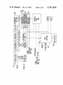
Jr. et a] patent. For ease of understanding, only the
elements of the Bus Unit are shown in FIG. 2, whereas
in addition to the bus unit the elements of all the other
units of the microprocessor are shown in detail in FIG.
3 of the aboveidenti?ed Childs Jr. et al patent.
The bus unit is responsible for supplying code to the
instruction unit. To this end the bus unit generates main
memory cycles as required to obtain code and places
(HIGHEST)
(LOWEST)
this code in a code queue. The output of the code queue
is available to the instruction unit for removal of code
The bus unit includes a prefetch mechanism which
by the execution unit.
fetches code bytes in advance of their being required by
the instruction unit.
The bus unit is responsible for coordinating the se 15
MASTER MICROPROCESSOR INTERFACE
quencing of data cycles and prefetch cycles, since only
Pin Functions
one cycle can be performed at a time. Since the execu
passes a 24-bit real address to the bus unit along with
read/write information. Upon completion of a read
cycle, data is passed from the bus unit to the execution
unit. At the beginning of a write cycle, data is passed
from the execution unit to the bus unit.
The address unit also informs the bus unit as to
whether the current data cycle is to be performed upon
a byte or a word. This information is used to control the
bus high enable signal (BHE#). In addition, the address
The prefetcher.
The instruction unit accepts code bytes from the code
queue of the bus unit and prepares instructions in the
instruction queue. This instruction queue is accessible
bytes.
tion unit is required to wait on data reads, data cycles
are given priority over prefetch cycles so that if a data
cycle and a prefetch cycle are ready to begin simulta
neously, the prefetch cycle will be forced to wait. Any
cycle, once initiated, will run to completion without
interruption for any other type of cycle.
Data cycles are initiated by the address unit which
External bus masters which are
attempting to gain control of the
bus through use of the HOLD signal.
The coprocessor data channel.
The execution unit.
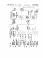
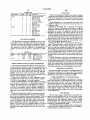
Table I lists the master microprocessor pin signal
names and de?nitions. The 68 pins of the master micro
processor include:
25
24 pins for address (400)
16 pins for data (406)
10 pins for bus and processor control (412)
2 pins for interrupt (406)
4 pins for Coprocessor (402, 404, 408, 410)
5 pins for ICE and
7 pins for power, ground, clock, and substrate ?lter.
The 24-bit address bus is used to output the memory
30 mapped real address and the separate 16-bit data bus is
provided for data transfers. The memory-mapping ad
dress translation and memory-protection limit testing
are performed internally on the master microprocessor
instead of on an external device. This allows the transla
also instructs the bus unit as to which address space is to 35
tion and limit testing to be performed for the next mem
be used, ICE or user’s. This information is used to select
ory cycle overlapped with the completion of the cur
which bus cycle status signals to use, S0# and SI# or
rent memory cycle. Hence, no bus bandwidth is lost due
ICESO# and ICES1#.
to the address translation and limit testing. Due to the
The bus unit also includes temporary address latches
(401) and data latches (within data section 420). These
demultiplexed address and data buses, consecutive bus
latches are used to buffer the address and data for a
cycles can be pipelined so that the beginning of the next
bus cycle is overlapped with the end of the current bus
write cycle if the bus unit is busy with a current bus
cycle. This buffering allows the execution unit to pro
cycle. The result is that fully address-translated and
ceed with execution instead of waiting for the bus unit
limittested bus cycles can be performed at the rate of
to complete the current bus cycle. If a write cycle is 45 one every two processor cycles and memory access
initiated by the execution unit while the bus unit buffers
time is essentially that required for a three-processor
are busy, the bus unit will require the execution unit to
wait until the current cycle terminates and the buffer
cycle bus cycle.
Bus and processor control is similar to that of the
MCS-86
system MAX mode except that certain modi?
The bus unit contains a coprocessor data channel for 50
cations are made in order to optimize the system for
support of a math coprocessor. This channel operates in
high bus bandwidth. (The MCS-86 is a single board
a manner which is very similar to direct memory access.
microcomputer system and is described in the 8086
The channel contains an address counter and a limit
contents are removed for use in the next bus cycle.
checker so that all data transfers can be made to comply
with protection requirements.
Miscellaneous bus cycles include I/O, interrupt ac
knowledge, and halt/shutdown cycles. These cycles are
all initiated by the execution unit. The bus unit treats
them as data cycles in regard to prioritization so that the
bus unit can inhibit the prefetcher in order to avoid lost
clock cycles due to bus collisions. Therefore the execu
tion unit is seldom required to wait because the bus is
busy with a prefetch.
Family User’s Manual dated October 1979, copies of
55 which may be obtained from: Literature Department,
Intel Corporation, 3065 Bowers Avenue, Santa Clara,
CA 95051).
.
For example, selection between memory cycles and
[/0 cycles is no longer encoded in the bus cycle status
signals but, instead, is provided on an M/10# pin which
has electrical timing equivalent to the address bus so
that more time is allowed for address decoders to map
I/O address space and to distinguish between 1/0 ad
During each processor cycle, the bus unit polls and
prioritizes all of the bus cycle requests in order to grant 65 dresses and memory addresses. Bus hold request and
acknowledge signals are provided for allowing arbitra
the next available bus cycle to the highest priority re
tion of asynchronous bus masters which desire to gain
quest. The requests are prioritized in the following way:
control of the processor bus.