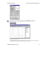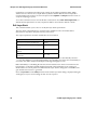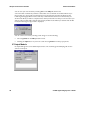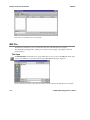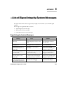
1
Signal Integrity
Copyrights
Software, documentation and related materials:
Copyright © 2002 Altium Limited
This software product is copyrighted and all rights are reserved. The distribution and sale of this
product are intended for the use of the original purchaser only per the terms of the License
Agreement.
This document may not, in whole or part, be copied, photocopied, reproduced, translated, reduced
or transferred to any electronic medium or machine-readable form without prior consent in writing
from Altium Limited.
U.S. Government use, duplication or disclosure is subject to RESTRICTED RIGHTS under applicable
government regulations pertaining to trade secret, commercial computer software developed at
private expense, including FAR 227-14 subparagraph (g)(3)(i), Alternative III and DFAR 252.227-7013
subparagraph (c)(1)(ii).
P-CAD is a registered trademark and P-CAD Schematic, P-CAD Relay, P-CAD PCB, P-CAD ProRoute,
P-CAD QuickRoute, P-CAD InterRoute, P-CAD InterRoute Gold, P-CAD Library Manager, P-CAD
Library Executive, P-CAD Document Toolbox, P-CAD InterPlace, P-CAD Parametric Constraint
Solver, P-CAD Signal Integrity, P-CAD Shape-Based Autorouter, P-CAD DesignFlow, P-CAD
ViewCenter, Master Designer and Associate Designer are trademarks of Altium Limited. Other
brand names are trademarks of their respective companies.
Altium Limited
www.altium.com
Table of Contents
chapter 1
Introduction to P-CAD Signal Integrity
P-CAD Signal Integrity Simulator ........................................................................................1
About this Guide..................................................................................................................1
Signal Integrity Features......................................................................................................2
Features .......................................................................................................................2
Software I/O Buffer Modeling .......................................................................................2
User Interface...............................................................................................................3
chapter 2
P-CAD Signal Integrity - Getting Started
System Requirements .........................................................................................................5
Recommended System ................................................................................................5
Minimum System..........................................................................................................5
Installing P-CAD Products ...................................................................................................6
P-CAD Signal Integrity Interface..........................................................................................6
Accessing P-CAD Signal Integrity .......................................................................................6
Menu Bar......................................................................................................................7
Toolbar .........................................................................................................................7
chapter 3
P-CAD Signal Integrity Tutorial
Starting up P-CAD Signal Integrity ....................................................................................10
Import list of PCB nets to analyze ..............................................................................11
Review and Complete your PCB Design Parameters .......................................................11
Edit Components........................................................................................................11
Edit Nets.....................................................................................................................13
Edit Layer Stack .........................................................................................................13
Select nets to Analyze................................................................................................15
Select Nets by Net Class............................................................................................16
Edit Components specifications .................................................................................17
Screen the Nets.................................................................................................................21
Run Reflection Simulation .................................................................................................26
Run Crosstalk simulation...................................................................................................33
Create a Macromodel ........................................................................................................36
Create a new Macromodel from an IBIS file...............................................................39
chapter 4
P-CAD Signal Integrity Command Reference
P-CAD Signal Integrity User’s Guide
i
File Commands................................................................................................................. 43
File Open ................................................................................................................... 43
File Get Nets.............................................................................................................. 44
File Reports ............................................................................................................... 44
File SULTAN Out....................................................................................................... 48
File Exit...................................................................................................................... 48
Edit Commands ................................................................................................................ 48
Edit Take Over........................................................................................................... 49
Edit Get PCB Selected Nets ...................................................................................... 49
Edit Find Coupled Nets.............................................................................................. 49
Edit Layer Stack ........................................................................................................ 50
Edit Components ....................................................................................................... 51
Edit Nets .................................................................................................................... 53
chapter 5
P-CAD Signal Integrity Screening Commands
File Commands................................................................................................................. 57
File Report ................................................................................................................. 57
File SDF Out.............................................................................................................. 61
File Close .................................................................................................................. 62
Edit Commands ................................................................................................................ 62
Edit Delete ................................................................................................................. 62
Edit Select All ............................................................................................................ 62
Edit Invert Selection................................................................................................... 62
View Commands............................................................................................................... 63
Net Data View............................................................................................................ 63
Impedance View ........................................................................................................ 63
Voltage View.............................................................................................................. 64
Timing View ............................................................................................................... 65
Arrange Nets ............................................................................................................. 66
Select Columns ......................................................................................................... 66
Help Commands ............................................................................................................... 67
Help Topics................................................................................................................ 67
About Help................................................................................................................. 67
chapter 6
P-CAD Signal Integrity Simulation Commands
Termination Advisor.......................................................................................................... 69
Set Victim Net ................................................................................................................... 75
Set Aggressor Net ............................................................................................................ 75
Reflection.......................................................................................................................... 75
Crosstalk........................................................................................................................... 76
chapter 7
P-CAD Signal Integrity Wave Analyzer
Wave Analyzer File Commands ....................................................................................... 78
File Open ................................................................................................................... 78
File Save ................................................................................................................... 78
File Save As .............................................................................................................. 79
File Print .................................................................................................................... 79
ii
P-CAD Signal Integrity User’s Guide
File Page Setup..........................................................................................................80
File Exit ......................................................................................................................81
Edit Commands.................................................................................................................81
Edit Copy....................................................................................................................81
Edit Rescale ...............................................................................................................82
Edit Redraw................................................................................................................82
Edit Delete Selected Wave.........................................................................................82
Edit Delete all Waves .................................................................................................82
Edit Clear Measurement Area ....................................................................................82
Edit Zoom In...............................................................................................................82
Edit Zoom Out ............................................................................................................83
Edit Origin ..................................................................................................................83
Analyze Commands ..........................................................................................................83
Analyze Cartes ...........................................................................................................83
Analyze FFT...............................................................................................................84
Analyze Rise Time .....................................................................................................85
Analyze Fall Time.......................................................................................................85
Analyze Minimum .......................................................................................................85
Analyze Maximum ......................................................................................................86
Analyze Baseline........................................................................................................86
Analyze Topline..........................................................................................................86
Options Commands...........................................................................................................87
Options Measurement Area .......................................................................................87
Options Wave Names ................................................................................................87
Options Display ..........................................................................................................87
Options Coordinate System .......................................................................................89
Options X-Axis ...........................................................................................................89
Options Y-Axis ...........................................................................................................90
Options Wave.............................................................................................................90
Help Commands................................................................................................................90
WaveAnalyser Help Topics ........................................................................................90
How to Use Help ........................................................................................................90
About WaveAnalyzer..................................................................................................91
chapter 8
General Commands
Library Commands ............................................................................................................93
Macromodel Editor ............................................................................................................93
Description of the library tree .....................................................................................94
IC Models ...................................................................................................................96
IC Input, IC Tristate ....................................................................................................97
IC Output Models .......................................................................................................98
Resistors, Inductors, Capacitors Models ..................................................................100
Diode Models ...........................................................................................................102
BJT Transistor ..........................................................................................................104
Connector (Transmission line) .................................................................................108
Connector (Lumped Element) ..................................................................................108
File Commands ...............................................................................................................109
File Exit ....................................................................................................................109
P-CAD Signal Integrity User’s Guide
iii
Edit Commands .............................................................................................................. 109
Edit Open ................................................................................................................ 109
Edit Add ................................................................................................................... 110
Edit Save ................................................................................................................. 110
Edit Save As ............................................................................................................ 110
Edit Close ................................................................................................................ 110
Edit Delete ............................................................................................................... 110
Window Commands........................................................................................................ 110
Window Cascade..................................................................................................... 111
Window Arrange Icons ............................................................................................ 111
Window Next ........................................................................................................... 111
Import IBIS File ............................................................................................................... 111
IBIS File .......................................................................................................................... 112
File Open ................................................................................................................. 112
Export ...................................................................................................................... 113
Report...................................................................................................................... 114
Exit .......................................................................................................................... 115
Options Commands ........................................................................................................ 115
Configure ................................................................................................................. 115
Simulator ................................................................................................................. 116
Help Commands ............................................................................................................. 119
Signal Integrity Help Topics ..................................................................................... 119
How to use Help ...................................................................................................... 119
About P-CAD Signal Integrity .................................................................................. 119
appendix A List of Signal Integrity Digital Integrated Circuits
Signal Integrity Device Library ........................................................................................ 121
Signal Integrity Device Handling/Search......................................................................... 121
Digital Integrated Circuits included in P-CAD Signal Integrity......................................... 122
appendix B List of Signal Integrity System Messages
Signal Integrity System Messages.................................................................................. 169
Wave Analyzer Messages List................................................................................. 170
P-CAD IBIS Converter System Messages...................................................................... 171
appendix C Units and Default Values
Units Representation ...................................................................................................... 173
Common Unit Factor Characters ............................................................................. 173
Common Units ................................................................................................................ 174
Editor Parameter Descriptions ........................................................................................ 174
iv
P-CAD Signal Integrity User’s Guide
CHAPTER
1
Introduction to P-CAD Signal Integrity
Congratulations on your purchase of a high performance simulator to complement your copy of
P-CAD PCB. The applications are paired for fast simulation of reflection effects and are seamlessly
integrated for your ease of use.
Two simulation products are documented in this manual:
•
P-CAD Signal Integrity - Reflection Simulator
•
P-CAD XTalk – Crosstalk Simulator
The menu structure and user interface is consistent for all P-CAD products. Options specific to
each particular simulation are offered through context-sensitive dialogs, giving you exactly those
options supported by your simulator, but in a familiar environment.
P-CAD Signal Integrity Simulator
When you choose the P-CAD Signal Integrity Simulator its entry screen appears. It lets you select
PCB nets to analyze from your P-CAD PCB database or from SULTAN files. It loads these in the
simulator, display their details and enables interactive modification of parameters. When
parameters are missing, default parameters are used. These are listed in the section discussing the
parameters. P-CAD Signal Integrity also provides access to start and restart the simulation process.
About this Guide
This manual includes information on the use and operation of the following products:
•
P-CAD Signal Integrity
•
P-CAD Xtalk
The information in this manual is presented in tutorial and reference format. It is designed to get
you started simulating, and to present some advanced features which will be helpful as you gain
more experience of the functionality of the simulators.
P-CAD Signal Integrity User’s Guide
1
Chapter 1: Introduction to P-CAD Signal Integrity
Signal Integrity Features
Signal Integrity Features
As Windows based PCB design tools become more and more sophisticated and are used to design
printed circuit boards with high clock speeds and high density, the demand for simulation tools
addressing signal integrity problems has increased dramatically.
P-CAD Signal Integrity has been created specially for PCB designers using the P-CAD PCB tool, and
is tightly coupled to the PCB to provide a simple interactive simulation environment. Using P-CAD
Signal Integrity, design engineers may check their multilayer boards for noise effects like ringing
and crosstalk. When installed, P-CAD Signal Integrity is seamlessly integrated with P-CAD PCB,
giving you the familiarity of P-CAD PCB's Windows™ interface standard and easy access to its
powerful capabilities.
P-CAD Signal Integrity is based on a Fast Reflection and Crosstalk Simulator, which produces very
accurate simulations, (provided that full model information is available), with algorithms proven in
industry.
The P-CAD Signal Integrity simulator uses the characteristic impedance of the traces calculated
through a transmission line calculator and I/O buffer macro-model information as input for the
simulations. Where model information is not available the system utilizes fallback models.
Features
•
Provides fast simulation of reflection and crosstalk effects.
•
Fast screening (pre-analysis) for signal integrity effects (over- and undershoot, delay, etc.) for
entire boards with spreadsheet-like result display.
•
Seamlessly integrated with P-CAD PCB, allowing access to simulation options.
•
No special expertise is required to use it, due to the simple user interface and tight integration.
•
As the system utilizes I/O buffer macro-models, no knowledge of SPICE or analogue simulation
is required.
•
Oscilloscope type display of simulation results with integrated result measurement facilities.
•
Well-proven algorithms for the calculation of the transmission line characteristics and
subsequent simulations.
•
What-if-analysis concerning different termination strategies with parametric values of
resistors/capacitors and through easy substitution of macro-models.
•
What-if-analysis concerning different routing strategies through tight integration with P-CAD
PCB.
Software I/O Buffer Modeling
2
•
Macro-model approach for fast and accurate simulation.
•
Supplied with a basic IC model library including verified models.
•
Automatic model attachment according to Part Number.
P-CAD Signal Integrity User’s Guide
Signal Integrity Features
Chapter 1: Introduction to P-CAD Signal Integrity
•
Supporting the IBIS 3 industry standard sub-set for I/O buffer modeling.
•
Integrated macro-model-editor allows easy and fast definition of own models using databook
or measurement values.
•
P-CAD Signal Integrity utilizes the P-CAD PCB, DBX API interface for interactive
communications.
•
P-CAD Signal Integrity can be loaded with complete PCBs or subsets of data (single or multiple
nets, single layers, etc.).
•
P-CAD Signal Integrity supports cross highlighting with the layout (nets under analysis).
•
P-CAD Signal Integrity can provide an INCASES EMC-WORKBENCH ‘SULTAN” file for extended
EMC analysis.
•
P-CAD Signal Integrity can back annotate termination networks onto the board as a DRC
marker.
•
P-CAD Signal Integrity and Xtalk are designed for analyzing PCB’s with consistent power and/or
ground planes. Use of the tools on boards without consistent power or ground planes will lead
to untrustworthy results.
User Interface
There are three basic operational screens for P-CAD Signal Integrity: the net screen, the preanalysis screen and the result screen. The net screen and the result screen can be utilized
simultaneously.
P-CAD Signal Integrity User’s Guide
3
CHAPTER
2
P-CAD Signal Integrity - Getting Started
This chapter gives information on the required hardware and software needed before installing
P-CAD Signal Integrity products. It also introduces you to the P-CAD Signal Integrity interface.
System Requirements
Make sure that your PC and its software conform to the following P-CAD requirements and
recommendations.
Recommended System
•
Windows NT 4/2000 Professional
•
PC with Pentium III Processor
•
128MB RAM (256MB for high component/net count)
•
400MB Hard Disk Space
•
Desktop area 1024x768 pixels
•
32-bit Color Palette
•
CD-ROM Drive
•
Mouse or compatible pointing device
Minimum System
•
Windows 95/98/2000Me
•
PC with Pentium 166MHz
•
64MB RAM
•
200MB Hard Disk Space (without ISO libraries)
•
Desktop area 800x600 pixels
P-CAD Signal Integrity User’s Guide
5
Chapter 2: P-CAD Signal Integrity - Getting Started
•
256 Color Palette
•
CD-ROM Drive
•
Mouse.
Installing P-CAD Products
Installing P-CAD Products
For up-to-date installation information refer to the file Readme.WRI, located on the product CD.
This file can also be found in the application program folder (\Program Files\P-CAD 2002)
after installation. Note that the setup program on the Product CD can also be used to repair or
remove an existing P-CAD Installation.
P-CAD Signal Integrity Interface
You are probably already familiar with the P-CAD PCB interface in addition to being proficient in
the operation of Windows, so every detail of the screen is not provided here.
Accessing P-CAD Signal Integrity
P-CAD Signal Integrity simulator is accessed by choosing Utils » P-CAD Signal Integrity from the
P-CAD PCB menus. This brings up the simulator entry window. You can now choose PCB nets and
analyze them using either commands from the pull-down menu or icons on the tool bar.
6
P-CAD Signal Integrity User’s Guide
Accessing P-CAD Signal Integrity
Chapter 2: P-CAD Signal Integrity - Getting Started
Menu Bar
P-CAD Signal Integrity menu bar, displayed on the simulator entry screen, provide access to
commands that let you:
•
Bring in PCB nets to analyze
•
Review/complete/modify PCB design parameters
•
Launch simulations
•
Produce reports
•
Create output files
•
Import IBIS files and create Macromodels
•
Specify simulator options and preference settings.
Toolbar
The toolbar consists of graphical display buttons (icons) that correspond to commonly used P-CAD
Signal Integrity commands. These icons appear just below the menu bar on the P-CAD Signal
Integrity entry screen.
Tool Tips explain each of the toolbar buttons. To activate a Tool Tip, place the mouse over the
button. The Tool Tip pops up.
The icon display is context sensitive, so icons not highlighted indicate commands not available at
this stage. The commands linked with each icon are listed below:
Open SULTAN File
Create Report
Get Netlist from P-CAD PCB
Get PCB Selected Nets
Find Coupled Nets
P-CAD Signal Integrity User’s Guide
7
Chapter 2: P-CAD Signal Integrity - Getting Started
Accessing P-CAD Signal Integrity
Take Over Selected Nets
Start the Termination Advisor
Start Net Screening
Start Reflection Simulation
Set Victim Net
Set Aggressor Net
Start Crosstalk Simulation
The simulation commands Reflection and Crosstalk give access to the Wave Analyzer, which has its
own icons and menu bar.
8
P-CAD Signal Integrity User’s Guide
CHAPTER
3
P-CAD Signal Integrity Tutorial
This tutorial includes hands-on instructions to help you become familiar with how to use P-CAD
Signal Integrity to analyze and simulate your PCB designs and to investigate remedies to signal
integrity problems.
The following steps indicate what you will accomplish in this tutorial.
1.
Starting up P-CAD Signal Integrity
•
2.
Import list of PCB nets to analyze
Review and complete your PCB design parameters
•
Edit Designator specifications
•
Edit Supply Nets specifications
•
Edit Layer Stack specifications
•
Select nets to analyze
•
Edit Components specifications
3.
Screen the Nets
4.
Run Reflection simulation
5.
•
Modify parameters
•
Re-run simulation
•
Produce a report
Run Crosstalk simulation
•
Modify parameters
•
Re-run Crosstalk simulation
P-CAD Signal Integrity User’s Guide
9
Chapter 3: P-CAD Signal Integrity Tutorial
•
6.
7.
Starting up P-CAD Signal Integrity
Produce a report
Create a Macro Model
•
Edit Macro Model
•
Create a new Macro Model from an IBIS file
Specify simulation options and preference settings.
Each of these steps is discussed in detail in this tutorial. It will be worth your time to go through
the complete tutorial, which is designed to get you going quickly.
If a message is displayed by the system during the tutorial, see Appendix B - System Messages, for a
description of the problem and a possible solution.
For more detailed information about any of the commands and options used in this tutorial, refer
to the relevant Commands Reference chapters.
Please note that the examples do not reflect the current state of the art techniques to avoid and
solve signal integrity problems. The Termination methods used in the different examples are for
tutorial purposes only.
Starting up P-CAD Signal Integrity
In this tutorial we will analyze nets from the demo PCB provided with P-CAD Signal Integrity.
Within P-CAD PCB, open the file \P-CAD 2002\Demo\Signal Integrity\demo.pcb.
Start the Signal Integrity program by choosing Utils » P-CAD Signal Integrity from the P-CAD PCB
menus. This will display the Signal Integrity entry window.
10
P-CAD Signal Integrity User’s Guide
Review and Complete your PCB Design Parameters
Chapter 3: P-CAD Signal Integrity Tutorial
The toolbar display is context sensitive, and only commands available at each stage have their icon
highlighted.
Import list of PCB nets to analyze
The first step is to import the nets from the PCB into P-CAD Signal Integrity. To do this click on the
Get Netlist icon, or choose File in the menu bar and select Get Nets from the pull-down menu.
This will list, on the left of the window in the All Nets column, all the nets in the PCB currently open
in P-CAD PCB.
Review and Complete your PCB Design Parameters
We can now edit and modify:
1.
The electrical component types
2.
The supply nets
3.
The Layer Stack of the whole PCB
4.
The choice of nets to analyze
5.
The components specifications.
Edit Components
To access the Edit Components dialog, choose Edit in the Menu bar and select Components from
the pull-down menu. The Components list box contains the names of all components in the active
design. You can select individual or multiple components in the list box. Once selected you can
specify the electrical type of a component.
P-CAD Signal Integrity User’s Guide
11
Chapter 3: P-CAD Signal Integrity Tutorial
Review and Complete your PCB Design Parameters
Select the component C1 in the Component list. Note that the Category is already set to Capacitor.
If it was not, you would choose the type Capacitor in the Category drop down list. Confirm that all
other capacitors have their Category set to Capacitor.
In the same way confirm that the components D1 and D2 are set to Diode, J1 is set to Connector,
R1, R2 and R3 are set to Resistor, and U1 to U9 are set to IC.
With the button To Database you can save the specified component type back to the PCB currently
open in P-CAD PCB. The information is saved in the PCB as a component attribute.
A second way to specify the component type is to define a component attribute directly in P-CAD
PCB. Define the Component attribute Category, and set the value of the attribute to one of the
following qualifiers. If you now load the design into P-CAD Signal Integrity, the components will
have their Category already defined (as in the demo file).
The following electrical component types are supported:
Component Type
Attribute Value
Bipolar Junction Transistor
BJT
Capacitor
Capacitor, Cap
Connector
Connector, Con
Diode
Diode, Dio
IC
IC
Inductor
Inductor, Ind
Resistor
Resistor, Res
If you do not set the Category, P-CAD Signal Integrity will use the type IC.
12
P-CAD Signal Integrity User’s Guide
Review and Complete your PCB Design Parameters
Chapter 3: P-CAD Signal Integrity Tutorial
Edit Nets
Although Supply Nets can not be simulated, they are necessary for the correct simulation of nets
with Pull-up or Pull-down components.
To access the Edit Nets dialog, click on Edit on the Menu bar and choose Nets from the pull-down
menu.
The Edit Nets dialog contains the names of all nets in the active design. You can select individual or
multiple nets in the list box. Once selected you can specify the category and the voltage of the net.
Select the net VCC in the net list box, choose the category Supply in the Category drop down list,
enter 5V as the Value and click the Apply button for the changes to take place. In the same way set
the category Supply and the value 5V for the nets VCC, VCC1, VCC2 and VCC3.
With the button To Database you can save the specified net category and value to your P-CAD PCB.
The information is saved in the PCB as net attributes.
A second way to specify the net category and value is to define net attributes directly in P-CAD PCB.
Define the net attribute Category and set the value of the attribute to Supply, and the net attribute
Voltage and set the value to the voltage of the net. If you now load the design into P-CAD Signal
Integrity, the nets get the defined category and value.
Edit Layer Stack
For the calculation of the correct electrical behavior of the traces, the layer stack of the PCB must
be specified.
The required parameter definitions and their applicable default values are listed below:
P-CAD Signal Integrity User’s Guide
13
Chapter 3: P-CAD Signal Integrity Tutorial
Parameter definition
The correct sequence of the layers
The thickness of the different copper
and dielectric planes
The dielectric constant of the substrate
Review and Complete your PCB Design Parameters
Defaults
None
35µm
0.32mm
ετ = 4.8
The layer stack and all associated transmission line parameters are automatically saved in a layer
stack information file. The file is named as the same as the PCB, with the extension .TDB. It is saved
into a folder with the same name as the PCB, under the Projects folder. For example, for the demo
board it is \P-CAD 2002\Projects\Demo\Demo.tdb.
Before a new transmission line parameter is calculated, the system checks if appropriate
transmission line parameters already exist in the database file.
Whenever the layer stack is changed, the old database file gets deleted and a new one is generated.
Choose Edit on the Menu bar and select Layer Stack from the pull-down menu to access the Layer
Stack Specifications window. The signal and plane layers are displayed in the Layer Stack dialog.
This window shows the layer name, the layer type (Signal or Plane), and the layer number as
defined by the user in P-CAD PCB. Here you can modify the Dielectric and Copper property
definitions for a layer. To do so select a layer and enter the changes required in the available entry
windows.
When you enter the Copper thickness and the Dielectric value, the Dielectric referred to is the one
immediately above the Copper layer. As a result, it is not possible to enter a Dielectric value for the
top layer.
14
P-CAD Signal Integrity User’s Guide
Review and Complete your PCB Design Parameters
Chapter 3: P-CAD Signal Integrity Tutorial
All the layers except the Top and Bottom layers can be moved up or down, by selecting a layer and
clicking the appropriate button. The Top layer is always number 1, and the Bottom layer which is
always number 2 and at the bottom.
For the purpose of this tutorial, we will leave the layer stack unchanged. Click OK or Cancel to
close the window.
Select nets to Analyze
In the Signal Integrity main entry dialog, choose the nets DEMO_D0 to DEMO_D31, by clicking and
holding the left mouse button on DEMO_D0 and dragging the cursor to select all DEMO_Dx nets.
This will highlight the desired nets.
To analyze these nets, the simulator must acquire all the required data for simulation. The editor
does this when you do one of the following:
•
Click on the Takeover icon or
•
Choose Edit in the menu bar and select Take Over from the pull-down menu. The simulator
acquires the nets’ data and displays the details in the simulation windows.
P-CAD Signal Integrity User’s Guide
15
Chapter 3: P-CAD Signal Integrity Tutorial
Review and Complete your PCB Design Parameters
The selected nets are listed in the top window on the right hand side.
For each selected net, the following are displayed:
•
The Net name (some net names are concatenated).
•
The Net length (the sum of the length of all trace segments).
•
The Net characteristic impedance (the average impedance derived by the sum of the
impedance of each trace segment multiplied by the length of the trace segment and divided by
the sum of the length of the traces).
The bottom right hand window displays the connected pins for the net selected in the top
simulation window.
Scroll down and select DEMO_D5_DEMO_NET11 from the top simulation window.
Select Nets by Net Class
Allows you to analyze nets by net classes. Normally, the left list box shows the names of all nets of
the current design. To analyze only a group of nets, define net classes in P-CAD PCB and assign the
affected nets to the class. After pressing the button Get PCB Nets, the drop down list Net Class is
filled with all net classes of the design.
Select a net class and the list below contains only the nets of that class. To see all nets, select the
entry All.
16
P-CAD Signal Integrity User’s Guide
Review and Complete your PCB Design Parameters
Chapter 3: P-CAD Signal Integrity Tutorial
Edit Components specifications
The Edit Buffer button, located on the Signal Integrity entry window, gives access to the
component’s data dialog. We will look at data windows for IC’s, Resistors and Capacitors. Other
components will display different screens as applicable.
First, on the Signal Integrity bottom right-hand window, select the component: U1.
Use the In <-> Out button to modify the direction specification for the selected component, to
change it from the input to output or vice versa. Return the buffer to an Output.
To modify the specifications for components, click on the Edit Buffer button. This displays the
Integrated Circuit dialog. You can change the Model data and the Stimulus used by the simulator
for the highlighted components, in our case U1.
P-CAD Signal Integrity User’s Guide
17
Chapter 3: P-CAD Signal Integrity Tutorial
Review and Complete your PCB Design Parameters
The Model tab shows the current settings for the IC component selected. Choosing a Technology
and Direction will automatically give a list of input and / or output models as appropriate. For the
purpose of this tutorial, we will leave the Model settings unchanged.
Changes to technology and direction are used locally in the design. If however, you wish to update
the library to reflect changes, then click on Save to Library button. Remember that you are
modifying the library when you do this, so care should be taken to ensure that the library is not
corrupted for future use.
Choose the Stimulus tab. In the Stimulus window you can modify the Stimulus which is applied to
the input of the output I/O buffer for Simulation to:
Constant Level,
Single Pulse or
Periodic Pulses.
Select the Single Pulse or Periodic Pulse option in the Stimulus Type box, and notice that you can
set the Start Level to High or Low in the Start Level box. The wave display will change to reflect your
choices.
18
P-CAD Signal Integrity User’s Guide
Review and Complete your PCB Design Parameters
Chapter 3: P-CAD Signal Integrity Tutorial
You can also specify Start and Stop times of the pulse and the Period time if a periodic pulse is
chosen.
Stimulus details can be saved to a file. This is described in the Edit section of the Command
Reference chapter.
Stimulus details may also be loaded from a file. To do so, click the Load button. The Load Stimulus
dialog is displayed. Choose the demo stimulus file, single.stm, located in the stimuli subdirectory and click the Open button. This will update the Stimulus tab with the details of the file.
Click OK to close the Integrated Circuit dialog.
Back in the Signal Integrity window, select component ‘R2’.
P-CAD Signal Integrity User’s Guide
19
Chapter 3: P-CAD Signal Integrity Tutorial
Review and Complete your PCB Design Parameters
Now click the Edit Buffer button again. This displays the Resistor dialog.
You can add or remove pins for connections routed to resistor arrays. For the purpose of this
tutorial, we will make no change to this resistor. Click the Cancel button to close the Resistor
dialog.
Back in the Signal Integrity window, select the component C1 and choose the Edit Buffer button to
display the Capacitor dialog.
Again, leave the Capacitor unchanged, and click the Cancel button.
20
P-CAD Signal Integrity User’s Guide
Screen the Nets
Chapter 3: P-CAD Signal Integrity Tutorial
Screen the Nets
Screening provides a fast simulation of many nets to enable you to get closer information about the
nets and to identify critical nets for closer examination. Besides geometrical information, it also
provides estimated values for Signal Integrity effects (overshoot, undershoot).
When screening bi-directional nets, both directions are simulated and the worst result of each
effect is displayed.
The Screening commands can be accessed from the Simulation pull-down menu or by clicking the
Screening icon.
Click on the Screening icon to get the Screening window to display details for the currently
selected nets.
The data displayed when you enter the Screening window shows the information requested on the
last access. We will review each of the screening views and identify nets to analyze in greater detail.
The message in the comment window indicates that nets with Diodes or Transistors cannot be
analyzed by the Screening fast simulation method. These can, however be simulated using the
Reflection and Crosstalk simulation options.
First, click on all of the four results display icons, which are currently highlighted, to switch the
options off.
Click on the Net Data View icon. This displays for each net:
P-CAD Signal Integrity User’s Guide
21
Chapter 3: P-CAD Signal Integrity Tutorial
•
The net name
•
The length of the trace
•
The number of components connected to the traces
•
The number of segments in each trace.
Screen the Nets
Now click on the Net Data View icon again to switch this view off.
Next, click on the Impedance View icon. This displays for each net:
22
•
The net name
•
The average impedance of the whole trace
•
The minimum impedance of the whole trace
•
The maximum impedance of the whole trace.
P-CAD Signal Integrity User’s Guide
Screen the Nets
Chapter 3: P-CAD Signal Integrity Tutorial
Click on the Impedance View icon again to switch this view off.
Now, click the Voltage View icon, and drag the right edge of the Screening window to enlarge it
and display more columns on the screen.
To display all the seven columns at once, you can make the columns narrower by clicking a column
edge on the header line and dragging the column to the desired width.
This displays for each net:
•
The net name
•
The Top Voltage Value for the Rising Edge
•
The Maximum Overshoot for the Rising Edge
•
The Maximum Undershoot for the Rising Edge
•
The Base Voltage Value for the Falling Edge
•
The Maximum Overshoot for the Falling Edge
•
The Maximum Undershoot for the Falling Edge.
P-CAD Signal Integrity User’s Guide
23
Chapter 3: P-CAD Signal Integrity Tutorial
Screen the Nets
You can select to display only the columns of interest on a view, to ease the identification of
problem nets by defined criteria.
Let’s view the Maximum Overshoot (Rising Edge) and Maximum Undershoot (Falling Edge).
Choose the View command on the screening header menu.
Select the Select Columns command.
In the Select Columns dialog, click the Voltage tab. On the Voltage tab, choose to display only the
Maximum Overshoot on the Rising Edge and Maximum Undershoot on the Falling Edge, by
disabling all other options as displayed below. Click OK.
This will now display only the two chosen columns on the Voltage View.
We can also sort the nets by values within displayed columns.
24
P-CAD Signal Integrity User’s Guide
Screen the Nets
Chapter 3: P-CAD Signal Integrity Tutorial
From the View menu, select the Arrange Nets By command. The Arrange Nets By menu is displayed
highlighting only the columns currently displayed.
Select Maximum Overshoot (Rising Edge). This displays the nets sorted in order of Maximum
Overshoot.
Now click on the Voltage View icon again to switch this view off.
Lastly, click on the Timing View icon. This displays for each net:
•
The net name
•
The Slope for the Rising Edge
•
The Flight Time for the Rising Edge
•
The Slope for the Falling Edge
•
The Flight Time for the Falling Edge.
P-CAD Signal Integrity User’s Guide
25
Chapter 3: P-CAD Signal Integrity Tutorial
Run Reflection Simulation
You can identify the nets displaying the longest flight time.
Now close the screening window using the X in the top right corner.
Run Reflection Simulation
Back on the Signal Integrity main screen, select the net DEMO_A31 in the All Nets column. Click the
Takeover icon to acquire data for this net.
The Reflection simulator calculates voltages at nodes of a net using routing and layer information of
the PCB and associated driver and receiver I/O buffer models.
A 2D-field solver automatically calculates the electrical characterization of the lines. Modeling
assumes that DC path losses are small enough to be ignored. The simulator provides you with
detailed and highly accurate information on all signal integrity related aspects, such as overshoot,
undershoot and timing. The results are presented in an oscilloscope-like wave analyzer.
To start a Reflection simulation, you can either click on the Reflection Simulation icon, or choose
Simulation in the menu bar and select Reflection from the pull-down menu.
The simulator runs a reflection simulation on the nets displayed in the simulation window.
The results of the Reflection simulation are returned on the WaveAnalyzer screen.
The X and Y specified on the bar under the WaveAnalyzer screen indicate the location of the cursor
on the display.
26
P-CAD Signal Integrity User’s Guide
Run Reflection Simulation
Chapter 3: P-CAD Signal Integrity Tutorial
The display above shows the wave U9.9 (U9, pin 9 on net DEMO_A31) and wave U1.118 (U1, pin 118
on net DEMO_A31) as the worst for overshoot and undershoot. Let’s look at the range of the
overshoot for each of these waves.
Select the wave U9.9 by clicking on the line beneath its name which is displayed on the right of the
wave display.
The WaveAnalyzer Analyze commands allow you to display the simulation results as waveform
measurements. Click on the Minimum, Maximum, Base Line, Top Line icons.
The calculated measurements are displayed in the Measurements area of the WaveAnalyzer
window. These measurements can also be performed using the pull-down options of the Analyze
menu.
Let’s zoom in on the worst overshoot area on the top left of the display. To do so, click the Zoom In
icon then click and hold the mouse button on the top left corner, then drag the cursor toward the
bottom right to define the zoom region. The picture below displays the zoomed area with its
measurements.
P-CAD Signal Integrity User’s Guide
27
Chapter 3: P-CAD Signal Integrity Tutorial
Run Reflection Simulation
Clear the measurement area by selecting Clear Measurement Area on the Edit pull-down menu.
Now reselect Minimum, Maximum, Baseline and Topline.
The measurements are display dependent. The measurements displayed are for the selected wave
within the currently visible area. If you compare the measurements of the zoomed graph with the
measurements of the original chart, you can see that the measurement values are different. They
now show the measurements for the currently displayed waveforms.
To return the display to the original full waves display, select the Origin command from the Edit
pull-down menu.
Let’s save the current wave as DEMO_A31 for subsequent reference.
Do this by selecting Save As on the File pull-down menu.
The File Save dialog is displayed. Here you can specify the directory and filename for the wave file
you want to save.
Enter DEMO_A31 in the File Name field and click the Save button.
When saving using the File Save command, the default name result.dia is given. This default can
be changed, by entering a new name, as appropriate. The current file name, displayed on the title
bar, is overwritten each time the File Save command is issued.
28
P-CAD Signal Integrity User’s Guide
Run Reflection Simulation
Chapter 3: P-CAD Signal Integrity Tutorial
Close the Waveform Analyzer by clicking the X in the upper right corner. The file saved can later be
opened using the File Open command.
Having identified the net DEMO_A31 as problematic, let’s go back to the Signal Integrity screen to
select it and try a termination on the component U9 pin 9 to reduce the overshoot.
To do so, we first select the entry U9 pin 9 in the Signal Integrity window. Click on the Termination
Advisor icon.
The Termination examples given here are for the purpose of demonstrating the tool only and may
not be appropriate in the electrical sense.
The Termination Advisor dialog is displayed.
Choose Parallel C to GND termination method and click OK.
P-CAD Signal Integrity User’s Guide
29
Chapter 3: P-CAD Signal Integrity Tutorial
Run Reflection Simulation
Now let’s run the reflection simulation again. Click on the Reflection icon and on the
WaveAnalyzer display, select the wave U9 pin 9 again by clicking on the line under its name and
click the measurement icons to display the measurements in the Measurements area.
The overshoot Vmax = 7.11 V, is a slight reduction on the original 7.92 V before the termination was
added, but it is still significant. Let’s try a different termination.
Close the WaveAnalyzer window and go back to the Signal Integrity window, click on the
Termination Advisor icon again. This time, select the Parallel R to GND Termination with 100 Ohm
resistance and click OK.
30
P-CAD Signal Integrity User’s Guide
Run Reflection Simulation
Chapter 3: P-CAD Signal Integrity Tutorial
Now let’s run the reflection simulation again. Click on the Reflection icon. Again, on the
WaveAnalyzer display, select the wave U9.9 and click on the measurement icons.
Now let’s print out these results.
Select Page Setup on the WaveAnalyzer File pull-down menu. This displays the Page Setup dialog,
on which you can specify paper size, source, orientation and margins.
P-CAD Signal Integrity User’s Guide
31
Chapter 3: P-CAD Signal Integrity Tutorial
Run Reflection Simulation
Click on the Printer button to specify the printer. On the displayed dialog you can select a printer
and enter the property details for the chosen printer.
Click OK to accept the printer selection and again to close the Page Setup dialog. Then click on
Print on the WaveAnalyzer File pull-down menu. This displays the standard Windows print dialog,
and sends the Wave display to the printer.
You can also use the Print icon to print the display, when the page setup and the printer details are
already specified.
The introduction of the termination appears to have resolved the ringing noise problem.
You can save this termination solution and send it as a DRC error indicator to the P-CAD PCB
database. First close the WaveAnalyzer window. Return to the Signal Integrity window.
Click on the Termination Advisor icon. Click on the Send to P-CAD PCB button and click OK.
To display the DRC error indicator in P-CAD PCB, restore the P-CAD PCB window. In the P-CAD
PCB window, choose File from the menu line and select Reports. Then enable DRC Error Indicators
in the Reports to Generate list and click the Generate button.
32
P-CAD Signal Integrity User’s Guide
Run Crosstalk simulation
Chapter 3: P-CAD Signal Integrity Tutorial
This produces a report giving the ideal X, Y coordinate location of the termination network on the
board together with the values of the component.
A DRC marker is placed in P-CAD PCB adjacent to the pin where the termination network should
be applied. If you click on the DRC marker and view its properties (right mouse click and choose
Properties), you get the value and configuration of the termination network.
Run Crosstalk simulation
The Termination examples given here are for the purpose of demonstrating the tool only and may
not be appropriate in the electrical sense.
P-CAD Xtalk, the Crosstalk simulator simulates the coupling between traces with adjacent parallel
segments.
P-CAD Signal Integrity User’s Guide
33
Chapter 3: P-CAD Signal Integrity Tutorial
Run Crosstalk simulation
P-CAD Signal Integrity is automatically searching for parallel traces, which may cause crosstalk
problems. To enter the geometrical parameters for this search, select the Configure command from
the Options menu. Enter the following values:
•
Max. Couple Distance: 1mm
•
Min. Couple Length:
1mm
Max. Couple Distance specifies the maximum distance, which is used for searching parallel traces.
The larger this distance is specified the more parallel traces will be found. Therefore the simulation
time will increase.
Min. Couple Length specifies the minimum parallel length of a trace, which is still considered to
provide crosstalk. Short parallel segments do not provide much crosstalk, but the simulation time
will increase drastically.
Click on the Get Nets icon in P-CAD Signal Integrity and then select net DEMO_D1 in the All Nets
column. After that, click on the Find Coupled Nets button. Now, all nets within the range of the
specification entered in the Options Configure menu will be selected automatically in the All Net
list. In this case, these are DEMO_D0, DEMO_D1 and DEMO_D2.
Click the Takeover icon.
34
P-CAD Signal Integrity User’s Guide
Run Crosstalk simulation
Chapter 3: P-CAD Signal Integrity Tutorial
Next, choose net DEMO_D1 in the simulation window, and click the Set Victim Net button. This will
set the stimulus for the net DEMO_D1 to constant low level and all other nets will have the default
stimulus (single pulse, rising edge at 10ns, falling edge at 60ns). By this, the maximum crosstalk of
all coupled nets onto the victim net is calculated.
Now run the Crosstalk simulation by clicking on the Crosstalk button.
P-CAD Signal Integrity User’s Guide
35
Chapter 3: P-CAD Signal Integrity Tutorial
Create a Macromodel
The WaveAnalyzer shows maximum crosstalk of 1.07V measured on net DEMO_D1 at pin 3 at
component U2. This crosstalk results from the ringing on net DEMO_D0 and DEMO_D2 during the
signal transition from low to high and high to low.
Close the WaveAnalyzer to return to P-CAD Signal Integrity.
Select net DEMO_D1 in the Simulation window on the right. Now press the Set Aggressor Net icon.
By doing this, net DEMO_D1 will get the default stimulus (single pulse, rising edge at 10ns, falling
edge at 60ns) while all other nets will be set to constant low. This will calculate the crosstalk from
the aggressor net to all its neighbor nets. After clicking on the Crosstalk Simulation button, the
WaveAnalyzer displays the results.
Create a Macromodel
The Macromodel Editor enables you to create your own custom device models. The models are
organized in the library tree.
To open the Macromodel Editor, select the Macromodel Editor command from the Library menu in
P-CAD Signal Integrity screen. The library tree displays as shown.
36
P-CAD Signal Integrity User’s Guide
Create a Macromodel
Chapter 3: P-CAD Signal Integrity Tutorial
You can navigate through the User Model Library as you do in Windows Explorer.
The library contains a folder for each type of parts and models defined in the database. IC models
folders are also sub-divided into folders for each available technology. The full list of technologies
available is described in the Macromodel Editor commands’ description in chapter 8.
The items in the tree represent user defined custom models.
Let’s add a new Resistor component. To do so, click on the Resistor model folder. This displays the
currently defined Resistor components (there may be none currently defined).
Choose Edit from the Macromodel Editor menu bar and select Add from the pull-down menu. This
displays the Modelname Entry dialog.
Enter Res500 as shown below and click OK.
P-CAD Signal Integrity User’s Guide
37
Chapter 3: P-CAD Signal Integrity Tutorial
Create a Macromodel
The RLC Enter Value dialog is displayed where you can enter the number of pins. In our case, leave
the default value as 2 and click OK.
The newly created Resistor Res500 is now displayed on the Library tree.
The Resistor - Res500 dialog is displayed with the information supplied so far and default values for
the other parameters.
38
P-CAD Signal Integrity User’s Guide
Create a Macromodel
Chapter 3: P-CAD Signal Integrity Tutorial
In this dialog you can change the value in the Using Value box and click the Apply button. The
entry on the top window will be modified accordingly.
Some IC models in the Library cannot be edited. These models have been created by the P-CAD
Signal Integrity IBIS converter and contain data that cannot be modified.
Create a new Macromodel from an IBIS file
IBIS stands for ‘Input/Output Buffer Information Specifications’. It is an ANSI/EIA standard for
behavioral specifications of integrated circuit’s input/output analog characteristics.
You can create new custom user models based on input from IBIS files.
The Import IBIS File command enables you to do so. The Import IBIS File command is accessed
from the Library pull-down menu on the Signal Integrity entry screen.
P-CAD Signal Integrity User’s Guide
39
Chapter 3: P-CAD Signal Integrity Tutorial
Create a Macromodel
Choose the Import IBIS File command from the pull-down menu of the Library command. This
displays the P-CAD IBIS Converter window.
Choose the File command from the menu bar, and select Open on its pull-down menu.
This displays the File Open dialog, choose the \P-CAD 2002\Demo\Signal Integrity folder
which includes an example IBIS file.
Choose the file lvx240db.ibs as shown above. The information is loaded on the IBIS Converter
window.
We can now choose which model to generate.
The Strong Case Model allows you to test your design performance envelope. The strong case
model represents the fast extreme of IC performance.
40
P-CAD Signal Integrity User’s Guide
Create a Macromodel
Chapter 3: P-CAD Signal Integrity Tutorial
The Typical Case Model lets you get an idea of the typical performance of the design.
Let’s choose these two models. To do so, select these two models from the File pull-down menu.
Let’s produce a report of these models. Select the Report command from the File pull-down menu.
This displays the Generate Model Report dialog, which, by default, allocates for the report the name
of the currently opened file. You can modify this or accept this name.
Let’s accept the name. This will generate a Word report in the specified directory.
The picture above shows part of the report generated.
Now, let’s add these models to the Library.
This is done with the IBIS File Export command. It can be accessed from the File pull-down menu or
by its icon.
When you choose this command, the models are added to the Library. If the models already exist,
in the library, a confirmation window is displayed which gives you the option to over-write the
currently stored models or cancel your export operation.
P-CAD Signal Integrity User’s Guide
41
Chapter 3: P-CAD Signal Integrity Tutorial
Create a Macromodel
Otherwise, an export confirmation message is displayed.
42
P-CAD Signal Integrity User’s Guide
CHAPTER
4
P-CAD Signal Integrity Command Reference
This Reference chapter provides information on each command, dialog and option available during
the simulation process, in the order in which they appear in the menus and dialogs. It also includes
additional information about simulation concepts and procedures.
When you start the P-CAD Signal Integrity, the entry screen is displayed, giving you access to
process specific icons, menus and commands.
File Commands
The File commands are accessed from the File menu, which appears on the menu bar when you
enter P-CAD Signal Integrity. The File commands allow you to open and save files, get nets to
analyze and produce reports. Each of these commands is discussed below.
File Open
The File Open command imports an existing SULTAN file, as input to the simulator, using the
Windows standard File Open dialog.
A SULTAN file is a representation of the PCB geometry and the required electrical and design
specific information (like value of resistors and component designators). This representation is
used to store PCB databases so that P-CAD Signal Integrity can be used without having P-CAD PCB
open.
The File Open command can be initiated from the File command pull-down menu or by its icon.
When you choose File Open, P-CAD Signal Integrity displays a dialog from which you can choose
the directory and file name of the file you want to open.
The Look In area displays the current folder; a list of files in the folder appears directly underneath.
The File name area lets you select or enter a SULTAN file, from the list of files displayed with the
P-CAD Signal Integrity User’s Guide
43
Chapter 4: P-CAD Signal Integrity Command Reference
File Commands
extension .slt. If a file you want is not in the current directory, you can select another directory
from the Directories list.
Once you have made your selection, click the Open button.
File Get Nets
This command displays a list of all nets of the current P-CAD PCB design in the All Nets column of
the entry screen. Click on the nets you want to select. These will become highlighted. To select
nets, which are not displayed consecutively, press the Ctrl button while selecting.
In order to analyze a PCB, P-CAD PCB must be active and a PCB file must be open.
The File Get Nets command can be initiated by choosing Get Nets from the File pull-down menu or
by clicking on its icon.
File Reports
The File Reports command allows you to output reports with specific output options. These options
are saved when you exit the program.
The File Reports command can be initiated by choosing Reports… from the File pull-down menu or
by clicking on its icon. This displays the File Report dialog.
44
P-CAD Signal Integrity User’s Guide
File Commands
Chapter 4: P-CAD Signal Integrity Command Reference
Filename
You can specify individual reports (selecting from the list of report options) and choose to output
these all at once or one at a time. Each report type has its own file extension. The file name defaults
to the currently open design.
Reports File extensions
These cannot be changed. The extensions used are as follows:
•
LAY for Layer Stack information
•
NET for Net Data
•
XTK for Crosstalk data.
Each of these reports is displayed under Report Options, in the screen report format, which
displays a Notepad window.
Reports Options
Layer Stack reports the parameters for each layer as listed below.
P-CAD Signal Integrity User’s Guide
45
Chapter 4: P-CAD Signal Integrity Command Reference
File Commands
Net Data reports the parameters and component details for each selected net as listed below.
Crosstalk Data reports the parameters for each selected net as listed below.
46
P-CAD Signal Integrity User’s Guide
File Commands
Chapter 4: P-CAD Signal Integrity Command Reference
Page Format
These options, when enabled, are output with whatever report type you have chosen to use.
Use Header and Use Footer include the text you have specified in the header and footer fields.
Date/Page includes the current date and page number.
Pagination allows you to create your own pagination (lines per page) when you generate the report
to the printer or to a file (see Report Destination section below). When you generate the report to
the screen, the report is displayed on the Notepad. In this case, use the print command available in
the Notepad File command to print the report.
Style Format
This enables you to specify the format of the report contents.
Comma Separated puts all information in comma separated format, which is a spreadsheetloadable format.
Report is a readable format with columns and spaces, etc.
Report Destination
This enables you to specify where to send the output.
Screen sends the output to a file and invokes Notepad to display the file. To print this file, use the
Notepad File/Print command.
File sends the output to a file. The name of the file defaults to the name of the currently open
design. You can specify a name of your choice by clicking the Filename button. This will display the
Reports File Save dialog on which you can enter a file name. The file extension will be automatically
assigned depending on the type of the report to be generated.
Printer sends the output directly to the printer without creating files.
Lines per Page
This enables you to specify the number of lines per page in your output.
P-CAD Signal Integrity User’s Guide
47
Chapter 4: P-CAD Signal Integrity Command Reference
Edit Commands
File SULTAN Out
This command enables you to save the entire current P-CAD PCB design in a SULTAN file. Similar
to the File Get Nets command, P-CAD PCB must be active and a PCB database must be open. This
command enables the user to load the database later on without any interaction with P-CAD PCB
(see command File Open).
When you choose SULTAN Out from the File pull-down menu, the SULTAN File Name dialog is
displayed and you can specify the directory and filename for the file you want to save.
Enter the file name for the nets. The .slt file type identifying SULTAN files is automatically
assigned.
File Exit
This command exits the P-CAD Signal Integrity Simulator. Before exiting, P-CAD Signal Integrity
saves the settings of supply nets, designators and the layer stack as well as the latest simulation
options. These will be re-used the next time P-CAD Signal Integrity is started.
Edit Commands
The Edit commands are accessed from the Edit menu, which appears on the menu bar when you
enter P-CAD Signal Integrity. They deal with obtaining and modifying the Nets data for the
simulation process.
Each of these commands is discussed below.
48
P-CAD Signal Integrity User’s Guide
Edit Commands
Chapter 4: P-CAD Signal Integrity Command Reference
Edit Take Over
The Take Over command acquires the geometric and part data for the nets selected in the left All
Nets column from the current P-CAD PCB database. After successful data transfer, these will be
displayed in the Simulation windows.
The Edit Take Over command can be initiated from the Edit pull-down menu or by its icon.
The upper window lists the length and average characteristic impedance for each selected net.
The Net Length is the sum of the length of the traces in the net.
The Net Characteristic Impedance is the mean value of the impedance. It is derived from the sum
of the impedance of each trace segment multiplied by the length of the trace and divided by the
sum of the length of the trace segments.
The lower window displays the components connected to the net selected in the upper window
and their characteristics.
Edit Get PCB Selected Nets
The Get PCB Selected Nets command selects those nets in the All Nets column that are currently
selected on the PCB in P-CAD PCB.
To use this command first select the net(s) in P-CAD PCB, then chose Edit » Get PCB Selected Nets,
or click the Get PCB Selected Nets icon.
Edit Find Coupled Nets
The Find Coupled Nets command analyses the PCB to identify coupled nets, and then selects any
coupled nets in the All Nets column.
P-CAD Signal Integrity User’s Guide
49
Chapter 4: P-CAD Signal Integrity Command Reference
Edit Commands
Coupled nets are identified according to the settings in the Options Configure dialog, which
defines how close the nets are (couple distance), and the distance that the nets run in parallel
(couple length) for them to be considered coupled. Select Options » Configure from the menus to
set up the coupling properties.
To use this command select a net in the All Nets column, then chose Edit » Find Coupled Nets, or
click the Find Coupled Nets icon. Any coupled nets will be selected in the All Nets column.
Edit Layer Stack
This command enables you to enter or modify the Layer Stack specifications.
The Layer Stack of the PCB must be specified for the calculation of the electrical behavior
(characteristic impedance and phase velocity) of the traces.
The required parameters and their default value are listed below:
Parameter details
Default Value
The correct sequence of the layers
None
The thickness of the different copper
layers
35 µm
The thickness of the dielectric
planes
0.32mm
The dielectric constant of the
substrate
ετ
= 4.8
The Layer Stack and all the calculated transmission line parameters are automatically saved as a
.tdb file. This database is stored together with the current PCB project name. It is automatically reused if the same PCB is analyzed in multiple P-CAD Signal Integrity sessions.
Rather than always re-calculating the transmission line characteristics before a new transmission
line parameter is calculated, P-CAD Signal Integrity will search its database for an existing set,
which matches its current parameters. Whenever the Layer Stack is changed, the old database file
gets deleted and a new one is generated.
Choose Layer Stack from the Edit pull-down menu and the Layer Stack dialog is displayed listing all
existing layers in your selected design in their current sequence.
50
P-CAD Signal Integrity User’s Guide
Edit Commands
Chapter 4: P-CAD Signal Integrity Command Reference
This window shows the layer name, the layer type (Signal or Plane) and the layer number as defined
by the user in P-CAD PCB.
Here you can modify the Dielectric and Copper property definitions for a layer. To do so, select a
layer and enter the changes required in the available entry windows.
When you enter the Copper thickness and the Dielectric value, the Dielectric referred to is the one
immediately above the Copper layer. As a result, it is not possible to enter a Dielectric value for the
top layer.
All the layers, except the Top and Bottom layers, can be moved up or down by selecting a layer and
clicking the appropriate button. The Top layer is always number 1 and the Bottom layer is always
number 2 and at the bottom.
Enter changes and click on OK for these to take effect.
Edit Components
This command enables you to specify the electrical type of components.
P-CAD Signal Integrity User’s Guide
51
Chapter 4: P-CAD Signal Integrity Command Reference
Edit Commands
The Components list box contains the names of all components in the active design. You can select
individual or multiple components in the list box. Once selected you can specify the electrical type
of the components in the Category drop down list.
With the button To Database you can save the specified component types to your P-CAD PCB
database. The information is saved in the database by a component attribute.
A second way to specify the component type is to define a component attribute directly in P-CAD
PCB. Define the Component attribute Category and set the value of the attribute to one of the
following qualifier. If you now load the design into P-CAD Signal Integrity, the components get the
defined electrical types.
The following electrical component types are supported:
Component Type
Attribute Value
Bipolar Junction Transistor
BJT
Capacitor
Capacitor, Cap
Connector
Connector, Con
Diode
Diode, Dio
IC
IC
Inductor
Inductor, Ind
Resistor
Resistor, Res
The default component type is IC.
52
P-CAD Signal Integrity User’s Guide
Edit Commands
Chapter 4: P-CAD Signal Integrity Command Reference
Edit Nets
This command allows you to specify the name of Supply Nets and their voltage.
Although the Supply Nets cannot be simulated they are necessary for the correct simulation of nets
with Pull-up or Pull-down components.
The list box contains the names of all nets in the active design. You can select individual or multiple
nets in the list box. Once selected you can specify the category and the voltage of the net.
With the button To Database you can save the specified net category and value to your P-CAD PCB
database. The information is saved in the database by net attributes.
A second way to specify the net category and value is to define net attributes directly in P-CAD PCB.
Define the net attribute Category and set the value of the attribute to SUPPLY and the net attribute
Voltage and set the value to the voltage of the net. If you now load the design into P-CAD Signal
Integrity, the nets get the defined category and value.
Edit components specifications
You can only modify components that are attached to a specific net. Therefore you must select nets
from the All Nets column (see display below) and click the Takeover icon. P-CAD Signal Integrity
then extracts all the required data for these nets and displays these in the simulation windows. You
can now select a net in the upper window and select the respective component in the lower
window. You can now proceed with the editing as described below.
P-CAD Signal Integrity User’s Guide
53
Chapter 4: P-CAD Signal Integrity Command Reference
Edit Commands
To modify specifications of components, click on the Edit Buffer button under the simulation
windows. This displays the relevant component dialog.
You can change the component Model data and the Stimulus pattern.
The Model tab shows the selected component parameters and its current settings. The Part
Technology, Input Model and Output Model boxes are context sensitive. When you choose a part
technology the default models of the part are taken from this technology. Similarly, choosing a
Technology and a direction will automatically display a list of relevant input and/or output models
to select from.
54
P-CAD Signal Integrity User’s Guide
Edit Commands
Chapter 4: P-CAD Signal Integrity Command Reference
Select a model and click OK to apply the changes. To save these changes to the library, click the
Save to Library button.
On the Stimulus tab you can modify the Stimulus pattern to one of the following: Constant Level,
Single pulse or Periodic pulses, and the Stimulus level to: High or Low. The wave display will
change to reflect your choices. The number of parameters displayed is context sensitive with the
stimulus type chosen. You can also specify Start and Stop times for the pulse and the Period time if
a periodic pulse is chosen.
Stimulus details may also be loaded from a file. To do so, click on the Load button. This will display
the Load Stimulus dialog, with the files contained in the current folder. If the file you want is not
displayed, you can browse through other directories.
P-CAD Signal Integrity User’s Guide
55
Chapter 4: P-CAD Signal Integrity Command Reference
Edit Commands
Select the file you want to use and click the Open button. This will update the Stimulus with the file
data.
Stimulus details can be saved to a file. This is done by clicking the Save button, which displays the
Stimulus Save dialog.
Enter a name for the Stimulus file. The file type .stm is automatically assigned.
56
P-CAD Signal Integrity User’s Guide
CHAPTER
5
P-CAD Signal Integrity Screening Commands
P-CAD Signal Integrity’s screening capability allows you to quickly screen a number of nets for
signal integrity and timing effects. It utilizes a very fast 2D-reflection simulator that uses a linear
representation of the IC pin behavior to achieve the high speed. It provides you with an overview
of the characteristics of the nets that are screened. Besides geometrical information it provides also
estimated values for signal integrity effects (overshoot, undershoot).
P-CAD Signal Integrity Screening should be used to determine which nets may be critical and
therefore require inspection in greater details using the Reflection simulator.
When screening bi-directional nets, both directions are simulated and the worst result of each
effect is displayed.
P-CAD Signal Integrity Screening commands can be accessed by choosing Screening from the
Simulation pull-down menu or by clicking on its icon.
When you start the Screening command, the Screening window is displayed, giving you access to
process specific icons, menus and commands.
File Commands
The File commands are accessed from the Screening File menu, which appears on the menu bar
when you initiate the Screening command. The File commands allow you to print and save files in
different formats. Each of these commands is discussed below.
File Report
The File Reports command allows you to output reports with specific output options. These options
are saved when you exit the program.
P-CAD Signal Integrity User’s Guide
57
Chapter 5: P-CAD Signal Integrity Screening Commands
File Commands
Filename
When choosing a file as the destination for the report, you can specify a file name. The file name
defaults to the currently open design. The file extension is automatically assigned depending on
the report option chosen.
Report File extensions
These cannot be changed. The extensions used are as follows:
•
NDT for Net Data
•
IMP for Impedance Data
•
VOL for Voltage Data
•
TIM for Timing Data
Report Options
You can specify individual reports (selecting from the list of report options) and choose to output
these all at once or one at a time. Each report type has its own file extension. The file name defaults
to the currently open design.
The following report examples have been produced choosing the screen as report destination.
Net Data reports the data for each selected net as listed below.
58
P-CAD Signal Integrity User’s Guide
File Commands
Chapter 5: P-CAD Signal Integrity Screening Commands
Impedance Data reports the impedance readings for each selected net as listed below.
Voltage Data reports the voltage readings for the Rising and Falling edges of each selected net as
listed below.
P-CAD Signal Integrity User’s Guide
59
Chapter 5: P-CAD Signal Integrity Screening Commands
File Commands
Timing Data reports the Slope and Flight Time on the Rising and Falling edges for each selected net
as listed below.
Page Format
These options, when enabled, are output with whatever report type you have chosen to use.
Use Header and Use Footer include the text you have specified in the header and footer fields.
Date/Page includes the current date and page number.
Pagination allows you to create your own pagination (lines per page) when you generate the report
to the printer or to a file (see Report Destination section below). When you generate the report to
the screen, the report is displayed on the Notepad. In this case, use the DOS print command
available in the Notepad File command to print the report.
60
P-CAD Signal Integrity User’s Guide
File Commands
Chapter 5: P-CAD Signal Integrity Screening Commands
Style Format
This enables you to specify the format of the report contents.
Comma Separated puts all information in comma separated format, which is a spreadsheetloadable format.
Report is a human-readable format with columns and spaces, etc.
Report Destination
This enables you to specify where to send the output.
Screen sends the output to a file and invokes Notepad to display the file. To print this file, use the
Notepad File/Print command.
File sends the output to a file. The name of the file defaults to the name of the currently open
design. You can specify a name of your choice by clicking the Filename button. This will display the
Reports File Save dialog on which you can enter a file name. The file extension will be automatically
assigned depending on the report option chosen.
Printer sends the output directly to the printer without creating files.
Lines per Page
This enables you to specify the number of lines per page in your output.
File SDF Out
This command enables you to save the details on interconnect delays between the different pins of
a signal into a SDF file.
The SDF (an abbreviation for Standard Delay Format) file is an ASCII text file that stores the timing
data generated by EDA tools. With the SDF intrinsic delays, interconnect delays, loading delays,
timing checks and timing constraints are represented using an abstract, tool-independent delay
model which is applicable to a variety of tools. The major purpose of the delay file is to facilitate the
distribution and control of design delay information between different EDA tools.
The File SDF Out command can be initiated by choosing SDF Out ... from the File pull-down menu
or by clicking on its icon. The Save File dialog is displayed, and you can specify the directory and
filename for the file you want to save.
P-CAD Signal Integrity User’s Guide
61
Chapter 5: P-CAD Signal Integrity Screening Commands
Edit Commands
Enter a name for your SDF file in the File name box. The SDF file type is automatically assigned.
File Close
This command exits the Net Screening process.
On exit from the Screening program, Signal Integrity saves the last settings used during the
screening session.
Edit Commands
The Screening Edit commands are accessed from the Edit menu, which appears on the menu bar
when you initiate the Screening command. They deal with modifying the Screening display.
Each of these commands is discussed below.
Edit Delete
The Edit Delete command removes the selected nets from the display.
The Edit Delete command can be initiated by choosing Delete from the Edit pull-down menu or by
clicking on its icon.
Edit Select All
The Select All command selects all the nets displayed. The Edit Select All command is initiated by
choosing Select All from the Edit pull-down menu.
Edit Invert Selection
The Invert Selection command redefines the nets selected by substituting the currently selected
nets with the currently not-selected nets.
The Edit Invert Selection command is initiated by choosing Invert Selection from the Edit pull-down
menu.
62
P-CAD Signal Integrity User’s Guide
View Commands
Chapter 5: P-CAD Signal Integrity Screening Commands
View Commands
The Screening View commands are accessed from the View menu, which appears on the menu bar
when you initiate the Screening command. They deal with selecting and organizing what is
displayed on the Screening window and displaying the nets' characteristics.
Each of these commands is discussed below.
Net Data View
The Net Data View displays for each net:
•
The net length. This is the sum of the length of the traces
•
The number of IC’s connected to the traces
•
The number of segments for each trace.
The Net Data View command can be initiated by choosing Net Data View from the View pull-down
menu or by clicking on its icon.
You can expand or restrict the columns size by dragging-in or out, at the column separation vertical
line on the column header.
Impedance View
The Impedance View displays for each net:
•
The average impedance of the trace. It is derived from. The sum of the impedance of the
traces multiplied by the length of the traces and divided by the sum of the length of the traces.
•
The minimum impedance of the trace.
P-CAD Signal Integrity User’s Guide
63
Chapter 5: P-CAD Signal Integrity Screening Commands
•
View Commands
The maximum impedance of the trace.
The View Impedance View command can be initiated by choosing Impedance View from the View
pull-down menu or by clicking on its icon.
Voltage View
The Voltage View displays for each net:
64
•
The Top value of the Rising edge
•
The Maximum Overshoot of the Rising edge
•
The Maximum Undershoot of the Rising edge
•
The Base value of the Falling edge
•
The Maximum Overshoot of the Rising edge
•
The Maximum Undershoot of the Rising edge
P-CAD Signal Integrity User’s Guide
View Commands
Chapter 5: P-CAD Signal Integrity Screening Commands
The Voltage View command can be initiated by choosing Voltage View from the View pull-down
menu or by clicking on its icon.
These voltages help you identify the critical nets that will require further investigation with the
Reflection Simulator.
Timing View
The Timing View displays for each net:
•
The Slope of the Rising edge
•
The Flight Time of the Rising edge
•
The Slope of the Falling edge
•
The Flight Time of the Falling edge
P-CAD Signal Integrity User’s Guide
65
Chapter 5: P-CAD Signal Integrity Screening Commands
View Commands
The Timing View command can be initiated by choosing Timing View from the View pull-down
menu or by clicking on its icon.
Arrange Nets
The Arrange Nets command enables you to sort the nets displayed by the value in any of the view
columns. The Arrange Nets command is initiated by choosing Arrange Nets from the View pulldown menu. This displays the Arrange Nets selection menu. The menu displays in highlight the
choices currently available. This corresponds to the view displayed.
Select the sorting parameter and the nets displayed will be sorted by the values of that parameter,
and displayed in the new sequence.
Select Columns
The Select Columns command enables you to define what columns should be displayed in each of
the Screening views. The Select Columns command is initiated by choosing Select Columns from
the View pull-down menu. This displays the Select Columns dialog, which has a tab for each of the
Screening views.
The columns currently displayed are ticked. Click on the column(s) to select or de-select.
The dialog below enables you to specify what columns to display on each data view.
66
P-CAD Signal Integrity User’s Guide
Help Commands
Chapter 5: P-CAD Signal Integrity Screening Commands
Help Commands
The Screening Help commands are accessed from the Help menu. They allow you to access all the
Help messages.
Help Topics
Displays the P-CAD Signal Integrity online help including the Contents tab which is structured to
match the order of commands as they appear in the product, and the Index tab which lets you look
up a specific concept or keyword.
About Help
Connects you to the Windows help system, where instructions on how to use the help system are
provided.
P-CAD Signal Integrity User’s Guide
67
CHAPTER
6
P-CAD Signal Integrity Simulation Commands
The Simulator is designed to analyze the behavior of complex transmission line systems on printed
circuit boards. You can analyze reflections and crosstalk by simulating nets process takes into
account the characteristic impedance and phase velocity of the different segments of a net, which
is calculated from the cross-section of the PCB, as well as the input and output characteristics of the
buffers connected to this net. For Crosstalk analysis the mutual capacitance and inductance
between parallel segments of different nets are considered additionally.
The Simulation commands are accessed from the Simulation menu, which appears on the menu
bar when you enter P-CAD Signal Integrity. They deal with reviewing parameters, running
simulations and producing outputs.
The Screening command is described in Chapter 5: P-CAD Signal Integrity Screening Commands.
All other Simulation commands are discussed in this chapter.
Termination Advisor
Sometimes termination networks are a good way to prevent reflections, which become prevalent at
higher frequencies. These reflections cause noise, which degrade signal integrity and lead to
malfunction in the worst case.
Terminations are used to minimize reflection and achieve the signal integrity necessary for
successful data integrity.
The Termination Advisor allows you to test termination strategies without making physical changes
to your board, by inserting ‘virtual terminations’ into the net at the location you define.
You can select from a variety of termination options to achieve an optimal PCB electrical
performance.
The Termination Advisor command can be accessed from the Simulation menu or by clicking on its
icon.
Select a Termination method out of the eight choices available. These are described below:
P-CAD Signal Integrity User’s Guide
69
Chapter 6: P-CAD Signal Integrity Simulation Commands
1.
Termination Advisor
None
No termination is applied. This is the default.
2.
Serial R
This is the serial impedance termination method.
A series resistor located at the driver output is a very effective termination technique for point-topoint connections. The value of the amplitude of the incident voltage wave is decreased. The
correctly terminated line (R1 = ZL – Rout; (ZL characteristic impedance, Rout output resistance of the
70
P-CAD Signal Integrity User’s Guide
Termination Advisor
Chapter 6: P-CAD Signal Integrity Simulation Commands
buffer) shows no overshoot at the receiver. The series termination is best suited for CMOS
technologies.
The value displayed is the default value for the parameter.
3.
Parallel R to VCC
With a parallel resistor connected to VCC at the receiver (Pull-up resistor), the input is matched to
the transmission line impedance (R1 = ZL). This is a perfect termination for effects due to line
reflections, but there is a continuous flow of current through the termination resistor. This
increases power dissipation and, depending on the resistor value, leads to increased low voltage
levels, which may conflict with ‘operation conditions’ specified in the component data sheets.
The values displayed are the default values for the parameters.
4. Parallel R to GND
With a parallel resistor connected to GND at the receiver (Pull-down resistor), the receiver input is
matched to the transmission line impedance. (R2 = ZL). This is a perfect termination regarding line
reflections but there is a continuous current drain through the termination resistor. This increases
power dissipation and, depending on the resistor value, leads to decreased high voltage levels,
which may conflict with ‘operation conditions’ specified in the component data sheets.
P-CAD Signal Integrity User’s Guide
71
Chapter 6: P-CAD Signal Integrity Simulation Commands
Termination Advisor
The value displayed is the default value for the parameter.
5. Parallel R’s to VCC and GND
This kind of termination, also called ‘Thevenin termination’ or ‘split termination’, can be used for
TTL bus systems. With R1║ R2 = ZL the termination network is well dimensioned for eliminating
transmission line reflections. However the disadvantage of this termination is the large DC current
through the resistor divider. In order to avoid violations of datasheet specifications, resistor values
should be derived carefully. In most cases a compromise between perfect match and acceptably
low current can be achieved.
72
P-CAD Signal Integrity User’s Guide
Termination Advisor
Chapter 6: P-CAD Signal Integrity Simulation Commands
The values displayed are the default values for the parameters.
6. Parallel C to GND
Sometimes a capacitor to GND is used at the receiver input to reduce signal noise. A disadvantage
is that rising and falling waveforms at the receiver may become too smooth and these increases in
rise and fall times may cause timing problems.
The value displayed is the default value for the parameter.
7. Parallel R and C to GND
RC termination at the receiver input has the advantage that no DC current flows in the termination
network. When the time constant R x C is about four times the propagation delay of the
connection, the line is almost sufficiently terminated. For this rule of thumb the value of the
resistor is assumed to be equal to the characteristic impedance of the line (R2 = ZL).
P-CAD Signal Integrity User’s Guide
73
Chapter 6: P-CAD Signal Integrity Simulation Commands
Termination Advisor
The values displayed are the default values for the parameters.
8. Parallel Schottky Diodes
Schottky clamping diodes at the end of the transmission line connected to GND and / or VCC
reduce under- and overshoot at the receiver. Most input circuits of standard logic ICs contain
Schottky clamping diodes.
The value displayed is the default value for the parameter.
74
P-CAD Signal Integrity User’s Guide
Set Victim Net
Chapter 6: P-CAD Signal Integrity Simulation Commands
Set Victim Net
This command is active only for Crosstalk simulations.
To set a victim net select a net from the list in the Simulation window on the Signal Integrity entry
screen and click the Set Victim Net icon, or select Set Victim Net from the Simulation menu.
A net which is a victim net will have its driving stimulus set to a constant level ‘0’ while all other nets
have the stimulus defined in the Stimulus tab of the Integrated Circuit dialog.
Set Aggressor Net
This command is active only for Crosstalk simulations.
To set an aggressor net select a net from the list in the Simulation window on the Signal Integrity
entry screen and click the Set Aggressor Net icon or select Set Aggressor Net from the Simulation
menu.
A net which is an aggressor net will have its stimulus defined in the Stimulus tab of the Integrated
Circuit dialog while all other nets are assigned a constant level ‘0’ stimulus.
Reflection
With high-speed logic design it is becoming increasingly important to ensure that the topology of
the PCB interconnect is designed to minimize reflection and crosstalk effects.
Reflection effects are caused by impedance mismatching between components and traces as well
as individual trace segments. When traces go from layer to layer impedance discontinuities can
occur. Changes in topology such as T-junctions can also cause reflection.
The Reflection simulator calculates voltages at nodes of a net using routing and layer information of
the PCB and associated driver and receiver circuits.
The electrical characterization of the lines is automatically calculated by a 2D-field solver. Modeling
initially assumes that path losses are small enough to be disregarded.
The simulator provides you with detailed and highly accurate information on all signal integrity
related aspects like over- / undershoot, voltage and timing.
The Reflection simulator can be accessed either from the Simulation menu by choosing Reflection
from the pull-down menu or by clicking the mouse button on its icon. This initiates the Reflection
simulation for the selected nets.
The results of the Reflection simulation are returned presented in an oscilloscope-like wave
analyzer. The WaveAnalyzer commands are described in Chapter 7.
P-CAD Signal Integrity User’s Guide
75
Chapter 6: P-CAD Signal Integrity Simulation Commands
Crosstalk
Crosstalk
The P-CAD Xtalk simulator enables you to analyze crosstalk by simulating coupled nets extracted
from PC board circuit layouts.
Crosstalk is a type of interference caused by the electromagnetic waves transmitted from one trace
into adjacent traces.
P-CAD Xtalk simulator can be accessed either from the Simulation menu by selecting Crosstalk
from the pull-down menu, or by clicking the mouse button on its icon. This initiates the Crosstalk
simulation for the selected nets.
The output of the Crosstalk simulation is displayed by the Wave Analyzer on completion of the
simulation.
The time taken to simulate is related to the complexity of the problem being solved. The simulation
preparation involves the creation of a n² matrix of capacitance and inductance per unit length
where n is the number of traces being analyzed.
76
P-CAD Signal Integrity User’s Guide
CHAPTER
7
P-CAD Signal Integrity Wave Analyzer
P-CAD Signal Integrity Wave Analyzer displays the results of the P-CAD Signal Integrity Reflection
or P-CAD Signal Integrity Xtalk simulations in an oscilloscope-like format.
The picture above shows the results of a Reflection simulation. On the right of the wave display
wave names are listed under the name of their respective net.
The Wave Analyzer calculates performance parameters like overshoot, rise time, etc. of the nets
analyzed. It provides facilities to file, edit and print the results, as well as options to modify the
display and zoom-in on areas of interest. The actual values of the parameters can be displayed in
the measurement area.
The Wave Analyzer commands are accessed through menus and icons as pictured below. Each
command is described in this section.
P-CAD Signal Integrity User’s Guide
77
Chapter 7: P-CAD Signal Integrity Wave Analyzer
Wave Analyzer File Commands
Wave Analyzer File Commands
The Wave Analyzer File commands deal with opening, saving and printing wave files.
File Open
The File Open command enables you to load a wave file onto the display.
The File Open command can be initiated from the File command pull-down menu or by its icon.
When you choose the File Open command, P-CAD Signal Integrity displays the Open File dialog
from which you can choose the directory and filename of the file you want to open.
Select the wave file you want to use from the files listed. The selection will be shown in the file
name box, with the file type .dia. Click the Open button and the waves from the file will be added
to the current display.
File Save
Use the File Save command to keep waves details in a file.
The File Save command can be initiated from the File command pull-down menu or by its icon.
When you choose the File Save command, P-CAD Signal Integrity saves the displayed waves and
their parameters in the currently open file. If none is opened yet the Save File dialog is displayed,
on which you can enter a file name. The extension .dia is automatically assigned. This file will be
over-written every time you issue a File Save command. If you want to save a wave file with a new
file name, use the File Save As command.
78
P-CAD Signal Integrity User’s Guide
Wave Analyzer File Commands
Chapter 7: P-CAD Signal Integrity Wave Analyzer
File Save As
The File Save As command saves waves details in a new file with a name and location of your
choice.
The File Save As command is initiated from the File command pull-down menu.
When you choose File Save As, the Save File dialog is displayed. Here you can specify the directory
and filename for the wave file you want to save.
Enter the file name in the File name box, and click the Save button. The File type .dia is
automatically assigned and the next time you look in the file list the wave file will appear in the file
list window with the extension added to the name.
File Print
The File Print command prints the current content of the Wave Analyser display.
The File Print command can be initiated from the File command pull-down menu or by its icon.
When you choose the File Print, the Print dialog is displayed. Here you can specify the printer and
print details.
P-CAD Signal Integrity User’s Guide
79
Chapter 7: P-CAD Signal Integrity Wave Analyzer
Wave Analyzer File Commands
File Page Setup
The File Page Setup command enables you to define the page layout details for the printer. It deals
with page orientation, margin size and paper size.
The File Page Setup command is initiated from the File command pull-down menu, and displays the
Page Setup dialog.
You can specify the paper size and source, and the orientation and margins of the printed page.
You can check your layout specification on the page model in the top of the window.
80
P-CAD Signal Integrity User’s Guide
Edit Commands
Chapter 7: P-CAD Signal Integrity Wave Analyzer
Clicking the Printer button displays the following dialog.
File Exit
The File Exit command closes the Wave Analyzer and returns to the P-CAD Signal Integrity screen.
Edit Commands
The Wave Analyzer Edit commands deal with managing the Wave Analyzer display.
Edit Copy
The Edit Copy command is initiated from the Edit command pull-down menu. The Edit Copy
command copies the displayed waves to the clipboard so that you can load them to another
program such as Word. The picture below shows a wave display copied from the Wave Analyzer.
P-CAD Signal Integrity User’s Guide
81
Chapter 7: P-CAD Signal Integrity Wave Analyzer
Edit Commands
Edit Rescale
The Edit Rescale command rescales the display so that all the full waves fit into the diagram. If you
issue the Edit Rescale command when the display is zoomed-in, the display reverts to the original
size and scale, ignoring any range options specified for the X and Y axes.
The Edit Rescale command is initiated from the Edit command pull-down menu.
Edit Redraw
The Edit Redraw command redraws the display. The Edit Redraw command is initiated from the Edit
command pull-down menu.
Edit Delete Selected Wave
The Edit Delete Selected Wave command deletes the selected wave. A wave can be selected or deselected by clicking with the mouse on the wave name (on the right of the waves display). The Edit
Delete Selected Wave command is initiated from the Edit command pull-down menu.
Edit Delete all Waves
The Edit Delete all Waves command deletes all the displayed waves. The Edit Delete all Waves
command can be initiated from the Edit command pull-down menu.
Edit Clear Measurement Area
The Edit Clear Measurement Area clears the measurements box which is located on the right of the
waves display area. The Edit Clear Measurement Area command is initiated from the Edit command
pull-down menu.
Edit Zoom In
The Edit Zoom In command enables you to zoom-in on sections of the display. Click and hold the
mouse button on the top left corner of the area you want to zoom-in on, then move the cursor to
the lower right corner of the area and release the mouse button.
The Edit Zoom In command can be initiated from the Edit command pull-down menu or by its icon.
The picture below shows a zoomed-in wave area.
82
P-CAD Signal Integrity User’s Guide
Analyze Commands
Chapter 7: P-CAD Signal Integrity Wave Analyzer
Edit Zoom Out
Use the Edit Zoom Out command to undo the last Zoom In. The Edit Zoom Out command can be
initiated from the Edit command pull-down menu or by its icon.
Edit Origin
Use the Edit Origin command to undo all the Zoom Ins and restore the original waves display. The
Edit Origin command maintains the range definitions for the X and Y-axis (set in the Options
menu). The Edit Origin command is initiated from the Edit command pull-down menu.
Analyze Commands
The Wave Analyzer Analyze commands are used to switch between time domain and frequency
domain display and to analyze performance parameters of the signal behavior.
Analyze Cartes
The Analyze Cartes command switches the waves display to a Cartesian coordinate system view.
The picture below shows a wave display in Cartesian coordinate system view, which represents the
time domain behavior of the signals.
The Analyze Cartes command can be initiated from the Analyze command pull-down menu or by
its icon.
P-CAD Signal Integrity User’s Guide
83
Chapter 7: P-CAD Signal Integrity Wave Analyzer
Analyze Commands
Analyze FFT
The Analyze FFT command switches a wave display to the frequency domain view which is
calculated using Fast Fourier Transformation (FFT).
The picture below shows this display method which can be used to analyze the frequency
spectrum of the signals. By this, frequencies that may be radiated from the trace with high energy
can be detected.
The Analyze FFT command can be initiated from the Analyze command pull-down menu or by its
icon. You must select a wave before you initiate the Analyze FFT command.
84
P-CAD Signal Integrity User’s Guide
Analyze Commands
Chapter 7: P-CAD Signal Integrity Wave Analyzer
Click the Analyze Cartes icon to revert to the Cartesian coordinate system.
Analyze Rise Time
The Analyze Rise Time command displays the rise time of the selected wave in the measurement
area. The picture below shows this display.
The Analyze Rise Time command can be initiated from the Analyze command pull-down menu or
by its icon.
This displays the Rise Time for wave U3.5.
Analyze Fall Time
The Analyze Fall Time command displays the fall time of the selected wave in the measurement
area. The picture below shows this display.
The Analyze Fall Time command can be initiated from the Analyze command pull-down menu or by
its icon.
This displays the Fall Time for wave U3.5.
Analyze Minimum
The Analyze Minimum command determines the minimum of the selected wave within the
currently visible area (zoomed or unzoomed) and displays it in the measurement area.
If there are several minima with the same Y value, the one with the lowest X value is displayed.
The Analyze Minimum command can be initiated from the Analyze command pull-down menu or
by its icon.
This displays the minimum for wave U3.5.
P-CAD Signal Integrity User’s Guide
85
Chapter 7: P-CAD Signal Integrity Wave Analyzer
Analyze Commands
Analyze Maximum
The Analyze Maximum command determines the maximum of the selected wave within the
currently visible area (zoomed or unzoomed) and displays it in the measurement area.
The Analyze Maximum command can be initiated from the Analyze command pull-down menu or
by its icon.
If there are several maxima with the same Y value, the one with the lowest X value is displayed.
This displays the maximum for wave U3.5.
Analyze Baseline
The Analyze Baseline command determines the values of the base line for the selected wave and
displays these in the measurement area.
These values are the basis for the calculation of the rise and fall times of the slopes of a signal.
In order to calculate the values for the base line a grid is superimposed on the coordinate system
and the frequency with which the coordinates occur within the discrete grid cells (events) is
evaluated with the aid of a histogram. The lower maximum values of the histogram are the values
for the base line. Due to this type of analysis the section in which the slope to be analyzed is
displayed is significant. This means the results depend on the zooming.
The Analyze Baseline command can be initiated from the Analyze command pull-down menu or by
its icon.
This displays the base line for wave U3.5.
Analyze Topline
The Analyze Topline command determines the values of the top line for the selected wave and
displays these in the measurement area.
These values are the basis for the calculation of the rise and fall times of the slopes of a signal.
In order to calculate the values for the top line a grid is superimposed on the coordinate system
and the frequency with which the coordinates occur within the discrete grid cells (events) is
86
P-CAD Signal Integrity User’s Guide
Options Commands
Chapter 7: P-CAD Signal Integrity Wave Analyzer
evaluated with the aid of a histogram. The higher maximum values of the histogram are the values
for the top line. Due to this type of analysis the section in which the slope to be analyzed is
displayed is significant. This means the results depend on the zooming.
The Analyze Topline command can be initiated from the Analyze command pull-down menu or by
its icon.
This displays the top line for wave U3.5.
Options Commands
The Wave Analyzer Options commands deal with modifying the waves display attributes.
Options Measurement Area
The Options Measurement Area command toggles the display of the measurement area. The
Options Measurement Area command is initiated from the Options command pull-down menu.
Options Wave Names
The Options Wave Names command toggles the display of the wave names. The Options Wave
Names command is initiated from the Options command pull-down menu.
Options Display
The Options Display command enables you to set the fonts and colors for the Title, Axis, Wave
Names as well as the Background, Foreground and Highlight on the simulation result display area.
The Options Display command is initiated from the Options command pull-down menu.
P-CAD Signal Integrity User’s Guide
87
Chapter 7: P-CAD Signal Integrity Wave Analyzer
Options Commands
Clicking any of the buttons in the Fonts column of the Options Display dialog displays the Font
dialog. This enables you to specify the font characteristics. These take effect when you click the OK
button.
Clicking any of the buttons in the Colors column of the Options Display dialog displays the Color
dialog. This enables you to specify the background, foreground and highlight colors. They take
effect when you click the OK button.
88
P-CAD Signal Integrity User’s Guide
Options Commands
Chapter 7: P-CAD Signal Integrity Wave Analyzer
Options Coordinate System
The Options Coordinate System command enables you to select the type and line style of the grid
and the title of the diagram displayed in the simulation result display area.
The Options Coordinate System command is initiated from the Options command pull-down
menu.
Options X-Axis
The Options X-Axis command enables you to set the range* of the diagram, the scaling of the X-axis
(linear or logarithmic) and the tick density on the axis. The tick density defines also the density of
the grid. You can also set the title for the X-axis.
* Limits for the range: All values (minimum, maximum and step width) must be higher than 1.0e-30
and lower than 1.0e30.
The initial Minimum, Maximum and Step Width values are by default, the values required to fit in
all the full waves on the Wave Analyzer display. These are the values that will be restored when
issuing the Edit Rescale command.
The Options X-Axis command is initiated from the Options command pull-down menu.
P-CAD Signal Integrity User’s Guide
89
Chapter 7: P-CAD Signal Integrity Wave Analyzer
Help Commands
Options Y-Axis
The Options Y-Axis command enables you to set the range* of the diagram, the scaling of the Y-axis
(linear or logarithmic) and the tick density on the axis. You can also set the title for the Y-axis.
* Limits for the range: All values (minimum, maximum and step width) must be higher than 1.0e-30
and lower than 1.0e30.
The Options Y-Axis command is initiated from the Options command pull-down menu.
The maximum must be higher than the minimum. All the values are rounded automatically to the
next possible value.
Options Wave
The Options Wave command enables you to set the line style, the line thickness and color and title
for the selected wave.
This command operates only when a wave is selected.
The Options Wave command is initiated from the Options command pull-down menu.
Help Commands
The Wave Analyzer Help commands provide access to the Help messages for all Wave Analyzer
commands.
WaveAnalyser Help Topics
The Help WaveAnalyzer Help Topics command is initiated from the Help menu.
The Help WaveAnalyzer Help Topics command displays the Wave Analyzer online help including
the Contents tab which is structured to match the order of commands as they appear in the
product, and the index tab which lets you look-up a specific concept or keyword.
How to Use Help
The How to Use Help command is initiated from the Help menu.
90
P-CAD Signal Integrity User’s Guide
Help Commands
Chapter 7: P-CAD Signal Integrity Wave Analyzer
The How to Use Help command connects you to the Windows help system where instructions on
how to use the help system are provided.
About WaveAnalyzer
The Help About WaveAnalyzer command is initiated from the Help menu. It displays a window with
details of the product and the version number.
P-CAD Signal Integrity User’s Guide
91
CHAPTER
8
General Commands
Library Commands
P-CAD Signal Integrity simulation results depend on parts and macromodel specifications. These
specifications are looked-up in a database – the model library. This library is split into two sections:
•
Basic library
•
User library
The Basic library is an integral part of P-CAD Signal Integrity and cannot be modified.
The User library is initially empty and the user can use the Macromodel editor to insert custom
models and parts into the model library.
When the simulator looks-up a model or a part (searching is done by name) it first searches the
User library. If the desired model or part is not found in the User library, the simulator tries to find
in the Basic library. If the model or part is not found in the Basic library either, the simulator uses a
fallback model: Fallback model Technology HC.
The Library commands are accessed from the Library menu, which appears on the menu bar on the
P-CAD Signal Integrity screen. They deal with editing Macromodels and importing IBIS files.
Each of these commands is discussed below.
Macromodel Editor
Choosing Macromodel Editor from the Library pull-down menu displays the Macromodel Editor
window which is similar in appearance and functionality to the Microsoft Windows’ Windows
Explorer display.
P-CAD Signal Integrity User’s Guide
93
Chapter 8: General Commands
Macromodel Editor
The editor window is divided into two areas:
•
A library tree on the left
•
A document area on the right
The custom user models are organized in the library tree. You can navigate through the files system
as you do in the Windows Explorer.
Description of the library tree
The User library is the root of the tree. It contains a folder for each type of parts and models. Each
folder holds the list of user custom models defined in the database.
IC models are also sub-divided into available technology folders, as shown in the picture below.
Each technology folder holds the custom defined IC buffer models.
94
P-CAD Signal Integrity User’s Guide
Macromodel Editor
Chapter 8: General Commands
The full list of available technologies is in the table below:
Alias
Description
ABT
Advanced Bipolar CMOS Technology
AC
Advanced CMOS
ACT
Advanced CMOS with TTL inputs
AHC
Advanced High Speed CMOS
AHC_50
Advanced High Speed CMOS 5.0V
AHCT
Advanced High Speed CMOS with TTL inputs
AHCT_50
Advanced High Speed CMOS 5.0V with TTL inputs
ALS
Advanced Low Power Schottky
ALVC
Advanced Low Voltage CMOS
AS
Advanced Schottky
BCT
Bipolar CMOS Technology
BTL
Backplane Transceiver Logic/Futurebus+
CMOS
CMOS
F
FAST
FCT
FAST CMOS Technology
GTL
Gunning Transceiver Logic
GTL_LVT
Gunning Transceiver Logic Low Voltage
HC
High Speed CMOS
HCT
High Speed CMOS with TTL inputs
HLL
High Speed Low Power Low Voltage CMOS
LS
Low Power Schottky
LV
Low Voltage High Speed CMOS
LVC
Low Voltage CMOS
LVT
Low Voltage BiCMOS Technology
S
Schottky
STD_TTL
Standard TTL
TTL
TTL
Unknown technologies (UK) are mapped to HC – (High Speed CMOS).
The items in the tree folders represent user’s custom models.
P-CAD Signal Integrity User’s Guide
95
Chapter 8: General Commands
Macromodel Editor
Depending on the type of model you create, view or edit, the appropriate dialog is launched in the
area on the right of the library tree.
To view or modify the model parameters you can:
1.
Double-click on the model name.
2.
Choose the model name, click the right mouse button and select Open from the pop-up
menu.
3.
Click once on a model name and choose the Open command from the Edit pull-down menu.
On the dialog that displays you can view or modify the model parameters.
IC Models
To create a new model, select a model type or choose a technology for the model, e.g. ‘ALS’ or
‘CMOS’ in the appropriate IC folder in the model library, and then select Add from the Edit menu.
After supplying a model name, an IC custom model dialog displays in the area on the right of the
Macromodel Editor window. The dialogs vary depending on the model type. There are three tabs to
describe the parameters of IC models. Each tab shows the default values for the parameters. You
can modify these as required to create your new model.
96
P-CAD Signal Integrity User’s Guide
Macromodel Editor
Chapter 8: General Commands
IC Input, IC Tristate
IC Input and Tristate dialogs are the same. You can modify parameters by entering them on the
relevant tab as described below.
1.
The Technology tab. On it you can specify the Supply Voltage for the model.
2.
The Resistance and Capacitance tab. On it you specify the Resistance and Capacitance values.
3.
The Clamping tab. On this tab you specify the clamping voltage and the differential resistance
of the power.
P-CAD Signal Integrity User’s Guide
97
Chapter 8: General Commands
Macromodel Editor
You can save your new model by selecting Save on the Edit pull-down menu.
Some IC models in the library cannot be edited and some commands are disabled when any of
these models are selected. The models have been created and inserted into the library by the
P-CAD Signal Integrity IBIS Converter and they contain data that cannot be modified. They are
shown in the library to make it complete and to draw your attention to their presence because you
cannot create a model with a name already used by an IBIS model. When you double-click an IBIS
model, the warning message below is displayed.
You can remove a model by selecting it and doing one of the following:
•
Choosing Delete for the Edit pull-down menu.
•
Clicking the right button of your mouse and choosing Delete from the pop-up menu.
IC Output Models
IC output dialogs have some additional parameters. The Technology and Clamping tabs are the
same as for IC Input.
98
P-CAD Signal Integrity User’s Guide
Macromodel Editor
Chapter 8: General Commands
The Resistance and Capacitance tab is different and the Voltage and Timing tab is additional.
On this tab you can specify the output resistance values for low and high states and the capacitance
value. Additionally, you can choose between ‘push-pull’ and ‘open-sink’ output stages.
For Open Sink output, you must specify the typical Pull-up Resistance and Pull-up Voltage values.
The Voltage and Timing tab is additional. On this tab, you can specify the output voltage values for
low and high states and the rise and fall times.
P-CAD Signal Integrity User’s Guide
99
Chapter 8: General Commands
Macromodel Editor
Resistors, Inductors, Capacitors Models
The view/edit dialog for Resistor, Inductors and Capacitors shows a list of pin connections and their
value.
When you create a new Resistor, Inductor or Capacitor you are prompted to specify how many pins
the new part will have. For simple resistors, you will use two, and for arrays (several resistors within
a part) you will use a number larger than two.
The Resistor Res500 shown below is a simple 2-pin.
Below is an example of a resistor array with 8 pins :
This will show as displayed below:
100
P-CAD Signal Integrity User’s Guide
Macromodel Editor
Chapter 8: General Commands
The picture below shows the default Resistor creation dialog. When you create a new resistor array
of 8 pins, the dialog displays no connections.
To assign values to connections, select a pin from the list (this highlights the chosen pin line) and
choose a pin to connect to (from the box below the list). Then edit the value of the connection and
click the Apply button for the assignment to take place.
To delete a connection, select the pin you want to disconnect (the pin line will be highlighted),
then choose None for the connected pin and click the Apply button for the change to take place.
You cannot reduce the number of connections to less than one.
When establishing new connections, you can connect to pins, which already have other pins
connected, only when the pins already connected to your target pin do not have any other
connections established.
P-CAD Signal Integrity User’s Guide
101
Chapter 8: General Commands
Macromodel Editor
For example, you cannot generate the following connections:
Because you would have to do the following connections:
•
Connect pin 1 to pin 4 (110 Ohm) Î OK
•
Connect pin 2 to pin 4 (220 Ohm) Î OK
•
Connect pin 3 to pin 2 (330 Ohm) Î INVALID !
You cannot connect pin 3 to pin 2 because pin 2 is connected to pin 4 and pin 4 has already got
connections (connected to pin 1).
The edit dialog for Inductors and Capacitors is similar to the Resistor dialog but the dialog captions
are different and other units are used.
Diode Models
The Diode Model dialog has five tabs. When you add a new Diode model, the tabs are filled with
default values.
102
P-CAD Signal Integrity User’s Guide
Macromodel Editor
P-CAD Signal Integrity User’s Guide
Chapter 8: General Commands
103
Chapter 8: General Commands
Macromodel Editor
You can modify the parameter fields as required and when you click the File Close button, the
following dialog is displayed.
Click Yes to save the changes you have made.
BJT Transistor
Here the Edit window has six tabs. When you add a new BJT model, the tabs are filled with default
values.
You can modify the parameters as required and when you click the File Close button the following
dialog is displayed.
104
P-CAD Signal Integrity User’s Guide
Macromodel Editor
P-CAD Signal Integrity User’s Guide
Chapter 8: General Commands
105
Chapter 8: General Commands
106
Macromodel Editor
P-CAD Signal Integrity User’s Guide
Macromodel Editor
P-CAD Signal Integrity User’s Guide
Chapter 8: General Commands
107
Chapter 8: General Commands
Macromodel Editor
Connector (Transmission line)
When you add a connector TL model, the Connector dialog is filled with default values.
You can modify the parameter fields as required and when you click the File Close button, the
following dialog is displayed.
Click the Yes button to save the changes you have made.
Connector (Lumped Element)
This kind of Connector model allows you to modify the number of cascades, Capacitor – Inductor –
Capacitor.
108
P-CAD Signal Integrity User’s Guide
File Commands
Chapter 8: General Commands
You can add or remove cascades by using the Add or Remove buttons.
When you add a new Connector LE, the Connector LE dialog is displayed with default values. You
can change the values of the cascade currently selected in the list and assign them by clicking the
Apply button. When removing cascades at least one cascade must remain.
File Commands
File Exit
The Macromodel Editor File Exit command exits the Macromodel Editor program.
Edit Commands
The Macromodel Editor Edit commands are accessed from the Macromodel Editor menu. They
allow you to view, add and make changes to objects in the library.
The Edit menu is context sensitive and is described below in context.
Edit Open
This command is available only when you point to a model component (inside a folder). It opens
the model component dialog in the Macromodel Editor right hand side of the display.
P-CAD Signal Integrity User’s Guide
109
Chapter 8: General Commands
Window Commands
Edit Add
This command is available only when you point on a folder. It lets you add an item in the current
model. When you click the Add command, a component model dialog is displayed with default
values for the parameters. You can then modify these as required. Further details on adding a
component model are listed in each model section above.
Once you are displaying a component model, more Edit commands become available. These
commands are described below.
Edit Save
The Edit Save command lets you save the component model displayed with its current name.
Edit Save As
The Edit Save As command lets you save the model component displayed as a new component with
a different name which you are prompted to enter on the Input Text dialog.
Edit Close
The Edit Close command closes the currently displayed component model.
Edit Delete
The Edit Delete command deletes the currently displayed (or currently pointed at) component
model.
Window Commands
The Macromodel Editor Window commands are accessed from the Macromodel Editor menu. They
allow you to manage multiple windows displayed in the right area of the Macromodel Editor. The
title of all the open windows are listed on the Window menu box under the menu options.
The window you are working on is the active window and it is shown with a tick on the window
titles list. You can move from one window to another by selecting it.
Each of these commands is discussed below.
110
P-CAD Signal Integrity User’s Guide
Import IBIS File
Chapter 8: General Commands
Window Cascade
The Window Cascade command displays all the open windows within the right area of the
Macromodel Editor screen so that each window’s title is visible.
Window Arrange Icons
The Window Arrange Icons command arranges minimized windows in the main application
window. To minimize a window, click the Minimize button in the upper-right corner of the
window. You can open one of these minimized icons by double clicking it.
Window Next
The Window Next command makes the window next to the currently active window on the right
area of the Macromodel Editor screen to become the currently active window and displays it on top
of all other windows.
Import IBIS File
IBIS stands for ‘Input/Output’ Buffer Information Specifications. It is an ANSI/EIA standard for
behavioral specifications of integrated circuit’s input/output analog characteristics.
The IBIS Standard is maintained by the IBIS Open Forum which meets monthly via teleconference
to discuss updates to the IBIS Standard.
In general IBIS defines the static input and output characteristics as well as values for slew rates for
Low/High and High/Low transition. Additionally, the IBIS v3.2 allows the specification of rising and
falling waveforms at the output. In IBIS, a reference load is used that consists of lumped elements
(resistance, capacitance, inductance and voltage source). Capacitance values for input and output
buffers are also specified in IBIS.
The complete IBIS specification and other information about IBIS are available on the IBIS home
page:
http://www.eia.org/eig/ibis/ibis.htm
The Import IBIS File command is accessed from the Library pull-down menu on the Signal Integrity
entry screen. When you choose Import IBIS File, the P-CAD IBIS Converter window is displayed
giving access to its menus and icons.
The icons and menu items are context sensitive; therefore only the commands available at any
stage are fully displayed.
P-CAD Signal Integrity User’s Guide
111
Chapter 8: General Commands
IBIS File
Each of these commands is discussed below.
IBIS File
The IBIS File commands are accessed from the menu bar of the IBIS Converter display.
They deal with opening IBIS file creating case models to test IC designs, exporting models and
printing reports.
File Open
The IBIS File Open command lets you open an IBIS file. It is accessed from the File pull-down menu
or by its icon. When you select this command the Open IBIS File dialog is displayed.
Click on the file you want to open. The information is then loaded on the IBIS Converter window.
112
P-CAD Signal Integrity User’s Guide
IBIS File
Chapter 8: General Commands
The next three commands deal with models generation. By creating these models you can test the
performance of your IC design. These commands are accessed from the File pull-down menu or by
their icons.
Strong Case Model Generation
Choosing this model allows you to test your design performance envelope. The Strong Case Model
represents the extreme of IC fast performance.
Typical Case Model Generation
In most cases, Typical model is chosen to get an idea of the typical performance of the design.
Weak Case Model Generation
Choosing this model allows you to test your design performance envelope. The Weak Case Model
represents the extreme of IC slow performance.
Export
The IBIS File Export command allows you to add the current models to the Library. It can be
accessed from the File pull-down menu or by its icon.
When you choose this command the models are added to the Library. If the models already exist in
the Library, a confirmation window is displayed which gives you the option to over-write the
currently stored models or cancel your export operation.
P-CAD Signal Integrity User’s Guide
113
Chapter 8: General Commands
IBIS File
The Library entries resulting from the Export are displayed below (st=Strong, tp=Typical, wk=Weak).
Report
The IBIS File Report command lets you generate a report as a Word document. When you choose
this command, the Generate Model Report dialog is displayed.
You can enter a name for the report in the File name box. By default, the name of the currently
opened IBIS file is displayed.
114
P-CAD Signal Integrity User’s Guide
Options Commands
Chapter 8: General Commands
The picture above shows part of the report generated.
Exit
This command closes the IBIS Converter program.
Options Commands
Signal Integrity Options commands deal with specifying net attributes, simulation parameters and
configuration details.
The Options commands are accessed from the Options menu in P-CAD Signal Integrity.
Each of these commands is discussed below.
Configure
When you select this command, the Options Configure dialog appears.
P-CAD Signal Integrity User’s Guide
115
Chapter 8: General Commands
Options Commands
Crosstalk
You can set the parameter used for search of parallel traces for the crosstalk simulation. Max.
Couple Distance specifies the maximum distance, which is used for searching parallel traces. The
larger this distance is specified, the more parallel traces will be found. Therefore the simulation
time will increase. Min. Couple Length specifies the minimum parallel length of a trace, which is
still considered to provide crosstalk. Short parallel segments do not provide much crosstalk, but
the simulation time will increase drastically.
Net Simplify
You can define the length of stubs (short open traces) to exclude from the simulation. Short stubs
will increase the simulation time drastically.
Units
You can alter your display units between mils and milllimeter with this option. Dimensions are not
altered, only the unit of measurements of dimension. A mil equals 0.001 inch or 0.0254 mm. A mm
equals 0.001 meter.
Highlight Nets in P-CAD PCB
If you choose the Highlight Nets in P-CAD PCB option, any nets selected in the All Nets column of
the Signal Integrity screen are automatically highlighted in P-CAD PCB.
The settings are saved when you exit the Signal Integrity program.
Simulator
This command enables you to specify the Simulator options. All the Simulator option settings are
saved when you exit the Signal Integrity program.
To choose this command, select Simulator from the Options pull-down menu. This displays a three
tab dialog.
116
P-CAD Signal Integrity User’s Guide
Options Commands
Chapter 8: General Commands
Simulator Integration
Click on the Integration tab to choose one of the four different numerical integration algorithms
for the simulator.
Trapezoidal Integration is the default integration algorithm.
Choose the algorithm you require and click OK.
Simulator Accuracy
Click on the Accuracy tab to enter values for:
Keyword
Default
Description
RELTOL
1.0e-3
Relative Tolerance for calculating current voltage values
ABSTOL
1.02-12
Absolute tolerance for calculating current values
VNTOL
1.0e-6
V
Absolute tolerance for calculating voltage values
TRTOL
10
Factor of estimating error of integration
NRVABS
1.0e-3
Truncation error bound using Newton-Raphson algorithm
DTMIN
1.0e-15
Minimum permitted time step size
ITL
100
Maximum number of iterations using Newton-Raphson algorithm
LIMPTS
1000
Maximum number of value pairs in output file for each voltage curve
P-CAD Signal Integrity User’s Guide
117
Chapter 8: General Commands
Options Commands
Simulator DC Analysis
Click on the DC Analysis tab to enter values for:
Keyword
Default
Description
RAMP_FACT
80
Control of ramp’s length during the DC-analysis
DELTA_DC
1.0e-9
Time-step width used for DC-analysis
ZLINE_DC
100 Ohm
Transmission line impedance of the lines during the DCanalysis
ITL_DC
10000
Maximum number of iterations during the DC-analysis
DELTAV_DC
1.0e-4 V
Absolute tolerance of voltages between two time-steps
during the DC-analysis
DELTA_DC
1.0e-6 A
Absolute tolerance of currents between two time-steps
during the DC-analysis
DV_ITERAT_DC
0.1 V
Absolute tolerance of voltages per iteration during the DCanalysis
Enter the values on the relevant window and click OK for these to be applied.
118
P-CAD Signal Integrity User’s Guide
Help Commands
Chapter 8: General Commands
Help Commands
Signal Integrity includes online reference help but differs from the manuals in its format and
accessibility.
The main advantages of online help are the availability of hypertext links between related subjects
(an electronic cross-reference utility) and the keyword search function (an electronic index).
Signal Integrity Help Topics
Displays the P-CAD Signal Integrity online help including Contents tab which is structured to
match the order of the commands as they appear in the product, and the Index tab which lets you
look-up a specific concept or keyword.
How to use Help
Connects you to the Windows help system where instructions on how to use the help system are
provided.
About P-CAD Signal Integrity
Displays a dialog that contains information such as the product version number, release date,
memory used, memory available and license details.
P-CAD Signal Integrity User’s Guide
119
APPENDIX
A
List of Signal Integrity Digital Integrated Circuits
This appendix lists all the Digital Integrated Circuits included in P-CAD Signal Integrity and explains
the process of searching the Signal Integrity Device Library.
Signal Integrity Device Library
The P-CAD Signal Integrity Device Library consists of two major parts:
1.
A Base area
It contains electrical oriented device descriptions and simulation models. This data cannot be
modified by the user.
2.
A User area
Initially this area is empty. It is used to store any user driven extension or modification of
Signal Integrity Library contents.
Signal Integrity Device Handling/Search
When P-CAD Signal Integrity is searching PCB data initially the library module is called to get the
necessary electrical parameters and simulation models.
The following classes of devices are considered:
•
Digital Integrated Circuits
•
Connectors
•
Capacitors
•
Coils
•
Resistors
P-CAD Signal Integrity User’s Guide
121
Appendix A: Digital Integrated Circuits included in P-CAD Signal Integrity
Devices, which could not be assigned to one of the named classes, are handled as Digital
Integrated Circuits.
The primary Signal Integrity library access key is the device name used inside the design data. If a
design device exactly matches a Signal Integrity library device, the latter’s electrical parameters and
simulation models will be used to perform the analysis.
When there is no direct match in a second search step for each not already found device, the first
more or less similar named device of the Signal Integrity library is used as reference. Example:
•
design name '74ABT244' matches Signal Integrity library device 'SN74ABT244DB',
•
design name 'ALVC16240' matches Signal Integrity library device '74ALVC16240DGG'.
If the second step search fails to find a nearly similar named device, the device type and associated
technology fallbacks are used to guarantee the proper functioning of the simulators.
In all cases of searching data, the pin count and the device type are taken into account.
All search operations start on the user area.
Digital Integrated Circuits included in P-CAD Signal Integrity
There are 4474 Digital Integrated Circuit components in the library. These are listed here in
alphabetical order.
122
4SN74ACT534PW
74ALVC16652DL
74LV04D
4SN74LVC257DW
74ALVC16952DGG
74LV04N
74ALVC16240DGG
74ALVC16952DL
74LV08D
74ALVC16240DL
74HL33240D
74LV08N
74ALVC16241DGG
74HL33240DB
74LV123D
74ALVC16241DL
74HL33241D
74LV123N
74ALVC16244DGG
74HL33241DB
74LV125D
74ALVC16244DL
74HL33244D
74LV125N
74ALVC16245DGG
74HL33244DB
74LV132D
74ALVC16245DL
74HL33245D
74LV132N
74ALVC16373DGG
74HL33245DB
74LV138D
74ALVC16373DL
74HL33373D
74LV138N
74ALVC16374DGG
74HL33373DB
74LV139D
74ALVC16374DL
74HL33374D
74LV139N
74ALVC164245DGG
74HL33374DB
74LV14D
74ALVC164245DL
74HL33533D
74LV14N
P-CAD Signal Integrity User’s Guide
Appendix A: Digital Integrated Circuits included in P-CAD Signal Integrity
74ALVC16500DGG
74HL33533DB
74LV157D
74ALVC16500DL
74HL33534D
74LV157N
74ALVC16501DGG
74HL33534DB
74LV161D
74ALVC16501DL
74HL33620D
74LV161N
74ALVC16540DGG
74HL33620DB
74LV163D
74ALVC16540DL
74HL33623D
74LV163N
74ALVC16541DGG
74HL33623DB
74LV164D
74ALVC16541DL
74HL33640D
74LV164N
74ALVC16543DGG
74HL33640DB
74LV174D
74ALVC16543DL
74HL33646D
74LV174N
74ALVC16600DGG
74HL33646DB
74LV240D
74ALVC16600DL
74HL33652D
74LV240DB
74ALVC16601DGG
74HL33652DB
74LV240N
74ALVC16601DL
74HL33952D
74LV244D
74ALVC16623DGG
74HL33952DB
74LV244DB
74ALVC16623DL
74LV00D
74LV244N
74ALVC16646DGG
74LV00N
74LV245D
74ALVC16646DL
74LV02D
74LV245DB
74ALVC16652DGG
74LV02N
74LV245N
74LV259D
74LVC02PW
74LVC2952DB
74LV259N
74LVC04D
74LVC2952PW
74LV273D
74LVC04DB
74LVC32D
74LV273DB
74LVC04PW
74LVC32DB
74LV273N
74LVC08D
74LVC32PW
74LV32D
74LVC08DB
74LVC373D
74LV32N
74LVC08PW
74LVC373DB
74LV365D
74LVC109D
74LVC373PW
74LV365N
74LVC109DB
74LVC374D
74LV368D
74LVC109PW
74LVC374DB
74LV368N
74LVC125D
74LVC374PW
74LV373D
74LVC125DB
74LVC38D
74LV373DB
74LVC125PW
74LVC38DB
74LV373N
74LVC137D
74LVC38PW
P-CAD Signal Integrity User’s Guide
123
Appendix A: Digital Integrated Circuits included in P-CAD Signal Integrity
124
74LV374D
74LVC137N
74LVC4245D
74LV374DB
74LVC138D
74LVC4245DB
74LV374N
74LVC138DB
74LVC4245PW
74LV377D
74LVC138PW
74LVC543D
74LV377DB
74LVC139D
74LVC543DB
74LV377N
74LVC139DB
74LVC543PW
74LV541D
74LVC139PW
74LVC544D
74LV541DB
74LVC157D
74LVC544DB
74LV541N
74LVC157DB
74LVC544PW
74LV573D
74LVC157PW
74LVC573D
74LV573DB
74LVC240D
74LVC573DB
74LV573N
74LVC240DB
74LVC573PW
74LV574D
74LVC240PW
74LVC574D
74LV574DB
74LVC241D
74LVC574DB
74LV574N
74LVC241DB
74LVC574PW
74LV595D
74LVC241PW
74LVC623D
74LV595N
74LVC244D
74LVC623DB
74LV74D
74LVC244DB
74LVC623PW
74LV74N
74LVC244PW
74LVC646D
74LV86D
74LVC245D
74LVC646DB
74LV86N
74LVC245DB
74LVC646PW
74LVC00D
74LVC245PW
74LVC652D
74LVC00DB
74LVC257D
74LVC652DB
74LVC00PW
74LVC257DB
74LVC652PW
74LVC02D
74LVC257PW
74LVC74D
74LVC02DB
74LVC2952D
74LVC74DB
74LVC74PW
MACH110-12JC
PAL16R4DCJ
74LVC821D
MACH110-15CQFPC
PAL16R4DCN
74LVC821DB
MACH110-15JC
PAL16R4DCNL
74LVC821PW
MACH120-15CQFPC
PAL16R6-5JC
74LVC823D
MACH120-15JC
PAL16R6-5PC
74LVC823DB
MACH130-15CQFPC
PAL16R6A-2CJ
74LVC823PW
MACH130-15JC
PAL16R6A-2CN
P-CAD Signal Integrity User’s Guide
Appendix A: Digital Integrated Circuits included in P-CAD Signal Integrity
74LVC827D
MACH210-12CQFPC
PAL16R6A-2CNL
74LVC827DB
MACH210-12JC
PAL16R6B-2CJ
74LVC827PW
MACH210-15CQFPC
PAL16R6B-2CN
74LVC841D
MACH210-15JC
PAL16R6B-2CNL
74LVC841DB
MACH220-15CQFPC
PAL16R6B-4CJ
74LVC841PW
MACH220-15JC
PAL16R6B-4CN
74LVC86D
MACH230-15CQFPC
PAL16R6B-4CNL
74LVC86DB
MACH230-15JC
PAL16R6DCJ
74LVC86PW
PAL16L8-5JC
PAL16R6DCN
74LVU04D
PAL16L8-5PC
PAL16R6DCNL
74LVU04N
PAL16L8A-2CJ
PAL16R8-5JC
AmPAL22V10/ADC
PAL16L8A-2CN
PAL16R8-5PC
AmPAL22V10/AJC
PAL16L8A-2CNL
PAL16R8A-2CJ
AmPAL22V10/APC
PAL16L8B-2CJ
PAL16R8A-2CN
CDC209-7DW
PAL16L8B-2CN
PAL16R8A-2CNL
CDC209-7N
PAL16L8B-2CNL
PAL16R8B-2CJ
CDC209DW
PAL16L8B-4CJ
PAL16R8B-2CN
CDC209N
PAL16L8B-4CN
PAL16R8B-2CNL
CDC337DB
PAL16L8B-4CNL
PAL16R8B-4CJ
CDC337DW
PAL16L8DCJ
PAL16R8B-4CN
CDC340DB
PAL16L8DCN
PAL16R8B-4CNL
CDC340DW
PAL16L8DCNL
PAL16R8DCJ
CDC341DB
PAL16R4-5JC
PAL16R8DCN
CDC341DW
PAL16R4-5PC
PAL16R8DCNL
GAL16V8B-7J
PAL16R4A-2CJ
PAL20L8-5JC
GAL16V8B-7P
PAL16R4A-2CN
PAL20L8-5PC
GAL16V8H-152C
PAL16R4A-2CNL
PAL20L8A-2CJS
GAL16V8H-15JC
PAL16R4B-2CJ
PAL20L8A-2CNL
GAL16V8H-15PC
PAL16R4B-2CN
PAL20L8A-2CNS
GAL16V8H-15RC
PAL16R4B-2CNL
PAL20L8B-2CFN
GAL20V8B-7J
PAL16R4B-4CJ
PAL20L8B-2CJS
GAL20V8B-7P
PAL16R4B-4CN
PAL20L8B-2CNS
MACH110-12CQFPC
PAL16R4B-4CNL
PAL20R4-5JC
P-CAD Signal Integrity User’s Guide
125
Appendix A: Digital Integrated Circuits included in P-CAD Signal Integrity
126
PAL20R4-5PC
SN7403J
SN7412J
PAL20R4A-2CJS
SN7403N
SN7412N
PAL20R4A-2CNL
SN7404J
SN74130J
PAL20R4A-2CNS
SN7404N
SN74130N
PAL20R4B-2CFN
SN7405J
SN74132J
PAL20R4B-2CJS
SN7405N
SN74132N
PAL20R4B-2CNS
SN7406J
SN74136J
PAL20R6-5JC
SN7406N
SN74136N
PAL20R6-5PC
SN7407J
SN7413J
PAL20R6A-2CJS
SN7407N
SN7413N
PAL20R6A-2CNL
SN7408J
SN74141J
PAL20R6A-2CNS
SN7408N
SN74141N
PAL20R6B-2CFN
SN7409J
SN74143J
PAL20R6B-2CJS
SN7409N
SN74143N
PAL20R6B-2CNS
SN74100J
SN74144J
PAL20R8-5JC
SN74100N
SN74144N
PAL20R8-5PC
SN74107J
SN74145J
PAL20R8A-2CJS
SN74107N
SN74145N
PAL20R8A-2CNL
SN74109J
SN74147J
PAL20R8A-2CNS
SN74109N
SN74147N
PAL20R8B-2CFN
SN7410J
SN74148J
PAL20R8B-2CJS
SN7410N
SN74148N
PAL20R8B-2CNS
SN74111J
SN7414J
PAL22V10-153C
SN74111N
SN7414N
PAL22V10-15JC
SN74116J
SN74150J
PAL22V10-15KC
SN74116N
SN74150N
PAL22V10-15LC
SN74120J
SN74151AJ
PAL22V10-15PC
SN74120N
SN74151AN
PALC22V10-25JC
SN74121J
SN74153J
PALC22V10-25PC
SN74121N
SN74153N
PALC22V10-25WC
SN74122J
SN74154J
PALC22V10B-15JC
SN74122N
SN74154N
PALC22V10B-15PC
SN74123J
SN74155J
P-CAD Signal Integrity User’s Guide
Appendix A: Digital Integrated Circuits included in P-CAD Signal Integrity
PALC22V10B-15WC
SN74123N
SN74155N
SN7400J
SN74125J
SN74156J
SN7400N
SN74125N
SN74156N
SN7401J
SN74126J
SN74157J
SN7401N
SN74126N
SN74157N
SN7402J
SN74128J
SN74159J
SN7402N
SN74128N
SN74159N
SN74160J
SN74181J
SN74259N
SN74160N
SN74181N
SN7425J
SN74161J
SN74182J
SN7425N
SN74161N
SN74182N
SN74265J
SN74162J
SN74184J
SN74265N
SN74162N
SN74184N
SN7426J
SN74163J
SN74185AJ
SN7426N
SN74163N
SN74185AN
SN74273J
SN74164J
SN74190J
SN74273N
SN74164N
SN74191J
SN74276J
SN74165J
SN74191N
SN74276N
SN74165N
SN74192J
SN74278J
SN74166J
SN74192N
SN74278N
SN74166N
SN74193J
SN74279J
SN74167J
SN74193N
SN74279N
SN74167N
SN74194J
SN7427J
SN7416J
SN74194N
SN7427N
SN7416N
SN74195J
SN74283J
SN74170J
SN74195N
SN74283N
SN74170N
SN74196J
SN74284J
SN74172J
SN74196N
SN74284N
SN74172N
SN74197J
SN74285J
SN74173J
SN74197N
SN74285N
SN74173N
SN74198J
SN7428J
SN74174J
SN74198N
SN7428N
SN74174N
SN74199J
SN74290J
P-CAD Signal Integrity User’s Guide
127
Appendix A: Digital Integrated Circuits included in P-CAD Signal Integrity
128
SN74175J
SN74199N
SN74290N
SN74175N
SN7420J
SN74293J
SN74176J
SN7420N
SN74293N
SN74176N
SN74221J
SN74298J
SN74177J
SN74221N
SN74298N
SN74177N
SN7422J
SN7430J
SN74178J
SN7422N
SN7430N
SN74178N
SN7423J
SN7432J
SN74179J
SN7423N
SN7432N
SN74179N
SN74247J
SN7433J
SN7417J
SN74247N
SN7433N
SN7417N
SN74251J
SN74365AJ
SN74180J
SN74251N
SN74365AN
SN74180N
SN74259J
SN74366AJ
SN74366AN
SN7454N
SN74ABT162240DGG
SN74367AJ
SN7470J
SN74ABT162240DL
SN74367AN
SN7470N
SN74ABT162244DGG
SN74368AJ
SN7472J
SN74ABT162244DL
SN74368AN
SN7472N
SN74ABT162245DGG
SN74376J
SN7473J
SN74ABT162245DL
SN74376N
SN7473N
SN74ABT162260DL
SN7437J
SN7474J
SN74ABT16240DGG
SN7437N
SN7474N
SN74ABT16240DL
SN7438J
SN7475J
SN74ABT16241DGG
SN7438N
SN7475N
SN74ABT16241DL
SN74390J
SN7476J
SN74ABT16244DGG
SN74390N
SN7476N
SN74ABT16244DL
SN74393J
SN7482J
SN74ABT16245DGG
SN74393N
SN7482N
SN74ABT16245DL
SN7439J
SN7483AJ
SN74ABT162500DGG
SN7439N
SN7483AN
SN74ABT162500DL
SN7440J
SN7485J
SN74ABT162501DGG
SN7440N
SN7485N
SN74ABT162501DL
P-CAD Signal Integrity User’s Guide
Appendix A: Digital Integrated Circuits included in P-CAD Signal Integrity
SN74425J
SN7486J
SN74ABT162600DGG
SN74425N
SN7486N
SN74ABT162600DL
SN7442AJ
SN7490AJ
SN74ABT162601DGG
SN7442AN
SN7490AN
SN74ABT162601DL
SN7445J
SN7492AJ
SN74ABT16260DL
SN7445N
SN7492AN
SN74ABT16373DGG
SN7446AJ
SN7493AJ
SN74ABT16373DL
SN7446AN
SN7493AN
SN74ABT16374DGG
SN7447AJ
SN7495AJ
SN74ABT16374DL
SN7447AN
SN7495AN
SN74ABT16377DGG
SN7448J
SN7496J
SN74ABT16377DL
SN7448N
SN7496N
SN74ABT16460DGG
SN74490J
SN7497J
SN74ABT16460DL
SN74490N
SN7497N
SN74ABT16470DGG
SN7450J
SN74ABT125D
SN74ABT16470DL
SN7450N
SN74ABT125DB
SN74ABT16500ADGG
SN7451J
SN74ABT125N
SN74ABT16500ADL
SN7451N
SN74ABT125PW
SN74ABT16501DGG
SN7453J
SN74ABT126D
SN74ABT16501DL
SN7453N
SN74ABT126DB
SN74ABT16540DGG
SN7454J
SN74ABT126N
SN74ABT16540DL
SN74ABT16541DGG
SN74ABT2240DB
SN74ABT273PW
SN74ABT16541DL
SN74ABT2240DW
SN74ABT2952ADB
SN74ABT16543DGG
SN74ABT2240N
SN74ABT2952ADW
SN74ABT16543DL
SN74ABT2240PW
SN74ABT2952ANT
SN74ABT16600DGG
SN74ABT2241DB
SN74ABT2952APW
SN74ABT16600DL
SN74ABT2241DW
SN74ABT2953DB
SN74ABT16601DGG
SN74ABT2241N
SN74ABT2953DW
SN74ABT16601DL
SN74ABT2241PW
SN74ABT2953NT
SN74ABT16623DGG
SN74ABT2244DB
SN74ABT2953PW
SN74ABT16623DL
SN74ABT2244DW
SN74ABT32245PZ
SN74ABT16640DGG
SN74ABT2244N
SN74ABT32316PN
SN74ABT16640DL
SN74ABT2244PW
SN74ABT32318PN
P-CAD Signal Integrity User’s Guide
129
Appendix A: Digital Integrated Circuits included in P-CAD Signal Integrity
130
SN74ABT16646DGG
SN74ABT2245DB
SN74ABT32373PZ
SN74ABT16646DL
SN74ABT2245DW
SN74ABT32374PZ
SN74ABT16648DGG
SN74ABT2245N
SN74ABT32500PZ
SN74ABT16648DL
SN74ABT240DB
SN74ABT32501PZ
SN74ABT16651DL
SN74ABT240DW
SN74ABT32543PZ
SN74ABT16652DL
SN74ABT240N
SN74ABT32952PZ
SN74ABT16657DGG
SN74ABT240PW
SN74ABT373DB
SN74ABT16657DL
SN74ABT241DB
SN74ABT373DW
SN74ABT16821DGG
SN74ABT241DW
SN74ABT373N
SN74ABT16821DL
SN74ABT241N
SN74ABT373PW
SN74ABT16823DGG
SN74ABT241PW
SN74ABT374DB
SN74ABT16823DL
SN74ABT244DB
SN74ABT374DW
SN74ABT16825DGG
SN74ABT244DW
SN74ABT374N
SN74ABT16825DL
SN74ABT244N
SN74ABT374PW
SN74ABT16826DGG
SN74ABT244PW
SN74ABT377DB
SN74ABT16826DL
SN74ABT245DB
SN74ABT377DW
SN74ABT16827DL
SN74ABT245DW
SN74ABT377N
SN74ABT16828DL
SN74ABT245N
SN74ABT377PW
SN74ABT16833DGG
SN74ABT245PW
SN74ABT533DB
SN74ABT16833DL
SN74ABT25241DW
SN74ABT533DW
SN74ABT16841DL
SN74ABT25241NT
SN74ABT533N
SN74ABT16843DGG
SN74ABT25244DW
SN74ABT533PW
SN74ABT16843DL
SN74ABT25244NT
SN74ABT534DB
SN74ABT16853DL
SN74ABT25245DW
SN74ABT534DW
SN74ABT16862DL
SN74ABT25245NT
SN74ABT534N
SN74ABT16863DL
SN74ABT273DB
SN74ABT534PW
SN74ABT16952DGG
SN74ABT273DW
SN74ABT5400DW
SN74ABT16952DL
SN74ABT273N
SN74ABT5401DW
SN74ABT5402DW
SN74ABT646APW
SN74ABT853NT
SN74ABT5403DW
SN74ABT651DB
SN74ABT853PW
SN74ABT540DB
SN74ABT651DW
SN74ABT861DB
SN74ABT540DW
SN74ABT651NT
SN74ABT861DW
SN74ABT540N
SN74ABT651PW
SN74ABT861NT
P-CAD Signal Integrity User’s Guide
Appendix A: Digital Integrated Circuits included in P-CAD Signal Integrity
SN74ABT541DB
SN74ABT652ADB
SN74ABT862DB
SN74ABT541DW
SN74ABT652ADW
SN74ABT862DW
SN74ABT541N
SN74ABT652ANT
SN74ABT862NT
SN74ABT541PW
SN74ABT652APW
SN74ABT863DB
SN74ABT543DB
SN74ABT657DB
SN74ABT863DW
SN74ABT543DW
SN74ABT657DW
SN74ABT863NT
SN74ABT543NT
SN74ABT657NT
SN74AC00D
SN74ABT543PW
SN74ABT821DB
SN74AC00DB
SN74ABT544DB
SN74ABT821DW
SN74AC00N
SN74ABT544DW
SN74ABT821NT
SN74AC00PW
SN74ABT544NT
SN74ABT821PW
SN74AC04D
SN74ABT544PW
SN74ABT823DB
SN74AC04DB
SN74ABT573DB
SN74ABT823DW
SN74AC04N
SN74ABT573DW
SN74ABT823NT
SN74AC04PW
SN74ABT573N
SN74ABT823PW
SN74AC08D
SN74ABT573PW
SN74ABT827DB
SN74AC08DB
SN74ABT574DB
SN74ABT827DW
SN74AC08N
SN74ABT574DW
SN74ABT827NT
SN74AC08PW
SN74ABT574N
SN74ABT827PW
SN74AC10D
SN74ABT574PW
SN74ABT828DB
SN74AC10DB
SN74ABT620DB
SN74ABT828DW
SN74AC10N
SN74ABT620DW
SN74ABT828NT
SN74AC10PW
SN74ABT620N
SN74ABT828PW
SN74AC11000D
SN74ABT620PW
SN74ABT833DB
SN74AC11000N
SN74ABT623DB
SN74ABT833DW
SN74AC11002D
SN74ABT623DW
SN74ABT833NT
SN74AC11002N
SN74ABT623N
SN74ABT841DB
SN74AC11004DB
SN74ABT623PW
SN74ABT841DW
SN74AC11004DW
SN74ABT640DB
SN74ABT841NT
SN74AC11004N
SN74ABT640DW
SN74ABT841PW
SN74AC11008D
SN74ABT640N
SN74ABT843DB
SN74AC11008N
SN74ABT640PW
SN74ABT843DW
SN74AC11010D
SN74ABT646ADB
SN74ABT843NT
SN74AC11010N
P-CAD Signal Integrity User’s Guide
131
Appendix A: Digital Integrated Circuits included in P-CAD Signal Integrity
132
SN74ABT646ADW
SN74ABT853DB
SN74AC11011D
SN74ABT646ANT
SN74ABT853DW
SN74AC11011N
SN74AC11014DW
SN74AC11174DW
SN74AC11520N
SN74AC11014N
SN74AC11174N
SN74AC11521DB
SN74AC11020D
SN74AC11175DW
SN74AC11521DW
SN74AC11020N
SN74AC11175N
SN74AC11521N
SN74AC11021D
SN74AC11181DW
SN74AC11533DW
SN74AC11021N
SN74AC11238D
SN74AC11533NT
SN74AC11027D
SN74AC11238N
SN74AC11534DW
SN74AC11027N
SN74AC11240DB
SN74AC11534NT
SN74AC11030D
SN74AC11240DW
SN74AC11590DW
SN74AC11030N
SN74AC11240NT
SN74AC11590N
SN74AC11032D
SN74AC11241DB
SN74AC11593DW
SN74AC11032DB
SN74AC11241DW
SN74AC11593NT
SN74AC11032N
SN74AC11241NT
SN74AC11646DW
SN74AC11034DW
SN74AC11244DB
SN74AC11648DW
SN74AC11034N
SN74AC11244DW
SN74AC11648NT
SN74AC11074D
SN74AC11244NT
SN74AC11652DW
SN74AC11074N
SN74AC11244PW
SN74AC11652NT
SN74AC11074PW
SN74AC11245DB
SN74AC11800DW
SN74AC11086D
SN74AC11245DW
SN74AC11827DW
SN74AC11086N
SN74AC11245NT
SN74AC11873DW
SN74AC11109D
SN74AC11245PW
SN74AC11898DW
SN74AC11109N
SN74AC11253D
SN74AC11898N
SN74AC11112D
SN74AC11253N
SN74AC11D
SN74AC11112N
SN74AC11257DW
SN74AC11DB
SN74AC11132D
SN74AC11257N
SN74AC11N
SN74AC11132N
SN74AC11273DW
SN74AC11PW
SN74AC11138D
SN74AC11273NT
SN74AC14AD
SN74AC11138N
SN74AC11280D
SN74AC14ADB
SN74AC11138PW
SN74AC11280N
SN74AC14AN
SN74AC11139D
SN74AC11286D
SN74AC14APW
SN74AC11139N
SN74AC11286N
SN74AC16240DL
P-CAD Signal Integrity User’s Guide
Appendix A: Digital Integrated Circuits included in P-CAD Signal Integrity
SN74AC11139PW
SN74AC11373DB
SN74AC16244DGG
SN74AC11151D
SN74AC11373DW
SN74AC16244DL
SN74AC11151N
SN74AC11373NT
SN74AC16245DGG
SN74AC11153D
SN74AC11374DB
SN74AC16245DL
SN74AC11153N
SN74AC11374DW
SN74AC16373DL
SN74AC11157DW
SN74AC11374NT
SN74AC16374DL
SN74AC11157N
SN74AC11377DW
SN74AC16472DL
SN74AC11158DW
SN74AC11377NT
SN74AC16543DL
SN74AC11158N
SN74AC11520DW
SN74AC16620DL
SN74AC16623DL
SN74AC534PW
SN74ACT10PW
SN74AC16640DL
SN74AC563DB
SN74ACT11000D
SN74AC16646DL
SN74AC563DW
SN74ACT11000N
SN74AC16652DL
SN74AC563N
SN74ACT11002D
SN74AC16823DL
SN74AC563PW
SN74ACT11002N
SN74AC240DB
SN74AC564DB
SN74ACT11004DB
SN74AC240DW
SN74AC564DW
SN74ACT11004DW
SN74AC240N
SN74AC564N
SN74ACT11004N
SN74AC240PW
SN74AC564PW
SN74ACT11008D
SN74AC241DB
SN74AC573DB
SN74ACT11008N
SN74AC241DW
SN74AC573DW
SN74ACT11008PW
SN74AC241N
SN74AC573N
SN74ACT11010D
SN74AC241PW
SN74AC573PW
SN74ACT11010N
SN74AC244DB
SN74AC574DB
SN74ACT11011D
SN74AC244DW
SN74AC574DW
SN74ACT11011N
SN74AC244N
SN74AC574N
SN74ACT11014DW
SN74AC244PW
SN74AC574PW
SN74ACT11014N
SN74AC245DB
SN74AC74D
SN74ACT11020D
SN74AC245DW
SN74AC74DB
SN74ACT11020N
SN74AC245N
SN74AC74N
SN74ACT11021D
SN74AC245PW
SN74AC74PW
SN74ACT11021N
SN74AC32D
SN74AC86D
SN74ACT11027D
SN74AC32DB
SN74AC86DB
SN74ACT11027N
SN74AC32N
SN74AC86N
SN74ACT11030D
P-CAD Signal Integrity User’s Guide
133
Appendix A: Digital Integrated Circuits included in P-CAD Signal Integrity
134
SN74AC32PW
SN74AC86PW
SN74ACT11030N
SN74AC373DB
SN74ACT00D
SN74ACT11032D
SN74AC373DW
SN74ACT00DB
SN74ACT11032DB
SN74AC373N
SN74ACT00N
SN74ACT11032N
SN74AC373PW
SN74ACT00PW
SN74ACT11032PW
SN74AC374DB
SN74ACT04D
SN74ACT11034DW
SN74AC374DW
SN74ACT04DB
SN74ACT11034N
SN74AC374N
SN74ACT04N
SN74ACT11074D
SN74AC374PW
SN74ACT04PW
SN74ACT11074DB
SN74AC533DB
SN74ACT08D
SN74ACT11074N
SN74AC533DW
SN74ACT08DB
SN74ACT11086D
SN74AC533N
SN74ACT08N
SN74ACT11086N
SN74AC533PW
SN74ACT08PW
SN74ACT11109D
SN74AC534DB
SN74ACT10D
SN74ACT11109N
SN74AC534DW
SN74ACT10DB
SN74ACT11112D
SN74AC534N
SN74ACT10N
SN74ACT11112N
SN74ACT11132D
SN74ACT11245PW
SN74ACT11623DW
SN74ACT11132N
SN74ACT11253D
SN74ACT11623NT
SN74ACT11138D
SN74ACT11253N
SN74ACT11640DW
SN74ACT11138N
SN74ACT11257DW
SN74ACT11640NT
SN74ACT11138PW
SN74ACT11257N
SN74ACT11646DW
SN74ACT11139D
SN74ACT11258DW
SN74ACT11648DW
SN74ACT11139N
SN74ACT11258N
SN74ACT11652DW
SN74ACT11139PW
SN74ACT11273DW
SN74ACT11652NT
SN74ACT11151D
SN74ACT11273NT
SN74ACT11657DW
SN74ACT11151N
SN74ACT11280D
SN74ACT11802DW
SN74ACT11153D
SN74ACT11280N
SN74ACT11802NT
SN74ACT11153N
SN74ACT11286D
SN74ACT11821DW
SN74ACT11157DW
SN74ACT11286N
SN74ACT11825DW
SN74ACT11157N
SN74ACT11353D
SN74ACT11827DW
SN74ACT11158DW
SN74ACT11353N
SN74ACT11828DW
SN74ACT11158N
SN74ACT11373DB
SN74ACT11867DW
SN74ACT11174DW
SN74ACT11373DW
SN74ACT11874DW
P-CAD Signal Integrity User’s Guide
Appendix A: Digital Integrated Circuits included in P-CAD Signal Integrity
SN74ACT11174N
SN74ACT11373NT
SN74ACT11898DW
SN74ACT11175DW
SN74ACT11374DB
SN74ACT11898N
SN74ACT11175N
SN74ACT11374DW
SN74ACT11D
SN74ACT11181DW
SN74ACT11374NT
SN74ACT11DB
SN74ACT11191DW
SN74ACT11377DB
SN74ACT11N
SN74ACT11191N
SN74ACT11377DW
SN74ACT11PW
SN74ACT11194DW
SN74ACT11377NT
SN74ACT14AD
SN74ACT11194N
SN74ACT11470DW
SN74ACT14ADB
SN74ACT11238D
SN74ACT11520DW
SN74ACT14AN
SN74ACT11238N
SN74ACT11520N
SN74ACT14APW
SN74ACT11240DB
SN74ACT11521DB
SN74ACT16240DL
SN74ACT11240DW
SN74ACT11521DW
SN74ACT16241DL
SN74ACT11240NT
SN74ACT11521N
SN74ACT16244DGG
SN74ACT11241DB
SN74ACT11533DW
SN74ACT16244DL
SN74ACT11241DW
SN74ACT11533NT
SN74ACT16245DGG
SN74ACT11241NT
SN74ACT11534DW
SN74ACT16245DL
SN74ACT11244DB
SN74ACT11534NT
SN74ACT16373DL
SN74ACT11244DW
SN74ACT11543DW
SN74ACT16374DL
SN74ACT11244NT
SN74ACT11544DW
SN74ACT16470DL
SN74ACT11244PW
SN74ACT11590DW
SN74ACT16474DL
SN74ACT11245DB
SN74ACT11590N
SN74ACT16475DL
SN74ACT11245DW
SN74ACT11593DW
SN74ACT16540DL
SN74ACT11245NT
SN74ACT11593NT
SN74ACT16541DL
SN74ACT16543DL
SN74ACT373DB
SN74AHC00DB
SN74ACT16544DL
SN74ACT373DW
SN74AHC00N
SN74ACT16620DL
SN74ACT373N
SN74AHC00PW
SN74ACT16623DL
SN74ACT373PW
SN74AHC02D
SN74ACT16640DL
SN74ACT374DB
SN74AHC02DB
SN74ACT16646DL
SN74ACT374DW
SN74AHC02N
SN74ACT16648DL
SN74ACT374N
SN74AHC02PW
SN74ACT16651DL
SN74ACT374PW
SN74AHC04D
SN74ACT16652DL
SN74ACT533DB
SN74AHC04DB
SN74ACT16657DL
SN74ACT533DW
SN74AHC04N
P-CAD Signal Integrity User’s Guide
135
Appendix A: Digital Integrated Circuits included in P-CAD Signal Integrity
136
SN74ACT16821DL
SN74ACT533N
SN74AHC04PW
SN74ACT16823DL
SN74ACT533PW
SN74AHC08D
SN74ACT16825DL
SN74ACT534DB
SN74AHC08DB
SN74ACT16827DL
SN74ACT534DW
SN74AHC08N
SN74ACT16833DL
SN74ACT534N
SN74AHC08PW
SN74ACT16841DL
SN74ACT563DB
SN74AHC125D
SN74ACT16861DL
SN74ACT563DW
SN74AHC125DB
SN74ACT16863DL
SN74ACT563N
SN74AHC125N
SN74ACT16864DL
SN74ACT563PW
SN74AHC125PW
SN74ACT16952DL
SN74ACT564DB
SN74AHC126D
SN74ACT240DB
SN74ACT564DW
SN74AHC126DB
SN74ACT240DW
SN74ACT564N
SN74AHC126N
SN74ACT240N
SN74ACT564PW
SN74AHC126PW
SN74ACT240PW
SN74ACT573DB
SN74AHC138D
SN74ACT241DB
SN74ACT573DW
SN74AHC138DB
SN74ACT241DW
SN74ACT573N
SN74AHC138N
SN74ACT241N
SN74ACT573PW
SN74AHC138PW
SN74ACT241PW
SN74ACT574DB
SN74AHC139D
SN74ACT244DB
SN74ACT574DW
SN74AHC139DB
SN74ACT244DW
SN74ACT574N
SN74AHC139N
SN74ACT244N
SN74ACT574PW
SN74AHC139PW
SN74ACT244PW
SN74ACT74D
SN74AHC14D
SN74ACT245DB
SN74ACT74DB
SN74AHC14DB
SN74ACT245DW
SN74ACT74N
SN74AHC14N
SN74ACT245N
SN74ACT74PW
SN74AHC14PW
SN74ACT245PW
SN74ACT86D
SN74AHC240DB
SN74ACT32D
SN74ACT86DB
SN74AHC240DW
SN74ACT32DB
SN74ACT86N
SN74AHC240N
SN74ACT32N
SN74ACT86PW
SN74AHC240PW
SN74ACT32PW
SN74AHC00D
SN74AHC244DB
SN74AHC244DW
SN74AHC86DB
SN74AHCT240DW
SN74AHC244N
SN74AHC86N
SN74AHCT240N
SN74AHC244PW
SN74AHC86PW
SN74AHCT240PW
P-CAD Signal Integrity User’s Guide
Appendix A: Digital Integrated Circuits included in P-CAD Signal Integrity
SN74AHC245DB
SN74AHCT00D
SN74AHCT244DB
SN74AHC245DW
SN74AHCT00DB
SN74AHCT244DW
SN74AHC245N
SN74AHCT00N
SN74AHCT244N
SN74AHC245PW
SN74AHCT00PW
SN74AHCT244PW
SN74AHC32D
SN74AHCT02D
SN74AHCT245DB
SN74AHC32DB
SN74AHCT02DB
SN74AHCT245DW
SN74AHC32N
SN74AHCT02N
SN74AHCT245N
SN74AHC32PW
SN74AHCT02PW
SN74AHCT245PW
SN74AHC373DB
SN74AHCT04D
SN74AHCT32D
SN74AHC373DW
SN74AHCT04DB
SN74AHCT32DB
SN74AHC373N
SN74AHCT04N
SN74AHCT32N
SN74AHC373PW
SN74AHCT04PW
SN74AHCT32PW
SN74AHC374DB
SN74AHCT08D
SN74AHCT373DB
SN74AHC374DW
SN74AHCT08DB
SN74AHCT373DW
SN74AHC374N
SN74AHCT08N
SN74AHCT373N
SN74AHC374PW
SN74AHCT08PW
SN74AHCT373PW
SN74AHC540DB
SN74AHCT125D
SN74AHCT374DB
SN74AHC540DW
SN74AHCT125DB
SN74AHCT374DW
SN74AHC540N
SN74AHCT125N
SN74AHCT374N
SN74AHC540PW
SN74AHCT125PW
SN74AHCT374PW
SN74AHC541DB
SN74AHCT126D
SN74AHCT540DB
SN74AHC541DW
SN74AHCT126DB
SN74AHCT540DW
SN74AHC541N
SN74AHCT126N
SN74AHCT540N
SN74AHC541PW
SN74AHCT126PW
SN74AHCT540PW
SN74AHC573DB
SN74AHCT138D
SN74AHCT541DB
SN74AHC573DW
SN74AHCT138DB
SN74AHCT541DW
SN74AHC573N
SN74AHCT138N
SN74AHCT541N
SN74AHC573PW
SN74AHCT138PW
SN74AHCT541PW
SN74AHC574DB
SN74AHCT139D
SN74AHCT573DB
SN74AHC574DW
SN74AHCT139DB
SN74AHCT573DW
SN74AHC574N
SN74AHCT139N
SN74AHCT573N
SN74AHC574PW
SN74AHCT139PW
SN74AHCT573PW
SN74AHC74D
SN74AHCT14D
SN74AHCT574DB
P-CAD Signal Integrity User’s Guide
137
Appendix A: Digital Integrated Circuits included in P-CAD Signal Integrity
138
SN74AHC74DB
SN74AHCT14DB
SN74AHCT574DW
SN74AHC74N
SN74AHCT14N
SN74AHCT574N
SN74AHC74PW
SN74AHCT14PW
SN74AHCT574PW
SN74AHC86D
SN74AHCT240DB
SN74AHCT74D
SN74AHCT74DB
SN74ALS1010AD
SN74ALS139D
SN74AHCT74N
SN74ALS1010AN
SN74ALS139N
SN74AHCT74PW
SN74ALS1020AD
SN74ALS151D
SN74AHCT86D
SN74ALS1020AN
SN74ALS151N
SN74AHCT86DB
SN74ALS1032AD
SN74ALS153D
SN74AHCT86N
SN74ALS1032AN
SN74ALS153N
SN74AHCT86PW
SN74ALS1034D
SN74ALS154DW
SN74AHCU04D
SN74ALS1034N
SN74ALS154NT
SN74AHCU04DB
SN74ALS1035D
SN74ALS156D
SN74AHCU04N
SN74ALS1035N
SN74ALS156N
SN74AHCU04PW
SN74ALS109AD
SN74ALS157AD
SN74ALS00AD
SN74ALS109AN
SN74ALS157AN
SN74ALS00AN
SN74ALS10AD
SN74ALS158D
SN74ALS01D
SN74ALS10AN
SN74ALS158N
SN74ALS01N
SN74ALS112AD
SN74ALS15AD
SN74ALS02D
SN74ALS112AN
SN74ALS15AN
SN74ALS02N
SN74ALS113AD
SN74ALS160BD
SN74ALS03BD
SN74ALS113AN
SN74ALS160BN
SN74ALS03BN
SN74ALS114AD
SN74ALS161BD
SN74ALS04BD
SN74ALS114AN
SN74ALS161BN
SN74ALS04BDB
SN74ALS11AD
SN74ALS162BD
SN74ALS04BN
SN74ALS11AN
SN74ALS162BN
SN74ALS05AD
SN74ALS1240-1DW
SN74ALS163BD
SN74ALS05AN
SN74ALS1240-1N
SN74ALS163BN
SN74ALS08D
SN74ALS1244-1ADW
SN74ALS1640-1ADW
SN74ALS08N
SN74ALS1244-1AN
SN74ALS1640-1AN
SN74ALS09D
SN74ALS1245-1ADW
SN74ALS1645-1ADW
SN74ALS09N
SN74ALS1245-1AN
SN74ALS1645-1AN
SN74ALS1000AD
SN74ALS12AD
SN74ALS164AD
P-CAD Signal Integrity User’s Guide
Appendix A: Digital Integrated Circuits included in P-CAD Signal Integrity
SN74ALS1000AN
SN74ALS12AN
SN74ALS164AN
SN74ALS1002AD
SN74ALS131D
SN74ALS165D
SN74ALS1002AN
SN74ALS131N
SN74ALS165N
SN74ALS1003AD
SN74ALS133D
SN74ALS166D
SN74ALS1003AN
SN74ALS133N
SN74ALS166N
SN74ALS1004D
SN74ALS136D
SN74ALS168BD
SN74ALS1004N
SN74ALS136N
SN74ALS168BN
SN74ALS1005D
SN74ALS137AD
SN74ALS169BD
SN74ALS1005N
SN74ALS137AN
SN74ALS169BN
SN74ALS1008AD
SN74ALS138AD
SN74ALS174D
SN74ALS1008AN
SN74ALS138AN
SN74ALS174N
SN74ALS175D
SN74ALS235N
SN74ALS29821DW
SN74ALS175N
SN74ALS236DW
SN74ALS29821NT
SN74ALS1804ADW
SN74ALS236N
SN74ALS29822DW
SN74ALS1804AN
SN74ALS240ADW
SN74ALS29822NT
SN74ALS190D
SN74ALS240AN
SN74ALS29823DW
SN74ALS190N
SN74ALS241CD
SN74ALS29823NT
SN74ALS191AD
SN74ALS241CN
SN74ALS29824DW
SN74ALS191AN
SN74ALS242BD
SN74ALS29824NT
SN74ALS192D
SN74ALS242BN
SN74ALS29825DW
SN74ALS192N
SN74ALS243AD
SN74ALS29825NT
SN74ALS193AD
SN74ALS243AN
SN74ALS29826DW
SN74ALS193AN
SN74ALS244CDW
SN74ALS29826NT
SN74ALS194D
SN74ALS244CN
SN74ALS29827DW
SN74ALS194N
SN74ALS245ABD
SN74ALS29827NT
SN74ALS20AD
SN74ALS245ADW
SN74ALS29828DW
SN74ALS20AN
SN74ALS245AN
SN74ALS29828NT
SN74ALS21AD
SN74ALS251D
SN74ALS29833DW
SN74ALS21AN
SN74ALS251N
SN74ALS29833NT
SN74ALS2232ANT
SN74ALS253D
SN74ALS29841DW
SN74ALS2233ANT
SN74ALS253N
SN74ALS29841NT
SN74ALS2238N
SN74ALS2540DW
SN74ALS29842DW
SN74ALS2239D
SN74ALS2540N
SN74ALS29842NT
P-CAD Signal Integrity User’s Guide
139
Appendix A: Digital Integrated Circuits included in P-CAD Signal Integrity
140
SN74ALS2239N
SN74ALS2541DW
SN74ALS29843DW
SN74ALS2240DW
SN74ALS2541N
SN74ALS29843NT
SN74ALS2240N
SN74ALS257AD
SN74ALS29844DW
SN74ALS2241DW
SN74ALS257AN
SN74ALS29844NT
SN74ALS2241N
SN74ALS258AD
SN74ALS29845DW
SN74ALS2244DW
SN74ALS258AN
SN74ALS29845NT
SN74ALS2244N
SN74ALS259D
SN74ALS29846DW
SN74ALS229BDW
SN74ALS259N
SN74ALS29846NT
SN74ALS229BN
SN74ALS273DW
SN74ALS29853DW
SN74ALS22BD
SN74ALS273N
SN74ALS29853NT
SN74ALS22BN
SN74ALS27AD
SN74ALS29854DW
SN74ALS232BDW
SN74ALS27AN
SN74ALS29854NT
SN74ALS232BN
SN74ALS280D
SN74ALS29861DW
SN74ALS233BDW
SN74ALS280N
SN74ALS29861NT
SN74ALS233BN
SN74ALS28AD
SN74ALS29862DW
SN74ALS234DW
SN74ALS28AN
SN74ALS29862NT
SN74ALS234N
SN74ALS29818DW
SN74ALS29863DW
SN74ALS235DW
SN74ALS29818NT
SN74ALS29863NT
SN74ALS29864DW
SN74ALS521DW
SN74ALS577AN
SN74ALS29864NT
SN74ALS521N
SN74ALS580BDW
SN74ALS299DW
SN74ALS522DW
SN74ALS580BN
SN74ALS299N
SN74ALS522N
SN74ALS620ADW
SN74ALS30AD
SN74ALS526DW
SN74ALS620AN
SN74ALS30AN
SN74ALS526N
SN74ALS621ADW
SN74ALS323DW
SN74ALS527DW
SN74ALS621AN
SN74ALS323N
SN74ALS527N
SN74ALS622ADW
SN74ALS32AD
SN74ALS528DW
SN74ALS622AN
SN74ALS32AN
SN74ALS528N
SN74ALS623ADW
SN74ALS33AD
SN74ALS533ADW
SN74ALS623AN
SN74ALS33AN
SN74ALS533AN
SN74ALS638ADW
SN74ALS34D
SN74ALS534ADW
SN74ALS638AN
SN74ALS34N
SN74ALS534AN
SN74ALS639ADW
SN74ALS352D
SN74ALS540DW
SN74ALS639AN
P-CAD Signal Integrity User’s Guide
Appendix A: Digital Integrated Circuits included in P-CAD Signal Integrity
SN74ALS352N
SN74ALS540N
SN74ALS640BDW
SN74ALS353D
SN74ALS541DW
SN74ALS640BN
SN74ALS353N
SN74ALS541N
SN74ALS641ADW
SN74ALS35AD
SN74ALS560ADW
SN74ALS641AN
SN74ALS35AN
SN74ALS560AN
SN74ALS642ADW
SN74ALS373ADW
SN74ALS561ADW
SN74ALS642AN
SN74ALS373AN
SN74ALS561AN
SN74ALS643ADW
SN74ALS374ADW
SN74ALS563BDW
SN74ALS643AN
SN74ALS374AN
SN74ALS563BN
SN74ALS645ADW
SN74ALS37AD
SN74ALS564BDW
SN74ALS645AN
SN74ALS37AN
SN74ALS564BN
SN74ALS646ADW
SN74ALS38BD
SN74ALS568ADW
SN74ALS646ANT
SN74ALS38BN
SN74ALS568AN
SN74ALS647DW
SN74ALS40AD
SN74ALS569ADW
SN74ALS647NT
SN74ALS40AN
SN74ALS569AN
SN74ALS648ADW
SN74ALS465ADW
SN74ALS573CDB
SN74ALS648ANT
SN74ALS465AN
SN74ALS573CDW
SN74ALS651ADW
SN74ALS466ADW
SN74ALS573CN
SN74ALS651ANT
SN74ALS466AN
SN74ALS574BDW
SN74ALS652ADW
SN74ALS518DW
SN74ALS574BN
SN74ALS652ANT
SN74ALS518N
SN74ALS575ADW
SN74ALS653DW
SN74ALS519DW
SN74ALS575AN
SN74ALS653NT
SN74ALS519N
SN74ALS576BDW
SN74ALS654DW
SN74ALS520DW
SN74ALS576BN
SN74ALS654NT
SN74ALS520N
SN74ALS577ADW
SN74ALS666DW
SN74ALS666NT
SN74ALS810N
SN74ALS994DW
SN74ALS667DW
SN74ALS811D
SN74ALS994NT
SN74ALS667NT
SN74ALS811N
SN74ALS996DW
SN74ALS677ADW
SN74ALS8169N
SN74ALS996NT
SN74ALS677ANT
SN74ALS832ADW
SN74ALVC16240DGG
SN74ALS678DW
SN74ALS832AN
SN74ALVC16240DL
SN74ALS678NT
SN74ALS857DW
SN74ALVC16244DGG
SN74ALS679DW
SN74ALS857NT
SN74ALVC16244DL
P-CAD Signal Integrity User’s Guide
141
Appendix A: Digital Integrated Circuits included in P-CAD Signal Integrity
142
SN74ALS679N
SN74ALS867ADW
SN74ALVC16245DGG
SN74ALS680DW
SN74ALS867ANT
SN74ALVC16245DL
SN74ALS680N
SN74ALS869DW
SN74ALVC16260DGG
SN74ALS688DW
SN74ALS869NT
SN74ALVC16260DL
SN74ALS688N
SN74ALS86D
SN74ALVC16269DGG
SN74ALS689DW
SN74ALS86N
SN74ALVC16269DL
SN74ALS689N
SN74ALS870DW
SN74ALVC16270DGG
SN74ALS746DW
SN74ALS870NT
SN74ALVC16270DL
SN74ALS746N
SN74ALS873BDW
SN74ALVC16271DGG
SN74ALS747DW
SN74ALS873BNT
SN74ALVC16271DL
SN74ALS747N
SN74ALS874BDW
SN74ALVC16272DGG
SN74ALS74AD
SN74ALS874BNT
SN74ALVC16272DL
SN74ALS74AN
SN74ALS876ADW
SN74ALVC16373DGG
SN74ALS756DW
SN74ALS876ANT
SN74ALVC16373DL
SN74ALS756N
SN74ALS878ADW
SN74ALVC16374DGG
SN74ALS757DW
SN74ALS878ANT
SN74ALVC16374DL
SN74ALS757N
SN74ALS879ADW
SN74ALVC164245DGG
SN74ALS758D
SN74ALS879ANT
SN74ALVC164245DL
SN74ALS758N
SN74ALS880ADW
SN74ALVC16500DGG
SN74ALS760DW
SN74ALS880ANT
SN74ALVC16500DL
SN74ALS760N
SN74ALS963DW
SN74ALVC16501DGG
SN74ALS762DW
SN74ALS963N
SN74ALVC16501DL
SN74ALS762N
SN74ALS964DW
SN74ALVC16540DGG
SN74ALS763DW
SN74ALS964N
SN74ALVC16540DL
SN74ALS763N
SN74ALS990DW
SN74ALVC16541DGG
SN74ALS8003AD
SN74ALS990N
SN74ALVC16541DL
SN74ALS8003AP
SN74ALS991DW
SN74ALVC16543DGG
SN74ALS804ADW
SN74ALS991N
SN74ALVC16543DL
SN74ALS804AN
SN74ALS992DW
SN74ALVC16600DGG
SN74ALS805ADW
SN74ALS992NT
SN74ALVC16600DL
SN74ALS805AN
SN74ALS993DW
SN74ALVC16601DGG
SN74ALS810D
SN74ALS993NT
SN74ALVC16601DL
SN74ALVC16646DGG
SN74AS1034AD
SN74AS175AD
P-CAD Signal Integrity User’s Guide
Appendix A: Digital Integrated Circuits included in P-CAD Signal Integrity
SN74ALVC16646DL
SN74AS1034AN
SN74AS175AN
SN74ALVC16652DGG
SN74AS1036AD
SN74AS1804DW
SN74ALVC16652DL
SN74AS1036AN
SN74AS1804N
SN74ALVC16721DGG
SN74AS109D
SN74AS1805DW
SN74ALVC16721DL
SN74AS109N
SN74AS1805N
SN74ALVC16820DGG
SN74AS10D
SN74AS1808DW
SN74ALVC16820DL
SN74AS10N
SN74AS1808N
SN74ALVC16821DGG
SN74AS1181DW
SN74AS181ADW
SN74ALVC16821DL
SN74AS1181NT
SN74AS181ANT
SN74ALVC16823DGG
SN74AS11D
SN74AS181ANW
SN74ALVC16823DL
SN74AS11N
SN74AS181BN
SN74ALVC16825DGG
SN74AS131AD
SN74AS181BNT
SN74ALVC16825DL
SN74AS131AN
SN74AS1821NT
SN74ALVC16827DGG
SN74AS136D
SN74AS1832N
SN74ALVC16827DL
SN74AS136N
SN74AS194D
SN74ALVC16828DGG
SN74AS137D
SN74AS194N
SN74ALVC16828DL
SN74AS137N
SN74AS195D
SN74ALVC16841DGG
SN74AS138D
SN74AS195N
SN74ALVC16841DL
SN74AS138N
SN74AS20D
SN74ALVC16843DGG
SN74AS151D
SN74AS20N
SN74ALVC16843DL
SN74AS151N
SN74AS21D
SN74ALVC16952DGG
SN74AS153D
SN74AS21N
SN74ALVC16952DL
SN74AS153N
SN74AS230DW
SN74AS00D
SN74AS157D
SN74AS230N
SN74AS00N
SN74AS157N
SN74AS240DW
SN74AS02D
SN74AS158D
SN74AS240N
SN74AS02N
SN74AS158N
SN74AS241D
SN74AS04D
SN74AS160D
SN74AS241N
SN74AS04N
SN74AS160N
SN74AS242D
SN74AS08D
SN74AS161D
SN74AS242N
SN74AS08N
SN74AS161N
SN74AS243AD
SN74AS1000AD
SN74AS162D
SN74AS243AN
SN74AS1000AN
SN74AS162N
SN74AS244DW
P-CAD Signal Integrity User’s Guide
143
Appendix A: Digital Integrated Circuits included in P-CAD Signal Integrity
144
SN74AS1004AD
SN74AS163D
SN74AS244N
SN74AS1004AN
SN74AS163N
SN74AS245DW
SN74AS1008AD
SN74AS169AD
SN74AS245N
SN74AS1008AN
SN74AS169AN
SN74AS250ADW
SN74AS1032AD
SN74AS174D
SN74AS250ANT
SN74AS1032AN
SN74AS174N
SN74AS251D
SN74AS251N
SN74AS353AN
SN74AS644N
SN74AS253D
SN74AS373DW
SN74AS645DW
SN74AS253N
SN74AS373N
SN74AS645N
SN74AS257D
SN74AS374DW
SN74AS646DW
SN74AS257N
SN74AS374N
SN74AS646NT
SN74AS258D
SN74AS4374BDW
SN74AS648DW
SN74AS258N
SN74AS4374BN
SN74AS648NT
SN74AS2623DW
SN74AS533DW
SN74AS651DW
SN74AS2623N
SN74AS533N
SN74AS651NT
SN74AS2640DW
SN74AS534DW
SN74AS652DW
SN74AS2640N
SN74AS534N
SN74AS652NT
SN74AS2645DW
SN74AS573ADW
SN74AS74D
SN74AS2645N
SN74AS573AN
SN74AS74N
SN74AS27D
SN74AS574DW
SN74AS756DW
SN74AS27N
SN74AS574N
SN74AS756N
SN74AS280D
SN74AS575DW
SN74AS757DW
SN74AS280N
SN74AS575NT
SN74AS757N
SN74AS286D
SN74AS576DW
SN74AS759D
SN74AS286N
SN74AS576N
SN74AS759N
SN74AS298D
SN74AS577DW
SN74AS760DW
SN74AS298N
SN74AS577NT
SN74AS760N
SN74AS299DW
SN74AS580DW
SN74AS762DW
SN74AS299N
SN74AS580N
SN74AS762N
SN74AS303D
SN74AS620DW
SN74AS763DW
SN74AS303N
SN74AS620N
SN74AS763N
SN74AS304D
SN74AS623DW
SN74AS804BDW
SN74AS304N
SN74AS623N
SN74AS804BN
P-CAD Signal Integrity User’s Guide
Appendix A: Digital Integrated Circuits included in P-CAD Signal Integrity
SN74AS305D
SN74AS638ADW
SN74AS805BDW
SN74AS305N
SN74AS638AN
SN74AS805BN
SN74AS30D
SN74AS639DW
SN74AS808BDW
SN74AS30N
SN74AS639N
SN74AS808BN
SN74AS323DW
SN74AS640DW
SN74AS810D
SN74AS323N
SN74AS640N
SN74AS810N
SN74AS32D
SN74AS641DW
SN74AS811D
SN74AS32N
SN74AS641N
SN74AS811N
SN74AS34D
SN74AS642DW
SN74AS821DW
SN74AS34N
SN74AS642N
SN74AS821NT
SN74AS352D
SN74AS643DW
SN74AS822DW
SN74AS352N
SN74AS643N
SN74AS822NT
SN74AS353AD
SN74AS644DW
SN74AS823DW
SN74AS823NT
SN74AS885NT
SN74BCT29841NT
SN74AS824DW
SN74BCT2240DB
SN74BCT29843DW
SN74AS824NT
SN74BCT2240DW
SN74BCT29843NT
SN74AS825DW
SN74BCT2240N
SN74BCT29854DW
SN74AS825NT
SN74BCT2241DB
SN74BCT29854NT
SN74AS826DW
SN74BCT2241DW
SN74BCT29863ADW
SN74AS826NT
SN74BCT2241N
SN74BCT29863ANT
SN74AS832BDW
SN74BCT2244DW
SN74BCT373DB
SN74AS832BN
SN74BCT2244N
SN74BCT373DW
SN74AS856DW
SN74BCT240DB
SN74BCT373N
SN74AS856NT
SN74BCT240DW
SN74BCT374DB
SN74AS857ADW
SN74BCT240N
SN74BCT374DW
SN74AS857ANT
SN74BCT241DB
SN74BCT374N
SN74AS867DW
SN74BCT241DW
SN74BCT540ADW
SN74AS867NT
SN74BCT241N
SN74BCT540AN
SN74AS869DW
SN74BCT244DB
SN74BCT541ADW
SN74AS869NT
SN74BCT244DW
SN74BCT541AN
SN74AS86AD
SN74BCT244N
SN74BCT543DW
SN74AS86AN
SN74BCT245DB
SN74BCT543NT
SN74AS870DW
SN74BCT245DW
SN74BCT620ADW
P-CAD Signal Integrity User’s Guide
145
Appendix A: Digital Integrated Circuits included in P-CAD Signal Integrity
146
SN74AS870NT
SN74BCT245N
SN74BCT620AN
SN74AS873ADW
SN74BCT25244DW
SN74BCT623DW
SN74AS873ANT
SN74BCT25244NT
SN74BCT623N
SN74AS874DW
SN74BCT25245DW
SN74BCT640DW
SN74AS874NT
SN74BCT25245NT
SN74BCT640N
SN74AS876DW
SN74BCT2827CDW
SN74BCT646DW
SN74AS876NT
SN74BCT2827CNT
SN74BCT646NT
SN74AS877DW
SN74BCT2828BDW
SN74BCT756DW
SN74AS877NT
SN74BCT2828BNT
SN74BCT756N
SN74AS878DW
SN74BCT29821DW
SN74BCT757DW
SN74AS878NT
SN74BCT29821NT
SN74BCT757N
SN74AS879DW
SN74BCT29823DW
SN74BCT760DW
SN74AS879NT
SN74BCT29823NT
SN74BCT760N
SN74AS880DW
SN74BCT29827BDW
SN74BCT8244DW
SN74AS880NT
SN74BCT29827BNT
SN74BCT8244NT
SN74AS881ADW
SN74BCT29828BDW
SN74F00D
SN74AS881ANT
SN74BCT29828BNT
SN74F00N
SN74AS882ADW
SN74BCT29834DW
SN74F02D
SN74AS882ANT
SN74BCT29834NT
SN74F02N
SN74AS885DW
SN74BCT29841DW
SN74F04D
SN74F04N
SN74F166N
SN74F27D
SN74F08D
SN74F168D
SN74F27N
SN74F08N
SN74F168N
SN74F280BD
SN74F09D
SN74F169D
SN74F280BN
SN74F09N
SN74F169N
SN74F283D
SN74F109D
SN74F174D
SN74F283N
SN74F109N
SN74F174N
SN74F286D
SN74F10D
SN74F175D
SN74F286N
SN74F10N
SN74F175N
SN74F299DW
SN74F112D
SN74F20D
SN74F299N
SN74F112N
SN74F20N
SN74F30D
SN74F113D
SN74F21D
SN74F30N
SN74F113N
SN74F21N
SN74F323DW
P-CAD Signal Integrity User’s Guide
Appendix A: Digital Integrated Circuits included in P-CAD Signal Integrity
SN74F114D
SN74F240DB
SN74F323N
SN74F114N
SN74F240DW
SN74F32D
SN74F11D
SN74F240N
SN74F32N
SN74F11N
SN74F241DW
SN74F350D
SN74F125D
SN74F241N
SN74F350N
SN74F125N
SN74F242D
SN74F352D
SN74F126D
SN74F242N
SN74F352N
SN74F126N
SN74F243D
SN74F353D
SN74F138D
SN74F243N
SN74F353N
SN74F138N
SN74F244DB
SN74F36D
SN74F151AD
SN74F244DW
SN74F36N
SN74F151AN
SN74F244N
SN74F373DB
SN74F153D
SN74F245DB
SN74F373DW
SN74F153N
SN74F245DW
SN74F373N
SN74F157AD
SN74F245N
SN74F374DB
SN74F157AN
SN74F251D
SN74F374DW
SN74F158AD
SN74F251N
SN74F374N
SN74F158AN
SN74F253D
SN74F377D
SN74F160AD
SN74F253N
SN74F377N
SN74F160AN
SN74F257D
SN74F378D
SN74F161AD
SN74F257N
SN74F378N
SN74F161AN
SN74F258D
SN74F379D
SN74F162AD
SN74F258N
SN74F379N
SN74F162AN
SN74F260D
SN74F37D
SN74F163AD
SN74F260N
SN74F37N
SN74F163AN
SN74F273DW
SN74F381DW
SN74F166D
SN74F273N
SN74F381N
SN74F382DW
SN74F574N
SN74HC05N
SN74F382N
SN74F620DW
SN74HC08D
SN74F38D
SN74F620N
SN74HC08DB
SN74F38N
SN74F621DW
SN74HC08N
SN74F40D
SN74F621N
SN74HC109D
SN74F40N
SN74F622DW
SN74HC109DB
P-CAD Signal Integrity User’s Guide
147
Appendix A: Digital Integrated Circuits included in P-CAD Signal Integrity
148
SN74F518DW
SN74F622N
SN74HC109N
SN74F518N
SN74F623DW
SN74HC10D
SN74F519DW
SN74F623N
SN74HC10DB
SN74F519N
SN74F64D
SN74HC10N
SN74F51D
SN74F64N
SN74HC112D
SN74F51N
SN74F657DW
SN74HC112DB
SN74F520DW
SN74F657N
SN74HC112N
SN74F520N
SN74F74D
SN74HC11D
SN74F521DW
SN74F74N
SN74HC11DB
SN74F521N
SN74F86D
SN74HC11N
SN74F533DW
SN74F86N
SN74HC125D
SN74F533N
SN74FB1650PCA
SN74HC125DB
SN74F534DW
SN74FB1651PCA
SN74HC125N
SN74F534N
SN74FB2031RC
SN74HC126D
SN74F540DW
SN74FB2032RC
SN74HC126DB
SN74F540N
SN74FB2033ARC
SN74HC126N
SN74F541DW
SN74FB2040RC
SN74HC132D
SN74F541N
SN74FB2041RC
SN74HC132DB
SN74F543DB
SN74GTL16612DGG
SN74HC132N
SN74F543DW
SN74GTL16612DL
SN74HC138D
SN74F543N
SN74HC00D
SN74HC138DB
SN74F544DW
SN74HC00DB
SN74HC138N
SN74F544N
SN74HC00N
SN74HC139D
SN74F563DW
SN74HC02D
SN74HC139DB
SN74F563N
SN74HC02DB
SN74HC139N
SN74F564DW
SN74HC02N
SN74HC148N
SN74F564N
SN74HC03D
SN74HC14D
SN74F568DW
SN74HC03DB
SN74HC14DB
SN74F568N
SN74HC03N
SN74HC14N
SN74F569DW
SN74HC04D
SN74HC151D
SN74F569N
SN74HC04DB
SN74HC151DB
SN74F573DW
SN74HC04N
SN74HC151N
SN74F573N
SN74HC05D
SN74HC153D
P-CAD Signal Integrity User’s Guide
Appendix A: Digital Integrated Circuits included in P-CAD Signal Integrity
SN74F574DW
SN74HC05DB
SN74HC153DB
SN74HC153N
SN74HC240N
SN74HC367D
SN74HC157D
SN74HC241DB
SN74HC367DB
SN74HC157DB
SN74HC241DW
SN74HC367N
SN74HC157N
SN74HC241N
SN74HC368D
SN74HC158D
SN74HC244DB
SN74HC368DB
SN74HC158DB
SN74HC244DW
SN74HC368N
SN74HC158N
SN74HC244N
SN74HC373DB
SN74HC161D
SN74HC245DB
SN74HC373DW
SN74HC161DB
SN74HC245DW
SN74HC373N
SN74HC161N
SN74HC245N
SN74HC374DB
SN74HC163D
SN74HC251D
SN74HC374DW
SN74HC163DB
SN74HC251DB
SN74HC374N
SN74HC163N
SN74HC251N
SN74HC377DB
SN74HC164D
SN74HC253D
SN74HC377DW
SN74HC164DB
SN74HC253DB
SN74HC377N
SN74HC164N
SN74HC253N
SN74HC393D
SN74HC165D
SN74HC257D
SN74HC393DB
SN74HC165DB
SN74HC257DB
SN74HC393N
SN74HC165N
SN74HC257N
SN74HC4020D
SN74HC166D
SN74HC258D
SN74HC4020DB
SN74HC166DB
SN74HC258DB
SN74HC4020N
SN74HC166N
SN74HC258N
SN74HC4040D
SN74HC174D
SN74HC259D
SN74HC4040DB
SN74HC174DB
SN74HC259DB
SN74HC4040N
SN74HC174N
SN74HC259N
SN74HC4060D
SN74HC175D
SN74HC266D
SN74HC4060DB
SN74HC175DB
SN74HC266DB
SN74HC4060N
SN74HC175N
SN74HC266N
SN74HC42N
SN74HC191N
SN74HC273DB
SN74HC534DW
SN74HC193D
SN74HC273DW
SN74HC534N
SN74HC193DB
SN74HC273N
SN74HC540DB
SN74HC193N
SN74HC27D
SN74HC540DW
P-CAD Signal Integrity User’s Guide
149
Appendix A: Digital Integrated Circuits included in P-CAD Signal Integrity
150
SN74HC20D
SN74HC27DB
SN74HC540N
SN74HC20DB
SN74HC27N
SN74HC541DB
SN74HC20N
SN74HC32D
SN74HC541DW
SN74HC21D
SN74HC32DB
SN74HC541N
SN74HC21DB
SN74HC32N
SN74HC563DW
SN74HC21N
SN74HC365D
SN74HC563N
SN74HC240DB
SN74HC365DB
SN74HC573ADB
SN74HC240DW
SN74HC365N
SN74HC573ADW
SN74HC573AN
SN74HC7032D
SN74HCT245N
SN74HC573DB
SN74HC7032DB
SN74HCT257D
SN74HC573DW
SN74HC7032N
SN74HCT257N
SN74HC573N
SN74HC74D
SN74HCT273DB
SN74HC574DB
SN74HC74DB
SN74HCT273DW
SN74HC574DW
SN74HC74N
SN74HCT273N
SN74HC574N
SN74HC86D
SN74HCT32D
SN74HC590D
SN74HC86DB
SN74HCT32DB
SN74HC590N
SN74HC86N
SN74HCT32N
SN74HC594DW
SN74HCT00D
SN74HCT373DB
SN74HC594N
SN74HCT00DB
SN74HCT373DW
SN74HC595DB
SN74HCT00N
SN74HCT373N
SN74HC595DW
SN74HCT02D
SN74HCT374DB
SN74HC595N
SN74HCT02DB
SN74HCT374DW
SN74HC623DW
SN74HCT02N
SN74HCT374N
SN74HC623N
SN74HCT04D
SN74HCT377DB
SN74HC640DB
SN74HCT04DB
SN74HCT377DW
SN74HC640DW
SN74HCT04N
SN74HCT377N
SN74HC640N
SN74HCT08D
SN74HCT540DB
SN74HC645DB
SN74HCT08DB
SN74HCT540DW
SN74HC645DW
SN74HCT08N
SN74HCT540N
SN74HC645N
SN74HCT125D
SN74HCT541DB
SN74HC646DW
SN74HCT125N
SN74HCT541DW
SN74HC646NT
SN74HCT138D
SN74HCT541N
SN74HC652DW
SN74HCT138DB
SN74HCT573DB
P-CAD Signal Integrity User’s Guide
Appendix A: Digital Integrated Circuits included in P-CAD Signal Integrity
SN74HC652NT
SN74HCT138N
SN74HCT573DW
SN74HC682DW
SN74HCT139D
SN74HCT573N
SN74HC682N
SN74HCT139DB
SN74HCT574DB
SN74HC684DW
SN74HCT139N
SN74HCT574DW
SN74HC684N
SN74HCT157D
SN74HCT574N
SN74HC688DB
SN74HCT157DB
SN74HCT623DW
SN74HC688DW
SN74HCT157N
SN74HCT623N
SN74HC688N
SN74HCT240DB
SN74HCT640DB
SN74HC688PW
SN74HCT240DW
SN74HCT640DW
SN74HC7001D
SN74HCT240N
SN74HCT640N
SN74HC7001DB
SN74HCT244DB
SN74HCT645DB
SN74HC7001N
SN74HCT244DW
SN74HCT645DW
SN74HC7002D
SN74HCT244N
SN74HCT645N
SN74HC7002DB
SN74HCT245DB
SN74HCT646DW
SN74HC7002N
SN74HCT245DW
SN74HCT646NT
SN74HCT652DW
SN74LS107AD
SN74LS126AD
SN74HCT652NT
SN74LS107AFK
SN74LS126AFK
SN74HCT74D
SN74LS107AJ
SN74LS126AJ
SN74HCT74DB
SN74LS107AN
SN74LS126AN
SN74HCT74N
SN74LS109AD
SN74LS12D
SN74HCU04D
SN74LS109AFK
SN74LS12FK
SN74HCU04DB
SN74LS109AJ
SN74LS12J
SN74HCU04N
SN74LS109AN
SN74LS12N
SN74LS00D
SN74LS10D
SN74LS132D
SN74LS00FK
SN74LS10FK
SN74LS132FK
SN74LS00J
SN74LS10J
SN74LS132J
SN74LS00N
SN74LS10N
SN74LS132N
SN74LS01D
SN74LS112AD
SN74LS136D
SN74LS01FK
SN74LS112AFK
SN74LS136FK
SN74LS01J
SN74LS112AJ
SN74LS136J
SN74LS01N
SN74LS112AN
SN74LS136N
SN74LS02D
SN74LS113AD
SN74LS137D
SN74LS02FK
SN74LS113AFK
SN74LS137FK
P-CAD Signal Integrity User’s Guide
151
Appendix A: Digital Integrated Circuits included in P-CAD Signal Integrity
152
SN74LS02J
SN74LS113AJ
SN74LS137J
SN74LS02N
SN74LS113AN
SN74LS137N
SN74LS03D
SN74LS114AD
SN74LS138D
SN74LS03FK
SN74LS114AFK
SN74LS138FK
SN74LS03J
SN74LS114AJ
SN74LS138J
SN74LS03N
SN74LS114AN
SN74LS138N
SN74LS04D
SN74LS11D
SN74LS139AD
SN74LS04FK
SN74LS11FK
SN74LS139AFK
SN74LS04J
SN74LS11J
SN74LS139AJ
SN74LS04N
SN74LS11N
SN74LS139AN
SN74LS05D
SN74LS122D
SN74LS13D
SN74LS05FK
SN74LS122FK
SN74LS13FK
SN74LS05J
SN74LS122J
SN74LS13J
SN74LS05N
SN74LS122N
SN74LS13N
SN74LS08D
SN74LS123D
SN74LS14D
SN74LS08FK
SN74LS123FK
SN74LS14FK
SN74LS08J
SN74LS123J
SN74LS14J
SN74LS08N
SN74LS123N
SN74LS14N
SN74LS09D
SN74LS125AD
SN74LS151D
SN74LS09FK
SN74LS125AFK
SN74LS151FK
SN74LS09J
SN74LS125AJ
SN74LS151J
SN74LS09N
SN74LS125AN
SN74LS151N
SN74LS153D
SN74LS164D
SN74LS183D
SN74LS153FK
SN74LS164FK
SN74LS183FK
SN74LS153J
SN74LS164J
SN74LS183J
SN74LS153N
SN74LS164N
SN74LS183N
SN74LS155AD
SN74LS165AD
SN74LS18D
SN74LS155AFK
SN74LS165AFK
SN74LS18J
SN74LS155AJ
SN74LS165AJ
SN74LS18N
SN74LS155AN
SN74LS165AN
SN74LS190D
SN74LS156D
SN74LS166AD
SN74LS190FK
SN74LS156FK
SN74LS166AFK
SN74LS190J
SN74LS156J
SN74LS166AJ
SN74LS190N
P-CAD Signal Integrity User’s Guide
Appendix A: Digital Integrated Circuits included in P-CAD Signal Integrity
SN74LS156N
SN74LS166AN
SN74LS191D
SN74LS157D
SN74LS169BD
SN74LS191FK
SN74LS157FK
SN74LS169BFK
SN74LS191J
SN74LS157J
SN74LS169BJ
SN74LS191N
SN74LS157N
SN74LS169BN
SN74LS192D
SN74LS158D
SN74LS170D
SN74LS192FK
SN74LS158FK
SN74LS170FK
SN74LS192J
SN74LS158J
SN74LS170J
SN74LS192N
SN74LS158N
SN74LS170N
SN74LS193D
SN74LS15D
SN74LS171D
SN74LS193FK
SN74LS15FK
SN74LS171FK
SN74LS193J
SN74LS15J
SN74LS171J
SN74LS193N
SN74LS15N
SN74LS171N
SN74LS194AD
SN74LS160AD
SN74LS173AD
SN74LS194AFK
SN74LS160AFK
SN74LS173AFK
SN74LS194AJ
SN74LS160AJ
SN74LS173AJ
SN74LS194AN
SN74LS160AN
SN74LS173AN
SN74LS195AD
SN74LS161AD
SN74LS174D
SN74LS195AFK
SN74LS161AFK
SN74LS174FK
SN74LS195AJ
SN74LS161AJ
SN74LS174J
SN74LS195AN
SN74LS161AN
SN74LS174N
SN74LS196D
SN74LS162AD
SN74LS175D
SN74LS196FK
SN74LS162AFK
SN74LS175FK
SN74LS196J
SN74LS162AJ
SN74LS175J
SN74LS196N
SN74LS162AN
SN74LS175N
SN74LS197D
SN74LS163AD
SN74LS181DW
SN74LS197FK
SN74LS163AFK
SN74LS181FK
SN74LS197J
SN74LS163AJ
SN74LS181J
SN74LS197N
SN74LS163AN
SN74LS181N
SN74LS19D
SN74LS19J
SN74LS245J
SN74LS261N
SN74LS19N
SN74LS245N
SN74LS266D
SN74LS20D
SN74LS247D
SN74LS266FK
SN74LS20FK
SN74LS247FK
SN74LS266J
P-CAD Signal Integrity User’s Guide
153
Appendix A: Digital Integrated Circuits included in P-CAD Signal Integrity
154
SN74LS20J
SN74LS247J
SN74LS266N
SN74LS20N
SN74LS247N
SN74LS26D
SN74LS21D
SN74LS248D
SN74LS26FK
SN74LS21FK
SN74LS248FK
SN74LS26J
SN74LS21J
SN74LS248J
SN74LS26N
SN74LS21N
SN74LS248N
SN74LS273DW
SN74LS221D
SN74LS249D
SN74LS273FK
SN74LS221FK
SN74LS249FK
SN74LS273J
SN74LS221J
SN74LS249J
SN74LS273N
SN74LS221N
SN74LS249N
SN74LS279AD
SN74LS22D
SN74LS24D
SN74LS279AFK
SN74LS22FK
SN74LS24J
SN74LS279AJ
SN74LS22J
SN74LS24N
SN74LS279AN
SN74LS22N
SN74LS251D
SN74LS27D
SN74LS240DW
SN74LS251FK
SN74LS27FK
SN74LS240FK
SN74LS251J
SN74LS27J
SN74LS240J
SN74LS251N
SN74LS27N
SN74LS240N
SN74LS253D
SN74LS280D
SN74LS241
SN74LS253FK
SN74LS280FK
SN74LS241DW
SN74LS253J
SN74LS280J
SN74LS241FK
SN74LS253N
SN74LS280N
SN74LS241N
SN74LS257BD
SN74LS283D
SN74LS242D
SN74LS257BFK
SN74LS283FK
SN74LS242FK
SN74LS257BJ
SN74LS283J
SN74LS242J
SN74LS257BN
SN74LS283N
SN74LS242N
SN74LS258BD
SN74LS28D
SN74LS243D
SN74LS258BFK
SN74LS28FK
SN74LS243FK
SN74LS258BJ
SN74LS28J
SN74LS243J
SN74LS258BN
SN74LS28N
SN74LS243N
SN74LS259BD
SN74LS290D
SN74LS244DW
SN74LS259BFK
SN74LS290FK
SN74LS244FK
SN74LS259BJ
SN74LS290J
SN74LS244J
SN74LS259BN
SN74LS290N
P-CAD Signal Integrity User’s Guide
Appendix A: Digital Integrated Circuits included in P-CAD Signal Integrity
SN74LS244N
SN74LS261D
SN74LS292FK
SN74LS245DW
SN74LS261FK
SN74LS292J
SN74LS245FK
SN74LS261J
SN74LS292N
SN74LS293D
SN74LS32FK
SN74LS365AFK
SN74LS293FK
SN74LS32J
SN74LS365AJ
SN74LS293J
SN74LS32N
SN74LS365AN
SN74LS293N
SN74LS33D
SN74LS366AD
SN74LS294FK
SN74LS33FK
SN74LS366AFK
SN74LS294J
SN74LS33J
SN74LS366AJ
SN74LS294N
SN74LS33N
SN74LS366AN
SN74LS295BD
SN74LS347D
SN74LS367AD
SN74LS295BFK
SN74LS347FK
SN74LS367AFK
SN74LS295BJ
SN74LS347J
SN74LS367AJ
SN74LS295BN
SN74LS347N
SN74LS367AN
SN74LS297D
SN74LS348D
SN74LS368AD
SN74LS297FK
SN74LS348FK
SN74LS368AFK
SN74LS297J
SN74LS348J
SN74LS368AJ
SN74LS297N
SN74LS348N
SN74LS368AN
SN74LS298D
SN74LS352D
SN74LS373DW
SN74LS298FK
SN74LS352FK
SN74LS373FK
SN74LS298J
SN74LS352J
SN74LS373J
SN74LS298N
SN74LS352N
SN74LS373N
SN74LS299DW
SN74LS353D
SN74LS374DW
SN74LS299FK
SN74LS353FK
SN74LS374FK
SN74LS299J
SN74LS353J
SN74LS374J
SN74LS299N
SN74LS353N
SN74LS374N
SN74LS30D
SN74LS354DW
SN74LS375D
SN74LS30FK
SN74LS354FK
SN74LS375FK
SN74LS30J
SN74LS354J
SN74LS375J
SN74LS30N
SN74LS354N
SN74LS375N
SN74LS31D
SN74LS355DW
SN74LS377DW
SN74LS31FK
SN74LS355FK
SN74LS377FK
SN74LS31J
SN74LS355J
SN74LS377J
P-CAD Signal Integrity User’s Guide
155
Appendix A: Digital Integrated Circuits included in P-CAD Signal Integrity
156
SN74LS31N
SN74LS355N
SN74LS377N
SN74LS322ADW
SN74LS356DW
SN74LS378D
SN74LS322AFK
SN74LS356FK
SN74LS378FK
SN74LS322AJ
SN74LS356J
SN74LS378J
SN74LS322AN
SN74LS356N
SN74LS378N
SN74LS323DW
SN74LS357DW
SN74LS379D
SN74LS323FK
SN74LS357FK
SN74LS379FK
SN74LS323J
SN74LS357J
SN74LS379J
SN74LS323N
SN74LS357N
SN74LS379N
SN74LS32D
SN74LS365AD
SN74LS37D
SN74LS37FK
SN74LS396FK
SN74LS443FK
SN74LS37J
SN74LS396J
SN74LS443J
SN74LS37N
SN74LS396N
SN74LS443N
SN74LS381ADW
SN74LS398DW
SN74LS444DW
SN74LS381AFK
SN74LS398FK
SN74LS444FK
SN74LS381AJ
SN74LS398J
SN74LS444J
SN74LS381AN
SN74LS398N
SN74LS444N
SN74LS382ADW
SN74LS399D
SN74LS445D
SN74LS382AFK
SN74LS399FK
SN74LS445FK
SN74LS382AJ
SN74LS399J
SN74LS445J
SN74LS382AN
SN74LS399N
SN74LS445N
SN74LS384D
SN74LS40D
SN74LS446D
SN74LS384FK
SN74LS40FK
SN74LS446FK
SN74LS384J
SN74LS40J
SN74LS446J
SN74LS384N
SN74LS40N
SN74LS446N
SN74LS385DW
SN74LS422D
SN74LS447D
SN74LS385FK
SN74LS422FK
SN74LS447FK
SN74LS385J
SN74LS422J
SN74LS447J
SN74LS385N
SN74LS422N
SN74LS447N
SN74LS386AD
SN74LS423D
SN74LS448DW
SN74LS386AFK
SN74LS423FK
SN74LS448FK
SN74LS386AJ
SN74LS423J
SN74LS448J
SN74LS386AN
SN74LS423N
SN74LS448N
P-CAD Signal Integrity User’s Guide
Appendix A: Digital Integrated Circuits included in P-CAD Signal Integrity
SN74LS38D
SN74LS42D
SN74LS449D
SN74LS38FK
SN74LS42FK
SN74LS449FK
SN74LS38J
SN74LS42J
SN74LS449J
SN74LS38N
SN74LS42N
SN74LS449N
SN74LS390D
SN74LS440DW
SN74LS465DW
SN74LS390FK
SN74LS440FK
SN74LS465FK
SN74LS390J
SN74LS440J
SN74LS465J
SN74LS390N
SN74LS440N
SN74LS465N
SN74LS393D
SN74LS441DW
SN74LS466DW
SN74LS393FK
SN74LS441FK
SN74LS466FK
SN74LS393J
SN74LS441J
SN74LS466J
SN74LS393N
SN74LS441N
SN74LS466N
SN74LS395AD
SN74LS442DW
SN74LS467DW
SN74LS395AFK
SN74LS442FK
SN74LS467FK
SN74LS395AJ
SN74LS442J
SN74LS467J
SN74LS395AN
SN74LS442N
SN74LS467N
SN74LS396D
SN74LS443DW
SN74LS468DW
SN74LS468FK
SN74LS56P
SN74LS600AN
SN74LS468J
SN74LS57JG
SN74LS601ADW
SN74LS468N
SN74LS57P
SN74LS601AJ
SN74LS47D
SN74LS589FK
SN74LS601AN
SN74LS47FK
SN74LS589J
SN74LS602ADW
SN74LS47J
SN74LS589N
SN74LS602AJ
SN74LS47N
SN74LS590FK
SN74LS602AN
SN74LS48D
SN74LS590J
SN74LS603ADW
SN74LS48FK
SN74LS590N
SN74LS603AJ
SN74LS48J
SN74LS591FK
SN74LS603AN
SN74LS48N
SN74LS591J
SN74LS604FK
SN74LS490D
SN74LS591N
SN74LS604JD
SN74LS490FK
SN74LS592FK
SN74LS604N
SN74LS490J
SN74LS592J
SN74LS605FK
SN74LS490N
SN74LS592N
SN74LS605JD
SN74LS49D
SN74LS593DW
SN74LS605N
P-CAD Signal Integrity User’s Guide
157
Appendix A: Digital Integrated Circuits included in P-CAD Signal Integrity
158
SN74LS49FK
SN74LS593FK
SN74LS606FK
SN74LS49J
SN74LS593J
SN74LS606JD
SN74LS49N
SN74LS593N
SN74LS606N
SN74LS51D
SN74LS594FK
SN74LS607FK
SN74LS51FK
SN74LS594J
SN74LS607JD
SN74LS51J
SN74LS594N
SN74LS607N
SN74LS51N
SN74LS595FK
SN74LS608D
SN74LS540DW
SN74LS595J
SN74LS608FK
SN74LS540FK
SN74LS595N
SN74LS608J
SN74LS540J
SN74LS596FK
SN74LS608N
SN74LS540N
SN74LS596J
SN74LS610JD
SN74LS541DW
SN74LS596N
SN74LS610N
SN74LS541FK
SN74LS597FK
SN74LS611JD
SN74LS541J
SN74LS597J
SN74LS611N
SN74LS541N
SN74LS597N
SN74LS612JD
SN74LS54D
SN74LS598DW
SN74LS612N
SN74LS54FK
SN74LS598FK
SN74LS613JD
SN74LS54J
SN74LS598J
SN74LS613N
SN74LS54N
SN74LS598N
SN74LS620DW
SN74LS55D
SN74LS599FK
SN74LS620FK
SN74LS55FK
SN74LS599J
SN74LS620J
SN74LS55J
SN74LS599N
SN74LS620N
SN74LS55N
SN74LS600ADW
SN74LS621DW
SN74LS56JG
SN74LS600AJ
SN74LS621FK
SN74LS621J
SN74LS641DW
SN74LS652DW
SN74LS621N
SN74LS641FK
SN74LS652FK
SN74LS622DW
SN74LS641J
SN74LS652JT
SN74LS622FK
SN74LS641N
SN74LS652NT
SN74LS622J
SN74LS642DW
SN74LS653DW
SN74LS622N
SN74LS642FK
SN74LS653FK
SN74LS623DW
SN74LS642J
SN74LS653JT
SN74LS623FK
SN74LS642N
SN74LS653NT
SN74LS623J
SN74LS643DW
SN74LS654DW
P-CAD Signal Integrity User’s Guide
Appendix A: Digital Integrated Circuits included in P-CAD Signal Integrity
SN74LS623N
SN74LS643FK
SN74LS654FK
SN74LS630Fk
SN74LS643J
SN74LS654JT
SN74LS630JD
SN74LS643N
SN74LS654NT
SN74LS630N
SN74LS644DW
SN74LS668D
SN74LS631FK
SN74LS644FK
SN74LS668FK
SN74LS631JD
SN74LS644J
SN74LS668J
SN74LS631N
SN74LS644N
SN74LS668N
SN74LS636DW
SN74LS645DW
SN74LS669D
SN74LS636FK
SN74LS645FK
SN74LS669FK
SN74LS636J
SN74LS645J
SN74LS669J
SN74LS636N
SN74LS645N
SN74LS669N
SN74LS637DW
SN74LS646DW
SN74LS670D
SN74LS637FK
SN74LS646FK
SN74LS670FK
SN74LS637J
SN74LS646JT
SN74LS670J
SN74LS637N
SN74LS646NT
SN74LS670N
SN74LS638DW
SN74LS647DW
SN74LS671DW
SN74LS638FK
SN74LS647FK
SN74LS671FK
SN74LS638J
SN74LS647JT
SN74LS671J
SN74LS638N
SN74LS647NT
SN74LS671N
SN74LS639DW
SN74LS648DW
SN74LS672DW
SN74LS639FK
SN74LS648FK
SN74LS672FK
SN74LS639J
SN74LS648JT
SN74LS672J
SN74LS639N
SN74LS648NT
SN74LS672N
SN74LS63D
SN74LS649DW
SN74LS673DW
SN74LS63FK
SN74LS649FK
SN74LS673FK
SN74LS63J
SN74LS649JT
SN74LS673J
SN74LS63N
SN74LS649NT
SN74LS673N
SN74LS640DW
SN74LS651DW
SN74LS674DW
SN74LS640FK
SN74LS651FK
SN74LS674FK
SN74LS640J
SN74LS651JT
SN74LS674J
SN74LS640N
SN74LS651NT
SN74LS674N
SN74LS681DW
SN74LS690DW
SN74LS74AFK
SN74LS681FK
SN74LS690FK
SN74LS74AJ
P-CAD Signal Integrity User’s Guide
159
Appendix A: Digital Integrated Circuits included in P-CAD Signal Integrity
160
SN74LS681J
SN74LS690J
SN74LS74AN
SN74LS681N
SN74LS690N
SN74LS75D
SN74LS682DW
SN74LS691DW
SN74LS75J
SN74LS682FK
SN74LS691FK
SN74LS75N
SN74LS682J
SN74LS691J
SN74LS76AD
SN74LS682N
SN74LS691N
SN74LS76AJ
SN74LS683DW
SN74LS692DW
SN74LS76AN
SN74LS683FK
SN74LS692FK
SN74LS78AD
SN74LS683J
SN74LS692J
SN74LS78AJ
SN74LS683N
SN74LS692N
SN74LS78AN
SN74LS684DW
SN74LS693DW
SN74LS83AD
SN74LS684FK
SN74LS693FK
SN74LS83AFK
SN74LS684J
SN74LS693J
SN74LS83AJ
SN74LS684N
SN74LS693N
SN74LS83AN
SN74LS685DW
SN74LS696DW
SN74LS85D
SN74LS685FK
SN74LS696FK
SN74LS85FK
SN74LS685J
SN74LS696J
SN74LS85J
SN74LS685N
SN74LS696N
SN74LS85N
SN74LS686DW
SN74LS697DW
SN74LS86AD
SN74LS686FK
SN74LS697FK
SN74LS86AFK
SN74LS686JT
SN74LS697J
SN74LS86AJ
SN74LS686NT
SN74LS697N
SN74LS86AN
SN74LS687DW
SN74LS698DW
SN74LS90D
SN74LS687FK
SN74LS698FK
SN74LS90J
SN74LS687JT
SN74LS698J
SN74LS90N
SN74LS687NT
SN74LS698N
SN74LS91D
SN74LS688DW
SN74LS699DW
SN74LS91J
SN74LS688FK
SN74LS699FK
SN74LS91N
SN74LS688J
SN74LS699J
SN74LS92D
SN74LS688N
SN74LS699N
SN74LS92J
SN74LS689DW
SN74LS69D
SN74LS92N
SN74LS689FK
SN74LS69FK
SN74LS93D
SN74LS689J
SN74LS69J
SN74LS93J
P-CAD Signal Integrity User’s Guide
Appendix A: Digital Integrated Circuits included in P-CAD Signal Integrity
SN74LS689N
SN74LS69N
SN74LS93N
SN74LS68D
SN74LS73AD
SN74LS95BD
SN74LS68FK
SN74LS73AJ
SN74LS95BFK
SN74LS68J
SN74LS73AN
SN74LS95BJ
SN74LS68N
SN74LS74AD
SN74LS95BN
SN74LS96D
SN74LV273DW
SN74LVC125PW
SN74LS96J
SN74LV273PW
SN74LVC126D
SN74LS96N
SN74LV32D
SN74LVC126DB
SN74LV00D
SN74LV32DB
SN74LVC126PW
SN74LV00DB
SN74LV32PW
SN74LVC137DB
SN74LV00PW
SN74LV373DB
SN74LVC137DW
SN74LV02D
SN74LV373DW
SN74LVC137PW
SN74LV02DB
SN74LV373PW
SN74LVC138DB
SN74LV02PW
SN74LV374DB
SN74LVC138DW
SN74LV04D
SN74LV374DW
SN74LVC138PW
SN74LV04DB
SN74LV374PW
SN74LVC139DB
SN74LV04PW
SN74LV573DB
SN74LVC139DW
SN74LV08D
SN74LV573DW
SN74LVC139PW
SN74LV08DB
SN74LV573PW
SN74LVC14D
SN74LV08PW
SN74LV574DB
SN74LVC14DB
SN74LV125D
SN74LV574DW
SN74LVC14PW
SN74LV125DB
SN74LV574PW
SN74LVC157DB
SN74LV125PW
SN74LV74D
SN74LVC157DW
SN74LV138D
SN74LV74DB
SN74LVC157PW
SN74LV138DB
SN74LV74PW
SN74LVC158DB
SN74LV138PW
SN74LVC00D
SN74LVC158DW
SN74LV14D
SN74LVC00DB
SN74LVC158PW
SN74LV14DB
SN74LVC00PW
SN74LVC16240DGG
SN74LV14PW
SN74LVC02D
SN74LVC16240DL
SN74LV164D
SN74LVC02DB
SN74LVC16241DGG
SN74LV164DB
SN74LVC02PW
SN74LVC16241DL
SN74LV164PW
SN74LVC04D
SN74LVC16244DGG
SN74LV174D
SN74LVC04DB
SN74LVC16244DL
P-CAD Signal Integrity User’s Guide
161
Appendix A: Digital Integrated Circuits included in P-CAD Signal Integrity
162
SN74LV174DB
SN74LVC04PW
SN74LVC16245DGG
SN74LV174PW
SN74LVC08D
SN74LVC16245DL
SN74LV240DB
SN74LVC08DB
SN74LVC16373DGG
SN74LV240DW
SN74LVC08PW
SN74LVC16373DL
SN74LV240PW
SN74LVC10D
SN74LVC16374DGG
SN74LV244DB
SN74LVC10DB
SN74LVC16374DL
SN74LV244DW
SN74LVC10PW
SN74LVC16540DGG
SN74LV244PW
SN74LVC112DB
SN74LVC16540DL
SN74LV245DB
SN74LVC112DW
SN74LVC16541DGG
SN74LV245DW
SN74LVC112PW
SN74LVC16541DL
SN74LV245PW
SN74LVC125D
SN74LVC16543DGG
SN74LV273DB
SN74LVC125DB
SN74LVC16543DL
SN74LVC16646DGG
SN74LVC540PW
SN74LVC843DB
SN74LVC16646DL
SN74LVC541DB
SN74LVC843DW
SN74LVC16652DGG
SN74LVC541DW
SN74LVC843PW
SN74LVC16652DL
SN74LVC541PW
SN74LVC861DB
SN74LVC16952DGG
SN74LVC543DB
SN74LVC861DW
SN74LVC16952DL
SN74LVC543DW
SN74LVC861PW
SN74LVC240DB
SN74LVC543PW
SN74LVC863DB
SN74LVC240DW
SN74LVC544DB
SN74LVC863DW
SN74LVC240PW
SN74LVC544DW
SN74LVC863PW
SN74LVC241DB
SN74LVC544PW
SN74LVC86D
SN74LVC241DW
SN74LVC573DB
SN74LVC86DB
SN74LVC241PW
SN74LVC573DW
SN74LVC86PW
SN74LVC244DB
SN74LVC573PW
SN74LVCU04D
SN74LVC244DW
SN74LVC574DB
SN74LVCU04DB
SN74LVC244PW
SN74LVC574DW
SN74LVCU04PW
SN74LVC245DB
SN74LVC574PW
SN74LVT125DB
SN74LVC245DW
SN74LVC646DB
SN74LVT125DW
SN74LVC245PW
SN74LVC646DW
SN74LVT125PW
SN74LVC257DB
SN74LVC646PW
SN74LVT162244DGG
SN74LVC257PW
SN74LVC652DB
SN74LVT162244DL
SN74LVC258DB
SN74LVC652DW
SN74LVT162245DGG
P-CAD Signal Integrity User’s Guide
Appendix A: Digital Integrated Circuits included in P-CAD Signal Integrity
SN74LVC258DW
SN74LVC652PW
SN74LVT162245DL
SN74LVC258PW
SN74LVC74D
SN74LVT162373DGG
SN74LVC2952DB
SN74LVC74DB
SN74LVT162373DL
SN74LVC2952DW
SN74LVC74PW
SN74LVT162374DGG
SN74LVC2952PW
SN74LVC821DB
SN74LVT162374DL
SN74LVC32D
SN74LVC821DW
SN74LVT16244ADGG
SN74LVC32DB
SN74LVC821PW
SN74LVT16244ADL
SN74LVC32PW
SN74LVC823DB
SN74LVT16245DGG
SN74LVC373DB
SN74LVC823DW
SN74LVT16245DL
SN74LVC373DW
SN74LVC823PW
SN74LVT16373DGG
SN74LVC373PW
SN74LVC827DB
SN74LVT16373DL
SN74LVC374DB
SN74LVC827DW
SN74LVT16374DGG
SN74LVC374DW
SN74LVC827PW
SN74LVT16374DL
SN74LVC374PW
SN74LVC828DB
SN74LVT16500DGG
SN74LVC4245DB
SN74LVC828DW
SN74LVT16500DL
SN74LVC4245DW
SN74LVC828PW
SN74LVT16501DGG
SN74LVC4245PW
SN74LVC841DB
SN74LVT16501DL
SN74LVC540DB
SN74LVC841DW
SN74LVT16543DGG
SN74LVC540DW
SN74LVC841PW
SN74LVT16543DL
SN74LVT16646DGG
SN74LVT652DW
SN74S09J
SN74LVT16646DL
SN74LVT652PW
SN74S09N
SN74LVT16652DGG
SN74LVTZ240DB
SN74S10D
SN74LVT16652DL
SN74LVTZ240DW
SN74S10FK
SN74LVT16952DGG
SN74LVTZ240PW
SN74S10J
SN74LVT18245DGG
SN74LVTZ244DB
SN74S10N
SN74LVT18245DL
SN74LVTZ244DW
SN74S112AD
SN74LVT18502PM
SN74LVTZ244PW
SN74S112AFK
SN74LVT18504PM
SN74LVTZ245DB
SN74S112AJ
SN74LVT240DB
SN74LVTZ245DW
SN74S112AN
SN74LVT240DW
SN74LVTZ245PW
SN74S113AD
SN74LVT240PW
SN74LVU04D
SN74S113AFK
SN74LVT241DB
SN74LVU04DB
SN74S113AJ
SN74LVT241DW
SN74LVU04PW
SN74S113AN
P-CAD Signal Integrity User’s Guide
163
Appendix A: Digital Integrated Circuits included in P-CAD Signal Integrity
164
SN74LVT241PW
SN74S00D
SN74S114AD
SN74LVT244ADB
SN74S00FK
SN74S114AFK
SN74LVT244ADW
SN74S00J
SN74S114AJ
SN74LVT244APW
SN74S00N
SN74S114AN
SN74LVT245DB
SN74S02D
SN74S11D
SN74LVT245DW
SN74S02FK
SN74S11FK
SN74LVT245PW
SN74S02J
SN74S11J
SN74LVT273DB
SN74S02N
SN74S11N
SN74LVT273DW
SN74S03D
SN74S132D
SN74LVT273PW
SN74S03FK
SN74S132FK
SN74LVT2952DB
SN74S03J
SN74S132J
SN74LVT2952DW
SN74S03N
SN74S132N
SN74LVT2952PW
SN74S04D
SN74S133D
SN74LVT543DB
SN74S04FK
SN74S133FK
SN74LVT543DW
SN74S04J
SN74S133J
SN74LVT543PW
SN74S04N
SN74S133N
SN74LVT573DB
SN74S05D
SN74S134D
SN74LVT573DW
SN74S05FK
SN74S134FK
SN74LVT573PW
SN74S05J
SN74S134J
SN74LVT574DB
SN74S05N
SN74S134N
SN74LVT574DW
SN74S08D
SN74S135D
SN74LVT574PW
SN74S08FK
SN74S135FK
SN74LVT646DB
SN74S08J
SN74S135J
SN74LVT646DW
SN74S08N
SN74S135N
SN74LVT646PW
SN74S09D
SN74S138AD
SN74LVT652DB
SN74S09FK
SN74S138AFK
SN74S138AJ
SN74S168J
SN74S20J
SN74S138AN
SN74S168N
SN74S20N
SN74S139AD
SN74S169D
SN74S22D
SN74S139AFK
SN74S169FK
SN74S22FK
SN74S139AJ
SN74S169J
SN74S22J
SN74S139AN
SN74S169N
SN74S22N
SN74S140D
SN74S174D
SN74S240DW
P-CAD Signal Integrity User’s Guide
Appendix A: Digital Integrated Circuits included in P-CAD Signal Integrity
SN74S140FK
SN74S174FK
SN74S240FK
SN74S140J
SN74S174J
SN74S240J
SN74S140N
SN74S174N
SN74S240N
SN74S151D
SN74S175D
SN74S241DW
SN74S151FK
SN74S175FK
SN74S241FK
SN74S151J
SN74S175J
SN74S241J
SN74S151N
SN74S175N
SN74S241N
SN74S153D
SN74S181DW
SN74S244DW
SN74S153FK
SN74S181FK
SN74S244FK
SN74S153J
SN74S181J
SN74S244J
SN74S153N
SN74S181N
SN74S244N
SN74S157D
SN74S182D
SN74S251D
SN74S157FK
SN74S182FK
SN74S251FK
SN74S157J
SN74S182J
SN74S251J
SN74S157N
SN74S182N
SN74S251N
SN74S158D
SN74S194D
SN74S253D
SN74S158FK
SN74S194FK
SN74S253FK
SN74S158J
SN74S194J
SN74S253J
SN74S158N
SN74S194N
SN74S253N
SN74S15D
SN74S195D
SN74S257D
SN74S15FK
SN74S195FK
SN74S257FK
SN74S15J
SN74S195J
SN74S257J
SN74S15N
SN74S195N
SN74S257N
SN74S162D
SN74S196D
SN74S258D
SN74S162FK
SN74S196FK
SN74S258FK
SN74S162J
SN74S196J
SN74S258J
SN74S162N
SN74S196N
SN74S258N
SN74S163D
SN74S197D
SN74S260D
SN74S163FK
SN74S197FK
SN74S260FK
SN74S163J
SN74S197J
SN74S260J
SN74S163N
SN74S197N
SN74S260N
SN74S168D
SN74S20D
SN74S280D
SN74S168FK
SN74S20FK
SN74S280FK
P-CAD Signal Integrity User’s Guide
165
Appendix A: Digital Integrated Circuits included in P-CAD Signal Integrity
166
SN74S280J
SN74S40J
TIBPAL16R4-10CJ
SN74S280N
SN74S40N
TIBPAL16R4-10CN
SN74S283D
SN74S412DW
TIBPAL16R4-15CFN
SN74S283FK
SN74S412FK
TIBPAL16R4-15CJ
SN74S283J
SN74S412J
TIBPAL16R4-15CN
SN74S283N
SN74S412N
TIBPAL16R4-7CFN
SN74S299DW
SN74S51D
TIBPAL16R4-7CJ
SN74S299FK
SN74S51FK
TIBPAL16R4-7CN
SN74S299J
SN74S51J
TIBPAL16R6-10CFN
SN74S299N
SN74S51N
TIBPAL16R6-10CJ
SN74S30D
SN74S64D
TIBPAL16R6-10CN
SN74S30FK
SN74S64FK
TIBPAL16R6-15CFN
SN74S30J
SN74S64J
TIBPAL16R6-15CJ
SN74S30N
SN74S64N
TIBPAL16R6-15CN
SN74S32D
SN74S65D
TIBPAL16R6-7CFN
SN74S32FK
SN74S65FK
TIBPAL16R6-7CJ
SN74S32J
SN74S65J
TIBPAL16R6-7CN
SN74S32N
SN74S65N
TIBPAL16R8-10CFN
SN74S373DW
SN74S74D
TIBPAL16R8-10CJ
SN74S373FK
SN74S74FK
TIBPAL16R8-10CN
SN74S373J
SN74S74J
TIBPAL16R8-15CFN
SN74S373N
SN74S74N
TIBPAL16R8-15CJ
SN74S374DW
SN74S85D
TIBPAL16R8-15CN
SN74S374FK
SN74S85FK
TIBPAL16R8-7CFN
SN74S374J
SN74S85J
TIBPAL16R8-7CJ
SN74S374N
SN74S85N
TIBPAL16R8-7CN
SN74S37D
SN74S86D
TIBPAL20L8-10CFN
SN74S37FK
SN74S86FK
TIBPAL20L8-10CJT
SN74S37J
SN74S86J
TIBPAL20L8-10CNT
SN74S37N
SN74S86N
TIBPAL20L8-15CFN
SN74S381DW
TIBPAL16L8-10CFN
TIBPAL20L8-15CJT
SN74S381FK
TIBPAL16L8-10CJ
TIBPAL20L8-15CNT
SN74S381J
TIBPAL16L8-10CN
TIBPAL20L8-7CFN
P-CAD Signal Integrity User’s Guide
Appendix A: Digital Integrated Circuits included in P-CAD Signal Integrity
SN74S381N
TIBPAL16L8-15CFN
TIBPAL20L8-7CJT
SN74S38D
TIBPAL16L8-15CJ
TIBPAL20L8-7CNT
SN74S38FK
TIBPAL16L8-15CN
TIBPAL20R4-10CFN
SN74S38J
TIBPAL16L8-7CFN
TIBPAL20R4-10CJT
SN74S38N
TIBPAL16L8-7CJ
TIBPAL20R4-10CNT
SN74S40D
TIBPAL16L8-7CN
TIBPAL20R4-15CFN
SN74S40FK
TIBPAL16R4-10CFN
TIBPAL20R4-15CJT
TIBPAL20R4-15CNT
TIBPAL20R6-15CJT
TIBPAL20R8-10CNT
TIBPAL20R4-7CFN
TIBPAL20R6-15CNT
TIBPAL20R8-15CFN
TIBPAL20R4-7CJT
TIBPAL20R6-7CFN
TIBPAL20R8-15CJT
TIBPAL20R4-7CNT
TIBPAL20R6-7CJT
TIBPAL20R8-15CNT
TIBPAL20R6-10CFN
TIBPAL20R6-7CNT
TIBPAL20R8-7CFN
TIBPAL20R6-10CJT
TIBPAL20R8-10CFN
TIBPAL20R8-7CJT
TIBPAL20R6-10CNT
TIBPAL20R8-10CJT
TIBPAL20R8-7CNT
TIBPAL20R6-15CFN
P-CAD Signal Integrity User’s Guide
167
APPENDIX
B
List of Signal Integrity System Messages
This appendix documents the messages that you might encounter when you use P-CAD Signal
Integrity.
The messages are organized in three sections:
1.
Signal Integrity System Messages
2.
Wave Analyzer System Messages
3.
P-CAD IBIS Converter System Messages
Signal Integrity System Messages
Message
Cause
Solution
Cannot create project
directory
This could mean that the P-CAD
Signal Integrity directory is readonly.
Make sure that the P-CAD
Signal Integrity directory is
not read-only.
Error reading file:
<filename>
A syntax error was encountered
during the load of a SULTAN file.
Check the file that it is a
correct SULTAN file.
Cannot load licensing
information. Please re-run
SETUP.EXE
The license is not installed
correctly.
Re-run the SETUP.EXE
located on the P-CAD Signal
Integrity installation CD.
Cannot locate program
<program name>. Please rerun SETUP.EXE
The application cannot find a
program that is necessary for the
correct functionality.
Re-run the SETUP.EXE
located on the P-CAD Signal
Integrity installation CD.
Cannot initialize library
module. Please re-run
SETUP.EXE
This could mean that the library
is deleted or the P-CAD Signal
Integrity directory is read-only.
Re-run the SETUP.EXE
located on the P-CAD-Signal
Integrity installation CD.
DC Operation point not
found. Check the nets and
the simulator options and
Unmatched line terminations
produce a lot of ringing.
Change the Simulator
options for DC Analysis.
P-CAD Signal Integrity User’s Guide
169
Appendix B: Signal Integrity System Messages
Message
Cause
Solution
try again.
Equation for the calculation
of the line currents cannot
be solved.
Transmission line loop in the
net.
Re-design the net without
any transmission line loop.
Internal time step too small.
Check the nets and the
simulator options and try
again.
Numerical problems in solve the
network equations.
Reduce the accuracy of the
solution.
Simulation Error. Check the
nets and try again.
The simulator generates an error
message.
Check the nets.
Wave Analyzer Messages List
Message
170
Cause
Solution
Cannot open file
<filename>
The input file does not exist.
Check for an existing input
file.
Invalid input file <filename>
A syntax error was encountered
during the load of the input file.
Check the file that it is a
correct input file.
Value out of bounds
One of the values is out of the
range -1.0e-30 ... 1.0e30
Enter appropriate value.
Cannot calculate the base
line for a horizontal wave.
The program cannot calculate
the base line for the current
visible range of the selected
wave.
Change display to include
the base horizontal section
of the wave.
Cannot calculate the top
line for a horizontal wave.
The program cannot calculate
the top line for the current
visible range of the selected
wave.
Change display to include
the top horizontal section of
the wave.
Cannot find values for topand base-line.
The program cannot calculate
the top- and base-line.
Inappropriate measurement
tool has been chosen.
No ascending wave flank in
the given range.
Cannot calculate the rise time,
because the selected wave has
no ascending wave flank.
Inappropriate measurement
tool has been chosen.
No descending wave flank
in the given range.
Cannot calculate the fall time,
because the selected wave has
no descending wave flank.
Inappropriate measurement
tool has been chosen.
Cannot open file for output:
<filename>
The system is trying to open for
writing a read-only file.
Make sure that the specified
file is not a read-only file.
P-CAD Signal Integrity User’s Guide
Appendix B: P-CAD IBIS Converter System Messages
P-CAD IBIS Converter System Messages
Message
Model library could not be initialized!
You will not be able to generate any models!
Possible reasons
•
Model library non-existent/accessible or in wrong place
•
Model library damaged
Type
Warning
Occurrence
Converter Program Start
Cause
The converter program could not find the Model library. This may be
reasoned by:
•
passing an invalid library path to the converter on startup
•
•
the model library is not existent or in wrong place
the model library is damaged
Consequence
You cannot generate any models because there is no library to write them
to.
Solution
If you started P-CAD IBIS Converter from outside P-CAD Signal Integrity,
ensure that the parameter -lib <libpath> was passed where <libpath> is the
path to the Signal Integrity library, which is: \P-CAD 2002\Lib.
If you started P-CAD IBIS Converter from inside P-CAD Signal Integrity or if
you could not fix this problem for the case described above, you must reinstall P-CAD Signal Integrity.
Message
Loading IBIS File failed!
Type
Error
Occurrence
Loading an IBIS file
Cause
The IBIS file to be opened was not existent or could not be parsed correctly.
Consequence
You cannot use the IBIS file.
Solution
Contact device manufacturer for updated IBIS model.
Message
Invalid Model Name Syntax!
Type
Error
Occurrence
Editing the model name of a buffer
Cause
Syntax of model name was invalid. You may only use standard identifier
P-CAD Signal Integrity User’s Guide
171
Appendix B: P-CAD IBIS Converter System Messages
syntax for model names, which is:
•
name must with an alphabetic character or a '_'
•
name may only contain alphanumeric characters or '_'
Consequence
The model name has not been changed.
Solution
Retry and enter a valid model name.
Message
Model Name too long (20-char. max.)!
Type
Error
Occurrence
Editing the model name of a buffer
Cause
Model name was too long.
Consequence
The model name has not been changed.
Solution
Retry and enter a model name using a maximum of 20 characters.
Message
The following models already exist in the library: [...model name list...]
These models will be overwritten if you continue. You may avoid this by
aborting the export now, re-name the affected models and then export
again.
Do you really want to overwrite the existing models?
Type
Warning
Occurrence
Exporting models to the library
Cause
The models listed already exist in the library.
Reasons for this can be that you exported the same models or other models
with the same names before or that other non-IBIS models in the library,
which were created with the macromodel editor already use that names.
Consequence
You must decide between aborting your action or overwriting the existing
models in the library.
Solution
If you are sure that you want to overwrite the listed models (e.g. because
you exported them before, changed some parameters now and want to rewrite the models to the library) press the Yes button.
If you are unsure and do not know anything about the models you would
over-write, press the No button, re-name the affected models and retry
exporting.
172
P-CAD Signal Integrity User’s Guide
Appendix C: Units Representation
APPENDIX
C
Units and Default Values
This appendix explains the units of measure used and their range and lists the default values used
throughout P-CAD Signal Integrity.
Units Representation
When you edit values for resistance, capacitance, time, length, temperature or whatever you may
specify as follows:
Value type
Example (Voltage)
Result
Integer
13
13 V
Pointed decimal
3.65
3.65 V
Exponential form
4.2e-2
42 mV
Unit factor char.
8k
8 kV
Unit factor char. and
unit
5300 mV
5.3 V
Common Unit Factor Characters
Character
Name
Factor
f
fento
10e-15
p
pico
10e-12
n
nano
10e-9
u
micro
10e-6
m
milli
10e-3
-
-
1
P-CAD Signal Integrity User’s Guide
173
Appendix C: Common Units
Character
Name
Factor
k
kilo
10e+3
M
mega
10e+6
G
giga
10e+9
T
terra
10e+12
You cannot use unit factor characters where it is unusual, e.g. on temperature, time, angle.
Common Units
Description
Unit
Unit name
Length
m
Meter
Time
s
Second
Voltage
V
Volt
Current
A
Ampere
Resistance
Ohm
Ohm
Inductance
H
Henry
Capacitance
F
Farad
Angle
Degree
Temperature
C
Degree Celsius
Temperature
F
Farenheit
Temperature
K
Kelvin
Editor Parameter Descriptions
Infinite Values (+inf) have been substituted by a value of 1000 within the application.
Resistor(arrays)
By default there is one connection (pin 1-pin2) using a value of 1 MOhm.
Inductor(arrays)
By default there is one connection (pin 1-pin2) using a value of 10 nH.
Capacitor(arrays)
By default there is one connection (pin 1-pin2) using a value of 10 pF.
174
P-CAD Signal Integrity User’s Guide
Appendix C: Editor Parameter Descriptions
IC - INPUT, TRISTATE - Basic
Name
Default
Description
Technology
-
technology
Supply Voltage
5V
supply voltage
Resistance
1 Mohm
resistance
Capacitance
4 pF
capacitance
IC - INPUT, TRISTATE - Clamping
Name
Default
Description
Power Voltage
5V
power clamping voltage
Power dV/dI
50 Ohm
power clamping characteristic
GND Voltage
0V
GND clamping voltage
GND dV/dI
50 Ohm
GND clamping characteristic
Default
Description
IC – OUTPUT - Basic
Name
Technology
-
technology
Supply Voltage
5V
supply voltage
Resistance Low
74.6 Ohm
resistance when signal is at a low level
Resistance High
57.1 Ohm
resistance when signal is at a high level
Capacitance
10 pF
capacitance
IC – OUTPUT - Clamping
Name
Default
Description
Power Voltage
5V
power clamping voltage
Power dV/dI
50 Ohm
power clamping characteristic
GND Voltage
0V
GND clamping voltage
GND dV/dI
50 Ohm
GND clamping characteristic
IC – OUTPUT - Voltage/Timing
Name
Default
Description
Voltage High
5V
high level voltage
Voltage Low
0V
low level voltage
Rise Time
3 ns
rising flank time
Fall Time
3.6 ns
falling flank time
P-CAD Signal Integrity User’s Guide
175
Appendix C: Editor Parameter Descriptions
Checking the Open Sink Box enables these parameters but disables Voltage Hi from the
Voltage/Timing parameters!
IC – OUTPUT - Open Sink
Name
Default
Description
Pull-up
Resistance
220 Ohm
Pull-up resistance used for parameter determination
Pull-up Voltage
5V
Pull-up voltage used for parameter determination
CONNECTOR – TRANSMISSION LINE
Alias
Default
Description
C1
1 pF
line capacitance 1
C2
1 pF
line capacitance 2
ZL
57 Ohm
line impedance
td
125 ps
line delay time
l
18 mm
line length
By default there is a connector consisting of three lumped elements.
CONNECTOR - LUMPED ELEMENT
Alias
Default
Description
CA1
600 fF
element capacitance A1
L1
700 pH
element inductance 1
CB1
500 fF
element capacitance B1
CA2
500 fF
element capacitance A2
L2
3.3 nH
element inductance 2
CB2
500 fF
element capacitance B2
CA3
600 fF
element capacitance A3
L3
3.3 nH
element inductance 3
CB3
600 fF
element capacitance B3
DIODE
For more information on diode parameters please consult a SPICE reference.
Junction DC
176
Alias
Default
Description
IS
10 fA
reverse saturation current
P-CAD Signal Integrity User’s Guide
Appendix C: Editor Parameter Descriptions
Alias
Default
Description
RS
0 Ohm
path resistance (ohmic series resistance)
N
1
emission coefficient
BV
+inf V
reverse breakdown voltage
IBV
1 kA
current at breakdown voltage
Junction Capacitance
Alias
Default
Description
TT
0s
transit time
CJO
0F
zero-bias junction capacitance per unit function bottom wall
VJ
1V
area junction contact potential
M
0.5
area junction grading coefficient
Temperature Effect
Alias
Default
Description
EG
1.11 V
energy gap for p-n junction diode
XTI
3
saturation current temperature exponent
Alias
Default
Description
KF
0
flicker noise coefficient
AF
1
flicker noise exponent
Noise
Bipolar Junction Transistor (BJT) - NPN, PNP
For more information on BJT parameters, please consult a SPICE reference.
Basic DC Model
Alias
Default
Description
IS
0.1 fA
transport saturation current
BF
100
ideal maximum forward BETA
NF
1
forward current emission coefficient
BR
1
ideal maximum reverse BETA
NR
1
reverse current emission coefficient
Base Width Modulation
Alias
Default
Description
VAF
+inf V
forward early voltage
P-CAD Signal Integrity User’s Guide
177
Appendix C: Editor Parameter Descriptions
Alias
Default
Description
VAR
+inf V
reverse early voltage
High Current BETA Degradation Effect
Alias
Default
Description
IKF
+inf A
corner forward BETA high current roll-off
IKR
+inf A
corner for reverse BETA high current roll-off
Low Current BETA Degradation Effect
Alias
Default
Description
ISE
0A
base-emitter saturation current
NE
1.5
base-emitter leakage saturation coefficient
ISC
0A
base-collector leakage saturation current
NC
2
base-collector leakage emission coefficient
IBFL
0A
forward base current at low level
IBRL
0A
reverse base current at low level
Parasitic Resistor
Alias
Default
Description
RB
0 Ohm
base resistance
IRB
+inf A
base current, where base resistance falls half way to RBM
RBM
RB
minimum high current base resistance
RE
0 Ohm
emitter resistance
RC
0 Ohm
collector resistance
Junction Capacitor
178
Alias
Default
Description
CJE
0F
base-emitter zero-bias depletion capacitance
VJE
750 mV
base-emitter built-in potential
MJE
0.33
base-emitter junction exponent (grading factor)
CJC
0F
base-collector zero-bias depletion capacitance
VJC
750 mV
base-collector built-in potential
MJC
0.33
base-collector junction exponent (grading factor)
XCJC
1
internal base fraction of base-collector depletion capacitance
CJS
0F
zero-bias collector-substrate capacitance
P-CAD Signal Integrity User’s Guide
Appendix C: Editor Parameter Descriptions
Alias
Default
Description
VJS
750 mV
substrate junction built-in potential
MJS
0
substrate junction exponent (grading factor)
FC
0.5
coefficient for forward-bias depletion periphery capacitance
formula
Alias
Default
Description
TF
0s
base forward transit time
XTF
0
TF bias dependence coefficient
Transit Time
VTF
+inf
TF base-collector voltage dependence coefficient
ITF
0A
TF high current parameter
PTF
0 Degree
frequency multiplier to determine excess phase
TR
0s
base reverse transit time
Temperature Effect
Alias
Default
Description
XTB
0
forward and reverse BETA temperature coefficient
EG
1.11 V
energy gap for p-n junction
XTI
3
saturation current temperature coefficient
T_NOM
27 Celsius
temperature at parameter determination
Alias
Default
Description
KF
0
flicker noise coefficient
AF
1
flicker noise exponent
Noise
P-CAD Signal Integrity User’s Guide
179
Index
Index
-AAccessing Signal Integrity.............................6
Altium IBIS Converter
System messages list...............................171
Altium PCB
database.......................................................49
databases.....................................................44
Receiving the DRC error indicator ........32
Altium PRO Route 2/4 ....................................2
Altium Xtalk....................................................76
-BBuffer data
changing the stimulus ..............................18
loading the stimulus from a file .............19
model screen..............................................18
window for resistors .................................20
-CCommon units.............................................174
Components Specifications
edit................................................................53
Create a Macromodel
from an IBIS file .........................................39
tutorial example.........................................36
Crosstalk .........................................................75
introduction to...........................................76
simulation....................................................76
simulation results ......................................76
starting a simulation .................................76
Crosstalk Data
report ...........................................................46
-DDesignator
edit................................................................51
P-CAD Signal Integrity User’s Guide
types....................................................... 12, 52
-EEdit
component specifications ................ 17, 53
Designator ...................................................51
Designator specifications.........................11
Layer Stack...................................................50
Layer stack specifications.........................13
menu.............................................................48
Supply Nets .................................................53
Supply nets specifications .......................13
Take Over ....................................................49
Edit Buffer Data
model............................................................54
stimulus........................................................75
stimulus load from a file...........................55
stimulus pattern .........................................55
stimulus save to a file................................56
window.........................................................54
Edit commands ..............................................48
Editor parameter description
Base width modulation.......................... 177
Bipolar junction transistor .................... 177
Connector - Transmission Line............ 176
Diode ......................................................... 176
IC input, triatate - clamping.................. 175
IC output - basic...................................... 175
IC output - clamping .............................. 175
IC output - Voltage / Timing ................. 175
Junction capacitance.............................. 177
Junction capacitor................................... 178
Junction DC.............................................. 176
Low current BETA degradation effect 178
Noise.................................................. 177, 179
Parasitic Resistor ..................................... 178
Temperature effect......................... 177, 179
181
Index
Transit time ...............................................179
Editor parameter specification
High current BETA degradation effect 178
Editor parameters descriptions................174
Exit ....................................................................48
-FFile
Get Nets .......................................................44
Open.............................................................43
Reports.........................................................44
SULTAN Out ...............................................48
File Menu ........................................................43
File.commands...............................................43
-GGeneral commands ......................................93
Library commands .....................................93
Macromodel editor ...................................93
Options commands.................................115
Generate model report
tutorial example .........................................41
-Hhardware requirements.................................5
Help commands ..........................................119
-IIBIS files
definition ...................................................111
exit...............................................................115
File commands .........................................112
File export..................................................113
File menu ...................................................112
File open ....................................................112
File report ..................................................114
model generation
Strong case.............................................113
Typical case............................................113
Weak case ..............................................113
report example.........................................115
Import IBIS file ............................................111
Info, Route....................................................109
Installation and Setup
installing P-CAD products .........................6
system requirements ..................................5
182
-LLayer stack
edit window................................................ 14
parameter defaults.................................... 13
Layer Stack
parameters default values....................... 50
parameters saved ...................................... 50
report ........................................................... 45
specifications ............................................. 50
transmission line parameters ................. 50
window........................................................ 50
Library commands........................................ 93
Basic library ................................................ 93
Import IBIS file......................................... 111
menu............................................................ 93
searching the library................................. 93
User library ................................................. 93
-MMacromodel editor
accessing the.............................................. 93
BJT transistor models ............................. 104
Capacitors model.................................... 100
Connector (Lumped element) model 108
Connector (Transmission line) model 108
Diode models .......................................... 102
Edit add...................................................... 110
Edit close ................................................... 110
Edit commands ........................................ 109
Edit delete ................................................. 110
Edit open ................................................... 109
Edit save..................................................... 110
Edit save as................................................ 110
establishing connections ...................... 101
File commands......................................... 109
IBIS model .................................................. 98
IC clamping window ................................ 97
IC models.............................................. 96, 98
IC technology window............................. 96
Inductors edit window........................... 102
library tree description ............................ 94
Resistance and Capacitance window ... 97
Resistors model ....................................... 100
User library ................................................. 37
Window arrange icons........................... 111
Window cascade ..................................... 111
Window commands ............................... 110
P-CAD Signal Integrity User’s Guide
Index
Window next ............................................111
Macromodel editors
Inductors model ......................................100
-NNet
characteristic impedance.........................49
length ...........................................................49
screening.....................................................57
Net Data
report ...........................................................46
Net simplify ..................................................115
Nets
details displayed ........................................16
Nets Screening
description ..................................................57
Edit commands...........................................62
edit delete ...................................................62
edit invert selection ..................................62
edit menu ....................................................62
edit select all...............................................62
File close......................................................62
file commands............................................57
File Report ...................................................57
Help commands.........................................67
Help topics..................................................67
Impedance view.........................................63
Net Data view .............................................63
Report comma-separated ........................61
Report date .................................................60
Report destination.....................................61
Report file extension ................................58
Report filename .........................................58
Report format .............................................61
Report Impedance data............................59
Report Net data..........................................58
Report Options ..........................................58
Report page footer ....................................60
Report page format ...................................60
Report page header ..................................60
Report page numbers...............................60
Report pagination......................................60
Report spreadsheet-loadable .................61
Report style.................................................61
Report Timing data....................................60
Report to file...............................................61
Report to screen ........................................61
P-CAD Signal Integrity User’s Guide
Report Voltage data...................................59
Save to an SDF file .....................................61
Timing view .................................................65
View arrange nets ......................................66
View commands.........................................63
View select columns .................................66
Voltage view................................................64
-OOptions commands................................... 115
menu.......................................................... 115
Net simplify .............................................. 115
Simulator .................................................. 116
Simulator accuracy ................................. 117
Simulator DC analysis............................ 118
Simulator integration ............................. 117
-PPCB design parameters
review and complete.................................11
-RReflection
Introduction to the simulator .................26
simulation....................................................75
simulation results ......................................75
starting a simulation..................................75
Reflection simulation
introduction to ...........................................75
results ...........................................................26
Reports
create ............................................................44
Date...............................................................47
destination...................................................61
Destination..................................................47
File extensions............................................45
File save........................................................47
Filename................................................ 45, 47
filename default .........................................47
Footer ...........................................................47
Format ..........................................................47
Header..........................................................47
Line per page ..............................................47
Net data........................................................58
Net Screening file extensions .................58
Nets Screening ...........................................57
Nets Screening filename ..........................58
Nets Screening options ............................58
183
Index
Options ........................................................45
Crosstalk Data .........................................46
Layer Stack ...............................................45
Net Data....................................................46
output...........................................................44
Page...............................................................47
page format .................................................60
Page format .................................................47
Pagination....................................................47
spreadsheet-loadable ...............................47
Style ..............................................................47
to file.............................................................47
to printer......................................................47
to screen ......................................................47
Reports Format
Comma-Separated.....................................47
Route
Info..............................................................109
Route Autorouters ..........................................1
Run Crosstalk simulation
tutorial example .........................................33
Run Reflection simulation.....................26, 30
-Ssaving a wave .................................................28
Screen the nets..............................................21
Screening
arrange nets by...........................................25
Impedance view.........................................22
Net Data view .............................................21
select columns............................................24
Timing view .................................................25
Voltage view................................................23
Screening commands ..................................57
SDF file
description ..................................................61
filename .......................................................62
output...........................................................61
Select nets to analyze...................................11
Set Aggressor Net .........................................75
Set Victim Net ................................................75
Signal Integrity
Device library............................................121
Device searching / handling..................121
entry window..............................................10
Getting started..............................................5
Help topics ................................................119
184
icons............................................................. 43
interface ........................................................ 6
introduction to the simulator................. 69
List of digital circuits included ............. 122
menu bar................................................. 7, 43
starting-up .................................................. 10
System messages..................................... 169
System messages list .............................. 169
Toolbar .......................................................... 7
Tutorial .......................................................... 9
Tutorial steps................................................ 9
Units and default values ........................ 173
Wave Analyzer ........................................... 77
Simulation
Crosstalk ..................................................... 76
menu............................................................ 69
Reflection.................................................... 75
Set Aggressor Net ..................................... 75
Set Victim Net ............................................ 75
Termination Advisor................................. 69
Simulation commands ................................ 69
Simulator
Accuracy options..................................... 117
DC analysis options ................................ 118
input............................................................. 43
Integration option................................... 117
options ...................................................... 116
save settings ............................................... 48
software requirements.................................. 5
Start Reflection simulation......................... 26
SULTAN File
definition .................................................... 43
open ............................................................. 43
save............................................................... 48
using............................................................. 43
Supply Nets
edit ............................................................... 53
specifications ............................................. 53
system
requirements ............................................... 5
System messages........................................ 169
-TTake Over
command .................................................... 49
Termination Advisor
commands .................................................. 69
P-CAD Signal Integrity User’s Guide
Index
introduction to...........................................69
Parallel R to GND.......................................72
Parallel R's to VCC and GND ..................72
Serial R .........................................................70
termination methods................................69
tutorial examples .......................................29
-UUnits and default values............................173
Units representation ..................................173
user manual
organization..................................................1
-WWave Analyzer...............................................77
Analyze Baseline........................................86
Analyze Cartes............................................83
Analyze commands ...................................83
Analyze Fall time........................................85
Analyze FFT .................................................84
Analyze Maximum.....................................86
Analyze menu.............................................83
Analyze Minimum .....................................85
Analyze Rise time ......................................85
Analyze Topline .........................................86
Cartesian coordiantes display ................83
clear measurement area ....................28, 82
coordinate system .....................................89
copying wave to the clipboard ...............81
Edit commands...........................................81
edit copy......................................................81
edit delete ...................................................82
edit delete all waves..................................82
Edit menu ....................................................81
P-CAD Signal Integrity User’s Guide
edit redraw ..................................................82
edit rescale ..................................................82
file exit..........................................................81
File menu .....................................................78
file open.......................................................78
file page setup ............................................80
file print........................................................79
file save ........................................................78
file save as ...................................................79
frequency domain view............................84
Help commands .........................................90
Help menu...................................................90
Help topics ..................................................90
introduction to ...........................................77
Measurement area.....................................87
measurement display................................28
opening a wave file....................................78
Options commands...................................87
Options display ..........................................87
Options menu ............................................87
Options wave..............................................90
origin ............................................................83
print the display .........................................32
printer setup ...............................................81
save file name .............................................79
saving waves in a file .................................78
wave names.................................................87
X-axis.............................................................89
Y-axis.............................................................90
zoom-in................................................. 27, 82
zoom-out .....................................................83
Wave save file ................................................28
185