1
IOM-2 Interfacing on TMS320C54x
Literature Number: BPRA074
Texas Instruments Europe
February 1998
IMPORTANT NOTICE
Texas Instruments (TI) reserves the right to make changes to its products or to discontinue any
semiconductor product or service without notice, and advises its customers to obtain the latest
version of relevant information to verify, before placing orders, that the information being relied
on is current.
TI warrants performance of its semiconductor products and related software to the specifications
applicable at the time of sale in accordance with TI’s standard warranty. Testing and other
quality control techniques are utilized to the extent TI deems necessary to support this warranty.
Specific testing of all parameters of each device is not necessarily performed, except those
mandated by government requirements.
Certain applications using semiconductor products may involve potential risks of death, personal
injury, or severe property or environmental damage ("Critical Applications").
TI SEMICONDUCTOR PRODUCTS ARE NOT DESIGNED, INTENDED, AUTHORIZED, OR
WARRANTED TO BE SUITABLE FOR USE IN LIFE-SUPPORT APPLICATIONS, DEVICES
OR SYSTEMS OR OTHER CRITICAL APPLICATIONS.
Inclusion of TI products in such applications is understood to be fully at the risk of the customer.
Use of TI products in such applications requires the written approval of an appropriate TI officer.
Questions concerning potential risk applications should be directed to TI through a local SC
sales office.
In order to minimize risks associated with the customer’s applications, adequate design and
operating safeguards should be provided by the customer to minimize inherent or procedural
hazards.
TI assumes no liability for applications assistance, customer product design, software
performance, or infringement of patents or services described herein. Nor does TI warrant or
represent that any license, either express or implied, is granted under any patent right,
copyright, mask work right, or other intellectual property right of TI covering or relating to any
combination, machine, or process in which such semiconductor products or services might be or
are used.
Copyright 1998, Texas Instruments Incorporated
Contents
Contents
1. Introduction ............................................................................................................1
2. IOM-2 Serial Bus ....................................................................................................2
3. TMS320C54x Serial Port ........................................................................................3
3.1 Standard Serial Port ....................................................................................3
3.2 Buffered Serial Port .....................................................................................3
3.3 TDM Port .....................................................................................................4
4. IOM-2 Interfacing....................................................................................................5
4.1 Serial Interface Characteristics ....................................................................5
4.2 Interface Adaptation.....................................................................................6
5. Test System .........................................................................................................10
5.1 TMS320C543 ............................................................................................10
5.2 ISDN Transceiver PSB2186.......................................................................11
5.3 Test Software ............................................................................................11
5.4 Results ......................................................................................................12
6. Summary..............................................................................................................14
References...............................................................................................................15
Appendix A Schematic Diagrams .............................................................................17
Appendix B PAL Equations.......................................................................................19
Appendix C System Test Software ...........................................................................22
Appendix C Glossary................................................................................................28
IOM-2 Interfacing on TMS320C54x
iii
Contents
List of Figures
Figure 1: IOM-2 simplified timing diagram........................................................................2
Figure 2: IOM-2 frame structure for terminal mode...........................................................2
Figure 3: Simplified SSP burst mode timing .....................................................................3
Figure 4: Simplified BSP block diagram ...........................................................................4
Figure 5: IOM-2 / C54x SSP timing ..................................................................................5
Figure 6: Interface Logic Block Diagram ..........................................................................6
Figure 7: Interface Logic Implementation .........................................................................7
Figure 8: Bit Multiplexing .................................................................................................8
Figure 9: Interface Logic Timing.......................................................................................9
Figure 10: Test Setup Block Diagram ............................................................................10
Figure 11: TMS320C543 Block Diagram........................................................................11
Figure 12: Waveform Diagram .......................................................................................13
Figure 13: Schematic Test System 1 of 2.......................................................................17
Figure 14: Schematic Test System 2 of 2.......................................................................18
IOM-2 Interfacing on TMS320C54x
iv
IOM-2 Interfacing on TMS320C54x
ABSTRACT
This application report describes an interface design for connecting the
synchronous serial port of the TMS320C54x DSP to an IOM-2 serial bus.
The optional buffering feature of this peripheral gives an easy connection to
all the different data, command and communication channels of the IOM-2
bus.
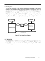
1. Introduction
Various types of Telecommunication end-equipment such as phones, answering
machines, line cards and modems are becoming more and more intelligent. This means
that most of the different elements or ICs contributing to the final functionality contain a
certain amount of processing power. There is therefore an urgent need for flexible
communication with other elements of the end-equipment to be able to manage and
control all the different features of the device. To provide an efficient solution, four of the
major European telephone equipment manufacturers jointly invented the IOM-Bus
specially adapted to the future needs of the ISDN telecommunication endequipment.(ISDN Oriented Modular Interface Revision 2)
This report shows how to interface the TMS320C54x DSP family to IOM-2 bus via the
standard and/or buffered serial port. It includes the schematics of the required logic
together with the software running on the DSP to read/write to/from different channels of
the bus. Additionally, the test setup using a SIEMENS ISDN transceiver PEB2186 in
IOM-2 loopback mode is described.
IOM-2 Interfacing on TMS320C54x
1
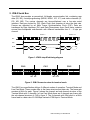
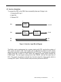
2. IOM-2 Serial Bus
The IOM-2 bus provides a symmetrical, full-duplex communication link, containing user
data (B1, B2), control/programming (MON0, MON1, IC0, IC1) and status channels (D,
CI0, MX, MR). The various channels are time-multiplexed over a four-wire serial
interface. Data are clocked by DCL (Data Clock) that operates at twice the data rate.
Frames are delimited by an 8kHz Frame Synchronization Clock (FSC). Data are
transferred by Data Upstream (DU) and Data Downstream lines. Each frame contains
several time-multiplexed sub-channels with different bandwidths from 2 - 8 byte per
channel.
Frame n
Frame n+1
DCL
FSC
DU/DI
bit 1
bit 1
bit 2
bit 2
Figure 1: IOM-2 simplified timing diagram
CH 0
B1
CH 1
B2 MON 0 D CI0
IC1
MR MX
CH 2
IC2 MON,1 CI 1
MR MX
Figure 2: IOM-2 frame structure for terminal mode
The IOM-2 bus specification defines 2 different modes of operation: Terminal Mode and
Line Card Mode. These modes differ in the frame structure and data rate. The frame rate
remains at 8kHz for each. Figure 2 shows the channel and sub-channel structure of the
Terminal Mode with 3 channels. In Line Card Mode there are 8 channels per frame with
the sub-channel structure of CH0 in figure 2. The 8 channels with 32bit each in a 8kHz
frame lead to a data rate of 2.048 Mbps instead of 768 kbps in Terminal Mode.
IOM-2 Interfacing on TMS320C54x
2
3. TMS320C54x Serial Port
The serial ports of the C54x DSP family are full duplex on-chip communication links
providing a direct communication with serial devices such as CODECs or serial ADCs.
There are three types of ports available: the Standard Serial Port (SSP), the TDM Serial
Port and the Buffered Serial Port (BSP).
3.1 Standard Serial Port
This port is a 6-wire, full-duplex, synchronous port with 3 signals for each direction :
clock (CLKX/R)
frame synch (FSX/R)
data (DX/R)
There are 2 synchronization schemes available:
Burst Mode
Continuous Mode
In Burst Mode a frame synch is required to transfer every data word. In Continuous Mode
only one frame synch at the beginning of the transfer is necessary to send and/or receive
data words continuously without re-synchronisation. The word length may be set to 8bit
or 16bit. Operations in both directions are double buffered, enabling a continuous
communication with a data rate equal to the clock rate regardless of whether the clock
signal and the frame synch signal are generated internally by the DSP or are supplied
from an external source.
CLKX/R
FSX/R
DX/R
bit 1
bit 2
bit 1
bit 2
Figure 3: Simplified SSP burst mode timing
3.2 Buffered Serial Port
The BSP is an extension of the SSP which allows the connection of the IO register of the
SSP to the internal memory of the DSP. By means of an Automatic Buffering Unit the
transmit or receive data are stored in a maximum of two circular buffers in the memory
without CPU intervention. This reduces the CPU load quite significantly.
IOM-2 Interfacing on TMS320C54x
3
internal
memory
ABU
rcv
buffer
SSP
xmt
buffer
Figure 4: Simplified BSP block diagram
3.3 TDM Port
The Time Division Multiplex Port is again a special extension to the SSP, establishing a
time-slot scheme on the serial bus to facilitate the communication between multiple
DSPs. There are 8 time-slots available, allowing the glueless connection of up to 8 DSPs
which can than communicate in a very flexible way, point-to-point or broadcast.
IOM-2 Interfacing on TMS320C54x
4
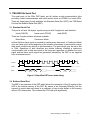
4. IOM-2 Interfacing
At first glance, the IOM-2 bus and the serial port timings seem to be very similar. Indeed,
there are only small differences. These concern frame synchronization and data clock
signal.
4.1 Serial Interface Characteristics
IOM-2:
The rising edge of the frame signal (FSC) occurs together with the first data bit
of every frame.
The FSC width is longer than one clock cycle
The data clock DCL is twice the frequency of the bit transfer rate
SSP:
The rising edge of the frame signal (FSX/R) occurs one clock cycle before the
first data bit of every transfer
The FSX/R width is one clock cycle
The clock rate CLKX/R is equal the frequency of the bit transfer rate
Frame n
Frame n+1
DCL
FSC
DU/DI
bit 1
bit 2
bit 1
bit 2
bit 1
bit 2
bit 1
bit 2
CLKX/R
FSX/R
DX/R
Figure 5: IOM-2 / C54x SSP timing
IOM-2 Interfacing on TMS320C54x
5
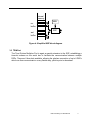
4.2 Interface Adaptation
To connect the SSP to the IOM-2 bus successfully there are 3 things to do:
1. Divide the DCL by 2.
2. Shift FSC
3. Shorten FSC
1
Clock
Divider
DCL
FSC
CLKX/R
2
3
Shifter:
- count
- compare
Pulse
Generator
FSX/R
DD
DR
DU
DX
Figure 6: Interface Logic Block Diagram
The Shifter can be implemented by a counter starting with FSC counting the number of
DCL cycles we want to shift. This number can be decoded by means of a PAL device
which then resets the counter after getting the next FSC pulse. To generate the required
FSX/R pulse with a width of 2 DCL cycles, two adjacent counter values activate the
FSX/R signal. The only signal missing now is the CLKX/R, with half the cycle time of
DCL. This signal can easily be derived from the first output bit of the counter which is
counting DCL cycles. The 8-bit counter must provide a synchronous RESET.
IOM-2 Interfacing on TMS320C54x
6
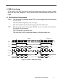
DCL
8 bit counter
SN74AS869
FSC
Qa - Qh
RESET
CLKX/R
FSX/R
PAL
22V10
DU
DD
DX
DR
Figure 7: Interface Logic Implementation
RESET = FSC & Qh & Qg
FSX/R = ( counter == (190 OR 191) )
To access all 12 TDM byte-wide sub-channels of the IOM-2 bus in Terminal Mode, the
FSX/R synch pulse has to be generated 12 times, activated by the corresponding timer
values (190-i*16 OR191-i*16, 0<i<12).
In this case, the use of the BSP would facilitate IOM-2 access quite dramatically. Instead
of providing 12 interrupts every frame transmit and receive buffers with the size of 12
words, each is served automatically by the ABU - generating only one interrupt per frame
to read and update the data inside the buffers. To access specific channels out of the 12,
you need only read/write from/to the corresponding memory location inside the buffers.
Running in Line Card Mode would increase the number of byte-wide sub-channels from
12 to 32 which practically forces the use of the BSP in order to avoid heavy DSP interrupt
loading. The timer values to create the 32 pulses, accessing all 32 sub-channels, are
derived by an equation similar to that used for the 12 sub-channels; just increasing the
range of i from 12 to 32 and adjusting the number of DCL cycles per frame to 510 due to
the higher data rate of 2.048 Mbps in the Line Card Mode. (510-i*16 OR511-i*16, 0<i<32)
The above interface logic implementation allows the realization of the aforementioned
functions. In addition, the DX-DU signal is put through the PAL device so that it may
control the output state of DU bitwise by means of a tri-state buffer. The state of DX can
only be changed byte by byte, using just the SSP which does not permit writing into TDM
channels smaller than one byte from more than one DSP without generating bus
conflicts.
IOM-2 Interfacing on TMS320C54x
7
IOM-2 bus
DSP 1
DSP 2
DX
DX
DSP n
DX
Figure 8: Bit Multiplexing
An additional latch in the FSX/R signal path avoids any glitches. This introduces one
waitstate. Therefore the equation for FSX/R must be changed to
FSX/R = ( counter == (189 OR 190) )
and
FSX/R = ( counter == (190-i*16 OR191-i*16, 0<i<12))
IOM-2 Interfacing on TMS320C54x
8
Frame n
Count
189 190
191 0
1
2
Frame n+1
190 191
192 0
1
2
DCL
Qa
RESET
Qh
~
~
~
~
FSC
bit 1
bit 2
~
~
DU/DI
bit 1
bit 2
FSX/R
Figure 9: Interface Logic Timing
To meet all timing requirements the falling edge of DCL triggers the counter.
IOM-2 Interfacing on TMS320C54x
9
5. Test System
To verify the functionality of the interface implementation described in the previous
chapter, a small hardware platform was built containing a TMS320C543 DSP, the
described logic elements and a SIEMENS ISDN Transceiver with IOM-2 interface. As
SIEMENS is the main user of this interface it was quite natural to take the PSB2186 as
the IOM-2 test device. The DSP generates a test pattern and sends it on a particular
IOM-2 channel running in Terminal Mode. The ISDN transceiver runs in loopback mode,
sending the same data back on the receive part of the serial port. By comparing input and
output data in the DSP we can verify that the interface operates correctly.
10.368MHz
7.68MHz
SSP
IOM-2
IF
IOM-2
PSB2186
TMS320C54x
Parallel Port
Figure 10: Test Setup Block Diagram
5.1 TMS320C543
The TMS320C543 is a RAM-based member of the ’C54x family with 10K words of on
chip RAM. This device has 2 serial ports, 1 TDM port and 1 BSP. The BSP will be used
for the IOM-2 connection in order to have the flexibility of selecting either SSP- or BSPmode for test purposes.
IOM-2 Interfacing on TMS320C54x
10
Memory
2 KW
Program
ROM
MAC
Peripherals
10 KW
Program
RAM
ALU
17*17 MPY
40 Bit ALU
40 Bit Adder
CMPS Operator
(Viterbi)
RND, SAT
Shifter
40 Bit Barrel
[-16, 31]
EXP Encoder
JTAG
TEST/EMU
Buffered Serial Port
TDM Serial Port
Timer
Accumulators
40 Bit ACC A
S/W Waitstate
Generator
40 Bit ACC B
Addressing Unit
PLL Clock
Generator
Software
Programmable
8 Auxilliary Registers
2 Addressing Units
Figure 11: TMS320C543 Block Diagram
5.2 ISDN Transceiver PSB2186
The PSB2186 implements a 4-wire S/T interface used to link voice/data terminals to
ISDN. This device switches B- and D- channels between the S/T side and the IOM
interface where other devices - such as a DSP to handle voice compression, modem
signals or answering machine functions - could be connected for further processing,. The
setup and control of the PSB2186 is performed by the DSP connected via the parallel
port to the microprocessor interface of the PSB2186. Simply by means of software this
allows a flexible access to all the functions and features of this ISDN device. The
microprocessor interface is configured for Motorola non-multiplexed bus type giving
glueless access to the DSP external bus.
5.3 Test Software
After power-up reset both the DSP and the PSB2186 devices have to be initialized
properly. The DSP has to set up the serial port to external clock and frame synch running
in burst mode.
SPC[MCM] = 0
SPC[FSM] = 1
SPC[FO] = 1
IOM-2 Interfacing on TMS320C54x
11
The PSB2186 is running in IOM-1 mode after reset and has to be switched to IOM-2
interface mode. In a second step, the ISAC-TE has to be set to test-looping of the IC1
channels. This allows the DSP to send data on a selected channel (IC1) and to read this
data for verification in the next frame.
ADF2[IMS] = 1
SPCR[TLP] = 1
SPCR[SPU] = 1
SPCR[C1C0] = 1
SPCR[C2C0] = 1
These registers can be modified by the DSP writing to the corresponding memory
addresses, mapped into the IO space of the DSP.
After initialization, the DSP just waits for interrupts from the serial port to receive and
send data to the ISAC-TE. The received data is then compared with the data sent one
frame before to check if the loopback-transfer works. By means of the BIO pin it is
possible to shut off the error check, making the startup procedure of the system easier.
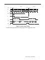
5.4 Results
The test verifies the functionality of the IOM-2 IF logic described and gives a good start
up example which can easily be adapted to a certain application. Simply by making small
modifications of the PAL equations, all kind of different IOM2- access schemes can be
achieved.
The figure below show the logic analyzer printout for the key signal of the test system.
IOM-2 Interfacing on TMS320C54x
12
Figure 12: Waveform Diagram
IOM-2 Interfacing on TMS320C54x
13
6. Summary
The interface logic described in this document demonstrates the feasibility of connecting
the TMS320C54x DSP to all channels of an IOM-2 bus. Using the BSP feature of the
DSP adds more flexibility concerning multiple channel access and reduces the interrupt
load of the processor. The IOM-2 protocols are not covered by this report because they
can be fully implemented by software alone.
The two devices added to the serial port of the TMS320C54x implement a quite flexible
interface. For a more cost effective solution it is also possible to include the 8-bit counter
in the 22V10 PAL.
IOM-2 Interfacing on TMS320C54x
14
References
References
1. ICs for Communications, IOM-2 Interface Reference Guide, Siemens AG 1991
2. TMS320C54x DSP Reference Set Volume 1-4, Texas Instruments,1996
3. ICs for Communications, ISDN Subscriber Access Controller for Terminals, ISACSTE, PSB2186, User’s Manual 10.94
IOM-2 Interfacing on TMS320C54x
15
Appendix A
Appendix A Schematic Diagrams
1
2
3
Vdd
4
5
6
Vdd
5V
2
U?A
J3
D
D8
1S1588
R6
22K
R13
470K
R8
22K
1
2
U?A
S5
SW SPDT
U28A
S2C
1
3
1
C24
0.1uF
4
U?A
1
DIP-SW3
S2A
6
DIP-SW3
SN74HC14
1
CLKOUT
SN74HC14_VDD
2
1
DIP-SW3
S2B
5
2
2
R12
100R
R7
22K
MSTRB
R/W
IOSTRB
IS
U1
SN74HC14_VDD
2
8
OUT
Vdd
2
Vdd
D16
1S1588
COM
R1
R2
R3
R4
R5
R6
R7
R8
R30
470K
BCLKX
BCLKR
BFSR
BFSX
BDR
BDX
RP7
R8-22K
S13
SW SPDT
D0
D1
D2
D3
D4
D5
D6
D7
2
3
5
6
8
9
11
12
D8
D9
D10
D11
D12
D13
D14
D15
13
14
16
17
19
20
22
23
Y1
Y2
Y3
Y4
Y5
Y6
Y7
Y8
68
67
66
51
52
53
Vdd
34
28
30
38
32
42
6
33
27
29
37
31
41
1
1
2
3
4
5
6
7
8
9
U31C
5
9
2
8
D19
1S1588
10
R36
470K
S16
SW SPDT
SN74HC08_VDD
1
U31F
13
R35
100R
12
Vdd Vdd
C35
0.1uF
SN74HC14
R3 R4
10K 10K
RS
CLKOUT
X2/CLKIN
X1
CLKMD1
CLKMD2
CLKMD3
IACK
INT0
INT1
INT2
INT3
NMI
READY
RS
HOLD
A[15..0]
HOLDA
XF
CNT
BIO
MP/MC
IAQ
TRST
EMU1/OFF
EMU0
TCK
TDO
TDI
TMS
A15
A14
A13
A12
A11
A10
A9
A8
A7
A6
A5
A4
A3
A2
A1
A0
7
6
5
4
3
2
100
99
98
97
96
95
94
93
92
91
J1
TDO
TCK
EMU0
1
3
5
7
9
11
13
2
4
6
8
10
12
14
Y1
Y2
Y3
Y4
Y5
Y6
Y7
Y8
25
24
G
DIR
36
35
33
32
30
29
27
26
A1
A2
A3
A4
A5
A6
A7
A8
IO_D8
IO_D9
IO_D10
IO_D11
IO_D12
IO_D13
IO_D14
IO_D15
SN74LVT16245
A3
A2
A1
A0
1
2
3
4
5
6
7
8
9
11
IS
MSTRB
IOSTRB
R/W
TRST*
D15
D14
D13
D12
D11
D10
D9
D8
D7
D6
D5
D4
D3
D2
D1
D0
TMS
TDI
55
19
14
15
13
16
18
17
86
85
84
83
82
81
80
79
78
77
75
74
73
72
71
70
Vdd
IO_D0
IO_D1
IO_D2
IO_D3
IO_D4
IO_D5
IO_D6
IO_D7
U7
TMS320LC543
B
47
46
44
43
41
40
38
37
A1
A2
A3
A4
A5
A6
A7
A8
RS_IN
TOUT
MSC
DS
IS
PS
R/W
IOSTRB
MSTRB
U29C
Vdd
43
45
46
47
48
44
12
69
23
21
20
54
24
25
22
60
57
56
61
58
59
62
TCLKX
TCLKR
TFSR
TFSX
TDR
TDX
SN74HC14
BCLKX
BCLKR
BFSR
BFSX
BDR
BDX
C32
0.1uF
D15
D14
D13
D12
D11
D10
D9
D8
D7
D6
D5
D4
D3
D2
D1
D0
R29
100R
48
1
G
DIR
SN74LVT16245
U?B
U2
C
A0
A1
A2
A3
U?A
OSCILLATOR
SN74HC14_VDD
EMU1
I0
I1
I2
I3
I4
I5
I6
I7
I8
I9
O0
I/O1
I/O2
I/O3
I/O4
I/O5
I/O6
O7
19
18
17
16
15
14
13
12
BCLKR
BCLKX
BDR
BDX
BFSR
BFSX
5V
TIBPAL16L8-5CN
HEADER 7X2
RS
A1
C1
A2
C2
A3
C3
A4
C4
A5
C5
A6
C6
A7
C7
A8
C8
A9
C9
A10
C10
A11
C11
A12
C12
A13
C13
A14
C14
A15
C15
A16
C16
A17
C17
A18
C18
A19
C19
A20
C20
A21
C21
A22
C22
A23
C23
A24
C24
A25
C25
A26
C26
A27
C27
A28
C28
A29
C29
A30
C30
A31
C31
A32
C32
D
C
B
64PINAC
A
A
Title
Size
IOM-2 Interface Reference Design
Number
Revision
1.0
B
Date:
File:
1
2
3
4
22-Sep-1997
C:\ADVSCH\IOM2\IOM2_C54.SCH
Sheet 1 of 2
Drawn By: Michael Seidl
5
6
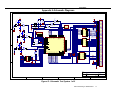
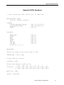
Figure 13: Schematic Test System 1 of 2
IOM-2 Interfacing on TMS320C54x
17
Appendix A
1
2
3
Vdd
4
5
6
Vdd
5V
2
U?A
J3
D
D8
1S1588
R6
22K
R13
470K
R8
22K
1
2
U?A
S5
SW SPDT
U28A
S2C
1
3
1
C24
0.1uF
4
U?A
1
DIP-SW3
S2A
6
DIP-SW3
SN74HC14
1
CLKOUT
SN74HC14_VDD
2
1
DIP-SW3
S2B
5
2
2
R12
100R
R7
22K
MSTRB
R/W
IOSTRB
IS
U1
SN74HC14_VDD
2
8
OUT
Vdd
D0
D1
D2
D3
D4
D5
D6
D7
2
Vdd
COM
R1
R2
R3
R4
R5
R6
R7
R8
R30
470K
BCLKX
BCLKR
BFSR
BFSX
BDR
BDX
RP7
R8-22K
D16
1S1588
S13
SW SPDT
2
3
5
6
8
9
11
12
Y1
Y2
Y3
Y4
Y5
Y6
Y7
Y8
68
67
66
51
52
53
Vdd
34
28
30
38
32
42
6
33
27
29
37
31
41
1
1
2
3
4
5
6
7
8
9
U31C
5
9
2
8
D19
1S1588
10
R36
470K
S16
SW SPDT
SN74HC08_VDD
1
U31F
13
R35
100R
12
Vdd Vdd
C35
0.1uF
SN74HC14
R3 R4
10K 10K
RS
CLKOUT
X2/CLKIN
X1
CLKMD1
CLKMD2
CLKMD3
IACK
INT0
INT1
INT2
INT3
NMI
READY
RS
HOLD
A[15..0]
HOLDA
XF
CNT
BIO
MP/MC
IAQ
TRST
EMU1/OFF
EMU0
TCK
TDO
TDI
TMS
A15
A14
A13
A12
A11
A10
A9
A8
A7
A6
A5
A4
A3
A2
A1
A0
7
6
5
4
3
2
100
99
98
97
96
95
94
93
92
91
J1
TDO
TCK
EMU0
1
3
5
7
9
11
13
2
4
6
8
10
12
14
TRST*
D15
D14
D13
D12
D11
D10
D9
D8
D7
D6
D5
D4
D3
D2
D1
D0
TMS
TDI
55
19
14
15
13
16
18
17
86
85
84
83
82
81
80
79
78
77
75
74
73
72
71
70
Vdd
IO_D0
IO_D1
IO_D2
IO_D3
IO_D4
IO_D5
IO_D6
IO_D7
D8
D9
D10
D11
D12
D13
D14
D15
13
14
16
17
19
20
22
23
Y1
Y2
Y3
Y4
Y5
Y6
Y7
Y8
25
24
G
DIR
36
35
33
32
30
29
27
26
A1
A2
A3
A4
A5
A6
A7
A8
IO_D8
IO_D9
IO_D10
IO_D11
IO_D12
IO_D13
IO_D14
IO_D15
SN74LVT16245
A3
A2
A1
A0
U7
TMS320LC543
B
47
46
44
43
41
40
38
37
A1
A2
A3
A4
A5
A6
A7
A8
RS_IN
TOUT
MSC
DS
IS
PS
R/W
IOSTRB
MSTRB
U29C
Vdd
43
45
46
47
48
44
12
69
23
21
20
54
24
25
22
60
57
56
61
58
59
62
TCLKX
TCLKR
TFSR
TFSX
TDR
TDX
SN74HC14
BCLKX
BCLKR
BFSR
BFSX
BDR
BDX
C32
0.1uF
D15
D14
D13
D12
D11
D10
D9
D8
D7
D6
D5
D4
D3
D2
D1
D0
R29
100R
48
1
G
DIR
SN74LVT16245
U?B
U2
C
A0
A1
A2
A3
U?A
OSCILLATOR
SN74HC14_VDD
EMU1
IS
MSTRB
IOSTRB
R/W
1
2
3
4
5
6
7
8
9
11
I0
I1
I2
I3
I4
I5
I6
I7
I8
I9
O0
I/O1
I/O2
I/O3
I/O4
I/O5
I/O6
O7
19
18
17
16
15
14
13
12
BCLKR
BCLKX
BDR
BDX
BFSR
BFSX
5V
TIBPAL16L8-5CN
HEADER 7X2
RS
A1
C1
A2
C2
A3
C3
A4
C4
A5
C5
A6
C6
A7
C7
A8
C8
A9
C9
A10
C10
A11
C11
A12
C12
A13
C13
A14
C14
A15
C15
A16
C16
A17
C17
A18
C18
A19
C19
A20
C20
A21
C21
A22
C22
A23
C23
A24
C24
A25
C25
A26
C26
A27
C27
A28
C28
A29
C29
A30
C30
A31
C31
A32
C32
D
C
B
64PINAC
A
A
Title
Size
IOM-2 Interface Reference Design
Number
Revision
1.0
B
Date:
File:
1
2
3
4
5
22-Sep-1997
C:\ADVSCH\IOM2\IOM2_C54.SCH
Sheet 1 of 2
Drawn By: Michael Seidl
6
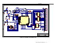
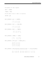
Figure 14: Schematic Test System 2 of 2
IOM-2 Interfacing on TMS320C54x
18
Appendix B PAL Equations
Appendix B PAL Equations
" logic connecting c54x’ serial port to IOM-2 bus
MODULE module_name
iom2_ic1 DEVICE ’p22v10’;
"INPUTS
CLK,DCL,QA,QB,QC,QD,QE
QF,QG,QH,FSC1,BDX
IOMDR
PIN 1,2,3,4,5,6,7;
PIN 8,9,10,11,13;
PIN 14;
"OUTPUTS
RESET_CNT
BCLKX
BDR
IOMDX
BFSX
FSX_INT
CLK_CNT
X,C,Z=.X.,.C.,.Z.;
PIN
PIN
PIN
PIN
PIN
PIN
PIN
23;
22;
21;
20;
19;
18;
17;
EQUATIONS
"Reset of counter with rising edge of FSC1
!RESET_CNT = FSC1 & QH;
"invert CLK for counter
!CLK_CNT = DCL;
"Frame sync pulse @ 61,62
"
128
64
!FSX_INT =
(!QH & !QG &
# (!QH & !QG &
on IC1
32
16
8
4
2
1
QF & QE & QD & QC & QB & !QA)
QF & QE & QD & QC & !QB & QA);
BFSX.clk = CLK;
!BFSX := FSX_INT;
IOM-2 Interfacing on TMS320C54x
19
Appendix B PAL Equations
"bitenable for data signals
!BDR = !IOMDR;
!IOMDX = !BDX;
"serial data clock to c54x = A inverted
!BCLKX = QA;
TEST_VECTORS ([QA] -> [BCLKX])
[ 0 ] -> [ 1 ];
[ 1 ] -> [ 0 ];
TEST_VECTORS ([DCL] -> [CLK_CNT])
[ 0 ] -> [ 1 ];
[ 1 ] -> [ 0 ];
TEST_VECTORS ([BDX] -> [IOMDX])
[ 0 ] -> [ 0 ];
[ 1 ] -> [ 1 ];
TEST_VECTORS ([IOMDR] -> [BDR])
[ 0 ]
[ 1 ]
-> [ 0 ];
-> [ 1 ];
TEST_VECTORS ([FSC1,QH] -> [RESET_CNT])
[0,
[0,
[1,
[1,
0]
1]
0]
1]
->
->
->
->
[1
[1
[1
[0
];
];
];
];
TEST_VECTORS ([CLK,QA,QB,QC,QD,QE,QF,QG,QH] -> [FSX_INT,BFSX])
[C,
[C,
0, 0, 0,
0, 0, 1,
0, 0, 0, 0, 0] -> [ 1 , 0 ];
0, 0, 0, 0, 0] -> [ 1 , 0 ];
IOM-2 Interfacing on TMS320C54x
20
Appendix B PAL Equations
[C,
[C,
[C,
[C,
[C,
[C,
[C,
[C,
1,
1,
0,
0,
0,
1,
0,
1,
0,
0,
1,
1,
1,
0,
1,
0,
0,
0,
0,
1,
1,
1,
1,
1,
0,
1,
1,
1,
1,
1,
1,
1,
0,
0,
0,
1,
1,
1,
1,
1,
0,
0,
1,
1,
1,
1,
1,
1,
1,
0,
0,
1,
0,
0,
0,
0,
0]
0]
1]
1]
1]
1]
0]
0]
->
->
->
->
->
->
->
->
[
[
[
[
[
[
[
[
1
1
1
1
1
1
0
0
,
,
,
,
,
,
,
,
0
0
0
0
0
0
1
1
];
];
];
];
];
];
];
];
END module_name
IOM-2 Interfacing on TMS320C54x
21
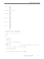
Appendix C System Test Software
Appendix C System Test Software
;/*
FILENAME:
iom2test.asm
*/
;/* -----------------------------------------------------------*/
;/*
TITLE:
TMS320C543 IOM-2 Interface Test SW
*/
;/*
*/
;/*
PURPOSE:
This code writes and reads data
*/
;/*
via the serial port of the DSP to/from the*/
;/*
ISAC TE chip to test the IOM-2 IF logic
*/
;/*
inbetween those devices
*/
;/*
*/
;/*------------------------------------------------------------*/
;/*
DATE:
09/30/97
*/
;/*
REV.:
1.0
*/
;/*
AUTHOR:
Markus Tremmel
*/
;/* -----------------------------------------------------------*/
.version 543
.mmregs
.global start
;------------------------; Interrupt Vector Table
;------------------------.sect "vectors"
reset:
B
start
NOP
NOP
nmi:
RETE
NOP
NOP
NOP
.space 14*4*16 ; software interrupts
int0:
RETE
NOP
NOP
NOP
int1:
RETE
NOP
NOP
NOP
int2:
RETE
NOP
NOP
NOP
IOM-2 Interfacing on TMS320C54x
22
Appendix C System Test Software
tint:
brint0:
bxint0:
trint:
txint:
int3:
RETE
NOP
NOP
NOP
B rcvxmt_int
NOP
NOP
RETE
NOP
NOP
NOP
RETE
NOP
NOP
NOP
RETE
NOP
NOP
NOP
RETE
NOP
NOP
NOP
;----------------------------; IOM-2 Test SW for TMS320C54x
;----------------------------.text
start:
;---------; DSP init
;---------; disable interrupts globally
SSBX
SSBX
INTM
XF
; set XF flag connected to A4 of ISAC
; set OVLY =1, MP/MC = 1, IPTR = 0x0080
STM
#0x00e0, PMST
; setup interrupt register
enable BRINT
IOM-2 Interfacing on TMS320C54x
23
Appendix C System Test Software
STM
#0x010, IMR
; enable receive interrupt
; clear accu B
LD
#0,A
LD
#0,B
STM #0x0,DXR
STM #0,AR0
STM #0,AR1
STM #0,AR2
STM #0,AR3
;-------------------------; Standard Serial Port Init
;-------------------------; set burst mode FSM = 1, ext.clk MCM = 0 and frame TXM = 0,
; 8bit mode FO = 1
STM
#0x8008, SPC
; clear pending interrrupts
STM
#0xffff, IFR
; bring SSP out of reset
; STM
#0x80c8, SPC
;--------------------; initialize ISAC-S TE
; -------------------SPCR_VAL1
SPCR_VAL2
ADF2_VAL
SPCR_MEM
ADF2_MEM
SPCR_REC
ADF2_REC
.set
.set
.set
0x85
0x05
0x88
.usect
.usect
.usect
.usect
; loopback mode enabled/IC1 looping
; loopback mode enabled/IC1 looping
; IOM-2 mode and tristate drivers
"isac", 1
"isac", 1
"isac", 1
"isac", 1
; set ISAC-S TE ADF2 reg. in IOM-2 mode
ST
#ADF2_VAL,ADF2_MEM
PORTW ADF2_MEM, 0x8039
NOP
; wait
NOP
NOP
IOM-2 Interfacing on TMS320C54x
24
Appendix C System Test Software
NOP
; set ISAC-S TE SPCR in testmode
ST
#SPCR_VAL1,SPCR_MEM
PORTW SPCR_MEM, 0x8030
NOP
NOP
NOP
NOP
with soft power up
; wait
;set ISAC-S TE SPCR in testmode without soft power up
ST
#SPCR_VAL2,SPCR_MEM
PORTW SPCR_MEM, 0x8030
NOP
NOP
NOP
NOP
PORTR 0x8039, SPCR_REC
; wait
; read registers of ISAC-S TE
;for verification
NOP
NOP
NOP
NOP
PORTR 0x8030, ADF2_REC
NOP
NOP
NOP
NOP
; enable interrupts globally
STM
#0x80c8, SPC
RSBX INTM
; idle, just wait for the rcvxmt interrupt
wait: NOP
NOP
NOP
B wait
IOM-2 Interfacing on TMS320C54x
25
Appendix C System Test Software
;----------------------------; receive and transmit interrupt
; service routine
;----------------------------rcvxmt_int:
OVFL:
OK:
LD
BC
LD
ADD
STLM
DRR,A
OVFL, ANEQ
AR3, B
#1, B
B, AR3
SUB
ADD
AND
BC
BC
LD
ADD
STLM
NOP
LD
ADD
STLM
STLM
AR1, A ; compare received and sent
#1, A
; new received must be equal previous sent
#0xffff,A
OK, AEQ
; branch if equal
OK, NBIO
; ignore error if BIO = high
AR2, B
; or increment error counter
#1, B
B, AR2
STM
NOP
NOP
NOP
RETE
AR1, A
#1, A
A, DXR
A, AR1
#0xffff, IFR
; read input data
; count in AR3 each counter overflow
; increment overflow counter
;
;
;
;
reload previous sent
increment value to be sent
write output data
keep sent value in AR1
; clear pending interrrupts
.end
IOM-2 Interfacing on TMS320C54x
26
Appendix C System Test Software
IOM-2 Interfacing on TMS320C54x
27
Appendix C Glossary
Appendix C Glossary
SSP:
Standard Serial Port
BSP:
Buffered Serial Port
TDM:
Time Division Multiplex
ABU:
Automatic Buffering Unit
IO:
Input Output
CODEC:
Coder Decoder
IOM-2 Interfacing on TMS320C54x
28