1
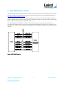
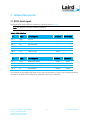
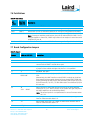
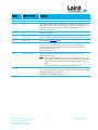
Laird Audio Development Kit (ADK) User Manual Part # DVK-BTM511 Applicable to the following Bluetooth module part numbers: BTM511 – Revision 07 and later Americas: +1-800-492-2320 Option 3 Europe: +44-1628-858-940 Hong Kong: +852-2923-0610 www.lairdtech.com/wireless CONTENTS Laird Audio Development Kit (ADK) .......................................................................................................... 3 1. Overview .............................................................................................................................................. 3 Introduction ..............................................................................................................................................................3 Package Contents......................................................................................................................................................3 2. ADK – Main Development Board ....................................................................................................... 4 3. Getting to know the Development Board ........................................................................................ 4 4. Power Supply ....................................................................................................................................... 5 5. USB - RS232 Serial Interface ............................................................................................................... 6 6. Software .............................................................................................................................................. 7 7. Interface Specification ........................................................................................................................ 8 7.1 RS232 Serial signals ......................................................................................................................................8 7.2 PCM / I2S ......................................................................................................................................................9 7.3 Differential input – J12 on ADK, labeled DIFF_IN .........................................................................................9 7.4 SPI Interface - J16 on ADK, labeled SPI ...............................................................................................................9 7.5 Audio Connectors – Labeled LINE_In, MIC_IN and STEREO_OUT .......................................................................9 7.6 Push Buttons .....................................................................................................................................................10 7.7 Board Configuration Jumpers ....................................................................................................................10 7.8 SW - Switches ....................................................................................................................................................12 8. 9. Other Features................................................................................................................................... 12 8.1 Power Consumption Measurement ...........................................................................................................12 8.2 USB Access .................................................................................................................................................12 Additional Documentation .............................................................................................................. 13 Americas: +1-800-492-2320 Option 3 Europe: +44-1628-858-940 Hong Kong: +852-2923-0610 www.lairdtech.com/wireless 2 Laird Technologies LAIRD AUDIO DEVELOPMENT KIT (ADK) Part # DVK-BTM511 Applicable to the following Bluetooth module part numbers: BTM511 Revision -07 onwards 1. OVERVIEW Laird’s Audio Development Kit (ADK) provides a platform for rapid wireless connectivity prototyping, providing multiple options for the development of Bluetooth stereo and mono audio applications. This manual is for Rev. 01 of the development PCB and relates to BTM511 DVK-V04 on the PCB itself. The complete functionality of the ADK hardware requires the use of Laird BTM511 firmware revision -07 (firmware v18.1.3.0) or greater. Introduction The Laird ADK is designed to support the rapid development of applications and software for the specific Laird Bluetooth module part number BTM511. More information regarding this product including a detailed module User’s Manual is available from the following link: http://www.lairdtech.com/Products/Wireless-M2M-and-Telematics-Solutions/Bluetooth-Module/ Package Contents All kits contain the following items: Development Board The motherboard has the BTM511 module already soldered onto it and exposes all the various hardware interfaces available. USB cable – Type A to Type B The USB cable is one option for providing power for the ADK via the on-board connector. The cable also provides serial communications via a FTDI USB – RS232 converter chip. 3.5mm Audio cable The audio cable is one option for connecting one of the Line in / MIC / Speaker ports to an external media device with 3.5mm audio jack socket. Web link Card Provides links to additional information including the BTM511 User Manual, terminal utilities, schematics, quick start guides and firmware release notes. Americas: +1-800-492-2320 Option 3 Europe: +44-1628-858-940 Hong Kong: +852-2923-0610 www.lairdtech.com/wireless 3 Laird Technologies 2. ADK – MAIN DEVELOPMENT BOARD The development board allows the Laird Bluetooth module to connect to a PC. The development board provides USB-to-Virtual COM port conversion through a FTDI chip. Any Windows PC (XP or later) auto-installs the necessary drivers; if your PC cannot locate the drivers, you can download them from http://www.ftdichip.com/FTDrivers.htm 3. GETTING TO KNOW THE DEVELOPMENT BOARD SW 7 – Left Channel Input SW8 – Right Channel Input RS232 Differential Input USB Line Input MIC Input DC Jack Speaker Figure 1: Main ADK Board Reset Americas: +1-800-492-2320 Option 3 Europe: +44-1628-858-940 Hong Kong: +852-2923-0610 www.lairdtech.com/wireless PCM/I2S 4 SPI Laird Technologies 4. POWER SUPPLY Input Voltage Minimum Typical Maximum 4.5 V 5V 5.5 V The development board has two options for providing power to the module: 5V power from a USB port Power from an external mains power block via a 2.0 mm DC connector The developer kit includes a USB cable to provide power to the development board. It should be plugged into a PC USB port, a USB hub, or a mains adaptor with a USB output. If a hub is used, it should be a powered USB hub to ensure that sufficient current is available at the port being used. The BTM511 module can be driven by the current available at a standard USB port. Switch SW1 is used to select between USB or DC jack power source. Figure 2: SW1 Settings SW1 (slide switch) provides the selection of input power for BTM511 module from USB or DC jack. The power for the U3 (FT232R) is always powered by the USB bus. SW2 (push button TACT switch) provides a reset signal to the BTM511 module. Americas: +1-800-492-2320 Option 3 Europe: +44-1628-858-940 Hong Kong: +852-2923-0610 www.lairdtech.com/wireless 5 Laird Technologies 5. USB - RS232 SERIAL INTERFACE The ADK provides USB-to-Virtual COM port conversion through a FTDI chip and any Windows PC (XP or later) will auto install the necessary drivers and if your PC cannot locate the drivers, you can download them from http://www.ftdichip.com/FTDrivers.htm The development board contains a USB to UART interface on the RX, TX, CTS, RTS, DTR, DSR, RI, and DCD signals. In default setting, the FTDI is on by having the J8 open (no jumper), so providing a USB to virtual COM port for evaluation through standard USB cable. See Figure 3. The UART interface on the BTM511 module can be driven from external microcontroller instead of the on-board FTDI FT232R chip (U3), if the DVK is powered from DC jack and SW1 (Figure 2) is in position ‘DC’. At a minimum, RX, TX, RTS, and CTS need to be connected (J15) for this use case. Modem control lines (J19) are optional. Figure 3: USB to UART Interface Americas: +1-800-492-2320 Option 3 Europe: +44-1628-858-940 Hong Kong: +852-2923-0610 www.lairdtech.com/wireless 6 Laird Technologies 6. SOFTWARE The development board connects the BTM511 module to a virtual COM port of a PC or other device. From a PC, you can communicate with the module using any Terminal Emulator software, such as HyperTerminal, Procomm, or the supplied EZURiO / Laird Terminal application. EZURiO / Laird Terminal is a terminal emulation application capable of running on Windows 98, Me, 2000, XP, Windows 7 and Windows 8 operating systems. It was developed specifically to aid development and testing of Laird modules. It allows connection to serial devices using any combination of the communications parameters listed in Table 1. Table 1: Communication Parameters COM Port: 1 to 255 Baud rate: 300 to 921600 Parity: None, Odd, Even Data Bits: 7 or 8 Stop Bits: 1 or 2 Handshaking: None or CTS/RTS The benefits of using EZURiO / Laird Terminal include: Continually displayed status of DSR, CTS, DCD, and RI Direct control of DTR on the host PC via a check box Direct control of RTS Sending of BREAK signals Scripts can be run to assist Additional built-in features accelerate development Laird includes a “Data Transfer Test” mode allowing data to be sent as fast as the handshaking permits. This feature is useful for testing the bit transfer rate of a Bluetooth connection. The EZURiO / Laird Terminal application can be downloaded from our website: http://www.lairdtech.com/Products/Wireless-M2M-and-Telematics-Solutions/Bluetooth-Module/ Americas: +1-800-492-2320 Option 3 Europe: +44-1628-858-940 Hong Kong: +852-2923-0610 www.lairdtech.com/wireless 7 Laird Technologies 7. INTERFACE SPECIFICATION 7.1 RS232 Serial signals The digital RS232 Serial signals are contained in J15/J19 as shown in Table 2. Note: The direction is from the module’s perspective. Table 2: RS232 Definitions J15 Signal J15 Description Direction Shared with Pin-1 GND Ground - - Pin-2 RTS Request To Send Output - Pin-3 NC No Connection - - Pin-4 RXD Receive Data Input - Pin-5 TXD Transmit Data Output - Pin-6 CTS Clear To Send Input - J19 Signal J19 Description Pin-1 DCD Data Carrier Detect Output GPIO2 Pin-2 DTR Data Terminal Ready Output GPIO8 Pin-3 DSR Data Set Ready Input GPIO3 Pin-4 RI Ring Indicator Output GPIO4 Direction Shared with The format of the holes allows the fitting of your choice of connectors, or can be used for directly soldering test wires to the board. Pins are laid out on a standard 2.54 mm (0.1 inch) pitch. Americas: +1-800-492-2320 Option 3 Europe: +44-1628-858-940 Hong Kong: +852-2923-0610 www.lairdtech.com/wireless 8 Laird Technologies 7.2 PCM / I2S The development board provides for a PCM / I2S interface for the BTM511. The pins provide the developer with access to the module’s I2S or PCM lines, as well as providing power for additional audio hardware to be developed. I2S signals are mapped to the PCM pins of BTM51x as outlined in this table: Table 3: BTM51x pins and I2S Signals I2S Signal Name BTM51x Signal Name BTM51x Module Pin Number ADK Header (J18) Comment SD_IN PCM_IN 3 5 I2S Serial data in SD_OUT PCM_OUT 4 7 I2S Serial data out WS PCM_SYNC 5 6 I2S Word select (right/left ch) SCK PCM_CLK 6 4 I2S clock GND1/2/3/4 [9,22,13,47] 10 GND Note: For backward compatibility reasons, remaining pins of J18 are connected to signals that are not directly related to PCM/I2S functions. 7.3 Differential input – J12 on ADK, labeled DIFF_IN If the audio input should be driven by a differential audio source rather than a single-ended signal, J12 allows connecting non-inverted (‘P’) and inverted (‘N’) signal of the source to BTM511, as well as AGND (analogue GND) for left and for right channel. In addition, SW7 and SW8 must be set to middle position “DIFF”. Differential signals provide better audio quality due to better noise immunity. 7.4 SPI Interface - J16 on ADK, labeled SPI This interface is only utilized for Laird’s internal use and production testing. We do not recommend that the OEM use these pins. Note: J14, J13 (labelled SPI/VCC) and J4 are similarly only used for Laird internal use in manufacturing test. 7.5 Audio Connectors – Labeled LINE_In, MIC_IN and STEREO_OUT These 3.5 mm audio connectors on the right side of the ADK allow OEMs to connect standard speakers, microphones and headphones. Americas: +1-800-492-2320 Option 3 Europe: +44-1628-858-940 Hong Kong: +852-2923-0610 www.lairdtech.com/wireless 9 Laird Technologies 7.6 Push Buttons Table 4: Push buttons Push Button Label on ADK PCB Description SW2 RESET Button to reset the BTM511 module SW3 GPIO 5 Push button for use of associated GPIO line for a range of configurable functionality SW4 GPIO 1 Push button for use of associated GPIO line for a range of configurable functionality SW5 GPIO 7 Push button for use of associated GPIO line for a range of configurable functionality Note: Contrary to remaining push buttons, the pull-up resistor (R29) for GPIO 7 is not fitted per default. In future use, GPIO7 may function as an output to control the audio amplifier (U7), see J9. SW6 GPIO 6 Push button for use of associated GPIO line for a range of configurable functionality 7.7 Board Configuration Jumpers Table 5: Jumpers Jumper Label on ADK PCB Description J1 – J3 N/A Unused on the development board. J4 J4 INTERNAL USE ONLY. J5 J5 Provides provide voltage drop on 3.3 V across 0.25 ohm to measure the current for the BTM511 module when open. J6 J6 Place a jumper on the middle and left side pins for 3.3 V operation. Place a jumper on the middle and right side pins for 1.8 V operation. J7 J7 INTERNAL USE ONLY. J8 J8 RS232-OFF Default state is J8 open (no jumper) for use with USB power and on board FTDI. Alternatively, the UART interface on the BTM511 module can be driven from external microcontroller instead of the on-board FTDI FT232R chip (U3) by powering the DVK via DC jack and setting SW1 (Figure 2) to ‘DC’. At a minimum RX, TX, RTS, CTS and GND need to be connected (J15) for this use case. J9 J9 3.3V Place a jumper on the middle and left side pins to set audio amplifier enabled pin to 3.3 V. Place a jumper on the middle and right side pins to set audio amplifier to be controlled by GPIO-7. Note: This second option is not implemented in current firmware version 18.1.3.0. GPIO7 J10 J10 Place jumper across J10 / J11 (closed) to select audio amplifier gain as listed on silkscreen table below J11. J11 J11 Place jumper across J10 / J11 (closed) to select audio amplifier gain as listed on silkscreen table below J11. J12 DIFF_IN Differential stereo audio input. Americas: +1-800-492-2320 Option 3 Europe: +44-1628-858-940 Hong Kong: +852-2923-0610 www.lairdtech.com/wireless 10 Laird Technologies Jumper Label on ADK PCB Description J13 J13 INTERNAL USE ONLY. J14 N/A INTERNAL USE ONLY. J15 J15 Through hole plated UART interface for use when direct access to the UART pins from an external microcontroller. UART pins supported on J15 are GND, RTS, NC, RXD, TXD, CTS. Additional UART lines on J19. Please see notes on J8. J16 SPI INTERNAL USE ONLY. J17 J17 3V3 Place a jumper on left hand side and middle pins to set VDDIO to 3.3 V. Place a jumper on middle and right hand side pins to set VDDIO to 1.8 V. 1V8 J18 PCM / I2S Please see the PCM / I2S section. J19 J19 Through hole plated UART interface (modem control lines) for use when direct access to the UART pins from an external microcontroller is required. UART pins supported on J19 are DCD, DTR, DSR and RI. Additional UART lines on J15. Please see notes on J8. J20 USB_D+ J21 J21 USB_D- Americas: +1-800-492-2320 Option 3 Europe: +44-1628-858-940 Hong Kong: +852-2923-0610 www.lairdtech.com/wireless USB access can be provided to allow a direct USB connection to a Bluetooth HCI module. Note: If this is done and the unit is connected to a USB host port, it will be powered from that same port. Do not attempt to use any other power source for the development kit when operating in this mode. This is not relevant for modules with a UART interface. Do not close J21 by placing a jumper. J21 is not fitted by default to prevent a short circuit caused by accidentally closing the headers with a jumper. Full details are available in Section 8.1 11 Laird Technologies 7.8 SW - Switches Switch Label on ADK PCB Description SW1 DC Switch to select power input from DC jack or USB connector. SW7 - Left SW 8 - Right LINE DIFF MIC USB Control the input source from Line input /Differential input /MIC input. SW7/SW8 should be placed at the same position for each input setting. For example, if you require Line Input then both SW7 and SW8 need to be placed in the TOP position. 8. OTHER FEATURES 8.1 Power Consumption Measurement J21, pin 2 provides the output voltage of current sensing amplifier U17 (INA216A4). Current is measured by voltage drop over the parallel resistors R64, R65 (0.51 Ohm each). R64 and R65 can be seen as one 0.255 Ohm resistor. With the gain of U17, which is 200, the following formula results: I = ((voltage_J21 / 200) / 0.255) A Or simplified: I = (voltage_J21 / 51) A _________________________________________________________________________________________ Note 1 : The parameters of this DVK are optimised for measuring average low currents. If the intention is to measure current patterns (e.g. for sniff mode investigation, higher currents), the bandwidth of this design (response to fast changing currents) is insufficient. In that case, a current-sensing amplifier with less gain but higher bandwidth should be utilised (see INA216A data sheet). J5 allows to do this externally. Note 2: This only measures the current consumption of the module, and not of the level shifter or other peripheral circuitry. 8.2 USB Access USB access can be provided to allow a direct USB connection to a Bluetooth HCI module. To enable this operation, close J8 by placing a jumper on the pins. If this is done and the unit is connected to a USB host port, it will be powered from that same port. Do not attempt to use any other power source for the development kit when operating in this mode. Note: This is not relevant for modules with a UART interface. Americas: +1-800-492-2320 Option 3 Europe: +44-1628-858-940 Hong Kong: +852-2923-0610 www.lairdtech.com/wireless 12 Laird Technologies 9. ADDITIONAL DOCUMENTATION Laird offers a variety of documentation and ancillary information to support our customers through the initial evaluation process and ultimately into mass production. Additional documentation includes: BTM511 – Class 2 Audio Multimedia Module – Datasheet BTM510 / 511 – User Manual Firmware Release Notes – BTM510 / 511 to v18.1.x.x ADK – Audio Development Kit - Schematics BTM511 – ADK – Quick Start Guide – A2DP & AVRCP BTM511 – ADK – Quick Start Guide – HFP BTM511 – ADK – Quick Start Guide – SPP For any additional question or queries or to receive local technical support for the ADK or BTM511 module, please contact [email protected]. APN_06008_1_v2_ADK Copyright © 2012 Laird Technologies, Inc. All rights reserved. The information contained in this manual and the accompanying software programs are copyrighted and all rights are reserved by Laird Technologies, Inc. Laird Technologies, Inc. reserves the right to make periodic modifications of this product without obligation to notify any person or entity of such revision. Copying, duplicating, selling, or otherwise distributing any part of this product or accompanying documentation/software without the prior consent of an authorized representative of Laird Technologies, Inc. is strictly prohibited. All brands and product names in this publication are registered trademarks or trademarks of their respective holders. This material is preliminary Information furnished by Laird Technologies in this specification is believed to be accurate. Devices sold by Laird Technologies are covered by the warranty and patent indemnification provisions appearing in its Terms of Sale only. Laird Technologies makes no warranty, express, statutory, and implied or by description, regarding the information set forth herein. Laird Technologies reserves the right to change specifications at any time and without notice. Laird Technologies’ products are intended for use in normal commercial and industrial applications. Applications requiring unusual environmental requirements such as military, medical life-support or life-sustaining equipment are specifically not recommended without additional testing for such application. Limited Warranty, Disclaimer, Limitation of Liability Americas: +1-800-492-2320 Option 3 Europe: +44-1628-858-940 Hong Kong: +852-2923-0610 www.lairdtech.com/wireless 13 Laird Technologies Bluetooth® Audio Modules BTM510/511 Innovative Technology for a Connected World The BTM510 and BTM 511 are low-power Bluetooth® modules designed for adding robust audio and voice capabilities. Based on the market-leading Cambridge Silicon Radio BC05 chipset, these modules provide exceptionally low power consumption with outstanding range. Supporting the latest Bluetooth Version 2.1+EDR specification, these modules provide the important advantage of secure simple pairing that improves security and enhances easy use. At only 14mm x 20mm for the BTM510 and 14mm x 25mm for the BTM511, the compact size of the modules makes them ideal for battery-powered or headset form factor audio and voice devices. With a 16-bit stereo codec and microphone inputs to support both stereo and mono applications, these modules also contain a full, integrated Bluetooth-qualified stack along with SPP, HFP 1.5, HSP, AVRCP, and A2DP profiles. (Customers using these modules may list and promote their products free of charge on the Bluetooth website.) The BTM510/511 modules include an embedded 32-bit, 64-MIPS DSP core within the BC05. This allows designers to add significant product enhancements including features such as echo cancellation, noise reduction, and audio enhancement using additional soft codecs. The availability of the 16MB of flash memory in the module allows complex functionality to be included. DSP routines can be licensed through a number of specialist partners. To speed product development and integration, Laird Technologies has developed a comprehensive AT command interface that simplifies application development, including support for audio and headset functionality. Combined with a low-cost development kit, Laird Technologies’ Bluetooth modules provide faster time to market. FEATURES • Fully featured Bluetooth multimedia chipset • Bluetooth v2.1+EDR • Supports mono and stereo headset applications • Adaptive frequency hopping to cope with interference from other wireless devices • 32bit Kalimba DSP for enhanced audio applications • Support for secure simple pairing • External or internal antenna options • HSP, HFP, A2DP, and AVRCP audio profiles • 16-bit stereo codec and microphone input • Integrated audio amplifiers for driving stereo speaker global solutions: local support USA: +1.800.492.2320 Europe: +44.1628.858.940 Asia: +852.2268.6567 [email protected] www.lairdtech.com/wireless TM • Comprehensive AT interface for simple programming • Bluetooth End product qualified • Compact size • Class 2 output – 4dBm • Low power operation • Wi-Fi co-existence hardware support APPLICATION AREAS • High-quality stereo headsets • Mono voice headsets • Hands-free devices • Wireless audio cable replacement • MP3 and music players • Phone accessories • VoIP products • Cordless headsets • Aftermarket automotive applications Bluetooth® Audio Modules BTM510/511 Innovative Technology for a Connected World CATEGORIES FEATURE IMPLEMENTATION Wireless Specification Bluetooth® Version 2.1+EDR Frequency 2.402 – 2.480 GHz Max Transmit Power Class 2 4dBm (at antenna pad – BTM510) 4dBmi (from integrated antenna – BTM511) Receive Sensitivity Better than -86dBm Range 30 meters Data Rates Up to 3Mbps (over the air) UART Data Transfer Rate Greater than 300 Kbps Host Interface UART Audio Interfaces Codec Microphone Supports DTR, DSR, DCD and RI, multiplexed with other functionality. Internal 16 bit Stereo Codec Integrated Amplifiers for driving Stereo Speaker Stereo microphone input Integrated Kalimba DSP 32bit, 64MIPS DSP SPP – Serial Port Profile HSP HFP – Audio Gateway and Handset A2DP – Source and Sink AVRCP – Target and Controller Profiles Supply Voltage Supply 3.0V – 3.6V DC I/O 1.7V – 3.6V DC Power Consumption Current Consumption Operational - Less than 70 mA (including speaker amplifiers) Idle (sleep) < 1.0mA Coexistence / Compatibility 802.11 (Wi-Fi) 2 wire and 3 wire schemes supported Connections External Antenna Connection via SMT pad – BTM510 Internal Antenna Multilayer ceramic antenna – BTM511 Physical Dimensions Environmental Operating Temperature AT Command Set (extended for audio and headset functions) 14.0mm x 20.0mm x 3.4mm (integrated antenna – BTM510) 14.0mm x 25.0mm x 3.4mm (integrated antenna – BTM511) -30°C to +70°C Storage Temperature -40°C to +85°C Lead free Lead-free and RoHS compliant Warranty 1 Year Development Tools Development Kit Development board and software tools Approvals Bluetooth End Product Approved FCC/IC & CE BTM510 - Limited Modular Approval BTM511 - Full Modular Approval Programming API Miscellaneous ORDERING INFORMATION BTM510 BTM511 DVK- BTM510 DVK- BTM511 global solutions: local support USA: +1.800.492.2320 Europe: +44.1628.858.940 Asia: +852.2268.6567 [email protected] www.lairdtech.com/wireless Bluetooth Multimedia Module (external antenna) Bluetooth Multimedia Module (with integrated antenna) Development Kit (external antenna) Development Kit (with integrated antenna) The details contained within the document are subject to change. Download the product specification from www.lairdtech.com/wireless for the most current specification. TM LWS-DS-BTM510-511 0310 Any information furnished by Laird Technologies, Inc. and its agents is believed to be accurate and reliable. All specifications are subject to change without notice. Responsibility for the use and application of Laird Technologies materials rests with the end user, since Laird Technologies and its agents cannot be aware of all potential uses. Laird Technologies makes no warranties as to the fitness, merchantability or suitability of any Laird Technologies materials or products for any specific or general uses. Laird Technologies shall not be liable for incidental or consequential damages of any kind. All Laird Technologies products are sold pursuant to the Laird Technologies’ Terms and Conditions of sale in effect from time to time, a copy of which will be furnished upon request. © Copyright 2010 Laird Technologies, Inc. All Rights Reserved. Laird, Laird Technologies, the Laird Technologies Logo, and other marks are trade marks or registered trade marks of Laird Technologies, Inc. or an affiliate company thereof. Other product or service names may be the property of third parties. Nothing herein provides a license under any Laird Technologies or any third party intellectual property rights.