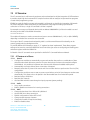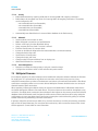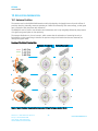
1
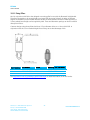
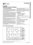
BTM402 Long Range Bluetooth Serial Module User Manual Version 2.0 Americas: +1-800-492-2320 Option 3 Europe: +44-1628-858-940 Hong Kong: +852 2923 0610 www.lairdtech.com/wireless BTM402 User’s Manual REVISION HISTORY Version Date Description 2.0 7/2/2013 Updated to Laird formatting. Americas: +1-800-492-2320 Option 3 Europe: +44-1628-858-940 Hong Kong: +852 2923 0610 www.lairdtech.com/wireless 2 LWS-UM-BTM402-0713 BTM402 User’s Manual CONTENTS Revision History ............................................................................................................................................ 2 Contents ....................................................................................................................................................... 3 1 General Description ............................................................................................................................ 4 2 Features ............................................................................................................................................... 5 3 Functional Block Diagram .................................................................................................................. 7 4 I/O Characteristics .............................................................................................................................. 11 5 RF Performance ................................................................................................................................. 11 6 Functional Description ...................................................................................................................... 12 7 Integrated Firmware ......................................................................................................................... 15 8 Low Power Modes ............................................................................................................................. 19 9 Application Examples........................................................................................................................ 21 10 Application Information ................................................................................................................... 25 11 Board to Board Connector ............................................................................................................... 28 12 Qualification ...................................................................................................................................... 29 13 Environmental ................................................................................................................................... 31 14 Physical Dimensions .......................................................................................................................... 32 15 Related Documents ........................................................................................................................... 33 16 Development Kit ............................................................................................................................... 34 17 Interchangeable 802.11 Module ...................................................................................................... 35 18 Disclaimers ......................................................................................................................................... 36 Americas: +1-800-492-2320 Option 3 Europe: +44-1628-858-940 Hong Kong: +852 2923 0610 www.lairdtech.com/wireless 3 LWS-UM-BTM402-0713 BTM402 User’s Manual 1 GENERAL DESCRIPTION Laird’s BISM II PA Bluetooth Serial Module is a fully integrated and qualified Class 1 Bluetooth solution (Bluetooth version 2.0), which incorporates a power amplifier and low noise amplifier that maximises the RF link budget to provide the greatest range of any Bluetooth Module. The module is designed for lowest cost of integration and ownership for designers to incorporate Bluetooth functionality into their products. The BISM II PA Bluetooth Serial Module is one of the most compact complete Bluetooth solutions, making it ideal to integrate into handheld devices. The module includes a high sensitivity, high gain antenna which provides excellent range. Typical open field performance provides ranges of up to 1,000 metres at transmit powers of 65 mW. The BISM II PA Module is based on Cambridge Silicon Radio’s BlueCore 04 chipset. The module contains all of the hardware and firmware for a complete Bluetooth solution without further components. The Module has an integrated, high performance antenna matched with the Bluetooth RF and baseband circuitry. The firmware integrated into the BC04 chipset implements the higher layer Bluetooth protocol stack and supports profiles like Generic Access Profile (GAP), Service Discovery Profile (SDAP), Serial Port Profile (SPP), Dial Up Networking(DUN), Headset Profile (HSP), Hands Free Profile (HFP), File Transfer Profile (FTP) and OBEX (Client). A virtual processor is used within the BC04 to implement an AT command processor. This interfaces to the host system over a straight forward serial port using an extensive range of AT commands. The AT command set abstracts the Bluetooth protocol from the host application, saving many months of programming and integration time. It provides extremely short integration times for data oriented cable replacement and voice applications. Firmware is also included that provides programming support for multi-point applications. A low cost development system is available for fast product evaluation and development. Support is provided for low power modes that make the BISM II PA apt in battery powered installations. The Module can be configured so that it can be attached to a ‘dumb’ terminal or attached to a PC or PDA for cable replacement applications. In addition to the Bluetooth functionality, The BISM II PA Module provides access to 7 General I/O lines and 2 analogue input lines. These can be configured to provide connection to simple devices such as switches or LEDs without requiring any external processor. Both the GPIO and ADC lines can be accessed either via the wired host UART connection, or remotely over the Bluetooth link. The BISM II PA module is supplied in a small form factor PCB (22 x 34 x 7.6 mm) that connects to a main PCB via 40-way Hirose connector. The interface is compatible with the BISM1 module and Laird’s 40 pin 802.11 modules. The BISM II PA module is Lead-free, RoHS compliant and supports an industrial temperature range of -10° C to +85° C. A key design feature is that the module is pin and format compatible with Laird’s range of 802.11 wireless LAN modules. This allows designers to manufacture a single version of PCB that accepts either a Bluetooth or an 802.11 module, greatly reducing development time to generate a range of wirelessly enabled products. The compatible 802.11 modules are the WISMC01, which contains a full TCP/IP stack, network drivers and a web server, and the WISMC02 which contains wireless network drivers and a UDP stack with SLIP interface. 1.1 Applications POS Equipment Medical Equipment Telematics Voice Applications Industrial Automation Automotive Applications Americas: +1-800-492-2320 Option 3 Europe: +44-1628-858-940 Hong Kong: +852 2923 0610 www.lairdtech.com/wireless 4 LWS-UM-BTM402-0713 BTM402 User’s Manual 2 FEATURES Feature Wireless Specification Standards Supported Transmit Class Frequency Channels Max Transmit Power Min Transmit Power Receive Sensitivity Data Transfer Rate Range Antenna Modes Integrated Antenna External Antenna (option) UART Interface Serial Interface Baud Rate Bits Parity Stop bits Default Serial parameters Levels Modem Control General Purpose Interface Implementation Bluetooth v2.0 Class 1 2.400 – 2.4835 GHz 79 channels Frequency Hopping Adaptive Frequency Hopping +18 dBmi from integrated antenna +16 dBm @ antenna connector (option) -27 dBmi from integrated antenna -87 dBm Up to 300kbps Up to 1,000 metres free space High performance +2 dBi multilayer ceramic 50 Ohm U.FL connection RS-232 bi-directional for commands and data 16550 compatible Configurable from 1,200 to 921,600 bps Non-standard baud rates supported 7 or 8 Odd, even, none 1 or 2 9,600,n,8,1 3.3V CMOS DTR, DSR, DCD, RI, RTS, CTS † I/O ADC Audio 7 general purpose I/O pins, 3.3V CMOS† 2 ADC inputs. 8 bit, 1.8 V max Support SCO Channels PCM Interface 3 PCM Channels @ 64kbps Support SCO and eSCO Configurable as master or slave 8 bit A-law 8 bit μ-law 13 bit linear PCM Clock available when in slave mode V2.0 compliant. Fully integrated. GAP (Generic Access Profile) SDP (Service Discovery Profile) SPP (Serial Port Profile) FTP Client DUN (Dial Up Networking) Bluetooth Stack Profiles Advertised Profiles Americas: +1-800-492-2320 Option 3 Europe: +44-1628-858-940 Hong Kong: +852 2923 0610 www.lairdtech.com/wireless 5 LWS-UM-BTM402-0713 BTM402 User’s Manual Profile Components Firmware Upgrade Connection Modes FTP Server Headset (Audio Gateway) Handsfree (Audio Gateway) Audio Gateway Generic OBEX Push/Pull Client Available over UART Point to point (cable replacement) Multipoint – max 7 slaves Command Interface AT Instructions set Multipoint Software Current Consumption Comprehensive control of connection and module operation S Registers for non-volatile storage of parameters Supports multiple connections Data Transfer Low Power Sniff Mode Supply Voltage Typically 130 mA Less than 2.5 mA Supply 3.6V – 5.0 V DC (For 3.3V operation see BTM404) On-board regulators and brown-out detection Regulation Coexistence / Compatibility WLAN (802.11) 2-wire and 3-wire hardware coexistence schemes supported Pin compatible with Laird’s WISM Bluetooth modules Connections Interface External Antenna (option) Physical 40 way Hirose DF-12 Connector U.FL connector for 50 Ohm antenna Dimensions Weight Environmental 22.8 mm x 33.8 mm x 7.6 mm 8 grams Operating Temperature Storage Temperature Approvals Continuous transmission: -10° C to +85° C -40° C to +85° C Bluetooth FCC IC CE & R&TTE Miscellaneous Qualified as an END product B0xxxx Modular Approval PI408B Industry Canada 1931B-BISMPA Approved Lead free Warranty Development Tools Lead-free and RoHS compliant 2 Years Development Kit Development board and software tools DSR, DTR, RI and DCD are configurable either as GPIO or as modem control lines. † Americas: +1-800-492-2320 Option 3 Europe: +44-1628-858-940 Hong Kong: +852 2923 0610 www.lairdtech.com/wireless 6 LWS-UM-BTM402-0713 BTM402 User’s Manual 3 FUNCTIONAL BLOCK DIAGRAM 3.1 Interconnection The Module is equipped with a 40-pin 0.5 mm pitch board-to-board connector that connects to the application platform. Note that the underside (connector side) of the PCB contains a number of components. Sufficient clearance must be ensured on the mating PCB. Figure 1: Underside of BTM402 PCB Americas: +1-800-492-2320 Option 3 Europe: +44-1628-858-940 Hong Kong: +852 2923 0610 www.lairdtech.com/wireless 7 LWS-UM-BTM402-0713 BTM402 User’s Manual 3.2 Pin Descriptions The Hirose DF12C board-to-board connector on the module is a 40-pin double-row receptacle. The table below defines the pin functions. Note that this pin-out is as viewed from the underside of the Module. Pin No. 1 3 5 Signal Description Pin No. Signal Description Analogue 0 Analogue 1 SPI_MISO 1.8 v Max 1.8 v Max SPI bus serial O/P 2 4 6 N/C N/C UART_RI 7 9 11 13 15 17 19 21 23 25 27 29 31 33 35 37 39 SPI_CSB SPI_CLK GND RESET GND SPI_MOSI UART_CTS UART_TX UART_RTS UART_RX VCC_3V3 VCC_5V N/C GPIO6 ** GPIO7 ** GPIO8 ** GPIO9 SPI bus chip select I/P SPI bus clock I/P 8 10 12 14 16 18 20 22 24 26 28 30 32 34 36 38 40 UART_DCD UART_DSR GPIO3/UART_DTR GPIO4 GPIO5 GND PCM_CLK PCM_IN PCM_SYNC PCM_OUT N/C GND USB / RESERVED USB / RESERVED GND GND N/C Do not connect *** Do not connect *** ‘Ring’ Input or Output Input or Output Input I/O for Host I/O for Host I/O for Host Reset I/P * SPI bus serial I/P Clear to Send I/P Transmit Data O/P Request to Send O/P Receive Data I/P 3.3 V Monitor 3.6 V < VIN < 5.0V I/O for Host I/O for Host I/O for Host I/O for Host PCM Clock I/P PCM Data I/P PCM Sync I/P PCM Data O/P Do not connect Do not connect Notes: * The reset circuitry within the BISM Serial Modules now incorporates a brown-out detector within the module. Customers migrating from previous modules should check their implementation, as they may be able to simplify their external power supply design. The reset line has a fixed 10 kOhm pull down resistor to ground. ** Pins 33, 35 and 37 were N/C on BISM1. Pin 39 was a 1 V8 monitor. Designers migrating between designs should be aware that these are now available as I/O. Default configuration is as an input. *** Pins 2 and 4 were used as GPIO in previous versions of the BISM and WISM. These signals are used internally for PA control. These pins MUST NOT BE CONNECTED. PIO lines can be configured through software to be either inputs or outputs with weak or strong pull-ups or pull-downs. At reset, all PIO lines are configured as inputs with weak pull-downs. UART_RX, UART_TX, UART_CTS, UART_RTS, UART_RI, UART_DCD and UART_DSR are all 3.3 v level logic. For example, when RX and TX are idle they will be sitting at 3.3V. Conversely for handshaking pins CTS, RTS, RI, DCD, DSR a 0v is treated as an assertion. Americas: +1-800-492-2320 Option 3 Europe: +44-1628-858-940 Hong Kong: +852 2923 0610 www.lairdtech.com/wireless 8 LWS-UM-BTM402-0713 BTM402 User’s Manual Pin 6 (UART_RI) is active low. It is normally 3.3 v. When a remote device initiates a connection, this pin goes low. This means that when this pin is converted to RS232 voltage levels it will have the correct voltage level for assertion. Pin 8 (UART_DCD) is active low. It is normally 3.3 v. When a connection is live this pin is low. This means that when this pin is converted to RS232 voltage levels it will have the correct voltage level for assertion. Pin 10 (UART_DSR) is an input, with active low logic. It should be connected to the DTR output of the host. When the BISM II PA Module is in high speed mode (See definition for S Register 507), this pin should be asserted by the host to ensure that the connection is maintained. A deassertion is taken to mean that the connection should be dropped, or an online command mode is being requested. Pin 27 (VCC_3V3 monitor) may only be used for monitoring purposes. It must not be used as a current source. The GPIO pins can be accessed using S Registers 621 to 628. GPIO3 is also used for DTR output (active low). See S Register 552 & 553. Analogue 0 and 1 should not exceed 1.8v and S Registers 701 and 702 are used to access them. 3.3 Electrical Specifications 3.3.1 Absolute Maximum Ratings Absolute maximum ratings for supply voltage and voltages on digital and analogue pins of the Module are listed below; exceeding these values will cause permanent damage. Parameter Peak or current of power supply Voltage at digital pins Voltage at POWER pin Min Max Unit 0 -0.4 3.5 * 200 3.7 8.0 mA V V 3.3.2 Recommended Operating Parameters 3.3.2.1 Power Supply Signal Name Vcc GND Pin No. I/O Voltage Level Comments 29 11, 15, 18, 30, 36, 38 I 3.6 V to 5.0 V * VCC_3V3 27 O 3.3 V typical Ityp = 130 mA 6 Ground terminals to be attached in parallel For monitoring only. No current source. 3.3.2.2 Signal Levels for Interface, PCM, SPI, and GPIO Signal Type Input Signal Level Signal Level at 0 mA Load VILmin= -0.4 V VILmax=0.8 V VIHmin=2.3 V VIHmax=3.7 V Output VOLmax=0.2 V VOHmin=3.1 V Americas: +1-800-492-2320 Option 3 Europe: +44-1628-858-940 Hong Kong: +852 2923 0610 www.lairdtech.com/wireless 9 LWS-UM-BTM402-0713 BTM402 User’s Manual 3.3.2.3 RS232 Interface Signal Name UART_TX UART_RX UART_CTS UART_RTS UART_DSR UART_DTR UART_RI UART_DCD 3.3.2.4 Comments 21 25 19 23 10 12 6 8 O I I O I O I or O I or O Shared with GPIO3 Direction may be programmed. Direction may be programmed. Pin No. I/O Comments 17 5 7 9 I O I I Used to reprogram Flash. PCM Interface Signal Name PCM_CLK PCM_IN PCM_SYNC PCM_OUT 3.3.2.6 I/O SPI Bus Signal Name SPI_MOSI SPI_MISO SPI_CSB SPI_CLK 3.3.2.5 Pin No. Pin No. I/O Comments 20 22 24 26 I or O I I or O O If unused keep pins open. General Purpose I/O and ADC Signal Name GPIO 3 - 9 Pin No. I/O Signal Level Comments 12,14, 16, 33, 35,37, 39 I or O AIO_0, AIO_1 1, 3 I See Singal Levels for Interface, PCM, SPI, and GPIO. Range 0 – 1.8 V 8 bit 3.3.2.7 Miscellaneous Signal Name USB D- Pin No. I/O Signal Level Comments 32 I Normally inactive. Pull to GND through 10 kS. USB D+ 34 I RESET 13 I VILmax =0.3vdd_usb VIHmin =0.7vdd_usb VILmax =0.3vdd_usb VIHmin =0.7vdd_usb VILmax=1.0V VIHmin=2.3V Normally inactive. Pull to GND through 10 kS. Active HIGH. The Reset input contains a 10 kS pull down resistor to ground. Terminology: USB Signal Levels. vdd_usb refers to the internal voltage generated by the LDO regulator on the module, which is typically 3.3V. Hence 0.3vdd_usb and 0.7vdd_usb correspond to 1.0V to 2.3V. If Vcc falls below the recommended minimum of 3.6 V, these values will be reduced. Americas: +1-800-492-2320 Option 3 Europe: +44-1628-858-940 Hong Kong: +852 2923 0610 www.lairdtech.com/wireless 10 LWS-UM-BTM402-0713 BTM402 User’s Manual 4 I/O CHARACTERISTICS 4.1 Power Consumption The current drain from the Vcc power input line is dependent on various factors. The three most significant factors are the voltage level at Vcc, UART Baudrate and the operating mode. The hardware specification for the Module allows for a voltage range of 3.6 to 5.0 at Vcc. The unit includes a linear regulator and tests have shown that there is no significant difference in current draw when Vcc changes within the operating limits. Tests have shown that where power dissipation is an issue, it is best to keep Vcc at the lower end of the range. The UART baudrate has a bearing on power dissipation because as is normal for digital electronics, the power requirements increase linearly with increasing clocking frequencies. Hence higher baudrates result in a higher current drain. Finally with regards to operating mode the significant modes are; idle, waiting for a connection, inquiring, initiating a connection, sniff and connected. With connected mode, it is also relevant to differentiate between no data being transferred and when data is being transferred at the maximum rate possible. The AT Command Set document describes how to configure the Module for optimal power performance. 4.1.1 Typical Current Consumption in mA Vcc = 4.1V, Baudrate = 115,200 bps, Range = 10 metres Idle Mode, S512=1 Wait for Connection Or Discoverable Mode, AT+BTP S508=S510=640, S509=S511=320 Wait for Connection Or Discoverable Mode, AT+BTP, S508=S510=1000, S509=S511=11 Inquiry Mode, AT+BTI Connecting Mode (ATDxxx) Connected Mode (No Data Transfer) Connected Mode (Max Data Transfer) Current (mA) 1.5 57 3.4 114 129 10 46 See Low Power Modes for details of different low power modes. 5 RF PERFORMANCE 5.1 Transmit Power Conducted Transmit Power Antenna Gain Effective Transmit Power max: 40 mW (16 dBm) +2dBi typ. Max: 65 mW (+18 dBmi) 5.2 Receive Sensitivity Receive Sensitivity Antenna Gain Effective Receive Sensitivity Americas: +1-800-492-2320 Option 3 Europe: +44-1628-858-940 Hong Kong: +852 2923 0610 www.lairdtech.com/wireless -85 dBm (at 25° C) +2 dBi typ -87 dBm (at 25° C) 11 LWS-UM-BTM402-0713 BTM402 User’s Manual 6 FUNCTIONAL DESCRIPTION The BISM II PA Bluetooth module is a self-contained Bluetooth product and requires only power to implement full Bluetooth communication. The integrated, high performance antenna together with the RF and Baseband circuitry provides the Bluetooth wireless link and the UART interface provides a connection to the host system. The variety of interfaces and the AT command set allow the BISM II PA module to be used for a wide number of short range wireless applications, from simple cable replacement to complex multipoint applications, where multiple radio links are active at the same time. The complexity and flexibility of configuration are made simple for the design engineer by the integration of an extremely comprehensive set of AT commands, supplemented with a range of “S” registers which are used for non-volatile storage of system parameters. These are fully documented in the “Blu2i AT Command Reference Manual”. To provide the widest scope for integration a range of different physical host interfaces are provided: 6.1 Interfaces 6.1.1 UART Interface UART_TX, UART_RX, UART_RTS and UART_CTS form a conventional asynchronous serial data port with handshaking. The interface is designed to operate correctly when connected to other UART devices such as the 16550A. The signalling levels are nominal 0V and 3.3V and are inverted with respect to the signalling on an RS232 cable. The interface is programmable over a variety of bit rates; no, even or odd parity; stop bit and hardware flow control. The default condition on power-up is pre-assigned in the external Flash. Two-way hardware flow control is implemented by UART_RTS and UART_CTS. UART_RTS is an output and is active low. UART_CTS is an input and is active low. These signals operate according to normal industry convention. By writing different values to the relevant S register the UART_RI can be continuously polled to detect incoming communication. The UART_RI signal serves to indicate incoming calls. UART_DSR is an active low input. It should be connected to DTR output of the host. When the module is running in high speed mode (See definition for S Reg 507), this pin should be asserted by the host to ensure connection is maintained. A de-assertion is taken to mean that the connection should be dropped, or an online command mode is being requested. The module communicates with the customer application using the following signals: Port /TXD of the application sends data to the module’s UART_RX signal line Port /RXD of the application receives data from the module’s UART_TX signal line Note that the serial module output is at 3.3 V CMOS logic levels. Level conversion must be added to interface with an RS-232 level compliant interface. Americas: +1-800-492-2320 Option 3 Europe: +44-1628-858-940 Hong Kong: +852 2923 0610 www.lairdtech.com/wireless 12 LWS-UM-BTM402-0713 BTM402 User’s Manual 6.1.2 SPI Bus The Module is a slave device that uses terminals SPI_MOSI, SPI_MISO, SPI_CLK and SPI_CSB. This interface is used for program firmware updates at the factory. Laird supplies a PC based utility to allow firmware upgrade over the UART port. It is highly recommended that customers should use this method for updating firmware. Note: The designer should be aware that no security protection is built into the hardware or firmware associated with this port, so the terminals should not be permanently connected in a PC application. 6.1.3 GPIO Port Seven lines of programmable bi-directional input/outputs (I/O) are provided that can be accessed either via the UART port, or Over The Air (OTA) from a second Bluetooth unit. These can be used as data inputs or to control external equipment. By using these in OTA mode, a BISM module can be used for control and data acquisition without the need for any additional host processor. Each of the GPIO[3:9] ports can be independently configured to be either an Input or Output. A selection of ports can be accessed synchronously. The ports are powered from VCC. The mode of these lines can be configured and the lines are accessed via S Registers 623 to 629. Low latency I/O can be accessed by using Laird ‘s I/O via an enhanced inquiry process. 6.1.4 PCM CODEC Interface PCM_OUT, PCM_IN, PCM_CLK and PCM_SYNC carry up to three bi-directional channels of voice data, each at 8ksamples/s. The format of the PCM samples can be 8-bit A-law, 8-bit μ-law, 13-bit linear or 16-bit linear. The PCM_CLK and PCM_SYNC terminals can be configured as inputs or outputs, depending on whether the module is the Master or Slave of the PCM interface. Please contact a Laird FAE for further details. The Module is compatible with the Motorola SSI TM interface and interfaces directly to PCM audio devices including the following: 6.1.4.1 Compatible Codec Chips OKI 7702 single channel A-law and μ-law CODEC OKI MSM7705 four channel A-law and μ-law CODEC Winbond W681360 13 bit linear CODEC 6.1.4.2 Audio Codec Development Boards Laird supplies a range of audio codec evaluation boards to allow rapid development of audio applications. These connect to the PCM output connector of Laird ‘s Wireless Development Kit. Order Numbers for these boards are: Laird Order Code ACC-006 ACC-007 ACC-005 Description OKI 7702 single channel CODEC OKI 7705 four channel CODEC Winbond W681360 13 bit linear CODEC Americas: +1-800-492-2320 Option 3 Europe: +44-1628-858-940 Hong Kong: +852 2923 0610 www.lairdtech.com/wireless 13 LWS-UM-BTM402-0713 BTM402 User’s Manual 6.1.5 ADC The BISM II PA provides access to two 8-bit ADCs. These provide an input range of 0mV to 1,800mV, which can be read using the S registers 701 and 702. Suitable external scaling and over-voltage protection should be incorporated in your design. The module provides 5 samples per second at the UART with a baud rate of 115,200 or above. Low latency access of the upper 6 bits of the ADCs can be obtained by using Laird ‘s I/O via an enhanced inquiry process. Americas: +1-800-492-2320 Option 3 Europe: +44-1628-858-940 Hong Kong: +852 2923 0610 www.lairdtech.com/wireless 14 LWS-UM-BTM402-0713 BTM402 User’s Manual 7 INTEGRATED FIRMWARE 7.1 General The BISM II PA has been designed to provide the fastest route to market for designers who wish to use Bluetooth to wirelessly enable their products. To achieve this Laird has implemented a wide ranging set of AT commands that control all of the standard Bluetooth tasks. These remove the complexity of Bluetooth from the design engineer and allow the wireless link to be controlled by means of a simple set of commands. For applications where multiple concurrent live connections need to be maintained a variant of firmware is available which is specifically targeted at multipoint operation. For both applications a comprehensive range of windows based software is available to speed up the design process. A low cost development kit is also available that can be used for prototyping both cable replacement and multipoint applications. 7.2 Profiles Bluetooth has been designed to accommodate a very wide range of wireless applications. To enable these different applications the Bluetooth SIG (Special Interest Group) has defined a series of different profiles that define the way in which Bluetooth devices communicate with each other and perform basic functions. These provide a base line of interoperability for specific application scenarios, upon which more complex user applications can be developed. There are over 30 different profiles, many of which have been developed for specific applications. The BISM II PA firmware is provided with support for the profiles that are most commonly required for cable replacement applications. The current profiles supported by the AT command set firmware (point to point applications) include: GAP: Generic Access Profile. The base connection profile upon which others are based. SDP: Service Discovery Profile. The profile to find other Bluetooth devices and the services they support. SPP: Serial Port Profile. Emulation of a serial cable for cable replacement applications. FTP: File Transfer Profile (Client). Generic OBEX push and pull functionality is available as a part of FTP Client support. The following profiles can be advertised by the module. This allows the user application to implement the required interactive portion of the profile in an external host processor. DUN: Dial Up Networking. Profile support for connection to an external PSTN, GSM, GPRS or VPN connection. HSP: Headset Profile (AG). Supports early implementations of headsets. Now largely replaced by the: - HFP: Hands-Free Profile (AG), which provide more control over the headset operation. FTP: File Transfer Profile (Server) The Audio Gateway requirements of Headset and Handsfree profiles are implemented within the AT Command firmware. For full profile support a portion of these profiles must be implemented within the host system. For other profile support, please contact Laird at [email protected]. Americas: +1-800-492-2320 Option 3 Europe: +44-1628-858-940 Hong Kong: +852 2923 0610 www.lairdtech.com/wireless 15 LWS-UM-BTM402-0713 BTM402 User’s Manual 7.3 AT Overview The AT command set is well known by engineers and was developed to aid the integration of PSTN modems. It provides simple high level commands for complex functions that can easily be incorporated into programs or used within programming scripts. EZURiO has used this familiar concept and extended it to Bluetooth to simplify the integration of Bluetooth for product designers. Rather than having to understand the many stages of setting up a Bluetooth connection or function, a single AT command is all that is required. For example to connect to a Bluetooth device with an address 00809844EA13, all that is needed is to send this string to the UART of the BISM II PA module: ATD00809844EA13 The module will attempt to make a connection and return connect 00809844ea13, 1101) or (NO CARRIER), depending on whether the connection was successful. The scope of the AT command set developed by Laird is such that most Bluetooth functionality can be covered, greatly reducing development time. To provide additional functionality a range of “S” registers has been implemented. These allow program settings to be stored to control the BISM II PA function and also give access to configuring and reading ports and status registers within the BISM II PA. Full details of the AT command set are provided in the Blu2i AT Command Reference Manual. 7.3.1 AT Features at a Glance 7.3.1.1 Configure two modules to automatically connect and transfer data, audio or a combination of data and audio when both devices are powered. The peer device does not have to be another Intelligent Serial Module. It is possible to implement auto connect with a Bluetooth enabled mobile phone. Automatically re-connect devices when a connection is dropped. Remotely access the AT parser of the remote unit from a master device to perform Over The Air (OTA) configuration. Configure the module to enter a state on power up and after a period of time change to another state automatically. This allows units to be placed in the discoverable state for a limited time period. Read and write to GPIO lines Read the ADC channels Get fast GPIO and ADC status through an inquiry response (patent pending) 7.3.1.2 Audio Set up audio connections Enable / disable Auto Answer for incoming connections 7.3.1.3 General UART Change the baud rate from 1200 to 921,600 baud. Use the DSR line to drop connections Flexible configuration as either DTE or DCE Change escape sequence character Change the number of Stop bits and Parity Enable or disable echoes Americas: +1-800-492-2320 Option 3 Europe: +44-1628-858-940 Hong Kong: +852 2923 0610 www.lairdtech.com/wireless 16 LWS-UM-BTM402-0713 BTM402 User’s Manual 7.3.1.4 Security Enable Authentication by requiring a PIN code for incoming AND / OR outgoing connections Enable data to be encrypted over the air for incoming AND / OR outgoing connections. The module can be configured to be: - non-connectable and non-discoverable, - non-connectable but discoverable, - connectable but non-discoverable, - connectable and discoverable. Automatically store Paired devices in a trusted device database in the flash memory 7.3.1.5 7.3.1.6 Bluetooth Set the module to be a master or slave Make a Bluetooth connection to a specified device Perform a full inquiry for other Bluetooth devices Query a remote device to check if a service is offered Fetch the friendly name of a remote device Increase or decrease the delay before the master abandons a connection attempt Change the device class code Set the device’s friendly name Change the Inquiry scan time Change number of returned devices from an inquiry scan Obtain the RSSI value for a connection Power Management Decrease or increase the output power to suit your connection range Configure the modules to work in Sniff and other low power modes. 7.4 Multipoint Firmware For multipoint operation, the same hardware can be loaded with multipoint software. Whereas the firmware for single point ‘AT’ communication only allows one connection to be active at any one time, using multipoint firmware allows a number of simultaneous connections to be made and maintained. It also allows connections to multiple profiles to one or more devices. Multipoint firmware should be seen as a concept of channels instead of slave connections. When operating in Bluetooth multipoint mode, the resources and bandwidth of a Bluetooth master device are shared amongst the different connected devices. This has an impact on the maximum throughput to any one device. If multiple device connections are maintained it also impacts on the memory resources and device database within the Bluetooth stack. Designers should be aware of these restrictions when using multipoint configurations. In most cases better latency and power consumption can be achieved by polling or fast data transfer rather than by maintaining concurrent connections. In general, multipoint connections are viable for up to three connections, at which point memory constraints start to limit the actual data rates. For more than three connections, other connection schemes offer a more efficient approach. Contact Laird for more information. Americas: +1-800-492-2320 Option 3 Europe: +44-1628-858-940 Hong Kong: +852 2923 0610 www.lairdtech.com/wireless 17 LWS-UM-BTM402-0713 BTM402 User’s Manual 7.5 OTA (Over The Air) Configuration When the BISM II PA has its remote AT parser enabled, its settings can be remotely controlled by a master unit (see register S536). This places the slave unit’s AT parser in remote mode providing over the air configuration. This mode is of use for remote sensor applications, where no host processor is required to control the slave Bluetooth unit. 7.6 Boot Modes The module has the capability of booting into 1 of 7 modes. Currently only Boot Mode 1 is supported. Boot Mode 1 is default and gives functionality equivalent to the BISM1 module. These modes will specify different PSKEY settings to allow for different basic operation. Please contact Laird for further information. Americas: +1-800-492-2320 Option 3 Europe: +44-1628-858-940 Hong Kong: +852 2923 0610 www.lairdtech.com/wireless 18 LWS-UM-BTM402-0713 BTM402 User’s Manual 8 LOW POWER MODES The current drain from the Vcc power input line is dependent on various factors. The three most significant factors are the voltage level at Vcc, UART baud rate and the operating mode. The hardware specification for the PA module allows for a voltage range of 3.6V to 5.0V at Vcc. The UART baud rate has a bearing on power drain because as is normal for digital electronics, the power requirements increase linearly with increasing clocking frequencies. Hence higher baud rates result in a higher current drain. Finally with regards to operating mode the significant modes are; idle, waiting for a connection, inquiring, initiating a connection and connected. With connected mode, it is also relevant to differentiate between no data being transferred and when data is being transferred at the maximum rate possible. The operating mode can best be described by stating the AT commands required to enter that mode. In addition, there are certain S Registers which have a direct impact on power consumption, which are described next. S Registers 508 to 511, which specify the page and inquiry scan intervals and windows, can be used to adjust the average current drain when in discoverable and or connectable modes. Registers 508 and 509 specify the interval and window for page scans and registers 510 and 511 specify the interval and window for inquiry scans. Register pairs 508/509 and 510/511 describe duty cycles when the module goes into scan modes. It is while scanning that the highest current draw occurs. The average current draw is determined by simple arithmetic using the values stored in the 508/509 and 510/511 register pairs. Typical current consumption is given in Power Consumption. The current drain while waiting for a connection or discoverable mode is about 30 times higher than in idle mode. This is when the page/inquiry scan duty cycle is 100%. These modes give the quickest response to a page or inquiry request from a remote peer. It is possible to reduce the duty cycle down to as low as 0.5% at the expense of response time. The response time can be specified via S Registers 508 and 510 for page and inquiry respectively, where the worst case response time can be as high as 2.5 seconds. Then the duty cycle can be varied by changing the value of S Registers 509 and 511 appropriately. For example, if S Register 508 and 510 are both set to 1000ms and S Register 509 and 511 are both set to 11ms then the duty cycle is reduced to 1%, this means that average current drain at 5.0v will be 2% of 65mA plus the normal idle mode current, that is, it is as low as 2.75mA. However, in this case, it can take up to 1 second to establish a connection. The connected state current consumption while a master or slave can be considerably reduced by enabling Sniff mode, described in detail in the next section. When a Bluetooth connection has been made, the units in the connection will use internal measurements of the signal quality to implement power control, reducing the transmit power at each end of the link to a level sufficient to maintain the connection. For this reason power consumption will vary with range. Americas: +1-800-492-2320 Option 3 Europe: +44-1628-858-940 Hong Kong: +852 2923 0610 www.lairdtech.com/wireless 19 LWS-UM-BTM402-0713 BTM402 User’s Manual 8.1 Low Power Modes using Sniff Bluetooth connections are master/slave in nature. A master sends packets and a slave has to acknowledge that packet in the next timeslot. Timeslots in Bluetooth are 625 microseconds wide. This implies that a master will always know when packets will be sent and received, which further means it is able to optimise power usage by switching on power hungry circuitry only when needed. A slave on the other hand does NOT have prior knowledge of when a packet will be received and has to assume that a packet will be received from a master on every receive slot. This means that it has to leave its receiving circuitry on for most of the receive slot duration. This problem was identified very early in the evolution of Bluetooth (especially since headsets spend all their time as a slave in a Bluetooth connection) and it was solved by having a mode called Sniff, with appropriate lower layer negotiating protocol. Sniff mode during connection is basically an agreement between the slave and its master that data packets will only be exchanged for N timeslots every M slots. The slave can then assume that it will never be contacted during N-M slots, and so can switch its power hungry circuitry off. The specification goes further by also specifying a third parameter called ‘timeout’ (T) which specifies ‘extra’ timeslots that the slave will agree to listen for after receiving a valid data packet. Put another way, if a data packet is received by the slave, then it knows that it MUST carry on listening for at least T more slots. If within that T slot time period another data packet is received, then the timer is restarted. This mechanism ensures low power consumption when there is no data transfer – at the expense of latency. When there is a lot of data to be transferred, it acts as if sniff mode were not enabled. It is stated above that during sniff mode, a slave listens for N slots every M slots. The Bluetooth specification states that a master can have up to 7 slaves attached to it with all slaves having requested varying sniff parameters. It may therefore be impossible to guarantee that each slave gets the M parameter it requested. In light of this, the protocol for enabling sniff mode specifies that a requesting peer specify the M parameter as a minimum and maximum value. This will allow the master to interleave the sniff modes for all slaves attached. For this reason, the sniff parameters are specified in the BISM II PA module via four S registers. S Register 561 is used to specify ‘N’, S Register 562 is used to specify ‘T’ and S Registers 563/564 are used to specify minimum ‘M’ and maximum ‘M’ respectively. Although the specification defines these parameters in terms of timeslots, the S register values have to be specified in units of milliseconds and the firmware does the necessary translation to timeslots. Americas: +1-800-492-2320 Option 3 Europe: +44-1628-858-940 Hong Kong: +852 2923 0610 www.lairdtech.com/wireless 20 LWS-UM-BTM402-0713 BTM402 User’s Manual 9 APPLICATION EXAMPLES 9.1 RS232 Modem Signals A serial port has DTR, DSR, RTS, CTS, DCD and RI control lines. RTS and CTS are locally controlled to prevent local buffer overflow. The status of DTR, DRS, DCD and RI can be exchanged with the remote peer device. If for example, the DTR/DSR lines are to be exchanged between the two peers to simulate the performance of a physical cable, then it is possible to do so. Refer to the description for S Registers 551, 552 and 553 for more details. Just as a telephony modem has control and status lines, the Module also provides for 6 control and status lines as per the table below. The direction column is as seen from the module’s viewpoint. Function Direction RI also known as CI (Ring Indicate) IN or OUT * DCD (Data Carrier Detect) IN or OUT * DSR (Data Set ready) IN DTR (Data Terminal Ready) OUT CTS (Clear to Send) IN RTS (Request to Send) OUT * configurable with S register 552 The first four lines are under program control. These use four of the GPIO pins and are mapped to I/O as per the table below. The last two are under control of the UART driver and their functionality is always enabled. Direction IN/OUT IN/OUT IN IN/OUT IN/OUT IN/OUT IN/OUT IN/OUT IN/OUT IN/OUT Connector Pin Label Function UART_RI UART_DCD UART_DSR GPIO3/UART_DTR GPIO4 GPIO5 GPIO6 GPIO7 GPIO8 GPIO9 Input/Output from module Input/Output from module Input to Module General Purpose I/O (or DTR functionality) General Purpose I/O General Purpose I/O General Purpose I/O General Purpose I/O General Purpose I/O General Purpose I/O Some serial implementations link CTS and RTS to remove the need for handshaking. Laird does not recommend linking CTS and RTS other than for testing and prototyping. If these pins are linked and the host sends data at the point that the Bluetooth Serial Module deasserts its RTS signal, then there is a significant risk that internal receive buffers will overflow which could lead to an internal processor crash. This will lead to a drop in connection and may require a power cycle to reset the module. Laird recommends that the correct CTS/RTS handshaking protocol be adhered to for proper operation. Americas: +1-800-492-2320 Option 3 Europe: +44-1628-858-940 Hong Kong: +852 2923 0610 www.lairdtech.com/wireless 21 LWS-UM-BTM402-0713 BTM402 User’s Manual Notes: 1. DSR is used by the module to sense that the host is connected, and is intricately linked with connections. For outgoing calls, if this line is not asserted then an error is indicated. Similarly for AT+BTP and AT+BTG. While in a call, for appropriate modes, a de-assertion means fall into command state. If the deassertion exists for longer than the period specified in S Register 519 then the connection is dropped as if an ATH command was received. 2. RI, is normally de-asserted. When an incoming connection is detected it will be asserted, until the connection is either answered or rejected using ATA and ATH respectively. See S Registers 552 & 553 for more details 3. DCD will be de-asserted when the device is in the unconnected state. Asserted when a connection is active. See S Registers 552 and 553 for more details. 4. PIO3 is either used as GPIO or driven as UART_DTR. When the unit is configured in pure host mode, this pin is forced into UART_DTR and is asserted when there is a Bluetooth connection. GPIO Pins 3 to 9 are available for general purpose use. 9.2 Modem Signalling over Bluetooth The RFCOMM protocol used in Bluetooth for implementing the serial port profile allows for the exchange of four modem signals. This information is contained in a special transparent message which contains bits identified as RTR, RTC, DV and IC which depending on the type of serial device being emulated maps to DTR or DSR, RTS, DCD and RI respectively. In addition, this message also includes the ability to convey a BREAK input from one end to the other. To allow for the greatest flexibility and variability in how the modem control signals are used out in the real world, S Registers 551, 552 and 553 have been provided which allow for any of RTR, RTC, DV and IC to be mapped to any modem control/status line. BREAK signal on RX line If the host sends a break signal of duration greater than 100ms, then the module is configured to treat that as a signal to perform a hardware reset. For obvious reasons it is not possible to convey a BREAK over Bluetooth to the peer device. Americas: +1-800-492-2320 Option 3 Europe: +44-1628-858-940 Hong Kong: +852 2923 0610 www.lairdtech.com/wireless 22 LWS-UM-BTM402-0713 BTM402 User’s Manual 9.3 Pure Cable Replacement Mode The module has the capability of being preset into a pure 5-wire data cable replacement mode. The 5 wires being RX, TX, CTS, RTS and GND. This mode requires no changes to a host application since the Bluetooth connection is automatically set up on power up. If the connection is lost the BISM II PA module will constantly retry until the connection is reinstated. By implication, two devices are needed to replace a cable. One device is pre-configured to always be a master and the other, a slave. Assuming the Bluetooth address of the master to be <bdaddr_m> and that of the slave to be <bdaddr_s>, the master module is configured by sending it the following AT commands: AT&F* ATS512=1 ATS504=1 ATS507=2 ATS530=2000 AT&W AT+BTR<bdaddr_s> Where <bdaddr_m> is optional. If it is not specified, then the slave unit will accept connections from any device. If specified then only connections from the device specified will be accepted. If it is desired that the slave unit should not be discoverable (the master is by default not discoverable), then the configuration commands are: AT&F* ATS512=3 ATS0=-1 AT&W AT+BTR<bdaddr_m> Where <bdaddr_m> is optional. If it is not specified, then the slave unit will accept connections from any device. If specified then only connections from the device specified will be accepted. When the units are next power cycled, the slave unit will wait for the master to connect to it and the master will continually look for the slave. If a connection attempt fails, the master will wait for 2 seconds before reattempting a connection. This 2 second delay can be varied by issuing it an ATS530 command with an appropriate value in the range 100 ms to 15000 ms. IMPORTANT NOTE: The DSR input to the module MUST be asserted for the auto connection to succeed. When operating at TTL levels a low (0V) is seen as an assert state. When operating at RS232 levels any voltage greater than 2.3 V is seen as assert. It is usual to connect the DTR line of the host to the DSR line of this device. Americas: +1-800-492-2320 Option 3 Europe: +44-1628-858-940 Hong Kong: +852 2923 0610 www.lairdtech.com/wireless 23 LWS-UM-BTM402-0713 BTM402 User’s Manual 9.4 Audio Cable (voice) With a pair of these modules it is possible to replace a mono audio cable with two way traffic. That is, a setup where a microphone is connected to a speaker at the remote end and vice versa. So this mode effectively replaces two audio cables. Assuming the Bluetooth address of the master to be <bdaddr_m> and that of the slave to be <bdaddr_s>, the master module is configured by sending it the following AT commands: AT&F* ATS512=1 ATS504=1 ATS530=2000 ATS532=7 AT&W AT+BTR<bdaddr_s> And the slave is configured by: AT&F* ATS512=4 ATS0=-1 AT&W AT+BTR<bdaddr_m> 9.5 Oscillator Output The output from the high performance crystal oscillator (+ 10ppm) can be divided and output on one of the selected PIO lines, removing the need for a crystal on the customer’s main PCB. The frequencies available are: 8 MHz 16 MHz For more implementation details, refer to Laird’s Application Note APN_06004_1v0 Crystal Output from BISM.pdf. Americas: +1-800-492-2320 Option 3 Europe: +44-1628-858-940 Hong Kong: +852 2923 0610 www.lairdtech.com/wireless 24 LWS-UM-BTM402-0713 BTM402 User’s Manual 10 APPLICATION INFORMATION 10.1 Antenna Position The antenna used on the BISM II PA Bluetooth module is designed to be largely immune from the effects of proximity detuning. Normally, antennas operating at 2.4GHz are affected by their surroundings, so that great care is needed in their placement and orientation. The BISM II PA can be used in most locations and orientations and is only marginally affected by the presence of a significant ground plane in close proximity. The antenna distribution is close to isotropic, which means that the orientation of mounting has only a limited effect on the overall range. However the optimum range is achieved when the two antennae are directly facing each other. Example of Radiation Characteristics Horizontal Polarisation Vertical Polarisation Figure 2:Typical Radiation Characteristics. Measured at 2.5 metres from a standard dipole. Americas: +1-800-492-2320 Option 3 Europe: +44-1628-858-940 Hong Kong: +852 2923 0610 www.lairdtech.com/wireless 25 LWS-UM-BTM402-0713 BTM402 User’s Manual The module should not be located in a sealed metal enclosure, as this will act as a Faraday cage and severely attenuate the radio signal. The antenna finish may tarnish as a result of environmental effects and handling. This is a cosmetic effect and does not affect the RF performance. 10.2 Power Supply Considerations The power supply for the Module should be a single voltage source of Vcc within the range of 3.6 V to 5.0 V. It must be able to provide sufficient current in a transmit burst. This can rise to 200mA. To limit dissipation it is recommended that a voltage at the lower end of the range is used. The Module includes regulators to provide local 3.3V. This rail is accessible on connector J2 for monitoring purposes only. Under no circumstances should this pin be used to source current. Power (Vcc) to the module is provided via the board-to-board connector Pin 29 on J2. 10.3 Power-On-Reset (Power Cycling and Brown Out Considerations) The Module is provided with an active high reset pin (Hirose 40way DF12C connector pin 13). Upon the application of power, the Power On Reset circuit built into the Module will ensure that the unit starts correctly. There is no need for an external power reset monitor. Note: The previous version of the Bluetooth Serial Module required an external Brown Out circuit to ensure correct operation. This circuitry has now been incorporated into the module. The power supply has been designed to work with previous versions of customer circuitry that may or may not have external brown-out implementations. Customers migrating from a BISM1 to BISM II PA module may be able to simplify their power supply circuitry as a result. 10.4 RF Shield To meet FCC requirements, all modules are supplied with a soldered RF shield. This meets the requirement that users may not be able to access RF circuitry without special tools. Removal of the shield will negate RF approvals. 10.5 Mounting the Module onto the Application Platform There are many ways to properly install the Module in the host device. An efficient approach is to mount the PCB to a frame, plate, rack or chassis. Fasteners can be M1.8 or M2 screws plus suitable washers, circuit board spacers, or customized screws, clamps, or brackets in 2.2mm diameter holes. Note that care should be taken to ensure the head of the fixing does not interfere with the circuit. Nylon fixings are recommended. In addition, the board-to-board connection can also be utilized to achieve better support. The antenna (Brown square component on top side of PCB) must not be influenced by any other PCBs, components or by the housing of the host device. The proximity of the antenna to large metallic objects can affect the range and performance of the system. Designers should carefully consider the location of the Module and the type of enclosure material that is used. To prevent mechanical damage, be careful not to force, bend or twist the Module. Be sure it is positioned flat against the host device. Americas: +1-800-492-2320 Option 3 Europe: +44-1628-858-940 Hong Kong: +852 2923 0610 www.lairdtech.com/wireless 26 LWS-UM-BTM402-0713 BTM402 User’s Manual 10.5.1 Fixing Pillars Laird in conjunction with Richco has designed a mounting pillar for use with the Bluetooth Serial Module. This allows the module to be securely held to a primary PCB using snap fit details. A variety of different heights are available to accommodate different variants of Hirose stacked connectors. Pillars supporting a 3.5mm stacked board height can be supplied by Laird. These and alternative spacings can also be ordered directly from Richco. Customer designs using these pillars should use 2.5 mm diameter holes on a 1.6 mm thick PCB. In conjunction with the 3.3 mm stacked height Hirose if they are to take advantage of this. Board Spacing 3.3 mm 4.1 mm 5.1 mm Part Number Source Matching HRS PCB Socket NPR2005-153-3.3 NPR2005-153-4.1 NPR2005-153-5.1 Laird / Richco Richco Richco CL537-0032-4-86 CL537-0057-5-86 CL537-0157-0-86 See http://www.hirose.co.jp/cataloge_hp/e53700036.pdf for detail information on the PCB socket. Americas: +1-800-492-2320 Option 3 Europe: +44-1628-858-940 Hong Kong: +852 2923 0610 www.lairdtech.com/wireless 27 LWS-UM-BTM402-0713 BTM402 User’s Manual 11 BOARD TO BOARD CONNECTOR This chapter provides specifications for the 40-pin board-to-board connector which serves as physical interface to the host application. The receptacle assembled on the Module is Hirose type DF12C. Details are available at: http://www.hirose.co.jp/cataloge_hp/e53700036.pdf 11.1 Stacking Height Mating headers from Hirose are available in different stacking heights, allowing the spacing between the BISM II PA and carrier PCB to be changed from 3.5 mm to 5.0 mm. Item Receptacle on Module Headers DF12 series Part Number Stacking Height HRS Number DF12C-40DS-0.5V(86) DF12(3.5)-40DP-0.5V(86) DF12(4.0)-40DP-0.5V(86) DF12(5.0)-40DP-0.5V(86) 3.5 mm – 5 mm 3.5 mm 4.0 mm 5.0 mm CL537-0007-7-86 CL537-0032-4-86 CL537-0057-5-86 CL537-0157-0-86 Notes: The headers listed above are with boss and metal fitting. Suffix -86 denotes RoHS compliance. 11.2 Hirose Connector General Specification Parameter Number of Contacts Quantity delivered Voltage Current Rating Resistance Dielectric Withstanding Voltage Operating Temperature Contact Material Insulator Stacking height Insertion force Withdrawal force 1st Withdrawal force 50th Maximum connection cycles Americas: +1-800-492-2320 Option 3 Europe: +44-1628-858-940 Hong Kong: +852 2923 0610 www.lairdtech.com/wireless Specification (40 pin Board to Board connector) 40 2000 Connectors per Tape & Reel 50 V 0.5 A max per contact 0.05 Ohm per contact 500 V RMS min -45°C...+125°C phosphor bronze (surface: gold plated) Material PA , beige natural 3.0 mm ; 3.5 mm ; 4.0 mm ; 5.0 mm 21.8N 10N 10N 50 28 LWS-UM-BTM402-0713 BTM402 User’s Manual 12 QUALIFICATION 12.1 Qualification Process The following safety precautions must be observed during all phases of the operation, usage, service or repair of any application incorporating this Module. Manufacturers of the RF equipment are advised to convey the following safety information to users and operating personnel and to incorporate these guidelines into all manuals supplied with the product. Failure to comply with these precautions violates safety standards of design, manufacture and intended use of the product. Laird assumes no liability for customer failure to comply with these precautions. 12.2 Safety Information If the Bluetooth module is used in equipment that might be taken and operated on a commercial flight, the following safety instructions, or similar warning should be added to the user manual. “Switch off the Wireless device before boarding an aircraft. Make sure it cannot be switched on inadvertently. The operation of wireless appliances in an aircraft is forbidden by many airlines to prevent interference with communications systems.” 12.3 Certifications 12.3.1 Bluetooth Qualification This device has been tested according to the Bluetooth Qualification program and approved as an END product, with Bluetooth approval number BOxxx. END product approval means that integrators do not need to perform any further Bluetooth approvals unless additional profiles are added within their specific product. To meet the requirements of the Bluetooth SIG, this approval number must be marked on the final equipment or referenced in the accompanying documentation. The use of the Bluetooth logo on a product or any associated material is controlled by the Bluetooth Brand Book. Usage is freely allowed for devices incorporating this END product module, so long as the manufacturer is a member of the Bluetooth SIG. Membership of the Bluetooth SIG is free and application can be made at www.bluetooth.org.and Industry Canada Statements This device complies with part 15 of the FCC Rules. Operation is subject to the following two conditions: (1) This device may not cause harmful interference, and (2) this device must accept any interference received, including interference that may cause undesired operation. Changes or modifications not expressly approved by the party responsible for compliance could void the user's authority to operate the equipment. To inherit the modular approval, the antennas for this transmitter must be installed to provide a separation distance of at least 20 cm from all persons and must not be co-located or operating in conjunction with any other antenna or transmitter. Co-location with other radio transmitting devices operating concurrently in the same band will require additional testing and certification. Americas: +1-800-492-2320 Option 3 Europe: +44-1628-858-940 Hong Kong: +852 2923 0610 www.lairdtech.com/wireless 29 LWS-UM-BTM402-0713 BTM402 User’s Manual 12.3.1.1 FCC Labelling Requirement If the FCC ID is not visible when the module is installed inside another device, then the outside of the device into which the module is installed must also display a label referring to the enclosed module. This exterior label can use wording such as the following: “Contains Transmitter Module FCC ID: PI408B” or “Contains FCC ID: PI408B.” Any similar wording that expresses the same meaning may be used. 12.3.2 National RF Approvals A list of the countries where the Module is approved will be provided by Laird as required. As a minimum the product is listed in Europe, Scandinavia, Canada and USA. Laird assumes no liability for customer failure to comply with national RF approval. 12.3.2.1 R&TTE Notification Requirement The 2.4GHz band has some restrictions within the EU when the transmit power level is greater than 10 mW (R&TTE Class 2). Because of this, it is designated within R&TTE as a non-harmonised band. Such products must be notified to the appropriate Notified Body within each country where it is placed on the market. Laird has notified the WISM module, but manufacturers incorporating it within their products and intending to sell these within Europe have a responsibility to notify the appropriate nominated body before commercial introduction. A list of nominated bodies is available at: http://eur-lex.europa.eu/LexUriServ/site/en/oj/2003/c_302/c_30220031212en00010414.pdf Further details on the notification procedure are given in Laird’s Application Note AN016 - Notification Requirements for Wireless Products. Americas: +1-800-492-2320 Option 3 Europe: +44-1628-858-940 Hong Kong: +852 2923 0610 www.lairdtech.com/wireless 30 LWS-UM-BTM402-0713 BTM402 User’s Manual 13 ENVIRONMENTAL 13.1 Operating Temperatures Parameter Operating temp (standard product) Min Typ Max Unit -10 25 +85 °C Min Max Unit -40 +85 °C 13.2 Storage Temperatures Parameter Storage temp 13.3 Reliability Parameter Thermal Shock Vibration Shock Moisture Resistance High Temp Storage Low Temp Storage High Temp/Humidity Operation Thermal shock Test Comment 200 cycles -20º C /+65º C 30 min Continuous operation at 60 Hz, 2 mm stroke 50G 11 ms Half Sine Wave 1 cycle/hour 15g max sine wave, 12 hours 6 axis x 3 cycles each axis Electro Static Discharge Drop Test EN55024:1998 & IEC61000-4-3 75 cm to concrete, 3 axis x 2 cycles per corner 80º C, 360 hours -20º C, 240 hours 60º C, 90% RH, 360 hours -20 to 60ºC in 30min Americas: +1-800-492-2320 Option 3 Europe: +44-1628-858-940 Hong Kong: +852 2923 0610 www.lairdtech.com/wireless 200 cycles with continuous operation 31 LWS-UM-BTM402-0713 BTM402 User’s Manual 14 PHYSICAL DIMENSIONS 14.1 Mechanical Dimensions 14.1.1 Standard Module Location of Connector (Bottom View) All dimensions are shown in mm. Note that there are components on the underside of the PCB. See Interconnection for details. Americas: +1-800-492-2320 Option 3 Europe: +44-1628-858-940 Hong Kong: +852 2923 0610 www.lairdtech.com/wireless 32 LWS-UM-BTM402-0713 BTM402 User’s Manual 14.2 BISM II PA Module without Antenna (special order) The dimensions for this module are identical to the standard BISM II PA illustrated above, but the antenna is replaced with a U-FL connector. The external antenna must provide a 50 Ohm impedance. The external antenna used must not result in an increased output power. I.e. the total gain of mating connector, cable and antenna must not exceed +2dB. If a higher gain antenna is connected, it will invalidate Bluetooth approvals for the module as well as national RF compliance. Any change of antenna may require retesting of the RF performance, to ensure that compliance is not affected. This is covered in more detail in application note AN015 – Use of External Antenna with Wireless Modules. The antenna connector is a U.FL connector, supplied by Hirose. Mating connectors with cables are available from Hirose and their distributors, and also from other cable suppliers. The data sheet for the connector series is available at http://www.hirose.co.jp/cataloge_hp/e32119372.pdf 14.3 Labeling The label contains the Part number and the unique Bluetooth address of the module. 14.4 Ordering Information The Bluetooth PA Module described in this data sheet should be ordered using the part number below: Part Number BTM402 Description Bluetooth PA Module with Antenna 15 RELATED DOCUMENTS The firmware incorporated into the BTM402 Bluetooth Module is the same as that for the BISM2 Module. All of the firmware documentation and application data for the BISM2 module can be used for this module. blu2i AT Command Set Reference Manual blu2i Firmware Release Notes blu2i Multipoint Firmware Reference Manual Intelligent Bluetooth Serial Module - Quick Start Guide Intelligent Bluetooth Serial Module – FAQ Wireless Developer’s Kit User Guide ACC-005 Winbond W61360 Audio Codec Board Manual ACC-006 OKI 7702 Audio Codec Board Manual ACC-007 OKI 7705 Multi-channel Audio Codec Board Manual AN015 – Use of External Antenna with Wireless Modules AN016 - Notification Requirements for Wireless Products. blu2i Application Scenarios Bluetooth Core 2.0 Specification – www.Bluetooth.org DSH_BTM404 BISM2 PA Data Sheet – 3.3V version of this module Americas: +1-800-492-2320 Option 3 Europe: +44-1628-858-940 Hong Kong: +852 2923 0610 www.lairdtech.com/wireless 33 LWS-UM-BTM402-0713 BTM402 User’s Manual 16 DEVELOPMENT KIT Laird offers a Wireless Development Kit for embedded developers which uniquely supports Bluetooth, 802.11 and GSM/GPRS. It provides a simple design environment that can dramatically reduce the development time of wirelessly enabled products. The Wireless Development Kit is available with Laird’s pre-qualified Bluetooth and 802.11 Wireless LAN modules. Both modules contain embedded protocol stacks, removing the need for complex programming on a host processor. 16.1 Features Bluetooth Complete, qualified Bluetooth stack Support for Version 2.0 Upgradeable for Bluetooth 2.1 when available Simple AT style programming interface Audio codec evaluation kits available 802.11b/g Enhanced drivers for low power operation Robust TCP/IP stack Integrated Web Server Embedded interpreter (UWScript) for fast development A range of codec audio development boards (see Audio Codec Development Boards) are available. These can be plugged into the wireless development kit for rapid of audio applications. For cellular applications, the Wireless Development Kit also supports Siemens’ MC55 range of GSM/GPRS modules, which are pin compatible with Laird’s wireless LAN module. This permits designers to develop products which can support either short range or wide area wireless connectivity, with incredibly fast time to market. Americas: +1-800-492-2320 Option 3 Europe: +44-1628-858-940 Hong Kong: +852 2923 0610 www.lairdtech.com/wireless 34 LWS-UM-BTM402-0713 BTM402 User’s Manual 17 INTERCHANGEABLE 802.11 MODULE Laird’s range of Wireless LAN modules have been designed to be physically interchangeable with the BTM402 Bluetooth module and the BISM Bluetooth Serial Module. For product designers this means that they can design a single PCB, which can be populated with either an 802.11 or Bluetooth module, giving the opportunity to launch two different variants of wireless connectivity at minimal additional engineering effort. The WISMC01 802.11b/g TCP/IP Wireless LAN Module is a fully integrated and qualified wireless device server, designed to make it simple to embed 802.11 connectivity. Unlike other wireless modules all of the necessary drivers, protocol stack, security algorithms and antenna are integrated. The module also includes an interpreter that can run scripts, providing a complete wireless processing solution. It enables you to add wireless internet connectivity to almost any device with a serial port. The module is designed for lowest cost of integration and ownership. It is ideal for enabling M2M applications. The module is a dual processor design, dedicating one processor to the 802.11b/g baseband with a second powerful ARM7 processor, with 16 MB of SRAM and 64 MB of flash memory running the wireless drivers, TCP/IP stack, web server and UWScript interpreter. Connection to the host device is via a high-speed 921600 bps UART, with an additional twelve GPIO lines and two 10 bit ADCs. The interpreter allows complex scripts to be run, allowing the WISM module to operate with zero host loading. It means it is possible to use the module to wirelessly enable “dumb” sensors or UART ports. Americas: +1-800-492-2320 Option 3 Europe: +44-1628-858-940 Hong Kong: +852 2923 0610 www.lairdtech.com/wireless 35 LWS-UM-BTM402-0713 BTM402 User’s Manual 18 DISCLAIMERS LAIRD’S BLUETOOTH PRODUCTS ARE NOT AUTHORISED FOR USE AS CRITICAL COMPONENTS IN LIFE SUPPORT DEVICES OR SYSTEMS WITHOUT THE EXPRESS WRITTEN APPROVAL OF THE MANAGING DIRECTOR OF LAIRD LTD. The definitions used herein are: a) Life support devices or systems are devices which (1) are intended for surgical implant into the body, or (2) support or sustain life and whose failure to perform when properly used in accordance with the instructions for use provided in the labelling can reasonably be expected to result in a significant injury to the user. b) A critical component is any component of a life support device or system whose failure to perform can be reasonably expected to cause the failure of the life support device or system, or to affect its safety or effectiveness. Laird does not assume responsibility for use of any of the circuitry described, no circuit patent licenses are implied and Laird reserves the right at any time to change without notice said circuitry and specifications. 18.1 Data Sheet Status – Preliminary Engineering Release Laird Ltd reserve the right to change the specification without notice in order to improve the design and supply the best possible product. Please check with Laird Ltd for the most recent data before initiating or completing a design. Where reference is made to related products from other suppliers, Laird takes no responsibility for the information, availability or performance of such products. 18.2 Warranty Laird warrants that its products shall conform to Laird’s published specifications and remain free from defects in materials and workmanship under normal, proper and intended use for a period of two (2) years from date of purchase, provided that proof of purchase be furnished with any returned equipment. If during the warranty period any component part of the equipment becomes defective by reason of material or workmanship, and Laird is immediately notified of such defect, Laird shall at its option supply a replacement part or request return of equipment, freight prepaid, to its designated facility for repair. In the event no trouble is found on products returned for repair, Laird reserves the right to charge the customer its standard published repair charge. This warranty shall not apply to any products that have been subject to misuse, bending, twisting, neglect, alteration, improper installation, testing or unauthorized repair performed by anyone other than a Laird designated repair facility. Any non-warranty repairs or maintenance shall be at Laird’s standard rates in effect at the time. This warranty is in lieu of all other warranties, whether expressed, implied, or statutory, including but not limited to, implied warranties or merchantability and fitness for a particular purpose. In no event shall Laird be liable, whether in contract, in part, or on any other basis, for any damage sustained by its customers or any other person arising from or related to loss of use, failure or interruption in the operation of any products, or delay in maintenance, or for incidental, consequential, in direct, or special damages or liabilities, or for loss of revenue, loss of business, or other financial loss arising out of or in connection with the sale, lease, maintenance, use, performance, failure, or interruption of these products. Bluetooth is a trademark owned by Bluetooth SIG, Inc., USA, and is licensed to Laird. Americas: +1-800-492-2320 Option 3 Europe: +44-1628-858-940 Hong Kong: +852 2923 0610 www.lairdtech.com/wireless 36 LWS-UM-BTM402-0713