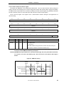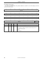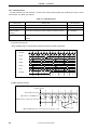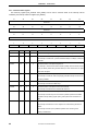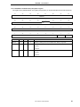
1
To our customers, Old Company Name in Catalogs and Other Documents On April 1st, 2010, NEC Electronics Corporation merged with Renesas Technology Corporation, and Renesas Electronics Corporation took over all the business of both companies. Therefore, although the old company name remains in this document, it is a valid Renesas Electronics document. We appreciate your understanding. Renesas Electronics website: http://www.renesas.com April 1st, 2010 Renesas Electronics Corporation Issued by: Renesas Electronics Corporation (http://www.renesas.com) Send any inquiries to http://www.renesas.com/inquiry. Notice 1. 2. 3. 4. 5. 6. 7. All information included in this document is current as of the date this document is issued. Such information, however, is subject to change without any prior notice. Before purchasing or using any Renesas Electronics products listed herein, please confirm the latest product information with a Renesas Electronics sales office. Also, please pay regular and careful attention to additional and different information to be disclosed by Renesas Electronics such as that disclosed through our website. Renesas Electronics does not assume any liability for infringement of patents, copyrights, or other intellectual property rights of third parties by or arising from the use of Renesas Electronics products or technical information described in this document. No license, express, implied or otherwise, is granted hereby under any patents, copyrights or other intellectual property rights of Renesas Electronics or others. You should not alter, modify, copy, or otherwise misappropriate any Renesas Electronics product, whether in whole or in part. Descriptions of circuits, software and other related information in this document are provided only to illustrate the operation of semiconductor products and application examples. You are fully responsible for the incorporation of these circuits, software, and information in the design of your equipment. Renesas Electronics assumes no responsibility for any losses incurred by you or third parties arising from the use of these circuits, software, or information. When exporting the products or technology described in this document, you should comply with the applicable export control laws and regulations and follow the procedures required by such laws and regulations. You should not use Renesas Electronics products or the technology described in this document for any purpose relating to military applications or use by the military, including but not limited to the development of weapons of mass destruction. Renesas Electronics products and technology may not be used for or incorporated into any products or systems whose manufacture, use, or sale is prohibited under any applicable domestic or foreign laws or regulations. Renesas Electronics has used reasonable care in preparing the information included in this document, but Renesas Electronics does not warrant that such information is error free. Renesas Electronics assumes no liability whatsoever for any damages incurred by you resulting from errors in or omissions from the information included herein. Renesas Electronics products are classified according to the following three quality grades: “Standard”, “High Quality”, and “Specific”. The recommended applications for each Renesas Electronics product depends on the product’s quality grade, as indicated below. You must check the quality grade of each Renesas Electronics product before using it in a particular application. You may not use any Renesas Electronics product for any application categorized as “Specific” without the prior written consent of Renesas Electronics. Further, you may not use any Renesas Electronics product for any application for which it is not intended without the prior written consent of Renesas Electronics. Renesas Electronics shall not be in any way liable for any damages or losses incurred by you or third parties arising from the use of any Renesas Electronics product for an application categorized as “Specific” or for which the product is not intended where you have failed to obtain the prior written consent of Renesas Electronics. The quality grade of each Renesas Electronics product is “Standard” unless otherwise expressly specified in a Renesas Electronics data sheets or data books, etc. “Standard”: 8. 9. 10. 11. 12. Computers; office equipment; communications equipment; test and measurement equipment; audio and visual equipment; home electronic appliances; machine tools; personal electronic equipment; and industrial robots. “High Quality”: Transportation equipment (automobiles, trains, ships, etc.); traffic control systems; anti-disaster systems; anticrime systems; safety equipment; and medical equipment not specifically designed for life support. “Specific”: Aircraft; aerospace equipment; submersible repeaters; nuclear reactor control systems; medical equipment or systems for life support (e.g. artificial life support devices or systems), surgical implantations, or healthcare intervention (e.g. excision, etc.), and any other applications or purposes that pose a direct threat to human life. You should use the Renesas Electronics products described in this document within the range specified by Renesas Electronics, especially with respect to the maximum rating, operating supply voltage range, movement power voltage range, heat radiation characteristics, installation and other product characteristics. Renesas Electronics shall have no liability for malfunctions or damages arising out of the use of Renesas Electronics products beyond such specified ranges. Although Renesas Electronics endeavors to improve the quality and reliability of its products, semiconductor products have specific characteristics such as the occurrence of failure at a certain rate and malfunctions under certain use conditions. Further, Renesas Electronics products are not subject to radiation resistance design. Please be sure to implement safety measures to guard them against the possibility of physical injury, and injury or damage caused by fire in the event of the failure of a Renesas Electronics product, such as safety design for hardware and software including but not limited to redundancy, fire control and malfunction prevention, appropriate treatment for aging degradation or any other appropriate measures. Because the evaluation of microcomputer software alone is very difficult, please evaluate the safety of the final products or system manufactured by you. Please contact a Renesas Electronics sales office for details as to environmental matters such as the environmental compatibility of each Renesas Electronics product. Please use Renesas Electronics products in compliance with all applicable laws and regulations that regulate the inclusion or use of controlled substances, including without limitation, the EU RoHS Directive. Renesas Electronics assumes no liability for damages or losses occurring as a result of your noncompliance with applicable laws and regulations. This document may not be reproduced or duplicated, in any form, in whole or in part, without prior written consent of Renesas Electronics. Please contact a Renesas Electronics sales office if you have any questions regarding the information contained in this document or Renesas Electronics products, or if you have any other inquiries. (Note 1) “Renesas Electronics” as used in this document means Renesas Electronics Corporation and also includes its majorityowned subsidiaries. (Note 2) “Renesas Electronics product(s)” means any product developed or manufactured by or for Renesas Electronics. User’s Manual Multimedia Processor for Mobile Applications Terrestrial Digital TV Interface EMMA MobileTM1 Document No. S19267EJ4V0UM00 (4th edition) Date Published October 2009 2009 Printed in Japan [MEMO] 2 User’s Manual S19267EJ4V0UM NOTES FOR CMOS DEVICES 1 VOLTAGE APPLICATION WAVEFORM AT INPUT PIN Waveform distortion due to input noise or a reflected wave may cause malfunction. If the input of the CMOS device stays in the area between VIL (MAX) and VIH (MIN) due to noise, etc., the device may malfunction. Take care to prevent chattering noise from entering the device when the input level is fixed, and also in the transition period when the input level passes through the area between VIL (MAX) and VIH (MIN). 2 HANDLING OF UNUSED INPUT PINS Unconnected CMOS device inputs can be cause of malfunction. If an input pin is unconnected, it is possible that an internal input level may be generated due to noise, etc., causing malfunction. CMOS devices behave differently than Bipolar or NMOS devices. Input levels of CMOS devices must be fixed high or low by using pull-up or pull-down circuitry. Each unused pin should be connected to VDD or GND via a resistor if there is a possibility that it will be an output pin. All handling related to unused pins must be judged separately for each device and according to related specifications governing the device. 3 PRECAUTION AGAINST ESD A strong electric field, when exposed to a MOS device, can cause destruction of the gate oxide and ultimately degrade the device operation. Steps must be taken to stop generation of static electricity as much as possible, and quickly dissipate it when it has occurred. Environmental control must be adequate. When it is dry, a humidifier should be used. It is recommended to avoid using insulators that easily build up static electricity. Semiconductor devices must be stored and transported in an anti-static container, static shielding bag or conductive material. All test and measurement tools including work benches and floors should be grounded. The operator should be grounded using a wrist strap. Semiconductor devices must not be touched with bare hands. Similar precautions need to be taken for PW boards with mounted semiconductor devices. 4 STATUS BEFORE INITIALIZATION Power-on does not necessarily define the initial status of a MOS device. Immediately after the power source is turned ON, devices with reset functions have not yet been initialized. Hence, power-on does not guarantee output pin levels, I/O settings or contents of registers. A device is not initialized until the reset signal is received. A reset operation must be executed immediately after power-on for devices with reset functions. 5 POWER ON/OFF SEQUENCE In the case of a device that uses different power supplies for the internal operation and external interface, as a rule, switch on the external power supply after switching on the internal power supply. When switching the power supply off, as a rule, switch off the external power supply and then the internal power supply. Use of the reverse power on/off sequences may result in the application of an overvoltage to the internal elements of the device, causing malfunction and degradation of internal elements due to the passage of an abnormal current. The correct power on/off sequence must be judged separately for each device and according to related specifications governing the device. 6 INPUT OF SIGNAL DURING POWER OFF STATE Do not input signals or an I/O pull-up power supply while the device is not powered. The current injection that results from input of such a signal or I/O pull-up power supply may cause malfunction and the abnormal current that passes in the device at this time may cause degradation of internal elements. Input of signals during the power off state must be judged separately for each device and according to related specifications governing the device. User’s Manual S19267EJ4V0UM 3 The names of other companies and products are the registered trademarks or trademarks of the respective company. • The information in this document is current as of September, 2009. The information is subject to change without notice. For actual design-in, refer to the latest publications of NEC Electronics data sheets, etc., for the most up-to-date specifications of NEC Electronics products. Not all products and/or types are available in every country. Please check with an NEC Electronics sales representative for availability and additional information. • No part of this document may be copied or reproduced in any form or by any means without the prior written consent of NEC Electronics. NEC Electronics assumes no responsibility for any errors that may appear in this document. • NEC Electronics does not assume any liability for infringement of patents, copyrights or other intellectual property rights of third parties by or arising from the use of NEC Electronics products listed in this document or any other liability arising from the use of such products. No license, express, implied or otherwise, is granted under any patents, copyrights or other intellectual property rights of NEC Electronics or others. • Descriptions of circuits, software and other related information in this document are provided for illustrative purposes in semiconductor product operation and application examples. The incorporation of these circuits, software and information in the design of a customer's equipment shall be done under the full responsibility of the customer. NEC Electronics assumes no responsibility for any losses incurred by customers or third parties arising from the use of these circuits, software and information. • While NEC Electronics endeavors to enhance the quality and safety of NEC Electronics products, customers agree and acknowledge that the possibility of defects thereof cannot be eliminated entirely. In addition, NEC Electronics products are not taken measures to prevent radioactive rays in the product design. When customers use NEC Electronics products with their products, customers shall, on their own responsibility, incorporate sufficient safety measures such as redundancy, fire-containment and anti-failure features to their products in order to avoid risks of the damages to property (including public or social property) or injury (including death) to persons, as the result of defects of NEC Electronics products. • NEC Electronics products are classified into the following three quality grades: "Standard", "Special" and "Specific". The "Specific" quality grade applies only to NEC Electronics products developed based on a customerdesignated "quality assurance program" for a specific application. The recommended applications of an NEC Electronics product depend on its quality grade, as indicated below. Customers must check the quality grade of each NEC Electronics product before using it in a particular application. "Standard": Computers, office equipment, communications equipment, test and measurement equipment, audio and visual equipment, home electronic appliances, machine tools, personal electronic equipment and industrial robots. "Special": Transportation equipment (automobiles, trains, ships, etc.), traffic control systems, anti-disaster systems, anti-crime systems, safety equipment and medical equipment (not specifically designed for life support). "Specific": Aircraft, aerospace equipment, submersible repeaters, nuclear reactor control systems, life support systems and medical equipment for life support, etc. The quality grade of NEC Electronics products is "Standard" unless otherwise expressly specified in NEC Electronics data sheets or data books, etc. If customers wish to use NEC Electronics products in applications not intended by NEC Electronics, they must contact an NEC Electronics sales representative in advance to determine NEC Electronics' willingness to support a given application. (Note) (1) "NEC Electronics" as used in this statement means NEC Electronics Corporation and also includes its majority-owned subsidiaries. (2) "NEC Electronics products" means any product developed or manufactured by or for NEC Electronics (as defined above). M8E0904E 4 User’s Manual S19267EJ4V0UM PREFACE Readers This manual is intended for hardware/software application system designers who wish to understand and use the terrestrial digital TV interface functions of EMMA Mobile1 (EM1), a multimedia processor for mobile applications. Purpose This manual is intended to explain to users the hardware and software functions of the terrestrial digital TV interface of EM1, and be used as a reference material for developing hardware and software for systems that use EM1. Organization How to Read This Manual This manual consists of the following chapters. Chapter 1 Overview Chapter 2 Pin functions Chapter 3 DTV details Chapter 4 DTV2 datails It is assumed that the readers of this manual have general knowledge of electricity, logic circuits, and microcontrollers. To understand the functions of the terrestrial digital TV interface of EM1 in detail Read this manual according to the CONTENTS. To understand the other functions of EM1 Refer to the user’s manual of the respective module. To understand the electrical specifications of EM1 Conventions Refer to the Data Sheet. Data significance: Higher digits on the left and lower digits on the right Note: Footnote for item marked with Note in the text Caution: Information requiring particular attention Remark: Supplementary information Numeric representation: Binary ... xxxx or xxxxB Decimal ... xxxx Hexadecimal ... xxxxH Data type: Word … 32 bits Halfword … 16 bits Byte User’s Manual S19267EJ4V0UM … 8 bits 5 Related Documents The related documents indicated in this publication may include preliminary versions. However, preliminary versions are not marked as such. Document Name Document No. MC-10118A Data sheet S19657E μPD77630A Data sheet S19686E User’s manual Audio/Voice and PWM Interfaces S19253E DDR SDRAM Interface S19254E DMA Controller S19255E 2 Caution I C Interface S19256E ITU-R BT.656 Interface S19257E LCD Controller S19258E MICROWIRE S19259E NAND Flash Interface S19260E SPI S19261E UART Interface S19262E Image Composer S19263E Image Processor Unit S19264E System Control/General-Purpose I/O Interface S19265E Timer S19266E Terrestrial Digital TV Interface This manual Camera Interface S19285E USB Interface S19359E SD Memory Card Interface S19361E PDMA S19373E One Chip (MC-10118A) S19268E One Chip (μPD77630A) S19687E The related documents listed above are subject to change without notice. Be sure to use the latest version of each document when designing. 6 User’s Manual S19267EJ4V0UM CONTENTS CHAPTER 1 OVERVIEW..........................................................................................................................11 1.1 1.2 1.3 1.4 1.5 1.6 General.......................................................................................................................................11 Features .....................................................................................................................................11 Module Structure (DTV and DTV2) ..........................................................................................12 Clock Supply .............................................................................................................................12 Reset / Reset release ................................................................................................................12 At the timing of DTV / DTV2 change........................................................................................12 CHAPTER 2 PIN FUNCTIONS ................................................................................................................13 2.1 Terrestrial Digital TV Interface Pins ........................................................................................13 CHAPTER 3 DTV Details .........................................................................................................................14 3.1 3.2 3.3 Function Block Diagram...........................................................................................................14 Registers....................................................................................................................................15 Register Functions ...................................................................................................................16 3.3.1 DTV / DTV2 change register ......................................................................................................... 16 3.3.2 Interface status register ................................................................................................................ 16 3.3.3 Interface raw status register.......................................................................................................... 18 3.3.4 Interrupt enable set register .......................................................................................................... 19 3.3.5 Interrupt enable clear register ....................................................................................................... 20 3.3.6 Interrupt source clear register ....................................................................................................... 21 3.3.7 Error address register ................................................................................................................... 22 3.3.8 Transfer control register ................................................................................................................ 23 3.3.9 Transfer request register............................................................................................................... 24 3.3.10 Transfer request cancellation register ........................................................................................... 25 3.3.11 Start address register.................................................................................................................... 26 3.3.12 Buffer size register ........................................................................................................................26 3.3.13 Blank size register.........................................................................................................................27 3.3.14 Current packet register ................................................................................................................. 28 3.3.15 DMA completion interrupt setting register .....................................................................................29 3.3.16 Module control register ................................................................................................................. 30 3.4 Function details.........................................................................................................................31 3.4.1 Input Signal Timing ....................................................................................................................... 31 3.4.2 Data Format ..................................................................................................................................32 3.4.3 DTV Transfer Processing.............................................................................................................. 33 3.4.4 Interrupt Control ............................................................................................................................34 3.4.5 Clocks Control...............................................................................................................................35 3.4.6 Return method from synchronous difference ................................................................................38 CHAPTER 4 DTV2 Details .......................................................................................................................39 4.1 4.2 Function Block Diagram...........................................................................................................39 Registers....................................................................................................................................40 User’s Manual S19267EJ4V0UM 7 4.3 Register Functions....................................................................................................................41 4.3.1 DTV / DTV2 change register .........................................................................................................41 4.3.2 Interface status register.................................................................................................................42 4.3.3 Interface raw status register ..........................................................................................................43 4.3.4 Interrupt enable set register ..........................................................................................................44 4.3.5 Interrupt enable clear register .......................................................................................................46 4.3.6 Interrupt source clear register .......................................................................................................47 4.3.7 Error address register....................................................................................................................48 4.3.8 Transfer control register ................................................................................................................49 4.3.9 Transfer request register ...............................................................................................................50 4.3.10 Transfer request cancellation register ...........................................................................................51 4.3.11 Start address register ....................................................................................................................52 4.3.12 Buffer size register ........................................................................................................................52 4.3.13 Blank size register .........................................................................................................................53 4.3.14 Current packet register..................................................................................................................54 4.3.15 DMA completion interrupt setting register .....................................................................................55 4.3.16 Module control register..................................................................................................................56 4.3.17 DTVPSYNC / DTVVLD Polarity designation register ....................................................................57 4.3.18 Input pin status monitor register ....................................................................................................58 4.4 8 Function details.........................................................................................................................59 4.4.1 Input Signal Timing .......................................................................................................................59 4.4.2 Data Format ..................................................................................................................................63 4.4.3 DTV Transfer Processing ..............................................................................................................64 4.4.4 Interrupt Control ............................................................................................................................66 4.4.5 Clocks Control...............................................................................................................................69 User’s Manual S19267EJ4V0UM LIST OF FIGURES Figure No. Title Page Figure 1-1. Block diagram ............................................................................................................................................12 Figure 3-1. DTV Block diagram....................................................................................................................................14 Figure 3-2. DMA Stop Timing.......................................................................................................................................25 Figure 3-2. Current Packet Register Values ................................................................................................................28 Figure 3-4. DTV Interface DMA Completion Interrupt Set Timing ................................................................................29 Figure 3-5. DTV Interface Signal Timing......................................................................................................................31 Figure 3-6. Stream Timing (Burst Serial Output)..........................................................................................................31 Figure 3-7. Stream Data Storage Format.....................................................................................................................32 Figure 3-8. Ring Buffer Mapping ..................................................................................................................................33 Figure 3-9. Transfer error interrupt timing ....................................................................................................................34 Figure 3-10. DMA completion interrupt Timing.............................................................................................................34 Figure 3-11. DMA stop interrupt Timing .......................................................................................................................35 Figure 3-12. DMA_SWT_CLKREQ Timing ..................................................................................................................36 Figure 3-13. Frequency conversion of DTV_CLK and DTVBCLK ................................................................................37 Figure 3-14. Relation between DTVBCLK and input data............................................................................................37 Figure 4-1. DTV Block diagram....................................................................................................................................39 Figure 4-2. Change of transfer request register value..................................................................................................50 Figure 4-3. Current Packet Register Values ................................................................................................................54 Figure 4-4. DTV Interface DMA Completion Interrupt Set Timing ................................................................................55 Figure 4-5. DTV2 Interface Signal Timing....................................................................................................................59 Figure 4-6. Stream Timing (Burst Serial Output)..........................................................................................................59 Figure 4-7. Judgment of DTVPSYNC data (Burst Serial Output) ................................................................................59 Figure 4-8. When DTVPSYNC reaches continuously (Burst Serial Output)................................................................60 Figure 4-9. When DTVVLD intermits (Burst Serial Output) .........................................................................................60 Figure 4-10. When DTVVLD intermits while DTVPSYNC is HIGH (Burst Serial Output) ............................................60 Figure 4-11. When DTVPSYNC stands up and goes down during a DTVVLD intermission period (Burst Serial Output)...................................................................................................................................................................61 Figure 4-12. When BCLK intermits (Burst Serial Output)............................................................................................61 Figure 4-13. When DTVPSYNC stands up and goes down during a BCLK intermission period (Burst Serial Output)61 Figure 4-14. The bit just before the DTVPSYNC arrival was filled in 8bits, when I don't have that (Burst Serial Output) ...............................................................................................................................................................................62 Figure 4-15. The bit line just before the DTVPSYNC arrival, when 8bits non-rise and DTVPSYNC are 8bits non-rise (Burst Serial Output) ..............................................................................................................................................62 Figure 4-16. Until DTVPSYNC comes to the data just after the reset, invalid data (Burst Serial Output) ....................62 Figure 4-17. It was filled in 8bits just before the reset, the data I don't have is invalid data (Burst Serial Output)........63 Figure 4-18. Stream Data Storage Format...................................................................................................................63 Figure 4-19. Ring Buffer Mapping ................................................................................................................................64 Figure 4-20. Stock method of a packet (at DTVMODE=0) ...........................................................................................65 Figure 4-21. Packet stock method when next SyncByte has come, (at DTVMODE=0) ...............................................65 Figure 4-21. Transfer error interrupt timing ..................................................................................................................66 Figure 4-23. At the timing of the interruption when DMA transfer is being done, and transfer has been reserved to cry ...............................................................................................................................................................................67 Figure 4-24. At the timing of the interruption when transfer has been reserved during DMA transfer..........................67 User’s Manual S19267EJ4V0UM 9 Figure 4-25. Interrupt timing of the word transfer which includes PSYNC part-time work by less than 187 bytes (at DTVMODE=0)....................................................................................................................................................... 68 Figure 4-26. Interrupt timing when also not having complete set of word data including SyncByte beyond 188byte, (at DTVMODE=0)....................................................................................................................................................... 68 Figure 4-27. Interrupt timing when PSYNC part-time work is the unjust value, (at DTVMODE=0).............................. 69 LIST OF TABLES Table No. Title Page Table 3-1. Interrupt Sources........................................................................................................................................ 34 Table 4-1. Interrupt Sources........................................................................................................................................ 66 10 User’s Manual S19267EJ4V0UM CHAPTER 1 OVERVIEW 1.1 General The terrestrial digital television interface (DTV interface) has a function to transfer stream data sent from an externally connected terrestrial digital TV channel decoder LSI to memory, via DMA. The DTV interface only supports burst output (serial) mode. 1.2 Features The main features of DTV are as follows. The DTV interface only supports serial output. DTV interface signals DTV_DATA[7] is used in the serial output mode. Packet synchronization pulse (DTV_PSYNC) Stream data enable signal (DTV_VLD) Bus clock (DTV_BCLK) DMA transfer destination buffer A ring buffer area can be specified. Reception data selection Whether to receive parity fields can be selected. Buffer memory A buffer memory of 32 bits 4 words is incorporated. User’s Manual S19267EJ4V0UM 11 CHAPTER 1 OVERVIEW 1.3 Module Structure (DTV and DTV2) EM1 has 2 of DTV macro (DTV2 function module (in the following, DTV2) and DTV function module (in the following, DTV)). A circuit and a register of each module are separate perfectly. The register address is common. A mutual function module is sharing OFDM interface and AHB bus interface. The main features of DTV are as follows. Exclusion moves by setting of DTV/DTV2 change register SWITCH for each module. When 1 is set as DT_SWITCH, DTV2 is chosen, and when 0 is established, DTV is chosen. Defaults are DT_SWITCH=0, and DTV will be in the chosen state. AHB Crocus DTV APB DTVPSYNC System Bus AHB DTVDATA[7:0] DTVVLD Clock Reset TM APB DTVDATA[7:0] DTVPSYNC DTV_BCLK Reset DTVVLD AHB DTV2 DTVDATA[7:0] APB DTVPSYNC Clock Reset TM DTVVLD Clock Reset TM DTV_BCLK Reset DTV_BCLK Reset Figure 1-1. Block diagram 1.4 Clock Supply All clocks are supplied only the function module chosen by DTV / DTV2 change register DT_SWITCH with. It isn't supplied non-selection function module with. 1.5 Reset / Reset release All resets are reflected by only the function module chosen by DTV / DTV2 change register DT_SWITCH. Nonchoice module will be always in the reset state. Next to DTV / DTV2 change register DT_SWITCH=0 and DTV become effective just after the hardware reset. After reset release, it's necessary to establish DTV / DTV2 change register DT_SWITCH=1 to make DTV2 effective. 1.6 At the timing of DTV / DTV2 change When changing DTV / DTV2, be sure to change by the following procedure. 1. H/W reset 2. H/W reset release 3. DT_SWITCH setting 12 User’s Manual S19267EJ4V0UM CHAPTER 2 PIN FUNCTIONS 2.1 Terrestrial Digital TV Interface Pins Pin Name I/O After Reset Function Alternate Pin Function DTV_BCLK Input Data clock SP2_CLK DTV_DATA Input YUV data SP2_SI DTV_PSYNC Input Packet synchronization signal SP2_SO DTV_VLD Input Packet data enable SP2_CS0 1 User’s Manual S19267EJ4V0UM 13 CHAPTER 3 DTV Details 3.1 Function Block Diagram DTVIF Data Buffer AHB Frame Buffer Interface Packet Control Stream Interface DTVDATA[7:0] System Bus DTVPSYNC DTVVLD APB Processor Interface DTVIF Internal All Unit Clock Reset TM DTV_BCLK Figure 3-1. DTV Block diagram 14 User’s Manual S19267EJ4V0UM CHAPTER 3 DTV Details 3.2 Registers Do not access reserved registers. Any value written to reserved bits in each register is ignored. Base address: 4015_0000H Address 0020H Register Name DTV / DTV2 change register Register Symbol DT_SWITCH R/W R/W After Reset 0000_0000H DTV/DTV2 change register DT_SWITCH=0 can use following register. 4015_0000H to 4015_0040H overlaps DTV2 , but at DT_SWITCH=0, register operation is reflected by only a DTV register. Base address: 4015_0000H Address Register Name Register Symbol R/W After Reset 0000H Interface status register DT_STATUS R 0000_0000H 0004H Interface raw status register DT_RAWSTATUS R 0000_0000H 0008H Interrupt enable set register DT_ENSET R/W 0000_0000H 000CH Interrupt enable clear register DT_ENCLR W 0000_0000H 0010H Interrupt source clear register DT_FFCLR W 0000_0000H 0014H Error address register DT_ERRORADR R/W 0000_0000H 0020H Transfer control register DT_DMACNT R/W 0000_0003H 0024H Transfer request register DT_DMAREQ R/W 0000_0000H 0028H Transfer request cancellation register DT_DMASTOP W 0000_0000H 002CH Start address register DT_START R/W 0000_0000H 0030H Buffer size register DT_BUFSIZE R/W 0000_0000H 0034H Blank size register DT_BLANK R/W 0000_0000H 0038H Current packet register DT_CURRENT R 0000_0000H 003CH DMA completion interrupt setting register DT_INTCONT R/W 0000_0000H 0040H Module control register DT_MODULECONT R/W 0000_0000H User’s Manual S19267EJ4V0UM 15 CHAPTER 3 DTV Details 3.3 Register Functions 3.3.1 DTV / DTV2 change register This register (DT_SWITCH:4015_0200H) changes DTV and DTV2 exclusively. 31 30 29 28 27 26 25 24 19 18 17 16 11 10 9 8 3 2 1 0 Reserved 23 22 21 20 Reserved 15 14 13 12 Reserved 7 6 5 4 Reserved Name SWITCH R/W Bit After Reset Function Reserved R 31:1 0 Reserved. Reading returns the unsettled value. Writing in is ignored. SWITCH R/W 0 0 DTV / DTV2 change 0 : DTV 1 : DTV2 3.3.2 Interface status register This read-only register (DT_STATUS: 4015_0000H) can be used to read the status of the interrupt sources enabled by the interrupt enable set register (DT_ENSET). 31 30 29 28 27 26 25 24 19 18 17 16 11 10 9 8 3 2 1 0 DTVSTOP DTVOR DTVDMA DMAERR Reserved 23 22 21 20 Reserved 15 14 13 12 Reserved 7 6 5 Reserved Name 4 R/W Bit After Reset Function Reserved R 31:4 0 Reserved. Don't write in anything but 0. It's prohibited to write in 1. DTVSTOP R 3 0 Indicates the status of the DMA stop interrupt. This interrupt is issued when DMA stops. 16 User’s Manual S19267EJ4V0UM CHAPTER 3 DTV Details DTVOR R 2 0 DTVDMA R 1 0 Indicates the status of the packet overrun error interrupt. This interrupt is issued when the internal buffer overruns. Indicates the status of the DMA completion interrupt. This interrupt is issued every time the number of packets specified in the DMA completion interrupt setting register (4015_003CH) have been transferred via DMA. DMAERR R 0 0 Indicates the status of the transfer error interrupt. This interrupt is issued when an error response is received during internal bus transfer. This interrupt is issued upon a prohibited operation such as writing to the transfer-prohibited area. User’s Manual S19267EJ4V0UM 17 CHAPTER 3 DTV Details 3.3.3 Interface raw status register This read-only register (DT_RAWSTATUS: 4015_0004H) can be used to read the status of the interrupt sources, regardless of the setting of the interrupt enable set register (DT_ENSET). 31 30 29 28 27 26 25 24 19 18 17 16 11 10 9 8 3 2 1 0 DTVSTOPRAW DTVORRAW Reserved 23 22 21 20 Reserved 15 14 13 12 Reserved 7 6 5 4 Reserved Name R/W Bit After Reset Reserved R 31:4 0 DTVSTOP R 3 0 RAW DTVORRAW DTVDMARAW DMAERRRAW Function Reserved. Don't write in anything but 0. It's prohibited to write in 1. Indicates the status of the DMA stop interrupt. This interrupt is issued when DMA stops. R 2 0 Indicates the status of the packet overrun error interrupt. This interrupt is issued when the internal buffer overruns. DTVDMA R 1 0 RAW Indicates the status of the DMA completion interrupt. This interrupt is issued every time the number of packets specified in the DMA completion interrupt setting register (4015_003CH) have been transferred via DMA. DMAERR RAW R 0 0 Indicates the status of the transfer error interrupt. This interrupt is issued when an error response is received during internal bus transfer. This interrupt is issued upon a prohibited operation such as writing to the transfer-protected area. 18 User’s Manual S19267EJ4V0UM CHAPTER 3 DTV Details 3.3.4 Interrupt enable set register This register (DT_ENSET: 4015_0008H) enables issuance of interrupt requests. When the bit corresponding to an interrupt source is set to 1 in this register, if the interrupt source is set, an interrupt request is issued and the corresponding bit of the interrupt status register (DT_STATUS) is set to 1. Writing 0 to this register does not affect the setting. The interrupt request issuance enable status can be checked by reading this register. 31 30 29 28 27 26 25 24 19 18 17 16 11 10 9 8 3 2 1 0 DTVSTOP_EN DTVOR_EN DTVDMA_EN DMAERR_EN Reserved 23 22 21 20 Reserved 15 14 13 12 Reserved 7 6 5 4 Reserved Name R/W Bit After Reset Reserved R 31:4 0 DTVSTOP_ R 3 0 EN Function Reserved. Don't write in anything but 0. It's prohibited to write in 1. Indicates whether issuance of DMA stop interrupt requests is enabled. 0: Not enabled. 1: Enabled. W Specifies whether to enable issuance of DMA stop interrupt requests. 1: Cancels interrupt masking. DTVOR_EN R 2 0 Indicates whether issuance of packet overrun error interrupt requests is enabled. 0: Not enabled. 1: Enabled. W Specifies whether to enable issuance packet overrun error interrupt requests. 1: Cancels interrupt masking. DTVDMA_EN R 1 0 Indicates whether issuance of DMA completion interrupt requests is enabled. 0: Not enabled. 1: Enabled. W Specifies whether to enable issuance of DMA completion interrupt requests. 1: Cancels interrupt masking. DMAERR_EN R 0 0 Indicates whether issuance of transfer error interrupt requests is enabled. 0: Not enabled. 1: Enabled. W Specifies whether to enable issuance of transfer error interrupt requests. 1: Cancels interrupt masking. User’s Manual S19267EJ4V0UM 19 CHAPTER 3 DTV Details 3.3.5 Interrupt enable clear register This register (DT_ENCLR: 4015_000CH) disables issuance of interrupt requests. When the bit corresponding to an interrupt source is set to 1 in this register, an interrupt request is not issued even if an interrupt source occurs. The status of the corresponding bit of the interrupt status register (DT_STATUS) also remains unchanged. Writing 0 to this register does not affect the setting. 31 30 29 28 27 26 25 24 19 18 17 16 11 10 9 8 3 2 1 0 Reserved 23 22 21 20 Reserved 15 14 13 12 Reserved 7 6 5 4 DTVSTOPMASK DTVORMASK DTVDMAMASK DMAERRMASK Reserved Name R/W Bit After Reset Reserved R 31:4 0 Reserved. Don't write in anything but 0. It's prohibited to write in 1. DTVSTOP W 3 0 Disables issuance of DMA stop interrupt requests. MASK DTVOR 1: Disable W 2 0 MASK DTVDMA MASK 20 Disables issuance of packet overrun error interrupt requests. 1: Disable W 1 0 MASK DMAERR Function Disables issuance of DMA completion interrupt requests. 1: Disable W 0 0 Disables issuance of transfer error requests. 1: Disable User’s Manual S19267EJ4V0UM CHAPTER 3 DTV Details 3.3.6 Interrupt source clear register This write-only register (DT_FFCLR: 4015_0010H) clears the interrupt source by setting the bit corresponding to the interrupt source to 1. Writing 0 to this register does not affect the setting. 31 30 29 28 27 26 25 24 19 18 17 16 11 10 9 8 3 2 1 0 DTVSTOPCLR DTVORCLR DTVDMACLR DMAERRCLR Reserved 23 22 21 20 Reserved 15 14 13 12 Reserved 7 6 5 Reserved Name 4 R/W Bit After Reset Reserved R 31:4 0 Reserved. Don't write in anything but 0. It's prohibited to write in 1. DTVSTOPCL W 3 0 Clears the DMA stop interrupt source. R DTVORCLR Function 1: Clears the source. W 2 0 Clears the packet overrun error interrupt source. 1: Clears the source. DTVDMACLR W 1 0 Clears the DMA completion interrupt source. 1: Clears the source. DMAERRCLR W 0 0 Clears the transfer error interrupt source. 1: Clears the source. User’s Manual S19267EJ4V0UM 21 CHAPTER 3 DTV Details 3.3.7 Error address register This register (DT_ERRORADR: 4015_0014H) holds the current HADDR status when an internal bus response ERROR, RETRY or SPLIT is received during DMA transfer. 31 30 29 28 27 26 25 24 19 18 17 16 11 10 9 8 3 2 1 0 0 LOCK ERRADR 23 22 21 20 ERRADR 15 14 13 12 ERRADR 7 6 5 4 ERRADR Name R/W Bit After Reset ERRADR R 31:2 0 Stores the HADDR status upon occurrence of an error response. Reserved R 1 0 Reserved. Don't write in anything but 0. It's prohibited to write in 1. R/W 0 0 LOCK Function Sets error status. 0: Stores the address when an error response occurs. 1: An error response occurred and the address was stored. Caution If an error response occurs when the LOCK bit is 0, the current HADDR status is stored in the ERRADR bit and the LOCK bit is set to 1. To acquire the error status again, set the LOCK bit to 0. Writing 1 to the LOCK bit does not affect the setting. 22 User’s Manual S19267EJ4V0UM CHAPTER 3 DTV Details 3.3.8 Transfer control register This register (DT_DMACNT: 4015_0020H) controls data transfer. Settings can be changed only when DMA transfer is not being performed (DT_DMAREQ register = 0H). The DTVSP bit must be set to 1 after activation. 31 30 29 28 27 26 25 24 19 18 17 16 11 10 9 8 3 2 1 0 DTVSP DTVMODE DTVENDIAN Reserved 23 22 21 20 Reserved 15 14 13 12 Reserved 7 6 5 4 Reserved Name Reserved DTVSP R/W Bit After Reset Function R 31:3 0 Reserved. Don't write in anything but 0. It's prohibited to write in 1. R/W 2 0 Specifies the data bus type of DTV stream. 0: Burst parallel output (setting prohibited) 1: Burst serial output DTVMODE R/W 1 1 Specifies the size of a packet. 0: Transfer of synchronization field + data field (188 bytes = 47 words) 1: Transfer of synchronization field + data field + parity field (204 bytes = 51 words) DTVENDIAN R/W 0 1 Specifies the DTV stream data format. 0: Big endian 1: Little endian User’s Manual S19267EJ4V0UM 23 CHAPTER 3 DTV Details 3.3.9 Transfer request register This register (DT_DMAREQ: 4015_0024H) specifies the activation of DMA transfer. 31 30 29 28 27 26 25 24 19 18 17 16 11 10 9 8 3 2 1 0 Reserved 23 22 21 20 Reserved 15 14 13 12 Reserved 7 6 5 4 Reserved Name DMAREQ R/W Bit After Reset Function Reserved R 31:1 0 Reserved. Don't write in anything but 0. It's prohibited to write in 1. DMAREQ R 0 0 This bit is set to 1 when DMAREQ is acknowledged. This bit is cleared when the transfer request cancellation register (4015_0028H) is set. W Writing 1 to this bit issues a DMA transfer request. DMA is repeated until the transfer request cancellation register (4015_0028H) is set. Writing 0 to this bit does not affect the setting. Caution) Data transfer is begun from the start address at the time of a DMA transfer request. 24 User’s Manual S19267EJ4V0UM CHAPTER 3 DTV Details 3.3.10 Transfer request cancellation register This register (DT_DMASTOP: 4015_0028H) stops DMA transfer. It'll be the stop reservation state by setting this register, and when not forwarding to the occasion during packet transfer after transfer, DMA is stopped immediately. The DMA transfer request status can be checked by reading the transfer request register (DT_DMAREQ). DMA stop interrupt is issued by the time of a fall of status (the lead value of the transfer request register). This is a write-only register. If the register is set to 1, DMA transfer is finished. Writing 0 to this register does not affect the setting. 31 30 29 28 27 26 25 24 19 18 17 16 11 10 9 8 3 2 1 0 Reserved 23 22 21 20 Reserved 15 14 13 12 Reserved 7 6 5 4 Reserved Name R/W Bit After Reset Reserved W 31:1 0 DMASTOP W 0 0 DMASTOP Function Reserved. Don't write in anything but 0. It's prohibited to write in 1. Stops DMA transfer. 1: Transfer stop When DMA transfer is being performed, the transfer stops after sending the current packet. Otherwise, the transfer immediately stops Caution1) That one for 10 cycles of DTVBCLK leave a space by the (transfer request register set) which resumes DMA after DMA stop interruption. Caution2) By DMA stop request fixation time, the effective data length, that, even packet data is forwarded to a memory. The data of the buffering way I don't have filled in the effective data length is broken. Figure 3-2. DMA Stop Timing Transfer request DTV stream data output Transfer request Packet 0 Packet 1 Packet 2 Packet 3 DMA transfer period (AHB_Write) DMA status DMA stop request User’s Manual S19267EJ4V0UM 25 CHAPTER 3 DTV Details 3.3.11 Start address register This register (DT_START: 4015_002CH) specifies the start address of the DMA transfer destination. Settings can be changed only when DMA transfer is not being performed (DT_DMAREQ register = 0H). 31 30 29 28 27 26 25 24 19 18 17 16 11 10 9 8 3 2 1 0 0 0 DTV_START 23 22 21 20 DTV_START 15 14 13 12 DTV_START 7 6 5 4 DTV_START Name R/W Bit After Reset DTV_START R/W 31:0 0 Function Specifies the start address of the DMA transfer destination (the lower 2 bits are fixed to 0). 3.3.12 Buffer size register This register (DT_BUFSIZE: 4015_0030H) specifies the size of the DMA transfer destination area in units of packets. Settings can be changed only when DMA transfer is not being performed (DT_DMAREQ register = 0H). 31 30 29 28 27 26 25 24 19 18 17 16 Reserved 23 22 21 20 Reserved 15 14 DTV_BUFSIZE 13 12 11 10 9 8 2 1 0 0 0 DTV_BUFSIZE 7 6 5 4 3 DTV_BUFSIZE Name Reserved DTV_ BUFSIZE 26 R/W Bit After Reset Function R 31:20 0 Reserved. Don't write in anything but 0. It's prohibited to write in 1. R/W 19:0 0 Specifies the size of the DMA transfer destination area in units of packets (the lower 2 bits are fixed to 0). User’s Manual S19267EJ4V0UM CHAPTER 3 DTV Details 3.3.13 Blank size register This register (DT_BLANK: 4015_0034H) specifies the blank size between packets during DMA transfer. Settings can be changed only when DMA transfer is not being performed (DT_DMAREQ register = 0H). 31 30 29 28 27 26 25 24 19 18 17 16 11 10 9 8 3 2 1 0 0 0 Reserved 23 22 21 20 Reserved 15 14 13 12 Reserved 7 6 5 4 DTV_BLANK Name Reserved DTV_BLANK R/W Bit After Reset Function R 31:8 0 Reserved. Don't write in anything but 0. It's prohibited to write in 1. R/W 7:0 0 Specifies the blank size between packets (the lower 2 bits must be set to 0). User’s Manual S19267EJ4V0UM 27 CHAPTER 3 DTV Details 3.3.14 Current packet register This register (DT_CURRENT: 4015_0038H) indicates the number of packets that have been transferred via DMA. This register shows the value from 0 to “DT_BUFSIZE register value 1”. Settings can be changed only when DMA transfer is not being performed (DT_DMAREQ register = 0H). 31 30 29 28 27 26 25 24 19 18 17 16 Reserved 23 22 21 20 Reserved 15 14 DTV_CURRENT 13 12 11 10 9 8 2 1 0 DTV_CURRENT 7 6 5 4 3 DTV_CURRENT Name R/W Bit After Reset Function Reserved R 31:20 0 Reserved. Don't write in anything but 0. It's prohibited to write in 1. DTV_ R 19:0 0 Stores the number of packets that have been transferred via DMA minus 1. CURRENT Figure 3-2. Current Packet Register Values Transfer request DTV stream data output Packet 0 Packet 1 Packet 2 Packet 3 Packet 4 Packet 5 DMA transfer period (AHB_Write) Current packet Remark 0 1 2 3 0 When the DTV buffer size is set to 4H Caution) Only while the count value is DT_DMAREQ=1, the count value is effective. While it's DT_DMAREQ=0, it'll be 0. 28 User’s Manual S19267EJ4V0UM CHAPTER 3 DTV Details 3.3.15 DMA completion interrupt setting register This register (DT_INTCONT: 4015_003CH) specifies the interval at which a DMA transfer completion interrupt is issued, in units of packets. A DMA transfer completion interrupt is issued each time DMA transfer of “DT_INTCONT register value + 1” packets is completed. Settings can be changed only when DMA transfer is not being performed (DT_DMAREQ register = 0H). 31 30 29 28 27 26 25 24 19 18 17 16 11 10 9 8 3 2 1 0 Reserved 23 22 21 20 Reserved 15 14 13 12 Reserved 7 6 5 4 DTV_INTCONT Name Reserved DTV_ R/W Bit After Reset R 31:8 0 R/W 7:0 0 INTCONT Function Reserved. Don't write in anything but 0. It's prohibited to write in 1. Specifies in units of packets the interval at which a DMA transfer completion interrupt is issued. An interrupt is issued every time the number of packets equal to the set value plus 1 are received. Figure 3-4. DTV Interface DMA Completion Interrupt Set Timing Transfer request DTV stream data output Packet 0 Packet 1 Packet 2 Packet 3 Packet 4 Packet 5 DMA transfer period (AHB_Write) DMA completion interrupt Interrupt source clear Remark When the DMA completion interrupt setting register is set to 1H User’s Manual S19267EJ4V0UM 29 CHAPTER 3 DTV Details 3.3.16 Module control register This register (DT_MODULECONT: 4015_0040H) initializes the operation of the data capturing circuit that synchronizes with DTV_BCLK. 31 30 29 28 27 26 25 24 19 18 17 16 11 10 9 8 3 2 1 0 Reserved 23 22 21 20 Reserved 15 14 13 12 Reserved 7 6 5 4 Reserved Name R/W Bit After Reset Reserved R 31:1 0 HW_RSTZ R/W 0 0 HW_RSTZ Function Reserved. Don't write in anything but 0. It's prohibited to write in 1. Specifies hardware reset. Specifies whether to initialize the operation of the data capturing circuit that synchronizes with DTV_BCLK. 0: Reset 1: Cancels reset 30 User’s Manual S19267EJ4V0UM CHAPTER 3 DTV Details 3.4 Function details 3.4.1 Input Signal Timing (1) DTV I/F signal timing Figure 3-5. DTV Interface Signal Timing DTV_BCLK DTV_PSYNC, DTV_VLD, DTV_DATA[7:0] Thold Tsetup (2) Stream timing Figure 3-6. Stream Timing (Burst Serial Output) DTV_BCLK DTV_PSYNC DTV_VLD DTV_DATA[7] 7 6 5 4 3 2 1 0 7 6 5 4 3 2 1 0 Sync (1 byte) Caution Data (187 bytes) 4 3 2 1 0 7 2 1 0 Parity (16 bytes) When reception of the parity field is selected, a blanking interval of at least 2T DTV_BCLK cycles must be inserted between packets. User’s Manual S19267EJ4V0UM 31 CHAPTER 3 DTV Details 3.4.2 Data Format Figure 3-7. Stream Data Storage Format DTV_PSYNC DTV_VLD D0 DTV_DATA[7:0] D1 D2 D3 D185 D186 P0 Parity (16 bytes) Data (187 bytes) Sync (1 byte) P15 Data input as shown in Figure 3-7 is stored in the memory in the following format, in accordance with the value set to the DTVENDIAN bit of the transfer control register (DT_DMACNT). Bit alignment 31 to 24 23 to 16 15 to 8 7 to 0 31 to 24 23 to 16 15 to 8 7 to 0 50 words P15 P14 P13 P12 P14 P15 P12 P13 49 words P11 P10 P9 P8 P10 P11 P8 P9 48 words P7 P6 P5 P4 P6 P7 P4 P5 47 words P3 P2 P1 P0 P2 P3 P0 P1 46 words D186 D185 D184 D183 D185 D186 D183 D184 : : : : : : : : 3 words D14 D13 D12 D11 D13 D14 D11 D12 2 words D10 D9 D8 D7 D9 D10 D7 D8 1 word D6 D5 D4 D3 D5 D6 D3 D4 0 words D2 D1 D0 Sync D1 D2 Sync D0 Little endian 32 User’s Manual S19267EJ4V0UM Big endian CHAPTER 3 DTV Details 3.4.3 DTV Transfer Processing Stream data is transferred to the specified buffer area in the memory, in units of packets. The buffer is used as a ring buffer in which the pointer returns to the beginning of the buffer after the specified number of packets are stored. The following three registers are used to set up the buffer. Start address register (32 bits): Specifies the ring buffer start address. Buffer size register (20 bits): Specifies the ring buffer area by a packet count. Blank size register (8 bits): Specifies the blanking interval between packets. Figure 3-8. Ring Buffer Mapping Ring buffer area Buffer size 1 packet size Packet 1 Blank size Packet 0 Start address The valid size of a packet can be set to 188 or 204 bytes by using the DTVMODE bit of the transfer control register (DT_DMACNT). The size of a packet to be mapped to a buffer is the valid size selected by the DTVMODE bit plus the blank size. The total ring buffer size is the above packet size multiplied by the buffer size. User’s Manual S19267EJ4V0UM 33 CHAPTER 3 DTV Details 3.4.4 Interrupt Control The DTV interface uses four interrupts. The bits of the interrupt status register (DT_STATUS) are used to control the interrupts. For details, see Table 3-1. Table 3-1. Interrupt Sources Interrupt Type When to Issue Bit Assignment DMA stop interrupt Issued when the DMA transfer stops. Bit 3 (DTVSTOP) Packet overrun Issued when the internal buffer overruns. Bit 2 (DTVOR) DMA completion Issued when the specified number of packets have been transferred. Bit 1 (DTVDMA) Issued when the ERROR response is received during internal bus Bit 0 (DMAERR) interrupt Transfer error interrupt transfer. (1) Transfer error interrupt When a ERROR reply is received during Internal bus transfer, interrupt is generated. DTVCLK hready 2 htrans 0 2 a100 hwaddr OK hresp 2 a101 a100 hwdata 0 OK 0 2 a102 a101 a103 a102 OK ER ER OK OK 0 OK a103 OK OK DTV_INT Figure 3-9. Transfer error interrupt timing (2) DMA completion interrupt Trabsfer Request DTV Stream Data output Packet0 Packet1 Packet2 Packet3 Packet4 Packet5 DMA Transfer time(AHB_Write) DTV DMA Transfer Completion Interrupt When DTV DMA completion interrupt setting register is 0x1. Figure 3-10. DMA completion interrupt Timing 34 User’s Manual S19267EJ4V0UM Factor Clear CHAPTER 3 DTV Details (3) Packet overrun interrupt The DTV interface uses internal memory (32 bits × 128 words) as a buffer having two banks. Banks are switched for each packet for buffering and the data in the filled bank is transferred to the memory via DMA. In stream data transfer via the DTV interface, the case where the DMA transfer of the previous packet data is not completed within the period in which a packet is loaded is defined as a packet overrun. If a packet overrun occurs, the corresponding bit of the interrupt source register is immediately set. If a packet overrun occurs, packet data input via the channel decoder LSI and data stored in the ring buffer becomes inconsistent. In such a case, terminate DMA once, reserve a sufficient band for the internal bus, and then load data again. (4) DMA stop interrupt Transfer Request DTV Stream Data output Packet0 Transfer Request Packet1 Packet2 Packet3 DMA Transfer time(AHB_Write) DMA Status DMA Stop Request Figure 3-11. DMA stop interrupt Timing Caution : Leave the space for 10 cycles of DTVBCLK by the (transfer request register set) which resumes DMA after DMA stop interruption. 3.4.5 Clocks Control In EM1, supply of the internal bus clock is controlled by each module to save power. The internal bus clock is supplied upon requests from modules and upon register access. In the DTV interface, a clock supply request is set when a DMA transfer is requested through register access, and the clock supply request is cleared when transfer of the current DMA is completed with no other transfers requested. (1) Clocks used in DTV interface (a) DTV_BCLK (external input clock) Used for capturing the DTV data clock and data. (b) DTV_CLK (DTV internal clock) Used for the AHB bus clock and the internal operation of the DTV interface. (c) DTV_PCLK (APB clock) Used for the accessing the APB bus (registers). For details about clock/reset settings, see the Multimedia Processor for Mobile Applications - System Control/General-Purpose I/O Interface User's Manual (S19265E). User’s Manual S19267EJ4V0UM 35 CHAPTER 3 DTV Details (2) DTV_CLKREQ set timing When the DTV transfer request register is set. (3) DTV_CLKREQ clear timing When the DTV transfer request cancellation register is set and DMA transfer of the current packet is completed. (4) DTV_SWT_CLKREQ output timing The signal 1CLK preceded to transaction is output as CLKREQ for bus switches. Signal rising is 1CLK precedence of transaction, and a fall is at the timing of an end of the data phase. : IDLE DTV_CLK DTV_SWT_CLKREQ 1clk preceding supply DTV_SWT_HTRANS NOSEQ SEQ NOSEQ DTV_SWT_HADDR DTV_SWT_HWDATA SWT_DTV_HREADY Figure 3-12. DMA_SWT_CLKREQ Timing (5) Clock restriction DTV_3 clocks of CLK is need to 32 clocks of DTVBCLK for a data delivery between the external clock and the internal clock. 32 / DTVBCLK > 3 / DTV_CLK DTV_CLK > 0.093*DTVBCLK Caution : Even when a clock stop period occurs in clock changes, convert it into a frequency and judge normal movement pros and cons. 36 User’s Manual S19267EJ4V0UM CHAPTER 3 DTV Details DTVBCLK When 4 clocks stopped DTV_CLK Converted by 0.2MHz 1MHz Figure 3-13. Frequency conversion of DTV_CLK and DTVBCLK (6) Relation between DTVBCLK and input data Supply is also necessary to DTVBCLK by the following case outside the effective data area. (1) Before a head packet just after the DMA start (DMAREQ register) is input, it's needed beyond 5 clocks. (2) It's needed between the packet beyond 10 clocks. A clock in front of the head packet is for data fetch preparations, and a clock between the packet is necessary to take it in and deliver data to a AHB clock from DTVBCLK. DMA start 5 clocks need Head packet data area effective 10 clocks need Effective data area DTVBCLK DTVPSYNC DTVVLD DTVDATA[7:0] D0 D1 D2 D0 D185 D186 Caution : When taking Parity data in, it’s 10 clocks of need after a Parity bustle. Figure 3-14. Relation between DTVBCLK and input data User’s Manual S19267EJ4V0UM 37 CHAPTER 3 DTV Details 3.4.6 Return method from synchronous difference (1) The bit difference chosen at the timing of a start When it's piled in a H period of DTVPSYNC input (between 8 clocks) at the timing of a DMA start (DMAREQ), a bit difference occurs to bustle data. When a bit difference occurs, head packet data after a DMA start is forwarded by the data unit which isn't an original byte boundary. To evade that, head packet data after a DMA start check a Sync code, and please confirm that there are no bit differences. When it isn't a Sync code, a bit difference occurs, so please break packet data. A bit difference is canceled automatically, and the next packet after a while is forwarded at a normal byte boundary. (2) Return from a synchronous difference by prescritive outside input When the case when a clock (DTVBCLK) isn't supplied right and at the timing of prescribed input did, and were different input such as noise occurred to a clock, a same year can't slip and sometimes forward data right. It's possible to make them return from a synchronous difference by the next processing. Further, the data maintained in the circuit is broken. (1) Head 1byte data of packet data is checked and a synchronous difference is judged. (2) DMA transfer stop (DMASTOP register). (3) The DMA stop interruption is confirmed. (4) The DTV I/F is reset in HW of a MODULECONT register_RSTZ (note). (5) The reset release which is the DTV I/F in HW of a MODULECONT register_RSTZ. (6) Restart of DMA transfer (DMAREQ register). Note : For HW_RSTZ to initialize only DTV_IF part (the circuit which moves in DTVBCLK), register setting is maintained. Register's readjustment isn't necessary. 38 User’s Manual S19267EJ4V0UM CHAPTER 4 DTV2 Details 4.1 Function Block Diagram DTV_IF DTV_DMA Data Buffer AHB Frame Buffer Interface Packet Control Stream Interface DTVDATA[7:0] System Bus DTVPSYNC DTVVLD APB Processor Interface DTVIF Internal All Unit Serial/Parallel IF Clock Reset TM DTV_BCLK Reset Figure 4-1. DTV Block diagram User’s Manual S19267EJ4V0UM 39 CHAPTER 4 DTV2 Details 4.2 Registers Do not access reserved registers. Any value written to reserved bits in each register is ignored. Base address: 4015_0000H Address 0020H Register Name DTV / DTV2 change register Register Symbol DT_SWITCH R/W R/W After Reset 0000_0000H DTV/DTV2 change register DT_SWITCH=1 can use following register. 4015_0000H to 4015_0040H overlaps DTV2 , but at DT_SWITCH=1, register operation is reflected by only a DTV2 register. Base address: 4015_0000H Address Register Name Register Symbol R/W After Reset 0000H Interface status register DT2_STATUS R 0000_0000H 0004H Interface raw status register DT2_RAWSTATUS R 0000_0000H 0008H Interrupt enable set register DT2_ENSET R/W 0000_0000H 000CH Interrupt enable clear register DT2_ENCLR W 0000_0000H 0010H Interrupt source clear register DT2_FFCLR W 0000_0000H 0014H Error address register DT2_ERRORADR R/W 0000_0000H 0020H Transfer control register DT2_DMACNT R/W 0000_0003H 0024H Transfer request register DT2_DMAREQ R/W 0000_0000H 0028H Transfer request cancellation register DT2_DMASTOP W 0000_0000H 002CH Start address register DT2_START R/W 0000_0000H 0030H Buffer size register DT2_BUFSIZE R/W 0000_0000H 0034H Blank size register DT2_BLANK R/W 0000_0000H 0038H Current packet register DT2_CURRENT R 0000_0000H 003CH DMA completion interrupt setting register DT2_INTCONT R/W 0000_0000H 0040H Module control register DT2_MODULECONT R/W 0000_0000H 0044H DTVPSYNC / DTVVLD Polarity designation register DT2_SIGNALINVERT R/W 0000_0000H 0048H Input pin status monitor register DT2_MONITOR R 0000_0000H 40 User’s Manual S19267EJ4V0UM CHAPTER 4 DTV2 Details 4.3 Register Functions 4.3.1 DTV / DTV2 change register This register (DT_SWITCH:4015_0200H) changes DTV and DTV2 exclusively. 31 30 29 28 27 26 25 24 19 18 17 16 11 10 9 8 3 2 1 0 Reserved 23 22 21 20 Reserved 15 14 13 12 Reserved 7 6 5 4 Reserved Name SWITCH R/W Bit After Reset Function Reserved R 31:1 0 Reserved. Reading returns the unsettled value. Writing in is ignored. SWITCH R/W 0 0 DTV / DTV2 change 0 : DTV 1 : DTV2 User’s Manual S19267EJ4V0UM 41 CHAPTER 4 DTV2 Details 4.3.2 Interface status register This read-only register (DT2_STATUS: 4015_0000H) can be used to read the status of the interrupt sources enabled by the interrupt enable set register (DT_ENSET). 31 30 29 28 27 26 25 24 19 18 17 16 11 10 9 8 Reserved 23 22 21 20 Reserved 15 14 13 12 Reserved 7 6 5 4 3 2 1 0 Reserved DTVLP DTVSP DTVSYNC DTVSTOP DTVOR DTVDMA DMAERR Name R/W Bit After Reset Function Reserved R 31:7 0 Reserved. Reading returns the unsettled value. Writing in is ignored. DTVLP R 6 0 Indicates the status of the packet length excess. This interrupt is issued when 1 packet exceeded 188byte or 204byte, interrupt is generated. DTVSP R 5 0 Indicates the status of the packet length short. This interrupt is issued transfer data includes SyncByte and the transfer amount of the just before packet data generates interrupt in case of less than 187 bytes or less than 203 bytes. DTVSYNC R 4 0 Indicates the status of the illegal SyncByte. This interrupt is issued the value of SyncByte generates interrupt in case of 47H or anything but B8H. DTVSTOP R 3 0 Indicates the status of the DMA stop interrupt. This interrupt is issued when DMA stops. DTVOR R 2 0 Indicates the status of the packet overrun error interrupt. This interrupt is issued when the internal buffer overruns. DTVDMA R 1 0 Indicates the status of the DMA completion interrupt. This interrupt is issued every time the number of packets specified in the DMA completion interrupt setting register (4015_003CH) have been transferred via DMA. DMAERR R 0 0 Indicates the status of the transfer error interrupt. This interrupt is issued when an error response is received during internal bus transfer. This interrupt is issued upon a prohibited operation such as writing to the transfer-prohibited area. 42 User’s Manual S19267EJ4V0UM CHAPTER 4 DTV2 Details 4.3.3 Interface raw status register This read-only register (DT2_RAWSTATUS: 4015_0004H) can be used to read the status of the interrupt sources, regardless of the setting of the interrupt enable set register (DT2_ENSET). 31 30 29 28 27 26 25 24 19 18 17 16 11 10 9 8 1 0 Reserved 23 22 21 20 Reserved 15 14 13 12 Reserved 7 6 5 4 3 2 Reserved DTVLPRAW DTVSPRAW DTVSYNCR DTVSTOPRAW DTVORRAW DTVDMARAW DMAERRRAW AW Name R/W Bit After Reset Function Reserved R 31:7 0 Reserved. Reading returns the unsettled value. Writing in is ignored. DTVLPRAW R 6 0 Indicates the status of the packet length excess. This interrupt is issued when 1 packet exceeded 188byte or 204byte, interrupt is generated. DTVSPRAW R 5 0 Indicates the status of the packet length short. This interrupt is issued transfer data includes SyncByte and the transfer amount of the just before packet data generates interrupt in case of less than 187 bytes or less than 203 bytes. DTVSYNCRA R 4 0 W Indicates the status of the illegal SyncByte. This interrupt is issued the value of SyncByte generates interrupt in case of 47H or anything but B8H. DTVSTOP R 3 0 RAW DTVORRAW Indicates the status of the DMA stop interrupt. This interrupt is issued when DMA stops. R 2 0 Indicates the status of the packet overrun error interrupt. This interrupt is issued when the internal buffer overruns. DTVDMA R 1 0 RAW Indicates the status of the DMA completion interrupt. This interrupt is issued every time the number of packets specified in the DMA completion interrupt setting register (4015_003CH) have been transferred via DMA. DMAERR RAW R 0 0 Indicates the status of the transfer error interrupt. This interrupt is issued when an error response is received during internal bus transfer. This interrupt is issued upon a prohibited operation such as writing to the transfer-protected area. User’s Manual S19267EJ4V0UM 43 CHAPTER 4 DTV2 Details 4.3.4 Interrupt enable set register This register (DT2_ENSET: 4015_0008H) enables issuance of interrupt requests. When the bit corresponding to an interrupt source is set to 1 in this register, if the interrupt source is set, an interrupt request is issued and the corresponding bit of the interrupt status register (DT2_STATUS) is set to 1. Writing 0 to this register does not affect the setting. The interrupt request issuance enable status can be checked by reading this register. 31 30 29 28 27 26 25 24 19 18 17 16 11 10 9 8 Reserved 23 22 21 20 Reserved 15 14 13 12 Reserved 7 Reserved 6 DTVLP_EN 5 4 3 2 1 0 DTVSP_EN DTVSYNC_ DTVSTOP_EN DTVOR_EN DTVDMA_EN DMAERR_EN EN (1/2) Name R/W Bit After Reset Function Reserved R 31:7 0 Reserved. Reading returns the unsettled value. Writing in is ignored. DTVLP_EN R 6 0 Indicates whether issuance of packet length excess interrupt request is enabled. 0: Not enabled. W 1: Enabled. Specifies whether to enable issuance of packet length excess interrupt requests. 1: Cancels interrupt masking. DTVSP_EN R 5 0 Indicates whether issuance of packet length short interrupt request is enabled. 0: Not enabled. W 1: Enabled. Specifies whether to enable issuance of packet length short interrupt requests. 1: Cancels interrupt masking. DTVSYNC_E R 4 0 N Indicates whether issuance of illegal SyncByte interrupt request is enabled. 0: Not enabled. W 1: Enabled. Specifies whether to enable issuance of illegal SyncByte interrupt requests. 1: Cancels interrupt masking. DTVSTOP_ R 3 0 EN Indicates whether issuance of DMA stop interrupt requests is enabled. 0: Not enabled. 1: Enabled. W Specifies whether to enable issuance of DMA stop interrupt requests. 1: Cancels interrupt masking. DTVOR_EN R 2 0 Indicates whether issuance of packet overrun error interrupt requests is enabled. 0: Not enabled. 1: Enabled. W Specifies whether to enable issuance packet overrun error interrupt requests. 1: Cancels interrupt masking. 44 User’s Manual S19267EJ4V0UM CHAPTER 4 DTV2 Details (2/2) Name R/W Bit After Reset DTVDMA_EN R 1 0 Function Indicates whether issuance of DMA completion interrupt requests is enabled. 0: Not enabled. 1: Enabled. W Specifies whether to enable issuance of DMA completion interrupt requests. 1: Cancels interrupt masking. DMAERR_EN R 0 0 Indicates whether issuance of transfer error interrupt requests is enabled. 0: Not enabled. 1: Enabled. W Specifies whether to enable issuance of transfer error interrupt requests. 1: Cancels interrupt masking. User’s Manual S19267EJ4V0UM 45 CHAPTER 4 DTV2 Details 4.3.5 Interrupt enable clear register This register (DT2_ENCLR: 4015_000CH) disables issuance of interrupt requests. When the bit corresponding to an interrupt source is set to 1 in this register, an interrupt request is not issued even if an interrupt source occurs. The status of the corresponding bit of the interrupt status register (DT2_STATUS) also remains unchanged. Writing 0 to this register does not affect the setting. 31 30 29 28 27 26 25 24 19 18 17 16 11 10 9 8 3 2 1 0 Reserved 23 22 21 20 Reserved 15 14 13 12 Reserved 7 6 5 Reserved DTVLPMAS DTVSPMAS K K Name 4 DTVSYNCM DTVSTOPMASK DTVORMASK DTVDMAMASK DMAERRMASK ASK R/W Bit After Reset Function Reserved R 31:7 0 Reserved. Reading returns the unsettled value. Writing in is ignored. DTVLPMASK W 6 0 Disables issuance of packet length excess interrupt requests. 1: Disable DTVSPMASK W 5 0 Disables issuance of packet length short interrupt requests. 1: Disable DTVSYNCMA W 4 0 SK DTVSTOP W 3 0 MASK DTVOR W 2 0 MASK 46 Disables issuance of packet overrun error interrupt requests. 1: Disable W 1 0 Disables issuance of DMA completion interrupt requests. W 0 0 Disables issuance of transfer error requests. MASK DMAERR Disables issuance of DMA stop interrupt requests. 1: Disable MASK DTVDMA Disables issuance of illegal SyncByte interrupt requests. 1: Disable 1: Disable 1: Disable User’s Manual S19267EJ4V0UM CHAPTER 4 DTV2 Details 4.3.6 Interrupt source clear register This write-only register (DT2_FFCLR: 4015_0010H) clears the interrupt source by setting the bit corresponding to the interrupt source to 1. Writing 0 to this register does not affect the setting. 31 30 29 28 27 26 25 24 19 18 17 16 11 10 9 8 Reserved 23 22 21 20 Reserved 15 14 13 12 Reserved 7 6 5 4 3 2 1 0 Reserved DTVLPCLR DTVSPCLR DTVSYNCC DTVSTOPCLR DTVORCLR DTVDMACLR DMAERRCLR LR Name R/W Bit After Reset Function Reserved R 31:7 0 Reserved. Reading returns the unsettled value. Writing in is ignored. DTVLPCLR W 6 0 Clears the packet length excess interrupt source. 1: Clears the source. DTVSPCLR W 5 0 Clears the packet length short interrupt source. 1: Clears the source. DTVSYNCCL W 4 0 R DTVSTOPCL 1: Clears the source. W 3 0 R DTVORCLR Clears the illegal SyncByte interrupt source. Clears the DMA stop interrupt source. 1: Clears the source. W 2 0 Clears the packet overrun error interrupt source. 1: Clears the source. DTVDMACLR W 1 0 Clears the DMA completion interrupt source. DMAERRCLR W 0 0 Clears the transfer error interrupt source. 1: Clears the source. 1: Clears the source. User’s Manual S19267EJ4V0UM 47 CHAPTER 4 DTV2 Details 4.3.7 Error address register This register (DT2_ERRORADR: 4015_0014H) holds the current HADDR status when an internal bus response ERROR, RETRY or SPLIT is received during DMA transfer. 31 30 29 28 27 26 25 24 19 18 17 16 11 10 9 8 3 2 1 0 0 LOCK ERRADR 23 22 21 20 ERRADR 15 14 13 12 ERRADR 7 6 5 4 ERRADR Name R/W Bit After Reset Function ERRADR R 31:2 0 Stores the HADDR status upon occurrence of an error response. Reserved R 1 0 Reserved. Reading returns the unsettled value. Writing in is ignored. LOCK R/ 0 0 Sets error status. 0: Stores the address when an error response occurs. 1: An error response occurred and the address was stored. W Clear error status. 0: Stores the address when an next error response occurs. 1: Nothing action. Caution If an error response occurs when the LOCK bit is 0, the current HADDR status is stored in the ERRADR bit and the LOCK bit is set to 1. To acquire the error status again, set the LOCK bit to 0. Writing 1 to the LOCK bit does not affect the setting. 48 User’s Manual S19267EJ4V0UM CHAPTER 4 DTV2 Details 4.3.8 Transfer control register This register (DT2_DMACNT: 4015_0020H) controls data transfer. Settings can be changed only when DMA transfer is not being performed (DT2_DMAREQ register = 0H). The DTVSP bit must be set to 1 after activation. 31 30 29 28 27 26 25 24 19 18 17 16 11 10 9 8 3 2 1 0 DTVSP DTVMODE DTVENDIAN Reserved 23 22 21 20 Reserved 15 14 13 12 Reserved 7 6 5 4 Reserved Name Reserved DTVSP R/W Bit After Reset Function R 31:3 0 Reserved. Reading returns the unsettled value. Writing in is ignored. R/W 2 0 Specifies the data bus type of DTV stream. 0: Burst parallel output (setting prohibited) 1: Burst serial output DTVMODE R/W 1 1 Specifies the size of a packet. 0: Transfer of synchronization field + data field (188 bytes = 47 words) 1: Transfer of synchronization field + data field + parity field (204 bytes = 51 words) DTVENDIAN R/W 0 1 Specifies the DTV stream data format. 0: Big endian 1: Little endian User’s Manual S19267EJ4V0UM 49 CHAPTER 4 DTV2 Details 4.3.9 Transfer request register This register (DT2_DMAREQ: 4015_0024H) specifies the activation of DMA transfer. After setting 1 in this register, the lead value of this register is 0 until DMA transfer begins it. When DMA transfer begins it, the lead value changes into 1. 1 is set by a transfer release request cashier, and when DMA transfer stops, the lead value of this register changes into 0. 31 30 29 28 27 26 25 24 19 18 17 16 11 10 9 8 3 2 1 0 Reserved 23 22 21 20 Reserved 15 14 13 12 Reserved 7 6 5 4 Reserved Name R/W Bit After Reset Reserved R 31:1 0 DMAREQ R 0 0 DMAREQ Function Reserved. Reading returns the unsettled value. Writing in is ignored. This bit is set to 1 when DMAREQ is acknowledged. This bit is cleared when the transfer request cancellation register (4015_0028H) is set. W Writing 1 to this bit issues a DMA transfer request. DMA is repeated until the transfer request cancellation register (4015_0028H) is set. Writing 0 to this bit does not affect the setting. Transfer clear request: 1 is written in transfer request DT2_DMASTOP Transfer request: 1 is written in transfer request DT2_DMAREQ. Register Write DT_M2H_DMAREQ 0 htrans 0 2 2 2 2 2 2 2 0 2 2 2 2 2 2 2 2 2 2 2 2 2 hwaddr hwdata When DMA transfer is 0 begun, DT2_DMAREQ will be 1. 1 0 2 When DMA transfer is stopped, DT2_DMAREQ Figure 4-2. Change of transfer request register value Caution) At the time of a DMA transfer request, a data transfer, just before, DMASTOP, it begins from the address location. When beginning DMA transfer from the start address, do a DMA transfer request after H/W is reset. 50 User’s Manual S19267EJ4V0UM CHAPTER 4 DTV2 Details 4.3.10 Transfer request cancellation register This register (DT2_DMASTOP: 4015_0028H) stops DMA transfer. It'll be the stop reservation state by setting this register, and when not forwarding to the occasion during packet transfer after transfer, DMA is stopped immediately. The DMA transfer request status can be checked by reading the transfer request register (DT2_DMAREQ). DMA stop interrupt is issued by the time of a fall of status (the lead value of the transfer request register). This is a write-only register. If the register is set to 1, DMA transfer is finished. Writing 0 to this register does not affect the setting. 31 30 29 28 27 26 25 24 19 18 17 16 11 10 9 8 3 2 1 0 Reserved 23 22 21 20 Reserved 15 14 13 12 Reserved 7 6 5 4 Reserved Name R/W Bit After Reset Reserved W 31:1 0 DMASTOP W 0 0 DMASTOP Function Reserved. Reading returns the unsettled value. Writing in is ignored. Stops DMA transfer. 1: Transfer stop When DMA transfer is being performed, the transfer stops after sending the current packet. Otherwise, the transfer immediately stops Caution1) The restriction matter in DTV "One for 10 cycles of DTVBCLK leave a space by the (transfer request register set) which resumes DMA after DMA stop interruption, please." is unnecessary in DTV2. Caution2) Word data until DMA stop request fixation time is forwarded to a memory. Transfer data was filled in the effective data length of 1 packet (188byte or 204byte), when not having that, even a packet next to the stop request fixation after a while will be unsettled data.. User’s Manual S19267EJ4V0UM 51 CHAPTER 4 DTV2 Details 4.3.11 Start address register This register (DT2_START: 4015_002CH) specifies the start address of the DMA transfer destination. Settings can be changed only when DMA transfer is not being performed (DT2_DMAREQ register = 0H). 31 30 29 28 27 26 25 24 19 18 17 16 11 10 9 8 3 2 1 0 0 0 DTV_START 23 22 21 20 DTV_START 15 14 13 12 DTV_START 7 6 5 4 DTV_START Name R/W Bit After Reset DTV_START R/W 31:0 0 Function Specifies the start address of the DMA transfer destination (the lower 2 bits are fixed to 0). 4.3.12 Buffer size register This register (DT2_BUFSIZE: 4015_0030H) specifies the size of the DMA transfer destination area in units of packets. Settings can be changed only when DMA transfer is not being performed (DT2_DMAREQ register = 0H). 31 30 29 28 27 26 25 24 19 18 17 16 Reserved 23 22 21 20 Reserved 15 14 DTV_BUFSIZE 13 12 11 10 9 8 2 1 0 0 0 DTV_BUFSIZE 7 6 5 4 3 DTV_BUFSIZE Name Reserved DTV_ BUFSIZE 52 R/W Bit After Reset Function R 31:20 0 Reserved. Reading returns the unsettled value. Writing in is ignored. R/W 19:0 0 Specifies the size of the DMA transfer destination area in units of packets (the lower 2 bits are fixed to 0). User’s Manual S19267EJ4V0UM CHAPTER 4 DTV2 Details 4.3.13 Blank size register This register (DT2_BLANK: 4015_0034H) specifies the blank size between packets during DMA transfer. Settings can be changed only when DMA transfer is not being performed (DT2_DMAREQ register = 0H). 31 30 29 28 27 26 25 24 19 18 17 16 11 10 9 8 3 2 1 0 0 0 Reserved 23 22 21 20 Reserved 15 14 13 12 Reserved 7 6 5 4 DTV_BLANK Name Reserved DTV_BLANK R/W Bit After Reset Function R 31:8 0 Reserved. Reading returns the unsettled value. Writing in is ignored. R/W 7:0 0 Specifies the blank size between packets (the lower 2 bits must be set to 0). User’s Manual S19267EJ4V0UM 53 CHAPTER 4 DTV2 Details 4.3.14 Current packet register This register (DT2_CURRENT: 4015_0038H) indicates the number of packets that have been transferred via DMA. This register shows the value from 0 to “DT2_BUFSIZE register value 1”. Settings can be changed only when DMA transfer is not being performed (DT2_DMAREQ register = 0H). 31 30 29 28 27 26 25 24 19 18 17 16 Reserved 23 22 21 20 Reserved 15 14 DTV_CURRENT 13 12 11 10 9 8 2 1 0 DTV_CURRENT 7 6 5 4 3 DTV_CURRENT Name R/W Bit After Reset Function Reserved R 31:20 0 Reserved. Reading returns the unsettled value. Writing in is ignored. DTV_ R 19:0 0 Stores the number of packets that have been transferred via DMA minus 1. CURRENT Figure 4-3. Current Packet Register Values Transfer request DTV stream data output Packet 0 Packet 1 Packet 2 Packet 3 Packet 4 Packet 5 DMA transfer period (AHB_Write) Current packet Remark 0 1 2 When the DTV buffer size is set to 4H Caution) The count value is maintained until H/W resets. 54 User’s Manual S19267EJ4V0UM 3 0 CHAPTER 4 DTV2 Details 4.3.15 DMA completion interrupt setting register This register (DT2_INTCONT: 4015_003CH) specifies the interval at which a DMA transfer completion interrupt is issued, in units of packets. A DMA transfer completion interrupt is issued each time DMA transfer of “DT2_INTCONT register value + 1” packets is completed. Settings can be changed only when DMA transfer is not being performed (DT2_DMAREQ register = 0H). 31 30 29 28 27 26 25 24 19 18 17 16 11 10 9 8 3 2 1 0 Reserved 23 22 21 20 Reserved 15 14 13 12 Reserved 7 6 5 4 DTV_INTCONT Name Reserved DTV_ R/W Bit After Reset R 31:8 0 R/W 7:0 0 INTCONT Function Reserved. Reading returns the unsettled value. Writing in is ignored. Specifies in units of packets the interval at which a DMA transfer completion interrupt is issued. An interrupt is issued every time the number of packets equal to the set value plus 1 are received. Figure 4-4. DTV Interface DMA Completion Interrupt Set Timing Transfer request DTV stream data output Packet 0 Packet 1 Packet 2 Packet 3 Packet 4 Packet 5 DMA transfer period (AHB_Write) DMA completion interrupt Interrupt source clear Remark When the DMA completion interrupt setting register is set to 1H User’s Manual S19267EJ4V0UM 55 CHAPTER 4 DTV2 Details 4.3.16 Module control register This register (DT2_MODULECONT: 4015_0040H) initializes the operation of the data capturing circuit that synchronizes with DTV_BCLK. 31 30 29 28 27 26 25 24 19 18 17 16 11 10 9 8 3 2 1 0 Reserved 23 22 21 20 Reserved 15 14 13 12 Reserved 7 6 5 4 Reserved Name R/W Bit After Reset Reserved R 31:1 0 HW_RSTZ R/W 0 0 HW_RSTZ Function Reserved. Reading returns the unsettled value. Writing in is ignored. Specifies hardware reset. Specifies whether to initialize the operation of the data capturing circuit that synchronizes with DTV_BCLK. 0: Reset 1: Cancels reset 56 User’s Manual S19267EJ4V0UM CHAPTER 4 DTV2 Details 4.3.17 DTVPSYNC / DTVVLD Polarity designation register This register (DT2_SIGNALINVERT: 4015_0044H) assign polarity of used DTVPSYNC and DTVVLD respectively.. 31 30 29 28 27 26 25 24 19 18 17 16 11 10 9 8 3 2 1 0 DTVPSYNC DTVVLD Reserved 23 22 21 20 Reserved 15 14 13 12 Reserved 7 6 5 4 Reserved Name Reserved DTVPSYNC R/W Bit After Reset Function R 31:2 0 Reserved. Reading returns the unsettled value. Writing in is ignored. R/W 1 0 Polarity of DTVPSYNC is assigned. 0: Normal 1: Reverse DTVVLD R/W 0 0 Polarity of DTVVLD is assigned. 0: Normal 1: Reverse User’s Manual S19267EJ4V0UM 57 CHAPTER 4 DTV2 Details 4.3.18 Input pin status monitor register This register (DT2_MONITOR: 4015_0048H) indicates terminal input status of DTVPSYNC, DTVVLD, DTVDATA, BCLK.. 31 30 29 28 27 26 25 24 19 18 17 16 11 10 9 8 3 2 1 0 Reserved DTVBCLK DTVPSYNC DTVVLD Function Reserved 23 22 21 20 Reserved 15 14 13 12 DTVDATA 7 Name 6 5 4 R/W Bit After Reset Reserved R 31:16 0 Reserved. Reading returns the unsettled value. Writing in is ignored. DTVDATA R 15:8 0 DTVDATA is indicated. Reserved R 7:3 0 Reserved. Reading returns the unsettled value. Writing in is ignored. DTVBCLK R 2 0 DTVBCLK is indicated. DTVPSYNC R/ 1 0 DTVPSYNC is indicated. DTVVLD R/ 0 0 DTVVLD is indicated. 58 User’s Manual S19267EJ4V0UM CHAPTER 4 DTV2 Details 4.4 Function details 4.4.1 Input Signal Timing (1) DTV2 I/F signal timing Figure 4-5. DTV2 Interface Signal Timing DTV_BCLK DTV_PSYNC, DTV_VLD, DTV_DATA[7:0] Thold Tsetup (2) Stream timing Figure 4-6. Stream Timing (Burst Serial Output) DTV_BCLK DTV_PSYNC DTV_VLD DTV_DATA[7] 7 6 5 4 3 2 1 0 7 6 5 4 3 2 1 0 Sync (1 byte) Caution 4 3 2 1 0 7 2 1 0 Parity (16 bytes) Data (187 bytes) Polarity assignation is possible by register setting in DTVSYNC,DTVVLD. (3) At the timing of a receipt of DTV2 I/F signal (Burst Serial Output)Stream timing When DTVVLD=1 and DTVPSYNC=1 reached for 8 cycles continuously, the 8bits data received at that time is made SYNC. It's made DATA from 8bits following that. Figure 4-7. Judgment of DTVPSYNC data (Burst Serial Output) DTVBCLK DTVVLD DTVPSYNC DTVDATA (Serial) 0 1 2 3 4 5 6 7 0 SYNC User’s Manual S19267EJ4V0UM 1 2 3 4 5 6 7 DATA 59 CHAPTER 4 DTV2 Details It's made SYNC continued by the 8bits unit as it indicates on figure 4-8 when DTVVLD=1 and DTVPSYNC=1 reached more than 16 cycles continuously. Figure 4-8. When DTVPSYNC reaches continuously (Burst Serial Output) DTVBCLK DTVVLD DTVPSYNC 0 DTVDATA (Serial) 1 2 3 4 5 6 7 0 1 2 SYNC 3 4 5 6 7 SYNC When it was DTVVLD=0 during reception, the effective Data bit is made data using 8bits except for DTVVLD=0 period (figure 4-9). In case of DTVPSYNC=1, like, it's made SYNC using 8bits except for DTVVLD=0 period (figure 410). But, when changing into DTVPSYNC=0 during DTVVLD=0 period, it's made DATA, not SYNC (figure 4-11). Figure 4-9. When DTVVLD intermits (Burst Serial Output) DTVBCLK DTVVLD DTVPSYNC DTVDATA (Serial) 0 1 2 3 4 5 * * 6 7 0 1 2 3 4 5 DATA Figure 4-10. When DTVVLD intermits while DTVPSYNC is HIGH (Burst Serial Output) DTVBCLK DTVVLD DTVPSYNC DTVDATA (Serial) 0 1 2 3 4 5 * * 6 SYNC 60 User’s Manual S19267EJ4V0UM 7 0 1 2 3 4 5 CHAPTER 4 DTV2 Details Figure 4-11. When DTVPSYNC stands up and goes down during a DTVVLD intermission period (Burst Serial Output) DTVCLK DTVVLD DTVPSYNC 0 DTVDATA (Serial) 1 2 3 4 5 * * 6 7 0 1 2 3 4 5 Even DTVVLD=1 doesn't receive data in the period when DTVBCLK doesn't enter (figure 4-12, 4-13). Figure 4-12. When BCLK intermits (Burst Serial Output) DTVBCLK DTVVLD DTVPSYNC 0 DTVDATA (Serial) 1 2 3 4 5 * * 6 7 0 1 2 3 4 5 SYNC Figure 4-13. When DTVPSYNC stands up and goes down during a BCLK intermission period (Burst Serial Output) DTVBCLK DTVVLD DTVPSYNC DTVDATA (Serial) 0 1 2 3 4 5 * * 6 7 0 1 2 3 4 5 Data The bit line was filled in 8bits, when it was DTVPSYNC=1 in the state I don't have, it's made Data after that 8 bits in even time. When DTVPSYNC continues it 8 cycles, just after making the rising of DTVPSYNC a cardinal point, it's made SYNC with 8bits (figure 4-14). DTVPSYNC=1 was filled in 8 cycles, when not having that, it's made effective data just before from the bit line 8bits later (figure 4-15). User’s Manual S19267EJ4V0UM 61 CHAPTER 4 DTV2 Details Figure 4-14. The bit just before the DTVPSYNC arrival was filled in 8bits, when I don't have that (Burst Serial Output) DTVBCLK DTVVLD DTVPSYNC DTVDATA (Serial) 0 1 2 3 4 5 6 0 1 2 Data 3 4 5 6 7 0 PSYNC Figure 4-15. The bit line just before the DTVPSYNC arrival, when 8bits non-rise and DTVPSYNC are 8bits nonrise (Burst Serial Output) DTVBCLK DTVVLD DTVPSYNC DTVDATA (Serial) 0 1 2 3 4 5 6 7 0 1 2 3 4 5 6 7 PSYNC: less than 8bits Data Data The bit line received just after just after the start and the reset will be an invalid bit, and it's made the effective bit from first DTVPSYNC (figure 4-16). It was filled in 8bits which has been received at the end in a case with a reset when receiving an effective bit, the data I don't have is made invalid data (figure 4-17). Figure 4-16. Until DTVPSYNC comes to the data just after the reset, invalid data (Burst Serial Output) DTVBCLK SRSTZ DTVVLD DTVPSYNC 0 DTVDATA (Serial) Invalid data 62 1 2 3 4 Valid data User’s Manual S19267EJ4V0UM 5 6 7 0 1 2 CHAPTER 4 DTV2 Details Figure 4-17. It was filled in 8bits just before the reset, the data I don't have is invalid data (Burst Serial Output) DTVBCLK SRSTZ DTVVLD DTVPSYNC 0 DTVDATA (Serail) 1 2 3 4 0 Invalid data 1 Invalid data 2 3 4 5 Valid data 4.4.2 Data Format Figure 4-18. Stream Data Storage Format DTV_PSYNC DTV_VLD D1 D0 DTV_DATA[7:0] D2 D3 D185 D186 P0 Parity (16 bytes) Data (187 bytes) Sync (1 byte) P15 Data input as shown in Figure 4-18 is stored in the memory in the following format, in accordance with the value set to the DTVENDIAN bit of the transfer control register (DT2_DMACNT). Bit alignment 31 to 24 23 to 16 15 to 8 7 to 0 31 to 24 23 to 16 15 to 8 7 to 0 50 words P15 P14 P13 P12 P14 P15 P12 P13 49 words P11 P10 P9 P8 P10 P11 P8 P9 48 words P7 P6 P5 P4 P6 P7 P4 P5 47 words P3 P2 P1 P0 P2 P3 P0 P1 46 words D186 D185 D184 D183 D185 D186 D183 D184 : : : : : : : : 3 words D14 D13 D12 D11 D13 D14 D11 D12 2 words D10 D9 D8 D7 D9 D10 D7 D8 1 word D6 D5 D4 D3 D5 D6 D3 D4 0 words D2 D1 D0 Sync D1 D2 Sync D0 Little endian User’s Manual S19267EJ4V0UM Big endian 63 CHAPTER 4 DTV2 Details 4.4.3 DTV Transfer Processing Stream data is transferred to the specified buffer area in the memory, in units of packets. The buffer is used as a ring buffer in which the pointer returns to the beginning of the buffer after the specified number of packets are stored. The following three registers are used to set up the buffer. Start address register (32 bits): Specifies the ring buffer start address. Buffer size register (20 bits): Specifies the ring buffer area by a packet count. Blank size register (8 bits): Specifies the blanking interval between packets. Figure 4-19. Ring Buffer Mapping Ring buffer area Buffer size 1 packet size Packet 1 Blank size Packet 0 Start address Effective size of 1 packet and data is established by the DTVMODE bit of the transfer control register (DT2_DMACNT) by 188 bytes or 204 bytes. The capacity of 1 packet unit by which the mapping is made a buffer will be the effective size chosen by the DTVMODE bit+ blank size. The total capacity of the ring buffer will be a packet of above-mentioned volume x buffer size. The DTV flow received from OFDM is the part-time work unit, and buffering is done by FIFO inside DTV2, and every time it gathers 4 bytes, DMA is forwarded to a memory (figure 4-20). Data is stocked by new address aligning which made SyncByte the head as I come and show in figure 4-21 at the time of the following exception occurrence at the time of SyncByte reception at the time of normal operation. a) When next SyncByte has come after restoration from a FIFO overflow by a packet overrun. b) When next SyncByte has come (An excess is repealed.) after the transfer amount of the data exceeded a packet of effective size. c) When the transfer amount of the data is a packet of effective size sheep rise, and next SyncByte has come (The shortage will be unsettled data.) d) When it's different from the expectation value (47H or B8H is established by the DTVMODE bit of the DMA control register.) in the price of received SyncByte. 64 User’s Manual S19267EJ4V0UM CHAPTER 4 DTV2 Details Figure 4-20. Stock method of a packet (at DTVMODE=0) CLK PSYNC ByteData a0 a1 a2 a3 b0 haddr b1 b2 b3 c0 a c1 d0 b 1st word d3 3rd word c 1packet Data [187Byte] bytes, DMA is forwarded. d2 c 2nd word b a d1 c a +0 c3 b hwdata Every time I match FIFO 4 c2 : +188 +188×(N-1) Data [187Byte] N packet memory image Figure 4-21. Packet stock method when next SyncByte has come, (at DTVMODE=0) CLK PSYNC ByteData a0 a1 a2 a3 haddr b0 b1 c0 c1 a hwdata c3 b a d2 d3 e0 e1 d c d Sync a +188 1packet 不定データ b blank c d Data [187Byte] +376 d1 2nd word 3rd word (last 2bytes are dummy) Data [187Byte] +188+blank d0 c b 1st word +0 c2 2packet : Memory image User’s Manual S19267EJ4V0UM 65 CHAPTER 4 DTV2 Details 4.4.4 Interrupt Control DTV2 I/F issues 7 kinds of interrupt. Control of each interrupt interrupts, and it's assigned to each bit of the status register. Please refer to table 4-1 for details. Table 4-1. Interrupt Sources Interrupt Type When to Issue Bit Assignment Packet length excess interrupt Issued when 1 packet exceeded 188byte or 204byte. DT2_STATUS[6] : DTVLP Packet length short interrupt Issued when DTVPSYNC=1 and reception data are less DT2_STATUS[5] : DTVSP than 187 bytes or less than 203 bytes. Illegal SyncByte onyerrupt Issued when the price of DTVPSYNC=1 and SyncByte DT2_STATUS[4] : DTVSYNC is 47H or anything but B8H. DMA stop interrupt Issued when the DMA transfer stops. DT2_STATUS[3] : DTVSTOP Packet overrun Issued when the internal buffer overruns. DT2_STATUS[2] : DTVOR DMA completion Issued when the specified number of packets have DT2_STATUS[1] : DTVDMA interrupt been transferred. Transfer error interrupt Issued when the ERROR response is received during DT2_STATUS[0] : DMAERR internal bus transfer. (1) Transfer error interrupt When a ERROR reply is received during Internal bus transfer, interrupt is generated. DTVCLK hready htrans 2 2 a100 hwaddr OK 0 2 a101 a100 hwdata hresp 0 OK 0 2 a102 a101 OK ER ER OK OK 0 a103 a102 OK a103 OK OK DTV_INT Figure 4-21. Transfer error interrupt timing (2) DMA completion interrupt Every time DMA of the number of packets set as register DT2_INTCONT is completed, interrupt is generated. (3) Packet overrun interrupt DTV2 I/F uses the inner memory (32 bits x 128 words) as a buffer. A bustle of a word does DMA transfer of completed data. When the interior buffer overflows, overrun interrupt is generated. When a packet overrun occurred, the adjustment-lessness occurs to the packet data input from DTV and the range stocked in a ring buffer, but after return, a normal packet bustle is resumed from next Psync from a packet overrun. 66 User’s Manual S19267EJ4V0UM CHAPTER 4 DTV2 Details (4) DMA stop interrupt When doing DMA transfer of DMA immediately when not forwarding, when DMA transfer stop reservation was formed out of register DT2_DMASTOP, when the transfer has been completed, interrupt is generated. Figure 4-23. At the timing of the interruption when DMA transfer is being done, and transfer has been reserved to cry DTVCLK dma_stop htrans 2 0 a100 hwaddr OK 0 a101 a100 hwdata hresp 2 OK a101 OK OK DTV_INT Figure 4-24. At the timing of the interruption when transfer has been reserved during DMA transfer DTVCLK dma_stop htrans 2 2 a100 hwaddr OK 0 a101 a100 hwdata hresp 0 OK a101 OK OK DTV_INT User’s Manual S19267EJ4V0UM 67 CHAPTER 4 DTV2 Details (5) Packet length short interrupt When next SyncByte has arrived in less than 203 bytes of state at less than 187 bytes and packet chief effective size 204byte at packet chief effective size 188byte, the forwarded data length generates interrupt. Effective size is established by the DTVMODE bit of the transfer control register. Figure 4-25. Interrupt timing of the word transfer which includes PSYNC part-time work by less than 187 bytes (at DTVMODE=0) DTVCLK hready htrans 2 0 2 a180 hwaddr 2 PSYNC a180 hwdata 0 0 2 b00 PSYNC 0 b01 b00 b01 DTV_INT (6) Packet length excess interrupt When a packet chief closes beyond effective size (188byte or 204byte), interrupt is generated. Effective size is designated by the DTVMODE bit of the transfer control register. Figure 4-26. Interrupt timing when also not having complete set of word data including SyncByte beyond 188byte, (at DTVMODE=0) DTVCLK hready htrans hwaddr hwdata DMA transmission for 188 bytes has been completed, but the next data in FIFO doesn't include S B t 2 a187 a187 DTV_INT 68 User’s Manual S19267EJ4V0UM CHAPTER 4 DTV2 Details (6) Illegal SyncByte interrupt SyncByte shows 47H or B8H. The time 47H the price is decided about by DTVMODE of a transfer control register, and which is DTVMODE=0, the B8H is made the expectation value at DTVMODE=1. In case of all except for the expectation value, SyncByte of DMA transfer word data including SyncByte brings about unjust SyncByte interrupt. Figure 4-27. Interrupt timing when PSYNC part-time work is the unjust value, (at DTVMODE=0) DTVCLK SWT_DTV_ The value which is a word including SyncByte and a relevant byte i 47H htrans 2 hwaddr 0 2 a00 hwdata It's a word including SyncByte, but the price of the relevant byte isn't 47H. 0403_0247 0 a01 4433_2211 2 0 2 b00 4433_2211 0 b01 eeff_aabb DTV_INT 4.4.5 Clocks Control In EM1, supply of the internal bus clock is controlled by each module to save power. The internal bus clock is supplied upon requests from modules and upon register access. In the DTV interface, a clock supply request is set when a DMA transfer is requested through register access, and the clock supply request is cleared when transfer of the current DMA is completed with no other transfers requested. (1) Clocks used in DTV interface (a) DTV_BCLK (external input clock) (b) DTV_CLK (DTV internal clock) (c) DTV_PCLK (APB clock) Used for capturing the DTV data clock and data. Used for the AHB bus clock and the internal operation of the DTV interface. Used for the accessing the APB bus (registers). For details about clock/reset settings, see the Multimedia Processor for Mobile Applications - System Control/General-Purpose I/O Interface User's Manual (S19265E). (2) DTV_CLKREQ set timing When the DTV transfer request register is set. (3) DTV_CLKREQ clear timing When the DTV transfer request cancellation register is set and DMA transfer of the current packet is completed. (4) DTV_SWT_CLKREQ output timing The signal 1CLK preceded to transaction is output as CLKREQ for bus switches. Signal rising is 1CLK precedence of transaction, and a fall is at the timing of an end of the data phase. User’s Manual S19267EJ4V0UM 69 Revision History Date Revision Comments February 10, 2009 1.0 − April 27, 2009 2.0 Incremental update from comments to the 1.0. September 30, 2009 3.0 Incremental update from comments to the 2.0. 4.5 chapters and 4.6 chapters are added. October 13, 2009 70 4.0 The item of DTV2 is added. (chapter 4) User’s Manual S19267EJ4V0UM For further information, please contact: NEC Electronics Corporation 1753, Shimonumabe, Nakahara-ku, Kawasaki, Kanagawa 211-8668, Japan Tel: 044-435-5111 http://www.necel.com/ [America] [Europe] [Asia & Oceania] NEC Electronics America, Inc. 2880 Scott Blvd. Santa Clara, CA 95050-2554, U.S.A. Tel: 408-588-6000 800-366-9782 http://www.am.necel.com/ NEC Electronics (Europe) GmbH Arcadiastrasse 10 40472 Düsseldorf, Germany Tel: 0211-65030 http://www.eu.necel.com/ NEC Electronics (China) Co., Ltd 7th Floor, Quantum Plaza, No. 27 ZhiChunLu Haidian District, Beijing 100083, P.R.China Tel: 010-8235-1155 http://www.cn.necel.com/ Hanover Office Podbielskistrasse 166 B 30177 Hannover Tel: 0 511 33 40 2-0 Munich Office Werner-Eckert-Strasse 9 81829 München Tel: 0 89 92 10 03-0 Stuttgart Office Industriestrasse 3 70565 Stuttgart Tel: 0 711 99 01 0-0 United Kingdom Branch Cygnus House, Sunrise Parkway Linford Wood, Milton Keynes MK14 6NP, U.K. Tel: 01908-691-133 Succursale Française 9, rue Paul Dautier, B.P. 52 78142 Velizy-Villacoublay Cédex France Tel: 01-3067-5800 Sucursal en España Juan Esplandiu, 15 28007 Madrid, Spain Tel: 091-504-2787 Tyskland Filial Täby Centrum Entrance S (7th floor) 18322 Täby, Sweden Tel: 08 638 72 00 Filiale Italiana Via Fabio Filzi, 25/A 20124 Milano, Italy Tel: 02-667541 Shanghai Branch Room 2509-2510, Bank of China Tower, 200 Yincheng Road Central, Pudong New Area, Shanghai, P.R.China P.C:200120 Tel:021-5888-5400 http://www.cn.necel.com/ Shenzhen Branch Unit 01, 39/F, Excellence Times Square Building, No. 4068 Yi Tian Road, Futian District, Shenzhen, P.R.China P.C:518048 Tel:0755-8282-9800 http://www.cn.necel.com/ NEC Electronics Hong Kong Ltd. Unit 1601-1613, 16/F., Tower 2, Grand Century Place, 193 Prince Edward Road West, Mongkok, Kowloon, Hong Kong Tel: 2886-9318 http://www.hk.necel.com/ NEC Electronics Taiwan Ltd. 7F, No. 363 Fu Shing North Road Taipei, Taiwan, R. O. C. Tel: 02-8175-9600 http://www.tw.necel.com/ NEC Electronics Singapore Pte. Ltd. 238A Thomson Road, #12-08 Novena Square, Singapore 307684 Tel: 6253-8311 http://www.sg.necel.com/ NEC Electronics Korea Ltd. 11F., Samik Lavied’or Bldg., 720-2, Yeoksam-Dong, Kangnam-Ku, Seoul, 135-080, Korea Tel: 02-558-3737 http://www.kr.necel.com/ Branch The Netherlands Steijgerweg 6 5616 HS Eindhoven The Netherlands Tel: 040 265 40 10 G0706