1
RM0305
Reference manual
SPEAr®600
Introduction
The SPEAr600 is a member of the SPEAr family of embedded MPUs for networked devices,
it is based on dual ARM926EJ-S processors (up to 333 MHz), widely used in applications
where high computation performance is required.
This document provides technical details about the architecture and functionality of
SPEAr600, and is intended to be used by systems-level and board-level product designers,
as well as software developers.
September 2012
Doc ID 022038 Rev 1
1/712
www.st.com
Contents
RM0305
Contents
1
Preface . . . . . . . . . . . . . . . . . . . . . . . . . . . . . . . . . . . . . . . . . . . . . . . . . . . 10
1.1
Terms and definitions . . . . . . . . . . . . . . . . . . . . . . . . . . . . . . . . . . . . . . . . 10
1.2
Conventions . . . . . . . . . . . . . . . . . . . . . . . . . . . . . . . . . . . . . . . . . . . . . . . 11
2
Reference documents . . . . . . . . . . . . . . . . . . . . . . . . . . . . . . . . . . . . . . . 13
3
Architecture . . . . . . . . . . . . . . . . . . . . . . . . . . . . . . . . . . . . . . . . . . . . . . . 14
4
5
3.1
SoC overview . . . . . . . . . . . . . . . . . . . . . . . . . . . . . . . . . . . . . . . . . . . . . . 14
3.2
Architecture properties . . . . . . . . . . . . . . . . . . . . . . . . . . . . . . . . . . . . . . . 16
3.3
SoC architecture overview . . . . . . . . . . . . . . . . . . . . . . . . . . . . . . . . . . . . 17
3.4
Interconnection matrix . . . . . . . . . . . . . . . . . . . . . . . . . . . . . . . . . . . . . . . 21
3.5
Multilayer interconnection matrix (ICM) . . . . . . . . . . . . . . . . . . . . . . . . . . 22
Product overview . . . . . . . . . . . . . . . . . . . . . . . . . . . . . . . . . . . . . . . . . . 24
4.1
CPU subsystem . . . . . . . . . . . . . . . . . . . . . . . . . . . . . . . . . . . . . . . . . . . . 24
4.2
Multilayer bus matrix . . . . . . . . . . . . . . . . . . . . . . . . . . . . . . . . . . . . . . . . . 24
4.3
Clock and reset system . . . . . . . . . . . . . . . . . . . . . . . . . . . . . . . . . . . . . . 25
4.4
High speed connectivity subsystem . . . . . . . . . . . . . . . . . . . . . . . . . . . . . 25
4.5
Low speed connectivity subsystem . . . . . . . . . . . . . . . . . . . . . . . . . . . . . 26
4.6
Dynamic memory controller . . . . . . . . . . . . . . . . . . . . . . . . . . . . . . . . . . . 26
4.7
Application subsystem . . . . . . . . . . . . . . . . . . . . . . . . . . . . . . . . . . . . . . . 26
4.8
Basic subsystem . . . . . . . . . . . . . . . . . . . . . . . . . . . . . . . . . . . . . . . . . . . 27
4.9
Customizable logic block . . . . . . . . . . . . . . . . . . . . . . . . . . . . . . . . . . . . . 27
Pin description . . . . . . . . . . . . . . . . . . . . . . . . . . . . . . . . . . . . . . . . . . . . 28
5.1
Required external components . . . . . . . . . . . . . . . . . . . . . . . . . . . . . . . . 28
5.2
Pin descriptions listed by functional block . . . . . . . . . . . . . . . . . . . . . . . . 29
5.3
Configuration modes . . . . . . . . . . . . . . . . . . . . . . . . . . . . . . . . . . . . . . . . 44
6
Memory map . . . . . . . . . . . . . . . . . . . . . . . . . . . . . . . . . . . . . . . . . . . . . . 46
7
Clock and reset system . . . . . . . . . . . . . . . . . . . . . . . . . . . . . . . . . . . . . 49
7.1
2/712
Clock generation scheme . . . . . . . . . . . . . . . . . . . . . . . . . . . . . . . . . . . . . 50
Doc ID 022038 Rev 1
RM0305
8
9
10
11
Contents
7.2
Clock distribution scheme . . . . . . . . . . . . . . . . . . . . . . . . . . . . . . . . . . . . 51
7.3
Clock summary . . . . . . . . . . . . . . . . . . . . . . . . . . . . . . . . . . . . . . . . . . . . 53
7.4
Clock programming . . . . . . . . . . . . . . . . . . . . . . . . . . . . . . . . . . . . . . . . . 54
7.5
Main oscillator . . . . . . . . . . . . . . . . . . . . . . . . . . . . . . . . . . . . . . . . . . . . . 58
7.6
RTC oscillator . . . . . . . . . . . . . . . . . . . . . . . . . . . . . . . . . . . . . . . . . . . . . . 59
7.7
System reset . . . . . . . . . . . . . . . . . . . . . . . . . . . . . . . . . . . . . . . . . . . . . . 59
Power and clock management . . . . . . . . . . . . . . . . . . . . . . . . . . . . . . . . 66
8.1
Overview . . . . . . . . . . . . . . . . . . . . . . . . . . . . . . . . . . . . . . . . . . . . . . . . . 66
8.2
System control state machine . . . . . . . . . . . . . . . . . . . . . . . . . . . . . . . . . 67
8.3
Dynamic frequency scaling . . . . . . . . . . . . . . . . . . . . . . . . . . . . . . . . . . . 70
8.4
Dynamic clock switching . . . . . . . . . . . . . . . . . . . . . . . . . . . . . . . . . . . . . 71
8.5
Combining frequency scaling and clock switching techniques . . . . . . . . . 71
8.6
Static frequency selection and clock switching OFF . . . . . . . . . . . . . . . . 72
8.7
Using the PLLs . . . . . . . . . . . . . . . . . . . . . . . . . . . . . . . . . . . . . . . . . . . . . 72
8.8
Power consumption . . . . . . . . . . . . . . . . . . . . . . . . . . . . . . . . . . . . . . . . . 73
BootROM . . . . . . . . . . . . . . . . . . . . . . . . . . . . . . . . . . . . . . . . . . . . . . . . . 77
9.1
Boot levels . . . . . . . . . . . . . . . . . . . . . . . . . . . . . . . . . . . . . . . . . . . . . . . . 77
9.2
Booting pins . . . . . . . . . . . . . . . . . . . . . . . . . . . . . . . . . . . . . . . . . . . . . . . 78
9.3
Hardware overview . . . . . . . . . . . . . . . . . . . . . . . . . . . . . . . . . . . . . . . . . . 79
9.4
Software overview . . . . . . . . . . . . . . . . . . . . . . . . . . . . . . . . . . . . . . . . . . 80
ARM926EJ-S . . . . . . . . . . . . . . . . . . . . . . . . . . . . . . . . . . . . . . . . . . . . . . 91
10.1
Overview . . . . . . . . . . . . . . . . . . . . . . . . . . . . . . . . . . . . . . . . . . . . . . . . . 91
10.2
Block diagram . . . . . . . . . . . . . . . . . . . . . . . . . . . . . . . . . . . . . . . . . . . . . . 92
10.3
Main function description . . . . . . . . . . . . . . . . . . . . . . . . . . . . . . . . . . . . . 92
Miscellaneous registers (MISC) . . . . . . . . . . . . . . . . . . . . . . . . . . . . . . . 95
11.1
Signal description . . . . . . . . . . . . . . . . . . . . . . . . . . . . . . . . . . . . . . . . . . . 95
11.2
Overview features . . . . . . . . . . . . . . . . . . . . . . . . . . . . . . . . . . . . . . . . . . 96
11.3
Register address map . . . . . . . . . . . . . . . . . . . . . . . . . . . . . . . . . . . . . . . 96
11.4
Miscellaneous register local space . . . . . . . . . . . . . . . . . . . . . . . . . . . . . . 97
11.5
Miscellaneous register global space . . . . . . . . . . . . . . . . . . . . . . . . . . . 175
Doc ID 022038 Rev 1
3/712
Contents
RM0305
11.6
12
13
14
15
16
4/712
Overview . . . . . . . . . . . . . . . . . . . . . . . . . . . . . . . . . . . . . . . . . . . . . . . . 175
System controller . . . . . . . . . . . . . . . . . . . . . . . . . . . . . . . . . . . . . . . . . 178
12.1
Overview . . . . . . . . . . . . . . . . . . . . . . . . . . . . . . . . . . . . . . . . . . . . . . . . 178
12.2
Block diagram . . . . . . . . . . . . . . . . . . . . . . . . . . . . . . . . . . . . . . . . . . . . . 178
12.3
Main function description . . . . . . . . . . . . . . . . . . . . . . . . . . . . . . . . . . . . 179
12.4
Programming model . . . . . . . . . . . . . . . . . . . . . . . . . . . . . . . . . . . . . . . . 183
Vectored interrupt controller (VIC) . . . . . . . . . . . . . . . . . . . . . . . . . . . 190
13.1
Overview . . . . . . . . . . . . . . . . . . . . . . . . . . . . . . . . . . . . . . . . . . . . . . . . 190
13.2
Block diagram . . . . . . . . . . . . . . . . . . . . . . . . . . . . . . . . . . . . . . . . . . . . . 191
13.3
Main functions . . . . . . . . . . . . . . . . . . . . . . . . . . . . . . . . . . . . . . . . . . . . 191
13.4
Interrupt connections . . . . . . . . . . . . . . . . . . . . . . . . . . . . . . . . . . . . . . . 193
13.5
How to reduce interrupt latency . . . . . . . . . . . . . . . . . . . . . . . . . . . . . . . 196
13.6
Programming model . . . . . . . . . . . . . . . . . . . . . . . . . . . . . . . . . . . . . . . . 197
Watchdog timer . . . . . . . . . . . . . . . . . . . . . . . . . . . . . . . . . . . . . . . . . . . 203
14.1
Overview . . . . . . . . . . . . . . . . . . . . . . . . . . . . . . . . . . . . . . . . . . . . . . . . 203
14.2
Block diagram . . . . . . . . . . . . . . . . . . . . . . . . . . . . . . . . . . . . . . . . . . . . . 203
14.3
Main functions . . . . . . . . . . . . . . . . . . . . . . . . . . . . . . . . . . . . . . . . . . . . 204
14.4
Clock signals . . . . . . . . . . . . . . . . . . . . . . . . . . . . . . . . . . . . . . . . . . . . . 204
14.5
Signal interfaces . . . . . . . . . . . . . . . . . . . . . . . . . . . . . . . . . . . . . . . . . . . 205
14.6
Programming model . . . . . . . . . . . . . . . . . . . . . . . . . . . . . . . . . . . . . . . . 205
General purpose timer (GPT) . . . . . . . . . . . . . . . . . . . . . . . . . . . . . . . . 210
15.1
Overview . . . . . . . . . . . . . . . . . . . . . . . . . . . . . . . . . . . . . . . . . . . . . . . . 210
15.2
Block diagram . . . . . . . . . . . . . . . . . . . . . . . . . . . . . . . . . . . . . . . . . . . . . 211
15.3
Programming model . . . . . . . . . . . . . . . . . . . . . . . . . . . . . . . . . . . . . . . . 211
Memory controller . . . . . . . . . . . . . . . . . . . . . . . . . . . . . . . . . . . . . . . . . 216
16.1
Overview . . . . . . . . . . . . . . . . . . . . . . . . . . . . . . . . . . . . . . . . . . . . . . . . 216
16.2
Block diagram . . . . . . . . . . . . . . . . . . . . . . . . . . . . . . . . . . . . . . . . . . . . . 217
16.3
Sub-block description . . . . . . . . . . . . . . . . . . . . . . . . . . . . . . . . . . . . . . . 220
16.4
Programming model . . . . . . . . . . . . . . . . . . . . . . . . . . . . . . . . . . . . . . . . 236
Doc ID 022038 Rev 1
RM0305
17
18
19
20
21
Contents
Serial memory interface . . . . . . . . . . . . . . . . . . . . . . . . . . . . . . . . . . . . 293
17.1
Overview . . . . . . . . . . . . . . . . . . . . . . . . . . . . . . . . . . . . . . . . . . . . . . . . 293
17.2
Block diagram . . . . . . . . . . . . . . . . . . . . . . . . . . . . . . . . . . . . . . . . . . . . . 293
17.3
Main functions . . . . . . . . . . . . . . . . . . . . . . . . . . . . . . . . . . . . . . . . . . . . 294
17.4
Operation modes . . . . . . . . . . . . . . . . . . . . . . . . . . . . . . . . . . . . . . . . . . 295
17.5
Data transfers . . . . . . . . . . . . . . . . . . . . . . . . . . . . . . . . . . . . . . . . . . . . . 297
17.6
Timings . . . . . . . . . . . . . . . . . . . . . . . . . . . . . . . . . . . . . . . . . . . . . . . . . . 299
17.7
How to boot from external memory . . . . . . . . . . . . . . . . . . . . . . . . . . . . 300
17.8
Programming model . . . . . . . . . . . . . . . . . . . . . . . . . . . . . . . . . . . . . . . . 301
NAND Flash static memory controller . . . . . . . . . . . . . . . . . . . . . . . . . 308
18.1
Overview . . . . . . . . . . . . . . . . . . . . . . . . . . . . . . . . . . . . . . . . . . . . . . . . 308
18.2
Block diagram . . . . . . . . . . . . . . . . . . . . . . . . . . . . . . . . . . . . . . . . . . . . . 309
18.3
Main functions . . . . . . . . . . . . . . . . . . . . . . . . . . . . . . . . . . . . . . . . . . . . 309
18.4
Programming model . . . . . . . . . . . . . . . . . . . . . . . . . . . . . . . . . . . . . . . . 310
Ether MAC 10/100/1000 (GMAC-Univ) . . . . . . . . . . . . . . . . . . . . . . . . . 318
19.1
Overview . . . . . . . . . . . . . . . . . . . . . . . . . . . . . . . . . . . . . . . . . . . . . . . . 318
19.2
Block diagram . . . . . . . . . . . . . . . . . . . . . . . . . . . . . . . . . . . . . . . . . . . . . 318
19.3
Main functions . . . . . . . . . . . . . . . . . . . . . . . . . . . . . . . . . . . . . . . . . . . . 319
19.4
DMA descriptors . . . . . . . . . . . . . . . . . . . . . . . . . . . . . . . . . . . . . . . . . . . 321
19.5
How to initialize DMA . . . . . . . . . . . . . . . . . . . . . . . . . . . . . . . . . . . . . . . 327
19.6
Interrupt management . . . . . . . . . . . . . . . . . . . . . . . . . . . . . . . . . . . . . . 328
19.7
Programming model . . . . . . . . . . . . . . . . . . . . . . . . . . . . . . . . . . . . . . . . 329
USB 2.0 host . . . . . . . . . . . . . . . . . . . . . . . . . . . . . . . . . . . . . . . . . . . . . 368
20.1
Overview . . . . . . . . . . . . . . . . . . . . . . . . . . . . . . . . . . . . . . . . . . . . . . . . 368
20.2
Block diagram . . . . . . . . . . . . . . . . . . . . . . . . . . . . . . . . . . . . . . . . . . . . . 368
20.3
Main functions . . . . . . . . . . . . . . . . . . . . . . . . . . . . . . . . . . . . . . . . . . . . 369
20.4
EHCI host controller blocks . . . . . . . . . . . . . . . . . . . . . . . . . . . . . . . . . . 369
20.5
OHCI operational registers (simplified version) . . . . . . . . . . . . . . . . . . . 370
20.6
Programming model . . . . . . . . . . . . . . . . . . . . . . . . . . . . . . . . . . . . . . . . 374
USB 2.0 device . . . . . . . . . . . . . . . . . . . . . . . . . . . . . . . . . . . . . . . . . . . . 394
Doc ID 022038 Rev 1
5/712
Contents
22
23
24
6/712
RM0305
21.1
Overview . . . . . . . . . . . . . . . . . . . . . . . . . . . . . . . . . . . . . . . . . . . . . . . . 394
21.2
Block diagram . . . . . . . . . . . . . . . . . . . . . . . . . . . . . . . . . . . . . . . . . . . . . 395
21.3
Main functions . . . . . . . . . . . . . . . . . . . . . . . . . . . . . . . . . . . . . . . . . . . . 396
21.4
Theory of operation . . . . . . . . . . . . . . . . . . . . . . . . . . . . . . . . . . . . . . . . 400
21.5
Data memory structure in DMA mode . . . . . . . . . . . . . . . . . . . . . . . . . . 408
21.6
Operation modes in DMA mode . . . . . . . . . . . . . . . . . . . . . . . . . . . . . . . 414
21.7
USB plug detect . . . . . . . . . . . . . . . . . . . . . . . . . . . . . . . . . . . . . . . . . . . 415
21.8
Programming model . . . . . . . . . . . . . . . . . . . . . . . . . . . . . . . . . . . . . . . . 417
Universal asynchronous receiver/transmitter (UART) . . . . . . . . . . . . 437
22.1
Overview . . . . . . . . . . . . . . . . . . . . . . . . . . . . . . . . . . . . . . . . . . . . . . . . 437
22.2
Block diagram . . . . . . . . . . . . . . . . . . . . . . . . . . . . . . . . . . . . . . . . . . . . . 438
22.3
Main functions . . . . . . . . . . . . . . . . . . . . . . . . . . . . . . . . . . . . . . . . . . . . 438
22.4
Interrupt sources . . . . . . . . . . . . . . . . . . . . . . . . . . . . . . . . . . . . . . . . . . 440
22.5
Programming model . . . . . . . . . . . . . . . . . . . . . . . . . . . . . . . . . . . . . . . . 442
22.6
UART modem operation . . . . . . . . . . . . . . . . . . . . . . . . . . . . . . . . . . . . . 456
Fast IRDA controller . . . . . . . . . . . . . . . . . . . . . . . . . . . . . . . . . . . . . . . 457
23.1
Overview . . . . . . . . . . . . . . . . . . . . . . . . . . . . . . . . . . . . . . . . . . . . . . . . 457
23.2
Block diagram . . . . . . . . . . . . . . . . . . . . . . . . . . . . . . . . . . . . . . . . . . . . . 458
23.3
Main functions . . . . . . . . . . . . . . . . . . . . . . . . . . . . . . . . . . . . . . . . . . . . 458
23.4
Interrupt sources . . . . . . . . . . . . . . . . . . . . . . . . . . . . . . . . . . . . . . . . . . 463
23.5
Programming model . . . . . . . . . . . . . . . . . . . . . . . . . . . . . . . . . . . . . . . . 464
Synchronous serial port (SSP) . . . . . . . . . . . . . . . . . . . . . . . . . . . . . . 475
24.1
Overview . . . . . . . . . . . . . . . . . . . . . . . . . . . . . . . . . . . . . . . . . . . . . . . . 475
24.2
Block diagram . . . . . . . . . . . . . . . . . . . . . . . . . . . . . . . . . . . . . . . . . . . . . 475
24.3
Signal interfaces . . . . . . . . . . . . . . . . . . . . . . . . . . . . . . . . . . . . . . . . . . . 476
24.4
Main functions . . . . . . . . . . . . . . . . . . . . . . . . . . . . . . . . . . . . . . . . . . . . 476
24.5
Interrupt sources . . . . . . . . . . . . . . . . . . . . . . . . . . . . . . . . . . . . . . . . . . 478
24.6
SSP operation . . . . . . . . . . . . . . . . . . . . . . . . . . . . . . . . . . . . . . . . . . . . 479
24.7
External pin connection . . . . . . . . . . . . . . . . . . . . . . . . . . . . . . . . . . . . . 481
24.8
Register map . . . . . . . . . . . . . . . . . . . . . . . . . . . . . . . . . . . . . . . . . . . . . 481
24.9
Register description . . . . . . . . . . . . . . . . . . . . . . . . . . . . . . . . . . . . . . . . 482
Doc ID 022038 Rev 1
RM0305
25
26
27
28
Contents
I2C controller . . . . . . . . . . . . . . . . . . . . . . . . . . . . . . . . . . . . . . . . . . . . . 490
25.1
Overview . . . . . . . . . . . . . . . . . . . . . . . . . . . . . . . . . . . . . . . . . . . . . . . . 490
25.2
Block diagram . . . . . . . . . . . . . . . . . . . . . . . . . . . . . . . . . . . . . . . . . . . . . 491
25.3
Main functions . . . . . . . . . . . . . . . . . . . . . . . . . . . . . . . . . . . . . . . . . . . . 491
25.4
Operation modes . . . . . . . . . . . . . . . . . . . . . . . . . . . . . . . . . . . . . . . . . . 494
25.5
Interrupt sources . . . . . . . . . . . . . . . . . . . . . . . . . . . . . . . . . . . . . . . . . . 498
25.6
Programming model . . . . . . . . . . . . . . . . . . . . . . . . . . . . . . . . . . . . . . . . 500
DMA controller . . . . . . . . . . . . . . . . . . . . . . . . . . . . . . . . . . . . . . . . . . . . 522
26.1
Overview . . . . . . . . . . . . . . . . . . . . . . . . . . . . . . . . . . . . . . . . . . . . . . . . 522
26.2
Block diagram . . . . . . . . . . . . . . . . . . . . . . . . . . . . . . . . . . . . . . . . . . . . . 523
26.3
Signal interfaces . . . . . . . . . . . . . . . . . . . . . . . . . . . . . . . . . . . . . . . . . . . 523
26.4
Main functions . . . . . . . . . . . . . . . . . . . . . . . . . . . . . . . . . . . . . . . . . . . . 524
26.5
Scatter/gather . . . . . . . . . . . . . . . . . . . . . . . . . . . . . . . . . . . . . . . . . . . . . 525
26.6
Interrupt requests . . . . . . . . . . . . . . . . . . . . . . . . . . . . . . . . . . . . . . . . . . 526
26.7
Programming model . . . . . . . . . . . . . . . . . . . . . . . . . . . . . . . . . . . . . . . . 528
General purpose input/output (GPIO) . . . . . . . . . . . . . . . . . . . . . . . . . 542
27.1
Overview . . . . . . . . . . . . . . . . . . . . . . . . . . . . . . . . . . . . . . . . . . . . . . . . 542
27.2
Block diagram . . . . . . . . . . . . . . . . . . . . . . . . . . . . . . . . . . . . . . . . . . . . . 542
27.3
Signal interfaces . . . . . . . . . . . . . . . . . . . . . . . . . . . . . . . . . . . . . . . . . . . 543
27.4
Main functions . . . . . . . . . . . . . . . . . . . . . . . . . . . . . . . . . . . . . . . . . . . . 543
27.5
How to read from and write to input/output lines . . . . . . . . . . . . . . . . . . 544
27.6
How to control interrupt generation . . . . . . . . . . . . . . . . . . . . . . . . . . . . 544
27.7
Programming model . . . . . . . . . . . . . . . . . . . . . . . . . . . . . . . . . . . . . . . . 546
Color liquid crystal display controller (CLCD) . . . . . . . . . . . . . . . . . . 552
28.1
Overview . . . . . . . . . . . . . . . . . . . . . . . . . . . . . . . . . . . . . . . . . . . . . . . . 552
28.2
Block diagram . . . . . . . . . . . . . . . . . . . . . . . . . . . . . . . . . . . . . . . . . . . . . 554
28.3
Signal interfaces . . . . . . . . . . . . . . . . . . . . . . . . . . . . . . . . . . . . . . . . . . . 554
28.4
Main functions . . . . . . . . . . . . . . . . . . . . . . . . . . . . . . . . . . . . . . . . . . . . 555
28.5
Programming model . . . . . . . . . . . . . . . . . . . . . . . . . . . . . . . . . . . . . . . . 562
28.6
Interrupts . . . . . . . . . . . . . . . . . . . . . . . . . . . . . . . . . . . . . . . . . . . . . . . . 575
Doc ID 022038 Rev 1
7/712
Contents
29
30
31
32
33
8/712
RM0305
JPEG codec . . . . . . . . . . . . . . . . . . . . . . . . . . . . . . . . . . . . . . . . . . . . . . 577
29.1
Overview . . . . . . . . . . . . . . . . . . . . . . . . . . . . . . . . . . . . . . . . . . . . . . . . 577
29.2
Block diagram . . . . . . . . . . . . . . . . . . . . . . . . . . . . . . . . . . . . . . . . . . . . . 577
29.3
Signal interfaces . . . . . . . . . . . . . . . . . . . . . . . . . . . . . . . . . . . . . . . . . . . 578
29.4
Main functions . . . . . . . . . . . . . . . . . . . . . . . . . . . . . . . . . . . . . . . . . . . . 578
29.5
Register map . . . . . . . . . . . . . . . . . . . . . . . . . . . . . . . . . . . . . . . . . . . . . 580
29.6
Register description . . . . . . . . . . . . . . . . . . . . . . . . . . . . . . . . . . . . . . . . 582
Analog-to-digital converter (ADC) . . . . . . . . . . . . . . . . . . . . . . . . . . . . 594
30.1
Overview . . . . . . . . . . . . . . . . . . . . . . . . . . . . . . . . . . . . . . . . . . . . . . . . 594
30.2
Block diagram . . . . . . . . . . . . . . . . . . . . . . . . . . . . . . . . . . . . . . . . . . . . . 594
30.3
Main functions . . . . . . . . . . . . . . . . . . . . . . . . . . . . . . . . . . . . . . . . . . . . 595
30.4
Programming model . . . . . . . . . . . . . . . . . . . . . . . . . . . . . . . . . . . . . . . . 595
30.5
Operating sequence . . . . . . . . . . . . . . . . . . . . . . . . . . . . . . . . . . . . . . . . 601
30.6
Operating mode . . . . . . . . . . . . . . . . . . . . . . . . . . . . . . . . . . . . . . . . . . . 602
Real time clock . . . . . . . . . . . . . . . . . . . . . . . . . . . . . . . . . . . . . . . . . . . 604
31.1
Overview . . . . . . . . . . . . . . . . . . . . . . . . . . . . . . . . . . . . . . . . . . . . . . . . 604
31.2
Block diagram . . . . . . . . . . . . . . . . . . . . . . . . . . . . . . . . . . . . . . . . . . . . . 604
31.3
Signal interfaces . . . . . . . . . . . . . . . . . . . . . . . . . . . . . . . . . . . . . . . . . . . 604
31.4
Programming model . . . . . . . . . . . . . . . . . . . . . . . . . . . . . . . . . . . . . . . . 605
Audio block interface (I2S) . . . . . . . . . . . . . . . . . . . . . . . . . . . . . . . . . . 611
32.1
Overview . . . . . . . . . . . . . . . . . . . . . . . . . . . . . . . . . . . . . . . . . . . . . . . . 611
32.2
Block diagram . . . . . . . . . . . . . . . . . . . . . . . . . . . . . . . . . . . . . . . . . . . . . 611
32.3
Interface overview . . . . . . . . . . . . . . . . . . . . . . . . . . . . . . . . . . . . . . . . . 612
32.4
I2S signals . . . . . . . . . . . . . . . . . . . . . . . . . . . . . . . . . . . . . . . . . . . . . . . 613
32.5
Main functions . . . . . . . . . . . . . . . . . . . . . . . . . . . . . . . . . . . . . . . . . . . . 614
32.6
Interrupt description . . . . . . . . . . . . . . . . . . . . . . . . . . . . . . . . . . . . . . . . 615
32.7
Programming model . . . . . . . . . . . . . . . . . . . . . . . . . . . . . . . . . . . . . . . . 616
Reconfigurable array subsystem connectivity . . . . . . . . . . . . . . . . . . 621
33.1
General purpose . . . . . . . . . . . . . . . . . . . . . . . . . . . . . . . . . . . . . . . . . . 621
33.2
Features overview . . . . . . . . . . . . . . . . . . . . . . . . . . . . . . . . . . . . . . . . . 621
Doc ID 022038 Rev 1
RM0305
Contents
33.3
Architecture overview . . . . . . . . . . . . . . . . . . . . . . . . . . . . . . . . . . . . . . . 622
33.4
Memory subsystem interfaces . . . . . . . . . . . . . . . . . . . . . . . . . . . . . . . . 625
33.5
Single port memory cut . . . . . . . . . . . . . . . . . . . . . . . . . . . . . . . . . . . . . 627
33.6
Dual port memory cuts . . . . . . . . . . . . . . . . . . . . . . . . . . . . . . . . . . . . . . 629
33.7
RAS AHB interfaces . . . . . . . . . . . . . . . . . . . . . . . . . . . . . . . . . . . . . . . . 635
33.8
AHB slave interfaces . . . . . . . . . . . . . . . . . . . . . . . . . . . . . . . . . . . . . . . 636
33.9
AHB master interfaces . . . . . . . . . . . . . . . . . . . . . . . . . . . . . . . . . . . . . . 637
33.10 CPU tightly coupled memory and coprocessor interfaces . . . . . . . . . . . 640
33.11 Control and sideband signals . . . . . . . . . . . . . . . . . . . . . . . . . . . . . . . . . 643
33.12 DMA support . . . . . . . . . . . . . . . . . . . . . . . . . . . . . . . . . . . . . . . . . . . . . 650
33.13 User configurable internal I/O lines . . . . . . . . . . . . . . . . . . . . . . . . . . . . 652
33.14 SoC dynamic power management control interface . . . . . . . . . . . . . . . . 652
33.15 ADC external scan rate control . . . . . . . . . . . . . . . . . . . . . . . . . . . . . . . 653
33.16 RAS ATE test interface . . . . . . . . . . . . . . . . . . . . . . . . . . . . . . . . . . . . . . 653
33.17 RAS interface and external pads . . . . . . . . . . . . . . . . . . . . . . . . . . . . . . 654
33.18 RAS interface, external pads and expansion Interface . . . . . . . . . . . . . . 655
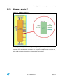
33.19 Mapping a generic IP
. . . . . . . . . . . . . . . . . . . . . . . . . . . . . . . . . . . . . . 663
33.20 Example of a mapped custom design . . . . . . . . . . . . . . . . . . . . . . . . . . 664
34
Expansion interface (EXPI) . . . . . . . . . . . . . . . . . . . . . . . . . . . . . . . . . . 666
34.1
Architecture overview . . . . . . . . . . . . . . . . . . . . . . . . . . . . . . . . . . . . . . . 666
34.2
Signal interface . . . . . . . . . . . . . . . . . . . . . . . . . . . . . . . . . . . . . . . . . . . . 667
34.3
Functional description . . . . . . . . . . . . . . . . . . . . . . . . . . . . . . . . . . . . . . 670
34.4
Address translation mechanism . . . . . . . . . . . . . . . . . . . . . . . . . . . . . . . 670
34.5
Programming model . . . . . . . . . . . . . . . . . . . . . . . . . . . . . . . . . . . . . . . . 672
34.6
Interface configuration logic . . . . . . . . . . . . . . . . . . . . . . . . . . . . . . . . . . 687
Appendix A Pin information. . . . . . . . . . . . . . . . . . . . . . . . . . . . . . . . . . . . . . . . . 689
Revision history . . . . . . . . . . . . . . . . . . . . . . . . . . . . . . . . . . . . . . . . . . . . . . . . . . . 711
Doc ID 022038 Rev 1
9/712
Preface
RM0305
1
Preface
1.1
Terms and definitions
The following terms are used in this document.
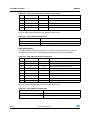
Table 1.
List of acronyms
Acronym
10/712
Description
ADC
Analog to Digital Convertor
AFE
Analog front end
ASIC
Application specific integrated circuit
AS
Application subsystem
AMBA
Advanced microcontroller bus architecture
AHB
AMBA High Speed bus
APB
Advanced Peripheral Bus
BS
Basic Subsystem
CLCD
Color Liquid Crystal Display
CRC
Cyclic Redundancy Check
DMA
Direct Memory Access
DDR
Double Data Rate
EMI
Extended Memory Interface
FIrDA
Fast Infrared Data Association
FPGA
Field Programmable Gate Array
FSMC
Flash NAND Static Memory Controller
GPIO
General Purpose Input Output
GPT
General Purpose Timer
HS
High speed subsystem
I2C
Inter Integrated Circuit
I2S
Inter IC Sound
JPEG
Joint Photographic Experts Group
JTAG
Joint Test Action Group
LS
Low speed subsystem
MAC
Media Access Control
PHY
Physical layer
RAM
Random Access Memory
RAS
Reconfigurable Array Subsystem
RFU
Reserved for Future Use
ROM
Read Only Memory
Doc ID 022038 Rev 1
RM0305
Preface
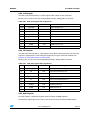
Table 1.
List of acronyms (continued)
Acronym
Description
RTC
Real Time Clock
SoC
System-on-Chip
SDIO
Secure Digital Input Output
SPEAr
Structured Processor Enhanced Architecture
SMI
Serial Memory Interface
SSP
Synchronous Serial Port
TCM
Tightly coupled memory
UART
Universal Asynchronous Receiver Transmitter
USB
Universal Serial Bus
VIC
Vectored Interrupt Controller
WDT
Watchdog Timer
Reserved
All reserved or unused bits of registers must be written as zero, and
ignored on read unless otherwise stated in the relevant text.
1.2
Conventions
1.2.1
Numbering
The following convention of stating constant numbers is used in this document:
[<size in bits>]′<base><number>
Where:
<size in bits>
(optional) width of bits field associated to <number>
<base>
“b” for binary, “h” for hexadecimal, “o” for octal, “d” for decimal
<number>
value of constant number, according to <base>
Examples:
d19
unsized decimal value
8′h2C
8-bit wide hexadecimal value of 0x2C, corresponding to b00101100
8′b011001
8-bit wide binary value of b00011001
32′hFFFF
32-bit wide hexadecimal value of 0xFFFF, corresponding to
b00000000000000001111111111111111
Doc ID 022038 Rev 1
11/712
Preface
1.2.2
RM0305
Bits
The conventions below apply to description of both bit and registry field hereafter in this
document:
1.2.3
●
a bit is defined as “set” when its value is set to ‘b1
●
a bit is defined as “cleared” when its value is set to ‘b0
Typographical conventions
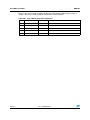
Table 2.
Typographical conventions
Format
12/712
Meaning
italic
Highlights notes.
bold
Highlights important terms, definitions and
names of registry field.
MONOSPACE CAPITAL BOLD
Indicates signal names.
Doc ID 022038 Rev 1
RM0305
2
Reference documents
Reference documents
Table 3.
Reference documents
Document
ARM926EJ-S – Technical Reference Manual
AMBA Specification (ARM IHI 0011A)
USB 2.0 Specification
Revision
–
2.0
–
(1)
SPEAr600_USB-Hosts.zip
–
SPEAr600_USB-Device.zip(1)
–
OHCI Specification
–
EHCI Specification
–
ISO/IEC 10918-1 (International Organization for Standardization)
–
1. These two documents are issued together with this reference manual.
Doc ID 022038 Rev 1
13/712
Architecture
RM0305
3
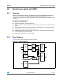
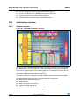
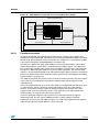
Architecture
3.1
SoC overview
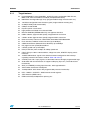
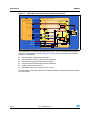
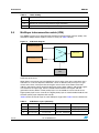
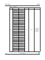
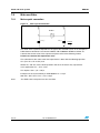
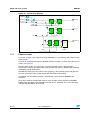
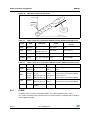
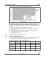
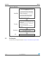
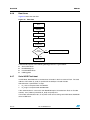
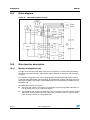
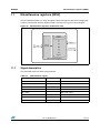
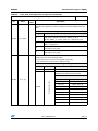
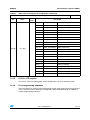
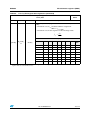
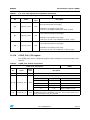
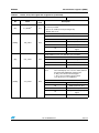
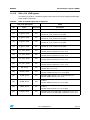
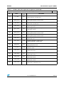
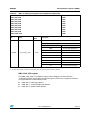
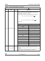
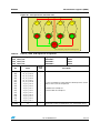
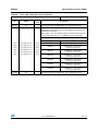
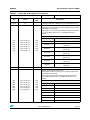
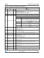
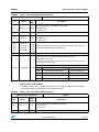
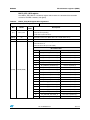
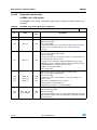
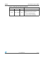
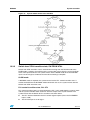
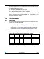
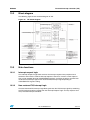
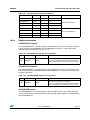
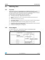
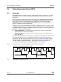
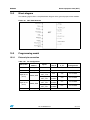
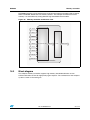
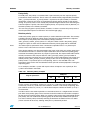
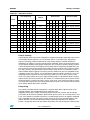
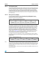
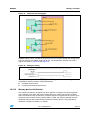
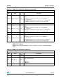
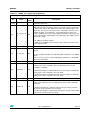
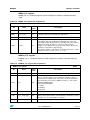
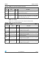
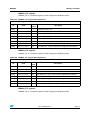
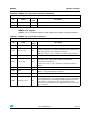
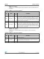
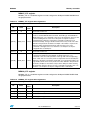
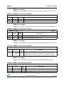
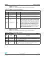
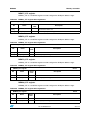
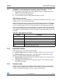
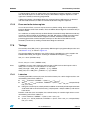
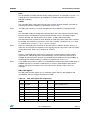
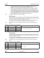
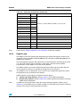
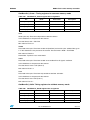
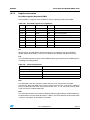
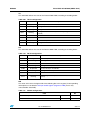
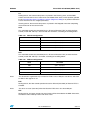
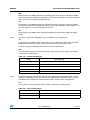
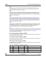
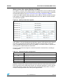
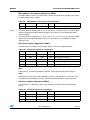
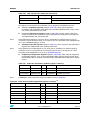
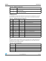
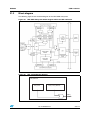
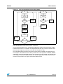
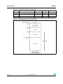
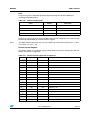
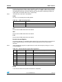
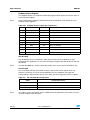
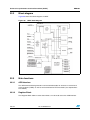
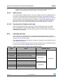
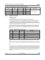
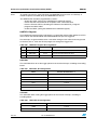
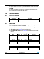
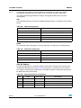
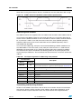
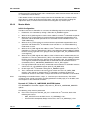
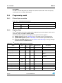
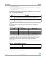
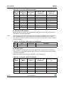
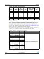
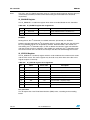
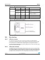
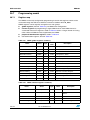
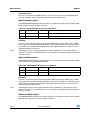
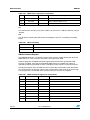
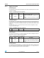
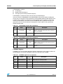
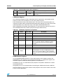
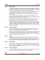
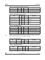
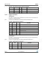
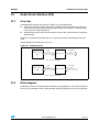
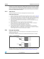
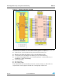
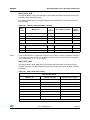
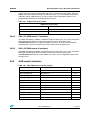
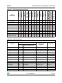
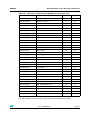
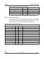
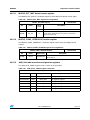
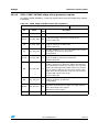
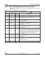
The following figure shows the main SPEAr600 functional interfaces.
Figure 1.
SPEAr600 top view
I2Ss (3)
GMII/MII
I2C
USB2.0 dev
SSPs (3)
USB2.0 host(2)
UARTs (2)
CLCD
IrDA
DDR 1/2
14/712
Spear600
GPIOs
PL_GPIOs
ADCs
PL_LVDSs
Flash Serial
JTAG & Test
Flash Nand
Doc ID 022038 Rev 1
RM0305
3.1.1
Architecture
Target features
●
Dual ARM926EJ-S core @333 MHz, 16 KB-I/D cache, configurable TMC-I/D size,
MMU, TLB, JTAG and ETM trace module (multiplexed interfaces)
●
600 KGate reconfigurable logic array (programmable through 4 metal and 4 vias)
●
128 KByte configurable internal memory pool (single and dual memory port)
●
32 KByte ROM (code customizable)
●
8 KByte shared SRAM
●
Dynamic power save features
●
High performance linked list 8 channels DMA
●
Ethernet GMII/MII (IEEE802.3/3x/1Q), management interface
●
USB 2.0 Device (high-full-slow speed); integrated PHY transceiver
●
2 USB 2.0 Host (high-full-slow speed); integrated PHY transceiver
●
External memory interface: 8-/16-bit DDR1@166 Mhz/ DDR2@333 Mhz
●
Flash interface: NAND 8-/16-bit and serial (up to 50 Mbps)
●
3 SSP Master/Slave (Motorola-Texas-National) up to 40 Mbps
●
I2C (high-fast-slow speed) Master/Slave
●
2 UART (speed rate up to 3 Mbps)
●
IrDA (Fir–Mir–Sir) from 9.6 Kbps to 4 Mbps speed-rate
●
Color LCD up to 1024 x 768 resolutions; 24bpp true color; STN/TFT display panels
interfaces.
●
10 GPIO bidirectional signals in the default functional configuration with interrupt
capability (named “Full features” mode in Table 796: Pin list)
●
9 LVDS (8 out and 1 input) signals; customizable interface through programmable logic
●
Audio block with 3-I2S interfaces to support audio play (Up to 3.1) and audio record
functionality
●
ADC (1us/1MSPS) 8 analog input channels; 10-bit approximation
●
JPEG Codec accelerator 1clock/pixel
●
10 independent 16-bit timers with programmable prescaler functionality
●
RTC – WDOG – SYSCTR – MISC internal control registers
●
JTAG interface (IEEE1149.1)
●
ETM functionality multiplexed on primary pins
Doc ID 022038 Rev 1
15/712
Architecture
3.2
Architecture properties
●
●
●
16/712
RM0305
Dual symmetric processor architecture:
–
All internal peripherals are shared, allowing flexible and efficient software
partitions
–
High throughput can be sustained in aggregate way splitting critical tasks either
onto additional CPUs and optional hardware accelerators engines
–
Critical resources are private to each CPU (interrupt controller and OS Timers)
–
Both processors are equipped with ICE and ETM configurable debug interfaces
Power save features:
–
Operating frequency software programmable
–
Clock gating functionality
–
Low frequency operating mode
–
Automatic power saving controlled from application activity demands
Customizable logic to embed the customer real ‘core competence’:
–
600 Kgate standard cell array based on the 7S01 high speed library (LST90 with
HVT and SVT mixed cells)
–
Internal memory pool (128 Kbyte) fully configurable
–
Up to 17 external and/or internal source clocks (some of which programmable)
–
Four memory path toward the SDRAM controller to ensure a good bandwidth
●
Easily extensible architecture
●
External memory bandwidth of each master tunable to meet the target performances of
different applications
Doc ID 022038 Rev 1
RM0305
Architecture
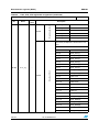
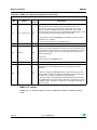
3.3
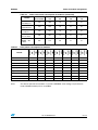
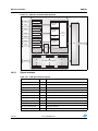
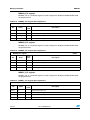
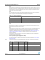
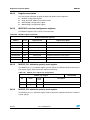
SoC architecture overview
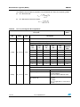
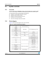
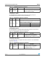
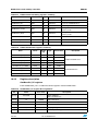
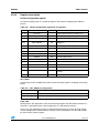
3.3.1
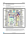
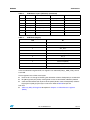
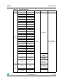
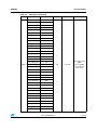
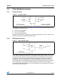
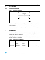
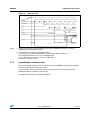
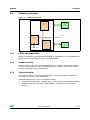
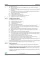
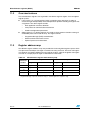
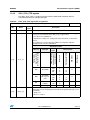
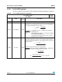
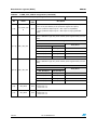
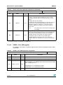
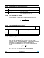
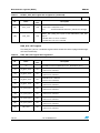
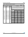
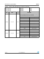
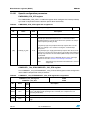
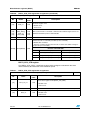
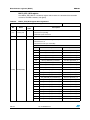
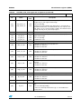
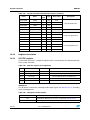
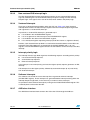
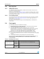
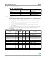
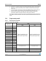
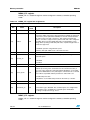
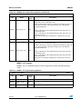
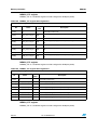
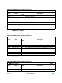
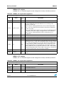
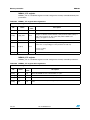
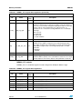
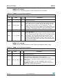
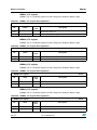
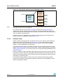
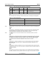
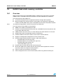
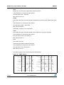
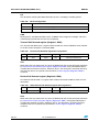
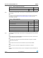
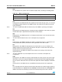
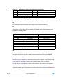
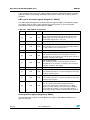
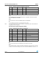
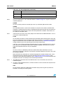
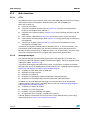
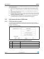
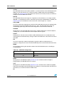
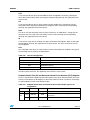
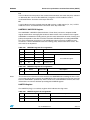
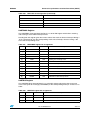
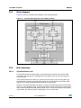
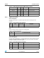
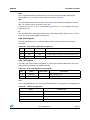
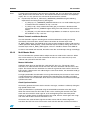
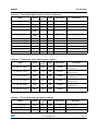
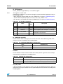
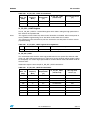
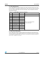
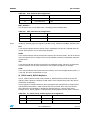
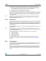
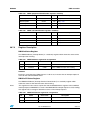
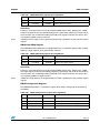
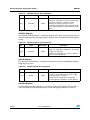
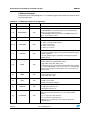
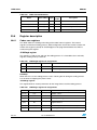
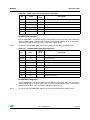
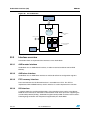
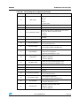
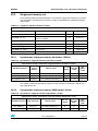
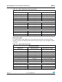
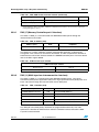
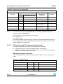
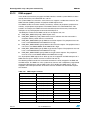
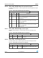
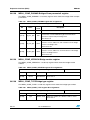
Core architecture
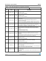
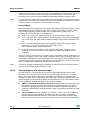
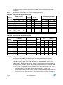
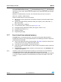
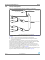
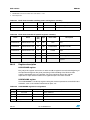
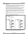
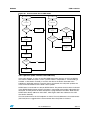
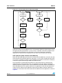
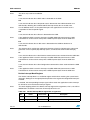
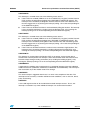
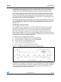
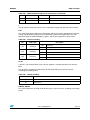
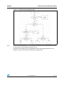
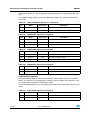
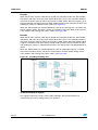
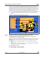
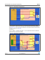
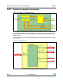
The SoC internal architecture is based on several shared subsystem logics interconnected
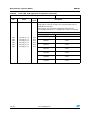
through a multilayer interconnection matrix, as detailed in the next figure.
Figure 2.
SPEAr600 core architecture overview
12
CPU 1
JTAG/ETM9
CPU 2
ARM926EJS
32kI/32kD cache
Coprocessor
TCM-I/D
SPEAr600
ARM926EJS
32kI/32lD cache
TCM-I/D
ARM1 subsystem
GPIO 1
0÷4
1 without nand
4 without CLCD
4 without GMAC
Timer 1
Int.Ctrl
Low Speed
subsystem
ARM2 subsystem
M1
M2
M6
1234
1
JPEG
codec
2
Int.Ctrl
6
45
3
125
IrDA
2
I2C
4
SSP 1
Q
P
O
N
M
F
57
DDR
M5
123
4 5 123 6
A
Flash
NAND
2
Timer 2
1 without nand
4 without CLCD
4 without GMAC
SDRAM
Ctrl DDR1-2
M3
cfg M4
34
Multi-layer AHB interconnect matrix
1235
0/15÷23
0÷4
GPIO 2
M0
D
RAM
8KB
0 without nand
Debug
G
High Speed
subsystem
USB 2.0
host 1
4
USB host
USB 2.0
host 2
4
USB host
USB 2.0
device
3
USB device
Giga
Ethernet
0/28
MII/GMII
to PHY
H
L
4
SSP 2
2÷8
UART 1
2÷4
UART 2
8 w/o nand
8 w/o CLCD
8 w/o GMAC
Exp I/F
Cell Array
600Kgates
Z
4 w/o GMAC
I2S
B
Application
subsystem
1 without CLCD
2 without GMAC
I2S
C
0÷2
9
Timer 4
0÷2
Timer 5
10
GPIO 4
4
SSP 3
10
8 ch.
ADC
1 LVDS in
8 LVDS out
ROM
Flash
serial
Timer 3
GPIO 3
Misc.
RTC
CLCD
ctrl
WDT
E
Dual Port
4 x 4kB
8 x 2kB
Reconfigurable
Array
Subsystem
2
16
Master clck
2
Master rst
1
5÷6
6 w/o nand
6 w/o CLCD
6 w/o GMAC
0÷6
128kB RAM Cuts:
4 x 8kB
8 x 4kB
16 x 2kB
System
Ctrl
DMA
8 chan.
R
I2S
Basic
subsystem
MUX
0/30
88
6 w/o nand
6 w/o CLCD
6 w/o GMAC
2
Oscillator
Color LCD
75 GPIO, 9 I2S
The switch matrix structure allows different subsystem dataflow to be executed in parallel
improving the core platform efficiency.
High performance master agents are directly interconnected with the memory controller
reducing the memory access latency; four different memory paths (three of them shared
with other masters) are reserved for the programmable logic to enhance the user application
throughput; the overall memory bandwidth assigned to each master port can be
Doc ID 022038 Rev 1
17/712
Architecture
RM0305
programmed and optimized through an internal efficient weighted round-robin arbitration
mechanism.
The internal memory pool is completely configurable to improve the performances of the
user application custom logic.
3.3.2
Subsystem overview
The SoC includes three major subsystems logic domains:
●
the configurable cell array subsystem
●
the common subsystem
●
the CPU subsystem
Configurable cell array subsystem
This block contains the Reconfigurable array subsystem logic (RAS) made by an array of
600 Kgate equivalent standard cells freely customizable through few metals and vias mask
layers changes during the customization process. The programmable logic allows reducing
the SoC NRE cost, the development cycle time improving the devices time to market. The
user custom logic can be configured using the following SoC internal resources:
Caution:
●
130 Kbyte of static memory arranged in four 32-KB macro group and one 2-KB group
●
Up to 17 selectable source clocks (either internal or external)
●
DMA support (up to 16 configurable DMA input/output request lines)
●
Power management interface
●
Interrupts line (12 outputs – 64 inputs)
●
4 AHB output master ports interconnected with the multi-channel memory controller
●
5 AHB input slave ports
●
1 interconnection port with the Expansion interface bus (EXPI)
●
9 LVDS (8 outputs – 1 input) signals
●
88/112 PL_GPIOS primary input/output signals
PL_GPIO pins are not configurable by software.
Common subsystem
This block consists of four different subsystems logics used to control the SoC basic
functions:
●
18/712
I/O connectivity:
–
Low speed: UART, SSP, I2C and IrDA.
–
High speed: MII 10/100/1000, USB 2.0 Host and Devices.
●
Hardware accelerator: JPEG-codec and DMA.
●
Video: Color LCD interface.
●
Common resources: Timers, GPIOs, RTC and Watchdog.
●
Power management functionality.
●
SoC configurability: Miscellaneous control logic.
Doc ID 022038 Rev 1
RM0305
Architecture
CPU subsystem
This subsystem includes the embedded CPU and its private subsystem logic based on
GPIOs, the interrupt controller and a double timer IP that provide the minimal hardware
resources necessary to support a generic operating system.
The subsystem is replicated twice so both processors have the same memory map (see
Table 24: ML1, 2 – Multi Layer CPU Subsystem); this structure allows the implementation of
a real symmetric multiprocessor architecture where both processors can execute the same
unique OS at the same time (all interrupt sources are handled by both processors). In a real
functional environment the CPUs can execute the same or different OS based on the user’s
application scenario; anyway the software architecture should be designed in such way to
avoid conflict on shared hardware resources (IPs or identical memory locations) avoiding to
use them at the same time.
The miscellaneous logic provides some internal resources like the processor-interlock and
the inter-processor communication mechanisms used to regulate the access on these
resources.
Each subsystem is configured with a different processor identification device number (PID
value readable at the address 0XF010.0004 bit0); this allows a conditional CPU software
code execution through a simple bit-test instruction in case the same OS is run by both
processors:
The processor identification device numbers are:
3.3.3
●
CPU subsystem number 1: PID value is equal to 0.
●
CPU subsystem number 2: PID value is equal to 1.
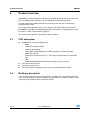
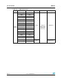
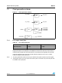
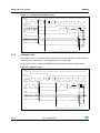
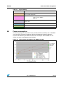
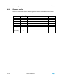
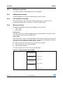
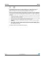
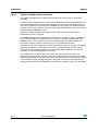
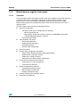
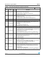
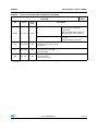
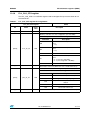
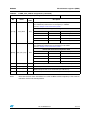
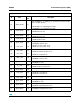
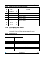
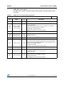
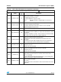
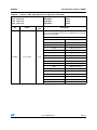
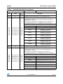
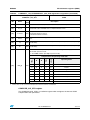
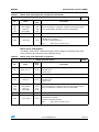
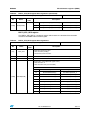
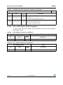
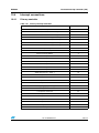
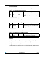
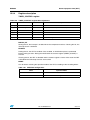
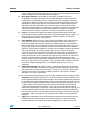
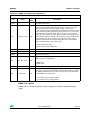
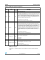
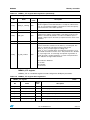
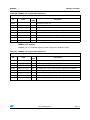
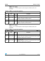
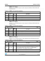
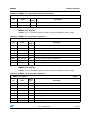
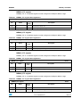
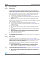
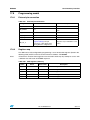
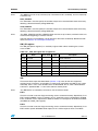
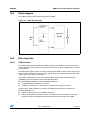
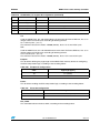
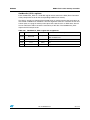
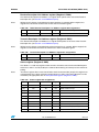
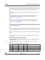
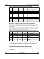
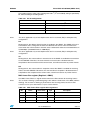
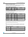
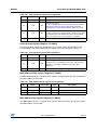
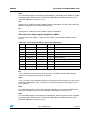
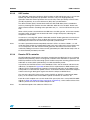
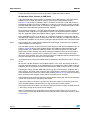
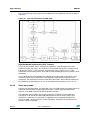
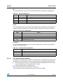
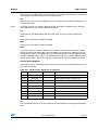
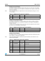
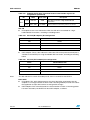
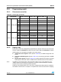
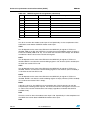
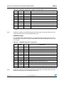
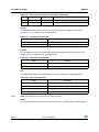
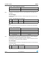
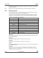
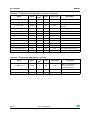
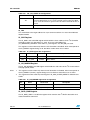
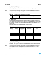
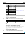
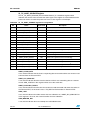
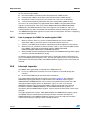
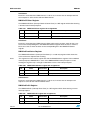
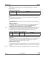
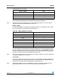
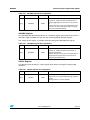
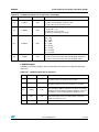
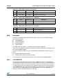
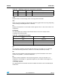
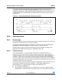
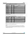
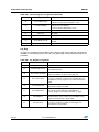
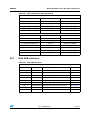
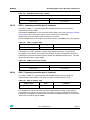
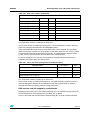
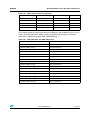
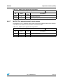
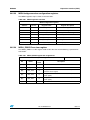
Expansion interface (EXPI)
The SoC provides an auxiliary AHB bidirectional interface (EXPI) multiplexed with PL_GPIO
signals to interconnect the external emulation FPGA used during the SoC RTL custom logic
development and validation phase. The FPGA ensures the code consistency before being
embedded in the ASIC programmable logic.
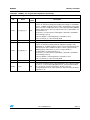
The EXPI interface is managed by the port controller subsystem which is mainly based on
three asynchronous internal bridges plus a small address translation unit (currently with four
entries) used to automatically reconstruct and remap the external master address, as
detailed in the next figure.
Doc ID 022038 Rev 1
19/712
Architecture
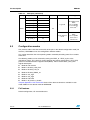
RM0305
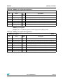
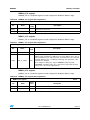
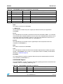
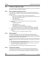
Figure 3.
SPEAr600 expansion interface architecture overview
Expansion Interface SoC scheme
RAS
EXPI_ITF_ENB
AHB Port controller Subsystem
(Logic Array)
Port Core
GPIO_Enb
0
Bdir Enable
Ctr
GPIO_Out
1
0
SLV i/f
2
1
1
3
0v
EXPI_RAS_ENB
0
MST i/f
M
L 2
E
11
X
P
0
GPIO_In
1
Port Ras
AHB-ICM9
EH2HA
ME2H
1
AHB-ML3
H2H-A
SH2H
4
AHB-ICM8
SL
IEXP
EH2HA
SE2H
ICM
Diag
3
Pads bidir.
0
0V
Loopback
Ctr
1
AHB_Xlat
Table
0
The EXPI interface is enabled from TEST (5:0) signals, and it is controlled and configured
through the Miscellaneous registers (Chapter 11); the main port controller programmable
features are listed below:
●
Internal bridges configuration parameters
●
Internal/external sources Clock and reset definition
●
Internal Clock gating and reset control functions
●
Internal source clock operating frequency definition
●
AHB bus compression scheme
●
EXPI DMA transfer type (single or burst cycles)
The AHB address translation table must be initialized before starting the expansion interface
bus transactions.
20/712
Doc ID 022038 Rev 1
RM0305
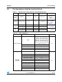
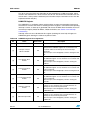
3.4
Architecture
Interconnection matrix
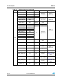
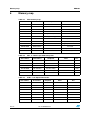
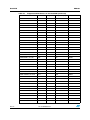
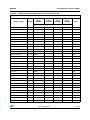
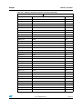
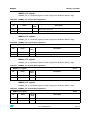
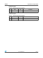
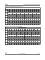
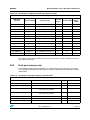
The following table shows the SPEAr600 interconnection matrix scheme.
See also Section 3.5: Multilayer interconnection matrix (ICM) below.
Table 4.
SoC interconnection matrix scheme
MemCtr#0
–
Icm8
MemCtr#3
Icm5
MemCtr#4
Icm10 Req2
Req
2
Req
1
Req
1
Req
Req
2
Icm7
Req
1
Req
Ras_M
Req
Ras_G1
Req
Ras_G2
Req
Icm6
Req1 Req2
Req
3
Sbs_LowSpeed Icm1
Req
4
Req
4
Req
1
Req
2
Sbs_HighSpeed Icm4
Req
3
Req
3
Req
1
Req
2
Icm3
Req
3
Req
3
Req
1
Req
2
Sbs_Application Icm2
Req
4
Req
4
Req
1
Req
2
Req
3
Req
1
Req
2
Req
3
Sbs_Basic
Expi_slave
Ras_Z
Req
2
Ras_N
Ras_F
Dma#2
Req
Req
1
MemCtr#2
MemCtr#5
Targets
Dma#1
Req
MemCtr#1
MemCtr#6
Processor#2
Processor#1
Expi_mst_eh2h
Ras_L
Expi_mst_h2h
Ras_H
Ras_E
CLCD
USB (Hosts- Device)
GMAC
Initiators
Icm9
Doc ID 022038 Rev 1
Req
3
21/712
Architecture
RM0305
Table 5.
Table shading
Legend
3.5
Description
A
Grey box: No connection exists between target and initiator.
B
White box: A connection exists between target and initiator.
C
'Req': A connection that is required between target and initiator.
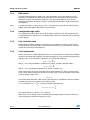
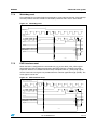
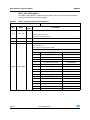
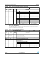
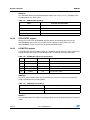
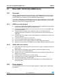
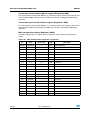
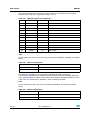
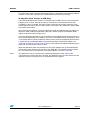
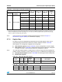
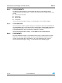
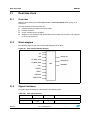
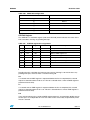
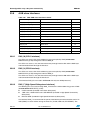
Multilayer interconnection matrix (ICM)
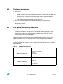
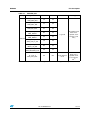
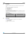
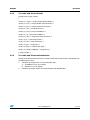
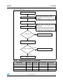
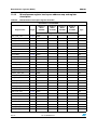
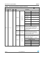
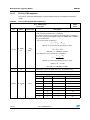
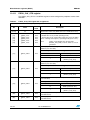
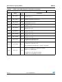
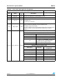
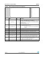
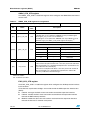
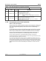
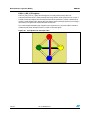
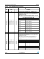
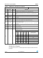
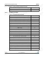
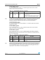
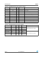
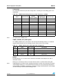
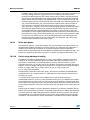
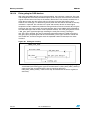
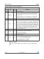
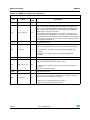
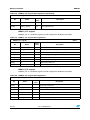
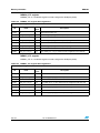
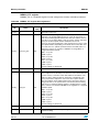
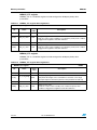
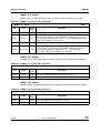
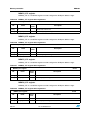
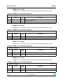
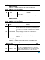
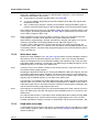
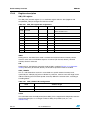
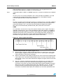
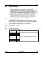
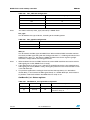
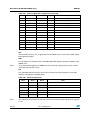
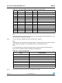
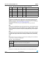
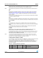
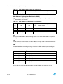
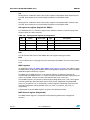
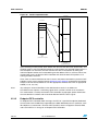
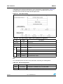
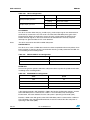
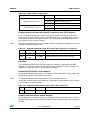
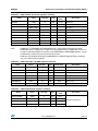
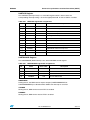
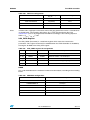
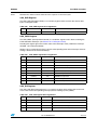
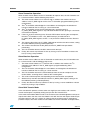
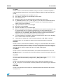
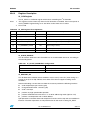
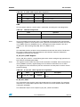
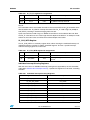
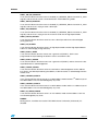
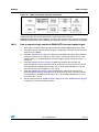
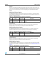
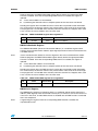
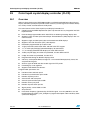
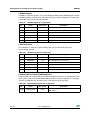
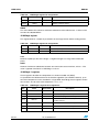
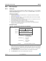
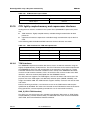
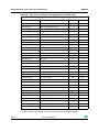
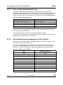
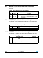
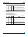
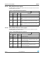
The AMBA system has ten programmable multilayer interconnection matrices (ICMs). The
ICM allows multiple master layers to access a slave (see Table 4 above).
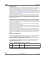
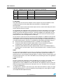
Figure 4.
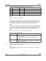
ICM block diagram
AHB MASTER (Layer 0)
ICM
AHB SLAVE
AHB MASTER (Layer N)
priority
Arbiter
A layer is referred to as one or more masters that compete together with one master taking
ownership of the slave.
When there is more than one layer looking for access to the slave at the same time, this is
referred to as a clash of requests. Whenever a clash is detected, only one layer can gain
access to the slave. The layers that do not gain access to the slave need to have their
address and control signals stored into their input stage. When address and control signals
are stored into an input stage, then the stored transfer controls the request and lock
generation circuitry. When a lower priority layer is in the middle of a burst transfer and a
higher priority layer issues a transfer, the higher priority layer is stored and then held off until
the lower priority layer completes the transfer.
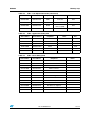
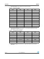
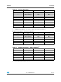
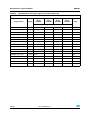
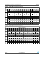
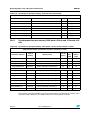
Table 6 shows the master layer on each ICM input stages while Table 7 lists the ICM slaves.
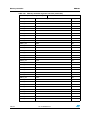
Table 6.
22/712
ICM Master Layers (initiators)
ICM
L0
L1
L2
L3
1
Processor#1
Processor#2
Dma#1
Expi_mst_h2h/RASH
2
Processor#1
Processor#2
Dma#2
Expi_mst_h2h/RASH
3
Processor#1
Processor#2
Expi_mst_h2h/RASH
Doc ID 022038 Rev 1
RM0305
Architecture
Table 6.
ICM Master Layers (initiators) (continued)
ICM
L0
L1
L2
4
Processor#1
Processor#2
Expi_mst_h2h/RASH
5
Dma#1
Expi_mst_h2h/RASH
6
GMAC
USB (Host s- Device)
7
Ras_E
CLCD
8
Ras_L
Expi_mst_eh2h
9
Processor#1
Processor#2
10
Ras_Z
GMAC
Table 7.
L3
CLCD
Dma#2
ICM Slave (targets)
ICM
M1
1
Sbs_LowSpeed
2
Sbs_Application
3
Sbs_Basic
4
Sbs_HighSpeed
5
MemCtr#3(MPMC)
6
Ras_F
7
MemCtr#6(MPMC)
8
MemCtr#2(MPMC)
9
Expi_slave
10
MemCtr#4(MPMC)
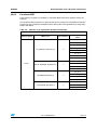
In the miscellaneous register bank, ten registers are allocated (ICM_x_ARB_CFG), one for
each ICM.
These registers have all the same layout:
●
the 31st bit is in charge of choosing the arbitration scheme: fixed priority or round robin
●
Bit [30:28] specify the priority starting level in case of round robin arbitration protocol
●
3 bits are allocated to each layer to set the priority level in case of fixed priority scheme:
bit [2:0] for Layer0, [5:3] for Layer1 and so on. Refer toTable 6 for layer list.
See also:
●
ICM1-10_ARB_CFG register description in Chapter 11: Miscellaneous registers
(MISC)
Doc ID 022038 Rev 1
23/712
Product overview
4
RM0305
Product overview
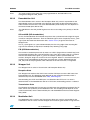
SPEAr600 is a powerful System-on-Chip based on 90nm HCMOS and consists of 2 main
parts: an ARM based architecture and an embedded customizable logic block.
The high performance ARM architecture frees the user from the task of developing a
complete RISC system.
The customizable logic block allows user to design custom logic and special functions.
SPEAr600 is optimized for embedded applications and thanks to its high performance can
be used for a wide range of different purposes.
The sections below provide a description of the main blocks.
4.1
CPU subsystem
●
4.2
ARM926EJ-S running at 333 MHz with:
–
MMU
–
16 KB of instruction CACHE
–
16 KB of data CACHE
–
TCM (Tightly Coupled Memory) available through the customizable logic
–
AMBA Bus interface
–
Coprocessor interface (Only the 1st processor) connected to the customizable
logic
–
JTAG
–
ETM9 (Embedded Trace Macro-cell) for debug; large size version.
●
Local Timer (two channels)
●
Local GPIO (up to 8 lines)
●
Interrupt controller managing sources which are prioritized and vectorized.
Multilayer bus matrix
It has six master inputs that are: two processors, two DMAs, the customizable logic block
and a muxed bus between Ethernet, USB device and USB host controller as well as seven
slave output connected to almost all the other blocks.
24/712
Doc ID 022038 Rev 1
RM0305
4.3
Product overview
Clock and reset system
●
4.4
Three PLLs:
–
Two of them are fully programmable (the first one generates the clock for CPU and
AMBA system; instead the second one generates the clock for the RAS block and
for some other blocks of the system. Both the PLLs offer an EMI reduction mode
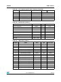
(Dithering) than can replace all traditional drop methods for Electro-Magnetic
Interference.
–
The third PLL generates the clock for USB controllers.
●
Several synthesizer able to provide different frequency for the different IPs.
●
Full control of clock and reset for all the slave blocks allowing a sophisticate Power
Management Control.
High speed connectivity subsystem
●
Ethernet GMAC controller that can run at 10/100/1000 with external PHY
●
Two USB hosts compatible with USB 2.0 High-Speed specification. They can work
simultaneously either in Full-Speed or in High-Speed mode. The peripherals have
dedicated channels to the multiport memory controller and 4 slave ports for CPU
programming. The PHYs are embedded.
●
One USB device compatible with USB 2.0 High-Speed specifications.
A dedicated channel connects the peripheral with the multiport memory controller and
registers and internal FIFO are accessible from the CPU through the main AHB Bus.
An USB-Plug Detector block is also available to verify the presence of the VBUS voltage.
The port is provided with sixteen physical endpoints and proper configurations to achieve
logical endpoints.
Table 8.
Endpoint Configuration
EP0
Control (IN/OUT)
EP1-3-5-7-9-11-13-15
Software configurable to:
– Bulk In
– Interrupt In
– Isochronous
EP2-4-6-8-10-12-14
Software configurable to:
– Bulk Out
– Interrupt Out
– Isochronous
Doc ID 022038 Rev 1
25/712
Product overview
4.5
4.6
RM0305
Low speed connectivity subsystem
●
Two UARTs with a speed rate up to 3 Mbps
●
FIrDA controller with a speed rate from 9.6 Kbps to 4 Mbps
●
Two SSP controllers capable to operate in Master and Slave (Motorola-Texas-National)
with a speed rate up to 40 Mbps.
●
One I2C controller capable to operate in master and slave mode and covering all the
possible speeds (High, Fast and Slow)
●
A NAND Flash Controller with 8 or 16 bit interface (this last interface is achievable only
in the configuration Disable_nand_flash. For more details refer to Miscellaneous
register SOC_CFG_CTR [bit 5:0] description.
●
JPEG Codec accelerator (1clk per pixel)
●
8 KB of static RAM
Dynamic memory controller
It is a multiport memory controller able to manage external DDR1 memory up to 166 MHz
and external DDR2 memory up to 333 MHz. Internally it handles 7 ports supporting the
following masters:
●
the two CPUs
●
Customizable logic block
●
Bus Matrix
●
Ethernet GMAC
●
USB 2.0 Device
●
the two USB 2.0 Hosts muxed with the LCD controller
The multiport memory controller block has a programmable arbitration scheme and the
transactions happen on a different layer from the main bus. It also offers local FIFO to
increase the throughput and reduce the latency.
4.7
26/712
Application subsystem
●
Four timers with programmable prescaler
●
Eight GPIOs bidirectional signals with interrupt capability
●
One SSP controller capable to operate in Master and Slave (Motorola-Texas-National)
with a speed rate up to 40Mbps
●
An ADC converter (1us/1MSPS) with 8 analog input channels; 10bit approximation
Doc ID 022038 Rev 1
RM0305
4.8
4.9
Product overview
Basic subsystem
●
Eight high performances DMA channels with two AHB Master Interfaces to parallelize
the activity when two channels are working at the same time
●
32 KB of ROM
●
Serial Flash Interface capable to work up to 50 Mbps
●
Color LCD controller up to 1024x768 resolutions; 24bpp true color; STN/TFT display
panel
●
Two timers with programmable prescaler
●
Watchdog timer
●
RTC with separated power supply allowing battery connection
●
Eight GPIOs bidirectional signals with interrupt capability
●
System Controller and miscellaneous registers array allowing a full configurability of the
SoC
Customizable logic block
The Configurable Logic array consists of an embedded macro where it is possible to
implement a custom project by mapping up to 600 K equivalent gates.
This macro is interfaced with the rest of the system by some AHB bus and some memory
channels and has a direct connection to the 1st ARM processor internal bus. In this way, it is
also possible to customize the TCM memory or add a coprocessor using this macro.
The following memory cuts are available to this block:
●
3 cuts single port with size of 768 bytes each
●
4 cuts single port with size of 8 kB each
●
8 cuts single port with size of 4 kB each
●
16 cuts single port with size of 2 kB each
●
8 cuts dual port with size of 2 kB each
●
4 cuts dual port with size of 4 kB each
The array is also connected to 88 I/O (3.3 V capable/tolerant and 4 mA sink/source) plus 9
lvds lines (one input and 8 outputs).
The following clocks can be used in the integrated logic:
●
5 different coming from the external balls
●
4 different coming from the integrated frequency synthesizer
●
PLL1 frequency
●
PLL2 Frequency
●
48 MHz (USB PLL)
●
30 MHZ (MAIN Oscillator)
●
32.768 KHz (RTC Oscillator)
●
APB clock (programmable)
●
AHB clock (programmable)
Doc ID 022038 Rev 1
27/712
Pin description
5
RM0305
Pin description
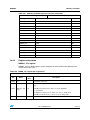
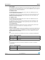
This chapter describes the pinout of the SPEAr600 listed by functional block. This
description refers to the default configuration of SPEAr600 (full features). More details on
the configuration of each pin are given in Chapter Appendix A: Pin information.
This chapter provides information about:
●
System reset, master clock, RTC and configuration pins
●
Power supply pins
●
Debug pins
●
SMI, SSP, UART, FIrDA and I2C pins
●
USB pins
●
Ethernet pins
●
GPIO pins
●
ADC pins
●
NAND Flash interface pins
●
DDR interface pins
●
LCD interface pins
●
LVDS interface pins
●
EXPI/I2S pins
●
EXPI pins
List of abbreviations:
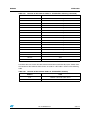
PU = Pull Up
PD = Pull Down
5.1
28/712
Required external components
●
DDR_COMP_1V8: place an external 121 kΩ resistor between ball V7 and ball V8
●
DDR_COMP_2V5: place an external 121 kΩ resistor between ball V9 and ball V8
●
USB_RREF: connect an external 1.5 kΩ pull-down resistor to ball U4
●
DIGITAL_REXT: place an external 121 kΩ resistor between ball E11 and ball E12
Doc ID 022038 Rev 1
RM0305
5.2
Pin description
Pin descriptions listed by functional block
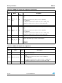
Table 9.
System reset, master clock, RTC and configuration pins
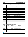
Group
Signal name
SYSTEM
RESET
Ball
MRESET
Direction
C17
Input
Function
Pin type
Main reset
TTL Schmitt
trigger input
buffer,
3.3 V tolerant, PU
Analog,
3.3 V capable,
see Section 5.1,
4th bullet.
CONFIG
DIGITAL_REXT
E11
Ref
Configuration
Master
clock
MCLK_XI
Y1
Input
30 MHz crystal I
MCLK_XO
Y2
Output
30 MHz crystal O
RTC_XI
A9
Input
32 kHz crystal I
RTC_XO
B9
Output
32 kHz crystal O
RTC
Table 10.
Oscillator,
2.5 V capable
Oscillator,
1.8 V capable
Power supply pins
Group
Signal name
Ball
Value
GND
J9, J10, J11, J12, J13, J14, K9,
K10, K11, K12, K13, K14, L9,
L10, L11, L12, L13, L14, M9,
M10, M11, M12, M13, M14, N9,
N10, N11, N12, N13, N14, P9,
P10, P11, P12, P13, P14, M18,
N18, P18, T5, V6
0V
DIGITAL GROUND
ANALOG
GROUND
RTC_GNDE
A10
DITH_VSS
U5
DDR_MEM_PLL_VSS_DIG
U17
DIGITAL_GNDBGCOMP
E12
ADC_AGND
V16
DDR_MEM_PLL_VSS_ANA
V17
USB_VSSC2V5
T4
USB_HOST1_VSSBS
R1
USB_HOST2_VSSBS
N2
USB_DEV_VSSBS
U2
USB_PLL_VSSP
W3
USB_PLL_VSSP2V5
W2
MCLK_GND
Y3
MCLK_GNDSUB
AA3
DITH_VSS2V5
V5
Doc ID 022038 Rev 1
0V
29/712
Pin description
RM0305
Table 10.
Power supply pins (continued)
Group
Signal name
Ball
Value
I/O
VDDE3V3
J6, H6, F8, F9, F16, H17, K17,
L17, N17, P17, M6, F17
3.3 V
CORE
VDD
G6, L6, G17, M17, R17, F10,
F13, F15, J17, T6, U13, U10, U16
1.0 V
HOST1/HOST2
USB PHY
USB_HOST_VDD3V3
R3
3.3V
USB_HOST2_VDDBC
N1
2.5 V
USB_HOST2_VDDBS
N3
1.0 V
USB_HOST1_VDDBC
P3
2.5 V
USB_HOST1_VDDBS
R2
1.0 V
USB_DEVICE_VDDBC
U1
2.5 V
USB_DEVICE_VDDBS
U3
1.0 V
USB_DEVICE_VDD3V3
T3
3.3 V
USB_PLL_VDDP
V3
1.0 V
USB_PLL_VDDP2V5
W1
2.5 V
MCLK_VDD
AA1
1.0 V
MCLK_VDD2V5
AA2
2.5 V
DITH_VDD2V5
V4
2.5 V
DITH_VDD
U6
1.0 V
DDR I/O(1)
SSTL_VDDE1V8
U7, U8, U9, U11, U12, U14, U15
1.8/2.5 V
ADC
ADC_AVDD
W16
2.5 V
DDR_MEM_PLL_VDD_ANA
W17
2.5 V
DDR_MEM_PLL_VDD_DIG
T17
1.0 V
LVDS I/O
LVDS_VDD2V5
F11, F12, F14
2.5 V
OSCI RTC
RTC_VDDE_1V8
B10
1.8 V
HOST2 USB PHY
HOST1 USB PHY
DEVICE USB PHY
USB PLL
OSCI (MASTER
CLOCK)
PLL1
PLL2
1. For DDRI the supply voltage must be 2.5 V, instead for DDR2 the supply voltage must be 1.8 V.
30/712
Doc ID 022038 Rev 1
RM0305
Pin description
Table 11.
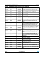
Debug pins
Group
Signal name
Ball
Direction
Function
BOOT_SEL
K18
Input
Boot selection
TEST_0
E15
TEST_1
E14
TEST_2
D14
Input
Configuration
ports
TTL input buffer,
3.3 V tolerant, PD
DEBUG
Table 12.
Group
TEST_3
D13
TEST_4
E13
TEST_5
D12
Pin type
nTRST
D17
Input
Test reset Input
TTL Schmitt
trigger, input
buffer, 3.3 V
tolerant, PU
TDO
E17
Output
Test data output
TTL output buffer,
3.3 V capable,
4 mA
TCK
E16
Input
Test clock
TDI
D16
Input
Test data input
TMS
D15
Input
Test mode
select
TTL Schmitt
trigger, input
buffer, 3.3 V
tolerant, PU
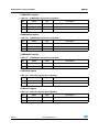
SMI, SSP, UART, FIrDA and I2C pins
Signal name
Ball
Direction
Function
Pin type
SMI_DATAIN
L21
Input
Serial Flash
input data
TTL input buffer,
3.3 V tolerant, PU
SMI_DATAOUT
L20
SMI_CLK
L22
SMI_CS_0
L19
SMI_CS_1
L18
Serial Flash
output data
SMI
Output
Doc ID 022038 Rev 1
Serial Flash
clock
TTL output buffer,
3.3 V capable,
4 mA
Serial Flash chip
selects
31/712
Pin description
Table 12.
Group
SSP
RM0305
SMI, SSP, UART, FIrDA and I2C pins (continued)
Signal name
Ball
SSP_1_MOSI
AA21
Master out slave
in
SSP_1_MISO
AB21
Master in slave
out
SSP_1_SCLK
AB22
Serial clock
SSP_1_SS
AA22
Slave select
SSP_2_MOSI
K20
Master out slave
in
SSP_2_MISO
K21
SSP_2_SCLK
K22
Serial clock
SSP_2_SS_0
K19
Slave select
SSP_3_MOSI
J20
Master out slave
in
SSP_3_MISO
J21
Master in slave
out
SSP_3_SCLK
J22
Serial clock
SSP_3_SS
J19
Slave select
UART1_TXD
AA19
UART2_TXD
AA20
UART1_RXD
AB19
Direction
I/O
Function
Master in slave
out
Pin type
TTL bidirectional
buffer, 3.3 V
capable,
8 mA,
3.3 V tolerant,
PU(1)
Output
Serial data out
TTL output buffer,
3.3 V capable,
4 mA
Input
Serial data in
TTL input buffer,
3.3 V tolerant, PD
UART
UART2_RXD
AB20
FIRDA_TXD
AA18
Output
Serial data out
TTL output buffer,
3.3 V capable,
4mA
FIRDA_RXD
AB18
Input
Serial data in
TTL input buffer,
3.3 V tolerant, PU
SDA
Y18
I/O
Serial data
in/out
SCL
Y19
I/O
Serial clock
FIrDA
I2C
TTL bidirectional
buffer, 3.3V
capable, 4 mA,
3.3 V tolerant, PU
1. When the pin is not driven, the output voltage is 2.5 V. On the core side, logic ‘1’ state is guaranteed.
32/712
Doc ID 022038 Rev 1
RM0305
Pin description
Table 13.
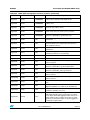
Group
USB pins
Signal name
Ball
USB_DEV_DP
V1
Direction
Function
Pin type
USB Device D+
Bidirectional
analog buffer,
5 V tolerant
I/O
USB_DEV_DM
V2
USB_DEV_VBUS
R4
USB_HOST1_DP
T1
USB Device D-
Input
USB Device
VBUS
TTL input buffer,
3.3 V tolerant, PD
USB HOST1 D+
Bidirectional
analog buffer
5 V tolerant
I/O
USB
USB_HOST1_DM
T2
USB HOST1 D-
USB_HOST1_VBUS
P5
Output
USB HOST1
VBUS
TTL output buffer,
3.3 V capable,
4 mA
USB_HOST1_OVRC
P6
Input
USB Host1
Over-current
TTL input buffer,
3.3V tolerant,
active low
USB_HOST2_DP
P1
USB HOST2 D+
I/O
Bidirectional
analog buffer,
5 V tolerant
USB_HOST2_DM
P2
USB HOST2 D-
USB_HOST2_VBUS
R5
Output
USB HOST2
VBUS
TTL output buffer,
3.3 V capable,
4 mA
USB_HOST2_OVRC
R6
Input
USB Host2
Over-current
TTL input buffer,
3.3 V tolerant,
active low
USB_RREF
U4
Output
Ext.Reference
resistor
Analog, see
Section 5.1, 3rd
bullet.
Doc ID 022038 Rev 1
33/712
Pin description
Table 14.
Group
RM0305
Ethernet pins
Signal name
Ball
Direction
Function
Pin type
GMII_TXCLK
F22
Output
Transmit clock
(GMII)
TTL output buffer,
3.3 V capable,
8 mA
GMII_TXCLK125
E22
Input
External Clock
I/O
Transmit clock
MII
MII_TXCLK
D22
TXD_0
F21
TXD_1
E21
TTL output buffer,
3.3 V capable,
8 mA
Output
TXD_2
F20
TXD_3
E20
GMII_TXD_4
D21
GMII_TXD_5
D20
GMII_TXD_6
C22
GMII_TXD_7
C21
TX_ER
D18
TTL input buffer,
3.3 V tolerant, PD
Transmit data
TTL bidirectional
buffer, 3.3 V
capable, 8 mA,
3.3 V tolerant, PD
I/O
Transmit error
Output
Ethernet
TTL output buffer,
3.3 V capable,
Transmit enable
8 mA
TX_EN
D19
RX_ER
C20
Receive error
RX_DV
C19
Receive data
valid
RX_CLK
A22
RXD_0
B22
RXD_1
B21
RXD_2
A21
RXD_3
B20
GMII_RXD_4
A20
GMII_RXD_5
B19
GMII_RXD_6
A18
GMII_RXD_7
A19
COL
A17
Receive clock
Input
TTL input buffer,
3.3 V tolerant, PD
Receive data
TTL bidirectional
buffer, 3.3 V
capable, 8 mA,
3.3 V tolerant, PD
I/O
Collision detect
Input
CRS
34/712
TTL input buffer,
3.3 V tolerant, PD
B17
Carrier sense
MDIO
B18
I/O
Management
data I/O
TTL bidirectional
buffer, 3.3 V
capable, 4 mA,
3.3 V tolerant, PD
MDC
C18
Output
Management
data clock
TTL output buffer,
3.3 V capable,
4 mA
Doc ID 022038 Rev 1
RM0305
Pin description
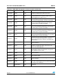
Table 15.
GPIO pins
Group
Signal name
Ball
GPIO_0
W18
GPIO_1
V18
GPIO_2
U18
GPIO_3
T18
GPIO_4
W19
GPIO_5
V19
GPIO_6
U19
GPIO_7
T19
GPIO_8
R19
GPIO_9
R18
Direction
GPIO
I/O
Function
Pin type
General
purpose I/O
TTL bidirectional
buffer, 3.3 V
capable, 8mA,
3.3 V tolerant,
PU(1)
1. When the pin is not driven, the output voltage is 2.5 V. On the core side, logic ‘1’ state is guaranteed.
Table 16.
Group
ADC
ADC pins
Signal name
Ball
Direction
Function
AIN_0
W11
AIN_1
V11
AIN_2
V12
AIN_3
W12
AIN_4
W13
AIN_5
V13
AIN_6
V14
AIN_7
W14
ADC_VREFN
W15
ADC negative
voltage
reference
ADC_VREP
V15
ADC positive
voltage
reference
Pin Type
ADC analog
input channel
Analog buffer,
2.5 V tolerant
Input
Doc ID 022038 Rev 1
35/712
Pin description
Table 17.
Group
RM0305
NAND Flash interface pins
Signal name
Ball
Direction
NF_IO_0
H19
NF_IO_1
H18
NF_IO_2
G19
NF_IO_3
G18
NF_IO_4
F19
NF_IO_5
F18
NF_IO_6
E18
NF_IO_7
E19
NF_CE
G20
Chip enable
NF_RE
G22
Read enable
NF_WE
H20
Write enable
NF_ALE
H21
I/O
NAND
FLASH
interface
Output
Function
Pin Type
Data
TTL bidirectional
buffer,
3.3 V capable,
4 mA,
3.3 V tolerant,
PU(1)
Address latch
enable
NF_CLE
G21
Command latch
enable
NF_WP
J18
Write protect
NF_RB
H22
Input
Read/busy
TTL output buffer,
3.3 V capable,
4 mA, active low
TTL output buffer,
3.3 V capable,
4 mA
TTL input buffer
3.3 V tolerant, PU
1. When the pin is not driven, the output voltage is 2.5 V. On the core side, logic ‘1’ state is guaranteed.
36/712
Doc ID 022038 Rev 1
RM0305
Pin description
Table 18.
Group
DDR
interface
DDR interface pins
Signal name
Ball
DDR_ADD_0
AB3
DDR_ADD_1
AB4
DDR_ADD_2
AA4
DDR_ADD_3
Y4
DDR_ADD_4
W4
DDR_ADD_5
W5
DDR_ADD_6
Y5
DDR_ADD_7
AA5
DDR_ADD_8
AB5
DDR_ADD_9
AB6
DDR_ADD_10
AA6
DDR_ADD_11
Y6
DDR_ADD_12
W6
DDR_ADD_13
W7
DDR_ADD_14
Y7
DDR_BA_0
Y9
DDR_BA_1
W9
DDR_BA_2
W10
DDR_RAS
AB7
DDR_CAS
AA7
Direction
Function
Output
Address
line
Pin type
SSTL_2/
SSTTL_18
Output
Bank
select
Row strobe
Column strobe
Output
DDR_WE
AA8
Write enable
DDR_CLKEN
AB8
Clock enable
DDR_CLK_P
AA9
Differential
Differential
DDR_CLK_N
AB9
Clock
SSTL_2/
SSTTL_18
DDR_CS_0
Y8
Output
Chip select
Output
DDR_CS_1
W8
Chip select
DDR_ODT_0
AB2
On-die
Termination
DDR_ODT_1
AB1
DDR_DATA_0
AB11
DDR_DATA_1
AA10
DDR_DATA_2
AB10
DDR_DATA_3
Y10
DDR_DATA_4
Y11
Output
Doc ID 022038 Rev 1
Enable lines
I/O
SSTL_2/
SSTTL_18
Data lines
(lower byte)
37/712
Pin description
Table 18.
Group
DDR
interface
38/712
RM0305
DDR interface pins (continued)
Signal name
Ball
DDR_DATA_5
Y12
DDR_DATA_6
AB12
DDR_DATA_7
AA12
DDR_DQS_0
AB13
Direction
Function
Pin type
Data lines
(Lower byte)
SSTL_2
/SSTTL_18
I/O
Differential lower
Data Strobe
Differential
SSTL_2/
SSTTL_18
DDR_nDQS_0
AA13
DDR_DM_0
AA11
Output
Lower data
mask
DDR_GATE_0
Y13
I/O
Lower gate open
DDR_DATA_8
AB15
DDR_DATA_9
AA16
DDR_DATA_10
AB16
DDR_DATA_11
Y16
DDR_DATA_12
Y15
DDR_DATA_13
Y14
DDR_DATA_14
AB14
DDR_DATA_15
AA14
DDR_DQS_1
AB17
DDR_nDQS_1
AA17
DDR_DM_1
AA15
SSTL_2/
SSTTL_18
I/O
Data lines
(Upper byte)
I/O
Differential
upper
Differential
Data strobe
SSTL_2/
SSTTL_18
Output
Upper data
mask
SSTL_2/
SSTTL_18
DDR_GATE_1
Y17
I/O
Upper gate open
DDR_VREF
V10
Input
Ref. voltage
Analog
DDR_COMP_2V5
V9
Ref
External ref.
resistor
Analog, see
Section 5.1, 2nd
bullet.
DDR_COMP_GND
V8
-
Common return
for ext. resistors
Power
DDR_COMP_1V8
V7
Ref
External ref.
resistor
Analog, see
Section 5.1, 1st
bullet.
DDR2_EN
D11
Input
Configuration
TTL input buffer,
3.3 V tolerant, PU
Doc ID 022038 Rev 1
RM0305
Pin description
Table 19.
Group
LCD interface pins
Signal name
Ball
Direction
Function
CLD_0
Y20
CLD_1
Y21
CLD_2
Y22
CLD_3
W22
CLD_4
W21
CLD_5
W20
CLD_6
V20
CLD_7
V21
CLD_8
V22
CLD_9
U22
CLD_10
U21
CLD_11
U20
CLD_12
T20
CLD_13
T21
CLD_14
R21
CLD_15
R20
CLD_16
P19
CLD_17
P20
CLD_18
P21
CLD_19
N21
CLD_20
N20
CLD_21
N19
CLD_22
M20
CLD_23
M21
CLAC
T22
STN AC bias
drive TFT Data
Enable
CLCP
R22
LCD Panel
Clock
CLFP
P22
STN Frame
Pulse\TFT
Vertical Sync
CLLP
N22
STN Line
Pulse\TFT
Horizontal Sync
CLLE
M22
Line End
CLPOWER
M19
LCD Power
Enable
Pin Type
LCD Data
LCD
interface
LCD
interface
TTL output buffer,
3.3 V capable,
8 mA
Output
Doc ID 022038 Rev 1
39/712
Pin description
Table 20.
Group
LVDS
interface
RM0305
LVDS interface pins
Signal name
Ball
PH0
A16
PH0n
B16
PH1
C16
PH1n
C15
PH2
A15
PH2n
B15
PH3
A14
PH3n
B14
PH4
C14
PH4n
C13
PH5
A13
PH5n
B13
PH6
A12
PH6n
B12
PH7
C12
PH7n
C11
PH8
A11
PH8n
B11
Direction
Function
Pin Type
Output
General
purpose I/O
With LVDS
transceiver
LVDS Driver
Input
40/712
Doc ID 022038 Rev 1
LVDS Receiver
RM0305
Pin description
Table 21.
EXPI/I2S pins
Group
Signal name
Ball
Direction
PL_GPIO_47/
ADO_REC_DIN
C2
I/O
PL_GPIO_48/
ADO_REC_WS
C1
I/O
PL_GPIO_50/
ADO_WS_OUT
A1
I/O
PL_GPIO_51/
ADO_DOUT2
B2
I/O
PL_GPIO_52/
ADO_DOUT1
A2
I/O
PL_GPIO_53/
ADO_CLK_in_529
C3
I/O
PL_GPIO_54/
MCLK_out_309
B3
I/O
PL_GPIO_55/
ADO_RECORD_CLK
A3
I/O
EXPI/I2S
PL_CLK_4/
ADO_CLK_OUT
A4
Out
Function
Pin Type
Logic I/O
TTL bidirectional
buffer 3.3 V
capable, 3.3 V
tolerant, 4 mA,
PU(1)
Logic External
Clock
TTL bidirectional
buffer, 3.3 V
capable, 8 mA,
3.3 V tolerant,
PU(1)
1. When the pin is not driven, the output voltage is 2.5 V. On the core side, logic ‘1’ state is guaranteed.
Doc ID 022038 Rev 1
41/712
Pin description
Table 22.
Group
EXPI
42/712
RM0305
EXPI pins
Signal name
Ball
PL_GPIO_0
P4
PL_GPIO_1
N4
PL_GPIO_2
N5
PL_GPIO_3
N6
PL_GPIO_4
M5
PL_GPIO_5
M4
PL_GPIO_6
M3
PL_GPIO_7
M2
PL_GPIO_8
M1
PL_GPIO_9
L1
PL_GPIO_10
L2
PL_GPIO_11
L3
PL_GPIO_12
L4
PL_GPIO_13
L5
PL_GPIO_14
K6
PL_GPIO_15
K5
PL_GPIO_16
K4
PL_GPIO_17
K3
PL_GPIO_18
K2
PL_GPIO_19
K1
PL_GPIO_20
J1
PL_GPIO_21
J2
PL_GPIO_22
J3
PL_GPIO_23
J4
PL_GPIO_24
J5
PL_GPIO_25
H5
PL_GPIO_26
H4
PL_GPIO_27
H3
PL_GPIO_28
H2
PL_GPIO_29
H1
PL_GPIO_30
G1
PL_GPIO_31
G2
PL_GPIO_32
G3
PL_GPIO_33
G4
PL_GPIO_34
G5
Direction
Doc ID 022038 Rev 1
I/O
Function
Pin Type
Logic I/O
TTL bidirectional
buffer,
3.3 V capable,
3.3 V tolerant,
4 mA, PU(1)
RM0305
Pin description
Table 22.
Group
EXPI
EXPI pins (continued)
Signal name
Ball
PL_GPIO_35
F5
PL_GPIO_36
F4
PL_GPIO_37
F3
PL_GPIO_38
F2
PL_GPIO_39
F1
PL_GPIO_40
E4
PL_GPIO_41
E3
PL_GPIO_42
E2
PL_GPIO_43
E1
PL_GPIO_44
D3
PL_GPIO_45
D2
PL_GPIO_46
D1
PL_GPIO_49
B1
PL_GPIO_56
B4
PL_GPIO_57
C4
PL_GPIO_58
D4
PL_GPIO_59
E5
PL_GPIO_60
D5
PL_GPIO_61
C5
PL_GPIO_62
B5
PL_GPIO_63
B6
PL_GPIO_64
C6
PL_GPIO_65
D6
PL_GPIO_66
E6
PL_GPIO_67
F6
PL_GPIO_68
F7
PL_GPIO_69
E7
PL_GPIO_70
D7
PL_GPIO_71
C7
PL_GPIO_72
B7
PL_GPIO_73
E8
PL_GPIO_74
D8
PL_GPIO_75
C8
PL_GPIO_76
B8
PL_GPIO_77
A8
Direction
Doc ID 022038 Rev 1
I/O
Function
Pin Type
Logic I/O
TTL bidirectional
buffer,
3.3 V capable,
3.3 V tolerant,
4 mA, PU(1)
43/712
Pin description
RM0305
Table 22.
Group
EXPI
EXPI pins (continued)
Signal name
Ball
PL_GPIO_78
C9
PL_GPIO_79
D9
PL_GPIO_80
E9
PL_GPIO_81
E10
PL_GPIO_82
D10
PL_GPIO_83
C10
PL_CLK_1
A7
PL_CLK_2
A6
PL_CLK_3
A5
Direction
Function
Pin Type
Logic I/O
TTL bidirectional
buffer,
3.3 V capable,
3.3 V tolerant,
4 mA, PU(1)
Logic External
Clock
TTL bidirectional
buffer,
3.3 V capable,
8 mA, 3.3 V
tolerant, PU
I/O
1. When the pin is not driven, the output voltage is 2.5 V. On the core side, logic ‘1’ state is guaranteed.
5.3
Configuration modes
The previous tables show the connectivity of the pins in the default configuration mode (full
features). SPEAr600 can be also configured in different modes.
This section describes the main operating modes created by disabling some IPs to enable
other ones.
The following modes can be selected by setting the TEST_0... TEST_5 pins at the
appropriate values. This setting is used to program the control register (SOC_CFG_CTR)
present in the Miscellaneous registers block (MISC). Please refer to SOC_CFG_CTR
register description.
●
Mode 0: Full features
●
Mode 1: Disable_nand_flash
●
Mode 2: Disable_LCD_ctr
●
Mode 3: Disable_GMAC_ctr
●
Mode 4: self_cfg4
●
Mode 5: self_cfg5
●
Mode 6: Full RAS
●
Mode 7: All_Process_disable
Chapter Appendix A: Pin information shows all the alternate functions available in each
mode. Mode 0 is the default mode for SPEAr600.
5.3.1
Full features
Default configuration, I/O standard features.
44/712
Doc ID 022038 Rev 1
RM0305
5.3.2
Pin description
Disable NAND Flash
The NAND Flash interface is disabled and alternatively the following features are provided:
5.3.3
●
UART extension for modem flow control
●
One additional SMI chip select (see Chapter 17: Serial memory interface).
Disable LCD controller
The Color LCD controller interface is disabled and alternatively the following features are
provided:
5.3.4
●
UART extension for modem flow control
●
One additional clock programmable through GPT registers (see also Chapter 15:
General purpose timer (GPT))
●
Additional 8 data lines of NAND Flash interface not otherwise available.
●
One additional SMI chip select.
Disable GMAC controller
The GMAC interface is disabled and alternatively the following features are provided:
5.3.5
●
Two UARTs: one with extension for modem flow control and one with simplified
hardware flow control
●
One additional SMI chip select
●
Four additional clocks programmable trough the GPT registers
Self cfg_4
In this mode the AHB expansion interface is enabled on the PL_GPIO (83:0) pins. In this
mode source clock and reset signals are provided from the external application logic.
5.3.6
Self cfg_5
In this mode the AHB expansion interface is enabled on the PL_GPIO (83:0) pins. In this
mode source clock and reset signals are internally provided.
5.3.7
All processors disabled
This mode configures the SoC as an I/O slave target device controlled by an external master
application (the internal processors can be disabled).
Doc ID 022038 Rev 1
45/712
Memory map
6
RM0305
Memory map
Table 23.
Start address
End address
Peripheral
Notes
0x0000.0000
0x3FFF.FFFF
External SDRAM
DDR1 or DDR2
0x4000.0000
0x400007FF
R.F.U
R.F.U
0x40000800
0x40000820
I2S
I2S dual port memory
0x40000821
0xBFFF.FFFF
R.F.U
R.F.U
0xC000.0000
0xCFFF.F7FF
AHB_EH2H exp. interface
0xCFFF.F800
0xCFFF.FFFF
AHB_EH2H registers
0xD000.0000
0xD7FF.FFFF
ICM1
Low Speed connection
0xD800.0000
0xDFFF.FFFF
ICM2
Application Subsystem
0xE000.0000
0xE7FF.FFFF
ICM4
High Speed Connection
0xE800.0000
0xEFFF.FFFF
0xF000.0000
0xF7FF.FFFF
ML1,2
Multi Layer CPU subsystem
0xF800.0000
0xFFFF.FFFF
ICM3
Basic Subsystem
Table 24.
Reserved
ML1, 2 – Multi Layer CPU Subsystem
Start address
End address
Peripheral
0xF000.0000
0xF00F.FFFF
Timer
APB
0xF010.0000
0xF01F.FFFF
GPIO
APB
0xF020.0000
0xF0FF.FFFF
-
0xF100.0000
0xF10F.FFFF
VIC Secondary
AHB
0xF110.0000
0xF11F.FFFF
VIC Primary
AHB
0xF120.0000
0xF7FF.FFFF
-
Table 25.
46/712
Main memory map
Notes
Bus
Reserved
AHB
Reserved
AHB
ICM1 – Low Speed Connection
Start address
End address
Peripheral
0xD000.0000
0xD007.FFFF
UART 1
APB
0xD008.0000
0xD00F.FFFF
UART 2
APB
0xD010.0000
0xD017.FFFF
SSP 1
APB
0xD018.0000
0xD01F.FFFF
SSP 2
APB
0xD020.0000
0xD027.FFFF
I2C
APB
0xD028.0000
0xD07F.FFFF
-
0xD080.0000
0xD0FF.FFFF
JPEG codec
AHB
0xD100.0000
0xD17F.FFFF
FIrDA
AHB
Doc ID 022038 Rev 1
Notes
Reserved
Bus
-
RM0305
Memory map
Table 25.
ICM1 – Low Speed Connection (continued)
Start address
End address
Peripheral
Notes
Bus
0xD180.0000
0xD1FF.FFFF
FSMC
NAND Flash
Controller
AHB
0xD200.0000
0xD27F.FFFF
FSMC
NAND Flash Memory
AHB
0xD280.0000
0xD2FF.FFFF
SRAM
Static Ram Shared
memory (8KB)
AHB
0xD300.0000
0xD7FF.FFFF
-
Reserved
-
Table 26.
ICM2 – Application Subsystem
Start address
End address
Peripheral
0xD800.0000
0xD807.FFFF
Timer 1
APB
0xD808.0000
0xD80F.FFFF
Timer 2
APB
0xD810.0000
0xD817.FFFF
GPIO
APB
0xD818.0000
0xD81F.FFFF
SSP 3
APB
0xD820.0000
0xD827.FFFF
ADC
APB
0xD828.0000
0xDFFF.FFFF
-
Table 27.
Notes
Bus
Reserved
ICM3 – Basic Subsystem
Start address
End address
Peripheral
0xF800.0000
0xFBFF.FFFF
Serial Flash Memory
0xFC00.0000
0xFC1F.FFFF
Serial Flash Controller
0xFC20.0000
0xFC3F.FFFF
LCD Controller
0xFC40.0000
0xFC5F.FFFF
DMA Controller
0xFC60.0000
0xFC7F.FFFF
SDRAM Controller
0xFC80.0000
0xFC87.FFFF
Timer
0xFC88.0000
0xFC8F.FFFF
Watch Dog Timer
0xFC90.0000
0xFC97.FFFF
Real Time Clock
0xFC98.0000
0xFC9F.FFFF
General Purpose I/O
0xFCA0.0000
0xFCA7.FFFF
System Controller
0xFCA8.0000
0xFCAF.FFFF
Miscellaneous registers
0xFCB0.0000
0xFEFF.FFFF
-
Reserved
0xFF00.0000
0xFFFF.FFFF
Internal Rom
Boot
Doc ID 022038 Rev 1
Notes
47/712
Memory map
RM0305
Table 28.
48/712
ICM4 – High Speed Connection
Start address
End address
Peripheral
Notes
Bus
0xE000.0000
0xE07F.FFFF
-
Reserved
APB
0xE080.0000
0xE0FF.FFFF
Ethernet ctrl
GMAC
AHB
0xE100.0000
0xE10F.FFFF
USB2.0 Device
FIFO
AHB
0xE110.0000
0xE11F.FFFF
USB2.0 Device
Configuration registers
AHB
0xE120.0000
0xE12F.FFFF
USB2.0 Device
Plug Detect
AHB
0xE130.0000
0xE17F.FFFF
-
Reserved
AHB
0xE180.0000
0xE18F.FFFF
USB2.0 EHCI 1
AHB
0xE190.0000
0xE19F.FFFF
USB2.0 OHCI 1
AHB
0xE1A0.0000
0xE1FF.FFFF
-
0xE200.0000
0xE20F.FFFF
USB2.0 EHCI 2
AHB
0xE210.0000
0xE21F.FFFF
USB2.0 OHCI 2
AHB
0xE220.0000
0xE27F.FFFF
-
Reserved
AHB
0xE280.0000
0xE28F.FFFF
ML USB ARB
Configuration register
AHB
0xE290.0000
0xE7FF.FFFF
-
Reserved
AHB
Doc ID 022038 Rev 1
Reserved
AHB
RM0305
7
Clock and reset system
Clock and reset system
The Clock System block is able to generate all clocks necessary for the chip.
The main clocks, at default operative frequency, are:
●
Clock @ 333 MHz for the CPUs (PLL1 source)
●
Clock @ 166 MHz for AHB Bus and AHB peripherals (PLL1 source)
●
Clock @ 83 MHz for, APB Bus and APB peripherals (PLL1 source)
●
Clock @ 100-333 MHz for DDR memory interface (PLL1, PLL2 source)
●
Clock @ 12 MHz, 30 MHz, 48 MHz (PLL3 source)
The above frequencies are the maximum allowed value.
All these clocks are generated by three PLLs.
PLL1 and PLL2 sources are fully programmable through dedicated registers.
See also PLL-related registers in Chapter 11: Miscellaneous registers (MISC).
The PLLs input reference clocks can be chosen between (see PLL_CLK_CFG register):
●
30 MHz oscillator or PL_CLK_4 pad for PLL1
●
30 MHz oscillator or PL_CLK_3 pad for PLL2
At reset, the 30MHz source is selected.
To reduce the electromagnetic emission both PLL1 and PLL2 can be programmed to work in
dithered mode.
When the dithered mode is enabled the PLL output clock is modulated and the frequency
assumes a triangular shape. In this way the clock power spectrum is spread on a small
range (programmable) of frequencies decreasing the emission power peak.
This method replaces the other traditional methods of E.M.I. reduction, as filtering, ferrite
beads, chokes, adding power layers and ground planes to PCBs, metal shielding etc.,
allowing sensible cost saving for customers.
PLL1 and PLL2 can work in three operating modes:
●
Normal Mode (Dither-Off Mode): the PLL behaves as a normal PLL
●
Fractional-N Synthesis Mode: with this mode you can select VCO frequencies that are
not integer multiples of the reference frequency.
●
Dither-On Mode (double side modulation): in this mode, the triangular wave is added to
the VCO frequency.
●
Dither-On Mode (single side modulation): it is similar to double side modulation but the
modulation is only subtracting from the main frequency.
PLL3 is used to generate the USB controller clocks and it cannot be configured through
registers.
Doc ID 022038 Rev 1
49/712
Clock and reset system
7.1
RM0305
Clock generation scheme
Figure 5.
Clock generation scheme
PL_CLK(2)
PLL2
(AUX)
CLK_PLL2
PL_CLK(3)
PLL1
(SYS)
CLK_PLL1
PLL3
(USB)
UCLK12MHZ
UCLK30MHZ
UCLK48MHZ
30 MHZ
OSC
CLK30MHZ
32.768 KHZ
7.1.1
OSC
CLK32KHZ
PLL output clock jitter
Table 29.
PLL output clock jitter
Jitter
PLL1/PLL2
PLL3
Single Period Jitter
+/-35ps
+/-30ps
Cycle to Cycle Jitter
+/-40.8ps
+/-30ps
Single period jitter can be defined as the difference of the Tmax and Tmin, where Tmax is
maximum time period of the CLOCK and Tmin is the minimum time period of the CLOCK.
Cycle-to-cycle jitter is the cycle time variation between adjacent cycles over a random
sample of adjacent clock cycle pairs.
Note:
50/712
1
The jitter specification holds true only up to 50 mV noise (peak to peak) on power supply.
2
These jitter values are for PLL input clock with no jitter. In CI mode, any clock tree jitter will
be added to the output jitter.
Doc ID 022038 Rev 1
RM0305
Clock and reset system
7.2
Clock distribution scheme
7.2.1
Processor clock
Figure 6.
Processor clock
CLK_Pll1
CLK_ARM1
CLK30MHz
CLK_ARM2
CLK32KHz
HCLK
Frequency CLK Selector
(From MISC Registers)
Source CLK Selector
(From System CTRL)
According to the state machine (see Chapter 12: System controller) the CPU clock can be
derived from the following sources:
●
External crystal (30 MHz)
●
PLL1 (up to 333 MHz)
●
RTC crystal (32.768 KHz)
Setting the miscellaneous registers you can define the frequency of the PLL1 and the ratio
between the CPU clock and the BUS (HCLK) clock.
7.2.2
DDR controller clock
Figure 7.
DDR controller clock
CLK_Pll1
CLK_Pll2
Memory
Controller
Cloc k
DLL
Mem.
Ctrl
DDR_CLK
HCLK
CLK Selec tor
(From MISC Regis ters )
The memory controller uses the HCLK to synchronize the internal bus access and the other
clock, which can be chosen from PLL1 or PLL2 (Misc register setting) and that is used on
the external memory interface. Two clock domains can be synchronous or asynchronous.
For example, we can have the CPU running at 333 MHz and the HCLK bus running at
166 MHz, but the external DDR memory running at 166 MHz to reduce the board cost. In
this example, the PLL1 will provide the clock to all the internal blocks (CPU and bus) while
PLL2 will provide the frequency to the external memory. Having the two clock domains
asynchronous offers more flexibility in the system definition, but also adds more latency due
to the resynchronization stages.
Doc ID 022038 Rev 1
51/712
Clock and reset system
7.2.3
RM0305
BUS clocks
Through the miscellaneous CORE_CLK_CFG and PRPH_CLK_CFG registers you can
define the ratio between the CPU clock and its HCLK, the ratio between the AHB and the
APB clock, and the source for the peripheral clock. Some other registers offer also the
possibility to enable or disable the clock for each peripheral allowing a sophisticated power
management.
Note:
It is NOT possible to set hclk_clk[1,2]_ratio = 1:3 when clk[1,2]_divsel=1:2. Please refer to
CORE_CLK_CFG register description for more details.
7.2.4
Configurable logic clock
The configurable logic receives almost all the clocks available on the SoC and, during the
customization phase, the final user can define which is the most useful one to be used in the
custom design.
7.2.5
Port controller clock
Several different clocks defining a synchronous or asynchronous interface to the external
FPGA can drive the port controller. The miscellaneous EXPI_CLK_CFG register is used to
control this clock source and frequency.
7.2.6
Clock synthesizer
Clock synthesizer is a digital signal generator. It is used to perform a fractional clock divider.
Giving an input clock with frequency Fin and two integers X (synt_xdiv field of programming
register) and Y (synt_xdiv field), it generates a new clock with frequency:
X
F out 1 = ⎛ Fin ⋅ ----⎞ ⁄ 2
⎝
Y⎠
With X ≤ Y/2, if the post divider is enabled (synt_clkout_sel field is cleared). While:
X
F out 2 = ⎛ Fin ⋅ ----⎞
⎝
Y⎠
With X ≤ Y/2, if post divider is disable (synt_clkout_sel field is set).
Clock synthesizer is based on Y-modulo counter incremented by X. After reset the counter
value is zero and it increments of X every input clock cycle. If N is the number of input clock
cycle the output is high when:
N⋅X≥Y
The counter loads the value Y-NX a clock cycle after that it is verified the previous condition,
the output becomes low and the process iterates again.
If Y is a multiple of X, N = Y
---- is a constant and the output period is:
X
Y
T out = T in ⋅ N = T in ⋅ ---X
The output frequency is given by F out 2 formula.
When Y/X is not an integer value, the output period swings between N and N+1 times the
input clock period, with N the integer part of Y/X.
52/712
Doc ID 022038 Rev 1
RM0305
Clock and reset system
This means that the maximum period drift is of one input clock period.
For instance:
With Fout= 40 MHz, Fin= 333MHz the synthesizer parameters using F out 2 are:
X=40 and Y=333
This means that the output clock period is on average: Tout = 8.325 * Tin.
The output period will be 8 or 9 times the input clock period:
Tout = 8 * 3 = 24 ns and Tout = 9 * 3 = 27 ns
The maximum output period drift is 27-25 =2 ns.
Since the output clock is high for one input clock cycle the duty cycle is:
X
DC ( % ) = ⎛⎝ ----⎞⎠ ⋅ 100
Y
If the post divider by two is enabled the D.C. is 50%; in this case the output frequency is
given by F out 1 .
It can be shown that the period drift in this case is twice the input clock period.
To program the synthesizer please refer to Section 11.4.17: Auxiliary clock synthesizer
registers.
7.3
Clock summary
The following table shows all the clocks present inside the SPEAr600.
Table 30.
Clock summary
Clock name
Frequency
Source
Block
clk
333
PLL-DITH1
CPU
hclk
166.5
PLL-DITH1
AHB
pclk
83.25
PLL-DITH1
APB
sclk
83.25
PLL-DITH1
SYSCTRL
timer_clk
≤ 166.5(p) / 48 / -
PLL-DITH1 / PLL-USB /
TIMER (GPT)
irda_clk
≤ 83.25(s) / 48 / -
PLL-DITH1 / PLL-USB / PAD
IRDA
uartclk
≤ 83.25(s) / 48
PLL-DITH1 / PLL-USB
UART
sspclk
83.25 / -
PLL-DITH1 / PAD
SSP
ic_clk
166.5 / -
PLL-DITH1 / PAD
I2C
adc_clk
≤ 83.25/6(p)
PLL-DITH1
ADC
clcdclk
≤ 83.25(s) - 166.5 / 48 / -
PLL-DITH1 / PLL-USB / PAD
CLCD
wdogclk
83.25
PLL-DITH1
WDOG
clk32k
32768 Hz
PAD
RTC
rxclk
125-25-2.5 / 25-2.5
PAD / PLL-DITH2
txclk
125-25-2.5 / 25-25-2.5
PAD / PLL-DITH2
GMAC
Doc ID 022038 Rev 1
53/712
Clock and reset system
RM0305
Table 30.
Clock summary (continued)
Clock name
7.4
Frequency
clk30_[1,2,3]
30
clk48_[2,3]
48
clk12_[2,3]
12
ddrcore_clk
Source
Block
PLL-USB
USBD - USBH
166.5-333 / <333
PLL-DITH1 / PLL-DITH2
MPMC
ahb_exp_clk
≤ 83.25(s)-166.5 / ≤ 83.25(s) / -
PLL-DITH1 / PLL-DITH2 / PAD
PORT-CTRL/
RAS
ras_mem_clk
≤ 83.25(s)-166.5 / ≤ 83.25(s) / -
PLL-DITH1 / PLL-DITH2 / PAD
PORT-CTRL/
MPMC/ RAS
Clock programming
The three following tables give information about the configuration and the programming of
the SPEAr600 clocks. Refer to the IP-dedicated chapter and to Chapter 11: Miscellaneous
registers (MISC) for more details.
Table 31.
Primary clocks
Clocks sources
Primary sources
Configuration
osci32k
Crystal 32 KHz
external pad RTC_XI
osci30
Crustal 30 MHz
external pad MCLK_XI
pllusb
osci30
USB2_PHY_CFG
pll1
osci30
PL_CLK3
PLL_CLK_CFG, PLL1_CTR
PLL1_FRQ, PLL1_MOD
pll2
osci30
PL_CLK2
PLL_CLK_CFG, PLL2_CTR
PLL2_FRQ, PLL2_MOD
Table 32.
AMBA clocks(1)
SLEEP
DOZE
SLOW
NORMAL
clk
osci32k,
osci30
osci32k,
osci30
osci30
pll1
hclk
osci32k,
osci30
osci32k,
osci30
osci30
pll1
pclk
osci32k,
osci30
osci32k,
osci30
osci30
pll1
1. See also: Chapter 12: System controller and CORE_CLK_CFG register description.
54/712
Doc ID 022038 Rev 1
RM0305
Table 33.
Clock and reset system
System clocks
Subsystem
name
ARM subsystem
1-2
IP
Clock name
Sources
(CPU + ETM)-1,2
clk
clk
PERIP1_CLK_ENB
VIC-1,2
hclk
hclk
PERIP1_CLK_ENB
GPIO-1,2
pclk
pclk
PERIP1_CLK_ENB
pclk
pclk
PERIP1_CLK_ENB
timer_clk
pll1
pllusb
JPEG
hclk
hclk
PERIP1_CLK_ENB
FSMC
hclk
hclk
PERIP1_CLK_ENB
hclk
hclk
PERIP1_CLK_ENB
irda_clk
pll1
pllusb
PL_CLK2
pclk
pclk
uartclk
pll1
pllusb
pclk, sspclk
pclk
sspclkin
SSP1,
2_SCK
pclk
pclk
PERIP1_CLK_ENB
ic_clk
hclk
PERIP1_CLK_ENB
ic_clk_in
SCL
pclk
pclk
timer_clk
pll1
pllusb
pclk
pclk
PERIP1_CLK_ENB
pclk, sspclk
pclk
PERIP1_CLK_ENB
sspclkin
SSP3_SCK
external pad
No
pclk, adc_clk
pclk
See Chapter 30:
Analog-to-digital
converter (ADC)
See Chapter 30:
Analog-to-digital
converter (ADC)
GPT-1,2
FIRDA
Low speed
connectivity
UART-1,2
SSP-1,2
I2C
GPT-4,5
GPIO-4
Application
subsystem
Configuration
registers
PRPH_CLK_CFG,
PRSC1_CLK_CFG
PRPH_CLK_CFG,
IRDA_CLK_SYNT
Gating registers
PERIP1_CLK_ENB
PERIP1_CLK_ENB
PERIP1_CLK_ENB
PRPH_CLK_CFG,
UART_CLK_SYNT
PERIP1_CLK_ENB
PERIP1_CLK_ENB
External pad
External pad
No
PERIP1_CLK_ENB
PERIP1_CLK_ENB
PRPH_CLK_CFG,
PRSC2, 3_CLK_CFG
PERIP1_CLK_ENB
SSP3
ADC
Doc ID 022038 Rev 1
55/712
Clock and reset system
Table 33.
RM0305
System clocks (continued)
Subsystem
name
IP
Clock name
Sources
DMA
hclk
hclk
PERIP1_CLK_ENB
ROM wrapper
hclk
hclk
PERIP1_CLK_ENB
SMI
hclk
hclk
PERIP1_CLK_ENB
hclk
hclk
PERIP1_CLK_ENB
clcdclk
pll1
pllusb
PL_CLK3
pclk
pclk
timer_clk
pll1
pllusb
pclk,
wdogclk
pclk
No
pclk
pclk
PERIP1_CLK_ENB
clk32k
osci32k
No
GPIO-3
pclk
pclk
PERIP1_CLK_ENB
SYSCTRL
sclk
pclk
No
Miscellaneous
pclk
pclk
No
hclk
hclk
PERIP1_CLK_ENB
rxclk
pll2 (RMII),
RX_CLK
(MII, GMII)
GMAC_CFG_CTR,
GMAC_CLK_SYNT
No
txclk
pll2 (GMII,
RMII),
MII_TXCLK
(MII),
GMII_TXCL
K125 (GMII)
GMAC_CFG_CTR,
GMAC_CLK_SYNT
No
hclk
hclk
PERIP1_CLK_ENB
clk30_1
pllusb
No
hclk
hclk
PERIP1_CLK_ENB
clk30_[2,3]
pllusb
No
clk48_[2,3]
pllusb
No
clk12_[2,3]
pllusb
No
hclk
hclk
PERIP1_CLK_ENB
ddrcore_clk
pll1
pll2
CLCD
Basic
subsystem
GPT-3
WDOG
Configuration
registers
PRPH_CLK_CFG,
CLCD_CLK_SYNT
Gating registers
PERIP1_CLK_ENB
PERIP1_CLK_ENB
PRPH_CLK_CFG,
PRSC1_CLK_CFG
PERIP1_CLK_ENB
RTC
GMAC
High speed
connectivity
USBD
USBH -1,2
Ext. memory ctr.
DDR1-2
56/712
MPMC
Doc ID 022038 Rev 1
PLL_CLK_CFG
PERIP1_CLK_ENB
RM0305
Table 33.
Clock and reset system
System clocks (continued)
Subsystem
name
IP
Clock name
Sources
Configuration
registers
Gating registers
ahb_exp_clk
pll1
pll2
PL_CLK0
EXPI_CLK_CFG
EXPI_CLK_CFG
ras_mem_clk
pll1
pll2
PL_CLK0
AMEM_CLK_CFG
AMEM_CLK_CFG
hclk
hclk
PERIP1_CLK_ENB
clk
clk
RAS_CLK_ENB
ras_mem_clk
pll1
pll2
PL_CLK0
hclk
hclk
RAS_CLK_ENB
pclk_appl
pclk
RAS_CLK_ENB
32KHz
osci32k
RAS_CLK_ENB
30MHz
osci30
RAS_CLK_ENB
48MHz
pllusb
RAS_CLK_ENB
clk125
GMII_TXCL
K125
clk_pll2
pll2
ras_synt1
pll1
RAS1_CLK_SYNT
RAS_CLK_ENB
ras_synt2
pll1
RAS2_CLK_SYNT
RAS_CLK_ENB
ras_synt3
pll1
pll2
CORE_CLK_CFG,
RAS3_CLK_SYNT
RAS_CLK_ENB
ras_synt4
pll1
pll2
RAS4_CLK_SYNT,
CORE_CLK_CFG
RAS_CLK_ENB
extclk1
PL_CLK0
External pad
RAS_CLK_ENB
extclk2
PL_CLK1
External pad
RAS_CLK_ENB
extclk3
PL_CLK2
External pad
RAS_CLK_ENB
extclk4
PL_CLK3
External pad
RAS_CLK_ENB
PORT-CTRL
SRAM wrapper
Logic array
Cell array
Doc ID 022038 Rev 1
AMEM_CLK_CFG
External pad
AMEM_CLK_CFG
RAS_CLK_ENB
RAS_CLK_ENB
57/712
Clock and reset system
RM0305
7.5
Main oscillator
7.5.1
Main crystal connection
Figure 8.
Main crystal connection
Xi
Xo
30 MHz
CL1 (*)
CL2 (* )
VDD2 V 5
The value of the capacitors depends on the type of the selected crystal. As an example, in
STM reference board we have chosen RAKON, P/N Xtal003342 30 MHz oscillator. To
calculate the correct value of the capacitance please refer to the following section.
Formula to calculate the capacitance value
The calculation of the value of the load capacitance is done with the following equation:
CL= (CL1*CL2 / CL1+CL2)+CS
Where CL1 and CL2 are the load capacitors and CS is the circuit stray capacitance.
In our application CL1 = CL2 = Cext
This implies: Cext = (CL −CS)*2
Example: for the crystal Rakon p/n XTAL003342: CL = 12 pF
With CS = 3PF: Cext = CL1 = CL2 = 18 pF
Note:
58/712
The ESR of the used quarz must be < 50 Ohm.
Doc ID 022038 Rev 1
RM0305
Clock and reset system
7.6
RTC oscillator
7.6.1
RTC crystal connection
Figure 9.
RTC crystal connection
Xi
Xo
32.768 KHz
(*)
(*)
GND
The value of the capacitors depends on the type of the selected crystal. As an example, in
STM reference board we have chosen Fox Electronics, P/N NC26LF-327 32.768 KHz
oscillator then the value of the capacitors is 15 pF. The oscillator may not start if we use the
crystal Fox fx325bs.
If the shunt capacitance CO of the crystal is ~7.0 pF then the maximum ESR of the crystal
must be less than 50 Ohms.
7.7
System reset
There are many ways to activate a reset state, as global reset (see Table 34) or as IP reset
(see Table 35 and Table 36). The reset of each IP is the combination of the global reset and
of the reset coming from the registers of the miscellaneous PERIP1_SOF_RST and
RAS_SOF_RST register bit assignments.
Regarding the global resets, the system start-up is different only for the power-on reset,
because it must wait until the clock oscillator at 30 MHz is stable, while in the other cases all
the clocks are already up and running.
Table 34.
Global reset event definition
Reset source
Pad name
Status
Conditions
Power-On reset
MRESET
Active Low
Power-On
Asynchronous
hardware reset
MRESET
Active Low
Accidental reset caused by an
external event to the system.
Software reset
Softresreq_i(1)
Active High
Software reset generated by the
system controller (Section 12.3.6)
Doc ID 022038 Rev 1
59/712
Clock and reset system
Table 34.
RM0305
Global reset event definition (continued)
Reset source
Pad name
Status
Conditions
Watchdog reset
Wdogres_i(1)
Active High
Watchdog time-out on a software
failure (Chapter 14)
EXPI interface
reset
PL_CLK_2
Active Low
Only when the EXPI is in self_cfg4
(external clock and reset from the
FPGA)
1. Not accessible from outside.
Table 35.
PERIP1_SOF_RST bits assignment
PERIP1_SOF_RST
Subsystem
Type
BIts
Reset value
Block
R/W
0
0x0
ARM1_WE
R/W
1
0x0
ARM1
R/W
2
0x1
ARM2
R/W
3
0x0
UART1
R/W
4
0x1
UART2
R/W
5
0x1
SSP1
R/W
6
0x1
SSP2
R/W
7
0x0
I2C
R/W
8
0x1
JPEG
R/W
9
0x0
FSMC
R/W
10
0x1
FIrDA
R/W
11
0x1
GPT4
R/W
12
0x1
GPT5
R/W
13
0x1
GPIO4
R/W
14
0x1
SSP3
R/W
15
0x1
ADC
R/W
16
0x1
GPT3
R/W
17
0x1
RTC
R/W
18
0x1
GPIO3
R/W
19
0x1
DMA
R/W
20
0x0
ROM
R/W
21
0x0
SMI
R/W
22
0x1
CLCD
ARM SUB1
ARM SUB2
LOW SPEED
APPLICATION
BASIC
60/712
Doc ID 022038 Rev 1
RM0305
Clock and reset system
Table 35.
PERIP1_SOF_RST bits assignment (continued)
PERIP1_SOF_RST
Subsystem
Type
BIts
Reset value
Block
R/W
23
0x1
GMAC
R/W
24
0x1
USBDEV
R/W
25
0x1
USBHOST1
R/W
26
0x1
USBHOST2
DDR CTRL
R/W
27
0x0
DDR CTRL
RAM WRAPPER
R/W
28
0x1
RAM WRAPPER
29
0x0
DDR CORE
30
0x0
DDR_WE
HIGH SPEED
DDR_CORE
Table 36.
RAS_SOF_RST bits assignment
RAS_SOF_RST
Type
Bits
Reset value
Clock domain
R/W
0
0x1
hclk
R/W
1
0x1
clk
R/W
2
0x1
pclk_appl
R/W
3
0x1
clk32k
R/W
4
0x1
clk30
R/W
5
0x1
clk48
R/W
6
0x1
clk125
R/W
7
0x1
clk_pll2
R/W
8
0x1
ras_synth1
R/W
9
0x1
ras_synth2
R/W
10
0x1
ras_synth3
R/W
11
0x1
ras_synth4
R/W
12
0x1
extclk1
R/W
13
0x1
extclk2
R/W
14
0x1
extclk3
R/W
15
0x1
extclk4
As shown in Table 36, at system boot the logic array is still under reset.
While from Table 35 it is clear that only the following blocks exit from the reset at boot:
ARM Subsystem 1, UART1, I2C, FSMC, ROM, SMI, DDR CTRL and DDR_CORE.
All the programmable resets are de-asserted synchronously with respect to the related clock
domain as shown in the following figure.
Doc ID 022038 Rev 1
61/712
Clock and reset system
RM0305
Figure 10. System reset diagram
wdogres_i
in v
d
softresreq_i
rst_ext_i n_i
( PL_CLK1 )
q
d
ffd
U _29
in v
an d
osci30_i
q
resets_o
ff d
U_37
clk rstn
osci30_iclk
rstn
reseta_i
( MRESET )
v dd
U_34
d
q
q22
ffd
U _32
d
npor_o
q
ff d
U_33
clk rstn
clkrstn
resets_o
sclk_i
v dd
U_ 38
d
q
ff d
U_25
clk rstn
df f d
q
rst_req
U _26
hresetn_o
rst 51
3
clk rstn
sclk_i
reseta_i
7.7.1
npor_int
Power-on reset
As shown in Figure 10, the power-on Reset (MRESET) is asynchronous with respect to the
entire system.
It can be de-asserted only when the 30 MHz oscillator is stable, i.e. when all the powers are
stable, see Figure 11.
After few clock cycles, the signal npor_o (system controller reset) is de-asserted in
synchronous way with an internal clock (sclk) and the chip enters in DOZE mode (all clocks
at 30 MHz), but still under reset.
After 60 sclk clock cycles, the internal reset (hresetn) is de-asserted (all the chip goes out
from the reset state) and few clock cycles later the ARM starts fetching.
Concluding, the first ARM instruction is fetched after 2.95 us from the MRESET deassertion.
Then all the software configuration process starts and the system switches in NORMAL
MODE when the software acknowledges the lock of PLL, around (2.9 us + PLL lock time)
after that the MRESET is de-asserted.
62/712
Doc ID 022038 Rev 1
RM0305
Clock and reset system
Figure 11. Power-on reset
All Vdd are
stable
MRESET
synch
OSCI 30MHz
resets_o
synch
60 cl ock
cycl es
sclk
synch
npor_o
hresetn
arm_fetching
17 sclk clo ck
cycle s (at 3 0MH z)
pll_lock
Pll l ock ti me (n ote 2 )
tm in = 1 .5 ms
(no te 1 )
Note:
7.7.2
DOZE MODE
2.9 5 us
NORMAL
MODE
1
A tmin startup delay is inserted between powerup and MRESET release to allow for
stabilization of the 30 MHz oscillator
2
PLL lock time is given by the following formula:
Lock time = 4ms / (decimal equivalent of PLL Charge Pump bit setting + 1)
PLL Charge Pump bits are PLL1/2_CTR Register.CP
In our software we use a CP = 01110 = 14(decimal), so:
Lock time = 4ms/15 = 267us
Asynchronous hardware reset
The asynchronous hardware reset is an external reset on MRESET pad (such as a Master
reset on the board, push button and so on).
In this situation, there is no clock to wait for (as in power-on reset case), because the
30 MHz oscillator is already up and running.
The figure below shows the waveforms diagram.
Doc ID 022038 Rev 1
63/712
Clock and reset system
RM0305
Figure 12. Asynchronous hardware reset
MRESET
OSCI 30MHz
synch
resets _o
6 0 clo ck
cycle s
synch
sclk
syn ch
npor_o
hresetn
arm_fetching
1 7 sclk clo ck
cycl es (at 3 0M Hz)
pll_lock
Pll l ock time (no te 2 )
2.95 u s
7.7.3
Software reset
The software reset is an internal reset and has to be asserted in SLOW or DOZE mode. At
system boot, the softresreq_i is set to high because it is active high.
To manage this reset, use the SCSYSSTAT register inside the system controller block.
Figure 13. Software reset
MRESET
Softresreq_i
OSC I 30MHz
syn ch
resets _o
60 cl ock
cycl es
syn ch
sclk
syn ch
npor_o
hres etn
arm_fetching
17 scl k cl ock
c ycle s (a t 30 MH z)
pll_l ock
Pl l lo ck ti me (n ote 2)
~ 2.95 u s
64/712
Doc ID 022038 Rev 1
RM0305
7.7.4
Clock and reset system
Watchdog reset
The watchdog has an internal logic that generates a reset signal on time-out, if the interrupt
from the previous time-out remains un-serviced by software. This reset is active HIGH.
Figure 14. Watchdog reset
MRE SE T
Wdogres_i
syn ch
OSC I 30MHz
resets _o
60 cl ock
cycl es
syn ch
sclk
syn ch
npor_o
hres etn
arm_fetching
17 scl k cl ock
c ycle s (a t 30 MH z)
pll_l ock
Pl l lo ck ti me (n ote 2)
~ 2.95 u s
7.7.5
EXPI interface reset
When the SoC is configured in the test mode self_cfg_4 (see SOC_CFG_CTR register
description) the SoC I/O default connectivity with EXPI interface is enabled. The AHB
expansion interface is enabled and alternatively multiplexed with PL_GPIO(83:0) signals;
source clock and reset signals are provided from the external application logic (FPGA). The
reset signal is active low.
Figure 15. EXPI interface reset
rs t_e xt_ in_ i(P L_CL K_ 1)
OS C I 3 0M Hz
syn ch
re sets _o
60 cl ock
cycl es
syn ch
sclk
synch
n p or_o
hre setn
a rm_ fetch in g
17 scl k clo ck
cycle s (a t 3 0MH z)
pl l_ lock
Pl l l ock ti me (n o te 2 )
2 .9 5 u s
Doc ID 022038 Rev 1
65/712
Power and clock management
RM0305
8
Power and clock management
8.1
Overview
Power consumption is an important design aspect of any modern system. Power
management techniques allow to reduce power consumption ensuring requested
performances by utilization.
8.1.1
Power management techniques
The system control state machine is a device feature designed to support reduction of
power consumption controlling clock inputs to the CPU. It presents four states:
●
SLEEP
●
DOZE (reset state)
●
SLOW
●
NORMAL
All transactions between states are software controllable except for SLEEP to DOZE that
are activated only by a hardware event.
66/712
Doc ID 022038 Rev 1
RM0305
Power and clock management
The following items describe the power management techniques:
●
Dynamic Frequency Scaling applicable in NORMAL state
This technique uses dynamic selection of the optimal frequency to allow a task to be
performed in the requirement amount of time.
As described in Chapter 7: Clock and reset system, PLL1 (Sys) provides frequency to
the system. By default also DRAM is driven by PLL1; this mode is called synchronous
DRAM.
It is possible to use PLL2 to drive DRAM; this mode is called asynchronous DRAM.
In asynchronous DRAM mode, it is possible to change system frequency (PLL1)
without affecting how DRAM works. For this reason, to apply Dynamic Frequency
Scaling, the system has to work in asynchronous DRAM mode.
Frequency changes are applied with small delay to the system, due to PLL lock time
(see the formula below to calculate this delay).
●
Dynamic Clock Switching
It is possible to dynamically switch off, or on, the clock to module group according to
their use.
This operation is performed without delay.
●
Combining Frequency Scaling and Clock Switching techniques
In NORMAL state the best active power saving is obtained by combining the power
management techniques previously described.
These techniques allow a fast response to critical tasks (that can be performed always
at maximum frequency, if needed).
●
Statically Frequency Selection and Clock Switching OFF
In a well known system, it is possible to define statically, based on the performance
defined in the manufacturing process, the operating frequency and the groups that do
not need clock.
This technique is easier from a design prospect for software development and offers a
well-known consumption. It is recommended when the performance required is without
critical task and it is sufficient to guarantee an average power computation.
8.2
System control state machine
The system control state machine is used to select the input frequency to apply to the
system.
Three selections are mainly available:
●
MAIN Oscillator: directly 30MHz or its ratio (1:2, 1:4, 1:16 or 1:32)
●
RTC Oscillator, if present it is 32.768KHz
●
PLL1 Frequency, generated from MAIN Oscillator
The following sections describe operative System Control State (note that only operating
states are described here, for all intermediate states referred to Chapter 12: System
controller).
See SCCTRL register (field ModeCtrl) to change System states.
Doc ID 022038 Rev 1
67/712
Power and clock management
RM0305
Figure 16. Operative system control states
Consumption
NORMAL
IRQ, FIQ
and RESET
SLOW
Dynamic
Frequency
Scaling
DOZE
SLEEP
Performances
Table 37.
State
ARM
ARM clock
DRAM
Possible code execution
memory
SLEEP
Hibernate
Off
Self refresh
None
DOZE
Running
RTC Osc.
MAIN Osc.(PLL off)
Self refresh
Internal memory
SLOW
Running
MAIN Osc.(PLL off)
Self refresh
Internal memory
NORMAL
Running
PLL1 (Up to 333 MHz) Active
Table 38.
State
8.2.1
Power states for synchronous DRAM systems (DRAM clocked by PLL1)
Internal memory and
external DRAM
Power states for asynchronous DRAM systems (DRAM clocked by PLL2)
ARM
ARM clock
DRAM
Possible code execution memory
SLEEP
Hibernate Off
Hibernate Off
Self refresh
Active
None
None
DOZE
Running
Running
Running
Running
RTC Osc.
RTC Osc.
MAIN Osc.(PLL off)
MAIN Osc.(PLL off)
Self refresh
Active
Self refresh
Active
Internal memory
Internal memory and external DRAM
Internal memory
Internal memory and external DRAM
SLOW
Running
MAIN Osc.(PLL off)
MAIN Osc.(PLL off)
Self refresh
Active
Internal memory
Internal memory and external DRAM
NORMAL
Running
PLL1 (Up to
333MHz)
Active
Internal memory and external DRAM
SLEEP
In SLEEP state, no clock is provided to CPU1. This state maximize power saving.
The system controller clock is driven by the last selected source in DOZE mode, it could be
RTC or MAIN Oscillator.
68/712
Doc ID 022038 Rev 1
RM0305
Power and clock management
On interrupt request, normal (IRQ) or fast (FIQ), CPU1 wakes up and goes in DOZE. Few
clock cycles (less than five) are requested for this transition.
SLEEP state is not applied to CPU2. It is managed as slave of CPU1. Its clock is
controllable by software running on CPU1, no interrupt wake-up is supported for CPU2.
To reduce power consumption, it is recommended to switch off all clocks to modules not
used for wake-up purposes (see also Section 8.6).
The interrupts enabling wake-up from SLEEP state are:
●
Ethernet MAC: In this case it is possible to disable clock to Ethernet MAC
(PERIP1_CLK_ENB Register.gmac_clkenb) using external clock provided by PHY
MAC.
●
USB device: In this case clock to USB device cannot be switched off
(PERIP1_CLK_ENB Register.usbdev_clkenb) and AHB since the resume interrupt is
registered by HCLK.
●
RTC: All clocks to internal modules can be switched off.
●
GPIO: All clocks to internal modules can be switched off.
●
TIMER: All timers, if timer clock is not switched off (see PRPH_CLK_CFG register for
timer clock sources)
Note:
Sleep state is only activated if SCCTRL register.ModeCtrl is set to zero and processor is in
Wait-for-Interrupt state.
8.2.2
DOZE (reset state)
DOZE state is the first state activated after reset. Note that after reset the CPU2 is disabled.
In this state CPUs are running with RTC or MAIN Oscillator, according to the bit set in
PRPH_CLK_CFG Register.rtc_disable. After reset the MAIN Oscillator is selected (which
allows to have systems without RTC Oscillator).
It is possible select a division of MAIN Oscillator frequency through CORE_CLK_CFG
Register.osci30_div_en to enable and CORE_CLK_CFG Register.osci30_div_ratio bits to
select ratio.
Better results, to reduce power consumption, are achieved with RTC Oscillator.
Code execution:
In DOZE state the code has to run from internal memory (Boot ROM, internal RAM, Cache
and TCM if present) or from external memory Serial Flash or DRAM.
To run from DRAM it is necessary to use PLL2 for the SDRAM controller (asynchronous
DRAM mode) with a frequency higher than 100MHz.
It is also recommended, if wake-up response allows it, to put DDR in self-refresh mode.
The transition to other states is software controlled through the SCCTRL register, ModeCtrl
bits. It is allowed to program directly the NORMAL state; in this case the hardware will
execute transitioning in several steps. Less than five clock cycles are required to change
from one state to the other.
Doc ID 022038 Rev 1
69/712
Power and clock management
8.2.3
RM0305
SLOW
In SLOW state the MAIN Oscillator is used to clock CPUs.
It is possible to select a division of MAIN Oscillator frequency through CORE_CLK_CFG
Register.osci30_div_en to enable and CORE_CLK_CFG Register.osci30_div_ratio bits to
select ratio.
In SLOW state there are the same constrains of DOZE state for code execution.
The transition to other states is software controlled through SCCTRL Register.ModeCtrl bits.
It is allowed to program DOZE state and nothing else is required.
To go in NORMAL state it is necessary to program PLL1 at the desired frequency. PLL has
to be stable before switch in NORMAL, two ways are available:
8.2.4
●
Controlled by software, verifying PLL1/2_CTR Register.pll_lock bit, applicable if Dither
is disabled (PLL1/2_CTR Register.pll_control1.DitherMode).
●
Controlled by Hardware. An intermediate hardware state waits for PLL stabilization
using a preprogrammed delay, use SCPLLCTRL Register.PllTime for time delay with
SCPLLCTRL Register.PllOver disabled. See formula in Dynamic Frequency Scaling to
calculate the proper delay.
NORMAL
In NORMAL state it is possible to apply the power management techniques described in the
following sections.
Table 39.
Techniques applicable in NORMAL state
Technique
8.3
Synchronous DRAM
Asynchronous DRAM
Dynamic Frequency Scaling (DFS)
Denied
Allowed
Dynamic Clock Switching (DCS)
Allowed
Allowed
Combining DFC + DCS
Denied
Allowed
Statically Frequency Selection and Clock
Switching OFF
Allowed
Allowed
Dynamic frequency scaling
Dynamic Frequency Scaling (DFS) is generally used when the workload is not CPU-bound.
It reduces the processor instructions in a given amount of time, thus reducing performance
but also consumption. It is very efficient to run briefly at peak speed and at a reduced clock
rate for a long time.
It is possible to change PLL frequency in Normal state, but it generates undesirable
frequency overshoot/undershoots. To avoid this, it is better to switch in Slow state, change
PLL frequency, disable Dithering (if enabled), wait for PLL lock signal, switch again in
Normal mode and enable again Dithering (if it was originally enabled).
With the following formula it is possible to calculate the delay time introduced by PLL for
frequency changes.
Lock time = 4ms/(decimal equivalent of PLL Charge Pump bit setting + 1)
70/712
Doc ID 022038 Rev 1
RM0305
Power and clock management
PLL Charge Pump bits are PLL1/2_CTR Register.CP
In our software we use CP = 01110 = 14(decimal), so
Lock time = 4ms/15 = 267us
There are two ways to wait PLL stabilization, software and hardware, see Section 8.2.3 for
details.
8.4
Dynamic clock switching
Like DFS, Dynamic Clock switching (DCS) is a power management technique aimed at
reducing active power consumption of a device. However, whereas DFS change frequency
of all modules using CLK_Pll1 signal, DCS could switch OFF completely the clock of an
unused modules and quickly ON when its use is required.
With this technique the processor, or system, can run at maximum frequency maintaining
highest performance.
To have maximum flexibility the DCS is fully software controlled through PERIP1_CLK_ENB
miscellaneous register.
DCS is useful when a real-time application is waiting for an event. The system can switch
OFF the clock to unused modules and enable them, with a low latency, when needed.
Modules that support this feature are shown in the following table.
Table 40.
Modules supporting DCS technique
Module
8.5
Module
Module
Module
SDRAM Ctrl
DMA
UART1
IrDA
USB 2.0 host 1
ADC
UART 2
Flash NAND (FSMC)
USB 2.0 host 2
RTC
ARM 1 subsystem
JPEG codec
USB 2.0 device
GPIO 3
ARM 2 subsystem
SSP 1
Giga Ethernet
GPIO 4
ARM 1
SSP 2
CLCD Ctrl
Timer 3
PLL 1
SSP 3
Flash serial (SMI)
Timer 4
PLL 2
I2C
Internal ROM
Timer 5
PLL 3
Combining frequency scaling and clock switching
techniques
The best active power saving is obtained by combining the power management techniques
previously described; there are no limitations to do that.
Doc ID 022038 Rev 1
71/712
Power and clock management
8.6
RM0305
Static frequency selection and clock switching OFF
With this technique, it is possible (based on performance points predefined in the
manufacturing process of a given device) to statically define the frequency and activate only
modules requested by the application.
You should apply this technique when a constant consumption is requested by the system.
It is useful when USB ports are not requested (PLL3 could be OFF) and peripheral clock
could be attached to PLL1, with the right prescaler.
Also PLL2 should be OFF in synchronous mode.
8.7
Using the PLLs
The following diagram shows the frequency distribution in the system with the clock domains
generated by the different PLLs. Table 41 explains the meaning of the used colors.
Figure 17. Frequency distribution
CPU 1
JTAG/ETM9
CPU 2
ARM926EJS
32kI/32kD cache
Coprocessor
TCM-I/D
SPEAr600
ARM926EJS
32kI/32lD cache
TCM-I/D
ARM1 subsystem
GPIO 1
Timer 1
Int.Ctrl
Int.Ctrl
Timer 2
M0
(Selectable System clk or
M1
PLL2. Always > 100 MHz)
M2
SDRAM
M6
Ctrl DDR1-2
M3
M5
cfg M4
D
RAM
8KB
GPIO 2
(System clk up to 333MHz)
(System clk up to 333MHz)
Low Speed
subsystem
ARM2 subsystem
1234
1
1235
Multi-layer AHB interconnect matrix
Else
6
45
3
125
2
34
(System clk :2 Å 166 MHz)
JPEG
codec
123
4 5 123 6
A
Flash
NAND
High Speed
subsystem
USB 2.0
host 1
IrDA
Q
I2C
P
O
N
M
(Selectable
System clk
PLL2)
SSP 1
F
G
USB 2.0
host 2
H
USB 2.0
device
L
SSP 2
Exp I/F
Giga
Ethernet
Uart 1
Cell Array
600Kgates
Uart 2
Z
(PLL2 up to
66 MHz)
B
Application
subsystem
C
Timer 5
GPIO 4
E
128kB RAM
4 x 8kB
8 x 4kB
16 x 2kB
System
Ctrl
DMA
8 chan.
R
Timer 4
Basic
subsystem
Cuts:
Dual Port
4 x 4kB
8 x 2kB
ROM
Flash
serial
Timer 3
GPIO 3
Misc.
RTC
CLCD
ctrl
WDT
SSP 3
ADC
Reconfigurable
Array
Subsystem
MUX
(PLL2 up to 66 MHz)
Virtex5 FPGA
User IP1
72/712
Doc ID 022038 Rev 1
User IP…
User IPn
RM0305
Power and clock management
Table 41.
Figure shading
Color
Definition
If (System clk > 166 MHz), System clk : 2
Else it could be System clk
System clk could be : PLL1, up to 333 MHz
Main clk, up to 30 MHz
RTC clk
Multilayer AHB clock : 2
System clk : 4
PLL3 48 MHz
PLL2 up to 66 MHz
Selectable system clk or PLL2
8.8
Power consumption
The following diagrams show different states (SLOW, DOZE and SLEEP) and, for NORMAL
state, the results of Dynamic Frequency Scaling and Statically Frequency Selection,
Dynamic Clock Switching and Statically Clock OFF techniques. When DRAM is in selfrefresh, the code is executed from internal RAM.
Figure 18. Typical power consumption with DDR2@333 MHz
Doc ID 022038 Rev 1
73/712
Power and clock management
RM0305
Figure 19. Typical power consumption with DDR2@133 MHz
Typical current and power values listed in this chapter are not guaranteed. These values are
depending on many factors including the type of application running, use of internal
functional capability, external interface usage, case temperature and power supply voltages.
The following information provides details about the condition under which values could be
obtained:
●
Data based on characterization results, tested at nominal VDD
●
Several STD pieces, tested on SPEAr600 demo board with external power supply
dedicated to SPEAr.
●
For NORMAL state, DDR2 clocked by PLL2 @333MHz (133MHz on the right)
●
UBOOT code running (except for Linux measures)
●
Ambient temperature +25°C
Note:
Linux: all modules are clocked except for CPU2.
8.8.1
Power consumption by module
The following table contains the power consumption values for different modules, there are
also columns that show the current consumption on different input voltages.
Table 42.
Power and current consumption for modules
CPU@332MHz
1V current
mA
1V8 current
mA
2V5 current
mA
3V3 current
mA
ARM 1 SDRAM
712
440
76
21
25
ARM 1 + SDRAM
+ USB 2.0 host 1
728
448
76
21
27
ARM 1 + SDRAM
+ USB 2.0 host 2
732
452
76
21
27
ARM 1 + SDRAM
+ USB 2.0 device
736
460
76
21
27
Module
74/712
Power mW
Doc ID 022038 Rev 1
RM0305
Power and clock management
Table 42.
Power and current consumption for modules (continued)
Power mW
CPU@332MHz
1V current
mA
1V8 current
mA
2V5 current
mA
3V3 current
mA
ARM 1 + SDRAM
+ All USB ports
759
466
76
21
31
ARM 1 + SDRAM
+ Giga Ethernet
729
458
76
21
25
ARM 1 + SDRAM
+ CLCD Ctrl
729
457
76
21
31
ARM 1 + SDRAM
+ ALL modules
788
497
75
21
31
ARM 1 and 2 +
SDRAM + ALL
modules
856
518
101
21
31
Module
CPU@3
32MHz
Power
mW
CPU@2
66MHz
Power
mW
CPU@1
66MHz
Power
mW
CPU@1
33MHz
Power
mW
CPU@7
5MHz
Power
mW
CPU@3
0MHz
Power
mW
Module
CPU@1
5MHz
Delta power consumption for modules
Power
mW
Table 43.
ARM + SDRAM
496
510
548
588
610
674
712
USB 2.0 host 1
12
12
13
14
15
16
16
USB 2.0 host 2
14
15
16
17
18
19
20
USB 2.0 device
11
12
14
17
19
22
24
All USB ports
29
30
33
37
39
45
47
Giga Ethernet
8
9
10
12
13
16
17
CLCD Ctrl
7
8
10
12
13
16
17
ARM 2 subsystem
8
15
30
43
49
62
67
All ARM and IPs
537
560
620
682
714
806
856
Note:
The values reported are related to a system in NORMAL state setting in asynchronous
mode, DRAM clocked by PLL2 at 333MHz
Doc ID 022038 Rev 1
75/712
Power and clock management
8.8.2
RM0305
IP power supplies
All IPs are connected to Vcore (1Volt) to power the interface logic with the internal buses,
some IPs are also connected to other voltages.
Table 44.
IP voltage usage
Modules
VDD 1.0
VDD 1.8
VDD 2.5
LVDS
PLLs
ctrl
Osc
X
USB
ctrl
DRAM
ctrl
phy
pad DDR2
phy
pad DDR1
I/O pads
X
RTC
76/712
VDD RTC
X
ADC
All other logic
(VCORE)
VDD 3.3
X
X
Doc ID 022038 Rev 1
RM0305
9
BootROM
BootROM
BootROM is a small piece of code that starts its execution just after the SoC exits from
reset.
These are the features supported by SPEAr600 BootROM:
●
Boot from NOR serial Flash
●
Boot from NAND Flash
●
BootROM Bypass
●
Boot/ Upgrade from USB
The first three are the normal ways of booting the software. It is required to have a secondlevel boot software (Xloader) in NOR/NAND Flash.
USB Boot is meant to boot without Flash memories. It is used to upgrade the boot software
in Flash memories.
Table 45.
Booting ways
Booting using Flash memories
Upgrading the Flash memories
Serial NOR
USB
Parallel NAND
BootROM Bypass
9.1
Boot levels
Figure 20 describes the boot levels in SPEAr SoC. There are 4 booting levels:
1.
Boot level 1 (BootROM)
2.
Boot level 2 (Xloader)
3.
Boot level 3 (Bootloader, e.g. U-Boot)
4.
OS
Doc ID 022038 Rev 1
77/712
BootROM
RM0305
Figure 20. Boot levels
After exiting the reset state, the ARM runs the
BootROM code.
BootROM
1. In the case of Flash booting it copies a second
level boot code from Flash to the internal SRAM
(shadow memory) and jumps to it. This mechanism
is called ‘Code Shadowing’
2. In case of non-Flash booting, it receives the
second level boot code, executes it and then
receives third level boot code and jumps to it.
3. Upgrade the Flash through USB.
This is the second level boot code. It should be very
small to fit into the internal SRAM (8 KB) and know
the timing details of the external SDRAM. It enables
SDRAM and:
X-Loader
1. In the case of Flash booting, it copies the third
level boot code and jumps to it.
2. In case of non-Flash booting, it jumps back to
BootROM.
9.2
Bootloader
This is the third level boot code. It copies the primary OS
into the SDRAM and jumps to it.
OS
This is the primary OS
Booting pins
See SOC_CFG_CTR register description in Chapter 11: Miscellaneous registers (MISC).
78/712
Doc ID 022038 Rev 1
RM0305
9.3
BootROM
Hardware overview
Figure 21. Hardware overview
SPEAr6 0 0
D 2 8 0 0 0 0 0h
Sh a d o w
M e m o ry
N AN D/
NO R
FL AS H ES
e S R AM
Po w e r On R e se t
AR M
FFF F 0 0 0 0h
Bo o t
RO M
SD R AM
(D D R 2 )
H ig h Ve c to rs
e S R AM
9.3.1
eROM (embedded ROM)
eROM is the 32KB area starting from 0xFFFF0000. The ARM processor is mapped to HIGH
vectors and starts executing instructions from 0xFFFF0000.
9.3.2
Shadow memory
Shadow memory is the area where BootROM copies the X-Loader after reading/ receiving
from any of the booting processes. The address where X-Loader is copied in the shadow
memory is specified in the X-Loader header.
9.3.3
System controller
The system controller is used to program/control the system clock mode and frequency.
After reset, the system is set to SLOW mode
BootROM configures the system in two different modes:
1.
SLOW mode (CPU 24 MHz – AHB 24 MHz) : For Serial NOR, 8-/16-bit NAND booting
2.
NORMAL mode (CPU 332 MHz – AHB 166 MHz) : For Ethernet, USB and UART
booting
Doc ID 022038 Rev 1
79/712
BootROM
9.4
RM0305
Software overview
This section describes the BootROM software for SPEAr600.
9.4.1
ARM processor modes
SPEAr BootROM runs in supervisor mode during the entire execution.
9.4.2
SoC peripheral interrupts
SPEAr BootROM runs with all interrupts disabled, except for the particular case of
boot/upgrade through USB, in which case it enables the USB interrupt.
9.4.3
Memory overview
BootROM in SPEAr600 is located at 0xFFFF0000. It has two sections:
1.
Code section
2.
Table section
Code Section
The code section starts from 0xFFFF0000 and ends at 0xFFFF7EFF. This section contains
all the routines required to boot on SPEAr device.
Table section
In the table section, a table is maintained keeping the information usable by the second level
boot, for instance the addresses of NAND routines. These routines of BootROM are used by
X-Loader. This helps reducing the code length of X-Loader.
The table consists of one structure having the following two variables:
●
Table Version (data type : unsigned integer)
●
Version Specific Structure
The following figure shows the memory used by BootROM:
Figure 22. Usage of memory by BootROM
0xFFFF_7FFF
Unused Section
0xFFFF_7FXX
Table Section
0xFFFF_7F00
Unused Section
0xFFFF_XXXX
Code Section
0xFFFF_0000
80/712
Doc ID 022038 Rev 1
RM0305
9.4.4
BootROM
X-Loader and U-boot header
typedef struct image_header
{
uint32_t ih_magic; /* Image Header Magic Number */
uint32_t ih_hcrc; /* Image Header CRC Checksum */
uint32_t ih_time; /* Image Creation Timestamp */
uint32_t ih_size; /* Image Data Size */
uint32_t ih_load; /* Data Load Address */
uint32_t ih_ep; /* Entry Point Address */
uint32_t ih_dcrc; /* Image Data CRC Checksum */
uint8_t ih_os; /* Operating System */
uint8_t ih_arch; /* CPU architecture */
uint8_t ih_type; /* Image Type */
uint8_t ih_comp; /* Compression Type */
uint8_t ih_name[IH_NMLEN]; /* Image Name */
} image_header_t;
9.4.5
X-Loader and U-boot authentication
During the next level of the boot flow, X-Loader and U-boot authentication is performed with
the following two steps:
1.
2.
Compare the Image Name in received header with:
a)
XLOADER in case of X-Loader
b)
UBOOT in case of U-Boot
Compare the magic number in received header with 0x27051956
Doc ID 022038 Rev 1
81/712
BootROM
9.4.6
RM0305
Boot flows
Figure 20 shows the boot flow.
Figure 23. Boot flow
Start
Initialize
interrupts
SMI initialization
Test boot type
Proceed to
specific boot
Boot
successful?
Yes
Jump to X-loader/ U_Boot
No
Infinite loop
A detailed description of the following booting processes is given below:
9.4.7
●
Serial NOR Flash
●
BootROM Bypass
●
Parallel NAND Flash
●
USB upgrade
Serial NOR Flash boot
In NOR Boot, BootROM tries to authenticate X-Loader in the first sector of Flash. The load
address of X-Loader (ih_load) is specified in the 64-byte X-Loader header.
Authentication is performed in 2 steps:
1.
ih_name is compared with “XLOADER”
2.
ih_magic is compared with 0x27051956
If the authentication is successful, then BootROM copies X-Loader from Flash to ‘shadow
memory’ area (address pointed by ih_load) and jumps to it.
If X-Loader authentication fails, or any other error occurs during serial NOR boot, BootROM
shifts to USB boot.
82/712
Doc ID 022038 Rev 1
RM0305
9.4.8
BootROM
BootROM bypass
BootROM bypass mode uses the serial NOR device in XIP (execute in place) mode. The
image header is authenticated and the code directly jumps to an address pointed to by the
image load address (ih_load) found in the image header, with an offset of 64 bytes. When
using BootROM bypass mode, no validation or authentication is performed on the image
data, it is the sole responsibility of the user to ensure that the image being executed comes
from a trusted source.
Header authentication is performed in 2 steps:
1.
ih_name is compared with “UBOOT”
2.
ih_magic is compared with 0x27051956
If the authentication is successful, then BootROM jumps to address ih_load + 64.
If authentication fails, or any other error occurs, BootROM shifts to USB boot.
Figure 24. Serial NOR Flash boot and BootROM bypass
BootROM
YES
bypass
Bypass mode
Jump to
ih_load + 64
authenticated?
NO
Failed
Authenticate X - Loader?
USB boot
Passed
Copy X - Loader from Flash to shadow memory
Jump (at ih_load) to X - Loader in shadow memory
9.4.9
NAND Flash boot
The NAND Flash device used for bootstrap must be one listed in Table 46, otherwise the
BootROM will be not able to detect the Xloader firmware. 1-bit ECC is supported.
To detect NAND devices, initialize the FSMC controller with the relaxed timing values.
Thiz
= 0x01;
Thold
= 0x04;
Doc ID 022038 Rev 1
83/712
BootROM
RM0305
Twait
= 0x06;
Tset
= 0x00;
Boot ROM code reads the device ID code and looks for it in a table which contains all
supported device codes. Then, it fills a device description structure for page_size,
block_size, memory size and spare command according to this ID code.
After that, it searches for X-Loader in the first page of every block of the Flash starting from
the 1st block to the 4th block. Before reading the block, it checks the sanity by reading the
1st word of the spare area of each block which should be 0xFF. If it not 0xFF, it skips to the
next block.
3.
Read the whole page in a buffer (buffer size equals page size) and search for X-Loader.
If found, return to the start address.
4.
Find the transfer size from the header. Calculate the number of pages and start reading
the pages from the Flash copying them into the shadow memory.
5.
Authenticate X-Loader. If authenticated, jump to the start address, otherwise jump to
USB boot.
6.
While reading, check ECC for every page, read ECC from the NAND memory spare
area and from the FSMC controller. If there is an error of 1 bit, fix it ,otherwise you will
get a “Boot failed” message.
The following figure shows the NAND Flash boot flow.
84/712
Doc ID 022038 Rev 1
RM0305
BootROM
Figure 25. NAND boot
Initialize FSMC controller for NAND
Notes:
1. Check if device ID is 8-bit, then proceed
2. Else jump back to FSMC initialize and try 16bit NAND boot
Read device ID code
Compare ID and fill device
descriptor
Notes:
1. Check in first four blocks of NAND, starting
from first block
2. Before reading a block, its sanity is chancked
by reading 1 word of spare arrea on first page. It
should be 0xFF (0xFF represents sanity).
Search for XLOADER in NAND
No
USB boot
XLOADER found?
Yes
Copy XLOADER to shadow
memory
Failed
USB boot
Authenticate XLOADER
Passed
Jump to XLOADER in shadow
memory
Table 46.
Supported NAND devices in the BootROM
Device Name
Device ID
Page Size
Chip Size (MB)
Block Size
NAND 16MiB 1,8V 8-bit
0x33
512
16
0x1000
NAND 16MiB 3,3V 8-bit
0x73
512
16
0x1000
NAND 16MiB 1,8V 16-bit
0x43
512
16
0x2000
NAND 16MiB 3,3V 16-bit
0x53
512
16
0x1000
Doc ID 022038 Rev 1
85/712
BootROM
RM0305
Table 46.
Supported NAND devices in the BootROM (continued)
Device Name
86/712
Device ID
Page Size
Chip Size (MB)
Block Size
NAND 32MiB 1,8V 8-bit
0x35
512
32
0x1000
NAND 32MiB 3,3V 8-bit
0x75
512
32
0x1000
NAND 32MiB 1,8V 16-bit
0x45
512
32
0x2000
NAND 32MiB 3,3V 16-bit
0x55
512
32
0x2000
NAND 64MiB 1,8V 8-bit
0x36
512
64
0x2000
NAND 64MiB 3,3V 8-bit
0x76
512
64
0x2000
NAND 64MiB 1,8V 16-bit
0x46
512
64
0x2000
NAND 64MiB 3,3V 16-bit
0x56
512
64
0x2000
NAND 128MiB 1,8V 8-bit
0x78
512
128
0x2000
NAND 128MiB 1,8V 8-bit
0x39
512
128
0x2000
NAND 128MiB 3,3V 8-bit
0x79
512
128
0x4000
NAND 128MiB 1,8V 16-bit
0x72
512
128
0x4000
NAND 128MiB 1,8V 16-bit
0x49
512
128
0x4000
NAND 128MiB 3,3V 16-bit
0x74
512
128
0x4000
NAND 128MiB 3,3V 16-bit
0x59
512
128
0x4000
NAND 256MiB 3,3V 8-bit
0x71
512
256
0x4000
NAND 64MiB 1,8V 8-bit
0xA2
0
64
0x4000
NAND 64MiB 3,3V 8-bit
0xF2
0
64
0x4000
NAND 64MiB 1,8V 16-bit
0xB2
0
64
0x4000
NAND 64MiB 3,3V 16-bit
0xC2
0
64
0x4000
NAND 128MiB 1,8V 8-bit
0xA1
0
128
0x4000
NAND 128MiB 3,3V 8-bit
0xF1
0
128
0x4000
NAND 128MiB 1,8V 16-bit
0xB1
0
128
0x4000
NAND 128MiB 3,3V 16-bit
0xC1
0
128
0x4000
NAND 256MiB 1,8V 8-bit
0xAA
0
256
0x4000
NAND 256MiB 3,3V 8-bit
0xDA
0
256
0x4000
NAND 256MiB 1,8V 16-bit
0xBA
0
256
0x4000
NAND 256MiB 3,3V 16-bit
0xCA
0
256
0x4000
NAND 512MiB 1,8V 8-bit
0xAC
0
512
0x4000
NAND 512MiB 3,3V 8-bit
0xDC
0
512
0x4000
NAND 512MiB 1,8V 16-bit
0xBC
0
512
0
NAND 512MiB 3,3V 16-bit
0xCC
0
512
0
NAND 1GiB 1,8V 8-bit
0xA3
0
1024
0
NAND 1GiB 3,3V 8-bit
0xD3
0
1024
0
NAND 1GiB 1,8V 16-bit
0xB3
0
1024
0
Doc ID 022038 Rev 1
RM0305
BootROM
Table 46.
Supported NAND devices in the BootROM (continued)
Device Name
9.4.10
Device ID
Page Size
Chip Size (MB)
Block Size
NAND 1GiB 3,3V 16-bit
0xC3
0
1024
0
NAND 2GiB 1,8V 8-bit
0xA5
0
2048
0
NAND 2GiB 3,3V 8-bit
0xD5
0
2048
0
NAND 2GiB 1,8V 16-bit
0xB5
0
2048
0
NAND 2GiB 3,3V 16-bit
0xC5
0
2048
0
AND 128MiB 3,3V 8-bit
0x01
2048
128
0
USB boot
USB Boot refers to upgrading of Flash memories (NAND and NOR) via USB. In USB boot,
BootROM programs PLL1 to 333 MHz and system to Normal mode, for instance ARM
frequency at 333 MHz, initializes the USB Device Controller (UDC) and initializes USB state
machine to GET_CMD phase.
UDC supports 2 modes of operation, Slave mode and DMA mode, in SPEAr BootROM UDC
is configured in slave mode.
After initializing, BootROM waits for a 12 byte command on BULK Out End point 2 from the
USB Host, the format for 12 byte command is as follows:
Table 47.
Command format
Byte 0
Type of Data
Byte 1 - 3
RESERVED
Byte 4 - 7
Size of Data
Byte 8 - 11
Load Address in RAM
After receiving 12 bytes, BootROM decodes the 12 byte command, changes the USB state
machine to GET_DATA phase and waits for the expected number of bytes from the Host.
BootROM receives the data and stores it into the load address specified in the command,
once all the data is received, BootROM changes the USB state machine to EXEC phase
and decodes the type of data. If the received data is DDR Driver, then BootROM jumps to
load address, executes the DDR driver and jumps back to BootROM. Now that the DDR is
initialized, BootROM changes the USB state machine again to GET_CMD phase. Now
same process is repeated again, but this time type of data received is FIRMWARE, the
FIRMWARE is capable of receiving data from Host, Flash upgrade capable etc. After
receiving the FIRMWARE, BootROM jumps to it in DDR.
The current version of BootROM uses the slave mode, because of limitation of SPEAr
architecture i.e. there is no Path from UDC DMA to access descriptors present in eRAM.
USB descriptors
As part of the process, several descriptors are exchanged. A detailed description is provided
below:
Doc ID 022038 Rev 1
87/712
BootROM
RM0305
1.
Device descriptors: Each gadget has one device descriptor.
Table 48.
2.
Device descriptors
Offset
Field
Size
Value
0
bLength
Byte
0x12h
1
bDescriptorType
Byte
0x01h
2
bcdUSB
Word
0x200
4
bDeviceClass
Byte
00h
5
bDeviceSubClass
Byte
00h
6
bDeviceProtocol
Byte
00h
7
wMaxPacketSize0
Byte
0x40
8
idVendor
Word
0x0483h
10
iProduct
word
0x3801h
12
bcdDevice
word
0x100
14
iManufacturer
Byte
0x01h
15
iProduct
Byte
0x02h
16
iSerialNumber
Byte
0x03h
17
bNumConfiguration
Byte
0x01h
Configuration descriptors: Each device has one default configuration descriptor
which supports at least one interface.
Table 49.
3.
88/712
Configuration descriptors
Offset
Field
Size
Value
0
bLength
Byte
09h
1
bDescriptorType
Byte
02h
2
bTotalLength
Word
0x0020h
4
bNumInterfaces
Byte
0x01h
5
bConfigurationValue
Byte
0x01h
6
iConfiguration
Byte
0x00h
7
bmAttributes
Byte
0xE0h
8
MaxPower
Byte
0x00h
Interface descriptors: Each device has a single data interface with no possible
alternatives.
Doc ID 022038 Rev 1
RM0305
BootROM
Table 50.
4.
Interface descriptors
Offset
Field
Size
Value
0
bLength
Byte
09h
1
bDescriptorType
Byte
04h
2
bInterfaceNumber
Byte
00h
3
bAlternateSetting
Byte
0x00h
4
bNumEndpoints
Byte
0x02h
5
bInterfaceClass
Byte
00h
6
iInterfaceSubClass
Byte
00h
7
bInterfaceProtocol
Byte
0x02h
8
iInterface
Byte
0x01h
Endpoint descriptors: The device supports the following endpoints.
Endpoint descriptors – Bulk out endpoints(1)
Offset
Field
Size
Value
0
bLength
Byte
07h
1
bDescriptorType
Byte
05h
2
bEndpointAddress
Byte
02h
3
bmAttributes
Byte
02h
4
wMaxPacketSize
Word
0x040h
6
bInterval
Byte
00h
1. Used for transfers of data from host to device.
Endpoint descriptors – Bulk in endpoints(1)
Table 51.
Offset
Field
Size
Value
0
bLength
Byte
07h
1
bDescriptorType
Byte
05h
2
bEndpointAddress
Byte
0x81h
3
bmAttributes
Byte
0x02h
4
wMaxPacketSize
Word
0x040h
6
bInterval
Byte
0x00h
1. Used for data transfers from device to host.
Doc ID 022038 Rev 1
89/712
BootROM
RM0305
5.
String descriptors:
Table 52.
90/712
String descriptors
Offset
Field
Size
Value
0
bLength
Byte
04h
1
bDescriptorType
Byte
03h
2
bEndpointAddress
Byte
0x0409h
Doc ID 022038 Rev 1
RM0305
ARM926EJ-S
10
ARM926EJ-S
10.1
Overview
The ARM926EJ-S is a powerful processor, targeted for multitasking applications.
Belonging to the ARM9 generalpurpose family of microprocessors, its main outstanding
feature is the memory management unit, which provides virtual memory features, making it
also compliant with advanced operating systems, like Windows CE, Linux and SymbianOS
operating systems.
The ARM926EJ-S supports the 32-bit ARM and the 16-bit Thumb instruction sets, enabling
the user to trade off between high performance and high code density. It includes features
for efficient execution of byte code Java mode. Additionally, it has the ARM debug
architecture and includes logic to assist in software debug.
Its main features are:
●
fMAX 333 MHz (downward scalable)
●
MMU
●
16 KB of instruction CACHE + 16 KB of data CACHE
●
TCM memory available through customization for both processors (see also
Section 33.10.1: TCM interfaces)
●
AMBA Bus interface
●
Coprocessor interface (through customization on 1st processor only)
●
JTAG
●
ETM9 (Embedded Trace Macro-cell) for debug; large size version
Doc ID 022038 Rev 1
91/712
ARM926EJ-S
10.2
RM0305
Block diagram
Figure 26. ARM 926EJS Block Diagram
10.3
Main function description
10.3.1
Memory management unit
A single set of two-level page tables stored in main memory is used to control the address
translation, permission checks, and memory region attributes for both data and instruction
accesses.
The memory management unit uses a single unified translation look aside buffer (TLB) to
cache the information held in the page tables. To support both sections and pages, there are
two levels of address translation, and the MMU puts the translated physical addresses into
the MMU TLB.
The MMU TLB consists of two parts:
92/712
●
The main TLB, which is a two-way, set-associative cache for page table information. It
has 32 entries per way for a total of 64 entries.
●
The lockdown TLB, which is an eight-entry fully-associative cache that contains locked
TLB entries. Locking TLB entries can ensure that a memory access to a given region
never incurs the penalty of a page table walk.
Doc ID 022038 Rev 1
RM0305
ARM926EJ-S
The MMU features are:
10.3.2
●
Standard ARM architecture v4 and v5 MMU mapping sizes, domains, and access
protection scheme
●
Mapping sizes are 1 MB (sections), 64 KB (large pages), 4 KB (small pages), and 1 KB
(tiny pages)
●
Access permissions for large pages and small pages can be specified separately for
each quarter of the page (subpage permissions).
●
Hardware page table walks
●
Invalidate entire TLB using CP15 c8
●
Invalidate TLB entry selected by MVA, using CP15 c8
●
Lockdown of TLB entries using CP15 c10
Caches and write buffer
The ARM926EJ-S processor includes:
●
a 16-KB instruction cache (ICache)
●
a 16-KB data cache (DCache)
●
a 16-KB write buffer
The caches have the following features:
●
Virtual index, virtual tag, addressed using the Modified Virtual Address (MVA)
●
Four-way set associative, with a cache line length of 32 bytes per line, and with two
dirty bits in the DCache.
●
DCache supports write-through and write-back (or copyback) cache operations,
●
Allocate on read-miss is supported. The caches perform critical-word first cache
refilling.
●
Pseudo-random or round-robin replacement selectable
●
Cache lockdown registers enable control over which cache ways are used for allocation
on a linefill, providing a mechanism for both lockdown and controlling cache pollution.
●
The DCache stores the physical address (PA) tag.
●
PLD data preload instruction does not cause data cache linefills.
●
Maintenance operations to provide efficient invalidation of the entire DCache or
ICache, regions of the two caches or region of virtual memory.
●
Provide operations for efficient cleaning and invalidation of entire DCache, regions of it
and regions of virtual memory.
The latter enables DCache coherency to be efficiently maintained when small code changes
occur, for example for self-modifying code and changes to exception vectors.
10.3.3
Bus interface unit
The ARM926EJ-S Bus Interface Unit (BIU) arbitrates and schedules the AHB requests.
The BIU contains separate masters for both instruction and data access, enabling multilayer
AHB and multi-AHB systems to be implemented, giving the benefit of increased overall bus
bandwidth and more flexible system architecture.
To increase system performance, write buffers are used to prevent AHB writes stalling the
ARM926EJ-S system.
Doc ID 022038 Rev 1
93/712
ARM926EJ-S
10.3.4
RM0305
Tightly-coupled memory interface
The Tightly Coupled Memory (TCM) interface enables low latency access to external
memories.
The term "tightly coupled memory" refers to the relationship between the ARM9EJ-S CPU
core and the operation of the memories, where there is a strong correlation between the
instruction and data access activity of the ARM9EJ-S and the accesses made to external
memory. This is in contrast to the accesses made to the AHB interfaces, which are relatively
decoupled from the ARM9EJ-S core.
TCMs are used for storing certain types of critical code or data, where low latency,
deterministic access is required.
The ARM926EJ-S processor supports two TCM regions, one for instructions (ITCM) and
one for data (DTCM). The ITCM interface can also be accessed by the data side of the
ARM9EJ-S core. This is necessary for code to be loaded into the ITCM, for SWI and
emulated instruction handlers, and for accesses to PC-relative literal pools.
The physical size of the TCM regions is defined by external inputs and ranges from 4KB to
1MB. The TCM regions can be placed anywhere in the physical address map, with the
restriction that the TCM base address must be aligned with the TCM size, and that the
instruction and data TCM regions do not overlap.
The TCM interface supports memory accesses with zero or more wait-states. The
requirement to support zero wait state accesses imposes various constraints on the TCM
subsystem design that do not apply when interfacing memories with a generic bus interface
such as AHB. Because of timing restrictions, read accesses occur on the TCM interface
without prior qualification by the MMU. The TCM interface contains a two-entry write buffer.
94/712
Doc ID 022038 Rev 1
RM0305
11
Miscellaneous registers (MISC)
Miscellaneous registers (MISC)
The miscellaneous block is an array of registers which manages the SoC main configuration
schemes and controls all basic device functions; the top view is given in the next figure.
Figure 27. Miscellaneous registers architecture view
R eg #0
R eg #1
Status
Apb
Apb i/f
Control
Commands
R eg #n
Miscellaneous Register
11.1
Signal description
The next table shows the APB system interface.
Table 53.
APB interface signals
Signal
Type
Description
Apb_clk
In
APB port clock
Apb_resetn
In
APB Input reset
Apb_addr(31:0)
In
APB Address bus
Apb_sel
In
APB select
Apb_enable
In
APB strobe signal
Apb_write
In
APB write signal
Apb_wdata(31:0)
In
APB write data bus
Apb_rdata(31:0)
Out
APB read data bus
Doc ID 022038 Rev 1
95/712
Miscellaneous registers (MISC)
11.2
RM0305
Overview features
The miscellaneous registers are organized in two distinct register regions: local and global
register spaces.
●
●
11.3
Local space: it is a private-register region assigned to every processor in order to
ensure the right interoperability of the multiprocessor platform avoiding the register over
assignment. The above region controls:
–
SoC application schemes definition
–
Inter-processor communication mechanism
–
Platform configuration parameters
Global space: it is a general-register area used to share common functions among all
embedded processors inside the chip. The region controls:
–
Programmable logic (RAS) customizations
–
Global command and status events
–
Optional processor mail box data
Register address map
Two different register address maps are provided for local and global register spaces which
are split into four 32 Kbyte sub-region associated at every processor. The local sub-regions
are singularly assigned to different physical register regions, while all the global sub-regions
are alias of a unique physical region as detailed in the next table.
Table 54.
Processor
Number
Miscellaneous register main memory map
Local space
Region1-4
Offset address range
Global space
Region-1
Offset address range
Proc-1
Region-1
0x0.0000 – 0x0.7FFF
Alias-1
0x0.8000 – 0x0.FFFF
Proc-2
Region-2
0x1.0000 – 0x1.7FFF
Alias-2
0x1.8000 – 0x1.FFFF
Proc-3(1)
Region-3
0x2.0000 – 0x2.7FFF
Alias-3
0x2.8000 – 0x2.FFFF
(1)
Region-4
0x3.0000 – 0x3.7FFF
Alias-4
0x3.8000 – 0x3.FFFF
Proc-4
1. The additional processors Proc-3 and Proc-4 are optional and can be either embedded inside the
programmable logic or present outside the chip (i.e. external application companion chip)
96/712
Doc ID 022038 Rev 1
RM0305
Miscellaneous registers (MISC)
11.4
Miscellaneous register local space
11.4.1
Overview
The Local region protects the register content values from accidental overwriting originated
by different processors. It configures and controls all basic platform functions; each
processor has a reserved sub-region protected through the internal processor MMU
(Memory Management Unit) functionality which ensures the full exclusivity access for all
register spaces.
The local register space controls the following functions:
●
SoC man configuration:
–
Functional mode (up to 7 configuration are allowed):
- Normal operating mode
- Debug mode: enable and control the processors Embedded trace module
and EmbeddedICE diagnostic functions
–
●
Test manufacture mode.
Clock definition and control:
–
Source clock definition
–
Setting operating frequency
–
Clock gating control
–
Auxiliary clock configuration
●
Soft reset control
●
Platform basic configuration parameters:
●
●
–
Switch matrix arbitration protocol and priority definition
–
DMA channel assignment scheme
–
USB2 PHYs setting parameter
–
AHB expansion interface (EXPI) configuration
Inter-processor communication functions:
–
Inter-processor hw lock semaphores
–
Inter-processor interrupts
Special configuration parameters:
–
Compensation pad parameters
–
SSTL pad basic functionality
–
Wakeup configuration type
●
Functional memory bist execution control
●
Diagnostic error detection
Doc ID 022038 Rev 1
97/712
Miscellaneous registers (MISC)
RM0305
11.4.2
Miscellaneous register local space address map and register
description
Table 55.
Miscellaneous local space register overview
Base Address: 0xFCA8.0000
Register name
Page#
Region-1
Offset
0x0.0000
Region-2
Offset
0x1.0000
Region-3
Offset
0x2.0000
Region-4
Offset
0x3.0000
Type
Register displacement
SOC_CFG_CTR
p. 101
0x000
RO
DIAG_CFG_CTR
p. 108
0x004
R/W
PLL1_CTR
p. 111
0x008
R/W
PLL1_FRQ
p. 114
0x00C
R/W
PLL1_MOD
p. 116
0x010
R/W
PLL2_CTR
p. 111
0x014
R/W
PLL2_FRQ
p. 114
0x018
R/W
PLL2_MOD
p. 116
0x01C
R/W
PLL_CLK_CFG
p. 117
0x020
R/W
CORE_CLK_CFG
p. 119
0x024
R/W
PRPH_CLK_CFG
p. 122
0x028
R/W
PERIP1_CLK_ENB
p. 124
0x02C
R/W
SOC_CORE_ID
p. 174
0x030
RO
RAS_CLK_ENB
p. 127
0x034
R/W
PERIP1_SOF_RST
p. 134
0x038
R/W
SOC_USER_ID
p. 174
0x03C
RO
RAS_SOF_RST
p. 136
0x040
R/W
PRSC1_CLK_CFG
p. 128
0x044
R/W
PRSC2_CLK_CFG
p. 128
0x048
R/W
PRSC3_CLK_CFG
p. 128
0x04C
R/W
AMEM_CLK_CFG
p. 128
0x050
R/W
EXPI_CLK_CFG
p. 129
0x054
R/W
0x058
R/W
Reserved
–
CLCD_CLK_SYNT
p. 132
0x05C
R/W
IRDA_CLK_SYNT
p. 132
0x060
R/W
UART_CLK_SYNT
p. 132
0x064
R/W
GMAC_CLK_SYNT
p. 132
0x068
R/W
RAS1_CLK_SYNT
p. 132
0x06C
R/W
RAS2_CLK_SYNT
p. 132
0x070
R/W
98/712
Doc ID 022038 Rev 1
RM0305
Table 55.
Miscellaneous registers (MISC)
Miscellaneous local space register overview (continued)
Base Address: 0xFCA8.0000
Register name
Page#
Region-1
Offset
0x0.0000
Region-2
Offset
0x1.0000
Region-3
Offset
0x2.0000
Region-4
Offset
0x3.0000
Type
Register displacement
RAS3_CLK_SYNT
p. 132
0x074
R/W
RAS4_CLK_SYNT
p. 132
0x078
R/W
ICM1_ARB_CFG
p. 137
0x07C
R/W
ICM2_ARB_CFG
p. 137
0x080
R/W
ICM3_ARB_CFG
p. 137
0x084
R/W
ICM4_ARB_CFG
p. 137
0x088
R/W
ICM5_ARB_CFG
p. 137
0x08C
R/W
ICM6_ARB_CFG
p. 137
0x090
R/W
ICM7_ARB_CFG
p. 137
0x094
R/W
ICM8_ARB_CFG
p. 137
0x098
R/W
ICM9_ARB_CFG
p. 137
0x09C
R/W
DMA_CHN_CFG
p. 139
0x0A0
R/W
USB2_PHY_CFG
p. 141
0x0A4
R/W
GMAC_CFG_CTR
p. 142
0x0A8
R/W
EXPI_CFG_CTR
p. 142
0x0AC
R/W
ICM10_ARB_CFG
p. 137
0x0B0
R/W
Reserved
–
0x0B4
R/W
Reserved
–
0x0B8
R/W
Reserved
–
0x0BC
R/W
R/W
PRC1_LOCK_CTR
p. 146
0x0C0
PRC2_LOCK_CTR
p. 146
0x0C4
PRC3_LOCK_CTR
p. 146
0x0C8
PRC4_LOCK_CTR
p. 146
0x0CC
PRC1_IRQ_CTR
p. 150
0x0D0
PRC2_IRQ_CTR
p. 150
0x0D4
PRC3_IRQ_CTR
p. 150
0x0D8
PRC4_IRQ_CTR
p. 150
0x0DC
PWRDOWN_CFG_CTR
p. 156
0x0E0
R/W
COMPSSTL_1V8_CFG
p. 156
0x0E4
R/W
COMPSSTL_2V5_CFG
p. 156
0x0E8
R/W
COMPCOR_3V3_CFG
p. 157
0x0EC
R/W
0x0C0
R/W
0x0C0
R/W
0x0C0
R/W
R/W
0x0D0
R/W
0x0D0
R/W
0x0D0
Doc ID 022038 Rev 1
R/W
99/712
Miscellaneous registers (MISC)
Table 55.
RM0305
Miscellaneous local space register overview (continued)
Base Address: 0xFCA8.0000
Register name
Page#
Region-1
Offset
0x0.0000
Region-2
Offset
0x1.0000
Region-3
Offset
0x2.0000
Region-4
Offset
0x3.0000
Type
Register displacement
SSTLPAD_CFG_CTR
p. 158
0x0F0
R/W
BIST1_CFG_CTR
p. 161
0x0F4
R/W
BIST2_CFG_CTR
p. 162
0x0F8
R/W
BIST3_CFG_CTR
p. 163
0x0FC
R/W
BIST4_CFG_CTR
p. 164
0x100
R/W
BIST5_CFG_CTR
p. 165
0x104
R/W
BIST1_STS_RES
p. 166
0x108
R/W
BIST2_STS_RES
p. 167
0x10C
R/W
BIST3_STS_RES
p. 168
0x110
R/W
BIST4_STS_RES
p. 169
0x114
R/W
BIST5_STS_RES
p. 170
0x118
R/W
SYSERR_CFG_CTR
p. 172
0x11C
R/W
Reserved
–
0x200
RO
Reserved
–
0x204
RO
Reserved
–
0x208
RO
Reserved
–
0x20C
RO
100/712
Doc ID 022038 Rev 1
RM0305
11.4.3
Miscellaneous registers (MISC)
SOC_CFG_CTR register
The SOC_CFG_CTR is a read-only register which handles both functional and test
manufacture SoC basic configuration type.
Table 56.
SOC_CFG_CTR register bit assignments
SOC_CFG_CTR register
Bit
Name
Reset
value
[31:20]
rfu
-
0x000
Description
Reserved for future use (Write don’t care – Read return zeros).
This field selects the boot source target device (see also Table 11: Debug pins
on page 31); this field reflects the SSP_2_SS_1 signal value:
0: Boot phase from USB device.
1: Standard boot sequences starting from either serial Flash or nand Flash
devices.
The complete boot scheme involving additional configuration signals is
detailed in the Boot Source table below:
Boot Source Table
[18]
dual_core
-
000
SPEAr600
with only one
CPU
0XX
11X
100
101
X
X
X
001
SPEAr600
FullRas
010
110
X
1XX
I/O Bridge
XXX
X
X
X
8
16
8
16
Boot bypass
SPEAr600
USB device
010
0XX
11X
100
101
Flash parallel 8/16b
-
Flash serial
boot_sel
Boot sources
nand_16b (bit-16)
nand_disab (bit-17)
boot_sel (bit-19)
[19]
Boot
conf
SoC type
Fullras (bit-13)
dual_core (bit-18)
All_Processor_disable
SoC cfg
X
X
X
X
This field reports the processors number currently embedded inside the SoC
(optional processors eventually present inside the programmable logic are not
considered):
0: Single core.
1: Dual core solution.
Doc ID 022038 Rev 1
101/712
Miscellaneous registers (MISC)
Table 56.
RM0305
SOC_CFG_CTR register bit assignments (continued)
SOC_CFG_CTR register
Bit
[17]
Name
nand_disab
Reset
value
0x000
Description
-
Nand Flash interface disable. This field is active when either
Disable_nand_flash or FULL_RAS is high:
0: Nand Flash interface enable (default operating mode).
1: Nand Flash interface disable.
[16]
nand_16b
-
Nand Flash interface 8/16bit data width configuration type. This field reflects
the Disable_LCD_ctr value:
0: Nand Flash interface supports 8bit target device.
1: Nand Flash interface supports either 8 or 16 bit target devices.
[15]
rfu
-
Reserved for future use (Write don’t care - Read return zeros).
[14]
rfu
-
Reserved for future use (Write don’t care - Read return zeros).
[13]
full_ras_mode
-
SoC operating mode; this filed reflects the FULL_RAS configuration value
which defines the SoC full RAS operating mode.
0: SPEAr600
SoC configuration mode (default case).
1: SPEAr600 full RAS configuration mode.
[12]
rfu
-
Reserved for future use (Write don’t care - Read return zeros).
-
Enable predisposition AHB expansion interface (EXPI) with source clock and
reset signals provided from the external application device. This field is driven
from the programmable logic in agree with the embedded customization and it
is qualified by All_Processor_disable SoC actives high:
0: Disable AHB expansion interface.
1: AHB I/O bridge Expansion interface predisposition; the EXPI interface is
enabled when both current field and All_Processor_disable are active high.
-
Enable programmable logic master/slave internal ports (RAs EXPI path)
towards the EXPI interface. This field is directly drives from programmable
logic in agree with the embedded extensions:
0: Disable RAs Expi path.
1: Enable RAs Expi path.
-
Expansion interface source clock and reset definition (field ignored when the
expi interface is disabled):
0: External source clock and reset signals (asserted when either self_cfg4 or
expi_iobrg_enb & All_Processor_disable are active high).
1: Clock and reset signals provided from the internal logic (see
EXPI_CLK_CFG register description).
-
Enable expansion interface (EXPI); when actives the EXPI interface is
alternatively multiplexed with PL_GPIO (83-0) signals. The Epxi interface
interconnects an external emulation FPGA used during the SoC RTL RAs
code development:
0: Disable Expi interface (default mode).
1: Enable Expi interface (asserted in case of following SoC operating mode:
self_cfg4, self_cfg5 or expi_iobrg_enb & All_Processor_disable active high).
[11]
[10]
[09]
[08]
102/712
expi_iobrg_enb
expi_ras_enb
expi_clk_src
expi_itf_enb
Doc ID 022038 Rev 1
RM0305
Table 56.
Miscellaneous registers (MISC)
SOC_CFG_CTR register bit assignments (continued)
SOC_CFG_CTR register
Bit
Name
0x000
Reset
value
Description
SoC application scheme; this field reflects the Test(5:0) signal values and
shows the SoC application scheme currently selected as detailed in the next
table.
SoC Application table
Soc_applic
[06:07]
SoC_applic
-
Description
00
Standalone application (default mode) actives in case of
Full_features, Disable_nand_flash, Disable_LCD_ctr,
Disable_GMAC_ctr or FULL_RAS SoC configurations type.
01
I/O bridge connectivity actives in case of All_Processor_disable
device configuration.
10
Dual chip solution configured with internal source clock and
reset signals (self_cfg5).
11
Dual chip solution configured with external source clock and
reset signals (self_cfg4).
SoC operating mode; this field reflects the Test(5:0) signals values which
configure the ASIC main operating modes:
– Functional (see SoC Functional configuration type Tab.)
– Test manufacture (see SoC Test configuration Tab.)
SoC Functional configuration type
SoC_cfg
000XXX
Name
Full_features
Description
Default configuration, I/O standard features.
Nand Flash interface disable and alternatively
multiplexed as detailed in the next table.
Nand Flash multi-function I/Os
SoC_cfg
-
001XXX
Disable_nand_flash
[05:00]
Doc ID 022038 Rev 1
Standard IOs
Alternative I/Os
NF_IO_0
GPIO_basic[7]
NF_IO_1
GPIO_ basic [6]
NF_IO_2
GPIO_ basic [5]
NF_IO_3
GPIO_ basic [4]
NF_IO_4
GPIO_ basic [3]
NF_IO_5
GPIO_ basic [2]
NF_IO_6
GPIO_ARM1[7]
NF_IO_7
GPIO_ARM2[7]
NF_CE
UART1RTS
103/712
Miscellaneous registers (MISC)
Table 56.
RM0305
SOC_CFG_CTR register bit assignments (continued)
SOC_CFG_CTR register
Name
Reset
value
Description
001XXX
Disable_nand_flash
Bit
0x000
NF_WE
UART1CTS
NF_RE
UART1DCD
NF_ALE
UART1DTR
NF_CLE
UART1DSR
NF_RB
UART1RI
NF_WP
SMI_CS_3
Color LCD controller interface disable and
alternatively multiplexed as defined in the next
table.
CLCD multi-function I/Os
Standard IOs
SoC_cfg
-
010XXX
104/712
Disable_LCD_ctr
[05:00]
Alternative I/Os
CLD_0
GPIO_basic[7]
CLD_1
GPIO_basic[6]
CLD_2
GPIO_basic[5]
CLD_3
GPIO_basic[4]
CLD_4
GPIO_basic[3]
CLD_5
GPIO_basic[2]
CLD_6
GPIO_ARM1[7]
CLD_7
GPIO_ARM2[7]
CLD_8
UART1RTS
CLD_9
UART1CTS
CLD_10
UART1DCD
CLD_11
UART1DTR
CLD_12
UART1DSR
CLD_13
UART1RI
CLD_14
SMI_CS_3
CLD_15
GPIO_ARM1[6]
CLD_16
GPIO_ARM1[5]
CLD_17
GPIO_ARM1[4]
CLD_18
GPIO_ARM2[6]
CLD_19
GPIO_ARM2[5]
CLD_20
GPIO_ARM2[4]
Doc ID 022038 Rev 1
RM0305
Table 56.
Miscellaneous registers (MISC)
SOC_CFG_CTR register bit assignments (continued)
SOC_CFG_CTR register
Name
Reset
value
Description
010XXX
Disable_LCD_ctr
Bit
0x000
CLD_21
Tmr1_app_MT_INT1_CL
K
CLD_22
NFIO_15_o
CLD_23
NFIO_14_o
CLAC
NFIO_13_o
CLCP
NFIO_12_o
CLFP
NFIO_11_o
CLLE
NFIO_10_o
CLLP
NFIO_9_o
CLPOWER
NFIO_8_o
GMAC interface disable and alternatively
multiplexed as shown in the next table.
GMAC multi-function I/Os
Standard IOs
SoC_cfg
-
011XXX
Disable_GMAC_ctr
[05:00]
Alternative I/Os
GMII_TXCLK
GPIO_basic[7]
MII_TXCLK
GPIO_basic[6]
TXD_0
GPIO_basic[5]
TXD_1
GPIO_basic[4]
TXD_2
GPIO_basic[3]
TXD_3
GPIO_basic[2]
GMII_TXD_4
GPIO_ARM1[7]
GMII_TXD_5
GPIO_ARM2[7[
GMII_TXD_6
UART1RTS
GMII_TXD_7
UART1CTS
TX_EN
UART1DCD
TX_ER
UART1DTR
RX_CLK
UART1DSR
RX_DV
UART1RI
RX_ER
SMI_CS_3
RXD_0
GPIO_ARM1[6]
RXD_1
GPIO_ARM1[5]
Doc ID 022038 Rev 1
105/712
Miscellaneous registers (MISC)
Table 56.
RM0305
SOC_CFG_CTR register bit assignments (continued)
SOC_CFG_CTR register
Name
Reset
value
Description
011XXX
[05:00]
SoC_cfg
-
100XXX
101XXX
Disable_GMAC_ctr
Bit
0x000
RXD_2
GPIO_ARM1[4]
RXD_3
GPIO_ARM2[6]
GMII_RXD_4
GPIO_ARM2[5]
GMII_RXD_5
GPIO_ARM2[4]
GMII_RXD_6
Tmr1_app_MT_INT1_CL
K
GMII_RXD_7
Tmr1_app_MT_INT2_CL
K
COL
Tmr2_app_MT_INT1_CL
K
CRS
Tmr2_app_MT_INT2_CL
K
MDC
UART2RTS
MDIO
UART2CTS
self_cfg4
SoC I/O default connectivity with EXPI interface
enabled; The AHB expansion interface is
enabled and alternatively multiplexed with
PL_GPIO(83:0) signals; source clock and reset
signals are provided from the external
application logic.
self_cfg5
SoC I/O default connectivity with EXPI interface
enabled; The AHB expansion interface is
enabled and alternatively multiplexed with
PL_GPIO(83:0) signals; source clock and reset
signals are internally provided.
1100XX
FULL_RAS
SPEAr600 full RAS mode. In this configuration
the LCD controller is disabled and the CLCD
pads are used to exports the
RAS_R_GPIO[111:84] pins on CLCD pads
according to the next table
Full RAS mode I/Os
RAS pins
SPEAr600 I/Os
RAS_R_GPIO[111] CLLE
RAS_R_GPIO[110] CLFP
RAS_R_GPIO[109] CLCP
RAS_R_GPIO[108] CLAC
106/712
Doc ID 022038 Rev 1
RM0305
Table 56.
Miscellaneous registers (MISC)
SOC_CFG_CTR register bit assignments (continued)
SOC_CFG_CTR register
Name
Reset
value
Description
1100XX
FULL_RAS
Bit
0x000
RAS_R_GPIO[107:
CLD[23:0]
84]
I/O bridge connectivity; SoC configured as an
All_Processor I/O slave target device controlled from an
_disable
external master application (the internal
processors can be disabled).
110100
SoC Test configuration type
SoC_cfg
[05:00]
SoC_cfg
-
Name
Description
110110
selt_cfg0
Scan atpg actives on core logic.
110111
selt_cfg1
Scan atpg actives on programmable logic.
111000
selt_cfg2
Boundary scan BSD_1.
111001
selt_cfg3
Boundary scan BSD_2.
111010
selt_cfg4
Boundary scan BSD_3.
111011
selt_cfg5
Boundary scan BSD_4.
111100
selt_cfg6
Boundary scan BSD_5.
111101
selt_cfg7
Bist mode involving internal Rams/Rom and
DDR delay line.
111110
selt_cfg8
Analog test_1:
– PLLs
– OSCIs
– ADC
– USB2 PHY
111111
selt_cfg9
Analog test_2:
– Compensation cell
– SSTL pad
Doc ID 022038 Rev 1
107/712
Miscellaneous registers (MISC)
11.4.4
RM0305
DIAG_CFG_CTR register
The DIAG_CFG_CTR is a read/write register which configures the embedded processors
ETM9 (Embedded Trace Module) and EmbeddedICE-RT (TAP base debug support)
diagnostic functions.
Table 57.
DIAG_CFG_CTR register bit assignments
DIAG_CFG_CTR register
Bit
Name
Reset
value
[31:16]
rfu
-
0x004
Description
Reserved for future use (Write don’t care - Read return zeros).
Enable timer and watch dog clock freeze to prevent time-out events when
either processor-1 or processor-2 enter in debug mode (refer to next
table).
Debug freeze control table
Control bit
[15:14]
[13:12]
debug_freez
rfu
2h’0
Description
X0
Enable freeze condition when either processor-1 or
processor-2 enters in debug mode.
01
Enable freeze condition when processor-2 enters in debug
mode.
11
Enable freeze condition when processor-1 enters in debug
mode
-
Reserved for future use (Write don’t care - Read return zeros).
[11]
sys_error
-
SoC internal error (RO); reflects SYSERR_CFG_CTR bit (2) value; it is
active when an internal error is detected (further details can be found into
the SYSERR_CFG_CTR register description). This field is exported out
on GPIO_9 signal in debug mode (when SoC_dbg register field is
different from 0):
0: No error pending.
1: Active SoC internal error event.
[10:03]
rfu
-
Reserved for future use (Write don’t care - Read return zeros).
108/712
Doc ID 022038 Rev 1
RM0305
Table 57.
Miscellaneous registers (MISC)
DIAG_CFG_CTR register bit assignments (continued)
DIAG_CFG_CTR register
Bit
Name
Reset
value
0x004
Description
SPEAr600 debug configuration (RO); this field is applicable in the
almost SoC's configurations types with the exception of
All_Processor_disable.
Only dbg_jtag1 is allowed in FULL_RAS. It reflects the Test (2:0) signals
value and configures the internal processors EmbeddedICE-RT (Jtag
port) and Etm debugging features as described in the next table.
Note:
In all the debug configurations (with exept to Soc_dbg =
000) the field sys_error is exported out on GPIO_9 signal.
Processor debug configuration features table
[02:00]
SoC_dbg
Soc_dbg
Name
000
dbg_disab
Normal mode (ARMs debug
features disable).
001
dbg_jtag1
Jtag1: ARM1 Jtag port connected
with main Jtag interface.
010
dbg_jtag2
Jtag2: ARM2 Jtag port connected
with main Jtag interface.
011
dbg_jtagd
Jtag1/2: Jtag1 port connected with
main Jtag interface and Jtag2
connected in daisy chain mode with
Jtag1 tap controller.
100
dbg_jtage
Jtag1/2: Jtag1 port connected with
main Jtag interface and Jtag2 tap
signals multiplexed with the SSP_2
interface as detailed in the Auxiliary
Jtag interface table.
Note: The Auxiliary Jtag interface
requires some external pull-up
resistances.
-
Description
Auxiliary JTAG interface table
Standard IOs
Doc ID 022038 Rev 1
Alternative
IOs
SSP2_SS_1
ARMx_nTRS
T
SSP2_SS_0
ARMx_TMS
SSP2_SCLK
ARMx_TCK
SSP2_MOSI
ARMx_TDI
SSP2_MISO
ARMx_TDO
109/712
Miscellaneous registers (MISC)
Table 57.
RM0305
DIAG_CFG_CTR register bit assignments (continued)
DIAG_CFG_CTR register
Bit
[02:00]
Name
SoC_dbg
Reset
value
0x004
Description
101
dbg_etm1
Etm1: ARM1 ETM interface (single /
double packets mode) alternatively
multiplexed with CLCD interface (see
ETMs Signal assignment table,
Single port column).
Jtag1/2: jtag ports configured as
detailed in ‘dbg_jtage’ mode.
110
dbg_etm2
Etm2: ARM2 ETM interface (single /
double packets mode) alternatively
multiplexed with CLCD interface (see
ETMs Signal assignment table,
Single port column).
Jtag1/2: Jtag2 port connected with
main Jtag interface and Jtag1
signals multiplexed with the Auxiliary
Jtag interface.
111
dbg_etma
Etm1/2: Double Etm single packet
mode multiplexed with CLCD and
GPIOs signals (see ETMs Signal
assignment table, Double port
column).
Jtag1/2: jtag ports configured as
detailed in ‘dbg_jtage’ mode.
-
ETMs Signal assignment table
Standard
IOs
110/712
8 bit demux mode
4 bit demux mode
CLD_0
ARMx_TRCCLK
CLD_1
ARMx_TRCPKTA(0) ARM1_TRCPKTA(0)
CLD_2
ARMx_TRCPKTA(1) ARM1_TRCPKTA(1)
CLD_3
ARMx_TRCPKTA(2) ARM1_TRCPKTA(2)
CLD_4
ARMx_TRCPKTA(3) ARM1_TRCPKTA(3)
CLD_5
ARMx_TRCPKTB(0) ARM1_TRCPKTB(0)
CLD_6
ARMx_TRCPKTB(1) ARM1_TRCPKTB(1)
CLD_7
ARMx_TRCPKTB(2) ARM1_TRCPKTB(2)
CLD_8
ARMx_TRCPKTB(3) ARM1_TRCPKTB(3)
CLD_9
ARMx_TRCSYNCA
ARM1_TRCSYNCA
CLD_10
ARMx_TRCSYNCB
ARM1_TRCSYNCB
CLD_11
ARMx_PIPSTATA(0) ARM1_PIPSTATA(0)
CLD_12
ARMx_PIPSTATA(1) ARM1_PIPSTATA(1)
Doc ID 022038 Rev 1
ARM1_TRCCLK
RM0305
Table 57.
Miscellaneous registers (MISC)
DIAG_CFG_CTR register bit assignments (continued)
DIAG_CFG_CTR register
Bit
[02:00]
11.4.5
Name
SoC_dbg
Reset
value
0x004
Description
CLD_13
ARMx_PIPSTATA(2) ARM1_PIPSTATA(2)
CLD_14
ARMx_PIPSTATB(0) ARM1_PIPSTATB(0)
CLD_15
ARMx_PIPSTATB(1) ARM1_PIPSTATB(1)
CLD_16
ARMx_PIPSTATB(2) ARM1_PIPSTATB(2)
CLD_17
ARMx_TRCPKTA(4) ARM2_TRCCLK
CLD_18
ARMx_TRCPKTA(5) ARM2_TRCPKTA(0)
CLD_19
ARMx_TRCPKTA(6) ARM2_TRCPKTA(1)
CLD_20
ARMx_TRCPKTA(7) ARM2_TRCPKTA(2)
CLD_21
ARMx_TRCPKTB(4) ARM2_TRCPKTA(3)
CLD_22
ARMx_TRCPKTB(5) ARM2_TRCPKTB(0)
CLD_23
ARMx_TRCPKTB(6) ARM2_TRCPKTB(1)
CLAC
ARMx_TRCPKTB(7) ARM2_TRCPKTB(2)
CLCP
ARM2_TRCPKTB(3)
CLFP
ARM2_TRCSYNCA
CLLE
ARM2_TRCSYNCB
CLLP
ARM2_PIPSTATA(0)
CLPOWER 0V (Force disable)
0V (Force disable)
GPIO_4
ARM2_PIPSTATA(1)
GPIO_5
ARM2_PIPSTATA(2)
GPIO_6
ARM2_PIPSTATB(0)
GPIO_7
ARM2_PIPSTATB(1)
GPIO_8
ARM2_PIPSTATB(2)
-
PLL1/2_CTR register
The PLL1/2_CTR are R/W registers which configure the main PLLs operating mode.
11.4.6
PLL programming sequence
After reset both PLLs must be firstly configured in normal mode waiting for the PLL lock valid
status, than these can be optionally reconfigured in dithered mode through an additional
specific programming sequence.
Doc ID 022038 Rev 1
111/712
Miscellaneous registers (MISC)
RM0305
Two different output frequency equations are provided for the above PLL operating mode:
Table 58.
●
PLL Normal mode:
●
PLL Dithered or fractional-N mode:
2 × M [ 15:8 ] × F in
F out = ----------------------------------------P
N×2
2 × M × F in
F out = -------------------------------P
256 × N × 2
PLL1/2_CTR register bit assignments
PLL1_CTR register
PLL2_CTR
Bit
Name
Reset
value
[31:14]
rfu
-
0x008
0x014
Description
Reserved for future use (Write don’t care - Read return zeros).
CP (4:0): Pll charge pump configuration control (see next table).
Charge Pump table
[13:09]
pll_control2
5’h0
CP4
6.4
CP3
3.2
CP2
1.6
CP1
0.8
CP0
0.4
Charge
pump cur.
I(uA)
0
0
0
0
0
0.4
0
0
0
0
1
0.8
0
0
0
1
0
1.2
~
~
~
~
~
~
1
1
1
0
1
12
1
1
1
1
0
12.4
1
1
1
1
1
12.8
Pll main configuration parameters (detailed in the next table).
PLL Main Configuration table
Control bit
[08:03]
112/712
pll_control1
6’h0
Description
Pll_control1(8)
0
1
External feedback enable:
Internal feedback.
External feedback (dithered mode).
Pll_control1(7:6)
00
01
1X
Sigma Delta Order:
1st Order.
2nd Order.
N.A. (not applicable for current silicon
version).
Doc ID 022038 Rev 1
RM0305
Table 58.
Miscellaneous registers (MISC)
PLL1/2_CTR register bit assignments (continued)
PLL1_CTR register
PLL2_CTR
Bit
[08:03]
Name
pll_control1
Reset
value
6’h0
0x008
0x014
Description
Pll_control1(5:4)
00
01
10
11
Dither mode:
Normal mode (non dithered).
Fractional-N.
Dithering (double side modulation).
Dithering (single side modulation).
Pll_control1(3)
0
1
PLL sample program parameters:
No action.
Sample program parameters(1).
[02]
pll_enable
1h’0
Enable Pll:
0: Disable Pll (power-down mode).
1: Enable Pll.
[01]
pll_resetn
1h’0
Pll soft reset command:
0: Pll active reset command.
1: Pll reset disable.
[00]
pll_lock
1h’0
Pll Lock status (RO); field meaningful when Pll is configured in normal mode:
0: Pll unlock status.
1: Pll lock active status.
1. PLL register sample value requires that Pll_control1 (3) field should be program with the transition sequences from 1 to 0
and back to 1.
Doc ID 022038 Rev 1
113/712
Miscellaneous registers (MISC)
11.4.7
RM0305
PLL1/2_FRQ registers
The PLL1/2_FRQ are R/W registers used to configure the pll vco frequency operating
mode.
Table 59.
Bit
PLL1/2_FRQ register bit assignments
Name
PLL1_FRQ register
0x00C
PLL2_FRQ
0x018
Reset value
Description
M (15:0): Pll feedback divisor values; when pll is configured in normal
mode only M [15:8] upper byte is considered.
Two different equations are provided for the VCO frequency definition
which must be programmed within range from 200Mhz min. to 800Mhz
max as detailed below:
– PLL Normal mode configuration:
f vco = 2 ⋅ f ref ⋅ M [15:8]
M[15:8] can assume the following range of values:
[31:16]
pll_fbkdiv_
M
50 < M < 200
16’h
A600(1)
With 200 < fvco<800 MHz; fref 2Mhz.
– PLL dithered or fractional-N mode configurations:
f vco =
2 ⋅ f ref ⋅ M
256
M[15:0] can assume the following range of values:
12800 < M < 51200
with 200 < fvco<800 MHz; fref 2Mhz.
[15:11]
rfu
-
Reserved for future use (Write don’t care - Read return zeros).
P (2:0): Pll post-divisor values 1:32 in 2’s powers (see Post divider table).
Post divider (P) table
[10:08]
114/712
pll_postdiv
_P
2h’1(1)
Pdiv2
Pdiv1
Pdiv0
Division factor
0
0
0
1
0
0
1
2
0
1
0
4
0
1
1
8
1
0
0
16
1
0
1
32
1
1
0
32
1
1
1
32
Doc ID 022038 Rev 1
RM0305
Table 59.
Bit
Miscellaneous registers (MISC)
PLL1/2_FRQ register bit assignments (continued)
Name
PLL1_FRQ register
0x00C
PLL2_FRQ
0x018
Reset value
Description
N(7:0): Pll pre-divider programmable value from 1 to 255 (see next
table):
– The reference clock fref should be within the range below:
1Mhz <= fref <= 40Mhz
– The reference clock value is given from the following formula:
f ref =
f osci
N
Pre-divider (N) table
[07:00]
pll_prediv_
N
div7
8h’0F(1)
div6
div5
div4
div3
div2
div1
div0
Div
fact.
0
0
0
0
0
0
0
0
1
0
0
0
0
0
0
0
1
1
0
0
0
0
0
0
1
0
2
~
~
~
~
~
~
~
~
~
1
1
1
1
1
1
1
0
254
1
1
1
1
1
1
1
1
255
1. Initialization values are referred to PLL1_FRQ register which is configured in Normal mode @ 333 MHz; the PLL2_FRQ
register fields are cleared with all zeros.
Doc ID 022038 Rev 1
115/712
Miscellaneous registers (MISC)
11.4.8
RM0305
PLL1/2_MOD registers
The PLL1/2_MOD are R/W registers which configure the dithering modulation parameters.
Table 60.
PLL1/2_MOD register bit assignments
PLL1_MOD register
0x010
PLL2_MOD
0x01C
Bit
Name
Reset
value
[31:29]
rfu
-
Description
Reserved for future use (Write don’t care - Read return zeros).
MP(12:0) Pll modulation wave parameters:
Modulation rate fmod depends on reference clock fref; and modulation
period mp as detailed in the next formula:
f mod ( KHz ) =
[28:16]
pll_modperiod
13h’0
f ref ( KHz )
4 ⋅ mp
Example: If fref = 24000 KHz and fmod = 100 KHz the modulation
period register will be mp = 60.
Note:
1
2
Any changes in the reference clock results in changes
in the modulation frequency.
The maximum modulation frequency that can pass
through the filter is 100 KHz.
SR(15:0) Pll slope modulation wave parameters:
The slope modulation rate reflects the modulation-depth (md) with
respect to the nominal frequency of the un-dithered clock as shown in
the next formula:
sr =
[15:00]
pll_slope
16h’0
217 ⋅ md ⋅ f vco ⋅ f mod
2
Where sr is the actual value of the slope register.
Example: If md = 2.5% and fvco = 576 MHz and fmod = 100 KHz with
fref = 24 Mhz, (using the simplified formula) it results :
sr =
sr =
116/712
f ref
2 8 ⋅ md ⋅ M
mp
256 ⋅ 0.025 ⋅ 3072
= 327 = 0 x0147
60
Doc ID 022038 Rev 1
RM0305
11.4.9
Miscellaneous registers (MISC)
PLL_CLK_CFG register
The PLL_CLK_CFG is a read/write register used to configure the input source clock for all
the internal Plls.
Table 61.
PLL_CLK_CFG register bit assignments
PLL_CLK_CFG register
Bit
Name
Reset
value
[31]
rfu
-
0x020
Description
Reserved for future use (Write don’t care - Read return zeros).
Memory controller core clock configuration (see next table).
Memory core clock to hclk ratio configuration table
Control bit
[30:28]
[27]
mctr_clk_sel
rfu
3h’0
-
Description
000
Synch. mode: core clock provided from
PLL1:
– 1:1(1)
001
Synch. mode: core clock provided from
PLL1:
– 2:1(1)
010
Reserved for future use.
011
Asynch. mode: core clock provided from
PLL2:
– >1:1 (clock up to 333 MHz).
– <1:1 (clock range 100 – 166 MHz).
1XX
Reserved for future use
Reserved for future use (Write don’t care - Read return zeros).
Auxiliary PLL2 source clock configuration (see next table).
Aux. PLL2 sources clock configuration table
[26:24]
[23]
pll2_clk_sel
rfu
3h’0
-
Control bit
Description
000
30Mhz Oscillator (default mode).
001
Programmable PL_CLK_3 signal.
010
Synch. Mode clock provided from PLL1
deskew.
011
Reserved for future use.
1XX
Reserved for future use.
Reserved for future use (Write don’t care - Read return zeros).
Doc ID 022038 Rev 1
117/712
Miscellaneous registers (MISC)
Table 61.
RM0305
PLL_CLK_CFG register bit assignments (continued)
PLL_CLK_CFG register
Bit
Name
0x020
Reset
value
Description
Main PLL1 source clock configuration (see next table).
Main PLL1 sources clock configuration table
[22:20]
pll1_clk_sel
Control bit
Description
000
30Mhz Oscillator (default mode).
001
Programmable PL_CLK_4 signal.
01X
Reserved for future use.
1XX
Reserved for future use.
3h’0
Memory dll lock; this field reflects the current vale of memory
controller dll lock signal (RO):
[19]
mem_dll_lock
0: Dll unlock status (for interrupt capability see
SYSERR_CFG_CTR register description).
1: Dll active lock.
USB pll3 lock; this field reflects the current vale of USB2 pll lock
signal (RO):
[18]
usb_pll_lock
-
0: USB pll3 unlock status (for interrupt capability see
SYSERR_CFG_CTR register description).
1: Pll3 active lock.
Auxiliary System pll2 lock; this field reflects the current vale of
System pll2 lock signal (RO):
[17]
sys_pll2_lock
-
0: Pll2 unlock status (for interrupt capability see
SYSERR_CFG_CTR register description).
1: Pll2 active lock.
Note:
This field should be ignored when pll2 is
programmed in dithering mode.
Main System pll1 lock; this field reflects the current vale of the
System pll2 lock signal (RO):
[16]
sys_pll1_lock
-
0: Pll1 unlock status (for interrupt capability see
SYSERR_CFG_CTR register description).
1: Pll1 active lock
Note:
[15:03]
118/712
Rfu
-
This field should be ignored when pll1 is
programmed in dithering mode.
Reserved for future use (Write don’t care - Read return zeros).
Doc ID 022038 Rev 1
RM0305
Table 61.
Miscellaneous registers (MISC)
PLL_CLK_CFG register bit assignments (continued)
PLL_CLK_CFG register
Bit
0x020
Reset
value
Name
Description
Enable Usb Pll3 clock output probing; this functionality is used to
check the internal Pll3 clock integrity:
[02]
pll3_enb_clkout
1h’0
0: Disable clock probing (normal mode).
1: Pll3 clock out (48Mhz) multiplexed on GPIO_2 signal.
Enable System Pll2 clock output probing; this functionality is used
to check the internal Pll2 clock integrity:
[01]
pll2_enb_clkout
1h’0
0: Disable clock probing (normal mode).
1: Pll2 clock out (clk2 x 1/8) multiplexed on GPIO_1 signal.
Enable System Pll1 clock output probing; this functionality is used
to check the internal Pll1 clock integrity:
[00]
pll1_enb_clkout
1h’0
0: Disable clock probing (normal mode).
1: Pll1 clock out (clk1x 1/8) multiplexed on GPIO_0 signal.
1. For DDRCORE_CLK the reference frequency is HCLK (scaled in relation to the ratio listed). DDR_CLK = 2 x HCLK.
11.4.10
CORE_CLK_CFG register
The CORE_CLK_CFG is a read/write register used to configure the internal platform clock
domains.
Table 62.
CORE_CLK_CFG bit assignments
CORE_CLK_CFG register
Bit
Name
Reset
value
[31:22]
rfu
-
0x024
Description
Reserved for future use (Write don’t care - Read return zeros).
Osci30 divider configuration table
[21:20]
[19]
osci30_div_ratio
osci30_div_en
Control bit
Ratio
Description
00
1:2
30MHz to divider out ratio.
01
1:4
30MHz to divider out ratio.
10
1:16
30MHz to divider out ratio.
11
1:32
30MHz to divider out ratio.
2h’0
1h’0
When set the 30 MHz Oscillator clock, used in SLOW and DOZE mode for
the AMBA subsystem is divided by a prescaler. The prescaler division factor
can be set through osci30_div_ratio field.
Doc ID 022038 Rev 1
119/712
Miscellaneous registers (MISC)
Table 62.
RM0305
CORE_CLK_CFG bit assignments (continued)
CORE_CLK_CFG register
Bit
[18]
Name
ras_synt34_clks
el
0x024
Reset
value
1h’0
Description
Current field selects the RAS clock synthesizer Synt-3 and Synt-4 input
source clock (see Auxiliary clock synthesizer register description):
0: Clock synthesizer input freq. Fin = Pll1 output clock (333Mhz).
1: Clock synthesizer input freq. Fin = Pll2 output clock (programmable
value).
Hclk to Clk2 clock ratio (RO): this field reflects the hclk to clk2 clock ratio
which is defined through clk2_divsel and hclk_divsel register fields (see next
table).
Hclk to Clk2 ratio configuration table
Control bit
[17:16]
hclk_clk2_ratio
-
hclk_divsel
clk2_divsel(1:1)
clk2_divsel(1:2)
00(1:1)
Not Applicable
1:1
01(1:2)
00(1:1)
1:2
02(1:3)
Not Applicable
1:3
03(1:4)
01(1:2)
1:4
Hclk to Clk1 clock ratio (RO): this field reflects the hclk to clk1 clock ratio
which is defined through clk1_divsel and hclk_divsel register fields (see next
table).
Hclk to Clk1 ratio configuration table
Control bit
[15:14]
[13]
[12]
120/712
hclk_clk1_ratio
clk2_divsel
clk1_divsel
-
hclk_divsel
clk1_divsel(1:1)
clk1_divsel(1:2)
00(1:1)
Not Applicable
1:1
01(1:2)
00(1:1)
1:2
02(1:3)
Not Applicable
1:3
03(1:4)
01(1:2)
1:4
1h’0
Pll1_clkout to Clk2 clock ratio definition:
0: Clock ratio 1:1.
1: Clock ratio 1:2.
1h’0
Pll1_clkout to Clk1 clock ratio definition:
0: Clock ratio 1:1.
1: Clock ratio 1:2.
Doc ID 022038 Rev 1
RM0305
Table 62.
Miscellaneous registers (MISC)
CORE_CLK_CFG bit assignments (continued)
CORE_CLK_CFG register
Bit
Name
0x024
Reset
value
Description
Hclk to Pll1_clkout clock ratio definition (see next table).
Note: Maximum possible HCLK clock frequency is 166MHz.
See also: Chapter 7: Clock and reset system.
Hclk to Pll1_clkout configuration table
[11:10]
hclk_divsel
2h’0
Control bit
Ratio
Description
00
1:1
Hclk to Pll1_clkout ratio.
01
1:2
Hclk to Pll1_clkout ratio.
10
1:3
Hclk to Pll1_clkout ratio.
11
1:4
Hclk to Pll1_clkout ratio.
Low speed subsystem Pclk clock ratio divider (see next table).
Note: Maximum possible PCLK clock frequency is 83.5 MHz.
See also: Chapter 7: Clock and reset system.
Pclk to Hclk clock ratio configuration table
[09:08]
pclk_ratio_lwsp
2h’0
Control bit
Ratio
Description
00
1:1
Pclk to Hclk clock ratio.
01
1:2
Pclk to Hclk clock ratio.
10
1:3
Pclk to Hclk clock ratio.
11
1:4
Pclk to Hclk clock ratio.
[07:06]
pclk_ratio_appl
2h’0
Application subsystem Pclk clock ratio divider (see table above).
[05:04]
pclk_ratio_basc
2h’0
Basic subsystem Pclk clock ratio divider (see table above).
[03:02]
pclk_ratio_arm2
2h’0
ARM2 subsystem Pclk clock ratio divider (see table above).
[01:00]
pclk_ratio_arm1
2h’0
ARM1 subsystem Pclk clock ratio divider (see table above).
Note:
After reset all clock ratios are defined 1:1 so the 30 MHz oscillator frequency is the common
reference clock for the whole platform.
Doc ID 022038 Rev 1
121/712
Miscellaneous registers (MISC)
11.4.11
RM0305
PRPH_CLK_CFG register
The PRPH_CLK_CFG is a read/write register used to configure the peripheral source clock
definition.
Table 63.
PRPH_CLK_CFG register bit assignments
PRPH_CLK_CFG register
0x028
Bit
Name
Reset
value
Description
[31:18]
rfu
-
Reserved for future use (Write don’t care - Read return zeros).
[17]
[16]
[15]
[14]
[13]
gptmr5_freez
gptmr4_freez
gptmr3_freez
gptmr2_freez
gptmr1_freez
1h’0
1h’0
1h’0
1h’0
1h’0
General purpose timer clock enable:
0: Enable timer clock (normal operating mode).
1: Freeze timer clock; actives either when SoC enters in debug
phase or during slow frequency operating mode (power save).
Note:
gptmr1_freez disables also the prescale1
(PRSC1_CLK_CFG) used for timer-1,2,3 clock
generation.
General purpose timer-5 (Application Subs.2) source clock
definition (see next table).
Gptim5 source clock configuration table
[12]
gptmr5_clksel
1h’0
Control bit
Description
0
48Mhz (USB PHY PLL).
1
Clock prescaler
(PRSC3_CLK_CFG).
General purpose timer-4 (Application Subs.1) source clock
definition (see next table).
Gptim4 source clock configuration table
[11]
gptmr4_clksel
1h’0
Control bit
Description
0
48Mhz (USB PHY PLL).
1
Clock prescaler
(PRSC2_CLK_CFG).
General purpose timer-3 (Basic Subs.) source clock definition
(see next table).
Gptim common source clock configuration table
[10]
gptmr3_clksel
1h’0
Control bit
Description
0
48Mhz (USB PHY PLL).
1
Clock prescaler
(PRSC1_CLK_CFG).
[09]
gptmr2_clksel
1h’0
General purpose timer-2 (ARM2 Subs.) source clock definition
(see table above).
[08]
gptmr1_clksel
1h’0
General purpose timer-1 (ARM1 Subs.) source clock definition
(see table above).
122/712
Doc ID 022038 Rev 1
RM0305
Table 63.
Miscellaneous registers (MISC)
PRPH_CLK_CFG register bit assignments (continued)
PRPH_CLK_CFG register
Bit
[07]
Name
rtc_disable(1)
0x028
Reset
value
Description
1h’1
Real Time Clock enable; has be set to ‘0’ when the 32KHz input
clock is not provided:
0: RTC clock enable (normal operating mode).
1: Disable RTC clock.
IrDA source clock definition (see next table).
IrDA source clock table
[06:05]
irda_clksel
2h’0
Control bit
Description
00
48Mhz (USB PHY PLL).
01
IrDA Clock synthesizer.
10
Programmable PL_CLK_3
signal.
11
Reserved.
UART1/UART2 source clock definition (see next table).
UART source clock table
[04]
uart_clksel
1h’0
Control bit
Description
0
48MHz (USB PHY PLL).
1
UART Clock synthesizer.
Color LCD display source clock definition (see next table).
Note:
Color LCD display source clock is mainly defined
through CLCD LCDtiming2 register bit(5):
0: Clcd_clk is driven from Hclk signal.
1: Clcd_clk is provided in agree with the
clcd_clksel source clock definition.
CLCD source clock table
[03:02]
clcd_clksel
2h’0
Control bit
Description
00
48Mhz (USB PHY PLL).
01
CLCD Clock Synthesizer
10
Programmable PL_CLK_4
signal.
11
Reserved.
Doc ID 022038 Rev 1
123/712
Miscellaneous registers (MISC)
Table 63.
RM0305
PRPH_CLK_CFG register bit assignments (continued)
PRPH_CLK_CFG register
Bit
[01]
Reset
value
Name
plltimeen
1h’1
Description
Enable Pll1 timer: this functionality replace Pll lock signals and it
is used to control the switch transition from slow to normal
operating mode when System controller Pll1 time-out event
expires:
0: Disable Pll1 timer functionality.
1: Enable Pll1 timer switching transition; set from processor-1 to
switch into the normal operating frequency either after the
initialization sequence complete or to restore the normal
operating condition from a dynamic power down sequence
(power save).
Note:
[00]
0x028
xtaltimeen
1h’0
For current silicon version this functionality must
be enabling.
Enable Xtal timer: this functionality enables an auxiliary timer to
control the switch transition from doze to slow operating mode
when system controller Xtaltimeout time-out event expires:
0: Disable Xtal timer functionality: the switch transition is
controlled from macro-oscillator clock enable signal.
1: Enable Xtal timer; set from processor-1 to ensure the
oscillator output clock stable before to enter in slow operating
mode.
1. When the main reset is released 30MHz clock is used in DOZE mode since the rtc_disable=1.After the boot this field can
be cleared to allow the use of 32KHz clock in DOZE mode.
11.4.12
PERIP1_CLK_ENB register
The PERIP1_CLK_ENB is a read/write register which controls the peripheral clock enable
functionality.
Table 64.
PERIP1_CLK_ENB register bit assignments
PERIP1_CLK_ENB register
Bit
Name
Reset
value
[31]
rfu
-
[30]
ddr_enb
1h’0
0x02C
Description
Reserved for future use (Write don’t care - Read return zeros).
DDR memory controller clock enable; used to clear bit [27] and [29].
DDR memory controller core clock enable; to disable these clock a double
write with PERIPH1_CLK_ENB [30, 29] =10 must be performed. A single
write to 1 enable this clock.
[29]
ddrcore_clkenb
1h’1
0: Disable DDR core clock gating functionality.
1: Enable DDR core clock gating functionality.
[28]
124/712
rfu
-
Reserved for future use (Write don’t care - Read return zeros).
Doc ID 022038 Rev 1
RM0305
Table 64.
Miscellaneous registers (MISC)
PERIP1_CLK_ENB register bit assignments (continued)
PERIP1_CLK_ENB register
Bit
Name
Reset
value
0x02C
Description
DDR memory controller hclk clock enable; to disable these clock a double
write with PERIPH1_CLK_ENB [30, 27] =10 must be performed. A single
write to 1 enable this clock.
[27]
ddrctrl _clkenb
1h’1
0: Disable DDR core clock gating functionality.
1: Enable DDR core clock gating functionality.
[26]
usbh2_clkenb
1h’0
0: Disable usb2 host clock.
1: Enable usb2 host clock.
[25]
usbh1_clkenb
1h’0
0: Disable usb1 host clock.
1: Enable usb1 host clock.
[24]
usbdev_clkenb
1h’0
0: Disable usb device clock.
1: Enable usb device clock.
[23]
gmac_clkenb
1h’0
0: Disable gmac ethernet clock.
1: Enable gmac ethernet clock.
[22]
clcd_clkenb
1h’0
0: Disable color lcd controller clock.
1: Enable color lcd controller clock.
[21]
smi_clkenb
1h’1
0: Disable serial Flash controller clock.
1: Enable serial Flash controller clock.
[20]
rom_clkenb
1h’1
0: Disable rom controller clock.
1: Enable rom controller clock.
[19]
dma_clkenb
1h’0
0: Disable dma controller clock.
1: Enable dma controller clock.
[18]
gpio3_clkenb
1h’0
0: Disable gpio-3 (Basic Sub.) clock.
1: Enable gpio-3 clock.
[17]
rtc_clkenb
1h’0
0: Disable real time controller clock.
1: Enable real time controller clock.
[16]
gptm3_clkenb
1h’0
0: Disable general purpose timer-3 (Basic Sub.) Clock.
1: Enable general purpose timer-3 clock.
[15]
adc_clkenb
1h’0
0: Disable adc controller clock.
1: Enable adc controller clock.
[14]
ssp3_clkenb
1h’0
0: Disable ssp-3 (Application Sub.) clock.
1: Enable ssp-3 clock.
[13]
gpio4_clkenb
1h’0
0: Disable gpio-4 (Application Sub.) clock.
1: Enable gpio-4 clock.
[12]
gptm5_clkenb
1h’0
0: Disable general purpose timer-5 (Application Sub.2) clock.
1: Enable general purpose timer-5 clock.
[11]
gptm4_clkenb
1h’0
0: Disable general purpose timer-4 (Application Sub.1) clock.
1: Enable general purpose timer-4 clock.
Doc ID 022038 Rev 1
125/712
Miscellaneous registers (MISC)
Table 64.
RM0305
PERIP1_CLK_ENB register bit assignments (continued)
PERIP1_CLK_ENB register
0x02C
Bit
Name
Reset
value
[10]
irda_clkenb
1h’0
0: Disable irda clock.
1: Enable irda clock.
[09]
fsmc_clkenb
1h’1
0: Disable nand Flash controller clock.
1: Enable nand Flash controller clock.
[08]
jpeg_clkenb
1h’0
0: Disable jpeg codec clock.
1: Enable jpeg codec clock.
[07]
i2c_clkenb
1h’0
0: Disable i2c clock.
1: Enable i2c clock.
[06]
ssp2_clkenb
1h’0
0: Disable ssp-2 (Low Speed Sub.) clock.
1: Enable ssp-2 clock.
[05]
ssp1_clkenb
1h’0
0: Disable ssp-1 (Low Speed Sub.) clock.
1: Enable ssp-1 clock.
[04]
uart2_clkenb
1h’0
0: Disable uart-2 clock.
1: Enable uart-2 clock.
[03]
uart1_clkenb
1h’1
0: Disable uart-1 clock.
1: Enable uart-1 clock.
[02]
arm2_clkenb
1h’0
0: Disable Arm-2 subsystem clock.
1: Enable Arm-2 subsystem clock.
[01]
arm1_clkenb
1h’1
Description
0: Disable Arm-1 subsystem clock.
1: Enable Arm-1 subsystem clock.
Note: Command allowed when arm1_enb bit is active high.
Arm1 clock enable; functionality asserted setting ‘0’ the
PERIPH1_CLK_ENB[1] after a previous write with
PERIPH1_CLK_ENB[1,0]=01:
[00]
arm1_enb
1h’0
0: Disable Arm1 clock gating functionality.
1: Enable Arm1 clock gating functionality.
126/712
Doc ID 022038 Rev 1
RM0305
11.4.13
Miscellaneous registers (MISC)
RAS_CLK_ENB register
The RAS_CLK_ENB is a read/write register which controls the internal programmable logic
clock enable functionality.
Table 65.
RAS_CLK_ENB register bit assignments
RAS_CLK_ENB register
0x034
Bit
Name
Reset value
Description
[31:16]
reserved
-
[15]
pl_gpck4_clkenb
1h’0
0: Disable PL_CLK_4 external clock signal.
1: Enable PL_CLK_4 external clock signal.
[14]
pl_gpck3_clkenb
1h’0
0: Disable PL_CLK_3 external clock signal.
1: Enable PL_CLK_3 external clock signal.
[13]
pl_gpck2_clkenb
1h’0
0: Disable PL_CLK_2 external clock signal.
1: Enable PL_CLK_2 external clock signal.
[12]
pl_gpck1_clkenb
1h’0
0: Disable PL_CLK_1 external clock signal.
1: Enable PL_CLK_1 external clock signal.
[11]
ras_synt4_clkenb
1h’0
0: Disable internal synthesizer-4 source clock.
1: Enable internal synthesizer-4 source clock.
[10]
ras_synt3_clkenb
1h’0
0: Disable internal synthesizer-3 source clock.
1: Enable internal synthesizer-3 source clock.
[09]
ras_synt2_clkenb
1h’0
0: Disable internal synthesizer-2 source clock.
1: Enable internal synthesizer-2 source clock.
[08]
ras_synt1_clkenb
1h’0
0: Disable internal synthesizer-1 source clock.
1: Enable internal synthesizer-1 source clock.
[07]
pll2_clkenb
1h’0
0: Disable Pll2 source clock.
1: Enable Pll2 source clock.
[06]
clk125M_clkenb
1h’0
0: Disable 125Mhz external source clock signal.
1: Enable 125Mhz external source clock signal.
[05]
clk48M_clkenb
1h’0
0: Disable 48Mhz internal source clock (USB PHY PLL).
1: Enable 48Mhz internal source clock.
[04]
clk30M_clkenb
1h’0
0: Disable 30Mhz external source clock signal (30MHz
oscillator).
1: Enable 30Mhz external source clock signal.
[03]
clk32K_clkenb
1h’0
0: Disable 32Khz external source clock signal (32KHz
oscillator).
1: Enable 32Khz external source clock signal.
[02]
pclkappl_clkenb
1h’0
0: Disable internal Pclk (Apb applic. Subsystem) source clock.
1: Enable internal Pclk (Apb applic. Subsystem) source clock.
RFU
Doc ID 022038 Rev 1
127/712
Miscellaneous registers (MISC)
Table 65.
RM0305
RAS_CLK_ENB register bit assignments (continued)
RAS_CLK_ENB register
0x034
Bit
Name
Reset value
[01]
pll1_clkenb
1h’0
0: Disable Pll1 source clock.
1: Enable Pll1 source clock.
[00]
hclk_clkenb
1h’0
0: Disable internal AHB Hclk source clock.
1: Enable internal AHB Hclk source clock.
11.4.14
Description
PRSC1/2/3_CLK_CFG register
The PRSC1/2/3_CLK_CFG are three read/write registers used to configure the timer
prescaler frequencies. The output frequency is given from the following expression:
F
in
F
=
out
( N + 1)
2
∗ (M + 1)
With M < 4096; N < 16; Fin = (PLL1 out frequency) 333Mhz. Fout Max 83 MHz.
Table 66.
PRSC1/2/3_CLK_CFG register bit assignments
PRSC1_CLK_CFG register
0x044
PRSC2_CLK_CFG
0x048
PRSC3_CLK_CFG
0x04C
Bit
Name
Reset
value
[31:16]
rfu
-
[15:12]
presc_n
4h’0
N (3:0) constant factor division value: N < 16.
[11:00]
presc_m
12h’0
M (11:0) constant division value: M < 4096.
11.4.15
Description
Reserved for future use (Write don’t care - Read return zeros).
AMEM_CLK_CFG register
The AMEM_CLK_CFG is a read/write register which configures and controls the
asynchronous/synchronous memory port-2 source clock and reset definition:
RclkM_mem_hclk and RrstM_mem_hresetn (ras_mem_clk in the RCG chapter).
RAS (RAS_L ) and EXPI are connected to MPMC port 2 through the ICM8, hence all these
block are driven by the signals RclkM_mem_hclk and RrstM_mem_hresetn.
The output frequency originated from the x/y clock synthesizer is given from the next
equation:
X⎞
⎛
Fout = ⎜ Fin ∗ ⎟ / 2
Y ⎠
⎝
With Y < 256; X ≤ Y/2; Fin = (see amem_synt_enb source clock definition)
128/712
Doc ID 022038 Rev 1
RM0305
Table 67.
Miscellaneous registers (MISC)
AMEM_CLK_CFG register bit assignments
AMEM_CLK_CFG register
0x050
Bit
Name
Reset
value
[31:24]
amem_xdiv
8h’0
X (7:0) clock synthesizer constant division: X ≤ Y/2.
[23:16]
amem_ydiv
8h’0
Y (7:0) clock synthesizer constant division: Y < 256.
Description
Memory port-2 soft reset command:
[15]
amem_rst
1h’0
[14:05]
Rfu
-
0: Disable soft reset.
1: Active soft reset command.
Reserved for future use (Write don’t care - Read return zeros).
Enable memory port-2 clock synthesizer:
[04]
amem_synt_enb
1h’0
0: Disable memory clock synthesizer; memory clock is provided in
agree with the amem_clksel source clock definitions.
1: Enable memory clock synthesizer; memory clock is provided from
clock synthesizer logic (see amem Fout equation).
Memory port-2 source clock definition (see next table).
Memory port2 source clock configuration table
Control bit
[03:01]
amem_clk_sel
3h’0
Description
000
Hclk (synchronous operating mode).(1)
001
Pll1 (clock synthesizer should be enable).
010
Pll2 (clock synthesizer should be enable).
011
Ras_clk (programmable logic output clock).(1)
100
Ext_clk (expansion interface clock).
101-111
Reserve (rfu).
Memory port-2 clock gating functionality:
[00]
amem_clk_enb
1h’0
0: Disable memory clock.
1: Enable memory clock.
1. This clock bypass the memory clock synthesizer logic.
11.4.16
EXPI_CLK_CFG register
The EXPI_CLK_CFG is a read/write register which configures the AHB expansion interface
basic functionality.
The output frequency originated from the x/y clock synthesizer is given from the following
equation:
X⎞
⎛
Fout = ⎜ Fin ∗ ⎟ / 2
Y ⎠
⎝
With Y < 256; X ≤ Y/2; Fin (see expi_synt_enb source clock definition).
Doc ID 022038 Rev 1
129/712
Miscellaneous registers (MISC)
Table 68.
RM0305
EXPI_CLK_CFG register bit assignments
EXPI_CLK_CFG register
0x054
Bit
Name
Reset
value
[31:24]
expi_xdiv
8h’0
X (7:0) clock synthesizer constant division: X ≤ Y/2.
[23:16]
expi_ydiv
8h’0
Y (7:0) clock synthesizer constant division: Y < 256.
1h’0
AHB expansion interface reset command:
0: Disable reset.
1: Active reset command.
1h’0
Ahb expansion interface loopback; this field is used only for diagnostic
purpose and must be disable in normal operating mode:
0: Disable loopback functionality.
1: Active loopback; when assert the EXPI master transactions bypass the
expansion interface and are alternatively forwarded to the external
memory.
[15]
[14]
expi_rst
expi_lopbck
Description
Expansion interface bus compression scheme definition (see next table).
EXPI bus compression scheme
[13:12]
130/712
expi_compr_sel
2h’10
Control bit
Description
00
Reserved
01
Reserved
10
Low compression (SPEAr600): it requires 83
PL_GPIOs and 4 PL_CLKs signals (see
AHB EXPI signal assignment table).
11
Reserved
AHB EXPI signal assignment table
EXPI signal
Direction
PL_GPIOs signal
assignment.
HAdd(19:00)
Bidir.
PL_GPIO(19:00)
HAdd(21:20)
Bidir.
PL_GPIO(56:55)
HAdd(23-:22)
Bidir.
PL_GPIO(82:81)
HRWData(07:00)
Bidir.
PL_GPIO(27:20)
HRWData(15:08)
Bidir.
PL_GPIO(64:57)
HRWData(31:16)
Bidir.
PL_GPIO(80:65)
HSize(2-0)
Bidir.
PL_GPIO(30:28)
Doc ID 022038 Rev 1
RM0305
Table 68.
Miscellaneous registers (MISC)
EXPI_CLK_CFG register bit assignments (continued)
EXPI_CLK_CFG register
Bit
[13:12]
Name
expi_compr_sel
Reset
value
2h’10
0x054
Description
HWrite
Bidir.
PL_GPIO_31
HBurst(2-0)
Bidir.
PL_GPIO(34:32)
HTrans(1-0)
Bidir.
PL_GPIO(36:35)
HLock
Inp.
PL_GPIO_37
HMastlock
Out.
PL_GPIO_38
HBreq
Inp.
PL_GPIO_39
HGrant
Out.
PL_GPIO_40
HResp(1:0)
Bidir.
PL_GPIO(42:41)
HReady_mst
Out.
PL_GPIO_43
HReady_out
Inp.
PL_GPIO_44
HReady_in
Out.
PL_GPIO_45
Out.
PL_GPIO_46
Inp.
PL_GPIO(48:47)
DMA_REQ(1:0)(1)
Inp.
PL_GPIO(50:49)
DMACCLR(1:0)(1)
Out.
PL_GPIO(52:51)
Out.
PL_GPIO(54:53)
INT_IN_2
Inp.
PL_GPIO_83
CLK
Bidir.
PL_CLK_1
Reset
Bidir.
PL_CLK_2
INT_IN_1
Inp.
PL_CLK_3
INT_OUT
Out.
PL_CLK_4
HSel
DMA_LREQ(1:0)
DMACTC(1:0)
[11]
[10]
[09]
expi_clk_retim
expi_clk_enb
expi_rst
(1)
(1)
1h’0
EXPI internal clock retiming functionality:
0: Disable clock retiming functionality; the internal EXPI clock is provided
directly from RCG block.
1: Enable clock retiming functionality; the internal EXPI clock is provided
from the RCG clock which is forwarded back through the PL_CLK_1
bidirectional signal.
1h’0
Expansion interface clock gating functionality (command ignored when
clock and reset signals are provided from an external source):
0: Disable EXPI clock.
1: Enable EXPI clock.
1h’0
Expansion interface soft reset command (ignored when clock and reset
signals are provided from an external source):
0: Disable soft reset.
1: Active soft reset command.
Doc ID 022038 Rev 1
131/712
Miscellaneous registers (MISC)
Table 68.
RM0305
EXPI_CLK_CFG register bit assignments (continued)
EXPI_CLK_CFG register
0x054
Bit
Name
Reset
value
[08]
[07]
[06]
[05]
expi_dma_cfg(3)
expi_dma_cfg(2)
expi_dma_cfg(1)
expi_dma_cfg(0)
1h’0
1h’0
1h’0
1h’0
Expansion interface DMA channel transfer type definition:
0: DMA single word: single word dma transfer type.
1: DMA burst: multiple word dma burst transfer type.
1h’0
EXPI clock synthesizer enable:
0: Disable EXPI clock synthesizer; the expi clock is provided in agree with
the expi_clk_sel source clock definitions.
1: Enable EXPI clock synthesizer; the expi clock is provided from clock
synthesizer logic (see expi Fout equation).
[04]
expi_synt_enb
Description
Expansion interface source clock definition (see next table).
EXPI source clock configuration table
[03:01]
[00]
expi_clk_sel
portctr_clk_enb
3h’0
1h’0
Control bit
Description
000
Hclk (synchronous operating mode).(2)
001
Pll1 (clock synthesizer should be enable).
010
Pll2 (clock synthesizer should be enable).
011
Ras_clk (programmable logic output
clock).(2)
100
Ext_clk (expansion interface clock).
101-111
Reserved (rfu).
Port controller logic clock gating functionality:
0: Disable internal clock.
1: Enable internal clock.
1. When expi_fulladdr_enb is set (see EXPI_CFG_CTR [7]), DMA interface is disabled and HAdd (31:24) = PL_GPIO (54:47).
2. This clock bypass the expi clock synthesizer logic.
11.4.17
Auxiliary clock synthesizer registers
The Auxiliary clock synthesizers is a group of R/W registers which provide an auxiliary
source clock for some internal target devices: Color LCD display, IrDA, UARTs, GMII, and
Programmable logic.
The output frequency originated from every clock synthesizer is given from the following
equations:
X⎞
⎛
Fout 1 = ⎜ Fin ∗ ⎟ / 2
Y ⎠
⎝
X⎞
⎛
Fout 2 = ⎜ Fin ∗ ⎟
Y ⎠
⎝
With Y < 4096; X ≤ Y/2; Fin = (see Clock synthesizer input frequency table).
132/712
Doc ID 022038 Rev 1
RM0305
Miscellaneous registers (MISC)
For furher details please refer to Section 7.2.6: Clock synthesizer.
The clock synthesizer input frequency is detailed in the next table:
Table 69.
Clock synthesizer input frequency
Clock synthesizer input frequency
Clock synthesizer
Src. Clk1 PLL1
CLCD
X
Clock provided from Pll1_clkout
IRDA
X
Clock provided from Pll1_clkout
UART
X
Clock provided from Pll1_clkout
GMAC
Table 70.
Src. Clk2 PLL2
X
Description
Programmable source clock
(see GMAC_CFG_REG register description)
RAS1
X
Clock provided from Pll1_clkout
RAS2
X
Clock provided from Pll1_clkout
RAS3
X
X
Source clock selected from
‘ras_synt34_clksel’ register field
RAS4
X
X
Source clock selected from
‘ras_synt34_clksel’ register field
Auxiliary clock synthesizer registers bit assignments
CLCD_CLK_SYNT register
0x05C
IRDA_CLK_SYNT
0x060
UART_CLK_SYNT
0x064
GMAC_CLK_SYNT
0x068
RAS1_CLK_SYNT
0x06C
RAS2_CLK_SYNT
0x070
RAS3_CLK_SYNT
0x074
RAS4_CLK_SYNT
0x078
Bit
Name
Reset
value
Description
[31]
synt_clk_enb
1h’0
Enable clock synthesizer functionality(1):
0: Disable clock synthesizer.
1:.Enable clock synthesizer.
[30]
synt_clkout_sel
1h’0
Output Clock synthesizer selection:
0: Output frequency derived from Fout1 equation.
1: Output frequency derived from Fout2 equation.
[29:28]
rfu
-
[27:16]
synt_xdiv
12h’0
[15:12]
rfu
-
[11:00]
synt_ydiv
12h’0
Reserved for future use (Write don’t care - Read return zeros).
X (11:0) clock synthesizer constant division: X ≤ Y/2.
Reserved for future use (Write don’t care - Read return zeros).
Y (11:0) clock synthesizer constant division: Y < 4096.
1. GMAC_CLK_SYNT clock enable functionality is controlled from GMAC_CFG_CTR bit-4.
Doc ID 022038 Rev 1
133/712
Miscellaneous registers (MISC)
11.4.18
RM0305
Soft reset control
PERIP1_SOF_RST register
The PERIP1_SOF_RST is a read/write register used to control the peripheral soft reset
functionality.
Table 71.
PERIP1_SOF_RST register bit assignments
PERIP1_SOF_RST register
0x038
Bit
Name
Reset
value
[31]
rfu
-
[30]
ddr_enbr
1h’0
DDR memory controller reset enable; used to set bit [27] and [29].
Description
Reserved for future use (Write don’t care - Read return zeros).
[29]
ddrcore_ swrst
1h’0
DDR memory core reset enable. To assert the reset a double write
with PERIP1_SOF_RST [30, 29] =11 must be performed. A single
write to 0 disable the reset.
0: Disable DDR core soft reset command.
1: Enable DDR core soft reset command.
[28]
ram_swrst
1h’1
0: Disable Basic subsystem ram reset.
1: Active Basic subsystem ram reset command.
[27]
ddrctrl_swrst
1h’0
DDR memory controller reset enable. To assert the reset a double
write with PERIP1_SOF_RST [30, 27] =11 must be performed. A
single write to 0 disable the reset.
0: Disable DDR core controller reset.
1: Active DDR core controller reset.
[26]
usbh2_swrst
1h’1
0: Disable usb2 host reset.
1: Active usb2 host reset.
[25]
usbh1_swrst
1h’1
0: Disable usb1 host reset.
1: Active usb1 host reset.
[24]
usbdev_swrst
1h’1
0: Disable usb device reset.
1: Active usb device reset.
[23]
gmac_swrst
1h’1
0: Disable gmac ethernet reset.
1: Active gmac ethernet reset.
[22]
clcd_swrst
1h’1
0: Disable color lcd controller reset.
1: Active color lcd controller reset.
[21]
smi_swrst
1h’0
0: Disable serial Flash controller reset.
1: Active serial Flash controller reset.
[20]
rom_swrst
1h’0
0: Disable rom controller reset.
1: Active rom controller reset.
[19]
dma_swrst
1h’1
0: Disable dma controller reset.
1: Active dma controller reset.
[18]
gpio3_swrst
1h’1
0: Disable gpio-3 (Basic Sub.) reset.
1: Active gpio-3 reset.
134/712
Doc ID 022038 Rev 1
RM0305
Table 71.
Miscellaneous registers (MISC)
PERIP1_SOF_RST register bit assignments (continued)
PERIP1_SOF_RST register
0x038
Bit
Name
Reset
value
[17]
rtc_swrst
1h’1
0: Disable real time controller reset.
1: Active real time controller reset.
[16]
gptm3_swrst
1h’1
0: Disable general purpose timer-3 (Basic Sub.) reset.
1: Active general purpose timer-3 reset.
[15]
adc_swrst
1h’1
0: Disable adc controller reset.
1: Active adc controller reset.
[14]
ssp3_swrst
1h’1
0: Disable ssp-3 (Application Sub.) reset.
1: Active ssp-3 reset.
[13]
gpio4_swrst
1h’1
0: Disable gpio-4 (Application Sub.) reset.
1: Active gpio-4 reset.
[12]
gptm5_swrst
1h’1
0: Disable general purpose timer-5 (Application Sub.2) reset.
1: Active general purpose timer-5 reset.
[11]
gptm4_swrst
1h’1
0: Disable general purpose timer-4 (Application Sub.1) reset.
1: Active general purpose timer-4 reset.
[10]
irda_swrst
1h’1
0: Disable irda reset.
1: Active irda reset.
[09]
fsmc_swrst
1h’0
0: Disable nand Flash controller reset.
1: Active nand Flash controller reset.
[08]
jpeg_swrst
1h’1
0: Disable jpeg codec reset.
1: Active jpeg codec reset.
[07]
i2c_swrst
1h’0
0: Disable i2c reset.
1: Active i2c reset.
[06]
ssp2_swrst
1h’1
0: Disable ssp-2 (Low Speed Sub.) reset.
1: Active ssp-2 reset.
[05]
ssp1_swrst
1h’1
0: Disable ssp-1 (Low Speed Sub.) reset.
1: Active ssp-1 reset.
[04]
uart2_swrst
1h’1
0: Disable uart-2 reset.
1: Active uart-2 reset.
[03]
uart1_swrst
1h’0
0: Disable uart-1 reset.
1: Active uart-1 reset.
[02]
arm2_swrst
1h’1
0: Disable Arm-2 subsystem reset.
1: Active Arm-2 subsystem reset.
Description
Doc ID 022038 Rev 1
135/712
Miscellaneous registers (MISC)
Table 71.
RM0305
PERIP1_SOF_RST register bit assignments (continued)
PERIP1_SOF_RST register
Bit
[01]
Name
arm1_swrst
Reset
value
1h’0
Description
0: Disable Arm-1 subsystem reset.
1: Active Arm-1 subsystem reset
Note:
[00]
arm1_enbr
1h’0
0x038
Command allowed when arm1_enbr bit is active high.
Arm1 reset enable; functionality asserted setting ‘0’ the
PERIP1_SOF_RST[1] after a previous write with PERIP1_SOF_RST
[1,0]=11:
0: Disable Arm1 soft reset command.
1: Enable Arm1 soft reset command.
RAS_SOF_RST register
The RAS_SOF_RST is a read/write register which controls the internal programmable logic
soft reset functionality.
Table 72.
RAS_SOF_RST register bit assignments
RAS_SOF_RST register
Bit
Name
Reset
value
[31:16]
rfu
-
[15]
pl_gpck4_swrst
1h’1
0: Disable reset command.
1: Active reset command.
[14]
pl_gpck3_swrst
1h’1
0: Disable reset command.
1: Active reset command.
[13]
pl_gpck2_swrst
1h’1
0: Disable reset command.
1: Active reset command.
[12]
pl_gpck1_swrst
1h’1
0: Disable reset command.
1: Active reset command.
[11]
ras_synt4_swrst
1h’1
0: Disable reset command.
1: Active reset command.
[10]
ras_synt3_swrst
1h’1
0: Disable reset command.
1: Active reset command.
[09]
ras_synt2_swrst
1h’1
0: Disable reset command.
1: Active reset command.
[08]
ras_synt1_swrst
1h’1
0: Disable reset command.
1: Active reset command.
[07]
pll2_swrst
1h’1
0: Disable reset command.
1: Active reset command.
136/712
0x040
Description
Reserved for future use (Write don’t care - Read return zeros).
Doc ID 022038 Rev 1
RM0305
Table 72.
Miscellaneous registers (MISC)
RAS_SOF_RST register bit assignments (continued)
RAS_SOF_RST register
Bit
Name
Reset
value
[06]
clk125M_swrst
1h’1
0: Disable reset command.
1: Active reset command.
[05]
clk48M_swrst
1h’1
0: Disable reset command.
1: Active reset command.
[04]
clk30M_swrst
1h’1
0: Disable reset command.
1: Active reset command.
[03]
Clk32K_swrst
1h’1
0: Disable reset command.
1: Active reset command.
[02]
pclkappl_swrst
1h’1
0: Disable reset command.
1: Active reset command.
[01]
pll1_swrst
1h’1
0: Disable reset command.
1: Active reset command.
[00]
hclk_swrst
1h’1
0: Disable reset command.
1: Active reset command.
11.4.19
0x040
Description
SoC configuration basic parameter
ICM1-10_ARB_CFG register
The ICM1-10_ARB_CFG is a group of R/W registers which configure the embedded
interconnection matrix arbitration protocol and the priority level of each masters; the next
table shows the relations from all ICMs and their correspondent logic domains.
Table 73.
Interconnection matrix
Interconnection matrix
ICM properties
Logic domain
ICM number
ICM Master number
ICM-1
4
Low speed subsystem
ICM-2
4
Application subsystem
ICM-3
3
Basic subsystem
ICM-4
3
High speed subsystem
ICM-5
2
Memory controller port-3
ICM-6
3
I/O forwarding path
ICM-7
2
Memory controller port-6
ICM-8
2
Memory controller port-2
ICM-9
3
Expansion interface (port controller)
ICM-10
2
Memory controller port-4
Doc ID 022038 Rev 1
137/712
Miscellaneous registers (MISC)
Table 74.
RM0305
ICM1-10_ARB_CFG registers bit assignments
ICM1_ARB_CFG register
0x07C
ICM2_ARB_CFG
0x080
ICM3_ARB_CFG
0x084
ICM4_ARB_CFG
0x088
ICM5_ARB_CFG
0x08C
ICM6_ARB_CFG
0x090
ICM7_ARB_CFG
0x094
ICM8_ARB_CFG
0x098
ICM9_ARB_CFG
0x09C
ICM10_ARB_CFG
0x0B0
Bit
Reset
value
Name
[31]
mtx_arb_type
1h’0
Description
Interconnect matrix arbitration protocol definition:
0: Fixed priority arbitration type; the arbitration policy is done in
agree with the priority level definition of each master (level 0 is
the highest priority).
1: Round robin arbitration type.
This field specifies the priority starting level (from 0 to 7) used
from round robin arbitration protocol.
[30:28]
mxt_rndrb_pry_lyr
3h’0
[27:24]
rfu
-
[23:21]
mtx_fix_pry_lyr7
3h’0
Reserved field not applicable for current silicon version.
[20:18]
mtx_fix_pry_lyr6
3h’0
Reserved field not applicable for current silicon version.
[17:15]
mtx_fix_pry_lyr5
3h’0
Reserved field not applicable for current silicon version.
[14:12]
mtx_fix_pry_lyr4
3h’0
Reserved field not applicable for current silicon version.
[11:09]
mtx_fix_pry_lyr3
3h’0
Master layer-3 fixed priority number level (from 0 to 7). This field
is relevant for both ICM1_ARB_CFG and ICM2_ARB_CFG
registers. (see “Fixed priority number level definition” table)(1)
[08:06]
mtx_fix_pry_lyr2
3h’0
Master layer-2 fixed priority number level (from 0 to 7). This field
is not relevant for the registers: ICM5_ARB_CFG,
ICM7_ARB_CFG and ICM8_ARB_CF.G.(1)
[05:03]
mtx_fix_pry_lyr1
3h’0
Master layer-1 fixed priority number level (from 0 to 7)(1)
138/712
Note:
This field is not relevant in case of fixed arbitration
scheme.
Reserved for future use (Write don’t care – Read return zeros).
Doc ID 022038 Rev 1
RM0305
Table 74.
Miscellaneous registers (MISC)
ICM1-10_ARB_CFG registers bit assignments (continued)
ICM1_ARB_CFG register
0x07C
ICM2_ARB_CFG
0x080
ICM3_ARB_CFG
0x084
ICM4_ARB_CFG
0x088
ICM5_ARB_CFG
0x08C
ICM6_ARB_CFG
0x090
ICM7_ARB_CFG
0x094
ICM8_ARB_CFG
0x098
ICM9_ARB_CFG
0x09C
ICM10_ARB_CFG
0x0B0
Bit
Name
Reset
value
Description
Master layer-0 fixed priority number level (from 0 to 7)(2)
Fixed priority level definition table
[02:00]
mtx_fix_pry_lyr0
3h’0
Control bit
Description
000
Priority level 0 (highest)
001
Priority level 1
010
Priority level 2
011
Priority level 3
100
Priority level 4
101
Priority level 5
110
Priority level 6
111
Priority level 7 (lowest)
1. Field ignored in case of round-robin arbitration type.
2. In case more masters share the same priority level, the lowest master number is granted.
DMA_CHN_CFG register
The DMA_CHN_CFG is a read/write register which configures the dma channels
assignment scheme among different requester agents. Three basic assignment schemes
are supported from current silicon version:
●
DMA_Sch_0: Core logic domain.
●
DMA_Sch_1: Programmable logic domain.
●
DMA_Sch_2: External EXPI domain.
Doc ID 022038 Rev 1
139/712
Miscellaneous registers (MISC)
Table 75.
RM0305
DMA_CHN_CFG register bit assignments
DMA_CHN_CFG
Bit
Name
0x0A0
Reset
value
Description
Dma channel configuration scheme: this field configures each dma
channel assignment as detailed in the next table (the configuration
value ‘11’ is reserved and not applicable for current silicon
version).
DMA channel configuration table
Dma_cfg_chanxx
[31:30]
[29:28]
[27:26]
[25:24]
[23:22]
[21:20]
[19:18]
[17:16]
[15:14]
[13:12]
[11:10]
[09:08]
[07:06]
[05:04]
[03:02]
[01:00]
140/712
dma_cfg_chan15
dma_cfg_chan14
dma_cfg_chan13
dma_cfg_chan12
dma_cfg_chan11
dma_cfg_chan10
dma_cfg_chan09
dma_cfg_chan08
dma_cfg_chan07
dma_cfg_chan06
dma_cfg_chan05
dma_cfg_chan04
dma_cfg_chan03
dma_cfg_chan02
dma_cfg_chan01
dma_cfg_chan00
2h’0
2h’0
2h’0
2h’0
2h’0
2h’0
2h’0
2h’0
2h’0
2h’0
2h’0
2h’0
2h’0
2h’0
2h’0
2h’0
Chan
(sch_0)00
(sch_1)01
(sch_2)10
15
FROM_JPEG
RAS_7 TX
Expi_7 TX (rfu)
14
TO_JPEG
RAS_7 RX
Expi_7 RX (rfu)
13
ADC
RAS_6 TX
Expi_6 TX (rfu)
12
IrDA RX/TX
RAS_6 RX
Expi_6 RX (rfu)
11
I2C TX
RAS_5 TX
Expi_5 TX (rfu)
10
I2C RX
RAS_5 RX
Expi_5 RX (rfu)
09
SSP1 TX
RAS_4 TX
Expi_4 TX (rfu)
08
SSP1 RX
RAS_4 RX
Expi_4 RX (rfu)
07
SSP3 TX
RAS_3 TX
Reserved
06
SSP3 RX
RAS_3 RX
Reserved
05
UART2 TX
RAS_2 TX
Reserved
04
UART 2 RX
RAS_2 RX
Reserved
03
UART 1 TX
RAS_1 TX
Reserved
02
UART 1 RX
RAS_1 RX
Expi_1 RX/TX
01
SSP2 TX
RAS_0 TX
Reserved
00
SSP2 RX
RAS_0 RX
Expi_0 RX/TX
Doc ID 022038 Rev 1
RM0305
Miscellaneous registers (MISC)
USB2_PHY_CFG register
The USB2_PHY_CFG is a read/write register which configures the USB2 triple phy basic
parameters.
Table 76.
USB2_PHY_CFG register bit assignments
USB2_PHY_CFG register
0x0A4
Bit
Name
Reset
value
[31:15]
rfu
-
Reserved for future use (Write don’t care - Read return zeros).
Description
[14]
[13]
[12]
rxerror3_usbh2
rxerror2_usbh1
rxerror1_usbdv
-
Usb receiver error (RO):
0: No error pending.
1: Active usb error: detected in case of following error conditions:
Bit stuff error during FS receive operation.
Elasticity buffer overrun/underrun.
Alignment error; EOP not on a byte boundary.
[11]
rfu
-
Reserved for future use (Write don’t care - Read return zeros).
[10]
[09]
[08]
phyreset_chn3
phyreset_chn2
phyreset_chn1
1h’0
1h’0
1h’0
[07:04]
rfu
-
Usb2 triple phy soft reset command:
0: Disable soft reset.
1: Active soft reset command.
Reserved for future use (Write don’t care - Read return zeros).
Usb host over-current: enable both Usbh1 and Usbh2 controller to
enter in power down state when an electrical over-current condition is
detected on the corresponding USB bus ( see the description of the
field PP of the PORTSC register):
0: Disable functionality.
1: Enable over-current detection functionality.
[03]
usbh_overcur
1h’0
[02]
rfu
-
[01]
pll_pwdn
1h’0
USB phy Pll3 power down:
0: Enable Pll3 (USB2 PHY normal operation).
1: Pll3 power down.
1h’0
Dynamic power down control field: enables Pll3 to switch off when no
activity is detected on any USB tri-channels:
0: Disable functionality.
1: Enable dynamic power down functionality.
[00]
dynamic_pwdn
Reserved for future use (Write don’t care - Read return zeros).
Doc ID 022038 Rev 1
141/712
Miscellaneous registers (MISC)
RM0305
GMAC_CFG_CTR register
The GMAC_CFG_CTR is a read/write register which configures the GMAC Ethernet internal
source clock.
Table 77.
GMAC_CFG_CTR register bit assignments
GMAC_CFG_CTR register
Bit
Name
Reset
value
[31:05]
rfu
-
[04]
gmac_synt_enb
1h’0
0x0A8
Description
Reserved for future use (Write don’t care - Read return zeros).
Gmac GMII/MII clock synthesizer enable:
0: Disable gmac clock synthesizer: GMII/MII clock is provided in agree
with the gmac_clk_sel source clock definitions.
1: Enable gmac clock synthesizer: GMII/MII clock is provided from clock
synthesizer logic (see GMAC_CLK_SYNT register description).(1)
Gmac internal source clock definition (see next table).(1)
GMII/MII source clock configuration table
[03:02]
gmac_clk_sel
[01]
[00]
rfu
mii_reverse
Control bit
Source Clock
Description
00
External
GMII_TXCLK125’ signal
01
Internal
PLL2 output clock
10
External
30Mhz oscillator
11
-
Reserved
2h’0
-
1h’0
Reserved for future use (Write don’t care - Read return zeros).
MII normal/reverse mode configuration type:
0: MII normal mode (external Eth. PHY connection): both Txclk and Rxclk
bidirectional signals are configured with input direction and the MII clocks
are provided from the external phy.
1: MII reverse mode (MII to MII direct connection): both Txclk and Rxclk
bidirectional signals are configured with output direction and the MII
clocks are provided from the internal logic.
1. GMII/MII frequency definition should be compliant with IEEE-803.3 std:
GMII: Txclk 125Mhz.
MII: .Txclk/Rxclk 25/2.5 MHz.
EXPI_CFG_CTR register
The EXPI_CFG_CTR is a read/write register which configures the AHB expansion interface
basic functions.
Three internal asynchronous bridges are used to control the AHB expansion interface bus
(EXPI):
142/712
●
Ic9eh2h: manages the SoC master transactions toward the expansion interface.
●
Ic8eh2h: handles the SoC slave transactions received from the expansion interface
towards the DDR memory interface.
●
Ml3h2h: handles the SoC slave transactions received from the expansion interface
towards the internal I/O common subsystems.
Doc ID 022038 Rev 1
RM0305
Table 78.
Miscellaneous registers (MISC)
EXPI_CFG_CTR register bit assignments
EXPI_CFG_CTR register
Bit
Name
0x0AC
Reset
value
Description
Tick time-out transfer complete: this filed define the tick time-out pulse
used to break the EXPI bus transactions with bus-error response to
prevent deadlock condition (see next table).
The bus termination interval time is defined from the next equations:
1 ⎞
⎛
Bus _ Term _ Tmout _ min = ⎜ N *
⎟
Fin ⎠
⎝
1 ⎞
⎛
Bus _ Term _ Tmout _ max = 2 * ⎜ N *
⎟
Fin ⎠
⎝
With Fin = Hclk.
Timer tick pulse definition table
[31:28]
[27]
ml3icm9_tiktmout
ml3h2h_tikenb
4h’2
1h’0
Control bit
Description
0000
Constant clock cycle N= 50
0001
Constant clock cycle N= 100
0010
Constant clock cycle N= 200
0011
Constant clock cycle N= 350
0100
Constant clock cycle N= 500
0101
Constant clock cycle N= 750
0110
Constant clock cycle N= 1000
0111
Constant clock cycle N= 1300
1000
Constant clock cycle N= 1600
1001
Constant clock cycle N= 2000
1010
Constant clock cycle N= 2500
1011
Constant clock cycle N= 3000
1100
Constant clock cycle N= 3500
1101
Constant clock cycle N= 4000
1110
Constant clock cycle N= 4500
1111
Constant clock cycle N= 5000
Enable free running tick timer pulse generation:
0: Disable timer functionality: the EXPI bus transactions are never
interrupted.
1: Enable timer functionality: the EXPI transactions are terminated on the
second tick pulse (see bus termination time-out equations).
Doc ID 022038 Rev 1
143/712
Miscellaneous registers (MISC)
Table 78.
RM0305
EXPI_CFG_CTR register bit assignments (continued)
EXPI_CFG_CTR register
Bit
Name
Reset
value
0x0AC
Description
[26]
ml3h2h_rstslv
1h’0
Asynchronous bridge slave port soft reset command:
0: Disable soft reset.
1: Active soft reset command.
[25]
ml3h2h_rstmst
1h’0
Asynchronous bridge master port soft reset command:
0: Disable soft reset.
1: Active soft reset command.
1h’0
Asynchronous bridge master/slave clock type definition (synchronousasynchronous):
0: Asynchronous clock type: both master and slave ports are
asynchronous default case.
1: Synchronous clock type: configuration applicable when the expansion
interface clock is provided internally and is equal to hclk system clock.
4h’2
Tick time-out transfer complete: this filed define the tick time-out pulse
used to break the EXPI bus transactions with bus-error response to
prevent deadlock condition (see Timer tick pulse definition table and bus
termination time-out equations considering Fin = HclkC).
1h’0
Expansion interface software interrupt output request. This field is
asserted from the SoC to notify general events toward the expansion
interface.
0: Disable SW interrupt request.
1: SW interrupt request asserted.
[24]
[23:20]
[19]
ml3h2h_clksync
ic8eh2h_tiktmout
expi_intout_req
[18]
icm8eh2h_tikenb
1h’0
Enable free running tick timer pulse generation:
0: Disable timer functionality: the EXPI bus transactions are never
interrupted.
1: Enable timer functionality: the EXPI transactions are terminated on the
second tick pulse (see bus termination time-out equations).
[17]
icm8eh2h_rstslv
1h’0
Asynchronous bridge slave port soft reset command:
0: Disable soft reset.
1: Active soft reset command.
[16]
icm8eh2h_rstmst
1h’0
Asynchronous bridge master port soft reset command:
0: Disable soft reset.
1: Active soft reset command.
[15]
[14]
144/712
icm8eh2h_irq
icm8eh2h_sflush
-
EXPI write error interrupt (RO): Error response detected from the Seh2h
bridge during an external master write transactions:
0: No error pending.
1: Active write error interrupt: the interrupt event is cleared writing 0 the
bridge internal address register 0xCFFF.F000.
-
EXPI read buffer flush (RO):
0: No buffer flush.
1: Active Buffer flush: asserted when a data word is flushed out from the
read buffer.
Doc ID 022038 Rev 1
RM0305
Table 78.
Miscellaneous registers (MISC)
EXPI_CFG_CTR register bit assignments (continued)
EXPI_CFG_CTR register
Bit
[13]
Name
icm8eh2h_sstall
Reset
value
1h’1
Description
Address phase qualifier for transfers:
0: Enable SPLIT response mode.
1: Enable HREADY low response mode.
Note:
[12]
icm8eh2h_rdpref
1h’0
[11:08]
rfu
-
[7]
expi_fulladdr_enb
0x0AC
This field should be configured high for current silicon
version.
Enable Read undefined length prefetch functionality:
0: Disable read prefetch functionality.
1: Enable read prefetch functionality: actives in case of read with
undefined length burst transactions.
Reserved for future use (Write don’t care - Read return zeros).
1h’0
Enable full 32 bit haddr on expi interface :
0: only the least 24 bit of Haddr are on expi if, the other 8 bits are coded
through Xlat.
1: all 32 bit of haddr are on expi if . The most 8 bits are switched on DMA
if (see EXPI_CLK_CFG [13:12] for signal assignment).
[06]
icm9eh2h_tikenb
1h’0
Enable free running tick timer pulse generation:
0: Disable timer functionality: the EXPI bus transactions are never
interrupted.
1: Enable timer functionality: the EXPI transactions are terminated on
the second tick pulse (see bus termination time-out equations).
[05]
icm9eh2h_rstslv
1h’0
Asynchronous bridge slave port soft reset command:
0: Disable soft reset.
1: Active soft reset command.
[04]
icm9eh2h_rstmst
1h’0
Asynchronous bridge master port soft reset command:
0: Disable soft reset.
1: Active soft reset command.
[03]
[02]
icm9eh2h_irq
icm9eh2h_sflush
-
EXPI write error interrupt (RO): Error response detected from the Meh2h
bridge during a master transaction toward an external slave device:
0: No error pending.
1: Active write error interrupt: the interrupt event is cleared writing 0 the
bridge internal address register 0xCFFF.F800.
-
EXPI read buffer flush (RO):
0: No flush.
1: Active Buffer flush: asserted when a data word is flushed out from the
read buffer.
Doc ID 022038 Rev 1
145/712
Miscellaneous registers (MISC)
Table 78.
RM0305
EXPI_CFG_CTR register bit assignments (continued)
EXPI_CFG_CTR register
Bit
[01]
Name
icm9eh2h_sstall
Reset
value
1h’1
Description
Address phase qualifier for transfers:
0: Enable SPLIT response mode.
1: Enable HREADY low response mode.
Note:
[00]
11.4.20
icm9eh2h_rdpref
0x0AC
1h’0
This field should be configured high for current silicon
version.
Enable Read undefined length prefetch functionality:
0: Disable read prefetch functionality.
1: Enable read prefetch functionality: active in case of read with
undefined length burst transactions.
Inter-processor communication functionality
PRC1-4_LOCK_CTR registers
PRC1-4_LOCK_CTR is a group of read/write registers used to configure the hardware lock
mechanism which regulates the exclusive access to all internal shared resources (buffer
pools, memory regions and peripherals) either within the same or in different logic
subsystems.
The lock mechanism is based on a strict execution of a pair of two instructions: bit-set and
bit-test. Atomic read/write operation through the ARM SWAP instruction is not supported.
Before using any shared resource, a processor must become the owner of the resource.
So first, it sets the lock bit dynamically associated with the common resource (up to 15
individual hardware lock semaphores are available) thought the bit-set instruction.
The bit set will be ignored if the corresponding Global bit lock[x] is already busy.
Finally through the bit-test instruction the processor checks if it has gained exclusive access
to the resource exclusivity, and then it can use it.
The current lock implementation scheme supports a multiprocessor platform with up to 4
processors and a maximum of 15 hardware lock semaphores; the lock mechanism is based
on four simple state machines (one for every processor) running in parallel, which control
the setting and resetting functionality of the local semaphores. The global lock semaphores
reflect the active status of all the corresponding local semaphores as shown in the next
figure.
146/712
Doc ID 022038 Rev 1
RM0305
Miscellaneous registers (MISC)
Figure 28. Inter-processor interlock view
Prc#4
Idle[1:15]
Prc#3
Idle[1:15]
Prc#2
Idle[1:15]
Prc#1
Idle[1:15]
(*)
Prc#4
Lock[1:15]
Prc#3
Lock[1:15]
Prc#2
Lock[1:15]
Prc#1
Lock[1:15]
(+)
Global
Glock[1:15]
(*)Set_lock[x]=(Req_lock[x]=true and Glock[x]=false)
Table 79.
PRC1-4_LOCK_CTR register bit assignments
PRC1_LOCK_CTR register
Region(2-4)
0x0C0
PRC2_LOCK_CTR
0x0C0 RG-2
0x0C4
PRC3_LOCK_CTR
0x0C0 RG-3
0x0C8
PRC4_LOCK_CTR
0x0C0 RG-4
0x0CC
Bit
Name
Reset
value
[31]
[30]
[29]
[28]
[27]
[26]
[25]
[24]
[23]
[22]
[21]
[20]
[19]
[18]
[17]
sts_loc_lock-15
sts_loc_lock-14
sts_loc_lock-13
sts_loc_lock-12
sts_loc_lock-11
sts_loc_lock-10
sts_loc_lock-9
sts_loc_lock-8
sts_loc_lock-7
sts_loc_lock-6
sts_loc_lock-5
sts_loc_lock-4
sts_loc_lock-3
sts_loc_lock-2
sts_loc_lock-1
-
[16:08]
rfu
-
Description
Local lock semaphores status (RO); this field reports the current
value for the local lock semaphores:
0: Disable lock semaphore.
1: Active HW lock semaphore.
Reserved for future use (Write don’t care - Read return zeros).
Doc ID 022038 Rev 1
147/712
Miscellaneous registers (MISC)
Table 79.
RM0305
PRC1-4_LOCK_CTR register bit assignments (continued)
PRC1_LOCK_CTR register
Region(2-4)
0x0C0
PRC2_LOCK_CTR
0x0C0 RG-2
0x0C4
PRC3_LOCK_CTR
0x0C0 RG-3
0x0C8
PRC4_LOCK_CTR
0x0C0 RG-4
0x0CC
Bit
Name
Reset
value
Description
Reset lock semaphores pulse command (WO); when high reset
the corresponding local lock bit (see next table).
Lock reset table
[07:04]
[07:04]
148/712
lock_reset
lock_reset
4h’0
Control bit
Description
0000
No action
0001
Reset lock-1 bit.
0010
Reset lock-2 bit.
0011
Reset lock-3 bit.
0100
Reset lock-4 bit.
0101
Reset lock-5 bit.
0110
Reset lock-6 bit.
0111
Reset lock-7 bit.
1000
Reset lock-8 bit.
1001
Reset lock-9 bit.
1010
Reset lock-10 bit.
1011
Reset lock-11 bit.
1100
Reset lock-12 bit.
1101
Reset lock-13 bit.
1110
Reset lock-14 bit.
1111
Reset lock-15 bit.
4h’0
Doc ID 022038 Rev 1
RM0305
Table 79.
Miscellaneous registers (MISC)
PRC1-4_LOCK_CTR register bit assignments (continued)
PRC1_LOCK_CTR register
Region(2-4)
0x0C0
PRC2_LOCK_CTR
0x0C0 RG-2
0x0C4
PRC3_LOCK_CTR
0x0C0 RG-3
0x0C8
PRC4_LOCK_CTR
0x0C0 RG-4
0x0CC
Bit
Name
Reset
value
Description
Request lock semaphores pulse command (WO); when high and
the corresponding global lock bit is low enables the local lock bit
setting (see next table).
Lock request table
[03:00]
lock_request
4h’0
Control bit
Description
0000
No action
0001
Request lock-1 bit.
0010
Request lock-2 bit.
0011
Request lock-3 bit.
0100
Request lock-4 bit.
0101
Request lock-5 bit.
0110
Request lock-6 bit.
0111
Request lock-7 bit.
1000
Request lock-8 bit.
1001
Request lock-9 bit.
1010
Request lock-10 bit.
1011
Request lock-11 bit.
1100
Request lock-12 bit.
1101
Request lock-13 bit.
1110
Request lock-14 bit.
1111
Request lock-15 bit.
Doc ID 022038 Rev 1
149/712
Miscellaneous registers (MISC)
RM0305
PRC1-4_IRQ_CTR register
PRC1-4_IRQ_CTR is a group of R/W registers used to perform inter-processor
communication based on a notify interrupt crossing scheme. Each processor can assert a
couple of interrupt request lines towards the other three processors, which autonomously
reset the received interrupts without the intervention of the interrupter processor ensuring a
low latency inter-processor communication mechanism.
The current implementation logic supports up to 4 processors, each one able to handle a
maximum of 6 notify interrupt events as shown in the next figure.
Figure 29. Inter-processor interrupts view
Proc#1
Proc#4
Proc#2
Proc#3
150/712
Doc ID 022038 Rev 1
RM0305
Table 80.
Miscellaneous registers (MISC)
PRC1_IRQ_CTR register bit assignments
PRC1_IRQ_CTR register
Bit
Name
Reset
value
[31:22]
rfu
-
0x0D0
Description
Reserved for future use (Write don’t care - Read return zeros).
Receiver notify interrupts:
Read register: return the receiver notify interrupt status request as
detailed in the next table.
Write register: clear the interrupt request active lines which have the
corresponding write bit set to ‘1’ (multiple bit clear are allowed).
Proc-1 Notify Interrupt receiver table
[21]
[20]
[19]
[18]
[17]
[16]
[15:06]
int1_req_prc4_2
int1_req_prc4_1
int1_req_prc3_2
int1_req_prc3_1
int1_req_prc2_2
int1_req_prc2_1
rfu
1h’0
1h’0
1h’0
1h’0
1h’0
1h’0
-
int1_req_x [21:16]
Description
000000
No interrupt line pending
XXXXX1
Pending Proc-2 irq. Line-1
(source int. tab1. lin-1).
XXXX1X
Pending Proc-2 irq. Line-2
(source int. tab1. lin-2).
XXX1XX
Pending Proc-3 irq. Line-1
(source int. tab1. lin-3).
XX1XXX
Pending Proc-3 irq. Line-2
(source int. tab1. lin-4).
X1XXXX
Pending Proc-4 irq. Line-1
(source int. tab1. lin-5).
1XXXXX
Pending Proc-4 irq. Line-2
(source int. tab1. lin-6).
Reserved for future use (Write don’t care – Read return zeros)
Doc ID 022038 Rev 1
151/712
Miscellaneous registers (MISC)
Table 80.
RM0305
PRC1_IRQ_CTR register bit assignments (continued)
PRC1_IRQ_CTR register
Bit
Name
0x0D0
Reset
value
Description
Assertion notify interrupt request line:
Read register: return the local processor interrupt request line as
detailed in the next table.
Write register: set the interrupt request lines which have the
corresponding write bit set to ‘1’ (multiple bit assertion are allowed).
Proc-1 Notify Interrupt request table
[05]
[04]
[03]
[02]
[01]
[00]
152/712
int4_req_prc1_2
int4_req_prc1_1
int3_req_prc1_2
int3_req_prc1_1
int2_req_prc1_2
int2_req_prc1_1
1h’0
1h’0
1h’0
1h’0
1h’0
1h’0
intx_req_x [05:00]
Description
000000
No interrupt line asserted
XXXXX1
Interrupt request for the Proc-2 irq.
Line-1.
XXXX1X
Interrupt request for the Proc-2 irq.
Line-2.
XXX1XX
Interrupt request for the Proc-3 irq.
Line-1.
XX1XXX
Interrupt request for the Proc-3 irq.
Line-2.
X1XXXX
Interrupt request for the Proc-4 irq.
Line-1.
1XXXXX
Interrupt request for the Proc-4 irq.
Line-2.
Doc ID 022038 Rev 1
RM0305
Table 81.
Miscellaneous registers (MISC)
PRC2_IRQ_CTR register bit assignments
PRC2_IRQ_CTR register
0x0D0 RG-2
Bit
Name
Reset
value
[31:22]
rfu
-
0x0D4
Description
Reserved for future use (Write don’t care - Read return zeros)
Receiver notify interrupts:
– Read register: return the receiver notify interrupt status request as
detailed in the next table.
– Write register: clear the interrupt request active lines which have the
corresponding write bit set to ‘1’ (multiple bit clear are allowed).
Proc-2 Notify Interrupt receiver table
[21]
[20]
[19]
[18]
[17]
[16]
[15:06]
int2_req_prc4_2
int2_req_prc4_1
int2_req_prc3_2
int2_req_prc3_1
int2_req_prc1_2
int2_req_prc1_1
rfu
1h’0
1h’0
1h’0
1h’0
1h’0
1h’0
-
Int2_req_x [21:16]
Description
000000
No interrupt line pending
XXXXX1
Pending Proc-1 irq. Line-1
(source int. tab2. lin-1).
XXXX1X
Pending Proc-1 irq. Line-2
(source int. tab2. lin-2).
XXX1XX
Pending Proc-3 irq. Line-1
(source int. tab2. lin-3).
XX1XXX
Pending Proc-3 irq. Line-2
(source int. tab2. lin-4).
X1XXXX
Pending Proc-4 irq. Line-1
(source int. tab2. lin-5).
1XXXXX
Pending Proc-4 irq. Line-2
(source int. tab2. lin-6).
Reserved for future use (Write don’t care - Read return zeros).
Assertion notify interrupt request line:
– Read register: return the local processor interrupt request line as
detailed in the next table.
– Write register: set the interrupt request lines which have the
corresponding write bit set to ‘1’ (multiple bit assertion are allowed).
[05]
[04]
[03]
[02]
[01]
[00]
int4_req_prc2_2
int4_req_prc2_1
int3_req_prc2_2
int3_req_prc2_1
int1_req_prc2_2
int1_req_prc2_1
1h’0
1h’0
1h’0
1h’0
1h’0
1h’0
Proc-2 Notify Interrupt request table
intx_req_x [05:00]
Description
000000
No interrupt line asserted
XXXXX1
Interrupt request for the Proc-1 irq. Line-1.
XXXX1X
Interrupt request for the Proc-1 irq. Line-2.
XXX1XX
Interrupt request for the Proc-3 irq. Line-1.
XX1XXX
Interrupt request for the Proc-3 irq. Line-2.
X1XXXX
Interrupt request for the Proc-4 irq. Line-1.
1XXXXX
Interrupt request for the Proc-4 irq. Line-2.
Doc ID 022038 Rev 1
153/712
Miscellaneous registers (MISC)
Table 82.
RM0305
PRC3_IRQ_CTR register bit assignments
PRC3_IRQ_CTR register
0x0D0 RG-3
Bit
Name
Reset
value
[31:22]
rfu
-
0x0D8
Description
Reserved for future use (Write don’t care - Read return zeros).
Receiver notify interrupts:
– Read register: return the receiver notify interrupt status request as
detailed in the next table.
– Write register: clear the interrupt request active lines which have
the corresponding write bit set to ‘1’ (multiple bit clear are allowed).
Proc-3 Notify Interrupt receiver table
Int3_req_x [21:16]
[21]
[20]
[19]
[18]
[17]
[16]
[15:06]
int3_req_prc4_2
int3_req_prc4_1
int3_req_prc2_2
int3_req_prc2_1
int3_req_prc1_2
int3_req_prc1_1
rfu
1h’0
1h’0
1h’0
1h’0
1h’0
1h’0
-
Description
000000
No interrupt line pending
XXXXX1
Pending Proc-1 irq. Line-1
(source int. tabr. lin-1).
XXXX1X
Pending Proc-1 irq. Line-2
(source int. tabr. lin-2).
XXX1XX
Pending Proc-2 irq. Line-1
(source int. tabr. lin-3).
XX1XXX
Pending Proc-2 irq. Line-2
(source int. tabr. lin-4).
X1XXXX
Pending Proc-4 irq. Line-1
(source int. tabr. lin-7).
1XXXXX
Pending Proc-4 irq. Line-2
(source int. tabr. lin-8).
Reserved for future use (Write don’t care - Read return zeros).
Assertion notify interrupt request line:
– Read register: return the local processor interrupt request line as
detailed in the next table.
– Write register: set the interrupt request lines which have the
corresponding write bit set to ‘1’ (multiple bit assertion are
allowed).
[05]
[04]
[03]
[02]
[01]
[00]
154/712
int4_req_prc3_2
int4_req_prc3_1
int2_req_prc3_2
int2_req_prc3_1
int1_req_prc3_2
int1_req_prc3_1
1h’0
1h’0
1h’0
1h’0
1h’0
1h’0
Proc-3 Notify Interrupt request table
intx_req_x [05:00]
Description
000000
No interrupt line asserted
XXXXX1
Interrupt request for the Proc-1 irq. Line-1.
XXXX1X
Interrupt request for the Proc-1 irq. Line-2.
XXX1XX
Interrupt request for the Proc-2 irq. Line-1.
XX1XXX
Interrupt request for the Proc-2 irq. Line-2.
X1XXXX
Interrupt request for the Proc-4 irq. Line-1.
1XXXXX
Interrupt request for the Proc-4 irq. Line-2.
Doc ID 022038 Rev 1
RM0305
Table 83.
Miscellaneous registers (MISC)
PRC4_IRQ_CTR register bit assignments
PRC4_IRQ_CTR register
0x0D0 RG-4
Bit
Name
Reset
value
[31:22]
rfu
-
0x0DC
Description
Reserved for future use (Write don’t care - Read return zeros).
Receiver notify interrupts:
Read register: return the receiver notify interrupt status request
as detailed in the next table.
Write register: clear the interrupt request active lines which have
the corresponding write bit set to ‘1’ (multiple bit clear are
allowed).
Proc-4 Notify Interrupt receiver table
[21]
[20]
[19]
[18]
[17]
[16]
[15:06]
int4_req_prc3_2
int4_req_prc3_1
int4_req_prc2_2
int4_req_prc2_1
int4_req_prc1_2
int4_req_prc1_1
rfu
1h’0
1h’0
1h’0
1h’0
1h’0
1h’0
-
Int4_req_x [21:16]
Description
000000
No interrupt line pending
XXXXX1
Pending Proc-1 irq. Line-1 (source int.
tabr. lin-9).
XXXX1X
Pending Proc-1 irq. Line-2 (source int.
tabr. lin-10).
XXX1XX
Pending Proc-2 irq. Line-1 (source int.
tabr. lin-11).
XX1XXX
Pending Proc-2 irq. Line-2 (source int.
tabr. lin-12).
X1XXXX
Pending Proc-3 irq. Line-1 (source int.
tabr. lin-5).
1XXXXX
Pending Proc-3 irq. Line-2 (source int.
tabr. lin-6).
Reserved for future use (Write don’t care - Read return zeros).
Assertion notify interrupt request line:
Read register: return the local processor interrupt request line
as detailed in the next table.
Write register: set the interrupt request lines which have the
corresponding write bit set to ‘1’ (multiple bit assertion are
allowed).
[05]
[04]
[03]
[02]
[01]
[00]
int3_req_prc4_2
int3_req_prc4_1
int2_req_prc4_2
int2_req_prc4_1
int1_req_prc4_2
int1_req_prc4_1
1h’0
1h’0
1h’0
1h’0
1h’0
1h’0
Proc-4 Notify Interrupt request table
intx_req_x [05:00]
Description
000000
No interrupt line asserted
XXXXX1
Interrupt request for the Proc-1 irq. Line-1.
XXXX1X
Interrupt request for the Proc-1 irq. Line-2.
XXX1XX
Interrupt request for the Proc-2 irq. Line-1.
XX1XXX
Interrupt request for the Proc-2 irq. Line-2.
X1XXXX
Interrupt request for the Proc-3 irq. Line-1.
1XXXXX
Interrupt request for the Proc-3 irq. Line-2.
Doc ID 022038 Rev 1
155/712
Miscellaneous registers (MISC)
11.4.21
RM0305
Special configuration parameters
PWRDOWN_CFG_CTR register
The PWRDOWN_CFG_CTR is a read/write register which configures the interrupt wakeup
type used in conjunction with the dynamic power down functionality.
Table 84.
PWRDOWN_CFG_CTR register bit assignments
PWRDOWN_CFG_CTR register
Bit
Name
Reset
value
[31:01]
rfu
-
0x0E0
Description
Reserved for future use (Write don’t care - Read return zeros)
Wakeup interrupt type (Firq/Irq) definition; this field selects the
interrupt type detected from processor-1 to restore the normal
operating frequency from the power down state (switch from sleep to
doze/low speed operating mode):
[00]
wakeup_fiq_enb
1h’0
0: Irq interrupt type: the peripheral interrupt requests lines are also
used as a wakeup source event increasing the overall interrupt
latency time.
1: Fiq interrupt type: single global interrupt request line which ensure
both fast recovery time from power down state and the best peripheral
interrupt response time since the wakeup SW interrupt service routine
is centralized.
The wakeup interrupt vector is defined in the processor-1 interrupt
table line-21. See also:Section 13.4: Interrupt connections.
Note:
IRQ interrupt type should be masked before to enter in
sleep mode.
COMPSSTL_1V8_CFG/COMPSSTL_2V5_CFG register
The COMPSSTL_1V8_CFG/COMPSSTL_2V5_CFG are R/W registers which configure the
internal SSTL compensation cells parameters.
Table 85.
COMPSSTL_1V8_CFG/COMPSSTL_2V5_CFG register bit assignments
COMPSSTL_1V8_CFG register
0x0E4
COMPSSTL_2V5_CFG
0x0E8
Bit
Name
Reset
value
[31]
rfu
-
[30:24]
rasrc
[23]
rfu
-
Reserved for future use (Write don’t care - Read return zeros).
[22:16]
nasrc
-
Read code compensation parameter (RO); this field is qualified from ‘sts_ok’ active
high.
156/712
Description
Reserved for future use (Write don’t care - Read return zeros).
Writing code compensation parameter: field sampled from the compensation
7h’7C macro-cell during Read operating mode command (see Compensation cell
operating mode table).
Doc ID 022038 Rev 1
RM0305
Table 85.
Miscellaneous registers (MISC)
COMPSSTL_1V8_CFG/COMPSSTL_2V5_CFG register bit assignments (continued)
COMPSSTL_1V8_CFG register
0x0E4
COMPSSTL_2V5_CFG
0x0E8
Bit
Name
Reset
value
[15:06]
rfu
-
Reserved for future use (Write don’t care - Read return zeros).
[05]
sts_ok
-
Valid code compensation (RO); field actives high in normal mode when the
measured code is available on the compensation bus nasrc.
[04]
accurate
1h’0
Compensation cell internal/external reference resistance definition:
0: Internal reference resistor.
1: External reference resistor:
[03]
freeze
1h’0
Freeze command: when high freezes the current calculated value of compensation
bus.
[02]
tq
1h’0
Compensation cell internal command parameter (see Compensation cell operating
mode table).
[01]
en
1h’0
Compensation cell internal command parameter (see Compensation cell operating
mode table).
Description
Enable IDDQ mode (see Compensation cell operating mode table)(1):
0: Normal operation mode.
1: Test IDDQ enables (the iddq low power mode).
freeze
accurate
1h’0
tq
Iddq_tq
en
[00]
Iddq_tq
Compensation cell operating mode table
0
0
0
0
X
Normal
0
0
0
1
X
Freeze
0
0
1
X
X
Typ
0
1
0
X
X
HZ
0
1
1
X
X
Read
1
X
X
X
X
Iddq
X
X
X
X
1
Accurate
Vdde (1v8/2v5) not ok
Operating mode
Power not ok
1. Further detail can be found in both Compensation Cell 1v8 and 2v5 User Manuals.
COMPCOR_3V3_CFG register
The COMPCOR_3V3_CFG is a read/write register which configures the internal CORE
compensation cells parameters.
Doc ID 022038 Rev 1
157/712
Miscellaneous registers (MISC)
Table 86.
RM0305
COMPCOR_3V3_CFG register bit assignments
COMPCOR_3V3_CFG register
0x0EC
Bit
Name
Reset
value
[31]
rfu
-
[30:24]
rasrc
7h’7C
[23]
rfu
-
Reserved for future use (Write don’t care - Read return zeros).
[22:16]
nasrc
-
Read code compensation parameter (RO); this field is qualified from ‘sts_ok’
active high.
[15:05]
rfu
-
Reserved for future use (Write don’t care - Read return zeros).
[04]
sts_ok
-
Valid code compensation (RO); field actives high in normal mode when the
measured code is available on the compensation bus nasrc.
Description
Reserved for future use (Write don’t care - Read return zeros).
Writing code compensation parameter sample from the compensation macrocell during Read operating mode (see Compensation cell operating mode
table).
[03]
accurate
1h’0
Compensation cell internal/external reference resistance definition:
0: Internal reference resistor.
1: External reference resistor: used to improve the accuracy of compensation
code value.
[02]
freeze
1h’0
Freeze command: when high freezes the current calculated value of
compensation bus.
[01]
tq
1h’0
Compensation cell internal command parameter (see Compensation cell
operating mode table).
Compensation cell internal command parameter (see Compensation cell
operating mode table).(1)
freeze
accurate
1h’0
tq
en
en
[00]
Iddq_tq
Compensation cell operating mode table
Operating mode
0
0
0
0
X
Normal
0
0
0
1
X
Freeze
0
0
1
X
X
Typ
0
1
0
X
X
HZ
0
1
1
X
X
Read
1
X
X
X
X
Iddq
0
0
0
X
X
Sleep (Case not applicable)
Vdde (3v3) not ok
Power not ok
1. Further detail can be found in the Compensation Cell 3v3 User Manual.
SSTLPAD_CFG_CTR register
The SSTLPAD_CFG_CTR is a read/write register which configures the SSTL pad internal
parameters.
158/712
Doc ID 022038 Rev 1
RM0305
Miscellaneous registers (MISC)
Table 87.
SSTLPAD_CFG_CTR register bit assignments
SSTLPAD_CFG_CTR register
Bit
Name
Reset
value
[31]
lvds_bengup_enb
1h’0
[30:20]
Rfu
-
0x0F0
Description
Pad LVDS bang-up enable:
0: Enable functionality (LVDS normal operating mode).
1: Disable functionality (power down mode).
Reserved for future use (Write don’t care - Read return zeros).
External memory interface configuration type (see next table).
Memory interface configuration table
[19:16]
swkey_ddrsel
Control bit
Definition
0000
Enable HW memory auto-configuration: external memory
interface configuration type is directly detected through
’ddr2_en’ signal which is also reflected in the register field
‘dram_type’ (bit15).
0001-0101
Reserved
0110
Enable SW memory configuration: the memory interface
configuration is programmed through ‘sstl_sel’ (bit0) register
field.
0111-1111
Reserved
4h’0
Memory interface configuration type (RO):
0: DDR1 dram interface.
1: DDR2 dram interface.
[15]
dram_type
-
[14]
com._ref
1h’0
Internal/External SSTL common reference voltage definition:
0: Internal reference voltage.
1: External reference voltage to be applied on DDR_VREF signal.
[13]
Reserved
1h’1
Reserved, the writing can generate unpredictable state
[12]
pseudo_dif_dis
1h’0
DDR_DQS_0 and DDR_DQS_1 SSTL pad differential/single ended
configuration type:
0: SSTL pad differential mode.
1: SSTL pad single ended mode.
[11]
ndqs_pdn_sel
1h’1
Programmable DDR_nDQS_0 and DDR_nDQS_1 Pull down functionality
connected with PDCLKB signal of SSTL differential pads (see Pull-up/down
configuration table).
[10]
ndqs_pu_sel
1h’0
Programmable DDR_nDQS_0 and DDR_nDQS_1 Pull up functionality
connected with PUCLKB signal of SSTL diff pads (see Pull-up/down
configuration table).
[09]
dqs_pdn_sel
1h’1
Programmable DDR_DQS_0 and DDR_DQS_1 Pull down functionality
connected with PDCLK signal of SSTL diff pads (see Pull-up/down
configuration table).
[08]
dqs_pu_sel
1h’0
Programmable DDR_DQS_0 and DDR_DQS_1 Pull up functionality connected
with PUCLK signal of SSTL diff pads (see Pull-up/down configuration table).
[07]
clk_pdn_sel
1h’1
Programmable CLK Pull down functionality connected with both PDCLK and
PDCLKB signals of SSTL diff pads (see Pull-up/down configuration table).
Doc ID 022038 Rev 1
159/712
Miscellaneous registers (MISC)
Table 87.
RM0305
SSTLPAD_CFG_CTR register bit assignments (continued)
SSTLPAD_CFG_CTR register
Bit
Name
Reset
value
[06]
clk_pu_sel
1h’0
0x0F0
Description
Programmable CLK Pull up functionality connected with both PUCLK and
PUCLKB signal of SSTL diff pads (see Pull-up/down configuration table).
Enable active Pull Down for SE SSTL pads (see next table).
Pull up/down configuration table
[05]
[04]
pdn_sel
pu_sel
1h’0
Pull-Up
Pull-Down
Description
0
1
Pull up/down not actives
1
1
Active pull-up
0
0
Active pull-down
1
0
Forbidden
1h’0
Pull Up activation for SE SSTL pads (see Pull-up/down configuration table).
SSTL pad drive strength mode: the overall drive strength picture is detailed
here below.
0: Strong drive strength.
1: Weak drive strength.
This bit changes the output impedance of the pad.
[03]
drive_mode_s_w
1h’0
[02]
prog_a
1h’0
[01]
prog_b
1h’1
These two bits set the characteristics of the internal transistors of the IO-buffer
predriver. The resulting effect is on the slope of the signals.
They together define four possibilities of increasing capability: from 00 (slower
slope) to 11 (higher slope).
SW Memory model selection (command allowed when swkey_ddrsel filed is
configured with 0x6 constant value):
[00]
sstl_sel
1h’0
0: DDR1 dram interface (SSTL2V5).
1: DDR2 dram interface (SSTL1V8).
Note:
The combination of bits [1-3] is application-dependent. The setting of these three bits is
board dependent and must be tuned according to the pcb characteristic impedance and to
the frequency of the DDR signals.
The bit drive_mode_s_w is independent of the two bits prog_a/prog_b, but not really
uncorrelated; infact all the eight combinations are valid, but overlapping.
160/712
Doc ID 022038 Rev 1
RM0305
11.4.22
Miscellaneous registers (MISC)
Memory bist execution control
BIST1_CFG_CTR register
The BIST1_CFG_CTR is a read/write register which configures and controls the internal
core memory bist execution at the functional speed.
Table 88.
BIST1_CFG_CTR register bit assignments
BIST1_CFG_CTR register
Bit
Name
Reset
value
[31]
bist1_res_rst
1h’0
[30:29]
rfu
-
[28]
bist1_rst
1h’0
0x0F4
Description
Reset status register result (BIST1_STS_RES):
0: Disable reset status.
1: Active reset status.
Reserved for future use (Write don’t care - Read return zeros).
Reset bist engine collar:
0: Disable reset.
1: Active reset.
Memory bist interface command: command code and bist engine actions are
detailed in the next table.
Memory Bist Command Table
[23:15]
rfu
-
Iddq
Debug
1h’0
1h’0
1h’0
1h’0
Rbactx
bist1_tm
bist1_debug
bist1_ret
bist1_iddq
Ret
[27]
[26]
[25]
[24]
Peripherals
Tm
Bist command
0
0
1
0
0
Run bist
0
0
0
0
1
Scan collar
0
1
0
0
0
Read 0 retention test
0
1
0
0
1
Read 1 retention test
0
0
0
1
0
Iddq fill 0
0
0
0
1
1
Iddq fill 0
0
0
1
1
0
Stable mode
0
0
0
0
0
Transparent mode
Rbact reserved command.
Doc ID 022038 Rev 1
161/712
Miscellaneous registers (MISC)
Table 88.
RM0305
BIST1_CFG_CTR register bit assignments (continued)
BIST1_CFG_CTR register
Bit
Name
0x0F4
Reset
value
Description
Run bist execution command (see Memory bist command):
0: Disable bist command.
1: Run bist command: memory bist execution can be done either in single or
group mode (see next table).
Run bist command table
[14:00]
rbact1(14:00)
15h’0
Rbact
Memory cut
Peripherals
14
SPUHD90gp_2048x32m8_b
Low speed shrd mem
13
DPHS_768KUHD_128x32m8
LCDC palette Fifo
12
SP_64KUHD_384x12m4
Jpeg HUFFENC
11
SP_64KUHD_412x8m4
Jpeg DHTMEM
10
SP_64KUHD_412x8m4
Jpeg QMEM
09
SP_64KUHD_256x8m4
Jpeg ZIGRAM_2
08
SPSMALL90gp_64x11m2
Jpeg ZIGRAM_1
07
DPHS_768KUHD_64x15m8
Jpeg DCTRAM
06
DPREG90gp_8x32m1_b
Jpeg CTRL TX Fifo
05
DPREG90gp_8x32m1
Jpeg CTRL RX Fifo
04
DPREGHS_256KUHD_1024
x35m4
Gmac_rxfifo
03
DPREGHS_256KUHD_512x
35m4
Gmac_txfifo
02
DPHS_768KUHD_1024x36m
8
Usb_device
01
DPHS_768KUHD_256x32m8
Usb_host_2
00
DPHS_768KUHD_256x32m8
Usb_host_1
BIST2_CFG_CTR register
The BIST2_CFG_CTR is a read/write register which configures and controls the RAS-1 subgroup memory bist execution at the functional speed.
162/712
Doc ID 022038 Rev 1
RM0305
Miscellaneous registers (MISC)
Table 89.
BIST2_CFG_CTR register bit assignments
BIST2_CFG_CTR register
0x0F8
Bit
Name
Reset
value
[31]
bist2_res_rst
1h’0
[30:29]
rfu
-
[28]
bist2_rst
1h’0
Reset bist engine collar:
0: Disable reset.
1: Active reset.
[27]
[26]
[25]
[24]
bist2_tm
bist2_debug
bist2_ret
bist2_iddq
1h’0
1h’0
1h’0
1h’0
1h’0
Memory bist interface command: command code and bist engine actions are
detailed in the Memory Bist Command table.
[23:04]
rfu
-
Description
Reset status register result (BIST2_STS_RES):
0: Disable reset.
1: Active reset.
Reserved for future use (Write don’t care - Read return zeros).
Rbact reserved command.
Run bist execution command (see Memory bist command):
0: Disable bist command.
1: Run bist command: memory bist execution can be done either in single or
group mode (see next table).
Run bist command table
[03:00]
rbact2(03:00)
4h’0
Rbact
Memory cut
Peripherals
03
SP_64KUHD_1024x32m4_b
Ras buf. Sp1Kx32_1:8
02
DPHS_768KUHD_1024x32m8_b
Ras buf. Dp1Kx32_1:4
01
SPUHD90gp_2048x32m8_b
Ras buf. Sp2Kx32_1:4
00
SP_64KUHD_48x128m2_b
Ras hwac.Sp48x128_1:3
BIST3_CFG_CTR register
The BIST3_CFG_CTR is a read/write register which configures and controls the RAS-2
sub-group memory bist execution at the functional speed.
Table 90.
BIST3_CFG_CTR register bit assignments
BIST3_CFG_CTR register
Bit
Name
Reset
value
[31]
Bist3_res_rst
1h’0
[30:29]
rfu
-
0x0FC
Description
Reset status register result (BIST3_STS_RES):
0: Disable reset.
1: Active reset.
Reserved for future use (Write don’t care - Read return zeros).
Doc ID 022038 Rev 1
163/712
Miscellaneous registers (MISC)
Table 90.
RM0305
BIST3_CFG_CTR register bit assignments (continued)
BIST3_CFG_CTR register
0x0FC
Bit
Name
Reset
value
[28]
bist3_rst
1h’0
Reset bist engine collar:
0: Disable reset.
1: Active reset.
[27]
[26]
[25]
[24]
bist3_tm
bist3_debug
bist3_ret
bist3_iddq
1h’0
1h’0
1h’0
1h’0
Memory bist interface command: command code and bist engine actions are
detailed in the Memory Bist Command table.
[23:03]
rfu
-
Description
Rbact reserved command.
Run bist execution command (see Memory bist command):
0: Disable bist command.
1: Run bist command: memory bist execution can be done either in single or
group mode (see next table).
[02:00]
rbact3(02:00)
Run bist command table
3h’0
Rbact
Memory cut
Peripherals
02
DPHS_768KUHD_512x32m8
Ras buf. Dp512Kx32_1:8
01
SP_64KUHD_ST_512x32m4_b
Ras buf. Sp512x32_9:16
00
SP_64KUHD_ST_512x32m4_b
Ras buf. Sp512x32_1:8
BIST4_CFG_CTR register
The BIST4_CFG_CTR is a read/write register which configures and controls the Arm1
internal memory bist execution at the functional speed.
Table 91.
BIST4_CFG_CTR register bit assignments
BIST4_CFG_CTR register
Bit
Name
Reset
value
0x100
Description
Reset status register result (BIST4_STS_RES):
[31]
bist4_res_rst
1h’0
[30:29]
rfu
-
[28]
bist4_rst
1h’0
164/712
0: Disable reset.
1: Active reset.
Reserved for future use (Write don’t care - Read return zeros).
Reset bist engine collar:
0: Disable reset.
1: Active reset.
Doc ID 022038 Rev 1
RM0305
Table 91.
Miscellaneous registers (MISC)
BIST4_CFG_CTR register bit assignments (continued)
BIST4_CFG_CTR register
Bit
Name
Reset
value
[27]
[26]
[25]
[24]
bist4_tm
bist4_debug
bist4_ret
bist4_iddq
1h’0
1h’0
1h’0
1h’0
[23:01]
rfu
-
[00]
rbact4_00
1h’0
0x100
Description
Memory bist interface command: command code and bist engine
actions are detailed in the Memory Bist Command table.
Rbact reserved command.
Run bist execution command (see Memory bist command):
0: Disable bist command.
1: Run bist command execution.
Note:
Rbact (arm-1) memory pool.
BIST5_CFG_CTR register
The BIST5_CFG_CTR is a read/write register which configures and controls the Arm2
internal memory bist execution at the functional speed.
Table 92.
BIST5_CFG_CTR register bit assignments
BIST5_CFG_CTR register
Bit
Name
Reset
value
[31]
bist5_res_rst
1h’0
[30:29]
rfu
-
0x104
Description
Reset status register result (BIST5_STS_RES):
0: Disable reset.
1: Active reset.
Reserved for future use (Write don’t care - Read return zeros).
[28]
bist5_rst
1h’0
Reset bist engine collar:
0: Disable reset.
1: Active reset.
[27]
[26]
[25]
[24]
bist5_tm
bist5_debug
bist5_ret
bist5_iddq
1h’0
1h’0
1h’0
1h’0
Memory bist interface command: command code and bist engine
actions are detailed in the Memory Bist Command table.
[23:01]
rfu
-
[00]
rbact5_00
1h’0
Rbact reserved command.
Run bist execution command (see Memory bist command):
0: Disable bist command.
1: Run bist command execution.
Note:
Rbact (arm-2) memory pool.
Doc ID 022038 Rev 1
165/712
Miscellaneous registers (MISC)
RM0305
BIST1_STS_RES register
The BIST1_STS_RES is a read-only register which returns the functional bist execution
results for the internal core memory group.
Table 93.
BIST1_STS_RES register bit assignments
BIST1_STS_RES register
Bit
Name
0x108
Reset
value
Description
End memory bist1 execution:
[31]
bist1_end
-
[30:24]
rfu
-
Reserved for future use (Write don’t care - Read return zeros).
[23:15]
rfu
-
Reserved for Bist Bbad extension field.
0: Bist execution pending.
1: End memory bist execution.
Bist execution result (Bist bad signal status):
0: Bist execution ok.
1: Bist execution fails (see next table).
Bist failure table
[14:00]
166/712
bbad1(14:00)
-
Bbad
Memory cut
Peripherals
14
SPUHD90gp_2048x32m8_b
Low speed shrd mem
13
DPHS_768KUHD_128x32m8
LCDC palette Fifo
12
SP_64KUHD_384x12m4
Jpeg HUFFENC
11
SP_64KUHD_412x8m4
Jpeg DHTMEM
10
P_64KUHD_412x8m4
Jpeg QMEM
09
SP_64KUHD_256x8m4
Jpeg ZIGRAM_2
08
SPSMALL90gp_64x11m2
Jpeg ZIGRAM_1
07
DPHS_768KUHD_64x15m8
Jpeg DCTRAM
06
DPREG90gp_8x32m1_b
Jpeg CTRL TX Fifo
05
DPREG90gp_8x32m1
Jpeg CTRL RX Fifo
04
DPREGHS_256KUHD_1024x35m4
Gmac_rxfifo
03
DPREGHS_256KUHD_512x35m4
Gmac_txfifo
02
DPHS_768KUHD_1024x36m8
Usb_device
01
DPHS_768KUHD_256x32m8
Usb_host_2
00
DPHS_768KUHD_256x32m8
Usb_host_1
Doc ID 022038 Rev 1
RM0305
Miscellaneous registers (MISC)
BIST2_STS_RES register
The BIST2_STS_RES is a read-only register which returns the functional bist execution
results for the RAS-1 memory sub-group.
Table 94.
BIST2_STS_RES register bit assignments
BIST2_STS_RES register
0x10C
Bit
Name
Reset
value
[31]
bist2_end
-
End memory bist2 execution:
0: Bist execution pending.
1: End memory bist execution.
[30:24]
rfu
-
Reserved for future use (Write don’t care - Read return zeros).
[23:19]
rfu
-
Reserved for Bist Bbad extension field.
Description
Bist execution result (Bist bad signal status):
0: Bist execution ok.
1: Bist execution fails (see next table).
Bist failure table
[18:00]
bbad2(18:00)
-
Bbad
Memory cut
Peripherals
18
SP_64KUHD_1024x32m4_b
Ras buf. Sp1Kx32_8
17
SP_64KUHD_1024x32m4_b
Ras buf. Sp1Kx32_7
16
SP_64KUHD_1024x32m4_b
Ras buf. Sp1Kx32_6
15
SP_64KUHD_1024x32m4_b
Ras buf. Sp1Kx32_5
14
SP_64KUHD_1024x32m4_b
Ras buf. Sp1Kx32_4
13
SP_64KUHD_1024x32m4_b
Ras buf. Sp1Kx32_3
12
SP_64KUHD_1024x32m4_b
Ras buf. Sp1Kx32_2
11
SP_64KUHD_1024x32m4_b
Ras buf. Sp1Kx32_1
10
DPHS_768KUHD_1024x32m8_b
Ras buf. Dp1Kx32_4
09
DPHS_768KUHD_1024x32m8_b
Ras buf. Dp1Kx32_3
08
DPHS_768KUHD_1024x32m8_b
Ras buf. Dp1Kx32_2
07
DPHS_768KUHD_1024x32m8_b
Ras buf. Dp1Kx32_1
06
SPUHD90gp_2048x32m8_b
Ras buf. Sp2Kx32_4
05
SPUHD90gp_2048x32m8_b
Ras buf. Sp2Kx32_3
04
SPUHD90gp_2048x32m8_b
Ras buf. Sp2Kx32_2
03
SPUHD90gp_2048x32m8_b
Ras buf. Sp2Kx32_1
02
SP_64KUHD_48x128m2_b
Ras hwacc.Sp48x128_3
01
SP_64KUHD_48x128m2_b
Ras hwacc.Sp48x128_2
00
SP_64KUHD_48x128m2_b
Ras hwacc.Sp48x128_1
Doc ID 022038 Rev 1
167/712
Miscellaneous registers (MISC)
RM0305
BIST3_STS_RES register
The BIST3_STS_RES is a read-only register which returns the functional bist execution
results for the RAS-2 memory sub-group.
Table 95.
BIST3_STS_RES register bit assignments
BIST3_STS_RES register
Bit
Name
0x110
Reset
value
Description
[31]
bist3_end
-
End memory bist3 execution:
0: Bist execution pending.
1: End memory bist execution.
[30:24]
Rfu
-
Reserved for future use (Write don’t care - Read return zeros).
Bist execution result (Bist bad signal status):
0: Bist execution ok.
1: Bist execution fails (see next table).
Bist failure table
[23:00]
168/712
bbad3(23:00)
-
Bbad
Memory cut
Peripherals
23
DPHS_768KUHD_512x32m8
Ras buf. Dp512x32_8
22
DPHS_768KUHD_512x32m8
Ras buf. Dp512x32_7
21
DPHS_768KUHD_512x32m8
Ras buf. Dp512x32_6
20
DPHS_768KUHD_512x32m8
Ras buf. Dp512x32_5
19
DPHS_768KUHD_512x32m8
Ras buf. Dp512x32_4
18
DPHS_768KUHD_512x32m8
Ras buf. Dp512x32_3
17
DPHS_768KUHD_512x32m8
Ras buf. Dp512x32_2
16
DPHS_768KUHD_512x32m8
Ras buf. Dp512x32_1
15
SP_64KUHD_ST_512x32m4_b
Ras buf. Sp512x32_16
14
SP_64KUHD_ST_512x32m4_b
Ras buf. Sp512x32_15
13
SP_64KUHD_ST_512x32m4_b
Ras buf. Sp512x32_14
12
SP_64KUHD_ST_512x32m4_b
Ras buf. Sp512x32_13
11
SP_64KUHD_ST_512x32m4_b
Ras buf. Sp512x32_12
10
SP_64KUHD_ST_512x32m4_b
Ras buf. Sp512x32_11
09
SP_64KUHD_ST_512x32m4_b
Ras buf. Sp512x32_10
08
SP_64KUHD_ST_512x32m4_b
Ras buf. Sp512x32_9
07
SP_64KUHD_ST_512x32m4_b
Ras buf. Sp512x32_8
06
SP_64KUHD_ST_512x32m4_b
Ras buf. Sp512x32_7
05
SP_64KUHD_ST_512x32m4_b
Ras buf. Sp512x32_6
04
SP_64KUHD_ST_512x32m4_b
Ras buf. Sp512x32_5
03
SP_64KUHD_ST_512x32m4_b
Ras buf. Sp512x32_4
Doc ID 022038 Rev 1
RM0305
Table 95.
Miscellaneous registers (MISC)
BIST3_STS_RES register bit assignments (continued)
BIST3_STS_RES register
Bit
[23:00]
Name
bbad3(23:00)
0x110
Reset
value
-
Description
02
SP_64KUHD_ST_512x32m4_b
Ras buf. Sp512x32_3
01
SP_64KUHD_ST_512x32m4_b
Ras buf. Sp512x32_2
00
SP_64KUHD_ST_512x32m4_b
Ras buf. Sp512x32_1
BIST4_STS_RES register
The BIST4_STS_RES is a read-only register which returns the functional bist execution
results for the ARM1 internal memory pool.
Table 96.
BIST4_STS_RES register bit assignments
BIST4_STS_RES register
0x114
Bit
Name
Reset
value
[31]
bist4_end
-
End memory bist4 execution:
0: Bist execution pending.
1: End memory bist execution.
[30:24]
rfu
-
Reserved for future use (Write don’t care - Read return zeros).
[23:20]
rfu
-
Reserved for Bist Bbad extension field
Description
Bist execution result (Bist bad signal status):
0: Bist execution ok
1: Bist execution fails (see next table).
Bist failure table
[19:00]
bbad4(19:00)
-
Bbad
Memory cut
Peripherals
19
SPUHD1024x32m8_b
Arm ddata Sp1Kx32_3
18
SPUHD1024x32m8_b
Arm ddata Sp1Kx32_2
17
SPUHD1024x32m8_b
Arm ddata Sp1Kx32_1
16
SPUHD1024x32m8_b
Arm ddata Sp1Kx32_0
15
SP_64KUHD_256x22m4
Arm dtag Sp256Kx22_3
14
SP_64KUHD_256x22m4
Arm dtag Sp256Kx22_2
13
SP_64KUHD_256x22m4
Arm dtag Sp256Kx22_1
12
SP_64KUHD_256x22m4
Arm dtag Sp256Kx22_0
11
SPUHD1024x32m8
Arm idata Sp1Kx32_3
Doc ID 022038 Rev 1
169/712
Miscellaneous registers (MISC)
Table 96.
RM0305
BIST4_STS_RES register bit assignments (continued)
BIST4_STS_RES register
Bit
[19:00]
Name
bbad4(19:00)
0x114
Reset
value
-
Description
10
SPUHD1024x32m8
Arm idata Sp1Kx32_2
09
SPUHD1024x32m8
Arm idata Sp1Kx32_1
08
SPUHD1024x32m8
Arm idata Sp1Kx32_0
07
SP_64KUHD_128x22m4
Arm itag Sp128Kx22_3
06
SP_64KUHD_128x22m4
Arm itag Sp128Kx22_3
05
SP_64KUHD_128x22m4
Arm itag Sp128Kx22_3
04
SP_64KUHD_128x22m4
Arm itag Sp128Kx22_3
03
SP_64KUHD_32x24m2
Arm dvalid Sp32Kx24
02
SP_64KUHD_128x8m2_b
Arm ddirty Sp128Kx8
01
SP_64KUHD_32x24m2
Arm ivalid Sp32Kx24
00
SP_64KUHD_32x112m2_b
Arm mmu Sp32x112
BIST5_STS_RES register
The BIST5_STS_RES is a read-only register which returns the functional bist execution
results for the ARM2 internal memory pool.
Table 97.
BIST5_STS_RES register bit assignments
BIST5_STS_RES register
0x118
Bit
Name
Reset
value
[31]
bist5_end
-
End memory bist5 execution:
0: Bist execution pending.
1: End memory bist execution.
[30:24]
rfu
-
Reserved for future use (Write don’t care - Read return zeros).
[23:20]
rfu
-
Reserved for Bist Bbad extension field.
Description
Bist execution result (Bist bad signal status):
0: Bist execution ok.
1: Bist execution fails (see next table).
[19:00]
170/712
bbad5(19:00)
Bist failure table
Bbad
Memory cut
Peripherals
19
SPUHD1024x32m8_b
Arm ddata Sp1Kx32_3
18
SPUHD1024x32m8_b
Arm ddata Sp1Kx32_2
Doc ID 022038 Rev 1
RM0305
Table 97.
Miscellaneous registers (MISC)
BIST5_STS_RES register bit assignments (continued)
BIST5_STS_RES register
Bit
[19:00]
Name
bbad5(19:00)
0x118
Reset
value
Description
17
SPUHD1024x32m8_b
Arm ddata Sp1Kx32_1
16
SPUHD1024x32m8_b
Arm ddata Sp1Kx32_0
15
SP_64KUHD_256x22m4
Arm dtag Sp256Kx22_3
14
SP_64KUHD_256x22m4
Arm dtag Sp256Kx22_2
13
SP_64KUHD_256x22m4
Arm dtag Sp256Kx22_1
12
SP_64KUHD_256x22m4
Arm dtag Sp256Kx22_0
11
SPUHD1024x32m8
Arm idata Sp1Kx32_3
10
SPUHD1024x32m8
Arm idata Sp1Kx32_2
09
SPUHD1024x32m8
Arm idata Sp1Kx32_1
08
SPUHD1024x32m8
Arm idata Sp1Kx32_0
07
SP_64KUHD_128x22m4
Arm itag Sp128Kx22_3
06
SP_64KUHD_128x22m4
Arm itag Sp128Kx22_3
05
SP_64KUHD_128x22m4
Arm itag Sp128Kx22_3
04
SP_64KUHD_128x22m4
Arm itag Sp128Kx22_3
03
SP_64KUHD_32x24m2
Arm dvalid Sp32Kx24
02
SP_64KUHD_128x8m2_b
Arm ddirty Sp128Kx8
01
SP_64KUHD_32x24m2
Arm ivalid Sp32Kx24
00
SP_64KUHD_32x112m2_b
Arm mmu Sp32x112
-
Doc ID 022038 Rev 1
171/712
Miscellaneous registers (MISC)
11.4.23
RM0305
Diagnostic functionality
SYSERR_CFG_CTR register
The SYSERR_CFG_CTR is a read/write register which configures the SoC internal error
detections.
Table 98.
SYSERR_CFG_CTR register bit assignments
SYSERR_CFG_CTR register
Bit
Name
Reset
value
[31:29]
rfu
-
[28]
[27]
[26]
[25]
[24]
[23]
[22]
172/712
dma_err
Mem_err
usbh2_err
usbh1_err
usbdv_err
arm2_wdg_err
arm1_wdg_err
0x11C
Description
Reserved for future use (Write don’t care - Read return zeros).
1h’0
Dma transfer error (RO); detection enable through ‘dma_err_enb’
register field set high:
0: No error pending.
1: Active Dma transfer error; asserted when dma master transaction
receives an error response type (see also: Chapter 26: DMA
controller).
1h’0
Memory transaction error (RO); detection enable through
‘mem_err_enb’ register field set high:
0: No error pending.
1: Memory transfer error; asserted from memory controller when one
of the following error event is active:
– A single access outside the defined PHYSICAL memory space.
– Multiple accesses outside the defined PHYSI-CAL memory space.
– DRAM initialization completes (no error event).
– Address cross page boundary.
– DLL unlock event.
1h’0
1h’0
1h’0
USB2 PHY receiver error (RO); detection enable through
‘usb_err_enb’ register field set high:
0: No error pending.
1: USB2 PHY ‘rxerror’; asserted when one of the following error
events is active:
– Bit stuff error during FS receive operation.
– Elasticity buffer overrun/under run.
– Alignment error; EOP not on a byte boundary.
1h’0
1h’0
Processors watch dog time-out error (RO); detection enable through
‘wdg_err_enb’ bit set high:
0: No error pending.
1: Active watch dog time-out error; asserted when the arms watch dog
timer expires (the arm2 watch dog functionality is supplied from Basic
subsystem Timer1).
Doc ID 022038 Rev 1
RM0305
Table 98.
Miscellaneous registers (MISC)
SYSERR_CFG_CTR register bit assignments (continued)
SYSERR_CFG_CTR register
Bit
Name
0x11C
Reset
value
Description
Expansion interface write deferred error (RO); detection enable
through ‘exp_err_enb’ register field set high:
0: No error pending.
1: Expansion interface (EXPI) write deferred error; asserted when a
write deferred transaction is terminated with bus error response. The
‘expi_eh2hs_err’ error event should be notified to the external master
thorough the ‘expi_intout_req’ interrupt request.
[21]
[20]
expi_eh2hs_err
expi_eh2hm_err
1h’0
1h’0
[19:16]
rfu
-
[15]
[14]
[13]
[12]
mem_dll_err
usb_pll_err
sys_pll2_err
sys_pll1_err
1h’0
1h’0
1h’0
1h’0
[11]
rfu
-
[10]
dma_err_enb
1h’0
Enable Dma transfer error interrupt detection:
0: Disable error detection.
1: Enable error detection.
Reserved for future use (Write don’t care - Read return zeros).
PLL/DLL unlock error (RO); detection enable through ‘pll_err_enb’
register field set high:
0: No error pending.
1: Pll/Dll unlock error.
Reserved for future use (Write don’t care - Read return zeros).
[09]
mem_err_enb
1h’0
Enable Memory transfer error interrupt detection:
0: Disable error detection.
1: Enable error detection.
[08]
usb_err_enb
1h’0
Enable USB2 PHY receive error interrupt detection:
0: Disable error detection.
1: Enable error detection.
1h’0
Enable AHB Expansion interface write deferred error interrupt
detection:
0: Disable error detection.
1: Enable error detection.
Enable Watch dog time-out error interrupt detection:
0: Disable error detection.
1: Enable error detection.
[07]
exp_err_enb
[06]
wdg_err_enb
1h’0
[05]
rfu
-
[04]
pll_err_enb
1h’0
[03]
rfu
-
[02]
int_error
1h’0
Reserved for future use (Write don’t care - Read return zeros).
Enable Pll/Dll unlock error interrupt detection:
0: Disable error detection.
1: Enable error detection.
Reserved for future use (Write don’t care - Read return zeros).
SYS_ERROR interrupt request (RO): enabled when ‘int_error_enb’ is
high:
0: No error interrupt pending.
1: Active error interrupt: this bit is the logic or of all enabled error
interrupt events.
Doc ID 022038 Rev 1
173/712
Miscellaneous registers (MISC)
Table 98.
RM0305
SYSERR_CFG_CTR register bit assignments (continued)
SYSERR_CFG_CTR register
Bit
Reset
value
Name
0x11C
Description
[01]
int_error_rst
1h’0
Reset error interrupt request:
0: No action.
1: Reset all active error interrupt requests.
[00]
int_error_enb
1h’0
Enable SYS_ERROR interrupt event:
0: Disable error interrupt assertion.
1: Enable error interrupt assertion.
11.4.24
SOC_CORE_ID/SOC_USER_ID registers
The SOC_CORE_ID and SOC_USER_ID are RO registers which contain the SoC product
identification numbers.
Table 99.
SOC_CORE_ID register bit assignments
SOC_CORE_ID register
Bit
[31:00]
0x30
Reset
value
Name
-
-
Description
Reserved
Table 100. SOC_USER_ID register bit assignments
SOC_USER_ID register
Bit
[31:00]
174/712
0x3C
Reset
value
Name
-
-
Description
Reserved
Doc ID 022038 Rev 1
RM0305
Miscellaneous registers (MISC)
11.5
Miscellaneous register global space
11.6
Overview
The global register space includes all common functionality at every processor present
within the SoC. This area is not subject to a particular restriction in terms of usage.
The global space controls the following functions:
●
●
11.6.1
General purpose input signals:
–
General status/command interface received from programmable logic
–
Registered input mail box data
General purpose output signals:
–
General output command interface
–
Programmable logic configuration extension
–
Registered output mail box data
Miscellaneous registers global space address map
Table 101. Miscellaneous global space registers overview
Miscellaneous global space
registers map
Alias-1
Register name
Base address: 0xFCA8.0000
Alias-2
Alias-3
Alias-4
Offset
Offset
Offset
Offset
0x0.8000
0x1.8000
0x2.8000
0x3.8000
Type
Register displacement (single region)
RAS1_GPP_INP
0x00
R/W
RAS1_GPP_INP
0x00
R/W
RAS2_GPP_INP
0x04
R/W
RAS2_GPP_INP
0x04
R/W
RAS1_GPP_OUT
0x08
R/W
RAS1_GPP_OUT
0x08
R/W
RAS2_GPP_OUT
0x0C
R/W
RAS2_GPP_OUT
0x0C
R/W
Reserved
0x10
R/W
Reserved
0x10
R/W
Reserved
0x14
R/W
Reserved
0x14
R/W
Reserved
0x18
R/W
Reserved
0x18
R/W
Reserved
0x1C
R/W
Reserved
0x1C
R/W
Doc ID 022038 Rev 1
175/712
Miscellaneous registers (MISC)
11.6.2
RM0305
General input output registers
RAS1/2_GPP_INP register
The RAS1/2_GPP_INP is a group of RO general purpose input registers used to pass
different kind of information from the reconfigurable logic array towards the internal core
logic.
Table 102. RAS1_GPP_INP register bit assignments
RAS1_GPP_INP register
0x000
Bit
Name
Reset value
Description
[31:00]
gpp1_in[31:00]
-
General purpose input register (RO) which return
the current value of the programmable logic
GPP_INP (31:00) signals.
Table 103. RAS2_GPP_INP register bit assignments
RAS2_GPP_INP register
0x004
Bit
Name
Reset value
Description
[31:00]
gpp2_in[31:00]
-
General purpose input register (RO) which return
the current value of the programmable logic
GPP_INP (63:32) signals.
RAS1/2_GPP_OUT register
The RAS1/2_GPP_OUT is a group of R/W general purpose output registers used to pass
different kind of data/command from the internal core logic to reconfigurable logic array.
Table 104. RAS1_GPP_OUT register bit assignments
RAS1_GPP_INP register
Bit
[31:00]
176/712
Name
gpp1_out[31:00]
0x000
Reset value
Description
32h’0
General purpose output register direct controls
the programmable logic GPP_OUT(31:00) signals
0: Force the corresponding bit signal low.
1: Force the corresponding bit signal high.
General purpose output command field.
Doc ID 022038 Rev 1
RM0305
Miscellaneous registers (MISC)
Table 105. RAS2_GPP_OUT register bit assignments
RAS2_GPP_OUT register
Bit
[31:00]
Name
0x000
Reset value
Gpp2_out[31:00]
32h’0
Description
General purpose output register direct controls
the programmable logic GPP_OUT(63:32)
signals:
0: Force the correspondent signal low.
1: Force the correspondent signal high.
General purpose output command field.
Doc ID 022038 Rev 1
177/712
System controller
RM0305
12
System controller
12.1
Overview
The basic subsystem of SPEAr600 provides a PrimeXsysTM system controller by ARM
which is used to supply an interface for controlling the operation of the overall system.
The main features of the system controller are listed below:
12.2
●
Provides a system mode control state machine;
●
Integrates crystal and PLL control;
●
Defines the system response to interrupts;
●
Implements soft reset generation;
●
Generates Watchdog module clock enable;
Block diagram
Figure 30 shows the block diagram of the system controller.
Figure 30. System controller block diagram
178/712
Doc ID 022038 Rev 1
RM0305
System controller
12.3
Main function description
12.3.1
System control state machine
A system mode control state machine (SM) is provided to define the source of the system
clock and system controller clock inputs. The states of the SM are:
12.3.2
●
SLEEP: in SLEEP mode, the CPU1 clock (clk) is disabled and the system controller
clock (sclk) is driven from a slow speed oscillator (nominally 32KHz).When either an
FIQ or an IRQ interrupt is activated (through the VIC) the system moves into the DOZE
mode.
●
DOZE: in DOZE mode, the system clocks and the system controller clock are driven
from a low frequency oscillator: when the system exits from reset the 30MHz clock is
selected for the DOZE mode, but through the bit rtc_disable of the miscellaneous
PRPH_CLK_CFG[7] register, it is possible to switch on the 32KHz clock of RTC. At
reset, this bit is set to ‘1’, so the 30MHz clock is selected; 32 KHz clock is chosen when
the bit is cleared. In this way the system works even when the RTC quartz is not used.
The SM moves into SLEEP mode from DOZE mode only when none of the mode
control bits are set and the processor is in Wait-for-interrupt state.
●
SLOW: in SLOW mode, both the system clocks and the system controller clock are
driven from the output of the crystal oscillator (nominally 30 MHz). If NORMAL mode is
required the system moves into the PLL control transition state.
●
NORMAL: in NORMAL mode, both of the system clocks and the system controller
clock are driven from the output of the PLL (nominally 333 MHz).
System mode control
This section describes how the System controller changes between modes: DOZE, SLEEP,
SLOW and NORMAL.
The state machine is controlled using three-mode control bits (ModeCtrl [2:0]) in the system
control register (SCCTRL), which define the required system operating mode. The mode
control bits control the modes:
●
1xx: if the Most Significant Bit (MSB) is set then the system moves into NORMAL
mode.
●
01x: if the MSB is not set and the next MSB is set then the system moves into SLOW
mode.
●
001: if only the Least Significant Bit (LSB) is set then the system moves into DOZE
mode.
●
000: if none of the mode control bits are set the system moves into SLEEP mode.
When the required operating mode has been defined in the system mode control register,
the system mode control state machine moves to the required operating mode without
further software interaction.
The current system mode is output on the SYSMODE [3:0] bus and can also be read back
by the processor using the ModeStatus bit in the SCCTRL register.
If the nPOR input is activated, the state machine and the required operating mode in the
system control register are set to DOZE. If the PRESETn input is activated, the system
mode control state machine does not change mode but the required operating mode is set
to DOZE in the system control register.
Doc ID 022038 Rev 1
179/712
System controller
RM0305
SLEEP mode
When the system has activated an FIQ interrupt or an IRQ (through the VIC), it moves into
the DOZE mode. Additionally, the required operating mode in the system control register
automatically changes from SLEEP to DOZE.
DOZE mode
The system controller moves into SLEEP mode from DOZE mode only when none of the
mode control bits are set and the processor is in Wait-for-interrupt state. If SLOW mode or
NORMAL mode is required the system moves into the XTAL control transition state to
initialize the crystal oscillator.
XTAL control transition state, XTAL CTL
XTAL control transition state is used to initialize the crystal oscillator. While in this state, both
the system clocks and the system controller clock are driven from a low-frequency oscillator.
The system moves into the Switch to XTAL transition state when the crystal oscillator output
is stable. This is indicated when either the Xtal time-out defined in the Xtal control register
expires (when the XTALTIMEEN input is valid) or by the XTALON input being set to logic 1.
Switch to XTAL transition state, SW TO XTAL
Switch to XTAL transition state is used to initiate the switching of the system clock source
from the slow speed oscillator to the crystal oscillator. The system moves into the SLOW
mode when the XTALSW input is set to logic 1, to indicate that the clock switching is
complete.
180/712
Doc ID 022038 Rev 1
RM0305
System controller
Figure 31. System mode control state machine
12.3.3
Switch from XTAL transition state, SW FROM XTAL
Switch from XTAL transition state is entered when moving from the SLOW mode to the
DOZE mode. It initiates the switching of the system clock source from the crystal oscillator
to the slow speed oscillator. The system moves into the DOZE mode when the XTALSW
input is reset to logic 0, to indicate that the clock switching is complete.
SLOW mode
If NORMAL mode is required, the system moves into the PLL control transition state. If
neither the SLOW nor the NORMAL mode control bits are set, the system moves into the
Switch from XTAL transition state.
PLL control transition state, PLL CTL
PLL control transition state is used to initialize the PLL. In this mode both the systems clock
and the system controller clock are driven from the output of the crystal oscillator. The
system moves into the Switch to PLL transition state when either:
●
The PLL time-out defined in the PLL control register expires (when the PLLTIMEEN
input is valid)
●
The PLLON input is set to logic 1.
Doc ID 022038 Rev 1
181/712
System controller
RM0305
Switch to PLL transition state, SW TO PLL
Switch to PLL transition state is used to initiate the switching of the system clock source
from the crystal oscillator to the PLL output. The system moves into the NORMAL mode
when the PLLSW input is set to logic 1, to indicate that clock switching is complete.
Switch from PLL transition state, SW FROM PLL
Switch from PLL transition state is entered when moving from the NORMAL mode to SLOW
mode. It initiates the switching of the clock sources from the PLL to the crystal oscillator
output. The system moves into the SLOW mode when the PLLSW input is reset to logic 0, to
indicate that clock switching is complete.
NORMAL mode
If the NORMAL mode control bit is not set, the system moves into the Switch from PLL
Transition state.
12.3.4
Crystal Oscillator and PLL control
The system control state machine (see Section 12.3.1) can also be used to control the
crystal oscillator and the PLL.
Nevertheless, software can be used to override control of the crystal and PLL by using the
crystal control register (SCXTALCTRL, see Section 12.4.7) and the PLL control register
(SCPLLCTRL, see Section 12.4.8).
12.3.5
Interrupt response mode
To enable the best possible response to interrupts, the present mode bits can be overriden
in the System Control register after an interrupt has been generated. This enables, for
example, the state machine to move from the DOZE to the NORMAL mode after an
interrupt.
The interrupt response functionality is controlled by the interrupt mode control register
(SCIMCTRL, see Section 12.4.5), which defines if the functionality has been enabled, the
mode of operation that is required following an interrupt, what type of interrupt is permitted
to enable the interrupt response mode, an interrupt mode status bit and clear mechanism.
Note:
It is not possible for the interrupt response mode to slow the system operating speed, for
example, changing mode from NORMAL to SLOW.
The interrupt response mode is cleared by writing a ‘b0 to the interrupt mode control register
SCIMCTRL. Following a power-on reset, the interrupt response mode is disabled.
12.3.6
Reset control
The reset control is used to request a soft reset to be generated by asserting the
SOFTRESREQ output for a single SCLK cycle when any value is written to the reset status
register. The soft reset has to be asserted in SLOW or DOZE mode.
12.3.7
Watchdog clock enable generation
Enable signals are generated by the system controller to allow the Watchdog modules to be
clocked at a rate that is independent of the system clock SCLK. In particular, the enable
signals are generated by sampling a free-running, constant frequency input clock and
182/712
Doc ID 022038 Rev 1
RM0305
System controller
generating an active high pulse for a single SCLK clock cycle on each rising edge of the
input clock.
The supported module enable signals are:
●
WDCLKEN for the Watchdog module clock enable;
The enable signal for the Watchdog module is generated from the REFCLK input: it is 32
KHz or 30MHz depending on PRPH_CLK_CFG [7] (rtc_disable).
Additionally, to enable the Watchdog modules to be clocked directly at the system clock rate,
it is also possible to selectively force the enable outputs high. The watchdog clock enable
output can be forced inactive by de-asserting the WDEN input. The WDEN input is driven
low when the processor is in debug state.
12.4
Programming model
12.4.1
Register map
The system controller can be fully configured by programming its registers which can be
accessed at the base address 0xFCA00000
The system controller registers can be logically arranged in two main groups:
Note:
●
control and status registers, CSRs (listed in Table 106), for system controller
configuration,
●
Identification registers (listed in Table 107), namely twelve 8-bit RO registers (which
can be treated as three 32-bit registers) reporting system information and system
controller-specific information. Refer to ARM technical documentation for further
details.
In addition to reserved locations within the CSRs address space (Table 106) offset
addresses from ‘hF00 to ‘hFDC are reserved for test purposes. All these locations must not
be used during normal operation.
Table 106. System controller control and status registers summary
Name
Offset
Width (bit) (1)
Type
Reset value
Description
SCCTRL
‘h000
24
RW
24’h000009
System Control
SCSYSSTAT
‘h004
32
RW
-
System Status
SCIMCTRL
‘h008
8
RW
8’h00
Interrupt Mode Control
SCIMSTAT
‘h00C
1
RW
1’b0
Interrupt Mode Status
SCXTALCTRL
‘h010
19
RW
19’h0
Crystal Control
SCPLLCTRL
‘h014
28
RW
28’h0
PLL Control
-
‘h018 to ‘hEDC
-
-
-
Reserved
1. This value represents the actual number of used bits.
Doc ID 022038 Rev 1
183/712
System controller
RM0305
Table 107. System controller identification registers summary
Name
Offset
Width
(bit)
Type
Reset value
SCSYSID0
‘hEE0
8
RO
8’h0
SCSYSID1
‘hEE4
8
RO
8’h0
SCSYSID2
‘hEE8
8
RO
-
SCSYSID3
‘hEEC
8
RO
-
-
‘hEF0 to ‘hEFC
-
-
-
SCPeriphID0
‘hFE0
8
RO
8’h10
SCPeriphID1
‘hFE4
8
RO
8’h18
SCPeriphID2
‘hFE8
8
RO
8’h04
SCPeriphID3
‘hFEC
8
RO
8’h00
SCPCellID0
‘hFF0
8
RO
8’h0D
SCPCellID1
‘hFF4
8
RO
8’hF0
SCPCellID2
‘hFF8
8
RO
8’h05
SCPCellID3
‘hFFC
8
RO
8’hB1
Description
System Identification
Reserved
Peripheral Identification
PrimeCell Identification
12.4.2
Register description
12.4.3
SCCTRL register
The SCCTRL (Control) is a read/write register which is used to define the required operation
of the system controller.
Table 108. SCCTRL register bit assignments
Bit
Name
Reset value
Description
[31:24]
Reserved
-
Read: undefined. Write: should be zero.
[23]
WDogEnOv
1’b0
Watchdog enable override.
[22:7]
Reserved
-
Read: undefined. Write: should be zero.
[6:3]
ModeStatus
4’b0001
Mode status bits.
[2:0]
ModeCtrl
3’b001
Mode control bits.
WdogEnOv
This bit allows to control the watchdog enable output signal (see Section 12.3.7), according
to the encoding below:
Table 109. WdogEnOv bit description
Value
184/712
Watchdog enable output
‘b0
Derived from REFCLK clock source, as defined in Section 12.3.7.
‘b1
Forced high.
Doc ID 022038 Rev 1
RM0305
System controller
ModeStatus
This 4-bit field returns the current operation mode as defined by the system controller state
machine (Section 12.3.1), according to the encoding below:
Table 110. ModeStatus bit encoding
Value
Current Operation Mode
‘b0000
SLEEP
‘b0001
DOZE (reset value)
‘b0010
SLOW
‘b0011
XTAL CTL
‘b0100
NORMAL
‘b0101
Not used
‘b0110
PLL CTL
‘b0111
Not used
‘b1000
Not used
‘b1001
SW from XTAL
‘b1010
SW from PLL
‘b1011
SW to XTAL
‘b1100
Not used
‘b1101
Not used
‘b1110
SW to PLL
‘b1111
Not used
Doc ID 022038 Rev 1
185/712
System controller
RM0305
ModeCtrl
This 3-bit field defines the required operation mode (see Section 12.3.1), according to the
encoding below (x is “don’t care”):
Table 111. ModeCtrl bit encoding
12.4.4
Value
Required Operation Mode
‘b000
SLEEP
‘b001
DOZE (reset value)
‘b01x
SLOW
‘b1xx
NORMAL
SCSYSSTAT register
Writing any value to the SCSYSSTAT (System Status) 32-bit RW register causes the
SOFTRESREQ output (soft reset request) to pulse high for a single clock cycle. The
SOFTRESREQ can be asserted only in SLOW and DOZE mode.
12.4.5
SCIMCTRL register
The SCIMCTRL (Interrupt Mode Control) is a read/write register which is used to enable and
control the operation of the system controller when an interrupt has been generated.
Table 112. SCIMCTRL register bit assignments
Bit
Name
Reset value
Description
[31:8]
Reserved
-
[7]
InMdType
1’b0
[6:4]
Reserved
-
[3:1]
ItMdCtrl
3’b0
Interrupt mode control bits
[0]
ItMdEn
1’b0
Interrupt mode enable
Read: undefined. Write: should be zero.
Interrupt mode type.
Read: undefined. Write: should be zero.
InMdType
This bit is used to define which type of interrupt can cause the system to enter interrupt
mode, according to the encoding below:
Table 113. InMdType bit encoding
Value
Type of Interrupt
‘b0
FIQ
‘b1
FIQ and IRQ
ItMdCtrl
This 3-bit field defines the slowest operating mode that must be requested when in interrupt
mode.
186/712
Doc ID 022038 Rev 1
RM0305
System controller
ItMdEn
This bit is used to enable the interrupt mode, according to the encoding below:
Table 114. ItMdEn bit encoding
12.4.6
Value
Interrupt mode
‘b0
Disabled
‘b1
Entered when an interrupt becomes active
SCIMSTAT register
The SCIMSTAT (Interrupt Mode Status) is a read/write register which is used to monitor and
control the system controller interrupt mode.
Table 115. SCIMSTAT register bit assignments
Bit
Name
Reset value
Description
[31:1]
Reserved
-
Read: undefined. Write: should be zero
[0]
ItMdStat
1’b0
Interrupt mode status
ItMdStat
This bit is used to enable the interrupt mode, according to the encoding below:
Table 116. ItMdStat bit encoding
Value
Interrupt mode
‘b0
Not active
‘b1
Active
This bit can be directly written to enable software control of the interrupt mode logic.
Note:
The interrupt mode must be cleared manually when the interrupt service routine has
completed executing.
Doc ID 022038 Rev 1
187/712
System controller
12.4.7
RM0305
SCXTALCTRL register
The SCXTALCTRL (Crystal Control) is a read/write register which is used to directly control
the crystal oscillator used to generate the system clock SCLK in both SLOW and NORMAL
mode (see Section 12.3.1).
Table 117. SCXTALCTRL register bit assignments
Bit
Name
Type
Reset value
Description
[31:19]
Reserved
-
-
Read: undefined. Write: should be zero
[18:3]
XtalTime
RW
16’h0
Crystal time-out count
[2]
XtalStat
RO
1’b0
Crystal status bit
[1]
XtalEn
RW
1’b0
Crystal enable bit
[0]
XtalOver
RW
1’b0
Crystal control override
XtalTime
This value is used to define the number of slow speed oscillator cycles permitted for the
crystal oscillator output to settle after being enabled. The time-out is given by: 65536 –
XtalTime.
XtalStat
This RO bit returns the value on the xtalon input signal.
XtalEn
This bit is used to directly control the XTALEN output when the crystal control override is
enabled (XtalOver bit set to ‘b1 in this register).
XtalOver
If set, this bit enables the crystal control signals (from system controller) to be placed under
direct software control, rather than being controlled by the system mode control state
machine.
188/712
Doc ID 022038 Rev 1
RM0305
12.4.8
System controller
SCPLLCTRL register
The SCPLLCTRL (PLL Control) is a read/write register which allows the system controller to
directly control the PLL.
SCPLLCTRL register bit assignments
Bit
Name
Type
Reset value
Description
[31:28]
Reserved
-
-
Read: undefined. Write: should be zero
[27:3]
PllTime
RW
25’h0
PLL time-out count
[2]
PllStat
RO
1’b0
PLL status bit
[1]
PllEn
RW
1’b0
PLL enable bit
[0]
PllOver
RW
1’b0
PLL control override
PllTime
This value is used to define the number of crystal oscillator cycles permitted for the PLL
output to settle after being enabled. The time-out value is given by: 33554432 – PllTime.
PllStat
This RO bit returns the value on the PLlon input signal.
PllEn
This bit is used to directly control the PLLEN output when the PLL control override is
enabled (PllOver bit set to ‘b1 in this register).
PllOver
If set, this bit enables the PLL control signals (from the system controller) to be placed under
direct software control, rather than being controlled by the system mode control state
machine.
Doc ID 022038 Rev 1
189/712
Vectored interrupt controller (VIC)
RM0305
13
Vectored interrupt controller (VIC)
13.1
Overview
Each ARM Subsystem of SPEAr600 offers two daisy-chained ARM PrimeCell® Vectored
Interrupted Controller (VIC) blocks (PL190), providing a software interface to the interrupt
system.
Acting as an interrupt controller, the VIC determines the source requesting service and
where its interrupt service routine (ISR) is loaded, this is done by hardware. In particular, the
VIC supplies the starting address, or vector address, of the ISR corresponding to the
highest priority requesting interrupt source.
The main features of the VIC are listed below:
●
Support for 32 standard interrupt sources (a total of 64 lines are available for each CPU
from its two daisy-chained VICs)
●
Generation of both Fast Interrupt reQuest (FIQ) and Interrupt ReQuest (IRQ),
according to ARM system operation. IRQ is used for general interrupts, whereas FIQ is
intended for fast, low-latency interrupt handling. In particular, using a single FIQ source
at a time in the system provides interrupt latency reduction, because the ISR can be
directly executed without determining the source of the interrupt;
●
Support for 16 vectored interrupts (IRQ only)
●
Hardware interrupt priority, where FIQ interrupt has the highest priority, followed by
vectored IRQ interrupts (from vector 0 to vector 15), and then non-vectored IRQ
interrupts with the lowest priority
●
Interrupt masking
●
Interrupts request status and rwa interrupt status (prior to masking)
●
Software interrupt generation
●
An AHB slave to connect to the CPU.
The interrupt inputs must be level sensitive, active HIGH, and held asserted until the
interrupt service routine clears the interrupt. Edge-triggered interrupts are not compatible.
The interrupt inputs do not have to be synchronous to HCLK.
Note:
190/712
The VIC does not handle interrupt sources with transient behavior.
Doc ID 022038 Rev 1
RM0305
13.2
Vectored interrupt controller (VIC)
Block diagram
The following figure shows the block diagram of VIC.
Figure 32. VIC block diagram
13.3
Main functions
13.3.1
Interrupt request logic
The Interrupt Request Logic block receives the interrupt requests from peripheral and
combines them with the software interrupt requests. After that, it masks out the requests
that are not enabled (through VICINTENABLE register) and roots the others to either Nonvectored FIQ Interrupt Logic or Non-vectored IRQ Interrupt Logic depending on
VICINTSELECT register setting.
13.3.2
Non-vectored FIQ interrupt logic
The Non-Vectored FIQ Interrupt Logic block generates the FIQ interrupt signal by combining
the FIQ interrupt requests coming from the Interrupt Request Logic and any requests from
daisy-chained interrupt controllers.
Doc ID 022038 Rev 1
191/712
Vectored interrupt controller (VIC)
13.3.3
RM0305
Non-vectored IRQ interrupt logic
The Non-Vectored IRQ Interrupt Logic block generates the non-vectored IRQ interrupt
signal by combining the non-vectored IRQ interrupt requests coming from the Interrupt
Request Logic. This signal is then sent to the IRQ vector address and priority logic.
13.3.4
Vectored interrupts
There are 16 Vectored Interrupt blocks within the VIC (see Table 123). Each Vectored
Interrupt block receives the IRQ interrupt requests from the Interrupt Request Logic block
and it generates a “vectored IRQ interrupt”.
In particular, a vectored IRQ interrupt is generated only if:
●
it is enabled in the VICINTENABLE register,
●
it is set to generate an IRQ interrupt in the VICINTSELECT register,
●
it is enabled in the relevant VICVECTCNTL register,
●
It is currently the highest requesting interrupt (vector 0 to vector 15, highest to lowest).
Besides, each Vectored Interrupt block is associated to the 32-bit address of the ISR to be
executed. These ISR addresses are mapped in the VICVECTADDRi (with i = 0...15)
registers. The VICVECTADDR register contains the ISR address for the currently active IRQ
interrupt.
13.3.5
Interrupt priority logic
The Interrupt Priority Logic block organizes the following requests according to their priority:
●
non-vectored interrupt requests,
●
vectored interrupt requests,
●
External interrupt requests.
If the interrupt is not currently being serviced, the highest priority request generates an IRQ
interrupt.
FIQ interrupts have the highest priority, followed by vectored interrupts (0-15) and, finally,
non-vectored interrupts.
13.3.6
Software interrupts
The software can control the source interrupt lines to generate software interrupts
(VICSOFTINT register). These interrupts are generated before interrupt masking within the
Interrupt Request Logic block, in the same way as external source interrupts.
It is possible to clear software interrupts by writing to the VICSOFTINTCLEAR register. This
is normally done at the end of the ISR.
13.3.7
AHB slave interface
The AHB Slave Interface block connects the VIC to the CPU through the AHB bus.
192/712
Doc ID 022038 Rev 1
RM0305
Vectored interrupt controller (VIC)
13.4
Interrupt connections
13.4.1
Primary controller
Table 118. Primary interrupt controller
Interrupt sources
IRQ #
SW Interrupt
0
Processor intercommunication ARM1/2 _1
1
Processor intercommunication ARM1/2 _2
2
Processor intercommunication RAS1_ARM1/2-1_3
3
Processor intercommunication RAS1_ARM1/2-2_4
4
Processor intercommunication RAS2_ARM1/2-1_3
5
Processor intercommunication RAS2_ARM1/2-2_4
6
Audio Play Interrupt
7
Audio Record Interrupt
8
Generic Interrupt RAS-2
9
Generic Interrupt RAS-3
10
Generic Interrupt RAS-4
11
Generic Interrupt RAS-5
12
Generic Interrupt RAS-6
13
Generic Interrupt RAS-7
14
Generic Interrupt RAS-8
15
ARM subsystem1/2 - Timer 1
16
ARM subsystem1/2 - Timer 2
17
ARM subsystem1/2 - GPIO
18
System Error
19
Low speed - JPEG
20
Wakeup_Rcg_fiq (Cpu1 only)
21
Low Speed - IrDA
22
Low Speed - Reserved
23
Low Speed - UART1
24
Low Speed - UART2
25
Low Speed – SSP1
26
Low Speed – SSP2
27
Low Speed - I2C
28
Generic Interrupt RAS-9
29
Doc ID 022038 Rev 1
193/712
Vectored interrupt controller (VIC)
RM0305
Table 118. Primary interrupt controller (continued)
13.4.2
Interrupt sources
IRQ #
Generic Interrupt RAS-10
30
Generic Interrupt RAS-11
31
Secondary controller
Table 119. Secondary interrupt controller
194/712
Interrupt sources
IRQ #
Application subsystem Timer1_1
32
Application subsystem Timer1_2
33
Application subsystem Timer2_1
34
Application subsystem Timer2_2
35
Application subsystem GPIO
36
Application subsystem SSP3
37
Application subsystem ADC
38
Application Reserved
39
AHB_EXP Master
40
DDR Controller
41
Basic subsystem DMA - INTR
42
Basic subsystemReserved
43
Basic subsystem SMI
44
Basic subsystem LCD controller
45
EXP_AHB_1
46
EXP_AHB_2
47
Basic subsystem Timer 1 (Opt.Wdog ARM2)
48
Basic subsystem Timer 2
49
Basic subsystem RTC
50
Basic subsystem GPIO
51
Basic subsystem Watchdog
52
Basic subsystem Reserved
53
AHB_EXP Slave
54
High Speed GMAC-1_pmt
55
High Speed GMAC-2
56
High Speed USB2 Device controller
57
High Speed USB2 Host ctrl1 – OHCI
58
High Speed USB2 Host ctrl1 – EHCI
59
Doc ID 022038 Rev 1
RM0305
Vectored interrupt controller (VIC)
Table 119. Secondary interrupt controller (continued)
13.4.3
Interrupt sources
IRQ #
High Speed USB2 Host ctrl2 – OHCI
60
High Speed USB2 Host ctrl2 – EHCI
61
EXP_AHB_3
62
EXP_AHB_4
63
Interrupt request lines
●
IRQ0 - Software interrupt.
●
IRQ1 to 6 - These interrupt lines are used to synchronize the data exchange between
the two processors. See also PRC1-4_IRQ_CTR register description.
●
IRQ7 and 8 - These lines come from the Audio block. See also Chapter 32: Audio block
interface (I2S).
●
IRQ9 to 15 and 29 to 31 - These lines are reserved for the logic fitted in the
customizable block. See also Section 33.11.2: RAS interface and VIC (vectored
interrupt circuit).
●
IRQ16 to 17, 32 to 35 and 48 to 49 - Timer interrupts. See also Chapter 15: General
purpose timer (GPT).
●
IRQ18, 36 and 51 - These lines come from the GPIO blocks. See also Section 27.4.2:
Interrupt detection logic.
●
IRQ19 - System error interrupt. See also SYSERR_CFG_CTR register description.
●
IRQ20 - JPEG interrupt. See also JPGCControlStatus register description.
●
IRQ21 - Wakeup interrupt. This line routed the IRQ VIC output in an FIQ output in order
to reduce latency in the wakeup process. To enable this wakeup interrupt, refer to
PWRDOWN_CFG_CTR register description. This IRQ line is only available for the 1st
CPU and is reserved for the 2nd.
●
IRQ22 - FIrDA interrupt. See also IrDA_ISR Register description.
●
IRQ23, 39, 43, 53 - Reserved.
●
IRQ24 and 25 - UART interrupts. See also: Section 22.3.8: Interrupt Generation Logic
and Section 22.4: Interrupt sources.
●
IRQ26, 27 and 37 - SSP interrupt. See also Chapter 24: Synchronous serial port
(SSP).
●
IRQ28 - I2C interrupt. See also IC_INTR_STAT Register description.
●
IRQ38 - ADC interrupt. See also Chapter 30: Analog-to-digital converter (ADC).
Doc ID 022038 Rev 1
195/712
Vectored interrupt controller (VIC)
13.5
RM0305
●
IRQ40 - ME2H Port Controller interrupt, asserted when a write error occurs on bridge
master. It is the OR of the EXPI ME2H_EWS Error status register.
●
IRQ41 - DDR controller interrupt. See also the Memctr_int signal description Table 157:
Sideband signals.
●
IRQ42 - DMA controller interrupt. See also Chapter 26: DMA controller.
●
IRQ44 - SMI interrupts. See also SMI_CR2 register description.
●
IRQ45 - LCD controller interrupt. See also Chapter 28: Color liquid crystal display
controller (CLCD).
●
IRQ46, 47, 62 and 63 - External interrupt (FPGA)
●
IRQ50 - RTC interrupt. See also Chapter 31: Real time clock.
●
IRQ52 - Watchdog interrupt. See also Chapter 14: Watchdog timer.
●
IRQ54 - SE2H Port Controller interrupt, asserted when a write error occurs on bridge
master. It is the OR of the EXPI SE2H_EWS error status register.
●
IRQ55 and 56 - Ethernet controller interrupts. See also Chapter 19: Ether MAC
10/100/1000 (GMAC-Univ).
●
IRQ57 - USB device controller interrupt. See also Section 21.3.2: Interrupt manager.
●
IRQ58 and 59 - USB Host controller 1 interrupt. See also USBINTR Register
description.
●
IRQ60 and 61 - USB Host controller 2 interrupt. See also USBINTR Register
description.
How to reduce interrupt latency
The interrupt latency depends on the type of interrupt, as can be seen from the table below.
Table 120. Interrupt latency for different types of interrupts
Worst case (cycles)
Event
FIQ
IRQ
Fast IRQ
Interrupt synchronization
3
3
3
Worst case interrupt disable period
7
10
10
Entry to first instruction
2
2
2
Nesting, assuming single-state AHB
-
10
-
Load IRQ vector to PC
-
-
5
12
25
20
Total
In case of daisy chained VIC, the worst case latency of the primary VIC increases by one to
26 cycles and the secondary daisy chained VIC increases by two cycles to 27. This latency
applies to any number of secondary VICs.
To reduce interrupt latency, you can re-enable the IRQ interrupts in the processor after the
ISR is entered, so the current ISR is interrupted, and the higher-priority ISR is executed.
The VIC then only enables a higher priority interrupt than the interrupt currently being
serviced. If a higher priority interrupt goes active, the current ISR is interrupted and the
higher-priority ISR is executed. Before the interrupt enable bits in the processor can be re-
196/712
Doc ID 022038 Rev 1
RM0305
Vectored interrupt controller (VIC)
enabled, the LR and SPSR must be saved, preferably on a software stack. When the ISR is
exited, you must disable the interrupts, reload the LR and SPSR, and write to the Vector
Address register, VICVECTADDR.
13.6
Programming model
13.6.1
Register map
The two daisy-chained VICs can be fully configured by programming its 32-bit wide registers
which can be accessed at the base addresses 0xF110_0000 (primary) and 0xF100_0000
(secondary).
VIC registers can be logically divided in four main groups:
Note:
●
Interrupt control and status registers (listed in Table 121), for interrupt configuration
●
Vector address registers (listed in Table 122), which contain the address of the ISRs
●
Vector control registers (listed in Table 123), which select the interrupt source for the
vectored interrupt
●
Identification registers (listed in Table 124), namely eight 8-bit RO registers reporting
VIC-specific information (part number, revision number and so on). Refer to ARM
technical documentation for further details.
Offset addresses from ‘h300 to ‘h310 are reserved for test purposes.
Table 121. VIC interrupt control registers summary
Name
Offset
Type
Reset value
Description
VICIRQSTATUS
’h000
RO
32’h0
IRQ Status.
VICFIQSTATUS
’h004
RO
32’h0
FIQ Status.
VICRAWINTR
’h008
RO
-
Raw Interrupt Status.
VICINTSELECT
’h00C
RW
32’h0
Interrupt Select.
VICINTENABLE
’h010
RW
32’h0
Interrupt Enable.
VICINTENCLEAR
’h014
WO
-
Interrupt Enable Clear.
VICSOFTINT
’h018
RW
32’h0
Software Interrupt.
VICSOFTINTCLEAR
’h01C
WO
-
Software Interrupt Clear.
VICPROTECTION
’h020
RW
32’h0
Protection Enable.
Table 122. VIC vector address registers summary
Name
Offset
Type
Reset value
Description
VICVECTADDR
’h030
RW
32’h0
Vector Address
VICDEFVECTADDR
’h034
RW
32’h0
Default Vector Address
Doc ID 022038 Rev 1
197/712
Vectored interrupt controller (VIC)
RM0305
Table 122. VIC vector address registers summary (continued)
Name
Offset
Type
Reset value
VICVECTADDR0
’h100
RW
32’h0
VICVECTADDR1
’h104
RW
32’h0
VICVECTADDR2
’h108
RW
32’h0
VICVECTADDR3
’h10C
RW
32’h0
VICVECTADDR4
’h110
RW
32’h0
VICVECTADDR5
’h114
RW
32’h0
VICVECTADDR6
’h118
RW
32’h0
VICVECTADDR7
’h11C
RW
32’h0
VICVECTADDR8
’h120
RW
32’h0
VICVECTADDR9
’h124
RW
32’h0
VICVECTADDR10
’h128
RW
32’h0
VICVECTADDR11
’h12C
RW
32’h0
VICVECTADDR12
’h130
RW
32’h0
VICVECTADDR13
’h134
RW
32’h0
VICVECTADDR14
’h138
RW
32’h0
VICVECTADDR15
’h13C
RW
32’h0
Description
Vector Address registers
Table 123. VIC interrupt vector control registers summary
Name
Offset
Type
Reset value
VICVECTCNTL0
’h200
RW
32’h0
VICVECTCNTL1
’h204
RW
32’h0
VICVECTCNTL2
‘h208
RW
32’h0
VICVECTCNTL3
‘h20C
RW
32’h0
VICVECTCNTL4
‘h210
RW
32’h0
VICVECTCNTL5
‘h214
RW
32’h0
VICVECTCNTL6
‘h218
RW
32’h0
VICVECTCNTL7
‘h21C
RW
32’h0
VICVECTCNTL8
‘h220
RW
32’h0
VICVECTCNTL9
‘h224
RW
32’h0
VICVECTCNTL10
‘h228
RW
32’h0
VICVECTCNTL11
‘h22C
RW
32’h0
VICVECTCNTL12
‘h230
RW
32’h0
VICVECTCNTL13
‘h234
RW
32’h0
VICVECTCNTL14
‘h238
RW
32’h0
VICVECTCNTL15
‘h23C
RW
32’h0
Description
Vector Control
198/712
Doc ID 022038 Rev 1
RM0305
Vectored interrupt controller (VIC)
Table 124. VIC identification registers summary
Name
Offset
Type
Reset value
VICPERIPHID0
‘hFE0
RO
8’h90
VICPERIPHID1
‘hFE4
RO
8’h11
VICPERIPHID2
‘hFE8
RO
8’h04
VICPERIPHID3
‘hFEC
RO
8’h00
VICPCELLID0
‘hFF0
RO
8’h0D
VICPCELLID1
‘hFF4
RO
8’hF0
VICPCELLID2
‘hFF8
RO
8’h05
VICPCELLID3
‘hFFC
RO
8’hB1
Description
Peripheral Identification
Prime Cell Identification
13.6.2
Register description
VICIRQSTATUS register
The VICIRQSTATUS is a read-only register which provides the status of interrupts after IRQ
masking (through VICINTENABLE and VICINTSELECT registers), at the output of the
Interrupt Request Logic block (Section 13.3.1).
Table 125. VICIRQSTATUS register bit assignments
Bit
[31:0]
Name
IRQStatus
Reset value
32’h0
Description
Each bit is associated to an interrupt.
If a bit is set, it indicates that the relevant interrupt is
active, and generates an interrupt to the processor.
VICFIQSTATUS register
The VICFIQSTATUS is a read-only register which provides the status of the interrupts after
FIQ masking (through VICINTENABLE and VICINTSELECT); at the output of the Interrupt
Request Logic block.
Table 126. VICFIQSTATUS register bit assignments
Bit
[31:0]
Name
FIQStatus
Reset value
32’h0
Description
Each bit is associated to an interrupt.
If a bit is set, it indicates that the relevant interrupt is
active, and generates an interrupt to the processor.
VICRAWINTR register
The VICRAWINTR is a read-only register, which provides the raw status of both interrupt
sources and software interrupts (before masking through enable registers, VICINTENABLE
and VICINTSELECT).
Doc ID 022038 Rev 1
199/712
Vectored interrupt controller (VIC)
RM0305
Table 127. VICRAWINTR register bit assignments
Bit
[31:0]
Name
Reset value
RawInterrupt
Description
Each bit is associated to an interrupt.
If a bit is set, it indicates that the relevant interrupt
request is active before masking.
-
VICINTSELECT register
The VICINTSELECT is a read/write register which allows selecting whether the
corresponding interrupt generates an FIQ or an IRQ interrupt.
Table 128. VICINTSELECT register bit assignments
Bit
Name
Reset value
Description
Each bit is associated to an interrupt line.
Each bit allows to select the type of interrupt for relevant interrupt
requests, according to encoding below:
[31:0]
IntSelect
32’h0
Value
Type
'b0
IRQ interrupt
'b1
FIQ interrupt
VICINTENABLE register
The VICINTENABLE is a read/write register which allows enabling the interrupt request
lines by masking the interrupt sources for the IRQ interrupt.
Table 129. VICINTENABLE register bit assignments
Bit
[31:0]
Name
IntEnable
Reset value
32’h0
Description
Each bit is associated to an interrupt line.
A HIGH bit sets the correspondent bit in the
VICINTENABLE register; a LOW bit has no effect.
VICINTENCLEAR register
The VICINTENCLEAR is a WO register which allows to clear bits in the VICINTENABLE
register (see Table 129).
Table 130. VICINTENCLEAR register bit assignments
Bit
[31:0]
200/712
Name
IntEnableClear
Reset value
-
Description
Each bit is associated to an interrupt line.
Writing a ‘b1 in a bit, the corresponding bit in the
VICINTENABLE register is cleared.
Writing a ‘b0 has no effect.
Doc ID 022038 Rev 1
RM0305
Vectored interrupt controller (VIC)
VICSOFTINT register
The VICSOFTINT (software interrupt) is a read/write register which generates software
interrupts.
Table 131. VICSOFTINT register bit assignments
Bit
[31:0]
Name
SoftInt
Reset value
32’h0
Description
Each bit is associated to a source interrupt.
Setting a bit, a software interrupt for the specific
source interrupt is generated before interrupt
masking.
VICSOFTINTCLEAR register
The VICSOFTINTCLEAR is a WO register which allows to clear bits in the VICSOFTINT
register (see Table 131 above).
Table 132. VICSOFTINTCLEAR register bit assignments
Bit
[31:0]
Name
SoftIntClear
Reset value
Description
Each bit is associated to an interrupt line.
Writing a ‘b1 in a bit, the corresponding bit in the
VICSOFTINT register is cleared.
Writing a ‘b0 has no effect.
-
VICPROTECTION register
The VICPROTECTION is a read/write register which allows enabling or disable protected
register access.
Table 133. VICPROTECTION register bit assignments
Bit
Name
Reset value
Description
[31:1]
Reserved
-
Read: undefined. Write: should be zero.
[0]
Protection
1’b0
Enable/disable protected register access.
Protection
Setting this bit the protected register access is enabled ensuring that only privileged mode
accesses, reads and writes can access the interrupt controller registers.
Clearing this bit the protected register access is disabled allowing both user mode and
privileged mode to access the registers.
Note:
This register is cleared on reset, and it can only be accessed in privileged mode.
If the AHB master cannot generate accurate protection information, this register should be
let in its reset state (protection disabled) in order to enable User mode access.
Doc ID 022038 Rev 1
201/712
Vectored interrupt controller (VIC)
RM0305
VICVECTADDR register
The VICVECTADDR (vector address) is a read/write register which contains the ISR
address of the currently active interrupt.
Table 134. VICVECTADDR register bit assignments
Bit
[31:0]
Note:
Name
Vector Addr
Reset value
32’h0
Description
Reading from this register provides the address of
the currently active ISR, indicating that the interrupt
is being serviced.
Writing to this register indicates that the interrupt
has been serviced and the interrupt is cleared.
The ISR reads the VICVECTADDR register when an IRQ interrupt is generated. At the end
of the ISR, the VICVECTADDR register is written to, to update the priority hardware.
Reading or writing to this register at other times can cause incorrect operation.
VICDEFVECTADDR register
The VICDEFVECTADDR (Default Vector Address) is a read/write register which contains
the default ISR address.
VICVECTADDR registers
Each VICVECTADDRi (with i = 0...15) is a read/write register which contains the ISR
address for the relevant vectored interrupt.
VICVECTCNTL registers
Each VICVECTCNTLi (with i = 0...15) is a read/write register which allows to select the
interrupt source for the i-th vectored interrupt. The bit assignments of VICVECTCNTLi are
given in the following table.
Table 135. VICVECTCNTL registers bit assignments
Bit
Note:
202/712
Name
Reset value
Description
[31:6]
Reserved
-
Read: undefined. Write: should be zero.
[5]
E
1’b0
If set, it enables vector interrupt.
[4:0]
IntSource
5’h0
It allows selecting any of the 32 interrupt sources
(IRQ only).
Vectored interrupts are only generated if the interrupt is enabled. The specific interrupt is
enabled in the VICINTENABLE register, and the interrupt is set to generate an IRQ interrupt
in the VICINTSELECT register. This prevents multiple interrupts being generated from a
single request if the controller is incorrectly programmed.
Doc ID 022038 Rev 1
RM0305
Watchdog timer
14
Watchdog timer
14.1
Overview
Within its Basic Subsystem, SPEAr600 provides an ARM Watchdog module. It consists of a
32-bit down counter with a programmable time-out interval that has the capability to
generate an interrupt and a reset signal on timing out. The Watchdog module is intended to
be used to apply a reset to a system in the event of a software failure.
The main features of the Watchdog module are listed below:
14.2
●
32-bit down counter with a programmable time-out interval
●
Separate Watchdog clock with its clock enable for flexible control of the time-out
interval
●
Interrupt output generation on time-out
●
Reset signal generation on time-out, if the interrupt from the previous time-out remains
unserviced by software
●
Lock register to protect registers from being altered by runaway software
●
Identification registers that uniquely identify the Watchdog module. These can be used
by software to automatically configure itself
●
An APB slave allowing access to all registers
Block diagram
The following figure shows a simplified block diagram of the Watchdog module.
Figure 33. Watchdog module block diagram
Doc ID 022038 Rev 1
203/712
Watchdog timer
RM0305
14.3
Main functions
14.3.1
AMBA APB interface
The AMBA APB Interface block provides an APB slave which allows to accesses to all
registers in the Watchdog module.
In particular, the Lock register (WdogLock register) controls the enabling of write accesses
to all the other registers in order to ensure that the software cannot unintentionally disable
the Watchdog module operation.
14.3.2
Free running counter
The Free Running Counter block contains the 32-bit down counter functionality (including
related registers, Section 14.6.2: Register description), and the logic to generate the
interrupt and reset signal outputs.
The counter and the interrupt/reset logic are clocked independently, as detailed in the
section below.
14.4
Clock signals
The Watchdog module uses two different input clocks:
●
the clock of the APB bus (PCLK signal), which is used to time all accesses to the
Watchdog module registers through APB bus
●
The external WDOGCLK signal that, in conjunction with its clock enable
WGDOGCLKEN, is used to clock the Watchdog module counter and its associated
interrupt and reset generation logic. In particular, the Watchdog counter only
decrements on a rising edge of WDOGCLK when WDOGCLKEN is HIGH.
Following constraints must be observed in the relationship between the two clocks:
●
the rising edge of WDOGCLK must be synchronous and balanced with the rising edge
of PCLK
●
The WDOGCLK frequency cannot be greater than the PCLK frequency.
From the constraints above and depending on the relationship between WDOGCLK and
WDOGCLKEN, the Watchdog module counter is decremented on different ways
summarized below:
Table 136. Watchdog module counter
Clocks
WDOGCLKEN
HIGH
The counter is decremented on every WDOGCLK edge.
Pulsed
The counter is decremented on every second WDOGCLK rising
edge.
HIGH
The counter is decremented on every WDOGCLK rising edge.
Pulsed
The counter is decremented on every second WDOGCLK rising
edge.
WDOGCLK equals PCLK
WDOGCLK less than PCLK
204/712
Behavior
Doc ID 022038 Rev 1
RM0305
14.5
Watchdog timer
Signal interfaces
The WatchDog directly interfaces with the signals summarized in the following table.
Table 137. Watchdog signal interface
Group
Signal name
APB Interface
Non AMBA
Signals
Test Controller
Interface
Direction
Size (bit)
Description
PRESETn
Input
1
APB reset
Bus reset signal. Active LOW.
PCLK
Input
1
AMBA APB clock, used to time all bus transfers.
PSEL
Input
1
Watchdog select signal from decoder within the
APB bridge. When HIGH this signal indicates
the slave device is selected by the AMBA APB
bridge, and that a data transfer is required.
PENABLE
Input
1
AMBA APB enable signal.
PENABLE is asserted HIGH for one cycle of
PCLK to enable a bus transfer.
PWRITE
Input
1
AMBA APB transfer direction signal, indicates a
write access when HIGH, read access when
LOW.
PADDR[11:2]
Input
10
Subset of AMBA APB address bus.
PWDATA[31:0]
Input
8
Unidirectional AMBA APB write data bus.
PRDATA[31:0]
Output
8
Unidirectional AMBA APB read data bus.
WDOGCLK
Input
1
Watchdog clock
WDOGCLKEN
Input
1
Watchdog clock enable
WDOGRESn
Input
1
Watchdog reset signal, active LOW
WDOGINT
Output
1
Watchdog interrupt, active HIGH
WDOGRES
Output
1
Watchdog time-out reset, active HIGH
SCANENABLE
Input
1
Placeholder for watchdog Scan enable signal
SCANINPCLK
Input
1
Placeholder for watchdog input scan signal
SCANOUTPCLK
Output
1
Placeholder for watchdog output scan signal
14.6
Programming model
14.6.1
Register map
The Watchdog module can be fully configured by programming its 32-bit wide registers
which can be accessed at the base address 0xFC88_0000. Watchdog registers can be
logically arranged in two main groups:
●
Control and status registers (listed in Table 138), which allow to control the
Watchdog module configuration and to get its status;
●
Identification registers (listed in Table 139), namely eight 8-bit RO registers reporting
Watchdog module-specific information (part number, revision number and so on). Refer
to ARM technical documentation for further details.
Doc ID 022038 Rev 1
205/712
Watchdog timer
RM0305
Table 138. Watchdog control and status registers summary
Name
Offset
Type
Reset value
Description
WdogLoad
‘h00
RW
32’hFFFFFFFF
Load register
WdogValue
‘h04
RO
32’hFFFFFFFF
Value register
WdogControl
‘h08
RW
32’h0
WdogIntClr
‘h0C
WO
-
WdogRIS
‘h10
RO
32’h0
Raw Interrupt Status register
WdogMIS
‘h14
RO
32’h0
Masked Interrupt Status register
-
‘h0018 to ’hBFC
-
-
WdogLock
‘hC00
RW
32’h0
-
‘hC04 to ’hEFC
-
-
Reserved
-
‘hF00
-
-
Reserved (for test purpose only)
-
‘hF04
-
-
Reserved (for test purpose only)
-
‘hF08-’hFDC
-
-
Reserved
Control register
Interrupt Clear register
Reserved
Lock register
Table 139. Watchdog identification registers summary
Name
Offset
Width
Type
Reset value
WdogPeriphID0
‘hFE0
8
RO
8’h05
WdogPeriphID1
‘hFE4
8
RO
8’h18
WdogPeriphID2
‘hFE8
8
RO
8’h14
WdogPeriphID3
‘hFEC
8
RO
8’h00
WdogPCellID0
‘hFF0
8
RO
8’h0D
WdogPCellID1
‘hFF4
8
RO
8’hF0
WdogPCellID2
‘hFF8
8
RO
8’h05
WdogPCellID3
‘hFFC
8
RO
8’hB1
Description
Peripheral Identification registers
Prime Cell Identification registers
206/712
Doc ID 022038 Rev 1
RM0305
14.6.2
Watchdog timer
Register description
WdogLoad register
The WdogLoad is a read/write register that contains the value from which the counter is to
decrement. When this register is written to, the counter is immediately restarted from the
new value. The minimum valid value for WdogLoad is 32’h1.
Note:
If WdogLoad is set to 32’h0 then an interrupt is generated immediately.
The WdogLoad Register must be programmed with the desired time-out interval before the
Watchdog module is enabled (by setting the INTEN bit of the WdogControl register).
WdogValue register
The WdogValue is a read-only register that gives the current value of the decrementing
counter.
WdogControl register
The WdogControl is a read/write register which allows the software to control the Watchdog
module.
Table 140. WdogControl register bit assignments
Bit
Name
Reset value
Description
[31:2] Reserved
-
Read: undefined. Write: should be zero.
[1]
RESEN
1’b0
Enable Watchdog module reset output.
[0]
INTEN
1’b0
Enable the interrupt event.
RESEN
This bit acts as a mask for the reset output of the Watchdog module: it is set to enable the
reset, and it is cleared to disable the reset.
Note:
If enabled (RESEN set to ‘b1), the reset output is asserted if the interrupt (raised when the
counter reaches zero) is not cleared by software (writing any value to WdogIntClr register)
before the counter next reaches zero. After reset, the counter stops.
INTEN
Setting this bit, the counter and the interrupt are enabled. In this case, the counter is reloaded with the WdogLoad register value and it starts to decrement according to behavior
detailed in Section 14.4: Clock signals. When the counter reaches zero an interrupt is
generated.
Clearing this bit, the counter and the interrupt are disabled.
WdogIntClr register
A write of any value to the WO WdogIntClr (Interrupt Clear) register clears the Watchdog
module interrupt. Then the counter is re-loaded with the value in the WdogLoad register and
another count down sequence starts.
Doc ID 022038 Rev 1
207/712
Watchdog timer
RM0305
WdogRIS register
The WdogRIS (Raw Interrupt Status) is a read-only register indicates the raw interrupt
status from the counter (before masking by WdogControl register).
Table 141. WdogRIS register bit assignments
Bit
Name
Reset value
Description
[31:1]
Reserved
-
Read: undefined.
[0]
WDOGRIS
1’b0
If set, it indicates that an interrupt has been raised by
the Watchdog counter reaching zero.
WdogMIS register
The WdogMIS (Masked Interrupt Status) is a read-only register indicates the masked
interrupt status from the counter (after masking by the WdogControl register).
Table 142. WdogMIS register bit assignments
Bit
Name
Reset value
Description
[31:1]
Reserved
-
Read: undefined.
[0]
WDOGMIS
1’b0
Masked interrupt status.
WDOGMIS
The value of this bit is the logical AND of the raw interrupt status (WDOGRIS bit of the
WdogRIS register) with the INTEN bit of the WdogControl register. It is the same value that
is passed to the interrupt output of the Watchdog module.
WdogLock register
The WdogLock is a read/write register allows to enable/disable write-access to all other
registers. This is to prevent software from disabling the Watchdog module operation.
Table 143. WdogLock register bit assignments
Bit
Name
Reset value
[31:0]
WDOGLOCK
32’h0
Description
Write access enable.
WDOGLOCK
Writing 32‘h1ACCE551 to this register enables write access to all other registers. Writing
any other value disables write access to all other registers.
A read from this register returns the lock status rather than the actual value:
Table 144. WDOGLOCK bit encoding
Return Value
208/712
Lock Status
32‘h00000000
Write access to all others registers is enabled (not locked).
32‘h00000001
Write access to all others registers is disabled (locked).
Doc ID 022038 Rev 1
RM0305
Watchdog timer
WdogPeriphID0-3 register
WdogPeriphID0-3 registers are four 8-bit registers that can conceptually be treated as a 32bit register providing the following options of the peripheral:
●
Configuration [31:24]: is the configuration option of the peripheral. The configuration
value is 0.
●
Revision [23:20]: is the revision number of the peripheral. The revision number starts
from 0.
●
Designer ID[19:12]: is the identification of the designer (0x41).
●
PartNumber [11:0]: is used to identify the peripheral. The three digit product code
0x805 is used.
All memory access to the peripheral identification registers must be 32-bit, using LDR and
STR instructions.
Doc ID 022038 Rev 1
209/712
General purpose timer (GPT)
RM0305
15
General purpose timer (GPT)
15.1
Overview
SPEAr600 provides five General Purpose Timers (GPTs) acting as APB slaves (two local
timers in the CPUs, two timers in the Application Subsystem and one timer in the Basic
Subsystem).
Each GPT consists of two channels, each one made up of a programmable 16-bit counter
and a dedicated 8-bit timer clock prescaler. The programmable 8-bit prescaler performs a
clock division by 1 up to 256, and different input frequencies can be chosen through
SPEAr600 configuration registers connected to TIMER_CLK (so we can synthesize, for
instance, a frequency range up to 83 MHz).
Enabling a GPT (setting the ENABLE bit in TIMER_CONTROL register), its counter is firstly
cleared and then it starts incrementing. When the counter reaches a pre-set compare value
(in TIMER_COMPARE register), two different modes of operation are available (setting the
MODE bit in TIMER_CONTROL register):
●
Auto-Reload Mode, an interrupt source is activated, the counter is automatically
cleared and then it restarts incrementing;
●
Single-Shot Mode, an interrupt source is activated, the counter is stopped and the
GPT is disabled.
During Auto-reload mode, the Timer produces a periodic interrupt on MT_INT. To make use
of this periodic signal there is the output MT_INT_CLK which changes each time the
interrupt MT_INT goes active. This output may be used as a clock. The functional modes
“Disable LCD ctr” and “Disable GMAC ctr” give the possibility to use this signal to make
available additional programmable clocks. Please refer to Chapter Appendix A: Pin
information and to SOC_CFG_CTR register description for more details.
Note:
During Single Shot mode the output MT_INT_CLK will be redundant.
Figure 34. Generation of MT_INT_CLK
MT_CLK
MT_INT
S
S
MT_INT_CLK
Note:
210/712
If you need to read the timers while they are going to count please refer to
SPEAr600_GPT_AppNote_Revx.
Doc ID 022038 Rev 1
S
RM0305
15.2
General purpose timer (GPT)
Block diagram
The following figure shows a simplified block diagram of the general purpose timer module.
Figure 35. GPT block diagram
15.3
Programming model
15.3.1
External pin connection
Table 145. Pin configuration
Subsystem
Basic
Address
Signals
CPU1
0xF000_0000
-
Not available
CPU2
0xF000_0000
-
Not available
Application1
(GPT4)
Application2
(GPT5)
Basic
Disable_ Disable_GMA
LCD_ctr
C_ctr
Other
Configurations
Tmr1_app_MT_
INT1_ CLK
N19
A18
Not available
Tmr1_app_MT_
INT2_CLK
Not
available
A19
Not available
Tmr2_app_MT_
INT1_CLK
Not
available
A17
Not available
Tmr2_app_MT_
INT2_CLK
Not
available
B17
Not available
0xD800_0000
0xD808_0000
0xFC80_0000
-
Doc ID 022038 Rev 1
Not available
211/712
General purpose timer (GPT)
15.3.2
RM0305
Internal pin connection
Table 146. Internal pin connections
Name
15.3.3
Direction
Description
MT_CLK
Input
Peripheral clock
MT_INT
Input
Interrupt generated by Timer
MT_INT_CLK
Output
Output which changes each
time the interrupt is active
Register map
Programming a set of 16-bit wide registers can configure each GPT. The registers of the five
GPTs are mapped in memory by couples, namely:
●
The local timer in the CPU subsystems, which can be accessed at the base address
0xF000_0000;
●
The two timers in the Application Subsystem, which can be accessed at the base
addresses 0xD800_0000 and 0xD808_0000;
●
The timer in the Basic Subsystem, which can be accessed at the base address
0xFC80_0000.
The registers for each couple of GPTs are listed in the following table and they are the same
for both couples. The description below (see next section) is given for the registers of a
generic GPT.
Table 147. Couple of GPTs registers summary
Name
Offset
Size
[bit]
Type
Reset value
Description
TIMER_CONTROL1
0x0080
16
RW
16’h0000
Control register of 1st timer in the
couple (GPT0 or GPT2).
TIMER_STATUS_INT_ACK1
0x0084
16
RW
16’h0000
Status register of 1st timer.
TIMER_COMPARE1
0x0088
16
RW
16’hFFFF
Compare register of 1st timer.
TIMER_COUNT1
0x008C
16
RO
16’h0000
Count register of 1st timer.
Reserved
0x0090
16
RO
16’h0000
Reserved
Reserved
0x0094
16
RO
16’h0000
Reserved
TIMER_CONTROL2
0x0100
16
RW
16’h0000
Control register of 2nd timer in the
pair (GPT1 or GPT3).
TIMER_STATUS_INT_ACK2
0x0104
16
RW
16’h0000
Status register of 2nd timer.
TIMER_COMPARE2
0x0108
16
RW
16’hFFFF
Compare register of 2nd timer.
TIMER_COUNT2
0x010C
16
RO
16’h0000
Count register of 2nd timer.
Reserved
0x0110
16
RO
16’h0000
reserved
Reserved
0x0114
16
RO
16’h0000
reserved
212/712
Doc ID 022038 Rev 1
RM0305
15.3.4
General purpose timer (GPT)
Register description
TIMER_CONTROL register
Table 148. TIMER_CONTROL register bit assignments
Bit
Name
Reset value
Description
[15:9]
Reserved
-
[8]
MATCH_INT
1’b0
[7:6]
Reserved
-
[5]
ENABLE
1’b0
Timer enable.
[4]
MODE
1’b0
Operation mode.
[3:0]
PRESCALER
4’h0
Prescaler configuration.
Read: undefined. Write: should be zero.
If set, it enables interruption when comparator matches.
Read: undefined. Write: should be zero.
MATCH_INT
Setting this bit, the interrupt is enabled when the comparator matches. Clearing this bit, the
interrupt source is disabled.
ENABLE
Setting this bit, the GPT is enabled. Once enabled, an initialization phase is performed
before starting to count. During the initialization the counter register (TIMER_COUNT) is
cleared.
Clearing this bit, the GPT is disabled and the counter register is frozen. After reset the GPT
is disabled and all interrupt sources are masked.
MODE
This bit allows selecting the operation mode of the GPT, according to the encoding below:
Table 149. MODE bit configuration
Value
Operation Mode
‘b0
Auto-reload mode.
‘b1
Single-shot.
Doc ID 022038 Rev 1
213/712
General purpose timer (GPT)
RM0305
PRESCALER
This 4-bit field controls the prescaler configuration, according to the encoding given in the
table below:
Table 150. PRESCALER configuration (e.g. input frequency = 48 MHz)
Note:
Value
Division Scale
Counter
Frequency [MHz]
Resolution [ns]
‘b0000
1
48
20.833
1.365
‘b0001
2
24
41.667
2.731
‘b0010
4
12
83.333
5.461
‘b0011
8
6
166.667
10.923
‘b0100
16
3
333.333
21.845
‘b0101
32
1.50
666.667
43.691
‘b0110
64
0.750
1333.333
87.381
‘b0111
128
0.375
2666.667
174.763
‘b1000
256
0.188
5333.333
349.525
‘b1001 to ‘b1111
Not allowed
Not allowed
Not allowed
Not allowed
Counter Period
Max Time [ms]
The input clock is TIMER_CLK
TIMER_STATUS_INT_ACK register
The TIMER_STATUS_INT_ACK (Status and Interrupt Acknowledge Timer) is a read/write
register which indicates the raw interrupt sources status, prior to any masking.
Table 151. TIMER_STATUS_INT_ACK register bit assignments
Bit
Name
Reset value
Description
[15:3]
Reserved
13’h0
Read undefined. Write: should be zero.
[2]
Reserved
1’b0
Reserved
[1]
Reserved
1’b0
Reserved
[0]
MATCH
1’b0
Match status
MATCH
Reading this bit as ‘b1, it means that a match has occurred in the compare unit and an
interrupt is raised.
Writing ‘b1, the interrupt source is cleared, whereas there is no effect when writing ‘b0.
Note:
214/712
Independently by the timer activity, pending interruptions remain active until they have been
acknowledged (writing a ‘b1 in the relevant bit) and they are not automatically deactivated
when the timer is disabled or enabled. It is therefore strongly recommended to acknowledge
all active interrupt sources before enabling a timer.
Doc ID 022038 Rev 1
RM0305
General purpose timer (GPT)
TIMER_COMPARE register
The TIMER_COMPARE is a read/write register allows the software to program the timer
period.
Table 152. TIMER_COMPARE register bit assignments
Bit
Name
Reset value
Description
[15:0]
COMPARE_VALUE
16’hFFFF
Compare value
The COMPARE_VALUE is an integer number of clock periods (where the input “clock” of the
timer is the output of the prescaler) ranging from the 16h’0001 minimum value to the
16h’FFFF maximum value (default, to be intended as free-running timer in auto-reload
mode). When the counter reaches the COMPARE_VALUE, the GPT behaves depending on
the operation mode (auto-reload or single-shot).
Note:
In auto-reload mode, when the counter reaches the COMPARE_VALUE, it is cleared and
restarts:
TIMER_PERIOD = (COMPARE_VALUE - 1) x COUNTER_PERIOD + 2 TIMER_CLK
periods.
COUNTER_PERIOD is the period of the timer’s input clock (i.e. the prescaler’s output).
TIMER_COUNT register
The TIMER_COUNT is a read-only register indicates the current counter value.
Table 153. TIMER_COUNT register bit assignments
Bit
Name
Reset value
Description
[15:0]
CONT_VALUE
16’h0000
Current counter value
Doc ID 022038 Rev 1
215/712
Memory controller
RM0305
16
Memory controller
16.1
Overview
The memory controller includes the following main features:
●
Multichannel AHB interfaces:
–
Seven independent AHB ports
–
Separate AHB memory controller programming interface
–
Support all AHB burst types
–
Lock transaction are not supported.
–
Port queue post multiple AHB transactions.
●
Internal efficient port arbitration scheme to ensure high memory bandwidth utilization
●
Fully pipelined read – write commands
●
Advanced bank look-ahead features for high memory throughput.
●
Programmable register interface to control memory device parameters and protocols
including the following main functionalists
–
Auto pre-charge
–
Read/Write grouping
–
Bank splitting
–
Bank grouping
–
Swapping
–
Aging
●
Full initialization of memory on memory controller reset
●
Dram controller supports both DDR1 and DDR2 memory devices:
–
DDR1 up to 166 MHz
–
DDR2 up to 333 MHz
●
Memory frequency with DLL enable configurable from 100MHz to 333 MHz.
●
Controller supports:
–
Wide range of memory device: 128 Mbit, 256 Mbit, 512 Mbit, 1Gbit, 2 Gbit
–
Two chip selects
–
Memory data with 8 or 16 bits
–
Configurable memory parameters:
Row address from 8 to 15 bit
Column address from 7 to 14 bit
Memory internal banks 4 or 8
216/712
●
Programmable DQS0/1 signals per byte configurable single ended and differential
mode
●
Built-in adjustable Delay Compensation Circuitry (DCC) for reliable data sends and
captures timing
●
Dynamic memory self refresh power reduction automatically activated from SoC Power
management unit
Doc ID 022038 Rev 1
RM0305
Memory controller
SPEAr600 integrates a high performances multi-channel memory controller able to support
DDR1 and DDR2 double data rate memory devices. The multiport architecture ensures
memory is shared efficiently among different high-bandwidth client modules.
Figure 36. Memory controller architecture view
Ahb-0
Ahb-1
Ahb-2
Ahb-3
Ahb-4
Core Controller
Phy i/f
PHY
Memory i/f
Ahb-5
Ahb-6
Ahb-Ctr
Main-Ctr
Memory Controller
16.2
Block diagram
The multiport memory controller supports high memory bandwidth utilization and an
efficient arbitration scheme for high priority agent requests. The architecture of the multiport
system is shown in the next figure.
Doc ID 022038 Rev 1
217/712
Memory controller
RM0305
Figure 37. Memory controller block diagram
Ahb-0
Port queue
Ahb-1
Port queue
Ahb-2
Port queue
Write Data
Queue
Command
Queue
Ahb-3
Port queue
Ahb-4
Port queue
Ahb-5
Port queue
Ahb-6
Port queue
Placement
Logic
Dram
Command
Logic
Read Data
Queue
PHY
Memory i/f
Arbiter
AHB Port i/f
Core Controller
Configuration Registers
Ahb-Ctr
16.2.1
Signal interface
Table 154. AHB port interface signals
Signal
218/712
Type
Description
Ahb_PX_Hclk
In
AHB port clock
Ahb_PX_Hresetn
In
Input reset
Ahb_PX_Haddr(31:0)
In
AHB Address bus
Ahb_PX_Hburst(2:0)
In
AHB Burst type (all type supported)
Ahb_PX_Hsize(2:0)
In
AHB transfer size
Ahb_PX_Htrans(1:0)
In
AHB transfer attribute (Idle – Busy – Non sequential – Seq.)
Ahb_PX_Hsel
In
AHB select
Ahb_PX_Hsel_err
In
AHB error decode cycle
Ahb_PX_Hwrite
In
AHB write signal
Ahb_PX_Hwdata(31:0)
In
AHB write data bus
Ahb_PX_Hrdata(31:0)
Out
AHB read data bus
Doc ID 022038 Rev 1
RM0305
Memory controller
Table 154. AHB port interface signals (continued)
Signal
Type
Description
Ahb_PX_Hready_in
In
Global Hready signal from centralized arbiter
Ahb_PX_Hready_out
Out
AHB transfer ready (end transaction)
Ahb_PX_Hresp(1:0)
Out
AHB response type (either Acknowledge and Error)
Table 155. AHB control register port signals
Signal
Type
Description
Ahb_R_Hclk
In
AHB port clock
Ahb_R_Hresetn
In
Input reset
Ahb_R_Haddr(8:0)
In
AHB Address bus
Ahb_R_Hburst(2:0)
In
AHB Burst type (all type supported)
Ahb_R_Hsize(2:0)
In
AHB transfer size
Ahb_R_Htrans(1:0)
In
AHB transfer attributes (Idle – Busy – Non sequential –
Sequential)
Ahb_R_Hsel
In
AHB select
Ahb_R_Hwrite
In
AHB write signal
Ahb_R_Hwdata(31:0)
In
AHB write data bus
Ahb_R_Hrdata(31:0)
Out
AHB read data bus
Ahb_R_Hready_in
In
Global Hready signal from centralized arbiter
Ahb_R_Hready_out
Out
AHB transfer ready (end transaction)
Ahb_R_Hresp(1:0)
Out
AHB response type (either Acknowledge and Error)
Table 156. Memory interface signals
Signal
Type
Description
DDR_CLK_P
Out
Differential memory clock active high
DDR_CLK_N
Out
Differential memory clock active low
DDR_DQS_0
DDR_DQS_1
Bidir.
Differential memory data strobe actives high; drove during write
transaction and received from memory device during read
during transfer.
DDR_nDQS_0
DDR_nDQS_1
Bidir.
Differential memory data strobe actives low; drove during write
transaction and received from memory device during read
during transfer.
DDR_CLKEN
Out
Memory clock enable (active high)
DDR_CS_0
DDR_CS_1
Out
Memory chip select (active low)
DDR_RAS
Out
Memory row address select (active low)
DDR_CAS
Out
Memory columns address select (active low)
DDR_MEM_WE
Out
Memory write transfer cycle (active low)
Doc ID 022038 Rev 1
219/712
Memory controller
RM0305
Table 156. Memory interface signals (continued)
Signal
Type
Description
DDR_ADDR_(14:0)
Out
Memory address bus
DDR_BA_(2:0)
Out
Memory bank address
DDR_DM_(1:0)
Out
Memory data mask active high
DDR_DATA_(15:0)
Bidir.
Memory data bus
DDR_ODT_(1:0)
Out
Memory ODT signal
DDR_GATE_(1:0)
Bidir.
Memory gate open (DQS delay tune considering memory
printed path and internal pad propagation delay)
Table 157. Sideband signals
Signal
16.3
Type
Description
Memctr_int
Out
Interrupt request (active high), connected to CPU1/2 VIC IRQ
line 41, Miscellaneous register. See also Section 13.4: Interrupt
connections.
Memdll_lock
Out
Memory Dll lock signal active high, connected to the
Miscellaneous register PLL_CLK_CFG.
Pad_termination_75
In
Decoded termination resistance, asserted if the
rtt_pad_termination parameter is set to ’b01.
Reset_n
In
Active-low reset signal for the memory controller.
Tsel
In
Active-high, dynamic signal which is used in the pads to enable
termination on reads, disabled when the rtt_pad_termination
parameter is set to ’b00.
Sub-block description
The memory controller architecture consists of the following main sub-blocks:
●
AHB Port Interfaces
●
Arbiter
●
Command Queue with Placement Logic
●
Write Data Queue
●
DRAM Command Processing
The core controller interfaces with standard AHB ports through the interface blocks. All
requests are processed through the internal arbiter who feeds single commands to the
command queue of core controller. Write and read data is routed independently of the
arbiter through the data interfaces. There are multiple write data interfaces to the write data
queue of core controller, and a single read data interface back from the core controller to the
port interface blocks.
16.3.1
AHB port interface
The multi-channel memory controller is equipped with 7 AHB data ports and 1 AHB register
port. The AHB data ports function as AHB slaves to external AHB masters such as CPUs,
220/712
Doc ID 022038 Rev 1
RM0305
Memory controller
DMAs, DSPs, and other peripherals. The port interfaces handle all communication between
the AHB bus and the core controller. An incoming bus transaction is first synchronized from
the AHB clock domain to core clock domain, then mapped into a core-level transaction, and
finally stored in the AHB port FIFOs. From the AHB FIFOs, the transaction is presented to
the arbiter who arbitrates requests from all ports and forwards a single transaction to the
core controller. The slave ports support all AHB transactions type including WRAP cycles
and will never respond with SPLIT or RETRY response. The early burst termination features
is fully supported.
Port configured options
Each port can be individually configured with the following parameters:
●
Note:
Interface clock: this parameter specifies the clock relationship between port and core
controller which can be programmed as synchronous 1:1, synchronous 1:2 and
asynchronous. Setting the ahbY_fifo_type_reg parameter to ’b11 changes port Y to
synchronous 1:1 operation. If a port is programmed to be asynchronous, ‘b00, the
configured FIFOs will be asynchronous and 4 cycles of overall latency will be added for
read requests. In the synchronous 1:2 mode, ‘b10, the port operates at half of the
frequency of the controller core frequency, with clocks that are aligned in phase. One
stage of the two-stage synchronization logic of the FIFOs will be utilized to synchronize
commands, write data and read data to the appropriate clock domain (see
PLL_CLK_CFG register description).
Before switching the port frequency please ensure that there are no outstanding
transactions on the port whose behavior is being changed; if transactions are waiting there
may be unexpected data loss or a lockout condition on that AHB port.
●
Read and Write Command Lengths for INCR Operations: AHB ports handle
sequential requests of unspecified length (INCR) by issuing block data requests of the
size programmed in the associated ahbY_wrcnt or ahbY_rdcnt parameter (where Y is
the port number). If the request is larger than the value programmed in that parameter,
the request will be divided into multiple requests. Subsequent read commands will be
issued when the last word of data has been delivered back to the requesting AHB port.
Subsequent write commands will be issued after the last data word of the previous
request has been transferred from the AHB interface to the core controller. The value
defined in each parameter should be a multiple of the number of bytes in the AHB bus
width; the parameter should be programmed to 4, 8, 12, 16, etc. up to 1024 bytes.
●
Port Fifos: each data port contains a read, write and command FIFOs. The depth of
every buffer is detailed in the next table.
Table 158. AHB Port fifo depth
Fifo depth
Port
●
Command
Write
Read
(add. phs)
(word)
(word)
Port 2
8
16
16
Port 0,1,3-6
8
8
8
Address Protection Regions: each AHB port contains an address protection option to
set up regions of the memory map that will be protected. If the port_addr_protection_en
parameter is set to ’b1, all incoming addresses and access types will be checked
against valid address ranges and types in order to protect each port's specified
Doc ID 022038 Rev 1
221/712
Memory controller
RM0305
memory space. When the port_addr_protection_en parameter is cleared to ’b0, no
addresses will be checked. When enabled, if an address falls outside all valid address
ranges, or the access type is within an address range but is not the correct type for that
range, then an out-of-range error will be logged. The out-of-range instruction will be
thrown out before entering the Arbiter, and the AHB transfer will be terminated with a
bus error. Valid address ranges and types are defined in the ahbY_start_addr_Y,
ahbY_end_addr_Y and ahbY_range_type_Y parameters. Y represents the port
number and Z differentiates between the various ranges (the granularity of each check
is 1K).
●
16.3.2
Error detections: when an illegal operational condition is detected on a new AHB
transaction entering the port, the port responds with an ERROR. Such an error could
result if the incoming instruction is out of bounds, or if the access type isn't correct for
the specified address. The address, error type, and command source ID corresponding
to the first transaction that caused the error condition are saved in the
port_cmd_error_addr, port_cmd_error_type, and port_cmd_error_id parameters for
debugging purposes. Even if multiple errors occur prior to an acknowledgment of the
first error, the parameters will still represent the first error attributes. Other error
signatures will be lost. If multiple errors occur simultaneously on different ports, the
error information will represent the lowest numbered erring port.
AHB port FIFOs
Incoming transactions on the AHB bus are processed by the interface logic and mapped into
equivalent transactions on the core bus. These transactions are queued in the port FIFOs.
There are three separate AHB port FIFOs for commands, read data and write data. The
depths of the FIFOs are configured by the user and generally dependent on system
requirements.
Read FIFO
The read FIFO holds the ahbY_HRDATA signals sent back from the memory controller.
There is only one streaming read data interface out from the memory for all AHB ports. The
memory controller steers this data stream to the port that requested the data.
Command FIFO
The command FIFO holds the AHB command address, burst type and size. Typically, the
command FIFO is fairly small in depth due to the single-threaded, pipelined nature of the
AHB protocol. The protocol does not allow more than one outstanding transaction on any
AHB port. A deeper command FIFO is only useful in situations when the master issues
several very short WRITE bursts. In this case, the commands and the associated data will
be completely captured in the command and write FIFOs and the bus will be free to start
other operations.
Write FIFO
The write FIFO holds the ahbY_HWDATA signals sent into the memory controller. The depth
of the write FIFO depends on the typical length of a burst write transaction. Note that there
is a write data queue inside the core controller as well. Therefore, the write FIFOs allow the
AHB bus to off load its write command completely before it is fully transferred to the core
buffers.
222/712
Doc ID 022038 Rev 1
RM0305
16.3.3
Memory controller
AHB register configuration port
The AHB Interface contains a special register port used to configure the memory controller
configuration parameters. The register port supports the next AHB transaction types:
SINGLE, INCR4, INCR8, INCR16 and INCR, for all transactions with bytes per beat
(2ahbY_HSIZE) equal to or less than the width of the AHB register bus. There is no support
for WRAP transactions or early burst termination for the register port. All transactions at this
port must be aligned to the size of the bus transaction type. The parameters related to the
AHB port operation are located in the core controller register map. These parameters are
programmed during the memory controller initialization sequence along with all of the other
device parameters. The core register interface, and the AHB register mapping, is detailed in
the next chapters. A typical boot-up sequence includes a reset of the AHB ports as well as
the core, followed by programming of the core for AHB operation through the AHB register
port.
AHB port transactions
The memory controller supports all kind of bursts transaction including wrap transfer. The
core accepts these commands in a pipelined fashion such that, for read transactions, the
read data can be delivered in contiguous data words back to the AHB interface. These
words may not be contiguous if other AHB requests with higher priority get placed ahead of
some of these commands, or if the read queue inside the core is not deep enough to absorb
a full burst.
The INCR transaction with undefined length requires special handling by the AHB port logic.
Each AHB port contains a pair of programmable parameters for determining the length of a
command that will be issued to the core when an INCR command is issued to the AHB port.
These parameters are ahbY_wrcnt and ahbY_rdcnt and they hold the programmed size
used for an unspecified length WRITE and a READ command length in bytes for port Y
when this type of command is issued to the core which should be a multiple of the number of
bytes in a data word for the core. If that is not the case, the parameter values will
automatically be truncated to the data word boundary. Clearing these parameters will cause
the port to issue commands of 0 length to the core, which the core interprets as the preconfigured value of 1024. The values for the ahbY_wrcnt and ahbY_rdcnt parameters
should be chosen carefully and should be based on the average length of an INCR
transaction expected from the AHB master.
Note:
If the values are programmed too low, then the AHB port must issue a large number of
small core transactions that may fill up the command queue and reduce system
performance.
A full queue may also inhibit higher priority requests from meeting their latency
requirements. On the other hand, if the values for the parameters are programmed too high,
then write transactions may force the AHB port to issue masked write commands (write
commands that do not alter the contents of memory) to the core to complete the
transactions. Similarly, for READ transactions, programming the length too large will cause
extraneous data to be gathered, wasting cycles.
16.3.4
Early burst termination
The SDRAM controller requires master to complete the whole READ/WRITE transaction of
the length specified to the core. The length is a defined quantity that is specified at the
beginning of the transaction. For WRITE transactions, the AHB port forwards the data from
the ahbY_HWDATA signals provided by the AHB master to the memory controller. If the
WRITE transaction is early burst-terminated, the port will continue the data stream, but
Doc ID 022038 Rev 1
223/712
Memory controller
RM0305
issue masked write data for the duration of the transaction instead. This allows the whole
transaction to be completed without corrupting data in memory. For READ transactions, the
AHB port returns the expected number of bytes of data to the AHB master. If a READ
transaction is early burst-terminated, the memory devices continues to send the read data
which are not forwarded back to the AHB master.
16.3.5
Error types
When an illegal operational condition is detected on a new AHB transaction (i.e. during a
NONSEQ burst), the port involved on the transfer replies with an ERROR response; the
illegal conditions which generate this error are:
16.3.6
1.
Transactions with a bytes-per-beat greater than the width of the AHB bus.
2.
The transaction address is not aligned to the size of the transaction. This is a
requirement of the AHB protocol.
3.
The transaction address is outside of the address range specified for that port. When
the port_addr_protection_en parameter is set to ’b1, the address and transaction type
of the instruction are checked against the specified port address ranges. Illegal
operations will trigger an out-of-range interrupt inside the memory controller.
4.
The ahbY_HSELx_ERR signal is triggered. This always generates an interrupt,
regardless of the status of the port_addr_protection_en parameter, the address or the
type of instruction.
Error handling
Once a port error is detected the memory controller performs the following actions:
1.
The internal interrupt signal controller_int is asserted.
2.
A bit in the status parameter int_status will be set to ’b1 to indicate the type of error.
The interrupt is cleared by writing to the interrupt acknowledge parameter int_ack. So when
it writes ’b1 to a bit in the int_ack parameter the same bit in the int_status parameter will be
cleared to ’b0.
16.3.7
Arbiter
The Arbiter is responsible for arbitrating requests from the ports and forwarding these to the
core controller. The memory controller supports the weighted round-robin arbitration
scheme which is based on three-step system arbitration:
1.
All commands are routed into priority groups based on the port priority requests.
2.
The requests within each priority group are serviced according to the “weight” (relative
priority) of each port.
3.
Each priority group presents a single command to the priority select module, which
passes the highest priority command on to the memory controller.
The arbitration scheme also supports two additional features:
224/712
●
For situations where the priority and the relative priority for multiple commands are
identical, a port ordering system is included whereby the user may adjust the order in
which the ports are considered.
●
Secondly, for situations where two ports may be related, a mechanism is included
which allows a pair of ports to share arbitration bandwidth for bandwidth efficiency.
Doc ID 022038 Rev 1
RM0305
Memory controller
Port priority
For AHB ports, the priority is associated with a port and each port has separate priority
parameter for reads and writes. These values are stored into the programmable parameters
ahbY_r_priority and ahbY_w_priority (where Y represents the port number) at controller
initialization. Internally, the ports are organized into priority groups based on their priority
setting. The priority value is also used by the placement logic inside the core when filling the
command queue. A priority value of 0 is highest priority, and a priority value of (decimal) 7 is
the lowest priority in the memory controller.
Note:
The user may program at priority level 0; however, it is best to reserve this priority value so
that the placement queue can elevate to this level through aging.
Relative priority
Inside each priority group, the relative priority is used to determine arbitration. The memory
controller contains 8 identical priority groups with logic that selects between the requests
from all ports at that priority level. The relative priority parameters
ahbY_priorityZ_relative_priority (where Y is the port number and Z is the priority group)
“weight” the ports for each level and determine how the priority group will be arbitrated.
Note:
The relative priority parameters have a minimum acceptable value of 1 to prevent port
lockout. A zero value will cause an error condition.
If the relative priorities are all programmed to the same value within any priority group, then
the arbitration will mimic a version of simple round-robin scheme within that priority group.
Instead of incrementing whenever any request is processed, the simple round-robin counter
will only increment to the next port after the ahbY_priorityZ_relative_priority number of
requests are processed. Each port Y for priority level Y will be allocated the ratio of that port
relative priority (ahbY_priorityZ_relative_priority) to the sum of all requesting port relative
priority values. If a particular port is not requesting, then it is not included in the sum
calculation, which means that the arbitration will be split with relative proportions among the
requesting ports.
As an example, consider a system with 4 ports where all requests are at priority 0. This
system is described in next table.
Table 159. Relative priority example
AHB ports
Register parameters
AhbX_priority0_relative_ptiority
P0
P1
P2
P3
1
2
3
4
For this system, port 0 will be serviced 1/ (1+2+3+4) = 1/10 of the time and Port 3 will be
serviced 4/ (1+2+3+4) = 4/10 of the time. However, if Port 2 is not actively requesting, then
port 0 will be serviced 1/ (1+2+4) = 1/7 of the time and port 3 will be serviced 4/ (1+2+4) =
4/7 of the time.
In order to ensure that relative priorities are maintained, there is a weight counter for each
port within each priority group. These counters track the number of transactions accepted
for that port in that priority group. When any counter value reaches the programmed relative
port priority, the scan order for that priority group will be internally modified. The port that
has met its relative priority will be dynamically positioned to the bottom of the scan order
(and its counter will be reset), allowing other ports a preferential position.
Doc ID 022038 Rev 1
225/712
Memory controller
Note:
RM0305
For ports that are not expected to issue requests at a certain priority level, the associated
relative priority parameter should be programmed to 0x1. This allows for minimum allocation
without the risk of lock out in case a command appears.
Port ordering
With simple round-robin arbitration, the ports are scanned based on their port number in
incrementing order in the system. Assuming that the command queue is not full, the port
referenced by the counter is examined for valid incoming transactions. If there is an active
request, it will be accepted. Otherwise, the next port in the scan order will be checked, and
its request accepted. For the memory controller with weighted round-robin arbitration, the
user has the option of adjusting the order that the ports are scanned. This is useful if
requests from certain ports are more critical, or if a specific order may reduce contention
between ports. The three-bit ahbY_port_ordering parameters are used to set this new scan
order. A value of ’b000 gives the highest listing in the scan order, and a value of ’b111 is the
lowest listing in the scan order. If the 7 ahbY_port_ordering parameters are programmed
with unique values, then the scan order will be modified to proceed sequentially in this new
order. If any of the port ordering parameters has the same value, then those ports will still be
equal in the arbitration test.
Weighted Round robin arbitration summary
The memory controller weighted round-robin arbitration system combines the concepts of
round robin operation, priority, relative priority and port ordering. The incoming commands
are separated into priority groups based on the priority of the associated port for that type of
command. Within each priority group, the relative priority values are examined to determine
the arbitration winner. If the relative priority values are identical and no individual command
can be selected, then the scan order is used to select between the requests. In the end, the
highest priority command, from the highest relative priority port, with the highest location in
the scan order will be selected and sent to the core.
As an example, consider the system described in the next Table. The counters refer to the
counters that exist for each port within each priority group to ensure that relative priorities
are maintained. For simplification, the command queue is considered to never be full and it
is assumed that commands from ports 0, 1, 2 and 3 are only received at priority level 0 while
the ports 4 and 5 are configured with priority level 1.The highest port in the scan order that is
requesting always wins arbitration, and the scan order is dynamically modified when any
port counter reaches its allocated relative priority value. Note that if the command queue
was considered, then cycles where the command queue was full would not have any
arbitration winner and therefore, the counter values and scan order would not change on
that cycle.
Table 160. Port parameters
Port Parameters
Register Parameters
226/712
P0
P1
P2
P3
P4
P5
AhbY_priority0_relative_ptiority
4
3
2
1
1
1
AhbY_priority1_relative_ptiority
1
1
1
1
3
2
AhbY_port_ordering
0
1
2
3
4
5
AhbY_piority_level
0
0
0
0
1
1
Doc ID 022038 Rev 1
RM0305
Memory controller
Table 161. Arbitration scheme
Arbitration
Winner
Port Requesting
Cycle
P
P
P
P
P
P
P
P
P
P
P
Priority 0
0
1
2
3
4
5
0
1
2
3
4
5
Priority 1
Y
2
3
Next Scan Order
P
0
1
Next Counter
Y
Y
Y
P2
0
0
1
0
0
0
P0, P1, P2, P3, P4, P5
Y
Y
P0
1
0
1
0
0
0
P0, P1, P2, P3, P4, P5
Y
Y
P2
1
0
2
0
0
0
P0, P1, P3, P2, P4, P5
Y
Y
Y
P0
2
0
0
0
0
0
P0, P1, P3, P2, P4, P5
Y
Y
Y
P2
2
0
1
0
0
0
P0, P1, P3, P2, P4, P5
Y
Y
P4
2
0
1
0
1
0
P0, P1, P3, P2, P4, P5
Y
Y
P1
2
1
1
0
1
0
P0, P1, P3, P2, P4, P5
7
Y
Y
P4
2
1
1
0
2
0
P0, P1, P3, P2, P4, P5
8
Y
Y
P4
2
1
1
0
3
0
P0, P1, P3, P2, P5, P4
9
Y
Y
P5
2
1
1
0
0
1
P0, P1, P3, P2, P5, P4
10
Y
P4
2
0
1
0
1
1
P0, P1, P3, P2, P5, P4
4
5
6
Y
Priority relaxing
A lower priority levels will not win arbitration in weighted round-robin arbitration unless there
are no higher priority requests. This could mean that, in a situation where high priority
requests are being received continuously, lower priority requests could be locked out
indefinitely. To avoid this scenario and control the arbitration latency for lower-priority ports,
it is possible to disable priority groups temporarily. This is known as priority relaxing, and it is
a time-controlled function. Each higher priority group will be temporarily disabled when the
pre-set counter value for the lower priority group has been reached and a request is waiting.
The ahbY_priority_relax parameters set the counter value for port Y at which the priority
relax condition will be triggered. The timing counters inside each port are controlled by the
weighted_round_robin_latency_control parameter. When the latency control bit is set to ’b1,
the timing counters are free-running. Any timing counter may hit its ahbY_priority_relax
value at any point. When this occurs, higher-priority groups are disabled to allow a waiting
request for this port to be processed. This results in a random latency for each port, but the
maximum latency is fixed at the ahbY_priority_relax value. If the current port does not have
any commands waiting when the timing counter hits the relax value, then the counter will be
reset and the Arbiter will function normally.
Port pairing
The memory controller Arbiter incorporates a feature which allows adjacent ports to be
grouped together and considered jointly for arbitration. The
weighted_round_robin_weight_sharing parameter controls this function, with one bit per
pair of ports in the memory controller. Bit 0 controls ports 0 and 1; Bit 1 controls ports 2 and
3, etc. If the memory controller interfaces to an odd number of ports, the highest numbered
port is excluded from the port pairing system. Since the ports are grouped together, their
relative priorities are not considered separately. Referring to Section 6.3.4, “Relative
Priority”, the general formula for port priority allocation is the ratio of that port relative priority
Doc ID 022038 Rev 1
227/712
Memory controller
RM0305
(ahbY_priorityZ_relative_priority) to the sum of all requesting port relative priority values. In
this case, the relative priority value of only one of the paired ports is used for the sum
calculation. This means that the bandwidth will be divided differently among the ports.
Note:
In order to use port weight sharing, the relative priority parameters for the port pair must be
programmed to the same value and the port order of the paired ports should be sequential.
If either condition is not followed, an error bit will be set to ’b1.
Error condition
With the programming complexities of the weighted round-robin arbitration scheme, an error
reporting mechanism is included to notify users of illegal programming scenarios. These
error conditions generate a core interrupt and set a bit in the wrr_param_value_err
parameter to ’b1. The potential error conditions are:
●
Bit 0 = The 7 ahbY_port_ordering parameters do not all contain unique values.
●
Bit 1 = any of the ahbY_priorityZ_relative_priority parameters have been programmed
with a zero value. A 0 value leads to unknown behavior. The minimum allowable value
is1.
●
Bit 2 = any ports, whose related bit of the weighted_round_robin_weight_sharing
parameter is set to ’b1, do not have the same values in their
ahbY_priorityZ_relative_priority parameters.
●
Bit 3 = for ports whose related bit of the weighted_round_robin_weight_sharing
parameter is set to ’b1, the values of the ahbY_port_ordering parameters are not
sequential.
If bits 0, 2 or 3 are set to ’b1 in the wrr_param_value_err parameter, and any of the ports are
paired in the weighted_round_robin_weight_sharing parameter, then all weight sharing data
will be ignored during memory controller initialization and the ports will be prioritized by port
number. If port pairing is not being used, but the bit 0 error condition is set to ’b1, then ports
with a non-unique port ordering are prioritized by port number.
Note:
The user is strongly cautioned against modifying the values of the port ordering or relative
priority port parameters during active port usage.
16.3.8
Command queue with placement logic
The core contains a command queue that accepts commands from the Arbiter. If the
placement_en parameter is cleared to ’b0, the command queue functions as an in-line
queue, servicing requests in the order in which they are received. If the placement_en
parameter is set to ’b1, the command queue is fed using a placement algorithm. The order
that the requests are placed into the queue and serviced is based on many features which
may be enabled or disabled individually. These features include:
228/712
●
Address Collision/Data Coherency Violation: Reads or Writes that access the same
chip select, bank and row as previous commands are processed after the original
command, regardless of priority. This feature is enabled through the addr_cmp_en
parameter and should only be disabled if the system can guarantee coherency of reads
and writes.
●
Source ID Collision: Each “requestor” is assigned a specific source ID. A requestor
may be a port, another module on the ASIC or any other source for a read/write
request. Multiple commands with the same source ID will be processed in the order
that the commands were sent. The only exception to this rule is that read commands
Doc ID 022038 Rev 1
RM0305
Memory controller
can be placed ahead of write commands to the same source ID as long as there are no
address collisions. This feature will always be enabled.
●
Write Buffer Collision: The number of write buffers available in the core is
configurable. Incoming write requests in the command queue are allocated to the
various buffers automatically based on availability. Once all write buffers have been
assigned, new write commands may be received and will be designated to the same
write buffers. However, back-to-back write requests from a single source ID will be
allocated to the same write buffer. The new write command in each buffer will be
executed after the previous write commands, regardless of its priority. To minimize the
effect of write buffer collision on command execution, the number of write buffers
should match the number of “requestors.” This feature will always be enabled.
●
Priority: The placement algorithm will attempt to place higher priority commands
(lower priority number) ahead of lower priority commands (higher priority number), as
long as they have no source ID, write buffer or address collisions. This feature is
enabled through the priority_en parameter.
●
Bank Splitting: Before accesses can be made to two different rows within the same
bank, the first active row must be closed (pre-charged) and the new row must be
opened (activated). Both activities require some timing overhead, so the placement
queue will attempt to insert commands to other banks between these two accesses as
long as they are of the same priority and have no source ID, write buffer or address
collisions. If the placement algorithm is not able to insert additional commands between
two such commands, an alternative optimization exists to reduce overall timing
overhead. Consider two commands in the placement queue that are sequential and
access two rows in the same bank and assume that Command A will be executed
before Command B. If a new command enters the core that accesses the same bank
and row as Command A, the placement algorithm will attempt to place this new
command after Command A to reduce timing overhead. This optimization will only be
relevant as long as there are no priorities, source ID, write buffer or address collisions
or conflicts. All bank splitting features are enabled through the bank_split_en
parameter.
●
Read/Write Grouping: The memory suffers a small timing overhead when switching
from read to write mode. Therefore, the placement queue will attempt to group reads
with other reads and writes with other writes, as long as they are of the same priority
and have no source ID, write buffer or address collisions. This feature is enabled
through the rw_same_en parameter.
Once a command is placed in the queue, there are two conditions that can modify the order:
1.
Swapping: A high priority command may arrive that satisfies all of the conditions such
that it is placed at the top of the command queue. This command will then be compared
to the command currently being executed. If the new command does not have a source
ID, write buffer or address collision with the current command being executed, and is of
a higher priority (not the same priority), then the new command may interrupt the
current command and be executed first. In this case, the current command will be
halted after completing the current burst, stored and placed at the top of the queue, and
the new command will be executed. The interrupted command will be executed next,
from the point at which it was interrupted. Note that priority 0 commands will never be
interrupted, so the user should set any commands that should not be interrupted to
priority 0.
2.
Aging: Since commands can be inserted ahead of existing commands based on the
conditions for the placement queue, the situation could occur where a low priority
command remains at the bottom of the queue indefinitely. To avoid such a lockout
Doc ID 022038 Rev 1
229/712
Memory controller
RM0305
condition, aging counters exist that measure the number of cycles that each command
has been waiting. When the aging counter hits its maximum, the priority of that
command is decremented by one number (lower priority numbers are executed first).
This increases the likelihood that this command will move to the top of the command
queue and be executed. Aging is controlled through a master aging-rate counter and
command aging counters associated with each command in the command queue. The
age_count and command_age_count parameters hold the initial values for each of
these counters, respectively. Each time that the master counter counts down the
age_count value, a signal is sent to the command aging counters to decrement. When
the command aging counters have completely decremented, then the priority of the
associated command is decremented by one number and the counter is reset. The
total number of cycles required to decrement the priority value on a command by one is
the product of the age_count and command_age_count values. The maximum number
of cycles that any command can wait in the command queue until reaching the top
priority level is the product of the age_count value, the command_age_count value,
and the number of priority levels in the system.
16.3.9
Write data queue
The write data queue is a write data storage array for transactions. The queue consists of
multiple buffers holding write data for the write requests of a particular port. Write data is
stored in these buffers for commands in the command queue until the command is
processed in the placement logic and needed by the DRAM command arbitration logic. The
buffers can accept data whenever any space is available. The depth of the buffers is 16.
16.3.10
Out-of-range address checking
The Memory controller is equipped with an out-of –range address checking feature that
compares all incoming addresses against the addressable physical memory space. If a
transaction is addressed to an out-range memory location, then bit 0 of the int_status
parameter will set to 1 to alert the user of this condition. The memory controller will record
address, source ID, length and type of transaction that caused the out-of-range interrupt in
the out_of_range_addr, out_of_range_source_id, out_of_range_length and
out_of_range_type parameters.
Reading these parameters clears their values. The interrupt should be acknowledged by
setting bit 0 of the int_ack parameter to 1, which will cause the clearing of the bit 0 in the
parameter int_status.
If a second out-of-range access occurs before the first out-of-range interrupt is
acknowledged, the bit 1 of the int_status parameter will be set to 1 to indicate that multiple
out-of-range accesses have occurred. If the out-of-range parameters have been read when
the second out-of-range error occurs, then the details for this transaction will be stored in the
out-of-range parameters. If they have not been read, then the details of the second error will
be lost.
Even though the address has been identified as erroneous, the memory controller will still
process the read and write transaction. A read transaction will return random data which the
user must receive to avoid stalling the memory controller. A write transaction will write the
associated data to an unknown location in the memory array, potentially overwriting other
stored data. The command can not be aborted once accepted into the memory controller.
230/712
Doc ID 022038 Rev 1
RM0305
16.3.11
Memory controller
Half datapath option
The memory controller includes the option to reduce the usable size of the bus between the
memory controller and the memory devices. This feature is useful when a different memory
part, with a smaller data width, is utilized. The half datapath option must be enabled by
setting the parameter reduc. By this setting only the lower half of the memory interface is
used and the signals dm_disable, dqs_disable and data_disable are driven high, causing
the upper half of the data and data strobe to be driven low. The upper half of the dat mask
bus is driven high.
16.3.12
Memory device mapping
The maximum allowable address space and mapping into the DRAM devices for the
memory controller is shown in the following figure. This map corresponds to a memory
device with 15 row bits and 14 column bits.
Figure 38. Memory controller maximum map
The addr_pins and column_size parameters can each range from the maximum configured
for the memory controller to seven bits smaller than the maximum configured. This allows
the memory controller to function with a wide variety of memory device sizes. The settings
for the addr_pins and column_size parameters control how the address map is used to
decode the user address to the DRAM chip selects and row and column addresses. The
eight_bank_mode parameters control the address in DDR2 mode. It is assumed that the
values in these parameters never exceed the maximum values configured. Using the
example shown in Figure 38, if the memory controller is wired to devices with 12 row pins
and 12 column bits, the maximum accessible memory space would be reduced. The
accessible memory space for this configuration is 512 MB.
The address map for this configuration is shown in the following figure. Note that address
bits 29 through 33 are not used. These bits are ignored when generating the address to the
DRAM devices.
Figure 39. Alternate memory map
Note:
The Chip Select, Row, Bank, and Column fields are used to address an entire memory
word, and the data path bits are used to address individual bytes within that user word. For
example, for a read starting at byte address 0x2, the data path bits must be defined as ’b010
in order to address this byte directly. Reads and writes are memory word aligned if all the
Datapath bits are 0.
The controller supports a wide range of memory models from 64 Mbit to 8 Gbit with 8 or 16
data with per device.
Doc ID 022038 Rev 1
231/712
Memory controller
RM0305
The following tables summarize both DDR1 and DDR2 memory controller configuration
parameters.
Note:
The following tables do not show all the possible configurations.
Table 162. DDR1 memory device configuration
Memory Density
(x data bits)
Memory
Depth
(row x col)
Row (bit)
Overall Memory size (MB)
Col (bit)
Cs0
Bank
x4
x8
x16
x8
x16
x8
x16
16M
64Mb
128Mb
256Mb
12
13
10
9
32M
128Mb
256Mb
512Mb
13
13
10
64M
256Mb
512Mb
1Gb
13
–
128M
512Mb
1Gb
2Gb
14
256M
1Gb
2Gb
4Gb
512M
2Gb
4Gb
1G
4Gb
8Gb
(Cs0,Cs1)
x8
x16
x8
x16
4
16
32
32
64
10
4
32
64
64
128
11
–
4
64
128
128
256
–
12
–
4
128
–
–
?
–
4
8Gb
–
–
?
–
4
–
–
–
?
–
4
256
Table 163. DDR2 memory device configuration
Memory Density
(x data bits)
Memory
Depth
(row x col)
Row (bit)
Cs0
Bank
x4
x8
x16
X8
x16
x8
x16
16M
64Mb
128Mb
256Mb
12
13
10
9
32M
128Mb
256Mb
512Mb
13
13
10
64M
256Mb
512Mb
1Gb
14
13
128M
512Mb
1Gb
2Gb
14
256M
1Gb
2Gb
4Gb
512M
2Gb
4Gb
1G
4Gb
8Gb
16.3.13
Overall Memory size (MB)
Col (bit)
(Cs0,Cs1)
x8
x16
x8
x16
4
16
32
32
64
10
4
32
64
64
128
10
10
4/8
64
128
128
256
14
10
10
8
128
256
15
?
10
?
8
256
512
8Gb
?
?
?
?
8
?
?
?
?
?
8
DCC tuning timing:
The command and address for the transaction are sent from the memory controller
coincident with the falling edge of the memory controller clock. Since the clock, command,
and address signals will all have roughly the same pad and flight delays to travel to the
memory, the rising edge of the clock at the memory will be centered with the command and
address signals, allowing reliable capture. To ensure proper memory read write sequences
the DDR memory controller contains a delay compensation circuit that, in conjunction with
I/O cell circuitry, can be used to meet the memory target timing requirements. The delay
compensation circuit offers the following features:
1.
232/712
Programmable read clock delay specified as a percentage of a clock cycle:
Read transfer path, should also take in account the memory the flight paths. There is a
certain time lag from when the clock is sent from the memory controller to when the
Doc ID 022038 Rev 1
RM0305
Memory controller
data and DQS signals are received at the memory controller from the memory. Since
the DQS from the memory will be sent coincident with the data, and the data must be
captured reliably, the DQS signal is delayed through the register field dll_dqs_delay_X
so that it is centered in the data valid window (nominally approximately 1/4 cycle).
2.
Programmable write clock and write DQS delays specified as percentages of a clock
cycle:
Write transfer path are control from dqs_out_shift and wr_dqs_shif register parameters
which set the delay for the DQS signal for dll_wr_dqs_slice and for the clk_wr signal,
respectively. These parameters should be programmed such that clk_dqs_out is in
phase with clk and that clk_wr is 1/4 cycle ahead of clk_dqs_out.
3.
Delay compensation circuit re-sync circuitry activated during refresh cycles to
compensate for temperature and voltage drift.
The delay compensation circuitry relies on a master/slave approach. There is a master
delay line which is used to determine how many delay elements constitute a complete
cycle. This count is used, along with the programmable fractional delay settings, to
determine the actual number of delay elements to program into the slave delay lines.
The master and slave delay lines are identical. This approach allows the memory
controller to observe a clock and then delay other signals a fixed percentage of that
clock. The DCC logic does not actively generate clock signals. The total delay can be
determined based on the following equation:
⎛ trs1
⎞
Param ( 6:0 )
Delay = ⎜ ∑ delay_element⎟ ⋅ ⎛ ---------------------------------⎞
⎜
⎟ ⎝
⎠
128
⎝ trs0
⎠
where Param (6:0) is one of the wr/rd delay parameters; trs0/trs1 is the interval time for the
memory clock period.
4. Separate delay chains for each DQS signal from the DRAM devices.
5.
Support fro multiple DQ:DQS ratios.
The DQS bus is a bidirectional bus that is driven by the memory controller on writes and the
memory on reads. When neither device is driving the bus, DQS will remain in a highimpedance state. However, DQS is only relevant to the memory controller during reads in
order to capture valid data. For this reason, the DQS signal from memory must be gated so
that it is ignored at all other times.
The timing of when to start gating the DQS depends on the design itself, the flight time of
the clock to memory, and the flight time of the data/DQS to the memory controller, as
follows:
●
If the round trip time is between ½ cycle and 1½ cycle, program the caslat_lin
parameter equal to the caslat parameter.
●
If the round trip time is less than ½ cycle, program the caslat_lin parameter one value
less (which translates to ½ cycle) than the caslat parameter to open the gate ½ cycle
sooner.
●
If the round trip time is longer than 1½ cycles, program the caslat_lin parameter one
value more (which translates to ½ cycle) than the caslat parameter to open the gate ½
cycle later.
In addition, the caslat_lin_gate parameter controls the opening of the gating signal.
Nominally, caslat_lin_gate should have the same value as the caslat_lin parameter.
However, to accommodate the skew of the memory devices, it may be necessary to open
the gate a 1/2-cycle sooner or later. Adjusting the value of caslat_lin_gate modifies the gate
opening by this factor.
Doc ID 022038 Rev 1
233/712
Memory controller
16.3.14
RM0305
Echo gating for DDR devices
With high-speed DDR designs using clock forwarding, the cycle time is quite low. The pads
and the flight time to memory will tend to require up to a full cycle or more of time to send the
signals from the internal circuitry to the memory device lines. The memory controller has a
rough idea of when the data stream will start and stop using the CAS latency value.
However, the challenge is in determining exactly when the data will be returned so that only
valid data is captured. The variation in the pads and memory devices at these higher
frequencies makes it difficult to predict the timing of the data stream accurately. By using the
echo gate, the gate can be more accurately timed to open in the middle of the preamble of
the read DQS signal and the data will be captured correctly. The echo gating feature sends
a ddr_gate_open signal through logic matching the read path in timing, resulting in
ddr_gate_open_delayed. The gate is opened and closed based on the XOR result of the
ddr_gate_open_delayed signal and the calculated ddr_close signal. Counters monitor the
data strobe line, and close the gate when the expected number of data bytes has been
received.
Figure 40. Echo gate circuitry
For each DQ/DQS group there is a single bidirectional pin for the outgoing gate signal
and the delayed incoming gate signal on the ASIC device. (PAD_DDR_GATE_OPEN_0
works on the dqs associated with the 8 least significant data lines,
PAD_DDR_GATE_OPEN_1 works on the dqs associated with the 8 most significant
data lines).
234/712
Doc ID 022038 Rev 1
RM0305
Memory controller
Figure 41. Echo gate pad connection
Additional delay can be inserted on the gate path to tune the gate through the routing of the
signal on the board or adding loading to the pin. The relationships between the various
signals are shown in Figure 40 and Figure 42.
Figure 42. Echo gate timing
Two possible timing tune schemes (programmed through the miscellaneous register) are
selectable to meet the memory timing requirements:
16.3.15
●
Pad delay recovery time
●
Pad and printed board recovery time
Memory device initialization
The memory controller is designed such that it requires a sequence for correct operation
after all power to the ASIC and to the memory devices is stable. The memory controller
does not include circuitry to control the activation of power and ground to the system. Once
the power to the memory devices and the ASIC is stable, the memory controller must be
initialized and it will then automatically initialize the memory devices. The procedure to
initialize the memory controller is as follows:
Doc ID 022038 Rev 1
235/712
Memory controller
RM0305
1.
Clear the rst_n signal by driving it to ‘b0. All programmable registers will be cleared.
2.
Set the rst_n signal synchronously with the memory controller clock by driving the
signal to ’b1.
3.
Issue write register commands to configure the DRAM protocols and the settings for
the DCC. Keep the start parameter de-asserted during this initialization step.
4.
Assert the start parameter. This triggers the memory controller to execute the
initialization sequence using the parameters written into the registers.
The memory controller will automatically initialize the DRAM memory devices and lock the
internal DCC. The DLL will process and send a signal to the initialization block when it has
locked.
16.4
Programming model
16.4.1
External pin connection
Table 164. External pin connection
Notes
Signal name
Pin
DDR2
DDR1
Address lines during the normal
operation. Data lines during the
Memory Modes register setting.
Address lines during the normal
operation. Data lines during the
Memory Modes register setting.
Bank addresses lines
Bank addresses lines
DDR_ADD_0
AB3
DDR_ADD_1
AB4
DDR_ADD_2
AA4
DDR_ADD_3
Y4
DDR_ADD_4
W4
DDR_ADD_5
W5
DDR_ADD_6
Y5
DDR_ADD_7
AA5
DDR_ADD_8
AB5
DDR_ADD_9
AB6
DDR_ADD_10
AA6
DDR_ADD_11
Y6
DDR_ADD_12
W6
DDR_ADD_13
W7
DDR_ADD_14
Y7
DDR_BA_0
Y9
DDR_BA_1
W9
DDR_BA_2
W10
DDR_RAS
AB7
Row Address Strobe (active low)
Row Address Strobe (active low)
DDR_CAS
AA7
Column Address Strobe (active low)
Column Address Strobe (active low)
DDR_MEM_WE
AA8
Write Enable (active low)
Write Enable (active low)
236/712
Doc ID 022038 Rev 1
RM0305
Memory controller
Table 164. External pin connection (continued)
Notes
Signal name
Pin
DDR2
DDR1
DDR_CS_0
Y8
Chip Select 0 (active low)
Chip Select 0 (active low)
DDR_CS_1
W8
Chip Select 1 (active low)
Chip Select 1 (active low)
DDR_DQS_0
AB13
Differential Lower Data Strobe Positive
line
Single ended Lower Data Strobe
DDR_nDQS_0
AA13
Differential Lower Data Strobe Negative
line
Not used
DDR_DQS_1
AB17
Differential Upper Data Strobe Positive
line
Single ended Upper Data Strobe
DDR_nDQS_1
AA17
Differential Upper Data Strobe Negative
line
Not used
DDR_DM_0
AA11
Lower Data Mask
Lower Data Mask
DDR_DM_1
AA15
Upper Data Mask
Upper Data Mask
DDR_CLKEN
AB8
Clock Enable
Clock Enable
DDR_CLK_P
AA9
Differential Clock
Positive line
Single ended Clock
DDR_CLK_N
AB9
Differential Clock
Negative line
Not used
DDR_DATA_0
AB11
DDR_DATA_1
AA10
DDR_DATA_2
AB10
DDR_DATA_3
Y10
DDR_DATA_4
Y11
DDR_DATA_5
Y12
DDR_DATA_6
AB12
DDR_DATA_7
AA12
Data lines
Data lines
DDR_DATA_8
AB15
DDR_DATA_9
AA16
DDR_DATA_10
AB16
DDR_DATA_11
Y16
DDR_DATA_12
Y15
DDR_DATA_13
Y14
DDR_DATA_14
AB14
DDR_DATA_15
AA14
DDR_ODT_0
AB2
On die Termination enable line (CS0)
Not used
DDR_ODT_1
AB1
On die Termination enable line (CS1)
Not used
Doc ID 022038 Rev 1
237/712
Memory controller
RM0305
Table 164. External pin connection (continued)
Notes
Signal name
Pin
DDR_GATE_0
Y13
DDR2
DDR1
These pins, if connected together with
trace that has the same length of the
data lines, can be used to automatically
compensate the delay introduced by the
traces.
Not used
DDR_GATE_1
Y17
DDR_VREF
V10
SSTL2 external reference voltage
SSTL1 external reference voltage
DDR_COMP_1V8
V7
External reference resistor (SSTL2)
used to tune the pad impedance
Not used
DDR_COMP_2V5
V9
Not used
External reference resistor (SSTL1)
used to tune the pad impedance
16.4.2
Register address map
The next table shows the memory controller register map.
Table 165. Memory controller registers overview
Memory controller register map
Register name
238/712
Base Address: 0xFC60.0000
Register displacement
Type
MEM0_CTL
0x000
R/W
MEM1_CTL
0x004
R/W
MEM2_CTL
0x008
R/W
MEM3_CTL
0x00C
R/W
MEM4_CTL
0x010
R/W
MEM5_CTL
0x014
R/W
MEM6_CTL
0x018
R/W
MEM7_CTL
0x01C
R/W
MEM8_CTL
0x020
R/W
MEM9_CTL
0x024
R/W
MEM10_CTL
0x028
R/W
MEM11_CTL
0x02C
R/W
MEM12_CTL
0x030
R/W
MEM13_CTL
0x034
R/W
MEM14_CTL
0x038
R/W
MEM15_CTL
0x03C
R/W
MEM16_CTL
0x040
R/W
MEM17_CTL
0x044
R/W
MEM18_CTL
0x048
R/W
Doc ID 022038 Rev 1
RM0305
Memory controller
Table 165. Memory controller registers overview (continued)
Memory controller register map
Register name
Base Address: 0xFC60.0000
Register displacement
Type
MEM19_CTL
0x04C
R/W
MEM20_CTL
0x050
R/W
MEM21_CTL
0x054
R/W
MEM22_CTL
0x058
R/W
MEM23_CTL
0x05C
R/W
MEM24_CTL
0x060
R/W
MEM25_CTL
0x064
R/W
MEM26_CTL
0x068
R/W
MEM27_CTL
0x06C
R/W
MEM28_CTL
0x070
R/W
MEM29_CTL
0x074
R/W
MEM30_CTL
0x078
R/W
MEM31_CTL
0x07C
R/W
MEM32_CTL
0x080
R/W
MEM33_CTL
0x084
R/W
MEM34_CTL
0x088
R/W
MEM35_CTL
0x08C
R/W
MEM36_CTL
0x090
R/W
MEM37_CTL
0x094
R/W
MEM38_CTL
0x098
R/W
MEM39_CTL
0x09C
R/W
MEM40_CTL
0x0A0
R/W
MEM41_CTL
0x0A4
R/W
MEM42_CTL
0x0A8
R/W
MEM43_CTL
0x0AC
R/W
MEM44_CTL
0x0B0
R/W
MEM45_CTL
0x0B4
R/W
MEM46_CTL
0x0B8
R/W
MEM47_CTL
0x0BC
R/W
MEM48_CTL
0x0C0
R/W
MEM49_CTL
0x0C4
R/W
MEM50_CTL
0x0C8
R/W
MEM51_CTL
0x0CC
R/W
Doc ID 022038 Rev 1
239/712
Memory controller
RM0305
Table 165. Memory controller registers overview (continued)
Memory controller register map
Register name
240/712
Base Address: 0xFC60.0000
Register displacement
Type
MEM52_CTL
0x0D0
R/W
MEM53_CTL
0x0D4
R/W
MEM54_CTL
0x0D8
R/W
MEM55_CTL
0x0DC
R/W
MEM56_CTL
0x0E0
R/W
MEM57_CTL
0x0E4
R/W
MEM58_CTL
0x0E8
R/W
MEM59_CTL
0x0EC
R/W
MEM60_CTL
0x0F0
R/W
MEM61_CTL
0x0F4
R/W
MEM62_CTL
0x0F8
R/W
MEM63_CTL
0x0FC
R/W
MEM64_CTL
0x100
R/W
MEM65_CTL
0x104
R/W
MEM66_CTL
0x108
R/W
MEM67_CTL
0x10C
R/W
MEM68_CTL
0x110
R/W
MEM69_CTL
0x114
R/W
MEM70_CTL
0x118
R/W
MEM71_CTL
0x11C
R/W
MEM72_CTL
0x120
R/W
MEM73_CTL
0x124
R/W
MEM74_CTL
0x128
R/W
MEM75_CTL
0x12C
R/W
MEM76_CTL
0x130
R/W
MEM77_CTL
0x134
R/W
MEM78_CTL
0x138
R/W
MEM79_CTL
0x13C
R/W
MEM80_CTL
0x140
R/W
MEM81_CTL
0x144
R/W
MEM82_CTL
0x148
R/W
MEM83_CTL
0x14C
R/W
MEM84_CTL
0x150
R/W
Doc ID 022038 Rev 1
RM0305
Memory controller
Table 165. Memory controller registers overview (continued)
Memory controller register map
Register name
16.4.3
Base Address: 0xFC60.0000
Register displacement
Type
MEM85_CTL
0x154
R/W
MEM86_CTL
0x158
R/W
MEM87_CTL
0x15C
R/W
MEM88_CTL
0x160
R/W
MEM89_CTL
0x164
R/W
MEM90_CTL
0x168
R/W
MEM91_CTL
0x16C
R/W
MEM92_CTL
0x170
R/W
MEM93_CTL
0x174
R/W
MEM94_CTL
0x178
R/W
MEM95_CTL
0x17C
R/W
MEM96_CTL
0x180
R/W
MEM97_CTL
0x184
R/W
MEM98_CTL
0x188
R/W
MEM99_CTL
0x18C
R/W
Register description
MEM0/1_CTL register
MEM0/1_CTL are R/W registers used to configure the clock relation from AHB port with
respect to the core clock.
Table 166. MEM0_CTL register bit assignments
MEM0_CTL register
Bit
[31:26]
0x000
Reset
value
Name
rfu
-
Description
Reserved for future use.
AHB Port-2 configurable clock relation with respect to the core controller
clock:
[25:24]
ahb2_fifo_typ
1h’0
_reg
00: AHB port asynchronous. (max core clock: 333 MHz)
01 : not allowed
10 : AHB port synchronous 1:2 (max core clock: 2 * AHB_CLK)
11: AHB port synchronous 1:1 (max core clock: AHB_CLK)
[23:18]
rfu
Reserved for future use.
-
Doc ID 022038 Rev 1
241/712
Memory controller
RM0305
Table 166. MEM0_CTL register bit assignments (continued)
MEM0_CTL register
Bit
0x000
Reset
value
Name
Description
AHB Port-1 configurable clock relation with respect to the core controller
clock:
[17:16]
ahb1_fifo_typ
1h’0
_reg
[15:10]
rfu
00: AHB port asynchronous. (max core clock: 333 MHz)
01 : not allowed
10 : AHB port synchronous 1:2 (max core clock: 2 * AHB_CLK)
11: AHB port synchronous 1:1 (max core clock: AHB_CLK)
-
Reserved for future use.
AHB Port-0 configurable clock relation with respect to the core controller
clock:
[09:08]
ahb0_fifo_typ
1h’0
_reg
00: AHB port asynchronous. (max core clock: 333 MHz)
01 : not allowed
10 : AHB port synchronous 1:2 (max core clock: 2 * AHB_CLK)
11: AHB port synchronous 1:1 (max core clock: AHB_CLK)
[07:01]
rfu
Reserved for future use.
-
Enables address collision/data coherency detection as a condition when
using the placement logic to fill the command queue.
[00]
add_cmp_en
1h’0
0: Disabled.
1: Enabled.
Table 167. MEM1_CTL register bit assignments
MEM1_CTL register
Bit
[31:26]
0x004
Reset
value
Name
rfu
Description
-
Reserved for future use.
[25:24]
ahb6_fifo_typ_reg
1h’0
AHB Port-6 configurable clock relation with respect to the core controller
clock:
00: AHB port asynchronous. (max core clock: 333 MHz)
01 : not allowed
10 : AHB port synchronous 1:2 (max core clock: 2 * AHB_CLK)
11: AHB port synchronous 1:1 (max core clock: AHB_CLK)
[23:18]
rfu
-
Reserved for future use.
242/712
Doc ID 022038 Rev 1
RM0305
Memory controller
Table 167. MEM1_CTL register bit assignments (continued)
MEM1_CTL register
Bit
0x004
Reset
value
Name
Description
[17:16]
ahb5_fifo_typ_reg
1h’0
AHB Port-5 configurable clock relation with respect to the core controller
clock:
00: AHB port asynchronous. (max core clock: 333 MHz)
01 : not allowed
10 : AHB port synchronous 1:2 (max core clock: 2 * AHB_CLK)
11: AHB port synchronous 1:1 (max core clock: AHB_CLK)
[15:10]
rfu
-
Reserved for future use.
[09:08]
ahb4_fifo_typ_reg
1h’0
AHB Port-4 configurable clock relation with respect to the core controller
clock:
00: AHB port asynchronous. (max core clock: 333 MHz)
01 : not allowed
10 : AHB port synchronous 1:2 (max core clock: 2 * AHB_CLK)
11: AHB port synchronous 1:1 (max core clock: AHB_CLK)
[07:02]
rfu
-
Reserved for future use.
1h’0
AHB Port-3 configurable clock relation with respect to the core controller
clock:
00: AHB port asynchronous. (max core clock: 333 MHz)
01 : not allowed
10 : AHB port synchronous 1:2 (max core clock: 2 * AHB_CLK)
11: AHB port synchronous 1:1 (max core clock: AHB_CLK)
[01:00]
ahb3_fifo_typ_reg
MEM2_CTL register
MEM2_CTL is a read/write register used to configure the memory controller operating
mode.
Table 168. MEM2_CTL register bit assignments
MEM2_CTL register
Bit
[31:25]
0x008
Reset
value
Name
rfu
-
Description
Reserved for future use.
Enables bank splitting as a condition when using the placement logic to
fill the command queue:
[24]
bank_split_en
1h’0
0: Disabled.
1: Enabled.
[23:17]
rfu
-
Reserved for future use.
Doc ID 022038 Rev 1
243/712
Memory controller
RM0305
Table 168. MEM2_CTL register bit assignments (continued)
MEM2_CTL register
Bit
[16]
0x008
Reset
value
Name
auto_resfreh_mod
1h’0
Description
auto_refresh_mode
(WO) Sets the mode for when the automatic refresh will occur. If
auto_refresh_mode is set and a refresh is required to memory, the
memory controller will delay this refresh until the end of the current
transaction the transaction is fully contained inside a single page), or until
the current transaction hits the end of the cur-rent page:
0: Issue refresh on the next DRAM burst boundary, even if the current
command is not complete.
1: Issue refresh on the next command boundary.
[15:09]
[08]
rfu
arefresh
-
Reserved for future use.
1h’0
Initiates an automatic refresh to the DRAM devices based on the setting
of the auto_refresh_mode parameter. If there are any open banks when
this parameter is set, the memory controller will automatically close these
banks before issuing the auto-refresh command. This parameter will
always read back “0”:
0: No action.
1; Issue refresh to the DRAM devices.
[07:01]
rfu
-
Reserved for future use.
Enables auto pre-charge mode for DRAM devices. NOTE: This
parameter may not be modified after the start parameter has been
asserted:
[00]
ap
1h’0
0: Auto pre-charge mode disabled. Memory banks will stay open until
another request requires this bank, the maximum open time (tras_max)
has elapsed, or a refresh command closes all the banks.
1: Auto pre-charge mode enabled. All read and write transactions must
be terminated by an auto pre-charge command. If a transaction consists
of multiple read or write bursts, only the last command is issued with an
auto pre-charge.
MEM3_CTL register
MEM3_CTL is a read/write register used to configure the memory controller operating
mode.
244/712
Doc ID 022038 Rev 1
RM0305
Memory controller
Table 169. MEM3_CTL register bit assignments
MEM3_CTL register
Bit
[31:25]
[24]
0x00C
Reset
value
Name
rfu
-
dll_bypass_mode
1h’0
Description
Reserved for future use.
Defines the behavior of the DLL bypass logic and establishes which set of
delay parameters will be used. When dll_bypass_mode is set to 0, the
values programmed in the dll_dqs_delay_X, dqs_out_shift, and
wr_dqs_shift are used. These parameters add fractional increments of the
clock to the specified lines. When dll_bypass_mode is set to 1, the values
programmed into the dll_dqs_delay_bypass_X, dqs_out_shift_bypass,
and wr_dqs_shift_bypass are used. These parameters specify the actual
number of delay elements added to each of the lines. If the total delay time
programmed into the delay parameters exceeds the number of delay
elements in the delay chain, then the delay will be set to the maximum
number of delay elements in the delay chain:
0: Normal operational mode.
1: Bypass the DLL master delay line.
[23:17]
rfu
-
Reserved for future use.
[16]
dll_lockreg
1h’0
DLL lock/unlock. This parameter is read-only.
[15:09]
rfu
-
Reserved for future use.
ddrii_sdrama-mode
DDR2/1 memory model definition:
[08]
ddr2_ddr1_mode
1h’0
0: DDRI mode.
1: DDRII mode.
[07:01]
[00]
rfu
concurrentap
-
Reserved for future use.
1h’0
Enables concurrent auto pre-charge. Some DRAM devices do not allow
one bank to be auto pre-charged while another bank is reading or writing.
The JEDEC standard allows concurrent auto pre-charge. Set parameter
for the DRAM device being used:
0: Concurrent auto pre-charge disabled.
1: Concurrent auto pre-charge enabled.
MEM4_CTL register
MEM4_CTL is a read/write register used to configure the memory controller operating
mode.
Doc ID 022038 Rev 1
245/712
Memory controller
RM0305
Table 170. MEM4_CTL register bit assignments
MEM4_CTL register
Bit
[31:25]
[24]
0x010
Reset
value
Name
rfu
intrptapburst
Description
-
Reserved for future use.
1h’0
Enables interrupting an auto pre-charge command with another command
for a different bank. If enabled, the current operation will be interrupted.
However, the bank will be pre-charged as if the current operation were
allowed to continue:
0: Disable interrupting an auto pre-charge operation on a different bank.
1: Enable interrupting an auto pre-charge operation on a different bank.
[23:17]
rfu
-
Reserved for future use.
Controls when the write commands are issued to the DRAM devices:
[16]
fast_write
1h’0
[15:09]
rfu
-
0: The memory controller will issue a write command to the DRAM devices
when it has received enough data for one DRAM burst. In this mode, write
data can be sent in any cycle relative to the write command. This mode also
allows for multi-word write command data to arrive in non-sequential cycles.
1: The memory controller will issue a write command to the DRAM devices
after the first word of the write data is received by the memory controller. The
first word can be sent at any time relative to the write command. In this
mode, multi-word write command data must be available to the memory
controller in sequential cycles.
Reserved for future use.
Indicates that the memory devices have eight banks:
[08]
eight_bank_mod
1h’0
e
[07:01]
rfu
-
0: Memory devices have 4 banks.
1: Memory devices have 8 banks.
Reserved for future use.
Enables differential data strobe signals from the DRAM. In DDRII mode this
value is used to determine the proper field value in the memory EMR in the
place of emrs1_data parameter (MEM55 [30:16]).
[00]
dqs_n_en
1h’0
0: Single-ended DQS signal from the DRAM.
1: Differential DQS signal from the DRAM.
MEM5_CTL register
MEM5_CTL is a read/write register used to configure the memory controller operating
mode.
246/712
Doc ID 022038 Rev 1
RM0305
Memory controller
Table 171. MEM5_CTL register bit assignments
MEM5_CTL register
Bit
[31:25]
[24]
0x014
Reset
value
Name
rfu
-
odt_ad_turn_clk
1h’0
en
Description
Reserved for future use.
odt_add_turn_clken
Adds a turn-around clock between back-to-back reads or back-to-back writes
to different chip selects. The additional clock may be needed at higher clock
frequencies. The “turn off” and “turn on” time of termination resistors are not
scalable. At higher clock frequencies, it is possible that these times may
overlap, resulting in two active resistors while the DQS line is still active. This
could compromise the signal integrity of the DQS signal. The additional clock
prevents this overlap:
0: No additional clocking required.
1: Additional clock added for back-to-back reads or back-to-back writes that
occur to different banks.
[23:17]
rfu
-
Reserved for future use.
Disables DRAM commands until DLL initialization is complete and tdll has
expired.
[16]
no_cmd_init
1h’0
0: Issue only REF and PRE commands during DLL initialization of the DRAM
devices.
1: Do not issue any type of command during DLL initialization of the DRAM
devices (recommended).
[15:09]
rfu
-
Reserved for future use.
Enables interrupting of a combined write with auto pre-charge command with
another read or write command to the same bank before the first write
command is completed:
[08]
intrptwritea
1h’0
[07:01]
Rfu
-
0: Disable interrupting a combined write with auto pre-charge command with
another read or write command to the same bank.
1: Enable interrupting a combined write with auto pre-charge command with
another read or write command to the same bank.
Reserved for future use.
Enables interrupting of a combined read with auto pre-charge command with
another read command to the same bank before the first read command is
completed:
[00]
intrptreada
1h’0
0: Disable interrupting the combined read with auto pre-charge command
with another read command to the same bank.
1: Enable interrupting the combined read with auto pre-charge command with
another read command to the same bank.
Doc ID 022038 Rev 1
247/712
Memory controller
RM0305
MEM6_CTL register
MEM6_CTL is a read/write register used to configure the memory controller operating
mode.
Table 172. MEM6_CTL register bit assignments
MEM6_CTL register
Bit
[31:25]
[24]
0x018
Reset
value
Name
rfu
-
reduce
1h’0
Description
Reserved for future use.
reduc
Controls the width of the memory data path. When enabled, the upper half
of the memory buses (DQ, DQS and DM) are unused and relevant data
only exists in the lower half of the buses. This parameter permits the
memory controller to support memory devices with half of the configured
data width. Note: The entire user data path is used regardless of this
setting. When operating in half data path mode, only burst length values of
4 and 8 are supported.
0: Standard operation using full memory bus.
1: Memory data path width is half of the maxi-mum size.
[23:17]
rfu
-
Reserved for future use.
Enables priority as a condition when using the placement logic to fill the
command queue:
[16]
priority_en
1h’0
0: Disabled.
1: Enabled.
[15:09]
[08]
rfu
power_down
-
Reserved for future use.
1h’0
When this parameter is written with a “1”, the memory controller will
complete processing of the current burst for the current transaction (if
any), issue a pre-charge all command and then disable the clock enable
signal to the DRAM devices. Any subsequent commands in the command
queue will be suspended until this parameter is written with a “0”:
0: Enable full power state.
1: Disable the clock enable and power down the memory controller.
[07:01]
rfu
-
Reserved for future use.
Enables using the placement logic to fill the command queue:
[00]
placement_en
1h’0
0: Placement logic is disabled. The command queue is a straight FIFO.
1: Placement logic is enabled. The command queue will be filled
according to the placement logic factors.
MEM7_CTL register
MEM7_CTL is a read/write register used to configure the memory controller operating
mode.
248/712
Doc ID 022038 Rev 1
RM0305
Memory controller
Table 173. MEM7_CTL register bit assignments
MEM7_CTL register
Bit
[31:25]
[24]
0x01C
Reset
value
Name
rfu
start
-
1h’0
Description
Reserved for future use.
With this parameter set to ’b0, the memory controller will not issue any
commands to the DRAM devices or respond to any signal activity except
for reading and writing parameters. Once this parameter is set to ’b1, the
memory controller will respond to inputs from the ASIC. When set, the
memory controller begins its initialization routine. When the interrupt bit
in the int_status parameter associated with completed initialization is set,
the user may begin to submit transactions:
0: Controller is not in active mode.
1: Initiate active mode for the memory controller.
[23:17]
[16]
rfu
srefresh
-
1h’0
Reserved for future use.
When this parameter is written with a ’b1, the DRAM device(s) will be
placed in self-refresh mode. For this, the current burst for the current
transaction (if any) will complete, all banks will be closed, the self-refresh
command will be issued to the DRAM, and the clock enable signal will be
de-asserted. The system will remain in self-refresh mode until this
parameter is written with a ’b0. The DRAM devices will return to normal
operating mode after the self-refresh exit time (txsr) of the device and
any DLL initialization time for the DRAM is reached. The memory
controller will resume processing of the commands from the interruption
point.
0: Disable self-refresh mode.
1: Initiate self-refresh of the DRAM devices.
[15:09]
rfu
-
Reserved for future use.
Enables read/write grouping as a condition when using the placement
logic to fill the command queue:
[08]
rw_same_en
1h’0
0: Disabled.
1: Enabled.
[07:01]
rfu
-
Reserved for future use.
Enables registered DIMM operations to control the address and
command pipeline of the memory controller:
[00]
reg_dimm_enabl
e
1h’0
0: Normal operation.
1: Enable registered DIMM operation.
MEM8_CTL register
MEM8_CTL is a read/write register used to configure the memory controller operating
mode.
Doc ID 022038 Rev 1
249/712
Memory controller
RM0305
Table 174. MEM8_CTL register bit assignments
MEM8_CTL register
Bit
[31:25]
0x020
Reset
value
Name
rfu
Description
-
Reserved for future use.
[24]
write_modereg
1h’0
(WO) Supplies the EMRS data for each chip select to allow individual
chips to set masked refreshing. When this parameter is written with a
’b1, the mode parameter(s) [EMRS register] within the DRAM devices
will be written. Each subsequent write_modereg setting will write the
EMRS register of the next chip select.
This parameter will always read back as ’b0. The mode registers are
automatically written at initialization of the memory controller. There is
no need to initiate a mode register write after setting the start parameter
in the memory controller unless some value in these registers needs to
be changed after initialization.
[23:17]
rfu
-
Reserved for future use.
Defines whether the memory controller can interrupt a write burst with a
read command. Some memory devices do not allow this functionality:
[16]
writeinterp
1h’0
0: The device does not support read commands interrupting write
commands.
1: The device does support read commands interrupting write
commands.
[15:09]
rfu
-
Reserved for future use.
weighted_round_robin_latency_control
Controls the weighted round-robin latency option:
[08]
wgth_rrb_lat_ctrl
1h’0
[07:01]
rfu
-
0: Counters only count when their port has a command waiting to be
processed.
1: Counters are always running.
Reserved for future use.
Defines the tRAS lockout setting for the DRAM device. tRAS lockout
allows the memory controller to execute auto pre-charge commands
before the tras_min parameter has expired:
[00]
tras_lockout
1h’0
0: tRAS lockout not supported by memory device.
1: tRAS lockout supported by memory device.
250/712
Doc ID 022038 Rev 1
RM0305
Memory controller
MEM9_CTL register
MEM9_CTL is a read/write register used to configure the memory controller operating
mode.
Table 175. MEM9_CTL register bit assignments
MEM9_CTL register
Bit
0x024
Reset
value
Name
Description
[31:10]
rfu
-
Reserved for future use.
[09:08]
max_cs_reg
2h’2
(RO) Defines the maximum number of chip selects for the memory
controller as the log2 of the number of chip selects.
[07:02]
Rfu
-
Reserved for future use.
2h’0
Sets the mask that determines which chip select pins is active. The
user address chip select field will be mapped into the active chip
selects indicated by this parameter in ascending order from lowest to
highest. This allows the memory controller to map the entire
contiguous user address into any group of chip selects. Bit 0 of this
parameter corresponds to chip select [0].
Note that the number of chip selects, the number of bits set to 1 in this
parameter, must be a power of 2 (20, 21, 22, etc.).
[01:00]
cs_map
MEM10_CTL register
MEM10_CTL is a read/write register used to configure the memory controller operating
mode.
Table 176. MEM10_CTL register bit assignments
MEM10_CTL register
Bit
[31:26]
0x028
Reset
value
Name
rfu
Description
-
Reserved for future use.
[25:24]
rtt_0
2h’0
Defines the On-Die termination resistance for all DRAM devices. The
memory controller cannot be set for different termination values for
each chip select. In DDRII mode this value is used to determine the
proper field value in the memory EMR in the place of emrs1_data
parameter (MEM55[30:16])
00: Termination Disabled.
01: 75 Ohm.
10: 150 Ohm.
11: Reserved.
[23:18]
rfu
-
Reserved for future use.
[17:16]
out_of_range_type
2h’0
Holds the type of command that caused an out-of-range interrupt
request to the memory devices. This parameter is read-only. For more
information on out-of-range address checking.
[15:10]
rfu
-
Reserved for future use.
Doc ID 022038 Rev 1
251/712
Memory controller
RM0305
Table 176. MEM10_CTL register bit assignments (continued)
MEM10_CTL register
Bit
0x028
Reset
value
Name
Description
Sets up which (if any) chip(s) will have their ODT termination active
while a write occurs on chip select CS1.
Example: If the system consists of 2 chip selects and odt_wr_map_cs1
is set to ’b01, then when CS1 is performing a write, CS0 will have
active ODT termination.
[09:08]
odt_wr_map_cs1
2h’0
[07:02]
rfu
-
– Bit 0 = CS0 will have active ODT termination when chip select 1 is
performing a write.
– Bit 1 = CS1 will have active ODT termination when chip select 1 is
performing a write.
NOTE: Only one chip select (and therefore 1 bit) may be set at any
time.
Reserved for future use.
Sets up which (if any) chip(s) will have their ODT termination active
while a write occurs on chip select CS0.
Example: If the system consists of 2 chip selects and odt_wr_map_cs0
is set to ’b10, then when CS0 is performing a write, CS1 will have
active ODT termination.
[01:00]
odt_wr_map_cs0
2h’0
– Bit 0 = CS0 will have active ODT termination when chip select 0 is
performing a write.
– Bit 1 = CS1 will have active ODT termination when chip select 0 is
performing a write.
NOTE: Only one chip select (and therefore 1 bit) may be set at any
time.
MEM11_CTL register
MEM11_CTL is a read/write register used to configure the memory controller operating
mode.
Table 177. MEM11_CTL register bit assignments
MEM11_CTL register
Bit
0x02C
Reset
value
Name
Description
[31:27]
rfu
-
Reserved for future use.
[26:24]
ahb0_r_priority
3h’0
Sets the priority of read commands from AHB port. A value of 0 is the
highest priority.
[23:19]
rfu
-
Reserved for future use.
252/712
Doc ID 022038 Rev 1
RM0305
Memory controller
Table 177. MEM11_CTL register bit assignments (continued)
MEM11_CTL register
Bit
0x02C
Reset
value
Name
Description
[18:16]
ahb0_prt_ordering
3h’0
ahb0_port_ordering
Used in weighted round-robin arbitration to modify the order than the
ports are scanned when multiple commands are at the same priority
level and have the same relative priorities.
[15:11]
rfu
-
Reserved for future use.
[10:08]
addr_pins
3h’0
Defines the difference between the maximum number of address pins
configured (15) and the actual number of pins being used. The user
address is automatically shifted so that the user address space is
mapped contiguously into the memory map based on the value of this
parameter.
[07:02]
rfu
-
Reserved for future use.
[01:00]
rtt_pad_terminat
rtt_pad_termination
Sets the termination resistance in the memory controller pads. The
memory controller decodes this information and sets the
param_75_ohm_sel output signal accordingly. The
param_75_ohm_sel signal will be asserted if this parameter is set to
’b01 and de-asserted for all other cases. This parameter also disables
the out-put signal tsel, an active-high, and dynamic signal which is
used in the pads to enable termination on reads. If this parameter is
set to ’b00, the tsel signal will be held low:
2h’0
00: Termination Disabled.
01: 75 Ohm.
10: 150 Ohm.
11: Reserved.
MEM12_CTL register
MEM12_CTL is a read/write register used to configure the AHB port parameters.
Table 178. MEM12_CTL register bit assignments
MEM12_CTL register
Bit
0x030
Reset
value
Name
Description
[31:27]
rfu
-
Reserved for future use.
[26:24]
ahb1_w_priority
3h’0
See ‘ahb0_w_priority’ register filed description.
[23:19]
rfu
-
Reserved for future use.
[18:16]
ahb1_r_priority
3h’0
See ‘ahb0_r_priority’ register filed description.
[15:11]
rfu
-
Reserved for future use.
[10:08]
ahb1_prt_ordering
3h’0
See ‘ahb0_prt_ordering’ register filed description.
Doc ID 022038 Rev 1
253/712
Memory controller
RM0305
Table 178. MEM12_CTL register bit assignments (continued)
MEM12_CTL register
Bit
0x030
Reset
value
Name
Description
[07:03]
rfu
-
Reserved for future use.
[02:00]
ahb0_w_priority
3h’0
Sets the priority of write commands from AHB port. A value of 0
is the highest priority.
MEM13_CTL register
MEM13_CTL is a read/write register used to configure the AHB port parameters.
Table 179. MEM13_CTL register bit assignments
MEM13_CTL register
Bit
0x034
Reset
value
Name
Description
[31:27]
rfu
-
Reserved for future use.
[26:24]
ahb3_prt_ordering
3h’0
See ‘ahb0_prt_ordering’ register filed description.
[23:19]
rfu
-
Reserved for future use.
[18:16]
ahb2_w_priority
3h’0
See ‘ahb0_w_priority’ register filed description.
[15:11]
rfu
-
Reserved for future use.
[10:08]
ahb2_r_priority
3h’0
See ‘ahb0_r_priority’ register filed description.
[07:03]
rfu
-
Reserved for future use.
[02:00]
ahb2_prt_ordering
3h’0
See ‘ahb0_prt_ordering’ register filed description.
MEM14_CTL register
MEM14_CTL is a read/write register used to configure the AHB port parameters.
Table 180. MEM14_CTL register bit assignments
MEM14_CTL register
Bit
0x038
Reset
value
Name
Description
[31:27]
rfu
-
Reserved for future use.
[26:24]
ahb4_r_priority
3h’0
See ‘ahb0_r_priority’ register filed description.
[23:19]
rfu
-
Reserved for future use.
[18:16]
ahb4_prt_ordering
3h’0
See ‘ahb0_prt_ordering’ register filed description.
[15:11]
rfu
-
Reserved for future use.
[10:08]
ahb3_w_priority
3h’0
See ‘ahb0_w_priority’ register filed description.
254/712
Doc ID 022038 Rev 1
RM0305
Memory controller
Table 180. MEM14_CTL register bit assignments (continued)
MEM14_CTL register
Bit
0x038
Reset
value
Name
Description
[07:03]
rfu
-
Reserved for future use.
[02:00]
ahb3_r_priority
3h’0
See ‘ahb0_r_priority’ register filed description.
MEM15_CTL register
MEM15_CTL is a read/write register used to configure the AHB port parameters.
Table 181. MEM15_CTL register bit assignments
MEM15_CTL register
Bit
0x03C
Reset
value
Name
Description
[31:27]
rfu
-
Reserved for future use.
[26:24]
ahb5_w_priority
3h’0
See ‘ahb0_w_priority’ register filed description.
[23:19]
rfu
-
Reserved for future use.
[18:16]
ahb5_r_priority
3h’0
See ‘ahb0_r_priority’ register filed description.
[15:11]
rfu
-
Reserved for future use.
[10:08]
ahb5_prt_ordering
3h’0
See ‘ahb0_prt_ordering’ register filed description.
[07:03]
rfu
-
Reserved for future use.
[02:00]
ahb4_w_priority
3h’0
See ‘ahb0_w_priority’ register filed description.
MEM16_CTL register
MEM16_CTL is a read/write register used to configure the AHB port parameters.
Table 182. MEM16_CTL register bit assignments
MEM16_CTL register
Bit
[31:27]
0x040
Reset
value
Name
rfu
-
Description
Reserved for future use.
Defines the burst length encoding that will be programmed into the
DRAM devices at initialization:
[26:24]
bstlen
3h’0
[23:19]
rfu
-
001: 2 words (This setting is reserved when the reduc parameter is
set to 1 for half data path mode.).
010: 4 words (Only valid bstlen for DDR2 device.).
011: 8 words.
All other settings are Reserved.
Reserved for future use.
Doc ID 022038 Rev 1
255/712
Memory controller
RM0305
Table 182. MEM16_CTL register bit assignments (continued)
MEM16_CTL register
Bit
0x040
Reset
value
Name
Description
[18:16]
ahb6_w_prior
3h’0
ity
See ‘ahb0_w_priority’ register filed description.
[15:11]
rfu
Reserved for future use.
[10:08]
ahb6_r_priorit
3h’0
y
See ‘ahb0_r_priority’ register filed description.
[07:03]
rfu
Reserved for future use.
[02:00]
ahb6_prt_ord
3h’0
ering
-
-
See ‘ahb0_prt_ordering’ register filed description.
MEM17_CTL register
MEM17_CTL is a read/write register used to configure the memory controller operating
mode.
Table 183. MEM17_CTL register bit assignments
MEM17_CTL register
Bit
0x044
Reset
value
Name
Description
[31:27]
rfu
-
Reserved for future use.
[26:24]
tcke
3h’0
Defines the minimum CKE pulse width, in cycles.
[23:19]
rfu
-
Reserved for future use.
[18:16]
out_of_rng_sr
3h’0
c_id
out_of_range_source_id
Holds the Source ID of the command that caused an out-of-range
interrupt request to the memory devices. This parameter is read-only.
[15:11]
rfu
-
Reserved for future use.
[10:08]
column_size
3h’0
Shows the difference between the maximum column width available
(14) and the actual number of column pins being used. The user
address is automatically shifted so that the user address space is
mapped contiguously into the memory map based on the value of
this parameter.
[07:03]
rfu
-
Reserved for future use.
3h’0
Sets the CAS (Column Address Strobe) latency encoding that the
memory uses. The binary value programmed into this parameter is
dependent on the memory device, since the same caslat value may
have different meanings to different memories. This will be
programmed into the DRAM devices at initialization. The CAS
encoding will be specified in the DRAM spec sheet, and should
correspond to the caslat_lin parameter.
Note: For optimal synthesis behavior, the ODT path for a CAS
latency of three is clocked at a 200 MHz clock regardless of
configured maximum speed.
[02:00]
256/712
caslat
Doc ID 022038 Rev 1
RM0305
Memory controller
MEM18_CTL register
MEM18_CTL is a read/write register used to configure the DRAM parameters.
Table 184. MEM18_CTL register bit assignments
MEM18_CTL register
Bit
0x048
Reset
value
Name
Description
[31:27]
rfu
-
Reserved for future use.
[26:24]
trtp
3h’0
Defines the DRAM tRTP (read to pre-charge time) parameter, in
cycles.
[23:19]
rfu
-
Reserved for future use.
[18:16]
trrd
3h’0
Defines the DRAM activate to activate delay for different banks, in
cycles.
[15:11]
rfu
-
Reserved for future use.
[10:08]
tpdex
3h’0
Defines the DRAM power-down exit command period, in cycles.
[07:03]
rfu
-
Reserved for future use.
[02:00]
temrs
3h’0
Defines the DRAM extended mode parameter set time, in cycles.
Doc ID 022038 Rev 1
257/712
Memory controller
RM0305
MEM19_CTL register
MEM19_CTL is a read/write register used to configure the DRAM parameters.
Table 185. MEM19_CTL register bit assignments
MEM19_CTL register
Bit
0x04C
Reset
value
Name
Description
[31:27]
rfu
-
Reserved for future use.
[26:24]
wrlat
3h’0
Defines the write latency from when the write command is issued to
the time the write data is presented to the DRAM devices, in cycles.
[23:19]
rfu
-
Reserved for future use.
3h’0
weighted_round_robin_weight_sharing
Indicates that the port pair is tied together in arbitration decisions in
weighted round-robin arbitration. Bit 0 represents ports 0 and 1; bit 1
represents ports 2 and 3, etc. Each bit setting is as follows:
[18:16]
wgt_rrb_wgt_shar
0: The represented ports are treated independently in arbitration.
1: The represented ports are tied together for arbitration.
[15:11]
rfu
-
Reserved for future use.
[10:08]
twtr
3h’0
Sets the number of cycles needed to switch from a write to a read
operation, as dictated by the DDR SDRAM specification.
[07:03]
rfu
-
Reserved for future use.
[02:00]
twr_int
3h’0
Defines the DRAM write recovery time, in cycles.
MEM20_CTL register
MEM20_CTL is a read/write register used to configure the AHB port priority.
Table 186. MEM20_CTL register bit assignments
MEM20_CTL register
Bit
0x050
Reset
value
Name
Description
[31:29]
rfu
-
Reserved for future use.
[28:24]
ahb0_pry2_rel_pry
5h’0
ahb0_pryoryity2_relative_pryority
Holds the relative priority of AHB port 0 for priority 2 commands in
weighted round robin arbitration.
[23:21]
rfu
-
Reserved for future use.
[20:16]
ahb0_pry1_rel_pry
5h’0
ahb0_pryoryity1_relative_pryority
Holds the relative priority of AHB port 0 for priority 1 commands in
weighted round robin arbitration.
[15:13]
rfu
-
Reserved for future use.
258/712
Doc ID 022038 Rev 1
RM0305
Memory controller
Table 186. MEM20_CTL register bit assignments (continued)
MEM20_CTL register
Bit
0x050
Reset
value
Name
Description
[12:08]
ahb0_pry0_rel_pry
5h’0
ahb0_pryoryity0_relative_pryority
Holds the relative priority of AHB port 0 for priority 0 commands in
weighted round robin arbitration.
[07:06]
rfu
-
Reserved for future use.
6h’0
Holds the initial value of the master aging-rate counter. When using
the placement logic to fill the command queue, the command aging
counters will be decremented one each time the master aging-rate
counter counts down age_count cycles.
[05:00]
age_count
MEM21_CTL register
MEM21_CTL is a read/write register used to configure the AHB port priority.
Table 187. MEM21_CTL register bit assignments
MEM21_CTL register
Bit
0x054
Reset
value
Name
Description
[31:29]
rfu
-
Reserved for future use.
[28:24]
ahb0_pry6_rel_pry
5h’0
ahb0_pryoryity6_relative_pryority
Holds the relative priority of AHB port 0 for priority 6 commands
in weighted round robin arbitration.
[23:21]
rfu
-
Reserved for future use.
[20:16]
ahb0_pry5_rel_pry
5h’0
ahb0_pryoryity5_relative_pryority
Holds the relative priority of AHB port 0 for priority 5 commands
in weighted round robin arbitration.
[15:13]
rfu
-
Reserved for future use.
[12:08]
ahb0_pry4_rel_pry
5h’0
ahb0_pryoryity4_relative_pryority
Holds the relative priority of AHB port 0 for priority 4 commands
in weighted round robin arbitration.
[07:05]
rfu
-
Reserved for future use.
[04:00]
ahb0_pry3_rel_pry
5h’0
ahb0_pryoryity3_relative_pryority
Holds the relative priority of AHB port 0 for priority 3 commands
in weighted round robin arbitration.
Doc ID 022038 Rev 1
259/712
Memory controller
RM0305
MEM22_CTL register
MEM22_CTL is a read/write register used to configure the AHB port priority.
Table 188. MEM22_CTL register bit assignments
MEM22_CTL register
Bit
0x058
Reset
value
Name
Description
[31:29]
rfu
-
Reserved for future use.
[28:24]
ahb1_pry2_rel_pry
5h’0
See ‘ahb0_pryY_rel_pry’ relative priority command round robin
arb.
[23:21]
rfu
-
Reserved for future use.
[20:16]
ahb1_pry1_rel_pry
5h’0
See ‘ahb0_pryY_rel_pry’ relative priority weighted round robin
arb.
[15:13]
rfu
-
Reserved for future use.
[12:08]
ahb1_pry0_rel_pry
5h’0
See ‘ahb0_pryY_rel_pry’ relative priority weighted round robin
arb.
[07:05]
rfu
-
Reserved for future use.
[04:00]
ahb0_pry7_rel_pry
5h’0
See ‘ahb0_pryY_rel_pry’ relative priority weighted round robin
arb.
MEM23_CTL register
MEM23_CTL is a read/write register used to configure the AHB port priority.
Table 189. MEM23_CTL register bit assignments
MEM23_CTL register
Bit
0x05C
Reset
value
Name
Description
[31:29]
rfu
-
Reserved for future use.
[28:24]
ahb1_pry6_rel_pry
5h’0
See ‘ahb0_pryY_rel_pry’ relative priority command round robin arb.
[23:21]
rfu
-
Reserved for future use.
[20:16]
ahb1_pry5_rel_pry
5h’0
See ‘ahb0_pryY_rel_pry’ relative priority weighted round robin arb.
[15:13]
rfu
-
Reserved for future use.
[12:08]
ahb1_pry4_rel_pry
5h’0
See ‘ahb0_pryY_rel_pry’ relative priority weighted round robin arb.
[07:05]
rfu
-
Reserved for future use.
[04:00]
ahb1_pry3_rel_pry
5h’0
See ‘ahb0_pryY_rel_pry’ relative priority weighted round robin arb.
MEM24_CTL register
MEM24_CTL is a read/write register used to configure the AHB port priority.
260/712
Doc ID 022038 Rev 1
RM0305
Memory controller
Table 190. MEM24_CTL register bit assignments
MEM24_CTL register
Bit
0x060
Reset
value
Name
Description
[31:29]
rfu
-
Reserved for future use.
[28:24]
ahb2_pry2_rel_pry
5h’0
See ‘ahb0_pryY_rel_pry’ relative priority command round robin arb.
[23:21]
rfu
-
Reserved for future use.
[20:16]
ahb2_pry1_rel_pry
5h’0
See ‘ahb0_pryY_rel_pry’ relative priority weighted round robin arb.
[15:13]
rfu
-
Reserved for future use.
[12:08]
ahb2_pry0_rel_pry
5h’0
See ‘ahb0_pryY_rel_pry’ relative priority weighted round robin arb.
[07:05]
rfu
-
Reserved for future use.
[04:00]
ahb1_pry7_rel_pry
5h’0
See ‘ahb0_pryY_rel_pry’ relative priority weighted round robin arb.
MEM25_CTL register
MEM25_CTL is a read/write register used to configure the AHB port priority.
Table 191. MEM25_CTL register bit assignments
MEM25_CTL register
Bit
0x064
Reset
value
Name
Description
[31:29]
rfu
-
Reserved for future use.
[28:24]
ahb2_pry6_rel_pry
5h’0
See ‘ahb0_pryY_rel_pry’ relative priority command round robin arb.
[23:21]
rfu
-
Reserved for future use.
[20:16]
ahb2_pry5_rel_pry
5h’0
See ‘ahb0_pryY_rel_pry’ relative priority weighted round robin arb.
[15:13]
rfu
-
Reserved for future use.
[12:08]
ahb2_pry4_rel_pry
5h’0
See ‘ahb0_pryY_rel_pry’ relative priority weighted round robin arb.
[07:05]
rfu
-
Reserved for future use.
[04:00]
ahb2_pry3_rel_pry
5h’0
See ‘ahb0_pryY_rel_pry’ relative priority weighted round robin arb.
Doc ID 022038 Rev 1
261/712
Memory controller
RM0305
MEM26_CTL register
MEM26_CTL is a read/write register used to configure the AHB port priority.
Table 192. MEM26_CTL register bit assignments
MEM26_CTL register
Bit
0x068
Reset
value
Name
Description
[31:29]
rfu
-
Reserved for future use.
[28:24]
ahb3_pry2_rel_pry
5h’0
See ‘ahb0_pryY_rel_pry’ relative priority command round robin arb.
[23:21]
rfu
-
Reserved for future use.
[20:16]
ahb3_pry1_rel_pry
5h’0
See ‘ahb0_pryY_rel_pry’ relative priority weighted round robin arb.
[15:13]
rfu
-
Reserved for future use.
[12:08]
ahb3_pry0_rel_pry
5h’0
See ‘ahb0_pryY_rel_pry’ relative priority weighted round robin arb.
[07:05]
rfu
-
Reserved for future use.
[04:00]
ahb2_pry7_rel_pry
5h’0
See ‘ahb0_pryY_rel_pry’ relative priority weighted round robin arb.
MEM27_CTL register
MEM27_CTL is a read/write register used to configure the AHB port priority.
Table 193. MEM27_CTL register bit assignments
MEM27_CTL register
Bit
0x06C
Reset
value
Name
Description
[31:29]
rfu
-
Reserved for future use.
[28:24]
ahb3_pry6_rel_pry
5h’0
See ‘ahb0_pryY_rel_pry’ relative priority command round robin arb.
[23:21]
rfu
-
Reserved for future use.
[20:16]
ahb3_pry5_rel_pry
5h’0
See ‘ahb0_pryY_rel_pry’ relative priority weighted round robin arb.
[15:13]
rfu
-
Reserved for future use.
[12:08]
ahb3_pry4_rel_pry
5h’0
See ‘ahb0_pryY_rel_pry’ relative priority weighted round robin arb.
[07:05]
rfu
-
Reserved for future use.
[04:00]
ahb3_pry3_rel_pry
5h’0
See ‘ahb0_pryY_rel_pry’ relative priority weighted round robin arb.
262/712
Doc ID 022038 Rev 1
RM0305
Memory controller
MEM28_CTL register
MEM28_CTL is a read/write register used to configure the AHB port priority.
Table 194. MEM28_CTL register bit assignments
MEM28_CTL register
Bit
0x070
Reset
value
Name
Description
[31:29]
rfu
-
Reserved for future use.
[28:24]
ahb4_pry2_rel_pry
5h’0
See ‘ahb0_pryY_rel_pry’ relative priority command round robin arb.
[23:21]
rfu
-
Reserved for future use.
[20:16]
ahb4_pry1_rel_pry
5h’0
See ‘ahb0_pryY_rel_pry’ relative priority weighted round robin arb.
[15:13]
rfu
-
Reserved for future use.
[12:08]
ahb4_pry0_rel_pry
5h’0
See ‘ahb0_pryY_rel_pry’ relative priority weighted round robin arb.
[07:05]
rfu
-
Reserved for future use.
[04:00]
ahb3_pry7_rel_pry
5h’0
See ‘ahb0_pryY_rel_pry’ relative priority weighted round robin arb.
MEM29_CTL register
MEM29_CTL is a read/write register used to configure the AHB port priority.
Table 195. MEM29_CTL register bit assignments
MEM29_CTL register
Bit
0x074
Reset
value
Name
Description
[31:29]
rfu
-
Reserved for future use.
[28:24]
ahb4_pry6_rel_pry
5h’0
See ‘ahb0_pryY_rel_pry’ relative priority command round robin arb.
[23:21]
rfu
-
Reserved for future use.
[20:16]
ahb4_pry5_rel_pry
5h’0
See ‘ahb0_pryY_rel_pry’ relative priority weighted round robin arb.
[15:13]
rfu
-
Reserved for future use.
[12:08]
ahb4_pry4_rel_pry
5h’0
See ‘ahb0_pryY_rel_pry’ relative priority weighted round robin arb.
[07:05]
rfu
-
Reserved for future use.
[04:00]
ahb4_pry3_rel_pry
5h’0
See ‘ahb0_pryY_rel_pry’ relative priority weighted round robin arb.
MEM30_CTL register
MEM30_CTL is a read/write register used to configure the AHB port priority.
Doc ID 022038 Rev 1
263/712
Memory controller
RM0305
Table 196. MEM30_CTL register bit assignments
MEM30_CTL register
Bit
0x078
Reset
value
Name
Description
[31:29]
rfu
-
Reserved for future use.
[28:24]
ahb5_pry2_rel_pry
5h’0
See ‘ahb0_pryY_rel_pry’ relative priority command round robin arb.
[23:21]
rfu
-
Reserved for future use.
[20:16]
ahb5_pry1_rel_pry
5h’0
See ‘ahb0_pryY_rel_pry’ relative priority weighted round robin arb.
[15:13]
rfu
-
Reserved for future use.
[12:08]
ahb5_pry0_rel_pry
5h’0
See ‘ahb0_pryY_rel_pry’ relative priority weighted round robin arb.
[07:05]
rfu
-
Reserved for future use.
[04:00]
ahb4_pry7_rel_pry
5h’0
See ‘ahb0_pryY_rel_pry’ relative priority weighted round robin arb.
MEM31_CTL register
MEM31_CTL is a read/write register used to configure the AHB port priority.
Table 197. MEM31_CTL register bit assignments
MEM31_CTL register
Bit
0x07C
Reset
value
Name
Description
[31:29]
rfu
-
Reserved for future use.
[28:24]
ahb5_pry6_rel_pry
5h’0
See ‘ahb0_pryY_rel_pry’ relative priority command round robin arb.
[23:21]
rfu
-
Reserved for future use.
[20:16]
ahb5_pry5_rel_pry
5h’0
See ‘ahb0_pryY_rel_pry’ relative priority weighted round robin arb.
[15:13]
rfu
-
Reserved for future use.
[12:08]
ahb5_pry4_rel_pry
5h’0
See ‘ahb0_pryY_rel_pry’ relative priority weighted round robin arb.
[07:05]
rfu
-
Reserved for future use.
[04:00]
ahb5_pry3_rel_pry
5h’0
See ‘ahb0_pryY_rel_pry’ relative priority weighted round robin arb.
MEM32_CTL register
MEM32_CTL is a read/write register used to configure the AHB port priority.
Table 198. MEM32_CTL register bit assignments
MEM32_CTL register
Bit
0x080
Reset
value
Name
Description
[31:29]
rfu
-
Reserved for future use.
[28:24]
ahb6_pry2_rel_pry
5h’0
See ‘ahb0_pryY_rel_pry’ relative priority command round robin arb.
264/712
Doc ID 022038 Rev 1
RM0305
Memory controller
Table 198. MEM32_CTL register bit assignments
MEM32_CTL register
Bit
0x080
Reset
value
Name
Description
[23:21]
rfu
-
Reserved for future use.
[20:16]
ahb6_pry1_rel_pry
5h’0
See ‘ahb0_pryY_rel_pry’ relative priority weighted round robin arb.
[15:13]
rfu
-
Reserved for future use.
[12:08]
ahb6_pry0_rel_pry
5h’0
See ‘ahb0_pryY_rel_pry’ relative priority weighted round robin arb.
[07:05]
rfu
-
Reserved for future use.
[04:00]
ahb5_pry7_rel_pry
5h’0
See ‘ahb0_pryY_rel_pry’ relative priority weighted round robin arb.
MEM33_CTL register
MEM33_CTL is a read/write register used to configure the AHB port priority.
Table 199. MEM33_CTL register bit assignments
MEM33_CTL register
Bit
0x084
Reset
value
Name
Description
[31:29]
rfu
-
Reserved for future use.
[28:24]
ahb6_pry6_rel_pry
5h’0
See ‘ahb0_pryY_rel_pry’ relative priority command round robin arb.
[23:21]
rfu
-
Reserved for future use.
[20:16]
ahb6_pry5_rel_pry
5h’0
See ‘ahb0_pryY_rel_pry’ relative priority weighted round robin arb.
[15:13]
rfu
-
Reserved for future use.
[12:08]
ahb6_pry4_rel_pry
5h’0
See ‘ahb0_pryY_rel_pry’ relative priority weighted round robin arb.
[07:05]
rfu
-
Reserved for future use.
[04:00]
ahb6_pry3_rel_pry
5h’0
See ‘ahb0_pryY_rel_pry’ relative priority weighted round robin arb.
Doc ID 022038 Rev 1
265/712
Memory controller
RM0305
MEM34_CTL register
MEM34_CTL is a read/write register used to configure the memory controller parameters.
Table 200. MEM34_CTL register bit assignments
MEM34_CTL register
Bit
[31:29]
0x088
Reset
value
Name
rfu
Description
-
Reserved for future use.
[28:24]
caslat_lin_gate
5h’0
Adjusts the data capture gate open time by 1/2 cycle increments. This
parameter is programmed differently than caslat_lin when there are
fixed offsets in the flight path between the memories and the memory
controller for clock gating. When caslat_lin_gate is a larger value than
caslat_lin, the data capture window will become shorter. A
caslat_lin_gate value smaller than caslat_lin may have no effect on the
data capture window, depending on the fixed offsets in the ASIC and
the board. Note: For optimal synthesis behavior, the ODT path for a
CAS latency of three is clocked at a 200 MHz clock regardless of
configured maximum speed:
00011: 1.5 cycles.
00100: 2 cycles.
00101: 2.5 cycles.
00110: 3 cycles.
00111: 3.5 cycles.
01000: 4 cycles.
01010: 5 cycles.
All other settings are Reserved.
[23:21]
rfu
-
Reserved for future use.
[20:16]
caslat_lin
5h’0
Sets the CAS latency linear value in 1/2 cycle increments. This sets an
internal adjustment for the delay from when the read command is sent
from the memory controller to when data will be received back. The
window of time in which the data is captured is a fixed length. The
caslat_lin parameter adjusts the start of this data capture window.
Note: Not all linear values will be supported for the memory devices
being used. Refer to the specification for the memory devices being
used. Note: For optimal synthesis behavior, the ODT path for a CAS
latency of three is clocked at a 200 MHz clock regardless of configured
maximum speed:
00011: 1.5 cycles.
00100: 2 cycles.
00101: 2.5 cycles.
00110: 3 cycles.
00111: 3.5 cycles.
01000: 4 cycles.
01010: 5 cycles.
All other settings are Reserved.
[15:12]
rfu
-
Reserved for future use.
[11:08]
aprebit
4h’0
Defines the location of the auto pre-charge bit in the DRAM address in
decimal encoding.
266/712
Doc ID 022038 Rev 1
RM0305
Memory controller
Table 200. MEM34_CTL register bit assignments (continued)
MEM34_CTL register
Bit
0x088
Reset
value
Name
Description
[07:05]
rfu
-
Reserved for future use.
[04:00]
ahb6_pry7_rel_pry
5h’0
See ‘ahb0_pryY_rel_pry’ relative priority weighted round robin arb.
MEM35_CTL register
MEM35_CTL is a read/write register used to configure the memory controller parameters.
Table 201. MEM35_CTL register bit assignments
MEM35_CTL register
Bit
[31:28]
0x08C
Reset
value
Name
rfu
Description
-
Reserved for future use.
[27:24]
max_row_reg
4h’0
Defines the maximum width of the memory address bus (number of
row bits) for the memory controller. This value can be used to set the
addr_pins parameter. This parameter is read-only.
addr_pins = max_row_reg - <number of row bits in memory device>.
[23:20]
rfu
-
Reserved for future use.
[19:16]
max_col_reg
4h’0
Defines the maximum width of column address in the DRAM devices.
This value can be used to set the column_size parameter.
This parameter is read-only.
column_size = max_col_reg - <number of column bits in memory
device>.
[15:12]
rfu
-
Reserved for future use.
[11:08]
initaref
4h’0
Defines the number of auto-refresh commands needed by the DRAM
devices to satisfy the initialization sequence.
[07:06]
rfu
-
Reserved for future use.
5h’0
command_age_count
Holds the initial value of the command aging counters associated with
each command in the command queue. When using the placement
logic to fill the command queue, the command aging counters
decrement one each time the master aging-rate counter counts down
age_count cycles.
[05:00]
comd_age_count
Doc ID 022038 Rev 1
267/712
Memory controller
RM0305
MEM36_CTL register
MEM36_CTL is a read/write register used to configure the memory controller parameters.
Table 202. MEM36_CTL register bit assignments
MEM36_CTL register
Bit
[31:28]
0x090
Reset
value
Name
rfu
Description
-
Reserved for future use.
[27:24]
wrr_prm_val_err
4h’0
Wrr_param_value_err
Shows the weighted round-robin arbitration errors/ warnings. This
parameter is read-only:
– Bit 0: The port ordering parameters do not all contain unique values.
– Bit 1: Any of the relative priority parameters have been programmed
with a zero value.
– Bit 2: The relative priority values for any of the ports paired through the
– weighted_round_robin_weight_sharing parameter are not identical.
– Bit 3: The port ordering parameter values for paired ports is not
sequential.
[23:20]
rfu
-
Reserved for future use.
[19:16]
trp
4h’0
Defines the DRAM pre-charge command time, in cycles.
[15:12]
rfu
-
Reserved for future use.
[11:08]
tdal
4h’0
Defines the auto pre-charge write recovery time when auto pre-charge is
enabled (ap is set), in cycles. This is defined internally as tRP (pre-charge
time) + auto pre-charge write recovery time. Note that not all memories
use this parameter. If tDAL is defined in the memory specification, then
program this parameter to the specified value. If the memory does not
specify a tDAL time, then program this parameter to tWR + tRP. DO NOT
program this parameter with a value of 0x0 or the memory controller will
not function properly when auto pre-charge is enabled.
[07:04]
rfu
-
Reserved for future use.
[03:00]
q_fullness
4h’0
Defines quantity of data that will be considered full for the command
queue.
MEM37_CTL register
MEM37_CTL is a read/write register used to configure the memory controller parameters.
Table 203. MEM37_CTL register bit assignments
MEM37_CTL register
Bit
0x094
Reset
value
Name
Description
[31:29]
rfu
-
Reserved for future use.
[28:24]
tfaw
5h’0
Defines the DRAM tFAW parameter, in cycles.
[23:21]
rfu
-
Reserved for future use.
268/712
Doc ID 022038 Rev 1
RM0305
Memory controller
Table 203. MEM37_CTL register bit assignments (continued)
MEM37_CTL register
Bit
0x094
Reset
value
Name
Description
[20:16]
ocd_adj_pup_cs
5h’0
ocd_adjust_pup_cs0
Sets the off-chip driver (OCD) pull-up adjustment settings for the DRAM
devices. . In DDRII mode this value is used to determine the proper field
value in the memory EMR in the place of emrs1_data parameter (MEM55
[30:16]). When memory does not support OCD it is recommended to set
this parameter to 0
The memory controller will issue OCD adjust commands to the DRAM
devices during power up:
– Bits 3-0: Number of OCD adjustment commands to issue.
– Bit 4: Increment (1) or decrement (0) OCD.
[15:13]
rfu
-
Reserved for future use.
[12:08]
ocd_adj_pdn_cs
5h’0
ocd_adjust_pdn_cs0
Sets the off-chip driver (OCD) pull-down adjustment settings for the
DRAM devices. In DDRII mode this value is used to determine the proper
field value in the memory EMR in the place of emrs1_data parameter
(MEM55 [30:16]). When memory does not support OCD it is
recommended to set this parameter to 0
The memory controller will issue OCD adjust commands to the DRAM
devices during power up:
– Bits 3-0: Number of OCD adjustment commands to issue.
– Bit 4: Increment (1) or decrement (0) OCD.
[07:06]
rfu
-
Reserved for future use.
6h’0
Controls the clearing of the int_status parameter. If any of the int_ack bits
are set to a “1,” the corresponding bit in the int_status parameter will be
set to “0.” Any int_ack bits written with a “0” will not alter the
corresponding bit in the int_status parameter. This parameter will always
read back as “0”.
[05:00]
int_ack
Doc ID 022038 Rev 1
269/712
Memory controller
RM0305
MEM38_CTL register
MEM38_CTL is a read/write register used to configure the memory controller parameters.
Table 204. MEM38_CTL register bit assignments
MEM38_CTL register
0x098
Bit
Name
Reset
value
[31]
rfu
-
[30:24]
int_status
7h’0
[23]
rfu
-
[22:16]
int_mask
7h’0
[15:13]
rfu
-
[12:08]
trc
5h’0
[07:05]
rfu
-
[04:00]
tmrd
5h’0
270/712
Description
Reserved for future use.
Shows the status of all possible interrupts generated by the memory
controller. The MSB is the result of a logical OR of all the lower bits. This
parameter is read-only.
The int_status bits correspond to these interrupts:
– Bit 0: A single access outside the defined PHYSI-CAL memory space
detected.
– Bit 1: Multiple accesses outside the defined PHYSICAL memory space
detected.
– Bit 2: Port address range error detected.
– Bit 3: DRAM initialization complete.
– Bit 4: Address cross page boundary detected.
– Bit 5: DLL unlock condition detected.
– Bit 6: Logical OR of all lower bits.
Reserved for future use.
Active-high mask bits that control the value of the memory controller_int
signal on the ASIC interface. This mask is inverted and then logically AND’ed
with the outputs of the int_status parameter.
Reserved for future use.
Defines the DRAM period between active commands for the same bank, in
cycles.
Reserved for future use.
Defines the DRAM mode register set command time, in cycles.
Doc ID 022038 Rev 1
RM0305
Memory controller
MEM39_CTL register
MEM39_CTL is a read/write register used to configure the memory controller dll delay line
parameters.
Table 205. MEM39_CTL register bit assignments
MEM39_CTL register
Bit
[31:15]
0x09C
Reset
value
Name
rfu
Description
-
Reserved for future use.
[14:08]
dll_dqs_delay_1
7h’0
Sets the delay for the read_dqs signal from the DDR SDRAM devices for
dll_rd_dqs_slice 1. This delay is used center the edges of the read_dqs
signal so that the read data will be captured in the middle of the valid
window in the I/O logic. Each increment of this parameter adds a delay of
1/128 of the system clock. The same delay will be added to the read_dqs
signal for each byte of the read data.
[07]
rfu
-
Reserved for future use.
7h’0
Sets the delay for the read_dqs signal from the DDR SDRAM devices for
dll_rd_dqs_slice 0. This delay is used center the edges of the read_dqs
signal so that the read data will be captured in the middle of the valid
window in the I/O logic. Each increment of this parameter adds a delay of
1/128 of the system clock. The same delay will be added to the read_dqs
signal for each byte of the read data.
[06:00]
dll_dqs_delay_0
MEM40_CTL register
MEM40_CTL is a read/write register used to configure the memory controller dqs
parameters.
Table 206. MEM40_CTL register bit assignments
MEM40_CTL register
Bit
0x0A0
Reset
value
Name
Description
[31]
rfu
-
Reserved for future use.
[30:24]
dqs_out_shift
7h’0
Sets the delay for the clk_dqs_out signal of the dll_wr_dqs_slice to ensure
correct data capture in the I/ O logic. Each increment of this parameter
adds a delay of 1/128 of the system clock.
[23:00]
rfu
-
Reserved for future use.
Doc ID 022038 Rev 1
271/712
Memory controller
RM0305
MEM41_CTL register
MEM41_CTL is a read/write register used to configure the memory controller dll delay line
parameters.
Table 207. MEM41_CTL register bit assignments
MEM41_CTL register
Bit
[31:23]
0x0A4
Reset
value
Name
rfu
Description
-
Reserved for future use.
[22:16]
wr_dqs_shift
7h’0
Sets the delay for the clk_wr signal to ensure correct data capture in the
I/O logic. For details. Each increment of this parameter adds a delay of
1/128 of the system clock. The same delay will be added to the
clk_dqs_out signal for each slice.
[15]
rfu
-
Reserved for future use.
(RO) Indicates that a port is actively processing a command. Each bit
controls the corresponding port. This parameter is read-only.
[14:08]
port_busy
7h’0
0: Port is not busy.
1: Port is busy.
[07:00]
rfu
-
Reserved for future use.
MEM42_CTL register
MEM42_CTL is a read/write register used to configure the memory controller parameters.
Table 208. MEM42_CTL register bit assignments
MEM42_CTL register
Bit
Name
0x0A8
Reset
value
Description
[31:24]
trfc
8h’0
Defines the DRAM refresh command time, in cycles.
[23:16]
trcd_int
8h’0
Defines the DRAM RAS to CAS delay, in cycles
[15:08]
tras_min
8h’0
Defines the DRAM minimum row activate time, in cycles.
[07:00]
tcpd
8h’0
Defines the clock enable to pre-charge delay time for the DRAM devices, in
cycles.
272/712
Doc ID 022038 Rev 1
RM0305
Memory controller
MEM43_CTL register
MEM43_CTL is a read/write register used to configure the AHB port priority relax
parameters.
Table 209. MEM43_CTL register bit assignments
MEM43_CTL register
Bit
0x0AC
Reset
value
Name
Description
[31:27]
rfu
-
Reserved for future use.
[26:16]
ahb1_pry_relax
11h’0
ahb1_pryority_relax
Holds the counter value for AHB port 1 at which the priority relax condition
is triggered in weighted round robin arbitration.
[15:11]
rfu
-
Reserved for future use.
[10:00]
ahb0_pry_relax
11h’0
ahb0_pryority_relax
Holds the counter value for AHB port 0 at which the priority relax condition
is triggered in weighted round robin arbitration.
MEM44_CTL register
MEM44_CTL is a read/write register used to configure the AHB port priority relax
parameters.
Table 210. MEM44_CTL register bit assignments
MEM44_CTL register
Bit
0x0B0
Reset
value
Name
Description
[31:27]
rfu
-
Reserved for future use.
[26:16]
ahb3_pry_relax
11h’0
ahb3_pryority_relax
Holds the counter value for AHB port 3 at which the priority relax condition
is triggered in weighted round robin arbitration.
[15:11]
rfu
-
Reserved for future use.
[10:00]
ahb2_pry_relax
11h’0
ahb2_pryority_relax
Holds the counter value for AHB port 2 at which the priority relax condition
is triggered in weighted round robin arbitration.
Doc ID 022038 Rev 1
273/712
Memory controller
RM0305
MEM45_CTL register
MEM45_CTL is a read/write register used to configure the AHB port priority relax
parameters.
Table 211. MEM45_CTL register bit assignments
MEM45_CTL register
Bit
0x0B4
Reset
value
Name
Description
[31:27]
rfu
-
Reserved for future use.
[26:16]
ahb5_pry_relax
11h’0
ahb5_pryority_relax
Holds the counter value for AHB port 5 at which the priority relax condition
is triggered in weighted round robin arbitration.
[15:11]
rfu
-
Reserved for future use.
[10:00]
ahb4_pry_relax
11h’0
ahb4_pryority_relax
Holds the counter value for AHB port 4 at which the priority relax condition
is triggered in weighted round robin arbitration.
MEM46_CTL register
MEM46_CTL is a read/write register used to configure the AHB port priority relax
parameters.
Table 212. MEM46_CTL register bit assignments
MEM46_CTL register
Bit
0x0B8
Reset
value
Name
[31:26]
rfu
[25:16]
out_of_rng_lengt
10h’0
h
out_of_range_length
(RO) Holds the length of the command that caused an out-of-range
interrupt request to the memory devices. This parameter is read-only.
[15:11]
rfu
-
Reserved for future use.
[10:00]
ahb6_pry_relax
11h’0
ahb6_pryority_relax
Holds the counter value for AHB port 6 at which the priority relax
condition is triggered in weighted round robin arbitration.
274/712
-
Description
Reserved for future use.
Doc ID 022038 Rev 1
RM0305
Memory controller
MEM47_CTL register
MEM47_CTL is a read/write register used to configure the AHB port INCRX RW/WR fixed
length parameters.
Table 213. MEM47_CTL register bit assignments
MEM47_CTL register
0x0BC
Bit
Name
Reset
value
[31:27]
rfu
-
[26:16]
ahb0_wrcnt
11h’0
[15:11]
rfu
-
[10:00]
ahb0_rdcnt
11h’0
Description
Reserved for future use.
Holds the number of bytes to send to the memory controller core from AHB
port 0 for an INCR WRITE AHB command. The AHB logic will subdivide an
INCR request into core commands of the size of this parameter. The logic will
continue sending bursts of this size as the previous request has been
transmitted by the AHB port. If the INCR command is terminated on an
unnatural boundary, the logic will discard the unnecessary words. The value
defined in this parameter should be a multiple of the number of bytes in the
AHB port width. Clearing this parameter will cause the port to issue
commands of 0 length to the core, which the core interprets as the preconfigured value of 1024 bytes.
Reserved for future use.
Holds the number of bytes to return to AHB port 0 for an INCR READ AHB
command. The AHB logic will subdivide an INCR request into core
commands of the size of this parameter. The logic will continue requesting
bursts of this size as soon as the previous request has been received by the
AHB port. If the INCR command is terminated on an unnatural boundary, the
logic will discard the unnecessary words. The value defined in this parameter
should be a multiple of the number of bytes in the AHB port width. Clearing
this parameter will cause the port to issue commands of 0 length to the core,
which the core interprets as the pre-configured value of 1024 bytes.
MEM48_CTL register
MEM48_CTL is a read/write register used to configure the AHB port INCRX RD/WR fixed
length parameters.
Table 214. MEM48_CTL register bit assignments
MEM48_CTL register
Bit
0x0C0
Reset
value
Name
Description
[31:27]
rfu
-
Reserved for future use.
[26:16]
ahb1_wrcnt
11h’0
Ref ‘ahb0_wrcnt’ register field definition.
[15:11]
rfu
-
Reserved for future use.
[10:00]
ahb1_rdcnt
11h’0
Ref ‘ahb0_rdcnt’ register field definition.
Doc ID 022038 Rev 1
275/712
Memory controller
RM0305
MEM49_CTL register
MEM49_CTL is a read/write register used to configure the AHB port INCRX RD/WR fixed
length parameters.
Table 215. MEM49_CTL register bit assignments
MEM49_CTL register
Bit
0x0C4
Reset
value
Name
Description
[31:27]
rfu
-
Reserved for future use.
[26:16]
ahb2_wrcnt
11h’0
Ref ‘ahb0_wrcnt’ register field definition.
[15:11]
rfu
-
Reserved for future use.
[10:00]
ahb2_rdcnt
11h’0
Ref ‘ahb0_rdcnt’ register field definition.
MEM50_CTL register
MEM50_CTL is a read/write register used to configure the AHB port INCRX RD/WR fixed
length parameters.
Table 216. MEM50_CTL register bit assignments
MEM50_CTL register
Bit
0x0C8
Reset
value
Name
Description
[31:27]
Rfu
-
Reserved for future use.
[26:16]
ahb3_wrcnt
11h’0
Ref ‘ahb0_wrcnt’ register field definition.
[15:11]
Rfu
-
Reserved for future use.
[10:00]
ahb3_rdcnt
11h’0
Ref ‘ahb0_rdcnt’ register field definition.
MEM51_CTL register
MEM51_CTL is a read/write register used to configure the AHB port INCRX RD/WR fixed
length parameters.
Table 217. MEM51_CTL register bit assignments
MEM51_CTL register
Bit
0x0CC
Reset
value
Name
Description
[31:27]
Rfu
-
Reserved for future use.
[26:16]
ahb4_wrcnt
11h’0
Ref ‘ahb0_wrcnt’ register field definition.
[15:11]
rfu
-
Reserved for future use.
[10:00]
ahb4_rdcnt
11h’0
Ref ‘ahb0_rdcnt’ register field definition.
276/712
Doc ID 022038 Rev 1
RM0305
Memory controller
MEM52_CTL register
MEM52_CTL is a read/write register used to configure the AHB port INCRX RD/WR fixed
length parameters.
Table 218. MEM52_CTL register bit assignments
MEM52_CTL register
Bit
0x0D0
Reset
value
Name
Description
[31:27]
rfu
-
Reserved for future use.
[26:16]
ahb5_wrcnt
11h’0
Ref ‘ahb0_wrcnt’ register field definition.
[15:11]
rfu
-
Reserved for future use.
[10:00]
ahb5_rdcnt
11h’0
Ref ‘ahb0_rdcnt’ register field definition.
MEM53_CTL register
MEM53_CTL is a read/write register used to configure the AHB port INCRX RD/WR fixed
length parameters.
Table 219. MEM53_CTL register bit assignments
MEM53_CTL register
Bit
0x0D4
Reset
value
Name
Description
[31:27]
rfu
-
Reserved for future use.
[26:16]
ahb6_wrcnt
11h’0
Ref ‘ahb0_wrcnt’ register field definition.
[15:11]
rfu
-
Reserved for future use.
[10:00]
ahb6_rdcnt
11h’0
Ref ‘ahb0_rdcnt’ register field definition.
MEM54_CTL register
MEM54_CTL is a read/write register used to configure the Dram initialization parameters.
Table 220. MEM54_CTL register bit assignments
ME54_CTL register
Bit
[31]
0x0D8
Reset
value
Name
rfu
Description
-
Reserved for future use.
[30:16]
emrs2_data
15h’0
Holds the EMRS2 data written during DDRII initialization. The contents of this
parameter will be programmed into the DRAM at initialization or when the
write_modereg parameter is written with a “1”. Consult the DRAM
specification for the correct settings for this parameter.
[15:14]
rfu
-
Reserved for future use.
[13:00]
tref
14h’0
Defines the DRAM cycles between refresh commands.
Doc ID 022038 Rev 1
277/712
Memory controller
RM0305
MEM55_CTL register
MEM55_CTL is a read/write register used to configure the Dram initialization parameters.
Table 221. MEM55_CTL register bit assignments
MEM55_CTL register
Bit
[31]
Reset
value
Name
rfu
0x0DC
Description
-
Reserved for future use.
[30:16]
emrs_data
15h’0
Holds the EMRS1 data written during DDRII initialization. The contents of this
parameter will be programmed into the DRAM at initialization or when the
write_modereg parameter is written with a “1”. Consult the DRAM specification
for the correct settings for this parameter.
[15]
rfu
-
Reserved for future use.
[14:00]
emrs3_data
15h’0
Holds the EMRS3 data written during DDRII initialization. The contents of this
parameter will be programmed into the DRAM at initialization or when the
write_modereg parameter is written with a “1”. Consult the DRAM
specification for the correct settings for this parameter.
MEM56_CTL register
MEM56_CTL is a read/write register used to configure the Dram initialization parameters.
Table 222. MEM56_CTL register bit assignments
MEM56_CTL register
Bit
0x0E0
Reset
value
Name
Description
[31:16]
tras_max
16h’0
Defines the DRAM maximum row active time, in cycles.
[15:00]
tdll
16h’0
Defines the DRAM DLL lock time, in cycles.
MEM57_CTL register
MEM57_CTL is a read/write register used to configure the Dram initialization parameters.
Table 223. MEM57_CTL register bit assignments
MEM57_CTL register
Bit
Name
0x0E4
Reset
value
Description
[31:16]
txsr
16h’0
Defines the DRAM self-refresh exit time, in cycles.
[15:00]
txsnr
16h’0
Defines the DRAM tXSNR parameter, in cycles.
278/712
Doc ID 022038 Rev 1
RM0305
Memory controller
MEM58_CTL register
MEM58_CTL is a read/write register which shows the memory controller version number.
Table 224. MEM58_CTL register bit assignments
MEM58_CTL register
Bit
Name
0x0E8
Reset value
Description
[31:16]
rfu
-
Reserved for future use.
[15:00]
version
16h’ 2041
Holds the memory controller version number. This parameter is read-only.
MEM59_CTL register
MEM59_CTL is a read/write register used to configure the Dram initialization parameters.
Table 225. MEM59_CTL register bit assignments
MEM59_CTL register
Bit
0x0EC
Reset
value
Name
Description
[31:24]
rfu
-
Reserved for future use.
[23:00]
tinit
24h’0
Defines the DRAM initialization time, in cycles.
MEM60_CTL register
MEM60_CTL is a read/write register used to configure the Dram initialization parameters.
Table 226. MEM60_CTL register bit assignments
MEM60_CTL register
Bit
[31:00]
Name
out_rng_addr
0x0F0
Reset
value
Description
out_of_range_addr[31:0]
Holds the address (31:00) of the command that caused an out-of-range
interrupt request to the memory devices. This parameter is read-only.
32h’0
MEM61_CTL register
MEM61_CTL is a read/write register used to configure the AHB port address range.
Table 227. MEM61_CTL register bit assignments
MEM61_CTL register
Bit
0x0F4
Reset
value
Name
Description
[31:26]
rfu
-
Reserved for future use.
[25:24]
ahb0_rng_typ1
2h’0
See ‘ahb0_rng_typ0’ register field definition.
Doc ID 022038 Rev 1
279/712
Memory controller
RM0305
Table 227. MEM61_CTL register bit assignments (continued)
MEM61_CTL register
Bit
[23:18]
0x0F4
Reset
value
Name
rfu
Description
-
Reserved for future use.
[17:16]
ahb0_rng_typ0
2h’0
ahb0_range_type0
Holds the command type for AHB port 0 address range 0. Initializes to
No Access. The user must change the range type in order to access the
memory. This is only used when the port_addr_protection_en
parameter is set to verify that incoming addresses are of a valid type
and range:
00: No Access.
01: Read Only.
10: Write Only.
11: Read and Write.
[15:09]
rfu
-
Reserved for future use.
[08]
prt_addr_prot_enb
1h’0
port_addr_protection_en
Enables the port address range protection and interrupt generation
logic. When enabled, all incoming addresses will be checked against
valid address ranges and an out-of-range interrupt will occur if the
check fails:
0: Disabled.
1: Enabled.
[07:02]
rfu
-
Reserved for future use.
[01:00]
out_rng_addr
2h’0
out_of_range_addr[33:32]
Holds the address (33:32) of the command that caused an out-of-range
interrupt request to the memory devices. This parameter is read-only.
MEM62_CTL register
MEM62_CTL is a read/write register used to configure the AHB port address range.
Table 228. MEM62_CTL register bit assignments
MEM62_CTL register
Bit
0x0F8
Reset
value
Name
Description
[31:26]
rfu
-
Reserved for future use.
[25:24]
ahb2_rng_typ1
2h’0
See ‘ahb0_rng_typ0’ register field definition.
[23:18]
rfu
-
Reserved for future use.
[17:16]
ahb2_rng_typ0
2h’0
See ‘ahb0_rng_typ0’ register field definition.
[15:10]
rfu
-
Reserved for future use.
[09:08]
ahb1_rng_typ1
2h’0
See ‘ahb0_rng_typ0’ register field definition.
280/712
Doc ID 022038 Rev 1
RM0305
Memory controller
Table 228. MEM62_CTL register bit assignments (continued)
MEM62_CTL register
Bit
0x0F8
Reset
value
Name
Description
[07:02]
rfu
-
Reserved for future use.
[01:00]
ahb1_rng_typ0
2h’0
See ‘ahb0_rng_typ0’ register field definition.
MEM63_CTL register
MEM63_CTL is a read/write register used to configure the AHB port address range.
Table 229. MEM63_CTL register bit assignments
MEM63_CTL register
Bit
0x0FC
Reset
value
Name
Description
[31:26]
rfu
-
Reserved for future use.
[25:24]
ahb4_rng_typ1
2h’0
See ‘ahb0_rng_typ0’ register field definition.
[23:18]
rfu
-
Reserved for future use.
[17:16]
ahb4_rng_typ0
2h’0
See ‘ahb0_rng_typ0’ register field definition.
[15:10]
rfu
-
Reserved for future use.
[09:08]
ahb3_rng_typ1
2h’0
See ‘ahb0_rng_typ0’ register field definition.
[07:02]
rfu
-
Reserved for future use.
[01:00]
ahb3_rng_typ0
2h’0
See ‘ahb0_rng_typ0’ register field definition.
MEM64_CTL register
MEM64_CTL is a read/write register used to configure the AHB port address range.
Table 230. MEM64_CTL register bit assignments
MEM64_CTL register
Bit
0x100
Reset
value
Name
Description
[31:26]
rfu
-
Reserved for future use.
[25:24]
ahb6_rng_typ1
2h’0
See ‘ahb0_rng_typ0’ register field definition.
[23:18]
rfu
-
Reserved for future use.
[17:16]
ahb6_rng_typ0
2h’0
See ‘ahb0_rng_typ0’ register field definition.
[15:10]
rfu
-
Reserved for future use.
[09:08]
ahb5_rng_typ1
2h’0
See ‘ahb0_rng_typ0’ register field definition.
[07:02]
rfu
-
Reserved for future use.
[01:00]
ahb5_rng_typ0
2h’0
See ‘ahb0_rng_typ0’ register field definition.
Doc ID 022038 Rev 1
281/712
Memory controller
RM0305
MEM65_CTL register
MEM65_CTL is a read/write register which return the port error information.
Table 231. MEM65_CTL register bit assignments
MEM65_CTL register
Bit
[31:25]
0x104
Reset
value
Name
rfu
-
Description
Reserved for future use.
[24:16]
dll_dqs_dly_byps
9h’0
0
dll_dqs_delay_bypass_0
Sets the delay for the read_dqs signal from the DDR SDRAM devices for
dll_rd_dqs_slice 0 for reads when the DLL is being bypassed. This delay is
used center the edges of the read_dqs signal so that the read data will be
captured in the middle of the valid window in the I/O logic. The value
programmed into this parameter sets the actual number of delay elements
in the read_dqs line. The same delay will be added to the read_dqs signal
for each byte of the read data. If the total delay time programmed exceeds
the number of delay elements in the delay chain, then the delay will be set
internally to the maximum number of delay elements available.
[15:12]
rfu
-
Reserved for future use.
[11:08]
port_err_type
4h’0
port_error_type
Defines the type of error and the access type that caused the port out-ofrange interrupt condition at the port interface. This parameter is read-only:
Bit 0 = Indicates the transaction type that generated the error. (0 for Read, 1
for Write).
Bit 1 = Indicates that there was an in-range type error. The input address
was valid, but the transaction type requested (RD/WR) was not valid for this
address range. (
ahbY_range_type_Z)
Bit 2 = Indicates that there was an address range error. The input address
was outside of all valid address ranges. (Valid addresses fall into any of the
ahbY_start_addr_Z to ahbY_end_addr_Z address ranges.)
Bit 3 = Indicates that there was forced error response due to the
ahbY_HSELx_ERR signal.
[07:03]
rfu
-
Reserved for future use.
[02:00]
282/712
port_err_prt_num 3h’0
port_error_port_num
Shows the port number in decimal encoding of the command that caused a
port out-of-range interrupt condition at the port interface. This parameter is
read-only.
Doc ID 022038 Rev 1
RM0305
Memory controller
MEM66_CTL register
MEM66_CTL is a read/write register used to configure the DLL parameters.
Table 232. MEM66_CTL register bit assignments
MEM66_CTL register
Bit
0x108
Name
Reset value
Description
[31:25]
rfu
-
Reserved for future use.
[24:16]
dll_increment
9h’0
Defines the number of delay elements to recursively increment
the dll_start_point parameter with when searching for lock.
[15:09]
rfu
-
Reserved for future use.
9h’0
dll_dqs_delay_bypass1
Sets the delay for the read_dqs signal from the DDR SDRAM
devices for dll_rd_dqs_slice 1 for reads when the DLL is being
bypassed. This delay is used center the edges of the read_dqs
signal so that the read data will be captured in the middle of the
valid window in the I/O logic. The value programmed into this
parameter sets the actual number of delay elements in the
read_dqs line. The same delay will be added to the read_dqs
signal for each byte of the read data. If the total delay time
programmed exceeds the number of delay elements in the delay
chain, then the delay will be set internally to the maximum
number of delay elements available.
[08:00]
dll_dqs_dly_byps1
MEM67_CTL register
MEM67_CTL is a read/write register used to configure the DLL parameters.
Table 233. MEM67_CTL register bit assignments
MEM67_CTL register
Bit
0x10C
Reset
value
Name
Description
[31:25]
rfu
-
Reserved for future use.
[24:16]
dll_start_point
9h’0
Sets the number of delay elements to place in the master delay line to start
searching for lock in master DLL.
[15:09]
rfu
-
Reserved for future use.
[08:00]
dll_lock
9h’0
Defines the actual number of delay elements used to capture one full clock
cycle. This parameter is automatically updated every time a refresh
operation is per-formed. This parameter is read-only.
Doc ID 022038 Rev 1
283/712
Memory controller
RM0305
MEM68_CTL register
MEM68_CTL is a read/write register used to configure the DLL parameters.
Table 234. MEM68_CTL register bit assignments
MEM68_CTL register
Bit
[31:25]
0x110
Reset
value
Name
rfu
Description
-
Reserved for future use.
[24:16]
wr_dqs_shft_byps
9h’0
wr_dqs_shift_bypass
Sets the delay for the clk_wr signal when the DLL is being bypassed.
This is used to ensure correct data capture in the I/O logic. The value
programmed into this parameter sets the actual number of delay
elements in the clk_wr line. If the total delay time programmed exceeds
the number of delay elements in the delay chain, then the delay will be
set internally to the maximum number of delay elements available.
[15:09]
rfu
-
Reserved for future use.
9h’0
dqs_out_shift_bypass
Sets the delay for the clk_dqs_out signal of the dll_wr_dqs_slice when
the DLL is being bypassed. This is used to ensure correct data capture
in the I/O logic. The value programmed into this parameter sets the
actual number of delay elements in the clk_dqs_out line. If the total
delay time programmed exceeds the number of delay elements in the
delay chain, then the delay will be set internally to the maximum number
of delay elements available.
[08:00]
dqs_out_shft_byps
MEM69_CTL register
MEM69_CTL is a read/write register used to configure the AHB port address range.
Table 235. MEM69_CTL register bit assignments
MEM69_CTL register
Bit
[31:22]
[21:00]
284/712
0x114
Reset
value
Name
rfu
ahb0_end_addr0
Description
-
Reserved for future use.
22h’0
‘ahbY_end_addr_Z [21:0] ‘Holds the end address of AHB port Y’s address
range Z. Initializes to 0x00. This is only used when the
port_addr_protection_en parameter is set to verify that incoming
addresses are of a valid type and range. The granularity of this parameter
is in kilobytes.
As an example, if ahb0_start_addr_1=0x000000, ahb0_end_addr_1
=0x000002, and ahb0_range_type_1=0x1, then port 0 would only have
read-access to the 1st 2K of the memory.
Doc ID 022038 Rev 1
RM0305
Memory controller
MEM70_CTL register
MEM70_CTL is a read/write register used to configure the AHB port address range.
Table 236. MEM70_CTL register bit assignments
MEM70_CTL register
Bit
0x118
Reset
value
Name
Description
[31:22]
rfu
-
Reserved for future use.
[21:00]
ahb0_end_addr1
22h’0
Ref ‘ahb0_end_addr0’ register field definition.
MEM71_CTL register
MEM71_CTL is a read/write register used to configure the AHB port address range.
Table 237. MEM71_CTL register bit assignments
MEM71_CTL register
Bit
[31:22]
[21:00]
0x11C
Reset
value
Name
rfu
ahb0_str_addr0
Description
-
Reserved for future use.
22h’0
‘ahbY_start_addr_Z [21:0] ‘Holds the start address of AHB port Y’s
address range Z. Initializes to 0x00, the start of the address space. This is
only used when the port_addr_protection_en parameter is set to verify that
incoming addresses are of a valid type and range. The granularity of this
parameter is in kilobytes.
As an example, if ahb0_start_addr_1=0x000000, ahb0_end_addr_
1=0x000002, and ahb0_range_type_1=0x1, then port 0 would only have
read-access to the 1st 2K of the memory.
MEM72_CTL register
MEM72_CTL is a read/write register used to configure the AHB port address range.
Table 238. MEM72_CTL register bit assignments
MEM72_CTL register
Bit
0x120
Reset
value
Name
Description
[31:22]
rfu
-
Reserved for future use.
[21:00]
ahb0_str_addr1
22h’0
Ref ‘ahb0_str_addr0’ register field definition.
Doc ID 022038 Rev 1
285/712
Memory controller
RM0305
MEM73_CTL register
MEM73_CTL is a read/write register used to configure the AHB port address range.
Table 239. MEM73_CTL register bit assignments
MEM73_CTL register
Bit
0x124
Reset
value
Name
Description
[31:22]
rfu
-
Reserved for future use.
[21:00]
ahb1_end_addr0
22h’0
Ref ‘ahb0_end_addr0’ register field definition.
MEM74_CTL register
MEM74_CTL is a read/write register used to configure the AHB port address range.
Table 240. MEM74_CTL register bit assignments
MEM74_CTL register
Bit
0x128
Reset
value
Name
Description
[31:22]
rfu
-
Reserved for future use.
[21:00]
ahb1_end_addr1
22h’0
Ref ‘ahb0_end_addr0’ register field definition.
MEM75_CTL register
MEM75_CTL is a read/write register used to configure the AHB port address range.
Table 241. MEM75_CTL register bit assignments
MEM75_CTL register
Bit
0x12C
Reset
value
Name
Description
[31:22]
rfu
-
Reserved for future use.
[21:00]
ahb1_str_addr0
22h’0
Ref ‘ahb0_str_addr0’ register field definition.
MEM76_CTL register
MEM76_CTL is a read/write register used to configure the AHB port address range.
Table 242. MEM76_CTL register bit assignments
MEM76_CTL register
Bit
0x130
Reset
value
Name
Description
[31:22]
rfu
-
Reserved for future use.
[21:00]
ahb1_str_addr1
22h’0
Ref ‘ahb0_str_addr0’ register field definition.
286/712
Doc ID 022038 Rev 1
RM0305
Memory controller
MEM77_CTL register
MEM77_CTL is a read/write register used to configure the AHB port address range.
Table 243. MEM77_CTL register bit assignments
MEM77_CTL register
Bit
0x134
Reset
value
Name
Description
[31:22]
rfu
-
Reserved for future use.
[21:00]
ahb2_end_addr0
22h’0
Ref ‘ahb0_end_addr0’ register field definition.
MEM78_CTL register
MEM78_CTL is a read/write register used to configure the AHB port address range.
Table 244. MEM78_CTL register bit assignments
MEM78_CTL register
Bit
0x138
Reset
value
Name
Description
[31:22]
rfu
-
Reserved for future use.
[21:00]
ahb2_end_addr1
22h’0
Ref ‘ahb0_end_addr0’ register field definition.
MEM79_CTL register
MEM79_CTL is a read/write register used to configure the AHB port address range.
Table 245. MEM79_CTL register bit assignments
MEM79_CTL register
Bit
0x13C
Reset
value
Name
Description
[31:22]
rfu
-
Reserved for future use.
[21:00]
ahb2_str_addr0
22h’0
Ref ‘ahb0_str_addr0’ register field definition.
MEM80_CTL register
MEM80_CTL is a read/write register used to configure the AHB port address range.
Table 246. MEM80_CTL register bit assignments
MEM80_CTL register
Bit
0x140
Reset
value
Name
Description
[31:22]
rfu
-
Reserved for future use.
[21:00]
ahb2_str_addr1
22h’0
Ref ‘ahb0_str_addr0’ register field definition.
Doc ID 022038 Rev 1
287/712
Memory controller
RM0305
MEM81_CTL register
MEM81_CTL is a read/write register used to configure the AHB port address range.
Table 247. MEM81_CTL register bit assignments
MEM81_CTL register
Bit
0x144
Reset
value
Name
Description
[31:22]
rfu
-
Reserved for future use.
[21:00]
ahb3_end_addr0
22h’0
Ref ‘ahb0_end_addr0’ register field definition.
MEM82_CTL register
MEM82_CTL is a read/write register used to configure the AHB port address range.
Table 248. MEM82_CTL register bit assignments
MEM82_CTL register
Bit
0x148
Reset
value
Name
Description
[31:22]
rfu
-
Reserved for future use.
[21:00]
ahb3_end_addr1
22h’0
Ref ‘ahb0_end_addr0’ register field definition.
MEM83_CTL register
MEM83_CTL is a read/write register used to configure the AHB port address range.
Table 249. MEM83_CTL register bit assignments
MEM83_CTL register
Bit
0x14C
Reset
value
Name
Description
[31:22]
rfu
-
Reserved for future use.
[21:00]
ahb3_str_addr0
22h’0
Ref ‘ahb0_str_addr0’ register field definition.
MEM84_CTL register
MEM84_CTL is a read/write register used to configure the AHB port address range.
Table 250. MEM84_CTL register bit assignments
MEM84_CTL register
Bit
0x150
Reset
value
Name
Description
[31:22]
rfu
-
Reserved for future use.
[21:00]
ahb3_str_addr1
22h’0
Ref ‘ahb0_str_addr0’ register field definition.
288/712
Doc ID 022038 Rev 1
RM0305
Memory controller
MEM85_CTL register
MEM85_CTL is a read/write register used to configure the AHB port address range.
Table 251. MEM85_CTL register bit assignments
MEM85_CTL register
Bit
0x154
Reset
value
Name
Description
[31:22]
rfu
-
Reserved for future use.
[21:00]
ahb4_end_addr0
22h’0
Ref ‘ahb0_end_addr0’ register field definition.
MEM86_CTL register
MEM86_CTL is a read/write register used to configure the AHB port address range.
Table 252. MEM86_CTL register bit assignments
MEM86_CTL register
Bit
0x158
Reset
value
Name
Description
[31:22]
rfu
-
Reserved for future use.
[21:00]
ahb4_end_addr1
22h’0
Ref ‘ahb0_end_addr0’ register field definition.
MEM87_CTL register
MEM87_CTL is a read/write register used to configure the AHB port address range.
Table 253. MEM87_CTL register bit assignments
MEM87_CTL register
Bit
0x15C
Reset
value
Name
Description
[31:22]
rfu
-
Reserved for future use.
[21:00]
ahb4_str_addr0
22h’0
Ref ‘ahb0_str_addr0’ register field definition.
MEM88_CTL register
MEM88_CTL is a read/write register used to configure the AHB port address range.
Table 254. MEM88_CTL register bit assignments
MEM88_CTL register
Bit
0x160
Reset
value
Name
Description
[31:22]
rfu
-
Reserved for future use.
[21:00]
ahb4_str_addr1
22h’0
Ref ‘ahb0_str_addr0’ register field definition.
Doc ID 022038 Rev 1
289/712
Memory controller
RM0305
MEM89_CTL register
MEM89_CTL is a read/write register used to configure the AHB port address range.
Table 255. MEM89_CTL register bit assignments
MEM89_CTL register
Bit
0x164
Reset
value
Name
Description
[31:22]
rfu
-
Reserved for future use.
[21:00]
ahb5_end_addr0
22h’0
Ref ‘ahb0_end_addr0’ register field definition.
MEM90_CTL register
MEM90_CTL is a read/write register used to configure the AHB port address range.
Table 256. MEM90_CTL register bit assignments
MEM90_CTL register
Bit
0x168
Reset
value
Name
Description
[31:22]
rfu
-
Reserved for future use.
[21:00]
ahb5_end_addr1
22h’0
Ref ‘ahb0_end_addr0’ register field definition.
MEM91_CTL register
MEM91_CTL is a read/write register used to configure the AHB port address range.
Table 257. MEM91_CTL register bit assignments
MEM91_CTL register
Bit
0x16C
Reset
value
Name
Description
[31:22]
rfu
-
Reserved for future use.
[21:00]
ahb5_str_addr0
22h’0
Ref ‘ahb0_str_addr0’ register field definition.
MEM92_CTL register
MEM92_CTL is a read/write register used to configure the AHB port address range.
Table 258. MEM92_CTL register bit assignments
MEM92_CTL register
Bit
0x170
Reset
value
Name
Description
[31:22]
rfu
-
Reserved for future use.
[21:00]
ahb5_str_addr1
22h’0
Ref ‘ahb0_str_addr0’ register field definition.
290/712
Doc ID 022038 Rev 1
RM0305
Memory controller
MEM93_CTL register
MEM93_CTL is a read/write register used to configure the AHB port address range.
Table 259. MEM93_CTL register bit assignments
MEM93_CTL register
Bit
0x174
Reset
value
Name
Description
[31:22]
rfu
-
Reserved for future use.
[21:00]
ahb6_end_addr0
22h’0
Ref ‘ahb0_end_addr0’ register field definition.
MEM94_CTL register
MEM94_CTL is a read/write register used to configure the AHB port address range.
Table 260. MEM94_CTL register bit assignments
MEM94_CTL register
Bit
0x178
Reset
value
Name
Description
[31:22]
rfu
-
Reserved for future use.
[21:00]
ahb6_end_addr1
22h’0
Ref ‘ahb0_end_addr0’ register field definition.
MEM95_CTL register
MEM95_CTL is a read/write register used to configure the AHB port address range.
Table 261. MEM95_CTL register bit assignments
MEM95_CTL register
Bit
0x17C
Reset
value
Name
Description
[31:22]
rfu
-
Reserved for future use.
[21:00]
ahb6_str_addr0
22h’0
Ref ‘ahb0_str_addr0’ register field definition.
MEM96_CTL register
MEM96_CTL is a read/write register used to configure the AHB port address range.
Table 262. MEM96_CTL register bit assignments
MEM96_CTL register
Bit
0x180
Reset
value
Name
Description
[31:22]
rfu
-
Reserved for future use.
[21:00]
ahb6_str_addr1
22h’0
Ref ‘ahb0_str_addr0’ register field definition.
Doc ID 022038 Rev 1
291/712
Memory controller
RM0305
MEM97_CTL register
MEM97_CTL is a read/write register which return the AHB port address error.
Table 263. MEM97_CTL register bit assignments
MEM97_CTL register
Bit
[31:00]
Name
port_error_add
0x184
Reset
value
Description
port_error_address
Holds the address of the port that caused a port out-of-range interrupt
condition. This parameter is read-only.
32h’0
MEM98_CTL register
MEM98_CTL is a read/write register used to configure the AHB port address range.
Table 264. MEM98_CTL register bit assignments
MEM98_CTL register
Bit
[31:00]
Name
0x188
Reset
value
user_def_reg0 32h’0
Description
param_user_def_reg0
Bit 0 of this register controls the re-time between the entry flops and the Read
Data FIFO. When in circuit the re-time will add one cycle of latency to the read
data path. This re-time is a configured with a bypass multiplexer, allowing the
cycle of latency to be recovered if the core operating frequency is sufficiently
low.
The bypass multiplexer is controlled from the user definable register
‘param_user_def_reg_0’ bit ‘0’ as defined in the following table.
- 0 : Re-time in circuit
- 1 : Re-time bypassed
It is recommended to set this bit to 0 for high frequency.
Note that these registers have no effect on the memory controller
functionality.
MEM99_CTL register
MEM99_CTL is a read/write register used to configure the AHB port address range.
Table 265. MEM99_CTL register bit assignments
MEM99_CTL register
Bit
[31:00]
292/712
Name
user_def_reg1
0x18C
Reset
value
32h’0
Description
Holds user-defined values that will be available as out-put signals
param_user_def_reg_X (where X ranges from 0 to 1) at the memory
controller core (stp_memcd.v) level. There are a total of 2 user-defined
registers. Note that these registers have no effect on the memory
controller functions.
Doc ID 022038 Rev 1
RM0305
Serial memory interface
17
Serial memory interface
17.1
Overview
SPEAr600 provides a Serial Memory Interface (SMI), acting as an AHB slave interface (32-,
16- or 8-bit) to SPI-compatible off-chip memories (see SPI standard protocol for details).
SMI allows then CPU to use these serial memories either as data storage or for code
execution.
The main features of SMI are listed below:
●
17.2
Supports the following SPI-compatible Flash and EEPROM devices:
–
STMicroelectronics M25Pxxx, M45Pxxx
–
STMicroelectronics M95xxx, except M95040, M95020 and M95010
–
ATMEL AT25Fxx
–
YMC Y25Fxx
–
SST SST25LFxx
●
Acts always as a SSP master and supports up to 3 SSP slave memory devices (with
separate chip select signals), with up to 16 MB address space each
●
The SMI clock signal ( SMI_CLK) is generated by SMI (and input to all slaves) using
clock provided by the AHB bus
●
SMI_CLK can be up to 50 MHz in Fast Read mode (or 20 MHz in Normal mode), and it
can be controlled by a programmable 7-bits prescaler allowing then 127 different clock
frequencies.
Block diagram
Figure 43 shows the block diagram of SMI.
SMI consists of two main functions which are detailed in the following sections:
●
the Clock Prescaler (Section 17.3.1)
●
the Data Processing and Control (Section 17.3.2)
Doc ID 022038 Rev 1
293/712
Serial memory interface
RM0305
Figure 43. SMI block diagram
SMI clock
prescaler
(1 to 127)
AMBA AHB Bus
SMI data processing
and control
Clock
Data,
command
Bank select
SPIcompatible
memories
Transmit register
AHB slave
interface
Control and
status register
Receive register/
Status register
17.3
Main functions
17.3.1
Clock prescaler
Data,
Status
The SMI Clock Prescaler block allows to set-up the memory clock SMI_CLK using the AHB
clock HCLK, as detailed in Section 17.6.
17.3.2
Data processing and control
The SMI Data Processing and Control block represents the logic controlling the transfer of
data between SPI-compatible off-chip memory and AHB bus. Transfer rules through both
AHB-to-SMI and SMI-to-memory interfaces are reported below. Different data transfer mode
between SPI-compatible off-chip memory and AHB bus are detailed in Section 17.5.
AHB-to-SMI Interface
Acting as an AHB slave interface, the SMI is accessed by AHB master through AHB bus.
The following rules apply to this interface:
294/712
●
Endianness is fixed to little-endian
●
SPLIT / RETRY responses from AHB slave (i.e., the SMI) are not supported
●
Size of data transfers to external serial memories can be byte, half-word or word (that is
8, 16 or 32-bit)
●
size of data transfers to SMI registers must be 32 bits;
●
Read requests: all types of BURST defined by AHB protocol are supported (single,
wrapping and incrementing). Please note that wrapping bursts take more time than
incrementing bursts, as there is a break in the address increment;
Doc ID 022038 Rev 1
RM0305
Note:
Serial memory interface
If EEPROMs are used instead of Flash memories, a Read request address should be
(ADDRESS + 1), being ADDRESS the actual target address to be read.
●
Write requests: wrapping bursts are not supported, causing an ERROR response on
HRESP sent back by SMI to AHB master
●
bursts must not cross bank boundaries
●
In case of BUSY transfer, the SMI is held until BUSY is inactive.
SMI-to-Memory Interface
Acting as a SSP master, the SMI supports a synchronous full-duplex data link with it is up to
3 SSP slaves (i.e., the serial memory devices).
It follows that each SSP slave must agree with the communication protocol fixed by SMI in
terms of clock polarity (CPOL) and clock phase (CPHA), specifically CPOL = 1 and CPHA =
1 (that is, clock idles high and data are shifted in and out on the rising edge of the clock).
Prior to any operation involving a SPI-compatible off-chip memory device, the related SSP
slave must be selected by SMI (through chip select), and then a 1-byte instruction must be
sent by SMI to the selected memory. The set of instructions supported by SMI is given in the
next table.
Table 266. SMI supported instructions
Opcode
17.4
Description
8’h03
Read data bytes
8’h0B
Read data bytes at high speed
8’h05
Read status register
8’h06
Write enable
8’h02
Page program
8’hAB
Release from deep power-down
Operation modes
SMI is allowed to run in two distinct operation modes:
●
Hardware mode (detailed here below), clearing the SW bit in the SMI_CR1 register
●
Software mode (detailed here below), setting the SW bit in the SMI_CR1 register.
Moreover, in both operation modes SMI can work either in:
17.4.1
●
Normal mode, clearing the FAST bit in the SMI_CR1 register, with a frequency up to
20 MHz (19 MHz at power-on), or in
●
Fast mode, setting the FAST bit in the SMI_CR1 register, with a frequency ranging
from 20 MHz to 50 MHz.
Hardware mode
Hardware mode is intended to allow SMI to perform read/write requests from any AHB
master, which can directly access the external serial memory. In particular, external serial
memory is mapped in AHB address space as shown in the next figure.
Doc ID 022038 Rev 1
295/712
Serial memory interface
RM0305
Figure 44. External SSP memory map in AHB address space
FBFFFFFF
EXTERNAL
SERIAL
MEMORY
SPACE
F8000000
Note:
CS3
FBFFFFFF
(supported
only in some
configurations)
see note
FB000000
FAFFFFFF
CS2 (not
supported)
FA000000
F9FFFFFF
CS1
F9000000
F8FFFFFF
CS0
F8000000
To understand which are the configurations that use CS3 memory bank please refer to the
description of SOC_CFG_CTR register.
In this mode, both the transmit (SMI_TR register) and the receive (SMI_RR register)
registers must not be accessed. They are actually in charge of the SMI state machine to
communicate with the selected external memory device, whenever an AHB master reads or
writes an address into the memory.
At power-on reset, the SMI operates in Hardware mode (allowing then boot phase from
external memory, as explained in section Section 17.7).
17.4.2
Software mode
Software mode is intended to allow any AHB master to access external serial memory by
programming the internal SMI registers (Section 17.8.1) and reading them for memory
replies. In this mode, direct transfer to/from external memory - that is, bypassing SMI
registers - are not permitted to an AHB master.
In particular, Software mode is used both to transfer any data or commands from transmit
register (SMI_TR register) to external serial memory, and to read data directly in the receive
register (SMI_RR register). The transfer actually starts setting the dedicated SEND bit in the
SMI_CR2 register.
Besides in Software mode, application code being executed by the CPU cannot be fetched
from external memory, because incompatibility between Software and Hardware mode. The
code must be either hosted by internal memory or previously loaded from external memory
while SMI is in Hardware mode.
For example, Software mode is used to erase Flash memories before writing. Indeed,
memory erasing cannot be performed in Hardware mode due to incompatibilities in Flash
devices from different vendors.
296/712
Doc ID 022038 Rev 1
RM0305
Serial memory interface
17.5
Data transfers
17.5.1
Read request
A Read request from an AHB master to external SSP memory is served only if SMI is in
Hardware mode, and Write Burst mode is not enabled. Otherwise, an error flag is set (ERF1
flag in the SMI_SR register) and an ERROR response is sent back to the AHB master.
When, in Normal mode, a Read request occurs (i.e., frequency up to 20 MHz), the SMI
sends following data sequence to the bank selected by the AHB address, bits [24-25].
●
“read data bytes” instruction opcode (8’h03, see Table 266)
●
3- or 2-byte address (depending on the ADD_LENGTH bit of SMI_CR1 register) from
the MSB to the LSB
●
Then, the clock is sent to the memory until the end of burst requested by the AHB
master.
In contrast, when a Read request occurs in Fast mode (i.e., frequency ranging from 20 to 50
MHz), the following sequence is sent:
●
“read data bytes at high speed” instruction opcode (8’h0B, see Table 266)
●
3- or 2-byte address (depending on the ADD_LENGTH bit of SMI_CR1 register) from
the MSB to the LSB,
●
1 dummy byte (8’h00),
●
Then, the clock is sent to the memory until the end of burst requested by the AHB
master.
●
The external memory bank remains selected as long as there is no external memory
address jump
●
No new commands are sent to the SMI (such as Write Enable request, Read Status
register Command set, Software mode or Write Burst mode, Write request, Bank
Disable, Prescaler Configuration Change)
●
No memory access error occurs.
Note:
The memory bank also remains selected when the address rolls over from 32’h00FFFFFF
to 32’h00000000 within the same bank.
17.5.2
Write request
A Write request from AHB master to external SSP memory is served only if SMI is in
Hardware mode, otherwise an error flag is set (ERF1 flag in the SMI_SR register). Wrapping
bursts are not allowed as long as external SSP memories don’t support them, and an
ERROR response is sent back to the AHB master.
When a Write request occurs, this request is forwarded to external memory only if both
following conditions are fulfilled:
●
Note:
At first, selected bank is in Write mode (corresponding bit in WM field of SMI_SR
register is flagged). Otherwise, a dedicated error flag is set (the ERF2 flag in the
SMI_SR register) and an ERROR response is sent back to the AHB master;
To enable Write mode, select the memory bank using the BS bits in the SMI_CR2 register,
and then set the WEN bit in the SMI_CR1 register.
●
Then, no write in progress. The WIP bit of external memory status register in the
SMI_SR register (bit [0]) must be cleared. If this condition is not met, AHB is stalled
until WIP = ‘b0.
Doc ID 022038 Rev 1
297/712
Serial memory interface
RM0305
When the 2 conditions above are met, the following data sequence is sent to the bank
selected by AHB address bits [24-25]:
●
“page program” instruction opcode (8’h02, see Table 266),
●
3- or 2-byte address (depending on the ADD_LENGTH bit of SMI_CR1 register from
the MSB to the LSB,
●
Then, all data bytes (from bit 7 to bit 0) are transferred, starting with address given in
previous step and incrementing it to the last depending on the size of the Write request.
After a Write request has been sent, the WM bit in SMI_SR register is cleared and the “read
status register” instruction (opcode 8’h05, see Table 266) is automatically sent to this bank
until no write in progress (WIP = ‘b0).
Note:
Write capability must be used only if Write in Progress / Busy bit of the external memory
status register is located in bit 0. Otherwise the system will become locked.
When memory programming is finished, the WCF bit in the SMI_SR register is set and an
interrupt is generated if the enabling WCIE bit in the SMI_CR1 register is set.
In order to send a Write request to a bank other than the one under programming, the
software must wait for WIP = ‘b1, otherwise the error ERF2 would be generated due to non
incrementing address. The bank under programming phase must not be disabled in order to
write to another one.
17.5.3
Write burst mode
Write Burst mode (WBM bit set in SMI_CR1 register) enables to keep selected the external
SSP memory after an AHB Write request (see above). In this case, the next AHB Write
request should point to the next incremented address and should have the same size (byte,
half-word or word). Otherwise, an error flag is set (ERF2 flag in the SMI_SR register, and an
ERROR response is sent back to the AHB master.
Note:
A memory access error (ERF1 or ERF2) results in both release of chip select and start of
the external memory page program.
Disabling the Write Burst mode (that is, clearing the WBM bit in SMI_CR1 register), the next
incrementing AHB Write request should be sent to external memory if it occurs before the
end of the previous serial transfer. Otherwise, an error flag is set (ERF2 flag in the SMI_SR
register) and an ERROR response is sent back to the AHB master.
Consequently, it is mandatory to enable Write Burst mode in order to perform several Write
requests which are not sent in the same AHB incrementing burst. If WBM is cleared and no
other Write request occurs, the external memory selection is released after sending the data
and the external memory page program cycle starts.
Note:
Read requests to external memory are not allowed in Write Burst mode, otherwise an error
flag is set (ERF1 flag in the SMI_SR register) and an ERROR response is sent back to the
AHB master.
The external SSP memory is released by either disabling Write Burst mode (clearing WBM
bit) or disabling the bank, and the external memory page program cycle starts. If bank is
enabled, Read Status Register instruction is automatically sent to this bank until WIP = ‘b0 .
17.5.4
Read while write mode
If a Read request occurs for the bank which is in programming phase, the AHB bus is stalled
until no write in progress (WIP = ‘b0) (please refer to SMI_SR register description for major
details on WIP bit).
298/712
Doc ID 022038 Rev 1
RM0305
Serial memory interface
If a Read request occurs for another bank, the Read Status Register sequence is stopped,
then the Read request is served and, finally, the Read Status Register sequence is sent
again to the memory bank being programmed.
It follows that during a Read While Write, the selected external SSP memory is released
after the Read command, in order to send the Read Status Register sequence.
17.5.5
Erase and write status register
In case of serial Flash, an erase may be necessary before writing. Due to incompatibility
between different serial Flash vendors, Erase and Write Status Register can be done only in
Software mode.
It is mandatory to send previously the Write Enable instruction through Software mode only
in order to avoid corruption of the WM bit in the SMI_SR register. Indeed, the end of either
internal Flash erase or Write Status Register cannot be checked by Hardware mode,
preventing generation of Write Complete interrupt. On the other hand, WIP bit can be
checked by continuously sending a Read Status Register command.
17.6
Timings
The memory clock (SMI_CLK) is generated by SMI through its programmable prescaler unit
(see Section 17.3), as shown in Figure 43.
The incoming AHB bus frequency fAHB (HCLK signal) is divided by the value stored in the
PRESC field of SMI_CR1 register, resulting in the SMI clock frequency fSMI_CLK:
fSMI_CLK = fAHB / (PRESC value)
That is, tSMI_CLK = tAHB · (PRESC value)
Note:
If PRESC is an even value, high time and low time of SMI clock are both equal to half a
tSMI_CLK. In contrast, in case PRESC is an odd value:
tSMI_CLK, high = tSMI_CLK · [(PRESC - 1) / 2] / PRESC
tSMI_CLK, low = tSMI_CLK · [(PRESC + 1) / 2] / PRESC
17.6.1
Latencies
Assuming that SMI is not busy by now, the nominal latency for a 32-bit single read to a nonincrementing serial Flash address is:
●
73 tAHB maximum, if PRESC = 1 (that is, tAHB = tSMI_CLK).
●
(68 tSMI_CLK + 5 tAHB) maximum, if PRESC > 1 (that is, tAHB ≠ tSMI_CLK, and specifically
tSMI_CLK > tAHB),
●
taking into account up to 9 clock periods in addition to 64 clock periods required to both
send command to serial Flash memory (1-byte opcode + 3-bytes address) and receive
back 32 bits.
Besides, under the same assumption, the nominal latency for a 32-bit single write to a nonincrementing serial Flash address is:
●
5 tAHB maximum, if PRESC = 1 (that is, tAHB = tSMI_CLK).
●
(2 tSMI_CLK + 3 tAHB) maximum, if PRESC > 1 (that is, tAHB ≠ tSMI_CLK, and specifically
tSMI_CLK > tAHB).
Doc ID 022038 Rev 1
299/712
Serial memory interface
RM0305
In case of AHB Read Burst transfers, the maximum latency for all transfers after the first is
the same as data size, that is (32 tSMI_CLK) for a word transfer, (16 tSMI_CLK) for a half-word
and (8 tSMI_CLK) for a byte, because of no mandatory extra commands (instruction opcode
and address).
Moreover, for AHB Write Burst transfers, the maximum latency for the 2nd transfer is:
(data size + opcode + address bytes)
However, nominal latency can be increased by:
17.7
●
SMI transfer on going (Read, Write, Read Status Register Command or Write Enable
Command)
●
deselect time programming (field TCS in SMI_CR1 register), which adds (TCS + 1) ·
SMI_CLK periods
●
Busy / Idle transfer on AHB bus
●
Fast Read which adds 1 dummy byte (see Section 17.5)
●
hold programming (field HOLD in SMI_CR1 register, section 17.8.4)
●
boot delay time (section 17.7)
●
frequency change
●
Programming on-going
How to boot from external memory
SPEAr600 allows an external boot from a serial Flash only located at Bank0 (which is
enabled after power-on reset). During the boot phase, the following instructions sequence is
automatically sent to Bank0:
Note:
300/712
●
release from deep power-down (opcode 8’hAB, Table 266), in order to be able to boot
on this bank even if it was in deep power-down mode
●
29 µs delay to ensure Bank0 is successfully released
●
read status register (opcode 8’h05), in order to check that Bank0 is neither in Write nor
in Erase cycle
●
Read data bytes (opcode 8’h03) at memory start location (that is, 32’h00000000) with a
19 MHz clock frequency.
All memory banks other than Bank0 are disabled at reset and they must be enabled by
setting dedicated BE bits in SMI_CR1 register before they can be accessed.
If an AHB request occurs while either the WEN bit or the RSR bit (both in SMI_CR2 register)
is set, the on-going command is first finished before the request from AHB is sent to the
memory.
Doc ID 022038 Rev 1
RM0305
Serial memory interface
17.8
Programming model
17.8.1
External pin connection
Table 267. External pin connection
Signal name
17.8.2
Pin
Description
SMI_DATAOUT
L20
Data out to the external serial Flash
SMI_DATAIN
L21
Data in from the external serial
Flash
SMI_CLK
L22
Clock
SMI_CS_0
L19
Chip select 0
SMI_CS_1
L18
Chip select 1
SMI_CS_3
See Chapter 11: Miscellaneous
registers (MISC)). The pin
connection of this signal varies
among different configurations.
Chip select 3 (not available in some
modes)
Register map
The SMI can be fully configured by programming a set of 32-bit wide registers (listed in the
following table) which can be accessed at the base address ‘hFC000000
Note:
All transfer to and from these registers must be 32-bits wide only. Any attempt to access with
a different size will result an ERROR response.
Table 268. SMI registers summary
Name
Offset
Reset value
Description
SMI_CR1
‘h000
32’h00000051
SMI Control register 1.
SMI_CR2
‘h004
32’h00000000
SMI Control register 2.
SMI_SR
‘h008
32’h00000000
SMI Status register.
SMI_TR
‘h00C
32’h00000000
SMI Transmit register.
SMI_RR
‘h010
32’h00000000
SMI Receive register.
Doc ID 022038 Rev 1
301/712
Serial memory interface
17.8.3
RM0305
Register description
SMI_CR1 register
The SMI_CR1 (Control register 1) is a read/write register which is able (together with
coupled SMI_CR2) to configure the behavior of SMI.
Table 269. SMI_CR1 register bit assignments
Bit
Name
Reset value
Type
Description
[31:30] Reserved
-
-
Read: undefined
Write: should be zero
[29]
WBM
’b0
RW
Write Burst Mode
[28]
SW
’b0
RW
Software Mode
[27:24] ADD_LENGTH
4’b0000
RW
Address Length
[23:16] HOLD
8’h00
RW
Clock Hold Period Selection
[15]
FAST
’b0
RW
Fast Read Mode
[14:8]
PRESC
7’b0000000
RW
Prescaler Value
[7:4]
TCS
4’b0101
RW
Deselect Time
[3:0]
BE
4’b0001
RW
Bank Enable
WBM
Setting this bit, the Write Burst mode is enabled and selected external memory device
remains active after an AHB Write request. In contrast (bit cleared, default), selected
memory device is released.
SW
Setting this bit, the Software operation mode of SMI is enabled (Section 17.4: Operation
modes), otherwise (bit cleared, default), the Hardware operation mode is enabled.
ADD_LENGTH
This is a 4-bit field where each bit is associated to a specific external memory bank,
specifically the LSB (bit [24]) refers to Bank0. In particular, each bit states the length of the
address following the instruction opcode issued by SMI to the relevant bank, according to
encoding below:
Table 270. ADD_LENGTH bit configuration
Value
Address length
‘b0
3 bytes (default)
‘b1
2 bytes (for EEPROM compliance)
HOLD
This 8-bit field states the hold period (where SMI_CLK is stopped while Chip Select remains
active) between bytes as an integer number of SMI_CLK periods (tSMI_CLK, see
Section 17.6).
302/712
Doc ID 022038 Rev 1
RM0305
Serial memory interface
FAST
This bit provides for mode selection during reading operation. As specified in Section 17.4,
setting this bit a clock frequency up to 50 MHz is available, otherwise (bit cleared) it is
reduced to 20 MHz.
PRESC
This 7-bit field allows setting the prescaler value used to generate the SMI_CLK clock by
adjusting the AHB bus frequency, as detailed in Section 17.6.
Note:
The SMI_CLK frequency is actually changed after the completion of ongoing transfer.
TCS
This 4-bit field enables to configure the deselect time, that is the minimum interval lasting
between release of Chip Select signal and next selection. That is, Chip Select signal
remains released (not selected) for at least (TCS + 1) SMI_CLK clock periods.
Actual deselect time at power-on reset depends on TCS reset value (4’h5) and it is limited
by the SMI_CLK frequency at power-on reset, that is 19 MHz, resulting in tSMI_CLK = 52.6
ns. It follows that, at reset, tcs = (5+1) · 52.6 ns = 316 ns.
Note:
FAST and TCS fields must be written at the same time as PRESC. All these values are
taken into account after the completion of the ongoing transfer. Any check of the consistency
among these three values has to be done by software.
BE
These is a 4-bit field where each bit is associated to a specific external memory bank,
specifically the LSB (bit [0]) refers to Bank0. Setting a bit, the relevant memory bank is
enabled. At power-on reset, all banks are disabled except Bank0 (reset value 4’b0001) as
the booting from external memory is allowed, as explained in Section 17.7.
Note:
If any AHB master makes a request on a disabled bank (relevant bit cleared in BE field), an
ERROR response is sent back to AHB master. In contrast, Write Enable, Read Status
Register and Send commands are not sent if the bank is disable, without any error
message.
SMI_CR2 register
The SMI_CR2 (Control register 2) is a read/write register which is able (together with
coupled SMI_CR1) to configure the behavior of SMI.
Table 271. SMI_CR2 register bit assignments
Bit
Name
Reset value
Type
Description
[31:14] Reserved
-
-
Read: undefined
Write: should be zero
[13:12] BS
2’b00
RW
Bank Select
[11]
WEN
’b0
RW
Write Enable command
[10]
RSR
’b0
RW
Read Status Register command
[9]
WCIE
’b0
RW
Write Complete Interrupt Enable
[8]
TFIE
’b0
RW
Transfer Finished Interrupt Enable
[7]
SEND
’b0
RW
Send command
Doc ID 022038 Rev 1
303/712
Serial memory interface
RM0305
Table 271. SMI_CR2 register bit assignments (continued)
Bit
Name
Reset value
Type
Description
[6:4]
REC_LENGTH
3’b000
RW
Reception Length
[3]
Reserved
-
-
Read: undefined
Write: should be zero
[2:0]
TRA_LENGTH
3’b000
RW
Transmission Length
BS
This 2-bit field allows selecting the external memory bank, according to encoding below:
Table 272. BS bit configuration
Note:
Value
Bank
‘b00
Bank0
‘b01
Bank1
‘b10
Bank2
‘b11
Bank2
Only one bank can be accessed at a time, and the BS value is latched at the beginning of
transfer.
WEN
Setting this bit, a Write Enable command is sent to the memory bank selected by the BS
field. The WEN bit is then directly cleared by hardware as soon as the Write Enable
command has been successfully sent. A write of ‘b0 has no effect.
Note:
The WEN bit must not be used in Software mode to send either a Write or an Erase
command.
RSR
Setting this bit, a Read Status Register command is sent to the memory bank selected by
the BS field. Result from memory is then loaded into the SMSR field of SMI_SR register.
The RSR bit is then directly cleared by hardware as soon as the Read Status Register
command has been successfully completed. A write of ‘b0 has no effect.
WCIE
Setting this bit, it allows to enable the issue of an interrupt request when write complete
event occurs. This event also results in setting the Write Complete Flag (WCF) in the
SMI_SR register.
TFIE
Setting this bit, it allows to enable the issue of an interrupt request when software transfer
complete event occurs. This event also results in setting the Transfer Finished Flag (TFF) in
the SMI_SR register.
SEND
Setting this bit, the transfer to external memory starts according to data format defined by
both REC_LENGTH and TRA_LENGTH fields of this register. A write of ‘b0 has no effect.
304/712
Doc ID 022038 Rev 1
RM0305
Note:
Serial memory interface
The WEN bit can be set by software (only if Software mode is enabled), and it is cleared by
hardware only.
REC_LENGTH
This 3-bit field is used to specify the number of bytes to be received from external memory,
following a Send command (setting SEND bit).
TRA_LENGTH
This 3-bit field is used to specify the number of bytes to be transmitted to external memory,
following a Send command (setting SEND bit).
Note:
The REC_LENGTH and TRA_LENGTH fields must be set by software, and their values are
latched at the beginning of software transfer.
Interrupt request issued (IRQ44), will be the OR of the events enabled by WCIE and TFIE
fields (see Section 13.4: Interrupt connections).
SMI_SR register
The SMI_SR (Status register) is a read-only register which allows retrieving the current
status of SMI.
Table 273. SMI_SR register bit assignments
Bit
Name
Reset value
Type
Description
[31:16] Reserved
-
-
Read: undefined
[15:12] WM
4’b0000
RO
Write Mode for selected bank
[11]
ERF1
’b0
RO
Error Flag 1: forbidden access
[10]
ERF2
’b0
RO
Error Flag 2: forbidden Write request
[9]
WCF
’b0
RO
Write Complete Flag
[8]
TFF
’b0
RO
Transfer Finished Flag
[7:0]
SMSR
8’h00
RO
Memory Device Status register
WM
These 4-bit fields report the Write Mode (Section 17.5) status for the four supported
memory banks. Each bit is associated to a single bank (specifically the LSB, bit [12], refers
to Bank0). A bit is set in case related bank is in Write Mode, that is, when a Write Enable
command – opcode 8’h06 – is sent to the relevant memory bank.
Note:
The WM field is not cleared by instructions sent in Software mode.
ERF1
This bit is used to issue error flags concerning access to external memory. Specifically, if set
ERF1 marks forbidden access to memory, that is: read/write access requested on disabled
bank, read/write access requested in Software mode, or read requests in Write Burst Mode
(bit WBM set in SMI_CR1 register).
ERF2
This bit is used to issue error flags concerning access to external memory. Specifically, if set
ERF2 marks specific forbidden Write request, that is: Write requests when out of Write
Doc ID 022038 Rev 1
305/712
Serial memory interface
RM0305
Mode (bit WM cleared in this register for relevant bank), size changed between two
consecutive Write requests, or address is not incremented.
Note:
Setting either ERF1 or ERF2, an ERROR response is sent back to AHB master on HRESP.
WCF
This bit is set in case of write completion, that is when the WIP bit of SMSR is set to ‘b0
(stating the end of programming). After a write instruction, a Read Status Register
command (opcode 8’h05) is performed by hardware.
TFF
This bit is set when transfer with external memory is completed, that is after REC_LENGTH
and TRA_LENGTH bytes (set in SMI_CR2 register) have been received and transmitted,
respectively. Besides, TFF is set when either the Read Status Register (bit RSR in
SMI_CR2) or the Write Enable (bit WEN in SMI_CR2) commands are finished.
SMSR
This 8-bit field is used to store a copy of the external memory status register. This field is
updated in 2 distinct ways: at first, when the RSR bit in SMI_CR2 register is set (SMSR is
updated after the RSR sequence), and after a Write request to a memory bank (SMSR is
updated until the write cycle is finished, that is when bit [0] of this field is cleared). For
example, the format of the Status register of MP25Pxx STMicroelectronics memories is
described in the figure below (see specific data sheet for more details).
Figure 45. Status register description
The status and control bits of the Status register are as:
306/712
●
WIP bit: Write In Progress (WIP) bit indicates whether the memory busy with a Write
Status Register, Program or Erase cycle. When set to 1, such a cycle is in progress,
when reset to 0 no such cycle is in progress.
●
WEL bit: Write Enable Latch (WEL) bit indicates the status of the internal Write Enable
Latch. When set to 1 the internal Write Enable Latch is set, when set to 0 the internal
Write Enable. Latch is reset and no Write Status Register, Program or Erase instruction
is accepted.
●
BP2, BP1, BP0 bits: the Block Protect (BP2, BP1, BP0) bits are non-volatile. They
define the size of the area to be software protected against Program and Erase
instructions. These bits are written with the Write Status Register (WRSR) instruction.
When one or more of the Block Protect (BP2, BP1, BP0) bits is set to 1, the relevant
memory becomes protected against Page Program (PP) and Sector Erase (SE)
instructions. The Block Protect (BP2, BP1, BP0) bits can be written provided that the
Doc ID 022038 Rev 1
RM0305
Serial memory interface
Hardware Protected mode has not been set. The Bulk Erase (BE) instruction is
executed if, and only if, all Block Protect (BP2, BP1, BP0) bits are 0.
●
Note:
SRWD bit: The Status Register Write Disable (SRWD) bit is operated in conjunction
with the Write Protect (W/VPP) signal of the memory. The Status Register Write
Disable (SRWD) bit and Write Protect (W/VPP) signal allow the device to be put in the
Hardware Protected mode (when the Status Register Write Disable (SRWD) bit is set
to 1, and Write Protect (W/VPP) is driven Low). In this mode, the non-volatile bits of the
Status Register (SRWD, BP2, BP1, BP0) become read-only bits and the Write Status
Register (WRSR) instruction is no longer accepted for execution.
This field is refreshed every 8 SMI_CLK periods.
SMI_TR register
The SMI_TR is the transmit register which is used by SMI to send either data or commands
to external serial memory. In particular, SMI_TR is a 8-bit barrel shifter, where Byte0 is sent
first and then 8 bits are shifted before sending Byte1 and so on.
This register can be written in Software mode only (bit SW set in SMI_CR1 register), and
when actual transfer is not yet started (bit SEND cleared in SMI_CR2 register).
Note:
The SMI_TR is also used in Hardware mode, but its content is not kept entering in this
mode.
Table 274. SMI_TR register bit assignments
Bit
Name
Reset value
[31:24]
Byte3
8’h00
[23:16]
Byte2
8’h00
[15:8]
Byte1
8’h00
[7:0]
Byte0
8’h00
Description
Transmit register (8-bit barrel shifter).
SMI_RR register
The SMI_RR is the receive register which is used by SMI to receive data from external serial
memory. Received bytes from external memory are first placed in Byte0, and then in other
next fields of SMI_RR until Byte3.
This register must be read in Software mode (bit SW set in SMI_CR1 register) after transfer
is finished (bit TFF set in SMI_SR register), otherwise the register content is not valid.
Note:
The SMI_RR is also used in Hardware mode, but its content is not kept entering in this
mode.
Table 275. SMI_RR register bit assignments
Bit
Name
Reset value
[31:24]
Byte3
8’h00
[23:16]
Byte2
8’h00
[15:8]
Byte1
8’h00
[7:0]
Byte0
8’h00
Description
Receive register
Doc ID 022038 Rev 1
307/712
NAND Flash static memory controller
RM0305
18
NAND Flash static memory controller
18.1
Overview
Within its Basic Subsystem, SPEAr600 provides a NAND Flash static memory controller
(FSMC) which is intended to interface an AHB bus to external NAND Flash memories.
The main purpose of the FSMC is to:
Note:
●
Translate AHB protocol into the appropriate external storage device protocol
●
Meet the timing of the external devices, slowing down and counting an appropriate
number of HCLK (AHB clock) cycles to complete the transaction to the external device
The external storage device cannot be faster than one AHB cycle.
The main features of the FSMC are listed below:
308/712
●
AMBA slave module connected to the AHB
●
Provides an interface between AHB system bus and NAND Flash memory devices with
8 and 16 bits wide data paths
●
FSMC performs only one access at a time and only one external device is accessed
●
Support little-endian and big-endian memory architectures
●
Handles AHB burst transfers to reduce access time to external devices
●
Supplies an independent configuration for each memory bank
●
Provides programmable timings to support a wide range of devices:
–
Programmable wait states (up to 31)
–
Programmable bus turn around cycles (up to 15)
–
Programmable output enable and
–
write enable delays (up to 15)
●
Provides only one chip select for the first memory bank
●
Shares the address bus and the data bus with all the external peripherals, whereas
only chips selects are unique for each peripheral
●
Offers an external asynchronous wait control
●
Offers configurable size at reset for boot memory bank using external control pins.
Doc ID 022038 Rev 1
RM0305
18.2
NAND Flash static memory controller
Block diagram
The following figure shows the block diagram of FSMC.
Figure 46. FSMC block diagram
18.3
Main functions
18.3.1
AHB interface
The AHB Interface block provides the FSMC interface to the AHB bus. The AHB Interface is
used to decompose the system bus transfers into external accesses supported by the Nand
Flash memory.
The RW control register values are accessed through the AHB, and their values are passed
to the rest of the peripheral. The RO status register values are generated from AHB control
signals within the transfer control block.
The FSMC is implemented so that all the AHB signals except clock (HCLK) and reset
(HRESETn) are connected only to the AHB Interface block.
Note that following conditions cause an ERROR response:
●
if a disabled external device is accessed
●
if HSIZE is greater than 1, which means a transfer size larger than 16 bits
In other cases, OKAY response is returned. The AHB interface does not support the
following AHB features:
●
it does not generate SPLIT or RETRY responses
●
it does not implement protection control, i.e. HPROT is not connected. The memory
protection must be implemented using the protection unit present in the FSMC.
Doc ID 022038 Rev 1
309/712
NAND Flash static memory controller
18.3.2
RM0305
NAND Flash controller
For NAND Flash, two types of accesses are supported:
18.3.3
●
Common memory space access. It is the normal way of accessing the NAND Flash.
The data size is specified in the DevWidth field of configuration register
(GenMemCtrl_PC register), and corresponding timings must be specified in the
GenMemCtrl_Comm register. To access particular regions of the common memory
space we can send to the NAND Flash a command via NF_CLE (CLE high) or an
address via NF_ALE (ALE high).The data used while accessing this region is passed
to NF_IO_[7:0] (or NF_IO_[15:0] according to the Flash memory bus width).
●
Attribute memory space access. The only difference with respect to previous
common memory access mode is that the timings used are specified in the
GenMemCtrl_Attrib register. Also in this case, the data size is specified in the
DevWidth field of the configuration register (GenMemCtrl_PC register).
Interrupt generation logic
The NAND Flash has an open-drain output pin named RB (Ready/Busy), as shown in
Table 276 below, which can be connected to a pull-up resistor and to the FSMC input pin
pcwaitn.
In this case FSMC internally manages the access to the NAND Flash.
18.4
Programming model
18.4.1
External pin connection
Table 276. External pin connection
Signal name
Pin
NF_IO_0
H19
NF_IO_1
H18
NF_IO_2
G19
NF_IO_3
G18
NF_IO_4
F19
NF_IO_5
F18
NF_IO_6
E18
NF_IO_7
E19
Description
Data lines – Not available in Disable_nand_flash mode
310/712
Doc ID 022038 Rev 1
RM0305
NAND Flash static memory controller
Table 276. External pin connection (continued)
Signal name
Pin
Description
NF_IO_8
M19
NF_IO_9
N22
NF_IO_10
M22
NF_IO_11
P22
NF_IO_12
R22
NF_IO_13
T22
NF_IO_14
M21
NF_IO_15
M20
NF_CE
G20
Chip Enable, active low
NF_CLE
G21
Command Latch Enable
NF_RE
G22
Read Enable, active low
NF_WE
H20
Write Enable, active low
NF_ALE
H21
Address Latch Enable
NF_RB
H22
Ready/Busy
NF_WP
J18
Write Protect
Data lines – Only available in Disable_LCD_ctr mode
Note:
Please refer to Chapter Appendix A: Pin information for the pins mapping.
18.4.2
Register map
The FSMC can be fully configured by programming its 32-bit wide registers which can be
accessed at the base address 0xD180_0000 (for the controller) and 0xD200_0000 (for the
NAND Flash memories).
These configuration registers define the timings associated with the selected type of access
(i.e., how many HCLK cycles to complete a transaction), and other external device
characteristics so that FSMC can use the correct protocol.
The FSMC registers are usually initialized at boot time and they do not change until next
reset or power up, however it is possible to change them in any moment.
Note:
The FSMC has also an appropriate “reset” value for one configuration register that allows
booting directly from an external Flash memory.
FSMC registers can be logically arranged in two main groups:
Note:
●
Control and timing registers (listed in Table 277), for FSMC configuration,
●
Identification registers (listed in Table 278), namely eight 8-bit RO registers reporting
FSMC-specific information.
In addition to reserved locations within the control and timing registers address space
(Table 277); offset addresses from ‘h0C0 to ‘hFDC are reserved for test purposes. All these
locations must not be used during normal operation.
Doc ID 022038 Rev 1
311/712
NAND Flash static memory controller
RM0305
Table 277. FSMC control and timing registers summary
Name
Offset
Type
Reset value
Description
-
‘h000 to ‘h03C
RW
-
Reserved
GenMemCtrl_PC
‘h040
RW
undefined
Controls of NAND Flash 0
GenMemCtrl_Int
‘h044
RW
undefined
Status register 0
GenMemCtrl_Comm
‘h048
RW
undefined
Timings in NAND Flash 0 in common
memory mode
GenMemCtrl_Attrib
‘h04C
RW
undefined
Timings in NAND Flash 0 in attribute
memory mode
-
‘h050
RW
undefined
Reserved
GenMemCtrl_ECCr
‘h054
RO
32’h00FFFFFF
NAND-Flash 0 ECC Result.
-
‘h058 to ‘h0BC
-
-
Reserved
Table 278. FSMC identification registers summary
Name
Offset
Width
(bit)
Type
Reset value
GenMemCtrl_PeriphID0
‘hFE0
8
RO
8’h90
GenMemCtrl_PeriphID1
‘hFE4
8
RO
8’h00
GenMemCtrl_PeriphID2
‘hFE8
8
RO
8’h08
GenMemCtrl_PeriphID3
‘hFEC
8
RO
8’h00
GenMemCtrl_PCellID0
‘hFF0
8
RO
8’h0D
GenMemCtrl_PCellID1
‘hFF4
8
RO
8’hF0
GenMemCtrl_PCellID2
‘hFF8
8
RO
8’h05
GenMemCtrl_PCellID3
‘hFFC
8
RO
8’hB1
Description
Peripheral Identification
IPCell Identification
18.4.3
Register description
GenMemCtrl_PC registers
Each GenMemCtrl_PC is a read/write control registers used for NAND Flash.
Table 279. GenMemCtrl_PC register bit assignments
Bit
Name
Reset value
[31:17]
Reserved
-
[16:13]
tar
4’b0000
ALE to REb delay
[12:9]
tlcr
4’b0000
CLE to REb delay
[8]
Reserved
1’b0
-
[7]
Eccplen
1’b0
ECC page length
[6]
Eccen
1’b0
ECC computation logic enable bit
312/712
Description
Read: undefined
Write: should be zero
Doc ID 022038 Rev 1
RM0305
NAND Flash static memory controller
Table 279. GenMemCtrl_PC register bit assignments (continued)
Bit
Name
Reset value
Description
[5:4]
Dev_width
Undefined
[3]
Dev_type
1’b1
Type of device
[2]
Enable
1’b0
Enable NAND Active High
[1]
Wait_on
1’b0
Activates the wait feature for the NAND Active High
[0]
Reset
1’b0
Software reset for NAND Reset level = 1
Data width
Tar
Used for NAND Flash, this 4-bit field indicates the time from ALE low to REb low, Tar, as an
integer number of HCLK cycles according to following formula:
Tar = HCLK cycles * (tar +1).
The minimum value for this field is 4’b0000 (default), that is Tar is one HCLK cycle.
Tclr
Used for NAND Flash, this 4-bit field indicates the time from CLE low to REb low, Tclr, as an
integer number of HCLK cycles according to following formula:
Tclr = HCLK cycles * (tclr +1).
The minimum value for this field is 4’b0000 (default), that is Tclr is one HCLK cycle.
Eccplen
This bit allows defining the page length of the NAND Flash memory device for configuring
the ECC computation logic, according to the encoding below:
Table 280. Eccplen bit configuration
Value
Page length [bytes]
‘b0
512 (default)
‘b1
256
Eccen
This bit allows enabling the ECC computation logic, according to the encoding below:
Table 281. Eccen bit configuration
Value
ECC Logic State
‘b0
Disabled and reset (default)
‘b1
Enabled
Dev_width
This 2-bit field indicates the data width, according to the encoding below:
Doc ID 022038 Rev 1
313/712
NAND Flash static memory controller
RM0305
Table 282. Dev_width bit configuration
Note:
Value
Data width [bits]
‘b00
8
‘b01
16
‘b10
32
‘b11
Not used.
This field is valid only if Dev_type (see below) is NAND Flash.
Dev_type
This bit indicates the type of device, according to the encoding below:
Table 283. Dev_type bit configuration
Value
Device
‘b0
Reserved
‘b1
NAND Flash
Wait_on
This bit controls the RBn signal of NAND Flash. When enabled, FMSC controller monitors
the activity on RBn signal along with the Timing parameters. i.e., If RBn signal indicates that
NAND Flash is busy (i.e., low) then the FSMC controller waits for this signal to go high.
Otherwise it simply follows the Timing parameters.
Note:
1
When enabled it forces the FSMC to block the current AHB read/write transaction until the
RBn signal goes active (NAND Flash is ready).
2
If the AHB master is the cpu core, it will wait for the AHB transaction to be completed until
RBn signal goes active (NAND is ready). During that period the core will not be able to even
serve FIQ interrupts.
3
For particular applications seeking for hard real time interrupt latency it is desirable to
disable Wait_on and connect the RBn signal directly to a SPEAr GPIO pin, which needs to
be polled to understand whether the NAND Flash is ready or not.
GenMemCtrl_Int : Status registers
Table 284. GenMemCtrl_Int register bits assignment
314/712
Bit
Name
Reset value
[31:1]
Reserved
-
[0]
Interrupt
‘b0
Description
No interrupts to VIC will be generated. This
field returns always 0.
Doc ID 022038 Rev 1
RM0305
NAND Flash static memory controller
GenMemCtrl_Comm : Timing registers for common memory mode
Table 285. GenMemCtrl_Comm register bits assignment
Bit
Name
Reset value
Description
[31:24]
Thiz
8’hFC
See below
[23:16]
Thold
8’hFC
See below
[15:8]
Twait
8’hFC
See below
[7:0]
Tset
8’hFC
See below
Thiz
Write cycle only. Time from chip enable to data bus driven.
In this field there is the preset for the counter.
The total time is thiz = Tclk*Thiz
Min value for Thiz is 0.
Thold
Read and write cycle. Time from enable off (oe#/we#) and end of cycle: address/data go to
x. In this field there is the preset for the counter. The total time is thold = Tclk*Thold
Min value for Thold is 1
Remember: T period = tset+ twait+thold
Twait
Read and write cycle. Time from enable on to enable off for all signals: oe#/we#.
In this field there is the preset for the counter.
The total time is twait = Tclk*(Twait+1)
Min value for Twait is 1
Tset
Read and write cycle. Time from chip enable to oe#/we# activation.
In this field there is the preset for the counter.
The total time is tset= Tclk*(Tset+1)
Min value for Tset is 1
GenMemCtrl_Attrib: Timing registers for attribute memory mode
Table 286. GenMemCtrl_Attrib register bits assignment
Bit
Name
Reset value
Description
[31:24]
Thiz
8’hFC
See below
[23:16]
Thold
8’hFC
See below
[15:8]
Twait
8’hFC
See below
[7:0]
Tset
8’hFC
See below
Doc ID 022038 Rev 1
315/712
NAND Flash static memory controller
RM0305
Thiz
Write cycle only. Time from chip enable to data bus driven
In this field there is the preset for the counter.
The total time is thiz = Tclk*Thiz
Min value for Thiz is 0.
Thold
Read and write cycle. Time from enable off (oe#/we#) and end of cycle: address/data go to
x.
In this field there is the preset for the counter.
The total time is thold = Tclk*Thold
Min value for Thold is 1
Remember: T period = tset+ twait+thold
Twait
Read and write cycle. Time from enable on to enable off for all signals: oe#/we#.
In this field there is the preset for the counter.
The total time is twait = Tclk*(Twait+1)
Min value for Twait is 1
Tset
Read and write cycle.
Time from chip enable to oe#/we# activation.
In this field there is the preset for the counter.
The total time is tset= Tclk*(Tset+1)
Min value for Tset is 1.
The following figure shows all the timings described above.
Figure 47. FSMC timings
ts et
t wait
thold
ts et
NF_CE
N F_CE
NF_ ALE/N F_C LE
N F_ALE /NF _C LE
tw ait
thiz
D read
NF_IO
D w rite
N F_IO
N F_RE
high
NF _RE
high
NF _WE
N F_WE
read
316/712
thold
write
Doc ID 022038 Rev 1
RM0305
NAND Flash static memory controller
GenMemCtrl_ECCr registers
Each GenMemCtrl_ECCr is a 32-bit RO register which contains the ECC (Error Correction
Code) computation result for the corresponding NAND Flash memory.
The ECC is actually an Hamming-based code which is used to preserve the consistency of
data stored in NAND Flash memories. The ECC algorithm consists in calculate the row and
column parity of a page of memory and to place the 3-byte result in an ECC table, where it
can be retrieved in order to check the consistency of the data. The GenMemCtrl_ECCr
reports this ECC 3-byte result.
Table 287. GenMemCtrl_ECCr register bit assignments
Bit
Name
Reset value
Description
[31:24]
Reserved
-
[23:16]
ecc3
8‘hFF
MSB part of ECC
[15:8]
ecc2
8‘hFF
ECC
[7:0]
ecc1
8‘hFF
LSB part of ECC
Read: undefined
Write: should be zero
Doc ID 022038 Rev 1
317/712
Ether MAC 10/100/1000 (GMAC-Univ)
RM0305
19
Ether MAC 10/100/1000 (GMAC-Univ)
19.1
Overview
Within its High-Speed (HS) Connection Subsystem, SPEAr600 provides an Ethernet MAC
10/1000/1000 Univ (commonly referred as GMAC-UNIV), enabling to transmit and receive
data over Ethernet in compliance with the IEEE 802.3-2002 standard.
In particular, GMAC-UNIV in SPEAr600 is configured to offer an AHB-interfaced native DMA
(also referred as GMAC-AHB) over a GMAC Core. The GMAC-AHB allows transfer data by
DMA with system memory through AHB interface.
19.1.1
19.1.2
19.2
GMAC core main features
●
It supports the default Gigabit Media Independent Interface (GMII)/Media Independent
Interface (MII) defined in the IEEE 802.3 specifications
●
It supports 10/100/1000 Mbps data transfer rates with any one or a combination of the
PHY interfaces above
●
It supports both half-duplex and full-duplex operation. In half-duplex operation,
CSMA/CD protocol is provided for, as well as packet bursting and frame extension at
1000 Mbps
●
Programmable frame length to support both Standard and Jumbo Ethernet frames with
size up to 16 Kbytes
●
32 bit data transfer interface on system-side
●
A variety of flexible address filtering modes are supported
●
A set of control and status registers (CSRs) to control GMAC Core operation
●
Complete network statistics with RMON Counters (MMC, MAC Management Counters)
GMAC-AHB main features
●
Native DMA with single-channel Transmit and Receive engines, providing 32/64/128-bit
data transfers
●
DMA implements dual-buffer (ring) or linked-list (chained) descriptor chaining
●
A set of CSRs to control DMA operation
●
An AHB slave acting as programming interface to access all CSRs, for both DMA and
GMAC Core subsystems
●
An AHB master for data transfer to system memory
●
32-bit AHB master bus width, supporting 32 bit wide data transactions
●
It support both big-endian and little-endian
●
Power Management Module (PMT) with Remote Wake-up and Magic Packet frame
processing options
Block diagram
The following figure shows the system-level block diagram of GMAC-UNIV in GMAC-AHB
configuration.
318/712
Doc ID 022038 Rev 1
RM0305
Ether MAC 10/100/1000 (GMAC-Univ)
Figure 48. GMAC-UNIV (GMAC-AHB configuration) system-level block diagram
AHB
MASTER
INTERFACE
DMA
TXFIFO
RXFIFO
TX
FIFO
CTRL
RX
FIFO
CTRL
GMAC
AHB
SLAVE
INTERFACE
19.3
Main functions
19.3.1
AHB slave interface
DMA
CSR
OMR
CSR
MII
or
GMII
MAC
CSR
The AHB Slave Interface block allows the host CPU to access all the DMA and GMAC
control and status registers (CSRs), see Section 19.7.1: External pin connection.
32-bit, 16-bit and 8-bit write/read transfers to CSRs are all supported by AHB Slave
Interface, but 32-bit access to CSRs are recommended to avoid any software
synchronization problems.
19.3.2
AHB master interface
Because of GMAC-AHB configuration, the GMAC-UNIV transfers data by DMA to system
memory through the AHB Master Interface.
In particular, the AHB Master interfaces with the DMA Controller and converts the internal
DMA request cycles into AHB cycles. Both fixed burst length (SINGLE, INCR4, INCR8, and
INCR16) and unspecified burst length (SINGLE, INCR) transfer types are supported.
Note:
1
The DMA Controller should request an AHB Burst Read transfer only when it has the
capability of accepting the received burst data completely. Indeed, data read from AHB is
always pushed into the DMA without any delay.
2
The DMA Controller should request an AHB Burst Write transfer only when it has the
sufficient data to transfer the burst completely. Indeed, the AHB interface assumes that it
always has data available to push into the AHB bus.
Doc ID 022038 Rev 1
319/712
Ether MAC 10/100/1000 (GMAC-Univ)
19.3.3
RM0305
DMA controller
A native DMA is available within the GMAC-AHB, and its DMA Controller interfaces both
with the host through the AHB interface (as explained in the two sections above) and with
the GMAC Core.
The DMA Controller has independent Transmit and Receive engines. The Transmit Engine
transfers data from system memory (through the AHB Master interface) to GMAC Core,
while the Receive Engine transfers data from the GMAC Core to the system memory
(through AHB Master Interface).
Apart from DMA CSRs (see Section 19.7.1: External pin connection), the DMA Controller
communicates with the host using both descriptor lists and data buffers.
The descriptor lists are used by the DMA Controller to efficiently move data from source to
destination with minimal host CPU involvement. The descriptor lists (detailed in
Section 19.4: DMA descriptors) reside in the host physical memory space, and they act as
pointers to the data buffer (each descriptor can point to two buffers maximum).
A data buffer consists of an entire frame or part of a frame, but cannot exceed a single
frame. Data buffers reside in the host physical memory space, and they are used by the
DMA Controller to write to (Receive Buffer) and read from (Transmit Buffer) frames which
have been received or have to be transmitted, respectively.
Note:
Only data are contained in data buffer, whereas buffer status is maintained in the relevant
descriptor.
19.3.4
Transmit and receive FIFOs
The Transmit FIFO (TxFIFO), which dimension is 2 KB, buffers data read from system
memory by the DMA, before transmission by the GMAC Core.
Similarly, the Receive FIFO (RxFIFO), which dimension is 4KB, is intended to store the
frames received from the Ethernet until they are transferred to system memory by the DMA.
These are asynchronous FIFOs, as they also transfer data between the application clock
domain and the GMAC line clock.
19.3.5
GMAC management counters (MMC)
The MMC (MAC Management Counters) Module provides a mechanism compliant with the
standard RMON (Remote Networking Monitoring) specification. This standard defines a set
of statistics and functions that can be exchanged between RMON-compliant console
systems and network probes.
The counters in the MMC module can be viewed as an extension of the register address
space of the CSR module. The MMC module maintains a set of registers (listed in
Table 299) for gathering statistics on the received and transmitted frames. These include a
control register for controlling the behavior of the registers, two 32-bit registers containing
interrupts generated (receive and transmit) and two 32-bit registers containing mask for the
interrupt register (receive and transmit).
The organization of these registers is shown in Section : MMC registers and the following
ones. The MMCs are accessed using transactions, in the same way the CSR address space
is accessed.
320/712
Doc ID 022038 Rev 1
RM0305
Ether MAC 10/100/1000 (GMAC-Univ)
The Receive MMC counters are updated for frames that are passed by Address Filter (AFM)
block. Statistics of frames that are dropped by the AFM module are not updated unless they
are runt frames of less than 6 bytes (DA bytes are not received fully).
19.3.6
Power management module (PMT)
This section describes the power management (PMT) mechanism as supported by the
GMAC. PMT supports the reception of network (remote) wake-up frames and Magic Packet
frames. PMT does not perform the clock gate function, but generates interrupts for wake-up
frames and Magic Packets received by the GMAC. The PMT block sits on the receiver path
of the GMAC and is enabled with remote wake-up frame enable and Magic Packet enable.
These enables are in the PMT control and status register (Register11, GMAC) and are
programmed by the application.
19.4
DMA descriptors
The DMA Controller operates two descriptor lists, one for reception and one for
transmission. The base address of each list is written into DMA Register3 (Receive
Descriptor List Address register (Register3, DMA)) and Register4 (Transmit Descriptor List
Address register (Register4, DMA).
Each descriptor list (both for reception and for transmission) consists of a set of descriptor,
and each descriptor is provided with (see Figure 49 below):
●
the status of the received/transmitted frames together with descriptor ownership
information
●
a set of control bits
●
the byte-count of the two pointed data buffers
●
the address pointers of the two data buffers
Figure 49. DMA descriptor format (Receive Descriptor, 32-bit)
Note:
The descriptor addresses must be aligned to the bus-width used (32/64/128-bit buses).
The complete description of the format of both Receive and Transmit descriptors is given in
Section 19.4.1: Receive descriptors and Section 19.4.2: Transmit descriptors respectively.
Doc ID 022038 Rev 1
321/712
Ether MAC 10/100/1000 (GMAC-Univ)
RM0305
Depending on the contents of the 2nd data buffer of the last descriptor in the list, two
different lists can result (as depicted in Figure 50):
●
a ring structure: the list is implicitly forward linked, each descriptor points to two data
buffers, and the last descriptor points back to the first entry of the list;
●
A chain structure: the list is explicitly forward linked by using the 2nd address pointer of
each descriptor to point the next descriptor in the list.
Figure 50. DMA descriptor list: ring structure (left) and chain structure (right)
19.4.1
Receive descriptors
According to Figure 49, the Receive Descriptor structure is composed by four 32 bit wide
registers:
●
Receive Descriptor 0, RDES0 (Table 288): it contains the status of the received frame,
the frame length and the descriptor ownership information
322/712
●
Receive Descriptor 1, RDES1 (Table 289): it contains the data buffer sizes and other
bits which controls the descriptor structure (chain/ring)
●
Receive Descriptor 2, RDES2 (Table 290): it contains the address pointer to the first
data buffer in the descriptor
●
Receive Descriptor 3, RDES3 (Table 291): it contains the address pointer to the second
data buffer in the descriptor or the next descriptor (in case of chained structure)
Doc ID 022038 Rev 1
RM0305
Ether MAC 10/100/1000 (GMAC-Univ)
Table 288. Receive descriptor 0 (RDES0)
Bit
Name
Description
[31]
OWN
Own Bit. If set, it indicates that the descriptor is owned by the DMA
of GMAC. If cleared, the descriptor is owned by the host.
[30]
AFM
Destination Address Filter Fail. If set, it indicates a frame that failed
in the DA filter in the GMAC Core.
[29:16]
FL
Frame Length. These 14-bit field reports the byte length of the
received frame (including CRC and the 2 bytes appended to the
frame when IP checksum calculation is enabled and the received
frame is not a MAC Control frame).
[15]
ES
Error Summary. It is the logical OR of the following bits of this
descriptor: [1], [3], [4], [6], [10], [11] and [14].
[14]
DE
Descriptor Error. If set, it indicates a frame truncation caused by a
frame that does not fit within the current descriptor buffers, and that
the DMA does not own the next descriptor.
[13]
SAF
Source Address Filter Fail. If set, it indicates a frame that failed in
the SA filter in the GMAC Core.
[12]
LE
Length Error. If set, it states that the actual length of the frame
received and that the Length/Type field does not match.
[11]
OE
Overflow Error. If set, it indicates that received frame was damaged
due to buffer overflow in GMAC Core.
[10]
VLAN
VLAN Tag. If set, it indicates that the frame pointed to by this
descriptor is a VLAN frame tagged by the GMAC Core.
[9]
FS
First Descriptor. If set, this descriptor contains the first buffer of the
frame.
[8]
LS
Last Descriptor. If set, it indicates that the buffers pointed to by this
descriptor are the last buffers of the frame.
[7]
IPC Checksum Error
If set, it indicates that the 16-bit IP Header checksum calculated by
the GMAC Core did not match the received checksum bytes.
[6]
LC
Late Collision. If set, it indicates that late collision has occurred
while receiving the frame in half-duplex mode.
[5]
FT
Frame Type. If set, it indicates that the received frame is an
Ethernet-type frame, whereas the received frame is an IEEE802.3
frame.
[4]
RWT
Receive Watchdog time-out. If set, it indicates that the Receive
Watchdog Timer has expired while receiving the current frame and
the current frame is truncated after the Watchdog time-out.
[3]
RE
Receive Error.
[2]
DE
Dribble Bit Error. If set, it indicates that the received frame has a
non-integer multiple of bytes (odd nibbles). Valid only in MII mode.
[1]
CE
CRC Error.
[0]
Rx MAC Address
If set, it indicates that the Rx MAC Address value (Register1 to
Register15) matched the DA field of the frame. If cleared, it
indicates that Rx MAC Address0 matched the DA field.
Doc ID 022038 Rev 1
323/712
Ether MAC 10/100/1000 (GMAC-Univ)
RM0305
Table 289. Receive descriptor 1 (RDES1)
Bit
Name
Description
[31]
Disable Interrupt on
Completion
Setting this bit will prevent the setting of the RI bit of the Status
register (Register5, DMA) for the received frame that ends in the
buffer pointer to by this descriptor. This, in turn, will disable the
assertion of the interrupt to the host due to RI.
[30:26]
Reserved
-
[25]
RER
Receive End of Ring. If set, it indicates that the descriptor list
reached its final descriptor. The DMA returns to the base address of
the list, creating a descriptor ring structure.
[24]
RCH
Second Address Chained. If set, it indicates that the second
address in the descriptor list is the next descriptor address rather
than the second buffer address.
Note: RER bit (RDES [25]) takes precedence over this bit.
[23:22]
Reserved
-
RBS2
Receive Buffer 2 Size. These 11-bit field reports the size (in bytes)
of the second data buffer.
Note: The RBS2 value must be a multiple of 4/8/16 depending on
the bus width; otherwise the resulting behavior is undefined.
RBS1
Receive Buffer 1 Size. These 11-bit field reports the size (in bytes)
of the first data buffer.
Note: The RBS1 value must be a multiple of 4/8/16 depending on
the bus width; otherwise the resulting behavior is undefined.
Note: If RBS1 value is 11’h0, then the DMA ignores this buffer and
uses the 2nd buffer or next descriptor (depending on RCH bit value).
[21:11]
[10:0]
Table 290. Receive descriptor 2 (RDES2)
Bit
[31:0]
Name
Description
Buffer 1 Address Pointer
This field indicates the physical address of the 1st data buffer
pointed to by this descriptor.
Table 291. Receive descriptor 3 (RDES3)
Bit
[31:0]
324/712
Name
Description
This field indicates the physical address of the 2nd data buffer
pointed
to by this descriptor, if descriptor chaining is used.
Buffer 1 Address Pointer
(Next Descriptor Address) If RDES1 [24] bit is set, then this field contains the pointer to the
physical memory when the next descriptor is present.
Doc ID 022038 Rev 1
RM0305
19.4.2
Ether MAC 10/100/1000 (GMAC-Univ)
Transmit descriptors
As for Receive Descriptor above, the Transmit Descriptor has a structure composed by four
32 bit wide registers:
●
Transmit Descriptor 0, TDES0 (Table 292): it contains the status of the transmitted
frame and the descriptor ownership information;
●
Transmit Descriptor 1, TDES1 (Table 293) it contains the data buffer sizes and other
bits which controls the descriptor structure (chain/ring) and the frame being transferred;
●
Transmit Descriptor 2, TDES2 (Table 294): it contains the address pointer to the first
data buffer in the descriptor;
●
Transmit Descriptor 3, TDES3 (Table 295): it contains the address pointer to the
second data buffer in the descriptor or the next descriptor (in case of chained
structure).
Table 292. Transmit descriptor 0 (TDES0)
Bit
Name
Description
[31]
OWN
Own Bit. If set, it indicates that the descriptor is owned by the DMA
of GMAC. If cleared, the descriptor is owned by the host.
[30:16]
Reserved
-
[15]
ES
Error Summary. It is the logical OR of the following bits of this
descriptor: [1], [2], [8], [9], [10], [11], [13] and [14].
[14]
JT
Jabber time-out. If set, it indicates that the GMAC transmitter has
experienced a jabber time-out.
[13]
FF
Frame Flushed. If set, it indicates that the DMA flushed the frame
due to a software flush command given by the CPU.
[12]
Reserved
-
[11]
LC
Loss of Carrier. If set, it indicates that loss of carrier occurred during
frame transmission.
[10]
NC
No Carrier. If set, it indicates that the carrier sense signal from the
PHY was not asserted during transmission.
[9]
LC
Late Collision. If set, it indicates that the frame transmission was
aborted due to a collision after the collision window.
[8]
EC
Excessive Collision. If set, it indicates that the frame transmission
was aborted after 16 successive collisions while attempting to
transmit the current frame.
Note: If the DR (Disable Retry) bit in the MAC configuration register
(Register0, GMAC) is set, the EC bit is set after the first collision
and the transmission is aborted.
[7]
VF
VLAN Frame. If set, it indicates that the transmitted frame was a
VLAN-type frame.
[6:3]
CC
Collision Count. This 4-bit counter value reports the number of
collisions occurring before the frame was transmitted.
Note: The count is not valid when the EC bit (TDES0 [8]) is set.
Doc ID 022038 Rev 1
325/712
Ether MAC 10/100/1000 (GMAC-Univ)
RM0305
Table 292. Transmit descriptor 0 (TDES0) (continued)
Bit
Name
Description
ED
Excessive Deferral. If set, it indicates that the transmission has
ended because of excessive deferral of over 24288 bit times
(155680 bit times in 1000 Mbps mode or in Jumbo Frame enabled
mode), if the DC (Deferral Check) bit in the MAC configuration
register (Register0, GMAC) is set.
[1]
UF
Underflow Error. If set, it indicates that the GMAC aborted the frame
because data arrived late from the host memory. This means that
DMA encountered an empty Transmit Buffer while transmitting the
frame.
[0]
DB
Deferred Bit. If set, it indicates that the GMAC defers before
transmission because of the presence of carrier. Valid in half-duplex
mode only.
[2]
Table 293. Transmit descriptor 1 (TDES1)
Bit
Description
[31]
IC
Interrupt on Completion. Setting this bit, the TI bit of the Status
register (Register5, DMA) is set after the present frame has been
transmitted.
[30]
LS
Last Segment. If set, it indicates that the buffer contains the last
segment of the frame.
[29]
FS
First Segment. If set, it indicates that the buffer contains the first
segment of the frame.
[28:27]
Reserved
-
[26]
DC
Disable CRC. Setting this bit, the GMAC does not append the CRC
to the end of transmitted frame. Valid only if TDES1 [29] is set.
[25]
TER
Transmit End of Ring. If set, it indicates that the descriptor list
reached its final descriptor. The DMA returns to the base address of
the list, creating a descriptor ring structure.
TCH
Second Address Chained. If set, it indicates that the second
address in the descriptor list is the next descriptor address rather
than the second buffer address.
Note: TER bit (TDES1 [25]) takes precedence over this bit.
[23]
DP
Disable Padding. Setting this bit, the GMAC does not automatically
add padding to a frame shorter than 64 bytes.
If cleared, the DMA automatically adds padding and CRC to a
frame shorter than 64 bytes and the CRC field is added despite the
state if the DC bit (TDES1[26]). Valid only if TDES1 [29] is set.
[22]
Reserved
-
[24]
326/712
Name
Doc ID 022038 Rev 1
RM0305
Ether MAC 10/100/1000 (GMAC-Univ)
Table 293. Transmit descriptor 1 (TDES1) (continued)
Bit
[21:11]
[10:0]
Name
Description
TBS2
Transmit Buffer 2 Size. These 11-bit field reports the size (in bytes)
of the second data buffer.
Note: This field is not valid if TDES1 [24] is set.
TBS1
Transmit Buffer 1 Size. These 11-bit field reports the size (in bytes)
of the first data buffer.
Note: If TBS1 value is 11’h0, then the DMA ignores this buffer and
uses the 2nd buffer or next descriptor (depending on TCH bit value).
Table 294. Transmit descriptor 2 (TDES2)
Bit
[31:0]
Name
Description
Buffer 1 Address Pointer
This field indicates the physical address of the 1st data buffer
pointed to by this descriptor.
Table 295. Transmit descriptor 3 (TDES3)
Bit
[31:0]
19.5
Name
Description
Buffer 1 Address Pointer
(Next Descriptor Address)
This field indicates the physical address of the 2nd data buffer
pointed to by this descriptor, if descriptor chaining is used.
If TDES1 [24] bit is set, then this field contains the pointer to
the physical memory when the next descriptor is present.
How to initialize DMA
5.
Write to DMA Register0 (Bus Mode register (Register0, DMA)) to set the host bus
access parameters
6.
Write to DMA Register7 (Interrupt enable register (Register7, DMA)) to mask needless
interrupt causes
7.
Create the Transmit and Receive descriptor lists (DMA descriptors) into the host
physical memory space
8.
Write to both DMA Register3 (Receive Descriptor List Address register (Register3,
DMA)) and Register4 (Transmit Descriptor List Address register (Register4, DMA))
providing the DMA with the starting address of each descriptor list
9.
Write to GMAC Register1 (MAC frame filter register (Register1, GMAC)), Register2
(Hash table high register (Register2, GMAC)) and Register3 (Hash table low register
(Register3, GMAC)) for desidered filtering options
10. Write to GMAC Register0 (MAC configuration register (Register0, GMAC)) to configure
and enable the Transmit and Receive operating modes. The PS and DM bits are set
based on the auto-negotiation result (read from the PHY)
11. Write to DMA Register6 (Operation Mode register (Register6, DMA)) setting bits [1] SR
and [13] ST to start reception and transmission, respectively.
Doc ID 022038 Rev 1
327/712
Ether MAC 10/100/1000 (GMAC-Univ)
19.6
RM0305
Interrupt management
Figure 51. Interrupt management: sbd_intr_o and pmt_intr_o generation
PMT_INTR
pmt_intr_o
AND
~PMT_INTR_MASK
To VIC IRQ 55
GPI
MMC_INTR
GMI
TI
AND
TIE
OR
ERI
NIS
TPS
AND
AND
ERE
NIE
AND
OR
AIS
AND
FBE
To VIC IRQ 56
TSE
FBI
Sbd_intr_o
OR
AND
AIE
Note: signals NIS and AIS are registered
The Ethernet GMAC provides to the VIC two interrupt lines (see Section 13.4.2: Secondary
controller):
●
sbd_intr_o : general interrupt signal connected to the VIC IRQ 56 line
●
pmt_intr_o: interrupt signal generated from PMT (Power Management) module
connected to VIC IRQ 55 line
The signal pmt_intr_o reflects the combination of the value PMT_INTR in the Interrupt
Status register (Register14, GMAC), bit 3) and the value PMT_INTR_MASK in the GMAC
interrupt mask register (Interrupt Mask register (Register15, GMAC), bit 3.
Interrupts can be generated from the GMAC Core as a result of various events in the
optional modules in it (for example MMC and PMT modules). These interrupt events are
combined with events in the DMA on the sbd_intr_o signal. In fact the signal pmt_intr_o is
also used to drive the signal sbd_intr_o (GPI in Figure 51.)
In the same way the MMC block through MMC_INTR (controlled by Interrupt Status register
(Register14, GMAC), bit 4) drives the sbd_intr_o signal (GMI in Figure 51).
328/712
Doc ID 022038 Rev 1
RM0305
Ether MAC 10/100/1000 (GMAC-Univ)
The other events in the DMA that drive the sbd_intr_o signal are produced by the
combinations of status register bits and interrupt mask bits (listed correspondingly in the
Status register (Register5, DMA) and Interrupt Enable register (Register7, DMA).
19.7
Programming model
19.7.1
External pin connection
Table 296. External pin connections
Signal name
Pin
Description
MII_TXCLK
Transmit clock used for 10/100
GMII_TXCLK
Transmit clock used for Gigabit
GMII_TXCLK125
Input clock for GMII interface
TXD_0
TXD_1
Transmit Data Lines used in all modes
TXD_2
TXD_3
GMII_TXD_4
GMII_TXD_5
GMII Transmit data Lines, only used in Gigabit mode.
GMII_TXD_6
GMII_TXD_7
TX_EN
Transmit enable. It indicates that valid data is available on TX data lines.
TX_ER
Transmit error. It forces the PHY to send an invalid symbol on the line.
(Debug feature)
RX_CLK
Receive clock.
RXD_0
RXD_1
Receive Data Lines used in all modes.
RXD_2
RXD_3
GMII_RXD_4
GMII_RXD_5
GMII Receive Data Lines, only used in Gigabit mode.
GMII_RXD_6
GMII_RXD_7
RX_DV
Data Valid. It indicates that valid data is available on Receive Data Lines.
RX_ER
Receive Error. It indicates that he PHY has detected an error on the line.
CRS
Carrier Sense. It indicates that the carrier is present on the line due to
receive or transmit activity.
COL
Collisions detect. It indicates that a collision is occurred in the line.
Doc ID 022038 Rev 1
329/712
Ether MAC 10/100/1000 (GMAC-Univ)
RM0305
Table 296. External pin connections (continued)
Signal name
Pin
Description
MDC
Management Data Clock. It is used to synchronize the serial communication
between MAC and PHY.
MDIO
Management Data I/O. Bidirectional serial data line.
19.7.2
Register map
The GMAC-UNIV can be fully configured by programming a set of 32-bit wide registers
which can be accessed at the base address 0xE080_0000.
The GMAC-UNIV registers can be grouped in two different classes:
●
DMA registers (see Table 297)
●
GMAC registers (see Table 298)
Table 297. GMAC-UNIV DMA registers summary
Name
Offset
Reset value
Description
Register0
‘h1000
32’h00000000
Bus Mode register
Register1
‘h1004
32’h00000000
Transmit Poll Demand register
Register2
‘h1008
32’h00000000
Receive Poll Demand register
Register3
‘h100C
32’h00000000
Receive Descriptor List Address register
Register4
‘h1010
32’h00000000
Transmit Descriptor List Address register
Register5
‘h1014
32’h00000000
Status register
Register6
‘h1018
32’h00000000
Operation Mode register
Register7
‘h101C
32’h00000000
Interrupt Enable register
Register8
‘h1020
32’h00000000
Missed Frame and Buffer Overflow Counter register
-
‘h1024 to ‘h1044
-
Reserved
Register18
‘h1048
32’h00000000
Current Host Transmit Descriptor register
Register19
‘h104C
32’h00000000
Current Host Receive Descriptor register
Register20
‘h1050
32’h00000000
Current Host Transmit Buffer Address register
Register21
‘h1054
32’h00000000
Current Host Receive Buffer Address register
Table 298. GMAC-UNIV GMAC global registers summary
Name
Offset
Reset value
Description
Register0
‘h0000
32’h00000000
MAC Configuration register
Register1
‘h0004
32’h00000000
MAC Frame Filter register
Register2
‘h0008
32’h00000000
Hash Table High register
Register3
‘h000C
32’h00000000
Hash Table Low register
Register4
‘h0010
32’h00000000
GMII Address register
Register5
‘h0014
32’h00000000
GMII Data register
330/712
Doc ID 022038 Rev 1
RM0305
Ether MAC 10/100/1000 (GMAC-Univ)
Table 298. GMAC-UNIV GMAC global registers summary (continued)
Name
Offset
Reset value
Description
Register6
‘h0018
32’h00000000
Flow Control register
Register7
‘h001C
32’h00000000
VLAN Tag register
Register8
‘h0020
8’h100000000
Version register (RO)
-
‘h0024
-
Reserved
Register10
‘h0028
-
Pointer to Wake-Up Frame Filter registers
Register11
‘h002C
32’h00000000
PMT Control and Status register
-
‘h0030 to ‘h0034
-
Reserved
Register14
‘h0038
32’h00000000
Interrupt register
Register15
‘h003C
32’h00000000
Interrupt Mask register
Register16
‘h0040
32’h8000FFFF
MAC Address0 High register
Register17
‘h0044
32’hFFFFFFFF
MAC Address0 Low register
Register18
‘h0048
32’h0000FFFF
MAC Address1 High register
Register19
‘h004C
32’hFFFFFFFF
MAC Address1 Low register
Register20 to
Register47
‘h0050 to ‘h00BC
As for
Register18/19
MAC Addressi High/Low registers(With i = 2...15)
Register48
‘h00C0
32’h00000000
AN Control register
Register49
‘h00C4
32’h00000108
AN Status register
Register50
‘h00C8
32’h000001E0
AN Advertisement register
Register51
‘h00CC
32’h00000000
AN Link Partner Ability register
Register52
‘h00D0
32’h00000000
AN Expansion register
reserved
Reserved
reserved
Reserved
-
‘h00DC to ‘h00FC
-
Reserved
Register64 to
Register127
‘h0100 to ‘h01FC
-
MMC registers (described in Table 299 below)
Table 299. MMC (MAC management counters) registers
Name
Offset
Reset value
Description
Register64
‘h0100
32’h00000000
Mmc_cntrl establishes the operating mode of MMC
Register65
‘h0104
32’h00000000
Mmc_intr_rx maintains the interrupts generated from all
of the receive statistics counters.
Register66
‘h0108
32’h00000000
Mmc_intr_tx maintains the interrupts generated from all
of the transmit statistics counters.
Register67
‘h010C
32’h00000000
Mmc_intr_mask_rx maintains the mask for the interrupt
generated from all of the received statistics counters.
Register68
‘h0110
32’h00000000
Mmc_intr_mask_tx maintains the mask for the interrupt
generated from all of the transmit statistics counters.
Doc ID 022038 Rev 1
331/712
Ether MAC 10/100/1000 (GMAC-Univ)
RM0305
Table 299. MMC (MAC management counters) registers (continued)
Name
Offset
Reset value
Description
Register69
‘h0114
32’h00000000
Txoctetcount_gb is the number of bytes, exclusive of
preamble anf retried bytes, in good and bad frames
Register70
‘h0118
32’h00000000
Txframecount_gb is the number of good and bad
frames transmitted, exclusive of retried frames.
Register71
‘h011C
32’h00000000
Txbroadcastframes_g is the number of good broadcast
frames transmitted
Register72
‘h0120
32’h00000000
Txmulticastframes_g is the number of good multicast
frames transmitted
Register73
‘h0124
32’h00000000
Tx64octets_gb is the number of good and bad frames
transmitted with length 64 bytes, exclusive of preamble
and retried frames.
32’h00000000
Tx65to127octets_gb is the number of good and bad
frames transmitted with length between 65 and 127
(inclusive) bytes, exclusive of preamble and retried
frames.
32’h00000000
Tx128to255octets_gb is the number of good and bad
frames transmitted with length between 127 and 255
(inclusive) bytes, exclusive of preamble and retried
frames.
32’h00000000
Tx256to511octets_gb is the number of good and bad
frames transmitted with length between 256 and 511
(inclusive) bytes, exclusive of preamble and retried
frames.
32’h00000000
Tx512to1023octets_gb is the number of good and bad
frames transmitted with length between 512 and 1023
(inclusive) bytes, exclusive of preamble and retried
frames.
Register74
Register75
Register76
Register77
‘h0128
‘h012C
‘h0130
‘h0134
Register78
‘h0138
32’h00000000
Tx1024tomaxoctets_gb is the number of good and bad
frames transmitted with length between1024 and
mqaxsize (inclusive) bytes, exclusive of preamble and
retried frames.
Register79
‘h013C
32’h00000000
Txunicastframes_gb is the number of good and bad
unicast frames transmitted.
Register80
‘h0140
32’h00000000
Txmulticastframes_gb is the number of good and bad
multicast frames transmitted.
Register81
‘h0144
32’h00000000
Txbroadcastframes_gb is the number of good and bad
broadcast frames transmitted.
Register82
‘h0148
32’h00000000
Txunderflowerror is the number of frames aborted due
to frame underflow error.
Register83
‘h014C
32’h00000000
Txsinglecol_g is the number of successfully transmitted
frames after a single collision in Half-duplex mode.
Register84
‘h0150
32’h00000000
Txmulticol_g is the number of successfully transmitted
frames after more than a single collision in Half-duplex
mode.
332/712
Doc ID 022038 Rev 1
RM0305
Ether MAC 10/100/1000 (GMAC-Univ)
Table 299. MMC (MAC management counters) registers (continued)
Name
Offset
Reset value
Description
Register85
‘h0154
32’h00000000
Txdeferred is the number of successfully transmitted
frames after a deferral in Half-duplex mode.
Register86
‘h0158
32’h00000000
Txlatecol is the number of frames aborted due to late
collision error.
Register87
‘h015C
32’h00000000
Txexesscol is the number of frames aborted due to
excessive (16) collision errors.
Register88
‘h0160
32’h00000000
Txcarriererror is the number of frames aborted due to
carrier sense error (no carrier or loss of carrier).
Register89
‘h0164
32’h00000000
Txoctetcount_g is the number of bytes transmitted,
exclusive of preamble, in good frames only.
Register90
‘h0168
32’h0
Txframecount_g is the number of good frames
transmitted.
Register91
‘h016C
32’h0
Txexcessdef is the number of frames aborted due to
excessive deferral error (deferred for more than two
max-sized frame times).
Register92
‘h0170
32’h0
Txpauseframes is the number of good PAUSE frames
transmitted.
Register93
‘h0174
32’h0
Txvlanframes_g is the number of good VLAN frames
transmitted, exclusive of retried frames.
Register94
‘h0178
32’h0
Reserved
Register95
‘h017C
32’h0
Reserved
Register96
‘h0180
32’h0
Rxframecount_gb is the number of good and bad
frames received.
Register97
‘h0184
32’h0
Rxoctetcount_gb is the number of bytes received
exclusive of preamble, in good and bad frames.
Register98
‘h0188
32’h0
Rxoctetcount_g is the number of bytes received
exclusive of preamble, only in good frames.
Register99
‘h018C
32’h0
Rxbroadcastframes_g is the number of good broadcast
frames received.
Register100
‘h0190
32’h0
Rxmulticastframes_g is the number of good multicast
frames received.
Register101
‘h0194
32’h0
Rxcrcerror is the number of frames received with CRC
error.
Register102
‘h0198
32’h0
Rxalignmenterror is the number of frames received with
alignment (dribble) error. Valid only in 10/100 mode.
Register103
‘h019C
32’h0
Rxrunterror is the number of frames received with runt
(<64 bytes and CRC error) error.
32’h0
Rxjabbererror is the number of giant frames received
with length (including CRC) greater than 1,518 bytes
(1,522 bytes with VLAN tagged) and with CRC error. If
Jumbo Frame mode is enabled, the frames of length
greater than 9,018 bytes (9,022 for VLAN tagged) are
considered as giant frames.
Register104
‘h01A0
Doc ID 022038 Rev 1
333/712
Ether MAC 10/100/1000 (GMAC-Univ)
RM0305
Table 299. MMC (MAC management counters) registers (continued)
Name
Offset
Reset value
Description
Register105
‘h01A4
32’h0
Rxundersize_g is the number of frames received with
length less than 64 bytes, without any errors.
Register106
‘h01A8
32’h0
Rxoversize_g is the number of frames received with
length greater than the maxsize (1,518 0r 1,522 for
VLAN tagged frames) without errors.
Register107
‘h01AC
32’h0
Rx64octets_gb is the number of good and bad frames
received with length 64 bytes, exclusive of preamble.
Register108
‘h01B0
32’h0
Rx65to127octets_gb is the number of good and bad
frames received with length between 127 and 255
(inclusive) bytes, exclusive of preamble.
Register109
‘h01B4
32’h0
Rx128to255octets_gb is the number of good and bad
frames transmitted with length between 127 and 255
(inclusive) bytes, exclusive of preamble.
Register110
‘h01B8
32’h0
Rx256to511octets_gb is the number of good and bad
frames transmitted with length between 256 and 511
(inclusive) bytes, exclusive of preamble.
Register111
‘h01BC
32’h0
Rx512to1023octets_gb is the number of good and bad
frames transmitted with length between 512 and 1023
(inclusive) bytes, exclusive of preamble.
Register112
‘h01C0
32’h0
Rx1023tomaxoctets_gb is the number of good and bad
frames transmitted with length between 1023 and
maxsize (inclusive) bytes, exclusive of preamble and
retried frames.
Register113
‘h01C4
32’h0
Rxunicastframes_g is the number of good unicast
frames received.
Register114
‘h01C8
32’h0
Rxlengtherror is the number of frames received with
length error (length type field != frame size) for all
frames with valid length field.
Register115
‘h01CC
32’h0
Rxoutofrangetype is the number of frames received with
length field not equal to the valid frame size (greater
than 1500 but less than 1536).
Register116
‘h01D0
32’h0
Rxpauseframes is the number of good and valid PAUSE
frames received.
Register117
‘h01D4
32’h0
Rxfifooverflow is the number of missed received frames
due to FIFO overflow.
Register118
‘h01D8
32’h0
Rxvlanframes_gb is the number of good and bad VLAN
frames received.
Register119
‘h01DC
32’h0
Rxwatchdogerror is the number of frames received with
error due to watchdog time-out error (frames with a data
load larger than 2,048 bytes).
Register120127
‘h01E0-‘h01FC
32’h0
Reserved
334/712
Doc ID 022038 Rev 1
RM0305
19.7.3
Ether MAC 10/100/1000 (GMAC-Univ)
Register description
Bus Mode register (Register0, DMA)
The Bus Mode is a register which establishes the bus operating mode for the DMA.
Table 300. Bus Mode register bit assignments
Bit
Name
Reset value
Type
Description
[31:17]
Reserved
-
RO
Read: undefined
[16]
FB
’b0
RW
Fixed Burst
[15:14]
PR
2’b00
RW
Rx: Tx Priority Ratio
[13:8]
PBL
6’h0
RW
Programmable Burst Length
[7]
Reserved
-
RO
Read: undefined
[6:2]
DSL
5’h0
RW
Descriptor Skip Length
[1]
DA
’b0
RW
DMA Arbitration scheme
[0]
SWR
’b0
RW
Software Reset
FB
Setting this bit, the AHB Master interface performs only fixed burst transfers (SINGLE,
INCR4, INCR8 or INCR16). In contrast, the AHB will use SINGLE and INCR burst only.
PR
This 2-bit field indicates the ratio of the RxDMA requests given priority over TxDMA request,
according to encoding below:
Table 301. PR bit configuration
Value
Rx:Tx ratio
‘b00
1:1
‘b01
2:1
‘b10
3:1
‘b11
4:1
PBL
This 6-bit field states the maximum number of beats to be transferred in one DMA
transmission. Each time DMA starts a burst transfer on the host bus, it will always attempt to
burst as specified by PBL value. Valid values for PBL are 1, 2, 4, 8, 16 and 32, and any other
value will result in undefined behavior.
DSL
This 5-bit field specifies the number of Word/Dword/Long (depending on 32/64/128-bit bus)
to skip between two unchained descriptors. If DSL is zero (5’h0, default) the descriptor table
is taken as contiguous by the DMA in ring mode.
Doc ID 022038 Rev 1
335/712
Ether MAC 10/100/1000 (GMAC-Univ)
RM0305
DA
This bit allows selecting the DMA arbitration scheme, according to encoding below:
Table 302. DA bit configuration
Value
Arbitration scheme
‘b0
Round robin with Rx: Tx priority given in PR field.
‘b1
Rx has priority over Tx.
SWR
Setting this bit, the DMA Controller resets all GMAC internal registers and logic. This bit is
automatically cleared after the reset has completed.
Transmit Poll Demand register (Register1, DMA)
The Transmit Poll Demand is a register which enables the Transmit DMA to check whether
or not the current descriptor is owned by DMA.
Table 303. Transmit Poll Demand register bit assignments
Bit
Name
Reset value
Type
Description
[31:0]
TPD
32’h0
RW
Transmit Poll Demand.
TPD
When these bits are written with any value, the DMA reads the current descriptor pointed to
by Current host transmit descriptor register (Register18, DMA). If the pointed descriptor is
available the transmission resumes, otherwise (that is, the descriptor is owned by the host),
transmission returns to suspend state and TU bit in Status register (Register5, DMA) is
asserted.
Receive Poll Demand register (Register2, DMA)
The Receive Poll Demand is a register which enables the Receive DMA to check for new
descriptors.
Table 304. Table Receive Poll Demand register bit assignments
Bit
Name
Reset value
Type
Description
[31:0]
RPD
32’h0
RW
Receive Poll Demand.
RPD
When these bits are written with any value, the DMA reads the current descriptor pointed to
by Current host receive descriptor register (Register19, DMA). If the pointed descriptor is
available the reception resumes, otherwise (that is, the descriptor is owned by the host),
reception returns to suspend state and RU bit in Status register (Register5, DMA) is
asserted.
336/712
Doc ID 022038 Rev 1
RM0305
Ether MAC 10/100/1000 (GMAC-Univ)
Receive Descriptor List Address register (Register3, DMA)
The Receive Descriptor List Address is a register which points to the start of the Receive
Descriptor List (see Section 19.4: DMA descriptors).
Note:
Writing to this register is permitted only when reception is stopped. When stopped, the
register must be written to before the receive Start command is given.
Table 305. Table Receive Descriptor List Address register bit assignments
Bit
Name
Reset value
Type
Description
[31:0]
SRL
32’h0
RW
Start of Receive List.
Transmit Descriptor List Address register (Register4, DMA)
The Transmit Descriptor List Address is a register which points to the start of the Transmit
Descriptor List (see Section 19.4: DMA descriptors).
Note:
Writing to this register is permitted only when transmission is stopped. When stopped, the
register can be written to before the transmission Start command is given.
Table 306. Transmit Descriptor List Address register bit assignments
Bit
Name
Reset value
Type
Description
[31:0]
STL
32’h0
RW
Start of Transmit List.
Status register (Register5, DMA)
The Status is a read-only register which contains the entire status bit that the DMA reports
to the host, and it is usually read by the software driver during an interrupt service routine or
polling.
Note:
The Status register bits are not cleared when read. Unreserved bits [16:0] in this register are
cleared writing ‘b1 to them, whereas writing ‘b0 has no effect. The same [16:0] bits can be
masked by the appropriate bits in Interrupt enable register (Register7, DMA).
Table 307. Status register bit assignments
Bit
Name
Reset value
Type
[31:29]
Reserved
-
RO
Read: undefined.
[28]
GPI
’b0
RO
GMAC PMT Interrupt.
[27]
GMI
’b0
RO
GMAC MMC Interrupt.
[26]
Reserved
-
RO
Read: undefined.
[25:23]
EB
3’b000
RO
Error Bits.
[22:20]
TS
3’b000
RO
Transmit Process State.
[19:17]
RS
3’b000
RO
Receive Process State.
[16]
NIS
’b0
RW
Normal Interrupt Summary.
[15]
AIS
’b0
RW
Abnormal Interrupt Summary.
[14]
ERI
’b0
RW
Early Receive Interrupt.
Doc ID 022038 Rev 1
Description
337/712
Ether MAC 10/100/1000 (GMAC-Univ)
RM0305
Table 307. Status register bit assignments (continued)
Bit
Name
Reset value
Type
Description
[13]
FBI
’b0
RW
Fatal Bus Error Interrupt.
[12:11]
Reserved
-
RO
Read: undefined.
[10]
ETI
’b0
RW
Early Transmit Interrupt.
[9]
RWT
’b0
RW
Receive Watchdog time-out.
[8]
RPS
’b0
RW
Receive Process Stopped.
[7]
RU
’b0
RW
Receive Buffer Unavailable.
[6]
RI
’b0
RW
Receive Interrupt.
[5]
UNF
’b0
RW
Transmit Underflow.
[4]
OVF
’b0
RW
Receive Overflow.
[3]
TJT
’b0
RW
Transmit Jabber time-out.
[2]
TU
’b0
RW
Transmit Buffer Unavailable.
[1]
TPS
’b0
RW
Transmit Process Stopped.
[0]
TI
’b0
RW
Transmit Interrupt.
GPI
This bit reflects the pmt_intr_o signal output of the GMAC Core, in the frame of PMT (Power
Management) module.
GMI
This bit reflects an interrupt event in the MMC (MAC Management Counters) module of the
GMAC Core.
Note:
The corresponding registers in GMAC Core must be read to get the exact cause of these
interrupts and clear the source.
EB
This 3-bit field indicates the type of error that caused a Bus Error response on the AHB
interface, according to encoding below:
Table 308. EB bit configuration
Bit 23
Note:
338/712
Bit 24
Bit 25
Error
‘b0
During data transfer by RxDMA
‘b1
During data transfer by TxDMA
‘b0
During write transfer
‘b1
During read transfer
‘b0
During data buffer access
‘b1
During descriptor access
This field does not generate an interrupt. This field is valid only when FBI bit in this register
is set.
Doc ID 022038 Rev 1
RM0305
Ether MAC 10/100/1000 (GMAC-Univ)
TS
This 3-bit field reflects the state of the Transmit DMA FSM, according to encoding below:
Table 309. TS bit configuration
Value
State
Description
‘b000
Stopped
Reset or stop transmit command issued
‘b001
Running
Fetching transmit transfer descriptor
‘b010
Running
Waiting for status
‘b011
Running
Reading data from host memory buffer and queuing it to transmit buffer
(TxFIFO)
‘b100
Reserved
-
‘b101
Reserved
-
‘b110
Suspended
‘b111
Running
Transmit descriptor unavailable or transmit buffer underflow
Closing transmit descriptor
RS
This 3-bit field reflects the state of the Receive DMA FSM, according to encoding below:
Table 310. RS bit configuration
Value
State
Description
‘b000
Stopped
Reset or stop receive command issued
‘b001
Running
Fetching receive transfer descriptor
‘b010
Reserved
-
‘b011
Running
Waiting for receive packet
‘b100
Suspended
‘b101
Running
Closing receive descriptor
‘b110
Reserved
-
‘b111
Running
Transferring the receive packet data from receiver buffer to host
memory
Receive descriptor unavailable
NIS
The value of this bit is the logical OR of the following bits in this register (if corresponding
interrupt bits are enabled in Interrupt enable register (Register7, DMA), that is only
unmasked bits affect NIS):
Table 311. NIS bit configuration
Field
Bit
Transmit Interrupt
TI
0
Transmit Buffer Unavailable
TU
2
Doc ID 022038 Rev 1
339/712
Ether MAC 10/100/1000 (GMAC-Univ)
RM0305
Table 311. NIS bit configuration (continued)
Field
Receive Interrupt
Early Receive Interrupt
Note:
Bit
RI
6
ERI
14
This bit must be cleared (writing a ‘b1) each time a corresponding bit that causes NIS to be
set is cleared.
AIS
The value of this bit is the logical OR of the following bits in this register (if corresponding
interrupt bits are enabled inInterrupt enable register (Register7, DMA), that is only
unmasked bits affect AIS):
Table 312. AIS bit configuration
Field
Note:
Bit
Transmit Process Stopped
TPS
1
Transmit Jabber time-out
TJT
3
Receive FIFO Overflow
OVF
4
Transmit Underflow
UNF
5
Receive Buffer Unavailable
RU
7
Receive Process Stopped
RPS
8
Receive Watchdog time-out
RWT
9
Early Transmit Interrupt
ETI
10
Fatal Bus Error
FBI
13
This bit must be cleared (writing a ‘b1) each time a corresponding bit that causes AIS to be
set is cleared.
ERI
If set it indicates that the DMA had filled the first data buffer of the packet. The RI bit in this
register automatically clears the ERI bit.
FBI
If set it indicates that a Bus Error occurred (refer to EB field in this register), and DMA
disables all its bus accesses.
ETI
If set it indicates that the frame to be transmitted was fully transferred to GMAC
RWT
This bit is set when a frame with a length greater than 2048 bytes is received.
RPS
This bit is set when the Receive Process enters in the Stopped state (refer to RS field in this
register).
340/712
Doc ID 022038 Rev 1
RM0305
Ether MAC 10/100/1000 (GMAC-Univ)
RU
If set it indicates that the Next Descriptor in the Receive list is owned by the host and it can’t
be acquired by DMA (receive buffer unavailable), resulting in Receive Process suspended.
This bit is set only when the previous descriptor in Receive list is owned by DMA.
RI
If set it indicates the completion of frame reception. Note that Receive Process remains in
running state.
UNF
If set it indicates that the Transmit Buffer had an underflow during frame transmission.
Transmission is then suspended and an underflow error is set in TDES0 (see
Section 19.4.2: Transmit descriptors).
OVF
If set it indicates that the Receive Buffer had an overflow during frame reception. If the
partial frame is transferred to application, the overflow status is set in RDES0 (see
Section 19.4.1: Receive descriptors).
TJT
If set it indicates that the transmit jabber time-out expired, meaning that the transmitter had
been excessively active. Transmission is then aborted and placed in Stopped state, causing
the bit [14] in TDES0 to be set.
TU
If set it indicates that the Next Descriptor in the Transmit list is owned by the host and it can’t
be acquired by DMA (transmit buffer unavailable), resulting in Transmit Process suspended.
TPS
This bit is set when the Transmit Process enters in the Stopped state (refer to TS field in this
register).
TI
If set it indicates the completion of frame transmission, and bit [31] in TDES1 is set for the
first descriptor.
Operation Mode register (Register6, DMA)
The Operation Mode is a register which establishes the Transmit and Receive operating
modes and commands.
Note:
The Operation Mode register should be the last CSR to be written as part of DMA
initialization.
Table 313. Operation Mode register bit assignments
Bit
Name
Reset value
Type
[31:22]
Reserved
-
RO
Read: undefined
[21]
SF
’b0
RW
Store and Forward
[20]
FTF
’b0
RW
Flush Transmit FIFO
[19:17]
Reserved
-
RO
Read: undefined
Doc ID 022038 Rev 1
Description
341/712
Ether MAC 10/100/1000 (GMAC-Univ)
RM0305
Table 313. Operation Mode register bit assignments (continued)
Bit
Name
Reset value
Type
Description
[16:14]
TTC
3’b000
RW
Transmit Threshold Control
[13]
ST
’b0
RW
Start/Stop Transmission Command
[12:11]
RFD
2’b00
RW
Threshold for De-activating Flow Control
[10:9]
RFA
2’b00
RW
Threshold for Activating Flow Control
[8]
EFC
’b0
RW
Enable HW Flow Control
[7]
FEF
’b0
RW
Forward Error Frames
[6]
FUF
’b0
RW
Forward Undersized Good Frames
[5]
Reserved
-
RO
Read: undefined
[4:3]
RTC
’b00
RW
Receive Threshold Control
[2]
OSF
’b0
RW
Operate on Second Frame
[1]
SR
’b0
RW
Start/Stop Receive
[0]
Reserved
-
RO
Read: undefined
SF
Setting this bit, the transmission starts when a full frame resides in the Transmit FIFO. If set,
the TTC field in this register is ignored.
Note:
This bit should be changed only when transmission is stopped.
FTF
Setting this bit, the Transmit FIFO controller logic is reset and all data in the FIFO is flushed
(lost). When the flushing is fully completed, this bit is automatically cleared.
TTC
This 3-bit field allows starting transmission when the frame size in the Transmit FIFO is
larger than the stated threshold, according to encoding below:
Table 314. TTC bit configuration
Note:
342/712
Value
Threshold (Byte)
‘b000
64
‘b001
128
‘b010
192
‘b011
256
‘b100
40
‘b101
32
‘b110
24
‘b111
16
This field is used only when SF bit in this register is cleared.
Doc ID 022038 Rev 1
RM0305
Ether MAC 10/100/1000 (GMAC-Univ)
ST
Setting this bit, the transmission process is placed in the Running state, and the DMA
checks the Transmit List for a frame to be transmitted either at the current position (pointed
by the Transmit Descriptor List Address register (Register4, DMA)) or at position retained in
case of transmission was stopped previously.
Clearing this bit, the transmission process is placed in the Stopped state after completing
the transmission of the current frame.
RFD
This 2-bit field controls the threshold (that is, fill-level of Receive FIFO) at which the flowcontrol (in both HD and FD) is de-asserted after activation, according to encoding below:
Table 315. RFD bit configuration
Value
Threshold
‘b00
(Full – 1K) bytes
‘b01
(Full – 2K) bytes
‘b10
(Full – 3K) bytes
‘011
(Full – 4K) bytes
RFA
This 2-bit field controls the threshold (that is, fill-level of Receive FIFO) at which the flowcontrol (in both HD and FD) is activated, according to encoding below:
Table 316. RFA bit configuration
Note:
Value
Threshold
‘b00
(Full – 1K) bytes
‘b01
(Full – 2K) bytes
‘b10
(Full – 3K) bytes
‘011
(Full – 4K) bytes
This threshold is applicable only for Receive FIFO of size of 4Kbytes and above, and when
bit EFC in this register is set.
EFC
Setting this bit, the flow-control operation based on fill-level (threshold) of Receive FIFO is
enabled.
Note:
This bit is not used (reserved) when the Receive FIFO size is less than 4Kbytes.
FEF
Setting this bit, all frames except runt-error frames will be forwarded to the DMA. Otherwise,
the Receive FIFO will drop frames with error status.
Doc ID 022038 Rev 1
343/712
Ether MAC 10/100/1000 (GMAC-Univ)
RM0305
FUF
Setting this bit, the Receive FIFO will forward undersized frames (frames with no error and
length less than 64 bytes, including pad-bytes and CRC). Otherwise, the Receive FIFO will
drop all frames of size less than 64 bytes, unless frame is already transferred due to lower
value of RTC value (in this register).
RTC
This 2-bit field allows starting transfer request to DMA when the frame size in the Receive
FIFO is larger than the stated threshold, according to encoding below:
Table 317. RTC bit configuration
Value
Threshold (Byte)
‘b00
64
‘b01
32
‘b10
96
‘b11
128
OSF
Setting this bit, the DMA is instructed to process a second frame of the Transmit List even
before to obtain the status of the first frame.
SR
Setting this bit, the receive process is placed in the Running state, and the DMA attempts to
acquire the descriptor from the Receive List and process incoming frames. Descriptor
acquisition is attempted from the current position (pointed by the Receive Descriptor List
Address register (Register3, DMA)) or at position retained in case of reception was
previously stopped.
Clearing this bit, the receive process is placed in the Stopped state after completing the
transmission of the current frame.
Interrupt enable register (Register7, DMA)
The Interrupt Enable is a register which enables the interrupts reported by Status register
(Register5, DMA).
Note:
Setting a bit enables the corresponding interrupt. After reset, all interrupts are disabled.
Table 318. Interrupt enable register bit assignments
344/712
Bit
Name
Reset value
Type
[31:17]
Reserved
-
RO
Read: undefined.
[16]
NIE
’b0
RW
Normal Interrupt Summary Enable.
[15]
AIE
’b0
RW
Abnormal Interrupt Summary Enable.
[14]
ERE
’b0
RW
Early Receive Interrupt Enable.
[13]
FBE
’b0
RW
Fatal Bus Error Interrupt Enable.
[12:11]
Reserved
-
RO
Read: undefined.
Doc ID 022038 Rev 1
Description
RM0305
Ether MAC 10/100/1000 (GMAC-Univ)
Table 318. Interrupt enable register bit assignments (continued)
Bit
Name
Reset value
Type
Description
[10]
ETE
’b0
RW
Early Transmit Interrupt Enable.
[9]
RWE
’b0
RW
Receive Watchdog time-out Enable.
[8]
RSE
’b0
RW
Receive Stopped Enable.
[7]
RUE
’b0
RW
Receive Buffer Unavailable Enable.
[6]
RIE
’b0
RW
Receive Interrupt Enable.
[5]
UNE
’b0
RW
Underflow Interrupt Enable.
[4]
OVE
’b0
RW
Overflow Interrupt Enable.
[3]
TJE
’b0
RW
Transmit Jabber time-out Enable.
[2]
TUE
’b0
RW
Transmit Buffer Unavailable Enable.
[1]
TSE
’b0
RW
Transmit Stopped Enable.
[0]
TIE
’b0
RW
Transmit Interrupt Enable.
Missed frame and buffer overflow counter register (Register8, DMA)
The Missed Frame and Buffer Overflow Counter is a register which reports the current value
of the two counters maintained by DMA Controller to track the number of missed frames
during reception.
As stated in the bit assignments given in the following table, bits [15:0] indicate the number
of missed frames due to the host buffer being unavailable, and bits [27:17] indicate the
number of missed frames due to buffer overflow conditions.
Table 319. Missed frame and buffer overflow counter register bit assignments
Bit
Name
Reset value
Type
Description
[31:29]
Reserved
-
RO
Read: undefined
[28]
-
’b0
RW
Overflow for FIFO Overflow Counter
[27:17]
-
11’h0
RW
Number of frames missed by the
application
[16]
-
’b0
RW
Overflow for Missed Frame Counter
[15:0]
-
16’h0
RW
Number of frames missed by the
controller
Current host transmit descriptor register (Register18, DMA)
The Current Host Transmit Descriptor is a read-only register which points to the start
address of the current Transmit Descriptor read by the DMA. This pointer is updated by
DMA during operation.
Current host receive descriptor register (Register19, DMA)
The Current Host Receive Descriptor is a read-only register which points to the start
address of the current Receive Descriptor read by the DMA. This pointer is updated by DMA
during operation.
Doc ID 022038 Rev 1
345/712
Ether MAC 10/100/1000 (GMAC-Univ)
RM0305
Current host transmit buffer address register (Register20, DMA)
The Current Host Transmit Buffer Address is a read-only register which points to the current
Transmit Buffer Address being read by the DMA. This pointer is updated by DMA during
operation.
Current host receive buffer address register (Register21, DMA)
The Current Host Receive Buffer Address is a read-only register which points to the current
Receive Buffer Address being read by the DMA. This pointer is updated by DMA during
operation.
MAC configuration register (Register0, GMAC)
The MAC Configuration is a register which establishes receive and transmit operating
modes.
Table 320. MAC Configuration register bit assignments
346/712
Bit
Name
Reset value
Type
Description
[31:24]
Reserved
-
RO
Read: undefined
[23]
WD
’b0
RW
Watchdog Disable
[22]
JD
’b0
RW
Jabber Disable
[21]
BE
’b0
RW
Frame Burst Enable
[20]
JE
’b0
RW
Jumbo Frame Enable
[19:17]
IFG
3’b000
RW
Inter Frame Gap
[16]
Reserved
-
RO
Read: undefined
[15]
PS
’b0
RW
Port Select
[14]
FES
’b0
RW
Speed (in Fast Ethernet mode)
[13]
DO
’b0
RW
Disable Receive Own
[12]
LM
’b0
RW
Loop-back Mode
[11]
DM
’b0
RW
Duplex Mode
[10]
IPC
’b0
RW
Checksum Offload
[9]
DR
’b0
RW
Disable Retry
[8]
reserved
[7]
ACS
’b0
RW
Automatic Pad/CRC Stripping
[6:5]
BL
’b00
RW
Back-off Limit
[4]
DC
’b0
RW
Deferral Check
[3]
TE
’b0
RW
Transmitter Enable
[2]
RE
’b0
RW
Receiver Enable
[1:0]
Reserved
-
RO
Read: undefined
Reserved
Doc ID 022038 Rev 1
RM0305
Ether MAC 10/100/1000 (GMAC-Univ)
WD
Setting this bit, the GMAC disables the watchdog timer on the receiver. Otherwise, GMAC
allows no more than 2048 bytes (10240 bytes, if JE bit in this register is set) of the receiving
frame and cuts off any bytes received after that.
JD
Setting this bit, the GMAC disables the jabber timer on the transmitter. Otherwise, GMAC
cuts off the transmitter if the application sends out more than 2048 bytes (10240 bytes, if JE
bit in this register is set) of data during transmission.
BE
Setting this bit, the GMAC allows frame bursting during transmission in GMII half-duplex
mode.
Note:
This bit is reserved in 10/100 Mbps only or full-duplex only configurations.
JE
Setting this bit, the GMAC allows Jumbo frames of size 9018 bytes (9022 bytes for VLAN
tagged frames) without reporting a giant frame error in the receive frame status.
JD bit in his register should be set in order to transmit jumbo frames.
IFG
This 3-bit field controls the minimum inter frame gap between frames during transmission,
according to encoding below:
Table 321. IFB bit configuration
Note:
Value
Inter frame gap
‘b000
96 bit times
‘b001
88 bit times
‘b010
80 bit times
...
...
‘b111
40 bit times
In half-duplex mode, the minimum IFG can be configured up to 64 bit times (IFG = ‘b100).
Besides, in 1000 Mbps mode, the minimum IFG supported is 64 bit times (IFG = ‘b100) in
the GMAC Core configuration and 80 bit times (IFG = ‘b010) in other configurations.
PS
This bit allows selecting between GMII and MII, according to encoding below:
Table 322. PS bit configuration
Value
Port
‘b0
GMII (1000 Mbps)
‘b1
MII (10/100 Mbps)
Doc ID 022038 Rev 1
347/712
Ether MAC 10/100/1000 (GMAC-Univ)
RM0305
FES
This bit indicates the speed in the Fast Ethernet (MII) mode, according to encoding below:
Table 323. FES bit configuration
Value
Speed
‘b0
10 Mbps
‘b1
100 Mbps
DO
Setting this bit, the GMAC disables the reception of frame when the gmii_txen_o is asserted
in half-duplex mode. Otherwise, the GMAC receives all packets that are given by the PHY
while transmitting.
Note:
This bit is not applicable (RO with default value) if the GMAC is operating in full-duplex.
LM
Setting this bit, the GMAC operates in loop-back mode at GMII/MII. In this mode, the (G) MII
receive clock input is required for the loop-back to work properly.
DM
Setting this bit, the GMAC operates in a full-duplex mode where it can transmit and receive
simultaneously.
Note:
This bit is RO with default value of ‘b1 in full-duplex only configuration.
IPC
Setting this bit, the GMAC calculates the 16-bit 1’s complement of the 1’s complement sum
of the payload data (16-bit) and sends it to the application at the end of frame.
DR
Setting this bit, the GMAC will attempt only one transmission. In case of a collision, the
GMAC will ignore the current frame transmission and report a Frame Abort with excessive
collision error in the transmit frame status.
Clearing this bit, the GMAC will attempt retries based on the settings of BL field in this
register (bits [6:5]).
Note:
This bit is applicable only to half-duplex mode and it is reserved in full-duplex only
configuration.
ACS
Setting this bit, the GMAC will strip the Pad/FCS field on incoming frames only if the length
field value is less than or equal to 1500 bytes. All received frames with length field greater
than or equal to 1501 bytes will be passed to the application without stripping the Pad/FCS
field.
Clearing this bit, the GMAC will pass unmodified all incoming frames to the application.
BL
This 2-bit field represents the back-off limit which determines the random integer number (r)
of slot time delays (i.e., 4096 bit times for 1000 Mbps and 512 bit times for 10/100 Mbps) the
GMAC waits before rescheduling a transmission attempt during retries after a collision.
348/712
Doc ID 022038 Rev 1
RM0305
Ether MAC 10/100/1000 (GMAC-Univ)
The random integer r takes value ranging from 0 to 2k (2k not included), being k specified by
BL field according to encoding below:
Table 324. BL bit configuration
Value
k
‘b00
min(n,10)(1)
‘b01
min(n,8)
‘b10
min(n,4)
‘b11
min(n,1)
1. Where n is the number of retransmission attempts.
Note:
This bit is applicable only to half-duplex mode and it is reserved (RO) in full-duplex only
configuration.
DC
Setting this bit, the deferral check function is enabled in the GMAC. The GMAC will issue a
Frame Abort status, along with the excessive deferral error bit set in the transmit frame
status when the state machine in transmit state is deferred for more than 24 288 bit times in
10/100 Mbps (155 680 bit times in 1000 Mbps).
Note:
This bit is applicable only to half-duplex mode and it is reserved (RO) in full-duplex only
configuration.
TE
Setting this bit, the state machine in transmission of the GMAC is enabled for transmission
on the GMII/MII. Otherwise, the state machine in transmission is disabled after the
completion of the transmission of the current frame, and will not transmit any further frames.
RE
Setting this bit, the state machine in reception state of the GMAC is enabled for receiving
frames from the GMII/MII. Otherwise, the state machine in reception is disabled after the
completion of the reception of the current frame, and will not receive any further frames.
MAC frame filter register (Register1, GMAC)
The MAC Frame Filter is a register which contains the filter controls for receiving frames.
Note:
The 1st level of filtering is performed going to the address check block of the MAC (address
filtering). The 2nd level of filtering is performed on the incoming frame, based on other
controls such as ‘pass bad frames’ or ‘pass control frames’.
Table 325. MAC Frame Filter register bit assignments
Bit
Name
Reset value
Type
[31]
RA
’b0
RW
Receive All
[30:10]
Reserved
-
RO
Read: undefined
[9]
SAF
’b0
RW
Source Address Filter Enable
[8]
SAIF
’b0
RW
SA Inverse Filtering
Doc ID 022038 Rev 1
Description
349/712
Ether MAC 10/100/1000 (GMAC-Univ)
RM0305
Table 325. MAC Frame Filter register bit assignments (continued)
Bit
Name
Reset value
Type
Description
[7:6]
PCF
’b00
RW
Pass Control Frames
[5]
DBF
’b0
RW
Disable Broadcast Frames
[4]
PM
’b0
RW
Pass All Multicasts
[3]
DAIF
’b0
RW
DA Inverse Filtering
[2]
HMC
’b0
RW
Hash MultiCast
[1]
HUC
’b0
RW
Hash UniCast
[0]
PR
’b0
RW
Promiscuous Mode
RA
Setting this bit, the GMAC Receiver module passes to the application all frames received
regardless of whether they pass the address filter or not (but result of SA/DA filtering is
updated – pass or fail – in the corresponding bits in the received frame status word (Receive
Descriptor 0, RDES0, see Section 19.4.1: Receive descriptors).
Clearing this bit, only frames that pass the SA/DA address filter are passed to the
application.
SAF
Setting this bit, the GMAC drops frame when SA filter fails (that is, when SA field of received
frames does not match with the values programmed in the enabled SA registers). Clearing
this bit, the GMAC Core forwards the received frame to the application and with the updated
received frame status word (Receive Descriptor 0, RDES0) depending on the SA address
comparison.
SAIF
Setting this bit, the frames whose SA matches the SA registers will be marked as failing the
SA address filter (inverse filtering mode). Otherwise (bit cleared), frames whose SA does
not match the SA registers will be marked as failing the SA address filter (nominal filtering
mode).
PCF
This 2-bit field controls the forwarding of all control frames (including unicast and multicast
PAUSE frames), according to encoding below:
Table 326. PCF bit configuration
Value
Description
‘b00
GMAC filters all control frames from reaching application
‘b01
‘b10
GMAC forwards all control frames to application even if they fail the address filter.
‘b11
GMAC forwards all control frames that pass the address filter.
DBF
Setting this bit, the GMAC address filtering module filters all incoming broadcast frames.
350/712
Doc ID 022038 Rev 1
RM0305
Ether MAC 10/100/1000 (GMAC-Univ)
PM
Setting this bit, all received frames with a multicast destination address (first bit in the
destination address is ‘b1) are passed. If this bit is cleared, filtering of multicast frames
depends on HMC field (bit [2]) in this register.
DAIF
Setting this bit, the unicast/multicast frames whose DA matches the DA registers will be
marked as failing the DA address filter (inverse filtering mode). Otherwise (bit cleared),
frames whose DA does not match the DA registers will be marked as failing the DA address
filter (nominal filtering mode).
HMC
Setting this bit, the GMAC performs destination address filtering of received multicast
frames according to the hash table (as set in Hash table high register (Register2, GMAC)
and Hash table low register (Register3, GMAC)). Clearing this bit, the GMAC performs a
perfect destination address filtering for multicast frames (comparing the DA field with the
values programmed in DA registers).
HUC
Setting this bit, the GMAC performs destination address filtering of received unicast frames
according to the hash table (as set in Register2, GMAC, and Register3, GMAC). Clearing
this bit, the GMAC performs a perfect destination address filtering for unicast frames
(comparing the DA field with the values programmed in DA registers).
PR
Setting this bit, the GMAC address filtering module passes all incoming frames regardless of
its destination or source address. In this case, the SA/DA filter fails status bit of the received
frame status word (Receive Descriptor 0, RDES0, see Section 19.4.1: Receive
descriptors)will always be cleared.
Hash table high register (Register2, GMAC)
The Hash Table High (HTH) is a register which contains the upper 32 bits of the 64-bit Hash
table used for group address filtering.
Hash table low register (Register3, GMAC)
The Hash Table Low (HTL) is a register which contains the lower 32 bits of the 64-bit Hash
table used for group address filtering.
GMII address register (Register4, GMAC)
The GMII Address is a register which controls the management cycles to the external PHY
through the management interface.
Table 327. GMII address register bit assignments
Bit
Name
Reset value
Type
[31:16]
Reserved
-
RO
Read: undefined
[15:11]
PA
5’h0
RW
Physical Layer Address
[10:6]
GR
5’h0
RW
GMII register
[5]
Reserved
-
RO
Read: undefined
Doc ID 022038 Rev 1
Description
351/712
Ether MAC 10/100/1000 (GMAC-Univ)
RM0305
Table 327. GMII address register bit assignments (continued)
Bit
Name
Reset value
Type
Description
[4:2]
CR
3’b000
RW
CSR Clock Range
[1]
GW
1’b0
RW
GMII Write
[0]
GB
1’b0
RW
GMII Busy
PA
This 5-bit field tells which of the 32 possible PHY devices are being accessed.
GR
This 5-bit field selects the desired GMII register in the selected PHY device.
CR
This 3-bit field allows selecting the frequency range of CSR clock (provided as input by the
application) and it is used to set the frequency of the MDC (MAC DMA Controller) clock,
according to encoding below:
Table 328. CR bit configuration
Value
CSR frequency range
MDC clock
‘b000
60-100 MHz
CSR clock/42
‘b001
100-150 MHz
CSR clock/62
‘b010
20-35 MHz
CSR clock/16
‘b011
35-60 MHz
CSR clock/26
‘b100
150-250 MHz
CSR clock/102
‘b101
250-300 MHz
CSR clock/122
‘b110
Reserved
-
‘b111
Reserved
-
GW
If set, this bit tells the PHY that this will be a Write operation using the GMII Data register.
Otherwise (bit cleared), this will be a Read operation placing the data in the GMII Data
register.
GB
This bit should read a logic ‘b0 before writing to this register (Register4, GMII Address) and
GMII Data register (Register5, GMAC) below. During a PHY register access, this bit will be
set to ‘b1 by the application to indicate that a Read or Write access in progress.
This bit must be set to ‘b0 during a Write to this Register4. This Register4 should not be
written to until this bit is cleared.
Register5 should be kept valid until this bit GB is cleared by the GMAC during a PHY Write
operation. Besides, the same Register5 is invalid until this bit is cleared by the GMAC during
a PHY Read operation.
352/712
Doc ID 022038 Rev 1
RM0305
Ether MAC 10/100/1000 (GMAC-Univ)
GMII Data register (Register5, GMAC)
The GMII Data is a register which stores the 16-bit Write data to be written to the PHY
register located at the address indicated in GMII Address register above. It also stores the
16-bit Read data from the PHY register located at the same address.
Table 329. GMII data register bit assignments
Bit
Name
Reset value
Type
Description
[31:16]
Reserved
-
RO
Read: undefined
[15:0]
GD
16’h0
RW
GMII Data
Flow control register (Register6, GMAC)
The Flow Control is a register which controls the generation and reception of the Control
(Pause Command) frames by the GMAC.
Table 330. Flow control register bit assignments
Bit
Name
Reset value
Type
Description
[31:16]
PT
16’h0
RW
Pause Time
[15:6]
Reserved
-
RO
Read: undefined
[5:4]
PLT
2’b00
RW
Pause Low Threshold
[3]
UP
1’b0
RW
Unicast Pause Frame Detect
[2]
RFE
1’b0
RW
Receive Flow Control Enable
[1]
TFE
1’b0
RW
Transmit Flow Control Enable
[0]
FCB/BPA
1’b0
RW
Flow Control Busy/Back-Pressure
Activate
PT
This 16-bit field represents the value (expressed as an integer number of slot times) to be
used in the Pause Time field in the transmit control frame.
PLT
This 2-bit field allows configuring the threshold of the PAUSE timer at which the input flow
control is checked for automatic re-transmission of PAUSE frame, according to encoding
below:
Table 331. PLT bit configuration
Value
Threshold
‘b00
Pause Time – 4 slot time
‘b01
Pause Time – 28 slot time
‘b10
Pause Time – 144 slot time
‘b11
Pause Time – 256 slot time
Doc ID 022038 Rev 1
353/712
Ether MAC 10/100/1000 (GMAC-Univ)
RM0305
Where Pause Time is configured by the PT field in this register (see above), and slot time is
the time taken to transmit 512 bits (64 bytes) on the GMII/MII interface.
Note:
The threshold value specified by PLT should be always greater than the Pause Time (PT
field).
UP
Setting this bit, the GMAC will detect the Pause frames with the station unicast address
specified in MAC Address0 high register (Register16, GMAC) and MAC Address0 low
register (Register17, GMAC), in addition to the detecting Pause frame with the unique
multicast address.
Clearing this bit, the GMAC will detect only a Pause frame with the unique multicast address
specified in the 802.3x standard.
RFE
Setting this bit, the GMAC will decode the received Pause frame and disable its transmitter
for a specified time (Pause Time). Otherwise (bit cleared), the decode function of the Pause
frame is disabled.
TFE
In Full-Duplex mode: setting this bit, the GMAC enables the flow control operation to
transmit Pause frames. Otherwise (bit cleared), no Pause frames will not be transmitted by
GMAC.
In Half-Duplex mode: setting this bit, the GMAC enables the back-pressure operation.
Otherwise (bit cleared), back-pressure feature is disabled.
FCB/BPA
Setting this bit, a Pause Control frame is initiated in Full-Duplex mode and the backpressure function is activated in Half-Duplex mode (if TFE bit above is set).
In Full-Duplex mode: during a transfer of the Control Frame, this bit will continue to be set
meaning that a frame transmission is in progress. After the completion of Pause control
frame transmission, the GMAC will clear this bit.
Note:
The Flow Control register (Register6) should not be written to until this bit is cleared.
In Half-Duplex mode: during back-pressure, when the GMAC receives a new frame, the
transmitter starts sending a JAM pattern resulting in a collision.
VLAN tag register (Register7, GMAC)
The VLAN Tag is a register which contains the IEEE 802.1Q VLAN Tag to identify the VLAN
frames. The MAC compares the 13th and the 14th bytes of the receiving frames
(Length/Type) with 16’h8100, and the following 15th and 16th bytes with the VLAN tag: if a
match occurs, the MAC sets the VLAN bit in the received frame status word (Receive
Descriptor 0, RDES0).
Table 332. VLAN tag register bit assignments
354/712
Bit
Name
Reset value
Type
[31:16]
Reserved
-
RO
Read: undefined
[15:0]
VL
16’h0
RW
VLAN Tag Identifier
Doc ID 022038 Rev 1
Description
RM0305
Ether MAC 10/100/1000 (GMAC-Univ)
Wake-up frame filter register (Register10, GMAC)
This register is actually a 32-bit pointer used by the application to access (read/write) eight
(not transparent) Wake-up Frame Filter registers, reported in the following figure, involved in
the Power Management (see PMT control and status register (Register11, GMAC)).
It means that eight sequential Write operations to this address will write all Wake-up Frame
Filter registers, and eight sequential Read operations from this address will read all Wakeup Frame Filter registers.
Figure 52. Wake-up frame filter registers
Four programmable filters (Filter 0 to Filter 3) are available to support four different receive
frame patterns. The corresponding 32-bit Byte Mask registers allow defining which bytes of
the frame are checked by the filter to determine whether or not the frame is a wake-up
frame. The MSB (bit [31]) must be ‘b0. If a bit j ([30:0]) is set, then the (Offset + j) byte of the
incoming frame is processed by the CRC block.
As many as 4-bit Command registers control the operation of relevant filter, according to
encoding below:
Table 333. Command register configuration
Bit
Description
[3]
Setting this bit, filter applies only to multicast frames, otherwise to unicast
frames only.
[2]
Reserved
[1]
Reserved
[0]
Setting this bit, the relevant filter is enabled.
Moreover, the 8-bit Offset registers define the offset (within the frame) which point the first
byte of the frames to be examined by the filter. The minimum allowed is 12. At last, the four
16-bit CRC registers contain the 16-bit CRC value calculated from the pattern, as well as
the byte mask programmed to the wake-up filter register block.
Doc ID 022038 Rev 1
355/712
Ether MAC 10/100/1000 (GMAC-Univ)
RM0305
If the incoming frame passes the address filtering set by the Command register, and if the
CRC-16 matches the incoming examined pattern, then it means that a wake-up frame is
received.
PMT control and status register (Register11, GMAC)
The PMT (Power Management) Control and Status register (CSR) is intended to program
the request wake-up events and to monitor the wake-up events as part of the power
management mechanism supported by the GMAC.
Table 334. PMT CSR bit assignments
Bit
Reset value
Type
Description
[31]
1’b0
RW
Wake-up Frame Filter Register Pointer Reset.
If set, it resets the Remote Wake-up Frame Filter pointer to
3’b000 (eight remote wake-up registers are present). It is
automatically cleared after 1 clock cycle.
[30:10]
-
RO
Reserved. Read: undefined.
[9]
1’b0
RW
Global Unicast.
If set, it enables any unicast packet filtered by GMAC address
recognition (DAF) to be a wake-up frame.
[8:7]
-
RO
Reserved. Read: undefined.
RW
Wake-up Frame Received.
If set, it indicates that the power management event was
generated due to the reception of a wake-up frame. This bit is
cleared by a Read into this register.
[6]
1’b0
[5]
1’b0
RW
Magic Packet Received.
If set, it indicates that the power management event was
generated due to the reception of a Magic Packet. This bit is
cleared by a Read into this register.
[4:3]
-
RO
Reserved. Read: undefined.
[2]
1’b0
RW
Wake-up Frame Enable.
If set, it enables generation of a power management event due
to wake-up frame reception.
[1]
1’b0
RW
Magic Packet Enable.
If set, it enables generation of a power management event due
to Magic Packet reception.
RW
Power Down.
If set, all received frames will be dropped. This bit is
automatically cleared when a wake-up frame or a Magic
Packet is received, and the power-down mode is disabled.
Note that this bit should be set only when either Wake-up
Frame Enable (bit [2]) or Magic Packet Enable (bit [1]) are set.
[0]
1’b0
Interrupt status register (Register14, GMAC)
The interrupt Status register contents identify the events in the GMAC-CORE that can
generate interrupt.
356/712
Doc ID 022038 Rev 1
RM0305
Ether MAC 10/100/1000 (GMAC-Univ)
Table 335. Interrupt Status register bit assignments
Bit
Reset value
Type
[15:5]
-
RO
Reserved
RO
MMC interrupt status
This bit is set high whenever an interrupt is generated in the
MMC Receive interrupt register (Register65). This bit is
cleared whenever the bit in the interrupt register is cleared.
[4]
1’b0
Description
[3]
1’b0
RO
PMT interrupt status
This bit is set whenever a Magic packet or Wake-on-Lan frame
is received in the Power-down mode (refer to bit 5 and 6 in
PMT control and status register (Register11, GMAC))
[2:0]
-
RO
Reserved
Interrupt mask register (Register 15, GMAC)
The interrupt Mask register bits enable the user to mask the interrupt signal due to the
corresponding event in the Interrupt Status register. The interrupt signal is sbd_intr_o.
Table 336. Interrupt mask register bit assignments
Bit
Reset value
Type
Description
[15:4]
-
RO
Reserved
[3]
1’b0
RW
PMT interrupt mask
This bit when set , will disable the assertion of the interrupt
signal due to the setting of PMT interrupt status bit in
Register14
[2:0]
-
RO
Reserved. Read: undefined.
MAC Address0 high register (Register16, GMAC)
The MAC Address0 High is a register which contains the upper 16 bits ([47:32]) of the 6-byte
first MAC address of the station.
Table 337. MAC Address0 high register bit assignments
Bit
Name
Reset value
Type
Description
[31]
MO
1’b1
RO
Always set to 1’b1
[30:16]
Reserved
-
RO
Read: undefined
[15:0]
A[47:32]
16’hFFFF
RW
MAC Address0 [47:32]
MAC Address0 low register (Register17, GMAC)
The MAC Address0 Low is a register which contains the lower 32 bits ([31:0]) of the 6-byte
first MAC address of the station.
Doc ID 022038 Rev 1
357/712
Ether MAC 10/100/1000 (GMAC-Univ)
RM0305
Table 338. MAC Address0 low register bit assignments
Bit
Name
Reset value
Type
[31:0]
A[31:0]
32’hFFFFFFFF
RW
Description
MAC Address0 [31:0].
MAC Address1 high register (Register18, GMAC)
The MAC Address1 High is a register which contains the upper 16 bits ([47:32]) of the 6-byte
2nd MAC address of the station.
Table 339. MAC Address1 high register bit assignments
Bit
Name
Reset value
Type
Description
[31]
AE
1’b0
RW
Address Enable
[30]
SA
1’b0
RW
Source Address
[29:24]
MBC
6’h0
RW
Mask Byte Control
[23:16]
Reserved
-
RO
Read: undefined
[15:0]
A[47:32]
16’hFFFF
RW
MAC Address1 [47:32]
AE
Setting this bit, the GMAC address filtering module uses the 2nd MAC address for perfect
filtering.
SA
This bit allows to specify whether the MAC Address1 [47:0] is used to compare with the SA
fields (SA is ‘b1) or with the DA fields (SA is ‘b0) of the received frame.
MBC
This 6-bit field allows controlling masking of each of the MAC address byte, according to
encoding below:
Table 340. MBC bit configuration
Bit
MAC address byte
[29]
Register18[15:8]
[28]
Register18[7:0]
[27]
Register19[31:24]
[26]
Register19[23:16]
[25]
Register19[15:8]
[24]
Register19[7:0]
Setting a bit, the corresponding byte of the received SA/DA is not compared with the
contents of MAC Address1 registers.
358/712
Doc ID 022038 Rev 1
RM0305
Ether MAC 10/100/1000 (GMAC-Univ)
MAC Address1 low register (Register19, GMAC)
The MAC Address1 Low is a register which contains the lower 32 bits ([31:0]) of the 6-byte
2nd MAC address of the station.
Table 341. MAC Address1 Low register bit assignments
Note:
Bit
Name
Reset value
Type
[31:0]
A[31:0]
32’hFFFFFFFF
RW
Description
MAC Address1 [31:0].
1
The description for Registers20, 22, 24, 26, 28, 30, 32, 34, 36, 38, 40, 42, 44 and 46 (MAC
Address2 High through MAC Address15 High) is the same as for the Register18 (MAC
Address1 High).
2
The description for Registers21, 23, 25, 27, 29, 31, 33, 35, 37, 39, 41, 43, 45 and 47 (MAC
Address2 Low through MAC Address15 Low) is the same as for the Register19 (MAC
Address1 Low).
AN Control register (Register48, GMAC)
The AN Control is a register which enables and/or restarts auto-negotiation (AN).
Table 342. AN Control register bit assignments
Bit
Name
Reset value
Type
Description
[31:13]
Reserved
-
RO
Read: undefined
[12]
ANE
1’b0
RW
Auto-Negotiation Enable
[11:10]
Reserved
-
RO
Read: undefined
[9]
RAN
1’b0
RW
Restart Auto-Negotiation
[8:0]
Reserved
-
RO
Read: undefined
ANE
Setting this bit, it enables the GMAC to perform auto-negotiation with the link partner.
RAN
Setting this bit, it will cause auto-negotiation to restart if the ANE bit is set. This bit is selfclearing after auto-negotiation restarts. This bit should be cleared for normal operation.
AN Status register (Register49, GMAC)
The AN Status is a read-only register which indicates the link and the auto-negotiation
status.
Table 343. AN Status register bit assignments
Bit
Name
Reset value
Type
[31:9]
Reserved
-
RO
[8]
reserved
[7:6]
Reserved
Description
Read: undefined
Reserved
-
RO
Doc ID 022038 Rev 1
Read: undefined
359/712
Ether MAC 10/100/1000 (GMAC-Univ)
RM0305
Table 343. AN Status register bit assignments (continued)
Bit
Name
Reset value
Type
Description
[5]
ANC
1’b0
RO
Auto-Negotiation Complete
[4]
Reserved
-
RO
Read: undefined
[3]
ANA
1’b1
RO
Auto-Negotiation Ability
[2]
LS
1’b0
RO
Link Status
[1:0]
Reserved
-
RO
Read: undefined
ANC
If set, it indicates that the auto-negotiation process is completed. This bit will be cleared
when auto-negotiation is reinitiated.
ANA
This bit is tied to ‘b1, because the GMAC supports auto-negotiation.
LS
If set, it indicates that the link is up, otherwise the link is down.
Note:
This bit gets updated only after the read. When it is cleared, the value is then latched until
the application reads the register.
AN Advertisement register (Register50, GMAC)
Table 344. AN Advertisement register bit assignments
Bit
Name
Reset value
Type
Description
[31:16]
Reserved
-
RO
Read: undefined
[15]
NP
1’b0
RO
Next Page Support
[14]
Reserved
-
RO
Read: undefined
[13:12]
RFE
2’b00
RW
Remote Fault Encoding
[11:9]
Reserved
-
RO
Read: undefined
[8:7]
PSE
2’b11
RW
Pause Encoding
[6]
HD
1’b1
RW
Half-Duplex
[5]
FD
1’b1
RW
Full-Duplex
[4:0]
Reserved
-
RO
Read: undefined
NP
This bit is tied to ‘b0, because the GMAC does not support the next page.
RFE
This 2-bit field provides a remote fault encoding, indicating to a link partner that a fault error
condition has occurred. Encoding of these 2 bits is defined in IEEE 802.3z section 37.2.1.5.
360/712
Doc ID 022038 Rev 1
RM0305
Ether MAC 10/100/1000 (GMAC-Univ)
PSE
This 2-bit field provides an encoding for the PAUSE bits, indicating that the GMAC is capable
of configuring the PAUSE function as defined in IEEE 802.3x. Encoding of these 2 bits is
defined in IEEE 802.3z section 37.2.1.4.
HD
Setting this bit, it indicates that the GMAC supports Half-Duplex. This bit is tied to ‘b0 when
GMAC is configured for Full-Duplex operation only.
FD
Setting this bit, it indicates that the GMAC supports Full-Duplex.
AN Link Partner Ability register (Register51, GMAC)
The AN Link Partner Ability is a register which contains the advertised ability of the link
partner.
Table 345. AN Link Partner Ability register bit assignments
Bit
Name
Reset value
Type
Description
[31:16]
Reserved
-
RO
Read: undefined
[15]
NP
1’b0
RO
Next Page Support
[14]
ACK
1’b0
RO
Acknowledge
[13:12]
RFE
2’b00
RW
Remote Fault Encoding
[11:9]
Reserved
-
RO
Read: undefined
[8:7]
PSE
2’b00
RW
Pause Encoding
[6]
HD
1’b0
RW
Half-Duplex
[5]
FD
1’b0
RW
Full-Duplex
[4:0]
Reserved
-
RO
Read: undefined
NP
If set, it indicates that more next page information is available, otherwise (bit cleared) it
indicates that next page exchange is not desired.
ACK
If set, it is used in auto-negotiation function to indicate that the link partner has successfully
received the GMAC base page. If cleared, a successful receipt of the base page has not
been achieved.
RFE
This 2-bit field provides a remote fault encoding, indicating a fault or error condition of the
link partner. Encoding of these 2 bits is defined in IEEE 802.3z section 37.2.1.5.
PSE
This 2-bit field provides an encoding for the PAUSE bits, indicating the link partner capability
of configuring the PAUSE function as defined in IEEE 802.3x. Encoding of these 2 bits is
defined in IEEE 802.3z section 37.2.1.4.
Doc ID 022038 Rev 1
361/712
Ether MAC 10/100/1000 (GMAC-Univ)
RM0305
HD
Setting this bit, it indicates that the link partner supports Half-Duplex mode. Otherwise (bit
cleared), the link partner has not the ability to operate in Half-Duplex mode.
FD
Setting this bit, it indicates that the link partner supports Full-Duplex mode. Otherwise (bit
cleared), the link partner has not the ability to operate in Full-Duplex mode.
AN expansion register (Register52, GMAC)
The AN Expansion is a read-only register which indicates whether a new base page from
the link partner has been received.
Table 346. AN expansion register bit assignments
Bit
Name
Reset value
Type
Description
[31:3]
Reserved
-
RO
Read: undefined
[2]
NPA
1’b0
RO
Next Page Ability
[1]
NPR
1’b0
RO
New Page Received
[0]
Reserved
-
RO
Read: undefined
NPA
This bit is tied to ‘b0, because the GMAC does not support next page function.
NPR
f set, it indicates that a new page has been received by the GMAC. This bit is cleared when
read.
MMC registers
As reported in Table 298: GMAC-UNIV GMAC global registers summary, the address space
of GMAC CSRs ranging from ‘h0100 to ‘h01FC (Register64 to Register127) hosts the MMC
(MAC Management Counters) registers.
The MMC unit of GMAC maintains a set of 32-bit registers for gathering statistics on
received and transmitted frames (i.e., number of bytes transmitted, number of good and bad
frames transmitted, number of frames received with CRC error, and so on).
These MMC registers also include a control register (Register64, mmc_cntrl), two registers
containing interrupts generated, both receive and transmit (Register65 and Register66,
mmc_intr_rx and mmc_intr_tx respectively), and two registers containing masks for these
interrupts (Register67 and Register68, mmc_intr_mask_rx and mmc_intr_mask_tx
respectively).
A description of the five MMC registers is given in the following sections.
MMC Control register (Register64)
The MMC Control register is responsible of the operating mode of the management
counters.
362/712
Doc ID 022038 Rev 1
RM0305
Ether MAC 10/100/1000 (GMAC-Univ)
Table 347. MMC control register bit assignments
Bit
Name
Reset value
Type
Description
[31:3]
Reserved
-
RO
-
[2]
ROR
1’b0
RO
Reset On Read. When set, the MMC counters will
be reset to zero after Read (self-clearing after
reset). The counters are cleared when the least
significant byte lane (bits [7:0]) is read.
[1]
CSR
1’b0
RO
Counter Stop Rollover. When set, counter after
reaching maximum value will not roll over to zero.
[0]
CR
1’b0
RO
Counters Reset. When set, all counters will be
reset. This bit will be cleared automatically after 1
clock cycle.
MMC Receive interrupt register (Register65)
The MMC Receive Interrupt register maintains the interrupts generated when receive
statistic counters reach half their maximum values. (MSB of the counters is set.) It is a 32-bit
wide register. An interrupt bit is cleared when the respective MMC counter that caused the
interrupt is read. The least significant byte-lane (bits [7:0]) of the respective counter must be
read in order to clear the interrupt bit.
Table 348. MMC Receive Interrupt register bit assignments
Bit
Name
Reset value
Type
Description
[31:24]
Reserved
-
RO
[23]
-
1’b0
-
The bit is set when the rxwatchdog error counter
reaches half the maximum value.
[22]
-
1’b0
-
The bit is set when the rxvlanframes_gb counter
reaches half the maximum value.
[21]
-
1’b0
-
The bit is set when the rxfifooverflow counter
reaches half the maximum value.
[20]
-
1’b0
-
The bit is set when the rxpauseframes counter
reaches half the maximum value.
[19]
-
1’b0
-
The bit is set when the rxoutofrangetype counter
reaches half the maximum value.
[18]
-
1’b0
-
The bit is set when the rxlengtherror counter
reaches half the maximum value.
[17]
-
1’b0
-
The bit is set when the rxunicastframes_gb
counter reaches half the maximum value.
[16]
-
1’b0
-
The bit is set when the rx1024tomaxoctets_gb
counter reaches half the maximum value.
[15]
-
1’b0
-
The bit is set when the rx512to1023octets_gb
counter reaches half the maximum value.
[14]
-
1’b0
-
The bit is set when the rx216to511octets_gb
counter reaches half the maximum value.
-
Doc ID 022038 Rev 1
363/712
Ether MAC 10/100/1000 (GMAC-Univ)
RM0305
Table 348. MMC Receive Interrupt register bit assignments (continued)
Bit
Name
Reset value
Type
Description
[13]
-
1’b0
-
The bit is set when the rx128to255octets_gb
counter reaches half the maximum value.
[12]
-
1’b0
-
The bit is set when the rx64to127octets_gb
counter reaches half the maximum value.
[11]
-
1’b0
-
The bit is set when the rx64octets_gb counter
reaches half the maximum value.
[10]
-
1’b0
-
The bit is set when the rxoversize_g counter
reaches half the maximum value.
[9]
-
1’b0
-
The bit is set when the rxundersize_g counter
reaches half the maximum value.
[8]
-
1’b0
-
The bit is set when the rxjabbererror counter
reaches half the maximum value.
[7]
-
1’b0
-
The bit is set when the rxrunterror counter
reaches half the maximum value.
[6]
-
1’b0
-
The bit is set when the rxalignmenterror counter
reaches half the maximum value.
[5]
-
1’b0
-
The bit is set when the rxcrcerror counter
reaches half the maximum value.
[4]
-
1’b0
-
The bit is set when the rxmulticastframes_g
counter reaches half the maximum value.
[3]
-
1’b0
-
The bit is set when the rxbroadcastframes_g
counter reaches half the maximum value.
[2]
-
1’b0
-
The bit is set when the rxoctetcount_g counter
reaches half the maximum value.
[1]
-
1’b0
-
The bit is set when the rxoctetcount_gb counter
reaches half the maximum value.
[0]
-
1’b0
-
The bit is set when the rxframecount_gb counter
reaches half the maximum value.
MMC Transmit Interrupt register (Register66)
The MMC Transmit Interrupt register maintains the interrupts generated when transmit
statistic counters reach half their maximum values. (MSB of the counters is set.) It is a 32-bit
wide register. An interrupt bit is cleared when the respective MMC counter that caused the
interrupt is read. The least significant byte-lane (bits [7:0]) of the respective counter must be
read in order to clear the interrupt bit.
Table 349. MMC Transmit Interrupt register bit assignments
364/712
Bit
Name
Reset value
Type
[31:25]
Reserved
-
RO
[24]
-
1’b0
-
Description
The bit is set when the txvlanframes_g counter
reaches half the maximum value.
Doc ID 022038 Rev 1
RM0305
Ether MAC 10/100/1000 (GMAC-Univ)
Table 349. MMC Transmit Interrupt register bit assignments (continued)
Bit
Name
Reset value
Type
Description
[23]
-
1’b0
-
The bit is set when the txpauseframes error
counter reaches half the maximum value.
[22]
-
1’b0
-
The bit is set when the txoexcessdef counter
reaches half the maximum value.
[21]
-
1’b0
-
The bit is set when the txframecount_g counter
reaches half the maximum value.
[20]
-
1’b0
-
The bit is set when the txoctetcount_g counter
reaches half the maximum value.
[19]
-
1’b0
-
The bit is set when the txcarriererror counter
reaches half the maximum value.
[18]
-
1’b0
-
The bit is set when the txexesscol counter
reaches half the maximum value.
[17]
-
1’b0
-
The bit is set when the txlatecol counter
reaches half the maximum value.
[16]
-
1’b0
-
The bit is set when the txdeferred counter
reaches half the maximum value.
[15]
-
1’b0
-
The bit is set when the txmulticol_g counter
reaches half the maximum value.
[14]
-
1’b0
-
The bit is set when the txsinglecol_g counter
reaches half the maximum value.
[13]
-
1’b0
-
The bit is set when the txunderflowerror
counter reaches half the maximum value.
[12]
-
1’b0
-
The bit is set when the txbroadcastframes_gb
counter reaches half the maximum value.
[11]
-
1’b0
-
The bit is set when the txmulticastframes_gb
counter reaches half the maximum value.
[10]
-
1’b0
-
The bit is set when the txunicastframes_gb
counter reaches half the maximum value.
[9]
-
1’b0
-
The bit is set when the tx1024tomaxoctets_gb
counter reaches half the maximum value.
[8]
-
1’b0
-
The bit is set when the tx512to1023octets_gb
counter reaches half the maximum value.
[7]
-
1’b0
-
The bit is set when the tx256to511octets_gb
counter reaches half the maximum value.
[6]
-
1’b0
-
The bit is set when the tx128to255octets_gb
counter reaches half the maximum value.
[5]
-
1’b0
-
The bit is set when the tx65to127octets_gb
counter reaches half the maximum value.
[4]
-
1’b0
-
The bit is set when the tx64to127octets_gb
counter reaches half the maximum value.
[3]
-
1’b0
-
The bit is set when the txmulticastframes_g
counter reaches half the maximum value.
Doc ID 022038 Rev 1
365/712
Ether MAC 10/100/1000 (GMAC-Univ)
RM0305
Table 349. MMC Transmit Interrupt register bit assignments (continued)
Bit
Name
Reset value
Type
Description
[2]
-
1’b0
-
The bit is set when the txbroadcastframes_g
counter reaches half the maximum value.
[1]
-
1’b0
-
The bit is set when the txframecount_gb
counter reaches half the maximum value.
[0]
-
1’b0
-
The bit is set when the txoctetcount_gb counter
reaches half the maximum value.
MMC Receive Interrupt Mask register (Register67)
The MMC Receive Interrupt Mask register maintains masks for the interrupts generated
when receive statistic counters reach half their maximum values. (MSB of the counters is
set.) It is a 32-bit wide register.
Table 350. MMC Receive Interrupt Mask register bit assignments
Bit
Name
Reset value
Type
Description
[31:24]
Reserved
-
RO
-
[23]
-
1’b0
RW
Setting this bit masks the interrupt when the
rxwatchdog counter reaches half the maximum
value.
[22]
-
1’b0
RW
Setting this bit masks the interrupt when the
rxvlanframes_gb counter reaches half the
maximum value.
[21]
-
1’b0
RW
Setting this bit masks the interrupt when the
rxfifooverflow counter reaches half the maximum
value.
[20]
-
1’b0
RW
Setting this bit masks the interrupt when the
rxpauseframes counter reaches half the
maximum value.
…
…
…
…
[1]
-
1’b0
RW
Setting this bit masks the interrupt when the
rxoctetcount_gb counter reaches half the
maximum value.
[0]
-
1’b0
RW
Setting this bit masks the interrupt when the
rxframecount_gb counter reaches half the
maximum value.
…Same as above for corresponding counters in
MMC Receive Interrupt register.
MMC Transmit Interrupt Mask register (Register68)
The MMC Transmit Interrupt Mask register maintains masks for the interrupts generated
when transmit statistic counters reach half their maximum values. (MSB of the counters is
set.) It is a 32-bit wide register.
366/712
Doc ID 022038 Rev 1
RM0305
Ether MAC 10/100/1000 (GMAC-Univ)
Table 351. MMC Transmit Interrupt Mask register bit assignments
Bit
Name
Reset value
Type
Description
[31:25]
Reserved
-
RO
[24]
-
1’b0
-
Setting this bit masks the interrupt when the
txvlanframes_g counter reaches half the
maximum value.
[23]
-
1’b0
-
Setting this bit masks the interrupt when the
txpauseframes counter reaches half the
maximum value.
[22]
-
1’b0
-
Setting this bit masks the interrupt when the
txoexcessdef counter reaches half the
maximum value.
[21]
-
1’b0
-
Setting this bit masks the interrupt when the
txframecount_g counter reaches half the
maximum value.
…
…
…
…
[1]
-
1’b0
-
Setting this bit masks the interrupt when the
txframecount_gb counter reaches half the
maximum value.
[0]
-
1’b0
-
Setting this bit masks the interrupt when the
txoctetcount_gb counter reaches half the
maximum value.
-
…Same as above for corresponding counters
in MMC Transmit Interrupt register.
Doc ID 022038 Rev 1
367/712
USB 2.0 host
RM0305
20
USB 2.0 host
20.1
Overview
Within its High-Speed (HS) Connection Subsystem, SPEAr600 provides two independent
USB 2.0 Hosts which are fully compliant with the Universal Serial Bus specification (version
2.0), and offering an interface to the industry-standard AHB bus.
The main features provided by each USB 2.0 Host are listed below:
20.2
●
a PHY interface implementing a USB 2.0 Transceiver Macrocell Interface (UTMI) fully
compliant with UTMI specification (revision 1.05), to execute serialization and
deserialization of transmissions over the USB line
●
30 MHz clock for 16-bit interface is supported by the UTMI PHY interface
●
a USB 2.0 Host Controller (UHC) which is connected to the AHB bus and generates the
commands for the UTMI PHY;
●
the UHC complies with both the Enhanced Host Controller Interface (EHCI)
specification (version 1.0) and the Open Host Controller Interface (OHCI) specification
(version 1.0a);
●
the UHC supports the 480 Mbps high-speed (HS) for USB 2.0 through an embedded
EHCI Host Controller, as well as the 12 Mbps full-speed (FS) and the 1.5 Mbps lowspeed (LS) for USB 1.1 through an integrated OHCI Host Controller
●
all clock synchronization is handled within the UHC
●
an AHB slave for each controller (EHCI and OHCI), acting as programming interface to
access to control and status registers
●
an AHB master for each controller (EHCI and OHCI) for data transfer to system
memory, supporting 8, 16, and 32-bit wide data transactions on the AHB bus
●
32-bit AHB bus addressing.
Block diagram
The following figure shows the block diagram of an USB 2.0 Host.
Figure 53. USB 2.0 Host block diagram
368/712
Doc ID 022038 Rev 1
RM0305
USB 2.0 host
20.3
Main functions
20.3.1
AHB bus interface unit (BIU)
USB 2.0 Host access to the AHB bus is granted by the AHB Bus Interface Unit (BIU), which
consists of a Master module and a Slave module.
The AHB BIU Slave module acts a slave on the AHB and responds to all EHCI/OHCI
Operational registers (Section 20.6.1) accesses from an AHB master. In particular, this
module supplies the Enhanced Host Controller Driver (EHCD), which is the software layer
that abstracts the EHCI hardware, allowing RW access to its operational registers through
the AHB bus.
Note:
There is only a single AHB slave port in AHB BIU Slave module for both EHCI and OHCI
host controllers’ registers access.
The AHB BIU Master module, acting as a master on the AHB, receives requests from the
List Processor block within the EHCI Host Controller, and transfers data with system
memory through the AHB bus. The AHB BIU Master supports 8-, 16-, and 32-bit data
transfers, and 32-bit address transfers.
20.3.2
EHCI host controller
An EHCI Host Controller compliant with the EHCI specification (version 1.0) is embedded
within the UHC to support the 480 Mbps high-speed (HS) transaction of USB 2.0.
Major blocks of the EHCI Host Controller are described in Section 20.4.
20.3.3
OHCI host controller
An OHCI Host Controller compliant with the OHCI specification (version 1.0a) is also
integrated in the UHC to support the 12 Mbps full-speed (FS) and the 1.5 Mbps low-speed
(LS) operation of USB 1.1.
The Open Host Controller Interface (OHCI) standard documentation can be freely
downloaded, for example, at the following URL:
ftp://ftp.compaq.com/pub/supportinformation/papers/hcir1_0a.pdf
A simplified version of the Operational registers of the OHCI Host Controller is described in
Section 20.5.
20.4
EHCI host controller blocks
20.4.1
List processor
The List Processor is the main block of the EHCI Host Controller. The List Processor is
implemented with multiple state machines to perform the list service flow, which is set up by
the Host Controller Driver (HCD) according to the priority set in the Operational registers.
In addition, the List Processor consists of a controller that interfaces with all the other EHCI
Host Controller blocks, such as the AHB BIU (Master module), the Packet Buffer, the EHCI
Operational registers, the SOF Generators and the Root Hub.
Doc ID 022038 Rev 1
369/712
USB 2.0 host
20.4.2
RM0305
Operational registers
This block stores the implemented EHCI Capability and Operational registers
(Section 20.6.1) as defined in the USB EHCI specification. In addition, certain IP-specific
registers are also implemented in this block, to allow to program the IP configurable
registers (Section 20.6.1), like the Packet Buffer depth, break memory transfer, frame
length.
The Operational registers block interfaces with the AHB BIU (Slave module), the List
Processor and the Root Hub.
20.4.3
Start-of-frame (SOF) generator
The SOF generator block implements the counter which generates the Start-Of-Frame
(SOF) packets to supply micro-SOFs for each micro frame. The SOF counter runs in the
PHY clock domain.
Micro frame duration is derived from the EHCI Frame Length Adjustment (FLADJ) register
value. This ensures that the Host micro frame duration and per-port micro frame duration
remain the same.
This block interfaces with the List Processor only.
20.4.4
Packet buffer
The Packet Buffer (PBUF) block provides storage and control for IN/OUT data transaction,
with a configurable size from 64 to 1024 bytes (default size is 128 x 32 = 512 bytes).
According to its functionality, the PBUF block interface with both the List Processor and the
Root Hub. Specifically, during an OUT transaction, the List Processor fetches data from the
system memory and writes them in the PBUF. Besides, during an IN transaction, the data
are written to PBUF by the Root Hub (Section 20.4.5 below).
Note:
The Packet Buffer size depends on the system latency and bandwidth allocated to the EHCI
Host Controller. For example, in case PBUF size is programmed to 64 bytes, a 1024-byte IN
transfer would get 1024/64 = 16 data transfer on the AHB bus. If the system is not able to
ensure EHCI access to AHB bus for these 16 transfers with no breaks, then a buffer overrun
occurs. In this case, to avoid buffer overrun or underrun, PBUF size could be set to
1024 bytes.
20.4.5
Root hub
The Root Hub (RH) block propagates reset and resume signals to downstream ports, and
handles port connections and disconnections.
In addition the RH is implemented with Port Router logic to route the ports to either the EHCI
Host Controller or OHCI Host Controller. The RH Operates on the local PHY clock, that
means on a free-running 30MHz clock and on the clock source for the physical port.
20.5
OHCI operational registers (simplified version)
The Host Controller (HC) contains a set of on-chip operational registers which are mapped
into a non-cacheable portion of the system addressable space. These registers are used by
the Host Controller Driver (HCD). According to the function of these registers, they are
370/712
Doc ID 022038 Rev 1
RM0305
USB 2.0 host
divided into four partitions, specifically for Control and Status, Memory Pointer, Frame
Counter and Root Hub. All of the registers should be read and written as words.
To ensure interoperability, the Host Controller Driver that does not use a reserved field
should not assume that the reserved field contains 0. Furthermore, the Host Controller
Driver should always preserve the value(s) of the reserved field. When a read/write register
is modified, the Host Controller Driver should first read the register, modify the bits desired,
then write the register with the reserved bits still containing the read value. Alternatively, the
Host Controller Driver can maintain an in-memory copy of previously written values that can
be modified and then written to the Host Controller register.
When a write to set/clear register is written, bits written to reserved fields should be 0.
Table 352. OHCI Host controller operational registers
Offset(1)
31:0
00
HcRevision
04
HcControl
08
HcCommandStatus
0C
HcInterruptStatus
10
HcInterruptEnable
14
HcInterruptDisable
18
HcHCCA
1C
HcPeriodCurrentED
20
HcControlHeadED
24
HcControlCurrentED
28
HcBulkHeadED
2C
HcBulkCurrentED
30
HcDoneHead
34
HcFmInterval
38
HcFmRemaining
3C
HcFmNumber
40
HcPeriodicStart
44
HcLSThreshold
48
HcRhDescriptorA
4C
HcRhDescriptorB
50
HcRhStatus
54
HcRhPortStatus
1. The offset is mentioned in OHCI Base Address (see Table 354: UHC register base addresses).
Doc ID 022038 Rev 1
371/712
USB 2.0 host
20.5.1
RM0305
Control and status partition
The HcRevision read-only register contains the BCD representation of the version of the
HCI specification that is implemented by this HC.
The HcControl register defines the operating modes for the Host Controller. Most of the
fields in this register are modified only by the Host Controller Driver, except
HostControllerFunctionalState and RemoteWakeupConnected.
The HcCommandStatus register is used by the Host Controller to receive commands
issued by the Host Controller Driver, as well as reflecting the current status of the Host
Controller. To the Host Controller Driver, it appears to be a "write to set" register. The Host
Controller must ensure that bits written as ‘1’ become set in the register while bits written as
‘0’ remain unchanged in the register. The Host Controller Driver may issue multiple distinct
commands to the Host Controller without concern for corrupting previously issued
commands. The Host Controller Driver has normal read access to all bits.
The HcInterruptStatus register provides status on various events that cause hardware
interrupts. When an event occurs, Host Controller sets the corresponding bit in this register.
When a bit becomes set, a hardware interrupt is generated if the interrupt is enabled in the
HcInterruptEnable register and the MasterInterruptEnable bit is set. The Host Controller
Driver may clear specific bits in this register by writing ‘1’ to bit positions to be cleared. The
Host Controller Driver may not set any of these bits. The Host Controller will never clear the
bit.
Each enable bit in the HcInterruptEnable register corresponds to an associated interrupt
bit in the HcInterruptStatus register. The HcInterruptEnable register is used to control which
events generate a hardware interrupt (IRQ58 for OHCI1, IRQ60 for OHCI2; see
Section 13.4: Interrupt connections). When a bit is set in the HcInterruptStatus register AND
the corresponding bit in the HcInterruptEnable register is set AND the
MasterInterruptEnable bit is set, then a hardware interrupt is requested on the host bus.
Writing a '1' to a bit in this register sets the corresponding bit, whereas writing a '0' to a bit in
this register leaves the corresponding bit unchanged. On read, the current value of this
register is returned.
Each disable bit in the HcInterruptDisable register corresponds to an associated interrupt
bit in the HcInterruptStatus register. The HcInterruptDisable register is coupled with the
HcInterruptEnable register. Thus, writing a '1' to a bit in this register clears the
corresponding bit in the HcInterruptEnable register, whereas writing a '0' to a bit in this
register leaves the corresponding bit in the HcInterruptEnable register unchanged. On read,
the current value of the HcInterruptEnable register is returned.
20.5.2
Memory pointer partition
The HcHCCA register contains the physical address of the Host Controller Communication
Area. The Host Controller Driver determines the alignment restrictions by writing all 1s to
HcHCCA and reading the content of HcHCCA. The alignment is evaluated by examining the
number of zeroes in the lower order bits. The minimum alignment is 256 bytes; therefore,
bits 0 through 7 must always return '0' when read. This area is used to hold the control
structures and the Interrupt table that are accessed by both the Host Controller and the Host
Controller Driver.
The HcPeriodCurrentED register contains the physical address of the current Isochronous
or Interrupt Endpoint Descriptor.
372/712
Doc ID 022038 Rev 1
RM0305
USB 2.0 host
The HcControlHeadED register contains the physical address of the first Endpoint
descriptor of the Control list.
The HcControlCurrentED register contains the physical address of the current Endpoint
Descriptor of the Control list.
The HcBulkHeadED register contains the physical address of the first Endpoint Descriptor
of the Bulk list.
The HcBulkCurrentED register contains the physical address of the current endpoint of the
Bulk list. As the Bulk list will be served in a round-robin fashion, the endpoints will be
ordered according to their insertion to the list.
The HcDoneHead register contains the physical address of the last completed Transfer
Descriptor that was added to the done queue. In normal operation, the Host Controller
Driver should not need to read this register as its content is periodically written to the HCCA.
20.5.3
Frame counter partition
The HcFmInterval register contains a 14-bit value which indicates the bit time interval in a
Frame, (i.e., between two consecutive SOFs), and a 15-bit value indicating the Full Speed
maximum packet size that the Host Controller may transmit or receive without causing
scheduling overrun.The Host Controller Driver may carry out minor adjustment on the
FrameInterval by writing a new value over the present one at each SOF. This provides the
programmability necessary for the Host Controller to synchronize with an external clocking
resource and to adjust any unknown local clock offset.
The HcFmRemaining register is a 14-bit down counter showing the bit time remaining in
the current Frame.
The HcFmNumber register is a 16-bit counter. It provides a timing reference among events
happening in the Host Controller and the Host Controller Driver. The Host Controller Driver
may use the 16-bit value specified in this register and generate a 32-bit frame number
without requiring frequent access to the register.
The HcPeriodicStart register has a 14-bit programmable value which determines when is
the earliest time HC should start processing the periodic list.
The HcLSThreshold register contains an 11-bit value used by the Host Controller to
determine whether to commit to the transfer of a maximum of 8-byte LS packet before EOF.
Neither the Host Controller nor the Host Controller Driver is allowed to change this value.
20.5.4
Root hub partition
All registers included in this partition are dedicated to the USB Root Hub which is an integral
part of the Host Controller though still a functionally separate entity. The HCD emulates
USBD accesses to the Root Hub via a register interface. The HCD maintains many USBdefined hub features which are not required to be supported in hardware. For example, the
Hub's Device, Configuration, Interface, and Endpoint Descriptors are maintained only in the
HCD as well as some static fields of the Class Descriptor. The HCD also maintains and
decodes the Root Hub's device address as well as other trivial operations which are better
suited to software than hardware. The Root Hub register interface is otherwise developed to
maintain similarity of bit organization and operation to typical hubs which are found in the
system. It follows four register definitions: HcRhDescriptorA, HcRhDescriptorB,
HcRhStatus, and HcRhPortStatus. Each register is read and written as a word. These
registers are only written during initialization to correspond with the system implementation.
Doc ID 022038 Rev 1
373/712
USB 2.0 host
RM0305
The HcRhDescriptorA and HcRhDescriptorB registers should be implemented such that
they are writable regardless of the HC USB state. HcRhStatus and HcRhPortStatus must be
writable during the USBOPERATIONAL state.
The HcRhDescriptorA register is the first register of two describing the characteristics of
the Root Hub.
The HcRhDescriptorB register is the second register of two describing the characteristics
of the Root Hub. These fields are written during initialization to correspond with the system
implementation.
The HcRhStatus register is divided into two parts. The lower half word represents the Hub
Status field and the upper half word represents the Hub Status Change field.
The HcRhPortStatus register is used to control and report port events on a per-port basis.
The lower half word is used to reflect the port status, whereas the upper half word reflects
the status change bits. Some status bits are implemented with special write behavior. If a
transaction (token through handshake) is in progress when a write to change port status
occurs, the resulting port status change must be postponed until the transaction completes.
20.6
Programming model
20.6.1
External pin connection
Table 353. External pin connection
Signal name
Pin
HOST1_DP
20.6.2
T1
Description
Host Port 1, Positive Data Line
HOST1_DM
T2
Host Port 1, Negative Data Line
HOST1_VBUS
P5
Host Port 1, VBUS Enable line
HOST1_OVRC
P6
Host Port 1, Overcurrent on VBUS line Indicator
HOST2_DP
P1
Host Port 2, Positive Data Line
HOST2_DM
P2
Host Port 2, Negative Data Line
HOST2_VBUS
R5
Host Port 2, VBUS Enable line
HOST2_OVRC
R6
Host Port 2, Overcurrent on VBUS line Indicator
Register map
The UHC can be fully configured by programming a set of 32-bit wide registers which can be
accessed through the AHB BIU Slave module at the base addresses given in the table
below (for both controllers and for the two host ports provided by SPEAr600).
Table 354. UHC register base addresses
Host controller
Host port
EHCI
Base address
0xE180_0000 (USBBASE)
1
OHCI
374/712
0xE190_0000
Doc ID 022038 Rev 1
RM0305
USB 2.0 host
Table 354. UHC register base addresses (continued)
Host controller
Host port
Base address
EHCI
0xE200_0000 (USBBASE)
2
OHCI
0xE210_0000
The registers of each EHCI Host Controller can be grouped in four different classes:
Note:
●
Read-only Capability registers (listed in Table 355), which specify the limits,
restrictions and capabilities of the EHCI Host Controller implementation. These values
are used as parameters for the HCD.
●
Read/write Operational registers (listed in Table 356), used by system software to
control and monitor the operational state of the EHCI Host Controller. These registers
are implemented in the core power well.
Each Operational register is only reset (that is, initialized to its default value) in case of
assertion of system hardware reset, or in response to a Host Controller reset (HCRESET bit
set to ‘b1 in USBCMD register, section).
●
Note:
Auxiliary Power Well registers (listed in Table 357), which are part of the Operational
registers but implemented in the auxiliary power well.
Each Auxiliary Power Well register is only reset (that is, initialized to its default value) by
hardware in case of initial power-up of the auxiliary power well, or in response to a Host
Controller reset (HCRESET bit set to ‘b1 in USBCMD Register).
●
Proprietary Configuration Registers (listed in Table 358), which allow to program IP
configurable registers, such as the Packet Buffer depth, break memory transfer when
the threshold value is reached, the frame length, and UTMI Control and Status register
access.
Table 355. EHCI Host Controller Capability registers summary
Note:
Name
Offset
Type
Reset value
Description
HCCAPBASE
USBBASE+‘h00
RO
32’h01000010
Capability Registers Base Address
HCSPARAMS
USBBASE+‘h04
RO
32’h00001111
Structural Parameters
HCCPARAMS
USBBASE+‘h08
RO
32’h0000A014 Capability Parameters
USBBASE is fixed to the EHCI slave start address (refer to Table 354)
Table 356. EHCI Host Controller operational registers summary (1)
Name
Offset
Type
Reset value
USBCMD
USBOPBASE+ ‘h00
(2)
32’h00080900
USB Command
USBSTS
USBOPBASE+ ‘h04
(2)
32’h00001000
USB Status
USBINTR
USBOPBASE+ ‘h08
RW
32’h0
USB Interrupt Enable
FRINDEX
USBOPBASE+ ‘h0C
RW
32’h0
USB Frame Index
CTRLDSSEGMENT
USBOPBASE+ ‘h10
-
32’h0
Not used in SPEAr600
PERIODICLISTBASE
USBOPBASE+ ‘h14
RW
32’h0
Periodic Frame List Base Address
ASYNCLISTADDR
USBOPBASE+ ‘h18
RW
32’h0
Asynchronous List Address
Doc ID 022038 Rev 1
Description
375/712
USB 2.0 host
RM0305
1. USBOPBASE is fixed to the EHCI slave start address + ‘h10.
2. Field independent.
Table 357. EHCI Host Controller auxiliary power well registers summary
Name
Offset
Type
Reset value
CONFIGFLAG
USBOPBASE+ ‘h40
RW
32’h0
USBOPBASE+ ‘h44
(1)
32’h00002000
PORTSC
Description
Configured Flag
Port Status and Control
1. Field independent.
Table 358. EHCI Host Controller IP-specific registers summary
Name
Offset
Size
(bit)
Type
Reset value
Description
INSNREG00
USBOPBASE+ ‘h80
14
RW
14’h0
Programmable micro frame base
value
INSNREG01
USBOPBASE+ ‘h84
32
RW
32’h00200020
Programmable packet buffer
OUT/IN thresholds
INSNREG02
USBOPBASE+ ‘h88
12
RW
12’h080
Programmable packet buffer
depth
INSNREG03
USBOPBASE+ ‘h8C
1
RW
1’b0
Break memory transfer
INSNREG04
USBOPBASE+ ‘h90
3
-
’b000
For debug purposes only
INSNREG05
USBOPBASE+ ‘h94
32
-
32’h00001000
UTMI control and status
registers
20.6.3
Register description
HCCAPBASE register
Bits [7:0] of this register are used as an offset to add to register base to find the beginning of
the Operational Register. Bits [31:0] containing a BCD encoding of the EHCI revision
number supported by the host controller. The most significant byte of this register
represents a major revision and the least significant byte is the minor revision.
HCSPARAMS register
The HCSPARAMS is a read-only register stating the structural parameters of the EHCI Host
Controller, such as the number of downstream ports, etc.
Table 359. HCSPARAMS register bit assignments
Bit
Name
Reset value
[31:24]
Reserved
-
[23:20]
DPN
’b0000
[19:17]
Reserved
-
[16]
P_INDICATOR
‘b0
376/712
Description
Read: undefined
Debug port number
Read: undefined
Port indicators
Doc ID 022038 Rev 1
RM0305
USB 2.0 host
Table 359. HCSPARAMS register bit assignments (continued)
Bit
Name
Reset value
Description
[15:12]
N_CC
‘b0001
Number of companion controllers
[11:8]
N_PCC
‘b0001
Number of ports per companion controller
[7]
PRR
‘b0
Port routing rules
[6:5]
Reserved
-
Read: undefined
[4]
PPC
‘b1
Port power control
[3:0]
N_PORTS
4’h1
Number of physical downstream ports
DPN
This field is not relevant in SPEAr600.
P_INDICATOR
This bit indicates whether the ports support port indicator control (not supported in
SPEAr600).
N_CC
This field indicates the number of companion OHCI Host Controllers (USB 1.1) associated
with the EHCI Host Controller (USB 2.0). A zero value in this field indicates that there are no
companion OHCI Host Controllers, whereas a non-zero value indicates that there are as
many companion OHCI Host Controllers (in SPEAr600 is 1).
N_PCC
This field indicates the number of ports supported per each companion OHCI Host
Controller (in SPEAr600 is 1).
PRR
This field is not relevant in SPEAr600.
PPC
This field indicates whether the EHCI Host Controller implementation includes port power
control. In SPEAr600 this bit is set to 1 so a port power switch is enabled (see Port Power
field (PP) in PORTSC Register).
N_PORTS
This field specifies the number of physical downstream ports implemented on this EHCI
Host Controller (in SPEAr600 is 1).
HCCPARAMS Register
The HCCPARAMS is a read-only register stating the capability parameters of the EHCI Host
Controller, such as scheduling, addressing, etc.
Table 360. HCCPARAMS register bit assignments
Bit
Name
Reset value
[31:16]
Reserved
-
[15:8]
EECP
8’hA0
Description
Read: undefined
EHCI Extended Capabilities Pointer
Doc ID 022038 Rev 1
377/712
USB 2.0 host
RM0305
Table 360. HCCPARAMS register bit assignments (continued)
Bit
Name
Reset value
Description
[7:4]
IST
’b0001
[3]
Reserved
-
[2]
ASPC
‘b1
Asynchronous Schedule Park Capability
[1]
PFLF
‘b0
Programmable Frame List Flag
[0]
64BAC
‘b0
64 bits Addressing Capability
Isochronous Scheduling Threshold
Read: undefined
EECP
This field is not relevant for SPEAr600.
IST
This field indicates, relative to the current position of the executing EHCI Host Controller,
where software can reliably update the isochronous schedule. The value of the least
significant 3 bits indicates the number of micro-frames a EHCI Host Controller can hold a set
of isochronous data structures (one as default or more) before flushing the state.
ASPC
If this bit is set, then the EHCI Host Controller supports the park feature for High-Speed (HS)
queue heads in the Asynchronous Schedule. The park feature can be disabled or enabled
as well as set to a specific level by using the Asynchronous Schedule Park Mode Enable
and Asynchronous Schedule Park Mode Count fields in the USBCMD Register.
PFLF
This bit states the frame list length, according to encoding below:
Table 361. PFLP bit configuration
Value
Note:
Description
‘b0
System software must use a frame list length of 1024 elements with this
EHCI Host Controller.
In this case, the Frame List Size (FLS) in the USBCMD Register is a readonly field and it should be set to ‘b00. This configuration is used by
SPEAr600.
‘b1
System software can specify and use a smaller frame list, configured by the
Frame List Size (FLS) field in the USBCMD register. This configuration is
not supported by SPEAr600.
The frame list must always be aligned on a 4K page boundary, in order to ensure that the
frame list is always physically contiguous.
64BAC
This bit documents the addressing range capability of this implementation, according to
encoding below:
378/712
Doc ID 022038 Rev 1
RM0305
USB 2.0 host
Table 362. 64BAC bit configuration
Value
Description
‘b0
Data structures using 32-bit address memory pointers. This configuration is
used by SPEAr600.
‘b1
Data structures using 64-bit address memory pointers. This configuration is
not supported by SPEAr600.
USBCMD Register
The USBCMD is a register which indicates the command to be executed by the serial bus
EHCI Host Controller. Note that writing this register causes a command to be executed.
Table 363. USBCMD register bit assignments
Bit
Name
Reset value
Description
[31:24]
Reserved
-
[23:16]
ITC
8’h08
[15:12]
Reserved
-
[11]
ASPME
‘b1
[10]
Reserved
-
[9:8]
ASPMC
‘b01
Asynchronous Schedule Park Mode Count
[7]
LHCR
‘b0
Light Host Controller Reset
[6]
IAAD
‘b0
Interrupt on Async Advance Doorbell
[5]
ASE
‘b0
Asynchronous Schedule Enable
[4]
PSE
‘b0
Periodic Schedule Enable
[3:2]
FLS
‘b00
Frame List Size
[1]
HCRESET
‘b0
Host Controller Reset
[0]
RS
‘b0
Run / Stop
Read: undefined. Write: should be zero.
Interrupt Threshold Control
Read: undefined. Write: should be zero
Asynchronous Schedule Park Mode Enable
Read: undefined. Write: should be zero.
ITC
This field is used by system software to select the maximum rate at which the EHCI Host
Controller will issue interrupts, according to encoding below (any value other than those
defined above yields undefined results):
Table 364. ITC bit configuration
Value
Description
8‘h00
Reserved
8‘h01
1 micro-frame
8‘h02
2 micro-frames
8‘h04
4 micro-frames
8‘h08
8 micro-frames (default, equal to 1 ms)
Doc ID 022038 Rev 1
379/712
USB 2.0 host
RM0305
Table 364. ITC bit configuration (continued)
Value
Note:
Description
8‘h10
16 micro-frames (2 ms)
8‘h20
32 micro-frames (4 ms)
8‘h40
64 micro-frames (8 ms)
Software modifications to this field while HH bit in USBSTS Register is equal to 0 results in
undefined behavior.
ASPME
This bit is used by software to enable (bit set to ‘b1) or disable (‘b0) the Park mode.
ASPMC
This 2-bit field contains a count of the number of successive transactions the EHCI Host
Controller is allowed to execute from a High-Speed (HS) queue head on the Asynchronous
Schedule before continuing the traversal of the Asynchronous schedule. Valid values are
2’h1 (‘b01) to 2’h3 (0b11) only.
Note:
Software must not write a zero value (‘b00) to this field when Park Mode Enable is set as it
will result in undefined behavior.
LHCR
This bit allows the driver to reset the EHCI Host Controller without affecting the state of the
port or the relationship to the companion OHCI Host Controllers. For example, the PORTSC
register should not be reset to its default value and the CF bit (in CONFIGFLAG Register)
setting should not go to zero (retaining port ownership relationships).
If this bit is set to ‘b0 the Light Host Controller Reset has been completed and it is safe for
Host software to re-initialize the EHCI Host Controller. Besides, if this bit is set to ‘b1 the
Light Host Controller Reset has not yet completed.
IAAD
This bit is used as a doorbell by software to tell the EHCI Host Controller to issue an
interrupt the next time it advances asynchronous schedule. Software must write a ‘b1 to this
bit to ring the doorbell.
When the EHCI Host Controller has evicted all appropriate cached schedule state, it sets
the Interrupt on Async Advance status bit (IAA, bit [5]) in the USBSTS Register. If the
Interrupt on Async Advance Enable bit in the USBINTR Register, is set, then the EHCI Host
Controller will assert an interrupt at the next interrupt threshold.
Note:
1
The EHCI Host Controller clears the IAAD bit after it has set the IAA status bit in the
USBSTS register.
2
In order to avoid undefined results, software should not set this bit when the Asynchronous
Schedule is disabled.
ASE
This bit controls whether the EHCI Host Controller skips processing the Asynchronous
Schedule, according to encoding below:
380/712
Doc ID 022038 Rev 1
RM0305
USB 2.0 host
Table 365. ASE bit configuration
Value
Description
‘b0
Don’t process the Asynchronous Schedule.
‘b1
Use the ASYNCLISTADDR Register to access the Asynchronous Schedule.
PSE
This bit controls whether the EHCI Host Controller skips processing the Periodic Schedule,
according to encoding below:
Table 366. PSE bit configuration
Value
Description
‘b0
Don’t process the Periodic Schedule.
‘b1
Use the PERIODICLISTBASE Register to access the Periodic Schedule.
FLS
This 2-bit field is fixed to ‘b00 in SPEAr600, because of setting of PFLF field of
HCCPARAMS Register. Frame list size is not programmable, and is set to 1024 elements
(4096 bytes).
HCRESET
This control bit is used by software to reset the EHCI Host Controller. When software set this
bit, the EHCI Host Controller resets its internal pipelines, timers, counters, state machines,
etc. to their initial values. Any transaction currently in progress on USB is immediately
terminated. A USB reset is not driven on downstream ports. All operational registers,
including port registers and port state machines are set to their initial values. Port ownership
reverts to the companion OHCI Host Controller, with the side effects. This bit is cleared by
the EHCI Host Controller when the reset process is complete. Note that software cannot
terminate the reset process early by writing a ‘b0 to this field. Software must reinitialize the
EHCI Host Controller in order to return to an operational state. Software setting this bit while
HCHalted bit in USBSTS register is equal to ‘b0 results in undefined behavior (because
attempting to reset an actively running EHCI Host Controller).
RS
Setting this bit, the EHCI Host Controller proceeds with execution of the schedule, and it
continues execution as long as RS is set.
Clearing this bit, the EHCI Host Controller completes the current and any actively pipelined
transactions on the USB and then halts. The HCHalted bit in the USBSTS register reflects
this status. The EHCI Host Controller must halt within 16 micro-frames after software clears
the RS bit. In order to avoid undefined results, software must not set the RS bit until the
EHCI Host Controller is in the Halted state (i.e., HCHalted in the USBSTS register is set to
‘b1).
USBSTS Register
The USBSTS is a register which indicates pending interrupts and various states of the EHCI
Host Controller.
Doc ID 022038 Rev 1
381/712
USB 2.0 host
RM0305
The status resulting from a transaction on the serial bus is not indicated in this register.
Software clears a bit in this register by writing a ‘b1 to it.
Table 367. USBSTS register bit assignments
Bit
Name
Reset value
Description
[31:16]
Reserved
-
[15]
ASS
‘b0
Asynchronous Schedule Status
[14]
PSS
‘b0
Periodic Schedule Status
[13]
R
‘b0
Reclamation
[12]
HH
‘b1
HCHalted
[11:6]
Reserved
-
[5]
IAA
‘b0
Interrupt on Async Advance
[4]
HSE
‘b0
Host System Error
[3]
FLR
‘b0
Frame List Rollover
[2]
PCD
‘b0
Port Change Detect
[1]
USBERRINT
‘b0
USB Error Interrupt
[0]
USBINT
‘b0
USB Interrupt
Read: undefined. Write: should be zero.
Read: undefined. Write: should be zero.
ASS
The bit reports the current real status of the Asynchronous Schedule, according to encoding
below:
Table 368. ASS bit configuration
Value
Status
‘b0
Disabled
‘b1
Enabled
The EHCI Host Controller is not required to immediately disable or enable the
Asynchronous Schedule when software transitions the Asynchronous Schedule Enable bit
in the USBCMD Register. When this bit and the Asynchronous Schedule Enable bit are the
same value, the Asynchronous Schedule is either enabled or disabled.
PSS
The bit reports the current real status of the Periodic Schedule, according to encoding
below:
Table 369. PSS bit configuration
Value
382/712
Status
‘b0
Disabled
‘b1
Enabled
Doc ID 022038 Rev 1
RM0305
USB 2.0 host
The EHCI Host Controller is not required to immediately disable or enable the Periodic
Schedule when software transitions the Periodic Schedule Enable bit in the USBCMD
Register. When this bit and the Periodic Schedule Enable bit are the same value, the
Periodic Schedule is either enabled or disabled.
R
This is a read-only status bit, which is used to detect an empty asynchronous schedule.
HH
This bit is set by the EHCI Host Controller after it has stopped executing as a result of the
RS bit (in USBCMD Register) being cleared, either by software or by the EHCI Host
Controller hardware (e.g. internal error). Besides, this bit is set to ‘b0 whenever the RS bit is
set to ‘b1.
IAA
This status bit indicates the assertion of that interrupt source. System software can force the
EHCI Host Controller to issue an interrupt the next time the EHCI Host Controller advances
the asynchronous schedule by setting the Interrupt on Async Advance Doorbell bit (IAAD) in
the USBCMD Register.
HSE
This bit is set by the EHCI Host Controller when a serious error occurs during a Host system
access involving the EHCI Host Controller module.
When this error occurs, the EHCI Host Controller clears the RS bit in the USBCMD register
to prevent further execution of the scheduled TDs.
Note:
See EHCI documentation for the detailed definitions of the data structures TD, IOC, etc.
FLR
This bit is set by the EHCI Host Controller when the Frame List Index (see FRINDEX
register) rolls over from its maximum value to 0.
The exact value at which the rollover occurs depends on the frame list size. For example, if
the frame list size (as programmed in the Frame List Size, FLS, field of the USBCMD
Register) is 1024 (FLS is ‘b00), the Frame Index Register rolls over every time FRINDEX
[13] toggles. Similarly, if the size is 512 (FLS is ‘b01), the EHCI Host Controller sets the FLR
bit every time FRINDEX [12] toggles.
PCD
This bit is set by the EHCI Host Controller when any port for which the Port Owner bit is set
to ‘b0 (bit PO in PORTSC Register) has a change bit transition from a ‘b0 to a ‘b1 or a Force
Port Resume bit transition from a ‘b0 to a ‘b1 as a result of a J-K transition detected on a
suspended port.
This bit will also be set as a result of the Connect Status Change being set to ‘b1 after
system software has relinquished ownership of a connected port by writing a ‘b1 to a port's
Port Owner (PO) bit.
USBERRINT
This bit is set by the EHCI Host Controller when completion of a USB transaction results in
an error condition (e.g., error counter underflow). If the TD on which the error interrupt
occurred also had its IOC bit set, both this bit and USBINT bit (see below) are set.
USBINT
Doc ID 022038 Rev 1
383/712
USB 2.0 host
RM0305
This bit is set by the EHCI Host Controller on the completion of a USB transaction, which
results in the retirement of a TD that had its IOC bit set. The EHCI Host Controller also sets
this bit when a short packet is detected (actual number of bytes received was less than the
expected number of bytes).
USBINTR Register
The USBINTR is a read/write register which enables to report corresponding interrupts to
the software. It means that when an enabling bit of this register is set and the corresponding
interrupt is active, an interrupt is generated and sent to the EHCI Host Controller, that issue
the interrupt request (IRQ59 for EHCI1, IRQ61 for EHCI2; see Section 13.4: Interrupt
connections).
Interrupt sources that are disabled in this register (enabling bit set to ‘b0) still appear in
USBSTS register allowing the software to poll for events.
Table 370. USBINTR register bit assignments
Bit
Name
Reset value
[31:6]
Reserved
-
[5]
[4]
[3]
[2]
[1]
[0]
384/712
Interrupt on Async
Advance Enable
Host System Error
Enable
Frame List Rollover
Enable
Port Change Interrupt
Enable
USB Error Interrupt
Enable
USB Interrupt Enable
Description
Read: undefined. Write: should be zero.
‘b0
When both this bit and the Interrupt on Async Advance
(IAA) bit in the USBSTS register are set, the EHCI Host
Controller will issue an interrupt at the next interrupt
threshold.
The interrupt is acknowledged by software clearing the IAA
bit.
‘b0
When both this bit and the Host System Error (HSE) bit in
the USBSTS register are set, the EHCI Host Controller will
issue an interrupt.
The interrupt is acknowledged by software clearing the
HSE bit.
‘b0
When both this bit and the Frame List Rollover (FLR) bit in
the USBSTS register are set, the EHCI Host Controller will
issue an interrupt.
The interrupt is acknowledged by software clearing the FLR
bit.
‘b0
When both this bit and the Port Change Detect (PCD) bit in
the USBSTS register are set, the EHCI Host Controller will
issue an interrupt.
The interrupt is acknowledged by software clearing the
PCD bit.
‘b0
When both this bit and the USBERRINT bit in the USBSTS
register are set, the EHCI Host Controller will issue an
interrupt at the next interrupt threshold.
The interrupt is acknowledged by software clearing the
USBERRINT bit.
‘b0
When both this bit and the USBINT bit in the USBSTS
register are set, the EHCI Host Controller will issue an
interrupt at the next interrupt threshold.
The interrupt is acknowledged by software clearing the
USBINT bit.
Doc ID 022038 Rev 1
RM0305
USB 2.0 host
FRINDEX Register
The FRINDEX (Frame Index) is a read/write register used by the EHCI Host Controller to
index into the periodic frame list. The register updates every 125 microseconds that is each
micro-frame. The FRINDEX register must be written as a word. Byte writes produce
undefined results. The FRINDEX register cannot be written unless the EHCI Host Controller
is in the Halted state as indicated by the HCHalted bit (in USBSTS Register). A write to this
register while the RS bit (in USBCMD Register) is set, produces undefined results. Writes to
this register also affect the SOF value.
The value of the field Frame Index increments at the end of each time-frame (e.g. microframe). In particular, bits [12: 3] of this field are used as frame list current index to select a
particular entry in the Periodic Frame List during periodic schedule execution. This means
that each location of the frame list is accessed 8 times (frames or micro-frames) before
moving to the next index.
The SOF frame number value for the bus SOF token is derived or alternatively managed
from this register. The value of FRINDEX must be 125 µsec (1 micro-frame) ahead of the
SOF token value. The SOF value may be implemented as an 11 bit shadow register. For this
discussion, this shadow register is 11 bits and is named SOFV. Then, SOFV updates every
8 micro-frames (1 millisecond).
An example implementation to achieve this behavior is to increment SOFV each time the
FRINDEX [2:0] increments from a 0 to a 1.
Software must use the value of FRINDEX to derive the current micro-frame number, both for
High-Speed isochronous scheduling purposes and to provide the get micro-frame number
function required for client drivers.
Therefore, the value of FRINDEX and the value of SOFV must be kept consistent if either
chip is reset or software writes to FRINDEX. Writes to FRINDEX must also write-through
FRINDEX [13:3] to SOFV [10:0]. In order to keep the update as simple as possible, software
should never write a FRINDEX value where the three least significant bits are ‘b111 or
‘b000.
PERIODICLISTBASE Register
The PERIODICLISTBASE (Periodic Frame List Base Address) is a read/write register which
contains the beginning address of the Periodic Frame List in the system memory. The
contents of this register are combined with the FRINDEX Register to enable the EHCI Host
Controller to step through the Periodic Frame List in sequence.
System software loads this register prior to starting the schedule execution by the EHCI
Host Controller. The memory structure referenced by this physical memory pointer is
assumed to be 4 Kbyte aligned.
Table 371. PERIODICLISTBASE register bit assignments
Bit
Name
Reset value
[31:12]
Base Address
20’h0
[11:0]
Reserved
-
Description
These bits correspond to memory address signals
[31:12], respectively.
Read: undefined. Write: should be zero.
Doc ID 022038 Rev 1
385/712
USB 2.0 host
RM0305
ASYNCLISTADDR Register
The ASYNCLISTADDR (Current Asynchronous List Address) is a read/write register which
contains the address of the next asynchronous queue head to be executed.
Bits [4:0] of this register cannot be modified by system software and will always return a zero
when read. The memory structure referenced by this physical memory pointer is assumed
to be 32 bytes (cache line) aligned.
Table 372. ASYNCLISTADDR register bit assignments
Bit
Name
Reset value
Description
[31:5]
LPL
27’h0
Link Pointer Low. These bits correspond to memory
address signals [31:5], respectively. This field may
only reference a Queue Head (QH).
[4:0]
Reserved
-
Read: undefined. Write: should be zero.
CONFIGFLAG Register
The CONFIGFLAG is a read/write register which is properly set by the Host software as the
last action in EHCI Host Controller initialization (after initial power-on or hardware/software
reset). In particular, this register allows controlling the global port routing policy of the EHCI
Host Controller.
Table 373. CONFIGFLAG register bit assignments
Bit
Name
Reset value
[31:1]
Reserved
-
[0]
CF
’b0
Description
Read: undefined. Write: should be zero.
Configure Flag
CF
This bit controls the global port routing policy of the EHCI Host Controller, according to
encoding below:
Table 374. CF bit configuration
Value
Port routing
‘b0
All ports are routed to the appropriate companion OHCI Host Controller.
‘b1
All ports are routed to the EHCI Host Controller.
PORTSC Register
This register is in the auxiliary power well. It is only reset by hardware when the auxiliary
power is initially applied or in response to a host controller reset. The initial conditions of a
port are that device is not connected and the Port disabled.
386/712
Doc ID 022038 Rev 1
RM0305
USB 2.0 host
Table 375. PORTSC register bit assignments
Bit
Name
Reset value
Description
[31:23]
Reserved
-
[22]
WKOC_E
’b0
Wake on Over-current Enable
[21]
WKDSCNNT_E
’b0
Wake on Disconnect Enable
[20]
WKCNNT_E
’b0
Wake on Connect Enable
[19:16]
PTC
‘b0000
[15:14]
PIC
‘b00
Port Indicator Control
[13]
PO
‘b1
Port Owner
[12]
PP
‘b0
Port Power
[11:10]
LS
‘b00
Line Status
[9]
Reserved
-
[8]
PR
’b0
Port Reset
[7]
S
’b0
Suspend
[6]
FPR
’b0
Force Port Resume
[5]
OcC
’b0
Over-current Change
[4]
OcA
’b0
Over-current Active
[3]
PEDC
’b0
Port Enable/Disable Change
[2]
PEN
’b0
Port Enabled/Disabled
[1]
CSC
’b0
Connect Status Change
[0]
CCS
’b0
Current Connect Status
Read: undefined. Write: should be zero.
Port Test Control
Read: undefined. Write: should be zero.
WKOC_E
Setting this bit enables the port to be sensitive to over-current conditions as wake-up events.
WKDSCNNT_E
Setting this bit enables the port to be sensitive to device disconnects as wake-up events.
WKCNNT_E
Setting this bit enables the port to be sensitive to device connects as wake-up events.
Note:
The three fields above are all zero if Port Power (PP bit in this register) is zero.
PTC
When this 4-bit field is zero (‘b0000), the port is not operating in a Test mode. In contrast, a
non-zero value indicates that it is operating in Test mode and the specific Test mode is
indicated by the specific value, according to encoding below:
Doc ID 022038 Rev 1
387/712
USB 2.0 host
RM0305
Table 376. PTC bit configuration
Value
Test mode
‘b0000
Disabled
‘b0001
Test J_STATE
‘b0010
Test K_STATE
‘b0011
Test SE0_NAK
‘b0100
Test Packet
‘b0101
Test FORCE_ENABLE
‘b0001 to ‘b1111
Reserved
PIC
This field is not relevant for SPEAr600.
PO
This bit unconditionally goes to ‘b0 when the CF bit in the CONFIGFLAG Register makes a
‘b0 to ‘b1 transition. In contrast, this bit unconditionally goes to ‘b1 whenever the CF bit is
‘b0.
System software uses this PO field to release ownership of the port to a selected Host
Controller (in the event that the attached device is not a High-Speed device). Software
writes a ‘b1 to this bit when the attached device is not an HS device, meaning that a
companion OHCI Host Controller owns and controls the relevant port.
PP
This bit manages the Port Power switch according to encoding below:
Table 377. PP bit configuration
Value
Status
EHCI Host controller has port power control switches, and actual PP value represents the current
setting of the switch:
‘b0
Off
‘b1
On
When power is not available on a port (i.e. PP equals to ‘b0), the port is non-functional and will not
report attaches, detaches, etc.
Note:
When an over-current condition is detected and the field usbh_overcur of the register
USB2_PHY_CFG is set the PP bit is automatically transitioned by the HOST Controller from
a 1 to 0, removing power from the port.
Instead if the field usbh_overcur of the register USB2_PHY_CFG is not set the software
needs to disable port power when an over current condition occurs (see also
USB2_PHY_CFG Register (MISC)).
LS
This 2-bit field reflects the current logical levels of the D+ (bit [11]) and D- (bit [10]) signal
lines, according to encoding below:
388/712
Doc ID 022038 Rev 1
RM0305
USB 2.0 host
Table 378. LS bit configuration
LS
USB State
State Interpretation
‘b00
SE0
Not Low-Speed device, perform EHCI reset
‘b01
J-state
Not Low-Speed device, perform EHCI reset
‘b10
K-state
Low-Speed device, release ownership of port
‘b11
Undefined
Not Low-Speed device, perform EHCI reset
These bits are used for detection of Low-Speed (LS) USB devices prior to the port reset and
enable sequence.
Note:
This field is valid only when the port enable bit is ‘b0 and the current connect status bit is set
to ‘b1.
The value of this field is undefined if Port Power (PP bit in this register) is zero.
PR
This bit states whether the port is in reset, according to encoding below:
Table 379. PR bit configuration
Value
Status
‘b0
Port is not in reset.
‘b1
Port is in reset.
When software writes a ‘b1 to this bit (from a ‘b0), the bus reset sequence as defined in the
Universal Serial Bus Specification Revision 2.0 is started. Software must keep this bit at a
‘b1 long enough to ensure the reset sequence completes. When software writes this PR bit
to a ‘b1, it must also write a ‘b0 to the Port Enable bit.
Software writes a ‘b0 to this bit to terminate the bus reset sequence. Note that when
software writes a ‘b0 to this bit there may be a delay before the bit status changes to a ‘b0.
The bit status will not read as a ‘b0 until after the reset has completed.
If the port is in High-Speed (HS) mode after reset is complete, the EHCI Host Controller will
automatically enable this port (e.g. set the Port Enable bit to a ‘b1). An EHCI Host Controller
must terminate the reset and stabilize the state of the port within 2 milliseconds of software
transitioning this bit from a ’b1 to a ‘b0. The HCHalted bit in the USBSTS Register should be
a zero before software attempts to use the PR bit. The EHCI Host Controller may hold PR
asserted to a one when the HCHalted bit is a one. This field is zero if Port Power (PP bit in
this register) is zero.
S
This bit states whether the port is in suspend, according to encoding below:
Table 380. S bit configuration
Value
Status
‘b0
Port is not in suspend state.
‘b1
Port is in suspend state.
Doc ID 022038 Rev 1
389/712
USB 2.0 host
RM0305
This S bit together with the Port Enabled bit (PEN) in this register defines the port states as
follows:
Table 381. PEN bit configuration
Value
S
Port State
‘b0
‘bx
Disabled
‘b1
‘b0
Enabled
‘b1
‘b1
Suspend
When in suspend state, downstream propagation of data is blocked on this port, except for
port reset. The blocking occurs at the end of the current transaction, if a transaction was in
progress when this bit was written to ‘b1. In the suspend state, the port is sensitive to
resume detection. Note that the bit status does not change until the port is suspended and
that there may be a delay in suspending a port if there is a transaction currently in progress
on the USB.
A write of ‘b0 to this bit is ignored by the EHCI Host Controller. The EHCI Host Controller will
unconditionally set this bit to a zero when:
●
Software sets the Force Port Resume (FPR) bit to ‘b0 (from a ‘b1)
●
Software sets the Port Reset (PR) bit to ‘b1 (from a ‘b0).
If Host software sets this bit to ‘b1 when the port is not enabled (i.e. PEN bit is ‘b0) the
results are undefined. This field is zero if Port Power (PP bit in this register) is zero.
FPR
This bit states whether the port is in suspend, according to encoding below:
Table 382. FPR bit configuration
Value
Status
‘b0
No resume (K-state) detected/driven on port.
‘b1
Resume detected/driven on port.
The functionality defined for manipulating this bit depends on the value of the Suspend bit
(see above). For example, if the port is not suspended (S is ‘b0 and PEN is ‘b1) and
software transitions this bit to ‘b1, then the effects on the bus are undefined.
The EHCI Host Controller sets the FPR bit to ‘b1 if a J-to-K transition is detected while the
port is in the Suspend state. When this bit changes to ‘b1 because a J-to-K transition is
detected, the Port Change Detect (PCD) bit in the USBSTS Register is also set to ‘b1.
Software sets this bit to ‘b1 to drive resume signaling. In this case, the EHCI Host Controller
must not set the Port Change Detect bit. The resume signaling (Full-Speed 'K') is driven on
the port as long as this bit remains a ‘b1. Software must appropriately time the Resume and
set this bit to a zero when the appropriate amount of time has elapsed. Writing a zero (from
one) causes the port to return to High-Speed mode (forcing the bus below the port into a
high-speed idle). This bit will remain a one until the port has switched to the High-Speed
idle.
The EHCI Host Controller must complete this transition within 2 milliseconds of software
setting this bit to ‘b0.
390/712
Doc ID 022038 Rev 1
RM0305
Note:
USB 2.0 host
This field is zero if Port Power (PP bit in this register) is zero.
OcC
This bit is set to ‘b1 when there is a change in the Over-current Active (OcA) bit in this
register. Software clears this bit by writing a one to this bit position.
OcA
This bit states whether the port has an over-current condition, according to encoding below:
Table 383. OcA bit configuration
Value
Note:
Status
‘b0
This port does not have an over-current condition.
‘b1
This port currently has an over-current condition.
This bit will automatically transition from a ‘b1 to a ‘b0 when the over-current condition is
removed.
PEDC
This bit is set to ‘b1 when port enabled/disabled status (reflected by the PEN bit in this
register) has changed. Software clears this bit by writing a one to this bit position.
PEN
This bit states whether the port is enabled, according to encoding below:
Table 384. PEN bit configuration
Value
Status
‘b0
Disabled
‘b1
Enabled
Ports can only be enabled by the EHCI Host Controller as a part of the reset and enable.
Software cannot enable a port by writing a ‘b1 to this field. The EHCI Host Controller will
only set this bit to ‘b1 when the reset sequence determines that the attached device is a
High-Speed (HS) device.
Ports can be disabled by either a fault condition (disconnect event or other fault condition) or
by Host software. When the port is disabled (‘b0), downstream propagation of data is
blocked on this port, except for reset.
The bit status does not change until the port state actually changes. There may be a delay in
disabling or enabling a port due to other EHCI Host Controller and bus events. This field is
zero if Port Power (PP bit in this register) is zero.
CSC
This bit is set to indicate that a change has occurred in the port Current Connect Status
(CCS bit in this register).
The EHCI Host Controller sets this bit for all changes to the port device connect status, even
if system software has not cleared an existing connect status change. For example, the
insertion status changes twice before system software has cleared the changed condition,
hub hardware will be “setting” an already-set bit (i.e., the bit will remain set).
Doc ID 022038 Rev 1
391/712
USB 2.0 host
RM0305
Software clears this bit by writing a one to this bit position.
Note:
This field is zero if Port Power (PP bit in this register) is zero.
CCS
This bit reflects the current state of the port, according to encoding below, and may not
correspond directly to the event that caused the CSC bit to be set:
Table 385. CCS bit configuration
Value
Note:
Status
‘b0
No device is present on port.
‘b1
Device is present on port.
This field is zero if Port Power (PP bit in this register) is zero.
INSNREG00 Register
The INSNREG00 is a read/write register which allows reducing the micro frame length in
simulation (default is microframe SOF = 125 us).
Table 386. INSNREG00 Register bit assignments
Note:
Bit
Name
Reset value
[31:11]
Reserved
-
[12:1]
PMBV
12’h0000
[0]
IN
1’b0
Description
Read: undefined. Write: should be zero.
Programmable Microframe Base Value for the
counter.
Writing 1’b1 enables this register
Do not enable this register for the gate-level netlist.
INSNREG01 Register
The INSNREG01 is a read/write register which allows breaking memory transactions (in
both OUT and IN direction) into chunks once a threshold value (in bytes) is reached.
Enabling of break memory feature is driven by the INSNREG03 Register.
Table 387. INSNREG01 register bit assignments
Bit
Name
Reset value
Description
[31:16]
OUT
16’h0020
OUT transactions threshold (in bytes)
[15:0]
IN
16’h0020
IN transactions threshold (in bytes)
The value specified here is the number of words. The OUT threshold is used to start the
USB transfer as soon as the OUT threshold amount of data is fetched from system memory.
It is also used to disconnect the data fetch, if the threshold amount of space is not available
in the Packet Buffer. The IN threshold is used to start the memory transfer as soon as the IN
threshold amount of data is available in the Packet Buffer. It is also used to disconnect the
data write, if the threshold amount of data is not available in the Packet Buffer.
392/712
Doc ID 022038 Rev 1
RM0305
USB 2.0 host
INSNREG02 Register
The INSNREG02 is a read/write 12-bit register which allows configuring the packet buffer
depth. As stated by the reset value (12’h080), the buffer depth is 128 x 32 by default.
INSNREG03 Register
The INSNREG03 is a read/write 1-bit register used in conjunction with INSNREG01
Register to enable/disable breaking of memory transactions into chunks.
Table 388. INSNREG03 register bit assignments
Bit
Name
Reset value
[0]
BMT
‘b0
Description
Setting this bit enables break memory transfer.
Doc ID 022038 Rev 1
393/712
USB 2.0 device
RM0305
21
USB 2.0 device
21.1
Overview
In addition to two independent USB 2.0 Hosts, within its High-Speed (HS) Connection
Subsystem SPEAr600 provides a USB 2.0 Device which is fully compliant with the Universal
Serial Bus specification (version 2.0), and offering an interface to the industry-standard AHB
bus.
The main features provided by the USB 2.0 Device are listed below:
●
a PHY interface implementing a USB 2.0 Transceiver Macrocell Interface (UTMI) fully
compliant with UTMI specification (version 1.05), to execute serialization and deserialization of transmissions over the USB line
●
unidirectional/bidirectional 16-bit UTMI data bus interfaces are supported
●
a USB Plug Detect (UPD) which detects the connection of a device (detailed in
Section 21.7)
●
a USB Device Controller (UDC) which is connected to the AHB bus and generates the
commands for the UTMI PHY. Hereafter the UDC along with AHB interface is referred
to UDC-AHB Subsystem
●
the UDC-AHB supports the 480 Mbps high-speed (HS) for USB 2.0, as well as the 12
Mbps full-speed (FS) for USB 1.1
●
the UDC-AHB supports 16 physical endpoints (listed in Table 389), and proper
configurations to achieve logical endpoints
●
both DMA mode and Slave-Only mode supported (detailed in Section 21.4)
●
in DMA mode, the UDC-AHB supports descriptor-based memory structures in
application memory
●
in both modes, an AHB slave is provided by UDC-AHB, acting as programming
interface to access to memory-mapped control and status registers (CSRs)
●
an AHB master for data transfer to system memory, supporting 8, 16, and 32-bit wide
data transactions on the AHB bus
Table 389. Endpoints assignment
Endpoint Number
Endpoint Direction
0
IN/OUT
1-3-5-7-9-11-13-15
2-4-6-8-10-12-14
394/712
Transfer Type
Control.
IN
Software configurable to:
– Bulk
– Interrupt
– Isochronous
OUT
Software configurable to:
– Bulk
– Interrupt
– Isochronous
Doc ID 022038 Rev 1
RM0305
21.2
USB 2.0 device
Block diagram
The following figure shows the block diagram of the UDC-AHB subsystem.
Figure 54. UDC-AHB Subsystem block diagram within the USB 2.0 Device
Figure 55. UDC_DEVICE block diagram
USB_DEVICE
UDC_AHB
USB_PLUG_DETECT
Interrupt_plug
Interrupt_manager
IRQ57
to VIC
Doc ID 022038 Rev 1
395/712
USB 2.0 device
RM0305
21.3
Main functions
21.3.1
UTLI
The USB Transaction Layer Interface (UTLI) of the UDC-AHB Subsystem interfaces with the
UDC and the FIFOs to handle data reception/transmission with and USB Host.
Main tasks of UTLI are:
●
interfaces to the UDC
●
interfaces to endpoint-specific TxFIFOs (Section 21.3.5) when transmitting data in
response to IN requests from USB Host
●
interfaces to the common RxFIFO (Section 21.3.4) when receiving OUT data from the
USB Host
●
works with the CSRs block (Section 21.3.6) to maintain correct status and control
●
works with the interrupt manager block (Section 21.3.2) to generate proper interrupts to
the application
●
Interfaces to the SOF tracker (Section 21.3.3) to ensure that isochronous data is
transmitted in intended frame
In particular, during data reception from an USB Host (that is, an "OUT transaction"), the
UTLI directly reads incoming data from the UDC and writes them to the Receive FIFO.
Besides, for data transmission to an USB Host (that is, an "IN transaction"), the UTLI reads
data to be transmitted from relevant endpoint FIFO and provides them to UDC.
21.3.2
Interrupt manager
The Interrupt Manager controls interrupt generation to the application. This block also
maintains the Interrupt registers and the Interrupt Mask registers, which are mapped into the
CSR space (CSRs, Section 21.3.6).
In particular, exchanging information with the UTLI, an interrupt is issued by the Interrupt
Manager when any of the following device-level events occurs, according with the setting of
Device Interrupt Register and Device Interrupt Mask Register:
●
reception of a SOF token from the USB Host
●
detection of a USB suspend
●
detection of a USB reset
●
reception of a SetInterface command (defined in USB specification)
●
reception of a SetConfiguration command (defined in USB specification).
In addition, the Interrupt Manager also triggers an interrupt when any of the following
endpoint-specific events occurs, according with the setting of Endpoint Interrupt Register
and Endpoint Interrupt Mask Register:
●
reception of a request for IN data
●
reception of an OUT data packet
●
reception of 8 bytes of SETUP data packet
●
An application error resulting in an AHB error response.
Interrupt (IRQ57) issued will be the OR of all active events defined above, plus the plug
detect interrupt (see Section 13.4: Interrupt connections).
396/712
Doc ID 022038 Rev 1
RM0305
21.3.3
USB 2.0 device
SOF tracker
The USB Host sends Start-Of-Frame (SOF) packets to USB 2.0 Device every 1 ms for LowSpeed (LS) and Full-Speed (FS) operation, and every 125 µs for High-Speed (HS)
operation. Each SOF token represents the start of every frame (for LS/FS) or micro-frame
(for HS) respectively, in case of isochronous (ISO) data synchronization.
The Start-of-Frame (SOF) Tracker block within the UDC-AHB Subsystem is intended to
track any incoming SOF packets from the USB Host. With this aim, the SOF Tracker runs
internal frame counters according to the operation rate (i.e., 1 ms for LS/FS and 125 µs for
HS).
When a SOF packet is received from the USB Host, the UDC gets the 11-bit frame number
from the packet, and gives it to the back end within a single clock pulse, indicating the
reception of a SOF token.
In contrast, if a missing SOF packet is detected, the SOF Tracker generates an event that is
used by the ISO IN FIFOs to clear residual data from the previous frame, whereas UDCAHB Subsystem moves to the next frame to provide synchronization.
Note:
In order to provide backward-compatibility with the LS/FS 1 ms frame of USB 1.1, in HS
mode the frame number is incremented by UDC once every eight 125 μs micro-frames only.
As a consequence, the SOF Tracker module generates the correct 14-bit micro-frame
number by adding a 3-bit micro-frame counter (operated by the SOF Tracker itself) to the 11bit frame number provided by the UDC.
21.3.4
Receive FIFO controller
All OUT endpoints (dedicated to transactions coming from the USB Host) share a common
Receive FIFO (RxFIFO), which is managed by a Receive FIFO Controller. In particular, the
RxFIFO provides the UTLI with enough space to either accept the incoming packet from the
USB Host or send a NYET (UDC20 only) or a NAK handshake packet.
In particular, the RxFIFO consists of two individual FIFOs, one for the data and one for the
addresses. As depicted in Figure 56, the data FIFO is implemented as RAM, whereas the
address FIFO is implemented using registers. Each 32-bit wide entry in the address FIFO
corresponds to a received OUT packet, and it is associated to both the destination endpoint
number and a flag to distinguish regular data from the 8 bytes of SETUP data.
The size of the total FIFO (that can be used as RxFIFO or TxFIFO) is 1024 words (4096
bytes), so the number of bits of the address pointer for RxFIFO or TxFIFO is 10.
Each IN or OUT endpoint can use this whole FIFO space (this size is set by BUFFER SIZE
register in Table 430: Endpoint Status register bit assignments), so the number of bits of the
address pointers for each IN and OUT endpoint is 10.
Note:
The minimum depth of the addresses FIFO is four.
Doc ID 022038 Rev 1
397/712
USB 2.0 device
RM0305
Figure 56. RxFIFO implementation
37 bits wide
Packet 1
32 bits wide
Address
Address
Address
FIFO
(Implemented in registers)
Packet 3
Packet 2
Data
Data
Data FIFO
(Implemented in RAM)
Upon receiving an OUT packet, UTLI strobes this data into the data FIFO (37-bit wide), and
the UDC sends a status bit indicating whether or not the data was received without errors. If
data reception was error-free, the UTLI confirms the data in the RxFIFO by writing the
relevant endpoint number and associated flag into the address FIFO. In contrast, if data was
received with errors, the Receive FIFO Controller rolls back the data FIFO pointers as if
nothing had been received.
Then, when an external AHB master tries to access the packet received for a particular OUT
endpoint, at first it must read the relevant Endpoint Status Register to determine the number
of bytes to be transferred, before to start the appropriate AHB transfers with an appropriate
HSIZE (i.e. 32, 16, or 8).
Note:
Any attempt to write the RxFIFO via the AHB interface results in an AHB error.
The RxFIFO also requires a confirming signal when a packet is written to or read from it.
This confirmation is used by the Receive FIFO Controller to propagate pointer information
from one domain to another and to calculate different RxFIFO status signals.
21.3.5
Endpoint FIFO controller
An Endpoint FIFO Controller block manages the FIFO of a specific IN endpoint (dedicated
to transactions to the USB Host) supported by the UDC-AHB Subsystem. In particular, each
IN endpoint is associated to a Transmit FIFO (TxFIFO) which is mapped in external RAM,
and each TxFIFO is in charge of an Endpoint FIFO Controller.
398/712
Doc ID 022038 Rev 1
RM0305
USB 2.0 device
Each Endpoint FIFO Controller maintains the write and read pointers to access the memory
where relevant TxFIFO is located. Besides, these controllers need both the base address
and the buffer size of each endpoint TxFIFO to implement adaptive buffer management.
This feature allows tailoring the size of each TxFIFO depending on specific buffering
requirements.
In particular, the base address of each TxFIFO results from the upper limit of the previous
TxFIFO which, in turn, depends on the buffer size set by the CSRs for this endpoint (Buffer
Size register). That is, the base address of the TxFIFO associated to nth IN endpoint added
to the size of the TxFIFO of the same nth IN endpoint represents the base address for the
TxFIFO associated to the (n+1)th IN endpoint.
Note:
Any attempt to read from TxFIFO via the AHB interface results in an AHB error.
Like Receive FIFO Controller, the Endpoint FIFO Controller also requires a confirmation
signal indicating a successful transfer. This confirmation signal allows the controller to
export the FIFO pointers to other domains.
21.3.6
Control and status registers
The Control and Status Registers (CSRs) allow exchanging control information with the
application, as well as providing a means for the application to control the UDC-AHB
Subsystem. These CSRs are fully described in Section 21.8: Programming model.
21.3.7
AHB slave-only interface
The AHB Slave-Only Interface block is active only when the UDC-AHB Subsystem is
configured as a slave on the AHB (Slave-Only mode, Section 21.4.2).
In this scenario, all endpoint FIFOs are mapped to the system memory and the application
writes the data directly to the endpoint FIFOs. Similarly, the RxFIFO is also mapped to the
system memory, and the application reads directly from the RxFIFO.
21.3.8
DMA (AHB master interface)
Enabling the UDC-AHB Subsystem to become an AHB master (that is, entering the DMA
mode, Section 21.4.1), the DMA block receives the required data pointers from the values
programmed in the CSRs (Section 21.3.6), and it can transfer data with the system memory.
In particular, the DMA supports a true scatter/gather memory distribution, where each
endpoint memory structure is implemented as a linked-list.
The DMA block (which is inactive in Slave-Only mode) consists of three basic components:
●
the DMA Transfer Engine, which moves the actual data,
●
the DMA Controller, which controls the movement of the data,
●
The AHB Interface, which manages the flow of data between the DMA and AHB for
both data transfer and CSRs accesses.
DMA Transfer Engine
The DMA Transfer Engine is slaved by the DMA Controller for the actual data transfer to and
from system memory.
In case of a memory access, the DMA Transfer Engine interfaces with the FIFOs and the
AHB Interface module of DMA, and indicates to the DMA whether or not the transfer was
successful. If the data transfer was unsuccessful, the DMA Transfer Engine also indicates
Doc ID 022038 Rev 1
399/712
USB 2.0 device
RM0305
how many bytes were successfully transferred to the destination, so that the DMA can
decide whether to retry the transaction.
In case of data transfer from the FIFOs to system memory, the DMA Transfer Engine
depends on status signals from the FIFOs’ respective FIFO controllers. In case of
transferring the data to system memory, the DMA Transfer Engine registers the data, then
waits for the request from the DMA Controller and decides on the direction of the transfer. It
completes the transfer whether the transaction is completed successfully or if there is an
error during the data transfer.
DMA Controller
The DMA Controller is in charge of all data exchange between FIFOs and system memory.
Specifically, the DMA Controller actually consists of two distinct controllers with the aim to
manage both IN (transmit) and OUT (receive) transactions simultaneously, although
transmit and receive functions cannot be performed simultaneously.
From a functional perspective, the DMA Controller parses the descriptor structures and then
commands the other subsystem blocks to perform data transfers accordingly. The
descriptors fetched from memory are stored by the DMA Controller in a proper descriptors
buffer.
AHB Interface
This block contains all the subsystem AHB protocol logic. In particular, the AHB Interface
has two functional states where it is able to act as:
●
an AHB slave, when the application programs the CSRs of either the UDC-AHB
Subsystem or the UDC
●
an AHB master, when the DMA performs data transfers.
Acting as AHB master, the UDC-AHB subsystem accesses the application memory for
descriptors and data buffers. When the subsystem is in Slave-Only mode, the AHB Interface
also acts as a slave. In this mode, all the FIFOs are memory-mapped, and the application
writes directly to the FIFOs.
21.3.9
CSRs slave access
The CSRs Slave Access block is active in DMA mode only and, acting as an AHB slave, it
responds to any CSRs access from the application (which acts as an AHB master).
Note:
In DMA mode the AHB Slave-Only Interface is not active, therefore the CSRs Slave Access
block is the only AHB slave to access to CSRs of UDC-AHB Subsystem.
21.4
Theory of operation
The UDC-AHB Subsystem supports two distinct operation modes:
●
DMA mode, a DMA-based implementation where the UDC-AHB Subsystem acts as an
AHB master for data transfers;
●
Slave-Only mode, where the UDC-AHB Subsystem is slaved to the application and
any application AHB master reads data from, or writes data to the memory-mapped
FIFOs provided by the device.
In both modes, all data transfers are interrupt-driven.
400/712
Doc ID 022038 Rev 1
RM0305
21.4.1
USB 2.0 device
DMA mode
In general, a major advantage of DMA-based implementations is that they spare the main
processor computing power from involvement in data transfer tasks. Moreover, use of a
scatter-gather DMA helps applications to make efficient and optimal use of system memory,
which is indeed a major design constraint on portable systems.
Specifically, in DMA mode, the UDC-AHB Subsystem implements a true scatter-gather
memory distribution, in which memory structures are scattered over the system memory. As
illustrated in Figure 57, each IN/OUT endpoint memory structure is implemented as a
linked-list, where each element of the list is a data buffer of a predefined size.
In addition to data (both IN and OUT), each buffer also has a status quadlet and a pointer to
the next buffer. The last element of such a linked list can point either to a null pointer or, if
the linked list is implemented as a ring buffer, to the first element of the list. Data buffer
structure for both IN and OUT endpoint is described in Section 21.5.3 and Section 21.5.2,
respectively.
Besides, all control endpoints implement an additional 16-byte buffer to store SETUP data.
The SETUP data structure (detailed in Section 21.5.1) does not implement a linked-list
structure.
Figure 57. Linked-list memory structure in DMA mode
Setup Buffer Pointer
Setup Buffer Status Quadlet
R
Data
Data
IN Data Descriptor
Pointer
OUT Data Descriptor
Pointer
IN B uffer Status Quadlet
R
OUT Buffer Status Quadlet
R
Next Pointer
Buffer
Next Pointer
IN Buffer Status Quadlet
OUT Buffer Status Quadlet
R
R
Next Pointer
Buffer
Next Pointer
Buffer
Buffer
IN B uffer Status Quadlet
OUT Buffer Status Quadlet
R
R
Next Pointer
Next Pointer
Buffer
Buffer
In DMA mode, before starting any action, the application must both initialize the buffer
descriptor chains in the DMA data memory structure for all active endpoints of the UDCAHB Subsystem, and configure the required CSRs during the USB reset.
Doc ID 022038 Rev 1
401/712
USB 2.0 device
RM0305
A brief description of both IN and OUT operation in DMA mode follows below.
IN Operation (Data Transfer to USB Host)
If the UDC-AHB Subsystem receives an IN token from a USB Host for a non-isochronous
endpoint (such as, bulk, interrupt or control), it checks the corresponding TxFIFO
(Section 21.3.5) for data availability. If data is available, the TxFIFO is read and the data is
provided to the UDC for transfer to USB Host. In contrast, if the TxFIFO is empty (no data),
the UDC-AHB Subsystem sends an interrupt to the application and the UDC sends a NAK
handshake to the USB Host connected to that endpoint.
On receiving the interrupt, at first the application probes the Endpoint Interrupt register to
determine which endpoint has requested the interrupt. Having determined this endpoint,
then the application probes the Endpoint Status register to determine the cause of interrupt.
Upon notification that this is an IN token for a particular endpoint, the application updates
the addressed endpoint system memory buffer with data. Besides, the application reports to
the DMA the availability of such data by setting the Poll Demand bit in the subsystem CSRs.
Note:
Each endpoint has a dedicated Poll Demand bit within CSRs, specifically in the endpointspecific Endpoint Control register.
Now the DMA transfers the data from the system memory to the relevant endpoint FIFO. As
shown in Figure 57 above, these endpoint buffers are RAM-based implementations with
programmable sizes. When the USB Host retries with another IN token, the UDC-AHB
Subsystem provides the data to the UDC reading the endpoint buffers for transmission to
USB Host. When the transmission is complete, the status is written back into the buffer
descriptor status quadlet. Then, the subsystem clears the endpoint-specific Poll Demand bit
once the descriptor chain reaches the last descriptor.
Note:
The application can read the Poll Demand bit to determine if the descriptor chain is serviced
or not.
IN transfers with ISO endpoints are handled similarly. In this case, the transfer of IN data
from the application memory to the endpoint FIFO is not initiated by request tokens from the
USB Host, but the application sets the Poll Demand bit of CSR as soon as data is available.
Following bit setting, the UDC-AHB Subsystem tags data for isochronous endpoints with a
frame number. The UDC, which maintains the Frame Counter, sends the isochronous data
in the intended frame, whereas the SOF tracker module (Section 21.3.2) tracks the incoming
SOFs and their frame numbers. Three distinct scenarios can be raised up:
If the incoming frame number matches the frame number in the buffer, the UDC is allowed to
transfer the frame from the appropriate data buffer;
If the frame number in the SOF is greater than the frame number in the Frame Counter of
UDC, the DMA module skips the buffers to align to the correct frame number;
If the frame number in the SOF is less than the subsystem frame number, the DMA waits for
a few frames to align to the correct frame number.
Hooks are provided for the application to flush the subsystem FIFOs in case of missing
SOFs. The transaction flow of IN data from the USB Host to the application memory is given
in Figure 58.
402/712
Doc ID 022038 Rev 1
RM0305
USB 2.0 device
Figure 58. IN transaction flow in DMA mode
Idle
Idle
IN
tra ns a ction
Po ll d em an d
Da ta
av aila ble ?
No
Ge n era te INTR
& NA K
T ra ns fe r d at a
fro m m em o ry to
TxFIFO
Y es
TxFIFO
av aila ble ?
No
Ye s
Re ad t he
TxFIFO an d p ro vid e
I N d ata
Pa ck et com ple te ly
tra ns fe rre d?
Tran sf er do n e
Ye s
No
Se rvice ot he r IN
re q ue sts an d
re turn wh e n do ne
Up da te d es crip to r
s ta tu s
W ait fo r sta tu s f rom
US B ho st
Go t A CK
st at us?
Y es
No
Re win d R EAD
po in te r
OUT Operation (Data Transfer from USB Host)
In the OUT direction, as soon as the UDC-AHB Subsystem receives an OUT (or SETUP)
data from the USB Host (that is, when a packet of data is completed or - if thresholding is
enabled - a threshold is reached), it transfers the data to the buffers allocated to the
endpoint in application memory. Once the data is transferred, the subsystem updates the
status of the received data to the buffer status quadlet.
SETUP data is transferred to a 16-byte SETUP buffer. The pointer for this buffer is indicated
in the SETUP Buffer Pointer register. OUT data is transferred to the buffers indicated by the
descriptor, and the pointer for these descriptors is programmed in the CSRs. Note that the
SETUP data directly addresses the buffers, while regular OUT data addresses the OUT
data buffers indirectly.
The transaction flow for all OUT endpoints is similar. The only difference is that isochronous
(ISO-OUT) data is tagged with the frame number when the packet is received.
Doc ID 022038 Rev 1
403/712
USB 2.0 device
RM0305
The transaction flow of OUT data from the USB Host to the application memory is given in
Figure 59.
Figure 59. OUT transaction flow in DMA mode
High-Bandwidth Isochronous (ISO) Transfers
In case of OUT packets (that is, coming from USB Host), each descriptor stores one
maximum packet size of data. The data PID associated with the packet is available in the
PID field, bits [15:14], of the OUT data memory buffer status (Section 21.5.2). If the
microframe contains three packets, data and the corresponding data PID are stored in three
descriptors.
In case of IN packets (transmitted to the USB Host), the application creates data of one
maximum packet size per descriptor. If the application must send three packets in the
microframe, the application must then create three descriptors. Data PID information must
be provided in the PID field, bits [15:14], of the IN data memory buffer (Section 21.5.3).
21.4.2
Slave-only mode
In Slave-Only implementation, the application acts as an AHB master to read data from or to
write data to the memory-mapped subsystem FIFOs, and the UDC-AHB Subsystem
operates as an AHB slave for both data and CSRs transfers.
The USB Host initiates USB traffic and the application responds to all the USB Host
commands. In this mode, the UDC-AHB Subsystem can only be used in device-type
applications, and before any operation the application must completely configure the
necessary CSRs. All data transfers are interrupt-driven, except ISO-IN and interrupt-IN
transfers, which are periodic.
404/712
Doc ID 022038 Rev 1
RM0305
USB 2.0 device
The Slave-Only mode is typically implemented either in applications with limited complexity
software, or when the subsystem has a dedicated master for data processing.
IN Operation (Data Transfer to USB Host)
If the UDC-AHB Subsystem receives an IN token from an USB Host for a non-isochronous
endpoint (such as, bulk, interrupt or control), it checks the associated TxFIFO for data
availability. If data is available, the UDC reads the data from the TxFIFO, otherwise if the
TxFIFO does not contain data, the UDC sends an interrupt to the application, and the USB
Host retries the IN token.
Upon receiving the interrupt, at first the application reads the Endpoint Interrupt register to
determine which endpoint requested the interrupt, and then probes the Endpoint Status
register to determine the interrupt cause.
Once the application determines that an IN token for the endpoint requested the interrupt, it
writes the packet directly to the address where the associated TxFIFO is mapped. As soon
as the packet data has been completely written into the FIFO, the application performs then
a single write to a predefined address (pointed by the Write Confirmation register, see
Table 408: IN endpoint-specific CSRs summary of the relevant IN endpoint) indicating to the
subsystem that the packet transfer is done.
When the USB Host retries the IN token the subsystem provides the associated endpoint
TxFIFO data to the UDC for transmission to the USB Host. The sequence of these events
for a non-isochronous (interrupt, bulk, or control) endpoint is shown in Figure 60.
Note:
The application does not receive status update regarding the packet, because the
subsystem must transmit this data. However, the application may flush the packet from the
relevant TxFIFO by setting the F bit in the Endpoint Control register.
Doc ID 022038 Rev 1
405/712
USB 2.0 device
RM0305
Figure 60. IN transaction flow in Slave-Only mode
Idle
Idle
IN transaction
TxFIFO write
Data available?
No
Generate
INTR & NAK
TxFIFO
available?
Yes
Yes
Read the TxFIFO
and provide IN data
Write data to
TxFIFO
No
Retry
Yes
Transfer done
TxFIFO full?
Wait for status
Yes
No
Confirm packet
in TxFIFO
Status = ACK?
No
Rewind READ
pointer
Isochronous-IN endpoints are handled similarly. In this case, the transfer of IN data from the
application memory to the endpoint FIFO is not initiated by USB Host request tokens, but by
the application filling the TxFIFOs as soon as data is available. Isochronous endpoint data
must be filled in the TxFIFO only if the buffer is set for the current frame, which the
application can determine by reading the current active frame number from the CSR.
OUT Operation (Data Transfer from USB Host)
When the UDC-AHB Subsystem receives OUT data from the USB Host, it transfers the data
to the Receive FIFO (RxFIFO) within the subsystem - if it has space available for the packet.
If no space is available, the packet is retried. SETUP OUT packets are stored in a temporary
subsystem register before being loaded to the Receive FIFO.
Once the packet is transferred to the RxFIFO, the subsystem sends an interrupt to the
application for the received packet. Then, the application reads the addressed endpoint
Interrupt and Status registers and it is able to determine the number of bytes received by the
UDC-AHB Subsystem in the packet. After that, the application reads from the RxFIFO this
number of bytes. Note that the application reads from the address where the RxFIFO is
mapped. The transaction flow of OUT data from the USB Host to the application is shown in
Figure 61.
406/712
Doc ID 022038 Rev 1
RM0305
USB 2.0 device
Figure 61. OUT transaction flow in Slave-Only mode
Idle
Idle
OUT
transaction
Read data from
RxFIFO
RxFIFO
available?
No
Send NAK
(if non-ISO)
Excess
read?
Yes
No
Write the OUT
data in the
RxFIFO
Transfer done
Yes
Assert
error
Wait for status
Got status
Confirm data &
generate INTR
Flush data
No
Status = Success
or ISO transaction?
Yes
High-Bandwidth Isochronous (ISO) Transfers
In case of OUT packets (that is, coming from USB Host), the data PID received for a highbandwidth transaction is available in the Endpoint Buffer Size (IN) / Receive Packet Frame
Number (OUT) register, specifically in the ISO PID field (bit [17:16]).
This 2-bit field indicates the data PID for the current packet available in the Receive FIFO.
For example, if the USB Host sends three packets with a PID sequence of MDATA, MDATA,
and DATA2, when the application receives the interrupt for the first packet, the ISO PID field
of the register indicates an MDATA PID (‘b11). After the application reads out the first two
maximum-size packets, this register will indicate DATA2 (‘b10).
Doc ID 022038 Rev 1
407/712
USB 2.0 device
RM0305
In case of IN packets (that is, transmitted to the USB Host), the transfer is described by the
following example flow:
●
Write the initial data PID (bit [17:16]) in the Endpoint Buffer Size IN register (section )
For example, to send three packets in a microframe, write 2’b11 to the ISO PID field
(IN)
●
Write the data one maximum-size packet at a time. After writing one maximum-size
packet, perform a confirm cycle
●
Wait for the UDC-AHB Subsystem to send the ISO IN DONE interrupt, setting the ISO
IN DONE (bit [23]) field in the Endpoint Status register after the entire high-bandwidth
transaction is completed on the USB
●
To change the packet number to be sent in the next microframe, the application can
now modify the ISO PID (IN) field in the Endpoint Buffer Size IN register.
21.5
Data memory structure in DMA mode
21.5.1
SETUP data memory structure
The memory structure for SETUP data is given in the figure below. The 16-byte buffer
consists of 4 fields of 32 bits each: the status quadlet, a reserved one and the 2 last fields for
the 8 bytes of SETUP data.
Figure 62. SETUP data memory
Table 390. SETUP data memory: status quadlet bit assignments
408/712
Bit
Name
Description
[31:30]
BS
[29:28]
Rx Sts
[27:16]
Config Sts
Configuration Status
[15:0]
Reserved
Read: undefined. Write: should be zero.
Buffer Status
Receive Status
Doc ID 022038 Rev 1
RM0305
USB 2.0 device
BS
This 2-bit field reports the status of the SETUP data buffer, according to encoding below:
Table 391. BS bit configuration
Value
Status
Description
‘b00
Host ready
The descriptor is available to be processed by DMA.
‘b01
DMA busy
The DMA is still processing the descriptor.
‘b10
DMA done
Buffer data transfer completed by DMA.
‘b11
Host busy
The application is processing the descriptor.
Rx Sts
This 2-bit field reports the status of the received SETUP data (according to encoding below),
reflecting whether the SETUP data has been correctly received or some errors occurred:
Table 392. Rx Sts bit configuration
Value
Status
‘b00
Success
‘b01
DESERR (descriptor transfer error)
‘b10
Reserved
‘b11
BUFFER (data transfer error)
Config Sts
This 12-bit field echoes the status of the current configuration associated with the SETUP
packet for a control endpoint.
Table 393. Config Sts bit configuration
Bit
21.5.2
Description
[27:24]
Configuration number
[23:20]
Interface number
[19:16]
Alternate setting number
OUT data memory structure
All endpoints that support OUT direction transactions (that is, endpoints receiving data from
the USB Host) must implement a memory structure accord to the following characteristics:
●
Each data buffer must have an associated descriptor which provides the status of the
buffer. Indeed, the buffer itself contains only raw data
●
Each buffer descriptor is 4-quadlet length
The OUT data memory structure is given in Figure 63.
Table 394 reports the bits assignments for OUT buffer status quadlet.
Doc ID 022038 Rev 1
409/712
USB 2.0 device
RM0305
If the buffer status of the first descriptor is set to “Host Ready” (see BS field in Table 394),
the DMA fetches and processes its data buffer. Otherwise, the DMA skips to the next
descriptor until it reaches the end of the descriptor chain.
Figure 63. OUT data memory
Table 394. OUT data memory: buffer status quadlet bit assignments
Name
[31:30]
BS
[29:28]
Rx Sts
[27]
L
Non ISO
ISO
Bit
Description
Buffer Status
Receive Status
If set, it indicates that this descriptor is the last one of the chain.
[26:16] Frame Number
11-bit frame number in which the current ISO-OUT packet is
received.
[15:14]
PID
ISO Received Data PID
[13:0]
Rx Bytes
Received number of bytes
[26:16]
Reserved
Read: undefined. Write: should be zero.
[15:0]
Rx Bytes
Received number of bytes
BS
This 2-bit field reports the status of the OUT buffer, according to encoding below:
Table 395. BS bit configuration
410/712
Value
Status
Description
‘b00
Host ready
The descriptor is available to be processed by DMA.
‘b01
DMA busy
The DMA is still processing the descriptor.
Doc ID 022038 Rev 1
RM0305
USB 2.0 device
Table 395. BS bit configuration (continued)
Value
Status
Description
‘b10
DMA done
Buffer data transfer completed by DMA.
‘b11
Host busy
The application is processing the descriptor.
Rx Sts
This 2-bit field reports the status of the received OUT data (according to encoding below),
reflecting whether the OUT data has been correctly received or some errors occurred:
Table 396. Rx Sts bit configuration
Value
Note:
Status
‘b00
Success
‘b01
DESERR (descriptor transfer error)
‘b10
Reserved
‘b11
BUFFER (data transfer error)
In particular, a DESERR receive status indicates that the OUT buffer status is something
other than “Host ready” (that is, BS not equal to ‘b00) during descriptor fetch.
PID
This 2-bit field indicates the data PID (according to encoding below) for the received ISO
packet which is contained in the descriptor:
Table 397. PID bit configuration
Note:
Value
Data PID
‘b00
DATA0
‘b01
DATA1
‘b10
DATA2
‘b11
MDATA
The PID field is for HS ISO transactions only. For FS ISO transactions, this field is “don’t
care”.
Rx Bytes
The value of this field gives the received number of bytes. In case of non-ISO OUT, its 16-bit
length allows values ranging from 0 to 64 Kbytes, depending on the packet size of data
received from the USB Host.
Doc ID 022038 Rev 1
411/712
USB 2.0 device
21.5.3
RM0305
IN data memory structure
All endpoints that support IN direction transactions (that is, endpoints transmitting data to
the USB Host) must implement the memory structure given in Figure 64, where each IN
buffer must be associated to a descriptor. Table 398 reports the bits assignments for IN
buffer status quadlet.
The application fills the data buffer, then updates its status in the descriptor, and sets the
Poll Demand bit. Besides, the DMA fetches this descriptor and processes it, moving on in
this fashion until it reaches the end of the descriptor chain.
Figure 64. IN data memory
Table 398. IN data memory: buffer status quadlet bit assignments
Name
[31:30]
BS
[29:28]
Tx Sts
[27]
L
If set, it indicates that this descriptor is the last one of the
chain.
[26:16]
Frame Number
11-bit frame number in which the current ISO-OUT packet
is transmitted.
[15:14]
PID
Number of packets per microframe
[13:0]
Tx Bytes
Number of bytes to be transmitted
[26:16]
Reserved
Read: undefined. Write: should be zero.
[15:0]
Tx Bytes
Number of bytes to be transmitted
Non ISO
ISO
Bit
Description
Buffer Status
Transmit Status
BS
This 2-bit field reports the status of the IN buffer, according to encoding below:
412/712
Doc ID 022038 Rev 1
RM0305
USB 2.0 device
Table 399. BS bit configuration
Value
Status
Description
‘b00
Host ready
The descriptor is available to be processed by DMA.
‘b01
DMA busy
The DMA is still processing the descriptor.
‘b10
DMA done
Buffer data transfer completed by DMA.
‘b11
Host busy
The application is processing the descriptor.
Tx Sts
This 2-bit field reports the status of the transmitted IN data (according to encoding),
reflecting whether the IN data has been correctly transmitted or some errors occurred:
Table 400. Tx Sts bit configuration
Value
Status
‘b00
Success
‘b01
DESERR (descriptor transfer error)
‘b10
Reserved
‘b11
BUFFER (data transfer error)
Frame number
This 11-bit field gives the frame number in which the current ISO-IN packet is transmitted,
according to the following bits assignments:
Table 401. Frame number bit configuration
Bit
Description
[26:19]
Millisecond frame number
[18:16]
Micro-frame number
PID
This 2-bit field indicates the number of packets per microframe for isochronous (ISO) IN
transfers during High-Speed (HS) operation. The application must program these bits in the
descriptor (and they must be the same for all descriptors of the same microframe) according
to encoding below, such that the subsystem core returns an isochronous packet with an
appropriate data PID per frame:
Table 402. PID bit configuration
Value
Packets/μFrame
‘b00
1
‘b01
1
‘b10
2
‘b11
3
Doc ID 022038 Rev 1
413/712
USB 2.0 device
Note:
RM0305
The PID field is for HS ISO transactions only. For FS ISO transactions, this field is
“reserved”.
Tx Bytes
The value of this field gives the number of bytes to be transmitted to USB Host. In case of
non-ISO IN, its 16-bit length allows values ranging from 0 to 64 Kbytes; for ISO IN
transactions, a maximum value of 16 Kbytes is allowed by the 14-bit length of the Tx Bytes
field.
21.6
Operation modes in DMA mode
21.6.1
Packet-per-buffer mode
In Packet-Per-Buffer mode (alternate to Buffer Fill mode, see following section), the DMA
transfers packet by packet to various addresses as indicated by the descriptor,
implementing then a true scatter-gather mechanism.
A descriptor update can happen either at the end of each packet transfer or at the end of the
descriptor chain only. As a result, the application may be interrupted either after processing
each descriptor or at the end of a descriptor chain, respectively. In particular, setting to ‘b1
the DU bit of the global CSRs’ Device Control register, it enables descriptor updating and
the interrupt of the application to the software at the end of each packet.
21.6.2
Buffer fill mode (OUT)
Enabling the Buffer Fill mode (setting the bit BF in the global CSRs’ Device Control register),
the DMA transfers all packets to the large buffer whose address is indicated by the single
OUT data memory structure descriptor. This DMA mode of operation requires fewer
memory accesses than Packet-Per-Buffer with descriptor update mode, increasing then the
throughput.
The DMA Controller updates buffer status when a short packet is received, and
simultaneously sends an interrupt to the application.
21.6.3
Buffer fill mode (IN)
In case of IN transactions, the DMA Buffer Fill mode can be entered by using the PacketPer-Buffer mode with only one descriptor indicating:
●
the system memory starting address
●
the number of bytes to be transferred to the USB Host (the Tx Bytes can be greater
than one packet)
●
The L bit set in the status quadlet
The DMA Controller updates buffer status after all data has been transferred to the TxFIFO.
The UDC-AHB subsystem then sends an interrupt to the application.
21.6.4
Threshold enable
The Threshold Enable feature is used for transferring packets in the OUT direction for DMA
operation only. There is no Threshold Enable for the IN direction.
414/712
Doc ID 022038 Rev 1
RM0305
Note:
USB 2.0 device
In this context, “thresholding” means emptying the OUT RxFIFO as soon as it receives a
certain number (the “threshold” value) of 32 bit words.
Thresholding is enabled by setting to ‘b1 the THE bit in the global CSRs’ Device Control
register. Moreover, the threshold value is programmed by setting the THLEN 8-bit in the
same Device Control register. As mentioned, the threshold value is the number of 32-bit
words (quadlets) that must be received by the RxFIFO before the DMA can start the
transfer.
When thresholding is disabled (bit THE set to ‘b0), then the DMA waits for the complete
packet before starting the data transfer. In contrast, if thresholding is enabled, the transfer of
the packet to host memory starts before the validity of the packet is assessed. If the packet
is found to be corrupt at the end of the transfer, the descriptor is not updated and the next
clean packet overwrites the previous corrupted one. This conceals the USB error from the
application.
21.6.5
Burst split enable
When Burst Split is enabled, all AHB transfers (from the DMA to system memory and from
system memory to the TxFIFO) are divided into bursts of a specified length.
The Burst Split is enabled by setting to ‘b1 the BREN bit in the global CSRs’ Device Control
register. Moreover, the burst length value is programmed by setting the BRLEN 8-bit in the
same Device Control register. As mentioned, this value indicates the number of 32-bit
transfers that should happen in a single burst.
Note:
When thresholding and burst splitting are both enabled, the threshold length (THLEN)
should be either greater than multiples of burst length (BRLEN) or equal to BRLEN.
21.7
USB plug detect
The USB Plug Detect block (UPD) allows detecting when an USB Host is either connected
or disconnected to the USB 2.0 Device. This is done through the VBUS pad which is driven
high when the USB Host is attached. In particular, a plug interrupt is raised by the UPD
block when the USB Host is attached/detached. This interrupt is putted in OR with the
output of the Interrupt Manager block and the output of he OR logic goes to the VIC block
(see Chapter 13: Vectored interrupt controller (VIC)).
Two 32-bit RW registers are associated to the UPD block, namely the Plug Status register
and the Plug Pending register (see . These registers can be accessed at the base address
0xE1200000
As soon as the USB Host is connected to the device, the VBUS signal goes high enabling
the UPD internal counter, which generates an interrupt 10 ms after the connection. The
software routine handling the interrupt reads as ‘b1 the intpend field of the Plug Pending
register, and as ‘b1 the state field of the Plug Status register: the USB 2.0 PHY reset is then
released (phy_rst set to ‘b0 in Plug Status register) and the USB 2.0 PHY is placed in
normal mode (phy_mode set to ‘b0 in Plug Status register).
In contrast, when the USB Host is detached, the VBUS signal goes low and after 10 ms an
interrupt is generated by the PD block (intpend field set to ‘b1 in Plug Pending register).
Then, the interrupt handler reads as ‘b0 the state field of the Plug Status register, so the
reset is asserted (phy_rst set to ‘b1 in Plug Status register) and the USB 2.0 PHY is placed
in non-driving state (phy_mode set to ‘b1 in Plug Status register).
Doc ID 022038 Rev 1
415/712
USB 2.0 device
RM0305
Table 403. Plug status register bit assignments
Bit
Name
Reset value
Description
[31:4]
Reserved
-
[3]
phy_mode
’b1
USB PHY Mode
[2]
phy_rst
’b1
USB PHY Reset
[1]
state
’b0
USB Host Connection State
[0]
enable
’b0
Plug Interrupt
Read: undefined. Write: should be zero.
Phy_mode
This bit allows setting the physical terminations of PHY, according to encoding below:
Table 404. Phy_mode bit configuration
Value
Direction
‘b0
Normal (UDC is allowed to drive the USB 2.0 PHY)
‘b1
Tri-state (the USB 2.0 PHY is in non-driving mode)
Phy_rst
If set, this bit indicates that the USB PHY is in reset mode, otherwise it is in normal mode.
State
This RO bit reports the connection status of the USB Host, according to encoding below:
Table 405. State bit configuration
Value
Direction
‘b0
Disconnected
‘b1
Connection deleted
Enable
If set, this bit enables an interrupt to be raised when the USB Host is attached/detached.
Table 406. Plug Pending register bit assignments
Bit
Name
Reset Value
[31:1]
Reserved
-
[0]
intpend
’b0
Description
Read: undefined. Write: should be zero.
Plug Interrupt
Intpend
This bit is set when the UPD block generates a plug interrupt. It is cleared when the CPU
reads it.
416/712
Doc ID 022038 Rev 1
RM0305
USB 2.0 device
21.8
Programming model
21.8.1
External pin connection
Table 407. External pin connection
Signal name
21.8.2
Pin
Description
DEV_VBUS
R4
Device,VBUS Enable line
DEV_DP
V1
Device, Positive Data Line
DEV_DM
V2
Device, Negative Data Line
Register map
The 32-bit wide CSRs of the UDC-AHB Subsystem provide a high degree of control, making
the device both configurable and scalable. These CSRs can be accessed at the base
address 0xE1100000
The CSRs can be grouped in two basic categories:
●
Global CSRs, which are specific to the UDC-AHB Subsystem
●
Endpoint CSRs , which are specific to a particular endpoint within the UDC-AHB
Subsystem. Specifically, each endpoint supported by the UDC-AHB Subsystem is
associated to a set of specific 32-bit CSRs for each direction (IN/OUT).
As explained by the memory map in Figure 65, these CSRs are mapped in the ‘h0000 to
‘h04FC offset address space (with respect to the base address above). Apart from these
device-level CSRs, the UDC itself contains other specific CSRs which are mapped in the
‘h0500 to ‘h07FC offset address space.
Moreover, offset addresses from ‘h0800 up to an h0BFC host the data in the RxFIFO
(section Section 21.3.4), which are followed by the memory space allocated to TxFIFOs
(Section 21.3.5).
Note:
Offset addresses from ‘h041C to ‘h04FC are reserved.
Table 408. IN endpoint-specific CSRs summary
Endpoint
Name
Offset
Type
Reset value
Control
‘h0000
RW
32’h0
Status
‘h0004
RO
32’h0
Buffer Size
‘h0008
RW
32’h0
Maximum Packet Size
‘h000C
RW
32’h0
Reserved
‘h0010
-
-
Data Description Pointer
‘h0014
RW
32’h0
Reserved
‘h0018
-
-
Write Confirmation
‘h001C
RW
-
As Endpoint 0
‘h0020 - ‘h003C
Reserved
‘h0040 - ‘h005C
0
1
Doc ID 022038 Rev 1
As Endpoint 0
417/712
USB 2.0 device
RM0305
Table 408. IN endpoint-specific CSRs summary (continued)
Endpoint
Name
Offset
3
As Endpoint 0
‘h0060 - ‘h007C
Reserved
‘h0080 - ‘h009C
As Endpoint 0
‘h00A0 - ‘h00BC
Reserved
‘h00C0 - ‘h00DC
As Endpoint 0
‘h00E0 - ‘h00FC
Reserved
‘h0100 - ‘h011C
As Endpoint 0
‘h0120 - ‘h013C
Reserved
‘h0140 - ‘h015C
As Endpoint 0
‘h0160 - ‘h017C
5
7
9
11
Type
Reset value
As Endpoint 0
As Endpoint 0
As Endpoint 0
As Endpoint 0
As Endpoint 0
‘h0180 - ‘h019C
13
As Endpoint 0
‘h01A0 - ‘h01BC
As Endpoint 0
‘h01C0 - ‘h01DC
15
As Endpoint 0
‘h01E0 - ‘h01FC
As Endpoint 0
Table 409. OUT endpoint-specific CSRs summary
Endpoint
Name
Offset
Type
Reset value
0
Control
‘h0200
RW
32’h0
Status
‘h0204
RO
32’h0
Packet Frame Number
‘h0208
RW
32’h0
Buffer Size
‘h020C
RW
32’h0
SETUP Buffer Pointer
‘h0210
RW
32’h0
Data Description Pointer
‘h0214
RW
32’h0
Reserved
‘h0218
-
-
Read Confirmation
‘h021C
RW
-
Reserved
‘h0220 - ‘h023C
As Endpoint 0
‘h0240 - ‘h025C
Reserved
‘h0260 - ‘h027C
As Endpoint 0
‘h0280 - ‘h029C
Reserved
‘h02A0 - ‘h02BC
As Endpoint 0
‘h02C0 - ‘h02DC
Reserved
‘h02E0 - ‘h02FC
As Endpoint 0
‘h0300 - ‘h031C
Reserved
‘h0320 - ‘h033C
As Endpoint 0
‘h0340 - ‘h035C
2
4
6
8
10
418/712
Doc ID 022038 Rev 1
As Endpoint 0
As Endpoint 0
As Endpoint 0
As Endpoint 0
As Endpoint 0
RM0305
USB 2.0 device
Table 409. OUT endpoint-specific CSRs summary (continued)
Endpoint
12
14
Name
Offset
Reserved
‘h0360 - ‘h037C
As Endpoint 0
‘h0380 - ‘h039C
Reserved
‘h03A0 - ‘h03BC
As Endpoint 0
‘h03C0 - ‘h03DC
Reserved
‘h03E0 - ‘h03FC
Type
Reset value
As Endpoint 0
As Endpoint 0
Table 410. Global CSRs summary
Name
Offset
Type
Reset value
Device Configuration
‘h0400
RW
32’h0
Device Control
‘h0404
RW
32’h0
Device Status
‘h0408
RO
32’h0
Device Interrupt
‘h040C
RW
32’h0
Device Interrupt Mask
‘h0410
RW
32’h0
Endpoint Interrupt
‘h0414
RW
32’h0
Endpoint Interrupt Mask
‘h0418
RW
32’h0
Reserved
‘h041C - ‘h04fc
Table 411. UDCl CSRs summary
Endpoint
Name
Offset
Type
Reset value
Reserved
‘h0500
0
UDC20 Endpoint Register
‘h0504
RW
32’h0
1
UDC20 Endpoint Register
‘h0508
RW
32’h0
2
UDC20 Endpoint Register
‘h050C
RW
32’h0
3
UDC20 Endpoint Register
‘h0510
RW
32’h0
4
UDC20 Endpoint Register
‘h0514
RW
32’h0
5
UDC20 Endpoint Register
‘h0518
RW
32’h0
6
UDC20 Endpoint Register
‘h051C
RW
32’h0
7
UDC20 Endpoint Register
‘h0520
RW
32’h0
8
UDC20 Endpoint Register
‘h0524
RW
32’h0
9
UDC20 Endpoint Register
‘h0528
RW
32’h0
10
UDC20 Endpoint Register
‘h052C
RW
32’h0
11
UDC20 Endpoint Register
‘h0530
RW
32’h0
12
UDC20 Endpoint Register
‘h0534
RW
32’h0
13
UDC20 Endpoint Register
‘h0538
RW
32’h0
Doc ID 022038 Rev 1
419/712
USB 2.0 device
RM0305
Table 411. UDCl CSRs summary (continued)
Endpoint
Name
Offset
Type
Reset value
14
UDC20 Endpoint Register
‘h053C
RW
32’h0
15
UDC20 Endpoint Register
‘h0540
RW
32’h0
Reserved
‘h0544 to ‘h07FC
Figure 65. UDC-AHB Subsystem memory map
420/712
Doc ID 022038 Rev 1
RM0305
21.8.3
USB 2.0 device
Register description
Device configuration register
The Device Configuration is a read/write register which allows configuring the USB 2.0
Device.
Table 412. Device configuration register bit assignments
Bit
Name
Reset value
Description
[31:19]
Reserved
-
[18]
SET_DESC
’b0
Set Descriptor requests support.
[17]
CSR_PRG
’b0
Dynamic UDC register programming support.
[16]
HALT STATUS
‘b0
Reply to USB Host Clear_Feature request for
endpoint 0.
[15:13]
HS_TIMEOUT CALIB
3‘b000
Time-out counter in HS operation.
[12:10]
FS_TIMEOUT CALIB
3‘b000
Time-out counter in FS operation.
[9]
PHY_ERROR DETECT
’b0
PHY error detection.
[8]
STATUS_1
’b0
See description below.
[7]
STATUS
’b0
See description below.
[6]
DIR
’b0
UTMI data bus interface direction.
[5]
PI
‘b0
UTMI PHY interface.
[4]
SS
‘b0
If set, the USB Device supports Sync Frame.
[3]
SP
’b0
If set, the USB Device is self-powered.
[2]
RWKP
’b0
If set, the USB Device is remote wake up
capable.
[1:0]
SPD
2’b00
Read: undefined. Write: should be zero.
Device speed.
SET_DESC
This bit states how the USB Device replies to Set Descriptor request, according to encoding
below:
Table 413. SET_DESC bit configuration
Value
Description
‘b0
A STALL handshake is sent back to the USB Host.
‘b1
The SETUP packet passes to the application.
CSR_PRG
Setting this bit, the application is able to dynamically program the UDC CSRs whenever an
interrupt is received for either a Set Configuration or a Set Interface request.
In this case, the USB Device returns a NAK handshake during the status IN stage of both
the Set Configuration and Set Interface requests until the application sets the CSR_DONE
bit of the Device Control register.
Doc ID 022038 Rev 1
421/712
USB 2.0 device
RM0305
HALT_STATUS
This bit indicates whether the USB Device must respond with either a STALL (bit set to ‘b1)
or an ACK (bit set to ‘b0) handshake when a Clear_Feature (ENDPOINT_HALT) request for
Endpoint 0 has been issued by the USB Host.
HS_TIMEOUT CALIB
This 3-bit field indicates the integer number of PHY clocks to the USB Device time-out
counter in High-Speed (HS) operation.
The application uses this value to increase the time-out value (736 to 848 bit times in HS
operation), which depends on the PHYs delay in generating a line state condition. The
default time-out value is 736 bit times.
FS_TIMEOUT CALIB
This 3-bit field indicates the integer number of PHY clocks to the USB Device time-out
counter in Full-Speed (FS) operation.
The application uses this value to increase the time-out value (16 to 18 bit times in FS
operation), which depends on the PHYs delay in generating a line state condition. The
default time-out value is 16 bit times.
PHY_ERROR DETECT
Setting this bit, the USB Device detects either the phy_rxvalid or the phy_rxactive input
signal to be continuously asserted for 2 ms, indicating a PHY error.
STATUS_1, STATUS
These 2 bits together provide an option for the USB Device to respond to the USB Host with
a STALL or an ACK handshake if the USB Host has issued a non-zero-length data packet
during the STATUS-OUT stage of a CONTROL transfer. Refer to USB Device technical
documentation for more information.
DIR
This bit states the direction of the UTMI data bus interface, according to encoding below:
Table 414. DIR bit configuration
Value
Description
‘b0
Unidirectional
‘b1
Bidirectional
PI
This bit indicates the interface size which the UTMI PHY must support, according to
encoding below:
Table 415. PI bit configuration
Value
422/712
Size
‘b0
16-bit
‘b1
8-bit
Doc ID 022038 Rev 1
RM0305
USB 2.0 device
SPD
These 2 bits give the expected speed the application programs for the USB Device,
according to encoding below:
Table 416. SPD bit configuration
Value
Speed
PHY Clock
‘b00
HS
30/60 MHz
‘b01
FS
30/60 MHz
‘b10
LS
6 MHz
‘b11
FS
48 MHz
However, the actual speed at which the USB Device operates depends on the Enumerated
Speed field (ENUM SPD) of the Device Status register.
Note:
The UDC11-AHB Subsystem uses only the LSB (bit 0) of SPD field, whereas bit 1 is “don’t
care” (’bx0 = LS, ‘bx1 = FS).
Device Control Register
The Device Control is a read/write register which allows to control (at runtime) the USB 2.0
Device after device configuration.
Table 417. Device Control register bit assignments
Bit
Name
Reset Value
(1)
THLEN
8’h00
Threshold length
[23:16](1)
BRLEN
8’h00
Burst length
[15:14]
Reserved
-
[13]
CSR_DONE
’b0
CSR programming completion notification
[12]
DEVNAK
’b0
NAK handshake
[11]
SCALE
’b0
Scale down
[10]
SD
’b0
Soft disconnect
[9]
MODE
’b0
Operation mode
BREN
’b0
Burst transfer to AHB bus enable
[31:24]
[8]
(1)
[7](1)
Description
Read: undefined. Write: should be zero.
THE
’b0
Thresholding enable
[6]
(1)
BF
’b0
Buffer fill mode enable
[5]
(1)
BE
’b0
Endianness bit
[4](1)
DU
’b0
Descriptor update
[3](1)
TDE
’b0
DMA transmission
(1)
RDE
’b0
DMA receive
[1]
Reserved
-
[0]
RES
’b0
[2]
Read: undefined. Write: should be zero.
Resuming signaling on the USB
1. Field supported in DMA mode only.
Doc ID 022038 Rev 1
423/712
USB 2.0 device
RM0305
THLEN
This 8-bit field indicates the number (THLEN + 1) of 32-bit entries in the RxFIFO before the
DMA can start data transfer (in an OUT transaction in DMA mode when thresholding is
enabled, see Section 21.6.4). The 8’h00 reset value means that only one entry in RxFIFO is
enough to start the DMA data transfer.
BRLEN
This 8-bit field indicates the length of a single burst on the AHB bus as an integer number
(BRLEN + 1) of 32-bit data transfers, when burst split features of DMA mode is enabled (see
Section 21.6.5). The 8’h00 reset value means then a burst length of (1 • 32) bits.
CSR_DONE
This bit is used by the application to notify the UDC-AHB Subsystem that all required CSRs
configuration has been completed (bit set to ‘b1). Then, the UDC-AHB Subsystem can
acknowledge (ACK reply) the current Set Configuration or Set Interface command.
DEVNAK
Setting this bit, the UDC-AHB Subsystem returns a NAK handshake to all OUT endpoints,
avoiding then to set the SNAK bit of each Endpoint Control register.
SCALE
Setting this bit, the timer values inside the UDC-AHB Subsystem are scaled down when
running gate-level simulation only, aiming to reduce simulation time. Clear the bit for normal
operation.
SD
This bit is used by the software application to signal the UDC to soft-disconnect. In
particular, setting this bit causes the UDC-AHB Subsystem to enter the disconnected state.
MODE
This bit allows selecting the operation mode of the UDC-AHB Subsystem, according to
encoding below:
Table 418. MODE bit configuration
Value
Operation mode
‘b0
Slave-Only mode
‘b1
DMA mode
BREN
Setting this bit, the DMA Burst Split (Section 21.6.5) is enabled, and burst length is
programmed by the BRLEN field in this register.
THE
Setting this bit, the DMA Threshold (Section 21.6.4) is enabled, and a number of quadlets
equal to the threshold value (field THLEN in this register) are transferred from the RxFIFO to
the memory in an OUT transaction in DMA mode.
BF
424/712
Doc ID 022038 Rev 1
RM0305
USB 2.0 device
Setting this bit, the DMA Buffer Fill mode (section ) is enabled, and the data are transferred
into contiguous locations pointed to by the buffer address.
BE
Setting this bit, the system byte ordering can be changed from little endian (default, BE set
to ‘b0) to big endian.
Note:
Only data accesses are endian-sensitive (in both Slave-Only and DMA mode). Descriptor
and CSR accesses are always in little endian mode.
DU
Setting this bit, the DMA updates the descriptor at the end of each packet processed.
TDE
Setting this bit, the Transmit DMA is enabled.
RDE
Setting this bit, the Receive DMA is enabled.
RES
This bit is used by the software application to perform a remote wake-up resume. Setting
this bit, the UDC-AHB Subsystem signals the USB Host to resume the USB bus; however,
the application must first set RWKP bit in the Device Configuration register (indicating that
the UDC-AHB Subsystem supports the Remote Wake-up feature), and the USB Host must
already have issued a Set Feature request to enable the device Remote Wake-up feature.
Device Status Register
The Device Status is a read-only register which echoes status information needed to service
some of the interrupts.
Table 419. Device Status register bit assignments
Bit
Name
Reset value
Description
[31:18]
TS
14’h0000
[17]
Reserved
-
[16]
PHY ERROR
’b0
PHY Error
[15]
RXFIFO EMPTY
’b0
Receive FIFO empty status
[14:13]
ENUM SPD
2’b00
[12]
SUSP
’b0
Suspend status
[11:8]
ALT
4’h0
Alternate setting
[7:4]
INTF
4’h0
Interface
[3:0]
CFG
4’h0
Configuration
Frame number of the received SOF
Read: undefined. Write: should be zero.
Enumerated speed
TS
This 14-bit field indicates the frame number of the received SOF, according to the following
rules:
Doc ID 022038 Rev 1
425/712
USB 2.0 device
RM0305
Table 420. TS bit configuration
Type of operation
Bit field
Frame number
[31:21]
Millisecond frame number.
[20:18]
Microframe number
[31:29]
Reserved
[28:18]
Millisecond frame number.
High-Speed (HS) operation
Full-Speed (FS) operation
PHY ERROR
This bit is set when either the phy_rxvalid or phy_rxactive input signals are detected to be
continuously asserted for 2 ms.The result is that the UDC-AHB Subsystem goes to the
Suspend state. When the application serves the early suspend interrupt (ES bit of the
Device Interrupt register, it also must check this bit to determine if the early suspend
interrupt was generated due to PHY error detection.
Note:
This bit is reserved for the UDC11-AHB Subsystem.
RXFIFO EMPTY
This bit is set as soon as DMA data transfer has been completed and no new packets have
been received. In contrast, this bit is cleared after receiving a valid packet from the USB. It is
set according to the encoding below:
Table 421. RXFIFO EMPTY bit configuration
Value
FIFO
‘b0
Not empty
‘b1
Empty
ENUM SPD
These 2 bits give the speed at which the subsystem comes up after the speed enumeration,
according to the encoding below:
Table 422. ENUM SPD bit configuration
Value
Speed
‘b00
HS
‘b01
FS
‘b10
LS
‘b11
FS
If the expected speed is HS (field SPD = ‘b00 in the Device Configuration register, and the
UDC-AHB Subsystem is connected to a USB 1.1 Host Controller, then after Speed
Enumeration, these bits indicates that the subsystem is operating in FS mode (‘b01).
Besides, if SPD states HS again but the UDC-AHB Subsystem is connected to a USB 2.0
Host Controller, then after Speed Enumeration, these bits indicate that the subsystem is
operating in HS mode (‘b00).
426/712
Doc ID 022038 Rev 1
RM0305
USB 2.0 device
Finally, if the expected speed is either LS (SPD = ‘b10) or FS (SPD = ‘b01 or ‘b11) and the
UDC-AHB Subsystem is connected to either a USB 1.1 or a USB 2.0 Host Controller, then
after Speed Enumeration, these bits indicate that the subsystem is operating in either LS
mode (‘b10) or FS mode (‘b01 or ‘b11, respectively).
Note:
These bits are used only for the UDC20.
SUSP
This bit is set according the encoding below:
Table 423. SUSP bit configuration
Value
Suspend Condition
‘b0
Not detected
‘b1
Detected on USB
ALT
Please refer to USB standard for more details.
INTF
Please refer to USB standard for more details.
CFG
Please refer to USB standard for more details.
Device Interrupt Register
The Device Interrupt is a read/write register whose bits are set when there are system-level
events. Indeed interrupts are used by the software application to make system-level
decisions.
Note:
After checking this register, the application must clear the interrupt by writing a ‘b1 to the
corresponding bit.
Table 424. Device Interrupt register bit assignments
Bit
Name
Reset value
Description
[31:7]
Reserved
-
[6]
ENUM
’b0
Speed enumeration completed
[5]
SOF
’b0
SOF token detected
[4]
US
’b0
Suspend state detected
[3]
UR
’b0
Reset detected
[2]
ES
‘b0
Idle state detected
[1]
SI
‘b0
Set interface command
[0]
SC
’b0
Set configuration command
Read: undefined. Write: should be zero.
ENUM
If set, this bit indicates that speed enumeration is completed.
Doc ID 022038 Rev 1
427/712
USB 2.0 device
Note:
RM0305
This bit is only used for the UDC20.
SOF
If set, this bit indicates that a SOF token is detected on the USB.
US
If set, this bit indicates that a Suspend state is detected on the USB for duration of 3
milliseconds, following the 3 millisecond ES interrupt activity due to an idle state.
Note:
For the UDC20, there is no Suspend interrupt to the application if the PHY clock is
suspended via the Suspendm signal.
UR
If set, this bit indicates that a Reset is detected on the USB.
Note:
If the application didn’t serve this interrupt, the UDC-AHB Subsystem returns a NAK
handshake for all transactions except the 8 SETUP packet bytes from the USB Host.
ES
If set, this bit indicates that an idle state is detected on the USB for duration of 3
milliseconds.
Note:
This interrupt bit is used by the application firmware to finish its job before the subsystem
generates a true suspend (US) interrupt (that is, 3 milliseconds after the ES interrupt).
SI
If set, this bit indicates that a Set Interface command has been received from the USB Host.
Note:
If the application didn’t serve this interrupt, the UDC-AHB Subsystem returns a NAK
handshake for all transactions except the 8 SETUP packet bytes from the USB Host.
SC
If set, this bit indicates that a Set Configuration command has been received from the USB
Host.
Note:
If the application didn’t serve this interrupt, the UDC-AHB Subsystem returns a NAK
handshake for all transactions except the 8 SETUP packet bytes from the USB Host.
Device Interrupt Mask Register
The Device Interrupt Mask is a read/write register which allows masking the system levels
interrupts. Setting to ‘b1 the appropriate bit position in the register the designated interrupt is
masked.
If masked, the corresponding interrupt signal will not reach the application and its interrupt
bit will not be set in the Device Interrupt register.
Note:
The mask mapping reflects the Device Interrupt register bit assignments, that is, the LSB of
MASK field is intended to mask the SC interrupt bit and so on.
Table 425. Device Interrupt Mask register bit assignments
428/712
Bit
Name
Reset value
[31:7]
Reserved
-
[6:0]
MASK
7’h0
Description
Read: undefined. Write: should be zero.
Mask equivalent device interrupt bit
Doc ID 022038 Rev 1
RM0305
USB 2.0 device
Endpoint Interrupt Register
The Endpoint Interrupt is a read/write register whose bits are set when there are endpointlevel events. The MSB 16 bits of the register are allocated to OUT endpoints, and the LSB
16 bits to IN endpoints.
Note:
After checking this register, the application must clear the interrupt by writing a ‘b1 to the
corresponding bit.
Table 426. Endpoint Interrupt register bit assignments
Bit
Name
Reset value
Description
[31:16]
OUT EP
16’h0000
One bit per OUT endpoint
[15:0]
IN EP
16’h0000
One bit per IN endpoint
Endpoint Interrupt Mask Register
The Endpoint Interrupt Mask is a read/write register which allows masking the endpointlevel interrupts. Setting to ‘b1 the appropriate bit position in the register, the designated
interrupt is masked.
If masked, the corresponding interrupt signal will not reach the application and its interrupt
bit will not be set in the Endpoint Interrupt register.
Table 427. Endpoint Interrupt Mask register bit assignments
Bit
Name
Reset value
Description
[31:16]
OUT EP MASK
16’h0000
One bit per OUT endpoint
[15:0]
IN EP MASK
16’h0000
One bit per IN endpoint
Endpoint Control Register
The Endpoint Control is an endpoint-specific RW register which allows executing the setup
of the endpoint as required by the application.
Note:
If the corresponding endpoint is bidirectional (both IN and OUT), there will be two such
Endpoint Control registers.
Table 428. Endpoint Control register bit assignments
Bit
Name
Reset value
Description
[31:12]
Reserved
-
[11]
CLOSE DESC
‘b0
[10]
Reserved
-
[9]
RRDY
’b0
Receive ready
[8]
CNAK
’b0
Clear NAK
[7]
SNAK
‘b0
Set NAK
[6]
NAK
‘b0
NAK handshake
[5:4]
ET
2’b00
Read: undefined. Write: should be zero.
Close descriptor channel for this endpoint
(only OUT ep)
Read: undefined. Write: should be zero.
Endpoint type
Doc ID 022038 Rev 1
429/712
USB 2.0 device
RM0305
Table 428. Endpoint Control register bit assignments (continued)
Bit
Name
Reset value
Description
[3]
P
‘b0
Poll demand
[2]
SN
‘b0
Snoop mode
[1]
F
‘b0
Flush the TxFIFO
[0]
S
‘b0
STALL handshake
CLOSE DESC
Close descriptor channel for this endpoint. This bit applies only to OUT endpoints and is
available only when the Close Descriptor Channel option is selected through
coreConsultant.
The application sets this bit to close the descriptor channel, and the UDC Subsystem clears
this bit after the channel is closed.
This bit provides the application with a mechanism to close the descriptors in cases where
the USB host does not indicate an end-of-transfer (by issuing a short packet to the USB
device). To close the descriptor channel for a particular endpoint, the application sets the
CLOSE DESC bit in the Endpoint Control register. When the channel is closed, the UDC
Subsystem clears this bit and generates an interrupt.
This bit must be used only for bulk and interrupt OUT endpoints. In addition, before closing
the descriptor, software must ensure that the current descriptor reachable by the DMA is
active (buffer status is Host Ready). When closed, the descriptor is marked with the Last bit
set. When the descriptor is closed, it is assigned one of the following descriptor statuses:
●
Buffer Fill mode: Accumulated byte count is available in the Rx Bytes field.
●
Packet-Per-Buffer With Descriptor Update mode: Current reachable descriptor is
marked with the Last descriptor, and the Rx Bytes field is set to 0.
●
Packet-Per-Buffer Without Descriptor Update mode: Current reachable descriptor is
marked with the Last descriptor, and the accumulated byte count is available in the Rx
Bytes field.
RRDY
This bit is set by the application (at any time), or receiving an OUT packet, the DMA sends
the packet to system memory. This bit is cleared at the end of packet if the Descriptor
Update bit, DU, is set in the Device Control register. In contrast, this bit is cleared at the end
of payload if the DU bit is set to ‘b0. If the DMA is busy transferring the data, the application
cannot clear this bit.
CNAK
This bit is used by the application to clear the NAK bit in this register. For example, after a
SETUP packet has been decoded as a valid command by the application, then the
application must set the CNAK bit to clear the NAK bit. The application also must clear the
NAK bit (through CNAK) whenever the subsystem sets it (i.e., the STALL bit in this register
is set by the application).
Note:
430/712
The application is allowed to clear this bit only when either the RxFIFO is empty (for single
RxFIFO implementation) or when the RxFIFO corresponding to the same logical is empty
(for multiple RxFIFO implementations).
Doc ID 022038 Rev 1
RM0305
USB 2.0 device
SNAK
This bit is used by the application to set the NAK bit in this register.
Note:
The application must not set the NAK bit for an IN endpoint until an IN token has been
received indicating that the TxFIFO is empty.
NAK
If set, this bit forces the endpoint to reply to the USB Host with a NAK handshake. Setting
and clearing of NAK bit are allowed by SNAK and CNAK bits respectively. For example, after
a SETUP packet (preliminarily decoded by the application) has been received by the core,
the core sets the NAK bit for all control IN and OUT endpoints. Besides, NAK bit is also set
after a STALL response for the endpoint.
Note:
A SETUP packet is sent to the application regardless of whether the NAK bit is set.
ET
This 2-bit field gives the endpoint type, according to encoding below:
Table 429. ET bit configuration
Value
Endpoint Type
‘b00
Control
‘b01
Isochronous (ISO)
‘b10
Bulk
‘b11
Interrupt
P
If set, this bit indicates a poll demand from the application.
Note:
This bit is reserved for OUT endpoints only.
SN
Enabling this bit, the subsystem does not check the correctness of OUT packets before
transferring them to application memory (“snoop” mode).
Note:
This bit is reserved for IN endpoints only.
F
Setting this bit, it flushes the TxFIFO.
Note:
This bit is reserved for OUT endpoints only.
S
If set, this bit forces the endpoint to reply to the USB Host with a STALL handshake. For
example, when there is a successful reception of a SETUP packet (preliminarily decoded by
the application) the subsystem clears both IN and OUT stall bits and sets both IN and OUT
NAK bits. In case of non-SETUP packets, the subsystem clears either IN or OUT stall bit if a
STALL handshake is sent back to the USB Host, and set the corresponding NAK bit.
Besides, a STALL handshake for next transactions of a stalled endpoint is returned until the
USB Host issues a Clear_Feature command to clear it.
Note:
The application must check for RxFIFO emptiness before setting the IN and OUT stall bit.
Doc ID 022038 Rev 1
431/712
USB 2.0 device
RM0305
Endpoint Status Register
The Endpoint Status is an endpoint-specific RO register which reports the current status of
the associated endpoint.
Note:
If the corresponding endpoint is bidirectional (both IN and OUT), there will be two such
Endpoint Status registers.
Table 430. Endpoint Status register bit assignments
Bit
Name
Reset Value
Description
[31:24]
Reserved
-
[23]
ISO IN DONE
’b0
[22:11]
RX PKT SIZE
12’h000
[10]
TDC
’b0
Transmit DMA completion
[9]
HE
’b0
Error response on the AHB
[8]
Reserved
-
[7]
BNA
‘b0
Buffer not available
[6]
IN
’b0
IN token reception
[5:4]
OUT
2‘b00
[3:0]
Reserved
-
Read: undefined
Isochronous IN transaction is completed
Receive packet size
Read: undefined
OUT packet reception
Read: undefined
ISO IN DONE
This bit indicates that an isochronous (ISO) IN transaction for this endpoint has been
completed. The application can use this information to program the ISO IN data for the next
microframe.
Note:
The ISO IN DONE bit is used in Slave-Only mode, and it is reserved for the UDC11 only.
RX PKT SIZE
This 12-bit field indicates the number of bytes in the current receive packet which the
RxFIFO is receiving. In case of incoming SETUP data, this field does not report the
corresponding number of bytes (8 byte every time), but the configuration status as follows:
Table 431. RX PKT SIZE bit configuration
Fields
Note:
432/712
Configuration Status
[22:19]
Configuration number
[18:15]
Interface number
[14:11]
Alternate setting number
This field is used in Slave-Only mode. In DMA mode, the application must check the status
from the endpoint data descriptor.
Doc ID 022038 Rev 1
RM0305
USB 2.0 device
TDC
If set, this bit indicates that transmit DMA has been completed, transferring a descriptor
chain data to the TxFIFO. After servicing the corresponding interrupt, the application must
clear this bit.
HE
If set, this bit indicates that an error response on the AHB occurs, during data transfer,
descriptor fetch or descriptor update for this endpoint. After servicing the corresponding
interrupt, the application must clear this bit.
BNA
This bit is set if the descriptor status is either “Host busy” or “DMA done”, stating that the
descriptor was not ready at the time tried to access. After servicing the corresponding
interrupt, the application must clear this bit.
IN
If set, this bit states that an IN token has been received by the endpoint. After servicing the
corresponding interrupt, the application must clear this bit. This bit is reserved in case of
OUT endpoints.
OUT
This 2-bit field states that if an OUT packet has been received by the endpoint. The type of
the incoming data is given by encoding below:
Table 432. OUT bit configuration
Value
Received Data Type
‘b00
None
‘b01
Data
‘b10
SETUP data (8 bytes)
‘b11
Reserved
In order to clear these bits, the application must write the same values.
Endpoint Buffer Size (IN) and Received Packet Frame Number (OUT) Register
This is a dual-function endpoint-specific RW register which gives either the buffer size or the
TxFIFO associated to an IN endpoint, or the frame number in which a packet is received by
an OUT endpoint (useful to handle ISO traffic).
Table 433. Endpoint Buffer Size / Received Packet Frame Number register bit
assignments
Bit
Name
Reset value
[31:18]
Reserved
-
[17:16]
ISO PID
2’b00
[15:0]
BUFF SIZE
16’h0000
IN
Description
Read: undefined. Write: should be zero.
Initial data PID to be sent for a high-bandwidth ISO
transaction.
Buffer size required for this endpoint.
Doc ID 022038 Rev 1
433/712
USB 2.0 device
RM0305
Table 433. Endpoint Buffer Size / Received Packet Frame Number register bit
assignments (continued)
Bit
Name
Reset value
[17:16]
ISO PID
2’b00
[15:0]
BUFF SIZE
16’h0000
OUT
Description
Data PID received for a high-bandwidth ISO
transaction.
Frame number in which the packet is received.
ISO PID
●
IN endpoint: these 2 bits indicate the initial data PID to be transmitted for a highbandwidth ISO transaction, according to encoding below:
Table 434. ISO PID (IN endpoint) bit configuration
●
Value
Data PID to be sent
‘b00
DATA0.
‘b01
DATA0.
‘b10
DATA1.
‘b11
DATA2.
OUT endpoint: These 2 bits indicate the initial data PID of the packet received (that is,
available in the RxFIFO) for a high-bandwidth ISO transaction, according to encoding
below:
Table 435. ISO PID (OUT endpoint) bit configuration
Note:
Value
Received data PID
‘b00
DATA0.
‘b01
DATA1.
‘b10
DATA2.
‘b11
MDATA.
The ISO PID field is used in Slave-Only mode, and it is reserved for the UDC11.
BUFF SIZE
434/712
●
IN endpoint: This 16-bit field represents the size of the buffer associated to that IN
endpoint as an integer number of 32-bit words. Resulting flexibility in buffer size allows
the application to cope with interface or configuration changes.
●
OUT Endpoint: This 16-bit field states the frame number in which an incoming packet
has been received by the RxFIFO for that OUT endpoint, as follows:
Doc ID 022038 Rev 1
RM0305
USB 2.0 device
Table 436. BUFF SIZE bit configuration
Type of operation
Fields
High-Speed (HS) operation
Frame Number
[15:14]
Reserved
[13:3]
Millisecond frame number
[2:0]
Micro-frame number
[15:11]
Reserved
[10:0]
Millisecond frame number
Full-Speed (FS) operation
Endpoint Maximum Packet Size (IN/OUT) and Buffer Size (OUT) Register
This is an endpoint-specific RW register which gives both the buffer size in the RxFIFO
associated to an OUT endpoint, and the maximum packet size an endpoint (both IN and
OUT) should support. This maximum packet size is used to calculate whether the RxFIFO
has sufficient space to accept a packet.
Note:
When the maximum packet size for a specific endpoint is changed, the application must also
properly set the UDC register space.
Table 437. Endpoint Maximum Packet Size / Buffer Size register bit assignments
Bit
Name
Reset value
Description
[31:16]
BUFF SIZE
16’h0000
Buffer size required for this endpoint.
[15:0]
MAX PKT
SIZE
16’h0000
Maximum packet size for the endpoint (in bytes).
BUFF SIZE
This 16-bit field represents the size of the buffer in the RxFIFO associated to that OUT
endpoint as an integer number of 32-bit words. Resulting flexibility in buffer size allows the
application to cope with interface or configuration changes.
Endpoint SETUP Buffer Pointer Register
The Endpoint SETUP Buffer Pointer is an endpoint-specific RW register which contains the
SETUP buffer pointer used in SETUP commands.
Note:
The Endpoint SETUP Buffer Pointer register is used in DMA mode only.
The Endpoint SETUP Buffer Pointer register is applicable to control endpoints only, whereas
it is reserved for all other endpoints.
Table 438. Endpoint SETUP Buffer Pointer register bit assignments
Bit
Name
Reset value
[31:0]
SUBPTR
32’h0000
Description
SETUP buffer pointer
Endpoint Data Description Pointer Register
The Endpoint Data Description Pointer is an endpoint-specific RW register which contains
data descriptor pointer. Both IN and OUT endpoints have a data descriptor pointer each (32bit wide).
Doc ID 022038 Rev 1
435/712
USB 2.0 device
RM0305
Table 439. Endpoint Data Description Pointer register bit assignments
Bit
Name
Reset value
[31:0]
DESPTR
32’h0000
Description
Data descriptor pointer
UDC20 Endpoint Register
The UDC20 endpoint register is used by software to describe the endpoint characteristics.
Table 440. Endpoint register bit assignments
436/712
Bit
Name
Reset value
Description
[31:30]
Reserved
-
[29 :19]
MaxPackSize
11’h000
Maximum Endpoint packet size
[18 :15]
AltSetting
4’b0000
Alternate setting to which this endpoint belongs.
[14:11]
InterfNumber
4’b0000
Interface number to which this endpoint belongs.
[10:7]
ConfNumber
4’b0000
Configuration number to which this endpoint belongs.
Read: undefined. Write: should be zero.
[6:5]
EPType
2’b00
Endpoint type. The possible options are:
2’b00: Control
2’b01: Isochronous
2’b10: Bulk
2’b11: Interrupt
[4]
EPDir
1’b0
Endpoint direction. The possible options are :
1’b0: OUT
1’b1: IN
[3:0]
EPNumber
4’b0000
Logical endpoint number
Doc ID 022038 Rev 1
RM0305
Universal asynchronous receiver/transmitter (UART)
22
Universal asynchronous receiver/transmitter (UART)
22.1
Overview
Within its Low Speed Connectivity Subsystem, SPEAr600 provides two ARM PrimeCell®
UART (Universal Asynchronous Receiver/Transmitter) that are APB slave modules. Each
UART is intended to perform:
●
Serial-to-parallel conversion on data received from a peripheral device
●
Parallel-to-serial conversion on data transmitted to the peripheral device
The main features of UART are listed below:
●
Separate 16x8 (16 location deep x 8-bit wide) transmit and 16x12 receive FIFOs to
reduce CPU interrupts
●
Provides programmable FIFO disabling for 1-byte depth
●
Programmable baud rate generator that enables division of the reference clock by
(1x16) to (65535x16) and generates an internal x16 clock. The divisor can be a
fractional number enabling you to use any clock with a frequency > 3.6864 MHz as the
reference clock.
●
Provides standard asynchronous communication bits (start, stop and parity) which are
added prior transmission and removed on reception
●
Supplies independent masking of transmit or receive FIFO, receive time-out, modem
status and error condition interrupts
●
Supports DMA;
●
Detects false start bit
●
Generates and detects line break
●
Supports the modem control functions CTS, DCD, DSR, RTS, DTS and RI (please refer
to SOC_CFG_CTR register for more details)
●
Provides programmable hardware flow control
●
Provides fully-programmable serial interface with the subsequent characteristics:
●
–
data can be 5, 6, 7 or 8 bits
–
even, odd, stick or no-parity bit generation and detection
–
1 or 2 stop bit generation
–
baud rate generation dc up to UARTCLK_max_freq/16
Provides some programmable parameters, such as:
–
communication baud rate, integer and fractional parts
–
number of data bits
–
number of stop bits
–
parity mode
–
FIFO enable (16 deep) or disable (1 deep)
–
FIFO trigger levels selectable between 1/8, 1/4, 1/2, 3/4 and 7/8
–
internal nominal 1.8432 MHz clock frequency (1.42 – 2.12 MHz) to generate lowpower mode shorter bit duration
–
Hardware flow control
Doc ID 022038 Rev 1
437/712
Universal asynchronous receiver/transmitter (UART)
22.2
RM0305
Block diagram
Figure 66 shows the block diagram of UART.
Figure 66. UART block diagram
22.3
Main functions
22.3.1
APB Interface
The APB Interface block generates read and write decodes for accesses to control and
status registers (CSRs) as well as to transmit/receive FIFO memories (see explanations
here below).
22.3.2
Register Block
The Register Block allows to store data written, or to be read across the APB Interface.
438/712
Doc ID 022038 Rev 1
RM0305
22.3.3
Universal asynchronous receiver/transmitter (UART)
Baud Rate Generator
The Baud Rate Generator contains free-running counters that generate the internal x16
clocks Baud16, signal.
Baud16 provides timing information for UART transmit and receive control. It consists of a
stream of pulses with a width of one UARTCLK clock period (being UARTCLK the reference
clock to be provided to UART, with a frequency ranging 1.42 MHz to 542.72 MHz) and a
frequency of 16 times the baud rate.
22.3.4
Transmit FIFO
The Transmit FIFO consists of an 8-bit wide, 16 location deep, and FIFO memory buffer.
CPU data written across the APB interface is stored in this FIFO until read out by the
Transmit Logic.
Note:
The Transmit FIFO block can be disabled to act like a one-byte holding register.
22.3.5
Receive FIFO
The Receive FIFO consists of a 12-bit wide, 16 location deep, and FIFO memory buffer.
Received data and corresponding error bits are stored in the Receive FIFO by the Receive
Logic until read our by the CPU across the APB interface. This block can be disabled to act
like a one-byte holding register.
Note:
The Receive FIFO block can be disabled to act like a one-byte holding register.
22.3.6
Transmit Logic
The Transmit Logic performs parallel-to-serial conversion on the data read from the Transmit
FIFO. The control logic outputs the serial bit stream beginning with a start bit followed by
data bits, with the LSB first and ended by parity bit and stop bit according to the
programmed configuration in control registers (Section 22.5: Programming model).
22.3.7
Receive Logic
The Receive Logic performs serial-to-parallel conversion on the received serial bit stream
after a valid pulse has been detected. The Receive Logic also performs detection of
overrun, parity, frame error checking and line break, and their status accompanies the data
that is written to the Receive FIFO.
22.3.8
Interrupt Generation Logic
UART generates individual maskable active HIGH interrupts. A combined interrupt output is
also generated as an OR function of the individual interrupt requests.
Two methods are supported by UART to generate interrupts:
●
A single combined interrupt can be used in case of a system interrupt controller that
provides another level of masking on a per-peripheral basis. This enables to use
modular device drivers that always know where to find the interrupt source control
register bits.
●
Individual interrupt requests can be also used with a system interrupt controller that
provides masking for the outputs of each peripheral, so a global interrupt service
routine can read the entire set of sources from one wide register in the system interrupt
Doc ID 022038 Rev 1
439/712
Universal asynchronous receiver/transmitter (UART)
RM0305
controller. This is attractive where the time-to-read from the peripheral registers is
significant compared to the CPU clock speed in a real-time system.
22.3.9
DMA interface
The UART provides a DMA Interface to connect to a DMA controller. The DMA operation of
the UART is controlled through the UART DMA control register (UARTDMACR Register).
The burst transfer and single transfer request signals are not mutually exclusive, so they can
both be asserted at the same time. When the UART is in the FIFO disabled mode (where
both FIFOs act like a one-byte holding register), only the DMA single transfer mode can
operate, since only one character can be transferred to or from the FIFO at any time.
22.3.10
Synchronization Registers and Logic
Since the UART supports both asynchronous and synchronous operation of the clocks
PCLK and UARTCLK, Synchronization Registers and Handshaking Logic have been
implemented and are active at all times. Synchronization of control signal is performed on
both directions of data flow.
22.4
Interrupt sources
Table 441 shows a summary of the 11 maskable interrupts generated within the UART.
These interrupts are combined to form five individual interrupt outputs and one which is the
logical OR of the individual outputs.
Any individual interrupt can be enabled or disabled by changing the corresponding mask bit
in the UARTIMSC Register.
The status of the individual interrupt sources can be read either from the UARTRIS register
for raw status or from the UARTMIS Register for the masked status.
Table 441. UART interrupt summary together with combined outputs
Name
Source
Combined outputs
UARTRXINTR
Receive FIFO
UARTRXINTR
UARTTXINTR
Transmit FIFO
UARTTXINTR
UARTRTINTR
Receive time-out in Receive FIFO
UARTRTINTR
UARTRIINTR
nUARTRI modem status line change
UARTCTSINTR
nUARTCTS modem status line change
UARTDCDINTR
nUARTDCS modem status line change
UARTDSRINTR
nUARTDSR modem status line change
UARTMSINTR
UARTOEINTR
Overrun error
UARTBEINTR
Break error (in reception)
UARTPEINTR
Parity error in the received character
UARTFEINTR
Framing error in the received character
UARTEINTR
UARTEINTR
440/712
Doc ID 022038 Rev 1
RM0305
Universal asynchronous receiver/transmitter (UART)
UARTRXINTR
This interrupt is asserted when one of the following events occurs:
●
If the FIFOs are enabled (FEN bit set to ‘b1 in UARTLCR_H register) and the Receive
FIFO reaches the programmed trigger level (RXIFLSEL in UARTIFLS register). The
interrupt is then cleared by reading data from the Receive FIFO until it becomes less
than the trigger level, or by clearing the interrupt (writing a ‘b1 to the corresponding bit
of the UARTICR register).
●
If the FIFOs are disabled and data is received thereby filling the location. The interrupt
is then cleared by performing a single read of the Receive FIFO, or by clearing the
interrupt (writing a ‘b1 to the corresponding bit of the UARTICR register).
UARTTXINTR
This interrupt is asserted when one of the following events occurs:
●
If the FIFOs are enabled (FEN bit set to ‘b1 in UARTLCR_H register) and the Transmit
FIFO reaches the programmed trigger level (TXIFLSEL in UARTIFLS register). The
interrupt is then cleared by writing data to the Transmit FIFO until it becomes greater
than the trigger level, or by clearing the interrupt (writing a ‘b1 to the corresponding bit
of the UARTICR register).
●
If the FIFOs are disabled and there is no data in the transmitter single location. The
interrupt is then cleared by performing a single writing to the Transmit FIFO, or by
clearing the interrupt (writing a ‘b1 to the corresponding bit of the UARTICR register).
UARTRTINTR
This interrupt is asserted when the Receive FIFO is not empty, and no further data is
received over a 32-bit period. The interrupt is then cleared either when the Receive FIFO
becomes empty through reading all the data (or by reading the holding register), or by
clearing the interrupt (writing a ‘b1 to the corresponding bit of the UARTICR register)
UARTMSINTR
It represents the modem status interrupt that is a combined interrupt of the four individual
modem status lines (nUARTRI, nUARTCTS, nUARTDCS and nUARTDSR). This interrupt is
then asserted if any of the modem status lines change.
UARTEINTR
This error interrupt is triggered when there is an error in the reception of the data. The
interrupt can be caused by a number of different error conditions, such as overrun, break,
parity and framing.
UARTINTR
It is the OR logical function of all the individual masked interrupt sources. That is, this
interrupt is asserted if any of the individual interrupts are asserted and enabled.
Doc ID 022038 Rev 1
441/712
Universal asynchronous receiver/transmitter (UART)
22.5
Programming model
22.5.1
External pin connection
RM0305
Table 442. External pin connection
Configuration
Disable_nand_flash Disable_LCD_ctr
Disable_GMAC_ctr
Other
configurations
RX
AB19
AB19
AB19
AB19
TX
AA19
AA19
AA19
AA19
RTS
G20
V22
C22
Not available
CTS
H20
U22
C21
Not available
DTR
H21
U20
D18
Not available
DSR
G21
T20
A22
Not available
DCD
G22
U21
D19
Not available
RI
H22
T21
C19
Not available
RX
AB20
AB20
AB20
AB20
TX
AA20
AA20
AA20
AA20
RTS
Not available
Not available
C18
Not available
CTS
Not available
Not available
B18
Not available
DTR
Not available
Not available
Not available
Not available
DSR
Not available
Not available
Not available
Not available
DCD
Not available
Not available
Not available
Not available
RI
Not available
Not available
Not available
Not available
UART1 0xD000_0000
UART2 0xD008_0000
22.5.2
Register map
Each UART can be fully configured by programming its registers which can be accessed at
the base address 0xD0000000 for UART1 and at the base address 0xD0080000 for UART2.
UART registers can be logically arranged in three main groups:
Note:
●
control and status registers, CSRs (listed in Table 443), for UART configuration and
control
●
interrupts and DMA registers (listed in Table 444), for interrupts generation and DMA
control;
●
Identification registers (listed in Table 445), namely eight 8-bit RO registers reporting
UART-specific information. Refer to ARM technical documentation for further details.
In addition to reserved locations within the CSRs address space offset addresses from
‘h080 to ‘hFDC are reserved for test purposes as well as for future extensions. All these
locations must not be used during normal operation.
UART must be disabled before any of the CSrs is programmed. When UART is disabled in
the middle of transmission or reception, it completes the current character before stopping.
442/712
Doc ID 022038 Rev 1
RM0305
Universal asynchronous receiver/transmitter (UART)
Table 443. UART control and status registers summary
Offset
Size (bit)
Type
Reset
value
UARTDR
‘h000
16
RW
16‘h0
UART Data
UARTRSR/UARTECR
‘h004
8
RW
8‘h0
Receive Status / Error Clear
‘h008 to ‘h014
-
-
-
Reserved
‘h018
16
RO
16’h00A0
UART Flag
-
-
Reserved
Name
UARTFR
-
‘h01C to ‘h020
Description
UARTIBRD
‘h024
16
RW
16‘h0
Integer Baud Rate
UARTFBRD
‘h028
6
RW
6‘h0
Fractional Baud Rate
UARTLCR_H
‘h02C
16
RW
16‘h0
Line Control
UARTCR
‘h030
16
RW
16‘h0300
Note:
UART Control
UARTLCR_H, UARTIBRD and UARTFBRD form a single 30-bit wide register named
UARTLCR, which is updated on a single write strobe generated by a UARTLCR_H write. So,
in order to internally update the contents of the UARTIBRD or UARTFBRD registers, a write
to UARTLCR_H must always be performed at the end.
UART must be disabled (cleaning the UARTEN bit of UARTCR register) before modifying
any of the above control registers.
Table 444. UART interrupts and DMA registers summary
Name
Offset
Size (bit)
Type
Reset value
UARTIFLS
‘h034
16
RW
16‘h0012
Interrupt FIFO Level Select
UARTIMSC
‘h038
16
RW
16‘h0
Interrupt Mask Select/Clear
UARTRIS
‘h03C
16
RO
16‘h0
Raw Interrupt Status
UARTMIS
‘h040
16
RO
16‘h0
Masked Interrupt Status
UARTICR
‘h044
16
WO
-
UARTDMACR
‘h048
16
RW
16‘h0
‘h04C to ‘h07C
-
-
-
-
Description
Interrupt Clear
DMA Control
Reserved
Table 445. UART identification registers summary
Offset
Size (bit)
Type
Reset
value
UARTPeriphID0
’hFE0
8
RO
8’h11
UARTPeriphID1
’hFE4
8
RO
8’h10
UARTPeriphID2
’hFE8
8
RO
8’h24
UARTPeriphID3
‘hFEC
8
RO
8’h00
Name
Description
Peripheral Identification.
Doc ID 022038 Rev 1
443/712
Universal asynchronous receiver/transmitter (UART)
RM0305
Table 445. UART identification registers summary (continued)
Offset
Size (bit)
Type
Reset
value
UARTPCellID0
‘hFF0
8
RO
8’h0D
UARTPCellID1
‘hFF4
8
RO
8’hF0
UARTPCellID2
‘hFF8
8
RO
8’h05
UARTPCellID3
‘hFFC
8
RO
8’hB1
Name
Description
Prime Cell Identification.
22.5.3
Register description
UARTDR register
The UARTDR (UART Data) is a 16-bit RW register which contains data.
For words to be transmitted, if FIFOs are enabled, data written to this location is pushed
onto Transmit FIFO. If FIFOs are not enabled, data is stored in the transmitter holding
register (bottom word of the Transmit FIFO). The write operation initiates transmission from
the UART. The data is prefixed with a start bit, appended with the parity bit (if enabled) and
a stop bit. The resultant word is then transmitted.
For received words, if FIFOs are enabled, the data byte and the 4-bit status (break, frame,
parity and overrun) is pushed into the 12-bit Receive FIFO. If FIFOs are not enabled, data
byte and status are stored in the receiving holding register (bottom word of the Receive
FIFO).
Table 446. UARTDR register bit assignments
Bit
Name
Reset value
Description
[15:12]
Reserved
-
[11]
OE
1’b0
Overrun error
[10]
BE
1’b0
Break error
[9]
PE
1’b0
Parity error
[8]
FE
1’b0
Framing error
[7:0]
DATA
8’b0
Receive (read) or transmit (write) data character
Read: undefined. Write: should be zero.
OE
If set it indicates that data is received but Receive FIFO is already full. This bit is cleared as
soon as there is an empty space in the Receive FIFO and a new character can be written to
it.
BE
If set it indicates that a break condition was detected, indicating that the received data input
was held LOW for longer than a full-word transmission time (start+data+parity+stop bits). In
FIFO mode, this error is associated with the character at the top of the FIFO. When a break
happen only one character ‘b0 is loaded into the FIFO. The next character is only enabled
after the received data input goes to ‘b1 (marking state) and the next valid start bit is
received.
444/712
Doc ID 022038 Rev 1
RM0305
Universal asynchronous receiver/transmitter (UART)
PE
If set it indicates that the parity of the received character does not match the parity selected
as defined by bits 2 and 7 of the UARTLCR_H register. In FIFO mode this error is
associated with the character at the top of the FIFO.
FE
If set it indicates that the received character did not have a valid stop bit (i.e., ‘b1). In FIFO
mode this error is associated with the character at the top of the FIFO.
UARTRSR / UARTECR Register
The UARTRSR / UARTECR (Receive Status / Error Clear) are both a unique 8-bit RW
register which allows managing the function of both receive status and error clear register.
UARTRSR is intended for reading only to give the status information for break, framing and
priority corresponds to the data character read from UARTDR prior to reading UARTRSR.
The status information for overrun is set immediately when an overrun condition occurs.
In contrast, a write to UARTECR clears the framing, parity, break and overrun errors. The
data value is not important.
Table 447. UARTRSR register bit assignments
Bit
Name
Reset value
Description
[7:4]
Reserved
-
Read: undefined. Write: should be zero.
[3]
OE
1’b0
Overrun error
[2]
BE
1’b0
Break error
[1]
PE
1’b0
Parity error
[0]
FE
1’b0
Framing error
See UARTDR register
Table 448. UARTECR register bit assignments
Note:
Bit
Name
Reset value
[7:0]
-
8’h0
Description
Clear errors.
The received data character must be read first from UARTDR before reading the error status
associated with the data character from UARTRSR. This read sequence cannot be reversed
because UARTRSR is updated only when a read occurs from UARTDR. However, the status
informations can also be obtained by reading the UARTDR register.
UARTFR Register
The UARTFR (Flag) is a read-only register which indicates the flag status.
Table 449. UARTFR register bit assignments
Bit
Name
Reset value
Description
[15:9]
Reserved
-
Read: as zero
[8]
RI
1’b0
Ring indicator
Doc ID 022038 Rev 1
445/712
Universal asynchronous receiver/transmitter (UART)
RM0305
Table 449. UARTFR register bit assignments (continued)
Bit
Name
Reset value
Description
[7]
TXFE
1’b1
Transmit FIFO empty
[6]
RXFF
1’b0
Receive FIFO full
[5]
TXFF
1’b0
Transmit FIFO full
[4]
RXFE
1’b1
Receive FIFO empty
[3]
BUSY
1’b0
UART busy
[2]
DCD
1’b0
Data carrier detect
[1]
DSR
1’b0
Data set ready
[0]
CTS
1’b0
Clear to send
RI
This bit is set when the modem status input is ‘b0. Specifically, it is the complement of the
UART data carrier detect nUARTRI modem status input.
TXFE
This bit depends on the state of the FEN bit in the UARTLCR_H register. If FIFOs are
disabled (FEN set to ‘b0), the TXFE bit is set when the transmit holding register is empty; if
FIFOs are enabled (FEN set to ‘b1), it is set when the Transmit FIFO is empty. This bit does
not indicate if there is data in the transmit shift register.
RXFF
This bit depends on the state of the FEN bit in the UARTLCR_H register. If FIFOs are
disabled, RXFF is set when the receive holding register is full, whereas (FIFOs enabled) it is
set when the receive FIFO is full.
TXFF
This bit depends on the state of the FEN bit in the UARTLCR_H register. If FIFOs are
disabled, TXFF is set when the transmit holding register is full, whereas (FIFOs enabled) it
is set when the transmit FIFO is full.
RXFE
This bit depends on the state of the FEN bit in the UARTLCR_H register. If FIFOs are
disabled, RXFE is set when the receive holding register is empty, whereas (FIFOs enabled)
it is set when the receive FIFO is empty.
BUSY
If this bit is set to ‘b1, the UART is busy transmitting data. This bit remains set until the
complete byte, including all the stop bits, has been sent from the shift register. This bit is set
as soon as the transmit FIFO becomes non-empty (regardless of whether the UART is
enabled or not).
DCD
This bit is set to ‘b1 when the modem status input is ‘b0 . Specifically, it is the complement of
the UART data carrier detect nUARTDCD modem status input.
DSR
446/712
Doc ID 022038 Rev 1
RM0305
Universal asynchronous receiver/transmitter (UART)
This bit is set to ‘b1 when the modem status input is ‘b0. Specifically, it is the complement of
the UART data carrier detect nUARTDSR modem status input.
CTS
This bit is set to ‘b1 when the modem status input is ‘b0. Specifically, it is the complement of
the UART clear to send nUARTCTS modem status input.
UARTIBRD Register
The UARTIBRD (Integer Baud Rate) is a 16-bit RW register which indicates the integer part
of the baud rate divisor value.
Table 450. UARTIBRD register bit assignments
Bit
Name
Reset value
[15:0]
BAUD DIVINT
16’h0
Description
Integer baud rate divisor
UARTFBRD Register
The UARTFBRD (Fractional Baud Rate) is a 6-bit RW register which indicates the fractional
part of the baud rate divisor value.
Table 451. UARTFBRD register bit assignments
Bit
Name
Reset value
[5:0]
BAUD DIVFRAC
6’h0
Description
Fractional baud rate divisor
The baud rate divisor is calculates as follows:
BAUDDIV = fUARTCLK / (16 · Baud rate)
Where fUARTCLK is the reference clock frequency of the UART. The BAUDDIV is comprised
of the integer value BAUD DIVINT and the fractional value BAUD DIVFRAC.
Note:
The contents of UARTIBRD and UARTFBRD registers are not updated until transmission or
reception of the current character is complete.
The minimum divide ratio is 1 and the maximum is 65535 (that is, 216-1). When UARTIBRD
= 65535 (16‘hFFFF), UARTFBRD must not be greater than zero.
Some typical bit rates and their corresponding integer divisors (BAUD DIVINT in
UARTIBRD) are given in the following table, assuming that UART clock frequency is 48 MHz
(default value). These values do not use the UARTFBRD that is then set to zero (6’h0).
Table 452. Typical baud rate and divisors
Programmed integer divisor
(UARTIBRD)
Bit rate [bps]
Error
16'h0001
3000000
0.16%
16'h0002
1500000
0.16%
16'h0004
750000
0.16%
16'h0008
375000
0.16%
Doc ID 022038 Rev 1
447/712
Universal asynchronous receiver/transmitter (UART)
RM0305
Table 452. Typical baud rate and divisors (continued)
Programmed integer divisor
(UARTIBRD)
Bit rate [bps]
Error
16‘h000D
230400
0.16%
16‘h001A
115200
0.16%
16‘h0027
76800
0.16%
16‘h0034
57600
0.16%
16‘h004E
38400
0.16%
16‘h009C
19200
0.16%
16‘h00D0
14400
0.16%
16‘h0138
9600
0.16%
16’h01A1
7200
-0.08%
16’h0271
4800
0%
16‘h04E2
2400
0%
16’h09C4
1200
0%
16’h1388
600
0%
16’h2710
300
0%
16’h3A98
200
0%
16‘h4E20
150
0%
16‘h6A88
110
0%
UARTLCR_H Register
The UARTLCR_H (Line Control) is a 16-bit RW register which accesses bit 29 to 22 of the
UART bit rate and line control register UARTLCR.
Table 453. UARTLCR_H register bit assignments
448/712
Bit
Name
Reset value
Description
[15:8]
Reserved
-
[7]
SPS
1’b0
Stick parity select
[6:5]
WLEN
2’b00
Word length
[4]
FEN
1’b0
Enable FIFOs
[3]
STP2
1’b0
Two stop bit select
[2]
EPS
1’b0
Even parity select
[1]
PEN
1’b0
Parity enable
[0]
BRK
1’b0
Send break
Read: as zero. Write: should be zero.
Doc ID 022038 Rev 1
RM0305
Universal asynchronous receiver/transmitter (UART)
SPS
When bits 1 (PEN), 2 (EPS) and 7 (SPS, this one) of this register are set, the parity bit is
transmitted and checked as ‘b0. When bits 1 and 7 of this register are set, and bit 2 is
cleared, the parity bit is transmitted and checked as ‘b1. When bit SPS is cleared stick parity
is disabled. Refer to Table 456: Truth table for SPS, EPS and PEN bits for more details.
WLEN
This 2-bit field indicates the number of data bits transmitted or received in a frame,
according to encoding below:
Table 454. WLEN bit configuration
Value
Bits Number
‘b00
5
‘b01
6
‘b10
7
‘b11
8
FEN
Setting this bit, transmit and receive FIFO buffers are enabled. In contrast (FEN cleared),
the FIFOs are disabled becoming 1-byte-deep holding registers.
STP2
Setting this bit, two stop bits are transmitted at the end of the frame. The receive logic does
not check for two stop bits being received.
EPS
This bit allows to select either an even or an odd parity generation and checking during
transmission and reception, which checks for an even or an odd number of 1s in data and
parity bits, according to encoding below:
Table 455. EPS bit configuration
Value
Parity
‘b0
Odd
‘b1
Even
Refer to Table 456: Truth table for SPS, EPS and PEN bits for more details.
Note:
This bit has no effect when parity is disabled by clearing Parity Enable bit (PEN in this
register).
PEN
Setting this bit, parity checking and generation is enabled, otherwise (PEN set to ‘b0) parity
is disabled and no parity bit is added to the data frame. Refer to Table 456: Truth table for
SPS, EPS and PEN bits for more details.
BRK
Doc ID 022038 Rev 1
449/712
Universal asynchronous receiver/transmitter (UART)
RM0305
Setting this bit, a low-level is continually output on the UARTTXD output after completing
transmission of the current character. For proper execution of the break command, the
software must set this bit for at least two complete frames.
Note:
UARTLCR_H, UARTIBRD and UARTFBRD form a single 30-bit wide register named
UARTLCR, which is updated on a single write strobe generated by a UARTLCR_H write. So,
in order to internally update the contents of the UARTIBRD or UARTFBRD registers, a write
to UARTLCR_H must always be performed at the end.
Table 456. Truth table for SPS, EPS and PEN bits
Note:
PEN
EPS
SPS
Parity Bit
‘b0
X
X
‘b1
‘b1
‘b0
Even parity
‘b1
‘b0
‘b0
Odd parity
‘b1
‘b0
‘b1
1
‘b1
‘b1
‘b1
0
Not transmitted or checked
Baud rate and line control registers (UARTIBRD, UARTFBRD and UARTLCR_H) must not
be changed:
- when UART is enabled,
- when completing a transmission or a reception when it has programmed to become
disabled.
Moreover, the FIFOs integrity is not guaranteed under the following conditions:
- after the BRK bit (in UARTLCR_H register) has been initiated,
- if the software disables the UART in the middle of a transmission with data in the FIFO and
then re-enables it.
UARTCR Register
The UARTCR (Control) is a 16-bit RW register which allows controlling the UART.
Table 457. UARTCR register bit assignments
Bit
Name
Reset value
Description
[15]
CTSEn
1’b0
CTS hardware flow control enable
[14]
RTSEn
1’b0
RTS hardware flow control enable
[13]
Out2
1’b0
[12]
Out1
1’b0
[11]
RTS
1’b0
Request to send
[10]
DTR
1’b0
Data transmit ready
[9]
RXE
1’b1
Receive enable
[8]
TXE
1’b1
Transmit enable
[7]
LBE
1’b0
Loop back enable
[6:3]
Reserved
-
Output
450/712
Read: as zero. Write: should be zero.
Doc ID 022038 Rev 1
RM0305
Universal asynchronous receiver/transmitter (UART)
Table 457. UARTCR register bit assignments (continued)
Bit
Name
Reset value
Description
[2]
reserved
1’b0
Reserved
[1]
reserved
1’b0
Reserved
[0]
UARTEN
1’b0
UART enable
CTSEn
Setting this bit, the CTS hardware flow control is enabled and data is only transmitted when
nUARTCTS signal is asserted.
RTSEn
Setting this bit, the RTS hardware flow control is enabled and data is only requested when
there is space in the Receive FIFO.
Out2
This bit is the complement of UART Out2 (nUARTOut2) modem status output. Setting this
bit, this output is ‘b0. For DTE this can be used as Ring Indicator (RI).
Out1
This bit is the complement of UART Out1 (nUARTOut1) modem status output. Setting this
bit, this output is ‘b0. For DTE this can be used as Data Carrier Detect (DCD).
RTS
This bit is the complement of UART RTS (nUARTRTS) modem status output. Setting this bit,
this output is ‘b0.
DTR
This bit is the complement of UART DTR (nUARTDTR) modem status output. Setting this
bit, this output is ‘b0.
RXE
Setting this bit the receive section of UART is enabled. Data reception occurs for either
UART signals or SIR signals, according to the setting of SIREN bit in this register. When the
UART is disabled in the middle of reception, it completes the current character before
stopping.
TXE
Setting this bit the transmit section of UART is enabled. Data transmission occurs for either
UART signals or SIR signals, according to the setting of SIREN bit in this register. When the
UART is disabled in the middle of transmission, it completes the current character before
stopping.
LBE
Used together with test registers only.
UARTEN
Setting this bit, the UART is enabled. Data transmission and reception occurs for either
UART signals . When the UART is disabled in the middle of transmission or reception, it
completes the current character before stopping.
Doc ID 022038 Rev 1
451/712
Universal asynchronous receiver/transmitter (UART)
Note:
RM0305
To enable transmission, both TXE (bit 8) and UARTEN (bit 0) must be set. Similarly, to
enable reception, both RXE (bit 9) and UARTEN must be set.
The UART CSRs should be programmed as follows:
- disable the UART (clearing the UARTEN bit in UARTCR register)
- wait for the end of transmission or reception of the current character
- flush the Transmit FIFO by disabling the FEN bit in the UARTLCR_H register
- program the UART CSRs
- enable the UART (setting the UARTEN bit in UARTCR register)
UARTIFLS Register
The UARTIFLS (Interrupt FIFO Level Select) is a 16-bit RW register which defines the FIFO
level at which the UARTTXINTR and UARTRXINTR interrupts are triggered.
The interrupts are generated based on a transition through a level rather than being based
on the level, that is, when the fill level progresses through the trigger level.
Table 458. UARTIFLS register bit assignments
Bit
Name
Reset value
Description
[15:6]
Reserved
-
[5:3]
RXIFLSEL
3’h12
Receive interrupt FIFO level select
[2:0]
TXIFLSEL
3’h12
Transmit interrupt FIFO level select
Read: as zero. Write: should be zero.
RXIFLSEL
This 3-bit field allows to set the trigger points for the receive interrupt, according to encoding
below:
Table 459. RXIFLSEL bit configuration
Value
Receive FIFO becomes >=
‘b000
1/8 full
‘b001
1/4 full
‘b010
1/2 full (default)
‘b011
3/4 full
‘b100
7/8 full
Any other value
Reserved
TXIFLSEL
This 3-bit field allows setting the trigger points for the transmit interrupt, according to
encoding below:
Table 460. TXIFLSEL bit configuration
452/712
Value
Transmit FIFO becomes <=
‘b000
1/8 full
‘b001
1/4 full
Doc ID 022038 Rev 1
RM0305
Universal asynchronous receiver/transmitter (UART)
Table 460. TXIFLSEL bit configuration (continued)
Value
Transmit FIFO becomes <=
‘b010
1/2 full (default)
‘b011
3/4 full
‘b100
7/8 full
Any other value
Reserved
UARTIMSC Register
The UARTIMSC (Interrupt Mask Set/Clear) is a 16-bit RW register which allows masking
and clearing of each UART interrupt source.
Reading from this register gives the current value of the mask on relevant interrupt. Writing a
‘b1 to a particular bit sets the corresponding mask of that interrupt, whereas writing a ‘b0
clears the corresponding mask.
Table 461. UARTIMSC register bit assignments
Bit
Name
Reset value
Description
[15:11]
Reserved
-
[10]
OEIM
1’b0
Overrun error interrupt mask
[9]
BEIM
1’b0
Break error interrupt mask
[8]
PEIM
1’b0
Parity error interrupt mask
[7]
FEIM
1’b0
Framing error interrupt mask
[6]
RTIM
1’b0
Receive time-out interrupt mask
[5]
TXIM
1’b0
Transmit interrupt mask
[4]
RXIM
1’b0
Receive interrupt mask
[3]
DSRMIM
1’b0
nUARTDSR modem interrupt mask
[2]
DCDMIM
1’b0
nUARTDCD modem interrupt mask
[1]
CTSMIM
1’b0
nUARTCTS modem interrupt mask
[0]
RIMIM
1’b0
nUARTRI modem interrupt mask
Read: as zero. Write: should be zero.
UARTRIS Register
The UARTRIS (Raw Interrupt Status) is a 16-bit RO register which gives the current raw
status value (prior to masking by UARTIMSC) of the corresponding interrupt. A write has no
effect.
Table 462. UARTRIS register bit assignments
Bit
Name
Reset value
Description
[15:11]
Reserved
-
[10]
OERIS
1’b0
Overrun error raw interrupt status
[9]
BERIS
1’b0
Break error raw interrupt status
Read: as zero
Doc ID 022038 Rev 1
453/712
Universal asynchronous receiver/transmitter (UART)
RM0305
Table 462. UARTRIS register bit assignments (continued)
Bit
Name
Reset value
Description
[8]
PERIS
1’b0
Parity error raw interrupt status
[7]
FERIS
1’b0
Framing error raw interrupt status
[6]
RTRIS(1)
1’b0
Receive time-out raw interrupt status
[5]
TXRIS
1’b0
Transmit raw interrupt status
[4]
RXRIS
1’b0
Receive raw interrupt status
[3]
DSRRMIS
1’b0
nUARTDSR modem raw interrupt status
[2]
DCDRMIS
1’b0
nUARTDCD modem raw interrupt status
[1]
CTSRMIS
1’b0
nUARTCTS modem raw interrupt status
[0]
RIRMIS
1’b0
nUARTRI modem raw interrupt status
1. The raw interrupt cannot be set unless the mask is set, because the mask acts as an enable for power
saving.
Note:
All the bits, except for the modem interrupt status (bit [3:0]), are cleared when reset. The
modem interrupt status bits are undefined after reset.
UARTMIS Register
The UARTMIS (Masked Interrupt Status) is a 16-bit RO register which gives the current
masked status value (after masking by UARTIMSC) of the corresponding interrupt. A write
has no effect.
Table 463. UARTMIS register bit assignments
Note:
454/712
Bit
Name
Reset
value
[15:11]
Reserved
-
[10]
OEMIS
1’b0
Overrun error masked interrupt status
[9]
BEMIS
1’b0
Break error masked interrupt status
[8]
PEMIS
1’b0
Parity error masked interrupt status
[7]
FEMIS
1’b0
Framing error masked interrupt status
[6]
RTMIS
1’b0
Receive time-out masked interrupt status
[5]
TXMIS
1’b0
Transmit masked interrupt status
[4]
RXMIS
1’b0
Receive masked interrupt status
[3]
DSRMMIS
1’b0
nUARTDSR modem masked interrupt status
[2]
DCDMMIS
1’b0
nUARTDCD modem masked interrupt status
[1]
CTSMMIS
1’b0
nUARTCTS modem masked interrupt status
[0]
RIMMIS
1’b0
nUARTRI modem masked interrupt status
Description
Read: as zero
All the bits, except for the modem interrupt status (bit [3:0]), are cleared when reset. The
modem interrupt status bits are undefined after reset.
Doc ID 022038 Rev 1
RM0305
Universal asynchronous receiver/transmitter (UART)
UARTICR Register
The UARTICR (Interrupt Clear) is a 16-bit WO register which is able to clear the
corresponding interrupt writing a ‘b1 to the appropriate field. A write of ‘b0 has no effect.
Table 464. UARTICR register bit assignments
Bit
Name
Reset value
Description
[15:11]
Reserved
-
Write: should be zero
[10]
OEIC
-
Overrun error interrupt clear
[9]
BEIC
-
Break error interrupt clear
[8]
PEIC
-
Parity error interrupt clear
[7]
FEIC
-
Framing error interrupt clear
[6]
RTIC
-
Receive time-out interrupt clear
[5]
TXIC
-
Transmit interrupt clear
[4]
RXIC
-
Receive interrupt clear
[3]
DSRMIC
-
nUARTDSR modem interrupt clear
[2]
DCDMIC
-
nUARTDCD modem interrupt clear
[1]
CTSMIC
-
nUARTCTS modem interrupt clear
[0]
RIMIC
-
nUARTRI modem interrupt clear
UARTDMACR Register
The UARTDMACR (DMA Control) is the 16-bit RW DMA control register.
Table 465. UARTDMACR register bit assignments
Bit
Name
Reset value
Description
[15:3]
Reserved
-
[2]
DMAONERR
1’b0
DMA on error
[1]
TXDMAE
1’b0
Transmit DMA enable
[0]
RXDMAE
1’b0
Receive DMA enable
Read: as zero. Write: should be zero.
DMAONERR
Setting this bit, the DMA receive request outputs (UARTRXDMASREQ or
UARTRXDMABREQ) are disabled when UART error interrupt is asserted.
TXDMAE
Setting this bit, DMA for the transmit FIFO is enabled.
RXDMAE
Setting this bit, DMA for the receive FIFO is enabled.
Doc ID 022038 Rev 1
455/712
Universal asynchronous receiver/transmitter (UART)
22.6
RM0305
UART modem operation
UART is allowed to support both Data Terminal Equipment (DTE) and Data Communication
Equipment (DCE) modes of operation. The table below shows the meaning of the signals.
Table 466. Meaning of modem input/output in DTE and DCE modes
Meaning
Signal
456/712
DTE
DCE
nUARTCTS
Clear to send
Request to send
nUARTDSR
Data set ready
Data terminal ready
nUARTDCD
Data carrier detect
-
nUARTRI
Ring indicator
-
nUARTRTS
Request to send
Clear to send
nUARTDTR
Data terminal ready
Data set ready
nUARTOUT1
-
Data carrier detect
nUARTOUT2
-
Ring indicator
Doc ID 022038 Rev 1
RM0305
Fast IRDA controller
23
Fast IRDA controller
23.1
Overview
Within its Low Speed Connectivity Subsystem, SPEAr600 provides a Fast IrDA Controller
modeled according to the standard of the Infrared Data Association (IrDA).
It is a parameterizable, synthesizable and programmable infrared controller that acts as an
interface between the on-chip bus (APB or AHB) and an off-chip infrared transceiver. This
controller is able to perform the modulation and the demodulation of the infrared signals and
the wrapping of the IrDA Link Access Protocol (IrLAP) frames.
The main features of the Fast IrDA (FIrDA) Controller are listed below:
●
●
Supports different standards:
–
IrDA Serial Infrared Physical Layer Specification (IrPHY), version 1.3
–
IrDA Link Access Protocol (IrLAP), version 1.1
Supports different infrared modes and baud rates:
–
Serial Infrared (SIR), with rates 9.6 kbps, 19.2 kbps, 38.4 kbps, 57.6 kbps and
115.2 kbps
–
Medium Infrared (MIR), with rates 576 kbps and 1.152 Mbps
–
Fast Infrared (FIR), with rate 4 Mbps
●
Provides a transceiver interface compliant to all IrDA transceivers with configurable
polarity of TX and RX signals
●
Integrates half-duplex infrared frame transmission and reception
●
Integrates 16-bit CRC algorithm for SIR and MIR, and 32-bit CRC algorithm for FIR
●
Generates preamble, start and stop flag
●
Uses the RZI (Return-to-Zero Inverted) modulation/demodulation scheme for SIR and
MIR, and the 4PPM (4 Pulse Position Modulation) modulation/demodulation scheme
for FIR
●
Provides synchronization by means of a DPLL in FIR mode
●
Presents a bus interface easily adaptable to different bus system with 32-bit register
interface and FIFO with configurable FIFO size
●
Implements a payload data transfer controllable by either CPU or DMA controller
optimized for ARM PrimeCell ® DMA Controller
●
Presents two clock domains:
–
a programmable clock (irda_clk signal) for an accurate signal generation (e.g. 48
MHz), (see for more details the Miscellaneous register PRPH_CLK_CFG[bit 6:5]
and the Auxiliary clock synthesizer registers
–
an AHB clock for the bus interface
Doc ID 022038 Rev 1
457/712
Fast IRDA controller
23.2
RM0305
Block diagram
Figure 67 shows the dataflow block diagram of the FIrDA Controller.
Figure 67. Dataflow block diagram of the FIrDA Controller
23.3
Main functions
23.3.1
Synchronization unit
The Synchronization Unit block allows synchronizing the RX signal of the off-chip IrDA
transceiver. The RX signal is sampled by the rising edge of the irda_clk clock signal for
synchronization.
If the Synchronization Unit detects an activity of the RX signal in the Listening State, the
FIrDA Controller switches to the Reception State and sets the RXS bit of the IrDA_STAT
register, then a Signal Detected Interrupt (SD_INT) is generated.
Besides, if the Synchronization Unit detects no activity of the RX signal for more than 10 ms
when it is in the Reception State, the FIrDA Controller switches back to the Listening State
and reset the bit RXS of the IrDA_STAT register. At last, a Frame Invalid Interrupt (FI_INT, )
is generated. This behavior allows handling the case of a frame abort.
458/712
Doc ID 022038 Rev 1
RM0305
Fast IRDA controller
Note:
The used reception abort timer has to be programmed via the field RATV of the
Configuration Register IrDA_CONF.
23.3.2
Demodulation Unit
The Demodulation Unit is active in the Reception State only, and it is responsible for the
demodulation of the synchronized active high RX signal from the Synchronization Unit in
order to obtain the RX frame. The actual demodulation performed by this unit depends on
the infrared mode (SIR, MIR or FIR).
Note:
The POLRX bit in the IrDA_CONF register must be set according to the polarity of the RX
signal.
SIR and MIR (RIZ demodulation)
At first, the Demodulation Unit extends the pulse of the synchronized active high RX signal
in order to avoid jitter influences. Then the obtained signal is then sampled by the en_symb
signal (from the Baud Rate Generation Unit, Section 23.3.4) to get the RX frame for
Wrapper Unit.
The en_symb signal has a phase determined by the first rising edge of the incoming RX
signal and is checked (re-adjusted, if needed) every following rising edge.
FIR (4PPM demodulation)
The receiver to establish phase lock by means of a DPLL (Digital Phase Locked Loop) uses
the preamble field PA of the synchronized RX signal. Then the incoming signal is sampled
with the recovered enable signal en_pulse. To establish symbol synchronization the
receiver, during PA, begins to search for the start flag STA. When it is received correctly the
receiver starts to demodulate the RX frame and generates a Frame Detected Interrupt
(FD_INT) until the stop flag STOP, which indicates the end of the frame, is recognized.
23.3.3
Wrapper Unit
The Wrapper Unit is active in Transmission and Reception States only.
Reception State
The Wrapper Unit retrieves the IrLAP frame and the CRC bytes out of the RX frame from
Demodulation Unit. The decoding mode depends on the used infrared mode, which is
determined by the 2-bit field MODE of the IrDA_PARA Register.
After decoding, the IrLAP and CRC bytes are shifted into the FIFO unit. If an error is
detected either in the Demodulation Unit or in FIFO Unit, the decoding process is aborted.
Transmission State
The Wrapper Unit builds the TX frame out of IrLAP frame that should be transmitted. The TX
frame is then sent (LSB first) to the Modulation Unit. The encoding mode depends on the
used infrared mode, which is determined by the 2-bit field MODE of the Parameter Register
IrDA_PARA.
23.3.4
Modulation Unit
The Modulation Unit is active in the Transmission State only, and it is responsible for the
modulation of the TX frames from the Wrapper Unit in order to generate the TX signal for the
Doc ID 022038 Rev 1
459/712
Fast IRDA controller
RM0305
off-chip IrDA transceiver. The actual modulation performed by this unit depends on the
infrared mode (SIR, MIR or FIR).
Note:
The POLTX bit in the IrDA_CONF register determines the polarity of the TX signal.
The TX signal is generated by means of the en_symb and en_pulse signals from the Baud
Rate Generation Unit. If a frame is completely transmitted, a Frame Transmitted Interrupt
(FT_INT) is generated and the FIrDA Controller changes back to the Listening State.
In case of FIR mode a 4PPM modulation is used. Additional preamble (PA), start flag (STA)
and stop flag (STO) are added. With a bit rate of 4 Mbps the resulting data symbol duration
is 500 ns and the chip duration is then 125 ns.
23.3.5
Baud Rate Generation Unit
The Baud Rate Generation Unit creates the two enable signals which are used throughout
the FIrDA Controller, namely:
●
en_symb, which determines the symbol rate at which the synchronized inverted RX
signal from Synchronization Unit is sampled by the Demodulation Unit in the Reception
State of SIR and MIR modes;
●
en_pulse, which creates the pulses of the TX signal during transmission.
The two signals are obtained from the same irda_clk clock signal by using cascaded clock
dividers, so the resulting frequencies are:
fen_pulse = firda_clk · K/L
fen_symb = fen_pulse / (N+1)
Where the values of K, L and N parameters are determined by software setting the 8-bit field
INC, the 11-bit field DEC, and the 8-bit field N, respectively, of the Divider Register IrDA_DV.
Note:
The fractional divider causes jitter with a maximum of 1/ (2·firda_clk), that is 10.417 ns at SIR
and MIR (being firda_clk = 48 MHz), which meets the IrPHY specification.
In case of SIR, for each SIR symbol one bit is transmitted, then the bit rate and the symbol
rate are equal. It follows that the Baund Rate Generation Unit has to create the following
symbol rates: fen_symb = 9.6 kHz, 19.2 kHz, 38.4 kHz, 57.6 kHz and 115.2 kHz. Besides,
since a pulse duration of 1.736 µs is used in SIR transmission, the Baund Rate Generation
Unit has to create a pulse rate of fen_pulse = 576 kHz.
Like SIR, for each MIR symbol one bit is transmitted only, then the bit rate and the symbol
rate are equal. The Baund Rate Generation Unit has to create the following symbol rates,
fen_symb = 576 kHz and 1.152 MHz. Moreover, since a pulse duration of a quarter of the
symbol duration is used for MIR transmission, the Baund Rate Generation Unit has to create
a pulse rate of fen_pulse = 4* fen_symb.
At last, for each FIR symbol two bits are transmitted: the symbol rate is then one half of the
bit rate, and the Baund Rate Generation Unit has to create a unique symbol rate of fen_symb
= 2 MHz (being a bit rate of 4 Mbps). Since the pulse duration is a quarter of the symbol
duration for FIR transmission (like MIR), the Baund Rate Generation Unit has to create a
pulse rate of fen_pulse = 4* fen_symb.
The following table provides a list of the settings of K, L and (N+1) parameters in case of
SIR, MIR and FIR (and with firda_clk = 48 MHz).
460/712
Doc ID 022038 Rev 1
RM0305
Fast IRDA controller
Table 467. Settings of K, L and (N+1) parameters for SIR, MIR and FIR in Baud Rate
Generation Unit
Name
Bit Rate [kbps]
fen_pulse [kHz]
fen_symb [kHz]
K
L
N+1
9.6
576
9.6
3
250
60
19.2
576
19.2
3
250
30
38.4
576
38.4
3
250
15
57.6
576
57.6
3
250
10
115.2
576
115.2
3
250
5
576
2304
576
6
125
4
1152
4608
1152
12
125
4
4000
8000
2000
1
6
4
SIR
MIR
FIR
23.3.6
FIFO Unit
The FIFO Unit allows to control the data transfer between peripheral and system memory,
and to buffer the reception and the transmission data.
In particular, data can be transmitted by writing to the Transmission Buffer register
(IrDA_TXB), which represent the head of the FIFO, and can be read out from the Reception
Buffer register (IrDA_RXB), which is the tail of the FIFO.
An 8-stage 32-bit shft register is used as buffer. This allows that data can be transferred at
full speed using DMA burst transfers.
Note:
Since IrDA supports only half-duplex communication, one buffer is used for both
transmission and reception.
The FIrDA Controller generates the following request signals to control the data transfer to
and from memory:
Table 468. FIrDA Controller request signals
Signal
Description
BREQ_INT
Burst Request Signal: request for a transfer of a programmed burst of words.
LBREQ_INT
Last Burst Request Signal: request for a last burst transfer.
SREQ_INT
Single Request Signal: request for a transfer of a single word.
LSREQ_INT
Last Single Request Signal: request a last single transfer.
These signals can either be used as either interrupt requests or DMA requests, and they are
reset on the occurrence of the Request Clear Signal (REQCLR) which is either set by
software via IrDA_ICR Register or generated by a DMA controller, respectively. The burst
size is programmable by the field BS of IrDA_CONF Register.
Transmission State
In order to start to transmit data, the software writes the frame size to the 12-bit field TFS of
Transmission Frame Size register (IrDA_TFS Register). Then, the FIrDA Controller changes
Doc ID 022038 Rev 1
461/712
Fast IRDA controller
RM0305
to the Transmission State and the FIFO Unit asserts burst requests (BREQ_INT) until the
amount of data to be transferred is equal or less than BS.
If the remaining data is equal to BS, a last burst request is issued using LBREQ_INT;
otherwise single requests are issued using SREQ_INT until the last data item is ready, when
LSREQ_INT is used.
Note:
The size of the frame to be transmitted is not necessarily a multiple of 4, so the last word
could be filled up with dummy bytes. The hardware transmits only the valid bytes of the last
word by means of the bit field TFS of IrDA_TFS register.
The data is buffered in an 8-stage 32-bit shift register before it is processed by the FIrDA
Controller. If a FIFO underflow occurs before all bytes of a frame has been shifted into the
FIFO, a Frame Invalid Interrupt (FI_INT) is generated, the transmission is aborted and all
pending bytes in the peripheral are discarded.
The next frame to be transmitted can be copied into the buffer only when all bytes of the
current frame are completely transferred to the Wrapper Unit. The software can write the
size of the next frame into TFS immediately after the last word of the current frame has been
written to the IrDA_TXB Register.
Reception State
The received bytes of the frame are shifted from the Wrapper Unit to the FIFO where the
data is buffered. The received bytes are counted by a 12-bit counter and that value can be
read by software in the Received Frame Size register (IrDA_RFS). If this number is greater
than the maximum number of received bytes (MNRB field in the IrDA_PARA Register), the
currently received frame becomes invalid, a buffer overflow occurs and a Frame Invalid
Interrupt (FI_INT) is generated.
The signal Frame Complete indicates that the whole data of the current received frame has
been moved to the buffer. The bytes of this frame have to be moved out of the buffer by
software before the next received frame will be shifted into the buffer, if not the next received
frame will be completely discarded.
The buffered data is moved out at full speed bus using DMA burst transfers: the FIFO Unit
asserts burst requests (BREQ_INT) until the amount of data to be transferred is equal or
less than BS. If the remaining data is equal to BS, a last burst request is issued using
LBREQ_INT; otherwise single requests are issued using SREQ_INT until the last data item
is ready, when a LSREQ_INT is used.
Note:
The size of the frame to be received is not necessarily a multiple of 4, so the upper bytes of
the last word could be invalid. The software has to check for invalid bytes of the last word by
means of the bit field RFS of the IrDA_RFS register.
Along with the IrLAP bytes, the CRC bytes are also transferred to the memory. The CRC
bytes can be double-checked by the software for the purpose of testing.
The occurrence of a Frame Invalid Interrupt (FI_INT) due to any reason during the reception
indicates that the received data has become invalid and then the buffer content is cleared
without sending further requests.
When the received frame has been completely read out of the buffer, the FIrDA Controller
changes back to the Listening Stage.
462/712
Doc ID 022038 Rev 1
RM0305
23.4
Fast IRDA controller
Interrupt sources
The following table shows a summary of the interrupts of the FIrDA Controller. A brief
description of each interrupt follows after the table.
Table 469. FIrDA Controller interrupt summary
Name
Description
FD_INT
Frame Detected
FI_INT
Frame Invalid
SD_INT
Signal Detected
FT_INT
Frame Transmitted
BREQ_INT
Burst Request
LBREQ_INT
Last Burst Request
SREQ_INT
Single Request
LSREQ_INT
Last Single Request
FD_INT
This type of interrupt indicates that a frame has been detected during the Reception State
(see Section 23.3.3).
FI_INT
When it occurs in Reception State, it means that the currently received frame is invalid. This
can be due to a CRC error, the reception of an invalid flag, a frame abort, the reception of an
invalid symbol, the reception of a too long frame or a FIFO overflow, or an abort by software.
In the interrupt service routine the software should discard the bytes of the current frame,
which have already been transferred to the memory.
When it occurs in Transmission State, it indicates that the current frame has not been sent
completely. This can be due to either a FIFO underflow or an abort by software.
Note:
FD_INT must have a lower priority than FI_INT.
SD_INT
This kind of interrupt indicates that a signal has been detected by the Synchronization Unit
during the Listening State.
FT_INT
This kind of interrupt occurs when a frame has been completely transmitted by the
Modulation Unit.
BREQ_INT
This interrupt occurs when a transfer of a programmed burst number of words from/to the
memory is requested. This request can either be used as interrupt or DMA requests.
LBREQ_INT
This interrupt indicates that a last burst transfer from/to the memory is requested. This
request can either be used as interrupt or DMA requests.
SREQ_INT
Doc ID 022038 Rev 1
463/712
Fast IRDA controller
RM0305
This interrupt indicates that a transfer of a single word from/to the memory is requested.
This request can either be used as interrupt or DMA requests.
LSREQ_INT
This interrupt occurs when a last single transfer from/to the memory is requested. This
request can either be used as interrupt or DMA requests.
23.5
Programming model
23.5.1
External pin connection
Table 470. External pin connection
23.5.2
Signal name
Pin
Description
FIRDA_TXD
AA18
Transmit Data
FIRDA_RXD
AB18
Receive Data
Register map
The FIrDA Controller can be fully configured by programming its 32-bit wide registers which
can be accessed at the base address 0xD100_0000
As depicted in Figure 30: System controller block diagram, FIrDA Controller registers can be
logically arranged in three main groups:
●
control and status registers (listed in Table 471), for IrDA configuration
●
data registers (listed in Table 472), containing the data bytes
●
Interrupt and DMA registers (listed in Table 473), for managing interrupts and DMA
requests
Table 471. FIrDA Controller control and status registers summary
Name
Offset
Type
Reset value
Description
IrDA_CON
0x10
RW
32’h0
IrDA_CONF
0x14
RW
32’h00020EA6
IrDA Configuration
IrDA_PARA
0x18
RW
32’h00460000
IrDA Parameter
IrDA_DV
0x1C
RW
32’h0
IrDA Divider
IrDA_STAT
0x20
RO
32’h0
IrDA Status
IrDA_TFS
0x24
WO
32’h0
Transmission Frame Size
IrDA_RFS
0x28
RO
32’h0
Reception Frame Size
IrDA Control
Table 472. FIrDA Controller data registers summary
464/712
Name
Offset
Type
Reset value
IrDA_TXB
0x2C
WO
32’h0
Transmission Buffer
IrDA_RXB
0x30
RO
32’h0
Reception Buffer
Doc ID 022038 Rev 1
Description
RM0305
Fast IRDA controller
Table 473. FIrDA Controller interrupt and DMA registers summary
23.5.3
Name
Offset
Type
Reset value
Description
IrDA_IMSC
0xE8
RW
32’h0
Interrupt Mask Control
IrDA_RIS
0xEC
RO
32’h0
Raw Interrupt Status
IrDA_MIS
0xF0
RO
32’h0
Masked Interrupt Status
IrDA_ICR
0xF4
WO
32’h0
Interrupt Clear
IrDA_ISR
0xF8
WO
32’h0
Interrupt Set
IrDA_DMA
0xFC
RW
32’h0
DMA Control
Register description
IrDA_CON Register
The IrDA_CON (Control) is a read/write register which allows controlling the FIrDA
Controller.
Table 474. IrDA_CON register bit assignments
Bit
Name
Reset value
[31:1]
Reserved
-
[0]
RUN
1’b0
Description
Read: undefined. Write: should be zero.
Enable FIrDA Controller
RUN
Enable the FIrDA Controller according to the encoding below:
Table 475. RUN bit configuration
Value
Fast IrDA Controller State
‘b0
FIrDA Controller switches to the Inactive State
‘b1
FIrDA Controller switches to the Listening State
IrDA_CONF Register
The IrDA_CONF (Configuration) is a read/write register which is able to configure the FIrDA
Controller. This register should only be modified when the FIrDA Controller is disabled by
clearing the bit RUN of the IrDA_CON register.
Table 476. IrDA_CONF register bit assignments
Bit
Name
Reset value
Description
[31:21]
Reserved
-
[20]
POLTX
1’b0
Polarity of TX pulses
[19]
POLRX
1’b0
Polarity of RX pulses
[18:16]
BS
3’b010
Read: undefined. Write: should be zero.
Burst size
Doc ID 022038 Rev 1
465/712
Fast IRDA controller
RM0305
Table 476. IrDA_CONF register bit assignments (continued)
Bit
Name
Reset value
[15:13]
Reserved
-
[12:0]
RATV
13’h0EA6
Description
Read: undefined. Write: should be zero
Reception abort timer value
POLTX
This bit indicates the polarity of the TX pulses generated by the Modulation Unit (see
Section 23.3.4), according to the encoding below:
Table 477. POLTX bit configuration
Value
Polarity
‘b0
Active high (default)
‘b1
Active low
POLRX
This bit indicates the polarity of the RX pulses generated by the Demodulation Unit (see
Section 23.3.2), according to the encoding below:
Table 478. POLRX bit configuration
Value
Polarity
‘b0
Active low (default)
‘b1
Active high
BS
This 3-bit field indicates the value of the burst size, according to the encoding below:
Table 479. BS bit configuration
Value
3‘b000
1 word
3‘b001
2 words
3‘b010
4 words (default)
Any other value
Note:
Burst size
Reserved
DMA Controller does not support a burst size of 2 words.
RATV
This 13-bit field indicates the reception abort timer value, according to the encoding below:
466/712
Doc ID 022038 Rev 1
RM0305
Fast IRDA controller
Table 480. RATV bit configuration
Note:
Value
firda_clk[MHz]
Time Gap
13‘b0110000110101
40
10 ms
13‘b0111010100110
48 (default)
10 ms
13‘b1000100010111
56
10 ms
13‘b1111110111101
104
10 ms
A frame with a single pair of characters with a time gap greater than 10 ms is considered as
an invalid frame. The reception abort timer Tabort of the Synchronization Unit (see
Section 23.3.1) has to be programmed with RATV accordingly to the following equation:
RATV = (Tabort · firda_clk) / 128.
IrDA_PARA Register
The IrDA_PARA (Parameter) is a read/write register which states the transmission
parameters. This register should only be modified when the FIrDA Controller is disabled by
clearing the bit RUN of the IrDA_CON register.
Table 481. IrDA_PARA register bit assignments
Bit
Name
Reset value
Description
[31:28]
Reserved
-
[27:16]
MNRB
12’h046
[15:8]
Reserved
-
[7:2]
ABF
6’b0
Number of additional beginning flags
[1:0]
MODE
2’b0
Infrared mode
Read: undefined. Write: should be zero.
Maximum number of received bytes
Read: undefined. Write: should be zero
MNRB
This 12-bit field indicates the maximum number of received bytes, according to the encoding
below:
Table 482. MNRB bit configuration
Value
Max received bytes
12‘b000001000110
70 bytes (default)
12‘b000010000110
134 bytes
12‘b000100000110
262 bytes
12‘b001000000110
518 bytes
12‘b010000000110
1030 bytes
12‘b100000000110
2054 bytes
Doc ID 022038 Rev 1
467/712
Fast IRDA controller
Note:
RM0305
In FIR mode, the effective maximum number of received bytes is data size + 6 bytes,
including the information byte, the address and control byte, and the 4 CRC bytes.
This field should be programmed according to the negotiated Data Size (see IrLAP
specification).
ABF
This 6-bit field indicates the number of additional beginning flags, according to the encoding
below:
Table 483. ABF bit configuration
Value
Additional Beginning Flags
6‘b000000
No additional beginning flags
6‘b000001
1
…
…
6‘b110000
48
Any other value
Reserved
MODE
This 2-bit field allows selecting the used infrared mode, according to the encoding below:
Table 484. MODE bit configuration
Value
Ir Mode
2‘b00
SIR
2‘b01
MIR
2‘b10
FIR
2’b11
Reserved
IrDA_DV Register
The IrDA_DV (Divider) is a read/write register which allows setting the clock divider within
the Baud rate Generation unit (Section 23.3.5) to get the en_symb and en_pulse signals.
This register should only be modified when the FIrDA Controller is disabled by clearing the
bit RUN of the IrDA_CON register.
Table 485. IrDA_DV register bit assignments
468/712
Bit
Name
Reset value
Description
[31:27]
Reserved
-
[26:16]
DEC
11’h0
Decrement value of fractional divider
[15:8]
INC
8’h0
Increment value of fractional divider
[7:0]
N
8’h0
Denominator of the integer divider
Read: undefined. Write: should be zero.
Doc ID 022038 Rev 1
RM0305
Fast IRDA controller
DEC
This 11-bit field represents the decrement value of the fractional divider, following the
formula DEC = L – K, where L and K values are listed in Table 467.
INC
This 8-bit field indicates the increment value of the fractional divider, following the formula
INC = K, where K values are listed in Table 467.
It always has to be K < L. K = L is not allowed, apart from K = L = 0, resulting in en_pulse
equal to irda_clk.
N
This 8-bit field allows setting the denominator of the integer divider, which is (N+1). The N
value can range from 0 (8’h00) to 255 (8’hFF):
IrDA_STAT Register
The IrDA_STAT (Status) is a read-only register which reflects the status of the FIrDA
Controller.
Table 486. IrDA_STAT register bit assignments
Bit
Name
Reset value
Description
[31:2]
Reserved
-
[1]
TXS
1’b0
If set, the FIrDA Controller is in the Transmission state.
[0]
RXS
1’b0
If set, the FIrDA Controller is in the Reception state.
Read: undefined
IrDA_TFS Register
The IrDA_TFS (Transmission Frame Size) is a WO register which indicates the size of the
frame to be transmitted by the FIrDA Controller.
Table 487. IrDA_TFS register bit assignments
Bit
Name
Reset value
[31:12]
Reserved
-
[11:0]
TFS
12’h0
Description
Write: should be zero
Transmission frame size
TFS
This 12-bit field indicates the size of the transmitted frame, according to the encoding below:
Table 488. TFS bit configuration
Value
Tx frame size
12‘b000000000000
Reset value
12‘b000000000001
2 data bytes
12‘b000000000010
3 data bytes
…
…
Doc ID 022038 Rev 1
469/712
Fast IRDA controller
RM0305
Table 488. TFS bit configuration (continued)
Note:
Value
Tx frame size
12‘b100000000001
2050 data bytes
Any other value
Reserved
The number of transmitted bytes is data size + the information byte + the address and
control byte.
IrDA_RFS Register
The IrDA_RFS (Reception Frame Size) is a read-only register which states the size of the
received frame.
Table 489. IrDA_RFS register bit assignments
Bit
Name
Reset value
[31:12]
Reserved
-
[11:0]
RFS
12’b0
Description
Read: undefined
Reception frame size
RFS
This 12-bit field indicates the size of the received frame, according to the encoding below:
Table 490. RFS bit configuration
Note:
Value
Rx Frame Size
12‘b000000000000
Reset value
12‘b000000000100
4 data bytes
…
…
12‘b100000000110
2054 data bytes
Any other value
Reserved
In SIR and MIR modes, the number of received bytes is data size + 4 bytes, including the
information byte, the address and control byte, and the 2 CRC bytes.
In FIR mode, the number of received bytes is data size + 6 bytes, including the information
byte, the address and control byte, and the 4 CRC bytes.
IrDA_TXB Register
The IrDA_TXB (Transmission Buffer) is a WO register which contains the transmit data bytes
in transmission mode.
Table 491. IrDA_TXB register bit assignments
470/712
Bit
Name
Reset value
[31:0]
TXD
32’h0
Description
Transmission data
Doc ID 022038 Rev 1
RM0305
Note:
Fast IRDA controller
Between two write accesses there must be a pause of one clock cycle.
IrDA_RXB Register
The IrDA_RXB (Reception Buffer) is a read-only register which contains the receive data
bytes in reception mode.
Table 492. IrDA_RXB register bit assignments
Bit
Name
Reset value
[31:0]
RXD
32’h0
Description
Reception data
IrDA_IMSC Register
The IrDA_IMSC (Interrupt Mask Control) is a read/write register which allows enabling the
FIrDA Controller interrupts (see Section 23.4: Interrupt sources).
Reading this register gives the current value of the interrupts mask (1‘b0 means interrupt
disabled, 1’b1 interrupt enabled).
Writing a ‘b1 to a particular bit ([0:7]) sets the corresponding mask of that interrupt, whereas
writing a ‘b0 clears the relevant interrupt.
Table 493. IrDA_IMSC register bit assignments
Bit
Name
Reset value
Description
[31:8]
Reserved
-
[7]
FD
1’b0
Frame detected interrupt mask
[6]
FI
1’b0
Frame invalid interrupt mask
[5]
SD
1’b0
Signal detected interrupt mask
[4]
FT
1’b0
Frame transmitted interrupt mask
[3]
BREQ
1’b0
BREQ interrupt mask
[2]
LBREQ
1’b0
LBREQ interrupt mask
[1]
SREQ
1’b0
SREQ interrupt mask
[0]
LSREQ
1’b0
LSREQ interrupt mask
Read: undefined. Write: should be zero.
IrDA_RIS Register
The IrDA_RIS (Raw Interrupt Status) is a read-only register which reflects the current raw
status value of the corresponding interrupt (before masking by IrDA_IMSC).
Table 494. IrDA_RIS register bit assignments
Bit
Name
Reset value
Description
[31:8]
Reserved
-
[7]
FD
1’b0
Frame detected raw interrupt status
[6]
FI
1’b0
Frame invalid raw interrupt status
[5]
SD
1’b0
Signal detected raw interrupt status
Read: undefined.
Doc ID 022038 Rev 1
471/712
Fast IRDA controller
RM0305
Table 494. IrDA_RIS register bit assignments (continued)
Bit
Name
Reset value
Description
[4]
FT
1’b0
Frame transmitted raw interrupt status
[3]
BREQ
1’b0
BREQ raw interrupt status
[2]
LBREQ
1’b0
LBREQ raw interrupt status
[1]
SREQ
1’b0
SREQ raw interrupt status
[0]
LSREQ
1’b0
LSREQ raw interrupt status
For each field of IrDA_RIS register, the following table is valid:
Table 495. IrDA_RIS bits configuration
Value
Raw Interrupt Status
‘b0
No interrupt
‘b1
Interrupt pending
IrDA_MIS Register
The IrDA_MIS (Masked Interrupt Status) is a read-only register which gives the current
masked status value of the corresponding interrupt (after masking by IrDA_IMSC).
Table 496. IrDA_MIS register bit assignments
Bit
Name
Reset value
Description
[31:8]
Reserved
-
Read: undefined. Write: should be zero.
[7]
FD
1’b0
Frame detected masked interrupt status
[6]
FI
1’b0
Frame invalid masked interrupt status
[5]
SD
1’b0
Signal detected masked interrupt status
[4]
FT
1’b0
Frame transmitted masked interrupt status
[3]
BREQ
1’b0
BREQ masked interrupt status
[2]
LBREQ
1’b0
LBREQ masked interrupt status
[1]
SREQ
1’b0
SREQ masked interrupt status
[0]
LSREQ
1’b0
LSREQ masked interrupt status
For each field of IrDA_MIS register, the following table is valid:
Table 497. IrDA_MIS bits configuration
Value
472/712
Masked Interrupt Status
‘b0
No interrupt
‘b1
Interrupt pending
Doc ID 022038 Rev 1
RM0305
Fast IRDA controller
IrDA_ICR Register
The IrDA_ICR (Interrupt Clear) is a WO register which allows to clear interrupts.
Writing a ‘b1 to a bit it clears the corresponding interrupt. Writing ‘b0 has no effect.
Table 498. IrDA_ICR register bit assignments
Bit
Name
Reset value
Description
[31:8]
Reserved
-
[7]
FD
1’b0
Frame detected interrupt clear
[6]
FI
1’b0
Frame invalid interrupt clear
[5]
SD
1’b0
Signal detected interrupt clear
[4]
FT
1’b0
Frame transmitted interrupt clear
[3]
BREQ
1’b0
BREQ interrupt clear
[2]
LBREQ
1’b0
LBREQ interrupt clear
[1]
SREQ
1’b0
SREQ interrupt clear
[0]
LSREQ
1’b0
LSREQ interrupt clear
Write: should be zero
IrDA_ISR Register
The IrDA_ISR (Interrupt Set) is a WO register which allows setting interrupt. The OR of the
eight less significant bits is the interrupt line (IRQ 22) that goes to the VIC module (see
Chapter 13: Vectored interrupt controller (VIC)).
Writing a ‘b1 to a bit it sets the corresponding interrupt. Writing ‘b0 has no effect.
Table 499. IrDA_ISR register bit assignments
Bit
Name
Reset value
Description
[31:8]
Reserved
-
[7]
FD
1’b0
Frame detected interrupt set
[6]
FI
1’b0
Frame invalid interrupt set
[5]
SD
1’b0
Signal detected interrupt set
[4]
FT
1’b0
Frame transmitted interrupt set
[3]
BREQ
1’b0
BREQ interrupt set
[2]
LBREQ
1’b0
LBREQ interrupt set
[1]
SREQ
1’b0
SREQ interrupt set
[0]
LSREQ
1’b0
LSREQ interrupt set
Read: undefined. Write: should be zero.
IrDA_DMA Register
The IrDA_DMA is a read/write register which manages the DMA requests.
Reading this register gives the current status of the mask on the relevant DMA request.
Doc ID 022038 Rev 1
473/712
Fast IRDA controller
RM0305
Writing a ‘b1 to a particular bit ([0:3]) enables the corresponding DMA request, whereas
writing a ‘b0 clears a pending request and disables further requests.
Table 500. IrDA_DMA register bit assignments
474/712
Bit
Name
Reset value
Description
[31:4]
Reserved
-
[3]
BREQEN
1’b0
Burst request DMA enable
[2]
LBREQEN
1’b0
Last burst request DMA enable
[1]
SREQEN
1’b0
Single request DMA enable
[0]
LSREQEN
1’b0
Last single request DMA enable
Read: undefined. Write: should be zero.
Doc ID 022038 Rev 1
RM0305
Synchronous serial port (SSP)
24
Synchronous serial port (SSP)
24.1
Overview
Within its Low Speed Connectivity and Application subsystem, SPEAr600 provides three
instantiations of ARM PrimeCell® Synchronous Serial Port (SSP) block that offers a
master or slave interface to enables synchronous serial communication with slave or master
peripherals
The main features of the SSP are:
24.2
●
Master or slave operation
●
Programmable clock bit rate and prescale
●
Separate transmit and receive first-in, first-out memory buffers, 16 bits wide, 8 locations
deep
●
Programmable choice of interface operation, SPI, Microwire, or TI synchronous serial
●
Programmable data frame size from 4 to 16 bits
●
Independent masking of transmit FIFO, receive FIFO, and receive overrun interrupts
●
Internal loopback test mode available
●
Support for Direct Memory Access (DMA)
Block diagram
Figure 68 shows the block diagram of SSP controller.
Figure 68. SSP block diagram
TX FIFO
(16x8)
PCLK
AMBA
APB
I/F
RX FIFO
(16x8)
Register
Block
Clock
Prescaler
FIFO
Status
and
Interrupt
Generation
Transmit/
Receive
logic
IRQ
SPI BUS
DMA
Interface
Doc ID 022038 Rev 1
475/712
Synchronous serial port (SSP)
24.3
RM0305
Signal interfaces
The SSP directly interfaces with the signals summarized in the following table.
Table 501. SSP signal interface
Group
Signal name
Direction
Size (bit)
Description
PCLK
Input
1
Main SSP clock input (APB clock)
nRST
Input
1
SSP reset signal
TXINTR
Output
1
Transmit FIFO service request interrupt
RXINTR
Output
1
Receive FIFO service request interrupt
RORINTR
Output
1
Receive overrun interrupt
RTINTR
Output
1
Receive time-out interrupt
INTR
Output
1
SSP interrupt. This interrupt is an OR of the four
individual interrupts TXINTR, RXINTR,
RORINTR and RTINTR.
TXDMASREQ
Output
1
Transmit DMA single request
TXDMABREQ
Output
1
Transmit DMA burst request
RXDMASREQ
Output
1
Receive DMA single request
RXDMABREQ
Output
1
Receive DMA burst request
TXDMACLR
Input
1
DMA request clear. Asserted by DMA controller
to clear the transmit request signal.
RXDMACLR
Input
1
DMA request clear. Asserted by DMA controller
to clear the receive request signal.
FSSOUT
Output
SSP frame or slave select (master mode)
CLKOUT
Output
SSP clock output (master mode)
TXD
Output
Transmit data output
OE
Output
Output enable signal
FSSIN
Input
SSP frame input (slave mode)
CLKIN
Input
SSP clock input (slave mode)
RXD
Input
Receive data input.
-
Input/Output
Global
Interrupts
DMA interface
PAD control
APB Slave
24.4
Main functions
24.4.1
APB slave interface
-
See AMBA Specification
The AMBA APB interface generates read and write decodes for accesses to status and
control registers, and transmit and receive FIFO memories.
The AMBA APB is a local secondary bus that provides a low-power extension to the higher
bandwidth AMBA Advanced High-performance Bus (AHB) within the AMBA system
hierarchy. The AMBA APB groups narrow-bus peripherals to avoid loading the system bus
476/712
Doc ID 022038 Rev 1
RM0305
Synchronous serial port (SSP)
and provides an interface using memory-mapped registers, which are accessed under
programmed control.
24.4.2
Register block
The register block stores data written or to be read across the AMBA APB interface.
24.4.3
Clock prescaler
When configured as a master, an internal prescaler, comprising two free-running reloadable
serially linked counters, is used to provide the serial output clock CLKOUT.
You can program the clock prescaler, through the SSPCPSR register, to divide PCLK by a
factor of 2 to 254 in steps of two. By not utilizing the least significant bit of the SSPCPSR
register, division by an odd number is not possible and this ensures a symmetrical (equal
mark space ratio) clock is generated.
The output of the prescaler is further divided by a factor of 1 to 256, through the
programming of the SSPCR0 control register, to give the final master output clock CLKOUT.
24.4.4
Transmit FIFO
The common transmit FIFO is a 16-bit wide, 8-locations deep, first-in, first-out memory
buffer. CPU data written across the AMBA APB interface are stored in the buffer until read
out by the transmit logic.
When configured as a master or a slave parallel data is written into the transmit FIFO prior
to serial conversion and transmission to the attached slave or master respectively, through
the SSPTXD pin.
24.4.5
Receive FIFO
The common receive FIFO is a 16-bit wide, 8-locations deep, first-in, first-out memory buffer.
Received data from the serial interface are stored in the buffer until read out by the CPU
across the AMBA APB interface.
When configured as a master or slave, serial data received through the SSPRXD pin is
registered prior to parallel loading into the attached slave or master receive FIFO
respectively.
24.4.6
Transmit and receive logic
When configured as a master, the clock to the attached slaves is derived from a divided
down version of PCLK through the prescaler operations described previously. The master
transmit logic successively reads a value from its transmit FIFO and performs parallel to
serial conversion on it. Then the serial data stream and frame control signal, synchronized
to CLKOUT, are output through the TXD pin to the attached slaves. The master receive logic
performs serial to parallel conversion on the incoming synchronous SSPRXD data stream,
extracting and storing values into its receive FIFO, for subsequent reading through the APB
interface.
When configured as a slave, the CLKIN clock is provided by an attached master and used to
time its transmission and reception sequences. The slave transmit logic, under control of the
master clock, successively reads a value from its transmit FIFO, performs parallel to serial
conversion, then output the serial data stream and frame control signal through the slave
Doc ID 022038 Rev 1
477/712
Synchronous serial port (SSP)
RM0305
SSPTXD pin. The slave receive logic performs serial to parallel conversion on the incoming
SSPRXD data stream, extracting and storing values into its receive FIFO, for subsequent
reading through the APB interface.
24.4.7
Interrupt generation logic
The PrimeCell SSP generates four individual maskable, active HIGH interrupts.
A combined interrupt output is also generated as an OR function of the individual interrupt
requests.
You can use the single combined interrupt with a system interrupt controller that provides
another level of masking on a per-peripheral basis. This allows use of modular device
drivers that always know where to find the interrupt source control register bits.
The individual interrupt requests could also be used with a system interrupt controller that
provides masking for the outputs of each peripheral. In this way, a global interrupt controller
service routine would be able to read the entire set of sources from one wide register in the
system interrupt controller. This is attractive where the time to read from the peripheral
registers is significant compared to the CPU clock speed in a real-time system.
The peripheral supports both the above methods.
The transmit and receive dynamic data-flow interrupts, TXINTR and RXINTR, are separated
from the status interrupts so that data can be read or written in response to the FIFO trigger
levels.
24.4.8
DMA interface
This block manages the DMA interface. It can work in single transfer mode or in burst
transfer mode.
Refer to the DMA controller chapter to have more details on this interface.
24.5
Interrupt sources
There are five interrupts generated by the SSP.
Four of these are individual, maskable, active HIGH interrupts:
●
SSPRXINTR - SSP receive FIFO service interrupt request.
●
SSPTXINTR - SSP transmit FIFO service interrupt request.
●
SSPRORINTR - SSP receive overrun interrupt request
●
SSPRTINTR - SSP time out interrupt request.
The fifth is a combined single interrupt SSPINTR
You can mask each of the four individual maskable interrupts by setting the appropriate bits
in the SSPIMSC register. Setting the appropriate mask bit HIGH enables the interrupt.
Provision of the individual outputs as well as a combined interrupt output, allows use of
either a global interrupt service routine, or modular device drivers to handle interrupts.
The transmit and receive dynamic dataflow interrupts SSPTXINTR and SSPRXINTR have
been separated from the status interrupts, so that data can be read or written in response to
just the FIFO trigger levels.
478/712
Doc ID 022038 Rev 1
RM0305
Synchronous serial port (SSP)
The status of the individual interrupt sources can be read from SSPRIS and SSPMIS
registers.
24.5.1
SSPRXINTR
The receive interrupt is asserted when there is four or more valid entries in the receive FIFO.
24.5.2
SSPTXINTR
The transmit interrupt is asserted when there are four or less valid entries in the transmit
FIFO. The transmitter interrupt SSPTXINTR is not qualified with the SSP enable signal,
which allows operation in one of two ways. Data can be written to the transmit FIFO prior to
enabling the PrimeCell SSP and the interrupts. Alternatively, the SSP and interrupts can be
enabled so that data can be written to the transmit FIFO by an interrupt service routine.
24.5.3
SSPRORINTR
The receive overrun interrupt SSPORINTR is asserted when the FIFO is already full and an
additional data frame is received, causing an overrun of the FIFO. Data is over-written in the
receive shift register, but not the FIFO.
24.5.4
SSPRTINTR
The receive time-out interrupt is asserted when the receive FIFO is not empty and the SSP
has remained idle for a fixed 32 bit period. This mechanism ensures that the user is aware
that data is still present in the receive FIFO and requires servicing. This interrupt is deasserted if the receive FIFO becomes empty by subsequent reads, or if new data is received
on SSPRXD. It can also be cleared by writing to the RTIC bit in the SSPICR register.
24.5.5
SSPINTR
The interrupts are also combined into a single output SSPINTR, that is an OR function of
the individual masked sources. You can connect this output to the system interrupt controller
to provide another level of masking on an individual per-peripheral basis. The combined
SSP interrupt is asserted if any of the four individual interrupts above are asserted and
enabled.
24.6
SSP operation
In the following sections are described the operation of the SSP block.
24.6.1
Configuring the SSP
Following reset, the SSP logic is disabled and must be configured when in this state.
Control registers SSPCR0 and SSPCR1 need to be programmed to configure the peripheral
as a master or slave operating under one of the following protocols:
●
Motorola SPI
●
Texas Instruments SSI
●
National Semiconductor
Doc ID 022038 Rev 1
479/712
Synchronous serial port (SSP)
RM0305
The bit rate, derived from the APB clock (PCLK), requires the programming of the clock
prescale register SSPCPSR. (Refer to Chapter 11: Miscellaneous registers (MISC) for the
PCLK frequency).
24.6.2
Enable SSP operation
You can either prime the transmit FIFO, by writing up to eight 16-bit values when the SSP is
disabled, or allow the transmit FIFO service request to interrupt the CPU. Once enabled,
transmission or reception of data begins on the transmit (SSPTXD) and receive (SSPRXD)
pins.
24.6.3
Bit rate generation
Dividing down the input clock PCLK derives the serial bit rate. The clock is first divided by an
even prescale value CPSDVSR from 2 to 254, which is programmed in SSPCPSR. The
clock is further divided by a value from 1 to 256, which is 1 + SCR, where SCR is the value
programmed in SSPCR0. See SSPCR0 register and SSPCPSR register descriptions for
more details.
The frequency of the output signal bit clock CLKOUT is defined below:
FPCLK
FCLKOUT = ---------------------------------------------------------CPSDVR ⋅ ( 1 + SCR )
24.6.4
Frame Format
Each data frame is between 4 and 16 bits long depending on the size of data programmed,
and is transmitted starting with the MSB. There are three basic frame types that can be
selected:
●
Texas Instruments synchronous serial
●
Motorola SPI
●
National Semiconductor Microwire
For all three formats, the serial clock (CLKOUT) is held inactive while the SSP is idle, and
transitions at the programmed frequency only during active transmission or reception of
data. The idle state of CLKOUT is utilized to provide a receive time-out indication that occurs
when the receive FIFO still contains data after a time-out period.
For Motorola SPI and National Semiconductor Microwire frame formats, the serial frame
(SSPFSSOUT) pin is active LOW, and is asserted (pulled down) during the entire
transmission of the frame.
For Texas Instruments synchronous serial frame format, the SSPFSSOUT pin is pulsed for
one serial clock period starting at its rising edge, prior to the transmission of each frame. For
this frame format, both the SSP and the off-chip slave device drive their output data on the
rising edge of CLKOUT, and latch data from the other device on the falling edge.
Unlike the full-duplex transmission of the other two frame formats, the National
Semiconductor Microwire format uses a special master-slave messaging technique, which
operates at half-duplex. In this mode, when a frame begins, an 8-bit control message is
transmitted to the off-chip slave. During this transmission no incoming data is received by
the SSP. After the message has been sent, the off-chip slave decodes it and, after waiting
one serial clock after the last bit of the 8-bit control message has been sent, responds with
the requested data. The returned data can be 4 to 16 bits in length, making the total frame
length anywhere from 13 to 25 bits.
480/712
Doc ID 022038 Rev 1
RM0305
24.7
Synchronous serial port (SSP)
External pin connection
Table 502. External pin connection
Ball assignment
Base Address
SSP_1_
24.8
0xD010_0000
MOSI
MISO
SCLK
SS
Note
AA21
AB21
AB22
AA22
–
SSP_2_
0xD018_0000
K20
K21
K22
K19
SSP_3_
0xD818_0000
J20
J21
J22
J19
The SSP_2 signals are
multiplexed with the Secondary
JTAG interface (see Chapter 11:
Miscellaneous registers (MISC))
–
Register map
The SSP can be fully configured by programming its registers which can be accessed
through the APB slave interface at the following base address:
Table 503. SSP registers summary
Name
Offset
Type
Width (bit)
Reset value
SSPCR0
h000
R/W
16
16’h0
Control register 0
SSPCR1
h004
R/W
4
4’h0
Control register 1
SSPDR
h008
R/W
16
-
SSPSR
h00C
RO
5
5’h03
Status register
SSPCPSR
h010
R/W
8
8’h0
Clock prescale register
SSPIMSC
h014
R/W
4
4’h0
Interrupt mask set and clear register
SSPRIS
h018
RO
4
4’h8
Raw interrupt status register
SSPMIS
h01C
RO
4
4’h0
Masked interrupt status register
SSPICR
h020
WO
4
4’h0
Interrupt clear register
SSPDMACR
h024
R/W
2
2’b00
DMA control register
Reserved
h028 to
hFDC
-
-
-
SSPPeriphID0
hFE0
RO
8
8’h22
Peripheral Identification register bits 7:0
SSPPeriphID1
hFE4
RO
8
8’h10
Peripheral Identification register bits 15:8
SSPPheriphID2
hFE8
RO
8
8’h04
Peripheral Identification register bits 23:16
SSPPheriphID3
hFEC
RO
8
8’h00
Peripheral Identification register bits 31:24
SSPCellID0
hFF0
RO
8
8’h0D
PrimeCell Identification register bits 7:0
SSPCellID1
hFF4
RO
8
8’hF0
PrimeCell Identification register bits 15:8
SSPCellID2
hFF8
RO
8
8’h05
PrimeCell Identification register bits 23:16
SSPCellID3
hFFC
RO
8
8’hB1
PrimeCell Identification register bits 31:24
Doc ID 022038 Rev 1
Description
Receive FIFO (read) and transmit FIFO
(write) data register
Reserved
481/712
Synchronous serial port (SSP)
24.9
RM0305
Register description
SSPCR0 register
SSPCR0 is control register 0 and contains five bit fields that control various functions within
the SSP.
Table 504. SSPCR0 register bit assignments
Bit
Name
Type
Description
[15:8]
SCR
R/W
Serial clock rate. The value SCR is used to generate the transmit and
receive bit rate of the SSP.
The bit rate is:
PCLK
.
CPSDVR * (1 + SPR)
Where CPSDVSR is an even value from 2 to 254, programmed
through the SSPCPSR register and SCR is a value from 0 to 255.
[7]
SPH
R/W
CLKOUT phase (applicable to Motorola SPI frame format only).
[6]
SPO
R/W
CLKOUT polarity (applicable to Motorola SPI frame format only).
R/W
Frame format:
00 = Motorola SPI frame format
01 = TI synchronous serial frame format
10 = National Microwire frame format
11 = Reserved, undefined operation
R/W
Data Size Select:
0000 = Reserved, undefined operation
0001 = Reserved, undefined operation
0010 = Reserved, undefined operation
0011 = 4 bit data
0100 = 5 bit data
……..
1110 = 15 bit data
1111 = 16 bit data
[5:4]
[3:0]
FRF
DSS
Programming the SSPCR0 control register
The SSPCR0 register is used to:
●
program the serial clock rate
●
select one of the three protocols
●
select the data word size (where applicable).
The Serial Clock Rate (SCR) value, in conjunction with the SSPCPSR clock prescale divisor
value (CPSDVSR), is used to derive the SSP transmit and receive bit rate from the external
PCLK.
The frame format is programmed through the FRF bits and the data word size through the
DSS bits.
482/712
Doc ID 022038 Rev 1
RM0305
Synchronous serial port (SSP)
Bit phase and polarity, applicable to Motorola SPI format only, are programmed through the
SPH and SPO bits.
SSPCR1 register
SSPCR1 is the control register 1 and contains four different bit fields, which control various
functions within the SSP.
Table 505. SSPCR1 register bit assignments
Bit
Name
Type
[15:4]
-
-
[3]
[2]
[1]
[0]
SOD
MS
SSE
LBM
Description
Reserved. Read unpredictable, should be written as 0
R/W
Slave-mode output disable. This bit is relevant only in the slave mode
(MS=1). In multiple-slave systems, it is possible for an SSP master to
broadcast a message to all slaves in the system while ensuring that
only one slave drives data onto its serial output line. In such systems
the RXD lines from multiple slaves could be tied together.
To operate in such systems, the SOD bit can be set if the SSP slave is
not supposed to drive the SSPTXD line.
0 = SSP can drive the TXD output in slave mode.
1 = SSP must not drive the TXD output in slave mode.
R/W
Master or slave mode select. This bit can be modified only when the
SSP is disabled (SSE=0):
0 = device configured as master (default)
1 = device configured as slave.
R/W
Synchronous serial port enable:
0 = SSP operation disabled
1 = SSP operation enabled.
R/W
Loop back mode:
0 = Normal serial port operation enabled
1 = Output of transmit serial shifter is connected to input of receive
serial shifter internally.
Programming the SSP CR1 control register
The SSPCR1 register is used to:
●
select master or slave mode
●
enable a loop back test feature
●
enable the SSP peripheral
To configure the SSP as a master, clear the SSPCR1 register master or slave selection bit
(MS) to 0, which is the default value on reset.
Setting the SSPCR1 register MS bit to 1 configures the SSP as a slave. When configured as
a slave, enabling or disabling of the SSP SSPTXD signal is provided through the SSPCR1
slave mode SSPTXD output disable bit (SOD). This can be used in some multi-slave
environments where masters might parallel broadcast.
To enable the operation of the PrimeCell SSP set the Synchronous Serial Port Enable (SSE)
bit to 1.
Doc ID 022038 Rev 1
483/712
Synchronous serial port (SSP)
RM0305
SSPDR register
SSPDR is the data register and is 16-bits wide. When SSPDR is read, the entry in the
receive FIFO (pointed to by the current FIFO read pointer) is accessed. As data values are
removed by the PrimeCell SSP receive logic from the incoming data frame, they are placed
into the entry in the receive FIFO (pointed to by the current FIFO write pointer).
When SSPDR is written to, the entry in the transmit FIFO (pointed to by the write pointer), is
written to. Data values are removed from the transmit FIFO one value at a time by the
transmit logic. It is loaded into the transmit serial shifter, and then serially shifted out onto
the SSPTXD pin at the programmed bit rate.
When a data size of less than 16 bits is selected, the user must right-justify data written to
the transmit FIFO. The transmit logic ignores the unused bits. Received data less than 16
bits is automatically right-justified in the receive buffer.
When the PrimeCell SSP is programmed for National Microwire frame format, the default
size for transmit data is eight bits (the most significant byte is ignored). The receive data size
is controlled by the programmer. The transmit FIFO and the receive FIFO are not cleared
even when SSE is set to zero. This allows the software to fill the transmit FIFO before
enabling the PrimeCell SSP. Table 3-4 shows the bit assignments for SSPDR.
Table 506. SSPDR register bit assignments
Bit
[15:0]
Name
DATA
Type
Description
R/W
Transmit/Receive FIFO:
Read = Receive FIFO
Write = Transmit FIFO
You must right justify data when the SSP is
programmed for a data size that is less then 16
bits. Unused bits are ignored by transmit logic. The
receive logic automatically right justifies.
SSPSR register
SSPSR is a read only register that contains bits that indicates the FIFO fill status and the
SSP busy status.
Table 507. SSPSR register bit assignments
484/712
Bit
Name
Type
Description
[15:5]
-
-
Reserved, read unpredictable, should be written as
0.
[4]
BSY
RO
SSP busy flag:
0 = SSP is idle
1 = SSP is currently transmitting or receiving a
frame
[3]
RFF
RO
Receive FIFO Full:
0 = receive FIFO is not full
1 = Receive FIFO is full
Doc ID 022038 Rev 1
RM0305
Synchronous serial port (SSP)
Table 507. SSPSR register bit assignments (continued)
Bit
Name
Type
Description
[2]
RNE
RO
Receive FIFO not empty
0 = Receive FIFO is empty
1 = receive FIFO is not empty
[1]
TNF
RO
Transmit FIFO not full
0 = Transmit FIFO is full
1 = transmit FIFO is not full
[0]
TFE
RO
Transmit FIFO empty
0 = Transmit FIFO is not empty
1 = transmit FIFO is empty
SSPCPSR register
SSPCPSR is the clock prescale register and specifies the division factor by which the input
PCLK must be internally divided before further use.
The value programmed into this register must be an even number between 2 to 254. The
least significant bit of the programmed number is hard-coded to zero. If an odd number is
written to this register, data read back from this register has the least significant bit as zero.
Table 508. SSPCPSR register bit assignments
Bit
Name
Type
[15:8]
-
-
[7:0]
CPSDVSR
R/W
Description
Reserved, read unpredictable, must be written as 0.
Clock prescale divisor. Must be an even number from 2 to
254, depending on the frequency of PCLK. The least
significant bit always returns zero on reads.
SSPIMSC register
The SSPIMSC register is the interrupt mask set or clear register. It is a read/write register.
On a read this register gives the current value of the mask on the relevant interrupt. A write
of 1 to the particular bit sets the mask, enabling the interrupt to be read. A write of 0 clears
the corresponding mask. All the bits are cleared to 0 when reset.
Table 509. SSPIMSC register bit assignments
Bit
Name
Type
Description
[15:4]
-
-
[3]
TXIM
R/W
Transmit FIFO interrupt mask:
0 = Tx FIFO half empty or less condition interrupt is masked.
1 = Tx FIFO half empty or less condition interrupt is not masked
[2]
RXIM
R/W
Receive FIFO interrupt mask:
0 = Rx FIFO half full or less condition interrupt is masked
1 = Rx FIFO half full or less condition interrupt is not masked.
Reserved, read as 0, do not modify.
Doc ID 022038 Rev 1
485/712
Synchronous serial port (SSP)
RM0305
Table 509. SSPIMSC register bit assignments (continued)
Bit
[1]
[0]
Name
Type
RTIM
RORIM
Description
R/W
Receive time-out interrupt mask:
0 = Rx FIFO not empty and no read prior to time-out period
interrupt is masked
1= Rx FIFO not empty and no read prior to time-out period
interrupt is not masked.
R/W
Receive overrun interrupt mask:
0 = Rx FIFO written to while full condition interrupt is masked
1= Rx FIFO written to while full condition interrupt is not
masked.
SSPRIS register
The SSPRIS register is the raw interrupt status register. It is a read-only register. On a read
this register gives the current raw status value of the corresponding interrupt prior to
masking. A write has no effect.
Table 510. SSPRIS register bit assignments
Bit
Name
Type
Description
[15:4]
-
-
[3]
TXRIS
RO
Gives the raw interrupt state (prior to masking) of the
SSPTXINTR interrupt.
[2]
RXRIS
RO
Gives the raw interrupt state (prior to masking) of the
SSPRXINTR interrupt.
[1]
RTRIS
RO
Gives the raw interrupt state (prior to masking) of the
SSPRTINTR interrupt.
[0]
RORRIS
RO
Gives the raw interrupt state (prior to masking) of the
SSPRORINTR interrupt.
Reserved, read as 0, do not modify.
SSPMIS register
The SSPMIS register is the masked interrupt status register. It is a read-only register. On a
read this register gives the current masked status value of the corresponding interrupt. A
write has no effect.
Table 511. SSPMIS register bit assignments
486/712
Bit
Name
Type
Description
[15:4]
-
-
[3]
TXMIS
RO
Gives the transmit FIFO masked interrupt state
(after masking) of the SSPTXINTR interrupt.
[2]
RXMIS
RO
Gives the transmit FIFO masked interrupt state
(after masking) of the SSPRXINTR interrupt.
Reserved, read as 0, do not modify
Doc ID 022038 Rev 1
RM0305
Synchronous serial port (SSP)
Table 511. SSPMIS register bit assignments (continued)
Bit
Name
Type
Description
[1]
RTMIS
RO
Gives the transmit FIFO masked interrupt state
(after masking) of the SSPRTINTR interrupt.
[0]
RORMIS
RO
Gives the transmit FIFO masked interrupt state
(after masking) of the SSPRORINTR interrupt.
SSPICR register
The SSPICR register is the interrupt clear register and is write-only. On a write of 1, the
corresponding interrupt is cleared. A write of 0 has no effect.
Table 512. SSPICR register bit assignments
Bit
Name
Type
Description
[15:2]
-
-
[1]
RTIC
WO
Clear the SSPRTINTR interrupt.
[0]
RORIC
WO
Clear the SSPRORINTR interrupt.
Reserved, read as 0, do not modify.
SSPDMACR register
The SSPDMACR register is the DMA control register. It is a read/write register. All the bits
are cleared to 0 on reset.
Table 513. SSPDMACR register bit assignments
Bit
Name
Type
Description
[15:2]
-
-
[1]
TXDMAEn
R/W
If this bit is set to 1, DMA for the transmit FIFO is
enabled.
[0]
RXDMAEn
R/W
If this bit is set to 1, DMA for the receive FIFO is
enabled.
Reserved, read as 0, do not modify.
PHERIPHID0 register
Table 514. PHERIPHID0 register bit assignments
Bit
Name
Type
[31:8]
-
-
[7:0]
PartNumber0
RO
Description
Reserved, read as zero
These bits read back as 0x22
Doc ID 022038 Rev 1
487/712
Synchronous serial port (SSP)
RM0305
PHERIPHID1 register
Table 515. PHERIPHID1 register bit assignment
Bit
Name
Type
Description
[31:8]
-
-
[7:4]
Designer0
RO
These bits read back as 0x1
[3:0]
PartNumber1
RO
These bits read back as 0x0
Reserved, read as zero
PHERIPHID2 register
Table 516. PHERIPHID2 register bit assignment
Bit
Name
Type
Description
[31:8]
-
-
[7:4]
Revision
RO
These bits read back as 0x0
[3:0]
Designer1
RO
These bits read back as 0x4
Reserved, read as zero
PHERIPHID3 register
Table 517. PHERIPHID3 register bit assignment
Bit
Name
Type
[31:8]
-
-
[7:0]
Configuration
RO
Description
Reserved, read as zero
These bits read back as 0x00
PCELLID0 register
Table 518. PCELLID0 register bit assignment
Bit
Name
Type
[31:8]
-
-
[7:0]
PCELLID0
RO
Description
Reserved, read as zero
These bits read back as 0x0D
PCELLID1 register
Table 519. PCELLID1 register bit assignment
488/712
Bit
Name
Type
[31:8]
-
-
[7:0]
PCELLID1
RO
Description
Reserved, read as zero
These bits read back as 0xF0
Doc ID 022038 Rev 1
RM0305
Synchronous serial port (SSP)
PCELLID2 register
Table 520. PCELLID2 register bit assignment
Bit
Name
Type
[31:8]
-
-
[7:0]
PCELLID2
RO
Description
Reserved, read as zero
These bits read back as 0x05
PCELLID3 register
Table 521. PCELLID3 register bit assignment
Bit
Name
Type
[31:8]
-
-
[7:0]
PCELLID3
RO
Description
Reserved, read as zero
These bits read back as 0xB1
Doc ID 022038 Rev 1
489/712
I2C controller
RM0305
25
I2C controller
25.1
Overview
Within its Low Speed Connectivity Subsystem, SPEAr600 provides an I2C Controller, acting
as an APB slave interface to the two-wire serial I2C bus.
The main features of the I2C Controller are listed below:
490/712
●
Compliance to the I2C-Bus Specification from Phillips
●
Operates in three different modes:
–
standard-speed mode (data rates up to 100 Kb/s)
–
fast-speed mode (data rates up to 400 Kb/s)
–
high-speed mode (data rates up to 3.4 Mb/s)
●
Provides clock synchronization
●
Supports either master or slave I2C operation mode
●
Supports multi-master operation mode (bus arbitration)
●
Provides 7-bit or 10-bit addressing
●
Supports 7-bit or 10-bit combined format transfers
●
Provides slave bulk transfer mode
●
Ignores CBUS addresses (an older ancestor of I2C that used to share the I2C bus)
●
Transmits and receives buffers
●
Provides interrupt or polled-mode operation
●
Handles bit and byte waiting at all bus speeds
●
Provides digital filter for the received SDA and SCL lines
●
Handles component parameters for a configurable software driver support
●
Provides a DMA handshaking interface compatible with the DW_ahb_dmac
handshaking interface
●
Supports for APB data bus width of 16 bits
Doc ID 022038 Rev 1
RM0305
25.2
I2C controller
Block diagram
Figure 69 shows the functional block diagram of the I2C Controller.
Figure 69. I2C Controller functional block diagram
25.3
Main functions
25.3.1
APB interface
The host processor accesses data, control and status information on the I2C Controller
through the APB Slave Interface. The I2C Controller supports 16-bit APB data bus width.
25.3.2
I2C protocols
According to the I2C-Bus Specification, the I2C Controller implements the following
protocols:
●
START and STOP Condition Protocol
●
Addressing Slave Protocol
●
Transmitting and Receiving Protocol
●
START Byte Transfer Protocol
START and STOP Condition Protocol
When the bus is IDLE, both the SCL (serial clock) and SDA (serial data) signals are pulled
high through external pull-up resistors on the bus.
When the master wants to start a transmission on the bus, it issues a START condition
which is defined as an high-to-low transition of the SDA signal while SCL is high (see
Figure 70).
When the master wants to terminate the transmission, it issues a STOP condition which is
defined as a low-to-high transition of the SDA signal while SCL is high.
Doc ID 022038 Rev 1
491/712
I2C controller
RM0305
When data is being transmitted on the bus, the SDA line must be stable when SCL is high.
Figure 70. START and STOP conditions (from I2C-Bus Specification)
Addressing Slave Protocol
Two address formats are supported: the 7-bit address format and the 10-bit address format.
In case of the 7-bit address format, the first seven bits (bits 7 to 1) of the first byte sent on
the bus after the START condition set the slave address, while the LSB is the data direction
bit. In particular, if LSB is set to ‘b0, the master writes to the slave (WRITE operation),
otherwise (LSB set to ‘b1) the master reads from the slave (READ operation). Data is
transmitted from the MSB.
In case of 10-bit addressing, two bytes are transferred following a START condition to set
the 10-bit address. The first five bits (7 to 3) notify the slaves that this is a 10-bit transfer,
followed by the next two bits (2 to 1) which set the bit 9 and 8 of the 10-bit slave address.
The LSB of the first byte is the RW bit. The following table lists the special purpose and
reserved first byte addresses. The second byte transferred sets bits 7 to 0 of the 10-bit slave
address.
Table 522. First byte assignment in addressing slave protocol
First Byte Sent
Description
Bit [7:1]
RW Bit [0]
0000 000
‘b0
General call address. The I2C Controller places the data in the
receive buffer and issues a general call interrupt (see Section 25.5).
0000 000
‘b1
START byte (see “START BYTE Transfer Protocol” below)
0000 001
X
CBUS address. The I2C Controller ignores these accesses.
0000 010
X
Reserved
0000 011
X
Reserved
0000 1XX
X
High-speed master code
1111 1XX
X
Reserved
1111 0XX
X
10-bit slave addressing
Transmitting and Receiving Protocol
All data is transmitted in byte format, with no limits on the number of bytes transferred per
data transfer. After the master sends the slave address and the data direction bit, or the
master transmits a byte of data to the slave, the slave-receiver must respond with the
492/712
Doc ID 022038 Rev 1
RM0305
I2C controller
acknowledge signal after every byte of data is received. When a slave-receiver does not
respond with an acknowledge pulse, the master aborts the transfer by issuing a STOP
condition. The slave shall leave the SDA line high so the master can abort the transfer.
If the master is receiving data, then the master-receiver responds to the slave-transmitter
with an acknowledge pulse after a byte of data has been received, except for the last byte.
This is the way the master-receiver notifies the slave-transmitter that this is the last byte.
The slave-transmitter relinquishes the SDA line after detecting the no acknowledge so that
the master-receiver can issue a STOP condition.
When the master does not want to relinquish the bus with a STOP condition, the master can
issue a repeated start condition. This is identical to a START condition except it occurs after
the acknowledge pulse. The master can then communicate with the same slave or with a
different slave.
START Byte Transfer Protocol
The “START byte” transfer protocol is set up for systems that do not have an on-board
dedicated I2C hardware module. In this case, the systems can’t be only interrupted by
requests from the I2C bus, but it must constantly monitor the bus (software polling).
When the I2C Controller is addressed as a slave it always samples the I2C bus at the
highest speed supported, so that it never requires START byte transfer. However, when the
I2C Controller is a master, it supports the generation of START byte transfer at the beginning
of every transfer in case a slave device requires it.
As depicted in, the start procedure is as follows:
●
master generates a START condition (as explained above),
●
master transmits the “START byte” (constant 8’b0000 0001)
●
master transmits an acknowledge clock pulse
●
no slave sets the acknowledge signal to ‘b0
●
Master generates a repeated START (Sr) condition
Figure 71. START byte procedure (from I2C-Bus Specification)
The START byte protocol consist of seven zeros being transmitted followed by a ‘b1 (the
“START byte”). This allows the system processor that is polling the bus to under-sample the
address phase until ‘b0 (low level on SDA) is detected. Once the system processor detects
a low level on SDA, it switches to a higher sampling rate to find the Sr condition of the
master (which is the used for synchronization).
Doc ID 022038 Rev 1
493/712
I2C controller
RM0305
A hardware receiver does not respond to the START byte because it is a reserved address
and it resets after the Sr (restart condition) is generated.
25.3.3
DMA controller interface
DMA interface works with a width data transfer of 16 bits for transferring the 8 bits of data
and the 1 bit of command (Read/Write) (see IC_DATA_CMD Register).
25.4
Operation modes
The I2C interface protocol is setup with a master and a slave. The master is responsible for
generating the clock and controlling the transfer of data. The slave is responsible for either
transmitting or receiving data to/from the master. The acknowledgement of data is sent by
the device that is receiving data, which can be either the master or the slave. The protocol
also allows multiple masters to reside on the I2C bus, which requires the masters to arbitrate
for ownership.
According to this specification, the I2C Controller provided by SPEAr600 supports three
distinct operation modes, specifically:
25.4.1
●
Slave mode
●
Master mode
●
Multi-Master mode
Slave Mode
Initial Configuration
In order to use the I2C Controller as a slave, the following steps have to be performed:
Note:
494/712
●
Disable the I2C Controller by writing a ‘b0 to the IC_ENABLE register
●
Write to the IC_SAR register to set the slave address. This is the address to which the
I2C Controller responds (Def. value is 0x055)
●
Write to the IC_CON register to specify whether 10-bit addressing is supported
(through IC_10BITADDR_SLAVE bit) and whether the I2C Controller is in slave-only or
master-slave mode. The master-only mode is not valid in slave mode, (def. value is set)
●
Then, enable the I2C Controller setting the IC_ENABLE register
Depending on the default values, step 2 and 3 may not be necessary. The values stored are
static and do not need to be reprogrammed if the I2C Controller is disabled.
Doc ID 022038 Rev 1
RM0305
I2C controller
Slave-Transmitter Operation
When another master addresses the I2C Controller to requests data, the I2C Controller acts
as a “slave-transmitter” and the following steps occur:
●
The other master initiates an I2C transfer with an address that matches the slave
address in the IC_SAR register of the slave I2C Controller (programmed during initial
configuration),
●
The I2C Controller acknowledges the sent address and recognizes the direction of
transfer to indicate that it is acting as a slave-transmitter
●
The I2C Controller asserts the RD_REQ interrupt, (and relevant bit in
IC_RAW_INTR_STAT register is set) and holds the SCL line low, placing in a wait state
until software responds
●
If there is any data remaining in the Transmit FIFO before receiving the read request,
then the I2C Controller asserts a TX_ABRT interrupt, (and relevant bit in
IC_RAW_INTR_STAT register, section , is set) to flush the old data from the Transmit
FIFO
●
The software then writes the IC_DATA_CMD register with the data to be written, setting
to ‘b0 the CMD bit (meaning a Write operation)
●
The software should clear the RD_REQ and the TX_ABRT interrupts before
proceeding,
●
The I2C Controller releases the SCL and transmits the byte,
●
Finally, the master may hold the I2C bus by issuing a restart condition or release the
bus by issuing a stop condition.
Slave-Receiver Operation
When another master addresses the I2C Controller to send its data, the I2C Controller acts
as a “slave-receiver” and the following steps occur:
1.
The other master initiates an I2C transfer with an address that matches the I2C
Controller slave address in the IC_SAR register, programmed during initial
configuration.
2.
The I2C Controller acknowledges the sent address and recognizes the direction of
transfer to indicate that it is acting as a slave-receiver.
3.
The I2C Controller receives the transmitted byte from the master and place it in the
receive buffer, assuming there is room for this incoming data.
4.
The status and interrupt bits corresponding to the receive buffer are updated.
5.
Software may read the received byte from the IC_DATA_CMD register, setting to ‘b1
the CMD bit (meaning a Read operation).
6.
Finally, the other master may hold the I2C bus by issuing a restart condition or release
the bus by issuing a stop condition.
Slave Bulk Transfer Mode
In the standard I2C protocol, all transaction are single byte transactions and a remote
master read request is replied by writing one byte into the Transmit FIFO.
In the mode named Slave Bulk Transfer, if the remote master acknowledged the sent byte to
request more data, then the slave must hold the I2C SCL line low and request another byte
from the processor side. If it is known in advance that the remote master is requesting a
packet of n bytes, then when another master addresses the I2C Controller and request data,
Doc ID 022038 Rev 1
495/712
I2C controller
RM0305
the Transmit FIFO could be written with n number bytes and the remote master will receive it
as a continuous stream of data.
If the remote master is to receive n bytes from the I2C Controller but a number of bytes
larger than n is written to the Transmit FIFO then, when the slave finishes sending the
requested n bytes, it will clear the Transmit FIFO and ignore any excess bytes.
25.4.2
Master Mode
Initial Configuration
In order to use the I2C Controller as a master, the following steps have to be performed:
Note:
1.
Disable the I2C Controller by writing a ‘b0 to the IC_ENABLE register.
2.
Write to the IC_SAR register to set the slave address at which I2C Controller responds.
3.
Write to the IC_CON register to set the maximum speed mode supported for slave
operation and the desired speed of the I2C Controller master-initiated transfers, 7 or
10-bit addressing.
4.
Write to the IC_CON register to set the maximum speed mode supported for slave
operation and whether the I2C Controller starts transfers in 7- or 10-bit addressing
mode when a slave.
5.
Write to the IC_TAR register the address of the I2C device to be addressed by the I2C
Controller as a master (10-bit field IC_TAR). It also indicates whether adding a START
BYTE or issuing a general call is going to occur (through the GC_OR_START bit on the
same register).
6.
Write to the IC_TAR register the address of the I2C device to be addressed by the I2C
Controller as a master (10-bit field IC_TAR). It also indicates whether adding a START
BYTE or issuing a general call is going to occur (through the GC_OR_START bit on the
same register). The desired speed of the I2C Controller master-initiated transfer is
controlled by the IC_10BITADDR_MASTER bit in the IC_TAR register.
7.
For high-speed mode transfer only: the desired master code for I2C Controller must be
written to the IC_HS_MADDR register (3-bit IC_HS_MAR field).
8.
Enable again the I2C Controller setting the IC_ENABLE register.
9.
Then, commands and data to be sent may be written now to the IC_DATA_CMD
register. If this register is written before I2C Controller is enabled, the data and
commands are lost as the buffers are kept cleared when I2C Controller is not enabled.
Depending on the default values, step 2, 3, 4 and 5 may not be necessary. The values
stored are static and do not need to be reprogrammed if the DW_apb_i2c is disabled, with
the exception of the commands and data.
Dynamic IC_TAR or IC_10BITADDR_MASTER Update
The SPEAr600 I2C Controller supports a dynamic IC_TAR or IC_10BITADDR_MASTER
update.
The following steps must be performed:
●
496/712
Even if the slave part of the DW_apb_i2c is involved in an I2C transfer, both of the
following must occur.
–
MST_ACTIVITY must be IDLE, that is, IC_STATUS[5] = ‘b0 .
–
Transmit FIFO Completely Empty must occurs, that is, IC_STATUS [2] = ‘b0.
Doc ID 022038 Rev 1
RM0305
Note:
I2C controller
If a bulk read is performed on the slave part of the DW_apb_i2c over the I2C bus, then only
MST_ACTIVITY must be IDLE; that is, the Transmit FIFO does not need to be completely
empty. This is a very specific case and should be monitored in software.
●
Dynamically write the IC_TAR and IC_10BITADDR_MASTER using the following
requirements for writing to the IC_TAR register.
–
IC_TAR [12] = IC_10BITADDR_MASTER. Master uses 7 or 10 bit addressing and
is writable when the conditions in step 1 are met.
–
IC_TAR [11:10] = Only writable when DW_apb_i2c interface is disabled, which
corresponds to the IC_ENABLE register being set to ‘b0; otherwise writes have no
effects.
–
IC_TAR [9:0] = IC_TAR. Master 10 bit Target Address is writable at any time when
the conditions in step 1 are met.
Master Transmit and Master Receive
The I2C Controller supports switching back and forward between reading and writing
dynamically. To transmit data, write the data to be written to the lower byte of the
IC_DATA_CMD register. The CMD bit in the same register should be written to ‘b0 meaning
a Write operation. Subsequently, a read command may be issued by writing “don’t cares” to
the lower byte of the IC_DATA_CMD register, and a ‘b1 should be written to the CMD bit.
As data is transmitted and received, the buffer status bits and interrupts change accordingly.
25.4.3
Multi-Master Mode
The I2C Controller bus protocol allows multiple masters to reside on the same bus. When
two or more masters try to transfer information on the bus at the same time, they must
arbitrate and synchronize the SCL clock.
Master Arbitration
Arbitration takes place on the SDA line, while the SCL line is ‘b1. The master, which
transmits a ‘b1 while the other master transmits ‘b0, loses arbitration and turns off its data
output. The master that lost arbitration can continue to generate clocks until the end of the
byte transfer. If both masters are addressing the same slave device, the arbitration could go
into the data phase.
For high-speed mode, the arbitration can not go into the data phase, because each master
is programmed with a different high-speed master code. Because the codes are unique,
only one master can win arbitration, which occurs by the end of the transmission of the highspeed master code.
Clock Synchronization
All masters generate their own clock to transfer messages, and data is valid only during the
high period of SCL clock.
Clock synchronization is performed using the wired-AND connection to the SCL signal.
When the master lowers the SCL clock to ‘b0, it starts counting the low time of the SCL
clock and raises the SCL clock signal to ‘b1 at the beginning of the next clock period.
However, if another master is holding the SCL line to ‘b0, then the master goes into a high
wait state until the SCL clock line transitions to ‘b1.
All masters then count off their high time and the master with the shortest high time
transitions the SCL line to ‘b0. The masters count out their low time and the one with the
Doc ID 022038 Rev 1
497/712
I2C controller
RM0305
longest low time forces the other master into a high wait state. Therefore, a synchronized
SCL clock is generated.
Note:
Optionally, slaves may hold the SCL line low to slow down the timing on the I2C bus.
25.5
Interrupt sources
The following table lists the interrupt generated within the I2C Controller. These interrupt
sources could be masked using the IC_INTR_MASK register.
Interrupts status (after masking) and raw interrupts status (before masking) are available
through the IC_INTR_STAT register and the IC_RAW_INTR_STAT register, respectively.
Table 523. I2C Controller interrupt sources
Name
Source
GEN_CALL
General Call request received
START_DET
START condition occurred
STOP_DET
STOP condition occurred
ACTIVITY
Capture system activity
RX_DONE
Indicates transmission done
TX_ABRT
Indicates transmission abort
RD_REQ
Read request
TX_EMPTY
Transmit buffer at threshold value
TX_OVER
Transmit buffer filled to IC_TX_BUFFER_DEPTH
RX_FULL
Transmit buffer reach RX_TL threshold
RX_OVER
Receive buffer filled to IC_RX_BUFFER_DEPTH
RX_UNDER
Receive buffer empty
GEN_CALL
Indicates that a general call request was received. The I2C Controller stores the received
data in the Receive buffer.
START_DET
Indicates that a START condition has occurred on the I2C interface.
STOP_DET
Indicates that a STOP condition has occurred on the I2C interface.
ACTIVITY
This bit captures I2C Controller activity and it remains set until it is cleared, regardless of the
I2C Controller going idle.
RX_DONE
This bit is set to ‘b1 if the master does not acknowledge a transmitted byte, while I2C
Controller is acting as a slave-transmitter. This occurs on the last byte of the transmission,
indicating that the transmission is done.
498/712
Doc ID 022038 Rev 1
RM0305
I2C controller
TX_ABRT
This bit is set to ‘b1 when the I2C Controller, acting as a master, is unable to complete a
command that the processor has sent. Several conditions could cause this interrupt to be
issued.
●
No slave acknowledge after the address is sent.
●
The address slave does not acknowledge a byte of data.
●
The arbitration is lost.
●
Attempt to send a master command when configured only to be slave.
●
IC_RESTART_EN bit in the IC_CON register is set to ‘b0 (restart condition disabled),
and the processor attempts to issue an I2C function that is impossible to perform
without using restart conditions.
●
High-speed master code is acknowledged.
●
Start byte is acknowledged.
●
General call address is not acknowledged.
●
When a read request interrupt occurs and the processor has previously placed the data
in Transmit buffer that has not been transmitted yet. This data could have been
intended to service a multi-byte RD_REQ that ended up having fewer numbers of byte
requested. Or, if IC_RESTART_EN is disabled and the I2C loses control of the bus
between transfers and is then accessed as a slave-transmitter.
●
If a read command is issued after a general call command has been issued. Disabling
the I2C reverts it back to normal operation.
●
If the processor attempts to issue read command before a RD_REQ is serviced.
Anytime this bit is set, the contents of both transmit and receive buffers are flushed.
RD_REQ
This bit is set to ‘b1 when the I2C Controller is acting as a slave and another I2C master is
attempting to read data from our module. The I2C Controller holds the I2C bus in waiting
state (SCL tied to low) until this interrupt is serviced. The processor must acknowledge this
interrupt and then write the request data to the IC_DATA_CMD register.
TX_EMPTY
This bit is set to ‘b1 when the transmit buffer is at or below the threshold value set in the
IC_TX_TL register. It is automatically cleared by hardware when buffer level goes above the
threshold.
TX_OVER
This bit is set during transmit if the transmit buffer is filled to 0x8 and the processor attempts
to issue another I2C command by writing to the IC_DATA_CMD register.
RX_FULL
This bit is set when the transmit buffer reaches or goes above the threshold set in the
IC_RX_TL register. It is automatically cleared by hardware when buffer level goes below the
threshold.
RX_OVER
This bit is set when the receive buffer was completely filled to 0x8 and more data arrived.
The data is lost.
Doc ID 022038 Rev 1
499/712
I2C controller
RM0305
RX_UNDER
This bit is set when the processor attempts to read the receive buffer when it is empty by
reading from the IC_DATA_CMD register.
25.6
Programming model
25.6.1
External pin connection
Table 524. External pin connection
Ball assignment
25.6.2
SCL
SDA
Y19
Y18
Note
The I2C Interface is available in all the configurations.
Register Map
The I2C Controller can be fully configured by programming its 16-bit registers which can be
accessed at the base address 0xD020_0000.
The I2C Controller registers can be logically arranged in three main groups:
●
global registers (listed in Table 525), for I2C Controller control and configuration
●
speed mode registers (listed in Table 526), for I2C Controller speed mode control
●
Interrupt and DMA registers (listed in Table 527 and Table 528), to manage interrupt
control and reset, and DMA interface
Table 525. I2C Controller global registers summary
Name
Offset
Width
(bit)(1)
Type
Reset value
IC_CON
‘h000
7
RW
7’h2F
IC_TAR
‘h004
13
RW
13’h0055
I2C Target Address
IC_SAR
‘h008
10
RW
10’h055
I2C Slave Address
IC_HS_MADDR
‘h00C
3
RW
3’b000
I2C HS Master Mode Core
Address
IC_DATA_CMD
‘h010
8 or 9
RW
9’h00
I2C RX/TX Data Buffer and
Command
-
‘h014 to
‘h028
-
-
-
See Table 526.
-
‘h02C to
‘h068
-
-
-
See Table 527.
IC_ENABLE
‘h06C
1
RW
1’b0
I2C Enable
IC_STATUS
‘h070
7
RO
7’h06
I2C Status
IC_TXFLR
‘h074
4
RO
4’h0
Transmit FIFO Level
IC_RXFLR
‘h078
4
RO
4’h0
Receive FIFO Level
500/712
Doc ID 022038 Rev 1
Description
I2C Control
RM0305
I2C controller
Table 525. I2C Controller global registers summary (continued)
Name
Offset
Width
(bit)(1)
Type
Reset value
-
‘h07C
-
-
-
IC_TX_ABRT_SOURCE
‘h080
16
RW
16’h0
-
‘h084
-
-
-
Reserved
-
‘h088 to
‘h090
-
-
-
See Table 528.
-
‘h094 to
‘h0F0
-
-
-
Reserved
IC_COMP_PARAM_1_Lo
‘h0F4
16
RO
16’h07ED
Component Parameter (Low)
IC_COMP_PARAM_1_Hi
‘h0F6
16
RO
16’h0007
Component Parameter (High)
IC_COMP_VERSION_Lo
‘h0F8
16
RO
16’h352A
Component Version ID (Low)
IC_COMP_VERSION_Hi
‘h0FA
16
RO
16’h3130
Component Version ID (High)
IC_COMP_TYPE_Lo
‘h0FC
16
RO
16’h0140
DW Component Type (Low)
IC_COMP_TYPE_Hi
‘h0FE
16
RO
16’h4457
DW Component Type (High)
Description
Reserved
I2C Transmit Abort Status
1. This value represents the actual number of used bits, being reserved the others to 16.
Table 526. I2C Controller speed mode registers summary
Name
Offset
Width
(bit)(1)
Type
Reset value
IC_SS_SCL_HCNT
‘h014
16
RW
16’h29B
Standard-Speed I2C Clock
SCL High Count
IC_SS_SCL_LCNT
‘h018
16
RW
16’h310
Standard-Speed I2C Clock
SCL Low Count
IC_FS_SCL_HCNT
‘h01C
16
RW
16’h064
Fast-Speed I2C Clock
SCL High Count
IC_FS_SCL_LCNT
‘h020
16
RW
16’h0D9
Fast-Speed I2C Clock
SCL Low Count
IC_HS_SCL_HCNT
‘h024
16
RW
16’h00A
High-Speed I2C Clock
SCL High Count
IC_HS_SCL_LCNT
‘h028
16
RW
16’h01B
High-Speed I2C Clock
SCL Low Count
Description
1. This value represents the actual number of used bits, being reserved the others to 16.
Table 527. I2C Controller interrupt registers summary
Name
Offset
Width
(bit)(1)
Type
Reset value
IC_INTR_STAT
‘h02C
12
RO
12’h0
I2C Interrupt Status
IC_INTR_MASK
‘h030
12
RW
12’h8FF
I2C Interrupt Mask
IC_RAW_INTR_STAT
‘h034
12
RO
12’h0
Doc ID 022038 Rev 1
Description
I2C Raw Interrupt Status
501/712
I2C controller
RM0305
Table 527. I2C Controller interrupt registers summary (continued)
Name
Offset
Width
(bit)(1)
Type
Reset value
IC_RX_TL
‘h038
8
RW
8’h0
I2C Receive FIFO Threshold
IC_TX_TL
‘h03C
8
RW
8’h0
I2C Transmit FIFO Threshold
IC_CLR_INTR
‘h040
1
RO
1’b0
Clear Combined and Individual
Interrupts
IC_CLR_RX_UNDER
‘h044
1
RO
1’b0
Clear RX_UNDER Interrupt
IC_CLR_RX_OVER
‘h048
1
RO
1’b0
Clear RX_OVER Interrupt
IC_CLR_TX_OVER
‘h04C
1
RO
1’b0
Clear TX_OVER Interrupt
IC_CLR_RD_REQ
‘h050
1
RO
1’b0
Clear RD_REQ Interrupt
IC_CLR_TX_ABRT
‘h054
1
RO
1’b0
Clear TX_ABRT Interrupt
IC_CLR_RX_DONE
‘h058
1
RO
1’b0
Clear RX_DONE Interrupt
IC_CLR_ACTIVITY
‘h05C
1
RO
1’b0
Clear ACTIVITY Interrupt
IC_CLR_STOP_DET
‘h060
1
RO
1’b0
Clear STOP_DET Interrupt
IC_CLR_START_DET
‘h064
1
RO
1’b0
Clear START_DET Interrupt
IC_CLR_GEN_CALL
‘h068
1
RO
1’b0
Clear GEN_CALL Interrup
Description
1. This value represents the actual number of used bits, being reserved the others to 16.
Table 528. I2C Controller DMA registers summary
Name
Offset
Width
(bit)(1)
Type
Reset value
IC_DMA_CR
‘h088
2
RW
2’b0
DAM Control Register for
transmit and receive
handshaking interface
IC_DMA_TDLR
‘h08c
4
RW
4’h0
DMA Transmit data level
IC_DMA_RDLR
‘h090
3
RW
3’b0
DMAT Receive data level
1. This value represents the actual number of used bits, being reserved the others to 16.
502/712
Doc ID 022038 Rev 1
Description
RM0305
25.6.3
I2C controller
Register Description
IC_CON Register
The IC_CON is a read/write register which allows controlling the I2C Controller.
Note:
1
This register can be written only when the I2C Controller is disabled, which corresponds to
the IC_ENABLE register being set to ‘b0. Write at other times has no effect.
2
Bit 4 is RO.
Table 529. IC_CON register bit assignments
Bit
Name
Reset value
Description
[15:7]
Reserved
-
[6]
IC_SLAVE_DISABLE
1’b0
Slave disabled after reset
[5]
IC_RESTART_EN
1’b1
Enable restart conditions (when acting as master)
[4]
IC_10BITADDR_MASTER
1’b0
10-bit addressing mode (when acting as master)
[3]
IC_10BITADDR_SLAVE
1’b1
Responds to 7- or 10-bit addresses
(when acting as slave).
[2:1]
SPEED
2’b11
Controls operation speed
[0]
MASTER_MODE
1’b1
Enable master
Read: undefined. Write: should be zero.
IC_SLAVE_DISABLE
This bit controls whether the I2C Controller has its slave disabled after reset, according to
the encoding below:
Table 530. IC_SLAVE_DISABLE bit configuration
Value
Slave State
‘b0
Enabled (default)
‘b1
Disabled
IC_RESTART_EN
This bit determines whether restart conditions may be sent (if set to ‘b1) when acting as a
master or not (if set to ‘b0). Indeed, some older slaves do not support handling restart
conditions.
Note that disabling a restart does not allow the master to perform the following functions:
●
send multiple bytes per transfer (split)
●
change direction within a transfer (split)
●
send a start byte
●
perform any high-speed mode operation
●
perform combined format transfers in 7- or 10-bit addressing mode (split for 7 bit)
●
perform a read operation with a 10-bit address
Split operations are broken down into multiple I2C transfers with a stop and start condition in
between. The other operations are not performed at all and result in setting TX_ABRT.
Doc ID 022038 Rev 1
503/712
I2C controller
RM0305
IC_10BITADDR_MASTER
The function of this bit is handled by bit 12 of IC_TAR. This bit becomes a read-only copy
called IC_10BITADDR_MASTER_rd_only.
IC_10BITADDR_SLAVE
This bit controls if I2C Controller responds to either 7- or 10-bit addresses when acting as a
slave, according to the encoding below:
Table 531. IC_10BITADDR_SLAVE bit configuration
Value
Bit Address
‘b0
7
The I2C Controller ignores transactions which involve 10-bit addressing; for 7-bit
addressing, only the lower 7 bits of the IC_SAR register are compared.
‘b1
10
The I2C Controller responds to only 10-bit addressing transfers that match the full 10
bits of the IC_SAR register.
SPEED
This 2-bit field controls at which speed the I2C Controller operates, according to the
encoding below:
Table 532. SPEED bit configuration
Value
Speed Mode
Max Data Rate
‘b00
Illegal
-
‘b01
Standard
100 Kbit/s
‘b10
Fast
400 Kbit/s
‘b11
High
3.4 Mbit/s (default)
If the device is configured for fast or standard mode and value 3 is written, then the
IC_MAX_SPEED_MODE is stored. If an APB write is performed to these bits such that the
data is decimal 2 or 3, then these would change the maximum speed mode. Hardware
prevents this fact and writes in the value of IC_MAX_SPEED_MODE instead.
MASTER_MODE
This bit controls if the I2C Controller is enabled to act as master, according to the encoding
below:
Table 533. MASTER_MODE bit configuration
Value
Note:
504/712
Master State
‘b0
Disabled
‘b1
Enabled (default)
The I2C Controller slave is always enabled.
Doc ID 022038 Rev 1
RM0305
I2C controller
IC_TAR Register
The IC_TAR (I2C Target Address) is a read/write register.
Note:
This register is 13 bits wide.
Under these conditions bit 12 and bits 9 through 0 can be dynamically updated as long as
the following are true:
- MST_ACTIVITY must be IDLE; that is, IC_STATUS [5] = ‘b0 (see IC_STATUS Register)
- Transmit FIFO Completely Empty must occur; that is, IC_STATUS = ‘b0..
- Bits 10 and 11 are writable only when IC_ENABLE [0] = ‘b0 (see IC_ENABLE Register).
Table 534. IC_TAR bit assignments
Bit
Name
Reset
value
[15:13]
Reserved
-
[12]
IC_10BITADDR_MASTER
1’b1
10-bit addressing mode (when acting as master).
[11]
SPECIAL
1’b0
Perform a general call or start byte I2C command.
[10]
GC_OR_START
1’b0
Indicates when a general call or start byte I2C
command is to be performed.
[9:0]
IC_TAR
Description
Read: undefined. Write: should be zero.
10’h055 Target address.
IC_10BITADDR_MASTER
This bit controls whether DW_apb_i2c starts its transfer in 10-bit addressing mode when
acting as a master according to the encoding below:
Table 535. IC_10BITADDR_MASTER bit configuration
Value
Bit Addressing
‘b0
7
‘b1
10
SPECIAL
This bit indicates whether software would like to either perform a general call or start byte
I2C command, according to the encoding below:
Table 536. SPECIAL bit configuration
Value
Effect
‘b0
Ignore bit [10], GC_OR_START, in this register and use IC_TAR normally.
‘b1
Perform special I2C command as specified in GC_OR_START bit.
GC_OR_START
If bit[11], SPECIAL, in this register is set to ‘b1, the GC_OR_START bit indicates whether a
general call or start byte command is to be performed by the I2C Controller, according to the
encoding below:
Doc ID 022038 Rev 1
505/712
I2C controller
RM0305
Table 537. GC_OR_START bit configuration
Value
Command
‘b0
General Call Address: after issuing a general call, only writes may be
performed. Attempting to issue a read command result in setting TX_ABRT.
The I2C Controller remains in general call mode until the SPECIAL bit value is
cleared.
‘b1
Start Byte
IC_TAR
This 10-bit field is the target address for any master transactions. Its reset value indicates
loopback mode.
IC_SAR Register
The IC_SAR is the 10-bit RW register which holds the slave address which I2C Controller
responds to when it is operating as a slave. In case of 7-bit addressing
(IC_10BITADDR_SLAVE bit set to ‘b0 in IC_CON register, only bits [6:0] are used.
This register can be written only when the I2C Controller is disabled, which corresponds to
the IC_ENABLE register being set to ‘b0. Write at other times has no effect.
Table 538. IC_SAR register bit assignments
Bit
Name
Reset value
[15:10]
Reserved
-
[9:0]
IC_SAR
10’h055
Description
Read: undefined. Write: should be zero.
Slave address
IC_HS_MADDR Register
The IC_HS_MADDR is the RW register which holds the 3-bit value of the I2C master code in
HS (high-speed) mode.
Note:
1
This register can be written only when the I2C Controller is disabled, which corresponds to
the IC_ENABLE (section ) register being set to ‘b0. Write at other times has no effect.
2
This register becomes read-only returning ‘b0 if IC_MAX_SPEED_MODE is different from
HIGH.
Table 539. IC_HS_MADDR register bit assignments
Bit
Name
Reset value
[15:3]
Reserved
-
[2:0]
IC_HS_MAR
IC_HS_MASTER_CODE
Description
Read: undefined. Write: should be zero.
I2C HS mode master code
IC_DATA_CMD Register
The IC_DATA_CMD is a read/write register which contains the I2C Rx/Tx data buffer and
related read/write command.
506/712
Doc ID 022038 Rev 1
RM0305
I2C controller
Table 540. IC_DATA_CMD register bit assignments
Bit
Name
Reset value
Description
[15:9]
Reserved
-
[8]
CMD
1‘b1
Control read or write
[7:0]
DAT
8‘h00
Contains data
Read: undefined. Write: should be zero.
CMD
This bit controls whether a read or write is performed, according to the encoding below:
Table 541. CMD bit configuration
Value
Note:
Operation
‘b0
Write
‘b1
Read
In case of reading, the lower bits from 7 to 0 (DAT field) are ignored by the I2C Controller
Attempting to perform a read operation after a general call command has been sent results
in TX_ABRT unless the SPECIAL bit in IC_TAR register has been cleared. If this bit is
written to ‘b1 after receiving RD_REQ, then a TX_ABRT occurs.
DAT
This 8-bit field contains the data to be transmitted or received on the I2C bus. Read these
bits means reading out the data received on the I2C interface. Write this field means
sending data out on the I2C interface.
IC_SS_SCL_HCNT Register
The IC_SS_SCL_HCNT is a 16-bit RW register which allows setting the high period of the
SCL clock for standard-speed mode.
Note:
This register can be written only when the I2C Controller is disabled, which corresponds to
the IC_ENABLE (section ) register being set to ‘b0. Write at other times has no effect.
This register must be set before any I2C bus transaction can take place in order to ensure
proper I/O timing.
Table 542. IC_SS_SCL_HCNT register bit assignments
Bit
Name
Reset value
[15:0]
IC_SS_SCL_HCNT
16’h029B
Description
SCL clock high period count for standard
speed.
IC_SS_SCL_HCNT
This 16-bit field states the SCL clock high period count for standard speed. The minimum
valid value is 6, and hardware prevents that a value less than this minimum will be written
(setting 6 if attempted).
The table below reports some sample IC_SS_SCL_HCNT calculations:
Doc ID 022038 Rev 1
507/712
I2C controller
RM0305
Table 543. IC_SS_SCL_HCNT bit calculation
I2C Data
Rate - SS
(kbps)
SCL Clock
Frequency
(MHz)
SCL High Time
Required Min
(μs)
IC_SS_SCL_HCNT
(hex/decimal)
SCL High Time
Actual (μs)
100
2
4
16‘h0008/’d8
4.00
100
6.6
4
16‘h001B/’d27
4.09
100
10
4
16‘h0028/’d40
4.00
100
75
4
16‘h012C/’d300
4.00
100
83
4
16’h014C/’d332
4.00
100
100
4
16‘h0190/’d400
4.00
100
125
4
16‘h01F4/’d500
4.00
100
1000
4
‘16h0FA0/’d4000
4.00
IC_SS_SCL_LCNT Register
The IC_SS_SCL_LCNT is a 16-bit RW register which allows setting the low period of the
SCL clock for standard-speed mode.
Note:
This register can be written only when the I2C Controller is disabled, which corresponds to
the IC_ENABLE (section ) register being set to ‘b0. Write at other times has no effect.
This register must be set before any I2C bus transaction can take place in order to ensure
proper I/O timing.
Table 544. IC_SS_SCL_LCNT register bit assignments
Bit
Name
Reset value
Description
[15:0]
IC_SS_SCL_LCNT
16’h0310
SCL clock low period count for standard speed.
IC_SS_SCL_LCNT
This 16-bit field states the SCL clock low period count for standard speed. The minimum
valid value is 8, and hardware prevents that a value less than this minimum will be written
(setting 8 if attempted).
Table below reports some sample IC_SS_SCL_LCNT calculations:
Table 545. IC_SS_SCL_LCNT bit calculation
508/712
I2C Data
Rate - SS
(kbps)
SCL Clock
Frequency
(MHz)
SCL Low Time
Required Min
(μs)
IC_SS_SCL_LCNT
(hex/decimal)
SCL Low Time Actual
(μs)
100
2
4.7
16‘h000A/’d10
5.00
100
6.6
4.7
16‘h0020/’d32
4.85
100
10
4.7
16‘h002F/’d47
4.70
100
75
4.7
16’h0161/’d353
4.71
100
83
4.7
16’h0187/’d391
4.71
100
100
4.7
16‘h01D6/’d470
4.70
Doc ID 022038 Rev 1
RM0305
I2C controller
Table 545. IC_SS_SCL_LCNT bit calculation
I2C Data
Rate - SS
(kbps)
SCL Clock
Frequency
(MHz)
SCL Low Time
Required Min
(μs)
IC_SS_SCL_LCNT
(hex/decimal)
SCL Low Time Actual
(μs)
100
125
4.7
16‘h024C/’d588
4.70
100
1000
4.7
16‘h125C/’d4700
4.70
IC_FS_SCL_HCNT Register
The IC_FS_SCL_HCNT is a 16-bit RW register which allows setting the high period of the
SCL clock for fast-speed mode.
Note:
This register can be written only when the I2C Controller is disabled, which corresponds to
the IC_ENABLE register being set to ‘b0. Write at other times has no effect.
This register must be set before any I2C bus transaction can take place in order to ensure
proper I/O timing.
Table 546. IC_FS_SCL_HCNT register bit assignments
Bit
Name
Reset value
[15:0]
IC_FS_SCL_HCNT
16’h0064
Description
SCL clock high period count for fast speed.
IC_FS_SCL_HCNT
This 16-bit field states the SCL clock high period count for fast speed. The minimum valid
value is 6, and hardware prevents that a value less than this minimum will be written (setting
6 if attempted). It is used in high speed mode to send the Master Code and START BYTE or
General CALL.
Table below reports some sample IC_SS_SCL_HCNT calculations:
Table 547. IC_SS_SCL_HCNT bit calculation
I2C Data
Rate - FS
(kbps)
SCL Clock
Frequency
(MHz)
SCL High Time
Required Min
(μs)
IC_FS_SCL_HCNT
(hex/decimal)
SCL High Time
Actual (μs)
400
10
0.6
16‘h0006/’d6
0.60
400
25
0.6
16‘h000F/’d15
0.60
400
50
0.6
16‘h001E/’d30
0.60
400
75
0.6
16‘h002D/’d45
0.60
400
83
0.6
16’h0032/’d50
0.60
400
100
0.6
16‘h003C/’d60
0.60
400
125
0.6
16‘h004B/’d75
0.60
400
1000
0.6
16‘h0258/’d600
0.60
Doc ID 022038 Rev 1
509/712
I2C controller
RM0305
IC_FS_SCL_LCNT Register
The IC_FS_SCL_LCNT is a 16-bit RW register which allows setting the low period of the
SCL clock for fast-speed mode.
Note:
This register can be written only when the I2C Controller is disabled, which corresponds to
the IC_ENABLE (section ) register being set to ‘b0. Write at other times has no effect.
This register must be set before any I2C bus transaction can take place in order to ensure
proper I/O timing.
Table 548. IC_FS_SCL_LCNT register bit assignments
Bit
Name
Reset value
[15:0]
IC_FS_SCL_LCNT
16’h00D9
Description
SCL clock low period count for fast speed.
IC_FS_SCL_LCNT
This 16-bit field states the SCL clock low period count for fast speed. The minimum valid
value is 8, and hardware prevents that a value less than this minimum will be written (setting
8 if attempted). It is used in high speed mode to send the Master Code and START BYTE or
General CALL.
Table below reports some sample IC_FS_SCL_LCNT calculations:
IC_FS_SCL_LCNT bit calculation
I2C Data
Rate - FS
(kbps)
SCL Clock
Frequency
(MHz)
SCL Low Time
Required Min
(μs)
IC_FS_SCL_LCNT
(hex/decimal)
SCL Low Time Actual
(μs)
400
10
1.3
16‘h000D/’d13
1.30
400
25
1.3
16‘h0021/’d33
1.32
400
50
1.3
16‘h0041/’d65
1.30
400
75
1.3
16‘h0062/’d98
1.31
400
83
1.3
16’h006C/’d108
1.30
400
100
1.3
16‘h0082/’d130
1.30
400
125
1.3
16‘h00A3/’d163
1.30
400
1000
1.3
16‘h0514/’d1300
1.30
IC_HS_SCL_HCNT Register
The IC_HS_SCL_HCNT is a 16-bit RW register which allows setting the high period of the
SCL clock for high-speed mode.
Note:
510/712
This register can be written only when the I2C Controller is disabled, which corresponds to
the IC_ENABLE (section ) register being set to ‘b0. Write at other times has no effect.
This register must be set before any I2C bus transaction can take place in order to ensure
proper I/O timing.
Doc ID 022038 Rev 1
RM0305
I2C controller
Table 549. IC_HS_SCL_HCNT register bit assignments
Bit
Name
Reset value
[15:0]
IC_HS_SCL_HCNT
16’h000A
Description
SCL clock high period count for high speed.
IC_HS_SCL_HCNT
This 16-bit field states the SCL clock high period count for high speed. The minimum valid
value is 6, and hardware prevents that a value less than this minimum will be written (setting
6 if attempted).
Table below reports some sample IC_HS_SCL_HCNT calculations:
Table 550. IC_HS_SCL_HCNT bit calculation
I2C Data
Rate - HS
(kbps)
SCL Clock
Frequency
(MHz)
SCL High Time
Required Min
(ns)
I2C Bus
Loading
(pF)
IC_HS_SCL_HCNT
(hex/decimal)
SCL High
Time Actual
(ns)
3400
83
60
100
16’h0006/’d6
72
3400
100
60
100
16‘h0006/’d6
60
3400
125
60
100
16‘h0008/’d8
64
3400
1000
60
100
16‘h003C/’d60
60
3400
100
120
400
16‘h000C/’d12
120
3400
125
120
400
16‘h000F/’d15
120
3400
1000
120
400
16‘h0078/’d120
120
IC_HS_SCL_LCNT Register
The IC_HS_SCL_LCNT is a 16-bit RW register which allows setting the low period of the
SCL clock for high-speed mode.
Note:
This register can be written only when the I2C Controller is disabled, which corresponds to
the IC_ENABLE (section 28.3.3.19) register being set to ‘b0. Write at other times has no
effect.
This register must be set before any I2C bus transaction can take place in order to ensure
proper I/O timing.
Table 551. IC_HS_SCL_LCNT register bit assignments
Bit
Name
Reset value
[15:0]
IC_HS_SCL_LCNT
16’h001B
Description
SCL clock low period count for high speed.
IC_HS_SCL_LCNT
This 16-bit field states the SCL clock low period count for high speed. The minimum valid
value is 8, and hardware prevents that a value less than this minimum will be written (setting
8 if attempted).
Table below reports some sample IC_HS_SCL_LCNT calculations:
Doc ID 022038 Rev 1
511/712
I2C controller
RM0305
Table 552. IC_HS_SCL_LCNT bit calculation
I2C Data
Rate - HS
(kbps)
SCL Clock
Frequency
(MHz)
SCL Low
Time
Required Min
(ns)
I2C Bus
Loading
(pF)
IC_HS_SCL_HCNT
(hex/decimal)
SCL Low
Time Actual
(ns)
3400
83
160
100
16’h000E/’d14
168
3400
100
160
100
16‘h0010/’d16
160
3400
125
160
100
16‘h0014/’d20
160
3400
1000
160
100
16‘h00A0/’d160
160
3400
100
320
400
16‘h0020/’d32
320
3400
125
320
400
16‘h0028/’d40
320
3400
1000
320
400
16‘h0140/’d320
320
IC_INTR_STAT Register
The IC_INTR_STAT is a read-only register which indicates the interrupt status of the I2C
Controller. Each bit in this register is associated to an interrupt source, and if a bit is set it
indicates that relevant interrupt has been issued. The OR of these bits generates the
interrupt line (IRQ 28) that goes to the VIC module (see Chapter 13: Vectored interrupt
controller (VIC)). These bits are then cleared by reading the corresponding interrupt clear 1bit register (see Section : Individual Interrupt Clearing Registers).
Each bit has a corresponding mask bit in the IC_INTR_MASK register. The raw version of
these bits (prior to masking) is available in the IC_RAW_INTR_STAT register.
Table 553. IC_INTR_STAT register bit assignments
512/712
Bit
Name
Reset value
[15:12]
Reserved
-
[11]
R_GEN_CALL
1’b0
[10]
R_START_DET
1’b0
[9]
R_STOP_DET
1’b0
[8]
R_ACTIVITY
1’b0
[7]
R_RX_DONE
1’b0
[6]
R_TX_ABRT
1’b0
[5]
R_RD_REQ
1’b0
[4]
R_TX_EMPTY
1’b0
[3]
R_TX_OVER
1’b0
[2]
R_RX_FULL
1’b0
[1]
R_RX_OVER
1’b0
[0]
R_RX_UNDER
1’b0
Description
Read: undefined.
Refer to Section 25.5: Interrupt sources for a
detailed description of these interrupt sources.
Doc ID 022038 Rev 1
RM0305
I2C controller
IC_INTR_MASK Register
The IC_INTR_MASK is a read/write register which allows setting the interrupt mask. Each
bit in this register is associated to an interrupt source, and if a bit is set it masks the relevant
bit in the IC_INTR_STAT register. They are active high, a value of ‘b0 prevents a bit from
generating an interrupt.
Table 554. IC_INTR_MASK register bit assignments
Bit
Name
Reset value
[15:12]
Reserved
-
[11]
M_GEN_CALL
1’b1
[10]
M_START_DET
1’b1
[9]
M_STOP_DET
1’b1
[8]
M_ACTIVITY
1’b1
[7]
M_RX_DONE
1’b1
[6]
M_TX_ABRT
1’b1
[5]
M_RD_REQ
1’b1
[4]
M_TX_EMPTY
1’b1
[3]
M_TX_OVER
1’b1
[2]
M_RX_FULL
1’b1
[1]
M_RX_OVER
1’b1
[0]
M_RX_UNDER
1’b1
Description
Read: undefined. Write: should be zero.
Mask the corresponding bit in the
IC_INTR_STAT register.
IC_RAW_INTR_STAT Register
The IC_RAW_INTR_STAT is a read-only register which indicates the raw interrupt status
(prior to masking by IC_INTR_MASK register) of the I2C Controller. Each bit in this register
is associated to an interrupt source, and if a bit is set it indicates that relevant interrupt has
been issued – regardless of masking.
Doc ID 022038 Rev 1
513/712
I2C controller
RM0305
Table 555. IC_RAW_INTR_STAT register bit assignments
Bit
Name
Reset value
[15:12]
Reserved
-
[11]
GEN_CALL
1’b0
[10]
START_DET
1’b0
[9]
STOP_DET
1’b0
[8]
ACTIVITY
1’b0
[7]
RX_DONE
1’b0
[6]
TX_ABRT
1’b0
[5]
RD_REQ
1’b0
[4]
TX_EMPTY
1’b0
[3]
TX_OVER
1’b0
[2]
RX_FULL
1’b0
[1]
RX_OVER
1’b0
[0]
RX_UNDER
1’b0
Description
Read: undefined.
Refer to Section 25.5: Interrupt sources for a
detailed description of these interrupt sources.
IC_RX_TL Register
The IC_RX_TL is an 8-bit RW register which controls the level of entries (or above) in the
receive FIFO that triggers the RX_FULL interrupt.
Note:
This register is automatically cleared by hardware when buffer level goes below the
threshold.
Table 556. IC_RX_TL register bit assignments
Bit
Name
Reset value
[15:8]
Reserved
-
[7:0]
RX_TL
8’b0
Description
Read: undefined. Write: should be zero.
RX_FULL interrupt threshold.
RX_TL
This 8-bit field value is the number of entries in the receive FIFO of the I2C Controller which
defines the RX_FULL interrupt threshold, as (RX_TL + 1). The RX_TL valid range is 0
(8’h00) to 255 (8’hFF), resulting in threshold ranging from 1 to 256.
Apart from numerical valid range, an additional restriction is that hardware does not allow
the RX_TL value to be set to a value larger than the depth of the buffer. If an attempt is
made to do that, the actual value set will be the maximum depth of the buffer.
IC_TX_TL Register
The IC_TX_TL is an 8-bit RW register which controls the level of entries (or below) in the
transmit FIFO that triggers the TX_EMPTY interrupt.
Note:
514/712
This register is automatically cleared by hardware when buffer level goes above the
threshold.
Doc ID 022038 Rev 1
RM0305
I2C controller
Table 557. IC_TX_TL register bit assignments
Bit
Name
Reset value
[15:8]
Reserved
-
[7:0]
TX_TL
8’b0
Description
Read: undefined. Write: should be zero.
TX_EMPTY interrupt threshold.
TX_TL
This 8-bit field value is the number of entries in the transmit FIFO of the I2C Controller which
directly defines the TX_EMPTY interrupt threshold. The TX_TL valid range is 0 (8’h00) to
255 (8’hFF), resulting in threshold ranging from 0 to 255.
Apart from numerical valid range, an additional restriction is that hardware does not allow
the TX_TL value to be set to a value larger than the depth of the buffer. If an attempt is made
to do that, the actual value set will be the maximum depth of the buffer.
IC_CLR_INTR Register
The IC_CLR_INTR is a read-only register which allows clearing the combined interrupt, all
individual interrupts and the TX_ABRT_SOURCE register. To clear a specific interrupt,
relevant clearing register has to be used.
Table 558. IC_CLR_INTR register bit assignments
Bit
Name
Reset value
[15:1]
Reserved
-
[0]
CLR_INTR
1’b0
Description
Read: undefined
Reading this register causes interrupt to be
cleared.
Individual Interrupt Clearing Registers
With the aim to clear an individual interrupt (among those supported by the I2C Controller,
and listed in Section 25.5: Interrupt sources), a specific RO register must be read, according
to below:
Table 559. Individual Interrupt Clearing Registers
Register to be read
Relevant interrupt to be cleared
IC_CLR_RX_UNDER
RX_UNDER
IC_CLR_RX_OVER
RX_OVER
IC_CLR_TX_OVER
TX_OVER
IC_CLR_RD_REQ
RD_REQ
IC_CLR_TX_ABRT
TX_ABRT
IC_CLR_RX_DONE
RX_DONE
IC_CLR_ACTIVITY
ACTIVITY
IC_CLR_STOP_DET
STOP_DET
IC_CLR_START_DET
START_DET
IC_CLR_GEN_CALL
GEN_CALL
Doc ID 022038 Rev 1
515/712
I2C controller
Note:
RM0305
RX_FULL and TX_EMPTY interrupts have no a specific clearing register, because they are
automatically cleared by hardware when buffer level goes below/above the threshold,
respectively.
IC_ENABLE Register
The IC_ENABLE is a read/write register which allow of enable/disable the I2C Controller.
Table 560. IC_ENABLE register bit assignments
Bit
Name
Reset value
[15:1]
Reserved
-
[0]
ENABLE
1’b0
Description
Read: undefined. Write: should be zero.
I2C Controller Enable
ENABLE
Setting this bit, the I2C Controller is enabled, otherwise (bit cleared) it is disabled.
Software should not disable the I2C Controller while it is active. With this aim, the ACTIVITY
bit in IC_STATUS register can be polled by software. When disabled, if the module was
transmitting, the I2C Controller stops as well as deletes the contents of the transmit buffer
after the current transfer is complete. If the module was receiving, the I2C Controller stops
the current transfer at the end of the current byte and does not acknowledge the transfer.
IC_STATUS Register
The IC_STATUS is a read-only register which is used to indicate the current transfer status
and the FIFO status. The status register may be read at any time. None of the bits in this
register request an interrupt.
Table 561. IC_STATUS register bit assignments
Bit
Name
Reset value
Description
[15:7]
Reserved
-
[6]
SLV_ACTIVITY
1’b0
Slave FSM activity status
[5]
MST_ACTIVITY
1’b0
Master FSM activity status
[4]
RFF
1’b0
Receive FIFO completely full
[3]
RFNE
1’b0
Receive FIFO not empty
[2]
TFE
1’b1
Transmit FIFO completely empty
[1]
TFNF
1’b1
Transmit FIFO not full
[0]
ACTIVITY
1’b0
I2C activity status
Read: undefined
SLV_ACTIVITY
This bit reports the slave Finite State Machine (FSM) status, according to the encoding
below:
516/712
Doc ID 022038 Rev 1
RM0305
I2C controller
Table 562. SLV_ACTIVITY bit configuration
Value
Slave FSM
‘b0
In IDLE state
‘b1
Not in IDLE state
Slave Part of I2C Controller
Not active
Active
MST_ACTIVITY
This bit reports the master FSM status, according to the encoding below:
Table 563. MST_ACTIVITY bit configuration
Note:
Master Part of I2C Controller
Value
Master FSM
‘b0
In IDLE state
‘b1
Not in IDLE state
Not active
Active
ACTIVITY field (bit [0]) in this register is the OR of SLV_ACTIVITY and MST_ACTIVITY bits.
RFF
If set, this bit indicates that the receive FIFO is completely full. This bit is cleared when the
receive FIFO contains one or more empty locations.
RFNE
If set, this bit indicates that the receive FIFO contains one or more entries. This bit is cleared
when the receive FIFO is empty. This bit can be polled by software to completely empty the
receive FIFO.
TFE
If set, this bit indicates that the transmit FIFO is completely empty. This bit is cleared when
the FIFO contains one or more valid entries. This bit does not request an interrupt.
TFNF
If set, this bit indicates that the transmit FIFO contains one or more empty location (that is, it
is not full). This bit is cleared when it is full.
IC_TXFLR and IC_RXFLR Registers
The IC_TXFLR (Transmit FIFO Level) and the IC_RXFLR (Receive FIFO Level) are RO
registers which contain the number of valid entries in the transmit FIFO and in the receive
FIFO buffer, respectively.
These registers increment whenever data is placed into the transmit FIFO or receive FIFO,
and decrement when data is taken from the transmit or receive FIFO. They are cleared
when either the I2C Controller is disabled or whenever there is a transmission abort.
Besides, the IC_TXFLR register is cleared also if the Slave Bulk Transfer mode is aborted.
Table 564. IC_TXFLR and IC_RXFLR register bit assignments
Bit
Name
Reset value
[16:4]
Reserved
-
[3:0]
TXFLR/ RXFLR
4’b0
Doc ID 022038 Rev 1
Description
Read: undefined. Write: should be zero.
Transmit (or receive) FIFO level
517/712
I2C controller
RM0305
IC_TX_ABRT_SOURCE Register
The IC_TX_ABRT_SOURCE (Transmit Abort Source) is a read/write register which
indicates the source of the transmission abort signal. This register is cleared whenever the
processor reads it or when the processor issues a clear signal to all interrupts.
Table 565. IC_TX_ABRT_SOURCE register bit assignments
Bit
Name
Reset value
Description
[31:16]
Reserved
-
[15]
ABRT_SLVRD_INTX
1’b0
Slave requesting data to transmit
[14]
ABRT_SLV_ARBLOST
1’b0
Slave lost the bus
[13]
ABRT_SLVFLUSH_TXFIFO
1’b0
Slave receive a read command
[12]
ARB_LOST
1’b0
Master lost arbitration
[11]
ARB_MASTER_DIS
1’b0
Attempt to use disabled master
[10]
ABRT_10B_RD_NORSTRT
1’b0
Disable restart and master send a read command
[9]
ABRT_SBYTE_ NORSTRT
1’b0
Disable restart and user send a Start Byte
[8]
ABRT_HS_ NORSTRT
1’b0
Disable restart and user try to use master to send data
[7]
ABRT_SBYTE_ACKDET
1’b0
Master sent an acknowledge Start Byte
[6]
ABRT_HS_ACKDET
1’b0
Master in high speed mode
[5]
ABRT_GCALL_READ
1’b0
Master sent a general call
[4]
ABRT_GCALL_NOACK
1’b0
Master sent a general call not acknowledge
[3]
ABRT_TXDATA_ NOACK
1’b0
Master receive acknowledge
[2]
ABRT_10ADDR2_ NOACK
1’b0
Master in 10-bit addressing mode and 2nd address byte
[1]
ABRT_10ADDR1_ NOACK
1’b0
Master in 10-bit addressing mode and 1st address byte
[0]
ABRT_7B_ADDR_ NOACK
1’b0
Master in 7-bit addressing mode
Read: undefined. Write: should be zero.
ABRT_SLVRD_INTX
If set, this bit indicates that the slave is requesting data to transmit and the user wrote a read
command into the Transmit FIFO.
ABRT_SLV_ARBLOST
If set, this bit indicates that the slave lost the bus while it was transmitting data to a remote
master. ARB_LOST bit in this register will be set at the same time
ABRT_SLVFLUSH_TXFIFO
If set, this bit indicates that the slave has received a read command and some data exists in
the Transmit FIFO, so the slave issues a TX_ABRT to flush old data in Transmit FIFO.
ARB_LOST
If set, this bit indicates that either master has lost arbitration or, if ABRT_SLV_ARBLOST bit
in this register is also set, the slave transmitter has lost arbitration.
ARB_MASTER_DIS
If set, this bit indicates that user attempt to use disabled master.
518/712
Doc ID 022038 Rev 1
RM0305
I2C controller
ABRT_10B_RD_NORSTRT
If set, this bit indicates that the restart is disabled (IC_RESTART_EN bit cleared in IC_CON
register) and the master sends a read command in 10-bit addressing mode.
ABRT_SBYTE_NORSTRT
If set, this bit indicates that the restart is disabled (IC_RESTART_EN bit cleared in IC_CON
register) and the user is trying to send a Start Byte.
ABRT_HS_NORSTRT
If set, this bit indicates that the restart is disabled (IC_RESTART_EN bit cleared in IC_CON
register) and the user is trying to use the master to send data in High-Speed mode.
ABRT_SBYTE_ACKDET
If set, this bit indicates that the master has sent a Start Byte which was acknowledged
(wrong behavior).
ABRT_HS_ACKDET
If set, this bit indicates that the master is in High-Speed mode and the High-Speed Master
code was acknowledge (wrong behavior).
ABRT_GCALL_READ
If set, this bit indicates that the master sent a general call (GCALL), but the user
programmed the byte following the GCALL to be a read from the bus.
ABRT_GCALL_NOACK
If set, this bit indicates that the master sent a general call (GCALL) and no slave on the bus
responded with an acknowledgement.
ABRT_TXDATA_NOACK
If set, this bit indicates that the master has received an acknowledgement for the address
but, when it sent data byte following the address, it did not receive an acknowledge from the
remote slave.
ABRT_10ADDR2_NOACK
If set, this bit indicates that the master is in 10-bit address mode and the 2nd address byte of
the 10-bit address was not acknowledged by any slave.
ABRT_10ADDR1_NOACK
If set, this bit indicates that the master is in 10-bit address mode and the 1st address byte of
the 10-bit address was not acknowledged by any slave.
ABRT_7B_ADDR_NOACK
If set, this bit indicates that the master is in 7-bit address mode and the address sent was
not acknowledged by any slave.
RDMAE
Setting this bit, it enables the receive FIFO DMA channel. Otherwise (bit cleared) it is
disabled.
Doc ID 022038 Rev 1
519/712
I2C controller
RM0305
IC_COMP_PARAM1 Register
The IC_COMP_PARAM1 (Component Parameter Register 1) is a read-only register which
contains encoded information about the component’s parameter setting.
Table 566. IC_COMP_PARAM register bit assignments
Bit
Name
Value
Description
[31:24]
Reserved
-
[23:16]
TX_BUFFER_DEPTH
8’h07
Transmission buffer depth
[15:8]
RX_BUFFER_DEPTH
8’h07
Receive buffer depth
[7]
ADD_ENCODED_PARAMS
1’b0
Add encoded parameters
[6]
HAS_DMA
1’b1
DMA interface
[5]
INTR_IO
1’b1
Interrupt output port
[4]
HC_COUNT_VALUES
1’b1
Hard code count values
[3:2]
MAX_SPEED_MODE
2’b11
Maximum speed mode
[1:0]
APB_DATA_WIDTH
2’b11
Data width
Read: undefined
TX_BUFFER_DEPTH
This 8-bit field reports the transmission buffer depth, according to the encoding below:
Table 567. TX_BUFFER_DEPTH bit configuration
Value
TX Buffer Depth
8‘h00
Reserved
8‘h01
2
8‘h02
3
…
...
8‘hFF
256
RX_BUFFER_DEPTH
This 8-bit field reports the receive buffer depth, according to the encoding below:
Table 568. RX_BUFFER_DEPTH bit configuration
Value
8‘h00
Reserved
8‘h01
2
8‘h02
3
…
...
8‘hFF
520/712
RX Buffer Depth
256
Doc ID 022038 Rev 1
RM0305
I2C controller
ADD_ENCODED_PARAMS
If set, this bit indicates that the encoded parameters can be read via software.
HAS_DMA
If set, this bit indicates that the I2C Controller provides for a set of DMA Controller interface
signals (that are not used in SPEAr600).
INTR_IO
This bit indicates whether all the interrupt sources are combined into a single output
(INTR_IO set to ‘b1) or each interrupt source has its own output (INTR_IO set to ‘b0).
HC_COUNT_VALUES
This bit is set according to the encoding below:
Table 569. HC_COUNT_VALUES bit configuration
Value
CNT register
‘b0
RW
‘b1
RO
MAX_SPEED_MODE
This 2-bit field indicates the maximum supported operation mode for the I2C Controller,
according to the encoding below:
Table 570. MAX_SPEED_MODE bit configuration
Value
Max Speed Mode
‘b00
Reserved
‘b01
Standard
‘b10
Fast
‘b11
High
APB_DATA_WIDTH
This 2-bit field indicates the APB data bus width, according to the encoding below:
Table 571. APB_DATA_WIDTH bit configuration
Value
Bus Width
‘b00
8 bits
‘b01
16 bits
‘b10
32 bits
‘b11
Reserved
Doc ID 022038 Rev 1
521/712
DMA controller
RM0305
26
DMA controller
26.1
Overview
Within its Basic Subsystem, SPEAr600 provides an ARM PrimeCell® DMA Controller
(DMAC) able to service up to 8 independent DMA channels for serial data transfers between
single source and destination (i.e., memory-to-memory, memory-to-peripheral, peripheralto-memory, and peripheral-to-peripheral).
The main features of the DMA controller are:
●
Each DMA channel can support a unidirectional transfer, with internal 16-words FIFO
per channel
●
16 peripheral DMA request lines, where each peripheral connected to the DMAC can
assert either a single DMA request or a burst DMA request (with programmable size to
increase data transfer effectiveness
–
522/712
Each of 16 DMA handshaking interface can be connected to an internal IP, the
RAS or the EXPI: so, a register of MISC configures the DMA channels
assignment. For more details, see DMA_CHN_CFG Register.
●
Hardware priority (0 the highest to 7 the lowest) for each DMA channel to manage
requests from more than 1 channel at the same time
●
Scatter or gather DMA support through the use of linked lists
●
An AHB slave acting as programming interface to access to DMA control registers
●
Two AHB masters for data transfer following a DMA request
●
32-bit AHB master bus width, supporting 8, 16, and 32-bit wide transactions
●
Support both big-endian and little-endian (little-endian default on DMAC reset)
●
Separate and combined DMA error and DMA count interrupt requests, with three
interrupt request signals (DMACINTTC, DMACINTERR and DMACINTR)
●
Interrupt masking and raw interrupt status (prior to masking)
Doc ID 022038 Rev 1
RM0305
26.2
DMA controller
Block diagram
Figure 72 shows the block diagram of DMAC.
Figure 72. DMAC block diagram
DMACCLR[15 :0]
CHANNEL
0
DMACTC[ 15:0 ]
DMACSREQ[15:0]
DMACBREQ[15:0]
DMA
REQUEST
AND
RESPONSE
BLOCK
DMACLSREQ[ 15:0]
DMACLBREQ[ 15:0]
CHANNEL
1
AHB
BUS
I
N
T
E
R
N
A
L
A
R
B
I
T
E
R
I
N
T
E
R
N
A
L
A
R
B
I
T
E
R
AHB
MAST.
I /F
AHB MASTER 1
AHB AHB MASTER 2
MAST.
I /F
AHB
SLAVE
INTERFACE
CHANNEL
7
26.3
Signal interfaces
The DMAC directly interfaces with the signals summarized in the following table. A
functional diagram of these signal interfaces is shown in Figure 73.
Table 572. DMAC signal interface
Group
Signal Name
Direction
Size (bit)
Description
DMACBREQ
Input
16
DMA burst transfer request
DMACLBREQ
Input
16
DMA last burst transfer request
DMACSREQ
Input
16
DMA single transfer request
DMACLSREQ
Input
16
DMA last single transfer request
DMACCLR
Output
16
DMA request clear
DMACTC
Output
16
DMA terminal count (transaction
complete)
DMA request
DMA response
Doc ID 022038 Rev 1
523/712
DMA controller
RM0305
Table 572. DMAC signal interface (continued)
Group
Signal Name
Direction
Size (bit)
DMACINTERR
Output
1
DMA error interrupt request
DMACINTTC
Output
1
DMA terminal count interrupt
request
DMACINTR
Output
1
DMA interrupt request. This signal
combines the DMACINTERR and
DMACINTTC requests.
AHB Master #1
-
Input/Output
-
See AMBA Specification
AHB Master #2
-
Input/Output
-
See AMBA Specification
AHB Slave
-
Input/Output
-
See AMBA Specification
Interrupt request
Description
Figure 73. DMAC signal interfaces diagram
26.4
Main functions
26.4.1
AHB slave interface
The AHB Slave Interface block allows connecting the DMAC to the AMBA AHB bus.
In particular, the AHB Slave Interface properly decodes read and write command on AHB
bus providing access to DMAC memory-mapped registers for configuration purposes.
It is worth noticing that the AHB slave and the two AHB masters use the same clock, HCLK,
which is they are all synchronous.
26.4.2
AHB master interfaces
The DMAC contains two full independent AHB masters for data transfer. This feature allows,
for example, the DMAC to transfer data directly from the memory connected to AHB port #1
to any AHB peripheral connected to AHB port #2. Besides, it enables transactions between
the DMAC and any APB peripheral to occur independently of transactions on AHB bus 1.
524/712
Doc ID 022038 Rev 1
RM0305
DMA controller
Each AHB master is capable of dealing with all types of AHB transactions, including:
●
Split, retry and error responses from AHB slaves. If a peripheral performs a split or
retry, the DMAC stalls and waits until the transaction can complete;.
●
Locked transfers for source and destination of each stream
●
Setting of protection bits for transfers on each stream
The two AHB masters are connected to buses of the same width (the default is a 32-bit bus).
However, source and destination transfers can be with different widths, and can be the same
width or narrower than the physical bus width. In this case, the DMAC packs or unpacks
data as appropriate.
Note:
The DMAC uses HSIZE1 or HSIZE2 to indicate the width of a transfer, and if this fails to
match the width expected by the peripheral, then the peripheral can assert an error on
HRESP1 or HRESP2, respectively.
26.4.3
DMA Interface
The DMA Interface provides the set of signals (listed in Table 572) to be used by a generic
peripheral. Over this interface the connected peripheral is allowed to request a data transfer
(through DMA request signals), and DMA is able to reply to peripheral both acknowledging
the request and stating whether the data transfer has been completed (through DMA
response signals).
Each DMA request/response signal is 16-bit wide, allowing then DMAC connectivity with up
to 16 peripherals.
Note:
Some peripherals do not use all the signals provided by the DMA Interface. In this case,
response signals that are not required can be left unconnected, and request signals that are
not required can be tied to low.
Because of DMA Interface, the DMAC enables four different data transfer types:
●
memory-to-memory
●
memory-to-peripheral
●
peripheral-to-memory
●
peripheral-to-peripheral
where each transfer can have as “flow controller either the peripheral or the DMAC,
resulting then in eight different scenarios (see FlowCntrl field in DMACCnConfiguration
Register).
26.5
Scatter/gather
As mentioned before, the DMAC provides for scatter/gather DMA through the use of a series
of linked lists, allowing then source and destination of any DMA transfer to occupy noncontiguous areas in memory.
Each item of a linked list, referred to as Linked List Item (LLI), controls the transfer of one
block of data (the packet) over a DMA channel, and then optionally loads another LLI to
continue the DMA operation (in case of more than a packet transfer), or stops the DMA
stream.
Doc ID 022038 Rev 1
525/712
DMA controller
RM0305
An LLI consists of four words:
●
the source address of the data to be transferred over a DMA channel
●
the destination address of the data to be transferred over a DMA channel
●
the pointer to next LLI (set to 0 in case current LLI is the last in its linked list)
●
a control word containing information about the corresponding DMA channel
The first LLI of each linked list is programmed into the DMAC using the DMA channel
registers (summarized in Table 574), namely DMACCnSrcAddr, DMACCnDestAddr,
DMACCnLLI and DMACCnControl. Then, these registers are updated as soon as a
complete packet has been transferred over the DMA channel by following the linked list.
Note:
The DMACCnConfiguration register is not part of the LLI description, but allows configuring
the relevant DMA channel.
26.5.1
How to program the DMAC for scatter/gather DMA
1.
Write to memory all the LLIs for the complete DMA transfer (source address,
destination address, pointer to next LLI and control word for each LLI).
2.
Choose a free DMA channel with the required priority (0 the highest to 7 the lowest).
3.
Write the first LLI, previously written to memory (step 1), to the relevant DMA channel
in the DMAC, setting the corresponding registers (DMACCnSrcAddr,
DMACCnDestAddr, DMACCnLLI and DMACCnControl).
4.
Write the DMA channel configuration information to the DMACCnConfiguration register
and set its Channel Enable bit (E, bit [0]).
An interrupt can be generated at the end of each LLI setting the Terminal Count bit (I, bit
[31]) in the DMACCnControl register. Then, the interrupt request must be serviced and the
relevant bit of the IntTCClear field in the DMACIntTCClear register must be set to clear the
interrupt.
26.6
Interrupt requests
The DMAC allows generating an interrupt to the ARM processor:
●
In case of a DMA error (assertion of an error response on the AHB during data
transfer).
●
At the end of DMA transfer (terminal count reached 0).
The corresponding interrupt request signals are listed in Table 572. The combined
DMACINTR signal (generated as an OR function of the individual request signals,
DMACINTERR and DMACINTTC) can be useful in low performance system with a few
interrupt controller request inputs. As depicted in Figure 74, in this case only the
DMACINTR request signal coming from DMAC is directly connected to the interrupt
controller, but both the DMACIntErrStatus and the DMACIntTCStatus registers, in
conjunction with the DMACIntStatus register, must be read to find the actual source of the
interrupt.
For higher performance systems, both DMACINTERR and DMACINTTC request signals
from DMAC must be connected to the interrupt controller. It follows that either the
DMACIntErrStatus or the DMACIntTCStatus registers have to be read only to find the
source of the interrupt, resulting in faster interrupt response.
526/712
Doc ID 022038 Rev 1
RM0305
DMA controller
Figure 74. DMAC-to-interrupt controller connection
In any case the error and terminal count interrupts can be masked at the DMAC-level by
programming the relevant bits (IE and ITC, respectively) on the relevant
DMACCnConfiguration channel register. In order to get interrupt status prior to masking, the
DMACRawIntErrStatus and the DMACRawIntTCStatus registers are provided by the DMAC.
26.6.1
How to operate single combined DMACINTR interrupt request signal
1.
Wait until the combined interrupt request from the DMAC (DMACINTR) goes active.
2.
Read the interrupt controller Status Register and determine whether the source of the
request was the DMAC.
3.
Read the DMACIntStatus Register to determine the DMA channel that generated the
interrupt. If more than one request is active (that is, more than one bit are set in the
IntStatus field), it is recommended to check the highest priority channels first (0, 1, 2
and so on).
4.
Read the DMACIntTCStatus Register to determine whether the interrupt was
generated because of the end of the transfer or because an error occurred. If the bit
corresponding to the DMA channel (from step 3.) in the field IntTCStatus is set, the
data transfer has been completed → see step 6.
5.
Read the DMACIntErrorStatus Register to determine whether the interrupt was
generated because of the end of the transfer or because an error occurred. If the bit
corresponding to the DMA channel (from step 3.) in the field IntErrorStatus is set, an
error occurred → step 6.
6.
Set the relevant bit in the DMACIntTCClear Register or in the DMACIntErrClr Register,
respectively, to clear the interrupt request.
Doc ID 022038 Rev 1
527/712
DMA controller
RM0305
26.7
Programming model
26.7.1
Register map
The DMAC can be fully configured by programming its 32-bit wide registers which can be
accessed through the AHB slave interface at the base address 0xFC40_0000.
DMAC registers can be logically arranged in four main groups:
●
global registers (listed in Table 573), for DMAC-level configuration
●
channel registers for programming a single DMA channel. Each DMA channel is
associated to these five registers, listed in Table 574 where n ranges from 0 to 7 being
8 the number of DMA channels supported by the DMAC.
●
peripheral identification registers, listed in Table 575
●
cell identification registers, listed in Table 576
Table 573. DMAC global registers summary
Offset
Type
Reset
value
DMACIntStatus
0x000
RO
32’h0
Interrupt Status
DMACIntTCStatus
0x004
RO
32’h0
Interrupt Terminal Count Status
DMACIntTCClear
0x008
WO
32’h0
Interrupt Terminal Count Clear
DMACIntErrorStatus
0x00C
RO
32’h0
Interrupt Error Status
DMACIntErrClr
0x010
WO
32’h0
Interrupt Error Clear
DMACRawIntTCStatus
0x014
RO
32’h0
Raw Interrupt Terminal Count Status
DMACRawIntErrorStatus
0x018
RO
32’h0
Raw Interrupt Error Status
DMACEnbldChns
0x01C
RO
32’h0
Enabled Channel
DMACSoftBReq
0x020
RW
32’h0
Software Burst Request
DMACSoftSReq
0x024
RW
32’h0
Software Single Request
DMACSoftLBReq
0x028
RW
32’h0
Software Last Burst Request
DMACSoftLSReq
0x02C
RW
32’h0
Software Last Single Request
DMACConfiguration
0x030
RW
32’h0
DMAC Configuration
DMACSync
0x034
RW
32’h0
Synchronization
Name
Description
Table 574. DMAC channel registers summary
Offset
Type
Reset
value
DMACCnSrcAddr
0x100 + (n · 0x020)
RW
32’h0
Channel Source Address
DMACCnDestAddr
0x104 + (n · 0x020)
RW
32’h0
Channel Destination
Address
DMACCnLLI
0x108 + (n · 0x020)
RW
32’h0
Channel Linked List Item
DMACCnControl
0x10C + (n · 0x020)
RW
32’h0
Channel Control
DMACCnConfiguration
0x110 + (n · 0x020)
RW
32’h0
Channel Configuration
Name
528/712
Doc ID 022038 Rev 1
Description
RM0305
DMA controller
Table 575. DMAC peripheral identification registers summary
Name
Offset
Type
Description
DMACPeriphID0
0xFE0
RO
See p. 540
DMACPeriphID1
0xFE4
RO
See p. 540
DMACPeriphID2
0xFE8
RO
See p. 540
DMACPeriphID3
0xFEC
RO
See p. 540
Table 576. DMAC cell identification registers summary
Name
26.7.2
Offset
Type
Description
DMACPCellID0
0xFF0
RO
See p. 541
DMACPCellID1
0xFF4
RO
See p. 541
DMACPCellID2
0xFF8
RO
See p. 541
DMACPCellID3
0xFFC
RO
See p. 541
Register Description
DMACIntStatus Register
The DMACIntStatus (Interrupt Status) is a read-only register which shows the status of the
interrupts after masking.
Table 577. DMACIntStatus register bit assignments
Bit
Name
Reset value
[31:8]
Reserved
-
[7:0]
IntStatus
8’h00
Description
Read: undefined
Status of DMA interrupts after masking
IntStatus
Each bit is associated to a DMA channel. If a bit is set, it means that an interrupt request is
active for the relevant DMA channel.
DMACIntTCStatus Register
The DMACIntTCStatus (Interrupt Terminal Count Status) is a read-only register which
shows the status of the terminal count after masking.
Note:
This register must be used in conjunction with the DMACIntStatus register if the combined
interrupt request, DMACINTR, is used. If the DMACINTTC interrupt request is used, reading
this register only is enough to determine source of the interrupt request.
Table 578. DMACIntTCStatus register bit assignments
Bit
Name
Reset value
[31:8]
Reserved
-
[7:0]
IntTCStatus
8’h00
Description
Read: undefined
Interrupt terminal count request status
Doc ID 022038 Rev 1
529/712
DMA controller
RM0305
IntTCStatus
Each bit is associated to a DMA channel. If a bit is set, it means that an interrupt terminal
count request is active for the relevant DMA channel.
DMACIntTCClear Register
The DMACIntTCClear (Interrupt Terminal Count Clear) is a WO register which allow clearing
a terminal count interrupt request.
Table 579. DMACIntTCClear register bit assignments
Bit
Name
Reset value
[31:8]
Reserved
-
[7:0]
IntTCClear
8’h00
Description
Write as zero
Terminal count request clear
IntTCClear
Each bit is associated to a DMA channel. When writing to this register, each bit that is set
causes the corresponding bit in the DMACIntTCStatus register to be cleared. In contrast,
bits that are not set have no effect on the corresponding bit in the DMACIntTCStatus
register.
DMACIntErrorStatus Register
The DMACIntErrorStatus (Interrupt Error Status) is a read-only register which shows the
status of the error request after masking.
Note:
This register must be used in conjunction with the DMACIntStatus register if the combined
interrupt request, DMACINTR, is used. If the DMACINTERR interrupt request is used,
reading this register only is enough to determine source of the interrupt request.
Table 580. DMACIntErrorStatus register bit assignments
Bit
Name
Reset value
[31:8]
Reserved
-
[7:0]
IntErrorStatus
8’h00
Description
Read: undefined
Interrupt error status
IntErrorSatus
Each bit is associated to a DMA channel. If a bit is set, it means that an interrupt error
request is active for the relevant DMA channel.
DMACIntErrClr Register
The DMACIntErrClr (Interrupt Error Clear) is a WO register which allow clearing an error
interrupt request.
Table 581. DMACIntErrClr register bit assignments
530/712
Bit
Name
Reset value
[31:8]
Reserved
-
[7:0]
IntErrClr
8’h00
Description
Write as zero
Interrupt error request clear
Doc ID 022038 Rev 1
RM0305
DMA controller
IntErrClr
Each bit is associated to a DMA channel. When writing to this register, each bit that is set
causes the corresponding bit in the DMACIntErrorStatus register to be cleared. In contrast,
bits that are not set have no effect on the corresponding bit in the DMACIntErrorStatus
register.
DMACRawIntTCStatus Register
The DMACRawIntTCStatus (Raw Interrupt Terminal Count Status) is a read-only register
which indicates the DMA channels that are requesting a transfer complete, terminal count
interrupt, and prior to masking.
Table 582. DMACRawIntTCStatus register bit assignments
Bit
Name
Reset value
[31:8]
Reserved
-
[7:0]
RawIntTCStatus
8’h00
Description
Read: undefined
Status of the terminal count interrupt prior to
masking
RawIntTCStatus
Each bit is associated to a DMA channel. If a bit is set, it means that a terminal count
interrupt request is active prior to masking for the relevant DMA channel.
DMACRawIntErrorStatus Register
The DMACRawIntErrorStatus (Raw Interrupt Error Status) is a read-only register which
indicates the DMA channels that are requesting an error interrupt prior to masking.
Table 583. DMACRawIntErrorStatus register bit assignments
Bit
Name
Reset value
[31:8]
Reserved
-
[7:0]
RawIntErrorStatus
8’h00
Description
Read: undefined
Status of the error interrupt prior to masking
RawIntErrorStatus
Each bit is associated to a DMA channel. If a bit is set, it means that an error interrupt
request is active prior to masking for the relevant DMA channel.
DMACEnbldChns Register
The DMACEnbldChns (Enabled Channel) is a read-only register which indicates the DMA
channels that are enabled, as indicated by the Enable bit (E) in the DMACCnConfiguration
Register.
Table 584. DMACEnbldChns register bit assignments
Bit
Name
Reset value
[31:8]
Reserved
-
[7:0]
EnabledChannels
8’h00
Description
Read: undefined
Channel enable status
Doc ID 022038 Rev 1
531/712
DMA controller
RM0305
EnabledChannels
Each bit is associated to a DMA channel. If a bit is set, it means that corresponding DMA
channel is enabled. A bit is cleared on completion of the DMA transfer.
DMACSoftBReq Register
The DMACSoftBReq (Software Burst Request) is a read/write register which enables DMA
burst requests to be generated by software.
Table 585. DMACSoftBReq register bit assignments
Bit
Name
Reset value
[31:16]
Reserved
-
[15:0]
SoftBReq
16’h0000
Description
Read: undefined. Write as zero.
Software burst request
SoftBReq
Each bit is associated to one out of 16 peripheral DMA request lines. Setting a bit, a DMA
burst request for the corresponding peripheral is generated, and the bit is cleared when the
transaction has completed. Reading this field of the register indicates the sources that are
requesting DMA burst transfers.
Note:
A DMA burst request can be generated form either a peripheral or the software request
register. However, it is recommended not to use software and hardware peripheral requests
at the same time.
DMACSoftSReq Register
The DMACSoftSReq (Software Single Request) is a read/write register which enables DMA
single requests to be generated by software.
Table 586. DMACSoftSReq register bit assignments
Bit
Name
Reset value
[31:16]
Reserved
-
[15:0]
SoftSReq
16’h0000
Description
Read: undefined. Write as zero.
Software single request
SoftSReq
Each bit is associated to one out of 16 peripheral DMA request lines. Setting a bit, a DMA
single request for the corresponding peripheral is generated, and the bit is cleared when the
transaction has completed. Reading this field of the register indicates the sources that are
requesting DMA single transfers.
Note:
A DMA single request can be generated form either a peripheral or the software request
register. However, it is recommended not to use software and hardware peripheral requests
at the same time.
DMACSoftLBReq Register
The DMACSoftLBReq (Software Last Burst Request) is a read/write register which enables
DMA last burst requests to be generated by software.
532/712
Doc ID 022038 Rev 1
RM0305
DMA controller
Table 587. DMACSoftLBReq register bit assignments
Bit
Name
Reset value
[31:16]
Reserved
-
[15:0]
SoftLBReq
16’h0000
Description
Read: undefined. Write as zero.
Software last burst request
SoftLBReq
Each bit is associated to one out of 16 peripheral DMA request lines. Setting a bit, a DMA
last burst request for the corresponding peripheral is generated, and the bit is cleared when
the transaction has completed. Reading this field of the register indicates the sources that
are requesting DMA last burst transfers.
Note:
A DMA last burst request can be generated form either a peripheral or the software request
register.
DMACSoftLSReq Register
The DMACSoftLSReq (Software Last Single Request) is a read/write register which enables
DMA last single requests to be generated by software.
Table 588. DMACSoftLSReq register bit assignments
Bit
Name
Reset value
[31:16]
Reserved
-
[15:0]
SoftLSReq
16’h0000
Description
Read: undefined. Write as zero.
Software last single request.
SoftLBReq
Each bit is associated to one out of 16 peripheral DMA request lines. Setting a bit, a DMA
last single request for the corresponding peripheral is generated, and the bit is cleared when
the transaction has completed. Reading this field of the register indicates the sources that
are requesting DMA last single transfers.
Note:
A DMA last single request can be generated form either a peripheral or the software request
register.
DMACConfiguration Register
The DMACConfiguration is a read/write register which allows configuring the operation of
the DMAC.
Table 589. DMACConfiguration register bit assignments
Bit
Name
Reset value
Description
[31:3]
Reserved
-
[2]
M2
’b0
AHB master 2 endianness configuration
[1]
M1
’b0
AHB master 1 endianness configuration
[0]
E
’b0
DMAC enable
Read: undefined. Write as zero.
Doc ID 022038 Rev 1
533/712
DMA controller
RM0305
M2
This bit enables to alter the endianness of the AHB master interface 2, according to
encoding below:
Table 590. M2 bit encoding
M2
Endianness
‘b0
Little-endian mode.
‘b1
Big-endian mode.
M1
This bit enables to alter the endianness of the AHB master interface 1, according to the
same encoding as M2 (see above).
E
Setting this bit, the DMAC is enabled. Clearing this bit, the DMAC is disabled reducing
power consumption.
DMACSync Register
The DMACSync (Synchronization) is a read/write register which allows enable/disable
synchronization logic for the DMA request signals, namely DMACBREQ[15:0],
DMACSREQ[15:0], DMACLBREQ[15:0] and DMACLSREQ[15:0].
Note:
Synchronization logic must be used when the peripheral generating the DMA request runs
on a different clock to the DMAC. For peripherals running on the same clock as DMA,
disabling the synchronization logic improves the DMA request response time.
Table 591. DMACSync register bit assignments
Bit
Name
Reset value
[31:16]
Reserved
-
[15:0]
DMACSync
16’b0000
Description
Read: undefined. Write as zero.
DMA synchronization logic enable.
DMACSync
Each bit is associated to one out of 16 peripheral DMA request lines. A cleared bit (as for
default) indicates that the synchronization logic for the request signals is enabled. In
contrast, setting the bit the synchronization logic is disabled.
DMACCnSrcAddr Register
The DMACCnSrcAddr (Channel n Source Address) is a read/write register which contains
the current source address (byte-aligned) of the data to be transferred over the n-th DMA
channel.
Note:
534/712
Source and destination addresses must be aligned to the source and destination widths.
Doc ID 022038 Rev 1
RM0305
DMA controller
Software programs the DMACCnSrcAddr register directly before the appropriate DMA
channel is enabled. Once the corresponding DMA channel is enabled, this register is
updated:
●
as the source address is incremented,
●
by following the linked list when a complete packet of data has been transferred.
Reading the register when the DMA channel is active does not provide useful information.
This is because by the time the software has processed the value read, the channel might
have progressed. It is intended to be read-only when the channel has stopped, and in such
case, it shows the source address of the last item read.
Table 592. DMACCnSrcAddr register bit assignments
Bit
Name
Reset value
[31:0]
SrcAddr
32’h0
Description
DMA source address.
DMACCnDestAddr Register
The DMACCnDestAddr (Channel n Destination Address) is a read/write register which
contains the current destination address (byte-aligned) of the data to be transferred over the
n-th DMA channel.
Note:
Source and destination addresses must be aligned to the source and destination widths.
Software programs the DMACCnDestAddr register directly before the appropriate DMA
channel is enabled. Once the corresponding DMA channel is enabled, this register is
updated:
●
as the destination address is incremented,
●
by following the linked list when a complete packet of data has been transferred.
Reading the register when the DMA channel is active does not provide useful information.
This is because by the time the software has processed the value read, the channel might
have progressed. It is intended to be read-only when the channel has stopped, and in such
case, it shows the source address of the last item read.
Table 593. DMACCnDestAddr register bit assignments
Bit
Name
Reset value
[31:0]
DestAddr
32’h0
Description
DMA destination address.
DMACCnLLI Register
The DMACCnLLI (Channel n Linked List Item) is a read/write register which contains the
address (word-aligned) of the next Linked List Item (LLI). If next LLI is 0, then the current LLI
is the last in the chain, and the DMA channel is disabled after all DMA transfers associated
with it are completed.
Note:
Programming this register when the corresponding DMA channel is enabled has
unpredictable results.
Doc ID 022038 Rev 1
535/712
DMA controller
RM0305
Table 594. DMACCnLLI register bit assignments
Bit
Name
Reset value
[31:2]
LLI
30’h0
[1]
Reserved
-
[0]
LM
’b0
Description
Next LLI address.
Read: undefined. Write as zero.
AHB master select.
LLI
This field contains the bits [31:2] of the address for the next LLI. Address LSB bits [1:0] are
‘b0 both.
LM
This bit allows selecting the AHB master for loading the next LLI, according to encoding
below:
Table 595. LM bit encoding
LM
AHB Master
‘b0
AHB master 1.
‘b1
AHB master 2.
DMACCnControl Register
The DMACCnControl is a read/write register which contains control information about the
DMA channel n, such as transfer size, burst size and transfer width.
Software programs the DMACCnControl register directly before the appropriate DMA
channel is enabled. Once the corresponding DMA channel is enabled, this register is
updated by following the linked list when a complete packet of data has been transferred.
Reading the register when the DMA channel is active does not provide useful information.
This is because by the time the software has processed the value read, the channel might
have progressed. It is intended to be read-only when the channel has stopped.
Table 596. DMACCnControl register bit assignments
536/712
Bit
Name
Reset value
Description
[31]
I
’b0
[30:28]
Prot
3’b000
[27]
DI
’b0
Destination increment.
[26]
SI
’b0
Source increment.
[25]
D
’b0
Destination AHB master select.
[24]
S
’b0
Source AHB master select.
[23:21]
Dwidth
3’b000
Destination transfer width.
[20:18]
Swidth
3’b000
Source transfer width.
[17:15]
DBSize
3’b000
Destination burst size.
Terminal count interrupt enable.
Protection.
Doc ID 022038 Rev 1
RM0305
DMA controller
Table 596. DMACCnControl register bit assignments (continued)
Bit
Name
Reset value
Description
[14:12]
SBSize
3’b000
Source burst size.
[11:0]
TransferSize
12’h000
Transfer size.
I
This bit controls whether the current LLI is expected to trigger the terminal count interrupt.
Prot
This 3-bits field reports AHB access information which are primarily intended to be used by
source and destination peripherals for implementing some level of protection. This field
directly controls the AHB HPROT[3:1] signals, and the bit assignment is given below:
Table 597. Prot bit encoding
Bit
AHB signal
[28]
HPROT[1]
[29]
Description
‘b0
User mode
‘b1
Privileged mode
‘b0
Non-bufferable
‘b1
Bufferable
‘b0
Non-cacheable
‘b1
Cacheable
HPROT[2]
[30]
HPROT[3]
DI, SI
If the bit is set, the destination (resp. source) address is incremented after each transfer.
D, S
This bit allows selecting the AHB master for the destination (resp. source) transfer,
according to encoding below:
Table 598. D/S bit encoding
D, S
AHB master
‘b0
AHB master 1.
‘b1
AHB master 2.
DWidth, SWidth
This 3-bits field states the width of destination (resp. source) transfer, according to encoding
below:
Doc ID 022038 Rev 1
537/712
DMA controller
RM0305
DWidth/SWidth bit encoding
DWidth or SWidth
Width
‘b000
Byte (8 bit)
‘b001
Halfword (16 bit)
‘b010
Word (32 bit)
‘b011 to ‘b111
Reserved
The hardware automatically packs and unpacks the data when required.
Note:
Transfers wider than the AHB master bus width are illegal. Besides, the source and the
destinations widths can be different from each other.
DBSize, SBSize
This 3-bits field indicates the number of transfers that make up a destination (resp. source)
burst transfer request, according to the encoding below:
Table 599. DBSize/SBSize bit encoding
DBSize or SBSize
Burst size
‘b000
1
‘b001
4
‘b010
8
‘b011
16
‘b100
32
‘b101
64
‘b110
128
‘b111
256
This value must be set to the burst size of the destination (resp. source) peripheral, being
the burst size the amount of data that is transferred when the n-th DMACBREQ signal goes
active in the destination (resp. source) peripheral. In case destination (resp. source) is the
memory, this value must be set to the memory boundary size.
Note:
Burst equal or greater than 32 are available only using data-width 32. The data-width 8 and
16 support only bursts of 1, 4, 8 & 16.
TransferSize
A write to this field sets the size of the transfer in case the DMAC is the flow controller. This
value counts down from the original value to zero, and a read from this field provides then
the number of transfers still to be completed on the destination bus.
Note:
538/712
This field should be set to zero if the DMAC is not the flow controller, avoiding then the
DMAC might attempt to use a non-zero value instead of ignoring the field.
Doc ID 022038 Rev 1
RM0305
DMA controller
DMACCnConfiguration Register
The DMACCnConfiguration is a read/write register which allow configuring the relevant
DMA channel.
Table 600. DMACCnConfiguration register bit assignments
Bit
Name
Reset value
Description
[31:19]
Reserved
-
[18]
H
’b0
Halt.
[17]
A
’b0
Active (read-only).
[16]
L
’b0
Lock.
[15]
ITC
’b0
Terminal count interrupt mask.
[14]
IE
’b0
Error interrupt mask.
[13:11]
FlowCntrl
3’b000
[10]
Reserved
-
[9:6]
DestPeripheral
4’h0
[5]
Reserved
-
[4:1]
SrcPeripheral
4’h0
Source peripheral.
[0]
E
’b0
Channel enable.
Read: undefined. Write as zero.
Flow control and transfer type.
Read: undefined. Write as zero.
Destination peripheral.
Read: undefined. Write as zero.
H
Setting this bit, extra source DMA requests are ignored (otherwise enabled), and the content
of channel FIFO is drained. This bit can be jointly used with the Active bit (A field in this
register) and the Channel Enable bit (E field in this register) to cleanly disable a DMA
channel.
A
If this read-only field is set, it means that there is still data in the channel FIFO. This bit can
be jointly used with the Halt bit (H field in this register) and the Channel Enable bit (E field in
this register) to cleanly disable a DMA channel.
L
Setting this bit, locked transfers are enabled: when a burst occurs, the HLOCK signal is
asserted by the DMAC, so that the AHB arbiter does not de-grant the DMAC during the
burst until the lock is de-asserted, even if another master with greater priority requests the
bus.
ITC
Clearing this bit, it masks out the terminal count interrupt for this DMA channel.
IE
Clearing this bit, it masks out the error interrupt for this DMA channel.
FlowCntrl
Doc ID 022038 Rev 1
539/712
DMA controller
RM0305
This 3-bits field indicates both the flow controller (DMAC, destination peripheral or source
peripheral) and the transfer type (memory-to-memory, memory-to-peripheral, …), according
to encoding below:
Table 601. FlowCntrl bit encoding
FlowCntrl
Transfer type
Controller
‘b000
Memory-to-memory
DMAC
‘b001
Memory-to-peripheral
DMAC
‘b010
Peripheral-to-memory
DMAC
‘b011
Source peripheral-to-destination peripheral
DMAC
‘b100
Source peripheral-to-destination peripheral
Destination peripheral
‘b101
Memory-to-peripheral
Peripheral
‘b110
Peripheral-to-memory
Peripheral
‘b111
Source peripheral-to-destination peripheral
Source peripheral
DestPeripheral, SrcPeripheral
This 4-bit field allows selecting the DMA destination (resp. source) request peripheral. The
value is ignored in case the destination (resp. source) of the transfer is the memory.
Note:
The DestPeripheral and SrcPeripheral fields are the binary value of the request line (4’h0 to
4’hF that is 0 to 15) and not a mask value.
E
Setting this bit, the relevant DMA channel is enabled. When this bit is cleared, the current
AHB transfer – if any – is firstly completed (losing any data in the channel FIFO), then the
channel is disabled.
Note:
Restarting the DMA channel by setting back the E bit results in unpredictable effects and the
channel must be fully re-initialized.
If a DMA channel has to be disabled without losing data in its channel FIFO, at first the Halt
bit must be set, so that subsequent DMA requests are ignored. Then, the Active bit must be
polled until it reaches ‘b0, indicating that there is no data left in the channel FIFO. Finally, the
Channel Enable bit can be cleared.
The DMA channel is also disabled (and the E bit cleared) when either the last LLI is reached
or if a channel error is encountered.
Reading this bit indicates whether the DMA channel is enabled or disabled.
DMACPeriphID Register
The DMACPeriphID are four 8-bit RO registers, which can be treated conceptually as a
single 32-bit register. These read-only registers provide the following peripheral options:
PartNumber[11:0] - This identifies the peripheral. The three digit product code 0x080 is
used.
Designer ID[19:12] - This is the identification of the designer. ARM Limited is 0x41 (ASCII
A).
540/712
Doc ID 022038 Rev 1
RM0305
DMA controller
Revision[23:20] - This is the revision number of the peripheral. The revision number starts
from 0.
Configuration[31:24] - This is the configuration option of the peripheral.
DMACPCellID Register
The DMACPCellID are four 8-bit RO registers, which can be treated conceptually as a single
32-bit register. The register is a standard cross-peripheral identification system. The
DMACPCellID register is set to 0xB105F00D.
Doc ID 022038 Rev 1
541/712
General purpose input/output (GPIO)
RM0305
27
General purpose input/output (GPIO)
27.1
Overview
SPEAr600 provides four ARM PrimeCell® named General Purpose Input/Output (GPIO);
two local GPIO in the CPU, one GPIO in the Application Subsystem and one GPIO in the
Basic Subsystem. Each GPIO IP provides 8 programmable inputs or outputs. Each
input/output can be controlled in software mode through an APB interface.
SPEAr600 provides 10 GPIO lines in the default functional configuration (Full features
configuration), extensible in the other functional configurations present in Chapter Appendix
A: Pin information. See also: SOC_CFG_CTR register description
The main features of each GPIO are:
●
Eight individually programmable input/output pins (default to input at reset);
●
An APB slave acting as control interface in “software mode”;
●
Programmable interrupt generation capability on any number of pins;
●
Bit masking in both read and writes operation through address lines.
Note:
The feature “hardware control mode” is not available. The updated chapter without this
feature will be provided in the next release of the document.
27.2
Block diagram
The following figure shows the block diagram of GPIO.
Figure 75. GPIO block diagram
AMBA APB Interface
Register Block
MODE
control
Multiplexor
Hardware
Control
Interface
Enable lines
Input/
Output
Control
Input/Output
Multiplexor
Output Data
Input Data
ID
Interrupt
Control
542/712
Interrupt Detection
Logic
Doc ID 022038 Rev 1
RM0305
27.3
General purpose input/output (GPIO)
Signal interfaces
The GPIO directly interfaces with the signals summarized in the following table. Figure 76
below shows the functional diagram of these signal interfaces.
Table 602. GPIO signal interface
Group
External
(to chip pads)
Signal Name
Direction
Size (bit)
nGPEN
Output
8
Output pad enable signal (active low).
GPOUT
Output
8
Output pad data signal driver.
GPIN
Input
8
Input data from chip pad.
GPIOMIS
Output
8
Masked interrupt signals, to interrupt
controller.
GPIOINTR
Output
1
Combined OR version of GPIOMIS, to
interrupt controller.
-
Input/Output
-
See AMBA Specification.
Interrupt
(on-chip)
APB Slave
Description
Figure 76. GPIO signal interfaces diagram
AMBA APB Bus
External(to chip pad)
APB slave
27.4
Main functions
27.4.1
APB slave interface
GPIO
Interrupt (on-chip)
The APB Slave Interface block allows connecting the GPIO to the AMBA APB bus.
In particular, the APB Slave Interface properly decodes read and write command on APB
bus providing access to GPIO internal registers (data, data direction, mode control and
interrupt, Section 27.7.2). Moreover, these registers are memory-mapped in the APB Slave
Interface.
27.4.2
Interrupt detection logic
The Interrupt Detection Logic is the GPIO block which allow generating mask-programmable
interrupts based on either the signal level or the transitional value (edge) of any of GPIO
lines.
Doc ID 022038 Rev 1
543/712
General purpose input/output (GPIO)
RM0305
As depicted in GPIO block diagram, GPIO interfaces with both the interrupt control registers
(Table 606) hosted by the APB slave and the input signals from pad (GPIN[7:0]). Depending
on registers configuration and actual input signals features, a GPIO Interrupt signal
(GPIOINTR) is generated by the Interrupt Detection Logic block as the OR combination of
all the GPIO masked interrupt lines.
The resulting combined GPIOINTR signal can be then used to indicate to an external
interrupt controller that an interrupt occurred in one or more of the GPIO lines. Additional
output signals (GPIOMIS[7:0]) are also generated by the Interrupt Detection Logic block,
reflecting the status of each single masked interrupt lines. Provisional of individual outputs
as well as combined interrupt output allows to use either a global interrupt service routine
(trapping the GPIOINTR signal) or modular device drivers (looking at GPIOMIS[7:0]) to
handle GPIO interrupts.
27.4.3
Mode Control
Each GPIO line can be controlled by software through APB interface. The data direction is
controlled by the data direction register (GPIODIR). Data writing and reading are performed
through APB interface (and its GPIODATA register), according to the operation detailed in
the following section.
27.5
How to read from and write to input/output lines
So that independent software drivers can set their GPIO bits without affecting any other pins
in a single write operation, the APB address bus (PADDR) is used as a mask on read/write
operations.
The GPIO data register (GPIODATA) effectively covers 256 locations in the address space
that is the same register appears at 256 different locations (with offset ranging from 0x000 to
0x3FC with respect to base address). To access these locations, the 8-bit subset of the APB
address bus is used, according to the following rules:
27.6
●
during a write operation to GPIODATA register: a data bit of the GPIODATA register is
altered only if the associated address bit in PADDR[9:2] is set, otherwise it is left
unchanged;
●
during a read operation from GPIODATA register: a data bit of the GPIODATA register
is read only if the associated address bit in PADDR[9:2] is set, otherwise a zero is
returned regardless of its state.
How to control interrupt generation
The GPIO interrupt generation capability is fully controlled by a set of seven registers
located in the APB slave interface.
These registers allows to select, for each single pin, the interrupt source (the edge or the
level of signal on that pin), the event (rising/falling edge or high/low signal level) which
triggers the interrupt and any interrupt masking.
The figure below shows how the three main interrupt control registers (namely GPIOIS,
GPIOIBE and GPIOIEV) should be set to select an interrupt source event for a single pin.
544/712
Doc ID 022038 Rev 1
RM0305
General purpose input/output (GPIO)
Figure 77. GPIO interrupt triggering logic
Note:
In the case of level detection, it is assumed that an external source holds the level constant
for the interrupt to be recognized by the processor.
Interrupt control registers must be programmed when corresponding interrupts are not
enabled, in order to avoid spurious interrupts to be generated.
Doc ID 022038 Rev 1
545/712
General purpose input/output (GPIO)
RM0305
27.7
Programming model
27.7.1
External pin connection
Table 603. External pin connection
Configuration
Subsystem
CPU1
Base
address
Disable_nan Disable_LCD Disable_GM
d_flash
_ctr
AC_ctr
Other
configuratio
ns
GPIO_ARM1[0](1)
Not available
Not available
Not available
Not available
GPIO_ARM1[1]
Not available
Not available
Not available
Not available
GPIO_ARM1[2]
Not available
Not available
Not available
Not available
GPIO_ARM1[3]
Not available
Not available
Not available
Not available
GPIO_ARM1[4]
Not available
P20
A21
Not available
GPIO_ARM1[5]
Not available
P19
B21
Not available
GPIO_ARM1[6]
Not available
R20
B22
Not available
GPIO_ARM1[7]
E18
V20
D21
Not available
Not available
Not available
Not available
Not available
GPIO_ARM2[1]
Not available
Not available
Not available
Not available
GPIO_ARM2[2]
Not available
Not available
Not available
Not available
GPIO_ARM2[3]
Not available
Not available
Not available
Not available
GPIO_ARM2[4]
Not available
N20
B19
Not available
GPIO_ARM2[5]
Not available
N21
A20
Not available
GPIO_ARM2[6]
Not available
P21
B20
Not available
GPIO_ARM2[7]
E19
V21
D20
Not available
GPIO_app[0]
W18
W18
W18
W18
GPIO_app[1]
V18
V18
V18
V18
GPIO_app[2]
U18
U18
U18
U18
GPIO_app[3]
T18
T18
T18
T18
GPIO_app[4]
W19
W19
W19
W19
GPIO_app[5]
V19
V19
V19
V19
GPIO_app[6]
U19
U19
U19
U19
GPIO_app[7]
T19
T19
T19
T19
Register name
0xF010_0000
(1)
GPIO_ARM2[0]
CPU2
Application
546/712
0xF010_0000
0xD810_0000
Doc ID 022038 Rev 1
RM0305
General purpose input/output (GPIO)
Table 603. External pin connection (continued)
Configuration
Base
address
Subsystem
Basic
Disable_nan Disable_LCD Disable_GM
d_flash
_ctr
AC_ctr
Register name
0xFC98_0000
Other
configuratio
ns
GPIO_basic[0]
R19
R19
R19
R19
GPIO_basic[1]
R18
R18
R18
Not
available(2)
GPIO_basic[2]
F18
W20
E20
Not available
GPIO_basic[3]
F19
W21
F20
Not available
GPIO_basic[4]
G18
W22
E21
Not available
GPIO_basic[5]
G19
Y22
F21
Not available
GPIO_basic[6]
H18
Y21
D22
Not available
GPIO_basic[7]
H19
Y20
F22
Not available
1. This bit is reserved for the Processor ID see Chapter 4: Product overview for CPU subsystem information.
2. When the bits [2:0] of the register DIAG_CFG_CTR are different from ‘3b000 the pin GPIO_basic [1] (GPIO_9 as shown
inside the in Appendix A) is used for reporting an error, so in this case it is not available. Please refer also to the bits [2:0]
(filed “Soc_dbg”) of the DIAG_CFG_CTR register.
Note:
Some connection can disappear enabling the ETM Interface. Refer to Chapter 11:
Miscellaneous registers (MISC) for a detailed pin mapping.
27.7.2
Register Map
The GPIO can be fully configured by programming its 8-bit wide registers which can be
accessed through the APB slave interface at the base addresses listed in Table 603.
GPIO registers can be logically arranged in five main groups:
Note:
●
Data direction register (listed in Table 604), for pins configuration as input or output;
●
Data register (listed in Table 605), used to read value on those GPIO lines configured
as inputs, or to write a value on those GPIO lines configured as outputs
The same data register appears at 256 locations in memory map (with offset ranging from
0x000 to 0x3FC), allowing to use the address bus [9:2] as an additional bit masking feature.
●
Interrupt control registers (listed in Table 606), for interrupt generation configuration;
●
Identification registers
Table 604. GPIO data direction register
Name
Offset
Type
Width
(bit)
Reset value
GPIODIR
0x400
RW
8
8’h00
Description
Data Direction
Table 605. GPIO data register
Name
Offset
Type
Width (bit)
Reset Value
GPIODATA
0x000(1)
RW
8
8’h00
Doc ID 022038 Rev 1
Description
Data
547/712
General purpose input/output (GPIO)
RM0305
1. This is the offset for the first data register, however for the 256th it is up to 0x3FC (see the note about data
registers here above).
Table 606. GPIO interrupt control registers summary
Name
Offset
Type
Width (bit)
Reset Value
Description
GPIOIS
0x404
RW
8
8’h00
Interrupt Sense
GPIOIBE
0x408
RW
8
8’h00
Interrupt Both Edges
GPIOIEV
0x40C
RW
8
8’h00
Interrupt Event
GPIOIE
0x410
RW
8
8’h00
Interrupt Mask
GPIORIS
0x414
RO
8
8’h00
Raw Interrupt Status
GPIOMIS
0x418
RO
8
8’h00
Masked Interrupt Status
GPIOIC
0x41C
WO
8
8’h00
Interrupt Clear
Table 607. GPIO identification registers summary
548/712
Name
Offset
Type
Width
(bit)
Reset Value
GPIOPeriphID0
0xFE0
RO
8
8’h61
Peripheral Identification Register
(bits 7:0).
GPIOPeriphID1
0xFE4
RO
8
8’h10
Peripheral Identification Register
(bits 15:8).
GPIOPeriphID2
0xFE8
RO
8
8’h04
Peripheral Identification Register
(bits 23:16).
GPIOPeriphID3
0xFEC
RO
8
8’h00
Peripheral Identification Register
(bits 31:24).
Doc ID 022038 Rev 1
Description
RM0305
27.7.3
General purpose input/output (GPIO)
Register description
GPIODIR Register
The GPIODIR is the data direction RW register which allows configuring each pin as either
an input or an output.
Table 608. GPIODIR register bit assignments
Bit
[7:0]
Name
GPIODIR
Reset Value
Description
8’h00
Each bit is associated to a pin.
If a bit is set, the relevant pin is configured to be an
output.
Clearing a bit configures the relevant pin to be input
(default).
GPIODATA Register
The GPIODATA is the data RW register which allows reading from and writing to GPIO pins
configured as input or output, respectively, when GPIO is in software mode. SSPCR1 is the
control register 1 and contains four different bit fields, which control various functions within
the SSP.
The GPIODATA content is transferred to the pins which have been configured as output
through the GPIODIR register.
Table 609. GPIODATA register bit assignments
Bit
Name
Reset Value
[7:0]
GPIODATA
8’h00
Description
Input/Output data.
GPIOIS Register
The GPIOIS (Interrupt Sense) is a read/write register which allows to configure each pin to
detect either a level or an edge for interrupt triggering.
Table 610. GPIOIS register bit assignments
Bit
[7:0]
Name
GPIOIS
Reset Value
8’h00
Description
Each bit is associated to a pin.
If a bit is set, level on the relevant pin is detected.
Clearing a bit, edge on the relevant pin is detected
(default).
GPIOIBE Register
The GPIOIBE (Interrupt Both Edges) is a read/write register which allows to configure each
pin to detect both rising and falling edges for interrupt triggering, in case edge detection for
that pin is enabled (clearing relevant bit in GPIOIS register).
Doc ID 022038 Rev 1
549/712
General purpose input/output (GPIO)
RM0305
Table 611. GPIOIBE register bit assignments
Bit
[7:0]
Name
GPIOIBE
Reset Value
Description
8’h00
Each bit is associated to a pin.
If a bit is set, both edges on the relevant pin trigger
an interrupt, regardless of GPIOIEV setting.
Clearing a bit, interrupt generation event is
controlled by the GPIOIEV register (default). Single
edge is determined by the corresponding bit in that
register.
GPIOIEV Register
The GPIOIEV (Interrupt Event) is a read/write register which allows to select for each pin the
interrupt triggering event (rising/falling edge, high/low level), depending on GPIOIS register
setting.
Table 612. GPIOIEV register bit assignments
Bit
[7:0]
Name
GPIOIEV
Reset Value
Description
8’h00
Each bit is associated to a pin.
If a bit is set, rising edge or high level on the relevant
pin triggers the interrupt.
Clearing a bit, falling edge or low level on that pin
triggers the interrupt (default).
GPIOIE Register
The GPIOIE (Interrupt Mask) is a read/write register which allows enable/disable interrupt
triggering for each pin.
Table 613. GPIOIE register bit assignments
Bit
[7:0]
Name
GPIOIE
Reset Value
8’h00
Description
Each bit is associated to a pin.
If a bit is set, the relevant pin is allowed to trigger
their interrupts (pin not masked).
Clearing a bit, the relevant pin is masked and
interrupt triggering is disabled for that pin (default).
GPIORIS Register
The GPIORIS (Raw Interrupt Status) is a read-only register which reflects the raw status
(prior to masking through GPIOIE register) of interrupts trigger conditions on each pin.
550/712
Doc ID 022038 Rev 1
RM0305
General purpose input/output (GPIO)
Table 614. GPIORIS register bit assignments
Bit
[7:0]
Name
GPIORIS
Reset Value
8’h00
Description
Each bit is associated to a pin.
If a bit is set, it indicates that all requirements for
interrupt triggering have been met on the relevant
pin.
If a bit is cleared, it means that requirements have
not been met on the relevant pin and an interrupt
has not been initiated (default).
GPIOMIS Register
The GPIOMIS (Masked Interrupt Status) is a read-only register which reflects the status of
interrupts trigger conditions on each pin after masking (through GPIOIE register).
The content of this register is available externally through the GPIOMIS [7:0] signals.
Table 615. GPIOMIS register bit assignments
Bit
[7:0]
Name
GPIOMIS
Reset Value
Description
8’h00
Each bit is associated to a pin.
If a bit is set, it indicates that the relevant pin is
triggering an interrupt.
If a bit is cleared, it means that on that pin either no
interrupt has been generated or the interrupt is
masked by GPIOIE (default).
GPIOIC Register
The GPIOIC (Interrupt Clear) is a WO register which allows clearing the interrupt edge
detection.
Table 616. GPIOIC register bit assignments
Bit
[7:0]
Name
GPIOIC
Reset Value
8’h00
Description
Each bit is associated to a pin.
Setting a bit, the corresponding interrupt request is
cleared.
Clearing a bit has no effect (default).
Doc ID 022038 Rev 1
551/712
Color liquid crystal display controller (CLCD)
28
Color liquid crystal display controller (CLCD)
28.1
Overview
RM0305
Within its Basic Subsystem, SPEAr600 provides an ARM PrimeCell® Color Liquid Crystal
Display Controller (CLCD) that provides all the necessary control signals to interface directly
to a variety of color and monochrome LCD panels.
The main features of the Color Liquid Crystal Display Controller are:
●
Compliance to the AMBA Specification (Rev 2.0) onwards for easy integration into SoC
implementation
●
Dual 16-deep programmable 32-bit wide FIFOs for buffering incoming display data
●
Supports single and dual panel mono Super Twisted Nematic (STN) displays with 4 or
8-bit interfaces
●
Supports single and dual-panel color and monochrome STN displays
●
Supports Thin Film Transistor (TFT) color displays
●
Resolution programmable up to 1024 x 768
●
15 gray-level mono, 3375 color STN, and 32K color TFT support
●
1, 2, or 4 bits-per-pixel (bpp) palettized displays for mono STN
●
1, 2, 4 or 8 bpp palettized color displays for color STN and TFT
●
16 bits-per-pixel (bpp) true-color non-palettized, for color STN and TFT
●
24 bpp true-color non-palettized, for color TFT
●
Programmable timing for different display panels
●
256 entry, 16-bit palette RAM, arranged as a 128 x 32-bit RAM physically frame, line
and pixel clock signals
●
AC bias signal for STN and data enable signal for TFT panels
●
Patented gray scale algorithm
●
Supports little WinCE data formats.
Programmable parameters are:
552/712
●
Horizontal front and back porch
●
Horizontal synchronization pulse width
●
Number of pixels per line
●
Vertical front and back porch
●
Vertical synchronization pulse width
●
Number of lines per panel
●
Number of panel clocks per line
●
Signal polarity, active HIGH or LOW
●
AC panel bias
●
Panel clock frequency (generated by CLCDCLK signal , max freq.166 MHz, see also
the Miscellaneous PRPH_CLK_CFG[bit 3:2] register description and the Auxiliary clock
synthesizer Registers.
Doc ID 022038 Rev 1
RM0305
Color liquid crystal display controller (CLCD)
●
Bpp
●
Display type, STN mono/color or TFT
●
STN 4 or 8-bit interface mode
●
STN dual or single panel mode
●
WinCE mode
●
Interrupt generation event.
LCD can support standard panel resolution as:
●
320x200, 320x240
●
640x200, 640x240, 640x480
●
800x600
●
1024x768.
Types of LCD panel supported are:
●
Active matrix TFT panels with up to 24-bit bus interface
●
Single-panel monochrome STN panels (4-bit and 8-bit bus interface)
●
Dual-panel monochrome STN panels (4-bit and 8-bit bus interface per panel)
●
Single-panel color STN panels, 8-bit bus interface
●
Dual-panel color STN panels, 8-bit bus interface per panel.
Number of colors supported for TFT panels are:
●
1 bpp, palettized, 2 colors selected from available colors.
●
2 bpp, palettized, 4 colors selected from available colors.
●
4 bpp, palettized, 16 colors selected from available colors.
●
8bpp, palettized, 256 colors selected from available colors.
●
16 bpp, direct 5:5:5 RGB, with one bpp not normally being used. This pixel is still
output, and can be used as a bright bit to connect to the Least Significant Bit (LSB) of
R, G and B components of a 6:6:6 TFT panel.
●
24bpp, direct 8:8:8 RGB, providing over 16 million colors.
Each 16-bit palette entry is composed of five bpp (RGB) plus a common intensity bit.
This gives better memory utilization and performance compared with a full six bpp structure.
The total amount of colors supported can be doubled from 32K to 64K if the intensity bit is
used and applied to all three colors components simultaneously.
Number of colors supported for color STN panels are:
●
1 bpp, palettized, 2 colors selected from 3375
●
2 bpp, palettized, 4 colors selected from 3375
●
4 bpp, palettized, 16 colors selected from 3375
●
8 bpp, palettized, 256 colors selected from 3375
●
16 bpp, direct 4:4:4 RGB, with 4 bpp not being used.
Number of colors supported for mono STN panels are:
●
1bpp, palettized, 2 gray scales selected from 15
●
2bpp, palettized, 4 gray scales selected from 15
●
4bpp, palettized, 16 gray scales selected from 15
Doc ID 022038 Rev 1
553/712
Color liquid crystal display controller (CLCD)
RM0305
You can program greater than four bpp for mono panels but using these modes does not
make sense because the maximum number of gray scales supported on the display is 15.
28.2
Block diagram
Figure 78 shows the block diagram of CLCD.
Figure 78. CLCD block diagram
Panel
Clock
generator
Control
And
Status
Register
AH
Slave
Interface
LCD
panel
clock
LCD
panel
control
Timing
Controller
AH
BU
Upper
panel
DMA FIFO
AH
Master
Interface
Input
FIFO
control
Upper
panel
formatter
Pixel
Serializer
Palette
(128 x32)
STN/TF
data
select
Grey
scaler
Lower
panel
formatter
Lower
panel
DMA FIFO
Upper
panel
output FIFO
LCD
panel
data
Lower
panel
output FIFO
TF
FIFO Underflow
Interrupt
generation
AHB errors
28.3
Interrupts
Signal interfaces
The CLCD directly interfaces with the signals summarized in the following CLCD signal
interface.
554/712
Doc ID 022038 Rev 1
RM0305
Color liquid crystal display controller (CLCD)
Table 617. CLCD signal interface
Group
Signal name
Direction
Size (bit)
Description
CLAC
Output
1
STN AC bias drive or TFT data enable output
CLCP
Output
1
LCD panel clock
CLD[23:0]
Output
24
LCD panel data
CLFP
Output
1
Frame pulse (STN)/vertical synchronization
pulse (TFT)
CLLE
Output
1
Line end signal
CLLP
Output
1
Line synchronization pulse (STN)/horizontal
synchronization pulse (TFT)
CLPOWER
Output
1
LCD panel power enable
Control signal
CLCDC_INTR
Output
1
Combined OR version CLCD interrupt requests,
to interrupt controller.
AHB Slave
-
Input/Output
-
See AMBA Specification.
AHB Master
-
Input/Output
-
See AMBA Specification.
External
(to chip pads)
28.4
Main functions
28.4.1
AHB slave interface
The AMBA AHB slave interface connects the CLCD to the AMBA AHB bus and provides
CPU accesses to the registers and palette RAM. For more information on AMBA AHB slave
interfaces, refer to the AMBA Specification (Rev 2.0).
The following features are supported by the CLCD AMBA AHB slave interface:
28.4.2
●
Standard write and read AMBA AHB accesses
●
INCR4, INCR8, and undefined length WORD bursts only
●
OKAY response only.
AHB Master interface
The AMBA AHB master interface transfers display data from a selected slave (memory) to
the PrimeCell CLCD DMA FIFOs. It can be connected directly to the AMBA AHB system bus
or to the AMBA AHB port of a memory controller, such as an SDRAM controller.
The inherent AMBA AHB master interface state machine performs the following functions:
●
Loads the upper panel base address into the AMBA AHB address incrementor on
recognition of a new frame.
●
Monitors both the upper and lower DMA FIFO levels and asserts HBUSREQM to
request display data from memory, filling them to above the programmed water mark.
Doc ID 022038 Rev 1
555/712
Color liquid crystal display controller (CLCD)
RM0305
HBUSREQM is re-asserted when there are at least four locations available within either
FIFO (dual panel mode).
28.4.3
●
Checks for 1KB boundaries during fixed-length bursts and appropriately adjusts the
address in such occurrences.
●
Generates the address sequences for fixed-length and undefined bursts.
●
Controls the handshaking between the memory and DMA FIFOs. It inserts busy cycles
if the FIFOs have not completed their synchronization and updating sequence.
●
Fills up the DMA FIFOs, in dual panel mode, in an alternating fashion from a single
HBUSREQM request and subsequent HGRANTM.
●
Asserts the CLCDMBEINTR interrupt if an error occurs during an active burst.
●
Responds to retry commands by restarting the failed access.
Dual DMA FIFOs and associated control logic
The pixel data accessed from memory is buffered by two DMA FIFOs that can be
independently controlled to cover single and dual-panel LCD types. Each FIFO is 16 words
deep by 32 bits wide and can be cascaded to form an effective 32-word deep FIFO in singlepanel mode. The input ports of the FIFOs are connected to the AMBA AHB interface and the
output port feeds the pixel serializer.
Synchronization logic is used to transfer the pixel data from the AMBA AHB HCLK domain
to the CLCDCLK clock domain, the DMA FIFOs being clocked by the former.
The water level marks within each FIFO are set so that each FIFO requests data when at
least four locations become available.
An interrupt signal is asserted if an attempt is made to read either of the two DMA FIFOs
when they are empty, in other words an underflow condition has occurred.
28.4.4
Pixel serializer
This block reads the 32-bit wide LCD data from output port of the DMA FIFO and extracts
24, 16, 8, 4, 2, or 1 BPP data, depending on the current mode of operation. The CLCD
supports big-endian, little-endian, and WinCE data formats. In dual panel mode, data is
alternately read from the upper and lower DMA FIFOs. Depending upon the mode of
operation, you can use the extracted data to point to a color/gray scale value in the palette
ram or it can be a true color value that you can apply directly to an LCD panel input.
Table 618 and Table 619 show the structure of the data in each DMA FIFO word
corresponding to the endianness and bpp combinations. For each of the three supported
data formats, the required data for each panel display pixel must be extracted from the data
word.
The nomenclature used in the tables below is:
556/712
●
Little Endian Byte, Little Endian Pixel (LBLP) order
●
Big Endian Byte, Big Endian Pixel (BBBP) order
●
Little Endian Byte, Big Endian Pixel (LBBP) order (this is the WinCE format).
Doc ID 022038 Rev 1
RM0305
Color liquid crystal display controller (CLCD)
Table 618. LBLP, DMA FIFO output bits 31 to 16
DMA FIFO Output Bits
bpp
31
30
29
28
27
26
25
24
23
22
21
20
19
18
17
16
p31
p30
p29
p28
p27
p26
p25
p24
p23
p22
p21
p20
p19
p18
p17
p16
1
p15
p14
p13
p12
p11
p10
p9
p8
2
1
0
1
0
1
0
1
p7
0
1
0
p6
1
0
1
0
p5
1
0
p4
4
3
2
1
0
3
2
1
0
3
2
1
0
p3
3
2
1
0
p2
8
7
6
5
4
3
2
1
0
7
6
5
4
3
2
1
0
7
6
5
4
3
2
1
0
24
23
22
21
20
19
18
17
p1
16
15
14
13
12
11
10
9
8
p0
24
-
-
-
-
-
-
-
-
Table 619. LBLP, DMA FIFO output bits 15 to 0
DMA FIFO Output Bits
bpp
15
14
13
12
11
10
9
8
7
6
5
4
3
p15
p14
p13
p12
p11
p10
p9
p8
p7
p6
p5
p4
p3
2
1
p2
0
p1
p0
1
p7
p6
p5
p4
p3
p2
p1
p0
2
1
0
1
0
1
0
p3
1
0
1
0
p2
1
0
1
0
1
0
2
1
0
p1
p0
4
3
2
1
0
3
2
1
0
3
2
1
0
p1
3
p0
8
7
6
5
4
3
2
1
0
7
6
5
4
3
2
1
0
7
6
5
4
3
2
1
0
7
6
5
4
3
2
1
0
p0
16
15
14
13
12
11
10
9
8
p0
24
15
14
13
12
11
10
9
8
Doc ID 022038 Rev 1
557/712
Color liquid crystal display controller (CLCD)
RM0305
Table 620. BBBP, DMA FIFO output bit 31 to bit 16
DMA FIFO Output Bits
bpp
31
30
29
28
27
26
25
24
23
22
21
20
19
18
17
16
p0
p1
p2
p3
p4
p5
p6
p7
p8
p9
p10
p11
p12
p13
p14
p15
1
p0
p1
p2
p3
p4
p5
p6
p7
2
1
0
1
0
1
0
1
p0
0
1
0
1
p1
0
1
0
p2
1
0
p3
4
3
2
1
0
3
2
1
0
3
2
1
0
p0
3
2
1
0
p1
8
7
6
5
4
3
2
1
0
7
6
5
4
3
2
1
0
6
5
4
3
2
1
0
22
21
20
19
18
17
16
p0
16
15
14
13
12
11
10
9
8
7
p0
24
-
-
-
-
-
-
-
-
23
Table 621. BBBP, DMA FIFO output bit 15 to bit 0
DMA FIFO Output Bits
bpp
15
14
13
12
11
10
09
08
07
06
05
04
03
02
01
00
p16
p17
p18
p19
p20
p21
p22
p23
p24
p25
p26
p27
p28
p29
p30
p31
1
p8
p9
p10
p11
p12
p13
p14
p15
2
1
0
1
0
1
0
p4
1
0
1
0
p5
1
0
1
0
p6
1
0
p7
4
3
2
1
0
3
2
1
0
3
2
1
0
p2
3
2
1
0
p3
8
7
6
5
4
3
2
1
0
7
6
5
4
3
2
1
0
7
6
5
4
3
2
1
0
7
6
5
4
3
2
1
0
p1
16
15
14
13
12
11
10
9
8
p0
24
15
558/712
14
13
12
11
10
9
8
Doc ID 022038 Rev 1
RM0305
Color liquid crystal display controller (CLCD)
Table 622. LBBP, DMA FIFO output bit 31 to bit 16
DMA FIFO Output Bits
bpp
31
30
29
28
27
26
25
24
23
22
21
20
19
18
17
16
p24
p25
p26
p27
p28
p29
p30
p31
p16
p17
p18
p19
p20
p21
p22
p23
1
p12
p13
p14
p15
p8
p9
p10
p11
2
1
0
1
0
1
0
1
p6
0
1
0
p7
1
0
1
0
p4
1
0
p5
4
3
2
1
0
3
2
1
0
3
2
1
0
p3
3
2
1
0
p2
8
7
6
5
4
3
2
1
0
7
6
5
4
3
2
1
0
7
6
5
4
3
2
1
0
23
22
21
20
19
18
17
16
p1
16
15
14
13
12
11
10
9
8
p0
24
-
-
-
-
-
-
-
-
Table 623. LBBP, DMA FIFO output bit 15 to bit 0
DMA FIFO Output Bits
bpp
15
14
13
12
11
10
09
08
07
06
05
04
03
02
01
00
p8
p9
p10
p11
p12
p13
p14
p15
p0
p1
p2
p3
p4
p5
p6
p7
1
p8
p9
p10
p11
p12
p13
p14
p15
2
1
0
1
0
1
0
p2
1
0
1
0
p3
1
0
1
0
p0
1
0
p1
4
3
2
1
0
3
2
1
0
3
2
1
0
p1
3
2
1
0
p0
8
7
6
5
4
3
2
1
0
7
6
5
4
3
2
1
0
7
6
5
4
3
2
1
0
23
22
21
20
19
18
17
16
p0
16
15
14
13
12
11
10
9
8
p0
24
-
28.4.5
-
-
-
-
-
-
-
RAM palette
The RAM-based palette is a 256 x 16 bit dual-port RAM physically structured as 128 x 32
bit. This allows two entries to be written into the palette from a single word write access. The
least significant bit of the serialized pixel data is used to select between upper and lower
halves of the palette RAM. Which half is selected depends on the bytes ordering mode. In
Doc ID 022038 Rev 1
559/712
Color liquid crystal display controller (CLCD)
RM0305
little-endian mode, the LSB being set selects the upper half, but in big-endian, the lower half
of the palette is selected. WinCE byte ordering is little-endian, so the former case applies.
Pixel data values can be written and verified through the AMBA AHB slave interface.
For information on the numbers of colors supported, refer to Section 28.1: Overview
(Number of colors supported).
The palette RAM is a dual port RAM with independent controls and addresses for each port.
Port1 is used as a read/write port and is connected to the AMBA AHB slave interface. The
palette entries can be written and verified through this port. Port2 is used as a read-only port
and is connected to the unpacker and gray scaler.
The following table shows the bit representation of each word in the palette.
Table 624. Palette data storage
Bit
Name
Description
31
I
Intensity/unused
31:26
B[4:0]
Blue Palette data
25:20
G[4:0]
Green Palette Data
19:16
R[4:0]
Red Palette Data
15
I
Intensity/unused
14:10
B[4:0]
Blue Palette data
9:5
G[4:0]
Green Palette Data
4:0
R[4:0]
Red Palette Data
For mono STN mode only the red palette field bits [4:1] are used. However, in STN color
mode the green and blue [4:1] are also used.
The red and blue pixel data can be swapped to support BGR data format using a Control
Register bit.
In 16 and 24 bpp TFT mode, the palette is bypassed and the output of the pixel serializer is
used as the TFT panel data.
28.4.6
Gray scaler
A patented gray scale algorithm drives mono and color STN panels. This provides 15 gray
scales for mono displays. In the case of STN color displays, the three color components
(red, green, and blue) are gray scaled simultaneously which results in 3 375 (15x15x15)
colors being available. The gray scaler transforms each 4-bit gray value into a sequence of
activity-per-pixel over several frames, relying to some degree on the display characteristics,
to give the representation of gray scales and color.
28.4.7
Upper and lower panel formatters
Each formatter consists of three 3-bit (red, green, and blue) shift left registers. Red, green
and blue pixel data bit values from the gray scaler are concurrently shifted into the
respective registers. When enough data is available, a byte is constructed by multiplexing
the registered data to the correct bit position to satisfy the RGB data pattern of LCD panel.
560/712
Doc ID 022038 Rev 1
RM0305
Color liquid crystal display controller (CLCD)
The byte is transferred to the three-byte FIFO which has enough space to store eight color
pixels.
28.4.8
Panel clock generator
The output of the panel clock generator block is the panel clock. This is a divided down
version of CLCDCLK. It can be programmed in the range CLCDCLK/2 to CLCDCLK/33 to
match the bpp data rate of the LCD panel.
28.4.9
Timing controller
The primary function of the timing controller block is to generate the horizontal and vertical
timing panel signals. It also provides panel bias/enable signal. These timings are all register
programmable through the AMBA AHB slave interface.
28.4.10
Interrupt generation
The CLCD provides four individually maskable interrupts and a single combined interrupt.
The single combined interrupt is asserted if any of the combined interrupts are asserted and
unmasked.
28.4.11
Bus architecture
The CLCD incorporates a master and a slave interface.
The master interface is directly connected to a memory controller with an AMBA AHB slave
interface, while the slave interface is connected to the AMBA AHB bus.
AMBA AHB supports a wide range of on-chip bus sizes, from eight bits up to 1 024 bits. The
CLCD master and slave interfaces are implemented as 32-bit data bus devices only.
Doc ID 022038 Rev 1
561/712
Color liquid crystal display controller (CLCD)
RM0305
28.5
Programming model
28.5.1
External pin connection
Note:
The CLCD interface is not available when the device is configured in Disable_LCD_ctr
mode.
Table 625. CLCD External Pin Connection
TFT 24 bit
TFT 18 bit
Color STN
Dual Panel
Color STN
Single panel
Y20
Red(0)
Intensity
STN(7)
CUSTN(7)
CLD_1
Y21
Red(1)
Red(0)
STN(6)
CUSTN(6)
CLD_2
Y22
Red(2)
Red(1)
STN(5)
CUSTN(5)
CLD_3
W22
Red(3)
Red(2)
STN(4)
CUSTN(4)
CLD_4
W21
Red(4)
Red(3)
STN(3)
CUSTN(3)
CLD_5
W20
Red(5)
Red(4)
STN(2)
CUSTN(2)
CLD_6
V20
Red(6)
Intensity
STN(1)
CUSTN(1)
CLD_7
V21
Red(7)
Green(0)
STN(0)
CUSTN(0)
CLD_8
V22
Green(0)
Green(1)
Not used
CLSTN(7)
CLD_9
U22
Green(1)
Green(2)
Not used
CLSTN(6)
CLD_10
U21
Green(2)
Green(3)
Not used
CLSTN(5)
CLD_11
U20
Green(3)
Green(4)
Not used
CLSTN(4)
Signal name
Pin
CLD_0
Description
Data lines
CLD_12
T20
Green(4)
Intensity
Not used
CLSTN(3)
CLD_13
T21
Green(5)
Blue(0)
Not used
CLSTN(2)
CLD_14
R21
Green(6)
Blue(1)
Not used
CLSTN(1)
CLD_15
R20
Green(7)
Blue(2)
Not used
CLSTN(0)
CLD_16
P19
Blue(0)
Blue(3)
Not used
Not used
CLD_17
P20
Blue(1)
Blue(4)
Not used
Not used
CLD_18
P21
Blue(2)
Not used
Not used
Not used
CLD_19
N21
Blue(3)
Not used
Not used
Not used
CLD_20
N20
Blue(4)
Not used
Not used
Not used
CLD_21
N19
Blue(5)
Not used
Not used
Not used
CLD_22
M20
Blue(6)
Not used
Not used
Not used
CLD_23
M21
Blue(7)
Not used
Not used
Not used
CLCP
R22
LCD clock.
CLK
CLK
CLK
CLK
CLLP
N22
LCD horizontal sync.
HSYNC
HSYNC
CP
CP
CLFP
P22
LCD verical sync.
VSYNC
VSYNC
LP
LP
CLLE
M22
LCD line end
Not used
Not used
LE
LE
562/712
Doc ID 022038 Rev 1
RM0305
Color liquid crystal display controller (CLCD)
Table 625. CLCD External Pin Connection (continued)
Signal name
Pin
Description
TFT 24 bit
TFT 18 bit
Color STN
Dual Panel
Color STN
Single panel
CLAC
T22
STN AC bias drive or
TFT data enable output
ENAB
ENAB
AC
AC
CLPOWER
M19
LCD power enable
CLPOWER
CLPOWER
CLPOWER
CLPOWER
28.5.2
Register Map
The CLCD can be fully configured by programming its 32-bit wide registers, which can be
accessed through the AHB slave interface at the base address 0xFC20.0000
CLCD registers can be logically arranged in three main groups:
●
Configuration registers (listed in Table 626)
●
Color Palette register (listed in Table 627)
●
Identification registers (listed in Table 628)
Table 626. CLCD configuration registers
Name
Offset
Type
Width (bit)
Reset Value
Description
LCDTiming0
0x0
RW
32
32’h0
Horizontal Axis Panel Control Register
LCDTiming1
0x4
RW
32
32’h0
Vertical Axis Panel Control Register
LCDTiming2
0x8
RW
32
32’h0
Clock and Signal polarity Control Register
LCDTiming3
0xc
RW
17
17’h0
Line End Control register
LCDUPBase
0x10
RW
32
32’h0
Upper Panel Frame Base Address Register
LCDLPBase
0x14
RW
32
32’h0
Lower Panel Frame Base Address Register
LCDIMSC
0x18
RW
5
5’h0
Interrupt Mask, Set and Clear Register
LCDControl
0x1c
RW
16
16’h0
Control Register
LCDRIS
0x20
RO
5
5’h0
Raw Interrupt Status register
LCDMIS
0x24
RO
5
5’h0
Mask Interrupt Status register
LCDICR
0x28
WO
5
5’h0
Interrupt Clear Register
LCDUPCUR
0x2c
RO
32
undefined
Upper Panel Current Address Value
Register
LCDLPCUR
0x30
RO
32
undefined
Lower Panel Current Address Value
Register
Table 627. Color Palette Register
Name
Offset
Type
Width (bit)
Reset Value
LCDPalette
0x2000x3fc
RW
32
undefined
Doc ID 022038 Rev 1
Description
LCD Color Palette Registers.
563/712
Color liquid crystal display controller (CLCD)
RM0305
Table 628. Identification Registers
Name
Offset
Type
Width (bit)
Reset Value
PERIPHID0
0xFE0
RO
8
8’h10
Peripheral Identification Register 0
PERIPHID1
0xFE4
RO
8
8’h11
Peripheral Identification Register 1
PERIPHID2
0xFE8
RO
4
4’h4
Peripheral Identification Register 2
PERIPHID3
0xFEC
RO
8
8’h00
Peripheral Identification register 3
PCELLID0
0xFF0
RO
8
8’h0D
PrimeCell Identification Register 0
PCELLID1
0xFF4
RO
8
8’hF0
PrimeCell Identification Register 1
PCELLID2
0xFF8
RO
8
8h05
PrimeCell Identification Register 2
PCELLID3
0xFFC
RO
8
8’hB1
PrimeCell Identification Register 3
28.5.3
Description
Register Description
LCDTiming0 Register
LCDTiming0 is a read/write register that controls the:
●
Horizontal Synchronization pulse Width (HSW)
●
Horizontal Front Porch (HFP) period
●
Horizontal Back Porch (HBP) period
●
Pixels-Per-Line (PPL)
Table 629. LCDTiming0 register bit assignments
Bit
[31:24]
[23:16]
[15:8]
564/712
Name
HBP
HFP
HSW
Reset value
Description
8’h0
Horizontal back porch is the number of CLCP periods between the falling
edge of CLLP and the start of active data. Program with value minus 1.
The 8-bit HBP field specifies the number of pixel clock periods inserted at
the beginning of each line or row of pixels. After the line clock for the
previous line has been de-asserted, the value in HBP counts the number
of pixel clocks to wait before starting the next display line. HBP can
generate a delay of 1-256 pixel clock cycles.
8’h0
Horizontal front porch is the number of CLCP periods between the end of
active data and the rising edge of CLLP. Program with value minus 1. The
8-bit HFP field sets the number of pixel clock intervals at the end of each
line or row of pixels, before the LCD line clock is pulsed. When a complete
line of pixels is transmitted to the LCD driver, the value in HFP counts the
number of pixel clocks to wait before asserting the line clock. HFP can
generate a period of 1-256 pixel clock cycles.
8’h0
Horizontal synchronization pulse width is the width of the CLLP signal in
CLCP periods. Program with value minus 1. The 8-bit HSW field specifies
the pulse width of the line clock in passive mode, or the horizontal
synchronization pulse in active mode.
Doc ID 022038 Rev 1
RM0305
Color liquid crystal display controller (CLCD)
Table 629. LCDTiming0 register bit assignments
Bit
Name
Reset value
Description
Pixels-per-line. Actual pixels-per-line = 16 * (PPL + 1). The PPL bit field
specifies the number of pixels in each line or row of the screen. PPL is a 6bit value that represents between 16 and 1 024 PPL. PPL controls how
much data is read from the DMA input buffers through to the gray scaler.
[7:2]
PPL
6’h0
[1:0]
-
-
Reserved, do not modify, read as zero, and write as zero.
Horizontal timing restrictions
DMA requests new data at the start of a horizontal display line. Some time must be allowed
for the DMA transfer and for the data to propagate down the FIFO path in the LCD interface.
The data path latency forces some restrictions on the usable minimum values for horizontal
porch width in STN mode.
The minimum values are HSW = 2 and HBP = 2.
Single panel mode:
●
HSW = 3
●
HBP = 5
●
HFP = 5
●
Panel Clock Divisor (PCD) = 1 (CLCDCLK/3).
Dual panel mode:
●
HSW = 3
●
HBP = 5
●
HFP = 5
●
PCD = 5 (CLCDCLK/7).
If sufficient time is given at the start of the line (for example, setting HSW = 6, HBP = 10),
data is not corrupted for PCD = 4 (minimum value).
LCDTiming1 Register
LCDTiming1 is a read/write register that controls the:
●
Number of Lines Per Panel (LPP)
●
Vertical Synchronization pulse Width (VSW)
●
Vertical Front Porch (VFP) period
●
Vertical Back Porch (VBP) period.
Doc ID 022038 Rev 1
565/712
Color liquid crystal display controller (CLCD)
RM0305
Table 630. LCDTiming1 register bit assignments
Bit
[31:24]
[23:16]
[15:10]
[9:0]
Name
VBP
VFP
VSW
LPP
Reset value
Description
8’h0
Vertical back porch is the number of inactive lines at the start of a frame,
after vertical synchronization period. Program to 0 on passive displays or
reduced contrast results. The 8-bit VBP field specifies the number of line
clocks inserted at the beginning of each frame. The VBP count starts just
after the vertical synchronization signal for the previous frame has been
negated for active mode, or the extra line clocks have been inserted as
specified by the VSW bit field in passive mode. After this has occurred, the
count value in VBP sets the number of line clock periods inserted before
the next frame. VBP generates from 0-255 extra line clock cycles.
8’h0
Vertical front porch is the number of inactive lines at the end of frame,
before vertical synchronization period. Program to 0 on passive displays or
reduced contrast results. The 8-bit VFP field specifies the number of line
clocks to insert at the end of each frame. When a complete frame of pixels
is transmitted to the LCD display, the value in VFP is used to count the
number of line clock periods to wait. After that the count has elapsed the
vertical synchronization signal, CLFP, is asserted in active mode, or extra
line clocks are inserted as specified by the VSW bit-field in passive mode.
VFP generates from 0–255 line clock cycles.
6’h0
Vertical synchronization pulse width is the number of horizontal
synchronization lines. Must be small (for example, program to zero) for
passive STN LCDs. Program to the number of lines required minus one.
The higher the value the worse the contrast on STN LCDs. The 6-bit VSW
field specifies the pulse width of the vertical synchronization pulse. The
register is programmed with the number of line clocks in VSync minus one.
Number of horizontal synchronization lines. Must be small (for example,
program to 0) for passive STN LCDs. Program to the number of lines
required minus 1. The higher the value the worse the contrast on STN
LCDs.
10’h0
“Lines Per Panel” is the number of active lines per screen. Program to
number of lines required minus 1. The LPP field specifies the total number
of lines or rows on the LCD panel being controlled. LPP is a 10-bit value
that allows 1-1 024 lines. The register is programmed with the number of
lines per LCD panel minus 1. For dual panel displays this register is
programmed with the number of lines on each of the upper and lower
panels.
LCDTiming2 Register
LCDTiming2 is a read/write register that controls the CLCD timing.
566/712
Doc ID 022038 Rev 1
RM0305
Color liquid crystal display controller (CLCD)
Table 631. LCDTiming2 register bit assignments
Bit
Name
Reset value
Description
[31:27]
PCD_HI
5’h0
Upper five bits of Panel Clock Divisor.a The ten-bit PCD field, comprising
PCD_HI and PCD_LO (bits [4:0]), is used to derive the LCD panel clock
frequency CLCP from the CLCDCLK frequency:
CLCP = CLCDCLK/ (PCD+2).
For mono STN displays with a four or eight-bit interface, the panel clock is
a factor of four and eight down on the actual individual pixel clock rate. For
color STN displays, 2⅔ pixels are output per CLCP cycle, therefore the
panel clock is 0.375 times.
For TFT displays the pixel clock divider can be bypassed by setting the
LCDTiming2 [26] BCD bit.
[26]
BCD
1’h0
Bypass pixel clock divider. Setting this to 1 bypass the pixel clock divider
logic. This is mainly used for TFT displays.
Clocks per line. This field specifies the number of actual CLCP clocks to
the LCD panel on each line. This is the number of PPL divided by 1 for
TFT, 4 or 8 for mono passive, or 22/3 for color passive, minus one. This
must be correctly programmed in addition to PPL for the LCD controller to
work correctly.
[25:16]
CPL
10’h0
[15]
-
-
[14]
[13]
[12]
[11]
[10:6]
IEO
IPC
IHS
IVS
ACB
Reserved, do not modify, read as zero, and write as zero.
1’b0
Invert output enable:
0 = CLAC output pin is active HIGH in TFT mode
1 = CLAC output pin is active LOW in TFT mode.
The Invert Output Enable (IOE) bit is used to select the active polarity of
the output enable signal in TFT mode. In this mode, the CLAC pin is used
as an enable that indicates to the LCD panel when valid display data is
available. In active display mode, data is driven onto the LCD data lines at
the programmed edge of CLCP when CLAC is in its active state.
1’b0
Invert panel clock:
0 = Data is driven on the LCDs data lines on the rising-edge of CLCP
1 = Data is driven on the LCDs data lines on the falling-edge of CLCP.
The IPC bit is used to select the edge of the panel clock on which pixel
data is driven out onto the LCD data lines.
1’b0
Invert horizontal synchronization:
0 = CLLP pin is active HIGH and inactive LOW
1 = CLLP pin is active LOW and inactive HIGH.
The Invert HSync (IHS) bit is used to invert the polarity of the CLLP signal.
1’b0
Invert vertical synchronization:
0 = CLFP pin is active HIGH and inactive LOW
1 = CLFP pin is active LOW and inactive HIGH.
The Invert VSync (IVS) bit is used to invert the polarity of the CLFP signal.
5’h0
AC bias pin frequency. The AC bias pin frequency is only applicable to
STN displays, which require the pixel voltage polarity to be periodically
reversed to prevent damage due to DC charge accumulation. Program this
field with the required value minus 1 to apply the number of line clocks
between each toggle of the AC bias pin, CLAC. This field has no effect if
the CLCD is operating in TFT mode when the CLAC pin is used as a data
enable signal.
Doc ID 022038 Rev 1
567/712
Color liquid crystal display controller (CLCD)
RM0305
Table 631. LCDTiming2 register bit assignments (continued)
Bit
Name
Reset value
[5]
CLKSEL
1’b0
This bit drives the CLCDCLKSEL signal that is used as the select signal
for the external LCD clock multiplexer.
5’h0
Lower five bits of Panel Clock Divisor.a The ten-bit PCD field, comprising
PCD_HI (bits [31:27]) and PCD_LO, is used to derive the LCD panel clock
frequency CLCP from the CLCDCLK frequency,
CLCP = CLCDCLK/ (PCD+2).
For mono STN displays with a four or eight-bit interface, the panel clock is
a factor of four and eight down on the actual individual pixel clock rate.
For color STN displays, 2 2/3 pixels are output per CLCP cycle, so the
panel clock is 0.375 times. You can bypass the pixel clock divider for TFT
displays by setting the LCDTiming2 [26] BCD bit.
[4:0]
PCD_LO
Description
The data path latency forces some restrictions on the usable minimum values for the panel
clock divider in STN modes:
●
Single-panel color mode: PCD = 1 (CLCP = CLCDCLK/3)
●
Dual-panel color mode: PCD = 4 (CLCP = CLCDCLK/6)
●
Single-panel mono 4-bit interface mode: PCD = 2(CLCP = CLCDCLK/4)
●
Dual-panel mono 4-bit interface mode: PCD = 6(CLCP = CLCDCLK/8)
●
Single-panel mono 8-bit interface mode: PCD = 6(CLCP = CLCDCLK/8)
●
Dual-panel mono 8-bit interface mode: PCD = 14(CLCP = CLCDCLK/16).
LCDTiming3 Register
LCDTiming3 is a read/write register that controls the enabling of line-end signal CLLE.
When enabled, a positive pulse, four CLCDCLK periods wide, is output on CLLE after a
programmed delay set by the LED bits. If the line-end signal is disabled then it is held
permanently LOW.
Table 632. LCDTiming3 register bit assignments
Bit
Name
Reset value
[31:17]
-
-
[16]
LEE
1’b0
[15:7]
-
-
[6:0]
LED
7’h0
Description
Reserved, do not modify, read as zero, and write as zero.
LCD Line end enable:
0 = CLLE disabled (held LOW)
1 = CLLE signal active.
Reserved, do not modify, read as zero, write as zero
Line-end signal delay from the rising-edge of the last panel
clock, CLCP. Program with number of CLCDCLK clock periods
minus 1.
LCDUPBASE and LCPLPBASE Registers
LCDUPBASE and LCDLPBASE are the color LCD DMA Frame Address Registers. They
are read/write registers used to program the base address of the frame buffer.
568/712
Doc ID 022038 Rev 1
RM0305
Color liquid crystal display controller (CLCD)
LCDUPBASE is used for:
●
TFT displays
●
Single panel STN displays
●
The upper panel of dual panel STN displays.
LCDLPBASE is used for the lower panel of dual panel STN displays.
You must initialize LCDUPBASE (and LCDLPBASE for dual panels) before enabling the
CLCD. You can change the value mid-frame to enable double-buffered video displays to be
created. These registers are copied to the corresponding current registers at each LCD
vertical synchronization. This event causes the LNBU bit and an optional interrupt to be
generated. You can use the interrupt to reprogram the base address when generating
double-buffered video.
Table 633. LCDUPBASE register bit assignments
Bit
Name
Reset value
[31:2]
LCDUPBASE
29’h0
[1:0]
-
-
Description
LCD upper panel base address. This is the start
address of the upper panel frame data in memory
and is word aligned.
Reserved, do not modify, read as zero, and write as
zero.
Table 634. LCDLPBASE register bit assignments
Bit
Name
Reset value
Description
[31:2]
LCDLPBASE
29’h0
LCD lower panel base address. This is the start
address of the lower panel frame data in memory
and is word aligned.
[1:0]
-
-
Reserved, do not modify, read as zero, and write
as zero.
LCDIMSC Register
LCDIMSC is the Interrupt Mask Set/Clear Register. Setting bits in this register enables the
corresponding raw interrupt LCDRIS bit values to be passed to the LCDMIS,
Table 635. LCDIMSC register bit assignments
Bit
Name
Reset
value
[4]
MBERRINTRENB
1’b0
AHB master error interrupt enable
[3]
VCOMPINTRENB
1’b0
Vertical compare interrupt enable
[2]
LNBUINTRENB
1’b0
Next base update interrupt enable
[1]
FUFINTRENB
1’b0
FIFO underflow interrupt enable
[0]
-
-
Description
Reserved, do not modify, read as zero, write as zero
Doc ID 022038 Rev 1
569/712
Color liquid crystal display controller (CLCD)
RM0305
LCDControl Register
LCDControl is the Control Register. It is a read/write register that controls the mode in which
the CLCD operates.
Table 636. LCDControl register bit assignments
Bit
Name
Reset Value
[31:17]
-
-
[16]
WATERMARK
1’b0
[15:14]
-
-
[13:12]
[11]
LCDVCOMP
LCDPWR
Description
Reserved, do not modify, read as zero, write as zero
LCD DMA FIFO Watermark level:
0 = HBUSREQM is raised when either of the two DMA FIFOs
have four or more empty locations
1 = HBUSREQM is raised when either of the DMA FIFOs have
eight or more empty locations.
Reserved, do not modify, read as zero, write as zero
2’b0
Generate interrupt at:
00 = Start of vertical synchronization
01 = Start of back porch
10 = Start of active video
11 = Start of front porch
1’b0
LCD Power enable
0 = Power not gated through to LCD panel and CLD [23:0] signals
disabled. (Held low)
1 = Power gated through to LCD panel and CLD [23:0] signals
enabled. (Active)
[10]
BEPO
1’b0
Big-endian pixel order within a byte:
0 = little-endian pixel ordering within a byte
1 = big-endian pixel order within a byte
The BEPO bit selects between little and big-endian pixel packing
for 1, 2 and 4 bpp display mode. It has no effect on 8 and 16 bpp
pixel’s format. See Pixel serializer table for more information on
the data format.
[9]
BEBO
1’b0
Big-endian byte order:
0 = little-endian byte order
1 = big-endian byte order
[8]
BGR
1’b0
RGB of BGR format selection:
0 = RGB normal output
1 = BGR red and blue swapped.
1’b0
LCD Interface is dual panel STN:
0 = single panel LCD is in use
1 = dual panel LCD is in us
1’b0
Monochrome LCD has an 8 bits interface. This bit controls
whether monochrome STN LCD uses a 4 or 8 bits parallel
interface:
0 = mono LCD uses 4 bits interface
1 = mono LCD uses 8 bits interface
LcdMono8 has no meaning in other modes and must be
programmed to 0.
[7]
[6]
570/712
LCDDUAL
LCDMONO8
Doc ID 022038 Rev 1
RM0305
Color liquid crystal display controller (CLCD)
Table 636. LCDControl register bit assignments (continued)
Bit
[5]
[4]
[3:1]
[0]
Name
Reset Value
LCDTFT
LCDBW
LCDBPP
LCDEN
Description
1’b0
LCD is TFT:
0 = LCD is an STN display, use Gray scaler
1 = LCD is TFT, do not use Gray scaler
1’b0
STN LCD is monochrome (Black and White)
0 = STN LCD is color
1 = STN LCD is monochrome
This bit has no meaning in TFT mode.
3’b0
LCD bits per pixel:
000 = 1 bpp
001 = 2 bpp
010 = 4 bpp
011 = 8 bpp
100 = 16 bpp
101 = 24 bpp
110 = reserved
111 = reserved
1’b0
LCD controller enable bit:
0 = CLLP, CLCP, CLFP, CLAC, and CLLE disabled (held LOW)
1 = CLLP, CLCP, CLFP, CLAC, and CLLE enabled (active).
LCDRIS Register
LCDRIS is a read-only register. On a read it returns five bits that can generate interrupts
when set.
Table 637. LCDRIS register bit assignments
Bit
Name
Reset value
Description
[4]
MBERROR
1’b0
AHB bus master error status. Set when the AHB Master
encounters a bus error response from a slave.
[3]
VCOMP
1’b0
Vertical compare. Set when one of the four vertical regions,
selected through the LCD Control Register, is reached.
[2]
LNBU
1’b0
LCD next address base update, mode dependent, set when
the Current Base Address registers have been successfully
updated by the next Address Registers. Signifies that a new
next address can be loaded if double buffering is in use.
[1]
FUF
1’b0
FIFO underflow, set when either the upper or lower DMA
FIFOs have been read accessed hen empty causing an
underflow condition to occur.
[0]
-
-
Reserved, read as zero
Doc ID 022038 Rev 1
571/712
Color liquid crystal display controller (CLCD)
RM0305
LCDMIS Register
LCDMIS is a read-only register. It is a bit-by-bit logical AND of the LCDRIS Register and the
LCDIMSC Register. Interrupt lines correspond to each interrupt. A logical OR f all interrupts
is provided to the system interrupt controller.
Table 638. LCDMIS register bit assignments
Bit
Name
Reset value
Description
[31:5]
-
-
[4]
MBERRORINTR
1’b0
AHB Master errors interrupt status bit.
[3]
VCOMPINTR
1’b0
Vertical compare interrupt status bit.
[2]
LNBUINTR
1’b0
LCD next base address update interrupt status bit.
[1]
FUFINTR
1’b0
FIFO underflows interrupt status bit.
[0]
-
-
Reserved, read as zero
Reserved, read as zero.
LCDICR Register
The LCDICR is a write-only register. Writing logic 1 to the relevant bit clears the
corresponding interrupt.
Table 639. LCDICR register bit assignments
Bit
Name
Reset value
Description
[31:5]
-
-
[4]
MBERROR
1’b0
Clear AHB Master errors interrupt.
[3]
VCOMP
1’b0
Clear vertical compare interrupt.
[2]
LNBU
1’b0
Clear LCD next base address update interrupt.
[1]
FUF
1’b0
Clear FIFO underflows interrupt.
[0]
-
-
Reserved, do not modify, write as zero
Reserved, do not modify, write as zero
LCDUPCURR and LCDLPCURR Registers
LCDUPCURR and LCDLPCURR are read-only registers that contain an approximate value
of the upper and lower panel data DMA addresses when read. The registers can change at
any time and therefore can only be used as a mechanism for coarse delay.
Table 640. LCDUPCURR register bit assignments
572/712
Bit
Name
Reset Value
Description
[31:0]
LCDUPCURR
32’h0
Contains the approximate current upper panel data
DMA address.
Doc ID 022038 Rev 1
RM0305
Color liquid crystal display controller (CLCD)
Table 641. LCDLPCURR register bit assignments
Bit
Name
Reset Value
Description
[31:0]
LCDLPCURR
32’h0
Contains the approximate current lower panel data
DMA address.
LCDPalette Register
The LCDPalette Register contains 256 palette entries organized as 128 locations of two
entries per word. Only TFT displays use all of the palette entry bits.
Each word location contains two palette entries. This means that 128 word locations are
used for the palette. When configured for little-endian byte ordering, bits [15:0] are the lower
numbered palette entry and bits [31:16] are the higher numbered palette entry.
When configured for big-endian byte ordering this is reversed because bits [31:16] are the
low numbered palette entry and bits [15:0] are the high numbered entry.
Table 642. LCDPalette register bit assignments
Bit
Name
Reset value
Description
[31]
I
-
Intensity or unused.
[30:26]
B[4:0]
-
Blue palette data.
[25:21]
G[4:0]
-
Green palette data.
[20:16]
R[4:0]
-
Red palette data.
[15]
I
-
Intensity bit. Can be used as the LSB of the R, G, and B
inputs to a 6:6:6 TFT display, doubling the number of
colors to 64K, where each color has two different
intensities.
[14:10]
B[4:0]
-
Blue palette data.
[9:5]
G[4:0]
-
Green palette data.
-
Red palette data.
For STN displays, only the four MSBs (bits [4:1]) are
used. For monochrome displays only the red palette
data is used. All of the Palette Registers have the same
bit fields.
[4:0]
R[4:0]
PHERIPHID0-3 Registers
The CLCDPERIPHID0-3 Registers are four 8-bit registers which address locations are
0XFE0-0XFEC. The registers can conceptually be treated as a single 32-bit register. The
read-only registers provide the following options of the peripheral:
PartNumber [11:0]: it is used to identify the peripheral. The product code 0x10 is used for
the PrimeCell CLCD.
DesignerID [19:12]: it is the identification of the designer. ARM Limited is 0x41 (ASCII A).
Revision [23:20]: it is the revision number of the peripheral. The revision number starts from
0 and is revision dependent.
Doc ID 022038 Rev 1
573/712
Color liquid crystal display controller (CLCD)
RM0305
Configuration [31:24]: it is the configuration option of the peripheral. The configuration value
is 0.
The PHERIPHID0-3 registers are hard-coded and the fields in the register determine the
reset value.
Table 643. Table PHERIPHID0 register bit assignments
Bit
Name
Reset value
[31:8]
-
-
[7:0]
PartNumber0
8’h10
Description
Reserved, read as zero
These bits read back as 0x10
Table 644. PHERIPHID1 register bit assignment
Bit
Name
Reset value
Description
[31:8]
-
-
[7:4]
Designer0
4’h1
These bits read back as 0x1
[3:0]
PartNumber1
4’h1
These bits read back as 0x1
Reserved, read as zero
Table 645. PHERIPHID2 register bit assignment
Bit
Name
Reset value
Description
[31:8]
-
-
[7:4]
Revision
4’h0
These bits read back as 0x0
[3:0]
Designer1
4’h4
These bits read back as 0x4
Reserved, read as zero
Table 646. PHERIPHID3 register bit assignment
Bit
Name
Reset value
[31:8]
-
-
[7:0]
Configuration
8’h00
Description
Reserved, read as zero
These bits read back as 0x00
PCELLIDID0-3 Registers
The PCELLIDID0-3 Registers are four 8-bit registers which address locations are 0xFF00xFFC. The registers can conceptually be treated as a 32-bit register. The register is used
as a standard cross-peripheral identification system.
The PCELLIDID0 Registers are hard-coded and the fields in the register determine the reset
value.
Table 647. PCELLIDID0 register bit assignment
574/712
Bit
Name
Reset value
[31:8]
-
-
[7:0]
PCELLIDID0
8’h0D
Description
Reserved, read as zero
These bits read back as 0x0D
Doc ID 022038 Rev 1
RM0305
Color liquid crystal display controller (CLCD)
Table 648. PCELLIDID1 register bit assignment
Bit
Name
Reset value
[31:8]
-
-
[7:0]
PCELLIDID1
8’hF0
Description
Reserved, read as zero
These bits read back as 0xF0
Table 649. Table PCELLIDID2 register bit assignment
Bit
Name
Reset value
[31:8]
-
-
[7:0]
PCELLIDID2
8’h05
Description
Reserved, read as zero
These bits read back as 0x05
Table 650. Table PCELLIDID2 register bit assignment
28.6
Bit
Name
Reset value
[31:8]
-
-
[7:0]
PCELLIDID2
8’hB1
Description
Reserved, read as zero
These bits read back as 0xB1
Interrupts
There are five interrupts generated by the CLCD. The following are individual maskable
active HIGH interrupts:
●
CLCDMBEINTR
●
CLCDVCOMPINTR
●
CLCDLNBUINTR
●
CLCDFUFINTR
The outputs are also output as a combined single interrupt CLCDINTR.
Each of the four individual maskable interrupts is enabled or disabled by changing the mask
bits in the LCDIMSC Register.
Provision of individual outputs as well as a combined interrupt output enables you to use
either:
●
A global interrupt service routine
●
A modular device driver to handle interrupts.
The status of the individual interrupt sources can be read from the LCDRIS Register.
28.6.1
CLCDMBEINTR
The master bus error interrupt is asserted when an ERROR response is received by the
master interface during a transaction with a slave. When such an error is encountered, the
master interface enters an error state and remains in this state until clearance of the error
has been signaled to it. On completion of the respective interrupt service routine, writing a 1
to the MBERROR bit within the LCDICR Register clear the master bus error interrupt. This
action releases the master interface from its ERROR state to the start of FRAME state,
enabling a fresh frame of data display to be initiated.
Doc ID 022038 Rev 1
575/712
Color liquid crystal display controller (CLCD)
28.6.2
RM0305
CLCDVCOMPINTR
The vertical compare interrupt is asserted when one of four vertical display regions,
selected using the Control Register, is reached. The interrupt can be made to occur at the
start of:
●
Vertical synchronization
●
Back porch
●
Active video
●
Front porch.
You can clear the interrupt by writing a 1 to the VComp bit in the LCDICR Register.
28.6.3
CLCDLNBUINTR
The LCD next base address update interrupt is asserted when either the LCDUPBASE or
the LCDLPBASE values are transferred to the LCDUPCURR or LCDLPCURR incrementors
respectively. This signals to the system that it is safe to update the LCDUPBASE or the
LCDLPBASE Registers with new frame base addresses if required.
You can clear the interrupt by writing a 1 to the LNBU bit in the LCDICR Register.
28.6.4
CLCDFUFINTR
The FIFO underflow interrupt is asserted when internal data is requested from an empty
DMA FIFO. Internally, individual upper and lower panel DMA FIFO underflow interrupt
signals are generated and CLCDFUFINTR is the single combined version of these.
You can clear the interrupt by writing a 1 to the FUF bit in the LCDICR Register.
576/712
Doc ID 022038 Rev 1
RM0305
JPEG codec
29
JPEG codec
Note:
This chapter requires, for its understanding, a good acquaintance with the basic concepts
and terminology of the JPEG baseline algorithm, as described in the ISO/IEC standard
specification (ISO/IEC 10918-1).
29.1
Overview
Within its Low Speed Connectivity Block, the device provides a JPEG Codec with header
processing which is built based on the existing JPEG ECS CODEC and extends its
functionality by providing additional support for JPEG Header parsing and generation.
The encoding process compresses 8x8 pixel blocks (data units) into either a complete
JPEG encoded output stream or only ECS data depending on whether the header
processing functionality of the core is enabled.
The decoding process can either decode a complete JPEG encoded data stream or an input
data stream with only ECSs. In either case, the core decodes the ECS data into valid 8 x 8
pixel blocks (data units).
The main features of the JPGC are:
●
compliance with the baseline JPEG standard (ISO/IEC 10918-1).
●
single-clock per pixel encoding/decoding.
●
support for up to four channels of component color.
●
8-bit/channel pixel depths.
●
programmable quantization tables (up to four).
●
programmable Huffman tables (two AC and two DC).
●
programmable Minimum Coded Unit (MCU).
●
configurable JPEG headers processing.
●
support for restart marker insertion.
●
use of two DMA channels (from the Basic Subsystem) and of two 8 x 32-bits FIFOs
(local to the JPGC) for efficient transferring and buffering of encoded/decoded data
from/to the Codec Core.
Note:
Pay attention that the data format coming from JPEG and outgoing to JPEG are a MCU
sequence
29.2
Block diagram
The block diagram of the JPGC is shown in the following figure.
Doc ID 022038 Rev 1
577/712
JPEG codec
RM0305
Figure 79. JPGC block diagram
29.3
Signal interfaces
The JPGC directly interfaces with the signals summarized in . The JPGC is connected as a
slave on the AHB bus, and has two DMA channels asserted to it.
Table 651. JPGC signal interface
29.4
Group
Signal Name
Direction
Size (bit)
Description
AHB Slave
-
Input/Output
-
See AMBA Specification.
DMAC
-
Input/Output
-
See Chapter 26: DMA
controller.
Main functions
As one can see from the block diagram above, the main building blocks of the JPGC are
five:
●
the Codec Core
●
the Codec Controller
●
the DMA Controller (DMAC)
●
the FIFO buffers (FIFO In and FIFO Out)
●
the Internal Memories
A general description follows of each of these blocks, while a comprehensive discussion of
their internal registers from the programmer’s standpoint is the object of Section 29.6 .
578/712
Doc ID 022038 Rev 1
RM0305
29.4.1
JPEG codec
Codec Core
The Codec Core implements all the steps necessary to encode and decode image data
according to the JPEG baseline algorithm as specified in ISO/IEC 10918-1. It is specifically
designed to accelerate entropy-coded segment (ECS) encoding and decoding, because this
forms the most computing-intensive part of the baseline JPEG algorithm.
The Codec Core can enable/disable header processing. If disabled, only the ECS data are
generated/decoded. Support for restart markers is also provided: the Codec Core
recognizes them in the encoded stream when decoding, and can optionally insert them
when encoding.
JPEG encoded data streams decoded by the Codec Core must be compliant with the
interchange format syntax specified in the ISO/IEC 10918-1. Also JFIF images, the de facto
standard used to encoded JPEG images is supported.
Before any coding process can start, the Codec Core, together with the DMAC and the
Internal Memories, must be programmed, by writing to the corresponding registers.
The Codec Core receives from the FIFO In buffer its input data, which can be either a
sequence of Minimum Coded Units (MCU) (if the JPGC is used as encoder from bitmap to
JPEG) or a stream of Entropy Coded Segments (ECS) (if the JPGC is used as a decoder
from JPEG to bitmap). Conversely, output data from the Codec Core are sent to the FIFO
Out buffer as an ECS stream (resp. MCU sequence), whenever the JPGC is working as an
encoder (resp. decoder).
29.4.2
Codec Controller
The Codec Controller manages the data flow between the Codec Core and the FIFO
buffers, and between the FIFO buffers and the external RAM. In order to accomplish the
latter task, it uses the DMAC to perform fast data transfers.
Due to area optimization of the JPGC block, encoding and decoding operations performed
by the Codec Core cannot be simultaneous. Thus the Codec Controller is in charge to
assure that only a given data path (JPEG data from RAM -> JPGC -> uncompressed data to
RAM, or the opposite) is active at a certain time.
29.4.3
DMAC
The DMA Controller is exploited by the Codec Controller to perform fast data transfers
from/to external RAM to/from the internal FIFO buffers. The DMAC has to be programmed
with the correct transfer parameters, before any coding process can start. See also
Chapter 26: DMA controller, for an in-depth description of the direct memory access block.
29.4.4
FIFO Buffers
These two First-In First-Out buffers have a word width of 32 bits, and a depth of 8 words.
FIFOs are used by the Codec Controller to bufferize the flow of data incoming to (FIFO In)
and out coming from (FIFO Out) the Codec Core. Each FIFO is accessed by reading/writing
always from/to the same address.
29.4.5
Internal Memories
These memories have to be programmed, before the encoding process can start, with the
tables needed by the baseline JPEG algorithm (see ISO/IEC 10918-1).
Doc ID 022038 Rev 1
579/712
JPEG codec
RM0305
Up to four quantization tables are used for both encoding and decoding; DHTMem and
HuffEnc memories are used for encoding; HuffMin, HuffBase and HuffSymb memories are
used for decoding.
29.5
Register map
The JPGC can be fully configured by programming its 32-bit wide registers, which can be
accessed through the AHB slave interface at the base address 0xD080_0000.
An overview of the JPGC memory map is shown in Table 652.
JPGC registers can be logically arranged in five groups, each one referring to the
corresponding main block of the JPGC:
●
Codec Core Registers (listed in Table 653)
●
Codec Controller Registers (listed in Table 654)
●
DMAC Registers (listed in Table 655)
●
FIFO Registers (listed in Table 656)
●
Internal Memories (listed in Table 657)
A detailed description of all the JPGC registers is given in Section 29.6.
Table 652. JPGC memory map
Name
Base Address
Codec Core
0xD080_0000
Codec Controller
0xD080_0200
DMAC
0xFC40_0000
FIFO In
0xD080_0400
FIFO Out
0xD080_0600
Quantization Memory
0xD080_0800
HuffMin Memory
0xD080_0C00
HuffBase Memory
0xD080_1000
HuffSymb Memory
0xD080_1400
DHTMem Memory
0xD080_1800
HuffEnc Memory
0xD080_1C00
Table 653. JPGC Codec Core Registers
580/712
Name
Offset
Type
Reset Value
JPGCReg0
0x000
WO
32’h0
Codec Core Register 0.
JPGCReg1
0x004
RW
32’h0
Codec Core Register 1.
JPGCReg2
0x008
RW
32’h0
Codec Core Register 2.
JPGCReg3
0x00C
RW
32’h0
Codec Core Register 3.
JPGCReg4
0x010
RW
32’h0
Codec Core Register 4.
Doc ID 022038 Rev 1
Description
RM0305
JPEG codec
Table 653. JPGC Codec Core Registers (continued)
Name
Offset
Type
Reset Value
Description
JPGCReg5
0x014
RW
32’h0
Codec Core Register 5.
JPGCReg6
0x018
RW
32’h0
Codec Core Register 6.
JPGCReg7
0x01C
RW
32’h0
Codec Core Register 7.
Table 654. JPGC Codec Controller Registers
Offset
Type
Reset
value
Description
JPGCControlStatus
0x000
RW
32’h0
Codec Controller Status.
JPGCBytesFromFifoToCore
0x004
RO
32’h0
Number of bytes from FIFO In to
Codec Core.
JPGCBytesFromCoreToFifo
0x008
RO
32’h0
Number of bytes from Codec Core to
FIFO Out.
JPGCBurst_count_before_int
0x00C
RW
32’h0
Number of burst transfers sent by
FIFO In
Name
Table 655. JPGC DMAC Registers
Name
Note:
Offset
Type
Reset Value
Description
JPGCDMACCnSrcAddr
0x000
RW
32’h0
Channel Source Address.
JPGCDMACCnDestAddr
0x004
RW
32’h0
Channel Destination Address.
JPGCDMACCnLLI
0x008
RW
32’h0
Channel Linked List Item.
JPGCDMACCnControl
0x00C
RW
32’h0
Channel Control.
JPGCDMACCnConfig
0x010
RW
32’h0
Channel Configuration.
DMA channel request #14 is used by the JPGC for the input data, while the channel request
#15 is used for the output data, i.e. n = 14 (input) or 15 (output).
Table 656. JPGC FIFO Registers
Name
Address
Type
Reset
Value
JPGCFifoIn
0x2001_0400
RW
32’h0
FIFO In Register.
JPGCFifoOut
0x2001_0600
RW
32’h0
FIFO Out Register.
Description
Table 657. JPGC Internal Memories
Name
Base Address Type
Reset
Value
Description
JPGCQMem
0x2001_0800
RW
-
Quantization Table Memory.
JPGCHuffMin
0x2001_0C00
RW
-
HuffMin Table Memory.
Doc ID 022038 Rev 1
581/712
JPEG codec
RM0305
Table 657. JPGC Internal Memories
Name
Base Address Type
Reset
Value
Description
JPGCHuffBase
0x2001_1000
RW
-
HuffBase Table Memory.
JPGCHuffSymb
0x2001_1400
RW
-
HuffSymb Table Memory.
JPGCDHTMem
0x2001_1800
RW
-
DHT Marker Segment Memory.
JPGCHuffEnc
0x2001_1C00
RW
-
HuffEnc Table Memory.
29.6
Register description
29.6.1
Codec core registers
This block allows the reading and writing of the codec internal registers. The internal
registers control the encoding process, MCU configuration and restart marker insertion. All
Codec Core registers (except for JPGCReg0) must be programmed before the JPGC is
started using this register.
JPGCReg0 register
This register is used to start and stop the coding process. It is intended to be a write-only
register; reading it always returns 0.
Table 658. JPGCReg0 register bit assignments
Bit
Name
Reset Value
[31:1]
Reserved
-
[0]
StartStop
’b0
Description
Read as zero.
Write: coding process start/stop. Read as zero.
StartStop
When this bit is set, the coding process starts. Clearing this bit during the coding process
has the effect of stopping the process itself.
JPGCReg1 register
This register defines several parameters for the image format and the coding process.
Table 659. JPGCReg1 register bit assignments
582/712
Bit
Name
Reset Value
Description
[31:16]
Ysiz
-
[15:9]
Reserved
-
[8]
Hdr
-
Header processing enable.
[7:6]
Ns
-
Number of components for scan header marker
segment minus 1.
[5:4]
colspctype
-
Number of quantization tables in the output stream.
[3]
De
-
Decoding/encoding.
Number of lines.
Doc ID 022038 Rev 1
RM0305
JPEG codec
Table 659. JPGCReg1 register bit assignments (continued)
Bit
Name
Reset Value
Description
[2]
Re
-
Restart marker processing enable.
[1:0]
Nf
-
Number of color components minus 1.
Ysiz
Number of lines in source image; values can range from 0 to 64,535.
Hdr
When set, this bit enables the JPEG headers processing (generation or parsing, depending
if the encoding or decoding behavior is selected).
Ns
Number of components for scan header marker segment minus 1; there can be from 1 to 4
components.
Colspctype
This value defines the number of quantization tables to insert in the output stream,
according to the following table:
Table 660. Colspctype bit encoding
Value
Table
‘b00
Grayscale
‘b10
YUV
‘b11
RGB
‘b01
CMYK
De
This bit selects encoding or decoding behavior. When set, the codec acts as a decoder
(from JPEG to bitmap); otherwise, it works as an encoder (from bitmap to JPEG).
Re
When set, this bit enables restart marker processing. The ECS encoder inserts restart
markers every (NRST + 1) minimum coded units.
Nf
Number of color components in the source image minus 1; there can be from 1 to 4
components. For example, in a grayscale image Nf = 0; for a RGB or YUV image Nf = 2.
JPGCReg2 register
This register defines the number of minimum coded units which are to be encoded by the
Codec Core.
Doc ID 022038 Rev 1
583/712
JPEG codec
RM0305
Table 661. JPGCReg2 register bit assignments
Bit
Name
Reset Value
[31:26]
Reserved
-
[25:0]
NMCU
-
Description
Number of MCUs minus 1.
NMCU
This value defines the number of minimum coded units to be coded, minus 1; there can be
from 0 to 67,108,864 MCUs.
JPGCReg3 register
This register defines a couple of parameters for the image format and the coding process.
Table 662. JPGCReg3 register bit assignments
Bit
Name
Reset Value
Description
[31:16]
Xsiz
-
Number of pixels per line.
[15:0]
NRST
-
Number of MCUs between two restart markers minus 1.
Xsiz
Number of pixels per line of the image; a single line length can range from 0 to 64,535
pixels.
NRST
Number of minimum coded units between two consecutive restart markers, minus 1. This
value is ignored if the Re bit in JPGCReg1 is not set.
JPGCReg4-7 registers
These registers describe the composition of a minimum coded unit (MCU).
As specified in the ISO document for the baseline algorithm (see ISO/IEC 10918-1), up to
four color components can be encoded in a single ECS. Accordingly, these registers contain
four sections, one for each color component I = 0, 1, 2, 3.
Table 663. JPGCReg4-7 register bit assignments
584/712
Bit
Name
Reset Value
Description
[31:16]
Reserved
-
[15:12]
Vi
-
Vertical sampling factor for component i.
[11:8]
Hi
-
Horizontal sampling factor for component i.
[7:4]
Nblocki
-
Number of data units of the component I contained
in a MCU, minus 1.
[3:2]
QTi
-
Quantization table used for component i.
[1]
HAi
-
AC Huffman table used for component i.
[0]
HDi
-
DC Huffman table used for component i.
Doc ID 022038 Rev 1
RM0305
JPEG codec
Vi
This value defines the vertical sampling factor for the color component I; value can range
from 1 to 4.
Hi
This value defines the horizontal sampling factor for the color component I; value can range
from 1 to 4.
Nblocki
Number of data units (i.e. 8 x 8 blocks of data) of the color component I contained in a MCU,
minus 1. The range of possible values for Nblocki is 0-15, because 4 bits are set aside for
this field. However, it is important to note that according to the ISO specification, in the case
of the baseline algorithm, the following relation must hold:
Nblock_1 + Nblock_2 + … + Nblock_Nf 10.
QTi
This value defines the quantization table to be used for the color component i. Since four
quantization tables are possible, 2 bits are sufficient for this field.
HAi
This value defines the Huffman table to be used for the encoding of the AC coefficients in
the data units belonging to the color component i. Since only two AC tables are allowed in
the baseline algorithm, 1 bit is sufficient for this field.
HDi
This value defines the Huffman table to be used for the encoding of the DC coefficients in
the data units belonging to the color component i. Since only two DC tables are allowed in
the baseline algorithm, 1 bit is sufficient for this field.
29.6.2
Codec controller registers
The Controller registers manage the interrupt bit and record the data flow between JPEG
Codec and the FIFOs. It is also possible to use a sw reset (synchronous, active high) to
reset controller and codec.
It is always possible to read Control_Status_reg but it is possible to write only 0 in
Control_Status_reg [0] when end of conversion bit is high to clear interrupt bit.
Each FIFO is connected on a DMA channel. Our DMA allows the peripheral to be flow
controller and to decide when suspend the transaction.
During the download of data to convert in RX FIFO the DMA is the flow controller. In output
flow, when the TX FIFO sends converted data to AHB, the controller is the flow controller
because it is not possible to know before conversion how many bytes are required for the
result.
When TX FIFO is full the controller suspends transaction.
If burst count ENABLE bit is high, the controller will set interrupt bit after the number of
bursts set in burst_count_before_int register.
So it is necessary to configure a new DMA transfer for TX FIFO and then clear the interrupt
bit writing 2 times bit 0 of control_status_reg.
Doc ID 022038 Rev 1
585/712
JPEG codec
RM0305
Encode
When the RX FIFO contains valid data to encode, the controller enables the JPEG Codec
with EN pin and waits the answer from JPEG. When EN is set to 1 the controller holds the
first 8 bits to convert (from RX FIFO) on input pin of JPEG Codec. When the request_pin is
high the controller sends 8 bits data to JPEG reading 4 times same word from RX FIFO and
sending the 4 bytes in 4 different clock cycles (see Figure 80).
When the JPEG Codec has valid encoded data it will set the valid signal to 1 and will insert
data on outputs (8 bits). This data is written by controller in TX FIFO (8x32) writing 4 times
same address and masking every times 3 bytes (see Figure 80).
Decode
When the RX FIFO contains valid data to decode, the controller enables the JPEG Codec
with EN pin and waits the answer from JPEG. When EN is set to 1 the controller holds the
first 8 bits to convert (from RX FIFO) on input pin of JPEG Codec. When the request signal
is high the controller sends 8 bits data to JPEG reading 4 times same word from RX FIFO
and sending the 4 bytes in 4 different clock cycles, then the RX FIFO will download data to
JPEG.
When the JPEG Codec has valid decoded data it will set valid output signal to 1 and will
insert data on outputs (8 bits). This data is memorized in TX FIFO (8x32) writing 4 times
same address and masking every times 3 bytes (see Figure 80).
Figure 80. Encoding/decoding flow
JPGCControlStatus register
This register contains the status of the Codec Controller. The bit 0 (interrupt bit) is
automatically set when a coding process has finished.
586/712
Doc ID 022038 Rev 1
RM0305
JPEG codec
Table 664. JPGCControlStatus register bit assignments
Bit
Name
Reset Value
Description
[31]
EOC
-
End of conversion (active high).
Synchronous core reset (active high). Write only
field. Writing 1 on this bit will reset & disable both
CODEC and controller. Clear this bit to enable
CODEC.
[30]
SCR
-
[29:18]
Reserved
-
[17:3]
LLI
-
Number of LLI (DMA parameter). This field is only
writable and not readable.
[2:1]
BNV
-
Number of bytes not valid in last word.
[0]
INT
-
Interrupt bit. It is possible to write only 0 in this bit to
clear the interrupt bit. It is wrong to write 1 in this
field.
EOC
End of conversion (active high).
SCR
Synchronous core reset (active high).
LLI
Number of LLI (DMA parameter).for input data has to be programmed with.
BNV
Number of bytes not valid in last word: if the total byte number is not an exact multiple of 4, it
will happens that 1, 2 or 3 bytes in the last 4-byte word will be meaningless.
INT
Interrupt bit. Only a 0 can be written to this bit, having the effect of clearing the interrupt bit.
Trying to write a 1 to this bit will result in an unpredictable behavior.
JPGCBytesFromFifoToCore register
This register contains the number of bytes that have been sent, at a given time, from the
FIFO In buffer to the Codec Core. The content of this register is cleared automatically when
a new coding process starts.
Table 665. JPGCBytesFromFifoToCore register bit assignments
Bit
Name
Reset Value
[31:0]
NRX
-
Description
Number of bytes from FIFO In to Codec Core.
NRX
Number of bytes sent from FIFO In to the Codec Core. This register is cleared when a new
encoding process starts.
Doc ID 022038 Rev 1
587/712
JPEG codec
RM0305
JPGCBytesFromCoreToFifo register
This register contains the number of bytes that have been sent, at a given time, from the
Codec Core to the FIFO Out buffer. The content of this register is cleared automatically
when a new coding process starts.
Table 666. JPGCBytesFromCoreToFifo register bit assignments
Bit
Name
Reset Value
[31:0]
NTX
-
Description
Number of bytes from Codec Core to FIFO Out.
NTX
Number of bytes sent from the Codec Core to FIFO Out. This register is cleared when a new
encoding process starts.
JPGCBurst_count_before_int register
Table 667. JPGCBurst_count_before_int
Bit
Name
Reset Value
[31]
ENABLE
1’b0
[30:0]
NBX
-
Description
Burst count ENABLE. Active high.
Numbers of burst transfers sent by TX fifo.
ENABLE
Burst count ENABLE, active high.
NBX
Numbers of burst transfers sent by TX fifo before controller will set interrupt. It is ignored if
burst count ENABLE bit is 0.
29.6.3
DMAC registers
See Section 26.7.2: Register Description, for a detailed description of the DMAC registers.
29.6.4
FIFO Registers
The TX FIFO and RX FIFO are necessary to accumulate the data compressed or
decompressed.
They are 8x32 bits DPREG and they are implemented with two dual port ram with masking
capability. To download data converted is necessary to program DMA. To accede to TX
FIFO and RX FIFO is necessary to accede always to the same address (see Table 656).
The FIFO controller will manage the addresses.
JPGCFifoIn register
This register is used to read data from, or write data to, the FIFO In, which is used to
bufferize the transfers from the external RAM to the Codec Core, under the control of the
Codec Controller.
588/712
Doc ID 022038 Rev 1
RM0305
JPEG codec
Table 668. JPGCFifoIn register bit assignments
Bit
Name
Reset Value
[31:0]
DATA
-
Description
FIFO Data.
DATA
Data read from, or written to, the FIFO In buffer.
JPGCFifoOut register
This register is used to read data from, or write data to, the FIFO Out, which is used to
bufferize the transfers from the Codec Core to the external RAM, under the control of the
Codec Controller.
Table 669. JPGCFifoOut register bit assignments
Bit
Name
Reset Value
[31:0]
DATA
-
Description
FIFO data.
DATA
Data read from, or written to, the FIFO Out buffer.
29.6.5
Internal memories
Table 670. Internal memories
Name
Type
Size
R/w
S/a
Initialize
Number of
instances
DCTRAM
DUAL-PORT
64x15
R/W(1)
S
CODEC
1
2x (64x11)
R/W(1)
ZIGRAM
QMEM
SINGLE-PORT
SINGLE-PORT
256x8
R
S
CODEC
2
(2)
S
SW
1
(2)
DHTMEM
SINGLE-PORT
412x8
R
S
SW
1
HUFFENC
SINGLE-PORT
384x12
R(2)
S
SW
1
(2)
HUFFMIN
HUFFBASE
HUFFSYMB
FF
FF
FF
A
SW
1
64x9
(3)
R/W
A
SW
1
336x8
R/W(3)
A
SW
1
4x100
R
1. DCTRAM and ZIGRAM are readable and writable only by CODEC.
2. QMEM, DHTMEM, HUFFENC and HUFFMIN are writable by SW for initialization and they are read only during JPEG
conversion.
3. HUFFBASE and HUFFSYMB are writable by SW for initialization and they are readable and writable during JPEG
conversion.
JPGCQMem memory
This memory is used to store the quantization tables used by the Codec Core.
As specified in the ISO documentation, in the case of the baseline algorithm, up to four
tables can be used. Each table requires 64 x 8-bit words. The tables occupy contiguous
Doc ID 022038 Rev 1
589/712
JPEG codec
RM0305
memory locations. The memory map of the quantization memory is shown in the following
table.
Table 671. JPGCQMem memory map
First Address
Last Address
Table
0
63
Table 0
64
127
Table 1
128
191
Table 2
192
255
Table 3
For decoding with header parsing, no quantization table programming is required, because
the Codec Core extracts the dequantization coefficients from the JPEG encoded data, and
writes them to the JPGCQMem memory.
For encoding and decoding ECS data, quantization value can be simply loaded into the
tables. Note that the quantization coefficients must be specified in the table in zigzag order.
JPGCHuffMin memory
Together with the HuffBase table and the HuffSymb table, this is one of the three Huffman
tables required by the Codec Core when it acts as a decoder.
The HuffMin table can be up to 4 x 100-bit words; its memory map is shown in the following
table.
Table 672. JPGCHuffMin memory map
Address
Value
0
MIN AC 0 value
1
MIN DC 0 value
2
MIN AC 1 value
3
MIN DC 1 value
When decoding with header processing, this table is automatically programmed by the
Codec Core, while in the case of ECS only decoding, the HuffMin table must be
programmed before starting the Codec Core.
JPGCHuffBase memory
Together with the HuffMin table and the HuffSymb table, this is one of the three Huffman
tables required by the Codec Core when it acts as a decoder.
The HuffBase table can be up to 64 x 9-bit words; its memory map is shown in the following
table.
590/712
Doc ID 022038 Rev 1
RM0305
JPEG codec
Table 673. JPGCHuffBase memory map
First Address
Last Address
Table
0
15
BASE AC 0 value
16
31
BASE DC 0 value
32
47
BASE AC 1 value
48
63
BASE DC 1 value
When decoding with header processing, this table is automatically programmed by the
Codec Core, while in the case of ECS only decoding, the HuffBase table must be
programmed before starting the Codec Core.
JPGCHuffSymb memory
Together with the HuffMin table and the HuffBase table, this is one of the three Huffman
tables required by the Codec Core when it acts as a decoder.
The HuffSymb table can be up to 336 x 8-bit words; its memory map is shown in the
following table.
Table 674. JPGCHuffSymb memory map
First Address
Last Address
Table
0
161
SYMB AC 0 value
162
173
SYMB DC 0 and 1values
174
335
SYMB AC 1 value
When decoding with header processing, this table is automatically programmed by the
Codec Core, while in the case of ECS only decoding, the HuffSymb table must be
programmed before starting the Codec Core.
Together with the HuffEnc table, this is one of the two Huffman tables required by the Codec
Core when it acts as an encoder.
As specified in the ISO documentation, in the case of the baseline algorithm, up to two
tables for encoding DC coefficients and two tables for encoding AC coefficients can be used;
the memory map is shown in the following table.
Table 675. JPGCDHTMem memory map
First Address
Last Address
Table
0
27
DC Huffman table 0
28
205
AC Huffman table 0
206
233
DC Huffman table 1
234
411
AC Huffman table 1
The standard specifies that the Huffman table values be 8-bit words and in the following
format:
Doc ID 022038 Rev 1
591/712
JPEG codec
RM0305
DC Tables and AC Tables:
●
Li: number of Huffman codes of length i: this specifies the number of Huffman codes for
each of the 16 possible lengths that the specification allows. This represents the first 16
bytes of each DC table and AC table address block in the JPGCDHTMem memory.
●
Vi: value associated with each Huffman code: this specifies the value associated with
each Huffman code of length i. This mt = L1 + L2 + … + L16 bytes following the 16
length values.
JPGCHuffEnc memory
Together with the HuffDHTMem table, this is one of the two Huffman tables required by the
Codec Core when it acts as an encoder.
As specified in the ISO documentation, in the case of the baseline algorithm, up to two
tables for encoding DC coefficients and two tables for encoding AC coefficients can be used;
the memory map is shown in the following table.
Table 676. JPGCHuffEnc memory map
First Address
Last Address
Table
0
175
AC Huffman table 0
176
351
AC Huffman table 1
352
367
DC Huffman table 0
368
383
DC Huffman table 1
Each AC table requires 176 x 12-bit words. Each DC table requires 16 x 12-bit words. All the
AC and DC tables occupy contiguous locations in the JPGCHuffEnc memory.
Each Huffman code is stored as record containing the actual code HCODE (bits [7:0] of
each 12-bit word) and its length HLEN (bits [11:8] of each 12-bit word).
HLEN are the 4 most significant bits of the Huffman code. It is the number of bits in the
Huffman code minus 1.
HCODE are the 8 least significant bits of the Huffman code. If the Huffman code is less than
8 bits long, the bits that are not used must be 0.
Although Huffman codes used in the JPEG algorithm can be up to 16 bits long, when the
code is more than 8 bits long, the most significant bits are always 1. Therefore, it is
unnecessary to specify more than 8 bits for any code, as the most significant bits are
generated internally.
162 Huffman codes are required for the encoding the AC run-length codes and 12 for the
DC coefficients.
The location of the Huffman codes for the 162 run-length codes in an AC table is shown in
the following table.
Table 677. Location of AC Huffman Codes in JPGCHuffEnc memory
592/712
Address
Value
0-9
Huffman code of run lengths 0/1 to 0/A
10-19
Huffman code of run lengths 1/1 to 1/A
Doc ID 022038 Rev 1
RM0305
JPEG codec
Table 677. Location of AC Huffman Codes in JPGCHuffEnc memory (continued)
Address
Value
20-29
Huffman code of run lengths 2/1 to 2/A
30-39
Huffman code of run lengths 3/1 to 3/A
40-49
Huffman code of run lengths 4/1 to 4/A
50-59
Huffman code of run lengths 5/1 to 5/A
60-69
Huffman code of run lengths 6/1 to 6/A
70-79
Huffman code of run lengths 7/1 to 7/A
80-89
Huffman code of run lengths 8/1 to 8/A
90-99
Huffman code of run lengths 9/1 to 9/A
100-109
Huffman code of run lengths A/1 to A/A
110-119
Huffman code of run lengths B/1 to B/A
120-129
Huffman code of run lengths C/1 to C/A
130-139
Huffman code of run lengths D/1 to D/A
140-149
Huffman code of run lengths E/1 to E/A
150-159
Huffman code of run lengths F/1 to F/A
160
Huffman code of EOB
161
Huffman code of ZRL
162-167
$FFF
168-175
$FD0-$FD7
Locations 162-175 of each AC table contain information used internally by the Codec Core.
The location of the Huffman codes for the 12 codes in a DC table is shown in the following
table.
Table 678. Location of DC Huffman Codes in JPGCHuffEnc memory
Address
Value
0-11
Huffman code of DC codes 0 to A
12-15
Not used
Doc ID 022038 Rev 1
593/712
Analog-to-digital converter (ADC)
RM0305
30
Analog-to-digital converter (ADC)
30.1
Overview
The Application Subsystem of SPEAr600 includes an ST analog-to-digital converter (ADC),
which is connected to the APB bus.
The main features of the ADC are listed below:
●
Successive approximation A/D conversion
●
10-bit resolution
●
1 Msps
●
Supply requirement are 2.5V Analog and 1.0 V Digital
●
8 analog input (AIN) channels
●
For each AIN, the number of samples to be collected for average calculation can be 1
(no averaging) or up to 128 as 2’s power (2, 4, 8...)
●
INL < ± 1 LSB, DNL < ± 1 LSB
●
OFFSET ERROR < ± 2 LSB
●
GAIN ERROR < ± 2 LSB
●
Programmable conversion speed, from a minimum conversion time of 1 µs.
Note:
For detailed information related to the electrical parameters please refer to the Electrical
characteristics section of the datasheet.
30.2
Block diagram
The following figure shows the functional block diagram of the ADC.
Figure 81. ADC functional block diagram
ADC
Ext_scan_rate PCLK AMBA APB Bus
RAS
10-bit Conversion Data
PRESETn Control and Status
Registers
Interrupt VIC
Analog Input channel(8) 594/712
Doc ID 022038 Rev 1
RM0305
30.3
Analog-to-digital converter (ADC)
Main functions
As long as POWER DOWN bit in ADC_STATUS_REG register is set to ‘b0, the ADC is
inactive (disabled) and output latches contain last conversion.
Setting the POWER DOWN bit, the ADC enters in its functional mode after 50 μs.
The conversion starts when enabling bit is set to 1.
At first, the 10-bit Conversion Data field of the AVERAGE_REG register is reset to the value
10’b1000000000 and the acquisition from selected analog input channel occurs. After that,
the conversion phase takes place, and 13 clock cycles are required for one complete
conversion.
At the end of conversion, the CONVERSION READY bit in ADC_STATUS_REG is set and
an interrupt signal is generated. At this point the Conversion Data reading can begin. When
the reading finishes, two different scenarios could occur:
●
POWER DOWN bit is set (‘b1): the ENABLE bit is kept to ‘b1 (conversion enabled), and
next conversion can takes place without waiting for the start up time (50 μs).
●
POWER DOWN bit is cleared (‘b0): the ADC is switched-off and next conversion
requires again a start up time (after setting the ENABLE bit in the ADC_STATUS_REG
register).
30.4
Programming model
30.4.1
External pin connection
The signals accessible outside the chip are listed here below.
Table 679. External pins of ADC macro
30.4.2
Signal
Direction
Description
AIN[7:0]
Input
Analog channels
PCLK
Input
APB clock
PRESETn
Input
APB reset
External_scan_rate
Input
Setting ADC_STATUS_REG [EXT_SCAN_RATE] bit the
conversions can be external.
So in this case the external_scan_rate signal, coming from the
RAS module, will drive the start of conversions.
ADC_VREFP
Input
Positive reference Voltage
ADC_VREFN
Input
Negative reference Voltage
Interrupt
Output
Interrupt request to send to VIC module (IRQ38).
Register map
The ADC can be fully configured by programming, through the APB Bus, a set of registers
which can be accessed at the base address 0xD820_B000.
Doc ID 022038 Rev 1
595/712
Analog-to-digital converter (ADC)
RM0305
Table 680. ADC registers summary
Register name
Offset
Size
[bit]
Reset
Type
ADC_STATUS_REG
0x0000
16
0x0000
RW
Status register
ADC_CLK_REG
0x000C
16
0x0000
RW
Programming ADC clock frequency
CH0_CTRL
0x0010
4
0x0
RW
Channel 0 Control Register (enhanced mode)
CH1_CTRL
0x0014
4
0x0
RW
Channel 1 Control Register (enhanced mode)
CH2_CTRL
0x0018
4
0x0
RW
Channel 2 Control Register (enhanced mode)
CH3_CTRL
0x001C
4
0x0
RW
Channel 3 Control Register (enhanced mode)
CH4_CTRL
0x0020
4
0x0
RW
Channel 4 Control Register (enhanced mode)
CH5_CTRL
0x0024
4
0x0
RW
Channel 5 Control Register (enhanced mode)
CH6_CTRL
0x0028
4
0x0
RW
Channel 6 Control Register (enhanced mode)
CH7_CTRL
0x002C
4
0x0
RW
Channel 7 Control Register (enhanced mode)
CH0_DATA_LSB
0x0030
7
0x000
RO
Channel 0 Data Register (enhanced mode)
CH0_DATA_MSB
0x0034
11
0x000
RO
Channel 0 Data Register (enhanced mode)
CH1_DATA_LSB
0x0038
7
0x000
RO
Channel 1 Data Register (enhanced mode)
CH1_DATA_MSB
0x003C
11
0x000
RO
Channel 1 Data Register (enhanced mode)
CH2_DATA_LSB
0x0040
7
0x000
RO
Channel 2 Data Register (enhanced mode)
CH2_DATA_MSB
0x0044
11
0x000
RO
Channel 2 Data Register (enhanced mode)
CH3_DATA_LSB
0x0048
7
0x000
RO
Channel 3 Data Register (enhanced mode)
CH3_DATA_MSB
0x004C
11
0x000
RO
Channel 3 Data Register (enhanced mode)
CH4_DATA_LSB
0x0050
7
0x000
RO
Channel 4 Data Register (enhanced mode)
CH4_DATA_MSB
0x0054
11
0x000
RO
Channel 4 Data Register (enhanced mode)
CH5_DATA_LSB
0x0058
7
0x000
RO
Channel 5 Data Register (enhanced mode)
CH5_DATA_MSB
0x005C
11
0x000
RO
Channel 5 Data Register (enhanced mode)
CH6_DATA_LSB
0x0060
7
0x000
RO
Channel 6 Data Register (enhanced mode)
CH6_DATA_MSB
0x0064
11
0x000
RO
Channel 6 Data Register (enhanced mode)
CH7_DATA_LSB
0x0068
7
0x000
RO
Channel 7 Data Register (enhanced mode)
CH7_DATA_MSB
0x006C
11
0x000
RO
Channel 7 Data Register (enhanced mode)
SCAN_RATE_LO
0x0070
16
0x0000
RW
Scan rate for enhanced mode, lower 16 bits.
SCAN_RATE_HI
0x0074
16
0x0000
RW
Scan rate for enhanced mode, higher 16 bits.
AVERAGE_REG_LSB
0x0078
7
0x0000
RO
Report the data of requested conversion
AVERAGE_REG_MSB
0x007C
10
0x000
RO
Report the data of requested conversion
596/712
Doc ID 022038 Rev 1
Description
RM0305
30.4.3
Analog-to-digital converter (ADC)
Register description
ADC_STATUS_REG register
The ADC_STATUS_REG is a read/write register reporting the ADC status. It can be written
only if both values ADC_STATUS_REG [8] and ADC_STATUS_REG [0] are ‘0’.
Table 681. ADC_STATUS_REG register bit assignments
Bits
Name
Type
Description
15:13
Reserved
-
12
DMA_EN
RW
DMA Request Enable. It is possible to write this bit only if
ENABLE is ‘0’.
Reserved: read undefined
11
EXT_SCAN_RATE
RW
SCAN RATE type in Enhanced mode:
0 – internal
1 – external
It is possible to write this bit only if ENABLE is ‘0’.
For major details go to section
10
ENM
RW
Enhanced mode. It is possible to write this bit only if
ENABLE is ‘0’.
9
VOLTAGE REFERENCE
SELECT
RW
0 → Reference voltages are external.
1 → Reference voltages are internally generated.
8
CONVERSION READY
RW
0 → Conversion on going
1 → End of requested conversion
This bit is connected to Interrupt signal that goes to VIC
module to highlight that conversion is finished.
7:5
NUMBER OF AVERAGE
SAMPLE
RW
Average of samples to collect for average. Refer to
following table
4
POWER DOWN
RW
0 → ADC is disabled.
1 → ADC is enabled.
3:1
CHANNEL SELECT
RW
Refer to following table
0
ENABLE
RW
0 → Not conversion
1 → Conversion
VOLTAGE REFERENCE SELECT
This bit indicates whether the reference voltage for ADC is external (bit set to ‘b0) or is
internally generated (bit set to ‘b1).
CONVERSION READY
If set, this bit indicates that the requested conversion is completed and results are available.
In contrast (bit cleared), the conversion is ongoing.
NUMBER OF AVERAGE SAMPLES
This 3-bit field states the number of samples to be collects for average computation,
according to encoding below:
Doc ID 022038 Rev 1
597/712
Analog-to-digital converter (ADC)
RM0305
Table 682. NUMBER OF AVERAGE SAMPLES bit configuration
Value
Function
‘b000
No average, single data conversion.
‘b001
Average of 2 samples.
‘b010
Average of 4 samples.
‘b011
Average of 8 samples.
‘b100
Average of 16 samples.
‘b101
Average of 32 samples.
‘b110
Average of 64 samples.
‘b111
Average of 128 samples.
POWER DOWN
Setting this bit, the ADC is enabled, otherwise (bit cleared) the ADC is disabled.
CHANNEL SELECT
This 3-bit field allows selecting one of the 8 analog input (AIN) channels, according to
encoding below:
Table 683. CHANNEL SELECT bit configuration
Value
Channel
‘b000
AIN_0
‘b001
AIN_1
‘b010
AIN_2
‘b011
AIN_3
‘b100
AIN_4
‘b101
AIN_5
‘b110
AIN_6
‘b111
AIN_7
ENABLE
Setting this bit, the conversion is enabled.
ADC_CLK_REG register
This register is used to program ADC clock frequency and can be written only if both values
CONVERSION READY and ENABLE are ‘0’.
Table 684. ADC_CLK_reg bit assignments
598/712
Bits
Name
Type
15:8
Reserved
-
Description
Reserved: read undefined
Doc ID 022038 Rev 1
RM0305
Analog-to-digital converter (ADC)
Table 684. ADC_CLK_reg bit assignments (continued)
Bits
Name
Type
Description
7:4
ADC_CLK_H
RW
Number of APB clock periods for high state
3:0
ADC_CLK_L
RW
Number of APB clock period for low state
The duty cycle is done by the ratio of these two values while the frequency is the APB clock
frequency divided by the sum of these values. The max frequency of CLK_ADC is 14 MHz
as the minimum is 3 MHz; this Implies:
(ADC_CLK_H + ADC_CLK_L) ≥ (APB clock frequency / 14 MHz)
(ADC_CLK_H + ADC_CLK_L) ≤ (APB clock frequency / 3 MHz)
Figure 82. APB clock and CLK_ADC waveform relation
ADC clock period
ADC_CLK_H
· TAPB clock
· TAPB clock
TADC clock =
(ADC_CLK_H + ADC_CLK_L) · T APB clock
TAPB clock
CHx_CTRL register
The eight read/write Control registers are used only when enhanced mode is selected. They
activate the particular channel during the scan and select the number of samples for the
average. It is possible to write these registers only if ENABLE is ‘0’.
Table 685. CHx_CTRL bit assignments
Bits
Name
Type
Description
3:1
AVERAGE
RW
Number of average sample field
(see ADC_STATUS_REG register)
0
CHANNEL_EN
RW
Activation of channel during Scan:
1 → Channel on
0 → Channel off
Doc ID 022038 Rev 1
599/712
Analog-to-digital converter (ADC)
RM0305
CHx_DATA_LSB register
These eight read-only Data registers are used only when enhanced mode is selected. They
contain the result of last conversion on relative channel.
This register contains the rest of following ratio:
sum of all acquisitions
2N
Where N = CHx_CTRL [3:1].
Table 686. CHx_DATA_LSB bit assignments
Bits
Name
Type
15:7
Reserved
-
6:0
DATA
RO
Description
Reserved: read undefined
LSB bits of the result.
CHx_DATA_MSB register
These eight read-on