1
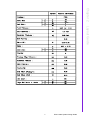
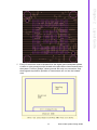
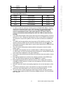
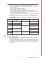
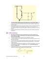
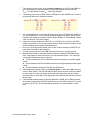
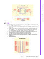
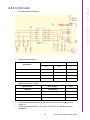
User Manual
EVA-X4300
System Design Guide
Copyright
Advantech reserves the right to make changes without further notice to any products
or data herein to improve reliability, function, or design. Information furnished by
Advantech is believed to be accurate and reliable. However, Advantech does not
assure any liability arising out of the application or use of this information, nor the
application or use of any product or circuit described herein, neither does it convey
any license under its patent rights nor the rights of others.
Copyright © 2008 Advantech Co., Ltd. All rights reserved.
Part No. 2006X43020
Edition 1
Printed in Taiwan
August 2008
EVA-X4300 System Design Guide
ii
Contents
Chapter
1
Overview...............................................1
1.1
Overview ................................................................................................... 2
2
Layout Guide........................................3
2.1
2.2
2.3
2.4
2.5
2.6
2.7
2.8
2.9
2.10
2.11
2.12
2.13
BGA Layout Guideline............................................................................... 4
Package Outline........................................................................................ 6
Signal Arrangement .................................................................................. 8
EVA-X4300 Power Requirement............................................................. 11
General Layout Rule ............................................................................... 11
Crystal / External Oscillator..................................................................... 15
DDR2 Interface ....................................................................................... 16
Switching Power...................................................................................... 19
PCI Interface ........................................................................................... 20
USB 2.0................................................................................................... 21
IDE .......................................................................................................... 23
LPC Interface .......................................................................................... 24
10/100 LAN ............................................................................................. 25
Appendix A
References .........................................29
A.1
References.............................................................................................. 30
Chapter
iii
EVA-X4300 System Design Guide
EVA-X4300 System Design Guide
iv
Chapter
1
Overview
1
1.1 Overview
The EVA-X4300 is a fully static 32-bit x86-based processor that is compatible with a
wide-range of PC peripherals, applications and operating systems, such as DOS,
WinCE, Linux, and most popular 32-bit RTOSs (Real Time OS). It enables maximum
software re-use based on its feature of legacy compatibility. The EVA-X4300 integrates 32 KB write-through direct map L1 cache, a PCI bus interface at 33 MHz, an 8/
16-bit ISA bus interface, SDR SDRAM, DDR2 SDRAM, a ROM controller, IPC (Internal Peripheral Controller) with DMA and interrupt timer/counter included, FIFO UART,
SPI (Serial Peripheral Interface), LPC (low pin count), a USB 1.1/2.0 host controller,
LoC (LAN on Chip), an IDE controller, and 256 KB flash within a single 581-pin BGA
package to form a an SoC (System-on-Chip) processor. The EVA-X4300 integrates
comprehensive features and rich I/O flexibility within a single System-on-Chip, to
reduce board design complexity and shorten product development schedules. Taking
advantage of ultra low power consumption, the EVA-X4300 is able to operate in a
wide range of temperatures without additional thermal design. With the commitment
of long term supply guaranteed for the EVA-X4300, customers can extend product
life cycle and receive a maximum return on investment.
The EVA-X4300 provides an ideal solution for embedded systems and communication products (such as the thin client, NAT router, home gateway, access point and
tablet PC) producing optimal performance.
This system design guide provides detailed usage information of the highly integrated EVA-X4300 SoC processor.
EVA-X4300 System Design Guide
2
Chapter
2
Layout Guide
2
2.1 BGA Layout Guideline
The package of EVA-X4300 is 581-ball PBGA. The ball diameter is 0.6 mm (24 mil);
ball pitch is 1 mm (40 mil). There are 6 rows of balls arranged along the edge of the
package.
For 6-layer:
! Ball pad diameter: 24 mil
! Traces width/ spacing for Signals: 5.5/ 5 mil
! Trace width for Power and Ground: 20 mils
! Vias PAD/ Drill diameter for all Signals: 14/ 8 mil
! Via-to-via spacing (center to center): 40 mil
! Via-to-pad spacing (center to center): 30 mil
EVA-X4300 System Design Guide
4
Chapter 2
For 4-layer:
! Ball pad diameter: 14 mil
! Traces width/ spacing for Signals: 5/ 5 mil
! Trace width for Power and Ground: 20 mils
! Vias PAD/ Drill diameter for all Signals: 22/ 12 mil
! Via-to-via spacing (center to center): 40 mil
! Via-to-pad spacing (center to center): 30 mil
Layout Guide
Note!
All the Vias must be covered by solder mask. To minimize inductance,
power vias should be as large as possible and take good care of the
inadvertently cut of the ground and power planes.
5
EVA-X4300 System Design Guide
2.2 Package Outline
EVA-X4300 System Design Guide
6
Chapter 2
Layout Guide
7
EVA-X4300 System Design Guide
2.3 Signal Arrangement
Top View
26 ○ ○ ○ ○ ○ ○
25 ○ ○ ○ ○ ○ ○
24 ○ ○ ○ ○ ○ ○
23 ○ ○ ○ ○ ○ ○
○ ○ ○ ○ ○ ○ ○ ○ ○ ○ ○ ○ ○ ○ ○ ○ ○ ○ ○ ○
○ ○ ○ ○ ○ ○ ○ ○ ○ ○ ○ ○ ○ ○ ○ ○ ○ ○ ○ ○
○ ○ ○ ○ ○ ○ ○ ○ ○ ○ ○ ○ ○ ○ ○ ○ ○ ○ ○ ○
○ ○ ○ ○ ○ ○ ○ ○ ○ ○ ○ ○ ○ ○ ○ ○
22 ○ ○ ○ ○ ○ ○ ○ ○ ○ ○ ○ ○ ○ ○ ○ ○ ○ ○ ○ ○ ○ ○
22 ○ ○ ○ ○ ○ ○ ○ ○ ○ ○ ○ ○ ○ ○ ○ ○ ○ ○ ○ ○ ○ ○
20 ○ ○ ○ ○ ○ ○
○ ○
19 ○ ○ ○ ○ ○ ○
○ ○
18 ○ ○ ○ ○ ○ ○
○ ○ ○ ○ ○ ○ ○ ○ ○ ○
○ ○
○ ○ ○ ○
○ ○ ○ ○
○ ○ ○ ○
○ ○ ○ ○
○ ○ ○ ○
○ ○ ○ ○
17 ○ ○ ○ ○ ○ ○
16 ○ ○ ○ ○ ○ ○
15 ○ ○ ○ ○ ○ ○
14 ○ ○ ○ ○ ○ ○
○ ○ ○ ○ ○ ○ ○ ○ ○ ○
○ ○ ○ ○ ○ ○
○ ○ ○ ○ ○ ○ ○ ○ ○ ○
○ ○ ○ ○ ○ ○
○ ○ ○ ○ ○ ○ ○ ○ ○ ○
○ ○ ○ ○ ○ ○
○ ○ ○ ○ ○ ○ ○ ○ ○ ○
○ ○ ○ ○ ○ ○
13 ○ ○ ○ ○ ○ ○
12 ○ ○ ○ ○ ○ ○
11 ○ ○ ○ ○ ○ ○
10 ○ ○ ○ ○ ○ ○
○ ○ ○ ○ ○ ○ ○ ○ ○ ○
○ ○ ○ ○ ○ ○
○ ○ ○ ○ ○ ○ ○ ○ ○ ○
○ ○ ○ ○ ○ ○
○ ○ ○ ○ ○ ○ ○ ○ ○ ○
○ ○ ○ ○ ○ ○
○ ○ ○ ○ ○ ○ ○ ○ ○ ○
○ ○ ○ ○ ○ ○
9 ○ ○ ○ ○ ○ ○
○ ○ ○
8 ○ ○ ○ ○ ○ ○
7 ○ ○ ○ ○ ○ ○ ○
6 ○ ○ ○ ○ ○ ○ ○ ○ ○ ○ ○
5 ○ ○ ○ ○ ○ ○ ○ ○ ○ ○ ○
4 ○ ○ ○ ○ ○ ○ ○ ○ ○ ○ ○
3 ○ ○ ○ ○ ○ ○
2 ○ ○ ○ ○ ○ ○
1 ○ ○ ○ ○ ○ ○
A B C D E F
○ ○ ○ ○ ○ ○ ○
○ ○ ○ ○ ○ ○
○ ○ ○ ○ ○ ○ ○ ○ ○ ○ ○ ○ ○ ○ ○
○ ○ ○ ○ ○ ○ ○ ○ ○ ○ ○ ○ ○ ○ ○
○ ○ ○ ○ ○ ○ ○ ○ ○ ○ ○ ○ ○ ○ ○
○ ○ ○ ○ ○ ○ ○ ○ ○ ○ ○ ○ ○ ○ ○ ○ ○ ○ ○ ○
○ ○ ○ ○ ○ ○ ○ ○ ○ ○ ○ ○ ○ ○ ○ ○ ○ ○ ○ ○
○ ○ ○ ○ ○ ○ ○ ○ ○ ○ ○ ○ ○ ○ ○ ○ ○ ○ ○ ○
G H J K L M N P R T U V W Y AA AB AC AD AE AF
Pin #1 Corner
EVA-X4300 System Design Guide
○ ○ ○ ○ ○ ○
○ ○ ○ ○ ○ ○
8
C
D
E
F
G
H
J
K
L
M
N
26
NC
AD24
TRDY_
PCIRST_
AD13
AD10
AD5
AD3
AD1
TXP
RXP
DP1
DP0
25
AD25
CBE_3
IRDY_
STOP_
AD14
AD9
AD7
AD4
AD2
TXN
RXN
DM1
DM0
24
AD26
CBE_2
AD15
CBE_0
PAR
AD0
ISET
VCCA0
VCCA1
VSSA1
AVSS0
23
AD27
AD16
AD17
TEST0
TEST4
VCC_SPI
AD11
INTA_
VSSA0
VCCABG
AVDDPLL
0
22
AD28
AD18
AD19
TEST2
TEST1
ATSTP
CBE_1
AD12
AD6
Duplex
21
AD29
AD20
AD21
GND_SPI
TEST3
ATSTN
ROM_CS_
AD8
TXC0
TXEN0
RXDV0
RXC0
RTC_AS_
GPIO_37
20
PCICLK_2
AD30
AD31
AD23
AD22
INTC_
19
PCICLK_0
PREQ2
PGNT0
PGNT2
INTD_
INTB_
18
PCICLK_1
PREQ1
PREQ0
PGNT1
VCC3V
VCC3V
TXD0_3
TXD0_0
RXD0_0
RXD0_3
Vdd_io
17
MD4
MD0
MD14
DQM1
GNDK
GND_R3
TXD0_2
TXD0_1
RXD0_1
RXD0_2
Vdd_io
16
MD3
MD1
MD9
MD15
MD15
GND_R3
MDC
MDIO
COL0
VCC3V
GND_R3
15
MD2
MD7
MD11
MD12
MD8
GND_R3
VCC3V
VCC3V
VCC3V
VCC3V
GND_R3
14
MD5
DQM0
MD13
DQS0
MD10
VCCK
VCCK
VCCK
VCCK
VCCK
GND_R3
13
MD6
CS_1
WE_
RAS_
CS_0
VCCK
GND_R3
GND_R3
GND_R3
GND_R3
GND_R3
12
MA10
MA6
BA2
BA0
CAS_
BA1
GNDK
GNDK
GNDK
GND_R3
GND_R3
11
MA1
MA5
MA7
MA9
MA11
MA13
GNDK
GNDK
GNDK
GNDK
GND_R3
10
MA0
MA3
MA4
VDLL0
GNDDLL0
MA12
GNDK
GNDK
GNDK
GNDK
GND_R3
9
SDRAMCLKN
SDRAMCLKP
MA2
VDLL1
GNDDLL1
MA8
TMS
GNDK
GNDK
GNDK
VCCK
8
NC
NC
NC
VCCO
GNDK
VCCK
7
NC
NC
VCCO
VCCO
GNDK
GNDO
TCK
6
NC
NC
VCCO
GNDO
GNDO
GNDO
TDO
SOUT9
SIN9
PE/SDD9
SOUT4
SIN4
5
NC
NC
VCCO
GNDO
GNDO
GNDO
GNDO
BUSY/
SDD10
SLCT/
SDD8
4
NC
NC
VCCO
VCCO
VCCO
GNDO
VCCK
VPLL0
3
NC
NC
NC
NC
TEST5
TEST6
SIN3
RTS3_/
SRST_
2
NC
NC
NC
NC
TEST7
TEST8
SOUT3
CTS3_/
SIOR_
1
NC
NC
NC
NC
NC
DTR3_/
SDACK_
RI3/
SIORDY
A
B
C
D
E
F
G
FRAME_ DEVSEL_
9
TDI
VCCAPLL VSSAPLL
Link/Active VSSABG
GNDPLL0 GNDPLL1 PD6/SDD6 PD5/SDD5
AVDD0
PD7/SDD7
ACK_/
SDD11
PD4/SDD4
ERR_/
SDD14
TESTCLK PD3/SDD3
AFD_/
SDD15
SLIN_/
SDD12
PDD9
VPLL1
DCD3_/
PD0/SDD0 PD1/SDD1 PD2/SDD2
SDRQ
PINT
DSR3_/
SCBLID_
INIT_/
SDD13
PA2
STB_/
SCS0_
PRST_
PDD3
H
J
K
L
M
N
EVA-X4300 System Design Guide
Layout Guide
B
Chapter 2
A
P
R
T
U
V
W
Y
AA
AB
AC
AD
AE
AVDD33_0
DP3
DP2
AVDD33_1 RTC_Xin
AVDD3
CTS2_/
DSR2_/
XOUT_14. POWER_ CLK25MO DCD2_/
PWM1GAT PWM0GAT
318
GOOD
UT
PWM0CLK
E
E
AVSSPLL0
DM3
DM2
AVSSPLL1 RTC_Xout
AVSS3
XIN_14.31
8
REXT0
AVDD1
AVSS2
REXT1
AVSS1
AVDD2
LAD0
LAD1
AVDDPLL SERIRQ
1
MTBF
AF
NC
DTR2_/
RTS2_/ TXD_EN2/
CLK24MO
SIN2/
PWM2OU PWM1OU PWM2GAT
ut
PWM2CLK
T
T
E
Vss_pll_1 Vdd_pll_1 Vdd_pll_0 Vss_pll_0
26
25
SOUT2/
RI2_/
DCD1_/
PWM0OU
PWM1CLK
GPIO_40
T
24
SPEAKER Vdd_core
Vss_io
Vdd_io
DTR1_/
CTS1_/
DSR1_/
GPIO_45 GPIO_47 GPIO_46
23
RTC_RD_ RTC_IRQ8
SYSFAILO Ext_Switch
RTC_PS
GPIO_36 _/GPIO_34
ut_
_fail_
E_SPI_CL
E_SPI_DI/
K/
Vdd_core
GPIOP_33
GPIOP_31
Vss_io
Vdd_io
RI1_/
SOUT1/
RTS1_/
GPIO_43 GPIO_41 GPIO_42
22
RTC_WR_ ExtSysFailI EXT_GPC
GPIO_35
n_
S_
E_SPI_CS E_SPI_DO
/
/
Vdd_core
GPIOP_30 GPIOP_32
Vss_io
Vdd_io
TXD_EN1
SIN1/ GPIO_P2_
GPIO_44 1/SA25
21
Vss_io
GPIO_P2_ GPIO_P2_ GPIO_P2_
5/SA29
4/SA28
2/SA26
20
GPIO_P1_ GPIO_P2_ GPIO_P1_ GPIO_P1_ GPIO_P1_ GPIO_P1_
7
0/SA24
6
5
4
0
19
VBat
VBatGnd
LAD2
LAD3
GPIO_P2_ GPIO_P2_
7/SA31
6/SA30
Vss_io
Vss_io
Vss_core LFRAME_
LDRQ_
GPIO_P0_ GPIO_P1_ GPIO_P1_ GPIO_P2_ GPIO_P0_ GPIO_P0_
7
3
2
3/SA27
5
3
18
Vss_io
Vss_io
Vss_core
Vss_io
GPIO_P0_ GPIO_P1_ GPIO_P0_ GPIO_P0_ GPIO_P0_ GPIO_P0_
6
1
1
0
4
2
17
Vdd_io
Vss_io
Vss_core Vss_core
Vdd_io
Vss_io
Vss_io
VCC3V
Vdd_io
VCC3V
Vdd_io
VCC3V
Vss_io
VCC3V
Vss_io
VCC3V
Vdd_io
Vss_io
VCCK
Vdd_io
Vss_io
Vss_io
KBDATA /
A20GATE_
SD3
IOR_
GPCS0_
GPCS1_
SD15
SD14
16
Vss_core
MSDATA
LA20
LA18
LA23
LA19
DRQ7
SD12
15
Vss_io
Vss_core
MSCLK
SD4
IRQ9
SD2
SD6
LA21
SD11
14
Vss_io
Vss_core
KBCLK_K
BRST_
IOCHCK_
SA2
SBHE_
LA22
SA5
DACK_2
13
Vdd_core Vss_core Vss_core
SA3
DRQ0
Vss_core
SD8
MEMW_
SA1
12
Vdd_core Vss_core Vss_core
DRQ5
SA4
Vss_core
DACK_6
SD10
DRQ6
11
SMEMR_
DACK_5
Vss_core
SD13
SD9
SYSCLK
10
SA19
SA17
DRQ2
DACK_0
LA17
MEMR_
9
SMEMW_
AEN
IRQ12
0WS_
IOCHRDY
OSC14M
_
8
SD0
SA10
SA8
IRQ5
IRQ7
DACK_7
7
Vdd_core Vdd_core
Vss_io
Vss_io
CTS4_/
SIOW_
DCD4_/
SA2
DSR4_/
SCS1_
RTS4_/
SINT
DTR4_/
SA0
Vss_io
SD7
Vdd_io
Vss_core Vdd_core
SA7
IRQ10
REFRESH
_
6
PDD12
PDD2
PDD1
PDD11
RI4/SA1
Vss_io
DRQ3
Vdd_io
Vss_core Vdd_core
SA18
SA9
TC
5
PDD10
PDD5
PDD6
PDD7
Vss_core
Vdd_io
SD5
Vdd_io
Vss_core Vdd_core
DRQ1
BALE
IRQ15
4
PIORDY
PIOW_
PDD0
PDD8
Vdd_io
Vdd_io
DACK_3
SA16
DACK_1
SA0
SA11
IOCS16_
IRQ11
3
PA1
PA0
PCS0_
PDD4
PDD15
PDD14
IOW_
SA12
SA14
SA6
SA13
IRQ3
IRQ14
2
PDD13
PDRQ
PDACK_
PCBLID_
PIOR_
PCS1_
SD1
SA15
RSET_DR
V
IRQ6
IRQ4
MEMCS16
_
NC
1
P
R
T
U
V
W
Y
AA
AB
AC
AD
AE
AF
EVA-X4300 System Design Guide
10
DC Volt
Tolerance
Ripple & Noise
Max. Current
3.3V for VCCP
± 0.30 V
< 100 mV
185 mA
3.3V for VCCO
1.8V for VCCO
± 0.15 V
± 0.09 V
< 50 mA
< 245 mA
Min. Volt
Max. Volt
Ripple & Noise
Max. Current
1.3V for VCCK
1.30 V
1.40 V
< 50 mA
240 mA
Note!
CPU clock 300 MHz, DDR2 clock 133 MHz and PCI clock 33 MHz
2.5 General Layout Rule
1.
2.
3.
4.
5.
6.
7.
8.
Keep all traces as SHORT as possible.
Decoupling is to remove the RF energy injected into the power distribution network from high-speed switching devices.
Bypassing is to divert unwanted common-mode RF noise from components or
cables coupling from one area to another.
Place 0.01 µF~0.1 µF decoupling capacitors across each pair of VCC and GND
pins. Use the shortest and thickest trace between decoupling capacitor and the
VCC/GND pins.
Bulk capacitors ensure that a sufficient amount of DC voltage and current is
available for digital components. At least one bulk capacitor should be located:
! Every VLSI device
! Power connector(s)
! Daughter card slots
! Furthest location from the power connector
! Clock generation circuitry
The voltage rating of the bulk capacitors should be 50% higher than the actual
voltage level to prevent self-destruction and/ or voltage surge.
For decoupling of DDR2 interface, please check the DDR2 section for more
details.
In digital circuits, conductors may be treated as transmission lines if the propagation time (Tdelay) is equal to or greater than the pulse transition time (Trise or
Tfall).
9.
The propagation speed on typical PCB is about 170 pS/inch (50 Ω Stripline),
150pS/inch (50 Ω Microstrip).
10. There are 4 properties affect the performance of the transmission line:
! Impedance: reflection/ distortion
! Time delay
! High-Frequency Loss: limit signal bandwidth and transmission distance
! Crosstalk: coupling
11
EVA-X4300 System Design Guide
Layout Guide
DC Volt
Chapter 2
2.4 EVA-X4300 Power Requirement
11. It is recommended to add serial damping resistors to all high-speed signals,
especially the clock signals, to reduce high frequency energy and EMI. These
resistors should be placed as close to the driving source as possible.
12. The clock signals should be the first routed trace in any PCB design. Adjacently
routed (guard) ground traces provide shielding and signal return path. These
ground shielding traces should be connect to the ground plane by vias at both
ends. It is best to run all clock signals on the signal plane above a solid ground
plane (on a multi-layer board).
13. If clock/ high-speed signals must make a layer jump, route ground trace adjacent to the signals and connect both ends of the ground trace to the GND plane,
to form a RF return path of the signals.
14. The split power planes may cause serious EMI and signal integrity problems for
high-speed signals which run adjacent to the power planes. To minimize these
problems, some decoupling capacitors should be placed between these split
power planes, to enhance RF return current path.
15. Any unused area of the top and bottom signal layers of the PCB can be filled
with copper that is connected to the ground plane through stitches of vias.
16. Example for BGA Power/ Ground routing:
EVA-X4300 System Design Guide
12
Chapter 2
Layout Guide
17. Every I/O connector must be isolated from the digital ground and power planes.
A clean or quiet ground must be located at the point where interconnects leave
the system. Connect (“Bridge”) those grounds with only one connection. Only
those signals required for operation or interconnect can run into the isolated
area.
13
EVA-X4300 System Design Guide
18. Ensure that any signal passing between those sections runs ONLY through the
“bridge”, and run the signals on a layer adjacent to the bridge to maintain RF
return path.
19. If analog or digital power is not required in the isolated area, the unused power
plane can be redefined as a second ground plane, referenced to the main
ground plane by stitches of vias within the isolated area.
20. Connect system Power-on and H/W Reset to “Power-good” input of EVAX4300, then use “/PCI_RST” output of EVA-X4300 to reset ALL peripherals.
21. The power-on-strap pins are combined with the memory address bus, which
belong to DRAM power category. So the pull-high resistors should connect to
the same supply (VCCO) of DRAM interface. That is:
DRAM type
Supply (V)
SDR
3.3
DDR2
1.8
Note
For detail of power-on-straps function, please refer to the EVA-X4300 data sheet.
22. Do follow the power-on sequence to prevent excessive current from the power
supplies during power-up and power-down periods:
! Power-up core supply (VDD_CORE), and then power-up the I/O supply
(DVDD).
! Power-down I/O supply (DVDD), and then power-down the core supply
(VDD_CORE).
23. Recommend Termination:
Signal
Zs (Ω)
Termination(Ω)
Trace impedance (Ω)
Clocks 24M
26
22
60
PCI clock
7.2
22
60
PCI signal
13.2
51
60
DDR Clocks
19
33
90, Differential
DDR signal
19
33
60
24. Recommended PCB stack up:
a. 4 layers
Layer
Type
Description
Material/ Thickness
1
Signal
Top Routing
Copper/ 0.5~1oz
FR4/ 5mil
2
Plane
Ground
Copper/ 1oz
FR4/ 40mil
3
Plane
Power
Copper/ 1oz
FR4/ 5mil
4
Signal
EVA-X4300 System Design Guide
Bottom Routing
14
Copper/ 0.5~1oz
Layer
Type
Description
Material/ Thickness
1
Signal
Top Routing
Copper/ 0.5~1oz
FR4/ 5mil
2
Plane
Ground
Copper/ 1oz
Chapter 2
b. 6 layers
FR4/ 5mil
Plane
Power
Copper/ 1oz
FR4/ 40mil
4
Signal
Internal Routing
Copper/ 1oz
FR4/ 5mil
5
Plane
Ground
Copper/ 1oz
FR4/ 5mil
6
Signal
Bottom Routing
Copper/ 0.5~1oz
2.6 Crystal / External Oscillator
The EVA-X4300 requires a 14.318 MHz clock to generate all the internal and external
clocks. Connect an external 14.318 MHz crystal (Parallel-resonant) between Xtal_I
and Xtal_o pins to operate as a Pierce oscillator. The EVA-X4300 specification
requires a frequency tolerance of ±30 parts pre million (PPM).
The other way is to use an external 14.318MHz oscillator, and directly route the oscillator is output into XTALi pin of EVA-X4300. A serial damping resistor and a bypass
capacitor are recommended for EMI reduction. The XTALo pin should leave unconnected. The requirement of the clock is duty cycle should be between 40% ~60%.
Recommended Layout:
! Route the signal traces of the crystal to EVA-X4300 as SHORT as possible.
! When use external crystal with EVA-X4300 internal oscillation circuitry to work
as clock oscillator, be sure to put all the related components close to EVAX4300 chip. The ground area under the crystal circuitry should be physically
insolated from system ground plane with only a small bridge between them for
signals crossing. This isolation prevents noise located elsewhere on the PCB
from corrupting the oscillator circuitry.
! The power plane under the crystal/ oscillator area should be void, when no use,
or insolated with exactly the same pattern of ground plane.
! Do NOT run any signals under this area, for EMI and interference enhancement.
15
EVA-X4300 System Design Guide
Layout Guide
3
2.7 DDR2 Interface
1.
2.
It is assumed that the reader is familiar with the specification and the basic electrical operation of the DDR2 interface.
EVA-X4300 DDR2 interface substrate conductors’ length for signal integrality:
EVA-X4300 Substrate Conductor Length
Net Name
Length in microns
MA[0]
13283.31
MA[1]
12989.16
MA[2]
8745.03
MA[3]
10321.07
MA[4]
10173.85
MA[5]
11728.8
MA[6]
12466.29
MA[7]
11480.64
MA[8]
7638.44
MA[9]
10753.84
MA[10]
13659.62
MA[11]
9367.04
MA[12]
7999.4
MA[13]
8948.06
MD[0]
12939.2
MD[1]
12379.26
MD[2]
12218.38
MD[3]
12868.28
MD[4]
13327.88
MD[5]
11731.55
MD[6]
11817.28
MD[7]
11681.94
MD[8]
11494.07
MD[9]
10379.54
MD[10]
10577.86
MD[11]
11902.14
MD[12]
11610.42
MD[13]
10048.32
MD[14]
10981.68
MD[15]
12062.12
BA0
10484.24
BA1
9914.61
BA2
9542.11
/CAS
9668.98
/CS0
10088.02
/CS1
10430.52
DQM0
12436.31
DQM1
10402.02
DQS0
10560.44
DQS1
9752.32
EVA-X4300 System Design Guide
16
5.
6.
7.
8.
9.
10.
11.
12.
13.
14.
15.
/MCLK
6678.9
/RAS
11307.98
/WE
10909.61
Supported DDR2 Devices:
Vendor
Part Number
Note
Hynix
HY5PS121621C
84-ball
Hynix
HY5PS12821C
60-ball
SiS
DDRII6408-5C
60-ball
Elpida
EDE1108ABSE
68-ball
In order to meet the maximum interface speed (200 MHz/400 Mbps), memory
device drive strength should be set 100% strength. This requires the series terminations to avoid excessive Under/Over-shoot. We highly recommend
reserve terminations for ALL high speed signals. It is much easier to
remove terminations than adding them after the PCB has been found to
fail EMI.
It is critical that all signal routing layers have a ground reference plane, meaning
that there is a full, contiguous ground plane next to every DDR2 routing layers.
The purpose is to provide a path for return currents to minimize crosstalk and
EMI.
The DDR2 devices should be placed as close to EVA-X4300 as possible. The
distance between DDR2 devices and EVA-X4300 should less than 3 inches.
Other devices should be kept away to ensure other signals do not interfere with
the DDR2 interface.
The 1.8V power partial plane (island) should encompass at least the entire
DDR2 region.
All signals avoid crossing over an unrelated plane or different power plane. Six
or more layers of PCB could eliminate these problems by routing DDR2 signals
in the layer that is adjacent to the ground plane(s).
Rout traces with minimal layer transitions and minimize the total number of turns
and vias.
Decoupling capacitors are critical to the reliable operation of the DDR2 interface. The decoupling capacitors should be 0402 size or smaller.
Bulk capacitors ensure that a sufficient amount of DC voltage and current is
available for DDR2 devices. At least one bulk capacitor should be located for
each DDR2 device.
DO NOT share the vias for decoupling capacitors, due to the inductance of the
vias.
To minimize inductance, power vias should be as large as possible, but take
good care of the inadvertently cut of the ground and power planes.
The PLL and DLL power supply pins draw small currents, but they are noise
sensitive. Each supply should be filtered by π-filter networks. Use Ferrite Bead,
NOT inductor.
17
EVA-X4300 System Design Guide
Layout Guide
4.
6700.98
Chapter 2
3.
MCLK
i. EVA-X4300:
ii. DDR2 SDRAM:
16. VREF is not a high current supply, but it is important to keep it as quiet as possible with minimum inductance. For VREF, the minimum trace width is 20 mil, and
keeps overall trace length as short as possible.
17. The VREF divider resistors can be placed close to the DDR2 devices.
18. The decoupling capacitors for VREF are intended to reduce AC noise. Place
one each at the divider and every VREF input of the DDR2(s).
19. Recommended Terminations for DDR2 interface:
Signal
Clock±
DQS±
Impedance (Ω)
DQ[0..15]
MD[0..15]
Note!
Near DDR2
33
60
Note
Near EVA-X4300
Differential, 90
A[0..13], BA[0..2], Controls
DQM
Value (Ω)
Near EVA-X4300
Near DDR2
Near EVA-X4300
Termination value may have to be adjusted according to manufacturing
condition.
EVA-X4300 System Design Guide
18
Width/ Spacing/
Isolation
Data Strobe
5 mil/ >20 mil/ 20 mil
Data Mask
5 mil/ >5 mil/ 15 mil
Data Bus
5 mil/ >5 mil/ 5 mil
Clock
5 mil/ >20 mil/ 20 mil
Address
Command
Maximum Length
Note
2 inches
The mismatch of the differential pair is ±10 mil
3 inches
5 mil/ >5 mil/ 5 mil
VREF
Power/
GND
Width > 20 mil
Kept to a minimum
2.8 Switching Power
1.
2.
Please check section 2.3 and DDR2 data sheet for the detailed power requirements of the DDR2 system.
In a step-down switching regulator, the input bypass capacitor, the main power
switch and the freewheeling diode carry discontinuous currents with high dt/di.
For jitter-free operation, the size of the loop formed by these components should
be minimized.
19
EVA-X4300 System Design Guide
Layout Guide
Signal
Chapter 2
20. Recommended layout:
Trace length (include the substrate & PCB trace length) routing:
(a) The following signals of DDR2 SDRAM in each group must route near by in
the same plane:
Group (1): LDQS, /LDQS, LDQM, DQ [0...7]
Group (2): UDQS, /UDQS, UDQM, DQ [8...15]
Group (3): MA [0...13], BA [0...2], /RAS, /CAS, /WE, MCLK, /MCLK
i. The intra-signals trace length in each group better keeps the same, otherwise keeps the mismatch less than 250 mils.
ii. The mismatch trace length between the inter-groups must be less than 400
mils.
(b) All signals avoid crossing over an unrelated plane or different power plane.
(c) Route traces with minimal layer transitions and minimize the total number of
turns & vias.
3.
4.
5.
The input bypass capacitors should be placed close to the VIN pins. Shortening
the traces of the SW node reduces the parasitic trace inductance at these
nodes. This not only reduces EMI but also decreases switching voltage spikes
at these nodes.
Some switching devices have exposed pad which should be soldered to a large
analog ground plane, as the analog ground copper acts as a heat sink. To
ensure proper adhesion to the ground plane, avoid using vias directly under the
device.
For more detailed design information, please refer to the switching regulatorís
data sheet.
2.9 PCI Interface
1.
2.
3.
4.
5.
6.
We highly recommend reserve terminations for ALL PCI signals. It is
much easier to remove terminations than adding them after the PCB has
been found to fail EMI.
The trace length for all PCI signals must be limited to 7 inches.
The trace length for PCI Clocks must be short for on-board PCI devices to minimize the clock skew.
The PCI clock traces should be parallel to their reference plane, usually ground
planes. That means the clock traces should be right beneath or on top of their
reference plane.
There is NO board impedance specified in the PCI bus specification. We recommend the trace impedance to be 60 Ω ± 10%, with a trace width/ spacing
design of 5 mil/10 mil.
Add serial termination resistor and bypassing capacitor (tens of pF) to PCI clock
signals to match the trace impedance and enhance EMI.
EVA-X4300 System Design Guide
20
8.
Avoid running PCI clocks in parallel with other signals for a long distance, for
interference and coupling.
The user may need to drive two or more source-terminated clock lines with single output. However, the following condition must be achieved:
i. The clock traces length must be as equal as possible, to guarantee the arriving time of the reflected pulses.
ii. The loads must be balanced, to guarantee the same shape of the reflected
pulses.
Rt = Z0 – Rs * N
Rt = termination resistor, Ω
Rs = output impedance of the driver
Z0 = line impedance
N = number of lines
2.10 USB 2.0
1.
2.
3.
4.
5.
6.
Route the Hi-Speed USB differential pairs over continuous ground or
power planes. Avoid crossing anti-etch areas and any breaks in the internal planes (plane splits).
Avoid placing a series of vias near the DP and DM lines, as these will create
“break areas” in the ground plane below.
Avoid routing the USB differential pairs near I/O connectors, signal headers,
crystals/ oscillators, magnetic and power connectors.
Maintain parallelism between USB differential signals, with the trace spacing
needed to achieve 90 Ω differential impedance.
We recommend the trace Width/ Spacing/ Isolation of USB differential pairs to
be 8 mil/ 8 mil/ >20 mil. And the mismatch of the differential pairs should be
less than ±70 mil. These values may vary depending on the actual PCB
parameters.
The maximum trace length of USB differential pairs should be less than 2”.
21
EVA-X4300 System Design Guide
Layout Guide
iii. The termination value must be calculated according to:
Chapter 2
7.
7.
The common-mode choke used (if really necessary) on the DP and DM lines
must be placed as close as possible to the USB connector and must have
Zcom< 8 Ω @ 100 MHz and Zdiff < 300 Ω @ 100 MHz.
8.
The analog power pins of EVA-X4300, AVDD0/1/2/3 and AVDDPLL0/1, need to
be properly filtered for USB performance.
9.
It is recommended to connect the analog ground pins of EVA-X4300, AVSS0/1/
2/3 and AVSSPLL0/1, to an isolated (quiet) analog ground plane, which is connected to the digital ground plane with a single “Bridge” or Ferrite Bead. Please
refer to section 2.4 for more details.
Place the external resistors of REXT0/1, pin U26 & P26, as close to the EVAX4300 as possible. And connect another ends of these external resistors to the
isolated analog ground plane described above.
Do not run any high-speed signal close to the external resistors of REXT0/1 to
keep from interference and coupling.
Provide a good path from the USB connector shell to the chassis ground.
Maintain the maximum possible distance between Hi-Speed USB differential
pairs, high-speed or lows-peed clock, and non-periodic signals. The minimum
recommended distances are as follows:
! 20 mils between the DP and DM traces and low-speed non-periodic signal
traces.
! 50 mils between the DP and DM traces and clock/high-speed periodic signal
traces.
! 20 mils between two pairs of the DP and DM traces.
USB data lines must be routed as “critical signals”. Locate the USB connector
close to EVA-X4300. The DP and DM signals in a pair must be routed in parallel
to each other. Do not route these traces near high frequency signals. Guard
ground traces on each side of the signal pair can minimize the induced common
mode noise.
Ferrite beads and decoupling capacitor placed on VBUS are for EMI purposes,
thus these components should be placed close to the USB connectors. A value
of about 150 µF/10 V for the decoupling capacitor is recommended on each
port.
10.
11.
12.
13.
14.
15.
EVA-X4300 System Design Guide
22
Chapter 2
Layout Guide
2.11 IDE
The trace-length and impedance-match must be considered for IDE signals to
enhance the EMI and signal integrity:
1. The pull-up resistors on open-collector signals, such as IORDY, should be more
than 1 KΩ.
2. All IDE signals need to be serial terminated. Place the termination resistors for
A[0...2], CS[0..1], /IOR, /IOW and /DACK near EVA-X4300. Place the termination resistors for D[0..15], DRQ, IORDY, and IRQ near IDE connector.
3. The termination value should be optimized to compensate for transceiver and
trace impedance to match the characteristic cable impedance.
4. The 28th pin of IDE connectors (CSEL) should be pulled low.
5. Signals in the same channel should have the same length, the mismatch must
be less than 1”.
6. Reference circuitry:
23
EVA-X4300 System Design Guide
2.12 LPC Interface
A Low Pin Count (LPC) controller is integrated in EVA-X4300. The LPC interface is to
replace ISA interface serving as a bus interface between the system processor and
peripherals (e.g. LPC super I/O chip). Many of the signals are the same as signals
found on the PCI interface. Data transfer on the LPC bus is serialized over a 4-bit
bus.
Route the LPC signals with the PCI design rule.
EVA-X4300 System Design Guide
24
Recommended Schematics:
2.
Magnetics Specification:
Layout Guide
1.
Chapter 2
2.13 10/100 LAN
Specification
Note
Parameters
3.
4.
5.
Tx
Rx
Turns Ratio
1CT:1 CT
1CT:1CT
Inductance, μH
350
350
Capacitance, pF
15
15
DC Resistance, Ω
0.9
0.9
Magnetics Selection Guide:
Manufacturer
Part Number
Mingtek
HN16005CG
Note
Keep the distance between the EVA-X4300 and the RJ-45 connector short
(under 4”).
Route the differential traces, TX±, RX±, TD± & RD±, for 100 Ω differential
impedance.
25
EVA-X4300 System Design Guide
6.
7.
Keep the differential traces lengths equal to reduce signal skew.
Keep the differential traces close and symmetric to reduce noise.
8.
The parallel termination resistors of TD± should be placed near the magnetic.
The parallel termination series resistors of RD± should be placed near the EVAX4300.
It is recommended that route the differential traces turn with arcs, and avoid any
vias and corners.
The traces of TX±/ TD± pair should be kept away from RX±/ RD± pair. It is best
to place ground guard traces between these two pair of traces.
We recommend the trace Width/Spacing/Isolation of TX±/ TD± and RX±/ RD±
pairs to be 8 mil/ 10 mil/ >20 mil. And the mismatch of the differential pairs
should be less than ±100 mil.
Do NOT run any digital trace close to and parallel to the differential pairs.
The RJ-45 and output side of transformer should reference to quiet ground
plane (chassis ground) which is isolated from the ground plane of the input side
of transformer and EVA-X4300. Connect this quiet ground plane to system
ground with only one connection (bridge). Do NOT run any signal into this isolated area.
The moat to isolate the quiet ground should be at least 100 mil.
Avoid laying power and ground planes underneath the magnetic to enhance
EMI.
Provide a good path from the RJ-45 connector shell to the chassis ground.
The analog power pins of EVA-X4300, VCCAPLL, VCCABG, VCCA0/1 and
AVDD33_0/1, need to be properly filtered for LAN performance.
9.
10.
11.
12.
13.
14.
15.
16.
17.
18. It is recommended to connect the analog ground pins of EVA-X4300, VSSAPLL,
VSSABG and VSSA0/1, to an isolated (quiet) analog ground plane, which is
connected to the digital ground plane with a single “Bridge” or Ferrite Bead.
Please refer to section 2.4 for more details.
19. Place the external resistor of ISET, pin J24, as close to the EVA-X4300 as
possible. And connect another end of the external resistor to the isolated
analog ground plane described above.
20. Do not run any high-speed signal close to the external resistor of ISET to keep
from interference and coupling.
EVA-X4300 System Design Guide
26
Chapter 2
21. Avoid over-damping which affects LAN stability. It is recommend to place 51
ohm and 22 pF from PCI AD0~AD3.
Layout Guide
27
EVA-X4300 System Design Guide
EVA-X4300 System Design Guide
28
Appendix
A
References
A
A.1 References
1.
2.
3.
4.
5.
6.
“EVA-X4300 Technical Manual”
“PCI Local Bus Specification” rev. 2.2
“EMC and the Printed Circuit Board”, Mark I. Montrose
“High-speed Digital Design”, Howard W. Johnson, PH.D.
“Noise reduction Techniques in the Electronic System”, Henry W. Ott
“Printed Circuit Board design Techniques for EMC Compliance”, Mark I. Montrose.
EVA-X4300 System Design Guide
30
Appendix A References
31
EVA-X4300 System Design Guide
www.advantech.com
Please verify specifications before quoting. This guide is intended for reference
purposes only.
All product specifications are subject to change without notice.
No part of this publication may be reproduced in any form or by any means,
electronic, photocopying, recording or otherwise, without prior written permission of the publisher.
All brand and product names are trademarks or registered trademarks of their
respective companies.
© Advantech Co., Ltd. 2008