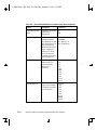
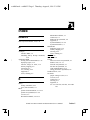
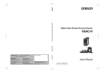
1
evalbd.book : frt Page 1 Thursday, August 8, 1996 2:34 PM
ÉlanSC310 Microcontroller
Evaluation Board
User’s Manual
evalbd.book : frt Page 2 Thursday, August 8, 1996 2:34 PM
ÉlanSC310 Microcontroller Evaluation Board, Revision 1.0
© 1996 by Advanced Micro Devices, Inc.
All rights reserved. No part of this publication may be reproduced, stored in a retrieval system, or transmitted in any
form or by any means, electronic, mechanical, photocopying, recording, or otherwise, without the prior written
permission of Advanced Micro Devices, Inc.
Use, duplication, or disclosure by the Government is subject to restrictions as set forth in subdivision (b)(3)(ii) of the
Rights in Technical Data and Computer Software clause at 252.227-7013. Advanced Micro Devices, Inc., 5204 E. Ben
White Blvd., Austin, TX 78741.
AMD is a registered trademark, and Élan is a trademark of Advanced Micro Devices, Inc.
Other product or brand names are used solely for identification and may be the trademarks or registered trademarks of
their respective companies.
The text pages of this document have been printed on recycled paper consisting of 50% recycled fiber and 50%
virgin fiber; the post-consumer waste content is 10%. These pages are recyclable.
Advanced Micro Devices, Inc.
5204 E. Ben White Blvd.
Austin, TX 78741-7399
evalbd.book : evalbd.TOC Page iii Thursday, August 8, 1996 2:34 PM
Contents
About the ÉlanSC310 Microcontroller Evaluation Board
Features..................................................................................................................x
Chapter 1
Quick Start
Booting DOS From a Diskette .......................................................................... 1-2
1.0
Installation Requirements.............................................................................. 1-3
Board Installation .......................................................................................... 1-4
Connecting an IDE Hard Drive ......................................................................... 1-7
For More Information ....................................................................................... 1-9
Chapter 2
Board Functional Description
Board Layout ..................................................................................................... 2-2
Evaluation Board Restrictions........................................................................... 2-4
BIOS .................................................................................................................. 2-5
SystemSoft BIOS .......................................................................................... 2-6
PhoenixPICO BIOS .................................................................................... 2-10
Bus Modes ....................................................................................................... 2-16
ISA Mode .................................................................................................... 2-17
Local Bus Mode .......................................................................................... 2-18
ÉlanSC310 Microcontroller Evaluation Board User’s Manual
iii
evalbd.book : evalbd.TOC Page iv Thursday, August 8, 1996 2:34 PM
Memory............................................................................................................ 2-18
DRAM Main Memory................................................................................. 2-19
Memory Voltage Setting ............................................................................. 2-19
I/O .................................................................................................................... 2-20
PS/2 Mouse.................................................................................................. 2-20
Serial Ports .................................................................................................. 2-21
Parallel Port ................................................................................................. 2-21
IDE Hard Drive ........................................................................................... 2-21
ROMs............................................................................................................... 2-22
Power Measurement ........................................................................................ 2-23
BL1–BL4 Pins............................................................................................. 2-24
Breadboard Area.......................................................................................... 2-24
Power Management ......................................................................................... 2-24
Suspend/Resume ......................................................................................... 2-25
MicroPower Off Mode .................................................................................... 2-26
Chapter 3
Using the Software
SystemSoft Evaluation Diskette.................................................................... 3-1
PhoenixPICO Evaluation Diskette ................................................................ 3-1
Datalight Software Evaluation Kit Diskette.................................................. 3-1
AMD Utilities Diskette ................................................................................. 3-2
Elan PMU Evaluation Utility ............................................................................ 3-4
A: Setup PMU Mode Characteristics (PMCx Pins, CPU Speed).................. 3-5
B: Force PMU State Transitions ................................................................... 3-8
C: Test Battery Level & ACIN Pins.............................................................. 3-9
X: Restore PMU State and Exit to DOS........................................................ 3-9
Z: Leave Current PMU Values and Exit to DOS .......................................... 3-9
iv
ÉlanSC310 Microcontroller Evaluation Board User’s Manual
1.0
Power Management Simulation .................................................................. 2-25
evalbd.book : evalbd.TOC Page v Thursday, August 8, 1996 2:34 PM
EvalSet Serial and Parallel Port Setup Utility ................................................. 3-10
Serial Port 1................................................................................................. 3-10
Serial Port 2................................................................................................. 3-10
Parallel Port 1.............................................................................................. 3-11
Usage........................................................................................................... 3-11
Memory Management System (MMS) Viewer Utility ................................... 3-12
Description .................................................................................................. 3-12
Scope ........................................................................................................... 3-13
Operating Instructions................................................................................. 3-13
Restrictions on Use ..................................................................................... 3-17
Register Dump Utility ..................................................................................... 3-19
Chapter 4
1.0
Developing Code
Programmable General Purpose (PGP) Pins ..................................................... 4-2
Power Management Control (PMC) Pins.......................................................... 4-3
Programming BIOS Flash/EPROM
or Application Flash/EPROM ........................................................................... 4-5
Evaluation Board’s Memory Map ..................................................................... 4-7
Evaluation Board’s I/O Map ........................................................................... 4-10
Evaluation Board’s IRQ Mapping................................................................... 4-11
Evaluation Board’s DMA Mapping ................................................................ 4-13
Evaluation Board’s Components..................................................................... 4-14
Enabling the ÉlanSC310 Internal Serial Port .................................................. 4-15
ÉlanSC310 Microcontroller Evaluation Board User’s Manual
v
evalbd.book : evalbd.TOC Page vi Thursday, August 8, 1996 2:34 PM
Appendix A
Evaluation Board Setup Summary
Setup Summary................................................................................................. A-1
Appendix B
Verified Peripherals
Verified Peripherals .......................................................................................... B-1
Appendix C
Board Layout Suggestions
Appendix D
Schematics
Schematics ........................................................................................................ D-1
Index
vi
ÉlanSC310 Microcontroller Evaluation Board User’s Manual
1.0
Board Layout Suggestions................................................................................ C-1
evalbd.book : evalbd.LOF Page vii Thursday, August 8, 1996 2:34 PM
List of Figures
ÉlanSC310 Microcontroller Evaluation Board ...................................................................... 2-2
List of Tables
Installation Troubleshooting ................................................................................................... 1-6
Board Layout........................................................................................................................... 2-3
SystemSoft BIOS Set-Up Screen Options .............................................................................. 2-6
PhoenixPICO BIOS Main Menu Setup Screen Options ....................................................... 2-11
PhoenixPICO BIOS Advanced Menu Setup Screen Options ............................................... 2-13
PhoenixPICO BIOS Power Menu Setup Screen Options ..................................................... 2-14
PhoenixPICO BIOS Exit Menu Setup Screen Options......................................................... 2-15
Bus Mode Selection and Affected Jumpers .......................................................................... 2-17
1.0
I/O Address 100–107 .............................................................................................................. 4-2
Typical Full ISA Memory Map .............................................................................................. 4-8
Typical Full ISA I/O Map ..................................................................................................... 4-10
Typical Full ISA IRQ Mapping ............................................................................................ 4-12
Typical Full ISA DMA Mapping.......................................................................................... 4-13
Bus Mode Selection and Affected Jumpers ........................................................................... A-2
Configuration Jumpers ........................................................................................................... A-2
JP18 ........................................................................................................................................ A-3
Switches ................................................................................................................................. A-3
Power Measurement Jumpers ................................................................................................ A-4
ÉlanSC310 Microcontroller Evaluation Board User’s Manual
vii
1.0
evalbd.book : evalbd.LOT Page viii Thursday, August 8, 1996 2:34 PM
viii
ÉlanSC310 Microcontroller Evaluation Board User’s Manual
evalbd.book : about Page ix Thursday, August 8, 1996 2:34 PM
About the ÉlanSC310
Microcontroller Evaluation Board
Congratulations on your decision to design with the ÉlanSC310 microcontroller!
This sophisticated, integrated device is uniquely suited to meet the needs of the
next generation of embedded solutions. From its high integration to PC/AT
compatibility to remarkable power management, the ÉlanSC310 microcontroller
is the ideal device to enable compact, fully functional, low-power designs with a
quick time to market.
1.0
The ÉlanSC310 microcontroller evaluation board has been provided as a test and
development platform for ÉlanSC310 microcontroller-based designs. Most of the
possible options and features of the ÉlanSC310 microcontroller can be exercised
on this board. Since there are numerous options available, this board is a much
larger form factor than could be achieved with a dedicated set of features. . This
evaluation board is provided as a reference only and should only be used to
experiment with the design trade-offs of the ÉlanSC310 microcontroller, make
power measurements, and develop operating and application software.
NOTE: Advanced Micro Devices does not assume any responsibility for the
maintenance of this evaluation tool. Changes to the schematics will only be made
if the board is required to go back through a CAD layout.
Refer to the ÉlanSC310 Microcontroller Data Sheet and the ÉlanSC310
Microcontroller Programmer’s Reference Manual for detailed information on the
ÉlanSC310 microcontroller.
ÉlanSC310 Microcontroller Evaluation Board User’s Manual
ix
evalbd.book : about Page x Thursday, August 8, 1996 2:34 PM
Features
External Connectors
• Two serial port connections
– One internal ÉlanSC310 16C450-compatible port (COM1 or COM2
configurable)
– One Super I/O 16C550-compatible port (COM1 through COM4
configurable)
• One parallel port connection from the ÉlanSC310 microcontroller
• Two 16-bit ISA slots (for evaluation of ISA-based devices only)
• One IDE connector (connected to the ÉlanSC310 ISA bus)
• One floppy-drive connector (connected to the Super I/O floppy-drive controller)
• One AT-style keyboard connector (connected to the 8042 keyboard controller)
Main Memory Configurations
• DRAM
– 512 Kbyte, 1 Mbyte, 2 Mbyte, 4 Mbyte, 8 Mbyte and 16 Mbyte DRAM
configurations supported
– 3-V or 5-V DRAM support
– Four standard 30-pin DRAM SIMM sockets
– One standard, 72-pin DRAM, 16-bit SIMM socket (can be used instead of
the 30-pin sockets)
Power Management
• Power planes are isolated and jumpers are provided to measure current
consumption. The CPU voltage sources are: VCC, VCCMEM, VCCSYS, VCCSYS2,
VCC5, VCC1, AVCC
• Suspend/Resume button provided (note that BIOS’ enable the suspend/resume
function)
• MicroPower Off button provided for testing
• DIP switch for transitioning battery-low and ACIN pins for testing
x
ÉlanSC310 Microcontroller Evaluation Board User’s Manual
1.0
• One PS/2-style mouse connector (connected to the 8042 keyboard controller)
evalbd.book : about Page xi Thursday, August 8, 1996 2:34 PM
Bus Modes
• Full ISA mode (full 16-bit ISA bus support)
• Local Bus mode (16-bit bus support for high speed video)
BIOS ROM
• Two 32-pin DIP sockets are provided to allow for BIOS ROMs (which socket
is enabled is selected via JP32)
• Either a 128Kx8 or 256Kx8 EPROM/Flash is supported (AMD’s 27C010 or
27C020 EPROM, and AMD’s 12-V 28F010, 5-V 29F010, 12-V 28F020, or
12-V 28F020A Flash are recommended)
• 12-V programming voltage is available
• Evaluation copies of PhoenixPICO BIOS and SystemSoft BIOS are provided
in the sockets of the evaluation board
Application ROM (DOS ROM)
• Four 32-pin DIP sockets are provided for application ROM space
• 256Kx8 or 512Kx8 EPROM/ROM devices are supported (AMD’s 27C020 or
27C040 are recommended)
1.0
• 256Kx8 Flash devices are supported (AMD’s 12-V 28F020 or 12-V 28F020A
Flash are recommended)
NOTE: 512Kx8 Flash can be supported after a minor board rework. Contact
your local AMD or distributor Field Application Engineer for more information.
• Application ROM space is 16-bits wide (two or four devices must be used)
• 12-V programming voltage is available
• Datalight ROM-DOS mini-SDK (software developer’s kit) is provided with the
evaluation kit
Debugging
• Headers for all 208 signals on the ÉlanSC310 microcontroller
• Supports DOS Soft ICE tools and ROM ICE tools
• Support for standard x86 application debugging tools
OS Support
• Compatible with standard 32-bit operating systems
• DOS, WinLight, Windows 3.1, GEOS, QNX
ÉlanSC310 Microcontroller Evaluation Board User’s Manual
xi
1.0
evalbd.book : about Page xii Thursday, August 8, 1996 2:34 PM
xii
ÉlanSC310 Microcontroller Evaluation Board User’s Manual
evalbd.book : ch1 Page 1 Thursday, August 8, 1996 2:34 PM
Chapter 1
Quick Start
This chapter provides information that helps you quickly set up and start using the
ÉlanSC310 microcontroller evaluation board.
The ÉlanSC310 microcontroller evaluation board is shipped with evaluation BIOS’
from Phoenix and SystemSoft, which have been configured specifically for this
board. (A jumper, JP32, selects which BIOS is used at power-up.) The BIOS
contains the code which allows the ÉlanSC310 microcontroller evaluation board
to function just like a standard AT-compatible PC. The ÉlanSC310 microcontroller
evaluation board can boot from standard AT-compatible diskettes and can use ATcompatible displays, display adapters and keyboards.
1.0
This chapter describes how to set up the ÉlanSC310 microcontroller evaluation
board in Full ISA Bus mode and boot DOS from a diskette. In this mode, the Trident
ISA bus VGA card is used to drive a common video monitor.
The end of the chapter explains how to connect an IDE hard drive to configure
your ÉlanSC310 microcontroller evaluation board to operate like a standard 386
desktop computer.
ÉlanSC310 Microcontroller Evaluation Board User’s Manual
1-1
evalbd.book : ch1 Page 2 Thursday, August 8, 1996 2:34 PM
Booting DOS From a Diskette
!
CAUTION: As with all computer equipment, the ÉlanSC310
microcontroller evaluation board may be damaged by
electrostatic discharge (ESD). Please take proper ESD
precautions when handling any board.
Warning: Read before using this evaluation board
Before applying power, the following precautions should be taken to avoid damage
or misuse of the board:
• Make sure power supply connectors (from a standard AT system power supply)
are plugged onto the board correctly. The grounds (usually black wires) should
meet at the center of the two power supply connectors on the board.
• See “Board Layout” on page 2-3 for important information.
The following documents are updated on an ongoing basis and contain important
errata information regarding the evaluation board.
• The Evaluation Board Errata document discusses hardware issues pertaining to
the evaluation board.The current version is shipped with the kit; contact your
local AMD representative for any updates.
• The BIOS Errata document discusses software issues pertaining to the Phoenix
and SystemSoft BIOS’ that are shipped with your evaluation board. This
document is available through your local AMD representative.
1-2
ÉlanSC310 Microcontroller Evaluation Board User’s Manual
1.0
• See appendix B for a list of peripherals that have been used to test the evaluation
board prior to shipping.
evalbd.book : ch1 Page 3 Thursday, August 8, 1996 2:34 PM
Installation Requirements
First you need the following from the ÉlanSC310 microcontroller evaluation board
kit:
• ÉlanSC310 microcontroller evaluation board
• VGA display adapter
You need to provide the following items (see the appendix “Verified Peripherals”
on page B-1 for a list of peripherals that are known to work with the ÉlanSC310
microcontroller evaluation board):
• An AT-compatible 3.5" disk drive
• A standard 34-wire AT disk-drive cable
• A VGA monitor
• A cable to connect the VGA monitor to the VGA display adapter
• An AT-compatible keyboard
1.0
• A standard PC power supply (at least 230 watts)
• A bootable 3.5" DOS diskette
ÉlanSC310 Microcontroller Evaluation Board User’s Manual
1-3
evalbd.book : ch1 Page 4 Thursday, August 8, 1996 2:34 PM
Board Installation
NOTE: See “ÉlanSC310 Microcontroller Evaluation Board” on page 2-2 for a
layout diagram of the board.
!
DANGER: Make sure the power supply and the VGA monitor
are not plugged into an electrical outlet during the following
steps.
1. Remove the board from the shipping carton. Visually inspect the board to verify
that it was not damaged during shipment. The board contains several jumpers.
The following steps assume all jumpers are in the factory default configuration.
Connect the other end of the 34-wire disk-drive cable to the 34-pin connector
P27 on the ÉlanSC310 microcontroller evaluation board with wire 1 toward
the ROM sockets.
3. Insert the VGA adapter into either of the ISA slots on the ÉlanSC310
microcontroller evaluation board. The ISA slots are labeled P21 and P22.
4. Connect the VGA monitor cable from the monitor to the D-connector at the
end of the VGA display adapter just as you would for a standard PC.
5. Connect the keyboard to the keyboard connector at P10.
6. Connect the connectors marked P8 and P9 from the standard PC power supply
into the board’s power connectors at P25 and P26. P8 connects to P25 (the six
pins closest to the corner of the board); P9 to the other six pins. (See Figure 21 on page 2-2 for the connector locations.) Make sure the black ground wires
from P8 and P9 meet in the middle of the board’s P25 and P26 connectors.
!
1-4
DANGER: Failure to verify and check the power supply
connections may result in total destruction of the ÉlanSC310
microcontroller evaluation board.
ÉlanSC310 Microcontroller Evaluation Board User’s Manual
1.0
2. Inspect the 34-wire disk-drive cable that you are providing. The red wire along
one edge of the ribbon cable indicates wire 1. Connect one end of the 34-wire
disk-drive cable to the disk drive just as you would for a standard PC
installation. The disk-drive documentation should indicate where to put wire 1.
evalbd.book : ch1 Page 5 Thursday, August 8, 1996 2:34 PM
7. Find one of the 4-wire power connectors from the PC power supply and attach
it to the 4-pin connector on the disk drive just as you would for a standard PC
installation. The disk-drive documentation should indicate the proper
orientation of the power cable.
8. Insert the bootable DOS diskette (not included) in the disk drive.
9. Plug the VGA monitor into an electrical outlet.
10. Apply power to the ÉlanSC310 microcontroller evaluation board by
connecting the PC power supply to an electrical outlet. If equipped, turn on the
power-supply switch. The power supply fan should be operating. Press the
black MicroPower Off button, SW5. The red LED should now be lit.
11. Press the red RESET button, SW2. You should see the BIOS boot message on
the monitor. When booting after being powered off, the CMOS ROM is not
configured and you need to use the BIOS setup utility to configure the system.
Follow the instructions shown on the screen to enter the Setup utility. Once
you are in the Setup utility, you can set the system’s processor speed, date,
time, and other options (see “SystemSoft BIOS Set-Up Screen Options” on
page 2-6 or “PhoenixPICO BIOS Main Menu Setup Screen Options” on page
2-11).
1.0
12. Save and exit the setup utility.
NOTE: The evaluation board does not have a battery backup. You need to run
the setup utility each time the system is powered off.
13. The system should now boot from the DOS diskette just like a standard PC.
ÉlanSC310 Microcontroller Evaluation Board User’s Manual
1-5
evalbd.book : ch1 Page 6 Thursday, August 8, 1996 2:34 PM
Table 1-1. Installation Troubleshooting
Solution
The board’s power LED does not
light when the power supply is
turned on.
The black MicroPower Off button, SW5,
needs to be pressed after power-up.
The board’s power LED does not
light even after the MicroPower Off
button, SW5 is pressed.
Check power supply connections at P25
and P26.
The red power LED is on but I see
nothing on the VGA monitor and
do not hear any beeps from the
speaker nor hear the head
synchronization on the disk drive.
Ensure processor reset by pressing the red
Reset button, SW2.
I hear a beep on the speaker but see
nothing on the VGA monitor.
Check that the monitor has AC power.
Check that the monitor is correctly
connected to the VGA display adapter.
Check that the display adapter is correctly
seated in the ISA slot.
I get the startup message on the
monitor but it says there’s a CMOS
checksum error and doesn’t finish
booting.
This is the normal condition after powerup. The ÉlanSC310 microcontroller
evaluation board’s CMOS RAM does not
have battery backup. Follow the BIOS’
instructions to run the Setup utility to
configure the CMOS RAM. Once
configured, the CMOS RAM can be saved
by leaving the power supply on but using
the MicroPower Off button, SW5, to
power down the board.
I’ve configured the CMOS RAM
but I don’t hear any sound from the
disk drive and the system does not
boot from the diskette.
Check that the 34-wire cable to the disk
drive is properly connected at both the
disk-drive end and the board end (board
connector P27). Check that the CMOS
setup indicates that drive A is a 3.5"
1.44 Mbyte drive.
I hear the diskette being accessed
but get an error message "Non
System disk".
Check that the diskette in the drive is
indeed bootable, just as you would on a
standard PC.
1.0
Problem
1-6
ÉlanSC310 Microcontroller Evaluation Board User’s Manual
evalbd.book : ch1 Page 7 Thursday, August 8, 1996 2:34 PM
Problem
Solution
I get a "Missing Keyboard" error
message on the monitor during
boot-up.
Check that keyboard is properly
connected.
There is a problem you cannot
resolve.
Contact the AMD Technical Support
Hotline at 1-800-222-9323.
Connecting an IDE Hard Drive
This section describes how to connect an IDE hard drive to the ÉlanSC310
microcontroller evaluation board. You need to provide the following additional
items:
• An IDE-compatible hard drive of size not more than 512 Mbyte. See the
appendix “Verified Peripherals” on page B-1 for a list of hard drives that are
known to work. Note that Connor and Fujitsu hard drives do not work with the
ÉlanSC310 microcontroller evaluation board.
1.0
• A standard 40-wire AT IDE cable.
Assuming you have successfully booted to DOS from a disk drive as described in
“Booting DOS From a Diskette” on page 1-2, do the following:
1. Disconnect power by unplugging the PC power supply from the AC outlet.
!
WARNING: If the PC power supply is on but the board
has been put in a standby mode using the MicroPower Off
button, there is still some power on the board. Completely
unplug the power supply before continuing.
2. Inspect the 40-wire IDE cable that you are providing. The red wire along one
edge of the ribbon cable indicates wire 1. Connect one end of the 40-wire IDE
cable to the hard drive just as you would for a standard PC installation. The
hard drive documentation should indicate where to put wire 1. Connect the
other end of the 40-wire IDE cable to the 40-pin connector P28 on the
ÉlanSC310 microcontroller evaluation board with wire 1 toward the ROM
sockets.
ÉlanSC310 Microcontroller Evaluation Board User’s Manual
1-7
evalbd.book : ch1 Page 8 Thursday, August 8, 1996 2:34 PM
3. Find one of the 4-wire power connectors from the PC power supply and attach
it to the 4-pin connector on the hard drive just as you would for a standard PC
installation. The hard drive documentation should indicate the proper
orientation of the power cable.
4. Apply power to the ÉlanSC310 microcontroller evaluation board by connecting
the PC power supply to an electrical outlet. Then press the black MicroPower
Off button, SW5. The red LED should now be lit.
5. Press the red Reset button, SW2. You should see the BIOS boot message on
the monitor. When booting after a power-up, the CMOS ROM is not configured
and you need to use the BIOS setup utility. Follow the instructions shown on
the monitor to enter the Setup utility.
7. Whether or not your hard drive contains an already installed bootable disk
image (written from some other PC), you should still keep your bootable
diskette in the A drive and boot from that. After you boot properly from A, try
to do a directory listing of C. If the directory listing of C works, you can try
removing the diskette from A and booting from C (Ctrl-Alt-Delete). Note that
not all BIOS’ have the same mapping of logical to physical sectors on a hard
drive, so if your hard drive was written by the BIOS on some other computer,
it may not be readable by the BIOS on the ÉlanSC310 microcontroller
evaluation board. If you are unable to boot from C, you should reformat the
hard drive for use on the ÉlanSC310 microcontroller evaluation board (see your
DOS documentation for how to reformat your hard drive).
1-8
ÉlanSC310 Microcontroller Evaluation Board User’s Manual
1.0
6. In the BIOS setup utility, you need to configure Drive C for the proper number
of heads, cylinders and sectors. (Some BIOS products have an AutoDetect
feature that automatically detects this information; some require you enter this
information manually.) You should be able to get these numbers from your
hard drive documentation. Follow the prompts to save this configuration and
exit the BIOS setup utility.
evalbd.book : ch1 Page 9 Thursday, August 8, 1996 2:34 PM
For More Information ...
If you need more information about:
• How to setup and use the serial ports or parallel port, including a serial mouse,
see “Serial Ports” on page 2-21.
• How to setup and use the parallel port, see “Parallel Port” on page 2-21.
• How to add a PS/2 mouse, see “PS/2 Mouse” on page 2-20.
• How to change the processor speed, see “SystemSoft BIOS” on page 2-6 or
“PhoenixPICO BIOS” on page 2-10.
• How to change the amount of DRAM, see “DRAM Main Memory” on page 219.
• How to use a local bus card, see “Local Bus Mode” on page 2-18.
• How to enable Power Management functions, see “SystemSoft BIOS” on page
2-6 or “PhoenixPICO BIOS” on page 2-10.
1.0
ÉlanSC310 Microcontroller Evaluation Board User’s Manual
1-9
1.0
evalbd.book : ch1 Page 10 Thursday, August 8, 1996 2:34 PM
1-10
ÉlanSC310 Microcontroller Evaluation Board User’s Manual
evalbd.book : ch2 Page 1 Thursday, August 8, 1996 2:34 PM
Chapter 2
Board Functional Description
The ÉlanSC310 microcontroller evaluation board provides a development platform
for ÉlanSC310 microcontroller-based designs. Read the following sections to learn
more about the board:
• “Board Layout” on page 2-2
• “Evaluation Board Restrictions” on page 2-4
• “BIOS” on page 2-5
• “Bus Modes” on page 2-16
• “Memory” on page 2-18
• “I/O” on page 2-20
1.0
• “ROMs” on page 2-22
• “Power Measurement” on page 2-23
• “Power Management” on page 2-24
• “MicroPower Off Mode” on page 2-26
See “Evaluation Board Setup Summary” on page A-1 for a summary of the board
settings. See “Board Layout Suggestions” on page C-1 for board layout strategy
for the 32-kHz oscillator, the PLLs, and the power supplies.
ÉlanSC310 Microcontroller Evaluation Board User’s Manual
2-1
evalbd.book : ch2 Page 2 Thursday, August 8, 1996 2:34 PM
Board Layout
P45
P21
P11
P10
Keyboard
16C550 UART
(Super I/O)
P22
P25
PS/2 Mouse
Power
Connector
KBD/Mouse
Controller
IDE and
Floppy
National
Super I/O
SW4
JP37
JP30
JP28
JP18 JP17
BIOS ROMs
P26
Application ROMs
JP10
U59
U20
U18
RP1–RP2 RP5-RP6
U19
U16
High ROMs
Even
JP25 JP24
JP32
JP26
U17
Low ROMs
Odd
Even
MicroPower Off Mode
Odd
SW5
JP12
P19
JP11
JP13
16C450 UART
(ÉlanSC310)
System Power
On Light
JP31
1.0
ISA
SLOTS
JP36
P27 P28
JP16
P2
Parallel
Port
JP27
VCC5
AVCC
JP1
JP3
VCC
VSYS2
JP2
JP7
DRAM VCC
VSYS
JP6
CPU
P44
JP5 JP4
VMEM
SW3
U50
SW2 SW1
Reset Suspend
/Resume
P5 P6 P7 P8
P4
P24
72-pin SIMM
P1
Bank 1, low byte
P3
Bank 1, high byte
JP29
Bank 0, high byte
VCC1
Bank 0, low byte
DRAM
SIMM Sockets
JP19
Breadboard
Area
U28
P9
Local Bus Card Connector
Figure 2-1. ÉlanSC310 Microcontroller Evaluation Board
2-2
ÉlanSC310 Microcontroller Evaluation Board User’s Manual
evalbd.book : ch2 Page 3 Thursday, August 8, 1996 2:34 PM
Table 2-1. Board Layout
1.0
Part
JP1–JP7
JP10–JP11
JP12
JP13
JP16
JP17
JP18
JP19
JP32
RP1–RP6
SW1
SW2
SW3
SW4-1
SW4-2
SW4-3
SW4-4—SW4-7
SW4-8
SW5
Description
Power measurement
Power measurement
ROM type
Application ROM size
2x CPU clock
Super I/O UART
PS/2 mouse
Power measurement
BIOS ROM selection
Bus mode selection
Suspend/Resume
Reset
Local Bus RDY config.
Memory voltage setting
PIRQ1 connect
IRQ1 connect
Battery status
ACIN
MicroPower Off mode
Page Number
2-23
2-23
2-22
2-22
2-16
2-16
2-16, 2-20
2-23
2-5, 2-22
2-16
2-18
2-19
2-25
2-25
2-24
2-25
2-26
ÉlanSC310 Microcontroller Evaluation Board User’s Manual
2-3
evalbd.book : ch2 Page 4 Thursday, August 8, 1996 2:34 PM
Evaluation Board Restrictions
• The evaluation board ISA bus can only run at 5 V. In normal designs this is not
a restriction.
• The DRAM SIMM modules must have a 70-ns or less RAS access time, for 33
MHz operation.
• The DRAM on the SIMM modules must be x4, x8 or x16. The ÉlanSC310
microcontroller cannot drive x1 DRAM due to the large capacitance associated
with 32 loads.
• System DRAM population of both the 30-pin SIMM sockets and the 72-pin
SIMM socket is not supported simultaneously.
• On the 72-pin SIMM socket, only 16-bit SIMM modules are fully supported.
32-bit SIMMs can be used in the 72-pin SIMM socket but only half of the
memory will be visible.
• The BIOS ROM sockets (U20 and U59) can only be populated with the
following (the AMD recommended part is also listed):
–
–
–
–
2-4
128Kx8 ROM/EPROM (AMD 27C010)
256Kx8 ROM/EPROM (AMD 27C020)
128Kx8 Flash (AMD 12-V 28F010 or 5-V 29F010)
256Kx8 Flash (AMD 12-V 28F020 or 28F020A)
ÉlanSC310 Microcontroller Evaluation Board User’s Manual
1.0
• Software cannot be used to switch between ISA and local bus configurations.
One of the configurations must be set up before power-up.
evalbd.book : ch2 Page 5 Thursday, August 8, 1996 2:34 PM
• Application (DOS) ROM space is 16-bits wide (two or four devices must be
used).
• The DOS ROM sockets (U16–U19) can only be populated with the following
(the AMD recommended part is also listed):
– 256Kx8 ROM/EPROM (AMD 27C020)
– 512Kx8 ROM/EPROM (AMD 27C040)
– 256Kx8 Flash (AMD 12-V 28F020 or 28F020A)
NOTE: 512Kx8 Flash can be supported after a minor board rework. Contact
your AMD FAE for more information.
• Some ISA signals are not available when using Local Bus mode. Refer to the
ÉlanSC310 Microcontroller Data Sheet and Programmer’s Reference Manual
for detailed information on the ÉlanSC310 functionality.
• The RTC RAM (integrated in the ÉlanSC310 microcontroller)—which is used
to maintain time, date and system configuration data—is cleared (lost) when
power is removed from the VCC & AVCC power planes.
1.0
• Connectors are available to test local bus operation and modes. However due
to bus loading, High Speed operation is not possible without depopulating
several components.
BIOS
The ÉlanSC310 microcontroller evaluation board comes with SystemSoft BIOS
programmed into the ROM in socket U20, and PhoenixPICO BIOS programmed
into the ROM in socket U59. Jumper JP32 selects which ROM socket is used when
the system boots (JP32 =1-2 selects socket U59, JP32=2-3 selects socket U20).
Each BIOS is an evaluation version specific to the evaluation board.
An evaluation diskette for each BIOS is shipped with your kit. The BIOS ROM
images are located on their respective diskettes.
NOTE: These are evaluation BIOS’ only. Each BIOS has been tested on the
evaluation board and a list of know errata is available on the AMD Utilities diskette.
For the most recent errata listing, contact your local AMD representative.
ÉlanSC310 Microcontroller Evaluation Board User’s Manual
2-5
evalbd.book : ch2 Page 6 Thursday, August 8, 1996 2:34 PM
SystemSoft BIOS
On system power-up, the SystemSoft BIOS tests the system and determines if there
are any problems with the setup configuration. Since there is no CMOS backup
power on the evaluation board, it uses the default BIOS settings upon initial powerup.
NOTE: You need to run setup each time the system is powered off and on again.
SystemSoft BIOS also monitors the Valid RAM and Time (VRT) bit in the RTC.
This bit gets reset every time a hardware reset occurs. Therefore, every time the
system is reset using the red Reset button, SystemSoft BIOS flags a setup error. If
this occurs, press F1 to continue booting with the previous setup information.
SystemSoft has a familiar menu-driven setup screen. The options are listed in the
table below. The default options are indicated in bold.
Table 2-2. SystemSoft BIOS Set-Up Screen Options
Menu-Bar
Item
Standard
Option
Description
Set Date
Set Time
Diskette Disk
Sets system date
Sets system time
Selects disk drive type
Hard Disk 1
2-6
Parameters
(User enters)
(User enters)
2.88MB
1.44MB (default for drive A)
1.7MB
720KB
360KB
none (default for drive B)
Sets parameters for Hard Standard (select from list)
Drive 1
Custom (enter your own)
Auto (auto-detects drive parameters; works for most
drives)
ÉlanSC310 Microcontroller Evaluation Board User’s Manual
1.0
If a setup error occurs, the BIOS prompts the user to press the CNTL-ALT-S keys
to enter the setup screen. The setup screen can also be entered while in DOS by
pressing the CNTL-ALT-S keys.
evalbd.book : ch2 Page 7 Thursday, August 8, 1996 2:34 PM
Menu-Bar
Item
Option
Description
HD1 Translate
Parameters
Hard Disk 2
Leave this unchecked
Parameters
Sets parameters for Hard Standard (select from list)
Drive 2
Custom (enter your own)
Auto (auto-detects drive parameters; works for most
drives)
Leave this unchecked
1.0
HD2 Translate
Parameters
Internal COM Port Sets the ÉlanSC310 inter- COM1
nal COM port
COM2
Disabled
Super I/O COM
Sets the Super I/O port
COM1
Port
COM2
COM3
COM4
Disabled
LPT Port Address Sets parallel port base ad- 3BC
dress
378
278
Disabled
Video Display
Sets video display type
EGA/VGA
CGA80
CGA40
Monochrome
CPU Speed
Sets processor speed
Low
20MHz
25MHz
33MHz
Preferences NumLock on
Turns on NumLock
On
Off
Fast Boot
When On, does not per- On
form memory check
Off
Virus Alter
When On, alerts user of On
boot sector writes
Off
First Boot
Selects which drive is Drive A
booted from first
Drive C
ÉlanSC310 Microcontroller Evaluation Board User’s Manual
2-7
evalbd.book : ch2 Page 8 Thursday, August 8, 1996 2:34 PM
Option
Description
Typematic Rate
Selects keyboard typematic rate
Boot Password
Sets power-on password
SCU Password
Sets password to enter
setup screen
Memory
Video & BIOS
When On, shadows video
shadow
and BIOS code to DRAM
PowerMgmt Enable PowerMgmt When On, sets up the
ÉlanSC310 timers to transition into Low, Doze and
Suspend Power modes.
When Off, the ÉlanSC310
always runs at the CPU
SPEED set in the Standard Menu.
Idle
Amount of time the
ÉlanSC310 remains in
High Speed mode with no
activity prior to transitioning to Low Speed
mode.
Doze
2-8
Amount of time the
ÉlanSC310 remains in
Low Speed mode with no
activity prior to transitioning to Doze mode.
Parameters
10CPS with 500ms delay
None
None
On
Off
On
Off
Off
0.5 seconds
1 seconds
2 seconds
4 seconds
8 seconds
12 seconds
16 seconds
Off
5 seconds
10 seconds
20 seconds
30 seconds
40 seconds
50 seconds
60 seconds
ÉlanSC310 Microcontroller Evaluation Board User’s Manual
1.0
Menu-Bar
Item
evalbd.book : ch2 Page 9 Thursday, August 8, 1996 2:34 PM
Menu-Bar
Item
Option
Description
Suspend
Amount of time the
ÉlanSC310 remains in
Doze mode with no activity prior to transitioning to
Sleep/Suspend mode.
Defaults
Defaults
Exit
Exit
Parameters
Off
2 minutes
4 minutes
6 minutes
8 minutes
10 minutes
12 minutes
14 minutes
Sets all setup screen set- N/A
tings to default values.
Prompts the user to save N/A
the setup and reboot.
1.0
ÉlanSC310 Microcontroller Evaluation Board User’s Manual
2-9
evalbd.book : ch2 Page 10 Thursday, August 8, 1996 2:34 PM
PhoenixPICO BIOS
On system power-up, the PhoenixPICO BIOS tests the system and determines if
there are any problems with the setup configuration. Since the evaluation board
does not have CMOS back-up power, it uses the default BIOS settings on initial
power-up. The user therefore needs to run setup each time the system is powered
off and then on again.
BIOS prompts the user to press F2 to enter Setup mode and display the setup screen.
Key
Up Arrow
Down Arrow
Left Arrow
Right Arrow
+ or –
ESC
F1
F9
F10
Enter
Function
Move cursor up
Move cursor down
Move cursor left
Move cursor right
Toggle through options
Exit menu
Help screen
Setup defaults
Previous values
Execute command
Four menus are available through the menu bar at the top of the window:
• MAIN: Use this menu for basic system configuration.
• ADVANCED: Use this menu to set the advanced features available on your
system’s chipset.
• POWER: Use this menu to specify your settings for Power Management.
• EXIT: Exits the current menu.
The PhoenixPICO BIOS setup screen options for each menu are shown in the tables
on the following pages. Option defaults are indicated in bold.
2-10
ÉlanSC310 Microcontroller Evaluation Board User’s Manual
1.0
BIOS uses the following keys for navigating the setup screens and editing or
selecting options.
evalbd.book : ch2 Page 11 Thursday, August 8, 1996 2:34 PM
Table 2-3. PhoenixPICO BIOS Main Menu Setup Screen Options
Description
Parameters
System Time
Hour, Minute, and
Second
(User enters)
System Date
Month, Date, and Year
(User enters)
Diskette A
Diskette B
Selects the type of
floppy disk drive(s)
installed in your system.
Not Installed (for B)
2.88MB/3.5"
1.44MB/3.5" (for A)
720KB/5.25"
1.2MB/5.25"
360KB/5.25"
IDE Adapter Master
IDE Adapter Slave
IDE adapters control
the hard disk drive(s).
The IDE adapter
supports one master
drive and one optional
slave drive. A separate
sub-menu is used to
configure each hard
drive.
Not Installed
Types 1–49*
Video System
Selects video type.
EGA/VGA
CGA 80x25
Monochrome
1.0
Option
ÉlanSC310 Microcontroller Evaluation Board User’s Manual
2-11
evalbd.book : ch2 Page 12 Thursday, August 8, 1996 2:34 PM
Option
Shadow Options:
Video Shadow
Memory Shadow
Description
Shadows Video BIOS
ROM.
Shadows memory in the
region specified.
Parameters
Enabled
Disabled
Enabled
Disabled
Boot Sequence
Order in which the
system searches drives
for a boot disk.
Embedded Features:
ROM DOS Support Enables booting from
the ROM DOS image.
2-12
C: then A:
C: only
A: then C:
Enabled
Disabled
ROM/RAM Disk 0
Non-magnetic boot
device
None
Serial
ROM/XMS
ROM/RAM Disk 1
Non-magnetic boot
device
None
Serial
ROM/XMS
ÉlanSC310 Microcontroller Evaluation Board User’s Manual
1.0
If enabled, options are:
C800–CBFF
CC00–CFFF
D000–D3FF
D400–D7FF
D800–DBFF
DC00–DFFF
E000–E3FF
E400–E7FF
E800–EBFF
EC00–EFFF
evalbd.book : ch2 Page 13 Thursday, August 8, 1996 2:34 PM
Option
Description
Parameters
System Memory
Amount of
conventional memory
detected during bootup.
N/A
Extended Memory
Amount of extended
memory installed on the
system. It is detected
automatically, so it
should not require any
manipulation.
N/A
* – If user type 48 is chosen, the following parameters must be set (they are usually found on the drive
label):
•
•
•
•
•
•
Type
Cyl
Hd
Pre
LZ
Sec
Number designation for the drive (user type = 48)
Number of cylinders on specified drive (see drive label or documentation)
Number of heads on specified drive (see drive label or documentation)
Designates the starting cylinder of the read delay circuitry (set to 0)
Designates cylinder location where heads normally park when system is down (set to 0)
Number of sectors per track (see drive label or documentation)
1.0
Table 2-4. PhoenixPICO BIOS Advanced Menu Setup Screen Options
Option
Description
Parameters
CPU Speed
Sets processor speed
9.2 MHz
20 MHz
25 MHz
33 MHz
Advanced Chipset
Control
Sets the divisor for the
AT CLK.
CLK/6
CLK/5
CLK/4
CLK/3
Large Disk Access
Mode
Select "DOS" if you
have DOS; select
"Other" if you use
another operating
system such as UNIX.
DOS
Other
ÉlanSC310 Microcontroller Evaluation Board User’s Manual
2-13
evalbd.book : ch2 Page 14 Thursday, August 8, 1996 2:34 PM
2-14
Option
Description
Parameters
Power Management
Mode
Turning this feature On
enables power
management.
On
Off
Power Savings
Selects power
management mode.
"Max. Battery Life" and
"Max. Performance" set
power management
options with predefined
values. "Customize"
enables you to make
your own selections.
"Disabled" turns off all
power management.
Disabled
Customize
Max. Battery Life
Max. Performance
Standby Timeout
Sets inactivity period
required to put the
system in Standby
(partial power
shutdown).
Disabled
1 sec
4 sec
8 sec
1 min
2 min
4 min
6 min
8 min
12 min
16 min
Suspend Timeout
Sets inactivity period
required after Standby
to Suspend (maximum
power shutdown).
Disabled
1 min
2 min
4 min
6 min
8 min
12 min
15 min
16 min
ÉlanSC310 Microcontroller Evaluation Board User’s Manual
1.0
Table 2-5. PhoenixPICO BIOS Power Menu Setup Screen Options
evalbd.book : ch2 Page 15 Thursday, August 8, 1996 2:34 PM
Sets inactivity period of
fixed disk required
before Standby (motor
off).
Disabled
10 sec
15 sec
30 sec
45 sec
1 min
2 min
4 min
8 min
12 min
16 min
Video Timeout
Length of time either
the keyboard or mouse
remains inactive before
the screen is turned off.
Disabled
10 sec
15 sec
30 sec
45 sec
1 min
2 min
4 min
8 min
12 min
16 min
1.0
Fixed Disk Timeout
Table 2-6. PhoenixPICO BIOS Exit Menu Setup Screen Options
Option
Description
Save changes & exit
Exit after writing all changed setup values to CMOS.
Exit without saving
changes
Exit without writing changed setup values to CMOS.
Get default values
Load default values for all setup items.
Load previous values
Read previous values from CMOS for all setup items.
Save changes
Write all setup item values to CMOS.
ÉlanSC310 Microcontroller Evaluation Board User’s Manual
2-15
evalbd.book : ch2 Page 16 Thursday, August 8, 1996 2:34 PM
Bus Modes
The ÉlanSC310 microcontroller allows designs to utilize two different bus options:
ISA or Local Bus. While in ISA mode, all of the device’s ISA bus signals are
available (refer to the ÉlanSC310 Microcontroller Data Sheet for a detailed
description of the ISA bus). Local Bus mode provides a 386 local bus in addition
to a subset of ISA bus signals. Refer to the ÉlanSC310 Microcontroller Data Sheet
for a description of the signals available in each of these modes.
The ÉlanSC310 microcontroller evaluation board allows testing in each of the two
bus modes available from the ÉlanSC310 microcontroller. Bus mode selection
must be made before applying power to the board and cannot be changed while
the board is in operation. Selection of the bus mode is determined by the resistor
packs labeled RP1, RP2, RP5, and RP6 (see Table 2-7).
1.0
When adjusting the Bus mode jumpers, be sure to follow pin 1 designations. Pin 1
on the resistor packs must correspond to pin 1 on the evaluation board. JP16–JP18
must be set based on what bus mode is selected (see Table 2-7).
2-16
ÉlanSC310 Microcontroller Evaluation Board User’s Manual
evalbd.book : ch2 Page 17 Thursday, August 8, 1996 2:34 PM
Table 2-7. Bus Mode Selection and Affected Jumpers
Bus Mode
Resistor
Pack
Setting
JP16
JP17
JP18
1-2
2-3
1-2
2-3
open
closed
Connects
IRQ3
from
Super I/O
Connects
IRQ3
from
Super I/O
N/A
N/A
N/A
N/A
Connects
IRQ12
from
mouse
Connects
IRQ12
from
mouse
Full ISA
Install
RP1 &
RP2 only
N/A
N/A
Local Bus
Install
RP5 &
RP6 only
2x CPU
clock
N/A
ISA Mode
1.0
Provided on the ÉlanSC310 microcontroller evaluation board are two physical 16bit ISA bus connectors. These slots are available for use when the board is
configured for ISA mode. The ÉlanSC310 microcontroller ISA bus is a subset of
a full ISA bus. Some signals are not available, therefore some ISA cards may not
function properly on the evaluation board (refer to the ÉlanSC310 Microcontroller
Data Sheet for a detailed description of the ISA bus). The ISA bus is wait-state
programmable (refer to the ÉlanSC310 Microcontroller Programmer’s Reference
Manual for details on programming ISA bus timings).
ÉlanSC310 Microcontroller Evaluation Board User’s Manual
2-17
evalbd.book : ch2 Page 18 Thursday, August 8, 1996 2:34 PM
Local Bus Mode
SW3-2
ON
OFF
Affected Signals
Connects VGARDY to VLRDYI
Open
SW3-3
ON
OFF
Affected Signals
Connects VLRDYO to VLRDYI
Open
NOTE: Due to loading, High Speed operation is not possible without depopulating
several components.
Memory
The ÉlanSC310 microcontroller evaluation board supports up to 16 Mbyte of
memory in two different formats: 72-pin, 16-bit SIMM; or 30-pin, 8-bit SIMMs.
Only one of these options can be used at a time. (That is, if the 30-pin DRAM
sockets are used, the 72-pin DRAM socket must be empty. If the 72-pin DRAM
socket is used, the 30-pin DRAM sockets must be empty.)
2-18
ÉlanSC310 Microcontroller Evaluation Board User’s Manual
1.0
The ÉlanSC310 microcontroller evaluation board provides a proprietary local-bus
connector for testing of local-bus designs. Since this connector is not standard, a
custom interface is required to test the local-bus functionality of the ÉlanSC310
microcontroller on the evaluation board. In Local Bus mode, some of the ISA bus
signals are lost. Refer to the ÉlanSC310 Microcontroller Data Sheet for more
details on what signals are available in this mode. Since different local-bus
implementations require different signal connections, the local bus signal VLRDYI
can be connected to either VGARDY (from the local bus device) or to VLRDYO
(from the ÉlanSC310) using switches 2 and 3 on SW3 (switches 1 and 4 are no
connects). Note that VLRDYI corresponds to LRDY on the ÉlanSC310
microcontroller, and VLRDYO corresponds to CPURDY.
evalbd.book : ch2 Page 19 Thursday, August 8, 1996 2:34 PM
DRAM Main Memory
The ÉlanSC310 microcontroller evaluation board comes standard with 2 Mbyte of
standard 30-pin, 70-ns DRAM SIMMs installed on the board. The evaluation board
requires DRAMs with access times of 70 ns or less (for 33 MHz operation). The
DRAM memory can be upgraded using 30-pin SIMMs with 4- or 8-bit DRAMs;
SIMMs with 1-bit DRAMs cannot be used on the evaluation board due to loading
restrictions associated with 32 loads.
Total Memory
1 Mbyte
2 Mbyte
2 Mbyte
4 Mbyte
8 Mbyte
16 Mbyte
Bank 0
Two 512-Kbyte
Two 512-Kbyte
Two 1-Mbyte
Two 1-Mbyte
Two 4-Mbyte
Two 4-Mbyte
Bank 1
Empty
Two 512-Kbyte
Empty
Two 1-Mbyte
Empty
Two 4-Mbyte
1.0
16 Mbyte of main DRAM memory can also be installed using a 72-pin, 16-bit
SIMM module. This can be installed in the 72-pin SIMM socket located next to
main memory bank 1 on the evaluation board (see Figure 2-1 on page 2-2). On the
72-pin SIMM socket, only 16-bit SIMM modules are fully supported. 32-bit
SIMMs can be used in the 72-pin SIMM socket but only half of the memory will
be visible.
BIOS automatically detects the amount of DRAM installed.
Memory Voltage Setting
The ÉlanSC310 microcontroller evaluation board allows system memory to
operate at either 5 V or 3.3 V. When operating in Local Bus mode, 3.3 V memory
must be used. In order to operate memory at 3.3 V, ensure that the memory is rated
for 3.3-V operation. SW4-1 controls the voltage for the system memory.
SW4-1 Setting
OFF
ON
Memory VCC
3.3 V
5V
ÉlanSC310 Microcontroller Evaluation Board User’s Manual
2-19
evalbd.book : ch2 Page 20 Thursday, August 8, 1996 2:34 PM
I/O
The ÉlanSC310 microcontroller integrates several standard I/O interfaces. A
16C450-compatible UART, bidirectional parallel port is controlled by the
ÉlanSC310 microcontroller. In addition, the ÉlanSC310 microcontroller
evaluation board contains a Super I/O, which contains a 16C550 UART, a floppy
disk controller, and IDE hard drive interface.
A standard 9-pin connector is provided for an extended PC keyboard. A PS/2 port
is provided for use with a PS/2 style mouse. Both the keyboard and PS/2 mouse
are driven by the 8042.
PS/2 Mouse
While in ISA or Local Bus mode, the ÉlanSC310 microcontroller IRQ12 signal is
connected to the IRQ12 signal on the 8042 to control the PS/2 mouse. (See the
settings for JP17 and JP18 in the table below.)
Bus Mode
Full ISA
Local Bus
2-20
JP17
1-2
Enables Super I/O
serial port IRQ
Enables Super I/O
serial port IRQ
JP18
2-3
Do not use
Do not use
Closed to enable
PS/2 mouse IRQ
Closed to enable
PS/2 mouse IRQ
ÉlanSC310 Microcontroller Evaluation Board User’s Manual
1.0
A PS/2 port has been provided on the evaluation board for a PS/2-style mouse.
This device is driven by the 8042 keyboard controller.
evalbd.book : ch2 Page 21 Thursday, August 8, 1996 2:34 PM
Serial Ports
The evaluation board has two serial ports. Connector P19 is connected to the
ÉlanSC310 internal 16C450-compatible UART. Connector P45 is connected to
the Super I/O 16C550 UART. The BIOS determines how the UART is set up, e.g.,
SystemSoft BIOS allows the ÉlanSC310 to be set up as COM1, COM2, or disabled;
and the Super I/O UART as COM1, COM2, COM3, COM4, or Disabled. (Note
that when the Super I/O UART is configured as COM1 or COM3, the IRQ4 line
from the Super I/O is not connected, therefore polling must be used.)
After DOS is booted, the DOS utility EVALSET.EXE provided on the AMD
Utilities diskette included in your kit can be used to reinitialize either UART to
the desired configuration. Refer to the documentation on the diskette for how to
do this.
Parallel Port
1.0
Connector P20 is connected to the ÉlanSC310 parallel port. Most BIOS’ let you
configure the parallel-port base address in the set-up screen.
IDE Hard Drive
The ÉlanSC310 microcontroller evaluation board contains a standard 40-pin
connection for an IDE drive at location P28 (see the figure on page 2-2). Pin 1 is
at the end near the ROM sockets. See “Connecting an IDE Hard Drive” on page
1-7 for a step-by-step guide.
ÉlanSC310 Microcontroller Evaluation Board User’s Manual
2-21
evalbd.book : ch2 Page 22 Thursday, August 8, 1996 2:34 PM
ROMs
The ÉlanSC310 microcontroller evaluation board provides two BIOS ROM
sockets and four application ROM sockets capable of handling up to 256 Kbyte of
BIOS ROM and up to 2 Mbyte of application ROM. The evaluation board supports
BIOS and application ROMs as either Flash or EPROM devices. JP12 must be set
to select either Flash or EPROM devices.
JP12
1-2
2-3
Type of ROM
Flash
EPROM
JP32
1-2
2-3
BIOS ROM Selection
U59 (Phoenix)
U20 (SystemSoft)
Four 8-bit application ROM sockets, U16–U19, are provided on the evaluation
board for ROM-based applications such as ROM-DOS. U16 (Even) and U17 (Odd)
make up one logical 16-bit ROM (Low) beginning at offset 0 in application ROM
space. U18 (Even) and U19 (Odd) make up a second logical 16-bit ROM (High)
beginning where U16 and U17 end in application ROM space. These sockets can
be populated with either 256 Kbyte 8-bit Flash, or 256 Kbyte or 512 Kbyte 8-bit
EPROM devices. JP13 selects the size of application ROMs that can be used.
JP13
1-2
2-3
Application ROM Size
256Kx8 (Flash or EPROM)
512Kx8 (EPROM only)
NOTE: 512Kx8 Flash can be supported after a minor board rework. Contact
your local AMD or distributor Field Application Engineer for more information.
2-22
ÉlanSC310 Microcontroller Evaluation Board User’s Manual
1.0
Two BIOS ROM sockets, U59 and U20, are available on the evaluation board.
Each BIOS ROM socket is capable of supporting 128-Kbyte or 256-Kbyte Flash
or EPROM BIOS ROMs. The active BIOS ROM is selectable by JP32.
evalbd.book : ch2 Page 23 Thursday, August 8, 1996 2:34 PM
Power Measurement
The evaluation board allows for measurement of current flow in separate VCC
planes for power budget analysis. The following table summarizes the connections
to the VCC jumpers. Be sure to turn off system power before removing JP1–
JP11. Replace JP1–JP11 before power-up or the system will not work.
Jumper
JP1
JP2
JP3
VCC
VCC
VCC3
VCC5
1.0
JP4
VCCMEM
JP5
VCCSYS
JP6
VCCSYS2
JP7
JP10
JP11
JP19
VCCMEM53
VCCKBOS
VCCROM
VCC1
Logic connected to VCC plane
ÉlanSC310 core VCC only. Always 3.3 V.
ÉlanSC310 AVCC pin. Analog VCC. Always 3.3 V.
ÉlanSC310 VCC5 pin. Diode clamp refs except VCCMEM
and AVCC source pins. Always 5 V except in full 3.3V designs. (Evaluation board limits to 5 V.)
ÉlanSC310 memory interface VCC. See the SW4 table
on page 2-19 for 3.3-V or 5-V setting. Restrictions do
apply. Also the diode clamp ref for pins sourced by the
VCCMEM pin.
ÉlanSC310 ISA bus VCC and other misc. pins. 5 V or
3.3 V. Refer to datasheet for details.
ÉlanSC310 alternate pin VCC. 5 V or 3.3 V. Refer to
datasheet for details.
System DRAM VCC plane.
8042 VCC
BIOS and Application ROM VCC
ÉlanSC310 VCC1 pin 176. 5 V or 3.3 V.
A DOS application program has been provided to aid in placing the system in the
various power management modes for power measurement. ELANPMU.EXE is
on the AMD utilities diskette included with your kit. See “Elan PMU Evaluation
Utility” on page 3-4 for more information on ELANPMU.EXE.
ÉlanSC310 Microcontroller Evaluation Board User’s Manual
2-23
evalbd.book : ch2 Page 24 Thursday, August 8, 1996 2:34 PM
BL1–BL4 Pins
These signals are used to indicate the current status of the battery to the ÉlanSC310
microcontroller. A high signal indicates normal operating conditions, while a low
indicates a warning condition. Access to these signals has been provided on the
evaluation board to allow designers to test their functionality. Switches 4–7 on
SW4 allow the BL1–BL4 signals to be toggles between GND (warning) and 5 V
(normal).
SW4 Switches
4
5
6
7
Signal
BL1
BL2
BL3
BL4
ON
GND
GND
GND
GND
OFF
5V
5V
5V
5V
A breadboard area has been provided on the ÉlanSC310 microcontroller evaluation
board. This area can be used as a convenient place to build custom circuits to
interface to the evaluation board. The pins in this breadboard are all isolated from
other pins and the rest of the board.
Power Management
The ÉlanSC310 microcontroller offers unparalleled power management in its class.
In addition to low operating current, six power management modes are available:
High Speed, Low Speed, Doze, Sleep, Suspend, and Off. Refer to the ÉlanSC310
Microcontroller Data Sheet and Programmer’s Reference Manual for an in-depth
discussion of these modes.
2-24
ÉlanSC310 Microcontroller Evaluation Board User’s Manual
1.0
Breadboard Area
evalbd.book : ch2 Page 25 Thursday, August 8, 1996 2:34 PM
Suspend/Resume
The ÉlanSC310 microcontroller evaluation board provides a hardware option to
allow the user to toggle between the High Speed and Suspend modes. By pressing
the Suspend/Resume button after the system has powered up, the system enters the
Suspend mode (assuming the ACIN signal is low). By pressing the Suspend/
Resume button again, the system returns to High Speed mode. The behavior of the
system in Suspend mode depends on the BIOS.
Power Management Simulation
Battery backup conditions can be simulated on the evaluation board by controlling
the ACIN signal to the ÉlanSC310 microcontroller. When ACIN is low, power
management functions on the ÉlanSC310 microcontroller are enabled. When
ACIN is high, power management functions on the ÉlanSC310 microcontroller
are disabled. Switch 8 on SW4 controls the ACIN pin on the ÉlanSC310, allowing
power management functions to take effect if they are enabled.
1.0
SW4-8
ON
OFF
ACIN
GND
5V
In order to get true power measurements while in Suspend mode, IRQ1 and PIRQ1
must be disconnected from the ÉlanSC310 microcontroller. The ÉlanSC310
microcontroller drives these signals low during Suspend mode. Since the
peripherals connected to these lines drive them high, this creates the appearance
of additional power drain. These signals can be easily disconnected while in
Suspend mode using switches 2 and 3 on SW4.
SW4-2
ON
OFF
SW4-3
ON
OFF
PIRQ1
Connect
Disconnect
IRQ1
Connect
Disconnect
Before exiting from Suspend mode, IRQ1 and PIRQ1 must be reconnected for the
system to function properly.
ÉlanSC310 Microcontroller Evaluation Board User’s Manual
2-25
evalbd.book : ch2 Page 26 Thursday, August 8, 1996 2:34 PM
MicroPower Off Mode
1.0
This mode is the lowest power mode for the ÉlanSC310 microcontroller. When
the system is initially powered by turning on the power supply and then pressing
the MicroPower Off button, SW5, the system enters High Speed mode. The red
power light indicates that the system is fully powered on. Pressing the MicroPower
Off button, SW5, again, causes the ÉlanSC310 microcontroller to enter
MicroPower Off mode. During MicroPower Off mode, only AVCC, VCC, and the
32-KHz crystal remain active. The system is essentially off, but the RTC remains
in operation. Please refer to the ÉlanSC310 Microcontroller Data Sheet for a more
detailed explanation of this feature.
2-26
ÉlanSC310 Microcontroller Evaluation Board User’s Manual
evalbd.book : ch3 Page 1 Thursday, August 8, 1996 2:34 PM
Chapter 3
Using the Software
The ÉlanSC310 microcontroller evaluation board kit currently ships with four
diskettes: the SystemSoft Evaluation diskette, the PhoneixPICO Evaluation
diskette, the Datalight Software Evaluation Kit diskette, and the AMD Utilities
diskette.
SystemSoft Evaluation Diskette
This diskette contains the evaluation version of SystemSoft’s BIOS ROM image
programmed into the ROM on the evaluation board. Please refer to the
documentation on the diskette for further information about these files.
1.0
PhoenixPICO Evaluation Diskette
This diskette contains the evaluation version of the PhoenixPICO BIOS ROM
image programmed into the ROM on the evaluation board. Please refer to the
documentation on the diskette for further information about these files.
Datalight Software Evaluation Kit Diskette
This diskette contains software for evaluating Datalight’s ROM-DOS and
WinLight software on the evaluation board. Please refer to the documentation on
the diskette for further information about these files.
ÉlanSC310 Microcontroller Evaluation Board User’s Manual
3-1
evalbd.book : ch3 Page 2 Thursday, August 8, 1996 2:34 PM
AMD Utilities Diskette
ELANINIT.ZIP
Initialization example for the ÉlanSC310.
ELANPMU.ZIP
Utility for demonstrating the ÉlanSC310 powermanagement features.
EVALSET.ZIP
Utility to configure the two serial ports on the evaluation
board. Source code is provided.
FLASH.ZIP
Utility for Flashing AMD’s 12-V 28F010, 5-V 29F010,
12-V 28F020, or 12-V 28F020A Flash parts on the
evaluation board. Source code is provided.
MMSINFO.ZIP
Utility for displaying MMS window configuration
information. Source code is provided.
MMSVIEW.ZIP
Utility for viewing data through the MMSA pages.
REGDUMP.EXE
Utility for displaying the ÉlanSC310 registers.
SDB.ZIP
Simple, debug utility for command-line accesses to
ÉlanSC310 registers.
ELANINIT.ZIP
This zipfile contains assembly language routines that give an example of how to
initialize the ÉlanSC310 microcontroller registers, enable DRAM, handle SMI
events, and report status through the serial port. The unzipped files compile to form
a binary image that can be programmed into a ROM and placed in the BIOS ROM
socket. Refer to the README and *.TXT files in this zipfile for more information.
3-2
ÉlanSC310 Microcontroller Evaluation Board User’s Manual
1.0
This diskette contains several utilities developed specifically for the evaluation
board to assist the user in their evaluation and design with the ÉlanSC310
microcontroller. Some of these utilities may work on other ÉlanSC310
microcontroller-based platforms, but their functionality outside of the evaluation
board cannot be guaranteed and therefore is not supported. The following utilities
are included on the AMD Utilities diskette:
evalbd.book : ch3 Page 3 Thursday, August 8, 1996 2:34 PM
ELANPMU.ZIP
This zipfile contains ELANPMU.EXE, which can be used to place the ÉlanSC310
microcontroller into various PMU modes. It allows the user to modify certain
settings for each PMU mode. The user can then measure current consumption of
the ÉlanSC310 microcontroller cores and see how the current changes, depending
on the current settings and PMU mode. Refer to “Elan PMU Evaluation Utility”
on page 3-4 for more information.
EVALSET.ZIP
This zipfile contains EVALSET.EXE, which has been provided to allow easy
activation of the serial and parallel ports on the ÉlanSC310 microcontroller
evaluation board. The BIOS on this board was designed to be generic, therefore
these functions are not enabled by the BIOS on the evaluation board. This utility
can be used to set up the base addresses for serial port 1, serial port 2 and parallel
port 1 on the evaluation board. For complete operating instructions on
EVALSET.EXE, refer to “EvalSet Serial and Parallel Port Setup Utility” on page
3-10.
FLASH.ZIP
1.0
This zipfile contains FLASH.EXE, which can be used to program 28F010,
29F010, 28F020, and 28F020A Flash parts on the ÉlanSC310 microcontroller
evaluation board. Source code is provided for this utility to be able to modify it for
other platforms and other AMD Flash devices. Refer to the README and *.TXT
files in this zipfile for more information.
MMSINFO.ZIP
This zipfile contains MMSINFO.EXE, a utility for displaying the current status
of the MMSA and MMSB windows. If an MMS window is enabled, then
information for each page within the window is displayed. If an MMS window is
disabled, then the information on each page within the window is not displayed.
Source code for this utility is also provided. The source code contains routines that
show how to manipulate the ÉlanSC310 microcontroller’s MMS window registers.
Refer to the README and *.TXT files in this zipfile for more information.
ÉlanSC310 Microcontroller Evaluation Board User’s Manual
3-3
evalbd.book : ch3 Page 4 Thursday, August 8, 1996 2:34 PM
MMSVIEW.ZIP
This zipfile contains MMSVIEW.EXE, which is a DOS application that may be
used to inspect various resources that are accessible by the ÉlanSC310
microcontroller MMS subsystem. These resources include SYSTEM RAM, the
BIOS ROM (or resources accessed by the ROMCS signal), or the DOS ROM (or
resources accessed by the DOSCS signal). For complete operating instructions on
MMSVIEW.EXE, refer to “Memory Management System (MMS) Viewer
Utility” on page 3-12.
REGDUMP.EXE
This register dump utility has been provided for use on the ÉlanSC310
microcontroller evaluation board. It is intended to provide a user with an easy-touse register manipulation program. This program displays the index register in the
ÉlanSC310 microcontroller, grouped by functionality. For complete operating
instructions on REGDUMP.EXE, refer to “Register Dump Utility” on page 3-19.
This zipfile contains SDB.EXE, a simple debug utility useful when working with
the ÉlanSC310 microcontroller. It allows the user to easily access the ÉlanSC310
microcontroller’s index registers, and I/O ports from the command line. This way
the user can place several SDB command lines in a batch file and just execute the
batch file. Source code is provided. Refer to the README and *.TXT files in this
zipfile for more information.
Elan PMU Evaluation Utility
The Elan PMU Evaluation Utility is a DOS utility designed to demonstrate the
power management capabilities of the ÉlanSC310 microcontroller. This utility
only runs on Rev. 2.2 or later of the ÉlanSC310 microcontroller evaluation board
(the revision number is silkscreened on the board next to the AMD logo and name).
By using a current meter attached to the ÉlanSC310 microcontroller’s various
voltage plains, the user can see how different PMU setups affect power
consumption. It is recommended that the user read through the ÉlanSC310
Microcontroller Programmer’s Reference Manual to gain an understanding of the
ÉlanSC310 microcontroller’s power management functions.
To bring up the main menu, type the following at the DOS prompt:
elanpmu
3-4
ÉlanSC310 Microcontroller Evaluation Board User’s Manual
1.0
SDB.ZIP
evalbd.book : ch3 Page 5 Thursday, August 8, 1996 2:34 PM
The following main menu appears:
ELAN PMU Evaluation Utility
Version 1.0
A: Setup PMU Mode Characteristics (PMCx Pins, CPU Speed)
B: Force PMU State Transitions
C: Test Battery Level & ACIN Pins
X: Restore PMU State and Exit to DOS
Z: Leave current PMU values and Exit to DOS
Enter Selection =>/
The spinning cursor "/" is used to emulate typical CPU activity. This activity gives
a lower current reading for core ÉlanSC310 microcontroller current than if the
processor was sitting idle waiting for keyboard input. This is because cycles to the
ISA devices (which occur as a result of this activity) are run at 9.2 Mhz. CPU idle
cycles occur at the High Speed PLL mode frequency (33/25/20/9.2 Mhz).
1.0
A: Setup PMU Mode Characteristics (PMCx Pins, CPU
Speed)
This menu selection brings up a matrix of options that can be set for each PMU
mode. The value of the highlighted matrix item can be changed by pressing the
"+" or "–" keys on the keyboard. The arrow keys control which item is highlighted.
Matrix items with a "*" after them are fixed in the ÉlanSC310 microcontroller and
cannot be highlighted or changed. Matrix items with a "#" after them are fixed at
the current state due to a requirement of the evaluation board. These items cannot
be highlighted or changed.
Changes made to this screen do not take effect until either the "S" key is pressed
(Program Elan), or the "X" key is pressed (Program Elan & Return to Main Menu).
To exit this screen without programming the ÉlanSC310 microcontroller with any
changes, press the "Q" key. To restore the values to those currently programmed
in the ÉlanSC310 microcontroller, press the "L" key.
While in this screen, the CPU is running in High Speed PLL mode. When any
changes to the High Speed PLL mode column are saved, the results are immediately
noticeable (e.g., the effect CPU Speed has on core current). Changes to other
columns on the screen are not noticeable until those PMU modes are entered.
ÉlanSC310 Microcontroller Evaluation Board User’s Manual
3-5
evalbd.book : ch3 Page 6 Thursday, August 8, 1996 2:34 PM
The state of the PMC pins can be set for each PMU mode. While the particular
state the PMC pin is in does not significantly affect the ÉlanSC310
microcontroller’s power consumption, this matrix allows the user to see what
control the user has for external control of the PMC pins for each PMU mode. Note
that the PMC pin setting for the Low and High Speed PLL modes mirror each
other. Changing the value in one column causes the value in the other column to
change also.
High Speed PLL Mode Column
• The CPU speed can be set to 33 Mhz, 25 Mhz, 20 Mhz, or 9.2 Mhz.
• Both the High Speed and Low Speed PLLs for this mode are enabled.
• Auto Low Speed mode, when enabled, switches the CPU clock speed to operate
at 9.2 Mhz for the duration of time listed in ALS Duration matrix item (0.25,
0.50, 1.0, 2.0 seconds). This switch is triggered at a rate determined by the ALS
Trigger matrix item, which can be set to 4, 8, 16, or 32 seconds. The ALS trigger
period and ALS Duration time are stored in write-only registers. Therefore it is
not possible to read the current ÉlanSC310 programed value when this utility
is started. The default values of 4 seconds for the ALS Trigger and 0.25 seconds
for the ALS Duration are programmed at start-up time.
• The CPU Idle Speed can be set to "HIGH" or "LOW." "HIGH" means that during
idle cycles the CPU runs at the current High Speed CPU speed (33, 25, 20, or
9.2 Mhz); "LOW" means 9.2 Mhz. The CPU Idle Speed can only be set "LOW"
if the High Speed CPU is set to 20 Mhz or 9.2 Mhz. If the High Speed CPU
speed is set to 33 Mhz or 25 Mhz and the CPU Idle Speed is then set to "LOW",
the CPU speed changes to 20 Mhz. Similarly, if the CPU Idle Speed is set to
"LOW" and the High Speed CPU speed is changed to 33 Mhz or 25 Mhz, the
CPU Idle speed is changed to "HIGH."
3-6
ÉlanSC310 Microcontroller Evaluation Board User’s Manual
1.0
• The state of the PMC pins for this mode mirror the settings in Low Speed PLL
mode. Changing the state in this mode also changes the state for Low Speed
PLL mode.
evalbd.book : ch3 Page 7 Thursday, August 8, 1996 2:34 PM
Low Speed PLL Mode Column
• The CPU speed can be set to 4.61 Mhz, 2.30 Mhz, 1.15 Mhz, or 0.58 Mhz.
• The High Speed PLL can be enabled or disabled in this mode.
• The Low Speed PLL is always enabled for this mode.
• The state of the PMC pins for this mode mirror the setting in High Speed PLL
mode. Changing the state in this mode also changes the state for High Speed
PLL mode.
Doze Mode Column
• The CPU for this mode can be turned "OFF," or it can be enabled to run at
9.2 Mhz in response to IRQ0 being generated. "IRQ0-9.2Mhz" appears as the
matrix item. For this mode, the CPU only runs at 9.2 Mhz during the time IRQ0
is being processed. Setting this matrix item to "IRQ0+64 R" enables the CPU
to run at 9.2 Mhz while processing IRQ0 and the CPU remains running for 64
refresh cycles after IRQ0 processing is completed.
• The High Speed PLL is always disabled for this mode.
• The Low Speed PLL and Video PLL (controlled by the same bit) can be enabled
or disabled for this mode.
1.0
Sleep Mode Column
• The CPU is always off in this mode.
• The High Speed PLL is always off in this mode.
• The Low Speed PLL and Video PLL (controlled by the same bit) can be enabled
or disabled for this mode.
Suspend & Off Mode Column
• The CPU is always off in these modes.
• The High Speed PLL is always off in these modes.
• The Low Speed PLL and Video PLL (controlled by the same bit) can be enabled
or disabled for these modes.
ÉlanSC310 Microcontroller Evaluation Board User’s Manual
3-7
evalbd.book : ch3 Page 8 Thursday, August 8, 1996 2:34 PM
B: Force PMU State Transitions
ELAN PMU Evaluation Utility
Force PMU Modes
A:
B:
C:
D:
Force
Force
Force
Force
PMU
PMU
PMU
PMU
to
to
to
to
Low Speed PLL Mode xxxMhz
Doze Mode
Sleep Mode
Suspend Mode
X: Return to Main Menu
Enter Selection=>/
Below this menu, the current PMU mode that the ÉlanSC310 microcontroller is in
is displayed along with any options set using option A from the main menu. For
modes where the CPU clock is running, the spinning activity cursor "/" helps show
the speed of the CPU.
• The CPU Clock slows to the speed shown.
• If set up to do so, the High Speed PLL is shut off.
• Pressing any key or toggling the ACIN pin brings the system back to High Speed
PLL mode.
B: Force PMU to Doze Mode
• If the CPU clock speed is off, no spinning activity cursor is displayed.
• If the CPU clock is enabled for IRQ0 processing only, then the spinning activity
cursor transitions about once every 10 seconds.
• If the CPU clock is enabled for IRQ0+64 Refresh cycles, then the spinning
activity cursor spins.
• Pressing any key or toggling the ACIN pin brings the system back to High Speed
PLL mode.
C: Force PMU to Sleep Mode
• The keyboard is disabled in this mode. Pressing the Suspend/Resume key or
toggling the ACIN pin returns the system to High Speed PLL mode.
3-8
ÉlanSC310 Microcontroller Evaluation Board User’s Manual
1.0
A: Force PMU to Low Speed PLL Mode xxxMhz
evalbd.book : ch3 Page 9 Thursday, August 8, 1996 2:34 PM
D: Force PMU to Suspend Mode
• The keyboard is disabled in this mode. Pressing the Suspend/Resume key or
toggling the ACIN pin returns the system to High Speed PLL mode.
C: Test Battery Level & ACIN Pins
This menu item shows how the battery level and ACIN pins are tied to the PMU.
Pin BL1 can be used to force the CPU to run at 9.2 Mhz. Pin BL2 can be used to
transition the PMU into Sleep mode. Pin BL4 can be used to transition the PMU
into Suspend mode. Each of the above transitions can be enabled or disabled by
selecting item "A: Change BL Transition Masks", highlighting the appropriate
field, and using the "+" and "–" keys to enable or disable the transitions. There is
also an option to enable/disable a transition message. If enabled, a Transition
message is displayed as the ÉlanSC310 microcontroller transitions from Low
Speed to Doze mode, prompting the user to press a key before the system transitions
to Sleep or Suspend mode.
1.0
The box on the top right of the screen displays the current state of the BL and ACIN
pins. Status for the BL4 pin is not directly readable by the ÉlanSC310. On the
ÉlanSC310 microcontroller evaluation board, the state of the BL pins and ACIN
pins are controlled by the Red 8 bank DIP switch SW4. Switches 4–7=BL1–BL4;
Switch 8=ACIN.
ACIN must be set to 0 in order for any of the BL pins to cause a PMU state change.
Once a BL pin is used to cause a PMU state change, setting ACIN to 1 (active)
wakes up the system and returns the PMU to High Speed PLL mode.
X: Restore PMU State and Exit to DOS
This option restores the ÉlanSC310 microcontroller’s index registers to the value
they were set to when the program was entered, and returns the user to the DOS
prompt.
Z: Leave Current PMU Values and Exit to DOS
This option leaves the ÉlanSC310 microcontroller’s index registers set at their
current value, and returns the user to the DOS prompt.
ÉlanSC310 Microcontroller Evaluation Board User’s Manual
3-9
evalbd.book : ch3 Page 10 Thursday, August 8, 1996 2:34 PM
EvalSet Serial and Parallel Port Setup Utility
EVALSET.EXE has been provided to allow easy activation of the serial and
parallel ports on the ÉlanSC310 microcontroller evaluation board. The BIOS on
this board was designed to be generic, therefore these functions are not enabled by
the BIOS on the evaluation board. This utility can be used to set up the base
addresses for serial port 1, serial port 2 and parallel port 1 on the evaluation board.
Serial Port 1
Serial Port 1 is the 16C450 UART internal to the ÉlanSC310 microcontroller. Its
base address can be set to either 3f8h or 2f8h. The IRQ level can be set to either 3
or 4. If you enter a base address of 0, the internal UART is disabled. If you enter
a valid base address but an IRQ of 0, then the UART is enabled but it is not attached
to an interrupt line.
evalset ser1 0x3f8 4
evalset ser1 0x2f8 3
evalset ser1 0 0
Sets the internal UART to be COM1:
Sets the internal UART to be COM2:
Disables the internal UART
NOTE: Once the base address is set, the UART is programmed to 9600 baud, no
parity, 8 data, 1 stop.
Serial Port 2
Serial Port 2 is connected to the 16C550 UART1 of the Super I/O chip (UART2
is not connected). Its base address can be set according to the table below. Note
that if you want serial port 2 to generate an interrupt, only IRQ3 can be used. This
is because IRQ4 from the Super I/O is not connected. However, the base addresses
that are associated with an IRQ4 configuration can still be set as long as the port
is used in polled mode.
IRQ
3
4 (polled only)
3-10
Base addresses
2f8, 2e8, 238, 2e0, 228
3f8, 3e8, 338, 2e8, 220
ÉlanSC310 Microcontroller Evaluation Board User’s Manual
1.0
Examples
evalbd.book : ch3 Page 11 Thursday, August 8, 1996 2:34 PM
Examples
evalset ser2 0x2f8 3
evalset ser2 0 0
Sets the Super I/O UART to be COM2:
Disables the Super I/O UART
NOTE: Once the base address is set, the UART is programmed to 9600 baud, no
parity, 8 data, 1 stop.
Parallel Port 1
This is the internal parallel port on the ÉlanSC310 microcontroller. The parallel
port base address is controlled through the Bus Configuration Registers (see the
ÉlanSC310 Microcontroller Programmer's Reference Manual). These bus
configuration registers can only be programmed before ISA or Local Bus accesses
are made, so setting the parallel port base address or disabling the parallel port can
only be done at boot time. Thus, the EvalSet utility merely allows control of the
EPP and bidirectional modes on the parallel port. Any base address that is specified
is ignored by the EvalSet utility.
1.0
Examples
evalset par1 0x3b8 epp_on bi_on
evalset par1 0x3b8 epp_off bi_off
Turns on EPP and
Bidirectional modes.
Turns off EPP and
Bidirectional modes.
Usage
EVALSET.EXE can be called from the DOS prompt, autoexec.bat file, or
config.sys file with the proper parameters.
config.sys Example
install=evalset.exe ser1 0x3f8 4
install=evalset.exe ser2 0x2f8 3
install=evalset.exe par1 0x3b8 epp_off bi_on
ÉlanSC310 Microcontroller Evaluation Board User’s Manual
3-11
evalbd.book : ch3 Page 12 Thursday, August 8, 1996 2:34 PM
Memory Management System (MMS) Viewer
Utility
This utility is part of the collateral for the ÉlanSC310 microcontroller. The
ÉlanSC310 microcontroller is a highly integrated device with many subsystems.
Many of these subsystems are unique to the ÉlanSC310. The purpose of the
MMSVIEW utility is to provide the new ÉlanSC310 microcontroller user with
the ability to explore the capabilities of the ÉlanSC310 MMS subsystem without
having to invest much in the way of software development or chip register learning
time.
MMSVIEW is a DOS application that may be used to inspect various resources
that are accessible by the ÉlanSC310 MMS subsystem. These resources include
SYSTEM RAM, the BIOS ROM (or resources accessed by the ROMCS signal),
or the DOS ROM (or resources accessed by the DOSCS signal). With this utility,
the following operations may be performed:
• Directly display any region of the system RAM (0–16 Mbyte range), BIOS ROM
(0–16 Mbyte range), and DOS ROM (0–16 Mbyte range).
• Step forward or backward through the data in 256-byte steps or 16-Kbyte steps.
• Select any ÉlanSC310 MMS page from MMSA to view system resources
through.
• Fill areas of system RAM memory with a selected byte.
• Append the currently displayed page of data to a log file in either ASCII or
binary formats.
• View DOS ROM using an 8- or 16-bit interface.
• Perform continuous read/compare operations from a selected resource, and
indicate miscompares on the display.
3-12
ÉlanSC310 Microcontroller Evaluation Board User’s Manual
1.0
Description
evalbd.book : ch3 Page 13 Thursday, August 8, 1996 2:34 PM
Scope
MMSVIEW is provided to enable discovery and understanding of the capabilities
of the ÉlanSC310 microcontroller MMS system. It has other uses such as looking
at DOS ROM disks to ensure that the odd/even parts are placed in the sockets
correctly. It is not designed to be a comprehensive or automated diagnostic
program, although its use may help in the debug of certain problems.
MMSVIEW uses MMSA only. To retain compatibility with systems using VGA
video, MMSB was left outside the scope of this tool. It was designed on, tested on,
and meant for use on the ÉlanSC310 microcontroller evaluation board revision 2.2
or later. The fact that it may run on other customer platforms is purely coincidental
NOTE: No support of any kind is provided for porting this utility to any platform
other than the ÉlanSC310 microcontroller evaluation board revision 2.2 or later
except by special agreement between AMD and the customer.
1.0
Operating Instructions
Command-Line Parameters
MMSVIEW assumes that MMS page 4 (resides at D0000h when MMS page 0 is
set up to reside at C0000h) is available for use. This default may be overridden
using a command-line parameter as shown below.
Syntax: MMSVIEW [page]
where:
page is a number from 0–7 to indicate the initial MMS page to view the system
resources through.
If an invalid command-line parameter is detected (not a number, out of range, etc.)
the default MMS page (4) is used. This option is provided to allow resolution of
system address space conflicts that may occur when using this program while some
other driver is loaded (EMM386, etc.).
There are no other command-line parameters available.
ÉlanSC310 Microcontroller Evaluation Board User’s Manual
3-13
evalbd.book : ch3 Page 14 Thursday, August 8, 1996 2:34 PM
Initial State
After MMSVIEW has been invoked from the DOS command line, data is
displayed in a fashion similar to DOS debug. MMSA page 4 at D0000h is selected,
and the device that is accessed is system RAM. The first 256 bytes of the selected
device are displayed starting at offset 0 (i.e., the start of the interrupt vector table
at 0:0 in RAM.)
Keystroke Commands
Keystroke commands are invoked by simply pressing the keys noted below.
Whenever a keystroke command requires user input, prompts request the required
data. If a command that requires user input is to be aborted without invoking the
command, press the Escape key, and the main data display returns. A command
summary follows.
+
The plus key moves forward through the data 256 bytes at a time. The plus key
thus makes it simple to view the next 100h bytes of data on the selected device.
–
The minus key performs the inverse operation of the plus key, and causes the
previous 256 bytes of device data to be displayed. The program disallows negative
addresses, and gives a warning click from the speaker if you press the minus key
when the first address displayed on the screen is 0.
Home Key
The Home key displays the data at offset 0 on the current device.
Escape
The Escape key causes the utility to return control to the DOS prompt. Note that
no cleanup is done as the program exits, so it is recommended that the user COLD
BOOT before performing any other important operations, especially if ROMDOS
or EMM386 drivers were loaded on the system when MMSVIEW was invoked.
3-14
ÉlanSC310 Microcontroller Evaluation Board User’s Manual
1.0
?
Pressing the question-mark key from the main data-display screen displays a quick
help list of the keystroke commands available to the utility. Press the Space Bar
from the quick help screen to return to the normal main display screen.
evalbd.book : ch3 Page 15 Thursday, August 8, 1996 2:34 PM
Page Up
The Page Up key displays data on the previous 16-Kbyte boundary. For example,
if the current device data starting at offset 4100h is being displayed, and Page Up
is pressed, the data from device offset 0100h is displayed.
Page Down
The Page Down key does the inverse of the Page Up key; it displays data from the
next 16-Kbyte boundary.
Space Bar
The Space Bar (or any key besides the other command keys listed in this section)
simply rereads the data from the selected resource, and refreshes the main data
display screen. The main data screen does not constantly update normally. Press
the Space Bar (or any other non-command key as specified in this list) to refresh
the screen with the new data. For a continuous read mode, see the c command
below.
a
This key is only useful on boards with PCMCIA.
1.0
c
The c key is useful for detecting changes in reading the data from a given resource.
An example application for this feature is in the detection of timing problems
(incorrect wait-state setup, etc.). When you press the c key, a “snapshot” of the
current device data is taken, and stored into a local buffer. After this, continuous
reads of the current device data are compared to the buffer. Miscompares cause
the offending byte location to Flash, and the result of an Exclusive OR between
the buffer (snapshot) and the current device data is displayed. This allows bit errors
to be picked out easily.
Upon leaving Continuous Read/Compare mode, the blink attribute is removed from
the characters for easier reading of the resulting data. The bytes which have the bit
miscompares are left highlighted in white (versus light gray for the normal data).
Any new command which causes the data to be read from the device again removes
the highlight attribute from the displayed data completely. If the highlight attribute
needs to be removed without losing the bit error data which may have been
captured, the r command may be used (see below).
ÉlanSC310 Microcontroller Evaluation Board User’s Manual
3-15
evalbd.book : ch3 Page 16 Thursday, August 8, 1996 2:34 PM
d
The d key selects which device the current MMS page points to. Pressing the d
key causes the system to prompt for the new device. Enter a 0, 1, or 3 (0 = DOS
ROM, 1 = system RAM, 3 = BIOS ROM), and press enter. Invalid input is not
accepted. Once a new device has been entered, the main data display returns
showing the data read from the selected device at the current offset. For example,
if you are looking at the DOS ROM at offset 4000h, and you use the d command
to select the BIOS ROM, the data displayed is from offset 4000h of the BIOS ROM.
g
The g command allows you to “go” to any place in the memory map desired. It is
the random access equivalent to the plus and minus keys. It provides one additional
benefit in that the data byte which resides at the address specified by the user to
go to is highlighted for easy recognition.
i
The i key allows the DOS ROM interface to be toggled between the 8- and 16-bit
interfaces supported on the ÉlanSC310 microcontroller. This is useful if running
the utility on a hardware platform that has an 8-bit DOS ROM interface as opposed
to the 16-bit DOS ROM interface on the ÉlanSC310 Microcontroller Evaluation
Board.
l
The l command allows one screen’s worth of data to be appended to a log.
Successive screens can be captured to the same file in this manner. Pressing the l
command prompts the user as to whether the output file should be a binary image
of the data, or whether a DOS debug-like ASCII representation should be saved.
If the binary option is chosen, data is logged to a file named MMSVIEW.BIN. If
the ASCII option is selected, the output file is MMSVIEW.ASC.
3-16
ÉlanSC310 Microcontroller Evaluation Board User’s Manual
1.0
f
The f command allows a range of memory to be filled with a user-selectable byte.
Pressing the f command brings up prompts for the start and stop fill addresses, and
requests the fill byte. Fill operations are available only when RAM is the selected
device. This command does not know how to write to Flash devices in a DOS ROM
socket.
evalbd.book : ch3 Page 17 Thursday, August 8, 1996 2:34 PM
n
The n command allows the user to select the use of a new MMS page (0–7). This
can be useful in avoiding system conflicts. The default page can be changed before
entering the program using the command-line capability to set this option as
described on page 3-13.
p
The p command is essentially a g command that accepts its input in terms of 16K
pages. In other words, you can randomly access data on specific 16-Kbyte
boundaries using this command. For example, if you want to view the start of the
first 16-Kbyte boundary of a device, select the p command, and input 0 when
prompted to specify page 0. This can be done just as easily using the g command
and supplying an address that’s a multiple of 4000h.
r
The r command resets the miscompare indicators as explained earlier in the section
that explains the c command. See the c command on page 3-15 for more detail.
s
This key is only useful on boards with PCMCIA.
1.0
Restrictions on Use
Although designed for the ÉlanSC310 microcontroller evaluation board, this utility
may work on other vendor’s platforms. (However, its functionality outside of the
ÉlanSC310 microcontroller evaluation board cannot be guaranteed and therefore
is not supported.) There are two key elements for compatibility:
1. MMSVIEW assumes that MMSA is programmed to begin page 0 at C0000h.
The starting location of MMSA is not reset by the utility in an attempt to
maintain software compatibility with customer platforms as this would
probably cause the customer’s platform to crash. Use this utility on a customer
platform only if customer-platform initialization programs MMSA page 0 to
start at C0000h.
ÉlanSC310 Microcontroller Evaluation Board User’s Manual
3-17
evalbd.book : ch3 Page 18 Thursday, August 8, 1996 2:34 PM
2. The second element of compatibility is the use of the MMS windows on the
customer platform. MMSVIEW assumes that MMS page 4 (resides at D0000h
when MMS page 0 is set up to reside at C0000h) is available for use. This may
conflict with drivers loaded on the evaluation board platform that require the
use of MMS (ROMDOS, EMM386, etc.). It may also conflict with customer
resources located on customer platforms. See “Operating Instructions” on page
3-13 for details on how to change MMS windows.
Use caution when selecting the MMS page to use. Selecting a page that causes
conflicts with other system resources can lock the system. For example, using a
VGA card in the ISA slot of the evaluation board, and selecting pages 0 or 1 of
MMSA causes system conflicts since VGA BIOS decodes at C0000h for 32 Kbyte,
and MMSA pages 0 and 1 also use that address space.
3-18
ÉlanSC310 Microcontroller Evaluation Board User’s Manual
1.0
It is recommended that the test platform/evaluation system be “cold” booted (using
reset button) after MMSVIEW exits so that the ÉlanSC310 microcontroller setup
registers are restored to the proper values before doing further work on the platform.
This is required not only on customer platforms, but on any ÉlanSC310
microcontroller evaluation board that has any ROMDOS, EMM386, or other
drivers installed that require use of the MMS, or memory regions that are controlled
by the MMS. Again, MMSVIEW makes no attempt to restore the system to its
initial state: reset the system when finished.
evalbd.book : ch3 Page 19 Thursday, August 8, 1996 2:34 PM
Register Dump Utility
This register dump utility has been provided for use on the ÉlanSC310
microcontroller evaluation board. It is intended to provide an easy-to-use registermanipulation program. This program displays the index registers in the ÉlanSC310
microcontroller, grouped by functionality:
• ÉlanSC310 PMU Registers Screen 1
• ÉlanSC310 PMU Registers Screen 2
• ÉlanSC310 MMU/ISA Registers
These registers can be read or written by simply entering a new value and pressing
Return. Some registers do not allow full read/write access. Read-only registers
display the contents of the register but do not allow the user to write a new value.
Write-only registers allow a user to write a new value to the register. When a value
is read from the register, it displays meaningless values. The following is a list of
commands available in REGDUMP.EXE:
Arrow Keys Move the cursor from register to register within the screen.
1.0
s
Toggles between the register screens.
v
Allows user to enter a new value for the selected register.
b
Switches the display to a bit-by-bit definition of the selected register.
m
Switches the display to an options menu screen.
p
Dumps all four register screens to an ASCII text file called
REGDUMP.LOG.
q
Exits from REGDUMP.EXE.
The register value display is read from the registers each time the screen is toggled.
Since the display is not updated with each write, it is possible that a register could
appear to be written to, but if it is a read-only register it remains unchanged. Please
refer to the ÉlanSC310 Microcontroller Programmer’s Reference Manual to
determine if the register being manipulated has any read/write restrictions.
NOTE: This regdump utility is used for both the ÉlanSC300 and ÉlanSC310
microcontrollers. However, some registers or some bits within registers are used
only on the ÉlanSC300. These registers or bits are marked with an "ÉlanSC300
only" indicator on the regdump screens.
ÉlanSC310 Microcontroller Evaluation Board User’s Manual
3-19
1.0
evalbd.book : ch3 Page 20 Thursday, August 8, 1996 2:34 PM
3-20
ÉlanSC310 Microcontroller Evaluation Board User’s Manual
evalbd.book : ch4 Page 1 Thursday, August 8, 1996 2:34 PM
Chapter 4
Developing Code
This document is meant to aid the programmer who is developing BIOS code,
Power Management code, etc. using the ÉlanSC310 microcontroller evaluation
board. This evaluation board was designed to support a number of different system
configurations (e.g., Full ISA Bus mode, Application ROM support, IDE drives,
Floppy drive, etc.). This document explains how to configure the ÉlanSC310
microcontroller on the evaluation board in order to support these configurations.
See the following sections for more information:
• “Programmable General Purpose (PGP) Pins” on page 4-2
• “Power Management Control (PMC) Pins” on page 4-3
1.0
• “Programming BIOS Flash/EPROM or Application Flash/EPROM” on page 45
• “Evaluation Board’s Memory Map” on page 4-7
• “Evaluation Board’s I/O Map” on page 4-10
• “Evaluation Board’s IRQ Mapping” on page 4-11
• “Evaluation Board’s DMA Mapping” on page 4-13
• “Evaluation Board’s Components” on page 4-14
• “Enabling the ÉlanSC310 Internal Serial Port” on page 4-15
For more information on the ÉlanSC310 microcontroller, see the ÉlanSC310
Microcontroller Data Sheet and the ÉlanSC310 Microcontroller Programmer’s
Reference Manual.
ÉlanSC310 Microcontroller Evaluation Board User’s Manual
4-1
evalbd.book : ch4 Page 2 Thursday, August 8, 1996 2:34 PM
Programmable General Purpose (PGP) Pins
The ÉlanSC310 microcontroller has four Programmable General Purpose (PGP)
pins which can be set up as inputs, outputs, address decodes, and address decodes
that are gated with the I/O read or I/O write pulse. Index registers for the PGP pins
are write only. Keep this in mind when writing to Index 91h, which controls all
PGP pins.
Remember, this particular implementation of the PGP pins is specific to the
ÉlanSC310 microcontroller evaluation board only. Other system designs may
implement these pins differently.
The ÉlanSC310 microcontroller evaluation board makes use of the PGP pins as
follows.
This pin in used to clock data from the data bus into a flip-flop that is used to control
the programming voltage to the ROM sockets. PGP0 must be set up to gate with
the I/O Write Command. This is done by setting the ÉlanSC310 Index 91h to
xxxxxx10b. Index 89h is used to set up the I/O address for PGP0. Setting Index
89h to a 20h programs PGP0 to respond to writes to I/O addresses 100h–107h.
PGP0 must also be enabled as an output. This is done by writing bit 6 of the
ÉlanSC310 Index 70h to a 1. By programming this pin as just described, the
ÉlanSC310 microcontroller is now able to write to the 1 bit register at I/O port
100h. When set up as described, the write-only register at I/O address 100 is as
shown in the table below.
NOTE: This pin is referenced as PGPA on the evaluation board schematics
beginning in “Schematics” on page D-1.
Table 4-1. I/O Address 100–107
4-2
Bit
Description
7–3
Reserved
2
1 = VPP line to ROM sockets set to 12 V
0 = VPP line to ROM sockets set to 5 V
1
Not used
0
Not used
ÉlanSC310 Microcontroller Evaluation Board User’s Manual
1.0
PGP0
evalbd.book : ch4 Page 3 Thursday, August 8, 1996 2:34 PM
PGP1
This pin is used as an address decode for the IDE CS0. It should be programmed
as an address decode for I/O addresses 1F0H–1F7H. Setting the ÉlanSC310
microcontroller’s Index 91h to xxxx11xxb programs PGP1 as an address decode.
Setting ÉlanSC310 Index 9Ch to 3Eh sets the address range to 1F0h–1F7h. PGP1
must also be enabled as an output for the evaluation board. This is done by setting
Bit 2 of the ÉlanSC310 Index 74h.
NOTE: This pin is referenced as PGPB on the evaluation board schematics
beginning in “Schematics” on page D-1.
PGP2
This pin is used as an address decode for the IDE CS1. It should be programmed
as an address decode for I/O addresses 3F0h–3F7h. Setting the ÉlanSC310 Index
91h to xx11xxxxb programs PGP2 as an address decode. Setting the ÉlanSC310
Index 94h to 7Eh sets the address range to 3F0h–3F7h.
NOTE: This pin is referenced as PGPC on the evaluation board schematics
beginning in “Schematics” on page D-1.
1.0
PGP3
This pin has no specific function on the ÉlanSC310 microcontroller evaluation
board.
NOTE: This pin is referenced as PGPD on the evaluation board schematics
beginning in “Schematics” on page D-1.
Power Management Control (PMC) Pins
The ÉlanSC310 microcontroller has five Power Management Control (PMC) pins
that can be programmed high or low based on the current power management mode.
The ÉlanSC310 microcontroller evaluation board makes use of the PMC pins as
follows.
ÉlanSC310 Microcontroller Evaluation Board User’s Manual
4-3
evalbd.book : ch4 Page 4 Thursday, August 8, 1996 2:34 PM
PMC0
This pin is logically ORed with the system Reset pin from the ÉlanSC310
microcontroller (RSTDRV) and fed to the reset pin of the 8042 keyboard controller.
It is used to perform a software reset to the 8042. A value of 1 drives the reset pin
of the 8042 active. A value of 0 allows for normal operation. The ÉlanSC310
microcontroller Index ACh bits 3:0 control PMC0 and are set to 0 on power-up.
If you are not using PMU states that turn off the Low Speed PLL (i.e., Doze, Sleep
or Suspend modes) then you do not need to change the settings for this pin. Refer
to “8042 Keyboard Controller” on page 4-14 for a further explanation of when you
need to do a software reset.
PMC1
This pin is not used on this board.
This pin is used to select whether the internal ÉlanSC310 microcontroller (serial
port 1) and the Super I/O (serial port 2) are enabled for RS232 serial data
(PMC2=1), or whether the IR Transmitter/Receiver pair is used to send and receive
serial data on serial port 1, and serial port 2 transmission is disabled (PMC2=0).
The ÉlanSC310 Indexes 80h and 81h control the state of PMC2.
PMC3
This pin is not used on this board.
PMC4
This pin is used to mask the system reset pin from the 8042 keyboard controller
that is fed to the Reset CPU pin (RC) of the ÉlanSC310 microcontroller. A value
of 1 holds the CPU’s RC input High, and prevents the 8042 keyboard controller’s
reset output from reaching the CPU. A value of 0 allows for normal operation. The
ÉlanSC310 Index ACh bits 3:0 control this pin and are set to 0 on power-up. If
you are not using PMU states Doze, Sleep, Suspend or Off, then you do not need
to change the settings for this pin.
4-4
ÉlanSC310 Microcontroller Evaluation Board User’s Manual
1.0
PMC2
evalbd.book : ch4 Page 5 Thursday, August 8, 1996 2:34 PM
Programming BIOS Flash/EPROM
or Application Flash/EPROM
This section describes how to program a Flash or EPROM device located in the
BIOS sockets (U20 or U59), and the application sockets (U16, U17, U18, U19).
The following items need to be addressed:
• Controlling the programming voltage for 12-V parts such as the AMD 28F020A
• Enabling writes to the BIOS and application ROM sockets
• Address mapping of the Flash sockets
• Evaluation board jumper settings
Controlling VPP
1.0
There is one control for the VPP line for all BIOS and application ROM
sockets (i.e., there is no way to individually control the VPP line for each socket).
As described in the section “Programmable General Purpose (PGP) Pins” on page
4-2, PGP0 is used to clock the flip flop that controls the programming voltage to
the ROM sockets. When Data Bit 2 is set to 1, VPP is set to 12 V for all ROM
sockets. See “Initialization Example for Flash Programming” on page 4-7.
Enabling Writes to the BIOS and Application ROM Sockets
Writes to the BIOS sockets and application sockets need to be specifically enabled
(they are disabled by default). This is accomplished by setting to a 1 bits 6 and 5
of the ÉlanSC310 Index 62h.
NOTE: Accesses to the BIOS socket or application socket are ISA cycles plus the
additional ROMCS or DOSCS signal going active. No special logic has been added
to the evaluation board to stop a ROMCS or DOSCS cycle from going to the ISA
bus. Because of this, if the ÉlanSC310 microcontroller is in Full ISA mode, an ISA
card (such as a VGA card) set up to respond to a memory range interferes with
cycles going to the application or BIOS sockets. For example, a VGA card with
on-board BIOS responds to the address range from A0000h through C7FFFh. An
access to the application ROM socket through the MMS page to an offset in this
range causes both the VGA card and the application ROM to respond. The only
way to avoid this is by either not accessing this range, or reworking the evaluation
board.
ÉlanSC310 Microcontroller Evaluation Board User’s Manual
4-5
evalbd.book : ch4 Page 6 Thursday, August 8, 1996 2:34 PM
Address Mapping of the Flash/EPROM Sockets
The BIOS sockets have an 8-bit interface. Only one socket (U20) or (U59) can be
enabled depending on the setting of jumper JP32. Address lines A0–A17, 256K
addressing, are connected to the socket. The BIOS ROM can be accessed for
programming by either using an MMS page, or setting up a linear decode region
(see the ÉlanSC310 Microcontroller Programmer’s Reference Manual).
Typically, an MMS page is used.
The application sockets have a 16-bit interface. If BIOS does not already enable
the 16-bit interface, this needs to be done after boot-up by setting to a 1 bit 1 of
the ÉlanSC310 Index 51h. Even addresses access sockets U16 and U18. Odd
addresses access sockets U17 and U19. Support for both 256Kx8 Flash or EPROM,
and 512Kx8 EPROM parts exists. Jumper JP13 controls which is selected.
When set for 256Kx8 parts: even addresses from 0–7FFFEh access socket U16;
odd addresses from 1–7FFFFh access socket U17; even addresses from 80000h–
FFFFEh access socket U18; and odd addresses from 80001h–FFFFFh access
socket U19.
When set for 512Kx8 parts: even addresses from 0–FFFFEh access socket U16;
odd addresses from 1–FFFFFh access socket U17; even addresses from 100000h–
1FFFFEh access socket U18; and odd addresses from 100001h–1FFFFFh access
socket U19. The application address space is accessed by using an MMS page or
by enabling the linear decode for the application ROM. Using an MMS page is
recommended because it can be accessed using real mode addressing.
Evaluation Board Jumper Settings
There are three jumpers which affect Flash programming on the ÉlanSC310
microcontroller evaluation board.
4-6
JP32:
This jumper controls whether BIOS socket U20 (JP32=2-3) or socket
U59 (JP32=1-2) is used.
JP12:
This jumper must be set to 1-2 when Flash parts are used (JP12=2-3
indicates EPROM parts).
ÉlanSC310 Microcontroller Evaluation Board User’s Manual
1.0
NOTE: 512Kx8 Flash can be supported after a minor board rework. Contact your
local AMD or distributor Field Application Engineer for more information.
evalbd.book : ch4 Page 7 Thursday, August 8, 1996 2:34 PM
JP13:
This jumper must be set to 1-2 to indicate 256Kx8 parts are in the
application sockets. (JP13=2-3 indicates 512Kx8 parts, and 512Kx8
Flash is only supported after a minor board rework. Contact your
local AMD or distributor Field Application Engineer for details.)
Initialization Example for Flash Programming
1. Set up PGP0 for I/O address 100h:
Elan Index 91H = 3Eh
;sets up PGP0 to be gated with
I/O write, keep settings for PGP1 and 2
Elan Index 89H = 20h ;set up PGP0 to respond to addresses
100-107.
Elan Index 70H = 40h; ;set up PGP0 as an output. Do a read,
modify, write, setting bit 6.
2. Enable writes to BIOS and application ROM:
Elan Index 62H = 70
;set bits 6,5 = 1. Note: bit 4 = 1
assuming 33Mhz operation.
3. Enable 16-bit interface to application ROM:
Elan Index 51H = 02h
1.0
;bit 1 =1, indicates 16-bit
application ROM size.
Evaluation Board’s Memory Map
Because the ÉlanSC310 microcontroller and the evaluation board are so
configurable, there is not one single memory map that covers all cases. What is
illustrated here is a typical memory map for the evaluation board configured in
Full ISA mode with a Trident VGA ISA card, ROM-DOS kernel, and 2 Mbyte
DRAM.
ÉlanSC310 Microcontroller Evaluation Board User’s Manual
4-7
evalbd.book : ch4 Page 8 Thursday, August 8, 1996 2:34 PM
Table 4-2. Typical Full ISA Memory Map
DFFFFh–
D0000h
CFFFFh–
CC000h
CBFFFh –
C8000h
C7FFFh–
C0000h
Memory Type Accessed
DRAM.
BIOS ROM (ROMCS).
ROMCS is set up for lin64K BIOS image + ROM-DOS kernel. ear decode. May be shadowed to DRAM.
Unused.
Application ROM (DOSCS).
Used by ROM-DOS.
DRAM at offset C8000h–CBFFFh.
Used for SMM save state area.
ISA bus.
VGA card 32K BIOS ROM.
BFFFFh – ISA bus.
A0000h
VGA card display buffers.
9FFFFh –
00000h
Special Notes
MMSA page 3.
MMSA page 2.
MMSA pages 0 & 1. Disabled to allow accesses to
pass through to ISA bus.
MMSB is disabled which
allows accesses to propagate to ISA bus.
DRAM.
NOTE:
1. In the above configuration, MMSB is disabled, and MMSA is defined to start
at base address C0000h (i.e., ÉlanSC310 Index 6Dh=00).
2. MMSA pages 0 and 1 are disabled allowing accesses to the address range at
C0000h–C7FFFFh to propagate to the ISA bus where the VGA BIOS is located.
3. Addresses E0000h–FFFFFh are set up as linear decodes to the BIOS ROM
(Index 65h, bit 0=0, bit 1=1, bit 2=0, bit 3=0). During BIOS initialization, if
shadowing is enabled (ÉlanSC310 Index 65h bit 4=1, ÉlanSC310 Index
69h=FFh), then accesses to this address range go to DRAM.
4. Refer to the ÉlanSC310 Microcontroller Programmer’s Reference Manual for
information on ROM BIOS and ROM DOS accesses using the MMS pages.
4-8
ÉlanSC310 Microcontroller Evaluation Board User’s Manual
1.0
386
Physical
Address
1FFFFFh–
100000h
FFFFFh–
E0000h
evalbd.book : ch4 Page 9 Thursday, August 8, 1996 2:34 PM
DOS ROM/Application ROM Mapping
The application ROM space (also known as DOS ROM space) is selected by the
DOSCS chip select. Only 256Kx8 Flash parts are supported; 256Kx8 and
512Kx8 EPROMs are supported. JP12 selects between Flash/EPROM (1-2 = Flash,
2-3 = EPROM). JP13 selects between 256Kx8 and 512Kx8 parts (1-2 = 256K,
2-3 = 512K).
NOTE: 512Kx8 Flash can be supported after a minor board rework. Contact your
local AMD or distributor Field Application Engineer for more information.
Access to the application ROM begins at offset 0h, and extends up to 1FFFFFh,
depending on the size and number of parts installed. Application ROM is accessed
through the MMS windows.
It is also possible to access linear decoded application ROM. This requires setting
up ÉlanSC310 Index B8h. However, the processor must be set up to access memory
above the 1 Mbyte boundary.
BIOS ROM Mapping
1.0
BIOS ROM mapping is similar to application ROM mapping. BIOS ROM is
selected by the BIOSCS chip select. 128Kx8 and 256Kx8 Flash and EPROM
devices are supported.
Access to the BIOS ROM begins at offset 0h, and extends up to 3FFFFh, depending
on the size of the device. Typically the BIOS ROM is accessed through a linear
decode set up for the address range E0000h through FFFFFh. This is set up using
ÉlanSC310 Index register 65h. It is also possible to access the BIOS ROM using
pages in the MMS windows.
ÉlanSC310 Microcontroller Evaluation Board User’s Manual
4-9
evalbd.book : ch4 Page 10 Thursday, August 8, 1996 2:34 PM
Evaluation Board’s I/O Map
Because the ÉlanSC310 microcontroller and the evaluation board are so
configurable, there is not one single I/O map that covers all cases. What is illustrated
here is a typical memory map for the evaluation board configured in Full ISA mode
with the ÉlanSC310 microcontroller internal serial port enabled as COM1, the
Super I/O floppy drive controller enabled, an IDE hard drive, and the Super I/O
serial port enabled as COM2.
Table 4-3. Typical Full ISA I/O Map
I/O Address Device Accessed
3B0h–3DFh
3BCh–3BFh
398h–399h
2F8h–2FFh
1F0h–1F7h
10Ch–10Fh
108h–10Bh
100h–107h
ECh–EFh
E8h–EBh
C0h–DEh
A0h, A1h
4-10
ÉlanSC310 internal 16C450 UART
IDE drive CS1,
Super I/O floppy drive controller
IDE CS1 selected using PGP2. Only
addresses 3F6 and 3F7 bit 7 are used
for IDE accesses.
Trident VGA card
3BCh–3BFh should be excluded from
this range. They are used for parallel
port accesses. Note this is a general address range. Not all I/O locations in
this range are used.
ÉlanSC310 parallel port enabled as Other I/O ranges for the ÉlanSC310
LPT1:
parallel port are 378h–37Fh and 278h–
27Fh.
Super I/O index and data ports
Used to enable Super I/O functions.
Super I/O serial port enabled as COM2
IDE drive CS0
IDE CS0 selected using PGP1.
Reserved
Reserved
Set up using ÉlanSC310 Index 89h.
PGP0 decode for VPP control
(Refer to “Programmable General Purpose (PGP) Pins” on page 4-2.)
Reserved
Reserved
DMA controller channels 4–7 (internal See 8237A Spec.
to the ÉlanSC310)
Programmable IRQ slave controller See 8259 Spec.
(internal to the ÉlanSC310)
ÉlanSC310 Microcontroller Evaluation Board User’s Manual
1.0
3F8h–3FFh
3F0h–3F7h
Special Notes
evalbd.book : ch4 Page 11 Thursday, August 8, 1996 2:34 PM
I/O Address Device Accessed
Special Notes
92h
Refer to the ÉlanSC310 Microcontroller Programmer’s Reference Manual.
80h–8Fh
70h–71h
60h, 64h
61h
40h–43h
20h, 21h
0h–Fh
ÉlanSC310 internal gate A20 and reset
control (internal to the ÉlanSC310)
DMA page registers.
Channels 0–7 (internal to the
ÉlanSC310).
RTC index and data registers (internal
to the ÉlanSC310).
NMI enable/disable (Bit 7 of Port 70).
8042 keyboard control and data register
Port B control (internal to the
ÉlanSC310)
Programmable timer registers (internal
to the ÉlanSC310)
Programmable IRQ master controller
(internal to ÉlanSC310)
DMA controller channels 0–3 (internal to the ÉlanSC310)
MMSB is disabled which allows accesses to propagate to ISA bus.
See 8042 Spec.
See 8254 Spec.
See 8259 Spec.
See 8237A Spec.
1.0
NOTE: All I/O addresses are at AT-compatible locations.
Evaluation Board’s IRQ Mapping
Because the ÉlanSC310 microcontroller and the evaluation board are so
configurable, there is not one single IRQ map that covers all cases. What is
illustrated here is a typical memory map for the evaluation board configured in
Full ISA mode with the ÉlanSC310 microcontroller internal serial port enabled as
COM1, the Super I/O floppy drive controller enabled, an IDE hard drive, and the
Super I/O serial port enabled as COM2.
ÉlanSC310 Microcontroller Evaluation Board User’s Manual
4-11
evalbd.book : ch4 Page 12 Thursday, August 8, 1996 2:34 PM
Table 4-4. Typical Full ISA IRQ Mapping
Device Assigned
Available for ISA bus
Connected to IDE interface
Reserved
Available for ISA bus
Available for ISA bus
Available for ISA bus
Available for ISA bus
ÉlanSC310 internal RTC interrupt
ÉlanSC310 internal parallel port
Super I/O floppy drive controller
Available for ISA bus
Internal serial port; COM1
Connected to Super I/O for COM2
2
1
0
Used to cascade to Slave PIC (8259)
Keyboard buffer full (driven by 8042)
Timer 0 output (internal to ÉlanSC310)
Special Notes
Connects to IRQ3 pin on Super
I/O
Typically used for DOS Clock
NOTE:
1. IRQ lines 3, 4, 5, 6, 7, 9, 10, 11, 12, 14 and 15 are available on the ISA bus.
Care must be taken so that cards on the ISA bus do not use interrupts that
conflict with internal ÉlanSC310 devices or each other.
4-12
ÉlanSC310 Microcontroller Evaluation Board User’s Manual
1.0
IRQ
15
14
13
12
11
10
9
8
7
6
5
4
3
evalbd.book : ch4 Page 13 Thursday, August 8, 1996 2:34 PM
Evaluation Board’s DMA Mapping
The following table is the DMA mapping for the ÉlanSC310 microcontroller
evaluation board.
Table 4-5. Typical Full ISA DMA Mapping
DMA
7
6
5
4
3
2
1
Device Assigned
ISA bus
ISA bus
ISA bus
Reserved
ISA bus
Super I/O floppy drive controller
ISA bus
0
ISA bus
Special Notes
16-bit I/O accesses
16-bit I/O accesses
16-bit I/O accesses
Used to cascade DMA channels 0–3
8-bit I/O accesses
8-bit I/O accesses
Also used for memory-to-memory
transfers with DMA channel 0
Also used for memory-to-memory
transfers with DMA channel 1
1.0
ÉlanSC310 Microcontroller Evaluation Board User’s Manual
4-13
evalbd.book : ch4 Page 14 Thursday, August 8, 1996 2:34 PM
Evaluation Board’s Components
8042 Keyboard Controller
The evaluation board uses a non-static 8042 keyboard controller. What this means
to the programmer is that if SysCLK stops being driven to the 8042 for any period
of time, the controller must be reset once SysCLK starts being driven again in order
for the 8042 to function properly. The ÉlanSC310 microcontroller stops driving
SysCLK any time the Low Speed PLL is disabled or when in Sleep, Suspend and
Off PMU modes even if the Low Speed PLL is enabled for these modes. One side
effect of not driving SysCLK to the 8042 is the RC pin from the 8042 will go active
for a short period of time. This active state is latched by the ÉlanSC310
microcontroller. Therefore when the ÉlanSC310 microcontroller goes back to High
Speed PLL mode from Sleep, Suspend or Off mode, the CPU is reset.
To work around these situations, the evaluation board has been wired to use two
pins on the ÉlanSC310 microcontroller to gate RC from the 8042 (PMC4) and to
reset the 8042 (PMC0). PMC4 should be programmed to mask off the RC pin from
the 8042 while in Sleep, Suspend, and Off modes to prevent the CPU from being
reset due to SysCLK not being driven out of the ÉlanSC310. (If the Low Speed
PLL is to be disabled in Doze mode then PMC4 should be driven for this mode as
well.) When the system goes back to High Speed PLL mode, the 8042 needs to be
reset by pulsing PMC0 high for 1 millisecond. Commands should also be issued
to the 8042 to re-enable the keyboard. See “PMC0” on page 4-4 and “PMC4” on
page 4-4 for more information.
National Super I/O PC87322VF
The Super I/O is set up to decode address 398h and 399h for its index and data
registers.
When configuring the serial port on the Super I/O it is important to note that IRQ3
from the chip is connected to PIRQ0 on the ÉlanSC310 microcontroller. (Note:
PIRQ0 on the ÉlanSC310 is internally set to IRQ3 when in Full ISA Bus mode; it
is programmable in all other bus modes.) IRQ4 from the Super I/O is not connected.
Therefore when configuring the serial port in the Super I/O, only configure it to
use IRQ3. Also PMC2 must be set to 1 in order to enable the RS232 drivers for
the serial port.
4-14
ÉlanSC310 Microcontroller Evaluation Board User’s Manual
1.0
Note that the above conditions only apply to a non-static 8042. If a static 8042 is
used, then these conditions don’t apply.
evalbd.book : ch4 Page 15 Thursday, August 8, 1996 2:34 PM
The Super I/O parallel port is not connected and therefore should not be enabled.
The floppy drive interface on the Super I/O is enabled. DMA channel 2 is used
and the floppy IRQ is connected to PIRQ1 on the ÉlanSC310 microcontroller.
(Note: PIRQ1 on the ÉlanSC310 is internally set to IRQ6 when in Full ISA Bus
mode; it is programmable in all other bus modes.)
IDE Interface
An IDE drive can be directly connected to the ÉlanSC310 microcontroller. On the
evaluation board, data bit 7 is routed through the Super I/O in order to properly
handle bit 7 for I/O addresses 3F6 and 3F7, which are jointly used by the Floppy
and the IDE interface. The IRQ line from the IDE connector is connected to IRQ14
on the ÉlanSC310 microcontroller. PGP1 is used for the IDE chip select 1 (I/O
address 1f0–1F7h). PGP2 is used for IDE chip select 2 (I/O address 3f6–3f7). See
“Connecting an IDE Hard Drive” on page 1-7 for the steps to connect the drive.
Enabling the ÉlanSC310 Internal Serial Port
1.0
The ÉlanSC310 microcontroller internal serial port is typically configured as
COM1. The following ÉlanSC310 index registers need to be set for this
configuration:
• Elan Index 77h = 90h ; Enable internal UART to base address 3F8 and IRQ 4
(COM1)
• Elan Index 92h = 01h ; Enable clock to UART
• Elan Index 48h = 02h ; Set for 16C450 compatibility
• Set pin PMC2 active for all PMU modes (refer to “Power Management Control
(PMC) Pins” on page 4-3).
The UART’s I/O registers 3F8h–3FFh can now be accessed to perform serial
transfers.
ÉlanSC310 Microcontroller Evaluation Board User’s Manual
4-15
1.0
evalbd.book : ch4 Page 16 Thursday, August 8, 1996 2:34 PM
4-16
ÉlanSC310 Microcontroller Evaluation Board User’s Manual
evalbd.book : appa Page 1 Thursday, August 8, 1996 2:34 PM
Appendix A
Evaluation Board Setup Summary
This appendix summarizes the jumper and switch settings of the ÉlanSC310
microcontroller evaluation board. For the location of these parts on the board, see
Figure 2-1 on page 2-2.
1.0
ÉlanSC310 Microcontroller Evaluation Board User’s Manual
A-1
evalbd.book : appa Page 2 Thursday, August 8, 1996 2:34 PM
Table A-1. Bus Mode Selection and Affected Jumpers
Bus Mode
Resistor
Pack
Setting
JP16
JP17
JP18
1-2
2-3
1-2
2-3
open
closed
Full ISA
Install
RP1 &
RP2 only
N/A
N/A
Connects
IRQ3
from
Super I/O
N/A
N/A
Connects
IRQ12
from
mouse
Local Bus
Install
RP5 &
RP6 only
2x CPU
clock
N/A
Connects
IRQ3
from
Super I/O
N/A
N/A
Connects
IRQ12
from
mouse
Table A-2. Configuration Jumpers
System Affected
1-2
2-3
JP12
DOS ROM
&
BIOS
Selects Flash
Selects EPROM
device
JP13
DOS sockets
256Kx8
512Kx81
CPU clock
2x
N/A
JP17
Super I/O Serial Port
PS/2 Mouse
Enables Super I/O
serial port IRQ
N/A2
JP18
(see Table A-3 on page A-3)
JP32
BIOS ROM socket
1.0
3 Position Jumpers
JP16
Local Bus mode
U59 (Phoenix)
U20 (SystemSoft)
1– 512Kx8 Flash can only be supported after a minor board rework. Contact your local AMD
or distributor Field Application Engineer for more information
2– Cannot be set in Full ISA or Local Bus mode.
A-2
ÉlanSC310 Microcontroller Evaluation Board User’s Manual
evalbd.book : appa Page 3 Thursday, August 8, 1996 2:34 PM
Table A-3. JP18
Mode
Pin Setting
Function
ISA or Local bus
Closed
Enables PS/2 port (Connects
IRQ12 from 8042 to IRQ12 on
ÉlanSC310 Device)
Table A-4. Switches
1.0
SW3:
ON
OFF
1
NC
NC
2
Connects VGARDY to
VLRDYI
Open
3
Connects VLRDYO to VLRDYI Open
4
NC
NC
SW4:
ON
OFF
1
Memory = 5 V
Memory = 3.3 V
2
Connects PIRQ1 to ÉlanSC310
device
Disconnects PIRQ1 from
ÉlanSC310 device
3
Connects IRQ1 to ÉlanSC310
device
Disconnects IRQ1 from
ÉlanSC310 device
4
BL1 = GND
BL1 = 5V
5
BL2 = GND
BL2 = 5V
6
BL3 = GND
BL3 = 5V
7
BL4 = GND
BL4 = 5V
8
ACIN = GND
ACIN = 5V
ÉlanSC310 Microcontroller Evaluation Board User’s Manual
A-3
evalbd.book : appa Page 4 Thursday, August 8, 1996 2:34 PM
Table A-5. Power Measurement Jumpers
A-4
Jumper
VCC
Logic connected to VCC plane
JP1
VCC
ÉlanSC310 core VCC only. Always 3.3 V.
JP2
VCC3
ÉlanSC310 AVCC pin. Analog VCC. Always 3.3 V.
JP3
VCC5
ÉlanSC310 VCC5 pin. Diode clamp refs except VCCMEM
and AVCC source pins. Always 5 V except in full 3.3V designs. (Evaluation board limits to 5 V.)
JP4
VCCMEM
ÉlanSC310 memory interface VCC. See the SW4 table
on page 2-19 for 3.3-V or 5-V setting. Restrictions do
apply. Also the diode clamp ref for pins sourced to the
VCCMEM pin.
JP5
VCCSYS
ÉlanSC310 ISA bus VCC and other misc. pins. 5 V or
3.3 V. Refer to datasheet for details.
JP6
VCCSYS2
ÉlanSC310 alternate pin VCC. 5 V or 3.3 V. Refer to
datasheet for details.
JP7
VCCMEM53
System DRAM VCC plane.
JP10
VCCKBOS
8042 VCC
JP11
VCCROM
BIOS and Application ROM VCC
JP19
VCC1
ÉlanSC310 VCC1 pin 176. 5 V or 3.3 V.
ÉlanSC310 Microcontroller Evaluation Board User’s Manual
1.0
NOTE: Be sure to turn off system power before removing JP1–JP11. Replace
JP1–11 before power-up or the system will not work.
evalbd.book : appb Page 1 Thursday, August 8, 1996 2:34 PM
Appendix B
Verified Peripherals
This a list of peripherals that have been verified to work on the ÉlanSC310
microcontroller evaluation board:
Peripheral
Floppy Drive
Hard Drive*
Power Supply
Keyboard
1.0
VGA Monitor
Video Card
Manufacturer
Mitsumi
TEAC
Quantum
Western Digital
DTK Computer Inc.
TransWorld
Jabert
Keytronic
Mitsumi
CTX
NEC MultiSync
AVED
Trident
Model #
D359T3
FD-235HF
ProDrive LPS series
Caviar series
PIP-151
TW-1800R
WE-D250
KT2000 series
KPQ-E99YC
6439
5FGE
AV540
TVGA 9000I
*– Note that Connor and Fujitsu hard drives do not work with this board.
ÉlanSC310 Microcontroller Evaluation Board User’s Manual
B-1
1.0
evalbd.book : appb Page 2 Thursday, August 8, 1996 2:34 PM
B-2
ÉlanSC310 Microcontroller Evaluation Board User’s Manual
evalbd.book : appc Page 1 Thursday, August 8, 1996 2:34 PM
Appendix C
Board Layout Suggestions
The following suggestions concern the ÉlanSC310 microcontroller evaluation
board layout strategy for the 32-kHz oscillator, the PLLs, and the power supplies.
The goal is to minimize noise and noise coupling associated with the way the board
is laid out. Special care is needed to minimize board leakages which can be fatal
to pins that are sensitive to leakage currents, such as the two crystal oscillator pins,
XTAl1 and XTAL2.
32-kHz Oscillator
Prudent board layout for the 32-kHz oscillator suggests the following precautions:
• Keep the two traces, XTAL1 and XTAL2, as short as possible, especially the
input trace, XTAL1. XTAL1 is extremely sensitive to leakage. Total leakage
from/to XTAL1 to/from all the pins on the board must be kept under 300 nA.
XTAL2 can tolerate a leakage as high as 900 nA.
1.0
• Keep all noisy signals (e.g., PLL outputs and other clocking signals) as far away
from XTAL1 and XTAL2 as possible. Again, XTAL1 is much more sensitive
to noise coupling than XTAL2.
• Minimize parasitic capacitance between XTAL1 and XTAL2; even a few
picofarads can potentially cause the oscillation frequency to be off target.
• Do not use a feedback resistor larger than 20 MΩ; it may fail to start up if the
leakage at XTAL1 is equivalent to 5MΩ or less. The feedback resistor value
can be lowered to counter leakage at XTAL1, but that increases start-up time.
The lower bound for the feedback resistor should be about 10 MΩ.
• The capacitors connected between XTAL1, XTAL2, and analog ground should
be between 15 pF and 30 pF, and they should be about equal in value. Increasing
the two capacitor values increases start-up time and power consumption, but it
does reduce noise coupling into XTAL1 and XTAL2.
ÉlanSC310 Microcontroller Evaluation Board User’s Manual
C-1
evalbd.book : appc Page 2 Thursday, August 8, 1996 2:34 PM
Phase-Locked Loops
Board layout considerations for the four PLLs suggest the following precautions:
• Keep the output traces for the four PLLs as short as possible and keep them as
far away from each other (and other clocking signals) as possible.
• Do not exceed the specified AC loading for the four PLL outputs. Certainly no
DC loading is allowed since they are all CMOS logic outputs. If the PLLs have
to drive more load than they are designed for in the actual application, make
sure they are properly buffered on the board.
Power Supplies
• Bring the analog VCC and digital VCC on separate traces from the output of the
voltage regulator to the ÉlanSC310 microcontroller; making sure the traces are
thick and wide. Filter the analog VCC with an RLC second-order low-pass filter
(e.g., R= 10 Ω, L=47 µH, C=33 µF). Since the digital VCC carries much more
current than the analog VCC, a second order LC low-pass filter should be used
instead (i.e., the series resistor should be removed). A small capacitor in the
order of a few nanofarads can be added in parallel to the large filter capacitor
to suppress high-frequency noise.
• Isolate the analog ground plane from the digital ground plane on the board, and
connect them after decoupling.
C-2
ÉlanSC310 Microcontroller Evaluation Board User’s Manual
1.0
Board layout considerations for the power supplies suggest the following
precautions:
evalbd.book : appd Page 1 Thursday, August 8, 1996 2:34 PM
Appendix D
Schematics
The schematics beginning on page D-2 are the actual Orcad schematics used to
build the ÉlanSC310 microcontroller evaluation board. These schematics are
useful for understanding and modifying the evaluation board. Since the evaluation
board incorporates many different possible configurations for the ÉlanSC310
microcontroller, these schematics are not a good place to start for actual ÉlanSC310
microcontroller-based designs.
1.0
ÉlanSC310 Microcontroller Evaluation Board User’s Manual
D-1
VCCEL1
VCCEL1
JP19
1
2
HEADER 2
LF1
32KOUT
32KINR
14MOUT
LF4
XIORESET#
SPKER
VCC5
JP3
1
2
HEADER 2
VCC1
L3
C229
’X1OUT[BAUD_OUT]’
’IORESET#’
JP4 VCCMEM53
1
2
HEADER 2
JP5 VCCSYS5
1
2
HEADER 2
JP6 VCCSY253
1
2
HEADER 2
VCCELSY2
VCCELMEM
VCCELSYS
VCCEL5
VCCELA
VCCEL3
’SUS#/RES#’
VCCEL5
VCCELSYS
VCCELMEM
VCCELSY2
’8042CS#[XTDAT]’
47uH
1
1 1 22 22 2 22 1 1 1111 11 11 1111
111291
2 23464
3 4 00 00 0 00 4 9 0009 33788 8888 777
283780
9 0 70 12 4 56 1 9 1230 78754 9876 589
ELPCLK
’SYSCLK[XTCLK]’
31560358925852
ELPCLK
R1
45
33
PCLK
SYSCLK
VVVVVAVVVVVVVV
S X L 1 X X L L L R J A E R L P P P P P P P P P 8 R A MCEH-A#
OVCC3
JP2
195
CCCCCVCCCCCCCC
P I F 4 3 3 F F F E T C X E P M M M M M G G G G 0 C 2 MCEL-A#
EIRQ1
194 IRQ1
CCCCCCCCCCCCCC
K O 4M 22 1 23 S A ITSH CCCCC PPPP 4#0
VPP-A
2
PIRQ0
I G NSU# 01234 0123 2 G
1 C55MMMSSS
R R
O IO
193 PIRQ0(IRQ3)
1
EPIRQ1
REG-A#
PIRQ1(IRQ6)
N E
MM
C A
EEEYYY
E
U NU
’DACK2#[TCK]’ 46 DACK2#(TCLK)
DACK2#
RST-A
# N
IE
S T
S
S
M
M
M
S
S
T
T
’DRQ2[TDO]’
HEADER 2
76 DRQ2(TDO)
##
# E
2
E
(
DRQ2
CD-A#
’AEN[TDI]’
47 AEN(TD)
T
B
AEN
RDY-A#
#
A
’TC[TMS]’
49 TC(TMS)
TC
WP-A
U
JP1
L4
54 IOR#
IOR#
BVD1-A
D
55
O
2
IOW#
IOW#
BVD2-A
56
U
1
EMEMR#
WAIT-AB#
T
1.2uH
57 MEMR#
EMEMW#
ICDIR
)
HEADER 2
58 MEMW#
ERESDRV
MCEH-B#
C230
192 RSTDRV
IOCHRDY
IOCHRDY
MCEL-B#
OVCC3
SA[0..12]
SA[0..12]
VPP-B
D[0..15]
SA0 74 SA0
33uF TANT D[0..15]
REG-B#
SA1 73 SA1
RST-B
SA2 72 SA2
GND
CD-B#
SA3 71 SA3
RDY-B#
SA4 70 SA4
WP-B
SA5 69 SA5
BVD1-B
SA6 67 SA6
BVD2-B
SA7 66 SA7
CA24
SA8 64 SA8
CA25
SA9 63 SA9
SA10 62 SA10
AFDT#
SA11 61 SA11
PE
SA12 60 SA12
STRB#
XIORESET#
SLCT
D0
42 D0
JP29
BUSY
D1
41 D1
1
ERROR#
D2
40 D2
2
SLCTIN#
D3
39 D3
ACK#
D4
*HEADER 2 RESIN#
38 D4
INIT#
D5
37 D5
PPDWE#(PPDCS#)
D6
Install JP29 if using ElanSC300 rev B or
36 D6
PPOEN#
D7
ElanSC310 without uPower mode.
34 D7
D8
32 D8
DTR#
D9
Remove JP29 if using ElanSC300 rev B or
31 D9
RTS#
D10
ElanSC310 with uPower mode.
30 D10
SOUT
D11
SCHEMATICS PROVIDED AS IS
29 D11
CTS#
D12
AMD MAKES NO WARRANTY
28 D12
DSR#
D13
EXPRESSED OR IMPLIED.
27 D13
DCD#
D14
26 D14
SIN
D15
For Reference Only
25 D15
RIN#
SDEN#
’DBUFOE#’
59
SDEN#
ROMCS#
SDRDH
’ENDIRH’
51 DBUFOE#
SDRDH
DOSCS#
SDRDL
’ENDIRL’
50 SDWRTH
SDWRTL
SDRDL
MWE#
106 BL1#
BL1#
RAS0#
107 BL2#
BL2#
RAS1#
108 BL3#
BL3#
CAS0H#(SRCS3#)
109 BL4#
BL4#
CAS0L#(SRCS2#)
D
D
FCC
D D D D D D D D D D D D D D D D D D D CAS1H#(SRCS1#)
L L
196 IOCS16#(LCDDL0)
S
S
RPP
S S S S S S S S S S S S S S S S S S S CAS1L#(SRCS0#)
C C
IOCS16#
197 MCS16#(LCDDL1)
MDDMMMMMMMMMMM MMMMMMMM
M12
LDLD DOD
MCS16#
L ///
ASSAAAAAAAAAAA DDDDDDDD
CDCD SES
198
IRQ14
IRQ14(LCDDL1)
LV VHV
1MM45678911111 01234567
D1D3 C#W
143 SBHE(LCDDL1)
VE DDD
(AA((((((01234 ((((((((
SBHE#
D/D/ E(E
DE RRO
N23AAAAAA((((( LLBBWMDA MMMMMMMMMMM
0R2B #C#
VCC1
D# VV(
A((111111AAAAA DRLH___D AAAAAAAAAAA
/(/( (P(
#( ((BM IDGI DUP
#CC34567812222 EDEERICS 01234567891
(I IPU( (A(O ARU
/PP//////90123 VY###O##
0
BR RRSI DCDC CDL DIUUDDDDLL///// ##////// ///////////
R9
R6
R7
R8
AQ QEYR RKRH KYL SRRCAAAAAALLLLL //IIDDD0 SSSSSSSSSSS
GGGGGGGGGGGGGG
L1 1Q#Q Q5QC 1#U MQSLCCCC11AAAAA RDRRRRRW AAAAAAAAAAA
10K
1K
1K
1K
NNNNNNNNNNNNNN
E5 2//4 1#5H #/P A7TKKKKK7812222 ERQQQQQS 11111122221
DDDDDDDDDDDDDD
)) )II) )))K )L) 0)))6730))90123 FQ19730# 45678901233
33uF TANT
R379
10
GND
ElanSC300/310
208-PQFP
IOCHRDY
1235561111112
12032380025590
4516718
11
48
52
1111
8777
1893
1111
7477
4457
111
448
673
GND
LVDD#
LVEE#
’A12(BALE)’
’IRQ15’
FRM1
CP11
CP21
M1
LD0
LD1
LD2
LD3
DSCE#
DSOE#
DSWE#
’IRQ12’
’PULLDN(IRQ5)’
’PULLUP(IRQ10)’
’IRQ4’
’DRQ1’
’DACK5#’
’DRQ5’
’IOCHCHK#’
’DACK1#’
’CPURDY#(LMEG#)’
’PULLUP’
111111111111111 11111111
666666555555554 46666777
543210985432109 86789012
’’’’’’’’’’’’’’’ ’’’’’’’’
RPCCAAAAAAAAAAA LLBBWMDA
SUPP11111112222 DRLH---D
VLUU34567890123 EDEERICS
DLRC((((((((((( VY###O##
(USLDDDDLLLLLLL ##(((#((
PPTKAAAAAAAAAAA ((IID(DO
U(((CCCC1112222 RDRRRDRW
LIRPKKKK7890123 SRQQQRQS
LRSU6730))))))) VQ197Q0#
UQVL####’’’’’’’ D61))3))
P7DL))))
)))’’)’’
’
)))U’’’’
’’’
’’’P
)
’
DDDDDDDDDDDDDDD
SSSSSSSSSSSSSSS
MMMMMMMMMMMMMMM
AAAAAAAAAAAAAAA
012345678911111
01234
DSMA[0..14]
DSMA[0..14]
DSMD[0..7]
DSMD[0..7]
DDDDDDDD
SSSSSSSS
MMMMMMMM
DDDDDDDD
01234567
22111111111
41987654310
LF2
LF3
RESIN#
JTAGEN
ACIN
SMI
RESUME#
LPH#
PMC0
PMC1
PMC2
PMC3
PMC4
PGPA
PGPB
PGPC
PGPD
8042CS#
RC#
A20GATE
p
p
p
p
p
p
p
p
p
p
p
p
p
p
p
p
p
p
p
p
p
p
U1
’RSVD’
’RSVD’
’RSVD’
’RSVD’
’RSVD’
’PULLUP’
’PULLUP’
’PULLUP’
’PULLUP’
’PULLUP’
’PULLUP’
’RSVD’
’RSVD’
’RSVD’
’RSVD’
’RSVD’
’RSVD’
’PULLUP’
’PULLUP’
’PULLUP’
’PULLUP’
’PULLUP’
’RSVD’
’RSVD’
MCE1#
MCE12#
VPP1
REG1#
1ICRST
CD1#
RDY1#
WP1
BVD11
BVD12
WAIT#
ICDIR
MCE2#
MCE22#
VPP2
REG2#
2ICRST
CD2#
RDY2#
WP2
BVD21
BVD22
ISA24
ISA25
80
82
83
87
85
86
84
88
89
90
91
’[X14OUT]’
AFDT#
PE
STRB#
SLCT
BUSY
ERR#
SLCTIN#
ACK#
INIT#
PPDWE#
PPOEN#
92
93
94
96
97
98
99
100
’DTR#/CFG1’
’RTS#/CFG0’
130
129
131
132
133
110
111
112
114
113
115
122
124
123
125
126
127
116
117
118
120
119
134
136
’[PPDSC#]’
44
43
|LINK
|fsocket.sch
|header.sch
|misc.sch
|33opt.sch
|dram.sch
|sram.sch
|keybrd.sch
|bufrom.sch
|biosdos.sch
|pcmbufct.sch
|pcmbcon.sch
|pcmnbcon.sch
|cgavideo.sch
|serpar.sch
|isabus.sch
|vlbus.sch
|power.sch
|upower.sch
|powersw.sch
|flopide.sch
|spares.sch
|spares1.sch
VCCELA
C11
0.01uF TANT
GND
VCCEL3
C1
0.01uF TANT
GND
VCCEL5
C3
C4
C189
0.1UF 0.1UF
10UF/10V
GND GND
C190
0.1UF 0.1UF
10UF/10V
GND GND
GND
VCCELMEM
C7
C8
C191
0.1UF 0.1UF
10UF/10V
GND GND
DTR#
RTS#
SOUT
CTS#
DSR#
DCD#
SIN
RI#
GND
VCCELSYS
C5
C6
GND
VCCELSY2
C186
C10
0.1UF
10UF/10V
GND
GND
ROMCS#
DOSCS#
8
2
3
7
6
5
4
R5
R4
R3
R2
33
33
33
33
ELCS0H#
ELCS0L#
ELCS1H#
ELCS1L#
SA[13..23]
ELAN
SA13
SA23
SA22
SA21
SA20
SA19
SA18
SA17
SA16
SA15
SA14
2
3
4
5
6
7
8
9
10
11
12
13
14
15
16
17
18
19
20
21
22
23
MWE#
RAS0#
RAS1#
CAS0H#
CAS0L#
CAS1H#
CAS1L#
ELCS0H#
ELCS0L#
ELCS1H#
ELCS1L#
SA[13..23]
VCCEL1
C202
C203
C201
10UF/10V
0.1UF 0.1UF
GND GND
GND
Note:
ElanSC300 Chip/schematic signal name
’ElanSC310 Chip signal name’
(C) Advanced Micro Devices, Inc.
5204 E. Ben White Blvd.
Austin, Texas 78741
(800) 222-9323
AMD Proprietary/All Rights Reserved
Title
ElanSC300/310 208-Pin QFP Chip
Size Document Number
B
ElanSC300/310 Evaluation Board
Date:
March 29, 1996 Sheet
1 of
REV
2.2
23
SLF2
SLF3
RESIN#
JTAGEN
ACIN
SMI
RESUME#
LPH#
PMC0
PMC1
PMC2
PMC3
PMC4
PGPA
PGPB
PGPC
PGPD
8042CS#
RC#
A20GATE
SLF1
P32KOUT
P32KINR
14MOUT
SLF4
XIORESET#
SPKER
L5
VCCEL1
VCCELSY2
VCCELSYS
VCCELMEM
VCCPELA VCCEL5
47uH
R380
10
TKDGMPUG
HUHCCB
1224341
1911131
5
710 45
C231
33uF TANT
GND
OVCC3
ELPCLK
ELPCLK
EIRQ1
PIRQ0
EPIRQ1
DACK2#
DRQ2
AEN
TC
IOR#
IOW#
EMEMR#
EMEMW#
ERESDRV
IOCHRDY
SA[0..12]
SA[0..12]
D[0..15]
D[0..15]
OVCC3
L6
VCCPEL3
1.2uH
C232
33uF TANT
R1
A5
C7
A6
N3
R8
R2
T1
P6
U1
P4
T3
R4
B7
SA0 T7
SA1 U7
SA2 R7
SA3 U6
SA4 T6
SA5 P9
SA6 U5
SA7 P7
SA8 R6
SA9 U3
SA10P8
SA11T4
SA12R5
GND
D0
D1
D2
D3
D4
D5
D6
D7
D8
D9
D10
D11
D12
D13
D14
D15
SDEN#
SDRDH
SDRDL
M3
P1
N2
N1
M2
M1
L3
L2
K3
K1
K2
J1
J3
J2
H2
K4
SDEN# U2
SDRDH R3
SDRDL N4
SYSCLK
VVVVVAVVVVVVVV
CCCCCVCCCCCCCC
IRQ1
CCCCCCCCCC
PIRQ0(IRQ3) C C C C
1 C55MMMSSS
PIRQ1(IRQ6)
EEEYYY
DACK2#(TCLK)
MMMSSS
2
DRQ2(TDO)
AEN(TD)
TC(TMS)
IOR#
IOW#
MEMR#
MEMW#
RSTDRV
IOCHRDY
SA0
SA1
SA2
SA3
SA4
SA5
SA6
SA7
SA8
SA9
SA10
SA11
SA12
F
1
4
S
P
K
R
CD
35
X
I
O
R
E
S
E
T
#
L1
F4
4M
O
U
T
(
B
A
U
D
O
U
T
)
AC
36
XX
33
22
IO
NU
T
C
5
L
F
1
AC
24
LL
FF
23
F
1
7
R
E
S
I
N
#
B
4
J
T
A
G
E
N
URRC
1118
645
AERL
CXEP
ITSH
NSU#
MM
IE
##
GGTAC
11999
76
PPPPP
MMMMM
CCCCC
01234
ABAB
7889
PGA
BL1#
BL2#
BL3#
BL4#
IOCS16#
MCS16#
IRQ14
SBHE#
B6
A4
B5
E17
IOCS16#(LCDDL0)
MCS16#(LCDDL1)
IRQ14(LCDDL1)
SBHE(LCDDL1)
GGGGGGGGGGGGGG
NNNNNNNNNNNNNN
DDDDDDDDDDDDDD
BFGLLTTPTJDBDD
23314251111164
46426
L
LV
VE
DE
D#
#(
(I
BR
AQ
L1
E5
))
DB
11
70
FCC
RPP
M12
///
VHV
DDD
RRO
VV(
((BM
IPU(
RRSI
QEYR
1Q#Q
2//4
)II)
DBAD
7119
11
L L
C C
LDLD
CDCD
D1D3
D/D/
0R2B
/(/(
IDGI
(A(O
DCDC
RKRH
Q5QC
1#5H
)))K
BFAA
1111
2632
GND
LVDD#
LVEE#
FRM1
CP11
CP21
M1
LD0
LD1
LD2
LD3
D
S
DOD
SES
C#W
E(E
#C#
(P(
DUP
ARU
CDL
KYL
1#U
#/P
)L)
EDA
111
660
D
DDDDDDDDDDD
S
SSSSSSSSSSS
MDDMMMMMMMMMMM
ASSAAAAAAAAAAA
1MM45678911111
(AA((((((01234
N23AAAAAA(((((
A((111111AAAAA
#CC34567812222
/PP//////90123
DIUUDDDDLL/////
SRRCAAAAAALLLLL
MQSLCCCC11AAAAA
A7TKKKKK7812222
0)))6730))90123
MCE1#
MCE12#
VPP1
REG1#
1ICRST
CD1#
RDY1#
WP1
BVD11
BVD12
WAIT#
ICDIR
MCE2#
MCE22#
VPP2
REG2#
2ICRST
CD2#
RDY2#
WP2
BVD21
BVD22
ISA24
ISA25
AFDT#
PE
STRB#
SLCT
BUSY
ERROR#
SLCTIN#
ACK#
INIT#
PPDWE#(PPDCS#)
PPOEN#
R9
T10
U10
P12
U11
T11
R10
R11
U12
T12
U13
AFDT#
PE
STRB#
SLCT
BUSY
ERR#
SLCTIN#
ACK#
INIT#
PPDWE#
PPOEN#
DTR#
RTS#
SOUT
CTS#
DSR#
DCD#
SIN
RIN#
P11
U14
T13
P13
U15
R12
T15
R13
DTR#
RTS#
SOUT
CTS#
DSR#
DCD#
SIN
RI#
P5
P2
MWE#
RAS0#
RAS1#
CAS0H#(SRCS3#)
CAS0L#(SRCS2#)
D D D D D D D D CAS1H#(SRCS1#)
S S S S S S S S CAS1L#(SRCS0#)
MMMMMMMM
DDDDDDDD
01234567
((((((((
LLBBWMDA MMMMMMMMMMM
DRLH___D AAAAAAAAAAA
EDEERICS 01234567891
0
VY###O##
##////// ///////////
//IIDDD0 SSSSSSSSSSS
RDRRRRRW AAAAAAAAAAA
ERQQQQQS 11111122221
FQ19730# 45678901233
E3
F4
A1
B1
E4
C2
D3
BCADBDADCEBECFC
111111181111111
4464557 5475657
DDACACDB
11111111
30534213
DDDDDDDDDDDDDDD
SSSSSSSSSSSSSSS
MMMMMMMMMMMMMMM
AAAAAAAAAAAAAAA
012345678911111
01234
DDDDDDDD
SSSSSSSS
MMMMMMMM
DDDDDDDD
01234567
0.01uF TANT
K16
J16
H14
J15
J17
P15
T17
N15
K14
P16
R17
M16
L15
M17
L17
L16
K17
M15
P17
L14
N16
N17
H16
H15
8RA
0C2
4#0
2 G
C A
S T
# E
VCCPELA
C12
U?
ROMCS#
DOSCS#
DBUFOE#
SDWRTH
SDWRTL
M14
U17
N14
R16
UTP
881
0
MCEH-A#
MCEL-A#
VPP-A
REG-A#
RST-A
CD-A#
RDY-A#
WP-A
BVD1-A
BVD2-A
WAIT-AB#
ICDIR
MCEH-B#
MCEL-B#
VPP-B
REG-B#
RST-B
CD-B#
RDY-B#
WP-B
BVD1-B
BVD2-B
CA24
CA25
PPPP
GGGG
PPPP
0123
ElanSC300
D0
D1
D2
D3
D4
D5
D6
D7
D8
D9
D10
D11
D12
D13
D14
D15
BL1#
BL2#
BL3#
BL4#
DSCE#
DSOE#
DSWE#
DSMA[0..14]
DSMD[0..7]
G
1
4
HGFFJEEGDCH
31124214114
GND
VCCPEL3
C166
0.01uF TANT
GND
VCCEL5
C167
C168
0.1UF
GND
0.1UF
GND
VCCELSYS
C169
C170
0.1UF
GND
0.1UF
GND
VCCELMEM
C171
C172
0.1UF
GND
0.1UF
GND
VCCELSY2
C173
0.1UF
GND
VCCEL1
C204
C205
ROMCS#
DOSCS#
0.1UF
MWE#
RAS0#
RAS1#
ELCS0H#
ELCS0L#
ELCS1H#
ELCS1L#
GND
SA[13..23]
0.1UF
GND
SA[13..23]
ELANPGA
SA13
SA23
SA22
SA21
SA20
SA19
SA18
SA17
SA16
SA15
SA14
ElanSC300 PGA Socket
- ElanSC300 only (C) Advanced Micro Devices, Inc.
5204 E. Ben White Blvd.
Austin, Texas 78741
(800) 222-9323
AMD Proprietary/All Rights Reserved
DSMA[0..14]
DSMD[0..7]
Title
ElanSC300 Socket - 208 PIN PGA SOCKET
Size Document Number
REV
B
ElanSC300/310 Evaluation Board
2.2
Date:
March 29, 1996 Sheet
2 of
23
P1
1
2
3
4
5
6
7
8
9 10
11
12
SA23
GND
13
14
SA21
15 16
SA19
17 18
SA17
19 20
SA15
21 22
23 24
D15
25 26
D13
27 28
D11
29 30
D9
31 32
D7
33 34
D5
35 36
D3
37 38
D1
39 40
41 42
43 44
’SYSCLK[XTCLK]’
45 46
’AEN[TDI]’
47 48
’ENDIRL’
49 50
51 52
53 54
55 56
57 58
59 60
GND 10th Center 30x2
AMP 3-102977-0
D[0..15]
RAS0#
CAS1L#
CAS0L#
MWE#
DOSCS#
PCLK
AEN
SDRDL
D[0..15]
SA[13..23]
SA[0..12]
GND
RAS1#
CAS1H#
CAS0H#
SA13
SA22
SA20
SA18
SA16
SA14
GND
D14
D12
D10
D8
D6
D4
D2
D0
’DRQ2[TDO]’
’TC[TMS]’
’ENDIRH’
’ENDIRH’
ROMCS#
DRQ2
TC
SDRDH
VCC1
Berg
GND
R225
1M
SA[13..23]
SA[0..12]
P2
IOR#
1
2
IOW#
EMEMR#
3
4
EMEMW#
ERESDRV
5
6
SDEN#
7
8
SA12
SA11
9 10
SA10
SA9
11 12
SA8
SA7
13 14
SA5
SA6
15 16
SA3
SA4
17 18
SA1
SA2
19 20
MEMR#
SA0
21 22
MEMW#
23
24
’8042CS#[XTDAT]’
’DACK2#[TCK]’
DACK2#
25 26
RC#
27 28
29 30
’AFDT#[X14OUT]’
AFDT#
31 32
STRB#
33 34
BUSY
35 36
SLCT
37 38
INIT#
39 40
’PPDWE#[PPDSC#]’
PPOEN#
41 42
43 44
’DTR#/CFG1’
DTR#
45 46
’RTS#/CFG0’
SOUT
47 48
DSR#
49 50
SIN
51 52
53 54
ACIN
55 56
RESUME# ’SUS#/RES#’
57 58
59 60
GND 10th Center 30x2 Berg GND
AMP 3-102977-0
P3
1
2
BL2#
3
4
BL4#
5
6
’PULLUP’
CD1#
7
8
RDY1#
’PULLUP’
GND
WP1
9 10
BVD12
’PULLUP’
BVD11
11 12
WAIT#
’PULLUP’
CD2#
13 14
RDY2#
’PULLUP’
WP2
15 16
BVD22
’RSVD’
BVD21
17 18
ICDIR
’RSVD’
MCE22#
19 20
MCE2#
’RSVD’
VPP2
21 22
REG2#
’RSVD’
2ICRST
23 24
MCE12#
’RSVD’
MCE1#
25 26
VPP1
’RSVD’
REG1#
27 28
1ICRST
’RSVD’
ISA24
29 30
ISA25
XIORESET#
31 32
PMC0
33 34
PMC1
SPKER
35 36
RESIN#
37 38
SBHE#
’A12(BALE)’
LD1
39 40
’DACK1#’
’CPURDY#(LMEG#)’ LVDD#
DSCE#
41 42
DSOE#
43 44
’A23(LA23)’
DSMD0
DSMA14
’LDEV#(RSVD)’
45 46
’A21(LA21)’
DSMA12
47
48
’A19(LA19)’
DSMA13
DSMA10
’A22(LA22)’
49 50
’A17(LA17)’
DSMA11
DSMA8
’A20(LA20)’
51 52
DSMA9
’A18(LA18)’
53 54
55 56
57 58
59 60
GND 10th Center 30x2 Berg
GND
AMP 3-102977-0
DSMA[0..14]
BL1#
BL3#
’PULLUP’
’PULLUP’
’PULLUP’
’PULLUP’
’PULLUP’
’PULLUP’
’RSVD’
’RSVD’
’RSVD’
’RSVD’
’RSVD’
’RSVD’
’IORESET#’
GND
DSMA[0..14]
DSMD[0..7]
DSMD[0..7]
DSMA3
GND
DSMA7
DSMA5
DSMA3
DSMA1
GND
DSMD1
DSMD3
DSMD5
DSMD7
MEMR#
MEMW#
8042CS#
PMC2
A20GATE
M1
LD2
CP11
FRM1
DSWE#
PE
SLCTIN#
ERR#
ACK#
PPDWE#
PMC4
PGPD
PGPB
LPH#
RTS#
CTS#
DCD#
RI#
SMI
EPIRQ1
EIRQ1
MCS16#
JTAGEN
P4
’A15(DACK3#)’
DSMA6
1
2
’A13(DACK6#)’
DSMA4
3
4
’CPURST(RSVD)’
DSMA2
5
6
’RSVD(PULLUP)’
DSMA0
7
8
9
10
’LRDY#(DRQ6)’
’BLE#(IRQ11)’
DSMD2
11
12
’BHE#(IRQ9)’
’W/R#(DRQ7)’
DSMD4
13 14
’M/IO#(DRQ3)’
’D/C#(DRQ0)’
DSMD6
15 16
’ADS#(OWS#)’
17 18
19 20
’IRQ4’
’DRQ1’
21 22
LD0
’DRQ5’
’IOICHCHK#’
23 24
LD3
’PULLDN(IRQ5)’
’PULLUP(IRQ10)’
25
26
CP21
’IRQ12’
’IRQ15’
27
28
LVEE#
’PULLUP’
29 30
31 32
33 34
PMC3
’PGP2’
’PGP3’
35 36
PGPC
’PGP0’
’PGP1’
37 38
PGPA
39 40
IOCHRDY
41
42
’PIRQ0(IRQ3)’
’PIR1(IRQ6)’
43
44
PIRQ0
’IRQ1’
45 46
IOCS16#
47 48
IRQ14
49 50
51 52
53 54
55 56
57 58
59 60
GND 10th Center 30x2 Berg GND
AMP 3-102977-0
VCC1
’A16(DACKO#)’
’A14(DACK7#)’
’CPUCLK(PULLUP)’
’PULLUP(IRQ7)’
R224
1M
GND
DSMA0
ELAN Signal Headers
Note:
ElanSC300 Chip/schematic signal name
’ElanSC310 Chip signal name’
(C) Advanced Micro Devices, Inc.
5204 E. Ben White Blvd.
Austin, Texas 78741
(800) 222-9323
AMD Proprietary/All Rights Reserved
Title
Debug Headers
Size Document Number
B
ElanSC300/310 Evaluation Board
Date:
March 29, 1996 Sheet
3 of
REV
2.2
23
Install this resistor & remove the 555 Timer when using ELAN rev B3.
R386
VCCSYS5
ERESDRV
0
VCC5
1
4
11
ERESDRV
U60
4
R391
10
2
TR
Q
3
CV
DIS
V THR
C
C
8
7
5
*67K
U37E
74HCT04(V5)
C241
*40pF
R385
67K
R
GND
C236
*.01uF
RESDRV
RESDRV
6
C235
200pF
*555 TIMER
GND
VCCSYS5
GND
C237
*.1uF
GND
Note: (ElanSC300 only)
The 555 Timer is configured to function as a one-shot.
ElanSC300 revs B1 & B2 deliver a short RESDRV pulse
when exiting uPower OFF mode which could cause some issues. That is the reason for this one-shot.
The ElanSC300 rev B3 device will address this issue & the one-shot is not needed.
- ElanSC300 only -
NOTE
Place these componments close to the
ELAN Socket pins to minimize trace length.
NOTE
Place these componments close to the
ELAN pins to minimize trace length.
SLF1
SLF2
SLF3
SLF4
SLF1
SLF2
SLF3
SLF4
LF1
LF2
LF3
LF4
R18
0
C30
*0.47uF
R20
0
C27
*0.47uF
R19
0
C32
*0.47uF
C29
0.47UF/5%
C26
0.47UF/5%
C31
0.47UF/5%
Video
PLL
Low Speed
PLL
Intermediate
PLL
GND
R21
0
LF1
LF2
LF3
LF4
C28
*0.47uF
R14
0
C33
0.47UF/5%
C22
*0.47uF
R16
0
C21
0.47uF/5%
High Speed
PLL
GND
Video
PLL
C18
*0.47uF
C23
0.47uF/5%
Low Speed
PLL
Intermediate
PLL
R382
0
SPKER
R11
RESUME#
C14
0.1UF
SW2
SW PBNO
RESET
P32KOUT
C200
0.1UF
R381
0
C25
0.47uF/5%
High Speed
PLL
C233
*27PF
X3 4 3
R384
*16M
SPKER
33
RESIN#
C20
2.2uF
P32KIN
*33
RESRC#
RESIN#
P32KINR
R10
100
1
C19
*0.47uF
R383
P32KINR
D1
RLS4148
R17
0
ElanSC300/310 QFP Chip Loop Filters
VCC5
2
R13
390K
C24
*0.47uF
C17
0.47uF/5%
ElanSC300 PGA Socket Loop Filters
OVCC3
R15
0
2
*32.768KHz
1
P32KOUT
C234
*27PF
GND
BZ1
RESUME#
32KHz Crystal (PGA)
R223
33
SW1
GND
BUZZER(V5)
(C) Advanced Micro Devices, Inc.
R216
GND
32KINR
SW PBNO
GND
SUS/RESUME
32KINR
32KIN
33
R12
16M
32KOUT
C16
27PF
X1 4 3
2
32.768KHz
1
32KOUT
C15
27PF
GND
Reset Switch
Suspend/Resume Switch
System Speaker
32KHz Crystal (QFP)
5204 E. Ben White Blvd.
Austin, Texas 78741
(800) 222-9323
AMD Proprietary/All Rights Reserved
Title
XTAL,SWITCHES,LOOP FILTER COMPONENTS,SPEAKER
Size Document Number
REV
B
ElanSC300/310 Evaluation Board
2.2
Date:
March 29, 1996 Sheet
4 of
23
D[0..15]
33D[0..15]
D15
D14
D13
D12
D11
D10
D9
D8
0
0
0
0
0
0
0
0
R311
R310
R312
R313
R314
R315
R316
R317
33D15
33D14
33D13
33D12
33D11
33D10
33D9
33D8
MCS16# Decode
SA[13..23]
VCCSYS5
2
0
VCCSYS5
SA16
SA17
SA18
SA19
SA20
SA21
R245
SA22
100K
SA23
128K/64K#
JP22
*HEADER 2
D7
D6
D5
D4
D3
D2
D1
D0
0
0
0
0
0
0
0
0
R318
R319
R320
R321
R322
R323
R324
R325
33D7
33D6
33D5
33D4
33D3
33D2
33D1
33D0
12
VCCSYS5
GND
JP23
*HEADER 2
12
1
2
3
4
5
6
7
8
9
11
R296
I1
O1 19
V
C
I2
O2 18
C
I3
O3 17
I4 O4 16
I5 O5 15
I6 O6 14
I7 O7 13
I8 O8 12
I9
I10
U50
*16L8-5
20-DIP Socket
MCS16#
MCS16#
0
AEN
R373
0
R246
100K
ENA/DIS#
GND
Place PAL close to ELAN to minimize trace length on address lines.
Install JP22 & Remove JP23 to enable MCS16# to addr FF0000-FFFFFE (64K)
Remove JP22 & JP23 to enable MCS16# to addr FFE000-FFFFFE (128K).
Install JP23 to disable PAL.
* - Indicates component removed from Bill of Material
SA[13..23]
33SA[12..23]
SA[0..12]
SA23
SA22
SA21
SA20
SA19
SA18
SA17
SA16
*0
*0
*0
*0
*0
*0
*0
*0
R326
R327
R328
R329
R330
R331
R332
R309
33SA23
33SA22
33SA21
33SA20
33SA19
33SA18
33SA17
33SA16
SA15
SA14
SA13
*0
*0
*0
*0
*0
*0
*0
0
R333
R334
R335
R336
R337
R338
R339
R340
33SA15
33SA14
33SA13
SRCS2#
SRCS3#
SRCS0#
SRCS1#
33SA12
R236
CAS0L#
CAS0H#
CAS1L#
CAS1H#
CAS0L#
CAS0H#
CAS1L#
CAS1H#
SA12
AFDT#
BAUDOUT
*0
SRCS2#
SRCS3#
SRCS0#
SRCS1#
R237
14MOUT
0
Note: (only one resistor can be populated).
If using ElanSC300 rev B or ElanSC310 without the parallel port,
install R236 and depop R237.
* - Note: if using ElanSC310, do not populate R309 and R326 - R339.
If using ElanSC300 rev B or ElanSC310 with the parallel port,
install R237 and depop R236.
If using ElanSC300 rev A, always install R237 and Depop R236.
ElanSC300 Only: Place Resistors R309-R340 as close as possible to ELAN.
Depop Resistors R309-R340 when running internal CGA mode at 33 MHZ to minimize capacitive loading on DRAM signals.
Removing Resistors will disable local bus video connector and SRAM sockets.
(C) Advanced Micro Devices, Inc.
5204 E. Ben White Blvd.
Austin, Texas 78741
(800) 222-9323
AMD Proprietary/All Rights Reserved
Title
33 MHz RPAK option,MCS16# decode,BAUDOUT opt
Size Document Number
REV
B
ElanSC300/310 Evaluation Board
2.2
Date:
March 29, 1996 Sheet
5 of
23
MWE#
RAS0#
RAS1#
CAS0L#
CAS0H#
CAS1L#
CAS1H#
VCCDRAM
P5
1
VCC 30
VCC 27
RAS0#
RAS
CAS0L#
2
CAS
CAS9 28
MWE#
WE 21
MA0
4
A0
MA1
5
A1
MA2
7
A2
MA3
8
A3 11
MA4
A4 12
MA5
A5 14
MA6
A6 15
MA7
A7 17
MA8
A8 18
MA9
A9 19
MA10
A10 24
MA11
A11
D0
3
D1
D1
6
D2 10
D2
D3 13
D3
D4 16
D4
D5 20
D5
D6 23
D6
D7 25
D7
D8 29
D9 26
Q9
9
GND 22
GND
30PINSIMM GND
Molex 15-46-3043
D[0..15]
VCCDRAM
P6
1
VCC 30
VCC 27
RAS0#
RAS
CAS0H#
2
CAS
CAS9 28
MWE#
WE 21
MA0
4
A0
MA1
5
A1
MA2
7
A2
MA3
8
A3 11
MA4
A4 12
MA5
A5 14
MA6
A6 15
MA7
A7 17
MA8
A8 18
MA9
A9 19
MA10
A10 24
MA11
A11
D8
3
D1
D9
6
D2 10
D10
D3 13
D11
D4 16
D12
D5 20
D13
D6 23
D14
D7 25
D15
D8 29
D9 26
Q9
9
GND 22
GND
30PINSIMM GND
Molex 15-46-3043
VCCDRAM
P7
1
VCC 30
VCC 27
RAS1#
RAS
CAS1L#
2
CAS
CAS9 28
MWE#
WE 21
MA0
4
A0
MA1
5
A1
MA2
7
A2
MA3
8
A3 11
MA4
A4 12
MA5
A5 14
MA6
A6 15
MA7
A7 17
MA8
A8 18
MA9
A9
MA10
A10 19
MA11
24
A11
D0
3
D1
D1
6
D2 10
D2
D3 13
D3
D4 16
D4
D5 20
D5
D6 23
D6
D7 25
D7
D8 29
D9 26
Q9
9
GND 22
GND
30PINSIMM GND
Molex 15-46-3043
VCCDRAM
P8
1
VCC 30
VCC 27
RAS1#
RAS
CAS1H#
2
CAS
CAS9 28
MWE#
WE 21
MA0
4
A0
MA1
5
A1
MA2
7
A2
MA3
8
A3 11
MA4
A4 12
MA5
A5 14
MA6
A6 15
MA7
A7 17
MA8
A8 18
MA9
A9
MA10
A10 19
MA11
24
A11
D8
3
D1
D9
6
D2 10
D10
D3 13
D11
D4 16
D12
D5 20
D13
D6 23
D14
D7 25
D15
D8 29
D9 26
Q9
9
GND 22
GND
30PINSIMM GND
Molex 15-46-3043
VCCDRAM
P9
VCC
VCC
VCC
RAS0#
RAS0
RAS1
RAS1#
RAS2
RAS3
CAS0L#
CAS0
CAS0H#
CAS1
CAS1L#
CAS2
CAS1H#
CAS3
MWE#
WE
MA0
A0
MA1
A1
MA2
A2
MA3
A3
MA4
A4
MA5
A5
MA6
A6
MA7
A7
MA8
A8
MA9
A9
MA10
A10
MA11
A11
D0
D0
D1
D1
D2
D2
D3
D3
D4
D4
D5
D5
D6
D6
D7
D7
D8
D8
D9
D9
D10
D10
D11
D11
D12
D12
D13
D13
D14
D14
D15
D15
D0
D16
D1
D17
D2
D18
D3
D19
D4
D20
D5
D21
D6
D22
D7
D23
D8
D24
D9
D25
D10
D26
D11
D27
D12
D28
D13
D29
D14
D30
D15
D31
PRD1
PRD2
PRD3
PRD4
NC
NC
NC
NC
NC
NC
NC
NC
NC
GND
GND
GND
72PINSIMM
GND
Molex 15-82-0762
10
30
59
44
45
34
33
40
43
41
42
47
12
13
14
15
16
17
18
28
31
32
19
29
2
4
6
8
20
22
24
26
49
51
53
55
57
61
63
65
3
5
7
9
21
23
25
27
50
52
54
56
58
60
62
64
67
68
69
70
11
35
36
37
38
46
48
66
71
1
39
72
D[0..15]
MA[0..11]
SA[0..12]
R248
SA12
SA[13..23]
MA11
SA[13..23]
*0
SA13
SA23
SA22
SA21
SA20
SA19
SA18
SA17
SA16
SA15
SA14
R31
R32
R30
R28
R29
R27
R26
R25
R24
R23
R22
0
0
0
0
0
0
0
0
0
0
0
VCCMEM53
JP7
1
2
HEADER 2
C34
C35
Power Measurement Point
10UF/10V 10UF/10V
GND
MA10
MA9
MA8
MA7
MA6
MA5
MA4
MA3
MA2
MA1
MA0
VCCDRAM
C37
C38
C36
C39
C40
0.1UF 0.1UF 0.1UF 0.1UF 0.1UF
GND GND
GND
GND
GND
Main System Memory - DRAM SIMMs
GND
(C) Advanced Micro Devices, Inc.
5204 E. Ben White Blvd.
Austin, Texas 78741
(800) 222-9323
AMD Proprietary/All Rights Reserved
Title
DRAM Main Memory SIMMS
Size Document Number
B
ElanSC300/310 Evaluation Board
Date:
March 29, 1996 Sheet
6 of
REV
2.2
23
33SA[12..23]
33SA[12..23]
SA[0..12]
SA[0..12]
D[0..15]
33D[0..15]
VCCMEM53
R33
1K
JP9
1
SA18CS
2
33SA18
3
*HEADER 3
3-pin Jumper
ElanSC300 only
NOTE:
Switch for 128Kx8
or 512Kx8 SRAM’s
SRCS2#
SA1
12
SA2
11
SA3
10
SA4
9
SA5
8
SA6
7
SA7
6
SA8
5
SA9
27
SA10 26
SA11 23
33SA1225
33SA13 4
33SA1428
33SA15 3
33SA1631
33SA17 2
SA18CS 30
33SA19 1
MWE# 29
SRCS2# 22
24
GND
SA1
12
SA2
11
SA3
10
SA4
9
SA5
8
SA6
7
SA7
6
SA8
5
SA9
27
SA10 26
SA11 23
33SA1225
33SA13 4
33SA1428
33SA15 3
33SA1631
33SA17 2
SA18CS 30
33SA19 1
SRCS0#
MWE# 29
SRCS0# 22
24
GND
U2
33D0
A0 I/O0 13
33D1
A1 I/O1 14
33D2
A2 I/O2 15
33D3
17
A3 I/O3 18
33D4
A4 I/O4 19
33D5
A5 I/O5 20
33D6
A6 I/O6 21
33D7
A7 I/O7
A8
A9
A10
A11
VCCSRAM
A12
A13
A14 VCC 32
A15
C42
A16
A17
0.33UF
A18
GND 16
WE
CS
GND
OE
*512KX8SRAM(MEM53)
32-Dip Socket
ElanSC300 only
U4
33D0
A0 I/O0 13
33D1
A1 I/O1 14
33D2
A2 I/O2 15
33D3
A3 I/O3 17
33D4
A4 I/O4 18
33D5
19
A5 I/O5 20
33D6
A6 I/O6 21
33D7
A7 I/O7
A8
A9
A10
A11
VCCSRAM
A12
A13
A14 VCC 32
A15
C44
A16
A17
0.33UF
A18
GND 16
WE
CS
GND
OE
*512KX8SRAM(MEM53)
32-Dip Socket
ElanSC300 only
SA1
12
SA2
11
SA3
10
SA4
9
SA5
8
SA6
7
SA7
6
SA8
5
SA9
27
SA10 26
SA11 23
33SA1225
33SA13 4
33SA1428
33SA15 3
33SA1631
33SA17 2
SA18CS 30
33SA19 1
MWE# 29
SRCS3# 22
24
GND
SA1
12
SA2
11
SA3
10
SA4
9
SA5
8
SA6
7
SA7
6
SA8
5
SA9
27
SA10 26
SA11 23
33SA1225
33SA13 4
33SA1428
33SA15 3
33SA1631
33SA17 2
SA18CS 30
33SA19 1
MWE# 29
SRCS1# 22
24
GND
U3
33D8
A0 I/O0 13
33D9
A1 I/O1 14
33D10
A2 I/O2 15
33D11
17
A3 I/O3 18
33D12
A4 I/O4 19
33D13
A5 I/O5 20
33D14
A6 I/O6 21
33D15
A7 I/O7
A8
A9
A10
A11
VCCSRAM
A12
A13
A14 VCC 32
A15
C43
A16
A17
0.33UF
A18
GND 16
WE
CS
GND
OE
*512KX8SRAM(MEM53)
32-Dip Socket
ElanSC300 only
U5
33D8
A0 I/O0 13
33D9
A1 I/O1 14
33D10
A2 I/O2 15
33D11
A3 I/O3 17
33D12
A4 I/O4 18
33D13
19
A5 I/O5 20
33D14
A6 I/O6 21
33D15
A7 I/O7
A8
A9
A10
A11
VCCSRAM
A12
A13
A14 VCC 32
A15
C45
A16
A17
0.33UF
A18
GND 16
WE
CS
GND
OE
*512KX8SRAM(MEM53)
32-Dip Socket
ElanSC300 only
SRCS3#
MWE#
SRCS1#
* - Note: If using ElanSC310, do not populate: U2 - U5, JP8, JP9
Main System Memory - SRAM
VCCMEM53
JP8
VCCSRAM
1
2
- ElanSC300 only (C) Advanced Micro Devices, Inc.
*HEADER 2
C41
ElanSC300 only
10UF/10V
GND
Power Measurement Point
5204 E. Ben White Blvd.
Austin, Texas 78741
(800) 222-9323
AMD Proprietary/All Rights Reserved
Title
SRAM Main Memory
Size Document Number
B
ElanSC300/310 Evaluation Board
Date:
March 29, 1996 Sheet
7 of
REV
2.2
23
VCCSYS5
VCCKBD5
JP10
1
2
HEADER 2
Power Measurement Point
C192
KRC#
A20GATE
IRQ1
MSIRQ12
VCCKBD5
GND
422
065
JP30
1
2
*HEADER 2
5
XT Keyboard
12
13
14
15
16
17
18
19
D0
D1
D2
D3
D4
D5
D6
D7
SA2
11
9
SYNC
A0
6
8
10
8042CS#
IOR#
IOW#
VCC5
1
4
XTAL1
3
XTAL2
5
6
21
22
23
24
35
36
1
37
38
KRC#
A20GATE
MSDATAO
MSCLKO
IRQ1
MSIRQ12
KBDCLKI
KBDCLKO
KBDDATO
P10
P11
P12
P13
P14
P15
P16
P17
27
28
29
30
31
32
33
34
KBDDATI
MSDATAI
T1
39
MSCLKI
V
SE
RESET S A
VCC5
C47
0.1UF
2
VCCKBD5
1
4
KBCLEN#
U8C
74HCT04(SYS5)
VCCSYS5
1
KBDDATO#
4
VCCKBD5
10
11
11
9
C52
0.1UF
8
GND
VCC5
R35
1K
KBDA
KBCL
KBDA
C49
47PF
4
GND
RESDRV
VCC5
1
4
3
9
VCCSYS5
1
4
8
KRESDRV#
3
2
U32A
74HCT32(SYS5)
U37D
74HCT04(V5)
PMC0
MSDATAI
5
R41
10K
1
R36
1K
U7C
74HCT125(KBD5)
GND
U8F
74HCT04(SYS5)
C54
2.2UF/6.3V
GND
MSDATAO#
VCCKBD5
1
4
VCCKBD5
KBCL
U7D
74HCT125(KBD5)
VCCKBD5
1 1
4 0
RLS4148
12
Component
side view
GND
VCC5
1
3
12
D3
2
1
VCCSYS5
1
4
B
o
a
r
d
GND
R37
10K
U8E
74HCT04(SYS5)
80C42DIP(SYS5)
40-DIP
C53
2.2UF/6.3V
RLS4148
6
o
f
3
1
5
1
2
5
D2
VCCSYS5
1
4
E
d
g
e
4
R34
10K
13
VCCSYS5
1
4
1
Keyboard
Connector
U6
P20
P21
P22
P23
P24/OB
P25/BF
T0
P26/DRQ
P27/DAK
2
07
U37C
74HCT04(V5)
GND
RC#
U48C
74HC32
PMC4
PMC4
VCCKBD5
VVP
CDR
CDO
G
CS
RD
WR
2
4
PCLK
SS
SD0
SD1
SD2
SD3
SD4
SD5
SD6
SD7
SA[0..12]
SA[0..12]
8
10
C46
0.1UF
10UF/10V
PCLK
8042CS#
VCCSYS5
1
4
9
6
C48
47PF
GND
VCC5
GND
P10
1
2
3
4
5
5-PIN DIN
Keyboard
MSDA
VCC5
GND
D4
2
U7B
74HCT125(KBD5)
R38
1K
RLS4148
MSCLKO#
VCCKBD5
VCCKBD5
1 1
4
U8B
74HCT04(SYS5)
MSCL
2
3
R40
10K
GND
D5 U7A
MSCLKI
1
2
74HCT125(KBD5)
R39
1K
VCC5
4
MSDA
MSCL
C51
47PF
RLS4148
GND
C50
47PF
GND
P11
1
2
3
4
5
6
6-PIN MINI-DIN
MOUSE
GND
Keyboard & Mouse Processor & Connectors
SVCCMEM53
C174
0.1UF
GND
SVCCMEM53 U9
1 VDA VDB
D0
3 A0
B0
D1
4 A1
B1
D2
5 A2
B2
D3
6 A3
B3
D4
7 A4
B4
D5
8 A5
B5
D6
9 A6
B6
D7
10 A7
B7
U9P11
11 A8
B8
12 GND DIR
13 GND
R58
G
10K
GND
GND
VCCSYS5
24
SD0
22
SD1
21
SD2
20
SD3
19
SD4
18
SD5
17
SD6
16
SD7
15
U9P14
14
2
23
BSDRDL
BSDEN#
HD151015
24-SOIC
VCCB>=VCCA
VCCSYS5
C175
0.1UF
C176
0.1UF
GND
D[0..15]
BSDRDH
D[0..15]
SVCCMEM53 U10
VCCSYS5
1 VDA VDB 24
SD8
D8
3 A0
B0 22
SD9
D9
4 A1
21
B1 20
SD10
D10
5 A2
B2 19
SD11
D11
6 A3
B3
SD12
D12
7 A4
18
B4
SD13
D13
8 A5
17
B5
SD14
D14
9 A6
16
B6
SD15
D15
10 A7
15
B7 14
U10P14
U10P11 11 A8
B8
BSDRDH
12 GND DIR
2
BSDEN#
13 GND
G 23
R61
10K
HD151015
GND
24-SOIC
VCCB>=VCCA
GND
SD[0..15]
(7,8,9,11,13,14,16,18)
VCCSYS5
R59
10K
GND
BSDEN#
BSDRDL
SVCCMEM53
SD[0..15]
GND
SD0
SD1
SD2
SD3
SD4
SD5
SD6
SD7
SD8
SD9
SD10
SD11
SD12
SD13
SD14
SD15
R49
R48
R47
R46
R45
R44
R43
R42
R51
R50
R52
R53
R54
R55
R56
R57
1M
1M
1M
1M
1M
1M
1M
1M
1M
1M
1M
1M
1M
1M
1M
1M
ISA Data Bus Level Translating Buffers
VCCSYS5
R60
10K
(C) Advanced Micro Devices, Inc.
5204 E. Ben White Blvd.
Austin, Texas 78741
(800) 222-9323
AMD Proprietary/All Rights Reserved
C177
0.1UF
GND
GND
Title
SCP, Keyboard, Mouse, & SD Buffers
Size Document Number
B
ElanSC300/310 Evaluation Board
Date:
March 29, 1996 Sheet
8 of
REV
2.2
23
ElanSC300 rev A: LVDD#(BALE)
ElanSC300 rev B: LVDD#(A12/BALE)
LVDD#
LVDD#
ElanSC310: ’A12(BALE)’
SA[0..12]
Note: (for Local Bus mode only).
123
If using ElanSC300 rev B or ElanSC310, then:
install JP31 on pins 1 & 2 to select A12, or
install JP31 on pins 2 & 3 to select SA12.
C178
0.1UF
GND
SA0
SA1
SA2
SA3
SA4
SA5
SA6
SA7
VCCSYS5
GND
2
4
6
8
11
13
15
17
U12
1A1
1A2
1A3
1A4
2A1
2A2
2A3
2A4
1Y1
1Y2
1Y3
1Y4
2Y1
2Y2
2Y3
2Y4
18
16
14
12
9
7
5
3
20 VCC
1G
10 GND
2G
74ACT244
1
19
33
33
33
33
33
33
33
33
R349
R350
R351
R352
R353
R354
R355
R356
BSA0
BSA1
BSA2
BSA3
BSA4
BSA5
BSA6
BSA7
A12 or SA12
VCCSYS5
C180
0.1UF
GND
VCCSYS5
C183
0.1UF
GND
SA8
SA9
SA10
SA11
SA12
SA21
SA22
SA23
VCCSYS5
GND
2
4
6
8
11
13
15
17
U13
1A1
1A2
1A3
1A4
2A1
2A2
2A3
2A4
1Y1
1Y2
1Y3
1Y4
2Y1
2Y2
2Y3
2Y4
18
16
14
12
9
7
5
3
20 VCC
1G
10 GND
2G
74ACT244
1
19
GND
33
33
33
33
33
33
33
33
R357
R358
R359
R360
R361
R362
R363
R364
BSA8
BSA9
BSA10
BSA11
BSA12
BSA21
BSA22
BSA23
GND
SA13
SA14
SA15
SA16
SA17
SA18
SA19
SA20
VCCSYS5
SA[13..23]
GND
2
4
6
8
11
13
15
17
U11
1A1
1A2
1A3
1A4
2A1
2A2
2A3
2A4
1Y1
1Y2
1Y3
1Y4
2Y1
2Y2
2Y3
2Y4
18
16
14
12
9
7
5
3
20 VCC
1G
10 GND
2G
74ACT244
1
19
VCCSYS5
24
22
21
20
19
18
17
16
15
14
SA1
SA2
SA3
SA4
SA5
SA6
SA7
SA8
SA9
2
23
GND
VCCSYS5
24
22
21
20
19
18
17
16
15
14
SA10
SA11
GND
VCCSYS5
C179
0.1UF
If using ElanSC300 rev A, always install JP31
on pins 2 & 3.
33SA12
MA11/SA12
SA[0..12]
VCCSYS5
SA[13..23]
33SA[12..23]
JP31
*HEADER 3
33
33
33
33
33
33
33
33
R365
R366
R367
R368
R369
R370
R371
R372
SDRDL
SDRDH
SDEN#
BSA13
BSA14
BSA15
BSA16
BSA17
BSA18
BSA19
BSA20
2
23
SVCCMEM53
U14
1
VDB VDA
VLA1
3
B0
A0
VLA2
4
B1
A1
VLA3
5
B2
A2
VLA4
6
B3
A3
VLA5
7
B4
A4
VLA6
8
B5
A5
VLA7
9
B6
A6 10
VLA8
B7
A7 11
VLA9
B8
A8
DIR GND 12
GND 13
G
GND
HD151015
24-SOIC
VCCB>=VCCA
SVCCMEM53
U15
1
VDB VDA
VLA10
3
B0
A0
VLA11
4
B1
A1
VLA12
5
B2
A2
6
B3
A3
7
B4
A4
8
B5
A5
9
B6
A6 10
B7
A7 11
B8
A8
DIR GND 12
GND 13
G
GND
VCCSYS5
VLA[1..12]
C184
0.1UF
GND
BSDRDL
BSDRDH
BSDEN#
SVCCMEM53
GND
HD151015
24-SOIC
VCCB>=VCCA
C182
0.1UF
C181
0.1UF
GND
GND
GND
Local Bus Address Translating Buffers
System Address Bus Buffers
SD[0..15]
SD[0..15]
BSA[0..23]
VCCSYS5
SD0
SD2
SD4
SD6
Connector
E
d
g
e
o
f
B
o
a
r
d
1
3
5
7
9
11
13
15
17
19
21
23
25
27
29
31
33
35
37
39
41
43
45
47
49
51
53
55
57
59
OO
OO
OO
OO
OO
OO
OO
OO
OO
OO
OO
OO
OO
OO
OO
OO
OO
OO
OO
OO
OO
OO
OO
OO
OO
OO
OO
OO
OO
OO
2
4
6
8
10
12
14
16
18
20
22
24
26
28
30
32
34
36
38
40
42
44
46
48
50
52
54
56
58
60
VLA[1..12]
SVCCMEM53
SD8
SD10
SD12
SD14
BSA0
BSA2
BSA4
BSA6
BSA8
BSA10
BSA12
BSA14
BSA16
BSA18
BSA20
BSA22
SBHE#
MEMR#
ROMVPP
SBHE#
MEMR#
ROMVPP
GND
VCCSYS5
P12
1
2
SD1
3
4
SD3
5
6
SD5
7
8
SD7
9 10
11 12
SD9
13 14
SD11
15 16
SD13
17 18
SD15
19 20
21 22
BSA1
23 24
BSA3
25 26
BSA5
27 28
BSA7
29 30
BSA9
31 32
BSA11
33 34
35 36
BSA13
37 38
BSA15
39 40
BSA17
41 42
BSA19
43 44
BSA21
45 46
BSA23
47 48
49 50
MEMW#
51 52
BROMCS#
53 54
BDOSCS#
55 56
57 58
59 60
*ROM Brd Male HDR GND
AMP 1-104118-4
BSA[0..23]
MEMW#
BROMCS#
BDOSCS#
MCS16#
ROM Card Connector
(C) Advanced Micro Devices, Inc.
5204 E. Ben White Blvd.
Austin, Texas 78741
(800) 222-9323
AMD Proprietary/All Rights Reserved
Component side
of board
NOTE
ROM Daughter card does full decoding
Depopulate ROMs on this board when using.
Connector (P12) is not standard on all
boards and is only populated when needed.
Title
Address Buffering & ROM Connector
Size Document Number
B
ElanSC300/310 Evaluation Board
Date:
March 29, 1996 Sheet
9 of
REV
2.2
23
NOTE:
Can place 128Kx8 Flash (28F010)
in these sockets.
A17 will not be used.
Install JP24 and remove JP25 to enable BDOSCS# as the chip select for ROM BIOS accesses.
Remove JP24 and Install JP25 to enable BROMCS# during ROM BIOS accesses.
VCCSYS5
JP24
1
2
*HEADER 2
ROMCS#
BIOS ROM
R250
1M
ROMCS#
VCCSYS5
1
4
R301
1
BDOSCS#
3
DOSCS#
SA0
SA1
SA2
SA3
SA4
SA5
SA6
SA7
SA8
SA9
SA10
SA11
BSA12
BSA13
BSA14
BSA15
BSA16
BSA17
DOSCS# 2
0
U52A
74ACT08
JP25
1
2
*HEADER 2
VCCSYS5
R249
1M
BROMCS#
JP32
3
2
1
HEADER 3
BROMCS1#
BROMCS#
BROMCS2#
12
11
10
9
8
7
6
5
27
26
23
25
4
28
29
3
2
30
MEMW# 31
ROMVPP
1
MEMR# 24
22
U20
A0
A1
A2
A3
A4
A5
A6
A7
A8
A9
A10
A11
A12
A13
A14
A15
A16
A17
Alternate BIOS ROM
DQ0
DQ1
DQ2
DQ3
DQ4
DQ5
DQ6
DQ7
13
14
15
17
18
19
20
21
VCC
32
SD0
SD1
SD2
SD3
SD4
SD5
SD6
SD7
VCCROM
C59
SA0
SA1
SA2
SA3
SA4
SA5
SA6
SA7
SA8
SA9
SA10
SA11
BSA12
BSA13
BSA14
BSA15
BSA16
BSA17
12
11
10
9
8
7
6
5
27
26
23
25
4
28
29
3
2
30
0.1UF
GND 16
WE
VPP
OE
GND
CE
28F020A(SYS5)
32-DIP Socket
28F010
ROMVPP
31
1
24
22
U59
A0
A1
A2
A3
A4
A5
A6
A7
A8
A9
A10
A11
A12
A13
A14
A15
A16
A17
DQ0
DQ1
DQ2
DQ3
DQ4
DQ5
DQ6
DQ7
13
14
15
17
18
19
20
21
VCC
32
SD0
SD1
SD2
SD3
SD4
SD5
SD6
SD7
VCCROM
C216
VCCSYS5
0.1UF
GND 16
WE
VPP
OE
GND
CE
28F020A(SYS5)
32-DIP Socket
28F010
R300
1M
BROMCS2#
MEMR#
MEMW#
BSA[0..23]
BSA[0..23]
SD[0..15]
SD[0..15]
SA[0..12]
U16
SA1
12 A0 O0 13 SD0
SA2
11 A1 O1 14 SD1
SA3
10 A2 O2 15 SD2
SA4
9 A3 O3 17 SD3
SA5
8 A4 O4 18 SD4
SA6
7 A5 O5 19 SD5
SA7
6 A6 O6 20 SD6
SA8
5
O7 21 SD7
SA9
27 A7
SA10 26 A8
A9
SA11 23 A10
BSA12 25
VCCROM
BSA13 4 A11
BSA14 28 A12
BSA15 29 A13
VCC 32
BSA16 3 A14
BSA17 2 A15
C55
BSA18 30 A16
ROMFLS19 31 A17
0.1UF
A18
GND 16
ROMVPP 1
DOS0CS# 22 VPP
MEMR# 24 CE
GND
OE
27C040(SYS5)
32-DIP Socket
28F020A
SA[0..12]
DOS ROMs:
MEMW#
SA1
SA2
SA3
SA4
SA5
SA6
SA7
SA8
SA9
SA10
SA11
BSA12
BSA13
BSA14
BSA15
BSA16
BSA17
BSA18
ROMFLS19
12
11
10
9
8
7
6
5
27
26
23
25
4
28
29
3
2
30
31
ROMVPP
1
DOS0CS# 22
MEMR# 24
U17
SD8
A0 O0 13
SD9
A1 O1 14
SD10
A2 O2 15
SD11
A3 O3 17
SD12
A4 O4 18
19
A5 O5 20 SD13
A6 O6 21 SD14
SD15
A7 O7
A8
A9
A10
A11
VCCROM
A12
A13
A14VCC 32
A15
C56
A16
A17
0.1UF
A18
GND 16
VPP
CE
GND
OE
27C040(SYS5)
32-DIP Socket
28F020A
SA1
SA2
SA3
SA4
SA5
SA6
SA7
SA8
SA9
SA10
SA11
BSA12
BSA13
BSA14
BSA15
BSA16
BSA17
BSA18
ROMFLS19
12
11
10
9
8
7
6
5
27
26
23
25
4
28
29
3
2
30
31
ROMVPP
1
DOS1CS# 22
MEMR# 24
U18
SD0
A0 O0 13
SD1
A1 O1 14
SD2
A2 O2 15
SD3
A3 O3 17
SD4
A4 O4 18
19
A5 O5 20 SD5
A6 O6 21 SD6
SD7
A7 O7
A8
A9
A10
A11
VCCROM
A12
A13
A14VCC 32
A15
C57
A16
A17
0.1UF
A18
GND 16
VPP
CE
GND
OE
*27C040(SYS5)
32-DIP Socket
SA1
SA2
SA3
SA4
SA5
SA6
SA7
SA8
SA9
SA10
SA11
BSA12
BSA13
BSA14
BSA15
BSA16
BSA17
BSA18
ROMFLS19
12
11
10
9
8
7
6
5
27
26
23
25
4
28
29
3
2
30
31
ROMVPP
1
DOS1CS# 22
MEMR# 24
U19
SD8
A0 O0 13
SD9
A1 O1 14
SD10
A2 O2 15
SD11
A3 O3 17
SD12
A4 O4 18
19
A5 O5 20 SD13
A6 O6 21 SD14
SD15
A7 O7
A8
A9
A10
A11
VCCROM
A12
A13
A14VCC 32
A15
C58
A16
A17
0.1UF
A18
GND 16
VPP
CE
GND
OE
*27C040(SYS5)
32-DIP Socket
ROMVPP
MEMR#
NOTE
Jumper 1 & 2 for Flash parts
Jumper 2 & 3 for ROM parts
NOTE
Jumper 1 & 2 for 256Kx8 parts
Jumper 2 & 3 for 512Kx8 parts
JP12
MEMW#
1
ROMFLS19
2
BSA19
3
HEADER 3
3-pin Jumper
JP13
BSA19
1
DOSAH
2
BSA20
3
HEADER 3
3-pin Jumper
R307
33
VCCSYS5
2
3
BDOSCS#
1
GND
1
6
V Y0
C Y1
C Y2
G
Y3
U21A
74ACT139
A
B
4
5
6
7
DOS0CS#
DOS1CS#
R308
33
BIOS & DOS ROMs
(C) Advanced Micro Devices, Inc.
VCCSYS5
JP11
1
2
HEADER 2
Power Measurement Point
VCCROM
NOTE
Use switch for 512Kx8 ROMs
or 256Kx8 Flash chips
5204 E. Ben White Blvd.
Austin, Texas 78741
(800) 222-9323
AMD Proprietary/All Rights Reserved
Title
C193
C194
10UF/10V
GND
10UF/10V
GND
BIOS & DOS ROM (Flash or EPROM)
Size Document Number
B
ElanSC300/310 Evaluation Board
Date:
March 29, 1996 Sheet
10 of
REV
2.2
23
1ISA0
1ISA1
1ISA2
1ISA3
1ISA4
1ISA5
1ISA6
VCCSYS5
BSA[0..23]
BSA[0..23]
VCCSYS5
MCE2#
MCE1#
1
2
MCE22#
MCE12#
4
5
1
4
3
MCE22#
6
ENB#
2
U45A
74HCT08(SYS5)
U47A
74HC20
VCCSYS5
1
4
1
VCCSYS5
1
4
4
MCE1#
6
3 MEMR#
EMEMR#
SA0
SA1
SA2
SA3
SA4
SA5
SA6
SA7
SA8
SA9
SA10
SA11
BSA12
BSA13
BSA14
BSA15
BSA16
BSA17
BSA18
BSA19
BSA20
BSA21
BSA22
BSA23
ISA24
ISA25
VCCSYS5
1
4
1
MCE2#
2
MCE12#
MEMR#
ENA#
5
U45B
74HCT08(SYS5)
U48A
74HC32
ENA#
R238
VCCSYS5
1
4
4
6 MEMW#
EMEMW#
ISA24
ISA25
JP34
3
2
1
*HEADER 3
ElanSC300 only
*0
5
MEMW#
U48B
74HC32
BENA#
BENB#
ENB#
R62
100K
R375
Lift (disconnect) U48 pins 3 and 6, and populate R238 & R239
if using ElanSC300 rev B without parallel port, or ElanSC310.
If using ElanSC310, do not populate U22-U24, U49, JP34,
Also see note on page 15.
SD[0..15]
SD[0..15]
SD0
EMEMR#
36
EMEMR#
SD1
EMEMW#
35
EMEMW#
SD2
34
SD3
PMC1
33
PMC1
SD4
PMC3
32
PMC3
SD5
31
SD6
29
SD7
28
SD8
27
VCCSYS5 VCCSYS5 VCCSYS5 VCCSYS5 VCCSYS5
SD9
26
SD10 25
SD11 24
SD12 23
R251
R252
R253
R254
R214
SD13 22
100K
100K
100K
100K
100K
SD14 21
SD15 20
12
13
19
11
18
37
38
8
9
BENA#15
BENB#14
VCCSYS5
1
4
R294
100K
PMEMR#
PMEMW#
IOR#
IOW#
VCCSYS5
VCCSYS5
2
4
6
8
11
13
15
17
20
10
GND
10
PMC1 16
PMC3 17
8
U8D
74HCT04(SYS5)
R295
100K
U49
1A1
1A2
1A3
1A4
2A1
2A2
2A3
2A4
R63
100K
1Y1
1Y2
1Y3
1Y4
2Y1
2Y2
2Y3
2Y4
18
16
14
12
9
7
5
3
1IMEMR#
1IMEMW#
1IXIOR#
1IXIOW#
2IMEMR#
2IMEMW#
2IXIOR#
2IXIOW#
PMC1
PMC3
1
VCC
1G 19
GND
2G
*74HCT244(SYS5)
20-SOIC ElanSC300 only
ENAA
ENAB
37
38
99
OR_IN1
OR_IN2
OR_OUT
MM
OO
DD
EEGGGGGGG
__NNNNNNN
TEST A C D D D D D D D
6
R374
100K
ICDIR
26
29
41
39
99
6
MVVVVVV
OCCCCCC
DCCCCCC
E
_
B
CCCCCCC
AAAAAAA
_______
AAAAAAA
0123456
ElanSC300 only
CCCCCCCC
BBBBBBBB
________
AAAAAAAA
22222211
54321098
100K
*0
Note:
Solder down U48 pins 3 and 6 and depop R238 & R239 if using
ElanSC300 rev A or ElanSC300 rev B with parallel port.
VCCSYS5
VCCSYS5
SA0
SA1
SA2
SA3
SA4
SA5
SA6
SA7
SA8
SA9
SA10
SA11
SA12
SA13
SA14
SA15
SA16
SA17
SA18
SA19
SA20
SA21
SA22
SA23
SA24
SA25
U21P37
R239
9
14
15
16
17
18
19
20
21
22
23
24
25
27
28
31
32
33
34
35
36
8
9
10
11
12
13
VCCSYS5
JP35
3
2
1
*HEADER 3
ElanSC300 only
1
0999999
0875421
34689
4307336
SA[0..12]
SA[0..12]
VCCSYS5
46889
271500073
VCCSYS5
R259
100K
R260
100K
55555544
86421085
GND
VCCSYS5
1ISA[0..25]
U22
CA_A7
CA_A8
CA_A9
CA_A10
CA_A11
CA_A12
CA_A13
CA_A14
CA_A15
CA_A16
CA_A17
CA_A18
CA_A19
CA_A20
CA_A21
CA_A22
CA_A23
CA_A24
CA_A25
90
73
71
69
70
88
75
77
85
82
72
74
76
78
79
81
84
86
89
1ISA7
1ISA8
1ISA9
1ISA10
1ISA11
1ISA12
1ISA13
1ISA14
1ISA15
1ISA16
1ISA17
1ISA18
1ISA19
1ISA20
1ISA21
1ISA22
1ISA23
1ISA24
1ISA25
CB_A0
CB_A1
CB_A2
CB_A3
CB_A4
CB_A5
CB_A6
CB_A7
CB_A8
CB_A9
CB_A10
CB_A11
CB_A12
CB_A13
CB_A14
CB_A15
CB_A16
CB_A17
68
67
66
65
64
62
61
59
44
42
39
41
57
46
49
55
53
43
2ISA0
2ISA1
2ISA2
2ISA3
2ISA4
2ISA5
2ISA6
2ISA7
2ISA8
2ISA9
2ISA10
2ISA11
2ISA12
2ISA13
2ISA14
2ISA15
2ISA16
2ISA17
2ISA[0..25]
*C&TF87000M2(SYS5)
100-PQFP
2ISA18
2ISA19
2ISA20
2ISA21
2ISA22
2ISA23
2ISA24
2ISA25
SD0
SD1
SD2
SD3
SD4
SD5
SD6
SD7
SD8
SD9
SD10
SD11
SD12
SD13
SD14
SD15
MMVVVVVV
OOCCCCCC
DDCCCCCC
EE
__
BC
IOW
IOR
OE0
REG
WE0
CCCCCCCCC
AAAAAAAAA
_________
IIWORIWCC
OOEEEOAEE
WR
GII12
ST
1
6
ElanSC300 only
IOIS16
WAIT
MCCE1
MCCE2
ENAA
ENAB
ICDIR
CARDAON
CARDBON
M
OR_IN1 O
OR_IN2 D
GGGGGGG
OR_OUT E
_NNNNNNN
TEST
ADDDDDDD
46889
21500073
R220
10K
1
999990989
425180790
C
B
_C
CC
CIBCC
BBCCBO_BB
__BB_IW__
II__RSACC
OOWOE1IEE
WREEG6T12
2ISA[0..25]
VCCSYS5
JP35.
34689
47307336
1ISA[0..25]
R221
10K
U23
1ISD[0..15]
CA_D0
CA_D1
CA_D2
CA_D3
CA_D4
CA_D5
CA_D6
CA_D7
CA_D8
CA_D9
CA_D10
CA_D11
CA_D12
CA_D13
CA_D14
CA_D15
82
85
88
70
72
74
76
78
81
84
86
71
73
75
77
79
CB_D0
CB_D1
CB_D2
CB_D3
CB_D4
CB_D5
CB_D6
CB_D7
CB_D8
CB_D9
CB_D10
CB_D11
CB_D12
CB_D13
CB_D14
CB_D15
65
67
69
52
54
56
58
61
64
66
68
53
55
57
59
62
444455444
658401923
1ISD0
1ISD1
1ISD2
1ISD3
1ISD4
1ISD5
1ISD6
1ISD7
1ISD8
1ISD9
1ISD10
1ISD11
1ISD12
1ISD13
1ISD14
1ISD15
1ISD[0..15]
(1,2,3) MCE1#
(1,2,3) MCE12#
(1,2,3) REG1#
(1,2,3) MCE2#
(1,2,3) MCE22#
(1,2,3) REG2#
2
4
6
8
11
13
15
17
VCCSYS5
20
10
GND
U24
1A1
1A2
1A3
1A4
2A1
2A2
2A3
2A4
1Y1
1Y2
1Y3
1Y4
2Y1
2Y2
2Y3
2Y4
18
16
14
12
9
7
5
3
1MCE2#
1MCE1#
1ICREG#
2MCE2#
2MCE1#
2ICREG#
PMC1
1
VCC
1G 19
PMC3
GND
2G
*74HCT244(SYS5)
20-SOIC
ElanSC300 only
2ISD[0..15]
2ISD0
2ISD1
2ISD2
2ISD3
2ISD4
2ISD5
2ISD6
2ISD7
2ISD8
2ISD9
2ISD10
2ISD11
2ISD12
2ISD13
2ISD14
2ISD15
2ISD[0..15]
VCCSYS5
1
4
4
ENA#
6
WAIT1#
U42P12
5
U46B
74HCT32(SYS5)
VCCSYS5
1
4
ENB#
1
U42P13
3
WAIT2#
2
VCC5
1
4
12
11
13
WAIT#
U42D
74HCT08(V5)
U46A
74HCT32(SYS5)
PCMCIA Buffers - ElanSC300 only
VCCSYS5
See note (above-left) for ElanSC300/310 rework.
*C&TF87000M3(SYS5)
100-PQFP
C67
C66
C65
C64
U22P41
VCCSYS5
VCCSYS5
0.1UF 0.1UF 0.1UF 0.1UF
GND
GND
R255
100K
R256
100K
GND
GND
GND
VCCSYS5
(C) Advanced Micro Devices, Inc.
5204 E. Ben White Blvd.
Austin, Texas 78741
(800) 222-9323
AMD Proprietary/All Rights Reserved
Title
C62
C61
C60
C&T F87000 PCMCIA Buffers
0.1UF 0.1UF 0.1UF 0.1UF Size Document Number
B
ElanSC300/310 Evaluation Board
GND
GND
GND
GND
Date:
March 29, 1996 Sheet
11 of
C63
REV1.2-PINS 8&9 OF U23 CHANGE FROM
MCE1# & MCE2# TO MCE12# & MCE22#
REV
2.2
23
VCC5
1ISD[0..15]
1ISD[0..15]
VCC1CRD5
GND
1ISD3
1ISD4
1ISD5
1ISD6
1ISD7
1MCE1#
1ISA10
1IMEMR#
1ISA11
1ISA9
1ISA8
1ISA13
1ISA14
1IMEMW#
RDY1#
1MCE1#
1IMEMR#
VCC1CRD5
R69
10K
RDY1#
1IMEMW#
ICVPP1
ICVPP1
1ISA16
1ISA15
1ISA12
1ISA7
1ISA6
1ISA5
1ISA4
1ISA3
1ISA2
1ISA1
1ISA0
1ISD0
1ISD1
1ISD2
WP1
C70
10UF/16V
GND
VCC1CRD5 VCC2CRD5
R302
1M
GND
R303
1M
1
2
3
4
5
6
7
8
9
10
11
12
13
14
15
16
17
18
19
20
21
22
23
24
25
26
27
28
29
30
31
32
33
34
VCC1CRD5
GND
GND
R83
10K
VCC1CRD5
P14
GND
GND
D3
CD1
D4
D11
D5
D12
D6
D13
D7
D14
CE1
D15
A10
CE2
OE
RFSH
A11
NIOR
A9
NIOW
A8
A17
A13
A18
A14
A19
WE
A20
RDY/IREQ
A21
VCC
VCC
VPP1
VPP2
A16
A22
A15
A23
A12
A24
A7
A25
A6
NC
A5
RESET
A4
WAIT
A3
INPACK
A2
REG
A1
BVD2/SPK
A0
BVD1/STS
D0
D8
D1
D9
D2
D10
WP/IOIS
CD2
GND
GND
*IC Card
AMP 175649-2
ElanSC300 only
R265
10K
PCD1#
35
36
37
38
39
40
41
42
43
44
45
46
47
48
49
50
51
52
53
54
55
56
57
58
59
60
61
62
63
64
65
66
67
68
GND
PCD1#
1ISD11
1ISD12
1ISD13
1ISD14
1ISD15
1MCE2#
R79
10K
VCC5
1
4
1
3
PCD12#
2
CD1#
U53A
74HC32
1MCE2#
1IXIOR#
1IXIOW#
1IXIOR#
1IXIOW#
1ISA17
1ISA18
1ISA19
1ISA20
1ISA21
VCC1CRD5
R80
10K
R81
10K
R82
10K
1ISA22
1ISA23
1ISA24
1ISA25
1ICRST
WAIT1#
IC Card
Connector
AMP 175649-2
1ICRST
WAIT1#
1ICREG#
BVD12
BVD11
1ISD8
1ISD9
1ISD10
PCD12#
1ICREG#
BVD12
BVD11
34
33
68
67
32
31
66
65
30
29
R269
1M
64
63
28
27
62
61
26
GND
25
60
59
24
GND
23
58
57
22
21
1ISA[0..25]
2ISD[0..15]
56
VCC5
19
1ISA[0..25]
18
VCC2CRD5
R67
10K
RDY2#
2IMEMW#
ICVPP2
C71
10UF/16V
GND
VCC2CRD5
GND
2ISD3
2ISD4
2ISD5
2ISD6
2ISD7
2MCE1#
2ISA10
2IMEMR#
2ISA11
2ISA9
2ISA8
2ISA13
2ISA14
2IMEMW#
RDY2#
2ISA16
2ISA15
2ISA12
2ISA7
2ISA6
2ISA5
2ISA4
2ISA3
2ISA2
2ISA1
2ISA0
2ISD0
2ISD1
2ISD2
WP2
1
2
3
4
5
6
7
8
9
10
11
12
13
14
15
16
17
18
19
20
21
22
23
24
25
26
27
28
29
30
31
32
33
34
GND
R65
10K
52
P13
GND
GND
D3
CD1
D4
D11
D5
D12
D6
D13
D7
D14
CE1
D15
A10
CE2
OE
RFSH
A11
NIOR
A9
NIOW
A8
A17
A13
A18
A14
A19
WE
A20
RDY/IREQ
A21
VCC
VCC
VPP1
VPP2
A16
A22
A15
A23
A12
A24
A7
A25
A6
NC
A5
RESET
A4
WAIT
A3
INPACK
A2
REG
A1
BVD2/SPK
A0
BVD1/STS
D0
D8
D1
D9
D2
D10
WP/IOIS
CD2
GND
GND
*IC Card
AMP 175649-2
ElanSC300 only
35
36
37
38
39
40
41
42
43
44
45
46
47
48
49
50
51
52
53
54
55
56
57
58
59
60
61
62
63
64
65
66
67
68
13
12
46
45
10
5
CD2#
9
44
43
8
7
42
41
6
U53B
74HC32
5
40
39
4
2IXIOR#
2IXIOW#
2ISA17
2ISA18
2ISA19
2ISA20
2ISA21
2MCE2#
3
2IXIOR#
2IXIOW#
1
R78
10K
R76
10K
38
37
2
VCC2CRD5
B
o
a
r
d
48
47
11
6
PCD22#
50
49
14
VCC5
1
4
4
R77
10K
GND
PCD2#
2ISD11
2ISD12
2ISD13
2ISD14
2ISD15
2MCE2#
2ISA22
2ISA23
2ISA24
2ISA25
15
R266
10K
PCD2#
VCC2CRD5
o
f
51
16
VCC2CRD5
2MCE1#
2IMEMR#
54
53
17
2ISD[0..15]
E
d
g
e
55
20
WP1
36
35
Component
side view
R75
10K
2ICRST
WAIT2#
2ICRST
WAIT2#
2ICREG#
BVD22
BVD21
2ICREG#
BVD22
BVD21
2ISD8
2ISD9
2ISD10
PCD22#
R272
1M
GND
GND
WP2
2ISA[0..25]
2ISA[0..25]
PCMCIA Buffered Connectors
- ElanSC300 only (C) Advanced Micro Devices, Inc.
If using ElanSC310, do not populate P13 and P14.
VCC1CRD5
C69
C68
10UF/10V
10UF/10V
GND
5204 E. Ben White Blvd.
Austin, Texas 78741
(800) 222-9323
AMD Proprietary/All Rights Reserved
VCC2CRD5
Title
GND
Buffered PCMCIA Connectors
Size Document Number
B
ElanSC300/310 Evaluation Board
Date:
March 29, 1996 Sheet
12 of
REV
2.2
23
VCC5
SD[0..15]
SD[0..15]
R92
10K
VCC1CRD5
GND
SD3
SD4
SD5
SD6
SD7
MCE12#
SA10
PMEMR#
SA11
SA9
SA8
BSA13
BSA14
PMEMW#
RDY1#
MCE12#
RDY1#
ICVPP1
SA[0..12]
SA[0..12]
ICVPP1
BSA16
BSA15
BSA12
SA7
SA6
SA5
SA4
SA3
SA2
SA1
SA0
SD0
SD1
SD2
WP1
PMEMR#
PMEMW#
1
2
3
4
5
6
7
8
9
10
11
12
13
14
15
16
17
18
19
20
21
22
23
24
25
26
27
28
29
30
31
32
33
34
GND
VCC1CRD5
P16
GND
GND
D3
CD1
D4
D11
D5
D12
D6
D13
D7
D14
CE1
D15
A10
CE2
OE
RFSH
A11
NIOR
A9
NIOW
A8
A17
A13
A18
A14
A19
WE
A20
RDY/IREQ
A21
VCC
VCC
VPP1
VPP2
A16
A22
A15
A23
A12
A24
A7
A25
A6
NC
A5
RESET
A4
WAIT
A3
INPACK
A2
REG
A1
BVD2/SPK
A0
BVD1/STS
D0
D8
D1
D9
D2
D10
WP/IOIS
CD2
GND
GND
*IC Card
AMP 175649-2
ElanSC300 only
NBCD1#
35
36
37
38
39
40
41
42
43
44
45
46
47
48
49
50
51
52
53
54
55
56
57
58
59
60
61
62
63
64
65
66
67
68
D6
GND
NBCD1#
SD11
SD12
SD13
SD14
SD15
MCE1#
3
2
PCD1#
RB400D
MCE1#
IOR#
IOW#
IOR#
IOW#
BSA17
BSA18
BSA19
BSA20
BSA21
BSA22
BSA23
ISA24
ISA25
ISA24
ISA25
1ICRST
WAIT1#
1ICRST
WAIT1#
REG1#
BVD12
BVD11
SD8
SD9
SD10
PCD12#
REG1#
BVD12
BVD11
IC Card
Connector
AMP 175649-2
34
33
68
67
32
31
66
65
30
29
64
63
28
27
62
61
26
GND
25
60
59
24
23
WP1
58
57
22
21
56
19
54
53
18
17
52
15
50
GND
SD3
SD4
SD5
SD6
SD7
MCE22#
SA10
PMEMR#
SA11
SA9
SA8
BSA13
BSA14
PMEMW#
RDY2#
MCE22#
RDY2#
ICVPP2
BSA16
BSA15
BSA12
SA7
SA6
SA5
SA4
SA3
SA2
SA1
SA0
SD0
SD1
SD2
WP2
1
2
3
4
5
6
7
8
9
10
11
12
13
14
15
16
17
18
19
20
21
22
23
24
25
26
27
28
29
30
31
32
33
34
GND
VCC2CRD5
P15
GND
GND
D3
CD1
D4
D11
D5
D12
D6
D13
D7
D14
CE1
D15
A10
CE2
OE
RFSH
A11
NIOR
A9
NIOW
A8
A17
A13
A18
A14
A19
WE
A20
RDY/IREQ
A21
VCC
VCC
VPP1
VPP2
A16
A22
A15
A23
A12
A24
A7
A25
A6
NC
A5
RESET
A4
WAIT
A3
INPACK
A2
REG
A1
BVD2/SPK
A0
BVD1/STS
D0
D8
D1
D9
D2
D10
WP/IOIS
CD2
GND
GND
*IC Card
AMP 175649-2
ElanSC300 only
NBCD2#
GND
NBCD2#
SD11
SD12
SD13
SD14
SD15
MCE2#
3
13
2
PCD2#
48
47
12
11
D7
35
36
37
38
39
40
41
42
43
44
45
46
47
48
49
50
51
52
53
54
55
56
57
58
59
60
61
62
63
64
65
66
67
68
46
45
10
9
44
43
8
RB400D
7
42
41
6
5
40
39
4
MCE2#
3
38
37
2
1
IOR#
IOW#
BSA17
BSA18
BSA19
BSA20
BSA21
B
o
a
r
d
49
14
VCC2CRD5
o
f
51
16
R93
10K
E
d
g
e
55
20
VCC5
36
35
Component
side view
BSA22
BSA23
ISA24
ISA25
2ICRST
WAIT2#
REG2#
BVD22
BVD21
SD8
SD9
SD10
PCD22#
2ICRST
WAIT2#
REG2#
BVD22
BVD21
GND
WP2
BSA[0..23]
BSA[0..23]
PCMCIA Non-Buffered Connectors
- ElanSC300 only (C) Advanced Micro Devices, Inc.
If using ElanSC310, do not populate P15 and P16.
5204 E. Ben White Blvd.
Austin, Texas 78741
(800) 222-9323
AMD Proprietary/All Rights Reserved
Title
Non-Buffered PCMCIA Connectors
Size Document Number
B
ElanSC300/310 Evaluation Board
Date:
March 29, 1996 Sheet
13 of
REV
2.2
23
VCC5
VCC5
VCC5
VCC5
VCC5
VCC5
1
13
2
11
14
23
22
21
20
19
18
17
16
BAUDOUT
SOUT
PMC2
SIN
R112
21.5K
D8
IR LED
F1000-80034
VCC5
U28
VCC 24
CLK1
CLK2
SIRO
15
I/O8
I1
SIRI
3
I/O9
I2
4
I/O10
I3
5
I/O11
I4
6
I/O1 I/O12
7
I/O2 I/O13
8
I/O3 I/O14
9
I/O4 I/O15 10
I/O5 I/O16
I/O6
12
GND
I/O7
*PALCE610(V5)GND
24-DIP Socket
Not populated
VCC5
VCC5
VCC5
R115
R114
R113
21.5K 21.5K 21.5K
SIRI
R108
21.5K
8 U27A
3
R107
21.5K
D9
IR DETECTOR
BPV22F
C82
1
Q1
2
0.01UF
R110
100K
LF353(V5)
4
3
2
1 MMBR5179L
GND
R109
GND
2
10K
R111
6.81K/1%
C83
1UF/10V
3
Q2
MMBR5179L
1
GND
GND
GND
Serial Infra-Red Circuit
DSMD[0..7]
DSMA[0..14]
DSMA0
DSMA1
DSMA2
DSMA3
DSMA4
DSMA5
DSMA6
DSMA7
DSMA8
DSMA9
DSMA10
DSMA11
DSMA12
DSMA13
DSMA14
10
9
8
7
6
5
4
3
25
24
21
23
2
26
1
U25
A0
A1
A2
A3
A4
A5
A6
A7
A8
A9
A10
A11
A12
A13
A14
SRAMCS#
20
22
27
CE
OE
WE
DSMA[0..14]
DSOE#
DSWE#
VCCSY253
1
4
1
DSCE#
O0
O1
O2
O3
O4
O5
O6
O7
11
12
13
15
16
17
18
19
SDSMD0
SDSMD1
SDSMD2
SDSMD3
SDSMD4
SDSMD5
SDSMD6
SDSMD7
R341
R343
R344
R342
R345
R346
R347
R348
*33
*33
*33
*33
*33
*33
*33
*33
DSMD[0..7]
DSMD0
DSMD1
DSMD2
DSMD3
DSMD4
DSMD5
DSMD6
DSMD7
Place R341-R348 close to U25.
VCCSY253
VCC
28
GND
14
C72
*0.1UF
*62256-10(SYS253)
28-DIP
32Kx8 SRAM
Toshiba
GND
3
ENCGA#
ENCGA#
If using ElanSC310, do not populate: U25, R341-R348, P17, P18, C72-81, R95-R106, VR1.
2
Internal Video RAM
U26A
74HCT32(SYS253)
- ElanSC300 only P17
GND
LD0
CP21
LD1
CP11
LD2
FRM1
LD3
1
6
2
7
3
8
4
9
5
AMP 747844-4
*CGA CRT
VCCLCD5
VCCLCD5
GND
FRM1
CP11
CP21
M1
LD1
LD2
LD3
LD0
IOCS16#
MCS16#
IRQ14
SBHE#
R102
R101
R100
R99
R98
R97
R96
R95
R106
R105
R104
R103
C73
C74
C75
C76
C77
C78
C80
C79
*330PF *330PF *330PF *330PF *330PF *330PF *330PF *330PF
*15
*15
*15
*15
*15
*15
*15
*15
*15
*15
*15
*15
VCCLCD5
REV1.2-CHANGE LD0,LD1,LD2,LD3 TO LD1,LD2,LD3,LD0
R94
*220K
GND P18
1
2
LCDFRM
3
LCDCP1
4
LCDCP2
5
LCDM
6
LCDD0
7
LCDD1
8
LCDD2
9
LCDD3
10
LCDD10
11
LCDD11
12
LCDD12
13
LCDD13
14
CONTRAST
15
VEE
16
17
18
19
20
CGA CRT
Connector
6
E
d
g
e
7
o
f
1
2
3
8
4
9
5
B
o
a
r
d
Component
side view
*LCD CONN 10th Cntr 20x1 Berg
AMP 2-102976-0
- ElanSC300 only -
3
VR1
Bourns 3590
2 CONTRAST
*20K
1
C81
*0.1UF
VEE
Internal Video LCD & CRT Connectors
(C) Advanced Micro Devices, Inc.
5204 E. Ben White Blvd.
Austin, Texas 78741
(800) 222-9323
AMD Proprietary/All Rights Reserved
Title
Display SRAM & CRT & LCD Connectors
Size Document Number
B
ElanSC300/310 Evaluation Board
Date:
March 29, 1996 Sheet
14 of
REV
2.2
23
side view
VCC5
Serial
Connector
R120 R119 R118 R117 R116
1M
1M
1M
1M
1M
DCD#
DSR#
SIN
RTS#
SOUT
CTS#
DTR#
RI#
PMC2
VCC5
D23
2
3
RB400D
U30
RO3
RO2
RO4
DI2
DI3
RO1
DI1
RO5
ON/OFF
C1+
21
22
20
23
19
24
25
18
13
SRPC1P
3
1UF/16V C115
C116
1UF/16V
SRPC1M
4
SRPVPLS 1
2
C92
0.1UF
RI3
RI2
RI4
DO2
DO3
RI1
DO1
RI5
C2+
27 SRPC2P
C1C2V+
V5V
GND
LT1337A(V5)
28-WSOIC
GND
R128
R127
R126
R125
R124
R122
R123
R121
DCD1#
DSR1#
SIN1
RTS1#
SOUT1
CTS1#
DTRX1#
RI1#
300
300
300
300
300
300
300
300
1
6
2
7
3
8
4
9
5
C113
1UF/16V
26 SRPC2M
28 SRPVM
17
C114
1UF/16V
C90
C91
C89
C88
C87
C86
C85
C84
220PF220PF220PF220PF220PF220PF220PF220PF
GND
GND
GND
GND
GND
GND
GND
E
d
g
e
8
o
f
4
3
7
2
6
1
SERIAL
AMP 747840-4
GND
9
5
P19
DCD1R#
DSR1R#
SIN1R
RTS1R#
SOUT1R
CTS1R#
DTRX1R#
RI1R#
9
8
10
7
11
6
5
12
B
o
a
r
d
Component
side view
GND
Serial Port Interface
GND GND
VCC5
P20
R143
4.7K
R144
4.7K
R145
4.7K
R132
R131
R130
R129
STRB#
AFDT#
INIT#
SLCTIN#
R242
PMEMR#
EMEMW#
C104
PMEMW#
*0
*0
R241
INIT#
*0
*0
Populate R242 & R240 and depop R243 & R241 if using ElanSC300 rev A or
ElanSC300 rev B with parallel port.
Populate R243 & R241 and depop R242 & R240 if using ElanSC300 rev B
without parallel port.
If using ElanSC310, depopulate all 4 resistors: R240 - R243.
Also see notes on
pages 5 and 11.
GND
IOW#
VCC5
1
4
11
PPDWE#
12
C102
C101
Q0
Q1
Q2
Q3
Q4
Q5
Q6
Q7
2
5
6
9
12
15
16
19
PD0
PD1
PD2
PD3
PD4
PD5
PD6
PD7
VCC5
OC VCC 20
LE GND 10
74HC373(V5)
GND
GND
GND
PD0
PD1
PD2
PD3
PD4
PD5
PD6
PD7
C93
C94
C95
C96
C97
C98
C99
C100
GND
220PF 220PF 220PF 220PF 220PF 220PF 220PF 220PF
C110
0.1UF
GND
GND
GND
GND
GND
GND
PRINTER
AMP 747846-4
GND
PPCLKR
GND
VCCSYS5
C112
0.1UF
GND
VCCSYS5
1
SD0
3
SD1
4
SD2
5
SD3
6
SD4
7
SD5
8
SD6
9
SD7 10
11
SD[0..15]
SD[0..15]
U29
D0
D1
D2
D3
D4
D5
D6
D7
GND
13
U41D
74HCT02(V5)
12
13
VCCSYS5
1
4
4
GND
6
IOR#
3
4
7
8
13
14
17
18
1
11
PPOEN#
C103
220PF 220PF 220PF 220PF
R243
SD0
SD1
SD2
SD3
SD4
SD5
SD6
SD7
1
14
2
15
3
16
4
17
5
18
PD4
6
19
PD5
7
20
PD6
8
21
PD7
9
22
PPACK#
10
23
PPBUSY
11
24
PPPE
12
25
PPSLCT 13
47
47
47
47
R240
EMEMR#
SLCTIN#
PPSTRB#
PPAFDT#
PD0
PPERR#
PD1
PPINIT#
PD2
PPSLCTN#
PD3
R146
4.7K
PPRD#
VCC5
U31
VDA VDB
A0
B0
A1
B1
A2
B2
A3
B3
A4
B4
A5
B5
A6
B6
A7
B7
A8
B8
24
22
21
20
19
18
17
16
15
14
GND DIR
GND
G
2
23
PD[0..7]
PD0
PD1
PD2
PD3
PD4
PD5
PD6
PD7
Parallel
Connector
1
14
2
15
VCC5
HD151015
24-SOIC
VCCB>=VCCA
3
16
PPRD#
GND
C111
4
0.1UF
5
17
18
6
GND
19
VCC5
7
20
5
8
21
U32B
74HCT32(SYS5)
E
d
g
e
o
f
B
o
a
r
d
9
22
R138 R139 R140 R141 R142
4.7K 4.7K 4.7K 4.7K 4.7K
10
23
11
ERR#
ACK#
BUSY
PE
SLCT
R137
R136
R135
R134
R133
24
47
47
47
47
47
12
25
13
C109
C108
C107
C106
C105
220PF 220PF 220PF 220PF 220PF
GND
GND
GND
GND
Component
side view
GND
Parallel Port Interface
(C) Advanced Micro Devices, Inc.
5204 E. Ben White Blvd.
Austin, Texas 78741
(800) 222-9323
AMD Proprietary/All Rights Reserved
Title
Serial & Parallel Port Circuits & Conns
Size Document Number
REV
B
ElanSC300/310 Evaluation Board
2.2
Date:
March 29, 1996 Sheet
15 of
23
IOCHCHK#
VCCSYS5
VCCSYS5
GND
50
51
52
IRQ9 53
M5VOLT
54
DRQ2 55
M12VOLT 56
0WS#
57
P12VOLT 58
59
SMEMW#
60
SMEMR#
61
IOW#
62
IOR#
63
DACK3# 64
DRQ3
65
DACK1# 66
DRQ1
67
68
PCLK
69
IRQ7
70
PIRQ1
71
IRQ5
72
IRQ4
73
PIRQ0
74
DACK2# 75
TC
76
BALE
77
78
14MOUT
79
80
RESDRV
GND
VCCSYS5
VCCSYS5
VCCSYS5
GND
MCS16# 81
IOCS16# 82
IRQ10
83
IRQ11
84
IRQ12
85
IRQ15
86
IRQ14
87
DACK0# 88
DRQ0
89
DACK5# 90
DRQ5
91
DACK6# 92
DRQ6
93
DACK7# 94
DRQ7
95
96
97
98
GND
P21
GND
-IOCHCK
RESDRV
D7
+5V
D6
IRQ9
D5
-5V
D4
DREQ2
D3
-12V
D2
D1
-0WS
D0
+12V
IOCHRDY
GND
AEN
-SMEMW
A19
-SMEMR
A18
-IOW
A17
-IOR
A16
-DACK3
A15
DREQ3
A14
-DACK1
A13
DREQ1
A12
-REFSH
A11
SYSCLK
A10
IRQ7
A9
IRQ6
A8
IRQ5
A7
IRQ4
A6
IRQ3
A5
-DACK2
A4
TC
A3
ALE
A2
+5V
A1
14.3MHZ
A0
GND
-MEMCS16 -SBHE
SA23
-IOCS16
LA22
IRQ10
LA21
IRQ11
LA20
IRQ12
LA19
IRQ15
LA18
IRQ14
LA17
-DACK0
DREQ0
-MEMR
-DACK5
-MEMW
DREQ5
SD8
-DACK6
SD9
DREQ6
SD10
SD11
-DACK7
SD12
DREQ7
SD13
+5V
SD14
-MASTER
SD15
GND
ISA AT CONN
AMP 645169-3
1
2
3
4
5
6
7
8
9
10
11
12
13
14
15
16
17
18
19
20
21
22
23
24
25
26
27
28
29
30
31
IOCHCHK#
SD7
SD6
SD5
SD4
SD3
SD2
SD1
SD0
IOCHRDY
AEN
BSA19
BSA18
BSA17
BSA16
BSA15
BSA14
BSA13
BSA12
BSA11
BSA10
BSA9
BSA8
BSA7
BSA6
BSA5
BSA4
BSA3
BSA2
BSA1
BSA0
32
33
34
35
36
37
38
39
40
41
42
43
44
45
46
47
48
49
SBHE#
LA23
LA22
LA21
LA20
LA19
LA18
LA17
MEMR#
MEMW#
SD8
SD9
SD10
SD11
SD12
SD13
SD14
SD15
50
51
52
IRQ9
53
M5VOLT
54
M5VOLT
55
DRQ2
M12VOLT
56
M12VOLT
0WS#
57
P12VOLT
58
P12VOLT
59
60
61
62
IOW#
63
IOR#
DACK3# 64
DRQ3
65
DACK1# 66
VCCSYS5
DRQ1
67
68
69
PCLK
IRQ7
70
71
PIRQ1
IRQ5
72
IRQ4
73
74
PIRQ0
75
DACK2#
76
TC
BALE
77
78
79
14MOUT
VCCSYS5
80
GND
RESDRV
GND
81
82
83
84
85
86
87
DACK0# 88
DRQ0
89
DACK5# 90
DRQ5
91
DACK6# 92
DRQ6
93
DACK7# 94
DRQ7
95
96
97
98
MCS16#
IOCS16#
IRQ10
IRQ11
IRQ12
IRQ15
IRQ14
VCCSYS5
GND
SD[0..15]
P22
GND
-IOCHCK
RESDRV
D7
+5V
D6
IRQ9
D5
-5V
D4
DREQ2
D3
-12V
D2
D1
-0WS
D0
+12V
IOCHRDY
GND
AEN
-SMEMW
A19
-SMEMR
A18
-IOW
A17
-IOR
A16
-DACK3
A15
DREQ3
A14
-DACK1
A13
DREQ1
A12
-REFSH
A11
SYSCLK
A10
IRQ7
A9
IRQ6
A8
IRQ5
A7
IRQ4
A6
IRQ3
A5
-DACK2
A4
TC
A3
ALE
A2
+5V
A1
14.3MHZ
A0
GND
1
2
3
4
5
6
7
8
9
10
11
12
13
14
15
16
17
18
19
20
21
22
23
24
25
26
27
28
29
30
31
SD[0..15]
SD7
SD6
SD5
SD4
SD3
SD2
SD1
SD0
IOCHRDY
AEN
BSA19
BSA18
BSA17
BSA16
BSA15
BSA14
BSA13
BSA12
BSA11
BSA10
BSA9
BSA8
BSA7
BSA6
BSA5
BSA4
BSA3
BSA2
BSA1
BSA0
BSA[0..23]
32
33
34
35
36
37
38
39
40
41
42
43
44
45
46
47
48
49
-MEMCS16 -SBHE
SA23
-IOCS16
LA22
IRQ10
LA21
IRQ11
LA20
IRQ12
LA19
IRQ15
LA18
IRQ14
LA17
-DACK0
DREQ0
-MEMR
-DACK5
-MEMW
DREQ5
SD8
-DACK6
SD9
DREQ6
SD10
SD11
-DACK7
SD12
DREQ7
SD13
+5V
SD14
-MASTER
SD15
GND
ISA AT CONN
AMP 645169-3
BSA[0..23]
SBHE#
LA23
LA22
LA21
LA20
LA19
LA18
LA17
SD8
SD9
SD10
SD11
SD12
SD13
SD14
SD15
U32C
74HCT32(SYS5)
MEMR#
10
VCC1
SMEMR#
MEMR#
8
ELMEG#
9
VCCSYS5
LMEG#
1
4
U32D
74HCT32(SYS5)
13
R232
1K
0WS#
SMEMW#
GND
11
12
MEMW#
MEMW#
VCCSYS5
1
4
DSMA[0..14]
VCC1
DSMA[0..14]
1
DSMA1
DSMA4
DSMA5
DSMA6
DSMA7
DSMA8
DSMA9
DSMA10
DSMA11
DSMA12
DSMA13
DSMA14
DSOE#
DSCE#
LD0
LVDD#
LD1
LD2
LD3
M1
CP11
CP21
FRM1
LVEE#
DSMD[0..7]
JP33
1
2
3
*HEADER 3
S30
S31
S32
S1
S2
S3
S4
S5
S6
S7
S8
S9
1
1
1
1
1
1
1
1
1
1
1
1
2
2
2
2
2
2
2
2
2
2
2
2
SHORT
SHORT
SHORT
SHORT
SHORT
SHORT
SHORT
SHORT
SHORT
SHORT
SHORT
SHORT
IRQ7
DACK6#
DACK7#
DACK3#
DACK0#
LA17
LA18
LA19
LA20
LA21
LA22
LA23
S10
S11
S12
S13
S14
S15
S16
S17
S18
S19
S20
S21
1
1
1
1
1
1
1
1
1
1
1
1
2
2
2
2
2
2
2
2
2
2
2
2
SHORT
SHORT
SHORT
SHORT
SHORT
SHORT
SHORT
SHORT
SHORT
SHORT
SHORT
SHORT
LMEG#
DACK1#
DRQ1
BALE
DACK5#
DRQ5
IOCHCHK#
IRQ4
IRQ5
IRQ10
IRQ12
IRQ15
DSMD[0..7]
VCC1
1
RP1
10K
Socket AMP 643646-2
RP3
*10K
Socket AMP 643646-2
2 3 4 5 6 7 8 9 1 1 1 1 1 ElanSC300 only
01234
2345678911111
01234
ENFLISA#
ENLOCAL
ENCGA#
DTR#
RTS#
DSWE#
IRQ4
IRQ5
IRQ7
IRQ9
IRQ10
IRQ11
IRQ12
IRQ15
11111
2345678901234
IOCHCHK#
DRQ0
DRQ1
DRQ3
DRQ5
DRQ6
DRQ7
RP4
*10K
Socket AMP 643646-2
1 ElanSC300 only
If using ElanSC310,
depopulate RP3 and RP4.
11111
2 3 4 5 6 7 8 9 0 1 2 3 4 RP2
10K
Socket AMP 643646-2
1
GND
S23
S24
S25
S26
S27
S28
S29
1
1
1
1
1
1
1
2
2
2
2
2
2
2
SHORT
SHORT
SHORT
SHORT
SHORT
SHORT
SHORT
’LDEV#(RSVD)’
DRQ6
IRQ11
IRQ9
DRQ7
DRQ3
DRQ0
0WS#
ISA Bus Interface
(C) Advanced Micro Devices, Inc.
5204 E. Ben White Blvd.
Austin, Texas 78741
(800) 222-9323
AMD Proprietary/All Rights Reserved
’ElanSC310 chip signal name’
DSMD0
DSMD1
DSMD2
DSMD3
DSMD4
DSMD5
DSMD6
DSMD7
GND
Title
NOTE:
Layout ISA & VL-Bus connectors
according to spec. (in line,
0.5 inch spacing).
ISA Bus Connectors
Size Document Number
B
ElanSC300/310 Evaluation Board
Date:
March 29, 1996 Sheet
16 of
REV
2.2
23
Note: Pin 1 indicator on Local Bus connector is really Pin 2 in our design.
VGA
Connector
GND
E
d
g
e
o
f
B
o
a
r
d
2
4
6
8
10
12
14
16
18
20
22
24
26
28
30
32
34
36
38
40
42
44
46
48
50
52
54
56
58
60
O
O
O
O
O
O
O
O
O
O
O
O
O
O
O
O
O
O
O
O
O
O
O
O
O
O
O
O
O
O
O
O
O
O
O
O
O
O
O
O
O
O
O
O
O
O
O
O
O
O
O
O
O
O
O
O
O
O
O
O
1
3
5
7
9
11
13
15
17
19
21
23
25
27
29
31
33
35
37
39
41
43
45
47
49
51
53
55
57
59
SVCCMEM53
VGALVEE#
VEE
VCC5
P24
VLCPUCLK
1
2
GND
3
4
VLA22
5
6
VLA20
7
8
VLA18
9 10
VLA16
11 12
VLA14
13 14
VLCPURST
15 16
VCCMEM53
17 18
VLADS#
19 20
VLW/R#
21 22
VLBLE#
23 24
VLLDEV#
25 26
RESDRV
27 28
VCC5
29 30
VLA2
31 32
VLA4
33 34
VLA6
35 36
VLA8
37 38
VLA10
39 40
VLA12
41 42
33D15
43 44
33D13
45 46
33D11
47 48
33D9
49 50
33D7
51 52
33D5
53 54
33D3
55 56
33D1
57 58
GND
59 60
VGA CONN 30X2
GND
HIROSE FX660P0.8SV2
GND
VLA23
VLA21
VLA19
VLA17
VLA15
VLA13
VCCMEM53
VCCMEM53
VLM/IO#
VLBHE#
VGARDY#
VEE
VCC5
VLA1
VLA3
VLA5
VLA7
VLA9
VLA11
33D14
33D12
33D10
33D8
33D6
33D4
33D2
33D0
GND
GND
GND
SVCCMEM53
RESDRV
VCC5
D[0..15]
Component side
of board
VCC1
33D[0..15]
VLA[1..12]
VLA[1..12]
1
RP5
10K
Socket AMP 643646-2
SVCCMEM53 U33A
14
1
VLCPURST
2345678911111
01234
IRQ4
IRQ12
IRQ15
387ERR#
IOCHCHK#
VLNA#
VLLDEV#
VLRDYI#
VLBUSY#
DTR#
ENLOCAL
ENCGA#
ENFLISA#
2
74HCT04(MEM53)
RTS#
VLPREQ
DRQ1
DRQ5
11111
2345678901234
RP6
10K
Socket AMP 643646-2
In Local Bus Mode, CPU clock = 2x
SOUT pulled up
1
JP16 VCC5
1
R151 100K
2
3
HEADER 3
GND
3-pin Jumper
NOTE
DTR# pulled up &
RTS# pulled down
forces Local Bus mode in Elan.
NOTE:
In Local Bus Mode, CPU clock = 1x
SOUT pulled down (not supported).
GND
DSMA[0..14]
SOUT
DSMA[0..14]
DSMA1
DSMA2
DSMA3
DSMA4
DSMA5
DSMA6
DSMA7
DSMA8
DSMA9
DSMA10
DSMA11
DSMA12
DSMA13
DSMA14
DSOE#
CP11
CP21
DSWE#
LD0
LD2
LD3
M1
FRM1
LVEE#
DSMD[0..7]
S36
S37
S38
S39
S40
S41
S42
S43
S44
S45
S46
S47
S48
S49
1
1
1
1
1
1
1
1
1
1
1
1
1
1
2
2
2
2
2
2
2
2
2
2
2
2
2
2
SHORT
SHORT
SHORT
SHORT
SHORT
SHORT
SHORT
SHORT
SHORT
SHORT
SHORT
SHORT
SHORT
SHORT
VLNA#
VLCPURST
VLCPUCLK
VLA13
VLA14
VLA15
VLA16
VLA17
VLA18
VLA19
VLA20
VLA21
VLA22
VLA23
S50
S51
S52
S53
S54
S55
S56
S57
S58
S59
1
1
1
1
1
1
1
1
1
1
2
2
2
2
2
2
2
2
2
2
SHORT
SHORT
SHORT
SHORT
SHORT
SHORT
SHORT
SHORT
SHORT
SHORT
VLRDYO#
VLPREQ
VLBUSY#
387ERR#
DRQ1
DRQ5
IOCHCHK#
IRQ4
IRQ12
IRQ15
DSMD[0..7]
SW3
VGARDY#
VLRDYO#
DSMD0
DSMD1
DSMD2
DSMD3
DSMD4
DSMD5
DSMD6
DSMD7
S60
S61
S62
S63
S64
S65
S66
S67
1
1
1
1
1
1
1
1
2
2
2
2
2
2
2
2
SHORT
SHORT
SHORT
SHORT
SHORT
SHORT
SHORT
SHORT
VLLDEV#
VLRDYI#
VLBLE#
VLBHE#
VLW/R#
VLM/IO#
VLD/C#
VLADS#
1
2
3
4
8
7
6
5
Local Bus Interface
VLRDYI#
(C) Advanced Micro Devices, Inc.
5204 E. Ben White Blvd.
Austin, Texas 78741
(800) 222-9323
AMD Proprietary/All Rights Reserved
SW DIP-4
Title
NOTE
Switch in VLBRDYI# to use the VL Bus.
Switch in VGARDY# to use the VGA Connector
Switch in VLRDYO# if the VGA card needs it.
VL-Bus & Local Bus VGA Connectors
Size Document Number
B
ElanSC300/310 Evaluation Board
Date:
March 29, 1996 Sheet
17 of
REV
2.2
23
P25
1
2
3
4
5
6
R147
RESIN#
OP12VOLT
PM12VOLT
*330
C125
C119
C124
0.1UF
10UF/16V
0.1UF
PC POWER CONN GND
Burndy GTC6R-1
P26
GND
GND
1
2
PM5VOLT
3
4
5
OP5VOLT
6
PC POWER CONN
Burndy GTC6R-1
C122
GND
JP36
*HEADER 2
10UF/16V
12
12
GND
JP37
*HEADER 2
M5VOLT
OP5VOLT
OP12VOLT
C127
0.1UF
GND
GND
R388
100K
NOTE
VEE is controlled by LVEE# in internal CGA mode.
VEE is controlled by VGALVEE# in Local bus mode.
VEE is off in ISA bus mode.
C121
0.1UF 10UF/10V
GND
OP12VOLT
M12VOLT
C120
C126
10UF/10V
R389
100K
R276
10K
GND
GND
LVEE#
VCC5
1
4
2
ENCGA#
3
1
VCC5
1
4
Q23
SI9430DY
5678
2
P5VOLT
1.5K
R228
10
R387
100K
4
3
9
VCC5
1
4
2
1
ENLOCAL
U37A
74HCT04(V5)
VCC5
U41A
74HCT02(V5)
VCC5
1
4
5
4
6
U37B
74HCT04(V5)
Rework Instructions:
(To correct 3.3 Volt (VCC3) output
regulation when in Suspend mode).
1.) Remove components: L1 and D18.
2.) Cut short shape S108
3.) Add wire: to connect U40 pin 9
to ’OP5VOLT’ (cathode side of D18).
U41B
74HCT02(V5)
Q25
Add Wire:
R279
OP12VOLT 3
D18
*3.6V 1W
2
0
4
P5VOLT
5
OVCC3
R283
100K
R154
100K
VGALVEE#
CX130
75UF/6.3V
C130
75UF/6.3V
GND
ENVEE
1
2
3
U40
SHDN
NEGON
3/5
R161
OVCC3
1M
7
FB3
13
LIN
2
D13
RLR4001
1 Q3
3
1
16
C123
0.1UF
R158
330
2
9
CS-
10
*SHORT
DHI
11
12
FBN
8
5
AGND
GND
PFO
MAX722
4
D10
2
1
OVCC3
1N5817
R376
1M
23
Q6
SI9400DY
5 6 7 8 D11
2
1
R156
470
C243
*10uF/10V
C129
100UF/6.3V
1
4
DLOW
VCC3
R155
R157
GND
GND
VEE
VEE
GND
1N5818
1.5M/1%
R160
110K/1%
C128
2.2UF/30V
L2
GND
47UH/0.25A
GND
RESDRV#
SI9956DY
GND
GND
CS+
FMC2
S108
2
15
VREF
V+
6
14
2 2N2955
LX3
GND
L1
*22UH/1A
1
GND
RESDRV
1
BAT
R159
100K
VCCSYS5
U8A
14
1
P12VOLT
C242
*10uF/20V
OVCC3
GND
Q26
GND
1
2
7
8
R280
1M
C206
5
*0.1uF
6
4
3
50K
U41C
74HCT02(V5)
123
3
Q24
PMBT3904
1
R277
VCC5
1
4
8
4
GND
74HCT04(SYS5)
C131
0.22UF
VCCMEM53
GND
Q28
Q27
OP12VOLT
GND
3
R281
1
2
2
7
8
0
R282
C207
1M
*0.1uF
4
P12VOLT
P5VOLT
5
5
6
4
1
VCC1
3
VCC5
GND
FMC2
SI9956DY
VCC5
1
4 U39A
4
2 D
5
P Q
V
R
C
3 C CLK
R233
10K
SD2
SD2
PGPA
PGPA
VCC5
VCC5
*74HCT74(V5)
1
4 U38A
ElanSC300 only 4
SD1
2 D
5
V
P Q
C
R
PGPA
3 C CLK
C
VCC5
6
L Q
VCC5
1
1
1
0 U38B
4
SD0
12 D
9
V
P Q
C
R
PGPA 11 C CLK
SD[0..15]
C
L
SD[0..15]
*74HCT74(V5)
ElanSC300 only
1
3
Q
C
L
Q
GND
SVCCMEM53
P12VOLT
VCCSYS5
R153
4
1M
6
74HCT74(V5)
1
R152
2
1.5K
2
Q5
SI9430DY
5 6 7 8 P-MOSFET
3
Q4
PMBT3904
VCC5 VCC5
1
D12
RB400D
3
VDD
14
VPP2
8
EN21
VCC2
5
9
EN20
VCC1
3
VPP1
11
EN11 VPPO2
7
12
EN10 VPPO1
1
13
LOW1
NC
2
10
VPP2
VPP1
GND
RB400D
C244
*10uF/10V
R
O
H
3
M
1
2
SOT-23
ICVPP2
ICVPP1
U36
VPPIN
RESDRV#
GND
ROMVPP
GND
P12VOLT 4
8
If using ElanSC310, depopulate U36 and U38.
123
C117
Power Supply
C118
0.1UF 0.1UF
GND
(C) Advanced Micro Devices, Inc.
GND
5204 E. Ben White Blvd.
Austin, Texas 78741
(800) 222-9323
AMD Proprietary/All Rights Reserved
Title
6
LOW2
GND
*MIC2558(V5) GND
14-SOIC
ElanSC300 only
DC/DC Power
Size Document Number
B
ElanSC300/310 Evaluation Board
Date:
June
6, 1996 Sheet
18 of
REV
2.2
23
U62A
74ACT14
U62B
74ACT14
ON/OFF Indicator
1
3
2
4
OP5VOLT
OP5VOLT
1
4
R284
100K
1
4
P5VOLT
OP5VOLT
OP5VOLT
OP5VOLT
SW5
1
4
4
2 D
P Q
V
R
C
3 C CLK
C
L Q
SW PBNO
R390
0
C238
.1uF
1
1
0
4
12 D
P Q
V
R
C
11 C CLK
C
L Q
U54A
5
6
74HC74
1
4
4
2 D
P Q
V
R
C
3 C CLK
C
L Q
9
8
74HC74
1
3
1
GND
ON/OFF switch
U54B
D24
LED
U55A
5
6
R304
300
74HC74
1
GND
RAS0#
OP12VOLT
R288
4.7K
OP5VOLT
1
4
1
OP5VOLT R285
100K
C208
1uF
OP5VOLT
1
4
3
Q29
PMBT3904
1
R287
3
1
2
2
2
1K
U58A
74HC32
GND
U57A
74HC04
GND
U56A
74HC08
2
3
1
1
4
OP5VOLT
R286
10K
GND
OP5VOLT
4
R290
1M
OP5VOLT
5678
Q30
SI9410DY
23
4
5678
Q31
SI9410DY
23
OP5VOLT
*HEADER 2
JP26
1
2
C210
0.1uF
P5VOLT
U62D
74ACT14
U62C
74ACT14
GND
9
8
P5VOLT
OP5VOLT
1
4
OP5VOLT
GND
1M
1
4
1
4
C245
10uF/10V
R289
GND
5
6
C209
1uF
JP27
1 2 *HEADER 2
Remove JP26 to enable micropower circuitry.
Install JP26 to disable micropower.
GND
4
R392
6
XIORESET#
5
33
U56B
74HC08
Remove JP27 if using ElanSC300 rev B or ElanSC310 without uPower mode.
Micro Power Mode Switch
(C) Advanced Micro Devices, Inc.
5204 E. Ben White Blvd.
Austin, Texas 78741
(800) 222-9323
AMD Proprietary/All Rights Reserved
Title
XIORESET#,P5VOLT generation
Size Document Number
B
ElanSC300/310 Evaluation Board
Date:
March 29, 1996 Sheet
19 of
REV
2.2
23
VCC1
VCC5
VCCSYS5
VCC5
VCCSY253
VCC5
2
D15
3
2
RB400D
VCC1
VCCSY253
VCCMEM53
C252
C253
D16
3
2
*RB400D
VCC5
VCC3
1
Q37
Q36
D14
3
R377
2
3
2
7
8
0
4
RB400D
VCCSYS5
R378
1M
C228
*0.1UF
5
1
5
6
4
3
C251
0.01uF TANT
0.01uF TANT
C254
0.01uF TANT
0.01uF TANT
FMC2A
GND
C255
GND
SI9956DY
0.01uF TANT
Q33
GND
GND
GND
GND
Q32
GND
3
R292
2
0
4
P5VOLT
5
ENLOCAL
SW_MEM53
R189
47K
EPIRQ1
1
2
3
4
5
6
7
8
1
SW_MEM53
PIRQ1 PIRQ1
IRQ1
SW_BL1# IRQ1
SW_BL2#
SW_BL3#
SW_BL4#
SW_ACIN
Q35
Q34
R305
2
U35B
74HCT32
ORIGIN OF
VCCSY253 PLANE
VCCSY253
7
8
R306
1M
C215
*0.1UF
GND
5
VCC3
1
2
0
4
R178 R184 R185 R186 R187
10K
10K
10K
10K
10K
GND
SI9956DY
R179
100K
EPIRQ1
SW4
16
15
14
13
12
11
10
9
C246
33uF TANT
GND
3
VCC5
1.2uH
4
FMC2A
5
C145
0.1UF
7
8
5
6
SW_MEM35
6
EIRQ1
ORIGIN OF
VCC1 PLANE
VCC1
L7
3
OP5VOLT
EIRQ1
R293
1M
C214
*0.1UF
OP5VOLT
1
4
4
P5VOLT
1
2
1
5
6
L8
4
3
FMC2A
GND
R180
R181
R182
R183
R188
100
100
100
100
33
SW DIP-8
C140
0.1UF
GND
C141
0.1UF
GND
C142
0.1UF
GND
Q19
P12VOLT
3
P5VOLT
4
P5VOLT
Q7
1
R170
2
C143
0.1UF
GND
1.2uH
C247
33uF TANT
SI9956DY
BL1#
BL2#
BL3#
BL4#
ACIN
C144
0.1UF
GND
GND
2
GND
7
8
0
R169
1M
C132
*0.1UF
GND
5
1
5
6
4
3
VCC5
1
4
9
ENFLISA#
ENFLISA#
FMC2A
SI9956DY
Q9
8
ENCGA#
ENCGA#
Q17
3
10
Install JP28 on pins 1&2 if using micropower to keep DRAM powered up
while in uPower OFF mode.
JP28
Install JP28 on pins 2&3 if not using micropower or if
*HEADER 3
DRAM is not required to be powered up in uPower OFF mode.
GND
R172
2
7
8
0
U42C
74HCT08(V5)
SW_MEM35 4
R167
1M
C134
*0.1UF
5
OVCC3
1
2
1
ORIGIN OF
VCCMEM53 PLANE
VCCMEM53
5
6
L9
4
3
123
FMC2A
GND
GND
1.2uH
SI9956DY
OP5VOLT
Q10
OP12VOLT
Q16
R173
2
3
1
2
0
OP5VOLT
4
R166
1M
C135
*0.1UF
SW_MEM35 5
C248
33uF TANT
7
8
1
GND
5
6
4
3
FMC2A
P12VOLT
SI9956DY
Q11
Q22
P12VOLT
PMC1
VCC5
1
4
4
NBCD1#
5
3
2
4
Q8
Q18
P12VOLT
7
8
R164
1M
1
5
6
3
P5VOLT
3
PMC3
NBCD2#
2
2
5
3
R176
L10
4
FMC2A
GND
GND
5
VCC5
1
Q14
2
Q15
P12VOLT
7
8
R162
1M
C138
0.1UF
1
5
6
2
P5VOLT
5
2
7
8
R165
1M
C136
*0.1UF
GND
FMC2A
VCC5
1
7
8
R163
1M
(C) Advanced Micro Devices, Inc.
5204 E. Ben White Blvd.
Austin, Texas 78741
(800) 222-9323
AMD Proprietary/All Rights Reserved
ROHM
FMC2A
L11
5
6
1
5
1.2uH
Title
3
GND
Power Switching
SI9956DY
4
1
5
GND
GND
ORIGIN OF
VCCSYS5 PLANE
VCCSYS5
2
C139
*0.1UF
C249
33uF TANT
5
6
4
1
1.2uH
3
R177
*FMC2A
ElanSC300 only
4
5
*SI9956DY ElanSC300 only
0
VCCSY253
4
R174
GND
Q13
Q20
3
2
0
ORIGIN OF
VCC2CRD5 PLANE
3
P12VOLT
3
1
VCC2CRD5
4
*FMC2A
ElanSC300 only
U42A
74HCT08(V5)
U26B
74HCT32(SYS253)
1
5
6
3
*SI9956DY ElanSC300 only
4.7K
4
6
R168
1M
C133
*0.1UF
SI9956DY
3
VCC5
VCCSY253
1
4
4
4
ORIGIN OF
VCC5 PLANE
VCC5
7
8
GND
Q12
Q21
VCC5
1
4
1
2
0
ORIGIN OF
VCC1CRD5 PLANE
P5VOLT
1
R171
2
VCC1CRD5
4
*FMC2A
ElanSC300 only
P12VOLT
LVDD#
VCC5
1
2
C137
0.1UF
5
6
R175
4.7K
VCC5
U42B
74HCT08(V5)
ENCGA#
GND
VCCLCD5
*SI9956DY
ElanSC300 only
C250
33uF TANT
GND
If using ElanSC310, remove Q11-Q13 and Q20-Q22.
4
3
2
SOT-25
Power Switching
Size Document Number
B
ElanSC300/310 Evaluation Board
Date:
March 29, 1996 Sheet
20 of
REV
2.2
23
SIO1RI#
SIO1DCD#
SIO1DSR#
SIO1CTS#
SIO1DTR#
SIO1RTS#
SIO1SOUT
SIO1SIN
VCCSYS5
R150
10K
FDD BERG
Connector
VCCSYS5
VCCSYS5
C150
C149
R190 R191 R192 R193 R194 R195 R196
1K
1K
1K
1K
1K
1K
1K
C148
0.1UF 0.1UF 0.1UF
SA[0..12]
SA[0..12]
SD[0..15]
GND
SD[0..15]
GND
GND
SA0
SA1
SA2
SA3
SA4
SA5
SA6
SA7
SA8
SA9
30
29
28
27
26
25
24
23
22
21
A0
A1
A2
A3
A4
A5
A6
A7
A8
A9
SD0
SD1
SD2
SD3
SD4
SD5
SD6
SD7
17
16
15
14
13
12
11
10
D0
D1
D2
D3
D4
D5
D6
D7
RESDRV
2
20
19
18
53
3
SIOIRQ3
1
100
98
97
96
TC
6
DRQ2
4
DACK2#
5
54
VCCSYS5
7
8
R149
10K
RESDRV
AEN
IOR#
IOW#
IOCHRDY
IOR#
IOW#
PIRQ1
TC
DRQ2
DACK2#
4693
92101
NOTE
Choose Mouse or
Uart for Interrupt
JP18
1
2
HEADER 2
FRM1
94
93
92
91
89
88
87
86
I
I D SLIN/STEP/ASTRB
DE
STB/WRITE
H H E L AFD/DSTRB/DENSE
CC HO
INIT/DIR
SS I/
ACK/DR1
01 /BI
//IVAO
ERR/HDSEL
PPDLDC
SLCT/WGATE
ODEDDS
PE/WDATA
EIDOR1
# R 7 # 0 6 BUSY/WAIT/MTR1
81
95
78
80
85
79
82
83
84
2
FLP24X1
1
FLPINDX#
FLPDCHG
FLPDIR#
FLPSTEP#
FLPWRD#
FLPWE#
FLPTRK0#
FLPWP#
FLPRDD#
FLPHDS#
FLPDS0#
FLPDS1#
FLPME0#
FLPME1#
FLPDENSR
FLPDRT0R
R198
R197
GND
1
3
5
7
9
11
13
15
17
19
21
23
25
27
29
31
33
P27
2
GND
DENSEL
4
- - - - - 6
GND
DRATE0
8
GND
INDEX 10
GND
MOTOR 12
GND
- - GND
DRVSEL 14
GND
MOTOR 16
GND
DIR 18
GND
STEP 20
GND
WDATA 22
GND
WGATE 24
GND
TRACK0 26
GND
WP 28
GND
RDATA 30
GND
SIDE 32
GND
DCHNG 34
FDD 10th Cntr 17x2 Berg
AMP 1-102977-7
GND
R229
100K
PGPB
S104 2
1
VCCSYS5
1
4
9
8
10
GND
SHORT
U46C
74HCT32(SYS5)
IRQ14
PGPC
S107 2
1 SHORT
IOW#
IOR#
SA1
SA0
VCCSYS5
1
4
12
VCCSYS5
11
U46P13 13
U46D
74HCT32(SYS5)
GND
1
3
5
7
9
11
13
15
17
19
21
23
25
27
29
31
33
35
37
39
41
43
E
d
g
e
o
f
B
o
a
r
d
VCCSYS5
GND
IDED7
SD6
SD5
SD4
SD3
SD2
SD1
SD0
2
4
6
8
10
12
14
16
18
20
22
24
26
28
30
32
34
FLPDENSL
FLPDRT0
*1K
*1K
C146
27PF
X2
24MHz
C147
27PF
OO
OO
OO
OO
OO
OO
OO
OO
OO
OO
OO
OO
OO
OO
OO
OO
OO
Component side
of board
PC87322VF(SYS5)
National Super I/O
556555
870659
R222
1K
RESDRV#
GND
PD0/INDEX
PD1/TRK0
PD2/WP
PD3/RDATA
PD4/DSKCHG
PD5/MSEN0
PD6
PD7/MSEN1
GND
FLP24X2
R200
1M
U43
47
32
41
40
39
38
37
36
35
34
44
45
46
43
49
48
52
51
NOTE
Populate to use
Mouse in Full ISA
Mode
VCC1
GND
66666666
75634892
S S R D C D D R INDEX
I O T T T S C I DSKCHG
NUSRSRD2
DIR
2T22222
STEP
2//
WDATA
/CV
BFL
WGATE
OGD
TRK0
T11
WP
2
RDATA
/
C
HDSEL
F
DR0
G
DR1
0
MTR0
MTR1
DRV2/PNF
DENSEL
DRATE0/MSEN0
DRATE1/MSEN1
SSRDCDDR
IOTTTSCI
NUSRSRD1
1T11111
1//
/CC
BFF
OGG
T42
1
/
C
F
G
3
VVV
CCC
CCC
A
MR
AEN
RD
WR
IOCHRDY/MFM
ZWS/CSOUT/PWDN
IRQ3
IRQ4
IRQ5
IRQ6
IRQ7
TC
DRQ
DACK
IDEACK/IDENT
V
GGGS
X1/OSC G
NNNNS
X2
DDDDA
JP17
1
2
3
HEADER 3
PIRQ0
MSIRQ12
77777777
53412670
359
309
1
3
5
7
9
11
13
15
17
19
21
23
25
27
29
31
33
P28
2
RESET
GND
SD8
4
DATA7
DATA8
SD9
6
DATA6
DATA9
SD10
8
DATA5 DATA10 10
SD11
DATA4 DATA11 12
SD12
DATA3 DATA12 14
SD13
DATA2 DATA13 16
SD14
DATA1 DATA14 18
SD15
DATA0 DATA15 20
GND
(VCC) 22
- - GND 24
R217
IOW
GND 26
IOR
GND 28
(IOCRDY)
(ALE) 30
0
- - GND
VCCSYS5
IRQ
IOCS16 32
ADDR1
PDIAG 34
SA2
36
ADDR0
ADDR2 38
CS0
CS1 40
HDDACC
GND 42
VCCLGC VCCMTR 44
GND
TYPE
IDE 10th Cntr 22x2 Berg
AMP 2-102977-2
GND
R230 R231
1K
1K
IDE HDD
Connector
1
3
5
7
9
11
13
15
17
19
21
23
25
27
29
31
33
35
37
39
41
43
OO
OO
OO
OO
OO
OO
OO
OO
OO
OO
OO
OO
OO
OO
OO
OO
OO
OO
OO
OO
OO
OO
2
4
6
8
10
12
14
16
18
20
22
24
26
28
30
32
34
36
38
40
42
44
E
d
g
e
o
f
B
o
a
r
d
Component side
of board
VCCSYS5
R199
10K
Super I/O Floppy & IDE Hard Drive
(C) Advanced Micro Devices, Inc.
5204 E. Ben White Blvd.
Austin, Texas 78741
(800) 222-9323
AMD Proprietary/All Rights Reserved
VCCSYS5
C195
Title
10UF/10V
IOCS16#
GND
Floppy & IDE Interface
Size Document Number
B
ElanSC300/310 Evaluation Board
Date:
March 29, 1996 Sheet
21 of
REV
2.2
23
VCC5
S87
2
1
U39P10
SHORT
VCCSYS5
1
S115
4
2
12
S116
13
2
SHORT
1
SHORT 1
S85
1
2 SHORT
S86
1
2 SHORT
GND
VCC5
1
1
0
4
VD P Q
R
C
U39P11 11 C CLK
C
L Q
U39P12 12
VCC5
11
S88
1
2
U48D
74HC32
P42
P31
P32
1
1
1
2
2
2
3
3
3
4
4
4
5
5
5
6
6
6
7
7
7
8
8
8
9
9
9
10
10
10
11
11
11
12
12
12
13
13
13
14
14
14
15
15
15
16
16
16
17
17
17
18
18
18
19
19
19
20
20
20
21
21
21
22
22
22
23
23
23
24
24
24
25
25
25
26
26
26
27
27
27
28
28
28
29
29
29
30
30
30
31
31
31
32
32
32
33
33
33
34
34
34
35
35
35
36
36
36
37
37
37
38
38
38
39
39
39
40
40
40
10TH CTR HOLE GRID
U39B
9
8
1 74HCT74(V5)
3
U39P13
SHORT
SVCCMEM53
1
4
1
S71
2
U33P5
6
5
SHORT
U33C
74HCT04(MEM53)
SVCCMEM53
1
4
1
S72
2
U33P9
9
8
SHORT
U33D
74HCT04(MEM53)
SVCCMEM53
1
4
1
S73
2
U33P11 11
VCC5
1
4
S78
1
2
10
U37P13 13
12
SHORT
U33E
74HCT04(MEM53)
SVCCMEM53
1
4
1
GND
S74
2
U33P13 13
GND
SHORT
U37F
74HCT04(V5)
12
SHORT
S101
SHORT
2
1 U35P1
S100
2
1
2 SHORT
S80
1
2 SHORT
U26P10 10
P35
1
2
3
4
5
6
7
8
9
10
11
12
13
14
15
16
17
18
19
20
21
22
23
24
25
26
27
28
29
30
31
32
33
34
35
36
37
38
39
40
P36
1
2
3
4
5
6
7
8
9
10
11
12
13
14
15
16
17
18
19
20
21
22
23
24
25
26
27
28
29
30
31
32
33
34
35
36
37
38
39
40
OP5VOLT
1
4
1
1 U35P2
1
2 SHORT
S82
1
2 SHORT
GND
1
2 SHORT
U35P9
S84
1
2 SHORT
U35P10 10
S89
1
2 SHORT
U35C
74HCT32
OP5VOLT
1
4
U35P12 12
S90
1
2 SHORT
U35P13 13
GND
8
VCCSYS5
S97
S98
1
1
2 SHORT
2 SHORT
U21P14
U21P13
14
13
S99
1
2 SHORT
U21P15
15
U27B
7
U27P7
6
GND
LF353(V5)
1
S109
1
2
S110
2 SHORT
4
GND
GND
9
10
SHORT
11
VCCSYS5
1
4
GND
8
12
13
U35D
74HCT32
1
6
A V Y0 12
B C Y1 11
C Y2 10
9
G
Y3
U21B
74ACT139
1
S111
1
2
S112
2SHORT
U47B
74HC20
GND
SHORT
GND
Spare Gates
GND
Serial
Connector
9
E
d
g
e
8
o
f
VCCSYS5
5
4
R205 R204 R203 R202 R201
1M
1M
1M
1M
1M
21
22
20
23
19
24
25
18
13
3
SIO1DCD#
SIO1DSR#
SIO1SIN
SIO1RTS#
SIO1SOUT
SIO1CTS#
SIO1DTR#
SIO1RI#
PMC2
1UF/16V
C161
1UF/16V
VCCSYS5
4
1
2
D25
2
C160
3
RB400D
C159
0.1UF
GND
3
7
P45
RI3
RI2
RI4
DO2
DO3
RI1
DO1
RI5
9
8
10
7
11
6
5
12
C2+
27
P41
1
2
3
4
5
6
7
8
9
10
11
12
13
14
15
16
17
18
19
20
21
22
23
24
25
26
27
28
29
30
31
32
33
34
35
36
37
38
39
40
5
8
U44
RO3
RO2
RO4
DI2
DI3
RO1
DI1
RO5
ON/OFF
C1+
P40
1
2
3
4
5
6
7
8
9
10
11
12
13
14
15
16
17
18
19
20
21
22
23
24
25
26
27
28
29
30
31
32
33
34
35
36
37
38
39
40
VCC5
U35A
74HCT32
OP5VOLT
1
4
9
S83
U26D
GND
74HCT32(SYS253)
GND
P39
1
2
3
4
5
6
7
8
9
10
11
12
13
14
15
16
17
18
19
20
21
22
23
24
25
26
27
28
29
30
31
32
33
34
35
36
37
38
39
40
DCD2R#
DSR2R#
SIN2R
RTS2R#
SOUT2R
CTS2R#
DTRX2R#
RI2R#
R213
R212
R211
R210
R209
R208
R207
R206
DCD2#
DSR2#
SIN2
RTS2#
SOUT2
CTS2#
DTRX2#
RI2#
300
300
300
300
300
300
300
300
GND
C163
1UF/16V
C1C2- 26
V+
V- 28
5V
GND 17
LT1337A(SYS5)
28-WSOIC
C162
1UF/16V
GND GND
P43
1
2
3
4
5
6
7
8
9
10
11
12
13
14
15
16
17
18
19
20
21
22
23
24
25
26
27
28
29
30
31
32
33
34
35
36
37
38
39
40
P44
1
2
3
4
5
6
7
8
9
10
11
12
13
14
15
16
17
18
19
20
21
22
23
24
25
26
27
28
29
30
31
32
33
34
35
36
37
38
39
40
Grid of 10th Center Holes for Board Updates
VCCSYS5
S81
P38
1
2
3
4
5
6
7
8
9
10
11
12
13
14
15
16
17
18
19
20
21
22
23
24
25
26
27
28
29
30
31
32
33
34
35
36
37
38
39
40
VCC5
8
U26C
74HCT32(SYS253)
VCCSY253
1
4
U26P12 12
11
U26P13 13
P37
1
2
3
4
5
6
7
8
9
10
11
12
13
14
15
16
17
18
19
20
21
22
23
24
25
26
27
28
29
30
31
32
33
34
35
36
37
38
39
40
2
SHORT
S79
P34
1
2
3
4
5
6
7
8
9
10
11
12
13
14
15
16
17
18
19
20
21
22
23
24
25
26
27
28
29
30
31
32
33
34
35
36
37
38
39
40
3
U33F
74HCT04(MEM53)
VCCSY253
1
4
U26P9
9
P33
1
2
3
4
5
6
7
8
9
10
11
12
13
14
15
16
17
18
19
20
21
22
23
24
25
26
27
28
29
30
31
32
33
34
35
36
37
38
39
40
C158 C157 C156 C155 C154 C153 C152 C151
220PF220PF220PF220PF220PF220PF220PF220PF
GND
GND
GND
GND
GND
GND
GND
GND
2
1
6
2
7
3
8
4
9
5
6
1
G1
1
CON1
GND Point
G2
1
CON1
GND Point
G3
1
CON1
GND Point
G4
1
CON1
GND Point
G5
1
CON1
GND Point
G6
1
CON1
GND Point
Berg Header
Berg Header
Berg Header
Berg Header
Berg Header
Berg Header
Ground Posts for Debug
B
o
a
r
d
Component
side view
Super I/O Serial Interface
SERIAL
AMP 747840-4
(C) Advanced Micro Devices, Inc.
5204 E. Ben White Blvd.
Austin, Texas 78741
(800) 222-9323
AMD Proprietary/All Rights Reserved
Title
Spare Gates & Super I/O Serial Port
Size Document Number
B
ElanSC300/310 Evaluation Board
Date:
March 29, 1996 Sheet
22 of
REV
2.2
23
OP5VOLT
2
S118
SHORT
VCCSYS5
OP5VOLT
1
S120
1
2
GND
OP5VOLT
1
1
0
4
S121
12 D
2
1
P Q
V
R
C
SHORT 11 C CLK
C
L
SHORT
Q
U55B
1
9
1
S123
2
S122
2
1
9
8
SHORT
1
10
U56C
74HC08
SHORT
8
S138
2
VCC5
1
4
9
S137
2
1
8
SHORT
10
1
U53C
74HC32
SHORT
S142
2
1
4
S141
2
4
SHORT
5
6
U52B
74ACT08
SHORT
OP5VOLT
74HC74
1
3
1
OP5VOLT
1
4
1
S119
SHORT
1
S125
2
VCCSYS5
1
4
S124
2
12
SHORT
13
1
11
1
S140
2
VCC5
1
4
S139
2
12
SHORT
13
11
1
S144
1
2
2
U56D
74HC08
SHORT
U53D
74HC32
SHORT
GND
1
4
S143
2
9
8
10
SHORT
SHORT
U52C
74ACT08
GND
VCCSYS5
1
S146
1
2
1
4
S145
2
12
SHORT
13
11
U52D
74ACT08
SHORT
GND
OP5VOLT
1
4
S126
1
2
S127
1
2
SHORT
OP5VOLT
1
4
4
1
5
6
SHORT
U57C
74HC04
OP5VOLT
1
4
6
5
U58B
74HC32
SHORT
1
S128
1
2
S129
1
2
SHORT
S133
2
OP5VOLT
1
4
9
S134
2
8
9
SHORT
U57D
74HC04
8
OP5VOLT
1
4
10
SHORT
U58C
74HC32
1
S135
2
10
11
SHORT
S130
1
2
S131
1
2
SHORT
SHORT
OP5VOLT
1
4
12
U57E
74HC04
OP5VOLT
1
4
11
13
U58D
74HC32
1
S136
2
13
OP5VOLT
1
4
12
SHORT
GND
U57F
74HC04
GND
S1511
2 SHORT
11
10
74ACT14
OP5VOLT
U62E
OP5VOLT
1
4
VCCSYS5
SVCCMEM53
1
4
2
GND
S102
1
U33P3
3
VCCSYS5
VCCSYS5
VCCSYS5
C217
C218
C219
0.1UF
0.1UF
0.1UF
VCCSYS5
C220
GND
0.1UF
VCC5
C221
C222
0.1UF
0.1UF
S1521
2 SHORT
13
C240
12
0.1UF
74ACT14
GND
U62F
GND
Decoupling caps for components that I added on the REV 2.2 design.
Place caps close to device that it belongs to.
GND
GND
GND
GND
GND
OP5VOLT
OP5VOLT
OP5VOLT
OP5VOLT
OP5VOLT
GND
4
SHORT
(C) Advanced Micro Devices, Inc.
U33B
74HCT04(MEM53)
C223
C224
C225
C226
C227
0.1UF
0.1UF
0.1UF
0.1UF
0.1UF
5204 E. Ben White Blvd.
Austin, Texas 78741
(800) 222-9323
AMD Proprietary/All Rights Reserved
Title
GND
GND
GND
GND
GND
Decoupling caps for components that I added on the REV 2 design.
Place caps close to device that it belongs to.
SPARES continued
Size Document Number
B
ElanSC300/310 Evaluation Board
Date:
March 29, 1996 Sheet
23 of
REV
2.2
23
evalbd.book : evalbd.IX Page 1 Thursday, August 8, 1996 2:34 PM
Index
Numerics
8042 keyboard controller, 2-20, 4-14
A
1.0
ACIN pin
related to PMU, 3-9
simulating battery back-up conditions,
2-25
Application ROM
booting from in PhoenixPICO, 2-12
displaying region, 3-12
interface, using 8- or 16-bit, 3-12
memory mapping, 4-9
restrictions, 2-5
size, selecting, 2-22
supported, xi
writes, enabling, 4-5
B
battery
backup, simulation, 2-25
level, related to PMU, 3-9
BIOS
options for PhoenixPICO, 2-11–2-15
options for SystemSoft, 2-6–2-9
overview, 2-5
PhoenixPICO BIOS, 2-10–2-15
PhoenixPICO diskette, 3-1
restrictions, 2-4
shadowing in SystemSoft, 2-8
supported, xi
SystemSoft BIOS, 2-6–2-9
SystemSoft diskette, 3-1
BIOS ROM
displaying region, 3-12
memory mapping, 4-9
selecting, 2-22
writes, enabling, 4-5
BIOSCS, 4-9
BL1–BL4, 2-24
booting
boot sector writes in SystemSoft, 2-7
diskette, from, 1-2–1-7
fast boot in SystemSoft, 2-7
first boot in SystemSoft, 2-7
order in PhoenixPICO, 2-12
setting password in SystemSoft, 2-8
breadboard area, 2-24
bus modes
jumper settings to select, A-2
overview, 2-16
restrictions, 2-4
selecting, 2-17
supported, xi
See also local bus, ISA bus, and video
bus.
ÉlanSC310 Microcontroller Evaluation Board User’s Manual
Index-1
C
E
CLK
setting in PhoenixPICO, 2-13
COM ports, internal
setting in SystemSoft, 2-7
configuration jumpers, A-2
connectors, external, x
CPURDY, 2-18
CS1, 4-3
Elan PMU evaluation utility
See elanpmu.
elaninit.zip, 3-2
elanpmu, 3-4–3-9
elanpmu.zip, 3-3
ÉlanSC310 Evaluation Board
See evaluation board.
EPROM
address mapping, 4-6
programming, 4-5–4-7
restrictions, 2-4
selecting, 2-22
errata, 1-2
EvalSet Serial and Parallel Port Setup utility
See evalset.exe.
evalset.exe
examples, 3-11
using, 3-10–3-11
evalset.zip, 3-3
evaluation board
avoiding damage to, 1-2
components of, 4-14–4-15
features, x–xi
installation requirements, 1-3
installing, 1-4–1-5
jumpers and switches, listing of, 2-3
layout diagram, 2-2
layout suggestions, C-1–C-2
overview, ix
quick start, 1-1
restrictions, 2-4–2-5
setup summary, A-1–A-4
troubleshooting, 1-6–1-7
exiting
PhoenixPICO setup screen, 2-15
SystemSoft setup screen, 2-9
extended memory
See memory, extended.
D
Datalight diskette, 3-1
debugging, supported, xi
disk drive
selecting type in PhoenixPICO, 2-11
selecting type in SystemSoft, 2-6
DMA mapping, 4-13
DOS
booting from a diskette, 1-2–1-7
DOS ROM
See Application ROM.
Doze mode
changing from in SystemSoft, 2-9
forcing, 3-8
power management, in, 2-24
setting in elanpmu, 3-7
DRAM
installing, 2-19
restrictions, 2-4
Index-2
ÉlanSC310 Microcontroller Evaluation Board User’s Manual
1.0
evalbd.book : evalbd.IX Page 2 Thursday, August 8, 1996 2:34 PM
evalbd.book : evalbd.IX Page 3 Thursday, August 8, 1996 2:34 PM
F
Flash
address mapping, 4-6
initialization example, 4-7
jumper settings, 4-6
programming, 3-3, 4-5–4-7
restrictions, 2-4
selecting, 2-22
flash.exe, 3-3
flash.zip, 3-3
H
1.0
hard drive
IDE, See IDE hard drive.
setting parameters in SystemSoft, 2-6, 211
High Speed mode
changing from in SystemSoft, 2-8
power management, in, 2-24
restrictions, 2-5
toggling between it and Suspend, 2-25
High Speed PLL Mode, 3-6
I
I/O
interfaces integrated, 2-20–2-21
map, 4-10–4-11
overview, 2-20
ports, accessing from command line, 3-4
IDE hard drive
connecting, 1-7–1-8
connection location, 2-21
interface, 4-15
Index 48h, 4-15
Index 51h, 4-6
Index 62H, 4-5
Index 62h, 4-5
Index 65h, 4-8, 4-9
Index 69h, 4-8
Index 6Dh, 4-8
Index 70h, 4-2
Index 74h, 4-3
Index 77h, 4-15
Index 80h, 4-4
Index 81h, 4-4
Index 89h, 4-2, 4-10
Index 91h, 4-2, 4-3
Index 92h, 4-15
Index 94h, 4-3
Index 9Ch, 4-3
Index ACh, 4-4
Index B8h, 4-9
index registers
accessing from command line, 3-4
initialization example, 3-2
installing
board, 1-4–1-5
requirements, 1-3
troubleshooting, 1-6–1-7
IRQ mapping, 4-11
IRQ1, 2-25
IRQ12, 2-20
IRQ4, 2-21
ISA bus mode
overview, 2-17
restrictions, 2-4
J
JP10, A-4
JP11, A-4
JP12, 2-22, A-2
JP13, 2-22, A-2
JP16, A-2
ÉlanSC310 Microcontroller Evaluation Board User’s Manual
Index-3
evalbd.book : evalbd.IX Page 4 Thursday, August 8, 1996 2:34 PM
L
layout of board, 2-2
local bus card
using, 2-18
Local Bus mode, 2-18
Low Speed mode
changing from in SystemSoft, 2-8
power management, in, 2-24
Low Speed PLL mode
forcing, 3-8
setting in elanpmu, 3-7
LRDY, 2-18
M
memory
board, on, x
extended, in PhoenixPICO, 2-13
map, 4-7–4-9
shadow
memory
regions
in
PhoenixPICO, 2-12
supported, 2-18
system, in PhoenixPICO, 2-13
voltage, 2-19
See also DRAM and SRAM.
Memory Management System Viewer utility
Index-4
See mmsview.exe
MicroPower Off mode, 2-26
MMS
MMSA and MMSB windows, 3-3
resources accessible, 3-12
viewing system resources through, 3-12
mmsinfo.exe, 3-3
mmsinfo.zip, 3-3
mmsview.exe
commands for, 3-14–3-17
syntax for, 3-13
using, 3-12–3-18
mmsview.zip, 3-4
mouse
PS/2, See PS/2 mouse.
N
NumLock
setting in SystemSoft, 2-7
O
Off mode
power management, in, 2-24
setting in elanpmu, 3-7
OS
supported, xi
oscillator, 32-kHz
layout suggestions, C-1
ÉlanSC310 Microcontroller Evaluation Board User’s Manual
1.0
JP16–JP18, 2-17
JP17, 2-20, A-2
JP18, 2-20, A-2, A-3
JP19, 2-23, A-4
JP1–JP11, 2-23
JP1–JP7, A-4
JP32, 2-5, 2-22, A-2
jumpers
configuration, A-2
power measurement, A-4
settings, A-1
evalbd.book : evalbd.IX Page 5 Thursday, August 8, 1996 2:34 PM
P
1.0
P19, 2-21
P20, 2-21
P28, 2-21
P45, 2-21
parallel port
setting, 2-21
setting base address, 3-11
setting for EPP and Bidirectional, 3-11
setting in SystemSoft, 2-7
peripherals
needed, 1-3
verified to work on board, B-1
PGP pins, 4-2–4-3
PGP0 pin, 4-2
PGP1 pin, 4-3
PGP2 pin, 4-3
PGP3 pin, 4-3
PGPA pin, 4-2
PGPB pin, 4-3
PGPC pin, 4-3
PGPD pin, 4-3
PhoenixPICO
See BIOS.
PIRQ1, 2-25
PLLs
layout suggestions, C-2
PMC pins, 4-3–4-4
PMC0 pin, 4-4
PMC1 pin, 4-4
PMC2 pin, 4-4
PMC3 pin, 4-4
PMC4 pin, 4-4
PMU modes
changing to current, 3-9
forcing, 3-8–3-9
restoring, 3-9
setting options, 3-5–3-7
power management
enabling in PhoenixPICO, 2-14
enabling in SystemSoft, 2-8
features, x
layout suggestions, C-2
lowest mode, 2-26
power consumption, affecting, 3-4
simulation, 2-25
using, 2-24–2-25
Power Management Control pins
See PMC pins.
power measurement
jumpers, A-4
using, 2-23–2-24
processor speed
setting in PhoenixPICO, 2-13
setting in SystemSoft, 2-7
Progammable General Purpose pins
See PGP pins.
PS/2 mouse
adding, 2-20
R
RAM, system
displaying region, 3-12
read/compares, continuous
performing, 3-12
regdump.exe, 3-4, 3-19
Register Dump utility
See regdump.exe.
registers
manipulating, 3-19
Reset pin, 4-4
ROM
sockets, 2-22
See also BIOS ROM, DOS ROM, and
Application ROM.
RP1–RP2, RP3–RP4, 2-17
RSTDRV pin, 4-4
RTC RAM
restrictions, 2-5
ÉlanSC310 Microcontroller Evaluation Board User’s Manual
Index-5
evalbd.book : evalbd.IX Page 6 Thursday, August 8, 1996 2:34 PM
sdb.exe, 3-4
sdb.zip, 3-4
serial ports
internal, enabling, 4-15
serial port 1, 3-10
serial port 2, 3-10
setting addresses, 3-10–3-11
setting up, 2-21
setup screen
setting in PhoenixPICO, 2-15
setting password in SystemSoft, 2-8
setting to defaults in SystemSoft, 2-9
SIMM
restrictions, 2-4
Sleep mode
forcing, 3-8
power management, in, 2-24
setting in elanpmu, 3-7
Super I/O
setting port in SystemSoft, 2-7
using, 4-14
Suspend mode
forcing, 3-9
power management, in, 2-24
setting in elanpmu, 3-7
toggling between it and High Speed, 225
Suspend/Resume button, 2-25
SW3-1, 2-18
SW3-1–SW3-4, A-3
SW3-2, 2-18
SW3-3, 2-18
SW3-4, 2-18
SW4, 3-9
SW4-1, 2-19
SW4-1–SW4-8, A-3
SW4-2, 2-25
SW4-3, 2-25
Index-6
T
timeouts
setting in PhoenixPICO, 2-14–2-15
typematic rate
in SystemSoft, 2-8
U
UARTs
connections to serial ports, 2-21
internal, 3-10
Super I/O, 3-10
utilities, 3-2–3-4
ÉlanSC310 Microcontroller Evaluation Board User’s Manual
1.0
S
SW4-4–SW4-7, 2-24
SW4-8, 2-25
SW5, 2-26
switches
list of, A-3
settings, A-1
system date and time
setting in PhoenixPICO, 2-11
setting in SystemSoft, 2-6
system memory, See memory, system.
system RAM
filling with selected byte, 3-12
SystemSoft, See BIOS.
evalbd.book : evalbd.IX Page 7 Thursday, August 8, 1996 2:34 PM
V
VGARDY, 2-18
video
display, setting in PhoenixPICO, 2-11
display, setting in SystemSoft, 2-7
shadowing BIOS ROM
in PhoenixPICO, 2-12
shadowing in SystemSoft, 2-8
view of data
appending to log file, 3-12
VLRDYI, 2-18
VLRDYO, 2-18
voltage
controlling, 4-5
VPP, 4-5
VRT bit, 2-6
1.0
ÉlanSC310 Microcontroller Evaluation Board User’s Manual
Index-7
1.0
evalbd.book : evalbd.IX Page 8 Thursday, August 8, 1996 2:34 PM
Index-8
ÉlanSC310 Microcontroller Evaluation Board User’s Manual