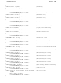
1
4 Axes Motor Control IC with High Functions
MCX514 User’s Manual
2014-08-01
2014-12-15
2015-02-01
2015-04-17
2015-10-15
Ver.
Ver.
Ver.
Ver.
Ver.
1.0
2.0
3.0
4.0
5.0
NOVA electronics
1. OUTLINE ................................................................ 1
1.1
The Main Features of Functions ..................................................................................................... 1
1.2
Functional Block Diagram ............................................................................................................... 9
1.3
Specification Table ......................................................................................................................... 11
2. The Descriptions of Functions .............................. 15
2.1
Fixed Pulse Driving and Continuous Pulse Driving....................................................................... 15
2.1.1
Relative Position Driving ...................................................................................................................... 15
2.1.2
Absolute Position Driving ..................................................................................................................... 16
2.1.3
Counter Relative Position Driving ......................................................................................................... 16
2.1.4
Continuous Pulse Driving ..................................................................................................................... 18
2.2
Acceleration and Deceleration ...................................................................................................... 20
2.2.1
Constant Speed Driving ........................................................................................................................ 20
2.2.2
Trapezoidal Driving [Symmetrical] ........................................................................................................ 21
2.2.3
Non-Symmetrical Trapezoidal Acceleration .......................................................................................... 23
2.2.4
S-curve Acceleration/Deceleration Driving [Symmetrical] ..................................................................... 25
2.2.5
Non-symmetrical S-Curve Acceleration/Deceleration ........................................................................... 31
2.2.6
Pulse Width and Speed Accuracy ......................................................................................................... 33
2.3
Position Control ............................................................................................................................ 34
2.3.1
Logical Position Counter and Real position Counter ............................................................................. 34
2.3.2
Position Comparison ............................................................................................................................ 34
2.3.3
Software Limit ...................................................................................................................................... 34
2.3.4
Position Counter Variable Ring ............................................................................................................. 35
2.4
Multi-Purpose Register ................................................................................................................. 36
2.4.1
Comparative Object and Comparison Condition ................................................................................... 36
2.4.2
Usage of Comparison Result ................................................................................................................ 37
2.4.3
Load / Save of Parameters by Synchronous Action .............................................................................. 40
2.5
Automatic Home Search ............................................................................................................... 41
2.5.1
Operation of Each Step ........................................................................................................................ 42
2.5.2
Deviation Counter Clearing Signal Output ............................................................................................ 45
2.5.3
Timer Between Steps ........................................................................................................................... 45
2.5.4
Setting a Search Speed and a Mode .................................................................................................... 46
2.5.5
Execution of Automatic Home Search and the Status ........................................................................... 50
2.5.6
Errors Occurring at Automatic Home Search ........................................................................................ 51
2.5.7
Notes on Automatic Home Search ........................................................................................................ 52
2.5.8
Examples of Automatic Home Search .................................................................................................. 53
2.6
Synchronous Action ...................................................................................................................... 59
2.6.1
Activation Factor .................................................................................................................................. 61
-i-
2.6.2
Action ................................................................................................................................................... 63
2.6.3
Synchronous Action Settings ................................................................................................................ 67
2.6.4
Synchronous Action Execution ............................................................................................................. 70
2.6.5
Interrupt by Synchronous Action ........................................................................................................... 70
2.6.6
Examples of Synchronous Action ......................................................................................................... 71
2.6.7
Synchronous Action Delay Time ........................................................................................................... 76
2.7
Split Pulse ..................................................................................................................................... 78
2.7.1
Split Pulse Setting ................................................................................................................................ 78
2.7.2
Start / Termination of Split Pulse ........................................................................................................... 79
2.7.3
Split Pulse in Synchronous Action ........................................................................................................ 80
2.7.4
Interrupt by Split Pulse ......................................................................................................................... 80
2.7.5
Notes on Split Pulse ............................................................................................................................. 80
2.7.6
Examples of Split Pulse ........................................................................................................................ 81
2.8
General Purpose Input / Output Signal ......................................................................................... 87
2.8.1
nPIOm Signal ....................................................................................................................................... 87
2.8.2
Other Input Signals .............................................................................................................................. 90
2.9
Timer ............................................................................................................................................ 91
2.9.1
Timer Operation ................................................................................................................................... 91
2.9.2
Timer Setting ........................................................................................................................................ 92
2.9.3
Timer-Start / Timer-Stop ....................................................................................................................... 92
2.9.4
Timer and Synchronous Action ............................................................................................................. 92
2.9.5
Timer Operating State and Current Timer Value Reading ..................................................................... 92
2.9.6
Interrupt by Timer ................................................................................................................................. 92
2.9.7
Examples of Timer................................................................................................................................ 93
2.10 Interrupt ........................................................................................................................................ 96
2.10.1
Interrupt from X, Y, Z and U axes ......................................................................................................... 96
2.10.2
Interrupt during Continuous Interpolation.............................................................................................. 97
2.11 Input Signal Filter ......................................................................................................................... 98
2.11.1
Setting of Input Signal Filter Function ................................................................................................... 99
2.11.2
Example of Setting Input Signal Filters ................................................................................................100
2.12 Other Functions .......................................................................................................................... 101
2.12.1
Driving By External Pulses ..................................................................................................................101
2.12.2
Pulse Output Type Selection ...............................................................................................................104
2.12.3
Encoder Pulse Input Type Selection ....................................................................................................105
2.12.4
Hardware Limit Signals .......................................................................................................................106
2.12.5
Interface to Servo Motor Driver ...........................................................................................................107
2.12.6
Emergency Stop ..................................................................................................................................107
2.12.7
Status Output ......................................................................................................................................108
- ii -
3. Interpolation ....................................................... 109
3.1
Linear Interpolation ...................................................................................................................... 111
3.1.1
Maximum Finish Point ......................................................................................................................... 111
3.1.2
Examples of Linear Interpolation ......................................................................................................... 111
3.2
Circular Interpolation ................................................................................................................... 113
3.2.1
The Finish Point Checking of Circular Interpolation ............................................................................. 114
3.2.2
Toggle of Interpolation Axis ................................................................................................................. 114
3.2.3
The Example for CW Circular Interpolation.......................................................................................... 114
3.3
Helical Interpolation ..................................................................................................................... 115
3.3.1
Interpolation Axis Setting ..................................................................................................................... 116
3.3.2
Interpolation Speed Setting ................................................................................................................. 116
3.3.3
Helical Rotation Number Setting .......................................................................................................... 116
3.3.4
Position Data Setting ........................................................................................................................... 117
3.3.5
Helical Calculation Execution .............................................................................................................. 118
3.3.6
Helical Interpolation Execution ............................................................................................................ 119
3.3.7
Current Helical Rotation Number Reading ........................................................................................... 119
3.3.8
Position Drift in Helical Interpolation ....................................................................................................120
3.3.9
Examples of Helical Interpolation ........................................................................................................121
3.4
Bit Pattern Interpolation .............................................................................................................. 124
3.4.1
Designation of Interpolation Axis .........................................................................................................125
3.4.2
Interpolation Speed Setting .................................................................................................................125
3.4.3
Bit Pattern Data Writing .......................................................................................................................125
3.4.4
Issue of Interpolation Driving Command ..............................................................................................126
3.4.5
Termination of Interpolation .................................................................................................................126
3.4.6
Check Available Space of Pre-buffer ...................................................................................................127
3.4.7
Interruption of Interpolation Driving .....................................................................................................127
3.4.8
Example of Bit Pattern Interpolation ....................................................................................................128
3.5
Constant Vector Speed ............................................................................................................... 129
3.5.1
3.6
Constant Vector Speed Setting ............................................................................................................130
Short Axis Pulse Equalization ..................................................................................................... 131
3.6.1
Short Axis Pulse Equalization Setting ..................................................................................................131
3.6.2
Notes on Using Short Axis Pulse Equalization .....................................................................................132
3.7
Continuous Interpolation ............................................................................................................. 133
3.7.1
How to Perform Continuous Interpolation ............................................................................................134
3.7.2
Continuous Interpolation by Using Interrupt .........................................................................................136
3.7.3
Errors during Continuous Interpolation ................................................................................................137
3.7.4
Attention for Continuous Interpolation .................................................................................................137
3.7.5
Example of Continuous Interpolation ...................................................................................................138
3.8
Acceleration / Deceleration Control in Interpolation.................................................................... 140
- iii -
3.8.1
Acceleration / Deceleration for Linear Interpolation .............................................................................140
3.8.2
Acceleration / Deceleration for Circular Interpolation and Bit Pattern Interpolation ..............................140
3.8.3
Acceleration / Deceleration for Continuous Interpolation .....................................................................142
3.9
Single-step interpolation ............................................................................................................. 143
3.9.1
Command Controlled Single-step Interpolation ...................................................................................143
3.9.2
External Signal Controlled Single-step Interpolation ............................................................................144
3.9.3
Attention for Single-step Interpolation..................................................................................................144
3.10 Multichip Interpolation................................................................................................................. 145
3.10.1
Execution Procedure ...........................................................................................................................146
3.10.2
Stop of Interpolation Driving ................................................................................................................148
3.10.3
Continuous Interpolation .....................................................................................................................148
3.10.4
Notes for Multichip Interpolation ..........................................................................................................148
3.10.5
Examples of Multichip Interpolation .....................................................................................................149
4. I2C Serial Bus .................................................... 153
4.1
Pins used in I2C Bus Mode ........................................................................................................ 153
4.1.1
Pull-up Resistor (Rp) ...........................................................................................................................153
4.1.2
I2CRSTN Reset...................................................................................................................................154
4.2
I2C Bus Transmitting and Receiving ........................................................................................... 154
4.2.1
Writing Operation ................................................................................................................................155
4.2.2
Reading Operation ..............................................................................................................................156
4.2.3
Notes on Using I2C Serial Bus ............................................................................................................158
4.2.4
Connection Example ...........................................................................................................................158
4.2.5
Control Example ..................................................................................................................................159
5. Pin Assignments and Signal Description ............ 162
5.1
Pin Assignments ......................................................................................................................... 162
5.2
Signal Description....................................................................................................................... 163
5.3
Input/Output Logic ...................................................................................................................... 169
5.4
Remarks of Logic Design ........................................................................................................... 170
6. Register .............................................................. 171
6.1
Register Address by 16-bit Data Bus .......................................................................................... 171
6.2
Register Address by 8-bit Data Bus ............................................................................................ 173
6.3
Register Address by I2C Serial Interface Bus Mode ................................................................... 173
6.4
Command Register: WR0 ........................................................................................................... 174
6.5
Mode Register1: WR1 ................................................................................................................ 174
6.6
Mode Register2: WR2 ................................................................................................................ 175
6.7
Mode Register3: WR3 ................................................................................................................ 176
6.8
Output Register: WR4 ................................................................................................................ 178
- iv -
6.9
Output Register: WR5 ................................................................................................................ 179
6.10 Data Register: WR6/WR7 ........................................................................................................... 179
6.11 Main Status Register: RR0 ......................................................................................................... 180
6.12 Status Register 1: RR1 ............................................................................................................... 181
6.13 Status Register 2: RR2 ............................................................................................................... 182
6.14 Status Register 3: RR3 ............................................................................................................... 183
6.15 PIO Read Register 1: RR4 ......................................................................................................... 185
6.16 PIO Read Register 2: RR5 ......................................................................................................... 185
6.17 Data-Read Register: RR6 / RR7 ................................................................................................. 185
7. Commands ......................................................... 186
7.1
Command Lists ........................................................................................................................... 186
7.2
Commands for Writing Data ....................................................................................................... 190
7.2.1
Jerk Setting .........................................................................................................................................190
7.2.2
Deceleration Increasing Rate Setting ..................................................................................................190
7.2.3
Acceleration Setting ............................................................................................................................191
7.2.4
Deceleration Setting ............................................................................................................................191
7.2.5
Initial Speed Setting ............................................................................................................................192
7.2.6
Drive Speed Setting ............................................................................................................................192
7.2.7
Drive pulse number / Finish point setting .............................................................................................193
7.2.8
Manual Decelerating Point Setting ......................................................................................................193
7.2.9
Circular Center Point Setting ...............................................................................................................194
7.2.10
Logical Position Counter Setting .........................................................................................................194
7.2.11
Real Position Counter Setting .............................................................................................................194
7.2.12
Software Limit + Setting ......................................................................................................................194
7.2.13
Software Limit − Setting ......................................................................................................................195
7.2.14
Acceleration Counter Offsetting ...........................................................................................................195
7.2.15
Logical Position Counter Maximum Value Setting ................................................................................195
7.2.16
Real Position Counter Maximum Value Setting ....................................................................................195
7.2.17
Multi-Purpose Register 0 Setting .........................................................................................................196
7.2.18
Multi-Purpose Register 1 Setting .........................................................................................................196
7.2.19
Multi-Purpose Register 2 Setting .........................................................................................................196
7.2.20
Multi-Purpose Register 3 Setting .........................................................................................................197
7.2.21
Home Search Speed Setting ...............................................................................................................197
7.2.22
Speed Increasing / Decreasing Value Setting ......................................................................................197
7.2.23
Timer Value Setting .............................................................................................................................198
7.2.24
Split Pulse Setting 1 ............................................................................................................................198
7.2.25
Split Pulse Setting 2 ............................................................................................................................198
7.2.26
Interpolation / Finish Point Maximum Value Setting .............................................................................199
7.2.27
Helical rotation number setting ............................................................................................................199
-v-
7.2.28
7.3
Helical calculation setting ....................................................................................................................199
Commands for Writing Mode ...................................................................................................... 200
7.3.1
Multi-Purpose Register Mode Setting ..................................................................................................200
7.3.2
PIO Signal Setting 1 ............................................................................................................................201
7.3.3
PIO Signal Setting 2・Other Settings ..................................................................................................203
7.3.4
Automatic Home Search Mode Setting 1 .............................................................................................204
7.3.5
Automatic Home Search Mode Setting 2 .............................................................................................205
7.3.6
Input Signal Filter Mode Setting ..........................................................................................................207
7.3.7
Synchronous Action SYNC0, 1, 2, 3 Setting ........................................................................................208
7.3.8
Interpolation Mode Setting ..................................................................................................................210
7.4
Commands for Reading Data ..................................................................................................... 212
7.4.1
Logical Position Counter Reading .......................................................................................................212
7.4.2
Real Position Counter Reading ...........................................................................................................212
7.4.3
Current Drive Speed Reading ..............................................................................................................212
7.4.4
Current Acceleration / Deceleration Reading .......................................................................................213
7.4.5
Multi-Purpose Register 0 Reading .......................................................................................................213
7.4.6
Multi-Purpose Register 1 Reading .......................................................................................................213
7.4.7
Multi-Purpose Register 2 Reading .......................................................................................................213
7.4.8
Multi-Purpose Register 3 Reading .......................................................................................................214
7.4.9
Current Timer Value Reading ..............................................................................................................214
7.4.10
Interpolation / Finish point maximum value Reading ............................................................................214
7.4.11
Current Helical Rotation Number Reading ...........................................................................................214
7.4.12
Helical Calculation Value Reading .......................................................................................................215
7.4.13
WR1 Setting Value Reading ................................................................................................................215
7.4.14
WR2 Setting Value Reading ................................................................................................................215
7.4.15
WR3 Setting Value Reading ................................................................................................................215
7.4.16
Multi-Purpose Register Mode Setting Reading ....................................................................................216
7.4.17
PIO Signal Setting 1 Reading ..............................................................................................................216
7.4.18
PIO Signal Setting 2 / Other Settings Reading ....................................................................................216
7.4.19
Acceleration Setting Value Reading.....................................................................................................217
7.4.20
Initial Speed Setting Value Reading .....................................................................................................217
7.4.21
Drive Speed Setting Value Reading .....................................................................................................217
7.4.22
Drive Pulse Number / Finish Point Setting Value Reading ...................................................................217
7.4.23
Split Pulse Setting 1 Reading ..............................................................................................................218
7.4.24
General Purpose Input Value Reading ................................................................................................218
7.5
Driving Commands ..................................................................................................................... 219
7.5.1
Relative Position Driving .....................................................................................................................219
7.5.2
Counter Relative Position Driving ........................................................................................................220
7.5.3
+ Direction Continuous Pulse Driving ..................................................................................................220
- vi -
7.5.4
− Direction Continuous Pulse Driving ..................................................................................................220
7.5.5
Absolute Position Driving ....................................................................................................................221
7.5.6
Decelerating Stop ................................................................................................................................221
7.5.7
Instant Stop .........................................................................................................................................221
7.5.8
Direction Signal + Setting ....................................................................................................................221
7.5.9
Direction Signal − Setting ....................................................................................................................222
7.5.10
Automatic Home Search Execution .....................................................................................................222
7.6
Interpolation Commands............................................................................................................. 223
7.6.1
1-axis Linear Interpolation Driving (Multichip) ......................................................................................223
7.6.2
2-axis Linear Interpolation Driving .......................................................................................................223
7.6.3
3-axis Linear Interpolation Driving .......................................................................................................223
7.6.4
4-axis Linear Interpolation Driving .......................................................................................................224
7.6.5
CW Circular Interpolation Driving ........................................................................................................224
7.6.6
CCW Circular Interpolation Driving ......................................................................................................224
7.6.7
2-Axis Bit Pattern Interpolation Driving ................................................................................................224
7.6.8
3-Axis Bit Pattern Interpolation Driving ................................................................................................225
7.6.9
4-Axis Bit Pattern Interpolation Driving ................................................................................................225
7.6.10
CW Helical Interpolation Driving ..........................................................................................................225
7.6.11
CCW Helical Interpolation Driving .......................................................................................................225
7.6.12
CW Helical Calculation ........................................................................................................................226
7.6.13
CCW Helical Calculation .....................................................................................................................226
7.6.14
Deceleration Enabling .........................................................................................................................226
7.6.15
Deceleration Disabling ........................................................................................................................226
7.6.16
Interpolation Interrupt Clear / Single-step Interpolation ........................................................................227
7.7
Synchronous Action Operation Commands ................................................................................ 228
7.7.1
Synchronous Action Enable Setting .....................................................................................................228
7.7.2
Synchronous Action Disable Setting ....................................................................................................229
7.7.3
Synchronous Action Activation ............................................................................................................229
7.8
Other Commands ....................................................................................................................... 230
7.8.1
Speed Increase ...................................................................................................................................230
7.8.2
Speed Decrease ..................................................................................................................................230
7.8.3
Deviation Counter Clear Output...........................................................................................................231
7.8.4
Timer-Start ..........................................................................................................................................231
7.8.5
Timer-Stop...........................................................................................................................................231
7.8.6
Start of Split Pulse ...............................................................................................................................231
7.8.7
Termination of Split Pulse ....................................................................................................................232
7.8.8
Drive Start Holding ..............................................................................................................................232
7.8.9
Drive Start Holding Release ................................................................................................................232
7.8.10
Error / Finishing Status Clear...............................................................................................................232
- vii -
7.8.11
RR3 Page 0 Display ............................................................................................................................233
7.8.12
RR3 Page 1 Display ............................................................................................................................233
7.8.13
Maximum finish point clear ..................................................................................................................233
7.8.14
NOP ....................................................................................................................................................233
7.8.15
Command Reset .................................................................................................................................234
8. Connection Examples ........................................ 235
8.1
Example of 16-bit / 8-bit Bus Mode Connection ......................................................................... 235
8.2
Example of Connection in I2C Bus Mode ................................................................................... 236
8.3
Connection Example .................................................................................................................. 237
8.4
Pulse Output Interface ................................................................................................................ 237
8.5
Connection Example for Input Signals ........................................................................................ 238
8.6
Connection Example for Encoder ............................................................................................... 238
9. Example Program............................................... 239
10. Electrical Characteristics ................................. 252
10.1 DC Characteristics ...................................................................................................................... 252
10.2 AC Characteristics ...................................................................................................................... 253
10.2.1
Clock ...................................................................................................................................................253
10.2.2
Read / Write Cycle ..............................................................................................................................253
10.2.3
CLK / Output Signal Timing .................................................................................................................254
10.2.4
Input Pulses ........................................................................................................................................254
10.2.5
General Purpose Input / Output Signals (nPIO7~0) ...........................................................................255
10.2.6
Split Pulse ...........................................................................................................................................255
10.2.7
I2C Serial Bus ......................................................................................................................................256
11. Timing of Input / Output Signals ...................... 257
11.1 Power-On Reset ......................................................................................................................... 257
11.2 Fixed Pulse or Continuous Pulse Driving ................................................................................... 257
11.3 Interpolation Driving ................................................................................................................... 258
11.4 Start Driving after Hold Command .............................................................................................. 258
11.5 Instant Stop ................................................................................................................................ 258
11.6 Decelerating Stop ....................................................................................................................... 259
11.7 Detailed Timing of Split Pulse ..................................................................................................... 259
12. Package Dimensions ...................................... 260
13. Storage and Recommended Installation
Conditions ............................................................. 261
13.1 Storage of this IC ........................................................................................................................ 261
- viii -
13.2 Standard Installation Conditions by Soldering Iron ..................................................................... 261
13.3 Standard Installation Conditions by Solder Reflow ..................................................................... 261
- ix -
MCX514 - i
NOVA electronics Inc.
■ Revision History
1st edition
2nd edition
2014-08-01
2014-12-15
3rd edition
2015-02-12
4th edition
2015-04-17
5th edition
2015-10-15
Newly created.
・Correction of the following errors
1.3 Specification Table
over limit signal
signal name
3. Interpolation
each interpolation speed
7.4.24 General Purpose Input Value Reading
data range of general purpose
input value reading
9. Example Program description of interpolation command functions
・ Correction of the following errors about the finish point range of interpolation
3.1 Linear Interpolation
range of coordinates
3.2 Circular Interpolation
range of center and finish point coordinates
3.6 Short Axis Pulse Equalization
settable range of center and finish points
7.1 Command Lists ■ Commands for Writing Data
data range of ・Drive pulse number/Finish point setting
・Circular center point setting
・Interpolation / Finish point maximum value setting
■ Commands for Reading Data
data range of ・Interpolation / Finish point maximum value reading
・Drive pulse number / Finish point setting value reading
7.2.7 Drive pulse number / Finish point setting
data range
7.2.9 Circular Center Point Setting
data range
7.2.26 Interpolation / Finish Point Maximum Value Setting data range
7.4.10 Interpolation / Finish point maximum value Reading
data range
7.4.22 Drive Pulse Number / Finish Point Setting Value Reading data range
・ Correction of the following error
5.2 Signal Description
VDD Pin No.
・ Correction of the following errors about triangle form prevention
2.2.2 Triangle form prevention of trapezoidal driving
2.2.3 Triangle form prevention of non-symmetrical trapezoidal driving
・ Correction of the following errors about changing drive speed during
interpolation driving
3. Interpolation
Set interpolation speed
3.7.1 How to Perform Continuous Interpolation
3.7.4 Attention for Continuous Interpolation
7.2.6 Drive Speed Setting
・ Correction of the following errors about short axis pulse equalization
3.6.2 Notes on Using Short Axis Pulse Equalization
3.7.4 Attention for Continuous Interpolation
・ Correction of the following errors
5.2
Signal Description Description (D15~D0 )
7.4.24 General Purpose Input Value Reading
・Add the following about EMGN signal input signal.
2.11.1 table2.11-1, Add the setting of ※EMGN signal
2.12.6 Emergency stop, Add “4 axes(all axes)”
5.2 Signal description, Add “all axes” about EMGN
1.3Temperature for driving→Operation Temperature
Power Voltage for driving→Operation Power Voltage
10.1 Ambient Temperature→Operation temperature
- i -
MCX514 - ii
NOVA electronics Inc.
Introduction
In general, semiconductor products sometimes malfunction or fail to function. When incorporating this IC in a system, make sure
that a safe system is designed to avoid any injuries or property damage caused by malfunctioning of this IC.
This IC is designed for application in general electronic devices (industrial automation devices, industrial robots, measuring
instruments, computers, office equipment, household electrical goods, and so on). This IC is not intended for the use in
high-performance and high-reliability equipment whose failure or malfunctioning may directly cause death or injuries (atomic
energy control equipment, aerospace equipment, transportation equipment, medical equipment, and various safety devices) and
the operation for such use is not guaranteed. The customer shall be responsible for the use of this IC in any such
high-performance and high-reliability equipment.
“Japanese Foreign Exchange and Foreign Trade Act” and other export-related laws and regulations must be observed and
complied with. Do not use this IC for the purpose of the development of weapons such as mass destruction weapons and any
military purposes. This IC shall not be used in equipment that manufacture, use and sale are prohibited by domestic and foreign
laws and regulations.
Information in this manual is subject to change without notice for continuous improvement in the product.
You can download the latest manual and software from our web site: http://www.novaelec.co.jp/eng
Please also feel free to contact us directly for any inquiries or questions.
■ Operating Precautions
Before using the MCX514, please read this manual thoroughly to ensure correct usage within the scope of the specification such
as the signal voltage, signal timing, and operation parameter values.
Operation is not verified in all combinations of modes and parameters. The user should fully verify and evaluate the operation
with a combination of the mode and parameter that is used before using this IC.
Treatment of unused pins that are not pulled up in the IC
Make sure that unused input pins are connected to GND or VDD. If these pins are open, the signal level of pins will unstable and
may cause malfunction.
Make sure that unused bi-directional pins are connected to VDD or GND through high impedance (about 10k~ 100 kΩ). If these
pins are directly connected to GND or VDD, the IC may be damaged by overcurrent in case of such as a programming mistake
causes the output state.
About Reset
Make sure to reset the IC when the power is on. This IC will be reset if RESETN signal is set to Low for more than 8 CLK
cycles when a stable clock has been input. Please note that the IC will not be reset if the clock is not input.
Note on S-curve Acceleration/Deceleration Driving
This IC is equipped with a function that performs decelerating stop for fixed pulse driving in S-curve deceleration with the
symmetrical acceleration/deceleration. However, when the initial speed is set to an extremely low speed, slight premature
termination or creep may occur. Before using S-curve deceleration driving, make sure that your system allows premature
termination or creep.
- ii -
MCX514 - iii
NOVA electronics Inc.
■ Terms and Symbols used in the Manual
Active
The function of a signal is the state of being enabled.
Drive
Action to output pulses for rotating a motor to the driver (drive unit) of a pulse type servo
motor or setepping motor.
Fixed pulse drive
Drive that outputs specified pulses. Three types of drives: relative position drive, counter
relative position drive and absolute position drive are available.
Continuous pulse drive
Drive that outputs pulses up to infinity unless a stop factor becomes active.
CW
Clockwise direction (abbreviation of clockwise)
CCW
Counter-clockwise direction (abbreviation of counter-clockwise)
Interpolation segment
Each interpolation driving that comprises continuous interpolation.
Jerk
Acceleration increasing/decreasing rate per unit time. This term includes a decreasing rate of
acceleration (=Jerk).
Deceleration increasing rate
Deceleration increasing/decreasing rate per unit time. This term includes a decreasing rate of
deceleration.
2's complement
2's complement is used to represent negative numbers in binary.
[Example] In 16-bit length, -1 is FFFFh, -2 is FFFEh, -3 is FFFDh, … -32768 is 8000h.
Creep
In deceleration of acceleration/ deceleration fixed pulse driving, output of specified driving
pulses is not completed even if the speed reaches the initial speed and the rest of driving
pulses is output at the initial speed (= Creep).
Premature termination
In deceleration of acceleration/ deceleration fixed pulse driving, output of specified driving
pulses is completed and driving is terminated before the speed reaches the initial speed. This is
a reverse behavior of creep.
↑
The rising edge of when a signal changes its level from Low to Hi.
↓
The falling edge of when a signal changes its level from Hi to Low.
n○○○○
The signal name of each axis X, Y, Z and U is written as n○○○○. This “n” stands for X, Y,
Z or U.
nPIOm
PIO signal of each axis X, Y, Z and U is written as nPIOm. This “n” stands for X, Y, Z or U,
and “m” stands for 0~7 of PIO0~PIO7.
SYNCm
Synchronous action set SYNC0~SYNC3 is written as SYNCm. This “m” stands for 0~3 of
SYNC0~SYNC3.
MRm
Multi-purpose register MR0~MR3 is written as MRm. This “m” stands for 0~3 of MR0~MR3.
- iii -
MCX514 - 1
NOVA electronics Inc.
1. OUTLINE
1.1
The Main Features of Functions
MCX514 is a 4-axis motion control IC that has improved greatly in functions of previous IC such as MCX314As / MCX314AL.
As the interpolation functions, it provides the existing linear interpolation, circular interpolation and bit pattern interpolation, in
addition, it has the helical interpolation function that works to move Z-axis in a vertical direction, synchronizing with the circular
interpolation on the XY plane.
MCX500 series motion control IC has no multiple of speed (speed range-free). This enables us to freely set and vary the drive
speed linearly from 1 pps up to 8 Mpps in increments of 1pps without changing the range.
MCX514 can be connected to a host CPU with either 8-bit or 16-bit bus, and I2C serial interface bus. It can also be connected to a
CPU without a parallel bus.
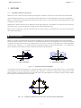
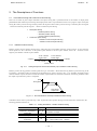
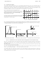
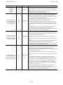
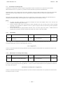
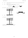
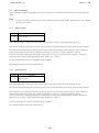
■ Helical Interpolation
MCX514 is capable of performing helical interpolation in addition to the existing linear interpolation and circular interpolation.
Helical interpolation operates to move another axis in synchronization with the circular interpolation in the XY plane (orthogonal
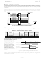
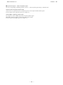
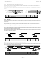
coordinates). The figure shown below is an example to move Z-axis in the + direction, corresponding to the circular interpolation
on the XY plane. The figure 1.1-1 a. illustrates the helical interpolation under one rotation, and the figure 1.1-1 b. illustrates the
helical interpolation in a plurality of rotations. MCX514 can perform both interpolation.
Z
Z
Finish Point
Y
Finish Point
Y
X
X
Start Point
Start Point
a. Under One Rotation
b. One Rotation or More
Fig. 1.1-1
Example of Helical interpolation
As an application of helical interpolation, it is possible to operate normal control that rotates another axis by a constant angle
corresponding to the circular interpolation on the XY plane. The figure 1.1-2 shows an example of the operation that an object
such as a camera or nozzle on a pedestal is directed to the center of circular interpolation, mounting a rotating axis in the pedestal
that performs circular interpolation on the XY plane.
Y
Z
Z
Z
Z
X
Z
Fig. 1.1-2
Example of Normal Control of Z axis in XY axes Circular Interpolation
- 1 -
MCX514 - 2
NOVA electronics Inc.
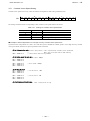
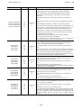
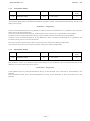
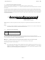
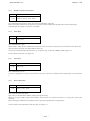
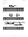
■ 8 Stages of Pre-Buffer for Continuous Interpolation
MCX514 is equipped with 8 stages of pre-buffer register that stores finish point data (and others) in each segment, in order to
handle continuous interpolation driving at high-speed.
In the case of the previous MCX314A having only 1 stage of pre-buffer, when performing continuous interpolation, driving time
of each interpolation segment must be longer than setting time of position data for next segment. Therefore, minimum drive pulses
of each segment are restricted depend on interpolation drive speed. For instance, when setting time of data to CPU isTDS=80μsec
and interpolation drive speed is V=100Kpps, minimum drive
Y
pulses are required at least 8 pulses or more.
Seg3
Seg10
Seg4
MCX514 increases pre-buffer to 8 stages and improves the
Seg2
restriction efficiently. When performing continuous interpolation
Seg9
Seg5
as shown in the right figure, and when there is a short segment
Seg1
such as Seg3, if the average driving time of 8 segments including
Seg6 Seg7 Seg8
Seg3 is longer than setting time of position data for next segment,
continuous interpolation can be performed.
Seg n
X
Fig. 1.1-3
Example of Continuous Interpolation
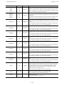
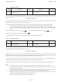
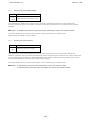
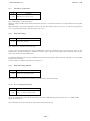
■ Multichip Interpolation
The user can perform multiple axes linear interpolation of 5 axes or more by connecting several MCX514 chips. Connect each
chip by using 8 multichip signal lines in parallel.
In multiple axes linear interpolation, the maximum values to the finish points of all axes that perform interpolation are required for
interpolation calculation. However, MCX514 does not need to set these maximum values. When a host CPU writes finish point
data of each axis into IC respectively, the data will be sent to each IC through the multichip signal line, and then the maximum
value of finish point will be calculated automatically in IC.
Drive Pulse
Host CPU
First Axis
Second Axis
MCX514
Third Axis
Drive Pulse
Motor
Driving
Circuit
MCX514
Fourth Axis
Fifth Axis
Sixth Axis
Seventh Axis
Eighth Axis
Multichip Interpolation Signal (8 lines)
Fig. 1.1-4
Example of Multichip Interpolation
- 2 -
MCX514 - 3
NOVA electronics Inc.
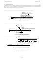
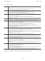
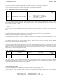
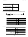
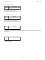
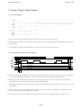
■ Short Axis Pulse Equalization Mode for Interpolation
In interpolation driving, all of axes that perform interpolation do not always output drive pulses at regular intervals during driving.
As shown in the figure below, in 2-axis linear interpolation, the axis (long axis) that has longer moving distance (pulse) outputs
pulses continuously; however, the axis (short axis) that has shorter one sometimes outputs and sometimes does not output pulses
depending on the result of interpolation calculation, and these uneven pulses could be a problem. When performing interpolation
in a stepper motor, if the user tries to perform interpolation at high-speed as well as independent driving, the vibration of a short
axis is increased due to these thinning-out pulses and may step out. MCX514 can improve this problem with the function: short
axis pulse equalization mode. Even in the axis has shorter moving distance, it can output drive pulses as equal as possible. And if
this function is used in combination with constant vector speed mode, it will increase the accuracy of constant vector speed.
Usual Interpolation
X
Y
Short axis pulse equalization mode
X
Y
Fig. 1.1-5
Pulse Output in 2-axis Linear Interpolation with Moving Distance of X: 30 pulses and Y: 26 pulses
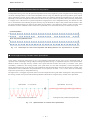
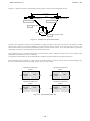
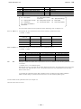
■ 2-Axis High Accuracy Constant Vector Speed Mode
Vector speed is the driving speed of the tip of a locus performing interpolation driving, and it is also called Head speed. In
operations such as machining or coating workpieces during interpolation driving, it is important to keep this vector speed constant.
MCX514 realizes 2-axis high accuracy constant vector speed mode that increases the accuracy of constant vector speed
considerably, in addition to the existing constant vector speed mode. In 2-axis linear interpolation, circular interpolation and
helical interpolation driving, if the short axis pulse equalization mode described above and 2-axis high accuracy constant vector
speed mode are used in combination, the speed deviation of vector speed can be within ±0.2% or less, and it will considerably
improve the speed accuracy in interpolation driving.
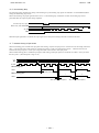
The figure below is each graph of speed deviation of circular interpolation driving with radius 10,000 pulses, when performed in
the existing constant vector speed mode and when performed in MCX514 2-axis high accuracy constant vector speed mode.
Speed deviation -7% at a maximum
Speed deviation ±0.2% or less
Existing constant vector speed mode
Fig. 1.1-6
2- axis high accuracy constant vector speed mode
Speed Deviation in Constant Vector Speed Mode
- 3 -
MCX514 - 4
NOVA electronics Inc.
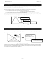
■ Speed Range-Free
MCX514 is a new motion control IC that has no multiple of speed (Range Setting) to set the drive speed. This will enable us to
freely set the speed from 1 pps up to 8 Mpps in increments of 1 pps.
When using the multiples of speed to set the speed by existing method, there are restrictions as described below.
•
For the detailed speed setting of low-speed, less multiples of speed must be set.
→
As a result, driving cannot be shifted to high-speed.
•
To perform the high-speed driving, larger multiples of speed must be set.
→
As a result, the detailed setting of drive speed cannot be configured.
MCX514 brings solutions to the inconvenience described above by Speed range-free, which makes it possible to directly change
the speed from low-speed such as 1 or 2 pps to high-speed such as 1 Mpps during the driving.
V
1,000,000pps
High-speed driving without
speed range setting
Speed can be set in
increments of 1 pps
Detailed low-speed
setting
163,927pps
7pps
Time
Fig. 1.1-7 Speed Range-Free
■ Easy and High-Accuracy Speed Setting
Since there is no need to set multiples of speed (Range Setting), the user can set a drive speed of output pulses as a speed
parameter (at CLK = 16MHz).
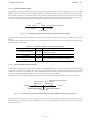
Drive speed (pps)=V×
8,000,000
R
Drive speed (pps) = DV
Acceleration (pps/sec)=A×125×
8,000,000
R
Acceleration (pps/sec) = AC
Jerk (pps/sec2)
・・・
=
Jerk (pps/sec2) = JK
8,000,000
62.5×10 6
×
K
R
Speed can be used as a parameter
→ no need to calculate a parameter
Fig. 1.1-8 Speed Parameter Setting
In the range of 1 pps to 8 Mpps, it can output the drive speed that is set with high accuracy. Speed accuracy of the pulse output is
less than ± 0.1%, which is on the assumption that there is no frequency error of input clock (CLK). In fact, there is a frequency
error of input clock (CLK), and speed accuracy depends on it.
- 4 -
MCX514 - 5
NOVA electronics Inc.
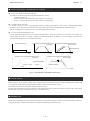
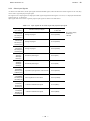
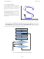
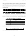
■ Various Acceleration / Deceleration Drive Mode
Types of acceleration / deceleration driving
Acceleration / deceleration driving can perform the following driving.
Constant speed driving
Linear acceleration / deceleration driving (symmetry/ non-symmetry)
S-curve acceleration/deceleration driving (symmetry/ non-symmetry)
Automatic deceleration start
In position driving of linear acceleration/deceleration (symmetry/non-symmetry) and S-curve acceleration/deceleration
(symmetry), the IC calculates the deceleration start point when in deceleration, and automatically starts deceleration.
(This is not applied to non-symmetry S-curve acceleration/deceleration driving.)
S-curve acceleration/deceleration curve
S-curve acceleration/deceleration uses the method which increases / decreases acceleration or deceleration in a primary line,
and the speed curve forms a secondary parabola acceleration/deceleration. In addition, it prevents triangle waveforms by a
special method during S-curve acceleration/deceleration.
Constant Speed Driving
Trapezoidal Acceleration/Deceleration Driving Trapezoidal Acceleration/Deceleration Driving
(Symmetry)
(Non- Symmetry)
V
V
V
w
Slo
Time
on
ati
ler
ce
c
A
Time
Rapid Deceleration
Time
Parabola S- curve Acceleration/Deceleration Driving
(Non- Symmetry)
Parabola S- curve Acceleration/Deceleration Driving
(Symmetry)
V
V
ow
Sl
P=200000
Rapid Acceleration
P=400000
P=50000
Time
n
tio
ra
P=100000
Manual Deceleration
le
ce
De
Automatic Deceleration
Time
Fig. 1.1-9 Acceleration / Deceleration Drive Mode
■ Position Control
MCX514 has two 32-bit position counters: one is a logical position counter that counts the number of output pulses and the other
is a real position counter that counts the feedback number of pulses from an external encoder.
The current position can be read by data reading commands anytime.
By using with synchronous action, the operation can be performed by the activation factor based on position data, such as drive
speed change or start/stop of another axis driving at a specified position.
■ Software Limit
MCX514 has a software limit function that controls driving to stop when the position counter is over a specified range. There are 2
stop types for when the software limit function is enabled: decelerating stop and instant stop.
- 5 -
MCX514 - 6
NOVA electronics Inc.
■ Various Synchronous Actions
Synchronous action is the function that executes a specified action together if a specified activation factor occurs. These
synchronous actions can be performed fast and precisely, independent of the CPU.
Synchronous action can be set up to 4 sets to each axis.
1 set of synchronous actions is configured with one specified activation factor and one specified action. 15 types of activation
factors are provided, such as the passage of a specified position, start/termination of driving, the rising/falling edge of an external
signal and expiring of an internal timer. In addition, 28 types of actions are provided, such as start/termination of driving, save the
current position counter value to multi-purpose register and writing of a drive speed.
When an activation factor of 1 set of any axis occurs, the other 3 sets of the same axis and 1set of another axis, which are total
7sets of actions, can be activated simultaneously.
Multiple synchronous action sets can be used in combination, which allows users to develop a wide array of applications.
Action
• Outputs an external signal when passing through a
specified position during the driving.
• Saves the current position to a specified register when
an external signal is input during the driving.
• Outputs N split pulses from a specified position to the
external during the driving.
Output the pulse signal to the external
PIO0
Activation Factor
Axis is passing through the position 15,000
Fig. 1.1-10 Synchronous Action
■ Four Multi-Purpose Registers
MCX514 has four 32-bit length multi-purpose registers in each axis.
Multi-purpose register can be used to compare with the current position, speed and timer, and then can read out the status which
represents comparison result and can output as a signal. In addition, it can activate a synchronous action according to comparison
result or can generate an interrupt.
By using with synchronous action, it can save values of current position or speed of during the driving to multi-purpose registers
and load values that are saved in multi-purpose registers to the output pulse number or drive speed.
■ Timer Function
MCX514 is equipped with a timer in each axis, which can set with the range of 1 ~ 2,147,483,647μsec in increments of 1μsec
(at CLK = 16MHz). By using with synchronous action, the following operations can be performed precisely.
V
Timer
V
Time
Time
Termination of driving
Start of driving
After 17.35 msecs
Fig. 1.1-11 Timer Function
- 6 -
• Starts driving after specified periods when the
driving is finished.
• Starts driving after specified periods after an
external signal is input.
• Stops continuous pulse driving after specified
periods.
• Times from position A to position B.
MCX514 - 7
NOVA electronics Inc.
■ Output of Split Pulse
This is a function in each axis that outputs split pulses during the driving, which synchronizes axis driving and performs various
operations. The split length, pulse width of a split pulse and split pulse number can be set. By using with synchronous action, the
output of split pulses can be started/terminated at a specified position and the split length or pulse width of a split pulse can be
changed by an external signal. Split pulses can be output corresponding to an arbitrary axis during interpolation driving.
Drive Pulse
2
1
Split Pulse
3
Pulse Width
Split Length
Split Pulse Number
Fig. 1.1-12 Split Pulse Output
■ Automatic Home Search Function
This IC is equipped with the function that automatically executes a home search sequence without CPU intervention. The
sequence comprises high-speed home search → low-speed home search → encoder Z-phase search → offset drive.
Deviation counter clear pulses can be output for a servo motor driver. In addition, the timer between steps which sets stop time
among each step is available, and the operation for a home search of a rotation axis is provided.
■ Servo Motor Feedback Signals
MCX514 has input pins for servo feedback signals such as encoder 2-phase, in-positioning and alarm signals. An output signal for
clearing a deviation counter is also available.
■ Interrupt Signals
MCX514 has 2 interrupt signals (INT0N, INT1N).
INT0N signal is used to generate an interrupt by various factors. For example, (1). at the start / finish of a constant speed drive
during the acceleration/deceleration driving, (2). at the end of driving, and (3). when the comparison result of a multi-purpose
register with a position counter changes.
INT1N signal is used to request to transfer next segment data to CPU while continuous interpolation driving is performed.
■ Driving by External Signals
Driving can be controlled by external signals, which are the relative position driving, continuous pulse driving and manual pulsar
driving. This function is used for JOG feed or teaching mode, reducing the CPU load and making operations smooth.
- 7 -
MCX514 - 8
NOVA electronics Inc.
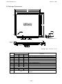
■ Built-in Input Signal Filter
The IC is equipped with an integral type filter in the input step of each input signal. It is possible to set for each input signal
whether the filter function is enabled or the signal is passed through. A filter time constant can be selected from 16 types (500nsec
~ 16msec).
MCX514
+3.3V
nLMTP
+24V
+LIMIT
Built-in Filter (Digital Processing)
Fig. 1.1-13 Built-in Input Signal Filter
■ Real Time Monitoring
During the driving, the current status such as logical position, real position, drive speed, acceleration / deceleration, status of
accelerating / constant speed driving / decelerating / acceleration increasing / acceleration constant / acceleration decreasing and a
timer can be read in real time.
■ CPU Interface
This IC has I2C serial interface bus in addition to the existing 8-bit/16-bit data bus as the interface to connect a host CPU.
I2C serial interface bus needs only 2 lines: serial data line (SDA) and serial clock line (SCL), so the user can use such a PICTM
microcomputer that has few terminals as a host CPU. I2C bus can be connected with several devices such as MCX514 or
EEPROM that have I2C bus interface on the same bus.
I 2C
Drive pulse
+3.3V
Motor
Driving
Circuit
SDA
Host CPU
SCL
MCX514
#1
Drive pulse
MCX514
#2
Fig. 1.1-14 I2C Serial Interface Bus
- 8 -
Motor
Driving
Circuit
MCX514 - 9
NOVA electronics Inc.
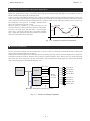
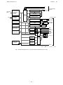
1.2
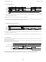
Functional Block Diagram
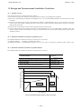
MCX514 functional block diagram is shown in the Fig. 1.2-1 as below. It comprises control sections of 4 axes, X, Y, Z and U that
have the same function, and interpolation counting sections. In interpolation driving, interpolation is calculated at the timing of
basic pulse oscillation of a specified main axis (AX1), which can be performed both in constant and acceleration/deceleration
driving.
Fig. 1.2-2 is the functional block diagram of each axis control section.
CSN
RDN
WRN
A3~A0
D15~D0
SCL
SDA
Parallel Bus
Control
Section
8Bit/16Bit
Serial Bus
Control
Section
I 2C
Multichip Interpolation
Counting Section
8 stages
Pre- buffer
Command
/Data
Interpretation
Process
Section
Linear Interpolation
Counting Section
2- axis/3- axis/4- axis
Interpolation
Control
Section
Circular
Interpolation
Counting Section
INT
Helical
Interpolation
Counting Section
CLK
16MHz Standard
Bit Pattern
Interpolation
Counting Section
2- axis/3- axis/4- axis
RESETN
Multichip
interpolation
Signal
AX1P+
AX1PAX2P+
AX2PAX3P+
AX3PAX4P+
AX4P-
XP+
XP-
AX1P+
AX1PAX2P+
AX2P-
YP+
YP-
Pulse
AX1P+
AX1PAX2P+
AX2PAX1P+
AX1PAX2P+
AX2PAX3P+
AX3PAX4P+
AX4P-
Main axis pulse
Separate
ZP+
ZP-
UP+
UP-
XP+
XP-
X- axis
I/O
X- axis Control Section
INT
Main axis pulse
YP+
YP-
Y- axis
I/O
Y- axis Control Section
INT
Main axis pulse
INT1N
Interrupt
Generator
1
INT0N
Interrupt
Generator
0
ZP+
ZP-
Z- axis
I/O
Z- axis Control Section
INT
UP+
UP-
U- axis Control Section
INT
Fig. 1.2-1 MCX514 The Whole Functional Block Diagram
- 9 -
U- axis
I/O
MCX514 - 10
NOVA electronics Inc.
P+
P-
Main axis
pulse
Jerk Generator
Command
/Data
INT
Command/Data
Interpretation
Process
Section
Interrupt
Generator
Action
Control
Section
Acceleration/Deceleration
Generator
CV
Speed Generator
External Signal
Pulse Generator
Automatic Home
Search Section
P+
P-
Logical Position Counter UP
DOWN
32bit
LP
Parameter/Mode
Setting Register
RP
Synchronous
Action Section
To Interpolation
Section
Real Position Counter UP
DOWN
32bit
Wave
Change
Integrated
Filter
Multi- purpose
A Compare
Register MR3~0
B
ECA/PPIN
ECB/PMIN
Wave
Change
LMTP
LMTM
STOP[2:0]
INPOS
ALARM
EMGNNote1
Timer
CT 31bit
PP/PLS/PA
PM/DIR/PB
Integrated
Filter
Register
A:B
PIO[7:0]
General Output
OUT[7:0]
A
Selector
Split Pulse
Generator
Drive Status
Output
B
Synchronous
Pulse / MR
Comparison
C
SPLTP
Note1: EMGN is in common all axes.
Fig. 1.2-2 Block Diagram of X, Y, Z and U-Axis Control Section (of 1 axis)
- 10 -
MCX514 - 11
NOVA electronics Inc.
1.3
Specification Table
(CLK=16MHz)
Item
Subitem
Description
Control Axis
4 axes
CPU Parallel Bus
16-bit/8-bit bus selectable
Connection
I2C serial interface bus
CPU Serial Bus
Connection
Interpolation Function Interpolation Commands
2-axis /3-axis /4-axis linear interpolation,
CW/CCW circular interpolation
2-axis /3-axis /4-axis bit pattern interpolation,
CW/CCW helical interpolation
Interpolation Range
Each axis -2,147,483,646 ~ 2,147,483,646 drive pulse
Interpolation Speed
1 pps ~ 8,000,000 pps
Interpolation Accuracy
±0.5LSB or less (linear interpolation)
*11
±1LSB or less (circular interpolation)
Other Interpolation Related
・Can select any axis
Functions
・Short axis pulse equalization
・Constant vector speed
(2-axis/3-axis simple mode, 2-axis high-accuracy mode selectable)
・Continuous interpolation
・Data buffering by 8 stages preregister
・Single step interpolation
・Multichip axes linear interpolation
Drive Pulses Output
Drive Speed Range
1 pps ~ 8,000,000 pps
Initial Speed Range
1 pps ~ 8,000,000 pps
Pulse Output Accuracy
±0.1% or less (according to the setting speed)
Acceleration Range
1 pps/sec ~ 536,870,911pps/sec
Acceleration Increasing /
1 pps/sec2 ~ 1,073,741,823 pps/sec2
(When CLK=20MHz: up to 10,000,000 pps)
*1
Decreasing Rate Range
Acceleration / Deceleration
Constant speed,
Curve
Symmetrical/non-symmetrical linear acceleration/deceleration,
Symmetrical/non-symmetrical parabola S-curve acceleration /
deceleration
Drive Pulse Range
・Relative position driving: -2,147,483,646~2,147,483,646
drive
pulse
・Absolute position driving: -2,147,483,646~2,147,483,646
drive
*2
pulse
Position Driving
Automatic deceleration stop / Manual deceleration stop
Decelerating Stop Mode
Override
Output pulse number and drive speed are changeable during the
driving
Driving Commands
Relative / Absolute position driving,
+/-direction continuous driving
Triangle Form Prevention
Can be used both in linear and S-curve acceleration / deceleration
Drive Pulse Output Type
Independent 2-pulse, 1-pulse 1-direction,
Quadrature pulse and quad edge evaluation,
Quadrature pulse and double edge evaluation are selectable
Encoder Input
Drive Pulse Output Logic
Positive / Negative logical level selectable
Drive Pulse Output Pin
Possible to pin inversion
Input Pulse Input Type
Quadrature pulses input and quad edge evaluation,
Quadrature pulses input and double edge evaluation,
Quadrature pulses input and single edge evaluation,
Up / down pulse input are selectable
Input Pin
Possible to pin inversion
- 11 -
*3
*4
MCX514 - 12
NOVA electronics Inc.
Logical Position Counter
Real Position Counter
Variable Ring
Setting Range
Count Range:-2,147,483,648 ~ +2,147,483,647
drive pulse
*5
Count Range:-2,147,483,648 ~ +2,147,483,647
drive pulse
*5
Stop Mode
Decelerating / Instant stop selectable
Multi-Purpose
Bit Length,
32-bit length
Register
Number of Registers
4 registers per axis
Uses
Compare with position, speed and timer value,
Position Counter
Software Limit
Possible to set the count maximum value of each counter
-2,147,483,648 ~ +2,147,483,647 pulse
load data such as position and speed, and save data such as current
position, speed and timer value
Timer
Split Pulse
Automatic Home
Number of timers
1 per axis
Setting Range
1 ~ 2,147,483,647μsec
Number of signals
1 per axis
Split Length
2 ~ 65,535 drive pulse
Split Pulse Width
1 ~ 65,534 drive pulse
Split Pulse Number
1 ~ 65,535, or up to infinity
Sequence
STEP1 high-speed home search → STEP2 low-speed home search
→ STEP3 encoder Z-phase search → STEP4 offset drive
・Enable / Disable each step and search signal / direction are
selectable
Search
Deviation Counter Clear
Synchronous Action
*6
Clear pulse width within the range of 10μ~20msec,
Output
Logical level selectable
Timer between Steps
1msec ~ 1,000msec selectable
Number of Sets
4 sets per axis
Activation Factor
・When multi-purpose register comparison changed
*7
・Comparative object: logical/real position counter value,
current drive speed, current timer value
・Comparison condition: ≧,>,=,<
・When a timer is up
・Start/Termination of driving, Start/Termination of driving at constant
speed area in acceleration / deceleration driving
・Start/Termination of split pulse, Output of split pulse
・nPIOm signal ↑/↓, nPIOm+4 signal Low and nPIOm signal ↑,
nPIOm+4 signal Hi and nPIOm signal ↑,
nPIOm+4 signal Low and nPIOm signal ↓,
nPIOm+4 signal Hi and nPIOm signal ↓ (m:0,1,2,3)
・Activation command
Action
・Load value (MRm→setting value):Drive speed,
Drive pulse number (Finish point), Split length, Split pulse width,
Logical/Real position counter value, Initial speed, Acceleration
・Save value (MRm←current value):Logical/Real position counter
value, Current timer value, Current drive speed,
Current acceleration / deceleration
・Synchronous pulse output to the external
・Start of relative/absolute position driving, Start of +/-direction
continuous driving, Start of relative/absolute position driving at the
position set by MRm
・Decelerating stop / Instant stop, Speed increase/decrease,
Timer-start/stop, Start / Termination of split pulse
Other SYNC Activation
Activation of other 3 sets actions can be set.
Another Axis SYNC0 Activation
Activation of another SYNC0 action can be set.
Repeat
Synchronous action can be operated once/repeatedly.
- 12 -
MCX514 - 13
NOVA electronics Inc.
Interrupt
Number of Signals
2: INT0N, INT1N
Interrupt Factor
・When multi-purpose register comparison changed
・Comparative object: logical/real position counter value,
current drive speed, current timer value
・Comparison condition: ≧,>,=,<
・Start/Termination of driving, Start/Termination of
acceleration/deceleration driving at constant speed
・When automatic home search is finished, When a timer is up
・Output/Termination of split pulse,
・When synchronous action 0 / 1 / 2 / 3 is activated
・When the state of 8 stages of pre-buffer register changes (in
continuous interpolation driving).
Enable / Disable
Enable / Disable each interrupt factor is selectable
External Signal for
・Relative position/Continuous driving by EXPP, EXPM signals
Driving
・Manual pulsar (encoder input: quadrature pulses input and single
edge evaluation)
*8
・Single step interpolation by EXPLSN signal
External Stop Signal
Number of Signals
3 signals (STOP0~2) per axis
Enable / Disable
Enable / Disable stop signal function is selectable
Logical Level
Low / Hi active is selectable
Stop Mode
When it is active, decelerating stop
*9
(When driving under initial speed, instant stop)
Servo Motor
Signals
Each axis: ALARM (alarm), INPOS (in-position), DCC (deviation
Enable / Disable
Enable / Disable a signal is selectable.
Logical Level
Low / Hi active is selectable.
Input/Output Signal
counter clear)
General Input/Output Number of Signals
8 signals per axis
Signal
・Synchronous input, pins share the input pin for driving by external
signals.
・Synchronous action output, multi-purpose register comparison
output, pins share drive status output signal pins.
Driving Status Output Signals
・Driving, Error, Accelerating, Constant speed driving, Decelerating,
Acceleration increasing, Acceleration constant, Acceleration
Signal
decreasing
*10
・Drive status can also be read by status register.
Over Limit Signal
Number of Signals
2 signals per axis ( for each + and - direction)
Enable / Disable
Enable / Disable limit function is selectable.
Logical Level
Low / Hi active is selectable.
Stop Mode
Decelerating stop or instant stop is selectable when it is active.
Input Pin
Possible to pin inversion
Emergency Stop
EMGN 1 signal in all axes, stops drive pulse output at Low level.
Signal
(Logical level can not be set)
Integral Type Filter
Input Signal Filter
Equipped with integral filters in the input column of each input signal.
Time Constant
Time constant can be selected from 16 types. (500n,1μ,2μ,4μ,8μ,
Enable / Disable
Enable / Disable filter function is selectable.
Electrical
Temperature Range for
-40℃~+85℃
Characteristics
Driving
16μ,32μ,64μ,128μ,256μ,512μ,1m,2 m,4 m,8 m,16 m[sec])
Power Voltage for Driving
Package
+3.3V ±10%
Consumption Current
150mA (average), 204mA(max) at CLK=16MHz
Input Clock Pulse
16MHz (standard) 20MHz (max)
Input Signal Level
TTL level (5V tolerant)
Output Signal Level
3.3V CMOS Level (only TTL can be connected to 5V type)
・144-pin plastic QFP, pin pitch:0.5mm, RoHS compliant
・Dimension: 20×20×1.4 mm
- 13 -
*9
MCX514 - 13
NOVA electronics Inc.
Interrupt
Number of Signals
2: INT0N, INT1N
Interrupt Factor
・When multi-purpose register comparison changed
・Comparative object: logical/real position counter value,
current drive speed, current timer value
・Comparison condition: ≧,>,=,<
・Start/Termination of driving, Start/Termination of
acceleration/deceleration driving at constant speed
・When automatic home search is finished, When a timer is up
・Output/Termination of split pulse,
・When synchronous action 0 / 1 / 2 / 3 is activated
・When the state of 8 stages of pre-buffer register changes (in
continuous interpolation driving).
Enable / Disable
Enable / Disable each interrupt factor is selectable
External Signal for
・Relative position/Continuous driving by EXPP, EXPM signals
Driving
・Manual pulsar (encoder input: quadrature pulses input and single
edge evaluation)
*8
・Single step interpolation by EXPLSN signal
External Stop Signal
Number of Signals
3 signals (STOP0~2) per axis
Enable / Disable
Enable / Disable stop signal function is selectable
Logical Level
Low / Hi active is selectable
Stop Mode
*9
When it is active, decelerating stop
(When driving under initial speed, instant stop)
Servo Motor
Signals
Each axis: ALARM (alarm), INPOS (in-position), DCC (deviation
Enable / Disable
Enable / Disable a signal is selectable.
Input/Output Signal
counter clear)
Logical Level
Low / Hi active is selectable.
General Input/Output Number of Signals
8 signals per axis
Signal
・Synchronous input, pins share the input pin for driving by external
signals.
・Synchronous action output, multi-purpose register comparison
output, pins share drive status output signal pins.
Driving Status Output Signals
・Driving, Error, Accelerating, Constant speed driving, Decelerating,
Acceleration increasing, Acceleration constant, Acceleration
Signal
decreasing
*10
・Drive status can also be read by status register.
Over Limit Signal
Number of Signals
2 signals per axis ( for each + and - direction)
Enable / Disable
Enable / Disable limit function is selectable.
Logical Level
Low / Hi active is selectable.
Stop Mode
Decelerating stop or instant stop is selectable when it is active.
Input Pin
Possible to pin inversion
Emergency Stop
EMGN 1 signal in all axes, stops drive pulse output at Low level.
Signal
(Logical level can not be set)
Integral Type Filter
Input Signal Filter
Equipped with integral filters in the input column of each input signal.
Time Constant
Time constant can be selected from 16 types. (500n,1μ,2μ,4μ,8μ,
16μ,32μ,64μ,128μ,256μ,512μ,1m,2 m,4 m,8 m,16 m[sec])
Enable / Disable
Enable / Disable filter function is selectable.
Electrical
Operation Temperature
-40℃~+85℃
Characteristics
Operation Power Voltage
+3.3V ±10%
Package
Consumption Current
150mA (average), 204mA(max) at CLK=16MHz
Input Clock Pulse
16MHz (standard) 20MHz (max)
Input Signal Level
TTL level (5V tolerant)
Output Signal Level
3.3V CMOS Level (only TTL can be connected to 5V type)
・144-pin plastic QFP, pin pitch:0.5mm, RoHS compliant
・Dimension: 20×20×1.4 mm
- 13 -
*9
MCX514 - 14
NOVA electronics Inc.
<Further Note>
*1
*2
Parameter that is used in S-curve acceleration / deceleration driving.
Pulse range that can be set for the driving that outputs specified pulses.
In continuous driving, pulses are output up to infinity.
Automatic deceleration stop performs decelerating stop automatically by calculating the deceleration start point based on
*3
specified drive pulses. Manual deceleration stop performs decelerating stop by setting the deceleration start point from
the high order. This IC can perform automatic deceleration stop except for non-symmetrical S-curve acceleration /
deceleration.
*4
After the start of driving, output pulse number can be changed for the same direction in only relative position driving.
The drive speed cannot be changed during continuous interpolation driving.
*5
Logical position counter counts output pulses and real position counter counts encoder input pulses.
*6
While driving, split pulses are output at specified intervals in synchronization with driving pulses.
*7
1 set of synchronous actions is configured with one specified activation factor and one specified action.
*8
Input pins for external signals share the general purpose input / output pins.
*9
When the function is not used, it can be used as general purpose input.
*10
Drive status output signal pins share the general purpose input / output pins.
*11
Bit pattern interpolation is 4Mpps or less, helical interpolation is 2Mpps or less, continuous interpolation is 4Mpps and
multichip interpolation is 4Mpps or less.
- 14 -
MCX514 - 15
NOVA electronics Inc.
2. The Descriptions of Functions
2.1
Fixed Pulse Driving and Continuous Pulse Driving
There are two kinds of pulse output commands: fixed pulse driving that is performed based on the number of output pulses
predetermined and continuous pulse driving that outputs pulses until a stop command is written or stop signal is input. Fixed pulse
driving has relative position driving, absolute position driving and counter relative position driving. Continuous pulse driving has
+direction continuous pulse driving and -direction continuous pulse driving.
•
•
2.1.1
Fixed pulse driving
・ Relative position driving
・ Absolute position driving
・ Counter relative position driving
Continuous pulse driving
・ +Direction continuous pulse driving
・ -Direction continuous pulse driving
Relative Position Driving
Relative position driving performs the driving by setting the drive pulse number from the current position. To drive from the
current position to the +direction, set the positive pulse number in the drive pulse number, and to the -direction, set the
negative pulse number in the drive pulse number.
To the-direction
20,000 pulses
-direction
To the+direction
20,000 pulses
TP:- 20,000
+direction
TP:+20,000
Current position
Fig. 2.1-1
Setting Example of Drive Pulse Number (TP) in Relative Position Driving
Relative position driving performs constant speed driving or acceleration / deceleration driving. Relative position driving in the
acceleration / deceleration where acceleration and deceleration are equal, as shown in Fig. 2.1-2, automatic deceleration starts
when the number of pulses becomes less than the number of pulses that were utilized at acceleration, and driving terminates when
the output of specified drive pulses is completed.
Speed
Driving Speed
Auto Deceleration
Initial Speed
Stop Specific
Output Pulse
time
Fig. 2.1-2
Auto Deceleration and Stop in Relative Position Driving
Command code for relative position driving is 50h. To perform relative position driving in linear acceleration / deceleration, the
following parameters must be set.
Table 2.1-1
Parameter
Setting Parameters:Relative Position Driving
Symbol
Acceleration / Deceleration
AC/DC
Initial speed
SV
Drive speed
DV
Drive pulse number /
Finish point
TP
Comment
No need to set deceleration when acceleration and
deceleration are equal.
Set +pulse number for the +direction.
Set -pulse number for the -direction.
- 15 -
MCX514 - 16
NOVA electronics Inc.
2.1.2
Absolute Position Driving
Absolute position driving performs the driving by setting the destination point based on a home (logical position counter = 0). The
destination point can be set by absolute coordinates regardless of the current position. The IC calculates drive direction and output
pulse number according to the difference between the specified destination point and current position, and then performs the
driving. In absolute position driving, the destination point should be set by absolute coordinates within the range of driving space.
So, the user first needs to perform automatic home search to determine the logical position counter before driving.
(Home)
0
+10,000
-20,000 -10,000
TP:-20,000
Fig. 2.1-3
+20,000 [Absolute coordinates]
TP:+20,000
Current position
Example of Specifying Finish Point (TP) in Absolute Position Driving
Absolute position driving performs constant speed driving or acceleration / deceleration driving as well as relative position
driving.
Command code for absolute position driving is 54h. To perform absolute position driving in linear acceleration / deceleration, the
following parameters must be set.
Table 2.1-2
Setting Parameters:Absolute Position Driving
Parameter
Symbol
Acceleration / Deceleration
AC/DC
Initial speed
SV
Drive speed
DV
Drive pulse number /
deceleration are equal
TP
Finish point
2.1.3
Comment
No need to set deceleration when acceleration and
Set the destination point by absolute coordinates.
Counter Relative Position Driving
Counter relative position driving performs the driving by setting the direction and drive pulse number to the destination point
based on the current position. Unlike relative position driving, driving is performed in a direction opposite to the sign of the pulse
number that is set in drive pulse number (TP). This is useful for when the user wants to determine a drive direction using a driving
command, by setting the predetermined positive value to the drive pulse number in advance.
If the negative value is set to the drive pulse number, counter relative position driving performs the driving in the +direction.
Drive pulse number(TP)=20,000
To the-direction
20,000 pulses
To the+direction
20,000 pulses
-direction
+direction
Relative position
Counter relative position
driving command (51h)
driving command (50h)
Current position
Fig. 2.1-4
Driving Direction is Determined by Relative/Counter Relative Position Driving Command
The operation of counter relative position driving is the same as relative position driving except the operation which drives in a
direction opposite to the sign of the pulse number that is set in drive pulse number (TP). Command code for counter relative
position driving is 51h.
- 16 -
MCX514 - 17
NOVA electronics Inc.
■ Changing Drive Pulse Number in the middle of Driving (Override)
The drive pulse number (TP) can be changed in relative position driving and counter relative position driving. However, the drive
direction must be the same before and after the change of drive pulse number. The drive pulse number cannot be changed to the
value of different direction.
TP:+20,000 in relative position driving
TP changed
-direction
+direction
TP:+30,000
TP:+10,000
TP:-10,000 …NG!
TP in the other direction cannot be changed
Fig. 2.1-5
Override Drive Pulse Number (TP) in Relative Position Driving
In acceleration / deceleration driving, if the rest of output pulses become less than the pulses at acceleration, and the drive
pulse number (TP) is changed during deceleration, the driving accelerates again (Fig. 2.1-7). And if the output pulse number of
changed drive pulse number (TP) is less than the number of pulses already output, the driving stops immediately (Fig. 2.1-8).
In S-curve acceleration / deceleration driving, if the drive pulse number (TP) is changed during deceleration, the S-curve profile
cannot be exactly tracked.
Speed
Speed
Change of Drive Pulse Number
Change of Drive Pulse Number
time
time
Fig. 2.1-6
Change of Drive Pulse Number in Driving
Fig. 2.1-7
Change of Drive Pulse Number
in Deceleration
Speed
Change of
Drive Pulse Number
time
Fig. 2.1-8
Changing Drive Pulse Number Less than Output Pulse Number
[Note]
The drive pulse number (TP) cannot be changed while Absolute position driving.
■ Manual Deceleration for Fixed Pulse Acceleration / Deceleration Driving
As shown in Fig. 2.1-2, generally the deceleration of fixed pulse driving (relative position driving, absolute position driving and
counter relative position driving) is controlled automatically by MCX514. However, in the following situations, it should be preset
the deceleration point by the users.
•
The change of speed is too often in the trapezoidal acceleration/deceleration fixed pulse driving.
- 17 -
MCX514 - 18
NOVA electronics Inc.
•
Speed is changed during the driving in the non-symmetry trapezoidal acceleration/deceleration and S-curve
acceleration/deceleration fixed pulse driving.
•
Acceleration, deceleration, jerk (acceleration increasing rate) and deceleration increasing rate are set individually for
S-curve acceleration/deceleration fixed pulse driving (non-symmetry S-curve acceleration/deceleration).
•
Circular interpolation, bit pattern interpolation and continuous interpolation are performed in acceleration/deceleration.
To perform manual deceleration mode, please set D0 bit of WR3 register to 1, and use manual decelerating point setting command
(07h) to set a deceleration point. As to other operations, the setting is the same as those of fixed pulse driving.
■ Offset Setting for Acceleration/Deceleration Driving
The offset function can be used for compensating the pulses when the decelerating speed does not reach the setting initial speed
during acceleration/deceleration fixed pulse driving. MCX514 will calculate the acceleration / deceleration point automatically,
and arrange the output pulses of deceleration phase that is equal to those of acceleration phase.
When setting the offset for deceleration, MCX514 will start deceleration early for the offset. The greater positive value is set for
the offset, the closer the automatic declaration point becomes, for this reason creep pulses of the initial speed will increase at the
termination of deceleration. If a negative value is set for the offset, output may stop prematurely before the speed reaches the
initial speed (see Fig. 2.1-9).
Speed
Offset Pulse
Initial Speed
time
Fig. 2.1-9
Offset for Deceleration
The default value for the offset is 0 when MCX514 power-on reset. It is not necessary to change the shift pulse value in normal
acceleration/deceleration fixed pulse driving. As for fixed pulse driving in non-symmetrical trapezoidal acceleration/deceleration
or S-curve acceleration/deceleration, if creep pulses or premature termination occurs at the termination of driving due to the low
initial speed, correct by setting the acceleration counter offset appropriately.
2.1.4
Continuous Pulse Driving
When continuous pulse driving is performed, MCX514 will drive pulse output in a specific speed until a stop command or
external stop signal becomes active. The user can use it for: home searching, teaching and speed control.
There are two stop commands, one is “decelerating stop” and the other is “instant stop”. And three input pins nSTOP0~nSTOP2
can be connected for external decelerating stop (instant stop when driving under initial speed) signal. Enable / disable and active
level can be set in mode setting.
Speed
Drive Speed
Stop Command or
External Stop Signal
Initial Speed
time
Fig. 2.1-10
Continuous Pulse Driving
+ Direction continuous pulse driving command (52h) and − Direction continuous pulse driving command (53h) are available.
To perform acceleration/deceleration continuous pulse driving, parameters except drive pulse number (TP) must be set as well as
fixed pulse driving.
- 18 -
MCX514 - 19
NOVA electronics Inc.
Table 2.1-3
Setting Parameters:Continuous Pulse Driving
Parameter
Symbol
Acceleration / Deceleration
AC/DC
Initial speed
SV
Drive speed
DV
Comment
No need to set deceleration when acceleration and
deceleration are equal.
■ Changing Drive Speed during the Driving (Override)
The drive speed can be changed freely during continuous pulse driving, which can be altered by changing a drive speed parameter
(DV) or issuing a speed increase/decrease command.
In S-curve acceleration / deceleration driving, it will be invalid if the speed is changed in the middle of acceleration / deceleration.
In fixed pulse driving under the symmetry trapezoidal acceleration/deceleration and constant speed, a drive speed (DV) can be
changed during the driving. However, if a speed of fixed pulse driving is changed at linear acceleration / deceleration, some
premature termination may occur. So please note when using the IC with low initial speed.
In fixed pulse driving (automatic deceleration mode) under the non-symmetry trapezoidal acceleration/deceleration and S-curve
acceleration / deceleration, the drive speed cannot be changed during the driving.
<Speed Change by Drive Speed Setting>
If a drive speed parameter (DV) is changed by drive speed setting command (05h), the setting will be immediately applied.
And if during acceleration / deceleration driving, the drive speed increases / decreases to a specified drive speed.
Speed (pps)
40k
30k
25k
DV:30,000 setting
15k
DV:40,000 setting
DV:15,000 setting
time
Fig. 2.1-11
Example of Drive Speed Change during the Driving
<Speed Change by Speed Increase / Decrease Command>
The speed increasing /decreasing value (IV) must be set in advance. If speed increase command (70h) or speed decrease command
(71h) is written during the driving, the setting will be immediately applied. And if during acceleration / deceleration driving, the
drive speed increases / decreases from the current drive speed to the value of the speed increasing / decreasing value setting.
Speed increasing / decreasing value (IV)=10,000
Speed (pps)
40k
30k
20k
10k
Speed Decrease
Speed Increase
Speed Decrease
Speed Decrease
Speed Increase
time
Fig. 2.1-12
[Note]
•
Example of Speed Change by Speed Increase / Decrease Command
When changing a drive speed during the driving, set the triangle form prevention function to disable (WR3/D13 : 1).
■ Stop Condition for External Input nSTOP2 to nSTOP0 in Continuous Pulse Driving
Assign a near home signal, a home signal and an encoder Z-phase signal in nSTOP0 to nSTOP2. (Assign an encoder Z phase
signal in nSTOP2.) Enable / disable and logical levels can be set by WR2 register. If high-speed searching, continuous pulse
driving is performed at acceleration / deceleration. And when the signal that is enabled becomes active, MCX514 will perform
- 19 -
MCX514 - 20
NOVA electronics Inc.
decelerating stop. If low-speed searching, continuous pulse driving is performed at constant speed. And when the signal that is
enabled becomes active, MCX514 will perform instant stop.
This IC has automatic home search function. See chapter 2.5 for details of automatic home search function.
2.2
Acceleration and Deceleration
There are the following speed curves that can trace from drive pulse output: Constant speed driving which does not perform
acceleration / deceleration, Trapezoidal acceleration / deceleration driving which performs linear acceleration / deceleration to a
setting speed, and S-curve acceleration / deceleration driving which performs acceleration / deceleration to a specified drive speed
with a smooth curve.
And the following acceleration / deceleration driving is each available: Symmetry acceleration / deceleration where acceleration
and deceleration are equal and Non-symmetry acceleration / deceleration where acceleration and deceleration are set individually.
2.2.1
Constant speed driving
Acceleration / Deceleration driving
• Trapezoidal acceleration / deceleration driving
・ linear acceleration / deceleration (Symmetry)
・ Non-symmetry linear acceleration / deceleration
• S-curve acceleration / deceleration driving
・ S-curve acceleration / deceleration (Symmetry)
・ Non-symmetry S-curve acceleration / deceleration
Constant Speed Driving
Constant speed driving outputs drive pulses at a constant speed without acceleration / deceleration. To perform constant speed
driving, the drive speed must be set lower than the initial speed (that is the initial speed is higher than the drive speed.). Constant
speed driving performs the driving at the drive speed lower than the initial speed without acceleration / deceleration. Stop mode is
instant stop.
If the user wants to stop immediately when the home sensor or encoder Z-phase signal is active, perform the low-speed constant
speed driving from the beginning not acceleration / deceleration driving.
Speed
Initial Speed
Drive Speed
time
Fig. 2.2-1
Constant Speed Driving
To perform constant speed driving, the following parameters must be set.
Table 2.2-1
Setting Parameters:Constant Speed Driving
Parameter
Symbol
Initial speed
SV
Drive speed
DV
Drive pulse number /
Finish point
TP
Comment
Set higher than the drive speed (DV).
Not required for continuous pulse driving.
- 20 -
MCX514 - 21
NOVA electronics Inc.
■ Example for Parameter Setting of Constant Speed
The constant speed is set 980 PPS as shown in Fig. 2.2-2 below. In this case, the relative position driving that the drive pulse
number is 2450 is performed.
Initial speed
SV = 980
Set the value which initial
Drive speed
DV = 980
Drive
TP = 2450
speed ≧ Drive speed
Speed
(pps)
980
pulse number
Please refer each parameter in chapter 7.2.
0
2.5
Fig. 2.2-2
2.2.2
time (sec)
Example of Constant Speed Driving
Trapezoidal Driving [Symmetrical]
In linear acceleration / deceleration driving, the driving accelerates from the initial speed at the start of driving to the drive speed
in a primary linear form with a specified acceleration slope. Linear acceleration / deceleration driving can decelerate automatically
and no need to set a decelerating point. In fixed pulse driving under the symmetry trapezoidal acceleration / deceleration where
acceleration and deceleration are equal, it counts the number of pulses that were utilized at acceleration and automatic deceleration
starts when the rest of output pulses become less than the pulses at acceleration. Deceleration continues in the primary line with
the same slope as that of acceleration until the speed reaches the initial speed, and then driving will stop at the completion of the
output all pulses.
If the decelerating stop command is performed during acceleration, the driving will start to decelerate during acceleration, as show
in Fig. 2.2-3.
Speed
Drive Speed
Deceleration = Acceleration
Acceleration (slope)
Decelerating stop is
performed during acceleration
Initial Speed
time
Fig. 2.2-3
Trapezoidal Driving (Symmetry)
To perform symmetry linear acceleration / deceleration driving using automatic deceleration, bits D2 to 0 of WR3 register and the
following parameters must be set.
Table 2.2-2
Mode Setting:Linear Acceleration / Deceleration (Symmetry)
Mode Setting Bit
Symbol
Setting
WR3/D0
MANLD
0
Automatic deceleration
WR3/D1
DSNDE
0
When in deceleration, acceleration setting value is used (symmetry).
WR3/D2
SACC
0
Linear acceleration / deceleration
Table 2.2-3
Comment
Setting Parameters:Linear Acceleration / Deceleration (Symmetry)
Parameter
Symbol
Acceleration
AC
Initial speed
SV
Drive speed
DV
Drive pulse number / Finish point
TP
Comment
When in deceleration, this value is used to decelerate.
Not required for continuous pulse driving.
- 21 -
MCX514 - 22
NOVA electronics Inc.
■ Example for Parameter Setting of Trapezoidal Driving
As shown in the figure right hand side, acceleration is formed from the initial speed 500 PPS to 15,000 PPS in 0.3 sec.
Acceleration
AC = 48333
Initial speed
SV = 500
Drive speed
DV = 15000
Speed
(pps)
(15000-500)/0.3
= 48333pps/sec
15,000
Please refer each parameter in chapter 7.2.
500
0.3
Fig. 2.2-4
time (sec)
Example of Trapezoidal Driving
(Symmetry)
■ Triangle Form Prevention of Trapezoidal Driving (Fixed Pulse Driving)
The triangle form prevention function prevents a triangle form in linear acceleration/ deceleration fixed pulse driving even if the
number of output pulses does not reach the number of pulses required for accelerating to a drive speed. The triangle form indicates
the speed curve that shifts to deceleration during the acceleration phase in linear acceleration/ deceleration driving.
When the number of pulses that were utilized at acceleration and deceleration exceeds 1/2 of the total number of output pulses
during acceleration, this IC stops acceleration and keeps that driving speed and then decelerates automatically. Therefore, even if
the number of output pulses is less in fixed pulse driving, 1/2 of the number of output pulses becomes constant speed area and can
make the triangle form into the trapezoidal form.
Speed
Accelerating
Stop
P = 2×(Pa+Pd)
P :Output pulse number in fixed driving
Pa:Number of pulses utilized at acceleration
Pd:Number of pulses utilized at deceleration
Pa Pa+Pd Pd
time
Fig. 2.2-5
Triangle Prevention of Linear Acceleration Driving
The triangle form prevention function in linear acceleration/ deceleration fixed pulse driving is enabled from a reset. And it can be
disabled by setting D13 bit of WR3 register to 1.
If the decelerating stop command is performed during acceleration, the triangle form prevention does not work. As shown in Fig.
2.2-3, deceleration starts from when the decelerating stop is performed.
[Note]
•
When changing a drive speed during the driving, set the triangle form prevention function to disable (WR3/D13 : 1).
- 22 -
MCX514 - 23
NOVA electronics Inc.
2.2.3
Non-Symmetrical Trapezoidal Acceleration
If an object is to be moved using stacking equipment, there will be a need to change acceleration and deceleration of vertical
transfer since gravity acceleration is applied to the object.
This IC can perform automatic deceleration in non-symmetrical linear acceleration / deceleration fixed pulse driving where
acceleration and deceleration are different. It is not necessary to set a manual deceleration point by calculation in advance. Fig.
2.2-6 shows the case where the deceleration is greater than the acceleration and Fig. 2.2-7 shows the case where the acceleration is
greater than the deceleration. In such non-symmetrical linear acceleration, the automatic deceleration start point is calculated by
the IC based on the number of output pulses in fixed pulse driving and each rate parameter.
Speed
(pps)
Drive Speed
DV = 30k
Deceleration Rate
DC = 145kpps/sec
Acceleration Rate
AC = 36.25kpps/sec
Initial Speed
SV = 1k
0.8
Fig. 2.2-6
1.2
1.4 time (sec)
Non-Symmetrical Linear Acceleration Driving (acceleration<deceleration)
Speed
(pps)
Drive Speed
DV = 30k
Deceleration Rate
DC = 36.25kpps/sec
Acceleration Rate
AC = 145kpps/sec
Initial Speed
SV = 1k
0.2
Fig. 2.2-7
0.6
1.4 time (sec)
Non-Symmetrical Linear Acceleration Driving (acceleration>deceleration)
To perform non-symmetry linear acceleration / deceleration driving using automatic deceleration, bits D2 to 0 of WR3 register and
the following parameters must be set.
Table 2.2-4
Mode Setting Bit
Mode Setting:Non-symmetry Linear Acceleration / Deceleration
Symbol
Setting
WR3/D0
MANLD
0
Automatic deceleration
WR3/D1
DSNDE
1
When in deceleration, deceleration setting value is used.
WR3/D2
SACC
0
Linear acceleration / deceleration
Table 2.2-5
Comment
Setting Parameters:Non-symmetry Linear Acceleration / Deceleration
Parameter
Symbol
Acceleration
AC
Deceleration
DC
Initial speed
SV
Drive speed
DV
Drive pulse number / Finish point
TP
Comment
Not required for continuous pulse driving.
- 23 -
MCX514 - 24
NOVA electronics Inc.
[Note]
•
In non-symmetry linear acceleration / deceleration driving, when acceleration > deceleration (Fig. 2.2-7), the following
condition is applied to the ratio of acceleration and deceleration.
DC > AC ×
DV
8 × 10 6
DC:Deceleration (pps/sec)
AC:Acceleration (pps/sec)
Where CLK = 16MHz
DV:Drive speed (pps)
For instance, if the driving speed DV = 100kpps, deceleration DC must be greater than 1/80 of acceleration AC. The
value must not be less than 1/80 of acceleration.
•
In non-symmetry linear acceleration / deceleration driving, if acceleration > deceleration (Fig. 2.2-7), the greater the
ratio of acceleration AC to deceleration DC becomes, the greater the number of creep pulses becomes (about maximum
of 10 pulses when AC/DC=10 times). When creep pulses cause a problem, solve the problem by increasing the initial
speed or setting a minus value to the acceleration counter offset.
■ Example of Parameter Setting
As shown in Fig. 2.2-6, parameter setting of relative position driving in non-symmetrical linear acceleration / deceleration
(acceleration < deceleration) is shown below.
[Note]
•
Mode setting
WR3←0002h
Mode setting of WR3 register
Acceleration
AC = 36250
(30000-1000)/0.8 = 36250pps/sec
Deceleration
DC = 145000
(30000-1000)/0.2 = 145000pps/sec
Initial speed
SV = 1000
Drive speed
DV = 30000
Drive pulse number
TP = 27500
Relative position driving
Though the triangle form prevention function works in non-symmetrical linear acceleration / deceleration driving, if
changing a drive speed during the driving, set the triangle form prevention function to disable (WR3/D13 : 1).
- 24 -
MCX514 - 25
NOVA electronics Inc.
2.2.4
S-curve Acceleration/Deceleration Driving [Symmetrical]
S-curve acceleration / deceleration driving performs acceleration and deceleration to a specified drive speed with a smooth curve
that forms a secondary parabolic curve. This IC creates a S-curve by increasing/reducing acceleration/deceleration in a primary
line at acceleration and deceleration of a drive speed.
Fig. 2.2-8 shows the operation of S-curve acceleration / deceleration driving where acceleration and deceleration are symmetrical.
Section a.
When driving starts, the acceleration increases on a straight line at a specified jerk. In this case, the speed data
forms a quadratic curve.
Section b. If the difference between a specified drive speed and the current speed becomes less than the speed that was
utilized at acceleration increasing, the acceleration starts to decrease on a straight line at a specified jerk.
The decrease ratio is the same as the increase ratio.
In this case, the rate curve forms a parabola of reverse direction.
Section c. When the speed reaches a specified drive speed or the acceleration reaches 0, the driving keeps that speed.
In fixed pulse driving of S-curve acceleration / deceleration where acceleration and deceleration are symmetrical,
when the rest of output pulses becomes less than the number of pulses that were utilized at acceleration,
deceleration starts (automatic deceleration).
Section d,e. Also in deceleration, the speed forms a S-curve by increasing/decreasing deceleration in a primary linear form.
The same operation is performed in acceleration/deceleration where the drive speed is changed during continuous pulse driving.
However, in S-curve acceleration / deceleration driving, change of a drive speed during acceleration / deceleration is invalid.
Speed
a
Drive Speed
c
b
e
d
Initial Speed
time
Acceleration
/ Deceleration
Acceleration increasing rate (slope)
Acceleration
Deceleration
time
Fig. 2.2-8
S-curve Acceleration/Deceleration Driving (Symmetry)
To perform symmetry S-curve acceleration / deceleration driving using automatic deceleration, bits D2 to 0 of WR3 register and
the following parameters must be set.
Table2.2-6
Mode Setting:S-curve Acceleration / Deceleration (Symmetry)
Mode Setting Bit
Symbol
Setting
WR3/D0
MANLD
0
Automatic deceleration
WR3/D1
DSNDE
0
When in deceleration, acceleration and jerk setting values are used.
WR3/D2
SACC
1
S-curve acceleration / deceleration
Table 2.2-7
Comment
Setting Parameters:S-curve Acceleration / Deceleration (Symmetry)
Parameter
Symbol
Jerk
JK
Acceleration
AC
Initial speed
SV
Drive speed
DV
Drive pulse number / Finish point
TP
Comment
Set the maximum value:536,870,911 (1FFF FFFFh).
Not required for continuous pulse driving.
- 25 -
MCX514 - 26
NOVA electronics Inc.
■ Triangle Form Prevention of S-curve Acceleration / Deceleration Driving
S-curve acceleration / deceleration driving also has the triangle form prevention function for keeping a speed curve smooth.
In fixed pulse driving of S-curve acceleration/deceleration where acceleration and deceleration are symmetrical, when the number
of output pulses does not reach the number of pulses required for accelerating to a drive speed or when decelerating stop is
performed during S-curve acceleration, the triangle form prevention function works in both cases and keeps a speed curve smooth.
<The Prevention of Triangle Driving Profile in Fixed Pulse Driving>
In fixed pulse driving of S-curve acceleration/deceleration where acceleration and deceleration are symmetrical, when the number
of output pulses does not reach the number of pulses required for accelerating to a drive speed, the following method is applied to
keep a speed curve smooth.
Fig. 2.2-9
The Rule of 1/12 of S-curve Acceleration / Deceleration
If the initial speed is "0" and the acceleration is increased up to the time "t" at a constant jerk "a", in the section of acceleration
increasing, the speed "v(t)" in the time "t" can be expressed as follows.
v(t) = at2
a: coefficient related to speed
Therefore, the total number of pulses “p(t)” utilized during the time from “0” to “t” is the integral of the speed “v(t)” from the time
“0” to “t”.
p(t) =
This value indicates 1/3 of
1
3
× at 3
at2×t
(the number of pulses of one square on the figure) regardless of the value of the jerk.
In fixed pulse driving, the acceleration is increased from the time “0” to “t” at a specified jerk, and is decreased from the time “t”
at the same jerk. When the acceleration reaches 0, and if the deceleration is also increased / decreased at the same jerk, the number
of pulses that were utilized in fixed pulse driving is expressed, as shown in Fig. 2.2-9, as follows.
1
2
2
1
+
+ 1 + 1 +
+
3
3
3
3
= 4 squares on the figure
Therefore, the number of pulses (1/3 of a square) that were utilized during the time from “0” to “t” in acceleration increasing
section is 1/12 of pulses that were utilized in all fixed pulse driving.
For this reason, in S-curve acceleration / deceleration fixed pulse driving, when the number of output pulses during acceleration is
more than 1/12 of total output pulses, MCX514 will stop increasing acceleration and start to decrease the acceleration value with
the speed curve as shown in Fig. 2.2-9. [Rule of 1/12]
This method makes an ideal curve when the initial speed is 0, however the initial speed cannot be 0, so the pulses from 0 on the
figure to the initial speed will be excess and will be output at the peak of the speed.
- 26 -
MCX514 - 27
NOVA electronics Inc.
<The Prevention of Triangle Driving Profile in Decelerating Stop>
In linear acceleration / deceleration driving, if the decelerating stop is commanded during acceleration, the speed curve forms a
triangle form. In S-curve acceleration / deceleration driving, if the decelerating stop is commanded during acceleration as shown
in Fig. 2.2-10, deceleration starts after the acceleration reaches 0.
Speed
time
Acceleration
/ Deceleration
②Decrease the Acceleration value
①Request for Deceleration Stop
time
③Deceleration starts when Acceleration becomes 0
Fig. 2.2-10
Triangle Prevention of S-curve Acceleration / Deceleration by Decelerating Stop
■ Constraints for S-curve Acceleration / Deceleration Driving
a.
b.
c.
d.
The drive speed cannot be changed during S-curve acceleration / deceleration fixed pulse driving.
In S-curve acceleration / deceleration fixed pulse driving, if the drive pulse number is changed during deceleration, the
S-curve profile cannot be exactly tracked.
In S-curve acceleration / deceleration fixed pulse driving, if an extremely low value is set as the initial speed, premature
termination (output of specified driving pulses is completed and terminated before the speed reaches the initial speed) or
creep (output of specified driving pulses is not completed even if the speed reaches the initial speed and the rest of driving
pulses is output at the initial speed) may occur.
The drive speed can be changed during S-curve acceleration / deceleration continuous pulse driving.
However, the command to change the drive speed during acceleration / deceleration will be invalid.
To change the speed in S-curve acceleration / deceleration continuous pulse driving, make sure to change it during
constant speed driving (RR3 register Page1 CNST=1).
Speed increase / speed decrease (70h, 71h) commands and speed change by synchronous action will also be invalid.
- 27 -
MCX514 - 28
NOVA electronics Inc.
■ Example of Parameter Setting (Symmetry S-Curve Acceleration / Deceleration)
The figure shown below is the example of S-curve acceleration that reaches from the initial speed 100pps to the drive speed
40kpps in 0.4 seconds.
Speed
DV
DV-SV
2
DV-SV
2
SV
time
Acceleration
JK(slope)
DV-SV
2
t
2
Fig. 2.2-11
t = 0.4sec
time
Example of Symmetry S-Curve Acceleration / Deceleration Driving
At acceleration, acceleration is increased on a straight line based on a specified jerk (JK). The integral value (area indicated by
diagonal lines) is the increased value of the speed from the initial speed “SV”.
Find the jerk (JK) to produce the result where the speed reaches a half ((DV-SV)/2) of the drive speed (DV) from the initial speed
(SV) within a half (5/2) of the acceleration time (t=0.4sec). Use the following expression to find a value of “JK” since the area
indicated by diagonal lines which uses “JK” in the left-hand member, is equal to the right-hand member.
t
1
× JK ×
2
2
JK =
JK =
2
=
DV − SV
2
Jerk
Drive speed
Initial speed
Acceleration time
4(DV − SV)
t2
4(40000 − 100)
0.4
2
JK [pps/sec2]
DV [pps]
SV [pps]
t [sec]
2
= 997,500 pps/sec
Therefore, the parameters for S-curve acceleration / deceleration driving with the acceleration as shown in Fig. 2.2-11 are as
follows.
Mode Setting
WR3 ← 0004h
Jerk
JK = 997500
Acceleration
AC = 536870911
Initial speed
SV = 100
Drive speed
DV = 40000
Drive pulse number
TP = 27500
Mode setting of WR3 register
Set the maximum value:(1FFF FFFFh)
Set when fixed pulse driving is performed.
- 28 -
MCX514 - 29
NOVA electronics Inc.
■ Partial S-curve Acceleration / Deceleration
In acceleration / deceleration driving with a linear section of acceleration and deceleration, it is possible to form a smooth S-curve
only in the start/end part of acceleration or deceleration. To set the speed parameter for acceleration and deceleration, specify not
the maximum value but the value of acceleration and deceleration in a linear section of acceleration/deceleration.
As shown in Fig. 2.2-12, section b,f indicate a linear section of acceleration/deceleration and section a,c,e,g indicate S-curve
section of acceleration/deceleration.
At section a, the acceleration increases on a straight line from 0 to the acceleration setting value and the speed curve forms a
secondary parabolic curve. When the acceleration reaches the acceleration setting value, the acceleration keeps that value and the
speed curve forms a straight line in the acceleration of section b. If the difference between a specified drive speed and the current
speed becomes less than the speed that was utilized at acceleration increasing, the acceleration starts to decrease at a specified jerk
and the speed curve forms a parabola of reverse direction at section c. Also in deceleration, it forms a partial S-curve of
deceleration.
Speed
a
b
c
d
e
f
g
Drive Speed
Initial Speed
time
Acceleration
/ Deceleration
Acceleration increasing rate (slope)
Specified Value
Acceleration
Deceleration
time
Fig. 2.2-12
Partial S-curve Acceleration / Deceleration Driving
- 29 -
MCX514 - 30
NOVA electronics Inc.
■ Example of Parameter Setting (Partial S-curve Acceleration / Deceleration)
The figure shown below is the example of partial S-curve acceleration that reaches to 10kpps in 0.2 seconds by parabolic
acceleration and then reaches from 10kpps to 30kpps in 0.2 seconds by acceleration on a straight line, finally reaches from 30kpps
to 40kpps in 0.2 seconds by parabolic acceleration.
To simplify a calculation, suppose the initial speed is 0.
The acceleration increases to the first 10kpps in 0.2 seconds by parabolic acceleration on a straight line, and this integral value
(area indicated by diagonal lines) corresponds to the rising speed 10kpps of the first parabolic acceleration. Therefore, the
acceleration at 0.2 seconds is 10k×2/0.2=100kpps/sec and the jerk is 100k/0.2=500kpps/sec2.
Fig. 2.2-13
Example of Partial S-curve Acceleration / Deceleration Driving
However the initial speed cannot be 0, the initial speed SV must be set the value larger than 0. In partial S-curve acceleration /
deceleration, the initial speed SV should be the value more than a square root of acceleration AC.
Thus, with the acceleration as shown in Fig. 2.2-13, parameter setting of partial S-curve acceleration / deceleration driving is
shown below.
Mode setting
WR3 ← 0004h
Mode setting of WR3 register
Jerk
JK = 500000
Set jerk for the section of parabolic acceleration (S-curve).
Acceleration
AC = 100000
Set Acceleration for the section of linear acceleration.
Initial speed
SV = 400
Drive speed
DV = 40000
Drive pulse number
TP = 40000
Set when fixed pulse driving is performed.
- 30 -
MCX514 - 31
NOVA electronics Inc.
2.2.5
Non-symmetrical S-Curve Acceleration/Deceleration
In S-curve acceleration/deceleration driving, a non-symmetrical S-curve can be created by setting a jerk and a deceleration
increasing rate individually. However, in non-symmetry S-curve acceleration/deceleration fixed pulse driving, a deceleration point
must be specified manually because automatic deceleration is not available. Since a triangle form prevention function (1/12 rule)
does not work either, a drive speed must be set according to the acceleration/ deceleration increasing rate and the number of output
pulses for fixed pulse driving.
Speed
Drive Speed
Initial Speed
time
Acceleration
/ Deceleration
Acceleration increasing rate (JK)
Deceleration increasing rate (DJ)
Acceleration
Deceleration
time
Fig. 2.2-14
Non-symmetry S-Curve Acceleration/Deceleration Driving
To perform non-symmetry S-curve acceleration / deceleration driving, bits D2 to 0 of WR3 register and the following parameters
must be set.
Table 2.2-8
Mode Setting:Non-symmetry S-curve Acceleration / Deceleration
Mode Setting Bit
Symbol
Setting
WR3/D0
MANLD
1
WR3/D1
DSNDE
1
WR3/D2
SACC
1
Table 2.2-9
Comment
Manual deceleration
When in deceleration, deceleration setting value and deceleration
increasing rate are used.
S-curve acceleration / deceleration
Setting Parameters:Non-symmetry S-curve Acceleration / Deceleration
Parameter
Symbol
Jerk
JK
Comment
Deceleration increasing rate
DJ
Acceleration
AC
Set the maximum value:536,870,911 (1FFF FFFFh)
Deceleration
DC
Set the maximum value:536,870,911 (1FFF FFFFh)
Initial speed
SV
Drive speed
DV
Drive pulse number / Finish point
TP
Not required for continuous pulse driving.
・Set the value calculated by subtracting the number of pulses that were
Manual deceleration point
DP
utilized at deceleration from the number of output pulses in fixed
pulse driving.
・Not required for continuous pulse driving.
- 31 -
MCX514 - 32
NOVA electronics Inc.
■ Example of Parameter Setting (Non-symmetry S-curve Acceleration / Deceleration)
The figure shown below is the example of non-symmetry S-curve acceleration / deceleration that reaches from the initial speed
(SV) 100pps to the drive speed (DV) 40kpps in 0.2 seconds by acceleration, and decreases from the drive speed (DV) 40kpps to
the initial speed (SV) 100pps in 0.4 seconds by deceleration. This is that drive pulse number (TP) is 20,000 and relative position
driving.
Speed
(pps)
40K
DJ = 0.9975 Mpps/sec2
JK = 3.99 Mpps/sec2
100
0.2
Fig. 2.2-15
0.4
time (sec)
Example of Non-symmetry S-Curve Acceleration/Deceleration Driving
Use the formula of the example of parameter setting (symmetry S-curve acceleration / deceleration) as described previously, and
find a jerk and a deceleration increasing rate.
Jerk
JK =
4(40000 − 100)
= 3.99 Mpps/sec2
2
0.2
Deceleration increasing rate
DJ =
4(40000 − 100)
= 0.9975 Mpps/sec2
0.42
Next, set a deceleration point (DP) manually because automatic deceleration is not available in non-symmetry S-curve
acceleration / deceleration. As a manual deceleration point, set the number of output pulses from the start of driving to the start of
deceleration in fixed pulse driving. In relative position driving, it should be the value calculated by subtracting the number of
pulses (Pd) that were utilized at deceleration from the number of drive pulses (TP), so first, find the number of pulses (Pd) that
were utilized at deceleration.
Pulses utilized at deceleration
Pd = (DV + SV)
DV − SV
DJ
= (40000 + 100)
40000 − 100
0.9975 × 10 6
= 8020
If the number of pulses (Pd) that were utilized at deceleration is 8,020 where the number of drive pulses (TP) is 20,000 in relative
position driving, the manual deceleration point will be as follows.
Manual deceleration point
DP = TP – Pd = 20000 – 8020 = 11980
Therefore, parameter setting is shown below.
[Note]
•
Mode setting
WR3←0007h
Jerk
JK = 3990000
Mode setting of WR3 register
Deceleration increasing rate
DJ = 997500
Acceleration
AC = 536870911
Set the maximum value: (1FFF FFFFh)
Deceleration
DC = 536870911
Set the maximum value: (1FFF FFFFh)
Initial speed
SV = 100
Drive speed
DV = 40000
Drive pulse number
TP = 20000
Manual deceleration point
DP = 11980
The above expression used for calculating the number of pulses that were utilized at deceleration is an ideal expression.
In the actual IC operation, creep or premature termination occurs depending on the parameter values that are set.
- 32 -
MCX514 - 33
NOVA electronics Inc.
2.2.6
Pulse Width and Speed Accuracy
■ Duty Ratio of Drive Pulse
The period time of +/- direction pulse driving is decided by system clock SCLK. The tolerance is within ±1CLK (For
CLK=16MHz, the tolerance is ±62.5nsec). Basically, the duty ratio of each pulse is 50% as shown below. When the parameter
setting is DV = 1000pps, the driving pulse is 500μsec on its Hi level and 500μsec on its Low level and the period is 1.00 msec.
SV = 1000
DV = 1000
500μsec
500μsec
1.00 msec
Fig. 2.2-16
High/Low Level Width of Driving Pulse Output (1000pps)
In acceleration / deceleration driving, the Low level pulse length is shorter than that of Hi level pulse during the acceleration; the
Low level pulse is longer than that of Hi level pulse during the deceleration.
Acceleration Area
tLA
tHA
tHA > tLA
Fig. 2.2-17
Constant Speed Area
Deceleration Area
tHC
tLC
tHC = tLC
tHD
tLD
tHD < tLD
Comparison of Drive Pulse Length in Acceleration / Deceleration
■ The Accuracy of Drive Speed
The circuits to generate drive pulses on MCX514 operate with input clock (CLK). If CLK input is standard 16MHz, the user had
better drive the pulse speed in an exact multiple of CLK period (62.5nsec). However, in this case the frequency (speed) of driving
pulse can only be generated by an exact multiple of CLK. For instance, double:8.000 MHz, triple:5.333 MHz, quadruple:4.000
MHz, five times:3.200 MHz, six times:2.667 MHz, seven times:2.286 MHz, eight times:2.000 MHz, nine times:1.778 MHz,
10 times:1.600 MHz, ······. Any fractional frequencies cannot be output. Therefore, MCX514 uses the following method to output
any drive speed.
For instance, in the case of the drive speed DV = 980kpps, since this period is not an integral multiple of CLK period, pulses of
980kpps cannot be output under a uniform frequency. Therefore, as shown in the figure below, MCX514 combines 16 times and
17 times of CLK period in a rate of 674:326 to generate an average 980kpps.
16
16
16
Fig. 2.2-18
17
16
16
17
The Driving Pulse of 980kpps
According to this method, MCX514 can generate a constant speed driving pulse in a very high accuracy. And speed accuracy of
pulse output is ± 0.1% or less.
Using oscilloscope for observing the driving pulse, we can find the jitter about 1CLK (62.5nsec). This is no matter when putting
the driving to a motor because the jitter will be absorbed by the inertia of motor system.
- 33 -
MCX514 - 34
NOVA electronics Inc.
2.3
Position Control
MCX514 has two 32-bit up-and-down counters per axis for controlling the current position (logical position counter and real
position counter), which can compare with the current position by presetting a value to a multi-purpose register. In addition, the
software limit function and variable ring function can be set to the logical and real position counters.
2.3.1
Logical Position Counter and Real position Counter
The logical position counter counts driving pulses in MCX514. When one + direction pulse is output, the counter will count up 1,
and when one – direction pulse is output, the counter will count down 1.
The real position counter counts input pulse numbers from external encoder. The type of input pulse can be selected from either
quadrature pulses type or Up / Down pulse type. (See chapter 2.12.3)
The host CPU can read or write these two counters anytime. The counting range is between -2,147,483,648 ~ +2,147,483,647 and
2's complement is used for negative numbers. The values of the logical and real position counters are undefined at reset.
Waveform
Transformation
Read / Write
Logical Position Counter UP
32bit
DOWN
Read / Write
Real Position Counter
32bit
Fig. 2.3-1
2.3.2
UP
DOWN
Waveform
Transformation
nPP/PLS/PA
Driving output pulse
nPM/DIR/PB
nECA/PPIN
Encoder input pulse
nECB/PMIN
Position Counter Functional Block Diagram
Position Comparison
MCX514 has four multi-purpose registers per axis, which can be used to compare with the current position of the logical and real
position counters. The comparison result of a multi-purpose register with the logical / real position counter can be read out even
while driving. And when it meets the comparison condition, a signal can be output, or an interrupt or synchronous action
activation can be executed.
For more details of the multi-purpose register comparison functions, see chapter 2.4.
2.3.3
Software Limit
Software limit can be set to the logical position counter and real position counter in each axis. The object of software limit can be
set by D14 bit of WR2 register. Two 32-bit registers (SLMT+, SLMT-) which set the software limit must be set the software limit
position of +/– direction individually.
When the value of the logical/real position counter that the software limit is set is larger than the value of SLMT+ register,
decelerating stop or instant stop is executed and D0 bit of RR2 register becomes 1. This error status will be cleared when the
– direction driving command is executed and the value of the logical/real position counter is smaller than the value of SLMT+
register. It is the same with the SLMT- register of – direction.
In + direction software limit, if “position counter≧SLMT+ value”, software limit error occurs. In − direction software limit, if
“position counter<SLMT− value”, software limit error occurs.
Fig. 2.3-2 is the example of SLMT+ register = 10000, SLMT− register = − 1000 and software limit function is enabled.
- 34 -
MCX514 - 35
NOVA electronics Inc.
SLMT+ register SP=10000
SLMT- register SM=-1000
SP
+direction software limit error
Current position ≧ SP
-direction software limit error SM
Current position < SM
-1000 0
Fig. 2.3-2
+10000
Value Setting of Software Limit and Software Limit Error
Software limit function can be enabled /disabled by setting D13 bit of WR2 register. And there are two stop types of software limit,
decelerating stop and instant stop, which sets D15 bit of WR2 register. SLMT+ and SLMT− registers can be written anytime.
Software limit function will be disabled and the values of SLMT+ and SLMT− registers will be undefined at reset.
2.3.4
Position Counter Variable Ring
A logical position counter and a real position counter are 32-bit up/down ring counters. Therefore, normally, when the counter
value is incremented in the + direction from FFFF FFFFh which is the maximum value of the 32-bit length, the value is reset to 0.
When the counter value is decremented in the − direction from 0, the value is reset to FFFF FFFFh. The variable ring function
enables the setting of any value as the maximum value. This function is useful for managing the position of the axis in circular
motions that return to the home position after one rotation, rather than linear motions.
The variable ring size, that is the maximum value of the logical / real position counter can be set to any value within the range of
1~2,147,483,647 (1~7FFF FFFFh). To use the variable ring function, set the logical position counter maximum value (LX) by
logical position counter maximum value setting command (0Eh) and set the real position counter maximum value (RX) by real
position counter maximum value setting command (0Fh).
The value of the logical position counter maximum value (LX) and real position counter maximum value (RX) will be FFFF
FFFFh at reset. When not using the variable ring function, leave it at default.
■ Example of Variable Ring Setting
For instance, set as follows for a rotation axis that rotates one cycle with 10,000 pulses.
① Set 9,999 (270Fh) in the logical position counter maximum value (LX).
② Set 9,999 (270Fh) in the real position counter maximum value (RX) also if using a real position counter.
The count operation will be as follows.
・
Increment in the + direction :
・
Decrement in the − direction :
…→9998→9999→0→1→…
…→1→0→9999→9998→…
9999 0 1 2
9998
-
+
5000
Fig. 2.3-3
[Note]
•
•
Operation of Position Counter Ring Maximum Value 9999
It is possible to set the value within the range of 1~2,147,483,647 (1~7FFF FFFFh) as the maximum value of the
variable ring function. The signed negative value (8000 0000h~FFFF FFFEh) of a 32-bit register cannot be set.
When setting values to the logical position counter (LP) and real position counter (RP), the values out of the range of
the logical position counter maximum value (LX) and the real position counter maximum value (RX) cannot be set.
- 35 -
MCX514 - 36
NOVA electronics Inc.
2.4
Multi-Purpose Register
MCX514 has four signed 32-bit multi-purpose registers (MR3~0) per axis.
Multi-purpose register can be used to compare with the current position, speed and timer, and then can read out the status which
represents comparison result and can output as a signal. In addition, it can activate a synchronous action according to comparison
result and can generate an interrupt. As an action of a synchronous action, it can load the values pre-set in multi-purpose registers
as a new speed or drive pulse number, and can save the current position or speed in multi-purpose registers.
Multi-purpose registers can be written / read anytime, by using each multi-purpose register setting command (10h~13h) and
multi-purpose register reading command (34h~37h).
The values of multi-purpose registers are undefined at reset.
2.4.1
Comparative Object and Comparison Condition
As the comparative objects of multi-purpose registers (MR3~0), the values of the logical position counter, real position counter,
current drive speed and timer can be set. The comparison condition expression to the comparative object can be selected from ≧,
>, =, <.
compare
Multi- Purpose Register × 4
Read / Write
MR3~0 32bit
Logical Position Counter
32bit
Read / Write
Real Position Counter
32bit
Selector
Read / Write
Use of comparison result
・Comparison output signal
・Synchronous action
・Interrupt
Comparison condition
MRm register setting command (20h)
Current Speed
Read
Comparison condition
MRm register setting command (20h)
Current Timer
31bit
Read
Fig. 2.4-1
Multi-Purpose Registers and Compare Function
The user can set the comparative object and comparison condition to four multi-purpose registers individually by using
multi-purpose register mode setting command (20h). Set specified bits of WR6 data writing register and write multi-purpose
register mode setting command (20h) to WR0 register, and then they will be set.
Multi-purpose register mode setting can be read out by multi-purpose register mode setting reading command (40h).
Multi-purpose register mode setting command (20h)
WR6
H
L
D15 D14 D13 D12 D11 D10 D9
D8
D3
D2
D1
D0
D7
D6
D5
D4
M3C1 M3C0 M3T1 M3T0 M2C1 M2C0 M2T1 M2T0 M1C1 M1C0 M1T1 M1T0 M0C1 M0C0 M0T1 M0T0
MR3
comparison
condition
MR3
comparative
object
MR2
comparison
condition
MR2
comparative
object
MR1
comparison
condition
- 36 -
MR1
comparative
object
MR0
comparison
condition
MR0
comparative
object
MCX514 - 37
NOVA electronics Inc.
Table 2.4-1
Table 2.4-2
Setting of Comparative Object
Setting of Comparison Condition
(n:0~3)
(k:0~3)
MkT1 bit
MkT0 bit
MkC1 bit
MkC0 bit
MRm Comparative Object
0
0
Logical position counter (LP)
0
0
Comparative object ≧ MRm
0
1
Real position counter (RP)
0
1
Comparative object > MRm
1
0
Current drive speed value (CV)
1
0
Comparative object = MRm
1
1
Current timer value (CT)
1
1
Comparative object < MRm
[Note]
•
MRm Comparative Object
When the comparative object is set to “current drive speed value (CV)” and comparison condition is set to
“comparative object =MRm”, if the acceleration/deceleration exceeds 4,194,304 (400000h) pps/sec in linear and
S-curve acceleration/deceleration driving, the comparison result may not become TRUE (active).
When the comparative object is “current drive speed value (CV)” and the acceleration/deceleration is more than this
value, set the other conditions such as “comparative object ≧MRm” and not “comparative object =MRm”.
■ Example: Comparison with Logical Position Counter
When the logical position counter value of X axis is larger than 500,000 and if the user wants the comparison result is TRUE, set
as follows.
WR6 ← A120h
WR7 ← 0007h
MR0:Set 500,000
Set the value to MR0
WR0 ← 0110h
WR6 ← 0000h
D3,D2:0,0
Comparison condition :≧
D1,D0:0,0
Comparative object
Set comparative object and comparison
:
condition of MR0
Logical position counter (LP)
WR0 ← 0120h
Writes multi-purpose register mode setting
[LP<500000]
[LP≧500000]
Comparison condition is not met
→Comparison result :False
400000
Fig. 2.4-2
2.4.2
450000
Comparison condition is met
→Comparison result :True
550000
500000
600000
Comparative object, Condition:
Logical position counter ≧ MR0
MR0:500000
Logical position counter (LP)
Comparison Example of Multi-Purpose Register with Logical Position Counter
Usage of Comparison Result
The user can use the comparison result of comparative object with a multi-purpose register as a comparison output signal,
synchronous action activation and interruption factor. The functions to use the comparison result and actions are as follows.
Table 2.4-3
Function
Comparison output signal
Synchronous action activation
Interruption factor
Usage of Comparison Result and Actions
Object
Action
nPIO7~4 Output signals
When comparison result is TRUE, output signal
is Hi.
Synchronous action SYNC3~0
When comparison result changes to TRUE,
synchronous action is activated.
Interrupt function
When comparison result changes to TRUE,
interrupt occurs.
- 37 -
MCX514 - 38
NOVA electronics Inc.
■ Comparison Output Signal
The user can output the comparison result of a multi-purpose register as a comparison output signal. When the comparison result
of a multi-purpose register meets a specified comparison condition, the comparison output signal outputs Hi level, and when does
not meet it, the comparison output signal outputs Low level.
The comparison results of multi-purpose registers (MR3~0) are output to each corresponding comparison output signal nPIO7~4.
nPIO7~4 signals share the other signals such as the general purpose input / output signals. To use them as comparative output pins,
the user needs to set the function of nPIO7~4 signals to the comparison output signal by using PIO signal setting 1 command
(21h) in advance.
Table 2.4-4
Comparison output signal and Bit corresponding to Multi-purpose Register
Multi-purpose
Comparison
PIO signal setting 1 command (21h)
register
output signal
Setting bit of WR6 register
MR0
nPIO4
WR6/D9 ,8 :1,1
MR1
nPIO5
WR6/D11,10:1,1
MR2
nPIO6
WR6/D13,12:1,1
MR3
nPIO7
WR6/D15,14:1,1
For more details of the general purpose nPIOm signal, see chapter 2.8.
■ Example: Comparison Output Signal
When the current drive speed exceeds 5,000pps during the driving of X axis, Hi is output to XPIO5 output signal and when it is
5,000pps or less, Low is output to XPIO5 output signal.
WR6 ← 1388h
WR7 ← 0000h
Set the value to MR1
MR1:Set 5,000
WR0 ← 0111h
WR6 ← 0060h
D7,D6:0,1
Comparison condition:>
D5,D4:1,0
Comparative object:
Current drive speed (CV)
WR0 ← 0120h
Writes multi-purpose register mode setting
WR6 ← 0C00h
D11,D10:1,1 XPIO5 Function:
MR1 comparison output
WR0 ← 0121h
Set comparative object and comparison
condition of MR1
Set the function of XPIO5 signal
Writes PIO signal setting 1
■ Synchronous Action Activation
Synchronous action can be activated according to the comparison result of a multi-purpose register. When the comparison result of
a multi-purpose register changes to meet a specified comparison condition, the synchronous action is activated. If it already meets
the comparison condition when the synchronous action is enabled, the synchronous action is not activated at that time. After it
returns to False, if the comparison result of a multi-purpose register again changes to meet a specified comparison condition, the
synchronous action will be activated.
The synchronous action activation according to the comparison result of multi-purpose register MR3~0 can be set as the activation
factor of each corresponding synchronous action set SYNC3~0. To use the comparison result of a multi-purpose register as the
activation factor of a synchronous action, first set the activation factor of a synchronous action set which the user wants to use to
“MRm comparison changed to True” (activation factor code:01h) by synchronous action SYNC0,1,2,3 setting commands(26h,
27h, 28h, 29h), and then enable the synchronous action set by using synchronous action enable setting command (81h~8Fh).
Table 2.4-5
Synchronous Action Set and Setting Command Corresponding to Multi-purpose Register
Multi-purpose
Register
MR0
Synchronous
Action Set
SYNC0
MR1
SYNC1
Synchronous action SYNC1 setting command (27h)
MR2
SYNC2
Synchronous action SYNC2 setting command (28h)
MR3
SYNC3
Synchronous action SYNC3 setting command (29h)
Synchronous Action Setting Command to set Activation Factor
Synchronous action SYNC0 setting command (26h)
In addition to the activation factor, synchronous action SYNC0,1,2,3 setting commands set other actions and repeat behavior for
- 38 -
MCX514 - 39
NOVA electronics Inc.
synchronous actions.
For more details of the synchronous action functions and settings, see chapter 2.6.
■ Example: Synchronous Action Activation
While 10 seconds timer is running, to activate relative position driving in X axis after 5 seconds from timer-start by synchronous
action SYNC2, set as follows.
The timer activates the synchronous action after 5 seconds from timer-start and is up after 10 seconds.
WR6 ← 4B40h
WR7 ← 004Ch
MR2:Set 5,000,000
WR0 ← 0112h
(5 seconds = 5,000,000μsec)
Set the value to MR2
WR6 ← 9680h
WR7 ← 0098h
Timer:Set 10,000,000
WR0 ← 0116h
(10 seconds = 10,000,000)
WR6 ← 0300h
Set10 seconds to the timer value
D11,D10:0,0 Comparison condition:≧
D9,D8:1,1
Comparative object:
Set comparative object and comparison
Current timer value (CT)
condition of MR2
WR0 ← 0120h
Writes multi-purpose register mode setting
WR6 ← 00A1h
Activation factor code 01h:
Set the function of SYNC2
MR2 comparison changed to True
Action code 0Ah:Start of relative position driving
WR0 ← 0128h
Writes synchronous action SYNC2 setting
WR0 ← 0184h
Synchronous action SYNC2 enable setting command
※ Parameters for relative position driving must be set in advance.
For more details of the relative position driving, see chapter 2.1.1.
Set to enable SYNC2
■ Generating an Interrupt
The user can generate an interrupt according to the comparison result of a multi-purpose register. When the comparison result of a
multi-purpose register changes to meet a specified comparison condition, an interrupt occurs. If it already meets the comparison
condition when an interrupt is enabled, an interrupt does not occur at that time. After it returns the state not to meet a specified
comparison condition, if the comparison result of a multi-purpose register again changes to meet the specified comparison
condition, an interrupt will occur.
To generate an interrupt according to the comparison result of multi-purpose register MR3~0, the user needs to set each bit of the
interrupt factor of WR1 mode register 1 to enable for the multi-purpose register that is used for comparison. The interrupt factor of
when an interrupt occurs can be checked by the interrupt factor check bit of RR1 Status register 1.
Table 2.4-6
Interrupt Enable and Check Bit corresponding to Comparison Result of Multi-purpose Register
Multi-purpose Register
Interrupt Enable Bit
MR0
WR1/D0:1
RR1/D0:1
MR1
WR1/D1:1
RR1/D1:1
MR2
WR1/D2:1
RR1/D2:1
MR3
WR1/D3:1
RR1/D3:1
Interrupt Factor Check Bit
For more details of the interrupt, see chapter 2.10.
■ Example: Interrupt
When the real position counter value is passing through 30,000, an interrupt occurs in X axis.
WR6 ← 7530h
WR7 ← 0000h
Set the value to MR3
MR3:Set 30,000
WR0 ← 0112h
WR6 ← 0060h
D15,D14:1,0 Comparison condition:=
D13,D12:0,1 Comparative object:
Real position counter (RP)
WR0 ← 0120h
Writes multi-purpose register mode setting
WR0 ← 011Fh
Assign Xaxis (NOP command)
WR1 ← 0008h
Interrupt Factor:Enable MR3 comparison changed to True
Set comparative object and comparison
condition of MR3
Set the interrupt factor
- 39 -
MCX514 - 40
NOVA electronics Inc.
2.4.3
Load / Save of Parameters by Synchronous Action
By using the synchronous action, the user can load the value pre-set in a multi-purpose register as a new speed or drive pulse
number, and save the current position and a speed to a multi-purpose register.
Activation Factor
External signal is input
Action
Save the current position
MR0 register
Fig. 2.4-3
-562,490
Usage Example of Saving Parameters
There are 7 kinds of parameters that are loadable from the multi-purpose register by using the synchronous action and 5 kinds of
parameters that can be saved in the multi-purpose register. Load / save of parameters will be executed to the multi-purpose register
according to the synchronous action SYNC3~0 activation.
To load /save the parameters by using the synchronous action, the user needs to set the action code for the action of the
synchronous action set which the user wants to use by executing synchronous action SYNC3~0 setting command
(26h,27h,28h,29h). And the synchronous action set which the user wants to use must also be enabled by synchronous action
enable setting command (81h~8Fh).
Table 2.4-7
Action Code
(Hex)
Parameter Loaded / Saved by Synchronous Action
Loadable Parameter (Load)
Action Code
(Hex)
Save the Current Value (Save)
01
Drive speed (DV)
05
Logical position counter (LP)
02
Drive pulse number / Finish point (TP)
06
Real position counter (RP)
03
Split pulse setting 1 (SP1)
07
Logical position counter (LP)
04
0F
10
Real position counter (RP)
(SYNC0)
08
(SYNC1)
Initial speed (SV)
(SYNC2)
Acceleration (AC)
(SYNC3)
Current timer value (CT)
Current drive speed (CV)
(SYNC0)
Current acceleration / deceleration (CA)
(SYNC1)
Set drive pulse number (TP),
and start relative position driving
Set finish point (TP),
and start absolute position driving
Action Code (Hex):Code that is set to the data writing register of synchronous action SYNC0,1,2,3 setting commands.
For more details of the load/save parameters to the multi-purpose register by using the synchronous action, see chapter 2.6.
- 40 -
MCX514 - 41
NOVA electronics Inc.
2.5
Automatic Home Search
This IC has a function that automatically executes a home search sequence such as high-speed home search → low-speed home
search → encoder Z-phase search → offset drive without CPU intervention. The automatic home search function sequentially
executes the steps from Step1to Step4that are listed below. The user can select execution or non-execution for each step. If
non-execution is selected, it proceeds with next step without executing that step. And for each step, the user sets a search direction
and a detection signal by mode setting. In steps 1 and 4, search operation or driving is performed at the high-speed that is set in the
drive speed. In Steps2 and 3, search operation is performed at the low-speed that is set in the home search speed. In addition in
Steps2 and 3, it is possible to output nDCC (deviation counter clear signal) or clear the real/logical position counter when the
signal is detected. The timer between steps can be used at the end of each step.
Table 2.5-1
Details of Automatic Home Search Sequence
Step number
Operation
Search speed
Detection signal
Step 1
High-speed home search
Drive speed (DV)
Specify any one of nSTOP0, nSTOP1 and Limit
Step 2
Low-speed home search
Home search speed (HV)
Specify either nSTOP1 or Limit
Step 3
Low-speed Z-phase search
Home search speed (HV)
nSTOP2
Step 4
High-speed offset drive
Drive speed (DV)
-
Generally, automatic home search has various operations according to the detection signal that is used. As shown in the following
examples, there are some cases of a home search, such as using two sensors, a near home signal and a home signal, and using only
a home signal or only one limit signal.
(1) Example of the home search using a near home signal (nSTOP0) and a home signal (nSTOP1)
It searches a near home signal at high-speed in a specified direction, and then if a near home signal is detected, it performs
decelerating stop. Next, it searches a home signal at low-speed, and then if a home signal is detected, it performs instant stop.
Near Home Sensor
Home Sensor
Active
Section
Decelerating stop
at detection of
Near Home
Step1
High- speed home search
Step2
Low- speed home search
Fig. 2.5-1
Instant stop at detection of Home
Example 1 of Automatic Home Search
(2) Example of the home search using only a home signal (nSTOP1) or only one limit signal (nLMTP/nLMTM)
It searches a home signal or a limit signal at high-speed in a specified direction, and then if a signal is detected, it performs
decelerating stop. Next, it escapes in the opposite direction from the signal active section, and then searches a home signal at
low-speed, and if a home signal is detected, it performs instant stop. If a limit signal is used as a detection signal, it becomes the
limit signal of a search direction.
Home or Limit Sensor
Step1 High- speed home search
Once Exit
Step2 Low- speed home search
search
When the same direction is specified in Step1 and 2
Fig. 2.5-2
Example 2 of Automatic Home Search
This IC provides several mode settings in response to these various home search operations.
- 41 -
MCX514 - 42
NOVA electronics Inc.
2.5.1
Operation of Each Step
In each step, the user can specify execution/non-execution, the +/- search direction and a detection signal by mode setting. If
non-execution is specified, it proceeds with next step without executing that step.
■ Step 1: High-speed home search
Drive pulses are output in a specified direction at the speed
set in the drive speed (DV) until the specified detection
signal becomes active. The user can specify any one of
nSTOP0, nSTOP1 and limit signals as the detection signal.
If a limit signal is selected, it becomes the limit signal of a
search direction.
To perform high-speed search operation, set the drive
speed (DV) higher than the initial speed.
Acceleration/deceleration driving is performed and when
the specified signal becomes active, the operation stops by
deceleration.
Specified Signal
Normal Operation
Active
Section
Specified Search
Direction
Over Run Limit in the
Search Direction
Active
Section
Irregular ③
Irregular ②
Irregular ①
Fig. 2.5-3
Irregular operation
① A specified detection signal is already active before Step 1 starts.
Operation of Step 1
→ Proceeds with Step 2.
② When nSTOP0 or nSTOP1 is specified as a detection signal and a limit
signal in the search direction is already active before Step 1 starts.
→ Proceeds with Step 2.
③ When nSTOP0 or nSTOP1 is specified as a detection signal, and a limit
signal in the search direction is activated during execution.
→ Stops driving and proceeds with Step 2.
Other operations in Step 1
At the end of Step 1, the timer between steps can be used. For more details, see chapter 2.5.3.
[Note]
•
Since Step 1 performs a high-speed search, if the user specifies a limit signal as a detection signal, the limit stop mode
must be set to decelerating stop mode (WR2/D12 : 1). For more details of the WR2 register, see chapter 6.6.
- 42 -
MCX514 - 43
NOVA electronics Inc.
■ Step 2: Low-speed home search
Drive pulses are output in a specified direction at the speed set in the
home search speed (HV) until the specified detection signal becomes
active. The user can specify either nSTOP1 or limit signal as a
detection signal. If a limit signal is selected, it becomes the limit
signal of a search direction. To perform low-speed search operation,.
set the home search (HV) lower than the initial speed (SV). A
constant speed driving mode is applied and when a specified signal
becomes active, the operation stops instantly
Normal Operation
Specified Signal
Active
Section
Specified Search Direction
Fig. 2.5-4
Irregular operation
①A specified signal is already active before Step 2 starts.
[Behavior]
The motor drives the axis in the direction opposite to a specified search
direction at the home search speed (HV) until a specified signal becomes
inactive. When a specified signal becomes inactive, the function executes
Step 2 normal operation from the beginning.
Operation of Step 2
Specified Signal
Active
Section
Exit in the
opposite direction
Search in the
specified direction
Fig. 2.5-5
Irregular Operation ① of Step 2
nSTOP1
Over Run Limit in the
Search Direction
②When nSTOP1 is specified as a detection signal and
Active
Active
a limit signal in the search direction is active before
Section
Section
Step 2 starts.
Detect STOP1
at high- speed
[Behavior]
in the opposite direction
The motor drives the axis in the direction
opposite to a specified search direction at the
Exit in the opposite
drive speed (DV) until nSTOP1 signal becomes
direction
active. When nSTOP1 signal becomes active, the
motor drives in the direction opposite to a
Search in the
specified direction
specified search direction at the home search
speed (HV) until nSTOP1 signal becomes
inactive. When nSTOP1 signal becomes inactive, the function executes Step 2 normal operation from the beginning.
Fig. 2.5-6
③When nSTOP1 is specified as a detection signal
and a limit signal in the search direction becomes
active during execution.
[Behavior]
Driving stops and the operation described in
Irregular operation ② is performed.
Irregular Operation ② of Step 2
nSTOP1
Active
Section
Over Run Limit in the
Search Direction
Active
Section
Limit signal is detected
Detect nSTOP1
at high- speed
in the opposite direction
Exit in the opposite
direction
Search in the
specified direction
Fig. 2.5-7
- 43 -
Irregular Operation ③ of Step 2
MCX514 - 44
NOVA electronics Inc.
nSTOP1 or Limit
Active
Section
④When a detection signal is the same in Step 1 and Step 2 and a search
direction is also the same in Step 1 and Step 2, and a specified signal is
inactive before Step 2 starts.
[Behavior]
The operation described in Irregular operation ② is performed.
Step1
Detect nSTOP1
at high- speed
in the opposite direction
This operation is appropriate to the home search for a rotation axis.
Step2
Exit in the
opposite direction
Search in the
specified direction
Fig. 2.5-8
Irregular Operation ④ of Step 2
Other operations in Step 2
While searching in a specified direction, when the detection signal of Step 2 changes from inactive to active, it is possible to
output deviation counter clear signal (nDCC) or clear the real/logical position counter. However during the irregular operation, if
the detection signal changes to active while the motor drives the axis in the direction opposite to a specified search direction, these
will not work. For more details of the deviation counter clearing (nDCC) signal output, see chapter 2.5.2.
In addition to at the end of Step 2, the timer between steps can be used after it escapes in the opposite direction of the irregular
operation ①~④.
■ Step 3: Low-speed Z-phase search
Drive pulses are output in a specified
direction at the speed set in the home search
speed (HV) until the encoder Z-phase signal
(nSTOP2) becomes active. To perform
low-speed search operation, set the home
search speed (HV) lower than the the initial
speed(SV).A constant speed driving mode is
applied and when the encoder Z-phase
signal (nSTOP2) becomes active, driving
stops instantly.
Normal Operation
nSTOP2
Active
Section
Over Run Limit in the
Search Direction
Active
Section
Error ③
Specified Search Direction
Error ①
Fig. 2.5-9
Error ②
Operation of Step 3
As a search condition, the AND condition of the encoder Z-phase signal (nSTOP2) and the home signal (nSTOP1) can be applied
to stop driving.
Other operations in Step 3
When the encoder Z-phase signal (nSTOP2) changes to active, it is possible to clear the real/logical position counter. The real
position counter can clear its counter without CPU intervention if nSTOP2 is active. This function is useful for solving the
problem of Z-phase detection position slippage that occurs due to a delay of the servo system or the mechanical system when
Z-phase search drive is set to low-speed.
When the encoder Z-phase signal (nSTOP2) changes to active, it is also possible to output deviation counter clear signal (nDCC).
And the timer between steps can be used at the end of Step 3.
[Note]
①
If the encoder Z-phase signal (nSTOP2) is already active at the start of Step 3, an error occurs and 1 is set in D6 bit of
RR2 register. Automatic home search ends. Adjust the mechanical system so that Step 3 always starts from an inactive
state that the encoder Z-phase signal (nSTOP2) is stable.
② If the limit signal in the search direction is already active before the start of Step 3, an error occurs and 1 is set in the
search direction limit error bit (D2 or D3) of RR2 register. Automatic home search ends.
③ If the limit signal in the search direction becomes active during execution, search operation is interrupted and 1 is set in
the search direction limit error bit (D2 or D3) of RR2 register. Automatic home search ends.
- 44 -
MCX514 - 45
NOVA electronics Inc.
■ Step 4: High-speed offset drive
Drive pulses set in the drive pulse number (TP) are output at the speed set in the drive speed (DV) by relative position driving.
This step 4 is normally used to move the axis from the mechanical home position to the operation home position. If a limit signal
is selected as a detection signal, it is used to keep the operation home position away from the limit a little bit.
If the limit signal of a drive direction becomes active before Step 4 starts or during execution, the operation stops due to an error
and 1 is set in the search direction limit error bit (D2 or D3) of RR2 register. Automatic home search ends.
2.5.2
Deviation Counter Clearing Signal Output
In Step2 or Step3, when a specified detection signal (fixed to nSTOP2 in Step 3) rises to active, it is possible to output the
deviation counter clear signal (nDCC). And the logical level of deviation counter clear pulses and pulse width can be set. For more
details, see chapter 2.5.4.
Active
Step2, 3 Detection Signal
Stop
Step2, 3 Driving
10μ~20msec
Deviation Counter Clear (nDCC)
Fig. 2.5-10
Deviation Counter Clearing Signal Output
Deviation counter clearing output becomes active at the termination of search operation in Step 2 or Step 3, and next step starts
after the completion of deviation counter clear (nDCC) pulses output.
2.5.3
Timer Between Steps
Each step for an automatic home search has the setting which reverses the motor. If the motor reverses suddenly, it may overload
the mechanical system. The timer between steps helps to reduce the load on the mechanical system.
This IC can use the timer between steps at the end of each step. About Step 2, the timer between steps can be used after a specified
irregular operation.
The user can set the use/nonuse of the timer between steps and timer value. For more details, see chapter 2.5.4.
Step1
High- speed
home
search
Step2
Timer
Low- speed
home
search
Fig. 2.5-11
Step4
Step3
Timer
Low- speed
Z- phase
search
Timer
High- speed
offset drive
Timer Between Steps
When the timer between steps is enabled, the timer starts at the end of each step and next step starts after the timer operation.
About Step 2, if a specified irregular operation occurs, the timer between steps starts there too, and Step2 normal operation starts
after the timer operation. For more details of the Step 2 irregular operation, see chapter 2.5.1.
[Note]
•
The timer between steps cannot be set for each step individually. If enabled, all the timers which are between steps
and after the specified irregular operation of Step 2 are all enabled, and the timer starts according to a specified timer
value. If disabled, all the timers between steps are disabled.
- 45 -
MCX514 - 46
NOVA electronics Inc.
2.5.4
Setting a Search Speed and a Mode
To perform an automatic home search, the following speed parameters and mode must be set.
■ Setting speed parameters
Table 2.5-2
Speed parameter
Setting Speed Parameters
Command code (hex)
Description
High-speed search and drive speed that is applied in Steps 1 and 4.
However in irregular operation of Step 2, when the user searches in
05
Drive speed (DV)
the direction opposite to a specified search direction, this drive
speed is applied. Acceleration (AC) and initial speed (SV) must also
be set to appropriate values to perform acceleration/deceleration
driving. See chapter 2.2.2.
Low-speed search speed that is applied in Steps 2 and 3.
14
Home search speed (HV)
Set a value lower than the initial speed (SV) to stop instantly when a
search signal becomes active. See chapter 2.2.1.
■ Automatic home search mode setting 1
Automatic home search mode setting 1 can be set by setting each bit of WR6 register as shown below and then writing automatic
home search mode setting 1 command (23h) into WR0 register. It specifies execution/non-execution of each step, detection signal,
search direction, deviation counter clear output and logical/real position counter clear.
WR6
H
L
D15 D14 D13 D12 D11 D10 D9
D8
D3
D2
D1
D0
D7
D6
D5
D4
S4EN S3LC S3RC S3DC S3DR S3EN S2LC S2RC S2DC S2SG S2DR S2EN S1G1 S1G0 S1DR S1EN
① Execution/non-execution of each step
Specify whether operation of each step is executed.
0: Non-execution, 1: Execution
The specified bit for execution / non-execution in each step is shown in the table below.
Table 2.5-3
Execution / Non-execution Specified Bit in Each Step
Step 1
Step 2
Step 3
Step 4
Execution / Non-execution
D0 bit
D4 bit
D10 bit
D15 bit
0: Non-execution
Specified Bit
S1EN
S2EN
S3EN
S4EN
1: Execution
② Search direction of each step
Specify the search direction of a detection signal in each step.
0:+direction, 1:-direction
The specified bit for a search direction in each step is shown in the table below.
Table 2.5-4
Search Direction Specified Bit in Each Step
Step 1
Step 2
Step 3
Step 4
Search Direction
D1 bit
D5 bit
D11 bit
Specified Bit
S1DR
S2DR
S3DR
―
- 46 -
0: +direction
1: -direction
MCX514 - 47
NOVA electronics Inc.
③ Detection signal of each step
Step 1 can be selected from nSTOP0, nSTOP1 and limit signals. Step 2 can be selected from either nSTOP1 or limit signals. Step
3 is fixed to nSTOP2 signal. The same signal can be set in Step 1 and Step 2.
The detection signal specification in Step 1 and Step 2 is shown in the table below.
Table 2.5-5
Detection Signal Specification in Step 1 and Step 2
Step 1
Step 2
D3 bit
D2 bit
S1G1
S1G0
0
0
nSTOP0
0
nSTOP1
0
1
nSTOP1
1
Limit signal
1
0
Limit signal
1
1
―
Detection signal
D6 bit
S2SG
Detection signal
If a limit signal is specified as a detection signal, the limit signal in the search direction specified by D1 bit (S1DR) in Step 1 or
D5 bit (S2DR) in Step 2 are selected. If the search direction is + direction, it becomes nLMTP signal and If − direction, it becomes
nLMTM signal.
The logical level of an input signal that is detected must be set to Hi active or Low active by WR2 register. For more details of the
WR2 register, see chapter 6.6.
④ Deviation counter clear output and real/logical position counter clear setting
In Step2 and Step3, when a specified detection signal rises from inactive to active, the user can specify whether to output the
deviation counter clear signal (nDCC) or not.
0: Non- output, 1: Output
And at the end of Step 2, 3 and 4, the user can clear real/logical position counter.
0: Non- clear, 1: Clear
The specified bits for deviation counter clear signal (nDCC) output and real/logical position counter clear in each step are shown
in the table below.
Table 2.5-6
nDCC Output and Real/Logical Position Counter Clear Specified Bit in Each Step
Step 1
Deviation counter clear signal
(nDCC) output
Real position counter clear
Logical position counter clear
―
―
―
Step 2
Step 3
Step 4
―
D7 bit
D12 bit
S2DC
S3DC
D8 bit
D13 bit
S2RC
S3RC
D9 bit
D14 bit
S2LC
S2LC
(※1)
(※1)
0: Non- output
1: Output
0: Non- clear
1: Clear
(※1) Real/logical position counter clear at the end of Step 4 (when Step 4 is executed), use the setting of automatic home search
mode setting 2 (24h) for whether or not to clear at the end of an automatic home search. See “■Automatic home search mode
setting 2” described as follows.
- 47 -
MCX514 - 48
NOVA electronics Inc.
■ Automatic home search mode setting 2
Automatic home search mode setting 2 can be set by setting each bit of WR6 register as shown below and then writing automatic
home search mode setting 2 command (24h) into WR0 register. It specifies the logical level of deviation counter clear (nDCC)
output pulses and pulse width, enable/disable the timer between steps and timer time, real/logical position counter clear at the end
of an automatic home search, AND stop condition for the encoder Z-phase signal (nSTOP2) and home signal (nSTOP1).
D15
D14
D13
D12
H
D11
WR6
D10
HTM2
D9
D8
D7
D6
D5
D4
HTM1 HTM0 HTME DCP2 DCP1 DCP0
L
D3
D2
D1
D0
DCPL LCLR RCLR SAND
① The logical level of deviation counter clear (nDCC) output pulse and pulse width
For when deviation counter clear signal (nDCC) is output in each step, the user can specify the logical level and pulse width.
To specify the logical level, set D3 bit (DCPL) to
0: Hi pulse, 1: Low pulse
Hi Pulse
Low Pulse
10μsec ~ 20msec
Fig. 2.5-12
The Logical Level of Deviation Counter Clear Output Pulse
Use 3bits, D6~4 (DCP2~DCP0) to set the pulse width. The settable pulse width is shown in the table below.
Table 2.5-7
The Pulse Width of Deviation Counter Clear Output
WR6/D6
WR6/D5
WR6/D4
Pulse Width
DCP2
DCP1
DCP0
(CLK=16MHz)
0
0
0
10 μsec
0
0
1
20 μsec
0
1
0
100 μsec
0
1
1
200 μsec
1
0
0
1 msec
1
0
1
2 msec
1
1
0
10 msec
1
1
1
20 msec
- 48 -
MCX514 - 49
NOVA electronics Inc.
② Enable/disable the timer between steps
The user can set to enable/disable the timer between steps and timer time.
To enable/disable the timer between steps, set D7 bit (HTME) to 0: Disable, 1: Enable
Timer time can be set by D10~7 bits (HTM2~HTM0), and the interval of the timer between steps is shown in the table below.
Table 2.5-8
The Interval of the Timer between Steps
WR6/D10
WR6/D9
WR6/D8
Timer Time
HTM2
HTM1
HTM0
(CLK=16MHz)
0
0
0
1 msec
0
0
1
2 msec
0
1
0
10 msec
0
1
1
20 msec
1
0
0
100 msec
1
0
1
200 msec
1
1
0
500 msec
1
1
1
1000 msec
③ Real/logical position counter clear at the end of automatic home search
At the end of an automatic home search, real/logical position counter clear can be set.
To clear the real position counter, set D1 bit (RCLR) to
0: Non-clear, 1: Clear
To clear the logical position counter, set D2 bit (LCLR) to
0: Non-clear, 1: Clear
④ AND stop condition for encoder Z-phase signal (nSTOP2) and home signal (nSTOP1)
This is the function to stop driving when a home signal (nSTOP1) is active and an encoder Z-phase signal (nSTOP2) changes to
active in Step 3. Set D0 bit (SAND) to 1, and driving will stop when a home signal (nSTOP1) is active and an encoder Z-phase
signal (nSTOP2) changes to active.
[Note]
•
Use this function only when nSTOP1 is selected as the detection signal in Step 2. When a limit signal is selected as the
detection signal in Step 2, set to 0, or the operation does not work correctly.
- 49 -
MCX514 - 50
NOVA electronics Inc.
2.5.5
Execution of Automatic Home Search and the Status
■ Execution of automatic home search
An automatic home search is executed by automatic home search execution command (5Ah). It will be started by writing the
command code 5Ah to WR0 register after correctly setting the automatic home search mode and speed parameter.
■ Suspension of automatic home search
In order to suspend automatic home search operation, write decelerating stop command (56h) or instant stop command (57h). The
step currently being executed is suspended and the automatic home search is terminated.
When the timer between steps is enabled and stop command is written during the timer operation, the timer is also suspended and
the automatic home search is terminated.
■ Status register
D3~0 bits (n-DRV) of the main status register RR0 indicate driving is in execution. The bits also indicate the automatic home
search is in execution. When an automatic home search starts, the bit of execution axis is set to 1 and the state is maintained from
the start of Step 1 operation to the end of Step 4 operation. At the termination of Step 4, the bit is reset to 0.
D15
D14
D13
D12
H
D11
D10
D9
D8
RR0
D7
D6
D5
L
D4
D3
D2
D1
D0
U-ERR Z-ERR Y-ERR X-ERR U-DRV Z-DRV Y-DRV X-DRV
Error
Automatic home search is in execution
If an error occurs during the execution of automatic home search, D7~4 bits (n-ERR) of execution axis in RR0 register becomes
1. The error factor will be displayed in D6~D0 bits of RR2 register as shown below.
D15
D14
D13
D12
H
D11
D10
D9
D8
D7
RR2
D6
HOME
D5
D4
L
D3
D2
D1
D0
EMG ALARM HLMT- HLMT+ SLMT- SLMT+
For more details of each error factor, see chapter 6.13.
D14~D9 bits (HSST5~0) of RR3 register Page0 indicate the automatic home search execution state by number. The user can
check the operation currently being executed.
D15
RR3
D14
D13
D12
H
D11
D10
D9
D8
D7
D6
D5
D4
L
D3
D2
D1
D0
HSST5 HSST4 HSST3 HSST2 HSST1 HSST0
Automatic Home Search
Execution State
Table 2.5-9
Execution state
Execution step
0
3
Step 1
The timer is running between Step 1 and Step 2.
specified search direction (irregular operation)
Step 2
18
Waits for deactivation of a detection signal in the direction opposite to the
specified search direction (irregular operation)
The timer is running after irregular operation
20
Waits for activation of a detection signal in the specified search direction
The timer is running between Step 2 and Step 3, or deviation counter clear is
23
outputting
Step 3
Waits for activation of nSTOP2 signal in the specified search direction
The timer is running between Step 3 and Step 4, or deviation counter clear is
32
36
Waits for activation of a detection signal in the specified search direction
Waits for activation of a detection signal in the direction opposite to the
11
28
Operation details
Waits for automatic home search execution command
6
15
Automatic Home Search Execution Status
outputting.
Step 4
Offset driving in the specified search direction
- 50 -
MCX514 - 51
NOVA electronics Inc.
2.5.6
Errors Occurring at Automatic Home Search
The following table lists the errors that may occur during the execution of an automatic home search.
Table 2.5-10
Errors Occurring at Automatic Home Search
Cause of the error
Operation of IC at the error
Display at termination
The nALARM signal was activated in any of
The search driving stops instantly without
RR0/D7~4(execution axis):1,
the Steps 1 to 4
executing the following steps.
RR2/D4:1
The EMGN signal was activated in any of the The search driving stops instantly without
RR0/ D7~4(execution axis):1,
Steps 1 to 4
executing the following steps.
RR2/D5:1
The limit signal in the moving direction
The search driving stops instantly / by
RR0/D7~4(execution axis):1,
(nLMTP/M) is activated in Step 3
deceleration without executing the following
RR2/D3 or D2:1
(Note)
The limit signal in the moving direction
steps.
The offset action stops instantly / by
RR0/D7~4(execution axis):1,
(nLMTP/M) is activated in Step 4
deceleration and the operation stops.
RR2/D3 or D2:1
(Note)
The nSTOP2 signal is already active at the
Operation stops without executing the
RR0/D7~4(execution axis):1,
start of Step 3
following steps.
RR2/D6:1
Make sure to check the D7~4 bits (n-ERR) of RR0 register after the termination of an automatic home search. If the error bit of
execution axis is 1, the automatic home search is not performed correctly.
[Note]
•
In Steps 1 and 2, when the limit signal in the moving direction becomes active, search driving stops instantly / by
deceleration, however the error does not occur.
■ Symptom at sensor failure
It describes the symptoms when a failure occurs regularly in the sensor circuit such as a home search signal or a limit signal.
However, analysis of intermittent failures caused by noise around the cable path, loose cable, or unstable operation of the device is
difficult and such failures are not applicable to these cases described below. These symptoms may occur due to a logical setting
error or signal wiring error at the development of a customer system.
Table 2.5-11
Symptom at Sensor Failure
Failure cause
Failure in the device of the
Kept ON
limit sensor and wiring path
Symptom
The axis does not advance to the direction and the limit error bit (RR2/D3 or
D2) is set to 1 at the termination.
Kept OFF
The axis runs into the mechanical terminal point and the home search
Kept ON
Although Step 1 is enabled and automatic home search is started from the
operation does not terminate.
Failure in the device of the
Step1 detection signal
signal OFF position, the axis advances to Step 2 without executing Step 1
(nSTOP0,1) sensor and wiring
path
(high-speed home search).
Kept OFF
Operation stops in Step 1 (high-speed home search) by setting the limit and
proceeds with irregular operation of Step 2. The home search result is
correct, however, the operation is not normal.
Failure in the device of the
Kept ON
Step2 detection signal (with
nSTOP1) sensor and wiring
path
The axis moves in the opposite direction in Step 2 (low-speed home search)
and stops by setting the limit. At the termination, the error bit (RR2/D3 or
D2) of the limit in the opposite direction is set to 1.
Kept OFF
The axis moves in the opposite direction after setting the limit in the
specified direction in Step 2 (low-speed home search) and terminates by
setting the limit in the opposite direction.
At the termination, the error limit (RR2/D3 or D2) of the limit in the opposite
direction is set to 1.
Failure in the device of the
Kept ON
Z-phase (nSTOP2) sensor
and wiring path
Operation stops due to an error in Step 3 (low-speed Z-phase search).
RR2/D6 is set to 1.
Kept OFF
Operation stops in Step 3 (low-speed Z-phase search) by setting the limit in
the specified direction. The error bit of the limit in the specified direction
(RR2/D3 or D2) is set to 1 at the termination.
- 51 -
MCX514 - 52
NOVA electronics Inc.
2.5.7
Notes on Automatic Home Search
■ Search speed
A home search speed (HV) must be set to a low speed to increase the home search position precision. Set a value lower than the
initial speed to stop the operation immediately when an input signal becomes active.
For the encoder Z-phase search of Step 3, the relationship between the Z-phase signal delay and the home search speed (HV)
becomes important. For instance, if a total of the photo coupler delay time of the Z-phase signal path and delay time of the integral
filter incorporated in the IC is the maximum 500μsec, the home search speed must be set so that the encoder Z-phase output is
ON for more than 1msec.
■ Step 3 (Z-phase search) starting position
In the Z-phase search of Step 3, the function stops search driving when the Z-phase signal (nSTOP2) changes from inactive to
active. Therefore, the Step 3 starting position (that is, Step 2 stop position) must be stable and different from this change point.
Normally, adjust mechanically so that the Step 3 starting position becomes the 180° opposite side to the encoder Z-phase
position.
■ Software limit
Disable the software limit during the execution of automatic home search. If software limit is enabled, the automatic home search
is not performed correctly. After the automatic home search is finished correctly, set a software limit after setting the real / logical
position counter.
■ Logical setting of each input signal
Use the bits (WR2/D0,D2,D4) of WR2 register for the active logical setting of the input signal (nSTOP0,1,2) that is used by an
automatic home search. In an automatic home search, the settings in the bits (WR2/D1,D3,D5) that enable/disable each signal are
ignored.
- 52 -
MCX514 - 53
NOVA electronics Inc.
2.5.8
Examples of Automatic Home Search
■ Example 1
Home search using a home signal
High-speed and low-speed home search is performed by one home
signal, and encoder Z-phase search is not performed. Make sure to
input a home signal to nSTOP1.
Fig. 2.5-13
MCX514
Home Sensor
Photo
Coupler
nSTOP1
Connection of Example 1 Automatic Home Search
The operation steps of an automatic home search are shown in the table below.
Table 2.5-12
Automatic Home Search
Execution/
Detection
Non- execution
signal
Step
Operation
1
High-speed search
Execution
Low -speed search
Z-phase search
Execution
Non- execution
2
3
4
Offset drive
Execution
Example 1
Signal level
Operation
Search direction
Search speed
-direction
20,000pps
-direction
500pps
nSTOP1
Low active
-
-
-
-
-
-
+direction
20,000pps
In Step 1, a home search is performed at a high-speed of
20,000pps in the-direction until nSTOP1 signal detects Low
level, and if it detects Low level (active), operation stops by
deceleration.
In Step 2, if nSTOP1 signal is Low level (active), it drives at
Step1
a low-speed of 500pps in the direction opposite to a specified
direction (in this case +direction ) by irregular operation ①,
and then if nSTOP1 signal becomes Hi level (that is it escapes
Step2
nSTOP1 active section), operation stops. After that it drives
at a low-speed of 500pps in the direction specified by Step 2
and if nSTOP1 signal becomes Low level again, operation stops.
Fig. 2.5-14
nSTOP1
Active
Section
Over Run Limit in the
Search Direction
Active
Section
Search
Direction
A
B
Operation of Example 1 Automatic Home Search
In Step 1, in the case when it passes through nSTOP1 active section and then stops by deceleration, as the dash line shown in the
figure above, it returns in the opposite direction once and escapes nSTOP1 active section, then search operation is performed in
the specified direction by Step 2. This operation is applied to only when a detection signal and search direction is the same in Step
1 and Step 2.
When the automatic home search starting position is in point A as shown in the figure above, the function performs irregular
operation ① of Step 2 without executing Step 1. When the starting position is in point B, the function performs irregular
operation ② of Step 2 after setting the limit in the search direction in Step 1. For more details of the irregular operation ②, see
chapter 2.5.1.
In this example, suppose that a home search is performed without an encoder such as a stepping motor, and Z-phase search is not
performed in Step 3. In Step 4, offset driving is performed to the operation home position up to 3500 pulses in the + direction.
- 53 -
MCX514 - 54
NOVA electronics Inc.
【Program Example in X axis】
// WR2 Register setting
WR0 ← 011Fh Write
// Select X axis
WR2 ← 0800h Write
// Home signal logical setting: XSTOP1: Low active
// Enables hardware limit
// Input signal filter mode setting
WR6 ← 0A0Fh Write
// D11~D8 1010 Filter delay: 512μsec
// D2
1
XSTOP1 signal: Enables the filter
WR0 ← 0125h Write
// Writes a command
// Automatic home search mode setting 1
WR6 ← 8037h Write
// D15
1 Step
// D14
0 Step
// D13
0 Step
// D12
0 Step
// D11
0 Step
// D10
0 Step
// D9
0 Step
// D8
0 Step
// D7
0 Step
// D6
0 Step
// D5
1 Step
// D4
1 Step
// D3,2
0,1 Step
// D1
1 Step
// D0
1 Step
WR0 ← 0123h Write
// Writes a command
4
3
3
3
3
3
2
2
2
2
2
2
1
1
1
execution/non-execution:
LP clear
RP clear
DCC output:
search direction:
execution/non-execution:
LP clear
RP clear
DCC output:
detection signal:
search direction:
execution/non-execution :
detection signal:
search direction:
execution/non-execution:
Execution
Disable
Disable
Disable
-
Non-execution
Disable
Disable
Disable
STOP1
-direction
Execution
STOP1
-direction
Execution
// Automatic home search mode setting 2
WR6 ← 0000h Write
// D15
0
// D14
0
// D13
0
// D12
0
// D11
0
// D10~8
0 Timer value
// D7
0 Timer between steps
// D6~4
0 DCC pulse width
// D3
0 DCC pulse logic
// D2
0 At the termination of home search, LP clear
// D1
0 At the termination of home search, RP clear
// D0
0 Step 2&3
WR0 ← 0124h Write
// Writes a command
// High-speed home search and low-speed home search setting
WR6 ← 7318h Write
// Acceleration/deceleration:95,000 PPS/SEC
WR7 ← 0001h Write
WR0 ← 0102h Write
WR6 ← 03E8h Write
WR7 ← 0000h Write
WR0 ← 0104h Write
// Initial speed:1000 PPS
WR6 ← 4E20h Write
WR7 ← 0000h Write
WR0 ← 0105h Write
// Speed of step 1 and 4:20000 PPS
WR6 ← 01F4h Write
WR7 ← 0000h Write
WR0 ← 0114h Write
// Speed of step 2:500 PPS
// Offset pulse setting
WR6 ← 0DACh Write
// Offset driving pulse count:3500
WR7 ← 0000h Write
WR0 ← 0106h Write
// Starts execution of automatic home search
WR0 ← 015Ah Write
- 54 -
Disable
Disable
Disable
Disable
MCX514 - 55
NOVA electronics Inc.
■ Example 2
Home search using a limit signal
The example that uses a limit signal of one side as an alternative home
signal and performs a home search. In this case, a limit signal in the -
direction is used as an alternative home signal. To perform a home
search by using a limit signal, the following two conditions are applied.
Fig. 2.5-15
-direction
Over Run Limit
MCX514
Photo
Coupler
nLMTM
Connection of Example 2 Automatic Home Search
a. When high-speed search operation in Step 1 is performed, decelerating stop must be done sufficiently within the
distance from the limit signal activation position to the mechanical limit position.
b. The automatic home search position is not beyond the limit signal active section in the search direction (B in Fig.
2.5-16).
The operation steps of an automatic home search in this case are shown in the table below. The mode setting in Steps 1 and 2,
when a search direction is specified in the -direction and a limit signal is specified as a detection signal, the limit signal of the
-direction is determined (nLMTM).
Step
Operation
1
High-speed search
2
Automatic Home Search
Execution/
Detection
Non- execution
signal
Execution
3
Low -speed search
Z-phase search
Execution
Non- execution
4
Offset drive
Execution
Example 2
Operation
Signal level
Search direction
Search speed
-direction
20,000pps
-direction
500pps
-
-
-
-
+direction
20,000pps
nLMTM
Low active
-
-
The operation from Step 1 to Step 4 is the same as the operation using a home
signal (nSTOP1) described above.
When the automatic home search starting position is in point A as shown in the
right side figure, the function performs irregular operation ① of Step 2
without executing Step 1. And it escapes in the reverse direction from the limit
signal active section once, and then search operation is performed in the
specified direction.
Over Run Limit in the
Search Direction
nLMTM
Active
Section
Step1
Search
Direction
Step2
Fig. 2.5-16
A
Operation of Example 2 Automatic Home Search
【Program Example in X axis】
// WR2 Register setting
WR0 ← 011Fh Write
// Select X axis
WR2 ← 1800h Write
// Limit signal logical setting: XLMTM:Low active
// Enables hardware limit
Decelerating stop
Note1
// Input signal filter mode setting
WR6 ← 0A0Fh Write
// D11~D8 1010
Filter delay:512μsec
// D1
1 XLMTM signal:Enables the filter
WR0 ← 0125h Write
// Writes a command
// Automatic home search mode setting 1
WR6 ← 807Bh Write
// D15
1
// D14
0
// D13
0
// D12
0
// D11
0
// D10
0
// D9
0
// D8
0
// D7
0
// D6
1
// D5
1
// D4
1
// D3,2
1,0
Step
Step
Step
Step
Step
Step
Step
Step
Step
Step
Step
Step
Step
4
3
3
3
3
3
2
2
2
2
2
2
1
B
execution/non-execution:
LP clear
RP clear
DCC output:
search direction:
execution/non-execution:
LP clear
RP clear
DCC output:
detection signal:
search direction:
execution/non-execution:
detection signal:
- 55 -
Execution
Disable
Disable
Disable
-
Non-execution
Disable
Disable
Disable
LMTM
-direction
Execution
LMTM
Mechanical Over
Run Limit
Table 2.5-13
MCX514 - 56
NOVA electronics Inc.
WR0 ← 0123h Write
// D1
1 Step 1 search direction:
// D0
1 Step 1 execution/non-execution:
// Writes a command
// Automatic home search mode setting 2
WR6 ← 0000h Write
// D15
0
// D14
0
// D13
0
// D12
0
// D11
0
// D10~8
0 Timer value
// D7
0 Timer between steps
// D6~4
0 DCC pulse width
// D3
0 DCC pulse logic
// D2
0 At the termination of home search, LP clear
// D1
0 At the termination of home search, RP clear
// D0
0 Step 2&3
WR0 ← 0124h Write
// Writes a command
-direction
Execution
Disable
Disable
Disable
Disable
// High-speed home search and low-speed home search setting
WR6 ← 7318h Write
// Acceleration/deceleration :95,000 PPS/SEC
WR7 ← 0001h Write
WR0 ← 0102h Write
WR6 ← 03E8h Write
WR7 ← 0000h Write
WR0 ← 0104h Write
// Initial speed:1000 PPS
WR6 ← 4E20h Write
WR7 ← 0000h Write
WR0 ← 0105h Write
// Speed of step 1 and 4:20000 PPS
WR6 ← 01F4h Write
WR7 ← 0000h Write
WR0 ← 0114h Write
// Speed of step 2:500 PPS
// Offset pulse setting
WR6 ← 0DACh Write
// Offset driving pulse count :3500
WR7 ← 0000h Write
WR0 ← 0106h Write
// Starts execution of automatic home search
WR0 ← 015Ah Write
Note1: The bits in WR2 register, D10 bit is to set the logical setting of a limit signal, D11 bit is to enable a limit function and D12
bit is to set a limit operation. However in this case, when a limit signal is used as a detection signal, the limit signal will be
enabled regardless of D11 setting in the operation of that step (D11 setting does not affect the operation of steps using a limit
signal as a detection signal). D12 bit must be enabled decelerating stop and about D10 bit, set it according to the usage.
[Notes on using limit signals]
•
The same search direction must be applied for Steps 1 and 2. For Step 3 (Z-phase search), apply a direction opposite to
the direction of Steps 1 and 2. For Step 4 also (offset driving), apply a direction opposite to Steps 1 and 2 and make
sure that automatic home search operation stops at the position beyond the limit active section.
- 56 -
MCX514 - 57
NOVA electronics Inc.
■ Example 3
Home search for a servo motor
In the case of the pulse input type servo driver, normally an encoder Z-phase signal is output from the driver (a servo amplifier).
To perform the home search with high position precision, a deviation counter in the driver must be cleared in the output timing of
the encoder Z-phase and a deviation counter clear signal must be input. The example of the home search connecting these signals
is shown below.
As shown in the figure below, the home signal (nSTOP1) is input through the interface circuit from the home sensor. The encoder
Z-phase input (nSTOP2) and the deviation counter clear output (nDCC) are connected to the servo driver through the interface
circuit.
Servo motor driver
MCX514
nPP
nPM
nDCC
nECA
nECB
nSTOP2
nINPOS
nALARM
nSTOP1
+Pulse Output
-Pulse Output
Deviation Counter Clear
Encoder B- phase
Encoder Z- phase
In- position
Alarm
Home Sensor
Home
Fig. 2.5-17
[Note]
•
Connection of Example 3 Automatic Home Search
The encoder Z-phase input must be connected to nSTOP2 of the IC. The line receiver or the high speed photo coupler
is appropriate to the interface circuit for a rapid response.
Table 2.5-14
Step
I/F
Circuit
Encoder A- phase
Operation
Automatic Home Search
Execution/
Detection
Non- execution
signal
1
High-speed search
Execution
2
Execution
3
Low -speed search
Z-phase search
4
Offset drive
Example 3
Signal level
Operation
Search direction
Search speed
-direction
20,000pps
-direction
500pps
nSTOP1
Low active
Execution
nSTOP2
Low
-direction
500pps
Execution
-
-
+direction
20,000pps
The operation from Step 1 to Step 2 is the same as the operation
using a home signal (nSTOP1) described above.
When nSTOP1 input becomes Low in
Step 2, Step 2 ends and it proceeds
Step2
with Step 3. In Step 3, a home search
is performed at a speed of 500pps in
nSTOP1 (Home) Input
the-direction until nSTOP2
(Z-phase) signal detects Low level,
nSTOP2 (Z- phase) Input
and if it detects Low level, operation
stops instantly. nDCC (deviation
nDCC Output
counter clear) is output by the↓of
(Deviation Counter Clear)
nSTOP2 input signal. In this case,
nDCC signal is set to output Hi pulses
of 100μsec.
Fig. 2.5-18
Step3
Step4
100μsec
Operation of Example 3 Automatic Home Search
In addition, when the nSTOP2 (Z-phase) signal becomes Low active in Step 3, the real position counter and logical position
counter should be set to clear them.
- 57 -
MCX514 - 58
NOVA electronics Inc.
【Program Example in X axis】
// WR2 Register setting
WR0 ← 011Fh Write
// Select X axis
WR2 ← 0800h Write
// Home signal logical setting: XSTOP1,2:Low active
// Enables hardware limit
// Input signal filter mode setting
WR6 ← 0ACFh Write
// D15~D12 0000 Filter FE6,7 delay:500nsec
// D11~D8 1010 Filter FE0-5 delay:512μsec
// D6
1 XSTOP2 signal:Enables the filter
// D2
1 XSTOP1 signal:Enables the filter
WR0 ← 0125h Write
// Writes a command
// Automatic home search mode setting 1
WR6 ← FC37h Write
// D15
1 Step
// D14
1 Step
// D13
1 Step
// D12
1 Step
// D11
1 Step
// D10
1 Step
// D9
0 Step
// D8
0 Step
// D7
0 Step
// D6
0 Step
// D5
1 Step
// D4
1 Step
// D3,2
0,1 Step
// D1
1 Step
// D0
1 Step
WR0 ← 0123h Write
// Writes a command
4
3
3
3
3
3
2
2
2
2
2
2
1
1
1
execution/non-execution
LP clear
RP clear
DCC output:
search direction:
execution/non-execution
LP clear
RP clear
DCC output:
detection signal:
search direction:
execution/non-execution
detection signal:
search direction:
execution/non-execution
:
:
:
:
Execution
Enable
Enable
Enable
-direction
Execution
Disable
Disable
Disable
STOP1
-direction
Execution
STOP1
-direction
Execution
// Automatic home search mode setting 2
WR6 ← 0020h Write
// D15
0
// D14
0
// D13
0
// D12
0
// D11
0
// D10~8
0 Timer value
// D7
0 Timer between steps
// D6~4
010 DCC pulse width
// D3
0 DCC pulse logic
// D2
0 At the termination of home search, LP clear
// D1
0 At the termination of home search, RR clear
// D0
0 Step 2&3
WR0 ← 0124h Write
// Writes a command
// High-speed home search and low-speed home search setting
WR6 ← 7318h Write
// Acceleration/deceleration :95,000 PPS/SEC
WR7 ← 0001h Write
WR0 ← 0102h Write
WR6 ← 03E8h Write
WR7 ← 0000h Write
WR0 ← 0104h Write
// Initial speed:1000 PPS
WR6 ← 4E20h Write
WR7 ← 0000h Write
WR0 ← 0105h Write
// Speed of step 1 and 4:20000 PPS
WR6 ← 01F4h Write
WR7 ← 0000h Write
WR0 ← 0114h Write
// Speed of step 2, 3:500 PPS
// Offset pulse setting
WR6 ← 0DACh Write
// Offset driving pulse count :3500
WR7 ← 0000h Write
WR0 ← 0106h Write
// Starts execution of automatic home search
WR0 ← 015Ah Write
- 58 -
Disable
100μsec
Hi pulse
Disable
Disable
Disable
MCX514 - 59
NOVA electronics Inc.
2.6
Synchronous Action
Synchronous action of this IC performs various actions in each axis, among axes or between the IC and an external device during
the driving, such as output an external signal at a specified position or save the current position to a specified register by the
external signal. For instance, the following actions can be performed.
Example 1
Outputs a signal to the external when passing through a specified position during the driving.
Action
Output the pulse signal to the external
nPIO0
Activation Factor
Axis is passing through the position 15,000
Driving start
Fig. 2.6-1
Example 2
Example 1 of Synchronous Action
Saves the current position to a specified register when an external signal is input during the driving.
Activation Factor
External signal is input
Action
Save the current position of the axis to the register
Driving start
MR0 register -562,490
Fig. 2.6-2
Example 3
Example 2 of Synchronous Action
Outputs N split pulses from a specified position to the external during the driving.
W
L
1
2
3
N
Action Start to output N split pulses
Activation Factor
Axis is passing through the position 5,000
Driving start
Fig. 2.6-3
Example 3 of Synchronous Action
- 59 -
MCX514 - 60
NOVA electronics Inc.
Example 4
Measures the time to pass through from the position A to the position B during the driving.
T(μsec)
passing through the position A
passing through the position B
Activation Factor
Activation Factor
Action Timer- start
Internal Timer
Action Save the timer value
Fig. 2.6-4
Example 4 of Synchronous Action
Normally, such synchronous actions can be performed by coding a program on the CPU side. However, this function is useful
when no delay caused by CPU interrupt handling or program execution time is allowed. The synchronous action of this IC is a
function that executes a specified action immediately when a specified activation factor occurs. This linked action is performed
without CPU intervention, achieving high-precision synchronous control.
One synchronous action set means that performs a specified action when a specified activation factor occurs. MCX514 has
independent 4 synchronous action sets in each axis.
It can perform 4 synchronous action sets independently, in addition can perform them in cooperation among axes.
Each synchronous action set SYNC0~3 has 15 types of activation factors in each axis, the user selects one and configures it by
the code. And about actions that are activated, 24 types of actions are provided.
Synchronous Action Set 0
SYNC0
Activation
Factor
Synchronous Action Set 2
SYNC2
Activation
Factor
Action
Synchronous Action Set 1
SYNC1
Activation
Factor
Synchronous Action Set 3
SYNC3
Activation
Factor
Action
Fig. 2.6-5
Action
Synchronous Action Set
- 60 -
Action
MCX514 - 61
NOVA electronics Inc.
2.6.1
Activation Factor
16 activation factors are provided for synchronous actions as shown in the table below.
Table 2.6-1
Code (Hex)
1
Activation Factors
Synchronous action
Synchronous action
Synchronous action
Synchronous action
set 0
set 1
set 2
set 3
SYNC0
SYNC1
SYNC2
SYNC3
Description
MR0 object changed MR1 object changed MR2 object changed MR3 object changed
to True
to True
to True
1
to True
2
The internal timer is up
2
3
Start of driving
3
4
Start of driving at constant speed area in acceleration / deceleration driving
3
5
Termination of driving at constant speed area in acceleration / deceleration driving
3
6
Termination of driving
3
7
Start of split pulse
4
8
Termination of split pulse
4
4
9
Output of split pulse
A
nPIO0 input signal ↑ nPIO1 input signal ↑ nPIO2 input signal ↑ nPIO3 input signal ↑
5
B
nPIO0 input signal ↓ nPIO1 input signal ↓ nPIO2 input signal ↓ nPIO3 input signal ↓
6
C
nPIO4 input Low
7
and nPIO0 input ↑
D
nPIO4 input Hi
and nPIO0 input ↑
E
nPIO4 input Low
and nPIO0 input ↓
F
nPIO4 input Hi
and nPIO0 input ↓
0
nPIO5 input Low
nPIO6 input Low
and nPIO1 input ↑
nPIO5 input Hi
nPIO7 input Low
and nPIO2 input ↑
nPIO6 input Hi
and nPIO1 input ↑
nPIO5 input Low
nPIO7 input Hi
and nPIO2 input ↑
nPIO6 input Low
and nPIO1 input ↓
nPIO5 input Hi
8
and nPIO3 input ↑
nPIO7 input Low
and nPIO2 input ↓
nPIO6 input Hi
and nPIO1 input ↓
and nPIO3 input ↑
9
and nPIO3 input ↓
nPIO7 input Hi
and nPIO2 input ↓
10
and nPIO3 input ↓
NOP
11
Description 1: MRm object changed to True
It is activated when the comparative object of a multi-purpose register (MRm register) meets the comparison condition.
As shown in the table, the MRm register corresponding to 4 synchronous action sets is fixed. The comparative object
and comparison condition can be set by multi-purpose register mode setting command (20h). For instance, when the
comparative object of MR0 register is set to the logical position counter (LP) and comparison condition is set to
“comparative object ≧ MRm”, if the value of the logical position counter is equal to or larger than MR0 value, it will be
activated. If comparison condition is already True when the synchronous action is enabled, the synchronous action is not
activated at that time. After it returns to False, and then if it again changes to True, the synchronous action will be
activated.
Description 2: The internal timer is up
It is activated when the internal timer is up. The timer value can be set by timer value setting command (16h). The timer
can be started by timer-start command (73h) or the other synchronous action sets.
Description 3: Change of driving state
As shown below, it is activated when the change of a driving state occurs during the driving.
Speed
Acceleration / Deceleration Driving
Start constant
speed driving
Speed
S- curve Acceleration / Deceleration Driving
Start constant
speed driving
Terminate
constant speed driving
Terminate
constant speed driving
Time
Time
Driving start
Driving finish
Fig. 2.6-6
Driving start
Activation Factor regarding Driving State
- 61 -
Driving finish
MCX514 - 62
NOVA electronics Inc.
[Note]
•
The constant speed area (the area that driving is performed at a constant speed) may be slightly generated at the
termination of driving in acceleration / deceleration driving.
Description 4: Split pulse
About “Start of split pulse”, a synchronous action is activated when split pulse is started by start of split pulse command
(75h) or the other synchronous action sets.
About “Termination of split pulse”, a synchronous action is activated when output of the last split pulse is finished.
About “Output of split pulse”, a synchronous action is activated when split pulse is output (when rising or falling to the
valid level). If a synchronous action is set to repeat, it is activated every split pulse.
Drive Pulse
Split Pulse
Last pulse
Output Split Pulse
RR3 Page1 / D11
(Split Pulse is in operation)
Start Split Pulse
Fig. 2.6-7
Terminate Split Pulse
Activation Factor of Split Pulse
Description 5: The change of when general purpose input signal is rising
About “nPIOm input signal ↑”, it is activated when nPIOm (m =0~3) input signal is rising from Low level to Hi level.
As shown in the table, the nPIOm signal corresponding to 4 synchronous action sets is fixed.
If the input signal is already Hi level when the synchronous action is enabled, the synchronous action is not activated at
that time. After it falls to Low level, and then if it again rises to Hi level, the synchronous action will be activated.
Description 6: The change of when general purpose input signal is falling
About “nPIOm input signal ↓”, it is activated when nPIOm (m =0~3) input signal is falling from Hi level to Low level.
As shown in the table, the nPIOm signal corresponding to 4 synchronous action sets is fixed.
If the input signal is already Low level when the synchronous action is enabled, the synchronous action is not activated
at that time. After it rises to Hi level, and then if it again falls to Low level, the synchronous action will be activated.
Description 7: General purpose input signal Low and the change of when rising
About “nPIOm input Low and nPIOk input ↑”, it is activated when nPIOm (m=4~7) input signal is Low level and nPIOk
(k =0~3) input signal is rising from Low level to Hi level.
As shown in the table, the nPIOk, nPIOm signals corresponding to 4 synchronous action sets are fixed.
If nPIOm input signal is already Low level and nPIOk input signal is Hi level when the synchronous action is enabled,
the behavior is the same as the description 5.
Description 8: General purpose input signal Hi and the change of when rising
About “nPIOm input Hi and nPIOk input ↑”, it is activated when nPIOm (m=4~7) input signal is Hi level and nPIOk (k
=0~3) input signal is rising from Low level to Hi level.
As shown in the table, the nPIOk, nPIOm signals corresponding to 4 synchronous action sets are fixed.
If nPIOm input signal is already Hi level and nPIOk input signal is Hi level when the synchronous action is enabled, the
behavior is the same as the description 5.
Description 9: General purpose input signal Low and the change of when falling
About “nPIOm input Low and nPIOk input ↓”, it is activated when nPIOm (m=4~7) input signal is Low level and nPIOk
(k =0~3) input signal is falling from Hi level to Low level.
As shown in the table, the nPIOk, nPIOm signals corresponding to 4 synchronous action sets are fixed.
If nPIOm input signal is already Low level and nPIOk input signal is Low level when the synchronous action is enabled,
the behavior is the same as the description 6.
- 62 -
MCX514 - 63
NOVA electronics Inc.
Description 10: General purpose input signal Hi and the change of when falling
About “nPIOm input Hi and nPIOk input ↓”, it is activated when nPIOm (m=4~7) input signal is Hi level and nPIOk (k
=0~3) input signal is falling from Hi level to Low level.
As shown in the table, the nPIOk, nPIOm signals corresponding to 4 synchronous action sets are fixed.
If nPIOm input signal is already Hi level and nPIOk input signal is Low level when the synchronous action is enabled,
the behavior is the same as the description 6.
Description 11: NOP
It uses when the user does not set the condition of activation factor.
For instance, when the other SYNC activation is used in mode setting, the activation factor of a synchronous action set
to be activated should be set to NOP.
2.6.2
Action
Activated actions are shown in the table below. Actions of code 01~09h, 0Fh, 10h are different depending on the synchronous
action set 0 to 4.
Table 2.6-2
Code (Hex)
Actions
Synchronous action
Synchronous action
Synchronous action
Synchronous action
set 0 SYNC0
set 1 SYNC1
set 2 SYNC2
set 3 SYNC3
Description
01
MR0 → DV
MR1 → DV
MR2 → DV
MR3 → DV
1
02
MR0 → TP
MR1 → TP
MR2 → TP
MR3 → TP
1
03
MR0 → SP1
MR1 → SP1
MR2 → SP1
MR3 → SP1
1
04
MR0 → LP
MR1 → RP
MR2 → SV
MR3 → AC
1
05
LP → MR0
LP → MR1
LP → MR2
LP → MR3
2
06
RP → MR0
RP → MR1
RP → MR2
RP → MR3
2
07
CT → MR0
CT → MR1
CT → MR2
CT → MR3
2
08
CV → MR0
CA → MR1
09
nPIO0 signal pulse
nPIO1 signal pulse
nPIO2 signal pulse
nPIO3 signal pulse
output
output
output
Start of relative
Start of relative
output
-
0A
Start of relative position driving
0B
Start of counter relative position driving
0C
Start of absolute position driving
0D
Start of +direction continuous pulse driving
0E
Start of -direction continuous pulse driving
0F
Start of relative
Start of relative
-
2
3
4
position driving using position driving using position driving using position driving using
10
MR0 value
MR1 value
MR2 value
MR3 value
Start of absolute
Start of absolute
Start of absolute
Start of absolute
4
position driving using position driving using position driving using position driving using
MR0 value
MR1 value
MR2 value
MR3 value
11
Decelerating stop
5
12
Instant stop
5
13
Drive speed increase
6
14
Drive speed decrease
6
15
Timer-start
16
Timer-stop
17
Start of split pulse
7
18
Termination of split pulse
7
00
NOP
8
- 63 -
MCX514 - 64
NOVA electronics Inc.
Description 1: Load parameter value
It loads the value of a multi-purpose register MRm into each parameter.
Table 2.6-3
Load parameter value
Notation
Description
MRm → DV
Loads the value of MRm register into drive speed (DV).
MRm → TP
Loads the value of MRm register into drive pulse number (TP).
MRm → SP1
Loads the value of MRm register into split pulse data 1 (split length and pulse
width).
MR0 → LP
Loads the value of MR0 register into logical position counter (LP).
MR1 → RP
Loads the value of MR1 register into real position counter (RP).
MR2 → SV
Loads the value of MR2 register into initial speed (SV).
MR3 → AC
Loads the value of MR3 register into acceleration (AC).
According to the number of synchronous action set, the MRm register that is used is fixed.
About action code 04h, the parameter that the value of MRm register is loaded changes according to the number of
synchronous action set.
Description 2: Save parameter value
It saves each parameter value into a multi-purpose register MRm.
Table 2.6-4
Save parameter value
Notation
LP → MRm
Description
Saves the value of logical position counter (LP) into MRm register.
RP → MRm
Saves the value of real position counter (RP) into MRm register.
CT → MRm
Saves the current timer value into MRm register.
CV → MR0
Saves the current drive speed into MR0 register.
CA → MR1
Saves the current acceleration / deceleration value into MR1 register.
According to the number of synchronous action set, the MRm register that is used is fixed.
About action code 08h, the synchronous action set 1 and 2 can only be enabled, and the parameter for saving the value
into MRm register is different.
Description 3: Synchronous pulse signal output
The pulse signal is output from nPIOm (m =0~3) signal.
The nPIOm signal corresponding to 4 synchronous action sets is fixed.
To perform this action, the following items must be set.
①
nPIOm signal synchronous pulse output setting
②
Logical level of output pulse signal and pulse width settings
To output the pulse signal for a synchronous action to the external, general purpose input/output signals must be set for
the synchronous pulse output by mode setting. And this signal must be set the logical level of whether Hi or Low pulses
are output and pulse width. These settings can be set by PIO signal setting 1 command (21h) or PIO signal setting 2・
Other settings (22h).
- 64 -
MCX514 - 65
NOVA electronics Inc.
①
nPIOm (m=0~3) signal synchronous pulse output setting
To set nPIOm signal for the synchronous pulse output by mode setting, use PIO signal setting 1 command (21h) and set
as shown below.
D15
D14
D13
D12
H
D11
D10
D9
D8
D7
WR6
D6
D5
D4
L
D3
D2
D1
D0
P3M1 P3M0 P2M1 P2M0 P1M1 P1M0 P0M1 P0M0
nPIO3 Signal nPIO2 Signal nPIO1 Signal nPIO0 Signal
PkM1
PkM0
1
1
Setting
k=0~3
Synchronous action output
2 bits of WR6 register corresponding to the nPIOm signal that is used must be set to 1, 1 for the synchronous pulse
output. For instance, when using XPIO2 signal, set D5, D4 bits (P2M1, P2M0) of WR6 register to 1, 1 and then write
PIO signal setting 1 command (21h) with X axis into WR0 register.
②
Logical level of output pulse signal and pulse width settings
To set the logical level of output pulse signal and pulse width, use PIO signal setting 2・Other settings (22h) and set as
shown below.
D15
D14
D13
D12
H
D11
D10
D9
D8
D7
WR6
D6
D5
D4
PW2
PW1
PW0
L
D3
D2
D1
D0
P3L
P2L
P1L
P0L
Select pulse width
nPIO3
nPIO2
nPIO1
nPIO0
Pulse
Pulse
Pulse
Pulse
signal
signal
signal
signal
logic
logic
logic
logic
Pulse signal logic
PkL (k=0~3)
0
Outputs positive logic pulse
1
Outputs negative logic pulse
PW2
PW1
0
0
PW0 Pulse width
0
125nsec
0
0
1
312nsec
0
1
0
1μsec
0
1
1
4μsec
1
0
0
16μsec
1
0
1
64μsec
1
1
0
256μsec
1
1
1
1msec
(CLK=16MHz)
Specify the logical level of nPIOm signal that is used to D0 to D3 bits (P0L~P3L) of WR6 register. 0 outputs the positive
logic pulse and 1 outputs the negative logic pulse. The bit corresponding to the unused signal should be set to either 0 or
1. And the pulse width shown above must be set to D4 to D6 bits (PW0~PW3) of WR6 register. The settings of WR6
register will be determined by writing PIO signal setting 2・Other settings (22h) into WR0 register.
[Note]
•
•
The setting of pulse width is common in nPIO0~ nPIO3 all signals. It cannot be set to each signal individually.
If the synchronous pulse output is activated continuously, when the user tries to activate the next during the
synchronous pulse output, the synchronous pulse does not become inactive and it will output a specified pulse width
again from when the next is activated.
- 65 -
MCX514 - 66
NOVA electronics Inc.
Description 4: Start of relative / absolute position driving using MRm value
At the start of driving, the value of MRm register is set to drive pulse number (TP) and relative or absolute position
driving is started.
Since the value of MRm register is written in drive pulse number (TP), the setting of drive pulse number (TP) will be
changed by execution of this action. The changed value of drive pulse number (TP) can be checked by drive pulse
number / finish point setting value reading command (46h).
Description 5: Drive decelerating stop / Instant stop
It stops driving in deceleration or instantly.
[Note]
•
When interpolation driving is stopped by this action, be sure to written error/finishing status clear command
(79h) to the interpolation axis.
Description 6: Drive speed increase / decrease
It increases / decreases the current drive speed during the driving. The increase / decrease value must be set by speed
increasing / decreasing value setting command (15h) in advance.
This action is invalid during the acceleration / deceleration of S-curve driving and interpolation driving.
Description 7: Start / termination of split pulse
“Start of split pulse” starts the split pulse with pre-set settings. The starting drive pulse of split pulse is determined by
the timing of an activation factor occurrence. “Termination of split pulse” stops the split pulse in operation. The stop
timing of split pulse is determined by the timing of an activation factor occurrence. For more details, see chapter 2.7.
Description 8: NOP
It uses when no action is needed even though the activation factor becomes active.
This is useful for when the user wants to generate an interrupt only by an activation factor.
- 66 -
MCX514 - 67
NOVA electronics Inc.
2.6.3
Synchronous Action Settings
There are SYNCm settings, Enable setting and Disable setting for synchronous action settings, and by configuring these settings, a
synchronous action is performed.
■ SYNCm Setting
It sets 4 synchronous action sets by synchronous action SYNCm setting command (26h, 27h, 28h, 29h), which sets the activation
factor, actions, the activation of other synchronous action sets, the setting for whether the synchronous action is performed once or
repeatedly.
Write the settings into WR6 register and then write synchronous action setting command.
WR6
H
L
D15 D14 D13 D12 D11 D10 D9
D8
D3
D2
D1
D0
D7
D6
D5
D4
REP AXIS3 AXIS2 AXIS1 SNC+3 SNC+2 SNC+1 ACT4 ACT3 ACT2 ACT1 ACT0 PRV3 PRV2 PRV1 PRV0
Repeat
Action
Other SYNC Activation
Other Axes
SYNC0 Activation
Activation Factor
Activation factor setting
Specify the activation factor by 4 bits, D3~0 (PRV3~PRV0).
For instance, to set “Start of driving” as the activation factor, specify the code 3h, that is D3~0 is 0011.
For more details of the activation factor, see chapter 2.6.1.
Action setting
Specify the action by 5 bits, D8~4 (ACT4~ACT0).
For instance, to set “Start of split pulse” as the action, specify the code 17h, that is D8~4 is 10111.
For more details of the action, see chapter 2.6.2.
Activation of other synchronous action sets
This bit is used to activate simultaneously with the action of the other synchronous action set when the activation factor is
activated by the synchronous action set.
Specify by D11~9 bits (SNC+3~SNC+1).
To activate the action of the other synchronous action set, specify 1 and not to activate, specify 0.
The specified bit and the activation of other synchronous action sets are shown in the table below.
Table 2.6-5
Self- synchronous
Activation of Other Synchronous Action Sets
D11(SNC+3)
D10(SNC+2)
D9(SNC+1)
SYNC0
SYNC3 activation
SYNC2 activation
SYNC1 activation
SYNC1
SYNC0 activation
SYNC3 activation
SYNC2 activation
SYNC2
SYNC1 activation
SYNC0 activation
SYNC3 activation
SYNC3
SYNC2 activation
SYNC1 activation
SYNC0 activation
action set
This function allows to perform more complex synchronous actions because it can activate multi-actions simultaneously to one
activation factor.
For example, suppose the self-synchronous action set is SYNC0, and if the user wants to activate the actions of SYNC1, 2 when
the activation factor of SYNC0 is activated, set D9 and D10 bits to 1 based on the table above. By these settings, when the
activation factor of SYNC0 is activated, the actions of SYNC1, 2 will be activated with the action of SYNC0. At this time, the
activation factor of SYNC1, 2 must be set to NOP and only set the action. In addition, they must be enabled by synchronous action
enable setting command.
- 67 -
MCX514 - 68
NOVA electronics Inc.
Activation of other synchronous action sets in other axes
This bit is used to activate simultaneously in cooperation with the action of synchronous action set 0(SYNC0) in another axis
when the activation factor is activated by the synchronous action set.
Specify by D14~12 bits (AXIS3~AXIS1).
To activate the action of synchronous action set 0(SYNC0) in another axis, specify 1 and not to activate, specify 0.
The specified bit and the activation of synchronous action set 0(SYNC0) in another axis are shown in the table below.
Table 2.6-6
Activation of Other Synchronous Action Sets in other axes
Self-axis
D14(AXIS3)
D13(AXIS2)
D12(AXIS1)
X
U axis SYNC0 activation
Z axis SYNC0 activation
Y axis SYNC0 activation
Y
X axis SYNC0 activation
U axis SYNC0 activation
Z axis SYNC0 activation
Z
Y axis SYNC0 activation
X axis SYNC0 activation
U axis SYNC0 activation
U
Z axis SYNC0 activation
Y axis SYNC0 activation
X axis SYNC0 activation
This function allows to perform more complex synchronous actions because it can activate multi-actions in other axes
simultaneously to one activation factor.
For example, suppose the X axis synchronous action set is SYNC0, and if the user wants to activate the actions of SYNC0 in Y
and Z axes when the activation factor of SYNC0 in X axis is activated, set D12 and D13 bits to 1 as shown in the table above. By
these settings, when the activation factor of SYNC0 in X axis is activated, the actions of SYNC0 in Y and Z axes will be activated
with the action of SYNC0 in X axis. At this time, the activation factor of SYNC0 in Y and Z axes must be set to NOP and only set
the action. In addition, they must be enabled by synchronous action enable setting command.
Synchronous action set repeat setting
The user can specify whether the synchronous action set is disabled or not after that is invoked once.
To enable the repeat setting, set D15 bit (REP) to 1 and to enable only once, set it to 0.
When the repeat setting is enabled, the synchronous action is invoked every activation of the activation factor. When it is enabled
only once, the synchronous action is invoked at the first activation of the activation factor.
[Note]
•
When the repeat setting is enabled, if the activation factor sets “Termination of driving” and the action sets “Start of
relative position driving”, the operation from the termination to the start of driving loops infinitely. This can be
stopped by synchronous action disable setting command (cannot be stopped by termination command)
■ Enable setting
Each synchronous action set can be enabled by synchronous action enable setting command (81h~8Fh).
When the synchronous action set is enabled, the action is invoked by when the activation factor is activated.
4 synchronous action sets have each corresponding command code. Synchronous action set SYNC0 is 81h, SYNC1 is 82h,
SYNC2 is 84h and SYNC3 is 88h. These commands can be enabled in combination simultaneously. For instance, if 83h is
executed, SYNC0, 1 become enable. For more details of a combination of command codes, see table 2.6-7.
When REP=0 is set in SYNCm setting, once the synchronous action is executed, the synchronous action becomes disable and even
if the activation factor is activated again, the synchronous action will not be executed. When REP=1 is set, the synchronous
action set keeps enable after the synchronous action is executed.
To enable the synchronous action set that is disabled by execution of the synchronous action, synchronous action enable setting
command must be wirtten again.
When ERRDE=1 is set in PIO signal setting 2・Other settings command (22h), all the synchronous action sets change to disable if
an error occurs (when the error bit of RR0 register becomes 1). In this case, unless the error status is cleared, the synchronous
action cannot be enabled by issuing synchronous action enable setting command. To clear the error status, write error/finishing
status clear command (79h).
Enable/disable of 4 synchronous action sets can be checked by D3~D0 bits (SYNC3~SYNC0) of RR3 register Page1.
- 68 -
MCX514 - 69
NOVA electronics Inc.
■ Disable setting
Each synchronous action set can be disabled by synchronous action disable setting command (91h~9Fh).
When the synchronous action set is disabled, the action is not invoked by when the activation factor is activated.
4 synchronous action sets are all disabled at reset.
4 synchronous action sets have each corresponding command code. Synchronous action set SYNC0 is 91h, SYNC1 is 92h,
SYNC2 is 94h and SYNC3 is 98h. These commands can be disabled in combination simultaneously as well as synchronous action
enable setting command. For more details of a combination of command codes, see table 2.6-7.
There are 3 occasions to change the state of a synchronous action to disable, “when synchronous action disable setting command
is written”, “when an error occurs by PIO signal setting 2・Other settings command (22h) when synchronous action disable setting
(D7:ERRDE) is set to enable”, and “after the synchronous action is activated when it is set once (disable the repeat setting)”.
Enable/disable of 4 synchronous action sets can be checked by D3~D0 bits (SYNC3~SYNC0) of RR3 register Page1.
Table 2.6-7
Enable/Disable and Command Code Corresponding to Synchronous Action Set
Command code (Hex)
Synchronous action set
Synchronous
Synchronous
Synchronous
Synchronous
action set 3
action set 2
action set 1
action set 0
SYNC3
SYNC2
SYNC1
SYNC0
Enable
Disable
setting
setting
81
91
A1
―
―
―
○
82
92
A2
―
―
○
―
83
93
A3
―
―
○
○
84
94
A4
―
○
―
―
85
95
A5
―
○
―
○
86
96
A6
―
○
○
―
87
97
A7
―
○
○
○
88
98
A8
○
―
―
―
○
Activation
89
99
A9
○
―
―
8A
9A
AA
○
―
○
―
8B
9B
AB
○
―
○
○
8C
9C
AC
○
○
―
―
8D
9D
AD
○
○
―
○
8E
9E
AE
○
○
○
―
8F
9F
AF
○
○
○
○
○: Enabled when enable setting command is executed and disabled when disable setting command is executed and
activated when activation command is executed.
―: The state does not change when enable/disable setting command is executed. And not activated when activation
command is executed.
- 69 -
MCX514 - 70
NOVA electronics Inc.
2.6.4
Synchronous Action Execution
■ Execution steps of synchronous action
Synchronous action is performed as follows.
① Set the activation factor and action by synchronous action SYNCm setting command (26h~29h).
② Enable the synchronous action set by synchronous action enable setting command (81h~8Fh).
③ The synchronous action is activated when the activation factor that is set occurs.
■ Activation by synchronous action activation command
The synchronous action can also be activated by a command, which is the synchronous action activation command (A1h~Ah).
Multiple synchronous action sets can be activated simultaneously by a command code. For the command code and corresponding
synchronous action SYNC3~0, see table 2.6-7.
To activate a synchronous action by a synchronous action activation command, the user must enable a specified synchronous
action set by a synchronous action enable setting command.
■ Synchronous action enable / disable state
The state of a synchronous action set can be checked by D3~D0 bits (SYNC3~SYNC0) of RR3 register Page1.
1 indicates enable of the synchronous action set, 0 indicates disable of the synchronous action set.
D15
D14
D13
D12
H
D11
D10
D9
D8
RR3 Page1
D6
D5
D4
L
D3
D2
D1
D0
SYNC3 SYNC2 SYNC1 SYNC0
Enable
Enable
Enable
Enable
2.6.5
D7
/
/
/
/
Disable
Disable
Disable
Disable
state
state
state
state
of
of
of
of
synchronous
synchronous
synchronous
synchronous
action
action
action
action
set
set
set
set
3
2
1
0
Interrupt by Synchronous Action
The user can generate an interrupt when a synchronous action is activated.
It is set to D15~D12 bits (SYNC3~SYNC0) of WR1 register.
When these bits are set to 1, an interrupt occurs when the activation factor of the synchronous action set corresponding to the bit is
activated.
For more details of the interrupt, see chapter 2.10.
- 70 -
MCX514 - 71
NOVA electronics Inc.
2.6.6
Examples of Synchronous Action
■ Example 1
When passing through the position 15,000 during the driving in X axis, output synchronous pulses to
XPIO0.
Action
Output the pulse signal to the external
XPIO0
Activation Factor
Axis is passing through the position 15,000
Driving start
Fig. 2.6-8
Example 1: Synchronous Action
【Program Example】
// Drive setting (constant speed driving at 1000 PPS)
WR6 ← 1200h Write
// Initial speed 8M PPS (maximum in specification)
WR7 ← 007Ah Write
WR0 ← 0104h Write
WR6 ← 03E8h Write
WR7 ← 0000h Write
WR0 ← 0105h Write
// Drive speed
WR6 ← 0000h Write
WR7 ← 0000h Write
WR0 ← 0109h Write
// Logical position counter
// MR0
WR6 ←
WR7 ←
WR0 ←
setting
3A98h Write
0000h Write
0110h Write
// MR0
1000 PPS
0
15000
// Multi-purpose register mode setting
WR6 ← 0000h Write
// D1,D0
// D3,D2
WR0 ← 0120h Write
00 M0T1,0:MR0 Comparative object
Logical position counter
00 M0C1,0:MR0 Comparison condition ≧
// PIO signal setting 1
WR6 ← 0003h Write
WR0 ← 0121h Write
// D1,D0
11 P0M1,0:PIO0 signal
// D0
// D6~D4
0 P0L:PIO0 Logical level of pulse signal
Positive logic
111 PW2~0:Pulse width 1msec (at CLK = 16MHz)
// PIO signal setting 2
WR6 ← 0070h Write
Synchronous action output
WR0 ← 0122h Write
// Synchronous action setting
// Synchronous action SYNC0 setting
WR6 ← 0091h Write
// D3~D0
// D8~D4
WR0 ← 0126h Write
0001 PREV3~0 :Activation factor MR0 object changed to True
01001 ACT4~0:Action
synchronous pulse output
// SYNC0 Enable
WR0 ← 0181h Write
// Start driving
WR0 ← 0152h Write
// Starts+direction continuous pulse driving
- 71 -
MCX514 - 72
NOVA electronics Inc.
PP,PM
LP
14999
15000
PIO0
Match the comparison with MR0
Delay of 2CLK
Fig. 2.6-7
Timing of Example 1: Synchronous Action
From chapter 2.6.7, a delay from the occurrence of an activation factor is 1CLK and a delay up to the action is 1CLK, so the delay
time of this synchronous action is 2CLK (125nsec).
- 72 -
MCX514 - 73
NOVA electronics Inc.
■ Example 2
When an external signal is input during the driving in X axis, save the position data.
Activation Factor
External signal is input
Action
Save the current position of the axis to the register
Driving start
MR0 register -562,490
Fig. 2.6-8
Example 2: Synchronous Action
【Program Example】
// Drive setting (constant speed driving at 1000 PPS)
WR6 ← 1200h Write
// Initial speed 8M PPS (maximum in specification)
WR7 ← 007Ah Write
WR0 ← 0104h Write
WR6 ← 03E8hWrite
WR7 ← 0000h Write
WR0 ← 0105h Write
// Drive speed
WR6 ← 0000h Write
WR7 ← 0000h Write
WR0 ← 0109h Write
// Logical position counter
// PIO signal setting 1
WR6 ← 0000h Write
WR0 ← 0121h Write
// Interrupt setting
WR0 ← 011Fh Write
WR1 ← 1000h Write
// D1,D0
1000 PPS
0
00 P0M1,0:PIO0 signal
General purpose・Synchronous input
// Select X axis
// D12
1 SYNC0:When synchronous action SYNC0 is activated
// Synchronous action setting
// Synchronous action SYNC0 setting
WR6 ← 005Ah Write
// D3~D0
// D8~D4
WR0 ← 0126h Write
1010 PREV3~0
00101 ACT4~0
:Activation factor XPIOm input↑
:Action Save LP → MRm
// SYNC0 Enable
WR0 ← 0181h Write
// Start driving
WR0 ← 0152h Write
// Starts+direction continuous pulse driving
SYNC0 is activated and interrupt occurs
// Read logical position counter value saved in MR0
WR0 ← 0134h Write
RR6 → Read
RR7 → Read
From chapter 2.6.7, a delay from the occurrence of an activation factor is from 0 (minimum) to 1CLK (maximum) and a delay up
to the action is 1CLK, so the delay time of this synchronous action is from a minimum of 1CLK (62.5nsec) up to 2CLK (125nsec).
- 73 -
MCX514 - 74
NOVA electronics Inc.
■ Example 3
Calculates the time passing through from position A (10000) to position B (55000) during X axis driving.
T(μsec)
passing through the position A
passing through the position B
Activation Factor
Activation Factor
Action Timer- start
Internal Timer
Action Save the timer value
Fig. 2.6-9
Example 3: Synchronous Action
【Program Example】
// Drive setting (constant speed driving at 10K PPS)
WR6 ← 1200h Write
// Initial speed 8M PPS (maximum in specification)
WR7 ← 007Ah Write
WR0 ← 0104h Write
WR6 ← 2710h Write
WR7 ← 0000h Write
WR0 ← 0105h Write
// Drive speed
WR6 ← 0000h Write
WR7 ← 0000h Write
WR0 ← 0109h Write
// Logical position counter
// Set
// MR0
WR6 ←
WR7 ←
WR0 ←
a specified position to MRm register
setting (specified position A:10000)
2710h Write
// MR0 10000
0000h Write
0110h Write
// MR1
WR6 ←
WR7 ←
WR0 ←
setting (specified position B:55000)
D6D8h Write
// MR1 55000
0000h Write
0110h Write
// Timer value setting
WR6 ← FFFFh Write
WR7 ← 7FFFh Write
WR0 ← 0116h Write
// Interrupt setting
WR0 ← 011Fh Write
WR1 ← 2000h Write
// Timer value
10K PPS
0
2147483647 (maximum)
// Select X axis
// D13
1 SYNC1:When synchronous action SYNC1 is activated
// Multi-purpose register mode setting
WR6 ← 0000h Write
// D1,D0
// D3,D2
// D5,D4
// D7,D6
WR0 ← 0120h Write
// Synchronous action setting
// Synchronous action SYNC0 setting
WR6 ← 0151h Write
// D3~D0
// D8~D4
WR0 ← 0126h Write
// Synchronous action SYNC1 setting
WR6 ← 0071h Write
// D3~D0
// D8~D4
WR0 ← 0127h Write
00
00
00
00
M0T1,0:MR0
M0C1,0:MR0
M1T1,0:MR1
M1C1,0:MR1
Comparative object
Comparison condition
Comparative object
Comparison condition
Logical position counter
≧
Logical position counter
≧
0001 PREV3~0
10101 ACT4~0
:Activation factor MRm object changed to True
:Action Timer-start
0001 PREV3~0
00111 ACT4~0
:Activation factor MRm object changed to True
:Action Save CT → MRm
- 74 -
MCX514 - 75
NOVA electronics Inc.
// SYNC0,1 Enable
WR0 ← 0183h Write
// Start driving
WR0 ← 0152h Write
// Starts+direction continuous pulse driving
SYNC1 is activated and interrupt occurs
// Read timer value saved in MR1
WR0 ← 0135h Write
RR6 → Read
RR7 → Read
// Timer-stop
WR0 ← 0174h Write
- 75 -
MCX514 - 76
NOVA electronics Inc.
2.6.7
Synchronous Action Delay Time
A synchronous action delay is a total of the delay from the occurrence of an activation factor to an action as shown in the tables
below.
■ Delay from the occurrence of an activation factor
Table 2.6-8
1CLK=62.5nsec (CLK=16MHz)
Delay from the Occurrence of an Activation Factor
Activation factor
Definition of the start of delay
Delay time (CLK)
Min.
MRm comparison
Logical position
From ↑ of the driving pulse when the LP value
changed to True
counter
satisfies the comparison condition with MRm value
Real position
From ↑↓ of the nECA/B input signal when the RP
counter
value satisfies the comparison condition with MRm
Standard
Max.
1
2
3
value
Current drive
From when the current drive speed satisfies the
speed
comparison condition with MRm value
Current timer
From when the current timer value satisfies the
value
comparison condition with MRm value
Timer is up
1
1
From when the current timer value reaches a
0
specified value
Start of driving
From ↑ of the WRN signal at writing of a driving
command
Start of driving at constant speed area in
2
From ↑ of the CNST signal
0
acceleration / deceleration driving.
Termination of driving at constant speed area
From ↓ of the CNST signal
0
in acceleration / deceleration driving.
Termination of driving
From Low level termination of the last driving pulse
Start of split pulse
From ↑ of the 1st nSPLTP signal (when starting pulse
3
1
0
is enabled)
Termination of split pulse
From ↓ of the last nSPLTP signal (positive logic)
2
Output of split pulse
From ↑ of the nSPLTP signal (positive logic)
0
nPIOm input↑
From ↑ of the nPIOm signal (when the built-in filter is
disabled)
nPIOm input↓
From ↓ of the nPIOm signal (when the built-in filter is
disabled)
nPIOm input Low and nPIO(m +4)↑
From ↑ of the nPIO(m +4) signal (when the built-in
filter is disabled)
nPIOm input Hi and nPIO(m +4)↑
From ↑ of the nPIO(m +4) signal (when the built-in
filter is disabled)
nPIOm input Low and nPIO(m +4)↓
From ↓ of the nPIO(m +4) signal (when the built-in
filter is disabled)
nPIOm input Hi and nPIO(m +4)↓
From ↓ of the nPIO(m +4) signal (when the built-in
filter is disabled)
Activation command
From ↑ of the WRN signal at writing of a synchronous
action activation command
- 76 -
0
1
0
1
0
1
0
1
0
1
0
1
1
2
MCX514 - 77
NOVA electronics Inc.
■ Delay up to an action
1CLK=62.5nsec (CLK=16MHz)
Table 2.6-9
Delay up to an Action
Action
Definition of the end of delay
Delay time
(CLK)
Load MRm → DV
Until the MRm value is loaded into DV
1
Load MRm → TP
Until the MRm value is loaded into TP
1
Load MRm → SP1
Until the MRm value is loaded into SP1
1
Load MRm → LP (SYNC0),
Until the MRm value is loaded into LP (SYNC0), RP (SYNC1),
RP (SYNC1), SV (SYNC2),
SV (SYNC2), AC (SYNC3)
1
AC (SYNC3)
Save LP → MRm
Until the LP value is saved to MRm
1
Save RP → MRm
Until the RP value is saved to MRm
1
Save CT → MRm
Until the CT value is saved to MRm
1
Save CV (SYNC0), CA (SYNC1)
Until the CV (SYNC0), CA (SYNC1) values are saved to MRm
→ MRm
Synchronous pulse nPIOm output
Until ↑ of the synchronous pulse nPIOm signal
1
Start of relative position driving
Until ↑ of the 1st driving pulse
3
Start of counter relative position
Until ↑ of the 1st driving pulse
3
driving
Start of absolute position driving
Until ↑ of the 1st driving pulse
Start of +direction continuous
Until ↑ of the 1st driving pulse
3
3
pulse driving
Start of -direction continuous
Until ↑ of the 1st driving pulse
3
pulse driving
Relative position driving by drive
Until ↑ of the 1st driving pulse
4
pulse number of MRm value
Absolute position driving to the
Until ↑ of the 1st driving pulse
4
finish point of MRm value
(※ 1)
(※ 2)
(※ 3)
1
Decelerating stop
Until the start of deceleration
(※1)
Instant stop
Until the termination of driving
(※1)
Drive speed increase
Until drive speed increase is started toward the changed speed.
1
Drive speed decrease
Until drive speed decrease is started toward the changed speed.
1
Timer-start
Until the timer-start
1
Timer-stop
Until the timer-stop
1
Start of split pulse
Until ↑ of the nSPLTP signal
Termination of split pulse
Until ↓ of the nSPLTP signal
Interrupt
Until ↓ of the INT0N signal
(with starting pulse)
(※2)
(※3)
1
The time until the one driving pulse being output is finished.
Since the split pulse is synchronized with the driving pulse, the delay will be 1 driving pulse cycle at the maximum.
The time until the split pulse being output is finished.
■ Calculation example of delay
For instance, the delay time from the activation factor “ ↑ of the nPIOm input” to the action “Save LP →MRm” is a total of the “ ↑
of the nPIOm input” delay time (0 to 1CLK) and “Save LP →MRm” delay time (1CLK), that is from a minimum of 1CLK up to
2CLK. The range is from a minimum of 62.5nsec up to 125nsec when CLK=16MHz.
■ Delay by the activation of the other SYNC
If the other SYNC is activated, the action will be activated with 1CLK delay compared to the action of self-synchronous action
set.
■ Delay by the activation of SYNC0 in another axis
If SYNC0 of another axis is activated, the action will be activated with 1CLK delay compared to the action of self-synchronous
action set.
- 77 -
MCX514 - 78
NOVA electronics Inc.
2.7
Split Pulse
This is a function that outputs the split pulse which is synchronized with a drive pulse during the driving in each axis.
This function is useful for when the user wants to perform the other operation at regular pulse intervals, synchronizing with
rotation of a motor and axis driving.
And it can be output during interpolation driving as well.
The pulse width of a split pulse, split length (cycle) and split pulse number can be set. And the logical level of pulses and with or
without starting pulse can be specified. Split pulses are output from the pin shown in the table 2.7-1.
Table 2.7-1
Split pulse Pin Number in each axis
Axis
Signal
Pin Number
X
XSPLTP
65
Y
Z
YSPLTP
ZSPLTP
84
103
U
USPLTP
122
While driving, start of split pulse can be performed by a command or a synchronous action. When using a synchronous action, the
user can start from a specified value of a position counter or↑of an external signal.
Split pulse example of Split length = 7, Pulse width = 3, Split pulse number = 5 and Positive logic
1
2
3
4
5
6
7
Drive Pulse
1
Split Pulse
2
3
4
5
Pulse
width
(with starting pulse)
Split length
Split pulse number
1
2
3
4
5
Split Pulse
(without starting pulse)
Start after a split length of driving pulses is output
Drive pulse to start split pulse
Fig. 2.7-1
2.7.1
Example of Split Pulse
Split Pulse Setting
To perform the split pulse, the following parameters and mode setting must be set.
■ Split length and pulse width setting
A split length and pulse width can be set by split pulse setting 1 command (17h). Set a split length to WR6 register and a pulse
width to WR7 register. The unit of split length and pulse width is the number of drive pulses.
Because of the function of split pulse, set split length > pulse width.
A split length can be set within the range of 2~65535 and a pulse width can be set within the range of 1~65534.
The user can check the settings by split pulse setting 1 reading command (47h).
A split length (cycle) and pulse width can be altered while the split pulse is in operation.
■ Split pulse number setting
The split pulse number can be set by split pulse setting 2 command (18h). Set the split pulse number to WR6 register.
It can be set within the range of 0~65535. If 0 is set, it becomes infinite. After starting, it continues to output split pulses until
termination of split pulse command is written or driving is stopped.
The split pulse number can be altered while the split pulse is in operation.
- 78 -
MCX514 - 79
NOVA electronics Inc.
■ Split pulse mode setting
The operating mode of split pulses can be set by PIO signal setting 2・Other settings command (22h).
At the start of split pulse, set with or without starting pulse, and the logical level of split pulse output to D10, D11 bits of WR6
register.
D15
WR6
D14
D13
D12
H
D11
D10
D9
D8
D7
D6
D5
D4
L
D3
D2
D1
D0
SPLBP SPLL
Split pulse mode setting bit
Set the split pulse logic to D10 bit (SPLL).
As shown below, when 0 is set, it is positive logic pulse and when 1 is set, it is negative logic pulse.
Positive logic pulse:
Fig. 2.7-2
Negative logic pulse:
Split Pulse Logic
Set with or without starting pulse to D11 bit (SPLBP).
When 1 is set to D11 bit (SPLBP), it starts with starting pulse and when 0 is set, it starts without starting pulse.
When with starting pulse is specified, after the start of split pulse, split pulses are output from next driving pulse. When without
starting pulse is specified, after the start of split pulse, the first split pulse is output after a split length of driving pulses is output.
2.7.2
Start / Termination of Split Pulse
■ Start of split pulse
Split pulse is started by start of split pulse command (75h) or a synchronous action.
When a command is written or the action of a synchronous action is started, next driving pulse is the starting drive pulse of split
pulse.
■ Termination of Split Pulse
Output of split pulse is terminated by any one of the following 3 behaviors.
・
When output of specified split pulses is finished.
・
When requested to stop by termination of split pulse command or the action of a synchronous action.
・
When driving stops.
After output of specified split pulses is finished, it will stop when the last split pulse of specified split pulses becomes OFF.
When split pulse is stopped by termination of split pulse command (76h) or a synchronous action, if the split pulse is ON, it will
stop after the split length of pulses is output. If it is OFF, it will stop at the timing of termination of split pulse command or
execution of a synchronous action.
When output of split pulse is terminated by the stop of driving, regardless of split pulse output state, the split pulse becomes OFF
and terminates at the timing of the stop of driving.
■ Check of Split Pulse Operation
Split pulse in operation can be checked by D11 bit (SPLIT) of RR3 register Page1.
When D11 bit (SPLIT) is 1, split pulse is in operation and when it is 0, split pulse is stopped.
- 79 -
MCX514 - 80
NOVA electronics Inc.
2.7.3
Split Pulse in Synchronous Action
Split pulse can be operated by a synchronous action.
As the activation factor of a synchronous action, the following 3 types can be specified: “at the start of split pulse”, “at the output
of split pulse” and “at the termination of split pulse”.
As the action of a synchronous action, the following 3 types can be specified: “at the start of split pulse”, “at the termination of
split pulse” and “load the data of a multi-purpose register to the split pulse data (split length and pulse width)”
For more details of these functions, see chapter 2.6.
2.7.4
Interrupt by Split Pulse
An interrupt related to split pulse operation can be generated.
Set to D10, D11 bits of WR1 register.
When D10 bit (SPLTP) is 1, an interrupt occurs at the↑of a pulse in each split pulse (when the split pulse logic is positive).
When D11bit (SPLTE) is 1, an interrupt occurs when operation of split pulse is finished.
For more details of the interrupt function, see chapter 2.10.
2.7.5
Notes on Split Pulse
•
When with starting pulse is enabled, only the first pulse is different in the timing of output. For more details, see
chapter11.7.
•
While operating split pulse, if it stops by such as a command before output of specified split pulses is finished and
then restarts split pulse again, it starts to count the split pulse number from 1.
- 80 -
MCX514 - 81
NOVA electronics Inc.
2.7.6
Examples of Split Pulse
■ Example 1
Split pulse starts from the start of X axis driving.
After issuing start of split pulse command, driving starts and split pulses are output with driving.
WRN
Write driving command
Issue start of split pulse command
XPP, XPM
XSPLTP
Start split pulse from the first driving pulse
Fig. 2.7-3
Timing of Split Pulse Output by Start of Driving
【Program Example】
// Drive setting (constant speed driving at 1000 PPS)
WR6 ← 1200h Write
// Initial speed 8M PPS (maximum in specification)
WR7 ← 007Ah Write
WR0 ← 0104h Write
WR6 ← 03E8h Write
WR7 ← 0000h Write
WR0 ← 0105h Write
// Drive speed
1000 PPS
WR6 ← 0000h Write
WR7 ← 0000h Write
WR0 ← 0109h Write
// Logical position counter
0
// Split pulse setting
// Split length, pulse width setting
WR6 ← 0009h Write
// Split length 9
WR7 ← 0005h Write
// Pulse width 5
WR0 ← 0117h Write
// Split pulse number setting
WR6 ← 000Ah Write
WR0 ← 0118h Write
// Split pulse number
// Split pulse logic, starting pulse setting
WR6 ← 0800h Write
// D10
// D11
WR0 ← 0122h Write
10
0 SPLL:Pulse logic Positive
1 SPLBP:With starting pulse
// Start split (write start of split pulse command before starting the drive)
WR0 ← 0175h Write
// Start driving
WR0 ← 0152h Write
// Starts+direction continuous pulse driving
After starting the drive, the first driving pulse becomes the starting drive pulse of split pulse.
After start of split pulse command is written, split pulses are not output unless driving starts, but D11 bit (SPLIT) of RR3 register
Page1 becomes 1 at the timing of when start of split pulse command is written.
- 81 -
MCX514 - 82
NOVA electronics Inc.
■ Example 2
Split pulse starts from position 5,000 in X axis.
After starting the drive, split pulse starts from when the logical position reaches to 5,000. This is performed by the function of a
synchronous action.
XPP, XPM
XLP
4999
5000
5001
XSPLTP
LP≧MR0
Fig. 2.7-4
Start split pulse
Timing of Split Pulse Output by Comparison with MRm
【Program Example】
// Drive setting (constant speed driving at 1000 PPS)
WR6 ← 1200h Write
// Initial speed 8M PPS (maximum in specification)
WR7 ← 007Ah Write
WR0 ← 0104h Write
WR6 ← 03E8h Write
WR7 ← 0000h Write
WR0 ← 0105h Write
// Drive speed
1000 PPS
WR6 ← 0000h Write
WR7 ← 0000h Write
WR0 ← 0109h Write
// Logical position counter
0
// Split pulse setting
// Split length, pulse width setting
WR6 ← 0008h Write
// Split length 8
WR7 ← 0005h Write
// Pulse width 5
WR0 ← 0117h Write
// Split pulse number setting
WR6 ← 000Ah Write
WR0 ← 0118h Write
// Split pulse number
// Split pulse logic, starting pulse setting
WR6 ← 0800h Write
// D10
// D11
WR0 ← 0122h Write
// Multi-purpose register setting
// MR0 の設定
WR6 ← 1388h Write
// MR0
WR7 ← 0000h Write
WR0 ← 0110h Write
10
0 SPLL:Pulse logic Positive
1 SPLBP:With starting pulse
5000
// Multi-purpose register mode setting
WR6 ← 0000h Write
// D1,D0
// D3,D2
WR0 ← 0120h Write
// Synchronous action setting
// Synchronous action SYNC0 setting
WR6 ← 0171h Write
// D3~D0
// D8~D4
WR0 ← 0126h Write
00 M0T1,0:MR0 Comparative object
Logical position counter
00 M0C1,0:MR0 Comparison condition ≧
0001 PREV3~0
10111 ACT4~0
:Activation factor MRm object changed to True
:Action
start of split pulse
// SYNC0 Enable
WR0 ← 0181h Write
// Start driving
WR0 ← 0152h Write
// Starts+direction continuous pulse driving
If the comparative value is 5,000 and comparison condition is ≧, the value of the logical position counter that split pulse is
started is 5001 as shown in the figure. That is, next driving pulse is the starting drive pulse when comparison condition changed to
True.
- 82 -
MCX514 - 83
NOVA electronics Inc.
■ Example 3
Split pulses are output at constant speed area during S-curve acceleration /deceleration driving in X axis.
At constant speed area during S-curve acceleration /deceleration driving, split pulses are output. This is performed by the function
of a synchronous action.
XPP, XPM
・ ・・
・ ・・
・・ ・
・・ ・
XSPLTP
Constant speed area in S- curve driving
・・ ・
Speed
Terminate
constant speed driving
Start
constant speed driving
Time
Driving finish
Driving start
Fig. 2.7-5
Output of Split Pulses at Constant Speed Area in S-curve Driving
【Program Example】
// S-curve acceleration /deceleration drive setting
WR6 ← 000Ah Write
// Initial speed 10 PPS
WR7 ← 0000h Write
WR0 ← 0104h Write
WR6 ← 0FA0h Write
WR7 ← 0000h Write
WR0 ← 0105h Write
// Drive speed
4000 PPS
WR6 ← FFFFh Write
WR7 ← 1FFFh Write
WR0 ← 0102h Write
// Acceleration
WR6 ← A048h Write
WR7 ← 000Dh Write
WR0 ← 0100h Write
// Jerk
WR6 ← 9C40h Write
WR7 ← 0000h Write
WR0 ← 0106h Write
// Drive pulse number
WR6 ← 0000h Write
WR7 ← 0000h Write
WR0 ← 0109h Write
// Logical position counter
WR3 ← 0104h Write
// D3
536870911(maximum)
893K PPS/SEC2
40000
0
1 SACC:S-curve acceleration /deceleration
// Split pulse setting
// Split length, pulse width setting
WR6 ← 0008h Write
// Split length 8
WR7 ← 0005h Write
// Pulse width 5
WR0 ← 0117h Write
// Split pulse number setting
WR6 ← 0000h Write
WR0 ← 0118h Write
// Split pulse number
// Split pulse logic, starting pulse setting
WR6 ← 0800h Write
// D10
// D11
WR0 ← 0122h Write
// Synchronous action setting
// Synchronous action SYNC0 setting
WR6 ← 0174h Write
// D3~D0
// D8~D4
// D15
WR0 ← 0126h Write
Infinite
0 SPLL:Pulse logic Positive
1 SPLBP:With starting pulse
0100 PREV3~0 :Activation factor
Start constant speed driving
10111 ACT4~0 :Action
start of split pulse
0 REP
:Repeat
must be disabled
- 83 -
MCX514 - 84
NOVA electronics Inc.
// Synchronous action SYNC1 setting
WR6 ← 0185h Write
// D3~D0
// D8~D4
// D15
WR0 ← 0127h Write
0101 PREV3~0 :Activation factor
Finish constant speed driving
11000 ACT4~0 :Action
termination of split pulse
0 REP
:Repeat
must be disabled
// SYNC0,1 Enable
WR0 ← 0183h Write
// Start driving
WR0 ← 0150h Write
// Starts relative position driving
- 84 -
MCX514 - 85
NOVA electronics Inc.
■ Example 4
Starts to output split pulses from position 5,000 in X axis and changes split length and pulse width from
position 10,000
Split pulse starts from the logical position 5,000 and changes a split length and pulse width from the logical position 10,000, and
then outputs the rest of split pulses. This is performed by the function of a synchronous action.
Position:5000
Position:10000
XPP, XPM
XSPLTP
Pulse width:2
Split length:4
Pulse width:5
Split length:10
Fig. 2.7-6
Change Split Length and Pulse Width at Specified Position during the Driving
【Program Example】
// Drive setting (constant speed driving at 1000 PPS)
WR6 ← 1200h Write
// Initial speed 8M PPS (maximum)
WR7 ← 007Ah Write
WR0 ← 0104h Write
WR6 ← 03E8h Write
WR7 ← 0000h Write
WR0 ← 0105h Write
// Drive speed
1000 PPS
WR6 ← 0000h Write
WR7 ← 0000h Write
WR0 ← 0109h Write
// Logical position counter
WR6 ← 2EE0h Write
WR7 ← 0000h Write
WR0 ← 0106h Write
// Drive pulse number
0
12000
// Split pulse setting
// Split length, pulse width setting
WR6 ← 000Ah Write
// Split length 10
WR7 ← 0005h Write
// Pulse width 5
WR0 ← 0117h Write
// Split pulse number setting
WR6 ← 0320h Write
WR0 ← 0118h Write
// Split pulse number
// Split pulse logic, starting pulse setting
WR6 ← 0800h Write
// D10
// D11
WR0 ← 0122h Write
// Multi-purpose register setting
// MR0 setting
WR6 ← 1387h Write
// MR0
WR7 ← 0000h Write
WR0 ← 0110h Write
// MR1
WR6 ←
WR7 ←
WR0 ←
setting
2710h Write
0000h Write
0111h Write
// MR2
WR6 ←
WR7 ←
WR0 ←
setting
0004h Write
0002h Write
0112h Write
// MR1
800
0 SPLL:Pulse logic Positive
1 SPLBP:With starting pulse
4999
10000
// Split length 4
// Pulse width 2
// Multi-purpose register mode setting
WR6 ← 0000h Write
// D1,D0
// D3,D2
// D5,D4
// D7,D6
WR0 ← 0120h Write
00
00
00
00
M0T1,0:MR0
M0C1,0:MR0
M1T1,0:MR1
M1C1,0:MR1
- 85 -
Comparative object
Logical position counter
Comparison condition ≧
Comparative object
Logical position counter
Comparison condition ≧
MCX514 - 86
NOVA electronics Inc.
// Synchronous action setting
// Synchronous action SYNC0 setting
WR6 ← 0171h Write
// D3~D0
// D8~D4
WR0 ← 0126h Write
0001 PREV3~0
10111 ACT4~0
:Activation factor MRm object changed to True
:Action
start of split pulse
// Synchronous action SYNC1 setting
WR6 ← 0201h Write
// D3~D0
// D8~D4
// D11~D9
WR0 ← 0127h Write
0001 PREV3~0
00000 ACT4~0
001 SNC+3,2,1
:Activation factor MRm object changed to True
:Action NOP
:Other SYNC Activation
Activate SNC+1
// Synchronous action SYNC2 setting
WR6 ← 0030h Write
// D3~D0
// D8~D4
// D11~D9
WR0 ← 0127h Write
0001 PREV3~0
00011 ACT4~0
001 SNC+3,2,1
:Activation factor NOP
:Action
Load MRm → SP1
:Other SYNC Activation
Activate SNC+1
// SYNC2~0 Enable
WR0 ← 0187h Write
// Start driving
WR0 ← 0150h Write
// Starts relative position driving
In this case, if split pulse is set to output at the timing of position 4,999, it actually starts to output from positon 5,000.
[Note]
•
In this case, while operating split pulse, the user must use caution with changing a split length and pulse width by such
as a synchronous action. Because split pulses around the change may cause unexpected behavior due to the timing of
change.
- 86 -
MCX514 - 87
NOVA electronics Inc.
2.8
General Purpose Input / Output Signal
MCX514 has 8 general purpose input / output pins in each axis, nPIO7~0.
When not using the input signal that has a specific function, disable its function, and it can be used as a general purpose input
signal.
2.8.1
nPIOm Signal
nPIOm signal can be used as input/output signals for various purposes as shown below.
1)
2)
3)
4)
5)
6)
7)
General purpose input signal
General purpose output signal
Input signal as the activation factor of a synchronous action
Synchronous pulse output signal as the action of a synchronous action
Output signal to output drive status
Output signal to output the comparison result of a multi-purpose register
Input signal for driving by external signals
■ nPIOm signal function setting
The function of nPIOm signals can be set by PIO signal setting 1 command (21h).
H
L
D12 D11 D10 D9
D8
D7
D6
D5
D4
D3
D2
D1
D0
P7M1 P7M0 P6M1 P6M0 P5M1 P5M0 P4M1 P4M0 P3M1 P3M0 P2M1 P2M0 P1M1 P1M0 P0M1 P0M0
D15
WR6
D14
D13
nPIO7
Signal
nPIO6
Signal
nPIO5
Signal
nPIO4
Signal
nPIO3
Signal
nPIO2
Signal
nPIO1
Signal
nPIO0
Signal
Set 2 bits corresponding to each nPIOm signal of WR6 register according to purposes.
The functions corresponding to 2 bits of each nPIOm signal are shown in the table below.
Table 2.8-1
nPIOm Signal Function Setting
(k:0~7)
PkM1 bit
PkM0 bit
Function
General purpose input
nPIO7~0 signals become an input state.
0
0
In synchronous action, it can be activated by the signals ↑ or ↓.
In driving by external signals, relative position driving or continuous pulse
driving can be activated by nPIO4, 5 signals.
0
1
1
0
General purpose output
nPIO7~0 signals become an output state.
Drive status output
nPIO7~0 signals become an output state and output the drive status.
Synchronous pulse・MRm comparison output
1
1
nPIO7~0 signals become an output state. nPIO3~0 output synchronous
pulses and nPIO7~4 output MRm comparison value.
- 87 -
MCX514 - 88
NOVA electronics Inc.
■ nPIOm signal reading
The signal levels of nPIOm signals can be read out by RR4, RR5 registers anytime regardless of input/output.
X axis is from D7~D0 bits (XPIO7~XPIO0) of RR4 register, Y axis is from D15~D8 bits (YPIO7~YPIO0), Z axis is from D7~
D0 bits (ZPIO7~ZPIO0) and U axis is from D15~D8 bits (UPIO7~UPIO0).
When the signal is Low level, 0 is displayed and when the signal is Hi level, 1 is displayed.
D15
RR4
D13
D12
H
D11
D10
D9
D8
D7
D6
D5
D4
L
D3
D2
D1
D0
YPIO7 YPIO6 YPIO5 YPIO4 YPIO3 YPIO2 YPIO1 YPIO0 XPIO7 XPIO6 XPIO5 XPIO4 XPIO3 XPIO2 XPIO1 XPIO0
D15
RR5
D14
D14
D13
D12
H
D11
D10
D9
D8
D7
D6
D5
D4
L
D3
D2
D1
D0
UPIO7 UPIO6 UPIO5 UPIO4 UPIO3 UPIO2 UPIO1 UPIO0 ZPIO7 ZPIO6 ZPIO5 ZPIO4 ZPIO3 ZPIO2 ZPIO1 ZPIO0
■ General purpose input
As the functions of an input signal, there are 3 kinds of input signals, general purpose input signal, synchronous input signal and
input signal for driving.
Set 2 bits corresponding to nPIOm signal that is used to 0, 0 and set by PIO signal setting 1 command (21h).
Used as general purpose input signal
The signal levels of nPIO7~0 signals are displayed in RR4, RR5 registers. X axis is from D7~D0 bits (XPIO7~XPIO0) of RR4
register, Y axis is from D15~D8 bits (YPIO7~YPIO0), Z axis is from D7~D0 bits (ZPIO7~ZPIO0) and U axis is from D15~D8
bits (UPIO7~UPIO0). When the signal is Low level, 0 is displayed and when the signal is Hi level, 1 is displayed.
Used as synchronous input signal
Input change of nPIOm signals can be used as the activation factor of a synchronous action.
For more details of the synchronous action, see chapter 2.6.
Used as input signal for driving by external signals
Relative position driving or continuous pulse driving can be activated by nPIOm signal and but a command.
Perform by using nPIO4, nPIO5 signals, and driving will be activated by the input state or input change of these signals.
For more details of driving by external signals, see chapter 2.12.1.
■ General purpose output
Set 2 bits corresponding to nPIOm signal that is used to 0, 1 and set by PIO signal setting 1 command (21h).
Writing into nPIOm signal is performed by writing into WR4, WR5 registers. X axis is to D7~D0 bits (XPIO7~XPIO0) of
WR4register, Y axis is to D15~D8 bits (YPIO7~YPIO0) of WR4register, Z axis is to D7~D0 bits (ZPIO7~ZPIO0) of
WR5register and U axis is to D15~D8 bits (UPIO7~UPIO0) WR5register. The values written in each bit are output to PIO7~0
signals in each axis. When 0 is written in the bit, it is Low level output and when 1 is written, it is Hi level output.
D15
WR4
D13
D12
H
D11
D10
D9
D8
D7
D6
D5
D4
L
D3
D2
D1
D0
YPIO7 YPIO6 YPIO5 YPIO4 YPIO3 YPIO2 YPIO1 YPIO0 XPIO7 XPIO6 XPIO5 XPIO4 XPIO3 XPIO2 XPIO1 XPIO0
D15
WR5
D14
D14
D13
D12
H
D11
D10
D9
D8
D7
D6
D5
D4
L
D3
D2
D1
D0
UPIO7 UPIO6 UPIO5 UPIO4 UPIO3 UPIO2 UPIO1 UPIO0 ZPIO7 ZPIO6 ZPIO5 ZPIO4 ZPIO3 ZPIO2 ZPIO1 ZPIO0
■ Drive status output
Drive status can be output to nPIOm signal.
Set 2 bits corresponding to nPIOm signal that is used to 1, 0 and set by PIO signal setting 1 command (21h).
Drive status such as driving, accelerating and decelerating is output from nPIOm signal.
For more details of the status output, see chapter 2.12.7.
- 88 -
MCX514 - 89
NOVA electronics Inc.
■ Synchronous pulse ・MRm comparison output
Set 2 bits corresponding to nPIOm signal that is used to 1, 1 and set by PIO signal setting 1 command (21h).
Used as synchronous pulse output signal
As the action of a synchronous action, synchronous pulses can be output to nPIO0~nPIO3 signals.
For more details of the synchronous action, see chapter 2.6.
Used as MRm comparison output signal
The comparison result of MRm register can be output to nPIOm signal.
MR0~MR3 comparison output is output from nPIO4~nPIO7 signals.
For more details of the MRm register, see chapter 2.4.
- 89 -
MCX514 - 90
NOVA electronics Inc.
2.8.2
Other Input Signals
As shown in the table below, about input signals other than nPIOm signals, when the functions of those signals are not used, they
can be used as a general purpose input signal.
The signal levels of input signals are displayed in RR3 register Page0. When the signal is Low level, 0 is displayed and when the
signal is Hi level, 1 is displayed.
Input signals that can be used as a general purpose input signal are shown in the table below.
Table 2.8-2
Input signal
(Pin number)
Input signals can be used as general purpose input signal
Function of the input signal
Bit of RR3 register Page0
in each Axis
RR3 status display
XSTOP0(74)
YSTOP0(93)
ZSTOP0(112)
Driving stop signal
D0 bit (STOP0)
Driving stop signal
D1 bit (STOP1)
Driving stop signal
D2 bit (STOP2)
Encoder A-phase signal
D3 bit (ECA)
Encoder B-phase signal
D4 bit (ECB)
In-position input signal from a servo driver
D5 bit (INPOS)
Alarm signal from a servo driver
D6 bit (ALARM)
+direction hardware limit signal
D7 bit (LMTP)
-direction hardware limit signal
D8 bit (LMTM)
USTOP0(131)
XSTOP1(73)
YSTOP1(92)
ZSTOP1(111)
USTOP1(130)
XSTOP2(70)
YSTOP2(91)
ZSTOP2(110)
USTOP2(129)
XECA(45)
YECA(47)
ZECA(49)
UECA(51)
XECB(46)
YECB(48)
ZECB(50)
UECB(52)
XINPOS(66)
YINPOS(85)
ZINPOS(104)
UINPOS(123)
XALARM(67)
YALARM(86)
ZALARM(105)
UALARM(124)
XLMTP(68)
YLMTP(87)
ZLMTP(106)
ULMTP(127)
XLMTM(69)
YLMTM(88)
ZLMTM(109)
ULMTM(128)
- 90 -
0:Low level
1:Hi level
MCX514 - 91
NOVA electronics Inc.
2.9
Timer
MCX514 is equipped with one timer in each axis, which can set with the range of 1 ~ 2,147,483,647μsec in increments of 1μsec
(at CLK = 16MHz).
By using with synchronous action, various operations which combine a motor drive and timer functions can be performed
precisely. The followings are some of examples.
■ After the termination of driving, driving starts after the elapse of a specified time.
V
V
Timer
Time
Time
Termination of driving
Start of driving
After 17.35 msecs
Fig. 2.9-1
Example 1 of Timer Operation
■ Designated drive pulses are output with a specified time period correctly.
Drive Pulse
1. 000ms
1. 000ms
Fig. 2.9-2
1. 000ms
Example 2 of Timer Operation
■ Performs decelerating stop after driving at constant speed for a specified time in acceleration/deceleration driving.
Speed
(pps)
500K
Acceleration
Constant Speed 10.00msec
Start Deceleration
Time
Fig. 2.9-3
2.9.1
Example 3 of Timer Operation
Timer Operation
MCX514 has a 31-bit length timer counter. When a timer is started, it counts up from 0 in increments of 1μsec, and when the
count reaches the value specified by the timer value (the time is up), then the timer stops. When the operation mode of a timer is
set to “once”, the timer operation is finished when the timer expires. When the operation mode of a timer is set to “repeat”, the
count starts to count up from 0 again after the timer expires. And it repeats the operation unless the timer is stopped by timer-stop
command or a synchronous action.
Expiring of a timer can be set as the activation factor of a synchronous action, and various operations such as the start of driving
or output of an external signal can be performed. For more details of the synchronous action, see chapter 2.6.
In addition, when a timer expires, the user can generate an interrupt signal and so it is possible to perform the operation in
synchronization with the CPU.
- 91 -
MCX514 - 92
NOVA electronics Inc.
2.9.2
Timer Setting
To operate a timer, the timer value and operation mode (once / repeat) must be set.
■ Timer value setting
A timer value can be set by timer value setting command (16h). Set values to WR6, 7 registers and write timer value setting
command (16h) into WR0 register, and then it will be set. It can be set with the range of 1 ~ 2,147,483,647μsec in increments of
1μsec (See chapter 7.2.23).
The timer value can be changed while operating a timer.
■ Timer operation mode setting
Set the operation mode of a timer to D14 bit (TMMD) of WR3 register.
When 0 is set to D14 bit (TMMD), the timer operates once and when 1 is set, the timer operates repeatedly.
2.9.3
Timer-Start / Timer-Stop
■ Timer-start
A timer is started by timer-start command (73h) or the activation of the synchronous action that timer-start is set as the action.
■ Timer-stop
In the operation mode is once, a timer stops when the count reaches the value specified by the timer value (the time is up). While
operating a timer, it can be stopped by timer-stop command (74h) or a synchronous action.
When the operation mode is repeat, it can be stopped by timer-stop command (74h) or a synchronous action.
2.9.4
Timer and Synchronous Action
Timer operation can be used in a synchronous action.
As the activation factor of a synchronous action, “Timer is up” can be specified. As the action of a synchronous action, there are 3
kinds, “CT → MRm (saving the current timer value intoMRm register)”, “Timer-start” and “Timer-stop” can be specified. For
more details of these functions, see chapter 2.6.
2.9.5
Timer Operating State and Current Timer Value Reading
■ Current timer value reading
The current timer value in operation can be read out by current timer value reading command (38h).
A timer counter starts to count up from 0, and the value of a timer counter can be read out anytime during operation.
A timer counter clears to 0 when a timer stops. After a timer is finished or issuing timer-stop command, if the user reads the
current timer value, 0 will be read out.
■ Timer operating check
Timer operating state can be checked by D10 bit (TIMER) of RR3 register Page1. When a timer starts, D10 bit (TIMER) becomes
1 and that indicates the timer is in operation.
2.9.6
Interrupt by Timer
The user can generate an interrupt signal when a timer is up. Set D9 bit (TIMER) of WR1 register to 1.
For more details of the interrupt function, see chapter 2.10.
- 92 -
MCX514 - 93
NOVA electronics Inc.
2.9.7
Examples of Timer
■ Example 1
Driving starts after 17.35msec when X axis driving is finished.
When relative position driving is finished, it again starts the same relative position driving after 17.35msec. This is performed by
the function of a synchronous action.
V
V
Timer
Time
Time
Termination of driving
Start of driving
After 17.35 msecs
Fig. 2.9-4
Example 1: Timer Operation
【Program Example】
// Acceleration / deceleration driving setting
WR6 ← 0190h Write
// Initial speed
WR7 ← 0000h Write
WR0 ← 0104h Write
400 PPS
WR6 ← 9C40h Write
WR7 ← 0000h Write
WR0 ← 0105h Write
// Drive speed
WR6 ← E848h Write
WR7 ← 0001h Write
WR0 ← 0102h Write
// Acceleration
WR6 ← 9C40h Write
WR7 ← 0000h Write
WR0 ← 0106h Write
// Drive pulse number
// Timer setting
// Single timer
WR0 ← 011Fh Write
WR3 ← 0000h Write
// Timer value setting
WR6 ← 43C6h Write
WR7 ← 0000h Write
WR0 ← 0116h Write
40K PPS
125K PPS/SEC
40000
// Select X axis
// D14
0 TMMD:
// Timer value
// Synchronous action setting
// Synchronous action SYNC0 setting
WR6 ← 0156h Write
// D3~D0
// D8~D4
WR0 ← 0126h Write
// Synchronous action SYNC1 setting
WR6 ← 00A2h Write
// D3~D0
// D8~D4
WR0 ← 0127h Write
Timer operation
17350μsec
0110 PREV3~0
10101 ACT4~0
:Activation factor Stops driving
:Action Timer-start
0010 PREV3~0
01010 ACT4~0
:Activation factor Timer is up
:Action Starts relative position driving
// SYNC1~0 Enable
WR0 ← 0183h Write
// Start driving
WR0 ← 0150h Write
Once
// Starts relative position driving
- 93 -
MCX514 - 94
NOVA electronics Inc.
■ Example 2
Outputs designated drive pulses to X axis every 1msec.
Relative position driving (20kpps×10 pulses of the constant speed drive) starts every 1msec. This is performed by the function of
a synchronous action.
Drive Pulse
1. 000ms
Fig. 2.9-5
1. 000ms
1. 000ms
Example 2: Timer Operation
【Program Example】
// Drive setting (constant speed driving at 1000 PPS)
WR6 ← 1200h Write
// Initial speed 8M PPS (maximum in specification)
WR7 ← 007Ah Write
WR0 ← 0104h Write
WR6 ← 4E20h Write
WR7 ← 0000h Write
WR0 ← 0105h Write
// Drive speed
WR6 ← 000Ah Write
WR7 ← 0000h Write
WR0 ← 0106h Write
// Drive pulse number
WR6 ← 0000h Write
WR7 ← 0000h Write
WR0 ← 0109h Write
// Logical position counter
// Timer setting
// Repeat timer
WR0 ← 011Fh Write
WR3 ← 4000h Write
// Timer value setting
WR6 ← 03E8h Write
WR7 ← 0000h Write
WR0 ← 0116h Write
20K PPS
10
// Select X axis
// D14
1 TMMD:
// Timer value
// Synchronous action setting
// Synchronous action SYNC0 setting
WR6 ← 0153h Write
// D3~D0
// D8~D4
// D15
WR0 ← 0126h Write
// Synchronous action SYNC1 setting
WR6 ← 80A2h Write
// D3~D0
// D8~D4
// D15
WR0 ← 0127h Write
0
Timer operation
1000μsec
0011 PREV3~0
10101 ACT4~0
0 REP
:Activation factor Starts driving
:Action
Timer-start
:Repeating action Disabled
0010 PREV3~0
01010 ACT4~0
1 REP
:Activation factor
Timer is up
:Action
Starts driving
:Repeating action
Enabled
// SYNC1~0 Enable
WR0 ← 0183h Write
// Start driving
WR0 ← 0150h Write
// Starts relative position driving
・
・
・
// Timer-stop
WR0 ← 0174h Write
Repeat
// Timer-stop
// Disable synchronous action SYNC1
WR0 ← 0192h Write
// Disables synchronous action SYNC1
- 94 -
MCX514 - 95
NOVA electronics Inc.
■ Example 3
Performs decelerating stop in acceleration/deceleration driving of X axis after driving at constant speed
for 10msec.
After acceleration/deceleration driving starts, a timer starts from the start of constant speed area for 10msec and when time is up, it
performs decelerating stop. This is performed by the function of a synchronous action.
Speed
(pps)
500K
Acceleration
Constant Speed 10.00msec
Start Deceleration
Time
Fig. 2.9-6
Example 3: Timer Operation
【Program Example】
// Acceleration / deceleration driving setting
WR6 ← 0064h Write
// Initial speed
WR7 ← 0000h Write
WR0 ← 0104h Write
WR6 ← A120h Write
WR7 ← 0007h Write
WR0 ← 0105h Write
// Drive speed
WR6 ← E848h Write
WR7 ← 0001h Write
WR0 ← 0102h Write
// Acceleration
// Timer setting
// Single timer
WR0 ← 011Fh Write
WR3 ← 0000h Write
// Timer value setting
WR6 ← 2710h Write
WR7 ← 0000h Write
WR0 ← 0116h Write
100 PPS
500K PPS
125K PPS/SEC
// Select X axis
// D14
0 TMMD:
Timer operation
Once
// Timer value 10000μsec
// Synchronous action setting
// Synchronous action SYNC0 setting
WR6 ← 0154h Write
// D3~D0
// D8~D4
WR0 ← 0126h Write
// Synchronous action SYNC1 setting
WR6 ← 0112h Write
// D3~D0
// D8~D4
WR0 ← 0127h Write
0100 PREV3~0 : Activation factor Starts driving at constant speed area
10101 ACT4~0 :Action
Timer-start
0010 PREV3~0
10001 ACT4~0
:Activation factor
Timer is up
:Action Decelerating stop
// SYNC1~0 Enable
WR0 ← 0183h Write
// Start driving
WR0 ← 0152h Write
// Starts+direction continuous pulse driving
- 95 -
MCX514 - 96
NOVA electronics Inc.
2.10 Interrupt
MCX514 has 2 kinds of interruptions, one is the interruption generated from each X, Y, Z and U axis, and the other is the
interruption generated during continuous interpolation driving.
The interrupt signal to the host CPU has also 2 signals, INT0N signal generated from each X, Y, Z and U axis, and INT1N signal
generated during continuous interpolation driving.
All interrupt factors can be set to enable / disable. At reset, all interrupt signals are disabled.
2.10.1 Interrupt from X, Y, Z and U axes
Factors that generate an interrupt from X, Y, Z and U axes are as follows.
Table 2.10-1
Enable / Disable
Status RR1
WR1 Register
Register
Factors of Interrupt from X, Y, Z and U axes
Factors of Interrupt
The comparison result of multi-purpose register MR0 with a comparative object
D0 (CMR0)
D0 (CMR0)
D1 (CMR1)
D1 (CMR1)
changed to meet the comparison condition.
The comparison result of multi-purpose register MR1 with a comparative object
changed to meet the comparison condition.
The comparison result of multi-purpose register MR2 with a comparative object
D2 (CMR2)
D2 (CMR2)
D3 (CMR3)
D3 (CMR3)
D4(D-STA)
D4(D-STA)
Driving starts.
D5(C-STA)
D5(C-STA)
Pulse output starts at constant speed area in acceleration / deceleration driving.
D6(C-END)
D6(C-END)
Pulse output is finished at constant speed area in acceleration / deceleration driving.
D7(D-END)
D7(D-END)
Driving is finished.
D8(H-END)
D8(H-END)
Automatic home search is finished.
D9(TIMER)
D9(TIMER)
Timer expires.
changed to meet the comparison condition.
The comparison result of multi-purpose register MR3 with a comparative object
changed to meet the comparison condition.
D10(SPLTP)
Outputs split pulse. (in positive logic, occurs at ↑ of split pulse)
D11(SPLTE)
Split pulse is finished.
D12(SYNC0)
Synchronous action SYNC0 is activated.
D13(SYNC1)
Synchronous action SYNC1 is activated.
D14(SYNC2)
Synchronous action SYNC2 is activated.
D15(SYNC3)
Synchronous action SYNC3 is activated.
■ Interrupt setting and reading
Each factor of interrupt can be set by setting levels in WR1 register bits: 1- enable and 0 - disable as shown in the table above.
When the interrupt factor that is enabled becomes True, the corresponding bit of RR1 register will be set to 1 and the interrupt
output signal (INT0N) will be on the Low level. After the RR1 status has been read from the host CPU, RR1 register will be
cleared from 1 to 0 and INT0N will return to the Hi-Z level. That is, the interrupt signal is automatically cleared by reading RR1
register. And the information that an interrupt occurred is sent to the CPU only once by the first reading of RR1 register after the
interrupt, and after that, if the user reads RR1 register, the bit indicates 0 unless the next interrupt factor becomes True (Read-reset
method).
■ Multiple interrupts
When multiple interrupt factors are enabled, if the first interrupt factor becomes True, the signal (INT0N ) will be on the Low and
the corresponding bit of RR1 register will be set to 1. After that, if the other factor becomes True before the CPU reads RR1
register, the bit corresponding to the other factor will be set to 1. In this case when reading RR1 register, two or more bits indicate
1 and the each interrupt factor notifies the occurrence of it.
- 96 -
MCX514 - 97
NOVA electronics Inc.
■ Interrupt in 8-bit data bus
When 8-bit data bus is used, individually set each WR1H/WR1L register to 1– enable or 0 – disable. When an interrupt occurs
(interrupt signal (INT0N) is Low), individually read each RR1H/ RR1L register. If either register is only enabled, there is no need
to read another register. The bits that indicate an interrupt are cleared to 0 by reading RR1H register once and RR1L register is the
same as RR1H. When all the bits of both registers are cleared, the interrupt signal (INT0N) returns to the Hi-Z level.
■ Interrupt in I2C serial interface bus
When I2C serial interface bus is used, individually set each WR1H/WR1L register to 1– enable or 0 – disable. In addition, it can
be set to 1– enable or 0 – disable by WR1 registers at once. When an interrupt occurs (interrupt signal (INT0N) is Low), read RR1
registers. Even though either register is only enabled, be sure to read 2 bytes (RR1L, RR1H). When RR1 register is read out, the
bits that indicate an interrupt are cleared to 0 and the interrupt signal (INT0N) returns to the Hi-Z level.
For more details of I2C serial interface bus, see chapter 4, details of WR1 register, see chapter 6.5 and details of RR1 register, see
chapter 6.12
Notes on the read timing from CPU
The timing of read/write cycles from the CPU is shown in chapter 10.2.2. In read cycle, the address signal A[3:0] must be
determined in the section of RDN signal is Low level. tAR minimum is 0 and tRA minimum is 3nsec. If this condition is violated
and non-valid address data is into the section of RDN signal is Low level, the data of RR1 register will be cleared by reading the
other register and the interrupt signal (INT0N) may be cleared. Please note the read timing from the CPU when using the interrupt
signal (INT0N).
2.10.2 Interrupt during Continuous Interpolation
It sets to 1– enable or 0 – disable by interpolation mode setting command (2Ah). When the interrupt factor that is enabled becomes
True, interpolation interrupt output signal (INT1N) becomes Low level.
D15
WR6
D14
D13
D12
H
D11
D10
D9
D8
D7
D6
D5
D4
L
D3
D2
D1
D0
INTB INTA
Interpolation driving Interrupt
Table 2.10-2
Enable / Disable
Interpolation Mode
Interrupt Factor generated in Continuous Interpolation
Factors of Interrupt
D14 (INTA)
Stack counter in pre buffer changed from 4 to 3.
D15 (INTB)
Stack counter in pre buffer changed from 8 to 7.
Interpolation interrupt output signal (INT1N) is cleared and returns to the Hi-Z level by the following condition.
① Interpolation interrupt clear command (6Fh) is written.
② Interpolation execution command of next segment is written.
③ Continuous interpolation driving is finished.
When both interrupt factors are enabled, if the first interrupt factor becomes True, interpolation interrupt output signal (INT1N)
will be on the Low level. After that, if the other interrupt factor becomes True before clearing, interpolation interrupt output signal
(INT1N) keeps the Low level. And if they are cleared, interpolation interrupt output signal (INT1N) returns to the Hi-Z level.
- 97 -
MCX514 - 98
NOVA electronics Inc.
2.11 Input Signal Filter
This IC is equipped with an integral type filter in the input stage of each input signal. Figure 2.11-1 shows the filter configuration
of each input signal in X axis, and Y, Z and U axes have the same circuit as X axis. The time constant of a filter is determined by
the T oscillation circuit in the diagram. This IC has two time constants A and B, and it is determined by the kind of an input signal
which of the time constants A or B is used. Enable/disable of a filter and a time constant can be set by input signal filter mode
setting command (25h).
Internal Register
D15
FL13
H
D14 D13 D12 D11 D10 D9
D8
FL12 FL11 FL10 FL03 FL02 FL01 FL00
Filter Time Constant B
Filter Time Constant A
T Oscillation Circuit
T Oscillation Circuit
EMGN
I
I
D4
FE4
L
D3
FE3
D2
FE2
D1
FE1
D0
FE0
O
FLT
O
I
FLT
O
T
XSTOP0
I
FLT
O
I
FLT
O
T
XINPOS
I
FLT
O
T
XALARM
I
FLT
O
T
XPIO0 - 3
I
FLT
O
T
XPIO4 - 7
I
FLT
O
T
I
FLT
O
T
I
FLT
O
T
I
FLT
O
T
O
I
T
Fig. 2.11-1
Time
Constant
Concept of X axis Input Signal Filter Circuit
- 98 -
To Internal Circuit
T
XSTOP1
XECB
D5
FE5
T
XLMTM
XECA
D6
FE6
T
XLMTP
XSTOP2
FLT
D7
FE7
MCX514 - 99
NOVA electronics Inc.
2.11.1 Setting of Input Signal Filter Function
The filter function of each input signal can be set by input signal filter mode setting command (25h).
WR6
D15
FL13
H
D14 D13 D12 D11 D10 D9
D8
FL12 FL11 FL10 FL03 FL02 FL01 FL00
Filter Time Constant B
Filter Time Constant A
D7
FE7
D6
FE6
D5
FE5
D4
FE4
L
D3
FE3
D2
FE2
D1
FE1
D0
FE0
Enable / Disable of Each Input Signal Filter
The user can set whether the IC built-in filter function is enabled or the signal is passed through, to D7~0 bits (FE7~FE0) of each
input signal. Set 1 to enable the filter function and 0 to disable (through).
Input signals corresponding to each bit is shown in the table 2.11-1. The time constant A or B applied to each input signal is
determined.
Table 2.11-1
Input Signal and Corresponding Time Constant
Specified bit
D0(FE0)
Input signal
Applied time constant
EMGN *
D1(FE1)
nLMTP, nLMTM
D2(FE2)
nSTOP0, nSTOP1
D3(FE3)
nINPOS, nALARM
D4(FE4)
nPIO3~0
D5(FE5)
nPIO7~4
D6(FE6)
nSTOP2
D7(FE7)
nECA, nECB
Filter Time Constant A
Filter Time Constant B
*Note: EMGN signal is set in D0 bit of WR6 register of X-axis.
Use D11~ D 8 bits (FL03~FL00) for setting the filter time constant A and D15~D12 bits (FL13~FL10) for setting the filter time
constant B.
Select a filter time constant from 16 stages shown in the table 2.11-2. When a time constant is increased, the removable maximum
noise width increases, however, the signal delay time also increases. Therefore, set an appropriate value. Normally, set Ah or Bh
for the time constant A. The time constant B (FL13~10) is provided for an encoder input signal.
Table 2.11-2
Time Constant and Removable Maximum Noise Width
(CLK=16MHz)
Time
constant
(Hex)
Removable maximum noise
width*1
Input signal delay time
0
437.5nsec
1
875nsec
1μsec
2
1.75μsec
2μsec
3
3.5μsec
4μsec
4
7μsec
8μsec
5
14μsec
16μsec
6
28μsec
32μsec
7
56μsec
64μsec
8
112μsec
128μsec
9
224μsec
256μsec
A
448μsec
512μsec
B
896μsec
1.024msec
C
1.792msec
2.048msec
500nsec
D
3.584msec
4.096msec
E
7.168msec
8.192msec
F
14.336msec
16.384msec
*1: Noise width
Noise width
TN
TN
Noise duty ratio = TC
TC
It requires that the noise duty ratio (time ratio under which
noise is generated in the signal) must be 1/4 or less.
At reset, all input signal filter functions are disabled (through).
- 99 -
MCX514 - 100
NOVA electronics Inc.
2.11.2 Example of Setting Input Signal Filters
For the input signals belong to the filter time constant A, set a 128μsec delay filter to EMGN, XLMTP, XLMTM, XSTOP0,
XSTOP1 input signals and set “through” to other input signals.
XECA, XECB, XSTOP2 input signals belong to the filter time constant B are “through”.
【Program Example】
// Input/output signal filter mode setting
WR6 ← 0807h Write
// D15~D12 0000
Filter time constant B
Filter delay:500nsec
// D11~D8
1000
Filter time constant A
Filter delay:128μsec
// D7
0 XECA, XECB signal (Filter time constant B):Disables the filter (through)
// D6
0 XSTOP2 signal (Filter time constant B):Disables the filter (through)
// D5
0 XPIO4-7 signal (Filter time constant A):Disables the filter (through)
// D4
0 XPIO0-3 signal (Filter time constant A):Disables the filter (through)
// D3
0 XINPOS, XALARM signal (Filter time constant A):Disables the filter (through)
// D2
1 XSTOP0,1 signal (Filter time constant A):Enables the filter
// D1
1 XLMTP, XLMTM signal (Filter time constant A):Enables the filter
// D0
1 EMGN signal (Filter time constant A):Enables the filter
WR0 ← 0125h Write
- 100 -
MCX514 - 101
NOVA electronics Inc.
2.12 Other Functions
2.12.1 Driving By External Pulses
This function is that controls relative position driving and continuous pulse driving not by the commands but by external signals.
(nEXPP, nEXPM). As the number of motor axis controlled by the system increases, there is a possibility that the CPU cannot
handle manual operations appropriately such as JOG feed or teaching mode due to the CPU load. This IC can reduce the host
CPU load using driving by external pulses. And by inputting an encoder 2-phase signal of a manual pulsar, jog feed will be
enabled.
nPIO4, 5 signals of general purpose input/output signals are assigned to nEXPP, nEXPM signals.
To perform driving by external signals, the following items must be set.
① Set nPIO4, 5 signals to the input by PIO signal setting 1 command (21h).
② Set the driving mode by PIO signal setting 2・Other settings (22h).
■ Function Setting for Driving by External Signals of nPIOm Signal
To perform driving by external signals, set nPIO4, 5 signals of general purpose input/output signals to nEXPP, nEXPM input
signals for driving by external pulses.
It sets D11~8 bits of PIO signal setting 1 command (21h).
D15
D14
D13
H
D12
WR6
D11 D10 D9
D8
P5M1 P5M0 P4M1 P4M0
D7
D6
D5
D4
L
D3
D2
D1
D0
nPIO5 Signal nPIO4 Signal
nEXPM
nEXPP
To use the function of nPIO4 signal as the input signal for driving by external pulses (nEXPP), set D9, 8 bits to 0, 0. Similarly, set
D11, 10 bits of nPIO5 signal to 0, 0.
■ Mode setting for driving
This is the mode setting for driving by external pulses. It sets D9, 8 bits of PIO signal setting 2・Other settings (22h).
D15
D14
D13
D12
H
D11
D10
WR6
D9
D8
D7
D6
D5
D4
L
D3
EXOP1 EXOP0
Driving Mode
by External Pulses
Use 2 bits, D9, 8 bits to set the mode of driving by external signals (nEXPP, nEXPM).
The driving mode corresponding to each bit is shown in the table below.
Table 2.12-1
Mode of Driving by External Signals
D9(EXOP1)
D8(EXOP0)
Mode of driving by external signals
0
0
Disables the driving by external signals
0
1
Continuous pulse driving mode
1
0
Relative position driving mode
1
1
Manual pulsar mode
- 101 -
D2
D1
D0
MCX514 - 102
NOVA electronics Inc.
■ Relative position driving mode
Set D9, 8 bits of PIO signal setting 2・Other settings (22h) to 1, 0 and set the appropriate speed parameters for relative position
driving and drive pulse number (positive value). Once nEXPP falls down to the Low level (↓), +direction relative position
driving will start by ↓ of it. Similarly, once nEXPM falls down to the Low level (↓), -direction relative position driving will start
by ↓ of it. The Low level width of each signal must be larger than 4 CLK cycles. Before the driving is finished, if the signal falls
down from the Hi to Low level again, it will be invalid.
XEXPP
XEXPM
XPP
XPM
Fig. 2.12-1
Example of X axis Relative Position Driving (Drive Pulse Number: 5) by External Signal
■ Continuous Pulse Driving Mode
Set D9, 8 bits of PIO signal setting 2・Other settings (22h) to 0, 1 and set the appropriate speed parameters for continuous pulse
driving. Once nEXPP falls down to the Low level (↓), the + direction driving pulses will be output continuously during the low
level. If nEXPP returns from Low level to Hi level, decelerating stop will be performed in trapezoidal driving and instant stop will
be performed in constant speed driving. Similarly, nEXPM will output the -direction driving pulses continuously during the low
level. If the other input signal of nEXPP/nEXPM signals falls down from the Hi to Low level, the driving in the other direction
will start immediately after the driving in the current direction is finished.
XEXPP
Low period
XEXPM
Low period
XPP
XPM
Fig. 2.12-2 Example of X axis Continuous Pulse Driving by External Signal
- 102 -
MCX514 - 103
NOVA electronics Inc.
■ Manual pulsar mode
Set D9, 8 bits of PIO signal setting 2・Other settings (22h) to 1, 1 and set the appropriate speed parameters for driving and drive
pulse number. Connect the A-phase signal of an encoder to nEXPP input and the B-phase signal to nEXPM input. When nEXPM
signal is on the Low level, +direction relative position driving is activated at the rising edge ↑ of nEXPP signal. When nEXPM
signal is on the Hi level, -direction relative position driving is activated at the rising edge ↑ of nEXPP signal. When the drive
pulse number is set to 1, one drive pulse is output at the each rising edge ↑ of nEXPP signal. If drive pulse number is set to TP, the
TP number of drive pulses is output.
Reverse rotation
Normal rotation
XEXPP
(A-phase)
XEXPM
(B-phase)
XPP
XPM
Fig. 2.12-3
Example of X axis Driving (Drive Pulse Number: 1) by Manual pulsar
Reverse rotation
Normal rotation
XEXPP
(A-phase)
XEXPM
(B-phase)
XPP
XPM
Fig. 2.12-4
Example of X axis Driving (Drive Pulse Number: 2) by Manual pulsar
Set the speed parameter in the following conditions to complete output of the TP number of drive pulses with a period from the
rising edge ↑ of nEXPP signal to the next rising edge ↑ of nEXPP signal.
DV≧F×TP×2
DV :Drive speed (pps)
TP :Drive pulse number
F :Frequency (Hz) at the maximum speed of the manual pulsar encoder
For instance, under the conditions where the maximum frequency of the manual pulsar is F=500Hz and the drive pulse number is
TP =1, the drive speed must be DV=1000pps or greater. Since acceleration/deceleration driving is not applied, set the initial speed
SV to the value larger than the drive speed DV. However, when a stepping motor is used for driving, the drive speed must not
exceed the self-starting frequency of the motor.
- 103 -
MCX514 - 104
NOVA electronics Inc.
2.12.2 Pulse Output Type Selection
Drive pulse output signals are XPP/PLS/PA(37) and XPM/DIR/PB(38) in X axis, YPP/PLS/PA (39) and YPM/DIR/PB(40) in Y
axis, ZPP/PLS/PA (41) and ZPM/DIR/PB(42) in Z axis, and UPP/PLS/PA (43) and UPM/DIR/PB(44) in U axis. Four pulse output
types are available to each axis as shown in the table below. In independent 2-pulse type, when the driving is in the + direction,
the pulse output is fromnPP, and when the driving is in the − direction, the pulse output is fromnPM. In 1-pulse 1- direction type,
nPLS is for output of drive pulses and nDIR is for output of direction signals. In quadrature pulse type, the A-phase signal of
quadrature pulse is output to nPA and the B-phase signal of quadrature pulse is output to nPB. In quadrature pulse and quad edge
evaluation, when output of nPA, nPB pulses changes, the logical position counter is up (down). In quadrature pulse and double
edge evaluation, when output of nPA pulses changes, the logical position counter is up (down).
Table 2.12-2
Pulse Output Type Signal
Example of X axis Drive Pulse Output Type
Driving in the + direction
LP
2
1
0
3
Driving in the - direction
4
4
3
0
1
2
Independent 2- pulse XPP
XPM
1- pulse 1- direction
XPLS
XDIR
Quadrature pulses and
quad edge evaluation
Quadrature pulses and
double edge evaluatio
XPA
XPB
XPA
XPB
Pulse output type can be set by D4, 3 bits (DPMD1, 0) of WR3 register.
D15
D14
D13
D12
H
D11
D10
D9
D8
WR3
D7
D6
D5
D4
L
D3
D2
D1
D0
DPINV DIR-L DP-L DPMD1 DPMD0
Pulse Output
Type
Drive pulse logic
Drive direction signal logic
Drive pulse pin inversion
The mode setting for driving corresponding to each bit is as follows.
Table 2.12-3
Drive Pulse Output Type
D4(DPMD1)
D3(DPMD0)
Pulse Output Type
0
0
Independent 2-pulse
0
1
1-pulse 1-direction
1
0
Quadrature pulse and quad edge evaluation
1
1
Quadrature pulse and double edge evaluation
Please refer to chapter 11.2 for the timing of output pulse signal (nPLS) and direction signal (nDIR) in 1-pulse 1-direction type.
When the user wants to set nDIR signal before driving, write direction signal + setting command (58h) or direction signal − setting
command (59h).
And it sets the logical level of driving pulses by D5 bit (DP-L), the logical level of the direction (DIR) output signal by D6 bit
(DIR-L) and sets whether the output pins of a drive pulse signal are replaced or not by D7 bit (DPINV).
[Note]
•
In interpolation driving, the direction changes on the way, therefore, use independent 2-pulse type for interpolation
driving and not 1-pulse 1-direction type.
- 104 -
MCX514 - 105
NOVA electronics Inc.
2.12.3 Encoder Pulse Input Type Selection
The encoder pulse input (nECA /PPIN, nECB /PMIN) which counts up/down the real position counter can be selected from 2
types, quadrature pulses input and Up / Down pulse input.
■ Quadrature pulses input
As quadrature pulses input types, the user can select from 3 types, quadrature pulses input and quad edge evaluation, quadrature
pulses input and double edge evaluation, quadrature pulses input and single edge evaluation.
When quadrature pulses input type is engaged and ECA signal goes faster 90 degree phase than ECB signal does, it's "count up"
and ECB signal goes faster 90 degree phase than ECA signal does, it's "count down". And when quad edge evaluation is set, it
counts Up/Down at the rising edge (↑) and falling edge (↓) of both signals. When double edge evaluation is set, it counts Up/Down
at the rising edge (↑) and falling edge (↓) of A-phase signals. When single edge evaluation is set, it counts Up/Down at the rising
edge (↑) of A-phase signals.
XECA/PPIN
XECB/PMIN
Quadrature pulses and
quad edge evaluation
Quadrature pulses and
double edge evaluation
Quadrature pulses and
single edge evaluation
○ ○ ○ ○ ○ ○ ○ ○
○ ○ ○ ○ ○ ○ ○ ○
○ × ○ × ○ × ○ ×
× ○ × ○ × ○ × ○
○ × × × ○ × × ×
× × × ○ × × × ○
○:Count up
○:Count down
×:Not count up
×:Not count down
Fig. 2.12-5
Example of X axis Quadrature Pulse Input
■ Up/down pulse input
nECA /PPIN is for "count up" input, and nECB /PMIN is for "count down" input. The counter counts up when the positive pulses
go up (↑). (when the positive logic is set.)
XECA/PPIN
XECB/PMIN
Count up
Fig. 2.12-6
Count down
Example of X axis Up / Down Pulse Input
- 105 -
MCX514 - 106
NOVA electronics Inc.
■ Encoder Pulse Input Type Setting
Encoder pulse input type can be set by D8, 9 bits (PIMD0, 1) of WR3 register.
D15
D14
D13
D12
H
WR3
D11
D10
D9
D8
D7
D6
D5
D4
L
D3
D2
D1
D0
PIINV PI-L PIMD1 PIMD0
Encoder pulse
input type
Logical level of encoder input signal
Replacing input pins of encoder input signal
The encoder pulse input type corresponding to each bit is as follows.
Table 2.12-4
Encoder pulse input type
D9(PIMD1)
D8(PIMD0)
0
0
Quadrature pulses input and quad edge evaluation
Encoder pulse input type
0
1
Quadrature pulses input and double edge evaluation
1
0
Quadrature pulses input and single edge evaluation
1
1
Up / Down pulse input
And it sets the logical level of an encoder input signal by D10 bit (PI-L) and sets whether the input pins of an encoder pulse input
are replaced or not by D11 bit (PIINV).
The increase/decrease of the real position counter due to replacing input pins of an encoder input signal as shown in the table
below.
Table 2.12-5
Increase/Decrease of Real Position Counter due to Replacing Input Pins of Encoder Input Signal
WR3/D11(PIINV)
Pulse input mode
Increase/decrease of real position counter
quadrature pulses mode
0
Up / Down pulse mode
quadrature pulses mode
1
Up / Down pulse mode
Count UP when the A phase is advancing.
Count DOWN when the B phase is advancing.
Count UP at nPPIN pulse input.
Count DOWN at nPMIN pulse input.
Count UP when the B phase is advancing.
Count DOWN when the A phase is advancing.
Count UP at nPMIN pulse input.
Count DONW at nPPIN pulse input.
2.12.4 Hardware Limit Signals
Hardware limit signals, nLMTP and nLMTM, are used for stopping the pulse output if the limit sensors of + and − directions are
triggered.
The user can set to enable/disable a limit signal and set the logical level of a limit signal, and set whether to perform decelerating
stop or instant stop when a limit signal becomes active, and select whether to replace input pins of hardware limit input signals.
Enable/disable of a limit signal, the logical level of a limit signal and the stop type can be set by D12~10 bits of WR2 register. For
more details of the WR2 register, see chapter 6.6.
Whether to replace input pins of hardware limit input signals or not can be set by D12 bit (LMINV) of WR3 register. For more
details of the WR3 register, see chapter 6.7.
The status of a limit signal can be read out from RR3 register Page0 anytime.
- 106 -
MCX514 - 107
NOVA electronics Inc.
2.12.5 Interface to Servo Motor Driver
■ nINPOS signal and nALARM signal
As the input signals for connecting a servo motor driver, there are the nINPOS signal (in-position input signal) and the nALARM
signal (alarm input signal).
The user can set each signal to enable/disable and the logical level by D9~6 bits of WR2 register. For more details of the WR2
register, see chapter 6.6.
nINPOS input signal responds to the in-position signal of a servo motor driver. When set to enable, and if nINPOS becomes active
after driving is finished, D3~0 bits (n-DRV: Driving status) of RR0 (main status) register will return to 0.
nALARM input signal receives the alarm signal from a servo motor driver. When set to enable, it monitors nALARM signal
during the driving, and when nALARM becomes active, driving will stop instantly. At this time, D4 (ALARM) and D14
(ALARM) bits of RR2 register become 1.
The status of these input signals from a servo motor driver can be read out from RR3 register Page0 anytime.
■ Deviation counter clear output signal
A Deviation counter clear signal (nDCC) is available as a servo motor driver output signal.
The logical level of a deviation counter clear signal (nDCC) and pulse width can be set by D3~6 bits of automatic home search
mode setting 2 command (24h). For more details of the automatic home search mode setting 2 command (24h), see chapter 7.3.5.
When deviation counter clear output command (72h) is written, deviation counter clear pulses are output based on the logical level
of pulses and pulse width set by automatic home search mode setting 2 command (24h).
In the case of using the deviation counter clear signal (nDCC) in automatic home search, see chapter 2.5.2 and 2.5.4.
2.12.6 Emergency Stop
MCX514 has the input signal EMGN that can perform the emergency stop function during the driving of all 4 axes. Normally, this
signal is kept on the Hi level. When it falls down to the Low level, all axes which drive will stop immediately and D5 (EMG) and
D15 (EMG) bits of RR2 register become 1. Please note that there is no way to select the logical level of EMGN signal.
There are the following methods to perform the emergency stop to function for 4 axes from the host CPU.
a. Write an instant stop command to 4 axes
Specify all 4 axes to WR0 register and then write instant stop command (57h).
b. Write a command reset
Write 00FFh into WR0 register, and it will be reset.
- 107 -
MCX514 - 108
NOVA electronics Inc.
2.12.7 Status Output
The status of driving /stop is output to D3~0 (n-DRV) bits of RR0 register
and nPIO0 signal.
The driving status of acceleration / constant speed / deceleration is output
to D4(ASND), D5(CNST), D6(DSND) bits of RR3 register Page1 in each
axis, and also the signals nPIO2/ASND, nPIO3/CNST,
nPIO4/DSNDshow the levels.
Speed
Constant
Stop Acceleration Speed Deceleration Stop
Time
Fig. 2.12-7
Table 2.12-6
Drive Status
RR0, RR3 registers and nPIOm signal corresponding to Driving Status
RR0 register
D3~0(n-DRV)
Driving Status
RR3 register Page1
D4/ASND
D5/CNST
nPIOm signal
D6/DSND nPIO0/DRIVE
nPIO2/ASND
nPIO3/CNST nPIO4/DSND
Stop
0
0
0
0
Low
Low
Low
Low
Acceleration
1
1
0
0
Hi
Hi
Low
Low
Constant Speed
1
0
1
0
Hi
Low
Hi
Low
Deceleration
1
0
0
1
Hi
Low
Low
Hi
In S-curve acceleration/deceleration driving, the status of acceleration increasing / acceleration constant / acceleration decreasing
is output to D7(AASND), D8(ACNST), D9(ADSND) bits of RR3 register Page1 in each axis and nPIO5/AASND, nPIO6/ACNST,
nPIO7/ADSND signals.
To output the driving status to nPIOm signal, use PIO signal setting 1 command (21h). See chapter 7.3.2
- 108 -
MCX514 - 109
NOVA electronics Inc.
3. Interpolation
Interpolation driving is the operation to move the position by interpolating every drive pulse each of more than 2axes.
MCX514 can perform linear interpolation, circular interpolation, helical interpolation and bit pattern interpolation driving,
selecting an arbitrary axis of 4 axes. In addition, multiple axes linear interpolation of more than 5 axes can be performed by using
several these ICs.
The basic operation procedures to perform interpolation are as follows.
Set interpolation axis
Set interpolation speed
Set position data
Start interpolation driving
Wait for the end of interpolation driving
Check error
Clear interpolation axis
Set interpolation axis
Select the axis to perform interpolation using interpolation mode setting command (2Ah).
For more details of interpolation mode setting command (2Ah), see chapter 7.3.8.
[Note]
•
Axis assignment for interpolation (issuing interpolation mode setting command (2Ah)) must be performed at the first of
interpolation settings. If assigned after interpolation speed or position data settings, interpolation driving will not be
performed correctly.
Set interpolation speed
Set the speed for interpolation driving, which should be set to the main axis that is automatically determined in order of priority
X>Y>Z>U from selected axes. For instance, when X, Z and U axes are assigned as the interpolation axis, the main axis is X axis,
and the user sets speed parameters such as initial speed and drive speed to the main axis. The main axis outputs main axis pulse to
the interpolation counting section when interpolation driving starts. In the interpolation counting section, the calculation cycle is
performed at the timing of main axis pulse, and drive pulses are generated for each interpolation axis. Please refer to Fig. 1.2-1
MCX514 The Whole Functional Block Diagram. As the main axis pulse works only in the interpolation counting section, so the
drive pulse of the main axis does not become the setting speed.
The maximum drive speed of each interpolation driving is as follows.
Interpolation
Linear interpolation
Circular interpolation
Bit pattern interpolation
Helical interpolation
Maximum Drive Speed
8Mpps
8Mpps
4Mpps
2Mpps
- 109 -
MCX514 - 110
NOVA electronics Inc.
Be sure to set interpolation speed when interpolation driving is performed, especially in the following cases, it must be set.
•
When interpolation driving is performed after normal driving, and when speed parameters are the same as those in
normal driving.
•
After interpolation driving, when interpolation driving is performed without changing speed and position parameters but
interpolation mode setting is changed.
[Note]
•
The drive speed cannot be changed during interpolation driving.
Set position data
In 2, 3, 4 axes linear interpolation, set the finish point of each axis, and in circular interpolation, set the center and finish points of
a circular arc. In 2, 3, 4 axes bit pattern interpolation, set the bit data in the +/- direction of each axis. In bit pattern
interpolation, the user can write 128 bit data to each axis before interpolation driving starts. In helical interpolation, set the center
and finish points of a circular arc and moving distance in the Z and U direction.
[Note]
•
Even though interpolation driving that has the same position data is performed continuously, be sure to set position
data.
Start interpolation driving
After necessary speed and position parameters for interpolation are set, if interpolation driving command is written, interpolation
driving will start. In bit pattern interpolation, the user can infinitely draw an arbitrary drive locus continuously by filling bit data
during interpolation driving.
Wait for termination of interpolation driving
During interpolation driving, n-DRV bits of all axes that perform RR0 (main status register) interpolation become 1. And after
interpolation driving is finished, the bits return to 0.
Error check
During interpolation driving, hardware and software limit error works in each driving axis. When the limit of any axis becomes
active during interpolation driving, the interpolation stops. If stopped by an error, the error bit of the axis designated interpolation
in RR0 (main status register) will become 1. If the bit is 1, the user can identify the cause of the error by reading RR2 (error
register) of the axis.
[Note]
•
In circular, helical and bit pattern interpolation, the hardware or software limit of either +/- direction becomes active,
the interpolation may stop. In this case, the user cannot escape from the limit area by circular, helical and bit pattern
interpolation. Please escape it by driving the axis alone.
Clear axis assignment of interpolation
When interpolation driving is finished, be sure to clear the axis assignment of interpolation by using interpolation mode setting
command (2Ah). If normal driving is performed with the axis assignment of interpolation, driving may not be performed correctly.
■ In-position Signal for Servo Motor
During interpolation driving, in case of the in-position signal (nINP0S) of each axis being enabled, nINP0S signals of all axes
become active after interpolation driving is finished, and then the drive bits of all axes that perform RR0 (main status register)
interpolation return to 0.
■ Stop of interpolation driving by synchronous action
When interpolation driving is stopped by synchronous action, be sure to write error/finishing status clear command (79h) to the
interpolation axis. The user can check the termination of driving by synchronous action, by using D8 bit of RR2 register.
For more details of synchronous action, see chapter 2.6, and details of RR2 register, see chapter 6.13.
■ Interpolation driving after driving stops by nSTOP0, nSTOP1 or nSTOP2 signal
When interpolation driving is performed by using the stopped axis after the driving except nterpolation is stopped by
nSTOP0, nSTOP1 or nSTOP2 signal, be sure to write error/finishing status clear command (79h) to the interpolation axis. The
user can check the termination of driving by RR2 register. For more details of RR2 register, see chapter 6.13.
- 110 -
MCX514 - 111
NOVA electronics Inc.
3.1
Linear Interpolation
Y
Any 2 or 3 axes or all the 4 axes can be set
(20,9)
Short axis
for linear interpolation.
To execute linear interpolation, set the finish
point coordinates relative to the present point
5
coordinates, and write the linear interpolation
driving command based on the number of
±0.5 LSB max
interpolation axis, then linear interpolation
will be performed.
The finish point coordinates should be set in
0
10
15
20 X
5
output pulse number of each axis by the
Long axis
relative value to the present point
coordinates.
Fig. 3.1-1 Position Accuracy for Linear Interpolation
Fig. 3.1-1 shows an example of 2-axis interpolation
where linear interpolation is performed from the
current coordinates to the finish point coordinates. As shown in the figure,
the calculation accuracy of position to the ideal line is within ±0.5 LSB.
As shown in Fig. 3.1-2, it is an example
for pulse output of the linear
interpolation driving. We define the
longest distance movement in
interpolation is the “long axis”.
XPP
XPM
YPP
YPM
And the other is “short axis”. The long axis
outputs an average pulse train. The driving
pulse of the short axis depends on the long
axis and the relationship of the two axes.
Long axis
Short axis
Fig. 3.1-2
Example of Pulse Output at Finish Point (X=20, Y=9)
When constant vector speed mode is disabled, the speed of the drive pulse in long axis becomes the drive speed for
the main axis.
The range for each axis is a 31-bit signed counter, from -1,073,741,823~+1,073,741,823 (signed 31-bit-2LSB).
3.1.1
Maximum Finish Point
The absolute value of the finish point in long axis is called the maximum finish point.
At the reset initial state of IC, the maximum finish point is automatically calculated, but the user can set it manually by
interpolation mode setting command (2Ah). If in manual setting, the user can specify the arbitrary value as the maximum finish
point. For more details of interpolation mode setting command (2Ah), see chapter 7.3.8.
3.1.2
Examples of Linear Interpolation
■ Example of linear interpolation for 2 axes
Executes linear interpolation in X and Y axes from the current position to the finish position ( X: +300, Y: −200). The
interpolation drive speed is constant: 1000PPS.
Y
0
WR6 ← 0003h Write
WR0 ← 002Ah Write
;map interpolation axis X, Y
WR6 ← 03E8h Write
WR7 ← 0000h Write
WR0 ← 0104h Write
;initial speed:1000 PPS
WR6 ← 03E8h Write
WR7 ← 0000h Write
WR0 ← 0105h Write
;drive speed:1000 PPS
WR6 ← 012Ch Write
;finish point of X axis :300
200
300
X
-100
-200
- 111 -
100
(300,-200)
MCX514 - 112
NOVA electronics Inc.
WR7 ← 0000h Write
WR0 ← 0106h Write
WR6 ← FF38h Write
WR7 ← FFFFh Write
WR0 ← 0206h Write
;finish point of Y axis :-200
WR0 ← 0061h Write
;2-axis linear interpolation driving
■ Example of linear interpolation for 3 axes
Executes linear interpolation for X, Y and Z axes from the current position to the finish position ( X: 15,000, Y: 16,000, Z:
20,000). The initial speed = 500PPS, acceleration / deceleration = 40,000PPS/SEC, drive speed = 5,000PPS.
WR6 ← 0007h Write
WR0 ← 002Ah Write
;map interpolation axis X, Y, Z
WR6 ← 9C40h Write
WR7 ← 0000h Write
WR0 ← 0102h Write
;40,000 PPS/SEC
WR6 ← 01F4h Write
WR7 ← 0000h Write
WR0 ← 0104h Write
;500 PPS
WR6 ← 1388h Write
WR7 ← 0000h Write
WR0 ← 0105h Write
;5000 PPS
WR6 ← 3A98h Write
WR7 ← 0000h Write
WR0 ← 0106h Write
;finish point of X axis :15,000
WR6 ← 3E80h Write
WR7 ← 0000h Write
WR0 ← 0206h Write
;finish point of Y axis :16,000
WR6 ← 4E20h Write
WR7 ← 0000h Write
WR0 ← 0406h Write
;finish point of Z axis :20,000
WR0 ← 006Dh Write
WR0 ← 0062h Write
;deceleration enabling
;3-axis linear interpolation driving
Z
(15000,16000,20000)
;set accel. speed to main axis
20000
Y
;set initial speed to main axis
;set drive speed to main axis
16000
X
0
15000
- 112 -
MCX514 - 113
NOVA electronics Inc.
3.2
Circular Interpolation
ax2
Any 2 axes of the 4 axes can be set for circular interpolation.
In the orthogonal coordinates on the right figure, 2 axes are each set to the
ax1 axis (horizontal axis) and ax2 axis (vertical axis) in order of priority
X>Y>Z>U, the higher priority axis is set to ax1 axis and the lower priority
axis is set to ax2 axis. The right direction of ax1 (horizontal axis) is +
direction, and the upper direction of ax2 (vertical axis) is + direction.
If X and Y axes are selected, X axis becomes ax1 (horizontal axis) and Y
axis becomes ax2 (vertical axis).
The user can reverse the axes by interpolation mode setting.
CCW circular interpolation
Finish point
Center point
Start point
Finish point
Start point
ax1
CW circular interpolation
To execute circular interpolation, set the center point coordinates of a
Fig. 3.2-1 CW/CCW circular interpolation
circular arc and the finish point coordinates relative to the present point
coordinates (start point), and write CW or CCW circular interpolation driving command, then circular interpolation will be
performed. The center and finish point coordinates must be set by the relative value to the present point coordinates.
In Fig. 3.2-1 CW circular interpolation, it explains the definition of CW and CCW circular interpolations. The CW circular
interpolation is starting from the start point to the finish point in clockwise direction; the CCW circular interpolation is in
counter-clockwise direction. When the finish point is set to (0, 0), a full circle will come out.
In Fig. 3.2-2, it explains the long axis and short axis. We define 8 quadrants in the X-Y plane and put the number 0~7 to each
quadrant. As shown in the figure, the absolute value of ax1 is always larger than that of ax2 in quadrants 0, 3, 4 and 7, and it is
defined ax1 is the long axis and ax2 is the short axis in these quadrants. In quadrants 1, 2, 5 and 6, ax2 is the long axis and ax1 is
the short axis. The short axis outputs pulses regularly, and the long axis outputs or does not output pulses depending on the
interpolation calculation.
In Fig. 3.2-3, it is an example to generate a full circle of radius 11 with the center point (-11,0) and the finish point (0,0). And Fig.
3.2-4 shows the pulse output at that time.
ax2
Y
ax1
ax1
2
1
2
1
CCW
(ax1, ax2)
ax2
3
ax2
4
0
3
ax2
0
ax1
7
5
XPP
XPM
YPP
YPM
Quadrant
ax2
7
4
6
ax1
Fig. 3.2-2
X
5
Fig. 3.2-4
start point / finish point
track of interpolation
solid line: circle with radium 11
dash line: circle with radium 11 1
ax1
The 0~7 Quadrants And Short Axis
0
6
1
2
Fig. 3.2-3
3
4
Example of CircularInterpolation
5
6
7
Example of Pulse Output in Circular Interpolation Driving
The range of the center and finish point coordinates is -1,073,741,823~+1,073,741,823 from the current position. The position
tolerance for the specified circular curve is ±1 LSB within the entire interpolation range. The interpolation speed is within the
range from 1PPS to 8MPPS.
- 113 -
MCX514 - 114
NOVA electronics Inc.
3.2.1
The Finish Point Checking of Circular Interpolation
ax2
In the circular interpolation, it assumes that the current position (start
point) is (0,0). The radius is determined depending on the value of the
center point coordinates, and then the circular tracking will start. The
maximum error range of interpolation is with in ±1LSB. Because of the
±1LSB error range, the designated finish point may not on the circular
track. When the current point is same or over the finish point of short
axis, this circular interpolation is finished in the quadrant where the
finish point is. If the current point cannot reach the finish point of short
axis, this circular interpolation is finished in the end of the quadrant
where the current point reaches.
Fig. 3.2-5 shows an example of CCW interpolation with the start point
(0,0), center point (−200,500) and finish point (−702, 299). The finish
point is in quadrant 4, and ax2 is the short axis in quadrant 4. So the
interpolation is finished when the ax2 is 299.
3.2.2
2
1
0
Center point
(- 200,500)
7
3
4
Finish point
(- 702,299)
6
Interpolation will be finished
when ax2=299 in the 4th
quadrant.
Fig. 3.2-5
ax1
Start point (0,0)
CW/CCW Circular Interpolation
Toggle of Interpolation Axis
The interpolation axes are defined that the higher priority axis is set to ax1 (horizontal axis) and the lower priority axis is set to
ax2 (vertical axis) in order of priority X>Y>Z>U. However, the user can toggle between the two axes. When the user wants to
change the lower priority axis to ax1 (horizontal axis) and the higher priority axis to ax2 (vertical axis), set D4 bit of WR6 register
to 1 by interpolation mode setting command (2Ah).
3.2.3
The Example for CW Circular Interpolation
This CW circular interpolation starts from the current point (start point: 0, 0) to the finish point ( X: 5000, Y: −5000); the center
point is X: 5000, Y: 0. The interpolating speed is constant at 1000PPS in 2-axis simple constant vector speed driving.
WR6 ← 0043h Write
WR0 ← 002Ah Write
;define: ax1:X axis, ax2:Y axis, and with
WR6 ← 03E8h Write
WR7 ← 0000h Write
WR0 ← 0104h Write
;1000 PPS
WR6 ← 03E8h Write
WR7 ← 0000h Write
WR0 ← 0105h Write
WR6 ← 1388h Write
WR7 ← 0000h Write
WR0 ← 0108h Write
2-axis simple constant linear speed
;Set initial speed to main axis
Y
;1000 PPS
;Set drive speed to main axis
;center point of X:5000
Start point
(0,0)
WR6 ← 0000h Write
WR7 ← 0000h Write
WR0 ← 0208h Write
;center point of Y:0
WR6 ← 1388h Write
WR7 ← 0000h Write
WR0 ← 0106h Write
;finish point of X:5000
WR6 ← EC78h Write
WR7 ← FFFFh Write
WR0 ← 0206h Write
;finish point of Y:-5000
WR0 ← 0064h Write
;CW circular interpolation driving
Center point
(5000,0)
X
Finish point (5000,- 5000)
- 114 -
MCX514 - 115
NOVA electronics Inc.
3.3
Helical Interpolation
Helical interpolation operates to move another axis in synchronization with the circular interpolation in the XY plane (orthogonal
coordinates). The figure shown below is an example to move Z-axis in the + direction, corresponding to the circular interpolation
on the XY plane. The figure 3.3-1 illustrates the helical interpolation under one rotation, and the figure 3.3-2 illustrates the helical
interpolation in a plurality of rotations. MCX514 can perform both interpolation.
Z
Z
Finish point
Y
Finish point
Y
X
X
Start point
Fig. 3.3-1
Start point
Helical interpolation (under one rotation)
Fig. 3.3-2
Helical interpolation (one rotation or more)
As an application of helical interpolation, it is possible to operate normal control that rotates another axis by a constant angle
corresponding to the circular interpolation on the XY plane. The figure 3.3-3 shows an example of the operation that an object
such as a camera or nozzle on a pedestal is directed to the center of circular interpolation, mounting a rotating axis on the pedestal
that performs circular interpolation on the XY plane.
Y
Z
Z
Z
Z
X
Z
Fig. 3.3-3
Example of XY axes Circular Interpolation and Z axis Normal Control
It describes the procedures to perform helical interpolation. This is the helical interpolation to move Z-axis in synchronization
with circular interpolation. MCX514 uses the total number of output pulses for circular interpolation and the drive pulse number
of Z-axis in order to perform moving of Z-axis uniformly. The drive pulse number of Z-axis is predetermined, but it is hard to find
out precisely the total number of output pulses in advance from the center and finish points for circular interpolation that is
operated on the XY plane. For this reason, MCX514 performs helical calculation to find out the total number of output pulses for
circular interpolation before executing helical interpolation driving. The procedures to perform helical interpolation are as follows.
Table 3.3-1
#1
#2
#3
#4
#5
#6
#7
Operating Procedures to Perform Helical Interpolation
Operation
Set interpolation axis
Set interpolation speed
Set helical rotation number
Set position data
Perform helical calculation
Set position data
Perform helical interpolation
Description
Set the axis to perform helical interpolation.
Set the speed for circular interpolation.
Set how many times to rotate.
Set the center and finish points for circular interpolation.
Find out the total number of output pulses for circular interpolation.
Set the center and finish points for circular interpolation and feed
amount of Z and U axes.
Perform helical interpolation.
#1 (Interpolation axis setting) must be done at first. Then perform #2 ~ #4 (in no particular order), and then perform #5 (helical
calculation). After performing #5 (helical calculation), perform #6 (position data setting). The center and finish points for circular
interpolation must be set again. And last of all perform #7 (helical interpolation). If these procedures are not followed, then
interpolation may not be performed properly.
When the identical helical interpolation is performed continuously, there is no need to set and perform #1, #4 and #5, but the other
operations must be set and performed again.
- 115 -
MCX514 - 116
NOVA electronics Inc.
3.3.1
Interpolation Axis Setting
In helical interpolation, the axes to perform circular interpolation are fixed in X and Y axes, which mean that the other axes cannot
be used to perform circular interpolation. Z and U axes can be specified as the axes to move in synchronization with circular
interpolation, and either one of Z and U axes or both axes can be moved (or rotated). Consequently for instance, a camera, nozzle
or edged tool can be performed helical interpolation using Z-axis in the vertical direction to the circular interpolation plane, and
the user performs rotation of a pedestal using U-axis and normal control of a head.
The interpolation axis can be set by interpolation mode setting command (2Ah). As shown below in D0~D3 bits of WR6 register,
set 1 to the bit corresponding to the interpolation axis. 1 must be set to the bits of X and Y axes, and set to either bit of Z and U
axes or both bits of them.
D15
D14
D13
D12
H
D11
D10
D9
D8
D7
WR6
D3
U-EN
0
D2
Z-EN
1
D1
Y-EN
1
1
0
1
1
1
1
D6
D5
D4
L
D3
U-EN
D2
Z-EN
D1
Y-EN
D0
X-EN
D0
Action of Axis
X-EN
1
Performs circular interpolation with X and Y axes, and moves Z axis
in synchronization with circular interpolation.
1
Performs circular interpolation with X and Y axes, and moves U
axis in synchronization with circular interpolation.
1
Performs circular interpolation with X and Y axes, and moves Z and
U axes in synchronization with circular interpolation.
The other bits (D15~D4) of WR6 register is the setting bits related to interpolation. See chapter 7.3.8 and the set the appropriate
values.
3.3.2
Interpolation Speed Setting
As the main axis of helical interpolation is X axis, the user sets the speed to X axis. The speed is within the range from 1PPS to
2MPPS. Normally, helical interpolation is performed at constant speed (no acceleration/deceleration), the user sets the initial and
drive speed to X axis. The circular interpolation is performed on the XY plane with these setting speeds. The speed of Z and U
axes that moves (rotates) in synchronization with circular interpolation is automatically determined depending on the speed of
circular interpolation and feed amount of the axis, so there is no need to set it.
To make the interpolation speed more constant, “short axis pulse equalization mode” and “constant vector speed mode” are
available, see chapter 3.6 and 3.5 for more details.
3.3.3
Helical Rotation Number Setting
When helical interpolation is performed one rotation or more, the user needs to set the number of rotation. If it is under one
rotation, set 0. Write the rotation number within the range from 0 to 65,535 in WR6 register and write helical rotation number
setting command (1Ah), and the number of rotation will be set. Axis assignment for the command is not necessary.
■ Regarding the rotation number of full circle in helical interpolation
If the finish point is set (0, 0) in both X and Y axes, a full circle comes out. In this case whether the helical rotation number is set 0
or 1, the number of rotation is 1. If 2 or more is set, it will rotate the number being set.
- 116 -
MCX514 - 117
NOVA electronics Inc.
3.3.4
Position Data Setting
It sets the center point (X, Y) and finish point of circular interpolation that is operated on the XY plane. In addition, if the user
moves Z or U axis in synchronization with circular interpolation, set the feed amount of Z or U axis respectively.
Table 3.3-2
Setting Data
Center point of
circular
interpolation
Finish point of
circular
interpolation
Feed amount of
Z / U axis
Position Data Setting for Helical Interpolation
Description
Set the center point (X, Y) by the relative value with respect to the current
position (previous position before starting helical interpolation). Write the
value in WR6, 7 registers and circular center point setting command (08h)
with axis assignment in WR0 register.
Set the finish point (X, Y) by the relative value with respect to the current
position. Write the value in WR6, 7 registers and drive pulse number / finish
point setting command (06h) with axis assignment in WR0 register.
・ Set the feed amount of the axis in synchronization with circular
interpolation by the relative value with respect to the current position.
When it is moved in the + direction, set the positive value and when in the –
direction, set the negative value. Write the value in WR6, 7 registers and
drive pulse number / finish point setting command (06h) with axis assignment
in WR0 register.
・ When circular interpolation is under one rotation, set the feed amount up to
the finish point (see Fig. 3.3-4 (a)). When it is one rotation or more, set the
feed amount of the axis for one rotation of circular interpolation (see Fig.
3.3-4 (b)).
・ The feed amount of Z or U axis being set must be smaller than the total
number of output pulses for circular interpolation (the value that can be found
out by helical calculation). Generally, it is required that the value is smaller
than the length of the circular arc of circular interpolation.
Z
Z
Finish point
Y
Feed amount of Z axis
Finish point
Y
X
X
Feed amount of Z axis
Start point
Start point
(a) Under One Rotation
Fig. 3.3-4
(b) one rotation or more
The Feed Amount of Z/U axis
The center and finish points for circular interpolation can be set as well as the normal circular interpolation. For just one rotation,
set (0, 0). When the user performs the rotation one or more and finishes it at the position of the start point, set (0, 0).
When performing helical calculation, it is not necessary to set the feed amount of Z and U axes.
- 117 -
MCX514 - 118
NOVA electronics Inc.
3.3.5
Helical Calculation Execution
It is required that the total number of output pulses for circular interpolation is found out in advance in order to perform moving of
Z-axis uniformly in helical interpolation. Helical calculation command is to find out this total number of output pulses.
Before execution of helical calculation, an interpolation axis, interpolation speed, helical rotation number and position data (the
center and finish points for circular interpolation) must be set. Helical calculation is performed based on these parameters.
There are two helical calculations: CW helical calculation and CCW helical calculation. Please be sure to execute the command in
the same rotation direction of the circular arc as helical interpolation. If the rotation direction is different, interpolation cannot be
performed correctly.
Write CW helical calculation command (6Bh) or CCW helical calculation command (6Ch) in WR0 register, then it will be
executed.
Table 3.3-3
Helical Calculation Command
Helical calculation command code
6Bh
6Ch
Helical calculation
CW helical calculation
CCW helical calculation
While performing the calculation, D0, D1 (XDRV, YDRV) bits become 1, and when it is finished, they return to 0. Or the user can
know whether the calculation is finished by generating an interruption at the end of driving. For more details of interrupt, see
chapter 2.10.
■ Reading and Writing of helical calculation result
When helical calculation is finished after execution, the user can obtain the helical calculation result (the total number of output
pulses for circular interpolation). This value can be read by helical calculation value reading command (3Bh). Write helical
calculation value reading command (3Bh) in WR0 register, and read from RR6, RR7 registers.
If the same helical interpolation (that has the same helical rotation number, the center and finish points for circular interpolation
and the feed amount of Z/U axis) is performed again and again, there is no need to execute helical calculation every interpolation.
Read the helical calculation result already obtained by using helical calculation value reading command (3Bh) and set that value
next time, and then the user can shift helical interpolation. To write the helical calculation result, use helical calculation setting
command (1Bh). Write the helical calculation result in WR6, 7 registers and write helical calculation setting command (1Bh) in
WR0 register, and the value will be set in IC internal register.
[Note]
•
Be sure that all bits of interpolation mode setting command (2Ah) must be the same, otherwise helical calculation and
helical interpolation will not work properly.
■ Execution time of helical calculation
The execution time of helical calculation is shown in the table below. The execution time of helical calculation is determined
depending on the radius of the circular arc of XY axes in helical interpolation. The calculation time only takes the time to calculate
the one rotation of the circular arc at a maximum. When the helical rotation number is 1 or more, the value in the table below will
be applied regardless of any value being set in the helical rotation number. When it is under 1, the value will be smaller than the
value in the table based on its rotation angle.
Table 3.3-4
Execution time of Helical Calculation
Execution time t of helical calculation (msec)
Short axis pulse equalization mode Short axis pulse equalization mode
Disabling
Enabling
1,000
0.7
5.6
10,000
7
56
100,000
70
565
1,000,000
707
5,656
The radius of circular interpolation can be found out from the center points (xc, yc) that is set in MCX514. The radius and
execution time are calculated by the following formula.
Radius r of circular
interpolation (pulse)
Radius of circular arc
Execution time
[Note]
•
r = √(xc2 + yc2)
t = (1×10⁻⁶×r)/√(2)
The execution time is multiplied by 8 times in short axis pulse equalization mode.
- 118 -
MCX514 - 119
NOVA electronics Inc.
3.3.6
Helical Interpolation Execution
Before performing helical interpolation, set the position data that is set in 3.3.4 again, and then helical interpolation will be
performed by CW helical interpolation driving command (69h) or CCW helical interpolation driving command (6Ah). Write CW
helical interpolation driving command (69h) in WR0 register when to rotate the circular arc on the XY plane in the CW direction,
and write CCW helical interpolation driving command (6Ah) in WR0 register when to rotate it in the CCW direction, and then
helical interpolation will be performed.
Table 3.3-5
Helical Interpolation Command
Helical Interpolation Command code
69h
6Ah
Helical Interpolation
CW helical interpolation
CCW helical interpolation
Before starting helical interpolation, all the necessary data must be set. For more details of setting items, see chapter from 3.3.1 to
3.3.5.
3.3.7
Current Helical Rotation Number Reading
During helical interpolation, the user can read the current rotation number by current helical rotation number reading command
(3Ah). The helical rotation number is counted up at the timing when it returns to the start point after one rotation of circular
interpolation.
- 119 -
MCX514 - 120
NOVA electronics Inc.
3.3.8
Position Drift in Helical Interpolation
Helical interpolation performs circular interpolation in the XY plane, and moves Z or U axis in synchronization with the circular
interpolation. Ideally, the increased amount of the rotation angle in the center of circular interpolation must be directly
proportional to the increased amount of Z/U axis feed as shown in Fig. 3.3-5. However, as the circular interpolation in MCX514 is
performed in the XY orthogonal coordinates, the increased amount of output pulses in X and Y axes is not directly proportional to
the increased amount of the rotation angle in the center of circular interpolation. This affects the Z/U axis feed that is calculated by
output pulses from X and Y axes of circular interpolation, as a result, it is not also directly proportional. Each time the quadrant
changes in circular interpolation, periodic drift is generated.
Z- axis
Displacement
Z /U- axis
Displacement
Feed
Amount
Feed
Amount
Drift range:±0.1% or less
(when feed amount of Z/U- axis is 100%)
Drift range:0%
0°
45
90
135
180
225
270
315
0°
360
Rotation Angle (degree) in XY Circular Interpolation
Fig. 3.3-5
Ideal Z-axis Feed in Helical Interpolation
45
90
135
180
225
270
315
360
Rotation Angle (degree) in XY Circular Interpolation
Fig. 3.3-6
MCX514 Z/U axis Drift in Helical Interpolation
As shown in Fig. 3.3-6, the position of Z or U axis is, each time the quadrant changes in circular interpolation, periodic drift is
generated. The drift range from an ideal position depends on operation environment and as follows.
Table 3.3-6
Drift Range of Feed Amount from Ideal Position
Operating Condition
Short axis pulse equalization mode
+
2-axis high accuracy constant vector speed mode
Without both
Short axis pulse equalization and
constant vector speed mode
For more details of short axis pulse equalization mode, see chapter 3.6.
For more details of constant vector speed mode, see chapter 3.5.
- 120 -
Drift Range from Ideal Position
±0.1% or less
±0.4% or less
MCX514 - 121
NOVA electronics Inc.
3.3.9
Examples of Helical Interpolation
■ Example 1 Helical Interpolation under 1 rotation (X, Y, Z axes)
It performs CCW circular interpolation that has the center at the relative
position (X:0, Y:10000) from the start point (current point), and terminates it
at the finish point (X:-3490, Y:19397).
At this time, it moves Z axis from the current position to +3000 in
synchronization with circular interpolation. The speed of circular
interpolation is 1000PPS at constant speed.
Z
Finish point
Y
Feed amount of Z axis: 3000
Finish point of arc (- 3490,19397)
Center point
(0,10000)
Start point (current position)
WR6 ← 01C7h Write
WR0 ← 002Ah Write
;XY axes Circular arc + Z axis, 2-axis high accuracy constant vector speed mode
;Short axis pulse equalization:Enable
WR6 ← 03E8h Write
WR7 ← 0000h Write
WR0 ← 0104h Write
;1000 PPS
WR6 ← 03E8h Write
WR7 ← 0000h Write
WR0 ← 0105h Write
;Set initial speed to main axis X
;1000 PPS
;Set drive speed to main axis X
WR6 ← 0000h Write
WR0 ← 001Ah Write
;Helical rotation number:0
WR6 ← 0000h Write
WR7 ← 0000h Write
WR0 ← 0108h Write
;Circle center X:0
WR6 ← 2710h Write
WR7 ← 0000h Write
WR0 ← 0208h Write
;Circle center Y:10000
WR6 ← F25Eh Write
WR7 ← FFFFh Write
WR0 ← 0106h Write
;Circle finish point X:-3490
WR0 ← 006Ch Write
;CCW helical calculation (calculation time:About 56ms)
RR0 → Read
;Waits for termination of calculation (D0 bit = 0 waiting)
WR6 ← 0000h Write
WR7 ← 0000h Write
WR0 ← 0108h Write
;Circle center X:0
WR6 ← 2710h Write
WR7 ← 0000h Write
WR0 ← 0208h Write
;Circle center Y:10000
WR6 ← F25Eh Write
WR7 ← FFFFh Write
WR0 ← 0106h Write
;Circle finish point X:-3490
WR6 ← 4BC5h Write
WR7 ← 0000h Write
WR0 ← 0206h Write
;Circle finish point Y:19397
WR6 ← 0BB8h Write
WR7 ← 0000h Write
WR0 ← 0406h Write
;Feed amount of Z:3000
WR0 ← 006Ah Write
;Starts CCW helical interpolation driving
RR0 → Read
;Waits for termination of interpolation (D0 bit = 0 waiting)
- 121 -
X
MCX514 - 122
NOVA electronics Inc.
■ Example 2 Helical Interpolation with multiple rotations (X, Y, Z axes)
It performs CW circular interpolation that has the center at the relative position
(X:0, Y:10000) from the start point (current point), and moves Z axis 3000
pulses every 1 rotation, and terminates it with 7 rotations.
The speed of circular interpolation is 1000PPS at constant speed.
To perform helical Interpolation with 1 rotation or more, set the feed amount of
one rotation of circular interpolation to the feed amount of Z axis.
Z
7
Finish point
6
5
4
WR6 ← 00C7h Write
WR0 ← 002Ah Write
WR6 ← 03E8h Write
WR7 ← 0000h Write
WR0 ← 0104h Write
WR6 ← 03E8h Write
WR7 ← 0000h Write
WR0 ← 0105h Write
3
;XY axes Circular arc + Z axis, 2-axis high
;accuracy constant vector speed mode
;Short axis pulse equalization:Disable
Y
1
;1000 PPS
;Set initial speed to main axis X
X
Z axis feed amount
per roration
;1000 PPS
;Set drive speed to main axis X
WR6 ← 0007h Write
WR0 ← 001Ah Write
;Helical rotation number:7
WR6 ← 0000h Write
WR7 ← 0000h Write
WR0 ← 0108h Write
;Circle center X:0
WR6 ← 2710h Write
WR7 ← 0000h Write
WR0 ← 0208h Write
;Circle center Y:10000
WR6 ← F25Eh Write
WR7 ← FFFFh Write
WR0 ← 0106h Write
;Circle finish point X:0
WR6 ← 4BC5h Write
WR7 ← 0000h Write
WR0 ← 0206h Write
;Circle finish point Y:0
WR0 ← 006Bh Write
;CW helical calculation (calculation time:About 56ms)
RR0 → Read
;Waits for termination of calculation (D0 bit = 0 waiting)
WR6 ← 0000h Write
WR7 ← 0000h Write
WR0 ← 0108h Write
;Circle center X:0
WR6 ← 2710h Write
WR7 ← 0000h Write
WR0 ← 0208h Write
;Circle center Y:10000
WR6 ← F25Eh Write
WR7 ← FFFFh Write
WR0 ← 0106h Write
;Circle finish point X:0
WR6 ← 4BC5h Write
WR7 ← 0000h Write
WR0 ← 0206h Write
;Circle finish point Y:0
WR6 ← 0BB8h Write
WR7 ← 0000h Write
WR0 ← 0406h Write
;Feed amount of Z:3000
WR0 ← 0069h Write
;Starts CW helical interpolation driving
RR0 → Read
;Waits for termination of interpolation (D0 bit = 0 waiting)
- 122 -
2
Start point
MCX514 - 123
NOVA electronics Inc.
■ Example 3 Helical Interpolation with both Z and U axes (X, Y, Z axes)
It performs the radius 10000 of circular interpolation with one rotation in the CCW direction. During one rotation of circular
interpolation, move Z axis 3000 pulses and rotate U axis once (400 pulses). The speed of circular interpolation is 1000PPS at
constant speed.
WR6 ← 00CFh Write
WR0 ← 002Ah Write
;XY axes Circular arc + Z, U axes, 2-axis high accuracy constant vector speed mode
;Short axis pulse equalization:Disable
WR6 ← 03E8h Write
WR7 ← 0000h Write
WR0 ← 0104h Write
;1000 PPS
WR6 ← 03E8h Write
WR7 ← 0000h Write
WR0 ← 0105h Write
;Set initial speed to main axis X
;1000 PPS
;Set drive speed to main axis X
WR6 ← 00007h Write
WR0 ← 001Ah Write
;Helical rotation number:1
WR6 ← 0000h Write
WR7 ← 0000h Write
WR0 ← 0108h Write
;Circle center X:0
WR6 ← 2710h Write
WR7 ← 0000h Write
WR0 ← 0208h Write
;Circle center Y:10000
WR6 ← F25Eh Write
WR7 ← FFFFh Write
WR0 ← 0106h Write
;Circle finish point X:0
WR6 ← 4BC5h Write
WR7 ← 0000h Write
WR0 ← 0206h Write
;Circle finish point Y:0
WR0 ← 006Ch Write
;CCW helical calculation (calculation time:About 56ms)
RR0 → Read
;Waits for termination of calculation (D0 bit = 0 waiting)
WR6 ← 0000h Write
WR7 ← 0000h Write
WR0 ← 0108h Write
;Circle center X:0
WR6 ← 2710h Write
WR7 ← 0000h Write
WR0 ← 0208h Write
;Circle center Y:10000
WR6 ← F25Eh Write
WR7 ← FFFFh Write
WR0 ← 0106h Write
;Circle finish point X:0
WR6 ← 4BC5h Write
WR7 ← 0000h Write
WR0 ← 0206h Write
;Circle finish point Y:0
WR6 ← 0BB8h Write
WR7 ← 0000h Write
WR0 ← 0406h Write
;Feed amount of Z:3000
WR6 ← 0190h Write
WR7 ← 0000h Write
WR0 ← 0806h Write
;Feed amount of U:400
WR0 ← 006Ah Write
;Starts CCW helical interpolation driving
RR0 → Read
;Waits for termination of interpolation (D0 bit = 0 waiting)
- 123 -
MCX514 - 124
NOVA electronics Inc.
3.4
Bit Pattern Interpolation
MCX514 bit pattern interpolation is the operation that
performs interpolation of several axes by specifying
whether to output pulses in the + or – direction by a unit
of 1 drive pulse. It can interpolate from 2 axes up to 4
axes.
Y+
64
79
Finish point
The user sets drive pulse in the + or – direction by one
bit one pulse from the CPU to each interpolation axis, 1
is to output and 0 is not to output.
For example, to draw the profile as shown in the right
Fig. 3.4-1, if output of drive pulse each in X+, X-, Y+,
Y- direction is “1”, and no output is “0”, the bit pattern
data is as follows.
48
32
Start point
0
16
X+
Fig. 3.4-1
10010111
10000000
00000000
01111111
64
11111111
00000000
00000000
00100000
11111110
00000000
00011111
00000000
48
10000000
00001111
11111111
00000000
00000000
11111111
01001010
00000000
32
00000000
11111111
10101011
00000000
00000011
01000000
11111111
00000000
16
11111111
00000000
11010000
00000000
Example of Bit Pattern Interpolation
11111111
00000000
00000000
00000011
0
11100100
00000000
00000000
11111111
The operation procedures to perform bit pattern interpolation are as follows.
Set interpolation axis
Set interpolation speed
Write bit pattern data
Write interpolation driving command
Yes
Interpolation data
finished?
No
Yes
Is full pre-buffer?
No
Finished
Fig. 3.4-2
Operation Procedures for Bit Pattern Interpolation
- 124 -
:XPP(X+direction
:XPM(X-direction
:YPP(Y+direction
:YPP(Y-direction
pulse)
pulse)
pulse)
pulse)
MCX514 - 125
NOVA electronics Inc.
3.4.1
Designation of Interpolation Axis
Interpolation axis can be specified by interpolation mode setting command (2Ah). As shown below, set D0~D3 bits of WR6
register, set 1 to the bit corresponding to the axis that interpolation is performed. Bit pattern interpolation can be performed with
from 2 axes to all 4 axes, but it cannot specify only 1 axis.
D15
D14
D13
D12
H
D11
D10
D9
D8
D7
D6
WR6
D5
D4
L
D3
U-EN
D2
Z-EN
D1
Y-EN
D0
X-EN
The other bits (D15~D4) of WR6 register are the setting bit related to interpolation. Please refer to 7.3.8, and set appropriate
values.
3.4.2
Interpolation Speed Setting
It sets the drive speed for bit pattern interpolation to the main axis among interpolation axes.
The drive speed can be set up to 4MHz at a maximum in bit pattern interpolation mode. However, if the bit pattern data is more
than 128 bits, the maximum speed will depend on the BP data update rate of a host CPU because the CPU is required to replenish
BP data to pre-buffer (described below) during interpolation driving.
For example of 2 axes bit pattern interpolation, the host CPU must write (16 bit data × 2 + 16 bit command) × 2 axes +
interpolation driving command in order to update BP data. If it takes 100μsec, output time of 16 bit (=16 drive pulses) must be
longer than that. Thereby, interpolation drive speed must be lower than 1 / (100μSEC / 16) = 160KPPS. If the higher value is set,
replenishment of BP data does not catch up.
3.4.3
Bit Pattern Data Writing
It writes bit pattern data for each interpolation axis.
Write bit data of 16 bit in the + direction to WR6 register, and write bit data of 16 bit in the - direction to WR7 register. The 16 bit
data will be output as drive pulse from D0 bit to the upper bit in turn.
When drive pulse number / finish point setting command (06h) is written with axis assignment in WR0 register, BP data is stored
in pre-buffer, which is applied to all interpolation axes.
WR6
D0
D15
1 1 1 1 1 1 1 1 1 1 1 0 0 1 0 0
nPP(+direction pulse)
WR7
D0
D15
0 0 0 0 0 0 0 0 0 0 0 0 0 0 0 0
nPM(-irection pulse)
D11
D8
06h
WR0
BP data setting command
Axis assignment
Fig. 3.4-3
Bit Pattern Data Writing
- 125 -
MCX514 - 126
NOVA electronics Inc.
3.4.4
Write of Interpolation Driving Command
After writing bit pattern data of all axes, write bit pattern interpolation driving command to WR0 register.
It can interpolate from 2 axes to 4 axes. The codes of interpolation driving commands are as follows.
Table 3.4-1
Bit Pattern Interpolation Command
Interpolation command
Code
2-axis bit pattern interpolation driving
66h
3-axis bit pattern interpolation driving
67h
4-axis bit pattern interpolation driving
68h
Axis assignment is not necessary. When a command is written in WR0 register, a stage of pre-buffer is updated (stack counter is
counted up by 1), and interpolation driving is performed immediately. If the user wants to start interpolation after storing a certain
amount of bit pattern data in pre-buffer, set drive start holding command (77h) to the main axis in advance. Write drive start
holding release command (78h) to the main axis after bit pattern data and interpolation command are written in several stages,
interpolation driving will be performed.
[Note]
•
3.4.5
It is necessary to write bit pattern interpolation driving command after writing bit pattern data into all the axes.
Pre-buffer is updated by writing bit pattern interpolation driving command.
Termination of Interpolation
There are 2 ways to terminate bit pattern interpolation as follows.
① Write an end code to bit pattern data of interpolation axis.
When 1 is set to bit data in the both + and – directions of any interpolation axes, it is determined that bit pattern interpolation is
finished. Bit pattern data after the end code will be invalid.
WR6
D0
D15
0 0 0 0 0 1 1 1 1 0 1 0 0 0 0 0
nPP(+direction pulse)
WR7
0 0 0 0 0 1 0 0 0 0 0 0 1 1 1 1
nPM(-direction pulse)
When 1 is set in both +/- directions of any axis, it is finished.
Fig. 3.4-4
Termination of Bit Pattern Interpolation by End Code
② Cancel the writing of data.
When the writing of bit pattern data is canceled, all bit pattern data stacked in pre-buffer is output as drive pulse and then bit
pattern interpolation is finished.
- 126 -
MCX514 - 127
NOVA electronics Inc.
3.4.6
Check Available Space of Pre-buffer
MCX514 has 8 stages of pre-buffer for continuous interpolation. In bit pattern interpolation, it can store 8 stages of 16 bit pattern
data for each of all interpolation axes, that is, 16 × 8 = 128 bits. When the user performs interpolation over 128 bits, the user must
check the free space of pre-buffer during interpolation. The 4 bits of D12~D15 in RR0 register displays this stack counter value
of pre-buffer. When the value of 4 bits is 0, it indicates an empty state, and when it is 8, it indicates a full state and cannot write
BP data anymore. When bit pattern interpolation command is written, the stack counter is counted up by 1 and interpolation
driving starts. When output of 16 bits is finished, the stack counter is counted dow n by 1.
D11 bit (CNEXT ) of RR0 register notifies the writable state of next data for continuous interpolation. After interpolation driving
starts, CNEXT bit becomes 1 while the stack counter of pre-buffer is from 1 to 7. And during 1 of this bit, the host CPU
determines that it is possible to write next data.
RR0
H
D15
D14
D13
D12
D11
HSTC3 HSTC2 HSTC1 HSTC0 CNEXT
Interpolation Pre-buffer
stack counter
3.4.7
D10
D9
D8
D7
D6
D5
D4
L
D3
D2
D1
D0
Writable state of next data for interpolation
Interruption of Interpolation Driving
■ Interruption by stop command
When instant or decelerating stop command is written to the main axis that performs bit pattern interpolation, interpolation driving
stops.
The stack counter of pre-buffer becomes 0 forcibly, and bit pattern data stacked in pre-buffer will be invalid.
■
Interruption by hardware limit or software limit
During interpolation driving, when hardware or software limit of any axis becomes active, interpolation driving stops.
In bit pattern interpolation, even hardware or software limit of either + or – direction becomes active, interpolation driving may
stop. So please note that the user cannot escape from the limit area in bit pattern interpolation.
- 127 -
MCX514 - 128
NOVA electronics Inc.
3.4.8
Example of Bit Pattern Interpolation
It performs bit pattern interpolation of m×16 bits with X and Y axes. For example, in case of Fig. 3.4-1 Example of Bit Pattern
Interpolation, it has 79 bits and so m = 5. Set interpolation drive speed: 1000PPS at constant speed and 2-axis simple constant
vector speed mode. The main axis is X axis, so set drive speed to X axis.
Bit pattern data should be stored in a memory as shown in the table below.
m = 5
X-axis
+direction data
m = 4
m = 3
m = 2
m = 1
1001011111111111
1111111010000000
0000000000000000
0000001111111111
1111111111100100
97FFh
FE80h
0000h
03FFh
FFE4h
1000000000000000
0000000000001111
1111111111111111
0100000000000000
0000000000000000
8000h
000Fh
FFFFh
4000h
0000h
0000000000000000
0001111111111111
0100101010101011
1111111111010000
0000000000000000
0000h
1FFFh
4AABh
FFD0h
0000h
0111111100100000
0000000000000000
0000000000000000
0000000000000000
0000001111111111
7F20h
0000h
0000h
0000h
03FFh
X_PlusBPdata(m)
X-axis
-direction data
X_MinusBPdata(m)
Y-axis
+direction data
Y_PlusBPdata(m)
Y-axis
-direction data
Y_MinusBPdata(m)
WR6 ← 0043h Write
WR0 ← 002Ah Write
;Xaxis and Yaxis, 2-axis simple constant vector speed mode
;Set interpolation mode
WR6 ← 03E8h Write
WR7 ← 0000h Write
WR0 ← 0104h Write
;Xaxis (main axis) Set speed parameters
;Initial speed:1000 PPS
WR6 ← 03E8h Write
WR7 ← 0000h Write
WR0 ← 0105h Write
;Drive speed:1000 PPS
m
;Data pointer =1
← 1
Loop:
WR6 ← X_PlusBPdata(m) Write
WR7 ← X_MinusBPdata(m) Write
WR0 ← 0106h Write
;Xaxis +direction BP data
;Xaxis -direction BP data
WR6 ← Y_PlusBPdata(m) Write
WR7 ← Y_MinusBPdata(m) Write
WR0 ← 0206h Write
;Yaxis +direction BP data
;Yaxis -direction BP data
WR0 ← 0066h Write
;2-axis BP interpolation command
;Starts interpolation driving by the first execution of this step
m
;Data pointer is incremented
;If m = 6, it is terminated.
← m + 1
RR0 → Read
;Checks free space of pre-buffer
;If RR0/D11 = 1, jump to Loop, and if = 0, go to RR0 Read
■ Bit pattern interpolation by interrupt
The interrupt signal (INT1N) for continuous interpolation is provided. This signal becomes active (Low level) when the stack
counter of pre-buffer changes from 8 to 7 or from 4 to 3.
After the interrupt signal is generated, the host CPU can write the next BP data until the stack counter becomes 8 (while CNEXT
bit is 1). It means that the host CPU can write the next BP data of 1 stage when selected from 8 to 7, and 5 stages continuously
when selected from 4 to 3.
The interrupt signal (INT1N) will return to inactive by writing interpolation command (such as 2/3/4-axis bit pattern interpolation
command) after BP data is written. And it will return to inactive forcibly when interpolation driving is finished.
- 128 -
MCX514 - 129
NOVA electronics Inc.
3.5
Constant Vector Speed
Vector speed is the driving speed of the tip of a locus performing interpolation driving, and it is also called Head speed. In
operations such as machining or coating workpieces during interpolation driving, it is important to keep this vector speed constant.
MCX514 provides 2-axis simple constant vector speed mode and 2-axis high accuracy constant vector speed mode for 2-axis
interpolation. In addition, it provides 3-axis simple constant vector speed mode for 3-axis interpolation.
Y
Fig. 3.5-1 shows the locus of 2 axes interpolation in the
orthogonal XY plane. Each axis outputs drive pulses according to
the basic pulse of the main axis. And as shown in the figure, when
both axes output drive pulses, it moves 1.414 times longer
distance than that of 1-axis output.
Speed becomes
1.414 times faster.
If not using constant vector speed mode when both axes outputs
drive pulses, the speed will be 1.414 times faster even though the
driving distance is 1.414 times longer.
X
Fig. 3.5-1
Example of 2-axis Interpolation
Fig. 3.5-2 shows the speed deviation of vector speed within the range from 0 to 90 degrees of the angle between X axis and the
line to be interpolated when linear interpolation is performed in the orthogonal XY plane. Although the figure shows the range 0
-90 degrees, the range 90-180, 180-270, 270-360 are the same.
+40
Y
Deviation of resultant speed
Speed Deviation
(%)
the maximum +41%
θAngle(°)
X
+30
Speed Deviation
(%)
+20
+10
0
+10
0
45
90
Angle(°)
0
-10
-10
a. Constant vector speed: disabled
Fig. 3.5-2
0
45
Speed Deviation
(%)
+10
Angle
90 (°)
0
the maximum -7.6%
-10
b. 2-axis simple constant vector speed
the maximum ±0.2%
0
45
90
Angle
(°)
Enable short axis pulse equalization mode
c. 2-axis high accuracy constant vector speed
Speed Deviation of Vector Speed with respect to Setting Speed in Linear Interpolation Driving
Fig. 3.5-2 a. is the speed deviation of vector speed with respect to the setting drive speed when constant vector speed mode is
disabled. When the angle from X axis is 45 degrees, the speed deviation will be maximum and the speed will increase by
approximately +41%.
Fig. 3.5-2 b. is the speed deviation in 2-axis simple constant vector speed mode, where the speed deviation is improved by setting
1/1.414 times pulse cycle for both axes pulse output.
Fig. 3.5-2 c. is the speed deviation in 2-axis high accuracy constant vector speed mode, where the speed deviation can be kept
±0.2%*1 or less in the range of all angles. *1:Short axis pulse equalization mode must be enabled.
3-axis simple constant vector speed mode is available for 3-axis linear interpolation, where the speed deviation is improved by
setting 1/1.414 times pulse cycle when pulses of any 2 axes among 3 axes are output, and improved by setting 1/1.732 times pulse
cycle when pulses of all 3 axes are output.
- 129 -
MCX514 - 130
NOVA electronics Inc.
3.5.1
Constant Vector Speed Setting
Constant vector speed can be set by 2 bits, D6 and D7 of interpolation mode setting command (2Ah).
D15
D14
D13
D12
H
D11
D10
D9
WR6
D8
D7
D6
D5
D4
L
D3
D2
D1
D0
SPD1 SPD0
The settings of D6 and D7 bits corresponding to each constant vector speed mode are as follows.
Table 3.5-1
Settings of Constant Vector Speed Mode
D7(SPD1) Bit
D6(SPD0) Bit
Constant Vector Speed Mode
0
0
Invalid
0
1
1
0
1
1
2-axis simple constant vector speed
3-axis simple constant vector speed
2-axis high accuracy constant vector speed
■ Example of linear interpolation in 2-axis high accuracy constant vector speed mode
It performs linear interpolation of X and Y axes with drive speed: 1000PPS at constant speed in 2-axis high accuracy constant
vector speed mode, and short axis pulse equalization mode is enabled.
// Set interpolation mode
WR6 ← 01C3h Write
// XY axes interpolation, 2-axis high accuracy constant vector speed mode,
//
Short axis pulse equalization mode enabling
WR0 ← 002Ah Write
// Interpolation mode setting command
// Set
WR6 ←
WR7 ←
WR0 ←
drive
03E8h
0000h
0104h
speed to main axis
Write
// Initial speed:1000pps
Write
Write
WR6 ← 03E8h Write
WR7 ← 0000h Write
WR0 ← 0105h Write
// Set
WR6 ←
WR7 ←
WR0 ←
Finish point
03E8h Write
0000h Write
0106h Write
WR6 ← 0190h Write
WR7 ← 0000h Write
WR0 ← 0206h Write
// Drive speed:1000pps
// Finish point X:1000
// Finish point Y:400
// Start interpolation driving
WR0 ← 0061h Write
// 2-axis linear interpolation driving
- 130 -
MCX514 - 131
NOVA electronics Inc.
3.6
Short Axis Pulse Equalization
Usually in interpolation driving, all of axes that perform interpolation do not output drive pulses at regular intervals during driving.
As shown in Fig. 3.6-1 a. below, in 2-axis linear interpolation, the axis (long axis) that has longer moving distance (pulse) outputs
pulses continuously; however, the axis (short axis) that has shorter one sometimes outputs and sometimes does not output pulses
depending on the result of interpolation calculation. In a stepper motor, these uneven pulses may increase mechanical vibration.
Short axis pulse equalization mode is the function to improve this problem. Even in the axis has shorter moving distance, it can
output drive pulses as equal as possible. The following Fig. 3.6-1 b. shows the waveform of the output pulse when short axis pulse
equalization mode is enabled.
a .Waveform in normal
X
Y
1
30
1
26
b .Waveform in short axis pulse equalization mode
1
30
X
Y
1
26
Fig. 3.6-1
Pulse Waveform in 2-axis Linear Interpolation (Finish point X:30, Y:26)
Short axis pulse equalization performs the interpolation calculation in the IC, enhancing by several times than usual. Because of
that, the setting range of parameters is restricted by 1/8 as shown in the table below. When enabling short axis pulse equalization
mode, be sure to perform interpolation driving within the range of the following table.
Table 3.6-1
Setting Range of Parameters in Short Axis Pulse Equalization
Parameter
Symbol
Settable Range
Usual
Short axis pulse equalization:
Enabled
Drive speed
V
1~1,000,000
Initial speed
SV
1~1,000,000
1~8,000,000
A,D
1~67,108,863
1~536,870,911
Finish point
P
-134,217,728~+134,217,728
-1,073,741,823~+1,073,741,823
Center point of arc
C
-134,217,728~+134,217,728
-1,073,741,823~+1,073,741,823
Acceleration/Deceleration
3.6.1
1~8,000,000
Short Axis Pulse Equalization Setting
Short axis pulse equalization can be set by D8 bit of interpolation mode setting command (2Ah).
D15
WR6
D14
D13
D12
H
D11
D10
D9
D8
D7
D6
D5
LMDF
When 1 is set, short axis pulse equalization is enabled, and when 0 is set, it is disabled.
- 131 -
D4
L
D3
D2
D1
D0
MCX514 - 132
NOVA electronics Inc.
3.6.2
Notes on Using Short Axis Pulse Equalization
•
Short axis pulse equalization cannot be used in the following driving.
① S-curve acceleration/deceleration driving
② Multichip interpolation
③ Single step interpolation
④ BP interpolation
⑤ Continuous interpolation driving
⑥ Comparing operation of current drive speed using a multi-purpose register
⑦ Synchronous action that sets the current speed of driving and acceleration / deceleration to a
multi-purpose register
•
When Short axis pulse equalization is used in circular interpolation or helical interpolation, and if the start and finish
points of a circular arc are not on the X or Y axis, the finish points of both axes may deviate by ±1 pulse. And this
deviation may be accumulated in helical interpolation. For this reason, in this case the user needs to fully consider
whether this deviation will be a problem or not.
When the start and finish points of a circular arc are on the X or Y axis, this deviation does not occur.
- 132 -
MCX514 - 133
NOVA electronics Inc.
3.7
Continuous Interpolation
Continuous interpolation is the operation that performs a series of interpolation processes such as linear interpolation → circular
interpolation → linear interpolation → ···. This can only be performed when the number of the axis that executes continuous
interpolation is the same, and it is possible to perform continuous interpolation as shown in the table below.
Table 3.7-1
Executable Continuous Interpolation
Executable Continuous Interpolation
Continuance of 2-axis linear interpolation
Continuance of 2-axis linear interpolation and
circular interpolation
Continuance of 3-axis linear interpolation
Continuance of 4-axis linear interpolation
Operation
2-axis linear → 2-axis linear → 2-axis linear → ・・・・・・
2-axis linear → Circular → 2-axis linear →2-axis linear →
Circular → ・・・・
3-axis linear → 3-axis linear →3-axis linear → ・・・・・・
4-axis linear → 4-axis linear →4-axis linear → ・・・・・・
Continuous interpolation is achieved by pre-buffer. Before starting interpolation or during interpolation driving, set interpolation
data to pre-buffer, and continuous interpolation driving will be performed. The user can set interpolation data of 8 segments to
pre-buffer at a maximum.
- 133 -
MCX514 - 134
NOVA electronics Inc.
3.7.1
How to Perform Continuous Interpolation
To perform continuous interpolation, set interpolation data to pre-buffer in advance and then start interpolation driving. The user
can set interpolation data of 8 segments to pre-buffer at a maximum before starting interpolation. After starting interpolation,
MCX514 achieves continuous interpolation by setting next interpolation data (segment data) to pre-buffer while checking the
value of the stack counter.
The operation procedures to perform continuous interpolation are as follows.
Set interpolation axis
(1)
Set interpolation speed
(2)
Write Drive start holding command
(3)
Write the 1st segment data・
interpolation command
(4)
Write the 8th segment data・
interpolation command
(5)
Write Drive start holding release
command
(6)
Error occurred?
(7)
Interpolation finished?
(8)
Yes
Error handling
Yes
Next data writable?
No
(9)
Yes
Finished
Write the n segment data・
interpolation command
Fig. 3.7-1
The Flow of Continuous Interpolation
- 134 -
(10)
MCX514 - 135
NOVA electronics Inc.
(1) Interpolation Axis Setting
Interpolation axis can be set by interpolation mode setting command (2Ah). As shown below, set D0~D3 bits of WR6 register, set
1 to the bit corresponding to the axis that interpolation is performed.
D15
D14
D13
D12
H
D11
D10
D9
D8
D7
D6
D4
D5
L
WR6
D3
U-EN
D2
Z-EN
D1
Y-EN
D0
X-EN
・ After starting interpolation, interpolation axis cannot be changed.
・ The other bits (D15~D4) of WR6 register are the setting bit related to interpolation. Please refer to 7.3.8, and set appropriate
values.
(2) Interpolation Speed Setting
It sets the drive speed for interpolation to the main axis among interpolation axes. The drive speed can be set up to 4MPPS at a
maximum. When the user performs continuous interpolation at constant speed during all segments, set the same speed to initial
speed as drive speed.
(3) Write Drive start holding command
It writes drive start holding command (77h) to the main axis. Once drive start holding command (77h) is write, driving cannot be
started by issuing interpolation driving command. This enables to set interpolation data of 8 segments to pre-buffer at a maximum
before starting interpolation.
(4) Write the 1st segment data and interpolation command
When the 1st segment is linear interpolation, write a finish point to each interpolation axis and then write linear interpolation
driving command. When is circular interpolation, write the center point of a circular arc and a finish point to each interpolation
axis and then write circular interpolation driving command.
When writing one segment information, any of a finish point, center point or interpolation axis can be written first; however,
interpolation driving command must be written last.
(5) Write up to the 8th segment data and interpolation command
It writes data and interpolation driving command from the second up to the 8th segment as the 1st segment.
Pre-buffer is composed of 8 stages. While checking the value of the stack counter displayed in D12~D15 bits of RR0 register, the
user can write data up to 8 segments before starting interpolation.
(6) Write Drive start holding release command
After writing interpolation data of segments that is necessary for pre-buffer, write drive start holding release command (78h) to the
main axis. Interpolation driving starts at this timing.
(7) Error check
D4~D7 bits (X~UERR) of RR0 register displays the error status of the interpolation axis. When an error occurs, the
corresponding bit becomes 1 and interpolation driving stops. These bits are checked and if an error does not occur, it will proceed
to next procedure. For more details of the error bit of RR0 register, see chapter 6.13.
D15
RR0
D14
D13
D12
H
D11
D10
D9
D8
D7
D6
D5
D4
L
D3
D2
D1
D0
HSTC3 HSTC2 HSTC1 HSTC0 CNEXT ZONE2 ZONE1 ZONE0 U-ERR Z-ERR Y-ERR X-ERR U-DRV Z-DRV Y-DRV X-DRV
(8) Check termination of interpolation
Check whether all segments are written or not, and if not, it will proceed to next procedure.
- 135 -
MCX514 - 136
NOVA electronics Inc.
(9) Check writable of next data
D12~D15 bits (HSTC0~3) of RR0 register are assigned to the value of the stack counter in 8 stages of pre-buffer, and it displays
the accumulation amount of the buffer. When the value of 4 bits is 0, it indicates an empty state, and when it is 8, it indicates a full
state and cannot write segment data anymore. When interpolation driving command is written, the stack counter is counted up by 1
and when driving currently being output is finished, the stack counter is counted down by 1.
D11 bit (CNEXT ) of RR0 register notifies the writable state of next data for continuous interpolation. After interpolation driving
starts, CNEXT bit becomes 1 while the stack counter of pre-buffer is from 1 to 7. And during 1 of this bit, the host CPU
determines that it is possible to write next data.
(10) Write the n segment data and interpolation command
It writes the data after the 9th segment during interpolation driving. The data is the same as the 1st to 8th segments described in
(4) and (5). After writing interpolation driving command, it will return to (7).
3.7.2
Continuous Interpolation by Using Interrupt
Continuous interpolation can be performed by using interrupt. When pre-buffer has free space, INT1N signal (pin number: 34)
becomes Low active and notifies the writable state of next segment data to the host CPU.
There are 2 kinds of the interruption timing that notifies the free space.
■ Interpolation interrupt setting
The interruption that notifies the free space can be set by 2 bits D14, D15 of interpolation mode setting command (2Ah).
D15
WR6
D14
D13
D12
H
D11
D10
D9
D8
D7
D6
D5
D4
L
D3
D2
D1
D0
INTB INTA
Interpolation interrupt
When D14 bit (INTA)is set to 1, and when the stack counter of pre-buffer changes from 4 to 3, INT1N signal becomes Low active.
It notifies that about half of 8 stages of pre-buffer is empty. This is suitable for when continuous interpolation driving is performed
relatively slowly.
When D14 bit (INTA)is set to 1, and when the stack counter of pre-buffer changes from 8 to 7, INT1N signal becomes Low active.
It notifies that one is free in pre-buffer. This is suitable for when continuous interpolation driving is performed at high speed.
■ Interrupt processing
When an interrupt is generated by INT1N signal, the host CPU writes the necessary next segment data in interrupt processing
routine. The data is the same as the 1st to 8th segments described in (4) and (5). At the end of one segment data, interpolation
driving command must be written. The user can write while checking the value of the stack counter by D15~12 bits (HSTC3~0)
of RR0 register.
■ Clear Interrupt signal (INT1N)
INT1N signal is cleared automatically by writing the nextinterpolation driving command and then returns to hi-Z. Or it can be
cleared by the following operation.
・ Write interpolation interrupt clear command (6Fh)
・ Continuous interpolation driving is finished.
- 136 -
MCX514 - 137
NOVA electronics Inc.
3.7.3
Errors during Continuous Interpolation
There are 2 types of errors occurred during continuous interpolation: the error such as limit over run, and the writing error of
interpolation data.
■ Error such as limit over run
When an error occurs such as limit over run during continuous interpolation, driving stops at the current interpolation segment. If
stopped by an error, the stack counter of pre-buffer becomes 0, and the segment data after the data already written and
interpolation command will be all disabled. It cannot proceed after clearing the error.
■ Data writing error
The writing error of interpolation data is occurred when it failed to set the data of next segment after the current interpolation
segment.
In continuous interpolation, when the writing of the next segment data before the falling edge (positive logic) of the last pulse of
interpolation driving in the last segment, and interpolation driving command are completed, there is no problem. While driving
this segment after the falling edge of the last pulse, if interpolation driving command for next segment is written, the data cannot
be handled. At this time, the segment will not be executed and the stack counter of pre-buffer will not be counted. D7 bit
(interpolation error) of the main axis RR2 register becomes 1 and interpolation driving is terminated by the error. This error can be
cleared by issuing error/finishing status clear command (79h) to all the interpolation axes.
3.7.4
•
•
•
•
•
•
•
•
•
•
Attention for Continuous Interpolation
Set the necessary data such as finish point for each interpolation segment first, and then set interpolation driving
command. Otherwise, it does not work properly.
The maximum drive speed is 4MPPS (when in CLK=16MHz) in continuous interpolation.
The time to drive all the interpolation segments should be longer than that for error checking and the data and
command setting of next segment. The next interpolation segment must be loaded before the current interpolation
segment is finished. When the current interpolation segment is finished before loading, and if driving command of
next interpolation segment is written, it stops and then performs continuous interpolation. However, when the writing
error of interpolation data (interpolation error) occurs, continuous interpolation is terminated.
In continuous interpolation, the user cannot set the data that does not output pulses such as the finish points of all axes
for linear interpolation or the center points of both axes for circular interpolation are 0. If set, interpolation cannot be
performed appropriately.
When circular interpolation is included in continuous interpolation, circular interpolation may have ±1LSB error of
the short axis value of finish point from true value. Be sure to make continuous interpolation not to accumulate errors
of each segment, checking each circular finish point. It is impossible to perform the different axis number of
continuous interpolation like from 3-axis to 2-axis.
Interpolation axis cannot be changed during continuous interpolation.
When driving is stopped by an error, be sure to check the error type, and clear the error by issuing error/finishing
status clear command (79h). Interpolation driving cannot be performed unless the error is cleared.
When driving is stopped by stop command during continuous interpolation, the segment data set in pre-buffer will be
all disabled.
Bit pattern interpolation and helical interpolation cannot be configured together with other interpolation in continuous
interpolation driving.
The drive speed cannot be changed during continuous interpolation driving. (If the user needs to change the drive
speed during continuous interpolation driving, please contact us.)
- 137 -
MCX514 - 138
NOVA electronics Inc.
3.7.5
Example of Continuous Interpolation
Fig. 3.7-2 shows an example of continuous interpolation started at the point (0, 0) from segment S1 to S21, which is configured
with 2-axis linear interpolation and circular interpolation. Circular interpolation is a quarter of a circle with the radius 500 and
1000, interpolation speed: 1000PPS at constant speed in 2-axis high accuracy constant vector speed mode. It supposes that the
segment S1 starts at the point (X0, Y6000). The following table shows the interpolation command of each segment and setting
data.
Y
Start point / Finish point
S4
S3
7000
S5
S7
S1
S21
S2
S6
S20
S19
Segment
Number
S8
S9
S17 S16
S18
S12
S14
S15
S11
S13
(0,0)
-3000
Fig. 3.7-2
S10
X
9000
Example of Continuous Interpolation
//--- Set interpolation axis / mode ----WR6 ← 00C3h Write
;Set X, Y axes,
2-axis high accuracy constant
vector speed mode
WR0 ← 002Ah Write
3000
0
S2
CCW circular
500
500
0
500
S3
CW circular
500
500
500
0
S4
2-axis linear
2000
0
S5
CW circular
500
-500
0
-500
S6
CCW circular
500
-500
500
0
S7
2-axis linear
1000
0
S8
CW circular
1000
-1000
0
-1000
-1000
0
2-axis linear
0
-2000
CW circular
-1000
-1000
S11
2-axis linear
-3000
0
S12
CCW circular
-500
-500
0
-500
S13
CW circular
-500
-500
-500
0
S14
2-axis linear
-4000
0
S15
CW circular
-500
500
0
500
S16
CCW circular
-500
500
-500
0
S17
2-axis linear
-1000
0
S18
CW circular
-1000
1000
0
1000
S19
2-axis linear
0
2000
CW circular
1000
1000
1000
0
2-axis linear
2000
0
//--- Drive start holding ------WR0 ← 0177h Write
;Drive start holding to main axis
//--- Set
WR6
WR7
WR0
WR6
WR7
WR0
WR0
Segment1
← 0BB8h
← 0000h
← 0106h
← 0000h
← 0000h
← 0206h
← 0061h
2-axis linear ----Write
;Finish point X:3000
Write
Write
;Finish point setting command
Write
;Finish point Y:0
Write
Write
Write
;2-axis linear interpolation command
//--- Set
WR6
WR7
WR0
WR6
WR7
WR0
WR6
WR7
WR0
WR6
WR7
WR0
WR0
Segment2
← 01F4h
← 0000h
← 0106h
← 01F4h
← 0000h
← 0206h
← 0000h
← 0000h
← 0108h
← 01F4h
← 0000h
← 0208h
← 0065h
CCW circular ----Write
;Finish point
Write
Write
Write
;Finish point
Write
Write
Write
;Center point
Write
Write
Write
;Center point
Write
Write
Write
;CCW circular
X:0
Y:500
interpolation command
- 138 -
Center
point Y
S9
;Set drive speed to main axis
Y:500
Center
point X
S10
;1000 PPS
X:500
Finish
point Y
2-axis linear
interpolation drive speed ------S21
← 03E8h Write
;1000 PPS
← 0000h Write
← 0104h Write
;Set initial speed to main axis (X)
WR6 ← 03E8h Write
WR7 ← 0000h Write
WR0 ← 0105h Write
Finish
point X
S1
S20
//--- Set
WR6
WR7
WR0
Command
MCX514 - 139
NOVA electronics Inc.
//--- Set
WR6
WR7
WR0
WR6
WR7
WR0
WR6
WR7
WR0
WR6
WR7
WR0
WR0
Segment3
← 01F4h
← 0000h
← 0106h
← 01F4h
← 0000h
← 0206h
← 01F4h
← 0000h
← 0108h
← 0000h
← 0000h
← 0208h
← 0064h
CW circular ----Write
;Finish point X:500
Write
Write
Write
;Finish point Y:500
Write
Write
Write
;Center point X:500
Write
Write
Write
;Center point Y:0
Write
Write
Write
;CW circular interpolation command
Similarly, set Segment4~8.
//--- Drive start holding release ------WR0 ← 0178h Write
; Write Drive start holding release command to main axis
;Interpolation driving is started
Set 9 to the segment counter SegCounter
Loop:
//---Error check ------RR0 → Read
;If RR0/D4 or D5 is 1, an error occurs. Go to error handling.
//--- Check termination of interpolation ------;If SegCounter is 22, continuous interpolation is terminated.
//--- Check writable of next data ------RR0 → Read
;If RR0/D11 is 1, it is writable and go to the next, and if = 0, read RR0 again.
//--- Write the next segment data ------;Write the segment data indicated by SegCounter and interpolation command
//---Go back to Loop ------;Count up SegCounter by 1 and jump to Loop.
- 139 -
MCX514 - 140
NOVA electronics Inc.
3.8
Acceleration / Deceleration Control in Interpolation
Interpolation is usually performed in constant speed driving; however, MCX514 can perform interpolation also in linear
acceleration / deceleration driving and S-curve acceleration / deceleration driving (linear interpolation only).
In interpolation driving, deceleration enabling (6Dh) and disabling (6Eh) commands are used to enable acceleration / deceleration
driving in continuous interpolation.
Deceleration enabling command (6Dh) is to enable the automatic and manual deceleration in interpolation driving, and
deceleration disabling command (6Eh) is to disable them. At reset, they are disabled. When the user performs single interpolation
driving at acceleration / deceleration, be sure to enable the deceleration enabling before the start of driving. If deceleration
enabling command is written during driving, it cannot be enabled.
3.8.1
Acceleration / Deceleration for Linear Interpolation
It is possible to perform trapezoidal and S-curve acceleration/deceleration driving in linear interpolation. Either automatic or
manual deceleration can be used for decelerating.
When using the manual deceleration, set the maximum absolute value among the finish points of each axis coordinates as the
manual deceleration point of the main axis. For instance, when 3-axis linear interpolation is performed with main axis: X, second
axis: Y, third axis: Z and finish point (X:-20000, Y:30000, Z:-50000), if the pulse number necessary for deceleration is 5000, the
maximum absolute value will be the finish point of Z axis, and so the user should set 50000-5000=45000 as the manual
deceleration point of the main axis: X.
For more details of examples of acceleration/deceleration driving in linear interpolation, see chapter 3.1 examples of linear
interpolation.
[Note]
•
3.8.2
S-curve acceleration/deceleration driving cannot be used in short axis pulse equalization mode.
Acceleration / Deceleration for Circular Interpolation and Bit Pattern Interpolation
In circular interpolation and bit pattern interpolation, only trapezoidal driving using manual deceleration is available, and S-curve
driving and automatic deceleration cannot be used.
The figure on the right side shows the circular interpolation of a true circle with
radius 10000 in a trapezoidal driving.
The user should calculate the manual deceleration point before driving because the
automatic deceleration cannot be used in circular interpolation.
In the figure, the circle tracks through all the 8 quadrants: 0~7. In quadrant 0, Y axis
is the short axis and it’s displace is about 10000 / √2=7071. The total output pulses
number of the short axis is 7071×8 = 56568.
If the initial speed is 500PPS and accelerated to 20KPPS in 0.3 SEC, the acceleration
will be (20000−500) /0.3 = 65000PPS/SEC. And the output pulses during
acceleration will be (500+20000) × 0.3/2 =3075. Thus, if we set the deceleration as
same as the acceleration, the manual deceleration point will be 56568 - 3075=53493.
[Note]
•
This formula is not applied to constant vector speed mode.
WR0 ← 011Fh Write
WR3 ← 0001h Write
;Select X axis
;Deceleration start point:Manual
WR6 ← 0003h Write
WR0 ← 002Ah Write
;Set interpolation mode:Specify X, Y axes
WR6 ← FDE8h Write
WR7 ← 0000h Write
WR0 ← 0102h Write
;Acceleration:65000 PPS/SEC
- 140 -
MCX514 - 141
NOVA electronics Inc.
WR6 ← 01F4h Write
WR7 ← 0000h Write
WR0 ← 0104h Write
;Initial speed:500 PPS
WR6 ← 4E20h Write
WR0 ← 0105h Write
;Drive speed: 20000 PPS
WR6 ← D8F0h Write
WR7 ← FFFFh Write
WR0 ← 0108h Write
;Center point X:-10000
WR6 ← 0000h Write
WR7 ← 0000h Write
WR0 ← 0208h Write
;Center point Y:0
WR6 ← 0000h Write
WR7 ← 0000h Write
WR0 ← 0106h Write
;Finish point X:0
WR6 ← 0000h Write
WR7 ← 0000h Write
WR0 ← 0206h Write
;Finish point Y:0
WR6 ← D0F5h Write
WR7 ← 0000h Write
WR0 ← 0107h Write
;Manual deceleration point:53493
WR0 ← 006Dh Write
;Deceleration enabling
WR0 ← 0065h Write
;CCW circular interpolation driving
- 141 -
MCX514 - 142
NOVA electronics Inc.
3.8.3
Acceleration / Deceleration for Continuous Interpolation
In continuous interpolation, same as in circular and bit pattern interpolations, only trapezoidal driving using manual deceleration
is available, and S-curve driving and automatic deceleration cannot be used.
Before performing the continuous interpolation, it is necessary to preset the manual deceleration point, which is related to the
basic pulse of the main axis output in the start segment of deceleration.
When setting interpolation data for the start segment of deceleration, write deceleration enabling command before writing the
interpolation command. When driving enters the segment that deceleration is enabled, the deceleration is enabled. And when the
output pulses that are counted from the start of the segment are larger than the manual deceleration point, deceleration will start.
The deceleration can be performed across segments.
For instance, to start the manual deceleration from the segment 3 in continuous interpolation with segments from 1 to 5, the
procedures are shown as follows:
Setting interpolation mode, acceleration / deceleration for main axis
Writing manual deceleration point
Writing Deceleration disabling command (6Eh)
Main axis:Writing drive start holding command (77h)
Writing segment 1 data, interpolation command
Writing segment 2 data, interpolation command
Writing Deceleration enabling command (6Dh)
Writing segment 3 data, interpolation command
Writing segment 5 data, interpolation command
Main axis:Writing drive start holding release command (78h)
;Start continuous interpolation driving
In this case, please note the manual deceleration point is the value for the output pulses of the main axis that are counted from the
start of the segment 3.
- 142 -
MCX514 - 143
NOVA electronics Inc.
3.9
Single-step interpolation
Single-step is defined as: pulse by pulse outputting. Either command or external signal can execute the single-step interpolation.
By using external signal, interpolation driving can be performed in synchronization with an external signal, but the basic pulse of
the main axis.
When using single-step, interpolation main axis must be set to constant speed driving. The Hi level width of the output pulse from
each axis is 1/2 of the pulse cycle which is decided by drive speed of interpolation main axis. The Low level width is kept until
next command or external signal comes. Fig. 3.9-1 is the example of single-step interpolation by an external signal. The main axis
initial speed is 500PPS, the drive speed is 500PPS at constant speed driving. The Hi level width of the output pulse is 1mSEC.
(positive logic)
Set 1 bit to D9 by interpolation mode setting command (2Ah), and it will enable the single-step interpolation mode.
EXPLSN
1 mSEC
XPP
YPM
Fig. 3.9-1
D15
WR6
D14
Example of Single-step Interpolation (500PPS) by External Signal (EXPLSN)
D13
D12
H
D11
D10
D9
D8
D7
D6
D5
D4
L
D3
D2
D1
D0
STEP
Single-step interpolation by external signal/command
3.9.1
Command Controlled Single-step Interpolation
Single-step interpolation command (6Fh) is provided for single-step interpolation. The operating procedure is shown as follows.
a. Set D9 bit to 1by interpolation mode setting command (2Ah).
It will enable the single-step interpolation.
b. Set the same value to the initial and drive speeds of interpolation main axis.
When the same value is set to the initial and drive speeds, driving becomes constant speed. This speed value must be faster than
the writing cycle of single-step interpolation command. If the host CPU writes single step command at most 1mSEC, the user
should set both speeds faster than 1000PPS.
c. Set interpolation data. (finish point, center point…)
d. Write interpolation command.
Although the interpolation segment is enabled, there is no pulse output because the single-step is command controlled.
e. Write the single-step interpolation command (6Fh).
The driving pulses result from the interpolation calculation will be output from each axis. Single-step interpolation command
(6Fh) is written until the interpolation driving is finished.
If the user wants to stop single-step interpolation on the way, write instant stop command (57h) to the main axis and wait for more
than 1 pulse cycle, and then write single-step interpolation command (6Fh) again, driving will stop.
Single-step interpolation command written after the termination of interpolation driving will be disabled.
- 143 -
MCX514 - 144
NOVA electronics Inc.
3.9.2
External Signal Controlled Single-step Interpolation
EXPLSN pin (30) is used for the single-step interpolation from the external signal.
Normally, EXPLSN input signal is on the Hi level. When it changes to Low, the interpolation step will be output.
The operating procedure is shown as follows.
a. Set D9 bit to 1by interpolation mode setting command (2Ah).
It will enable the single-step interpolation.
b. Set the same value to the initial and drive speeds of interpolation main axis.
When the same value is set to the initial and drive speeds, driving becomes constant speed. This speed value must be faster than
the Low pulse cycle of EXPLSN as well as the case of the command.
c. Set interpolation data. (finish point, center point…)
d. Write interpolation command.
Although the interpolation segment was written, the interpolation pulses are not output yet, because the single-step interpolation
is enabled.
e. EXPLSN input on Low level
The interpolation pulse will be output after 2~5 CLK from the EXPLSN
falling down.
The Low level pulse width of EXPLSN has to be longer than 4CLK. Furthermore, the pulse cycle of EXPLSN has to be longer
than the setting speed cycle of the main axis.
The Low level pulse of EXPLSN is repeated until the interpolation driving is finished.
If the user wants to stop single-step interpolation on the way, write instant stop command (57h) to the main axis and wait for more
than 1 pulse cycle, and then input the Low level pulse of EXPLSN again, driving will stop. (Or the user can software reset.)
The Low level pulse of EXPLSN input after the termination of interpolation driving will be disabled.
3.9.3
•
•
Attention for Single-step Interpolation
ESPLSN signal does not have the filter function. When generating Low pulses of EXPLSN at a mechanical contact
point, prevent the malfunction caused by chattering.
In single-step interpolation, short axis pulse equalization mode cannot be used.
- 144 -
MCX514 - 145
NOVA electronics Inc.
3.10 Multichip Interpolation
This is the function that performs multiple axes linear interpolation by using multiple IC chips.
Fig. 3.10-1 shows the connection example of 12 axes linear interpolation with 3 chips. Since the main chip plays a role to send the
synchronous pulse for interpolation driving, set the interpolation speed parameter to the main axis in the main chip.
As shown in the figure, 8 signals for multichip interpolation (MPLS,MCLK,MERR,MINP,MDT3~0) are each connected among
chips, and pull up with impedance of about 3.3KΩ. These signals cannot be used as general purpose input because they are shared
with the general purpose input signals (PIN7~0).
+3.3V
3.3KΩ×8
OSC
16MHz
XPP
XPM
YPP
YPM
ZPP
ZPM
UPP
UPM
37
38
39
40
41
42
43
44
MPLS
CLK
MERR
D15~0 MI NP
A2~0
MCLK
CSN
MDT3
RDN
MDT2
MDT1
WRN
RESETN MDT0
132
133
134
135
136
137
138
139
XPP
XPM
YPP
YPM
ZPP
ZPM
UPP
UPM
37
38
39
40
41
42
43
44
MPLS
MERR
MI NP
MCLK
MDT3
MDT2
MDT1
MDT0
132
133
134
135
136
137
138
139
XPP
XPM
YPP
YPM
ZPP
ZPM
UPP
UPM
37
38
39
40
41
42
43
44
MPLS
MERR
MI NP
MCLK
MDT3
MDT2
MDT1
MDT0
132
133
134
135
136
137
138
139
MCX514
Main
MCX514
Sub1
CLK
D15~0
A2~0
CSN
RDN
WRN
RESETN
From
Host CPU
MCX514
Sub2
CLK
D15~0
A2~0
CSN
RDN
WRN
RESETN
Fig. 3.10-1
First axis drive pulse
Second axis drive pulse
Third axis drive pulse
Fourth axis drive pulse
Fifth axis drive pulse
Sixth axis drive pulse
Seventh axis drive pulse
Eighth axis drive pulse
Ninth axis drive pulse
Tenth axis drive pulse
Eleventh axis drive pulse
Twelfth axis drive pulse
The Connection Example of Multichip Axes Interpolation
Each signal works as follows.
Table 3.10-1
Signal (Pin No.)
Operation of Each Signal in Multichip Interpolation
Signal Function
Direction
Shared General
Purpose Input Signal
MPLS(132)
Synchronous pulse of interpolation drive
Main → Sub
PIN7
MERR(133)
Error occurred / Stop of main chip
Main ←→ Sub
PIN6
MINP(134)
In-position waiting
Main ← Sub
PIN5
MCLK(135)
Clock of data transfer for MDT3~0
Main ←→ Sub
PIN4
MDT3~0(136~139)
Transfer data of finish point in each chip
Main ←→ Sub
PIN3~0
- 145 -
MCX514 - 146
NOVA electronics Inc.
3.10.1 Execution Procedure
The execution procedure of multiple axes linear interpolation by using multiple IC chips is as follows.
(1) Designation of multichip main/sub and interpolation axis
It specifies the main or sub chip and the execution axis of interpolation in each chip by interpolation mode setting command (2Ah).
Set the prescribed bit of WR6 register, and interpolation mode setting command will be executed by writing the command code
2Ah to WR0 register. Please set other bits of WR6 register corresponding to interpolation mode as needed.
D15
WR6
D14
D13
INTB INTA
0
D12
H
D11
D10
D9
D8
D7
D6
MAXM MLT1 MLT0 STEP LMDF SPD1 SPD0
D5
D4
0
CXIV
L
D3
D2
D1
D0
Z-EN Y-EN X-EN
U-EN
Designation of interpolation axis
Designation of Main/Sub
Use D10, 11 bits (MLT0, 1) to specify the main or sub chip.
Table 3.10-2
Designation of Chip for Multichip Interpolation
D11(MLT1)
D10(MLT0)
Designation of Main / Sub chip
0
0
Not perform multichip interpolation
0
1
Perform multichip interpolation as main chip
1
0
Perform multichip interpolation as sub chip
1
1
Invalid (cannot be set)
Use D3~D0 bits of WR6 register to specify the execution axis of interpolation in each chip. When set 1 to the corresponding bit,
it is enabled as interpolation axis.
Table 3.10-3
Designation of Axis for Multichip Interpolation
Bit of WR6
Interpolation Axis
D0(X-EN)
X
0:Disable interpolation
D1(Y-EN)
Y
1:Enable interpolation
D2(Z-EN)
Z
D3(U-EN)
U
In multichip interpolation, the user can also specify 1 axis only.
[Note]
•
In multichip interpolation, short axis pulse equalization mode cannot be used. Be sure to set D8bit to 1..
(2) Speed parameter setting for the main axis of the main chip
It sets the speed parameters to the main axis of the main chip for interpolation driving. There is no need to set to other
interpolation axes of the main and sub chips. The following parameters must be set to the main axis of the main chip based on the
acceleration/deceleration.
Table 3.10-4
Speed Parameters for the Main Axis of Main Chip
○: need to set
Acceleration/Deceleration
Speed parameters for the main axis of main chip
Jerk
Acceleration
Deceleration
Costant speed driving
○
Trapezoidal driving
○
Non-symmetry trapezoidal driving
S-curve symmetry driving
○
○
- 146 -
○
Initial Speed
Drive Speed
○
○
○
○
○
○
○
○
MCX514 - 147
NOVA electronics Inc.
[Note]
•
•
•
The maximum drive speed is 4MPPS in multichip interpolation. Set the drive speed lower than 4MPPS.
The setting drive speed is applied to the axis that has the maximum number of the drive pulse in all axes of multiple
axes linear interpolation. The setting speed is not necessarily applied to the main axis of the main chip.
When performing trapezoidal or S-curve acceleration/deceleration driving, deceleration enabling command (6Dh) must
be written to the main chip before interpolation driving command.
(3) Finish point setting of each axis
Write a finish point to all of each axis that performs interpolation with main/sub chips, by the relative value from the current
value.
The finish point range of multichip interpolation is signed 28-bit. Write the finish point data to WR6, 7 register, and then write the
command code 06h with axis assignment to WR0 register, and they will be set.
Generally, when multiple axes linear interpolation is performed, the maximum value of finish point data in all axes is required in
calculating linear interpolation for each axis. In order to enable high-speed continuous linear interpolation, this IC generates the
maximum value automatically when a finish point of each axis is set. There is no need to calculate the maximum value by CPU
and to set the maximum value to each axis.
When finish point data is written in the axis of some chip, it is transferred from the written chip to other chips through multichip
interpolation signal (MCLK, MDT3~0). In the receiving chip, when the finish point data is received, the data is compared with
the maximum finish point of its own chip by absolute value, and when the data is larger, the maximum finish point will be
updated.
This transfer time of finish point data takes about 2μsec (CLK=16MHz). Therefore an interval of writing of finish point for each
axis cannot be shortened than this time. In high-speed calculation CPU, if a writing cycle of finish point data is faster than this
time, it is necessary to input delay in the software.
The maximum finish point is cleared to 0 when resetting or immediately after starting interpolation driving command. Also it can
be cleared by the maximum finish point clear command (7Ch). And the maximum finish point can be read by the interpolation /
finish point maximum value reading command (39h), the user can confirm whether the maximum value is correctly generated after
writing finish point data of all axes.
[Note]
•
The value read by the interpolation / finish point maximum value reading command (39h) is different before and after
interpolation driving. For more details of interpolation / finish point maximum value reading command (39h), see
chapter 7.4.10.
■ Finish point data transfer error
In the receiving chip of finish point data, it checks whether there is an error in the data sum and transfer frame or not. If it is not
correctly received, an error occurs, and D7 bit (CERR) of RR2 register and D12 bit (MCERR) of RR3 register Page1 become 1. In
addition, all error bits (the corresponding bits of D7~4:n-ERR) of RR0 register in interpolation axes become 1. When a receiving
error occurs in the sub chip, the error is sent through multichip interpolation signal (MERR) to the main chip, and the error bit of
the main axis RR0 register in the main chip also becomes 1.
(4) Writing of interpolation command
Write the linear interpolation driving command (60h~63h) corresponding to the number of interpolation axis in each sub chip.
Then, write the linear interpolation driving command (60h~63h) corresponding to the number of interpolation axis in the main
chip. If the command is written to the main chip first, it does not work properly. When performing acceleration/deceleration
driving, the deceleration enabling command (6Dh) must be written to the main chip before the interpolation driving command.
Table 3.10-5
Multichip Interpolation Command
Interpolation Command
Code
1-axis linear interpolation driving
60h
2-axis linear interpolation driving
61h
3-axis linear interpolation driving
62h
4-axis linear interpolation driving
63h
When the linear interpolation driving command (60h~63h) is written to the main chip, the main chip starts immediately to output
the synchronous pulse of interpolation driving to each sub chip through MPLS signal, and then linear interpolation starts in all
axes.
- 147 -
MCX514 - 148
NOVA electronics Inc.
(5) Termination of driving, Error check
During interpolation driving, the drive bits (D3~0:n-DRV) of interpolation axis become 1 in RR0 register of each chip. The user
can check the termination of driving whether the drive bit of the main axis returns to 0 in the main chip.
When in-position is enabled in each axis, the drive bits (D3~0:n-DRV) of the main axis return to 0 in RR0 register of the main
chip after waiting for enabled nINPOS signals of all axes to become active.
When an error occurs in any axis of the main chip during interpolation driving, one of D5~0 bits becomes 1 in RR2 register of
each axis, and the error bit (D7~4:n-ERR of a corresponding axis) become 1 in RR0 register.
And when an error occurs in any axis of the sub chip, similarly to the main chip, one of D5~0 bits becomes 1 in RR2 register of
each axis, and the error bit (D7~4:n-ERR of a corresponding axis) become 1 in RR0 register. And the sub chip makes MERR
signal of multichip interpolation signal Low Active, and informs the main chip about an error occurring. In the main chip, when
the error is received, the error bit (D7~4:n-ERR of a corresponding axis) of the main axis become 1 in RR0 register. If an error
occurs, the main chip stops outputting the synchronous pulse of interpolation driving to the sub chip; as a result, all axes stop
immediately.
Thus, the user just monitors the error bit (D7~4:n-ERR) of RR0 register in the main axis of the main chip to check an error
during interpolation and at the termination of driving. If the error is detected (bit data = 1), check the data of RR2 register (register
for displaying error) of each interpolation axis, and perform error analysis.
3.10.2 Stop of Interpolation Driving
When the user wants to stop interpolation driving, write the stop command to the main axis of the main chip. When driving of the
main axis stops, other interpolation axes of main and sub chips also stop driving, and the drive bit (corresponding bit of D3~
0:n-DRV) of RR0 register returns to 0.
3.10.3 Continuous Interpolation
Linear interpolation driving can be performed continuously in multichip interpolation too, by the same way as the continuous
interpolation with single chip. Write the drive start holding command and drive start holding release command to the main axis of
the main chip. If pre-buffer of the main chip has free space, the user can write the finish point data into all the interpolation axes.
The empty state of pre-buffer in the sub chip will be updated at the same timing as the main chip.
3.10.4 Notes for Multichip Interpolation
•
•
•
•
Multichip interpolation signal (MPLS,MCLK,MERR,MINP,MDT3~0) must be pulled up to 3.3V, the range of a
resistance value is 1K~5.1KΩ. It is recommended to use about 3.3KΩ.
Do not cross the wiring path of multichip interpolation signal (MPLS, MCLK, MERR, MINP, MDT3~0) with other
signals, and connect them as short as possible, and cannot share the general input signal by jumper switching in
customer’s circuit system.
In multichip interpolation, constant vector speed can be performed only with axes of the main chip.
In-position should be set disabled in continuous interpolation.
- 148 -
MCX514 - 149
NOVA electronics Inc.
3.10.5 Examples of Multichip Interpolation
Examples using 2 chips: main and sub chips are as follows.
■ Example 1
Multichip Interpolation with each chip of 2-axis X and Y
【Program Example】
// Interpolation mode setting of main and sub chips
// Writing to main chip
WR6 ← 0403h Write
// Main chip Designation of X,Y Interpolation axis
WR0 ← 002Ah Write
// Writing to sub chip1
WR6 ← 0803h Write
// Sub chip
Designation of X,Y Interpolation axis
WR0 ← 002Ah Write
// Writing to sub chip2
WR6 ← 0803h Write
// Sub chip Designation of X,Y Interpolation axis
WR0 ← 002Ah Write
//Driving parameters setting to main axis of main chip (2M PPS constant speed driving)
WR6 ← 1200h Write
// Initial speed 8M PPS (maximum in specification)
WR7 ← 007Ah Write
WR0 ← 0104h Write
WR6 ← 8480h Write
WR7 ← 001Eh Write
WR0 ← 0105h Write
// Drive speed
2M PPS
// Writing of finish point data and Receiving error check
// Writing to main chip
WR6 ← 0014h Write
// Finish point1 X 20
WR7 ← 0000h Write
WR0 ← 0106h Write
Handling A
// Receiving error check of sub chip1
RR0 / D4,D5 Read
If D4,D5=1, jump to ERROR(sub chip)
// Go to error handling
Handling B
// Receiving error check of sub chip2
RR0 / D4,D5 Read
If D4,D5=1, jump to ERROR(sub chip)
// Go to error handling
WR6 ← 000Ah Write
// Finish point1 Y 10
WR7 ← 0000h Write
WR0 ← 0206h Write
// Execute the handling A
// Execute the handling B
// Writing to sub chip1
WR6 ← FFF6h Write
// Finish point1 X -10
WR7 ← FFFFh Write
WR0 ← 0106h Write
Handling C
// Receiving error check of main chip
RR0 / D4,D5 Read
If D4,D5=1, jump to ERROR(main chip)
// Go to error handling
// Execute the handling B
WR6 ← 0005h Write
// Finish point1 Y 5
WR7 ← 0000h Write
WR0 ← 0206h Write
// Execute the handling C
// Execute the handling B
// Writing to sub chip2
WR6 ← 0019h Write
WR7 ← 0000h Write
WR0 ← 0106h Write
// Execute the handling
// Execute the handling
WR6 ← FFF4hWrite
WR7 ← FFFFhWrite
WR0 ← 0206h Write
// Execute the handling
// Execute the handling
// Finish point1 X
25
// Finish point1 Y
-12
C
A
C
A
- 149 -
MCX514 - 150
NOVA electronics Inc.
// Write interpolation command in the order of sub chip and main chip
// Writing to sub chip1
WR0 ← 0061h Write
// 2-axis linear interpolation
// Writing to sub chip2
WR0 ← 0061h Write
// 2-axis linear interpolation
// Writing to main chip
WR0 ← 0061h Write
// 2-axis linear interpolation
// ERROR handling (main chip)
WR0 ← 011Fh Write
// Error check of interpolation in RR2 register, to any of interpolation axes
(Example: X)
RR0 / D4,5 Read
// Error check of interpolation axes
RR2 / D7
Read
// Interpolation error check
WR0 ← 017Bh Write
// Write RR3 Page1 display command, to any of interpolation axes (Example: X)
RR3 / D12
Read
// Error check of multichip interpolation transfer error
WR0
RR0
RR2
RR3
←
/
/
/
0179h
D4,5
D7
D12
Write
Read
Read
Read
//
//
//
//
Write error clear command to interpolation axes
Error clear check of interpolation axes
Error clear check of interpolation
Error clear check of multichip interpolation transfer error
// ERROR handling (sub chip)
WR0 ← 011Fh Write
// Error check of interpolation in RR2 register, to any of interpolation axes
(Example: X)
RR0 / D4,5 Read
// Error check of interpolation axes
RR2 / D7
Read
// nterpolation error check
WR0 ← 017Bh Write
// Write RR3 Page1 display command, to any of interpolation axes (Example: X)
RR3 / D12
Read
// Error check of multichip interpolation transfer error
// Reading RR0 register of main chip
RR0 / D4
Read
// Error check of main axis in main chip
WR0 ← 0179h Write
// Write
RR0 / D4,5 Read
// Error
RR2 / D7
Read
// Error
RR3 / D12
Read
// Error
// Reading RR0 register of main chip
RR0 / D4
Read
// Error
error clear command to interpolation axes
clear check of interpolation axes
clear check of interpolation
clear check of multichip interpolation transfer error
clear check of main axis in main chip
- 150 -
MCX514 - 151
NOVA electronics Inc.
■ Example 2
Continuous
Interpolation in Multichip Interpolation
The following example A, B, C and ERROR handling are the same as Example 1.
【Program Example】
// Interpolation mode setting of main and sub chips
// Writing to main chip
WR6 ← 0403h Write
// Main chip Designation of X,Y Interpolation axis
WR0 ← 002Ah Write
// Writing to sub chip1
WR6 ← 0803h Write
// Sub chip
Designation of X,Y Interpolation axis
WR0 ← 002Ah Write
// Writing to sub chip2
WR6 ← 0803h Write
// Sub chip Designation of X,Y Interpolation axis
WR0 ← 002Ah Write
// Driving parameters setting to main axis of main chip (2M PPS constant speed driving)
WR6 ← 1200h Write
// Initial speed 8M PPS (maximum in specification)
WR7 ← 007Ah Write
WR0 ← 0104h Write
WR6 ← 8480h Write
WR7 ← 001Eh Write
WR0 ← 0105h Write
// Drive speed
2M PPS
// Write drive start holding command to main axis of main chip
WR0 ← 0177h Write
// Writing of finish point data and Receiving error check
// Seg1
// Writing to main chip
WR6 ← 0014h Write
// Finish point1 X 20
WR7 ← 0000h Write
WR0 ← 0106h Write
// Execute the handling A
// Execute the handling B
WR6 ← 000Ah Write
// Finish point1 Y 10
WR7 ← 0000h Write
WR0 ← 0206h Write
// Execute the handling A
// Execute the handling B
// Writing to sub chip1
WR6 ← FFF6h Write
WR7 ← FFFFh Write
WR0 ← 0106h Write
// Execute the handling
// Execute the handling
WR6 ← 0005h Write
WR7 ← 0000h Write
WR0 ← 0206h Write
// Execute the handling
// Execute the handling
// Writing to sub chip2
WR6 ← 0019h Write
WR7 ← 0000h Write
WR0 ← 0106h Write
// Execute the handling
// Execute the handling
WR6 ← FFF4hWrite
WR7 ← FFFFhWrite
WR0 ← 0206h Write
// Execute the handling
// Execute the handling
// Finish point1 X
-10
// Finish point1 Y
5
// Finish point1 X
25
// Finish point1 Y
-12
C
B
C
B
C
A
C
A
// Write interpolation command in the order of sub chip and main chip
// Writing to sub chip1
WR0 ← 0061h Write
// 2-axis linear interpolation
// Writing to sub chip2
WR0 ← 0061h Write
// 2-axis linear interpolation
- 151 -
MCX514 - 152
NOVA electronics Inc.
// Writing to main chip
WR0 ← 0061h Write
// Seg2
// Writing to main chip
WR6 ← 000Ah Write
WR7 ← 0000h Write
WR0 ← 0106h Write
// Execute the handling
// Execute the handling
WR6 ← 0014h Write
WR7 ← 0000h Write
WR0 ← 0206h Write
// Execute the handling
// Execute the handling
// Writing to sub chip1
WR6 ← 0005hWrite
WR7 ← 0000hWrite
WR0 ← 0106h Write
// Execute the handling
// Execute the handling
WR6 ← 000Ah Write
WR7 ← 0000h Write
WR0 ← 0206h Write
// Execute the handling
// Execute the handling
// Writing to sub chip2
WR6 ← 0019h Write
WR7 ← 0000h Write
WR0 ← 0106h Write
// Execute the handling
// Execute the handling
WR6 ← 000ChWrite
WR7 ← 0000hWrite
WR0 ← 0206h Write
// Execute the handling
// Execute the handling
// 2-axis linear interpolation
// Finish point1 X
10
// Finish point1 Y
20
// Finish point1 X
5
// Finish point1 Y
10
// Finish point1 X
25
// Finish point1 Y
12
A
B
A
B
C
B
C
B
C
A
C
A
// Write interpolation command in the order of sub
// Writing to sub chip1
WR0 ← 0061h Write
// 2-axis linear
// Writing to sub chip2
WR0 ← 0061h Write
// 2-axis linear
// Writing to main chip
WR0 ← 0061h Write
// 2-axis linear
chip and main chip
interpolation
interpolation
interpolation
// Repeat up to Seg8 as needed in the same way
・
・
・
// Write drive start holding command to main axis of main chip
WR0 ← 0178h Write
// Starts continuous interpolation driving
- 152 -
MCX514 - 153
NOVA electronics Inc.
4. I2C Serial Bus
This IC has I2C serial interface bus in addition to the existing 8-bit/16-bit data bus as the interface to connect a host CPU. I2C
serial bus uses only 2 lines to transfer data: serial data line (SDA) and serial clock line (SCL). Three modes of data transfer rate
are available: Standard mode (100Kbit/sec), Fast mode (400Kbit/sec) and Fast plus mode (1Mbit/sec) when the load capacity of
the bus is 400pF or less. Compared with 8-bit/16-bit data bus, the data transfer efficiency is decreased by approximately 10 to 100
times; but it can be performed within 1~ a few mseconds from the setting of necessary parameters (drive speed, drive pulse
number, etc.) up to the start of relative driving. This is very suitable bus interface for the system that does not require high-speed
setup.
The following is the connection example of I2C serial bus.
+3.3V
Rp
SCL
Rp
SDA
SCL SDA
SCL SDA
MCX514
MCX514
#2
#1
Host CPU
BUSMOD
BUSMOD
I 2 CA0
A2 A1
A2 A1 A0
+3.3V
GND
Fig. 4.1-1
4.1
The Connection Example of I2C Serial Bus
Pins used in I2C Bus Mode
To use MCX514 in I2C bus mode, it is necessary to connect the following pins correctly.
Table 4.1-1
Signal
Pin No.
BUSMOD
32
A2~A0
22~24
Pins in I2C Bus Mode
Description
Sets the bus mode. Setting Low level becomes in I2C bus mode.
Address signals A2~A0 (22~24) are used as chip address setting
pins. Low level is 0, and Hi level is 1.
MCX514 chips can be connected up to 8 chips at a maximum on
the same bus.
SDA
25
SDA signal pin in I2C bus, which must be pulled up.
SCL
26
SCL signal pin in I2C bus, which must be pulled up.
It is shared with CSN signal. When in I2C bus mode, it is used as
SCL signal input.
I2CRSTN
31
Reset signal for I2C control section. Setting Low level in CLK
asynchronous input will reset. Keep on Low 1μsec or more.
It is shared with H16L8 signal.
4.1.1
Pull-up Resistor (Rp)
SDA and SCL signals of the bus line need pull-up resistor (Rp), and the value of pull-up resistor depends on the data transfer rate
and load capacity of the bus. For more details, please refer to I2C bus specification from NXP.
- 153 -
MCX514 - 154
NOVA electronics Inc.
4.1.2
I2CRSTN Reset
■ At initial setting
In the initial state of the system, noise may be occurred in SCL and SDA signals by switching I2C pin mode of the host CPU, and
then the data transfer may not be performed correctly. In this case, please adjust the steps of I2C initial setting on the CPU side, in
order to eliminate noise. If the noise is not reduced, the user needs to execute I2C Reset to MCX514 by using I2CRSTN signal
after completion of I2C initial setting. Or, the user can reset the I2C control section by using RESETN signal that resets MCX514.
■ At data transfer
When I2C communication does not work correctly such as retuning Hi from an acknowledge signal, reset the I2C control section
by I2CRSTN signal. Similarly to above, the user can use RESETN signal as substitution.
4.2
I2C Bus Transmitting and Receiving
From the host CPU to MCX514, the procedures of writing to WR register and reading from RR register are as follows.
Writing Operation
Reading Operation
Generate start condition
Write slave address
Write slave address
Write data
Generate stop condition
MCX514 has only slave function.
- 154 -
MCX514 - 155
NOVA electronics Inc.
4.2.1
Writing Operation
MCX514 Writing procedures to WR register are described below.
■ Generate start condition
When SCL signal is Hi and SDA signal changes from Hi to Low, it becomes start condition. Whenever sending and receiving, the
host CPU must generate this start condition at the beginning.
■ Write slave address
After making start condition, the user transmits an instruction whether to write from which WR register of which chip to MCX514.
It transmits 8-bit slave address synchronized with SCL shown below, and receives ACK (Low) from MCX514 in the 9th bit. The
slave address is composed of chip address of 3 bits D7~D5, register address of 4 bits D4~D1 and the bit D0 for reading /
writing.
1
2
3
4
5
6
7
8
9
D7
CA2
D6
D5
CA0
D4
RA3
D3
RA2
D2
RA1
D1
CA1
RA0
D0
R/W
ACK
SCL
SDA
Start
Condition
Chip address
Register address
ACK: 0(Low);outputted by MCX514
Reading:1(Hi), Writing:0(Low)
Fig. 4.2-1
Slave Address
Specify the address set by A2 (22), A1 (23), A0 (24) pins of MCX514 to CA2~CA0 of chip address. Low is 0 and Hi is 1.
As for a register address, specify the register address that the user wants to write, referring to the following table. Although WR
register is 16-bit configuration, but I2C data transfer must be specified in bytes.
Table 4.2-1
Register Address for Writing
Register Address
WRn Register
RA3 RA2 RA1 RA0
0
0
0
0
WR0L
0
0
0
1
WR0H
0
0
1
0
WR1L
0
0
1
1
WR1H
0
1
0
0
WR2L
0
1
0
1
WR2H
0
1
1
0
WR3L
0
1
1
1
WR3H
1
0
0
0
WR4L
1
0
0
1
WR4H
1
0
1
0
WR5L
1
0
1
1
WR5H
1
1
0
0
WR6L
1
1
0
1
WR6H
1
1
1
0
WR7L
1
1
1
1
WR7H
WRnL is the low byte (D7~D0) of WRn.
WRnH is the high byte (D15~D8) of WRn.
The last bit D0 for writing of slave address is the bit to designate reading / writing. When writing, set it to 0..
If the slave address is sent by 8SCL, MCX514 returns ACK to SDA signal in the 9th SCL. When it receives 8-bit slave address
correctly, MCX514 corresponding to the chip address returns Low (open drain output is turned ON). When it is not received
correctly or the chip addresses do not match, not return Low.
- 155 -
MCX514 - 156
NOVA electronics Inc.
■ Write data
Then, perform data writing. The data for writing is transmitted from WRn register specified by the slave address, byte by byte.
From only one byte to multiple bytes continuously can be written. In the 9th SCL after sending 1 byte, if MCX514 correctly
receives, it returns ACK signal of Low level to the SDA line. When the CPU receives this ACK signal, then, sends 1 byte data to
be written in the next register address.
1
2
3
4
5
6
8
9
W
ACK
7
1
2
3
4
6
5
7
8
1
9
2
3
4
5
6
7
8
9
SCL
D7 D6 D5 D4 D3 D2 D1 D0
SDA
Start
D7 D6 D5 D4 D3 D2 D1 D0
ACK
Writing data of
register address n+1
Writing data of
register address n
Slave address
Fig. 4.2-2
ACK
Stop
Data Writing
■ Generate stop condition
To stop data writing, the user needs to generate stop condition. When SCL signal is Hi and SDA signal changes from Low to Hi, it
becomes stop condition. Whenever sending and receiving, the host CPU must generate this stop condition at the end.
4.2.2
Reading Operation
MCX514 Reading procedures from RR register are described below.
■ Generate start condition
When SCL signal is Hi and SDA signal changes from Hi to Low, it becomes start condition. Whenever sending and receiving, the
host CPU must generate this start condition at the beginning.
■ Write slave address
After making start condition, the user transmits an instruction whether to read from which RR register of which chip to MCX514.
It transmits 8-bit slave address synchronized with SCL shown below, and receives ACK (Low) from MCX514 in the 9th bit. The
slave address is composed of chip address of 3 bits D7~D5, register address of 4 bits D4~D1 and the bit D0 for reading /
writing.
1
2
3
4
5
6
7
D7
CA2
D6
D5
CA0
D4
RA3
D3
D0
RA2
D2
RA1
D1
CA1
RA0
R/W
8
9
SCL
SDA
Start
Condition
Chip address
Register address
ACK
ACK: 0(Low);outputted by MCX514
Reading:1(Hi), Writing:0(Low)
Fig. 4.2-3
Slave Address
- 156 -
MCX514 - 157
NOVA electronics Inc.
Specify the address set by A2 (22), A1 (23), A0 (24) pins of MCX514 to CA2~CA0 of chip address. Low is 0 and Hi is 1.
As for a register address, specify the register address that the user wants to read, referring to the following table. Although RR
register is 16-bit configuration, but I2C data transfer must be specified in bytes.
Table 4.2-2
Register Address for Reading
Register Address
RRn Register
RA3 RA2 RA1 RA0
0
0
0
0
RR0L
0
0
0
1
RR0H
0
0
1
0
RR1L
0
0
1
1
RR1H
0
1
0
0
RR2L
0
1
0
1
RR2H
0
1
1
0
RR3L
0
1
1
1
RR3H
1
0
0
0
RR4L
1
0
0
1
RR4H
1
0
1
0
RR5L
1
0
1
1
RR5H
1
1
0
0
RR6L
1
1
0
1
RR6H
1
1
1
0
RR7L
1
1
1
1
RR7H
RRnL is the low byte (D7~D0) of RRn.
RRnH is the high byte (D15~D8) of RRn.
The last bit D0 for writing of slave address is the bit to designate reading / writing. When reading, set it to 1.
If the slave address is sent by 8SCL, MCX514 returns ACK to SDA signal in the 9th SCL. When it receives 8-bit slave address
correctly, MCX514 corresponding to the chip address returns Low (open drain output is turned ON). When it is not received
correctly or the chip addresses do not match, not return Low.
■ Read data
Then, perform data reading. The data for reading is outputted from RRn register specified by the slave address to the SDA line,
byte by byte. From only one byte to multiple bytes continuously can be read. In the 9th SCL after receiving 1 byte, if the CPU
correctly receives, it is necessary to return ACK signal of Low level to the SDA line. However, in the last data that comes stop
condition next, return ACK signal of Hi level.
1
2
3
4
5
6
7
8
9
R
ACK
1
2
3
4
5
6
7
8
9
1
2
3
4
5
6
7
8
9
SCL
D7 D6 D5 D4 D3 D2 D1 D0
SDA
Start
Slave address
D7 D6 D5 D4 D3 D2 D1 D0
ACK
Reading data of
register address n
Fig. 4.2-4
ACK
Reading data of
register address n+1
Stop
Data Reading
■ Generate stop condition
To stop data reading, the user needs to generate stop condition. When SCL signal is Hi and SDA signal changes from Low to Hi, it
becomes stop condition. Whenever sending and receiving, the host CPU must generate this stop condition at the end.
- 157 -
MCX514 - 158
NOVA electronics Inc.
4.2.3
•
•
•
•
•
4.2.4
Notes on Using I2C Serial Bus
When writing to WR0 register, the high byte (H) must be written first, followed by the low byte (L). The user cannot
write 2 bytes continuously. It is necessary to set and write each slave address individually. If the low byte is written,
the command is executed immediately to the axis prior specified.
When reading data, as for ACK signal at reading of the last data, the CPU must return Hi level of ACK signal on the
SDA line. If returns Low level, this IC cannot terminate communication correctly.
When using interrupt related to INT0N signal, the user cannot read RR0H. If reads RR0H, the interrupt related to
INT0N signal may be cleared. If the user needs to read RR0H when using interrupt, please contact us.
When reading RR1 register, be sure to read 2 bytes (RR1L, RR1H) from RR1L. If reads only 1 byte of RR1L, the
interrupt of RR1H may be cleared.
Repeat start condition is not available.
Connection Example
The connection example of this IC with CPU is as follows.
5
+3.3V
Host CPU
MCX514
3.3K
3.3K
26
SCL
25
SDA
31
Port Output
4
+3.3V
SCL
SDA
I2CRSTN
22 A2
23
A1
24 A0
2
Example of Chip address:100
WRN
RDN
BUSMOD
A3
+3.3V
28
D15-D8 1-8
D7-D0
32
27
3
11-18
21
1
①
②
③
④
Fix BUSMOD to GND, and set I2C bus mode.
Determine chip address by A2, A1, A0 signals.
Fix parallel bus signal (floating input) to GND or VCC.
Connect I2CRSTN as necessary, which is not needed unless noise is occurred on the SCL, SDA line from the CPU side at
initial setting.
⑤ Pull-up resistors are essential on the SCL, SDA lines.
- 158 -
MCX514 - 159
NOVA electronics Inc.
4.2.5
Control Example
The following three examples show the flow of controlling the IC using I2C serial bus. The user can download sample programs
for controlling each type of CPU including these three examples, from our web site: http://www.novaelec.co.jp/
(1) Write command
(2) Write data
(3) Read data
(1) Write command
To write a command, the user needs to write an execution axis and command to WR0 register. At this time, if the low byte of
WR0L is written, a command will be executed immediately. So the user needs to specify the axis before issuing a command. As
shown below, specify an axis at ①, and then write a command at ②.
① Write an axis assignment to WR0H.
Generate start condition
Write slave address
Write axis assignment (WR0H)
Generate stop condition
② Write a command to WR0L
Generate start condition
Write slave address
Write command (WR0L)
Generate stop condition
- 159 -
MCX514 - 160
NOVA electronics Inc.
(2) Write data
To perform data writing such as parameter settings, write parameters to WR6, WR7 registers and then write an axis assignment
and command to WR0 register. Regarding writing of WR0 register, as described in (1) Write command, a command must be
written after the axis assignment.
① Write data to WR6, 7
Generate start condition
Write slave address
Write data (WR6, WR7)
Generate stop condition
② Write axis assignment to WR0H
Generate start condition
Write slave address
Write axis assignment (WR0H)
Generate stop condition
③ Write data writing command to WR0L
Generate start condition
Write slave address
Write data writing command (WR0L)
Generate stop condition
- 160 -
MCX514 - 161
NOVA electronics Inc.
(3) Read data
To perform data reading, write an axis assignment and command to WR0 register, and then read RR6, RR7 registers. Regarding
writing of WR0 register, as described in (1) Write command, a command must be written after the axis assignment.
① Write axis assignment to WR0H
Generate start condition
Write slave address
Write axis assignment (WR0H)
Generate stop condition
② Write data reading command to WR0L
Generate start condition
Write slave address
Write data reading command (WR0L)
Generate stop condition
③
Read from RR6, 7
Generate start condition
Write slave address
Rread data (RR6, 7)
Generate stop condition
- 161 -
MCX514 - 162
NOVA electronics Inc.
5. Pin Assignments and Signal Description
Pin Assignments
108
107
106
105
104
103
102
101
100
99
98
97
96
95
94
93
92
91
90
89
88
87
86
85
84
83
82
81
80
79
78
77
76
75
74
73
GND
VDD
ZLMTP
ZALARM
ZINPOS
ZSPLTP
ZDCC
ZPIO0/DRIVE
ZPIO1/ERROR
ZPIO2/ASND
ZPIO3/CNST
ZPIO4/EXPP/DSND/CMP0
ZPIO5/EXPM/AASND/CMP1
ZPIO6/ACNST/CMP2
ZPIO7/ADSND/CMP3
YSTOP0
YSTOP1
YSTOP2
GND
VDD
YLMTM
YLMTP
YALARM
YINPOS
YSPLTP
YDCC
YPIO0/DRIVE
YPIO1/ERROR
YPIO2/ASND
YPIO3/CNST
YPIO4/EXPP/DSND/CMP0
YPIO5/EXPM/AASND/CMP1
YPIO6/ACNST/CMP2
YPIO7/ADSND/CMP3
XSTOP0
XSTOP1
5.1
109
110
111
112
113
114
115
116
117
118
119
120
121
122
123
124
125
126
127
128
129
130
131
132
133
134
135
136
137
138
139
140
141
142
143
144
NOVA elec.
MCX514
Pin 1 Mark
72
71
70
69
68
67
66
65
64
63
62
61
60
59
58
57
56
55
54
53
52
51
50
49
48
47
46
45
44
43
42
41
40
39
38
37
GND
VDD
XSTOP2
XLMTM
XLMTP
XALARM
XINPOS
XSPLTP
XDCC
XPIO0/DRIVE
XPIO1/ERROR
XPIO2/ASND
XPIO3/CNST
XPIO4/EXPP/DSND/CMP0
XPIO5/EXPM/AASND/CMP1
XPIO6/ACNST/CMP2
XPIO7/ADSND/CMP3
GND
CLK
VDD
UECB/PMIN
UECA/PPIN
ZECB/PMIN
ZECA/PPIN
YECB/PMIN
YECA/PPIN
XECB/PMIN
XECA/PPIN
UPM/DIR/PB
UPP/PLS/PA
ZPM/DIR/PB
ZPP/PLS/PA
YPM/DIR/PB
YPP/PLS/PA
XPM/DIR/PB
XPP/PLS/PA
D15
D14
D13
D12
D11
D10
D9
D8
VDD
GND
D7
D6
D5
D4
D3
D2
D1
D0
VDD
GND
A3
A2
A1
A0
SDA
CSN/SCL
WRN
RDN
RESETN
EXPLSN
H16L8/I2CRSTN
BUSMOD
INT0N
INT1N
VDD
GND
1
2
3
4
5
6
7
8
9
10
11
12
13
14
15
16
17
18
19
20
21
22
23
24
25
26
27
28
29
30
31
32
33
34
35
36
ZLMTM
ZSTOP2
ZSTOP1
ZSTOP0
UPIO7/ADSND/CMP3
UPIO6/ACNST/CMP2
UPIO5/EXPM/AASND/CMP1
UPIO4/EXPP/DSND/CMP0
UPIO3/CNST
UPIO2/ASND
UPIO1/ERROR
UPIO0/DRIVE
UDCC
USPLTP
UINPOS
UALARM
VDD
GND
ULMTP
ULMTM
USTOP2
USTOP1
USTOP0
PIN7/MPLS
PIN6/MERR
PIN5/MINP
PIN4/MCLK
PIN3/MDT3
PIN2/MDT2
PIN1/MDT1
PIN0/MDT0
EMGN
TEST1
TEST2
VDD
GND
See chapter 10 for the 144-pin plastic QFP package: 20×20mm, external package: 22×22mm, pin pitch: 0.5mm
- 162 -
MCX514 - 163
NOVA electronics Inc.
5.2
Signal Description
See chapter 5.3 for description of input/output logic. The input signals with – F – symbol indicates that an integral filter circuit is
available in the internal input column of this IC.
Signal Name
CLK
Pin No.
Input/Output
Signal Description
54
Input A
Clock: clock signal for internal synchronous loop of MCX514
The standard frequency is 16 MHz. This signal is for drive speed,
acceleration / deceleration and jerk. If the frequency setting is not 16 MHz,
the setting values of speed and acceleration / deceleration are different.
Data Bus (D15~D0): 3-state bi-direction 16-bit data bus
When CSN=Low and RDN=Low, these signals are for outputting.
D15~D0
1~8,
Bi-directional
Otherwise, they are high impedance inputs. If 8-bit data bus is used and
11~18
A
D15~D8 are not used, they should be connected to VDD or GND through
high impedance (about 10K~100 kΩ).
In I2C mode, can be used as general purpose input signals.
Address: address signal for the host CPU to access the write / read
A3~A0
21~24
SDA
25
CSN/SCL
26
Input A
Bi-directional
registers
If 16-bit data bus is used, A3 cannot be used and should be connected to
GND. In I2C mode, A2~A0 are used as chip address setting pins.
I2CSDA: SDA signal in I2C mode.
D
Input A
Chip Select / I2C SCL: input signal for selecting I/O device for MCX514
Set to the Low level for data reading and writing.
In I2C mode, used as SCL signal.
WRN
27
Input A
Write Strobe: its level is Low while data is being written to MCX514.
While WRN is Low, CSN and A3~A0 must be determined. Around when
WRN is up (↑), the levels of D15~D0 must be determined because the
data is latched in the write register when WRN is up (↑).
RDN
28
Input A
Read Strobe: its level is Low while data is being read from MCX514.
Set CSN to Low and RDN to Low, and while RDN is Low, the read register
data selected by A3~A0 address signals is output to the data bus.
Reset: reset (return to the initial setting) signal for MCX514.
Setting RESETN to Low for more than 8 CLK cycles resets MCX514. This
RESETN
29
Input A
IC must be reset by RESETN signal when the power is on.
[Note] If there is no clock input to MCX514, setting RESETN to Low
cannot reset this IC
Input B
External Pulse: pulse input signal for single-step interpolation by external
signal. In single-step interpolation by external signal, EXPLSN down (↓)
starts the interpolation calculation and 1 interpolation pulse of each axis is
output. The width of EXPLSN on the Low level must be more than 4CLK.
[Note] EXPLSN does not have the filter function.
31
Input B
Hi=16bit, Low=8bit: data bus width selection for 16-bit / 8-bit
When set to Hi, 16-bit data bus is selected for processing the 16-bit data
reading / writing in IC; when set to Low, 8-bit data bus (D7~D0) is active
for data reading / writing.
In I2C mode, used as I2C Reset. Setting Low resets the I2C control section
inside of the IC.
BUSMOD
32
Input B
Bus Mode: Selects CPU bus mode. When set to Hi, it is in 16bit / 8bit
parallel bus mode, and when set to Low, it is in I2C serial bus mode.
INT0N
33
Output B
Interrupt: outputs an interrupt signal to the host CPU. If any interrupt factor
except interpolation pre-buffer generates an interrupt, INT0N becomes
Low level. When an interrupt is released, it will return to the Hi-Z level.
INT1N
34
Output B
Interrupt: outputs an interrupt signal to the host CPU. If interrupt factor by
interpolation pre-buffer generates an interrupt, INT1N becomes Low level.
When an interrupt is released, it will return to the Hi-Z level.
EXPLSN
H16L8
/I2CRSTN
30
- 163 -
MCX514 - 164
NOVA electronics Inc.
Signal Name
Pin No.
Input/Output
Signal Description
Pulse + / Pulse / Pulse Phase A: + direction dive pulse outputting
It is Low level at reset, and when driving is started, DUTY 50% (at
XPP/PLS/PA
37
YPP/PLS/PA
39
ZPP/PLS/PA
41
UPP/PLS/PA
43
output.
When the quadrature pulse mode is selected, this terminal is for A-phase
signal output.
XPM/DIR/PB
38
It is Low level at reset, and when driving is started, DUTY 50% (at
YPM/DIR/PB
40
ZPM/DIR/PB
42
UPM/DIR/PB
44
XECA/PPIN
45
YECA/PPIN
47
Input B
pulse transformation to be the input count of real position counter.
ZECA/PPIN
49
-F-
When the Up / Down pulse input mode is selected, this terminal is for UP
UECA/PPIN
51
constant speed) of the plus drive pulses is output.
Output A
When the 1-pulse 1-direction mode is selected, this terminal is for drive
Pulse - / Direction / Pulse Phase B: − direction dive pulse outputting
constant speed) of the plus drive pulses is output.
Output A
When the 1-pulse 1-direction mode is selected, this terminal is the
direction signal.
When the quadrature pulse mode is selected, this terminal is for B-phase
signal output.
Encoder-A / Pulse+in: signal for encoder phase-A input
This input signal, together with phase-B signal, will make the Up / Down
pulses input. When the input pulse is up (↑), the real position counter is
counted up.
Encoder-B / Pulse-in: signal for encoder phase-B input
This input signal, together with phase-A signal, will make the Up / Down
XECB/PMIN
46
YECB/PMIN
48
Input B
pulse transformation to be the input count of real position counter.
ZECB/PMIN
50
-F-
When the Up / Down pulse input mode is selected, this terminal is for
UECB/PMIN
52
DOWN pulses input. When the input pulse is up (↑), the real position
counter is counted down.
Stop2~0: input signal to perform decelerating / instant stop
These signals can be used for HOME searching. When the filter function is
70,73,74
disabled, the active pulse width must be 2CLK or more. Enable / disable
XSTOP2~0
91,92,93
YSTOP2~0
110,111,11
Input B
and logical levels can be set for STOP2~STOP0.
ZSTOP2~0
2
-F-
In automatic home search, STOP0 can be assigned to a near home
USTOP2~0
129,130,13
search signal, STOP1 to a home signal and STOP2 to an encoder
1
Z-phase signal.
The signal status can be read from RR3 register Page0.
Over Run Limit +: signal of + direction over limit
During the + direction drive pulse outputting, decelerating stop or instant
stop will be performed once this signal is active. When the filter function is
XLMTP
68
YLMTP
87
Input B
ZLMTP
106
-F-
ULMTP
127
disabled, the active pulse width must be 2CLK or more. Enable / disable,
decelerating stop / instant stop and logical levels can be set as
commands. When the limit signal is enabled and this signal is in its active
level during + direction driving, HLMT+ bit of RR2 register becomes 1. The
signal status can be read from RR3 register Page0, and this signal can be
used to search a home position.
Over Run Limit -: signal of − direction over limit
During the − direction drive pulse outputting, decelerating stop or instant
stop will be performed once this signal is active. When the filter function is
XLMTM
69
YLMTM
88
Input B
ZLMTM
109
-F-
ULMTM
128
disabled, the active pulse width must be 2CLK or more. Enable / disable,
decelerating stop/instant stop and logical levels can be set as commands.
When the limit signal is enabled and this signal is in its active level during
− direction driving, HLMT− bit of RR2 register becomes 1. The signal
status can be read from RR3 register Page0, and this signal can be used
to search the home position.
Inposition: input signal for servo driver in-position
XINPOS
66
YINPOS
85
Input B
ZINPOS
104
-F-
UINPOS
123
Enable/disable and logical level can be set as commands. When enabled
and after driving is finished, DRIVE bit of main status register returns to 0
after this signal becomes active.
The signal status can be read from RR3 register Page0.
- 164 -
MCX514 - 165
NOVA electronics Inc.
Signal Name
Pin No.
Input/Output
Signal Description
Servo Alarm: input signal for servo driver alarm
XALARM
67
YALARM
86
Input B
ZALARM
105
-F-
UALARM
124
Enable/disable and logical level can be set as commands. When enabled
and when changes to active level during the driving, ALARM bit of RR2
register becomes 1 and driving stops instantly.
The signal status can be read from RR3 register Page0.
Universal Input Output7 / Acceleration Descend / Compare MR3: general
purpose input / output signals (PIO7), acceleration decreasing status
output signal (ADSND), MR3 comparison output (CMP3) share the same
pin. The signal to use can be set as commands.
General purpose input signal (PIO7) status can be read, XPIO7, YPIO7
XPIO7/ADSND/CMP3
56
YPIO7/ADSND/CMP3
75
ZPIO7/ADSND/CMP3
94
UPIO7/ADSND/CMP3
113
Bi-directional
from RR4 register and ZPIO7, UPIO7 from RR5 register.
B
General purpose output signal (PIO7) can set Hi / Low by writing the 1/0
-F-
data, XPIO7, YPIO7 to WR4 register and ZPIO7, UPIO7 to WR5 register.
For synchronous action, it can be used as the input signal of an activation
factor.
Acceleration decreasing status output (ADSND) becomes Hi while the
driving command is executed and when acceleration decrease.
MR3 comparison output (CMP3) becomes Hi when it satisfies the
comparison condition of multi-purpose register MR3.
Universal Input Output6 / Acceleration Constant / Compare MR2: general
purpose input / output signals (PIO6), acceleration constant status output
signal (ACNST), MR2 comparison output (CMP2) share the same pin. The
signal to use can be set as commands.
XPIO6/ACNST/CMP2
57
YPIO6/ACNST/CMP2
76
ZPIO6/ACNST/CMP2
95
UPIO6/ACNST/CMP2
114
Bi-directional
B
-F-
About general purpose input / output signals (PIO6), it is the same as
PIO7.
For synchronous action, it can be used as the input signal of an activation
factor.
Acceleration constant status output (ACNST) becomes Hi while the driving
command is executed and when acceleration keeps constant.
MR2 comparison output (CMP2) becomes Hi when it satisfies the
comparison condition of multi-purpose register MR2.
Universal Input Output5 / External Operation- / Acceleration Ascend /
Compare MR1: general purpose input / output signals (PIO5), External
Operation– (EXPM), acceleration increasing status output signal
(AASND), MR1 comparison output (CMP1) share the same pin. The signal
to use can be set as commands.
About general purpose input / output signals (PIO5), it is the same as
PIO7.
For synchronous action, it can be used as the input signal of an activation
XPIO5/EXPM/AASND/CMP1
58
YPIO5/EXPM/AASND/CMP1
77
ZPIO5/EXPM/AASND/CMP1
96
UPIO5/EXPM/AASND/CMP1
115
Bi-directional
B
-F-
factor.
External Operation– (EXPM) is − direction drive starting signal from
external source. When the relative position driving is commanded from an
external source, – direction relative position driving starts by down (↓) of
this signal. When the continuous pulse driving is commanded from an
external source, − direction continuous pulse driving is performed while
this signal is on the Low level. In the manual pulsar mode, the encoder
B-phase signal is input to this pin.
Acceleration increasing status output (AASND) becomes Hi while the
driving command is executed and when acceleration increase.
MR1 comparison output (CMP1) becomes Hi when it satisfies the
comparison condition of multi-purpose register MR1.
- 165 -
MCX514 - 166
NOVA electronics Inc.
Signal Name
Pin No.
Input/Output
Signal Description
Universal Input Output4 / External Operation+ / Descend / Compare MR0:
general purpose input / output signals (PIO4), External Operation+
(EXPP), deceleration status output signal (DSND), MR0 comparison
output (CMP0) share the same pin. The signal to use can be set as
commands.
About general purpose input / output signals (PIO4), it is the same as
PIO7.
For synchronous action, it can be used as the input signal of an activation
XPIO4/EXPP/DSND/CMP0
59
YPIO4/EXPP/DSND/CMP0
78
ZPIO4/EXPP/DSND/CMP0
97
UPIO4/EXPP/DSND/CMP0
116
Bi-directional
B
-F-
factor.
External Operation+ (EXPP) is + direction drive starting signal from
external source. When the relative position driving is commanded from an
external source, + direction relative position driving starts by down (↓) of
this signal. When the continuous pulse driving is commanded from an
external source, + direction continuous pulse driving is performed while
this signal is on the Low level. In the manual pulsar mode, the encoder
A-phase signal is input to this pin.
Deceleration status output (DSND) becomes Hi while the driving
command is executed and when in deceleration.
MR0 comparison output (CMP0) becomes Hi when it satisfies the
comparison condition of multi-purpose register MR0.
Universal Input Output3 / Constant: general purpose input / output signals
(PIO3), constant speed driving status output signal (CNST) share the
same pin. The signal to use can be set as commands.
XPIO3/CNST
60
YPIO3/CNST
79
ZPIO3/CNST
98
UPIO3/CNST
117
Bi-directional
B
-F-
About general purpose input / output signals (PIO3), it is the same as
PIO7.
For synchronous action, it can be used as the input signal of an activation
factor or the output signal of synchronous pulses of the action. The logical
level of synchronous pulses and pulse width can be set as commands.
Constant speed driving status output (CNST) becomes Hi while the driving
command is executed and when in constant speed driving.
Universal Input Output2 / Ascend: general purpose input / output signals
(PIO2), acceleration status output signal (ASND) share the same pin. The
XPIO2/ASND
61
YPIO2/ASND
80
ZPIO2/ASND
99
UPIO2/ASND
118
Bi-directional
B
-F-
signal to use can be set as commands.
About general purpose input / output signals (PIO2), it is the same as
PIO7.
About synchronous action, it is the same as PIO3.
Acceleration status output (ASND) becomes Hi while the driving command
is executed and when in acceleration.
Universal Input Output1 / Error: general purpose input / output signals
XPIO1/ERROR
62
YPIO1/ERROR
81
ZPIO1/ERROR
100
UPIO1/ERROR
119
(PIO1), error status output signal (ERROR) share the same pin. The
Bi-directional
B
-F-
signal to use can be set as commands.
About general purpose input / output signals (PIO1), it is the same as
PIO7.
About synchronous action, it is the same as PIO3.
Error status output (ERROR) becomes Hi while an error occurs.
Universal Input Output0 / Drive: general purpose input / output signals
(PIO0), drive status output signal (DRIVE) share the same pin. The signal
to use can be set as commands.
XPIO0/DRIVE
63
YPIO0/DRIVE
82
ZPIO0/DRIVE
101
UPIO0/DRIVE
120
Bi-directional
B
-F-
About general purpose input / output signals (PIO1), it is the same as
PIO7.
About synchronous action, it is the same as PIO3.
Drive status display output (DRIVE) is set to High level while drive pulses
are output. At execution of automatic home search, this signal is set to
High level. The DRIVE signal is set to High level until INPOS becomes
active when INPOS signal for the serve motor is enabled by mode
selection.
- 166 -
MCX514 - 167
NOVA electronics Inc.
Signal Name
Pin No.
XDCC
64
YDCC
83
ZDCC
102
UDCC
121
XSPLTP
65
YSPLTP
84
ZSPLTP
103
USPLTP
122
Input/Output
Signal Description
Deviation Counter Clear: deviation counter clear output signal
Output A
A deviation counter clear output (DCC) signal is output for a server motor
driver. The signal can be output by mode setting in automatic home
search. It can also be output by a command.
Split Pulse: Outputs split pulses
Split pulse output can be started and stopped by a synchronous action or
Output A
a command.
Split length, pulse width and pulse number can be set by a command. And
output logic, with or without starting pulse can be set as commands.
Universal Input7/: general purpose input signal. Gets the input value by
PIN7/MPLS
132
Bi-directional
C
general purpose input value reading command (48h), Low level is 0 and Hi
level is 1.
When performing multichip axes interpolation, connect this signal among
chips and pull up to VDD (+3.3V) with 3.3kΩ impedance.
Universal Input6/: general purpose input signal. Reading is the same as
PIN6/MERR
133
Bi-directional
E
PIN7.
When performing multichip axes interpolation, connect this signal among
chips and pull up to VDD (+3.3V) with 3.3kΩ impedance.
Universal Input5/: general purpose input signal. Reading is the same as
PIN5/MINP
134
Bi-directional
E
PIN7.
When performing multichip axes interpolation, connect this signal among
chips and pull up to VDD (+3.3V) with 3.3kΩ impedance.
Universal Input4/: general purpose input signal. Reading is the same as
PIN4/MCLK
135
Bi-directional
C
PIN7.
When performing multichip axes interpolation, connect this signal among
chips and pull up to VDD (+3.3V) with 3.3kΩ impedance.
Universal Input3/: general purpose input signal. Reading is the same as
PIN3/MDT3
136
Bi-directional
C
PIN7.
When performing multichip axes interpolation, connect this signal among
chips and pull up to VDD (+3.3V) with 3.3kΩ impedance.
Universal Input2/: general purpose input signal. Reading is the same as
PIN2/MDT2
137
Bi-directional
C
PIN7.
When performing multichip axes interpolation, connect this signal among
chips and pull up to VDD (+3.3V) with 3.3kΩ impedance.
Universal Input1/: general purpose input signal. Reading is the same as
PIN1/MDT1
138
Bi-directional
C
PIN7.
When performing multichip axes interpolation, connect this signal among
chips and pull up to VDD (+3.3V) with 3.3kΩ impedance.
Universal Input0/: general purpose input signal. Reading is the same as
PIN0/MDT0
139
Bi-directional
C
PIN7.
When performing multichip axes interpolation, connect this signal among
chips and pull up to VDD (+3.3V) with 3.3kΩ impedance.
Emergency Stop: input signal to perform the emergency stop for all axes
When this signal is set to Low level during the driving, driving of all axes
EMGN
140
Input B
including interpolation driving stops immediately and EMG bit of RR2
-F-
register becomes 1. When the filter function is disabled, the low level
pulse width must be more than 2CLK.
[Note] For this signal, its logical level cannot be selected.
TEST1
TEST2
141,142
10,20,36,
GND
55,72,90,
108,126,144
-
Test: input terminal for internal-circuit test
Make sure that both pins are open or connected to GND.
This is pulled down to GND with 50kΩ inside the IC.
Ground (0V) Terminal
All of the pins must be connected to 0V.
- 167 -
MCX514 - 168
NOVA electronics Inc.
Signal Name
Pin No.
9,19,35,
VDD
53,71,89,
107,125,143
Input/Output
Signal Description
+3.3V Power Terminal
All of the pins must be connected to each power without fail.
- 168 -
MCX514 - 169
NOVA electronics Inc.
5.3
Input/Output Logic
Input A
LVTTL Schmitt trigger input, which is high impedance because there is no pull high resister for those signals in this
IC.
Input is 5V tolerant. 3.3V and 5V type output (CMOS level and TTL level) can be connected.
The user should connect to GND or VDD if the input is not used.
Input B
LVTTL Schmitt trigger input, which is pulled up with 50kΩ in the IC.
Input is 5V tolerant. 3.3V and 5V type output (CMOS level and TTL level) can be connected.
The user should be Open or connect to VDD if the input is not used.
The signal with – F – symbol has an integral filter circuit in the internal input column of this IC.
Output A
It is 3.3V type CMOS level output, 6mA driving buffer (Hi level output current IOH=−6mA, VOH=2.6Vmin, Low level
output current IOL=6mA, VOL=0.4Vmax).
When in Hi level output, do not apply voltage more than the output voltage from outside.
5V type input can be connected when the other input is TTL level. If the other input is 5V type CMOS level, it cannot
be connected.
Output B
Bi-directional
A
※Note1
It is open collector type output, 12mA driving buffer, (Low level output current IOL=12mA, VOL=0.4Vmax).
Pull up to +3.3V with high impedance if this output is used. It can also be connected to TTL level 5V type IC.
Input side is 5V tolerant LVTTL Schmitt trigger. Because there is no pull high resister for those signals in this IC, the
user should pull up the data bus with high impedance.
The user should pull up to +3.3V with high impedance (about 10k~100kΩ) when bits D15~D8, PIN6, 5 are not used.
When in Hi level output, do not apply voltage more than the output voltage from outside.
Output side is 3.3V type CMOS level output, 12mA driving buffer (Hi level output current IOH=−12mA,
VOH=2.6Vmin, Low level output current IOL=12mA, VOL=0.4Vmax).
5V type bi-directional IC can be connected when the other input is TTL level. If the other input is 5V type CMOS level,
it cannot be connected.
Bi-directional
B
Note1
※
Input side is 5V tolerant LVTTL Schmitt trigger, which is pulled up with 50kΩ in the IC.
When in Hi level output, do not apply voltage more than the output voltage from outside.
Output side is 3.3V type CMOS level output, 6mA driving buffer (Hi level output current IOH=−6mA, VOH=2.6Vmin,
Low level output current IOL=6mA, VOL=0.4Vmax).
5V type bi-directional IC can be connected when the other input is TTL level. If the other input is 5V type CMOS level,
it cannot be connected.
※Note1
The signal with – F – symbol has an integral filter circuit in the internal input column of this IC.
Bi-directional
C
Input side is 5V tolerant LVTTL Schmitt trigger, which is pulled up with 100kΩ in the IC.
Output side is activated during multichip axes interpolation. When signals are connected among chips in multichip
axes interpolation, please shorten the length of wiring as far as possible and do not cross other signal paths.
The user should be Open if the input is not used.
Bi-directional
D
I2C exclusive SDA signal.
Input side is 5V tolerant LVTTL Schmitt trigger. Because there is no pull high resister for those signals in this IC, the
user should pull up the data bus with high impedance.
Output side is open collector type output of 6mA driving buffer. When used as SDA signal, pull up to VDD through a
resistor.
The user should pull up to VDD with high impedance or connect to GND directly if this is not used.
Bi-directional
E
Input side is 5V tolerant LVTTL Schmitt trigger. Because there is no pull high resister for those signals in this IC, the
user should pull up the data bus with high impedance.
Output side is open collector type output.
When signals are connected among chips in multichip axes interpolation, please shorten the length of wiring as far
as possible and do not cross other signal paths.
The user should pull up to VDD with high impedance or connect to GND directly if this is not used.
Note1: Even if the output signals of output A and Bi-directional A, B are pulled up to 5V through resister, Hi level output voltage
cannot raise to Hi level input voltage of 5V type CMOS. Please don’t design the logic like this.
- 169 -
MCX514 - 170
NOVA electronics Inc.
5.4
Remarks of Logic Design
a. About TEST1, 2 Pins
Make sure that TEST1, 2 (141, 142) pins are connected to GND. If set to Hi, it will not work correctly at all due to running the
internal test circuit.
b. About Unused Input Pins
Make sure that unused input pin A is connected to GND or VDD. If the unused pin is open, the signal level of the pin will be
unstable and may cause malfunction. Input pin B can be open.
c. About Unused Bi-directional Pins
Make sure that unused bi-directional pins (Bi-directional A, D, E) are connected to VDD or GND through high impedance (about
10k~ 100 kΩ). If these pins are directly connected to GND or VDD, the IC may be damaged by overcurrent in case of such as a
programming mistake causes the output state. Bi-directional pins B, C can be open.
d. De-coupling Capacitor
Please connect VDD and GND with two or three De-coupling capacitors (about 0.1μF).
e. Ringing noise by Terminal Induction
Ringing noise may occurred by inductance and load capacity of the output pin. The user can add a capacitor (10-100pF) to pins
to reduce the noise.
f. Reflection on Transfer Path
The load capacity for outputting types A, B, and bi-directional A~E is 20-50pf. So, the reflection will happen if the PCB wiring is
more than 60cm. Please shorten the PCB wiring length as shorter as you can.
g. Example of Connection between MCX514 and 5V type IC
The input/output of MCX514 is 5V tolerant. But its output can connect with TTL level input only. It cannot connect with CMOS
level input.
MCX514
5V Type IC
CMOS Level or
TTL Level Output
Input A, B
TTL Level Input
Output A
+5V
10K
Output B
Bi-directional
A, B
TTL Level Input
TTL Level Bi-direction
- 170 -
MCX514 - 171
NOVA electronics Inc.
6. Register
This chapter describes the user how to access all the registers in MCX514, and what are the mapping addresses of these registers.
6.1
Register Address by 16-bit Data Bus
As shown in the table below, when 16-bit data bus is used, the access address of read / write register is 8-bit.
■ Write Register in 16-bit Data Bus
All registers are 16-bit length.
Address
Symbol
Register Name
Contents
A2 A1 A0
0
0
0
0
0
1
WR0
Command Register
XWR1
X-axis Mode register 1
YWR1
Y-axis Mode register 1
ZWR1
Z-axis Mode register 1
UWR1
U-axis Mode register 1
XWR2
0
1
0
YWR2
ZWR2
UWR2
0
1
1
X-axis Mode register 2
Y-axis Mode register 2
Z-axis Mode register 2
U-axis Mode register 2
・for axis assignment and setting command
・for setting the valid / invalid of interrupt
・for setting the logical levels and enable/disable of external
decelerating stop
・for setting the logical levels and enable/disable of servo motor
signal
・for setting the limit signal mode and software limit mode
X-axis Mode register 3
・for setting the auto and manual deceleration
XWR3
Y-axis Mode register 3
・for setting the acceleration/deceleration mode (symmetry/
YWR3
Z-axis Mode register 3
ZWR3
U-axis Mode register 3
non-symmetry, linear acceleration/deceleration, S-curve
acceleration/deceleration)
・for setting the drive pulse output mode and pins
UWR3
・for setting the encoder input signal mode and pins
WR4
1
0
Output register 1
・for setting the output values of X-axis general purpose input/output
signals XPIO7~0
0
・for setting the output values of Y-axis general purpose input/output
signals YPIO7~0
WR5
Output register 2
・for setting the output values of Z-axis general purpose input/output
signals ZPIO7~0
1
0
1
1
1
0
WR6
Data writing register 1
・for setting the low word 16-bit (D15~D0) for data writing
1
1
1
WR7
Data writing register 2
・for setting the high word 16-bit (D31~D16) for data writing
・for setting the output values of U-axis general purpose input/output
signals UPIO7~0
As shown in the table above, each axis has WR1, WR2 and WR3 mode registers, which will be written by the same address.
The host CPU specifies which axis should be accessed depends on the axis of written command just before. Or the user can
specify the axis by writing NOP command with axis assignment.
The bits of WR1, WR2, WR3, WR4 and WR5 are cleared to 0 at reset.
- 171 -
MCX514 - 172
NOVA electronics Inc.
■ Read Register in 16-bit Data Bus
All registers are 16-bit length.
Address
Symbol
Register Name
Contents
RR0
Main status register
XRR1
X-axis Status register 1
YRR1
Y-axis Status register 1
A2 A1 A0
・driving status and error status
0
0
0
0
0
0
1
1
0
1
0
1
・ready for interpolation, quadrant for circle interpolation and
ZRR1
Z-axis Status register 1
URR1
U-axis Status register 1
XRR2
X-axis Status register 2
・error message
YRR2
Y-axis Status register 2
・finishing status
ZRR2
Z-axis Status register 2
URR2
U-axis Status register 2
X-axis Status register 3
Y-axis Status register 3
・input signal status
XRR3
Z-axis Status register 3
・automatic home search execution state
YRR3
U-axis Status register 3
Page 1
・enable/disable of synchronous action set
・acceleration/deceleration status, increase/decrease status of
acceleration/deceleration
・status of timer and split pulse operation
・finish point data transfer error during multichip interpolation
・X-axis general purpose input/output signal status
ZRR3
URR3
1
0
0
continuous interpolation pre-buffer stack counter (SC)
・interrupt message
RR4
PIO read register 1
RR5
PIO read register 2
Page 0
・Y-axis general purpose input/output signal status
・Z-axis general purpose input/output signal status
1
0
1
1
1
0
RR6
Data reading register 1
・low word of data register (D15~D0)
1
1
1
RR7
Data reading register 2
・high word of data register (D31~D16)
・U-axis general purpose input/output signal status
As with Write Register, each axis has RR1, RR2 and RR3 status registers, which will be read by the same address. The host
CPU specifies which axis should be accessed depends on the axis of written command just before. Or the user can specify
the axis by writing NOP command with axis assignment.
Regarding RR3 register, there are 2 kinds: Page 0 and Page1. The page can be specified by writing RR3 page display
command (7Ah, 7Bh). It will be Page 0 at reset.
- 172 -
MCX514 - 173
NOVA electronics Inc.
6.2
Register Address by 8-bit Data Bus
In case of the 8-bit data bus access, the 16-bit data bus can be divided into high and low word byte. As shown in the table below,
xxxxL is the low word byte (D7~D0) of 16-bit register xxxx, xxxxH is the high word byte (D15~8) of 16-bit register xxxx. To the
command register (WR0L, WR0H), make sure to first write the high word byte (WR0H), and next write the low word byte
(WR0L).
■ Write Register in 8-bit Data Bus
Address
A3 A2 A1 A0
6.3
■ Read Register in 8-bit Data Bus
Address
A3 A2 A1 A0
Write Register
Read Register
0
0
0
0
WR0L
0
0
0
0
RR0L
0
0
0
1
WR0H
0
0
0
1
RR0H
0
0
1
0
WR1L
0
0
1
0
RR1L
0
0
1
1
WR1H
0
0
1
1
RR1H
0
1
0
0
WR2L
0
1
0
0
RR2L
0
1
0
1
WR2H
0
1
0
1
RR2H
0
1
1
0
WR3L
0
1
1
0
RR3L
0
1
1
1
WR3H
0
1
1
1
RR3H
1
0
0
0
WR4L
1
0
0
0
RR4L
1
0
0
1
WR4H
1
0
0
1
RR4H
1
0
1
0
WR5L
1
0
1
0
RR5L
1
0
1
1
WR5H
1
0
1
1
RR5H
1
1
0
0
WR6L
1
1
0
0
RR6L
1
1
0
1
WR6H
1
1
0
1
RR6H
1
1
1
0
WR7L
1
1
1
0
RR7L
1
1
1
1
WR7H
1
1
1
1
RR7H
Register Address by I2C Serial Interface Bus Mode
When MCX514 is used in I2C serial interface bus, the user can access a register address by slave address control.
Follow the same way to specify a register address as described in chapter 6.2, dividing the 16 bit data bus into high and low word
byte.
For more details of I2C serial interface bus, see chapter 4.
- 173 -
MCX514 - 174
NOVA electronics Inc.
6.4
Command Register: WR0
Command register is used for axis assignment and command registration for each axis in MCX514. The register is composed of
the bit for axis assignment and setting command code.
After command code has been written to this register, the command will be executed immediately. The data writing command
such as a drive speed setting must be written to registers WR6 and WR7 first. Otherwise, when the reading command is engaged,
the data will be written and set, through IC internal circuit, to registers RR6 and RR7.
When using the 8-bit data bus, the user must write the high word byte (H) first, and the low word byte (L) next.
A command will be executed to the axis to be prior assigned immediately after writing the low word byte.
It requires 125nsec (maximum) to access the command code when CLK=16MHz. Please don’t write the next command during the
period of time.
WR0
D15
0
D14
0
D13
0
D12
0
H
D11
U
D10
Z
D9
Y
D8
X
D7
D6
D5
D4
L
D3
D2
D1
D0
Command Code
Axis Assignment
D7~0
Command code setting.
D11~8
Axis assignment.
When the bits of the axis are set to 1, the axis is assigned. The assignment is not limited only for one axis,
but for multi-axes simultaneously. It is possible to write the same parameters also. However, for data reading,
assign only one axis.
Whenever the interpolation is commanded, the bits of the assigned axis (axes) should be set 0.
Other bits must be set to 0; otherwise, the unknown situation could happen due to IC internal circuit test.
6.5
Mode Register1: WR1
Each axis has mode register WR1 individually. The host CPU specifies the mode register of which axis should be accessed
depends on the axis of written command just before. Or the user can specify the axis by writing NOP command with axis
assignment.
Mode register WR1 is used for setting each interrupt factor to enable/disable. Each bit is set: 1: enable, 0: disable
D15
WR1
D14
D13
D12
H
D11
D10
D9
D8
D7
D6
D5
D4
L
D3
D2
D1
D0
SYNC3 SYNC2 SYNC1 SYNC0 SPLTE SPLTP TIMER H-END D-END C-END C-STA D-STA CMR3 CMR2 CMR1 CMR0
Interrupt Enable/Disable
D3~0
CMR3~0
Interrupt occurs when the comparison result of multi-purpose register MR3~0 with a comparative object
changes to meet the comparison condition. Use multi-purpose register mode setting command (20h) to set
the object which the user wants to compare with MR3~0 and comparison condition.
D4
D-STA
Interrupt occurs at the start of driving.
D5
C-STA
Interrupt occurs when pulse output starts at constant speed area in acceleration / deceleration driving.
D6
C-END
Interrupt occurs when pulse output is finished at constant speed area in acceleration / deceleration driving.
D7
D-END
Interrupt occurs when the driving is finished.
D8
H-END
Interrupt occurs when the automatic home search is finished.
- 174 -
MCX514 - 175
NOVA electronics Inc.
D9
TIMER
Interrupt occurs when the timer expires.
D10
SPLTP
Interrupt occurs at the↑of a pulse in each split pulse. (When the split pulse logic is set to Hi pulse)
D11
SPLTE
Interrupt occurs when the split pulse is finished.
D15~12 SYNC3~0
Interrupt occurs when synchronous action SYNC3~0 is activated.
D15~D0 will be set to 0 at reset.
6.6
Mode Register2: WR2
Each axis has mode register WR2 individually. The host CPU specifies the mode register of which axis should be accessed
depends on the axis of written command just before. Or the user can specify the axis by writing NOP command with axis
assignment.
Mode register WR2 is used for setting: (1). input signal nSTOP2~ nSTOP0 (decelerating stop / instant stop during the driving),
(2). input signal for a servo motor, (3). external limit inputs, (4). software limit.
D15
WR2
D14
D13
D12
H
D11
D10
D9
D8
D7
D6
D5
D4
L
D3
D2
D1
D0
SLM-M SLM-O SLM-E HLM-M HLM-E HLM-L ALM-E ALM-L INP-E INP-L SP2-E SP2-L SP1-E SP1-L SP0-E SP0-L
D4,2,0
SPk-L
The bit for setting enable logical levels for driving stop input signal nSTOPk (k:2~0).
0: active on the Low level, 1: active on the Hi level
In automatic home search, the logical level of the nSTOPk signal that is used is set in these bits.
D5,3,1
SPk-E
The bit for setting enable / disable of driving stop input signal nSTOPk (k:2~0).
0: disable, 1: enable
Once nSTOP2~ nSTOP0 are active and then driving starts, when nSTOPk signal becomes active level, the
decelerating stop will be performed during acceleration / deceleration driving and the instant stop will be
performed during constant speed driving.
In automatic home search, the enable / disable bits of nSTOPk that are used should be set to disable.
D6
INP-L
Setting logical level of in-position input signal nINPOS from a servo driver.
0: active on the Low level, 1: active on the Hi level
D7
INP-E
Setting enable / disable of nINPOS input signal.
0: disable, 1: enable
When it is enabled, the DRIVE bit of RR0 (main status) register does not return to 0 until nINPOS signal is
on its active level after the driving is finished.
D8
ALM-L
Setting active level of servo alarm input signal nALARM.
0: active on the Low level, 1: active on the Hi level
D9
ALM-E
Setting enable / disable of input signal nALARM.
0: disable, 1: enable
When it is enabled, it checks input signal nALARM during the driving. And if it is active, D4 (ALARM) bit
of RR2 register will become 1 and the driving will stop.
D10
HLM-L
Setting logical level of hardware limit input signals nLMTP, nLMTM.
0: active on the Low level, 1: active on the Hi level
D11
HLM-E
Setting enable / disable of nLMTP, nLMTM limit input signals.
0: disable, 1: enable
Once it is enabled, if nLMTP limit input signal is active during the + direction driving, D2 (HLMT+) bit of
RR2 register will become 1 and if nLMTM limit input signal is active during the − direction driving, D3
- 175 -
MCX514 - 176
NOVA electronics Inc.
(HLMT−) bit of RR2 register will become 1. When it becomes active level, driving stops.
D12
HLM-M
The bit for controlling stop type when nLMTP, nLMTM limit input signals are active.
0: instant stop, 1: decelerating stop
When limit signal is used as the stop signal of an automatic home search, set to 1: decelerating stop.
D13
SLM-E
Setting enable / disable of software limit function.
0: disable, 1: enable
Once it is enabled, if + direction software limit error occurs during the + direction driving, D0 (SLMT+) bit
of RR2 register will become 1 and if − direction software limit error occurs during the − direction driving,
D1 (SLMT−) bit of RR2 register will become 1.
・ If + direction software limit: comparative position counter≧SLMT+ value, then error and driving stops.
・ If − direction software limit: comparative position counter<SLMT− value, then error and driving stops.
Driving commands for the direction in which software limit error occurs will not be executed.
D14
SLM-O
Setting the object of software limit to real position counter or logical position counter.
0: logical position counter, 1: real position counter
D15
SLM-M
The bit for controlling stop type when software limit function is enabled.
0: decelerating stop, 1: instant stop
(Note that the bit 0/1 is opposite of the bit for controlling stop type of hardware limit signals.)
D15~D0 will be set to 0 at reset.
6.7
Mode Register3: WR3
Each axis has mode register WR3 individually. The host CPU specifies the mode register of which axis should be accessed
depends on the axis of written command just before. Or the user can specify the axis by writing NOP command with axis
assignment.
Mode register WR3 is used for setting: (1). manual deceleration, (2). acceleration/deceleration mode (symmetry / non-symmetry,
linear acceleration/deceleration, S-curve acceleration/deceleration), (3). drive pulse output mode, (4). encoder input mode,
(5). limit signal pin inversion, (6). trapezoid triangle form prevention function, (7). repeat timer.
D15
WR3
0
D14
D13
D12
H
D11
D10
D9
D8
D7
D6
D5
D4
L
D3
D2
D1
D0
TMMD AVTRI LMINV PIINV PI-L PIMD1 PIMD0 DPINV DIR-L DP-L DPMD1 DPMD0 SACC DSNDE MANLD
D0
MANLD
Setting manual / automatic deceleration for fixed pulse acceleration / deceleration driving.
0: automatic deceleration, 1: manual deceleration
The decelerating point (DP) should be set if the manual deceleration mode is engaged.
D1
DSNDE
Setting decelerating rate whether to use the rate of the acceleration (symmetry) or an individual decelerating
rate (non-symmetry).
Set whether jerk (symmetry) or an individual deceleration increasing rate (non-symmetry) is used as a
deceleration increasing rate at S-curve deceleration.
0: symmetry acceleration/deceleration, 1: non-symmetry acceleration/deceleration
Automatic deceleration cannot be performed for non-symmetrical S-curve acceleration / deceleration fixed
pulse driving. In this case, the D0 (MANLD) bit must be set to 1 and a manual deceleration point (DP) must
be set.
D2
SACC
Setting the speed curve to either linear driving or S-curve driving during acceleration/deceleration driving.
0: linear driving, 1: S-curve driving
Before S-curve driving is engaged, jerk (JK) (deceleration increasing rate (DJ)) must be set.
- 176 -
MCX514 - 177
NOVA electronics Inc.
D4,3
DPMD1,0
Setting pulse output type.
D4(DPMD1)
D3(DPMD0)
Pulse Output Type
0
0
Independent 2-pulse
0
1
1-pulse 1-direction
1
0
Quadrature pulse and quad edge evaluation
1
1
Quadrature pulse and double edge evaluation
When independent 2-pulse type is engaged, + direction pulses are output through the output signal nPP, and
− direction pulses through nPM.
When 1-pulse 1-direction type is engaged, + and − directions pulses are output through the output signal
nPLS, and nDIR is for direction signals.
When quadrature pulse type is engaged, the A-phase signal of quadrature pulse is output through the output
signal nPA, and the B-phase signal of quadrature pulse through nPB.
D5
DP-L
Setting logical level of driving pulses.
0: positive logical level, 1: negative logical level
Positive Logical Level
D6
DIR-L
Negative Ligical Level
Setting logical level of the direction (nDIR) output signal for 1-pulse 1-direction mode DIR-L.
+direction
D6(DIR-L)
-direction
0
Low
Hi
1
Hi
Low
D7
DPINV
Replaces output pins of drive pulse output between nPP/PLS/PA signal and nPM/DIR/PB signal.
0: initial setting, 1: pin inversion
When this bit is set to 1 and pulse output type is independent 2-pulse, drive pulses are output to the nPM
signal during the + direction driving and to the nPP signal during the – direction driving. In the same way,
output pins are replaced when in other pulse output types.
D9,8
PIMD1,0
Setting encoder pulse input type.
Real position counter counts Up/Down according to an encoder input signal.
D9(PIMD1)
D3(PIMD0)
Encoder pulse input type
0
0
Quadrature pulses input and quad edge evaluation
0
1
Quadrature pulses input and double edge evaluation
1
0
Quadrature pulses input and single edge evaluation
1
1
Up / Down pulse input
When quadrature pulses input type is engaged and nECA signal goes faster 90 degree phase than nECB
signal does, it's "count up" and nECB signal goes faster 90 degree phase than nECA signal does, it's "count
down". And when quad edge evaluation is set, it counts Up/Down at the rising edge (↑) and falling edge (↓)
of both signals. When double edge evaluation is set, it counts Up/Down at the rising edge (↑) and falling
edge (↓) of A-phase signals. When single edge evaluation is set, it counts Up at the rising edge (↑) of
A-phase signals in the Low of B-phase signal, and it counts Down at the falling edge (↓) of A-phase signals
in the Low of B-phase signal.
nECA
nECB
Count Up
Count Down
When Up / Down pulse input type is engaged, nPPIN signal is for "count up" input, and nPMIN signal is for
- 177 -
MCX514 - 178
NOVA electronics Inc.
"count down" input. So, it will count up when the positive pulses go up (↑).
D10
PI-L
Setting logical level of an encoder input signal.
0: positive logical level, 1: negative logical level
When Up / Down pulse input type is engaged, it will count at the falling edge (↓) of the negative pulses.
D11
PIINV
Replaces input pins of encoder pulse input between nECA /PPIN signal and nECB /PMIN signal.
0: initial setting, 1: pin inversion
This reverses the increase/decrease of the real position counter.
D11(PIINV)
Encoder pulse input type
Increase/decrease of real position counter (RP)
Count UP when the A phase is advancing.
quadrature pulses input
Count DOWN when the B phase is advancing.
0
Count UP at nPPIN pulse input.
Up / Down pulse input
Count DOWN at nPMIN pulse input.
Count UP when the B phase is advancing.
quadrature pulses input
Count DOWN when the A phase is advancing.
1
Count UP at nPMIN pulse input.
Up / Down pulse input
Count DONW at nPPIN pulse input.
D12
LMINV
Replaces input pins of hardware limit input signals between nLMTP and nLMTM.
0: initial setting, 1: pin inversion
When this bit is set to 1, nLMTP signal is used as a limit signal for the – direction and nLMTM signal is
used as a limit signal for the + direction.
D13
AVTRI
Setting enable / disable of triangle form prevention function in linear acceleration fixed pulse driving.
The triangle form prevention function is enabled at reset.
0: enable, 1: disable
D14
TMMD
Setting once / repeat timer.
0: once, 1: repeat
D15~D0 will be set to 0 at reset. D15 should always be set to 0.
6.8
Output Register: WR4
This register is used for setting the X-axis general purpose input / output signals XPIO7~0 and Y-axis general purpose input /
output signals YPIO7~0 as general purpose output. It is Low level output when the bit is set 0, and Hi level output when the bit is
set 1.
D15
WR4
D14
D13
D12
H
D11
D10
D9
D8
D7
D6
D5
D4
L
D3
D2
D1
D0
YPIO7 YPIO6 YPIO5 YPIO4 YPIO3 YPIO2 YPIO1 YPIO0 XPIO7 XPIO6 XPIO5 XPIO4 XPIO3 XPIO2 XPIO1 XPIO0
D15~D0 will be set to 0 at reset.
- 178 -
MCX514 - 179
NOVA electronics Inc.
6.9
Output Register: WR5
This register is used for setting the Z-axis general purpose input / output signals ZPIO7~0 and U-axis general purpose input /
output signals UPIO7~0 as general purpose output. It is Low level output when the bit is set 0, and Hi level output when the bit is
set 1.
D15
WR5
D14
D13
D12
H
D11
D10
D9
D8
D7
D6
D5
D4
L
D3
D2
D1
D0
UPIO7 UPIO6 UPIO5 UPIO4 UPIO3 UPIO2 UPIO1 UPIO0 ZPIO7 ZPIO6 ZPIO5 ZPIO4 ZPIO3 ZPIO2 ZPIO1 ZPIO0
D15~D0 will be set to 0 at reset.
6.10 Data Register: WR6/WR7
Data registers are used for setting the data of commands for writing data. The low-word data-writing 16-bit (WD15~WD0) is for
register WR6 setting, and the high-word data-writing 16-bit (WD31~WD16) is for register WR7 setting.
WR6
WR7
D14
D10
D9
D8
D7
D6
D5
D4
WD15
WD14 WD13 WD12 WD11 WD10
WD9
WD8
WD7
WD6
WD5
WD4
D15
D14
D9
D8
D7
D6
D5
D4
WD31
D13
D13
D12
H
D15
D12
H
D11
D11
D10
L
D3
D2
D1
D0
WD3
WD2
WD1
WD0
L
D3
D2
D1
D0
WD30 WD29 WD28 WD27 WD26 WD25 WD24 WD23 WD22 WD21 WD20 WD19 WD18 WD17 WD16
The user can write command data with a designated data length into the write register. It does not matter to write WR6 or WR7
first (when 8-bit data bus is used, the registers are WR6L, WR6H, WR7L and WR7H).
The written data is binary and 2's complement is used for negative numbers.
For command data, the user should use designated data length.
The data of WR6 and WR7 registers are unknown at reset.
- 179 -
MCX514 - 180
NOVA electronics Inc.
6.11 Main Status Register: RR0
Main status register is used for displaying the driving and error status of each axis. It also displays ready signal for continuous
interpolation, quadrant of circular interpolation and continuous interpolation pre-buffer stack counter (SC).
D15
RR0
D3~0
n-DRV
D14
D13
D12
H
D11
D10
D9
D8
D7
D6
D5
D4
L
D3
D2
D1
D0
HSTC3 HSTC2 HSTC1 HSTC0 CNEXT ZONE2 ZONE1 ZONE0 U-ERR Z-ERR Y-ERR X-ERR U-DRV Z-DRV Y-DRV X-DRV
Displaying driving status of each axis.
When the bit is 1, the axis is outputting drive pulses, and when
the bit is 0, the driving of the axis is finished. During execution of automatic home search or helical
calculation, this bit is set to 1.
Once the in-position input signal nINPOS for servomotor is active, nINPOS will return to 0 after
the drive pulse output is finished.
D7~4
n-ERR
Displaying error status of each axis.
If any of the error bits (D7~D0) of each axis RR2 register becomes 1, this bit will become 1. When an error
occurs in any axis of sub chip during multichip interpolation, the error bit of main axis in main chip will
become 1.
During driving except interpolation driving (including automatic home search), this bit will return to 0 by
the error/finishing status clear command (79h) or the start of next driving. When interpolation driving is
performed, be sure to clear the error by the error/finishing status clear command (79h). Otherwise,
interpolation driving will not work properly after that.
D10~8
D11
ZONEm
CNEXT
D15~12 HSTC3~0
Displaying the quadrant of the current position in circular interpolation.
Quadrant
D10
D9
D8
0
0
0
0
0
0
1
1
0
1
0
2
0
1
1
3
1
0
0
4
1
0
1
5
1
1
0
6
1
1
1
7
Displaying the writable state of next data for continuous interpolation.
When interpolation driving is started, the bit is set to 1 during the period from 1 to 7 of pre-buffer stack
counter, and it is possible to write interpolation data for next node (parameters and interpolation
commands).
Displaying the value of continuous interpolation pre-buffer stack counter (SC).
D15
D14
D13
D12
Stack Counter (SC)
0
0
0
0
0
0
0
1
1
0
0
1
0
2
0
0
1
1
3
0
1
0
0
4
0
1
0
1
5
0
1
1
0
6
0
1
1
1
7
1
0
0
0
8
0
- 180 -
MCX514 - 181
NOVA electronics Inc.
During continuous interpolation driving, when SC is 8, it indicates the pre-buffer stack is the upper limit.
And when SC is 7 and under, it is possible to write interpolation data for next node (parameters and
interpolation commands). When SC is 0, it indicates all the interpolation data was output and continuous
interpolation driving is finished.
6.12 Status Register 1: RR1
Each axis has status register RR1 individually. The host CPU specifies the status register of which axis should be accessed
depends on the axis of written command just before. Or the user can specify the axis by writing NOP command with axis
assignment.
Status register RR1 is used for displaying an interrupt factor. When an interrupt occurs, the bit with the interrupt factor becomes 1.
To generate an interrupt, interrupt Enable must be set for each factor in WR1 register.
D15
RR1
D14
D13
D12
H
D11
D10
D9
D8
D7
D6
D5
D4
L
D3
D2
D1
D0
SYNC3 SYNC2 SYNC1 SYNC0 SPLTE SPLTP TIMER H-END D-END C-END C-STA D-STA CMR3 CMR2 CMR1 CMR0
Interrupt Factor
D3~0
CMR3~0
Indicates that an interrupt occurred when the comparison result of multi-purpose register MR3~0 with a
comparative object changed to meet the comparison condition.
Use multi-purpose register mode setting command (20h) to set the object which the user wants to compare
with MR3~0 and comparison condition.
D4
D-STA
Indicates that an interrupt occurred at the start of driving.
D5
C-STA
Indicates that an interrupt occurred when pulse output starts at constant speed area in acceleration /
deceleration driving
D6
C-END
Indicates that an interrupt occurred when pulse output was finished at constant speed area in acceleration /
deceleration driving.
D7
D-END
Indicates that an interrupt occurred when the driving was finished.
D8
H-END
Indicates that an interrupt occurred when the automatic home search was finished.
D9
TIMER
Indicates that an interrupt occurred when the timer expires.
D10
SPLTP
Indicates that an interrupt occurred at the↑of a pulse in each split pulse.
(When the split pulse logic is set to Hi pulse)
D11
SPLTE
Indicates that an interrupt occurred when the split pulse was finished.
D15~12 SYNC3~0
Indicates that an interrupt occurred when synchronous action SYNC3~0 was activated.
When one of the interrupt factors generates an interrupt, the bit of the register becomes 1, and the interrupt output signal (INT0N)
will become the Low level. If the host CPU reads RR1 register, the bit of RR1 will be cleared to 0 and the interrupt signal
(INT0N) will return to the non-active level.
[Note]
•
•
In 8-bit data bus, RR1L will be cleared by reading of RR1L register and RR1H will be cleared by reading of RR1H
register. RR1H will never be cleared by RR1L register and RR1L will never be cleared by RR1H register.
When in I2C serial interface bus, do not read RR1L and RR1H registers separately and be sure to read 2 bytes (RR1L,
RR1H) at one time.
- 181 -
MCX514 - 182
NOVA electronics Inc.
6.13 Status Register 2: RR2
Each axis has status register RR2 individually. The host CPU specifies the status register of which axis should be accessed
depends on the axis of written command just before. Or the user can specify the axis by writing NOP command with axis
assignment.
Status register RR2 is used for displaying the error information and the status of driving finishing. When an error occurs during
the driving, the error information bit (one of D7 to D0) is set to 1. When one or more of D7 to D0 bits of RR2 register are 1,
n-ERR bit of the axis in main status register RR0 becomes 1.
When one or more bits of RR2 register are 1, the bits keep 1 even though the factor of the error or driving finishing is cleared. As
for the error during driving except interpolation driving (including automatic home search), all bits will return to 0 by
error/finishing status clear command (79h) or the start of next driving. And the error during interpolation driving, be sure to clear
the error bit to 0 by error/finishing status clear command (79h).
D15
RR2
EMG
D14
D13
D12
H
D11
D10
D9
D8
D7
D6
ALARM LMTM LMTP STOP2 STOP1 STOP0 SYNC CERR HOME
Status of Driving Finishing
D5
D4
L
D3
D2
D1
D0
EMG ALARM HLMT- HLMT+ SLMT- SLMT+
Error Information
D0
SLMT+
During the + direction driving with software limit function enabled, when comparative position counter ≧
SLMT+ value, it becomes 1 and driving stops.
D1
SLMT-
During the − direction driving with software limit function enabled, when comparative position counter <
SLMT− value, it becomes 1 and driving stops.
D2
HLMT+
During the + direction driving with hardware limit signal enabled, when limit signal (nLMTP) is on its
active level, it becomes 1 and driving stops.
D3
HLMT-
During the − direction driving with hardware limit signal enabled, when limit signal (nLMTM) is on its
active level, it becomes 1 and driving stops.
D4
ALARM
During the driving with input signal for servo driver alarm enabled, when the alarm signal (nALARM) is on
its active level, it becomes 1 and driving stops.
D5
EMG
During the driving, when emergency stop signal (EMGN) becomes Low level, it becomes 1 and driving
stops.
D6
HOME
Error occurred at execution of an automatic home search. When the encoder Z-phase signal (nSTOP2) is
already active at the start of Step 3, this bit is set to 1.
D7
CERR
Error related to continuous interpolation. It becomes 1 when writing of interpolation data for next node
cannot be finished during continuous interpolation driving and then driving stops, or finish point data
transfer error occurs in multichip interpolation. When finish point data transfer error occurs in multichip
interpolation, D12 bit of RR3 register Page1 also becomes 1.
[Note]
•
•
•
When hardware / software limit becomes active during driving, the decelerating stop or instant stop is executed. Unless
the stop factor of driving is cleared, a driving command is not executed and an error occurs again even if a driving
command in the same direction is written.
The error information bits do not become 1 even if each factor is active during the stop of driving. About software /
hardware limit, an error does not occur even if each factor becomes active in the reverse direction driving.
When D7 bit becomes 1, be sure to write the error/finishing status clear command (79h). Otherwise, interpolation
driving will not work properly after that.
- 182 -
MCX514 - 183
NOVA electronics Inc.
D8
SYNC
If the driving is stopped by one of synchronous actions (SYNC3 ~ 0), it will become 1.
D11~9
STOP2~0
If the driving is stopped by one of external stop signals (nSTOP2~ 0), it will become 1.
D12
LMT+
If the driving is stopped by +direction limit signal (nLMTP), it will become 1.
D13
LMT-
If the driving is stopped by −direction limit signal (nLMTM), it will become 1.
D14
ALARM
If the driving is stopped by nALARM from a servo driver, it will become 1.
D15
EMG
If the driving is stopped by external emergency signal (EMGN), it will become 1.
Driving finishing status (D15~D8) is the bit indicates the finishing factor of driving. There are 3 factors that terminate driving as
shown below other than the factors that the status of driving finishing (D15~D8) indicate.
a. when all the drive pulses are output in fixed pulse driving,
b. when deceleration stop or instant stop command is written,
c. when software limit is enabled, and is active,
Make sure to check the status of driving finishing (D15~D8) after confirming the driving is finished by the n-DRV bit of RR0
main status register.
6.14 Status Register 3: RR3
Each axis has status register RR3 individually. The host CPU specifies the status register of which axis should be accessed
depends on the axis of written command just before. Or the user can specify the axis by writing NOP command with axis
assignment.
Status register RR3 has 2 kinds of pages, Page 0 and Page1. Page 0 is used for displaying the input signal status and automatic
home search execution state. Page 1 is used for displaying: (1). enable/disable of a synchronous action, (2).
acceleration/deceleration status in acceleration/deceleration driving, (3). acceleration increasing/decreasing status in S-curve
acceleration/deceleration, (4). timer operating state, (5). split pulse operating state, (6). transfer error status during multichip
interpolation.
The page can be designated by writing RR3 Page Display Command (7Ah, 7Bh). It will be Page 0 at reset.
D15
RR3 Page0
RR3 Page1
0
D14
D13
D12
H
D11
D10
D9
D8
HSST5 HSST4 HSST3 HSST2 HSST1 HSST0 LMTM
D15
D14
D13
1
0
0
D12
H
D11
D10
D9
D8
D7
D6
D5
D4
L
LMTP ALARM INPOS ECB
D7
D6
D5
D4
D3
ECA
L
D3
D2
D1
D0
STOP2 STOP1 STOP0
D2
D1
D0
MCERR SPLIT TIMER ADSND ACNST AASND DSND CNST ASND SYNC3 SYNC2 SYNC1 SYNC0
■ Page 0
The input signal status bit of each signal is 0 if the input is on the Low level and 1 if the input is on the Hi level. When the
functions of D8~D0 input signals are not used, they can be used as general purpose input signals.
In the description below, the number in brackets after signal name indicates the pin number from X axis to U axis in order.
D2~0
STOP2~0
Displaying the input status of external stop signals nSTOP2(70,91,110,129), nSTOP1(73,92,111,130),
nSTOP0(74,93,112,131).
D3
ECA
Displaying the input status of encoder input pulse signal nECA/PPIN (45,47,49,51).
The pin number for this bit does not change even though the pin inversion of encoder pulse input
(WR3/D11:PIINV) is set.
D4
ECB
Displaying the input status of encoder input pulse signal nECB/PMIN (46,48,50,52).
The pin number for this bit does not change even though the pin inversion of encoder pulse input
(WR3/D11:PIINV) is set.
- 183 -
MCX514 - 184
NOVA electronics Inc.
D5
INPOS
Displaying the input status of in-position input signal for a servomotor nINPOS (66,85,104,123).
D6
ALARM
Displaying the input status of servo alarm input signal nALARM (67,86,105,124).
D7
LMTP
Displaying the input status of hardware limit input signal nLMTP (68,87,106,127).
The pin number for this bit does not change even though the pin inversion of hardware limit input
(WR3/D12:LMINV) is set.
D8
LMTM
Displaying the input status of hardware limit input signal nLMTM (69,88,109,128).
The pin number for this bit does not change even though the pin inversion of hardware limit input
(WR3/D12:LMINV) is set.
D14~9
HSST5~0
The home search execution state indicates the operation currently executed while the automatic home search
is performed. See chapter 2.5.5.
D15
PAGE
Indicates RR3 is displaying Page 0 and becomes 0.
■ Page 1
D3~0
SYNC3~0
It becomes 1 when SYNC3~0 is active.
To enable a synchronous action, write a synchronous action enable command (8F~81h). To disable a
synchronous action, written a synchronous action disable command (9F~91h).
D4
ASND
It becomes 1 at acceleration ares in
acceleration/deceletration driving.
D5
CNST
Speed
It becomes 1 at constant speed area in
acceleration/deceletration driving.
ASND=1
D6
DSND
It becomes 1 at deceleration ares in
acceleration/deceleration driving.
D7
AASND
In S-curve, it becomes 1 when acceleration /
deceleration increases..
Acceleration
/Deceleration
CNST=1
DSND=1
Time
Acceleration
Deceleration
AASND=1 ACNST=1 ADSND=1
AASND=1 ACNST=1 ADSND=1
D8
ACNST
In S-curve, it becomes 1 when acceleration / deceleration keeps constant.
D9
ADSND
In S-curve, it becomes 1 when acceleration / deceleration decreases.
D10
TIMER
It becomes 1 when the timer is in operation.
D11
SPLIT
It becomes 1 when the split pulse is in operation.
D12
MCERR
It becomes 1 when the finish point data transfer error occurs during multichip interpolation. In this case, D7
bit of RR2 register also becomes 1.
D15
PAGE
Indicates RR3 is displaying Page 1 and becomes 1.
- 184 -
MCX514 - 185
NOVA electronics Inc.
6.15 PIO Read Register 1: RR4
PIO read register RR4 is used for displaying the signal status of general purpose input / output signals XPIO7~0 in X axis and
general purpose input / output signals YPIO7~0 in Y axis. The bit is 0 if the signal is on the Low level; the bit is 1 if the signal is
on the Hi level.
D15
RR4
D14
D13
D12
H
D11
D10
D9
D8
D7
D6
D5
D4
L
D3
D2
D1
D0
YPIO7 YPIO6 YPIO5 YPIO4 YPIO3 YPIO2 YPIO1 YPIO0 XPIO7 XPIO6 XPIO5 XPIO4 XPIO3 XPIO2 XPIO1 XPIO0
D7~0
XPIO7~0
Displaying the status of X axis general purpose input / output signals XPIO7~0.
When XPIO7~0 signals are set as input, it indicates the input state and when set as output, it indicates the
output state.
D15~8
YPIO7~0
Displaying the status of Y axis general purpose input / output signals YPIO7~0.
When YPIO7~0 signals are set as input, it indicates the input state and when set as output, it indicates the
output state.
6.16 PIO Read Register 2: RR5
PIO read register RR5 is used for displaying the signal status of general purpose input / output signals ZPIO7~0 in Z axis and
general purpose input / output signals UPIO7~0 in U axis. The bit is 0 if the signal is on the Low level; the bit is 1 if the signal is
on the Hi level.
D15
RR5
D14
D13
D12
H
D11
D10
D9
D8
D7
D6
D5
D4
L
D3
D2
D1
D0
UPIO7 UPIO6 UPIO5 UPIO4 UPIO3 UPIO2 UPIO1 UPIO0 ZPIO7 ZPIO6 ZPIO5 ZPIO4 ZPIO3 ZPIO2 ZPIO1 ZPIO0
D7~0
ZPIO7~0
Displaying the status of Z axis general purpose input / output signals ZPIO7~0.
When ZPIO7~0 signals are set as input, it indicates the input state and when set as output, it indicates the
output state.
D15~8
UPIO7~0
Displaying the status of U axis general purpose input / output signals UPIO7~0.
When UPIO7~0 signals are set as input, it indicates the input state and when set as output, it indicates the
output state.
6.17 Data-Read Register: RR6 / RR7
According to the data-read command, the data of internal registers will be set into registers RR6 and RR7. The low word 16 bits
(RD15 ~ RD0) is set in RR6 register, and the high word 16 bits (RD31 ~ RD16) is set in RR7 register for data reading.
RR6
RR7
D14
D10
D9
D8
D7
D6
D5
D4
RD15
RD14 RD13 RD12 RD11 RD10
RD9
RD8
RD7
RD6
RD5
RD4
D15
D14
D9
D8
D7
RD31
D13
D13
D12
H
D15
D12
H
D11
D11
D10
L
L
D3
D2
D1
D0
RD3
RD2
RD1
RD0
D3
D2
D1
D0
RD30 RD29 RD28 RD27 RD26 RD25 RD24 RD23 RD22 RD21 RD20 RD19 RD18 RD17 RD16
The data is binary and 2's complement is used for negative numbers.
- 185 -
D6
D5
D4
MCX514 - 186
NOVA electronics Inc.
7. Commands
7.1
Command Lists
■ Commands for Writing Data
Code
Command
Symbol
Data Range
Data Length
(byte)
00h
01
(Acceleration increasing rate)
Deceleration increasing rate
setting
JK
1 ~ 1,073,741,823
[pps/sec2]
4
DJ
1 ~ 1,073,741,823
[pps/sec2]
4
02
Acceleration setting
AC
1 ~ 536,870,911
[pps/sec]
4
03
Deceleration setting
DC
1 ~ 536,870,911
[pps/sec]
4
04
Initial speed setting
SV
1 ~ 8,000,000
[pps]
4
05
Drive speed setting
DV
1 ~ 8,000,000
[pps]
4
TP
-2,147,483,646 ~ +2,147,483,646
(※1)
4
DP
0 ~ 4,294,967,292
06
07
Drive pulse number /
Finish point setting
Manual deceleration point
setting
4
08
Circular center point setting
CT
-1,073,741,823~+1,073,741,823
4
09
Logical position counter setting
LP
-2,147,483,648 ~ +2,147,483,647
4
0A
Real position counter setting
RP
-2,147,483,648 ~ +2,147,483,647
4
0B
Software limit + setting
SP
-2,147,483,648 ~ +2,147,483,647
4
0C
Software limit − setting
SM
-2,147,483,648 ~ +2,147,483,647
4
0D
Acceleration counter offsetting
AO
-32,768 ~ +32,767
2
0E
0F
Logical position counter
maximum value setting
Real position counter maximum
value setting
LX
RX
1 ~ 2,147,483,647(7FFF FFFFh)
4
Or FFFF FFFFh
1 ~ 2,147,483,647(7FFF FFFFh)
4
Or FFFF FFFFh
10
Multi-purpose register 0 setting
MR0
-2,147,483,648 ~ +2,147,483,647
4
11
Multi-purpose register 1 setting
MR1
-2,147,483,648 ~ +2,147,483,647
4
12
Multi-purpose register 2 setting
MR2
-2,147,483,648 ~ +2,147,483,647
4
13
Multi-purpose register 3 setting
MR3
-2,147,483,648 ~ +2,147,483,647
4
14
Home search speed setting
15
16
Speed increasing / decreasing
value setting
Timer value setting
HV
1 ~ 8,000,000
[pps]
4
IV
1 ~ 1,000,000
[pps]
4
TM
1 ~ 2,147,483,647
[μsec]
4
17
Split pulse setting 1
SP1
18
Split pulse setting 2
SP2
19
1A
1B
(※1)
[Note]
•
•
Jerk setting
Interpolation / Finish point
maximum value setting
Helical rotation number setting
Helical calculation value
setting
TX
Split length:2 ~ 65,535
Pulse width:1 ~ 65,534
Split pulse number:0 ~ 65,535
1~1,073,741,823
4
2
4
HLN
0 ~ 65,535
2
HLV
1 ~ 2,147,483,646
4
However the range of interpolation finish point data is -1,073,741,823 ~ +1,073,741,823.
When parameters are written, the total data length should be completely filled.
The units described in speed parameters and the timer value are only applied to when input clock (CLK) is 16MHz.
When input clock (CLK) is other than 16MHz, please see Appendix B for parameter calculation formula.
- 186 -
MCX514 - 187
NOVA electronics Inc.
■ Commands for Writing Mode
Code
Command
Symbol
Data Length
(byte)
20h
Multi-purpose register mode setting
MRM
2
21
PIO signal setting 1
P1M
2
22
PIO signal setting 2・Other settings
P2M
2
23
Automatic home search mode setting 1
H1M
2
24
Automatic home search mode setting 2
H2M
2
25
Input signal filter mode setting
FLM
2
26
Synchronous action SYNC0 setting
S0M
2
27
Synchronous action SYNC1 setting
S1M
2
28
Synchronous action SYNC2 setting
S2M
2
29
Synchronous action SYNC3 setting
S3M
2
2A
Interpolation mode setting
IPM
2
[Note] When parameters are written, the total data length should be completely filled.
■ Commands for Reading Data
Data
Code
Command
Symbol
Data Range
Length
(byte)
30h
Logical position counter reading
LP
-2,147,483,648 ~ +2,147,483,647
31
Real position counter reading
RP
-2,147,483,648 ~ +2,147,483,647
32
Current drive speed reading
CV
0 ~ 8,000,000
CA
0 ~ 536,870,911
33
Current acceleration / deceleration
reading
4
4
[pps]
4
[pps/sec]
4
34
Multi-purpose register 0 reading
MR0
-2,147,483,648 ~ +2,147,483,647
4
35
Multi-purpose register 1 reading
MR1
-2,147,483,648 ~ +2,147,483,647
4
36
Multi-purpose register 2 reading
MR2
-2,147,483,648 ~ +2,147,483,647
4
37
Multi-purpose register 3 reading
MR3
-2,147,483,648 ~ +2,147,483,647
4
38
Current timer value reading
0 ~ 2,147,483,647
4
39
Interpolation / Finish point maximum
value reading
CT
TX
1~1,073,741,823
4
3A
Current helical rotation number reading
0 ~ 65,535
2
3B
Helical calculation value reading
HLV
1 ~ 2,147,483,646
4
3D
WR1 setting value reading
WR1
(bit data)
2
3E
WR2 setting value reading
WR2
(bit data)
2
3F
WR3 setting value reading
WR3
(bit data)
2
40
41
42
Multi-purpose register mode setting
reading
PIO signal setting 1 reading
PIO signal setting 2 / Other settings
reading
CHLN
[μsec]
MRM
P1M
P2M
(bit data)
2
2
(bit data)
(bit data)
2
43
Acceleration setting value reading
AC
1 ~ 536,870,911
[pps/sec]
4
44
Initial speed setting value reading
SV
1 ~ 8,000,000
[pps]
4
45
Drive speed setting value reading
DV
1 ~ 8,000,000
[pps]
4
TP
-2,147,483,646 ~ +2,147,483,646 (※1)
4
46
Drive pulse number / Finish point setting
value reading
47
Split pulse setting 1 reading
48
General purpose input value reading
SP1
Split length:2 ~ 65,535
Pulse width:1 ~ 65,534
4
RR7: Lower byte(PIN7~0)
UI
RR6: 2 bytes (D15~0 in I2C
4
communication)
(※1)
However the range of interpolation finish point data is -1,073,741,823 ~ +1,073,741,823.
- 187 -
MCX514 - 188
NOVA electronics Inc.
■ Driving Commands
Code
Command
50h
Relative position driving
51
Counter relative position driving
52
+ Direction continuous pulse driving
53
− Direction continuous pulse driving
54
Absolute position driving
56
Decelerating stop
57
Instant stop
58
Direction signal + setting
59
Direction signal − setting
5A
Automatic home search execution
■ Interpolation Commands
Code
Command
60h
1-axis linear interpolation driving (multichip)
61
2-axis linear interpolation driving
62
3-axis linear interpolation driving
63
4-axis linear interpolation driving
64
CW circular interpolation driving
65
CCW circular interpolation driving
66
2-axis bit pattern interpolation driving
67
3-axis bit pattern interpolation driving
68
4-axis bit pattern interpolation driving
69
CW helical interpolation driving
6A
CCW helical interpolation driving
6B
CW helical calculation
6C
CCW helical calculation
6D
Deceleration enabling
6E
Deceleration disabling
6F
Interpolation interrupt clear / Single-step interpolation
■ Synchronous Action Operation Commands
Code
Command
81~8Fh
Synchronous action enable setting
91~9F
Synchronous action disable setting
A1~AF
Synchronous action activation
- 188 -
MCX514 - 189
NOVA electronics Inc.
■ Other Commands
Code
Command
70h
Speed increase
71
Speed decrease
72
Deviation counter clear output
73
Timer-start
74
Timer-stop
75
Start of split pulse
76
Termination of split pulse
77
Drive start holding
78
Drive start holding release
79
Error / Finishing status clear
7A
RR3 Page0 display
7B
RR3 Page1 display
7C
Maximum finish point clear
1F
NOP
00FF
Command reset
[Note] Please do not write the codes not mentioned above. The unknown situation could happen due to IC internal circuit test.
- 189 -
MCX514 - 190
NOVA electronics Inc.
7.2
Commands for Writing Data
Commands for writing data is used for setting driving parameters such as acceleration, drive speed, drive pulse number…
When more than one axis is specified, it is possible to set the same data in specified axes simultaneously.
If the data length is 2 bytes, WR6 register can be used. If the data is 4 bytes, the high word data can be written into register WR7
and the low word into register WR6. Then, the axis assignment and command code will be written into register WR0 for
execution.
Writing data for registers WR6 and WR7 is binary and 2's complement is used for negative numbers. Each data should be set
within the permitted data range. If the setting data is out of range, operation cannot be done correctly.
[Note]
•
•
•
7.2.1
It requires 125 nSEC (maximum) to access the command code when CLK=16MHz. Please do not write the next
command or data during the period of time.
Except acceleration offset (AO), logical position counter maximum value (LX) and real position counter maximum
value (RX), other parameters are unknown at reset. So, please set proper values for those driving related parameters
before the driving starts.
The unit described in each speed parameter and timer value is for when input clock (CLK) is 16MHz. Please see
Appendix B for parameter calculation formula when input clock (CLK) is other than 16MHz.
Jerk Setting
Code
Command
Symbol
Data Range
Data Length
(byte)
00h
JK
Jerk setting
1 ~ 1,073,741,823
4
A jerk setting value is a parameter that determines the acceleration increasing / decreasing rate per unit in S-curve
acceleration/deceleration. The unit of the setting value is pps/sec2.
Jerk = JK [pps/sec2]
In S-curve acceleration/deceleration driving (WR3/D1=0) where acceleration and deceleration are symmetrical, this jerk is also
used at deceleration.
7.2.2
Deceleration Increasing Rate Setting
Code
Command
Symbol
Data Range
Data Length
(byte)
01h
Deceleration Increasing Rate Setting
DJ
1 ~ 1,073,741,823
4
This deceleration increasing rate value is a parameter used to determine a deceleration speed increase/decrease rate per unit time
in S-curve acceleration/deceleration driving (WR3/D1= 1) where acceleration and deceleration are non-symmetrical. The unit of
the setting value is pps/sec2.
Deceleration Increasing Rate = DJ [pps/sec2]
In S-curve acceleration/deceleration driving (WR3/D1=0) where acceleration and deceleration are symmetrical, the deceleration
increasing rate value is not used.
- 190 -
MCX514 - 191
NOVA electronics Inc.
7.2.3
Acceleration Setting
Code
Command
Symbol
Data Range
Data Length
(byte)
02h
Acceleration setting
AC
1 ~ 536,870,911
4
An acceleration setting value is a parameter that determines acceleration in linear acceleration/deceleration driving. The unit of the
setting value is pps/sec.
Acceleration = AC [pps/sec]
In linear acceleration/deceleration driving (WR3/D1=0) where acceleration and deceleration are symmetrical, this acceleration
setting value is also used at deceleration.
For S-curve acceleration/deceleration driving, set the maximum value of 536,870,911(1FFF FFFFh)to this parameter.
For Partial S-curve acceleration/deceleration driving, set the acceleration at linear acceleration part to this parameter.
In Partial S-curve acceleration/deceleration driving (WR3/D1=0) where acceleration and deceleration are symmetrical, this
acceleration setting value is also used at deceleration.
The value of current acceleration can be read by current acceleration / deceleration reading command (33h).
An acceleration setting value can be read by acceleration setting value reading command (43h).
7.2.4
Deceleration Setting
Code
Command
Symbol
Data Range
Data Length
(byte)
03h
Deceleration setting
DC
1 ~ 536,870,911
4
This parameter is used to set a deceleration speed at deceleration in non-symmetrical linear acceleration/deceleration driving
(WR3/D1=1). The unit of the setting value is pps/sec.
Deceleration = DC [pps/sec]
In non-symmetrical S-curve acceleration/deceleration driving, set the maximum value of 536,870,911(1FFF FFFFh)to this
parameter.
In non-symmetrical Partial S-curve acceleration/deceleration driving, set the deceleration at linear deceleration part to this
parameter.
- 191 -
MCX514 - 192
NOVA electronics Inc.
7.2.5
Initial Speed Setting
Code
Command
Symbol
Data Range
Data Length
(byte)
04h
SV
Initial speed setting
1 ~ 8,000,000
4
“SV” is the parameter determining the initial speed for the start of acceleration and the termination of deceleration. The unit of the
setting value is pps.
Initial Speed = SV [pps]
For a stepper motor, the user should set the initial speed smaller than the self-starting frequency of a stepper motor. If there is the
mechanical resonance frequency, set the initial speed to avoid it.
In fixed pulse driving, if the value which is too low is set to initial speed, premature termination or creep pulses may occur.
・
In linear acceleration/deceleration driving, set the value more than square root of an acceleration setting value.
・
In S-curve acceleration/deceleration driving, set the value more than 1/10 times the square root of a jerk setting value.
・
In Partial S-curve acceleration/deceleration driving, set the value more than square root of an acceleration setting
value.
Linear acceleration/deceleration driving SV ≧
AC , S-curve acceleration/deceleration driving SV ≧ JK × 1/10 ,
Partial S-curve acceleration/deceleration driving SV ≧
AC
An initial speed setting value can be read by initial speed setting value reading command (44h).
7.2.6
Drive Speed Setting
Code
Command
Symbol
Data Range
Data Length
(byte)
05h
Drive speed setting
DV
1 ~ 8,000,000
4
“DV” is the parameter determining the speed of constant speed period in trapezoidal driving. In constant speed driving, the drive
speed is the initial speed. The unit of the setting value is pps.
Drive speed = DV [pps]
If the drive speed is set a lower value than the initial speed, the acceleration / deceleration will not be performed, and the driving is
constant speed. If the user wants to perform instant stop immediately after the signal is detected during such as the encoder
Z-phase search (at a low-peed driving), the drive speed must be set lower than the initial speed.
A drive speed can be altered during the driving. When the drive speed of next constant speed period is newly set, the acceleration
or deceleration is performed to reach the new setting speed, then a constant speed driving starts.
In automatic home search, this drive speed is used for high-speed search speed of Step 1 and high-speed drive speed of Step 4.
[Note]
•
•
•
•
In fixed pulse S-curve acceleration / deceleration driving (when in auto deceleration mode) or in fixed pulse
non-symmetrical linear acceleration / deceleration driving (when in auto deceleration mode), there is no way to change
the drive speed during the driving.
In continuous S-curve acceleration / deceleration driving, the drive speed can be changed in the constant speed period
during the driving, but changing the drive speed during the acceleration / deceleration will be disabled.
In fixed pulse symmetrical trapezoidal driving, the drive speed can be changed during the driving, however the frequent
changes of drive speed may generate premature termination or creep.
The drive speed cannot be changed during interpolation driving.
- 192 -
MCX514 - 193
NOVA electronics Inc.
The value of current drive speed during the driving can be read by current drive speed reading command (32h).
A drive speed setting value can be read by drive speed setting value reading command (45h).
7.2.7
Drive pulse number / Finish point setting
Code
Command
Symbol
Data Range
Data Length
(byte)
Drive pulse number/
Absolute position finish point :
06h
Drive pulse number / finish point setting
TP
-2,147,483,646 ~ +2,147,483,646
4
Interpolation finish point :
-1,073,741,823~+1,073,741,823
“TP” is the parameter setting the drive pulse number from the current position for relative position driving. When the positive
pulse number is set in the drive pulse number, a drive direction is toward +direction, and when the negative pulse number is set,
a drive direction is toward -direction.
In counter relative position driving, when the positive pulse number is set in the drive pulse number, a drive direction is toward
-direction.
In absolute position driving, the destination point based on a home (logical position counter = 0) should be set with a signed 32-bit
value.
Drive pulse number can be changed during relative position driving or counter relative position driving. However, it cannot be set
to a different drive direction. Please note that if it is set to the position already passed, driving will stop immediately.
The finish point cannot be changed during absolute position driving.
In linear and circular interpolation driving, it sets the finish point of each axis. The finish point should be set the relative value to
the current position with a signed 31-bit value.
In bit pattern interpolation driving, it sets the bit data of each axis. The lower 16 bits of 32 bits are used to set + direction bit data
and the upper 16 bits are used to set – direction bit data.
In helical interpolation driving, it sets the finish point of X and Y axes and the drive pulse number of Z and U axes. The finish
point should be set the relative value to the current position with a signed 31-bit value. The drive pulse number, when the rotation
number is 0, it should be set the total amount of drive pulses with a signed 31-bit value, and when is 1, it should be set the drive
pulse number per rotation with a signed 31-bit value.
7.2.8
Manual Decelerating Point Setting
Code
Command
Symbol
Data Range
Data Length
(byte)
07h
Manual decelerating point setting
DP
0 ~ 4,294,967,292
4
“DP” is the parameter setting the manual deceleration point in fixed pulse acceleration / deceleration driving when the manual
deceleration mode (WR3/D0=1) is engaged. As a manual decelerating point, set the value which subtracts pulse number to be used
at deceleration from output pulse number in fixed pulse driving.
Manual Decelerating Point = Output Pulse Number − Pulse Number for Deceleration
<About output pulse number>
Output pulse number indicates the number of pulses which is actually output in fixed pulse driving.
In relative position driving, output pulse number P is the absolute value of drive pulse number setting value TP.
In absolute position driving, output pulse number P is the absolute value which reduces logical position counter value LP of before
driving starts from drive pulse number setting value TP.
Relative Position Driving : Output Pulse Number P = | TP |
Absolute Position Driving : Output Pulse Number P = | TP - LP |
- 193 -
MCX514 - 194
NOVA electronics Inc.
7.2.9
Circular Center Point Setting
Code
Command
Symbol
Data Range
Data Length
(byte)
08h
Circular center point setting
CT
-1,073,741,823~+1,073,741,823
4
“CT” is the parameter setting the center point in circular and helical interpolation driving. The coordinates of center point should
be set the signed relative value to the current position.
7.2.10 Logical Position Counter Setting
Code
Command
Symbol
Data Range
Data Length
(byte)
09h
Logical position counter setting
LP
-2,147,483,648 ~ +2,147,483,647
4
“LP” is the parameter setting the value of logical position counter.
Logical position counter counts Up / Down according to the +/− direction pulse output.
A logical position counter setting value can be written anytime, and read by logical position counter reading command (30h)
anytime.
7.2.11 Real Position Counter Setting
Code
Command
Symbol
Data Range
Data Length
(byte)
0Ah
Real position counter setting
RP
-2,147,483,648 ~ +2,147,483,647
4
“RP” is the parameter setting the value of real position counter.
Real position counter counts Up / Down according to encoder input pulse.
A real position counter setting value can be written anytime, and read by real position counter reading command (31h) anytime.
7.2.12 Software Limit + Setting
Code
Command
Symbol
Data Range
Data Length
(byte)
0Bh
Software limit + setting
SP
-2,147,483,648 ~ +2,147,483,647
“SP” is the parameter setting the value of + direction software limit SLMT+ register.
Enable / disable, an object to set, and stop mode of software limit can be set by WR2 register.
A software limit SLMT+ register setting value can be written anytime.
- 194 -
4
MCX514 - 195
NOVA electronics Inc.
7.2.13 Software Limit − Setting
Code
Command
Symbol
Data Range
Data Length
(byte)
0Ch
Software limit − setting
SM
-2,147,483,648 ~ +2,147,483,647
4
“SM” is the parameter setting the value of − direction software limit SLMT− register.
Enable / disable, an object to set, and stop mode of software limit can be set by WR2 register.
A software limit SLMT− register setting value can be written anytime.
7.2.14 Acceleration Counter Offsetting
Code
Command
Symbol
Data Range
Data Length
(byte)
0Dh
AO
Acceleration Counter Offsetting
-32,768 ~ +32,767
2
“AO” is the parameter executing acceleration counter offset.
The offset value of acceleration counter will be set to 0 at reset. There is usually no need to change it.
See chapter 2.1 for details of acceleration counter offsetting.
The data length of this writing command is 2 bytes. The setting value should only be written in WR6 register.
7.2.15 Logical Position Counter Maximum Value Setting
Code
Command
Symbol
Data Range
Data Length
(byte)
0Eh
Logical position counter maximum value
LX
setting
1 ~ 2,147,483,647(7FFF FFFFh)
Or FFFF FFFFh
4
“LX” is the parameter setting the logical position counter maximum value with positive value for the variable ring function of
logical position counter.
The value at reset is FFFF FFFFh. When the variable ring function is not used, the value should be default.
7.2.16 Real Position Counter Maximum Value Setting
Code
Command
Symbol
Data Range
Data Length
(byte)
0Fh
Real position counter maximum value
setting
RX
1 ~ 2,147,483,647(7FFF FFFFh)
Or FFFF FFFFh
4
“RX” is the parameter setting the real position counter maximum value with positive value for the variable ring function of real
position counter.
The value at reset is FFFF FFFFh. When the variable ring function is not used, the value should be default.
- 195 -
MCX514 - 196
NOVA electronics Inc.
7.2.17 Multi-Purpose Register 0 Setting
Code
Command
Symbol
Data Range
Data Length
(byte)
10h
Multi-purpose register 0 setting
MR0
-2,147,483,648 ~ +2,147,483,647
4
“MR0” is the parameter setting the value of multi-purpose register 0.
Multi-purpose register is used for comparison of position, speed, timer value and large or small, and load / save of each parameter
as a synchronous action. Comparison result is used for comparative signal output, synchronous action activation and generating an
interrupt.
A multi-purpose register MR0 setting value can be written anytime, and read by multi-purpose register 0 reading command (34h)
anytime.
7.2.18 Multi-Purpose Register 1 Setting
Code
Command
Symbol
Data Range
Data Length
(byte)
11h
Multi-purpose register 1 setting
MR1
-2,147,483,648 ~ +2,147,483,647
4
“MR1” is the parameter setting the value of multi-purpose register 1.
Multi-purpose register is used for comparison of position, speed, timer value and large or small, and load / save of each parameter
as a synchronous action. Comparison result is used for outputting of comparison output signal, synchronous action activation and
generating an interrupt.
A multi-purpose register MR1 setting value can be written anytime, and read by multi-purpose register 1 reading command (35h)
anytime.
7.2.19 Multi-Purpose Register 2 Setting
Code
Command
Symbol
Data Range
Data Length
(byte)
12h
Multi-purpose register 2 setting
MR2
-2,147,483,648 ~ +2,147,483,647
4
“MR2” is the parameter setting the value of multi-purpose register 2.
Multi-purpose register is used for comparison of position, speed, timer value and large or small, and load / save of each parameter
as a synchronous action. Comparison result is used for outputting of comparison output signal, synchronous action activation and
generating an interrupt.
A multi-purpose register MR2 setting value can be written anytime, and read by multi-purpose register 2 reading command (36h)
anytime.
- 196 -
MCX514 - 197
NOVA electronics Inc.
7.2.20 Multi-Purpose Register 3 Setting
Code
Command
Symbol
Data Range
Data Length
(byte)
13h
MR3
Multi-purpose register 3 setting
-2,147,483,648 ~ +2,147,483,647
4
“MR3” is the parameter setting the value of multi-purpose register 3.
Multi-purpose register is used for comparison of position, speed, timer value and large or small, and load / save of each parameter
as a synchronous action. Comparison result is used for outputting of comparison output signal, synchronous action activation and
generating an interrupt.
A multi-purpose register MR3 setting value can be written anytime, and read by multi-purpose register 3 reading command (37h)
anytime.
7.2.21 Home Search Speed Setting
Code
Command
Symbol
Data Range
Data Length
(byte)
14h
HV
Home search speed setting
1 ~ 8,000,000
4
“HV” is the parameter setting the low-speed home search speed that is applied in Steps 2 and 3.
The unit of the setting value is pps.
Home Search Speed = HV [pps]
Set a value lower than
the initial speed (SV) to stop driving immediately when a search signal becomes active.
See chapter 2.5 for details of automatic home search.
7.2.22 Speed Increasing / Decreasing Value Setting
命令コード
15h
命
令
Speed increasing / decreasing value
setting
パラメータ記号
IV
データ範囲
1 ~ 1,000,000
データ長(バイト)
4
“IV” is the parameter setting the value to increase / decrease the current drive speed by speed increase command (70h) and speed
decrease command (71h) during the driving. The unit of the setting value is pps.
Speed Increasing / Decreasing Value = IV [pps]
In acceleration / deceleration driving, the speed increase / decrease command is written at constant speed area, acceleration /
deceleration is performed until it reaches the drive speed by this speed increasing /decreasing value setting, and then constant
speed driving will start again.
- 197 -
MCX514 - 198
NOVA electronics Inc.
7.2.23 Timer Value Setting
Code
Command
Symbol
Data Range
Data Length
(byte)
16h
Timer value setting
TM
1 ~ 2,147,483,647
4
“TM” is the parameter setting the time that a timer is up. The unit of the setting value is μsec.
Timer Value = TM [μsec]
The current timer value during the timer operation can be read by current timer value reading command (38h).
7.2.24 Split Pulse Setting 1
Code
Command
Symbol
Data Range
Data Length
(byte)
17h
Split pulse setting 1
SP1
WR6 Split length:2 ~ 65,535
4
WR7 Pulse width:1 ~ 65,534
“SP1” is the parameter setting a split length and pulse width of a split pulse.
The unit of split length and pulse width is drive pulse. Set a split length to WR6 and pulse width to WR7.
Split length and pulse width can be altered during output of split pulse. When split length and pulse width are newly set, output of
split pulse will continue at the new settings.
This data length is 4 bytes, so even if only one of split length and pulse width is altered, the appropriate data should be set in both
WR6 and WR7 registers.
The value of split pulse setting 1 (SP1) can be read by split pulse setting 1 reading command (47h).
7.2.25 Split Pulse Setting 2
Code
Command
Symbol
Data Range
Data Length
(byte)
18h
Split pulse setting 2
SP2
Split pulse number:0,1 ~ 65,535
2
“SP2” is the parameter setting the split pulse number to output. When the split pulse number is set to 0, it continues to output split
pulses until the output of split pulse is stopped by a command or synchronous action.
The split pulse number can be altered during output of split pulse.
This data length is 2 bytes, the setting data should be written in WR6 register.
- 198 -
MCX514 - 199
NOVA electronics Inc.
7.2.26 Interpolation / Finish Point Maximum Value Setting
Code
Command
Symbol
Data Range
Data Length
(byte)
19h
Interpolatopn / Finish point maximum
TX
1~1,073,741,823
4
value setting
“TX” is the parameter setting the maximum value of finish point in linear interpolation. It does not require axis assignment, and
should be set with an unsigned 31-bit value.
The linear interpolation is calculated based on the value set by this command.
When using this command, the linear interpolation maximum value must be manually set by interpolation mode setting command
(2Ah).
7.2.27 Helical rotation number setting
Code
Command
Symbol
Data Range
Data Length
(byte)
1Ah
Helical rotation number setting
HLN
0~65,535
2
“HLN” is the parameter setting the helical rotation number during helical interpolation. It does not require axis assignment.
The helical rotation number during helical interpolation can be read by current helical rotation number reading command (3Ah).
7.2.28 Helical calculation setting
Code
Command
Symbol
Data Range
Data Length
(byte)
1Bh
Helical calculation setting
HLV
1 ~ 2,147,483,646
4
“HLV” is the parameter setting the helical calculation value during helical interpolation. It does not require axis assignment.
See chapter 3.3 for details of helical interpolation.
- 199 -
MCX514 - 200
NOVA electronics Inc.
7.3
Commands for Writing Mode
Commands for writing mode is used for setting driving parameters such as multi-purpose register, automatic home search,
synchronous action and interpolation driving. When more than one axis is specified, it is possible to set the same data in specified
axes simultaneously. Interpolation mode setting does not need axis assignment.
The data length of commands for writing mode is all 2 bytes. Set an appropriate value in each bit of WR6 register and write a
command code in WR0 register. As a result, the data of WR6 register will be set in each mode setting register in the IC.
At reset, all the bits of each mode setting register in the IC are cleared to 0.
[Note]
•
7.3.1
It requires 125 nSEC (maximum) to access the command code when CLK=16MHz. Please do not write the next
command or data during the period of time.
Multi-Purpose Register Mode Setting
Code
Command
20h
Multi-purpose register mode setting
Symbol
Data Length (byte)
MRM
2
“MRM” is the parameter setting the comparative object with multi-purpose register MR3~0 and the comparison condition. The
user can set the comparative object and comparison condition for each MR3~0 individually. Comparison result can be used for
comparative signal output, the factor of synchronous action activation and an interrupt.
WR6
H
L
D15 D14 D13 D12 D11 D10 D9
D8
D7
D6
D5
D4
D3
D2
D1
D0
M3C1 M3C0 M3T1 M3T0 M2C1 M2C0 M2T1 M2T0 M1C1 M1C0 M1T1 M1T0 M0C1 M0C0 M0T1 M0T0
MR3
comparison
condition
MR3
comparative
object
MR2
comparison
condition
MR2
comparative
object
D1,0
M0T1,0
Setting the comparative object with MR0.
D3,2
M0C1,0
Setting the comparison condition with MR0.
D5,4
M1T1,0
Setting the comparative object with MR1.
D7,6
M1C1,0
Setting the comparison condition with MR1
D9,8
M2T1,0
Setting the comparative object with MR2.
D11,10
M2C1,0
Setting the comparison condition with MR2.
D13,12
M3T1,0
Setting the comparative object with MR3.
D15,14
M3C1,0
MR1
comparison
condition
MR1
comparative
object
MR0
comparison
condition
MR0
comparative
object
(k:0~3)
MkT1 bit
MkT0 bit
0
0
Logical position counter (LP)
MRm comparative object
0
1
Real position counter (RP)
1
0
Current drive speed value (CV)
1
1
Current timer value (CT)
(k:0~3)
MkC1 bit
MkC0 bit
0
0
comparative object ≧ MRm
MRm comparison condition
0
1
comparative object > MRm
1
0
comparative object = MRm
1
1
comparative object < MRm
Setting the comparison condition with MR3.
Regardless of the comparison condition (MnC1, 0 bits) set by multi-purpose register mode setting, the comparison result of large
or small the MR3~0 with each comparative object can be checked by RR4 register.
See chapter 2.4 for details of multi-purpose register.
[Note]
•
When the comparative object is set to “current drive speed value (CV)” and comparison condition is set to “comparative
object =MRm”, if the acceleration/deceleration exceeds 4,194,304 (400000h) pps/sec in acceleration/deceleration
driving, the comparison result may not become active.
When the comparative object is “current drive speed value (CV)” and the acceleration/deceleration is more than this
value, set the other conditions such as “comparative object
≧M Rm” and not “comparative obje
=MRm”.
D15~D0 will be set to 0 at reset.
- 200 -
MCX514 - 201
NOVA electronics Inc.
7.3.2
PIO Signal Setting 1
Code
21h
Command
PIO signal setting 1
Symbol
Data Length (byte)
P1M
2
“P1M” is the parameter setting the function of nPIO7~0 signals. nPIO7~0 signals can be used for the general purpose input /
output signals, synchronous input signals, synchronous pulse output signals, drive status output signals, MRm comparison output
signals and driving by external signals.
H
L
D15 D14 D13 D12 D11 D10 D9
D8
D7
D6
D5
D4
D3
D2
D1
D0
P7M1 P7M0 P6M1 P6M0 P5M1 P5M0 P4M1 P4M0 P3M1 P3M0 P2M1 P2M0 P1M1 P1M0 P0M1 P0M0
WR6
nPIO7
signal
nPIO6
signal
nPIO5
signal
D1,0
P0M1,0
Setting the nPIO0 signal function.
D3,2
P1M1,0
Setting the nPIO1 signal function.
D5,4
P2M1,0
Setting the nPIO2 signal function.
D7,6
P3M1,0
Setting the nPIO3 signal function.
D9,8
P4M1,0
Setting the nPIO4 signal function.
D11,10
P5M1,0
Setting the nPIO5 signal function.
D13,12
P6M1,0
Setting the nPIO6 signal function.
D15,14
P7M1,0
Setting the nPIO7 signal function.
nPIO4
signal
nPIO3
signal
nPIO2
signal
nPIO1
signal
nPIO0
signal
Each function is shown as follows.
(k:0~7)
PkM1 bit
PkM0 bit
Function
General purpose input
nPIO7~0 signals become an input state. The signal level of each axis can be read by the
following register: X axis from D7~0 of RR4, Y axis from D15~8 of RR4, Z axis from
0
0
D7~0 of RR5 and U axis from D15~8 of RR5 register.
In synchronous action, it can be activated by the signals ↑ or ↓.
In driving by external signals, relative position driving or continuous pulse driving can be
activated by nPIO4, 5 signals.
General purpose output
nPIO7~0 signals become an output state. The values of WR4, 5 registers are output to
0
1
the following bit of each axis respectively: D7~0 of WR4 are output to PIO7~0 of X axis,
D15~8 of WR4 to PIO7~0 of Y axis, D7~0 of WR5 to PIO 7~0 of Z axis and D15~8 of
WR5 to PIO7~0 of U axis.
When the value is 0, it is Low level output and when is 1, it is Hi level output.
Drive status output
1
0
nPIO7~0 signals become an output state and each signal outputs the drive status as
shown in the following table.
Synchronous pulse・MRm comparison output
1
1
nPIO7~0 signals become an output state. nPIO3~0 output synchronous pulses and
nPIO7~4 output MRm comparison value. The comparative object and comparison
condition can be set by multi-purpose register mode setting command (20h).
The function of each nPIOm signal is shown as follows.
- 201 -
MCX514 - 202
NOVA electronics Inc.
(k:0~7)
nPIOm Signal
(Pin Number)
PkM1,0 = 0,0
PkM1,0 = 0,1
PkM1,0 = 1,0
PkM1,0 = 1,1
General Purpose Input
General Purpose
Drive Status Output
Synchronous Pulse Output,
*Note
Output
(True = Hi)
MRm Comparison Output
X axis:RR4/D0
X axis:WR4/D0
Y axis:RR4/D8
Y axis:WR4/D8
Z axis:RR5/D0
Z axis:WR5/D0
U axis:RR5/D8
U axis:WR5/D8
XPIO0(63)
YPIO0(82)
ZPIO0(101)
UPIO0(120)
XPIO1(62)
YPIO1(81)
ZPIO1(100)
UPIO1(119)
XPIO2(61)
YPIO2(80)
ZPIO2(99)
UPIO2(118)
XPIO3(60)
YPIO3(79)
ZPIO3(98)
UPIO3(117)
XPIO4(59)
YPIO4(78)
ZPIO4(97)
UPIO4(116)
XPIO5(58)
YPIO5(77)
ZPIO5(96)
UPIO5(115)
XPIO6(57)
YPIO6(76)
ZPIO6(95)
UPIO6(114)
XPIO7(56)
YPIO7(75)
ZPIO7(94)
UPIO7(113)
signal level reading
value output
X axis:RR4/D1
X axis:WR4/D1
Y axis:RR4/D9
Y axis:WR4/D9
Z axis:RR5/D1
Z axis:WR5/D1
U axis:RR5/D9
U axis:WR5/D9
signal level reading
value output
X axis:RR4/D2
X axis:WR4/D2
Y axis:RR4/D10
Y axis:WR4/D10
Z axis:RR5/D2
Z axis:WR5/D2
U axis:RR5/D10
U axis:WR5/D10
signal level reading
value output
X axis:RR4/D3
X axis:WR4/D3
Y axis:RR4/D11
Y axis:WR4/D11
Z axis:RR5/D3
Z axis:WR5/D3
U axis:RR5/D11
U axis:WR5/D11
signal level reading
value output
X axis:RR4/D4
X axis:WR4/D4
Y axis:RR4/D12
Y axis:WR4/D12
Z axis:RR5/D4
Z axis:WR5/D4
U axis:RR5/D12
U axis:WR5/D12
signal level reading
value output
X axis:RR4/D5
X axis:WR4/D5
Y axis:RR4/D13
Y axis:WR4/D13
Z axis:RR5/D5
Z axis:WR5/D5
U axis:RR5/D13
U axis:WR5/D13
signal level reading
value output
X axis:RR4/D6
X axis:WR4/D6
Y axis:RR4/D14
Y axis:WR4/D14
Z axis:RR5/D6
Z axis:WR5/D6
U axis:RR5/D14
U axis:WR5/D14
signal level reading
value output
X axis:RR4/D7
X axis:WR4/D7
Y axis:RR4/D15
Y axis:WR4/D15
Z axis:RR5/D7
Z axis:WR5/D7
U axis:RR5/D15
U axis:WR5/D15
signal level reading
value output
Driving
Error
Accelerating
SYNC0
Synchronous pulse output
SYNC1
Synchronous pulse output
SYNC2
Synchronous pulse output
Constant speed
SYNC3
driving
Synchronous pulse output
Decelerating
MR0 comparison output
(True = Hi)
Acceleration
MR1 comparison output
increasing
(True = Hi)
Acceleration
MR2 comparison output
Constant
(True = Hi)
Acceleration
MR3 comparison output
decreasing
(True = Hi)
See chapter 2.8 General Purpose Input / Output Signals for details of nPIO7~0 signals.
[Note]
•
•
When nPIO7~0 signals are general purpose input mode (PkM1,0 = 0,0), it can be used as activation factor of a
synchronous action. See chapter 2.6 for more details.
When nPIO4, 5 signals are general purpose input mode (PkM1,0 = 0,0), it can be used as input signals (nEXPP,nEXPM
input) for driving by external signals. See chapter 2.12.1 for more details.
D15~D0 will be set to 0 at reset.
- 202 -
MCX514 - 203
NOVA electronics Inc.
7.3.3
PIO Signal Setting 2・Other Settings
Code
22h
Command
PIO signal setting 2・Other settings
Symbol
Data Length (byte)
P2M
2
“P2M” is the parameter setting the logical level of a synchronous pulse and pulse width. In addition, it can set the synchronous
action disabling when an error occurs, the mode setting for driving by external signals, the logical level of split pulse output and
with or without starting pulse.
WR6
D15
D14
D13
D12
0
0
0
0
H
D11
D10
PnL
D8
D6
D7
SPLBP SPLL EXOP1 EXOP0 ERRDE PW2
Split Pulse
D3~0
D9
Driving by
External Signals
PW2~0
D4
PW0
L
D3
P3L
D2
P2L
D1
P1L
D0
P0L
Synchronous Pulse Output
Setting the logical level of pulses for when nPIOm (m:3~0) is used as synchronous pulse output signal.
0: positive logical pulse, 1: negative logical pulse
Positive Logical Pulse:
D6~4
D5
PW1
Negative Logical Pulse:
Setting the output pulse width of synchronous pulse output signal.
(When CLK=16MHz)
D6~4
(PW2~0)
D7
ERRDE
Output Pulse Width
0
125nsec
1
312nsec
2
1μsec
3
4μsec
4
16μsec
5
64μsec
6
256μsec
7
1msec
Output Pulse Width
(Positive Logical Pulse)
Setting for whether the enabling status of synchronous action SYNC3~0 is disabled or not when an error
occurs (RR0/D7~4:n-ERR = 1).
0: not disable at the error, 1: disable at the error
When this bit is set to 1, and when n-ERR bit of RR0 register becomes 1, synchronous action SYNC3~0 is
all disabled immediately.
When n-ERR bit of RR0 register is 1, synchronous action SYNC3~0 cannot be enabled again. Clear the
error bit by such as the error/finishing status clear command (79h) and then set the synchronous action
enable setting.
Error status and enable / disable setting of synchronous action SYNC3~0 can be checked by Page 1 of RR3
register.
D9,8
EXOP1,0
Setting the external input signals (nEXPP, nEXPM) for driving.
D9(EXOP1)
D8(EXOP0)
Driving mode by external signals
0
0
Driving disabled by external signals
0
1
Continuous driving mode
1
0
Relative position driving mode
1
1
Manual pulsar mode
- 203 -
MCX514 - 204
NOVA electronics Inc.
D10
SPLL
The logical level of split pulse output.
0: positive logical pulse, 1: negative logical pulse
Positive Logical Pulse:
D11
SPLBP
Negative Logical Pulse:
With or without starting pulse of split pulse output.
0: without starting pulse, 1: with starting pulse
D15~D0 will be set to 0 at reset. D15~D12 should always be set to 0.
7.3.4
Automatic Home Search Mode Setting 1
Code
23h
Command
Automatic home search mode setting 1
Symbol
Data Length (byte)
H1M
2
“H1M” is the parameter setting the automatic home search mode. Enable / disable of each step for automatic home search, search
direction, stop signal selectable, enable / disable of deviation counter clear output and position counter clear.
WR6
D15
S4EN
H
L
D14 D13 D12 D11 D10 D9
D8
D3
D2
D1
D0
D7
D6
D5
D4
S3LC S3RC S3DC S3DR S3EN S2LC S2RC S2DC S2SG S2DR S2EN S1G1 S1G0 S1DR S1EN
Step 4
Step 2
Step 3
Step 1
D0
S1EN
Setting for whether “high-speed search” of step 1 in the automatic home search is executed or not.
0: non-execution, 1: execution
D1
S1DR
The search direction of step 1.
0: + direction, 1: − direction
D3,2
S1G1,0
The search signal of step 1.
Use the WR2 register for logical setting of the input signal that is detected.
D3(S1G1)
D2(S1G0)
Search Signal
0
0
nSTOP0
0
1
nSTOP1
1
0
Limit signal *
1
1
(Invalid)
* If a limit signal is specified, the limit signal in the search direction specified by D1(S1DR) will be
selected.
D4
S2EN
Setting for whether “low-speed search” of step 2 in the automatic home search is executed or not.
0: non-execution, 1: execution
D5
S2DR
The search direction of step 2.
0: + direction, 1: − direction
D6
S2SG
The search signal of step 2.
Use the WR2 register for logical setting of the input signal that is detected.
D6(S2SG)
Search Signal
0
nSTOP1
1
Limit signal *
- 204 -
MCX514 - 205
NOVA electronics Inc.
* If a limit signal is specified, the limit signal in the search direction specified by D5(S2DR) will be
selected.
D7
S2DC
Setting for whether the deviation counter clear (nDCC) signal is output or not in the signal detection of step
2.
0: non-output, 1: output
D8
S2RC
Setting for whether the real position counter is cleared or not in the signal detection of step 2.
0: non-clear, 1: clear
D9
S2LC
Setting for whether the logical position counter is cleared or not in the signal detection of step 2.
0: non-clear, 1: clear
D10
S3EN
Setting for whether “low-speed Z-phase search” of step 3 in the automatic home search is executed or not.
0: non-execution, 1: execution
D11
S3DR
The search direction of step 3.
0: + direction, 1: − direction
D12
S3DC
Setting for whether the deviation counter clear (nDCC) signal is output or not in nSTOP2 signal detection of
step 3.
0: non-output, 1: output
D13
S3RC
Setting for whether the real position counter is cleared or not in nSTOP2 signal detection of step 3.
0: non-clear, 1: clear
D14
S3LC
Setting for whether the logical position counter is cleared or not in nSTOP2 signal detection of step 3.
0: non-clear, 1: clear
D15
S4EN
Setting for whether “high-speed offset drive” of step 4 in the automatic home search is executed or not.
0: non-execution, 1: execution
For more details of the automatic home search, see chapter 2.5 and 2.5.4.
D15~D0 will be set to 0 at reset.
7.3.5
Automatic Home Search Mode Setting 2
Code
24h
Command
Automatic home search mode setting 2
Symbol
Data Length (byte)
H2M
2
“H2M” is the parameter setting the automatic home search mode. The stop condition for automatic home search of step 3, position
counter clear, deviation counter clear output and the timer between steps.
WR6
D15
0
D14
0
D13
0
D12
0
H
D11
0
L
D10 D9
D8
D7
D6
D5
D4
D3
D2
D1
D0
HTM2 HTM1 HTM0 HTME DCP2 DCP1 DCP0 DCPL LCLR RCLR SAND
Timer between Steps
Deviation Counter Clear Output
D0
SAND
When this bit is set to 1, and when nSTOP1 signal is active and nSTOP2 signal changes to active, the
operation of step 3 will stop.
This is only enabled when nSTOP1 signal is selected as the search signal of step 2, when a limit signal is
selected, it cannot be enabled.
D1
RCLR
Setting for whether the real position counter is cleared or not at the end of automatic home search.
0: non-clear, 1: clear
- 205 -
MCX514 - 206
NOVA electronics Inc.
D2
LCLR
Setting for whether the logical position counter is cleared or not at the end of automatic home search.
0: non-clear, 1: clear
D3
DCPL
Setting the logical level of deviation counter clear (nDCC) output pulses.
0: positive logical pulse, 1: negative logical pulse
Positive Logical Pulse:
D6~4
DCP2~0
Negative Logical Pulse:
Setting the output pulse width of deviation counter clear (nDCC).
(When CLK=16MHz)
D6~4
(DCP2~0)
Output Pulse Width
0
10μsec
1
20μsec
2
100μsec
3
200μsec
4
1msec
5
2msec
6
10msec
7
20msec
Output Pulse Width
(Positive Logical Pulse)
D7
HTME
Enables the timer between steps.
0: disable, 1: enable
D10~8
HTM2~0
The interval of the timer between steps.
(When CLK=16MHz)
D10~8
(HTM2~0)
0
Timer Time
1msec
1
2msec
2
10msec
3
20msec
4
100msec
5
200msec
6
500msec
7
1000msec
For more details of the automatic home search, see chapter 2.5 and 2.5.4.
D15~D0 will be set to 0 at reset. D15~D11 should always be set to 0.
- 206 -
MCX514 - 207
NOVA electronics Inc.
7.3.6
Input Signal Filter Mode Setting
Code
25h
Command
Symbol
Data Length (byte)
FLM
2
Input signal filter mode setting
“FLM” is the parameter setting the enable / disable of input signal filter and the time constant of 2 filters.
WR6
D15
FL13
H
D14 D13 D12 D11 D10 D9
D8
FL12 FL11 FL10 FL03 FL02 FL01 FL00
Filter Time Constant B
D7~0
FE7~0
Filter Time Constant A
D6
FE6
D5
FE5
D4
FE4
L
D3
FE3
D2
FE2
D1
FE1
D0
FE0
Enable / disable of Input Signal Filter
For each input signals as shown in the table below, it can set whether the IC built-in filter function is
enabled or the signal is passed through.
0: disable (through), 1: enable
Specified bit
D11~8
D7
FE7
Input signal
Applied time constant
D0(FE0)
EMGN
D1(FE1)
nLMTP, nLMTM
D2(FE2)
nSTOP0, nSTOP1
D3(FE3)
nINPOS, nALARM
D4(FE4)
nPIO3~0
D5(FE5)
nPIO7~4
D6(FE6)
nSTOP2
D7(FE7)
nECA, nECB
Filter Time Constant A
Filter Time Constant B
FL03~00
Set the time constant of the input signal filter specified by D5~D0 (FE5~0) to Filter Time Constant A.
D15~12 FL13~10
Set the time constant of the input signal filter specified by D7, D6 (FE7, 6) to Filter Time Constant B.
(When CLK=16MHz)
Time Constant
Removable maximum
(Hex)
noise width
0
437.5nsec
500nsec
1
875nsec
1μsec
2
1.75μsec
2μsec
3
3.5μsec
4μsec
4
7μsec
8μsec
5
14μsec
16μsec
6
28μsec
32μsec
7
56μsec
64μsec
8
112μsec
128μsec
9
224μsec
256μsec
A
448μsec
512μsec
1.024msec
Input signal delay time
B
896μsec
C
1.792msec
2.048msec
D
3.584msec
4.096msec
E
7.168msec
8.192msec
F
14.336msec
16.384msec
As for EXPLSN, PIN7~0 input signals, filter function is not available.
See chapter 2.11 for details of input signal filter function.
D15~D0 will be set to 0 at reset.
- 207 -
MCX514 - 208
NOVA electronics Inc.
7.3.7
Synchronous Action SYNC0, 1, 2, 3 Setting
Code
Command
Symbol
Data Length (byte)
26h
Synchronous action SYNC0 setting
S0M
2
27h
Synchronous action SYNC1 setting
S1M
2
28h
Synchronous action SYNC2 setting
S2M
2
29h
Synchronous action SYNC3 setting
S3M
2
These parameters are used to set the synchronous action SYNC0,1,2,3 mode. The activation factor of each synchronous action
set, actions, the activation of other synchronous action sets, the activation of another axis SYNC0 and the setting for whether the
synchronous action is performed once or repeatedly.
H
L
D15 D14 D13 D12 D11 D10 D9
D8
D3
D2
D1
D0
D7
D6
D5
D4
REP AXIS3 AXIS2 AXIS1 SNC+3 SNC+2 SNC+1 ACT4 ACT3 ACT2 ACT1 ACT0 PRV3 PRV2 PRV1 PRV0
WR6
Repeat
D3~0
PREV3~0
Other SYNC Activation
Other Axes
SYNC0 Activation
Action
Activation Factor
It designates the activation factor of a synchronous action by code.
(m:0,1,2,3)
Code
Code
Activation factor in SYNCm
(Hex)
Activation factor in SYNCm
(Hex)
0
NOP
8
1
MRm comparison changed to True
9
Termination of split pulse
Output of split pulse
2
Timer is up
A
nPIOm input ↑
3
Start of driving
B
nPIOm input ↓
4
Start of driving at constant speed area
C
nPIO(m+4) input Low and nPIOm input ↑
Termination of driving at constant
D
nPIO(m+4) input Hi and nPIOm input ↑
5
speed area
6
Termination of driving
E
nPIO(m+4) input Low and nPIOm input ↓
7
Start of split pulse
F
nPIO(m+4) input Hi and nPIOm input ↓
For more details of the activation factor of a synchronous action and setting code, see chapter 2.6.1.
D8~4
ACT4~0
It designates the action of a synchronous action by code.
(m:0,1,2,3)
Code
Action in SYNCm
(Hex)
Code
Action in SYNCm
(Hex)
00
NOP
0C
01
Load MRm → DV
0D
Start of +direction continuous pulse driving
02
Load MRm → TP
0E
Start of -direction continuous pulse driving
03
Load MRm → SP1
0F
Relative position driving by drive pulse
Load MRm → LP(SYNC0),RP(SYNC1),
10
Absolute position driving to the finish point of
04
Start of absolute position driving
number of MRm value
SV(SYNC2),AC(SYNC3)
MRm value
11
Decelerating stop
05
Save LP → MRm
12
Instant stop
06
Save RP → MRm
13
Drive speed increase
- 208 -
MCX514 - 209
NOVA electronics Inc.
07
Save CT → MRm
14
Drive speed decrease
08
Save CV(SYNC0),CA(SYNC1) → MRm
15
Timer-start
09
Synchronous pulse nPIOm output
16
Timer-stop
0A
Start of relative position driving
17
Start of split pulse
0B
Start of counter relative position driving
18
Termination of split pulse
DV:Drive speed
TP:Drive pulse number /
Finish point
SP1:Split pulse setting 1
LP:Logical position counter
RP:Real position counter
SV:Initial speed
AC:Acceleration
CT:Current timer value
CV:Current drive speed
CA:Current acceleration /
deceleration
For more details of the action of synchronous action and setting code, see chapter 2.6.2.
D11~9
SNC+3~1
It designates the other synchronous action sets activated by a synchronous action.
0: disable, 1: enable
Self- synchronous
D11(SNC+3)
D10(SNC+2)
D9(SNC+1)
SYNC0
SYNC3 activation
SYNC2 activation
SYNC1 activation
SYNC1
SYNC0 activation
SYNC3 activation
SYNC2 activation
SYNC2
SYNC1 activation
SYNC0 activation
SYNC3 activation
SYNC3
SYNC2 activation
SYNC1 activation
SYNC0 activation
action set
D14~13 AXIS3~1
D15
REP
It designates another axis SYNC0 activated by a synchronous action.
0: disable, 1: enable
Own Axis
D14(AXIS3)
D13(AXIS2)
D12(AXIS1)
X
U axis SYNC0 activation
Z axis SYNC0 activation
Y axis SYNC0 activation
Y
X axis SYNC0 activation
U axis SYNC0 activation
Z axis SYNC0 activation
Z
Y axis SYNC0 activation
X axis SYNC0 activation
U axis SYNC0 activation
U
Z axis SYNC0 activation
Y axis SYNC0 activation
X axis SYNC0 activation
Setting for whether the enable state of synchronous action set is disabled or not once the synchronous action
is activated.
0: disable (once), 1: non-disable (repeat)
When this bit is set to 0, and when the activation factor becomes active, the synchronous action is activated
only the first time. When this bit is set to 1, the synchronous action is activated whenever the activation
factor becomes active.
To re-enable the synchronous action that is disabled, write a synchronous action enable command.
Enable / disable setting of synchronous action SYNC3~0 can be checked by RR0 register.
For more details of the synchronous action, see chapter 2.6.
D15~D0 will be set to 0 at reset.
- 209 -
MCX514 - 210
NOVA electronics Inc.
7.3.8
Interpolation Mode Setting
Code
2Ah
Command
Interpolation mode setting
Symbol
Data Length (byte)
IPM
2
“IPM” is the parameter setting the mode for interpolation driving. It does not need axis assignment.
D15
WR6
D3~0 U-EN~X-EN
D14
D13
INTB INTA
0
D12
H
D11
D10
D9
D8
D7
D6
D5
D4
0
CXIV
MAXM MLT1 MLT0 STEP LMDF SPD1 SPD0
L
D3
U-EN
D2
D1
D0
Z-EN Y-EN X-EN
Axis assignment for interpolation driving. The axis corresponding to the bit is shown in the table below.
0: not used as interpolation axis, 1: used as interpolation axis
Axis
Bit
X
D0
Y
D1
Z
D2
U
D3
Main axis priority is X-EN>Y-EN>Z-EN>U-EN in order, and the bit1:1 is selected.
D4
CXIV
Specify whether interpolation is performed by exchanging the interpolation axis when circular interpolation
is performed.
0: not exchange the interpolation axis, 1: exchange the interpolation axis
D7,6
SPD1,0
Setting constant vector speed mode for interpolation driving.
D7(SPD1)
D6(SPD0)
Constant Vector Speed Type
0
0
invalid
0
1
2-axis simple
1
0
3-axis simple
1
1
2-axis high-accuracy
D8
LMDF
Setting short axis pulse equalization mode for interpolation driving.
0: disable, 1: enable
D9
STEP
Setting the external signal / single-step command for interpolation driving.
0: disable, 1: enable
When this bit is 1, interpolation driving becomes the single-step mode controlled by the external signal
(EXPLSN ) or single-step interpolation command (6Fh).
D11,10
MLT1,0
Setting multichip interpolation.
Operation of multichip interpolation
D11(MLT1)
D10(MLT0)
0
0
invalid
0
1
Main chip
1
0
Sub chip
1
1
-
When using multichip interpolation, set main chip to 01 and others (sub chip) to 10.
When not using multichip interpolation, set to 00.
- 210 -
MCX514 - 211
NOVA electronics Inc.
D12
MAXM
Specifies the setting of the linear interpolation maximum value.
0: Automatic setting, 1: Manual setting
When using manual setting, set the finish point maximum value by interpolation / finish point maximum
value setting command (19h).
D15,14
INTB,A
Setting an interrupt during continuous interpolation driving.
Use when the user wants to generate an interrupt in response to a change of pre-buffer stack counter.
D15(INT1)
D14(INT0)
0
0
Interrupt during Interpolation
Invalid
0
1
stack counter 4→3
1
0
stack counter 8→7
1
1
stack counter 8→7
stack counter 4→3
When an interrupt occurs, interpolation interrupt output signal (INT1N) becomes Low level. After cleared
by interpolation interrupt clear command, interpolation execution command for next node or at the timing
continuous interpolation driving is finished, interpolation interrupt output signal returns to non-active level.
[Note]
•
When terminating interpolation driving, write 0 in WR6 register and write this mode setting command, then be sure to
clear interpolation mode. Otherwise, driving will not work properly.
D15~D0 will be set to 0 at reset. D5, 13 should always be set to 0.
- 211 -
MCX514 - 212
NOVA electronics Inc.
7.4
Commands for Reading Data
Commands for reading data are used to read the internal register.
After a data reading command is written into register WR0, this data will be set in registers RR6 and RR7.
The user can obtain a specified data by reading the registers RR6 and RR7. When the data length is 2 bytes, the data will be set in
register RR6 and when it is 4 bytes, the data will be set in registers RR6 and RR7.
Reading data is binary and 2's complement is used for negative numbers.
[Note]
•
•
•
7.4.1
It requires 125 nSEC (maximum) to access the command code of data reading where CLK = 16MHz. After the
command is written and passed that time, read registers RR6 and 7.
The unit described in each speed parameter and timer value is for when input clock (CLK) is 16MHz. Please see
Appendix B for parameter calculation formula when input clock (CLK) is other than 16MHz.
The axis assignment should be only 1 axis.
Logical Position Counter Reading
Code
Command
Symbol
Data Range
Data Length
(byte)
30h
Logical position counter reading
LP
-2,147,483,648 ~ +2,147,483,647
4
The current value of logical position counter is set in read registers RR6 and RR7.
7.4.2
Real Position Counter Reading
Code
Command
Symbol
Data Range
Data Length
(byte)
31h
Real position counter reading
RP
-2,147,483,648 ~ +2,147,483,647
4
The current value of real position counter is set in read registers RR6 and RR7.
7.4.3
Current Drive Speed Reading
Code
Command
Symbol
Data Range
Data Length
(byte)
32h
Current drive speed reading
CV
0 ~ 8,000,000
4
The value of current drive speed is set in read registers RR6 and RR7.
When the driving stops, the value becomes 0. The unit of the setting value is pps which is the same as Drive speed setting (DV).
During interpolation driving, calculated pulse speed of the main axis can be read, other axes cannot be read.
- 212 -
MCX514 - 213
NOVA electronics Inc.
7.4.4
Current Acceleration / Deceleration Reading
Code
Command
Symbol
Data Range
Data Length
(byte)
33h
Current acceleration / deceleration
reading
CA
0 ~ 536,870,911
4
In acceleration / deceleration driving, the value of current acceleration speed during acceleration and current deceleration speed
during deceleration is set in read registers RR6 and RR7. While driving stops, 0 will be read out.
The unit of the setting value is pps/sec which is the same as Acceleration setting (AC) and Deceleration setting (DC).
[Note]
•
•
7.4.5
In linear acceleration / deceleration driving (symmetrical), the acceleration setting value will always be read out during
the driving.
In S-curve acceleration / deceleration driving, the current acceleration / deceleration reading value will be invalid at the
constant speed area.
Multi-Purpose Register 0 Reading
Code
Command
Symbol
Data Range
Data Length
(byte)
34h
Multi-purpose register 0 reading
MR0
-2,147,483,648 ~ +2,147,483,647
4
The value of multi-purpose register MR0 is set in read registers RR6 and RR7.
It can be used to read out the current position, timer value and speed value saved in MR0 by a synchronous action.
7.4.6
Multi-Purpose Register 1 Reading
Code
Command
Symbol
Data Range
Data Length
(byte)
35h
Multi-purpose register 1 reading
MR1
-2,147,483,648 ~ +2,147,483,647
4
The value of multi-purpose register MR1 is set in read registers RR6 and RR7.
It can be used to read out the current position, current timer value and current acceleration / deceleration value saved in MR1 by a
synchronous action.
7.4.7
Multi-Purpose Register 2 Reading
Code
Command
Symbol
Data Range
Data Length
(byte)
36h
Multi-purpose register 2 reading
MR2
-2,147,483,648 ~ +2,147,483,647
The value of multi-purpose register MR2 is set in read registers RR6 and RR7.
It can be used to read out the current position and timer value saved in MR2 by a synchronous action.
- 213 -
4
MCX514 - 214
NOVA electronics Inc.
7.4.8
Multi-Purpose Register 3 Reading
Code
Command
Symbol
Data Range
Data Length
(byte)
37h
Multi-purpose register 3 reading
MR3
-2,147,483,648 ~ +2,147,483,647
4
The value of multi-purpose register MR3 is set in read registers RR6 and RR7.
It can be used to read out the current position and timer value saved in MR3 by a synchronous action.
7.4.9
Current Timer Value Reading
Code
Command
Symbol
Data Range
Data Length
(byte)
38h
Current timer value reading
CT
0 ~ 2,147,483,647
4
The value of current timer value in operation is set in read registers RR6 and RR7. While timer stops, 0 will be read out. The unit
of the setting value is μsec which is the same as Timer value setting (TM)
7.4.10 Interpolation / Finish point maximum value Reading
Code
Command
Symbol
Data Range
Data Length
(byte)
39h
Interpolation / Finish point maximum
TX
value reading
1~1,073,741,823
4
The maximum value of the finish point of each axis in linear interpolation is set in read registers RR6 and RR7. The axis
assignment is not necessary for this command.
The read values differ before and during interpolation driving.
Before interpolation driving, the finish point maximum value at the interpolation segment being inputted will be read. During
interpolation driving, the finish point maximum value at the interpolation segment currently being executed will be read.
7.4.11 Current Helical Rotation Number Reading
Code
Command
Symbol
Data Range
Data Length
(byte)
3Ah
Current helical rotation number
reading
CHLN
0~65,535
2
The value of current helical rotation number in operation is set in read register RR6. The axis assignment is not necessary for this
command.
- 214 -
MCX514 - 215
NOVA electronics Inc.
7.4.12 Helical Calculation Value Reading
Code
Command
Symbol
Data Range
Data Length
(byte)
3Bh
Helical calculation value reading
HLV
1 ~ 2,147,483,646
4
It reads the result of helical calculation by helical calculation command (6Bh, 6Ch). The helical calculation value is set in read
registers RR6 and RR7. The axis assignment is not necessary for this command.
For details of helical interpolation, see chapter 3.3.
7.4.13 WR1 Setting Value Reading
Code
Command
Symbol
Data Range
Data Length
(byte)
3Dh
WR1 setting value reading
WR1
(Bit data)
2
The setting value of WR1 register is set in read register RR6.
WR1 setting value cannot be read by accessing WR1 register address. To check and read out the WR1 setting value, use this
command.
Read register RR7 is set to 0.
7.4.14 WR2 Setting Value Reading
Code
Command
Symbol
Data Range
Data Length
(byte)
3Eh
WR2 setting value reading
WR2
(Bit data)
2
The setting value of WR2 register is set in read register RR6.
WR2 setting value cannot be read by accessing WR2 register address. To check and read out the WR2 setting value, use this
command.
Read register RR7 is set to 0.
7.4.15 WR3 Setting Value Reading
Code
Command
Symbol
Data Range
Data Length
(byte)
3Fh
WR3 setting value reading
WR3
(Bit data)
2
The setting value of WR3 register is set in read register RR6.
WR3 setting value cannot be read by accessing WR3 register address. To check and read out the WR3 setting value, use this
command.
Read register RR7 is set to 0.
- 215 -
MCX514 - 216
NOVA electronics Inc.
7.4.16 Multi-Purpose Register Mode Setting Reading
Code
Command
Symbol
Data Range
Data Length
(byte)
40h
Multi-purpose register mode setting
reading
MRM
(Bit data)
2
The value set by multi-purpose register mode setting command (20h) is set in read register RR6.
Read register RR7 is set to 0.
7.4.17 PIO Signal Setting 1 Reading
Code
Command
Symbol
Data Range
Data Length
(byte)
41h
PIO signal setting 1 reading
P1M
(Bit data)
2
The value set by PIO signal setting 1 command (21h) is set in read register RR6.
Read register RR7 is set to 0.
7.4.18 PIO Signal Setting 2 / Other Settings Reading
Code
Command
Symbol
Data Range
Data Length
(byte)
42h
PIO signal setting 2 / Other settings
reading
P2M
(Bit data)
The value set by PIO signal setting 2 / other settings command (22h) is set in read register RR6.
Read register RR7 is set to 0.
- 216 -
2
MCX514 - 217
NOVA electronics Inc.
7.4.19 Acceleration Setting Value Reading
Code
Command
Symbol
Data Range
Data Length
(byte)
43h
Acceleration setting value reading
AC
1 ~ 536,870,911
4
The value set by acceleration setting command (02h) is set in read registers RR6 and RR7.
The unit of the setting value is pps/sec.
When MR3 value is loaded to acceleration setting value (AC) by a synchronous action, that value will be read out.
7.4.20
Initial Speed Setting Value Reading
Code
Command
Symbol
Data Range
Data Length
(byte)
44h
Initial speed setting value reading
SV
1 ~ 8,000,000
4
The value set by initial speed setting command (04h) is set in read registers RR6 and RR7.
The unit of the setting value is pps.
When MR2 value is loaded to initial speed setting value (SV) by a synchronous action that value will be read out.
7.4.21
Drive Speed Setting Value Reading
Code
Command
Symbol
Data Range
Data Length
(byte)
45h
Drive speed setting value reading
DV
1 ~ 8,000,000
4
The value set by drive speed setting command (05h) is set in read registers RR6 and RR7.
The unit of the setting value is pps.
When MRm value is loaded to drive speed setting value (DV) by a synchronous action, that value will be read out.
7.4.22
Drive Pulse Number / Finish Point Setting Value Reading
Code
Command
Symbol
Data Range
Data Length
(byte)
Drive pulse number/
46h
Drive pulse number / Finish point setting
value reading
Absolute position finish point :
TP
-2,147,483,646 ~ +2,147,483,646
4
Interpolation finish point
:-1,073,741,823~+1,073,741,823
The value set by drive pulse number / finish point setting command (06h) is set in read registers RR6 and RR7.
When MRm value is loaded to drive pulse number / finish point setting value (TP) by a synchronous action, that value will be read
out.
- 217 -
MCX514 - 218
NOVA electronics Inc.
7.4.23
Split Pulse Setting 1 Reading
Code
Command
Symbol
Data Range
Data Length
(byte)
RR6 Split length:2 ~ 65,535
47h
Split pulse setting 1 reading
SP1
4
RR7 Pulse width:1 ~ 65,534
The value set by Split pulse setting 1 command (17h) is set in read registers RR6 and RR7.
The split length is set in RR6 and the pulse width is set in RR7.
When MRm value is loaded to split pulse setting 1 (SP1) by a synchronous action, that value will be read out.
7.4.24
General Purpose Input Value Reading
Code
Command
Symbol
Data Range
Data Length
(byte)
RR7: Lower byte(PIN7~0)
48h
General purpose input value reading
RR6: 2 bytes (D15~0 in I2C
UI
4
communication)
The axis assignment is not necessary for this command.
In I2C serial interface bus mode, the signal levels of D15~0 (pin number 1~8, 11~18) are set to read register RR6. If not in I2C
serial interface bus mode, read register RR6 will be 0.
When PIN7~0 (pin number 132~139) are used as the general purpose input, the signal levels of PIN7~0 are set to the lower 8bits
of read register RR7. The upper 8bits are 0.
RR6
RR7
D15
D14
D13
D12
D15
D14
D13
D12
D15
D14
D13
D12
O
O
O
O
H
H
D11
D10
D9
D8
D7
D6
D5
D4
D11
D10
D9
D8
D7
D6
D5
D4
D11
D10
D9
D8
D7
D6
D5
D4
O
O
O
O
L
L
D3
D2
D1
D0
D3
D2
D1
D0
D3
D2
D1
D0
PIN7 PIN6 PIN5 PIN4 PIN3 PIN2 PIN1 PIN0
When the signal is Low level, 0 is displayed and when the signal is Hi level, 1 is displayed.
- 218 -
MCX514 - 219
NOVA electronics Inc.
7.5
Driving Commands
Driving commands include the commands for drive pulse output for each axis and other related commands. After the command
code is written with axis assignment in command register WR0, the command will be executed immediately.
In driving, the n-DRV bit of main status register RR0 becomes 1. When the driving is finished, n-DRV bit will return to 0.
If nINPOS input signal for a servo driver is enabled, the n-DRV bit of main status register RR0 will not return to 0 until nINPOS
signal is on its active level after the driving is finished.
[Note]
•
7.5.1
It requires 125 nSEC (maximum) to access the command code when CLK = 16MHz. Please write the next command
after this period of time.
Relative Position Driving
Code
50h
Command
Relative position driving
The signed drive pulse number that is set will be output from the + direction drive pulse signal (nPP) or the – direction drive pulse
signal (nPM). When the drive pulse number is positive, it will be output from the output signal nPP, and when it is negative, it will
be output from the output signal nPM. (When the pulse output type is independent 2-pulse)
In driving, when one pulse of + direction drive pulses is output, the logical position counter will count up 1, and when one pulse of
– direction drive pulses is output, the logical position counter will count down 1.
Before writing the driving command, the user should set the parameters for the outputting speed curve and the drive pulse number
appropriately (see the table below).
○:Required
Speed curve to be output
Fixed speed
Parameter
Non-symmetrical
Symmetrical linear
Non-symmetrical
Symmetrical
acceleration/
linear acceleration
S-curve
S-curve
deceleration
/deceleration
acceleration
acceleration
/deceleration
/deceleration
○
○
Jerk (JK)
Deceleration increasing
○
rate (DJ)
○
Acceleration (AC)
○
○ *
○
Deceleration (DC)
○ *
○ *
Initial speed (SV)
○
○
○
○
○
Drive speed (DV)
○
○
○
○
○
○
○
○
○
○
Drive pulse number /
Finish point (TP)
Manual deceleration point
○
(DP)
*Note: Set the maximum value of 536,870,911(1FFF FFFFh). However, in Partial S-curve acceleration / deceleration driving, set
the acceleration / deceleration at the linear acceleration / deceleration part.
- 219 -
MCX514 - 220
NOVA electronics Inc.
7.5.2
Counter Relative Position Driving
Code
51h
Command
Counter relative position driving
The signed drive pulse number that is set will be output from the + direction drive pulse signal (nPP) or the – direction drive pulse
signal (nPM). When the drive pulse number is positive, it will be output from the output signal nPM, and when it is negative, it
will be output from the output signal nPP. (When the pulse output type is independent 2-pulse)
This command can be used to output the predetermined drive pulse number in the different direction by driving commands.
Usually, set the positive pulses to the drive pulse number (TP). When the user needs to drive in the + direction, write relative
position driving command (50h) and when to drive in the – direction, write counter relative position driving command (51h).
In driving, when one pulse of + direction drive pulses is output, the logical position counter will count up 1, and when one pulse of
– direction drive pulses is output, the logical position counter will count down 1.
Before writing the driving command, the user should set the parameters for the outputting speed curve and the drive pulse number
appropriately.
7.5.3
+ Direction Continuous Pulse Driving
Code
52h
Command
+ Direction continuous pulse driving
Until the stop command or specified external signal becomes active, pulse numbers will be output through the output signal nPP
continuously. (When the pulse output type is independent 2-pulse)
In driving, when one pulse of drive pulses is output, the logical position counter will count up 1.
Before writing the driving command, the user should set the parameters for the outputting speed curve appropriately.
7.5.4
− Direction Continuous Pulse Driving
Code
53h
Command
− Direction continuous pulse driving
Until the stop command or specified external signal becomes active, pulse numbers will be output through the output signal nPM
continuously. (When the pulse output type is independent 2-pulse)
In driving, when one pulse of drive pulses is output, the logical position counter will count down 1.
Before writing the driving command, the user should set the parameters for the outputting speed curve appropriately.
- 220 -
MCX514 - 221
NOVA electronics Inc.
7.5.5
Absolute Position Driving
Code
54h
Command
Absolute position driving
This command performs the driving from present point to finish point.
Before driving, the destination point based on a home (logical position counter = 0) should be set with a signed 32-bit value by
drive pulse number / finish point setting command (06h).
Before writing the driving command, the user should set the parameters for the outputting speed curve and finish point
appropriately.
7.5.6
Decelerating Stop
Code
56h
Command
Decelerating stop
This command performs the decelerating stop when the drive pulses are outputting.
If the speed is lower than the initial speed during the driving, the driving will stop instantly.
During interpolation driving, when decelerating stop or instant stop command is written to the main axis, interpolation driving
stops.
Once the driving stops, this command will not work.
7.5.7
Instant Stop
Code
57h
Command
Instant stop
This command performs the instant stop when the drive pulses are outputting. Also, the instant stop can be performed in
acceleration / deceleration driving.
Once the driving stops, this command will not work.
7.5.8
Direction Signal + Setting
Code
58h
Command
Direction signal + setting
This command is used to set the direction signal DIR to the active level of the + direction before driving when the pulse output
type is 1-pulse 1-direction.
As shown in 11.2, once the driving is started in the 1-pulse 1-direction type, the first pulse of drive pulses will be output after
1CLK from when the direction signal is determined. This command can be used to determine the direction signal in the + direction
when the user needs to take longer time than time to set up the direction signal for drive pulses.
- 221 -
MCX514 - 222
NOVA electronics Inc.
7.5.9
Direction Signal − Setting
Code
59h
Command
Direction signal − setting
This command is used to set the direction signal DIR to the active level of the – direction before driving when the pulse output
type is 1-pulse 1-direction.
As shown in 11.2, once the driving is started in the 1-pulse 1-direction type, the first pulse of drive pulses will be output after
1CLK from when the direction signal is determined. This command can be used to determine the direction signal in the – direction
when the user needs to take longer time than time to set up the direction signal for drive pulses.
7.5.10
Automatic Home Search Execution
Code
5Ah
Command
Automatic home search execution
This command executes automatic home search.
Before execution of the command, the automatic home search mode and correct parameters must be set. See chapter 2.5 for details
of automatic home search.
- 222 -
MCX514 - 223
NOVA electronics Inc.
7.6
Interpolation Commands
Interpolation commands consist of the commands for 2 / 3 / 4 axes linear interpolation, CW / CCW circular interpolation, 2 / 3 / 4
axes bit pattern interpolation, CW / CCW helical interpolation and other related commands. The axis assignment to D11~8 bits in
command register WR0 is not necessary for interpolation commands, set 0 to those bits.
Before the interpolation command is executed, be sure to check the following:
a. interpolation accessing axes assignment (set in interpolation mode setting)
b. speed parameter setting for main axis
In interpolation driving, n-DRV bit of interpolating axis in main status register RR0 becomes 1, and will return to 0 when the
driving is finished.
[Note]
•
7.6.1
It requires 125nSEC (maximum) to access the command code when CLK=16MHz. Please write the next command after
this period of time.
1-axis Linear Interpolation Driving (Multichip)
Code
60h
Command
1-axis linear interpolation driving (multichip)
This is available during multichip interpolation. It uses when 1-axis is set for interpolation in main or sub chip.
7.6.2
2-axis Linear Interpolation Driving
Code
61h
Command
2-axis linear interpolation driving
This command performs 2-axis interpolation from present point to finish point.
Before driving, the finish point of the 2 corresponding axes should be set by incremental value.
7.6.3
3-axis Linear Interpolation Driving
Code
62h
Command
3-axis linear interpolation driving
This command performs 3-axis interpolation from present point to finish point.
Before driving, the finish point of the 3 corresponding axes should be set by incremental value.
- 223 -
MCX514 - 224
NOVA electronics Inc.
7.6.4
4-axis Linear Interpolation Driving
Code
63h
Command
4-axis linear interpolation driving
This command performs 4-axis interpolation from present point to finish point.
Before driving, the finish point of the 4 corresponding axes should be set by incremental value.
7.6.5
CW Circular Interpolation Driving
Code
64h
Command
CW circular interpolation driving
This command performs 2-axis clockwise circular interpolation based on center point, from present point to finish point.
Before driving, the finish t and the center point of the 2 corresponding axes should be set by incremental value.
A full circle will come out if the finish position is set (0, 0).
7.6.6
CCW Circular Interpolation Driving
Code
65h
Command
CCW circular interpolation driving
This command performs 2-axis counterclockwise circular interpolation based on center point, from present point to finish point.
Before driving, the finish and center point of the 2 corresponding axes should be set by incremental value.
A full circle will come out If the finish position is set (0, 0).
7.6.7
2-Axis Bit Pattern Interpolation Driving
Code
66h
Command
2-axis bit pattern interpolation driving
This command performs 2-axis bit pattern interpolation.
Before driving, the +/− direction bit data of the two interpolating axes should be set, and the setting bit data of each axis (each
direction) is at most 16 × 8 = 128-bit. Once the data is over than 128-bit, those remaining data can be filled during the driving.
- 224 -
MCX514 - 225
NOVA electronics Inc.
7.6.8
3-Axis Bit Pattern Interpolation Driving
Code
67h
Command
3-axis bit pattern interpolation driving
This command performs 3-axis bit pattern interpolation.
Before driving, the +/− direction bit data of the three interpolating axes should be set, and the setting bit data of each axis (each
direction) is at most 16 × 8 = 128-bit. Once the data is over than 128-bit, those remaining data can be filled during the driving.
7.6.9
4-Axis Bit Pattern Interpolation Driving
Code
68h
Command
4-axis bit pattern interpolation driving
This command performs 4-axis bit pattern interpolation.
Before driving, the +/− direction bit data of the four interpolating axes should be set, and the setting bit data of each axis (each
direction) is at most 16 × 8 = 128-bit. Once the data is over than 128-bit, those remaining data can be filled during the driving.
7.6.10
CW Helical Interpolation Driving
Code
69h
Command
CW helical interpolation driving
This command performs helical interpolation in the clockwise direction.
For details of helical interpolation, see chapter 3.3.
7.6.11
CCW Helical Interpolation Driving
Code
6Ah
Command
CCW helical interpolation driving
This command performs helical interpolation in the counterclockwise direction.
- 225 -
MCX514 - 226
NOVA electronics Inc.
7.6.12
CW Helical Calculation
Code
6Bh
Command
CW helical calculation
This command performs helical calculation in the clockwise direction.
It is required that the total number of output pulses for circular interpolation be found out in advance in order to perform moving
of Z or U axis uniformly in helical interpolation. Helical calculation command is to find out this total number of output pulses.
For details of helical interpolation, see chapter 3.3.
7.6.13
CCW Helical Calculation
Code
6Ch
Command
CCW helical calculation
This command performs helical calculation in the counterclockwise direction.
7.6.14
Deceleration Enabling
Code
6Dh
Command
Deceleration enabling
This command enables the automatic or manual deceleration in interpolation.
In individual interpolation, the user must write this command before the driving. However, in continuous interpolation, this
command should be put in before writing the interpolation command of the interpolation node to be decelerated.
The deceleration is disabled while resetting. When the deceleration enabling command iswritten, the enabling status is kept until
interpolation driving is finished, the deceleration disabling command (6Eh) is written or the reset is performed.
Deceleration enabling / disabling only works during interpolation driving. When driving each axis individually, automatic and
manual deceleration is always enabled.
7.6.15
Deceleration Disabling
Code
6Eh
Command
Deceleration disabling
This command disables the automatic or manual deceleration in interpolation.
- 226 -
MCX514 - 227
NOVA electronics Inc.
7.6.16
Interpolation Interrupt Clear / Single-step Interpolation
Code
6Fh
Command
Interpolation interrupt clear / Single-step interpolation
Interpolation interrupt clear command clears the interrupt (INT1N) generated in continuous interpolation.
Single-step interpolation command performs 1-pulse (each step) output in interpolation driving.
For details of interrupt, see chapter 2.10 and for details of single-step interpolation, see chapter 3.9.
- 227 -
MCX514 - 228
NOVA electronics Inc.
7.7
Synchronous Action Operation Commands
Synchronous action operation commands are used to enable, disable or activate a synchronous action.
There are 4 synchronous action sets: SYNC0,1,2,3, and any of synchronous action sets can be enabled, disabled or activated at
the same time.
For synchronous action operation commands, set the operation command code to the four D7~D4 bits of WR0 command register
and set the synchronous action set which the user wants to operate to the four D3~D0 bits of WR0. That is, when the user wants to
enable the synchronous action, set 8h to D7~D4, and when to disable it, set 9h to D7~D4, and when to activate it, set Ah to D7~D4.
D3~D0 are corresponding to four synchronous action sets: SYNC3, SYNC2, SYNC1, SYNC0, and set 1 to the bit corresponding
to the synchronous action set.
WR0
D15
D14
D13
D12
0
0
0
0
H
D11
D10
D9
Axis Assignment
D8
D7
D6
D5
D4
L
D3
D2
D1
D0
SYNC3 SYNC2 SYNC1 SYNC0
Synchronous action
Designation of SYNC3~0
operation command code
1:Set
8h:Enable, 9h:Disable, Ah:Activation
These commands are without writing data and executed by writing the axis assignment and command code into WR0 command
register.
[Note]
•
7.7.1
It requires 125 nSEC (maximum) to access the command code of synchronous action operation commands when
CLK=16MHz. Please write the next command after this period of time.
Synchronous Action Enable Setting
Code
Command
81h
~8Fh
Synchronous action enable setting
This command sets to enable each synchronous action set which is specified by the lower 4-bit of the command code.
Before the synchronous action enable setting, the mode setting for the synchronous action set which the user wants to enable must
be set by synchronous action SYNC3~0 setting command (29h~26h).
Example:To enable the synchronous action sets SYNC0 and SYNC2 in X-axis, write 0185h into WR0.
The enable / disable state of synchronous action SYNC3~0 can be checked by Page 1 of RR3 register.
When resetting, all of SYNC3~0 will be disabled.
[Note]
•
By using PIO signal setting 2/other settings command (22h), when the synchronous action activated by an error is
disabled by the setting (D7:ERRDE bit = 1) and when an error occurs (n-ERR bit of RR0 register is 1.), this command
cannot be set to enable the synchronous action. Write the synchronous action enable setting command after clearing
n-ERR bit by such as error/finishing status clear command (79h).
- 228 -
MCX514 - 229
NOVA electronics Inc.
7.7.2
Synchronous Action Disable Setting
Code
91h
~9Fh
Command
Synchronous action disable setting
This command sets to disable each synchronous action set which is specified by the lower 4-bit of the command code.
Once the synchronous action is set to disable, it cannot be activated by an activation factor or synchronous action activation
command.
Example:To disable the synchronous action sets SYNC1 and SYNC3 in X-axis, write 019Ah into WR0.
The enable / disable state of synchronous action SYNC3~0 can be checked by Page 1 of RR3 register.
When resetting, all of SYNC3~0 will be disabled.
7.7.3
Synchronous Action Activation
Code
A1h
~AFh
Command
Synchronous action activation
This command sets to activate each synchronous action set which is specified by the lower 4-bit of the command code.
Before the synchronous action is activated, the mode setting for the synchronous action set which the user wants to activate must
be set by synchronous action SYNC3~0 setting command (29h~26h). And the synchronous action set which the user wants to
activate must be enabled by synchronous action enable setting command.
The enable / disable state of synchronous action SYNC3~0 can be checked by Page 1 of RR3 register.
Example:To activate the synchronous action set SYNC0 in X-axis, write 01A1h into WR0.
To activate all the synchronous action sets SYNC3~0 in X-axis, write 01AFh into WR0.
- 229 -
MCX514 - 230
NOVA electronics Inc.
7.8
Other Commands
These commands are without writing data and executed by writing the axis assignment and command code into WR0 command
register.
[Note]
•
7.8.1
It requires 125 nSEC (maximum) to access the command code when CLK=16MHz. Please write the next command
after this period of time.
Speed Increase
Code
70h
Command
Speed increase
This command increases a speed by the value of the speed increasing / decreasing value setting during the driving.
The speed increasing/decreasing value (IV) must be set by speed increasing/decreasing value setting command (15h) in advance.
This command can be used during continuous pulse driving and cannot be used during fixed pulse driving. If this command is
used frequently during fixed pulse driving, premature termination or creep may occur at the termination of driving.
In S-curve acceleration / deceleration driving, this command will be invalid even if written during acceleration / deceleration.
Make sure to use it during constant speed driving (Page1 of RR3 / D5:CNST=1).
The drive speed setting value (DV) is not updated by this command.
This command cannot be used in interpolation driving.
7.8.2
Speed Decrease
Code
71h
Command
Speed decrease
This command decreases a speed by the value of the speed increasing / decreasing value setting during the driving.
The speed increasing/decreasing value (IV) must be set by speed increasing/decreasing value setting command (15h) in advance.
This command can be used during continuous pulse driving and cannot be used during fixed pulse driving. If this command is
used frequently during fixed pulse driving, premature termination or creep may occur at the termination of driving.
In S-curve acceleration / deceleration driving, this command will be invalid even if written during acceleration / deceleration.
Make sure to use it during constant speed driving (Page1 of RR3/ D5:CNST=1).
The drive speed setting value (DV) is not updated by this command.
This command cannot be used in interpolation driving.
- 230 -
MCX514 - 231
NOVA electronics Inc.
7.8.3
Deviation Counter Clear Output
Code
72h
Command
Deviation counter clear output
This command outputs deviation counter clear pulses from the nDCC output pin.
Before issuing this command, set the logical level of pulses and pulse width by the automatic home search mode setting 2
command (24h). See chapter 2.5.2 and 2.5.4 for details.
7.8.4
Timer-Start
Code
73h
Command
Timer-start
This command starts a timer.
When a timer is started by this command, the current timer value (CT) starts to count up from 0, and when the count reaches the
value specified by the timer value (TM), then the timer is up.
A timer can be used repeatedly after the time is up. To repeat a timer, set D14 bit (TMMD) of WR3 register to 1.
For more details of the timer, see chapter 2.9.
7.8.5
Timer-Stop
Code
74h
Command
Timer-stop
This command stops a timer.
If a timer is stopped before it expires, the current timer value (CT) returns to 0. And if the timer is started again, it counts up from
0.
7.8.6
Start of Split Pulse
Code
75h
Command
Start of split pulse
This command outputs split pulses.
Split pulses are output from the nSPLTP output pin during the driving.
SPLIT bit of Page1 of RR3 register which indicates the split pulse is in operation becomes 1 by issuing start of split pulse
command.
Before issuing this command, each parameter such as a split pulse length must be set appropriately.
For more details of each parameter for the split pulse, see chapter 2.7.
- 231 -
MCX514 - 232
NOVA electronics Inc.
7.8.7
Termination of Split Pulse
Code
76h
Command
Termination of split pulse
This command stops to output split pulses.
SPLIT bit of Page1 of RR3 register which indicates the split pulse is in operation becomes 0 by issuing termination of split pulse
command.
When termination of split pulse command is written, if the split pulse output signal is on Hi level, it stops after keeping the Hi
level of a specified pulse width. (when the positive logic is set.)
7.8.8
Drive Start Holding
Code
77h
Command
Drive start holding
This command is to hold-on the start of driving.
It can be used for starting multi-axis driving simultaneously. Write this command to the axes that the user wants to start
simultaneously, and then write the drive command to each axis. Then, if the drive start holding release command (78h) is written,
all axes will start the driving simultaneously.
In continuous interpolation driving, this command can be used when interpolation data of necessary segments is set to pre-buffer
before the start of driving.
For more details of continuous interpolation, see chapter 3.7.
7.8.9
Drive Start Holding Release
Code
78h
Command
Drive start holding release
This command is to release the drive start holding command (77h), and start the driving.
7.8.10
Error / Finishing Status Clear
Code
79h
Command
Error / Finishing status clear
All the error information bits and the driving finishing status bits of RR2 register and the error bits (D7~4:n-ERR) of RR0
register are cleared to 0.
This command is also used to clear the error generated in interpolation driving.
- 232 -
MCX514 - 233
NOVA electronics Inc.
7.8.11
RR3 Page 0 Display
Code
7Ah
Command
RR3 Page 0 display
This command displays Page0 of RR3 register.
When displaying Page0, D15 bit of RR3 register becomes 0.
7.8.12
RR3 Page 1 Display
Code
7Bh
Command
RR3 Page 1 display
This command displays Page1 of RR3 register.
When displaying Page1, D15 bit of RR3 register becomes 1.
7.8.13
Maximum finish point clear
Code
7Ch
Command
Maximum finish point clear
In linear interpolation, this command clears the maximum finish point automatically calculated to the interpolation finish point
currently written.
The axis assignment is not necessary for this command.
7.8.14
NOP
Code
1Fh
Command
NOP
No operation is performed.
- 233 -
MCX514 - 234
NOVA electronics Inc.
7.8.15
Command Reset
Code
Command
00FFh Command reset
This command resets the IC.
All the upper 8 bits (D15~D8) of WR0 register must be set to 0.
The user cannot access the IC for a period of 8CLK (500nsec:CLK=16MHz) after the command code is written.
Similarly in 8-bit data bus and I2C serial interface bus, this command must write to the high word byte (WR0H).
The user should write 00h into the high word byte (WR0H), and then write FFh into the low word byte (WR0L). Reset will be
executed immediately after writing into the low word byte.
- 234 -
MCX514 - 235
NOVA electronics Inc.
8. Connection Examples
8.1
Example of 16-bit / 8-bit Bus Mode Connection
■ Example of Connection with SH-4CPU and 16-bit Bus Mode
Example of 16-bit Bus Mode Connection
SH-4/SH7760 Examples of Waiting Control
Bus Clock
66.664MHz
-
Setup Waiting
1 cycle insert
Resister set:WCR3/A1S0=1
Access Waiting
2 cycles insert
Resister set:WCR2/A1W2, A1W1, A1W0 = 010
Hold Waiting
1 cycle insert
Resister set:WCR3/A1H1, A1H0 = 01
- 235 -
MCX514 - 236
NOVA electronics Inc.
8.2
Example of Connection in I2C Bus Mode
■ Example of Connection with H8SX1655CPU and I2C Bus Mode
Example of I2C Bus Mode Connection
H8SX1655
MCX514
+3.3V
+3.3V
3.3k
3.3k
CSN/SCL
SCL0(87)
SDA
SDA0(86)
H8SX1655 Examples of Register Setting
Register
Address
Setting value:8 bit (D7~D0)
ICCRA_0
H’FFEB0
10101001
(*)
(*) D7:I2C Bus Interface Enable. Setting 1 enables transfer operation.
D5:selectable from master / slave. 1 set to master.
D4:selectable from send / receive. 1 is master receive mode and 0 is master send mode (example is 0).
D3~D0:select transfer clock. In this case, it is 200kbps (when CLK=16M).
- 236 -
MCX514 - 237
NOVA electronics Inc.
8.3
Connection Example
The figure below illustrates the connection example of X-axis. All of 4 axes can be configured in the same way as shown below.
8.4
Pulse Output Interface
■ Output to Motor Driver in Differential Circuit
Motor Driver
MCX514
CW+
XPP
+
CWAM26C31
AM26C32
CCW+
+
XPM
CCW-
Twisted Pair Shield Cable
GND
-
GND
■ Open Collector TTL Output
Motor Driver
MCX514
CW+
+5V
CW-
XPP
CCW+
+5V
CCW-
XPM
Twisted Pair Shield Cable
74LV06
GND
For drive pulse output signals, we recommend the user to use twisted pair shield cable due to the concern of EMC.
- 237 -
MCX514 - 238
NOVA electronics Inc.
8.5
Connection Example for Input Signals
Limit signals often pick up some noise since complicated cabling is normally involved. A photo coupler alone may not be able to
absorb this noise. Enable the filter function in the IC and set an appropriate time constant (FL=Ah, Bh).
MCX514
+3.3V
Disable
To the internal
Enable
circuit
+12~24V
10K
Integral
Filter
4.7K
LMTP
0.25W
TLP281
8.6
+Limit
Connection Example for Encoder
The following diagram is the example for the encoder signal which is differential line-drive output, then, this signal can be
received through the high speed photo coupler IC which can direct it to MCX514.
MCX514
Motor Driver
+3.3V
XECA
+3.3V
470
220
ECA+
1K
ECA-
TLP2066
- 238 -
MCX514 - 239
NOVA electronics Inc.
9. Example Program
The example of C program for MCX514 is shown in this chapter. This is a 16-bit bus configuration program.
This program can be downloaded from our web site (http://www.novaelec.co.jp/). File name:MCX514Aple.c
////////////////////////////////////////////////////////////////////////////////
// Command code definition
////////////////////////////////////////////////////////////////////////////////
//////////////////////////////
// Commands for writing data
//////////////////////////////
#define
MCX514_CMD00_JK
0x0000
// Jerk setting
#define
MCX514_CMD01_DJ
0x0001
// Deceleration increasing rate setting
#define
MCX514_CMD02_AC
0x0002
// Acceleration setting
#define
MCX514_CMD03_DC
0x0003
// Deceleration setting
#define
MCX514_CMD04_SV
0x0004
// Initial speed setting
#define
MCX514_CMD05_DV
0x0005
// Drive speed setting
#define
MCX514_CMD06_TP
0x0006
// Drive pulse number / Finish point setting
#define
MCX514_CMD07_DP
0x0007
// Manual deceleration point setting
#define
MCX514_CMD09_LP
0x0009
// Logical position counter setting
#define
MCX514_CMD0A_RP
0x000A
// Real position counter setting
#define
MCX514_CMD0B_SP
0x000B
// Software limit + setting
#define
MCX514_CMD0C_SM
0x000C
// Software limit − setting
#define
MCX514_CMD0D_AO
0x000D
// Acceleration counter offsetting
#define
MCX514_CMD0E_LX
0x000E
// Logical position counter maximum value setting
#define
MCX514_CMD0F_RX
0x000F
// Real position counter maximum value setting
#define
MCX514_CMD10_MR0
0x0010
// Multi-purpose register 0 setting
#define
MCX514_CMD11_MR1
0x0011
// Multi-purpose register 1 setting
#define
MCX514_CMD12_MR2
0x0012
// Multi-purpose register 2 setting
#define
MCX514_CMD13_MR3
0x0013
// Multi-purpose register 3 setting
#define
MCX514_CMD14_HV
0x0014
// Home search speed setting
#define
MCX514_CMD15_IV
0x0015
// Speed increasing / decreasing value setting
#define
MCX514_CMD16_TM
0x0016
// Timer value setting
#define
MCX514_CMD17_SP1
0x0017
// Split pulse setting 1
#define
MCX514_CMD18_SP2
0x0018
// Split pulse setting 2
#define
MCX514_CMD19_TX
0x0019
// Interpolation / Finish point maximum value
setting
#define
MCX514_CMD1A_HLN
0x001A
// Helical rotation number setting
#define
MCX514_CMD1B_HLV
0x001B
// Helical calculation value setting
//////////////////////////////
// Commands for writing mode
//////////////////////////////
#define
MCX514_CMD20_MRM
#define
MCX514_CMD21_P1M
#define
MCX514_CMD22_P2M
#define
MCX514_CMD23_H1M
#define
MCX514_CMD24_H2M
#define
MCX514_CMD25_FLM
#define
MCX514_CMD26_S0M
#define
MCX514_CMD27_S1M
#define
MCX514_CMD28_S2M
#define
MCX514_CMD29_S3M
#define
MCX514_CMD2A_IPM
0x0020
0x0021
0x0022
0x0023
0x0024
0x0025
0x0026
0x0027
0x0028
0x0029
0x002A
//
//
//
//
//
//
//
//
//
//
//
Multi-purpose register mode setting
PIO signal setting 1
PIO signal setting 2・Other settings
Automatic home search mode setting 1
Automatic home search mode setting 2
Input signal filter mode setting
Synchronous action SYNC0 setting
Synchronous action SYNC1 setting
Synchronous action SYNC2 setting
Synchronous action SYNC3 setting
Interpolation mode setting
//////////////////////////////
// Commands for reading data
//////////////////////////////
#define
MCX514_CMD30_LP
#define
MCX514_CMD31_RP
#define
MCX514_CMD32_CV
#define
MCX514_CMD33_CA
#define
MCX514_CMD34_MR0
#define
MCX514_CMD35_MR1
#define
MCX514_CMD36_MR2
#define
MCX514_CMD37_MR3
#define
MCX514_CMD38_CT
#define
MCX514_CMD39_TX
0x0030
0x0031
0x0032
0x0033
0x0034
0x0035
0x0036
0x0037
0x0038
0x0039
//
//
//
//
//
//
//
//
//
//
Logical position counter reading
Real position counter reading
Current drive speed reading
Current acceleration / deceleration reading
Multi-purpose register 0 reading
Multi-purpose register 1 reading
Multi-purpose register 2 reading
Multi-purpose register 3 reading
Current timer value reading
Interpolation / Finish point maximum value
- 239 -
MCX514 - 240
NOVA electronics Inc.
reading
#define
#define
#define
#define
#define
#define
#define
#define
#define
#define
#define
#define
reading
#define
#define
MCX514_CMD3A_CHLN
MCX514_CMD3B_HLV
MCX514_CMD3D_WR1
MCX514_CMD3E_WR2
MCX514_CMD3F_WR3
MCX514_CMD40_MRM
MCX514_CMD41_P1M
MCX514_CMD42_P2M
MCX514_CMD43_AC
MCX514_CMD44_SV
MCX514_CMD45_DV
MCX514_CMD46_TP
0x003A
0x003B
0x003D
0x003E
0x003F
0x0040
0x0041
0x0042
0x0043
0x0044
0x0045
0x0046
//
//
//
//
//
//
//
//
//
//
//
//
MCX514_CMD47_SP1
MCX514_CMD48_UI
0x0047
0x0048
// Split pulse setting 1 reading
// General purpose input value reading
0x0050
0x0051
0x0052
0x0053
0x0054
0x0056
0x0057
0x0058
0x0059
0x005A
//
//
//
//
//
//
//
//
//
//
0x0060
// 1-axis linear interpolation driving
0x0061
0x0062
0x0063
0x0064
0x0065
0x0066
0x0067
0x0068
0x0069
0x006A
0x006B
0x006C
0x006D
0x006E
0x006F
//
//
//
//
//
//
//
//
//
//
//
//
//
//
//
2-axis linear interpolation driving
3-axis linear interpolation driving
4-axis linear interpolation driving
CW circular interpolation driving
CCW circular interpolation driving
2-axis bit pattern interpolation driving
3-axis bit pattern interpolation driving
4-axis bit pattern interpolation driving
CW helical interpolation driving
CCW helical interpolation driving
CW helical calculation
CCW helical calculation
Deceleration enabling
Deceleration disabling
Interpolation interrupt clear / Single-step
0x0081
0x0082
0x0084
0x0088
0x0091
0x0092
0x0094
0x0098
0x00A1
0x00A2
0x00A4
0x00A8
//
//
//
//
//
//
//
//
//
//
//
//
Synchronous
Synchronous
Synchronous
Synchronous
Synchronous
Synchronous
Synchronous
Synchronous
Synchronous
Synchronous
Synchronous
Synchronous
//////////////////////////////
// Driving commands
//////////////////////////////
#define
MCX514_CMD50_DRVRL
#define
MCX514_CMD51_DRVNR
#define
MCX514_CMD52_DRVVP
#define
MCX514_CMD53_DRVVM
#define
MCX514_CMD54_DRVAB
#define
MCX514_CMD56_DRVSBRK
#define
MCX514_CMD57_DRVFBRK
#define
MCX514_CMD58_DIRCP
#define
MCX514_CMD59_DIRCM
#define
MCX514_CMD5A_HMSRC
//////////////////////////////
// Interpolation commands
//////////////////////////////
#define
MCX514_CMD60_LHK1
(multichip)
#define
MCX514_CMD61_LHK2
#define
MCX514_CMD62_LHK3
#define
MCX514_CMD63_LHK4
#define
MCX514_CMD64_CHKCW
#define
MCX514_CMD65_CHKCCW
#define
MCX514_CMD66_BHK2
#define
MCX514_CMD67_BHK3
#define
MCX514_CMD68_BHK4
#define
MCX514_CMD69_HLCW
#define
MCX514_CMD6A_HLCCW
#define
MCX514_CMD6B_HLPCW
#define
MCX514_CMD6C_HLPCCW
#define
MCX514_CMD6D_DECEN
#define
MCX514_CMD6E_DECDIS
#define
MCX514_CMD6F_CLRSTEP
interpolation
//////////////////////////////
// Synchronous action operation commands
//////////////////////////////
#define
MCX514_CMD81_SYNC0EN
#define
MCX514_CMD82_SYNC1EN
#define
MCX514_CMD84_SYNC2EN
#define
MCX514_CMD88_SYNC3EN
#define
MCX514_CMD91_SYNC0DIS
#define
MCX514_CMD92_SYNC1DIS
#define
MCX514_CMD94_SYNC2DIS
#define
MCX514_CMD98_SYNC3DIS
#define
MCX514_CMDA1_SYNC0ACT
#define
MCX514_CMDA2_SYNC1ACT
#define
MCX514_CMDA4_SYNC2ACT
#define
MCX514_CMDA8_SYNC3ACT
//////////////////////////////
- 240 -
Current helical rotation number reading
Helical calculation value reading
WR1 setting value reading
WR2 setting value reading
WR3 setting value reading
Multi-purpose register mode setting reading
PIO signal setting 1 reading
PIO signal setting 2・Other settings reading
Acceleration setting value reading
Initial speed setting value reading
Drive speed setting value reading
Drive pulse number/Finish point setting value
Relative position driving
Counter relative position driving
+ Direction continuous pulse driving
− Direction continuous pulse driving
Absolute position driving
Decelerating stop
Instant stop
Direction signal + setting
Direction signal − setting
Automatic home search execution
action
action
action
action
action
action
action
action
action
action
action
action
SYNC0
SYNC1
SYNC2
SYNC3
SYNC0
SYNC1
SYNC2
SYNC3
SYNC0
SYNC1
SYNC2
SYNC3
enable setting
enable setting
enable setting
enable setting
disable setting
disable setting
disable setting
disable setting
activation
activation
activation
activation
MCX514 - 241
NOVA electronics Inc.
// Other Commands
//////////////////////////////
#define
MCX514_CMD70_VINC
#define
MCX514_CMD71_VDEC
#define
MCX514_CMD72_DCC
#define
MCX514_CMD73_TMSTA
#define
MCX514_CMD74_TMSTP
#define
MCX514_CMD75_SPSTA
#define
MCX514_CMD76_SPSTP
#define
MCX514_CMD77_DHOLD
#define
MCX514_CMD78_DFREE
#define
MCX514_CMD79_R2CLR
#define
MCX514_CMD7A_RR3P0
#define
MCX514_CMD7B_RR3P1
#define
MCX514_CMD1F_NOP
#define
MCX514_CMDFF_RST
0x0070
0x0071
0x0072
0x0073
0x0074
0x0075
0x0076
0x0077
0x0078
0x0079
0x007A
0x007B
0x001F
0x00FF
//
//
//
//
//
//
//
//
//
//
//
//
//
//
Speed increase
Speed decrease
Deviation counter clear output
Timer-start
Timer-stop
Split pulse start
Split pulse stop
Drive start holding
Drive start holding release
Error / Finishing status clear
RR3 Page0 display
RR3 Page1 display
NOP
Command reset
////////////////////////////////////////////////////////////////////////////////
// Axis definition
////////////////////////////////////////////////////////////////////////////////
#define
MCX514_AXIS_X
0x01
// X axis
#define
MCX514_AXIS_Y
0x02
// Y axis
#define
MCX514_AXIS_Z
0x04
// Z axis
#define
MCX514_AXIS_U
0x08
// U axis
#define
MCX514_AXIS_ALL
0x0f
// All axes
#define
MCX514_AXIS_NONE
0x00
// No axis
////////////////////////////////////////////////////////////////////////////////
// Address definition
////////////////////////////////////////////////////////////////////////////////
#define
REG_ADDR
0x0000
// Basic address
// Write register, Read register definition
#define
MCX514_WR0
0x00
#define
MCX514_WR1
0x02
#define
MCX514_WR2
0x04
#define
MCX514_WR3
0x06
#define
MCX514_WR4
0x08
#define
MCX514_WR5
0x0a
#define
MCX514_WR6
0x0c
#define
MCX514_WR7
0x0e
#define
MCX514_RR0
0x00
#define
MCX514_RR1
0x02
#define
MCX514_RR2
0x04
#define
MCX514_RR3
0x06
#define
MCX514_RR4
0x08
#define
MCX514_RR5
0x0a
#define
MCX514_RR6
0x0c
#define
MCX514_RR7
0x0e
unsigned short reg_read (unsigned short n);
#define
#define
reg_write(n,c)
reg_read(n)
(*(volatile unsigned short *)n = ((volatile)c))
(*(volatile unsigned short *)n)
////////////////////////////////////////////////////////////////////////////////
// Common functions definition
////////////////////////////////////////////////////////////////////////////////
int WriteReg(volatile unsigned short *Adr, unsigned short Data);
// Common
int ReadReg(volatile unsigned short *Adr, unsigned short *Data);
// Common
int SetData(unsigned short Cmd, int Axis, long Data);
// Common
int SetModeData(unsigned short Cmd, int Axis, unsigned short Data);
// Common
int GetData(unsigned short Cmd, int Axis, long *Data);
// Common
int ExeCmd(unsigned short Cmd, int Axis);
// Common
function
function
function
function
function
function
of
of
of
of
of
of
writing WR register
reading RR register
commands for writing data
commands for writing mode
commands for reading data
command execution
///////////////////////////////////////////////////////////////////////////////////////
// Write functions for WR register
///////////////////////////////////////////////////////////////////////////////////////
int WriteReg0(unsigned short Data){
// Writes into WR0 register
return(WriteReg((volatile unsigned short*)(REG_ADDR + MCX514_WR0), Data));
- 241 -
MCX514 - 242
NOVA electronics Inc.
}
int WriteReg1(int Axis, unsigned short Data){
// Writes into WR1 register
WriteReg0(((Axis << 8) + MCX514_CMD1F_NOP)):
// Axis assignment
return(WriteReg((volatile unsigned short*)(REG_ADDR + MCX514_WR1), Data));
}
int WriteReg2(int Axis, unsigned short Data){
WriteReg0(((Axis << 8) + MCX514_CMD1F_NOP)):
return(WriteReg((volatile unsigned short*)(REG_ADDR
}
int WriteReg3(int Axis, unsigned short Data){
WriteReg0(((Axis << 8) + MCX514_CMD1F_NOP)):
return(WriteReg((volatile unsigned short*)(REG_ADDR
}
int WriteReg4(unsigned short Data){
return(WriteReg((volatile unsigned short*)(REG_ADDR
}
int WriteReg6(unsigned short Data){
return(WriteReg((volatile unsigned short*)(REG_ADDR
}
int WriteReg7(unsigned short Data){
return(WriteReg((volatile unsigned short*)(REG_ADDR
}
// Writes into WR2 register
// Axis assignment
+ MCX514_WR2), Data));
// Writes into WR3 register
// Axis assignment
+ MCX514_WR3), Data));
// Writes into WR4 register
+ MCX514_WR4), Data));
// Writes into WR6 register
+ MCX514_WR6), Data));
// Writes into WR7 register
+ MCX514_WR7), Data));
///////////////////////////////////////////////////////////////////////////////////////
// Read functions for RR register
///////////////////////////////////////////////////////////////////////////////////////
int ReadReg0(unsigned short *Data){
// Reads out RR0 register
return(ReadReg((volatile unsigned short*)(REG_ADDR + MCX514_RR0), Data));
}
int ReadReg1(int Axis, unsigned short *Data){
// Reads out RR1 register
WriteReg0(((Axis << 8) + MCX514_CMD1F_NOP)):
// Axis assignment
return(ReadReg((volatile unsigned short*)(REG_ADDR + MCX514_RR1), Data));
}
int ReadReg2(int Axis, unsigned short *Data){
// Reads out RR2 register
WriteReg0(((Axis << 8) + MCX514_CMD1F_NOP)):
// Axis assignment
return(ReadReg((volatile unsigned short*)(REG_ADDR + MCX514_RR2), Data));
}
int ReadReg3(int Page, int Axis, unsigned short *Data){
// Reads out RR3 register
if (Page == 0) {
// Specifies Page0
WriteReg0(((Axis << 8) + MCX514_CMD7A_RR3P0)):
}
else {
// Specifies Page1
WriteReg0(((Axis << 8) + MCX514_CMD7B_RR3P1)):
}
WriteReg0(((Axis << 8) + MCX514_CMD1F_NOP)):
// Axis assignment
return(ReadReg((volatile unsigned short*)(REG_ADDR + MCX514_RR3), Data));
}
int ReadReg4(unsigned short *Data){
// Reads out RR4 register
return(ReadReg((volatile unsigned short*)(REG_ADDR + MCX514_RR4), Data));
}
int ReadReg5(unsigned short *Data){
// Reads out RR5 register
return(ReadReg((volatile unsigned short*)(REG_ADDR + MCX514_RR5), Data));
}
int ReadReg6(unsigned short *Data){
// Reads out RR6 register
return(ReadReg((volatile unsigned short*)(REG_ADDR + MCX514_RR6), Data));
}
int ReadReg7(unsigned short *Data){
// Reads out RR7 register
return(ReadReg((volatile unsigned short*)(REG_ADDR + MCX514_RR7), Data));
}
///////////////////////////////////////////////////////////////////////////////////////
// Functions of commands for writing data
///////////////////////////////////////////////////////////////////////////////////////
int SetStartSpd(int Axis, long Data){
// Initial speed setting
return(SetData(MCX514_CMD04_SV, Axis, Data));
}
int SetSpeed(int Axis, long Data){
// Drive speed setting
return(SetData(MCX514_CMD05_DV, Axis, Data));
- 242 -
MCX514 - 243
NOVA electronics Inc.
}
int SetJerk(int Axis, long Data){
return(SetData(MCX514_CMD00_JK, Axis, Data));
}
int SetDJerk(int Axis, long Data){
return(SetData(MCX514_CMD01_DJ,
}
int SetAcc(int Axis, long Data){
return(SetData(MCX514_CMD02_AC,
}
int SetDec(int Axis, long Data){
return(SetData(MCX514_CMD03_DC,
}
int SetPulse(int Axis, long Data){
return(SetData(MCX514_CMD06_TP,
}
// Jerk setting
// Deceleration increasing rate setting
Axis, Data));
// Acceleration setting
Axis, Data));
// Deceleration setting
Axis, Data));
// Drive pulse number / Finish point setting
Axis, Data));
int SetDecP(int Axis, long Data){
return(SetData(MCX514_CMD07_DP, Axis, Data));
}
int SetLp(int Axis, long Data){
return(SetData(MCX514_CMD09_LP, Axis, Data));
}
int SetRp(int Axis, long Data){
return(SetData(MCX514_CMD0A_RP, Axis, Data));
}
int SetCompP(int Axis, long Data){
return(SetData(MCX514_CMD0B_SP, Axis, Data));
}
int SetCompM(int Axis, long Data){
return(SetData(MCX514_CMD0C_SM, Axis, Data));
}
int SetAccOfst(int Axis, long Data){
return(SetData(MCX514_CMD0D_AO, Axis, Data));
}
int SetHomeSpd(int Axis, long Data){
return(SetData(MCX514_CMD14_HV, Axis, Data));
}
int SetLpMax(int Axis, long Data){
return(SetData(MCX514_CMD0E_LX, Axis, Data));
}
int SetRpMax(int Axis, long Data){
return(SetData(MCX514_CMD0F_RX, Axis, Data));
}
int SetMR0(int Axis, long Data){
return(SetData(MCX514_CMD10_MR0, Axis, Data));
}
int SetMR1(int Axis, long Data){
return(SetData(MCX514_CMD11_MR1, Axis, Data));
}
int SetMR2(int Axis, long Data){
return(SetData(MCX514_CMD12_MR2, Axis, Data));
}
int SetMR3(int Axis, long Data){
return(SetData(MCX514_CMD13_MR3, Axis, Data));
}
int SetSpeedInc(int Axis, long Data){
return(SetData(MCX514_CMD15_IV, Axis, Data));
}
int SetTimer(int Axis, long Data){
return(SetData(MCX514_CMD16_TM, Axis, Data));
}
int SetSplit1(int Axis, unsigned short Data1, unsigned short Data2) {
long Data;
Data = ((Data1 << 16) | Data2);
return(SetData(MCX514_CMD17_SP1, Axis, Data));
}
- 243 -
// Manual deceleration point setting
// Logical position counter setting
// Real position counter setting
// Software limit + setting
// Software limit − setting
// Acceleration counter offsetting
// Home search speed setting
// Logical position counter maximum value setting
// Real position counter maximum value setting
// Multi-purpose register 0 setting
// Multi-purpose register 1 setting
// Multi-purpose register 2 setting
// Multi-purpose register 3 setting
// Speed increasing / decreasing value setting
// Timer value setting
// Split pulse setting 1
MCX514 - 244
NOVA electronics Inc.
int SetSplit2(int Axis, long Data){
// Split pulse setting 2
return(SetData(MCX514_CMD18_SP2, Axis, Data));
}
// Interpolation / Finish point maximum value
int SetTPMax(long Data){
setting
return(SetData(MCX514_CMD39_TX, MCX514_AXIS_NONE, Data));
}
int SetHLNumber(unsigned short Data){
// Helical rotation number setting
return(SetData(MCX514_CMD3A_CHLN, MCX514_AXIS_NONE, (long )Data));
}
int SetHLValue(long Data){
// Helical calculation value setting
return(SetData(MCX514_CMD3B_HLV, MCX514_AXIS_NONE, Data));
}
///////////////////////////////////////////////////////////////////////////////////////
// Functions of commands for writing mode
///////////////////////////////////////////////////////////////////////////////////////
int SetModeMRm(int Axis, unsigned short Data){
// Multi-purpose register mode setting
return(SetModeData(MCX514_CMD20_MRM, Axis, Data));
}
int SetModePIO1(int Axis, unsigned short Data){
// PIO signal setting 1
return(SetModeData(MCX514_CMD21_P1M, Axis, Data));
}
int SetModePIO2(int Axis, unsigned short Data){
// PIO signal setting 2・Other settings
return(SetModeData(MCX514_CMD22_P2M, Axis, Data));
}
int SetModeHMSrch1(int Axis, unsigned short Data){
// Automatic home search mode setting 1
return(SetModeData(MCX514_CMD23_H1M, Axis, Data));
}
int SetModeHMSrch2(int Axis, unsigned short Data){
// Automatic home search mode setting 2
return(SetModeData(MCX514_CMD24_H2M, Axis, Data));
}
int SetModeFilter(int Axis, unsigned short Data){
// Input signal filter mode setting
return(SetModeData(MCX514_CMD25_FLM, Axis, Data));
}
int SetModeSync0(int Axis, unsigned short Data){
// Synchronous action SYNC0 setting
return(SetModeData(MCX514_CMD26_S0M, Axis, Data));
}
int SetModeSync1(int Axis, unsigned short Data){
// Synchronous action SYNC1 setting
return(SetModeData(MCX514_CMD27_S1M, Axis, Data));
}
int SetModeSync2(int Axis, unsigned short Data){
// Synchronous action SYNC2 setting
return(SetModeData(MCX514_CMD28_S2M, Axis, Data));
}
int SetModeSync3(int Axis, unsigned short Data){
// Synchronous action SYNC3 setting
return(SetModeData(MCX514_CMD29_S3M, Axis, Data));
}
int SetModeIPM(unsigned short Data){
// Interpolation mode setting
return(SetModeData(MCX514_CMD2A_IPM, MCX514_AXIS_NONE, Data));
}
///////////////////////////////////////////////////////////////////////////////////////
// Functions of commands for reading data
///////////////////////////////////////////////////////////////////////////////////////
int GetLp(int Axis, long *Data){
// Logical position counter reading
return(GetData(MCX514_CMD30_LP, Axis, Data));
}
int GetRp(int Axis, long *Data){
// Real position counter reading
return(GetData(MCX514_CMD31_RP, Axis, Data));
}
int GetCV(int Axis, long *Data){
// Current drive speed reading
return(GetData(MCX514_CMD32_CV, Axis, Data));
}
int GetCA(int Axis, long *Data){
// Current acceleration / deceleration reading
return(GetData(MCX514_CMD33_CA, Axis, Data));
}
int GetCT(int Axis, long *Data){
// Current timer value reading
return(GetData(MCX514_CMD38_CT, Axis, Data));
}
int GetMR0(int Axis, long *Data){
// Multi-purpose register 0 reading
- 244 -
MCX514 - 245
NOVA electronics Inc.
return(GetData(MCX514_CMD34_MR0, Axis, Data));
}
int GetMR1(int Axis, long *Data){
return(GetData(MCX514_CMD35_MR1, Axis, Data));
}
int GetMR2(int Axis, long *Data){
return(GetData(MCX514_CMD36_MR2, Axis, Data));
}
int GetMR3(int Axis, long *Data){
return(GetData(MCX514_CMD37_MR3, Axis, Data));
}
int GetTX(long *Data){
reading
return(GetData(MCX514_CMD39_TX, MCX514_AXIS_NONE, Data));
}
int GetCHLN(long *Data){
return(GetData(MCX514_CMD3A_CHLN, MCX514_AXIS_NONE, Data));
}
int GetHLV(long *Data){
return(GetData(MCX514_CMD3B_HLV, MCX514_AXIS_NONE, Data));
}
int GetWR1(int Axis, long *Data){
return(GetData(MCX514_CMD3D_WR1, Axis, Data));
}
int GetWR2(int Axis, long *Data){
return(GetData(MCX514_CMD3E_WR2, Axis, Data));
}
int GetWR3(int Axis, long *Data){
return(GetData(MCX514_CMD3F_WR3, Axis, Data));
}
int GetMRM(int Axis, long *Data){
return(GetData(MCX514_CMD40_MRM, Axis, Data));
}
int GetP1M(int Axis, long *Data){
return(GetData(MCX514_CMD41_P1M, Axis, Data));
}
int GetP2M(int Axis, long *Data){
return(GetData(MCX514_CMD42_P2M, Axis, Data));
}
int GetAc(int Axis, long *Data ){
return(GetData(MCX514_CMD43_AC, Axis, Data));
}
int GetStartSpd(int Axis, long *Data ){
return(GetData(MCX514_CMD44_SV, Axis, Data));
}
int GetSpeed(int Axis, long *Data ){
return(GetData(MCX514_CMD45_DV, Axis, Data));
}
int GetPulse(int Axis, long *Data ){
reading
return(GetData(MCX514_CMD46_TP, Axis, Data));
}
int GetSplit(int Axis, long *Data ){
return(GetData(MCX514_CMD47_SP1, Axis, Data));
}
int GetUI(long *Data ){
return(GetData(MCX514_CMD48_UI, MCX514_AXIS_NONE, Data));
}
// Multi-purpose register 1 reading
// Multi-purpose register 2 reading
// Multi-purpose register 3 reading
// Interpolation / Finish point maximum value
// Current helical rotation number reading
// Helical calculation value reading
// WR1 setting value reading
// WR2 setting value reading
// WR3 setting value reading
// Multi-purpose register mode setting reading
// PIO signal setting 1 reading
// PIO signal setting 2・Other settings reading
// Acceleration setting value reading
// Initial speed setting value reading
// Drive speed setting value reading
// Drive pulse number/Finish point setting value
// Split pulse setting 1 reading
// General purpose input value reading
///////////////////////////////////////////////////////////////////////////////////////
// Driving command functions
///////////////////////////////////////////////////////////////////////////////////////
int ExeDRVRL(int Axis){
// Relative position driving
return (ExeCmd(MCX514_CMD50_DRVRL, Axis));
}
int ExeDRVNR(int Axis){
// Counter relative position driving
return (ExeCmd(MCX514_CMD51_DRVNR, Axis));
- 245 -
MCX514 - 246
NOVA electronics Inc.
}
int ExeDRVVP(int
return
}
int ExeDRVVM(int
return
}
Axis){
(ExeCmd(MCX514_CMD52_DRVVP, Axis));
// + Direction continuous pulse driving
Axis){
(ExeCmd(MCX514_CMD53_DRVVM, Axis));
// − Direction continuous pulse driving
int ExeDRVAB(int Axis){
return (ExeCmd(MCX514_CMD54_DRVAB, Axis));
}
int ExeDRVSBRK(int Axis){
return (ExeCmd(MCX514_CMD56_DRVSBRK, Axis));
}
int ExeDRVFBRK(int Axis){
return (ExeCmd(MCX514_CMD57_DRVFBRK, Axis));
}
int ExeDIRCP(int Axis){
return (ExeCmd(MCX514_CMD58_DIRCP, Axis));
}
int ExeDIRCM(int Axis){
return (ExeCmd(MCX514_CMD59_DIRCM, Axis));
}
int ExeHMSRC(int Axis){
return (ExeCmd(MCX514_CMD5A_HMSRC, Axis));
}
// Absolute position driving
// Decelerating stop
// Instant stop
// Direction signal + setting
// Direction signal − setting
// Automatic home search execution
///////////////////////////////////////////////////////////////////////////////////////
// Interpolation command functions
///////////////////////////////////////////////////////////////////////////////////////
int ExeLHK1(void ){
// 1-axis linear interpolation driving
(multichip)
return (ExeCmd(MCX514_CMD60_LHK1, MCX514_AXIS_NONE));
}
int ExeLHK2(void ){
// 2-axis linear interpolation driving
return (ExeCmd(MCX514_CMD61_LHK2, MCX514_AXIS_NONE));
}
int ExeLHK3(void ){
// 3-axis linear interpolation driving
return (ExeCmd(MCX514_CMD62_LHK3, MCX514_AXIS_NONE));
}
int ExeLHK4(void ){
// 4-axis linear interpolation driving
return (ExeCmd(MCX514_CMD63_LHK4, MCX514_AXIS_NONE));
}
int ExeCHKCW(void ){
// CW circular interpolation driving
return (ExeCmd(MCX514_CMD64_CHKCW, MCX514_AXIS_NONE));
}
int ExeCHKCCW(void ){
// CCW circular interpolation driving
return (ExeCmd(MCX514_CMD64_CHKCCW, MCX514_AXIS_NONE));
}
int ExeBHK2(void ){
// 2-axis bit pattern interpolation driving
return (ExeCmd(MCX514_CMD66_BHK2, MCX514_AXIS_NONE));
}
int ExeBHK3(void ){
// 3-axis bit pattern interpolation driving
return (ExeCmd(MCX514_CMD67_BHK3, MCX514_AXIS_NONE));
}
int ExeBHK4(void ){
// 4-axis bit pattern interpolation driving
return (ExeCmd(MCX514_CMD68_BHK4, MCX514_AXIS_NONE));
}
int ExeHLCW(void ){
// CW helical interpolation driving
return (ExeCmd(MCX514_CMD69_HLCW, MCX514_AXIS_NONE));
}
int ExeHLCCW(void ){
// CCW helical interpolation driving
return (ExeCmd(MCX514_CMD6A_HLCCW, MCX514_AXIS_NONE));
}
int ExeHLPCW(void ){
// CW helical calculation
return (ExeCmd(MCX514_CMD6B_HLPCW, MCX514_AXIS_NONE));
}
int ExeHLPCCW(void ){
// CCW helical calculation
return (ExeCmd(MCX514_CMD6C_HLPCCW, MCX514_AXIS_NONE));
- 246 -
MCX514 - 247
NOVA electronics Inc.
}
int ExeDECEN(void ){
// Deceleration enabling
return (ExeCmd(MCX514_CMD6D_ DECEN, MCX514_AXIS_NONE));
}
int ExeDECDIS(void ){
// Deceleration disabling
return (ExeCmd(MCX514_CMD6E_ DECDIS, MCX514_AXIS_NONE));
}
int ExeCLRSTEP(void ){
// Interpolation interrupt clear / Single-step interpolation
return (ExeCmd(MCX514_CMD6F_CLRSTEP, MCX514_AXIS_NONE));
}
///////////////////////////////////////////////////////////////////////////////////////
// Synchronous action operation command function
///////////////////////////////////////////////////////////////////////////////////////
int ExeSYNC(int Axis, unsigned short Cmd){
// Command related to synchronous action
return (ExeCmd(Cmd, Axis));
}
///////////////////////////////////////////////////////////////////////////////////////
// Other Commands functions
///////////////////////////////////////////////////////////////////////////////////////
int ExeVINC(int Axis){
// Speed increase
return (ExeCmd(MCX514_CMD70_VINC, Axis));
}
int ExeVDEC(int Axis){
// Speed decrease
return (ExeCmd(MCX514_CMD71_VDEC, Axis));
}
int ExeDCC(int Axis){
// Deviation counter clear output
return (ExeCmd(MCX514_CMD72_DCC, Axis));
}
int ExeTMSTA(int Axis){
// Timer-start
return (ExeCmd(MCX514_CMD73_TMSTA, Axis));
}
int ExeTMSTP(int Axis){
return (ExeCmd(MCX514_CMD74_TMSTP, Axis));
}
int ExeSPSTA(int Axis){
return (ExeCmd(MCX514_CMD75_SPSTA, Axis));
}
int ExeSPSTP(int Axis){
return (ExeCmd(MCX514_CMD76_SPSTP, Axis));
}
int ExeDHOLD(int Axis){
return (ExeCmd(MCX514_CMD77_DHOLD, Axis));
}
int ExeDFREE (int Axis){
return (ExeCmd(MCX514_CMD78_DFREE, Axis));
}
int ExeR2CLR(int Axis){
return (ExeCmd(MCX514_CMD79_R2CLR, Axis));
}
int ExeRR3P0(int Axis){
return (ExeCmd(MCX514_CMD7A_RR3P0, Axis));
}
int ExeRR3P1(int Axis){
return (ExeCmd(MCX514_CMD7B_RR3P1, Axis));
}
int ExeNOP(int Axis){
return (ExeCmd(MCX514_CMD1F_NOP, Axis));
}
int ExeSRST(void ){
return (ExeCmd(MCX514_CMDFF_RST, MCX514_AXIS_NONE));
}
// Timer-stop
// Split pulse start
// Split pulse stop
// Drive start holding
// Drive start holding release
// Error / Finishing status clear
// RR3 Page0 display
// RR3 Page1 display
// NOP
// Command reset
//////////////////////////////////////////////////////////////////////////////////
// Common functions
//////////////////////////////////////////////////////////////////////////////////
// Common function of writing WR register (I/O port access. The following is the example of SH microcomputer.)
int WriteReg(volatile unsigned short *Adr, unsigned short Data) {
reg_write(Adr, Data);
- 247 -
MCX514 - 248
NOVA electronics Inc.
return 0;
}
// Common function of reading RR register (I/O port access. The following is the example of SH microcomputer.)
int ReadReg(volatile unsigned short *Adr, unsigned short *Data) {
*Data = reg_read(Adr);
return 0;
}
- 248 -
MCX514 - 249
NOVA electronics Inc.
// Common function of commands for writing data
// Data can be written by writing data into WR6, WR7, and then writing a command into WR0.
int SetData(unsigned short Cmd, int Axis, long Data) {
long mask_data = 0x0000ffff;
unsigned short write_data;
// Writes the lower 16-bit of data into WR6
write_data = (unsigned short )(Data & mask_data);
WriteReg6(write_data);
// Writes the upper 16-bit of data into WR7
write_data = (unsigned short )(Data >> 16);
WriteReg7(write_data);
// Writes a command (into WR0)
WriteReg0(((Axis << 8) + Cmd));
return 0;
}
// Common function of commands for writing mode
// Data can be written by writing data into WR6, and then writing a command into WR0.
int SetModeData(unsigned short Cmd, int Axis, unsigned short Data) {
// Writes the lower 16-bit of data into WR6
WriteReg6(Data);
// Writes a command (into WR0)
WriteReg0(((Axis << 8) + Cmd));
return 0;
}
// Common function of commands for reading data
// Data can be read by writing a command into WR0, and then read
int GetData(unsigned short Cmd, int Axis, long *Data) {
RR6, RR7.
unsigned short rdata1,rdata2;
long retdata = 0x00000000;
if (Data == NULL) return 0;
// Writes a command (into WR0)
WriteReg0(((Axis << 8) + Cmd));
// Reads RR7
ReadReg7(&rdata1);
// Reads RR6
ReadReg6(&rdata2);
// Create data for reading
retdata = (long )rdata1;
*Data = (retdata << 16);
retdata = (long )rdata2;
*Data = *Data + retdata;
// Sets RR7 value to the upper 16-bit
// Sets RR6 value to the lower 16-bit
return 0;
}
// Common function of command execution
int ExeCmd(unsigned short Cmd, int Axis) {
// Writes a command (into WR0)
WriteReg0(((Axis << 8) + Cmd));
return 0;
}
- 249 -
MCX514 - 250
NOVA electronics Inc.
// Waiting for termination of driving
void waitdrive(int Axis) {
unsigned short rrData;
ReadReg0(&rrData);
while ((rrData & Axis)) {
ReadReg0(&rrData);
}
// Reads RR0
// If during the driving
// Reads RR0
}
// Waiting for termination of split pulse
void waitsplit(int Axis) {
unsigned short rrData;
ReadReg3(1, Axis, &rrData);
while ((rrData & 0x0800)) {
ReadReg3(1, Axis, &rrData);
}
// Reads RR3 Page1
// If split pulse is in operation
// Reads RR3 Page1
}
//////////////////////////////////////////////////////////////////////////////////
// Operation example functions
//////////////////////////////////////////////////////////////////////////////////
// Automatic home search
// Performs “Example 1 Home search using a home signal” in “2.5.8 Examples of Automatic Home Search”.
void homesrch(void ) {
WriteReg2(MCX514_AXIS_X, 0x0800);
SetModeFilter(MCX514_AXIS_X, 0x0A0F);
SetModeHMSrch1(MCX514_AXIS_X, 0x8037);
SetModeHMSrch2(MCX514_AXIS_X, 0x0000);
SetAcc(MCX514_AXIS_X, 95000);
SetStartSpd(MCX514_AXIS_X, 1000);
SetSpeed(MCX514_AXIS_X, 20000);
SetHomeSpd(MCX514_AXIS_X, 500);
SetPulse(MCX514_AXIS_X, 3500);
ExeHMSRC(MCX514_AXIS_X);
waitdrive(MCX514_AXIS_X);
//
//
//
//
//
//
//
//
//
//
//
//
//
//
//
//
//
//
//
//
//
//
//
Home signal logical setting STOP1 Low active
Enables hardware limit
STOP1 Enables the filter
Filter delay 512μsec
Step4 Execution
Step3 Non-execution
Step2 Execution
Detection signal STOP1
Search direction -direction
LP,RP clear Disable
DCC clear Disable
Step1 Execution
Detection signal STOP1
Search direction -direction
Timer between steps Disable
At the termination of home search, LP, RP clear
Acceleration 95,000 pps/sec
Initial speed 1000pps
Speed of step 1 and 4 20000pps
Speed of step 2 500pps
Offset driving pulse count 3500
Automatic home search execution
Waiting for termination of driving
Disable
}
// All axes S-curve acceleration / deceleration driving
void drive(void ) {
SetStartSpd(MCX514_AXIS_ALL, 10);
SetSpeed(MCX514_AXIS_ALL, 40000);
SetAcc(MCX514_AXIS_ALL, 536870911);
SetJerk(MCX514_AXIS_ALL, 89300);
SetPulse(MCX514_AXIS_ALL, 70000);
SetLp(MCX514_AXIS_ALL, 0);
WriteReg3(MCX514_AXIS_ALL, 0x0004);
ExeDRVRL(MCX514_AXIS_ALL);
waitdrive(MCX514_AXIS_ALL);
//
//
//
//
//
//
//
//
//
Initial speed 10pps
Drive speed 40Kpps
Acceleration (maximum in specification)
Jerk 89.3Kpps/sec2
Drive pulse number 70000
Logical position counter Clear
Specifies S-curve acceleration/deceleration driving
Relative position driving
Waiting for termination of driving
}
- 250 -
MCX514 - 251
NOVA electronics Inc.
// Synchronous action
// Performs “Example 3 Calculates the time passing through from position A (10000) to position B (55000) during X axis
// driving.” in “2.6.6 Examples of Synchronous Action”.
void sync(void ) {
// Constant speed driving at 10kpps
SetStartSpd(MCX514_AXIS_X,8000000);
SetSpeed(MCX514_AXIS_X,10000);
SetLp(MCX514_AXIS_X,0);
SetPulse(MCX514_AXIS_X,60000);
SetMR0(MCX514_AXIS_X,10000);
SetMR1(MCX514_AXIS_X,55000);
SetTimer(MCX514_AXIS_X,2147483647);
WriteReg1(MCX514_AXIS_X,0x2000);
SetModeMRm(MCX514_AXIS_X,0x0000);
// Initial speed 8Mpps (maximum in specification)
// Drive speed 10Kpps
// Logical position counter 0
// Drive pulse number 60000
// MR0 10000
// MR1 55000
// Timer value (maximum in specification)
// WR1
Synchronous action set 1 activation
// Compares MR0 with LP. Comparison condition ≧
// Compares MR1 with LP. Comparison condition ≧
SetModeSync0(MCX514_AXIS_X,0x0151);
// SYNC0 setting
// Activation factor MRm object changed to True
// Action
Timer-start
SetModeSync1(MCX514_AXIS_X,0x0071);
// SYNC1 setting
// Activation factor MRm object changed to True
// Action
Save CT→MRm
ExeSYNC(MCX514_AXIS_X, (MCX514_CMD81_SYNC0EN | MCX514_CMD82_SYNC1EN));
// SYNC0,1 Enable
ExeDRVRL(MCX514_AXIS_X);
// Relative position driving
waitdrive(MCX514_AXIS_X);
// Waiting for termination of driving
}
// Split pulse
// Performs “Example 1
void split(void ) {
Split pulse starts from the start of X axis driving.” in “2.7.6 Examples of Split Pulse”.
// Constant speed driving at 1000pps
SetStartSpd(MCX514_AXIS_X,8000000);
SetSpeed(MCX514_AXIS_X,1000);
SetLp(MCX514_AXIS_X,0);
SetSplit1(MCX514_AXIS_X,5,9);
SetSplit2(MCX514_AXIS_X,10);
SetModePIO2(MCX514_AXIS_X,0x0800);
ExeSPSTA(MCX514_AXIS_X);
ExeDRVVP(MCX514_AXIS_X);
waitsplit(MCX514_AXIS_X);
ExeDRVFBRK(MCX514_AXIS_X);
waitdrive(MCX514_AXIS_X);
//
//
//
//
//
//
//
//
//
//
//
Initial speed 8Mpps (maximum in specification)
Drive speed 1000pps
Logical position counter
Split length 9
Pulse width 5
Pulse number 10
Pulse logic Positive, With starting pulse
Split pulse start
+direction continuous pulse driving
Waiting for termination of split pulse
Instant stop
Waiting for termination of driving
}
// Main functions
void main(void ) {
ExeSRST();
// Command reset
homesrch();
// Automatic home search
drive();
// S-curve acceleration / deceleration driving
sync();
// Synchronous action
split();
// Split pulse
}
- 251 -
MCX514 - 252
NOVA electronics Inc.
10. Electrical Characteristics
10.1 DC Characteristics
■ Absolute Maximum Ratings
Item
Symbol
Condition
Value
Unit
Power Voltage
VDD
-
-0.3 ~ +4.0
V
Input voltage
VI
VI < VDD +3.0V
-0.3 ~ +7.0
V
Output voltage
VO
VO < VDD +3.0V
-0.3 ~ +7.0
V
Output Current
IO
-
±30
mA
-65 ~ +150
℃
Preservation
Temperature
TSTG
■ Recommend Operation Environment
Item
Symbol
Value
Unit
Power Voltage
VDD
3.3±0.3
V
Ta
-40 ~ +85
℃
Operation
temperature
■ DC Characteristics
( Ta = -40 ~ +85℃, VDD = 3.3v±0.3V )
Item
High level input
voltage
Low level input
voltage
High level input
current
Low level input
current
High level output
voltage
Low level output
voltage
Symbol
Condition
Min.
Typ.
Max.
Unit
VIH
2.0
5.5
V
VIL
-0.3
0.8
V
Remark
IIH
VIN = VDD
1.0
μA
IIL
VIN = 0V
-1.0
μA
IOH = 0mA
VDD -0.2
V
Note1
VOH
IOH = -12mA
VDD -0.4
V
D15~D0 signal
IOH = -6mA
VDD -0.4
V
Other signals except those above
VOL
IOL = 0mA
0.1
V
IOL = 12mA
0.4
V
IOL = 6mA
0.4
V
D15~D0 signal
INT0N,INT1N signal
Other signals except those above
D15~D0 signal
Output leakage
current
IOZ
VOUT =VDD or GND
-1
1
μA
PIN6,PIN5 signal
INT0N,ITN1N signal
SDA signal
Schmitt
hysteresis voltage
Consumption
current
VH
IDD
0.1
V
IIO =0mA,CLK=16MHz
150
204
IIO =0mA,CLK=20MHz
190
252
mA
Note1: INT0N, INT1N output signals and PIN6, 5, SDA signals have no items for high level output voltage due to the open drain
output.
■ Pin Capacity
Item
Symbol
Condition
Min.
Typ.
Max.
Unit
Remark
D15~D0 signal
Input/ Output
capacity
CIO
Ta=25℃, f=1MHz
10
pF
10
pF
nPIO7~nPIO0 signal
PIN7~PIN0 signal
SDA signal
Input capacity
CI
- 252 -
Other input pins
MCX514 - 253
NOVA electronics Inc.
10.2 AC Characteristics
(Ta = -40~+85℃, VDD = +3.3V±10%, Output load condition:D15~D0, INTN:85pF, SDA:400pF, Others:50pF)
10.2.1
Clock
■ CLK Input Signal
CLK
tWL
tWH
tCYC
Symbol
Item
Min.
Typ.
62.5
Max.
Unit
tCYC
CLK Cycle
50
tWH
CLK Hi Level Width
15
nS
tWL
CLK Low Level Width
15
nS
10.2.2
nS
Read / Write Cycle
The figure shown above is used for 16-bit data bus accessing (H16L8 = Hi). For 8-bit data bus (H16L8 = Low), the address signals
shown in the figure become A3~A0, and data signals become D7~D0.
Symbol
Item
Min.
Max.
Unit
tAR
Address Setup Time
( to
RDN↓)
0
nS
tCR
CSN Setup Time
( to
RDN↓)
0
nS
tRD
Output Data Delay Time
(from RDN↓)
21
nS
12
nS
tDF
Output Data Hold Time
(from RDN↑)
0
tRC
CSN Hold Time
(from RDN↑)
0
nS
tRA
Address Hold Time
(from RDN↑)
3
nS
tAW
Address Setup Time
( to
WRN↓)
0
nS
tCW
CSN Setup Time
( to
WRN↓)
0
nS
tWW
WRN Low Level Pulse Width
30
nS
tDW
Setup Time of Input Data
( to
WRN↑)
10
nS
tDH
Hold Time of Input Data
(from WRN↑)
0
nS
tWC
CSN Hold Time
(from WRN↑)
0
nS
tWA
Address Hold Time
(from WRN↑)
4
nS
- 253 -
MCX514 - 254
NOVA electronics Inc.
10.2.3
CLK / Output Signal Timing
The following output signals are synchronized with CLK signal. The level will be changed at CLK↑.
CLK
Output Signal
tDD
Output signals: nPP, nPM, nDCC, nSPLTP, nPIO7~0 (according to the function selected)
Symbol
tDD
Item
CLK↑ → Output Signal↑↓ Delay Time
Min.
Max.
Unit
7
30
nS
Min.
Max.
Unit
12
22
nS
Output signals: INT0N, INT1N
Symbol
tDD
10.2.4
Item
CLK↑ → INT0N, INT1N Signal↓ Delay Time
Input Pulses
■ Quadrature Pulses Input Mode (A/B phases)
Count up
Count down
nECA
nECB
tDE
tDE
tDE
tDE
tDE
tDE
tDE
tDE
■ Up / Down Pulses Input Mode
nPPIN
nPMIN
tIL
tIH
tIB
tIH
tICYC
tIL
tICYC
a. In quadrature pulses input mode, when nECA, nECB input pulses are changed, the value of real position counter will be
reflected in the value of after a maximum of 4 CLK cycles.
b. In UP/DOWN pulses input mode, the value of real position counter will be reflected in the value of after a maximum of 4 CLK
cycles from nPPIN, nPMIN input↑.
Symbol
tDE
tIH
tIL
tICYC
tIB
Item
Min.
nECA, nECB Phase Difference Time
nPPIN, nPMIN Hi Level Width
nPPIN, nPMIN Low Level Width
nPPIN, nPMIN Cycle
nPMIN↑between Time
nPPIN↑
Max.
Unit
tCYC +20
nS
tCYC +20
nS
tCYC +20
nS
tCYC×2 +20
nS
tCYC×2 +20
nS
tCYC is a cycle of CLK.
- 254 -
MCX514 - 255
NOVA electronics Inc.
10.2.5
General Purpose Input / Output Signals (nPIO7~0)
The figure shown at the lower left hand side illustrates the delay time when nPIO7~0 input signals are read through RR4, 5
registers. The IC built-in filter is disabled.
The figure shown at the lower right hand side illustrates the delay time when writing nPIO7~0 output signals data into WR4, 5
registers.
Input Signal
WRN
RDN
D15~0
D15~0
PIO7~0
tDI
Symbol
tDO
Item
Min.
Max.
Unit
tDI
Input Signal → Data Delay Time
17
nS
tDO
WRN↑→ Data Setup Time
23
nS
10.2.6
Split Pulse
The delay time from the rising edge of the drive pulse that starts the split pulse to when the split pulse becomes Hi (Split pulse is
positive logic).
When with starting pulse, only the first split pulse is output together with the drive pulse. The second or later split pulses are
output with 1 CLK delay from the drive pulse.
When without starting pulse, all the split pulses are output with 1 CLK delay from the drive pulse.
■ When with starting pulse is enabled in split pulse mode setting
This is, when with starting pulse is enabled in split pulse mode setting, the delay time from the rising edge of the drive pulse that
starts the split pulse to when the split pulse becomes Hi.
tDS1 is the delay time of the first split pulse. tDS2 indicates the delay time of the second or later split pulses. The second or later
split pulses are output with 1 CLK delay.
nPP,nPM
nSPLTP
・・・
・・・
tDS1
Symbol
tDS2
Item
tDS1
nPP, nPM↑ → nSPLTP↑ Delay Time
tDS2
nPP, nPM↑ → nSPLTP↑ Delay Time
・・・
tDS2
Min.
Max.
Unit
20
nS
tCYC +20
nS
tCYC is a cycle of CLK.
■ When without starting pulse is enabled in split pulse mode setting
This is, when without starting pulse is enabled in split pulse mode setting, the delay time from the rising edge of the drive pulse
that starts the split pulse to when the split pulse becomes Hi.
CLK
nPP,nPM
nSPLTP
tDS
tDS
Symbol
tDS
Item
Min.
nPP, nPM↑ → nSPLTP↑ Delay Time
Max.
Unit
tCYC +20
nS
tCYC is a cycle of CLK.
- 255 -
MCX514 - 256
NOVA electronics Inc.
10.2.7
I2C Serial Bus
■ SCL Clock
tSCF
tSCR
SCL
tSWH
Symbol
tSWL
Item
Min.
Max.
Unit
400
KHz
fSCL
SCL Clock Frequency
tSWH
SCL Clock Hi Level Width
600
tSWL
SCL Clock Low Level Width
1300
tSCR
SCL Clock Time of rising edge
300
nS
tSCF
SCL Clock Time of falling edge
300
nS
Max.
Unit
nS
nS
■ Start / Stop Condition
Start Condition
Stop Condition
S CL
SDA
tSSU tSHD
Symbol
tPSU
Item
Min.
tSSU
Start Condition Setup Time
600
nS
tSHD
Start Condition Hold Time
600
nS
tPSU
Stop Condition Setup Time
600
nS
■ Writing / Reading SDA Data
SCL
tDIH
tDIS
SDA
(Input)
tDOD
SDA
(Output)
Symbol
Item
Min.
tDIH
SDA Input Hold Time
0
tDIS
SDA Input Setup Time
100
tDOD
SDA Output Delay Time
0
- 256 -
Max.
Unit
nS
nS
900
nS
MCX514 - 257
NOVA electronics Inc.
11. Timing of Input / Output Signals
11.1 Power-On Reset
a. The reset signal input to pin RESETN needs to keep on the Low level for at least 8 CLK cycles.
b. When RESETN is on the Low level for 6 CLK cycles maximum, the power-on output signal is determined to the level shown in
the figure above.
c. For a maximum of 4 CLK cycles after RESETN is on the Hi level, this IC cannot be read/written.
11.2 Fixed Pulse or Continuous Pulse Driving
CLK
WRN
nPP,nPM,
nPLS
nDRIVE
Writing a drive command
b
2nd Pulse
1st Pulse
Final pulse
a
a
ASND,
CNST,
DSND
nDIR Pre- state
c
Valid Level
c
Valid Level
d
e
a. Drive status output signal (nDRIVE) is on Hi level after a maximum of 2 CLK cycles from WRN↑when a driving command is
written. And it returns to Low level after 1 CLK cycle from when the cycle of final pulse output has finished.
b. Driving pulses (nPP, nPM and nPLS) shown above are positive logic pulses. The first driving pulse will be output after a
maximum of 4 CLK cycles from WRN↑when a driving command is written.
c. ASND, CNST and DSND are on valid level after 3 CLK cycles from nDRIVE↑and they return to Low level after 1 CLK cycle
from nDRIVE↓.
d. When in 1-pulse 1-direction type, nDIR (direction) signal is valid after 1 CLK cycle from nDRIVE↑and keeps its level until
the next command is written after the driving is finished.
e. The first pulse of the drive pulse (nPLS) will be output after 1 CLK cycle from when nDIR (direction) signal is valid.
- 257 -
MCX514 - 258
NOVA electronics Inc.
11.3 Interpolation Driving
CLK
WRN
nPP,nPM,
nPLS
a
c
nDIR
undefined
nDRIVE
b
1st Pulse
Valid Level
c
c
undefined
2nd Pulse
c
c
Valid Level
Final pulse
c
Valid Level
a. The first pulses (nPP, nPM and nPLS) during interpolation driving will be output after a maximum of 4 CLK cycles from WRN
↑when a driving command is written.
b. nDRIVE will become Hi level after a maximum of 2 CLK cycles from WRN↑.
c. When in 1-pulse 1-direction type, nDIR (direction) signal is on valid level while Hi level pulse is being output and the period of
1CLK cycle before and after the output (when drive pulse is positive logic).
11.4 Start Driving after Hold Command
CLK
WRN
nPP,nPM,
nPLS
nDRIVE
Drive command
Start driving after hold command
a
1st Pulse
2nd Pulse
b
a. The first pulses (nPP, nPM and nPLS) of each axis will be output after a maximum of 4 CLK cycles from WRN↑when a start
driving after hold command is written.
b. nDRIVE will become Hi level after a maximum of 2 CLK cycles from WRN↑when a driving command of each axis is written.
11.5 Instant Stop
The following figure illustrates the timing of instant stop. Instant stop input signals are EMGN, nLMTP/M (When setting the
instant stop mode) and nALARM.
When an instant stop input signal becomes active, or an instant stop command is written, the output of pulses will be stopped
instantly after the output of pulses being outputted.
CLK
Instant stop signal
Active
Instant stop command WRN
nPP,nPM
nDRIVE
An instant stop input signal requires a pulse width of 2 CLK cycles or more even if the input signal filter is disabled.
When the input signal filter is enabled, the input signal will be delayed according to the time constant of the filter.
- 258 -
MCX514 - 259
NOVA electronics Inc.
11.6 Decelerating Stop
The following figure illustrates the timing of decelerating stop. Decelerating stop signals are nSTOP2~0 and nLMTP/M (When
setting the decelerating stop mode).
When a decelerating stop input signal becomes active, or a decelerating stop command is written, decelerating stop will be
performed after the output of pulses being outputted.
Decelerating stop signal
Active
Decelerating stop command WRN
nPP,nPM
DSND
When the input signal filter is enabled, the input signal will be delayed according to the time constant of the filter.
11.7 Detailed Timing of Split Pulse
When with starting pulse is enabled in split pulse mode setting, only the first split pulse is on the Hi level at the timing of the drive
pulse↑. The second or later split pulses are on the Hi level after 1 CLK cycle from the drive pulse↑. Therefore, the Hi level
width of the first split pulse is 1 CLK cycle longer than that of the second or later split pulses.
When without starting pulse is enabled in split pulse mode setting, all the split pulses are on the Hi level after 1 CLK cycle from
the drive pulse↑(when the positive logic is set).
CLK
WRN
Writing a start of split pulse command
nPP,nPM
With starting pulse
1
2
3
nSPLTP
↑timing of drive pulse
Without starting pulse
1
2
nSPLTP
After 1CLK from drive pulse ↑
- 259 -
After 1CLK from drive pulse ↑
MCX514 - 260
NOVA electronics Inc.
12. Package Dimensions
D
D1
73
108
109
72
NOVAelec.
E1 E
MCX514
I NDEX
144
37
1
c
36
e
L
b
θ
A部詳細図
Details of Section A
A2
Installation
Faceけ面
取り付
A部
Section A
A1
aaa
A
Package Size
Symbol
Size (mm)
Min.
Standard
Max.
20×20×1.4 mm
Description
A
-
-
1.7
Height from seating plane to the top end of package main unit
A1
-
0.1
-
Height from seating plane to the bottom end of package main unit
A2
-
1.4
-
b
0.17
-
0.27
Pin width
c
0.09
-
0.2
Pin thickness
Overall length including pin length
Height from the top end to the bottom end of package main unit
D
21.8
22
22.2
D1
19.8
20
20.2
Length of package main unit
E
21.8
22
22.2
Overall width including pin length
E1
19.8
20
20.2
e
0.5
Width of package main unit
Pin pitch
L
0.3
-
0.75
Length of the pin flat section contacting seating plane
θ
0゜
-
10゜
Angle of the pin flat section to seating plane
aaa
0.08
Uniformity of the bottom of pins (permissible value in the vertical
direction)
- 260 -
MCX514 - 261
NOVA electronics Inc.
13. Storage and Recommended Installation Conditions
13.1 Storage of this IC
Note the following items in regard to the storage of this IC.
(1) Do not throw or drop the IC. Otherwise, the packing material could be torn, damaging the airtightness.
(2) Store the IC sealed damp-proof package in the temperature 30°C or lower and humidity 85%RH or lower and use the IC within
12 months.
(3) If the IC usage date has expired, remove any dampness by baking it at the temperature 125°C±5°C for 20 hours or more and
36 hours or less. The number of baking must not exceed two times. If damp-proofing is damaged before expiration, also apply
damp removal processing.
(4) Protect the device from static electricity before applying damp removal processing.
(5) After opening the damp-proof package, store the IC in the temperature 30°C or lower and humidity 70%RH or lower, and
install it within seven days. If the allowable storage period described above has been exceeded, baking must be applied before
installation of the IC.
13.2 Standard Installation Conditions by Soldering Iron
The standard installation conditions for the IC by soldering iron are as follows.
(1) Installation method:
Soldering iron (heating pin section)
(2) Installation conditions: The temperature of the pin: 350°C or lower, Time: 5 seconds or less, Number of times: 2 times or less
13.3 Standard Installation Conditions by Solder Reflow
The standard installation conditions for the IC by solder reflow are as follows.
(1) Infrared
(2) Hot air
(3) Infrared and Hot air
Mounting Method
260℃ or less
Time of over 250℃
10 seconds or less
Time of over 220℃
60 seconds or less
Time of 140℃~200℃ (Preheating temperature)
60~120 seconds
Solder reflow count
Up to twice
Package Surface Temperature (℃)
Maximum reflow temperature (package surface temperature)
260
250
220
Max10
seconds
200
140
Preheating
60~120seconds
Main
heating
Max60seconds
Time (second)
MCX514 Standard Soldering Reflow Heat-proof Profile
- 261 -
MCX514 – A-1
NOVA electronics Inc.
Appendix A Calculation Formula of Acceleration/Deceleration Drive
A-1 Case of Trapezoidal Acceleration/Deceleration Driving
(CLK = 16MHz)
DV: Drive speed[pps]
SV: Initial speed[pps]
AC: Acceleration[pps/sec]
ta: Acceleration time [sec]
Pa: Pulse number for acceleration
◎Calculation Formula of acceleration AC when initial speed SV, drive speed DV and acceleration time ta are given
Acceleration
AC =
DV − SV
ta
[pps/sec]
◎Calculation Formula of acceleration time ta when initial speed SV, drive speed DV and acceleration AC are given
Acceleration time
ta =
DV − SV
AC
[sec]
◎Calculation Formula of pulse number for acceleration Pa when initial speed SV, drive speed DV and acceleration AC
are given
Pulse number for acceleration
Pa =
DV 2 − SV 2
2 × AC
Deceleration DC, deceleration time td and pulse number for deceleration Pd can be calculated by replacing acceleration AC,
acceleration time ta and pulse number for acceleration Pa with deceleration DC, deceleration time td and pulse number for
deceleration Pd respectively.
[Note]
•
The above calculation formula is an ideal expression and slight differences will be made in the actual IC operation.
- A-1 -
MCX514 – A-2
NOVA electronics Inc.
A-2 Case of S-curve Acceleration/Deceleration Driving
(CLK = 16MHz)
DV: Drive speed[pps]
SV: Initial speed[pps]
JK: Jerk[pps/sec2]
ta: Acceleration time [sec]
Pa: Pulse number for acceleration
Acceleration AC is fixed to 1FFF FFFFh.
◎Calculation Formula of jerk JK when initial speed SV, drive speed DV and acceleration time ta are given
Jerk
4 ( DV − SV )
ta 2
JK =
[pps/sec 2]
◎Calculation Formula of acceleration time ta when initial speed SV, drive speed DV and jerk JK are given
Acceleration time
ta = 2
DV − SV
JK
[sec]
◎Calculation Formula of pulse number for acceleration Pa when initial speed SV, drive speed DV and jerk JK are
given
Pulse number for acceleration
Pa = ( DV + SV )
DV − SV
JK
Deceleration increasing rate DJ, deceleration time td and pulse number for deceleration Pd can be calculated by replacing jerk JK,
acceleration time ta and pulse number for acceleration Pa with deceleration increasing rate DJ, deceleration time td and pulse
number for deceleration Pd respectively.
[Note]
•
•
The above calculation formula does not hold true in partial S-curve acceleration/deceleration driving.
The above calculation formula is an ideal expression and slight differences will be made in the actual IC operation.
- A-2 -
MCX514 – B-1
NOVA electronics Inc.
Appendix B Parameter Calculation Formula when Input Clock except 16MHz
When MCX514 input clock frequency is fCLK (Hz), setting values of each speed and timer are as follows.
Initial speed [pps]
=
SV ×
fCLK
16 × 10 6
Drive speed [pps]
=
DV ×
fCLK
16 × 10 6
fCLK
16 × 10 6
2
=
AC ×
fCLK
16 × 10 6
2
=
DC ×
fCLK
16 × 10 6
3
=
JK ×
fCLK
16 × 10 6
3
=
DJ ×
Home search speed [pps]
=
HV ×
fCLK
16 × 10 6
Speed increasing / decreasing value [pps]
=
IV ×
fCLK
16 × 10 6
TM ×
16 × 10 6
fCLK
Acceleration [pps/sec]
Deceleration [pps/sec]
Jerk
[pps/sec 2]
Deceleration increasing rate
[pps/sec 2 ]
Timer value [μsec]
=
[Symbol]
SV: Initial speed setting
DV: Drive speed setting
AC: Acceleration setting
DC: Deceleration setting
JK:
Jerk setting
DJ:
Deceleration increasing rate setting
HV: Home search speed setting
IV:
Speed increasing / decreasing value setting
TM: Timer value setting
Synchronous pulse output width (synchronous action), deviation counter clear output signal width (automatic home search),
timer time between steps (automatic home search) and input signal delay time (input signal filter) require correction by using
16 × 10 6
fCLK
respectively.
- B-1 -
MCX514 – C-1
NOVA electronics Inc.
Appendix C Differences with MCX300 series
Main differences between MCX300 series and MCX514 are as follows.
For details of functions, please refer to each description in this manual.
1
2
3
4
Item
Treatment of
unused input pins
MCX300 series
Can open.
(pulled up to VDD in the IC)
Width of reset signal
(RESETN)
Command reset
Setting of speed
parameter
Requires more than 4 CLK cycles
Writes 8000h (D15 bit:1) into WR0 register.
Speed range setting is provided.
(multiple:1~500)
Speed parameter should be set based on the
actual value and multiple.
・ + Direction fixed pulse driving
Specifies output pulse number as positive
value.
When executed, it drives specified pulses in
the + direction.
・ - Direction fixed pulse driving
Specifies output pulse number as positive
value.
When executed, it drives specified pulses in
the - direction.
MCX514
There are input pins not pulled up in the IC,
which should be connected to VDD or GND.
See chapter 5 for more details.
Requires more than 8 CLK cycles
Writes 00FFh into WR0 register.
No speed range setting (speed range-free)
Speed parameter is set the actual value.
・ Relative position driving
Specifies output pulse number as positive
value and when executed, it drives specified
pulses in the + direction.
Specifies output pulse number as negative
value and when executed, it drives specified
pulses in the - direction.
・ Counter relative position driving
Specifies output pulse number as positive
value and when executed, it drives specified
pulses in the - direction.
This is a driving command corresponding to direction fixed pulse driving of MCX300
series.
・ Absolute position driving
As the finish point of driving, specifies logical
position counter value that is a destination
point
If error factor becomes active during the driving
(or error factor is active at the start of driving),
error information bit becomes 1 and will keep 1
even after error factor is cleared.
If error factor becomes active while driving
stops, it does not error.
All the bits of RR2 return to 0 by error/finishing
status clear command (79h) or the start of next
driving. However, when an error occurs during
interpolation driving, it is necessary to write
error/finishing status clear command (79h).
Function of hardware limit signals (nLMTP and
nLMTM) can be enabled / disabled.
5
Fixed pulse driving
6
RR2 register / Error
information display
(Software limit and
hardware limit
signal, alarm signal
from a servo driver
and emergency
stop signal)
Even though driving stops, if error factor
becomes active, error information bit becomes
1. And when error factor is cleared, error
information bit returns to 0.
7
Enable / disable of
hardware limit
function
Function of hardware limit signals (nLMTP and
nLMTM) (LMT+ and LMT- in MCX305) cannot be
disabled.
8
Setting of software
limit value
Sets software limit value to compare register
(COMP+, COMP-)
Because of this, when using compare register as
software limit, the other function of compare
register cannot be used.
Sets software limit value to a dedicated register
(SLMT+, SLMT-).
9
Stop type of
software limit
Only decelerating stop
Selectable from decelerating stop or instant
stop.
10
Trapezoid triangle
form prevention
Acceleration
counter offsetting
At reset:Disabled
At reset:Enabled
At reset:8
At reset:0
11
- C-1 -
MCX514 – C-2
NOVA electronics Inc.
12
13
14
Differs from MCX300 series.
Command code and
mode setting bit
Position and speed
When interpolation driving is performed
Before interpolation driving, be sure to set
parameters setting
continuously, and if parameters are the same as
position and speed parameters. When
for interpolation
previous values, it is not necessary to set them
parameters are the same as previous values, it
driving
again.
is necessary to set them again.
How to set 2-axis
Mode setting: Set to WR5/D8, D9
Mode setting:
-
constant vector
Interpolation mode setting command (2Ah)
speed
Set to WR6/D6, D7
Speed range setting: Set the value that
multiplies the range of main axis by 1.414 to the
range of second axis.
- C-2 -
Not required