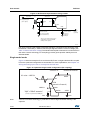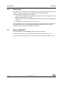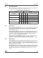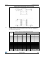
1
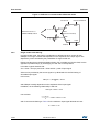
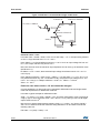
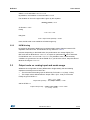
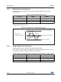
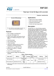
RHF1401 Rad-hard 14-bit 20 Msps A/D converter Datasheet - production data Applications Ceramic SO-48 package Digital communication satellites Space data acquisition systems Aerospace instrumentation Nuclear and high-energy physics Description The upper metallic lid is not electrically connected to any pins, nor to the IC die inside the package. Features Qml-V qualified, smd 5962-06260 Rad hard: 300 kRad(Si) TID Failure immune (SEFI) and latch-up immune (SEL) up to 120 MeV-cm2/mg at 2.7 V and 125° C Hermetic package Tested at Fs = 20 Msps Low power: 85 mW at 20 Msps Optimized for 2 Vpp differential input High linearity and dynamic performances 2.5 V/3.3 V compatible digital I/O The RHF1401 is a 14-bit analog-to-digital converter that uses pure (ELDRS-free) CMOS 0.25 μm technology combining high performance, radiation robustness and very low power consumption. The RHF1401 is based on a pipeline structure and digital error correction to provide excellent static linearity. Specifically designed to optimize power consumption, the device only dissipates 85 mW at 20 Msps, while maintaining a high level of performance. The device also integrates a proprietary track-and-hold structure to ensure a large effective resolution bandwidth. Voltage references are integrated in the circuit to simplify the design and minimize external components. A tri-state capability is available on the outputs to allow common bus sharing. A dataready signal, which is raised when the data is valid on the output, can be used for synchronization purposes. The RHF1401 has an operating temperature range of -55° C to +125° C and is available in a small 48-pin ceramic SO-48 package. Internal reference voltage with external reference option Table 1. Device summary Order code SMD pin Quality level - Engineering model RHF1401KSO1 Package Lead finish Mass EPPL(1) Temp range SO-48 Gold 1.1 g Yes -55 °C to +125 °C RHF1401KSO-01V 5962F0626001VXC QMLV-Flight 1. EPPL = ESA preferred part list July 2014 This is information on a product in full production. DocID13317 Rev 9 1/38 www.st.com Contents RHF1401 Contents 1 2 3 Description . . . . . . . . . . . . . . . . . . . . . . . . . . . . . . . . . . . . . . . . . . . . . . . . . 6 1.1 Block diagram . . . . . . . . . . . . . . . . . . . . . . . . . . . . . . . . . . . . . . . . . . . . . . . 6 1.2 Pin connections . . . . . . . . . . . . . . . . . . . . . . . . . . . . . . . . . . . . . . . . . . . . . 7 1.3 Pin descriptions . . . . . . . . . . . . . . . . . . . . . . . . . . . . . . . . . . . . . . . . . . . . . 8 1.4 Equivalent circuits . . . . . . . . . . . . . . . . . . . . . . . . . . . . . . . . . . . . . . . . . . . 9 Electrical characteristics . . . . . . . . . . . . . . . . . . . . . . . . . . . . . . . . . . . . 11 2.1 Absolute maximum ratings and operating conditions . . . . . . . . . . . . . . . . 11 2.2 Timing characteristics . . . . . . . . . . . . . . . . . . . . . . . . . . . . . . . . . . . . . . . . 12 2.3 Electrical characteristics (after 300 kRad) . . . . . . . . . . . . . . . . . . . . . . . . 13 User manual . . . . . . . . . . . . . . . . . . . . . . . . . . . . . . . . . . . . . . . . . . . . . . . 15 3.1 Optimizing the power consumption . . . . . . . . . . . . . . . . . . . . . . . . . . . . . 15 3.2 Driving the analog input: How to correctly bias the RHF1401 . . . . . . . . . 17 3.3 3.4 3.2.1 Differential mode biasing . . . . . . . . . . . . . . . . . . . . . . . . . . . . . . . . . . . . 17 3.2.2 Single-ended mode biasing . . . . . . . . . . . . . . . . . . . . . . . . . . . . . . . . . . 18 3.2.3 INCM biasing . . . . . . . . . . . . . . . . . . . . . . . . . . . . . . . . . . . . . . . . . . . . . 21 Output code vs. analog input and mode usage . . . . . . . . . . . . . . . . . . . . 21 3.3.1 Differential mode output code . . . . . . . . . . . . . . . . . . . . . . . . . . . . . . . . 22 3.3.2 Single-ended mode output code . . . . . . . . . . . . . . . . . . . . . . . . . . . . . . 22 Design examples . . . . . . . . . . . . . . . . . . . . . . . . . . . . . . . . . . . . . . . . . . . 23 Differential mode . . . . . . . . . . . . . . . . . . . . . . . . . . . . . . . . . . . . . . . . . . . . . . . . . . 23 Single-ended mode . . . . . . . . . . . . . . . . . . . . . . . . . . . . . . . . . . . . . . . . . . . . . . . . 24 3.5 3.5.1 Internal voltage reference . . . . . . . . . . . . . . . . . . . . . . . . . . . . . . . . . . . 26 3.5.2 External voltage reference . . . . . . . . . . . . . . . . . . . . . . . . . . . . . . . . . . . 26 3.6 Clock input . . . . . . . . . . . . . . . . . . . . . . . . . . . . . . . . . . . . . . . . . . . . . . . . 28 3.7 Reset of RHF1401 . . . . . . . . . . . . . . . . . . . . . . . . . . . . . . . . . . . . . . . . . . 28 3.8 Operating modes . . . . . . . . . . . . . . . . . . . . . . . . . . . . . . . . . . . . . . . . . . . 29 3.9 2/38 Reference connections . . . . . . . . . . . . . . . . . . . . . . . . . . . . . . . . . . . . . . . 26 3.8.1 Digital inputs . . . . . . . . . . . . . . . . . . . . . . . . . . . . . . . . . . . . . . . . . . . . . 29 3.8.2 Digital outputs . . . . . . . . . . . . . . . . . . . . . . . . . . . . . . . . . . . . . . . . . . . . 29 3.8.3 Digital output load considerations . . . . . . . . . . . . . . . . . . . . . . . . . . . . . 30 PCB layout precautions . . . . . . . . . . . . . . . . . . . . . . . . . . . . . . . . . . . . . . 30 DocID13317 Rev 9 RHF1401 4 Contents Definitions of specified parameters . . . . . . . . . . . . . . . . . . . . . . . . . . . 31 4.1 Static parameters . . . . . . . . . . . . . . . . . . . . . . . . . . . . . . . . . . . . . . . . . . . 31 4.2 Dynamic parameters . . . . . . . . . . . . . . . . . . . . . . . . . . . . . . . . . . . . . . . . 31 5 Package information . . . . . . . . . . . . . . . . . . . . . . . . . . . . . . . . . . . . . . . . 32 6 Ordering information . . . . . . . . . . . . . . . . . . . . . . . . . . . . . . . . . . . . . . . 34 7 Other information . . . . . . . . . . . . . . . . . . . . . . . . . . . . . . . . . . . . . . . . . . 35 8 7.1 Date code . . . . . . . . . . . . . . . . . . . . . . . . . . . . . . . . . . . . . . . . . . . . . . . . . 35 7.2 Documentation . . . . . . . . . . . . . . . . . . . . . . . . . . . . . . . . . . . . . . . . . . . . . 35 Revision history . . . . . . . . . . . . . . . . . . . . . . . . . . . . . . . . . . . . . . . . . . . 36 DocID13317 Rev 9 3/38 38 List of tables RHF1401 List of tables Table 1. Table 2. Table 3. Table 4. Table 5. Table 6. Table 7. Table 8. Table 9. Table 10. Table 11. Table 12. Table 13. Table 14. Table 15. Table 16. Table 17. Table 18. 4/38 Device summary . . . . . . . . . . . . . . . . . . . . . . . . . . . . . . . . . . . . . . . . . . . . . . . . . . . . . . . . . . 1 Pin descriptions. . . . . . . . . . . . . . . . . . . . . . . . . . . . . . . . . . . . . . . . . . . . . . . . . . . . . . . . . . . 8 Absolute maximum ratings . . . . . . . . . . . . . . . . . . . . . . . . . . . . . . . . . . . . . . . . . . . . . . . . . 11 Operating conditions . . . . . . . . . . . . . . . . . . . . . . . . . . . . . . . . . . . . . . . . . . . . . . . . . . . . . . 11 Timing characteristics . . . . . . . . . . . . . . . . . . . . . . . . . . . . . . . . . . . . . . . . . . . . . . . . . . . . . 12 Analog inputs . . . . . . . . . . . . . . . . . . . . . . . . . . . . . . . . . . . . . . . . . . . . . . . . . . . . . . . . . . . 13 Internal reference voltage . . . . . . . . . . . . . . . . . . . . . . . . . . . . . . . . . . . . . . . . . . . . . . . . . . 13 External reference voltage . . . . . . . . . . . . . . . . . . . . . . . . . . . . . . . . . . . . . . . . . . . . . . . . . 13 Static accuracy . . . . . . . . . . . . . . . . . . . . . . . . . . . . . . . . . . . . . . . . . . . . . . . . . . . . . . . . . . 14 Digital inputs and outputs . . . . . . . . . . . . . . . . . . . . . . . . . . . . . . . . . . . . . . . . . . . . . . . . . . 14 Dynamic characteristics . . . . . . . . . . . . . . . . . . . . . . . . . . . . . . . . . . . . . . . . . . . . . . . . . . . 14 Differential mode output codes . . . . . . . . . . . . . . . . . . . . . . . . . . . . . . . . . . . . . . . . . . . . . . 22 Single-ended mode output codes with Vinb = Vbias and A = (Vrefp - Vrefm) . . . . . . . . . . 22 RHF1401 operating modes. . . . . . . . . . . . . . . . . . . . . . . . . . . . . . . . . . . . . . . . . . . . . . . . . 29 Ceramic SO-48 package mechanical data . . . . . . . . . . . . . . . . . . . . . . . . . . . . . . . . . . . . . 33 Order codes . . . . . . . . . . . . . . . . . . . . . . . . . . . . . . . . . . . . . . . . . . . . . . . . . . . . . . . . . . . . 34 Documentation provided for QMLV flight . . . . . . . . . . . . . . . . . . . . . . . . . . . . . . . . . . . . . . 35 Document revision history. . . . . . . . . . . . . . . . . . . . . . . . . . . . . . . . . . . . . . . . . . . . . . . . . . 36 DocID13317 Rev 9 RHF1401 List of figures List of figures Figure 1. Figure 2. Figure 3. Figure 4. Figure 5. Figure 6. Figure 7. Figure 8. Figure 9. Figure 10. Figure 11. Figure 12. Figure 13. Figure 14. Figure 15. Figure 16. Figure 17. Figure 18. Figure 19. Figure 20. Figure 21. Figure 22. Figure 23. Figure 24. Figure 25. Figure 26. RHF1401 block diagram . . . . . . . . . . . . . . . . . . . . . . . . . . . . . . . . . . . . . . . . . . . . . . . . . . . . 6 Pin connections (top view) . . . . . . . . . . . . . . . . . . . . . . . . . . . . . . . . . . . . . . . . . . . . . . . . . . 7 Analog inputs . . . . . . . . . . . . . . . . . . . . . . . . . . . . . . . . . . . . . . . . . . . . . . . . . . . . . . . . . . . . 9 Output buffers . . . . . . . . . . . . . . . . . . . . . . . . . . . . . . . . . . . . . . . . . . . . . . . . . . . . . . . . . . . . 9 Clock input . . . . . . . . . . . . . . . . . . . . . . . . . . . . . . . . . . . . . . . . . . . . . . . . . . . . . . . . . . . . . . 9 Data format input . . . . . . . . . . . . . . . . . . . . . . . . . . . . . . . . . . . . . . . . . . . . . . . . . . . . . . . . . 9 Reference mode control input. . . . . . . . . . . . . . . . . . . . . . . . . . . . . . . . . . . . . . . . . . . . . . . . 9 Output enable input . . . . . . . . . . . . . . . . . . . . . . . . . . . . . . . . . . . . . . . . . . . . . . . . . . . . . . . 9 VREFP and INCM input/output . . . . . . . . . . . . . . . . . . . . . . . . . . . . . . . . . . . . . . . . . . . . . . 10 VREFM input. . . . . . . . . . . . . . . . . . . . . . . . . . . . . . . . . . . . . . . . . . . . . . . . . . . . . . . . . . . . 10 Timing diagram . . . . . . . . . . . . . . . . . . . . . . . . . . . . . . . . . . . . . . . . . . . . . . . . . . . . . . . . . . 12 Rpol values vs. Fs . . . . . . . . . . . . . . . . . . . . . . . . . . . . . . . . . . . . . . . . . . . . . . . . . . . . . . . . . . . . . . . . . . . . . . . 15 Power consumption values vs. Fs with internal references disabled . . . . . . . . . . . . . . . . . 16 RHF1401 in recommended differential mode . . . . . . . . . . . . . . . . . . . . . . . . . . . . . . . . . . . 18 RHF1401 in recommended single-ended mode . . . . . . . . . . . . . . . . . . . . . . . . . . . . . . . . . 20 Equivalent Vin - Vinb (differential input) . . . . . . . . . . . . . . . . . . . . . . . . . . . . . . . . . . . . . . . 22 Example 2 Vpp differential input . . . . . . . . . . . . . . . . . . . . . . . . . . . . . . . . . . . . . . . . . . . . . 23 Differential implementation using a balun . . . . . . . . . . . . . . . . . . . . . . . . . . . . . . . . . . . . . . 24 Optimized single-ended configuration (DC coupling) . . . . . . . . . . . . . . . . . . . . . . . . . . . . . 24 AC-coupling single-ended input configuration . . . . . . . . . . . . . . . . . . . . . . . . . . . . . . . . . . 25 Internal voltage reference setting . . . . . . . . . . . . . . . . . . . . . . . . . . . . . . . . . . . . . . . . . . . . 26 External voltage reference setting . . . . . . . . . . . . . . . . . . . . . . . . . . . . . . . . . . . . . . . . . . . 27 Example with zeners. . . . . . . . . . . . . . . . . . . . . . . . . . . . . . . . . . . . . . . . . . . . . . . . . . . . . . 27 Output buffer fall time . . . . . . . . . . . . . . . . . . . . . . . . . . . . . . . . . . . . . . . . . . . . . . . . . . . . . 30 Output buffer rise time . . . . . . . . . . . . . . . . . . . . . . . . . . . . . . . . . . . . . . . . . . . . . . . . . . . . 30 Ceramic SO-48 package mechanical drawing . . . . . . . . . . . . . . . . . . . . . . . . . . . . . . . . . . 33 DocID13317 Rev 9 5/38 38 Description RHF1401 1 Description 1.1 Block diagram Figure 1. RHF1401 block diagram VREFP GNDA VIN stage 1 INCM stage 2 stage n Biasing current setup Internal VREFP VINB IPOL VREFM Internal INCM REFMODE DFSB Sequencer-phase shifting OEB CLK Timing DR Digital data correction D0 Buffers D13 OR GND VCCBI VCCBE AM04556 6/38 DocID13317 Rev 9 RHF1401 1.2 Description Pin connections Figure 2. Pin connections (top view) GNDBI GNDBE VCCBE NC NC OR (MSB)D13 D12 D11 D10 D9 D8 D7 D6 D5 D4 D3 D2 D1 (LSB)D0 DR VCCBE GNDBE VCCBI 1 2 3 4 5 6 7 8 9 10 11 12 13 14 15 16 17 18 19 20 21 22 23 24 DocID13317 Rev 9 48 47 46 45 44 43 42 41 40 39 38 37 36 35 34 33 32 31 30 29 28 27 26 25 DGND DGND CLK DGND DVCC DVCC AVCC AVCC AGND INCM AGND VINB AGND VIN AGND VREFM VREFP IPOL AGND AVCC AVCC DFSB OEB REFMODE 7/38 38 Description 1.3 RHF1401 Pin descriptions Table 2. Pin descriptions Pin Name Description 1 GNDBI Digital buffer ground 2 GNDBE 3 VCCBE Observations Pin Name 0V 25 REFMODE Digital buffer ground 0V 26 Digital buffer power supply 2.5 V/3.3 V 4 NC 5 Description Observations Ref. mode control input 2.5 V/3.3 V CMOS input OEB Output enable input 2.5 V/3.3 V CMOS input 27 DFSB Data format select input 2.5 V/3.3 V CMOS input Not connected to the dice 28 AVCC Analog power supply 2.5 V NC Not connected to the dice 29 AVCC Analog power supply 2.5 V Analog ground 0V 6 OR Out of range output CMOS output (2.5 V/3.3 V) 30 AGND 7 D13(MSB) Most significant bit output CMOS output (2.5 V/3.3 V) 31 IPOL 8 D12 Digital output CMOS output (2.5 V/3.3 V) 32 VREFP Top voltage reference Can be external or internal 9 D11 Digital output CMOS output (2.5 V/3.3 V) 33 VREFM Bottom voltage reference 0V 10 D10 Digital output CMOS output (2.5 V/3.3 V) 34 AGND Analog ground 0V 11 D9 Digital output CMOS output (2.5 V/3.3 V) 35 VIN Analog input 1 Vpp 12 D8 Digital output CMOS output (2.5 V/3.3 V) 36 AGND Analog ground 0V 13 D7 Digital output CMOS output (2.5 V/3.3 V) 37 VINB Inverted analog input 1 Vpp 14 D6 Digital output CMOS output (2.5 V/3.3 V) 38 AGND Analog ground 0V 15 D5 Digital output CMOS output (2.5 V/3.3 V) 39 INCM Input common mode Can be external or internal 16 D4 Digital output CMOS output (2.5 V/3.3 V) 40 AGND Analog ground 0V 17 D3 Digital output CMOS output (2.5V /3.3 V) 41 AVCC Analog power supply 2.5 V 18 D2 Digital output CMOS output (2.5 V/3.3 V) 42 AVCC Analog power supply 2.5 V 19 D1 Digital output CMOS output (2.5 V/3.3 V) 43 DVCC Digital power supply 2.5 V 20 D0(LSB) Digital output LSB CMOS output (2.5 V/3.3 V) 44 DVCC Digital power supply 2.5 V 21 DR Data ready output(1) CMOS output (2.5 V/3.3 V) 45 DGND Digital ground 0V 22 VCCBE Digital buffer power supply 2.5 V/3.3 V 46 CLK Clock input 2.5 V compatible CMOS input 23 GNDBE Digital buffer ground 0V 47 DGND Digital ground 0V VCCBI Digital buffer power supply 2.5 V 48 DGND Digital ground 0V 24 1. See load considerations in Section 2.2: Timing characteristics. 8/38 DocID13317 Rev 9 Analog bias current input RHF1401 1.4 Description Equivalent circuits Figure 3. Analog inputs Figure 4. Output buffers VCCBE AVCC OEB GNDBE ZIN = 1/(CS.FS) VIN or VINB D0 …D13 Data VCCBE 7 pF (pad) INCM 7pF (pad) AGND GNDBE AM04558 Figure 5. Clock input Figure 6. Data format input VCCBE DVCC DFSB CLK 7 pF (pad) 7 pF (pad) GNDBE DGND AM04559 AM04560 Figure 7. Reference mode control input Figure 8. Output enable input VCCBE VCCBE REFMODE OEB 7 pF (pad) 7 pF (pad) GNDBE GNDBE AM04561 DocID13317 Rev 9 AM04562 9/38 38 Description RHF1401 Figure 9. VREFP and INCM input/output AVCC AVCC INCM VREFP 7 pF (pad) 7 pF (pad) REFMODE REFMODE AGND AGND AM04563 Figure 10. VREFM input AVCC VREFM High input impedance 7 pF (pad) AGND AM04564 10/38 DocID13317 Rev 9 RHF1401 Electrical characteristics 2 Electrical characteristics 2.1 Absolute maximum ratings and operating conditions Table 3. Absolute maximum ratings Symbol Parameter Values Unit AVCC Analog supply voltage 3.3 V DVCC Digital supply voltage 3.3 V VCCBI Digital buffer supply voltage 3.3 V VCCBE Digital buffer supply voltage 3.6 V Analog inputs: bottom limit -> top limit -0.6 V -> AVCC+0.6 V V External references: bottom limit -> top limit -0.6 V -> AVCC+0.6 V V VIN VINB VREFP VINCM IDout Digital output current -100 to 100 mA Tstg Storage temperature -65 to +150 °C Rthjc Thermal resistance junction to case 22 °C/W Rthja Thermal resistance junction to ambient 125 °C/W 2 kV ESD HBM (human body model) (1) 1. Human body model: a 100 pF capacitor is charged to the specified voltage, then discharged through a 1.5 kW resistor between two pins of the device. This is done for all couples of connected pin combinations while the other pins are floating. Table 4. Operating conditions Symbol Parameter Min Typ Max Unit AVCC Analog supply voltage 2.3 2.5 2.7 V DVCC Digital supply voltage 2.3 2.5 2.7 V VCCBI Digital internal buffer supply 2.3 2.5 2.7 V VCCBE Digital output buffer supply 2.3 2.5 3.4 V VREFP Forced top voltage reference 0.5 1 1.3 V VREFM Bottom external reference voltage 0 0 0.5 V VREFP VREFM Difference between external reference voltage 0.3 VINCM Forced common mode voltage 0.2 VIN or VINB Max. voltage versus GND Min. voltage versus GND -0.2 V 0.5 1.1 V 1 1.6 V GND V DFSB REFMODE Digital inputs 0 VCCBE V OEB DocID13317 Rev 9 11/38 38 Electrical characteristics 2.2 RHF1401 Timing characteristics Table 5. Timing characteristics Symbol Parameter Test conditions Min Typ Max Unit DC Clock duty cycle Fs = 20 Msps 45 50 65 % Tod Data output delay (fall of clock to data valid) (1) 10 pF load capacitance 5 7.5 13 ns Tpd Data pipeline delay(2) Duty cycle = 50% 7.5 7.5 7.5 cycles Ton Falling edge of OEB to digital output valid data 1 ns Toff Rising edge of OEB to digital output tri-state 1 ns TrD Data rising time 10 pF load capacitance 6 ns TfD Data falling time 10 pF load capacitance 3 ns 1. As per Figure 11. 2. If the duty cycle does not equal 50%: Tpd = 7 cycles + CLK pulse width. Figure 11. Timing diagram N+5 N+6 N+7 N+4 N+8 N- 2 Analog input N+3 N-1 N+2 N N+1 CLK Tpd + Tod OEB Tod Tod Toff Data output N -8 N -7 N -6 N-5 N -4 Ton N -3 N-1 N N+1 HZ state DR OR AM06120 The input signal is sampled on the rising edge of the clock while the digital outputs are synchronized on the falling edge of the clock. The duty cycles on DR and CLK are the same. The rising and falling edges of the OR pin are synchronized with the falling edge of the DR pin. 12/38 DocID13317 Rev 9 RHF1401 2.3 Electrical characteristics Electrical characteristics (after 300 kRad) Unless otherwise specified, the test conditions in the following tables are: AVCC = DVCC = VCCBI =VCCBE = 2.5 V, Fs=20 Msps, FIN= 15 MHz, VIN at -1 dBFS, VREFP = 1 V, INCM = 0.5 V, VREFM = 0 V, Tamb = 25 °C. Table 6. Analog inputs Symbol VIN-VINB Parameter Full-scale reference voltage (FS)(1) CIN Input capacitance ZIN Input impedance vs. INCM(2) ERB Test conditions Min VREFP = 1 V (forced) VREFM = 0 V Fs = 20 Msps Effective resolution bandwidth(1) Typ Max Unit 2 Vpp 7 pF 21 k 70 MHz 1. See Section 4: Definitions of specified parameters for more information. 2. Zin = 1/(Fs x C) with C = 2.4 pF Table 7. Internal reference voltage(1) Symbol Rout Parameter Output resistance of internal reference Test conditions Min Typ Max Unit REFMODE = 0 internal reference on 30 REFMODE = 1 internal reference off 7.5 k VREFP Top internal reference voltage REFMODE = 0 0.76 0.84 0.95 V VINCM Input common mode voltage REFMODE = 0 0.40 0.44 0.50 V 1. Refer to Section 3.2: Driving the analog input: How to correctly bias the RHF1401 for correct biasing of RHF1401 Table 8. External reference voltage(1) Symbol Parameter Test conditions Min Typ Max Unit VREFP Forced top reference voltage REFMODE = 1 0.5 1.3 V VREFM Forced bottom ref voltage REFMODE = 1 0 0.5 V VINCM Forced common mode voltage REFMODE = 1 0.2 1.1 V 1. See Figure 22 & Figure 23 Refer to Section 3.2: Driving the analog input: How to correctly bias the RHF1401 for correct biasing of RHF1401 DocID13317 Rev 9 13/38 38 Electrical characteristics RHF1401 Table 9. Static accuracy Symbol Parameter DNL Differential non-linearity INL Integral non-linearity Test conditions Min Fin = 1.5 Msps Vin at +1 dBFS Fs = 1.5 Msps Monotonicity and no missing codes Typ Max Unit ±0.4 LSB ±3 LSB Guaranteed OE Offset Error Fs = 5 Msps ±100 LSB GE Gain Error Fs = 5 Msps ±0.3 % Table 10. Digital inputs and outputs Symbol Parameter Test conditions Min Typ Max Unit Clock input CT Clock threshold DVCC = 2.5 V CA Square clock amplitude (DC component = 1.25 V) DVCC = 2.5 V 0.8 2.5 Vpp 1.25 V Digital inputs VIL Logic "0" voltage VCCBE = 2.5 V 0 0.25 x VCCBE V VIH Logic "1" voltage VCCBE = 2.5 V 0.75 x VCCBE VCCBE V 0.25 V Digital outputs VOL Logic "0" voltage IOL = -10 μA VOH Logic "1" voltage IOH = 10 μA IOZ High impedance leakage current OEB set to VIH CL Output load capacitance High CLK frequencies 0 VCCBE -0.25 V -15 15 μA 15 pF Max Unit Table 11. Dynamic characteristics Symbol SFDR Parameter Test conditions Spurious free dynamic range SNR Signal to noise ratio THD Total harmonic distortion SINAD Signal to noise and distortion ratio ENOB Effective number of bits Fin = 15 MHz Fs = 20 Msps Vin at -1 dBFS internal references CL = 6 pF Min Typ 70 91 dBFS 66 70 dB 70 86 dB 65 70 dB 10.6 11.5 bits Higher values of SNR, SINAD and ENOB can be obtained by increasing the full-scale range of the analog input if the sampling frequency and the biasing of RHF1401 allow it. 14/38 DocID13317 Rev 9 RHF1401 User manual 3 User manual 3.1 Optimizing the power consumption The polarization current in the input stage is set by an external resistor (Rpol). When selecting the resistor value, it is possible to optimize the power consumption according to the sampling frequency of the application. For this purpose, an external Rpol resistor is placed between the IPOL pin and the analog ground. The values in Figure 12 are achieved with VREFP = 1 V, VREFM = 0 V, INCM = 0.5 V and the input signal is 2 Vpp with a differential DC connection. If the conditions are changed, the Rpol resistor varies slightly but remains in the domain described in Figure 12. Figure 12 shows the optimum Rpol resistor value to obtain the best ENOB value. It also shows the minimum and maximum values to get good results. ENOB decreases by approximately 0.2 dB when you change Rpol from optimum to maximum or minimum. If Rpol is higher than the maximum value, there is not enough polarization current in the analog stage to obtain good results. If Rpol is below the minimum, THD increases significantly. Therefore, the total dissipation can be adjusted across the entire sampling range to fulfill the requirements of applications where power saving is critical. For sampling frequencies below 2 MHz, the optimum resistor value is approximately 80 kOhms. Figure 12. Rpol values vs. Fs The power consumption depends on the Rpol value and the sampling frequency. In Figure 13, it is shown with the internal references disabled (REFMODE = 1) and Rpol defined in Figure 12 as the optimum. DocID13317 Rev 9 15/38 38 User manual RHF1401 Figure 13. Power consumption values vs. Fs with internal references disabled 16/38 DocID13317 Rev 9 RHF1401 3.2 User manual Driving the analog input: How to correctly bias the RHF1401 It’s mandatory to follow some simple biasing rules to reach optimal performance when driving the RHF1401. DC biasing and the AC swing must be considered in order to keep the analog input in the correct range. Let’s define some parameters: Definition 1: The common mode of the input signal is: Vin + Vinb CMinput = -------------------------------2 Definition 2: The common mode of reference voltage is: Vrefp + Vrefm CMref = ----------------------------------------------2 To have correct biasing of RHF1401, this condition must be respected at all times: CMinput CMref + 0.2V Please note that the INCM value is not a parameter of the previous equations. INCM is an input/output that’s used to bias internal OTA amplifiers. So INCM can be any value from Table 4. However, if the INCM value is used to bias analog inputs (Vin and Vinb), Cminput becomes dependent of INCM. In this case, the setting of INCM must be chosen to respect the equation: CMinput CMref + 0.2V Now let’s see what happens when the RHF1401 is driven in differential mode and singleended mode. We will use a sinusoidal input signal for ease of computation, but the results presented after can be easily extrapolated to another kind of signal shape. 3.2.1 Differential mode biasing In differential mode we have Vin = Vbias + A sin(t) and Vinb = Vbias – A sin(t) with A = peak of input signal. Vbias can be provided by the source signal or by INCM. It’s the DC biasing of the sinusoidal input signal. As by definition, AC components are in opposite phase for Vin and Vinb, at any time on the signal we have CMinput = Vbias. In differential mode, to keep a safe operation of RHF1401 analog inputs, we have to respect : Vbias CMref + 0.2V and referring to Table 4 for the maximum input signal allowed we have: A + Vbias 1.6V and Vbias – A – 0.2V DocID13317 Rev 9 17/38 38 User manual RHF1401 Figure 14. RHF1401 in recommended differential mode 2.3V to 2.7V AVCC Internal or External VREFP VIN INCM (Internal or External) Maximum DC value = (VREFP+VREFM)/2+0.2V VINB VREFM External 3.2.2 AGND GND Single-ended mode biasing In single-ended mode, the biasing consideration is different because, as we will see, CMinput is no longer constant but dependent on the amplitude of the input signal. This dependency limits considerably the possibilities of single-ended use. Please note also that in the demonstration below, Vin is variable and Vinb is fixed, but the opposite is possible simply by exchanging Vin and Vinb in the equations. Let’s take a typical situation with: Vin = Vbias + A sin(t) and Vinb = Vbias with A = peak of input signal. Vbias can be provided by the source signal or by INCM which is the DC biasing of sinusoidal input signal. In this case, A sin t + Vbias CMinput = ----------------------------2 and CMinput is totally dependent on the amplitude of the input signal. In addition, as the following relationship is still true: CMinput CMref + 0.2V now we have: A sin t ----------------------------- + Vbias CMref + 0.2V 2 and of course and referring to Table 4 for the maximum input signal allowed we have: A + Vbias 1.6V 18/38 DocID13317 Rev 9 RHF1401 User manual and Vbias – A – 0.2V So, depending on the settings of Vrefp, Vrefm, the following condition A sin t ----------------------------- + Vbias CMref + 0.2V 2 can occur very soon before reaching the full-scale input of RHF1401. Example: you have an input signal in single-ended that maximizes the full swing authorized for RHF1401 input -0.2 V to 1.6 V which gives 1.8 Vpp in single-ended. The biasing settings are as follows: As the full scale of ADC is defined by (Vrefp – Vrefm)x2, if Vrefm = 0 V, we have 2xVrefp =1.8 V then Vrefp = 0.9 V Vbias = 1.6 V – 1.8V/2 = 0.7 V, then Vin = 0.7 V + (1.8V/2)xsin(t) = 0.7 V + 0.9Vxsin(t), then A = 0.9 V Vinb = Vbias Vin= 0.7 V With these setttings, we can calculate CMref + 0.2 V = 0.65 V and CMinput = 0.7 V + (0.9Vxsin(t))/2. Then, CMinput is maximum when sin(t) = 1 that gives CMinputmax.= 1.15 V which is far beyond the limit of 0.65 V previously calculated. The range of Vin allowed is -0.2 V to 0.65 V that is even below the half scale requested initially. A solution to this problem would be to increase the CMref value which is done by increasing Vrefm and Vrefp. Let’s take Vrefm = 0.5 V and calculate Vrefp to have CMref + 0.2 V = 1.15 V. The solution is Vrefp = 1.4 V that is 0.1 V higher than the maximum allowed in Table 4. So, the only way is to reduce the input swing in accordance with the maximum Vrefp and Vrefm allowed. With Vrefp = 1.3 V, Vrefm = 0.5 V, CMref + 0.2 V = 1.1 V. CMinput maximum = 1.1 V that gives Vbias = 1.1 V - A/2. With A = 0.8 V, Vbias = 0.7 V => Vinpp = 1.6 V, A + Vbias = 1.5 V, Vbias - A = -0.1 V. By reducing the input amplitude by 200 mVpp, we are able to find a solution that fits the limits given in Table 4. With this example, we can see that the main limitation in single-ended mode, on the condition to maximize the full digital swing (0 to 214), will come from the CMinput maxinum vs. Vrefp and Vrefm allowed. We can see also, with the previous example, to fit the large full swing requested, you need three different biasing values (Vrefp, Vrefm, Vbias = INCM) or four if the Vbias value is not compatible with the INCM range allowed. More generally, if the number of different biasing values is a problem, it’s possible to work in single-ended with two different biasing values. By setting INCM = Vrefm = Vbias = Vinb = Vrefp/2, you can have a “simple” single-ended as represented in Figure 15. DocID13317 Rev 9 19/38 38 User manual RHF1401 Figure 15. RHF1401 in recommended single-ended mode 2.3V to 2.7V DC value = VREFP/2 AVCC Internal or External VREFP VIN INCM (Internal or External) VINB VREFP/2 VREFM AGND GND External However, we can calculate that the main limitation will come from the Vrefm maximum value = 0.5 V. Let’s take Vrefm = INCM = Vbias = Vinb =0.5 V and Vrefp = 1 V => the input swing allowed on Vin is 1 Vpp centered at 0.5 V => A = 0.5 V Here, CMref = 0.75 V and CMinput maximum = 0.75 V. So for an input voltage Vin from 0 V to 1 V, the output code will vary from 0 to 214. Now, let’s see how much the maximum input amplitude Vin can be to go in saturation mode (bit OR set to 1). As CMref + 0.2 V = 0.95 V, the theoretical input voltage Vin allowed can be: Vin = 0.5 V + 0.9 V sin(t). Here, CMinput maximum = 0.95 V but A + Vbias = 1.4 V and Vbias - A = -0.4 V. The -0.4 V is a problem because only -0.2 V is allowed. Finally, the practical input voltage Vin is: Vin = 0.5 V + 0.7 V sin(t) => CMinput maximum = 0.85 V, A + Vbias = 1.2 V and Vbias - A = -0.2 V. Particular case where Vrefm = 0 V and cannot be changed In some applications, a dual mode can be requested: differential mode and single-ended mode with a preference for differential mode first. Let’s take a typical example for differential mode: Vrefp = 1 V, Vrefm = 0 V, Vbias = INCM = 0.5 V. This safe configuration gives a full scale at 2 Vpp (1 Vpp on each input with Vbias = 0.5 V and A = 0.5 V). Here you can use all digital output codes from 0 to 214. Now let’s go to single-ended mode by keeping Vrefp = 1 V, Vrefm = 0 V, Vbias = INCM = Vinb = 0.5 V. What would be the maximum swing allowed on Vin and what would be the resulting code? So: Full scale = 2 x (Vrefp - Vrefm) = 2 V 20/38 DocID13317 Rev 9 RHF1401 User manual CMref = 0.5 V and CMref + 0.2 V = 0.7 V By definition, the limitation on the lower side is -0.2 V The limitation of Vin on the upper side is given by this equation: Vinmax + Vbias ------------------------------------------------- 0.7V 2 So Vinmax = 0.9 V. Finally – 0.2V Vin 0.9V that gives: 5734 Output Code (decimal) 11468 Here, the full scale is not usable but a limited range only. 3.2.3 INCM biasing As previously discussed, INCM is an input/output that’s used to bias the internal OTA amplifiers of the RHF1401. So INCM can be any value from Table 4. However, depending on the INCM value, the performance can change slightly. For RHF1401 and for INCM from 0.4 V to 1 V, no impact on performances can be observed. For INCM from 0.2 V to 0.4 V and 1 V to 1.1 V, it’s possible to have, under boundary conditions, a typical loss of one bit of ENOB. So, if you have the choice, keep the value of INCM in the range 0.4 V to 1 V. 3.3 Output code vs. analog input and mode usage Whatever the configuration chosen (differential or single-ended), the two following equations are always true for RHF1401: The full scale of the analog input is defined by: Full scale = 2 x (Vrefp - Vrefm) The output code is defined also as: Output code = f(Vin - Vinb) vs. Full scale Finally we got for DFSB = 1: 3FFF Vin – VinB - + 1FFF Output code (14 bits) = -----------------------------------------------------2 Vrefp – Vrefm and for DFSB = 0: 3FFF Vin – VinB - + 1FFF + 2000 Output code (14 bits) = -----------------------------------------------------2 Vrefp – Vrefm DocID13317 Rev 9 21/38 38 User manual 3.3.1 RHF1401 Differential mode output code In this mode, the DC component of Vin and Vinb is naturally subtracted. We get the following table: Table 12. Differential mode output codes Vin - Vinb = DFSB = 1 DFSB = 0 + (VREFP-VREFM) 3FFF 1FFF 0 1FFF 3FFF - (VREFP-VREFM) 0000 2000 If INCM = Vbias we have Figure 16: Figure 16. Equivalent Vin - Vinb (differential input) VIN -VINB (level + FS, code 16383) VIN FS (full-scale) = 2(VREFP - VREFM) INCM (level 0, code 8191) VINB (level - FS, code 0) AM04567 3.3.2 Single-ended mode output code In single-ended mode, Vin or Vinb is constant and equal to Vbias. If Vin = Vbias + A sin(t) and Vinb = Vbias with A = peak of input signal, then (Vin - Vinb) = A sin(t) and A = (Vrefp - Vrefm) for maximum swing on input. Table 13. Single-ended mode output codes with Vinb = Vbias and A = (Vrefp - Vrefm) 22/38 Vin = DFSB = 1 DFSB = 0 Vbias + (VREFP-VREFM) 3FFF 1FFF Vbias 1FFF 3FFF Vbias - (VREFP-VREFM) 0000 2000 DocID13317 Rev 9 RHF1401 3.4 User manual Design examples The RHF1401 is designed to obtain optimum performance when driven on differential inputs with a differential amplitude of two volts peak-to-peak (2 Vpp). This is the result of 1 Vpp on the Vin and Vinb inputs in phase opposition (Figure 17). For all input frequencies, it is mandatory to add a capacitor on the PCB (between Vin and Vinb) to cut the HF noise. The lower the frequency, the higher the capacitor. The RHF1401 is specifically designed to meet sampling requirements for intermediate frequency (IF) input signals. In particular, the track-and-hold in the first stage of the pipeline is designed to minimize the linearity limitations as the analog frequency increases. Differential mode Figure 17 shows an example of how to drive the RHF1401 in differential and DC coupled. Figure 17. Example 2 Vpp differential input 1V 1 Vp -p 1 Vp -p REFP INCM INCM VIN REFMODE 2.5V VINB INCM 0.5V REFM Ground VIN -VINB (2 Vp-p) AM04570 Figure 18 shows an isolated differential input solution. The input signal is fed to the transformer’s primary, while the secondary drives both ADC inputs. The transformer must be matched with the generator output impedance: 50 in this case for proper matching with a 50 generator. The tracks between the secondary and Vin and Vinb pins must be as short as possible. DocID13317 Rev 9 23/38 38 User manual RHF1401 Figure 18. Differential implementation using a balun 50 Ω track ADT1 -1 1:1 Short track Analog input signal (50 Ω output) 33 pF VIN 50 Ω VINB INCM 470 nF* ceramic (as close as possible to the transformer) 100 nF* ceramic (as close as possible to INCM pin) External INCM (optional) *the use of a ceramic technology is preferable for a large bandwidth stability of the capacitor AM04571 The input common-mode voltage of the ADC (INCM) is connected to the center tap of the transformer’s secondary in order to bias the input signal around the common voltage (see Table 7: Internal reference voltage).The INCM is decoupled to maintain a low noise level on this node. Ceramic technology for decoupling provides good capacitor stability across a wide bandwidth. Single-ended mode Figure 19 shows an example of how to drive the RHF1401 in single-ended and DC coupled. This is the optimized configuration recommended. For more explanations, see Chapter 3.2: Driving the analog input: How to correctly bias the RHF1401 Figure 19. Optimized single-ended configuration (DC coupling) 2.3V to 2.7V DC value = VREFP/2 AVCC Internal or External VREFP VIN INCM (Internal or External) VREFP/2 10µF + 100nF ceramic* VINB VREFM AGND (as close as possible to VINB pin) GND Note: 24/38 GND *The use of ceramic technology is preferable to ensure large bandwidth stability of the capacitor. DocID13317 Rev 9 RHF1401 User manual As some applications may require a single-ended input, it can be easily done with the configuration shown in Figure 19 for DC coupling and Figure 20 for AC coupling. However, with this type of configuration, a degradation in the rated performance of the RHF1401 may occur compared with a differential configuration. You should expect a degradation of ENOB of about 2 bits compared to differential mode. A sufficiently decoupled DC reference should be used to bias the RHF1401 inputs. An AC-coupled analog input can also be used and the DC analog level set with a high-value resistor R (10 k) connected to a proper DC source. Cin and R behave like a high-pass filter and are calculated to set the lowest possible cut-off frequency. Figure 20. AC-coupling single-ended input configuration Cin Short track 50 Ω track Analog input signal (50 Ω output) VIN 50 Ω R INCM R Short track 470 pF ceramic* VINB 100 nF ceramic* External INCM (optional) 100 nF ceramic* (as close as possible to INCM pin) *the use of a ceramic technology is preferable for a large bandwidth stability of the capacitor AM04572 DocID13317 Rev 9 25/38 38 User manual RHF1401 3.5 Reference connections 3.5.1 Internal voltage reference In standard configuration, the ADC is biased with two internal voltage references: VREFP and INCM. They must be decoupled to minimize low and high frequency noise. When the REFMODE pin is set to 0, both internal voltage references are enabled and they can drive external components. The VREFM pin has no internal reference and must be connected to a voltage reference. It is usually connected to the analog ground for differential mode and to Vrefp/2 for singleended mode. Figure 21. Internal voltage reference setting As close as possible to the ADC pins 100 nF* 470 nF* 100 nF* 470 nF* VREFP VIN INCM VINB REFMODE VREFM *the use of a ceramic technology is preferable for a large bandwidth stability of the capacitor. AM04574 3.5.2 External voltage reference External voltage references can be used for specific applications requiring better linearity, enhanced temperature behavior, or different voltage values (see Table 7: Internal reference voltage). Internal voltage references are disabled when the REFMODE pin is equal to 1. In this case, external voltage references must be applied to the device. When internal voltage reference are disabled, ADC consumption is about 13 mA less than when they are enabled. The external voltage references with the configuration shown in Figure 22 and Figure 23 can be used to obtain optimum performance. Decoupling is achieved by using ceramic capacitors, which provide optimum linearity versus frequency. 26/38 DocID13317 Rev 9 RHF1401 User manual Figure 22. External voltage reference setting Figure 23. Example with zeners to the ADC pins 100 nF* VCCA 470 nF* As close as possible to the ADC pins DC source R R1 R2 VREFP VIN VCCA INCM VINB 100 nF* 470 nF* DC source 100 nF* 470 nF* 100 nF* 470 nF* VREFP VIN REFMODE VREFM INCM VINB REFMODE VREFM AM04575 AM04576 Note: *The use of ceramic technology is preferable to ensure large bandwidth stability of the capacitor. In multi-channel applications, the high impedance input (when REFMODE = 1) of the references allows one to drive several ADCs with only two voltage reference devices. In differential mode the voltage of the analog input common mode (INCM) should be around VREFP/2. Higher levels introduce more distortion. DocID13317 Rev 9 27/38 38 User manual 3.6 RHF1401 Clock input The quality of the converter very much depends on the accuracy of the clock input in terms of jitter. The use of a low-jitter, crystal-controlled oscillator is recommended. The following points should also be considered. The clock’s power supplies must be independent of the ADC’s output supplies to avoid digital noise modulation at the output. When powered-on, the circuit needs several clock periods to reach its normal operating conditions. The square clock must respect Table 5 and Table 10 The signal applied to the CLK pin is critical to obtain full performance from the RHF1401. It is recommended to use a square signal with fast transition times and to place proper termination resistors as close as possible to the device. 3.7 Reset of RHF1401 To reset the RHF1401, it’s mandatory to apply several clock periods. At power-up, without any clock signal applied to RHF1401, the device is not reset. In this case, parameters like Vrefp, Incm and Rout will not be in line with values in Table 7. 28/38 DocID13317 Rev 9 RHF1401 3.8 User manual Operating modes Extra functionalities are provided to simplify the application board as much as possible. The operating modes offered by the RHF1401 are described in Table 14. Table 14. RHF1401 operating modes Inputs Outputs Analog input differential amplitude DFSB OEB (VIN-VINB) above maximum range (VIN-VINB) below minimum range (VIN-VINB) within range X OR DR Most significant bit (MSB) H L H CLK D13 L L H CLK D13 complemented H L H CLK D13 L L H CLK D13 complemented H L L CLK D13 L L L CLK D13 complemented X H HZ(1) HZ HZ (all digital outputs are in high impedance) 1. High impedance. 3.8.1 Digital inputs Data format select bit (DFSB): when set to low level (VIL), the digital input DFSB provides a two’s complement digital output MSB. This can be of interest when performing some further signal processing. When set to high level (VIH), DFSB provides standard binary output coding (see Table 12). Output enable bit (OEB): when set to low level (VIL), all digital outputs remain active. When set to high level (VIH), all digital output buffers are in a high impedance state while the converter goes on sampling. When OEB is set to a low level again, the data arrives on the output with a very short Ton delay. This feature enables the chip select of the device. Figure 11: Timing diagram summarizes this functionality. Reference mode control (REFMODE): this allows the internal or external settings of the voltage references VREFP and INCM. REFMODE = 0 for internal references, REFMODE = 1 for external references (and disables both references VREFP and INCM). 3.8.2 Digital outputs Out of range (OR): this function is implemented on the output stage in order to set an "outof-range" flag whenever the digital data is over the full-scale range. Typically, there is a detection of all data at ‘0’ or all data at ‘1’. It sets an output signal OR, which is in a low-level state (VOL) when the data stays within the range, or in a high-level state (VOH) when the data read by the ADC is out of range. Data ready (DR): the Data Ready output is an image of the clock being synchronized on the output data (D0 to D13). This is a very helpful signal that simplifies the synchronization of the measurement equipment of the controlling DSP. Like all other digital outputs, DR goes into high impedance when OEB is set to a high level, as shown in Figure 11: Timing diagram. DocID13317 Rev 9 29/38 38 User manual 3.8.3 RHF1401 Digital output load considerations The features of the internal output buffers limit the maximum load on the digital data output. In particular, the shape and amplitude of the Data Ready signal, toggling at the clock frequency, can be weakened by a higher equivalent load. In applications that impose higher load conditions, it is recommended to use the falling edge of the master clock instead of the Data Ready signal. This is possible because the output transitions are internally synchronized with the falling edge of the clock. Figure 24. Output buffer fall time Figure 25. Output buffer rise time 25 25 VCCBE=2.5V 15 10 5 0 VCCBE=2.5V 20 VCCBE=3.3V Rise time (nS) Fall time (nS) 20 VCCBE=3.3V 15 10 5 0 3.9 10 40 50 0 0 10 20 30 load capacitor (pF) 40 50 PCB layout precautions 30/38 20 30 load capacitor (pF) A ground plane on each layer of the PCB with multiple vias dedicated for inter connexion is recommended for high-speed circuit applications to provide low parasitic inductance and resistance. The goal is to have a “common ground plane” where AGND and DGND are connected with the lowest DC resistance and lowest AC impedance. To minimize the transition current when the output changes, the capacitive load at the digital outputs must be reduced as much as possible by using the shortest-possible routing tracks. One way to reduce the capacitive load is to remove the ground plane under the output digital pins and layers at high sampling frequencies. The separation of the analog signal from the clock signal and digital outputs is mandatory to prevent noise from coupling onto the input signal. Power supply bypass capacitors must be placed as close as possible to the IC pins to improve high-frequency bypassing and reduce harmonic distortion. All leads must be as short as possible, especially for the analog input, so as to decrease parasitic capacitance and inductance. Choose the smallest-possible component sizes (SMD). DocID13317 Rev 9 RHF1401 Definitions of specified parameters 4 Definitions of specified parameters 4.1 Static parameters Differential non-linearity (DNL) The average deviation of any output code width from the ideal code width of 1 LSB. Integral non-linearity (INL) An ideal converter exhibits a transfer function that is a straight line from the starting code to the ending code. The INL is the deviation from this ideal line for each transition. 4.2 Dynamic parameters Spurious free dynamic range (SFDR) The ratio between the power of the worst spurious signal (not always a harmonic) and the amplitude of the fundamental tone (signal power) over the full Nyquist band. Expressed in dBc. Total harmonic distortion (THD) The ratio of the rms sum of the first five harmonic distortion components to the rms value of the fundamental line. Expressed in dB. Signal-to-noise ratio (SNR) The ratio of the rms value of the fundamental component to the rms sum of all other spectral components in the Nyquist band (Fs excluding DC, fundamental and the first five harmonics. Expressed in dB. Signal-to-noise and distortion ratio (SINAD) A similar ratio to the SNR but that includes the harmonic distortion components in the noise figure (not the DC signal). Expressed in dB. From SINAD, the effective number of bits (ENOB) can easily be deduced using the formula: SINAD = 6.02× ENOB + 1.76 dB When the analog input signal is not full scale (FS) but has an A0 amplitude, the SINAD expression becomes: SINAD = 6.02× ENOB + 1.76 dB + 20 log (A0 / FS) Analog input bandwidth The maximum analog input frequency at which the spectral response of a full power signal is reduced by 3 dB. Higher values can be achieved with smaller input levels. Pipeline delay The delay between the initial sample of the analog input and the availability of the corresponding digital data output on the output bus. Also called data latency. Expressed as a number of clock cycles. DocID13317 Rev 9 31/38 38 Package information 5 RHF1401 Package information In order to meet environmental requirements, ST offers these devices in different grades of ECOPACK® packages, depending on their level of environmental compliance. ECOPACK® specifications, grade definitions and product status are available at: www.st.com. ECOPACK® is an ST trademark. 32/38 DocID13317 Rev 9 RHF1401 Package information Figure 26. Ceramic SO-48 package mechanical drawing Note: The upper metallic lid is not electrically connected to any pins, nor to the IC die inside the package. Connecting unused pins or metal lid to ground or to the power supply will not affect the electrical characteristics. Table 15. Ceramic SO-48 package mechanical data Dimensions Ref. Millimeters Inches Min. Typ. Max. Min. Typ. Max. A 2.18 2.47 2.72 0.086 0.097 0.107 b 0.20 0.254 0.30 0.008 0.010 0.012 c 0.12 0.15 0.18 0.005 0.006 0.007 D 15.57 15.75 15.92 0.613 0.620 0.627 E 9.52 9.65 9.78 0.375 0.380 0.385 E1 10.90 E2 6.22 E3 1.52 0.429 6.35 6.48 0.245 0.250 0.255 1.65 1.78 0.060 0.065 0.070 e 0.635 0.025 f 0.20 0.008 L 12.28 12.58 12.88 0.483 0.495 0.507 P 1.30 1.45 1.60 0.051 0.057 0.063 Q 0.66 0.79 0.92 0.026 0.031 0.036 S1 0.25 0.43 0.61 0.010 0.017 0.024 DocID13317 Rev 9 33/38 38 Ordering information 6 RHF1401 Ordering information Table 16. Order codes Order code RHF1401KSO1 RHF1401KSO-01V 1. Description Engineering model QML-V flight Temp. range Package -55 °C to 125 °C SO-48 Marking (1) RHF1401KSO1 5962F0626001VXC Packing Strip pack Specific marking only. Complete marking includes the following: - SMD pin (for QML flight only) - ST logo - Date code (date the package was sealed) in YYWWA (year, week, and lot index of week) - QML logo (Q or V) - Country of origin (FR = France) Note: 34/38 Contact your ST sales office for information regarding the specific conditions for products in die form and QML-Q versions. DocID13317 Rev 9 RHF1401 Other information 7 Other information 7.1 Date code The date code is structured as shown below: Engineering model: EM xyywwz QML flight model: FM yywwz Where: x (EM only): 3, assembly location Rennes (France) yy: last two digits year ww: week digits z: lot index in the week 7.2 Documentation Table 17. Documentation provided for QMLV flight Quality level Documentation Engineering model QML-V flight – Certificate of conformance with Group C (reliability test) and group D (package qualification) reference – Precap report – PIND(1) test summary (test method conformance certificate) – SEM(2) report – X-ray report – Screening summary – Failed component list (list of components that have failed during screening) – Group A summary (QCI(3) electrical test) – Group B summary (QCI(3) mechanical test) – Group E (QCI(3) wafer lot radiation test) 1. PIND = particle impact noise detection 2. SEM = scanning electron microscope 3. QCI = quality conformance inspection DocID13317 Rev 9 35/38 38 Revision history 8 RHF1401 Revision history Table 18. Document revision history Date Changes 1 First public release. Failure immune and latchup immune value increased to 120 MeV-cm2/mg. Updated package mechanical information. Removed reference to non rad-hard components from External references, common mode: on page 16. 2 Updated Figure 1: RHF1401 block diagram. Added explanation on Figure 3: Timing diagram. Added introduction to Section 6: Typical performance characteristics. Updated Section 7.2: Clock signal requirements and Section 7.3: Power consumption optimization. Added Section 7.4: Low sampling rate recommendations. Updated information on Data Ready signal in Section 7.5: Digital inputs/outputs. Added Figure 24: Impact of clock frequency on RHF1401 performance and Figure 25: CLK signal derivation. 3 Changed input clock features in Table 10. Modified Table 14. Added Figure 24 to Figure 42. 4 Modified Figure 1: RHF1401 block diagram. Added details for Tdr and changed values for Tpd in Table 5: Timing characteristics. Modified Figure 11: Timing diagram. Changed values for VREFP in Table 4. Changed Vin operating conditions in Table 4, Figure 42 and Figure 19. Changed values for DNL in Table 9. 13-Sep-2010 5 Modified Figure 1 on page 6 and Figure 9 on page 10. Added note 2. on page 12. Modified CIN typ value in Table 6: Analog inputs as per Figure 3. Modified Figure 11: Timing diagram. Replaced Figure 18. Added Table 12: Output codes for DFSB = 1. Modified Figure 17: Example 2 Vpp differential input. 29-Jul-2011 6 Added Note: on page 31 and in the "Pin connections" diagram on the cover page. 29-Jun-2007 29-Oct-2007 09-Nov-2009 26-Feb-2010 36/38 Revision DocID13317 Rev 9 RHF1401 Revision history Table 18. Document revision history (continued) Date 06-Apr-2012 24-Oct-2012 22-July-2014 Revision Changes 7 Added Table 1: Device summary on cover page. Updated curves in Section 2.3: Electrical characteristics (after 300 kRad). Modified Section 3.1: Optimizing the power consumption. Modified Section 3.2: Driving the analog input: How to correctly bias the RHF1401. Modified Section 3.5.1: Internal voltage reference. Modified Section 3.5.2: External voltage reference. Modified Section 3.9: PCB layout precautions. 8 Updated Table 1 Modified Figure 1: RHF1401 block diagram Modified Figure 4: Output buffers Modified Table 4, Table 7, and Table 8 Modified Section 2.4: Results for differential input Modified Section 2.5: Results for single ended input Added comments and changed layout of Section 3.2: Driving the analog input: How to correctly bias the RHF1401. Modified Table 12 Modified Figure 19 Added Table 13 Added comments to Section 3.5: Reference connections Modified Section 3.8.1: Digital inputs 9 Modified Figure 3 Modified Table 4 Modified Table 6 Modified Table 8 Added OE and GE in Table 9 Rewording and new Section 3.1: Optimizing the power consumption, Section 3.2: Driving the analog input: How to correctly bias the RHF1401, Section 3.3: Output code vs. analog input and mode usage, Section 3.4: Design examples, Section 3.5: Reference connections, Section 3.6: Clock input, Section 3.7: Reset of RHF1401, Section 3.9: PCB layout precautions Added footnote 1 to Table 6 Added Section 7: Other information DocID13317 Rev 9 37/38 38 RHF1401 IMPORTANT NOTICE – PLEASE READ CAREFULLY STMicroelectronics NV and its subsidiaries (“ST”) reserve the right to make changes, corrections, enhancements, modifications, and improvements to ST products and/or to this document at any time without notice. Purchasers should obtain the latest relevant information on ST products before placing orders. ST products are sold pursuant to ST’s terms and conditions of sale in place at the time of order acknowledgement. Purchasers are solely responsible for the choice, selection, and use of ST products and ST assumes no liability for application assistance or the design of Purchasers’ products. No license, express or implied, to any intellectual property right is granted by ST herein. Resale of ST products with provisions different from the information set forth herein shall void any warranty granted by ST for such product. ST and the ST logo are trademarks of ST. All other product or service names are the property of their respective owners. Information in this document supersedes and replaces information previously supplied in any prior versions of this document. © 2014 STMicroelectronics – All rights reserved 38/38 DocID13317 Rev 9