1
Microcontroller Components
Errata Sheet
March 30, 2001 / Release 1.0
Device:
Stepping Code / Marking:
Package:
SAB-C165-LM, -LF
SAF-C165-LM, -LF
SAB-C165-L25M, -L25F
SAF-C165-L25M, -L25F
SAB-C165-LM3V, -LF3V
SAF-C165-LM3V, -LF3V
ES-HA, HA
P-MQFP-100, P-TQFP-100
This Errata Sheet describes the deviations from the current user documentation. The
classification and numbering system is module oriented in a continual ascending sequence
over several derivatives, as well already solved deviations are included. So gaps inside this
enumeration could occur.
The current documentation is: Data Sheet: C165 Data Sheet V2.0, 2000-12
User's Manual: C165/C163 User's Manual V2.0 10.96
C165 (Step FA) Specification Update 1998-12
Instruction Set Manual 12.97 Version 1.2
Note: Devices marked with EES- or ES are engineering samples which may not be
completely tested in all functional and electrical characteristics, therefore they should
be used for evaluation only.
The specific test conditions for EES and ES are documented in a separate Status Sheet.
Change summary to Errata Sheet Rel.1.2 for devices with stepping code/marking
(ES)-FA:
-
the following problems have been fixed:
BUS.17 (Spikes on CS# Lines after access with RDCS# and/or WRCS# - affects FAsteps only)
BUS.18 (PEC transfers after JMPR)
CPU.17 (Arithmetic Overflow by DIVLU instruction)
Microcontroller Division Errata Sheet, C165-L(25)M(3V), -L(25)F(3V), (ES)-HA, 1.0, Mh
- 1 of 11 -
-
•
•
•
•
•
•
the following items have been added/modified:
BFLDL/BFLDH Instructions after Write Operation to internal IRAM (CPU.21)
Application Hint 'Handling of the SSCBSY Flag' added
Links to Infineon Technologies Internet Pages updated
Reference to C165 Data Sheet V2.0, 2000-12
Section 'Functional Improvements/Compatibility Aspects' extended (Timing of SSCTIR,
Contents of IDCHIP)
Section 'Documentation Update' added (Pin EA# for ROMless devices)
Functional Problems:
PWRDN.1:
Execution of PWRDN Instruction while pin NMI# = high
When instruction PWRDN is executed while pin NMI# is at a high level, power down mode should not
be entered, and the PWRDN instruction should be ignored. However, under the conditions described
below, the PWRDN instruction may not be ignored, and no further instructions are fetched from
external memory, i.e. the CPU is in a quasi-idle state. This problem will only occur in the following
situations:
a) the instructions following the PWRDN instruction are located in external memory, and a multiplexed
bus configuration with memory tristate waitstate (bit MTTCx = 0) is used, or
b) the instruction preceding the PWRDN instruction writes to external memory, and the instructions
following the PWRDN instruction are located in external memory. In this case, the problem will occur
for any bus configuration.
Note: the on-chip peripherals are still working correctly, in particular the Watchdog Timer will reset the
device upon an overflow. Interrupts and PEC transfers, however, can not be processed. In case NMI#
is asserted low while the device is in this quasi-idle state, power down mode is entered.
Workaround:
Ensure that no instruction which writes to external memory precedes the PWRDN instruction, otherwise
insert e.g. a NOP instruction in front of PWRDN. When a muliplexed bus with memory tristate waitstate
is used, the PWRDN instruction should be executed out of internal RAM.
Microcontroller Division Errata Sheet, C165-L(25)M(3V), -L(25)F(3V), (ES)-HA, 1.0, Mh
- 2 of 11 -
CPU.21
BFLDL/BFLDH Instructions after Write Operation to internal IRAM
The result of a BFLDL/BFLDH (=BFLDx) instruction may be incorrect if the following conditions are true
at the same time:
(1) the previous 'instruction' is a PEC transfer which writes to IRAM, or any instruction with result write
back to IRAM (addresses 0F200h..0FDFFh for 3 Kbyte module, 0F600h..0FDFFh for 2 Kbyte
module, or 0FA00h..0FDFFh for 1 Kbyte module). For further restrictions on the destination
address see case (a) or case (b) below.
(2) the BFLDx instruction immediately follows the previous instruction or PEC transfer within the
instruction pipeline ('back-to-back' execution), i.e. decode phase of BFLDx and execute phase of
the previous instruction or PEC transfer coincide. This situation typically occurs during program
execution from internal program memory (ROM/OTP/Flash), or when the instruction queue is full
during program execution from external memory
rd
(3) the 3 byte of BFLDx (= #mask8 field of BFLDL or #data8 field of BFLDH) and the destination
address of the previous instruction or PEC transfer match in the following way:
(a) value of #mask8 of BFLDL or #data8 of BFLDH = 0Fyh (y = 0..Fh),
and the previous instruction or PEC writes to (the low and/or high byte of) GPR Ry or the
memory address of Ry (determined by the context pointer CP) via any addressing mode.
(b) value of #mask8 of BFLDL or #data8 of BFLDH = 00h..0EFh,
and the lower byte vL of the contents v of the IRAM location or (E)SFR or GPR which is read
by BFLDx is 00h ≤ vL ≤ 7Fh
and the previous instruction or PEC transfer writes to the (low and/or high byte of) the specific
bit-addressable IRAM location 0FD00h + 2 vL (i.e. the 8-bit offset address of the location in the
bit-addressable IRAM area (0FD00h..0FDFFh) equals vL).
When the problem occurs, the actual result (all 16 bits) of the BFLDx instruction is bitwise ORed with
the (byte or word) result of the previous instruction or PEC transfer.
Notes:
Write operations in the sense of the problem description include implicit write accesses caused by
- auto-increment operations of the PEC source or destination pointers (which are located on
0FCE0h..0FCFEh in IRAM)
- post-increment/pre-decrement operations on GPRs (addressing modes with [R+] or [-R])
- write operations on the system stack (which is located in IRAM).
In case PEC write operations to IRAM locations which match the above criteria (bit-addressable or
active register bank area, PEC pointers not overlapping with register bank area) can be excluded, the
problem will not occur when the instruction preceding BFLDx in the dynamic flow of the program is one
of the following instructions (which do not write to IRAM):
NOP
ATOMIC, EXTx
CALLA/CALLI/JBC/JNBS when branch condition = false
JMPx, JB, JNB
RETx (except RETP)
CMP(B) (except addressing mode with [Rwi+]), BCMP
MULx, DIVx
IDLE, PWRDN, DISWDT, SRVWDT, EINIT, SRST
For implicit IRAM write operations caused by auto-increment operations of the PEC source or
destination pointers, the problem can only occur if the value of #mask8 of BFLDL or #data8 of
BFLDH = 0Fyh (y = 0..Fh), and the range which is covered by the context pointer CP (partially or
completely) overlaps the PEC source and destination pointer area (0FCE0h..0FCFEh), and the
address of the source or destination pointer which is auto-incremented after the PEC transfer is equal
to the address of GPR Ry (included in case 3a).
Microcontroller Division Errata Sheet, C165-L(25)M(3V), -L(25)F(3V), (ES)-HA, 1.0, Mh
- 3 of 11 -
For system stack write operations, the problem can only occur if the system stack is located in the
bit-addressable portion of IRAM (0FD00h..0FDFFh), or if the system stack can overlap the register
bank area (i.e. the register bank area is located below the system stack, and the distance between the
contents of the context pointer CP and the stack pointer SP is ≤ 20h).
Workaround 1:
When a critical instruction combination or PEC transfer to IRAM can occur, then substitute the BFLDx
instruction by
(a) an equivalent sequence of single bit instructions. This sequence may be included in an
uninteruptable ATOMIC or EXTEND sequence to ensure completion after a defined time.
(b) an equivalent byte- or word MOV or logical instruction.
Note that byte operations to SFRs always clear the non-addressed complementary byte.
Note that protected bits in SFRs are overwritten by MOV or logical instructions.
Workaround 2:
When a critical instruction combination occurs, and PEC write operations to IRAM locations which
match the above criteria (bit-addressable or active register bank area) can be excluded, then
rearrange the BFLDx instruction within the instruction environment such that a non-critical instruction
sequence is generated.
Workaround 3:
When a critical instruction combination or PEC transfer to IRAM can occur, then
replace the BFLDx instruction by the instruction sequence
ATOMIC #1
BFLDx
This means e.g. when BFLDx was a branch target before, ATOMIC # 1 is now the new branch
target.
In case the BFLDx instruction is included at position n in an ATOMIC or EXTEND sequence with range
operator #m (n, m = 2..4, n ≤ m), then
insert (repeat) the corresponding ATOMIC or EXTEND instruction at position n with range operator
#z where z = (m - n) + 1
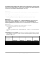
Position of BFLDx
within ATOMIC/
EXT.. sequence
1
2
3
4
1
Range of original ATOMIC/EXTEND statement
2
3
no problem / no
workaround
----
no problem / no
workaround
z=1
---
no problem / no
workaround
z=2
z=1
--
4
no problem / no
workaround
z=3
z=2
z=1
- - : case can not occur
Microcontroller Division Errata Sheet, C165-L(25)M(3V), -L(25)F(3V), (ES)-HA, 1.0, Mh
- 4 of 11 -
Tool Support for Problem CPU.21
The Keil C166 Compiler V3.xx generates BFLD instructions only in the following cases:
when using the _bfld_ intrinsic function.
at the beginning of interrupt service routines, when using #pragma disable
at the end of interrupt service routines, when using the chip bypass directive FIX166.
The C166 Compiler V4.xx uses the BFLD instruction to optimize bit-field struct accesses. Release
C166 V4.10 offers a new directive called FIXBFLD that inserts an ATOMIC #1 instruction before every
BFLD instruction that is not enclosed in an EXTR sequence. Detailed information can be found in the
C166\HLP\RELEASE.TXT of C166 Version 4.10.
The C166 Run-Time Library for C166 V3.xx and V4.xx uses BFLD instructions only in the
START167.A66 file. This part of the code should be not affected by the CPU.21 problem but should be
checked by the software designer.
The RTX166 Full Real-Time Operating system (any version) does not use BFLD instructions.
For RTX166 Tiny, you should rebuild the RTX166 Tiny library with the SET FIXBFLD = 1 directive. This
directive is enabled in the assembler source file RTX166T.A66. After change of this setting rebuild the
RTX166 Tiny library that you are using in your application.
The Tasking support organization provides a v7.0r1 A166 Assembler (build 177) including a check for
problem CPU.21 with optional pec/no_pec feature. This assembler version can also be used to check
code which was generated with previous versions of the Tasking tool chain. A v7.0r1 C166 Compiler
(build 368) offering a workaround for problem CPU.21 is also available from Tasking.
The scan tool aiScan21 analyzes files in hex format plus user-supplied additional information (locator
map file, configuration file), checks whether they may be affected by problem CPU.21, and produces
diagnostic information about potentially critical instruction sequences. This tool is included in AP1628
'Scanning for Problem CPU.21' on
http://www.infineon.com/cgi/ecrm.dll/ecrm/scripts/prod_cat.jsp?oid=-8137
Microcontroller Division Errata Sheet, C165-L(25)M(3V), -L(25)F(3V), (ES)-HA, 1.0, Mh
- 5 of 11 -
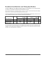
Deviations from Electrical- and Timing Specification:
The FA- and HA-step of the C165 are tested according to the specification in the C165 Data Sheet
V2.0 2000-12. No deviations compared to this specification are known.
Due to this new reference, AC problems AC.t6.1, AC.t22.1, AC.t55.1 of the C165 CA-step are implicitly
fixed in the FA- and HA-step (see following table and History List).
These three parameters are now specified as follows (Standard Supply Voltage Range, values for CPU
clock of 20 MHz are listed for easier comparison with previous Data Sheet):
Parameter
C165 FA/HA-step:
Address setup to ALE
Symbol
CPU Clock
= 20 MHz
Variable CPU Clock Unit
1/2TCL = 1 .. 25 MHz
min.
max.
min.
max.
t6
9+ta
-
TCL-16+ta
-
ns
Data valid to WR#
t22
30+tc
-
2TCL-20+tc
-
ns
Address hold after
RDCS#, WRCS#
t55
-6+tf
-
-6+tf
-
ns
The notes about the internal pull-ups on pins READY# and P6.[0:4], and the note about the test
conditions for t28, which were contained in previous versions of the C165 Errata Sheet have been
included in the C165 Data Sheet V2.0 2000-12.
Microcontroller Division Errata Sheet, C165-L(25)M(3V), -L(25)F(3V), (ES)-HA, 1.0, Mh
- 6 of 11 -
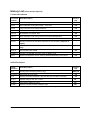
History List (since device step CA)
Functional Problems
Functional Short Description
Problem
Fixed in
step
CPU.6
CALLS to Segments 0F0h .. 0FFh
CA
CPU.7
Warm hardware reset (pulse length < 1032 TCL)
FA
CPU.8
Jump instructions in EXTEND sequence
FA
CPU.9
PEC Transfers during instruction execution from Internal RAM
FA
CPU.10
Bit Protection for register TFR
CA
CPU.11
Stack Underflow Trap during restart of interrupted Multiplication
FA
CPU.17
Arithmetic Overflow by DIVLU instruction
HA
CPU.21
BFLDL/H Instructions after Write Operation to internal IRAM (steps FA or
higher)
BUS.17
Spikes on CS# Lines after access with RDCS# and/or WRCS# (FA-step
only)
HA
BUS.18
PEC transfers after JMPR
HA
PWRDN.1
Execution of PWRDN Instruction while pin NMI# = high
RST.1
System Configuration via P0L.0 during Software/Watchdog Timer Reset
FA
AC/DC Deviations
AC/DC
Deviation
Short Description
Fixed in
step
DC.7
Bonding of pin #40/Vpp (C165-LF only)
(ES3-)CA
DC.RRST.1 RSTIN pull-up 25 to 125 kΩ
FA
AC.2
Address Hold after RD#/WR# - Nonmux Bus (test conditions changed)
CA
AC.t6.1
Address setup to ALE TCL-17.5 ns
FA
1)
AC.t22.1
Data valid to WR# 2TCL-20ns
FA
1)
AC.t55.1
Address hold after RDCS#, WRCS# -10ns
FA
1)
test according to C165 Data Sheet V2.0 2000-12
Microcontroller Division Errata Sheet, C165-L(25)M(3V), -L(25)F(3V), (ES)-HA, 1.0, Mh
1)
- 7 of 11 -
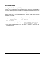
Application Hints
Handling of the SSC Busy Flag (SSCBSY)
In master mode of the High-Speed Synchronous Serial Interface (SSC), when register SSCTB has
been written, flag SSCBSY is set to '1' when the baud rate generator generates the next internal clock
pulse. The maximum delay between the time SSCTB has been written and flag SSCBSY=1 is up to 1/2
bit time. SSCBSY is cleared 1/2 bit time after the last latching edge.
When polling flag SSCBSY after SSCTB has been written, SSCBSY may not yet be set to '1' when it is
tested for the first time (in particular at lower baud rates). Therefore, e.g. the following alternative
methods are recommended:
1. test flag SSCRIR (receive interrupt request) instead of SSCBSY (in case the receive interrupt
request is not serviced by CPU interrupt or PEC), e.g.
loop:
BCLR SSCRIR
;clear receive interrupt request flag
MOV SSCTB, #xyz
;send character
wait_tx_complete:
JNB SSCRIR, wait_tx_complete ;test SSCRIR
JB SSCBSY, wait_tx_complete ;test SSCBSY to achieve original
timing(SSCRIR may be set 1/2 bit
time before SSCBSY is cleared)
2. use a software semaphore bit which is set when SSCTB is written and is cleared in the SSC
receive interrupt routine
Microcontroller Division Errata Sheet, C165-L(25)M(3V), -L(25)F(3V), (ES)-HA, 1.0, Mh
- 8 of 11 -
Functional Improvements/Compatibility Aspects
In the following sections, the functional improvements which have been implemented in the C165
beginning with the CA-step are described.
A. Stepping Update BA/BB --> CA
1. Clock Input: the prescaler (2:1) for the input clock of the C165 CA-step can be disabled by pulling
P0H.7 low during reset.
2. RDCS0#/WRCS0#: CS0# may also be programmed for RDCS0#/WRCS0# via BUSCON0.
3. ROM: the CA-step will be able to provide 4Kbyte of on-chip mask-programmable ROM.
Compatibility of 1 - 3: systems designed for earlier steps of the C165 will also work with the CA-step.
These additional features are also described in the Siemens Product Information 'C165 -LM Stepping
Update (BB -> CA)'. In addition, the following functional improvements in the External Bus Controller
should be noted:
4. External Bus Controller:
4.1 When exiting the HOLD mode, the CSx# signals are actively driven high one TCL earlier than in the
BA/BB-step.
Compatibility: systems designed for earlier steps of the C165 will also work with the CA-step.
4.2 When bit HLDEN=1, the bus arbitration mechanism can be switched to a special Slave Mode by
setting bit DP6.7=1 (i.e. selecting 'output' for pin BREQ#). Retaining the reset value (DP6.7 = 0)
selects the standard Master Mode. This feature (which is not yet fully implemented and released in
the CA-step) will allow to connect a master and a slave controller without any glue logic.
Compatibility: the standard Master Mode of the C165 does not require additional explicit
initialization of output pins, so generally DP6.7 should be at its reset state. This state ('0') selects
Master Mode also for the CA-step.
4.3 The Address Window Arbitration feature as described in the C165/C163 User's Manual V2.0,
p.8-22 is not yet implemented in C165 devices up to and including step CA. For these devices, the
description in C165 User's Manual V1.0 still applies in this context, i.e. the address windows
defined by ADDRSEL1 through ADDRSEL4 must not overlap each other.
B. Stepping Update CA --> FA/HA
1. The Bootstrap Loader Acknowledge Byte returned by FA/HA-step devices is D5h (CA-step:
B5h).
2. The Address Window Arbitration feature as described in the C165/C163 User's Manual V2.0,
p.8-22 is implemented in C165 devices beginning with stepping code FA.
Compatibility: systems designed for earlier steps of the C165 will also work with the FA/HA-step
3. The internal oscillator inverter (Type_RE) has been improved. It is compatible to external circuits
as described in ApNote 2420 'Crystal Oscillators of the C500 and C166 Microcontroller Families' for
Type_R oscillator inverter (see table 14, page 34 in Rel. 0.5–4/99 (page numbers may be different
in previous releases)). However, it is strongly recommended to verify the safety factor in the target
application, as described in this application note.
Location of the ApNote on the Internet/direct link to .pdf file:
http://www.infineon.com/cgi/ecrm.dll/ecrm/scripts/prod_cat.jsp?oid=-8137
http://www.infineon.com/cmc_upload/migrated_files/document_files/Application_Notes/ap242005.pdf
Microcontroller Division Errata Sheet, C165-L(25)M(3V), -L(25)F(3V), (ES)-HA, 1.0, Mh
- 9 of 11 -
4. The General Purpose Timers additionally provide the Incremental Interface mode which allows to
interface to incremental position sensors (A, B, Top0). Optionally, the contents of T5 may be
captured into register CAPREL upon an event on T3. A detailed description of this feature is
included in the 'Documentation Addendum: GPT Incremental Interface Mode V1.0 1998-10'.
5. Besides bit WDTR which indicates a watchdog timer reset, additional Reset Source Indication
Flags have been implemented in register WDTCON to signal other reset types (software reset,
long/short hardware reset). While in previous steps, only reset values 0000h or 0002h could occur in
register WDTCON, in the FA-step further values may occur in the low byte of WDTCON. Unlike the
other reset source indication flags, WDTR is not cleared by instructions EINIT or SRST. Therefore,
programs written for previous steps, which evaluate the contents of WDTCON directly after reset
and before execution of EINIT, may work differently on the FA/HA-step. The following table
summarizes the behaviour of the reset source indication flags:
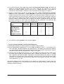
Flag
LHWR
WDTCON.4
SHWR
WDTCON.3
SWR
WDTCON.2
WDTR
WDTCON.1
Long HW Reset
1
1
1
0
Short HW Reset
-
1
1
0
SRST instruction
-
-
1
-
WDT Reset
-
-
1
1
EINIT instruction
0
0
0
-
SRVWDT instruction
-
-
-
0
Event
Legend: 1 = flag is set, 0 = flag is cleared, - = flag is not affected
6. The contents of register IDCHIP for the HA-step is 0513h.
7. Timing of flag SSCTIR (SSC Transmit Interrupt Request)
In master mode, the timing of SSCTIR depends on the device step as follows:
(a) before step FA (internal stepping F11) of the C165, flag SSCTIR is set to ‘1’ synchronous to the
shift clock SCLK 1/2 bit time before the first latching edge (= first shifting clock edge when SSCPH
= 0). When SSCTB is written while the shift register is empty, the maximum delay between the time
SSCTB has been written and flag SSCTIR=1 is up to 1/2 bit time.
(b) beginning with step FA (internal stepping F12) of the C165, when SSCTB has been written while
the transmit shift register was empty (and the SSC is enabled), flag SSCTIR is set to ‘1’ directly
after completion of the write operation, independent of the selected baud rate. When the transmit
shift register is not empty when SSCTB was written, SSCTIR is set to '1' after the last latching edge
of SCLK (= 1/2 bit time before the first shifting edge of the next character). See also e.g. C167CR
User's Manual V3.1, p. 12-5.
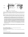
The following diagram shows these relations in an example for a data transfer in master mode with
SSCPO = 0 and SSCPH = 0. It is assumed that the transmit shift register is empty at the time the first
character is written to SSCTB:
Microcontroller Division Errata Sheet, C165-L(25)M(3V), -L(25)F(3V), (ES)-HA, 1.0, Mh
- 10 of 11 -
write to SSCTB, first character
write to SSCTB, next character
SCLK
Bit 0
Bit 1
Bit n
Bit 0
MTSR
case (a): SSCTIR = 1 in previous device steps
case (b): SSCTIR = 1 in current and future device steps
Typically, in interrupt driven systems, no problems are expected from the modified timing of flag
SSCTIR. However, when flag SSCTIR is polled by software in combination with other flags which are
set/cleared at the end or at the beginning of a transfer (e.g. SSCBSY), the modified timing may have an
effect.
Another situation where a different system behaviour may be noticed is the case when only one
character is transferred by the PEC into the transmit buffer register SSCTB. In this case, 2 interrupt
requests from SSCTIR are expected: the 'PEC COUNT = 0' interrupt, and the 'SSCTB empty' interrupt.
-
in the FA (and newer) steps of the C165, the second interrupt request ('SSCTB empty') is always
systematically generated before the first one ('PEC COUNT = 0') has been acknowledged by the
CPU, such that effectively only one interrupt request is generated for two different events.
-
before step FA of the C165, when the PEC transfer is performed with sufficient margin to the next
clock tick from the SSC baud rate generator, and no higher priority interrupt request has occurred
in the meantime, the 'PEC COUNT = 0' interrupt will be acknowledged before the 'SSCTB empty'
interrupt request is generated, i.e. two interrupts will occur based on these events. However,
when the PEC transfer takes place relatively close before the next clock tick from the SSC baud
rate generator, or a higher priority interrupt request has occurred while the PEC transfer is
performed, the 'PEC COUNT = 0' interrupt may not be acknowledged before the 'SSCTB empty'
interrupt request is generated, such that effectively only one interrupt request will be generated
for two different events.
In order to achieve a defined and systematic behavior with all device steps, the SSC receive interrupt,
which is generated at the end of a character transmission, may be used instead of the SSC transmit
interrupt.
Documentation Update (reference: C165/C163 User's Manual V2.0/10.96)
External Access Enable Pin EA# (page 7-2)
There is an obvious contradiction in this section: of course, the EA# input must be held low on
ROMless devices.
Application Support Group, Munich
Microcontroller Division Errata Sheet, C165-L(25)M(3V), -L(25)F(3V), (ES)-HA, 1.0, Mh
- 11 of 11 -