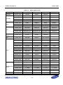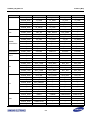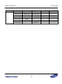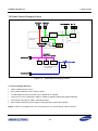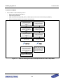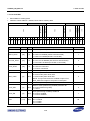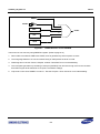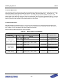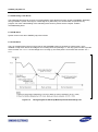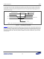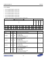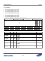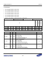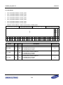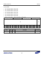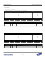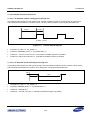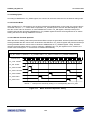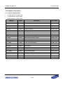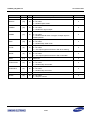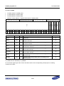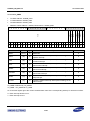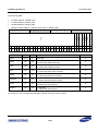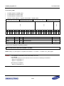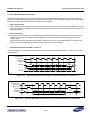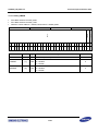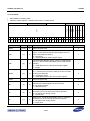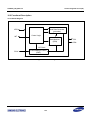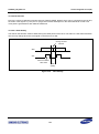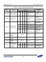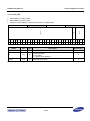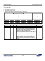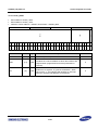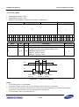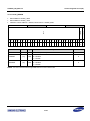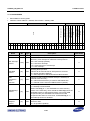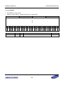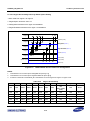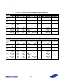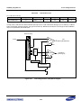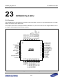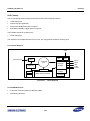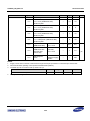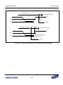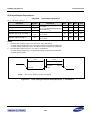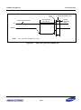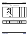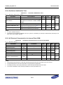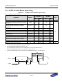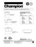
1
S3FN60D USB Remote 32-bit MCU Revision 1.30 January 2012 User's Manual 2012 Samsung Electronics Co., Ltd. All rights reserved. Important Notice Samsung Electronics Co. Ltd. (“Samsung”) reserves the right to make changes to the information in this publication at any time without prior notice. All information provided is for reference purpose only. Samsung assumes no responsibility for possible errors or omissions, or for any consequences resulting from the use of the information contained herein. indemnify and hold Samsung and its officers, employees, subsidiaries, affiliates, and distributors harmless against all claims, costs, damages, expenses, and reasonable attorney fees arising out of, either directly or indirectly, any claim (including but not limited to personal injury or death) that may be associated with such unintended, unauthorized and/or illegal use. This publication on its own does not convey any license, either express or implied, relating to any Samsung and/or third-party products, under the intellectual property rights of Samsung and/or any third parties. WARNING No part of this publication may be reproduced, Samsung makes no warranty, representation, or guarantee regarding the suitability of its products for any particular purpose, nor does Samsung assume any liability arising out of the application or use of any product or circuit and specifically disclaims any and all liability, including without limitation any consequential or incidental damages. Customers are responsible for their own products and applications. "Typical" parameters can and do vary in different applications. All operating parameters, including "Typicals" must be validated for each customer application by the customer's technical experts. Samsung products are not designed, intended, or authorized for use in applications intended to support or sustain life, or for any other application in which the failure of the Samsung product could reasonably be expected to create a situation where personal injury or death may occur. Customers acknowledge and agree that they are solely responsible to meet all other legal and regulatory requirements regarding their applications using Samsung products notwithstanding any information provided in this publication. Customer shall Copyright 2012 Samsung Electronics Co., Ltd. Samsung Electronics Co., Ltd. San #24 Nongseo-Dong, Giheung-Gu Yongin-City, Gyeonggi-Do, Korea 446-711 Contact Us: [email protected] TEL: (82)-(31)-209-3042 FAX: (82)-(31)-8000-2005 Home Page: http://www.samsungsemi.com stored in a retrieval system, or transmitted in any form or by any means, electric or mechanical, by photocopying, recording, or otherwise, without the prior written consent of Samsung. This publication is intended for use by designated recipients only. This publication contains confidential information (including trade secrets) of Samsung protected by Competition Law, Trade Secrets Protection Act and other related laws, and therefore may not be, in part or in whole, directly or indirectly publicized, distributed, photocopied or used (including in a posting on the Internet where unspecified access is possible) by any unauthorized third party. Samsung reserves its right to take any and all measures both in equity and law available to it and claim full damages against any party that misappropriates Samsung’s trade secrets and/or confidential information. 警 告 本文件仅向经韩国三星电子株式会社授权的人 员提供,其内容含有商业秘密保护相关法规规定并受其 保护的三星电子株式会社商业秘密,任何直接或间接非 法向第三人披露、传播、复制或允许第三人使用该文件 全部或部分内容的行为(包括在互联网等公开媒介刊登 该商业秘密而可能导致不特定第三人获取相关信息的行 为)皆为法律严格禁止。此等违法行为一经发现,三星 电子株式会社有权根据相关法规对其采取法律措施,包 括但不限于提出损害赔偿请求。 Trademarks All brand names, trademarks and registered trademarks belong to their respective owners. Exynos, Exynos4210, FlexOneNAND, and OneNAND are trademarks of Samsung Electronics. ARM, Jazelle, TrustZone, and Thumb are registered trademarks of ARM Limited. Cortex, ETM, ETB, Coresight, ISA, and Neon are trademarks of ARM Limited. Java is a trademark of Sun Microsystems, Inc. SD is a registered trademark of Toshiba Corporation. MMC and eMMC are trademarks of MultiMediaCard Association. JTAG is a registered trademark of JTAG Technologies, Inc. Synopsys is a registered trademark of Synopsys, Inc. I2S is a trademark of Phillips Electronics. I C is a trademark of Phillips Semiconductor Corp. MIPI and Slimbus are registered trademarks of the Mobile Industry Processor Interface (MIPI) Alliance. 2 All other trademarks used in this publication are the property of their respective owners. Chip Handling Guide Precaution against Electrostatic Discharge When handling semiconductor devices, be sure that the environment is protected against static electricity. 1. Operators should wear anti-static clothing and use earth band. 2. All objects that come in direct contact with devices should be made of materials that do not produce static electricity that would cause damage. 3. Equipment and work table must be earthed. 4. Ionizer is recommended to remove electron charge. Contamination Be sure to use semiconductor products in the environment that may not be exposed to dust or dirt adhesion. Temperature/Humidity Semiconductor devices are sensitive to environment temperature and humidity. High temperature or humidity may deteriorate semiconductor device’s characteristics. Therefore avoid storage or use in such conditions. Mechanical Shock Care should be exercised not to apply excessive mechanical shock or force on semiconductor device. Chemical Do not expose semiconductor device to chemical because reaction to chemical may cause deterioration of device characteristics. Light Protection In case of non-EMC (Epoxy Molding Compound) package, do not expose semiconductor IC to strong light. It may cause device’s malfunction. (But, some special products which utilize the light or have security function are excepted from this guide) Radioactive, Cosmic and X-ray Semiconductor devices can be influenced by radioactive, cosmic ray or X-ray. Radioactive, cosmic and X-ray may cause soft error during device operation. Therefore semiconductor devices must be shielded under environment that may be exposed to radioactive, cosmic ray or X-ray. EMS (Electromagnetic Susceptibility) Note that semiconductor device’s characteristics may be affected by strong electromagnetic wave or magnetic field during operation under insufficient PCB circuit design for EMS. Table of Contents 1 PRODUCT OVERVIEW .................................................................................1-1 1.1 Overview .................................................................................................................................................. 1-1 1.2 Feature ..................................................................................................................................................... 1-2 1.3 Block Diagram .......................................................................................................................................... 1-5 1.4 Pin Assignments (64-Pin TQFP) .............................................................................................................. 1-6 1.5 Pin Circuits ............................................................................................................................................. 1-10 2 ADDRESS SPACE ........................................................................................2-1 2.1 Overview .................................................................................................................................................. 2-1 2.2 Memory Configuration in Cortex M0 Side ................................................................................................ 2-1 2.3 Smart Option ............................................................................................................................................ 2-3 3 CORTEX-M0 ..................................................................................................3-1 3.1 Overview .................................................................................................................................................. 3-1 3.2 Features ................................................................................................................................................... 3-1 3.3 Interfaces ................................................................................................................................................. 3-1 4 INTERRUPTS ................................................................................................4-1 4.1 Overview .................................................................................................................................................. 4-1 4.2 Features ................................................................................................................................................... 4-1 4.3 Interrupt Sources & Interrupt Vector ........................................................................................................ 4-2 4.4 System Interrupt Vector ........................................................................................................................... 4-3 5 MEMORY MAP ..............................................................................................5-1 5.1 Overview .................................................................................................................................................. 5-1 5.2 Default Memory Map ................................................................................................................................ 5-1 5.3 Core & Peripheral Special Function Register Map .................................................................................. 5-2 6 INSTRUCTION SET .......................................................................................6-1 6.1 Cortex-M0 Instruction Set Summary ........................................................................................................ 6-1 7 CLOCK CIRCUITS ........................................................................................7-1 7.1 Overview .................................................................................................................................................. 7-1 7.2 Features ................................................................................................................................................... 7-1 7.2.1 System Clock Circuit......................................................................................................................... 7-1 7.2.2 Power Supply Selection Circuit ........................................................................................................ 7-1 7.2.3 PLL Clock Circuit .............................................................................................................................. 7-1 7.3 Block Diagram .......................................................................................................................................... 7-2 7.4 Clock Status during Power-down Modes ................................................................................................. 7-4 7.5 Clock Control State Machine ................................................................................................................... 7-5 7.6 Power Source Changing Circuit ............................................................................................................... 7-6 7.6.1 Power Supply Selection .................................................................................................................... 7-6 7.7 PLL (Phase Locked Loop) ....................................................................................................................... 7-7 7.8 Change PLL Settings in Normal Operation Mode.................................................................................... 7-7 7.9 Power Management ................................................................................................................................. 7-8 7.9.1 Power Modes .................................................................................................................................... 7-8 7.9.2 Low Power Mode and Wake-Up ....................................................................................................... 7-8 7.9.3 Enter IDLE Mode .............................................................................................................................. 7-8 7.9.4 Exit IDLE Mode ................................................................................................................................. 7-9 7.9.5 Enter STOP Mode ............................................................................................................................ 7-9 7.9.6 Exit STOP Mode ............................................................................................................................. 7-10 7.10 Register Description ............................................................................................................................. 7-11 7.10.1 Register Map Summary ................................................................................................................ 7-11 8 RESET ...........................................................................................................8-1 8.1 Overview .................................................................................................................................................. 8-1 8.1.1 Reset Sources .................................................................................................................................. 8-1 8.1.2 Reset Mechanism ............................................................................................................................. 8-3 8.1.3 External Reset Pin ............................................................................................................................ 8-3 8.1.4 Watch Dog Timer Reset ................................................................................................................... 8-4 8.1.5 S/W Reset......................................................................................................................................... 8-4 8.1.6 LVD Reset ........................................................................................................................................ 8-4 8.1.7 POR Reset (Internal Power-On Reset) ............................................................................................ 8-7 8.1.8 System Reset Operation .................................................................................................................. 8-9 8.1.9 Status Table of Back-Up Mode, Stop Mode, and Reset................................................................. 8-10 8.2 Register Description ............................................................................................................................... 8-11 8.2.1 Register Map Summary .................................................................................................................. 8-11 9 I/O PORTS .....................................................................................................9-1 9.1 Overview .................................................................................................................................................. 9-1 9.2 Features ................................................................................................................................................... 9-1 9.2.1 Port Control Description ................................................................................................................... 9-1 9.3 Register Description ................................................................................................................................. 9-2 9.3.1 Register Map Summary .................................................................................................................... 9-2 10 BASIC TIMER/WATCHDOG TIMER..........................................................10-1 10.1 Overview .............................................................................................................................................. 10-1 10.2 Features ............................................................................................................................................... 10-1 10.2.1 Basic Timer Control Register (BTCON) ....................................................................................... 10-1 10.2.2 Basic Timer Function Description ................................................................................................. 10-1 10.2.3 Basic Timer/Watchdog Timer Block Diagram ............................................................................... 10-3 10.3 Register Description ............................................................................................................................. 10-4 10.3.1 Register Map Summary ................................................................................................................ 10-4 11 COUNTER A ..............................................................................................11-1 11.1 Overview .............................................................................................................................................. 11-1 11.1.1 Feature ......................................................................................................................................... 11-1 11.1.2 Pin Description.............................................................................................................................. 11-1 11.2 Functional Description ......................................................................................................................... 11-2 11.2.1 Block Diagram .............................................................................................................................. 11-2 11.2.2 Counter A Pulse Width Calculations............................................................................................. 11-3 11.2.3 Counter A Data Register Setting .................................................................................................. 11-5 11.2.4 Counter A output Signal Waveform .............................................................................................. 11-6 11.3 Register Description ............................................................................................................................. 11-7 11.3.1 Register Map Summary ................................................................................................................ 11-7 12 TIMER/COUNTER .....................................................................................12-1 12.1 Overview .............................................................................................................................................. 12-1 12.1.1 Features ........................................................................................................................................ 12-1 12.1.2 Pin Description.............................................................................................................................. 12-1 12.2 Functional Description ......................................................................................................................... 12-1 12.2.1 Block Diagram .............................................................................................................................. 12-1 12.2.2 Counter Size ................................................................................................................................. 12-2 12.2.3 Counter Clock ............................................................................................................................... 12-2 12.2.4 Debug Option................................................................................................................................ 12-3 12.2.5 Overflow Mode.............................................................................................................................. 12-3 12.2.6 Period Mode ................................................................................................................................. 12-6 12.2.7 Interrupt ...................................................................................................................................... 12-14 12.3 Register Description ........................................................................................................................... 12-15 12.3.1 Register Map Summary .............................................................................................................. 12-15 13 FREE RUNNING TIMER ............................................................................13-1 13.1 Overview .............................................................................................................................................. 13-1 13.1.1 Features ........................................................................................................................................ 13-1 13.2 Functional Description ......................................................................................................................... 13-2 13.2.1 Block Diagram .............................................................................................................................. 13-2 13.2.2 Timer Clock ................................................................................................................................... 13-3 13.2.3 Count and Data register ............................................................................................................... 13-3 13.2.4 Interrupt ........................................................................................................................................ 13-3 13.2.5 Operation ...................................................................................................................................... 13-4 13.3 Register Description ............................................................................................................................. 13-5 13.3.1 Register Map Summary ................................................................................................................ 13-5 14 SERIAL PERIPHERAL INTERFACE (SPI) ................................................14-1 14.1 Overview .............................................................................................................................................. 14-1 14.1.1 Features ........................................................................................................................................ 14-1 14.1.2 Operation ...................................................................................................................................... 14-1 14.2 Register Description ........................................................................................................................... 14-14 14.2.1 Register Map Summary .............................................................................................................. 14-14 15 UART .........................................................................................................15-1 15.1 Overview .............................................................................................................................................. 15-1 15.2 Function Description ............................................................................................................................ 15-2 15.2.1 Uart Operation .............................................................................................................................. 15-2 15.2.2 Data Transmission ........................................................................................................................ 15-2 15.2.3 Data Reception ............................................................................................................................. 15-3 15.2.4 Interrupt Request Generation ....................................................................................................... 15-4 15.2.5 DMA Operation ............................................................................................................................. 15-5 15.3 Baud Rate Generation ......................................................................................................................... 15-6 15.3.1 Loop Back Mode ........................................................................................................................... 15-6 15.3.2 Infra Red (IrDA) Mode .................................................................................................................. 15-6 15.4 Register Description ............................................................................................................................. 15-8 15.4.1 Register Map Summary ................................................................................................................ 15-8 16 INTER-INTEGRATED CIRCUIT (IIC) .........................................................16-1 16.1 Overview .............................................................................................................................................. 16-1 16.1.1 Features ........................................................................................................................................ 16-1 16.1.2 Pin Description.............................................................................................................................. 16-2 16.2 Functional Description ......................................................................................................................... 16-3 16.2.1 Block Diagram .............................................................................................................................. 16-3 16.2.2 Functional Operation .................................................................................................................... 16-4 16.2.3 Extensions to the I2C-bus Specification ..................................................................................... 16-17 16.2.4 Fast Mode ................................................................................................................................... 16-17 16.3 Inter-Intergrated Circuit Timing .......................................................................................................... 16-18 16.4 Register Description ........................................................................................................................... 16-19 16.4.1 Register Map Summary .............................................................................................................. 16-19 17 USB CONTROLLER ..................................................................................17-1 17.1 Overview .............................................................................................................................................. 17-1 17.1.1 Features ........................................................................................................................................ 17-2 17.1.2 USB Block Overview..................................................................................................................... 17-3 17.2 Register Description ............................................................................................................................. 17-4 17.2.1 Register Map Summary ................................................................................................................ 17-4 18 10-BIT ANALOG-TO-DIGITAL CONVERTER ...........................................18-1 18.1 Overview .............................................................................................................................................. 18-1 18.1.1 Features ........................................................................................................................................ 18-1 18.1.2 Pin Description.............................................................................................................................. 18-1 18.2 Functional Description ......................................................................................................................... 18-2 18.2.1 Analog Input Type & Range ......................................................................................................... 18-2 18.2.2 Reference Voltage ........................................................................................................................ 18-2 18.2.3 Power down Mode ........................................................................................................................ 18-2 18.2.4 Wake-up Time .............................................................................................................................. 18-2 18.2.5 Digital Output Format ................................................................................................................... 18-2 18.2.6 Input/Output Chart ........................................................................................................................ 18-3 18.2.7 Conversion Timing ........................................................................................................................ 18-3 18.2.8 End of Conversion ........................................................................................................................ 18-3 18.2.9 A/D Converter Control Register (ADCCON) ................................................................................. 18-3 18.3 Functional Block Diagram .................................................................................................................... 18-4 18.4 Timing Diagram .................................................................................................................................... 18-5 18.5 Register Description ............................................................................................................................. 18-6 18.5.1 Register Map Summary ................................................................................................................ 18-6 19 DMA (DIRECT MEMORY ACCESS)..........................................................19-1 19.1 Overview .............................................................................................................................................. 19-1 19.2 DMA Operation .................................................................................................................................... 19-3 19.2.1 DMA Transfers.............................................................................................................................. 19-3 19.2.2 Starting/Ending DMA Transfers .................................................................................................... 19-3 19.3 Operation Mode-H/W Request............................................................................................................. 19-5 19.3.1 Single Service Mode ..................................................................................................................... 19-5 19.3.2 Continuous Service Mode ............................................................................................................ 19-6 19.4 DMA Transfer Size ............................................................................................................................... 19-7 19.4.1 Single Transfer Size ..................................................................................................................... 19-7 19.4.2 Burst (4-unit) Transfer Size .......................................................................................................... 19-7 19.5 DMA Operation Sequence ................................................................................................................... 19-8 19.5.1 S/W Request Sequence ............................................................................................................... 19-8 19.5.2 H/W Request Sequence ............................................................................................................... 19-9 19.6 Register Description ........................................................................................................................... 19-10 19.6.1 Register Map Summary .............................................................................................................. 19-10 20 EMBEDDED FLASH MEMORY .................................................................20-1 20.1 Overview .............................................................................................................................................. 20-1 20.1.1 Flash ROM Configuration ............................................................................................................. 20-1 20.2 Register Description ............................................................................................................................. 20-2 20.2.1 Register Map Summary ................................................................................................................ 20-2 20.3 Programming........................................................................................................................................ 20-6 21 MEMORY PROTECTION UNIT .................................................................21-1 21.1 Overview .............................................................................................................................................. 21-1 21.2 Feature ................................................................................................................................................. 21-2 21.2.1 Region Definition .......................................................................................................................... 21-2 21.2.2 Region to Region ACCESSBILITY ............................................................................................... 21-3 21.3 MPU Abort Cases ................................................................................................................................ 21-6 21.3.1 Read Cases .................................................................................................................................. 21-7 21.3.2 Write Cases .................................................................................................................................. 21-8 21.4 MPU SFR Configuration ...................................................................................................................... 21-9 21.5 No Allowance Cases .......................................................................................................................... 21-10 21.6 Register Description ........................................................................................................................... 21-11 21.6.1 Register Map Summary .............................................................................................................. 21-11 22 LOW VOLTAGE DETECTOR ....................................................................22-1 22.1 Overview .............................................................................................................................................. 22-1 22.2 LVD ...................................................................................................................................................... 22-2 22.2.1 LVD FLAG .................................................................................................................................... 22-2 22.3 Register Description ............................................................................................................................. 22-4 22.3.1 Register Map Summary ................................................................................................................ 22-4 23 S3FN60D FLASH MCU .............................................................................23-1 23.1 Overview .............................................................................................................................................. 23-1 23.1.1 Test Pin Voltage ........................................................................................................................... 23-3 24 DEBUG ......................................................................................................24-1 24.1 Overview .............................................................................................................................................. 24-1 24.2 Feature ................................................................................................................................................. 24-2 24.2.1 Block Diagram .............................................................................................................................. 24-2 24.2.2 ARM Reference ............................................................................................................................ 24-2 25 ELECTRICAL DATA..................................................................................25-1 25.1 Overview .............................................................................................................................................. 25-1 25.2 Absolute Maximum Ratings ................................................................................................................. 25-2 25.3 D.C. Electrical Characteristics ............................................................................................................. 25-3 25.4 Characteristics of Low Voltage Detect Circuit ...................................................................................... 25-5 25.5 LVD Enable Time ................................................................................................................................. 25-6 25.6 A/D Converter Electrical Characteristics .............................................................................................. 25-6 25.7 Power on Reset Circuit ........................................................................................................................ 25-6 25.8 Data Retention Supply Voltage in Stop Mode ..................................................................................... 25-7 25.9 Input/Output Capacitance .................................................................................................................... 25-9 25.10 Oscillation Characteristics ................................................................................................................ 25-11 25.11 Ring Oscillator Characteristics ......................................................................................................... 25-11 25.12 Oscillation Stabilization Time ........................................................................................................... 25-12 25.13 AC Electrical Characteristics for Internal Flash ROM ...................................................................... 25-12 25.14 ESD Characteristics ......................................................................................................................... 25-13 25.15 USB DC Electrical Characteristics ................................................................................................... 25-13 25.16 SPI Interface Transmit/Receive Timing Constants .......................................................................... 25-14 25.17 IIC BUS Controller Module Signal Timing ........................................................................................ 25-16 26 MECHANICAL DATA ................................................................................26-1 26.1 Overview .............................................................................................................................................. 26-1 List of Figures Figure Number Title Page Number Figure 1-1 Figure 1-2 Figure 1-3 Figure 1-4 Figure 1-5 Figure 1-6 Figure 1-7 Block Diagram................................................................................................................................... 1-5 Pin Assignment Diagram (64-Pin TQFP Package)........................................................................... 1-6 External Interrupt Port to Wake Up Stop Mode (Pin Circuit Type 1) .............................................. 1-10 IN/OUT Port, Alternative Function Port (Pin Circuit Type 2) .......................................................... 1-11 IN/OUT Port, Alternative Function Port & Ext. Interrupt (Pin Circuit Type 3) ................................. 1-12 IN/OUT Port, Alternative Input Port (ADC) & Ext. Interrupt (Pin Circuit Type 4) ............................ 1-13 nRESET Pin (Pin Circuit Type 5) .................................................................................................... 1-13 Figure 2-1 Program Memory Configuration ........................................................................................................ 2-2 Figure 7-1 Figure 7-2 Figure 7-3 Figure 7-4 Figure 7-5 Figure 7-6 Figure 7-7 Figure 7-8 Main Oscillator Circuit ....................................................................................................................... 7-2 Power Circuit (VDD) ........................................................................................................................... 7-2 nRESET Circuit ................................................................................................................................. 7-3 System Clock Circuit Diagram .......................................................................................................... 7-4 Clock Control State Machine ............................................................................................................ 7-5 Power Source Changing Circuit........................................................................................................ 7-6 Timing Diagram of Clock Change in Normal Mode .......................................................................... 7-7 Different Handling Process for Interrupt and Event in Idle or Stop Mode....................................... 7-10 Figure 8-1 Figure 8-2 Figure 8-3 Figure 8-4 Figure 8-5 Figure 8-6 Figure 8-7 RESET Sources of The S3FN60D.................................................................................................... 8-2 Timing Diagram for Back-Up Mode Input and Released by LVD ..................................................... 8-4 Timing Diagram in Stop Mode .......................................................................................................... 8-5 Timing Diagram in Stop Mode .......................................................................................................... 8-6 Timing Diagram for Internal Power-On Reset Circuit ....................................................................... 8-7 Reset Timing Diagram for the S3FN60D in STOP Mode by IPOR .................................................. 8-8 Wake Up in Stop Mode by IPOR (VPOR < VDD < VLVD) ............................................................... 8-8 Figure 10-1 Basic Timer & Watchdog Timer Block Diagram ........................................................................... 10-3 Figure 11-1 Figure 11-2 Figure 11-3 Figure 11-4 Figure 11-5 Figure 11-6 Counter A Block Diagram ............................................................................................................. 11-2 Counter A unit signal .................................................................................................................... 11-3 Counter A Block Diagram ............................................................................................................. 11-4 Counter A Output Flip-flop Waveforms in Repeat Mode .............................................................. 11-5 TA_EVELOPE = 0 ........................................................................................................................ 11-6 TA_ENVELOPE = 1 ...................................................................................................................... 11-6 Figure 12-1 Figure 12-2 Figure 12-3 Figure 12-4 Figure 12-5 Figure 12-6 Figure 12-7 Figure 12-8 Figure 12-9 Figure 12-10 TC Block Diagram ......................................................................................................................... 12-1 Match & Overflow Operation Timing ............................................................................................. 12-3 Counter Values According to START, STOPCLEAR and STOPHOLD ....................................... 12-4 Capture Operation Timing ............................................................................................................ 12-5 Period Mode Timing ...................................................................................................................... 12-6 Interval Operation ......................................................................................................................... 12-7 PWM Operation ............................................................................................................................ 12-8 PWM Extension Waveform ........................................................................................................... 12-9 PWM Waveform with OUTSL = 0 ............................................................................................... 12-11 PWM Waveform with OUTSL = 1 ............................................................................................. 12-11 Figure 12-11 Figure 12-12 Figure 12-13 PWM Waveform Under IDLE State .......................................................................................... 12-12 PWM Waveform with STOPHOLD = 1, STOPCLEAR = 0 ....................................................... 12-13 PWM Waveform with STOPCLEAR = 1 ................................................................................... 12-13 Figure 13-1 Figure 13-2 Free Running Timer Block Diagram ............................................................................................. 13-2 Simplified Timer Function Diagram: Match ................................................................................... 13-4 Figure 14-1 Figure 14-2 Figure 14-3 Figure 14-4 Figure 14-5 Figure 14-6 Figure 14-7 Figure 14-8 Motorola SPI Frame Format (Single Transfer) with SPO = 0 and SPH = 0 ................................. 14-4 Motorola SPI Frame Format (Continuous Transfer) with SPO = 0 and SPH = 0 ......................... 14-4 Motorola SPI Frame Format (Single Transfer) with SPO = 0 and SPH = 1 ................................. 14-6 Motorola SPI Frame Format (Single Transfer) with SPO = 1 and SPH = 0 ................................. 14-7 Motorola SPI Frame Format (Continuous Transfer) with SPO = 1 and SPH = 0 ......................... 14-7 Motorola SPI Frame Format with SPO = 1 and SPH = 1 ............................................................. 14-9 PrimeCell SSP Master Coupled To Two Slaves ......................................................................... 14-10 SPI Master Coupled to two PrimeCell SSP Slaves .................................................................... 14-11 Figure 15-1 Figure 15-2 Figure 15-3 Figure 15-4 Figure 15-5 Figure 15-6 Figure 15-7 UART Block Diagram .................................................................................................................... 15-1 UART Data Transmission Process ............................................................................................... 15-2 UART Data Reception Process .................................................................................................... 15-3 IrDA Function Block Diagram ....................................................................................................... 15-6 Serial I/O Frame Timing Diagram (Normal UART) ....................................................................... 15-7 Infra Red (IrDA) Transmit Mode Frame Timing Diagram ............................................................. 15-7 Infra Red (IrDA) Receive Mode Frame Timing Diagram .............................................................. 15-7 Figure 16-1 Figure 16-2 Figure 16-3 Figure 16-4 Figure 16-5 Figure 16-6 Figure 16-7 Block Diagram............................................................................................................................... 16-3 Data Validity .................................................................................................................................. 16-7 Start and Stop Conditions ............................................................................................................. 16-8 Data Transfer on the I2C Bus ....................................................................................................... 16-9 Acknowledge............................................................................................................................... 16-10 A Master-transmitter Addresses a Slave .................................................................................... 16-13 Hold and Setup Delays ............................................................................................................... 16-43 Figure 17-1 USB Core Block Diagram ............................................................................................................. 17-3 Figure 18-1 Figure 18-2 Figure 18-3 A/D Converter Functional Block Diagram ..................................................................................... 18-4 A/D Conversion Phase ................................................................................................................. 18-5 A/D Converter Data Register (ADDATA) ...................................................................................... 18-9 Figure 19-1 Figure 19-2 Figure 19-3 Figure 19-4 Figure 19-5 Figure 19-6 DMA Request Mode ..................................................................................................................... 19-2 DMA Unit Block Diagram .............................................................................................................. 19-2 Single Transfer in Single Service Mode ....................................................................................... 19-5 Sequential Transfer in Single Service Mode ................................................................................ 19-5 Continuous Service Mode ............................................................................................................. 19-6 Burst (4-unit) Transfer Size ........................................................................................................... 19-7 Figure 20-1 Figure 20-2 Figure 20-3 Figure 20-4 Sector Erase Flowchart in User Program Mode ........................................................................... 20-6 Page Erase Flowchart in User Program Mode ............................................................................. 20-7 1-word Program Flowchart in a User Program Mode ................................................................... 20-8 N-word Program Flowchart in a User Program Mode .................................................................. 20-9 Figure 21-1 Figure 21-2 Figure 21-3 MPU Enabled Access Permission Configuration .......................................................................... 21-3 MPU Enabled Access Permission Configuration .......................................................................... 21-4 MPU Enabled Access Permission Configuration .......................................................................... 21-5 Figure 21-4 Figure 21-5 MPU SFR Configuration ............................................................................................................... 21-9 NO Allowance Case .................................................................................................................... 21-10 Figure 22-1 Low Voltage Detect (LVD) Block Diagram .................................................................................... 22-3 Figure 23-1 S3FN60D Pin Assignment ............................................................................................................ 23-1 Figure 24-1 Block Diagram............................................................................................................................... 24-2 Figure 25-1 Figure 25-2 Figure 25-3 Figure 25-4 Figure 25-5 Figure 25-6 Stop Mode Release Timing when Initiated by an External Interrupt ............................................ 25-7 Stop Mode Release Timing when Initiated by a Reset ................................................................. 25-7 Stop Timing Diagram for Back-up Mode Input in Stop Mode ....................................................... 25-8 Input Timing for External Interrupts (Port 0, 1, 2 and Port 4) ....................................................... 25-9 Input Timing for Reset (nRESET Pin) ......................................................................................... 25-10 SPI Interface Transmit/Receive Timing Constants ..................................................................... 25-15 Figure 26-1 64-Pin TQFP Package Dimension ................................................................................................ 26-1 List of Tables Table Number Title Page Number Table 1-1 Pin Descriptions of 64-TQFP ............................................................................................................. 1-7 Table 4-1 Table 4-2 Core Exception Vector ....................................................................................................................... 4-2 System Interrupt Vectors & Sources .................................................................................................. 4-3 Table 5-1 Table 5-2 Table 5-3 Table 5-4 S3FN60D's Memory Map ................................................................................................................... 5-1 Core Special Function Register Map ................................................................................................. 5-2 Peripheral Memory Map ..................................................................................................................... 5-2 Memory Map of SFR .......................................................................................................................... 5-3 Table 6-1 Cortex-M0 Instruction Summary ........................................................................................................ 6-2 Table 8-1 Table 8-2 Reset Condition in STOP Mode ......................................................................................................... 8-3 Summary of Each Mode .................................................................................................................. 8-10 Table 11-1 Pin Description ............................................................................................................................... 11-1 Table 12-1 Table 12-2 Table 12-3 Pin Description ............................................................................................................................... 12-1 PWM Extension Bits ...................................................................................................................... 12-9 PWM Output Polarity According to Control Bits ........................................................................... 12-12 Table 15-1 Baud Rate Table .......................................................................................................................... 15-17 Table 16-1 Table 16-2 Table 16-3 Table 16-4 Table 16-5 Table 16-6 Table 16-7 Table 16-8 Table 16-9 Table 16-10 S3FN60D Pin Description .............................................................................................................. 16-2 Examples of Baud Rate Configuration ........................................................................................... 16-5 Definition of Bytes in First Byte .................................................................................................... 16-14 Timing Requirements ................................................................................................................... 16-18 Values of FSCL in kHz Depending of PRV, FAST and SCLK ..................................................... 16-26 Master/Transmitter Mode Status Codes ...................................................................................... 16-28 Master/Receiver Mode Status Codes .......................................................................................... 16-29 Slave/Receiver Mode Status Codes ............................................................................................ 16-31 Slave/Transmitter Mode Status Codes ........................................................................................ 16-34 Miscellaneous Status Codes ...................................................................................................... 16-36 Table 18-1 ADC Pin Description ...................................................................................................................... 18-1 Table 21-1 Table 21-2 Table 21-3 Table 21-4 Table 21-5 Table 21-6 Table 21-7 Table 21-8 Region Definition ............................................................................................................................ 21-2 Region Accessibility ....................................................................................................................... 21-4 Region Accessibility ....................................................................................................................... 21-5 MPU Abort Cases .......................................................................................................................... 21-6 Abort Occurrences DURING Reading Smart Option 0 .................................................................. 21-7 Abort Occurrences DURING Reading Smart Option 1 .................................................................. 21-7 Abort Occurrences DURING Writing Smart Option 0 .................................................................... 21-8 Abort Occurrences DURING Writing Smart Option 1 .................................................................... 21-8 Table 22-1 Characteristics of Low Voltage Detect Circuit ................................................................................ 22-2 Table 22-2 LVD Enable Time ........................................................................................................................... 22-3 Table 23-1 Descriptions of Pins Used to Read/Write the Flash ROM ............................................................. 23-2 Table 25-1 Table 25-2 Table 25-3 Table 25-4 Table 25-5 Table 25-6 Table 25-7 Table 25-8 Table 25-9 Table 25-10 Table 25-11 Table 25-12 Table 25-13 Table 25-14 Table 25-15 Table 25-16 Absolute Maximum Ratings ........................................................................................................... 25-2 D.C. Electrical Characteristics ....................................................................................................... 25-3 Characteristics of Low Voltage Detect Circuit ................................................................................ 25-5 LVD Enable Time ........................................................................................................................... 25-6 A/D Converter Electrical Characteristics ........................................................................................ 25-6 Power On Reset Circuit ................................................................................................................. 25-6 Data Retention Supply Voltage in Stop Mode ............................................................................... 25-7 Input/Output Capacitance .............................................................................................................. 25-9 Oscillation Characteristics ............................................................................................................ 25-11 Ring Oscillator Characteristics ................................................................................................... 25-11 Oscillation Stabilization Time ..................................................................................................... 25-12 AC Electrical Characteristics for Internal Flash ROM ................................................................ 25-12 ESD Characteristics ................................................................................................................... 25-13 USB DC Electrical Characteristics ............................................................................................. 25-13 SPI Interface Transmit/Receive Timing Constants .................................................................... 25-14 IIC BUS Controller Module Signal Timing .................................................................................. 25-16 S3FN60D_UM_REV1.30 1 1 Product Overview Product Overview 1.1 Overview The S3FN60D single-chip CMOS micro-controller is specially designed and packaged for "USB Remote controller" application. The S3FN60D is a family of the smallest and lowest power processor with Cortex-M0 designed by Advanced RISC Machines (ARM). The S3FN60D has 128 Kbytes flash memory, 8 Kbytes data memory. The following is the list of integrated on-chip functions that are described in detail in this user's manual: Internal LVD circuit and 32-bit-programmable pins for external interrupts One 8-bit basic timer for oscillation stabilization and watchdog function (System reset) Three variable timer/counters (16-bit, 32-bit etc.) with selectable operating modes One 16-bit counter with auto-reload function and one-shot or repeat control One 32-bit free running timer One channel UART Two channel 8-bit/16-bit/32-bit SPI Two channel IIC USB device 2.0 (12 Mbps full speed) One channel DMA controller Internal ring oscillator: 32.768 kHz Memory protection unit Crystal/Ceramic resonator or external clock can be used as the clock source and PLL The S3FN60D is a versatile general-purpose microcontroller, which is especially suitable for use as remote transmitter controller. It is currently available in 64-pin TQFP package. 1-1 S3FN60D_UM_REV1.30 1 Product Overview 1.2 Feature CPU 32-bit RISC ARM cortextm-M0 core Memory Program memory: 128 Kbyte internal flash memory 10 years data retention Endurance: 10,000 Erase/Program cycles 32-bit programmable Data memory: 8 Kbyte RAM Flash Erase Size: Page (256 byte) or sector (8 Kbyte) I/O Ports Five 8-bit I/O ports (P0, P1, P2, P4, P5), One 7-bit I/O port (P3) and one 3-bit I/O port (P6) for a total of 50-bit programmable pins. Carrier Frequency Generator One 16-bit counter with auto-reload function and one-shot or repeat control (Counter A) Basic Timer and Timer/Counters One programmable 8-bit basic timer (BT) for oscillation stabilization control or watchdog timer (Software reset) function Three variable bit timer/counter (TA, T1, T2) with five operating modes: One-shot operation or repeated operation, Match & Overflow operation, Capture operation, Interval operation, PWM operation One 32-bit free running timer (FRT) Two Channel SPI 8-bit/16-bit/32-bit programmable data length One Channel UART 1-channel UART with interrupt-based operation or a DMA request Programmable baud rates Supports 5-bit, 6-bit, 7-bit and 8-bit serial data transmit/receive frame in UART Two Channel IIC 2-channel I2C peripherals serial bus 1-2 S3FN60D_UM_REV1.30 1 Product Overview One Channel USB Device 1-port USB device USB 2.0 full speed (12 Mbps) Memory Protection Unit Read/write access controllable Base/Limit region registers: 4 sets Configurable range: 4 Mbytes areas with 256 byte resolution Analog to Digital Converter (10-bit Resolution) 8-channel multiplexed analog data input pins (AIN0-AIN7) 20 s conversion time One Channel DMA Controller Supports peripheral to memory, memory to peripheral and memory to memory Supports single service mode and continuous service mode Clock Circuit External crystal/resonator: 1 to 20 MHz CPU: upto 20 MHz USB block: 48 MHz (Generated by PLL) Internal ring oscillator: 32.768 kHz Back-up Mode When VDD is lower than VLVD and LVD is "ON", the chip enters back-up mode to block oscillation and reduce the current consumption When reset pin is lower than Input Low Voltage (VIL), the chip enters back-up mode to block oscillation and reduce the current consumption 1-3 S3FN60D_UM_REV1.30 1 Product Overview Low Voltage Detect Circuit Low voltage detect to get into back-up mode and reset 1.64 V (Typ.) 40 mV Low voltage detect to control LVD_flag bit (Selectable) 1.90 V, 2.10 V (Typ.) 70 mV 2.30 V, 2.40 V (Typ.) 90 mV LVD-reset is enabled in the operating mode: When the voltage at VDD is falling down and passing VLVD, the chip goes into back-up mode. The voltage at VDD is rising up, the reset pulse is generated at "VDD > VLVD". LVD is disable in the stop mode: If the voltage at VDD is not falling down to VPOR, the reset pulse is not generated Operating Temperature Range – 25 C to + 85 C Operating Voltage Range 1.60 V to 3.6 V Operating Frequency Range External crystal/resonator: 1 to 20 MHz USB logic: 48 MHz by PLL CPU: upto 20 MHz Package Types 64-pin TQFP 1-4 S3FN60D_UM_REV1.30 1 Product Overview 1.3 Block Diagram Figure 1-1 1-5 Block Diagram S3FN60D_UM_REV1.30 1 Product Overview 64 63 62 61 60 59 58 57 56 55 54 53 52 51 50 49 P0.0/IN T0 P0.1/IN T0 P0.2/IN T1 P0.3/IN T1 P0.4/IN T2 P0.5/IN T2 P6 .2 P6.1 / UARTTX P6.0 / UARTRX P5. 7 / SPICLK1 P5. 6 / MISO1 P5. 5 / MOSI1 / SDA0 P5.4 / SSEL1 / SCL0 P5 .3 / SPICLK0 P5 .2 / MISO0 P 5.1/ MOSI 0/ SDA 1 1.4 Pin Assignments (64-Pin TQFP) 1 2 3 4 5 6 7 8 9 10 11 12 13 14 15 16 S3FN60D (64-TQFP) 48 47 46 45 44 43 42 41 40 39 38 37 36 35 34 33 P5.0/SSEL0/SCL1 P4.7/JTDO/INT11 P4.6/JTMS/INT11 P4.5/JTDI/INT11 P4.4/JTCK/INT11 P4.3/nTRST/INT10 P4.2/T2PWM/INT10 P4.1/T2CAP/ INT10 P4.0/T2CLK/ INT10 P3.6/T1PWM P3.5/T1CAP P3.4/T1CLK P3.3/TAPWM P3.2/TACAP P3.1/ REM P3 .0/ TACLK P2.1/ INT4 P2.2/ INT5 P2.3/ INT5 AGND P1.0/AIN0/IN T8 P1.1/AIN1/IN T8 P1.2/AIN2/IN T8 P1.3/AIN3/IN T8 P1.4/AIN4/IN T 9 P1.5/AIN5/IN T 9 P1.6/AIN6/IN T 9 P1.7/AI N7 /IN T 9 P2 .4 / INT6 P2 .5 / INT6 P2 .6 / INT7 P2 .7 / INT7 17 18 19 20 21 22 23 24 25 26 27 28 29 30 31 32 D+ DVDDUSBOUT VDDUSB VSSUSB VDDVBAT VSS VDDIOOUT VDDIVCOUT XOUT XIN TEST nRESET P0.6/ INT3 /SDAT P0.7/ INT3 /SCLK P2.0/ INT4 Figure 1-2 Pin Assignment Diagram (64-Pin TQFP Package) 1-6 S3FN60D_UM_REV1.30 1 Product Overview Table 1-1 Pin Names P0.0-P0.7 P1.0-P1.7 P2.0-P2.7 P3.0-3.6 Pin Descriptions of 64-TQFP Pin Type Pin Description I/O I/O port with bit-programmable pins. Configurable to input, output mode or nchannel open-drain output mode. Pull-up resistors can be assigned by software. Pins can be assigned individually as external interrupt inputs with noise filters, interrupt enable/ disable, falling or rising edge control. In the tool mode, P0.6 and P0.7 are assigned as serial MTP interface pins; SDAT and SCLK 1 I/O I/O port with bit-programmable pins. Configurable to input, output mode, nchannel open-drain output mode or alternative function mode. Pull-up resistors can be assigned by software. Pins can be assigned individually as external interrupt inputs with noise filters, interrupt enable/ disable, falling or rising edge control. 4 I/O I/O port with bit-programmable pins. Configurable to input or push-pull output mode, or n-channel open-drain output mode. Pull-up resistors can be assigned by software. Pins can be assigned individually as external interrupt inputs with noise filters, interrupt enable/ disable, falling or rising edge control. 1 I/O Circuit Type I/O port with bit-programmable pins. Configurable to input, output mode, nchannel open-drain output mode or alternative function mode. Pull-up resistors can be assigned by software. 64 Pin No. 14-15 59-64 P4.0-P4.7 I/O 1-7 Ext. INT (INT0-INT3) (SDAT) (SCLK) AIN0-AIN7 2 21-28 Ext.INT (INT8-INT9) 16-19 Ext. INT (INT4-INT7) 29-32 33-39 REM T0CLK, T0CAP, T0PWM T1CLK, T1CAP, T1PWM 40-47 T2CLK, T2CAP, T2PWM nTRST, JTCK, JTDI, JTMS, JTDO Ext.INT (INT10-INT11) Port 3.1 has high current drive capability and can be assigned individually as an output pin for REM. P3.7 is not used. I/O port with bit-programmable pins. Configurable to input, output mode, nchannel open-drain output mode or alternative function mode. Pull-up resistors can be assigned by software. P4.3, 4, 5, 6, 7 are initially used for JTAG interface. Also P4.3, 4, 5, 6, 7 can be assigned as an I/O port from setting P4CONH/L. Pins can be assigned individually as external interrupt inputs with noise filters, interrupt enable/ disable, falling Shared Functions 3 S3FN60D_UM_REV1.30 Pin Names Pin Type 1 Product Overview Pin Description Circuit Type 64 Pin No. Shared Functions 2 48-55 SDA0/1, SCL0/1 MOSI0/1, MISO0/1 SPICLK0/1, SSEL0/1 2 56-58 UARTRX UARTTX – 6 – or rising edge control.* P5.0-P5.7 I/O I/O port with bit-programmable pins. Configurable to input, output mode, nchannel open-drain output mode or alternative function mode. Pull-up resistors can be assigned by software. *Pins don't have noise filters on alternative function mode. P6.0-P6.2 I/O I/O port with bit-programmable pins. Configurable to input, output mode, nchannel open-drain output mode or alternative function mode. Pull-up resistors can be assigned by software. Power supply input pin It is recommended that add 0.1 F and 470uF capacitor in parallel. For application systems, refer to power circuit description of page 7-2. VDDVBAT – VSS – Chip ground pin – 7 – AGND – ADC ground pin – 20 – VDDUSB – It is recommended that add 0.1 F and 10 F capacitor in parallel. – 4 – VSSUSB – USB ground pin – 5 – XOUT, XIN – System clock input and output pins – 10, 11 – I Test signal input pin If on board programming is needed, It is recommended that add 0.1 F capacitor for better noise immunity; otherwise, connect TEST pin to VSS directly. There is internal pull-down resistor in TEST pin. _ 12 _ 5 13 – – 9 – – 3 – USB power supply input pin (5 V) TEST System reset signal input pin and back-up mode input. nRESET I VDDIVCOUT – VDDUSBOUT – It is recommended that add a 0.1 F capacitor between nRESET pin and VSS for better noise immunity. There is internal pull-up resistor in nRESET pin that is active low. Connected to GND through capacitor. It is recommended that add a 1 F capacitor. Connected to GND through capacitor It is recommended that add a 2.2 F capacitor. 1-8 S3FN60D_UM_REV1.30 Pin Names Pin Type 1 Product Overview Pin Description Circuit Type 64 Pin No. Shared Functions Connected to GND through capacitor VDDIOOUT – It is recommended that add a 4.7 F capacitor. – 8 – D+ I USB signal pin – 1 – D– I USB signal pin – 2 – nTRST I JTAG test reset input 3 43 I/O port JTCK I JTAG test clock input 3 44 I/O port JTDI I JTAG test data input 3 45 I/O port JTMS I JTAG test mode selection input 3 46 I/O port JTDO O JTAG test data output 3 47 I/O port 1-9 S3FN60D_UM_REV1.30 1 Product Overview 1.5 Pin Circuits VDD Pull-Up Resistor Pull-up Enable VDD Data Output Data INPUT/ OUTPUT Open-Drain Output Disable VSS Input C O N Noise Filter External Interrupt Stop Release Stop Figure 1-3 External Interrupt Port to Wake Up Stop Mode (Pin Circuit Type 1) 1-10 S3FN60D_UM_REV1.30 1 Product Overview VDD Pull-Up Resistor Pull-up Enable VDD Output Data Alternative function Data C O N INPUT/OUTPUT Open-Drain Output Disable VSS Input Alternative function C O N Noise filter (1) NOTE: (1) There is not a noise filter in Port 5 Figure 1-4 IN/OUT Port, Alternative Function Port (Pin Circuit Type 2) 1-11 S3FN60D_UM_REV1.30 1 Product Overview VDD Pull-Up Resistor Pull-up Enable VDD Output Data Alternative function Data C O N INPUT/ OUTPUT Open-Drain Output Disable VSS Input Alternative Function C O N Noise Filter External Interrupt Stop Release Stop Figure 1-5 IN/OUT Port, Alternative Function Port & Ext. Interrupt (Pin Circuit Type 3) 1-12 S3FN60D_UM_REV1.30 1 Product Overview VDD Pull-Up Resistor Pull-up Enable VDD Data Output Data INPUT/ OUTPUT Open-Drain Output Disable VSS Alternative Function (ADC) C O N Input Noise Filter External Interrupt Stop Release Stop Figure 1-6 IN/OUT Port, Alternative Input Port (ADC) & Ext. Interrupt (Pin Circuit Type 4) VDD Pull-up Resistor nRESET Figure 1-7 nRESET Pin (Pin Circuit Type 5) 1-13 S3FN60D_UM_REV1.30 1 Product Overview 1-14 S3FN60D_UM_REV1.30 2 2 Address Space Address Space 2.1 Overview 2.2 Memory Configuration in Cortex M0 Side Program Memory: 128 Kbyte internal program flash (ROM) Data Memory: 8 Kbyte internal data memory (SRAM) 2-1 S3FN60D_UM_REV1.30 2 Address Space 0xFFFF_FFFFH Not used 0xE00F_FFFFH Cortex-M0 Internal Peripherals 0xE000_0000H Not used 0x4010_0FFFH Control Registers (SFR) 0x4000_0000H Not used Not used 0x1000_1FFFH Data RAM 8K (8Kbyte) 0x1000_0000H Not used 0x0001_FFFFH Program Flash (128Kbyte) 128K 0x0000_00C8H 0x0000_00C0H Smart Option Rom Cell System interrupt vector (INTV0~INTV31) 0x0000_0040H Core interrupt vector 0x0000_0000H Byte NOTE: The total size of ROM (Program Flash) is the 32K 32bits. The program ROM's address is 0000H-1FFFFH. Figure 2-1 Program Memory Configuration 2-2 S3FN60D_UM_REV1.30 2 Address Space 2.3 Smart Option Smart option is the program memory option for starting condition of the chip. The program memory addresses used by smart option is 00C0H. The default value of smart option bits in program memory is 0FFH. Before execution the program memory code, user can set the smart option bits according to the hardware option for user to want to select. Name Bit Type [31:29] RW Reserved (Not used) [28:26] RW Reset value of basic timer clock (BTCON.4 .3 .2) selection bit 000= fosc/2 001= fosc/4 010= fosc/16 011= fosc/32 100= fosc/128 101= fosc/256 110= fosc/1024 111= fosc/2048 WDT [25] RW WDT enable/disable bit 0 = WDT is disabled 1 = WDT is enabled RSVD [24:22] RW Reserved (Not used) [21] RW Usable region selection bit 0 = Use from region 0 to region 2 1 = Use from region 0 to region 3 RW Debug & MPU enable/disable bit 0 = Debug mode is disabled and MPU is enabled Flash read/write no accessible. Flash will be read 0xBF00H that is NOP instruction. Flash write instructions will be not operated MPU is enabled. User code cannot change MPU enable/disable control bit. 1 = Debug mode is enabled and MPU is disabled Flash read/write accessible MPU is disabled. User code can control MPU block. RW Protected debug region address Debug region end address bits [17:0] = A17 to A0 (128 Kbyte region) Debug region start/end address is located in 0x0000_00C8H(fixed)≤DebugAddr<[17:0] NOTE: When debug bit is only set to "0", debug region address is active for protecting debug mode RW Region end address of MPU SFR RegionEndAddr[8:0] = A17 to A8 : Although flash memory 256Kbyte range have A17 to A0 address bits, A9 to A0 is not used If RegionOption is set to 0: This address is set to MPU region1 end register RSVD BTCLK RegionOption Debug DebugAddr RegionEndAd dr [20] [19:10] [9:0] Description 2-3 S3FN60D_UM_REV1.30 Name Bit 2 Address Space Type Description If RegionOption is set to 1: This address is set to MPU region2 end register NOTE: 1. The default value of smart option bits in program memory is 0xFFFF_FFFFH 2. After CPU operation resumes (BTCNT.5 set), basic timer clock selection bits and watchdog timer enable selection bits can be changed by s/w (Refer to 10-5 page BTCON) 2-4 S3FN60D_UM_REV1.30 2 Address Space 2-5 S3FN60D_UM_REV1.30 3 3 Cortex-M0 Cortex-M0 3.1 Overview The Cortex-M0 processor is a very low gate count, highly energy efficient processor that is intended for microcontroller and deeply embedded applications that require an area optimized processor. 3.2 Features The Processor Features and Benefits are: Tight integration of system peripherals reduces area and development costs Thumb instruction set combines high code density with 32-bit performance Power control optimization of system components Integrated sleep modes for low power consumption Fast code execution permits slower processor clock or increases sleep mode time Hardware multiplier (1 cycle multiplier) Deterministic, high-performance interrupt handling for time-critical applications Serial wire debug reduces the number of pins required for debugging ARM architecture The Nested Vectored Interrupt Controller (NVIC), Debug and processor are implementations of the ARMv6-M architecture profile. See the ARMv6-M ARM 3.3 Interfaces The interfaces included in the processor for external access include: External AHB-lite interface Debug Access Port (DAP) For information about cortex-M0 architectural, see the cortex-M0 technical reference manual or www.arm.com. 3-1 S3FN60D_UM_REV1.30 3 Cortex-M0 3-2 S3FN60D_UM_REV1.30 4 4 Interrupts Interrupts 4.1 Overview The NVIC and Cortex-M0 processor enable low latency interrupt processing and provide efficient service for late arriving interrupts. There are 32 individual interrupt vector sources including 16 cortex-M0 own interrupt sources. 4.2 Features Cortex-M0's NVIC interface 32 interrupt vector sources (not including 16 cortex-M0 own interrupt vector sources) Low latency exception and interrupt handling Power management control Implement cortex-M0 system control registers The NVIC and the processor core interface are closely coupled, which enables low latency interrupt processing and efficient processing of late arriving interrupts. All interrupts including the core exceptions are managed by the NVIC. For more information on exceptions and NVIC programming, see ARMv6-M ARM Manual. 4-1 S3FN60D_UM_REV1.30 4 Interrupts 4.3 Interrupt Sources & Interrupt Vector Interrupt vector table includes Cortex-M0's processor interrupt vectors and vectors for S3FN60D interrupt sources. Table 4-1 Vector Category Core Interrupt Vector System Interrupt Vector Core Exception Vector Address Vector 0x0000_0000 Reserved 0x0000_0004 Reset 0x0000_0008 NMI 0x0000_000C HardFault 0x0000_0010 MemManage 0x0000_0014 BusFault Pre-fetch fault, memory access fault 0x0000_0018 UsageFault Undefined instruction or illegal state 0x0000_001C Reserved – 0x0000_0020 Reserved – 0x0000_0024 Reserved – 0x0000_0028 Reserved – 0x0000_002C SVCall 0x0000_0030 Debug Monitor 0x0000_0034 Reserved 0x0000_0038 PendSV Pendable request for system service 0x0000_003C SysTick System tick timer 0x0000_0040 to 0x0000_00C0 INTV0 to INTV31 Vectors for interrupt sources generated by peripherals and external input signals 4-2 Description Starting value of the MSP – Non-maskable interrupt All class of fault Memory management fault System service call via SWI instruction Debug monitor – S3FN60D_UM_REV1.30 4 Interrupts 4.4 System Interrupt Vector Table 4-2 System Interrupt Vectors & Sources Number Address Vector Description 0 0x0000_0040 MPUINT 1 0x0000_0044 TAINT Timer A P_END/MATCH/OVERFLOW/CAPTURE 2 0x0000_0048 T1INT Timer 1 P_END/MATCH/OVERFLOW/CAPTURE 3 0x0000_004C SPI0INT SPI0 interrupt 4 0x0000_0050 SPI1INT SPI1 interrupt 5 0x0000_0054 I2C0INT I2C0 interrupt 6 0x0000_0058 I2C1INT I2C1 interrupt 7 0x0000_005C BTOVF Basic timer overflow 8 0x0000_0060 ADC_INT 9 0x0000_0064 UARTTXINT UART data transmit interrupt 10 0x0000_0068 UARTRXINT UART data receive interrupt 11 0x0000_006C UARTERRINT 12 0x0000_0070 T2INT 13 0x0000_0074 FRTINT FRT MATCH 14 0x0000_0078 DMAINT DMA interrupt 15 0x0000_007C VUSB_DET VUSB detect 16 0x0000_0080 INT0 External pin interrupt P0.0/P0.1 17 0x0000_0084 INT1 External pin interrupt P0.2/P0.3 18 0x0000_0088 INT2 External pin interrupt P0.4/P0.5 19 0x0000_008C INT3 External pin interrupt P0.6/P0.7 20 0x0000_0090 INT4 External pin interrupt P2.0/P2.1 21 0x0000_0094 INT5 External pin interrupt P2.2/P2.3 22 0x0000_0098 INT6 External pin interrupt P2.4/P2.5 23 0x0000_009C INT7 External pin interrupt P2.6/P2.7 24 0x0000_00A0 INT8 External pin interrupt P1.0/P1.1/P1.2/P1.3 25 0x0000_00A4 INT9 External pin interrupt P1.4/P1.5/P1.6/P1.7 26 0x0000_00A8 INT10 External pin interrupt P4.0/P4.1/P4.2/P4.3 27 0x0000_00AC INT11 External pin interrupt P4.4/P4.5/P4.6/P4.7 28 0x0000_00B0 CAINT Counter A interrupt 29 0x0000_00B4 USBINT USB Resume/Suspend/Reset interrupt 30 0x0000_00B8 USBSOF USB SOF interrupt 31 0x0000_00BC USBEP MPU abort ADC interrupt UART data error interrupt Timer 2 P_END/MATCH/OVERFLOW/CAPTURE USB Endpoint 0/1/2/3/ interrupt 4-3 S3FN60D_UM_REV1.30 4 Interrupts NOTE: 1. Interrupt mask and pending status are controlled to SFR of each peripherals. 2. All interrupts vectors are controlled to NVIC of Cortex-M0. (Please refer to Cortex-M0 NVIC manual for details) The control registers of NVIC can control all interrupts. 4-4 S3FN60D_UM_REV1.30 4 Interrupts 4-5 S3FN60D_UM_REV1.30 5 5 Memory Map Memory Map 5.1 Overview To support the control of peripheral hardware, the address for peripheral control registers are memory-mapped to the area higher than 0x4010_0FFFH. Memory mapping lets you use a mnemonic as the operand of an instruction in place of the specific memory location. In this section, detailed descriptions of the S3FN60D control registers are presented in an easy-to-read format. 5.2 Default Memory Map The S3FN60D has memory space allocation as below. Table 5-1 # 4 3 2 1 S3FN60D's Memory Map Address Memory 0xFFFF_FFFF to 0xE010_0000 Reserved 0xE00F_FFFF to 0xE000_0000 Cortex-M0 internal peripherals Reserved Reserved 0x4010_0FFF to 0x4000_0000 S3FN60D’s special function registers Reserved Reserved 0x1000_1FFF to 0x1000_0000 8 Kbytes internal SRAM Reserved Reserved 0x0001_FFFF to 0x0000_0000 128 Kbytes internal program flash 5-1 S3FN60D_UM_REV1.30 5 Memory Map 5.3 Core & Peripheral Special Function Register Map Table 5-2 Core Special Function Register Map Base Address Peripheral Description 0xE00F_F000 ROM Table 0xE004_2000 External PPB 0xE004_1000 Reserved – 0xE004_0000 Reserved – 0xE000_F000 Reserved – 0xE000_E000 SCS 0xE000_3000 Reserved 0xE000_2000 BPU Flash Patch & Break pint 0xE000_1000 DWT Data Watch point & Trace 0xE000_0000 Reserved ROM memory table Private Peripheral Bus System Control Space – – Table 5-3 Function Blocks Peripheral Memory Map Base Address Peripheral Description USB 0x4010_0000 USB USB controller I2C1 0x400F_1000 I2C1 Inter-integrated Circuit 1 I2C0 0x400F_0000 I2C0 Inter-integrated Circuit 0 SPI1 0x400E_1000 SPI1 Serial Peripheral Interface 1 SPI0 0x400E_0000 SPI0 Serial Peripheral Interface 0 UART 0x400D_0000 UART Universal Asynchronous Receiver/Transmitter COUNTER A 0x400C_0000 CA Counter A TIMER/COUNTER A 0x400B_0000 TA Timer/Counter A FRT 0x400A_0000 FRT TIMER/COUNTER 2 0x4009_0000 T2 Timer/Counter 2 TIMER/COUNTER 1 0x4008_0000 T1 Timer/Counter 1 GPIO 0x4007_0000 GPIO General Purpose IO group ADC 0x4006_0000 ADC Analog to Digital Converter BASIC TIMER&WDT 0x4005_0000 BT MPU 0x4004_0000 MPU Memory Protection Unit DMA 0x4003_0000 DMA Direct Memory Access controller SYSTEM 0x4002_0000 SYS System register MEMORY 0x4001_0000 MEM Memory Free Running Timer Basic Timer & WDT 5-2 S3FN60D_UM_REV1.30 5 Memory Map Table 5-4 Block Memory Map of SFR Address 0 4 8 C 0x4001_0000 FMCON FMKEY FMADDR – 0x4002_0000 CLKCON0 CLKCON1 PLLPMS PLLLCNT 0x4002_0010 PLLLOCK SWRST PWRCHG – 0x4002_0020 RESETID – – – 0x4002_0030 LVDCON LVDSEL – – 0x4003_0000 DISRC DISRCC DIDST DIDSTC 0x4003_0010 DMACON DSTAT DCSRC DCDST 0x4003_0020 DMASKTRIG DMAREQSEL – – 0x4004_0000 MPUCON Reserved Reserved Reserved 0x4004_0010 MPUSTART_R0 MPUEND_R0 MPUEND_R1 MPUEND_R2 0x4004_0020 MPUEND_R3 MPUSTART_R4 MPUEND_R4 Reserved 0x4004_00A0 MPU_IRQ_MON Reserved Reserved Reserved BASIC TIMER & WDT 0x4005_0000 BTCON BTCNT WDTCNT – ADC 0x4006_0000 ADCCON ADDATA ADC_DMACR – 0x4007_0000 P0CONH P0CONL P0EDGE P0INT 0x4007_0010 P0PND P0PUR Reserved P0DATA 0x4007_0100 P1CONH P1CONL P1EDGE P1INT 0x4007_0110 P1PND P1PUR Reserved P1DATA 0x4007_0200 P2CONH P2CONL P2EDGE P2INT 0x4007_0210 P2PND P2PUR Reserved P2DATA 0x4007_0300 P3CONH P3CONL Reserved Reserved 0x4007_0300 Reserved P3PUR Reserved P3DATA 0x4007_0400 P4CONH P4CONL P4EDGE P4INT 0x4007_0410 P4PND P4PUR Reserved P4DATA 0x4007_0500 P5CONH P5CONL Reserved Reserved 0x4007_0510 Reserved P5PUR P5MODE P5DATA 0x4007_0600 Reserved P6CONL Reserved Reserved 0x4007_0610 Reserved P6PUR Reserved P6DATA 0x4008_0000 T1_IDR T1_CSSR T1_CEDR T1_SRR 0x4008_0010 T1_CSR T1_CCR T1_SR T1_IMSCR 0x4008_0020 T1_RISR T1_MISR T1_ICR T1_CDR 0x4008_0030 T1_CSMR T1_PRDR T1_PULR T1_UCDR 0x4008_0040 T1_UCSMR T1_UPRDR T1_UPULR T1_CUCR 0x4008_0050 T1_CDCR T1_CVR – – 0x4009_0000 T2_IDR T2_CSSR T2_CEDR T2_SRR MEMORY SYSTEM DMA MPU GPIO TIMER/COUN TER 1 TIMER/COUN 5-3 S3FN60D_UM_REV1.30 Block TER 2 FRT TIMER/ COUNTER A COUNTER A UART SPI I2C USB 5 Memory Map Address 0 4 8 C 0x4009_0010 T2_CSR T2_CCR T2_SR T2_IMSCR 0x4009_0020 T2_RISR T2_MISR T2_ICR T2_CDR 0x4009_0030 T2_CSMR T2_PRDR T2_PULR T2_UCDR 0x4009_0040 T2_UCSMR T2_UPRDR T2_UPULR T2_CUCR 0x4009_0050 T2_CDCR T2_CVR – – 0x400A_0000 FRT_IDR FRT_CEDR FRT_SRR FRT_CR 0x400A_0010 FRT_SR FRT_IMSCR FRT_RISR – 0x400A_0020 FRT_ICR FRT_DR FRT_DBR FRT_CVR 0x400B_0000 TA_IDR TA_CSSR TA_CEDR TA_SRR 0x400B_0010 TA_CSR TA_CCR TA_SR TA_IMSCR 0x400B_0020 TA_RISR TA_MISR TA_ICR TA_CDR 0x400B_0030 TA_CSMR TA_PRDR TA_PULR TA_UCDR 0x400B_0040 TA_UCSMR TA_UPRDR TA_UPULR TA_CUCR 0x400B_0050 TA_CDCR TA_CVR – – 0x400C_0000 CACONH CADATAL CACON1 CACON0 0x400D_0000 ULCON UCON USTAT UTXH 0x400D_0010 URXH UBRDIV – – 0x400D_0020 UDMACR – – – 0x400E_0000 SPI0_CR0 SPI0_CR1 SPI0_DR SPI0_SR 0x400E_0010 SPI0_CPSR SPI0_IMSC SPI0_RIS SPI0_MIS 0x400E_0020 SPI0_ICR SPI0_DMACR – – 0x400E_1000 SPI1_CR0 SPI1_CR1 SPI1_DR SPI1_SR 0x400E_1010 SPI1_CPSR SPI1_IMSC SPI1_RIS SPI1_MIS 0x400E_1020 SPI1_ICR SPI1_DMACR – – 0x400F_0000 I2C0_IDR I2C0_CEDR I2C0_SRR I2C0_CR 0x400F_0010 I2C0_MR I2C0_SR I2C0_IMSCR I2C0_RISR 0x400F_0020 I2C0_MISR I2C0_SDR I2C0_SSAR I2C0_HSDR 0x400F_0030 I2C0_DMACR – – – 0x400F_1000 I2C1_IDR I2C1_CEDR I2C1_SRR I2C1_CR 0x400F_1010 I2C1_MR I2C1_SR I2C1_IMSCR I2C1_RISR 0x400F_1020 I2C1_MISR I2C1_SDR I2C1_SSAR I2C1_HSDR 0x400F_1030 I2C1_DMACR – – – 0x4010_0000 USBFA USBPM USBINTMON USBINTCON 0x4010_0010 USBFN USBEPLNUM – – 0x4010_0020 USBEP0CSR USBEP1CSR USBEP2CSR USBEP3CSR 0x4010_0030 USBEP4CSR – – – 0x4010_0040 USBEP0WC USBEP1WC USBEP2WC USBEP3WC 5-4 S3FN60D_UM_REV1.30 Block 5 Memory Map Address 0 4 8 C 0x4010_0050 USBEP4WC – – – 0x4010_0060 USBNAKCON1 USBNAKCON2 – – 0x4010_0070 – – – – 0x4010_0080 USBEP0 USBEP1 USBEP2 USBEP3 0x4010_0090 USBEP4 – – – 0x4010_00A0 PROGREG – – – 0x4010_00B0 – FSPULLUP – – 5-5 S3FN60D_UM_REV1.30 5 Memory Map 5-6 S3FN60D_UM_REV1.30 6 6 Instruction Set Instruction Set 6.1 Cortex-M0 Instruction Set Summary The processor implements the ARMv6-M Thumb instruction set, including a number of 32-bit instructions that use Thumb-2 technology. The ARMv6-M instruction set comprises: All of the 16-bit Thumb instructions from ARMv7-M excluding CBZ, CBNZ and IT The 32-bit Thumb instructions BL, DMB, DSB, ISB, MRS and MSR 6-1 S3FN60D_UM_REV1.30 6 Instruction Set Table 6-1 shows the cortex-M0 instructions and their cycle counts. The cycle counts are based on a system with zero wait-states. Table 6-1 Operation Move Add Subtract Multiply Compare Logical Shift Cortex-M0 Instruction Summary Description Assembler Cycles 8-bit immediate MOVS Rd, #<imm> 1 Lo to Lo MOVS Rd, Rm 1 Any to Any MOV Rd, Rm 1 Any to PC MOV PC, Rm 3 3-bit immediate ADDS Rd, Rn, #<imm> 1 All registers Lo ADDS Rd, Rn, Rm 1 Any to Any ADD Rd, Rd, Rm 1 Any to PC ADD PC, PC, Rm 3 8-bitimmediate ADDS Rd, Rd, #<imm> 1 With carry ADCS Rd, Rd, Rm 1 Immediate to SP ADD SP, SP, #<imm> 1 Form address from SP ADD Rd, SP, #<imm> 1 Form address from PC ADR Rd, <label> 1 Lo and Lo SUBS Rd, Rn, Rm 1 3-bit immediate SUBS Rd, Rn, #<imm> 1 8-bit immediate SUBS Rd, Rn, #<imm> 1 With carry SBCS Rd, Rd, Rm 1 Immediate from SP SUB SP,SP, #<imm> 1 Negate RSBS Rd, Rn, #0 1 Multiply MULS Rd, Rm, Rd 1 or 32 (3) Compare CMP Rn, Rm 1 Negative CMN Rn, Rm 1 Immediate CMP Rn, #<imm> 1 AND ANDS Rd, Rd, Rm 1 Exclusive OR EORS Rd, Rd, Rm 1 OR ORRS Rd, Rd, Rm 1 Bit clear BICS Rd, Rd, Rm 1 Move NOT MVNS Rd, Rm 1 AND test TST Rn, Rm 1 Logical shift left by immediate LSLS Rd, Rm, #<shift> 1 Logical shift left by register LSLS Rd, Rd, Rs 1 Logical shift right by immediate LSRS Rd, Rm, #<shift> 1 Logical shift right by register LSRS Rd, Rd, Rs 1 Arithmetic shift right ASRS Rd, Rm, #<shift> 1 6-2 S3FN60D_UM_REV1.30 Operation Rotate Load (1) Store (2) Push Pop Branch Extend Reversed 6 Instruction Set Description Assembler Cycles Arithmetic shift right by register ASRS Rd, Rd, Rs 1 Rotate right by register RORS Rd, Rd, Rs 1 Word, immediate offset LDR Rd, [Rn, #<imm>] 2 Halfword, immediate offset LDRH Rd, [Rn, #<imm>] 2 Byte, Immediate offset LDRB Rd, [Rn, #<imm>] 2 Word, register offset LDR Rd, [Rn, Rm] 2 Halfword, register offset LDRH Rd, [Rn, Rm] 2 Signed halfword, register offset LDRSH Rd, [Rn, Rm] 2 Byte, register offset LDRB Rd, [Rn, Rm] 2 Signed byte, register offset LDRSB Rd, [Rn, Rm] 2 PC-relative LDR Rd, <label> 2 SP-relative LDR Rd, [SP, #<imm>] 2 Multiple, excluding base LDM Rn!, {<loreglist>} 1 + N (4) Multiple, including base LDM Rn, {<loreglist>} 1 + N (4) Word, immediate offset STR Rd, [Rn, #<imm>] 2 Halfword, immediate offset STRH Rd, [Rn, #<imm>] 2 Byte, immediate offset STRB Rd, [Rn, #<imm>] 2 Word, register offset STR Rd, [Rn, Rm] 2 Halfword, register offset STRH Rd, [Rn, Rm] 2 Byte, register offset STRB Rd, [Rn, Rm] 2 SP-relative STR Rd, [SP, #<imm>] 2 Multiple STM Rn! {<loreglist>} 1 + N (4) Push PUSH {<loreglist>} 1 + N (4) Push with link register PUSH {<loreglist>, LR} 1 + N (4) Pop POP {<loreglist>} 1 + N (4) Pop and return POP {<loreglist>, PC} 4 + N (5) Conditional B<cc> <label> 1 or 3 (6) Unconditional B <label> 3 With link BL <label> 4 With exchange BX Rm 3 With link and exchange BLX Rm 3 Signed halfword to word SXTH Rd, Rm 1 Signed byte to word SXTB Rd, Rm 1 Unsigned halfword UXTH Rd, Rm 1 Unsigned byte UXTB Rd, Rm 1 Bytes in word REV Rd, Rm 1 6-3 S3FN60D_UM_REV1.30 Operation State change Hint Barriers 6 Instruction Set Description Assembler Cycles Bytes in both halfwords REV16 Rd, Rm 1 Signed bottom halfword REVSH Rd, Rm 1 Supervisor Call SVC <imm> Disable interrupts CPSID I 1 Enable interrupts CPSIE I 1 Read special register MRS Rd, <specreg> 4 Write special register MSR <specreg>, Rn 4 Breakpoint BKPT <imm> Send event SEV 1 Wait for event WFE 2 (8) Wait for interrupt WFI 2 (8) Yield YIELD (9) 1 No operation NOP 1 Instruction synchronization ISB 4 Data memory DMB 4 Data synchronization DSB 4 – (7) – (7) NOTE: 1. Load: Flash memory read instruction 2. Store: Flash memory write instruction (Only Word programmable) 3. Depends on multiplier implementation 4. N is the number of elements 5. N is the number of elements in the stack-pop list including PC and assumes load or store does not generate a HardFault exception 6. 3 if taken, 1 if not-taken 7. Cycle count depends on core and debug configuration 8. Excludes time spent waiting for an interrupt or event 9. Executes an NOP See the ARMv6-M ARM for more information about the ARMv6-M Thumb instructions. 6-4 S3FN60D_UM_REV1.30 6 Instruction Set 6-5 S3FN60D_UM_REV1.30 7 7 Clock Circuits Clock Circuits 7.1 Overview This chapter describes the management for clock and power according to the operation mode. The clock frequency for the S3FN60D can be generated by an external crystal or supplied by an external clock source. The clock frequency for the S3FN60D can range from 1 MHz to 20 MHz. The maximum CPU clock frequency, as determined by CLKCON register, is 20 MHz. The XIN and XOUT pins connect the external oscillator/ceramic resonator or clock source to the on-chip clock circuit. 7.2 Features 7.2.1 System Clock Circuit The system clock circuit has the following components: External crystal or ceramic resonator oscillation source (or an external 1.8 V clock) Oscillator stop and wake-up functions Programmable frequency divider for the CPU clock (MCLK divided by 1 to 64) System clock control register, CLKCON0 Internal ring oscillator control register, CLKCON1 Programmable PLL operational frequency up to 48 MHz, PLLPMS For stable high speed clock generation, PLL lock status register and PLL lock count value register, PLLLOCK, PLLLCNT 7.2.2 Power Supply Selection Circuit VBAT is default power source Power source can be changed to VUSB when USB is attached Power source can be switched to VBAT via PWRCHG register setting while USB is attached After changing to VBAT, USB can still operate 7.2.3 PLL Clock Circuit The PLL clock circuit has the following components: PLL P, M, S value register, PLLOMS PLL lock count register, PLLLCNT 7-1 S3FN60D_UM_REV1.30 7 Clock Circuits 7.3 Block Diagram C1 Xin Xin External clock (NOTE) C1 Xout Xout Open pin C1, C2 is recommended to 10pF External Crystal or Ceramic Resonator External Clock Circuit NOTE: External clock should be supplied to only 1.8V Figure 7-1 Main Oscillator Circuit Main oscillator circuit is supplied to internal power 1.8 V. If using external clock directly, the clock should be supplied to 1.8 V. We recommend that main oscillator is used to a crystal with C1, C2 = 10 pF or resonator with 10 pF cap. VDD R1 VDD C1 Figure 7-2 C2 Power Circuit (VDD) 7-2 S3FN60D_UM_REV1.30 7 Clock Circuits Typically, application systems have a resister and two separate capacitors across the power pins. R1 and C1 located as near to the MCU power pins as practical to suppress high-frequency noise. C2 should be a bulk electrolytic capacitor to provide bulk charge storage for the overall system. We recommend that R1 = 10 , C1 = 0.1 F and C2 = 470 F. VDD R1 nRESET C1 Figure 7-3 nRESET Circuit When the nRESET pin input goes to high, the reset operation is released. External reset circuit has to be attached in the application systems for initializing. We recommend that R1 = 1 M and C1 = 0.1 F. 7-3 S3FN60D_UM_REV1.30 7 Clock Circuits 7.4 Clock Status during Power-down Modes The two power-down modes, Stop mode and idle mode, affect the system clock as follows: Stop mode (Deep sleep mode) entry using Wait for Interrupt (WFI), Wait for Event (WFE) instructions after SLEEPDEEP bit (System Control Register at 0xE000ED10) set to high, or the return from interrupt sleep-onexit feature. In Stop mode, the main oscillator is halted. When stop mode is released, the oscillator starts. Sources to release are reset or interrupts (INT0-INT11, FRTINT, VUSB_DET and USBINT) In Idle mode (Sleep mode), the internal clock signal is gated away from the CPU, but continues supplying to the interrupt structure, timer A, 1, 2, counter A and so on. Idle mode is released by a reset or by an interrupt (External or internally generated) CLKCON0.1 Normal speed or high speed(2) CPU clock STOP instruction Oscillator stop CKCON[7:4] 0 Main OSC (fosc) CDIV PLL (48 MHz) Oscillator wake-up Noise fiter Peripheral clock SCLK MCLK 1/4 1 /8 Systick timer STCLK enable USB clock CLKCON0.0 PLL enable or disable Ext. INT pin(1) CLKCON[1:0] LCLK ICLK 0 Internal ring OSC 32.768 kHz LDIV 1 CLKCON1.2 Internal clock enable or disable 32-bit free running timer CLKCON1.3 SCLK or internal clock Figure 7-4 System Clock Circuit Diagram NOTE: 1. An external interrupt with an RC-delay noise filter (for the S3FN60D INT0 to INT11) is fixed to release stop mode and wake up the main oscillator. 2. After PLL enabled, the user has to wait the PLL stabilization time. And then the user has to select the PLL mode. The stabilization time of PLL is Max. 200 s. 7-4 S3FN60D_UM_REV1.30 7 Clock Circuits 7.5 Clock Control State Machine SW(Deep Sleep) SW PLL Mode STOP Mode HW: Ext.int, VUSB_DET (stop mode 1,2) SW: FRTINT (stop mode 2) nRESET IPOR Normal Mode nRESET, LVRRST, WDRST, SWRST SW SW (Sleep) HW(Interrupts) SW (Sleep) IDLE Mode Reset Release RESET Figure 7-5 Clock Control State Machine 7-5 HW(Interrupts ) S3FN60D_UM_REV1.30 7 Clock Circuits 7.6 Power Source Changing Circuit VDDVBAT VDDUSB (3.6V) (5.0V) REGULATOR 3.3V Power Source Manager D+ D- VDDUSBOUT D+/D- REGULATOR 3.3V USB Selectable Register VDDVBAT/ REGULATOR(3.3V) VDDIOOUT LVD I/O IVC Internal Power Gen & Level Detect 1.8V POR VDDIVCOUT Figure 7-6 Power Source Changing Circuit 7.6.1 Power Supply Selection VBAT is default power source Even USB is attached, power source is VBAT If USB is attached when No power source, N60D do not operate Power source can be switched to VBAT or VUSB via register setting while USB is attached Even power sourced from VBAT, USB still operates When USB is detached, power supply is changed back to VBAT automatically NOTE: If VBAT is not supplied at first, CPU and USB block do not operate although VBUS is attached. 7-6 S3FN60D_UM_REV1.30 7 Clock Circuits 7.7 PLL (Phase Locked Loop) The PLL in the clock generator synchronizes the output signal with the input reference signal in terms of frequency as well as phase. The output clock frequency fout is related to the reference input clock frequency Fin by the following equation: FOUT = ((m + 8) FIN)/((p + 2) 2 ) (when LFPASS = 0) S FOUT = ((m + 8) FIN)/2 (when LFPASS = 1) S 7.8 Change PLL Settings in Normal Operation Mode If PLL power supply is provided firstly. RESETB (CLKCON0[0] PLL_EN) must always be set following instruction. Even after PLL power supply becomes stable at t1. RESETB must keep the logical low for enough time (t > 1 s). Whenever any register value is updated, PLL needs a period called "Locking Time" to generate a target frequency. Actually PLL generates an unknown frequency during the "Locking Time". However, PLL behavioral model is described to generate the low state during this period to prevent a simulation problem. It is recommended to disable PLL clock path during "Locking Time = Max 200 s". Enable Power Supply PLL Power Supply t1 P t M S t Initialize RESETB RESETB t2 Use FOUT FOUT Locking Time Figure 7-7 Locking Time Timing Diagram of Clock Change in Normal Mode 7-7 S3FN60D_UM_REV1.30 7 Clock Circuits 7.9 Power Management After a reset, the slowest clock (MCLK divided by 64) is selected as SCLK and internal ring oscillator is disabled by default. 7.9.1 Power Modes NORMAL mode is used to supply SCLK to CPU as well as all peripherals. In this case the power consumption will be increased when all peripherals are enabled. PLL mode is used to supply PLLCLK/4 (12 MHz) to CPU as well as all peripherals. IDLE mode is one of the low power modes. In idle mode disconnecting the clock to CPU halts the operation and some peripherals remain active by SW. STOP mode makes all logic stop basically. As the low power mode, the power consumption can be the lowest. The wake-up from STOP mode can be done by activating external interrupt (INT0 to INT11), FRT interrupt (FRTINT), USB detected interrupt (VUSB_DET), USB resume and USB reset interrupt (USBINT) or a chip reset. 7.9.2 Low Power Mode and Wake-Up There are two low-power modes that are IDLE and STOP mode. WFE: Wait For Event WFI: Wait For Interrupt 7.9.3 Enter IDLE Mode The Idle mode is applicable when wake-up with the minimum latency is required. The clock supplied to cortex-M0 core is disconnected. The status of oscillator and PLL is fully configurable in the idle mode Entry condition IDLE (Sleep-now): Execute (WFE or WFI) instruction IDLE (Sleep-on-exit): Set SLEEPONEXIT bit of the System Control Register (Cortex-M0 core register) Execute (WFE or WFI) instruction entering IDLE Mode Entry sequence Configure wakeup source Clock source configuration Oscillator and PLL configuration Execute entry condition The sleep-on-exit bit (SLEEPONEXIT) is located in System Control Register of Cortext-M0 NVIC. When it is set, the processor enters into the Idle mode after exiting from the interrupt service routine with the lowest priority. 7-8 S3FN60D_UM_REV1.30 7 Clock Circuits 7.9.4 Exit IDLE Mode Exit condition: IDLE (Sleep-now): Any of Interrupts or wake-up events (Peripherals or external pins) IDLE (Sleep-on-exit): Any of interrupts or wake-up events (Peripherals or external pins) or reset of cortexM0 core control register bit 1. 7.9.5 Enter STOP Mode The Stop mode is based upon the SLEEPDEEP in cortex-M0 core. The wall clocks stop operating. However, the status of internal ring oscillator (ICLK, 32.768 kHz) is configurable. The clock supply to MCLK is disconnected in entry of stop mode and connected in exit of stop mode. Since FCLK is disconnected in stop mode, the WIC shall always be enabled. It can be configured by WIC bit in CM_CR register. Entry Condition STOP: Set SLEEPDEEP bit of System Control Register Execute (WFE or WFI) instruction STOP (Sleep-on-exit): Set SLEEPONEXIT bit of the System Control Register (Cortex-M0 core register) Set SLEEPDEEP bit of System Control Register Execute (WFE or WFI) instruction Entry Sequence Configure wakeup sources Enable/Disable internal ring oscillator (ICLK, 32.768 kHz) for FRT which generates a periodic timer interrupt Execute entry condition The sleep-on-exit bit (SLEEPONEXIT) is located in System Control Register of Cortext-M0 NVIC. When it is set with WFE or WFI and SLEEPDEEP = 1, the processor enters into the Stop mode after exiting from the interrupt service routine with the lowest priority. 7-9 S3FN60D_UM_REV1.30 7 Clock Circuits 7.9.6 Exit STOP Mode Exit Condition: Defined wakeup source External interrupt (INT0 to INT11) FRT interrupt (FRTINT) USB detected interrupt (VUSB_DET), USB suspend, resume and reset interrupt (USBINT), External reset by nRESET and internal reset by IPOR. Disable interrupt in peripheral/external interrupt controller and NVIC Disable interrupt/event in peripheral/external interrupt controller Clear pending signal in peripheral/external interrupt controller and NVIC Clear pending signal in peripheral/external interrupt controller Enable interrupt in peripheral/external interrupt controller and NVIC Enable interrupt/event in peripheral/external interrupt controller Execute WFI Execute WFE interrupt event Serve an interrupt (clear pending signal in peripheral/external interrupt controller and NVIC) Resume code execution (clear pending signal in peripheral/external interrupt controller) Resume code execution Figure 7-8 Different Handling Process for Interrupt and Event in Idle or Stop Mode 7-10 S3FN60D_UM_REV1.30 7 Clock Circuits 7.10 Register Description 7.10.1 Register Map Summary Base Address = 0x4002_0000 Register Offset Description Reset Value CLKCON0 0x0000 System clock control register 0x0000_0000 CLKCON1 0x0004 Internal ring oscillator control register 0x0000_0000 PLLPMS 0x0008 PLL PMS value register 0x0000_0000 PLLLCNT 0x000C PLL lock count value register 0x0000_0000 PLLLOCK 0x0010 PLL lock status register 0x0000_0000 SWRST 0x0014 Chip reset by S/W 0x0000_0000 PWRCHG 0x0018 Power source changing register 0x0000_0001 7-11 S3FN60D_UM_REV1.30 7 Clock Circuits Address = Base Address + 0x0000, Reset Value: 0x0000_0000 28 27 26 25 24 23 22 21 20 19 18 17 16 15 14 13 12 11 10 9 8 0 0 0 0 0 0 0 0 0 0 0 0 0 0 0 0 0 0 0 0 0 0 0 0 R R R R R R R R R R R R R R R R R R R R R R R Name RSVD SYSTICK_EN Bit Type [31:9] R [8] RW 7 6 0 0 5 4 3 0 0 0 0 0 R CDIV 29 SYSTICK_EN 30 RSVD 31 PLL_EN CLK_SEL Base Address: 0x4002_0000 LFPASS RSVD 7.10.1.1 CLKCON0 0 R R R R R W W W W W Description 2 R R R W W Reset Value 0 Clock for SYSTICK timer enable/disable bit 0 = STCLK clock disable 1 = STCLK clock enable (SCLK/8) 0 Divide-by selection bits for CPU and Peripheral clock frequency. CDIV [7:4] RW 0 0 0 MCLK/64 0 0 0 1 MCLK/32 0 0 1 0 MCLK/24 0 0 1 1 MCLK/16 0 1 0 0 MCLK/12 0 1 0 1 MCLK/8 0 1 1 0 MCLK/6 0 1 1 1 MCLK/4 1 0 0 0 MCLK/2 1 0 0 1 Fosc (non-divided) Others 0 Not used for S3FN60D NOTE: After a reset, the slowest clock (Divided by 64) is selected as SCLK. To select faster clock speeds, load the appropriate values to CDIV. RSVD [3] R Reserved (Not used) 0 0 0 LFPASS [2] RW LFPASS MODE selection bit (1) 0 = LFPASS mode disable 1 = LFPASS mode enable CLK_SEL [1] RW Clock speed selection bit 7-12 0 W Reserved (Not used) 0 1 S3FN60D_UM_REV1.30 Name Bit 7 Clock Circuits Type Description Reset Value 0 = Normal speed mode 1 = High speed mode PLL_EN [0] RW PLL enable bit (RESETB) (2) 0 = PLL disable (Power down enable) 1 = PLL enable (Power down disable) 0 NOTE: 1. If LFPASS = 1, FOUT= ((m + 8) FIN)/2 S If LFPASS = 0, FOUT = ((m + 8) FIN)/((p + 2) 2 ) S 2. RESETB signal is provided for the power down of the PLL. If RESETB is 0, power down mode is enabled. When RESETB becomes 0 from 1 and locking time passes, the PLL starts normal operation. 7-13 S3FN60D_UM_REV1.30 7 Clock Circuits 26 25 24 23 22 21 20 19 18 0 1 0 0 0 0 R R R R R R 17 0 0 0 0 0 0 0 0 R R R R R R R R R 16 15 14 13 12 11 10 9 8 0 0 0 0 0 R R R R 7 6 0 0 0 0 0 0 0 R R R R R R R W Name 5 4 3 0 0 0 1 R R R R W W Reserved (Not used) 0 MCLK_STAT [18] R MCLK clock status bit 0 = MCLK is disabled (MCLK is disconnected) 1 = MCLK is enabled (MCLK is connected) 1 PLLCLK_STAT [17] R PLL clock status bit 0 = PLL CLK is disabled (PLLCLK/4 is disconnected) 1 = PLLCLK is enabled (PLLCLK/4 is connected) 0 [16] R LCLK clock status bit 0 = SCLK is connected 1 = ICLK is connected 0 [15:9] R Reserved (Not used) 0 IDLE mode power down on/off bit 0 = IDLE mode power down OFF 1 = IDLE mode power down ON NOTE: If only some blocks are enabled except to PLL, IDLE_PWR set to high for low power consumption. 0 Reserved (Not used) 0 RSVD LCLK_SEL LCLK_EN LDIV Reset Value [8] RW [7:4] R [3] RW SCLK or ICLK (Internal ring oscillator) selection bit 0 = ICLK (Internal ring clock) 1 = SCLK 0 RW ICLK (Internal ring oscillator) enable bit 0 = ICLK is enabled 1 = ICLK is disabled 1 RW Divide-by selection bits for Timer 3 00 = LCLK/16 01 = LCLK/8 10 = LCLK/2 00 [2] [1:0] 7-14 00 R R IDLE_PWR 0 W [31:19] RSVD 0 R Type LCLK_STAT 1 W Bit RSVD Description 2 LDIV 27 LCLK_EN 28 RSVD 29 RSVD 30 RSVD 31 IDLE_PWR Address = Base Address + 0x0004, Reset Value: 0x0004_0002 LCLK_STAT PLLCLK_STAT Base Address: 0x4002_0000 MCLK_STAT LCLK_SEL 7.10.1.2 CLKCON1 S3FN60D_UM_REV1.30 Name Bit 7 Clock Circuits Type Description 11 = LCLK (Non-divided) 7-15 Reset Value S3FN60D_UM_REV1.30 7 Clock Circuits 7.10.1.3 PLLPMS Address = Base Address + 0x0008, Reset Value: 0x0000_0000 29 28 27 0 0 0 0 0 R R R R R 26 25 24 23 22 21 20 19 0 0 0 0 0 0 0 0 R R R R R Name 18 17 16 15 14 13 12 0 0 0 0 0 0 PDIV Bit Type RSVD [31:22] R PDIV [21:16] MDIV 11 10 9 8 7 6 5 0 0 0 0 0 0 R R R MDIV 30 RSVD 31 0 4 3 2 1 0 0 0 0 0 R R R R R R R R R R R R R R W W W W W W W W W W W W W W R R R Description 0 R R W W Reset Value Reserved (Not used) 0 RW Pre divider control 0 [15:8] RW Main divider control 0 RSVD [7:2] R Reserved (Not used) 0 SDIV [1:0] RW Post-divider control 0 7.10.1.3.1 PMS Value Table (LFPASS = 0) FIN FOUT P M S 2 MHz 48 MHz 1 64 0 4 MHz 48 MHz 2 40 0 6 MHz 48 MHz 4 40 0 8 MHz 48 MHz 6 40 0 12 MHz 48 MHz 10 40 0 16 MHz 48 MHz 14 40 0 20 MHz 48 MHz 18 40 0 7-16 0 SDIV Base Address: 0x4002_0000 RSVD S3FN60D_UM_REV1.30 7 Clock Circuits 7.10.1.4 PLLLCNT Base Address: 0x4002_0000 Address = Base Address + 0x000C, Reset Value: 0x0000_0000 29 28 27 26 25 24 23 22 21 20 19 18 17 16 15 14 13 12 11 10 9 8 7 6 0 0 0 0 0 0 0 0 0 0 0 0 0 0 0 0 0 0 0 0 0 0 0 0 0 0 R R R R R R R R R R R R R R R R R R R Name Bit Type RSVD [31:13] R LOCK_CNT [12:0] RW 5 4 3 2 1 0 0 0 0 0 0 0 LOCK_CNT 30 RSVD 31 R R R R R R R R R R R R R W W W W W W W W W W W W W Description Reset Value Reserved (Not used) 0 PLL lock count value (Down counter) 0 NOTE: 1. Maximum PLL locking time = MAX 200 s 2. PLL output frequency is selected to be used for system clock. The system clock includes CPU clock and Peripheral clock, which are derived from corresponding Customer’s Divide at the output of the PLL. The implementation of the PLL output frequency for the system clock don’t have to be exactly the same with the nominal value suggested as the bellow, but can be selected closest value instead. p, m and s are decimal values of P[5:0], M[7:0] and S[1:0] p = P[5:0] , m = M[7:0], s = S[1:0] Output Frequency, FOUT, is like this equation: s FOUT = ((m + 8) FIN)/((p + 2) 2 ) (LFPASS = 0) s FOUT = ((m + 8) FIN)/2 (LFPASS = 1) The range of P[5:0], M[7:0] and S[2:0]: 6’b00 0001 P[5:0] 6’b11 1111 8’b0001 0000 M[7:0] 8’b1111 1111 2’b00 S[1:0] 2’b11 Don't set the value P[5:0] or M[7:0] to all zeros. (6’b00 0000/8’b0000 0000) 7-17 S3FN60D_UM_REV1.30 7 Clock Circuits 7.10.1.5 PLLLOCK Base Address: 0x4002_0000 Address = Base Address + 0x0010, Reset Value: 0x0000_0000 29 28 27 26 25 24 23 22 21 20 19 18 17 0 0 0 0 0 0 0 0 0 0 0 0 0 0 0 R R R R R R R R R R R R R R R 16 15 14 13 12 11 10 9 8 7 6 5 4 3 2 1 0 0 0 0 0 0 0 0 0 0 0 0 0 0 0 0 0 0 R R R R R R R R R R R R R R R R R PLL_LOCK 30 RSVD 31 Name RSVD PLL_LOCK Bit Type Description Reset Value [31:1] R Reserved (Not used) 0 [0] R PLL Lock Status 0 = Progress 1 = Locking done 0 NOTE: If PLL is turned on, PLLLCNT starts down count, and then, the PLLLCNT value becomes zero and PLL_LOCK register is changed to "1". 7-18 S3FN60D_UM_REV1.30 7 Clock Circuits 7.10.1.6 SWRST Base Address: 0x4002_0000 Address = Base Address + 0x0014, Reset Value: 0x0000_0000 29 28 27 26 25 24 23 22 21 20 0 0 0 0 0 0 0 0 0 0 0 0 R R R R R R R R R R R R 19 18 17 16 15 14 13 12 11 10 9 8 7 6 5 4 0 0 0 0 0 0 0 0 0 0 0 0 0 0 0 0 R R R R R R R R R R R R Name RSVD SWRST Bit Type [31:8] R [7:0] RW 3 2 1 0 0 0 0 SWRST 30 RSVD 31 0 R R R R R R R R W W W W W W W W Description Reset Value Reserved (Not used) 0 Chip Software reset. This bit is self-clearing, and is automatically cleared after several system clock cycles. 1010_0101 = Invoke a software reset of the chip. Other value = Do not invoke a software reset of the chip. 0 7-19 S3FN60D_UM_REV1.30 7 Clock Circuits 7.10.1.7 PWRCHG Address = Base Address + 0x0018, Reset Value: 0x0000_0001 31 30 29 28 27 26 25 24 23 22 21 20 19 18 17 15 14 13 12 11 10 9 8 7 6 5 4 3 2 1 0 0 0 0 0 0 0 0 0 0 0 0 0 0 0 0 0 0 0 0 0 0 0 0 0 0 0 0 0 0 – 1 R R R R R R R R R R R R R R R R R R R R R R R R R R R R R R R RSVD 16 PWRCHG Base Address: 0x4002_0000 VUSB_DET 0 R W Name Bit Type [31:2] R Reserved (Not used) VUSB_DET [1] R VUSB power detection register 0 = VUSB power is detached 1 = VUSB power is attached Decided by VUSB status PWRCHG [0] RW Power source change register 0 = VUSB power 1 = VDDVBAT power 1 RSVD Description NOTE: It will take Max. 50 s to change power source via PWRCHG bit. 7-20 Reset Value 0 S3FN60D_UM_REV1.30 7 Clock Circuits 7-21 S3FN60D_UM_REV1.30 8 8 Reset Reset 8.1 Overview Resetting the MCU is the function to start processing by generating reset signal using several reset schemes. During reset, most control and status are forced to initial values and the program counter is loaded with the Reset handler start address on reset. 8.1.1 Reset Sources The S3FN60D has four-different system reset sources as following Chip reset by S/W (SWRST): When SWRST is set to 0xA5, chip reset occurs The External Reset Pin (nRESET): When the nRESET pin transiting from VIL (Low input level of reset pin) to VIH (High input level of reset pin), the reset pulse is generated on the condition of "VDD VLVD" in any operation mode Watch Dog Timer (WDT) When watchdog timer enables in normal operating, a reset is generated whenever watchdog timer overflow occurs When lock-up in the case of a fault arising while executing a HardFault or NMI. (NOTE) Low Voltage Detect (LVD): When VDD is changed in condition for LVD operation in the normal operating mode, reset occurs Internal Power-ON Reset (IPOR): When VDD is changed in condition for IPOR operation, a reset is generated NOTE: The standard exception entry mechanism does not apply where a fault or supervisor call occurs at a priority of -1 or above. Cortex-M0 uses lock-up in all its supported cases. Lock-up suspends normal instruction execution and enters lock-up state. When in lock-up state, WDT reset occurs. This will exit lock-up state and reset the system as normal. 8-1 S3FN60D_UM_REV1.30 8 Reset SWRST nRESET 5 4 WDT 3 RESET 2 1 LVD IPOR Figure 8-1 RESET Sources of The S3FN60D These sources can check by using RESETID register. (Refer to page 8-13) 1. When POR circuit detects VDD below VPOR, reset is generated by internal power-on reset. 2. The rising edge detection of LVD circuit while rising of VDD passes the level of VLVD. 3. Watchdog timer over-flow. See the Chapter 10 Basic Timer/WDT for more understanding. 4. The reset pulse generation by transiting of reset pin (nRESET) from low level to high level on the condition that VDD is higher level state than VLVD (Low Level Detect Voltage). 5. Chip reset occurs when SWRST.0 is set to 1. See the Chapter 7 Clock Circuit for more understanding. 8-2 S3FN60D_UM_REV1.30 8 Reset 8.1.2 Reset Mechanism The interlocking work of reset pin and LVD circuit supplies two operating modes: back-up mode input, and system reset input. Back-up mode input automatically makes a chip stop, when the voltage at VDD is lower than VLVD. The LVD circuit detects rising edge of VDD on the point VLVD, the reset pulse generator makes a reset pulse, and system reset occurs. When the operating mode is in STOP mode, the LVD circuit is disabled to reduce the current consumption under 0.3 A (typ. at VDD = 3.6 V). Therefore, although the voltage at VDD is lower than VLVD, the chip doesn't go into back-up mode when the operating state is in stop mode. 8.1.3 External Reset Pin When the nRESET pin transiting from VIL (Low input level of reset pin) to VIH (High input level of reset pin), the reset pulse is generated on the condition of "VDD VLVD" in any operation mode. Although nRESET pin is held to low, oscillator circuit is operated still for system stable time retention. Refer to following table and figure for more information. Table 8-1 Reset Condition in STOP Mode Condition Slope of VDD Rising up from VPOR < VDD < VLVD Rising up from VDD < VPOR Standstill (VDD VLVD) VDD The Voltage Level of Reset Pin (Vreset) Reset Source System Reset VDD VLVD Vreset VIH – No system reset VDD > VLVD Vreset < VIH – No system reset VDD < VLVD Transition from "Vreset < VIL" to "VIH < Vreset" – No system reset VDD VLVD Vreset VIH Internal POR System reset occurs VDD > VLVD Vreset < VIH – No system reset VDD < VLVD Transition from "Vreset < VIL" to "VIH < Vreset" – No system reset VDD VLVD Transition from "Vreset < VIL" to "VIH < Vreset" Reset pin System reset occurs 8-3 S3FN60D_UM_REV1.30 8 Reset 8.1.4 Watch Dog Timer Reset The watchdog timer that can recover to normal operation from abnormal function is built in S3FN60D. Watchdog timer generates a system reset signal, if watchdog timer (WDTCNT) isn't cleared within a specific time by program. For more understanding of the watchdog timer function, please see the Chapter 10 Basic Timer/Watchdog timer. 8.1.5 S/W Reset System reset occurs when SWRST[7:0] is set to 0xA5. 8.1.6 LVD Reset The Low Voltage Detect Circuit (LVD) is built on the S3FN60D product to generate a system reset. LVD is disabled in stop mode. When the voltage at VDD is falling down and passing VLVD, the chip goes into back-up mode at the moment "VDD = VLVD". As the voltage at VDD is rising up, the reset pulse is occurred at the moment "VDD VLVD". Figure 8-2 Timing Diagram for Back-Up Mode Input and Released by LVD 8-4 S3FN60D_UM_REV1.30 8 Reset For reducing current consumption, S3FN60D goes into Back-up mode. Back-up mode voltage is VDD between LVD and POR. In back-up mode, chip cannot be released from back-up mode by any interrupt. The only way to release back-up mode is the system-reset operation by LVD circuit. The system reset of watchdog timer is not occurred in back up mode. Stop Mode (LVD off) Back-up Mode Normal Operating Mode tWAIT (NOTE) VDD VLVD Reset pulse generated, oscillation start VPOR Key-in LVD ON NOTE: tWAIT is determinded by Basic timer oscillation stabilization interval function. Figure 8-3 Timing Diagram in Stop Mode Figure 8-3 is timing diagram when external interrupt of key-in occurs below VLVD. In stop mode, chip turn off LVD block for minimizing current consumption. And although VDD is lower than VLVD, chip is still stop mode because LVD block is turned off. If VDD is above VPOR, chip maintains data retention including SFR. When key-in occurs below VLVD, LVD block is turned on and chip enters back-up mode. And then, If VDD go up VLVD, LVD reset is generated and oscillator start. After tWAIT (Oscillator stabilization interval timer of Basic timer), chip can resume normal operation. 8-5 S3FN60D_UM_REV1.30 8 Reset Normal Operating Mode Stop Mode (LVD off) tWAIT (NOTE) VDD VLVD VPOR Key-in LVD ON NOTE: tWAIT is determinded by Basic timer oscillation stabilization interval function. Figure 8-4 Timing Diagram in Stop Mode Figure 8-4 is timing diagram when external interrupt of key-in occurs above VLVD. Because VDD is above VLVD, LVD reset does not occur. If VDD is above VPOR, chip maintains data retention including SFR. When external interrupt of key-in occurs, chip operate to normal mode after tWAIT (Oscillator stabilization interval timer of Basic timer) 8-6 S3FN60D_UM_REV1.30 8 Reset 8.1.7 POR Reset (Internal Power-On Reset) The power-on reset circuit is built on the S3FN60D product. When power is initially applied to the MCU, or when VDD drops below the VPOR, the POR circuit holds the MCU in reset until VDD has risen above the VLVD level. Figure 8-5 Timing Diagram for Internal Power-On Reset Circuit After power is initially applied to the MCU, when VDD rise above VPOR, S3FN60D is initialized. And then S3FN60D is back-up mode between VPOR and VLVD. If VDD rise above VLVD, LVD reset occurs and oscillation starts. When BTCNT.4 overflows (After tWAIT), CPU resumes normal operation. 8-7 S3FN60D_UM_REV1.30 8 Reset Figure 8-6 Reset Timing Diagram for the S3FN60D in STOP Mode by IPOR For reduce current consumption, LVD is turn off in stop mode. Although VDD drops below VLVD, chip does not enter to back-up mode because LVD turn off still. When VDD drops below VPOR, POR circuit holds the MCU in reset until VDD has risen above VLVD. If VDD rise above VLVD, LVD reset occurs and oscillation starts. When BTCNT.4 overflows (After tWAIT), CPU resumes normal operation. Or If VDD is between VPOR and VLVD, chip is back-up mode. Stop Mode (LVD off) Reset Low (LVD on) VLVD Back-up mode (LVD on) VDD VPOR POR detected POR Reset LVD Reset Internal Reset Figure 8-7 Wake Up in Stop Mode by IPOR (VPOR < VDD < VLVD) VDD drops below VPOR, POR circuit holds the MCU in reset until VDD has risen above VLVD. If VDD is between VPOR and VLVD, chip is back-up mode. 8-8 S3FN60D_UM_REV1.30 8 Reset 8.1.8 System Reset Operation System reset starts the oscillation circuit, synchronize chip operation with CPU clock, and initialize the internal CPU and peripheral modules. This procedure brings the S3FN60D into a known operating status. To allow time for internal CPU clock oscillation to stabilize, the reset pulse generator must be held to active level for a minimum time interval after the power supply comes within tolerance. The minimum required reset operation for a oscillation stabilization time is 16 oscillation clocks. All system and peripheral control registers are then reset to their default hardware values. In summary, the following sequence of events occurs during a reset operation: All interrupts are disabled The basic timer and watch-dog timer are enabled General Ports are set to input mode and all pull-up resistors are disabled for the I/O port pin circuits (P4.3, 4, 5, 6, 7 are initially used for JTAG interface) Peripheral control and data register settings are disabled and reset to their default hardware values When the programmed oscillation stabilization time interval has elapsed, the instruction stored in reset address is fetched and executed NOTE: To program the duration of the oscillation stabilization interval, you make the appropriate settings to the basic timer control register, BTCON, before entering Stop mode. 8-9 S3FN60D_UM_REV1.30 8 Reset 8.1.9 Status Table of Back-Up Mode, Stop Mode, and Reset For more understanding, please see the below description Table 8-2. Table 8-2 Item/Mode Approach Condition Back-Up Mode VDD is lower than VLVD and upper than VPOR. Summary of Each Mode Stop Mode Stop mode (Deep sleep mode) entry using Wait For Interrupt (WFI), Wait for Event (WFE) instructions after SLEEPDEEP bit (System Control Register at 0xE000ED10) set to high, or the return from interrupt sleepon-exit feature. Reset Status External nRESET pin is on rising edge. The rising edge at VDD is detected by LVD circuit. (When VDD VLVD) Watch-dog timer overflow signal is activated. SWRST[7:0] is set to 0xA5 All I/O port is floating status Port status Control Register except to JTAG shared ports All the ports become input mode but is blocked except to JTAG shared ports Disable all pull-up resister except to JTAG shared ports NOTE: JTAG shared ports are P4.3 to P4.7. For the details, Refer to Chapter 9 I/O Ports. All I/O port is floating status All the ports keep the previous status. Output port data is not changed. All control register and system register are initialized – except to JTAG shared ports Disable all pull-up resisters except to JTAG shared ports. NOTE: JTAG shared ports are P4.3 to P4.7. For the details, Refer to Chapter 9 I/O Ports. All control register and system register are initialized External interrupt Releasing Condition The rising edge of LVD circuit is generated. Others There is no current consumption in chip except to LVD block (INT0-11) System reset (IPOR, nRESET) FRT interrupt (FRT MATCH) VUSB detect and USBINT It depends on control program 8-10 After passing an oscillation warm-up time There can be input leakage current in chip. S3FN60D_UM_REV1.30 8 Reset 8.2 Register Description 8.2.1 Register Map Summary Base Address: 0x4002_0000 Register RESETID Offset 0x0020 Description Reset source indicating register 8-11 Reset Value 0x0000_0000 S3FN60D_UM_REV1.30 8 Reset 8.2.1.1 RESETID Base Address: 0x4002_0000 Address = Base Address + 0x0020, Reset Value = 0x0000_0000 24 23 22 21 20 19 0 0 0 0 0 0 0 0 0 0 0 0 0 R R R R R R R R R R R R R 18 17 16 15 14 13 12 11 10 9 8 7 6 5 0 0 0 0 0 0 0 0 0 0 0 0 0 R R R R R R R R R R R R R Name Bit Type [31:6] R SW_RESET [5] NRESET_BIT RSVD Description 4 3 2 0 0 0 0 0 R R R W W R R R W W W Reset Value 0 RW S/W Reset Indicating Bit 0 = Reset is not generated by S/W (when read) 1 = Reset is generated by S/W (when read) 0 [4] RW nReset pin Indicating Bit 0 = Reset is not generated by nReset pin (when read) 1 = Reset is generated by nReset pin (when read) 0 RSVD [3] R Reserved (Not used for S3FN60D) 0 WDT_BIT [2] RW WDT Reset Indicating Bit 0 = Reset is not generated by WDT (when read) 1 = Reset is generated by WDT (when read) 0 0 0 LVD_BIT [1] RW POR_BIT [0] RW POR Reset Indicating Bit 0 = Reset is not generated by POR (when read) 1 = Reset is generated by POR (when read) 8-12 0 0 Reserved (Not used for S3FN60D) LVD Reset Indicating Bit 0 = Reset is not generated by LVD (when read) 1 = Reset is generated by LVD (when read) 1 LVD_BIT 25 POR_BIT 26 WDT_BIT 27 RSVD 28 NRESET_BIT 29 SW_RESET 30 RSVD 31 S3FN60D_UM_REV1.30 8 Reset State of RESETID Depends on Reset Source [7:6] 5 4 3 2 1 0 POR – 0 0 – 0 1 1 LVD – 0 0 – 0 1 (2) WDT or nRST or S/W reset – (2) (2) (3) NOTE: 1. To clear an indicating register, write a "1" to indicating flag bit. Writing a "0" to an reset indicating flag (RESETID.0-5) has no effect. 2. Not affected by any other reset. 3. Bits corresponding to sources that are active at the time of reset will be set. If POR reset occurs, both POR and LVD bit are set because LVD level is above POR level. POR and LVD bit are not cleared by WDT or nRST or S/W reset. 8-13 S3FN60D_UM_REV 1.30 8 Reset 8-14 S3FN60D_UM_REV1.30 9 9 I/O Ports I/O Ports 9.1 Overview S3FN60D has 50 multi-functional GPIO (General-purpose input/output) port pins organized into 7 port groups: Each port can be easily configured by software to meet various system configuration and design requirements. These multi-functional pins need to be properly configured before their use. If a multiplexed pin is not used as a dedicated functional pin, this pin can be configured as GPIO ports. The initial pin states, before pin configurations, are configured elegantly to avoid some problems. 9.2 Features 9.2.1 Port Control Description 9.2.1.1 Port Configuration Register (PCON0 to PCON6) In S3FN60D, most pins are multiplexed, and the PCONn (Port Control register) determines which function is used for each pin. For IR applications, port0, port1, port2 and port4 are used for external interrupt input pin and port 3.1 is used for IR drive pins. For Debugging mode, P4.3, 4, 5, 6, 7 are initially used for JTAG interface. Also P4.3, 4, 5, 6, 7 can be assigned as an I/O port from setting P4CONH/L. 9.2.1.2 External Interrupt Control Register The 32 external interrupts (Port0, port1, port2 and port4) support various trigger mode: the trigger mode can be configured as falling-edge trigger and rising-edge trigger. Because each external interrupt pin has an integrated digital noise filter, the interrupt controller can recognize the request signal that lasts longer than 75ns. 9.2.1.3 Port Data Register (PDAT0 to PDAT6) If Ports are configured as output ports, data can be written to the corresponding bit of Pn. If Ports are configured as input ports, the data can be read from the corresponding bit of Pn. 9-1 S3FN60D_UM_REV1.30 9 I/O Ports 9.3 Register Description 9.3.1 Register Map Summary Port 0 SFR Base Address: 0x4007_0000 Port 1 SFR Base Address: 0x4007_0100 Port 2 SFR Base Address: 0x4007_0200 Port 3 SFR Base Address: 0x4007_0300 Port 4 SFR Base Address: 0x4007_0400 Port 5 SFR Base Address: 0x4007_0500 Port 6 SFR Base Address: 0x4007_0600 Register Offset Description Reset Value P0CONH 0x0000 Port 0 control register high 0x0000_0000 P0CONL 0x0004 Port 0 control register low 0x0000_0000 P0EDGE 0x0008 Port 0 interrupt EDGE control register 0x0000_0000 P0INT 0x000C Port 0 interrupt control register 0x0000_0000 P0PND 0x0010 Port 0 interrupt pending register 0x0000_0000 P0PUR 0x0014 Port 0 pull-up resister enable register 0x0000_0000 RSVD 0x0018 Reserved 0x0000_0000 P0DATA 0x001C Port 0 data register 0x0000_0000 P1CONH 0x0100 Port 1 control register high 0x0000_0000 P1CONL 0x0104 Port 1 control register low 0x0000_0000 P1EDGE 0x0108 Port 1 interrupt EDGE control register 0x0000_0000 P1INT 0x010C Port 1 interrupt control register 0x0000_0000 P1PND 0x0110 Port 1 interrupt pending register 0x0000_0000 P1PUR 0x0114 Port 1 pull-up resister enable register 0x0000_0000 RSVD 0x0118 Reserved 0x0000_0000 P1DATA 0x011C Port 1 data register 0x0000_0000 P2CONH 0x0200 Port 2 control register high 0x0000_0000 P2CONL 0x0204 Port 2 control register low 0x0000_0000 P2EDGE 0x0208 Port 2 interrupt EDGE control register 0x0000_0000 P2INT 0x020C Port 2 interrupt control register 0x0000_0000 P2PND 0x0210 Port 2 interrupt pending register 0x0000_0000 P2PUR 0x0214 Port 2 pull-up resister enable register 0x0000_0000 RSVD 0x0218 Reserved 0x0000_0000 P2DATA 0x021C Port 2 data register 0x0000_0000 P3CONH 0x0300 Port 3 control register high 0x0000_0000 P3CONL 0x0304 Port 3 control register low 0x0000_0000 RSVD 0x0308 Reserved 0x0000_0000 9-2 S3FN60D_UM_REV1.30 Register 9 I/O Ports Offset Description Reset Value RSVD 0x030C Reserved 0x0000_0000 RSVD 0x0310 Reserved 0x0000_0000 P3PUR 0x0314 Port 3 pull-up resister enable register 0x0000_0000 RSVD 0x0318 Reserved 0x0000_0000 P3DATA 0x031C Port 3 data register 0x0000_0000 P4CONH 0x0400 Port 4 control register high 0x0000_00FF P4CONL 0x0404 Port 4 control register low 0x0000_0000 P4EDGE 0x0408 Port 4 interrupt EDGE control register 0x0000_0000 P4INT 0x040C Port 4 interrupt control register 0x0000_0000 P4PND 0x0410 Port 4 interrupt pending register 0x0000_0000 P4PUR 0x0414 Port 4 pull-up resister enable register 0x0000_0000 RSVD 0x0418 Reserved 0x0000_0000 P4DATA 0x041C Port 4 data register 0x0000_0000 P5CONH 0x0500 Port 5 control register high 0x0000_0000 P5CONL 0x0504 Port 5 control register low 0x0000_0000 RSVD 0x0508 Reserved 0x0000_0000 RSVD 0x050C Reserved 0x0000_0000 RSVD 0x0510 Reserved 0x0000_0000 P5PUR 0x0514 Port 5 pull-up resister enable register 0x0000_0000 P5MODE 0x0508 Port 5 MODE selection register 0x0000_0000 P5DATA 0x051C Port 5 data register 0x0000_0000 RSVD 0x0600 Reserved 0x0000_0000 P6CONL 0x0604 Port 6 control register low 0x0000_0000 RSVD 0x0608 Reserved 0x0000_0000 RSVD 0x060C Reserved 0x0000_0000 RSVD 0x0610 Reserved 0x0000_0000 P6PUR 0x0614 Port 6 pull-up resister enable register 0x0000_0000 RSVD 0x0618 Reserved 0x0000_0000 P6DATA 0x061C Port 6 data register 0x0000_0000 9-3 S3FN60D_UM_REV1.30 9 I/O Ports 9.3.1.1 P0CONH Port 0 SFR Base Address: 0x4007_0000 Port 1 SFR Base Address: 0x4007_0100 Port 2 SFR Base Address: 0x4007_0200 Port 3 SFR Base Address: 0x4007_0300 Port 4 SFR Base Address: 0x4007_0400 Port 5 SFR Base Address: 0x4007_0500 Port 6 SFR Base Address: 0x4007_0600 Address = Base Address + 0x0000, Reset Value = 0x0000_0000 26 25 24 23 22 21 20 0 0 0 0 0 0 0 0 0 0 0 0 19 18 17 16 15 14 13 12 11 10 9 8 7 R R R Name RSVD P07_SET P06_SET P05_SET P04_SET R R R R R R R Bit Type [31:8] R [7:6] [5:4] [3:2] [1:0] R R 6 5 0 R 0 0 0 0 0 0 0 0 0 0 0 0 0 0 0 0 0 0 0 0 0 0 0 0 0 0 0 R R R R R R R Description R R R R 4 3 2 0 R R R R R R R R W W W W W W W W Reset Value Reserved (Not used for S3FN60D) 0 RW Port 0.7 configuration bit. 00 = Input mode 01 = Output mode 10 = N-channel open-drain mode 11 = Not used for S3FN60D 00 RW Port 0.6 configuration bit. 00 = Input mode 01 = Output mode 10 = N-channel open-drain mode 11 = Not used for S3FN60D 00 RW Port 0.5 configuration bit. 00 = Input mode 01 = Output mode 10 = N-channel open-drain mode 11 = Not used for S3FN60D 00 RW Port 0.4 configuration bit. 00 = Input mode 01 = Output mode 10 = N-channel open-drain mode 11 = Not used for S3FN60D 00 9-4 1 P04_SET 27 P05_SET 28 P06_SET 29 P07_SET 30 RSVD 31 S3FN60D_UM_REV1.30 9 I/O Ports 9.3.1.2 P0CONL Port 0 SFR Base Address: 0x4007_0000 Port 1 SFR Base Address: 0x4007_0100 Port 2 SFR Base Address: 0x4007_0200 Port 3 SFR Base Address: 0x4007_0300 Port 4 SFR Base Address: 0x4007_0400 Port 5 SFR Base Address: 0x4007_0500 Port 6 SFR Base Address: 0x4007_0600 Address = Base Address + 0x0004, Reset Value = 0x0000_0000 26 25 24 23 22 21 20 0 0 0 0 0 0 0 0 0 0 0 0 19 18 17 16 15 14 13 12 11 10 9 8 7 R R R Name RSVD P03_SET P02_SET P01_SET P00_SET R R R R R R R Bit Type [31:8] R [7:6] [5:4] [3:2] [1:0] R R 6 5 0 R 0 0 0 0 0 0 0 0 0 0 0 0 0 0 0 0 0 0 0 0 0 0 0 0 0 0 0 R R R R R R R Description R R R 4 3 2 0 R Reset Value Reserved (Not used for S3FN60D) 0 RW Port 0.3 configuration bit. 00 = Input mode 01 = Output mode 10 = N-channel open-drain mode 11 = Not used for S3FN60D 00 RW Port 0.2 configuration bit. 00 = Input mode 01 = Output mode 10 = N-channel open-drain mode 11 = Not used for S3FN60D 00 RW Port 0.1 configuration bit. 00 = Input mode 01 = Output mode 10 = N-channel open-drain mode 11 = Not used for S3FN60D 00 RW Port 0.0 configuration bit. 00 = Input mode 01 = Output mode 10 = N-channel open-drain mode 11 = Not used for S3FN60D 00 9-5 1 P00_SET 27 P01_SET 28 P02_SET 29 P03_SET 30 RSVD 31 S3FN60D_UM_REV1.30 9 I/O Ports 9.3.1.3 P0EDGE Port 4 SFR Base Address: 0x4007_0400 Port 5 SFR Base Address: 0x4007_0500 Port 6 SFR Base Address: 0x4007_0600 Address = Base Address + 0x0008, Reset Value = 0x0000_0000 30 29 28 27 26 25 24 23 22 21 20 0 0 0 0 0 0 0 0 0 0 0 0 R R R R R R R R R R R R 19 18 17 16 15 14 13 12 11 10 9 8 7 0 0 0 0 0 0 0 0 0 0 0 0 0 0 0 0 0 0 0 0 R R R R R R R R R R R R RSVD 31 P00_EDGE Port 3 SFR Base Address: 0x4007_0300 P01_EDGE P02_EDGE Port 2 SFR Base Address: 0x4007_0200 P03_EDGE P04_EDGE Port 1 SFR Base Address: 0x4007_0100 P05_EDGE P06_ EDGE Port 0 SFR Base Address: 0x4007_0000 P07_ EDGE Name RSVD P07_ EDGE Bit Type [31:8] R [7] Description 6 5 4 3 2 0 R R R R R R R R W W W W W W W W Reset Value Reserved (Not used for S3FN60D) 0 RW Port 0.7 interrupt state setting bit. 0 = Falling edge interrupt 1 = Rising edge interrupt 0 0 P06_EDGE [6] RW Port 0.6 interrupt state setting bit. 0 = Falling edge interrupt 1 = Rising edge interrupt P05_EDGE [5] RW Port 0.5 interrupt state setting bit. 0 = Falling edge interrupt 1 = Rising edge interrupt 0 P04_EDGE [4] RW Port 0.4 interrupt state setting bit. 0 = Falling edge interrupt 1 = Rising edge interrupt 0 P03_EDGE [3] RW Port 0.3 interrupt state setting bit. 0 = Falling edge interrupt 1 = Rising edge interrupt 0 P02_EDGE [2] RW Port 0.2 interrupt state setting bit. 0 = Falling edge interrupt 1 = Rising edge interrupt 0 P01_EDGE [1] RW Port 0.1 interrupt state setting bit. 0 9-6 1 S3FN60D_UM_REV1.30 Name Bit 9 I/O Ports Type Description Reset Value 0 = Falling edge interrupt 1 = Rising edge interrupt P00_EDGE [0] RW Port 0.0 interrupt state setting bit. 0 = Falling edge interrupt 1 = Rising edge interrupt 9-7 0 S3FN60D_UM_REV1.30 9 I/O Ports 9.3.1.4 P0INT Port 4 SFR Base Address: 0x4007_0400 Port 5 SFR Base Address: 0x4007_0500 Port 6 SFR Base Address: 0x4007_0600 Address = Base Address + 0x000C, Reset Value = 0x0000_0000 30 29 28 27 26 25 24 23 22 21 20 0 0 0 0 0 0 0 0 0 0 0 0 R R R R R R R R R R R R 19 18 17 16 15 14 13 12 11 10 9 8 7 0 0 0 0 0 0 0 0 0 0 0 0 0 0 0 0 0 0 0 0 R R R R R R R R R R R R RSVD 31 P00_INT Port 3 SFR Base Address: 0x4007_0300 P01_ INT P02_ INT Port 2 SFR Base Address: 0x4007_0200 P03_ INT P04_ INT Port 1 SFR Base Address: 0x4007_0100 P05_ INT P06_ INT Port 0 SFR Base Address: 0x4007_0000 P07_ INT Name RSVD P07_INT Bit Type [31:8] R [7] Description 6 5 4 3 2 0 R R R R R R R R W W W W W W W W Reset Value Reserved (Not used for S3FN60D) 0 RW Port 0.7 interrupt enable bit. 0 = Disable interrupt 1 = Enable interrupt 0 0 P06_INT [6] RW Port 0.6 interrupt enable bit. 0 = Disable interrupt 1 = Enable interrupt P05_INT [5] RW Port 0.5 interrupt enable bit. 0 = Disable interrupt 1 = Enable interrupt 0 P04_INT [4] RW Port 0.4 interrupt enable bit. 0 = Disable interrupt 1 = Enable interrupt 0 P03_INT [3] RW Port 0.3 interrupt enable bit. 0 = Disable interrupt 1 = Enable interrupt 0 P02_INT [2] RW Port 0.2 interrupt enable bit. 0 = Disable interrupt 1 = Enable interrupt 0 P01_INT [1] RW Port 0.1 interrupt enable bit. 0 9-8 1 S3FN60D_UM_REV1.30 Name Bit 9 I/O Ports Type Description Reset Value 0 = Disable interrupt 1 = Enable interrupt P00_INT [0] RW Port 0.0 interrupt enable bit. 0 = Disable interrupt 1 = Enable interrupt 9-9 0 S3FN60D_UM_REV1.30 9 I/O Ports 9.3.1.5 P0PND Port 3 SFR Base Address: 0x4007_0300 Port 4 SFR Base Address: 0x4007_0400 Port 5 SFR Base Address: 0x4007_0500 Port 6 SFR Base Address: 0x4007_0600 Address = Base Address + 0x0010, Reset Value = 0x0000_0000 29 28 27 26 25 24 23 22 21 20 R R R R R R R R R R R R 19 18 17 16 15 14 13 12 11 10 9 8 R R R R R R R R R R R Name RSVD P07_PND Bit Type [31:8] R [7] 7 P07_ PND 30 RSVD 31 R Description 6 5 4 3 2 0 R R R R R R R R W W W W W W W W Reset Value Reserved (Not used for S3FN60D) 0 RW Port 0.7 interrupt pending bit. 0 = Not pending 1 = Pending 0 0 P06_PND [6] RW Port 0.6 interrupt pending bit. 0 = Not pending 1 = Pending P05_PND [5] RW Port 0.5 interrupt pending bit. 0 = Not pending 1 = Pending 0 P04_PND [4] RW Port 0.4 interrupt pending bit. 0 = Not pending 1 = Pending 0 P03_PND [3] RW Port 0.3 interrupt pending bit. 0 = Not pending 1 = Pending 0 P02_PND [2] RW Port 0.2 interrupt pending bit. 0 = Not pending 1 = Pending 0 P01_PND [1] RW Port 0.1 interrupt pending bit. 0 9-10 1 P00_ PND P01_ PND Port 2 SFR Base Address: 0x4007_0200 P02_ PND P03_ PND Port 1 SFR Base Address: 0x4007_0100 P04_ PND P05_ PND Port 0 SFR Base Address: 0x4007_0000 P06_ PND S3FN60D_UM_REV1.30 Name Bit 9 I/O Ports Type Description Reset Value 0 = Not pending 1 = Pending P00_PND [0] RW Port 0.0 interrupt pending bit. 0 = Not pending 1 = Pending NOTE: When writing "0", pending bit is cleared. 9-11 0 S3FN60D_UM_REV1.30 9 I/O Ports 9.3.1.6 P0PUR Port 4 SFR Base Address: 0x4007_0400 Port 5 SFR Base Address: 0x4007_0500 Port 6 SFR Base Address: 0x4007_0600 Address = Base Address + 0x0014, Reset Value = 0x0000_0000 30 29 28 27 26 25 24 23 22 21 20 0 0 0 0 0 0 0 0 0 0 0 0 R R R R R R R R R R R R 19 18 17 16 15 14 13 12 11 10 9 8 7 0 0 0 0 0 0 0 0 0 0 0 0 0 0 0 0 0 0 0 0 R R R R R R R R R R R R RSVD 31 P00_ PUR Port 3 SFR Base Address: 0x4007_0300 P01_ PUR P02_ PUR Port 2 SFR Base Address: 0x4007_0200 P03_ PUR P04_ PUR Port 1 SFR Base Address: 0x4007_0100 P05_ PUR P06_ PUR Port 0 SFR Base Address: 0x4007_0000 P07_ PUR Name RSVD P07_PUR Description 6 5 4 3 2 0 R R R R R R R R W W W W W W W W Bit Type [31:8] R Reserved (Not used for S3FN60D) 0 [7] RW Port 0.7 pull-up resister enable bit. 0 = Disable pull-up resistor 1 = Enable pull-up resister 0 Reset Value 0 P06_PUR [6] RW Port 0.6 pull-up resister enable bit. 0 = Disable pull-up resistor 1 = Enable pull-up resister P05_PUR [5] RW Port 0.5 pull-up resister enable bit. 0 = Disable pull-up resistor 1 = Enable pull-up resister 0 P04_PUR [4] RW Port 0.4 pull-up resister enable bit. 0 = Disable pull-up resistor 1 = Enable pull-up resister 0 P03_PUR [3] RW Port 0.3 pull-up resister enable bit. 0 = Disable pull-up resistor 1 = Enable pull-up resister 0 P02_PUR [2] RW Port 0.2 pull-up resister enable bit. 0 = Disable pull-up resistor 1 = Enable pull-up resister 0 P01_PUR [1] RW Port 0.1 pull-up resister enable bit. 0 9-12 1 S3FN60D_UM_REV1.30 Name Bit 9 I/O Ports Type Description Reset Value 0 = Disable pull-up resistor 1 = Enable pull-up resister P00_PUR [0] RW Port 0.0 pull-up resisters enable bit. 0 = Disable pull-up resistor 1 = Enable pull-up resister 9-13 0 S3FN60D_UM_REV1.30 9 I/O Ports 9.3.1.7 P0DATA Port 0 SFR Base Address: 0x4007_0000 Port 1 SFR Base Address: 0x4007_0100 Port 2 SFR Base Address: 0x4007_0200 Port 3 SFR Base Address: 0x4007_0300 Port 4 SFR Base Address: 0x4007_0400 Port 5 SFR Base Address: 0x4007_0500 Port 6 SFR Base Address: 0x4007_0600 Address = Base Address + 0x001C, Reset Value = 0x0000_0000 29 28 27 26 25 24 23 22 21 20 0 0 0 0 0 0 0 0 0 0 0 0 R R R R R R R R R R R R 19 18 17 16 15 14 13 12 11 10 9 8 7 6 5 4 0 0 0 0 0 0 0 0 0 0 0 0 0 0 0 0 R R R R R R R R R R R R Name Bit Type RSVD [31:8] R P0DATA [7:0] RW 3 2 1 0 0 0 0 P0DATA 30 RSVD 31 Description 0 R R R R R R R R W W W W W W W W Reset Value Reserved (Not used for S3FN60D) 0 P0 data register 0 9-14 S3FN60D_UM_REV1.30 9 I/O Ports 9.3.1.8 P1CONH Port 0 SFR Base Address: 0x4007_0000 Port 1 SFR Base Address: 0x4007_0100 Port 2 SFR Base Address: 0x4007_0200 Port 3 SFR Base Address: 0x4007_0300 Port 4 SFR Base Address: 0x4007_0400 Port 5 SFR Base Address: 0x4007_0500 Port 6 SFR Base Address: 0x4007_0600 Address = Base Address + 0x0100, Reset Value = 0x0000_0000 26 25 24 23 22 21 20 0 0 0 0 0 0 0 0 0 0 0 0 19 18 17 16 15 14 13 12 11 10 9 8 7 R R R Name RSVD P17_SET P16_SET P15_SET P14_SET R R R R R R R Bit Type [31:8] R [7:6] [5:4] [3:2] [1:0] R R 6 5 0 R 0 0 0 0 0 0 0 0 0 0 0 0 0 0 0 0 0 0 0 0 0 0 0 0 0 0 0 R R R R R R R Description R R R R 4 3 2 0 R R R R R R R R W W W W W W W W Reset Value Reserved (Not used for S3FN60D) 0 RW Port 1.7 configuration bit. 00 = Input mode 01 = Output mode 10 = N-channel open-drain mode 11 = Alternative function (AIN7) 00 RW Port 1.6 configuration bit. 00 = Input mode 01 = Output mode 10 = N-channel open-drain mode 11 = Alternative function (AIN6) 00 RW Port 1.5 configuration bit. 00 = Input mode 01 = Output mode 10 = N-channel open-drain mode 11 = Alternative function (AIN5) 00 RW Port 1.4 configuration bit. 00 = Input mode 01 = Output mode 10 = N-channel open-drain mode 11 = Alternative function (AIN4) 00 9-15 1 P14_SET 27 P15_SET 28 P16_SET 29 P17_SET 30 RSVD 31 S3FN60D_UM_REV1.30 9 I/O Ports 9.3.1.9 P1CONL Port 0 SFR Base Address: 0x4007_0000 Port 1 SFR Base Address: 0x4007_0100 Port 2 SFR Base Address: 0x4007_0200 Port 3 SFR Base Address: 0x4007_0300 Port 4 SFR Base Address: 0x4007_0400 Port 5 SFR Base Address: 0x4007_0500 Port 6 SFR Base Address: 0x4007_0600 Address = Base Address + 0x0104, Reset Value = 0x0000_0000 26 25 24 23 22 21 20 0 0 0 0 0 0 0 0 0 0 0 0 19 18 17 16 15 14 13 12 11 10 9 8 7 R R R Name RSVD P13_SET P12_SET P11_SET P10_SET R R R R R R R Bit Type [31:8] R [7:6] [5:4] [3:2] [1:0] R R 6 5 0 R 0 0 0 0 0 0 0 0 0 0 0 0 0 0 0 0 0 0 0 0 0 0 0 0 0 0 0 R R R R R R R Description R R R R 4 3 2 0 R R R R R R R R W W W W W W W W Reset Value Reserved (Not used for S3FN60D) 0 RW Port 1.3 configuration bit. 00 = Input mode 01 = Output mode 10 = N-channel open-drain mode 11 = Alternative function (AIN3) 00 RW Port 1.2 configuration bit. 00 = Input mode 01 = Output mode 10 = N-channel open-drain mode 11 = Alternative function (AIN2) 00 RW Port 1.1 configuration bit. 00 = Input mode 01 = Output mode 10 = N-channel open-drain mode 11 = Alternative function (AIN1) 00 RW Port 1.0 configuration bit. 00 = Input mode 01 = Output mode 10 = N-channel open-drain mode 11 = Alternative function (AIN0) 00 9-16 1 P10_SET 27 P11_SET 28 P12_SET 29 P13_SET 30 RSVD 31 S3FN60D_UM_REV1.30 9 I/O Ports 9.3.1.10 P1EDGE Port 4 SFR Base Address: 0x4007_0400 Port 5 SFR Base Address: 0x4007_0500 Port 6 SFR Base Address: 0x4007_0600 Address = Base Address + 0x0108, Reset Value = 0x0000_0000 30 29 28 27 26 25 24 23 22 21 20 0 0 0 0 0 0 0 0 0 0 0 0 R R R R R R R R R R R R 19 18 17 16 15 14 13 12 11 10 9 8 7 0 0 0 0 0 0 0 0 0 0 0 0 0 0 0 0 0 0 0 0 R R R R R R R R R R R R RSVD 31 P10_EDGE Port 3 SFR Base Address: 0x4007_0300 P11_EDGE P12_EDGE Port 2 SFR Base Address: 0x4007_0200 P13_EDGE P14_EDGE Port 1 SFR Base Address: 0x4007_0100 P15_EDGE P16_ EDGE Port 0 SFR Base Address: 0x4007_0000 P17_ EDGE Name RSVD P17_EDGE Bit Type [31:8] R [7] Description 6 5 4 3 2 0 R R R R R R R R W W W W W W W W Reset Value Reserved (Not used for S3FN60D) 0 RW Port 1.7 interrupt state setting bit. 0 = Falling edge interrupt 1 = Rising edge interrupt 0 0 P16_ EDGE [6] RW Port 1.6 interrupt state setting bit. 0 = Falling edge interrupt 1 = Rising edge interrupt P15_EDGE [5] RW Port 1.5 interrupt state setting bit. 0 = Falling edge interrupt 1 = Rising edge interrupt 0 P14_EDGE [4] RW Port 1.4 interrupt state setting bit. 0 = Falling edge interrupt 1 = Rising edge interrupt 0 P13_EDGE [3] RW Port 1.3 interrupt state setting bit. 0 = Falling edge interrupt 1 = Rising edge interrupt 0 P12_EDGE [2] RW Port 1.2 interrupt state setting bit. 0 = Falling edge interrupt 1 = Rising edge interrupt 0 P11_EDGE [1] RW Port 1.1 interrupt state setting bit. 0 9-17 1 S3FN60D_UM_REV1.30 Name Bit 9 I/O Ports Type Description Reset Value 0 = Falling edge interrupt 1 = Rising edge interrupt P10_EDGE [0] RW Port 1.0 interrupt state setting bit. 0 = Falling edge interrupt 1 = Rising edge interrupt 9-18 0 S3FN60D_UM_REV1.30 9 I/O Ports 9.3.1.11 P1INT Port 4 SFR Base Address: 0x4007_0400 Port 5 SFR Base Address: 0x4007_0500 Port 6 SFR Base Address: 0x4007_0600 Address = Base Address + 0x010C, Reset Value = 0x0000_0000 30 29 28 27 26 25 24 23 22 21 20 0 0 0 0 0 0 0 0 0 0 0 0 R R R R R R R R R R R R 19 18 17 16 15 14 13 12 11 10 9 8 7 0 0 0 0 0 0 0 0 0 0 0 0 0 0 0 0 0 0 0 0 R R R R R R R R R R R R RSVD 31 P10_INT Port 3 SFR Base Address: 0x4007_0300 P11_ INT P12_ INT Port 2 SFR Base Address: 0x4007_0200 P13_ INT P14_ INT Port 1 SFR Base Address: 0x4007_0100 P15_ INT P16_ INT Port 0 SFR Base Address: 0x4007_0000 P17_ INT Name RSVD P17_INT Bit Type [31:8] R [7] Description 6 5 4 3 2 0 R R R R R R R R W W W W W W W W Reset Value Reserved (Not used for S3FN60D) 0 RW Port 1.7 interrupt enable bit. 0 = Disable interrupt 1 = Enable interrupt 0 0 P16_INT [6] RW Port 1.6 interrupt enable bit. 0 = Disable interrupt 1 = Enable interrupt P15_INT [5] RW Port 1.5 interrupt enable bit. 0 = Disable interrupt 1 = Enable interrupt 0 P14_INT [4] RW Port 1.4 interrupt enable bit. 0 = Disable interrupt 1 = Enable interrupt 0 P13_INT [3] RW Port 1.3 interrupt enable bit. 0 = Disable interrupt 1 = Enable interrupt 0 P12_INT [2] RW Port 1.2 interrupt enable bit. 0 = Disable interrupt 1 = Enable interrupt 0 P11_INT [1] RW Port 1.1 interrupt enable bit. 0 9-19 1 S3FN60D_UM_REV1.30 Name Bit 9 I/O Ports Type Description Reset Value 0 = Disable interrupt 1 = Enable interrupt P10_INT [0] RW Port 1.0 interrupt enable bit. 0 = Disable interrupt 1 = Enable interrupt 9-20 0 S3FN60D_UM_REV1.30 9 I/O Ports 9.3.1.12 P1PND Port 4 SFR Base Address: 0x4007_0400 Port 5 SFR Base Address: 0x4007_0500 Port 6 SFR Base Address: 0x4007_0600 Address = Base Address + 0x0110, Reset Value = 0x0000_0000 30 29 28 27 26 25 24 23 22 21 20 0 0 0 0 0 0 0 0 0 0 0 0 R R R R R R R R R R R R 19 18 17 16 15 14 13 12 11 10 9 8 7 0 0 0 0 0 0 0 0 0 0 0 0 0 0 0 0 0 0 0 0 R R R R R R R R R R R R RSVD 31 P10_ PND Port 3 SFR Base Address: 0x4007_0300 P11_ PND P12_ PND Port 2 SFR Base Address: 0x4007_0200 P13_ PND P14_ PND Port 1 SFR Base Address: 0x4007_0100 P15_ PND P16_ PND Port 0 SFR Base Address: 0x4007_0000 P17_ PND Name RSVD P17_PND Bit Type [31:8] R [7] Description 6 5 4 3 2 0 R R R R R R R R W W W W W W W W Reset Value Reserved (Not used for S3FN60D) 0 RW Port 1.7 interrupt pending bit. 0 = Not pending 1 = Pending 0 0 P16_PND [6] RW Port 1.6 interrupt pending bit. 0 = Not pending 1 = Pending P15_PND [5] RW Port 1.5 interrupt pending bit. 0 = Not pending 1 = Pending 0 P14_PND [4] RW Port 1.4 interrupt pending bit. 0 = Not pending 1 = Pending 0 P13_PND [3] RW Port 1.3 interrupt pending bit. 0 = Not pending 1 = Pending 0 P12_PND [2] RW Port 1.2 interrupt pending bit. 0 = Not pending 1 = Pending 0 P11_PND [1] RW Port 1.1 interrupt pending bit. 0 9-21 1 S3FN60D_UM_REV1.30 Name Bit 9 I/O Ports Type Description Reset Value 0 = Not pending 1 = Pending P10_PND [0] RW Port 1.0 interrupt pending bit. 0 = Not pending 1 = Pending NOTE: When writing "0", pending bit is cleared. 9-22 0 S3FN60D_UM_REV1.30 9 I/O Ports 9.3.1.13 P1PUR Port 4 SFR Base Address: 0x4007_0400 Port 5 SFR Base Address: 0x4007_0500 Port 6 SFR Base Address: 0x4007_0600 Address = Base Address + 0x0114, Reset Value = 0x0000_0000 30 29 28 27 26 25 24 23 22 21 20 0 0 0 0 0 0 0 0 0 0 0 0 R R R R R R R R R R R R 19 18 17 16 15 14 13 12 11 10 9 8 7 0 0 0 0 0 0 0 0 0 0 0 0 0 0 0 0 0 0 0 0 R R R R R R R R R R R R RSVD 31 P10_PUR Port 3 SFR Base Address: 0x4007_0300 P11_ PUR P12_ PUR Port 2 SFR Base Address: 0x4007_0200 P13_ PUR P14_ PUR Port 1 SFR Base Address: 0x4007_0100 P15_ PUR P16_ PUR Port 0 SFR Base Address: 0x4007_0000 P17_ PUR Name RSVD P17_PUR Description 6 5 4 3 2 0 R R R R R R R R W W W W W W W W Bit Type [31:8] R Reserved (Not used for S3FN60D) 0 [7] RW Port 1.7 pull-up resister enable bit. 0 = Disable pull-up resistor 1 = Enable pull-up resister 0 Reset Value 0 P16_PUR [6] RW Port 1.6 pull-up resister enable bit. 0 = Disable pull-up resistor 1 = Enable pull-up resister P15_PUR [5] RW Port 1.5 pull-up resister enable bit. 0 = Disable pull-up resistor 1 = Enable pull-up resister 0 P14_PUR [4] RW Port 1.4 pull-up resister enable bit. 0 = Disable pull-up resistor 1 = Enable pull-up resister 0 P13_PUR [3] RW Port 1.3 pull-up resister enable bit. 0 = Disable pull-up resistor 1 = Enable pull-up resister 0 P12_PUR [2] RW Port 1.2 pull-up resister enable bit. 0 = Disable pull-up resistor 1 = Enable pull-up resister 0 P11_PUR [1] RW Port 1.1 pull-up resister enable bit. 0 9-23 1 S3FN60D_UM_REV1.30 Name Bit 9 I/O Ports Type Description Reset Value 0 = Disable pull-up resistor 1 = Enable pull-up resister P10_PUR [0] RW Port 1.0 pull-up resister enable bit. 0 = Disable pull-up resistor 1 = Enable pull-up resister 9-24 0 S3FN60D_UM_REV1.30 9 I/O Ports 9.3.1.14 P1DATA Port 0 SFR Base Address: 0x4007_0000 Port 1 SFR Base Address: 0x4007_0100 Port 2 SFR Base Address: 0x4007_0200 Port 3 SFR Base Address: 0x4007_0300 Port 4 SFR Base Address: 0x4007_0400 Port 5 SFR Base Address: 0x4007_0500 Port 6 SFR Base Address: 0x4007_0600 Address = Base Address + 0x011C, Reset Value = 0x0000_0000 29 28 27 26 25 24 23 22 21 20 0 0 0 0 0 0 0 0 0 0 0 0 R R R R R R R R R R R R 19 18 17 16 15 14 13 12 11 10 9 8 7 6 5 4 0 0 0 0 0 0 0 0 0 0 0 0 0 0 0 0 R R R R R R R R R R R R Name Bit Type RSVD [31:8] R P1DATA [7:0] RW 3 2 1 0 0 0 0 P1DATA 30 RSVD 31 Description 0 R R R R R R R R W W W W W W W W Reset Value Reserved (Not used for S3FN60D) 0 P1 data register 0 9-25 S3FN60D_UM_REV1.30 9 I/O Ports 9.3.1.15 P2CONH Port 0 SFR Base Address: 0x4007_0000 Port 1 SFR Base Address: 0x4007_0100 Port 2 SFR Base Address: 0x4007_0200 Port 3 SFR Base Address: 0x4007_0300 Port 4 SFR Base Address: 0x4007_0400 Port 5 SFR Base Address: 0x4007_0500 Port 6 SFR Base Address: 0x4007_0600 Address = Base Address + 0x0200, Reset Value = 0x0000_0000 26 25 24 23 22 21 20 0 0 0 0 0 0 0 0 0 0 0 0 19 18 17 16 15 14 13 12 11 10 9 8 7 R R R Name RSVD P27_SET P26_SET P25_SET P24_SET R R R R R R R Bit Type [31:8] R [7:6] [5:4] [3:2] [1:0] R R 6 5 0 R 0 0 0 0 0 0 0 0 0 0 0 0 0 0 0 0 0 0 0 0 0 0 0 0 0 0 0 R R R R R R R Description R R R R 4 3 2 0 R R R R R R R R W W W W W W W W Reset Value Reserved (Not used for S3FN60D) 0 RW Port 2.7 configuration bit. 00 = Input mode 01 = Output mode 10 = N-channel open-drain mode 11 = Not used for S3FN60D 00 RW Port 2.6 configuration bit. 00 = Input mode 01 = Output mode 10 = N-channel open-drain mode 11 = Not used for S3FN60D 00 RW Port 2.5 configuration bit. 00 = Input mode 01 = Output mode 10 = N-channel open-drain mode 11 = Not used for S3FN60D 00 RW Port 2.4 configuration bit. 00 = Input mode 01 = Output mode 10 = N-channel open-drain mode 11 = Not used for S3FN60D 00 9-26 1 P24_SET 27 P25_SET 28 P26_SET 29 P27_SET 30 RSVD 31 S3FN60D_UM_REV1.30 9 I/O Ports 9.3.1.16 P2CONL Port 0 SFR Base Address: 0x4007_0000 Port 1 SFR Base Address: 0x4007_0100 Port 2 SFR Base Address: 0x4007_0200 Port 3 SFR Base Address: 0x4007_0300 Port 4 SFR Base Address: 0x4007_0400 Port 5 SFR Base Address: 0x4007_0500 Port 6 SFR Base Address: 0x4007_0600 Address = Base Address + 0x0204, Reset Value = 0x0000_0000 26 25 24 23 22 21 20 0 0 0 0 0 0 0 0 0 0 0 0 19 18 17 16 15 14 13 12 11 10 9 8 7 R R R Name RSVD P23_SET P22_SET P21_SET P20_SET R R R R R R R Bit Type [31:8] R [7:6] [5:4] [3:2] [1:0] R R 6 5 0 R 0 0 0 0 0 0 0 0 0 0 0 0 0 0 0 0 0 0 0 0 0 0 0 0 0 0 0 R R R R R R R Description R R R R 4 3 2 0 R R R R R R R R W W W W W W W W Reset Value Reserved (Not used for S3FN60D) 0 RW Port 2.3 configuration bit. 00 = Input mode 01 = Output mode 10 = N-channel open-drain mode 11 = Not used for S3FN60D 00 RW Port 2.2 configuration bit. 00 = Input mode 01 = Output mode 10 = N-channel open-drain mode 11 = Not used for S3FN60D 00 RW Port 2.1 configuration bit. 00 = Input mode 01 = Output mode 10 = N-channel open-drain mode 11 = Not used for S3FN60D 00 RW Port 2.0 configuration bit. 00 = Input mode 01 = Output mode 10 = N-channel open-drain mode 11 = Not used for S3FN60D 00 9-27 1 P20_SET 27 P21_SET 28 P22_SET 29 P23_SET 30 RSVD 31 S3FN60D_UM_REV1.30 9 I/O Ports 9.3.1.17 P2EDGE Port 4 SFR Base Address: 0x4007_0400 Port 5 SFR Base Address: 0x4007_0500 Port 6 SFR Base Address: 0x4007_0600 Address = Base Address + 0x0208, Reset Value = 0x0000_0000 30 29 28 27 26 25 24 23 22 21 20 0 0 0 0 0 0 0 0 0 0 0 0 R R R R R R R R R R R R 19 18 17 16 15 14 13 12 11 10 9 8 7 0 0 0 0 0 0 0 0 0 0 0 0 0 0 0 0 0 0 0 0 R R R R R R R R R R R R RSVD 31 P20_EDGE Port 3 SFR Base Address: 0x4007_0300 P21_EDGE P22_EDGE Port 2 SFR Base Address: 0x4007_0200 P23_EDGE P24_EDGE Port 1 SFR Base Address: 0x4007_0100 P25_EDGE P26_EDGE Port 0 SFR Base Address: 0x4007_0000 P27_EDGE Name RSVD P27_EDGE Bit Type [31:8] R [7] Description 6 5 4 3 2 0 R R R R R R R R W W W W W W W W Reset Value Reserved (Not used for S3FN60D) 0 RW Port 2.7 interrupt state setting bit. 0 = Falling edge interrupt 1 = Rising edge interrupt 0 0 P26_EDGE [6] RW Port 2.6 interrupt state setting bit. 0 = Falling edge interrupt 1 = Rising edge interrupt P25_EDGE [5] RW Port 2.5 interrupt state setting bit. 0 = Falling edge interrupt 1 = Rising edge interrupt 0 P24_EDGE [4] RW Port 2.4 interrupt state setting bit. 0 = Falling edge interrupt 1 = Rising edge interrupt 0 P23_EDGE [3] RW Port 2.3 interrupt state setting bit. 0 = Falling edge interrupt 1 = Rising edge interrupt 0 P22_EDGE [2] RW Port 2.2 interrupt state setting bit. 0 = Falling edge interrupt 1 = Rising edge interrupt 0 P21_EDGE [1] RW Port 2.1 interrupt state setting bit. 0 9-28 1 S3FN60D_UM_REV1.30 Name Bit 9 I/O Ports Type Description Reset Value 0 = Falling edge interrupt 1 = Rising edge interrupt P20_EDGE [0] RW Port 2.0 interrupt state setting bit. 0 = Falling edge interrupt 1 = Rising edge interrupt 9-29 0 S3FN60D_UM_REV1.30 9 I/O Ports 9.3.1.18 P2INT Port 4 SFR Base Address: 0x4007_0400 Port 5 SFR Base Address: 0x4007_0500 Port 6 SFR Base Address: 0x4007_0600 Address = Base Address + 0x020C, Reset Value = 0x0000_0000 30 29 28 27 26 25 24 23 22 21 20 0 0 0 0 0 0 0 0 0 0 0 0 R R R R R R R R R R R R 19 18 17 16 15 14 13 12 11 10 9 8 7 0 0 0 0 0 0 0 0 0 0 0 0 0 0 0 0 0 0 0 0 R R R R R R R R R R R R RSVD 31 P20_INT Port 3 SFR Base Address: 0x4007_0300 P21_INT P22_INT Port 2 SFR Base Address: 0x4007_0200 P23_INT P24_INT Port 1 SFR Base Address: 0x4007_0100 P25_INT P26_INT Port 0 SFR Base Address: 0x4007_0000 P27_INT Name RSVD P27_INT Bit Type [31:8] R [7] Description 6 5 4 3 2 0 R R R R R R R R W W W W W W W W Reset Value Reserved (Not used for S3FN60D) 0 RW Port 2.7 interrupt enable bit. 0 = Disable interrupt 1 = Enable interrupt 0 0 P26_INT [6] RW Port 2.6 interrupt enable bit. 0 = Disable interrupt 1 = Enable interrupt P25_INT [5] RW Port 2.5 interrupt enable bit. 0 = Disable interrupt 1 = Enable interrupt 0 P24_INT [4] RW Port 2.4 interrupt enable bit. 0 = Disable interrupt 1 = Enable interrupt 0 P23_INT [3] RW Port 2.3 interrupt enable bit. 0 = Disable interrupt 1 = Enable interrupt 0 P22_INT [2] RW Port 2.2 interrupt enable bit. 0 = Disable interrupt 1 = Enable interrupt 0 P21_INT [1] RW Port 2.1 interrupt enable bit. 0 9-30 1 S3FN60D_UM_REV1.30 Name Bit 9 I/O Ports Type Description Reset Value 0 = Disable interrupt 1 = Enable interrupt P20_INT [0] RW Port 2.0 interrupt enable bit. 0 = Disable interrupt 1 = Enable interrupt 9-31 0 S3FN60D_UM_REV1.30 9 I/O Ports 9.3.1.19 P2PND Port 4 SFR Base Address: 0x4007_0400 Port 5 SFR Base Address: 0x4007_0500 Port 6 SFR Base Address: 0x4007_0600 Address = Base Address + 0x0210, Reset Value = 0x0000_0000 30 29 28 27 26 25 24 23 22 21 20 0 0 0 0 0 0 0 0 0 0 0 0 R R R R R R R R R R R R 19 18 17 16 15 14 13 12 11 10 9 8 7 0 0 0 0 0 0 0 0 0 0 0 0 0 0 0 0 0 0 0 0 R R R R R R R R R R R R RSVD 31 P20_PND Port 3 SFR Base Address: 0x4007_0300 P21_PND P22_PND Port 2 SFR Base Address: 0x4007_0200 P23_PND P24_PND Port 1 SFR Base Address: 0x4007_0100 P25_PND P26_PND Port 0 SFR Base Address: 0x4007_0000 P27_PND Name RSVD P27_PND Bit Type [31:8] R [7] Description 6 5 4 3 2 0 R R R R R R R R W W W W W W W W Reset Value Reserved (Not used for S3FN60D) 0 RW Port 2.7 interrupt pending bit. 0 = Not pending 1 = Pending 0 0 P26_PND [6] RW Port 2.6 interrupt pending bit. 0 = Not pending 1 = Pending P25_PND [5] RW Port 2.5 interrupt pending bit. 0 = Not pending 1 = Pending 0 P24_PND [4] RW Port 2.4 interrupt pending bit. 0 = Not pending 1 = Pending 0 P23_PND [3] RW Port 2.3 interrupt pending bit. 0 = Not pending 1 = Pending 0 P22_PND [2] RW Port 2.2 interrupt pending bit. 0 = Not pending 1 = Pending 0 P21_PND [1] RW Port 2.1 interrupt pending bit. 0 9-32 1 S3FN60D_UM_REV1.30 Name Bit 9 I/O Ports Type Description Reset Value 0 = Not pending 1 = Pending P20_PND [0] RW Port 2.0 interrupt pending bit. 0 = Not pending 1 = Pending NOTE: When writing "0", pending bit is cleared. 9-33 0 S3FN60D_UM_REV1.30 9 I/O Ports 9.3.1.20 P2PUR Port 4 SFR Base Address: 0x4007_0400 Port 5 SFR Base Address: 0x4007_0500 Port 6 SFR Base Address: 0x4007_0600 Address = Base Address + 0x0214, Reset Value = 0x0000_0000 30 29 28 27 26 25 24 23 22 21 20 0 0 0 0 0 0 0 0 0 0 0 0 R R R R R R R R R R R R 19 18 17 16 15 14 13 12 11 10 9 8 7 0 0 0 0 0 0 0 0 0 0 0 0 0 0 0 0 0 0 0 0 R R R R R R R R R R R R RSVD 31 P20_PUR Port 3 SFR Base Address: 0x4007_0300 P21_PUR P22_PUR Port 2 SFR Base Address: 0x4007_0200 P23_PUR P24_PUR Port 1 SFR Base Address: 0x4007_0100 P25_PUR P26_PUR Port 0 SFR Base Address: 0x4007_0000 P27_PUR Name RSVD P27_PUR Description 6 5 4 3 2 0 R R R R R R R R W W W W W W W W Bit Type [31:8] R Reserved (Not used for S3FN60D) 0 [7] RW Port 2.7 pull-up resister enable bit. 0 = Disable pull-up resistor 1 = Enable pull-up resister 0 Reset Value 0 P26_PUR [6] RW Port 2.6 pull-up resister enable bit. 0 = Disable pull-up resistor 1 = Enable pull-up resister P25_PUR [5] RW Port 2.5 pull-up resister enable bit. 0 = Disable pull-up resistor 1 = Enable pull-up resister 0 P24_PUR [4] RW Port 2.4 pull-up resister enable bit. 0 = Disable pull-up resistor 1 = Enable pull-up resister 0 P23_PUR [3] RW Port 2.3 pull-up resister enable bit. 0 = Disable pull-up resistor 1 = Enable pull-up resister 0 P22_PUR [2] RW Port 2.2 pull-up resister enable bit. 0 = Disable pull-up resistor 1 = Enable pull-up resister 0 P21_PUR [1] RW Port 2.1 pull-up resister enable bit. 0 9-34 1 S3FN60D_UM_REV1.30 Name Bit 9 I/O Ports Type Description Reset Value 0 = Disable pull-up resistor 1 = Enable pull-up resister P20_PUR [0] RW Port 2.0 pull-up resister enable bit. 0 = Disable pull-up resistor 1 = Enable pull-up resister 9-35 0 S3FN60D_UM_REV1.30 9 I/O Ports 9.3.1.21 P2DATA Port 0 SFR Base Address: 0x4007_0000 Port 1 SFR Base Address: 0x4007_0100 Port 2 SFR Base Address: 0x4007_0200 Port 3 SFR Base Address: 0x4007_0300 Port 4 SFR Base Address: 0x4007_0400 Port 5 SFR Base Address: 0x4007_0500 Port 6 SFR Base Address: 0x4007_0600 Address = Base Address + 0x021C, Reset Value = 0x0000_0000 29 28 27 26 25 24 23 22 21 20 0 0 0 0 0 0 0 0 0 0 0 0 R R R R R R R R R R R R 19 18 17 16 15 14 13 12 11 10 9 8 7 6 5 4 0 0 0 0 0 0 0 0 0 0 0 0 0 0 0 0 R R R R R R R R R R R R Name Bit Type RSVD [31:8] R P2DATA [7:0] RW 3 2 1 0 0 0 0 P2DATA 30 RSVD 31 Description 0 R R R R R R R R W W W W W W W W Reset Value Reserved (Not used for S3FN60D) 0 P2 data register 0 9-36 S3FN60D_UM_REV1.30 9 I/O Ports 9.3.1.22 P3CONH Port 0 SFR Base Address: 0x4007_0000 Port 1 SFR Base Address: 0x4007_0100 Port 2 SFR Base Address: 0x4007_0200 Port 3 SFR Base Address: 0x4007_0300 Port 4 SFR Base Address: 0x4007_0400 Port 5 SFR Base Address: 0x4007_0500 Port 6 SFR Base Address: 0x4007_0600 Address = Base Address + 0x0300, Reset Value = 0x0000_0000 26 25 24 23 22 21 20 0 0 0 0 0 0 0 0 0 0 0 0 19 18 17 16 15 14 13 12 11 10 9 8 7 R R R Name R R R R R R R R R 6 5 0 R 0 0 0 0 0 0 0 0 0 0 0 0 0 0 0 0 0 0 0 0 0 0 0 0 0 0 0 R R R R R R R R R R R R 3 2 R R R R R W W W W W RSVD [31:8] R Reserved (Not used for S3FN60D) 0 RSVD [7:6] R Reserved (Not used for S3FN60D) 00 RW Port 3.6 configuration bit. 00 = Input mode 01 = Output mode 10 = N-channel open-drain mode 11 = Alternative function (T1PWM) 00 RW Port 3.5 configuration bit. 00 = Input mode 01 = Output mode 10 = N-channel open-drain mode 11 = Alternative function (T1CAP) 00 RW Port 3.4 configuration bit. 00 = Input mode 01 = Output mode 10 = N-channel open-drain mode 11 = Alternative function (T1CLK) 00 P35_SET P34_SET [3:2] [1:0] 9-37 0 R Type [5:4] 1 W Bit P36_SET Description R 4 P34_SET 27 P35_SET 28 P36_SET 29 RSVD 30 RSVD 31 Reset Value S3FN60D_UM_REV1.30 9 I/O Ports 9.3.1.23 P3CONL Port 0 SFR Base Address: 0x4007_0000 Port 1 SFR Base Address: 0x4007_0100 Port 2 SFR Base Address: 0x4007_0200 Port 3 SFR Base Address: 0x4007_0300 Port 4 SFR Base Address: 0x4007_0400 Port 5 SFR Base Address: 0x4007_0500 Port 6 SFR Base Address: 0x4007_0600 Address = Base Address + 0x0304, Reset Value = 0x0000_0000 26 25 24 23 22 21 20 0 0 0 0 0 0 0 0 0 0 0 0 19 18 17 16 15 14 13 12 11 10 9 8 7 R R R Name RSVD P33_SET P32_SET P31_SET P30_SET R R R R R R R R R 6 5 0 R 0 0 0 0 0 0 0 0 0 0 0 0 0 0 0 0 0 0 0 0 0 0 0 0 0 0 0 R R R R R R R R R R 3 2 R R R R R R R W W W W W W W [31:8] R Reserved (Not used for S3FN60D) 0 RW Port 3.3 configuration bit. 00 = Input mode 01 = Output mode 10 = N-channel open-drain mode 11 = Alternative function (TAPWM) 00 RW Port 3.2configuration bit. 00 = Input mode 01 = Output mode 10 = N-channel open-drain mode 11 = Alternative function (TACAP) 00 RW Port 3.1 configuration bit. 00 = Input mode 01 = Output mode 10 = N-channel open-drain mode 11 = Alternative function (REM) 00 RW Port 3.0 configuration bit. 00 = Input mode 01 = Output mode 10 = N-channel open-drain mode 11 = Alternative function (TACLK) 00 [3:2] [1:0] 9-38 0 R Type [5:4] 1 W Bit [7:6] Description R 4 P30_SET 27 P31_SET 28 P32_SET 29 P33_SET 30 RSVD 31 Reset Value S3FN60D_UM_REV1.30 9 I/O Ports 9.3.1.24 P3PUR Port 3 SFR Base Address: 0x4007_0300 Port 4 SFR Base Address: 0x4007_0400 Port 5 SFR Base Address: 0x4007_0500 Port 6 SFR Base Address: 0x4007_0600 Address = Base Address + 0x0314, Reset Value = 0x0000_0000 31 30 29 28 27 26 25 24 23 22 21 20 19 17 16 15 14 13 12 11 10 9 8 7 6 0 0 0 0 0 0 0 0 0 0 0 0 0 0 0 0 0 0 0 0 0 0 0 0 0 0 0 0 0 0 0 0 R R R R R R R R R R R R R R R R R R R R R R R R R RSVD 18 P30_PUR P31_PUR Port 2 SFR Base Address: 0x4007_0200 P32_PUR P33_PUR Port 1 SFR Base Address: 0x4007_0100 P34_PUR P35_PUR Port 0 SFR Base Address: 0x4007_0000 P36_PUR Name RSVD P36_PUR Bit Type [31:7] R [6] Description 5 4 3 2 0 R R R R R R R W W W W W W W Reset Value Reserved 0 RW Port 3.6 pull-up resister enable bit. 0 = Disable pull-up resistor 1 = Enable pull-up resister 0 0 P35_PUR [5] RW Port 3.5 pull-up resister enable bit. 0 = Disable pull-up resistor 1 = Enable pull-up resister P34_PUR [4] RW Port 3.4 pull-up resister enable bit. 0 = Disable pull-up resistor 1 = Enable pull-up resister 0 P33_PUR [3] RW Port 3.3 pull-up resister enable bit. 0 = Disable pull-up resistor 1 = Enable pull-up resister 0 P32_PUR [2] RW Port 3.2 pull-up resister enable bit. 0 = Disable pull-up resistor 1 = Enable pull-up resister 0 P31_PUR [1] RW Port 3.1 pull-up resister enable bit. 0 = Disable pull-up resistor 1 = Enable pull-up resister 0 P30_PUR [0] RW Port 3.0 pull-up resister enable bit. 0 9-39 1 S3FN60D_UM_REV1.30 Name Bit 9 I/O Ports Type Description 0 = Disable pull-up resistor 1 = Enable pull-up resister 9-40 Reset Value S3FN60D_UM_REV1.30 9 I/O Ports 9.3.1.25 P3DATA Port 0 SFR Base Address: 0x4007_0000 Port 1 SFR Base Address: 0x4007_0100 Port 2 SFR Base Address: 0x4007_0200 Port 3 SFR Base Address: 0x4007_0300 Port 4 SFR Base Address: 0x4007_0400 Port 5 SFR Base Address: 0x4007_0500 Port 6 SFR Base Address: 0x4007_0600 Address = Base Address + 0x031C, Reset Value = 0x0000_0000 29 28 27 26 25 24 23 22 21 20 0 0 0 0 0 0 0 0 0 0 0 0 R R R R R R R R R R R R 19 18 17 16 15 14 13 12 11 10 9 8 7 6 5 4 0 0 0 0 0 0 0 0 0 0 0 0 0 0 0 0 R R R R R R R R R R R R Name Bit Type RSVD [31:8] R P3DATA [7:0] RW 3 2 1 0 0 0 0 P3DATA 30 RSVD 31 Description 0 R R R R R R R R W W W W W W W W Reset Value Reserved (Not used for S3FN60D) 0 P3 data register 0 9-41 S3FN60D_UM_REV1.30 9 I/O Ports 9.3.1.26 P4CONH Port 0 SFR Base Address: 0x4007_0000 Port 1 SFR Base Address: 0x4007_0100 Port 2 SFR Base Address: 0x4007_0200 Port 3 SFR Base Address: 0x4007_0300 Port 4 SFR Base Address: 0x4007_0400 Port 5 SFR Base Address: 0x4007_0500 Port 6 SFR Base Address: 0x4007_0600 Address = Base Address + 0x0400, Reset Value = 0x0000_00FF 26 25 24 23 22 21 20 0 0 0 0 0 0 0 0 0 0 0 0 19 18 17 16 15 14 13 12 11 10 9 8 7 R R R Name RSVD P47_SET P46_SET P45_SET P44_SET R R R R R R R Bit Type [31:8] R [7:6] [5:4] [3:2] [1:0] R R 6 5 0 R 0 0 0 0 0 0 0 0 0 0 0 1 1 1 1 1 1 1 1 1 1 1 1 1 1 1 1 R R R R R R R Description R R R R 4 3 2 0 R R R R R R R R W W W W W W W W Reset Value Reserved (Not used for S3FN60D) 0 RW Port 4.7 configuration bit. 00 = Input mode 01 = Output mode 10 = N-channel open-drain mode 11 = JTAG interface (JTDO) 11 RW Port 4.6 configuration bit. 00 = Input mode 01 = Output mode 10 = N-channel open-drain mode 11 = JTAG interface (JTMS) 11 RW Port 4.5 configuration bit. 00 = Input mode 01 = Output mode 10 = N-channel open-drain mode 11 = JTAG interface (JTDI) 11 RW Port 4.4 configuration bit. 00 = Input mode 01 = Output mode 10 = N-channel open-drain mode 11 9-42 1 P44_SET 27 P45_SET 28 P46_SET 29 P47_SET 30 RSVD 31 S3FN60D_UM_REV1.30 Name Bit 9 I/O Ports Type Description 11 = JTAG interface (JTCK) JTAG interface port pin have below initial state NTRST: Input floating JTCK: Input floating JTDI: Input floating JTMS: Input floating JTDO: Output high The software can then use these I/Os as standard GPIOs. 9-43 Reset Value S3FN60D_UM_REV1.30 9 I/O Ports 9.3.1.27 P4CONL Port 0 SFR Base Address: 0x4007_0000 Port 1 SFR Base Address: 0x4007_0100 Port 2 SFR Base Address: 0x4007_0200 Port 3 SFR Base Address: 0x4007_0300 Port 4 SFR Base Address: 0x4007_0400 Port 5 SFR Base Address: 0x4007_0500 Port 6 SFR Base Address: 0x4007_0600 Address = Base Address + 0x0404, Reset Value = 0x0000_0000 26 25 24 23 22 21 20 0 0 0 0 0 0 0 0 0 0 0 0 19 18 17 16 15 14 13 12 11 10 9 8 7 R R R Name RSVD P43_SET P42_SET P41_SET P40_SET R R R R R R R Bit Type [31:8] R [7:6] [5:4] [3:2] [1:0] R R 6 5 0 R 0 0 0 0 0 0 0 0 0 0 0 0 0 0 0 0 0 0 0 0 0 0 0 0 0 0 0 R R R R R R R R R R Description R 4 3 2 0 R R R R R R R R W W W W W W W W Reset Value Reserved (Not used for S3FN60D) 0 RW Port 4.3 configuration bit. 00 = Input mode and JTAG interface (nTRST) 01 = Output mode 10 = N-channel open-drain mode 11 = Not used for S3FN60D 00 RW Port 4.2 configuration bit. 00 = Input mode 01 = Output mode 10 = N-channel open-drain mode 11 = Alternative function (T2PWM) 00 RW Port 4.1 configuration bit. 00 = Input mode 01 = Output mode 10 = N-channel open-drain mode 11 = Alternative function (T2CAP) 00 RW Port 4.0 configuration bit. 00 = Input mode 01 = Output mode 10 = N-channel open-drain mode 11 = Alternative function (T2CLK) 00 9-44 1 P40_SET 27 P41_SET 28 P42_SET 29 P43_SET 30 RSVD 31 S3FN60D_UM_REV1.30 9 I/O Ports 9.3.1.28 P4EDGE Port 4 SFR Base Address: 0x4007_0400 Port 5 SFR Base Address: 0x4007_0500 Port 6 SFR Base Address: 0x4007_0600 Address = Base Address + 0x0408, Reset Value = 0x0000_0000 30 29 28 27 26 25 24 23 22 21 20 0 0 0 0 0 0 0 0 0 0 0 0 R R R R R R R R R R R R 19 18 17 16 15 14 13 12 11 10 9 8 7 0 0 0 0 0 0 0 0 0 0 0 0 0 0 0 0 0 0 0 0 R R R R R R R R R R R R RSVD 31 P40_EDGE Port 3 SFR Base Address: 0x4007_0300 P41_EDGE P42_EDGE Port 2 SFR Base Address: 0x4007_0200 P43_EDGE P44_EDGE Port 1 SFR Base Address: 0x4007_0100 P45_EDGE P46_EDGE Port 0 SFR Base Address: 0x4007_0000 P47_EDGE Name RSVD P47_EDGE Bit Type [31:8] R [7] Description 6 5 4 3 2 0 R R R R R R R R W W W W W W W W Reset Value Reserved (Not used for S3FN60D) 0 RW Port 4.7 interrupt state setting bit. 0 = Falling edge interrupt 1 = Rising edge interrupt 0 0 P46_EDGE [6] RW Port 4.6 interrupt state setting bit. 0 = Falling edge interrupt 1 = Rising edge interrupt P45_EDGE [5] RW Port 4.5 interrupt state setting bit. 0 = Falling edge interrupt 1 = Rising edge interrupt 0 P44_EDGE [4] RW Port 4.4 interrupt state setting bit. 0 = Falling edge interrupt 1 = Rising edge interrupt 0 P43_EDGE [3] RW Port 4.3 interrupt state setting bit. 0 = Falling edge interrupt 1 = Rising edge interrupt 0 P42_EDGE [2] RW Port 4.2 interrupt state setting bit. 0 = Falling edge interrupt 1 = Rising edge interrupt 0 P41_EDGE [1] RW Port 4.1 interrupt state setting bit. 0 9-45 1 S3FN60D_UM_REV1.30 Name Bit 9 I/O Ports Type Description Reset Value 0 = Falling edge interrupt 1 = Rising edge interrupt P40_EDGE [0] RW Port 4.0 interrupt state setting bit. 0 = Falling edge interrupt 1 = Rising edge interrupt 9-46 0 S3FN60D_UM_REV1.30 9 I/O Ports 9.3.1.29 P4INT Port 4 SFR Base Address: 0x4007_0400 Port 5 SFR Base Address: 0x4007_0500 Port 6 SFR Base Address: 0x4007_0600 Address = Base Address + 0x040C, Reset Value = 0x0000_0000 30 29 28 27 26 25 24 23 22 21 20 0 0 0 0 0 0 0 0 0 0 0 0 R R R R R R R R R R R R 19 18 17 16 15 14 13 12 11 10 9 8 7 0 0 0 0 0 0 0 0 0 0 0 0 0 0 0 0 0 0 0 0 R R R R R R R R R R R R RSVD 31 P40_INT Port 3 SFR Base Address: 0x4007_0300 P41_INT P42_INT Port 2 SFR Base Address: 0x4007_0200 P43_INT P44_INT Port 1 SFR Base Address: 0x4007_0100 P45_INT P46_INT Port 0 SFR Base Address: 0x4007_0000 P47_INT Name RSVD P47_INT Bit Type [31:8] R [7] Description 6 5 4 3 2 0 R R R R R R R R W W W W W W W W Reset Value Reserved (Not used for S3FN60D) 0 RW Port 4.7 interrupt enable bit. 0 = Disable interrupt 1 = Enable interrupt 0 0 P46_INT [6] RW Port 4.6 interrupt enable bit. 0 = Disable interrupt 1 = Enable interrupt P45_INT [5] RW Port 4.5 interrupt enable bit. 0 = Disable interrupt 1 = Enable interrupt 0 P44_INT [4] RW Port 4.4 interrupt enable bit. 0 = Disable interrupt 1 = Enable interrupt 0 P43_INT [3] RW Port 4.3 interrupt enable bit. 0 = Disable interrupt 1 = Enable interrupt 0 P42_INT [2] RW Port 4.2 interrupt enable bit. 0 = Disable interrupt 1 = Enable interrupt 0 P41_INT [1] RW Port 4.1 interrupt enable bit. 0 9-47 1 S3FN60D_UM_REV1.30 Name Bit 9 I/O Ports Type Description Reset Value 0 = Disable interrupt 1 = Enable interrupt P40_INT [0] RW Port 4.0 interrupt enable bit. 0 = Disable interrupt 1 = Enable interrupt 9-48 0 S3FN60D_UM_REV1.30 9 I/O Ports 9.3.1.30 P4PND Port 4 SFR Base Address: 0x4007_0400 Port 5 SFR Base Address: 0x4007_0500 Port 6 SFR Base Address: 0x4007_0600 Address = Base Address + 0x0410, Reset Value = 0x0000_0000 30 29 28 27 26 25 24 23 22 21 20 0 0 0 0 0 0 0 0 0 0 0 0 R R R R R R R R R R R R 19 18 17 16 15 14 13 12 11 10 9 8 7 0 0 0 0 0 0 0 0 0 0 0 0 0 0 0 0 0 0 0 0 R R R R R R R R R R R R RSVD 31 P40_PND Port 3 SFR Base Address: 0x4007_0300 P41_PND P42_PND Port 2 SFR Base Address: 0x4007_0200 P43_PND P44_PND Port 1 SFR Base Address: 0x4007_0100 P45_PND P46_PND Port 0 SFR Base Address: 0x4007_0000 P47_PND Name RSVD P47_PND Bit Type [31:8] R [7] Description 6 5 4 3 2 0 R R R R R R R R W W W W W W W W Reset Value Reserved (Not used for S3FN60D) 0 RW Port 4.7 interrupt pending bit. 0 = Not pending 1 = Pending 0 0 P46_PND [6] RW Port 4.6 interrupt pending bit. 0 = Not pending 1 = Pending P45_PND [5] RW Port 4.5 interrupt pending bit. 0 = Not pending 1 = Pending 0 P44_PND [4] RW Port 4.4 interrupt pending bit. 0 = Not pending 1 = Pending 0 P43_PND [3] RW Port 4.3 interrupt pending bit. 0 = Not pending 1 = Pending 0 P42_PND [2] RW Port 4.2 interrupt pending bit. 0 = Not pending 1 = Pending 0 P41_PND [1] RW Port 4.1 interrupt pending bit. 0 9-49 1 S3FN60D_UM_REV1.30 Name Bit 9 I/O Ports Type Description Reset Value 0 = Not pending 1 = Pending P40_PND [0] RW Port 4.0 interrupt pending bit. 0 = Not pending 1 = Pending NOTE: When writing "0", pending bit is cleared. 9-50 0 S3FN60D_UM_REV1.30 9 I/O Ports 9.3.1.31 P4PUR Port 4 SFR Base Address: 0x4007_0400 Port 5 SFR Base Address: 0x4007_0500 Port 6 SFR Base Address: 0x4007_0600 Address = Base Address + 0x0414, Reset Value = 0x0000_0000 30 29 28 27 26 25 24 23 22 21 20 0 0 0 0 0 0 0 0 0 0 0 0 R R R R R R R R R R R R 19 18 17 16 15 14 13 12 11 10 9 8 7 0 0 0 0 0 0 0 0 0 0 0 0 0 0 0 0 0 0 0 0 R R R R R R R R R R R R RSVD 31 P40_PUR Port 3 SFR Base Address: 0x4007_0300 P41_PUR P42_PUR Port 2 SFR Base Address: 0x4007_0200 P43_PUR P44_PUR Port 1 SFR Base Address: 0x4007_0100 P45_PUR P46_PUR Port 0 SFR Base Address: 0x4007_0000 P47_PUR Name RSVD P47_PUR Description 6 5 4 3 2 0 R R R R R R R R W W W W W W W W Bit Type [31:8] R Reserved (Not used for S3FN60D) 0 [7] RW Port 4.7 pull-up resister enable bit. 0 = Disable pull-up resistor 1 = Enable pull-up resister 0 Reset Value 0 P46_PUR [6] RW Port 4.6 pull-up resister enable bit. 0 = Disable pull-up resistor 1 = Enable pull-up resister P45_PUR [5] RW Port 4.5 pull-up resister enable bit. 0 = Disable pull-up resistor 1 = Enable pull-up resister 0 P44_PUR [4] RW Port 4.4 pull-up resister enable bit. 0 = Disable pull-up resistor 1 = Enable pull-up resister 0 P43_PUR [3] RW Port 4.3 pull-up resister enable bit. 0 = Disable pull-up resistor 1 = Enable pull-up resister 0 P42_PUR [2] RW Port 4.2 pull-up resister enable bit. 0 = Disable pull-up resistor 1 = Enable pull-up resister 0 P41_PUR [1] RW Port 4.1 pull-up resister enable bit. 0 9-51 1 S3FN60D_UM_REV1.30 Name Bit 9 I/O Ports Type Description Reset Value 0 = Disable pull-up resistor 1 = Enable pull-up resister P40_PUR [0] RW Port 4.0 pull-up resister enable bit. 0 = Disable pull-up resistor 1 = Enable pull-up resister 9-52 0 S3FN60D_UM_REV1.30 9 I/O Ports 9.3.1.32 P4DATA Port 0 SFR Base Address: 0x4007_0000 Port 1 SFR Base Address: 0x4007_0100 Port 2 SFR Base Address: 0x4007_0200 Port 3 SFR Base Address: 0x4007_0300 Port 4 SFR Base Address: 0x4007_0400 Port 5 SFR Base Address: 0x4007_0500 Port 6 SFR Base Address: 0x4007_0600 Address = Base Address + 0x041C, Reset Value = 0x0000_0000 29 28 27 26 25 24 23 22 21 20 0 0 0 0 0 0 0 0 0 0 0 0 R R R R R R R R R R R R 19 18 17 16 15 14 13 12 11 10 9 8 7 6 5 4 0 0 0 0 0 0 0 0 0 0 0 0 0 0 0 0 R R R R R R R R R R R R Name Bit Type RSVD [31:8] R P4DATA [7:0] RW 3 2 1 0 0 0 0 P4DATA 30 RSVD 31 Description 0 R R R R R R R R W W W W W W W W Reset Value Reserved (Not used for S3FN60D) 0 P4 data register 0 9-53 S3FN60D_UM_REV1.30 9 I/O Ports 9.3.1.33 P5CONH Port 0 SFR Base Address: 0x4007_0000 Port 1 SFR Base Address: 0x4007_0100 Port 2 SFR Base Address: 0x4007_0200 Port 3 SFR Base Address: 0x4007_0300 Port 4 SFR Base Address: 0x4007_0400 Port 5 SFR Base Address: 0x4007_0500 Port 6 SFR Base Address: 0x4007_0600 Address = Base Address + 0x0500, Reset Value = 0x0000_0000 26 25 24 23 22 21 20 0 0 0 0 0 0 0 0 0 0 0 0 19 18 17 16 15 14 13 12 11 10 9 8 7 R R R Name RSVD P57_SET P56_SET R R R R R R R R R 6 5 0 R 0 0 0 0 0 0 0 0 0 0 0 0 0 0 0 0 0 0 0 0 0 0 0 0 0 0 0 R R R R R R R R R R R 4 3 2 R R R R R R R R W W W W W W W Type [31:8] R Reserved (Not used for S3FN60D) 0 RW Port 5.7 configuration bit. 00 = Input mode 01 = Output mode 10 = N-channel open-drain mode 11 = Alternative function (SPICLK1) 00 RW Port 5.6 configuration bit. 00 = Input mode 01 = Output mode 10 = N-channel open-drain mode 11 = Alternative function (MISO1) 00 00 00 [5:4] Description P55_SET [3:2] RW Port 5.5 configuration bit. 00 = Input mode 01 = Output mode 10 = N-channel open-drain mode 11 = Alternative function (MOSI1 or SDA0, refer to P5MODE) P54_SET [1:0] RW Port 5.4 configuration bit. 00 = Input mode 01 = Output mode 9-54 0 W Bit [7:6] 1 P54_SET 27 P55_SET 28 P56_SET 29 P57_SET 30 RSVD 31 Reset Value S3FN60D_UM_REV1.30 Name Bit 9 I/O Ports Type Description 10 = N-channel open-drain mode 11 = Alternative function (SSEL1 or SCL0, refer to P5MODE) 9-55 Reset Value S3FN60D_UM_REV1.30 9 I/O Ports 9.3.1.34 P5CONL Port 0 SFR Base Address: 0x4007_0000 Port 1 SFR Base Address: 0x4007_0100 Port 2 SFR Base Address: 0x4007_0200 Port 3 SFR Base Address: 0x4007_0300 Port 4 SFR Base Address: 0x4007_0400 Port 5 SFR Base Address: 0x4007_0500 Port 6 SFR Base Address: 0x4007_0600 Address = Base Address + 0x0504, Reset Value = 0x0000_0000 26 25 24 23 22 21 20 0 0 0 0 0 0 0 0 0 0 0 0 19 18 17 16 15 14 13 12 11 10 9 8 7 R R R Name RSVD P53_SET P52_SET R R R R R R R R R 6 5 0 R 0 0 0 0 0 0 0 0 0 0 0 0 0 0 0 0 0 0 0 0 0 0 0 0 0 0 0 R R R R R R R R R R R 4 3 2 R R R R R R R R W W W W W W W Type [31:8] R Reserved (Not used for S3FN60D) 0 RW Port 5.3 configuration bit. 00 = Input mode 01 = Output mode 10 = N-channel open-drain mode 11 = Alternative function (SPICLK0) 00 RW Port 5.2 configuration bit. 00 = Input mode 01 = Output mode 10 = N-channel open-drain mode 11 = Alternative function (MISO0) 00 00 00 [5:4] Description P51_SET [3:2] RW Port 5.1 configuration bit. 00 = Input mode 01 = Output mode 10 = N-channel open-drain mode 11 = Alternative function (MOSI0 or SDA1, refer to P5MODE) P50_SET [1:0] RW Port 5.0 configuration bit. 00 = Input mode 01 = Output mode 9-56 0 W Bit [7:6] 1 P50_SET 27 P51_SET 28 P52_SET 29 P53_SET 30 RSVD 31 Reset Value S3FN60D_UM_REV1.30 Name Bit 9 I/O Ports Type Description 10 = N-channel open-drain mode 11 = Alternative function (SSEL0 or SCL1, refer to P5MODE) 9-57 Reset Value S3FN60D_UM_REV1.30 9 I/O Ports 9.3.1.35 P5PUR Port 4 SFR Base Address: 0x4007_0400 Port 5 SFR Base Address: 0x4007_0500 Port 6 SFR Base Address: 0x4007_0600 Address = Base Address + 0x0514, Reset Value = 0x0000_0000 30 29 28 27 26 25 24 23 22 21 20 0 0 0 0 0 0 0 0 0 0 0 0 R R R R R R R R R R R R 19 18 17 16 15 14 13 12 11 10 9 8 7 0 0 0 0 0 0 0 0 0 0 0 0 0 0 0 0 0 0 0 0 R R R R R R R R R R R R RSVD 31 P50_PUR Port 3 SFR Base Address: 0x4007_0300 P51_PUR P52_PUR Port 2 SFR Base Address: 0x4007_0200 P53_PUR P54_PUR Port 1 SFR Base Address: 0x4007_0100 P55_PUR P56_PUR Port 0 SFR Base Address: 0x4007_0000 P57_PUR Name RSVD P57_PUR Description 6 5 4 3 2 0 R R R R R R R R W W W W W W W W Bit Type [31:8] R Reserved (Not used for S3FN60D) 0 [7] RW Port 5.7 pull-up resister enable bit. 0 = Disable pull-up resistor 1 = Enable pull-up resister 0 Reset Value 0 P56_PUR [6] RW Port 5.6 pull-up resister enable bit. 0 = Disable pull-up resistor 1 = Enable pull-up resister P55_PUR [5] RW Port 5.5 pull-up resister enable bit. 0 = Disable pull-up resistor 1 = Enable pull-up resister 0 P54_PUR [4] RW Port 5.4 pull-up resister enable bit. 0 = Disable pull-up resistor 1 = Enable pull-up resister 0 P53_PUR [3] RW Port 5.3 pull-up resister enable bit. 0 = Disable pull-up resistor 1 = Enable pull-up resister 0 P52_PUR [2] RW Port 5.2 pull-up resister enable bit. 0 = Disable pull-up resistor 1 = Enable pull-up resister 0 P51_PUR [1] RW Port 5.1 pull-up resister enable bit. 0 9-58 1 S3FN60D_UM_REV1.30 Name Bit 9 I/O Ports Type Description Reset Value 0 = Disable pull-up resistor 1 = Enable pull-up resister P50_PUR [0] RW Port 5.0 pull-up resister enable bit. 0 = Disable pull-up resistor 1 = Enable pull-up resister 9-59 0 S3FN60D_UM_REV1.30 9 I/O Ports 9.3.1.36 P5MODE Port 2 SFR Base Address: 0x4007_0200 Port 3 SFR Base Address: 0x4007_0300 Port 4 SFR Base Address: 0x4007_0400 Port 5 SFR Base Address: 0x4007_0500 Port 6 SFR Base Address: 0x4007_0600 Address = Base Address + 0x0518, Reset Value = 0x0000_0000 30 29 28 27 26 25 24 23 22 21 20 19 0 0 0 0 0 0 0 0 0 0 0 0 0 18 17 16 15 14 13 12 11 10 9 8 7 6 5 0 0 0 0 0 0 0 0 0 0 0 0 0 0 RSVD 31 R R R R Name RSVD P55_MODE P54_MODE RSVD R R R R R R Bit Type [31:6] R [5] R R R 0 R R R R R R R R R Description R R R R 4 R R W W 3 2 0 0 0 0 R R 0 RW Port 5.5 Alternative function selection bit 0 = MOSI1 1 = SDA0 0 [4] RW Port 5.4 Alternative function selection bit 0 = SSEL1 1 = SCL0 0 [3:2] R Reserved (Not used for S3FN60D) 00 0 0 P51_MODE [1] RW P50_MODE [0] RW Port 5.0 Alternative function selection bit 0 = SSEL0 1 = SCL1 9-60 0 0 0 R R W W Reset Value Reserved (Not used for S3FN60D) Port 5.1 Alternative function selection bit. 0 = MOSI0 1 = SDA1 1 P50_MODE P51_MODE Port 1 SFR Base Address: 0x4007_0100 RSVD P54_MODE Port 0 SFR Base Address: 0x4007_0000 P55_MODE S3FN60D_UM_REV1.30 9 I/O Ports 9.3.1.37 P5DATA Port 0 SFR Base Address: 0x4007_0000 Port 1 SFR Base Address: 0x4007_0100 Port 2 SFR Base Address: 0x4007_0200 Port 3 SFR Base Address: 0x4007_0300 Port 4 SFR Base Address: 0x4007_0400 Port 5 SFR Base Address: 0x4007_0500 Port 6 SFR Base Address: 0x4007_0600 Address = Base Address + 0x051C, Reset Value = 0x0000_0000 29 28 27 26 25 24 23 22 21 20 0 0 0 0 0 0 0 0 0 0 0 0 R R R R R R R R R R R R 19 18 17 16 15 14 13 12 11 10 9 8 7 6 5 4 0 0 0 0 0 0 0 0 0 0 0 0 0 0 0 0 R R R R R R R R R R R R Name Bit Type RSVD [31:8] R P5DATA [7:0] RW 3 2 1 0 0 0 0 P5DATA 30 RSVD 31 Description 0 R R R R R R R R W W W W W W W W Reset Value Reserved (Not used for S3FN60D) 0 P5 data register 0 9-61 S3FN60D_UM_REV1.30 9 I/O Ports 9.3.1.38 P6CONL Port 0 SFR Base Address: 0x4007_0000 Port 1 SFR Base Address: 0x4007_0100 Port 2 SFR Base Address: 0x4007_0200 Port 3 SFR Base Address: 0x4007_0300 Port 4 SFR Base Address: 0x4007_0400 Port 5 SFR Base Address: 0x4007_0500 Port 6 SFR Base Address: 0x4007_0600 Address = Base Address + 0x0604, Reset Value = 0x0000_0000 27 26 25 24 23 22 21 20 19 0 0 0 0 0 0 0 0 0 0 0 0 0 18 17 16 15 14 13 12 11 10 9 8 7 6 5 R R R Name RSVD P62_SET P61_SET P60_SET R R R R R R Bit Type [31:6] R [5:4] [3:2] [1:0] R R R R 4 3 0 R 0 0 0 0 0 0 0 0 0 0 0 0 0 0 0 0 0 0 0 0 0 0 0 0 R R R R R R Description R R R R R R 2 0 R R R R R R W W W W W W Reset Value Reserved (Not used for S3FN60D) 0 RW Port 6.2 configuration bit. 00 = Input mode 01 = Output mode 10 = N-channel open-drain mode 11 = Not used for S3FN60D 00 RW Port 6.1 configuration bit. 00 = Input mode 01 = Output mode 10 = N-channel open-drain mode 11 = Alternative function (UARTTX) 00 RW Port 6.0 configuration bit. 00 = Input mode 01 = Output mode 10 = N-channel open-drain mode 11 = Alternative function (UARTRX) 00 9-62 1 P60_SET 28 P61_SET 29 P62_SET 30 RSVD 31 S3FN60D_UM_REV1.30 9 I/O Ports 9.3.1.39 P6PUR Port 1 SFR Base Address: 0x4007_0100 Port 2 SFR Base Address: 0x4007_0200 Port 3 SFR Base Address: 0x4007_0300 Port 4 SFR Base Address: 0x4007_0400 Port 5 SFR Base Address: 0x4007_0500 Port 6 SFR Base Address: 0x4007_0600 Address = Base Address + 0x0614, Reset Value = 0x0000_0000 30 29 28 27 26 25 24 23 22 21 20 19 18 0 0 0 0 0 0 0 0 0 0 0 0 0 0 R R R R R R R R R R R R R R 17 16 15 14 13 12 11 10 9 8 7 6 5 4 3 2 0 0 0 0 0 0 0 0 0 0 0 0 0 0 0 0 0 0 R R R R R R R R R R R R R R R RSVD 31 P60_PUR P61_PUR Port 0 SFR Base Address: 0x4007_0000 P62_PUR Name RSVD P62_PUR Description R R R W W Type [31:3] R Reserved (Not used for S3FN60D) 0 [2] RW Port 6.2 pull-up resister enable bit. 0 = Disable pull-up resistor 1 = Enable pull-up resister 0 0 0 P61_PUR [1] RW P60_PUR [0] RW Port 6.0 pull-up resister enable bit. 0 = Disable pull-up resistor 1 = Enable pull-up resister 9-63 0 W Bit Port 6.1 pull-up resister enable bit. 0 = Disable pull-up resistor 1 = Enable pull-up resister 1 Reset Value S3FN60D_UM_REV1.30 9 I/O Ports 9.3.1.40 P6DATA Port 0 SFR Base Address: 0x4007_0000 Port 1 SFR Base Address: 0x4007_0100 Port 2 SFR Base Address: 0x4007_0200 Port 3 SFR Base Address: 0x4007_0300 Port 4 SFR Base Address: 0x4007_0400 Port 5 SFR Base Address: 0x4007_0500 Port 6 SFR Base Address: 0x4007_0600 Address = Base Address + 0x061C, Reset Value = 0x0000_0000 29 28 27 26 25 24 23 22 21 20 19 18 0 0 0 0 0 0 0 0 0 0 0 0 0 0 R R R R R R R R R R R R R R 17 16 15 14 13 12 11 10 9 8 7 6 5 4 3 2 1 0 0 0 0 0 0 0 0 0 0 0 0 0 0 0 0 0 R R R R R R R R R R R R R R R Name Bit Type RSVD [31:3] R P6DATA [2:0] RW 0 P6DATA 30 RSVD 31 Description R R R W W W Reset Value Reserved (Not used for S3FN60D) 0 P6 data register 0 9-64 0 S3FN60D_UM_REV1.30 9 I/O Ports 9-65 S3FN60D_UM_REV1.30 10 10 Basic Timer/Watchdog Timer Basic Timer/Watchdog Timer 10.1 Overview BTCON controls basic timer clock selection and watchdog timer clear bit. Basic timer is used in two different ways: As a clock source to watchdog timer to provide an automatic reset mechanism in the event of a system malfunction (When watchdog function is enabled in smart option). Watchdog timer clock source is BTOVF To signal the end of the required oscillation stabilization interval after a reset or stop mode release The reset value of basic timer clock selection bits is decided by smart option. (Refer to Chapter 2 Smart option) After reset, programmer can select the basic timer input clock using BTCON. 10.2 Features 10.2.1 Basic Timer Control Register (BTCON) The basic timer control register, BTCON, is used to select the input clock frequency, to clear the basic timer counter, watchdog timer and frequency dividers, and to enable or disable the watch-dog timer function. To disable the watch-dog function, you must write the signature code "101B" to the basic timer register control bits BTCON[7:5]. For improved reliability, using the watch-dog timer function is recommended in remote controllers and hand-held product applications. 10.2.2 Basic Timer Function Description 10.2.2.1 Watch-dog Timer Function You can program the basic timer overflow signal (BTOVF) to generate a reset by setting BTCON[7:5] to any value other than "101B". (The "101B" value disables the watch-dog function.) A reset clears BTCON to "0000H", automatically enabling the watch-dog timer function. A reset is generated whenever 8-bit watchdog timer overflow occurs. During normal operation, the application program must prevent the overflow, and the accompanying reset operation, from occurring. To do this, the WDTCNT value must be cleared (by writing a "1" to BTCON.0) at regular intervals. If a system malfunction occurs due to circuit noise or some other error condition, the 8-bit watchdog counter clear operation will not be executed and a 6-bit watchdog timer overflow will occur, initiating a reset. If a malfunction does occur, a reset is triggered automatically. 10-1 S3FN60D_UM_REV1.30 10 Basic Timer/Watchdog Timer 10.2.2.2 Oscillation Stabilization Interval Timer Function You can also use the basic timer to program a specific oscillation stabilization interval following a reset or when Stop mode has been released by an external interrupt. In Stop mode, whenever a reset or an external interrupt occurs, the oscillator starts. When BTCNT[5] overflows, a signal is generated to indicate that the stabilization interval has elapsed and to gate the clock signal off to the CPU so that it can resume normal operation. In summary, the following events occur when Stop mode is released: 1. During Stop mode, a power-on reset or an external interrupt occurs to trigger the Stop mode release and oscillation starts. 2. If a power-on reset occurred, the basic timer counter will increase at the rate of basic timer clock selection bits is decided by smart option. If an external interrupt is used to release Stop mode, the BTCNT value increases at the rate of the preset clock source. 3. Clock oscillation stabilization interval begins and continues until bit 5 of the basic timer counter overflows. 4. When a BTCNT[5] overflow occurs, normal CPU operation resumes. 10-2 S3FN60D_UM_REV1.30 10 Basic Timer/Watchdog Timer 10.2.3 Basic Timer/Watchdog Timer Block Diagram Smart option 00C0H.28 , . 27, . 26 Data Bus MUX BTCON[4:2] Reset or Stop, or BTCON.1 Data BUS MCLK/ 2048 BTCON.8 MCLK/ 1024 Clear MCLK/ 256 8-bIt Basic Counter (read only) MCLK/ 128 MCLK/32 BTOVF BT INT MUX BTCNT.5 MCLK/ 16 CPU Start Signal power down release MCLK/4 MCLK/2 WDOVF 8-bit Watchdog Timer Counter CLK Smart option 00C0H. 25 MUX RESET (WDTCNT) BTCON[7:5] (1) clear WDT Enable/disable Data Bus BTCON.0 Reset STOP IDLE NOTE: 1. BTCON[7:5] initial value is mADe by SMArt oPTion 00C0H.25. If Smart Option Value is [0] disable then BTCON[7:5] will be “101B’and Smart option value is 1 (enable) then BTCON[7:5] will be “000B”. 2. The basiC timer CouNTeR Is cleared to “00H” when a “1” is written BTCON.1, and immediately the write operation the bit is automatically cleared to “0”. 3. The watch-dog timer counter Is cleared to “0H” when a “1” is written to BTCON.0, and immediately the write operation the bit is automatically cleared to “0”. Figure 10-1 Basic Timer & Watchdog Timer Block Diagram 10-3 S3FN60D_UM_REV1.30 10 Basic Timer/Watchdog Timer 10.3 Register Description 10.3.1 Register Map Summary Base Address: 0x4005_0000 Register Offset Description Reset Value BTCON 0x0000 Basic timer control register 0x0000_0000 BTCNT 0x0004 Basic timer counter register 0x0000_0000 WDTCNT 0x0008 Watchdog timer counter register 0x0000_0000 10-4 S3FN60D_UM_REV1.30 10 Basic Timer/Watchdog Timer Address = Base Address + 0x0000, Reset Value = 0x0000_0000 28 27 26 25 24 23 22 21 20 19 18 17 16 15 14 13 12 11 10 9 8 0 0 0 0 0 0 0 0 0 0 0 0 0 0 0 0 0 0 0 0 0 0 0 0 R R R R R R R R R R R R R R R R R R R R R R R Name RSVD BT_INT_EN Bit Type [31:9] R [8] RW 7 6 – – 5 4 3 – – – WDT_EN 29 BT_INT_EN 30 RSVD 31 2 1 BT_CLR Base Address: 0x4005_0000 – 0 0 BTCLK_SEL WDT_CLR 10.3.1.1 BTCON 0 R R R R R R R R R W W W W W W W W W Description Reset Value Reserved (Not used) 0 Basic timer interrupt enable bit 0 = Disable interrupt 1 = Enable interrupt 0 Watchdog timer function enable bit (for system reset) 1 0 1 Any other value WDT_EN BTCLK_SEL BT_CLR [7:5] RW Disable watchdog timer function Enable watchdog timer function BTCON[7:5] initial value is made by Smart option 00C0H.25. If Smart option value is 0 (Disable) then BTCON[7:5] will be "101B" and Smart option value is 1 (Enable) then BTCON[7:5] will be "000B". After reset, WDT is controlled by smart option 00C0H.25 and then WDT is controlled by BTCON[7:5] [4:2] RW Basic timer clock selection bit 000 = MCLK/2 001 = MCLK/4 010 = MCLK/16 011 = MCLK/32 100 = MCLK/128 101 = MCLK/256 110 = MCLK/1024 111 = MCLK/2048 After CPU operation resumes(BTCNT[5] set), basic timer clock can be changed by S/W. [1] RW Basic timer clear bit 0 = Don’t care 1 = Clear basic timer counter 10-5 Decided by Smart option Decided by Smart option 0 S3FN60D_UM_REV1.30 Name WDT_CLR Bit [0] 10 Basic Timer/Watchdog Timer Type RW Description Watchdog timer counter clear bit 0 = Don’t care 1 = Clear watchdog timer counter 10-6 Reset Value 0 S3FN60D_UM_REV1.30 10 Basic Timer/Watchdog Timer 10.3.1.2 BTCNT Base Address: 0x4005_0000 Address = Base Address + 0x0004, Reset Value = 0x0000_0000 29 28 27 26 25 24 23 22 21 20 0 0 0 0 0 0 0 0 0 0 0 0 R R R R R R R R R R R R 19 18 17 16 15 14 13 12 11 10 9 8 7 6 5 4 0 0 0 0 0 0 0 0 0 0 0 0 0 0 0 0 R R R R R R R R R R R R R R R R Name 3 2 1 0 0 0 0 0 R R R R BTCNT 30 RSVD 31 Bit Type Description Reset Value RSVD [31:8] R Reserved (Not used) 0 BTCNT [7:0] R Basic timer counter value 0 10.3.1.3 WDTCNT Base Address: 0x4005_0000 Address = Base Address + 0x0008, Reset Value = 0x0000_0000 29 28 27 26 25 24 23 22 21 20 0 0 0 0 0 0 0 0 0 0 0 0 R R R R R R R R R R R R 19 18 17 16 15 14 13 12 11 10 9 8 7 6 5 4 0 0 0 0 0 0 0 0 0 0 0 0 0 0 0 0 R R R R R R R R R R R R R R R R Name 3 2 1 0 0 0 0 0 R R R R WDTCNT 30 RSVD 31 Bit Type Description RSVD [31:8] R Reserved (Not used) 0 WDTCNT [7:0] R Watchdog timer counter value 0 10-7 Reset Value S3FN60D_UM_REV1.30 10 Basic Timer/Watchdog Timer 10-8 S3FN60D_UM_REV1.30 11 11 Counter A Counter A 11.1 Overview This chapter describes Counter A module. The Counter A operates as a 16-bit counter which can be used to generate the carrier frequency. The carrier frequency from Counter A is supplied to Timer/Counter A's clock source (Refer to Chapter 12 TC_CSSR register). 11.1.1 Feature As a interval timer, generating a Counter A interrupt at programmed time intervals. 16-bit down counter with repeating mode and one shot mode. To supply a clock source to Timer/Counter A (Hereinafter, TA) module, 16-bit down counter. NOTE: The CPU clock should be faster than Count A clock. 11.1.2 Pin Description Table 11-1 Pin Name REM Pin Description Function Carrier frequency output pin 11-1 I/O Type Comments O – S3FN60D_UM_REV1.30 11 Counter A 11.2 Functional Description 11.2.1 Block Diagram CAOS ( Timer/Counter 0 clock source ) TA Match interrupt CACON1 : TA_MATCH_REM_ONOFF CACON0 : CA_STOP CACON0 : CA_CLK CACON1 : TA_ENVELOPE Stop DIV 1 16-Bit Down SCLK CACON1 : CARRIER_CON DIV 2 MUX 0 Counter P3.1/REM DIV 4 1 DIV 8 CACON0 :CA_OSP Repeat Carrier off CACON0 : CA_MODE REM port CACON1 : REM_STAT Status Interrupt CAINT Control MUX CADATAH CADATAL CACON0 : CA_INTTIME CACON0 : CA_INTEN CACON1 : CA_SW_STROBE_DATA TA Match interrupt CACON1 : CA_HW_STROBE_DATA NOTE: Counter A Data Low Buffer Register CADATAL Counter A Data High Buffer Register CADATAH Low buffer register is loaded into the 16-bit down counter when the operation of the counter A start. If a borrow occurs, High buffer register is loaded into the 16-bit down counter. However, if the next borrow occurs, Low buffer register is loaded into the 16-bit down counter. Figure 11-1 Counter A Block Diagram 11-2 S3FN60D_UM_REV1.30 11 Counter A 11.2.2 Counter A Pulse Width Calculations SCLK CA_OSP=0 t HIGH REM Start t LOW t LOW Unit signal SCLK t LOW t LOW CA_OSP=1 REM t HIGH Start Unit signal Figure 11-2 Counter A unit signal To generate the above repeated waveform consisted of low period time, tLOW , and high period time, tHIGH. When CA_OSP = 0, tLOW = (CADATAL + 2) 1/SCLK. 0H < CADATAL < 10000H, where SCLK = the selected clock. tHIGH = (CADATAH + 2) 1/SCLK. 0H < CADATAH < 10000H, where SCLK = the selected clock. When CA_OSP = 1, tLOW = (CADATAH + 2) 1/SCLK. 0H < CADATAH < 10000H, where SCLK = the selected clock. tHIGH = (CADATAL + 2) 1/SCLK. 0H < CADATAL < 10000H, where SCLK = the selected clock. NOTE: REM signal is a unit signal of CADATAL/H. If CA_STOP bit is set to high (Stop Counter A), REM signal is terminated after down-counting CADATAL and then CADATAH. 11-3 S3FN60D_UM_REV1.30 11 Counter A 11.2.2.1 Example Counter A waveforms 11.2.2.1.1 To Generate 38 kHz, 1/3duty Signal Through P3.1 This example sets Counter A to the repeat mode, sets the oscillation frequency as the Counter A clock source, and CADATAH and CADATAL to make a 38 kHz, 1/3 Duty carrier frequency. The program parameters are: 8.795s 17.59s Start 37.9kHz 1/3 duty Figure 11-3 Counter A Block Diagram CACON0: CA_OSP = 0, CA_MODE = 1 CACON1: CARRIRER_CON = 1, TA_ENVELOPE = 0 CADATAL = 138 (17.59 s/0.125 s = 140.72 When oscillator frequency is 8 MHz) CADATAH = 68 (8.795 s/0.125 s = 70.36 When oscillator frequency is 8 MHz) 11.2.2.1.2 To Generate A One-Pulse Signal Through P3.1 This example sets Counter A to the one shot mode, sets the oscillation frequency as the Counter A clock source, and CADATAH and CADATAL to make a 40 s width pulse. The program parameters are: start 40s CADATAL CACON0: CA_OSP = 1, CA_MODE = 0 CACON1: CARRIER_CON = 1, TA_ENVELOPE = 0 CADATAL = Starting time CADATAL = 318 (40 s/0.125 s = 320 When oscillator frequency is 8 MHz) 11-4 S3FN60D_UM_REV1.30 11 Counter A 11.2.3 Counter A Data Register Setting CADATAL CADATAH SCLK CADATAL = 01-FFFFH CADATAH = 00H Low CA_OSP = '0' CADATAL = 00H CADATAH = 01-FFFFH CADATAL = 01-FFFFH CADATAH = 00H High High CA_OSP = '1' CADATAL = 00H CADATAH = 01-FFFFH Low High CA_OSP = '0' CADATAL = 00H CADATAH = 00H CA_OSP = '1' CADATAL = 00H CADATAH = 00H Figure 11-4 Low Counter A Output Flip-flop Waveforms in Repeat Mode 11-5 S3FN60D_UM_REV1.30 11 Counter A 11.2.4 Counter A output Signal Waveform Below waveforms are Counter A output signal waveform (REM). If Envelope OFF and CARRIER ON: REM = CAOUT If Envelope OFF and CARRIER OFF: REM = REM_STAT (CACON1.3) If Envelope ON and CARRIER ON: REM = High If Envelope ON and CARRIER OFF: REM = Low REM is changed after TA match interrupt if CA_TAMATCH_RE_ONOFF is set to high. Conditions : CACON0 : CA_OSP=0, CACON1 : TA_ENVELOPE=0, REM_STAT=0, TA_MATCH_REM_ONOFF=1 CAOUT REM TAmatch_intr CARRIER_CON Signal sequence OFF 1 0 Figure 11-5 1 1 0 0 1 0 1 TA_EVELOPE = 0 Conditions : CACON0 : CA_OSP=0, CACON1 : TA_ENVELOPE=1, REM_STAT=0, TA_MATCH_REM_ONOFF=1 CAOUT REM TAmatch_intr CARRIER_CON Signal sequence OFF 1 0 Figure 11-6 1 1 TA_ENVELOPE = 1 11-6 0 S3FN60D_UM_REV1.30 11 Counter A 11.3 Register Description 11.3.1 Register Map Summary Base Address: 0x400C_0000 Register Offset Description Reset Value CADATAH 0x0000 Counter A DATAH register 0x0000_0000 CADATAL 0x0004 Counter A DATAL register 0x0000_0000 CACON1 0x0008 Counter A control register 1 0x0000_0000 CACON0 0x000C Counter A control register 0 0x0000_0180 11-7 S3FN60D_UM_REV1.30 11 Counter A 11.3.1.1 CADATAH Base Address: 0x400C_0000 Address = Base Address + 0x0000, Reset Value = 0x0000_0000 29 28 27 26 25 24 0 0 0 0 0 0 0 0 R R R R R R R R 23 22 21 20 19 18 17 16 15 14 13 12 11 10 9 8 0 0 0 0 0 0 0 0 0 0 0 0 0 0 0 0 R R R R R R R R Name 7 6 5 4 3 2 1 0 0 0 0 0 0 0 0 0 CADATAH 30 RSVD 31 Bit Type RSVD [31:16] R CADATAH [15:0] RW R R R R R R R R R R R R R R R R W W W W W W W W W W W W W W W W Description Reset Value Reserved (Not used) 0 Counter A high DATAH value 0 11.3.1.2 CADATAL Base Address: 0x400C_0000 Address = Base Address + 0x0004, Reset Value = 0x0000_0000 29 28 27 26 25 24 0 0 0 0 0 0 0 0 R R R R R R R R 23 22 21 20 19 18 17 16 15 14 13 12 11 10 9 8 0 0 0 0 0 0 0 0 0 0 0 0 0 0 0 0 R R R R R R R R Name 7 6 5 4 3 2 1 0 0 0 0 0 0 0 0 0 CADATAL 30 RSVD 31 Bit Type RSVD [31:16] R CADATAL [15:0] RW R R R R R R R R R R R R R R R R W W W W W W W W W W W W W W W W Description Reset Value Reserved (Not used) 0 Counter A low DATAH value 0 11-8 S3FN60D_UM_REV1.30 11 Counter A 11.3.1.3 CACON1 27 26 25 24 23 22 21 20 19 18 17 16 15 14 13 12 11 10 9 8 7 6 5 0 0 0 0 0 0 0 0 0 0 0 0 R R R R R R R R R R R R 0 0 0 0 0 0 0 0 0 0 0 0 0 0 0 0 0 0 R R R R R R R R R R R R R R R R R RW W Name Bit Type [31:6] R CARRIER _CON [5] TA_ ENVELOPE [4] RSVD REM_STAT [3] 4 3 2 1 W W Description 0 0 R R W W Reset Value Reserved (Not used) 0 RW Carrier signal control bit 0 = Carrier off 1 = Carrier on (This bit is operated by TA match interrupt) 0 RW REM signal selection bit 0 = Carrier signal 1 = Envelope signal 0 RW REM port status (when carrier off) 0 = Low 1 = High 0 0 TA_MATCH_R EM_ONOFF [2] RW CARRIER_CON (CACON1.5) control bit when TA match interrupt occurs 0 = Disable 1 = Enable (1) CA_HW _STROBE _DATA [1] RW Counter A data register H/W strobe bit 0 = Disable 1 = Enable TA match interrupt (2) 0 CA_SW _STROBE _DATA [0] RW Counter A data register S/W strobe bit 0 = No effect 1 = Load CADATA (Auto-clear) 0 NOTE: 1. CACON1[2] = 0: No effect CACON1[2] = 1: If CARRIER_CON = 0 & TA_ENVELOPE = 0, carrier signal is off after TA Match interrupt. If CARRIER_CON = 1 & TA_ENVELOPE = 0, carrier signal is on after TA Match interrupt. If CARRIER_CON = 0 & TA_ENVELOPE = 1, envelope signal is off after TA Match interrupt. If CARRIER_CON = 1 & TA_ENVELOPE = 1, envelope signal is on after TA Match interrupt. 2. CACON1[1] = 0: No effect CACON1[1] = 1: Whenever TA Match interrupt occurs, CADATAH,L is loaded into 16-bit down-counter. 11-9 0 CA_SW_STROBE_DATA 28 FF 29 TC0_MATCH_REM_ONO 30 RSVD 31 CA_HW_STROBE_DATA Address = Base Address + 0x0008, Reset Value = 0x0000_0000 REM_STAT TA_ENVELOPE Base Address: 0x400C_0000 CARRIER_CON S3FN60D_UM_REV1.30 11 Counter A 11.3.1.4 CACON0 25 24 0 0 0 0 0 0 0 0 23 22 21 20 19 18 17 16 15 14 13 0 0 0 0 0 0 0 0 0 0 R R R R Name R R R R 12 11 10 9 0 R R R R R R R R R R R 0 0 0 0 R 8 R R R 7 6 5 1 1 0 0 1 1 0 0 4 3 2 0 0 0 0 R R R R R R R R R W W W W W W W W W Type [31:10] R Reserved (Not used) 0 [9] R Counter A status bit 0 = Counter A is stopped 1 = Counter A is started 0 RW Counter A input clock selection bit 00 = SCLK 01 = SCLK/2 10 = SCLK/4 11 = SCLK/8 11 [6:5] RW Counter A interrupt time selection bit 00 = Elapsed time for low data value 01 = Elapsed time for high data value 10 = Elapsed time for low and high data values 11 = Invalid setting 00 CA_INTEN [4] RW Counter A interrupt enable bit 0 = Disable interrupt 1 = Enable interrupt 0 CA_STOP [3] RW Counter A Stop bit 0 = Clear CA_STOP bit (NOTE) 1 = Stop counter A 0 RW Counter A Start bit 0 = No effect 1 = Start counter A (This bit is auto-cleared to 0 after counter A is started) 0 RW Counter A mode selection bit 0 = One shot mode 1 = Repeating mode 0 CA_STAT CA_CLK CA_INTTIME CA_START CA_MODE [8:7] [2] [1] Description 11-10 0 0 Bit RSVD 1 CA_OSP 26 CA_MODE 27 CA_START 28 CA_STOP 29 RSVD 30 RSVD 31 CA_INTEN Address = Base Address + 0x000C, Reset Value = 0x0000_0180 CA_INTTIME CA_CLK Base Address: 0X400C_0000 CA_STAT Reset Value S3FN60D_UM_REV1.30 Name CA_OSP Bit [0] 11 Counter A Type RW Description Counter A output starting polarity control bit 0 = Low 1 = High NOTE: In order to restart counter A, CA_STOP is set to low and CA_START bit is set to high. (After restarting, CA_START bit is auto-clear) 11-11 Reset Value 0 S3FN60D_UM_REV1.30 11 Counter A 11-12 S3FN60D_UM_REV1.30 12 12 Timer/Counter Timer/Counter 12.1 Overview This chapter describes Timer/Counter module. The Timer/Counter (Hereinafter, TC) can operate in match & overflow operation, capture operation, interval operation or PWM operation. The TC can also generate PWM signals via the dedicated pin and supports an external clock as its source clock. 12.1.1 Features Timer/Counter consist of Timer/Counter A (Hereinafter, TA), Timer/Counter 1 (Hereinafter, T1), Timer/Counter 2 (Hereinafter, T2) Programmable clock source for timer, including an external clock and counter A output signal (Carrier frequency generator) Programmable n-bit up counter with up to 32-bit One-shot operation or repeated operation Match & Overflow operation Capture operation Capture on rising edge, falling edge or both edges Two capture registers for each edge Interval operation PWM operation Programmable duty cycle and frequency Programmable active level and idle level Up to 22-bit resolution including extension function Debug option 12.1.2 Pin Description Table 12-1 Pin Name Pin Description Function I/O Type Comments TCLKn External clock input pin I – TCAPn Capture pin I – TPWMn PWM output pin O – NOTE: "n" means the channel number of TIMER/COUNTER. For example, they'll be TCLK0, TCAP0, and TPWM0, where "n" is 0. 12-1 S3FN60D_UM_REV1.30 12 Timer/Counter 12.2 Functional Description 12.2.1 Block Diagram TC_CSSR : CKSRC TCLK CAOS Counter A block output signal TC_CCDR : DIVM TC_CCDR : DIVN 00 01 PCLK Only TC0 FIN 11 / (DIVM+1) DIVN /2 TCLK n-bit Up Counter TC_CVR : COUNT INTMASK Start Interrupt TC_CEDR : CLKEN INTMASK TC_SR : PWMEN TPWM Stop Interrupt TC_CCSMR : SIZE PWM Generator = TC_SR : PWMIM, PWMEX, IDELSL, OUTSL, KEEP = TC_CPULSE : PULSE Only TC0 Counter A INTMASK Pulse Match Interrupt TC_CPERIOD : PERIOD TC_INT INTMASK Period End Interrupt = INTMASK TC_CDCR : COUNT TC_SR : CAPT_F INTMASK Overflow Interrupt Period Start Interrupt TC_CUCR : COUNT INTMASK TCAP Capture Interrupt TIMER/COUNTER TC_SR : CAPT_R Figure 12-1 TC Block Diagram NOTE: TCLK is a pin defined to assert the timer clock. That will be supported from an external clock source, instead of PCLK supported from an internal clock source. It must be equal or less than PCLK. 12-1 S3FN60D_UM_REV1.30 12 Timer/Counter 12.2.2 Counter Size There are two registers for the counter size, TC_CSMR (Counter Size Mask Register) and TC_CCSMR (Current Counter Size Mask Register). They include the SIZE[4:0] field. If the value of SIZE[4:0] is n, TC will become a (n (n 1) 1) bit timer. In other words, this timer can count from 1 to 2 – 1. It can be up to a 32-bit timer. TC_CSMR is copied to the TC_CCSMR when the TC starts or UPDATE bit in TC_CSR (Control Set Register) is set. It shows the information for the counter bit size of a current operating timer. During the operation, it can prepare the new counter size with TC_CSMR. 12.2.3 Counter Clock 12.2.3.1 Clock Source TC can use one of 2 different clocks (Internal or external clock). An internal clock is PCLK and external clock is asserted via TCLK pin. To use the external clock supplied by TCLK, pin configuration should be done before starting the timer. In case of using an external clock for the timer clock, the frequency of the external clock should be less than or equal to the frequency of PCLK. But TC0's clock source can be set to internal, external clock and CAOS (Counter a block Output Signal). 12.2.3.2 Counter Clock The counter clock based on FIN is determined by DIVM[10:0] and DIVN[3:0] in TC_CCDR (Current Clock Divider Register). The frequency of the counter clock is TCCLK determined by FIN and the internal clock divider (DIVM and DIVN). DIVN TCCLK = FIN/2 /(DIVM 1) Counter Resolution = 1/TCCLK Since TC_CCDR is read only, DIVM and DIVN in TC_CDR (Clock Divider Register) should be modified. They are copied to TC_CCDR when the timer starts or UPDATE bit in TC_CSR register is set. Caution: It is forbidden to set DIVM to zero when DIVN is not zero. For example, If the counter clock is 4 times slower than the clock source, followings are allowed: – DIVN = 0 and DIVM = 3 – DIVN = 1 and DIVM = 1 But following is forbidden: – DIVN = 2 and DIVM = 0 12-2 S3FN60D_UM_REV1.30 12 Timer/Counter 12.2.4 Debug Option According to DBGEN bit in TC_CEDR register, the counter can be frozen when the CPU is halted in debug mode. 12.2.5 Overflow Mode When OVFM bit in TC_SR register is set, the timer operates as Overflow Mode. In this mode, the counter value is (SIZE + 1) increased until 2 – 1, where SIZE is specified in TC_CCSMR (Current Counter Size Mask Register). And then the counter value is cleared to "0" when REPEAT bit is clear in TC_SR register, and Stop interrupt and Overflow interrupt are generated. PERIOD bits in TC_CPRDR register should be set and greater than "0" before starting the timer even though PERIOD is not used. 12.2.5.1 Match & Overflow Operation When the timer is starting, Start interrupt and Period Start interrupt are generated. And then pulse match interrupt will be generated after the counter value is identical to PULSE bits in TC_CPULR register and period end interrupt will be generated after the counter value is identical to PERIOD bits in TC_CPRDR register. Lastly, Overflow interrupt will be generated when the counter overflows. If REPEAT bit in TC_SR register is set on overflow, the counter value is changed to "1" and the timer is restarted automatically. Conditions: TC_SR: OVFM = 1 , REPEAT = 1 , TC_ CCSMR: SIZE = 3 , TC_ CPULR: PULSE = 4 , TC_ CPRDR: PERIOD = 8 Counter Clock TC_ CVR: COUNT TC_SR: START 0 1 2 3 4 5 6 7 8 9 A B C D E F 1 2 3 4 5 6 * TC_ RISR: STARTI * * TC_ RISR: PSTARTI * TC_ RISR: PENDI * TC_ RISR: MATI * * TC_ RISR: OVFI NOTE: “*” Interrupts are cleared by writing a 1 to corresponding bits in TC_ICR Figure 12-2 Match & Overflow Operation Timing 12-3 S3FN60D_UM_REV1.30 12 Timer/Counter To stop the timer, START bit in TC_SR should be cleared by writing a 1 to START bit in TC_CCR register. The timer stops differently according to STOPHOLD bit and STOPCLEAR bit in TC_SR register. TC_SR: START STOP after Overflow TC_CVR: COUNT STOPCLEAR = 0 STOPHOLD = 0 STOP immediately STOPCLEAR = 1 STOPHOLD = X STOPCLEAR = 0 STOPHOLD = 1 Figure 12-3 PAUSE and RESUME Counter Values According to START, STOPCLEAR and STOPHOLD When both STOPHOLD and STOPCLEAR are clear, clearing START bit in TC_SR register makes the timer stop when the counter value is cleared to "0" after it overflows. In order to stop the timer immediately, START bit in TC_SR should be cleared when STOPCLEAR bit in TC_SR register is set. The timer is stopped immediately and the counter value is cleared to "0". In order to pause the timer immediately, STOPHOLD bit in TC_SR should be set but STOPCLEAR bit should be clear before clearing START bit. The timer is stopped immediately but the timer holds the counter value. Therefore when the timer is resumed by setting START bit again, the counter value will be increased continuously from the last value it has kept. 12-4 S3FN60D_UM_REV1.30 12 Timer/Counter 12.2.5.2 Capture Operation The TC can perform the capturing operation which is that the counter value is transferred into the capture register, TC_CUCR (Capture up Counter Register) and TC_CDCR (Capture Down Counter Register) in synchronization with an external trigger. The time difference between external events could be measured with this operation. The external triggering signal for capturing operation is a pre-defined valid edge on the capture input pin. When the specified edge signal is detected, the counter value in process should be copied into the capture register, TC_CUCR or TC_CDCR. The external trigger signal on TCAP pin should be kept at least for three times longer than PCLK in order to distinguish from glitch signals. When either CAPT_R or CAPT_F is set, the capture function always operates regardless of whether the timer is running or not. Condition: TC_SR: CAPT_F = 1 Condition: TC_SR: CAPT_R = 1 PCLK TC_ CVR: COUNT N-1 N TCAP TC_ CUCR: COUNT TC_ CDCR: COUNT N+1 M-1 M 3 x PCLK M+1 3 x PCLK X N X X X M * * TC_ RISR: CAPI NOTE: “*”Interrupts are cleared by writing a 1to corresponding bits in TC_ICR Figure 12-4 Caution: Capture Operation Timing The TIMER/COUNTER doesn't supports the capture operation only when the clock source is an external clock, TCLK. 12-5 S3FN60D_UM_REV1.30 12 Timer/Counter 12.2.6 Period Mode The TC operates in Period Mode when OVFM bit in TC_SR register is clear. In this mode, the counter value is increased from 1 to PERIOD bits in TC_CPRDR register. When the counter value has reached PERIOD value, Period End event is generated. If REPEAT bit in TC_SR register is set, the counter value restarts from 1. If REPEAT is clear, the timer stops and the counter value is cleared to "0". During operation, TC_CPRDR and TC_CPULR represent the current configured values. PERIOD in TC_CPRDR and PULSE in TC_CPULR are changed to new values specified by TC_PRDR and TC_PULR respectively when the timer starts or UPDATE bit in TC_CSR register is set. PERIOD should be set and greater than "1" before starting the timer. Condition: TC_SR: OVFM = 0, REPEAT = 1, TC_CCSMR: SIZE >= 3, TC_CPULR: PULSE = 4, TC_CPRDR: PERIOD = 8 Counter Clock TC_ CVR: COUNT TC_SR: START 0 1 2 3 4 5 6 7 8 1 2 3 4 5 6 7 8 0 * TC_ RISR: STARTI * TC_ RISR: STOPI * * TC_ RISR: PSTARTI * * TC_ RISR: PENDI * * TC_ RISR: MATI NOTE: “*”Interrupts are cleared by writing a 1 to corresponding bits in TC_ICR Figure 12-5 Period Mode Timing The TC can also generate two types of output signals according to PWMIM bit in TC_SR register, Interval signal and PWM signal. PWMEN bit in TC_SR register should be set in order to output the signal generated via the TPWM pin as well as the pin should be configured as the relevant alternative function. 12-6 S3FN60D_UM_REV1.30 12 Timer/Counter 12.2.6.1 Interval Operation In the interval operation, TPWM output level toggles whenever the period end condition is detected. If, for example, you write the value "0x08" to TC_PRDR, the counter will increment until it reaches "0x08". The period of TPWM is 2 TCCLK PERIOD. Conditions: TC_SR: OVFM = 0, REPEAT = 1, PWMEN = 1, TC_CCSMR: SIZE >= 3, TC_CPRDR: PERIOD = 8 Counter Clock TC_CVR: COUNT 7 8 1 2 3 4 5 6 7 8 * 1 2 3 4 5 6 7 8 1 * * TC_RISR: PENDI TPWM Period Period NOTE: “*”Interrupts are cleared by writing a 1 to corresponding bits in TC_ICR Figure 12-6 Interval Operation 12-7 2 3 4 5 S3FN60D_UM_REV1.30 12 Timer/Counter 12.2.6.2 PWM Operation The TC can be used for generating the PWM (Pulse Width Modulation) signal. In this operation, TC_CPULR register should be specified by writing a relevant value to PULSE bits in TC_PULR register. PULSE bits in TC_PULR register are copied into TC_CPULR register when the timer starts or UPDATE bit in TC_CSR is set. TC_CPULR must be less than or equal to TC_CPRDR. The TPWM output signal when the timer is started is determined by OUTSL bit in TC_SR register. The output signal will be LOW when OUTSL is clear and the output signal will be HIGH when OUTSL is set. When the counter value became equal to TC_CPULR, the pulse match signal is generated and TPWM output is toggled to the opposite level of OUTSL bit. After then, the counter value will be increased until PERIOD value specified in TC_CPRDR and the period end signal is generated. At this time, if REPEAT bit is set in TC_SR register, the counter value is restarted from 1. If REPEAT is clear, the timer stops and the counter value is cleared to "0". Condition: TC_SR: OVFM = 0, REPEAT = 1, PWMEN = 1, PWMIM = 0, OUTSL= 0, TC_CCSMR: SIZE >= 3, TC_CPULR: PULSE = 4, TC_CPRDR: PERIOD = 8 Counter Clock TC_CVR: COUNT 7 8 1 2 3 4 5 6 7 8 1 2 3 4 * 5 6 7 8 1 2 3 * TC_RISR: MATI * * * TC_RISR: PENDI TPWM Pulse Period NOTE: “*”Interrupts are cleared by writing a 1 to corresponding bits in TC_ICR Figure 12-7 12-8 PWM Operation 4 5 S3FN60D_UM_REV1.30 12 Timer/Counter 12.2.6.2.1 Extension Bit Some Periods in every 64 Periods can be Extension Periods. Extension Period has an extended Pulse width which is a counter clock longer than one of a normal Period. It is determined by PWMEX bits in TC_SR register which of Periods is Extension Period. Since PWMEX is 6 bits long, the PWM output has approximately up to 38-bit resolution though the counter is 32-bit long. Table 12-2 PWMEX Bit PWM Extension Bits Extension Period PWMEX0 32 PWMEX1 16, 48 PWMEX2 8, 24, 40, 56 PWMEX3 4, 12, 20, 28, 36, 44, 52, 60 PWMEX4 2, 6, 10, 14, 18, 22, 26, 30, 34, 38, 42, 46, 50, 54, 58, 62 PWMEX5 1, 3, 5, 7, 9, 11, 13, 15, 17, 19, 21, 23, 25, 27, 29, 31, 33, 35, 37, 39, 41, 43, 45, 47, 49, 51, 53, 55, 57, 59, 61, 63 Following figure shows PWM output signals according to PWMEX bits. N (Normal Period) PERIOD = 64 1 2 3 63 E (Extension Period) 64 1 2 3 63 64 PULSE =2 stretch N N E N N N E N 1st 2nd 32nd 64th 1st 2nd 32nd 64th PWMEX0 = 1 64 periods N N E N E N N N 1st 2nd 16th 32nd 48th 64th 1st 2nd N N E E E N N N 1st 2nd 16th 32nd 48th 64th 1st 2nd PWMEX1 = 1 PWMEX0 = 1 PWMEX1 = 1 Figure 12-8 PWM Extension Waveform 12-9 S3FN60D_UM_REV1.30 12 Timer/Counter Duty of PWM signal can be calculated as following equation. For example, the PWM output has normally 50 % duty when PERIOD is 100 and PULSE is 50. If PWMEX0 is only set in this case, the pulse cycle of the 32nd period in 64 periods has 51 counter clocks. Therefore the PWM output has 50.015625 % duty because 1/64 is 0.015625. If PWMEX5 is only set, 32 periods in every 64 periods are Extension Periods and the duty would be 50.5 %. 12-10 S3FN60D_UM_REV1.30 12 Timer/Counter 12.2.6.2.2 PWM Waveform Figure 12-9 and Figure 12-10 illustrates PWM waveforms according to the relationship between PERIOD and PULSE in the PWM operation. The TC does not support 0 % duty of PWM signal. Therefore you should set PULSE to a value greater than 0. When PULSE is equal to PERIOD, the PWM duty is 100 %. The OUTSL bit in TC_SR register determines the output level on TPWM pin when the timer is running. The TPWM signal starts from LOW when OUTSL bit is clear. Conditions: TC_SR: OVFM = 0, REPEAT = 1, PWMEN = 1, PWMIM = 0, OUTSL= 0, TC_CPRDR: PERIOD = M Counter Clock TC_CVR: COUNT 1 2 3 N-1 N N+1 M-2 M-1 M 1 2 3 N-1 N N+1 M-2 M-1 M TC_CPULR: PULSE = 0 < N < M TC_CPULR: PULSE = M Normal Period Figure 12-9 Extension Period PWM Waveform with OUTSL = 0 If OUTSL bit is set, the TPWM signal starts from HIGH. Conditions: TC_SR: OVFM = 0, REPEAT = 1, PWMEN = 1, PWMIM = 0, OUTSL= 0, TC_CPRDR: PERIOD = M Counter Clock TC_CVR: COUNT 1 2 3 N-1 N N+1 M-2 M-1 M 1 2 3 N-1 N N+1 TC_CPULR: PULSE = 0 < N < M TC_CPULR: PULSE = M Normal Period Figure 12-10 PWM Waveform with OUTSL = 1 12-11 Extension Period M-2 M-1 M S3FN60D_UM_REV1.30 12 Timer/Counter 12.2.6.2.3 PWM Output Polarity The PWM output polarity on TPWM pin can have different states according to STOPCLEAR, STOPHOLD, KEEP, IDLESL and OUTSL in TC_SR register when the timer is stopped. Following table shows the differences of output polarity according to control bits. Table 12-3 PWM Output Polarity According to Control Bits STOPCLEAR STOPHOLD KEEP IDLESL OUTSL TPWM 0 0 0 0 X L 0 0 0 1 X H 0 0 1 X 0 H 0 0 1 X 1 L 0 1 X X X L/H 1 X X 0 X L 1 X X 1 X H Note The timer is stopped at the end of period and TPWM is IDLESL The timer is stopped at the end of period and TPWM is the opposite of OUTSL The timer is paused immediately and TPWM keeps the last level. The timer is stopped immediately and TPWM is IDLESL. NOTE: Priorities among control bits are STOPCLEAR STOPHOLD KEEP IDLESL. Clearing START bit when both STOPHOLD and STOPCLEAR are clear makes the timer stop after the current PERIOD cycle has been finished. In this state, the TC keeps the output level on TPWM pin, same as the opposite level of OUTSL, if KEEP bit in TC_SR register is set. If KEEP is clear, the output level on TPWM pin is determined by IDLESL bit in TC_SR register. Conditions: TC_SR: OVFM = 0, REPEAT = 1, PWMEN = 1, PWMIM = 0, STOPHOLD = 0, STOPCLEAR = 0 End of Period TC_SR: START KEEP IDLESL OUTSL 0 0 0 0 0 1 0 1 0 0 1 1 1 X 0 1 X 1 Period IDLE IDLESL KEEP Figure 12-11 PWM Waveform Under IDLE State 12-12 S3FN60D_UM_REV1.30 12 Timer/Counter If STOPHOLD bit in TC_SR register is set but STOPCLEAR bit in TC_SR register is clear when clearing START, the TIMER/COUNTER stops to increase the counter value immediately and keeps the counter value and the output level on TPWM pin. By setting START again, the TIMER/COUNTER restarts to increase the counter value from the last value it has kept when it stops. Conditions: TC_SR: OVFM = 0, REPEAT = 1, PWMEN = 1, PWMIM = 0, STOPHOLD = 1, STOPCLEAR = 0, KEEP = X Counter Clock TC_SR: START TC_CVR: COUNT 1 2 M-1 M 1 2 N-2 N-1 N+1 N IDLESL= X, OUTSL = 0 M-1 M 1 2 3 PAUSE and RESUME IDLESL= X, OUTSL = 1 Figure 12-12 PWM Waveform with STOPHOLD = 1, STOPCLEAR = 0 If STOPCLEAR bit in TC_SR register is set when clearing START bit, the TIMER/COUNTER stops immediately and the output level on TPWM pin is changed to the level specified by IDELSL bit in TC_SR register. Conditions: TC_SR: OVFM = 0, REPEAT = 1, PWMEN = 1, PWMIM = 0, STOPHOLD = X, STOPCLEAR = 1, KEEP = X Counter Clock TC_SR: START TC_CVR: COUNT 1 2 M-1 M 1 2 N-2 N-1 N 0 1 2 M-1 M 1 IDLESL IDLESL= 0, OUTSL = 0 IDLESL= 0, OUTSL = 1 IDLESL= 1, OUTSL = 0 IDLESL= 1, OUTSL = 1 Figure 12-13 PWM Waveform with STOPCLEAR = 1 When the TIMER/COUNTER is reset, the initial level of output signal is LOW. By changing IDELSL bit when STOPCLEAR bit is set and the timer is not running, the output level can be immediately changed to the level specified by IDLESL bit. 12-13 2 S3FN60D_UM_REV1.30 12 Timer/Counter 12.2.7 Interrupt The TIMER/COUNTER can generate 7 types of an interrupt, STARTI, STOPI, PSTARTI, PENDI, MATI, OVFI and CAPTI. 12.2.7.1 Start Interrupt Start interrupt can be generated when the timer starts. 12.2.7.2 Stop Interrupt Stop interrupt can be generated when the timer stops 12.2.7.3 Period Start Interrupt Period Start interrupt can be generated when the period starts. 12.2.7.4 Period End Interrupt Period End interrupt can be generated when the period ends. 12.2.7.5 Pulse Match Interrupt Pulse Match interrupt can be generated when the counter value is identical to the value read from the current pulse register, TC_CPULSE. 12.2.7.6 Overflow Interrupt The timer can run up to the overflow of counter value and generate Overflow interrupt, also. 12.2.7.7 Capture Interrupt Capture interrupt can be generated when the external capture signal is triggered. 12.2.7.8 Interruption Handling Interrupt Service Routine (ISR) Entry and call C function Read TC_IMSR and verify the source of the interrupt Clear the corresponding interrupt at peripheral level by writing in the TC_ICR Interrupt treatment ISR Exit 12-14 S3FN60D_UM_REV1.30 12 Timer/Counter 12.3 Register Description 12.3.1 Register Map Summary TA Base Address: 0x400B_0000 T1 Base Address: 0x4008_0000 T2 Base Address: 0x4009_0000 Register Offset Description Reset Value TC_IDR 0x0000 ID register 0x0011_000A TC_CSSR 0x0004 Clock source selection register 0x0000_0000 TC_CEDR 0x0008 Clock enable/disable register 0x0000_0000 TC_SRR 0x000C Software reset register 0x0000_0000 TC_CSR 0x0010 Control set register 0x0000_0000 TC_CCR 0x0014 Control clear register 0x0000_0000 TC_SR 0x0018 Status register 0x0000_0000 TC_IMSCR 0x001C Interrupt mask set/clear register 0x0000_0000 TC_RISR 0x0020 Raw interrupt status register 0x0000_0000 TC_MISR 0x0024 Masked interrupt status register 0x0000_0000 TC_ICR 0x0028 Interrupt clear register 0x0000_0000 TC_CDR 0x002C Clock divider register 0x0000_0000 TC_CSMR 0x0030 Counter size mask register 0x0000_000F TC_PRDR 0x0034 Period register 0x0000_0000 TC_PULR 0x0038 Pulse register 0x0000_0000 TC_CCDR 0x003C Current clock divider register 0x0000_0000 TC_CCSMR 0x0040 Current counter size mask register 0x0000_000F TC_CPRDR 0x0044 Current period register 0x0000_0000 TC_CPULR 0x0048 Current pulse register 0x0000_0000 TC_CUCR 0x004C Capture up count register 0x0000_0000 TC_CDCR 0x0050 Capture down count register 0x0000_0000 TC_CVR 0x0054 Counter value register 0x0000_0000 12-15 S3FN60D_UM_REV1.30 12 Timer/Counter 12.3.1.1 TC_IDR TA Base Address: 0x400B_0000 T1 Base Address: 0x4008_0000 T2 Base Address: 0x4009_0000 Address = Base Address + 0x0000, Reset Value = 0x0011_000A 29 0 0 0 R R R 28 27 26 25 24 23 22 21 20 19 18 17 16 15 14 13 0 0 0 0 0 0 0 0 1 0 0 0 1 0 0 0 R R R R R R R R R R R R R R R R 12 11 10 9 8 7 6 5 4 3 2 1 0 0 0 0 0 0 0 0 0 0 1 0 1 0 R R R R R R R R R R R R R IDCODE 30 RSVD 31 Name Bit Type Description RSVD [31:26] R Reserved IDCODE [25:0] R ID code register. This field stores the ID code for the corresponding IP. Reset Value 0 12-16 0x0011_000A S3FN60D_UM_REV1.30 12 Timer/Counter 12.3.1.2 TC_CSSR T1 Base Address: 0x4008_0000 T2 Base Address: 0x4009_0000 Address = Base Address + 0x0004, Reset Value = 0x0000_0000 31 30 29 28 27 26 25 24 23 22 21 20 19 18 17 15 14 13 12 11 10 9 8 7 6 5 4 3 2 1 0 0 0 0 0 0 0 0 0 0 0 0 0 0 0 0 0 0 0 0 0 0 0 0 0 0 0 0 0 0 0 0 R R R R R R R R R R R R R R R R R R R R R R R R R R R R R R RSVD 16 CLKSRC TA Base Address: 0x400B_0000 CLKSRC (TC0) Name RSVD CLKSRC Caution: Bit Type [31:2] R [1:0] RW Description R R W W Reset Value Reserved 0 TA's clock source selection field. 00 = Counter clock source is PCLK 01 = Counter clock source is external clock which is provided through TCLK pin. 10 = Invalid setting 11 = Counter clock source is CAOS (Counter A output signal) T1, 2's clock source selection field. 00 = Counter clock source is PCLK 01 = Counter clock source is external clock which is provided through TCLK pin. 0 The frequency of external clock should be slower than PCLK. When the Timer/Counter clock is enabled, User cannot change CLKSRC. Thus before changing CLKSRC, user must disable the clock enable bit of clock enable register. 12-17 0 S3FN60D_UM_REV1.30 12 Timer/Counter 12.3.1.3 TC_CEDR TA Base Address: 0x400B_0000 T1 Base Address: 0x4008_0000 T2 Base Address: 0x4009_0000 Address = Base Address + 0x0008, Reset Value = 0x0000_0000 29 28 27 26 25 24 23 22 21 20 19 18 17 16 15 14 13 12 11 10 9 8 7 6 5 4 3 2 1 0 0 0 0 0 0 0 0 0 0 0 0 0 0 0 0 0 0 0 0 0 0 0 0 0 0 0 0 0 0 0 0 0 R R R R R R R R R R R R R R R R R R R R R R R R R R R R R R R RSVD CLKEN 30 DBGEN 31 W R W Name DBGEN RSVD CLKEN Caution: Bit Type [31] RW [30:1] R [0] RW Description Reset Value Debug mode enable/Disable control bit. 0 = Disable debug mode. 1 = Enable debug mode. If DBGEN is set, the counter is frozen when the CPU is halted in debug mode. 0 Reserved 0 Clock enable/Disable control bit. 0 = Disable counter clock. 1 = Enable counter clock. SWRST doesn't affect CLKEN bit status. 0 When you set CLKEN to "0" or the CPU is halted in debug mode when DBGEN is set, the TPWM output will be float (tri-state). CLKEN should be set before writing to other registers. It is ignored to write to registers when CLKEN is clear. Regardless of CLKEN, Reading from registers and writing to DBGEN and SWRST are always available. 12-18 S3FN60D_UM_REV1.30 12 Timer/Counter 12.3.1.4 TC_SRR TA Base Address: 0x400B_0000 T1 Base Address: 0x4008_0000 T2 Base Address: 0x4009_0000 Address = Base Address + 0x000C, Reset Value = 0x0000_0000 29 28 27 26 25 24 23 22 21 20 19 18 17 0 0 0 0 0 0 0 0 0 0 0 0 0 0 0 R R R R R R R R R R R R R R R 16 15 14 13 12 11 10 9 8 7 6 5 4 3 2 1 0 0 0 0 0 0 0 0 0 0 0 0 0 0 0 0 0 0 R R R R R R R R R R R R R R R R W SWRST 30 RSVD 31 Name RSVD SWRST Bit Type Description [31:1] R Reserved 0 [0] W Software reset. 0 = No effect 1 = Timer/Counter software reset 0 12-19 Reset Value S3FN60D_UM_REV1.30 12 Timer/Counter 12.3.1.5 TC_CSR TA Base Address: 0x400B_0000 T1 Base Address: 0x4008_0000 T2 Base Address: 0x4009_0000 Address = Base Address + 0x0010, Reset Value = 0x0000_0000 11 10 9 8 7 6 5 4 3 2 1 0 0 0 0 0 0 0 0 0 0 0 0 0 0 0 0 0 0 0 0 0 0 0 0 0 0 0 0 0 0 R R W W W W W W R R R R R W W R W W W W W W W R R R R W W W W Name RSVD Bit Type [31:30] R RSVD 0 RSVD 0 RSVD START 12 UPDATE 13 STOPHOLD 14 STOPCLEAR 15 IDLESL 16 OUTSL 17 KEEP 18 PWMIM 19 PWMEN 20 REPEAT 21 OVFM 22 RSVD 23 CAPT_F 24 CAPT_R 25 PWMEX0 26 PWMEX1 27 PWMEX2 28 PWMEX3 29 PWMEX4 30 PWMEX5 31 Description Reserved Reset Value 0 PWM output extension. 0 = No effect 1 = Enable corresponding extension bits. PWMEX PWMEX RSVD CAPT_R CAPT_F [29:24] [23:19] [18] [17] W "Stretched" Cycle Number PWMEX0 32 PWMEX1 16, 48 PWMEX2 8, 24, 40, 56 PWMEX3 4, 12, 20, 28, 36, 44, 52, 60 PWMEX4 2, 6, 10, 14, 18, 22, 26, 30, 34, 38, 42, 46, 50, 54, 58, 62 PWMEX5 1, 3, 5, 7, 9, 11, 13, 15, 17, 19, 21, 23, 25, 27, 29, 31, 33, 35, 37, 39, 41, 43, 45, 47, 49, 51, 53, 55, 57, 59, 61, 63 0 R Reserved 0 W Capture by rising edge trigger. 0 = No effect. 1 = When rising edge of external input signal is detected, the current counter value is stored into the capture up register. 0 W Capture by falling edge trigger. 0 = No effect. 1 = When falling edge of external input signal is detected, the current counter value is stored into the capture down register. 0 12-20 S3FN60D_UM_REV1.30 Name RSVD 12 Timer/Counter Bit Type Description Reset Value [16:15] R Reserved 0 0 OVFM [14] W Overflow mode. 0 = No effect. 1 = Enable overflow mode. The counter value is increased until it overflows. REPEAT [13] W Repeat mode. 0 = No effect. 1 = Enable repeat mode. 0 PWMEN [12] W PWM enable. 0 = No effect. 1 = Enable the signal output. 0 PWMIM [11] W Interval mode. 0 = No effect 1 = PWM output will be toggled at the end of period. 0 0 KEEP [10] W Keep stop level. 0 = No effect. 1 = Enable keep state mode. OUTSL [9] W Output start level 0 = No effect. 1 = The output signal level will be HIGH when starting. 0 IDLESL [8] W IDLE state level. 0 = No effect. 1 = The output signal level will be HIGH in Idle state. 0 [7:4] R Reserved 0 STOPCLEAR [3] W Stop count clear. 0 = No effect. 1 = Enable stop clear mode. 0 STOPHOLD [2] W Stop count hold. 0 = No effect. 1 = Enable stop hold mode. 0 0 0 RSVD UPDATE [1] W Update parameters. 0 = No effect. 1 = Update TC_CCDR, TC_CCSMR, TC_CPRDR and TC_CPULR registers immediately to new values specified by TC_CDR, TC_CSMR, TC_PRDR and TC_PULR respectively. START [0] W 0 = No effect. 1 = Start the counter. Caution: By setting UPDATE bit while the timer is running, TC_CCDR, TC_CCSMR, TC_CPRDR and TC_CPULR registers are changed immediately. But values in them will take effect only after Overflow event in Overflow mode or Period End event in Period mode. 12-21 S3FN60D_UM_REV1.30 12 Timer/Counter 12.3.1.6 TC_CCR TA Base Address: 0x400B_0000 T1 Base Address: 0x4008_0000 T2 Base Address: 0x4009_0000 Address = Base Address + 0x0014, Reset Value = 0x0000_0000 11 10 9 8 7 6 5 4 3 2 1 0 0 0 0 0 0 0 0 0 0 0 0 0 0 0 0 0 0 0 0 0 0 0 0 0 0 0 0 0 0 R R W W W W W W R R R R R W W R W W W W W W W R R R R W W W W Name RSVD Bit Type [31:30] R RSVD 0 RSVD 0 RSVD RSVD 12 START 13 STOPHOLD 14 STOPCLEAR 15 IDLESL 16 OUTSL 17 KEEP 18 PWMIM 19 PWMEN 20 REPEAT 21 OVFM 22 RSVD 23 CAPT_F 24 CAPT_R 25 PWMEX0 26 PWMEX1 27 PWMEX2 28 PWMEX3 29 PWMEX4 30 PWMEX5 31 Description Reserved Reset Value 0 PWM output extension. 0 = No effect 1 = Enable corresponding extension bits. PWMEX PWMEX RSVD [29:24] W "Stretched" Cycle Number PWMEX0 32 PWMEX1 16, 48 PWMEX2 8, 24, 40, 56 PWMEX3 4, 12, 20, 28, 36 , 44, 52, 60 PWMEX4 2, 6, 10, 14, 18, 22, 26, 30, 34, 38, 42, 46, 50, 54, 58, 62 PWMEX5 1, 3, 5, 7, 9, 11, 13, 15, 17, 19, 21, 23, 25, 27, 29, 31, 33, 35, 37, 39, 41, 43, 45, 47, 49, 51, 53, 55, 57, 59, 61, 63 0 [23:19] R Reserved 0 CAPT_R [18] W Capture by rising edge trigger. 0 = No effect. 1 = Disable rising edge capture. 0 CAPT_F [17] W Capture by falling edge trigger. 0 = No effect. 1 = Disable falling edge capture. 0 RSVD [16:15] R Reserved 0 OVFM [14] W Overflow mode. 0 = No effect. 1 = Disable overflow mode. The counter value is 0 12-22 S3FN60D_UM_REV1.30 Name 12 Timer/Counter Bit Type Description increased until the end of period. Reset Value REPEAT [13] W Repeat mode. 0 = No effect. 1 = Disable repeat mode. 0 PWMEN [12] W PWM enable. 0 = No effect. 1 = Disable the signal output. 0 0 PWMIM [11] W Interval mode. 0 = No effect 1 = Disable interval mode. The type of output signal is PWM operation. KEEP [10] W Keep stop level. 0 = No effect. 1 = Disable keep state mode. 0 OUTSL [9] W Output start level 0 = No effect. 1 = The output signal level will be LOW when starting. 0 [8] W IDLE state level. 0 = No effect 1 = The output signal level will be LOW in Idle state. 0 [7:4] R Reserved 0 0 IDLESL RSVD STOPCLEAR [3] W Stop count clear. 0 = No effect. 1 = Disable stop clear mode. STOPHOLD [2] W Stop count hold. 0 = No effect. 1 = Disable stop hold mode. 0 RSVD [1] W Reserved 0 START [0] W 0 = No effect. 1 = Stop the counter. 0 12-23 S3FN60D_UM_REV1.30 12 Timer/Counter 12.3.1.7 TC_SR TA Base Address: 0x400B_0000 T1 Base Address: 0x4008_0000 T2 Base Address: 0x4009_0000 Address = Base Address + 0x0018, Reset Value = 0x0000_0000 11 10 9 8 7 6 5 4 3 2 1 0 0 0 0 0 0 0 0 0 0 0 0 0 0 0 0 0 0 0 0 0 0 0 0 0 0 0 0 0 0 R R R R R R R R R R R R R R R R R R R R R R R R R R R R R R R Name RSVD Bit Type [31:30] R RSVD 0 RSVD 0 RSVD START 12 RSVD 13 STOPHOLD 14 STOPCLEAR 15 IDLESL 16 OUTSL 17 KEEP 18 PWMIM 19 PWMEN 20 REPEAT 21 OVFM 22 RSVD 23 CAPT_F 24 CAPT_R 25 PWMEX0 26 PWMEX1 27 PWMEX2 28 PWMEX3 29 PWMEX4 30 PWMEX5 31 Description Reserved Reset Value 0 PWM output extension status. 0 = Corresponding extension bits are disabled. 1 = Corresponding extension bits are enabled. PWMEX PWMEX RSVD CAPT_R CAPT_F RSVD [29:24] [23:19] R "Stretched" Cycle Number PWMEX0 32 PWMEX1 16, 48 PWMEX2 8, 24, 40, 56 PWMEX3 4, 12, 20, 28, 36 , 44, 52, 60 PWMEX4 2, 6, 10, 14, 18, 22, 26, 30, 34, 38, 42, 46, 50, 54, 58, 62 PWMEX5 1, 3, 5, 7, 9, 11, 13, 15, 17, 19, 21, 23, 25, 27, 29, 31, 33, 35, 37, 39, 41, 43, 45, 47, 49, 51, 53, 55, 57, 59, 61, 63 0 R Reserved 0 R Capture by rising edge trigger. 0 = External rising edge capture is disabled. 1 = External rising edge capture is enabled. When rising edge of external input signal is detected, the current counter value is stored into the capture up register. 0 [17] R Capture by falling edge trigger. 0 = External falling edge capture is disabled. 1 = External falling edge capture is enabled. When falling edge of external input signal is detected, the current counter value is stored into the capture down register. 0 [16:15] R Reserved 0 [18] 12-24 S3FN60D_UM_REV1.30 Name OVFM 12 Timer/Counter Bit [14] Type Description Reset Value R Overflow mode. 0 = Period mode is enabled. The counter value is increased until the end of period. 1 = Overflow mode is enabled. The counter value is increased until it overflows. 0 0 REPEAT [13] R Repeat mode. 0 = Repeat mode is disabled. 1 = Repeat mode is enabled. The counter is automatically restarted after it overflows in Overflow mode or the end of period in Period mode. PWMEN [12] R PWM enable. 0 = The signal output is disabled. 1 = The signal output is enabled. 0 PWMIM [11] R Interval mode. 0 = The type of output signal is PWM operation. 1 = The type of output signal is Interval operation. 0 0 KEEP [10] R Keep stop level. 0 = Keep state mode is disabled. 1 = Keep state mode is enabled. Keep the output signal level as the last level after the counter is stopped regardless of IDLESL. OUTSL [9] R Output start level. 0 = The output signal level is LOW when starting. 1 = The output signal level is HIGH when starting. 0 [8] R IDLE state level. 0 = The output signal level is LOW in Idle state. 1 = The output signal level is HIGH in Idle state. 0 [7:4] R Reserved 0 R Stop count clear. 0 = Stop clear mode is disabled. 1 = Stop clear mode is enabled. By clearing START when STOPCLEAR is set, the counter is stopped and cleared to zero. The output signal level is determined by IDLESL. 0 0 IDLESL RSVD STOPCLEAR [3] STOPHOLD [2] R Stop count hold. 0 = Stop hold mode is disabled. 1 = Stop hold mode is enabled. By clearing START when STOPHOLD is set, the counter is stopped but keeps the current counter value and the output signal level. So the counter is resumed when START is set again. RSVD [1] R Reserved 0 START [0] R 0 = The counter is stopped. 1 = The counter is started. 0 12-25 S3FN60D_UM_REV1.30 12 Timer/Counter 12.3.1.8 TC_IMSCR Address = Base Address + 0x001C, Reset Value = 0x0000_0000 31 30 29 28 27 26 25 24 23 22 21 20 19 17 16 15 14 13 12 11 10 9 8 7 6 0 0 0 0 0 0 0 0 0 0 0 0 0 0 0 0 0 0 0 0 0 0 0 0 0 0 0 0 0 0 0 0 R R R R R R R R R R R R R R R R R R R R R R R R R RSVD 18 STOPI STARTI T2 Base Address: 0x4009_0000 PSTARTI PENDI T1 Base Address: 0x4008_0000 MATI OVFI TA Base Address: 0x400B_0000 CAPTI Name Bit Type RSVD [31:7] R CAPTI [6] 5 4 3 2 1 R R R R R R R W W W W W W W Description Reset Value Reserved 0 RW Capture interrupt mask. 0 = This interrupt is masked. (Disable this interrupt.) 1 = This interrupt is not masked. (Enable this interrupt.) 0 0 OVFI [5] RW Overflow interrupt mask. 0 = This interrupt is masked. (Disable this interrupt.) 1 = This interrupt is not masked. (Enable this interrupt.) MATI [4] RW Pulse match interrupt mask. 0 = This interrupt is masked. (Disable this interrupt.) 1 = This interrupt is not masked. (Enable this interrupt.) 0 PENDI [3] RW Period end interrupt mask. 0 = This interrupt is masked. (Disable this interrupt.) 1 = This interrupt is not masked. (Enable this interrupt.) 0 0 PSTARTI [2] RW Period start interrupt mask. 0 = This interrupt is masked. (Disable this interrupt.) 1 = This interrupt is not masked. (Enable this interrupt.) STOPI [1] RW Stop interrupt mask. 0 = This interrupt is masked. (Disable this interrupt.) 1 = This interrupt is not masked. (Enable this interrupt.) 0 STARTI [0] RW Start interrupt mask. 0 = This interrupt is masked. (Disable this interrupt.) 1 = This interrupt is not masked. (Enable this interrupt.) 0 On a read this register gives the current value of the mask on the relevant interrupt. A write of 1 to the particular bit sets the mask, enabling the interrupt to be read. A write of 0 clears the corresponding mask. 12-26 0 S3FN60D_UM_REV1.30 12 Timer/Counter 12.3.1.9 TC_RISR Address = Base Address + 0x0020, Reset Value = 0x0000_0000 31 30 29 28 27 26 25 24 23 22 21 20 19 17 16 15 14 13 12 11 10 9 8 7 6 0 0 0 0 0 0 0 0 0 0 0 0 0 0 0 0 0 0 0 0 0 0 0 0 0 0 0 0 0 0 0 0 R R R R R R R R R R R R R R R R R R R R R R R R R R R R R R R R RSVD 18 STOPI STARTI T2 Base Address: 0x4009_0000 PSTARTI PENDI T1 Base Address: 0x4008_0000 MATI OVFI TA Base Address: 0x400B_0000 CAPTI Name Description 5 4 3 2 Bit Type RSVD [31:7] R Reserved 0 CAPTI [6] R Gives the raw interrupt state (Prior to masking) of the Capture interrupt. 0 OVFI [5] R Gives the raw interrupt state (Prior to masking) of the Overflow interrupt. 0 MATI [4] R Gives the raw interrupt state (Prior to masking) of the Pulse Match interrupt. 0 PENDI [3] R Gives the raw interrupt state (Prior to masking) of the Period End interrupt. 0 PSTARTI [2] R Gives the raw interrupt state (Prior to masking) of the Period Start interrupt. 0 STOPI [1] R Gives the raw interrupt state (Prior to masking) of the Stop interrupt. 0 STARTI [0] R Gives the raw interrupt state (Prior to masking) of the Start interrupt. 0 0 Reset Value TC_RISR does not affected by TC_IMSCR On a read this register gives the current raw status value of the corresponding interrupt prior to masking. A write has no effect. 12-27 1 S3FN60D_UM_REV1.30 12 Timer/Counter 12.3.1.10 TC_MISR Address = Base Address + 0x0024, Reset Value = 0x0000_0000 31 30 29 28 27 26 25 24 23 22 21 20 19 17 16 15 14 13 12 11 10 9 8 7 6 0 0 0 0 0 0 0 0 0 0 0 0 0 0 0 0 0 0 0 0 0 0 0 0 0 0 0 0 0 0 0 0 R R R R R R R R R R R R R R R R R R R R R R R R R R R R R R R R RSVD 18 STOPI STARTI T2 Base Address: 0x4009_0000 PSTARTI PENDI T1 Base Address: 0x4008_0000 MATI OVFI TA Base Address: 0x400B_0000 CAPTI Name Description 5 4 3 2 Bit Type RSVD [31:7] R Reserved 0 CAPTI [6] R Gives the masked interrupt status (After masking) of the capture interrupt. 0 OVFI [5] R Gives the masked interrupt status (After masking) of the overflow interrupt. 0 MATI [4] R Gives the masked interrupt status (After masking) of the pulse match interrupt. 0 PENDI [3] R Gives the masked interrupt status (After masking) of the period end interrupt. 0 PSTARTI [2] R Gives the masked interrupt status (After masking) of the period start interrupt. 0 STOPI [1] R Gives the masked interrupt status (After masking) of the stop interrupt. 0 STARTI [0] R Gives the masked interrupt status (After masking) of the start interrupt. 0 1 0 Reset Value TC_MISR is affected by TC_IMSCR TC_MISR = TC_IMSCR & TC_RISR On a read this register gives the current masked status value of the corresponding interrupt. A write has no effect. 0 = Each interrupt doesn't occur. 1 = Each interrupt occurs. 12-28 S3FN60D_UM_REV1.30 12 Timer/Counter 12.3.1.11 TC_ICR Address = Base Address + 0x0028, Reset Value = 0x0000_0000 31 30 29 28 27 26 25 24 23 22 21 20 19 17 16 15 14 13 12 11 10 9 8 7 6 0 0 0 0 0 0 0 0 0 0 0 0 0 0 0 0 0 0 0 0 0 0 0 0 0 0 0 0 0 0 0 0 R R R R R R R R R R R R R R R R R R R R R R R R R W W W W W W W RSVD 18 STOPI STARTI T2 Base Address: 0x4009_0000 PSTARTI PENDI T1 Base Address: 0x4008_0000 MATI OVFI TA Base Address: 0x400B_0000 CAPTI Name Description 5 4 3 2 Bit Type RSVD [31:7] R Reserved 0 CAPTI [6] W 0 = No effect 1 = Clears the capture interrupt 0 OVFI [5] W 0 = No effect 1 = Clears the overflow interrupt 0 MATI [4] W 0 = No effect 1 = Clears the pulse match interrupt 0 PENDI [3] W 0 = No effect 1 = Clears the period end interrupt 0 PSTARTI [2] W 0 = No effect 1 = Clears the period start interrupt 0 STOPI [1] W 0 = No effect 1 = Clears the stop interrupt 0 STARTI [0] W 0 = No effect 1 = Clears the start interrupt 0 On a write of 1, the corresponding interrupt is cleared. A write of 0 has no effect. 12-29 1 0 Reset Value S3FN60D_UM_REV1.30 12 Timer/Counter 12.3.1.12 TC_CDR TA Base Address: 0x400B_0000 T1 Base Address: 0x4008_0000 T2 Base Address: 0x4009_0000 Address = Base Address + 0x002C, Reset Value = 0x0000_0000 29 28 27 26 25 24 23 22 21 20 19 18 17 16 15 14 13 12 11 10 0 0 0 0 0 0 0 0 0 0 0 0 0 0 0 0 0 0 0 0 0 0 R R R R R R R R R R R R R R R R R Name 8 7 6 5 4 3 2 0 0 0 0 0 0 0 DIVM 9 Bit Type RSVD [31:15] R DIVM [14:4] DIVN [3:0] 0 0 R R R R R R R R R R R R R R W W W W W W W W W W W W W W Reset Value Reserved 0 RW Specifies DIVM. 0 RW Specifies DIVN. 0 Timer Counter Clock = (Clock Source)/(DIVM + 1)/2^DIVN NOTE: Writing TC_CDR register is completed when UPDATE = 1 or START = 1 condition of TC_CSR register. It is forbidden to set DIVM to zero when DIVN is not zero. For example, If the counter clock is 4 times slower than the clock source, followings are allowed: – DIVN = 0 and DIVM = 3 – DIVN = 1 and DIVM = 1 12-30 0 R Description But following is forbidden: – DIVN = 2 and DIVM = 0 0 W Counter Clock is defined as following equation. Caution: 1 DIVN 30 RSVD 31 S3FN60D_UM_REV1.30 12 Timer/Counter 12.3.1.13 TC_CSMR TA Base Address: 0x400B_0000 T1 Base Address: 0x4008_0000 T2 Base Address: 0x4009_0000 Address = Base Address + 0x0030, Reset Value = 0x0000_000F 30 29 28 27 26 25 24 23 22 21 20 19 18 17 16 15 14 13 12 11 10 9 8 7 6 5 4 3 2 0 0 0 0 0 0 0 0 0 0 0 0 0 0 0 0 0 0 0 0 0 0 0 0 0 0 0 0 1 1 R R R R R R R R R R R R R R R R R R R R R R R R R R R R Name RSVD SIZE Bit Type [31:4] R [4:0] RW 1 0 SIZE RSVD 31 Description Reserved 1 R R R R W W W W Reset Value 0 Specifies the counter size. For example: If SIZE is 0x07 then Timer/Counter acts as 8-bit Timer/Counter. If SIZE is 0x09 then Timer/Counter acts as 10-bit Timer/Counter. If SIZE is 0x0f then Timer/Counter acts as 16-bit Timer/Counter. If SIZE is 0x1f then Timer/Counter acts as 32-bit Timer/Counter. Writing TC_CSMR register is completed when UPDATE = 1 or START = 1 condition of TC_CSR register. 12-31 1 0x1F S3FN60D_UM_REV1.30 12 Timer/Counter 12.3.1.14 TC_PRDR TA Base Address: 0x400B_0000 T1 Base Address: 0x4008_0000 T2 Base Address: 0x4009_0000 Address = Base Address + 0x0034, Reset Value = 0x0000_0000 30 29 28 27 26 25 24 23 22 21 20 19 18 17 16 0 0 0 0 0 0 0 0 0 0 0 0 0 0 0 0 15 14 13 12 11 10 9 8 7 6 5 4 3 2 1 0 0 0 0 0 0 0 0 0 0 0 0 0 0 0 0 0 PERIOD 31 R R R R R R R R R R R R R R R R R R R R R R R R R R R R R R R R W W W W W W W W W W W W W W W W W W W W W W W W W W W W W W W W Name PERIOD Caution: Bit [31:0] Type RW Description Specifies PERIOD value. Writing TC_PRDR register is completed when UPDATE = 1 or START = 1 condition of TC_CSR register. Reset Value 0 PERIOD should be set to any value greater than "0" in Overflow mode or greater than "1" in Period mode before staring the timer. 12-32 S3FN60D_UM_REV1.30 12 Timer/Counter 12.3.1.15 TC_PULR TA Base Address: 0x400B_0000 T1 Base Address: 0x4008_0000 T2 Base Address: 0x4009_0000 Address = Base Address + 0x0038, Reset Value = 0x0000_0000 30 29 28 27 26 25 24 23 22 21 20 19 18 17 16 0 0 0 0 0 0 0 0 0 0 0 0 0 0 0 0 15 14 13 12 11 10 9 8 7 6 5 4 3 2 1 0 0 0 0 0 0 0 0 0 0 0 0 0 0 0 0 0 PULSE 31 R R R R R R R R R R R R R R R R R R R R R R R R R R R R R R R R W W W W W W W W W W W W W W W W W W W W W W W W W W W W W W W W Name PULSE Bit [31:0] Type RW Description Specifies PULSE value. Writing TC_PULR register is completed when UPDATE = 1 or START = 1 condition of TC_CSR register. 12-33 Reset Value 0 S3FN60D_UM_REV1.30 12 Timer/Counter 12.3.1.16 TC_CCDR TA Base Address: 0x400B_0000 T1 Base Address: 0x4008_0000 T2 Base Address: 0x4009_0000 Address = Base Address + 0x003C, Reset Value = 0x0000_0000 29 28 27 26 25 24 23 22 21 20 19 18 17 16 15 14 13 12 11 10 0 0 0 0 0 0 0 0 0 0 0 0 0 0 0 0 0 0 0 0 0 0 R R R R R R R R R R R R R R R R R R R R R R Name 8 7 6 5 4 3 2 0 0 0 0 0 0 0 0 0 0 R R R R R R R R R R DIVM 9 Description Bit Type RSVD [31:15] R Reserved 0 DIVM [14:4] R Indicates current DIVM. 0 DIVN [3:0] R Indicates current DIVN. 0 Counter Clock is defined as following equation. Counter Clock = (Clock Source)/(DIVM + 1)/2^DIVN 12-34 1 0 DIVN 30 RSVD 31 Reset Value S3FN60D_UM_REV1.30 12 Timer/Counter 12.3.1.17 TC_CCSMR TA Base Address: 0x400B_0000 T1 Base Address: 0x4008_0000 T2 Base Address: 0x4009_0000 Address = Base Address + 0x0040, Reset Value = 0x0000_000F 30 29 28 27 26 25 24 23 22 21 20 19 0 0 0 0 0 0 0 0 0 0 0 0 0 R R R R R R R R R R R R R 18 17 16 15 14 13 12 11 10 9 8 7 6 5 4 3 2 0 0 0 0 0 0 0 0 0 0 0 0 0 0 1 1 R R R R R R R R R R R R R R R R Name 1 0 1 1 1 R R R SIZE RSVD 31 Bit Type Description RSVD [31:5] R Reserved SIZE [4:0] R Indicates current counter size. (SIZE + 1) The counter can count from 0 to 2 – 1. Reset Value 0 12-35 0x1F S3FN60D_UM_REV1.30 12 Timer/Counter 12.3.1.18 TC_CPRDR TA Base Address: 0x400B_0000 T1 Base Address: 0x4008_0000 T2 Base Address: 0x4009_0000 Address = Base Address + 0x0044, Reset Value = 0x0000_0000 30 29 28 27 26 25 24 23 22 21 20 19 18 17 16 15 14 13 12 11 10 9 8 7 6 5 4 3 2 1 0 0 0 0 0 0 0 0 0 0 0 0 0 0 0 0 0 0 0 0 0 0 0 0 0 0 0 0 0 0 0 0 0 R R R R R R R R R R R R R R R R R R R R R R R R R R R R R R R R PERIOD 31 Name PERIOD Bit Type [31:0] R Description Indicates current PERIOD value. 12-36 Reset Value 0 S3FN60D_UM_REV1.30 12 Timer/Counter 12.3.1.19 TC_CPULR TA Base Address: 0x400B_0000 T1 Base Address: 0x4008_0000 T2 Base Address: 0x4009_0000 Address = Base Address + 0x0048, Reset Value = 0x0000_0000 30 29 28 27 26 25 24 23 22 21 20 19 18 17 16 15 14 13 12 11 10 9 8 7 6 5 4 3 2 1 0 0 0 0 0 0 0 0 0 0 0 0 0 0 0 0 0 0 0 0 0 0 0 0 0 0 0 0 0 0 0 0 0 R R R R R R R R R R R R R R R R R R R R R R R R R R R R R R R R PULSE 31 Name PULSE Bit Type [31:0] R Description Indicates current PULSE value. 12-37 Reset Value 0 S3FN60D_UM_REV1.30 12 Timer/Counter 12.3.1.20 TC_CUCR TA Base Address: 0x400B_0000 T1 Base Address: 0x4008_0000 T2 Base Address: 0x4009_0000 Address = Base Address + 0x004C, Reset Value = 0x0000_0000 30 29 28 27 26 25 24 23 22 21 20 19 18 17 16 15 14 13 12 11 10 9 8 7 6 5 4 3 2 1 0 0 0 0 0 0 0 0 0 0 0 0 0 0 0 0 0 0 0 0 0 0 0 0 0 0 0 0 0 0 0 0 0 R R R R R R R R R R R R R R R R R R R R R R R R R R R R R R R R COUNT 31 Name COUNT Caution: Bit Type [31:0] R Description Indicates the counter value captured when the last rising edge is detected. This register is only valid when the clock source is PCLK. 12-38 Reset Value 0 S3FN60D_UM_REV1.30 12 Timer/Counter 12.3.1.21 TC_CDCR TA Base Address: 0x400B_0000 T1 Base Address: 0x4008_0000 T2 Base Address: 0x4009_0000 Address = Base Address + 0x0050, Reset Value = 0x0000_0000 30 29 28 27 26 25 24 23 22 21 20 19 18 17 16 15 14 13 12 11 10 9 8 7 6 5 4 3 2 1 0 0 0 0 0 0 0 0 0 0 0 0 0 0 0 0 0 0 0 0 0 0 0 0 0 0 0 0 0 0 0 0 0 R R R R R R R R R R R R R R R R R R R R R R R R R R R R R R R R COUNT 31 Name COUNT Caution: Bit Type Description Reset Value [31:0] R Indicates the counter value captured when the last falling edge is detected. 0 This register is only valid when the clock source is PCLK. 12-39 S3FN60D_UM_REV1.30 12 Timer/Counter 12.3.1.22 TC_CVR TA Base Address: 0x400B_0000 T1 Base Address: 0x4008_0000 T2 Base Address: 0x4009_0000 Address = Base Address + 0x0054, Reset Value = 0x0000_0000 30 29 28 27 26 25 24 23 22 21 20 19 18 17 16 15 14 13 12 11 10 9 8 7 6 5 4 3 2 1 0 0 0 0 0 0 0 0 0 0 0 0 0 0 0 0 0 0 0 0 0 0 0 0 0 0 0 0 0 0 0 0 0 R R R R R R R R R R R R R R R R R R R R R R R R R R R R R R R R COUNT 31 Name COUNT Caution: Bit Type [31:0] R Description Indicates the current counter value. This register is only valid when the clock source is PCLK. 12-40 Reset Value 0 S3FN60D_UM_REV1.30 12 Timer/Counter 12-41 S3FN60D_UM_REV1.30 13 13 Free Running Timer Free Running Timer 13.1 Overview This chapter describes a free running timer (FRT). FRT supports match function. The count size is 32-bit and clock source for timer can be SCLK or internal ring oscillator clock. To use of internal ring oscillator clock, FRT can operates in stop mode and can wake up from stop mode. 13.1.1 Features 32-bit free running timer Programmable clock source for timer, including internal ring oscillator clock Internal interrupt is generated on the occurrence of match to data buffer register (MATCH) Support a divider to generate the count clock. 13-1 S3FN60D_UM_REV1.30 13 Free Running Timer 13.2 Functional Description 13.2.1 Block Diagram FRT_CEDR: CKEN FRT_CR: CDIV[6:0] FRT_CR: START FRT_DR: DATA[31:0] FRTCLK Programmable Divider 32-bit Up Counter FRT_DBR: DATA[31:0] FRT_CVR: COUNT[31:0] = MATCH FRT_IMSCR: MATCH Figure 13-1 Free Running Timer Block Diagram 13-2 FRTINT S3FN60D_UM_REV1.30 13 Free Running Timer 13.2.2 Timer Clock 13.2.2.1 Clock Source FRT can use ICLK or SCLK and these clock sources are selected in internal oscillator control register (CLKCON1.3). The selected clock is refered to LCLK. 13.2.2.2 Count Clock The count clock based on LCLK is determined by CDIV[6:0] in FRT_CR and by LDIV[1:0] in CLKCON1. FRTCLK = LCLK / LDIV / (CDIV + 1) 13.2.3 Count and Data register The current counter value can be read in FRT_CVR register. FRT_DBR has the current value to generate a match signal. When a value is loaded from FRT_DR to FRT_DBR register and timer is started by START bit of FRT_CR register, the counter starts up-counting until the counter reaches 0xFFFFFFFF. If counter meets the value of FRT_DBR during up-counting, FRT generates a match signal. FRT_DR will be copied (updated) the FRT_DBR when the timer start bit (FRT_CR.0) is written as "1" (one). 13.2.4 Interrupt FRT supports MATCH interrupt. A match signal is generated when the counter value, FRT_CVR, is identical to the value written to the timer data register, FRT_DBR. 13.2.4.1 Interrupt Handling Interrupt Service Routine (ISR) Entry and call C function Save current FRT_CVR value into a variable 'A', for example Write FRT_DR for next match. To update FRT_DBR, write '1' in FRT_CR. (Optional) Wait until FRT_CVR is not the same as the match value 'A' Clear the match interrupt at peripheral level by writing in the FRT_ICR ISR Exit. 13-3 S3FN60D_UM_REV1.30 13 Free Running Timer 13.2.5 Operation 13.2.5.1 Match Operation A match signal is generated when the counter value, FRT_CVR, is identical to the value written to the timer data register, FRT_DBR. The timer runs up to the overflow of counter value. After the overflow of counter value, the counter value will be counted from 0x00000000, again. Counter Clock FRT_ CVR 0 FRT _DBR 4 FRT_ IMSCR : MATCH 1 2 3 4 5 FFFD FFFE FFFF 1 Match Figure 13-2 Simplified Timer Function Diagram: Match 13-4 0 1 2 S3FN60D_UM_REV1.30 13 Free Running Timer 13.3 Register Description 13.3.1 Register Map Summary Base Address: 0x400A_0000 Register Offset Description Reset Value FRT_IDR 0x0000 ID CODE register 0x0011_0018 FRT_CEDR 0x0004 Clock enable disable register 0x0000_0001 FRT_SRR 0x0008 Software reset register 0x0000_0000 FRT_CR 0x000C Control register 0x0001_0001 FRT_SR 0x0010 Status register 0x0000_0000 FRT_IMSCR 0x0014 Interrupt enable register 0x0000_0001 FRT_RISR 0x0018 Interrupt mask status register 0x0000_0000 Reserved 0x001C Reserved 0x0000_0000 FRT_ICR 0x0020 Interrupt clear register 0x0000_0000 FRT_DR 0x0024 Data register 0x0000_0000 FRT_DBR 0x0028 Data register buffer 0x0000_0000 FRT_CVR 0x002C Counter value register 0x0000_0000 13-5 S3FN60D_UM_REV1.30 13 Free Running Timer 13.3.1.1 FRT_IDR Base Address: 0x400A_0000 Address = Base Address + 0x0000, Reset Value = 0x0011_0018 30 29 28 27 26 25 24 23 22 21 20 19 18 17 16 15 14 13 12 11 10 9 8 7 6 5 4 3 2 1 0 0 0 0 0 0 0 0 0 0 0 0 1 0 0 0 1 0 0 0 0 0 0 0 0 0 0 0 0 1 0 0 0 R R R R R R R R R R R R R R R R R R R R R R R R R R R R R R R R RSVD 31 Name IDCODE Bit Type [31:0] R Description Identification code register: Reset value of FRT_IDCODE is 0x0011_0018. 13-6 Reset Value 0x0011_0018 S3FN60D_UM_REV1.30 13 Free Running Timer 13.3.1.2 FRT_CEDR Base Address: 0x400A_0000 Address = Base Address + 0x0004, Reset Value = 0x0000_0001 29 28 27 26 25 24 23 22 21 20 19 18 17 16 15 14 13 12 11 10 9 8 7 6 5 4 3 2 1 0 0 0 0 0 0 0 0 0 0 0 0 0 0 0 0 0 0 0 0 0 0 0 0 0 0 0 0 0 0 0 0 1 R R R R R R R R R R R R R R R R R R R R R R R R R R R R R R R W RSVD CKEN 30 DBGEN 31 W Name Bit Type [31] RW RSVD [30:1] CKEN [0] DBGEN Description Reset Value DBGEN 0 = Debug mode clock is disabled 1 = Debug mode clock is enabled 0 R Reserved (Not used) 0 W CKEN 0 = Counter clock is disabled 1 = Counter clock is enabled 1 13-7 S3FN60D_UM_REV1.30 13 Free Running Timer 13.3.1.3 FRT_SRR Base Address: 0x400A_0000 Address = Base Address + 0x0008, Reset Value = 0x0000_0000 29 28 27 26 25 24 23 22 21 20 19 18 17 0 0 0 0 0 0 0 0 0 0 0 0 0 0 0 R R R R R R R R R R R R R R R 16 15 14 13 12 11 10 9 8 7 6 5 4 3 2 1 0 0 0 0 0 0 0 0 0 0 0 0 0 0 0 0 0 0 R R R R R R R R R R R R R R R R W SWRST 30 RSVD 31 Name RSVD SWRST Bit Type [31:1] R Reserved (Not used) 0 W SWRST 0 = No effect 1 = Free running timer software reset This resets FRT registers except FRT_CEDR. User should check reset release status in FRT_SR after software reset. 0 [0] Description 13-8 Reset Value S3FN60D_UM_REV1.30 13 Free Running Timer 13.3.1.4 FRT_CR Base Address: 0x400A_0000 Address = Base Address + 0x000C, Reset Value = 0x0001_0001 29 28 27 26 25 24 23 22 21 20 19 0 0 0 0 0 0 0 0 0 0 0 0 0 R R R R R R R R R Name RSVD 17 16 15 14 13 12 11 10 9 0 0 1 0 0 0 0 0 0 0 R R R R R R R CDIV R R R R R R R W W W W W W W Bit Type [31:23] R CDIV [22:16] RW RSVD [15:1] R START 18 [0] RW 8 7 6 5 4 3 2 1 0 0 0 0 0 0 0 0 0 1 R R R R R R R R RSVD 30 RSVD 31 START Description Reserved (Not used) CDIV[6:0] Free running timer clock divider The frequency of free running timer = LCLK/LDIV/(CDIV + 1) Reset Value 0 0x01 Reserved (Not used) 0 START 0 = Free running timer stop. 1 = Free running timer start When FRT stops, FRT block is reset but FRT registers is not reset. To enter STOP mode right after writing "1", wait one CPU cycle because it takes time to start timer. 1 13-9 R W S3FN60D_UM_REV1.30 13 Free Running Timer 13.3.1.5 FRT_SR Base Address: 0x400A_0000 Address = Base Address + 0x0010, Reset Value = 0x0000_0000 29 28 27 26 25 24 23 22 21 20 19 18 17 0 0 0 0 0 0 0 0 0 0 0 0 0 0 0 R R R R R R R R R R R R R R R 16 15 14 13 12 11 10 9 8 7 6 5 4 3 2 1 0 0 0 0 0 0 0 0 0 0 0 0 0 0 0 0 0 0 R R R R R R R R R R R R R R R R R SWRST 30 RSVD 31 Name RSVD SWRST Bit Type [31:1] R Reserved (Not used) 0 R Software reset release status bit This shows the software reset is done after user writes "1" to SWRST bit in SRR (Software reset register). User should check it when using software reset. This will set to "1" during software reset. At the end of software reset, this bit will be cleared "0" automatically 0 [0] Description 13-10 Reset Value S3FN60D_UM_REV1.30 13 Free Running Timer 13.3.1.6 FRT_IMSCR Base Address: 0x400A_0000 Address = Base Address + 0x0014, Reset Value = 0x0000_0001 28 27 26 25 24 23 22 21 20 19 18 0 0 0 0 0 0 0 0 0 0 0 0 0 0 R R R R R R R R R R R R R R W W 17 16 15 14 13 12 11 10 9 8 7 6 5 4 3 2 0 0 0 0 0 0 0 0 0 0 0 0 0 0 0 0 R R R R R R R R R R R R R R R Name RSVD MATCH RSVD Bit Type [31:3] R [2] [1:0] 1 Description 0 1 R R R W W W Reset Value Reserved (Not used) 0 R/W MATCH 0 = Timer match Interrupt is disabled 1 = Timer match interrupt is enabled 0 R/W Reserved 1 13-11 0 RSVD 29 MATCH 30 RSVD 31 S3FN60D_UM_REV1.30 13 Free Running Timer 13.3.1.7 FRT_RISR Base Address: 0x400A_0000 Address = Base Address + 0x0018, Reset Value = 0x0000_0000 28 27 26 25 24 23 22 21 20 19 18 0 0 0 0 0 0 0 0 0 0 0 0 0 0 R R R R R R R R R R R R R R 17 16 15 14 13 12 11 10 9 8 7 6 5 4 3 2 Name RSVD MATCH RSVD 1 0 0 0 0 0 0 0 0 0 0 0 0 0 0 0 0 0 0 R R R R R R R R R R R R R R R R R R Bit Type Description [31:3] R Reserved (Not used) 0 [2] R MATCH 0 = Timer match Interrupt does not occur 1 = Timer match interrupt occurs (FRT_DBR = FRT_CVR) 0 [1:0] R Reserved 0 NOTE: FRT_RISR does not affected by FRT_IMSCR. 13-12 0 RSVD 29 MATCH 30 RSVD 31 Reset Value S3FN60D_UM_REV1.30 13 Free Running Timer 13.3.1.8 FRT_ICR Base Address: 0x400A_0000 Address = Base Address + 0x0020, Reset Value = 0x0000_0000 28 27 26 25 24 23 22 21 20 19 18 0 0 0 0 0 0 0 0 0 0 0 0 0 0 R R R R R R R R R R R R R R 17 16 15 14 13 12 11 10 9 8 7 6 5 4 3 2 Name RSVD MATCH RSVD 1 0 0 0 0 0 0 0 0 0 0 0 0 0 0 0 0 0 0 R R R R R R R R R R R R R R R W W W Bit Type Description [31:3] R Reserved (Not used) 0 [2] W MATCH 0 = No effect 1 = Timer match interrupt is cleared 0 [1:0] W Reserved 0 13-13 0 RSVD 29 MATCH 30 RSVD 31 Reset Value S3FN60D_UM_REV1.30 13 Free Running Timer 13.3.1.9 FRT_DR Base Address: 0x400A_0000 Address = Base Address + 0x0024, Reset Value = 0x0000_0000 30 29 28 27 26 25 24 23 22 21 20 19 18 17 16 0 0 0 0 0 0 0 0 0 0 0 0 0 0 0 0 15 14 13 12 11 10 9 8 7 6 5 4 3 2 1 0 0 0 0 0 0 0 0 0 0 0 0 0 0 0 0 0 DATA 31 R R R R R R R R R R R R R R R R R R R R R R R R R R R R R R R R W W W W W W W W W W W W W W W W W W W W W W W W W W W W W W W W Name DATA Bit [31:0] Type Description Reset Value RW DATA for match This register is for next match. This value will be copied the DBR (Data buffer register) when the timer start bit START in CR is written as "1" 0 13-14 S3FN60D_UM_REV1.30 13 Free Running Timer 13.3.1.10 FRT_DBR Base Address: 0x400A_0000 Address = Base Address + 0x0028, Reset Value = 0x0000_0000 30 29 28 27 26 25 24 23 22 21 20 19 18 17 16 15 14 13 12 11 10 9 8 7 6 5 4 3 2 1 0 0 0 0 0 0 0 0 0 0 0 0 0 0 0 0 0 0 0 0 0 0 0 0 0 0 0 0 0 0 0 0 0 R R R R R R R R R R R R R R R R R R R R R R R R R R R R R R R R DBR 31 Name DBR Bit [31:0] Type R Description DATA for match A match interrupt will occur when FRT_DBR[DATA] = FRT_CVR[COUNT]. This value will come from the DR (Data register). 13-15 Reset Value 0 S3FN60D_UM_REV1.30 13 Free Running Timer 13.3.1.11 FRT_CVR Base Address: 0x400A_0000 Address = Base Address + 0x002C, Reset Value = 0x0000_0000 30 29 28 27 26 25 24 23 22 21 20 19 18 17 16 15 14 13 12 11 10 9 8 7 6 5 4 3 2 1 0 0 0 0 0 0 0 0 0 0 0 0 0 0 0 0 0 0 0 0 0 0 0 0 0 0 0 0 0 0 0 0 0 R R R R R R R R R R R R R R R R R R R R R R R R R R R R R R R R COUNT 31 Name COUNT Bit Type [31:0] R Description COUNT value Reset Value 0 13-16 S3FN60D_UM_REV1.30 13 Free Running Timer 13-17 S3FN60D_UM_REV1.30 14 14 Serial Peripheral Interface (SPI) Serial Peripheral Interface (SPI) 14.1 Overview The S3FN60D can support 2-ch serial peripheral interface (SPI). SPI includes two 16-bit shift registers for transmission and receiving, respectively. During SPI transfer, data is simultaneously transmitted (Shifted out serially) and received (Shifted in serially). SPI supports the protocols for Motorola Serial Peripheral Interface. 14.1.1 Features The SPI supports the following features: Master or slave operation Programmable clock bit rate and prescale Separate transmit and receive first-in, first-out memory buffers, 16 bits wide, 8 locations deep Programmable data frame size from 4 to 16 bits Independent masking of transmit FIFO, receive FIFO, and receive overrun interrupts Internal loopback test mode available Support for Direct Memory Access (DMA) 14.1.2 Operation The SPI in S3FN60D transfers 1-bit serial data between S3FN60D and external device. The SPI in S3FN60D supports the CPU or DMA to transmit or receive FIFOs separately and to transfer data in both directions simultaneously. SPI has 2 channels, TX channel and RX channel. TX channel has the path from Tx FIFO to external device. RX channel has the path from external device to RX FIFO. SPIDR is the data register and is 16-bit wide. When SPIDR is read, the entry in the receive FIFO (pointed to by the current FIFO read pointer) is accessed. As data values are removed by the SPI receive logic from the incoming data frame, they are placed into the entry in the receive FIFO (pointed to by the current FIFO write pointer). When SPIDR is written to, the entry in the transmit FIFO (Pointed to by the write pointer), is written to. Data values are removed from the transmit FIFO one value at a time by the transmit logic. It is loaded into the transmit serial shifter, then serially shifted out onto the MOSI pin at the programmed bit rate. 14-1 S3FN60D_UM_REV1.30 14 Serial Peripheral Interface (SPI) 14.1.2.1 Clock Ratio The frequency of SPICLK equals to that of SCLK. FSPICLK = FSCLK In the slave mode of operation, the SPICLKIN signal from the external master is double synchronized and then delayed to detect an edge. It takes three SPICLKs to detect an edge on SPICLKIN. SPITXD has less setup time to the falling edge of SPICLKIN on which the master is sampling the line. The setup and hold times on SPIRXD with reference to SPICLKIN must be more conservative to ensure that it is at the right value when the actual sampling occurs within the SPIMS. To ensure correct device operation, SPICLK must be at least 12 times faster than the maximum expected frequency of SPICLKIN. The frequency selected for SPICLK must accommodate the desired range of bit clock rates. The ratio of minimum SPICLK frequency to SPICLKOUT maximum frequency in the case of the slave mode is 12 and for the master mode it is 2. As Prime Cell SSP (PL022) specification, to generate a maximum bit rate of 1.66 Mbps in the Master mode, the frequency of SPICLK must be at least 3.32 MHz. With an SPICLK frequency of 20 MHz, the SPICPSR register has to be programmed with a value of two and the SCR[7:0] field in the SPICR0 register needs to be programmed as zero. To work with a maximum bit rate of 1.66 Mbps in the slave mode, the frequency of SPICLK must be at least 20 MHz. With an SPICLK frequency of 20 MHz, the SPICPSR register can be programmed with a value of 12 and the SCR[7:0] field in the SPICR0 register can be programmed as zero. Similarly the ratio of SPICLK maximum frequency to SPICLKOUT minimum frequency is 254 256. The minimum frequency of SPICLK is governed by the following equations, both of which have to be satisfied: FSPICLK (min.) 2 FSPICLKOUT (max.) [for master mode] FSPICLK (min.) 12 FSPICLKIN (max.) [for slave mode] The maximum frequency of SPICLK is governed by the following equations, both of which have to be satisfied: FSPICLK (max.) 254 256 FSPICLKOUT (min.) [for master mode] FSPICLK (max.) 254 256 FSPICLKIN (min.) [for slave mode] 14-2 S3FN60D_UM_REV1.30 14 Serial Peripheral Interface (SPI) 14.1.2.2 Operation Mode SPI has 2 modes, master and slave mode. In master mode, SPICLK is generated and transmitted to external device. Depending on the operating mode selected, the SSEL output operates as an active LOW slave select for SPI. SSEL must be set low before packets starts to be transmitted or received 14.1.2.2.1 Transmit FIFO The common transmit FIFO is a 16-bit wide, 8-locations deep, first-in, first-out memory buffer. When configured as a master or a slave parallel data is written into the transmit FIFO prior to serial conversion and transmission to the attached slave or master respectively, through the MOSI pin. 14.1.2.2.2 Receive FIFO The common receive FIFO is a 16-bit wide, 8-locations deep, first-in, first-out memory buffer. When configured as a master or slave, serial data received through the MISO pin is registered prior to parallel loading into the attached slave or master receive FIFO respectively. 14.1.2.2.3 Transmit and Receive Logic When configured as a master, the master transmit logic successively reads a value from its transmit FIFO and performs parallel to serial conversion on it. Then the serial data stream and frame control signal, synchronized to SPICLK pin, are output through the MOSI pin to the attached slaves. The master receive logic performs serial to parallel conversion on the incoming synchronous MISO data stream, extracting and storing values into its receive FIFO. When configured as a slave, the SPICLK pin clock is provided by an attached master and used to time its transmission and reception sequences. The slave transmit logic, under control of the master clock, successively reads a value from its transmit FIFO, performs parallel to serial conversion, then output the serial data stream and frame control signal through the slave MOSI pin. The slave receive logic performs serial to parallel conversion on the incoming MISO data stream, extracting and storing values into its receive FIFO. 14.1.2.2.4 Frame Format Each data frame is between 4 and 16 bits long depending on the size of data programmed, and is transmitted starting with the MSB. For all three formats, the serial clock (SPICLK pin) is held inactive while the SPI is idle, and transitions at the programmed frequency only during active transmission or reception of data. The idle state of SPICLK pin is utilized to provide a receive timeout indication that occurs when the receive FIFO still contains data after a timeout period. For Motorola SPI, slave select signal (SSEL) pin is active LOW, and is asserted (pulled down) during the entire transmission of the frame. 14-3 S3FN60D_UM_REV1.30 14 Serial Peripheral Interface (SPI) 14.1.2.2.5 Motorola SPI Frame Format The Motorola SPI interface is a four-wire interface where the SSEL signal behaves as a slave select. The main feature of the Motorola SPI format is that the inactive state and phase of the SPICLK pin signal are programmable through the SPO and SPH bits within the SPISCR0 control register. SPO, Clock Polarity When the SPO clock polarity control bit is LOW, it produces a steady state low value on the SPICLK pin. If the SPO clock polarity control bit is HIGH, a steady state high value is placed on the SPICLK pin when data is not being transferred. SPH, Clock Phase The SPH control bit selects the clock edge that captures data and allows it to change state. It has the most impact on the first bit transmitted by either allowing or not allowing a clock transition before the first data capture edge. When the SPH phase control bit is LOW, data is captured on the first clock edge transition. If the SPH clock phase control bit is HIGH, data is captured on the second clock edge transition. 1. Motorola SPI Format with SPO = 0, SPH = 0 Single and continuous transmission signal sequences for Motorola SPI format with SPO = 0, SPH = 0 are shown in below figure. SPICLKOUT/ SPICLKIN SSELOUT/ SSELIN SPIRXD LSB MSB Q 4 to16 bits SPITXD Figure 14-1 MSB LSB Motorola SPI Frame Format (Single Transfer) with SPO = 0 and SPH = 0 SPICLKOUT/ SPICLKIN SSELOUT/ SSELIN SPITXD/ SPIRXD LSB LSB MSB MSB 4 to 16 bits Figure 14-2 Motorola SPI Frame Format (Continuous Transfer) with SPO = 0 and SPH = 0 14-4 S3FN60D_UM_REV1.30 14 Serial Peripheral Interface (SPI) In this configuration, during idle periods: The SPICLK pin signal is forced LOW SSEL is forced HIGH The transmit data line MOSI is arbitrarily forced LOW When the SPI is configured as a master, the SPICLK pin is enabled When the SPI is configured as a slave, SPICLK pin is disabled If the SPI is enabled and there is valid data within the transmit FIFO, the start of transmission is signified by the SSEL master signal being driven LOW. This causes slave data to be enabled onto the MISO input line of the master. One half SPICLK pin period later, valid master data is transferred to the MOSI pin. Now that both the master and slave data have been set, the SPICLK master clock pin goes HIGH after one further half SPICLK pin period. The data is now captured on the rising and propagated on the falling edges of the SPICLK pin signal. In the case of a single word transmission, after all bits of the data word have been transferred, the SSEL line is returned to its idle HIGH state one SPICLK pin period after the last bit has been captured. However, in the case of continuous back-to-back transmissions, the SSEL signal must be pulsed HIGH between each data word transfer. This is because the slave select pin freezes the data in its serial peripheral register and does not allow it to be altered if the SPH bit is logic zero. Therefore the master device must raise the SSEL pin of the slave device between each data transfer to enable the serial peripheral data write. On completion of the continuous transfer, the SSEL pin is returned to its idle state one SPICLK period after the last bit has been captured. 14-5 S3FN60D_UM_REV1.30 14 Serial Peripheral Interface (SPI) 2. Motorola SPI Format with SPO = 0, SPH = 1 The transfer signal sequence for Motorola SPI format with SPO = 0, SPH = 1 is shown in below figure, which covers both single and continuous transfers. SPICLKOUT/ SPICLKIN SSELOUT/ SSELIN SPIRXD Q MSB LSB Q 4 to 16 bits SPITXD Figure 14-3 MSB LSB Motorola SPI Frame Format (Single Transfer) with SPO = 0 and SPH = 1 In this configuration, during idle periods: The SPICLK signal is forced LOW SSEL is forced HIGH The transmit data line MOSI is arbitrarily forced LOW When the SPI is configured as a master, the SPICLK is enabled When the SPI is configured as a slave the SPICLK is disabled If the SPI is enabled and there is valid data within the transmit FIFO, the start of transmission is signified by the SSEL master signal being driven LOW. The master MOSI output pad is enabled. After a further one half SPICLK period, both master and slave valid data is enabled onto their respective transmission lines. At the same time, the SPICLK is enabled with a rising edge transition. Data is then captured on the falling edges and propagated on the rising edges of the SPICLK signal. In the case of a single word transfer, after all bits have been transferred, the SSEL line is returned to its idle HIGH state one SPICLK period after the last bit has been captured. For continuous back-to-back transfers, the SSEL pin is held LOW between successive data words and termination is the same as that of the single word transfer. 14-6 S3FN60D_UM_REV1.30 14 Serial Peripheral Interface (SPI) 3. Motorola SPI Format with SPO = 1, SPH = 0 Single and continuous transmission signal sequences for Motorola SPI format with SPO = 1, SPH = 0 are shown in below figure. SPICLKOUT/ SPICLKIN SSELOUT/ SSELIN SPIRXD MSB LSB Q 4 to 16 bits SPITXD Figure 14-4 SPICLKOUT/ SPICLKIN SSELOUT/ SSELIN SPITXD/S PIRXD MSB Motorola SPI Frame Format (Single Transfer) with SPO = 1 and SPH = 0 LSB Figure 14-5 LSB MSB LSB MSB 4 to 16 bits Motorola SPI Frame Format (Continuous Transfer) with SPO = 1 and SPH = 0 In this configuration, during idle periods The SPICLK signal is forced HIGH SSEL is forced HIGH The transmit data line MOSI is arbitrarily forced LOW When the SPI is configured as a master, the SPICLK is enabled When the SPI is configured as a slave, the SPICLK is disabled If the SPI is enabled and there is valid data within the transmit FIFO, the start of transmission is signified by the SSEL master signal being driven LOW, which causes slave data to be immediately transferred onto the MISO line of the master. The master MOSI output pad is enabled. One half period later, valid master data is transferred to the MOSI line. Now that both the master and slave data have been set, the SPICLK master clock pin becomes LOW after one further half SPICLK period. This means that data is captured on the falling edges and be propagated on the rising edges of the SPICLK signal. In the case of a single word transmission, after all bits of the data word are transferred, the SSEL line is returned to its idle HIGH state one SPICLK period after the last bit has been captured. 14-7 S3FN60D_UM_REV1.30 14 Serial Peripheral Interface (SPI) However, in the case of continuous back-to-back transmissions, the SSEL signal must be pulsed HIGH between each data word transfer. This is because the slave select pin freezes the data in its serial peripheral register and does not allow it to be altered if the SPH bit is logic zero. Therefore the master device must raise the SSEL pin of the slave device between each data transfer to enable the serial peripheral data write. On completion of the continuous transfer, the SSEL pin is returned to its idle state one SPICLK period after the last bit has been captured. 14-8 S3FN60D_UM_REV1.30 14 Serial Peripheral Interface (SPI) 4. Motorola SPI Format with SPO = 1, SPH = 1 The transfer signal sequence for Motorola SPI format with SPO = 1, SPH = 1 is shown in below figure, which covers both single and continuous transfers. SPICLKOUT/ SPICLKIN SSELOUT/ SSELIN SPIRXD Q MSB LSB Q 4 to 16 bits SPITXD MSB Figure 14-6 LSB Motorola SPI Frame Format with SPO = 1 and SPH = 1 In this configuration, during idle periods: The SPICLK signal is forced HIGH SSEL is forced HIGH The transmit data line MOSI is arbitrarily forced LOW When the SPI is configured as a master, the SPICLK is enabled When the SPI is configured as a slave, the SPICLK is disabled If the SPI is enabled and there is valid data within the transmit FIFO, the start of transmission is signified by the SSEL master signal being driven LOW. The master MOSI output pad is enabled. After a further one half SPICLK period, both master and slave data are enabled onto their respective transmission lines. At the same time, the SPICLK is enabled with a falling edge transition. Data is then captured on the rising edges and propagated on the falling edges of the SPICLK signal. After all bits have been transferred, in the case of a single word transmission, the SSEL line is returned to its idle HIGH state one SPICLK period after the last bit has been captured. For continuous back-to-back transmissions, the SSEL pins remains in its active LOW state, until the final bit of the last word has been captured, and then returns to its idle state as described above. For continuous back-to-back transfers, the SSEL pin is held LOW between successive data words and termination is the same as that of the single word transfer. 14-9 S3FN60D_UM_REV1.30 14 Serial Peripheral Interface (SPI) 5. Examples of Master and Slave Configurations Below figures show how the PrimeCell SSP (PL022) peripheral can be connected to other synchronous serial peripherals, when it is configured as a master or slave. NOTE: The SSP (PL022) does not support dynamic switching between master and slave in a system. Each instance is configured and connected either as a master or slave. PL022 Configured as Master SPI Slave MOSI SSPTXD SSPRXD MISO SSPFSS SCK SSPCLK SS 0V SPI Slave MOSI MISO SCK SS 0V Figure 14-7 PrimeCell SSP Master Coupled To Two Slaves Above figure shows how an PrimeCell SSP (PL022), configured as master, interfaces to two Motorola SPI slaves. Each SPI Slave Select (SS) signal is permanently tied LOW and configures them as slaves. Similar to the above operation, the master can broadcast to the two slaves through the master PrimeCell SSP SSPTXD line. In response, only one slave drives its SPI MISO port onto the SSPRXD line of the master. 14-10 S3FN60D_UM_REV1.30 14 Serial Peripheral Interface (SPI) PL022 Configured as Slave SPI Master SSPRXD MOSI SSPTXD MISO SSPFSS 0V SSPCLK SCK VDD SS PL022 Configured as Slave SSPRXD SSPTXD SSPFSS 0V SSPCLK Figure 14-8 SPI Master Coupled to two PrimeCell SSP Slaves Above figure shows a Motorola SPI configured as a master and interfaced to two instances of PrimeCell SSP (PL022) configured as slaves. In this case the slave Select Signal (SS) is permanently tied HIGH and configures it as a master. The master can broadcast to the two slaves through the master SPI MOSI line and in response, only one slave drives its nSSPOE signal LOW. This enables its SSPTXD data onto the MISO line of the master. 14-11 S3FN60D_UM_REV1.30 14 Serial Peripheral Interface (SPI) DMA Operation DMA Data Transfer: Each Periperal IP modules (Each IP's) provide Data to MEMORY or receive Data from MEMORY via DMA module. Therefore, Each IP's send the request signal to DMA module for Data and receive acknowledgement signal after the completion of data transfer. If receive and transmit mode are selected as DMA request mode, DMA request operation occurs instead of Rx or Tx interrupt in the above situation. For transmission, Each IP's send request signal when Tx data buffers are not occupied and receives acknowledgement signal after it receives data by burst length. For reception, the data buffer is empty at first (buffer_empty flag to high). The data is received into Rx shift register and is transferred to data buffer with the internal channel_start signal. After the buffer_empty flag is set to low, Each IP's send request signal for Rx to DMA and receives acknowledgement signal after data in data buffer is read. General sequence of DMA setting for Each IP's are such as the following: DMA Request & Setting Steps for Transmission Mode o Configure DMA as H/W request (Select Each IP's) and appropriate DMA operations (Source & Destination address/Transfer count/Data width, etc) o Configure the Each IP's as DMA mode and set DMA enable bit to high o Each IP's request DMA service o DMA transmits data to the Each IP's o Each IP's transmit data to external module o Go to step 2 until DMA count is 0 o Either Each IP's generate interrupt after delivering whole data by DMA and CPU can check the end of the Each IP's operation. After Reception, interrupt occurs and set DMA enable bit to low DMA Request & Setting Steps for Reception Mode o Configure DMA as H/W Request (Select Each IP's) and appropriate DMA operations (Source & Destination address/Transfer count/Data width, etc) o Configure Each IP's as DMA mode and set DMA enable bit to high o Each IP's receives data from external module o The Peri IP requests DMA service o DMA delivers the data from the Each IP's o Go to step 4 until DMA count is 0 o Either Each IP's generate interrupt after delivering whole data by DMA and CPU can check the end of the Each IP's operation. After Reception, interrupt occurs and set DMA enable bit to low 14-12 S3FN60D_UM_REV1.30 14 Serial Peripheral Interface (SPI) Interrupt There are five interrupts generated by the SPI. Four of these are individual, maskable, active HIGH interrupts: SPIRXINTR: SPI receive FIFO service interrupt request SPITXINTR: SPI transmit FIFO service interrupt request SPIRORINTR: SPI receive overrun interrupt request SPIRTINTR: SPI time out interrupt request You can mask each of the four individual maskable interrupts by setting the appropriate bits in the SPIIMSC register. Setting the appropriate mask bit HIGH enables the interrupt Provision of the individual outputs as well as a combined interrupt output, allows use of either a global interrupt service routine, or modular device drivers to handle interrupts. The transmit and receive dynamic dataflow interrupts SPITXINTR and SPIRXINTR have been separated from the status interrupts, so that data can be read or written in response to just the FIFO trigger levels. The status of the individual interrupt sources can be read from SPIRIS and SPIMIS registers. SSPRXINTR SSPTXINTR The transmit interrupt is asserted when there are four or less valid entries tin the transmit FIFO. The transmit interrupt SSPTXINTR is not qualified with the PrimeCell SSP enable signal, which allows operation in one of two ways. Data can be written to the transmit FIFO prior to enabling the PrimeCell SSP and interrupts Alternatively, the PrimeCell SSP and interrupts can be enabled so that data can be written to the transmit FIFO by an interrupt service routine SSPRORINTR The receive interrupt is asserted when there are four or more valid entries in the receive FIFO The receive overrun interrupt SSPORINTR is asserted when the FIFO is already full and an additional data frame is received, causing an overrun of the FIFO. Data is over-written in the receive shift register, but not the FIFO SSPRTINTR The receive timeout interrupt is asserted when the receive FIFO is not empty and the PrimeCell SSP has remained idle for a fixed 32 bit period. This mechanism ensures that the user is aware that data is still present in the receive FIFO and requires servicing. This interrupt is deasserted if the receive FIFO becomes empty by subsequent reads, or if new data is received on SSPRXD. It can also be cleared by writing to the RTIC bit in the SSPICR register 14-13 S3FN60D_UM_REV1.30 14 Serial Peripheral Interface (SPI) 14.2 Register Description 14.2.1 Register Map Summary SPI0 Base Address: 0x400E_0000 SPI1 Base Address: 0x400E_1000 Register Offset Description Reset Value SPI_CR0 0x0000 Control register 0 0x0000_0000 SPI_CR1 0x0004 Control register 1 0x0000_0010 SPI_DR 0x0008 Receive FIFO (read) and transmit FIFO data register (write) 0x0000_0000 SPI_SR 0x000C Status register 0x0000_0003 SPI_CPSR 0x0010 Clock prescale register 0x0000_0000 SPI_IMSCR 0x0014 Interrupt mask set and clear register 0x0000_0000 SPI_RISR 0x0018 Raw interrupt status register 0x0000_0008 SPI_MISR 0x001C Masked interrupt status register 0x0000_0000 SPI_ICR 0x0020 Interrupt clear register 0x0000_0000 SPI_DMACR 0x0024 DMA control register 0x0000_0000 14-14 S3FN60D_UM_REV1.30 14 Serial Peripheral Interface (SPI) SPI1 Base Address: 0x400E_1000 Address = Base Address + 0x0000, Reset Value = 0x0000 30 29 28 27 26 25 24 0 0 0 0 0 0 0 0 R R R R R R R R 23 22 21 20 19 18 17 16 15 14 13 12 0 0 0 0 0 0 0 0 0 0 0 0 R R R R R R R R Name RSVD 11 10 9 8 7 0 0 0 0 0 SCR RSVD 31 Bit Type [31:16] R 0 6 5 4 3 2 0 0 0 0 0 R R R R R R R R R R R R R R R W W W W W W W W W W W W W W W Description Reset Value Reserved (Not used) 0 0 RW SPH [7] RW SPICLK phase 0 = Data is captured on the first clock edge transition. 1 = Data is captured on the second clock edge transition 0 SPO [6] RW SPICLK polarity 0 = Low in a steady state 1 = High in a steady state 0 FRF [5:4] RW Frame format: Must be set to 00 for Motorola SPI frame format 0 RW Data Size Select: 0000 to 0010 = Reserved, undefined operation 0011 = 4-bit data 0100 = 5-bit data 0101 = 6-bit data 0110 = 7-bit data 0111 = 8-bit data 1000 = 9-bit data 1001 = 10-bit data 1010 = 11-bit data 1011 = 12-bit data 1100 = 13-bit data 1101 = 14-bit data 0 [3:0] 0 R [15:8] DSS 0 W Serial clock rate: The value SCR is used to generate the transmit and receive bit rate. The bit rate is: SCLK/(CPSDVSR (1 + SCR)) Where CPSDVSR is an even value from 2 to 254, programmed through the SPICPSR register and SCR is a value from 0 to 255. SCR (NOTE) 1 DSS FRF SPI0 Base Address: 0x400E_0000 SPO SPH 14.2.1.1 SPI_CR0 14-15 S3FN60D_UM_REV1.30 Name Bit 14 Serial Peripheral Interface (SPI) Type Description Reset Value 1110 = 15-bit data 1111 = 16-bit data NOTE: When SPI operates to master mode and slave, SPICLK is limited to each Max. Clock speed. Refer to page 16-2 Clock Ratio. 14-16 S3FN60D_UM_REV1.30 14 Serial Peripheral Interface (SPI) SPI1 Base Address: 0x400E_1000 Address = Base Address + 0x0004, Reset Value = 0x0010 29 28 27 26 25 24 23 22 21 20 19 18 17 16 15 14 13 12 11 10 9 8 7 6 5 0 0 0 0 0 0 0 0 0 0 0 0 0 0 0 0 0 0 0 0 0 0 0 0 0 1 1 R R R R R R R R R R R R R R R R R R R R R R R R R Name RSVD RXIFLSEL Bit Type [31:7] R [6:4] 4 3 1 0 0 0 0 RXIFLSEL 30 RSVD 31 BM SSE SPI0 Base Address: 0x400E_0000 MS SOD 14.2.1.2 SPI_CR1 2 R R R R R R R W W W W W W Description Reset Value Reserved (Not used) 0 RW Receive Interrupt FIFO Level Selection Field 001 = Trigger points: Receive FIFO becomes >= 1/8 010 = Trigger points: Receive FIFO becomes >= 1/4 100 = Trigger points: Receive FIFO becomes >= 1/2 Others = Reserved 1 0 SOD [3] RW MS [2] RW Master or slave mode select 0 = Device configured as master 1 = Device configured as slave 0 SSE [1] RW Synchronous serial port enable: 0 = SPI operation disabled 1 = SPI operation enabled 0 RW Loop back mode: 0 = Normal serial port operation enabled 1 = Output of transmit serial shifter is connected to input of receive serial shifter internally. 0 [0] 14-17 0 W Slave-mode output disable: This bit is relevant only in the slave mode (MS = 1). In multiple-slave systems, it is possible for an SPI master to broadcast a message to all slaves in the system while ensuring that only one slave drives data onto its serial output line. In such systems the RXD lines from multiple slaves could be tied together. To operate in such systems, the SOD bit can be set if the SPI slave is not supposed to drive the MOSI line. 0 = SPI can drive the MOSI output in slave mode. 1 = SPI must not drive the MOSI output in slave mode. BM 1 S3FN60D_UM_REV1.30 14 Serial Peripheral Interface (SPI) 14.2.1.3 SPI_DR SPI0 Base Address: 0x400E_0000 SPI1 Base Address: 0x400E_1000 Address = Base Address + 0x0008, Reset Value = 0x0000_0000 30 29 28 27 26 25 24 0 0 0 0 0 0 0 0 R R R R R R R R 23 22 21 20 19 18 17 16 15 14 13 12 11 10 9 8 0 0 0 0 0 0 0 0 – – – – – – – – R R R R R R R R Name RSVD DATA Bit Type [31:16] R [15:0] 7 6 5 4 3 2 1 0 – – – – – – – – DATA RSVD 31 RW R R R R R R R R R R R R R R R R W W W W W W W W W W W W W W W W Description Reset Value Reserved (Not used) 0 Transmit/Receive FIFO: Read = Receive FIFO Write = Transmit FIFO You must right-justify data when the SPI is programmed for a data size that is less than 16 bits. Unused bits at the top are ignored by transmit logic. The receive logic automatically right-justifies. – SPIDR is the data register and is 16-bits wide. When SPIDR is read, the entry in the receive FIFO (pointed to by the current FIFO read pointer) is accessed. As data values are removed by the SPI receive logic from the incoming data frame, they are placed into the entry in the receive FIFO (pointed to by the current FIFO write pointer). When SPIDR is written to, the entry in the transmit FIFO (Pointed to by the write pointer), is written to. Data values are removed from the transmit FIFO one value at a time by the transmit logic. It is loaded into the transmit serial shifter, then serially shifted out onto the MOSI pin at the programmed bit rate. When a data size of less than 16 bits is selected, the user must right-justify data written to the transmit FIFO. The transmit logic ignores the unused bits. Received data less than 16 bits is automatically right-justified in ther receive buffer. 14-18 S3FN60D_UM_REV1.30 14 Serial Peripheral Interface (SPI) 14.2.1.4 SPI_SR Address = Base Address + 0x000C, Reset Value = 0x0000_0003 30 29 28 27 26 25 24 23 22 21 20 19 0 0 0 0 0 0 0 0 0 0 0 0 0 R R R R R R R R R R R R R 18 17 16 15 14 13 12 11 10 9 8 7 6 5 4 0 0 0 0 0 0 0 0 0 0 0 0 0 0 0 0 0 1 1 R R R R R R R R R R R R R R R R R R R RSVD 31 TFE TNF SPI1 Base Address: 0x400E_1000 RNE RFF SPI0 Base Address: 0x400E_0000 BSY Name RSVD Description 3 2 Bit Type [31:5] R Reserved (Not used) 0 0 BSY [4] R RFF [3] R Receive FIFO Full: 0 = Receive FIFO is not full 1 = Receive is full 0 RNE [2] R Receive is Not Empty: 0 = Receive FIFO is empty 1 = Receive FIFO is not empty 0 1 1 TNF [1] R TFE [0] R Transmit FIFO Empty: 0 = Transmit FIFO is not empty 1 = Transmit FIFO is empty 14-19 0 Reset Value SPI busy flag: 0 = SPI is idle 1 = SPI is currently transmitting and/or receiving a frame or the transmit FIFO is not empty. Transmit FIFO Full: 0 = Transmit FIFO is full 1 = Transmit FIFO is not full 1 S3FN60D_UM_REV1.30 14 Serial Peripheral Interface (SPI) 14.2.1.5 SPI_CPSR SPI0 Base Address: 0x400E_0000 SPI1 Base Address: 0x400E_1000 Address = Base Address + 0x0010, Reset Value = 0x0000_0000 29 28 27 26 25 24 23 22 21 20 0 0 0 0 0 0 0 0 0 0 0 0 R R R R R R R R R R R R 19 18 17 16 15 14 13 12 11 10 9 8 7 6 5 4 0 0 0 0 0 0 0 0 0 0 0 0 0 0 0 0 R R R R R R R R R R R R Name RSVD CPSDVSR Bit Type [31:8] R [7:0] RW 3 2 1 0 0 0 0 CPSDVSR 30 RSVD 31 0 R R R R R R R R W W W W W W W W Description Reset Value Reserved (Not used) 0 Clock Prescale Divisor: Must be an even number from 2 to 254, depending on the frequency of FSPICLK. The least significant bit always returns zero on reads. 0 SPICPSR is the clock pre-scale register and specifies the division factor by which the input FSPICLK must be internally divided before further use. The value programmed into this register must be an even number between 2 to 254. The least significant bit of the programmed number is hard-coded to zero. If an odd number is written to this register, data read back from this register has the least significant bit as zero. 14-20 S3FN60D_UM_REV1.30 14 Serial Peripheral Interface (SPI) 14.2.1.6 SPI_IMSCR Address = Base Address + 0x0014, Reset Value = 0x0000_0000 31 30 29 28 27 26 25 24 23 22 21 20 19 18 16 15 14 13 12 11 10 9 8 7 6 5 4 3 – – – – – – – – – – – – – – – – – – – – – – – – – – – – 0 0 0 0 R R R R R R R R R R R R R R R R R R R R R R R R R R R R RSVD 17 RTIM SPI1 Base Address: 0x400E_1000 RORIM RXIM SPI0 Base Address: 0x400E_0000 TXIM Name RSVD TXIM RXIM RTIM RORIM Bit Type [31:4] R [3] [2] [1] [0] Description 2 1 R R R R W W W W Reset Value Reserved (Not used) – RW Transmit FIFO Interrupt Mask: 0 = Tx FIFO half full or less condition interrupt is masked. 1 = Tx FIFO half full or less condition interrupt is not masked. 0 RW Receive FIFO Interrupt Mask: 0 = Rx FIFO half full or less condition interrupt is masked. 1 = Rx FIFO half full or less condition interrupt is not masked. 0 RW Receive Timeout Interrupt Mask: 0 = Rx FIFO not empty and no read prior to timeout period interrupt is masked. 1 = Rx FIFO not empty and no read prior to timeout period interrupt is not masked. 0 RW Receive Overrun Interrupt Mask: 0 = Rx FIFO written to while full condition interrupt is masked. 1 = Rx FIFO written to while full condition interrupt is not masked. 0 On a read this register gives the current value of the mask on the relevant interrupt. A write of 1 to the particular bit sets the mask, enabling the interrupt to be read. A write of 0 clears the corresponding mask. 14-21 0 S3FN60D_UM_REV1.30 14 Serial Peripheral Interface (SPI) 14.2.1.7 SPI_RISR Address = Base Address + 0x0018, Reset Value = 0x0000_0008 31 30 29 28 27 26 25 24 23 22 21 20 19 18 16 15 14 13 12 11 10 9 8 7 6 5 4 3 0 0 0 0 0 0 0 0 0 0 0 0 0 0 0 0 0 0 0 0 0 0 0 0 0 0 0 0 1 0 0 0 R R R R R R R R R R R R R R R R R R R R R R R R R R R R R R R R RSVD 17 RTRIS SPI1 Base Address: 0x400E_1000 RORRIS RXRIS SPI0 Base Address: 0x400E_0000 TXRIS Name Description 2 Bit Type RSVD [31:4] R Reserved (Not used) 0 TXRIS [3] R Gives The Raw Interrupt State (Prior to masking) of the SPITXINTR interrupt 1 RXRIS [2] R Gives The Raw Interrupt State (Prior to masking) of the SPIRXINTR interrupt 0 RTRIS [1] R Gives The Raw Interrupt State (Prior to masking) of the SPIRTINTR interrupt 0 RORRIS [0] R Gives The Raw Interrupt State (Prior to masking) of the SPIRORINTR interrupt 0 1 Reset Value On a read this register gives the current raw status value of the corresponding interrupt prior to masking. A write has no effect. 14-22 0 S3FN60D_UM_REV1.30 14 Serial Peripheral Interface (SPI) 14.2.1.8 SPI_MISR Address = Base Address + 0x001C, Reset Value = 0x0000_0000 31 30 29 28 27 26 25 24 23 22 21 20 19 18 16 15 14 13 12 11 10 9 8 7 6 5 4 3 0 0 0 0 0 0 0 0 0 0 0 0 0 0 0 0 0 0 0 0 0 0 0 0 0 0 0 0 0 0 0 0 R R R R R R R R R R R R R R R R R R R R R R R R R R R R R R R R RSVD 17 RTRIS SPI1 Base Address: 0x400E_1000 RORRIS RXRIS SPI0 Base Address: 0x400E_0000 TXRIS Name Description 2 Bit Type RSVD [31:4] R Reserved (Not used) 0 TXRIS [3] R Gives the transmit FIFO masked interrupt state (After masking) of the SPITXINTR interrupt 0 RXRIS [2] R Gives the receive FIFO masked interrupt state (After masking) of the SPIRXINTR interrupt 0 RTRIS [1] R Gives the receive timeout masked interrupt state (After Masking) Of The SPIRTINTR Interrupt 0 RORRIS [0] R Gives the receive over run masked interrupt status (After masking) of the SPIRORINTR interrupt 0 1 0 Reset Value On a read this register gives the current masked status value of the corresponding interrupt. A write has no effect. 14-23 S3FN60D_UM_REV1.30 14 Serial Peripheral Interface (SPI) 14.2.1.9 SPI_ICR SPI1 Base Address: 0x400E_1000 Address = Base Address + 0x0020, Reset Value = 0x0000_0000 31 30 29 28 27 26 25 24 23 22 21 20 19 18 17 15 14 13 12 11 10 9 8 7 6 5 4 3 2 1 0 0 0 0 0 0 0 0 0 0 0 0 0 0 0 0 0 0 0 0 0 0 0 0 0 0 0 0 0 0 0 0 R R R R R R R R R R R R R R R R R R R R R R R R R R R R R R W W RSVD 16 RTIC SPI0 Base Address: 0x400E_0000 RORIC Name RSVD Bit Type Description [31:2] R Reserved (Not used) 0 0 0 RTIC [1] W Receive Timeout Interrupt Clear 0 = No effect 1 = Clears the SSPRTINTR interrupt RORIC [0] W Receive Overrun Interrupt Clear 0 = No effect 1 = Clears the SSPRORINTR interrupt On a write of 1, the corresponding interrupt is cleared. A write of 0 has no effect. 14-24 0 Reset Value S3FN60D_UM_REV1.30 14 Serial Peripheral Interface (SPI) 14.2.1.10 SPI_DMACR SPI1 Base Address: 0x400E_1000 Address = Base Address + 0x0024, Reset Value = 0x0000_0000 31 30 29 28 27 26 25 24 23 22 21 20 19 18 17 15 14 13 12 11 10 9 8 7 6 5 4 3 2 1 0 0 0 0 0 0 0 0 0 0 0 0 0 0 0 0 0 0 0 0 0 0 0 0 0 0 0 0 0 0 0 0 R R R R R R R R R R R R R R R R R R R R R R R R R R R R R R RSVD 16 TXDMAE SPI0 Base Address: 0x400E_0000 RXDMAE Name RSVD Bit Type [31:2] R Description 0 0 0 TXDMAE [1] RW RXDMAE [0] RW DMA for the receive FIFO Enable/Disable Control Bit 0 = Disable 1 = Enable 14-25 R R W W Reset Value Reserved (Not used) DMA for the transmit FIFO Enable/Disable Control Bit 0 = Disable 1 = Enable 0 S3FN60D_UM_REV1.30 14 Serial Peripheral Interface (SPI) 14-26 S3FN60D_UM_REV1.30 15 15 UART UART 15.1 Overview The UART (Universal Asynchronous Receiver and Transmitter) in S3FN60D can support one asynchronous serial I/O ports. The UART can be operated by the interrupt-based mode or a DMA request. In other words, the UART can generate an interrupt request or a DMA request to prepare the data to be sent, or to store the received data into the memory. UART can operate in DMA-based mode. In other words, UART can generate an interrupt or a DMA request. The functionality of UART includes the programmable baud-rate, frame format suitable for infra-red (IrDA ver. 1.0) transmit/receive, programmable number of stop bit insertion, programmable data width of 5, 6, 7 and 8-bit, and parity checking/attaching capability of received/transmitted data. The UART has a baud-rate generator, transmitter/receiver block and their control unit as shown in Figure 15-1. The baud-rate generator can generate the suitable baud rate for UART by using PCLK. To generate the proper baud rate, you should configure the proper division rate of PCLK in special register in baud rate generator. The transmitter and receiver contain data buffer register and data shifters. Data to be transmitted is first written to the transmit buffer register (UTXH) and then copied to the transmit shifter where it is shifted out by the transmit data pin (UTXD). Received data is shifted in by the receive data pin (URXD), and is copied from the shifter to the receive buffer register (URXH) when one complete data byte has been received. Controls are provided for mode selection, status monitoring, and for interrupt generation. Transmi tter Transmi t Buffer Transmi t Shi fter Control Uni t Baud-rate Generator Recei ve Shi fter Recei ve Buffer Recei ver Figure 15-1 UART Block Diagram 15-1 UTXD PCLK URXD S3FN60D_UM_REV1.30 15 UART 15.2 Function Description 15.2.1 Uart Operation The following section describe the operation of UART which include the data transmission, data reception, interrupt generation, baud-rate generation, loopback mode, infra-red mode, and so on. 15.2.2 Data Transmission The data frame for transmission is programmable. It can have several options regarding to the data size, number of stop bit, parity checking capability, and so on, which can be specified in the Line Control Register (ULCON). Sometimes, you need to send the break condition during the sending the UART frame. The break condition can be realized by writing SBS bit in UCON registers. If you write the SBS bit in UCON register during the UART frame sending, the break condition forces the serial output to logic 0 state at least for longer time than one frame transmission after successful sending the current UART frame. This break condition will be automatically cleared after one frame of break time. The UART will send the frame data again after break time. On the receive side, if the receive controller recognize the break condition from Transmitter, there will be break interrupt to CPU. The data transmission process is shown in Figure 15-2. The transmitter should transfer the data through a path as follows: data source transmit buffer register transmit shifter UTXD pins. Two flags (status signals) such as transmit buffer register empty and transmitter empty, are used to indicate the status of the transmit buffer register and transmitter. START UBRDIVn, ULCONn, UCONn is conf igured Transmit buf f er register empty ? N Y Transf er the data to transmit shif ter Set the transmit buf f er register empty f lag Af ter shif t out last stop bit, Set the transmitter empty f lag Figure 15-2 UART Data Transmission Process 15-2 S3FN60D_UM_REV1.30 15 UART 15.2.3 Data Reception The RX block of UART can also support several options necessary for UART frame receiving as similar with TX. It can support the option on data size, number of stop bit, parity checking capability, and so on, which can also be specified in the Line Control Register (ULCON). The receiver block of UART can detect the erroneous such as overrun error, parity error, frame error and break condition each of which can set an error flag. The overrun error indicates that new data has overwritten the previously received data before the previous one has been read. The parity error indicates that the receiver has detected a parity error, which is due to different parity bit from the expectation. The frame error indicates that the received data does not have a valid stop bit in terms of frame boundary. The break condition indicates that the URXD inputs are held in the logic 0 state at least for longer time than one frame transmission. The data reception process is shown in Figure 15-3. The receiver transfer data through a path as follows: URXD pin receive shifter register receive buffer register destination. A receive buffer full flag as well as several error flags during the reception can be used to indicate the status of the receive buffer register. START UBRDIVn, ULCONn, UCONn is conf igured Receiv e data into receiv e shif ter f rom URXD pin Data reception detected ? Y N Transf er the data to receiv e shif ter Set the receiv e buf f er f ull f lag Figure 15-3 UART Data Reception Process 15-3 S3FN60D_UM_REV1.30 15 UART 15.2.4 Interrupt Request Generation The UART of S3FN60D has seven status signals: overrun error, parity error, frame error, break, receive buffer full, transmit buffer register empty and transmitter empty, which are specified in the corresponding UART status register (USTAT). The overrun error, parity error, frame error and break condition are referred to as the receive status, each of which can cause the receive status interrupt request if the receive status interrupt enable bit is set to one in the control register (UCON). When a receive status interrupt request is detected, you can know the interrupt source by reading the content of UCON register. When the receiver transfers the data in the receive shifter to the receive buffer register, there will be the activation of the receive buffer full status signal, which will cause the receive interrupt if the receive mode in control register is selected as the interrupt mode. When the transmitter transfers the data in the transmit buffer register to transmit shifter, there will be the activation of the transmit buffer register empty status signal, which will cause the transmit interrupt if the transmit mode in control register is selected as the interrupt mode. NOTE: If the receive mode in control register is selected as the interrupt mode, the receive buffer should be read-out whenever the receive buffer full status is detected (by the receive interrupt or polling RDDR in USTAT). Otherwise, the receive interrupt for the subsequent data reception will never be generated. 15-4 S3FN60D_UM_REV1.30 15 UART 15.2.5 DMA Operation DMA Data Transfer: Each Periperal IP modules (Each IP's) provide Data to MEMORY or receive Data from MEMORY via DMA module. Therefore, Each IP's send the request signal to DMA module for Data and receive acknowledgement signal after the completion of data transfer. If receive and transmit mode are selected as DMA request mode, DMA request operation occurs instead of Rx or Tx interrupt in the above situation. For transmission, Each IP's send request signal when Tx data buffers are not occupied and receives acknowledgement signal after it receives data by burst length. For reception, the data buffer is empty at first (buffer_empty flag to high). The data is received into Rx shift register and is transferred to data buffer with the internal channel_start signal. After the buffer_empty flag is set to low, Each IP's send request signal for Rx to DMA and receives acknowledgement signal after data in data buffer is read. General sequence of DMA setting for Each IP's are such as the following: DMA Request & Setting Steps for Transmission Mode o Configure DMA as H/W request (Select Each IP's) and appropriate DMA operations (Source & Destination address/Transfer count/Data width, etc). o Configure the Each IP's as DMA mode and set DMA enable bit to high. o Each IP's request DMA service. o DMA transmits data to the Each IP's. o Each IP's transmit data to external module. o Go to step 2 until DMA count is 0. o Either Each IP's generate interrupt after delivering whole data by DMA and CPU can check the end of the Each IP's operation. After Reception, interrupt occurs and set DMA enable bit to low. DMA Request & Setting Steps for Reception Mode o Configure DMA as H/W request (select Each IP's) and appropriate DMA operations (Source & Destination address/Transfer count/Data width, etc). o Configure Each IP's as DMA mode and set DMA enable bit to high o Each IP's receives data from external module. o The Peri IP requests DMA service. o DMA delivers the data from the Each IP's. o Go to step 4 until DMA count is 0. o Either Each IP's generate interrupt after delivering whole data by DMA and CPU can check the end of the Each IP's operation. After Reception, interrupt occurs and set DMA enable bit to low. 15-5 S3FN60D_UM_REV1.30 15 UART 15.3 Baud Rate Generation The UART's baud-rate generator provides the serial clock for transmitter and receiver. The source clock for the baud-rate generator should be the S3FN60D's internal system clock. The baud-rate clock is generated by dividing the source clock by 16 and a 16-bit divisor specified by the UART baud-rate divisor register (UBRDIV). The UBRDIVn can be determined as follows: UBRDIV = (round_off) {SCLK/(Transfer rate 16)} – 1 Where the divisor should be from 1 to (216 – 1). For example, if the baud-rate is 57600bps and SCLK is 12MHz, UBRDIV is: UBRDIV = (int) {SCLK/(Transfer rate 16 ) 0.5} – 1 = (int) {12000000/(57600 16 ) 0.5} – 1 = (int) (13.02 + 0.5) – 1 = 13 – 1 = 12 15.3.1 Loop Back Mode The S3FN60D UART can support a test mode, so called the loop back mode. In this mode, the transmitted data from UART Transmit module is immediately received through UART Rx module via internal connection between Transmit and Receive module. This feature allows that the processor can verify the internal transmit/receive data path of UART channel. This mode can be selected by setting the loop back bit in the UART control register (UCON). 15.3.2 Infra Red (IrDA) Mode The UART in S3FN60D can support the frame of infra-red (IrDA) transmit and receive, which can be selected by setting the infra-red bit in the UART line control register (ULCON). As shown in Figure 15-4, we should have IrDA Tx Encoder and Rx Decoder, which is different from the normal UART operation mode. By using the specific Decoder/Encoder for IrDA, the signal frame in IrDA is different from the normal signal frame of UART, which is shown in Figure 15-5, Figure 15-6 and Figure 15-7. In IrDA transmit mode, the transmitter should pulse 3/16 duty to represent a zero data as shown in Figure 15-6. In IrDA receive mode, the receiver should detect the 3/16 pulsed period to recognize a zero data as shown in Figure 15-7. TxD 0 UTXD IrDA Tx Encoder 1 IRS UART Block 0 URXD RxD 1 IrDA Tx Encoder RE Figure 15-4 IrDA Function Block Diagram 15-6 S3FN60D_UM_REV1.30 15 UART UART Frame Data Bit Start Bit 0 1 0 1 Figure 15-5 0 Stop Bit 0 1 1 0 1 Serial I/O Frame Timing Diagram (Normal UART) IR Transmit Frame Data Bit Start Bit 0 1 0 1 0 Bit Time 0 Stop Bit 1 1 0 1 Pulse Width = 3/16 Bit Frame Figure 15-6 Infra Red (IrDA) Transmit Mode Frame Timing Diagram IR Receiv e Frame Data Bit Start Bit 0 1 0 Figure 15-7 1 0 0 Stop Bit 1 1 0 Infra Red (IrDA) Receive Mode Frame Timing Diagram 15-7 1 S3FN60D_UM_REV1.30 15 UART 15.4 Register Description 15.4.1 Register Map Summary Base Address: 0x400D_0000 Register Offset Description Reset Value ULCON 0x0000 UART line control register 0x0000_0000 UCON 0x0004 UART control register 0x0000_0000 USTAT 0x0008 UART status register 0x0000_00C0 UTXH 0x000C UART transmit buffer register 0x0000_0000 URXH 0x0010 UART receive buffer register 0x0000_0000 UBRDIV 0x0014 Baud rate divisor register for UART 0x0000_0000 RSVD 0x0018 Reserved 0x0000_0000 RSVD 0x001C Reserved 0x0000_0000 UDMACR 0x0020 DMA control register 0x0000_0000 15-8 S3FN60D_UM_REV1.30 15 UART 15.4.1.1 ULCON Address = Base Address + 0x0000, Reset Value = 0x0000_0000 30 29 28 27 26 25 24 23 22 21 20 19 18 17 16 15 14 13 12 11 10 9 8 7 6 0 0 0 0 0 0 0 0 0 0 0 0 0 0 0 0 0 0 0 0 0 0 0 0 0 0 R R R R R R R R R R R R R R R R R R R R R R R R R Name RSVD IRM PMD SB (NOTE) WL Bit Type [31:7] R [6] [5:3] [2] [1:0] 5 4 0 0 IRM RSVD 31 3 2 0 0 0 0 R R R R R R R W W W W W W Reset Value Reserved (Not used) 0 RW Infra-Red Mode: The Infra-Red mode can determine whether or not to be use the Infra-Red mode. 0 = Normal mode operation 1 = Infre-Red Tx/Rx mode 0 RW Parity Mode: The parity mode can specify the parity mode. When the parity mode is enabled, the parity generation for Tx and parity checking for Rx will be performed automatically during the Tx and Rx operation of UART. 0xx = No parity 100 = Odd parity 101 = Even parity 110 = Parity forced/checked as "1" 111 = Parity forced/checked as "0" RW Number of Stop Bit: The number of stop bit per frame should be specified by using SB. 0 = One stop bit per frame 1 = Two stop bit per frame 0 RW Word Length: The word length indicates the number of data bit to be transmitted or received per frame 00 = 5-bit 01 = 6-bit 10 = 7-bit 11 = 8-bit 00 15-9 0 W Description NOTE: The receiver always checks the first stop bit only. 1 WL SB Base Address: 0x400D_0000 PMD 000 S3FN60D_UM_REV1.30 15 UART 15.4.1.2 UCON 28 27 26 25 24 23 22 21 20 0 0 0 0 0 0 0 0 0 0 0 0 R R R R R R R R R R R R 19 18 17 16 15 14 13 12 11 10 9 8 7 Name RSVD LBM Bit Type [31:8] R [7] 6 5 0 0 0 0 0 0 0 0 0 0 0 0 0 0 0 R R R R R R R R R R R R 4 3 0 0 2 0 R R R R R R R W W W W W W Description Reset Value Reserved (Not used) 0 RW Loop Back Mode: Setting loop back bit to "1" can cause the UART to enter loop back mode. The Loop Back Mode means the internal connection between Tx and Rx module for test purpose. 0 = Normal operation 1 = Loopback mode 0 0 RW RVSD [5] RW Reserved (Not used) 0 RW Transmit Mode: This field can determine the operation mode of UART. If the interrupt is not enabled, it is polling mode. 00 = Disable 01 = Interrupt request or polling mode 1x = Reserved 00 RW Rx Status Interrupt Enable: This bit enables the UART to generate an interrupt if an exception, such as a break, frame error, parity error, or overrun error occurs during a receive operation. 0 = Do not generate receive status interrupt 1 = Generate receive status interrupt 0 RW Receive Mode: This field can determine the operation mode of UART. If the interrupt is not enabled, it is polling mode. 00 = Disable 01 = Interrupt request or polling mode 00 RM [2] [1:0] 15-10 0 W [6] RSIE 0 R SBS [4:3] 0 W Send Break Signal: Setting this bit can cause the UART to send a break signal. 0 = Normal transmit 1 = Send break signal TM 1 RM 29 RSIE 30 RSVD 31 TM Address = Base Address + 0x0004, Reset Value = 0x0000_0000 SBS RVSD Base Address: 0x400D_0000 LBM S3FN60D_UM_REV1.30 Name Bit 15 UART Type Description Reset Value 1x = Reserved NOTE: There are three interrupt requests supported by N60D UART. TX interrupt request (UARTTXINT), RX Interrupt request (UARTRXINT) and ERROR interrupt request (UARTERRINT). 1. When using RX Interrupt, ERROR Interrupt should be disabled. During RX ISR, check if there is any error by reading USTAT and read URXH to obtain RX data. 2. When using RX DMA operation, Error interrupt will be generated if error interrupt is enabled and there is any error. This error is tightly coupled with the latest data transferred by DMA. No error flag in error ISR is not shown in USTAT register because RX data is already read by DMA. And as a consequence, ERROR status in USTAT is cleared. 15-11 S3FN60D_UM_REV1.30 15 UART 15.4.1.3 USTAT 26 25 24 23 22 21 20 0 0 0 0 0 0 0 0 0 0 0 0 R R R R R R R R R R R R 18 17 16 15 14 13 12 11 10 9 8 7 PE 27 OE 28 FE 29 BD 30 19 0 0 0 0 0 0 0 0 0 0 0 0 1 1 0 0 0 0 0 0 R R R R R R R R R R R R R R R R R R R R RSVD 31 RSVD Address = Base Address + 0x0008, Reset Value = 0x0000_00C0 TBE RDDR Base Address: 0x400D_0000 TSE Name RSVD TSE TBE 6 5 3 2 Bit Type [31:8] R Reserved (Not used) 0 R Transmit Shift Register Empty: This bit is automatically set to "1" whenever the transmit shift register does not have a valid data for sending. 0 = Not empty 1 = Transmit buffer & shifter register empty 1 R Transmit Buffer Register Empty: This bit is automatically set to "0" whenever the transmitter has the valid data for sending. 0 = Valid data present in the transmit buffer register 1 = Empty 1 0 [7] [6] Description 4 RDDR [5] R RSVD [4] R Reserved (Not used) 0 R Break Detect: This bit is automatically set to "1" to indicate that a break signal has been received. 0 = No break received 1 = Break received 0 R Frame Error: This bit is automatically set to "1" whenever an frame error occurs during the receive operation. 0 = No frame error during receive 1 = Frame error 0 R Parity Error: This bit is automatically set to "1" whenever an parity error occurs during the receive operation. 0 = No parity error during receive 1 = Parity error 0 FE PE [3] [2] [1] 15-12 0 Reset Value Receive Buffer Data Ready: This bit is automatically set to "1" whenever the receiver is ready to receive the data through the URXD pin. 0 = Completely empty 1 = Valid data present in the receive buffer register BD 1 S3FN60D_UM_REV1.30 Name OE 15 UART Bit [0] Type R Description Overrun Error: This bit is automatically set to "1" whenever an overrun error occurs during the receive operation. 0 = No overrun error during receive 1 = Overrun error Reset Value 0 NOTE: 1. Break signal always causes FE set and BD set. If receiver set as odd parity, PE is also set. 2. If there is any error, it is associated with current RX data in URXH register. 3. If RDR is set, URXH should be read to clear RDR (and ERROR status if any error), thereby to prevent occurring OE. 15-13 S3FN60D_UM_REV1.30 15 UART 15.4.1.4 UTXH Base Address: 0x400D_0000 Address = Base Address + 0x000C, Reset Value = 0x0000_0000 29 28 27 26 25 24 23 22 21 20 0 0 0 0 0 0 0 0 0 0 0 0 R R R R R R R R R R R R 19 18 17 16 15 14 13 12 11 10 9 8 7 6 5 4 0 0 0 0 0 0 0 0 0 0 0 0 0 0 0 0 R R R R R R R R R R R R W W W W Name RSVD TXDATA Bit Type [31:8] R Reserved (Not used) W This field represents the data to be transmitted through TX module in UART. When you write the data in this register, the transmit buffer register empty bit (TBE) in the status register should be set to "0". This bit is for preventing the overwriting on transmitted data that may already be existed in the UTXH register. Users should update the UTXH after checking TBE bit. Whenever the UTXH is written with new value, the transmit register empty bit (TBE) will be automatically cleared to "0" [7:0] 3 2 1 0 0 0 0 0 W W W W TXDATA 30 RSVD 31 Description 15-14 Reset Value 0 0x0 S3FN60D_UM_REV1.30 15 UART 15.4.1.5 URXH Base Address: 0x400D_0000 Address = Base Address + 0x0010, Reset Value = 0x0000_0000 29 28 27 26 25 24 23 22 21 20 0 0 0 0 0 0 0 0 0 0 0 0 R R R R R R R R R R R R 19 18 17 16 15 14 13 12 11 10 9 8 7 6 5 4 0 0 0 0 0 0 0 0 0 0 0 0 0 0 0 0 R R R R R R R R R R R R W W W W Name RSVD RXDATA 3 2 1 0 0 0 0 0 W W W W RXDATA 30 RSVD 31 Bit Type [31:8] R Reserved (Not used) 0 W This field represents the data to be received through RX module in UART. When users read the data in this register, the receive buffer data ready bit (RBDR) in the status register should be set to "0". This bit is for preventing the reading the invalid received data in the URXH register before successful reception. You should read the URXH after checking RBDR bit. Whenever the URXH is read, the receive buffer data ready bit (RBDR) in the status register will be automatically cleared to "1" 0 [7:0] Description 15-15 Reset Value S3FN60D_UM_REV1.30 15 UART 15.4.1.6 UBRDIV Base Address: 0x400D_0000 Address = Base Address + 0x0014, Reset Value = 0x0000_0000 29 28 27 26 25 24 0 0 0 0 0 0 0 0 R R R R R R R R 23 22 21 20 19 18 17 16 15 14 13 12 11 10 9 8 0 0 0 0 0 0 0 0 0 0 0 0 0 0 0 0 R R R R R R R R Name 7 6 5 4 3 2 1 0 0 0 0 0 0 0 0 0 UBRDIV 30 RSVD 31 Bit Type RSVD [31:16] R UBRDIV [15:0] RW R R R R R R R R R R R R R R R R W W W W W W W W W W W W W W W W Description Reset Value Reserved (Not used) 0 Baud rate divisor value 0 NOTE: UART can operate up to 57600 Baud Rate. The value in the baud rate divisor register, UBRDIV, can be used to determine the UART Tx/Rx clock rate (baud rate) as follows: UBRDIV = (round_off) {PCLK/(Transfer rate 16)} – 1 Where the divisor should be from 1 to (216 – 1). For example, if the baud-rate is 57600 bps and PCLK is 12 MHz, UBRDIV is: UBRDIV = (int) {PCLK/(Transfer rate 16) 0.5} – 1 = (int) {12000000/(57600 16) 0.5} – 1 = (int) (13.02 0.5) – 1 = 13 – 1 = 12 15-16 S3FN60D_UM_REV1.30 15 UART Table 15-1 PCLK 4 8 12 16 20 Baud Rate Table UBRDIV[15:0] Baud Rate[bps] 17 14400 13 19200 34 14400 26 19200 13 38400 8 57600 52 14400 39 19200 19 38400 13 57600 52 19200 26 38400 17 57600 65 19200 32 38400 21 57600 15-17 S3FN60D_UM_REV1.30 15 UART 15.4.1.7 UDMACR Address = Base Address + 0x0020, Reset Value = 0X0000_0000 31 30 29 28 27 26 25 24 23 22 21 20 19 18 17 15 14 13 12 11 10 9 8 7 6 5 4 3 2 1 0 0 0 0 0 0 0 0 0 0 0 0 0 0 0 0 0 0 0 0 0 0 0 0 0 0 0 0 0 0 0 0 R R R R R R R R R R R R R R R R R R R R R R R R R R R R R R RSVD 16 UTXDMAE Base Address: 0x400D_0000 URXDMAE Name Bit Type [31:2] R UTXDMAE [1] URXDMAE [0] RSVD Description R R W W Reset Value Reserved (Not used) 0 RW DMA for the transmit Enable/Disable Control Bit 0 = Disable 1 = Enable 0 RW DMA for the receive Enable/Disable Control Bit 0 = Disable 1 = Enable 0 15-18 0 S3FN60D_UM_REV1.30 15 UART 15-19 S3FN60D_UM_REV1.30 16 16 Inter-Integrated Circuit (IIC) Inter-Integrated Circuit (IIC) 16.1 Overview The I2C (Inter-Integrated Circuit) bus is a two-wire synchronous serial interface consisting of one data (SDA) and one clock (SCL). Each device connected to the bus is software addressable by a unique address and simple relationships exist at all times. The lines SDA and SCL are bi-directional lines connected to a positive supply voltage via a pull-up resistor. The output stages of devices connected to the bus must have an open-drain in order to perform the wired-AND function. It is a true multi-master bus including collision detection and arbitration to prevent data corruption if two or more masters simultaneously initiate data transfer. Clock synchronization is performed using the wired-AND connection of I2C interfaces to the SCL lines. The I2C interface can operate in fast mode or in normal mode. This allows baud rates from 0 to 400 Kbit/s (Fast mode) or from 0 to 100 Kbit/s (Normal mode). The device supports four modes: Master Transmitter, Master Receiver, Slave Transmitter, Slave Receiver. The device allows 7 bits addressing or 10 bits addressing and detection of its own address and General Call address (Slave mode). 16.1.1 Features The following is the distinctive features that are described in detail in this user's manual: Only two bus lines are required; a serial data line (SDA) and a serial clock line (SCL). The simple 2-wire serial I2C-bus minimizes interconnections so ICs have fewer pins Each device connected to the bus is software addressable by a unique address and simple master/slave relationships exist at all times. Master can operate as master-transmitter or as master-receiver It is a true multi-master bus including collision detection and arbitration to prevent data corruption if two or more masters simultaneously initiate data transfer Serial, 8-bit oriented, bi-directional data transfers can be made at up to 100 Kbit/s in the Standard-mode, up to 400 Kbit/s in the Fast-mode. Data transfer speed is depending on bus capacitance and pull-up resister The number of ICs that can be connected to the same bus is limited only by a maximum bus capacitance of 400 pF Repeated START and early termination function are not support Every operation command used in I2C-bus needs delays of minimum 3 Cycles (SCLK) between them 16-1 S3FN60D_UM_REV1.30 16 Inter-Integrated Circuit (IIC) 16.1.2 Pin Description Table 16-1 Pin Name S3FN60D Pin Description Function I/O Type Active Level Comments SDA Serial data line I/O H – SCL Serial clock line I/O H – 16-2 S3FN60D_UM_REV1.30 16 Inter-Integrated Circuit (IIC) 16.2 Functional Description 16.2.1 Block Diagram Baud Rate Generator (prescalar ) APB INT Control Logic State Machine (SFM) I2C Clock SCLK Power Manage Control (PMC) Figure 16-1 16-3 Block Diagram SCL SDA S3FN60D_UM_REV1.30 16 Inter-Integrated Circuit (IIC) 16.2.2 Functional Operation 16.2.2.1 I2C Bus Concept 16.2.2.1.1 General Description Two wires, serial data (SDA) and serial clock (SCL), carry information between the devices connected to the bus. Each device is recognized by a unique address-whether it's a microcontroller, LCD driver, memory or keyboard interface-and can operate as either a transmitter or receiver, depending on the function of the device. Obviously an LCD driver is only a receiver, whereas a memory can both receive and transmit data. In addition to transmitters and receivers, devices can also be considered as masters or slaves when performing data transfers. A master is the device which initiates a data transfer on the bus and generates the clock signals to permit that transfer. At that time, any device addressed is considered a slave. The I2C bus is a multi-master bus. This means that more than one device capable of controlling the bus can be connected to it. As masters are usually micro-controllers, let's consider the case of a data transfer between two microcontrollers connected to the I2C bus. This highlights the master-slave and receiver-transmitter relationships to be found on the I2C bus. It should be noted that these relationships are not permanent, but only depend on the direction of data transfer at that time. The transfer of data would proceed as follows: Suppose microcontroller A wants to send information to microcontroller B Microcontroller A (master) addresses microcontroller B (slave) Microcontroller A (master-transmitter) sends data to microcontroller B (slave) Microcontroller A terminates the transfer If microcontroller A wants to receive information from microcontroller B Microcontroller A (master) addresses microcontroller B (slave) Microcontroller A (master-receiver) receives data from microcontroller B (slave-transmitter) Microcontroller A terminates the transfer Even in this case, the master (microcontroller A) generates the timing and terminates the transfer. The possibility of connecting more than one microcontroller to the I2C bus means that more than one master could try to initiate a data transfer at the same time. To avoid the chaos that might ensue from such an event-an arbitration procedure has been developed. This procedure relies on the wired-AND connection of all I2C interfaces to the I2C bus. If two or more masters try to put information onto the bus, the first to produce a "one" when the other produces a "zero" will lose the arbitration. The clock signals during arbitration are a synchronized combination of the clocks generated by the masters using the wired-AND connection to the SCL. Generation of clock signals on the I2C bus is always the responsibility of master devices; each master generates its own clock signals when transferring data on the bus. Bus clock signals from a master can only be altered when they are stretched by a slow-slave device holding-down the clock line or by another master when arbitration occurs. 16-4 S3FN60D_UM_REV1.30 16 Inter-Integrated Circuit (IIC) 16.2.2.1.2 General Characteristics Both SDA and SCL are bi-directional lines, connected to a positive supply voltage via a pull-up. When the bus is free, both lines are HIGH. The output stages of devices connected to the bus must have an open-drain in order to perform the wired-AND function. Data on the I2C bus can be transferred at a rate up to 100 Kbit/s in the standard mode, or up to 400 Kbit/s in the fast mode. The number of interfaces connected to the bus is solely dependent on the bus capacitance limit of 400 pF. The table below shows some examples of configuration for some pre-defined baud rates, depending on the I2C clock, FAST mode and PRV field (in I2C_MR register): Table 16-2 I2C Clock 75 72 60 50 40 36 30 Examples of Baud Rate Configuration PRV Baud Rate FAST % Error 777 96000 0 – 0.03 % 596 125000 1 0.00 % 387 192000 1 0.10 % 191 384000 1 – 0.16 % 746 96000 0 0.00 % 572 125000 1 0.00 % 371 192000 1 0.00 % 184 384000 1 0.27 % 621 96000 0 0.00 % 476 125000 1 0.00 % 309 192000 1 0.16 % 152 384000 1 – 0.16 % 517 96000 0 0.03 % 396 125000 1 0.00 % 256 192000 1 – 0.16 % 126 384000 1 – 0.16 % 413 96000 0 0.08 % 316 125000 1 0.00 % 204 192000 1 – 0.16 % 100 384000 1 – 0.16 % 371 96000 0 0.00 % 284 125000 1 0.00 % 184 192000 1 0.27 % 90 384000 1 0.27 % 309 96000 0 0.16 % 236 125000 1 0.00 % 152 192000 1 – 0.16 % 74 384000 1 – 0.16 % 16-5 S3FN60D_UM_REV1.30 I2C Clock 20 18 37.5 18.75 10 9.375 4.6875 16 Inter-Integrated Circuit (IIC) PRV Baud Rate FAST % Error 204 96000 0 – 0.16 % 156 125000 1 0.00 % 100 192000 1 – 0.16 % 48 384000 1 – 0.16 % 184 96000 0 0.27 % 140 125000 1 0.00 % 90 192000 1 0.27 % 43 384000 1 0.27 % 387 96000 0 0.10 % 296 125000 1 0.00 % 191 192000 1 – 0.16 % 94 384000 1 0.35 % 191 96000 0 – 0.16 % 146 125000 1 0.00 % 94 192000 1 0.35 % 45 384000 1 0.35 % 100 96000 0 – 0.16 % 76 125000 1 0.00 % 48 192000 1 – 0.16 % 22 384000 1 – 0.16 % 94 96000 0 0.35 % 71 125000 1 0.00 % 45 192000 1 0.35 % 45 96000 0 0.35 % 16-6 S3FN60D_UM_REV1.30 16 Inter-Integrated Circuit (IIC) 16.2.2.2 Bit Transfer Due to the variety of different technology devices (CMOS, NMOS, bipolar) which can be connected to the I2C bus, the levels of the logical "0" (Low) and "1" (High) are not fixed and depend on the associated level of VDD. One clock pulse is generated for each data bit transferred. 16.2.2.2.1 Data Validity The data on the SDA line must be stable during the HIGH period of the clock. The HIGH or LOW state of the data line can only change when the clock signal on the SCL line is LOW. Change of Data Allowed SDA SCL Data Line Stable: Data Vaild Data Validity Figure 16-2 16-7 Data Validity S3FN60D_UM_REV1.30 16 Inter-Integrated Circuit (IIC) 16.2.2.2.2 START and STOP Conditions Within the procedure of the I2C bus, unique situations arise which are defined as START and STOP conditions. A HIGH to LOW transition on the SDA line while SCL is HIGH is one such unique case. This situation indicates a START condition. A LOW to HIGH transition on the SDA line while SCL is HIGH defines a STOP condition. START and STOP conditions are always generated by the master. The bus is considered to be busy after the START condition. The bus is considered to be free again a certain time after the STOP condition. Detection of START and STOP conditions by devices connected to the bus is easy if they incorporate the necessary interfacing hardware. However, microcontrollers with no such interface have to sample the SDA line at least twice per clock period in order to sense the transition. SDA SCL S P Start Condition Start Condition Figure 16-3 Start and Stop Conditions 16-8 S3FN60D_UM_REV1.30 16 Inter-Integrated Circuit (IIC) 16.2.2.3 Transferring Data 16.2.2.3.1 Byte Format Every byte put on the SDA line must be 8-bit long. The number of bytes that can be transmitted per transfer is unrestricted. Each byte has to be followed by an acknowledge bit. Data is transferred with the most significant bit (MSB) first. If a receiver can't receive another complete byte of data until it has performed some other function, for example servicing an internal interrupt, it can hold the clock line SCL LOW to force the transmitter into a wait state. Data transfer then continues when the receiver is ready for another byte of data and releases clock line SCL. In some cases, it's permitted to use a different format from the I2C-bus format (for CBUS compatible devices for example). A message which starts with such an address can be terminated by generation of a STOP condition, even during the transmission of a byte. In this case, no acknowledge is generated. Acknowledgement signal from receiver Acknowledgement signal from receiver SDA MSB SCL 1 Start Condition 2 8 9 ACK 1 Byte complete, interrupt within receiver Figure 16-4 2 Clock line held low while interrupt are serviced Data Transfer on the I2C Bus 16-9 9 ACK Stop Condition S3FN60D_UM_REV1.30 16 Inter-Integrated Circuit (IIC) 16.2.2.3.2 Acknowledge Data transfer with acknowledge is mandatory. The acknowledge-related clock pulse is generated by the master. The transmitter releases the SDA line (HIGH) during the acknowledge clock pulse. The receiver must pull down the SDA line during the acknowledge clock pulse so that it remains stable LOW during the HIGH period of this clock pulse. Of course, set-up and hold times must also be taken into account. Usually, a receiver which has been addressed is obliged to generate an acknowledge after each byte has been received, except when the message starts with a CBUS address. When a slave-receiver doesn't acknowledge the slave address (for example, it's unable to receive because it's performing some real-time function), the data line must be left HIGH by the slave. The master can then generate a STOP condition to abort the transfer. If a slave-receiver does acknowledge the slave address but, sometime later in the transfer cannot receive any more data bytes, the master must again abort the transfer. This is indicated by the slave generating the not acknowledge on the first byte to follow. The slave leaves the data line HIGH and the master generates the STOP condition. If a master-receiver is involved in a transfer, it must signal the end of data to the slave-transmitter by not generating an acknowledge on the last byte that was clocked out of the slave. The slave-transmitter must release the data line to allow the master to generate a STOP or repeated START condition. Data output by transmitter MSB Data output by receiver 1 2 8 9 ACK SCL from master Start Condition Figure 16-5 16-10 Acknowledge S3FN60D_UM_REV1.30 16 Inter-Integrated Circuit (IIC) 16.2.2.4 Arbitration on Clock Generation 16.2.2.4.1 Synchronization All masters generate their own clock on the SCL line to transfer messages on the I2C-bus. Data is only valid during the HIGH period of the clock. A defined clock is therefore needed for the bit-by-bit arbitration procedure to take place. Clock synchronization is performed using the wired-AND connection of I2C interfaces to the SCL line. This means that a HIGH to LOW transition on the SCL line will cause the devices concerned to start counting off their LOW period and, once a device clock has gone LOW, it will hold the SCL line in that state until the clock HIGH state is reached. However, the LOW to HIGH transition of this clock may not change the state of the SCL line if another clock is still within its LOW period. The SCL line will therefore be held LOW by the device with the longest LOW period. Devices with shorter LOW periods enter a HIGH wait-state during this time. When all devices concerned have counted off their LOW period, the clock line will be released and go HIGH. There will then be no difference between the device clocks and the state of the SCL line, and all the devices will start counting their HIGH periods. The first device to complete its HIGH period will again pull the SCL line LOW. In this way, a synchronized SCL clock is generated with its LOW period determined by the device with the longest clock LOW period, and its HIGH period determined by the one with the shortest clock HIGH period. 16-11 S3FN60D_UM_REV1.30 16 Inter-Integrated Circuit (IIC) 16.2.2.4.2 Arbitration A master may start a transfer only if the bus is free. Two or more masters may generate a START condition within the minimum hold time (THD; STA) of the START condition which results in a defined START condition to the bus. Arbitration takes place on the SDA line, while the SCL line is at the HIGH level, in such a way that the master which transmits a HIGH level, while another master is transmitting a LOW level will switch off its DATA output stage because the level on the bus doesn't correspond to its own level. Arbitration can continue for many bits. Its first stage is comparison of the address bits. If the masters are each trying to address the same device, arbitration continues with comparison of the data. Because address and data information on the I2C-bus is used for arbitration, no information is lost during this process. A master which loses the arbitration can generate clock pulses until the end of the byte in which it loses the arbitration. If a master also incorporates a slave function and it loses arbitration during the addressing stage, it's possible that the winning master is trying to address it. The losing master must therefore switch over immediately to its slavereceiver mode. Since control of the I2C-bus is decided solely on the address and data sent by competing masters, there is no central master, nor any order of priority on the bus. Special attention must be paid if, during a serial transfer, the arbitration procedure is still in progress at the moment when a repeated START condition or a STOP condition is transmitted to the I2C-bus. If it's possible for such a situation to occur, the masters involved must send this repeated START condition or STOP condition at the same position in the format frame. In other words, arbitration isn't allowed between: A repeated START condition and a data bit A STOP condition and a data bit A repeated START condition and a STOP condition. 16-12 S3FN60D_UM_REV1.30 16 Inter-Integrated Circuit (IIC) 16.2.2.4.3 Use of the Clock Synchronizing Mechanism as a Handshake In addition to being used during the arbitration procedure, the clock synchronization mechanism can be used to enable receivers to cope with fast data transfers, on either a byte level or a bit level. On the byte level, a device may be able to receive bytes of data at a fast rate, but needs more time to store a received byte or prepare another byte to be transmitted. Slaves can then hold the SCL line LOW after reception and acknowledgement of a byte to force the master into a wait state until the slave is ready for the next byte transfer in a type of handshake procedure. On the bit level, a device such as a microcontroller without, or with only a limited hardware I2C interface on-chip can slow down the bus clock by extending each clock LOW period. The speed of any master is thereby adapted to the internal operating rate of this device. 16.2.2.4.4 Formats with 7-bits Addresses After the START condition (S), a slave address is sent. This address is 7 bits long followed by an eighth bit which is a data direction bit (R/W)-a "zero" indicates a transmission (WRITE), a "one" indicates a request for data (READ). A data transfer is always terminated by a STOP condition (P) generated by the master. However, if a master still wishes to communicate on the bus, it can generate a repeated START condition (Sr) and address another slave without first generating a STOP condition. Various combinations of read/write formats are then possible within such a transfer. Possible data transfer formats are: Master-transmitter transmits to slave-receiver. The transfer direction is not changed Master reads slave immediately after first byte. At the moment of the first acknowledge, the master-transmitter becomes a master-receiver and the slave-receiver becomes a slave-transmitter. This acknowledge is still generated by the slave. The STOP condition is generated by the master. Combined formats. During a change of direction within a transfer, the START condition and the slave address are both repeated, but with the R/W bit reversed. If a master receiver sends a repeated START condition, it has previously sent a not acknowledge (A). S SLAVE ADDRESS From master to slave From slave to master Figure 16-6 R/W (write) A DATA A DATA A/NA P A = Acknowledge (SDA low) NA = Not Acknowledge ( SDA high) S = Start condition P = Stop condition A Master-transmitter Addresses a Slave 16-13 S3FN60D_UM_REV1.30 16 Inter-Integrated Circuit (IIC) 16.2.2.5 7-Bits Addressing The addressing procedure for the I2C-bus is such that the first byte after the START condition usually determines which slave will be selected by the master. The exception is the "general call" address which can address all devices. When this address is used, all devices should, in theory, respond with an acknowledge. However, devices can be made to ignore this address. The second byte of the general call address then defines the action to be taken. 16.2.2.5.1 Definition of Bits in the First Byte The first seven bits of the first byte make up the slave address. The eighth bit is the LSB (least significant bit). It determines the direction of the message. A "zero" in the least significant position of the first byte means that the master will write information to a selected slave. A "one" in this position means that the master will read information from the slave. When an address is sent, each device in a system compares the first seven bits after the START condition with its address. If they match, the device considers itself addressed by the master as a slave-receiver or slavetransmitter, depending on the R/W bit. A slave address can be made-up of a fixed and a programmable part. Since it's likely that there will be several identical devices in a system, the programmable part of the slave address enables the maximum possible number of such devices to be connected to the I2C-bus. The number of programmable address bits of a device depends on the number of pins available. For example, if a device has 4 fixed and 3 programmable address bits, a total of 8 identical devices can be connected to the same bus. The I2C-bus committee coordinates allocation of I2C addresses. Two groups of eight addresses (0000XXX and 1111XXX) are reserved for the purposes shown in Table 16-1. The bit combination 11110XX of the slave address is reserved for 10-bit addressing. Table 16-3 Definition of Bytes in First Byte Slave Address RNW bit Description 0000 000 0 General call address 0000 000 1 START byte (1) 0000 001 X CBUS address (2) 0000 010 X Reserved for different bus format (3) 0000 011 X Reserved for future purposes 0000 1XX X HS-mode master code 1111 1XX X Reserved for future purposes 1111 0XX X 10-bit slave addressing (S3FN60D is not supported) NOTE: 1. No device is allowed to acknowledge at the reception of the START byte. 2. The CBUS address has been reserved to enable the inter-mixing of CBUS compatible and I2C -bus compatible devices in the same system. I2C -bus compatible devices are not allowed to respond on reception of this address. 3. The address reserved for a different bus format is included to enable I2C and other protocols to be mixed. Only I2C -bus compatible devices that can work with such formats and protocols are allowed to respond to this address. 16-14 S3FN60D_UM_REV1.30 16 Inter-Integrated Circuit (IIC) The general call address is for addressing every device connected to the I2C-bus. However, if a device doesn't need any of the data supplied within the general call structure, it can ignore this address by not issuing an acknowledgement. If a device does require data from a general call address, it will acknowledge this address and behave as a slave-receiver. The second and following bytes will be acknowledged by every slave-receiver capable of handling this data. A slave which cannot process one of these bytes must ignore it by not acknowledging. The meaning of the general call address is always specified in the second byte. There are two cases to consider: When the least significant bit B is a "zero" When the least significant bit B is a "one". When bit B is a "zero"; the second byte has the following definition: 00000110 (H "06"). Reset and write programmable part of slave address by hardware. On receiving this 2byte sequence, all devices designed to respond to the general call address will reset and take in the programmable part of their address. Precautions have to be taken to ensure that a device is not pulling down the SDA or SCL line after applying the supply voltage, since these low levels would block the bus. 00000100 (H "04"). Write programmable part of slave address by hardware. All devices which define the programmable part of their address by hardware (and which respond to the general call address) will latch this programmable part at the reception of this two byte sequence. The device will not reset. 00000000 (H "00"). This code is not allowed to be used as the second byte. The remaining codes have not been fixed and devices must ignore them. When bit B is a "one"; the 2-byte sequence is a "hardware general call". This means that the sequence is transmitted by a hardware master device, such as a keyboard scanner, which cannot be programmed to transmit a desired slave address. Since a hardware master doesn't know in advance to which device the message has to be transferred, it can only generate this hardware general call and its own address-identifying itself to the system. The seven bits remaining in the second byte contain the address of the hardware master. This address is recognized by an intelligent device (e.g. a microcontroller) connected to the bus which will then direct the information from the hardware master. If the hardware master can also act as a slave, the slave address is identical to the master address. In some systems, an alternative could be that the hardware master transmitter is set in the slave-receiver mode after the system reset. In this way, a system configuring master can tell the hardware master-transmitter (which is now in slave-receiver mode) to which address data must be sent. After this programming procedure, the hardware master remains in the master-transmitter mode. 16-15 S3FN60D_UM_REV1.30 16 Inter-Integrated Circuit (IIC) 16.2.2.5.2 Start Byte Microcontrollers can be connected to the I2C-bus in two ways. A microcontroller with an on-chip hardware I2C-bus interface can be programmed to be only interrupted by requests from the bus. When the device doesn't have such an interface, it must constantly monitor the bus via software. Obviously, the more times the microcontroller monitors, or polls the bus, the less time it can spend carrying out its intended function. There is therefore a speed difference between fast hardware devices and a relatively slow microcontroller which relies on software polling. In this case, data transfer can be preceded by a start procedure which is much longer than normal. The start procedure consists of: A START condition (S) A START byte (00000001) An acknowledge clock pulse (ACK) A repeated START condition (Sr). After the START condition S has been transmitted by a master which requires bus access, the START byte (00000001) is transmitted. Another microcontroller can therefore sample the SDA line at a low sampling rate until one of the seven zeros in the START byte is detected. After detection of this LOW level on the SDA line, the microcontroller can switch to a higher sampling rate to find the repeated START condition Sr which is then used for synchronization. A hardware receiver will reset on receipt of the repeated START condition Sr and will therefore ignore the START byte. An acknowledge-related clock pulse is generated after the START byte. This is present only to conform with the byte handling format used on the bus. No device is allowed to acknowledge the START byte. 16-16 S3FN60D_UM_REV1.30 16 Inter-Integrated Circuit (IIC) 16.2.3 Extensions to the I2C-bus Specification The I2C-bus with a data transfer rate of up to 100 Kbit/s and 7-bit addressing has now been in existence for more than ten years with an unchanged specification. The concept is accepted world-wide as a de facto standard and hundreds of different types of I2C-bus compatible ICs are available. The I2C-bus specification is now extended with the following two features: A fast-mode which allows a fourfold increase of the bit rate to 0 to 400 Kbit/s There is a reason for this extension to the I2C-bus specification: New applications will need to transfer a larger amount of serial data and will therefore demand a higher bit rate than 100 Kbit/s. Improved IC manufacturing technology now allows a fourfold speed increase without increasing the manufacturing cost of the interface circuitry. All new devices with an I2C-bus interface are provided with the fast-mode. Preferably, they should be able to receive and/or transmit at 400 Kbit/s. The minimum requirement is that they can synchronize with a 400 Kbit/s transfer; they can then prolong the LOW period of the SCL signal to slow down the transfer. Fast-mode devices must be downward-compatible which means that they must still be able to communicate with 0 to 100 Kbit/s devices in a 0 to 100 Kbit/s I2C-bus system. Obviously, devices with a 0 to 100 Kbit/s I2C-bus interface cannot be incorporated in a fast-mode I2C-bus system because, since they cannot follow the higher transfer rate, unpredictable states of these devices would occur. 16.2.4 Fast Mode In the fast-mode of the I2C-bus, the protocol, format, logic levels and maximum capacitive load for the SDA and SCL lines quoted in the previous I2C-bus specification are unchanged. Changes to the previous I2C-bus specification are: The maximum bit rate is increased to 400 Kbit/s Timing of the serial data (SDA) and serial clock (SCL) signals has been adapted. There is no need for compatibility with other bus systems such as CBUS because they cannot operate at the increased bit rate. The inputs of fast-mode devices must incorporate spike suppression and a Schmitt trigger at the SDA and SCL inputs. The output buffers of fast-mode devices must incorporate slope control of the falling edges of the SDA and SCL signals. If the power supply to a fast-mode device is switched off, the SDA and SCL I/O pins must be floating so that they don't obstruct the bus lines. The external pull-up devices connected to the bus lines must be adapted to accommodate the shorter maximum permissible rise time for the fast-mode I2C-bus. For bus loads up to 200 pF, the pull-up device for each bus line can be a resistor; for bus loads between 200 pF and 400 pF, the pull-up device can be a current source (3 mA Max.) or a switched resistor. 16-17 S3FN60D_UM_REV1.30 16 Inter-Integrated Circuit (IIC) 16.3 Inter-Intergrated Circuit Timing Table 16-4 Parameter Timing Requirements Standard-mode I2C Bus Symbol Fast-mode I2C Bus Unit Min. Max. Min. Max. SCL clock frequency FSCL 0 100 0 400 kHz Bus free time between a STOP and START condition TBUF 4.7 – 1.3 – s THD; STA 4.0 – 0.6 – s Low period of the SCL clock TLOW 4.7 – 1.3 – s High period of the SCL clock THIGH 4.0 – 0.6 – s Set-up time for a repeated START condition TSU; STA 4.7 – 0.6 – s Data hold time THD; DAT 0 – 0 0.9 s Data set-up time TSU; DAT 250 – 100 – ns Rise time for both SDA and SCL signals Tr – 1000 20 01 Cb 300 ns Fall time for both SDA and SCL signals Tf – 300 20 01 Cb 300 ns Set-up time for STOP condition TSU; STO 4.0 – 0.6 – s Cb – 400 – 400 pF Hold time (repeated) START condition. After this period, the first clock pulse is generated Capacitive load for each bus line 16-18 S3FN60D_UM_REV1.30 16 Inter-Integrated Circuit (IIC) 16.4 Register Description 16.4.1 Register Map Summary Base Address: 0x400F_0000 Base Address: 0x400F_1000 Register Offset Description Reset Value I2C_IDR 0x0000 ID register 0x0001_000E I2C_CEDR 0x0004 Clock enable/Disable register 0x0000_0000 I2C_SRR 0x0008 Software reset register 0x0000_0000 I2C_CR 0x000C Control register 0x0000_0000 I2C_MR 0x0010 Mode register 0x0000_01F4 I2C_SR 0x0014 Status register 0x0000_00F8 I2C_IMSCR 0x0018 Interrupt mask set/Clear register 0x0000_0000 I2C_RISR 0x001C Raw interrupt status register 0x0000_0000 I2C_MISR 0x0020 Masked interrupt status register 0x0000_0000 I2C_ICR 0x0024 Interrupt clear register 0x0000_0000 I2C_SDR 0x0028 Serial data register 0x0000_0000 I2C_SSAR 0x002C Serial slave address register 0x0000_0000 I2C_HSDR 0x0030 Hold/setup delay register 0x0000_0001 I2C_DMACR 0x0034 DMA control register 0x0000_0000 16-19 S3FN60D_UM_REV1.30 16 Inter-Integrated Circuit (IIC) 16.4.1.1 I2C_IDR Base Address: 0x400F_0000 Base Address: 0x400F_1000 Address = Base Address + 0x0000, Reset Value = 0x0001_000E 29 0 0 0 R R R 28 27 26 0 0 0 R R R 25 24 23 22 21 20 19 18 17 16 15 14 13 R R R R R R R R R R R R R Name RSVD IDCODE 12 11 10 9 8 7 6 5 4 3 2 1 0 R R R R R R R R R R R R R IDCODE 30 RSVD 31 Bit Type [31:26] R Reserved (Not used) R Identification Code Register This field stores the ID code for the corresponding IP. The value is 0x0001000E. [25:0] Description 16-20 Reset Value 0 0x0001_000E S3FN60D_UM_REV1.30 16 Inter-Integrated Circuit (IIC) 16.4.1.2 I2C_CEDR Base Address: 0x400F_0000 Base Address: 0x400F_1000 Address = Base Address + 0x0004, Reset Value = 0x0000_0000 30 29 28 27 26 25 24 23 22 21 20 19 18 17 0 0 0 0 0 0 0 0 0 0 0 0 0 0 0 R R R R R R R R R R R R R R R 16 15 14 13 12 11 10 9 8 7 6 5 4 3 2 1 0 0 0 0 0 0 0 0 0 0 0 0 0 0 0 0 0 0 R R R R R R R R R R R R R R R R CKEN RSVD 31 R W Name RSVD CKEN Bit Type [30:1] R [0] RW Description Reset Value Reserved (Not used) 0 I2C Clock Enable 0 = Disable the I2C clock 1 = Enables the I2C clock. 0 16-21 S3FN60D_UM_REV1.30 16 Inter-Integrated Circuit (IIC) 16.4.1.3 I2C_SRR Base Address: 0x400F_0000 Base Address: 0x400F_1000 Address = Base Address + 0x0008, Reset Value = 0x0000_0000 29 28 27 26 25 24 23 22 21 20 19 18 17 0 0 0 0 0 0 0 0 0 0 0 0 0 0 0 R R R R R R R R R R R R R R R 16 15 14 13 12 11 10 9 8 7 6 5 4 3 2 1 0 0 0 0 0 0 0 0 0 0 0 0 0 0 0 0 0 0 R R R R R R R R R R R R R R R R W SWRST 30 RSVD 31 Name RSVD SWRST Bit Type [31:1] R Reserved (Not used) 0 W Software reset 0 = No effect 1 = Perform software reset 0 [0] Description 16-22 Reset Value S3FN60D_UM_REV1.30 16 Inter-Integrated Circuit (IIC) Address = Base Address + 0x000C, Reset Value = 0x0000_0000 30 29 28 27 26 25 24 23 22 21 20 19 18 17 16 15 14 13 12 11 10 9 8 0 0 0 0 0 0 0 0 0 0 0 0 0 0 0 0 0 0 0 0 0 0 0 R R R R R R R R R R R R R R R R R R R R R R R 7 6 0 0 0 R R R ENA RSVD 31 5 4 3 0 0 0 R R W Name RSVD ENA RSVD STA STO AA Bit Type [31:9] R [1] R R R R W W W Reset Value 0 Reserved (Not used) 0 RW I2C start 0 = Set to "0" put the Interface in slave mode. 1 = When set to "1", the interface enters in master mode, check the status of the I2C bus and generates a START condition if the bus is free. If the bus is not free, the Interface will wait until a STOP condition to generate a START condition (after a minimum time). Set to "0" put the Interface in slave mode. 0 RW I2C stop. 0 = Clear not to send a STOP condition on the bus. 1 = Generates a stop condition. When the STOP condition is detected on bus, the STO bit is automatically cleared. In slave mode, this bit is used to recover from a bus error. In such case, no STOP condition is transmitted, but the interface do as if a STOP condition has been received and switch to the "not addressed" slave mode (the STO bit is cleared by the interface). 0 RW I2C acknowledge. 0 = No acknowledge is returned (SDA remains high during the acknowledge SCL clock pulses). 1 = Acknowledge is returned when the "own slave address" is received (or the general call address has 0 R [2] 0 I2C enable 0 = Disables the I2C Interface (When the I2C interface is disabled, the SCL and SDA lines are disabled. No output is generated and no input is taken account). 1 = Enables the I2C Interface [7:4] 16-23 0 0 0 RW 1 0 Reserved (Not used) [8] [3] Description 2 AA Base Address: 0x400F_1000 RSVD STO Base Address: 0x400F_0000 RSVD STA 16.4.1.4 I2C_CR S3FN60D_UM_REV1.30 Name 16 Inter-Integrated Circuit (IIC) Bit Type Description Reset Value been received while bit GC of I2C_ADR is set) or when a data byte has been received while being in the receiver mode. RSVD [0] R Reserved (Not used) 16-24 0 S3FN60D_UM_REV1.30 16 Inter-Integrated Circuit (IIC) 16.4.1.5 I2C_MR Base Address: 0x400F_0000 Base Address: 0x400F_1000 Address = Base Address + 0x0010, Reset Value = 0x0000_01F4 29 28 27 26 25 24 23 22 21 20 19 18 17 16 15 14 13 12 0 0 0 0 0 0 0 0 0 0 0 0 0 0 0 0 0 0 0 0 R R R R R R R R R R R R R R R R R R R Name RSVD FAST PRV Bit Type [31:13] R [12] [11:0] 10 9 8 7 6 0 0 0 1 1 1 FAST 11 5 4 3 2 1 0 1 1 0 1 0 0 PRV 30 RSVD 31 R R R R R R R R R R R R R W W W W W W W W W W W W W Description Reset Value Reserved (Not used) 0 RW Fast mode 0 = Disables FAST mode. Enables STANDARD mode. In this mode the high to low ratio is 1:1 and the maximum baud rate is 100 kHz. 1 = Enables FAST mode. In this mode the high to low ratio is 2:3 and the maximum baud rate is 400 kHz. 0 RW Pre-scalar value These bits select the speed of the bus (FSCL). The value of PRV (pre-scaler Value) is used to generate the FSCL with the formula: FSCL = SCLK/(PRV + 4) 0001_1111_0100 16-25 S3FN60D_UM_REV1.30 16 Inter-Integrated Circuit (IIC) Table 16-5 PRV (Decimal) FAST 500 Values of FSCL in kHz Depending of PRV, FAST and SCLK SCLK (MHz) 10 20 25 40 50 0 19.8 39.7 49.6 80 99.2 400 0 24.7 49.5 61.8 99 – 250 0 39.3 78.7 98.4 – – 200 0 49 98 – – – 125 0 77.5 – – – – 125 1 77.5 155 194 310 387 100 1 96 192 240 400 – 62.5 1 150 300 375 – – 50 1 185 370 – – – 25 1 344 – – – – NOTE: 1. The SCLK frequency must be at least 6 times greater than the faster FSCL frequency used on the I2C bus (SCL re-synchronization state machine). 2. The SCLK frequency must be 6 times greater than the desired FSCL value programmed in PRV. 3. PRV value after reset is "500" (decimal). 4. It is not possible to write "000" (hexadecimal) to PRV. 16-26 S3FN60D_UM_REV1.30 16 Inter-Integrated Circuit (IIC) 16.4.1.6 I2C_SR Base Address: 0x400F_0000 Base Address: 0x400F_1000 Address = Base Address + 0x0014, Reset Value = 0x0000_00F8 30 29 28 27 26 25 24 23 22 21 20 0 0 0 0 0 0 0 0 0 0 0 0 R R R R R R R R R R R R 19 18 17 16 15 14 13 12 11 10 9 8 0 0 0 0 0 0 0 0 0 0 0 0 R R R R R R R R R R R R 7 6 Name RSVD 5 4 3 2 1 0 0 0 R R R SR RSVD 31 Bit Type [31:8] R Reserved (Not used) R R R Description SR [7:3] R I2C status code Interface Status code. There are 27 possible status codes. I2C_SR reset value is 0x000000F8. When the I2C_SR contains this status code, no relevant status information is available. All other status codes correspond to a defined state of the interface. When each of these states is entered the corresponding status code appears in this register and the bit SI of I2C_CR is set. All of these status codes, their meaning, the next action to be performed by the sequencer/controller (software) driving the interface and the next action the interface will perform, are described next page RSVD [2:0] R Reserved (Not used) 16-27 0 RSVD R R Reset Value 0 11111 0 S3FN60D_UM_REV1.30 16 Inter-Integrated Circuit (IIC) Table 16-6 Status Code Meaning 0x00000008 START condition has been transmitted 0x00000010 0x00000018 Master/Transmitter Mode Status Codes Next Action to be Done by Controller (Software) STA REPEAT START condition has been transmitted Slave address and WRITE has been sent, ACK received x STO 0 AA x Next Action Interface will Perform SI – 0 Load I2C_DAT with slave address and R/W bit. Reset SI of I2C_CR. Slave address and R/W will be transmitted. Wait ACK. Slave address and R/W will be transmitted. Wait ACK. If R/W is Read, interface switch into receiver mode. x 0 x 0 Load I2C_DAT with slave address and R/W bit. Reset SI of I2C_CR. 0 0 x 0 Load I2C_DAT with data byte. Reset SI of I2C_CR. Data byte will be transmitted. Wait for ACK. 1 0 x 0 Set STA of I2C_CR. Reset SI of I2C_CR. Generates repeated START condition. 0 1 x 0 Set STO of I2C_CR Reset SI of I2C_CR. Generates STOP condition. 0 Set STA and STO of I2C_CR. Reset SI of I2C_CR. Generates STOP condition, then generates SART condition 1 1 x 0x00000020 Slave address and WRITE has been sent, No ACK received As above. As above. As above. 0x00000028 Data byte transmitted, ACK received As above. As above. As above. 0x00000030 Data byte transmitted, No ACK received As above. As above. As above. 0x00000038 Arbitration lost in Slave address and R/W bit transmission or in data byte transmission 0 0 x 0 Reset SI of I2C_CR. Release I2C bus, switch to slave mode. 1 0 x 0 Set STA of I2C_CR. Reset SI of I2C_CR. Wait until the I2C is free to generate a START condition. 16-28 S3FN60D_UM_REV1.30 16 Inter-Integrated Circuit (IIC) Table 16-7 Status Code STA 0x00000008 0x00000010 REPEAT START condition has been transmitted 0x00000038 0x00000040 0x00000048 0x00000050 0x00000058 Next Action to be Done by Controller (Software) Meaning START condition has been transmitted Master/Receiver Mode Status Codes x STO 0 AA x Next Action Interface will Perform SI – 0 Load I2C_DAT with slave address and R/W bit. Reset SI of I2C_CR. Slave address and R/W will be transmitted. Wait ACK. Slave address and R/W will be transmitted. Wait ACK. If R/W is Read, interface switch into receiver mode. x 0 x 0 Load I2C_DAT with slave address and R/W bit. Reset SI of I2C_CR. Arbitration lost in Slave address and R/W bit transmission 0 0 x 0 Reset SI of I2C_CR. Release I2C bus, switch to slave mode. 1 0 x 0 Set STA of I2C_CR. Reset SI of I2C_CR. Wait until the I2C is free to generate a START condition. Slave address and Read has been sent, ACK received 0 0 1 0 Reset SI of I2C_CR. Set AA of I2C_CR. Data byte will be received, ACK will be returned. 0 0 0 0 Reset SI of I2C_CR. Reset AA of I2C_CR. Data byte will be received, No ACK will be returned. 1 0 x 0 Set STA of I2C_CR Reset SI of I2C_CR. Generates repeated START condition. 0 1 x 0 Set STO of I2C_CR. Reset SI of I2C_CR. Generates STOP condition. Generates STOP condition, then generates START condition Slave address and Read has been sent, No ACK received Data byte received, ACK returned Data byte received, No ACK returned. 1 1 x 0 Set STA and STO of I2C_CR. Reset SI of I2C_CR. 0 0 1 0 Read data byte, reset SI of I2C_CR, set AA of I2C_CR. New data byte will be received and ACK will be returned. 0 0 0 0 Read data byte, reset SI of I2C_CR, reset AA of I2C_CR. New data byte will be received and no ACK will be returned. 1 0 x 0 Read data byte, set STA of I2C_CR, reset SI of I2C_CR. Generates repeated START condition. 0 1 x 0 Read data byte, set STO of I2C_CR, reset SI of I2C_CR. Generates STOP condition. 1 1 x 0 Read data byte, set Generates STOP 16-29 S3FN60D_UM_REV1.30 Status Code 16 Inter-Integrated Circuit (IIC) Next Action to be Done by Controller (Software) Meaning STA STO AA SI 16-30 – STO of I2C_CR, set STA of I2C_CR, reset SI of I2C_CR. Next Action Interface will Perform condition, then generates START condition S3FN60D_UM_REV1.30 16 Inter-Integrated Circuit (IIC) Table 16-8 Status Code 0x00000060 0x00000068 0x00000070 0x00000078 0x00000080 Slave/Receiver Mode Status Codes Next Action to be Done by Controller (Software) Meaning Own Slave address W received, ACK returned. Arbitration lost in Slave address R/W (in master mode); switch to slave mode, own slave address received; ACK has been returned General Call Address has been received; ACK has been returned Arbitration lost in Slave address R/W (in master mode); switch to slave mode, general call address received; ACK has been returned Addressed with own address and W, data byte received, ACK returned STA STO AA SI – x 0 1 0 Reset SI of I2C_CR. Set AA of I2C_CR. Data byte will be received, ACK will be returned. x 0 0 0 Reset SI of I2C_CR. Reset AA of I2C_CR. Data byte will be received, No ACK will be returned. x 0 1 0 Reset SI of I2C_CR. Set AA of I2C_CR. Data byte will be received, ACK will be returned. x 0 0 0 Reset SI of I2C_CR. Reset AA of I2C_CR. Data byte will be received, No ACK will be returned. x 0 1 0 Reset SI of I2C_CR. Set AA of I2C_CR. Data byte will be received, ACK will be returned. x 0 0 0 Reset SI of I2C_CR. Reset AA of I2C_CR. Data byte will be received, No ACK will be returned. x 0 1 0 Reset SI of I2C_CR. Set AA of I2C_CR. Data byte will be received, ACK will be returned. x 0 0 0 Reset SI of I2C_CR. Reset AA of I2C_CR. Data byte will be received, No ACK will be returned. x 0 1 0 Reset SI of I2C_CR. Set AA of I2C_CR. Data byte will be received, ACK will be returned. x 0 0 0 Reset SI of I2C_CR. Reset AA of I2C_CR. Data byte will be received, No ACK will be returned. 0 Read data byte, reset SI of I2C_CR. Reset AA of I2C_CR. Switch to "not addressed" slave mode. Own address and general call recognition disabled. 0 Read data byte, reset SI of I2C_CR. Set AA of I2C_CR. Switch to "not addressed" slave mode. Acknowledge own slave address and general call 0 0x00000088 Next Action Interface will Perform 0 0 Addressed with own address, data byte received, no ACK returned 0 0 1 16-31 S3FN60D_UM_REV1.30 Status Code 16 Inter-Integrated Circuit (IIC) Next Action to be Done by Controller (Software) Meaning STA STO AA SI – Next Action Interface will Perform (if GC = "1" of I2C_ADR). 1 0x00000090 Addressed by general call address, data byte received, ACK returned 0x00000098 0 0 Switch to "not addressed" slave mode. Acknowledge own slave address and general call (if GC = "1" of I2C_ADR). Start will be transmitted as soon as the bus becomes free. 1 0 1 0 Read data byte, reset SI of I2C_CR. Set AA of I2C_CR. Set STA of I2C_CR. x 0 1 0 Read data byte, reset SI of I2C_CR. Set AA of I2C_CR. Data byte will be received, ACK returned. 0 Read data byte, reset SI of I2C_CR. Reset AA of I2C_CR. Data byte will be received, no ACK returned. 0 Read data byte, reset SI of I2C_CR. Reset AA of I2C_CR. Switch to "not addressed" slave mode. Own address and general call recognition disabled. 0 Read data byte, reset SI of I2C_CR. Set AA of I2C_CR. Switch to "not addressed" slave mode. Acknowledge own slave address and general call (if GC = "1" of I2C_ADR). 0 Read data byte, reset SI of I2C_CR. Reset AA of I2C_CR. Set STA of I2C_CR Switch to "not addressed" slave mode. Own address and general call recognition disabled. Start will be x 0 Addressed by general call address, data byte received, no ACK returned 0 Read data byte, reset SI of I2C_CR. Reset AA of I2C_CR.Set STA of I2C_CR. Switch to "not addressed" slave mode. Own address and general call recognition disabled. Start will be transmitted as soon as the bus becomes free. 0 1 0 0 0 0 0 0 1 0 16-32 S3FN60D_UM_REV1.30 Status Code 16 Inter-Integrated Circuit (IIC) Next Action to be Done by Controller (Software) Meaning STA STO AA SI – Next Action Interface will Perform transmitted as soon as the bus becomes free. 0x000000A0 A stop condition or repeated start condition has been received while still addressed as slave 1 0 1 0 Read data byte, reset SI of I2C_CR. Set AA of I2C_CR. Set STA of I2C_CR. 0 0 0 0 Reset SI of I2C_CR. Reset AA of I2C_CR. 0 0 1 0 Reset SI of I2C_CR. Set AA of I2C_CR. 1 0 0 0 Reset SI of I2C_CR. Reset AA of I2C_CR. Set STA of I2C_CR. 1 0 1 0 Reset SI of I2C_CR. Set AA of I2C_CR. Set STA of I2C_CR. 16-33 Switch to "not addressed" slave mode. Acknowledge own slave address and general call (if GC = "1" of I2C_ADR). Start will be transmitted as soon as the bus becomes free. As Above S3FN60D_UM_REV1.30 16 Inter-Integrated Circuit (IIC) Table 16-9 Status Code 0x000000A8 0x000000B0 0x000000B8 Slave/Transmitter Mode Status Codes Next Action to be Done by Controller (Software) Meaning STA STO AA SI – x 0 1 0 Write data byte. Reset SI of I2C_CR. Set AA of I2C_CR. Data byte will be transmitted Last data byte will be transmitted and slave will not further respond. Own Slave address R received, ACK returned. Arbitration lost in slave address R/W as master; own slave address has been received; ACK has been returned. x 0 0 0 Write data byte. Reset SI of I2C_CR. Reset AA of I2C_CR. x 0 1 0 Write data byte. Reset SI of I2C_CR. Set AA of I2C_CR. Data byte will be transmitted Last data byte will be transmitted and slave will not further respond. x 0 0 0 Write data byte. Reset SI of I2C_CR. Reset AA of I2C_CR. x 0 1 0 Write data byte. Reset SI of I2C_CR. Set AA of I2C_CR. Data byte will be transmitted 0 Write data byte. Reset SI of I2C_CR. Reset AA of I2C_CR. Last data byte will be transmitted and slave will not further respond. 0 Reset SI of I2C_CR. Reset AA of I2C_CR. Switch to "not addressed" slave mode. Own address and general call recognition disabled. Reset SI of I2C_CR. Set AA of I2C_CR. Switch to "not addressed" slave mode. Acknowledge own slave address and general call (if GC = "1" of I2C_ADR). Switch to "not addressed" slave mode. Own address and general call recognition disabled. Start will be transmitted as soon as the bus becomes free. Switch to "not Data has been transmitted; ACK has been received. x 0 0 0x000000C0 Next Action Interface will Perform 0 0 0 0 0 1 0 Data has been transmitted; No ACK has been received 1 0 0 0 Reset SI of I2C_CR. Reset AA of I2C_CR. Set STA of I2C_CR. 1 0 1 0 Reset SI of I2C_CR. 16-34 S3FN60D_UM_REV1.30 Status Code 0x000000C8 16 Inter-Integrated Circuit (IIC) Next Action to be Done by Controller (Software) Meaning STA Last data has been transmitted, ACK received. STO AA SI – Set AA of I2C_CR. Set STA of I2C_CR. 0 0 0 0 Reset SI of I2C_CR. Reset AA of I2C_CR. 0 0 1 0 Reset SI of I2C_CR. Set AA of I2C_CR. 1 0 0 0 Reset SI of I2C_CR. Reset AA of I2C_CR. Set STA of I2C_CR. 1 0 1 0 Reset SI of I2C_CR. Set AA of I2C_CR. Set STA of I2C_CR. 16-35 Next Action Interface will Perform addressed" slave mode. Acknowledge own slave address and general call (if GC = "1" of I2C_ADR). Start will be transmitted as soon as the bus becomes free. As Above S3FN60D_UM_REV1.30 16 Inter-Integrated Circuit (IIC) Table 16-10 Status Code Meaning 0x000000F8 No revelant state information; SI = "0" in I2C_CR 0x00000000 Bus error due to an illegal START or STOP condition. Miscellaneous Status Codes Next Action to be Done by Controller (Software) Next Action Interface will Perform STA STO AA SI – – – – – No action Wait or proceed current transfer. No action Only internal hardware is affected. In all cases, the bus is released and STO is reset. 0 1 x 16-36 0 S3FN60D_UM_REV1.30 16 Inter-Integrated Circuit (IIC) 16.4.1.7 I2C_IMSCR Base Address: 0x400F_0000 Base Address: 0x400F_1000 Address = Base Address + 0x0018, Reset Value = 0x0000_0000 30 29 28 27 26 25 24 23 22 21 20 19 0 0 0 0 0 0 0 0 0 0 0 0 0 R R R R R R R R R R R R R 18 17 16 15 14 13 12 11 10 9 8 7 6 5 4 0 0 0 0 0 0 0 0 0 0 0 0 0 0 R R R R R R R R R R R R R R 3 2 0 0 0 0 0 R R R R R SI RSVD 31 1 0 RSVD W Name RSVD SI RSVD Bit Type [31:5] R [4] RW [3:0] R Description Reset Value Reserved (Not used) 0 SI interrupt enable 0 = No effect 1 = Enables SI interrupt 0 Reserved (Not used) 0 16-37 S3FN60D_UM_REV1.30 16 Inter-Integrated Circuit (IIC) 16.4.1.8 I2C_RISR Base Address: 0x400F_0000 Base Address: 0x400F_1000 Address = Base Address + 0x001C, Reset Value = 0x0000_0000 30 29 28 27 26 25 24 23 22 21 20 19 0 0 0 0 0 0 0 0 0 0 0 0 0 R R R R R R R R R R R R R 18 17 16 15 14 13 12 11 10 9 8 7 6 5 4 0 0 0 0 0 0 0 0 0 0 0 0 0 0 R R R R R R R R R R R R R R Name RSVD SI RSVD 3 2 0 0 0 0 0 R R R R R SI RSVD 31 Description 1 0 RSVD Bit Type Reset Value [31:5] R Reserved (Not used) 0 [4] R SI Raw Interrupt State Gives the raw interrupt state (prior to masking) of the SI interrupt 0 [3:0] R Reserved (Not used) 0 NOTE: On a read this register gives the current raw status value of the corresponding interrupt prior to masking. A write has no effect. 16-38 S3FN60D_UM_REV1.30 16 Inter-Integrated Circuit (IIC) 16.4.1.9 I2C_MISR Base Address: 0x400F_0000 Base Address: 0x400F_1000 Address = Base Address + 0x0020, Reset Value = 0x0000_0000 30 29 28 27 26 25 24 23 22 21 20 19 0 0 0 0 0 0 0 0 0 0 0 0 0 R R R R R R R R R R R R R 18 17 16 15 14 13 12 11 10 9 8 7 6 5 4 0 0 0 0 0 0 0 0 0 0 0 0 0 0 R R R R R R R R R R R R R R Name RSVD SI RSVD 3 2 0 0 0 0 0 R R R R R SI RSVD 31 Description 1 Bit Type [31:5] R Reserved (Not used) 0 [4] R SI Masked Interrupt State Gives the masked interrupt state (prior to masking) of the SI interrupt 0 [3:0] R Reserved (Not used) 0 Reset Value NOTE: On a read this register gives the current masked status value of the corresponding interrupt. A write has no effect. 16-39 0 RSVD S3FN60D_UM_REV1.30 16 Inter-Integrated Circuit (IIC) 16.4.1.10 I2C_ICR Base Address: 0x400F_0000 Base Address: 0x400F_1000 Address = Base Address + 0x0024, Reset Value = 0x0000_0000 30 29 28 27 26 25 24 23 22 21 20 19 0 0 0 0 0 0 0 0 0 0 0 0 0 R R R R R R R R R R R R R 18 17 16 15 14 13 12 11 10 9 8 7 6 5 4 0 0 0 0 0 0 0 0 0 0 0 0 0 0 R R R R R R R R R R R R R R Name RSVD SI RSVD 3 2 0 0 0 0 0 W R R R R SI RSVD 31 Description 1 Bit Type [31:5] R Reserved (Not used) 0 [4] W SI Interrupt Clear 0 = No effect 1 = Clears the SI interrupt 0 [3:0] R Reserved (Not used) 0 Reset Value NOTE: On a read this register gives the current masked status value of the corresponding interrupt. A write has no effect. 16-40 0 RSVD S3FN60D_UM_REV1.30 16 Inter-Integrated Circuit (IIC) 16.4.1.11 I2C_SDR Base Address: 0x400F_0000 Base Address: 0x400F_1000 Address = Base Address + 0x0028, Reset Value = 0x0000_0000 30 29 28 27 26 25 24 23 22 21 20 0 0 0 0 0 0 0 0 0 0 0 0 19 18 17 16 15 14 13 12 11 10 9 8 7 6 5 4 0 0 0 0 0 0 0 0 0 0 0 0 0 0 0 3 2 1 0 0 0 0 DAT RSVD 31 0 0 R R R R R R R R R R R R R R R R R R R R R R R R R R R R R R R R W W W W W W W W W W W W W W W W W W W W W W W W W W W W W W W W Name RSVD DAT Bit Type [31:8] RW Reserved (Not used) 0 RW I2C data Contains the incoming byte (just received from the I2Cbus) in the receiver mode and the outgoing data (to be send to the I2C-bus) in transmitter mode. DAT is always shifted from right to left. It means, the first bit transmitted to the I2C-bus is the MSB in transmitter mode, and the MSB is the first bit received from the I2Cbus in the receiver mode. During a transmission (when the interface send data to the I2C-bus) while the data is shifted out, the value on the SDA line is shifted in. So in case of an arbitration lost, DAT will contains the correct data (the value read from the bus) 0 [7:0] Description 16-41 Reset Value S3FN60D_UM_REV1.30 16 Inter-Integrated Circuit (IIC) 16.4.1.12 I2C_SSAR Base Address: 0x400F_0000 Base Address: 0x400F_1000 Address = Base Address + 0x002C, Reset Value = 0x0000_0000 29 28 27 26 25 24 23 22 21 20 0 0 0 0 0 0 0 0 0 0 0 0 19 18 17 16 15 14 13 12 11 10 9 8 7 6 5 4 0 0 0 0 0 0 0 0 0 0 0 0 0 0 0 2 1 0 0 0 0 0 ADR 3 0 GC 30 RSVD 31 R R R R R R R R R R R R R R R R R R R R R R R R R R R R R R R R W W W W W W W W W W W W W W W W W W W W W W W W W W W W W W W W Name RSVD ADR GC Bit Type [31:8] RW Reserved (Not used) 0 RW I2C address Contains the 7-bit I2C address to which the interface will respond when programmed as a slave (transmitter or receiver) 0 RW General call Enable the recognition of "general call address". When GC is set to "1", the interface will generate an interrupt when the "general call address" is recognized. 0 [7:1] [0] Description 16-42 Reset Value S3FN60D_UM_REV1.30 16 Inter-Integrated Circuit (IIC) 16.4.1.13 I2C_HSDR Base Address: 0x400F_0000 Base Address: 0x400F_1000 Address = Base Address + 0x0030, Reset Value = 0x0000_0001 30 29 28 27 26 25 24 23 22 21 20 0 0 0 0 0 0 0 0 0 0 0 0 19 18 17 16 15 14 13 12 11 10 9 8 7 6 5 4 0 0 0 0 0 0 0 0 0 0 0 1 1 1 1 3 2 1 0 1 1 1 DL RSVD 31 0 1 R R R R R R R R R R R R R R R R R R R R R R R R R R R R R R R R W W W W W W W W W W W W W W W W W W W W W W W W W W W W W W W W Name RSVD DL Bit Type [31:8] RW Reserved (Not used) 0 RW Hold/setup delay Contains the value of the Hold/Setup delay that is calculated with the formula: THOLD = DL[7-0] SCLK TSETUP = DL[7-0] SCLK 1 [7:0] Description Tsetup Reset Value Thold SDA SCL Data line stable: data valid Figure 16-7 Change of Data line stable: data allowed data valid Hold and Setup Delays NOTE: 1. DL value after reset is "1" (hexadecimal). 2. Setup delay (TSETUP) must be 250 ns (min in standard mode) or 100 ns (min in fast mode). 3. An I2C device must internally provide a hold time of at least 300 ns for the SDA signal. It is the user's responsibility to program the correct hold value to meet timing requirements of slow devices. 4. It is not possible to write "0" (hexadecimal) to DL 16-43 S3FN60D_UM_REV1.30 16 Inter-Integrated Circuit (IIC) 16.4.1.14 I2C_DMACR Base Address: 0x400F_1000 Address = Base Address + 0x0034, Reset Value = 0x0000_0000 31 30 29 28 27 26 25 24 23 22 21 20 19 18 17 15 14 13 12 11 10 9 8 7 6 5 4 3 2 1 0 0 0 0 0 0 0 0 0 0 0 0 0 0 0 0 0 0 0 0 0 0 0 0 0 0 0 0 0 0 0 0 R R R R R R R R R R R R R R R R R R R R R R R R R R R R R R RSVD 16 TXDMAE Base Address: 0x400F_0000 RXDMAE Name RSVD Bit Type [31:2] R Description 0 0 0 TXDMAE [1] RW RXDMAE [0] RW DMA for the receive Enable/Disable Control Bit 0 = Disable 1 = Enable NOTE: I2C cannot transmit data through DMA when I2C is set to slave mode. 16-44 R R W W Reset Value Reserved (Not used) DMA for the transmit Enable/Disable Control Bit 0 = Disable 1 = Enable 0 S3FN60D_UM_REV1.30 16 Inter-Integrated Circuit (IIC) 16-45 S3FN60D_UM_REV1.30 17 17 USB Controller USB Controller 17.1 Overview USB products are easy to use for end users. Electrical details, such as bus termination, are isolated from end users and plug and play is supported. There're other merits for users; Self-identifying peripherals, automatic mapping function to driver, auto-configuration, dynamically attach and detach and reconfiguration, and so on. USB architecture is suitable for wide range of workloads and applications. Various device can be attached which bandwidths ranging from a few Kbps (bits per sec) to several Mbps. This also supports multiple connections at the same time, up to 127 physical devices, including USB hub. USB architecture can be used for real-time data transfer, such as audio and video, with isochronous transfer. On the other hand, asynchronous transfer type is supported over the same set of wires. Other merits of USB architecture are listed below: Wide range of packet size Wide range of device data rates by accommodating packet buffer size and latencies Error handling/fault recovery mechanism built into protocol Support for identification of faulty devices Suitable for development of low cost peripherals Low cost cables and connectors Easy architecture upgrade with multiple USB host controllers in a system 17-1 S3FN60D_UM_REV1.30 17 USB Controller 17.1.1 Features Important features of the S3FN60D USB block are as follows: Fully Compliant to USB 2.0 full-speed specification (maximum 12 Mbps) Complete Device Configuration Compatible with both OpenHCI and Intel UHCI Standards Support 5 Endpoints (1 Control Endpoint, 4 Data Endpoints) with logical endpoint numbering EP0: 16 Bytes Control/Status Endpoint EP1/2: 64 Bytes Data Endpoint (In/Out) supporting automatic double buffering (each EP’s physical size is 32 Bytes). EP3/4: 16 Bytes Data Endpoint (In/Out) Endpoint Description 16 bytes FIFO Endpoint 0 Does not support double-buffering Bidirectional endpoint for control transfer physical 64 bytes FIFO Configurable FIFO size Endpoint 1/2 Supports double-buffering (32 Bytes 2) IN/OUT configurable Bulk/Interrupt/Isochronous Support logical endpoint feature physical 16 bytes FIFO Does not support double-buffering Endpoint 3/4 IN/OUT configurable Bulk/Interrupt/Isochronous Support logical endpoint feature Supports Bulk Data Transfer CRC16 Generation and CRC5/CRC16 Checking Suspend/Resume Control Logical Numbering DMA operation with the memory to memory transfer mode of the DMA controller (EP1/EP2/EP3/EP4) NOTE: For DMA operation of the USB device, the DMA controller should operate as memory to memory transfer mode. In order to transfer EPx FIFO to the memory, set the DMA source address register to the address of EPx FIFO and disable(Fixed) the source address increment bit. In order to transfer the memory to EPx FIFO, set the DMA destination address register to the address of EPx FIFO and disable(Fixed) the destination address increment bit. The transferring size of DMA operation should be less than or equal to the maximum FIFO size of the Endpoint. 17-2 S3FN60D_UM_REV1.30 17 USB Controller 17.1.2 USB Block Overview USB block is compatible with USB spec 1.1. There're 5 EPs (Endpoint) with EP0 for control transfer. This block uses 48 MHz. 48 MHz clock is used for SIE. 12 MHz clock is generated from 48 MHz and used for transmitting data throughout physical cable. FIQ/IRQ interrupt routine should be used for USB service. Max. packet size is programmable with special registers. Endpoint 0 FIFO D + (Out) D + (In) D + (In) 8 Endpoint 1 FIFO SIE I/F SIE Endpoint 2 FIFO 8 Endpoint 3 FIFO rxd Endpoint 4 FIFO Figure 17-1 USB Core Block Diagram 17-3 SIE I/F 8 BUS I/F 8 BUS TRANSCEIVER D + (Out) S3FN60D_UM_REV1.30 17 USB Controller 17.2 Register Description 17.2.1 Register Map Summary Base Address: 0x4010_0000 Register Offset Description Reset Value USBFA 0x0000 USB function address register 0x0000_0000 USBPM 0x0004 USB power management register 0x0000_0000 USBINTMON 0x0008 USB interrupt register 0x0000_0000 USBINTCON 0x000C USB interrupt enable register 0x0000_041F USBFN 0x0010 USB frame number register 0x0000_0000 USBEPLNUM 0x0014 USB Logical endpoint number control register 0x0000_4321 USBEP0CSR 0x0020 USB endpoint 0 common status register 0x0000_0001 USBEP1CSR 0x0024 USB endpoint 1 common status register 0x0000_2001 USBEP2CSR 0x0028 USB endpoint 2 common status register 0x0000_2001 USBEP3CSR 0x002C USB endpoint 3 common status register 0x0000_2001 USBEP4CSR 0x0030 USB endpoint 4 common status register 0x0000_2001 USBEP0WC 0x0040 USB write count register for endpoint 0 0x0000_0000 USBEP1WC 0x0044 USB write count register for endpoint 1 0x0000_0000 USBEP2WC 0x0048 USB write count register for endpoint 2 0x0000_0000 USBEP3WC 0x004C USB write count register for endpoint 3 0x0000_0000 USBEP4WC 0x0050 USB write count register for endpoint 4 0x0000_0000 USBNAKCON1 0x0060 USB NAK control 1 register 0x00000000 USBNAKCON2 0x0064 USB NAK control 2 register 0x00000000 USBEP0 0x0080 USB endpoint 0 FIFO 0xXXXX_XXXX USBEP1 0x0084 USB endpoint 1 FIFO 0xXXXX_XXXX USBEP2 0x0088 USB endpoint 2 FIFO 0xXXXX_XXXX USBEP3 0x008C USB endpoint 3 FIFO 0xXXXX_XXXX USBEP4 0x0090 USB endpoint 4 FIFO 0xXXXX_XXXX PROGREG 0x00A0 USB configuration 0x0000_X080 FSPULLUP 0x00B4 USB FS Pull up control 0x0000_0000 NOTE: The Mark of "R[W]" in R/W column means that each register can be set in read or write mode, but once it is set to one mode, it cannot operate in the other mode. For example, USBEP1 is set to "R" in setup time, It can be read but not be written. So, if you want to write something in USBEP1 after it is set to R mode, you must re-setup the register to "W" mode. 17-4 S3FN60D_UM_REV1.30 17 USB Controller 17.2.1.1 USBFA Base Address: 0x4010_0000 Address = Base Address + 0x0000, Reset Value = 0x0000_0000 28 27 26 25 24 23 22 21 20 0 0 0 0 0 0 0 0 0 0 0 0 – – – – – – – – – – – – 19 18 17 16 15 14 13 12 11 10 9 8 7 0 0 0 0 0 0 0 0 0 0 0 0 0 – – – – – – – – – – – – S Name RSVD 6 5 4 3 0 0 0 0 2 1 0 0 0 0 USBFAF 29 USBAUP 30 RSVD 31 R R R R R R R W W W W W W W Bit Type [31:8] – Reserved (Not used) 0 USB Address UPdate The CPU sets this bit whenever it updates the USB Function Address Field (USBFAF) in this register. The USBFAF is used after the Status phase of a Control transfer, which is signaled by the clearing of the DATA END bit in the Endpoint 0 CSR. 0 USB Function Address Field The CPU writes the address to these bits. 0 USBAUP [7] S USBFAF [6:0] RW Description 17-5 Reset Value S3FN60D_UM_REV1.30 17 USB Controller 17.2.1.2 USBPM 29 28 27 26 25 24 23 22 21 20 0 0 0 0 0 0 0 0 0 0 0 0 – – – – – – – – – – – – 19 18 17 16 15 14 13 12 11 10 9 8 7 6 5 0 0 0 0 0 0 0 0 0 0 0 0 – – – – – – – – – – – – 4 3 0 0 0 0 R – – – R ISOU W Name RSVD Bit Type [31:8] – Description 2 0 0 0 R R R W C W Reset Value Reserved (Not used) 0 ISO Update 0 = ISO data updated (zero data packet send) 1 = ISO data updated Used for ISO Mode only. If set, USB waits for a SOF token from the time USBINRDY was set to send the packet. If an IN token is received before a SOF token, then a zero length data packet will be sent. 0 [7] RW RSVD [6:4] – Reserved (Not used) 0 R ReSeT 0 = Normal operation 1 = Reset received state The USB set this bit if reset signaling is received from the host. This bit remains set as long as reset signaling persists on the bus. 0 RW ResUme 0 = Normal or suspend state 1 = Resume signal generation in suspend state The CPU sets this bit for a duration of 10 ms (maximum of 15ms) to initiate a resume signaling. The USB generates resume signaling while this bit is set in suspend mode. 0 RC SUSpend Mode 0 = Normal operation 1 = Suspend state This bit is set by the USB when it enters suspend mode. It is cleared under the following conditions: The CPU clears the USB RESUme bit, to end resume 0 RU SUSM [3] [2] [1] 17-6 0 0 ISOU RST 1 SUSE 30 RSVD 31 SUSM Address = Base Address + 0x0004, Reset Value = 0x0000_0000 RU RST Base Address: 0x4010_0000 RSVD S3FN60D_UM_REV1.30 Name Bit 17 USB Controller Type Description Reset Value signaling. The CPU reads USB Interrupt Register for the USB Resume Interrupt. SUSE [0] RW SUSpend Enable 0 = Disable Suspend mode (Default). 1 = Enable Suspend mode If this bit is a zero, the device will not enter suspend mode. 17-7 0 S3FN60D_UM_REV1.30 17 USB Controller 29 28 27 26 25 24 23 22 21 20 19 18 17 16 15 14 13 12 11 10 0 0 0 0 0 0 0 0 0 0 0 0 0 0 0 0 0 0 0 0 0 0 – – – – – – – – – – – – – – – – – – – – – R C Name RSVD RSTI RESI Bit Type [31:11] – [10] [9] 7 6 5 4 3 0 0 0 0 0 0 0 R R – C C – – R C 2 1 0 0 0 0 R R R R C C C C Description Reset Value 0 RC ReSeT Interrupt 0 = No reset interrupt 1 = Reset interrupt generated The USB sets this bit, when it receives reset signaling. 0 RC RESume Interrupt 0 = No resume interrupt 1 = Resume interrupt generated The USB sets this bit, when it receive resume signaling, while in suspend mode. If the resume is due to a USB reset, then the CPU is first interrupted with a Resume Interrupt. Once the clocks resume and the SE0 condition persists for 3 ms, USB RESET interrupt will be asserted. 0 SUSpend Interrupt 0 = No suspend interrupt 1 = Suspend interrupt generated The USB sets this bit when it receives suspend signaling. This bit is set whenever there is no activity for 3 ms on the bus. Thus, if the CPU does not stop the clock after the first suspend interrupt, it will be continue to be interrupted every 3 ms as long as there is no activity on the USB bus. By default this interrupt is disabled. 0 Reserved (Not used) 0 EP1 Interrupt-EP4 Interrupt [4] EP4 Interrupt (EP4I) 0 = No EP4 interrupt 1 = EP4 interrupt generated [3] EP3 Interrupt (EP3I) 0 [8] RC RSVD [7:5] – [4:1] 8 Reserved (Not used) SUSI EP1–EP4 9 EP0I 30 RSVD 31 EP1–EP4 Address = Base Address + 0x0008, Reset Value = 0x0000_0000 RSVD SUSI Base Address: 0x4010_0000 RSTI RESI 17.2.1.3 USBINTMON RC 17-8 S3FN60D_UM_REV1.30 Name Bit 17 USB Controller Type Description Reset Value 0 = No EP3 interrupt 1 = EP3 interrupt generated [2] EP2 Interrupt (EP2I) 0 = No EP2 interrupt 1 = EP2 interrupt generated [1] EP1 Interrupt (EP1I) 0 = No EP1 interrupt 1 = EP1 interrupt generated For Bulk Endpoints: The USB sets this bit under the following conditions: 1. IINRDY bit is cleared. 2. FIFO is flushed. 3. OSTSTALL/ISTSTALL is set. For ISO Endpoints: The USB sets this bit under the following conditions: 1. IUNDER bit is set. 2. IINRDY bit is cleared. 3. FIFO is flushed. 4. OSTSTALL/ISTSTALL is set. NOTE: Conditions 1 and 2 are mutually exclusive EP0 Interrupt 0 = No EP0 interrupt 1 = EP0 interrupt generated This bit corresponds to endpoint 0 interrupt. EP0I [0] RC The USB sets this bit under the following conditions: 1. ORDY bit is set. 2. INRDY bit is cleared. 3. STSTALL bit is set. 4. SETEND bit is set. 5. DEND bit is cleared (Indicates End of control transfer) 0 NOTE: The CPU will be written a "1" to clear each pending bit. There're 5 endpoints (EP0-EP4). Each bit in this register corresponds to the respective endpoint number. All interrupts corresponding to endpoints whose direction is programmable (Mode = IN/OUT), are mapped to this register. This register maintains interrupt status of bus signaling condition viz. Suspend Resume Reset Disconnect 17-9 S3FN60D_UM_REV1.30 17 USB Controller 30 29 28 27 26 25 24 23 22 21 20 19 18 17 16 15 14 13 12 11 10 0 0 0 0 0 0 0 0 0 0 0 0 0 0 0 0 0 0 0 0 0 1 – – – – – – – – – – – – – – – – – – – – – R – RSVD 31 9 7 6 0 0 0 R – W Name Bit Type [31:11] – RSTIEN [10] RW RSVD [9] – SUSIEN [8] RW [7:5] – RSVD RSVD EP0IEN– EP4IEN [4:0] RW Description 8 W 5 4 3 2 0 0 0 0 0 – – 1 0 0 0 EP0IEN–EP4IEN Address = Base Address + 0x000C, Reset Value = 0x0000_041F RSVD SUSIEN Base Address: 0x4010_0000 RSTIEN RSVD 17.2.1.4 USBINTCON R R R R R W W W W W Reset Value Reserved (Not used) 0 ReSeT Interrupt ENable If bit = 0, the corresponding interrupt is disabled. If bit = 1, the corresponding interrupt is enabled. 1 Reserved 0 SUSpend Interrupt ENable If bit = 0, the corresponding interrupt is disabled. If bit = 1, the corresponding interrupt is enabled. 0 Reserved (Not used) 0 EP0 Interrupt ENable–EP4 Interrupt Enable [4] EndPoint 4 Interrupt ENable (EP4IEN) 0 = Disable endpoint 4 interrupt 1 = Enable endpoint 4 interrupt [3] EndPoint 3 Interrupt ENable (EP3IEN) 0 = Disable endpoint 3 interrupt 1 = Enable endpoint 3 interrupt [2] EndPoint 2 Interrupt ENable (EP2IEN) 0 = Disable endpoint 2 interrupt 1 = Enable endpoint 2 interrupt [1] EndPoint 1 Interrupt ENable (EP1IEN) 0 = Disable endpoint 1 interrupt 1 = Enable endpoint 1 interrupt [0] EndPoint 0 Interrupt ENable (EP0IEN) 0 = Disable endpoint 0 interrupt 1 = Enable endpoint 0 interrupt 0 Corresponding to each USB Interrupt Register (USBINTMON), there is an interrupt enable bit at USB Interrupt Control Register (USBINTCON). By default all interrupts are disabled. 17-10 S3FN60D_UM_REV1.30 17 USB Controller 17.2.1.5 USBFN Base Address: 0x4010_0000 Address = Base Address + 0x0010, Reset Value = 0x0000_0000 30 29 28 27 26 25 24 23 22 21 20 19 18 17 16 15 14 13 12 11 10 9 8 7 6 5 0 0 0 0 0 0 0 0 0 0 0 0 0 0 0 0 0 0 0 0 0 0 0 0 0 0 – – – – – – – – – – – – – – – – – – – – – R R R R R Name 4 3 2 1 0 0 0 0 0 0 0 R R R R R R FN RSVD 31 Bit Type Description Reset Value RSVD [31:11] – Reserved (Not used) 0 FN [10:0] R Frame Number Frame Number from SOF packet. 0 These registers maintain the Frame Number within SOF Packet. Frame Number within SOF Packet is 11 bits. 17-11 S3FN60D_UM_REV1.30 17 USB Controller 17.2.1.6 USBEPLNUM Address = Base Address + 0x0014, Reset Value = 0x0000_4321 28 27 26 25 24 0 0 0 0 0 0 0 0 – – – – – – – – 23 22 21 20 19 18 17 16 15 14 0 0 0 0 0 0 0 0 0 0 – – – – – – – – Name RSVD LNUMEP4 LNUMEP3 LNUMEP2 LNUMEP1 Bit Type [31:16] – [15:12] [11:8] [7:4] [3:0] 13 12 11 10 0 0 0 9 8 7 6 0 0 0 0 LNUMEP3 29 LNUMEP4 30 RSVD 31 0 5 4 3 2 0 0 0 1 0 0 LNUMEP1 Base Address: 0x4010_0000 LNUMEP2 0 0 R R R R R R R R R R R R R R R R W W W W W W W W W W W W W W W W Description Reserved (Not used) Reset Value 0 RW Logical Number EP4 These bits express logical EP number. So, Endpoint 4 (default) is able to be changed to other EP number from 8 to 14. 0100b RW Logical Number EP3 These bits express logical EP number. So, Endpoint 3 (default) is able to be changed to other EP number from 8 to 14. 0011b RW Logical Number EP2 These bits express logical EP number. So, Endpoint 2 (default) is able to be changed to other EP number from 8 to 14. 0010b RW Logical Number EP1 These bits express logical EP number. So, Endpoint 1 (default) is able to be changed to other EP number from 8 to 14. 0001b This register holds the endpoint numbers to indicate each physical endpoint and the default number is the same as physical one. You can change endpoint number from 8 to 14 by setting this register. 17-12 S3FN60D_UM_REV1.30 17 USB Controller 17.2.1.7 USBEP0CSR Base Address: 0x4010_0000 Address = Base Address + 0x0020, Reset Value = 0x0000_0001 22 21 20 19 18 17 16 15 14 13 12 11 10 9 8 7 6 5 4 MAXPSET 23 3 2 1 0 0 0 0 0 0 0 0 0 0 0 0 0 0 0 0 0 0 0 0 0 0 0 0 0 0 0 0 0 0 W W S R R R R R – – – – – – – – – – – – – – – – W – – – – – S C S Name SVSET SVORDY SDSTALL SETEND Bit [31] [30] [29] [28] Type RSVD Description 0 R R W W Reset Value W SerViced SETup end 0 = No operation 1 = SETEND bit clear The CPU writes a 1 to this bit to clear SETEND 0 W SerViced Out ReaDY 0 = No operation 1 = ORDY bit clear The CPU writes a 1 to this bit to clear ORDY 0 S SenD STALL 0 = Normal operation state 1 = Go to stall token transmit state The CPU writes a 1 to this bit at the same time it clears ORDY, if it decodes a invalid token. The USB issues a STALL handshake to the current control transfer. The CPU writes a 0 to end the STALL condition. 0 R SETup END 0 = Normal operation state 1 = Setup end stage This is a read only bit The USB sets this bit when a control transfer ends before DEND is set. The CPU clears this bit by writing a 1 to the SVSET bit. When the USB sets this bit, an interrupt is generated to the CPU. When such a condition occurs, the USB flushes the FIFO, and invalidates CPU access to the FIFO. When CPU access to the FIFO is invalidated, this bit is cleared. 0 17-13 0 MAXP 0 RSVD ORDY 24 INRDY 25 STSTALL 26 DEND 27 SETEND 28 SDSTALL 29 SVORDY 30 SVSET 31 S3FN60D_UM_REV1.30 Name Bit 17 USB Controller Type Description Reset Value Data END 0 = Not dataend stage 1 = Dataend stage DEND STSTALL INRDY [27] [26] [25] RS The CPU sets this bit: 1. After loading the last packet of data into the FIFO, at the same time INRDY is set. 2. While it clears ORDY after unloading the last packet of data. 3. For a zero length data phase, when it clears ORDY and sets INRDY. 0 RC SenT STALL 0 = No stall token is transmitted. 1 = Control transaction is ended due to a protocol violation. The USB sets this bit if a control transaction is ended due to a protocol violation. An interrupt is generated when this bit is set. 0 RS IN packet ReaDY 0 = Not yet loaded packet to EP0 FIFO, or in OUT mode 1 = Loading packet to EP0 FIFO completed The CPU sets this bit after writing a packet of data into endpoint 0 FIFO. The USB clears this bit once the packet has been successfully sent to the host. An interrupt is generated when the USB clears this bit, so the CPU can load the next packet. For a zero length data phase, the CPU sets INRDY and DEND at the same time. 0 0 ORDY [24] R Out packet ReaDY 0 = Not received packet, or in IN mode 1 = Received packet from host This is a Read Only bit. The USB sets this bit once a valid token is written to the FIFO. An interrupt is generated when the USB sets this bit. The CPU clears this bit by writing a 1 to the SVORDY RSVD [23:8] – Reserved (Not used) 0 [7] W MAXP size SETtable 0 = USBEP0CSR[1:0] isn't overwritten when CPU writes a 32bit value to USBEP0CSR register. 1 = USBEP0CSR[1:0] is overwritten. 0 [6:2] – Reserved (Not used) 0 MAXP size value If MAXP[1:0] is 00, then MAXPsize is 8 byte If MAXP[1:0] is 01, then MAXPsize is 8 bytes If MAXP[1:0] is 10, then MAXPsize is 16 bytes 1 MAXPSET RSVD MAXP [1:0] RW 17-14 S3FN60D_UM_REV1.30 17 USB Controller NOTE: "N" in USBNCSR mean "1 to 4" This register includes the control bits, status bits, IN/OUT status information, and max packet size value for endpoint 1 to 4. 17-15 S3FN60D_UM_REV1.30 17 USB Controller 17.2.1.8 USBEP1CSR Name RSVD ICLTOG ISTSTALL ISDSTALL IFFLUSH R R C S 0 0 0 0 0 0 R R R R R R R R R W W C W W W 0 0 0 R R – W W 9 8 7 6 5 4 3 2 0 0 0 0 0 0 0 0 R R W – – – W W 1 0 R R R R W W W Type [31] – Reserved (Not used) 0 W In mode, CLear data TOGgle 0 = No operation 1 = Data toggle flag set to 0 This bit is valid only when endpoint N is set to IN. When the CPU writes a 1 to this bit, the data toggle bit is cleared. This is a write-only register. 0 RC In mode, SenT STALL 0 = No operation 1 = Stall handshake transmitted This bit is valid only when endpoint N is set to IN. The USB sets this bit when a STALL handshake is issued to an IN token, due to the CPU setting SEND STALL bit. When the USB issues a STALL handshake, IINRDY is cleared. 0 RW In mode, SenD STALL 0 = No operation 1 = Stall handshake transmit state This bit is valid only when endpoint N is set to IN. The CPU writes a 1 to this register to issue a STALL handshake to the USB. The CPU clears this bit to end the STALL condition. 0 RW In mode, Fifo FLUSH 0 = No operation 1 = FIFO flush This bit is valid only when endpoint N is set to IN. The CPU sets this bit if it intends to flush the IN FIFO. This bit is cleared by the USB when the FIFO is flushed. The CPU is interrupted when this happens. If a token is in progress, the USB waits until the transmission is complete before the FIFO 0 [29] [28] [27] 17-16 0 W Bit [30] Description 0 MAXP R 0 10 RSVD R C 0 11 MAXPSET R 0 12 OISO R W 13 MODE R W 14 OORDY 0 15 IATSET 0 16 OORDY 0 17 OFFULL 0 18 OOVER 0 19 ODERR 0 20 OFFLUSH 0 21 OSDSTALL C 22 OSTSTALL R 23 OCLTOG W 24 IINRDY – 25 INEMP 0 26 IUNDER 0 27 IFFLUSH 0 28 ISDSTALL ISTSTALL 29 ICLTOG 30 RSVD 31 OATCLR Address = Base Address + 0x0024, Reset Value = 0x0000_2001 RSVD DMA_IN_PKT Base Address: 0x4010_0000 DMA_MODE Reset Value S3FN60D_UM_REV1.30 Name Bit 17 USB Controller Type Description Reset Value is flushed. If two packets are loaded into the FIFO, only the top-most packet (one that was intended to be sent to the host) is flushed, and the corresponding IINRDY bit for that packet is cleared. IUNDER INEMP IINRDY OCLTOG OSTSTALL [26] [25] [24] [23] [22] In mode, UNDER run 0 = No operation 1 = Received IN token but not ready (ISO) This bit is valid only when endpoint N is set to IN ISO. The USB sets this bit when in ISO mode, an IN token is received and the IINRDY bit is not set. The USB sends a zero length data packet for such conditions, and the next packet that is loaded into the FIFO is flushed. 0 In mode, fifo Not EMPty 0 = No data packet in FIFO 1 = There is at least one packet of data in FIFO This bit is valid only when endpoint N is set to IN. Indicate there is at least one packet of data in FIFO. if USBEPNCSR[25:24] is 10 = 1 packet IN FIFO 11 = 2 packets of MAXP =< 1/2 FIFO or 1 packet of MAXP > 1/2 FIFO size 0 RS In mode, IN packet ReaDY 0 = Not ready for IN operation 1 = Ready for IN operation This bit is valid only when endpoint N is set to IN. The CPU sets this bit, after writing a packet of data into the FIFO. The USB clears this bit once the packet has been successfully sent to the host. An interrupt is generated when the USB clears this bit, so the CPU can load the next packet, While this bit is set, the CPU will not be able to write to the FIFO. If the SEND STALL bit is set by the CPU, this bit cannot be set. 0 R Out mode, CLear data TOGgle 0 = No operation 1 = Data toggle flag set to 0 This bit is valid only when endpoint N is set to OUT. When the CPU writes a "1" to this bit, the data toggle sequence bit is reset to DATA0. 0 RC Out mode, SenT STALL 0 = No operation 1 = Stall handshake transmitted This bit is valid only when endpoint N is set to OUT. The USB sets this bit when an OUT token is ended with a STALL handshake. The USB issues a stall handshake to the host if it sends more than MAXP data for the OUT token. 0 RC R 17-17 S3FN60D_UM_REV1.30 Name OSDSTALL OFFLUSH ODERR OOVER OFFULL OORDY Bit [21] [20] [19] [18] [17] [16] 17 USB Controller Type Description Reset Value RW Out mode, SenD STALL 0 = No operation 1 = Stall handshake transmit state This bit is valid only when endpoint N is set to OUT. The CPU writes a "1" to this bit to issue a STALL handshake to the USB. The CPU clears this bit to end the STALL condition 0 RW Out mode, Fifo FLUSH 0 = No operation 1 = FIFO flush This bit is valid only when endpoint N is set to OUT. The CPU writes a "1" to flush the FIFO. This bit can be set only when OORDY is set. The packet due to be unloaded by the CPU will be flushed. 0 R Out mode, Data ERRor 0 = Normal operation 1 = Data error (ISO) This bit is valid only when endpoint N is set to OUT ISO. This bit should be sampled with OORDY. When set, it indicates the data packet due to be unloaded by the CPU has an error (either bit stuffing or CRC). If two packets are loaded into the FIFO, and the second packet has an error, then this bit gets set only after the first packet is unloaded. This is automatically cleared when OORDY gets cleared. 0 R Out mode, fifo OVER run 0 = Normal operation 1 = Data received at FIFO full state (ISO) This bit is valid only when endpoint N is set to OUT ISO. This bit is set if the core is not able to load an OUT ISO packet into the FIFO 0 R Out mode, Fifo FULL 0 = Normal operation 1 = FIFO full state This bit is valid only when endpoint N is set to OUT. Indicates no more packets can be accepted if USBEPNCSR[17:16] is 00 = No packet in FIFO 01 = 1 packet in FIFO 11 = 2 packet of MAXP =< 1/2 FIFO size or 1 packet of MAXP > 1/2 FIFO size 0 Out mode, Out packet ReaDY 0 = Not received data packet 1 = Received packet from host This bit is valid only when endpoint N is set to OUT. The USB sets this bit once it has loaded a packet of data into the FIFO. 0 RC 17-18 S3FN60D_UM_REV1.30 Name Bit 17 USB Controller Type Description Reset Value Once the CPU reads the FIFO for the entire packet, this bit should be cleared by CPU IATSET IISO MODE DMA_MODE [15] [14] [13] [12] RW In mode, AuTo SET 0 = No operation 1 = Auto setting IINRDY when MAXP-sized packet loaded This bit is valid only when endpoint N is set to IN. If set, whenever the CPU writes MAXP data, IINRDY will be automatically be set without any intervention from CPU. If the CPU writes less than MAXP data, then IINRDY bit has to be set by the CPU. Default = 0 0 RW In mode, ISO mode This bit is valid only when endpoint N is set to IN. 0 = Endpoint N will be Bulk mode. 1 = Endpoint N will be ISO mode Default = 0 0 RW In/out MODE selection 0 = Transfer direction will be OUT 1 = Transfer direction will be IN Default = 1 (IN) 1 RW This bit is used only for endpoints whose interface has DMA. 0 = DMA disable (CPU interface) 1 = DMA enable Default = 0 0 This bit is used only for endpoints data transfer Start or End whose interface has DMA. 0 = Data transfer end indication with DMA 1 = Data transfer start indication with DMA Default = 0 0 Reserved (Not used) 0 RW Out mode, AuTo CLeaR 0 = No operation 1 = Auto clearing ORDY when FIFO data unloaded This bit is valid only when endpoint N is set to OUT.If set, whenever the CPU unloads last data in endpoint N FIFO, OORDY will automatically be cleared without any intervention from CPU. Default = 0 0 Out mode, ISO mode This bit is valid only when endpoint N is set to OUT. 0 = Endpoint N will be Bulk mode. 1 = Endpoint N will be ISO mode Default = 0 0 MAXP size SET table 0 = USBEPNCSR[4:0] isn’t overwritten when CPU writes a 32- 0 DMA_IN_PKT [11] RW RSVD [10] – OATCLR [9] OISO [8] RW MAXPSET [7] W 17-19 S3FN60D_UM_REV1.30 Name Bit 17 USB Controller Type Description Reset Value bit value to USBEPNCSR register. 1 = USBEPNCSR[4:0] is overwritten. RSVD MAXP [6:4] [3:0] – RW Reserved (Not used) MAXP size value If MAXP[3:0] is 0000, then MAXPsize is 8 byte If MAXP[3:0] is 0001, then MAXPsize is 8 bytes If MAXP[3:0] is 0010, then MAXPsize is 16 bytes If MAXP[3:0] is 0011, then MAXPsize is 24 bytes If MAXP[3:0] is 0100, then MAXPsize is 32 bytes If MAXP[3:0] is 0101, then MAXPsize is 40 bytes If MAXP[3:0] is 0110, then MAXPsize is 48 bytes If MAXP[3:0] is 0111, then MAXPsize is 56 bytes If MAXP[3:0] is 1000, then MAXPsize is 64 bytes If MAXP[3:0] is 1001, then MAXPsize is 72 bytes If MAXP[3:0] is 1010, then MAXPsize is 80 bytes If MAXP[3:0] is 1011, then MAXPsize is 88 bytes If MAXP[3:0] is 1100, then MAXPsize is 96 bytes If MAXP[3:0] is 1101, then MAXPsize is 104 bytes If MAXP[3:0] is 1110, then MAXPsize is 112 bytes If MAXP[3:0] is 1111, then MAXPsize is 120 bytes NOTE: EP3CSR and EP4CSR have up to 16 bytes 0 0001b NOTE: "N" in USBNCSR mean "1 to 4". This register includes the control bits, status bits, IN/OUT status information, and max packet size value for endpoint 1 to 4. 17-20 S3FN60D_UM_REV1.30 17 USB Controller 17.2.1.9 USBEP2CSR Name RSVD ICLTOG ISTSTALL ISDSTALL IFFLUSH R R C S 0 0 0 0 0 0 R R R R R R R R R W W C W W W 0 0 0 R R – W W 9 8 7 6 5 4 3 2 0 0 0 0 0 0 0 0 R R W – – – W W 1 0 R R R R W W W Type [31] – Reserved (Not used) 0 W In mode, CLear data TOGgle 0 = No operation 1 = Data toggle flag set to 0 This bit is valid only when endpoint N is set to IN. When the CPU writes a 1 to this bit, the data toggle bit is cleared. This is a write-only register. 0 RC In mode, SenT STALL 0 = No operation 1 = Stall handshake transmitted This bit is valid only when endpoint N is set to IN. The USB sets this bit when a STALL handshake is issued to an IN token, due to the CPU setting SEND STALL bit. When the USB issues a STALL handshake, IINRDY is cleared. 0 RW In mode, SenD STALL 0 = No operation 1 = Stall handshake transmit state This bit is valid only when endpoint N is set to IN. The CPU writes a 1 to this register to issue a STALL handshake to the USB. The CPU clears this bit to end the STALL condition. 0 RW In mode, Fifo FLUSH 0 = No operation 1 = FIFO flush This bit is valid only when endpoint N is set to IN. The CPU sets this bit if it intends to flush the IN FIFO. This bit is cleared by the USB when the FIFO is flushed. The CPU is interrupted when this happens. If a token is in progress, the USB waits until the transmission is complete before the FIFO 0 [29] [28] [27] 17-21 0 W Bit [30] Description 0 MAXP R 0 10 RSVD R C 0 11 MAXPSET R 0 12 OISO R W 13 MODE R W 14 IISO 0 15 IATSET 0 16 OORDY 0 17 OFFULL 0 18 OOVER 0 19 ODERR 0 20 OFFLUSH 0 21 OSDSTALL C 22 OSTSTALL R 23 OCLTOG W 24 IINRDY – 25 INEMP 0 26 IUNDER 0 27 IFFLUSH 0 28 ISDSTALL ISTSTALL 29 ICLTOG 30 RSVD 31 OATCLR Address = Base Address + 0x0028, Reset Value = 0x0000_2001 RSVD DMA_IN_PKT Base Address: 0x4010_0000 DMA_MODE Reset Value S3FN60D_UM_REV1.30 Name Bit 17 USB Controller Type Description Reset Value is flushed. If two packets are loaded into the FIFO, only the top-most packet (one that was intended to be sent to the host) is flushed, and the corresponding IINRDY bit for that packet is cleared. IUNDER INEMP IINRDY OCLTOG OSTSTALL [26] [25] [24] [23] [22] In mode, UNDER run 0 = No operation 1 = Received IN token but not ready (ISO) This bit is valid only when endpoint N is set to IN ISO. The USB sets this bit when in ISO mode, an IN token is received and the IINRDY bit is not set. The USB sends a zero length data packet for such conditions, and the next packet that is loaded into the FIFO is flushed. 0 In mode, fifo Not EMPty 0 = No data packet in FIFO 1 = There is at least one packet of data in FIFO This bit is valid only when endpoint N is set to IN. Indicate there is at least one packet of data in FIFO. if USBEPNCSR[25:24] is 10 = 1 packet IN FIFO 11 = 2 packets of MAXP =< 1/2 FIFO or 1 packet of MAXP > 1/2 FIFO size 0 RS In mode, IN packet ReaDY 0 = Not ready for IN operation 1 = Ready for IN operation This bit is valid only when endpoint N is set to IN. The CPU sets this bit, after writing a packet of data into the FIFO. The USB clears this bit once the packet has been successfully sent to the host. An interrupt is generated when the USB clears this bit, so the CPU can load the next packet, While this bit is set, the CPU will not be able to write to the FIFO. If the SEND STALL bit is set by the CPU, this bit cannot be set. 0 R Out mode, CLear data TOGgle 0 = No operation 1 = Data toggle flag set to 0 This bit is valid only when endpoint N is set to OUT. When the CPU writes a "1" to this bit, the data toggle sequence bit is reset to DATA0. 0 RC Out mode, SenT STALL 0 = No operation 1 = Stall handshake transmitted This bit is valid only when endpoint N is set to OUT. The USB sets this bit when an OUT token is ended with a STALL handshake. The USB issues a stall handshake to the host if it sends more than MAXP data for the OUT token. 0 RC R 17-22 S3FN60D_UM_REV1.30 Name OSDSTALL OFFLUSH ODERR OOVER OFFULL OORDY Bit [21] [20] [19] [18] [17] [16] 17 USB Controller Type Description Reset Value RW Out mode, SenD STALL 0 = No operation 1 = Stall handshake transmit state This bit is valid only when endpoint N is set to OUT. The CPU writes a "1" to this bit to issue a STALL handshake to the USB. The CPU clears this bit to end the STALL condition 0 RW Out mode, Fifo FLUSH 0 = No operation 1 = FIFO flush This bit is valid only when endpoint N is set to OUT. The CPU writes a "1" to flush the FIFO. This bit can be set only when OORDY is set. The packet due to be unloaded by the CPU will be flushed. 0 R Out mode, Data ERRor 0 = Normal operation 1 = Data error (ISO) This bit is valid only when endpoint N is set to OUT ISO. This bit should be sampled with OORDY. When set, it indicates the data packet due to be unloaded by the CPU has an error (either bit stuffing or CRC). If two packets are loaded into the FIFO, and the second packet has an error, then this bit gets set only after the first packet is unloaded. This is automatically cleared when OORDY gets cleared. 0 R Out mode, fifo OVER run 0 = Normal operation 1 = Data received at FIFO full state (ISO) This bit is valid only when endpoint N is set to OUT ISO. This bit is set if the core is not able to load an OUT ISO packet into the FIFO 0 R Out mode, Fifo FULL 0 = Normal operation 1 = FIFO full state This bit is valid only when endpoint N is set to OUT. Indicates no more packets can be accepted if USBEPNCSR[17:16] is 00 = No packet in FIFO 01 = 1 packet in FIFO 11 = 2 packet of MAXP =< 1/2 FIFO size or 1 packet of MAXP > 1/2 FIFO size 0 Out mode, Out packet ReaDY 0 = Not received data packet 1 = Received packet from host This bit is valid only when endpoint N is set to OUT. The USB sets this bit once it has loaded a packet of data into the FIFO. 0 RC 17-23 S3FN60D_UM_REV1.30 Name Bit 17 USB Controller Type Description Reset Value Once the CPU reads the FIFO for the entire packet, this bit should be cleared by CPU IATSET IISO MODE DMA_MODE [15] [14] [13] [12] RW In mode, AuTo SET 0 = No operation 1 = Auto setting IINRDY when MAXP-sized packet loaded This bit is valid only when endpoint N is set to IN. If set, whenever the CPU writes MAXP data, IINRDY will be automatically be set without any intervention from CPU. If the CPU writes less than MAXP data, then IINRDY bit has to be set by the CPU. Default = 0 0 RW In mode, ISO mode This bit is valid only when endpoint N is set to IN. 0 = Endpoint N will be Bulk mode. 1 = Endpoint N will be ISO mode Default = 0 0 RW In/out MODE selection 0 = Transfer direction will be OUT 1 = Transfer direction will be IN Default = 1 (IN) 1 RW This bit is used only for endpoints whose interface has DMA. 0 = DMA disable (CPU interface) 1 = DMA enable Default = 0 0 This bit is used only for endpoints data transfer Start or End whose interface has DMA. 0 = Data transfer end indication with DMA 1 = Data transfer start indication with DMA Default = 0 0 Reserved (Not used) 0 RW Out mode, AuTo CLeaR 0 = No operation 1 = Auto clearing ORDY when FIFO data unloaded This bit is valid only when endpoint N is set to OUT.If set, whenever the CPU unloads last data in endpoint N FIFO, OORDY will automatically be cleared without any intervention from CPU. Default = 0 0 Out mode, ISO mode This bit is valid only when endpoint N is set to OUT. 0 = Endpoint N will be Bulk mode. 1 = Endpoint N will be ISO mode Default = 0 0 MAXP size SET table 0 = USBEPNCSR[4:0] isn't overwritten when CPU writes a 32- 0 DMA_IN_PKT [11] RW RSVD [10] – OATCLR [9] OISO [8] RW MAXPSET [7] W 17-24 S3FN60D_UM_REV1.30 Name Bit 17 USB Controller Type Description Reset Value bit value to USBEPNCSR register. 1 = USBEPNCSR[4:0] is overwritten. RSVD MAXP [6:4] [3:0] – RW Reserved (Not used) MAXP size value If MAXP[3:0] is 0000, then MAXPsize is 8 byte If MAXP[3:0] is 0001, then MAXPsize is 8 bytes If MAXP[3:0] is 0010, then MAXPsize is 16 bytes If MAXP[3:0] is 0011, then MAXPsize is 24 bytes If MAXP[3:0] is 0100, then MAXPsize is 32 bytes If MAXP[3:0] is 0101, then MAXPsize is 40 bytes If MAXP[3:0] is 0110, then MAXPsize is 48 bytes If MAXP[3:0] is 0111, then MAXPsize is 56 bytes If MAXP[3:0] is 1000, then MAXPsize is 64 bytes If MAXP[3:0] is 1001, then MAXPsize is 72 bytes If MAXP[3:0] is 1010, then MAXPsize is 80 bytes If MAXP[3:0] is 1011, then MAXPsize is 88 bytes If MAXP[3:0] is 1100, then MAXPsize is 96 bytes If MAXP[3:0] is 1101, then MAXPsize is 104 bytes If MAXP[3:0] is 1110, then MAXPsize is 112 bytes If MAXP[3:0] is 1111, then MAXPsize is 120 bytes NOTE: EP3CSR and EP4CSR have up to 16 bytes 0 0001 NOTE: "N" in USBNCSR mean "1 to 4" This register includes the control bits, status bits, IN/OUT status information, and max packet size value for endpoint 1 to 4. 17-25 S3FN60D_UM_REV1.30 17 USB Controller 17.2.1.10 USBEP3CSR Name RSVD ICLTOG ISTSTALL ISDSTALL IFFLUSH R R C S 0 0 0 0 0 0 R R R R R R R R R W W C W W W 0 0 0 R R – W W 9 8 7 6 5 4 3 2 0 0 0 0 0 0 0 0 R R W – – – W W 1 0 R R R R W W W Type [31] – Reserved (Not used) 0 W In mode, CLear data TOGgle 0 = No operation 1 = Data toggle flag set to 0 This bit is valid only when endpoint N is set to IN. When the CPU writes a 1 to this bit, the data toggle bit is cleared. This is a write-only register. 0 RC In mode, SenT STALL 0 = No operation 1 = Stall handshake transmitted This bit is valid only when endpoint N is set to IN. The USB sets this bit when a STALL handshake is issued to an IN token, due to the CPU setting SEND STALL bit. When the USB issues a STALL handshake, IINRDY is cleared. 0 RW In mode, SenD STALL 0 = No operation 1 = Stall handshake transmit state This bit is valid only when endpoint N is set to IN. The CPU writes a 1 to this register to issue a STALL handshake to the USB. The CPU clears this bit to end the STALL condition. 0 RW In mode, Fifo FLUSH 0 = No operation 1 = FIFO flush This bit is valid only when endpoint N is set to IN. The CPU sets this bit if it intends to flush the IN FIFO. This bit is cleared by the USB when the FIFO is flushed. The CPU is interrupted when this happens. If a token is in progress, the USB waits until the transmission is complete before the FIFO 0 [29] [28] [27] 17-26 0 W Bit [30] Description 0 MAXP R 0 10 RSVD R C 0 11 MAXPSET R 0 12 OISO R W 13 MODE R W 14 IISO 0 15 IATSET 0 16 OORDY 0 17 OFFULL 0 18 OOVER 0 19 ODERR 0 20 OFFLUSH 0 21 OSDSTALL C 22 OSTSTALL R 23 OCLTOG W 24 IINRDY – 25 INEMP 0 26 IUNDER 0 27 IFFLUSH 0 28 ISDSTALL ISTSTALL 29 ICLTOG 30 RSVD 31 OATCLR Address = Base Address + 0x002C, Reset Value = 0x0000_2001 RSVD DMA_IN_PKT Base Address: 0x4010_0000 DMA_MODE Reset Value S3FN60D_UM_REV1.30 Name Bit 17 USB Controller Type Description Reset Value is flushed. If two packets are loaded into the FIFO, only the top-most packet (one that was intended to be sent to the host) is flushed, and the corresponding IINRDY bit for that packet is cleared. IUNDER INEMP IINRDY OCLTOG OSTSTALL [26] [25] [24] [23] [22] In mode, UNDER run 0 = No operation 1 = Received IN token but not ready (ISO) This bit is valid only when endpoint N is set to IN ISO. The USB sets this bit when in ISO mode, an IN token is received and the IINRDY bit is not set. The USB sends a zero length data packet for such conditions, and the next packet that is loaded into the FIFO is flushed. 0 In mode, fifo Not EMPty 0 = No data packet in FIFO 1 = There is at least one packet of data in FIFO This bit is valid only when endpoint N is set to IN. Indicate there is at least one packet of data in FIFO. if USBEPNCSR[25:24] is 10 = 1 packet IN FIFO 11 = 2 packets of MAXP =< 1/2 FIFO or 1 packet of MAXP > 1/2 FIFO size 0 RS In mode, IN packet ReaDY 0 = Not ready for IN operation 1 = Ready for IN operation This bit is valid only when endpoint N is set to IN. The CPU sets this bit, after writing a packet of data into the FIFO. The USB clears this bit once the packet has been successfully sent to the host. An interrupt is generated when the USB clears this bit, so the CPU can load the next packet, While this bit is set, the CPU will not be able to write to the FIFO. If the SEND STALL bit is set by the CPU, this bit cannot be set. 0 R Out mode, CLear data TOGgle 0 = No operation 1 = Data toggle flag set to 0 This bit is valid only when endpoint N is set to OUT. When the CPU writes a "1" to this bit, the data toggle sequence bit is reset to DATA0. 0 RC Out mode, SenT STALL 0 = No operation 1 = Stall handshake transmitted This bit is valid only when endpoint N is set to OUT. The USB sets this bit when an OUT token is ended with a STALL handshake. The USB issues a stall handshake to the host if it sends more than MAXP data for the OUT token. 0 RC R 17-27 S3FN60D_UM_REV1.30 Name OSDSTALL OFFLUSH ODERR OOVER OFFULL OORDY Bit [21] [20] [19] [18] [17] [16] 17 USB Controller Type Description Reset Value RW Out mode, SenD STALL 0 = No operation 1 = Stall handshake transmit state This bit is valid only when endpoint N is set to OUT. The CPU writes a "1" to this bit to issue a STALL handshake to the USB. The CPU clears this bit to end the STALL condition 0 RW Out mode, Fifo FLUSH 0 = No operation 1 = FIFO flush This bit is valid only when endpoint N is set to OUT. The CPU writes a "1" to flush the FIFO. This bit can be set only when OORDY is set. The packet due to be unloaded by the CPU will be flushed. 0 R Out mode, Data ERRor 0 = Normal operation 1 = Data error (ISO) This bit is valid only when endpoint N is set to OUT ISO. This bit should be sampled with OORDY. When set, it indicates the data packet due to be unloaded by the CPU has an error (either bit stuffing or CRC). If two packets are loaded into the FIFO, and the second packet has an error, then this bit gets set only after the first packet is unloaded. This is automatically cleared when OORDY gets cleared. 0 R Out mode, fifo OVER run 0 = Normal operation 1 = Data received at FIFO full state (ISO) This bit is valid only when endpoint N is set to OUT ISO. This bit is set if the core is not able to load an OUT ISO packet into the FIFO 0 R Out mode, Fifo FULL 0 = Normal operation 1 = FIFO full state This bit is valid only when endpoint N is set to OUT. Indicates no more packets can be accepted if USBEPNCSR[17:16] is 00 = No packet in FIFO 01 = 1 packet in FIFO 11 = 2 packet of MAXP =< 1/2 FIFO size or 1 packet of MAXP > 1/2 FIFO size 0 Out mode, Out packet ReaDY 0 = Not received data packet 1 = Received packet from host This bit is valid only when endpoint N is set to OUT. The USB sets this bit once it has loaded a packet of data into the FIFO. 0 RC 17-28 S3FN60D_UM_REV1.30 Name Bit 17 USB Controller Type Description Reset Value Once the CPU reads the FIFO for the entire packet, this bit should be cleared by CPU IATSET IISO MODE DMA_MODE [15] [14] [13] [12] RW In mode, AuTo SET 0 = No operation 1 = Auto setting IINRDY when MAXP-sized packet loaded This bit is valid only when endpoint N is set to IN. If set, whenever the CPU writes MAXP data, IINRDY will be automatically be set without any intervention from CPU. If the CPU writes less than MAXP data, then IINRDY bit has to be set by the CPU. Default = 0 0 RW In mode, ISO mode This bit is valid only when endpoint N is set to IN. 0 = Endpoint N will be Bulk mode. 1 = Endpoint N will be ISO mode Default = 0 0 RW In/out MODE selection 0 = Transfer direction will be OUT 1 = Transfer direction will be IN Default = 1 (IN) 1 RW This bit is used only for endpoints whose interface has DMA. 0 = DMA disable (CPU interface) 1 = DMA enable Default = 0 0 This bit is used only for endpoints data transfer Start or End whose interface has DMA. 0 = Data transfer end indication with DMA 1 = Data transfer start indication with DMA Default = 0 0 Reserved (Not used) 0 RW Out mode, AuTo CLeaR 0 = No operation 1 = Auto clearing ORDY when FIFO data unloaded This bit is valid only when endpoint N is set to OUT.If set, whenever the CPU unloads last data in endpoint N FIFO, OORDY will automatically be cleared without any intervention from CPU. Default = 0 0 Out mode, ISO mode This bit is valid only when endpoint N is set to OUT. 0 = Endpoint N will be Bulk mode. 1 = Endpoint N will be ISO mode Default = 0 0 MAXP size SET table 0 = USBEPNCSR[4:0] isn't overwritten when CPU writes a 32- 0 DMA_IN_PKT [11] RW RSVD [10] – OATCLR [9] OISO [8] RW MAXPSET [7] W 17-29 S3FN60D_UM_REV1.30 Name Bit 17 USB Controller Type Description Reset Value bit value to USBEPNCSR register. 1 = USBEPNCSR[4:0] is overwritten. RSVD MAXP [6:4] [3:0] – RW Reserved (Not used) MAXP size value If MAXP[3:0] is 0000, then MAXPsize is 8 byte If MAXP[3:0] is 0001, then MAXPsize is 8 bytes If MAXP[3:0] is 0010, then MAXPsize is 16 bytes If MAXP[3:0] is 0011, then MAXPsize is 24 bytes If MAXP[3:0] is 0100, then MAXPsize is 32 bytes If MAXP[3:0] is 0101, then MAXPsize is 40 bytes If MAXP[3:0] is 0110, then MAXPsize is 48 bytes If MAXP[3:0] is 0111, then MAXPsize is 56 bytes If MAXP[3:0] is 1000, then MAXPsize is 64 bytes If MAXP[3:0] is 1001, then MAXPsize is 72 bytes If MAXP[3:0] is 1010, then MAXPsize is 80 bytes If MAXP[3:0] is 1011, then MAXPsize is 88 bytes If MAXP[3:0] is 1100, then MAXPsize is 96 bytes If MAXP[3:0] is 1101, then MAXPsize is 104 bytes If MAXP[3:0] is 1110, then MAXPsize is 112 bytes If MAXP[3:0] is 1111, then MAXPsize is 120 bytes NOTE: EP3CSR and EP4CSR have up to 16 bytes 0 0001 NOTE: "N" in USBNCSR mean "1 to 4". This register includes the control bits, status bits, IN/OUT status information, and max packet size value for endpoint 1 to 4. 17-30 S3FN60D_UM_REV1.30 17 USB Controller 17.2.1.11 USBEP4CSR Name RSVD ICLTOG ISTSTALL ISDSTALL IFFLUSH R R C S 0 0 0 0 0 0 R R R R R R R R R W W C W W W 0 0 0 R R – W W 9 8 7 6 5 4 3 2 0 0 0 0 0 0 0 0 R R R – – – W W 1 0 R R R R W W W Type [31] – Reserved (Not used) 0 W In mode, CLear data TOGgle 0 = No operation 1 = Data toggle flag set to 0 This bit is valid only when endpoint N is set to IN. When the CPU writes a 1 to this bit, the data toggle bit is cleared. This is a write-only register. 0 RC In mode, SenT STALL 0 = No operation 1 = Stall handshake transmitted This bit is valid only when endpoint N is set to IN. The USB sets this bit when a STALL handshake is issued to an IN token, due to the CPU setting SEND STALL bit. When the USB issues a STALL handshake, IINRDY is cleared. 0 RW In mode, SenD STALL 0 = No operation 1 = Stall handshake transmit state This bit is valid only when endpoint N is set to IN. The CPU writes a 1 to this register to issue a STALL handshake to the USB. The CPU clears this bit to end the STALL condition. 0 RW In mode, Fifo FLUSH 0 = No operation 1 = FIFO flush This bit is valid only when endpoint N is set to IN. The CPU sets this bit if it intends to flush the IN FIFO. This bit is cleared by the USB when the FIFO is flushed. The CPU is interrupted when this happens. If a token is in progress, the 0 [29] [28] [27] 17-31 0 W Bit [30] Description 0 MAXP R 0 10 RSVD R C 0 11 MAXPSET R 0 12 OISO R W 13 MODE R W 14 IISO 0 15 IATSET 0 16 OORDY 0 17 OFFULL 0 18 OOVER 0 19 ODERR 0 20 OFFLUSH 0 21 OSDSTALL C 22 OSTSTALL R 23 OCLTOG W 24 IINRDY – 25 INEMP 0 26 IUNDER 0 27 IFFLUSH 0 28 ISDSTALL ISTSTALL 29 ICLTOG 30 RSVD 31 OATCLR Address = Base Address + 0x0030, Reset Value = 0x0000_2001 RSVD DMA_IN_PKT Base Address: 0x4010_0000 DMA_MODE Reset Value S3FN60D_UM_REV1.30 Name Bit 17 USB Controller Type Description Reset Value USB waits until the transmission is complete before the FIFO is flushed. If two packets are loaded into the FIFO, only the top-most packet (one that was intended to be sent to the host) is flushed, and the corresponding IINRDY bit for that packet is cleared. IUNDER INEMP IINRDY OCLTOG OSTSTALL [26] [25] [24] [23] [22] In mode, UNDER run 0 = No operation 1 = Received IN token but not ready (ISO) This bit is valid only when endpoint N is set to IN ISO. The USB sets this bit when in ISO mode, an IN token is received and the IINRDY bit is not set. The USB sends a zero length data packet for such conditions, and the next packet that is loaded into the FIFO is flushed. 0 In mode, fifo Not EMPty 0 = No data packet in FIFO 1 = There is at least one packet of data in FIFO This bit is valid only when endpoint N is set to IN. Indicate there is at least one packet of data in FIFO. if USBEPNCSR[25:24] is 10 = 1 packet IN FIFO 11 = 2 packets of MAXP =< 1/2 FIFO or 1 packet of MAXP > 1/2 FIFO size 0 RS In mode, IN packet ReaDY 0 = Not ready for IN operation 1 = Ready for IN operation This bit is valid only when endpoint N is set to IN. The CPU sets this bit, after writing a packet of data into the FIFO. The USB clears this bit once the packet has been successfully sent to the host. An interrupt is generated when the USB clears this bit, so the CPU can load the next packet, While this bit is set, the CPU will not be able to write to the FIFO. If the SEND STALL bit is set by the CPU, this bit cannot be set. 0 R Out mode, CLear data TOGgle 0 = No operation 1 = Data toggle flag set to 0 This bit is valid only when endpoint N is set to OUT. When the CPU writes a "1" to this bit, the data toggle sequence bit is reset to DATA0. 0 RC Out mode, SenT STALL 0 = No operation 1 = Stall handshake transmitted This bit is valid only when endpoint N is set to OUT. The USB sets this bit when an OUT token is ended with a STALL handshake. The USB issues a stall handshake to the host if it sends more 0 RC R 17-32 S3FN60D_UM_REV1.30 Name OSDSTALL OFFLUSH ODERR OOVER OFFULL OORDY Bit [21] [20] [19] [18] [17] [16] 17 USB Controller Type Description than MAXP data for the OUT token. Reset Value RW Out mode, SenD STALL 0 = No operation 1 = Stall handshake transmit state This bit is valid only when endpoint N is set to OUT. The CPU writes a "1" to this bit to issue a STALL handshake to the USB. The CPU clears this bit to end the STALL condition 0 RW Out mode, Fifo FLUSH 0 = No operation 1 = FIFO flush This bit is valid only when endpoint N is set to OUT. The CPU writes a "1" to flush the FIFO. This bit can be set only when OORDY is set. The packet due to be unloaded by the CPU will be flushed. 0 R Out mode, Data ERRor 0 = Normal operation 1 = Data error (ISO) This bit is valid only when endpoint N is set to OUT ISO. This bit should be sampled with OORDY. When set, it indicates the data packet due to be unloaded by the CPU has an error (either bit stuffing or CRC). If two packets are loaded into the FIFO, and the second packet has an error, then this bit gets set only after the first packet is unloaded. This is automatically cleared when OORDY gets cleared. 0 R Out mode, fifo OVER run 0 = Normal operation 1 = Data received at FIFO full state (ISO) This bit is valid only when endpoint N is set to OUT ISO. This bit is set if the core is not able to load an OUT ISO packet into the FIFO 0 R Out mode, Fifo FULL 0 = Normal operation 1 = FIFO full state This bit is valid only when endpoint N is set to OUT. Indicates no more packets can be accepted if USBEPNCSR[17:16] is 00 = No packet in FIFO 01 = 1 packet in FIFO 11 = 2 packet of MAXP =< 1/2 FIFO size or 1 packet of MAXP > 1/2 FIFO size 0 Out mode, Out packet ReaDY 0 = Not received data packet 1 = Received packet from host This bit is valid only when endpoint N is set to OUT. The USB 0 RC 17-33 S3FN60D_UM_REV1.30 Name Bit 17 USB Controller Type Description Reset Value sets this bit once it has loaded a packet of data into the FIFO. Once the CPU reads the FIFO for the entire packet, this bit should be cleared by CPU IATSET IISO MODE DMA_MODE [15] [14] [13] [12] RW In mode, AuTo SET 0 = No operation 1 = Auto setting IINRDY when MAXP-sized packet loaded This bit is valid only when endpoint N is set to IN. If set, whenever the CPU writes MAXP data, IINRDY will be automatically be set without any intervention from CPU. If the CPU writes less than MAXP data, then IINRDY bit has to be set by the CPU. Default = 0 0 RW In mode, ISO mode This bit is valid only when endpoint N is set to IN. 0 = Endpoint N will be Bulk mode. 1 = Endpoint N will be ISO mode Default = 0 0 RW In/out MODE selection 0 = Transfer direction will be OUT 1 = Transfer direction will be IN Default = 1 (IN) 1 RW This bit is used only for endpoints whose interface has DMA. 0 = DMA disable (CPU interface) 1 = DMA enable Default = 0 0 This bit is used only for endpoints data transfer Start or End whose interface has DMA. 0 = Data transfer end indication with DMA 1 = Data transfer start indication with DMA Default = 0 0 Reserved (Not used) 0 RW Out mode, AuTo CLeaR 0 = No operation 1 = Auto clearing ORDY when FIFO data unloaded This bit is valid only when endpoint N is set to OUT.If set, whenever the CPU unloads last data in endpoint N FIFO, OORDY will automatically be cleared without any intervention from CPU. Default = 0 0 Out mode, ISO mode This bit is valid only when endpoint N is set to OUT. 0 = Endpoint N will be Bulk mode. 1 = Endpoint N will be ISO mode Default = 0 0 MAXP size SET table 0 DMA_IN_PKT [11] RW RSVD [10] – OATCLR [9] OISO [8] RW MAXPSET [7] W 17-34 S3FN60D_UM_REV1.30 Name Bit 17 USB Controller Type Description Reset Value 0 = USBEPNCSR[4:0] isn't overwritten when CPU writes a 32bit value to USBEPNCSR register. 1 = USBEPNCSR[4:0] is overwritten. RSVD MAXP [6:4] [3:0] – RW Reserved (Not used) MAXP size value If MAXP[3:0] is 0000, then MAXPsize is 8 byte If MAXP[3:0] is 0001, then MAXPsize is 8 bytes If MAXP[3:0] is 0010, then MAXPsize is 16 bytes If MAXP[3:0] is 0011, then MAXPsize is 24 bytes If MAXP[3:0] is 0100, then MAXPsize is 32 bytes If MAXP[3:0] is 0101, then MAXPsize is 40 bytes If MAXP[3:0] is 0110, then MAXPsize is 48 bytes If MAXP[3:0] is 0111, then MAXPsize is 56 bytes If MAXP[3:0] is 1000, then MAXPsize is 64 bytes If MAXP[3:0] is 1001, then MAXPsize is 72 bytes If MAXP[3:0] is 1010, then MAXPsize is 80 bytes If MAXP[3:0] is 1011, then MAXPsize is 88 bytes If MAXP[3:0] is 1100, then MAXPsize is 96 bytes If MAXP[3:0] is 1101, then MAXPsize is 104 bytes If MAXP[3:0] is 1110, then MAXPsize is 112 bytes If MAXP[3:0] is 1111, then MAXPsize is 120 bytes NOTE: EP3CSR and EP4CSR have up to 16 bytes 0 0001 NOTE: "N" in USBNCSR mean "1 to 4". This register includes the control bits, status bits, IN/OUT status information, and max packet size value for endpoint 1 to 4. 17-35 S3FN60D_UM_REV1.30 17 USB Controller 17.2.1.12 USBEP0WC Base Address: 0x4010_0000 Address = Base Address + 0x0040, Reset Value = 0x0000_0000 29 28 27 26 25 24 23 22 21 20 19 0 0 0 0 0 0 0 0 0 0 0 0 0 – – – – – – – – – – – – – 18 17 16 15 14 13 12 11 10 9 8 7 6 5 4 3 2 Name 1 0 0 0 0 0 0 0 0 0 0 0 0 0 0 0 0 0 0 0 0 – – – – – – – – – – – – – – R R R R R WRTCNT 30 RSVD 31 Bit CPU Description Reset Value RSVD [31:5] – Reserved (Not used) 0 WRTCNT [4:0] R WRiTe CouNT the byte-count number of data in FIFO due to be unloaded by the CPU 0 When OORDY is set for OUT endpoints, USBEP0WC[4:0] maintains the byte-count number of data in FIFO due to be unloaded by the CPU. 17-36 S3FN60D_UM_REV1.30 17 USB Controller 17.2.1.13 USBEP1WC Base Address: 0x4010_0000 Address = Base Address + 0x0044, Reset Value = 0x0000_0000 28 0 0 0 0 – – – – 27 26 25 24 23 22 21 20 0 0 0 0 0 0 0 0 – – – – R R R R Name RSVD 19 18 17 16 15 14 13 12 0 0 0 0 0 0 0 0 R R R R – – – – 11 10 9 8 7 6 5 4 0 0 0 0 0 0 0 0 – – – – R R R R RSVD 29 WRTCNT 30 RSVD 31 3 2 1 0 0 0 0 0 R R R R WRTCNT Bit Type Description Reset Value [31:24] – Reserved (Not used) 0 0 WRTCNT [23:16] R Second WRiTe CouNT the byte-count number of data second-saved in FIFO due to be secondly unloaded by the CPU, when There are two packets of MAXP =< 1/2 FIFO size (USBEPNCSR[17:16] is 11b). In case USBEPNCSR[17:16] is 00b or 01b, 0x00 is displayed on USBEPNWC[23:16]. RSVD [15:8] – Reserved (Not used) 0 R First WRiTe CouNT The byte-count number of data first-saved in FIFO due to be firstly unloaded by the CPU, when There are two packets of MAXP =< 1/2 FIFO size (USBEPNCSR[17:16] is 11b). Otherwise, In case There is one packet in FIFO (USBEPNCSR[17:16] == 01b), it means the byte-count number of data in FIFO due to be unloaded by the CPU. 0 WRTCNT [7:0] NOTE: "N" in USBEPNWC Register means "1 to 4". When OORDY is set for OUT endpoints, USBEPNWC[7:0] maintains the byte-count number of data in FIFO due to be unloaded by the CPU. 17-37 S3FN60D_UM_REV1.30 17 USB Controller 17.2.1.14 USBEP2WC Base Address: 0x4010_0000 Address = Base Address + 0x0048, Reset Value = 0x0000_0000 28 0 0 0 0 – – – – 27 26 25 24 23 22 21 20 0 0 0 0 0 0 0 0 – – – – R R R R Name RSVD 19 18 17 16 15 14 13 12 0 0 0 0 0 0 0 0 R R R R – – – – 11 10 9 8 7 6 5 4 0 0 0 0 0 0 0 0 – – – – R R R R RSVD 29 WRTCNT 30 RSVD 31 3 2 1 0 0 0 0 0 R R R R WRTCNT Bit Type Description Reset Value [31:24] – Reserved (Not used) 0 0 WRTCNT [23:16] R Second WRiTe CouNT the byte-count number of data second-saved in FIFO due to be secondly unloaded by the CPU, when There are two packets of MAXP =< 1/2 FIFO size (USBEPNCSR[17:16] is 11b). In case USBEPNCSR[17:16] is 00b or 01b, 0x00 is displayed on USBEPNWC[23:16]. RSVD [15:8] – Reserved (Not used) 0 R First WRiTe CouNT The byte-count number of data first-saved in FIFO due to be firstly unloaded by the CPU, when There are two packets of MAXP =< 1/2 FIFO size (USBEPNCSR[17:16] is 11b). Otherwise, In case There is one packet in FIFO (USBEPNCSR[17:16] == 01b), it means the byte-count number of data in FIFO due to be unloaded by the CPU. 0 WRTCNT [7:0] NOTE: "N" in USBEPNWC Register means "1 to 4". When OORDY is set for OUT endpoints, USBEPNWC[7:0] maintains the byte-count number of data in FIFO due to be unloaded by the CPU. 17-38 S3FN60D_UM_REV1.30 17 USB Controller 17.2.1.15 USBEP3WC Base Address: 0x4010_0000 Address = Base Address + 0x004C, Reset Value = 0x0000_0000 28 0 0 0 0 – – – – 27 26 25 24 23 22 21 20 0 0 0 0 0 0 0 0 – – – – R R R R Name RSVD 19 18 17 16 15 14 13 12 0 0 0 0 0 0 0 0 R R R R – – – – 11 10 9 8 7 6 5 4 0 0 0 0 0 0 0 0 – – – – R R R R RSVD 29 WRTCNT 30 RSVD 31 3 2 1 0 0 0 0 0 R R R R WRTCNT Bit Type Description Reset Value [31:24] – Reserved (Not used) 0 0 WRTCNT [23:16] R Second WRiTe CouNT The byte-count number of data second-saved in FIFO due to be secondly unloaded by the CPU, when There are two packets of MAXP =< 1/2 FIFO size (USBEPNCSR[17:16] is 11b). In case USBEPNCSR[17:16] is 00b or 01b, 0x00 is displayed on USBEPNWC[23:16]. RSVD [15:8] – Reserved (Not used) 0 R First WRiTe CouNT The byte-count number of data first-saved in FIFO due to be firstly unloaded by the CPU, when There are two packets of MAXP =< 1/2 FIFO size (USBEPNCSR[17:16] is 11b). Otherwise, In case There is one packet in FIFO (USBEPNCSR[17:16] == 01b), it means the byte-count number of data in FIFO due to be unloaded by the CPU. 0 WRTCNT [7:0] NOTE: "N" in USBEPNWC Register means "1 to 4". When OORDY is set for OUT endpoints, USBEPNWC[7:0] maintains the byte-count number of data in FIFO due to be unloaded by the CPU. 17-39 S3FN60D_UM_REV1.30 17 USB Controller 17.2.1.16 USBEP4WC Base Address: 0x4010_0000 Address = Base Address + 0x0050, Reset Value = 0x0000_0000 28 0 0 0 0 – – – – 27 26 25 24 23 22 21 20 0 0 0 0 0 0 0 0 – – – – R R R R Name RSVD 19 18 17 16 15 14 13 12 0 0 0 0 0 0 0 0 R R R R – – – – 11 10 9 8 7 6 5 4 0 0 0 0 0 0 0 0 – – – – R R R R RSVD 29 WRTCNT 30 RSVD 31 3 2 1 0 0 0 0 0 R R R R WRTCNT Bit Type Description Reset Value [31:24] – Reserved (Not used) 0 0 WRTCNT [23:16] R Second WRiTe CouNT The byte-count number of data second-saved in FIFO due to be secondly unloaded by the CPU, when There are two packets of MAXP =< 1/2 FIFO size (USBEPNCSR[17:16] is 11b). In case USBEPNCSR[17:16] is 00b or 01b, 0x00 is displayed on USBEPNWC[23:16]. RSVD [15:8] – Reserved (Not used) 0 R First WRiTe CouNT The byte-count number of data first-saved in FIFO due to be firstly unloaded by the CPU, when There are two packets of MAXP =< 1/2 FIFO size (USBEPNCSR[17:16] is 11b). Otherwise, In case There is one packet in FIFO (USBEPNCSR[17:16] == 01b), it means the byte-count number of data in FIFO due to be unloaded by the CPU. 0 WRTCNT [7:0] NOTE: "N" in USBEPNWC Register means "1 to 4". When OORDY is set for OUT endpoints, USBEPNWC[7:0] maintains the byte-count number of data in FIFO due to be unloaded by the CPU. 17-40 S3FN60D_UM_REV1.30 17 USB Controller 17.2.1.17 USBNAKCON1 Address = Base Address + 0x0060, Reset Value = 0x0000_0000 26 25 24 23 22 0 0 0 0 0 0 0 0 0 0 R – – – – – – – RSVD W Name NAK Enable RSVD NAKEP1 NAKEP2 NAKEP3 NAKEP4 NAKEP5 NAKEP6 21 20 19 18 0 0 0 Bit [7:4] [3:0] 0 0 0 0 13 12 11 10 0 0 0 0 9 8 7 6 0 0 0 0 0 5 4 3 2 0 0 0 1 0 0 0 0 R R R R R R R R R R R R R R R R R R R R R R R W W W W W W W W W W W W W W W W W W W W W W Type – [11:8] 14 W [30:24] [15:12] 15 R RW [19:16] 16 W [31] [23:20] 17 NAKEP4 27 NAKEP3 28 NAKEP2 29 NAKEP1 30 NAK Enable 31 NAKEP6 Base Address: 0x4010_0000 NAKEP5 RW RW RW RW RW RW Description Reset Value 0 = NAK disable 1 = NAK enable If you set this bit, H/W will send NAK packet as a response from IN packet to all endpoints involved in NAKEP1 to NAKEP6 bits. 0 Reserved (Not used) 0 st 0 nd 0 rd 0 th 0 th 0 th 0 1 EP Address to transmit NAK, Do not set 0. 2 EP Address to transmit NAK, Do not set 0. 3 EP Address to transmit NAK, Do not set 0. 4 EP Address to transmit NAK, Do not set 0. 5 EP Address to transmit NAK, Do not set 0. 6 EP Address to transmit NAK, Do not set 0. NOTE: You can set each USBNAKCON1 and USBNAKCON2 registers separately. Do not set NAKEP1 to 6 to 0. Setting with 0 will lead to error on EP0. H/W will send NAK packet if the EP number matched with the one in NAKEP1 to 6 even though EP is already configured in USBEPxCSR and USBEPLNUM. 17-41 S3FN60D_UM_REV1.30 17 USB Controller 17.2.1.18 USBNAKCON2 Address = Base Address + 0x0064, Reset Value = 0x0000_0000 26 25 24 23 22 0 0 0 0 0 0 0 0 0 0 R – – – – – – – RSVD W Name NAK Enable RSVD NAKEP7 NAKEP8 NAKEP9 NAKEP10 NAKEP11 NAKEP12 21 20 19 18 0 0 0 Bit [7:4] [3:0] 0 0 0 0 13 12 11 10 0 0 0 0 9 8 7 6 0 0 0 0 0 5 4 3 2 0 0 0 1 0 0 0 0 R R R R R R R R R R R R R R R R R R R R R R R W W W W W W W W W W W W W W W W W W W W W W Type – [11:8] 14 W [30:24] [15:12] 15 R RW [19:16] 16 W [31] [23:20] 17 NAKEP10 27 NAKEP9 28 NAKEP8 29 NAKEP7 30 NAK Enable 31 NAKEP12 Base Address: 0x4010_0000 NAKEP11 RW RW RW RW RW RW Description Reset Value 0 = NAK disable 1 = NAK enable If you set this bit, H/W will send NAK packet as a response from IN packet to all endpoints involved in NAKEP1 to NAKEP6 bits. 0 Reserved (Not used) 0 st 0 nd 0 rd 0 7 EP Address to transmit NAK, Do not set 0. 8 EP Address to transmit NAK, Do not set 0. 9 EP Address to transmit NAK, Do not set 0. th 0 th 0 th 0 10 EP Address to transmit NAK, Do not set 0. 11 EP Address to transmit NAK, Do not set 0. 12 EP Address to transmit NAK, Do not set 0. NOTE: You can set each USBNAKCON1 and USBNAKCON2 registers separately. Do not set NAKEP7 to12 to 0. Setting with 0 will lead to error on EP0. H/W will send NAK packet if the EP number matched with the one in NAKEP7 to 12 even though EP is already configured in USBEPxCSR and USBEPLNUM. 17-42 S3FN60D_UM_REV1.30 17 USB Controller 17.2.1.19 USBEP0 Base Address: 0x4010_0000 Address = Base Address + 0x0080, Reset Value = 0xXXXX_XXXX 29 28 27 26 25 24 23 22 21 20 U U U U U U U U U U U U R R R R R R R R R R R R 19 18 17 16 15 14 13 12 11 10 9 8 7 6 5 4 U U U U U U U U U U U U U U U U R R R R R R R R R R R R 3 Name Bit Type RSVD [31:8] R EPFIFO [7:0] RW 2 1 0 U U U EPFIFO 30 RSVD 31 Description U R R R R R R R R W W W W W W W W Reset Value Reserved (Not used) – FIFO which is used for data IN/OUT – NOTE: "N" in USBEPN Register means "1 to 4". Each endpoint has its own FIFO. To access to each FIFO data, user must use these registers described. 17-43 S3FN60D_UM_REV1.30 17 USB Controller 17.2.1.20 USBEP1 Base Address: 0x4010_0000 Address = Base Address + 0x0084, Reset Value = 0xXXXX_XXXX 29 28 27 26 25 24 23 22 21 20 U U U U U U U U U U U U R R R R R R R R R R R R 19 18 17 16 15 14 13 12 11 10 9 8 7 6 5 4 U U U U U U U U U U U U U U U U R R R R R R R R R R R R 3 Name Bit Type RSVD [31:8] R EPFIFO [7:0] RW 2 1 0 U U U EPFIFO 30 RSVD 31 Description U R R R R R R R R W W W W W W W W Reset Value Reserved (Not used) – FIFO which is used for data IN/OUT – NOTE: "N" in USBEPN Register means "1 to 4". Each endpoint has its own FIFO. To access to each FIFO data, user must use these registers described. 17-44 S3FN60D_UM_REV1.30 17 USB Controller 17.2.1.21 USBEP2 Base Address: 0x4010_0000 Address = Base Address + 0x0088, Reset Value = 0xXXXX_XXXX 29 28 27 26 25 24 23 22 21 20 U U U U U U U U U U U U R R R R R R R R R R R R 19 18 17 16 15 14 13 12 11 10 9 8 7 6 5 4 U U U U U U U U U U U U U U U U R R R R R R R R R R R R 3 Name Bit Type RSVD [31:8] R EPFIFO [7:0] RW 2 1 0 U U U EPFIFO 30 RSVD 31 Description U R R R R R R R R W W W W W W W W Reset Value Reserved (Not used) – FIFO which is used for data IN/OUT – NOTE: "N" in USBEPN Register means "1 to 4". Each endpoint has its own FIFO. To access to each FIFO data, user must use these registers described. 17-45 S3FN60D_UM_REV1.30 17 USB Controller 17.2.1.22 USBEP3 Base Address: 0x4010_0000 Address = Base Address + 0x008C, Reset Value = 0xXXXX_XXXX 29 28 27 26 25 24 23 22 21 20 U U U U U U U U U U U U R R R R R R R R R R R R 19 18 17 16 15 14 13 12 11 10 9 8 7 6 5 4 U U U U U U U U U U U U U U U U R R R R R R R R R R R R 3 Name Bit Type RSVD [31:8] R EPFIFO [7:0] RW 2 1 0 U U U EPFIFO 30 RSVD 31 Description U R R R R R R R R W W W W W W W W Reset Value Reserved (Not used) – FIFO which is used for data IN/OUT – NOTE: "N" in USBEPN Register means "1 to 4". Each endpoint has its own FIFO. To access to each FIFO data, user must use these registers described. 17-46 S3FN60D_UM_REV1.30 17 USB Controller 17.2.1.23 USBEP4 Base Address: 0x4010_0000 Address = Base Address + 0x0088, Reset Value = 0xXXXX_XXXX 29 28 27 26 25 24 23 22 21 20 U U U U U U U U U U U U R R R R R R R R R R R R 19 18 17 16 15 14 13 12 11 10 9 8 7 6 5 4 U U U U U U U U U U U U U U U U R R R R R R R R R R R R 3 Name Bit Type RSVD [31:8] R EPFIFO [7:0] RW 2 1 0 U U U EPFIFO 30 RSVD 31 Description U R R R R R R R R W W W W W W W W Reset Value Reserved (Not used) – FIFO which is used for data IN/OUT – NOTE: "N" in USBEPN Register means "1 to 4". Each endpoint has its own FIFO. To access to each FIFO data, user must use these registers described. 17-47 S3FN60D_UM_REV1.30 17 USB Controller 25 24 23 22 21 20 19 18 17 16 15 14 13 12 11 10 U U U U U U U U U U – – – – – – – – – – Name RSVD SOF Interrupt Control USB NAK Control USB Transaction Clock Selection Bit Type [31:11] – [10:9] [8] [7] 9 8 7 U U U U U U U U U U U 0 0 1 0 – – – – – – – – – – – R R R R W W W W 6 5 4 3 2 1 0 0 0 0 0 0 0 R R – W W Description R R R R W W W W Reset Value Reserved (Not used) – RW User can select SOF interrupt, CRC Error Interrupt or ClockRecovery Lock Interrupt for USB SOF interrupt source. 00 = SOF Interrupt (default) 01 = CRC Error Interrupt 10 = Clock-Recovery Lock Interrupt 11 = SOF Interrupt 0 RW Sending NAK Operation. This bit will be reset whenever SOF packet is received. 0 = Normal operation (default). 1 = NAK response to USB host's IN/OUT/SETUP token. 0 RW This bit is used to select external clock (Ex. resonator) or Internal Clock Recovery. 0 = Internal Clock Recovery is used for USB transaction. 1 = External clock is used for USB transaction (default). 1 0 0 USB Wakeup Control [6] RW 0 = Wakeup function enable 1 = Wakeup function disable. When PDCON[0] is "1", the S3FN60D can enter stand-by mode. In the same way, users should set PDCON[0] when the S3FN60D enters to USB suspend mode. In this time (USB suspend mode), the S3FN60D can release from USB suspend mode when D level is low. If PROGREG[6] is "1", this wakeup function is disabled. USB Suspend Control [5] RW For power down mode in another mode except USB mode, this bit is used. 0 = No operation (default). 17-48 0 D– value 26 D value 27 D/D– direction 28 Crystal IO Enable 29 SOF Interrupt Control 30 RSVD 31 RSVD Address = Base Address + 0x00A0, Reset Value = 0x0000_X080 USB Wakeup Control USB Suspend Control Base Address: 0x4010_0000 USB Transaction Clock Selection USB NAK Control 17.2.1.24 PROGREG S3FN60D_UM_REV1.30 Name Bit 17 USB Controller Type Description Reset Value 1 = When the S3FN60D is not USB mode, this bit should be "1" when the S3FN60D enters to power down mode. RSVD [4] – Crystal IO Enable [3] D +/D – direction D + value D – value [2] [1] [0] Reserved (Not used) 0 RW 0 = Disable 1 = Enable 0 RW User can select to drive D+ and D- line by software or USB (hardware). 0 = D /D – are set to bi-direction (driven by USB, default). 1 = D /D – are set to output only (driven by software). 0 RW This bit is used when user only want to drive D line by software in force. 0 = If PROGREG[2] = 1, D drives low (default) 1 = If PROGREG[2] = 1, D drives high 0 RW This bit is used when user only want to drive D – line by software in force. 0 = If PROGREG[2] = 1, D – drives low (default) 1 = If PROGREG[2] = 1, D – drives high 0 17-49 S3FN60D_UM_REV1.30 17 USB Controller 17.2.1.25 FSPULLUP Base Address: 0x4010_0000 Address = Base Address + 0x00B4, Reset Value = 0x0000_0000 29 28 27 26 25 24 23 22 21 20 19 18 17 0 0 0 0 0 0 0 0 0 0 0 0 0 0 0 – – – – – – – – – – – – – – – 16 15 14 13 12 11 10 9 8 7 6 5 4 3 2 1 0 0 0 0 0 0 0 0 0 0 0 0 0 0 0 0 0 0 – – – – – – – – – – – – – – – – Full Speed PULLUP 30 RSVD 31 R W Name RSVD Full Speed PULLUP Bit Type [31:1] – [0] RW Description Reset Value Reserved (Not used) 0 0 = Pull-up resistor floating. 1 = Pull-up resistor 1.5 k. This register is used to notify the attachment of the S3FN60D for a host by attaching pull-up register at D line. 0 17-50 S3FN60D_UM_REV1.30 17 USB Controller 17-51 S3FN60D_UM_REV1.30 18 18 10-bit Analog-to-Digital Converter 10-bit Analog-to-Digital Converter 18.1 Overview ADC is a 10-bit analog-to-digital converter (ADC) with 8-channel analog input mux and internal reference voltage generator using BGR (Band Gap Reference). It converts the analog input signal into 10-bit digital codes at a maximum conversion rate of 50 KSPS. The device is a SAR type monolithic ADC with an on-chip sample-andhold function and a power down function. 18.1.1 Features Resolution: 10-bit Maximum conversion rate: 50 KSPS (main ADC clock: 700 kHz) Power supply: 3.6 V/1.8 V Power consumption: 1.98 mW (Max., normal operation mode) 1 W (Max., power down mode) Input range: 3.6VP-P (single-ended) ADC control register (ADCCON) 8-channel multiplexed analog data input pins (AIN0-AIN7) 10-bit A/D conversion data output register (ADDATA) 18.1.2 Pin Description Table 18-1 Pin Name ADC Pin Description I/O Type Pin Description AIN[7:0] AI 8-channel analog inputs. (3.6 Vpp Max., single-ended) Max. Current flowing due to finite input resistance is 120 A during analog input sampling. AGND AG Analog ground 18-1 S3FN60D_UM_REV1.30 18 10-bit Analog-to-Digital Converter 18.2 Functional Description To initiate an analog-to-digital conversion procedure, at first you must set with alternative function for ADC input enable at port 1, the pin set with alternative function can be used for ADC analog input. And you write the channel selection bits in ADCCON[9:7] to select analog input pins (AIN0-AIN7) and set the conversion start or enable bit, ADCON.0. During a normal conversion, ADC logic initially sets the successive approximation register to 800H (the approximate half-way point of an 10-bit register). This register is then updated automatically during each conversion step. The successive approximation block performs 10-bit conversions for one input channel at a time. You can dynamically select different channels by manipulating the channel selection bit value (ADCCON[9:7]). To start the A/D conversion, you should set the enable bit, ADCCON.0. When a conversion is completed, ADCCON.0, the start control bit (ADC_EN) is automatically cleared to 0 and the result is dumped into the ADDATA register where it can be read. The A/D converter then enters an idle state. Remember to read the contents of ADDATA before another conversion starts. Otherwise, the previous result will be overwritten by the next conversion result. 18.2.1 Analog Input Type & Range The analog input is single-ended type (3.6 Vpp). 18.2.2 Reference Voltage ADC has internal reference voltage generator using BGR. Reference voltage is 1.2 V. 18.2.3 Power down Mode ADC has several local power down options. EN_ADC (Low: ADC input MUX power down) EN_BGR (Low: BGR power down) STBY (High: ADC core power down) 18.2.4 Wake-up Time EN_BGR should be high prior to A/D conversion operation for BGR initialization. (wake up time > 4 s) 18.2.5 Digital Output Format The ADC's normal digital output format is offset binary and maintains the previous state at the power down mode. 18-2 S3FN60D_UM_REV1.30 18 10-bit Analog-to-Digital Converter 18.2.6 Input/Output Chart Index AIN Input (V) Digital Output 0 to 0001xLSB 00 0000 0000 1 0001xLSB to 0002xLSB 00 0000 0001 2 0002xLSB to 0003xLSB 00 0000 0010 : : : 511 0511xLSB to 0512xLSB 01 1111 1111 512 0512xLSB to 0513xLSB 10 0000 0000 513 0513xLSB to 0514xLSB 10 0000 0001 : : : 1021 1021xLSB to 1022xLSB 11 1111 1101 1022 1022xLSB to 1023xLSB 11 1111 1110 1023 1023xLSB to 11 1111 1111 1LSB = (3.6 V)/1024 = 3.51625 mV (Ideal case) 18.2.7 Conversion Timing ADC clock is max.700 kHz. ADC clock is set ADCCON[5:1] A/D converter needs at least 20 s (50 KSPS) for conversion time. 18.2.8 End of Conversion ADC can generate an interrupt or a DMA request at end of A/D conversion 18.2.9 A/D Converter Control Register (ADCCON) The A/D converter control register, ADCCON. It has four functions: End-of-conversion status detection (bit[0]) ADC clock selection (bit[5:1]) A/D operation starts or disable (bit[0]) Analog input pin selection (bit[9:7]) After a reset, the start bit is turned off. You can select only one analog input channel at a time. 18-3 S3FN60D_UM_REV1.30 18 10-bit Analog-to-Digital Converter 18.3 Functional Block Diagram SCLK ADCCON .9-.7 (Select one input pin of the assigned pins) U To ADCCON.0 (EOC Flag) ADC_ INT interrupt ADCCON .0 (AD/C Enable) M Input Pins AIN0-AIN7 Clock prescaler ADCCON[5:1] 1/3 Analog Comparator - X + Successive Approximation Logic & Register ADCCON.0 (AD/C Enable) P1CONL (Assign Pins to ADC Input) 10-bit D/A Converter Figure 18-1 Internal reference typ. 1.2V Conversion Result (ADDATA) VSS A/D Converter Functional Block Diagram 18-4 ADCON.11 S3FN60D_UM_REV1.30 18 10-bit Analog-to-Digital Converter 18.4 Timing Diagram ADC CLOCK (700kHz) EN_BGR Delay > 4us at least EN_ADC ADC Input Interface Enable STBY ADEN Auto clear FLAG (Internal Signal) Analog Input Sampling (Internal Signal) AIN[7:0] Analog Input Analog Input 1 Analog Input 2 DOUT[9:0] Digital Output 1 Figure 18-2 A/D Conversion Phase 18-5 S3FN60D_UM_REV1.30 18 10-bit Analog-to-Digital Converter 18.5 Register Description 18.5.1 Register Map Summary Base Address: 0x4006_0000 Register Offset Description Reset Value ADCCON 0x0000 A/D converter control register 0x0000_6000 ADDATA 0x0004 A/D converter data register 0x0000_0000 ADC_DMACR 0x0008 DMA control register 0x0000_0000 18-6 S3FN60D_UM_REV1.30 18 10-bit Analog-to-Digital Converter 18.5.1.1 ADCCON 27 26 25 24 23 20 19 18 17 16 15 14 0 0 0 0 0 0 0 0 R R R R R R R R Name RSVD ADC_EN_BGR ADC_STBY 13 12 11 10 0 0 0 0 0 0 0 0 0 1 1 0 0 0 R R R R R R R R 9 8 0 0 7 6 0 0 R 5 4 3 0 0 0 R R R R R R R R R W W W W W W W W W 2 1 0 0 0 0 ADC_EN 28 ADC_CLK 29 RSVD 30 ADC_CH_SEL 21 ADCCK_MASK 31 RSVD 22 ADC_INT_EN Address = Base Address + 0x0000, Reset Value = 0x0000_6000 ADC_EN_ADC ADC_STBY Base Address: 0x4006_0000 ADC_EN_BGR R R R R R R W W W W W W Bit Type [31:15] R [14] RW ADC BandGap control bit 0 = Enable 1 = Disable (Power down) 1 RW ADC Standby control bit (Initialization & ADC-Core power down) 0 = Disable 1 = Enable (Power down) 1 0 [13] Description Reserved (Not used) Reset Value 0000_0000 ADC_EN_ADC [12] RW ADC INPUT channel select enable control bit 0 = Disable (Power down) 1 = Enable ADC_INT_EN [11] RW ADC interrupt enable bit 0 = Disable interrupt 1 = Enable interrupt 0 ADCCK_MASK [10] RW ADC CK enable bit 0 = Disable (Power down) 1 = Enable 0 [9:7] RW A/D converter channel selection bit 000 = AIN0 001 = AIN1 010 = AIN2 011 = AIN3 100 = AIN4 101 = AIN5 110 = AIN6 111 = AIN7 [6] R [5:1] RW ADC_CH_SEL RSVD ADC_CLK 000 Reserved 0 Clock source division rate (NOTE) 00 18-7 S3FN60D_UM_REV1.30 Name 18 10-bit Analog-to-Digital Converter Bit Type Description Reset Value ADC_CLK= SCLK/(Prescaler value[5:1] 1) ADC_EN [0] RW ADC Start control bit (auto cleared when conversion complete) 0 = Disable 1 = Enable (Start) NOTE: ADC clock is max. 700 kHz. A/D converter needs at least 20 s (50 kbps) for conversion time. 18-8 0 S3FN60D_UM_REV1.30 18 10-bit Analog-to-Digital Converter 18.5.1.2 ADDATA Base Address: 0x4006_0000 Address = Base Address + 0x0004, Reset Value = 0x0000_0000 29 28 27 26 25 24 23 22 21 0 0 0 0 0 0 0 0 0 0 0 R R R R R R R R R R R 20 19 18 17 16 15 14 13 12 11 10 9 8 7 6 5 0 0 0 0 0 0 0 0 0 0 0 0 0 0 0 0 R R R R R R R R R R R R R R R R Name RSVD 3 2 1 0 0 0 0 0 0 R R R R R Bit Type [31:10] R Reserved (Not used) 0 [9:0] R A/D converter data register 0 ADDATA MSB 4 ADDATA 30 RSVD 31 - - - - Description - Figure 18-3 .10 .9 .8 .7 .6 .5 Reset Value .4 .3 .2 A/D Converter Data Register (ADDATA) 18-9 .1 .0 LSB S3FN60D_UM_REV1.30 18 10-bit Analog-to-Digital Converter 18.5.1.3 ADC_DMACR Base Address: 0x4006_0000 Address = Base Address + 0x0008, Reset Value = 0x0000_0000 29 28 27 26 25 24 23 22 21 20 19 18 17 0 0 0 0 0 0 0 0 0 0 0 0 0 0 0 R R R R R R R R R R R R R R R 16 15 14 13 12 11 10 9 8 7 6 5 4 3 2 1 0 0 0 0 0 0 0 0 0 0 0 0 0 0 0 0 0 0 R R R R R R R R R R R R R R R R ADC_DMAE 30 RSVD 31 R W Name RSVD ADC_DMAE Bit Type [31:1] R [0] RW Description Reset Value Reserved (Not used) 0 DMA for ADC Enable/Disable Control Bit 0 = Disable 1 = Enable 0 18-10 S3FN60D_UM_REV1.30 18 10-bit Analog-to-Digital Converter 18-11 S3FN60D_UM_REV1.30 19 19 DMA (Direct Memory Access) DMA (Direct Memory Access) 19.1 Overview The S3FN60D has one general direct memory access channels DMA that perform the data transfers between the following source without CPU intervention: Both source and destination are in the system bus (Ex, memory to memory transfer. But, Flash memory can only be source) Source is in the system bus while destination is in the peripheral bus (Ex, memory to an I/O device transfer) Source is in the peripheral bus while destination is in the system bus (Ex, I/O device to memory transfer) Both source and destination are in the peripheral bus (Ex, I/O device to I/O device transfer) The on-chip DMA controller can be started by two ways. One is by software, which is achieved by programming DMA internal register by CPU through system bus. The other is by DMA request from I/O devices such as UART, SPI0/1, IIC0/1 and ADC which are achieved by DMA request and acknowledge mechanism between I/O device and DMA. DMA operation can also be stopped and restarted by software. The CPU can recognize when a DMA operation has been completed by software polling or by a DMA interrupt request. The S3FN60D DMA controller can increase or decrease source or destination addresses and conduct 8-bit (byte), 16-bit (half-word) or 32-bit (word) data transfers. NOTE: For DMA operation of the USB device, the DMA controller should operate as memory to memory transfer mode. In order to transfer EPx FIFO to the memory, set the DMA source address register to the address of EPx FIFO and disable (Fixed) the source address increment bit. In order to transfer the memory to EPx FIFO, set the DMA destination address register to the address of EPx FIFO and disable(Fixed) the destination address increment bit. The transferring size of DMA operation should be less than or equal to the maximum FIFO size of the Endpoint. 19-1 S3FN60D_UM_REV1.30 19 DMA (Direct Memory Access) CPU AHB S/W Request AHB2APB M S REQSEL[5:0] APB MASKTRIG[0] DMA DREQ[31:0] H/W Request DACK[31:0] UART Figure 19-1 SPI IIC ADC DMA Request Mode DREQ[0] UART_TX DACK[0] UART_RX DMA DREQ[31:0] DREQ out S DACK[31:0] IIC0 MODE[5:1] 32 M FIFO (4-word) Figure 19-2 DMA Unit Block Diagram 19-2 System bus 32 SPI0 S3FN60D_UM_REV1.30 19 DMA (Direct Memory Access) 19.2 DMA Operation The DMA operation can be summarized as follows: DMA transfers Starting/Ending DMA transfers 19.2.1 DMA Transfers The DMA (Direct Memory Access) transfers data directly between source and destination. The source or the destination is SRAM, UART, SPI0/1, IIC0/1, ADC, or USB. Flash memory can only be source. A channel is programmed by writing the DMA control registers, which contain control information such as source address, destination address, and the amount of data. DMA operation is triggered by two methods. One is S/W request by CPU, and the other is H/W request by I/O device. The following I/O devices can send H/W request to DMA: UART, SPI0/1, IIC0/1 and ADC. In case of USB, DMA should operate as memory to memory transfer mode. Each device is internally connected to the DMA to request DMA service. 19.2.2 Starting/Ending DMA Transfers DMA starts to transfer data after the DMA receive request from UART, SPI0/1, IIC0/1, ADC or software. When the entire data programmed in DMACNT has been transferred, the DMA become idle. If you want to perform another transfer, the DMA must be reprogrammed. When the same transfer is performed again, the DMA must be reprogrammed. Before the start of DMA operation, DMA internal registers such as source/destination address, control, and transfer count register should be programmed In case of S/W request, the DMA operation will start as soon as both ON_OFF and SW_TRIG bit in DMASKTRIG register set to 1. In case of H/W request, the DMA waits until desired I/O device sends H/W request after ON_OFF bit in DMASKTRIG register set to 1. Only after receiving the H/W request, the DMA operation will start based on DMA configurations. In DMA, there are five H/W request sources: UART, SPI0/1, IIC0/1 and ADC. The H/W request source should be set only one I/O device at a time. H/W requests from other I/O devices are ignored. The DMA request mode can be configured by HWSRCSEL bits of DMAREQSEL register. 19-3 S3FN60D_UM_REV1.30 19 DMA (Direct Memory Access) The details of DMA S/W request operation is as follows: State-1: As an initial state, it waits for both ON_OFF and SW_TRIG bits in DMASKTRIG register set to 1. State-2: In this state, current transfer counter (CURR_TC) is loaded from the TC[19:0] and SW_TRIG value is automatically cleared. State-3: In this state, the atomic operation of DMA handled by sub-FSM is initiated. The sub-FSM reads the data from the source address and then writes it to destination address. In this operation, data size (byte, halfword, or word) and transfer size (single or burst) are considered. This operation is repeated until the current transfer counter (CURR_TC) reaches 0 in Continuous service mode (SERVMODE set to 1), while performed only once in a Single service mode. The main FSM counts down the CURR_TC when the sub_FSM finishes each atomic operation. The details of DMA H/W request operation can be explained based-on the following 4-state FSM (finite state machine): State-1: As an initial state, it waits for ON_OFF bit in DMASKTRIG register set to 1 State-2: In this state, it waits for DMA REQ from desired I/O device. Desired I/O device is determined by HWSRCSEL bits of DMAREQSEL register State-3: In this state, DMA ACK becomes high and current transfer counter (CURR_TC) is loaded from the TC[19:0] register. Note that DMA ACK becomes high and remains high until it becomes low later. State-4: In this state, the atomic operation of DMA handled by sub-FSM is initiated. The sub-FSM reads the data from the source address and then writes it to destination address. In this operation, data size (byte, half word, or word) and transfer size (single or burst) are considered. This operation is repeated until the current transfer counter (CURR_TC) reaches 0 in Continuous service mode (SERVMODE set to 1), while performed only once in a Single service mode. The main FSM (this FSM) counts down the CURR_TC when the subFSM finishes each atomic operation. In addition, this main FSM asserts the INT REQ signal when CURR_TC becomes 0 and the interrupt setting of INT is set to 1. In addition, the DMA ACK becomes low if one of the following conditions are met. 1) CURR_TC becomes 0 in Continuous service mode, or 2) Atomic operation finishes in the Single service mode Note that in the Single service mode, these three states (State-2 to State-4) of main FSM are performed once, then stops, and waits for another DMA REQ. And if another DMA REQ occurs, all the three states are repeated. Therefore, DMA ACK is asserted and then de-asserted for each atomic transfer. In contrast, in the Continuous service mode, main FSM waits at state-3 until CURR_TC becomes 0. Therefore, DMA ACK is asserted during all the transfers and then deasserted when TC reaches 0. However, INT REQ is asserted only if CURR_TC becomes 0 regardless of the service mode (Single service mode or Continuous service mode). The DMA also provides a temporary buffer which allows multiple transfers to enhance the bus utilization as well as transfer speed. Specifically, S3FN60D has a 4-word FIFO-type buffer to support the 4-word burst transfer during DMA operation. For example, the DMA operation between memories can be done by a 4-word burst write followed by a 4-word burst read. 19-4 S3FN60D_UM_REV1.30 19 DMA (Direct Memory Access) 19.3 Operation Mode-H/W Request 19.3.1 Single Service Mode The Single service mode needs DMA request and acknowledge handshake every atomic DMA read and write operation. When the DMA request signal goes high, the DMA controller indicates the acknowledge to the I/O device by asserting the DMA acknowledge signal high. During the first high level period of the DMA acknowledge signal, a DMA read cycle will be initiated. After the DMA read cycle, the next DMA write cycle follows. The DMA ACK signal is asserted until the atomic operation (i.e., read followed by write operation) is finished. The INT REQ signal is asserted only if current transfer counter (CURR_TC) becomes 0. ON_OFF In DMAMASK DMAREQ DMAACK DMA operation Read Write TC TC Figure 19-3 TC-1 Single Transfer in Single Service Mode ON_OFF In DMAMASK DMAREQ DMAACK DMA operation TC Read Write 3 Read 2 Write Read 1 INTREQ Figure 19-4 Sequential Transfer in Single Service Mode 19-5 Write 0 S3FN60D_UM_REV1.30 19 DMA (Direct Memory Access) 19.3.2 Continuous Service Mode The Continuous service mode means that the specified number of DMA operations, i.e., number of DMA operations based on transfer count, will be initiated by a single activation of DMA request, and will proceed without further activation of DMA requests. The below figure shows how the continuous mode proceeds. The DMAACK signal remains high until the end of whole DMA operations. ON_OFF In DMAMASK DMAREQ DMAACK Read TC Write TC Read Write TC - 1 INTREQ Figure 19-5 Continuous Service Mode 19-6 Read Write 1 0 S3FN60D_UM_REV1.30 19 DMA (Direct Memory Access) 19.4 DMA Transfer Size There are two types of DMA transfer size (Single transfer size, Burst transfer size). Unlike DMA request/acknowledge protocol, the DMA transfer size defines the number of read/write per unit transfer as shown in the following table. DMA Transfer Size Read/Write Single transfer 1 unit read, then 1 unit write Burst transfer 4 unit burst read, 4 unit burst write NOTE: Unit is Byte (8-bit), Half Word (16-bit), or Word (32-bit). 19.4.1 Single Transfer Size The single transfer mode means that the paired DMA read/write cycle is performed per each DMA request as shown in Figure 19-3. 19.4.2 Burst (4-unit) Transfer Size The burst (4-unit) transfer mode means that the successive 4-unit DMA read cycles is followed by the successive 4-unit DMA write cycles as shown in Figure 19-6. DMAREQ DMAACK Read Read Read Figure 19-6 Read Write Write Write Burst (4-unit) Transfer Size 19-7 Write S3FN60D_UM_REV1.30 19 DMA (Direct Memory Access) 19.5 DMA Operation Sequence 19.5.1 S/W Request Sequence 1. DMA Operation Condition Setting Set source address and control (DISRC, DISRCC) Set destination address and control (DIDST, DIDSTC) Set DMA control register (interrupt, operation mode, transfer width, burst mode, transfer count) 2. DMA Request Set, DMA Enable, and DMA Start Set DMA request selection register (DMAREQSEL[5:0] = 0 (S/W)) Set DMA Enable and Start (DMASKTRIG: ON_OFF = 1, SW_TRIG = 1) When SW_TRIG is set to "1", the DMA will start operation based on DMA configurations described in 1. The SW_TRIG is cleared automatically. Operation mode (Single service mode) o After the DMA finishes atomic transaction (single or burst of length four) and decrease Current Transfer Count (CURR_TC) by 1, DMA stops and waits until another SW_TRIG is set to "1" o Repeat i until CURR_TC reaches to zero Operation mode (Continuous service mode) o The DMA finishes whole DMA transactions (DMACNT x atomic transaction) without further DMA request. 19-8 S3FN60D_UM_REV1.30 19 DMA (Direct Memory Access) 19.5.2 H/W Request Sequence 1. DMA Operation Condition Setting Set source address and control (DISRC, DISRCC) Set destination address and control (DIDST, DIDSTC) Set DMA control register (interrupt, operation mode, transfer width, burst mode, transfer count) 2. DMA Request Set, DMA Enable Set DMA request selection register (DMAREQSEL: HWSRCSEL (5'b00001 (UART) to 5'b01001 (SUB)),SWHW_SEL (1)) We can select desired I/O device by setting HWSRCSEL. H/W requests from other devices are ignored. Set DMA Enable (DMASKTRIG: ON_OFF = 1) 3. DMA Start When the DMA receives H/W request from desired I/O device, the DMA operation will start automatically based on DMA configurations described in 1 Operation mode (Single service mode) o After the DMA finishes atomic transaction (single or burst of length four) and decrease Current Transfer Count (CURR_TC) by 1, DMA stops and waits until another H/W request from desired I/O device o Repeat i until CURR_TC reaches to zero Operation mode (Continuous service mode) o The DMA finishes whole DMA transactions (DMACNT atomic transaction) without further H/W request. 19-9 S3FN60D_UM_REV1.30 19 DMA (Direct Memory Access) 19.6 Register Description 19.6.1 Register Map Summary Base Address: 0x4003_0000 Register Offset Description Reset Value DISRC 0x0000 DMA initial source register 0x0000_0000 DISRCC 0x0004 DMA initial source control register 0x0000_0000 DIDST 0x0008 DMA initial destination register 0x0000_0000 DIDSTC 0x000C DMA initial destination control register 0x0000_0000 DMACON 0x0010 DMA control register 0x0000_0000 DSTAT 0x0014 DMA count register 0x0000_0000 DCSRC 0x0018 DMA current source register 0x0000_0000 DCDST 0x001C DMA current destination register 0x0000_0000 DMASKTRIG 0x0020 DMA mask trigger register 0x0000_0000 DMAREQSEL 0x0024 DMA request selection register 0x0000_0000 19-10 S3FN60D_UM_REV1.30 19 DMA (Direct Memory Access) 19.6.1.1 DISRC Base Address: 0x4003_0000 Address = Base Address + 0x0000, Reset Value = 0x0000_0000 29 28 27 26 25 24 23 22 21 20 19 18 17 16 0 0 0 0 0 0 0 0 0 0 0 0 0 0 0 0 R 15 14 13 12 11 10 9 8 7 6 5 4 3 2 1 0 0 0 0 0 0 0 0 0 0 0 0 0 0 0 0 S_ADDR 30 RSVD 31 0 R R R R R R R R R R R R R R R R R R R R R R R R R R R R R R R W W W W W W W W W W W W W W W W W W W W W W W W W W W W W W W Name RSVD S_ADDR Bit Type [31] R [30:0] RW Description Reset Value Reserved (Not used) 0 These bits are the base address (start address) of source data to transfer. 0 19-11 S3FN60D_UM_REV1.30 19 DMA (Direct Memory Access) 19.6.1.2 DISRCC Base Address: 0x4003_0000 Address = Base Address + 0x0004, Reset Value = 0x0000_0000 29 28 27 26 25 24 23 22 21 20 19 18 17 0 0 0 0 0 0 0 0 0 0 0 0 0 0 0 R R R R R R R R R R R R R R R 16 15 14 13 12 11 10 9 8 7 6 5 4 3 2 1 0 0 0 0 0 0 0 0 0 0 0 0 0 0 0 0 0 0 R R R R R R R R R R R R R R R R S_INC 30 RSVD 31 R W Name RSVD S_INC Bit Type [31:1] R [0] RW Description Reset Value Reserved (Not used) 0 This bit is used to select whether or not the address is increased. 0 = Increment 1 = Fixed If it is 0, the address is increased by its data size after each transfer in burst and single transfer mode. If it is 1, the address is not changed after the transfer. 0 19-12 S3FN60D_UM_REV1.30 19 DMA (Direct Memory Access) 19.6.1.3 DIDST Base Address: 0x4003_0000 Address = Base Address + 0x0008, Reset Value = 0x0000_0000 29 28 27 26 25 24 23 22 21 20 19 18 17 16 0 0 0 0 0 0 0 0 0 0 0 0 0 0 0 0 R 15 14 13 12 11 10 9 8 7 6 5 4 3 2 1 0 0 0 0 0 0 0 0 0 0 0 0 0 0 0 0 D_ADDR 30 RSVD 31 0 R R R R R R R R R R R R R R R R R R R R R R R R R R R R R R R W W W W W W W W W W W W W W W W W W W W W W W W W W W W W W W Name RSVD D_ADDR Bit Type [31] R [30:0] RW Description Reset Value Reserved (Not used) 0 These bits are the base address (start address) of destination for the transfer 0 19-13 S3FN60D_UM_REV1.30 19 DMA (Direct Memory Access) 19.6.1.4 DIDSTC Base Address: 0x4003_0000 Address = Base Address + 0x000C, Reset Value = 0x0000_0000 29 28 27 26 25 24 23 22 21 20 19 18 17 0 0 0 0 0 0 0 0 0 0 0 0 0 0 0 R R R R R R R R R R R R R R R 16 15 14 13 12 11 10 9 8 7 6 5 4 3 2 1 0 0 0 0 0 0 0 0 0 0 0 0 0 0 0 0 0 0 R R R R R R R R R R R R R R R R D_INC 30 RSVD 31 R W Name RSVD D_INC Bit Type [31:1] R [0] RW Description Reset Value Reserved (Not used) 0 Bit[0] is used to select the address increment. 0 = Increment 1 = Fixed If it is 0, the address is increased by its data size after each transfer in burst and single transfer mode. If it is 1, the address is not changed after the transfer. 0 19-14 S3FN60D_UM_REV1.30 19 DMA (Direct Memory Access) 19.6.1.5 DMACON Base Address: 0x4003_0000 Address = Base Address + 0x0010, Reset Value = 0x0000_0000 R R R R R W W W W Name RSVD INT TSZ SERVMODE RSVD RELOAD 0 0 R R 23 22 0 0 0 R R 21 20 19 18 17 16 15 14 13 12 11 10 0 0 0 0 0 0 0 0 0 0 0 9 8 7 6 5 4 3 2 1 0 0 0 0 0 0 0 0 0 0 0 TC 0 24 DSZ 0 25 RELOAD 0 26 RSVD 27 SERVMODE 0 28 TSZ 0 29 INT 30 RSVD 31 0 R R R R R R R R R R R R R R R R R R R R R R R W W W W W W W W W W W W W W W W W W W W W W W Bit Type [31:30] R Description Reset Value Reserved (Not used) 0 RW Enable/Disable the interrupt setting for DMA 0 = DMA interrupt is disabled. You have to look the transfer count in the status register by using bit polling method 1 = Interrupt request is generated when all the transfer is done (i.e., CURR_TC becomes 0). 0 RW Select the transfer size of an atomic transfer (i.e., transfer performed at each time DMA owns the bus before releasing the bus). 0 = A unit transfer of which size is defined by DSZ is performed. 1 = A burst transfer of which size is 4 times of DSZ is performed. 0 [27] RW Select the service mode between Single service mode and Continuous service mode for DMA operation. 0 = Single Service Mode is selected in which after each atomic transfer (single or burst of length four) DMA stops and waits for another DMA request. 1 = Continuous Service Mode is selected in which one request gets atomic transfers to be repeated until the transfer count reaches to 0. Here, note that even in the Continuous service mode, DMA releases the bus after each atomic transfer and then tries to re-get the bus to prevent starving of other bus masters. 0 [26:23] R Reserved (Not used) 0 Set the reload on/off option. 0 = Auto reload is performed when a current value of transfer count becomes 0 (i.e., all the required transfers are performed). Auto reload is useful for repetition of 0 [29] [28] [22] RW 19-15 S3FN60D_UM_REV1.30 Name Bit 19 DMA (Direct Memory Access) Type Description Reset Value same pattern of DMA operation loading same address and count. 1 = DMA channel is turned off when a current value of transfer count becomes 0. The channel on/off bit (DMASKTRIG[1]) is set to 0 to prevent unintended further start of new DMA operation DSZ TC [21:20] [19:0] RW Data size to be transferred. 00 = Byte 01 = Half word 10 = Word 11 = Reserved 0 RW Initial transfer count (or transfer beat). Note that the actual number of bytes that are transferred is computed by the following equation: DSZ TSZ TC, where DSZ, TSZ, and TC represent data size (DMACON[21:20]), transfer size (DMACON[28]), and initial transfer count, respectively. For example, if 256 bytes is transferred to any site with burst mode and word-size transferring, TC has 16. Real transfer count is 16 4 (word-size) 4 (burst mode). 0 NOTE: There are two masters in N60D system; The CPU and the DMA: If anyone between CPU and DMA generates transaction when the bus is idle, the master gets bus ownership, and releases the bus when the transaction is done – If both CPU and DMA generate transactions simultaneously, the CPU gets bus ownership and transfers data. The DMA should wait for being released the bus by the CPU. – If the DMA is configured to operate 100 transfers with each burst4, the DMA gets and releases bus ownership every burst4 transfer. Therefore the CPU can intrude into DMA operation and transfer data. 19-16 S3FN60D_UM_REV1.30 19 DMA (Direct Memory Access) 19.6.1.6 DSTAT Base Address: 0x4003_0000 Address = Base Address + 0x0014, Reset Value = 0x0000_0000 26 25 24 0 0 0 R R R 0 0 0 0 0 0 0 0 R R R R R R R R Name RSVD MPU_ABORT STAT CURR_TC 23 22 21 20 19 18 17 16 15 14 13 12 11 10 9 8 7 6 5 4 3 2 1 0 0 0 0 0 0 0 0 0 0 0 0 0 0 0 0 0 0 0 0 0 0 R R R R R R R R R R R R R R R R R R R R R CURR_TC 27 STAT 28 RSVD 29 MPU_ABORT 30 RSVD 31 Bit Type [31:25] R Reserved (Not used) 0 R Status of this DMA controller. 0 = MPU abort doesn't occur 1 = MPU abort occur. MPU_ABORT bit is set to below case. When Sum of DISRC and TC is set over MPU protection region. When DIDST is set to MPU_SFR region. (MPU_SFR region is only written to Region 0 and 1. This bit is affected when DMA channel on/off bit is set. For the details, refer to chapter 23. MPU. 0 R Status of this DMA controller. 00 = It indicates that DMA controller is ready for another DMA request. 01 = It indicates that DMA controller is busy for transfers. 0 R Current value of transfer count. Note that transfer count is initially set to the value of DMACON[19:0] register and decreased by one at the end of every atomic transfer. 0 [24] [21:20] [19:0] Description 19-17 Reset Value S3FN60D_UM_REV1.30 19 DMA (Direct Memory Access) 19.6.1.7 DCSRC Base Address: 0x4003_0000 Address = Base Address + 0x0018, Reset Value = 0x0000_0000 29 28 27 26 25 24 23 22 21 20 19 18 17 16 0 0 0 0 0 0 0 0 0 0 0 0 0 0 0 0 R R R R R R R R R R R R R R R R 15 14 13 12 11 10 9 8 7 6 5 4 3 2 1 0 0 0 0 0 0 0 0 0 0 0 0 0 0 0 0 0 R R R R R R R R R R R R R R R R CURR_SRC 30 RSVD 31 Name RSVD CURR_SRC Bit Type Description Reset Value [31] R Reserved (Not used) 0 [30:0] R Current source address from which data being transferring currently 0 19.6.1.8 DCDST Base Address: 0x4003_0000 Address = Base Address + 0x001C, Reset Value = 0x0000_0000 29 28 27 26 25 24 23 22 21 20 19 18 17 16 0 0 0 0 0 0 0 0 0 0 0 0 0 0 0 0 R R R R R R R R R R R R R R R R 15 14 13 12 11 10 9 8 7 6 5 4 3 2 1 0 0 0 0 0 0 0 0 0 0 0 0 0 0 0 0 0 R R R R R R R R R R R R R R R R CURR_DST 30 RSVD 31 Name RSVD CURR_DST Bit Type Description [31] R Reserved (Not used) 0 [30:0] R Current destination address to which data is being transferred currently 0 19-18 Reset Value S3FN60D_UM_REV1.30 19 DMA (Direct Memory Access) 19.6.1.9 DMASKTRIG Address = Base Address + 0x0020, Reset Value = 0x0000_0000 30 29 28 27 26 25 24 23 22 21 20 19 18 0 0 0 0 0 0 0 0 0 0 0 0 0 0 R R R R R R R R R R R R R R 17 16 15 14 13 12 11 10 9 8 7 6 5 4 3 2 0 0 0 0 0 0 0 0 0 0 0 0 0 0 0 0 0 0 R R R R R R R R R R R R R R R RSVD 31 ON_OFF SW_TRIG Base Address: 0x4003_0000 STOP Name RSVD STOP ON_OFF SW_TRIG Bit Type [31:3] R [2] [1] [0] Description 0 R R R W W W Reset Value Reserved (Not used) 0 RW Stop the DMA operation. 1 = DMA stops as soon as the current atomic transfer ends. If there is no current running atomic transfer, DMA stops immediately. The CURR_TC, CURR_SRC, CURR_DST will be 0. NOTE: Due to possible current atomic transfer, "stop" may take several cycles. The finish of "stopping" operation (i.e., actual stop time) can be detected by waiting until the channel on/off bit (DMASKTRIG[1]) is set to off. This stop is "actual stop". 0 RW DMA channel on/off bit. 0 = DMA channel is turned off. (DMA request to this channel is ignored.) 1 = DMA channel is turned on and the DMA request is handled. This bit is automatically set to off if we set the DMACON[22] bit to "no auto reload" and/or STOP bit of DMASKTRIG to "stop". Note that when DMACON[22] bit is "no auto reload", this bit becomes 0 when CURR_TC reaches 0. If the STOP bit is 1, this bit becomes 0 as soon as the current atomic transfer finishes. This bit should be set to "1" to start DMA operation. NOTE: This bit should not be changed manually during DMA operations (i.e., this has to be changed only by using DMACON[22] or STOP bit.) 0 RW Trigger the DMA channel in S/W request mode. 1 = It requests a DMA operation to this controller. This bit should be set to "1" to start DMA operation. When DMA operation starts, this bit is cleared automatically. 0 19-19 1 S3FN60D_UM_REV1.30 19 DMA (Direct Memory Access) NOTE: You can freely change the values of DISRC register, DIDST registers, and TC field of DMACON register. Those changes take effect only after the finish of current transfer (i.e., when CURR_TC becomes 0). On the other hand, any change made to other registers and/or fields takes immediate effect. Therefore, be careful in changing those registers and fields. 19-20 S3FN60D_UM_REV1.30 19 DMA (Direct Memory Access) 19.6.1.10 DMAREQSEL Base Address: 0x4003_0000 Address = Base Address + 0x0024, Reset Value = 0x0000_0000 29 28 27 26 25 24 23 22 21 20 19 0 0 0 0 0 0 0 0 0 0 0 0 0 R R R R R R R R R R R R R 18 17 16 15 14 13 12 11 10 9 8 7 6 5 4 3 0 0 0 0 0 0 0 0 0 0 0 0 0 0 0 0 R R R R R R R R R R R R R Name RSVD HWSRCSEL SWHW_SEL Bit Type [31:6] R [5:1] [0] 2 1 0 0 0 0 HWSRCSEL 30 RSVD 31 SWHW_SEL R R R R R R W W W W W W Description Reset Value Reserved (Not used) 0 RW Select DMA request source for each DMA. DMA H/W request source is below table. These bits have meanings if and only if H/W request mode is selected by DMAREQSEL[0]. Refer to below table 0 RW Select the DMA source between software (S/W request mode) and hardware (H/W request mode). 0 = S/W request mode is selected and DMA is triggered by setting SW_TRIG bit of DMASKTRIG control register. 1 = DMA source selected by bit[5:1] is used to trigger the DMA operation 0 19-21 S3FN60D_UM_REV1.30 19 DMA (Direct Memory Access) 19.6.1.10.1 HWSCRSEL Bit Table[5:1] Peripheral Binary Decimal UART_TX 00000 0 UART_RX 00001 1 Reserved 00010 to 01001 2 to 9 SPI0_TX 01010 10 SPI0_RX 01011 11 SPI1_TX 01100 12 SPI1_RX 01101 13 Reserved 01110 to 10001 14 to 17 I2C0_TX 10010 18 I2C0_RX 10011 19 I2C1_TX 10100 20 I2C1_RX 10101 21 ADC 10110 22 Reserved 10111 to 11111 23 to 31 19-22 S3FN60D_UM_REV1.30 19 DMA (Direct Memory Access) 19-23 S3FN60D_UM_REV1.30 20 20 Embedded Flash Memory Embedded Flash Memory 20.1 Overview The S3FN60D has an internal 128 Kbyte program FLASH memory. A single flash load operation consists of an erase and a write operation. Erase operation is performed in a page (256 byte) and a sector (8 Kbyte). User can program the data in a flash memory area any time you want. The S3FN60D's enabled 128 Kbyte memory has two operating features. Writing Operation is performed in a word (32-bit). User Program Mode Tool Program Mode 20.1.1 Flash ROM Configuration The S3FN60D flash memory consists of 16sectors. Each sector consists of 8 Kbytes. So, the total size of flash memory is 16 8 Kbytes (128 KB). User can erase the flash memory by a sector unit or a page (256 Byte) unit at a time and write the data into the flash memory by a word (32-bit) unit at a time. 128 Kbyte Internal flash memory Sector size: 8 KBytes Page size: 256 Bytes 10years data retention Word (32-bit) programmable User programmable by "Store" instruction External serial programming support Endurance: 10,000 Erase/Program cycles (Min.) 20-1 S3FN60D_UM_REV1.30 20 Embedded Flash Memory 20.2 Register Description 20.2.1 Register Map Summary Base Address: 0x4001_0000 Register Offset Description Reset Value FMCON 0x0000 FLASH memory control register 0x0000_0000 FMKEY 0x0004 FLASH program/erase key register 0x0000_0000 FMADDR 0x0008 Flash sector/page erase address register 0x0000_0000 20-2 S3FN60D_UM_REV1.30 20 Embedded Flash Memory 20.2.1.1 FMCON Base Address: 0x4001_0000 Address = Base Address + 0x0000, Reset Value = 0x0000_0000 28 27 26 25 24 23 22 21 20 0 0 0 0 0 0 0 0 0 0 0 0 R R R R R R R R R R R R 19 18 17 16 15 14 13 12 11 10 9 8 7 6 0 0 0 0 0 0 0 0 0 0 0 0 0 0 R R R R R R R R R R R R Name RSVD Bit Type [31:8] R 3 2 0 0 0 0 0 0 R R R R R R R W W W W W W W Description Reserved (Not used) [7:4] RW RSVD [3:1] RW Reserved (Not used) RW Flash Erase Operation Start Bit 0 = Erase operation stop 1 = Erase operation start (This bit will be cleared automatically just after erase operation) 20-3 0 1 R Mode Selection [0] 4 W Flash Memory Mode Selection Bits 0101 = Programming mode 1010 = Sector erase mode 1001 = Page erase mode Others = Not used for S3FN60D Operation Start 5 RSVD 29 Mode Selection 30 RSVD 31 Operation Start Reset Value 0 0000 000 0 S3FN60D_UM_REV1.30 20 Embedded Flash Memory 20.2.1.2 FMKEY Base Address: 0x4001_0000 Address = Base Address + 0x0004, Reset Value = 0x0000_0000 29 28 27 26 25 24 23 22 21 20 0 0 0 0 0 0 0 0 0 0 0 0 R R R R R R R R R R R R 19 18 17 16 15 14 13 12 11 10 9 8 7 6 5 4 0 0 0 0 0 0 0 0 0 0 0 0 0 0 0 0 R R R R R R R R R R R R 3 Name Bit Type RSVD [31:8] R FMKEY [7:0] RW 2 1 0 0 0 0 FMKEY 30 RSVD 31 Description 0 R R R R R R R R W W W W W W W W Reset Value Reserved (Not used) 0 Key for flash program/erase access bits 0 The FMKEY register is used for a safe operation of the flash memory. This register will protect undesired erase or program operation from malfunctioning of CPU caused by an electrical noise. After reset, the user-programming mode is disabled, because the value of FMKEY is "0x00000000" by reset operation. If necessary to operate the flash memory, you can use the user programming mode by setting the value of FMKEY to "0x5A". The other value of "0x5A", user program mode is disabled. 20-4 S3FN60D_UM_REV1.30 20 Embedded Flash Memory 20.2.1.3 FMADDR Base Address: 0x4001_0000 Address = Base Address + 0x0008, Reset Value = 0x0000_0000 30 29 28 27 26 25 24 23 22 21 20 19 18 17 16 0 0 0 0 0 0 0 0 0 0 0 0 0 0 0 0 15 14 13 12 11 10 9 8 7 6 5 4 3 2 1 0 0 0 0 0 0 0 0 0 0 0 0 0 0 0 0 0 FMADDR 31 R R R R R R R R R R R R R R R R R R R R R R R R R R R R R R R R W W W W W W W W W W W W W W W W W W W W W W W W W W W W W W W W Name FMADDR Bit Type [31:0] RW Description Flash sector/page erase address register 20-5 Reset Value 0 S3FN60D_UM_REV1.30 20 Embedded Flash Memory 20.3 Programming A flash memory is programmed in one-word (32-bit) unit after sector erase. The write operation of programming starts by "Store" instruction. The Sector Erase Procedure in User Program Mode 1. Set Flash Memory Key Register (FMKEY) to "0x5A". 2. Set Flash Memory Address Register (FMADDR). 3. Set Flash Memory Control Register (FMCON) to "10100000B". 4. Call the function "CSP_FlashEraseStart" that is below example assembler code. 5. Set Flash Memory KEY Register (FMKEY) to "0x00". 6. Set Flash Memory Control Register (FMCON) to "0x00". Start FMKEY = 0x5A ; User Programming Mode Enable FMADDR = Address of sector ; Set sector base address FMCON = 1010000B ; Sector erase mode select CSP_FlashEraseStart: CPSID I LDR R1,[R0,#0x00] MOVS R2,#0x01 ORRS R1,R1,R2 STR R1,[R0,#0x00] PUSH {R0-R3} ISB POP {R0-R3} CPSIE I BX LR /* This function should be added for flushing CPU pipe line */ (Note) ; __disable_irq(); ; ; ; ; Start erasing ; Store registers to obtain multi-cycle execution delay ; Flush CPU pipe line ; Restore registers for PUSH ; __enable_irq(); ; FMKEY = 0x00 ; User programming mode disable FMCON = 0x00 ; Sector erase mode disable Finish One Sector Erase Figure 20-1 Sector Erase Flowchart in User Program Mode NOTE: S3FN60D flash controller erases a page or a sector in state of CPU BUS hold. It takes 4 cycles from erase starting time to CPU BUS hold time. If CPU read data from a flash memory before holding CPU BUS according to Cortex-M0 pipe line, the data will be corrupted. For a exact operation without flash data corruption, assemble code is recommended because C code can be changed temporary depending on optimization level of compilers. 20-6 S3FN60D_UM_REV1.30 20 Embedded Flash Memory The Page Erase Procedure in User Program Mode 1. Set Flash Memory Key Register (FMKEY) to "0x5A". 2. Set Flash Memory Address Register (FMADDR). 3. Set Flash Memory Control Register (FMCON) to "10010000B". 4. Call the function "CSP_FlashEraseStart" that is below example assembler code. 5. Set Flash Memory KEY Register (FMKEY) to "0x00". 6. Set Flash Memory Control Register (FMCON) to "0x00". Start FMKEY = 0x5A ; User Programming Mode Enable FMADDR = Address of page ; Set page base address FMCON = 1001000B ; Page erase mode select CSP_FlashEraseStart: CPSID I LDR R1,[R0,#0x00] MOVS R2,#0x01 ORRS R1,R1,R2 STR R1,[R0,#0x00] PUSH {R0-R3} ISB POP {R0-R3} CPSIE I BX LR /* This function should be added for flushing CPU pipe line */ (NOTE) ; __disable_irq(); ; ; ; ; Start erasing ; Store registers to obtain multi-cycle execution delay ; Flush CPU pipe line ; Restore registers for PUSH ; __enable_irq(); ; FMKEY = 0x00 ; User programming mode disable FMCON = 0x00 ; Page erase mode disable Finish One page erase Figure 20-2 Page Erase Flowchart in User Program Mode NOTE: S3FN60D flash controller erases a page or a sector in state of CPU BUS hold. It takes 4 cycles from erase starting time to CPU BUS hold time. If CPU read data from a flash memory before holding CPU BUS according to Cortex-M0 pipe line, the data will be corrupted. For a exact operation without flash data corruption, assemble code is recommended because C code can be changed temporary depending on optimization level of compilers. 20-7 S3FN60D_UM_REV1.30 20 Embedded Flash Memory The Program Procedure in User Program Mode 1. Must erase target sectors before programming. 2. Set Flash Memory KEY Register (FMKEY) to "0x5A". 3. Set Flash Memory Control Register (FMCON) to "0101000XB". 4. Load transmission data to flash memory location area on "Store" instruction 5. Set Flash Memory KEY Register (FMKEY) to "0x00". 6. Set Flash Memory Control Register (FMCON) to "0x00". Start FMKEY <- 0x5A FMCON <- #01010000B Store Instruction ; User Programming Mode Enable ; Mode Select & Start Programming ; Write Word Data at Flash FMKEY <- 0x00 FMCON <- 0x00 Finish 1-Word Program Figure 20-3 ; User Programming Mode Disable ; Program Mode Disable 1-word Program Flowchart in a User Program Mode 20-8 S3FN60D_UM_REV1.30 20 Embedded Flash Memory Start ; User Programming Mode Enable FMKEY <- 0x5A FMCON <- #01010000B ; Mode Select & Start Programming Store Instruction ; Write 1st Word Data at Flash Store Instruction ; Write 2nd Word Data at Flash } N Times . . . Store Instruction ; Write nth Word Data at Flash FMKEY <- 0x00 ; Program Mode Disable FMCON <- 0x00 ; User Programming Mode Disable Finish N-Word Program Figure 20-4 N-word Program Flowchart in a User Program Mode 20-9 S3FN60D_UM_REV1.30 20 Embedded Flash Memory 20-10 S3FN60D_UM_REV1.30 21 21 Memory Protection Unit Memory Protection Unit 21.1 Overview The Memory Protection Unit (MPU) enables user to use partition memory and set individual protection attributes of each partition. MPU allows that some special partitions can protect themselves from direct access of application codes which are generated from other partitions. Each partition is called "Region" and MPU allows to divide memory into 6 regions, Sys Region, Region 0, 1, 2 & 3 for FLASH memory and Region 4 for SRAM, and each has its own access permission attributes. The attribution of each Region cannot be configured by software codes and the attribute is automatically set as MPU is enabled. If access against the attribute condition occurs, chip automatically generates MPUINT (Core interrupt Vector: 0x0000_0040) interrupt and sets a specific bit of MPU_IRQ_MON register. 21-1 S3FN60D_UM_REV1.30 21 Memory Protection Unit 21.2 Feature 21.2.1 Region Definition MPU has 6 Regions and each Region has its own start address and end address. The start and end address are configured by MPU SFR registers but those of sys region, Flash and SRAM are fixed with hardwire. System region is reserved for core interrupt vector (0x0000_0000H to 0x0000_0040H), system interrupt vector (0x0000_0040H to 0x0000_00C0H) and smart option ROM cell (0x0000_00C0H to 0x0000_00C8H). System region cannot read or write other regions except to region 4. MPUEND_R0 address is same as MPUSTART_R1 so that there is not spare address between region 0 and region 1. Other regions(MPUEND_R1 to MPUSTART_R2, MPUEND_R1 to MPUSTART_R3) are the same. Table 21-1 Region (Alias) Region Definition Description Start Address End Address Dedicated Memory 0x1000_0000 (fixed) 0x1000_2000 (fixed) SRAM Region 4 (R4) The highest numbered region Region 3 (R3) The fourthly low numbered region MPUSTART_R3 0x0002_0000 (fixed) Region 2 (R2) The thirdly low numbered region MPUSTART_R2 MPUEND_R2 Region 1 (R1) The secondly low numbered region. MPUSTART_R1 MPUEND_R1 The lowest numbered region. 0x0000_00C8 (fixed) MPUEND_R0 System region for Interrupt vector tables and smart options 0x0000_0000 (fixed) 0x0000_00C8 (fixed) Region 0 (R0) Sys Region (RS) 21-2 FLASH S3FN60D_UM_REV1.30 21 Memory Protection Unit 21.2.2 Region to Region ACCESSBILITY As long as MPU (MPUCON[0]) is active, the accessibility between each Regions is valid. If not, MPU is not operative. MPU function will be set automatically as Figure 21-1 if MPUCON.0 bit is set to high (it means MPU enable). If MPUCON.0 bit is set to low (it means MPU disable), all memory regions are accessible. Basically, MPU has the accessibility which defines like Low Numbered Region to High Numbered Region (Low numbered region can read and write to high numbered region) High Numbered Region to Low level Region (High numbered region can only read to low numbered region) E00F_FFFFh Cortex-M0 Internal Peripherals E000_0000h 4010_0FFFh SFR MPU_IRQ_MON (R/W) MPU SFR Region 4 Read R/W R/W (Note) 4004_00A0h 4004_0000h 4000_0000h 1000_1FFFh Data RAM 1000_0000h 8KB 0001_FFFFh Region 3 Region 2 Region 1 Region 0 No Permit R/W Read Read No Permit R/W Program Flash Read No Permit R/W 128KB Read No Permit R/W 0000_00C8h Smart Option Rom Cell 0000_00C0h System Interrupt Vecctor (INTV0 ~ INTV31) System Region 0000_0040h Core Interrupt Vector 0000_0000h Note: Region 4 can read a system region but, region 3 can or cannot be read from region 4. The permission from region 4 to region 3 is defined by smart option. (Refer to page 2-3) Figure 21-1 MPU Enabled Access Permission Configuration 21-3 S3FN60D_UM_REV1.30 21 Memory Protection Unit 21.2.2.1 Region Accessibility Define by Smart Option Setting - When used from region 0 to region 2 1. RegionOption should be set to "0" 2. DebugAddr should be set to region 2 end address 3. RegionEndAddr should be set to region 1 end address R RW Region 4 0x20000 (fixed) R Region 3 RW DebugAddr (Note 1) R Region 2 RW RegionEndAddr (Note 2) R Region 1 RW 0x1000 (Note 3) Region 0 RW 0xC8 (fixed) smart option System region 0xC0 (fixed) 0x0 (fixed) Figure 21-2 MPU Enabled Access Permission Configuration NOTE: 1. This address is set to smart option DebugAddr bits (0xC0 [17:9]) 2. This address is set to smart option RegionEndAddr bits (0xC0 [8:0]) 3. 0x1000 is a initial value of MPUEND_R0. This address can be changed from region0 or region1 code. Table 21-2 Region Accessibility Code RS R0 R1 R2 R3 R4 SFR MPU_SFR CPU_PERI INVALID RS RW Abort Abort Abort Abort RW RW RO MPU_MON (RW) RW Abort R0 RO RW RW RW RW RW RW RW RW Abort R1 RO RO RW RW RW RW RW RW RW Abort R2 RO Abort RO RW RW RW RW RO RW Abort R3 RO Abort Abort RO RW RW RW RO RW Abort R4 RO Abort Abort Abort RO RW RW RO RW Abort 21-4 S3FN60D_UM_REV1.30 21 Memory Protection Unit 21.2.2.2 Region Accessibility Define by Smart Option Setting - When used from region 0 to region 3 1. RegionOption should be set to "1" 2. DebugAddr should be set to region 3 end address 3. RegionEndAddr should be set to region 2 end address R RW Region 4 R/W is not permitted to Region 3 DebugAddr (Note 1) R Region 3 RW RegionEndAddr (Note 2) R Region 2 RW 0x2000 (Note 3) R Region 1 RW 0x1000 (Note 4) Region 0 RW 0xC8 (fixed) smart option System region 0xC0 (fixed) 0x0 (fixed) Figure 21-3 MPU Enabled Access Permission Configuration NOTE: 1. This address is set to smart option DebugAddr bits (0xC0 [17:9]) 2. This address is set to smart option RegionEndAddr bits (0xC0 [8:0]) 3. 0x2000 is a initial value of MPUEND_R1. This address can be changed from region0 or region1 code. 4. 0x1000 is a initial value of MPUEND_R0. This address can be changed from region0 or region1 code. Table 21-3 Region Accessibility Code RS R0 R1 R2 R3 R4 SFR MPU_SFR CPU_PERI INVALID RS RW Abort Abort Abort Abort RW RW RO MPU_MON (RW) RW Abort R0 RO RW RW RW RW RW RW RW RW Abort R1 RO RO RW RW RW RW RW RW RW Abort R2 RO Abort RO RW RW RW RW RO RW Abort R3 RO Abort Abort RO RW RW RW RO RW Abort R4 RO Abort Abort Abort Abort RW RW RO RW Abort 21-5 S3FN60D_UM_REV1.30 21 Memory Protection Unit 21.3 MPU Abort Cases If the accessibility between each regions is not observed, MPU generates Abort in order to protect data codes and IRQ occurs as long as NVIC is enabled. MPU generates only one IRQ handler but its sources are several cases. Refer to the Table 21-4. And these signals set to MPU_IRQ_MON (0x4004_00A0) for monitoring MPU IRQ sources. Make sure that MPU should be set in advance and refer to the Table 21-5 and Table 21-7 for more specific cases Table 21-4 MPU Abort Cases Abortion (Alias) Description DMA_INVAL_ABORT (–) When Mem to Mem Copy operation of DMA occurs between not accessible Regions, DMA_INVAL_ABORT occurs. MPUSFR_WRITE_ABORT (SFR_W_ABT) When MPUSFR register is written by not privileged regions (NOTE), MPUSFR_WRITE_ABORT occurs. But all region can write and read MPU_MON_REG (0x4004_00A0). NOTE: Not privileged regions sys region, region 2, region 3 and region 4. REGION_WRITE_ABORT (REG_W_ABT) When high numbered region write to just one level lower numbered region, REGION_WRITE_ABORT occurs (NOTE). Ex) When Region 3 write region 2, REGION_WRITE_ABORT occurs. When Region 3 read region 2, REGION_WRITE_ABORT not occurs. NOTE: Just one level lower numbered region region 4 to region 3, region 3 to region 2, region 2 to region 1, region 1 to region 0. HIGH_TO_LOW_ABORT (H2L_ABT) Two Cases of HIGH_TO_LOW_ABORT. When High numbered region write or read to lower numbered region, HIGH_TO_LOW_ABORT occurs. Ex) When region 3 write or read region 1, HIGH_TO_LOW_ABORT occurs, but REGION_WRITE_ABORT does not occur. When sys region access (W/R) to other regions, except region 4, HIGH_TO_LOW_ABORT occurs. SYS_WRITE_ABORT (SYS_W_ABT) When all region write sys region, SYS_WRITE_ABORT occurs. 21-6 S3FN60D_UM_REV1.30 21 Memory Protection Unit 21.3.1 Read Cases Table 21-5 Code Abort Occurrences DURING Reading Smart Option 0 Read RS R0 R1 R2 R3 R4 SFR MPU_SFR CPU_PERI RS – H2L_ABT H2L_ABT H2L_ABT H2L_ABT – – – – R0 – – – – – – – – – R1 – – – – – – – – – R2 – H2L_ABT – – – – – – – R3 – H2L_ABT H2L_ABT – – – – – – R4 – H2L_ABT H2L_ABT H2L_ABT – – – – – Table 21-6 Code Abort Occurrences DURING Reading Smart Option 1 Read RS R0 R1 R2 R3 R4 SFR MPU_SFR CPU_PERI RS – H2L_ABT H2L_ABT H2L_ABT H2L_ABT – – – – R0 – – – – – – – – – R1 – – – – – – – – – R2 – H2L_ABT – – – – – – – R3 – H2L_ABT H2L_ABT – – – – – – R4 – H2L_ABT H2L_ABT H2L_ABT H2L_ABT – – – – 21-7 S3FN60D_UM_REV1.30 21 Memory Protection Unit 21.3.2 Write Cases Table 21-7 Code Abort Occurrences DURING Writing Smart Option 0 Write RS R0 R1 R2 R3 R4 SFR MPU_SFR CPU_PERI RS – H2L_ ABT H2L_ ABT H2L_ ABT H2L_ ABT – – SFR_W_ ABT – R0 SYS_W_ ABT – – – – – – – – R1 SYS_W_ ABT REG_W_ ABT – – – – – – – R2 SYS_W_ ABT H2L_ ABT REG_W_ ABT – – – – SFR_W_ ABT – R3 SYS_W_ ABT H2L_ ABT H2L_ ABT REG_W_ ABT – – – SFR_W_ ABT – R4 SYS_W_ ABT H2L_ ABT H2L_ ABT H2L_ ABT REG_W_ ABT – – SFR_W_ ABT – Table 21-8 Code Abort Occurrences DURING Writing Smart Option 1 Write RS R0 R1 R2 R3 R4 SFR MPU_SFR CPU_PERI RS – H2L_ ABT H2L_ ABT H2L_ ABT H2L_ ABT – – SFR_W_ ABT – R0 SYS_W_ ABT – – – – – – – – R1 SYS_W_ ABT REG_W_ ABT – – – – – – – R2 SYS_W_ ABT H2L_ ABT REG_W_ ABT – – – – SFR_W_ ABT – R3 SYS_W_ ABT H2L_ ABT H2L_ ABT REG_W_ ABT – – – SFR_W_ ABT – R4 SYS_W_ ABT H2L_ ABT H2L_ ABT H2L_ ABT REG_W_ ABT – – SFR_W_ ABT – 21-8 S3FN60D_UM_REV1.30 21 Memory Protection Unit 21.4 MPU SFR Configuration + 0x0 + 0x4 + 0x8 + 0xC 0x4004_0000 MPUCON (R/W) Reserved Reserved Reserved 0x4004_0010 MPUSTART_R0 (R) MPUEND_R0 (R/W) MPUEND_R1 (R/W) MPUEND_R2 (R/W) 0x4004_0020 MPUEND_R3 (R) MPUSTART_R4 (R) MPUEND_R4 (R) Reserved 0x4004_00A0 MPU_IRQ_MON (R/W) Reserved Reserved Reserved Figure 21-4 Only Word Access MPU SFR Configuration Region 0 and 1 can read/write MPU SFR (Special Function Register), but Region 2, 3, 4 cannot write MPU SFR. The user cannot access MPU SFR through DMA operation. DMA cannot access MPU violation region. For example, If DMA which has a source address of region 0 is enabled in region 3, MPU will assert abort because region 3 cannot access region 0. If access against the set condition is performed, chip automatically generates MPUINT (Core interrupt Vector 0x0000_0040) interrupt. For the detail interrupt source, MPU_IRQ_MON register indicates each case of abort. 21-9 S3FN60D_UM_REV1.30 21 Memory Protection Unit 21.5 No Allowance Cases MPU does not support the normal operation in those cases. No Overlapped Region MPU basically does not support any overlapped region cases. Each region's start address is the same as the end address of neighbor region and region 0's start address and region 3's end address are fixed so it makes no overlapped region. No Allowance of Changing Region Hierarchy. MPU supports fixed region hierarchy, which region 0 responds to the lowest address of physical memory and the address of region 1 must be lower than that of region 2 and so on. So MPU does not support normal operation in case of changing region hierarchy like figure below. Region4 Region3 0x 1000 Region2 0x 12000 Region1 0x 2000 Region0 Sys Region Figure 21-5 NO Allowance Case 21-10 S3FN60D_UM_REV1.30 21 Memory Protection Unit 21.6 Register Description 21.6.1 Register Map Summary Base Address: 0x4004_0000 Register Offset Description Reset Value MPUCON 0x0000 MPU control register 0x0000_0000H RSVD 0x0004 Reserved 0x0000_0000H RSVD 0x0008 Reserved 0x0000_0000H RSVD 0x000C Reserved 0x0000_0000H MPUSTART_R0 0x0010 Region 0 start register 0x0000_00C8H (1) 0x0014 Region 0 end register 0x0000_1000H MPUEND_R1 (2) 0x0018 Region 1 end register 0x0000_2000H MPUEND_R2 (3) 0x001C Region 2 end register 0x0000_3000H MPUEND_R3 0x0020 Region 3 end register 0x0002_0000H MPUSTART_R4 0x0024 Region 4 start register 0x1000_0000H MPUEND_R4 0x0028 Region 4 end register 0x1000_2000H RSVD 0x002C Reserved 0x0000_0000H RSVD 0x0030 Reserved 0x0000_0000H RSVD 0x0034 Reserved 0x0000_0000H RSVD 0x0038 Reserved 0x0000_0000H RSVD 0x003C Reserved 0x0000_0000H RSVD 0x0040 to 0x009C Reserved 0x0000_0000H MPU_IRQ_MON 0x00A0 MPU IRQ monitoring register 0x0000_0000H MPUEND_R0 NOTE: 1. MPUEND_R0 covers both END address of Region 0 and START address of region 1. 2. MPUEND_R1 covers both END address of Region 1 and START address of region 2. 3. MPUEND_R2 covers both END address of Region 2 and START address of region 3. Each region is located in START address ≤ MPU region < END address. 21-11 S3FN60D_UM_REV1.30 21 Memory Protection Unit 21.6.1.1 MPUCON Base Address: 0x4004_0000 Address = Base Address + 0x0000, Reset Value = 0x0000_0000 29 28 27 26 25 24 23 22 21 20 19 18 17 0 0 0 0 0 0 0 0 0 0 0 0 0 0 0 R R R R R R R R R R R R R R R 16 15 14 13 12 11 10 9 8 7 6 5 4 3 2 1 0 0 0 0 0 0 0 0 0 0 0 0 0 0 0 0 0 – R R R R R R R R R R R R R R R R MPUCON 30 RSVD 31 R W Name RSVD Bit Type [31:1] R Description Reserved (Not used for S3FN60D) (NOTE) MPUCON [0] RW MPU Control Bit 0 = MPU Disable 1 = MPU Enable Reset Value 0000_000 Default value is "0". But it can be "1" by Smart option (Refer to page 2-3) NOTE: It is possible to enable/disable MPU through MPUCON.0 bit if smart option Debug bit (C0H.18) is "1". If smart option Debug bit (C0H.18) is "0", MPU is always enabled. 21-12 S3FN60D_UM_REV1.30 21 Memory Protection Unit 21.6.1.2 MPUSTART_R0 Base Address: 0x4004_0000 Address = Base Address + 0x0010, Reset Value = 0x0000_00C8H 30 29 28 27 26 25 24 23 22 21 20 19 18 17 16 15 14 13 12 11 10 9 8 7 6 5 4 3 2 1 0 0 0 0 0 0 0 0 0 0 0 0 0 0 0 0 0 0 0 0 0 0 0 0 0 1 1 0 0 1 0 0 0 R R R R R R R R R R R R R R R R R R R R R R R R R R R R R R R R R0_START 31 Name R0_STARTADDR Bit Type [31:0] R Description Region0 Start Address Bits NOTE: No SFR Registers for Sys Region. 21-13 Reset Value 0xC8 S3FN60D_UM_REV1.30 21 Memory Protection Unit 21.6.1.3 MPUEND_R0 Base Address: 0x4004_0000 Address = Base Address + 0x0014, Reset Value = 0x0000_1000H 28 27 0 0 0 0 0 R R R R R 26 25 24 23 22 21 20 19 18 17 16 15 0 0 0 0 0 0 0 0 0 0 0 0 R R R R R Name 14 13 12 11 10 9 8 7 6 5 4 0 1 0 0 0 0 0 0 0 0 R R R R 0 R R R R R R R R R R R R R R W W W W W W W W W W W W W W Bit Type RSVD [31:22] R R0_ENDADDR [21:8] RW R0_Offset [7:0] R 3 2 1 0 0 0 0 0 R R R R R0_Offset 29 R0_ENDADDR 30 RSVD 31 Description Reserved (Not used) Reset Value 0 Region Base Address Bits 0x10 The minimum size of each region is 256 byte.so these bits are fixed to 8'h00. 0x00 Region 0, 1 & 2 End Address consists of so whatever value is written to either[31:22] or [7:0] bits, the value of these bits are never changed. 21-14 S3FN60D_UM_REV1.30 21 Memory Protection Unit 21.6.1.4 MPUEND_R1 Base Address: 0x4004_0000 Address = Base Address + 0x0018, Reset Value = 0x0000_2000H 28 27 0 0 0 0 0 R R R R R 26 25 24 23 22 21 20 19 18 17 16 15 0 0 0 0 0 0 0 0 0 0 0 0 R R R R R Name 14 13 12 11 10 9 8 7 6 5 4 1 0 0 0 0 0 0 0 0 0 R R R R 0 R R R R R R R R R R R R R R W W W W W W W W W W W W W W Bit Type RSVD [31:22] R R1_ENDADDR [21:8] RW R1_Offset [7:0] R 3 2 1 0 0 0 0 0 R R R R R1_Offset 29 R1_ENDADDR 30 RSVD 31 Description Reserved (Not used) Reset Value 0 Region base address bits 0x20 The minimum size of each region is 256 byte.so these bits are fixed to 8'h00. 0x00 Region 0, 1 & 2 End Address consists of so whatever value is written to either[31:22] or [7:0] bits, the value of these bits are never changed. 21-15 S3FN60D_UM_REV1.30 21 Memory Protection Unit 21.6.1.5 MPUEND_R2 Base Address: 0x4004_0000 Address = Base Address + 0x001C, Reset Value = 0x0000_3000H 28 27 0 0 0 0 0 R R R R R 26 25 24 23 22 21 20 19 18 17 16 15 0 0 0 0 0 0 0 0 0 0 0 0 R R R R R Name 14 13 12 11 10 9 8 7 6 5 4 1 1 0 0 0 0 0 0 0 0 R R R R 0 R R R R R R R R R R R R R R W W W W W W W W W W W W W W Bit Type RSVD [31:22] R R2_ENDADDR [21:8] RW R2_Offset [7:0] R 3 2 1 0 0 0 0 0 R R R R R2_Offset 29 R2_ENDADDR 30 RSVD 31 Description Reserved (Not used) Reset Value 0 Region base address bits 0x30 The minimum size of each region is 256 byte.so these bits are fixed to 8'h00. 0x00 Region 0, 1 & 2 End Address consists of so whatever value is written to either[31:22] or [7:0] bits, the value of these bits are never changed. 21-16 S3FN60D_UM_REV1.30 21 Memory Protection Unit 21.6.1.6 MPUEND_R3 Base Address: 0x4004_0000 Address = Base Address + 0x0020, Reset Value = 0x0002_0000H 30 29 28 27 26 25 24 23 22 21 20 19 18 17 16 15 14 13 12 11 10 9 8 7 6 5 4 3 2 1 0 0 0 0 0 0 0 0 0 0 0 0 0 0 0 1 0 0 0 0 0 0 0 0 0 0 0 0 0 0 0 0 0 R R R R R R R R R R R R R R R R R R R R R R R R R R R R R R R R R3_ENDADDR 31 Name R3_ENDADDR Bit Type [31:0] R Description Region3 End Address Bits NOTE: No SFR Registers for Sys Region. 21-17 Reset Value 0x20000 S3FN60D_UM_REV1.30 21 Memory Protection Unit 21.6.1.7 MPUSTART_R4 Base Address: 0x4004_0000 Address = Base Address + 0x0024, Reset Value = 0x1000_0000H 30 29 28 27 26 25 24 23 22 21 20 19 18 17 16 15 14 13 12 11 10 9 8 7 6 5 4 3 2 1 0 0 0 0 1 0 0 0 0 0 0 0 0 0 0 1 0 0 0 0 0 0 0 0 0 0 0 0 0 0 0 0 0 R R R R R R R R R R R R R R R R R R R R R R R R R R R R R R R R R4_STARTADDR 31 Name R4_STARTADDR Bit Type [31:0] R Description Region4 Start Address Bits NOTE: No SFR Registers for Sys Region. 21-18 Reset Value 0x1000_0000 S3FN60D_UM_REV1.30 21 Memory Protection Unit 21.6.1.8 MPUEND_R4 Base Address: 0x4004_0000 Address = Base Address + 0x0028, Reset Value = 0x1000_2000H 30 29 28 27 26 25 24 23 22 21 20 19 18 17 16 15 14 13 12 11 10 9 8 7 6 5 4 3 2 1 0 0 0 0 1 0 0 0 0 0 0 0 0 0 0 1 0 0 0 0 0 0 0 1 0 0 0 0 0 0 0 0 0 R R R R R R R R R R R R R R R R R R R R R R R R R R R R R R R R R4_ENDADDR 31 Name R4_ENDADDR Bit Type [31:0] R Description Region4 end address bits NOTE: No SFR Registers for Sys Region. 21-19 Reset Value 0x1000_2000 S3FN60D_UM_REV1.30 21 Memory Protection Unit 21.6.1.9 MPU_IRQ_MON 28 27 26 25 24 23 22 21 20 19 0 0 0 0 0 0 0 0 0 0 0 0 0 R R R R R R R R R R R R R 18 17 16 15 14 13 12 11 10 9 8 7 6 5 Name 0 0 0 0 0 0 0 0 0 0 0 0 0 0 0 0 R R R R R R R R R R R R R R 3 2 0 R R R R R W W W W [31:6] R Reserved (Not used) 0 DMA_INVAL _ABORT [5] R DMA Invalid abort monitor 0 = Not detected 1 = Detected 0 MPUSFR_WRITE _ABORT [4] RW MPUSFR write abort monitor 0 = Not detected 1 = Detected 0 REGION_WRITE _ABORT [3] RW Region write abort monitor 0 = Not detected 1 = Detected 0 HIGH_TO_LOW _ABORT [2] RW High to low abort monitor 0 = Not detected 1 = Detected 0 System write abort monitor 0 = Not detected 1 = Detected 0 Reserved (Not used) 0 [1] RW RSVD [0] R 21-20 0 0 Type SYS_WRITE _ABORT 1 0 Bit RSVD Description 4 RSVD 29 SYS_WRITE_ABORT 30 RSVD 31 HIGH_TO_LOW_ABORT Address = Base Address + 0x00A0, Reset Value = 0x0000_0000 REGION_WRITE_ABORT MPUSFR_WRITE_ABORT Base Address: 0x4004_0000 DMA_INVAL_ABORT Reset Value S3FN60D_UM_REV1.30 21 Memory Protection Unit All MPU Mon register is not set when MPU is disabled. If access against access condition is generated, MPU MON register makes a specific bit set in hardware and enables user to monitor it. 0-bit is set to "1" if abort is generated from program memory space while MPU is in operation. 1-bit is set to "1" if "jump" is generated in non-mapped area. Each register is only set "0" to "1" by generation from MPU. It just use for the monitoring status. And it is only set "1" to "0" by generation from USER. This setting is for the checking and clearing register. When MPUSFR_WRITE_ABORT bit is set to "1" in Region 2, 3 and 4, USER cannot change other MPU SFR (MPUCON[0], REGION0_END, REGION1_END and REGION2_END registers) values even in Region 0 and Region 1 without clearing the bit, MPUSFR_WRITE_ABORT, in advance. Therefore user should clear the MPUSFR_WRITE_ABORT bit before changing MPU SFR register' value. DMA_INVAL_ABORTbit is cleared when DMA operation becomes normal. 21-21 S3FN60D_UM_REV1.30 21 Memory Protection Unit 21-22 S3FN60D_UM_REV1.30 22 22 Low Voltage Detector Low Voltage Detector 22.1 Overview The S3FN60D micro-controller has a built-in Low Voltage Detector (LVD) circuit, which allows LVD and LVD_FLAG detection of power voltage. Low voltage detect level for Backup Mode and Reset (LVD): 1.64V (Typ.) 40 mV Low voltage detect level for Flash Flag Bit (LVD_FLAG): 1.90, 2.10 (Typ.) 70 mV/2.30, 2.40 V (Typ.) 90 mV After power-on, LVD block is always enabled. LVD block is only disable when executed STOP instruction. The LVD block of S3FN60D consists of two comparators and a resistor string. One of comparators is for LVD detection, and the other is for LVD_FLAG detection. 22-1 S3FN60D_UM_REV1.30 22 Low Voltage Detector 22.2 LVD LVD circuit supplies two operating modes by one comparator: back-up mode input and system reset input. The S3FN60D can enter the back-up mode and generate the reset signal by the LVD level (1) detection using LVD circuit. When LVD circuit detects the LVD level in falling power, S3FN60D enters the Back-up mode. Back-up mode voltage is VDD between LVD and POR. Back-up mode input automatically makes a chip stop. When LVD circuit detects the LVD level in rising power, the system reset occurs. When the reset pin is at a high state and the LVD circuit detects rising edge of V DD on the point VLVD, the reset pulse generator makes a reset pulse, and system reset occurs. This reset by LVD circuit is one of the S3FN60D reset sources. (Refer to page 8-13 RESETID register.) 22.2.1 LVD FLAG The other comparator’s output makes LVD indicator flag bit "1" or "0". That is used to indicate low voltage level. When the power voltage is below the LVD_FLAG level, the bit 0 of LVDCON register is set "1". When the power voltage is above the LVD_FLAG level, the bit 0 of LVDCON register is set "0" automatically. LVDCON.0 can be used flag bit to indicate low battery in IR application or others. NOTE: 1. A term of LVD is a symbol of parameter that means Low Level Detect Voltage for Back-Up Mode. 2. A term of LVD_FLAG is a symbol of parameter that means Low Level Detect Voltage for Flag Indicator 3. The voltage gaps (LVD_GAPn (n = 1 to 4)) between LVD and LVD FLAGN (n = 1 to 4) have ± 80 mV distribution. LVD and LVD FLAGN (n = 1 to 4) are not overlapped. The variation of LVD FLAGN (n = 1 to 4) and LVD always is shifted in same direction. That is, if one chip has positive tolerance (e.g. 50 mV) in LVD FLAG, LVD has positive tolerance Table 22-1 Characteristics of Low Voltage Detect Circuit Symbol Min. Typ. Max. Unit LVD_GAP1 180 260 340 mV LVD_GAP2 280 360 440 mV LVD_GAP3 480 560 640 mV LVD_GAP4 580 660 740 mV Min. Typ. Max. Unit GAP Between LVD_Flag1 and LVD_Flag2 150 200 250 mV GAP Between LVD_Flag2 and LVD_Flag3 150 200 250 mV GAP Between LVD_Flag3 and LVD_Flag4 50 100 150 mV Symbol 22-2 S3FN60D_UM_REV1.30 22 Low Voltage Detector Table 22-2 LVD Enable Time (TA = 25 C to + 85 C) Parameter LVD enable time Symbol Conditions Min. Typ. Max. Unit tLVD VDD = 1.4 V 8 20 36 s In stop mode, LVD turns off. When external interrupt occurs, LVD needs tLVD during 20 s to wake up. If VDD is below VLVD after external interrupt, chip goes into back-up. Because tLVD time is not enough to start oscillation, chip is not operated to abnormal state. Resistor String STOP Comparator LVD (Backup Mode/Reset) Bias VDIV VDIV_Flag1 to 4 MUX VIN Comparator LVDCON.0 (LVD Flag bit) VREF LVDSEL.7-.6 Bias BANDGAP Figure 22-1 Low Voltage Detect (LVD) Block Diagram 22-3 S3FN60D_UM_REV1.30 22 Low Voltage Detector 22.3 Register Description 22.3.1 Register Map Summary Base Address: 0x4002_2000 Register Offset Description Reset Value LVDCON 0x0030 Control register 0x0000_0000 LVDSEL 0x0034 Control/status register 0x0000_0000 22-4 S3FN60D_UM_REV1.30 22 Low Voltage Detector 22.3.1.1 LVDCON Base Address: 0x4002_2000 Address = Base Address + 0x0030, Reset Value = 0x0000_0000 29 28 27 26 25 24 23 22 21 20 19 18 17 0 0 0 0 0 0 0 0 0 0 0 0 0 0 0 R R R R R R R R R R R R R R R 16 15 14 13 12 11 10 9 8 7 6 5 4 3 2 1 0 0 0 0 0 0 0 0 0 0 0 0 0 0 0 0 0 0 R R R R R R R R R R R R R R R R LVD_FLAG 30 RSVD 31 R W Name RSVD LVD_FLAG Bit Type [31:1] R [0] RW Description Reset Value Reserved (Not used) 0 LVD Indicator flag bit 0 = VDD LVD_Flag Voltage 1 = VDD LVD_Flag Voltage 0 LVDCON.0 is used flag bit to indicate low battery in IR application or others. When LVD circuit detects LVD_FLAG, LVDCON.0 flag bit is set automatically. The reset value of LVDCON is #00H 22-5 S3FN60D_UM_REV1.30 22 Low Voltage Detector 22.3.1.2 LVDSEL Base Address: 0x4002_2000 Address = Base Address + 0x0034, Reset Value = 0x0000_0000 29 28 27 26 25 24 23 22 21 20 19 18 17 16 15 14 13 12 11 10 9 8 7 6 5 4 3 2 1 0 0 0 0 0 0 0 0 0 0 0 0 0 0 0 0 0 0 0 0 0 0 0 0 0 0 0 0 0 0 0 R R R R R R R R R R R R R R R R R R R R R R R R R R R R R R Name RSVD LVD_FLAG Bit Type [31:2] R [1:0] RW 0 LVD_FLAG 30 RSVD 31 Description 0 LVD Indicator flag bit 00 = LVD Flag level: 1.90 V (Typ.) 01 = LVD Flag level: 2.10 V (Typ.) 10 = LVD Flag level: 2.30 V (Typ.) 11 = LVD Flag level: 2.40 V (Typ.) 0 22-6 R R W W Reset Value Reserved (Not used) LVDSEL is used to select LVD flag level. The reset value of LVDSEL is #00H. 0 S3FN60D_UM_REV1.30 22 Low Voltage Detector . 22-7 S3FN60D_UM_REV1.30 23 23 S3FN60D Flash MCU S3FN60D Flash MCU 23.1 Overview The S3FN60D single-chip CMOS microcontroller is the Flash MCU. It has an on-chip Flash MCU ROM. The Flash ROM is accessed by serial data format 64 63 62 61 60 59 58 57 56 55 54 53 52 51 50 49 P0.0/IN T0 P0.1/IN T0 P0.2/IN T1 P0.3/IN T1 P0.4/IN T2 P0.5/IN T2 P6 .2 P6.1 / UARTTX P6.0 / UARTRX P5. 7 / SPICLK1 P5. 6 / MISO1 P5. 5 / MOSI1 / SDA0 P5.4 / SSEL1 / SCL0 P5 .3 / SPICLK0 P5 .2 / MISO0 P 5.1/ MOSI 0/ SDA 1 This chapter is about the Tool Program Mode of Flash MCU. If you want to know the User Program Mode, refer to the Chapter 20 Embedded Flash Memory Interface. S3FN60D (64-TQFP) 48 47 46 45 44 43 42 41 40 39 38 37 36 35 34 33 17 18 19 20 21 22 23 24 25 26 27 28 29 30 31 32 1 2 3 4 5 6 7 8 9 10 11 12 13 14 15 16 P2.1/ INT4 P2.2/ INT5 P2.3/ INT5 AGND P1.0/AIN0/IN T8 P1.1/AIN1/IN T8 P1.2/AIN2/IN T8 P1.3/AIN3/IN T8 P1.4/AIN4/IN T 9 P1.5/AIN5/IN T 9 P1.6/AIN6/IN T 9 P1.7/AI N7 /IN T 9 P2 .4 / INT6 P2 .5 / INT6 P2 .6 / INT7 P2 .7 / INT7 D+ DVDDUSBOUT VDDUSB VSSUSB VDDVBAT VSS VDDIOOUT VDDIVCOUT XOUT XIN TEST nRESET P0.6/ INT3 /SDAT P0.7/ INT3 /SCLK P2.0/ INT4 Figure 23-1 S3FN60D Pin Assignment 23-1 P5.0/SSEL0/SCL1 P4.7/JTDO/INT11 P4.6/JTMS/INT11 P4.5/JTDI/INT11 P4.4/JTCK/INT11 P4.3/nTRST/INT10 P4.2/T2PWM/INT10 P4.1/T2CAP/ INT10 P4.0/T2CLK/ INT10 P3.6/T1PWM P3.5/T1CAP P3.4/T1CLK P3.3/TAPWM P3.2/TACAP P3.1/ REM P3 .0/ TACLK S3FN60D_UM_REV1.30 Table 23-1 Main Chip Pin Name 23 S3FN60D Flash MCU Descriptions of Pins Used to Read/Write the Flash ROM During Programming Pin Name Pin No. I/O P0.6 SDAT 14 I/O Serial data pin. Output port when reading and input port when writing. SDAT (P0.6) can be assigned as an input or push-pull output port. P0.7 SCLK 15 I/O Serial clock pin. Input only pin. TEST nRESET VDDVBAT, VSS Function TEST 12 I Tool mode selection when TEST pin sets Logic value "1". If user uses the flash writer tool mode, user should connect TEST pin to VDD. (S3FN60D supplies high voltage 12.5 V by internal high voltage generation circuit.). nRESET 13 I Chip Initialization VDDVBAT, VSS 6, 7 – Power supply pin for logic circuit. VDDVBAT should be tied to + 3.3 V during programming. 23-2 S3FN60D_UM_REV1.30 23 S3FN60D Flash MCU 23.1.1 Test Pin Voltage The TEST pin on socket board for OTP/MTP writer must be connected to Vdd (3.3 V). The TEST pin on socket board must not be connected Vpp (12.5 V) which is generated from OTP/MTP Writer. So the specific socket board for S3FN60D must be used, when writing or erasing using OTP/MTP writer. 23-3 S3FN60D_UM_REV1.30 23 S3FN60D Flash MCU 23-4 S3FN60D_UM_REV1.30 24 24 Debug Debug 24.1 Overview The debug features embedded in the Cortex-M0 are a subset of the ARM CORESIGHT Design Kit. The debug block contains the features supporting the core stop by means of 4-breakpoints or 2-watch points, and it is also able to resume or restore the core operation. 24-1 S3FN60D_UM_REV1.30 24 Debug 24.2 Feature The on-chip debug block provided Cortex-M0 consists of the following features: JTAG debug port AHB access port (AHB-AP) Flash Patch Breakpoint (FPB): 4 support Data WATCHPOINT Trigger (DWT): 2 support The available interfaces for debug are: JTAG debug port The interfaces are multiplexed with I/O port, thus, the configuration should be carefully done 24.2.1 Block Diagram nRST EXT.INT[15:0] LVD WIC Cortex-M0 Core Debugger interface NVIC IRQ[31:0] Bus Matrix Program Flash 128KB DMA MPU AMBA AHB-lite Interface Figure 24-1 24.2.2 ARM Reference Cortex-M0 Technical Reference Manual (TRM) ARM Debug Interface 24-2 POR RAM 8KB Block Diagram JTDO JTMS JTDI JTCK nTRST S3FN60D_UM_REV1.30 24 Debug 24-3 S3FN60D_UM_REV1.30 25 25 Electrical Data Electrical Data 25.1 Overview In this section, S3FN60D electrical characteristics are presented in tables and graphs. The information is arranged in the following order: Absolute maximum ratings D.C. electrical characteristics Characteristics of low voltage detect circuit Data retention supply voltage in stop mode Typical low-side driver (Sink) characteristics Typical high-side driver (Source) characteristics Stop mode release timing when initiated by an external interrupt Stop mode release timing when initiated by a reset Stop mode release timing when initiated by a LVD Input/output capacitance A.C. electrical characteristics Input timing for external interrupts Input timing for reset Oscillation characteristics Oscillation stabilization time Operating voltage range A.C. electrical characteristics for internal flash ROM 25-1 S3FN60D_UM_REV1.30 25 Electrical Data 25.2 Absolute Maximum Ratings Table 25-1 Absolute Maximum Ratings (TA = 25 C) Parameter Symbol Conditions Rating Supply voltage VDD – – 0.3 to + 3.8 Input voltage VIN – – 0.3 to VDD + 0.3 Output voltage VO Output current high IOH V – 0.3 to VDD + 0.3 All output pins One I/O pin active – 18 All I/O pins active – 60 One I/O pin active + 30 All I/O pins active + 150 Output current low IOL Operating temperature TA – – 25 to + 85 TSTG – – 65 to + 150 Storage temperature Unit 25-2 mA C S3FN60D_UM_REV1.30 25 Electrical Data 25.3 D.C. Electrical Characteristics Table 25-2 D.C. Electrical Characteristics (TA = – 25 C to + 85 C, VDD = 1.60 V to 3.6 V) Parameter Conditions Min. Typ. Max. VDD FOSC = 1 MHz to 20 MHz 1.60 – 3.6 VIH1 All input pins except VIH2 and VIH3 0.8 VDD VIH2 nRESET 0.85 VDD VIH3 XIN VIL1 All input pins except VIL2 and VIL3 VIL2 nRESET VIL3 XIN VOH1 VDD = 1.68 V, IOH = – 6 mA Port 3.1 only VDD – 0.7 – – VOH2 VDD = 1.68 V, IOH = – 2.2 mA P0, P1, P2, P3 and P4 VDD – 0.7 – – VOH3 VDD = 1.68 V, IOH = – 1 mA P5 and P6 VDD – 1.0 – – VOL1 VDD = 1.68 V, IOL = 8 mA Port 3.1 only 0.4 0.5 VOL2 VDD = 1.68 V, IOL = 5 mA P0, P1, P2, P3 and P4 0.4 0.5 VOL3 VDD = 1.68 V, IOL = 2 mA P5 and P6 0.4 1.0 Input high leakage current ILIH1 VIN = VDD All input pins except ILIH2 and XOUT ILIH2 VIN = VDD, XIN Input low leakage current ILIL1 VIN = 0 V All input pins except ILIL2 and XOUT ILIL2 VIN = 0 V, XIN Output high leakage current ILOH VOUT = VDD All output pins – – 1 Output low leakage current ILOL VOUT = 0 V All output pins – – –1 RL1 VIN = 0 V, VDD = 2.35 V TA = 25 C, Ports 0 – 6 44 67 95 RL2 VIN = 0 V, VDD = 2.35 V TA = 25 C, nRESET 150 500 1000 Feedback resistor Rfd VIN = VDD, VDD = 2.35 V TA = 25 C, XIN 300 700 1500 Supply current (1) IDD1 Normal mode (2) VDD = 3.6 V (USB block OFF) – 7 12 Operating voltage Input high voltage Input low voltage Output high voltage Output low voltage Symbol Pull-up resistors Unit VDD – VDD – 0.3 VDD VDD 0.2 VDD 0 – 0.2 VDD 0.3 – – – V 1 20 – – –1 – 20 25-3 A k mA S3FN60D_UM_REV1.30 Parameter 25 Electrical Data Symbol Conditions 12 MHz crystal Min. Typ. Max. IDD1 Normal mode (2) VDD = 3.6 V (USB block OFF) 20 MHz crystal – 10 18 IDD2 Idle mode (2) VDD = 3.6 V (USB block OFF) 12 MHz crystal – 5 9 IDD2 Idle mode (2) VDD = 3.6 V (USB block OFF) 20 MHz crystal – 7 12 IDD3 PLL mode (2) VDD = USB power (USB block ON) 12 MHz crystal – 9 15 IDD41 Stop mode1 (USB block OFF) LVD OFF, VDD = 3.6 V – 0.5 6.5 IDD42 Stop mode2 (USB block OFF ring OSC ON timer 3 ON) LVD OFF, VDD = 3.6 V – 1 7.5 IDD43 USB suspend mode VDD = VDDUSB, Suspend supply current – – 500 NOTE: 1. Supply current does not include current drawn through internal pull-up resistors or external output current loads. 2. IDD1 includes flash operating current (Flash erase/write/read operation). 3. The adder by LVD on current in back-up mode is 20 A. Conditions LVD on current in back-up mode VDD = 1.60 V 4. Back-up mode voltage is VDD between LVD and POR. 25-4 Min. Typ. Max. Unit – 20 35 A Unit A S3FN60D_UM_REV1.30 25 Electrical Data 25.4 Characteristics of Low Voltage Detect Circuit Table 25-3 Characteristics of Low Voltage Detect Circuit (TA = – 25 C to + 85 C) Parameter Symbol Conditions Min. Typ. Max. Unit V – – 100 200 mV LVD – 1.60 1.64 1.68 LVD_FLAG1 – 1.83 1.90 1.97 LVD_FLAG2 – 2.03 2.10 2.17 LVD_FLAG3 – 2.21 2.30 2.39 LVD_FLAG4 – 2.31 2.40 2.49 Hysteresis voltage of LVD (Slew rate of LVD) Low level detect voltage for back-up mode Low level detect voltage for flag indicator V NOTE: The voltage gaps (LVD_GAPn (n = 1 to 4)) between LVD and LVD FLAGn (n = 1 to 4) have ± 80 mV distribution. LVD and LVD FLAGn (n = 1 to 4) are not overlapped. The variation of LVD FLAGn (n = 1 to 4) and LVD always is shifted in same direction. That is, if one chip has positive tolerance (e.g. + 50 mV) in LVD FLAG, LVD has positive tolerance. Symbol Min. Typ. Max. LVD_GAP1 180 260 340 LVD_GAP2 280 360 440 LVD_GAP3 480 560 640 LVD_GAP4 580 660 740 GAP between LVD_Flag1 and LVD_Flag2 150 200 250 GAP between LVD_Flag2 and LVD_Flag3 150 200 250 GAP between LVD_Flag3 and LVD_Flag4 50 100 150 25-5 Unit mV S3FN60D_UM_REV1.30 25 Electrical Data 25.5 LVD Enable Time Table 25-4 LVD Enable Time (TA = – 25 C to + 85 C) Parameter Symbol Conditions Min. Typ. Max. Unit tLVD VDD = 1.4 V 8 20 36 s LVD enable time In stop mode, LVD turns off. When external interrupt occurs, LVD needs tLVD during 20 s to wake up. If VDD is below VLVD after external interrupt, chip goes into back-up. Because tLVD time isn't long enough to start oscillation, chip is not operated to abnormal state. 25.6 A/D Converter Electrical Characteristics Table 25-5 A/D Converter Electrical Characteristics (TA = – 25 C to + 85 C, VDD = 1.8 V to 3.6 V) Parameter Symbol Conditions Min. Typ. Max. Unit – – – 10 – bit – 1.5 – 1 – 6.5 – 2 Resolution Integral linearity error ILE Differential linearity error DLE Offset error of top EOT Offset error of bottom EOB VDD = 3.6 V VSS = 0 V ADC clock = 700 kHz – LSB TCON – 20 – – s Analog input voltage VIAN – VSS – VDD V Analog input impedance RAN – – – 30K Analog input current IADIN – – 120 A – 1 mA Analog block current IADC – 100 nA Conversion time (1) VDD = 3.6 V VDD = 3.6 V VDD = 3.6 V When power down mode – NOTE: 1. Conversion time is the time required from the moment a conversion operation starts until it ends. 2. IADC is an operating current during A/D converter. 3. The top offset error varies 6 LSB over – 25 C to + 85 C with offset compensation at 25 C. 25.7 Power on Reset Circuit Table 25-6 Power On Reset Circuit (TA = – 25 C to + 85 C) Parameter Symbol Conditions Min. Typ. Max. Unit Power on reset (POR) voltage VPOR – 0.8 1.1 1.4 V 25-6 S3FN60D_UM_REV1.30 25 Electrical Data 25.8 Data Retention Supply Voltage in Stop Mode Table 25-7 Data Retention Supply Voltage in Stop Mode (TA = – 25 C to + 85 C) Parameter Symbol Conditions Min. Typ. Max. Unit VDDDR – 0.8 – 3.3 V Data retention supply voltage Idle Mode (Basic Timer Active) ~ ~ Stop Mode Data Retention Mode ~ ~ VDD Normal Operating Mode VDDDR Execution of STOP Instrction EXT INT 0.8VDD 0.2VDD Figure 25-1 tWAIT Stop Mode Release Timing when Initiated by an External Interrupt Reset Occur ~ ~ Stop Mode Normal Operating Mode ~ ~ VDD Oscillation Stabilization Time Execution of STOP Instrction nRESET 0.85VDD 0.2VDD NOTE: tWAIT tWAIT is the same as 2048 x 32 x 1/f OSC. Figure 25-2 Stop Mode Release Timing when Initiated by a Reset 25-7 S3FN60D_UM_REV1.30 25 Electrical Data tWAIT Stop Mode (LVD off) Normal Operating Mode VDD VLVD Key-in VPOR LVD ON Stop Mode (LVD off) Back-up Mode Normal Operating Mode tWAIT VDD VLVD Reset pulse generated, oscillation start VPOR Key-in LVD ON Figure 25-3 Stop Timing Diagram for Back-up Mode Input in Stop Mode 25-8 S3FN60D_UM_REV1.30 25 Electrical Data 25.9 Input/Output Capacitance Table 25-8 Input/Output Capacitance (TA = – 25 C to + 85 C) Parameter Symbol Conditions CIN f = 1 MHz VDD = 0 V, unmeasured pins are connected to VSS Input capacitance Output capacitance COUT I/O capacitance CIO Min. Typ. Max. Unit – – 10 pF – – – – – – – – Interrupt input high, low width (1) tINTH, tINTL Port0, Port1, Port2 and Port4 VDD = 3.6 V 75 140 300 ns nRESET input low width (2) tRSL Input VDD = 3.6 V 1 2.5 5 s NOTE: 1. The noise filter of tINTH/L have min.75 ns to max. 300 ns distribution. – If signal width is smaller than 75 ns, the signal is always recognized as invalid pulse. – If signal width is greater than 300 ns, the signal is always recognized as valid pulse. 2. The noise filter of tRSL have min.1 s to max. 5 s distribution. – If signal width is smaller than 1 s, the signal is always recognized as invalid pulse. – If signal width is greater. tINTL tINTH 0.8 VDD 0.2 VDD NOTE: 0.8 VDD 0.2 VDD The unit tCPU means one CPU clock period. Figure 25-4 Input Timing for External Interrupts (Port 0, 1, 2 and Port 4) 25-9 S3FN60D_UM_REV1.30 25 Electrical Data Reset Occur Oscillation Stabilization Time Back-up Mode (Stop Mode) Normal Operating Mode Normal Operating Mode VDD nRESET tWAIT NOTE: tWAIT is the same as 2048 x 32 x 1/fOSC. Figure 25-5 Input Timing for Reset (nRESET Pin) 25-10 S3FN60D_UM_REV1.30 25 Electrical Data 25.10 Oscillation Characteristics Table 25-9 Oscillation Characteristics (TA = – 25 C to + 85 C) Oscillator Clock Circuit Conditions Min. Typ. Max. CPU clock oscillation frequency 1 – 20 CPU clock oscillation frequency 1 – 20 XIN input frequency 1 – 20 Unit XIN C1 Crystal XOUT C2 XIN C1 Ceramic MHz XOUT C2 External clock External Clock Open Pin XIN XOUT 25.11 Ring Oscillator Characteristics Table 25-10 Ring Oscillator Characteristics (TA = – 25 C to + 85 C, VDD = 3.6 V) Parameter Ring oscillator Symbol fring Conditions Min. Typ. Max. Unit Frequency 16.384 32.768 55.705 kHz Duty cycle 40 – 60 % Current consumption – 0.4 4 A 25-11 S3FN60D_UM_REV1.30 25 Electrical Data 25.12 Oscillation Stabilization Time Table 25-11 Oscillation Stabilization Time (TA = – 25 C to + 85 C, VDD = 3.6 V) Oscillator Test Condition Min. Typ. Max. Main crystal fOSC > 1 MHz – – 20 Main ceramic Oscillation stabilization occurs when VDD is equal to the minimum oscillator voltage range – – 10 External clock (Main system) XIN input High and Low width (tXH, tXL) 25 – 500 Oscillator stabilization wait time tWAIT when released by a reset (1) – 216/fOSC – – – – – tWAIT when released by an interrupt (2) Unit ms ns ms NOTE: 1. fOSC is the oscillator frequency. 2. The duration of the oscillation stabilization time (tWAIT) when it is released by an interrupt is determined by the setting in the basic timer control register, BTCON. 25.13 AC Electrical Characteristics for Internal Flash ROM Table 25-12 AC Electrical Characteristics for Internal Flash ROM (TA = – 25 C to + 85 C) Parameter Symbol Conditions Min. Typ. Max. Unit Flash erase/write/read voltage Fewrv VDD 1.60 3.3 3.6 V Ftp – 20 – 30 s Page erasing time (3) Ftp1 – 4 – 12 Sector erasing time (3) Ftp2 – 12 – 28 Ftp3 – 32 – 70 FtRS VDD = 1.6 V – – 50 Ns FNwe – 10,00 0 – – times Ftdr – 10 – – years Programming time Chip erasing time (2) (4) Data access time Number of writing/erasing Data retention NOTE: 1. Flash hardware operating times. Total flash operating (program/erase) time may depend upon the software. 2. The programming time is the time during which one byte (8-bit) is programmed. 3. The Page (128 byte), Sector (8K) erasing time is the time during which all blocks are erased. 4. In the case of SFN60D, the chip erasing is available in Tool Program Mode only. 25-12 ms S3FN60D_UM_REV1.30 25 Electrical Data 25.14 ESD Characteristics Table 25-13 Parameter Electrostatic discharge ESD Characteristics Symbol Conditions Min. Typ. Max. HBM 2000 – – MM 200 – – CDM 500 – – VESD Unit V NOTE: If on board programming is needed, it is recommended that add a 0.1 F capacitor between TEST pin and VSS for better noise immunity; otherwise, connect TEST pin to VSS directly. It is recommended also that add a 0.1 F capacitor between nRESET pin and VSS for better noise immunity. 25.15 USB DC Electrical Characteristics Table 25-14 Parameter USB DC Electrical Characteristics Symbol Conditions Min. Typ. Max. Unit VDDUSBOUT – 3.0 3.3 3.6 V USB regulator out current VUSBI – – – 50 mA Differential input sensitivity VDI – 0.2 – – Differential common mode voltage VCM – 0.8 – 2.5 Low level input voltage USB_VIL – – – 0.8 High level input voltage USB_VIH – 2.0 – – Low level output voltage USB_VOL RL = 1.5 k to + 3.6 V – – 0.3 High level output voltage USB_VOH RL = 15 k to GND 2.8 – 3.6 Tri-state leakage current ILZ – 10 – 10 A Transceiver capacitance Cin Pin to GND – – 10 pF Pull down resistance on pins DPR/DNR RPD External pull down resistor 10 – 20 Pull up resistance on DP RPU Enable internal resistor 1 – 2 Driver output impedance ZDRV Steady-state drive (NOTE) – – – Input impedance ZINP – 10 – – M VTERM – 3.0 – 3.6 V USB regulator out Termination voltage for upstream port pull up – V k NOTE: For better noise immunity, driver output impedance is recommended to external resistors 33 to 39 on both DPR and DNR. 25-13 S3FN60D_UM_REV1.30 25 Electrical Data 25.16 SPI Interface Transmit/Receive Timing Constants Table 25-15 SPI Interface Transmit/Receive Timing Constants (TA = – 25 to 85 C, VDD = 2.0V to 3.6 V) Parameter Symbol Min. Typ. Max. SPI Master Operating Frequency 1/tSPIMCK – – SCLK/2 SPI Slave Operating Frequency 1/tSPISCK – – SCLK/12 SPI MOSI master output delay time tSPIMOD – – 1 SPI MOSI slave input setup time tSPISIS 1/4 TSPICLKIN – 2 – – SPI MOSI slave input hold time tSPISIH 1/4 TSPICLKIN + 2 – – SPI MISO slave output delay time tSPISOD – – 300 SPI MISO master input setup time tSPIMIS 1/4 TSPICLKOUT – 2 – – SPI MISO master input hold time tSPIMIH 1/4 TSPICLKOUT + 2 – – SPI nSS master output delay time tSPICSSD – – TSPICLK + 0.3 SPI nSS slave input setup time tSPICSSS – – TSPICLK + 0.3 SPI MOSI master output delay time tSPIMOD – – 1 SPI MOSI slave input setup time tSPISIS 1/4 TSPICLKIN – 2 – – SPI MOSI slave input hold time tSPISIH 1/4 TSPICLKIN + 2 – – SPI MISO slave output delay time tSPISOD – – 300 SPI MISO master input setup time tSPIMIS 1/4 TSPICLKOUT – 2 – – SPI MISO master input hold time tSPIMIH 1/4 TSPICLKOUT + 2 – – SPI nSS master output delay time tSPICSSD – – TSPICLK + 0.3 SPI nSS slave input setup time tSPICSSS – – TSPICLK + 0.3 Ch 0 Ch 1 NOTE: 1. Clock cycle time (TSPICLK = 1/FSPICLK): FSPICLK = FSCLK. – FSPICLK (Min.) => 2 FSPICLKOUT (Max.) (for master mode) – FSPICLK (Min.) => 12 FSPICLKIN (Max.) (for slave mode) – FSPICLK (Max.) <= 254 256 FSPICLKOUT (Min.) (for master mode) – FSPICLK (Max.) <= 254 256 FSPICLKIN (Min.) (for slave mode) 2. Clock rise/fall time (TSPI_R_F): Max. = 12 ns with CL = 30 pF. Caution: The SPI electrical test is not included in mass production test cases. 25-14 Unit MHz ns S3FN60D_UM_REV1.30 25 Electrical Data SPICLK MOSI (MO) tSPIMOD tSPIMIH MISO (MI) tSPIMIS MISO (SO) tSPISOD tSPISIH MOSI (SI) tSPISIS SSEL tSPICSSD tSPICSSS Figure 25-6 SPI Interface Transmit/Receive Timing Constants 25-15 S3FN60D_UM_REV1.30 25 Electrical Data 25.17 IIC BUS Controller Module Signal Timing Table 25-16 IIC BUS Controller Module Signal Timing (TA = – 25 to 85 C, VDD = 3.6 V) Parameter Standard-Mode I2C Bus Symbol Fast-Mode I2C Bus Unit Min. Max. Min. Max. SCL clock frequency FSCL 0 100 0 400 Bus free time between a STOP and START condition TBUF 4.7 – 1.3 – THD;STA 4.0 – 0.6 – Low period of the SCL clock TLOW 4.7 – 1.3 – High period of the SCL clock THIGH 4.0 – 0.6 – Set-up time for a repeated START condition TSU;STA 4.7 – 0.6 – Data hold time THD;DAT 0 – 0 0.9 Data set-up time TSU;DAT 250 – 100 – Rise time for both SDA and SCL signals Tr – 1000 20 + 01 Cb 300 Fall time for both SDA and SCL signals Tf – 300 20 + 01 Cb 300 TSU;STO 4.0 – 0.6 – Cb – 400 – 400 Hold time (Repeated) START condition. After this period, the first clock pulse is generated Set-up time for STOP condition Capacitive load for each bus line NOTE: 1. std. means standard mode and fast means Fast Mode. 2. The IIC data hold time (tSDAH) is minimum 0 ns. (IIC data hold time is minimum 0ns for standard/fast bus mode IIC specification v2.1) Please check the data hold time of your IIC device if it's 0 ns or not. 3. The IIC controller supports only IIC bus device (standard/fast bus mode), not C bus device fSCL tSCLHIGH tSCLLOW IICSCL tSTOPH tBUF tSDAS tSTARTS IICSDA 25-16 tSDAH kHz us pF S3FN60D_UM_REV1.30 25 Electrical Data 25-17 S3FN60D_UM_REV1.30 26 26 Mechanical Data Mechanical Data 26.1 Overview The S3FN60D microcontroller have a 64-pin TQFP package type. Figure 26-1 64-Pin TQFP Package Dimension 26-1 S3FN60D_UM_REV1.30 26 Mechanical Data 26-2