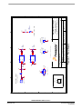
1
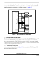
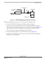
56F8037
Evaluation Module User Manual
56F8000
16-bit Digital Signal Controllers
MC56F8037EVMUM
Rev. 0
09/2006
freescale.com
TABLE OF CONTENTS
Preface 1-vii
Chapter 1
Introduction
1.1
56F8037EVM Architecture. . . . . . . . . . . . . . . . . . . . . . . . . . . . . . . . . . . . . . . . . . . . . . .
1.2
56F8037EVM Connections. . . . . . . . . . . . . . . . . . . . . . . . . . . . . . . . . . . . . . . . . . . . . . .
1.2.1
USB Power Connection. . . . . . . . . . . . . . . . . . . . . . . . . . . . . . . . . . . . . . . . . . . . . . .
1.2.2
External +9.0V DC Power Connection . . . . . . . . . . . . . . . . . . . . . . . . . . . . . . . . . . .
1.2.3
External +3.3V DC Power Connection . . . . . . . . . . . . . . . . . . . . . . . . . . . . . . . . . . .
1-1
1-2
1-2
1-3
1-4
Chapter 2
Technical Summary
2.1
2.2
2.3
2.4
2.5
2.6
2.7
2.7.1
2.7.2
2.7.3
2.8
2.9
56F8037. . . . . . . . . . . . . . . . . . . . . . . . . . . . . . . . . . . . . . . . . . . . . . . . . . . . . . . . . . . . . .
USB Serial Communications . . . . . . . . . . . . . . . . . . . . . . . . . . . . . . . . . . . . . . . . . . . . .
Debug LEDs . . . . . . . . . . . . . . . . . . . . . . . . . . . . . . . . . . . . . . . . . . . . . . . . . . . . . . . . . .
Debug Support . . . . . . . . . . . . . . . . . . . . . . . . . . . . . . . . . . . . . . . . . . . . . . . . . . . . . . . .
External Interrupts. . . . . . . . . . . . . . . . . . . . . . . . . . . . . . . . . . . . . . . . . . . . . . . . . . . . . .
Reset . . . . . . . . . . . . . . . . . . . . . . . . . . . . . . . . . . . . . . . . . . . . . . . . . . . . . . . . . . . . . . . .
Power Supply . . . . . . . . . . . . . . . . . . . . . . . . . . . . . . . . . . . . . . . . . . . . . . . . . . . . . . . . .
USB Power Source . . . . . . . . . . . . . . . . . . . . . . . . . . . . . . . . . . . . . . . . . . . . . . . . . .
External +9V DC Power Source . . . . . . . . . . . . . . . . . . . . . . . . . . . . . . . . . . . . . . . .
Daughter Card Power Source . . . . . . . . . . . . . . . . . . . . . . . . . . . . . . . . . . . . . . . . . .
Daughter Card Connector . . . . . . . . . . . . . . . . . . . . . . . . . . . . . . . . . . . . . . . . . . . . . . . .
Test Points. . . . . . . . . . . . . . . . . . . . . . . . . . . . . . . . . . . . . . . . . . . . . . . . . . . . . . . . . . . .
2-2
2-2
2-3
2-4
2-5
2-5
2-5
2-6
2-6
2-6
2-7
2-8
Appendix A
56F8037EVM Schematics
Appendix B
56F8037EVM
Bill of Material
Table of Contents, Rev. 0
Freescale Semiconductor
Preliminary
i
56F8037EVM User Manual, Rev. 0
ii
Freescale Semiconductor
Preliminary
LIST OF TABLES
2-1
SCI RxD Signal Options . . . . . . . . . . . . . . . . . . . . . . . . . . . . . . . . . . . . . . . . . . . 2-2
2-2
SCI TxD Signal Options . . . . . . . . . . . . . . . . . . . . . . . . . . . . . . . . . . . . . . . . . . . 2-3
2-3
LED Control. . . . . . . . . . . . . . . . . . . . . . . . . . . . . . . . . . . . . . . . . . . . . . . . . . . . . 2-4
2-4
JTAG Connector . . . . . . . . . . . . . . . . . . . . . . . . . . . . . . . . . . . . . . . . . . . . . . . . . 2-4
2-5
Power Source Selector . . . . . . . . . . . . . . . . . . . . . . . . . . . . . . . . . . . . . . . . . . . . . 2-6
2-6
Daughter Card Connector Description. . . . . . . . . . . . . . . . . . . . . . . . . . . . . . . . . 2-7
List of Tables, Rev. 0
Freescale Semiconductor
Preliminary
iii
56F8037EVM User Manual, Rev. 0
iv
Freescale Semiconductor
Preliminary
LIST OF FIGURES
1-1
Block Diagram of the 56F8037EVM . . . . . . . . . . . . . . . . . . . . . . . . . . . . . . . . . . . . 1-2
1-2
56F8037EVM Cabling for USB Power. . . . . . . . . . . . . . . . . . . . . . . . . . . . . . . . . . . 1-3
1-3
56F8037EVM Cabling for External +9V Power. . . . . . . . . . . . . . . . . . . . . . . . . . . . 1-4
1-4
56F8037EVM Cabling for External +3.3V Power . . . . . . . . . . . . . . . . . . . . . . . . . . 1-5
2-1
Diagram of the Debug LED Interface . . . . . . . . . . . . . . . . . . . . . . . . . . . . . . . . . . . . 2-3
2-2
Schematic Diagram of the User Interrupt Interface. . . . . . . . . . . . . . . . . . . . . . . . . . 2-5
List of Figures, Rev. 0
Freescale Semiconductor
Preliminary
v
56F8037EVM User Manual, Rev. 0
vi
Freescale Semiconductor
Preliminary
Preface
This manual describes the hardware on the 56F8037EVM in detail.
Audience
This document is intended for application developers who are creating software for
devices using the Freescale 56F8037 part or a member of the 56F8000 family that is
compatible with this part.
Organization
This manual is organized into two chapters and two appendices.
•
Chapter 1, Introduction, provides an overview of the Evaluation Module and its
features.
•
Chapter 2, Technical Summary, describes the 56F8037EVM hardware in detail.
•
Appendix A, 56F8037EVM Schematics, contains the schematics of the
56F8037EVM.
•
Appendix B, 56F8037EVM Bill of Material, provides a list of the materials used on
the 56F8037EVM.
Suggested Reading
More documentation on the 56F8037EVM and the MC56F8037EVM kit may be found at
URL:
www. freescale.com
Preface, Rev. 0
Freescale Semiconductor
Preliminary
vii
Notation Conventions
This manual uses the following notational conventions:
Term or Value
Symbol
Examples
Active High
Signals
(Logic One)
No special symbol
attached to the
signal name
A0
CLKO
Active Low
Signals
(Logic Zero)
Noted with an
overbar in text and
in most figures
WE
OE
Hexadecimal
Values
Begin with a “$”
symbol
Decimal Values
No special symbol
attached to the
number
Binary Values
Begin with the letter
“b” attached to the
number
b1010
b0011
Numbers
Considered positive
unless specifically
noted as a negative
value
5
-10
Blue Text
Linkable on-line
Bold
Reference sources,
paths, emphasis
Exceptions
In schematic drawings,
Active Low Signals may be
noted by a backslash: /WE
$0FF0
$80
10
34
Voltage is often shown as
positive: +3.3V
...refer to Chapter 7, License
...see:
http://www.freescale.com/
56F8037EVM User Manual, Rev. 0
viii
Freescale Semiconductor
Preliminary
Definitions, Acronyms, and Abbreviations
Definitions, acronyms and abbreviations for terms used in this document are defined below for
reference.
56F8037
Digital signal controller with motor control peripherals
A/D
Analog-to-Digital; a method of converting Analog signals to Digital values
ADC
Analog-to-Digital Converter; a peripheral on the 56F8037 part
D/A
Digital-to-Analog; a method of converting Digital values to Analog signals
DAC
Digital-to-Analog Converter; a peripheral on the 56F8037 part
EOnCE
Enhanced On-Chip Emulation; a debug bus and port which enables a designer
to create a low-cost hardware interface for a professional-quality debug
environment
EVM
Evaluation Module; a hardware platform which allows a customer to evaluate
the silicon and develop his application
GPIO
General Purpose Input and Output port on Freescale’s family of digital signal
controllers; does not share pin functionality with any other peripheral on the
chip and can only be set as an input, an output, or a level-sensitive interrupt
input
IC
Integrated Circuit
JTAG
Joint Test Action Group; a bus protocol/interface used for test and debug
LED
Light Emitting Diode
LQFP
Low-profile Quad Flat Package
OnCETM
On-Chip Emulation, a debug bus and port created to allow a means for low-cost
hardware to provide a professional-quality debug environment
PCB
Printed Circuit Board
PWM
Pulse Width Modulation
SCI
Serial Communications Interface; a peripheral on Freescale’s family of digital
signal controllers
SPI
Serial Peripheral Interface; a peripheral on Freescale’s family of digital signal
controllers
Preface, Rev. 0
Freescale Semiconductor
Preliminary
ix
References
The following sources were referenced to produce this manual:
[1] DSP56800E Reference Manual, DSP56800ERM, Freescale Semiconductor, Inc.
[2] 56F802X and 56F803X Peripheral Reference Manual, MC56F80XXRM,
Freescale Semiconductor, Inc.
[3] 56F8037 Technical Data, MC56F8037, Freescale Semiconductor, Inc.
56F8037EVM User Manual, Rev. 0
x
Freescale Semiconductor
Preliminary
Chapter 1
Introduction
The 56F8037EVM is used to demonstrate the abilities of the 56F8037 digital signal controller
and to provide a hardware tool allowing the development of applications.
The 56F8037EVM is an evaluation module board that includes a 56F8037 part, USB interface,
user LEDs, user pushbutton switches and a daughter card connector. The daughter card
connector allows signal monitoring and expandability of user features.
The 56F8037EVM is designed for the following purposes:
•
Allowing new users to become familiar with the features of the 56800E architecture. The
tools and examples provided with the 56F8037EVM facilitate evaluation of the feature set
and the benefits of the family.
•
Serving as a platform for real-time software development. The tool suite enables the user
to develop and simulate routines, download the software to on-chip memory, run it, and
debug it using a debugger via the JTAG/Enhanced OnCE (EOnCE) port. The breakpoint
features of the EOnCE port enable the user to easily specify complex break conditions and
to execute user-developed software at full speed until the break conditions are satisfied.
The ability to examine and modify all user-accessible registers, memory and peripherals
through the EOnCE port greatly facilitates the task of the developer.
•
Serving as a platform for hardware development. The hardware platform enables the user
to connect external hardware peripherals. The on-board peripherals can be disabled,
providing the user with the ability to reassign any and all of the processor's peripherals.
The EOnCE port's unobtrusive design means that all memory on the board and on the
processor is available to the user.
1.1 56F8037EVM Architecture
The 56F8037EVM facilitates the evaluation of various features present in the 56F8037 part. The
56F8037EVM can be used to develop real-time software and hardware products. The
56F8037EVM provides the features necessary for a user to write and debug software,
Introduction, Rev. 0
Freescale Semiconductor
Preliminary
1-1
demonstrate the functionality of that software and interface with the user's application-specific
device(s). The 56F8037EVM is flexible enough to allow a user to fully exploit the 56F8037's
features to optimize the performance of his product, as shown in Figure 1-1.
56F8037
JTAG/EOnCE
JTAG
Connector
SCI
SCI to USB
Bridge
USB
Type-B
SPI
Timer A
PWM
Daughter Card
Connector
ADCA
ADCB
RESET
Debug LEDs
IRQ Pushbuttons
RESET Pushbutton
+3.3V & GND
+3.3VA & AGND
Power Supply
+3.3V &+3.3VA
Figure 1-1. Block Diagram of the 56F8037EVM
1.2 56F8037EVM Connections
There are several power connection arrangements supported by the 56F8037EVM. Power can be
provided to the 56F8037EVM by using a USB connector, P2, attached to a PC or USB hub.
Power can be provided to the 56F8037EVM by an external +9.0V DC power supply using the
2.1mm power jack, P1, or via the Daughter Card connector, P3. However, the debug interconnect
is always the same using the JTAG connector, J1.
1.2.1 USB Power Connection
An interconnection diagram is shown in Figure 1-2 for connecting the JTAG Debug and USB
between a PC and the 56F8037EVM.
56F8037EVM User Manual, Rev. 0
1-2
Freescale Semiconductor
Preliminary
56F8037EVM Connections
USB A/B Cable
PC-compatible
Computer
56F8037EVM
USB-TAP
Connect cable
to USB port
USB A/B cable
J1
P2
Connect cable to USB port
Figure 1-2. 56F8037EVM Cabling for USB Power
Perform the following steps for USB power connection:
1. Connect the USB-TAP’s USB cable to a USB port on the host computer.
2. Connect the other end of the USB-TAP cable to the USB-TAP module. Connect the
ribbon cable from the USB-TAP module to J1 on the 56F8037EVM, shown in Figure 1-2.
This provides the connection which allows the host computer to control the debug
functions on the 56F8037EVM board.
3. Connect the second USB cable to another USB port on the host computer or a USB hub.
4. Connect the other end of the second USB cable to the USB connector, P2, on the
56F8037EVM board, shown in Figure 1-2. The green Power-ON LED, LED7, will
illuminate when power is correctly applied.
1.2.2 External +9.0V DC Power Connection
An interconnection diagram is shown in Figure 1-3 for connecting the PC and a user-supplied
external +9.0V DC power supply to the 56F8037EVM.
Introduction, Rev. 0
Freescale Semiconductor
Preliminary
1-3
USB A/B Cable
56F8037EVM
PC-compatible
Computer
USB-TAP
J1
P1
Connect cable
to USB port
External with 2.1mm,
+9V
receptacle
Power connector
Figure 1-3. 56F8037EVM Cabling for External +9V Power
Perform the following steps for +9.0V DC power connection:
1. Connect the USB-TAP’s USB cable to a USB port on the host computer.
2. Connect the other end of the USB-TAP cable to the USB-TAP module. Connect the
ribbon cable from the USB-TAP module to J1 on the 56F8037EVM, shown in Figure 1-3.
This provides the connection which allows the host computer to control the board.
3. Make sure that the external +9V DC, 450mA power supply is not plugged into any AC
power source.
4. Connect the 2.1mm output power plug from the external power supply into P1 on the
56F8037EVM, shown in Figure 1-3.
5. Apply power to the external power supply. The green Power-ON LED, LED7, will
illuminate when po wer is correctly applied.
1.2.3 External +3.3V DC Power Connection
An interconnection diagram is shown in Figure 1-4 for connecting the PC and a user-supplied
Daughter Card providing +3.3V DC to the 56F8037EVM.
56F8037EVM User Manual, Rev. 0
1-4
Freescale Semiconductor
Preliminary
56F8037EVM Connections
USB A/B Cable
PC-compatible
Computer
56F8037EVM
USB-TAP
J1
P3
Daughter Card
Figure 1-4. 56F8037EVM Cabling for External +3.3V Power
Perform the following steps to provide +3.3V DC power from a Daughter Card:
1. Connect the USB-TAP’s USB cable to a USB port on the host computer.
2. Connect the other end of the USB-TAP cable to the USB-TAP module. Connect the
ribbon cable from the USB-TAP module to J1 on the 56F8037EVM, shown in Figure 1-4.
This provides the connection which allows the host computer to control the board.
3. Make sure the power supply on the Daughter Card is turned OFF.
4. Connect the Daughter Card to P3 on the 56F8037EVM, shown in Figure 1-4.
5. Apply power to the Daughter Card. The green Power-ON LED, LED7, will illuminate
when power is correctly applied.
Introduction, Rev. 0
Freescale Semiconductor
Preliminary
1-5
56F8037EVM User Manual, Rev. 0
1-6
Freescale Semiconductor
Preliminary
Chapter 2
Technical Summary
The 56F8037EVM is designed as a versatile development card using the 56F8037 processor,
allowing the creation of real-time software and hardware products to support a new generation of
applications in servo and motor control, digital and wireless messaging, digital answering
machines, feature phones, modems, and digital cameras. The power of the 16-bit 56F8037
processor, combined with the on-board USB interface and daughter card connector, makes the
56F8037EVM ideal for developing and implementing many motor control algorithms, as well as
for learning the architecture and instruction set of the 56F8037 processor.
The main features of the 56F8037EVM, with board and schematic reference designators, include:
•
56F8037, a 16-bit +3.3V digital signal controller operating at 60MHz [U1]
•
Joint Test Action Group (JTAG) port interface connector, for an external debug Host
Target Interface [J1]
•
USB interface, for easy connection to a host processor [U2 and P2]
•
Daughter Card connector, to allow the user to connect his own PWM, ADC, DAC, SCI,
SPI or GPIO-compatible peripheral to the digital signal controller [P3]
•
On-board power regulation provided from an external +9V DC-supplied power input [P1]
•
Light Emitting Diode (LED) power indicator [LED7]
•
Six on-board real-time user debugging LEDs [LED1-6]
•
Manual RESET pushbutton [S1]
•
Manual interrupt #1 pushbutton [S2]
•
Manual interrupt #2 pushbutton [S3]
Technical Summary, Rev. 0
Freescale Semiconductor
Preliminary
2-1
2.1 56F8037
The 56F8037EVM uses a Freescale 56F8037 part, designated as U1 on the board and in the
schematics. This part will operate at a maximum external bus speed of 60MHz. A full description
of the 56F8037, including functionality and user information, is provided in these documents:
•
56F8037 Technical Data Sheet, (MC56F8037): Electrical and timing specifications, pin
descriptions, device specific peripheral information and package descriptions
•
56F802X and 56F803X Peripheral Reference Manual, (MC56F80XXRM): Detailed
description of peripherals of the 56F802x and 56F803x devices
•
DSP56800E Reference Manual, (DSP56800ERM): Detailed description of the 56800E
family architecture, 16-bit core processor, and the instruction set
Refer to these documents for detailed information about chip functionality and operation. They
can be found on this URL:
www.freescale.com
2.2 USB Serial Communications
The 56F8037EVM provides an RS-232 to USB bridge interface by the use of an USB bridge part,
Silicon Labs CP2102, designated as U2. Refer to the USB schematic details in Appendix A. The
USB bridge handles all the USB 2.0 protocol interactions and transitions the SCI port’s +3.3V
signal levels to USB-compatible signal levels and connects to the host’s USB port via connector
P2. The SCI ports signals, GPIOB6 and GPIOB7, or GPIOC12 and GPIOC8, can be
disconnected from the USB bridge by pulling the jumpers at JG3, RxD, and JG4, TxD, on the
board. The jumper options available on JG3 and JG4 for the SCI port are shown in Table 2-1 and
Table 2-2.
Table 2-1. SCI RxD Signal Options
JG3
Pin #
Signal
Description
1
GPIO Port B, Bit 6
RXD0
2
RxD
From CP2102
3
GPIO Port C, Bit 12
RXD1
56F8037EVM User Manual, Rev. 0
2-2
Freescale Semiconductor
Preliminary
Debug LEDs
Table 2-2. SCI TxD Signal Options
.
JG4
Pin #
Signal
Description
1
GPIO Port B, Bit 7
TXD0
2
TxD
To CP2102
3
GPIO Port C, Bit 8
TXD1
2.3 Debug LEDs
Six on-board Light-Emitting Diodes, (LEDs), are provided to allow real-time debugging for user
programs. These LEDs will allow the programmer to monitor program execution without having
to stop the program during debugging; refer to Figure 2-1. Table 2-3 describes the control of
each LED.
Setting GPIOA0, GPIOA1, GPIOA2, GPIOA3, GPIOA4, or GPIOA5 to a Logic One value will
turn on the associated LED.
56F8037
INVERTING BUFFER
+3.3V
RED LED
GPIOA0
YELLOW LED
GPIOA1
GREEN LED
GPIOA2
RED LED
GPIOA3
YELLOW LED
GPIOA4
GREEN LED
GPIOA5
Figure 2-1. Diagram of the Debug LED Interface
Technical Summary, Rev. 0
Freescale Semiconductor
Preliminary
2-3
Table 2-3. LED Control
Controlled by
User LED
Color
Signal
LED1
RED
GPIO Port A, Bit 0
LED2
YELLOW
GPIO Port A, Bit 1
LED3
GREEN
GPIO Port A, Bit 2
LED4
RED
GPIO Port A, Bit 3
LED5
YELLOW
GPIO Port A, Bit 4
LED6
GREEN
GPIO Port A, Bit 5
2.4 Debug Support
A JTAG connector, J1, on the 56F8037EVM allows the connection of an external Host Target
Interface for downloading programs and working with the 56F8037’s registers. This connector is
used to communicate with an external Host Target Interface, which passes information and data
back and forth with a host processor running a debugger program. Table 2-4 shows the pin-out
for this connector.
Table 2-4. JTAG Connector
J1
Pin #
Signal
Pin #
Description
1
TDI
2
GND
3
TDO
4
GND
5
TCK
6
GND
7
N/C
8
KEY
9
RESET
10
TMS
11
+3.3V DC
12
N/C
13
N/C
14
N/C
56F8037EVM User Manual, Rev. 0
2-4
Freescale Semiconductor
Preliminary
Power Supply
2.5 External Interrupts
Two on-board pushbutton switches are provided for external interrupt generation, as shown in
Figure 2-2. S2 allows the user to generate a hardware interrupt, IRQ #1, using GPIO Port B,
Bit 2. S3 allows the user to generate a hardware interrupt, IRQ #2, using GPIO Port B, Bit 3.
These two switches allow the user to generate interrupts for their user-specific programs.
Alternately, the user can use GPIO Port B, Bit 4, for IRQ #1. To accomplish this, remove the
jumper at JP5, pins 1 and 2, and place the jumper between JP5 pins 2 and 3. Also, the user can
use GPIO Port B, Bit 5, for IRQ #2. To accomplish this, remove the jumper at JP6, pins 1 and 2,
and place the jumper between JP6 pins 2 and 3.
+3.3V
56F8037
S2
4.7K
1
JG5
2
3
GPIOB2
GPIOB4
+3.3V
S3
4.7K
1
JG6
2
3
GPIOB3
GPIOB5
Figure 2-2. Schematic Diagram of the User Interrupt Interface
2.6 Reset
Logic is provided on the 56F8037 to generate an internal Power-On RESET. Additional reset
logic is provided to support the RESET signal from the JTAG connector and the user RESET
pushbutton, S1; refer to the schematics in Appendix A.
2.7 Power Supply
The 56F8037EVM supports the option of power being provided from three different sources.
Since only one power supply source can be active at one time, the selection of the active power
supply source is made by the jumper group formed by JG1 and JG2. Table 2-5 depicts the
jumper options for selecting each power supply source. Jumpering JG2, pins 2 and 3, the default
selection, selects the USB power supply source. Jumpering JG2, pins 1 and 2, selects the external
power supply source. Jumpering JG1 to JG2, pin 2, uses the Daughter Card power source.
Technical Summary, Rev. 0
Freescale Semiconductor
Preliminary
2-5
Table 2-5. Power Source Selector
JG1
Pin #
1
JG2
Description
Pin #
Description
1
External Power Supply Source
2
Power to 56F8037EVM
3
USB Power Supply Source
Daughter Card Source
2.7.1 USB Power Source
The main power source for the 56F8037EVM is through the USB connector, P2. This +5.0V
USB bus input power goes to the USB bridge device which creates a regulated +3.3V output
voltage. The USB bus power input is restricted to 450mA maximum for a high power device.
However, the USB bridge regulator output is limited to 350mA. This +3.3V DC voltage
regulation is used by the 56F8037 processor, ADC, LEDs, JTAG interface and supporting logic;
refer to schematics in Appendix A. When power is applied to the 56F8037EVM board, the
Power-ON LED, referenced as LED7, will illuminate.
2.7.2 External +9V DC Power Source
The optional external +9V DC power input to the 56F8037EVM is through the 2.1mm coax
power jack, P1. This input power passes through a reverse power-blocking diode to provide a DC
supply input for the +3.3V voltage regulator, U4, and the +5.0V voltage regulator, U5. A 450mA
external power supply is sufficient to power the 56F8037EVM. However, less than 300mA is
required by the 56F8037EVM board. The remaining current is available for custom control
applications when connected to the Daughter Card connector. The 56F8037EVM provides
+5.0V DC regulation for the CAN transceiver and, +3.3V DC voltage regulation for the
processor, ADC, JTAG interface and supporting logic; refer to schematics in Appendix A. When
power is applied to the 56F8037EVM board, the Power-ON LED, referenced as LED7, will
illuminate.
2.7.3 Daughter Card Power Source
The optional Daughter Card power input to the 56F8037EVM is through the Daughter Card
connector, P3. Regulated +3.3V voltage is provided on P3, pin 1. The Daughter Card power
supply ground reference is provided on P3, pin 3. At least 300mA should be provided to power
the 56F8037EVM board. This input +3.3V DC voltage will power the processor, ADC, DAC,
LEDs, JTAG interface and supporting logic; refer to schematics in Appendix A. When power is
applied to the 56F8037EVM board, the Power-ON LED, referenced as LED7, will illumate.
56F8037EVM User Manual, Rev. 0
2-6
Freescale Semiconductor
Preliminary
Daughter Card Connector
2.8 Daughter Card Connector
The 56F8037EVM contains a Daughter Card connector, P3, which contains the processor’s
peripheral port signals. The daughter card connector is used to connect a Daughter Card or a
user-specific Daughter Card to the processor’s peripheral port signals. The Daughter Card
connector is a 60-pin 0.1” pitch connector with signals for RESET, SPI, SCI, PWM, ADC, DAC
and GPIO ports. Table 2-6 shows the Daughter Card connector’s signal-to-pin assignments.
Table 2-6. Daughter Card Connector Description
P3
Pin #
Signal
Pin #
Signal
1
+3.3V
2
GPIOA10 / CINA2 / TB2
3
GND
4
GPIOA7 / RESET / VPP
5
GPIOB7 / TXD0 / SCL
6
GPIOD4 / EXTAL
7
GPIOB6 / RXD0 / SDA / CLKIN
8
GPIOD5 / XTAL / CLKIN
9
GPIOA0 / PWM0
10
GPIOC0 / ANA0 / CINA3
11
GPIOA1 / PWM1
12
GPIOC1 / ANA1
13
GPIOB4 / TA0 / CLKO / SS1 /
TB0 / SCR2
14
GPIOC2 / ANA2 / VREFH
15
GPIOB5 / TA1 / FAULT3 / CLKIN
16
GPIOC3 / ANA3 / VREFL
17
GPIOB3 / MOSI0 / T3 / PSRC1
18
GPIOC4 / ANB0 / CINB3
19
GPIOB2 / MISO0 / TA2 / PSRC0
20
GPIOC5 / ANB1
21
GPIOB0 / SCLK0 / SCL
22
GPIOC6 / ANB2 / VREFH
23
GPIOB1 / SS0 / SDA
24
GPIOC7 / ANB3 / VREFL
25
GPIOD0 / TDI
26
GPIOB1 / SS0 / SDA
27
GPIOD1 / TDO
28
GPIOB0 / SCLK0 / SCL
29
GPIOD2 / TCK
30
GPIOA2 / PWM2
31
GPIOD3 / TMS
32
GPIOA3 / PWM3
33
GPIOA6 / FAULT0 / TA0
34
GPIOA4 / PWM4
35
GPIOA11 / CINB2 / TB3
36
GPIOA5 / PWM5
37
GPIOA12 / TB1 / SCLK1 / TA1
38
CINA1 / FAULT1 / TA2
39
GPIOA13 / TB2 / MISO1 / TA2
40
FAULT2 / TA3 / CINB1
Technical Summary, Rev. 0
Freescale Semiconductor
Preliminary
2-7
Table 2-6. Daughter Card Connector Description (Continued)
P3
Pin #
Signal
Pin #
Signal
41
GPIOA14 / TB3 / MOSI1 / TA3
42
N/C
43
GPIOB8 / SCL / CANTX
44
GPIOC8 / ANA4 / TXD1
45
GPIOB9 / SDA / CANRX
46
GPIOC9 / ANA5
47
GPIOB10 / COUTA / TB0
48
GPIOC10 / ANA6
49
GPIOB11 / COUTB / TB1
50
GPIOC11 / ANA7
51
GPIOB12 / CANTX
52
GPIOC12 / ANB4 / RXD1
53
GPIOB13 / CANRX
54
GPIOC13 / ANB5
55
N/C
56
GPIOC14 / ANB6
57
GPIOD6 / DAC0
58
GPIOC15 / ANB7
59
GPIOD7 / DAC1
60
GNDA
2.9 Test Points
The 56F8037EVM board has two test points:
•
+3.3V, TP1
•
Digital Ground (GND), TP2
56F8037EVM User Manual, Rev. 0
2-8
Freescale Semiconductor
Preliminary
Appendix A
56F8037EVM Schematics
56F8037EVM Schematics, Rev. 0
Freescale Semiconductor
Preliminary
Appendix A-1
56F8037EVM User Manual, Rev. 0
Appendix A-2
Freescale Semiconductor
Preliminary
1
2
3
4
A
+3.3V
C1
22uF
+3.3V
TCK
TDO
TDI
13
11
9
7
5
3
1
J1
14
12
10
8
6
4
2
8
27
40
51
16
17
GPIOA0/PWM0
GPIOA1/PWM1
GPIOA2/PWM2
GPIOA3/PWM3
GPIOA4/PWM4/FAULT1/TA2
GPIOA5/PWM5/FAULT2/TA3
GPIOA6/FAULT0/TA0
RESET/GPIOA7/VPP
GPIOA8/CINA1/FAULT1/TA2
GPIOA9/FAULT2/TA3/CINB1
GPIOA10/CINA2/TB2
GPIOA11/CINB2/TB3
GPIOA12/TB1/SCLK1/TA1
GPIOA13/TB2/MISO1/TA2
GPIOA14/TB3/MOSI1/TA3
B
KEY
TMS
R11
4.7K
+3.3V
B
A
Size
Title
MC56F8037EVM.DSN
C
Date: Monday, March 27, 2006
Document
Number
+
+3.3V
C18
22pF
DNP
8.00MHz
DNP
Y1
C7
2.2uF
VCAP1
C8
2.2uF
VCAP2
D
GNDA
Place close to
VDDA and VSSA
on U1
GPIOD5
C14
0.1uF
VDDA
C19
22pF
DNP
DNP
1
2
JG10
E
1
E
of
7
FAX: (512) 895-8701
Sheet
(512) 895-7215
6501 William Cannon Drive West
Austin, Texas 78735
Microcontroller Division
C6
2.2uF
Ferrite Bead
L2
XTAL
1M DNP
R30
Ferrite Bead
L1
EXTAL
Designer: MCD Design
GND
D
External Crystal Option
DNP
1
2
JG9
C2
22uF
GPIOD4
Freescale Semiconductor
GPIOC0
GPIOC1
GPIOC2
GPIOC3
GPIOC4
GPIOC5
GPIOC6
GPIOC7
GPIOC8
GPIOC9
GPIOC10
GPIOC11
GPIOC12
GPIOC13
GPIOC14
GPIOC15
GPIOB0
GPIOB1
GPIOB2
GPIOB3
GPIOB4
GPIOB5
GPIOB6
GPIOB7
GPIOB8
GPIOB9
GPIOB10
GPIOB11
GPIOB12
GPIOB13
GPIOA0
GPIOA1
GPIOA2
GPIOA3
GPIOA4
GPIOA5
GPIOA6
/RESET
GPIOA8
GPIOA9
GPIOA10
GPIOA11
GPIOA12
GPIOA13
GPIOA14
MC56F8037 Processor
24
22
20
19
10
11
13
14
26
21
23
25
9
12
62
61
42
2
33
32
38
4
1
3
54
46
30
60
57
58
56
55
47
48
43
39
34
31
36
5
35
6
37
44
45
C
Figure A-1. MC56F8037 Processor
MC56F8037FGE
GPIOB0/SCLK0/SCL
GPIOB1/SS0/SDA
GPIOB2/MISO0/TA2/PSRC0
GPIOB3/MOSI0/TA3/PSRC1
GPIOB4/TA0/CLKO/SS1/TB0/PSCR2
GPIOB5/TA1/FAULT3/CLKIN
GPIOB6/RXD0/SDA/CLKIN
GPIOB7/TXD0/SCL
GPIOB8/SCL/CANTX
TDI/GPIOD0
TDO/GPIOD1
GPIOB9/SDA/CANRX
GPIOB10/COUTA/TB0
TCK/GPIOD2
GPIOB11/COUTB/TB1
TMS/GPIOD3
GPIOB12/CANTX
GPIOD4/EXTAL
GPIOD5/EXTAL/CLKIN GPIOB13/CANRX
GPIOD6/DAC0
GPIOD7/DAC1
GPIOC0/ANA0/CINA3
GPIOC1/ANA1
GPIOC2/ANA2/VREFH
VCAP1
GPIOC3/ANA3/VREFL
VCAP2
GPIOC4/ANB0/CINB3
GPIOC5/ANB1
VDDA
GPIOC6/ANB2/VREFH
VSSA
GPIOC7/ANB3/VREFL
GPIOC8/ANA4/TXD1
GPIOC9/ANA5
GPIOC10/ANA6
GPIOC11/ANA7
VSS_IO1
GPIOC12/ANB4/RXD1
VSS_IO2
GPIOC13/ANB5
VSS_IO3
GPIOC14/ANB6
VSS_IO4
GPIOC15/ANB7
VDD_IO3
VDD_IO2
VDD_IO1
U1
JTAG Connector
/RESET
59
64
29
63
53
52
18
15
50
41
7
VCAP1 28
VCAP2 49
C13
0.1uF
C12
0.1uF
C11
0.1uF
GNDA
VDDA
TDI
TDO
TCK
TMS
GPIOD4
GPIOD5
GPIOD6
GPIOD7
+
+3.3V
+3.3V
A
1.0
Rev.
1
2
3
4
56F8037EVM Schematics, Rev. 0
Freescale Semiconductor
Preliminary
Appendix A-3
1
2
3
4
A
A
R10
4.7K
+3.3V
/IRQ2
R9
4.7K
+3.3V
/IRQ1
R8
4.7K
B
A
Size
9
11
13
5
3
U3D
U3E
U3F
U3C
U3B
U3A
Freescale Semiconductor
GPIOA5
GPIOA4
GPIOA3
GPIOA2
GPIOA1
GPIOA0
1
74AC04
8
74AC04
10
74AC04
12
74AC04
6
74AC04
4
74AC04
2
MC56F8037EVM.DSN
C
Date: Monday, March 27, 2006
Document
Number
PWMA1
PWMA0
PWMA4
PWMA3
PWMA2
GREEN LED
LED6
D
270
R6
270
R5
270
R4
270
R3
270
R2
270
R1
VCC
+3.3V
E
2
E
of
7
FAX: (512) 895-8701
Sheet
(512) 895-7215
6501 William Cannon Drive West
Austin, Texas 78735
Microcontroller Division
PWMA5
YELLOW LED
LED5
RED LED
LED4
GREEN LED
LED3
YELLOW LED
LED2
RED LED
LED1
D
Designer: MCD Design
Interrupt and Reset Switches & PWM LEDs
GPIOB5
GPIOB3
GPIOB4
GPIOB2
Title
/RESET
IRQ #2
Selector
1
2
3
JG6
IRQ #1
Selector
1
2
3
JG5
C
Figure A-2. Interrupt and Reset Switches and PWM LEDs
S1
RESET
PUSHBUTTON
S3
IRQ #2
PUSHBUTTON
S2
IRQ #1
PUSHBUTTON
+3.3V
B
1.0
Rev.
1
2
3
4
56F8037EVM User Manual, Rev. 0
1
2
3
A
Vusb
1
DLP05LC
3
2
4.7K
R33
4.7K
R32
TXD
RXD
GPIOC8
GPIOB7
GPIOC12
GPIOB6
TXD1
TXD0
RXD1
RXD0
1
2
3
JG4
1
2
3
JG3
B
Vusb
SCI Port
Selectors
B
BYPASS
CP2102
3
6
7
8
4
5
C9
2.2uF
+5.0V
GND
VDD
REGIN
VBUS
D+
D-
C
Date: Tuesday, May 16, 2006
Document
Number
+5.0V
C16
0.1uF
D+
D-
D
D
D-
P2
GND
Shield1
Shield2
VBUS
D+
D-
D3
DLP05LC
D+
USB TYPE-B
CONNECTOR
4
5
6
1
3
2
E
3
E
of
7
FAX: (512) 895-8701
Sheet
(512) 895-7215
6501 William Cannon Drive West
Austin, Texas 78735
Microcontroller Division
D2
DLP05LC
Designer: MCD Design
Vusb
MC56F8037EVM.DSN
Freescale Semiconductor
RST
SUSPEND
SUSPEND
RI
DCD
DTR
DSR
RTS
CTS
RXD
USB Interface
Vusb
U2
TXD
Figure A-3. USB Interface
A
Size
Title
12
11
/RST 9
C15
0.1uF
4.7K
R31
25
TXD
2
1
28
27
24
23
26
RXD
C
3
1
4
A
3
1
Appendix A-4
Freescale Semiconductor
Preliminary
1.0
Rev.
1
2
3
4
56F8037EVM Schematics, Rev. 0
Freescale Semiconductor
Preliminary
Appendix A-5
1
2
3
4
A
A
GPIOB13
GPIOB9
GPIOB12
GPIOB8
B
CAN_RX
CAN_TX
A
Size
Title
U6
GND
CANH
CANL
VCC
VREF
Vcan
2
7
6
3
5
CANH
CANL
Freescale Semiconductor
C17
0.1uF
PCA82C250TD
SLOPE
TXD
RXD
C10
2.2uF
8
1
4
Vcan
MC56F8037EVM.DSN
C
Date: Monday, March 27, 2006
Document
Number
CAN Interface and Power Supplies
R28
1K
Vcan
C
2
4
6
8
10
120 1/4W
R29
D
2
E
E
4 of
7
FAX: (512) 895-8701
Sheet
(512) 895-7215
6501 William Cannon Drive West
Austin, Texas 78735
Microcontroller Division
CAN BUS
TERMINATION
1
JG11
CAN BUS
CONNECTOR
1
3
5
7
9
J2
Designer: MCD Design
D
Figure A-4. CAN Interface and Power Supplies
1
2
3
JG8
1
2
3
JG7
B
1.0
Rev.
1
2
3
4
56F8037EVM User Manual, Rev. 0
Appendix A-6
Freescale Semiconductor
Preliminary
1
2
3
4
C23
0.0022uF
C22
0.0022uF
C21
0.0022uF
C20
0.0022uF
A
GPIOC3
GPIOC2
GPIOC1
GPIOC0
A
R12
100
R15
100
R14
100
R13
100
ANA3
ANA2
ANA1
ANA0
A
Size
Title
C27
0.0022uF
C26
0.0022uF
C25
0.0022uF
C24
0.0022uF
R16
GPIOC7
GPIOC6
GPIOC5
GPIOC4
C31
0.0022uF
C30
0.0022uF
C29
0.0022uF
C28
0.0022uF
Freescale Semiconductor
ANA7
ANA6
ANA5
ANA4
R20
100
R23
100
R22
100
R21
100
MC56F8037EVM.DSN
C
Date: Monday, March 27, 2006
Document
Number
ADC Channel A & B Input Filters
100
R19
100
R18
100
R17
100
C
D
C35
0.0022uF
C34
0.0022uF
C33
0.0022uF
C32
0.0022uF
R24
100
R27
100
R26
100
R25
100
E
ANB7
ANB6
ANB5
ANB4
E
5 of
7
FAX: (512) 895-8701
Sheet
(512) 895-7215
6501 William Cannon Drive West
Austin, Texas 78735
Microcontroller Division
GPIOC15
GPIOC14
GPIOC13
GPIOC12
Designer: MCD Design
ANB3
ANB2
ANB1
ANB0
D
Figure A-5. ADC Channel A and B Input Filters
B
GPIOC11
GPIOC10
GPIOC9
GPIOC8
B
1.0
Rev.
1
2
3
4
56F8037EVM Schematics, Rev. 0
Freescale Semiconductor
Preliminary
Appendix A-7
1
2
3
4
GPIOD6
GPIOD7
A
A
DAC0
DAC1
1
3
J3
2
4
GNDA
GPIOD6
GPIOD7
GPIOB7
GPIOB6
GPIOA0
GPIOA1
GPIOB4
GPIOB5
GPIOB3
GPIOB2
GPIOB0
GPIOB1
TDI
TDO
TCK
TMS
GPIOA6
GPIOA11
GPIOA12
GPIOA13
GPIOA14
GPIOB8
GPIOB9
GPIOB10
GPIOB11
GPIOB12
GPIOB13
GND
Vio
B
DAC0
DAC1
P3
1
3
5
7
9
11
13
15
17
19
21
23
25
27
29
31
33
35
37
39
41
43
45
47
49
51
53
55
57
59
2
4
6
8
10
12
14
16
18
20
22
24
26
28
30
32
34
36
38
40
42
44
46
48
50
52
54
56
58
60
GPIOC8/TXD1
GPIOC9
GPIOC10
GPIOC11
GPIOC12/RXD1
GPIOC13
GPIOC14
GPIOC15
GNDA
Document
Number
Size
MC56F8037EVM.DSN
Figure A-6. I/O Connector
C
Date: Monday, March 27, 2006
I/O Connector
Title
A
ANA4
ANA5
ANA6
ANA7
ANB4
ANB5
ANB6
ANB7
GPIOA10
/RESET
GPIOD4
GPIOD5
ANA0
ANA1
ANA2
ANA3
ANB0
ANB1
ANB2
ANB3
GPIOB1
GPIOB0
GPIOA2
GPIOA3
GPIOA4
GPIOA5
GPIOA8
GPIOA9
Freescale Semiconductor
GNDA
(LOCATED ON BOTTOM OF BOARD)
GND
C
CINA2/TB2
GPIOA7/VPP
EXTAL
XTAL/CLKIN
GPIOC0/CINA3
GPIOC1
GPIOC2/VREFH
GPIOC3/VREFL
GPIOC4/CINB3
GPIOC5
GPIOC6/VREFH
GPIOC7/VREFL
SS0/SDA
SCLK0/SCL
PWM2
PWM3
PWM4
PWM5
CINA1/FAULT1/TA2
FAULT2/TA3/CINB1
I/O SIGNAL SOCKET
TXD0/SCL
RXD0/SDA/CLKIN
PWM0
PWM1
TA0/CLKO/SS1/TB0/SCR2
TA1/FALT3/CLKIN
MOSI0/TA3/PSRC1
MISO0/TA2/PSRC0
SCLK0/SCL
SS0/SDA
GPIOD0
GPIOD1
GPIOD2
GPIOD3
FAULT0/TA0
CINB2/TB3
TB1/SCLK1/TA1
TB2/MISO1/TA2
TB3/MOSI1/TA3
SCL/CANTX
SDA/CANRX
COUTA/TB0
COUTB/TB1
CANTX
CANRX
B
D
E
E
6 of
7
FAX: (512) 895-8701
Sheet
(512) 895-7215
6501 William Cannon Drive West
Austin, Texas 78735
Microcontroller Division
Designer: MCD Design
D
1.0
Rev.
1
2
3
4
56F8037EVM User Manual, Rev. 0
1
2
3
A
1
2
3
1
4
2
3
LM1117
LD1117
2.1mm
Power Jack
P1
1
JG2
3
+3.3V
JG1
Vio
+
+9V
B
Vusb
VOUT
VOUT
VOUT
VOUT
+
Vcan
+
C4
22uF
6.3VDC
C3
22uF
6.3VDC
+3.3V
DNP
TP1
+3.3V
TEST POINT
4
2
4
2
Vreg
Freescale Semiconductor
LD1117S50CTR
GND
VIN
U5
LM1117MPX-3.3
GND
VIN
C
D
D
LED7
GREEN LED
R7
270
+3.3V
E
E
7 of
7
FAX: (512) 895-8701
Sheet
(512) 895-7215
6501 William Cannon Drive West
Austin, Texas 78735
Microcontroller Division
POWER GOOD LED
Designer: MCD Design
DNP
TP2
GROUND
TEST POINT
MC56F8037EVM.DSN
Date: Monday, March 27, 2006
Document
Number
POWER SUPPLY
1
3
1
3
U4
C
Figure A-7. Power Supply
A
Size
Title
+9V
C5
22uF
16VDC
USB
Power Selector
REG
Vreg
I/O
FM4001
D1
1
2
EXTERNAL POWER
9VDC INPUT
B
1
4
A
1
Appendix A-8
Freescale Semiconductor
Preliminary
1.0
Rev.
1
2
3
4
Appendix B
56F8037EVM
Bill of Material
Qty
Description
Ref. Designators
Vendor Part #
Integrated Circuits
1
MC56F8037
U1
Freescale, MC56F8037VFBE
1
SCI to USB Bridge
U2
Silicon Lab, CP2102-GM
1
74AC04
U3
ON Semiconductor, MC74AC04DG
1
+3.3V Voltage Regulator
U4
National Semiconductor, LM1117MPX-3.3/NOPB
1
+5.0V Voltage Regulator
U5
STMicroelectronics, LD1117S50CTR
1
CAN Transceiver
U6
Philips Semiconductor, PCA82C250TD
Resistors
7
270 Ω, 0603
R1—R7
SMEC, RC73L2X271JTF
7
4.7 KΩ, 0603
R8-R11, R31-R33
SMEC, RC73L2X472JTF
16
100 Ω, 0603
R12—R27
SMEC, RC73L2X101JTF
1
1K Ω, 0603
R28
SMEC, RC73L2X102JTF
1
120 Ω, 1/4W
R29
YAGEO, CFR-25JB-120R
0
1.0M Ω, 0603
R30 (Optional)
SMEC, RC73L2X105JTF
Inductors
2
Ferrite Bead, 0603
L1—L2
SMEC, FCB0603-1000HNTF
LEDs
2
Red LED, 0805
LED1, LED4
Lite-ON, LTST-C171CKT
2
Yellow LED, 0805
LED2, LED5
Lite-ON, LTST-C171YKT
3
Green LED, 0805
LED3, LED6, LED7
Lite-ON, LTST-C171GKT
56F8037EVM Bill of Material, Rev. 0
Freescale Semiconductor
Preliminary
Appendix B-1
Qty
Description
Ref. Designators
Vendor Part #
Diode
1
1N4003, SMA
D1
ON Semiconductor, MRA4003T3G
2
TVS, SOT-23
D2, D3
Diodes Electronics, DLP05LC-7-F
Capacitors
4
22µF, +6.3V DC, EIA-A
C1—C4
SMEC, ESR900-22K6.3AF
1
22µF, +16V DC, EIA-B
C5
SMEC, ESR600-22K16BF
5
2.2µF, 0805
C6—C10
SMEC, MCCB225M2NRTF
7
0.1µF, 0603
C11—C17
SMEC, MCCA104K1NRTF
2
22pF, 0603
C18 , C19 (Optional)
SMEC, MCCA220K1NRTF
16
0.0022µF, 0603
C20—C35
SMEC, MCCA222K1NRTF
Test Points
0
+3.3V Test Point
TP1 (Optional)
KEYSTONE, 5000, RED
0
GND Test Point
TP2 (Optional)
KEYSTONE, 5001, BLACK
Connectors
1
2.1mm Power Jack
P1
CUI, PJ-102A
1
USB Type-B Connector
P2
MOLEX, 67068-8000
1
Daughter Card
Connector
P3
SAMTEC, SSM-130-L-DV-LC
1
1x1 Header
JG1
SAMTEC, TSW-101-07-G-S
7
3x1 Header
JG2—JG8
SAMTEC, TSW-103-07-G-S
2
2x1 Header
JG9, JG10 (Optional)
SAMTEC, TSW-102-07-G-S
1
2x1 Header
JG11
SAMTEC, TSW-102-07-G-S
1
7x2 JTAG Header
J1
SAMTEC, TSW-107-07-G-D
1
5x2 Header
J2
SAMTEC, TSW-105-07-G-D
1
2x2 Header
J3
SAMTEC, TSW-102-07-G-D
Switches
3
SPST Pushbutton
S1—S3
OMRON,B3F-1022
56F8037EVM User Manual, Rev. 0
Appendix B-2
Freescale Semiconductor
Preliminary
Qty
Description
Ref. Designators
Vendor Part #
Crystals
1
8.000MHz Crystal
Y1 (Optional)
CITIZEN CRYSTAL, HCM49-8.000MABJ-UT
Miscellaneous
2
Rubber Feet, 0.4”
3M, SJ-5007 (BLACK)
8
0.1” Shunt Jumpers
SULLINS, SPC02SYAN
56F8037EVM Bill of Material, Rev. 0
Freescale Semiconductor
Preliminary
Appendix B-3
56F8037EVM User Manual, Rev. 0
Appendix B-4
Freescale Semiconductor
Preliminary
INDEX
Numerics
J
450mA power supply 6
56F8000 Peripheral Reference Manual x, 2
56F8013 ix
56F8013 Technical Data x
56F8013 Technical Data Sheet 2
Joint Test Action Group
JTAG ix
JTAG ix
JTAG/Enhanced OnCE (EOnCE) 1
A
A/D ix
ADC ix
Analog-to-Digital
A/D ix
Analog-to-Digital Converter
ADC ix
D
Daughter Card Expansion
interface 1
Debugging 3
Demo Board ix
Demonstration Board
Demo Board ix
Digital Signal Controller
DSC ix
DSC ix
DSP56800E Reference Manual x, 2
E
Enhanced On-Chip Emulation
EOnCE ix
EOnCE ix
G
General Purpose Input and Output
GPIO ix
GPIO ix
I
IC ix
Integrated Circuit
IC ix
L
LED ix
Light Emitting Diode
LED ix
Low-profile Quad Flat Package
LQFP ix
LQFP ix
O
On-board power regulation 1
OnCE ix
On-Chip Emulation
OnCE ix
P
PCB ix
peripheral port signals 7
Printed Circuit Board
PCB ix
Pulse Width Modulation
PWM ix
PWM ix
R
real-time debugging 3
RS-232
level converter 2
schematic diagram 2
S
SCI ix
Serial Communications Interface
SCI ix
Serial Peripheral Interface
SPI ix
SPI ix
Index, Rev. 0
Freescale Semiconductor
Preliminary
i
How to Reach Us:
Home Page:
www.freescale.com
E-mail:
[email protected]
USA/Europe or Locations Not Listed:
Freescale Semiconductor
Technical Information Center, CH370
1300 N. Alma School Road
Chandler, Arizona 85224
+1-800-521-6274 or +1-480-768-2130
[email protected]
Europe, Middle East, and Africa:
Freescale Halbleiter Deutschland GmbH
Technical Information Center
Schatzbogen 7
81829 Muenchen, Germany
+44 1296 380 456 (English)
+46 8 52200080 (English)
+49 89 92103 559 (German)
+33 1 69 35 48 48 (French)
[email protected]
Japan:
Freescale Semiconductor Japan Ltd.
Headquarters
ARCO Tower 15F
1-8-1, Shimo-Meguro, Meguro-ku,
Tokyo 153-0064, Japan
0120 191014 or +81 3 5437 9125
[email protected]
Asia/Pacific:
Freescale Semiconductor Hong Kong Ltd.
Technical Information Center
2 Dai King Street
Tai Po Industrial Estate
Tai Po, N.T., Hong Kong
+800 2666 8080
[email protected]
For Literature Requests Only:
Freescale Semiconductor Literature Distribution Center
P.O. Box 5405
Denver, Colorado 80217
1-800-441-2447 or 303-675-2140
Fax: 303-675-2150
[email protected]
RoHS-compliant and/or Pb-free versions of Freescale products have the
functionality and electrical characteristics of their non-RoHS-compliant
and/or non-Pb-free counterparts. For further information, see
http://www.freescale.com or contact your Freescale sales representative.
For information on Freescale’s Environmental Products program, go to
http://www.freescale.com/epp.
Information in this document is provided solely to enable system and
software implementers to use Freescale Semiconductor products. There are
no express or implied copyright licenses granted hereunder to design or
fabricate any integrated circuits or integrated circuits based on the
information in this document.
Freescale Semiconductor reserves the right to make changes without further
notice to any products herein. Freescale Semiconductor makes no warranty,
representation or guarantee regarding the suitability of its products for any
particular purpose, nor does Freescale Semiconductor assume any liability
arising out of the application or use of any product or circuit, and specifically
disclaims any and all liability, including without limitation consequential or
incidental damages. “Typical” parameters that may be provided in Freescale
Semiconductor data sheets and/or specifications can and do vary in different
applications and actual performance may vary over time. All operating
parameters, including “Typicals”, must be validated for each customer
application by customer’s technical experts. Freescale Semiconductor does
not convey any license under its patent rights nor the rights of others.
Freescale Semiconductor products are not designed, intended, or authorized
for use as components in systems intended for surgical implant into the body,
or other applications intended to support or sustain life, or for any other
application in which the failure of the Freescale Semiconductor product could
create a situation where personal injury or death may occur. Should Buyer
purchase or use Freescale Semiconductor products for any such unintended
or unauthorized application, Buyer shall indemnify and hold Freescale
Semiconductor and its officers, employees, subsidiaries, affiliates, and
distributors harmless against all claims, costs, damages, and expenses, and
reasonable attorney fees arising out of, directly or indirectly, any claim of
personal injury or death associated with such unintended or unauthorized
use, even if such claim alleges that Freescale Semiconductor was negligent
regarding the design or manufacture of the part.
Freescale™ and the Freescale logo are trademarks of Freescale Semiconductor,
Inc. All other product or service names are the property of their respective owners.
This product incorporates SuperFlash® technology licensed from SST.
© Freescale Semiconductor, Inc. 2005. All rights reserved.
MC56F8037EVMUG
Rev. 0
09/2006