1
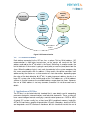
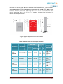
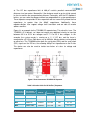
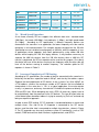
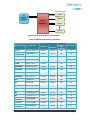
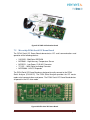
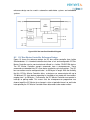
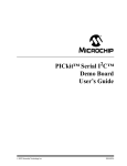
Solution Guide to I2C BUS
Communication
Yiying Sun – Global Technology Centre
Volume 1, October 2011
1. I2C Overview
I2C, short for Inter Integrated Circuits, is a well known standard developed by Philips
semiconductors (now NXP Semiconductors) in early 1980s. As its name suggests, it
is used for communications between ICs resided on the same circuit board.
Sometimes it is also called IIC, or I2C. Its original purpose was to provide an easy
way to connect multiple peripheral circuits to a central processing unit inside a TVset. Before that time, the common method of inter-IC communication was via a
parallel 8-bit wide bus. For example, the parallel data and address bus structure is
used to connect memory to MCUs for data transfer. It results in high interconnection
cost, such as more board area and I/O pins needed.
The I2C bus can eliminate that drawback. It is a simple, bidirectional, 2-wire serial
bus interface which supports moderate speed and short distance communication.
By switching from parallel to serial communication, this 2-wire bus structure reduces
the number of data lines and lowers general purpose input/output (GPIO) usage on
the central processor, which enables to simplify designs and reduce costs. Originally,
the I2C-bus was limited to 100 Kbps operation. Over time there have been several
additions to the specification so that it is able to support up to 3.4 Mbps today.
However, unlike other serial communication, the I2C bus is a multi-master bus,
which means each device connected to the bus can control the bus. Because all
communication takes place on only two wires, all devices must have a unique
address to identify it on the bus. Communication between master and slave is bidirectional. Collision detection and arbitration mechanisms are present to prevent
data corruption if two or more masters simultaneously initiate data transfer. Hence,
there is no need for chip selection or arbitration logic, making it simple to implement
in the design.
With the advancement of the technology, the implementation of I2C bus is not limited
to inside a single board only. It can be extended across multiple boards via bus
extensions and control devices. For example, a host microcontroller on a main
embedded board uses I2C to communicate with user interface devices located on a
separate front panel board. Because of its simplicity and flexibility, the I2C bus is
widely used in microcontroller / microprocessor-base systems across all industry
segments. It is also adopted by a large and growing number of semiconductor
manufacturers. These companies offer a variety of electronic devices, including
memories, input and output devices, different types of sensors, real-time clocks,
displays, and much more.
2. I2C Bus Theory of Operation
In order to use the I2C bus properly and efficiently, it is important to understand how
it works.
Solution Guide to I2C BUS Communication
Page 2
2.1
I2C Bus Hardware Architecture
I2C bus defines a data signal line SDA and a clock signal line SCL which supports
bidirectional data transfer between a master and several slaves. Regardless of how
many devices are attached to the I2C bus, there are only two signals connected to
all of them. A master is the device which initiates a data transfer on the bus and
generates the clock signals to permit that transfer. The device being addressed by
the master is called a slave. In Figure 1, the typical microcontroller (MCU)-based
system use I2C bus for communication between the host MCU and multiple
peripherals, such as memory, LCD drivers, data conversion devices, etc. In this
case, the MCU is the master and the peripherals are slaves. Both the master MCU
and slave peripherals can receive and transmit data.
In I2C bus, both SDA and SCL are connected to a positive supply voltage (VCC)
through pull-up resistors (see in Figure 1). Because SDA and SCL are open-drain,
the devices connected to I2C bus can only drive these lines low or leave them open.
The pull-up resistors RP pull the line up to HIGH (VCC) when the bus is free, or there
is no device on the bus. RP commonly ranges from 1 kΩ to 10 kΩ, resulting in typical
pull-up currents of about 1 mA and less.
So far we discussed a single master implementation of I2C bus. But I2C bus is in
fact a multi-master bus, which means more than one devices can be the master to
control the bus at the same time without corrupting the message. For example, there
are multiple MCUs connected to I2C bus. If two or more MCUs try to talk on the bus
concurrently, they have to determine whether the bus is currently idle or not before
I2C transferring. The arbitration procedure is used to decide which master is granted
access, and which master should wait for the next idle time.
VCC
RP
RP
SDA
SCL
Central
Processing
Unit
(MPU/MCU
Peripheral
Device 1
Peripheral
Device 2
Peripheral
Device 3
Peripheral
Device n
Figure 1 Connection of I2C Bus Devices
As for the total number of devices connected to the I2C bus is determined by the
maximum bus capacitance. According to I2C specification, a maximum bus
Solution Guide to I2C BUS Communication
Page 3
capacitive load is 400pF. This 400pF load includes all I2C devices as well as trace
lengths.
2.2
I2C Bus Speed
I2C bus is able to be operated at four speeds or modes: standard-mode (up to 100
Kbps), fast-mode (400 Kbps), fast-mode plus (up to 1 Mbps), and high speed mode
(up to 3.4 Mbps). Most of the I2C devices available today support 400Kbps
operation. Higher-speed operation may allow I2C to keep up with the rising demand
for bandwidth in multimedia and other applications.
The I2C devices are fully downward compatible, so any device may be operated at a
lower bus speed. It makes it possible that a combination of different speed I2C
devices exits in a system with the bus speed controlled by I2C master.
2.3
I2C Bus Communication
I2C is a master-slave protocol. Therefore, the communication is initiated by a master
only. When a master on the I2C bus wants to communicate with a slave, it first has
to take control of the bus. This is only possible when the bus is free. Then the master
device issues a START condition. A START condition is determined by a HIGH to
LOW transition on the SDA line while SCL is HIGH. This condition informs all the
slave devices to listen on the serial data line for their respective address. The bus is
considered to be busy after the START condition. After a START condition has been
signalled, the bus master will then send the unique ADDRESS of the target slave
device along with a Read or Write flag. The slave with the corresponding address
then responds with an acknowledgement (ACK) signal. Now the communication
proceeds between the master and the Slave on the data line. The transmitter sends
8-bits of data to the receiver which replies with a 1-bit acknowledgement. When the
communication is complete, the master issues a STOP condition indicating that
everything is done. A STOP condition is indicated by a LOW to HIGH transition on
the SDA line while SCL is HIGH. After the STOP condition is generated, the I2C bus
is considered free again.
Solution Guide to I2C BUS Communication
Page 4
Matching
Slave
responses ACK
Master
issues
START
I2C Bus Idle
Master
sends slave
ADDRESS
Data transfer
start
Master flags
READ/WRTIE
Master
issues
STOP
Slave Address
Invalid
Figure 2 I2C Communication
2.4
2C Address Scheme
Each device connected to the I2C bus has a unique 7-bit or 10-bit address. I2C
communication is 8-bit bytes transmission, so the master will send out the 7-bit
address and add on the 8th bit which is the Read / Write flag. In another words, the
last bit indicates if the master is going to send (write) or receive (read) data from the
slave. When the address byte is sent, each slave device in the system compares the
first seven receiving bits with its address. If they match, the device considers itself
addressed by the master as a slave-receiver or slave-transmitter, depending upon
the value of the data direction bit (8th bit). In order to prevent address clashes in a
large I2C system, due to the limited range of the 7 bit addresses, a 10 bit address
scheme is used to increases the available address range about ten times. However,
the use of 10-bit address is not very common; therefore it is not discussed here in
details.
3. Applications of I2C Bus
The I2C-bus is a de facto industrial standard that is now widely used in computing,
consumer electronics, communications, and industrial electronics. These systems all
have some intelligent control usually by a central control processor – MCU or MPU.
A typical I2C system usually has at least one MCU, peripheral memory, hard disk,
A/D or D/A converters, graphic chip and other I/O ports. Nowadays, almost all MCUs
are integrated a real I2C interface in hardware, but this should not restrict the use of
Solution Guide to I2C BUS Communication
Page 5
the I2C bus on other MCUs. Any MCU can be made to I2C communicate via general
purpose I/Os using software routines.
In current market, besides MCUs, I2C compatible devices are available in a wide
range of functions. Some examples are listed including, but not limited to:
•
•
•
•
•
•
•
Serial EEPROM / RAM / FLASH
I/O Expanders
Real-Time Clocks
Digital to Analog Converter / Analog to Digital Converter
LCD/LED Drivers
Sensors, such as temperature sensors, capacitive sensors, IR sensors, etc.
MEMS Sensors, such as accelerometers, compass, etc.
4. I2C Legal Information
The use and manufacturing of I2C devices is subject to a copyright and patents from
NXP. This means that electronics system designers need to purchase a license from
NXP to use I2C technology in their system. Fortunately, as of October 10, 2006, no
licensing fees are required to implement the I2C protocol. However, fees are still
required to obtain I²C slave addresses allocated by NXP. If you use an IC
component which incorporating the technology has been licensed by IC
manufacturers, then you can immediately use these components for free. In another
case, if you use an FPGA in your design and you want to build an I2C technology,
then you need to purchase a slave address from NXP.
5. Common Problems in I2C Applications
5.1
Mixed Voltage Levels
Today’s electronics systems require different supply voltages to power their various
components. With the increase demand of low power consumption, the high
performance of MCUs and DSPs are implemented advanced process technology to
get the supply voltages as low as 1.8V. On the other hand, some I2C peripheral
devices continue to operate at 3.3V or 5V supplies. I2C-bus devices currently in the
market range in supply voltage from 2 V to 5 V with commensurate I/O and threshold
levels. It results that I2C devices with different voltage levels might be connected to
the same bus. Since the I2C bus lines are bidirectional, interfacing I2C devices with
different voltage levels is not straightforward, special level translation are necessary
for this purpose.
One solution for this is using a bidirectional voltage level translator without the need
of a direction control signal. Here is one voltage level translation example, the
TCA9406 from TI, to show how dual-channel signal switches can be used to
Solution Guide to I2C BUS Communication
Page 6
translate I2C signals (SDA and SCL) between mixed voltage levels. The TCA9406 is
a dual bidirectional I2C-Bus
Bus Voltage-Level
Voltage Level translator with enable (OE) Input. It can
interface between processors operating from 1.8 V to 3.3 V and the I2C slave
devices operating from 2.3 V to 5.5 V. It supports standard and fast mode I2C
devices and multiple masters.
Figure 3 Typical Application Circuit of TCA9406
Table 1 Selection Guide for I2C Voltage Translators
Order Code
Manufacturer
Part Number
Newark
Farnell /
element14
Level
Translation
Range (V)
Port
A
Port
B
I2C Speed
Supported
Standard
Standardmode / FastFast
mode /
Fast
Fast-mode
Plus
Standard
Standardmode / FastFast
mode /
Fast
Fast-mode
Plus
Maxim
Integrated
MAX3373EEKA+T
68K9426
1787504
1.2
to 5.5
1.65
to 5.5
NXP
PCA9306D
70R6428
1831194
1.0 to
5.0
1.8 to
5.0
Texas
Instruments
PCA9306DCUTE4
97K6976
1053573
1.2 to
3.3
1.8 to
5.0
Standard
Standardmode / FastFast
mode
Texas
Instruments
TCA9406DCTR
59T0097
1972384
1.65
to 3.6
2.3 to
5.5
Standard
Standardmode / FastFast
mode
Solution Guide to I2C BUS Communication
Page 7
Another solution for this issue is to use a multiplexer/switch. An I2C multiplexer
basically expands the I2C Bus as it splits the SCL and SDA signals from the master
into one or more SCL and SDA Channels, where each channel can support unique
functions and needs. As each channel in the multiplexer is supply independent, each
channel can be pulled to a different supply voltage. Another advantage of these
multiplexers is their ability to isolate a section on the I2C bus through I2C software.
This saves valuable pins on the processor, which can be used for additional
functionality.
Table 2 Selection Guide for I2C Multiplexers/Switches
Order Code
Manufacturer
Part Number
Newark
Farnell /
element14
Max
Frequency
(KHz)
Configuration
(IN:OUT)
NXP
PCA9540BD
70R6561
1831206
400
1:2
NXP
PCA9544APW
70R6598
1831207
400
1:4
NXP
PCA9546APW
70R6610
1831208
400
1:4
NXP
PCA9547PW
70R6615
1831209
400
1:8
NXP
PCA9548APW
70R6620
1831210
400
1:8
PCA9544APW
66K4023
1470501
400
1:4
PCA9545APWR
66K4031
1652260
400
1:4
PCA9546APWT
67K8254
1564905
400
1:4
PCA9548APWR
67K8253
1607855
400
1:8
Texas
Instruments
Texas
Instruments
Texas
Instruments
Texas
Instruments
5.2
I2C Address Conflicts
As mentioned previously, a 7 or 10-bit addressing scheme is used to identify each
device on I2C bus. This address is usually defined by device manufacturers.
Therefore, it is possible that two different functions of devices with same address,
such as LCD driver and temperature sensor, are connected to same I2C bus. It will
cause addressing conflicts. One multiplexer/switch is a solution for address conflicts.
The multiplexer splits the I2C bus into several sub-branches and allow the I2C
master to select and address one of multiple identical devices, thus resolving
address conflict issues. The selection guide for multiplexers/switches is shown in
Table 2.
5.3
Limited Distance Communication
I2C is essentially a short-distance bus protocol for on board communication. The
maximum distance depends on the load of the bus and the speed which it operates
Solution Guide to I2C BUS Communication
Page 8
at. The I2C bus capacitance limit of 400 pF restricts practical communication
distances to a few meters. Meanwhile, if the designer needs to go far at high speed,
he has to sacrifice the communication distance. Fortunately, with the I2C repeaters/
buffers, you can solve the dilemma without any degradation of system performance.
These repeaters can provide I2C bus expansion and can successfully extend the line
capacitance to greater than the 400pF capacitance. Additionally, these
repeaters/buffers also support voltage level translation and are able to resolve
address conflicts.
Figure 4 is an example for the TCA9509 I2C repeater from TI to solve this issue. The
TCA9509 is 5-V tolerant, so it does not require any additional circuitry to translate
between 0.9-V to 5.5-V bus voltages and 2.7 V to 5.5 V bus voltages. In this
example, the system master is running on a 1.1 V I2C bus, and the slave is
connected to a 3.3-V bus. Both buses run at 400 kHz. Master devices can be placed
on either bus. The TCA9509 buffers both the serial data (SDA) and the serial clock
(SCL) signals on the I2C bus, thus allowing 400 pF bus capacitance on the B-side.
This device can also be used to isolate two halves of a bus for voltage and
capacitance.
Figure 4 Texas Instruments TCA9509 I2C Repeater
Table 3 Selection Guide for I2C Buffers / Repeaters
Order Code
Manufacturer
Part Number
Newark
Farnell /
element14
Max
Frequency
(KHz)
Supply Voltage
(V)
NXP
PCA9515ADP
70R6482
1831200
400
3.0 ~3.6
NXP
PCA9515D
70R6483
1831201
400
3.0 ~3.6
NXP
PCA9517D
71M0457
1831202
400
2.7 ~5.5
NXP
PCA9511ADP
70R6469
1831198
400
2.7 ~ 5.5
Solution Guide to I2C BUS Communication
Page 9
NXP
Texas
Instruments
Texas
Instruments
Texas
Instruments
Texas
Instruments
5.4
PCA9512ADP
70R6472
1831199
400
2.7 ~ 5.5
PCA9515AD
80K2690
1792276
400
2.3 ~ 3.6
PCA9517D
71M0457
1703190
400
0.9 ~ 5.5
PCA9518DW
53M3802
--
400
3.0 ~ 3.6
TCA9509RVHR
51T4809
1926947
400
27 ~ 5.5
Mixed Speed Operation
As we know, currently I2C bus supports four different data rates: standard mode
(100 Kbps), fast mode (400 Kbps), fast-mode plus (1 Mbps), and high-speed mode
(3.4 Mbps). According to I2C specification, if different frequency devices are
connected in the same bus in an application, the lowest frequency must be used to
guarantee a safe communication. For example, devices designed for the 100 kHz
specification are not suitable to work properly at 400 kHz, while the opposite is true.
In applications where upgrades have been performed by using newer 400 kHz
devices while keeping the 100 kHz legacy devices, it may become necessary to
separate the 400 kHz devices from the 100 kHz devices when a 400 kHz I2C
transfer is performed. An I2C bus repeater can be used for this purpose. One side of
the device will have all the devices running at one frequency while the other side will
have all the devices running to another frequency. The selection guide for I2C
repeaters is shown in Table 3.
5.5
Increased Complexity of PCB Routing
According to I2C specification, the number of devices connected to the same bus is
limited by the total bus capacitive load of 400 pF, and also by the address space.
Suppose the total capacitance of I2C devices in one system is less than 400 pF, for
a 7-bit address scheme, the maximum number of I2C devices that are allowed to
communicate in the same bus is 128. In a typical application, the master device
usually is a processor, and every slave device is linked to the processor directly via
SDA and SCL lines. When designing out such a PCB, all necessary signals have to
be routed directly from the processor to the I2C devices. This type of layout takes up
a lot of board space, becomes tedious in trying to correctly lay it all out, and ends up
being an expensive approach.
In order to ease PCB routing, I2C I/O expander is introduced between a master and
multiple slaves. One side of the I/O expander is connected to the I2C master
devices, and the other side is connected to multiple slave devices, shown in Figure
5. The I/O expander can also easily enhance system IO functionality, such as LED
controls, PWM and real time clock functions, keypad controls, and GPIOs.
Solution Guide to I2C BUS Communication
Page 10
I2C Slave Devices
Slave 1
I2C
Master
Device
Slave 2
I2C I/O
Expander
Slave 3
Slave n
Figure 5 The I2C System With an I/O Expander
Table 4 Selection Guide of I2C I/O Expanders
Order Code
Newark
Farnell /
element14
Max
Frequency
(KHz)
ADP5587ACPZ-R7
69R7646
1799906
400
18
CAT9555WI-T1
08R5467
1718510
400
16
MAXIM
MAX7311AUG+
89K6080
--
400
16
MAXIM
MAX7312ATG+
28K3566
--
400
16
MAXIM
MAX7315ATE+
61K0645
--
400
8
MICROCHIP
MCP23017-E/SP
31K2959
1332088
1700
16
MICROCHIP
MCP23018-E/MJ
31K2960
1854489
3400
16
MICROCHIP
MCP23008-E/P
08J8737
1439387
1700
8
MICROCHIP
MCP23009-E/SS
07P9508
1854487
3400
8
NXP
PCA8574TS
61M8240
1506642
400
8
NXP
PCA8575DB
61M8241
1506643
400
16
NXP
PCA9500PW
70R6437
1831195
400
8
NXP
PCA9501PW
70R6442
1831196
400
8
NXP
PCA9535PW,112
70R6540
1627049
400
16
NXP
PCA9539PW,118
70R6557
1831205
400
16
PCA9535DWR
63K6052
1575233
400
16
PCF8575CDBE4
97K6980
1053571
400
16
TCA6408APWR
55T7325
1903303
400
8
Manufacturer
Analog
Devices
Catalyst
Semiconductor
Texas
Instruments
Texas
Instruments
Texas
Instruments
Part Number
Solution Guide to I2C BUS Communication
No. of I/Os
Page 11
Texas
Instruments
Texas
Instruments
TCA6416APWR
10R6151
1754897
400
16
TCA6424ARGJR
01T0713
1863866
400
24
6. Special Function I2C Devices
I2C bus is currently popular in electronics world and widely supported by IC
manufacturers. Engineers can easily find an MCU integrated with I2C interface from
different IC vendors. Apart from the processors, more I2C-bus compatible devices
incorporate an on-chip interface which allows them to communicate directly with
each other via the I2C-bus. They include memories, LED/LCD drivers, sensors,
DACs/ADCs, and so on.
6.1
I2C Serial EEPROM
Serial EEPROMs are widely used in many different applications where data retention
during power-off is essential. These EEPROMs are designed to provide simple, but
flexible data storage for most popular MCU-based solutions. They need only two
wires to communicate the host processor. The MCU can use any tow available I/O
pins to emulate the operation of the SDA and SCL signals required for I2C
communications, shown in Figure 6. For a write operation, the microcontroller first
sends a start condition. Then the control byte is sent. The control byte consists of the
device code for the specific device that is being addressed, the address of the
memory block being accessed, and a bit that indicates a write operation is being
performed. The EEPROM then acknowledges receipt of the byte. The MCU then
sends the specific memory address of the byte being written to. The EEPROM
acknowledges again. The MCU then sends the data to be written into the memory
byte. After the EEPROM acknowledges the data, the MCU sends a stop condition.
Similar process is used to read from EEPROM. The only difference is that the control
byte is sent twice, once before the MCU sends the address byte and a second time
before the EEPROM returns the requested data byte. The read/write bit of the
control byte is also set to a read operation.
Solution Guide to I2C BUS Communication
Page 12
VCC
RP
RP
SDA
SCL
P1.0
P1.1
Central Processor
(MPU/MCU)
SDA SCL
I2C Serial EEPROM
Figure 6 I2C Serial EEPROM Interface with an MCU
6.2
LED Drivers with I2C Interface
LED lighting becomes more and more popular in current market with the
advancement of LED technology. LED drivers are required to ensure the proper
operation of LEDs, and able to add extra intelligence to the lighting system, such as
blinking, dimming, and color mixing. The purpose of this device is to free the
processor from the LED controls, which allows the processor to focus on other tasks
in the application. Without the I2C LED drivers, the host MCU needs to send out
repeated commands to turn LEDs on and off. This significantly increases the amount
of traffic on the MCU and uses up one of the MCU timers. The LED driver instead
requires to only program the individual port with the frequency and duty cycle, and
then it only requires one command from the master MCU to control the LEDs.
VCC
RP
RP
SDA
SCL
P1.0
P1.1
Central Processor
(MPU/MCU)
SDA SCL
I2C LED Driver
Figure 7 I2C LED Driver Interface with an MCU
Solution Guide to I2C BUS Communication
Page 13
6.3
I2C Digital Sensors
I2C compatible sensors can communicate with the master MCU via two-wire bus.
The most common used I2C sensors are temperature sensors. Many systems
across a variety of applications require some implementation of temperature
monitoring. These sensors can monitor the temperature of the thermal diode inside
the CPU or the diode connected to transistors, and can trigger an interrupt or alert
output. They are also able to produce accurate digital readings of the ambient
temperature and can be used to trigger interrupt, shut-down, or over-temperature
alarms. Figure 8 shows a typical connection of temperature sensors and the host
MCUs.
VCC
I2C
Temperature
Sensors
Figure 8 Interface I2C Temperature Sensors with the MCU
7. Development Tools For I2C Bus
7.1
NXP I2C 2002-1A Evaluation Kit
The I2C 2002-1A Evaluation kit is a low cost I2C based platform that allows
designers to use their Personal Computer (PC) to easily test and demonstrate I2C
devices in a platform that allows multiple operations to be performed in a setting
similar to a real system environment. The evaluation board features 11 different I2C
slave devices, including 1 temperature sensor, 1 I2C repeater, 3 I2C I/O expanders,
2 I2C LED drivers, 1 I2C EEPROM, 1 I2C buffer, and 2 I2C switches. It also supports
for easy programming and evaluation of various general purposes I2C products from
NXP. This evaluation board can be use to learn how to program and Blink LEDs
using the GPIOs and/or the LED drivers, learn how the multiplexer, serial EEPROM,
and temperature sensor work, learn how to program the multiplexed I2C EEPROM.
This kit also includes a PC graphical interface that allows easy manipulation of I2C
devices.
Solution Guide to I2C BUS Communication
Page 14
Figure 9 I2C 2002-1A Evaluation Board
7.2
Microchip PICkit Serial I2C Demo Board
The PICkit Serial I2C Demo Board demonstrates I2C serial communications and
operation of the following devices:
•
•
•
•
•
24LC02B - 2Kbit Serial EEPROM
MCP9801 - High-Accuracy Temperature Sensor
MCP3221 - Low-Power 12-Bit A/D Converter
TC1321 - 10-Bit Digital-to-Analog Converter
MCP23008 - 8-Bit I/O Expander
The PICkit Serial I2C Demo Board was designed to easily connect to the PICkit
Serial Analyzer (DV164122). The PICkit Serial Analyzer provides the I2C master
mode serial communications and power. The PICkit Serial I2C Demo Board devices
all operate in the I2C slave mode.
Figure 10 PICkit Serial I2C Demo Board
Solution Guide to I2C BUS Communication
Page 15
7.3
Total Phase I2C Development Kit (TP120112)
Total Phase's I2C development kit TP120112 allows developers to develop and
debug an I2C bus on an embedded system. With this kit, developers can exercise
target devices on an I2C bus as a master device, simulate an I2C master or slave
device, program and verify I2C-based memory devices, passively monitor an I2C
bus in real-time.
The I2C development kit contains an Aardvark I2C/SPI host adapter, a Beagle
I2C/SPI Protocol Analyzer, and one I2C/SPI Activity Board. The Aardvark I2C/SPI
host adapter can actively send and receive I2C message as a master or slave
device. With this interface, a PC can communicate directly with I2C devices.
Because every I2C device is different, this kit offers a free API that allows users to
create custom applications to interface with I2C based systems. The Beagle
analyzer provides a real-time bus monitoring and data capture for users’ systems.
Figure 11 TP120112 I2C Development Kit
8. Reference Design
8.1
I2C Bus Slave Reference Design
Figure 12 shows the block diagram of the I2C bus-interface slave reference design
from Digital Core Design. The reference design provides an interface between a
target device (e.g. memory, LCD display, and pressure sensors) and an I2C bus. It
can work as a receiver or transmitter depending on the working mode determined by
the master. It supports slave transmit and receive operations, speeds up to 400
Kbps, and 7-bit addressing. Meanwhile there is no programming required. This
Solution Guide to I2C BUS Communication
Page 16
reference design can be used in automotive audio-video systems and embedded
systems.
Figure 13 I2C Bus-Interface Slave Block Diagram
8.2
I2C Bus Master Controller Reference Design
Figure 13 shows the reference design for I2C bus master controller form Lattice
Semiconductor. It is intended to demonstrate how a fast and configurable I2C-Bus
Master Controller can be constructed and utilized in a Lattice CPLD/FPGA device.
The I2C Master Controller accepts commands from a microprocessor. These
commands are decoded into I2C slave device read/write cycle transactions. The I2C
bus transactions can be configured to be 1 to 256 bytes in length. With the flexibility
that this I2C-Bus Master Controller offers, a designer can communicate with up to
128 different I2C slave devices operating in standard or fast mode with transactions
ranging from 1 to 256 bytes. Furthermore, the I2C Master Controller can operate in
interrupt or polling mode. This means that the microprocessor programmer can
choose to poll the I2C Master for a change in status at periodic intervals or wait to be
interrupted by the I2C Master Controller when data needs to be read or written.
Solution Guide to I2C BUS Communication
Page 17
Figure 14 I2C Master Controller I/O Interface
9. Summary
There are thousands of I2C devices on the market today, ranging from data
converters, serial EEPROM, digital sensors, to video processors. Those devices are
built in on-chip programmable registers to provide an ideal low-cost solution to
establish communications between these intelligent devices and the central
controller. Nearly every microcontroller vendor has taken care of the physical
implementation of the bus, even if some of the MCUs do not have on-chip I2C
hardware interface, the I2C bus still can be implemented using software. In addition,
since silicon area and I/O pins heavily influence the IC price, I2C has a lot to offer in
cost-sensitive applications.
10.
References
[1] www.i2c-bus.org
[2] Introduction to I2C, http://www.eetimes.com/discussion/beginner-scorner/4023816/Introduction-to-I2C
[3] I2C Manual, http://www.nxp.com/documents/application_note/AN10216.pdf
[4] I2C-bus Specification and User Manual,
http://www.nxp.com/documents/user_manual/UM10204.pdf
[5] I2C Guide, http://www.ti.com/lit/sg/sszc003c/sszc003c.pdf
Solution Guide to I2C BUS Communication
Page 18
Disclaimer
The information contained in this document is for general purposes only.
Thanks to the suppliers/websites who provided the information and while
we endeavour to keep the information up to date and correct, we make
no representations or warranties of any kind, express or implied, about
the completeness, accuracy, reliability, suitability or availability with
respect to the website or the information, products, services, or related
graphics contained on the website for any purpose. Any reliance you
place on such information is therefore strictly at your own responsibility.
Solution Guide to I2C BUS Communication
Page 19