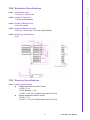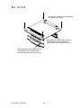
1
User Manual PCM-9388 Copyright This document is copyrighted, © 2008. All rights are reserved. The original manufacturer reserves the right to make improvements to the products described in this manual at any time without notice. No part of this manual may be reproduced, copied, translated or transmitted in any form or by any means without the prior written permission of the original manufacturer. Information provided in this manual is intended to be accurate and reliable. However, the original manufacturer assumes no responsibility for its use, nor for any infringements upon the rights of third parties that may result from such use. Trademarks Award is a trademark of Award Software International, Inc. VIA is a trademark of VIA Technologies, Inc. IBM, PC/AT, PS/2 and VGA are trademarks of International Business Machines Corporation. Intel® and Pentium® are trademarks of Intel Corporation. Microsoft Windows® is a registered trademark of Microsoft Corp. RTL is a trademark of Realtek Semi-Conductor Co., Ltd. ESS is a trademark of ESS Technology, Inc. UMC is a trademark of United Microelectronics Corporation. SMI is a trademark of Silicon Motion, Inc. Creative is a trademark of Creative Technology LTD. CHRONTEL is a trademark of Chrontel Inc. All other product names or trademarks are properties of their respective owners. PCM-9388 User Manual Part No. 2006938810 Edition 1 Printed in China April 2008 ii Product Warranty Warranty Period The manufacturer aims to meet the customer’s expectations for post-sales service and support; therefore, in addition to offering 2 years global warranty for our standard products, a global extended warranty service is also provided for customers upon request. Our customers are entitled to complete and prompt repair service beyond the standard 2 years of warranty. As a standard, most products manufactured by us are covered by a 2 year global warranty from the date of shipment. Products covered by extended warranty and cross-region repair services against defects in design, materials, and workmanship, are also covered from the date of shipment. All key parts assembled into a computer system products such as LCD, touchscreen, power supply, and peripherals, etc., will be covered by the standard 1 year warranty. Repairs under Warranty It is possible to obtain a replacement (Cross-Shipment) during the first 30 days of purchase (45 days for Channel Partners), if the products were purchased directly from your reseller and the product is DOA (Dead-on-Arrival). DOA Cross-Shipment excludes any customized and/or build-to-order products. The Cross-Shipment agreement signed by customers is required for initiating/releasing cross shipment with technician confirmation and verification. The only conditions for Cross-Shipment are: a) the return must not be damaged, altered or marked, b) all parts and accessories must be included as originally shipped; and c) proof of purchase must be included. Any returns that do not meet mentioned requirements above, or any wrong user settings/configurations will be denied, or subject to additional handling/service charges as determined by the Repair Service Department. For those products which are not DOA, or damaged, the return fee to an authorized repair facility will be at the customers’ expense. The shipping fee for reconstructive products from the warehouse back to customers’ sites will be at our expense. Exclusions from Warranty The product is excluded from warranty if: The product has been found to be defective after expiry of the warranty period. Warranty has been voided by removal or alteration of product or part identification labels. The product has been misused, abused, or subjected to unauthorized disassembly/modification; placed in an unsuitable physical or operating environment; improperly maintained by the customer; or failure caused which manufacturing is not responsible whether by accident or other cause. Such conditions will be determined by technicians at time of repair and their discretion. The product is damaged beyond repair due to a natural disaster such as a lighting strike, flood, earthquake, fire, etc. Products without warranty have been updated/upgraded or tested by customers. iii PCM-9388 User Manual Declaration of Conformity FCC This device complies with the requirements in part 15 of the FCC rules: Operation is subject to the following two conditions: 1. This device may not cause harmful interference, and 2. This device must accept any interference received, including interference that may cause undesired operation This equipment has been tested and found to comply with the limits for a Class A digital device, pursuant to Part 15 of the FCC Rules. These limits are designed to provide reasonable protection against harmful interference when the equipment is operated in a commercial environment. This equipment generates, uses, and can radiate radio frequency energy and, if not installed and used in accordance with the instruction manual, may cause harmful interference to radio communications. Operation of this device in a residential area is likely to cause harmful interference in which case the user will be required to correct the interference at his/her own expense. The user is advised that any equipment changes or modifications not expressly approved by the party responsible for compliance would void the compliance to FCC regulations and therefore, the user’s authority to operate the equipment. Caution! There is a danger of a new battery exploding if it is incorrectly installed. Do not attempt to recharge, force open, or heat the battery. Replace the battery only with the same or equivalent type recommended by the manufacturer. Discard used batteries according to the manufacturer’s instructions. Technical Support and Assistance For more information about this and our other products, please visit our website at: http://www.emacinc.com/ For technical support and service, please visit our support website at: http://www.emacinc.com/support/ Additional Information and Assistance 1. 2. Visit the reseller web site at http://www.emacinc.com/ where you can find the latest product information. Contact your distributor, sales representative, or customer service center for technical support if you need additional assistance. Please have the following information ready before you call or email: Product name and serial number Description of your peripheral attachments Description of your software (operating system, version, application software, updates installed, etc.) A complete description of the problem The exact wording of any error messages PCM-9388 User Manual iv Packing List Before installation, please ensure the following items have been shipped: Item Part Number 1 PCM-9388 SBC 1 Startup manual (optional on CD) 1 Utility CD (Optional) 1 Printer Port cable 1 mini jumper pack 1 IDE cable 1 Audio cable 1 Dual Port USB cable 1 PS2 KB/MS cable 1 RS232/422/485 cable Ordering Information Model Number Description PCM-9388F-M PCM-9388F-S Celeron® M 600 (512 K) SBC,VGA,LCD,Audio,ISA,ROHS Celeron® M 1G (0 K) SBC,VGA,LCD,Audio,ISA,ROHS Optional Accessories Model Number Description 1700001531 1703070101 FLAT CABLE 34P-2.54 mm/26P-2. 0mm 30 cm(LPT to FDD) Wire ATX20P/7P 10 cm( ATX power cable) v PCM-9388 User Manual PCM-9388 User Manual vi Contents Chapter 1 General Introduction ...........................1 1.1 1.2 Introduction ............................................................................................... 2 Product Specifications............................................................................... 2 1.2.1 General ......................................................................................... 2 1.2.2 I/O ................................................................................................. 2 1.2.3 Ethernet ........................................................................................ 2 1.2.4 Display .......................................................................................... 3 Chipset ...................................................................................................... 3 1.3.1 Functional Specifications .............................................................. 3 1.3.2 Mechanical Specifications............................................................. 5 1.3.3 Electrical Specifications ................................................................ 5 1.3.4 Environmental Specifications........................................................ 6 1.3 Chapter 2 H/W Installation....................................7 2.1 Jumpers .................................................................................................... 8 2.1.1 Jumper List ................................................................................... 8 2.1.2 Jumper Settings ............................................................................ 8 2.1.3 Jumper Description ....................................................................... 9 Connectors.............................................................................................. 10 2.2.1 Connector List............................................................................. 10 2.2.2 Connector Settings ..................................................................... 11 Mechanical .............................................................................................. 14 2.3.1 Jumper and Connector Location................................................. 14 Figure 2.1 PCM-9388 Jumper and Connector Layout (Component Side) ......................................................................... 14 Figure 2.2 PCM-9388 Jumper and Connector Layout (Solder Side) ......................................................................... 14 2.3.2 Board Dimensions....................................................................... 15 Figure 2.3 Board Dimensions (Component Side) .................................................................................. 15 Figure 2.4 Board Dimensions (Solder Side) .............................. 15 2.2 2.3 Chapter 3 BIOS Operation ..................................17 3.1 3.2 BIOS Introduction.................................................................................... 18 BIOS Setup ............................................................................................. 18 3.2.1 Main Menu .................................................................................. 19 3.2.2 Standard CMOS Features .......................................................... 20 3.2.3 Advanced BIOS Features ........................................................... 21 3.2.4 Advanced Chipset Features........................................................ 23 3.2.5 Integrated Peripherals................................................................. 25 3.2.6 Power Management Setup ......................................................... 26 3.2.7 PnP/PCI Configurations .............................................................. 28 3.2.8 PC Health Status ........................................................................ 29 3.2.9 Frequency/Voltage Control ......................................................... 30 3.2.10 Load Optimized Defaults............................................................. 31 3.2.11 Set Password.............................................................................. 32 3.2.12 Save & Exit Setup ....................................................................... 34 3.2.13 Quit Without Saving .................................................................... 34 vii PCM-9388 User Manual Chapter 4 S/W Introduction & Installation........ 35 4.1 4.2 S/W Introduction ..................................................................................... 36 Driver Installation .................................................................................... 36 4.2.1 Windows XP Professional........................................................... 36 4.2.2 Other OS Installations................................................................. 36 SUSI Application Library ......................................................................... 37 4.3.1 SUSI Introduction........................................................................ 37 4.3.2 SUSI Functions........................................................................... 37 4.3.3 SUSI Installation ......................................................................... 38 4.3.4 SUSI Sample Programs.............................................................. 39 Figure 4.1 CL............................................................................. 47 4.3 Chapter 5 Extension I/O Installation ................. 49 5.4 PC/104 .................................................................................................... 50 Appendix A Pin Assignments............................... 51 A.1 Pin Assignments ..................................................................................... 52 Appendix B Watchdog Timer................................ 73 B.1 Watchdog Timer Sample Code............................................................... 74 PCM-9388 User Manual viii Chapter 1 1 General Introduction This chapter gives background information on the PCM-9388 Sections include: Introduction Specifications 1.1 Introduction The PCM-9388 is a 3.5” SBC (Single Board Computer) with Intel Celeron® M on board CPU. The PCM-9388, in conjunction with Intel 852GM and ICH4 chipsets, supports processors clocked up to 1.0 GHz, two USB 2.0 compatible ports, one Ethernet connector up to 10/100 Mbps, 2-channel 18-bit LVDS (Optional support 2 x 24-bit LVDS) and one 18-bit TTL LCD which can support dual independent display (LVDS + VGA/TTL + VGA), can accommodate up to 1 GB of DDR SODIMM RAM memory (supports DDR 266 MHz), and one IDE (supports up to two devices), and two COM ports. The PCM-9388 also has the ability for expansion with one PC/104 connector. 1.2 Product Specifications 1.2.1 General CPU: Embedded Intel® Celeron M 600 MHz/1 GHz 2nd Cache Memory: Depends on CPU from 0 KB to 512 KB System Chipset: Intel® 852 GM GMCH/ICH4 Chipset BIOS AWARD: 512 kbit Flash BIOS System Memory: 1 x 200-pin SODIMM socket, supports Double Data Rate (DDR) up to 1 GB, accepts up to 266 MHz DRAM Watchdog Timer: 255-level interval timer, setup by software, Super I/O integrated in Winbond Controller Expansion Interface: Supports PC/104 Battery: Lithium 3 V/210 mA 1.2.2 I/O I/O Interface: 1 x EIDE (UDMA 33), 1 x CF, 1 x K/B, 1 x Mouse, 1 x RS-232, 1 x RS-232/422/485, 1 x LPT, 1 x FDD (shared with LPT) USB: 2 x USB 2.0 compliant ports Audio: AC97 Audio codec ALC203, supports 2.1 channel; supports Line-in, Line-out, Microphone IrDA: 115 kbps, SIR, IrDA 1.0 compliant GPIO: 8-bit general purpose input/output 1.2.3 Ethernet Chipset: 1 x Realtek RTL8100CL Speed: 10/100 Mbps Interface: 1 x RJ45 Standard: IEEE 802.3u 100Base-T PCM-9388 User Manual 2 1.3 Chipset 1.3.1 Functional Specifications 1.3.1.1 Processor Processor Intel Celeron support 400 MHz FSB Support 32-bit host bus addressing 852GM GMCH Supports 1 GB maximum memory Two 64-bit wide DDR SDRAM data channel Support DDR 200, DDR266 MHz 128-Mb, 256-Mb, 512-Mb and 1-GB DDR technology 1.3.1.2 Chipset (852) Memory Socket: SODIMM Socket: 1. 200-pin SODIMM socket type *1 3 PCM-9388 User Manual General Introduction Chipset: Intel 852GM chip integrated. (Intel Extreme Graphics 2 technology) Resolution: – CRT Display mode: pixel resolution up to 1600 x 1200 @ 85 Hz; 1920 x 1440 @ 60 Hz. – LCD Display mode: Dual channel LVDS panel supports up to UXGA panel resolution with frequency range from 25 MHz to 112 MHz LCD Interface: 2 Channel LVDS (36-bit), optional for 48-bit and 1x 18-bit TTL LCD LVDS: Hirose connector supports up to 2 channel (1 x 36-bit) LVDS LCD Panel TTL: Hirose connector supports up to 1 x TTL LCD Panel Dual Ind. Display: CRT + LVDS; CRT + TTL Chapter 1 1.2.4 Display Graphic and Video Controllers 852GM GMCH Support Up to 64-MB of Dynamic Video Memory Allocation Analog Display Support 350-MHz integrated 24-bit RAMDAC Dual Channel LVDS interface supports 36 bits CRT monitor resolutions supported: Up to 1600 x 1200 at 85 Hz, and up to 1920 x 1440 at 60 Hz LVDS panel resolution supported: Up to 1600 x 1200 at 85Hz Dual independent display options with digital display Analog CRT Connector: D-Sub 15-pin 5mm (Black) LVDS connector: Hirose DF13 type 40-pin TTL connector: Hirose DF13 type 40-pin 1.3.1.3 Chipset (ICH4) PCI Bus Interface Supports PCI Rev 2.3 Specification at 33 MHz 133 MB/sec maximum throughput IDE Interface Supports up to 2 IDE drives and one CF Ultra ATA 33, BMIDE and PIO mode AC-Link Interface Support for three AC97 2.3 codecs Support for 2.1 channels (PCM In/Out, Mic 1 input) USB Interface USB1.1, 2.0 compliant Including UHCI, EHCI Host controller Supports maximum 2 ports SMbus Supports SMBus 2.0 Specification Host interface allows CPU to communicate via SMBus 1.3.1.4 Others (Chipset) PCI to ISA PCM-9388 User Manual ITE8888G support PCI specification V.2.1 compliant Optional CLKRUN# interface support Supports full ISA compatible functions Supports ISA at 1/4 of PCI frequency 4 Chapter 1 1.3.2 Mechanical Specifications 1.3.2.1 Dimensions (mm) 147 mm (L) * 102 mm (W) 1.3.2.2 Height on Top (mm) 17.0 mm (with Heatsink) General Introduction 1.3.2.3 Height on Bottom (mm) 9 mm (CF socket) 1.3.2.4 Heatsink Dimensions (mm) 87mm (L) * 85 mm (W) * 13.04 mm (W) (Heatsink) 1.3.2.5 Weight (g) with Heatsink 95 g 1.3.3 Electrical Specifications 1.3.3.1 Power Supply Voltage Voltage requirement with ATX Power: +5 VDC +/- 5% +5 VDC Standby +/- 5% +12 VDC +/- 5% (For LVDS inverter power, PC/104) Voltage requirement with AT Power: +5V DC +/- 5% +12V DC +/- 5% (For LVDS inverter power, PC/104) 5 PCM-9388 User Manual 1.3.3.2 Power Supply Current CPU Type Celeron M 600MHz FSB=400 L2=512 K Status 256MB/533/ADATA DOS Idle +5 V +12 V 2.44 A 0.05 A Win Idle 1.56 A 0.16 A Win HCT11.2 2.11 A 0.17 A 1.3.3.3 RTC Battery Typical Voltage: 3.0 V Normal discharge capacity: 210 mAh 1.3.4 Environmental Specifications 1.3.4.1 Operating Temperature The Intel® Celeron® M processor is specified for proper operation when the junction temperature is within the specified range of 0° C to 100° C. The Intel® 852GM chipset temperature runs at a maximum of 100° C. The Intel® ICH4 I/O Controller case temperature runs at a maximum of 85° C. The processor protects itself from catastrophic overheating by use of an internal thermal sensor at a temperature level of approximately 100° C. Operating temperature: 0 ~ 60° C (32 ~ 140° F) 1.3.4.2 Operating Humidity Operating Humidity: 0% ~ 90% Relative Humidity, non-condensing 1.3.4.3 Storage Temperature Standard products: 0 ~ 60° C Storage temperature: -20 ~ 70° C 1.3.4.4 Storage Relative Humidity Standard products (0 ~ 60° C) Relative humidity: 95% @ 60° C PCM-9388 User Manual 6 Chapter 2 2 H/W Installation This chapter explains the setup procedures of the PCM-9388 hardware, including mechanical drawings, and instructions on setting jumpers and connecting peripherals, switches, and indicators. Be sure to read all safety precautions before you begin the installation procedure. 2.1 Jumpers 2.1.1 Jumper List J1 J2 AT/ATX selector J3/J4/J5 COM2 Setting J6 LCD power selector Audio power selector 2.1.2 Jumper Settings J1 AT/ATX selector Description PIN HEADER 2*1P 180D (M)SQUARE 2.0 mm DIP W/O Pb Setting Function (1-2) AT Power none ATX Power J2 Audio power selector Description PIN HEADER 3*1P 180D (M) SQUARE 2.0 mm Setting Function 1-2 Audio Power form 12 V-input & 5 V-output LDO 2-3 Audio Power from 5 V J3/J4/J5 COM2 Setting Description PIN HEADER 2*1P 180D (M) SQUARE 2. 0mm Setting Function J3 (1-2) RS-422 J4 (1-2) RS-232 J5 (1-2) RS-485 J6 LCD power selector Description PIN HEADER 3*1P 180D(M) 2.0 mm DIP SQUARE W/O Pb Setting Function J6 (1-2) +5 V J6 (2-3) +.3.3 V PCM-9388 User Manual 8 Cards can be configured by setting jumpers. A jumper is a metal bridge used to close an electric circuit. It consists of two metal pins and a small metal clip (often protected by a plastic cover) that slides over the pins to connect them. To close a jumper, you connect the pins with the clip. To open a jumper, you remove the clip. Sometimes a jumper will have three pins, labeled 1, 2 and 3. In this case you would connect either pins 1 and 2, or 2 and 3. 1 2 1 2 1 2 3 A pair of needle-nose pliers may be helpful when working with jumpers. If you have any doubts about the best hardware configuration for your application, contact your local distributor or sales representative before you make any changes. Setting Function 1-2 +5 V 2-3 +3.3 V Warning! To avoid damaging the computer, always turn off the power supply before setting jumpers. Clear CMOS. Before turning on the power supply, set the jumper back to 3.0 V Battery On. 9 PCM-9388 User Manual H/W Installation The jumper settings are schematically depicted in this manual as follows: Chapter 2 2.1.3 Jumper Description 2.2 Connectors 2.2.1 Connector List CN1 AT POWER Connector CN2 ATX POWER Standby Connector CN3 SMBus CN4 FAN Connector (SPEED Detect) CN5 ATX Power Button Connector CN6 GPIO CN7 AUDIO Connector CN8 IDE Connector CN9 CompactFlash CN10 HDD & PWR LED CN11 VGA CN12 COM1 CN13 LPT Connector CN14 IR Connector CN15 COM2 RS-232/RS-422/RS-485 Connector CN16 USB Connector CN17 PS2 (KB & MS) CN19 LAN Connector CN20 PC/104 SOLDER CONNECTOR CN21 Negative POWER Input CN22 LVDS LCD 40-Pin HIROSE CN23 Invert Power Connector CN24 TTL LCD 40-Pin HIROSE PCM-9388 User Manual 10 2.2.2.2 SMBus Connector One 4 x 1 pin wafer box (CN3) supports SMBus interface. 2.2.2.3 GPIO (General Purpose Input Output) (CN6) The board supports 8-bit GPIO through GPIO connector. The digital inputs and outputs can be programmed as input data or output to devices, with input or output defined. (CN6). 2.2.2.4 Audio Interface (CN7) Audio Port Connectors One 5 x 2-pin box header for Audio connector. These audio connectors are used for audio devices. 2.2.2.5 IDE, CDROM Hard Drive Connector (CN8) The board provides 1 IDE channel with which you can attach up to two Enhanced Integrated Device Electronics hard disk drives or CDROM to the board.s internal controller. Its IDE controller uses a PCI interface. This advanced IDE controller supports faster data transfer, PIO mode 4, Multi-word DMA mode 2 and an UltraDMA-33 interface. Connecting the hard drive Connecting drives is done in a daisy-chain fashion. This package includes one 44PIN IDE cable that can connect to 1.8" and 2.5" drives. 1. Connect one end of the cable to Hard Drive connector. Make sure that the red (or blue) wire corresponds to pin 1 on the connector, which is labeled on the board (on the right side). 2. Plug the other end of the cable into the Enhanced IDE hard drive, with pin 1 on the cable corresponding to pin 1 on the hard drive. (See your hard drive’s documentation for the location of the connector). If desired, connect a second drive as described above. Unlike floppy drives, IDE hard drives can connect to either end of the cable. If you install two drives, you will need to set one as the master and one as the slave by using jumpers on the drives. If you install only one drive, set it as the master. 2.2.2.6 Solid State Disk The board provides a CompactFlash. card type I socket. CompactFlash (CN9) The CompactFlash card shares a Primary IDE channel which can be enabled/disabled via the BIOS settings. 11 PCM-9388 User Manual H/W Installation 2.2.2.1 Power Connectors (CN1, CN2, CN4, CN5) Main power connector, +5 V, +12 V or 5V only PCM-9388 supports ATX and AT modes. One 4-Pin connector (CN1) supports 5 V/12 V AT power supply. Use ATX power cable (PN: 1703200201 ATX power control cable) connect CN2; it provides 5 VSB for ATX power. One 2-pin connector (CN5) for power button connector. Fan power supply connector (CN4) Provides +5 V power supply to CPU cooling fan. Chapter 2 2.2.2 Connector Settings 2.2.2.7 Power & HDD LED Connector (CN10) Next, you may want to install external switches to monitor and control the board. These features are optional: install them only if you need them. The Power & HDD LED connector is 4-pin Wafer box connector. It provides connections for a power and hard disk access indicator. Power & HDD LED Connector (CN10) The HDD LED indicator for hard disk access is an active low signal (24 mA sink rate). Power Reset button (S1) Momentarily pressing the reset button will activate a reset. The switch should be rated for 10 mA, 5 V. 2.2.2.8 VGA/LCD/LVDS Interface Connections CRT display connector (CN11) The CRT display connector is DB15 connector used for conventional CRT displays. LVDS LCD panel connector (CN22) The board supports 2 channel 18-bit LVDS LCD panel display. Users can connect a 48-bit LVDS LCD to it (optional) TTL LCD panel connector (CN24) The board supports 18-bit TTL LCD panel display. LCD inverter Power connector (CN23) The LCD inverter is connected to CN6 via a 5-pin connector to provide +5 V/+12 V power. 2.2.2.9 COM Port Connector (CN12, CN15, J3/J4/J5) The PCM-9388 provides 2 serial ports (COM1 and COM2). One 7*2P PIN HEADER (CN15) for COM2 output; and one DB-9 connector for COM1(CN12) COM RS-232/422/485 settings (J3) COM2 can be configured to operate in RS-232, RS-422, or RS-485 mode. This is done via J3. J3/J4/J5 COM2 Setting Setting Function J3 (1-2) RS-422 J4 (1-2) RS-232 J5 (1-2) RS-485 It provides connections for serial devices (ex: a mouse, etc.) or a communication network. You can find the pin assignments for the COM port connector in Appendix A. 2.2.2.10 Parallel Port Connector (CN13) Normally, the parallel port is used to connect the card to a printer. The board includes a multi-mode (ECP/EPP/SPP) parallel port accessed via CN13 The parallel port is designated as LPT1, and can be disabled in the system BIOS setup. The parallel port interrupt channel is designated to be IRQ7. You can select ECP/EPP DMA channel via BIOS setup. PCM-9388 User Manual 12 2.2.2.13 Keyboard and PS/2 Mouse Connector (CN17) The board provides a keyboard connector that supports both a keyboard and a PS/2 style mouse. In most cases, especially in embedded applications, a keyboard is not used. If the keyboard is not present, the standard PC/AT BIOS will report an error or fail during power-on self-test (POST) after a reset. The product’s BIOS standard setup menu allows you to select “All, But Keyboard” under the “Halt On” selection. This allows no-keyboard operation in embedded system applications, without the system halting under POST. 2.2.2.14 Ethernet Configuration The board is equipped with 1 high performance 32-bit PCI-bus Ethernet interface which is fully compliant with IEEE 802.3 10/100Mbps. It is supported by all major network operating systems. 100Base-T connector (CN19) 100Base-T connections are made via the on-board RJ-45 connector Network boot (Depends on Ethernet Controller Gigabit Ethernet only) The Network Boot feature can be utilized by incorporating the Boot ROM image files for the appropriate network operating system. The Boot ROM BIOS files are included in the system BIOS, which is on the utility CD disc. 2.2.2.15 PC/104 Connector Supports PCI to ISA interface via PC/104 (CN20) connector Supports full ISA compatible functions Socket2: 20 x 2 (F) 2.54 mm 51.86 mm x 5.01 mm x 11.45 mm p = 3.40 mm Socket3: 32 x 2 (F) 2.5 4mm 82.34 mm x 5.01 mm x 11.45 mm p = 3.40 mm PC/104 negative voltage: One 3 x 1-pin wafer box (CN23) supports -5 V/-12 V power input for ISA devices. 13 PCM-9388 User Manual H/W Installation 2.2.2.12 USB Connectors (CN16) The board provides up to two USB (Universal Serial Bus) ports. This gives complete plug and play capability. The USB interfaces comply with USB specification Rev. 2.0 which supports 480 Mbps transfer rate, and are fuse protected. 5 x 2 pin 180D (M) connectors for internal 2 x USB connectors at CN16.You will need an adapter cable if you use a standard USB connector. The adapter cable has a 5 x 2-pin connector with foolproof protection for incorrect plug-in on one end and a USB connector on the other. Chapter 2 2.2.2.11 IR Connector One 5 x 1-pin wafer box(CN14) supports IrDA; 115kbps, IrDA1.1 compliant. 2.3 Mechanical 2.3.1 Jumper and Connector Location Figure 2.1 PCM-9388 Jumper and Connector Layout (Component Side) Figure 2.2 PCM-9388 Jumper and Connector Layout (Solder Side) PCM-9388 User Manual 14 Chapter 2 2.3.2 Board Dimensions H/W Installation Figure 2.3 Board Dimensions (Component Side) Figure 2.4 Board Dimensions (Solder Side) 15 PCM-9388 User Manual PCM-9388 User Manual 16 Chapter 3 BIOS Operation Sections include: BIOS Introduction BIOS Setup 3 3.1 BIOS Introduction We try to provide a full-featured AwardBIOS 6.0 and delivers the superior performance, compatibility and functionality in the manufacture of Industry PC and Embedded boards. It’s many options and extensions let you customize your products to a wide range of designs and target markets. The modular, adaptable AwardBIOS 6.0 supports the broadest range of third-party peripherals and all popular chipsets, plus Intel, AMD, nVidia, VIA, and compatible CPUs from 386 through Pentium and AMD Geode, K7 and K8 (including multiple processor platforms), and VIA Eden C3 and C7 CPUs. You can use our utilities to select and install features to suit your designs for your customers needs. 3.2 BIOS Setup The PCM-9388 has a built-in AwardBIOS with a CMOS SETUP utility which allows users to configure required settings or to activate certain system features. The CMOS SETUP saves the configuration in the CMOS RAM of the motherboard. When the power is turned off, the battery on the board supplies the necessary power to the CMOS RAM. When the power is turned on, pressing the <Del> button during the BIOS POST (Power-On Self Test) will take you to the CMOS SETUP screen. CONTROL KEYS < ↑ >< ↓ >< ← >< → > Move to select item <Enter> Select Item <Esc> Main Menu - Quit and not save changes into CMOS Sub Menu - Exit current page and return to Main Menu <Page Up/+> Increase the numeric value or make changes <Page Down/-> Decrease the numeric value or make changes <F1> General help, for Setup Sub Menu <F2> Item Help <F5> Load Previous Values <F7> Load Optimized Default <F10> Save all CMOS changes PCM-9388 User Manual 18 Press <Del> to enter AwardBIOS CMOS Setup Utility, the Main Menu will appear on the screen. Use arrow keys to select among the items and press <Enter> to accept or enter the sub-menu. Chapter 3 3.2.1 Main Menu BIOS Operation Standard CMOS Features This setup page includes all the items in standard compatible BIOS. Advanced BIOS Features This setup page includes all the items of Award BIOS enhanced features. Advanced Chipset Features This setup page includes all the items of Chipset configuration features. Integrated Peripherals This setup page includes all onboard peripheral devices. Power Management Setup This setup page includes all the items of Power Management features. PnP/PCI Configurations This setup page includes PnP OS and PCI device configuration. PC Health Status This setup page includes the system auto detect CPU and system temperature, voltage, fan speed. Frequency/Voltage Control This setup page includes CPU host clock control, frequency ratio and voltage. Load Optimized Defaults This setup page includes Load system optimized value, and the system would be in best performance configuration. Set Password Establish, change or disable password. Save & Exit Setup Save CMOS value settings to CMOS and exit BIOS setup. Exit Without Saving Abandon all CMOS value changes and exit BIOS setup. 19 PCM-9388 User Manual 3.2.2 Standard CMOS Features Date The date format is <week>, <month>, <day>, <year>. Week From Sun to Sat, determined and display by BIOS only Month From Jan to Dec Day From 1 to 31 Year From 1999 through 2098 Time The time format in <hours> <minutes> <seconds>, based on 24-hour time IDE Channel 0 Master/Slave IDE HDD Auto-Detection Press "Enter" for automatic device detection. Drive A/Drive B The Item identifies the types of floppy disk drive A or drive B None No floppy drive installed 360 K, 5.25" 5.25 inch PC-type standard drive; 360 K byte capacity 1.2 M, 5.25" 5.25 inch AT-type high-density drive; 1.2 M byte capacity 720 K, 3.5" 3.5 inch double-sided drive; 720 K byte capacity 1.44 M, 3.5" 3.5 inch double-sided drive; 1.44 M byte capacity 2.88 M, 3.5" 3.5 inch double-sided drive; 2.88 M byte capacity Halt on The item determines whether the computer will stop if an error is detected during power up. No Errors The system boot will not stop for any error All Errors Whenever the BIOS detects a non-fatal error the system will be stopped. All, But Keyboard The system boot will not stop for a keyboard error; it will stop for all other errors. (Default value) All, But Diskette The system boot will not stop for a disk error; it will stop for all other errors. All, But Disk/Key The system boot will not stop for a keyboard or disk error; it will stop for all other errors. PCM-9388 User Manual 20 Base Memory The POST of the BIOS will determine the amount of base (or conventional) memory installed in the system. Extended Memory The POST of the BIOS will determine the amount of extended memory (above 1 MB in CPU’s memory address map) installed in the system. Total Memory This item displays the total system memory size. BIOS Operation 3.2.3 Advanced BIOS Features Chapter 3 Blank Boot [Disabled] (* feature enhancement) This item allows system only displays blank screen during BIOS Post stage. POST Beep [Enabled] (* feature enhancement) This item allows system send out Beep sound during BIOS Post stage. CPU Feature This item allows user to adjust CPU features, CPU ratio, VID and Thermal and special feature like XD flag. Hard Disk Boot Priority This item allows user to select boot sequence for system device HDD, SCSI, RAID. Virus Warning [Disabled] This item allows user to choose the VIRUS Warning feature for IDE Hard Disk boot sector protection. CPU L3 Cache [Enabled] This item allows user to enable CPU L3 cache. CPU L2 Cache ECC Checking [Enabled] This item allows user to enable CPU L2 cache and ECC checking function. Quick Power On Self Test [Enabled] This field speeds up the Power-On Self Test (POST) routine by skipping retesting a second, third and forth time. Setup setting default is enabled. First / Second / Third / Other Boot Drive Floppy Select boot device priority by Floppy. LS120 Select boot device priority by LS120. 21 PCM-9388 User Manual Hard Disk Select boot device priority by Hard Disk. CDROM Select boot device priority by CDROM. ZIP Select boot device priority by ZIP. USB-FDD Select boot device priority by USB-FDD. USB-ZIP Select boot device priority by USB-ZIP. USB-CDROM Select boot device priority by USB-CDROM. USB-HDD Select boot device priority by USB-HDD. LAN Select boot device priority by LAN. Disabled Disable this boot function. Swap Floppy Drive [Disabled] This item enables users to swap floppy drives identified as “A” and “B” without changing the hardware cable connection. Boot Up Floppy Seek [Disabled] When enabled, the BIOS will seek the floppy “A” drive one time. Boot Up NumLock Status [Disabled] This item enables users to activate the Number Lock function upon system boot. Typematic Rate Setting This item enables users to set the two typematic control items. This field controls the speed at – Typematic Rate (Chars/Sec) This item controls the speed at system registers repeated keystrokes. Eight settings are 6, 8, 10, 12, 15, 20, 24 and 30. – Typematic Delay (Msec) This item sets the time interval for displaying the first and second characters. Four delay rate options are 250, 500, 750 and 1000. Security Option[Setup] System System can not boot and can not access Setup page if the correct password is not entered at the prompt. Setup System will boot, but access Setup if the correct password is not entered at the prompt. (Default value) MPS Version Control for OS [1.4] This item sets the operating system multiprocessor support version. OS Select For DRAM > 64M [Non-OS2] Select OS/2 only if system is running OS/2 operating system with greater than 64MB of RAM on the system Video BIOS Shadow [Enabled] Enabled copies Video BIOS to shadow RAM improves performance Full Screen Logo Show [Enabled] Show full screen logo during post stage, and the Logo picture can be customized. Small Logo (EPA) Show [Enabled] Show EPA logo during system post stage. Summary Screen Show [Enabled] Show system status in Summary screen page. PCM-9388 User Manual 22 The "Advanced Chipset Features" option controls the configuration of the board's chipset and is chipset independent, for controlling chipset register settings and fine tuning system performance. It is strongly recommended only technical users make changes to the default settings. DRAM Timing Selectable [By SPD] This item enables users to set the optimal timings for items 2 through 5, system default setting of “By SPD” to follow the SPD information and ensure the system running in stable and optimal performance. CAS Latency Time [Auto] This item enables users to set the timing delay in clock cycles before SDRAM starts a read command after receiving it. Active to Precharge Delay [7] This item enables users to control the memory back’s minimum row active time (tRAS); system default setting is “7”. DRAM RAS# to CAS# Delay [3] This item enables users to set the timing of the transition from RAS (row address strobe) to CAS (column address strobe) as both rows and column are separately addressed shortly after DRAM is refreshed. DRAM RAS# Precharge [3] This item enables users to set the DRAM RAS# precharge timing, system default setting is “3”. DRAM Data Integrity Mode [Non-ECC] This item enables users to set the DRAM Type of Error data correction, system default setting is “Non-ECC”. MGM Core Frequency [Auto Max 266MHz] This item enables users to set the operation speed of internal Graphic Chip FSB and DRAM, system default setting is “Auto Max 266 MHz”. System BIOS Cacheable [Enabled] This item allows the system BIOS to be cached to allow faster execution and better performance. Video BIOS Cacheable [Disabled] 23 PCM-9388 User Manual BIOS Operation Note! Chapter 3 3.2.4 Advanced Chipset Features This item allows the video BIOS to be cached to allow faster execution and better performance. Memory Hole At 15 M-16 M [Disabled] This item reserves 15 MB-16 MB memory address space to ISA expansion cards that specifically require the setting. Memory from 15 MB-16 MB will be unavailable to the system because the expansion cards can only access memory at this area. DRAM Data Integrity Mode [Non-ECC] This item enables users to set the DRAM Type of Error data correction, system default setting is “Non-ECC”. Delayed Transaction [Enabled] This items enables users to activate the PCI delayed Transaction feature; it can improve PCI performance and meet PCI 2.1 specifications. Delay Period to Thermal [16 Min] This items enables users to select the time period the system uses to detect CPU Thermal condition; system default setting is “16 Min”. AGP Aperture Size (MB) [64] This item enables users to select size of system memory to support AGP graphic usage, system default setting is “64 MB”. On-Chip VGA Setting This platform supports On-Chip VGA function and will continue to support VGA related settings. On-Chip VGA [Enabled] This item enables users to Enable or Disable On-Chip VGA devices, system default setting is “Enabled”. On-Chip Frame Buffer Size [32MB] This Item enables users to set Video Memory size, system default setting is “32MB”. Boot Display [VBIOS Default] This Item enables users to set Initial display device of system boot up, system default setting is “VBIOS Default”. Panel Number [640 X 480] This item enables users to set the Resolution of Panel Type, system default setting ia “640 X 480”. PCM-9388 User Manual 24 The "Integrated Peripherals" option controls the configuration of the board's chipset, including IDE, ATA, SATA, USB, AC97, MC97 and Super IO and Sensor devices; it is chipset independent. OnChip IDE Device This item enables users to set the OnChip IDE device status, including enabling IDE devices and setting PIO and DMA access mode. Some new chipsets also support SATA devices (Serial-ATA). Onboard Device This item enables users to set the Onboard device status, including enabling USB, AC97, MC97 and LAN devices. Super IO Device This item enables users to set the Super IO device status, including enabling Floppy, COM, LPT, IR and control GPIO and Power fail status. Onboard Serial port 1 [ 3F8] This item allows user to adjust serial port 1 of address. 25 PCM-9388 User Manual BIOS Operation Note! Chapter 3 3.2.5 Integrated Peripherals 3.2.6 Power Management Setup Note! The "Power management Setup" option configures system to most effectively save energy while operating in a manner consistent with your style of computer use. ACPI Function [Enabled] This item defines the ACPI (Advanced Configuration and Power Management) feature that makes hardware status information available to the operating system, and communicates to PC and system devices for improving power management. ACPI Suspend Type [S1 (POS)] This item allows users to select sleep state when suspended. S1(POS) The suspend mode is equivalent to a software power down; S3(STR) The system shuts down with the exception of a refresh current to the system memory. Run VGA BIOS if S3 Resume [Auto] This item allows the system to reinitialize VGA BIOS after a system resume from ACPI S3 mode. Power Management [Min Saving] This item allows users to select system power saving mode. Min Saving Minimum power management. Suspend Mode=1 hr. Max Saving Maximum power management. Suspend Mode=1 min. User Define Allows user to set each mode individually. Suspend Mode= Disabled or 1 min ~1 hr. Video Off Method [DPMS] This item allows user to determine the manner is which the monitor is blanked. V/H SYNC+Blank This option will cause system to turn off vertical and horizontal synchronization ports and write blanks to the video buffer. Blank Screen This option only writes blanks to the video buffer. DPMS Initial display power management signaling. Video Off In Suspend [Yes] PCM-9388 User Manual 26 Instant-Off Press power button then Power off instantly. Delay 4 Sec Press power button 4 sec. to Power off. Wake-Up by PCI card [Enabled] This item allows users to defines PCI cards to wake up the system from suspend mode. Power On by Ring[Enabled] This item allows users to define the system to resume by activating of a modem ring. USB KB Wake-Up From S3 [Enabled] This item allows users to enable using a USB keyboard, and allowing a keystroke to wake up the system from power saving mode. Resume by Alarm [Disabled] This item allows user to enable and key in Date/time to power on system Disabled Disable this function. Enabled Enable alarm function to power on system Date (of month) Alarm 1-31 Time (HH:MM:SS) Alarm (0-23) : (0-59) : 0-59) 27 PCM-9388 User Manual BIOS Operation Chapter 3 This item allows user to turn off Video during system entering suspend mode. Suspend Type [Stop Gran] This item allows user to determine the suspend type. Modem use IRQ [3] This item allows user to determine the IRQ which the MODEM can use. Suspend Mode [1 Hour] This item allows user to determine the time of system inactivity, all devices except the CPU will be shut off. HDD Power Down Mode [15 Min] This item allows user to determine the time of system inactivity after which the hard disk drive will be powered down. Soft-Off by PWR-BTTN [Enabled]] This item allows user to define function of power button. 3.2.7 PnP/PCI Configurations Note! The "PnP/PCI Configurations" option is used to set up the IRQ and DMA resources (both PnP and PCI bus assignments). Init Display First [PCI Slot] This item is setting for start up Video output from PCI or Onboard device. Reset Configuration Data[Disabled] This item allow user to clear any PnP configuration data stored in the BIOS. Resources Controlled By[Auto (ESCD)] – IRQ Resources This item allows you respectively assign an interrupt type for IRQ-3, 4, 5, 7, 9, 10, 11, 12, 14, and 15. – DMA Resources This item allows you respectively assign an interrupt type for DMA, 0, 1, 2, 3, 4, 5, 6, and 7. PCI VGA Palette Snoop[Disabled] The item is designed to solve problems caused by some non-standard VGA cards. A built-in VGA system does not need this function. INT Pin 1 ~ 8 Assignment[Auto] The interrupt request (IRQ) assigned to devices connected to the PCI interface on your system. PCM-9388 User Manual 28 The “PC Health Status” option controls the Thermal, FAN and Voltage status of the board. It is chipset independent. Shutdown Temperature [Disabled] This item enables users to set the limits for CPU temperature; the range is from 85 ~ 100° C. Current System/CPU Temperature [Show Only] This item displays current CPU temperature. FAN 1 / FAN2 / FAN3 / FAN4 Speed [Show Only] This item displays current system FAN speed. 2.5 V / 3.3 V / 5 V / 12 V and VCore [Show Only] This item displays current CPU and system Voltage. 29 PCM-9388 User Manual BIOS Operation Note! Chapter 3 3.2.8 PC Health Status 3.2.9 Frequency/Voltage Control Note! The "Frequency/Voltage Control" option controls the CPU Host and PCI frequency; it is both CPU and Chipset independent. Some items will display only when you install a processor which supports this function. Auto Detect PCI Clk [Enabled] This item enables users to set the PCI Clk by system automatic detection or manually. Spread Spectrum [Disabled] This item enables users to set the spread spectrum modulation. CPU Host/SRC/PCI Clock [Default] This item enables users to set the CPU Host and PCI clock by system automatic detection or manually PCM-9388 User Manual 30 Load Optimized Defaults loads the default system values directly from ROM, if the stored record created by the Setup program should ever become corrupted (and therefore unusable). These defaults will load automatically when you turn on the PCM-9388. 31 PCM-9388 User Manual BIOS Operation Note! Chapter 3 3.2.10 Load Optimized Defaults 3.2.11 Set Password Note! To enable this feature, you should first go to the Advanced BIOS Features menu, choose the Security Option, and select either Setup or System, depending on which setting you want password protected. Selecting “Setup” requires a password only to enter Setup. Selecting “System” requires the password either to enter Setup or to boot the system. A password may be at most 8 characters long. To Establish Password 1. Choose the Set Password option from the CMOS Setup Utility main menu and press <Enter>. 2. When you see “Enter Password”, enter the desired password and press <Enter>. 3. At the “Confirm Password” prompt, retype the desired password, then press <Enter>. 4. Select Save to CMOS and EXIT, type <Y>, then <Enter>. To Change Password 1. Choose the Set Password option from the CMOS Setup Utility main menu and press <Enter>. 2. When you see “Enter Password”, enter the existing password and press <Enter>. 3. You will see “Confirm Password”. Type it again, and press <Enter>. 4. Select Set Password again, and at the “Enter Password” prompt, enter the new password and press <Enter>. 5. At the “Confirm Password” prompt, retype the new password, and press <Enter>. 6. Select Save to CMOS and EXIT, type <Y>, then <Enter>. PCM-9388 User Manual 32 PCM-9388 User Manual BIOS Operation 33 Chapter 3 To Disable Password 1. Choose the Set Password option from the CMOS Setup Utility main menu and press <Enter>. 2. When you see “Enter Password”, enter the existing password and press <Enter>. 3. You will see “Confirm Password”. Type it again, and press <Enter>. 4. Select Set Password again, and at the “Enter Password” prompt, don’t enter anything; just press <Enter>. 5. At the “Confirm Password” prompt, again, don’t type in anything; just press <Enter>. 6. Select Save to CMOS and EXIT, type <Y>, then <Enter>. 3.2.12 Save & Exit Setup Note! Typing "Y" will quit the BIOS Setup Utility and save user setup value to CMOS. Typing "N" will return to the BIOS Setup Utility. 3.2.13 Quit Without Saving Note! Typing "Y" will quit the BIOS Setup Utility without saving to CMOS. Typing "N" will return to the BIOS Setup Utility. PCM-9388 User Manual 34 Chapter 4 4 S/W Introduction & Installation Sections include: S/W Introduction Driver Installation SUSI Application Library 4.1 S/W Introduction The mission of our Embedded Software Services is to: "Enhance the quality of life with embedded platforms and Microsoft Windows Embedded technology". We enable Windows Embedded software products on our platforms to more effectively support the embedded computing community. Customers are freed from the hassle of dealing with multiple vendors (Hardware suppliers, System integrators, Embedded OS distributor) for projects. Our goal is to make Windows Embedded Software solutions easily and widely available to the embedded computing community. 4.2 Driver Installation 4.2.1 Windows XP Professional To install the drivers for Windows XP Professional, insert the CD into the CD-Rom, it will auto-detect the hardware platform and then pop up the “Embedded Computing Install Wizard” box; select the drivers that you want to install and click “Install All Selected Drivers”. Follow the Driver Setup Wizard instructions; click "Next" to complete the installation. 4.2.2 Other OS Installations To install the drivers for Other Windows OS or Linux installations, please find the appropriate chipset folder on the CD to run the setup file. PCM-9388 User Manual 36 4.3.1 SUSI Introduction 4.3.2 SUSI Functions 4.3.2.1 The GPIO API General Purpose Input/Output (GPIO) is a flexible parallel interface that allows a variety of custom connections, and supports digital I/O devices. 4.3.2.2 The I2C API I2C is a bi-directional two-wire bus that was developed by Philips for use in their televisions in the 1980s and nowadays is used in various types of embedded systems. The strict timing requirements defined in the I2C protocol has been taken care of by SUSI. Instead of asking application programmers to figure out the strict timing requirements in the I2C protocol, the I2C API in SUSI can be used to control I2C devices by invoking other function calls. SUSI provides a consistent programming interface for different boards. That means user programs using SUSI are portable among different boards as long as the boards and SUSI provide the required functionality. Overall product development times can be greatly reduced using SUSI. 4.3.2.3 The SMBus API The System Management Bus (SMBus) is a two-wire interface defined by Intel Corporation in 1995. It is based on the same principles of operation of I2C and is used in personal computers and servers for low-speed system management communications. Nowadays, it can be seen in many types of embedded systems. As with other API in SUSI, the SMBus API is available on many platforms including Windows XP and Windows CE. 37 PCM-9388 User Manual S/W Introduction & Installation To make hardware easier and more convenient to access for programmers, we have released a suite of APIs (Application Programming Interface) in the form of a program library. The program Library is called Secured and Unified Smart Interface or SUSI for short. In modern operating systems, user space applications cannot access hardware directly. Drivers are required to access hardware. User space applications access hardware through drivers. Different operating systems usually define different interfaces for drivers. This means that user space applications call different functions for hardware access in different operating systems. To provide a uniform interface for accessing hardware, an abstraction layer is built on top of the drivers and SUSI is such an abstraction layer. SUSI provides a uniform API for application programmers to access the hardware functions in different Operating Systems and on different hardware platforms. Application programmers can invoke the functions exported by SUSI instead of calling the drivers directly. The benefit of using SUSI is portability. The same set of APIs is defined for different hardware platforms. Also, the same set of APIs is implemented in different Operating Systems including Windows XP and Windows CE. This user’s manual describes some sample programs and the SUSI API. The hardware functions currently supported by SUSI can be grouped into a few categories including Watchdog, I2C, SMBus, GPIO, and VGA control. Each category of API in SUSI is briefly described below. Chapter 4 4.3 SUSI Application Library 4.3.2.4 The VGA Control API There are two kinds of VGA control APIs, backlight on/off control and brightness control. Backlight on/off control allows a developer to turn on or off the backlight, and to control brightness smoothly. 4.3.2.5 The Watchdog API A watchdog timer (abbreviated as WDT) is a hardware device which triggers an action, e.g. rebooting the system, if the system does not reset the timer within a specific period of time. The WDT API in SUSI provides developers with functions such as starting the timer, resetting the timer, and setting the timeout value if the hardware requires customized timeout values. 4.3.2.6 The Hardware Monitor API The hardware monitor (abbreviated as HWM) is a system health supervision capability achieved by placing certain I/O chips along with sensors for inspecting the target of interests for certain condition indexes, such as fan speed, temperature and voltage etc. However, due to the inaccuracy among many commercially available hardware monitoring chips, we have developed a unique scheme for hardware monitoring achieved by using a dedicated microprocessor with algorithms specifically designed for providing accurate, real-time and reliable data content; helping protect your system in a more reliable manner 4.3.3 SUSI Installation SUSI supports many different operating systems. Each subsection below describes how to install SUSI and related software on a specific operating system. Please refer to the subsection matching your operating system. 4.3.3.1 Windows XP In Windows XP, you can install the library, drivers and demo programs onto the platform easily using the installation tool - The SUSI Library Installer. After the installer has executed, the SUSI Library and related files for Windows XP can be found in the target installation directory. The files are listed in the following table. Directory Contents \Library \Demo Susi.lib Library for developing the applications on Windows XP. Susi.dll Dynamic library for SUSI on Windows XP. SusiDemo.EXE Demo program on Windows XP. Susi.dll Dynamic library for SUSI on Windows XP. \Demo\SRC Source code of the demo program on Windows XP. The following section illustrates the installation process: Note! The version of the SUSI Library Installer shown on each screen shot below depends on your own particular version. PCM-9388 User Manual 38 4.3.4 SUSI Sample Programs 4.3.4.1 Sample Programs The sample programs demonstrate how to incorporate SUSI into your program. There are sample programs for two categories of operating system, i.e. Windows XP and Windows CE. The sample programs run in graphics mode in Windows XP and Windows CE. The sample programs are described in the subsections below. 4.3.4.2 Windows Graphics Mode There are sample programs of Windows in graphics mode for two categories of operating system, i.e. Windows CE and Windows XP. Each demo application contains an executable file, “SusiDemo.exe”, a shared library, “Susi.dll”, and source code within the release package. The Windows CE and Windows XP files are not compatible with each other. SusiDemo.exe is an executable file and it requires the shared library, Susi.dll, to demonstrate the SUSI functions. The source code of SusiDemo.exe also has two versions, i.e. Windows CE and Windows XP, and must be compiled under Microsoft Visual C++ 6.0 on Windows XP or under Microsoft Embedded Visual C++ 4.0 on 39 PCM-9388 User Manual S/W Introduction & Installation 4.3.3.2 Windows CE In Windows CE, there are three ways to install the SUSI Library, you can install it manually or use Windows CE-Builder to install the library or just copy the programs and the library onto a compact flash card. Express Installation: You can use Microsoft Windows CE-Builder to load the library onto the image. First, click the “My Component: tab. In this tab, click the “Add New Category” button to add a new category; for example, the SUSI Library. Then, add a new file to this category, and upload the version of SUSI.dll for the category. After completing these steps, the SUSI Library category you created is available for all of your projects. Manual Installation: You can add the SUSI Library onto the image by editing any bib file. First, open project.bib in the platform builder. Add this line to the MODULES section of project.bib Susi.dll$(_FLATRELEASEDIR)\Susi.dll NK SH If you want to run the window-based demo, add following line: SusiTest.exe$(_FLATRELEASEDIR)\SusiTest.exe If you want to run the console-based demo, add following lines: Watchdog.exe$(_FLATRELEASEDIR)\Watchdog.exe NK S GPIO.exe$(_FLATRELEASEDIR)\GPIO.exeNK S SMBUS.exe$(_FLATRELEASEDIR)\SMBUS.exeNK S Place the three files into any files directory. Build your new Windows CE operating system. Chapter 4 1. Extract Susi.zip. 2. Double-click the "Setup.exe" file. The installer searches for a previous installation of the SUSI Library. If it locates one, a dialog opens asking whether you want to modify, repair or remove the software. If it is not located, the dialog proceeds by asking you to click “Next”. Windows CE. Developers must add the header file Susi.h and library Susi.lib to their own projects when they want to develop something with SUSI. 4.3.4.3 SusiDemo.exe The SusiDemo.exe test application is an application which uses all functions of the SUSI Library. It has five major function blocks: Watchdog, GPIO, SMBus, I2C and VGA control. The following screen shot appears when you execute SusiDemo.exe. You can click function tabs to select test functions respectively. Some function tabs will not show on the test application if your platform does not support such functions. For a complete list of supported applications, please refer to Appendix A where the steps to test all functions of this application are described. PCM-9388 User Manual 40 Chapter 4 4.3.4.4 GPIO 41 PCM-9388 User Manual S/W Introduction & Installation When the application is executed, it will display GPIO information in the GPIO INFORMATION group box. It displays the number of input pins and output pins. You can click the radio button to choose to test either the single pin function or multiple pin functions. The GPIO pin assignments of the supported platforms are located in Appendix B. Test Read Single Input Pin – Click the radio button- Single-Pin. – Key in the pin number to read the value of the input pin. The Pin number starts from '0'. – Click the READ GPIO DATA button and the status of the GPIO pin will be displayed in (R/W) Result field. Test Read Multiple Input Pin – Click the radio button- Multiple-Pins. – Key in the pin number from ‘0x01’ to ‘0x0F’ to read the value of the input pin. The pin numbers are ordered bitwise, i.e. bit 0 stands for GPIO 0, bit 1 stands for GPIO 1, etc. For example, if you want to read pin 0, 1, and 3, the pin numbers should be ‘0x0B’. – Click READ GPIO DATA button and the statuses of the GPIO pins will be displayed in (R/W) Result field. Test Write Single Output Pin – Click the radio button- Single-Pin. – Key in the pin numbers you want to write. Pin numbers start from '0'. – Key in the value either '0' or '1' in (R/W) Result field to write the output pin you chose above step. – Click the WRITE GPIO DATA button to write the GPIO output pin. Test Write Multiple Output Pins – Click the radio button- Multiple-Pins. – Key in the pin number from ’0x01’ to ‘0x0F’ to choose the multiple pin numbers to write the value of the output pin. The pin numbers are ordered bitwise, i.e. bit 0 stands for GPIO 0, bit 1 stands for GPIO 1, etc. For example, if you want to write pin 0, 1, and 3, the pin numbers should be ‘0x0B’. – Key in the value in (R/W) Result field from ‘0x01’ to ‘0x0F’ to write the value of the output pin. The pin numbers are ordered bitwise, i.e. bit 0 stands for GPIO 0, bit 1 stands for GPIO 1, etc. For example, if you want to set pin 0 and 1 high, 3 to low, the pin number should be ‘0x0B’, and then you should key in the value ‘0x0A’ to write. – Click the WRITE GPIO DATA button to write the GPIO output pins. 4.3.4.5 I2C When the application is executed, you can read or write a byte of data through I2C devices. All data must be read or written in hexadecimal system. Read a byte – Key in the slave device address in Slave address field. – Key in the register offset in Register Offset field. – Click the READ A BYTE button and then a byte of data from the device will be shown on the Result field. Write a byte – Key in the slave device address in Slave address field. – Key in the register offset in Register Offset field. – Key in the desired data in the Result field to write to the device. – Click the “WRITE A BYTE” button and the data will be written to the device through I2C. PCM-9388 User Manual 42 Chapter 4 4.3.4.6 SMBus 43 PCM-9388 User Manual S/W Introduction & Installation After the application has executed, you can click the radio button to choose to test each access mode, i.e. Access a byte, Access multiple bytes and Access a word. All data must be read or written in hexadecimal except the numbers for the radio button: Access multiple bytes mode must be written in decimal. You can test the functionalities of the watchdog as follows: Read a byte – Click the radio button- Access a byte. – Key in the slave device address in the Slave address field. – Key in the register offset in the Register Offset field. – Click the “READ SMBus DATA” button and a byte of data from the device will be shown on the Result field. Write a byte – Click the radio button- Access a byte. – Key in the slave device address in Slave address field. – Key in the register offset in Register Offset field. – Key the desired data in the Result field to write to the device. – Click the “WRITE SMBus DATA” button and then the data will be written to the device through SMBus. Read a word – Click the radio button- Access a word. – Key in the slave device address in the Slave address field. – Key in the register offset in the Register Offset field. – Click the “READ SMBus DATA” button and then a word of data from the device will be shown on the Result field. Write a word – Click the radio button- Access a word. – Key in the slave device address in the Slave address field. – Key in the register offset in the Register Offset field. – Key in the desired data, such as 0x1234, in the Result field to write to the device. – Click the “WRITE SMBus DATA” button and the data will be written to the device through the SMBus. Read Multiple bytes – Click the radio button- Access multiple bytes. – Key in the slave device address in the Slave address field. – Key in the register offset in the Register Offset field. – Key in the desired number of bytes, such as 3, in the right side field of radio button- Access multiple bytes. The number must be written in decimal. – Click the “READ SMBus DATA” button and all data from the device will be separated by comma delimters and be shown in the Result field. Write Multiple bytes – Click the radio button- Access multiple bytes. – Key in the slave device address in the Slave address field. – Key in the register offset in the Register Offset field. – Key in the desired number of bytes, such as 3, in the right side field of the radio button- Access multiple bytes. The number must be written in decimal. – Key in all the desired data in the Result field in hexadecimal format, separated by commas, for example, 0x50, 0x60, 0x7A. – Click the “WRITE SMBus DATA” button and all of the data will be written to the device through the SMBus. PCM-9388 User Manual 44 Chapter 4 4.3.4.7 VGA Control 45 PCM-9388 User Manual S/W Introduction & Installation When the application is executed, it will display two blocks of VGA control functions. The application can turn on or turn off the screen shot freely, and it also can tune the brightness of the panels if your platform is supported. You can test the functionality of VGA control as follows: Screen on/off control – Click the radio button ON or push the key F11 to turn on the panel screen. – Click the radio button OFF or push the key F12 to turn off the panel screen. – The display chip of your platform must be in the support list in Appendix A, or this function cannot work. Brightness control – Move the slider up, using either the mouse or the direction keys, or click the UP button to increase the brightness. – Move the slider down, using either the mouse or the direction keys, or click the DOWN button to decrease the brightness. 4.3.4.8 Watchdog When the application is executed, it will display watchdog information in the WATCHDOG INFORMATION group box. It displays max timeout, min timeout, and timeout steps in milliseconds. For example, a 1 ~ 255 second watchdog will have 255000 max timeout, 1000 min timeout, and 1000 timeout steps. You can test the functionality of the watchdog as follows: Set the timeout value 3000 (3 sec.) in the SET TIMEOUT field and set the delay value 2000 (2 sec.) in the SET DELAY field, then click the START button. The Timeout Countdown field will countdown the watchdog timer and display 5000 (5 sec.). Before the timer counts down to zero, it can be reset by clicking the REFRESH button. After clicking this button, the Timeout Countdown field will display the value of the SET TIMEOUT field. If you want to stop the watchdog timer, just click the STOP button. PCM-9388 User Manual 46 Chapter 4 4.3.4.9 Hardware Monitor 47 PCM-9388 User Manual S/W Introduction & Installation Figure 4.1 CL When the Monitor application is executed by clicking the button, hardware monitoring data values will be displayed. If certain data values are not supported by the platform, the correspondent data field will be grayed-out with a value of 0. PCM-9388 User Manual 48 Chapter 5 Extension I/O Installation 5 5.4 PC/104 Aim the pin connector to the footprint and apply force evenly. After applying force to the connector. The footprint of the module/CPU board needs to be inserted correctly. After applying force to the connector. The footprint of the module/CPU board need to be inserted correctly. PCM-9388 User Manual 50 Appendix A A Pin Assignments A.1 Pin Assignments CN1 AT POWER Connector Description HOUSING 5.08 mm 4P 180D Pin Pin name 1 +12 V 2 GND 3 GND 4 +5 V CN2 ATX POWER Standby Connector Description WAFER BOX 2.0 mm 3P 180D Pin Pin name 1 +5 VSB 2 GND 3 PSON# CN3 SMBUS Description WAFER BOX 2.0 mm 4P 180D (M) W/LOCK A2001WV2-4P Pin Pin name 1 GND 2 SMBDAT 3 SMBCLK 4 +5 V PCM-9388 User Manual 52 FAN Connector (SPEED Detect) Description WAFER BOX 2.0 mm 3P 180D Pin Pin name 1 SPEED DETECT 2 +5 V 3 GND CN5 ATX Power Button Connector Description WAFER BOX 2P 180D (M) 2.0 mm W/Lock Pin Pin Name 1 +5 VSB 2 PSIN CN6 GPIO Description PIN HEADER SMD 5*2P 180D (M) 2.0 mm Pin Pin Name 1 +5 V 2 GPIO4 3 GPIO0 4 GPIO5 5 GPIO1 6 GPIO6 7 GPIO2 8 GPIO7 9 GPIO3 10 GND 53 PCM-9388 User Manual Appendix A Pin Assignments CN4 CN7 AUDIO Connector Description BOX HEADER SMD 5*2 180D (M) 2.0 mm Pin Pin Name 1 LOUT_R 2 LIN_R 3 GND 4 GND 5 LOUT_L 6 LIN_L 7 GND 8 GND 9 MIC1R 10 MIC1L PCM-9388 User Manual 54 IDE Connector Description BOX HEADER SMD 22*2P 180D (M) 2.0 mm IDIOT-PROOF Pin Pin Name 1 RST# 2 GND 3 DD7 4 DD8 5 DD6 6 DD9 7 DD5 8 DD10 9 DD4 10 DD11 11 DD3 12 DD12 13 DD2 14 DD13 15 DD1 16 DD14 17 DD0 18 DD15 19 GND 20 KEYIN 21 DMARQ 22 GND 23 DIOW# 24 GND 25 DIOR# 26 GND 27 IORDY 28 CSEL 29 DMACK# 30 GND 31 INTRQ 32 NC 33 A1 34 PDIAG# 35 A0 36 A2 37 CS0# 38 CS1# 39 DASP# 40 GND 41 +5V 42 +5V 43 GND 55 PCM-9388 User Manual Appendix A Pin Assignments CN8 44 NC CN9 Compact Flash Description CF HEADER 50P 90D(M) 1.27 MM SMD N016@0140-004 Pin Pin Name 1 GND 2 D03 3 D04 4 D05 5 D06 6 D07 7 CS0# 8 A10 9 GND 10 GND 11 GND 12 GND 13 +5V 14 GND 15 GND 16 GND 17 GND 18 A02 19 A01 20 A00 21 D00 22 D01 23 D02 24 NC 25 CD2# 26 CD1# 27 D11 28 D12 29 D13 30 D14 31 D15 32 CS1# 33 VS1# PCM-9388 User Manual 56 IORD# 35 IOWR# 36 WE# 37 IREQ 38 +5V 39 CSEL# 40 VS2# 41 RESET 42 IORDY 43 INPACK# 44 REG# 45 DSAP# 46 POIAG# 47 D08 48 D09 49 D10 50 GND Appendix A Pin Assignments 34 57 PCM-9388 User Manual CN10 HDD & PWR LED Description WAFER BOX 2.0 mm 6P 180D Pin Pin name 1 +5 V 2 GND 3 Power LED+ 4 Power LED- 5 HDD LED+ 6 HDD LED- CN11 VGA Description D-SUB Conn. 15P 90D (F) DIP 070242FR015S200ZU Pin Pin Name 1 RED 2 GREEN 3 BLUE 4 NC 5 GND 6 GND 7 GND 8 GND 9 NC 10 GND 11 NC 12 DDAT 13 HSYNC 14 VSYNC 15 DCLK PCM-9388 User Manual 58 COM1 Description D-SUB CON. 9P 90D (M)DIP 070241MR009S200ZU SUYIN Pin Pin Name 1 DCD# 2 RXD 3 TXD 4 DTR# 5 GND 6 DSR# 7 RTS# 8 CTS# 9 RI# CN13 LPT Connector Description BOX HEADER SMD 13*2P 2.0 mm Pin Pin name Pin Pin name 1 STROBE# 2 AUTOFEED# 3 D0 4 ERROR# 5 D1 6 INIT# 7 D2 8 SLCTIN# 9 D3 10 GND 11 D4 12 GND 13 D5 14 GND 15 D6 16 GND 17 D7 18 GND 19 ACK# 20 GND 21 BUSY 22 GND 23 PE 24 GND 25 SLCT 26 NC 59 PCM-9388 User Manual Appendix A Pin Assignments CN12 CN14 IR Connector Description WAFER BOX 2.0 mm 5P 180D Pin Pin name 1 +5 V 2 Reserved 3 IRRX 4 GND 5 IRTX CN15 COM2 RS-232/RS-422/RS-485 Connector Description BOX HEADER SMD 7*2P 180D (M) 2.0 mm Pin Pin Name 1 DCD# 2 DSR 3 RXD 4 RTS# 5 TXD 6 CTS# 7 DTR# 8 RI# 9 GND 10 GND 11 485/422TX+ 12 485/422TX- 13 422RX+ 14 422RX- PCM-9388 User Manual 60 USB Connector Description PIN HEADER 5*2P 180D (M) 2.0 mm SMD IDIOT-PROOF Pin Pin name 1 +5 V 2 +5 V 3 A_D- 4 B_D- 5 A_D+ 6 B_D- 7 GND 8 GND 9 GND CN17 PS2 Description MINIDIN 6P 90D (F) D Short body W/Shielding WO/Pb Pin Pin Name 1 KBDAT 2 MSDAT 3 GND 4 +5 V 5 KBCLK 6 MSCLK 61 PCM-9388 User Manual Appendix A Pin Assignments CN16 CN19 LAN Connector Description PHONE JACK RJ45 8P 90D (F) DIP 677-088-D06 Pin Pin name 1 TX+ 2 TX- 3 RX+ 4 NC 5 NC 6 RX- 7 NC 8 NC CN20 PC104 Description Pin Pin Name A1 IOCHCK A2 SD7 A3 SD6 A4 SD5 A5 SD4 A6 SD3 A7 SD2 A8 SD1 A9 SD0 A10 IOCHRDY A11 AEN A12 SA19 A13 SA18 A14 SA17 A15 SA16 A16 SA15 A17 SA14 A18 SA13 A19 SA12 A20 SA11 A21 SA10 A22 SA9 A23 SA8 A24 SA7 PCM-9388 User Manual 62 SA6 A26 SA5 A27 SA4 A28 SA3 A29 SA2 A30 SA1 A31 SA0 A32 GND B1 GND B2 RSTDRV B3 +5 V B4 IRQ9 B5 -5 V B6 DRQ2 B7 -12 V B8 0WS# B9 +12 V B10 GND B11 SMEMW# B12 SMEMR# B13 IOW# B14 IOR# B15 DACK3# B16 DRQ3 B17 DACK1# B18 DRQ1 B19 REFRESH# B20 SYSCLK B21 IRQ7 B22 IRQ6 B23 IRQ5 B24 IRQ4 B25 IRQ3 B26 DACK2# B27 TC B28 ALE# B29 +5V B30 OSC B31 GND B32 GND C1 GND C2 BHE# C3 LA23 C4 LA22 C5 LA21 C6 LA20 C7 LA19 C8 LA18 Appendix A Pin Assignments A25 63 PCM-9388 User Manual C9 LA17 C10 MEMR# C11 MEMW# C12 SD8 C13 SD9 C14 SD10 C15 SD11 C16 SD12 C17 SD13 C18 SD14 C19 SD15 C20 NC D1 GND D2 MEMCS16# D3 IOCS16# D4 IRQ10 D5 IRQ11 D6 IRQ12 D7 IRQ15 D8 IRQ14 D9 DACK0# D10 DRQ0 D11 DACK5# D12 DRQ5 D13 DACK6# D14 DRQ6 D15 DACK7# D16 DRQ7 D17 +5 V D18 MASTER# D19 GND D20 GND PCM-9388 User Manual 64 Negative POWER Input Description WAFER BOX 2.0 mm 3P 180D w/LOCK Pin Pin name 1 -5 V 2 GND 3 -12 V CN22 LVDS LCD 40-Pin HIROSE Description DF13-40DP-1.25 V Pin Pin name Pin Pin name 1 +5 V or +3. 3V 2 +5 V or +3.3 V 3 GND 4 GND 5 +5 V or +3.3 V 6 +5 V or +3.3 V 7 LVDS0_D0- 8 LVDS1_D0- 9 LVDS0_D0+ 10 LVDS1_D0+ 11 GND 12 GND 13 LVDS0_D1- 14 LVDS1_D1- 15 LVDS0_D1+ 16 LVDS1_D1+ 17 GND 18 GND 19 LVDS0_D2- 20 LVDS1_D2- 21 LVDS0_D2+ 22 LVDS1_D2+ 23 GND 24 GND 25 LVDS0_CLK- 26 LVDS1_CLK- 27 LVDS0_CLK+ 28 LVDS1_CLK+ 29 GND 30 GND 31 DDC_CLK 32 DDC_DATA 33 GND 34 GND 35 LVDS0_D3- 36 LVDS1_D3- 37 LVDS0_D3+ 38 LVDS1_D3+ 39 NC 40 NC 65 PCM-9388 User Manual Appendix A Pin Assignments CN21 CN23 Invert Power Connector Description WAFER BOX 2.0 mm 5P 180D Pin Pin name 1 +12 V 2 GND 3 ENABKL 4 VBR 5 +5 V PCM-9388 User Manual 66 TTL LCD 40-Pin HIROSE Description DF13-40DP-1.25 V Pin Pin name Pin Pin name 1 +5 V 2 +5 V 3 GND 4 GND 5 +3.3 V 6 +3.3 V 7 NC 8 GND 9 NC 10 NC 11 PD2 (B0) 12 PD3 (B1) 13 PD4 (B2) 14 PD5 (B3) 15 PD6 (B4) 16 PD7 (B5) 17 NC 18 NC 19 PD10 (G0) 20 PD11 (G1) 21 PD12 (G2) 22 PD13 (G3) 23 PD14 (G4) 24 PD15 (G5) 25 NC 26 NC 27 PD18 (R0) 28 PD19 (R1) 29 PD20 (R2) 30 PD21 (R3) 31 PD22 (R4) 32 PD23 (R5) 33 GND 34 GND 35 SHFCLK 36 FLM (V-SYNC) 37 M/ (DE) 38 LP (H-SYNC) 39 NC 40 ENVEE 67 PCM-9388 User Manual Appendix A Pin Assignments CN24 DIMM1 DDR-SODIMM Description *SODIMM200P DDR RVS. 0.6 mm H=5.2 90D 0-1473006-1 Pin Pin Name 1 VREF 2 VREF 3 GND 4 GND 5 DQ5 6 DQ0 7 DQ4 8 DQ1 9 +2.5 V 10 +2.5 V 11 DQS0 12 DM0 13 DQ2 14 DQ7 15 GND 16 GND 17 DQ6 18 DQ3 19 DQ9 20 DQ8 21 +2.5 V 22 +2.5 V 23 DQ12 24 DQ13 25 DQS1 26 DM1 27 GND 28 GND 29 DQ11 30 DQ14 31 DQ10 32 DQ15 33 +2.5 V 34 +2.5 V 35 CK0 36 +2.5 V 37 CK0# 38 GND 39 GND 40 GND 41 DQ17 42 DQ21 43 DQ16 PCM-9388 User Manual 68 DQ20 45 +2.5 V 46 +2.5 V 47 DQS2 48 DM2 49 DQ18 50 DQ23 51 GND 52 GND 53 DQ19 54 DQ22 55 DQ25 56 DQ28 57 +2.5 V 58 +2.5 V 59 DQ29 60 DQ24 61 DQS3 62 DM3 63 GND 64 GND 65 DQ26 66 DQ30 67 DQ31 68 DQ27 69 +2.5 V 70 +2.5 V 71 NC 72 NC 73 NC 74 NC 75 GND 76 GND 77 NC 78 NC 79 NC 80 NC 81 +2. 5V 82 +2.5 V 83 NC 84 NC 85 NC 86 NC 87 GND 88 GND 89 NC 90 GND 91 NC Appendix A Pin Assignments 44 69 PCM-9388 User Manual 92 +2.5 V 93 +2.5 V 94 +2.5 V 95 CKE1 96 CKE0 97 NC 98 NC 99 A12 100 A11 101 A9 102 A8 103 GND 104 GND 105 A7 106 A6 107 A5 108 A4 109 A3 110 A2 111 A1 112 A0 113 +2.5 V 114 +2.5 V 115 A10 116 BA1 117 BA0 118 RAS# 119 WE# 120 CAS# 121 S0# 122 S1# 123 NC 124 NC 125 GND 126 GND 127 DQ32 128 DQ36 129 DQ33 130 DQ37 131 +2.5 V 132 +2.5 V 133 DQS4 134 DM4 135 DQ38 136 DQ39 137 GND 138 GND 139 DQ34 PCM-9388 User Manual 70 DQ35 141 DQ40 142 DQ45 143 +2.5 V 144 +2.5 V 145 DQ44 146 DQ41 147 DQS5 148 DM5 149 GND 150 GND 151 DQ43 152 DQ46 153 DQ42 154 DQ47 155 +2.5 V 156 +2.5 V 157 +2.5 V 158 CK1# 159 GND 160 CK1 161 GND 162 GND 163 DQ50 164 DQ52 165 DQ54 166 DQ49 167 +2.5 V 168 +2.5 V 169 DQS6 170 DM6 171 DQ48 172 DQ53 173 GND 174 GND 175 DQ51 176 DQ55 177 DQ56 178 DQ60 179 +2.5 V 180 +2.5 V 181 DQ57 182 DQ61 183 DQS7 184 DM7 185 GND 186 GND 187 DQ63 Appendix A Pin Assignments 140 71 PCM-9388 User Manual 188 DQ58 189 DQ59 190 DQ62 191 +2.5 V 192 +2.5 V 193 SDA 194 GND 195 SCL 196 GND 197 +2.5 V 198 GND 199 NC 200 NC PCM-9388 User Manual 72 Appendix B Watchdog Timer B B.1 Watchdog Timer Sample Code NEWIODELAY MACRO out 0ebh,al ENDM .MODEL small,c .486p .dosseg .stack .const Superio_Config_Port equ 2eh .data .code .startup call Superio_Enter_Config ;unlock superio mov al,10 ;set 10 seconds call Set_WDT ;Watch_Dog_Setting call Superio_Exit_Config ;lock superio .exit ;[] ================================== PCM-9388 User Manual 74 Appendix B Watchdog Timer ============================[] ;Input : AL - WDT timer ;[] ================================== ============================[] public Set_WDT Set_WDT proc near pusha push ax mov cl,8 ;set to device 8 call Set_Logic_Device mov cl,0f5h ;get and set WDT counter mode to second call Superio_Get_Reg and al, not 08h call Superio_Set_Reg mov cl,0f6h 75 PCM-9388 User Manual ;set WDT Timer pop ax call Superio_Set_Reg mov cl,0f7h ;Disable Watchdog timer resets by the mouse or keyboard interrupts xor al,al call Superio_Set_Reg mov cl,30h ;set device active mov al,1 call Superio_Set_Reg popa ret Set_WDT Endp ;[] ================================== ============================[] ;Input : CL - logic device to set PCM-9388 User Manual 76 Appendix B Watchdog Timer ;[] ================================== ============================[] public Set_Logic_Device Set_Logic_Device proc near push push xchg mov call ax cx al,cl cl,07h Superio_Set_Reg pop cx pop ax ret Set_Logic_Device Endp ;[] ================================== ============================[] ;Input : CL - register index ;Output : AL - Value read ;[] ================================== ============================[] public Superio_Get_Reg Superio_Get_Reg proc Near mov al, cl mov dx, 77 PCM-9388 User Manual Superio_Config_Port out dx, al NEWIODELAY inc dx in al, dx NEWIODELAY ret Superio_Get_Reg endp ;[] ================================== ============================[] ;Input : CL - register index ; AL - Value to write ;[] ================================== ============================[] public Superio_Set_Reg Superio_Set_Reg proc near push ax mov dx, Superio_Config_Port mov al,cl out dx,al NEWIODELAY pop ax inc dx out dx,al NEWIODELAY ret Superio_Set_Reg endp PCM-9388 User Manual 78 Superio_Enter_Config Superio_Enter_Config Appendix B Watchdog Timer public Proc Near mov dx, Superio_Config_Port mov al, 087h out dx, al out dx, al ret Superio_Enter_Config Endp public Superio_Exit_Config Superio_Exit_Config Proc Near mov dx, Superio_Config_Port mov al, 0AAh out dx, al ret Superio_Exit_Config Endp END 79 PCM-9388 User Manual www.emacinc.com Please verify specifications before quoting. This guide is intended for reference purposes only. All product specifications are subject to change without notice. No part of this publication may be reproduced in any form or by any means, electronic, photocopying, recording or otherwise, without prior written permission of the publisher. All brand and product names are trademarks or registered trademarks of their respective companies.