1
VIETNAM NATIONAL UNIVERSITY – HOCHIMINH CITY
THE INTERNATIONAL UNIVERSITY
SCHOOL OF ELECTRICAL ENGINEERING
FPGA-Based Soft Radio Transmitter
By
Nguyen Thi Thuy Phuong
Advisor
Udo Klein, PhD
A thesis submitted to the School of Electrical Engineering in partial fulfillment of
the requirements for the degree of Bachelor of Electrical Engineering.
1
FPGA-Based Soft Radio Transmitter
APPROVED BY:
Udo Klein, Ph,D
2
ACKNOWLEDGMENTS
It is with deep gratitude and appreciation that I acknowledge the professional guidance of Udo
Klein. This project would not have been possible without his instructive comments and
evaluation at every stage of the project. I am also grateful for his support and patience with all
the problems and numerous revisions which rose up during all the past three months. I am also
thankful for his extraordinary experiences throughout the work that can help me to be better in
the future career.
3
ABSTRACT
FPGA technology contains both memory and logic elements along with an intellectual property
(IP) processor core to implement a computer and custom hardware for system-on-chip (SOC)
applications. This approach has been termed system-on-programmable-chip (SOPC). This
project carriers out a sophisticated design of a digital system using techniques, along with a
variety of digital and analog interface technologies to build a device.
I have implemented a soft radio transmitter using AM modulation techniques. The Video
Graphics Array (VGA) Digital-to-Analog converter (DAC) can process sampling rates above 50
Msamples/sec. It is therefore possible to directly generate an amplitude modulation radio signal
in the standard AM band of 530 kHz to 1700 kHz. I will have used direct digital synthesis (DDS)
to generate a 1.0-MHz sine wave for a carrier, then multiplied the carrier by an audio signal
consisting of either a 400-Hz direct digital synthesis unit or audio from the audio codec. With
this project, I have implemented the AM modulator with the directly synthesized carrier and the
audio baseband signal on an FPGA. As the high-frequency output, the VGA output with the
ADV7123 330-MHz triple 10-bit high-speed video DAC is used.
4
TABLE OF CONTENTS
CHAPTER I .................................................................................................................................. 7
INTRODUCTION......................................................................................................................... 7
1. Background ........................................................................................................................ 7
2. Project Aims ....................................................................................................................... 7
3. Project objectives ............................................................................................................... 8
CHAPTER II ................................................................................................................................. 9
BACKGROUND ........................................................................................................................... 9
1.
Direct Digital Synthesis .............................................................................................. 9
2.
AM Modulation......................................................................................................... 11
CHAPTER III ......................................................................................................................... 15
DESIGN ................................................................................................................................... 15
1.
Design of Direct Digital Synthesis ........................................................................... 15
2.
AM Modulation in DDS ........................................................................................... 19
3.
User Interface ............................................................................................................ 20
4.
VGA Output .............................................................................................................. 20
5.
Verilog HDL Design ................................................................................................. 21
6.
Test ............................................................................................................................. 24
CHAPTER V ............................................................................................................................... 25
EXPERIMENT AND RESULTS .............................................................................................. 25
1. Experiment ....................................................................................................................... 25
2.
Results ........................................................................................................................ 27
3.
Conclusion ................................................................................................................. 29
REFERENCES ............................................................................................................................ 30
APPENDICES ............................................................................................................................. 31
5
LIST OF FIGURE
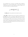
Figure 1: Block diagram of AM modulation scheme using direct digital synthesis [1:7] .............. 8
Figure 2: Block diagram of basis DDS [2:2] ................................................................................ 10
Figure 4: The DE2 board [4:4]..................................................................................................... 14
Figure 6: Flowchart of AM modulation scheme using direct digital synthesis [1:7] ................... 19
Figure 7: The Verilog HDL top-level file .................................................................................... 22
Figure 8: Quartus II compilation report ....................................................................................... 23
Figure 9: Loading sof file into DE2 board ................................................................................... 24
Figure 10: Effect of DAC Resolution [6] ..................................................................................... 25
Figure 12: DDS sine wave carrier with the frequency of 500 KHz. ............................................. 27
Figure 13: DDS sine wave carrier with the frequency of 1 MHz ................................................. 28
Figure 14: AM modulation test .................................................................................................... 29
6
CHAPTER I
INTRODUCTION
1.
Background
AM transmitter is a transmitter or radio transmitter using amplitude modulation. Amplitude
modulation (AM) is a technique used in electronic communication, most commonly for
transmitting information via a radio carrier wave. AM works by varying the strength of the
transmitted signal in relation to the information being sent. For example, changes in signal
strength may be used to specify the sounds to be reproduced by a loudspeaker, or the light
intensity of television pixels.
2.
Project Aims
The goal of this project was to build an AM transmitter on an FPGA with a carrier frequency at
1MHz. The direct digital synthesis (DDS) unit for the carrier should run at a clock of 50 MHz or
lower. The DDS for the audio can run at the same rate. The transmitter output should be
generated as 16-bit 2’s complement numbers, and then converted to 10-bit offset binary and sent
to the VGA DAC channel. The hardware will be use for AM transmitter on an FPGA is DE2
board.
7
Figure 1: Block diagram of AM modulation scheme using direct digital synthesis [1:7]
3.
Project objectives
The project objective of this thesis is:
Using direct digital synthesis to generate a 1.0 MHz sine wave as a carrier.
Multiply the carrier with an audio signal consisting of either a 400-Hz from a direct
digital synthesis unit or audio from the audio codec.
Use Verilog language to design the soft radio transmitter.
Implement the radio transmitter on an FPGA with the VGA output of the ADV7123 330MHz triple 10-bit high-speed video DAC.
Verify the functionality of the AM modulated radio transmitter.
8
CHAPTER II
BACKGROUND
1. Direct Digital Synthesis
Direct digital synthesis (DDS) is a technique for using digital data processing blocks as a means
to generate a frequency- and phase-tunable output signal referenced to a fixed-frequency
precision clock source. The tuning word enables a DDS implementation to provide good output
frequency tuning resolution. DDS is an alternative to traditional analog synthesizer solutions.
For many applications, the DDS solution holds some distinct advantages over the equivalent
analog frequency synthesizer employing PLL circuitry.
DDS advangtages:
digitally controlled micro-hertz frequency-tuning and sub-degree phase-tuning capability,
extremely fast hopping speed in tuning output frequency (or phase); phase-continuous
frequency hops with no overshoot/undershoot or analog-related loop settling-time
anomalies,
the digital architecture of DDS eliminates the need for the manual tuning and tweaking
related to component aging and temperature drift in analog synthesizer solutions, and
the digital control interface of the DDS architecture facilitates an environment where
systems can be remotely controlled and optimized with high resolution under processor
control.
Theory of operation:
As shown in the DDS block diagram in Fig. 2, the main components of direct digital synthesis
are a phase accumulator, a means of phase-to-amplitude conversion (often a sine look-up
table), and a DAC.
9
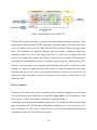
Figure 2: Block diagram of basis DDS [2:2]
The basic DDS requires two inputs: A system clock signal with Fs denoting its frequency, and a
digital numeric value denoted by FTW comprising a frequency tuning word. The system clock
serves as a timing reference for the DDS, while the FTW controls the output frequency tuning
word. The accumulator and angle to amplitude converter together constitute a numerically
controlled oscillator (or NCO). The output of the NCO is a time series of digital words that
occur at a rate equal to the system clock frequency. The time series of digital words represent a
sinusoidal waveform sampled at a rate of Fs and proccessing a frequency dictated by the FTW.
The DAC converts the time series of digital words produced by the NCO to an analog waveform,
yielding a so called real world signal at the DAC output. N, P and D constitute the width of the
interconnecting buses in bits. That is, the accumulatior buses are N-bits wide as is the FTW, the
input to the angle to amplitude converter is P-bits wide, and its output is D-bits wide as is the
input to the DAC.
Phase accumulator
The heart of the system is the phase accumulator whose contents is updated once each clock
cycle. Each time the phase accumulator is updated, the digital number, FTW, stored in the delta
phase register is added to the number in the phase accumulator register.
Assume that the number in the delta phase register is 00...01 and that the initial contents of the
phase accumulator is 00...00. The phase accumulator is updated by 00...01 on each clock cycl e.
If the accumulator is 32-bits wide, 232 clock cycles (over 4 billi on) are required before the phase
accumulator returns to 00...00, and the cycle repeats.
10
Angle to Amplitude converter
Angle-to-amplitude lookup table is used to convert a truncated version of the phase
accumulator’sinstantaneous output value into the sinewave amplitude information that is
presented to the D/A converter.
DAC (Digital to Analog converter)
The DAC converts the time series of digital words produced by the phase to amplitude
conversion to an analog waveform, yielding a so called real world signal at the DAC output.
.
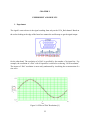
2. AM Modulation
Amplitude modulation (AM) is a technique used in electronic communication, most commonly
for transmitting information via a radio carrier wave. The amplitude of a sinusoidal signal with
fixed frequency and phase is varied in proportion to a given signal.
The output signal of a AM modulator is given by:
11
Figure 3: AM modulation [3]
12
The AM modulation index is the measure of the amplitude variation surrounding an
unmodulated carrier. As with other modulation indices, in AM this quantity (also called
"modulation depth") indicates how much the modulation varies around its "original" level. For
AM, it relates to variations in carrier amplitude and is defined as:
where
So if
and
are the message amplitude and carrier amplitude, respectively.
, carrier amplitude varies by 50% above (and below) its unmodulated level; for
, it varies by 100%. To avoid distortion, modulation depth must not exceed 100
percent. Transmitter systems will usually incorporate a limiter circuit to ensure this. However,
AM demodulators can be designed to detect the inversion (or 180-degree phase reversal) that
occurs when modulation exceeds 100 percent; they automatically correct for this defect.[citation
needed]. Variations of a modulated signal with percentages of modulation are shown in Fig. 3. In
each image, the maximum amplitude is higher than in the previous image (note that the scale
changes from one image to the next).
13
3. Hardware: The Altera DE2 Board
Figure 4: The DE2 board [4:4]
The DE2 board has many features that allow the user to implement a wide range of designed
circuits, from simple circuits to multimedia projects.
In addition to these hardware features, the DE2 board has software support for standard I/O
interfaces and a control panel facility for accessing various components. Also, software is
provided for a number of demonstrations that illustrate the advanced capabilities of the DE2
board.
In order to use the DE2 board, the user has to be familiar with the Quartus II software. The
necessary knowledge can be acquired by reading the tutorials Getting Started with Altera’s DE2
Board and Quartus II Introduction (which exists in th ree versions based on the design entry
method used, namely Verilog, VHDL or schematic entry).
This project will use: Cyclone II 2C35 FPGA, Clock inputs, VGA output … to do the project.
14
CHAPTER III
DESIGN
1. Design of Direct Digital Synthesis
DDS is a commonly used method for periodic waveform synthesis using a given reference
frequency, a lookup table (phase to amplitude conversion), an N-bit adder and associated
accumulator, and an FTW-bit phase increment value. The top 0 bits of the accumulator are used
as an index to the lookup table, which stores pre-computed samples of a single period of the
desired output waveform sinusoid. Adjusting the phase increment value the amount added to the
accumulator value on each cycle of the reference clock allows us to adjust the fundamental
frequency of the output waveform. The output frequency can be determined by the phase
increment using the following expression [2]:
Additionally, the phase increment for a desired frequency is [2]:
: desired frequency
: system clock
: phase accumulator
15
FTW: Frequency tuning word
where exact equality cannot be assured due to the fact that M is an integer value and therefore
cannot exactly replicate all frequency values
.
My design uses a 32-bit accumulator, a 31-bit increment, and an 8-bit accumulator output.
The accumulator output indexes into 256-entry lookup tables for sine wave lookup.
The 10-bit output connected to the VGA_R output of the DE2 board.
In DDS carrier, phase accumulator is very important. My design uses 32-bit accumulator, 50
MHz system clock, and 1 MHz desired frequency of carrier.
Based on the equation above, we calculate the phase increment for DDS
Because the value of M must be an integer, so that, the value of M use for phase accumulator of
DDS will be :
The actual DDS output frequency is:
16
Each time the phase accumulator is updated, the digital number FTW is added to the number in
the phase accumulator register. The phase accumulator is updated by 85899346 on each clock
cycle.
The frequency resolution of the system is equal to
. For N = 32, the resolution is greater
than one part in four billion. In a practical DDS system, all the bits out of the phase accumulator
are not passed on to the lookup table, but are truncated. In this project I will use 14-bit MSBs
which does not significantly affect the frequency resolution.
The output of the phase accumulator is linear and cannot directly be used to generate a sine wave
or any other waveform except a ramp. Therefore, a phase to amplitude conversion (a lookup
table) is used to convert a truncated version of the phase accumulator’s instantaneous output
value into sine wave amplitude information that is presented to the D/A converter. Most DDS
architectures exploit the symmetrical nature of a sine wave and utilize mapping logic to
synthesize a complete sine wave cycle from ¼ cycle of data from the phase accumulator. The
phase-to-amplitude lookup table generates all the necessary data by reading forward then back
through the lookup table.
Figure 5: Signal flow through the DDS architecture [6:6]
17
The phase truncated in this project is 14-bit MSBs. A Verilog ROM module is used to generate a
16-bit sine wave. The table is designed to generate a sine wave with only 14 bits of amplitude, so
that two sine waves can be added without further scaling to prevent overflow.
The table is designed by Matlab program with 14 bit of amplitude, and 8 bit address.
x = 1:256;
% Sin : scale to 15-bits
% 2's complement!
y = fix(((2^14)-1)*sin(2*pi*(x-1)/256));
for i=x
if y(i)<0
y(i) = 2^16 + y(i);
end
fprintf('\t\t\t8''h%02x: sine = 16''h%04x ;\n', x(i)-1 ,y(i))
end
For output through the VGA DAC, I will need to convert the 16-bit 2's comp to 10-bit
offset binary.
18
2. AM Modulation in DDS
Phase Accumulator
Audio codec
Sine lookup table
1
output
DAC
400 Hz DDS unit
0
Figure 6: Flowchart of AM modulation scheme using direct digital synthesis [1:7]
Figure 6 shows the AM modulation in DDS system. In this project, we can multiply the
carrier by an audio signal consisting of either a 400 Hz DDS unit or audio from the
audio codec module.
Using a 400 Hz DDS unit which is the same as the DDS carrier and only change the
frequency of it. Following the equations we calculate the phase increment of 400 Hz
[2]:
19
It will use the same lookup table of the carrier. After that we multiply carrier with 400 Hz DDS
unit. Both of them use 8 bits.
Using audio codec to modulate
The DE2 board provides high-quality 24-bit audio via the Wolfson WM8731 audio CODEC.
This chip supports microphone-in, line-in, and line-out ports, with a sample rate adjustable from
8 kHz to 96 kHz. We provide the music from mobile phone, laptop… via the line in port on DE2
board, using The hardware audio interface is a Wolfson WM8731 is controlled by an I2C
interface which is connected to pins on the Cyclone II FPGA. After that, we do such as in figure
shown, multiply the carrier by audio codec module.
On the other hand, There are a set of modules which are needed for all of the test programs
below which interface to the audio codec. They are:
I2C_AV_Config.v, I2C_Controller.v, Reset_Delay.v,AUDIO_DAC_ADC.v , All of it
is written in Verilog HDL.
3. User Interface
In order to adjust modulation of AM modulate with 400 Hz DDS unit or audio codec, the SW0
switches on the DE2 board are used to control the AM modulation output. When SW0 is not
pressed, modulate with 400 Hz DDS unit, when SW0 is pressed, modulate with audio codec.
4. VGA Output
Because the wave generator outputs pure voltage values through the VGA interface, without the
need for any sort of framing or timing, the code required to configure the VGA module is very
simple. We merely connect the output of the DDS lookup table mux to the VGA_R pin, drive
VGA_BLANK and VGA_SYNC to 1, and assign the main system clock to VGA_CLK. The
FPGA will program in the Run position. This design will make on the Altera Cyclone II
20
DE2 board. The major advantage of DE2 board was it supports the hardware components
needed, such as the basic FPGA support circuitry (power supply, programming, etc.), as well as
switches and buttons for user input along with VGA output port.
5. Verilog HDL Design
Verilog is a Hardware Description Language (HDL). A hardware description language is a
language used to describe a digital system: for example, a network switch, a microprocessor or a
memory or a simple flip-flop. This just means that, by using a HDL, one can describe any
(digital) hardware at any level.
In this project, Verilog HDL is used to describe an AM transmitter on FPGA. The top-level
Verilog file is called DE2_Default.v which defines ports that correspond to all of the useraccessible pins on the Cyclone II FPGA.
The table below describes each Verilog module:
DE2_Default : The top level module for our project. Included in this module are instantiations
of the modules listed below.
Reset_Delay: Needed to run the phase lock loop.
VGA_Audio_PLL: Used for generating the clocks used to run all of the modules, specifically
AUD_CTRL_CLK.
I2C_AV_Config: Needed to use the Audio Codec.
AUDIO_DAC_ADC: Module to run the inputs and outputs to the Audio Codec.
sync_rom: Look-up table for the synthesized sinusoids. The module takes accumulators (which
are increased at varying frequencies) as inputs and it outputs the corresponding sine values.
21
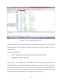
Figure 7: The Verilog HDL top-level file
Using Verilog HDL file of Quartus II software a system had to be built on the chip that would
interconnect all the Verilog modules as physical components on the FPGA board to create an
AM transmitter.
The purpose of this part is:
Using Verilog HDL file to design AM transmitter in Quartus II software
Implement the design on DE2 board.
All we need to do is instantiate the Verilog HDL file, the Verilog module generated by the
Verilog HDL file is in the file DE2_Default.v in the directory of the project, connect inputs and
outputs of the parallel I/O ports, as well as the clock and reset inputs, to the appropriate pins on
the Cyclone-series device. Note that the name of the Verilog module is the same as the system
name specified when first using the top-level design entity for this project.
22
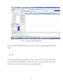
After successful compilation of AM transmitter on Quartus II the files that were required to
program the DE2 board were obtained. It was then programmed using the Quartus II
programmer. All the Verilog modules were successfully programmed into the board.
Figure 8: Quartus II compilation report
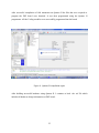
After building successful hardware using Quartus II. I continue to load the .sof file which
includes all hardware design information on DE2 board:
23
Figure 9: Loading sof file into DE2 board
The output would be available through the VGA port, using the VGA_Red channel for the output
signal.
6. Test
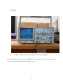
Due to the limited required functionality of the wave generator. The key points of the design
were the DDS unit, AM modulation, and the VGA output. Testing was carried out using the
oscilloscope to verify correctness of frequency and waveform shape.
24
CHAPTER V
EXPERIMENT AND RESULTS
1. Experiment
The signal I want to detect is the signal resulting from only on the VGA_Red channel. Based on
the socket looking at the edge of the board we connect the oscilloscope to get the signal output.
On the other hand, The resolution of a DAC is specified by the number of its input bits. For
example, the resolution of a DAC with 10 input bits is referred to as having “10-bit resolution”.
The impact of DAC resolution is most easily understood by visualizing the reconstruction of a
sine wave.
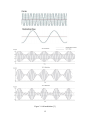
Figure 10: Effect of DAC Resolution [6]
25
Consider Fig. 10 in which a 4-bit DAC (quantized black trace) is used to reconstruct a perfect
sine wave (smooth red trace). The vertical lines are time markers and identify the instants in
timeat which the DAC output is updated to a new value. Thus, the horizontal distance between
the vertical lines represents the sample period. Note the deviation between the DAC output
signal and the perfect sine wave. The vertical distance between the two traces at the sampling
instants is the error introduced by the DAC as a result of its finite resolution. This error is known
as quantization error and gives rise to an effect known as quantization distortion.
To understand the nature of the quantization distortion, note the sharp edges in the DAC output
signal. These sharp edges imply the presence of high frequency components superimposed on
the fundamental. It is these high frequency components that constitute quantization distortion. In
the frequency domain, quantization distortion errors are aliased within the Nyquist band and
appear as discrete spurs in the DAC output spectrum.
Figure 11: 4-Bit vs. 8-Bit DAC output spectra [6:6]
As the DAC resolution increases the quantization distortion decreases; i.e., the spurious content
of the DAC output spectrum decreases. This makes sense because an increase in resolution
results in a decrease in quantization error. This, in turn, results in less error in the reconstructed
sine wave. Less error implies less distortion; i.e., less spurious content. This is graphically
depicted in Figure 11. Note that the spurs associated with the 8-bit DAC are generally lower
than those of the 4-bit DAC
26
2. Results
Figure 12: DDS sine wave carrier with the frequency of 500 KHz.
On the oscilloscope, I set the value of TIME/DIV = 1 microsecond, we can see on this picture
the value of frequency carrier base the formula
27
Figure 13: DDS sine wave carrier with the frequency of 1 MHz
The same with the DDS sine wave carrier above, I also set the TIME/DIV = 1 microsecond, and
VOLTS/DIV = 0.2 V.
After the test DDS carrier through VGA channel, I will show you the result of AM transmitter
on FPGA also via VGA , and modulate DDS carrier with 400 Hz DDS unit.
28
Figure 14: AM modulation test
As the figure 14, the first figure shows the AM modulation with set TIME/DIV = 2 mS, and
VOLTS/DIV = 0.1 V. The second figure shows the AM modulation with set TIME/DIV = 1
microsecond, and VOLTS/DIV = 0.1 V.
To implement on the DE2 board , Altera DE2 board is connected to power and to the PC as
specified in the evaluation board description, the toggle switch on the left edge of the board
marked (Run/Prog) is in the Run position and it is left there at all times. The FPGA will program
in the Run position.
3. Conclusion
Based on the results above, I designed an AM transmitter on FPGA successfully. Beside,
studying and understanding the technology of Direct Digital Synthesis to generate sine
wave. I used a DDS module as a carrier to modulate AM. I achieved the goal of the project.
29
REFERENCES
[1] “MT-085 TUTORIAL Fundamentals of Direct Digital Synthesis (DDS)”, Analog Devices,
Inc., 2009. Available FTP: http://www.analog.com/static/imported-files/tutorials/MT-085.pdf
[2] “The Accumulator”, Digi-Key Corp., MN 56701 USA, 1995-2013. Available FTP:
http://dkc1.digikey.com/ca/en/tod/ADI/Accumulator_NoAudio/Accumulator_NoAudio.html
[3] “Communication system 4th Edition”, Simon Haykin, John Wiley & Sons, Inc.
[4] “DE2 Development and Education Board. User Manual”, Altera Corp., Version 1.4, 2006.
Available FTP: ftp://ftp.altera.com/up/pub/Webdocs/DE2_UserManual.pdf
[5] “ADV7123, CMOS, 330 MHz, Triple 10-Bit High Speed Video DAC”, Norwood, U.S.A,
Rev. D, 2010. Available FTP: http://www.analog.com/static/importedfiles/data_sheets/ADV7123.pdf
[6] “A Technical Tutorial on Digital Signal Synthesis”, Analog Devices, Inc., 1999. Available
FTP: http://www.ieee.li/pdf/essay/dds.pdf
[7] “Angle to Amplitude converter”, Digi-Key Corp., MN 56701 USA, 1995-2013. Available
FTP: http://dkc1.digikey.com/us/en/tod/ADI/Angle-to-Amplitude-Converter/Angle-toAmplitude-Converter.html
[8] “Digital to Analog Converter”, Digi-Key Corp., MN 56701 USA, 1995-2013. Available FTP:
http://dkc1.digikey.com/hk/en/tod/ADI/Digital-to-Analog_NoAudio/Digital-toAnalog_NoAudio.html
30
APPENDICES
The main codec of AM transmitters
/// audio stuff /////////////////////////////////////////////////
// output to audio DAC
wire signed [15:0] audio_outL, audio_outR ;
// input from audio ADC
wire signed [15:0] audio_inL, audio_inR ;
//make a direct digital systnesis accumulator
// and output a 10-bit sine wave to the VGA plug
// set carrier frequency to 1 MHz DDS_incr = 32'h51EB84C
// set modulation to 400 Hz 85E7
//DDS hardware
// increment = 85.8993 * desired freq (50MHz sample rate)
reg [31:0] DDS_accum_carrier1;
wire signed [15:0] carrier1_out ;
reg [31:0] DDS_accum_mod1;
wire signed [15:0] mod1_out, modulation;
wire signed [15:0] xmit_out ;
wire [9:0] xmit_out_10bit ;
always @ (posedge CLOCK_50) begin
//transmitter 1
DDS_accum_carrier1 <= DDS_accum_carrier1 + 32'h51EB84C ;
31
DDS_accum_mod1 = DDS_accum_mod1 + 32'h85E7 ; //400 hz
End
//hook up the ROM table for carriers
sync_rom carrier1_table(CLOCK_50, DDS_accum_carrier1[31:24], carrier1_out);
//hook up the ROM table for modulation
sync_rom mod1_Table(CLOCK_50, DDS_accum_mod1[31:24], mod1_out);
// choose modulation
assign modulation = SW[0]? audio_inL : mod1_out ;
// balanced modulation
signed_mult xmit1( xmit_out, carrier1_out, (modulation + 16'h4000));
// convert 16-bit 2'comp to 10-bit offset binary for DAC
assign xmit_out_10bit = xmit_out[15:6] + 10'd512 ;
//use the VGA DAC for an AM modulated RF signal
assign VGA_R = xmit_out_10bit ;
assign VGA_SYNC = 1 ;
assign VGA_BLANK = 1 ;
assign VGA_CLK = CLOCK_50 ;
endmodule
32
//////////////////////////////////////////////////
//// signed mult of 0.16 format 2'comp////////////
//////////////////////////////////////////////////
module signed_mult (out, a, b);
output
[15:0] out;
input signed [15:0] a;
input signed [15:0] b;
wire
signed [15:0] out;
wire
signed [31:0] mult_out;
assign mult_out = a * b;
assign out = {mult_out[31], mult_out[29:15]} ;
//assign out = mult_out[31:16] ;
endmodule
//////////////////////////////////////////////////
////////////
Sin Wave ROM Table //////////////
//////////////////////////////////////////////////
// produces a 2's comp, 16-bit, approximation
// of a sine wave, given an input phase (address)
module sync_rom (clock, address, sine);
input clock;
33
input [7:0] address;
output [15:0] sine;
reg signed [15:0] sine;
always@(posedge clock)
begin
case(address)
8'h00: sine = 16'h0000 ;
8'h01: sine = 16'h0192 ;
8'h02: sine = 16'h0323 ;
8'h03: sine = 16'h04b5 ;
8'h04: sine = 16'h0645 ;
8'h05: sine = 16'h07d5 ;
8'h06: sine = 16'h0963 ;
8'h07: sine = 16'h0af0 ;
8'h08: sine = 16'h0c7c ;
8'h09: sine = 16'h0e05 ;
8'h0a: sine = 16'h0f8c ;
8'h0b: sine = 16'h1111 ;
8'h0c: sine = 16'h1293 ;
8'h0d: sine = 16'h1413 ;
8'h0e: sine = 16'h158f ;
8'h0f: sine = 16'h1708 ;
8'h10: sine = 16'h187d ;
34
8'h11: sine = 16'h19ef ;
8'h12: sine = 16'h1b5c ;
8'h13: sine = 16'h1cc5 ;
8'h14: sine = 16'h1e2a ;
8'h15: sine = 16'h1f8b ;
8'h16: sine = 16'h20e6 ;
8'h17: sine = 16'h223c ;
8'h18: sine = 16'h238d ;
8'h19: sine = 16'h24d9 ;
8'h1a: sine = 16'h261f ;
8'h1b: sine = 16'h275f ;
8'h1c: sine = 16'h2899 ;
8'h1d: sine = 16'h29cc ;
8'h1e: sine = 16'h2afa ;
8'h1f: sine = 16'h2c20 ;
8'h20: sine = 16'h2d40 ;
8'h21: sine = 16'h2e59 ;
8'h22: sine = 16'h2f6b ;
8'h23: sine = 16'h3075 ;
8'h24: sine = 16'h3178 ;
8'h25: sine = 16'h3273 ;
8'h26: sine = 16'h3366 ;
8'h27: sine = 16'h3452 ;
35
8'h28: sine = 16'h3535 ;
8'h29: sine = 16'h3611 ;
8'h2a: sine = 16'h36e4 ;
8'h2b: sine = 16'h37ae ;
8'h2c: sine = 16'h3870 ;
8'h2d: sine = 16'h3929 ;
8'h2e: sine = 16'h39da ;
8'h2f: sine = 16'h3a81 ;
8'h30: sine = 16'h3b1f ;
8'h31: sine = 16'h3bb5 ;
8'h32: sine = 16'h3c41 ;
8'h33: sine = 16'h3cc4 ;
8'h34: sine = 16'h3d3d ;
8'h35: sine = 16'h3dad ;
8'h36: sine = 16'h3e14 ;
8'h37: sine = 16'h3e70 ;
8'h38: sine = 16'h3ec4 ;
8'h39: sine = 16'h3f0d ;
8'h3a: sine = 16'h3f4d ;
8'h3b: sine = 16'h3f83 ;
8'h3c: sine = 16'h3fb0 ;
8'h3d: sine = 16'h3fd2 ;
8'h3e: sine = 16'h3feb ;
36
8'h3f: sine = 16'h3ffa ;
8'h40: sine = 16'h3fff ;
8'h41: sine = 16'h3ffa ;
8'h42: sine = 16'h3feb ;
8'h43: sine = 16'h3fd2 ;
8'h44: sine = 16'h3fb0 ;
8'h45: sine = 16'h3f83 ;
8'h46: sine = 16'h3f4d ;
8'h47: sine = 16'h3f0d ;
8'h48: sine = 16'h3ec4 ;
8'h49: sine = 16'h3e70 ;
8'h4a: sine = 16'h3e14 ;
8'h4b: sine = 16'h3dad ;
8'h4c: sine = 16'h3d3d ;
8'h4d: sine = 16'h3cc4 ;
8'h4e: sine = 16'h3c41 ;
8'h4f: sine = 16'h3bb5 ;
8'h50: sine = 16'h3b1f ;
8'h51: sine = 16'h3a81 ;
8'h52: sine = 16'h39da ;
8'h53: sine = 16'h3929 ;
8'h54: sine = 16'h3870 ;
8'h55: sine = 16'h37ae ;
37
8'h56: sine = 16'h36e4 ;
8'h57: sine = 16'h3611 ;
8'h58: sine = 16'h3535 ;
8'h59: sine = 16'h3452 ;
8'h5a: sine = 16'h3366 ;
8'h5b: sine = 16'h3273 ;
8'h5c: sine = 16'h3178 ;
8'h5d: sine = 16'h3075 ;
8'h5e: sine = 16'h2f6b ;
8'h5f: sine = 16'h2e59 ;
8'h60: sine = 16'h2d40 ;
8'h61: sine = 16'h2c20 ;
8'h62: sine = 16'h2afa ;
8'h63: sine = 16'h29cc ;
8'h64: sine = 16'h2899 ;
8'h65: sine = 16'h275f ;
8'h66: sine = 16'h261f ;
8'h67: sine = 16'h24d9 ;
8'h68: sine = 16'h238d ;
8'h69: sine = 16'h223c ;
8'h6a: sine = 16'h20e6 ;
8'h6b: sine = 16'h1f8b ;
8'h6c: sine = 16'h1e2a ;
38
8'h6d: sine = 16'h1cc5 ;
8'h6e: sine = 16'h1b5c ;
8'h6f: sine = 16'h19ef ;
8'h70: sine = 16'h187d ;
8'h71: sine = 16'h1708 ;
8'h72: sine = 16'h158f ;
8'h73: sine = 16'h1413 ;
8'h74: sine = 16'h1293 ;
8'h75: sine = 16'h1111 ;
8'h76: sine = 16'h0f8c ;
8'h77: sine = 16'h0e05 ;
8'h78: sine = 16'h0c7c ;
8'h79: sine = 16'h0af0 ;
8'h7a: sine = 16'h0963 ;
8'h7b: sine = 16'h07d5 ;
8'h7c: sine = 16'h0645 ;
8'h7d: sine = 16'h04b5 ;
8'h7e: sine = 16'h0323 ;
8'h7f: sine = 16'h0192 ;
8'h80: sine = 16'h0000 ;
8'h81: sine = 16'hfe6e ;
8'h82: sine = 16'hfcdd ;
8'h83: sine = 16'hfb4b ;
39
8'h84: sine = 16'hf9bb ;
8'h85: sine = 16'hf82b ;
8'h86: sine = 16'hf69d ;
8'h87: sine = 16'hf510 ;
8'h88: sine = 16'hf384 ;
8'h89: sine = 16'hf1fb ;
8'h8a: sine = 16'hf074 ;
8'h8b: sine = 16'heeef ;
8'h8c: sine = 16'hed6d ;
8'h8d: sine = 16'hebed ;
8'h8e: sine = 16'hea71 ;
8'h8f: sine = 16'he8f8 ;
8'h90: sine = 16'he783 ;
8'h91: sine = 16'he611 ;
8'h92: sine = 16'he4a4 ;
8'h93: sine = 16'he33b ;
8'h94: sine = 16'he1d6 ;
8'h95: sine = 16'he075 ;
8'h96: sine = 16'hdf1a ;
8'h97: sine = 16'hddc4 ;
8'h98: sine = 16'hdc73 ;
8'h99: sine = 16'hdb27 ;
8'h9a: sine = 16'hd9e1 ;
40
8'h9b: sine = 16'hd8a1 ;
8'h9c: sine = 16'hd767 ;
8'h9d: sine = 16'hd634 ;
8'h9e: sine = 16'hd506 ;
8'h9f: sine = 16'hd3e0 ;
8'ha0: sine = 16'hd2c0 ;
8'ha1: sine = 16'hd1a7 ;
8'ha2: sine = 16'hd095 ;
8'ha3: sine = 16'hcf8b ;
8'ha4: sine = 16'hce88 ;
8'ha5: sine = 16'hcd8d ;
8'ha6: sine = 16'hcc9a ;
8'ha7: sine = 16'hcbae ;
8'ha8: sine = 16'hcacb ;
8'ha9: sine = 16'hc9ef ;
8'haa: sine = 16'hc91c ;
8'hab: sine = 16'hc852 ;
8'hac: sine = 16'hc790 ;
8'had: sine = 16'hc6d7 ;
8'hae: sine = 16'hc626 ;
8'haf: sine = 16'hc57f ;
8'hb0: sine = 16'hc4e1 ;
8'hb1: sine = 16'hc44b ;
41
8'hb2: sine = 16'hc3bf ;
8'hb3: sine = 16'hc33c ;
8'hb4: sine = 16'hc2c3 ;
8'hb5: sine = 16'hc253 ;
8'hb6: sine = 16'hc1ec ;
8'hb7: sine = 16'hc190 ;
8'hb8: sine = 16'hc13c ;
8'hb9: sine = 16'hc0f3 ;
8'hba: sine = 16'hc0b3 ;
8'hbb: sine = 16'hc07d ;
8'hbc: sine = 16'hc050 ;
8'hbd: sine = 16'hc02e ;
8'hbe: sine = 16'hc015 ;
8'hbf: sine = 16'hc006 ;
8'hc0: sine = 16'hc001 ;
8'hc1: sine = 16'hc006 ;
8'hc2: sine = 16'hc015 ;
8'hc3: sine = 16'hc02e ;
8'hc4: sine = 16'hc050 ;
8'hc5: sine = 16'hc07d ;
8'hc6: sine = 16'hc0b3 ;
8'hc7: sine = 16'hc0f3 ;
8'hc8: sine = 16'hc13c ;
42
8'hc9: sine = 16'hc190 ;
8'hca: sine = 16'hc1ec ;
8'hcb: sine = 16'hc253 ;
8'hcc: sine = 16'hc2c3 ;
8'hcd: sine = 16'hc33c ;
8'hce: sine = 16'hc3bf ;
8'hcf: sine = 16'hc44b ;
8'hd0: sine = 16'hc4e1 ;
8'hd1: sine = 16'hc57f ;
8'hd2: sine = 16'hc626 ;
8'hd3: sine = 16'hc6d7 ;
8'hd4: sine = 16'hc790 ;
8'hd5: sine = 16'hc852 ;
8'hd6: sine = 16'hc91c ;
8'hd7: sine = 16'hc9ef ;
8'hd8: sine = 16'hcacb ;
8'hd9: sine = 16'hcbae ;
8'hda: sine = 16'hcc9a ;
8'hdb: sine = 16'hcd8d ;
8'hdc: sine = 16'hce88 ;
8'hdd: sine = 16'hcf8b ;
8'hde: sine = 16'hd095 ;
8'hdf: sine = 16'hd1a7 ;
43
8'he0: sine = 16'hd2c0 ;
8'he1: sine = 16'hd3e0 ;
8'he2: sine = 16'hd506 ;
8'he3: sine = 16'hd634 ;
8'he4: sine = 16'hd767 ;
8'he5: sine = 16'hd8a1 ;
8'he6: sine = 16'hd9e1 ;
8'he7: sine = 16'hdb27 ;
8'he8: sine = 16'hdc73 ;
8'he9: sine = 16'hddc4 ;
8'hea: sine = 16'hdf1a ;
8'heb: sine = 16'he075 ;
8'hec: sine = 16'he1d6 ;
8'hed: sine = 16'he33b ;
8'hee: sine = 16'he4a4 ;
8'hef: sine = 16'he611 ;
8'hf0: sine = 16'he783 ;
8'hf1: sine = 16'he8f8 ;
8'hf2: sine = 16'hea71 ;
8'hf3: sine = 16'hebed ;
8'hf4: sine = 16'hed6d ;
8'hf5: sine = 16'heeef ;
8'hf6: sine = 16'hf074 ;
44
8'hf7: sine = 16'hf1fb ;
8'hf8: sine = 16'hf384 ;
8'hf9: sine = 16'hf510 ;
8'hfa: sine = 16'hf69d ;
8'hfb: sine = 16'hf82b ;
8'hfc: sine = 16'hf9bb ;
8'hfd: sine = 16'hfb4b ;
8'hfe: sine = 16'hfcdd ;
8'hff: sine = 16'hfe6e ;
endcase
end
endmodule
45