1
ABSTRACT
SULE, AMBARISH MUKUND Hardware-Software Codesign of a Programmable
Wireless Receiver System-on-a-chip. (Under the direction of Prof. William Rhett
Davis).
With gate counts and system complexity growing rapidly, engineers have to find
efficient ways of designing hardware circuits. The advent of Hardware Description
Languages and synthesis methodologies improved designer productivity by raising
the abstraction level. With advances in semiconductor manufacturing technology,
however, there is still a growing productivity gap between the number of transistorsper-chip that can be fabricated and the transistors-per-day that can be effectively
designed[13].
Increasing costs of design encourage reusing cores. Various kinds of Intellectual
Property(IP) cores are now widely available and are used in making Integrated Circuits(IC). These System-on-a-chip(SOC) ICs generally contain a microprocessor as
one of their IP cores in order to make them more flexible. This heterogeneity of
hardware has increased challenges in verification. It is widely estimated that between 60%–80% of the design effort is dedicated to verification[12] with almost half
of that time spent in construction and debugging of the simulation environments.
Unfortunately, the high costs of industrial IP have made it difficult to explore SOC
verification at Universities.
This thesis describes the building of a Programmable Wireless Receiver SOC using
hardware-software codesign techniques. The SOC is comprised of a general purpose
Central Processing Unit(CPU) and a baseband coprocessor with some glue logic. The
CPU used is open-source, making it appropriate for teaching SOC verification as part
of a university curriculum. The simulation environment adopted to verify the system
and its documentation is an important product of this thesis. The thesis can be used
as a guideline for designing CPU-based SOCs.
Hardware-Software Codesign of a Programmable Wireless Receiver
System-on-a-chip
by
Ambarish Mukund Sule
A thesis submitted to the Graduate Faculty of
North Carolina State University
in partial satisfaction of the
requirements for the Degree of
Master of Science
Department of Electrical and Computer Engineering
Raleigh
2003
Approved By:
Prof. Eric Rotenberg
Prof. Alexander G. Dean
Prof. William Rhett Davis
Chair of Advisory Committee
To
Aai - Baba
ii
Biography
Ambarish Mukund Sule was born on 2nd December 1977 in Mumbai, India. He
received the Bachelor of Engineering (B.E.) Degree in Electronics Engineering from
Veermata Jijabai Technological Institute (V.J.T.I.), University of Mumbai in 1999.
He worked briefly as a Software Engineer at Infosys Technologies Ltd. Pune, India.
Thereafter he worked for about 2 years as an IC Design and Verification Engineer at
Texas Instruments, Bangalore, India.
Ambarish has been a graduate student in the Electrical and Computer Engineering
Department at North Carolina State University, Raleigh, NC since Fall 2001. He is a
member of the Honor Society of Phi Kappa Phi and a student member of the Institute
of Electrical and Electronics Engineers (IEEE). Since Fall 2002, he has been working
with the MUSE group of Prof. Rhett Davis in the field of ASIC and System-level
Design.
iii
Acknowledgements
First and foremost I would like to thank my parents and elder sister Anjali for
everything they have given me in life. It is only due to their love, support and
encouragement that I could achieve whatever I have achieved. Special thanks to my
father for continuously inspiring me with immense hard work and dedication towards
his goals. I thank my cousin brother Pushkar and sister-in-law Aparna Tamhane for
making me feel at home, 8000 miles away from home.
I sincerely thank my advisor Prof. Rhett Davis for giving me the opportunity to
work under his guidance. His vision and ideas are primarily responsible for the design
we built. His enthusiasm towards ASIC Design is really contagious and inspiring. I
have learned some fantastic things about ASIC Design tools from him and hope to
keep learning in the future.
I thank Prof. Eric Rotenberg for agreeing to be on my thesis committee and teaching me some incredible things about computer architecture. I also thank Prof. Alexander Dean for agreeing to be on my thesis committee and giving me the opportunity
to work on his Thrint Research Compiler.
Thanks are due to Ravi Jenkal for designing most parts of the Wireless Receiver
frontend I have used in the thesis. I thank Jiri Gaisler for designing the LEON-2
Processor and making it widely available as open source. Thanks to all the LATEX 2ε
developers and maintainers for creating this wonderful document typesetting system,
which I used for writing this thesis. Finally, I would like to thank John Goss from
IBM, Raleigh for making me his Teaching Assistant for the ASIC Verification Course
and also showing me a whole new perspective towards verification.
iv
Contents
List of Figures
vii
List of Tables
viii
1 Introduction
1.1 Overview . . .
1.2 Related Work
1.3 Contribution .
1.4 Organization
.
.
.
.
1
1
2
3
5
.
.
.
.
.
.
6
6
8
10
12
13
13
.
.
.
.
.
.
15
15
16
17
19
20
22
4 Integration of the WLSOC System
4.1 Stitching together the pieces . . . . . . . . . . . . . . . . . . . . . . .
4.2 Interrupts/Traps . . . . . . . . . . . . . . . . . . . . . . . . . . . . .
4.2.1 Overview of Interrupts and Traps . . . . . . . . . . . . . . . .
23
23
25
25
2 The
2.1
2.2
2.3
2.4
2.5
2.6
.
.
.
.
.
.
.
.
.
.
.
.
.
.
.
.
.
.
.
.
.
.
.
.
.
.
.
.
.
.
.
.
.
.
.
.
.
.
.
.
.
.
.
.
.
.
.
.
.
.
.
.
.
.
.
.
.
.
.
.
.
.
.
.
LEON-2 Processor System
Overview of the Original LEON-2 System
Integer Unit . . . . . . . . . . . . . . . . .
Memory Interface . . . . . . . . . . . . . .
UARTs . . . . . . . . . . . . . . . . . . . .
Interrupt Controller . . . . . . . . . . . . .
Parallel I/O port . . . . . . . . . . . . . .
3 Wireless System
3.1 Protocol . . . . .
3.2 Overall Design . .
3.3 Wireless Frontend
3.4 Decorrelator . . .
3.5 WLRCV Buffer .
3.6 Register File . . .
.
.
.
.
.
.
.
.
.
.
.
.
.
.
.
.
.
.
.
.
.
.
.
.
.
.
.
.
.
.
.
.
.
.
.
.
.
.
.
.
.
.
.
.
.
.
.
.
.
.
.
.
.
.
v
.
.
.
.
.
.
.
.
.
.
.
.
.
.
.
.
.
.
.
.
.
.
.
.
.
.
.
.
.
.
.
.
.
.
.
.
.
.
.
.
.
.
.
.
.
.
.
.
.
.
.
.
.
.
.
.
.
.
.
.
.
.
.
.
.
.
.
.
.
.
.
.
.
.
.
.
.
.
.
.
.
.
.
.
.
.
.
.
.
.
.
.
.
.
.
.
.
.
.
.
.
.
.
.
.
.
.
.
.
.
.
.
.
.
.
.
.
.
.
.
.
.
.
.
.
.
.
.
.
.
.
.
.
.
.
.
.
.
.
.
.
.
.
.
.
.
.
.
.
.
.
.
.
.
.
.
.
.
.
.
.
.
.
.
.
.
.
.
.
.
.
.
.
.
.
.
.
.
.
.
.
.
.
.
.
.
.
.
.
.
.
.
.
.
.
.
.
.
.
.
.
.
.
.
.
.
.
.
.
.
.
.
.
.
.
.
.
.
.
.
.
.
.
.
.
.
.
.
.
.
.
.
.
.
.
.
.
.
.
.
.
.
.
.
.
.
.
.
.
.
.
.
.
.
CONTENTS
4.3
4.2.2 Instruction-induced Traps . . .
4.2.3 Peripheral/External Interrupts .
Memory Map . . . . . . . . . . . . . .
4.3.1 Advanced High-speed Bus . . .
4.3.2 Advanced Peripheral Bus . . . .
.
.
.
.
.
.
.
.
.
.
.
.
.
.
.
5 Tool Flow
5.1 Tool flow . . . . . . . . . . . . . . . . . . . .
5.1.1 Nomenclature . . . . . . . . . . . . .
5.2 Xilinx System Generator . . . . . . . . . . .
5.3 Embedded Software . . . . . . . . . . . . . .
5.3.1 Boot Code . . . . . . . . . . . . . . .
5.3.2 Device Drivers . . . . . . . . . . . . .
5.3.3 ISR for WLRCV . . . . . . . . . . .
5.3.4 Compiling . . . . . . . . . . . . . . .
5.4 Stimuli Generation . . . . . . . . . . . . . .
5.5 Interface between Specman and C++ Code .
5.6 Specman Checker . . . . . . . . . . . . . . .
5.7 Decompilation of the Embedded Software . .
5.8 Printing Debug Messages . . . . . . . . . . .
5.9 Testcase Characteristics . . . . . . . . . . .
6 Results
6.1 Simulation Results
6.2 Synthesis Results .
6.3 Observations . . . .
6.4 Future Directions .
.
.
.
.
.
.
.
.
.
.
.
.
.
.
.
.
.
.
.
.
.
.
.
.
.
.
.
.
.
.
.
.
.
.
.
.
.
.
.
.
.
.
.
.
.
.
.
.
.
.
.
.
.
.
.
.
.
.
.
.
.
.
.
.
.
.
.
.
.
.
.
.
.
.
.
.
.
.
.
.
.
.
.
.
.
.
.
.
.
.
.
.
.
.
.
.
.
.
.
.
.
.
.
.
.
.
.
.
.
.
.
.
.
.
.
.
.
.
.
.
.
.
.
.
.
.
.
.
.
.
.
.
.
.
.
.
.
.
.
.
.
.
.
.
.
.
.
.
.
.
.
.
.
.
.
.
.
.
.
.
.
.
.
.
.
.
.
.
.
.
.
.
.
.
.
.
.
.
.
.
.
.
.
.
.
.
.
.
.
.
.
.
.
.
.
.
.
.
.
.
.
.
.
.
.
.
.
.
.
.
.
.
.
.
.
.
.
.
.
.
.
.
.
.
.
.
.
.
.
.
.
.
.
.
.
.
.
.
.
.
.
.
.
.
.
.
.
.
.
.
.
.
.
.
.
.
.
.
.
.
.
.
.
.
.
.
.
.
.
.
.
.
.
.
.
.
.
.
.
.
.
.
.
.
.
.
.
.
.
.
.
.
.
.
.
.
.
.
.
.
.
.
.
.
.
.
.
.
.
.
.
.
.
.
.
.
.
.
.
.
.
.
.
.
.
.
.
.
.
.
.
.
.
.
.
.
.
.
.
.
.
.
.
.
.
.
.
.
.
.
.
.
.
.
.
.
.
.
.
.
25
26
27
27
28
.
.
.
.
.
.
.
.
.
.
.
.
.
.
33
33
35
36
37
37
38
38
39
41
44
46
48
52
57
.
.
.
.
62
62
63
64
65
Bibliography
66
A Specman Code
68
B C++ Code
75
C Embedded Software
79
D VHDL Code
83
vi
List of Figures
1.1 Introduction to HW/SW Coverification . . . . . . . . . . . . . . . . .
1.2 Overview of the Wireless LAN SOC Cosimulation . . . . . . . . . . .
2
4
2.1
2.2
2.3
2.4
2.5
Original LEON-2 System Conceptual Block Diagram
Overlapping Register Windows . . . . . . . . . . . .
The Windowed r Registers (NWINDOWS=8) . . . .
Example Memory Interfaces connected to LEON-2 .
UART Block Diagram . . . . . . . . . . . . . . . . .
.
.
.
.
.
.
.
.
.
.
.
.
.
.
.
.
.
.
.
.
.
.
.
.
.
.
.
.
.
.
.
.
.
.
.
.
.
.
.
.
.
.
.
.
.
7
9
10
11
12
3.1
3.2
3.3
3.4
3.5
WLSOC Wireless
Wireless Receiver
Wireless Receiver
Wireless Receiver
Wireless Receiver
.
.
.
.
.
.
.
.
.
.
.
.
.
.
.
.
.
.
.
.
.
.
.
.
.
.
.
.
.
.
.
.
.
.
.
.
.
.
.
.
.
.
.
.
.
16
17
18
19
21
4.1
4.2
4.3
LEON Processor with Wireless Coprocessor Block Diagram . . . . . .
32-bit Trap Base Register (TBR) . . . . . . . . . . . . . . . . . . . .
Wireless Receiver Programmable Registers . . . . . . . . . . . . . . .
24
25
31
5.1
5.2
5.3
5.4
5.5
5.6
5.7
5.8
5.9
5.10
Simulation Flow for the WLSOC System . . . . . . . . . . . . .
Flowchart Legend . . . . . . . . . . . . . . . . . . . . . . . . . .
Generation of VHDL code from Matlab Simulink model . . . . .
Cross-Assembly of the Boot Code . . . . . . . . . . . . . . . . .
Cross-Compilation of the Embedded Software . . . . . . . . . .
Generation of customized Specman state from e and C++ code
Advantage of using HDL Wrappers . . . . . . . . . . . . . . . .
Decompilation of the Embedded Software . . . . . . . . . . . . .
Printing Debug messages from Embedded Software in “0-time”
Sequence of events (Timeline) in the simulation . . . . . . . . .
34
35
37
39
40
45
47
49
56
58
Protocol . . . . . . . . . . . . . .
Coprocessor Block Diagram . . .
Frontend Block Diagram . . . . .
Decorrelator Block Diagram . . .
Buffer (Memory) Block Diagram
vii
.
.
.
.
.
.
.
.
.
.
.
.
.
.
.
.
.
.
.
.
.
.
.
.
.
.
.
.
.
.
.
.
.
.
.
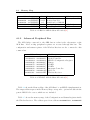
List of Tables
2.1
LEON-2 UART/IO Port Multiplexing . . . . . . . . . . . . . . . . . .
4.1 LEON-2 Precise/Deferred Trap Table . . . . .
4.2 WLSOC Interrupt Table . . . . . . . . . . . .
4.3 LEON-2 AHB Address Allocation . . . . . . .
4.4 LSOC APB Address Allocation . . . . . . . .
4.5 Wireless Receiver Register Address Allocation
6.1
6.2
.
.
.
.
.
26
27
28
28
29
WLSOC Simulation wall-clock Time . . . . . . . . . . . . . . . . . .
WLSOC Synthesis Results . . . . . . . . . . . . . . . . . . . . . . . .
62
63
viii
.
.
.
.
.
.
.
.
.
.
.
.
.
.
.
.
.
.
.
.
.
.
.
.
.
.
.
.
.
.
.
.
.
.
.
.
.
.
.
.
.
.
.
.
.
.
.
.
.
.
.
.
.
.
.
.
.
.
.
.
14
Chapter 1
Introduction
1.1
Overview
Embedded systems have a close-knit relationship between the hardware and the
software executing on it. In such systems, the traditional approach is to have different
hardware design and software design teams, which work separately. The software
team often starts integrating when the hardware team is in the final stages of its
development[16]. In general, at this later stage of the project, bugs found are more
difficult and costlier to rectify than if they were found earlier. It also takes much
larger time to find bug fixes at this stage.
Hardware-Software coverification is a technique to speed up the design of such
System-on-a-chip ASICs which use an embedded CPU core to control a bunch of
peripherals. Cosimulation or coverification intends to decrease the design time of the
system by overlapping the two debug cycles. Thus, hardware design teams simulate
their systems with a debug version of the software and the software design teams
simulate their software with behavioral models of the hardware, in effect codesigning
HW and SW. Both of them can keep updating the other team with newer versions of
1
1.2
Related Work
their code and speed up the effective design time.
1.2
Related Work
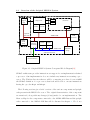
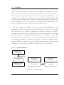
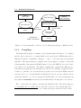
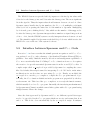
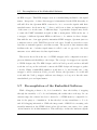
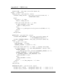
The Mentor Seamless tool[1] is a commercially available product that utilizes the
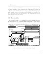
idea of coverification. Fig 1.1 shows a block diagram of an example coverification
tool. The HDL model of the Processor shown in the figure is replaced by a behavioral
!"
!
#
$
#
$
Figure 1.1: Introduction to HW/SW Coverification[10]
Instruction Set Simulator (ISS) of the core. The ISS is connected to the HW simulator
by the coverification tool and is instantiated by a HDL wrapper. This HDL wrapper
has to behave like a bus functional model controlled by the ISS in order to provide the
HW design with cycles. Moreover, Seamless allows connection of a software debugger
2
1.3
Contribution
to the ISS.
The key to simulation speedup is to reduce the number of events in the HDL
Simulator[10]. The Seamless tool performs this task by replacing the memories used
in the simulation by special behavioral models which can communicate directly with
the ISS without starting hardware cycles (if configured to do so). This concept of
“0-time”1 tasks is very important in reducing HW cycles in a simulation. However,
Seamless is not a free CAD tool and it takes time to create Seamless CPU models. An
approach based on inexpensive and open-source tools is required to make the subject
accessible to universities.
1.3
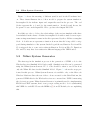
Contribution
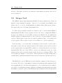
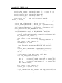
The thesis demonstrates the idea of HW-SW Coverification by verifying the design
of a Programmable Wireless Receiver SOC. This design uses the open-source SPARC
V8[2] compatible LEON-2 Processor[3] as the master and a Programmable Wireless
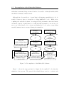
Receiver as a slave to perform a simple task of receiving a packet based on a simplistic
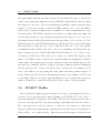
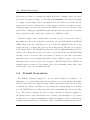
protocol. Section 3.1 has further details about the protocol we used. Fig 1.2 shows
the basic block diagram of the simulation environment used in the thesis. The main
components in the design the testcase uses are the UART Transmitter and Wireless
Receiver which are controlled by the LEON-2 Processor as slaves. The Processor
fetches instructions from the external memory, which is modeled in the testbench
for the design. Both the design and the testbench are simulated by the Modelsim
HDL Simulator[4]. The Memory contains a binary image of the embedded software
written in assembly language and C. The Stimuli for the Receiver is driven by a
Stimuli Generator, written in the e language[5] and simulated by the Specman tool.
Figures 5.1 and 5.10 show the complete simulation environment and testcase flow in
detail.
1
A task which does not increment the simulation time in the HDL simulator
3
1.3
Contribution
"
#
!
.%
$ % &"
&
+
$ )*
" ,-
$
'
%
$ %
$(
&"
&
( &* #
(
Figure 1.2: Overview of the Wireless LAN SOC Cosimulation
The flow presented does not use the Seamless tool. The main reason being that
there is no compatible SPARC V8 ISS available for Seamless as of this writing. The
flow tries to build comparable software debugging capabilities using free languages
like C, C++ and PERL. This would be a great economic advantage for University
students for their research. The only licenses required for the flow are for the Modelsim
HDL Simulator and Specman tool. Educational licenses were obtained for both these
tools. A simple decompiler (Section 5.7) is designed which can show the equivalent
C code that is being executed by the CPU during simulation. Similarly, a nearly
“0-time” method is designed to print debug messages from the embedded software
(Section 5.8).
4
1.4
Organization
The Programmable Receiver used has digital signal processing components, hence it
was designed using a tool which DSP designers generally prefer, i.e. Matlab Simulink.
Programmable capabilities were added by bringing out a lot of internal signals as
inputs to the chip. This design was then converted to VHDL using the Xilinx System
Generator. Finally, it was integrated with the LEON-2 Processor which acted as its
master in the system.
The simulation template presented in the thesis can be used for a range of designs
that have a CPU as the master and some programmable peripherals connected as
slaves to it. It shows an example of adding programmable capability to a digital signal
processing component designed in Matlab. Various heterogeneous languages and tools
are shown to be working together in tandem to fulfill the design and verification
objective.
1.4
Organization
The rest of the thesis is organized as follows. Chapter 2 gives an overview of the
original LEON-2[3] Processor Core which will be used as the CPU for this project.
Chapter 3 describes the digital wireless receiver used as a coprocessor in this design,
called the WLSOC (Wireless LAN SOC) System. Chapter 4 describes the integration
of the Wireless Receiver Coprocessor with the LEON-2 System and the characteristics
of the resultant system. Chapter 5 gives an overview of the different languages and
tools used to verify the complete WLSOC system. Chapter 6 shows the wall-clock
time taken for the simulation of one testcase, and synthesis results for the system. It
concludes the thesis by making some important observations. The appendices at the
end of the chapter show some source code that was developed for this project.
5
Chapter 2
The LEON-2 Processor System
This chapter gives an overview of the original LEON-2[3] Processor Core which
will be used as the CPU for this project.
2.1
Overview of the Original LEON-2 System
The LEON-2 processor, designed by Jiri Gaisler, is a synthesisable VHDL model
of a 32-bit processor compliant with the IEEE-1754 SPARC V8 [18] architecture. It
is designed for embedded applications with the following features on-chip: separate
instruction and data caches, hardware multiplier and divider, interrupt controller, debug support unit with trace buffer(DSU), two 24-bit timers, two UARTs, power-down
function, watchdog, 16-bit I/O port, PCI support and a flexible memory controller.
New modules can easily be added using the internal on-chip AMBA AHB and APB
buses[14].
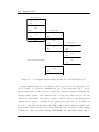
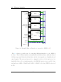
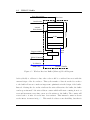
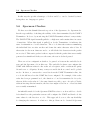
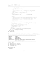
Figure 2.1 depicts the original LEON-2 Processor Block Diagram. We have used
Version 1.0.10 of the VHDL model for this project. Our implementation does not instantiate some of the optional modules from this core, viz. the multiplier and divider
inside the Integer Unit, Floating point Unit, the DSU unit and the PCI core. The
6
2.1
Overview of the Original LEON-2 System
$
)
!
*
$
*
! +
! +
!
% &
$
!
" !
#
%'$, -
!!
'(
Figure 2.1: Original LEON-2 System Conceptual Block Diagram[14]
SPARC architecture provides instruction set support for an implementation-defined
coprocessor. Our implementation does not include any instruction-executing coprocessor. The Wireless Receiver that we will be connecting as a slave does not fulfill
the SPARC definition of a coprocessor, that it should be able to execute instructions
having the opcodes CPop1 and CPop2.
The following sections give a brief overview of the various components and peripherals present in the LEON-2 Processor. The original characteristics of the component
are mentioned, along with any changes (if any) made for our implementation. The
Memory Map for the components connected to the AMBA AHB Bus and the peripherals connected to the AMBA APB Bus will be discussed in chapter 4. We do not
7
2.2
Integer Unit
use any of the timer blocks in our verification environment at present, hence those
are not described.
2.2
Integer Unit
The LEON-2 integer unit implements SPARC V8 integer instructions. It has an
internal 5-stage instruction pipeline. Since we do not include the multiplier and
divider, the boot code in our implementation emulates these functions in software.
The same is the case for floating point instructions.
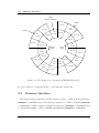
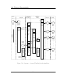
To reduce the performance penalty for a function call or context switch, LEON-2
implements the SPARC concept of register windows. In order to configure the LEON-2
Processor, we must choose how many windows are suitable for our application.
SPARC requires an implementation to have between 2–32 general-purpose register
windows. Each register window has 16 registers, partitioned into 8 in registers and
8 local registers. These register windows are in addition to 8 global registers[18].
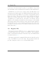
As shown in fig 2.2, at a given time, an instruction can access the 8 globals, and a
24-register windows into the current registers. The current window used is decided
by the current window pointer(CWP), which is a 5-bit field in the Processor State
Register(PSR). The outs of the CWP+1 window are addressable as the ins of the
current window and outs in the current window are the ins of window CWP-1. The
local registers are unique to each window. The register file is logically arranged in a
circular fashion, which means that the first window is adjacent to the last window [18].
The LEON-2 Processor VHDL model can be flexibly configured to have between 2–
32 windows. The choice of the number of windows depends upon the application and
area requirements. For our embedded application, a lot of windows are not required,
as would be by an high-performance application. Empirical measurements show that
the number of window overflow and underflow traps (explained later) in typical user
8
2.2
Integer Unit
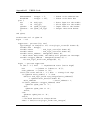
Figure 2.2: 3 overlapping Register Windows and the 8 Global Registers[18]
code approximately halves for each window added, up to about 12 windows[18]. We
choose a value of 8 windows to minimize the area of the register file. Fig 2.3 shows
the circular nature of the 8 window register file, and the causes for changing the
current register window. On a function call or a trap, the callers outs become the
callee’s ins. This makes it possible to make a context switch by just changing the
current window and not bothering about copying the register file onto the stack, as
in a lot of other CPU architectures. A SAVE on the stack is explicitly required only
when all the register windows are used up. Thus, in cases of window overflow during
a TRAP or window underflow during a RESTORE, the embedded software has to
9
2.3
Memory Interface
"
!
Figure 2.3: The Windowed r Registers (NWINDOWS=8)[18]
provide routines for explicitly saving or restoring the register file.
2.3
Memory Interface
The flexible memory interface handles a memory space of 2GB from hex addresses
00000000 to 7FFFFFFF. It provides interface signals for 512MB of PROM (00000000
to 1FFFFFFF), 512MB of memory mapped I/O devices (20000000 to 3FFFFFFF) and
a combined maximum of 1GB of SRAM and SDRAM (40000000 to 7FFFFFFF).
10
2.3
Memory Interface
,
)
)
#&
! "#$ !%
' (
)*
*+
Figure 2.4: Example Memory Interfaces connected to LEON-2 [14]
Fig 2.4 shows a possible way of connecting different interfaces to the LEON-2
Processor. The bold lines indicate the unidirectional Address lines, while the dotted
bold lines represent bidirectional data lines and the other signals are all unidirectional
control signals. The memory bus can be configured in 8-bit or 16-bit modes for low
bandwidth devices. In our implementation, the SDRAM interface is not enabled. Our
testbench uses 32KB of PROM and 256KB of SRAM, both being VHDL behavioral
models.
11
2.4
2.4
UARTs
UARTs
The LEON-2 Processor contains two 8-bit Universal Asynchronous Receiver Transmitters (UARTs) on-chip. Our implementation instantiates both of them. The testcase presented later in Chapter 5 shows an example utilizing one of the UARTs for
transmitting serial data. The baud-rate for the UARTs is individually programmable
and data is sent in 8-bit frames with one stop bit and an optional parity bit. All
internal details about the UART operation are obtained from the LEON-2 Processor
manual[14].
"#$ %
!
!
&'
Figure 2.5: UART Block Diagram[14]
The transmitter holding register (THR) acts as a buffer for the byte which has
to be transmitted. When the transmitter is enabled and ready to transmit, data is
transferred from the THR to the transmitter shift register (TSR) and sent out in a
serial fashion over the transmitter data output pin (TXD). On the receiver side, the
receiver holding register (RHR) acts as the buffer from which the LEON-2 Processor
can read the data received from the RXD input pin. In both cases, a transition
12
2.5
Interrupt Controller
from high to low on the data line indicates the start bit for a new frame. The least
significant bit of the byte is always transmitted or received first. In the inactive state,
both the RXD and TXD data pins stay at the high level. The Clear-to-send (CTSN)
and Ready-to-send (RTSN) signals are used when flow control is enabled as a means
of handshaking with the external receiver or transmitter.
2.5
Interrupt Controller
The interrupt controller manages a total of 15 interrupts, originating from internal
peripherals and external sources. The original LEON-2 core has 4 unused interrupts. Our implementation does not enable the secondary interrupt controller, which
is needed if more than 4 peripherals asserting interrupts are added to the system.
Further details about the interrupt controller and the changes made for integrating
the wireless receiver can be obtained in section 4.2.
2.6
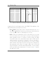
Parallel I/O port
The Parallel I/O Port available has 32 bits which can be individually programmed
as input or output. Some of the lower 16 bits of the I/O Port are multiplexed with
UART pins and External Interrupts as shown in table 2.1, while the higher 16 bits
of the I/O Port are multiplexed with the lower 16 bits of the Memory Data bus.
The higher 16 bits of the I/O Port are available in I/O mode only when the external
memory used has a data width of 8-bits or 16-bits.
This chapter gave an overview of the CPU being used in the design. The opensource nature of the LEON-2 Processor and its SPARC instruction set and good
flexibility in adding, removing and configuring components make it an attractive
choice for this thesis. We had initially started work on the thesis using the OpenRISC
Processor core[6]. But we switched to the LEON-2 Processor because it was felt that:
• LEON-2 has a more widely used and proven standard architecture (SPARC)
compared to the newer OpenRISC architecture.
13
2.6
Parallel I/O port
I/O port
PIO[15]
PIO[14]
PIO[13]
PIO[12]
PIO[11]
PIO[10]
PIO[9]
PIO[8]
PIO[3]
PIO[1:0]
Function
TXD1
RXD1
RTS1
CTS1
TXD2
RXD2
RTS2
CTS2
UART
clock
Prom
width
Type
Output
Input
Output
Input
Output
Input
Output
Input
Input
Input
Description
UART1 transmitter data
UART1 receiver data
UART1 request-to-send
UART1 clear-to-send
UART2 transmitter data
UART2 receiver data
UART2 request-to-send
UART2 clear-to-send
Use as alternative UART
clock
Defines prom width at
boot time
Output Enabling condition
UART1 transmitter enabled
UART1 flow-control enabled
UART2 transmitter enabled
UART2 flow-control enabled
-
Table 2.1: LEON-2 UART/IO Port Multiplexing [14]
• The GNU Cross-Compiler toolchain for LEON-2 is much more easy to install.
• The VHDL source code for LEON-2 seems to be more stable and has fewer or
no bugs.
• LEON-2 comes with a set of well-written VHDL testcases and embedded software.
• LEON-2 has a better user-friendly interface to configure and add/remove components and peripherals.
The next chapter will give an overview of the Programmable Wireless Receiver
used in the WLSOC design.
14
Chapter 3
Wireless System
This chapter describes the Digital Wireless Receiver used in the WLSOC System.
The Wireless Receiver we designed is intended to receive its input from an off-chip
coherent analog RF receiver front-end, filter noise from the signal and extract and
store the data packet in its internal 128-byte buffer. It is designed using VHDL and
the Xilinx System Generator Blockset for Matlab Simulink. The use of the System
Generator blockset is made because it is a toolkit designed primarily for Digital
Signal Processing Applications. This design shows an example of how different design
languages can be used in their area of expertise and the different components then
integrated together to get the combined benefits of both.
3.1
Protocol
To simplify the design of the Wireless Receiver, a dummy protocol was devised
loosely based on some aspects of the 802.11b Ethernet Wireless LAN protocol. Fig 3.1
shows the structure of one packet used for data communication. The data payload of
the packet consists of exactly 128 characters or its 1024-bit ASCII equivalent. This
size is fixed to simplify the design of the receiver. If the length of a message is less than
128 characters, the data payload can always be padded with spaces to make it 128
character wide. This packet also needs a delimiter to delineate start of one packet and
15
3.2
Overall Design
Figure 3.1: WLSOC Wireless Protocol
end of another. The SFD(Start of frame delimiter) we use is 0000 0101 1100 1111,
identical to the IEEE 802.11b-1999 Long PLCP SFD [15]. The packet should also
contain some known bits (SYNC) which the receiver will expect and tune itself accordingly. Depending on the (changing) multi-path characteristics of the intermediate channel, these SYNC bits will be distorted to varying degrees at various points
of time. Correlating the known SYNC bits with the actual received bits, the receiver
can modify its internal LMS filter tap coefficients to equalize the external noise. This
“learning” of the external channel characteristics should be performed before every
packet data payload. The varying nature of noise in the channel is one of the factors
in determining the size of the packet. If it varies quite frequently, the LMS filter
should get a chance to adapt itself more frequently, and hence the size of the packet
should be smaller. A string of 8 ones is chosen as the SYNC bits in our system.
This is the data link layer structure for the packet. At the physical level, the
SYNC and data bits are spread by a spreading code of 15-bits to increase immunity
to wireless multichannel fading. Details about spreading will be covered in section 5.4
3.2
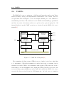
Overall Design
The overall function of the Wireless Receiver (WLRCV) is split into 4 blocks, viz.
the Frontend, Decorrelator, Buffer and Register File. Fig 3.2 shows the block diagram
of the design. The input from the analog RF Receiver is received from off-chip. The
Register File and buffer are read by the LEON-2 Processor using the AMBA APB
Bus. The Interrupt triggered by the Buffer is connected to the Interrupt Controller
of the LEON-2 Processor. Further details about the integration of the WLRCV with
16
3.3
Wireless Frontend
the LEON-2 Processor can be obtained from Chapter 4.
"
!
Figure 3.2: Wireless Receiver Coprocessor Block Diagram
3.3
Wireless Frontend
The frontend we used has been designed by Ravi Jenkal and Prof. Rhett Davis
from the ECE Department, NC State University. It will be used as a pre-verified
Intellectual Property core just as the LEON-2 Processor. The purpose of the Frontend
is to extract the chips one-by-one from the incoming noisy stream of data. Fig 3.3
shows the various components in the frontend. The SYNC bits in the packet are
helpful in tuning the 6-tap Linear Mean-Square Filter of the WLRCV to cancel the
noise in the channel. The synchronizer in the frontend tries to correlate the input
signal received with the known SYNC bits that it is expecting. As soon as it detects
this sequence at the input, it synchronizes the functioning of the LMS filter which
starts its training mode. Since the LMS filter is now expecting a series of 8 ones
converted to their spreading code, it tunes its internal taps to cancel the difference
between the expected and actual signals.
17
3.3
Wireless Frontend
"
#
"
!
Figure 3.3: Wireless Receiver Frontend Block Diagram
The Threshold input to the Synchronizer block is used a reference point by the
internal baseband clock synchronizing matched filter correlators to indicate that synchronization has been achieved. The bigger the value of this signal, the longer it
will take for the synchronizer block to confirm synchronization. On the other hand, a
smaller value could trigger an earlier incorrect synchronization. The Synch interval
input to the Sync control block indicates how many cycles the matched filter correlators run before resetting. The correlators should start afresh after they do not
find the expected SYNC bits for a long time, otherwise one of the correlators will
randomly reach the threshold, even though the SYNC signal is not present. If the
receiver comes out of reset while a packet has already started transmission, it has to
wait till the SYNC bits in the next packet to start receiving.
The µ signal is the LMS-adaptation scale-factor. It indicates how quickly the LMS
filter changes its tap coefficients to match the channel characteristics. Keeping a
18
3.4
Decorrelator
very low value will force the LMS filter to take a longer time to adapt, but it will
be a steady adaptation. A large value may result in huge fluctuations in the tap
coefficients, and the LMS filter may never converge to the intended sweet spot. The
Adapt interval indicates for how many cycles the LMS filter should adapt. The
Tap coefficients are driven out by the LMS filter so that external modules can read
them to find the channel characteristics.
3.4
Decorrelator
The decorrelator has the job of combining the chips from the input packet into
bits, bytes and words. Fig 3.4 shows the internal block diagram of the decorrelator.
The decorrelator receives the correct input chips from the frontend in the form of
"
.
"
/.
%
#
,
#
/.
'#
!
!"
&
$
,
&'
-
(
)
*
+
(
)
*
+
'
'
,
&
-
%
#!
!
$
#!
!
&
Figure 3.4: Wireless Receiver Decorrelator Block Diagram
19
3.5
WLRCV Buffer
the signal input_stream, after the frontend decides which half-chips to discard. It
waits for the signal lms_adapted from the LMS filter which indicates that the filter
has adapted to the noise. The most significant bit (MSB) of input_stream is then
scanned to detect the presence of the 16-bit SFD sequence. As soon as the SFD is
detected, the comparator indicates the accumulator to start accumulating the chips
from the packet. The LFSR contains the spreading code 1001 1010 1111 000, and
is used as the reference for decorrelating the input stream. Every set of 15 chips from
the input stream should ideally either match the spreading code for a 0 bit or a 1 bit.
Each successive bit of the LFSR thus indicates whether the next chip from the input
stream should be added (in case of 0) or subtracted (in case of 1) to the already
accumulated result. Finally, after all 15 chips are accumulated (as indicated by the
chip_counter), it gives a 20-bit result which is ideally either 15 or −15. Due to noise,
it would not be this exact value, but closer to either one of them. The sign bit of the
sum, i.e. the MSB, is then considered the actual bit which was transmitted. This bit
is then sent to the current_byte register, which is a temporary holding place for the
incoming byte. Similarly, the bit_counter, and byte_counter help in accumulating
the bits and bytes into 32-bit words. Every time a 32-bit word is accumulated, it is
sent to the buffer for storage using the write_data and write_enable signals. A
word_counter (not shown in the diagram) keeps track of the number of words sent
to the buffer. When 32 words are sent, signaling the end of a packet, the start/stop
signal is deasserted to restart the SFD detection procedure for the next packet.
3.5
WLRCV Buffer
The 128 character buffer is meant as temporary storage for the input packet, before
it can be read by the embedded software running on the LEON-2 Processor. Fig 3.5
shows the internal block diagram of the buffer. The storage is arranged in the form of
32 words of 32-bits each. The only device writing to this buffer will be the decorrelator.
The only legal way for the decorrelator to write into the buffer is to start from
address 0, and keep incrementing the address till it reaches the last word at address 31.
This would be one complete packet. When the next packet starts, it should revert
20
3.5
WLRCV Buffer
*
#
!
"
#
!
% &&
"
%
'()
$
Figure 3.5: Wireless Receiver Buffer (Memory) Block Diagram
back cyclically to address 0. Any other order would be considered incorrect with the
current design of the decorrelator. This cyclic transfer of data from the decorrelator
to the buffer allows us to make an important optimization in the design of the buffer.
Instead of letting the decorrelator indicate the write address into the buffer, the buffer
can keep an internal 5-bit write address counter which will start counting from 0 on
reset and increment every time a new word is written to the buffer. The counter will
revert back to 0 after 32 words have been written. This internal counter is shown
as the Write Pointer in fig 3.5. This method reduces some flexibility, but that is
21
3.6
Register File
not necessary for the current design. It would not be very difficult to bring out this
auto-incrementing counter as an input bus if it is required in a future implementation.
The LEON-2 Processor needs a way to read the contents of the buffer. Hence a read
data bus is provided, which connects to the AMBA bus in the System. In this case the
read address is driven by the LEON-2 Processor instead of being internally generated
like the write address. This gives the embedded software flexibility in reading the
buffer in any order that it wants, and also only so much as it wants. For example,
our simplistic protocol restricts the size of the packet to 128 characters. But an
application on the transmitter side might have a shorter message to send and might
just pad up the message with null characters. If the embedded software application
knows that this is the case, it can read just the relevant message and not waste cycles
in reading the other useless characters. The AMBA read address bus is shown as the
Read Pointer in fig 3.5.
3.6
Register File
The Register file allows the LEON-2 Processor to configure the Receiver and also
read internal signals like the tap coefficients of the LMS filter. The Programmable
features of the Register File and its place in the memory map of the WLSOC System
are described in section 4.3.2.
This chapter described the Programmable Wireless Receiver that will be used as
a slave of the LEON-2 Processor in the design. The next chapter describes the
procedure of integration of these 2 cores to form the WLSOC System.
22
Chapter 4
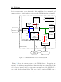
Integration of the WLSOC System
This chapter gives a description of how the integration of the Wireless Receiver
Coprocessor was performed with the LEON-2 System and the characteristics of the
resultant system.
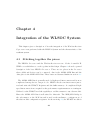
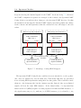
4.1
Stitching together the pieces
The LEON-2 Processor and the Wireless Receiver are two blocks of reusable IP
VHDL cores which have to work together in this design. Chapter 2 showed a general
description of the base LEON-2 Processor. There are two places in the Processor
where additional devices can be connected. One is the AMBA AHB Bus and the
other place is the AMBA APB Bus. These buses are discussed further in section 4.3.
The AMBA AHB Bus is generally used for high-speed interconnects and is more
complicated among the two bus protocols. LEON-2 needs some interconnect just to
read and write the WLRCV Registers and the buffer memory. A complicated highspeed interconnect in not required as the performance requirements are not stringent.
Neither does the WLRCV need the capability to act like a master to any other module.
Hence the AMBA APB Bus is well suited for this task. The AHB/APB Bridge is
the only master on the APB bus and is used as the medium to configure most of
the slave module configuration registers. As shown in fig 4.1, the WLRCV module is
23
4.1
Stitching together the pieces
connected to the AMBA APB Bus as a slave. The WLRCV interrupt is connected
to the Interrupt Controller just like other slave modules. The wireless signal data
input for WLRCV is driven by an external RF analog frontend. Sections 4.2 and 4.3
$
)
!
*
$
*
! +
! +
/ %" 0
!
% &
/
!!
!!
*/ %" 0+
$
")
!
" !
#
%'$, -
!!
.
/
!!
!!
'(
Figure 4.1: LEON Processor with Wireless Coprocessor Block Diagram
discuss the changes in the Interrupt table and Memory Map of the WLSOC System
due to the addition of the WLRCV Module.
24
4.2
Interrupts/Traps
4.2
4.2.1
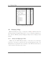
Interrupts/Traps
Overview of Interrupts and Traps
In a SPARC implementation, a trap is a vectored transfer of control to the supervisor software through a special trap table that contains the first 4 instructions of each
trap handler. The base address of the table is established by the supervisor software,
by writing the Trap Base Address (TBA) field of an IU state register called the Trap
Base Register (TBR). The displacement within the table is determined by the type
of trap[18]. Fig 4.2 shows the significance of the different bits of the 32–bit Trap Base
Figure 4.2: 32-bit Trap Base Register (TBR)
Register. Only the TBA bits can be written by software, while the tt bits are written
by hardware when a trap occurs. This register holds the address to which control is
transferred when a trap occurs.
Before it begins executing any instruction, the Instruction Unit selects the highestpriority interrupt, and if there are any, causes a trap. Instruction-induced exceptions
cause precise or deferred traps while external interrupt requests cause an interrupting
trap. A precise trap occurs before any program-visible state has been changed by the
trap-inducing instruction. A deferred trap may occur after program-visible state is
changed. [18]
4.2.2
Instruction-induced Traps
Table 4.1 shows the various Precise and Deferred Traps implemented by LEON-2,
their priorities and the values written by the hardware into the tt field of the Trap Base
Register. The Priority and tt values are based on the generic SPARC standard [14].
25
4.2
Interrupts/Traps
Exception Request
tt
Pri
reset
0x00
1
write error
0x2b
2
instr access error
0x01
3
illegal instruction
0x02
5
privileged instruction
0x03
4
fp disabled
0x04
6
cp disabled
0x24
6
watchpoint detected
0x0B
7
window overflow
0x05
8
window underflow
0x06
8
reg hardware error
0x20
9
mem addr not aligned
0x07
10
fp exception
0x08
11
cp exception
0x28
11
data access exception
0x09
13
tag overflow
0x0A
14
divide exception
0x2A
15
trap instruction
0x80–0xFF 16
Description
Power-on reset
Write buffer error
Error during instr fetch
Unimplemented instruction
Exec privileged instr in user mode
FP instr while FPU disabled
CP instr while CP disabled
Instr or data watchpoint match
SAVE into invalid window
RESTORE into invalid window
Reg file EDAC error (LEON-FT only)
Mem access to unaligned address
FPU exception
Co-processor exception
Access error LD or ST instr
Tagged arithmatic overflow
Divide by zero
Software Trap Instr (TA)
Table 4.1: LEON-2 Precise/Deferred Trap Table[14]
The register hardware error exception is implemented only on the Fault Tolerant
version of LEON-2 and is not present in the implementation that we used.
4.2.3
Peripheral/External Interrupts
The 15 interrupts are all implementation-dependent and LEON-2 uses all but 4
interrupts for its peripherals and external interrupts. To accomodate the Wireless
Receiver, we have connected its interrupt into the system such that it receives a
Priority of 20 and a tt value of 0x1C. This priority was chosen because it was the
next available unused slot in the already designed LEON-2 interrupt table.
Table 4.2 shows the complete Interrupt table for the Integrated WLSOC System.
26
4.3
Memory Map
Interrupt Request
Priority
tt
Interrupt 15 (Unused)
17
0x1F
Interrupt 14 (Unused)
18
0x1E
Interrupt 13 (Unused)
19
0x1D
WLSOC Receiver
20
0x1C
DSU Trace Buffer
21
0x1B
2nd Interrupt Controller
22
0x1A
Timer 2
23
0x19
Timer 1
24
0x18
Parallel I/O [3]
25
0x17
Parallel I/O [2]
26
0x16
Parallel I/O [1]
27
0x15
Parallel I/O [0]
28
0x14
UART 1
29
0x13
UART 2
30
0x12
AHB Error
31
0x11
Table 4.2: WLSOC Interrupt Table[14]
4.3
Memory Map
LEON-2 internally uses 2 types of on-chip buses: AMBA[11] AHB and APB. The
APB Bus (Advanced Peripheral Bus) is used to access on-chip slave peripheral registers, while the AHB Bus (Advanced High-speed Bus) is used for high-speed data
transfers.
4.3.1
Advanced High-speed Bus
LEON-2 uses the AMBA AHB bus mainly to connect the Processor I/D Cache
Controllers to the memory controllers and other (optional) high-speed units. The
implementation we used has IU as the only master on the AHB bus and the memory
controller and the APB bridge as the 2 slaves.
27
4.3
Memory Map
Address Range
0x00000000 – 0x1FFFFFFF
0x20000000 – 0x3FFFFFFF
0x40000000 – 0x7FFFFFFF
0x80000000 – 0x8FFFFFFF
0x90000000 – 0x9FFFFFFF
Size
512 M
512 M
1G
256 M
256 M
Mapping
Prom
Memory Bus I/O
SRAM and/or SDRAM
On-chip Registers
Debug Support Unit
Module
Memory Controller
APB Bridge
DSU
Table 4.3: LEON-2 AHB Address Allocation[14]
4.3.2
Advanced Peripheral Bus
The APB bridge connected to the AHB bus as a slave is the only master on the
APB Bus. Most on-chip peripheral registers are accessed through this bus. The
configuration and status registers of the Wireless Receiver are also connected to this
common bus.
Address Range
0x80000000 – 0x80000008
0x80000014 – 0x80000018
0x80000024 – 0x80000024
0x80000040 – 0x8000006C
0x80000070 – 0x8000007C
0x80000080 – 0x8000008C
0x80000090 – 0x8000009C
0x800000A0 – 0x800000AC
0x80000300 – 0x80000AFC
Module
Memory Controller
Cache Controller
LEON-2 Configuration Register
Timers
UART1
UART2
Interrupt Controller
I/O Port
Wireless Receiver
Table 4.4: WLSOC APB Address Allocation[14]
Table 4.4 shows the Memory Map of the APB Bus for our LEON-2 implementation.
The empty address spaces in the Memory Map correspond to optional modules in the
generic LEON-2 Processor, which are not included.
Table 4.5 shows the memory map of the Configuration and Status Registers inside
the Wireless Receiver. The address space from addresses 0x80000730 to 0x80000AFC
28
4.3
Memory Map
Address Range
Size (bytes)
0x80000300 – 0x800006FC
1K
0x80000700 – 0x80000700
4
0x80000704 – 0x80000704
4
0x80000708 – 0x80000708
4
0x8000070C – 0x8000070C
4
0x80000710 – 0x80000710
4
0x80000714 – 0x80000714
4
0x80000718 – 0x80000718
4
0x8000071C – 0x8000071C
4
0x80000720 – 0x80000720
4
0x80000724 – 0x80000724
4
0x80000728 – 0x80000728
4
0x8000072C – 0x8000072C
4
Register
Buffer
Adptint
MU
Synchint
Threshold
Reset WLRCV
Tapval1
Tapval2
Tapval3
Tapval4
Tapval5
Tapval6
Trigaddr
Read/Write
Read-only
Read/Write
Read/Write
Read/Write
Read/Write
Read/Write
Read-only
Read-only
Read-only
Read-only
Read-only
Read-only
Read/Write
Table 4.5: Wireless Receiver Register Address Allocation
is unused and can be used in future versions of the WLRCV. The significance of the
different Wireless Receiver Registers is as follows:
• Reset WLRCV: This register is used to bring the Wireless Receiver out of
reset. If Reset WLRCV[0] is 1, the Receiver is in reset state; if its 0, the Receiver
is out of reset state. Bits 31:1 of this Register are don’t care.
• Buffer: This acts as intermediate storage for the packet before it is being
moved to the memory. It is a 32-word space for storing one entire 128-character
packet. Currently, it is the job of software to read the contents of the buffer
as it is filled by the receiver. An alternative design could be a DMA controller
which automatically copies this data to main memory. The size of the buffer i.e.
32 words is chosen so that the entire packet fits into it at one time. A smaller
buffer would have reduced chip area but also have imposed more stringent realtime requirements on the software. For example, a buffer of size 8 words would
trigger 4 interrupts for each packet, thus causing the ISR to be serviced 4 times
in the same duration that a packet takes to be received. Section 3.5 describes
the buffer in more detail.
29
4.3
Memory Map
• Adptint: Bits 7:0 of this register directly drive the signal Adapt interval as
shown in Fig 3.3. Bits 31:8 of this register are don’t care. It is interpreted as
an 8-bit unsigned value.
•
µ: Bits 7:0 of this register directly drive the signal µ as shown in Fig 3.3.
Bits
31:8 of this register are don’t care. It is interpreted as a 8-bit fixed point signed
value with 3 bits before the binary point and 5 bits after it.
• Synchint: Bits 7:0 of this register directly drive the signal Synch interval as
shown in Fig 3.3. Bits 31:8 of this register are don’t care. It is interpreted as
an 8-bit unsigned value.
• Threshold: Bits 7:0 of this register directly drive the signal Threshold as
shown in Fig 3.3. Bits 31:8 of this register are don’t care. It is interpreted as a
18-bit fixed point signed value with 10 bits before the binary point and 8 bits
after it.
• Tapval: The value of the 6 Tap Coeff outputs from the WLRCV frontend are
captured in these 6 32-bit registers. The software can read these 6 32-bit values
but cannot modify them.
• Trigaddr: As the WLRCV buffer is being continuously refilled by the hardware, the software has to make sure that it reads the values in this buffer for
every packet received, before it is overwritten by the next packet. If the software waits for the entire packet to arrive in the buffer and then starts copying
the data, it risks the possibility that the initial words of the buffer could be
overwritten in the meantime. The time it takes for the LEON-2 Processor to
service the WLRCV ISR may be more than the time between two successive
packets. Hence, it is advisable to start the ISR even before the 32-words have
been filled. It is also possible, that the embedded software knows that the message is padded with dummy characters and does not need to wait for the entire
message to be downloaded into the buffer, before it can start processing it.
This register decides when the WLRCV would fire an interrupt to the LEON-2
30
4.3
Memory Map
Processor.
!
Figure 4.3: Wireless Receiver Programmable Registers
Figure 4.3 shows a graphical view of how these registers are connected to the
Wireless Receiver module. The LEON-2 Processor has to program the Adptint, µ,
Synchint, Threshold and Trigaddr configuration registers and bring the Receiver out
of reset by writing into the Reset WLRCV Register. The different Tapval and Buffer
values are then generated by the Receiver. The LEON-2 Processor cannot modify the
tapval and buffer values. The software can only read them as status registers. The
fact that some of these programmable registers control internal signals in the WLRCV
module gives immense flexibility to the software to tune the receiver to its needs. Also,
31
4.3
Memory Map
by being able to read the tap coefficients, the user can get a better perspective of the
internals of the WLRCV module. In the same manner, more internal signals could be
controlled or observed by being brought out of the system and connected to registers
if needed.
This chapter described the integration of the Wireless Receiver Coprocessor with
the LEON-2 System and the characteristics of the resultant system. The next chapter
explains the different CAD tools that were used in the design and the resultant
coverification flow developed.
32
Chapter 5
Tool Flow
This chapter gives an overview of the different languages and CAD tools used in
the design.
5.1
Tool flow
The goal of this thesis was to integrate the Wireless Receiver designed in Simulink
as a slave of the LEON-2 Processor. Chapter 4 shows the manner in which the whole
system was integrated. This chapter will show the verification setup for the system.
The individual components of the system like the LEON-2 Processor and the Wireless
Receiver are assumed to be thoroughly verified and would not be verified again at
the unit-level. The glue logic that binds these two modules together was verified at
the unit-level before integrating.
The main function of the WLSOC is to receive a packet from the Wireless Receiver
Network and store it into memory accessible by LEON-2 so that the embedded software can process it further. This procedure requires the cooperation of the software
with the hardware. The software has to program the appropriate configuration registers in the Receiver, wait till a packet is received, and copy it from the Receiver Buffer
to the main memory. In our test setup, we programmed the software to transmit every byte of the packet through the UART present in the system. An external UART
33
5.1
Tool flow
Receiver was present to receive this packet, which would later be reconstructed and
compared with the original packet to verify that the WLSOC functions as intended.
! +
'
(
& (
$
$
$ %$
$ &
0
0+
1
'!
' #22
( && &
0!34'
! "$
!"
!
#!
+
+ '"%!
%! '
'(
$
%$
$
)
0 #
* + ! ,-
) &* + ! ,/
.,
.'
!&
&
.
'++
. (
0+
.#! 3
! !
0+
'
'5
3'
.
0+
' $
Figure 5.1: Simulation Flow for the WLSOC System
Figure 5.1 shows the testbench setup for the WLSOC System. The various important blocks in the system are displayed along with their interactions. The blocks
enclosed by the internal dotted box represent a conceptual view of the LEON-2 Processor with only the relevant blocks. The outer dotted box encloses VHDL compo34
5.1
Tool flow
nents of the testbench like the external memory (RAM). The rectangular boxes with
curved corners represent the Specman[5] Stimuli Generators or Checkers/Monitors.
The dotted arrows represent the interaction between Specman and VHDL Code. Using this interface, the e code can drive and monitor the value of VHDL signals. The
solid lines represent VHDL buses or signals. The AHB, APB, Memory and I/O buses
are all bidirectional. The arrow between the Specman UART Config monitor and
Receiver represent exchange of data between two Specman units.
The Integer Unit in the LEON-2 Processor uses the AMBA AHB Bus to fetch
instructions from the external memory through the Memory Controller. The AMBA
APB Bus is used to program the configuration registers in the Memory Controller,
the UART, External I/O and the Wireless Receiver. The muxed signals of the UART
and External I/O are programmed in the UART-mode to make use of the UART
Transmitter. The Decompiler and testmod modules print useful debugging information during the simulation. Specman code is used to generate the stimuli, monitor
internal AMBA bus activity and verify the UART transmitted packet. These modules
and their interactions will be explained in detail in the rest of the chapter.
5.1.1
Nomenclature
Figure 5.2: Flowchart Legend
35
5.2
Xilinx System Generator
Figure 5.2 shows the meaning of different symbols used in the Flowcharts hereon. These charts illustrate the tool flow needed to prepare the system simulation.
Rectangular blocks indicate input and output files used in the process. The oval
blocks represent the tool used for the transformation. In the Legend shown, the
Program P1 acts on the Input File IF1 to produce the Output File OF1.
In addition to the tool flow, the relationships of the various simulation files have
been included in the charts. A dashed rectangular block with rounded corners represents an important function name in the file represented by the solid-line rectangular
block. A double-arrow represents a function from another file being called or triggered during simulation of the system. In the Legend shown, Function Fx2 from File
F2 is triggered due to some action taken in Function Fx1 from File F1. Functions
Fx1 and Fx2 may have been written in different languages like VHDL and C.
5.2
Xilinx System Generator
The first step in the simulation process is the generation of VHDL code for the
Wireless Receiver Simulink Model (wlsoc.mdl). Simulation models can be generated
using the Xilinx System Generator Tool. Care should be taken to use blocks from
only the Xilinx Blockset in this Simulink Model. Figure 5.3 shows the steps performed in this process. Xilinx System Generator is available only on the Microsoft
Windows Platform. Since the rest of the tools are executed on the Unix Platform, the
generated VHDL files for the Wireless Receiver are converted into UNIX format using
the dos2unix program. Xilinx System Generator is primarily used for implementing
FPGA-based DSP systems, hence some post-processing needs to be for synthesizing
this VHDL for an ASIC. We use the BEE flow[7] from UC Berkeley for accomplishing
this.
36
5.3
Embedded Software
!
!
Figure 5.3: Generation of VHDL code from Matlab Simulink model
5.3
Embedded Software
The next step is the design of the Embedded Software to execute on the LEON-2
Processor. The main parts of the Software are the initial boot code and low-level
Traps, device drivers (configuration) for the UART and WLRCV and an Interrupt
Service Routine for the WLRCV.
5.3.1
Boot Code
The main job of the boot code (file:boot.S) for the LEON-2 Processor is initializing
the Registers viz. the Processor State Register, Window Invalid Mask Register and
Trap Table Register. It also initializes most of the LEON-2 Configuration Registers
as well as the entire general-purpose circular Register file. This portion of code is
relocated by the linker command file linkboot to the ROM starting at hex address
0x0. This is the reset location for the LEON-2 Processor. Rest of the assembly and
37
5.3
Embedded Software
C code is relocated by the linker command file linkleon to the RAM starting at hex
address 0x40000000.
The later portion of the boot code (file:locore1.S) initializes the Trap Table with the
appropriate Service Routines for Hardware traps and Interrupts. Notable hardware
traps include Register Window Overflow/Underflow and Floating Point Instruction
Trap1 . The Interrupt Service Routines are written in C and the Trap Table uses
assembly code to transfer control to these ISRs.
5.3.2
Device Drivers
The device driver for the UART (file:uart.c) configures UART1 for transmission,
with Parity enabled. Fastest possible transmission is done by configuring the scaler
value to 1. This allows the UART to transmit one bit every 16 clock cycles. The device
driver for the WLRCV configures the adptint, synchint, µ and threshold registers and
brings it out of reset. The WLRCV can then proceed to receive Wireless Packets.
5.3.3
ISR for WLRCV
The Interrupt Service Routine for the WLRCV (file:isr.c) is responsible for processing the packet received and stored in the WLRCV Buffer. It copies this entire
packet from the Buffer to main memory. This frees up the WLRCV to receive the
next packet in the same buffer space. For verification purposes, this packet is then
transmitted in terms of characters out of the UART. After writing each character
to the UART Transmitter Holding Register(THR), the ISR keeps polling the UART
Status Register to find out when the THR is empty, so that it can write the next
character.
38
5.3
Embedded Software
!
"
$% & '
#
(
Figure 5.4: Cross-Assembly of the Boot Code with sparc-rtems-gcc [ROM Section]
5.3.4
Compiling
The Embedded Software consisting of the assembly and C files has to be compiled
and the data converted to a format which can be used by the VHDL memories for
Hardware-Software cosimulation. Figures 5.4 and 5.5 show the steps in generating
such files. The sparc-rtems-gcc compiler used for the purpose executes on the Sun
Solaris machine, but generates SPARC binary code for the LEON-2 Processor, hence
it is called a Cross-Compiler. The linker command file organizes the different sections in the program into various memory locations. For example, a typical scenario
would be to put the code sections in the program (.text section) in ROM and data
sections (.data, .bss, .stab) in RAM. As indicated before, in our case, all the sections
except the initial boot code are arranged in RAM with code sections starting from
hex address 0x40000000 and data sections immediately following the code sections.
Fig 5.4 shows the procedure for creating the ROM data file. The sparc-rtems-gcc
tool assembles the boot.S file and relocates the sections to hex address 0x0. Fig 5.5
1
Our instantiation of the LEON-2 Processor emulates Floating Point Instructions in Software
39
5.3
Embedded Software
(
!
)
*
% & "
(
)
' !
$ #
#
%
$ #
&"
!
!
"
'"
)
(
' !
(
!,
( +- * .
(
!+
&( +
Figure 5.5: Cross-Compilation of Embedded Software with sparc-rtems-gcc [RAM
Section]
40
5.4
Stimuli Generation
shows the procedure for creating the RAM Data files. Linking causes relocation
and symbol references relative to hex address 0x40000000. The sparc-rtems-strip
tool strips out the Symbol Table information from the binary executable and the
sparc-rtems-objcopy tool purges the .comment section. These are required only for
debugging purposes, and are not used by the LEON-2 Processor for execution. The
sparc-rtems-objdump program finally transforms this binary program into an assembly program in text file, which can be parsed by a VHDL procedure.
The final outputs of these transformations are the rom.dat, ram.dat and sdram.rec
files which are read by the testbench components, viz. the ROM, RAM and SDRAM
VHDL Memory models. Although we do not enable the SDRAM Controller in the
design, the flow to generate the sdram.rec file is still present. This file can be used if
needed in the future. The SDRAM model used is a Micron SDRAM Simulation Model
which reads in initial data in Motorola S-Records format. Hence the SDRAM initial
data file sdram.rec is in the S-Records format. Conversion to the S-Records format
implicitly removes any debugging information, hence explicit stripping of the debug
information and .comment section is not required. The RAM Model uses VHDL text
parsing features to parse an object-dump of the code in assembly format. Hence, this
is the format of the ram.dat initial data file.
5.4
Stimuli Generation
The WLSOC System is supposed to receive wireless packets conforming to our
dummy protocol, periodically train itself according to noise in the channel, then filter
the noise and retrieve the original message. While verifying the system, it is necessary
to simulate the effects of channel noise by altering the original signal before feeding
it to the WLSOC System. This is precisely what our Stimuli Generation procedure
does. The generator mimics the data an analog frontend would have supplied to
the digital portion of the Wireless Receiver. Verisity’s Specman Elite tool[5] is used
for this process because it implements a high-level language called e which allows
writing testcases with the use of abstraction and constraint-based random generation.
41
5.4
Stimuli Generation
Although e is a very good language by itself, it does not have the inherent capability
to handle fixed-point or floating-point numbers. Since the stimuli to be generated in
our case requires fixed-point numbers to simulate the effect of channel noise, we take
the help of C++ to complete the fixed-point aspect of the generation process.
The e code starts by generating a random message of 128 characters, in accordance
with our protocol mentioned in section 3.1. A readable string of a meaningful message
can be written, but even this has to be padded to make its size equal to 128 characters.
Each character is then individually converted to its 8-bit ASCII equivalent. This
converts the packet to 128 × 8 = 1024 bits. Each bit is then spread for the purpose
of increasing noise immunity, as indicated in chapter 15 of the reference [17]. The
15-chip spreading code used for each bit having value 1 is 1001 1010 1111 000 and
that used for each bit having value 0 is 0110 0101 0000 111. The size of the packet
is now 1024 × 15 = 15360 chips. This is the entire data payload of the packet.
This packet also needs a delimiter to delineate start of one packet and end of another. The SFD(Start of frame delimiter) we use is 0000 0101 1100 1111, identical
to the 802.11b-1999 Long PLCP SFD [15]. This SFD is prepended to the data payload without spreading. The packet should also contain some known bits (SYNC)
which the receiver will expect and tune itself accordingly. Depending on the (changing) characteristics of the intermediate channel, these SYNC bits will be distorted to
varying degrees at various points of time. Correlating the known SYNC bits with the
actual received bits, the receiver can modify its internal LMS filter tap coefficients
to equalize the external noise. This “learning” of the external channel characteristics
should be performed before every packet data payload. The varying nature of noise
in the channel is one of the factors in determining the size of the packet. If it varies
quite frequently, the LMS filter should get a chance to adapt itself more frequently,
and hence the size of the packet should be smaller. A string of 8 ones is chosen as the
SYNC bits in our system. They are spread and prepended to the SFD. The size of
the control portion of the packet thus becomes (8 × 15) + 16 = 136 chips. The total
size of the packet becomes 136 + 15360 = 15496 chips. This is the actual ideal packet
42
5.4
Stimuli Generation
that is transmitted by the wireless transmitter.
To model the distortions seen by the received analog signal due to the imperfect
channel, the e Code first converts all the 0 chips in the packet to −1. Further
processing requires fixed-point capability and hence the e code passes this entire
packet of 15496 chips to a C++ function. Details of the interface between Specman
and C++ code are explained in the section 5.5.
As indicated in chapter 6 of reference[17], the receiver has to sample the input at
twice the chip rate for eliminating the baseband clock offset problem. Hence, the
verification environment has to provide two half-chips for every chip in the packet.
The C++ function starts off by duplicating every chip into two half-chips. The initial
offsets for the two sampling instants of the input signal by the analog frontend are
pegged at 0.7. Sampling instants for all the later samples are successively decreased
by the Baseband Frequency tolerance (25 × 10−6 ) of the crystal oscillators. This
tolerance represents an offset between the transmit and receive clocks. The ideal
input signal, when it changes from −1 to +1 or vice versa, is assumed to change in
the form of a sine wave. The values for the half-chips are derived by sampling this sine
wave in case the value changes from one half-chip to another, or kept at the ideal case
if there is no change. This tries to simulate the effect of the analog frontend sampling
the RF input signal. The next effect simulated is the noise added to the channel. The
packet chips are convoluted with the channel characteristics. The channel model is
chosen to be the UMTS Pedestrian-A Channel Model. The channel coefficients for
this model are (1, 0.327, 0.11, 0, 0.0724) [9]. The convolution formula used is:
y[k] =
∞
X
x[k − n]h[n]
(5.1)
n=4
In formula 5.1, y[k] is the output of the convoluter or the input to be given to the
WLSOC Receiver. h[n] is the channel characteristics array and x[k − n] is the input
vector or the current half-chips. n is the number of tap coefficients we are modeling.
k varies till the number of half-chips, i.e. 30996. Finally, random white gaussian noise
is added to this packet.
43
5.5
Interface between Specman and C++ Code
The WLSOC System accepts the half-chip inputs as 8-bit fixed point values with
3 bits before the binary point, and 5 bits after the binary point. The most significant
bit is the sign bit. Thus, the input values should saturate between +4 and −4. Since
Specman cannot handle fixed point numbers, the C++ code multiplies each input
value by 32 before passing the entire list of 8-bit numbers to Specman. Multiplying
by 32 is analogous to shifting left by 5 bits, which are the number of bits supposed to
be after the binary point. Specman interprets these numbers as signed integers from
+128 to −128, but the WLSOC system correctly interprets them as between +4 and
−4. The stimuli is applied by Specman at the half-chip clock rate which is twice the
LEON-2 Processor and rest of the system clock rate.
5.5
Interface between Specman and C++ Code
In section 5.4 we have seen that the stimuli generation requires e and C++. C++
was preferred over C, to take advantage of its Standard Template Library(STL) capabilities. Personally, I find the memory allocation and management capabilities of
C++ more user-friendly than C. Calling C or C++ functions from e code requires
the creation of a special customized Specman state from the e and C/C++ files. A
compile script called sn compile.sh is provided by Specman for compiling the source
files. By default, this script is tuned for integrating C code. We had to make minor
modifications in our flow since we were using C++ code. Firstly, we modified the
sn compile.sh to use the g++ compiler to compile the C++ program instead of gcc.
Secondly, the C++ function definitions in the program were prepended by the keywords extern "C". This forced the g++ compiler to not mangle the function names,
which it usually does for a C++ program. Internally, the interfacing mechanism used
by Specman uses C functions which cannot link together with a C++ program having
mangled names. Hence the change.
Since the data types used by Specman and C++ are different, special data types
need to be typedef ed in the C++ program which can receive and return data from
and to e. This is also done automatically by the sn compile.sh script. It analyzes
44
5.5
Interface between Specman and C++ Code
!
!
&
&
"
#
#
#
&
!
"
#
!$
%
#
Figure 5.6: Generation of customized Specman state from e and C++ code
the e code and generates an header file consisting of the required typedef s specific
to that Specman program. As seen in fig 5.6, the header file wireless .h is generated
from the Specman file wireless.e. This header file is then #included in the C++
file wireless.cpp. The compilation of the C++ program using g++ creates a position independent object file wireless pic.o. This object code is then combined with
the Specman code, again using the sn compile.sh script, to create our customized
Specman state wireless.esv and a shared object file libsn wireless.so. The Specman
state can be thought to represent a compiled version of the e code as opposed to
the Specman file which is loaded or interpreted at run-time. The shared object file
contains the linking interface between Modelsim and the wireless.esv Specman state.
45
5.6
Specman Checker
In this way, the specific advantages of both e and C++ can be obtained by interfacing these two languages together.
5.6
Specman Checker
We have seen the Stimuli Generation portion of the Specman code. Specman also
has the responsibility of checking the validity of the data transmitted by the UART1
Transmitter. It does so by monitoring the UART1 Transmission lines for any activity.
The UART1 TXD signal is usually pulled to a high state and remains there in a state
of inactivity. When this signal is pulled low by the Transmitter, it indicates the
start of transmission of a new character. The e code thereafter starts accumulating
the individual bits one after another and forms the entire character after 8 bits. It
then waits for the next character and so on till all the 128 characters in the packet
are received. This entire packet is then compared with the packet that was actually
generated as stimuli and if they are the same, the test is declared passed.
There are a few configuration details to be passed on between the embedded software and the Specman code in this case. The embedded software can configure the
UART with different values for the scaler reload register, with or without the parity
bit and even or odd parity. It may or may not enable the flow control and loop-back
modes. In short, to extract the correct bits from the UART Transmission line, the
e code should know how the UART has been configured. For example, if the scaler
value has been programmed as 1, the duration of one bit transmitted is 16 cycles,
whereas if the scaler value is 5, the same duration would go up to 48 cycles. Clearly,
without knowing this information, the Receiver might receive more or less bits than
were actually transmitted.
An inflexible method for the Specman UART Receiver to work would be to decide
beforehand how the particular testcase will configure the UART and hardcode the
same values for the Receiver e code. This approach does not offer any flexibility
for changing the testcases. A solution to this problem can be obtained if Specman
46
5.6
Specman Checker
keeps monitoring the internal signals in the UART. As shown in fig 5.1, whenever
the UART configuration registers are changed by the software, the Specman UART
Config Monitor can indicate these changes to the Specman UART Receiver. By thus
unobtrusively monitoring the internal UART signals, Specman permits any change
in the software and still guarantees that the external receiver will adapt to the new
values.
)
*
+
)
*
+#
#
!
$
"
% $
#
'
&
(
#
Figure 5.7: Advantage of using HDL Wrappers
The Specman UART Config Monitor and Receivers are intended to work together.
Also, they are written in a very modular way. This means that they are prevented
from accessing HDL signal names using their absolute paths. This would have made
them not only design-specific, but also instance-specific. Instead, they access limited
signals, all from the same HDL instance. If the functionality of a Specman Bus
functional Model (BFM) requires accessing signals from different HDL instances, or
the signal names may not be uniform for all HDL instances, it is advisable to use
47
5.7
Decompilation of the Embedded Software
an HDL wrapper. This HDL wrapper acts as a standardizing medium for the signal
names. Irrespective of where this wrapper is instantiated in the HDL hierarchy, it
will still allow the Specman BFM connected to it to access the signals with their
standard names. As shown in fig 5.7, there could be more than one implementation
of the same core in the same or different chips. A particular designer may decide
to name the UART transmission signal as TXD or trans_data. Without the use of
a wrapper, 2 different Specman BFMs would have to be written for these designs.
But with the use of an appropriately instantiated HDL wrapper, Specman just sees
a uniform version of the UART Receiver in both cases. It still accesses the receiver
data line as rxd and request-to-send line as rtsn. The special e data structure that
facilitates the use of relative signal names is called a unit as opposed to the data
structure struct which uses absolute signal names.
This section showed how the use of a VHDL wrapper and a configuration monitor
gives modularity and flexibility to the design. The concept of a wrapper is not specific
to VHDL designs only. The HDL design could be in Verilog as well, and it would still
work fine as long as the testbench connects the HDL design and wrapper together
correctly. Either a multi-HDL simulator would have to be used in this case or the
wrapper could be written in Verilog as well. In fact, the Specman code would still
work with the Verilog wrapper without any changes, as long as it has the same
standardized port and signal names.
5.7
Decompilation of the Embedded Software
While debugging software code, it is beneficial to have the facility of stepping
through the assembly or C code and analyzing the results after each step. In our
current setup, the software has been converted to a VHDL memory compatible format for the purpose of simulation. It has already lost any resemblance to C code
and all debugging information. While the integer unit of LEON-2 is executing each
assembly instruction, the VHDL behavioral model can have some extra code to print
out information about this instruction. This will help correlate the hardware signals
48
5.7
Decompilation of the Embedded Software
with what is currently being executed. Such a disassembler is already included with
the LEON-2 Simulation Environment.
Although the disassembler is of great help in debugging assembly-level code, it
would be better to have a decompiler to debug high-level C code. While crosscompiling the embedded software, we stripped debug information from the binary
executable, but the original binary code still had that information. In our case, we
use a copy of this binary code to extract and display the C code as the corresponding
assembly instructions are executed during the simulation.
#%
+
*
+
,
'
( ) !
( ) !
$
( ) !
#
!
"
'
( ) !
( )
#
$
#
#
$
%
)
&
Figure 5.8: Decompilation of the Embedded Software
Figure 5.8 shows the steps performed to display the decompiled C code when the
simulation is in progress. The general idea behind this process is to correlate each
49
5.7
Decompilation of the Embedded Software
line of C code with the first hex address of the set of assembly instructions into which
this line is converted to. For example, the C code to initialize the adptint register
with the hex value 0x3C is as follows:
// ADPTINT = 0x3C
*(volatile int *)(PREGS + ADPTINT_REG) = 0x3C;
PREGS and ADPTINT REG are #defined with the hex addresses 0x80000000 and
0x700 respectively. Their addition gives the address for the adptint register i.e.
0x80000700. The volatile keyword indicates to the compiler NOT to optimize this
piece of code, as adptint is not a general-purpose register or memory location. Hence,
it should not be replaced with any other register or memory address. The corresponding SPARC V8 assembly code for this line (obtained from sparc-rtems-objdump) is
as follows:
40001cd8:
40001cdc:
40001ce0:
40001ce4:
sethi %hi(0x80000400), %o0
or %o0, 0x300, %g3
! 80000700 <LEON_REG+0x700>
mov 0x3c, %g2
st %g2, [ %g3 ]
Every line contains the hex address of the assembly code followed by the assembly instruction. LEON REG was defined in the linker command file to be equal
to the address 0x80000000. What we can correlate from this information is that
whenever the LEON-2 Processor executes the assembly instruction at 0x40001cd8,
it has actually started executing the C code mentioned above. In a similar manner, we can create a hash table correlating such “C-block” hex address with their
corresponding C code. At the end of the 2nd assembly instruction, the address dereferencing feature of sparc-rtems-objdump has hinted that 80000700 might be equal
to LEON_REG+0x700. The dereferencer does not know the context in which the value
was used in the assembly code and hence is just guessing, but nevertheless it is a
good guess most of the time. For example, in some other case, a program could be
using the value 0x80000700 as data. Since this is coincidentally equal to the address LEON_REG+0x700, the dereferencer would again hint (incorrectly) that the data
80000700 is equal to the address LEON_REG+0x700. It has to be mentioned that these
comments (whether right or wrong) do not affect the decompilation procedure at all.
50
5.7
Decompilation of the Embedded Software
As shown in fig 5.8, a PERL script disasC.pl parses the output of the program
sparc-rtems-objdump to create such a hash table in the form of another perl script
called disassembled.pl. The reason for creating another PERL script was programming efficiency. In this method, the parsing process is done only once as opposed to
every time a new assembly instruction is executed. During simulation, the decompiler has to call this script with the hex address of the assembly instruction currently
executed. Depending on whether this hex address is a start address of a “C-block”
or not, the disassembled.pl script will print the corresponding C code or not do anything. It is interesting to note that this PERL script relies totally on the output
from sparc-rtems-objdump to display the C code. This output usually not only includes executable C statements, but also the comments written in the C program.
For example, in our previous example, the comment “// ADPTINT = 0x3C” would
also be printed along with the decompiled code, thus displaying the actual intent of
the programmer rather than just the C code.
As simulation proceeds, it is the job of VHDL code to decide when to trigger
disassembled.pl. As shown in fig 5.8 the VHDL procedure trace from file debug.vhd
calls another procedure disasC from VHDL package flipkg. This procedure relies on
the Foreign Language Interface (FLI) mechanism available in Modelsim VHDL to
trigger the C function disasC, present in the shared library disaspkg.sl. The creation
of this shared library is accomplished using the native gcc compiler and ld linker
tools available. The C function disasC takes in the requisite address as an input
parameter and uses the Standard C function system to call the disassembled.pl script.
To reduce these inter-language calls, the hash table script could have been generated
in the C language; but since PERL already has inherent support for hash tables or
associative arrays, it was preferred in relation to C. While simulating with Specman
and Modelsim, the Specman terminal acts as stdout and hence this C code is logged
in the Specman log file.
The Foreign Language Interface (FLI) Mechanism used here is Modelsim-specific
and changes will have to be made for using with other VHDL Simulators. There is no
51
5.8
Printing Debug Messages
standardized VHDL Programmers Language Interface (PLI) as such, but efforts are
being made by the IEEE DASC VHDL PLI Task Force[8]. If the LEON-2 testbench is
written in Verilog, the standardized Verilog PLI mechanism could be used to call the
C function disasC. Interaction between Specman and Modelsim is well documented
in their manuals and takes place though the FLI since this is a VHDL simulation.
For a Verilog simulation, the Verilog PLI would have been utilized.
This section showed how the effects of changes in software code could be observed
and matched with the corresponding changes in the hardware signals, resulting in
hardware-software codesign. The Seamless tool from Mentor Graphics[1] is another
tool which gives similar codesign capabilities. Our procedure, though uses the freely
available languages C and PERL and hence is cost effective.
5.8
Printing Debug Messages
In addition to decompiler capabilities, we would like the system to have the capability to print debug messages from the software side. For example, a programmer
should be able to insert such messages in his code:
lr->uartctrl1 = (TX_EN | PAR_EN);
lr->uartscaler1 = 1;
printf_wlsoc("UART1 Configuration Completed");
printf_wlsoc("Starting UART2 Configuration");
lr->uartctrl2 = (RX_EN | PAR_EN | RIRQ_EN);
Here we assume that print_wlsoc is some basic implementation of the standard
printf function. When high-level C programs encounter such display statements,
they usually call an appropriate low-level OS routine which handles the responsibility
of feeding the correct data to the display device. In this case, we can use the I/O
area of the WLSOC System to simulate a similar effect. The general idea is to use
a specific address on the I/O port to exchange information between the Embedded
Software and a VHDL Monitor that is monitoring this address.
52
5.8
Printing Debug Messages
One method can be to write every character of a message string to the predefined
address which we can call as the Display Port. The VHDL monitor which is monitoring this port can then accumulate all the characters and finally display them on
the screen. Thus, a possible implementation of this function could be as follows:
// Use the I/O Area as a Display Port
#define DISPLAY_PORT 0x28000000
void printf_wlsoc(char *message){
while ( *(message++) != ’\0’){
*(volatile char *)(DISPLAY_PORT) = (char)(*message);
}
// Tell the VHDL Monitor to print the accumulated message
*(volatile char *)(DISPLAY_PORT) = ’\0’;
}
Although this method will work, it has one important drawback. The amount of
simulation cycles that the function uses up is dependent on the length of the message
itself. Moreover, the simulation cycles used are really worthless, in the sense that there
is no useful work being done in the system by the software. The more such useless
cycles present, bigger will be the size of the waveform files, more will be the system
resources used, all with no significant advantage being gained. Bigger designs will
have a bigger penalty in this regard. While observing such waveforms, the user will
have to ignore large chunks of useless cycles, making debugging somewhat irritating.
As an aside, another important place where simulation cycles are wasted is during the fetching of instructions from memory. Once the fetch interface is thoroughly
verified, all these fetches do not contribute to the verification of the rest of the system. The Mentor Seamless tool addresses this problem by replacing both the CPU
and Memory models with special models which can communicate directly with each
other without utilizing even a single simulation cycle. This special CPU model thus
“magically” fetches instructions in “0-time”. Simulation cycles are still utilized for
communication between other sections of the system, like between the CPU and configuration registers.
53
5.8
Printing Debug Messages
Getting back to the problem of wasted simulation cycles due to debug messages,
a possible solution could be to use pre-coded messages instead of entire character
strings. Both the C and VHDL programs could have a predetermined agreement on
a fixed number of messages that can be used for debugging. This would drastically
reduce the size of the display function as follows:
// Use the I/O Area as a Display Port
#define DISPLAY_PORT 0x28000000
void printf_wlsoc(int msg_code){
// Tell the VHDL Monitor to decode the message
*(volatile int *)(DISPLAY_PORT) = msg_code;
}
This method would always execute in the same number of simulation cycles irrespective of the size of the message. Then, if the message "UART1 Configuration
Completed" has the code 0 and the message "Starting UART2 Configuration" has
the code 1, the previous C code example would now change to:
lr->uartctrl1 = (TX_EN | PAR_EN);
lr->uartscaler1 = 1;
printf_wlsoc(0);
printf_wlsoc(1);
lr->uartctrl2 = (RX_EN | PAR_EN | RIRQ_EN);
The corresponding VHDL Monitor pseudo-code would be something like:
constant msg_array = {
"UART1 Configuration Completed",
"Starting UART2 Configuration"
}
.....
if (message request received) { print msg_array(msg_code); }
The drawback for this method is that there has to be perfect coordination between
the C and VHDL programs regarding the meaning of the message codes. There is
little scope for flexibility. Every time a new message is added to the list, the VHDL
code needs to be changed and compiled.
54
5.8
Printing Debug Messages
The process we used is a bit more computationally expensive, but removes the
problem of useless simulation cycles and also gives a lot of flexibility to the embedded
software. Rather than use inflexible message codes, this process can use complete
message strings of any arbitrary length. It takes advantage of the fact that all these
message strings will be stored as part of the binary executable of the software. The
software can just pass the address of these strings to the display port and the VHDL
monitor can use this address to extract the message from the binary executable. The
C code will now become:
// Use the I/O Area as a Display Port
#define DISPLAY_PORT 0x28000000
void printf_wlsoc(char *message){
// Pass the address of the string to the VHDL monitor
*(volatile int *)(DISPLAY_PORT) = (int)(message);
}
.....
print_wlsoc("UART1 Configuration Completed");
print_wlsoc("Starting UART2 Configuration");
An object dump of the binary executable will show something like:
Contents of section .text:
40005648 55415254 3120436f
40005658 696f6e20 436f6d70
40005668 53746172 74696e67
40005678 6f6e6669 67757261
40005688 3cd203af 9ee75616
6e666967
6c657465
20554152
74696f6e
3e7ad7f2
75726174
64000000
54322043
00000000
9abcaf48
UART1 Configurat
ion Completed...
Starting UART2 C
onfiguration....
<.....V.>z.....H
The first column shows the hex address, the next 4 columns show the ASCII values of
the characters while the last column shows the actual characters. In the case of the
first message, the hex address passed to the VHDL monitor would be 40005648 while
for the second message, it will be 40005668. It would be best to leave the message
extraction procedure, which involves parsing this output of sparc-rtems-objdump, to
a PERL script. Hence, we will have to again use the FLI to accomplish the same.
Figure 5.9 shows the steps performed in this extraction process. As before, the
intermediate C functions are written in the file disaspkg.c and they are compiled and
55
5.8
Printing Debug Messages
#
$%&
'(
!
#
$%&
$%&
!
!
"
!
!
"
&
#
Figure 5.9: Printing Debug messages from Embedded Software in “0-time”
linked to get the shared library disaspkg.sl. The VHDL I/O Monitor is the testmod
entity which is connected to the I/O port as shown in Figure 5.1. The Monitor calls
the VHDL procedure XtractMsg from the VHDL package flipkg, which triggers the C
function XtractMsg from the previous shared library. Finally, the C function makes a
system call to invoke the PERL script XtractMsg.pl with the address of the message
string as an input parameter. XtractMsg.pl starts parsing the last column from
the objdump till it encounters a “.” character, indicating the end of message. This
prevents the character “.” from appearing in a message, although this can be rectified
by parsing the 2nd to 4th columns and using the ASCII code for a null character (00)
as the delimiter. As before, the Specman terminal acts as stdout and this is where
the message will be printed.
56
5.9
Testcase Characteristics
This section showed how the embedded software can very flexibly print debug
messages during its execution, without wasting a lot of simulation cycles. The current
implementation prints only constant strings, since they have to be part of the binary
executable. Notable additions to this method could be to allow variables in the
message like an actual C standard library printf statement. This can be accomplished
by using various other I/O addresses for messages with a constant number of variables.
The embedded software can then pass the address of the message followed by the
data value of the variable to these new display ports. The VHDL Monitor will know
how many parameters to expect depending on the address of the display port, and
reconstruct the entire message accordingly.
5.9
Testcase Characteristics
The interaction between various components is already described. This section
explains how all these various verification components work together in tandem to
create a successful testcase for the WLSOC System. The overall goal of the testcase
is to verify that the WLSOC System can accept noisy RF input from the wireless
channel, extract the 128 character string message from it and transmit it out of the
UART Transmitter.
Figure 5.10 shows the timeline for the simulation. The nomenclature followed in
the figure is as follows. The timeline is for the Hardware simulation cycles and not
the actual wall-clock time. Rectangular vertical strips represent procedures that take
more than 0 simulation cycles to execute. The circles represent processes that take
0 simulation cycles. The dotted arrows indicate triggering of some event due to an
action taken in some other event. A straight arrow with double heads indicates one
function calling another function. The callee function can be in another language
from the caller function. As can be seen in the figure, the simulation starts off by
de-asserting the reset for the system and ends when the e code determines that one
packet has been successfully received by the WLRCV and transmitted out of the
UART1 transmitter without any changes.
57
5.9
Testcase Characteristics
*
& $
44
- *
&'
& $6
+''
'
()
*
!
' "*
,
* "5
!
%
,
"
#" $
' !
!
* "
--"
%
%
,
"
%&
"
''-
0%
!
""
''/ 0
' !
#" $
%
%
/ 0
01
%
*
-"5
!
%
-% .
/ 0
/
0
1
'
/ 0
#
2
- 2
03
Figure 5.10: Sequence of events (Timeline) in the simulation
58
,
"
5.9
Testcase Characteristics
All the events marked in the timeline are described below in detail. Important
VHDL events are as follows:
V1: Testbench starts clock, asserts and de-asserts reset.
V2: LEON starts fetching and executing instructions. The disassembler if
enabled, prints the instructions as they are executed. The decompiler if
enabled, is invoked for every assembly instruction.
V3: WLRCV Frontend starts receiving stimuli from e code, recognizes the
SYNC bits and trains the LMS filter.
V4: Decorrelator detects SFD. Buffer starts accumulating words received from
the Decorrelator.
V5: Buffer fires an interrupt to the Interrupt Controller after the programmed
number of words are received.
V6: UART starts transmitting the 128 characters one after another.
Specman Events:
E1: wireless.e converts a 128-character message string to ASCII values and
invokes the C++ program to insert sampling and channel noise. One
packet with 30996 half-chips is ready. This procedure takes 0 simulation
cycles.
E2: The half-chips in the packet are fed as stimuli to the design on every clock
edge.
E3: The UART Config Monitor spies on the Configuration values written in
the UART1 configuration registers. This procedure takes 0 simulation
cycles.
E4: The UART Receiver starts receiving the characters one after another and
reconstructs the entire packet.
59
5.9
Testcase Characteristics
E5: The complete received packet is checked to make sure that it is the same
as the original packet generated by the Stimuli Generator. This procedure
takes 0 simulation cycles. Specman declares the test pass or fail and stops
all simulation.
Embedded assembly/C events:
EAC1: Embedded Software starts executing boot code. Initializes internal
SPARC Registers.
EAC2: Initialize WLRCV Configuration Registers. Enable WLRCV Interrupt.
Infinite loop till this Interrupt is asserted.
EAC3: WLRCV Interrupt is trapped, Trap table transfers control to WLRCV
ISR.
EAC4: Start WLRCV ISR. Initialize UART Configuration Registers.
EAC5: Transfer each byte (total:128) from the packet in the buffer to the
UART1 Transmitter Holding Register. Wait till it is transferred to the
UART1 Transmitter Shift Register.
EAC6: Infinite loop till WLRCV Interrupt is asserted.
Native C events:
C1: FLI invokes C function disasC which invokes disassembled.pl. This procedure takes 0 simulation cycles.
C2: FLI invokes C function XtractMsg which invokes XtractMsg.pl. This procedure takes 0 simulation cycles.
PERL events:
P1: disasC.pl uses the hash table to decompile the current assembly instruction. This procedure takes 0 simulation cycles.
60
5.9
Testcase Characteristics
P2: XtractMsg.pl parses the objdump output of the binary executable to extract the constant debug string. This procedure takes 0 simulation cycles.
C++ events:
CPP1: C++ code in wireless.cpp inserts sampling noise and channel noise in
the packet and returns it back to e code. This procedure takes 0 simulation cycles.
This chapter explained the overall simulation flow in detail and described the various events taking place in the testcase for the WLSOC System. The next chapter
concludes the thesis with some results and observations.
61
Chapter 6
Results
This chapter shows some synthesis and simulation results of the design and concludes the thesis with some observations.
6.1
Simulation Results
The simulation flow presented in this thesis utilizes a lot of tools and the heavy
interaction between them degrades simulation performance. One important performance degrader is the Decompiler and Disassembler used during simulation. Table
Configuration
Decompiler and Disassembler enabled
Decompiler and Disassembler disabled
Time (Min:Sec)
32:35
20:25
Table 6.1: WLSOC Simulation wall-clock Time
6.1 shows the actual wall-clock time utilized by the simulation flow for one testcase.
The machine used was a 4-CPU Sun machine having 16GB Physical Memory, with
each of the 4 SPARC V9 processors running at 900Mhz. The OS loaded on the
system was Solaris 5.8. It can be seen that the performance penalty for using the
decompiler and disassembler is about 60%. This penalty would vary with the number of instructions in the program. For example, if the program becomes larger, the
62
6.2
Synthesis Results
Property
Clk Period
Cell Count
—
Area
—
Critical Path Delay
60 ns
30 ns
Slack
60 ns
30 ns
Clock Sinks
—
WLRCV
30682
2349544
48327 ps
28231 ps
11410 ps
1525 ps
2270
LEON-2
24699
1895810
15572 ps
—
41169 ps
—
1953
Table 6.2: WLSOC Synthesis Results
size of the hash table in the PERL script disassembled.pl would get larger and that
would increase this decompiler penalty. On the contrary, if the hardware blocks in the
design increase, that should approximately maintain the same absolute decompiler
penalty, but reduce the comparable percentage penalty. Also, this penalty should be
seen in the perspective of the added advantage of debugging SW at the same time as
the hardware. Using the decompiler is much better than trying to make sense of the
hardware signals to find out what instructions are being executed.
6.2
Synthesis Results
The WLSOC design was synthesized using a standard-cell library designed inhouse for the TSMC 0.25 µm process using MOSIS SCMOS-DEEP rules. It is a
simple standard-cell library having only 20 cells. Since required memories were not
present in the technology library, the LEON-2 Processor was synthesized with the
memories as black boxes. The synthesis was done to get a feel of how fast the design
could be run. The LEON-2 Processor synthesis scripts were included with its HDL
source code. The synthesis flow used for the WLSOC System was the INSECTA
section of the BEE flow[7] from UC Berkeley. Table 6.2 shows the cell count, standard
cell area, critical path delay, slack and clock sink information for both WLRCV and
the LEON-2 Processor. The Wireless Receiver uses 2 clocks, hence it has 2 lines for
the critical path delay and slack columns. The 30ns clock period is for the half-chip
63
6.3
Observations
clock while the chip-rate 60ns period clock is for all the other components in the
WLSOC design.
6.3
Observations
This thesis presented a simulation and verification flow for designing a Programmable Wireless Receiver SOC. The range of designs suitable for such a flow are
those which have a CPU as a master and programmable peripherals connected to
it. Although the Protocol used is a pretty simple one, it has illustrated some good
hardware-software design and verification practices that can be reused by other designs. Most of the design as well as verification components designed for the thesis
can be reused for other projects.
With current semiconductor processes, the cost of re-spin of a chip due to bugs is
great. Good verification practices play an important role in avoiding re-spins. If an IP
core is already proven in silicon, it greatly reduces the probability of finding bugs in
that core. This is an important reason for encouraging reuse. Since the sources of IP
cores can be quite varied, they could be written in different languages, for different
simulation environments, to be used in varied situations. It becomes a challenge
to integrate them homogeneously in one environment. The template shown in this
thesis is one such example of integration. The thesis also shows a path of integrating
Matlab Simulink circuits designed for the Xilinx FPGA with an embedded CPU and
synthesizing for an ASIC.
Hardware-Software codesign helps in finding bugs earlier and generally reduces the
cost of fixing them. Since the Software gets to run on the actual hardware models,
it can be checked for actual real-time constraints. The hardware debugging process
gains too, because it gets tested with real hardware rather than signals stimulated
with a pseudo software modeler.
64
6.4
6.4
Future Directions
Future Directions
The Xilinx Simulink tool is currently present only for the Windows OS while the
Specman tool is available for the Unix OS. It would be great to use the constraintrandom stimulus generation and checker capabilities in Specman to verify the IP core
in Simulink format itself, rather than after converting it to VHDL.
A more sophisticated method of debugging the software could be to try and connect
a real debugger like gdb to the hardware simulation. The debug message printing
utility could be modified to accept variables much like a real printf. An actual chip
with a more practical Wireless Protocol, or some other coprocessor could be designed
using this approach. DMA capabilities can be added to the coprocessor so that it
lessens the real-time burden on the software ISR.
65
Bibliography
[1] Seamless Hardware/Software Co-Verification tool, available from Mentor Graphics, at http://www.mentor.com/seamless.
[2] SPARC International, Inc. Internet homepage at http://www.sparc.org.
[3] LEON-2 Processor Internet homepage at http://www.gaisler.com/leon.html.
[4] Modelsim HDL Simulator available from Model Technology at http://www.
model.com/products/modelsim_pe_se.asp.
[5] Specman and the e Verification Language, available from Verisity Design, Inc.
at http://www.verisity.com.
[6] OpenRISC 1000, a free, open source 32-bit RISC Architecture core available at
http://www.opencores.org/projects/or1k.
[7] Berkeley Emulation Engine Flow, available at http://bwrc.eecs.berkeley.
edu/Research/BEE/doc/designflow/tutorials.htm.
[8] IEEE Design Automation Standards Committee VHDL PLI Task Force Internet
homepage at http://www.eda.org/vhdlpli.
[9] 3GPP TR 25.890 v1.0.0. Technical report, May 2002. http://www.3gpp.org.
[10] Thomas W. Albrecht, Johann Notbauer, and Stefan Rohringer.
HW/SW
CoVerification Performance Estimation & Benchmark for a 24 Embedded RISC Core Design.
In 35th Design Automation Conference, 1998.
66
BIBLIOGRAPHY
available from http://www.sigda.org/Archives/ProceedingArchives/Dac/
Dac98/papers/1998/dac98/pdffiles/48_4.pdf.
[11] ARM Limited. AMBA Specification, May 1999. Rev 2.0.
[12] Janick Bergeron. Writing Testbenches, Functional Verification of HDL Models.
Kluwer Academic, 2002.
[13] William Rhett Davis. A Hierarchical, Automated Design Flow for Low-Power,
High-Throughput Digital Signal Processing ICs. PhD thesis, 2002.
[14] Gaisler Research. The LEON-2 Processor User’s Manual, January 2003. Version 1.0.10.
[15] IEEE. Standards for Information Technology - Local and Metropolitan Area
Network - 802.11b Wireless LAN MAC and PHY specification, Sep 1999.
[16] Russ Klein and Ross Nelson. Seamless CVE Hardware/Software Co-Verification
Technology, available at http://www.mentor.com/soc/fulfillment/hwsw_
coverif_659.pdf.
[17] John Proakis. Digital Communications. McGraw Hill, 1995.
[18] SPARC International, Inc. The SPARC Architecture Manual, 1992. Version 8.
67
Appendix A
Specman Code
This appendix shows some important e Code used in the project. The first file is
the wireless.e file used for generating stimuli for the WLSOC System. This file also
has the code to call the C++ function for generating noise.
---------------------------------------------------------------------- File:
wireless.e
-- Author:
Ambarish Sule
-- Description: Generate and apply Test Vectors for the WLSOC System
--------------------------------------------------------------------<’
define ‘SIZE_OF_WLSOC_PACKET 128 ; -- no. of characters
// Alias the input signal names
define ‘WLSOC_CLK
clk;
define ‘WLSOC_RESET
reset;
define ‘WLSOC_INPUT
data;
define ‘WLSOC_MU
mu;
define ‘WLSOC_THRESH thresh;
define ‘WLSOC_SYNCHINT synchint;
define ‘WLSOC_ADPTINT adptint;
define RUNTIME_UPPER_BOUND
1M;
// default boundary for
// the whole environment
extend sys {
test_mode: test_mode;
};
struct test_mode {
68
Appendix A
Specman Code
max_runtime: int;
keep soft max_runtime == RUNTIME_UPPER_BOUND;
// here you should add other test configuration fields
};
extend global {
start_test() is also { // set global configuration of tick_max
set_config(run, tick_max, sys.test_mode.max_runtime);
};
};
extend sys {
wlsoc_transmitter : wlsoc_transmitter_def is instance;
keep wlsoc_transmitter.hdl_path() ==
"/tbleon/tb/p0/leon0/mcore0/wlsoc_entire0/wlsoc_top";
};
-- This unit will be used to generate the data packet and
-- inject it into the wlsoc system
unit wlsoc_transmitter_def {
event clk_fall is fall(’‘WLSOC_CLK’)@sim;
distort_packet( input_list : list of int ) : list of int
is C routine distort_packet_C;
run() is also {
’~/tbleon/tb/rf_input’ = 0;
start stimuli();
};
stimuli()@clk_fall is {
var ADPTINT_CONST : uint(bits:8) = 60;
var MU_CONST : uint (bits:8) = 1; -- From the .dat file
var SYNCHINT_CONST : uint (bits:8) = 59;
var THRESH_CONST : uint (bits:18) = (({0;0;0;0;0;1;1;0;0;
1;0;0;0;0;0;0;0;0}.as_a(list of bit)).reverse())[:];
var packet : list of int (bits:8) = gen_packet("Hello WLSOC!
This is my 1st message. Send it to the UART please");
’~/tbleon/tb/rf_input’ = 0;
wait [90]*cycle;
for each (one_chip) in packet {
69
Appendix A
Specman Code
’~/tbleon/tb/rf_input’ = one_chip;
wait cycle;
};
packet = gen_packet("Hello WLSOC! This is the 2nd message.
See if you can handle this ....");
for each (one_chip) in packet {
’~/tbleon/tb/rf_input’ = one_chip;
wait cycle;
};
’~/tbleon/tb/rf_input’ = 0;
wait; -- Infinite wait
};
gen_packet(message : string) : list of int(bits:8) is {
var packet_bytes : list of byte;
var packet_bits : list of bit;
var packet_chips : list of bit;
var packet_chip_ints : list of int(bits:8);
var SYNC : list of bit = {1;1;1;1; 1;1;1;1}; -- 8 ones
var SFD : list of bit = {0;0;0;0; 0;1;0;1; 1;1;0;0; 1;1;1;1};
var blank_string : string = " ";
packet_bytes = message.as_a(list of byte);
packet_bytes.resize(‘SIZE_OF_WLSOC_PACKET, TRUE, %{" "},
TRUE); -- Append spaces to the message
packet_bits = pack(packing.low, packet_bytes);
packet_chips = pack(packing.low,spread(SYNC),SFD,
spread(packet_bits));
packet_chip_ints = packet_chips.apply( (((it.as_a(int))*2)-1).
as_a(int(bits:8)) );
-- e to C++ interface :-- Pass this entire list to C++ to further preprocess it:packet_chip_ints = ( distort_packet(packet_chip_ints
.as_a(list of int))).as_a(list of int(bits:8));
return packet_chip_ints;
}; // gen_packet()@clk_rise is
spread(packet_bits : list of bit) : list of bit is {
var spreader_for_1 : list of bit =
{1;0;0;1;1;0;1;0;1;1;1;1;0;0;0};
var spreader_for_0 : list of bit = spreader_for_1.apply(~it);
70
Appendix A
Specman Code
var packet_chips : list of bit;
packet_chips.clear();
for each (one_bit) in packet_bits {
if (one_bit==0) {packet_chips.add(spreader_for_0)}
else if (one_bit==1) {packet_chips.add(spreader_for_1)};
};
return packet_chips;
};
};
’>
-- End of wireless.e
The next e file shown is the uart.e file which contains the e code for the UART
Configuration Monitor and UART Receiver BFM.
-------------------------------------------------------------------- File: uart.e
-- Author: Ambarish Sule
-- Description: An External UART Receiver for the LEON-2 Processor
------------------------------------------------------------------<’
// Alias the signals in the tb with more readable names
define ‘TOP_TB
/tbleon/tb/p0/leon0;
define ‘UART_CLK
‘TOP_TB/clk;
define ‘UART_RESET ‘TOP_TB/resetn;
define
define
define
define
define
‘AMBA_PSEL
‘AMBA_PENABLE
‘AMBA_PWDATA
‘AMBA_PADDR
‘AMBA_PWRITE
apbi.psel;
apbi.penable;
apbi.pwdata;
apbi.paddr;
apbi.pwrite;
define
define
define
define
‘UART_RXD
‘UART_TXD
‘UART_CTS
‘UART_RTS
rxd;
txd;
ctsn;
rtsn;
// UART
define
define
define
define
Register Addresses
‘UART_DATAREG_ADDR
‘UART_STSREG_ADDR
‘UART_CTRLREG_ADDR
‘UART_SCLRREG_ADDR
0x0;
0x4;
0x8;
0xC;
71
Appendix A
// UART
define
define
define
define
define
define
define
define
define
Specman Code
Register Bits assignment
‘UART_RECENB_BIT
0;
‘UART_TRXENB_BIT
1;
‘UART_RECINTENB_BIT 2;
‘UART_TRXINTENB_BIT 3;
‘UART_PARSEL_BIT
4;
‘UART_PARENB_BIT
5;
‘UART_FLCTRL_BIT
6;
‘UART_LOOPBACK_BIT
7;
‘UART_EXTCLK_BIT
8;
extend sys {
event reset_change is change (’‘UART_RESET’) @sim;
event clk_rise is rise (’‘UART_CLK’) @sim;
UART_BFM1 : UART_BFM is instance;
keep UART_BFM1.hdl_path()=="/tbleon/tb/uart_wrapper1";
keep UART_BFM1.ID==1;
UART_CONFIG_BFMS : list of UART_CONFIG_BFM is instance;
keep UART_CONFIG_BFMS.size()==2;
keep for each (UCB) in UART_CONFIG_BFMS {
UCB.ID == index+1;
UCB.hdl_path() == appendf("/tbleon/tb/p0/leon0/mcore0/uart%d",
(index+1));
};
}; // extend sys
unit UART_BFM {
ID:uint(bits:2);
RegData:uint(bits:32);
// The variable ReceivingPkt will be true if a packet is
// already being received. In that case, a falling edge on RXD
// is NOT considered as start of packet.
ReceivingPkt:bool;
keep soft ReceivingPkt==FALSE;
event clk_rise is rise (’clk’) @sim;
event clk_fall is fall (’clk’) @sim;
event RXD_fall is fall(’‘UART_RXD’) @clk_rise;
event start_of_packet is true(ReceivingPkt==FALSE) and @RXD_fall;
on start_of_packet {
72
Appendix A
Specman Code
ReceivingPkt=TRUE;
start ReceivePacket();
};
ReceivePacket() @clk_fall is {
var loop : uint=0; var cyc : uint=0;
var DataRecdUint : uint(bits:8)=0;
var DataRecdString : string = "";
var ScalerValue : uint(bits:32) =
sys.UART_CONFIG_BFMS[ID].RegScaler;
for {loop=0; loop<=7; loop+=1} do {
for {cyc=0; cyc<8*(ScalerValue+1);cyc+=1} do {
wait @clk_fall; -- Wait 8*(scaler+1) clk cycl for next data bit
};
DataRecdUint[loop:loop] = ’‘UART_RXD’;
};
unpack(packing.low, %{8’b0, DataRecdUint}, DataRecdString);
sys.ReceiveNextChar(DataRecdString);
ReceivingPkt=FALSE;
};
run() is also {
RegData = sys.UART_CONFIG_BFMS[ID].RegData;
};
};
extend sys {
EntireReceivedPacketString : string;
keep soft EntireReceivedPacketString=="";
quadnum : uint (bits:5); keep soft quadnum==0;
quadstring : string; keep soft quadstring=="";
charnum : uint (bits:2); keep soft charnum==0;
ReceiveNextChar(NextChar : string) is {
quadstring = append(NextChar,quadstring);
if (charnum==3) { -- Means one quadchar is filled
charnum=0;
EntireReceivedPacketString = append(EntireReceivedPacketString,
quadstring);
quadstring = "";
if (quadnum==31) { -- The entire packet has been received!!!
outf("\nTime : %d ps : Entire Packet received!!!\n",sys.time);
outf("\nTime : %d ps : The entire message is %s\n",
sys.time, EntireReceivedPacketString);
73
Appendix A
Specman Code
stop_run();
} else {
quadnum = quadnum + 1;
}; -- if !(quadnum==7)
} else {
charnum = charnum + 1;
}; -- if !(charnum==3)
}; -- ReceiveNextChar(char NextChar) is
};
unit UART_CONFIG_BFM {
event clk_rise is rise (’clk’) @sim;
event clk_fall is fall (’clk’) @sim;
event UART_accessed is true(’‘AMBA_PSEL’==1 and
’‘AMBA_PENABLE’==1)@clk_fall;
event UART_written is true(’‘AMBA_PWRITE’==1)@clk_fall
and @UART_accessed;
ID : uint(bits:2); keep soft ID==0;
RegData
: uint ( bits : 32 ); keep soft RegData==0;
RegStatus : uint ( bits : 32 ); keep soft RegStatus==0;
RegControl : uint ( bits : 32 ); keep soft RegControl==0;
RegScaler : uint ( bits : 32 ); keep soft RegScaler==0;
on UART_written {
update_config_regs();
};
update_config_regs() is {
var Address : uint(bits:4) = ’‘AMBA_PADDR[3:0]’;
var RegDataString : string;
case Address {
‘UART_DATAREG_ADDR : { RegData
= ’‘AMBA_PWDATA’;
unpack(packing.low, %{8’b0, RegData}, RegDataString); };
‘UART_STSREG_ADDR : { RegStatus = ’‘AMBA_PWDATA’; };
‘UART_CTRLREG_ADDR : { RegControl = ’‘AMBA_PWDATA’; };
‘UART_SCLRREG_ADDR : { RegScaler = ’‘AMBA_PWDATA’; };
};
}; // update_config_regs()
}; // unit UART_CONFIG_BFM
’>
-- End of uart.e
74
Appendix B
C++ Code
This appendix shows the only C++ file wireless.cpp used in the project for adding
noise to the input packet generated.
---------------------------------------------------------------------- File:
wireless.cpp
-- Author:
Ambarish Sule
-- Description: Add noise in the Test Packet for the WLSOC System
--------------------------------------------------------------------#include <iostream>
#include <math.h>
#include "wireless_.h" // The special .h file created by sn_compile.sh
using namespace std;
#define PI 3.14159265
extern "C" SN_LIST(int) distort_packet_C(
SN_TYPE(wlsoc_transmitter_def) unit_wlsoc_transmitter,
SN_LIST(int) original_list
);
extern "C" float eyefilt(int v1, int v2, int v3, float time, float r);
// Convert a transmitted value to appropriate matched filter output
float eyefilt(int v1, int v2, int v3, float time, float r) {
float transstop = (1-r)/2.0;
float transstart = r+transstop;
float outval = (float)v2;
75
Appendix B
C++ Code
if( (time>transstop) && (time<transstart) ) { return outval; };
if (time < transstop) {
if (v2 == v1) { return outval; }
outval = outval * sin((time/transstop)*(PI/2));
return outval;
};
// if T=time > transtart // <---- Implicit if statement
if (v2 == v3) { return outval; };
outval=outval*sin(((1-time)/transstop)*(PI/2));
return outval;
};// float eyefilt(float v1, float v2, float v3, float time, float r)
SN_LIST(int) distort_packet_C(
SN_TYPE(wlsoc_transmitter_def) unit_wlsoc_transmitter,
SN_LIST(int) original_list
)
{
int original_list_size = SN_LIST_SIZE(original_list);
int formatted_list_size = 2 * original_list_size;
int *original_list_array = new int[original_list_size];
// The new list will be double the size!!
int *formatted_list_array = new int[formatted_list_size];
float *formatted_time_list_array = new float[formatted_list_size];
for (int loop_var=0; loop_var<original_list_size; loop_var++) {
original_list_array[loop_var] =
SN_LIST_GET(original_list, loop_var, int);
};
double offset = 0.7;
float bbt = 0.000025; // Baseband Frequency Tolerance in ppm
for (int k_loop=0; k_loop<formatted_list_size; k_loop++) {
formatted_time_list_array[k_loop] = offset - ((int)offset);
int ceil_offset = (int)offset + 1;
if ( ceil_offset > original_list_size) {
formatted_list_array[k_loop]=0;
} else {
formatted_list_array[k_loop]=original_list_array[ceil_offset-1];
};
offset += (0.5 - (bbt/2.0));
};
76
Appendix B
C++ Code
// ---------------------------------------------------------------// This has "doubled" all the original sample values
// Till now, the values are +1 or -1 only
// Now starts the actual fun ....
// ---------------------------------------------------------------float channel_charac[] = {1, 0.327, 0.11, 0, 0.0724};
const int filterlen = 5; // no. of elements in channel_charac array
float *eye_list_array =
new float[formatted_list_size+(filterlen-1)];
float r = 0.2;
// Clear out the initial 5 "x" vector elements
for (int i_loop=0; i_loop<=(filterlen-1); i_loop++){
eye_list_array[i_loop]=0;
};
// There should be atleast 3 elements for the next for loop to work
eye_list_array[0+(filterlen-1)] = eyefilt(-formatted_list_array[0],
formatted_list_array[0],
formatted_list_array[1],
formatted_time_list_array[0],
r);
for (int k_loop=1; k_loop<(formatted_list_size-1); k_loop++) {
eye_list_array[k_loop+(filterlen-1)] =
eyefilt(formatted_list_array[k_loop-1],
formatted_list_array[k_loop],
formatted_list_array[k_loop+1],
formatted_time_list_array[k_loop],
r);
};
eye_list_array[formatted_list_size-1+(filterlen-1)] =
eyefilt(-formatted_list_array[formatted_list_size-2],
formatted_list_array[formatted_list_size-1],
-formatted_list_array[formatted_list_size-1],
formatted_time_list_array[formatted_list_size-1],
r);
// The "eyefilt" stage is done. Now for the convolution .....
// h[] is the channel characteristic array.
// x[] is the input vector
// y[] is the convoluted vector
//for i=0 to buflen-1
//
y[i]=0;
//
for j=0 to filterlen-1
77
Appendix B
C++ Code
//
y[i]=x[i-j]*h[j]+y[i];
float *convoluted_list_array =
new float[formatted_list_size+(filterlen-1)];
for (int i_loop=(filterlen-1);
i_loop<formatted_list_size+(filterlen-1); i_loop++) {
convoluted_list_array[i_loop]=0;
for (int j_loop=0; j_loop<filterlen; j_loop++) {
convoluted_list_array[i_loop] +=
(eye_list_array[i_loop-j_loop] * channel_charac[j_loop]);
};
};
// Convert our final floating point list into a format which
// SPECMAN will understand, i.e. good old signed integers!!!
SN_LIST(int)formatted_list = SN_LIST_NEW(int);
SN_LIST_CHANGE(formatted_list, formatted_list_size);
for (int index_loop=0;index_loop<formatted_list_size;index_loop++){
SN_LIST_SET(formatted_list, index_loop,
(int)(32*convoluted_list_array[(index_loop+(filterlen-1))]));
};
// Delete the huge arrays created in C++
// WARNING:- delete ONLY the arrays created in C++
// DO NOT try to delete the lists created using the SN_LIST macros
// The Specman Garbage Collector will handle these for us
delete original_list_array;
delete formatted_list_array;
delete formatted_time_list_array;
delete convoluted_list_array;
delete eye_list_array;
return formatted_list;
};
// End of wireless.cpp
78
Appendix C
Embedded Software
This appendix shows some important parts of the Embedded Software used in the
project. The first file locore1.S shows changes made to the TRAP Table for the
LEON-2 Processor.
/*******************************************
locore1.S (Traps for LEON-2)
*******************************************/
/* Entry for traps which jump to programmer-specified trap handler.*/
#define TRAP(H) mov %psr, %l0; sethi %hi(H), %l4;
jmp %l4+%lo(H); mov %tbr, %l3;
#define TRAPL(H) mov %g0, %l0; sethi %hi(H), %l4;
jmp %l4+%lo(H); nop;
#define ISR(PERIPHERAL) _ ## PERIPHERAL: call PERIPHERAL; nop;
jmpl %l1, %g0; rett %l2; nop; nop;
/* Unexpected trap will halt the processor */
#define BAD_TRAP ta 0; nop; nop; nop;
/* Software trap. Treat as BAD_TRAP */
#define SOFT_TRAP BAD_TRAP
.seg
"text"
.global _trap_table, start, _start, _hardreset
/* Hardware traps */
start:
79
Appendix C
Embedded Software
_trap_table: /* 0x40000000:- %tbr will contain this value
the base of the TRAP TABLE */
_hardreset:
TRAPL(_reset); ! 00 reset trap
BAD_TRAP; ! 01 instruction_access_exception
TRAP(_skipn); ! 02 illegal_instruction
BAD_TRAP; ! 03 priveleged_instruction
BAD_TRAP; ! 04 fp_disabled
TRAP(_window_overflow); ! 05 window_overflow
TRAP(_window_underflow); ! 06 window_underflow
BAD_TRAP; ! 07 memory_address_not_aligned
TRAP(fptrap); ! 08 fp_exception
TRAP(_skipn); ! 09 data_access_exception
BAD_TRAP; ! 0A tag_overflow
TRAP(_skipn); ! 0B watchpoint_exception
BAD_TRAP; ! 0C undefined
BAD_TRAP; ! 0D undefined
BAD_TRAP; ! 0E undefined
BAD_TRAP; ! 0F undefined
BAD_TRAP; ! 10 undefined
/* Interrupt entries */
TRAP(_AHB_ERROR_ISR); ! 11 interrupt level 1
/* TRAP(_reex); ! 11 interrupt level 1 */
TRAP(_UART2_ISR); ! 12 interrupt level 2 */
TRAP(_UART1_ISR); ! 13 interrupt level 3
TRAP(_EXT0_ISR); ! 14 interrupt level 4
TRAP(_EXT1_ISR); ! 15 interrupt level 5
TRAP(_EXT2_ISR); ! 16 interrupt level 6
TRAP(_EXT3_ISR); ! 17 interrupt level 7
TRAP(_TIMER1_ISR); ! 18 interrupt level 8
TRAP(_TIMER2_ISR); ! 19 interrupt level 9
TRAP(_INTRCTRL2_ISR); ! 1A interrupt level 1
TRAP(_DSUTRACE_ISR); ! 1B interrupt level 11
TRAP(_WLSOC_ISR); ! 1C interrupt level 12
TRAP(_irqh); ! 1D interrupt level 13
TRAP(_irqh); ! 1E interrupt level 14
TRAP(_irqh); ! 1F interrupt level 15
BAD_TRAP; BAD_TRAP; BAD_TRAP; BAD_TRAP; ! 20 - 23 undefined
BAD_TRAP; ! 24 cp_disabled
BAD_TRAP; BAD_TRAP; BAD_TRAP; ! 25 - 27 undefined
80
Appendix C
Embedded Software
BAD_TRAP; ! 28 cp_exception
BAD_TRAP; BAD_TRAP; ! 29 - 2A undefined
TRAP(_reexn); ! 2B data_store_error
! BAD_TRAPS till 7F
BAD_TRAP; BAD_TRAP; BAD_TRAP; BAD_TRAP; ! 2C - 2F undefined
.............................
BAD_TRAP; BAD_TRAP; BAD_TRAP; BAD_TRAP; ! 7C - 7F undefined
/* Software traps */
SOFT_TRAP; SOFT_TRAP; TRAP(spil); ! 80 - 82
TRAP(_flush_windows) ! 83
TRAP(_skip); SOFT_TRAP; SOFT_TRAP; SOFT_TRAP; ! 84 - 87
! SOFT_TRAPS till FF
SOFT_TRAP; SOFT_TRAP; SOFT_TRAP; SOFT_TRAP; ! 88 - 8B
............................
SOFT_TRAP; SOFT_TRAP; SOFT_TRAP; SOFT_TRAP; ! FC - FF
ISR(AHB_ERROR_ISR); ! Jump to AHB_ERROR_ISR() in C Code
ISR(UART2_ISR);
ISR(UART1_ISR);
ISR(EXT0_ISR);
ISR(EXT1_ISR);
ISR(EXT2_ISR);
ISR(EXT3_ISR);
ISR(TIMER1_ISR);
ISR(TIMER2_ISR);
ISR(INTRCTRL2_ISR);
ISR(DSUTRACE_ISR);
ISR(WLSOC_ISR); ! Jump to WLSOC_ISR() written in C code
The next file isr.c shows the changes made due to addition of the WLSOC Interrupt
Service Routine.
/*************************************************
isr.c (Interrupt Service Routines for LEON-2)
*************************************************/
// PREGS=0x80000000, BUFFER_START=0x300
char *cpbuffer_pointer = (volatile char *)(PREGS + BUFFER_START);
char *wlsoc_message;
81
Appendix C
Embedded Software
void WLSOC_ISR() {
const int cpbuffer_length=32*4;
int wlsoc_message_charno=0;
// set UART pins multiplexed with Parallel I/O in UART mode
lr->piodir = 0x0000AA00;
// enable UART1 for transmission
// TX_EN=2, PAR_EN=32
lr->uartctrl1 = (TX_EN | PAR_EN);
lr->uartscaler1 = 1;
// Disable all the UART2 transmission/reception
lr->uartctrl2 = 0;
lr->uartscaler2 = 1;
wlsoc_message_charno = 0;
// Put some value for transmission
while (wlsoc_message_charno < cpbuffer_length) {
// Loading UART1 with next character
lr->uartdata1 = *(cpbuffer_pointer++);
wlsoc_message_charno++;
// Wait till the Transmitter Holding Register is empty
// TX_THR_EMPTY=4
while (((lr->uartstatus1) & TX_THREMPTY) == 0) {};
};
};
82
Appendix D
VHDL Code
This appendix shows some important VHDL Designs used in the project. The
first file is the decorrelator.vhd file which has the decorrelator design in the WLRCV
System.
----------------------------------------------------- Entity:
decorrelator
-- File:
decorrelator.vhd
-- Author:
Ambarish Sule
---------------------------------------------------library IEEE;
use IEEE.STD_LOGIC_1164.ALL;
use IEEE.STD.STD_LOGIC_ARITH.ALL;
entity decorrelator is
port (
input_stream : in
lms_adapted : in
clk
: in
reset
: in
write_enable : out
write_data
: out
);
end decorrelator;
std_logic_vector(15 downto 0);
std_logic;
std_logic;
std_logic;
std_logic;
std_logic_vector(31 downto 0)
architecture behavioral of decorrelator is
signal SFD_DETECTED : boolean;
signal DATA_PAYLOAD : boolean;
83
Appendix D
VHDL Code
signal LFSR : std_logic_vector(14 downto 0);
begin -- behavioral
LFSR_process : process(clk, reset)
constant LFSR_initial : std_logic_vector(14 downto 0) :=
"010011010111100";
begin
if reset = ’1’ then
LFSR <= LFSR_initial;
elsif clk’event and clk = ’1’ then
if DATA_PAYLOAD = true then
LFSR <= LFSR_initial;
else
LFSR <= to_stdlogicvector(to_bitvector(LFSR) rol 1);
end if;
end if;
end process;
DETECT_SFD : process (clk, reset)
constant SFD_SEQUENCE
: std_logic_vector(15 downto 0)
:= not("0000010111001111");
variable CURRENT_STREAM : std_logic_vector(15 downto 0);
begin -- process
if (reset = ’1’) then
DATA_PAYLOAD
<= false;
CURRENT_STREAM := (others => ’0’);
elsif clk’event and clk = ’1’ then -- rising clock edge
if ((lms_adapted = ’1’) and (SFD_DETECTED = false)) then
CURRENT_STREAM
:=
to_stdlogicvector(to_bitvector(CURRENT_STREAM) sll 1);
CURRENT_STREAM(0) := input_stream(15);
if (CURRENT_STREAM = SFD_SEQUENCE) then
DATA_PAYLOAD <= true;
else
DATA_PAYLOAD <= false;
end if;
end if; -- if (lms_adapted = ’1’) then
end if;
end process;
DECORRELATE_DATA : process (clk, reset)
variable bit_counter : unsigned(2 downto 0);
variable byte_counter : unsigned(1 downto 0);
84
-- count 7 to 0
-- count 3 to 0
Appendix D
VHDL Code
variable chip_counter : unsigned(3 downto 0); -- count 14 to 0
variable word_counter : unsigned(4 downto 0); -- count 31 to 0
variable current_word : unsigned(31 downto 0);
variable current_byte : unsigned(7 downto 0);
variable current_sum : signed(19 downto 0);
alias current_bit
: std_logic is current_sum(19);
begin -- process
if (reset = ’1’) then
-- asynchronous reset (active high)
current_sum :=(others=>’0’); current_bit :=’0’;
current_word:=(others=>’0’); current_byte :=(others => ’0’);
bit_counter :=(others=>’1’); byte_counter :=(others => ’1’);
chip_counter:=(others=>’1’); word_counter :=(others => ’1’);
write_enable <= ’0’; SFD_DETECTED <= false;
elsif (clk’event and clk = ’1’) then -- rising clock edge
if ((DATA_PAYLOAD = true) or (SFD_DETECTED = true))then
if (chip_counter = 1) then
current_byte(7-conv_integer(bit_counter)):=not(current_bit);
bit_counter := bit_counter - 1;
current_sum := (others => ’0’);
chip_counter := conv_unsigned(15, 4);
else
-- !if (chip_counter = 1)
chip_counter := chip_counter - 1;
if LFSR(14) = ’0’ then
current_sum := current_sum + signed(input_stream(15) &
input_stream(15) & input_stream(15) & input_stream);
else
current_sum := current_sum - signed(input_stream(15) &
input_stream(15) & input_stream(15) & input_stream);
end if;
end if;
if (bit_counter = 7 and chip_counter = 15) then
case conv_integer(byte_counter) is
when 0
=> current_word(31 downto 24) := current_byte;
when 1
=> current_word(23 downto 16) := current_byte;
when 2
=> current_word(15 downto 8) := current_byte;
when 3
=> current_word(7 downto 0)
:= current_byte;
when others => null;
end case;
byte_counter := byte_counter - 1;
current_byte := (others => ’0’);
end if;
if (byte_counter=3 and bit_counter=7 and chip_counter=15) then
85
Appendix D
VHDL Code
if SFD_DETECTED = true then
write_enable <= ’1’;
else
write_enable <= ’0’; -- ANDing with SFD_DETECTED
end if;
word_counter := word_counter - 1;
else
write_enable <= ’0’;
-- after 1 ns;
end if;
if (word_counter=31 and byte_counter=3 and bit_counter=7
and chip_counter = 15 and SFD_DETECTED = true) then
SFD_DETECTED <= false; -- Detect another SFD
else
SFD_DETECTED <= true;
end if;
else
-- !if (DATA_PAYLOAD = true)
SFD_DETECTED <= false;
end if; -- if (DATA_PAYLOAD = true)
if SFD_DETECTED = false then
write_enable <= ’0’;
end if;
write_data <= std_logic_vector(current_word);
end if; -- rising clock edge
end process;
end behavioral;
The next file is the cpbuf.vhd file which has the buffer design in the WLRCV System.
--------------------------------------------------------------- Entity:
cpbuf
-- File:
cpbuf.vhd
-- Author:
Ambarish Sule
-- Description: A 32-byte "Round-Robin" buffer with separate
-Read and Write ports
-------------------------------------------------------------library IEEE;
use IEEE.std_logic_1164.all;
use IEEE.std_logic_arith.all;
use work.iface.all;
entity cpbuf is
generic (
86
Appendix D
VHDL Code
AddressWidth :
DataWidth
:
port (
rst
: in
clk
: in
cpbufin : in
cpbufout : out
);
end cpbuf;
integer := 5;
integer := 32);
-- Width of the address bus
-- Width of the Data Bus
std_logic;
clk_type;
cpbuf_in_type;
cpbuf_out_type
-----
Reset Input for the module
Clock Input for the module
Input lines to the buffer
Output lines from buffer
architecture rtl of cpbuf is
begin -- rtl
regprocess : process (clk, rst)
type buftype is array(0 to 31) of std_logic_vector(31 downto 0);
variable buf : buftype;
variable rdata
: std_logic_vector(31 downto 0);
variable wdata
: std_logic_vector(31 downto 0);
variable write_address : unsigned(4 downto 0);
-- After these many words, the buffer will generate an interrupt
variable trigger_address : unsigned(4 downto 0) :=
ieee.std_logic_arith.conv_unsigned(5, 5);
begin -- process regprocess
if (rst = ’1’) then
-- asynchronous reset (active high)
buf
:= (others => (others => ’0’));
write_address := (others => ’0’);
elsif (clk’event and clk = ’1’) then -- rising clock edge
if (cpbufin.write_enable) = ’1’ then
buf(ieee.std_logic_arith.conv_integer(write_address))
:= cpbufin.write_data(31 downto 0);
write_address
:= write_address + 1;
if (write_address = trigger_address) then
cpbufout.cpbuf_intr <= ’1’;
else
cpbufout.cpbuf_intr <= ’0’;
end if;
else
cpbufout.cpbuf_intr <= ’0’;
end if;
-- The Read data bus is always driven
rdata := buf(ieee.std_logic_arith.conv_integer(
87
Appendix D
VHDL Code
ieee.std_logic_arith.unsigned(cpbufin.read_address)));
cpbufout.read_data <= rdata;
end if; -- elsif (clk’event and clk = ’1’)
end process regprocess;
end rtl;
88