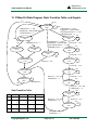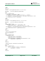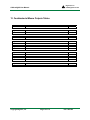
1
C1 X2 Memory Module Configuration Project User Manual Revision: 3/24/05 TM www .d ig ilen tinc .c om 246 East Main | Pullman, WA 99163 (509) 334 6306 Voice and Fax 1 Usage The C1MemCfgX2 project is similar to the C1MemCfg project, except that it allows two Digilent C1 memory modules to be connected to same motherboard. Each C1 memory module can be individually accessed: • reading and writing the 512 KB RAM chip on the module • erasing, reading and writing the 512 KB Flash chip on the module The project also supports two C0 memory modules or a C0/C1 combination. It can also be used as an example of extending the number of clients assigned to the same EppCtrl component. References made here to the C1 memory module also apply to a C0 memory module. 2 Related Digilent Reference Projects • • • The C1MemCfg project is the original project from which the C1MemCfgX2 project was derived. It supports a single C1 memory module connected to a system board. Please make yourself familiar with the C1MemCfg project before using the C1MemCfgX2 project. The C1X2 Memory Module Configuration Project User Manual does not repeat the behavioral description included in the C1 Memory Module Configuration Project User Manual, but only emphasizes the new features available with the C1MemCfgX2 project. The C2MemCfg project is a similar project, able to configure the Digilent C2 memory module (2 x 512 KB RAM chips, seen as a contiguous 1 MB RAM. The C3MemCfg project is a similar project, able to configure the Digilent C3 memory module. When reference is made to any of these projects, the generic name CxMemCfg is used. 3 PC Required Software • • Digilent TransPort and/or MemUtil 2.0 or greater 4 The Reference Digilent Board Configuration The ready-to-compile project is built for the Spartan 3 system board, with a Digilent USB 2.0 module attached to connector A1 and two Digilent C1 memory modules attached to connectors A2 and B1. 5 Available Digilent Board Configurations 5.1 Digilab 2FT Motherboard (Spartan XC2S300E or XC2S400E FPGA) with: • • • 5.2 Digilent USB 2.0 module on A1 motherboard connector Digilent C1 (or C0) memory module on A2 connector Digilent C1 (or C0) memory module on B1 connector Digilab 2SB Motherboard with: • • • Digilent USB 2.0 module on A1 motherboard connector Digilent C1 (or C0) memory module on A2 connector Digilent C1 (or C0) memory module on C1 connector Copyright Digilent, Inc. Page 1 of 12 Doc: 562-002 Digilent, IncTM C1MemCfgX2 User Manual 5.3 www.digilentinc.com Digilent Pegasus Motherboard (Spartan XC2S50 or XC2S200 FPGA) with: • • • 5.4 Digilent USB 2.0 module on A1 motherboard connector Digilent C1 (or C0) memory module on A2 connector Digilent C1 (or C0) memory module on B1 connector Digilent Spartan 3 Motherboard (Spartan XC3S200 or XC3S400 FPGA) with: • • • Digilent USB 2.0 module on A1 motherboard connector Digilent C1 (or C0) memory module on A2 connector Digilent C1 (or C0) memory module on B1 connector 6 Available Project and Compiling Variants • without display (C1MemCfg.bit). C1MemCfg.sch is the highest level file in the project hierarchy (the display feature is not available for the C1MemCfgX2 project). 7 Used Digilent Library Components • • • C1MemCtrl EppCtrl Disp7sCtrl 8 Project Description The project works similar to the C1MemCfg project, adding the second Digilent C1 memory module. All the functions described for the C1MemCfg project are available and refer to the Digilent C1 memory module connected to A2 – using the EPP Register Address range 0 to 7. All the functions described for the C1MemCfg project are available and refer to the Digilent C1 memory module connected to B1 – using the EPP Register Address range 8 to 15 (simply add an offset of 8 to the EPP address described in the C1 Memory Module Configuration Project User Manual). 9 Using Digilent MemUtil Software to Configure the Memory Module For information on using MemUtil to configure the memory module, please see the C1 Memory Module Configuration Project User Manual. To configure two memory modules connected to the same Digilent system board, through the same communication module (USB2, Ethernet, or serial), and using the C1MemCfgX2 project, keep in mind that: • A single MemUtil instance can only access a single memory module at once. • The accessed memory module is identified based on the Starting Register Address, set under Properties tab of the MemUtil main window. • The C1MemCfgX2 project assigns the register address range 0x00 to 0x07 (Starting Register Address = 0x00) to the memory module connected to the system board A2 connector and the register address range 0x08 to 0x0F (Starting Register Address = 0x08) to the other memory module (the other memory module connects to the Digilent system board connector B1 for most cases, except for D2SB system board, where connector C1 is used). • Multiple instances of MemUtil can run simultaneously on a PC, sharing the same connection (connection, communication module and system board). Moreover, other Digilent applications (e.g., Digilent TransPort, Digilent ExPort) can also share the same connection. o Multiple instances of MemUtil can run at the same time while sharing the same connection, communication module, system board, and memory module. Successive operations can be launched through any active MemUtil instance. You should allow a command to be fully executed before launching another one for the same communication module. Copyright Digilent, Inc. Page 2 of 12 Doc: 562-002 Digilent, IncTM C1MemCfgX2 User Manual www.digilentinc.com Multiple instances of MemUtil can also run at the same time while sharing the same connection, communication module, and system board, without sharing the same memory module. The C1MemCfgX2 project supports two memory modules (C1 or C0 type). Successive operations can be launched through any active MemUtil instance. The user should however allow a command to be fully executed before launching another one for the same Communication module. Multiple instances of MemUtil can be used to control different board sets, using different connections. For example, multiple different USB channels can be connected each to its own board configuration (USB module + system board + memory module(s)). Each system board needs to be configured with a CxMemCfg project. In this case, MemUtil instances are set to use different connections. This functionality is best left to experienced users. o • In conjunction with the C1MemCfgX2 project, MemUtil can be used in several different ways to configure two different memory modules, connected to the same system board and through the same connection and communication module. In the description below, the two memory modules are referred to as the first memory module and the second one. There is no restriction on which memory module (first or second) is connected to A2 (Starting address = 0x00) and which is connected to B1 (C1 for D2SB) (Starting address = 0x08). • Using a single instance of MemUtil: o launch an instance of MemUtil. o set the MemUtil Properties to match the hardware configuration, selecting the first memory module. choose (and configure) the communication module (Properties – Connection Properties and Configuration) choose the first memory module type (Properties –Memory Configuration) set the address range corresponding to the first memory module, based on the explanations above (Properties – Starting Register Address) o load/store the first memory module memory chips, as described in the C1 Memory Module Configuration Project User Manual. o modify the MemUtil Properties to switch to the second memory module. do not modify the Connection Properties and Configuration choose the second memory module type (Properties –Memory Configuration) set the address range corresponding to the second memory module, based on the explanations above (Properties – Starting Register Address) o load/store the second memory module memory chips, as described in the C1 Memory Module Configuration Project User Manual. o switch from a memory module to the other one as many times as needed. Keep in mind that the load/store action acts above the currently selected memory module. • Using two instances of MemUtil (recommended): o launch two instances of MemUtil. o set the Properties of the first MemUtil instance to match the hardware configuration, selecting the first memory module. choose (and configure) the communication module (Properties – Connection Properties and Configuration) choose the first memory module type (Properties –Memory Configuration) set the address range corresponding to the first memory module, based on the explanations above (Properties – Starting Register Address) o set the Properties of the second MemUtil instance to match the hardware configuration, selecting the second memory module. choose (and configure) the communication module – same module and configuration as for the first instance (Properties – Connection Properties) choose the second memory module type (Properties –Memory Configuration) Copyright Digilent, Inc. Page 3 of 12 Doc: 562-002 Digilent, IncTM C1MemCfgX2 User Manual www.digilentinc.com o o o o o • set the address range corresponding to the second memory module, based on the explanations above (Properties – Starting Register Address) prepare the load/store tabs in the first MemUtil instance, for the desired operations. Set file names, start addresses, transfer options, as described in the C1 Memory Module Configuration Project User Manual. You may perform the prepared operations now (press Store or Load button) or postpone that action for later. prepare the load/store tabs in the second MemUtil instance, for the desired operations. Set file names, start addresses, and transfer options, as described in the C1 Memory Module Configuration Project User Manual. You may perform the prepared operations now (press Store or Load button) or postpone that action for later. load/store the first memory module memory chips, using the first MemUtil instance, as described in the C1 Memory Module Configuration Project User Manual. load/store the second memory module memory chips, using the second MemUtil instance, as described in the C1 Memory Module Configuration Project User Manual. switch from a MemUtil instance to the other one as many times as needed. Adjust the Load/Store tab settings as needed and perform the transfer operations. Keep in mind that the load/store action acts above the instance-selected memory module. Using two groups of MemUtil instances (advanced users): o launch multiple instances of MemUtil and assign them to first group and second group. o set the Properties of all the MemUtil instances of the first group to match the hardware configuration, selecting the first memory module: choose (and configure) the communication module (Properties – Connection Properties and Configuration) choose the first memory module type (Properties –Memory Configuration) set the address range corresponding to the first memory module, based on the explanations above (Properties – Starting Register Address) o set the Properties of all the MemUtil instances of the second group to match the hardware configuration, selecting the second memory module: choose (and configure) the communication module – same module and configuration as for the first group (Properties – Connection Properties) choose the second memory module type (Properties –Memory Configuration) set the address range corresponding to the second memory module, based on the explanations above (Properties – Starting Register Address) o prepare the load/store tabs in all the MemUtil instances of the first group for the desired operations. Set file names, start addresses, transfer options, as described in the C1 Memory Module Configuration Project User Manual. For example, a memory test sequence would require multiple different files to be successively loaded and stored to/from the same chip. Each instance in the same group can be set to a different file in the sequence. You may perform the prepared operations now (press Store or Load button) or postpone that action for later. o prepare the load/store tabs in all the MemUtil instances of the second group for the desired operations, in a similar manner. o perform the prepared operations, pressing load/store buttons. You may switch from a MemUtil instance to any other, in any order. Keep in mind that each load/store action acts above the instance-selected memory module. 10 Using Digilent TransPort Software to Configure the Memory Module The Digilent TransPort software allows you to access the memory modules at lower level commands. The operation is similar to the one described in the C1 Memory Module Configuration Project User Manual. You should keep in mind that there are two distinct data register sets, one associated to each memory module. The memory modules can be accessed for address ranges 0 to 7, respectively 8 to 15. Copyright Digilent, Inc. Page 4 of 12 Doc: 562-002 Digilent, IncTM C1MemCfgX2 User Manual www.digilentinc.com TransPort can be used similarly to the MemUtil description above: • a single instance for both memory modules • two instances, each dedicated to a memory module • two groups of instances, each group dedicated to a memory module The properties tab of all the used instances is set identical, selecting and configuring the existing communication module. The instances assigned to the memory module connected to A2 system board connector use the register address range 0x00...0x07. All the EPP register addresses as described in the C1 Memory Module Configuration Project User Manual. The instances assigned to the memory module connected to B1 system board connector (C1, for D2SB) use the register address range 0x08...0x0F. (All the EPP register addresses described in the C1 Memory Module Configuration Project User Manual need to be incremented by 8). Copyright Digilent, Inc. Page 5 of 12 Doc: 562-002 Digilent, IncTM C1MemCfgX2 User Manual www.digilentinc.com 11 EppCtrl State Diagram, State Transition Table, and Signals EppRst stEppReady 000 else eppDstb = '0' or eppAstb = '0'; stEppStb 010 else EppDstb = ‘0’ and HandShakeReqIn = ‘1’ stEppSetProc 011 stEppRegTransf 110 stEppLaunchProc 111 else ctlMsmDoneIn = '1' stEppWaitProc 101 else ctlMsmDoneIn = '0' stEppDone 100 EppAstb = '0' or EppDstb = ‘0’ else State Transition Table 00 01 11 10 Copyright Digilent, Inc. Page 6 of 12 0 Ready ↓ Stb ↓ → RegTransf ↓ Done 1 SetProc ↓ LaunchProc ↓ WaitProc Doc: 562-002 Digilent, IncTM C1MemCfgX2 User Manual www.digilentinc.com 11.1 EppCtrl Port Signals -- Epp-like bus signals clk : in std_logic; -- system clock (50MHz) EppAstb : in std_logic; -- Address strobe EppDstb : in std_logic; -- Data strobe EppWr : in std_logic; -- Port write signal EppRst : in std_logic; -- Port reset signal EppDB : inout std_logic_vector(7 downto 0); -- port data bus EppWait : out std_logic; -- Port wait signal -- User signals busEppOut : out std_logic_vector(7 downto 0);-- Data Output bus busEppIn : in std_logic_vector(7 downto 0); -- Data Input bus ctlEppDwrOut : out std_logic; -- Data Write pulse ctlEppRdCycleOut: inout std_logic;-- Indicates a READ Epp cycle regEppAdrOut : inout std_logic_vector(7 downto 0) := "00000000"; -- Epp Address Register content HandShakeReqIn : in std_logic; -- User Handshake Request ctlEppStartOut : out std_logic; -- Automatic process Start ctlEppDoneIn : in std_logic -- Automatic process Done 11.2 EppCtrl Internal Signals busEppInternal: std_logic_vector(7 downto 0); ctlEppAwr : std_logic; 11.3 EppCtrl Signal Assignments -- Synchronized Epp outputs: process(clk) begin if clk'event and clk='1' then if stEppCur = stEppReady then ctlEppRdCycleOut <= '0'; elsif stEppCur = stEppStb then ctlEppRdCycleOut <= EppWr; state end if; end if; end process; -- not equivalent to EppWr due to default busEppOut <= EppDB; EppDB <= busEppInternal when (ctlEppRdCycleOut = '1') else "ZZZZZZZZ"; busEppInternal <= regEppAdrOut when EppAstb = '0' else busEppIn; -- Epp State machine related signals EppWait <= '1' when stEppCur = stEppDone else '0'; ctlEppAwr <= '1' when stEppCur = stEppRegTransf and EppAstb = '0' and EppWr = '0' else '0'; ctlEppDwrOut <= '1' when (stEppCur = stEppRegTransf or stEppCur = stEppSetProc) and EppDstb = '0' and EppWr = '0' else '0'; ctlEppStartOut <= '1' when stEppCur = stEpplaunchProc else '0'; Copyright Digilent, Inc. Page 7 of 12 Doc: 562-002 Digilent, IncTM C1MemCfgX2 User Manual www.digilentinc.com 12 C1MemCtrl State Diagram, State Transition Table, and Signals Reset stMsmReady 0000 CtlEppStartIn = ‘1’ and RegEppAdr = RamAutoRW and ComponentSelect = ‘1’ stMsmRAM01 0010 else else CtlEppRdCycleIn = ‘1’ stMsmRwr02 0110 stMsmRrd02 1010 stMsmRAM03 1110 else CtlEppStartIn = ‘1’ and RegEppAdr = FlashAutoRW and ComponentSelect = ‘1’ and CtlEppRdCycleIn = ‘0’ else stMsmFwr01 0001 CtlEppStartIn = ‘1’ and DelayCnt = “101” RegEppAdr = FlashAutoRW and ComponentSelect = ‘1’ and else CtlEppRdCycleIn = ‘1’ stMsmFwr02 0101 stMsmFrd01 0100 DelayCnt = “111” else else stMsmFwr03 DelayCnt = “101” 0111 DelayCnt = “101” stMsmAdInc 1100 stMsmDone 1000 else stMsmFwr04 1111 DelayCnt = “101” and busMemIn(7) = ‘1’ CtlMsmStartIn = 01 11 10 00 Ready ← ↓ → Frd01 ↓ AdrInc ↓ Done ↓ 01 Fwr01 11 ↓ Fwr02 Fwr03 → Fwr07 ↓ Fwr04 ← Fwr06 ↓ Fwr05 ↑ Copyright Digilent, Inc. ← 10 RAM01 ↑↓ Rwr02 ↓ RAM03 → Rrd02 ↑ DelayCnt = “111” else stMsmFwr05 1011 DelayCnt = “101” and busMemIn(7) = ‘0’ else stMsmFwr06 1001 State Transition Table 00 else DelayCnt = “101” and busMemIn(7) = ‘0’ DelayCnt = “111” else stMsmFwr07 1101 DelayCnt = “101” and busMemIn(7) = ‘1’ Page 8 of 12 Doc: 562-002 Digilent, IncTM C1MemCfgX2 User Manual www.digilentinc.com 12.1 C1MemCtrl Port Signals ck : in std_logic; -- system clock (50MHz) -- Epp interface signals HandShakeReqOut: out std_logic; -- User Handshake Request ctlMsmStartIn: in std_logic; -- Automatic process Start ctlMsmDoneOut: out std_logic; -- Automatic process Done ctlMsmDwrIn: in std_logic; -- Data Write pulse ctlEppRdCycleIn: in std_logic; -- Indicates a READ Epp cycle EppRdDataOut: out std_logic_vector(7 downto 0); -- Data Input bus EppWrDataIn: in std_logic_vector(7 downto 0); -- Data Output bus regEppAdrIn: in std_logic_vector(7 downto 0) ; -- Epp Address Register content (bits 7:3 ignored) ComponentSelect : in std_logic; -- active HIGH, selects the current MemCtrl instance -- Memory bus signals MemDB : inout std_logic_vector(7 downto 0); -- Memory data bus MemAdr : out std_logic_vector(18 downto 0); -- Memory Address bus RamCS : out std_logic; -- RAM CS FlashCS : out std_logic; -- Flash CS MemWR : out std_logic; -- memory write MemOE : out std_logic -- memory read (Output Enable), also controls the MemDB direction 12.2 C1MemCtrl Internal Signals signal DelayCnt : std_logic_vector(2 downto 0); -- Signals dealing with memory chips signal regMemCtl: std_logic_vector(4 downto 0) := "11111";-- Memory Control register signal regMemAdr: std_logic_vector(18 downto 0); -- Memory Address register signal carryoutL: std_logic := '0'; -- Carry out for memory address low byte signal carryoutM: std_logic := '0'; -- Carry out for memory address middle byte signal regMemWrData: std_logic_vector(7 downto 0); -- Memory Write Data register signal regMemRdData: std_logic_vector(7 downto 0); -- Memory Read Data register signal busMemIn: std_logic_vector(7 downto 0); signal busMemOut: std_logic_vector(7 downto 0); -- Signals in the memory control register signal ctlMcrOe : std_logic; signal ctlMcrWr : std_logic; signal ctlMcrRAMCs : std_logic; signal ctlMcrFlashCs : std_logic; signal ctlMcrDir : std_logic; -- Output enable (read strobe) -- Write enable (write strobe) -- RAM chip select -- Flash chip select -- composed out of previous ones -- Signals used by Memory control state machine signal ctlMsmOe : std_logic; signal ctlMsmWr : std_logic; signal ctlMsmRAMCs : std_logic; signal ctlMsmFlashCs : std_logic; signal ctlMsmDir : std_logic; signal ctlMsmAdrInc : std_logic; signal ctlMsmWrCmd : std_logic; Copyright Digilent, Inc. Page 9 of 12 Doc: 562-002 Digilent, IncTM C1MemCfgX2 User Manual www.digilentinc.com 12.3 C1MemCtrl Signal Assignments -- Memory signals -Memory control register ctlMcrOe <= regMemCtl(0); ctlMcrWr <= regMemCtl(1); ctlMcrRAMCs <= regMemCtl(2); ctlMcrFlashCs <= regMemCtl(3); -- Output enable (read strobe) -- Write enable (write strobe) -- RAM chip select -- Flash chip select -- Memory control bus driven either by automatic state machine or by memory control register RamCS <= ctlMsmRAMCs and ctlMcrRAMCs; -- PC generated RAM CS; FlashCS <= ctlMsmFlashCs and ctlMcrFlashCs; -- PC generated Flash CS; MemWR <= ctlMsmWr and ctlMcrWr; -- PC generated MemWr; MemOE <= ctlMsmOe and ctlMcrOe; -- PC generated MemOe; busMemIn <= MemDB; busMemOut <= "01000000" when ctlMsmWrCmd = '1' else regMemWrData; MemAdr <= regMemAdr; ctlMcrDir <= ctlMcrOe and ((not ctlMcrFlashCs) or (not ctlMcrRAMCs)); MemDB <= busMemOut when (ctlMsmDir = '1' or ctlMcrDir = '1') else "ZZZZZZZZ"; -- Handshake signal HandShakeReqOut <= '1' when (regEppAdrIn(2 downto 0) = RamAutoRW or regEppAdrIn(2 downto 0) = FlashAutoRW) and ComponentSelect = '1' else '0'; -- Delay Counter process (clk) begin if clk'event and clk = '1' then if stMsmCur = stMsmReady then DelayCnt <= "000"; else DelayCnt <= DelayCnt + 1; end if; end if; end process; -- Memory Control Register process (clk, ctlMsmDwrIn) begin if clk = '1' and clk'Event then if ctlMsmDwrIn = '1' and regEppAdrIn(2 downto 0) = MemCtrlReg and ComponentSelect = '1' then regMemCtl <= EppWrDataIn(4 downto 0); end if; end if; end process; -- Memory Address Register/Counter MsmAdrL: process (clk, ctlMsmDwrIn, ctlMsmAdrInc) begin if clk = '1' and clk'Event then if ctlMsmAdrInc = '1' then regMemAdr(7 downto 0) <= regMemAdr(7 downto 0) + 1; --"00000001"; elsif ctlMsmDwrIn = '1' and regEppAdrIn(2 downto 0) = MemAdrL and ComponentSelect = '1' then regMemAdr(7 downto 0) <= EppWrDataIn; Copyright Digilent, Inc. Page 10 of 12 Doc: 562-002 Digilent, IncTM C1MemCfgX2 User Manual www.digilentinc.com end if; end if; end process; carryoutL <= '1' when regMemAdr(7 downto 0) = "11111111" else '0'; MsmAdrM: process (clk, ctlMsmDwrIn, ctlMsmAdrInc) begin if clk = '1' and clk'Event then if ctlMsmAdrInc = '1' and carryoutL = '1' then regMemAdr(15 downto 8) <= regMemAdr(15 downto 8) + 1; --"00000001"; elsif ctlMsmDwrIn = '1' and regEppAdrIn(2 downto 0) = MemAdrM and ComponentSelect = '1' then regMemAdr(15 downto 8) <= EppWrDataIn; end if; end if; end process; carryoutM <= '1' when regMemAdr(15 downto 8) = "11111111" else '0'; MsmAdrH: process (clk, ctlMsmDwrIn, ctlMsmAdrInc) begin if clk = '1' and clk'Event then if ctlMsmAdrInc = '1' and carryoutL = '1' and carryoutM = '1' then regMemAdr(18 downto 16) <= regMemAdr(18 downto 16) + 1; --"001"; elsif ctlMsmDwrIn = '1' and regEppAdrIn(2 downto 0) = MemAdrH and ComponentSelect = '1' then regMemAdr(18 downto 16) <= EppWrDataIn(2 downto 0); end if; end if; end process; -- Memory write data holding register process (clk, ctlMsmDwrIn) begin if clk = '1' and clk'Event then if ctlMsmDwrIn = '1' and (regEppAdrIn(2 downto 0) = RamAutoRW or regEppAdrIn(2 downto 0) = FlashAutoRW or regEppAdrIn(2 downto 0) = MemDataWr) and ComponentSelect = '1' then regMemWrData <= EppWrDataIn; end if; end if; end process; -- Memory read register: - holds data after an automatic read process (clk) begin if clk = '1' and clk'Event then if stMsmCur = stMsmFrd01 or stMsmCur = stMsmRrd02 then regMemRdData <= busMemIn; end if; end if; end process; Copyright Digilent, Inc. Page 11 of 12 Doc: 562-002 Digilent, IncTM C1MemCfgX2 User Manual www.digilentinc.com 13 Combinatorial Moore Outputs Tables Signal ctlMsmOe stMsmFrd01 or stMsmFwr05 or stMsmFwr07 or stMsmFrd02 ‘0’ Others ‘1’ Signal ctlMsmWr stMsmFwr01 or stMsmFwr03 or stMsmRwr02 ‘0’ Others ‘1’ Signal ctlMsmRAMCs stMsmRAM01 or stMsmRAM03 or stMsmRwr02 or stMsmRrd02 ‘0’ Others ‘1’ Signal ctlMsmFlashCs stMsmFwr0X or stMsmFrd01 ‘0’ Others ‘1’ Signal ctlMsmDir stMsmFwr01 or stMsmFwr02 or stMsmFwr03 or stMsmRwr02 ‘1’ Others ‘0’ Signal ctlAdrInc stMsmAdInc ‘1’ Others ‘0’ Signal ctlMsmWrCmd stMsmFwr01 or stMsmFwr02 ‘1’ Others ‘0’ Signal ctlMsmDoneOut stMsmDone ‘1’ Others ‘0’ Copyright Digilent, Inc. Page 12 of 12 Doc: 562-002