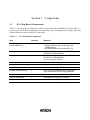
1
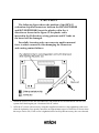
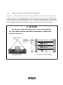
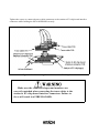
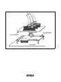
To our customers,
Old Company Name in Catalogs and Other Documents
On April 1st, 2010, NEC Electronics Corporation merged with Renesas Technology
Corporation, and Renesas Electronics Corporation took over all the business of both
companies. Therefore, although the old company name remains in this document, it is a valid
Renesas Electronics document. We appreciate your understanding.
Renesas Electronics website: http://www.renesas.com
April 1st, 2010
Renesas Electronics Corporation
Issued by: Renesas Electronics Corporation (http://www.renesas.com)
Send any inquiries to http://www.renesas.com/inquiry.
Notice
1.
2.
3.
4.
5.
6.
7.
All information included in this document is current as of the date this document is issued. Such information, however, is
subject to change without any prior notice. Before purchasing or using any Renesas Electronics products listed herein, please
confirm the latest product information with a Renesas Electronics sales office. Also, please pay regular and careful attention to
additional and different information to be disclosed by Renesas Electronics such as that disclosed through our website.
Renesas Electronics does not assume any liability for infringement of patents, copyrights, or other intellectual property rights
of third parties by or arising from the use of Renesas Electronics products or technical information described in this document.
No license, express, implied or otherwise, is granted hereby under any patents, copyrights or other intellectual property rights
of Renesas Electronics or others.
You should not alter, modify, copy, or otherwise misappropriate any Renesas Electronics product, whether in whole or in part.
Descriptions of circuits, software and other related information in this document are provided only to illustrate the operation of
semiconductor products and application examples. You are fully responsible for the incorporation of these circuits, software,
and information in the design of your equipment. Renesas Electronics assumes no responsibility for any losses incurred by
you or third parties arising from the use of these circuits, software, or information.
When exporting the products or technology described in this document, you should comply with the applicable export control
laws and regulations and follow the procedures required by such laws and regulations. You should not use Renesas
Electronics products or the technology described in this document for any purpose relating to military applications or use by
the military, including but not limited to the development of weapons of mass destruction. Renesas Electronics products and
technology may not be used for or incorporated into any products or systems whose manufacture, use, or sale is prohibited
under any applicable domestic or foreign laws or regulations.
Renesas Electronics has used reasonable care in preparing the information included in this document, but Renesas Electronics
does not warrant that such information is error free. Renesas Electronics assumes no liability whatsoever for any damages
incurred by you resulting from errors in or omissions from the information included herein.
Renesas Electronics products are classified according to the following three quality grades: “Standard”, “High Quality”, and
“Specific”. The recommended applications for each Renesas Electronics product depends on the product’s quality grade, as
indicated below. You must check the quality grade of each Renesas Electronics product before using it in a particular
application. You may not use any Renesas Electronics product for any application categorized as “Specific” without the prior
written consent of Renesas Electronics. Further, you may not use any Renesas Electronics product for any application for
which it is not intended without the prior written consent of Renesas Electronics. Renesas Electronics shall not be in any way
liable for any damages or losses incurred by you or third parties arising from the use of any Renesas Electronics product for an
application categorized as “Specific” or for which the product is not intended where you have failed to obtain the prior written
consent of Renesas Electronics. The quality grade of each Renesas Electronics product is “Standard” unless otherwise
expressly specified in a Renesas Electronics data sheets or data books, etc.
“Standard”:
8.
9.
10.
11.
12.
Computers; office equipment; communications equipment; test and measurement equipment; audio and visual
equipment; home electronic appliances; machine tools; personal electronic equipment; and industrial robots.
“High Quality”: Transportation equipment (automobiles, trains, ships, etc.); traffic control systems; anti-disaster systems; anticrime systems; safety equipment; and medical equipment not specifically designed for life support.
“Specific”:
Aircraft; aerospace equipment; submersible repeaters; nuclear reactor control systems; medical equipment or
systems for life support (e.g. artificial life support devices or systems), surgical implantations, or healthcare
intervention (e.g. excision, etc.), and any other applications or purposes that pose a direct threat to human life.
You should use the Renesas Electronics products described in this document within the range specified by Renesas Electronics,
especially with respect to the maximum rating, operating supply voltage range, movement power voltage range, heat radiation
characteristics, installation and other product characteristics. Renesas Electronics shall have no liability for malfunctions or
damages arising out of the use of Renesas Electronics products beyond such specified ranges.
Although Renesas Electronics endeavors to improve the quality and reliability of its products, semiconductor products have
specific characteristics such as the occurrence of failure at a certain rate and malfunctions under certain use conditions. Further,
Renesas Electronics products are not subject to radiation resistance design. Please be sure to implement safety measures to
guard them against the possibility of physical injury, and injury or damage caused by fire in the event of the failure of a
Renesas Electronics product, such as safety design for hardware and software including but not limited to redundancy, fire
control and malfunction prevention, appropriate treatment for aging degradation or any other appropriate measures. Because
the evaluation of microcomputer software alone is very difficult, please evaluate the safety of the final products or system
manufactured by you.
Please contact a Renesas Electronics sales office for details as to environmental matters such as the environmental
compatibility of each Renesas Electronics product. Please use Renesas Electronics products in compliance with all applicable
laws and regulations that regulate the inclusion or use of controlled substances, including without limitation, the EU RoHS
Directive. Renesas Electronics assumes no liability for damages or losses occurring as a result of your noncompliance with
applicable laws and regulations.
This document may not be reproduced or duplicated, in any form, in whole or in part, without prior written consent of Renesas
Electronics.
Please contact a Renesas Electronics sales office if you have any questions regarding the information contained in this
document or Renesas Electronics products, or if you have any other inquiries.
(Note 1) “Renesas Electronics” as used in this document means Renesas Electronics Corporation and also includes its majorityowned subsidiaries.
(Note 2) “Renesas Electronics product(s)” means any product developed or manufactured by or for Renesas Electronics.
To all our customers
Regarding the change of names mentioned in the document, such as Hitachi
Electric and Hitachi XX, to Renesas Technology Corp.
The semiconductor operations of Mitsubishi Electric and Hitachi were transferred to Renesas
Technology Corporation on April 1st 2003. These operations include microcomputer, logic, analog
and discrete devices, and memory chips other than DRAMs (flash memory, SRAMs etc.)
Accordingly, although Hitachi, Hitachi, Ltd., Hitachi Semiconductors, and other Hitachi brand
names are mentioned in the document, these names have in fact all been changed to Renesas
Technology Corp. Thank you for your understanding. Except for our corporate trademark, logo and
corporate statement, no changes whatsoever have been made to the contents of the document, and
these changes do not constitute any alteration to the contents of the document itself.
Renesas Technology Home Page: http://www.renesas.com
Renesas Technology Corp.
Customer Support Dept.
April 1, 2003
User’s Manual
SH7612 Evaluation Chip
Board (HS7612EBH81H) for
the E8000 Emulator
User’s Manual
www.renesas-electoronics.com
IMPORTANT INFORMATION
READ FIRST
• READ this user's manual before using this evaluation chip board (hereafter
referred to as the EV-chip board) for Hitachi microcomputer HD6437410.
• KEEP the user's manual handy for future reference.
Do not attempt to use the EV-chip board until you fully understand its mechanism.
EV-Chip Board:
Throughout this document, the term "EV-chip board" shall be defined as the following products
produced only by Hitachi, Ltd. excluding all subsidiary products.
• EV-chip board
• Device control board
The user system or a host computer is not included in this definition.
Purpose of the EV-Chip Board:
This EV-chip board is a software and hardware development tool for systems employing the
Hitachi microcomputer HD6437410 (hereafter referred to as SH7410). The E8000 emulator and
the user system can be connected through the EV-chip board. This EV-chip board must only be
used for the above purpose.
Improvement Policy:
Hitachi, Ltd. (including its subsidiaries, hereafter collectively referred to as Hitachi) pursues a
policy of continuing improvement in design, performance, and safety of the EV-chip board.
Hitachi reserves the right to change, wholly or partially, the specifications, design, user's manual,
and other documentation at any time without notice.
Target User of the EV-Chip Board:
This EV-chip board should only be used by those who have carefully read and thoroughly
understood the information and restrictions contained in the user's manual. Do not attempt to use
the EV-chip board until you fully understand its mechanism.
It is highly recommended that first-time users be instructed by users that are well versed in the
operation of the EV-chip board.
I
LIMITED WARRANTY
Hitachi warrants its EV-chip boards to be manufactured in
accordance with published specifications and free from defects in
material
and/or workmanship. Hitachi, at its option, will repair or replace any
EV-chip boards returned intact to the factory, transportation charges
prepaid, which Hitachi, upon inspection, determine to be defective in
material and/or workmanship. The foregoing shall constitute the sole
remedy for any breach of Hitachi's warranty. See the Hitachi warranty
booklet for details on the warranty period. This warranty extends only to
you, the original Purchaser. It is not transferable to anyone who
subsequently purchases the EV-chip board from you. Hitachi is not
liable for any claim made by a third party or made by you for a third
party.
DISCLAIMER
HITACHI MAKES NO WARRANTIES, EITHER EXPRESS OR
IMPLIED, ORAL OR WRITTEN, EXCEPT AS PROVIDED
HEREIN, INCLUDING WITHOUT LIMITATION THEREOF,
WARRANTIES AS TO MARKETABILITY, MERCHANTABILITY,
FITNESS FOR ANY PARTICULAR PURPOSE OR USE, OR
AGAINST INFRINGEMENT OF ANY PATENT. IN NO EVENT
SHALL HITACHI BE LIABLE FOR ANY DIRECT, INCIDENTAL
OR CONSEQUENTIAL DAMAGES OF ANY NATURE, OR
LOSSES OR EXPENSES RESULTING FROM ANY DEFECTIVE
EV-CHIP BOARD, THE USE OF ANY EV-CHIP BOARD,
OR ITS DOCUMENTATION, EVEN IF ADVISED OF
THE POSSIBILITY OF SUCH DAMAGES. EXCEPT AS
EXPRESSLY STATED OTHERWISE IN THIS WARRANTY,
THIS EV-CHIP BOARD IS SOLD "AS IS ", AND YOU
MUST ASSUME ALL RISK FOR THE USE AND RESULTS
OBTAINED FROM THE EV-CHIP BOARD.
II
State Law:
Some states do not allow the exclusion or limitation of implied warranties or liability for incidental
or consequential damages, so the above limitation or exclusion may not apply to you. This
warranty gives you specific legal rights, and you may have other rights which may vary from state
to state.
The Warranty is Void in the Following Cases:
Hitachi shall have no liability or legal responsibility for any problems caused by misuse, abuse,
misapplication, neglect, improper handling, installation, repair or modifications of the EV-chip
board without Hitachi's prior written consent or any problems caused by the user system.
All Rights Reserved:
This user's manual and EV-chip board are copyrighted and all rights are reserved by Hitachi. No
part of this user's manual, all or part, may be reproduced or duplicated in any form, in hard-copy or
machine-readable form, by any means available without Hitachi's prior written consent.
Other Important Things to Keep in Mind:
1. Circuitry and other examples described herein are meant merely to indicate the characteristics
and performance of Hitachi's semiconductor products. Hitachi assumes no responsibility for
any intellectual property claims or other problems that may result from applications based on
the examples described herein.
2. No license is granted by implication or otherwise under any patents or other rights of any third
party or Hitachi.
Figures:
Some figures in this user's manual may show items different from your actual system.
Limited Anticipation of Danger:
Hitachi cannot anticipate every possible circumstance that might involve a potential hazard. The
warnings in this user's manual and on the EV-chip board are therefore not all inclusive. Therefore,
you must use the EV-chip board safely at your own risk.
III
SAFETY PAGE
READ FIRST
• READ this user's manual before using this EV-chip board.
• KEEP the user's manual handy for future reference.
Do not attempt to use the EV-chip board until you fully understand its mechanism.
DEFINITION OF SIGNAL WORDS
DANGER indicates an imminently hazardous situation which, if not avoided,
will result in DEATH or SERIOUS INJURY to you or other people.
WARNING indicates a potentially hazardous situation which, if not avoided,
could result in DEATH or SERIOUS INJURY to you or other people.
CAUTION indicates a hazardous situation which, if not avoided, may result in minor or
moderate injury to you or other people, or may result in damage to the
machine or loss of the user program. It may also be used to alert against
unsafe usage.
NOTE emphasizes essential information.
Observe the precautions listed below. Failure to do so
will result in a FIRE HAZARD and will damage the user
system and the EV-chip board or will result in
PERSONAL INJURY. The USER PROGRAM will be
LOST.
1. Always switch OFF the emulator and user system
before connecting or disconnecting any CABLES or
PARTS.
2. Always before connecting, make sure that pin 1 on both
sides is correctly aligned.
IV
Warnings on EV-Chip Board Usage
Warnings described below apply as long as you use the EV-chip board. Be sure to read and
understand the warnings below before using the EV-chip board. Note that these are the main
warnings, not the complete list.
Always switch OFF the emulator and user system
before connecting or disconnecting any CABLES or PARTS.
Failure to do so will result in a FIRE HAZARD and will
damage the user system and the EV-chip board or will
result in PERSONAL INJURY. The USER PROGRAM
will be LOST.
V
Place the emulator station and EV-chip board so that
the cable is not bent or twisted. A bent or twisted cable
will impose stress on the user interface leading to connection
or contact failure. Make sure that the emulator station is
placed in a secure position so that it does not move
during use nor impose stress on the user interface.
VI
Notice
When using this document, keep the following in mind:
1. This document may, wholly or partially, be subject to change without notice.
2. All rights are reserved: No one is permitted to reproduce or duplicate, in any form, the whole
or part of this document without Hitachi’s permission.
3. Hitachi will not be held responsible for any damage to the user that may result from accidents
or any other reasons during operation of the user’s unit according to this document.
4. Circuitry and other examples described herein are meant merely to indicate the characteristics
and performance of Hitachi’s semiconductor products. Hitachi assumes no responsibility for
any intellectual property claims or other problems that may result from applications based on
the examples described herein.
5. No license is granted by implication or otherwise under any patents or other rights of any third
party or Hitachi, Ltd.
6. MEDICAL APPLICATIONS: Hitachi’s products are not authorized for use in MEDICAL
APPLICATIONS without the written consent of the appropriate officer of Hitachi’s sales
company. Such use includes, but is not limited to, use in life support systems. Buyers of
Hitachi’s products are requested to notify the relevant Hitachi sales office when planning to use
the products in MEDICAL APPLICATIONS.
Preface
This manual describes how to connect and operate the EV-chip board. The EV-chip board
incorporates an evaluation chip for connection to a user system that uses the SH7612 with the
E8000 emulator.
Read and understand Sec. 3, “Preparation before Use” of the E8000 Emulator User’s Manual
before using this EV-chip board.
CAUTION
The EV-chip board is only for connection to a user
system that uses the SH7612 with the E8000 emulator.
It cannot be used for user systems that target other devices.
Contents
Section 1
1.1
1.2
Section 2
2.1
3.2
3.3
Connecting the EV-Chip Board to the User System........................10
Connecting the HS7420PWB30H to the User System ...................................................... 10
3.1.1 Installing the QFP-176 Package IC Socket .......................................................... 10
3.1.2 Connecting the HS7420PWB30H to the User System......................................... 12
Connecting the Trace Cables............................................................................................. 16
3.2.1 Connecting the Trace Cables to the E8000 Station .............................................. 16
3.2.2 Connecting the Trace Cables to the EV-Chip Board............................................ 15
Connecting the HS7410PWB20H and HS7420PWB30H................................................. 19
Section 4
4.1
Preparation before Use ....................................................................4
Preparing the User System ................................................................................................ 4
2.1.1 Connector Mounting Position of the User System ............................................... 7
Section 3
3.1
Components .....................................................................................1
EV-Chip Board Components ............................................................................................ 1
Component Names ............................................................................................................ 2
Mounting the SH7612 .....................................................................21
Mounting the SH7612 on the User System ....................................................................... 21
Figures
Figure 1.1
Figure 2.1
Figure 2.2
Figure 3.1
Figure 3.2
Figure 3.3
Figure 3.4
Figure 3.5
Figure 3.6
Figure 4.1
EV-Chip Board....................................................................................................... 2
Recommended Mounting Pad Dimensions............................................................. 7
Component Height Restriction ............................................................................... 7
Positioning the IC Socket ....................................................................................... 11
Top View of the HS7420PWB30H ........................................................................ 12
Screw-Tightening Sequence (Top View of the HS7420PWB30H)........................ 14
Connecting the HS7420PWB30H to the User System ........................................... 15
Connecting Trace Cables to the EV-Chip Board.................................................... 18
Connecting the HS7410PWB20H and HS7420PWB30H...................................... 20
Mounting the SH7612 ............................................................................................ 22
Tables
Table 1.1
Table 2.1
EV-chip Board Components................................................................................... 1
Pin Assignment of the 176-Pin QFP IC Socket ...................................................... 5
Section 1 Components
1.1
EV-Chip Board Components
Table 1.1 lists the product components of the EV-chip board (HS7612EBH81H: 176-pin QFP IC
socket type). Check all the components after unpacking. If any components are missing, contact the
Hitachi salesperson who sold this EV-chip board.
Table 1.1
EV-chip Board Components
Item
Quantity
Remarks
EV-chip board
(HS7612EBH81H)
1
Consists of two boards.
• HS7410PWB20H (for connecting to the
E8000 station)
• HS7420PWB30H (IC socket QFP-176)
IC socket
1
NQPACK176SD manufactured by TOKYO
ELETECH CORPORATION
IC socket cover
1
HQPACK176SD manufactured by TOKYO
ELETECH CORPORATION.
For mounting the SH7612.
Screws (for the IC socket)
4
M2 x 6 mm for mounting the MCU
Screws (for the IC socket)
4
M2 x 10 mm for attaching the EV-chip board
Spacers
4
13 mm for attaching the EV-chip board.
Screws (for the spacers)
4
M3 x 6 mm for attaching the EV-chip board.
Four flat washers and four spring washers
Guide pins
3
For positioning the IC socket
Specific screwdriver
1
Screwdriver for fixing the IC socket
Nuts
4
M3 mm for attaching the EV-chip board
1
1.2
Component Names
The component names of the EV-chip board are described below.
Figure 1.1
EV-Chip Board
1. Station to EV-chip board interface
connector CN3:
For trace cable 3 which connects the E8000
station to the EV-chip board.
2. Station to EV-chip board interface
connector CN2:
For trace cable 2 which connects the E8000
station to the EV-chip board.
3. Station to EV-chip board interface
connector CN1:
For trace cable 1 which connects the E8000
station to the EV-chip board.
4. Crystal oscillator terminals:
For installing a crystal oscillator to be used as
a clock source for the SH7612.
5. User-system connector:
For connecting the user system.
6. Board connector:
For connecting HS7410PWB20H and
HS7420PWB30H.
7. HS7410PWB20H:
Includes connectors for interfacing with the
E8000 station.
8. HS7420PWB30H:
Includes connectors for interfacing with the
user system.
1
9 Spacer
1
Section 2 Preparation before Use
2.1
Preparing the User System
Table 2.1 lists the user interface pin assignment of the 176-pin QFP IC socket (NQPACK176SD
manufactured by TOKYO ELETECH CORPORATION) when the target MCU is the SH7612.
1
Table 2.1
Pin Assignment of the 176-Pin QFP IC Socket
Pin No.
Pin Name
Pin No.
Pin Name
Pin No.
Pin Name
1
SCK0
32
ASEMD0
63
GND15
2
TXD0/PB9
33
GND17
64
GND14
3
RXD0/PB10
34
GND
65
CAS 2N
4
SCK1/PB11
35
MD4
66
VCC15
5
TXD1/PB12
36
MD3
67
VCC14
6
GND20
37
MD2
68
CAS 3N
7
RXD1/PB13
38
MD1
69
A0
8
VCC20
39
MD0
70
A1
9
STS0/PB14
40
DREQ0N
71
A2
10
STCK0/PB15
41
DREQ1N
72
A3
11
STxD0/PA0
42
DACK0
73
A4
12
SRS0/PA1
43
DACK1
74
GND13
13
SRCK0/PA2
44
IVECFN
75
A5
14
SRxD0/PA3
45
BREQN
76
VCC13
15
STS1/PA4
46
BACKN
77
A6
16
STCK1/PA5
47
WE0N
78
A7
17
VCC19
48
WE1N
79
A8
18
STXD1/PA6
49
WE2N
80
A9
19
GND19
50
GND16
81
A10
20
SRS1/PA7
51
WE3N
82
A11
21
SRCK1/PA8
52
VCC16
83
VCC12
22
VCC18
53
RDN
84
A12
23
SRXD1/PA9
54
WAITN
85
GND12
24
STS2/PA10
55
CS0N
86
A13
25
GND18
56
CS1N
87
A14
26
STCK2/PA11
57
CS2N/RAS2N
88
A15
27
STXD2/PA12
58
CS3N/RAS3N/CEN
89
A16
28
SRS2/PA13
59
RDWR
90
A17
29
SRCK2/PA14
60
BSN
91
A18
30
SRXD2/PA15
61
CAS0N/RFSHN
92
VCC11
31
VCC17
62
CAS1N
93
A19
1
Table 2.1
Pin Assignment of the 176-Pin QFP IC Socket (cont)
Pin No.
Pin Name
Pin No.
Pin Name
Pin No.
Pin Name
94
GND11
122
D31
150
D9
95
A20
123
D30
151
D8
96
A21
124
D29
152
D7
97
A22
125
D28
153
VCC4
98
A23
126
D27
154
VCC3
99
TDO
127
VCC7
155
D6
100
VCC10
128
D26
156
GND4
101
TDI
129
GND7
157
GND3
102
GND10
130
D25
158
D5
103
TMS
131
D24
159
D4
104
PLLGND
132
D23
160
D3
105
PLLCAP
133
D22
161
D2
106
PLLVCC
134
D21
162
D1
107
EXTAL
135
D20
163
VCC2
108
XTAL
136
VCC6
164
D0
109
TRSTN
137
D19
165
GND2
110
VCC9
138
GND6
166
FTI0/FTOB0/PB0
111
VCC8
139
D18
167
FTOA0/PB1
112
TCK
140
D17
168
FTC0/PB2
113
GND9
141
D16
169
FTI1/PB3/FTOB1
114
GND8
142
D15
170
VCC1
115
CLK
143
D14
171
FTOA1/PB4
116
NMI
144
D13
172
GND1
117
RSTN
145
VCC5
173
FTC1/PB5
118
IRQ0
146
D12
174
FTI2/PB6/FTOB2
119
IRQ1
147
GND5
175
FTOA2/PB7
120
IRQ2
148
D11
176
FTC2/PB8
121
IRQ3
149
D10
1
2.1.1
Connector Mounting Position of the User System
Figure 2.1 shows the recommended mounting pad (footprint) dimensions and the hole position for
installing the EV-chip board for the supplied 176-pin QFP IC socket (NQPACK176SD)
manufactured by TOKYO ELETECH CORPORATION.
The screw holes in the EV-chip board for attaching the board are connected to the GND of the
board. The ground lines can be enhanced by forming a GND pattern at the screw hole locations of
the user system, enabling stable operation during high-speed emulation.
115.0
□ 27.1
□ 23.1
2.0
2.0
11.0
7.0
99.5
45.0
0.5×43=21.5
76.0
10.0
11.75
7.75
10.0
90.0
(A)
0.25
Pin1 mark
11.0
7.0
φ
14.0
3.
11.0
3-φ1.0
2
4-φ4
22.0
External frame of the EV-chip board
(A)
50.0
7.75
(A):Center line of the IC socket
:Pattern inhibition area, except for GND pattern
Unit: mm
Tolerance: + 0.1 mm
Figure 2.1
Recommended Mounting Pad Dimensions
1
Comply with the user system component height restriction shown in Figure 2.2 within the external
frame of the EV-chip board shown in Figure 2.1.
11.2
HS7420PWB30H
User system socket
NQPACK176SD manufactured by
TOKYO ELETEC CORPORATION
Figure 2.2
User system board
Unit: mm
Component Height Restriction
1
The screw holes of the EV-chip board for attaching the
board are connected to the GND of the board. Confirm
that the spacers, nuts, or washers of the EV-chip board do
not make contact with the patterns or components other than
the GND on the user system.
Failure to do so will result in a FIRE HAZARD and will
damage the user system and emulator or will result in
PERSONAL INJURY. The USER PROGRAM will be LOST.
Bottom view of the HS7420PWB30H
1
Section 3 Connecting the EV-Chip Board to the User
System
3.1
Connecting the HS7420PWB30H to the User System
3.1.1
Installing the QFP-176 Package IC Socket
This EV-chip board is designed exclusively for the supplied IC socket (type number:
NQPACK176SD) manufactured by TOKYO ELETECH CORPORATION. Therefore, it cannot be
used with other IC sockets.
• Positioning the IC socket
Position the IC socket with the supplied guide pins, as shown in figure 3.1. Apply an epoxy
adhesive to the tips of the four protrusions on the bottom surface of the IC socket to bond the IC
socket to the user system board.
1
Figure 3.1
Positioning the IC Socket
1
• Soldering the IC socket
After the epoxy adhesive has hardened, solder the IC socket. At this time, install the cover on
the IC socket to prevent flux or solder from adhering to the guide pins. Use more solder than
usual so that a fillet is formed on the lead edge being soldered.
3.1.2
Connecting the HS7420PWB30H to the User System
1. At shipment, the HS7410PWB20H and HS7420PWB30H are connected to each other. Before
connecting the EV-chip board to the user system, separate the HS7410PWB20H from the
HS7420PWB30H. The HS7410PWB20H is connected to the HS7420PWB30H through three
connectors as shown in figure 3.2.
Figure 3.2
Top View of the HS7420PWB30H
Insert the plastic rod between the HS7410PWB20H and HS7420PWB30H, and lever them
apart. Alternately between the four corners of the EV-chip board, gradually force the
HS7410PWB20H and HS7420PWB30H apart.
1
CAUTION
The following figure shows the position of the SH7612
evaluation chip and connectors between the HS7410PWB20H
and HS7420PWB30H. Insert the plastic rod in the A
direction as shown in the figure. If the plastic rod is
inserted in the B direction, wiring patterns and IC leads on
the board will be damaged.
Forcefully loosening only one connector applies unusual
force to other connectors, thus damaging the connectors
and causing contact failures.
2. Attach the spacers on the HS7420PWB30H, and install the HS7420PWB30H onto the user
system after checking the pin-1 location of the IC socket.
3. Affix the IC socket with screws by using the supplied screwdriver. Stop tightening each screw
when the tightening force greatly increases (an approximate target is 0.098 N•m or lower when
the torque can be set). If the screw is tightened more forcibly than necessary, the screw threads
1
in the IC socket may be damaged or a contact failure may occur due to a solder crack on the IC
socket.
CAUTION
When tightening the screws for the IC socket, use the
supplied screwdriver.
4. Attach the HS7420PWB30H to the IC socket on the user system with four screws (M2 x 10
mm). Gradually tighten the screws alternately in a figure-8 pattern (see figure 3.3). Never
forcibly tighten only one screw. Otherwise, a contact failure will occur or performance will be
degraded. When tightening the screws, hold the IC socket so that it does not twist.
Figure 3.3
Screw-Tightening Sequence (Top View of the HS7420PWB30H)
1
5. Affix the HS7420PWB30H to the user system with the appropriate screws and nuts.
CAUTION
1. Before connecting the EV-chip board to the user system,
check the location of pin 1 on both sides.
2. If a malfunction occurs during operation, a crack may
have occurred in the soldered section of the IC socket.
Check the electric conduction with a tester and resolder
the cracked section.
Figure 3.4
Connecting the HS7420PWB30H to the User System
1
3.2
Connecting the Trace Cables
Always switch OFF the emulator and user system before
connecting or disconnecting any CABLES or sockets.
Failure to do so will result in a FIRE HAZARD and will
damage the user system and the emulator or will result in
PERSONAL INJURY. The USER PROGRAM will be LOST.
3.2.1
Connecting the Trace Cables to the E8000 Station
Before connecting the trace cables to the HS7410PWB20H, connect the trace cables to the E8000
station.
Note: At shipment, trace cables CN2 and CN3 to be connected to the E8000 station are
bound into a bundle, and trace cables CN1, CN2, and CN3 to be connected to the
EV-chip board are bound into a bundle to prevent an insertion error. For more
information on connecting the EV-Chip board to the E8000 station, refer to section
3.2.2, Connecting the EV-Chip Board, in the SH7612 E8000 Emulator User’s
Manual.
1
3.2.2
Connecting the Trace Cables to the EV-Chip Board
Align the trace cables with the station to EV-chip board interface connectors CN1, CN2, and CN3
on the EV-chip board. Confirm that each trace cable connected to a connector on the E8000 station
is also connected to its corresponding station to EV-chip board interface connector on the EV-chip
board. For the prevention of insertion errors, colors are specified on the trace cable connectors and
the corresponding EV-chip board interface connectors (CN1: red, CN2: yellow, CN3: blue).
CAUTION
For the prevention of insertion errors, colors are specified on
the trace cable connectors and the corresponding EV-chip board
interface connectors.
1
Tighten the screws to connect the trace cable connectors to the station to EV-chip board interface
connectors while holding the HS7410PWB20H securely.
Figure 3.5
Connecting Trace Cables to the EV-Chip Board
Make sure the connector shapes and numbers are
correctly matched when connecting the trace cables to the
station to EV-chip board interface connectors. Failure to
do so will result in a FIRE HAZARD.
1
3.3
Connecting the HS7410PWB20H and HS7420PWB30H
Figure 3.6 shows the connection of the HS7410PWB20H and HS7420PWB30H.
Check the location of the connectors that are to be connected on the HS7410PWB20H and
HS7420PWB30H. Align the connectors on the HS7410PWB20H with those on the
HS7420PWB30H according to their numbers, and connect them while holding the
HS7420PWB30H securely. Gradually tighten the screws alternately and repeatedly in a diagonal
line on the HS7410PWB20H.
CAUTION
Forcefully tightening only one screw will damage the
connectors. Also, this will apply stress to the soldered
QFP sockets on the user system and cause cracks in the
solder.
CAUTION
The connector and socket structures prevent the
connectors from being inserted in the wrong direction.
If the connectors cannot be fully inserted or force is
required, pin 1 on the connector and pin 1 on the socket
may not be aligned correctly. Forcible insertion will apply
stress to the soldered sockets on the user system and
cause cracks in the solder. Recheck the location of pin 1 on
both sides and re-insert the connector.
1
Figure 3.6
Connecting the HS7410PWB20H and HS7420PWB30H
1
Section 4 Mounting the SH7612
4.1
Mounting the SH7612 on the User System
When mounting the SH7612 on the user system, position the SH7612 on the IC socket after
checking the direction of pin 1, and tighten the four screws (M2 x 6 mm) on the IC socket cover, as
shown in figure 4.1. When tightening the screws, hold the IC socket so that it does not twist.
CAUTION
1. Before mounting the SH7612 on the user system, check the
location of pin 1 on both sides.
2. Use the supplied screwdriver to tighten the screw.
3. Set the tightening torque to 0.98 kgf•cm (0.098 N•m) or
lower. If the torque cannot be set, stop tightening the
screw as soon as the tightening force greatly increases.
If the screw is tightened more forcibly than necessary,
the screw threads in the IC socket may be damaged or
a contact failure may occur due to a solder crack on the
IC socket.
4. If an electric conduction error occurs during operation,
a crack may have occurred in the soldered section of the
IC socket. Check the electric conduction with a tester
and resolder the cracked section.
1
Figure 4.1
Mounting the SH7612
1