1
To our customers,
Old Company Name in Catalogs and Other Documents
On April 1st, 2010, NEC Electronics Corporation merged with Renesas Technology
Corporation, and Renesas Electronics Corporation took over all the business of both
companies. Therefore, although the old company name remains in this document, it is a valid
Renesas Electronics document. We appreciate your understanding.
Renesas Electronics website: http://www.renesas.com
April 1st, 2010
Renesas Electronics Corporation
Issued by: Renesas Electronics Corporation (http://www.renesas.com)
Send any inquiries to http://www.renesas.com/inquiry.
Notice
1.
2.
3.
4.
5.
6.
7.
All information included in this document is current as of the date this document is issued. Such information, however, is
subject to change without any prior notice. Before purchasing or using any Renesas Electronics products listed herein, please
confirm the latest product information with a Renesas Electronics sales office. Also, please pay regular and careful attention to
additional and different information to be disclosed by Renesas Electronics such as that disclosed through our website.
Renesas Electronics does not assume any liability for infringement of patents, copyrights, or other intellectual property rights
of third parties by or arising from the use of Renesas Electronics products or technical information described in this document.
No license, express, implied or otherwise, is granted hereby under any patents, copyrights or other intellectual property rights
of Renesas Electronics or others.
You should not alter, modify, copy, or otherwise misappropriate any Renesas Electronics product, whether in whole or in part.
Descriptions of circuits, software and other related information in this document are provided only to illustrate the operation of
semiconductor products and application examples. You are fully responsible for the incorporation of these circuits, software,
and information in the design of your equipment. Renesas Electronics assumes no responsibility for any losses incurred by
you or third parties arising from the use of these circuits, software, or information.
When exporting the products or technology described in this document, you should comply with the applicable export control
laws and regulations and follow the procedures required by such laws and regulations. You should not use Renesas
Electronics products or the technology described in this document for any purpose relating to military applications or use by
the military, including but not limited to the development of weapons of mass destruction. Renesas Electronics products and
technology may not be used for or incorporated into any products or systems whose manufacture, use, or sale is prohibited
under any applicable domestic or foreign laws or regulations.
Renesas Electronics has used reasonable care in preparing the information included in this document, but Renesas Electronics
does not warrant that such information is error free. Renesas Electronics assumes no liability whatsoever for any damages
incurred by you resulting from errors in or omissions from the information included herein.
Renesas Electronics products are classified according to the following three quality grades: “Standard”, “High Quality”, and
“Specific”. The recommended applications for each Renesas Electronics product depends on the product’s quality grade, as
indicated below. You must check the quality grade of each Renesas Electronics product before using it in a particular
application. You may not use any Renesas Electronics product for any application categorized as “Specific” without the prior
written consent of Renesas Electronics. Further, you may not use any Renesas Electronics product for any application for
which it is not intended without the prior written consent of Renesas Electronics. Renesas Electronics shall not be in any way
liable for any damages or losses incurred by you or third parties arising from the use of any Renesas Electronics product for an
application categorized as “Specific” or for which the product is not intended where you have failed to obtain the prior written
consent of Renesas Electronics. The quality grade of each Renesas Electronics product is “Standard” unless otherwise
expressly specified in a Renesas Electronics data sheets or data books, etc.
“Standard”:
8.
9.
10.
11.
12.
Computers; office equipment; communications equipment; test and measurement equipment; audio and visual
equipment; home electronic appliances; machine tools; personal electronic equipment; and industrial robots.
“High Quality”: Transportation equipment (automobiles, trains, ships, etc.); traffic control systems; anti-disaster systems; anticrime systems; safety equipment; and medical equipment not specifically designed for life support.
“Specific”:
Aircraft; aerospace equipment; submersible repeaters; nuclear reactor control systems; medical equipment or
systems for life support (e.g. artificial life support devices or systems), surgical implantations, or healthcare
intervention (e.g. excision, etc.), and any other applications or purposes that pose a direct threat to human life.
You should use the Renesas Electronics products described in this document within the range specified by Renesas Electronics,
especially with respect to the maximum rating, operating supply voltage range, movement power voltage range, heat radiation
characteristics, installation and other product characteristics. Renesas Electronics shall have no liability for malfunctions or
damages arising out of the use of Renesas Electronics products beyond such specified ranges.
Although Renesas Electronics endeavors to improve the quality and reliability of its products, semiconductor products have
specific characteristics such as the occurrence of failure at a certain rate and malfunctions under certain use conditions. Further,
Renesas Electronics products are not subject to radiation resistance design. Please be sure to implement safety measures to
guard them against the possibility of physical injury, and injury or damage caused by fire in the event of the failure of a
Renesas Electronics product, such as safety design for hardware and software including but not limited to redundancy, fire
control and malfunction prevention, appropriate treatment for aging degradation or any other appropriate measures. Because
the evaluation of microcomputer software alone is very difficult, please evaluate the safety of the final products or system
manufactured by you.
Please contact a Renesas Electronics sales office for details as to environmental matters such as the environmental
compatibility of each Renesas Electronics product. Please use Renesas Electronics products in compliance with all applicable
laws and regulations that regulate the inclusion or use of controlled substances, including without limitation, the EU RoHS
Directive. Renesas Electronics assumes no liability for damages or losses occurring as a result of your noncompliance with
applicable laws and regulations.
This document may not be reproduced or duplicated, in any form, in whole or in part, without prior written consent of Renesas
Electronics.
Please contact a Renesas Electronics sales office if you have any questions regarding the information contained in this
document or Renesas Electronics products, or if you have any other inquiries.
(Note 1) “Renesas Electronics” as used in this document means Renesas Electronics Corporation and also includes its majorityowned subsidiaries.
(Note 2) “Renesas Electronics product(s)” means any product developed or manufactured by or for Renesas Electronics.
To all our customers
Regarding the change of names mentioned in the document, such as Hitachi
Electric and Hitachi XX, to Renesas Technology Corp.
The semiconductor operations of Mitsubishi Electric and Hitachi were transferred to Renesas
Technology Corporation on April 1st 2003. These operations include microcomputer, logic, analog
and discrete devices, and memory chips other than DRAMs (flash memory, SRAMs etc.)
Accordingly, although Hitachi, Hitachi, Ltd., Hitachi Semiconductors, and other Hitachi brand
names are mentioned in the document, these names have in fact all been changed to Renesas
Technology Corp. Thank you for your understanding. Except for our corporate trademark, logo and
corporate statement, no changes whatsoever have been made to the contents of the document, and
these changes do not constitute any alteration to the contents of the document itself.
Renesas Technology Home Page: http://www.renesas.com
Renesas Technology Corp.
Customer Support Dept.
April 1, 2003
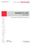
EDOSK2674
USER MANUAL
FOR H8/2674R
MICROCOMPUTER
Preface
Cautions
1.
This document may be, wholly or partially, subject to change without notice.
2.
All rights reserved. No one is permitted to reproduce or duplicate, in any form, a part or this entire
document without Hitachi Micro Systems Europe Limited's written permission.
Trademarks
General
All brand or product names used in this manual are trademarks or registered trademarks of their respective
companies or organisations.
Specific
Microsoft, MS and MS-DOS are registered trademarks and Windows and Windows NT are
trademarks of Microsoft Corporation.
Document Information
Product Code:
D003680_11
Version:
01.1
Date:
21/11/2002
Copyright © Hitachi Micro Systems Europe Ltd. 1995-2002. All rights reserved.
2
Table of Contents
TABLE OF CONTENTS ....................................................................................................................................................... 3
1.
INTRODUCTION ....................................................................................................................................................... 5
1.1. EDOSK2674 GENERAL BOARD LAYOUT.......................................................................................................... 5
1.2. EDOSK2674 ACTUAL BOARD LAYOUT............................................................................................................. 6
2.
EDOSK2674 BLOCK DIAGRAM .............................................................................................................................. 7
2.1. POWER SUPPLY................................................................................................................................................. 7
2.2. OPERATING MODES .......................................................................................................................................... 7
2.3. H8/2674R MICROCOMPUTER............................................................................................................................ 8
2.4. BOOT FLASH MEMORY...................................................................................................................................... 8
2.5. MAIN FLASH MEMORY....................................................................................................................................... 9
2.6. RAM ..................................................................................................................................................................... 9
2.7. SDRAM................................................................................................................................................................. 9
2.8. LAN CONTROLLER............................................................................................................................................. 9
2.9. REAL TIME CLOCK ........................................................................................................................................... 10
2.10. SWITCHES......................................................................................................................................................... 10
2.11. INDICATORS ..................................................................................................................................................... 10
3.
EXTERNAL INTERFACES ........................................................................................................................................ 11
3.1. SERIAL INTERFACE ......................................................................................................................................... 11
3.2. LAN INTERFACE ............................................................................................................................................... 12
3.3. EXPANSION CONNECTOR .............................................................................................................................. 13
3.4. AUXILIARY I/O HEADER................................................................................................................................... 14
4.
BOARD OPTIONS .................................................................................................................................................. 16
4.1. JUMPER LINKS ................................................................................................................................................. 16
4.2. RTC BACKUP SUPPLY ..................................................................................................................................... 16
4.3. REMOTE SWITCH............................................................................................................................................. 17
4.4. CRYSTAL CHOICE............................................................................................................................................ 17
4.5. REMOVABLE COMPONENT INFORMATION................................................................................................... 18
4.6. ADDITIONAL COMPONENT INFORMATION. .................................................................................................. 18
5.
START-UP INSTRUCTIONS...................................................................................................................................... 19
6.
CODE DEVELOPMENT ........................................................................................................................................... 20
6.1. FLASH PROGRAMMING................................................................................................................................... 20
6.2. TEST MENU....................................................................................................................................................... 20
6.3. HDI-MONITOR ................................................................................................................................................... 20
7.
SOFTWARE........................................................................................................................................................... 21
7.1. EDOSK2674 MEMORY MAP............................................................................................................................. 21
7.2. H8/2674R REGISTER CONFIGURATION......................................................................................................... 23
8.
MECHANICAL DRAWING ........................................................................................................................................ 33
9.
DESIGNING AN EXPANSION CARD .......................................................................................................................... 34
9.1. MECHANICAL.................................................................................................................................................... 34
3
9.2. FUNCTIONAL..................................................................................................................................................... 34
10. ADDITIONAL INFORMATION .................................................................................................................................... 38
4
1.
INTRODUCTION
The EDOSK2674 is an Evaluation Development Operating System Kit designed around the Hitachi H8/2674R
microcomputer (MCU).
The EDOSK2674 operates from a single 5V supply.
Only two modes of operation: Boot mode and Normal mode.
33MHz bus clock speed.
The EDOSK2674 card provides the following interfaces:
•
One serial communication interface up to 115200kbs with no errors.
•
A standard RJ45 Ethernet interface provides connection to a Local Area Network (includes Link and Activity
indicators).
•
A 140-way high-density connector for interface to a bus expansion card.
•
Position for a 50 way Auxiliary I/O header to allow connection to all unused MCU I/O pins and power.
The EDOSK2674 card is provided with the following memory types and densities:
•
512KBytes (8-bit x 512) Boot Flash memory
•
4MBytes (16-bit x 2M) Main Flash memory
•
8MBytes (16-bit x 4bank x 1M) SDRAM memory
A Real-time clock (RTC) is fitted to the EDOSK2674 to provide current date and time information to the MCU.
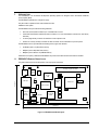
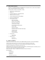
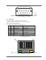
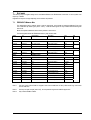
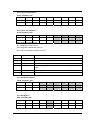
1.1. EDOSK2674 GENERAL BOARD LAYOUT
The general board layout shows the position of all major parts of the board.
Auxiliary I/O (NOT FITTED)
EEP
5V Input
3V
Main
FLASH
4MB
POWER
RTC
Xtal
Xtal
100.00mm
TIMER
SDRAM
8MB
LAN Rj45
BOOT
Xtal
H8S/2674R
LAN Controller
Xtal
7402
Jumpers
Serial Port
9-way
Female
74125
232
J8
NMI
RTC_BATTERY
Boot FLASH
512KB
7414
NMI
J10
Battery
Reset
J9
3V
A1
140-way, Expansion Connector
B1
RESET
160.00mm
Figure 1-1: EDOSK General Board Layout
5
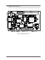
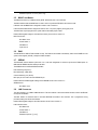
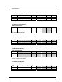
1.2. EDOSK2674 ACTUAL BOARD LAYOUT
The actual board layout shows the real position of all components, the reference numbers and silk screen labelling.
Figure 1-2: EDOSK Actual Board Layout
6
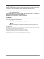
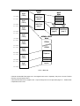
2.
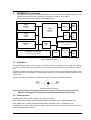
EDOSK2674 BLOCK DIAGRAM
The EDOSK2674 is designed around a H8/2674R MCU and includes FLASH memory, SDRAM, real-time clock, an
interface to a local expansion card, an interface for IO connections, a serial port and a LAN port.
The figure below shows the block diagram of the EDOSK2674 board.
Boot
FLASH
RS232
H8S
2674R
512KByte
DB9
(Female)
LQFP144
Main
FLASH
RTC
4MByte
SDRAM
LAN
8MByte
10Mbps
Expansion Connector
Memory Mapped Peripherals
XTAL
&
BATT
Auxiliary I/O Connector
I/O Peripherals
RJ45
3.3v Reg
x2
Power
Jack
FIGURE 2-1: EDOSK BLOCK DIAGRAM
2.1. POWER SUPPLY
The EDOSK hardware requires a power supply of +5V. Since total power consumption can vary widely due to external
connections, port states, and memory configuration, use a power supply capable of providing at least 500mA at +5V DC ±
5%.
The design is specified for evaluation of the MCU and so does not include circuitry for supply filtering/noise reduction, under
voltage protection, over current protection or reversed polarity protection. Caution should be used when selecting and using
a power supply.
The power connector on the EDOSK is a 2.5mm Barrel connector. The center pin is the positive connection.
FIGURE 2-2: POWER SUPPLY CONNECTION
Caution: Existing customers using E6000 products note that the polarity of this board is opposite to that for the
E6000. Use of the E6000 power supply with this board will damage both board and power supply.
2.2. OPERATING MODES
The H8/2674R has only two modes of operation set by jumper configuration:
Mode 1: (MD2=0, MD1=0, MD0=1) Advanced, External Data Bus initial Width is 16 bits. – EDOSK NORMAL mode.
Mode 2: (MD2=0, MD1=1, MD0=0) Advanced, External Data Bus initial Width is 8 bits. – EDOSK BOOT mode.
The H8/2674R has no internal Flash memory. On power-up the EDOSK mode (Boot or Normal) selects the Flash memory
from which the H8/2674R first accesses.
7
2.3. H8/2674R MICROCOMPUTER
The MCU is an H8/2674R derivative of the H8/2600 series microprocessor with an internal 16-bit architecture,
sixteen 16-bit general registers and 69 basic instructions.
The MCU contains a number of on-chip facilities, including:
•
33MHz maximum operating frequency
•
Voltage: 3.3V
•
24 bit external address bus, 16 bit external data bus
•
33MHz max external bus frequency
•
7 areas of external address space, each 2MBytes
•
Supports direct SDRAM interface
•
Various peripheral functions:
DMA controller (DMAC)
EXDMA controller (EXDMAC)
Data transfer controller (DTC)
16-bit timer-pulse unit (TPU)
Programmable pulse generator (PPG)
8-bit timer (TMR)
Watchdog timer (WDT)
Asynchronous serial communication interface (SCI)
10-bit A/D converter
8-bit D/A converter
Clock pulse generator
•
On-chip memory:
32Kbytes RAM
•
General I/O ports:
I/O pins: 103
Input-only pins: 12
2.4. BOOT FLASH MEMORY
The BOOT Flash memory is a 512K x 8bit PLCC device (AMD 29LV040B) and is fitted to a socket on the EDOSK2674.
The MCU interfaces with the BOOT Flash on reset in area 0 only when the EDOSK is set to Boot mode.
The same BOOT Flash is also accessible in area 7 when the EDOSK is set to either Boot or Normal mode.
In Normal mode the BOOT Flash is designed to reside in area 7 only.
The BOOT Flash may be removed from its socket to be programmed by a dedicated programmer or alternately it may be
programmed in system when the Boot write enable jumper is fitted.
Details of BSC register settings for the AMD Flash boot memory can be found in section 7.2.
Boot Flash access:
Bus Width: 8 bit.
Access States: 3
Wait States: 3
Cycle Burst: 6 (area 0 only)
8
Extended CS period: Th and Tt (area 7 only)
2.5. MAIN FLASH MEMORY
The MAIN Flash memory is a 4MByte device (INTEL 28F320J3A) and is word accessed.
The MCU interfaces with the MAIN Flash on reset in area 0 only when the EDOSK is set to Normal mode.
In Normal mode the MAIN Flash is designed to reside in area 0 and area 1.
In Boot mode the MAIN Flash is designed to reside in area 1 only and is paged by driving port pin 33.
The Main Flash may be programmed in system when write enable jumper is fitted.
Details of BSC register settings for the Intel Flash memory can be found in section 7.2.
Main Flash access:
Bus Width: 16 bit.
Access States: 3
Wait States: 2
Cycle burst: 6
2.6. RAM
The H8/2674R has 32KB of RAM available on-chip. This RAM can be enabled or disabled by means of the RAME bit in the
system control register (SYSCR). Initially this RAM is enabled.
2.7. SDRAM
The H8/2674R, external address space areas 2 to 5, has been designated as continuous Synchronous DRAM space. An
8MB external SDRAM interfaces directly to the MCU.
The SDRAM used is a MICRON MT48LC4M16A2:
Row addressing: 4K (A0-A11)
Bank addressing: 4 (BA0, BA1)
Column addressing: 512 (A0-A8)
MCU port pin 34 is used to drive the SDRAM CS pin.
Details of BSC and DRAM register settings for the SDRAM can be found in section 7.2.
SDRAM access:
Bus Width: 16 bit.
2.8. LAN CONTROLLER
The LAN controller IC is a SMSC LAN91C96 device. The base address of this device defaults to 300h, however the EDOSK
re-maps this to F80000h.
The MAC address is contained within a removable EEPROM connected to the Controller. This is programmed during
production testing and should not be altered.
Details of BSC register settings for the LAN controller can be found in section 7.2.
LAN Controller access:
Bus Width: 8 bit.
Access States: 3
Wait States: 3
Extended CS period: Th and Tt
9
2.9. REAL TIME CLOCK
The EDOSK is supplied with a Real Time Clock (RTC) and battery backup (when fitted) for current date and time information.
A cell retainer (J11) is used to hold a cell battery to keep time data correct when system supply is removed.
The RTC is a Dallas/Maxim DS1672U device that interfaces to the H8/2674R via an I2C bus.
-
SCL – Serial Clock (MCU port pin 31)
-
SDA – Serial Data (MCU port pin 32)
A coin-cell battery between 1.3V and 3.6V of 12mm diameter and 3.175mm maximum height may be inserted into the
EDOSK to allow timekeeping even when power to the board is removed.
Battery Reference: BR1216, CR1216, BR1220, CL1220, CR1220 and BR1225
2.10. SWITCHES
The EDOSK provides two buttons for influencing the operation of the board. The purpose of each button is clearly marked
next to it. Refer to the board layout for positions (Section 1).
•
Reset Switch
This button provides the MCU with a timed reset pulse of at least 250mS.
•
NMI Switch
The NMI button on this EDOSK provides the MCU with a positive pulse to generate a non-maskable interrupt.
2.11. INDICATORS
Three red LEDs are fitted to the PCB. The function of each red LED is clearly marked on the silk screen of the PCB. Please
refer to the board layout diagram for position information (Section 1).
POWER: When the board is connected to a power source this led will illuminate.
BOOT: When the EDOSK has been placed into Boot mode this LED will illuminate.
TIMER: Dedicated for user control and is driven by the MCU Watchdog Timer Overflow pin.
10
3.
EXTERNAL INTERFACES
Connector locations and pin orientation for Expansion and Auxiliary IO (right-angled 50-way IDC) is shown below:
Pin A1
Serial
ector
Conn
n
io
s
n
Expa
Ethernet
SK
EDO
2674
Power
O
iary I
Auxil
Note: Auxiliary IO connector is
not fitted as standard
Pin 1
3.1. SERIAL INTERFACE
The Serial Communication Interface (SCI-3) on the MCU directly supports three-wire serial interfaces.
The EDOSK provides the MCU with an external clock source at 1.8432MHz. This provides a fixed baud rate of 11520kbps
for the serial port with zero errors (irrespective of the operating crystal frequency).
A hyper terminal link between the EDOSK and a PC will enable the user interface.
•
Link to a Hyper Terminal
•
Connect at baud rate 115200, 8 bits, no parity, 1 stop bit
The EDOSK RS232 interface conforms to Data Communication Equipment (DCE) format allowing the use of 1-1 cables
when connected to Data Terminal Equipment (DTE) such as an IBM PC. Handshaking is not supported as standard on the
MCU so for normal use a minimal three-wire cable can be used. The minimum connections are not shaded in the following
table.
EDOSK DB9
Connector Pin
1
2
3
4
5
6
7
8
9
Signal
No Connection
EDOSK Tx Host Rx
EDOSK Rx Host Tx
No Connection
Ground
No Connection
No Connection
No Connection
No Connection
Host DB9
Connector Pin
1
2
3
4
5
6
7
8
9
TABLE 3-1: RS232 INTERFACE CONNECTIONS
11
5
4
9
3
8
2
7
1
6
Figure 3-1: EDOSK Serial Port Pin Numbering
3.2. LAN INTERFACE
A 10MHz LAN connection is provided through a standard RJ45 interface.
Two LEDs are integrated into the Ethernet connector and give the following indication:
Green: Link Indicator. Reflects the integrity status.
Yellow: Activity Indicator. Activated by Transmit or Receive activity.
Pin
Name
Direction
Description
RJ1
TxD+
Output from the EDOSK
Transmit Data Positive
RJ 2
TxD-
Output from the EDOSK
Transmit Data Negative
RJ 3
RxD+
Input from the LAN
Receive Data Positive
RJ 4
N/C
Not Connected
RJ 5
N/C
Not Connected
RJ 6
RxD-
Input from the LAN
RJ 7
N/C
Not Connected
RJ 8
N/C
Not Connected
Receive Data Negative
TABLE 3-2: LAN INTERFACE CONNECTIONS
RJ1
RJ8
Figure 3-2: EDOSK LAN Port Pin Numbering
12
3.3. EXPANSION CONNECTOR
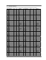
The EDOSK expansion bus connector is a 140-way JAE KX14-140K5D and has the following pin connections:
Col: A Assignment
Type
1
GND
2
CKIO
3
GND
4
D0
T
5
D2
6
7
8
GND
I/O
-
H8S2674R
Col: B Assignment
Type
I/O
H8S2674R
-
GND
1
GND
-
-
GND
Sys. Clk
2
GND
-
-
GND
-
GND
3
GND
-
-
GND
I/O
D0
4
D1
T
I/O
D1
T
I/O
D2
5
D3
T
I/O
D3
D4
T
I/O
D4
6
D5
T
I/O
D5
D6
T
I/O
D6
7
D7
T
I/O
GND
8
GND
O
OUT
-
-
-
-
D7
-
GND
9
D8
T
I/O
D8
9
D9
T
I/O
D9
10
D10
T
I/O
D10
10
D11
T
I/O
D11
11
D12
T
I/O
D12
11
D13
T
I/O
D13
12
D14
T
I/O
D14
12
D15
T
I/O
13
GND
GND
13
GND
14
D16
T
I/O
No Connect
14
D17
T
I/O
No Connect
15
D18
T
I/O
No Connect
15
D19
T
I/O
No Connect
16
D20
T
I/O
No Connect
16
D21
T
I/O
No Connect
17
D22
T
I/O
No Connect
17
D23
T
I/O
18
GND
GND
18
GND
19
D24
T
I/O
No Connect
19
D25
T
I/O
No Connect
20
D26
T
I/O
No Connect
20
D27
T
I/O
No Connect
21
D28
T
I/O
No Connect
21
D29
T
I/O
No Connect
22
D30
T
I/O
No Connect
22
D31
T
I/O
23
3.3V
-
-
3.3V
23
3.3V
-
-
3.3V
24
3.3V
-
-
3.3V
24
3.3V
-
-
3.3V
25
NC0
Option
Option
No Connect
25
3.3V
26
A0
O
OUT
A0
26
A1
O
OUT
A1
27
A2
O
OUT
A2
27
A3
O
OUT
A3
28
A4
O
OUT
A4
28
A5
O
OUT
A5
29
A6
O
OUT
A6
29
A7
O
OUT
A7
30
GND
GND
30
GND
31
A8
O
OUT
A8
31
A9
O
OUT
A9
32
A10
O
OUT
A10
32
A11
O
OUT
A11
33
A12
O
OUT
A12
33
A13
O
OUT
A13
34
A14
O
OUT
A14
34
A15
O
OUT
A15
35
GND
GND
35
GND
36
A16
O
OUT
A16
36
A17
O
OUT
A17
37
A18
O
OUT
A18
37
A19
O
OUT
A19
38
A20
O
OUT
A20
38
A21
O
OUT
A21
39
A22
O
A22
39
A23
O
OUT
A23
40
A24
-
-
No Connect
40
A25
O
OUT
41
GND
-
-
GND
41
GND
42
/DACK0
O
OUT
/DACK0
42
/DACK1
O
OUT
/DACK1
43
/DREQ0
I, P-UP
IN
/DREQ0
43
/DREQ1
I, P-UP
IN
/DREQ1
44
GND
GND
44
GND
45
/CS0
O, P-UP
OUT
/CS0
45
/CS1
O, P-UP
OUT
/CS1
46
/CS2
O
OUT
No Connect
46
/CS3
O
OUT
No Connect
47
/CS4
O
OUT
No Connect
47
/CS5
O
OUT
No Connect
48
/CS6
O, P-UP
OUT
/CS6
48
R/W
O
OUT
No Connect
49
GND
GND
49
GND
50
/RD
/RD
50
/BS
-
-
-
-
-
-
-
-
OUT
-
-
O
OUT
-
-
-
-
-
-
-
-
OUT
3.3V
GND
GND
No Connect
-
-
GND
No Connect
-
-
GND
No Connect
-
-
O
D15
-
GND
GND
GND
/AS
13
Col: A Assignment
Type
I/O
-
H8S2674R
51
GND
-
52
/WE0
O
53
/WE2
O
54
GND
55
/WAIT0
I, P-UP
IN
56
/WAIT2
I, P-UP
IN
57
GND
58
/IRQ1
I, P-UP
59
/IRQ3
I, P-UP
60
/IRQ5
61
/IRQ7
62
+5V
63
+5V
-
-
64
NC1
Option
Option
65
/RES
O
OUT
66
A+5V
67
A+5V
68
NC3
69
NC5
70
NC7
Col: B Assignment
Type
I/O
51
GND
/LWR
52
/WE1
O
No Connect
53
/WE3
O
GND
54
GND
/EXP_WAIT
55
/WAIT1
I, P-UP
IN
No Connect
56
/WAIT3
I, P-UP
IN
GND
57
GND
IN
/IRQ1
58
/IRQ2
I, P-UP
IN
/IRQ2
IN
/IRQ3
59
/IRQ4
I, P-UP
IN
/IRQ4
I, P-UP
IN
/IRQ5
60
/IRQ6
I, P-UP
IN
No Connect
I, P-UP
IN
No Connect
61
/IRQ8
I, P-UP
IN
+5V
62
+5V
-
-
+5V
+5V
63
+5V
-
-
+5V
No Connect
64
+5V
-
-
+5V
/RESET
65
+5V
-
-
+5V
-
+5V
66
+5V
-
-
+5V
-
-
+5V
67
NC2
Option
Option
No Connect
Option
Option
No Connect
68
NC4
Option
Option
No Connect
Option
Option
No Connect
69
NC6
Option
Option
No Connect
Option
Option
No Connect
70
NC8
Option
Option
No Connect
OUT
OUT
-
-
-
-
-
-
-
-
H8S2674R
GND
OUT
OUT
-
No Connect
-
-
GND
/HWR
GND
No Connect
No Connect
-
GND
No Connect
TABLE 3-3: EXPANSION BUS CONNECTIONS
O = Not buffered output. I = Not buffered input. P-UP = Pull up resistor.
Expansion cards to be fitted to the EDOSK should use JAE connector KX15-140K2D and should only have discrete
components fitted to the under side with a maximum height of 2mm.
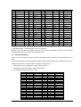
3.4. AUXILIARY I/O HEADER
Position for a 50 way Auxiliary I/O header is provided on the EDOSK to allow connection to all unused MCU I/O pins and
power.
This part has not been fitted as standard because it has been recognised that the user will wish to select the connector type.
Through holes and surface mount pads allow for a number of connector options:
•
SM pins fitted on top or under the PCB – Samtec TSM-125-0X-X-DV
•
SM sockets on top or under the PCB – Samtec SSM-125-X-DV
•
Any through hole 50-way connector at 0.1” pitch.
I/O Conn
1
3
5
7
9
11
13
15
17
19
21
23
25
27
29
31
33
35
37
39
41
MCU Pin
N/A
131
84
82
110
114
121
117
119
123
125
127
129
61
59
57
55
53
51
49
46
Symbol
No Connect
AVSS
P65
P63
P53
PG5
VREF
P40
P42
P44
P46
P54
P56
P61
P27
P25
P23
P21
P17
P15
P13
I/O Conn
2
4
6
8
10
12
14
16
18
20
22
24
26
28
30
32
34
36
38
40
42
MCU Pin
N/A
N/A
83
81
113
115
122
118
120
124
126
93
128
130
60
58
56
54
52
50
48
Symbol
5V
GND
P64
P62
PG4
PG6
AVCC
P41
P43
P45
P47
STBYn
P55
P57
P60
P26
P24
P22
P20
P16
P14
14
I/O Conn
43
45
47
49
MCU Pin
44
40
36
N/A
Symbol
P11
P73
P72
No Connect
I/O Conn
44
46
48
50
MCU Pin
45
43
N/A
N/A
Symbol
P12
P10
GND
3V3
TABLE 3-4: AUXILIARY I/O CONNECTIONS
15
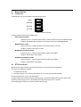
4.
BOARD OPTIONS
4.1. JUMPER LINKS
The EDOSK has a two-row 8 pin header for selecting operation modes.
BOOT
8
7
MON EN
6
5
MF WEN
4
3
BF WEN
2
1
FIGURE 4-1: JUMPER CONFIGURATION
As default, jumpers for BOOT and MF WEN are fited.
BOOT: Boot/Normal Mode.
Fitted to link pins 8-7 – Boot Mode: MCU initialises in 8-bit mode and boots from the 512KB Boot FLASH.
Not fitted – Normal Mode: Micon initialises in 16-bit mode and boots from the 4MB Main FLASH.
MON EN: Monitor Enable.
Fitted to link pins 6-5 – Enables the Hitachi monitor (when included in user code).
Not fitted – Program code runs with no monitor.
MF WEN: Main FLASH Write Enable.
Fitted to link pins 4-3 – Allows the Main FLASH to be written to by the MCU.
Not fitted – Main FLASH is write protected.
BF WEN: Boot FLASH Write Enable.
Fitted to link pins 2-1 – Allows the Boot FLASH to be written to by the MCU.
Not fitted – Boot FLASH is write protected.
4.2. RTC BACKUP SUPPLY
Without a backup supply to the RTC, time and date information is lost when the board is powered down.
Two options are available on the EDOSK:
1.
A cell battery may be fitted.
2.
An auxiliary supply of 1.3V to 3.6V may be provided to J8 – a 2-pin through hole header (not fitted).
Each of these options may or may not be rechargeable.
If however neither option is used or the backup supply falls below 1.3V then the EDOSK board will cease to function when
powered up unless a supply from Vcc is provided. By default design this supply from Vcc is provided.
The Following diagram shows the circuit used for the RTC backup supply:
16
3V3
D1
R
D2
RTC Backup
Cell Battery
J8
D1 provides the Vcc supply and prevents the cell battery (or auxiliary supply) from powering all of the board when powered
down.
D2 provides protection for the cell battery (or auxiliary supply) against accidental charging.
R (when fitted) allows charge current to be selected or charging by the RTC device.
The following options are available:
Backup power option
Component configuration
Comments
No cell battery, No auxiliary supply,
None rechargeable cell battery, None
rechargeable auxiliary supply
D1 and D2 fitted.
Default configuration.
R not fitted.
No method of recharging cell or
auxiliary supply.
Rechargeable cell battery,
Rechargeable auxiliary supply
D1 and D2 fitted.
Default configuration.
R not fitted.
No method of recharging cell or
auxiliary supply.
D1 fitted.
Backup supply is charged through D1.
D2 optional.
RTC trickle charge is not used.
R=3.3/Icharge
D1 not Fitted.
Backup supply is charged through
D2 optional.
RTC trickle charge network.
R=0 ohms.
EDOSK will not operate if backup
supply fails.
4.3. REMOTE SWITCH
Both Reset and NMI switches may be activated remotely.
By attaching 2-pin headers to J10 and J9, normally-open switches can be attached via flying leads.
J10 – NMI
J9 – RESET
The NMI switch signal is de-bounced on the EDOSK board with a time constant TRC=0.47 seconds.
The RESET switch signal is de-bounced on the EDOSK board with time constants TRC(off)=0.03 seconds and TRC(on)=0.22
seconds.
4.4. CRYSTAL CHOICE
The MCU crystal frequency has been chosen to support the fastest operation. The value of the crystal is 33.0000MHz.
17
The user may replace the HC49/U surface mounted AT cut crystal with another of similar type within the operating frequency
of the MCU device. Please refer to the hardware manual for the MCU for the valid operating range.
Another crystal is provided at 16 x 115200 (1.8432MHz). This crystal output is fed directly into the SCK2 pin of the MCU
allowing, with correct register settings, a fixed serial baud rate of 115200bps with zero errors.
The user may wish to ignore the serial clock oscillator input and use the system clock for baud rate generation – register
settings will need to be amended as per the following example.
Example:
The following table shows the baud rates and Baud Rate Register (BRR) setting required for each communication rate using
the operating speed of 33.0000MHz (default). Note that there are no zero error percentages.
SMR Setting:
Comm.
Baud
110
300
1200
2400
4800
9600
19200
38400
57600
115200
Baud Rate Register Settings for Serial Communication Rates using 33.0000MHz system clock
0
1
2
3
BRR
setting
Invalid
Invalid
Invalid
Invalid
214
106
53
26
17
8
ERR (%)
Invalid
Invalid
Invalid
Invalid
0.07
0.39
0.54
0.54
0.54
0.54
BRR
setting
Invalid
Invalid
214
106
53
26
12
6
3
1
ERR (%)
Invalid
Invalid
0.07
0.39
0.54
0.54
3.29
4.09
11.90
11.90
BRR
setting
Invalid
214
53
26
12
6
2
1
0
0
ERR (%)
Invalid
0.07
0.54
0.54
3.29
4.09
11.90
16.08
11.90
44.05
BRR
setting
145
53
12
6
2
1
0
Invalid
Invalid
Invalid
ERR (%)
0.33
0.54
3.29
4.09
11.90
16.08
16.08
Invalid
Invalid
Invalid
TABLE 4-1 CRYSTAL FREQUENCIES FOR RS232 COMMUNICATION
4.5. REMOVABLE COMPONENT INFORMATION.
Analogue and reference voltages to the MCU are, as default, isolated from the Auxiliary I/O connector by not fitted 0805
resistors. To make this connection the following resistors must be removed and re-soldered or replaced in the alternative
positions detailed below:
H8/2674R pin
Remove
Fit
Resistor Value
AVCC (pin 122)
R25
R9
0Ω, 0805
AVSS (pin 131)
R7
R8
0Ω, 0805
VREF (pin 121)
R11
R10
0Ω, 0805
Care must be taken not to damage the tracking around these components. Only use soldering equipment designed for
surface mount assembly and rework.
4.6. ADDITIONAL COMPONENT INFORMATION.
The addition of a 0Ω resistor fitted in position R37 will permanently deactivate the Main Flash. This is to be used when CS0n
and/or CS1n are to be used by an Expansion Board.
18
5.
START-UP INSTRUCTIONS
1.
Connect the EDOSK to a PC or notebook computer equipped with a nine pin D connector using a direct 1-1
cable (supplied).
HOST
PC
EDOSK
3
2
5
3
2
5
FIGURE 5-1: SERIAL CONNECTION TO PC/NOTEBOOK WITH DB-9 CONNECTOR (SUPPLIED)
2.
Open a Hyper terminal set to a baud rate of 115200, 8 bits, no parity and 1 stop bit.
3.
Connect a power supply of +5V capable of providing at least 500mA (supplied: Center +ve).
4.
Check Boot Flash Write Enable setting : No jumper fitted to J5 pins 1-2
5.
Check Main Flash Write Enable setting: Jumper is fitted to J5 pins 3-4
6.
Check Monitor Enable setting: No jumper fitted to J5 pins 5-6
7.
Check Boot Mode setting: Jumper is fitted to J5 pins 7-8
8.
Switch Power on.
19
6.
CODE DEVELOPMENT
Incorporated into the mot file that is programmed into the Boot Flash device is the option to run the Embedded Test Suite
software (ETS). This software is available to the user, via a hyper-terminal link and contains a number of functions including
the choice of testing the major functions of the EDOSK and the option of downloading user software to both the AMD and
INTEL Flash devices.
6.1. FLASH PROGRAMMING
EDOSK hardware allows both Boot and Main Flash memory to be programmed in system when the appropriate write enable
jumpers are fitted.
When the EDOSK is first powered up in Boot mode and a serial connection has been made to a hyper terminal the user will
be given the option to re-program Flash devices.
The user may specify any valid S-Record file to be programmed.
6.2. TEST MENU
The tests incorporated in the Boot Flash allow for a majority of the EDOSK to be verified – for production and for prototype
debugging.
Three main menu options are given to Program Flash, Testing and Diagnosis. These lead to further menu options as shown
below:
PROGRAM
FLASH
TESTING
DIAGNOSIS
Boot Flash
Quick
Memory
Main Flash
Environmental
Boot Flash
Main Flash
SDRAM
Production
Ethernet
EPH loop-back
Local loop-back
Connector loop-back
Configure MAC
RTC
Timer LED &
NMI
6.3. HDI-MONITOR
The H8/2674R has no dedicated debug port and at present SW has not been developed to enable a HDI monitor for the
EDOSK2674.
However, a MON_EN (monitor enable) jumper has been provided for this future feature. This jumper drives MCU port pin 30
Low when fitted and High when not fitted. HDI-Monitor code may be integrated with the user code and read the monitor
enable jumper setting to enable or disable the feature.
20
7.
SOFTWARE
The following map and register settings are for the H8/2674R fitted to the EDOSK2674 as standard i.e. with a system clock
frequency of 33MHz.
Registers are subject to change depending on the software requirements.
7.1. EDOSK2674 MEMORY MAP
The addressable memory address space is split into eight areas, each capable of addressing 2Mbytes. Each area
has a dedicated chip select signal (CS0n – CS7n). – Note that these signals are only enabled when PFCR0 register
bits are set.
Mode of the system determines which memory resides in areas 0 and 1.
The following table shows the EDOSK2674 memory map and bus width.
FROM
TO
MODE :
External Area
Description
Size
Bus
Width
BOOT
H’000000
H’1FFFFF
CS0
Boot FLASH (note 1)
512KB x4
8
H’200000
H’3FFFFF
CS1 (Port pin Low)
Main FLASH (page 0)
2MB
16
H’200000
H’3FFFFF
CS1 (Port pin High)
Main FLASH (page 1)
2MB
MODE :
NORMAL
H’000000
H’1FFFFF
CS0
Main FLASH (page 0)
2MB
H’200000
H’3FFFFF
CS1
Main FLASH (page 1)
2MB
SDRAM
8MB
MODE :
H’400000
16
NORMAL & BOOT
H’BFFFFF
CS2,CS3,CS4,CS5
16
H’C00000
H’DFFFFF
CS6
Expansion board
2MB
8/16
H’E00000
H’EFFFFF
CS7
Boot FLASH (note 1)
512KB x2
8
H’F00000
H’F7FFFF
CS7
TBD
0.5MB
H’F80000
H’FBFFFF
CS7
LAN CHIP (note 2)
256KB
H’FC0000
H’FF3FFF
CS7
TBD
208KB
H’FF4000
H’FFBFFF
CS7
On Chip RAM (note 3)
32KB
H’FFC000
H’FFFBFF
CS7
External address space
15 KB
H’FFFC00
H’FFFEFF
CS7
Internal I/O registers
768B
H’FFFF00
H’FFFF1F
CS7
External address space
32B
H’FFFF20
H’FFFFFF
CS7
Internal I/O registers
224B
TABLE 7-1: MEMORY MAP
Note 1:
The same 512K of Boot FLASH is mapped 4 times over the 2MB area of CS0 (in Boot mode only) and 2 times
over the 1MB area.
Note 2:
LAN only occupies 16 bytes (0x0 to 0xF), but is repeated throughout the 256KB mapped area.
Note 3:
Only if internal RAM is enabled.
21
00 0000h
Area 0
(CS0n)
1F FFFFh
20 0000h
NORMAL
Mode
BOOT
Mode
BOOT Flash
BOOT Flash
BOOT Flash
BOOT Flash
Port pin
Port pin
Low
High
MAIN Flash
(page 0)
Area 1
(CS1n)
MAIN Flash
(page 1)
3F FFFFh
40 0000h
Area 2
(CS2n)
MAIN Flash
(page 0)
5F FFFFh
60 0000h
Area 3
(CS3n)
7F FFFFh
80 0000h
Area 4
(CS4n)
9F FFFFh
A0 0000h
MAIN Flash
(page 1)
NORMAL & BOOT
Mode
SDRAM
SDRAM
Area 5
(CS5n)
BF FFFFh
C0 0000h
Expansion
Area 6
(CS6n)
DF FFFFh
E0 0000h
Area 7
(CS7n)
BOOT Flash
BOOT Flash
LAN, RAM, Int. I/O
Registers
FF FFFFh
FIGURE 7-1: MEMORY MAP
In Normal mode the Main Flash pages 0 and 1 are mapped to areas 0 and 1 respectively. Port pin 33 is not used. The Boot
Flash may only be accessed in area 7.
In Boot mode the Main Flash is mapped to area 1 only and driving Port 33 Low or High selects page 0 or 1. The Boot Flash
is duplicated in areas 0 and 7.
22
7.2. H8/2674R REGISTER CONFIGURATION
7.2.1. BUS CONTROLLER (BSC)
Bus Width Control Register:
ABWCR (H’FFFEC0) = H’81 (BOOT) or H’80 (NORMAL)
Bit No
7
6
5
4
3
2
1
0
Bit Name
ABW7
ABW6
ABW5
ABW4
ABW3
ABW2
ABW1
ABW0
Initial Value
1 or 0
1/0
1/0
1/0
1/0
0
0
1
Note: In BOOT mode (MCU mode 2), ABWCR is initialized to 1. In NORMAL mode (MCU mode 1), ABWCR is
initialized to 0.
In BOOT mode area 7 and 0 are mapped as 8-bit areas.
In NORMAL mode only area 7 is mapped as 8-bit area.
The SDRAM (ABW2) is always mapped as 16-bit area.
Access State Control Registers:
ASTCR (H’FFFEC1) = H’FF
Bit No
7
6
5
4
3
2
1
0
Bit Name
AST7
AST6
AST5
AST4
AST3
AST2
AST1
AST0
Initial Value
1
1
1
1
1
1
1
1
All areas are designated as 3-state access space.
Wait Control Registers:
WTCRAH (H’FFFEC2) = H’27
Bit No
15
14
13
12
11
10
9
8
Bit Name
Reserved
W72
W71
W70
Reserved
W62
W61
W60
Initial Value
0
0
1
0
0
1
1
1
Area 7 has 2 program wait states inserted.
Area 6 has 7 program wait states inserted.
WTCRAL (H’FFFEC3) = H’77
Bit No
7
6
5
4
3
2
1
0
Bit Name
Reserved
W52
W51
W50
Reserved
W42
W41
W40
Initial Value
0
1
1
1
0
1
1
1
Area 5 has 7 program wait states inserted.
Area 4 has 7 program wait states inserted.
23
WTCRBH (H’FFFEC4) = H’71
Bit No
15
14
13
12
11
10
9
8
Bit Name
Reserved
W32
W31
W30
Reserved
W22
W21
W20
Initial Value
0
1
1
1
0
0
0
1
Area 3 has 7 program wait states inserted.
SDRAM has a CAS Latency of 2.
WTCRBL (H’FFFEC5) = H’23 (BOOT) or H’22 (NORMAL)
Bit No
7
6
5
4
3
2
1
0
Bit Name
Reserved
W12
W11
W10
Reserved
W12
W11
W10
Initial Value
0
0
1
0
0
0
1
1 or 0
Area 1 has 2 program wait states inserted.
In BOOT mode, area 0 has 3 program wait states inserted.
In NORMAL mode area 0 has 2 program wait states inserted.
Read Strobe Timing Control Register:
RDNCR (H’FFFEC6) = H’00
Bit No
7
6
5
4
3
2
1
0
Bit Name
RDN7
RDN
RDN
RDN
RDN
RDN
RDN
RDN
Initial Value
0
0
0
0
0
0
0
0
In all areas the /RD signal is negated at the end of the read cycle.
CS assertion Period Control Registers:
CSACRH (H’FFFEC8) = H’80
Bit No
7
6
5
4
3
2
1
0
Bit Name
CSXH7
CSXH6
CSXH5
CSXH4
CSXH3
CSXH2
CSXH1
CSXH0
Initial Value
1
0
0
0
0
0
0
0
In area 7 basic bus interface access, the /CSn and address assertion period (Th) is extended.
CSACRL (H’FFFEC9) = H’80
Bit No
7
6
5
4
3
2
1
0
Bit Name
CSXT7
CSXT6
CSXT5
CSXT4
CSXT3
CSXT2
CSXT1
CSXT0
Initial Value
1
0
0
0
0
0
0
0
In area 7 basic bus interface access, the /CSn and address assertion period (Tt) is extended.
24
Burst ROM Interface Control Register:
BROMCRH (H’FFFECA) = H’D3 (BOOT) or H’A3 (NORMAL)
Bit No
7
6
5
4
3
2
1
0
Bit Name
BSRMn
BSTSn2
BSTSn1
BSTSn0
Reserved
Reserved
BSWDn1
BSWDn0
Initial Value
1
1 or 0
0 or 1
1 or 0
0
0
0
0
Area 0 burst ROM enabled with maximum of 4 words.
In BOOT mode 6-cycle burst states are used.
In NORMAL mode 3-cycle burst states are used.
BROMCRL (H’FFFECB) = H’A3
Bit No
7
6
5
4
3
2
1
0
Bit Name
BSRMn
BSTSn2
BSTSn1
BSTSn0
Reserved
Reserved
BSWDn1
BSWDn0
Initial Value
1
0
1
0
0
0
0
0
Area 1 burst ROM enabled with maximum of 4 words.
3-cycle burst states are used.
Bus Control Register:
BCR (H’FFFECC) = H’0100
Bit No
15
14
13
12
11
10
9
8
Bit Name
BRLE
BREQOE
Reserved
IDLC
ICIS1
ICIS0
WDBE
WAITE
Initial Value
0
0
0
0
0
0
0
1
Bit No
7
6
5
4
3
2
1
0
Bit Name
Reserved
Reserved
Reserved
Reserved
Reserved
ICIS2
Reserved
Reserved
Initial Value
0
0
0
0
0
0
0
0
External bus release and bus request disabled, no idle cycles inserted, WAIT pin enabled
DRAM control register:
DRAMCR (H’FFFED0) = H’84B4
Bit No
15
14
13
12
11
10
9
8
Bit Name
OEE
RAST
Reserved
CAST
Reserved
RMTS2
RMTS1
RMTS0
Initial Value
1
0
0
0
0
1
0
0
Bit No
7
6
5
4
3
2
1
0
Bit Name
BE
RCDM
DDS
EDDS
Reserved
MXC2
MXC1
MXC0
Initial Value
1
0
1
1
0
1
0
0
OE/CKE signal output enabled, RAS is asserted from ∅ falling edge in T1 cycle, 2-state column address cycle,
Continuous synchronous DRAM space
Access in fast page mode, 8-Bit shift, Row address bits A23 to A12 used for comparison, The precharge-sel is A15 to
A12 of the column address.
25
SDRAM Notes:
Prior to using the SDRAM the mode must be set in the SMR (SDRAM Mode Register).
The SMR should be set to the value B’0000 0010 0000 – CAS latency 2, Burst 1. This is achieved by a write cycle to
the SDRAM at an address equal to the required SMR value when in configuration mode.
The address to set the SMR should be H’400040 – SDRAM starts at area H’400000 and the SMR value must be
shifted to compensate for word access.
Example:
1.
Configure all other SDRAM Registers.
2.
DRAMCR = 0x85B4; //SMR configuration mode
3.
SDRAM_CONTROL = 0; // where SDRAM_CONTROL is H’400040
4.
DRAMCR = 0x84B4; //Return to SDRAM operating mode
DRAM Access Control Register:
DRACCR (H’FFFED2) = H’0000
Bit No
15
14
13
12
11
10
9
8
Bit Name
DRMI
Reserved
TPC1
TPC0
SDWCD
Reserved
RCD1
RCD0
Initial Value
0
0
0
0
0
0
0
0
Bit No
7
6
5
4
3
2
1
0
Bit Name
Reserved
Reserved
Reserved
Reserved
CKSPE
Reserved
RDXC1
RDXC0
Initial Value
0
0
0
0
0
0
0
0
Idle cycle not inserted, 1-State Pre-charge, CAS latency enabled, No wait between RAS and CAS cycles.
No clock suspend, 1-State read data extension cycle.
Refresh Control Register:
REFCR (H’FFFED4) = H’0188
Bit No
15
14
13
12
11
10
9
8
Bit Name
CMF
CMIE
RCW1
RCW0
Reserved
RTCK2
RTCK1
RTCK0
Initial Value
0
0
0
0
0
0
0
1
Bit No
7
6
5
4
3
2
1
0
Bit Name
RFSHE
CBRM
RLW1
RLW0
SLFRF
TPCS2
TPCS1
TPCS0
Initial Value
1
0
0
0
1
0
0
0
No wait states between CAS and RAS, REF count on ∅/2
Enable refresh control, No waits for CAS-before-RAS refresh cycle, Self refresh enabled, zero states in the
precharge cycle immediately after self refreshing.
26
Refresh Timer Counter:
RTCNT (H’FFFED6 ) = H’FF
Bit No
7
6
5
4
3
2
1
0
Bit Name
RTCNT7
RTCNT6
RTCNT5
RTCNT4
RTCNT3
RTCNT2
RTCNT1
RTCNT0
Initial Value
1
1
1
1
1
1
1
1
Refresh Time Constant Register:
RTCOR (H’FFFED7) = H’FF
Bit No
7
6
5
4
3
2
1
0
Bit Name
RTCOR7
RTCOR6
RTCOR5
RTCOR4
RTCOR3
RTCOR2
RTCOR1
RTCOR0
Initial Value
1
1
1
1
1
1
1
1
Compare refresh count with 0xFF
7.2.2. INTERRUPT CONTROLLER
The EDOSK2674 only uses the following interrupts:
•
IRQ5n – Main Flash
•
IRQ0n – LAN Controller
•
IRQ1n-IRQ5n – Expansion connector
•
NMI – Switch
Interrupt Control Register:
INTCR (H’FFFF31) = H’08
Bit No
7
6
5
4
3
2
1
0
Bit Name
Reserved
Reserved
INTM1
INTM0
NMIEG
Reserved
Reserved
Reserved
Initial Value
0
0
0
0
1
0
0
0
NMI is rising edge triggered. Interrupt Control mode 0
IRQ Pin Select Register:
ITSR (H’FFFE16) = H’FF3F
Bit No
15
14
13
12
11
10
9
8
Bit Name
ITS15
ITS14
ITS13
ITS12
ITS11
ITS10
ITS9
ITS8
Initial Value
1
1
1
1
1
1
1
1
Bit No
7
6
5
4
3
2
1
0
Bit Name
ITS7
ITS6
ITS5
ITS4
ITS3
ITS2
ITS1
ITS0
Initial Value
0
0
1
1
1
1
1
1
IRQ15-IRQ8 – Port 2
IRQ7,6 – Port 57, 56
IRQ5-IRQ0 – Port 8
27
7.2.3. SERIAL COMMUNICATION INTERFACE 2
Serial Extension Mode Register:
SEMR (H’FFFDA8) = H’00
Bit No
7
6
5
4
3
2
1
0
Bit Name
Reserved
Reserved
Reserved
Reserved
ABCS
ACS2
ACS1
ACS0
Initial Value
0
0
0
0
0
0
0
0
Basic Clock is External; this register is not used.
Serial Mode Register_2:
SMR_2 (H’FFFF88) = H’00
Bit No
7
6
5
4
3
2
1
0
Bit Name
C/A
CHR
PE
O/E
STOP
MP
CKS1
CKS0
Initial Value
0
0
0
0
0
0
0
0
Asynchronous, 8-bit, No Parity, 1-Stop bit, Clock source ∅
Bit Rate Register_2:
BRR_2 (H’FFFF89) = H’FF
Bit No
7
6
5
4
3
2
1
0
Bit Name
BRR7
BRR6
BRR5
BRR4
BRR3
BRR2
BRR1
BRR0
Initial Value
1
1
1
1
1
1
1
1
This register is not used.
Serial Control Register_2:
SCR_2 (H’FFFF8A) = H’32
Bit No
7
6
5
4
3
2
1
0
Bit Name
TIE
RIE
TE
RE
MPIE
TEIE
CKE1
CKE0
Initial Value
0
0
1
1
0
0
1
0
Interrupt settings depend on SW, External Clock input 16 times bit rate.
Smart Card Mode Register_2:
SCMR_2 (H’FFFF8E) = H’F2
Bit No
7
6
5
4
3
2
1
0
Bit Name
Reserved
Reserved
Reserved
Reserved
SDIR
SINV
Reserved
SMIF
Initial Value
1
1
1
1
0
0
1
0
Smart Cart Interface mode not used.
28
7.2.4. WATCHDOG TIMER
Timer Control/Status Register:
TCSR (H’FFFFBC) = H’18
Bit No
7
6
5
4
3
2
1
0
Bit Name
OVF
WT/IT
TME
Reserved
Reserved
CKS2
CKS1
CKS0
Initial Value
0
0
0
1
1
0
0
0
Timer Counter:
TCNT (H’FFFFBC-write / H’FFFFBD-read) = H’00
TCNT is an 8-bit readable/writable up-counter. TCNT is initialized to H'00 when the TME bit in TCSR is cleared to 0.
Reset Control/Status Register:
RSTCSR (H’FFFFBE) = H’1F
Bit No
7
6
5
4
3
2
1
0
Bit Name
WOVF
RSTE
Reserved
Reserved
Reserved
Reserved
Reserved
Reserved
Initial Value
0
0
0
1
1
1
1
1
To prevent accidental overwriting, access of WDT registers is different from other registers.
The WDT may be used to drive the ‘TIMER’ LED when the counter overflows. This, however, is a very short period
and in order to see the LED with the naked eye the WDT must be forced to overflow repeatedly.
Example to keep LED on:
TCSR = 0xA500; // clear lower byte.
TCSR = 0xA578; // setup & Enable the watchdog timer.
while( 1)
{
if( RSTCSR & 0x0080 ) // detect overflow and reset WDT.
{
RSTCSR = 0xA500; // clear watchdog overflow bit.
TCSR = 0xA578;
// clear overflow bit and enable WDT.
}
}
7.2.5. IO PORT
Port Function Control Register 0:
PFCR0 (H’FFFE32) = H’FF
Bit No
7
6
5
4
3
2
1
0
Bit Name
CS7E
CS6E
CS5E
CS4E
CS3E
CS2E
CS1E
CS0E
Initial Value
1
1
1
1
1
1
1
1
Enable all CS signals
29
Port Function Control Register 1:
PFCR1 (H’FFFE33) = H’FF
Bit No
7
6
5
4
3
2
1
0
Bit Name
A23E
A22E
A21E
A20E
A19E
A18E
A17E
A16E
Initial Value
1
1
1
1
1
1
1
1
Enable all Address lines (A21 and A23 used for SDRAM bank select)
Port Function Control Register 2:
PFCR2 (H’FFFE34) = H’0D
Bit No
7
6
5
4
3
2
1
0
Bit Name
Reserved
Reserved
Reserved
Reserved
ASOE
LWROE
OES
DMACS
Initial Value
0
0
0
0
1
1
0
1
PF6 is designated as /AS output pin.
PF3 is designated as /LWR output pin.
P35 is designated as SDRAM CKE output pin.
PF75 to PF70 are designated as DMAC control pins
MCU Port 3
Signal Name
Function
30
MON_ENn
Monitor Enable. Active Low. Enables monitor functions embedded in software.
31
I2C_SCL
I2C bus serial clock for RTC
32
I2C_SDA
I2C bus serial data signal to/from RTC
33
MFLASH_PAGE
Main Flash page select. Used in Boot mode only. Low selects page 0, High selects
page 1
34
SDRAM_CSn
SDRAM chip select. Active Low. Enables the SDRAM device.
35
SDRAM_CKE
SDRAM clock enable. Active Low. Enables the SDRAM clock input.
Port 3 Data Direction Register:
P3DDR (H’FFFE22) = H’3A
Bit No
7
6
5
4
3
2
1
0
Bit Name
Reserved
Reserved
P35DDR
P34DDR
P33DDR
P32DDR
P31DDR
P30DDR
Initial Value
0
0
1
1
1
0
1
0
The individual bits of P3DDR specify input or output for the pins of port 3 – ‘0’ input, ‘1’ output.
Port 3 Data Register:
P3DR (H’FFFF62) = H’00
Bit No
7
6
5
4
3
2
1
0
Bit Name
Reserved
Reserved
P35DR
P34DR
P33DR
P32DR
P31DR
P30DR
Initial Value
0
0
0
0
0
0
0
0
P3DR stores output data for the port 3 pins.
30
Enable SDRAM CS.
Port 3 Register:
PORT3 (H’FFFF52)
Bit No
7
6
5
4
3
2
1
0
Bit Name
Reserved
Reserved
P35
P34
P33
P32
P31
P30
Initial Value
0
0
X
X
X
X
X
X
Read only, value determined by the states of pins P35 to P30.
Port 3 Open Drain Control Register:
P3ODR (H’FFFE3C) = H’06
Bit No
7
6
5
4
3
2
1
0
Bit Name
Reserved
Reserved
P35ODR
P34ODR
P33ODR
P32ODR
P31ODR
P30ODR
Initial Value
0
0
0
0
0
1
1
0
I2C signals are NMOS open-drain
Port A Data Direction Register:
PADDR (H’FFFE29) = H’FF
Bit No
7
6
5
4
3
2
1
0
Bit Name
PADDR
PADDR
PADDR
PADDR
PADDR
PADDR
PADDR
PADDR
Initial Value
1
1
1
1
1
1
1
1
The individual bits of PADDR specify input or output for the pins of port A – ‘0’ input, ‘1’ output.
Port F Data Direction Register:
PFDDR (H’FFFE2E) = H’FE
Bit No
7
6
5
4
3
2
1
0
Bit Name
PFDDR
PFDDR
PFDDR
PFDDR
PFDDR
PFDDR
PFDDR
PFDDR
Initial Value
1
1
1
1
1
1
1
0
The individual bits of PFDDR specify input or output for the pins of port F – ‘0’ input, ‘1’ output.
Set all as outputs except PF0 (WAITn)
Port G Data Direction Register:
PGDDR (H’FFFE2F) = H’0F
Bit No
7
6
5
4
3
2
1
0
Bit Name
Reserved
PGDDR
PGDDR
PGDDR
PGDDR
PGDDR
PGDDR
PGDDR
Initial Value
0
0
0
0
1
1
1
1
The individual bits of PGDDR specify input or output for the pins of port G – ‘0’ input, ‘1’ output.
31
Port H Data Direction Register:
PHDDR (H’FFFF74) = H’0F
Bit No
7
6
5
4
3
2
1
0
Bit Name
Reserved
Reserved
Reserved
Reserved
PHDDR
PHDDR
PHDDR
PHDDR
Initial Value
0
0
0
0
1
1
1
1
The individual bits of PHDDR specify input or output for the pins of port H – ‘0’ input, ‘1’ output.
32
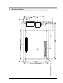
8.
MECHANICAL DRAWING
The mechanical drawing has been included here for the user to develop add-on boards and face plates.
33
9.
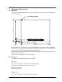
DESIGNING AN EXPANSION CARD
9.1. MECHANICAL
The Expansion Card should be designed using the following dimensions (viewed from the top looking through the
board at the connector):
The JAE connector KX15-140K2D (shown) is fitted to the under-side of the Expansion Card to mate with KX14140K5D of the main board (in this case the EDOSK2674) with board to board space of 7mm. Components fitted to
the under-side of the Expansion Card must have a maximum height of 2mm.
Both connectors are surface mounted and therefore another KX14-140K5D may be fitted to the top-side of the
Expansion Card to allow stacking.
The 4 off 2.7mm holes in the corners are for stand-off fixings.
9.2. FUNCTIONAL
Consideration must be given to the following connecting signals.
Reset Signal
The Expansion connector has a dedicated active low Reset signal (RESn).
When low all devices fitted to the plug-in board should be reset.
EDOSK2674 LimitationsRESn signal may be used.
System Clock
The Expansion connector has a dedicated System Clock signal (CKIO).
34
This clock may be used for bus cycle timing but may vary in frequency depending upon the main board used.
It is recommended that this clock is correctly terminated and/or buffered if being used.
EDOSK2674 LimitationsCKIO signal may be used but is not buffered.
Chip Select
There are 7 active low chip select signals dedicated to the Expansion connector (CS0n to CS6n).
Theses are used to select 7 areas of external memory.
To avoid contention the plug-in hardware should have the facility to select which of these is to be used.
EDOSK2674 LimitationsBOOT mode (H8 mode 2: 8-bit):
CS0n may be used if the AMD Boot Flash is removed.
CS1n may be used if R37 0Ω resistor is fitted.
NORMAL mode (H8 mode 1: 16-bit):
CS0n and CS1n may be used if R37 0Ω resistor is fitted.
Note that in this mode areas 0 and 1 can not be isolated.
CS2n to CS5n are not connected.
CS6n may be used.
Address Bus
There are 26 Address lines dedicated to the Expansion connector (A0 to A25).
This allows for address mapping of 2^26 Bytes = 64MB.
EDOSK2674 LimitationsA0 to A23 may be used (16MB maximum).
A24 and A25 are not connected
Data Bus
There are 32 Data lines dedicated to the Expansion connector (D0 to D31).
This allows data to be accessed as Byte (8-bit), Word (16-bit) or long (32-bit).
EDOSK2674 LimitationsD0 to D15 may be used (Byte or Word access).
D16 to D31 are not connected.
Note: For an 8-bit mapped area D8 to D15 must be used.
Read-Write Strobe
The Expansion connector has a dedicated Read-Write signal (RWn).
High indicates a read cycle and Low indicates a write cycle.
EDOSK2674 LimitationsRWn signal is not connected.
35
Read Strobe
The Expansion connector has a dedicated active low Read strobe (RDn).
EDOSK2674 LimitationsRDn signal may be used.
Write Strobe
There are 4 active low Write Enable signals dedicated to the Expansion connector (WE0n to WE3n).
A 32-bit data bus may be separated into 4 bytes, the Write Enable signals are used to determine which of those
bytes are to be written.
EDOSK2674 LimitationsWE0n may be used to enable write data on D0 to D7.
WE1n may be used to enable write data on D8 to D15.
WE2n and WE3n are not connected.
Note: For an 8-bit mapped area WE1n must be used.
Bus Strobe
The Expansion connector has a dedicated active low Bus strobe (BSn).
When low, this signifies the beginning of a bus cycle or it may be used for latching the address while in MPX mode.
EDOSK2674 LimitationsBSn signal may be used.
Note: H8S2674R does not support MPX mode.
Wait
There are 4 active low WAIT signals dedicated to the Expansion connector (WAIT0n to WAIT3n).
These are used to hold off the bus cycle until the device being accessed is ready.
To avoid contention the plug-in hardware should have the facility to select which of these is to be used.
EDOSK2674 LimitationsWAIT0n may be used.
WAIT1n to WAIT3n is not connected.
Interrupts
There are 8 Interrupt Request signals dedicated to the Expansion connector (IRQ1n to IRQ8n).
These are used to interrupt the main board processor. Depending upon the MCU IRQ may be level and/or edge
triggered.
To avoid contention the plug-in hardware should have the facility to select which of these is to be used.
EDOSK2674 LimitationsIRQ1n to IRQ4n may be used.
IRQ5n may be used, but is also used by the Main Flash.
IRQ6n to IRQ8n are not connected.
Direct Memory Access
36
There are 2 DMA request and 2 DMA acknowledge, all active low, signals dedicated to the Expansion connector
(DREQ0n, DREQ1n, DACK0n and DACK1n).
These are used by the plug-in hardware to request and acknowledge a faster memory access.
To avoid contention the plug-in hardware should have the facility to select which of these is to be used.
EDOSK2674 LimitationsAll DMA signals may be used.
37
10. ADDITIONAL INFORMATION
For details on how to use Hitachi Embedded Workshop (HEW) refer to the HEW manual available on the CD or from the web
site.
For information about the H8 series microcomputers refer to the H8 Series Hardware Manual
For information about the assembly language, refer to the H8 Series Programming Manual
Further information available for this product can be found on the HMSE web site at:
http://www.hmse.com/products/edosk
General information on Hitachi microcomputers can be found at the following URL.
Global:
http://www.hitachisemiconductor.com/
38