1
ASB-L701
User Manual
Version:1.2
This publication, including all photographs, illustrations and software, is protected under international
copyright laws, with all rights reserved. Neither this manual, nor any of the material contained herein, may
be reproduced without written consent of the author.
All rights are reserved by Aplex Technology Inc. The information in this document is subject to change
without notice. Please refer to your vendor for the latest information.
15F-1, No. 186, Jian- Yi Road, Chung- Ho, Taipei 235, Taiwan R.O.C
Tel: + 886- 2- 8226 2881 Fax: + 886- 2- 8226 2883 www.aplex.com.tw
Page 2 of 49
Table of Contents
TABLE OF CONTENTS ................................................................................................................2
1 THANK YOU FOR PURCHASING AN APLEX PRODUCT.................................................3
2 DISCLAIMER...............................................................................................................................3
3 TRADEMARKS ...........................................................................................................................3
4 SAFETY NOTICES .....................................................................................................................4
5 BRIEF DESCRIPTION OF ASB-L701.....................................................................................4
5.1 Product Specifications.........................................................................................................4
5.2 Product Appearance.............................................................................................................7
5.3 Product Layout ....................................................................................................................9
5.4 Onboard Jumpers and Port Pinouts ...................................................................................13
6 BIOS SETUP DESCRIPTION .................................................................................................21
6.1 Operations after POST Screen ............................................................................21
6.2 Standard CMOS Features ....................................................................................23
6.3 Advanced BIOS Features ..........................................................................................27
6.4 Advanced Chipset Features Setup......................................................................30
6.5 Integrated Peripherals ...........................................................................................33
6.6 Power Management Setup ...................................................................................39
6.7 PnP/PCI Configurations Setup.............................................................................43
6.8 PC Health Status....................................................................................................45
6.9 Load Fail-Safe/Optimized Defaults......................................................................46
6.10 Set Administrator/User Password......................................................................48
6.11 Save & Exit Setup ................................................................................................49
6.12 Exit Without Saving .............................................................................................49
7 EXAMPLES OF GPIO PROGRAMMING..............................................................................50
7.1 SuperIO Model: Winbond W83627UHG.............................................................50
7.2 W83627UHG Access index port: 4Eh/4Fh.........................................................50
7.3 Configure GPIO register sequence .....................................................................50
7.4 Read/write GPIO sequence..................................................................................51
7.5 Software programming example..........................................................................51
8 WATCHDOG SOURCE CODE ...............................................................................................58
* Specifications subject to change without notice. All brand names and trademark are their registered properties. *
15F-1, No. 186, Jian- Yi Road, Chung- Ho, Taipei 235, Taiwan R.O.C
Tel: + 886- 2- 8226 2881 Fax: + 886- 2- 8226 2883 www.aplex.com.tw
Page 3 of 49
1 Thank you for purchasing an Aplex
Product
2 Disclaimer
The information in this document is subject to change without further notice. Please refer to your
vendor for the latest information. In no event shall Aplex Technology Inc. be liable for hidden
defects or damages of any kind, whether consequential or incidental, arising from improper use or
installation of the product.
3 Trademarks
Microsoft, MS-DOS and Windows are registered trademarks of Microsoft Corporation.
MMX, Pentium, Pentium-II, Pentium-III and Celeron are trademarks owned by Intel Corporation.
Other trademarks mentioned in this manual are owned by their respective holders.
4 Safety Notices
1. Before using the product, please read this manual carefully;
2. Please handle the motherboard with necessary ESD protection measures. For example, when
putting unused motherboard into the antistatic bag, please wear antistatic gloves before
touching the motherboard;
3. Never bend the motherboard;
4. It is better to hold the motherboard by its edges;
5. Avoid turning on and off the PC frequently to prevent possible damages to the motherboard;
6. Be sure to unplug the system before installing or removing onboard devices.
5 Brief Description of ASB-L701
ASB-L701 is a 4" industrial motherboard developed on the basis of N270+Intel945GSE, which
provides abundant peripheral interfaces to meet the needs of different customers. Also, it features
* Specifications subject to change without notice. All brand names and trademark are their registered properties. *
15F-1, No. 186, Jian- Yi Road, Chung- Ho, Taipei 235, Taiwan R.O.C
Tel: + 886- 2- 8226 2881 Fax: + 886- 2- 8226 2883 www.aplex.com.tw
Page 4 of 49
dual 1000M LAN port, 6-COM port and dual LVDS configuration. To satisfy the special needs of
high-end customers, the integrated LVDS port supports up to 48-bit deep color. PC104+ port
(capable of adjusting IO voltage) and MINI PCIE port deliver richer extension functions. Due to its
compact size, the product is widely used in various sectors of industrial control.
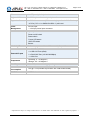
5.1 Product Specifications
Specifications
Board Size
165 x 115mm
CPU Support
Intel Atom N270 1.6 GHz with 533MHz FSB
Chipset
Intel 945GSE + Intel ICH7M
Memory Support
1x200pin 533/400MHz DDR2 SO-DIMM support, up to 2GB SDRAM
Graphics
Intel Graphics Media Accelerator 950VGA integrated in Intel 945GSE
18-bit dual-channel LVDS integrated in Intel 945GSE
18/24 bit dual-channel LVDS support by Chrontel CH7308B
1 x DB15 Female connector for external
Super I/O
Winbond W83627UHG
BIOS
Award BIOS
Storage
2 x SATA Connector
1 x Compact Flash II Slot
1 x 44-pin IDE Connector
Network
2 x Gigabit Ethernet Port by RJ45 with LED indicators - Ethernet
controller :
2 x PCIe by one bus Realtek 8111D
USB
4 x USB 2.0 stack port for external
2 x USB 2.0 header for internal
Serial
1 x RS232 port, DB9 connector for external (COM1),
pin 9 w/5V/12V/Ring select
1 x RS232/422/485 select header for internal (COM2), default RS232
4 x RS232 header for internal (COM3 – COM6)
Digital I/O
8-bit digital I/O by header
4-bit digital Input
4-bit digital Output
Battery
Support CR2477 battery by 2-pin header
Audio
Support Audio via Realtek ALC662 HD audio decoder
Support Line-in, Line-out, MIC by 2x5-pin header
* Specifications subject to change without notice. All brand names and trademark are their registered properties. *
15F-1, No. 186, Jian- Yi Road, Chung- Ho, Taipei 235, Taiwan R.O.C
Tel: + 886- 2- 8226 2881 Fax: + 886- 2- 8226 2883 www.aplex.com.tw
Page 5 of 49
Printer
1x LPT port by 2x13-pin header
Keyboard /Mouse
1x PS2 keyboard/mouse by 1x6 -pin wafer connector
Expansion Bus
1x PC 104+ connector (PCI master 4, jumper for +3.3V & 5V select)
1x PCIe ( PCI-e 1x +SMBUS+USB2. 0 ) mini card
Power
Management
DC12V input
Front I/O
by 2x5-pin header
1 x 2x2-pin power input connector
Power on/off switch
Reset switch
Power LED status
HDD LED status
Buzzer
Watchdog Timer
Software programmable 1 – 255 second by Super I/O
External I/O port
1 x COM Port (COM1)
4 x USB 2.0 Ports (stack)
2 x RJ45 GbE Port (10/100/1000Mbps)
1 x VGA Port
Temperature
Operating: 0 – 60 degree C
Storage: -20 – 80 degree C
Humidity
5% - 95%, non-condensing, operating
Power
Consumption
12V @1.4 5A (Intel N270 processor with 1GB DDR2 DRAM)
EMI/EMS
CE/FCC class A
* Specifications subject to change without notice. All brand names and trademark are their registered properties. *
15F-1, No. 186, Jian- Yi Road, Chung- Ho, Taipei 235, Taiwan R.O.C
Tel: + 886- 2- 8226 2881 Fax: + 886- 2- 8226 2883 www.aplex.com.tw
Page 6 of 49
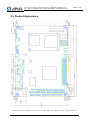
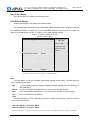
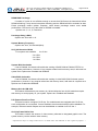
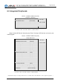
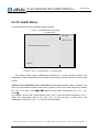
5.2 Product Appearance
* Specifications subject to change without notice. All brand names and trademark are their registered properties. *
15F-1, No. 186, Jian- Yi Road, Chung- Ho, Taipei 235, Taiwan R.O.C
Tel: + 886- 2- 8226 2881 Fax: + 886- 2- 8226 2883 www.aplex.com.tw
Page 7 of 49
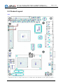
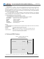
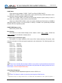
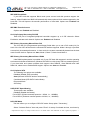
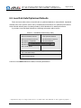
5.3 Product Layout
TOP
* Specifications subject to change without notice. All brand names and trademark are their registered properties. *
15F-1, No. 186, Jian- Yi Road, Chung- Ho, Taipei 235, Taiwan R.O.C
Tel: + 886- 2- 8226 2881 Fax: + 886- 2- 8226 2883 www.aplex.com.tw
Page 8 of 49
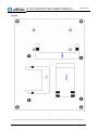
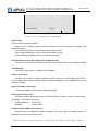
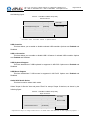
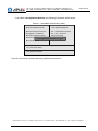
Bottom
* Specifications subject to change without notice. All brand names and trademark are their registered properties. *
15F-1, No. 186, Jian- Yi Road, Chung- Ho, Taipei 235, Taiwan R.O.C
Tel: + 886- 2- 8226 2881 Fax: + 886- 2- 8226 2883 www.aplex.com.tw
Page 9 of 49
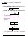
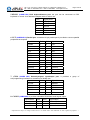
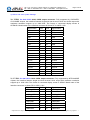
5.4 Onboard Jumpers and Port Pinouts
1. JVCCIO (2.0MM 1X3) PC104+ port voltage selection jumper: select voltage for PC104+
device
JVCCIO
PC104+ VCCIO Voltage
CLOSE 1-2
+3.3V (default)
CLOSE 2-3
+5V
2. JCLR_CMOS (2.0MM 1X3) CMOS clear jumper: CMOS clear operation will permanently
reset old BIOS settings to factory defaults.
JCLR_CMOS
CMOS
CLOSE 1-2
NORMAL
(default)
CLOSE 2-3
CLEAR CMOS
Procedures of CMOS clear:
1. Turn off the system and unplug the power cord from the power outlet;
2. To clear the CMOS settings, use the jumper cap to close pins 2 and 3 for about 3 seconds then
reinstall the jumper clip back to pins 1 and 2.
3. Power on the system again;
4. When entering the POST screen, press the <DEL> key to enter CMOS Setup Utility to load
optimal defaults;
5. After the above operations, save changes and exit BIOS Setup.
3. BAT (1.25.0MM 1X2) Battery port: a 3.3V battery is embedded to provide power for CMOS.
PIN#
Signal Name
PIN1
VBAT
PIN2
Ground
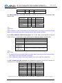
4.COM2-COM6 (2.0MM 2X5) COM2~COM6 port: up to 5 standard RS232 ports are provided.
They can be used directly via COM adapter cable connection.
Signal Name
Pin#
Pin#
Signal Name
DCD
1
2
RXD
TXD
3
4
DTR
Ground
5
6
DSR
RTS
7
8
CTS
RI
9
10
NC
Note: COM2 port is controlled by pins No.8~10 of JCOM. For details, please refer to
description of JCOM.
* Specifications subject to change without notice. All brand names and trademark are their registered properties. *
15F-1, No. 186, Jian- Yi Road, Chung- Ho, Taipei 235, Taiwan R.O.C
Tel: + 886- 2- 8226 2881 Fax: + 886- 2- 8226 2883 www.aplex.com.tw
Page 10 of 49
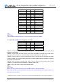
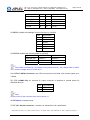
5.KB/MS (2.0MM 1X6) PS/2 keyboard/mouse port: the port can be connected to PS/2
keyboard or mouse via a dedicated adapter cable for direct use.
Pin#
Signal Name
1
KBDATA
2
MSDATA
3
Ground
4
+5V
5
KBCLK
6
MSCLK
6. LPT (2.0MM 2X13) Parallel port: a standard 26 pin parallel port is provided to connect parallel
peripherals as required.
Signal Name
Pin#
Pin#
Signal Name
PSTB#
1
2
PD0
PD1
3
4
DP2
DP3
5
6
DP4
DP5
7
8
DP6
DP7
9
10
ACK#
BUSY
11
12
PE
SLCT
13
14
AFD#
ERR#
15
16
INIT#
SLIN#
17
18
Ground
Ground
Ground
Ground
19
20
21
22
23
24
25
26
Ground
Ground
Ground
Ground
Ground
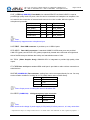
7. GPIO (2.0MM 2X5) General-purpose input/output port: it provides a group of
self-programming interfaces to customers for flexible use.
Signal Name
Pin#
Pin#
Signal Name
GPIO20
1
2
GPIO60
GPIO21
3
4
GPIO61
GPIO22
5
6
GPIO62
GPIO23
7
8
GPIO63
Ground
9
10
+5V
8. COM22 (2.0MM 2X5): it provides selectable RS422/485 serial signal output.
Signal Name
Pin#
Pin#
Signal Name
A
1
2
Terminal Resistance
B
3
4
Terminal Resistance
Z
5
6
NC
* Specifications subject to change without notice. All brand names and trademark are their registered properties. *
15F-1, No. 186, Jian- Yi Road, Chung- Ho, Taipei 235, Taiwan R.O.C
Tel: + 886- 2- 8226 2881 Fax: + 886- 2- 8226 2883 www.aplex.com.tw
Y
7
8
NC
Ground
9
10
NC
Page 11 of 49
9. USB4 (2.0MM 2X5) Front USB connector: it provides two USB ports via a dedicated USB
adapter cable.
Signal Name
Pin#
Pin#
Signal Name
+5V
1
2
+5V
USB_P6_DN
3
4
USB_P7_DN
USB_P6_DP
5
6
USB_P7_DP
Ground
7
8
Ground
NC
9
10
Ground
Note:
Before connection, make sure that pinout of the USB adapter is in accordance with that of the said
tables. Any inconformity may cause system down and even hardware damages.
10. JCOM (2.0MM 2X6) COM1/2 setup jumper: pin 1~6 are used to select signal out of pin 9 of
COM1 port; pin 7~12 are used to select output type for COM2 port (RS232 or RS422/485).
JCOM
Function
CLOSE 1-2
COM1 Pin9=RI (default)
CLOSE 3-4
COM1 Pin9=+5V
CLOSE 5-6
COM1 Pin9=+12V
CLOSE 7-9
CLOSE 8-10
COM2 FOR RS232 FROM COM2 (default)
CLOSE 9-11
CLOSE 10-12
COM2 FOR RS485/RS422 FROM COM22
Note:
1. As determined by its hardware design, the board features full-duplex RS485 communication.
Like RS422, a four-wire connection is necessary.
2. Since COM2 and COM22 use the same address, they cannot work at the same time.
11. IDE (2.0MM 2X22) IDE connector: the motherboard provides a 44-pin IDE connector for
connection of 2.5' IDE hard disk drivers and supports up to 2 IDE devices.
Signal Name
Pin#
Pin#
Signal Name
RESET
1
2
Ground
IDE_PDD7
3
4
IDE_PDD8
IDE_PDD6
5
6
IDE_PDD9
IDE_PDD5
7
8
IDE_PDD10
IDE_PDD4
9
10
IDE_PDD11
IDE_PDD3
11
12
IDE_PDD12
IDE_PDD2
13
14
IDE_PDD13
* Specifications subject to change without notice. All brand names and trademark are their registered properties. *
15F-1, No. 186, Jian- Yi Road, Chung- Ho, Taipei 235, Taiwan R.O.C
Tel: + 886- 2- 8226 2881 Fax: + 886- 2- 8226 2883 www.aplex.com.tw
IDE_PDD1
15
16
IDE_PDD14
IDE_PDD0
17
18
IDE_PDD15
Ground
19
20
NC
DREQ
21
22
Ground
IOW#
23
24
Ground
IOR#
25
26
Ground
IOCHRDY
27
28
Ground
DACK#
29
30
Ground
IRQ14
31
32
NC
Address 1
33
34
IDE_PDIAG
Address 0
35
36
Address 2
Chip select 0
37
38
Chip select 1
Activity
39
40
Ground
+5V
41
42
+5V
Ground
43
44
NC
Page 12 of 49
Note:
If two IDE devices are connected, CF card connection cannot be realized.
12. F_PANEL (2.0MM 2X5) Front panel connector
Signal Name
Pin#
Pin#
Signal Name
HD LED+
1
2
POWER LED+
HD LED-
3
4
POWER LED-
Ground
5
6
PWRBTN
RESET
7
8
Ground
BUZZER+
9
10
BUZZER-
PIN1&3: They are used to connect hard disk activity LED. The LED blinks when the hard disk is
reading or writing data.
PIN2&4: They are used to connect power LED. When the system is powered on or under S0/S1
state, the LED is normally on; when the system is under S4/S5 state, the LED is off.
PIN5&6: They are used to connect power switch button. The two pins are disconnected under
normal condition. You may short them temporarily to realize system startup & shutdown or awaken
the system from sleep state.
PIN7&8: They are used to connect reset button. The two pins are disconnected under normal
condition. You may short them temporarily to realize system reset.
PIN9&10: They are used to connect an external buzzer.
Note:
When connecting LEDs and buzzer, pay special attention to the signal polarity.
Make sure that the connector pins have a one-to-one correspondence with chassis wiring, or it
may cause boot up failure.
* Specifications subject to change without notice. All brand names and trademark are their registered properties. *
15F-1, No. 186, Jian- Yi Road, Chung- Ho, Taipei 235, Taiwan R.O.C
Tel: + 886- 2- 8226 2881 Fax: + 886- 2- 8226 2883 www.aplex.com.tw
Page 13 of 49
13. F_AUDIO (2.0MM 2X5) Front Audio: An onboard REALTEL ALC662 CODEC is used to
provide high-quality audio I/O ports; Line Out can be connected to a headphone or amplifier; Line
In is used for the connection of external audio source via a Line in cable; Mic is the port for
microphone input audio.
Signal Name
Pin#
Pin#
Signal Name
FRONT-OUT-L
1
2
LINEIN_R
AUD_AGND
3
4
AUD_AGND
FRONT-OUT-R
5
6
LINEIN_L
AUD_AGND
7
8
AUD_AGND
FRONT-MIC1
9
10
AUD_AGND
Note:
The board only supports mono microphone input.
14. USB1/2 Rear USB connector: it provides up to 4 USB2.0 ports.
15. LAN1/2 Rear LAN connectors: 2 standard 1000M RJ-45 Ethernet ports are provided.
LINK LED (green) and ACTIVE LED (yellow) respectively located at the left-hand and right-hand
side of the Ethernet port indicate the activity and transmission state of LAN.
16. VGA (Video Graphic Array): GMA950 GPU is integrated to provide high-quality video
output.
17. COM Rear serial port: standard DB9 serial port is provided to make a direct connection to
serial devices.
18. FAN (2.54MM 1X3) Fan connector: cooling fans can be connected directly for use. You may
set the rotation condition of cooling fan in PC Health Status menu of BIOS Setup.
Pin#
Signal Name
1
Ground
2
+12V
3
Rotation detection
Note: Output power of cooling fan must not be above 5W.
19. AT12V (5.0MM 1X2) 12V System power input connector
Pin#
Signal Name
1
+12V
2
Ground
Note:
Make sure that the voltage of power supply is DC(12±5%)V before power on, or it may cause boot
* Specifications subject to change without notice. All brand names and trademark are their registered properties. *
15F-1, No. 186, Jian- Yi Road, Chung- Ho, Taipei 235, Taiwan R.O.C
Tel: + 886- 2- 8226 2881 Fax: + 886- 2- 8226 2883 www.aplex.com.tw
Page 14 of 49
up failure and even system damage.
20. LVDS1 for dual 24 bit 24-bit LVDS output connector: Fully supported by CHRONTEL
CH70308BE chipset, the interface features single and dual channel 18-bit and 24-bit output with
maximum resolution support up to 1600*1200. The format of connected display screen is
OPENLDI. Model name of the interface connector is Hirose DF13-40DP-1.25V.
Signal Name
Pin#
Pin#
Signal Name
+5V
1
2
+5V
Ground
3
4
Ground
+3.3V
5
6
+3.3V
A0M
7
8
A4M
A0P
9
10
A4P
Ground
11
12
Ground
A1M
13
14
A5M
A1P
15
16
A5P
Ground
17
18
Ground
A2M
19
20
A6M
A2P
21
22
A6P
Ground
23
24
Ground
CLK1M
25
26
CLK2M
CLK1P
27
28
CLK2P
Ground
29
30
Ground
SC_DDC
31
32
SD_DDC
Ground
33
34
Ground
A3M
35
36
A7M
A3P
37
A3M
A7P
NC
39
40
NC
21. LVDS1 for dual 18 bit 18-bit LVDS output connector: Fully supported by INTEL945GSE
chipset, the interface features single and dual channel 18-bit output with maximum resolution
support up to 1600*1200. The format of connected display screen is SPWG. Model name of the
interface connector is Hirose DF13-30DP-1.25V.
Signal Name
Pin#
Pin#
Signal Name
LVDS1_VDD5
1
2
LVDS1_VDD5
Ground
3
4
Ground
LVDS1_VDD33
5
6
LVDS1_VDD33
LADATAN0
7
8
LBDATAN0
LADATAP0
9
10
LBDATAP0
LADATAN1
11
12
LBDATAN1
LADATAP1
13
14
LBDATAP1
LADATAN2
15
16
LBDATAN2
LADATAP2
17
18
LBDATAP2
* Specifications subject to change without notice. All brand names and trademark are their registered properties. *
15F-1, No. 186, Jian- Yi Road, Chung- Ho, Taipei 235, Taiwan R.O.C
Tel: + 886- 2- 8226 2881 Fax: + 886- 2- 8226 2883 www.aplex.com.tw
LACLKN
19
20
LBCLKN
LACLKP
21
22
LBCLKP
LDDC_CLK
23
24
LDDC_DATA
LBKLT_EN
25
26
JLVDS_CTRL
Ground
27
28
Ground
+V12S
29
30
+V12S
Page 15 of 49
22. BKL1 (2.0MM 1X5) Backlight control connector for LVDS1/2
Pin#
Signal Name
1
+12V
2
+12V
3
Ground
4
Ground
5
ENABKL
6
CTRBKL
23. JLVDS (2.0MM 1X6) Choice jumper for LVDS1/2
Signal Name
BKL For LVDS1
BKL For LVDS2
BackLight_EN
Close1-3
Close3-5
PWM
Close2-4
Close7-8
LEVEL
Close4-6
Close7-9
Note: Make sure based on LCD feature to set jumper correctly;The voltage value of LVDS1
is 3.3, and the voltage value of LVDS2 is 5.0
24. SATA1/2 SATA Connectors: two SATA connectors are provided, with transfer speed up to
3.0Gb/s.
25. CN1 (2.5MM 1X2): an onboard 5V output connector is reserved to provide power for
IDE/SATA devices.
Pin#
Signal Name
1
+5V
2
Ground
Note:
Output current of the connector must not be above 1A.
26. BZ Buzzer: onboard buzzer
27. PC104+ PC104+ connector: it conforms to standard PC104+ specification.
* Specifications subject to change without notice. All brand names and trademark are their registered properties. *
15F-1, No. 186, Jian- Yi Road, Chung- Ho, Taipei 235, Taiwan R.O.C
Tel: + 886- 2- 8226 2881 Fax: + 886- 2- 8226 2883 www.aplex.com.tw
Page 16 of 49
28. DIMM Memory socket: the socket is located at the backside of the board and supports
200PIN 1.8V DDRII400/533 memory module up to 2G. If a DDRII667/800 memory module is
installed, the system will reduce the DRAM frequency to 533MHz.
29. MPCIE Mini PCIE slot: it supports MINI PCIE devices with USB2.0, SMBUS and PCIE
signal.
30. CF CF Card Slot: it is located at the backside of the board and serves as an insert interface
for Type I and Type II Compact Flash card. The operating voltage of CF card can be set as 3.3V or
5V. The default setting of the product is 3.3V.
6 BIOS Setup Description
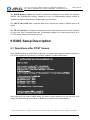
6.1 Operations after POST Screen
After CMOS discharge or BIOS flashing operation, the system will display the following screen for
your further operation. Press F1 key to continue or Del key to enter CMOS Setup.
Phoenix – AwardBIOS v6.00PG, An Energy Star Ally
Copyright © 1984-2007, Phoenix Technologies, LTD
ASB-L701 V015
Main Processor : Intel® Atom™ 1.60GHz(133x12)
Memory Testing :515008K OK + 8M shared memory
CPU Brand Name : Intel® Atom™ CPU N270 @1.60GHz
C1E BIOS Supported
Hyper-Threading Technology CPU Detected (Hyper-Threading Technology Enabled)
Memory Frequency For DDR2 533
IDE Channel 0 Master : None
IDE Channel 0 Slave : None
IDE Channel 1 Master : None
IDE Channel 1 Slave : None
CMOS checksum error – Defaults loaded
Press F1 to continue, DEL to enter SETUP
03/19/2010-Silverthrone-6A79KAPXC-00
After optimizing and exiting CMOS Setup, the POST screen displayed for the first time is as
follows and includes basic information on BIOS, CPU, memory, and storage devices.
* Specifications subject to change without notice. All brand names and trademark are their registered properties. *
15F-1, No. 186, Jian- Yi Road, Chung- Ho, Taipei 235, Taiwan R.O.C
Tel: + 886- 2- 8226 2881 Fax: + 886- 2- 8226 2883 www.aplex.com.tw
Page 17 of 49
Phoenix – AwardBIOS v6.00PG, An Energy Star Ally
Copyright © 1984-2007, Phoenix Technologies, LTD
ASB-L701 V015
Main Processor : Intel® Atom™ 1.60GHz(133x12)
Memory Testing :515008K OK + 8M shared memory
CPU Brand Name : Intel® Atom™ CPU N270 @1.60GHz
C1E BIOS Supported
Hyper-Threading Technology CPU Detected (Hyper-Threading Technology Enabled)
Memory Frequency For DDR2 533
IDE Channel 0 Master : None
IDE Channel 0 Slave : None
IDE Channel 1 Master : None
IDE Channel 1 Slave : None
Press DEL to enter SETUP, F12 to Enter Boot Menu
03/19/2010-Silverthrone-6A79KAPXC-00
Press F12 key to enter Boot Menu during POST, as shown by the following figure.
Boot Menu
==
Select a Boot First device ==
+ Removable
+Hard Disk
+CDROM
LAN
↑↓:Move
Enter:Accept
F4:Exit
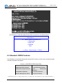
6.2 Standard CMOS Features
Press [Del] key to enter BIOS Setup utility during POST, and then a main menu containing system
summary information will appear.
Phoenix – Award BIOS CMOS Setup Utility
►Standard CMOS Features
►Advanced BIOS Features
►Advanced Chipset Features
►Integrated Peripherals
►Power Management Setup
Load Fail-Safe Defaults
Load Optimized Defaults
Set
Administrator
Password
Set User Password
Save & Exit Setup
* Specifications subject to change without notice. All brand names and trademark are their registered properties. *
15F-1, No. 186, Jian- Yi Road, Chung- Ho, Taipei 235, Taiwan R.O.C
Tel: + 886- 2- 8226 2881 Fax: + 886- 2- 8226 2883 www.aplex.com.tw
►PnP/PCI Configurations
►PC Health Status
Esc : Quit
F10 : Save & Exit Setup
Page 18 of 49
Exit Without Saving
↑↓→← : Select Item
Time, Date, Hard Disk Type…
Standard CMOS Features
Use this menu to modify basic system configurations such as time, date and etc.
Advanced BIOS Features
Use this menu configure advanced features of Award® BIOS.
Advanced Chipset Features
Use this menu to change the values in the chipset registers and optimize your system
performance.
Integrated Peripherals
Use this menu to specify your settings for integrated peripherals.
Power Management Setup
Use this menu to specify your settings for power management.
PnP/PCI Configurations
This menu is valid only if your system supports PnP/PCI.
PC Health Status
This menu shows the current status of your PC.
Load Fail-Safe Defaults
Use this menu to load Fail-Safe defaults into BIOS for the most stable, and minimal-performance
system operations.
Load Optimized Defaults
Use this menu to load factory settings into BIOS for optimal-performance system operations.
Set Administrator Password
Use this menu to set Administrator password.
Set User Password
Use this menu to set user password.
* Specifications subject to change without notice. All brand names and trademark are their registered properties. *
15F-1, No. 186, Jian- Yi Road, Chung- Ho, Taipei 235, Taiwan R.O.C
Tel: + 886- 2- 8226 2881 Fax: + 886- 2- 8226 2883 www.aplex.com.tw
Page 19 of 49
Save & Exit Setup
Save all changes to the CMOS and exit BIOS Setup.
Exit Without Saving
Abandon all changes to the CMOS and exit BIOS Setup.
The following figure shows the items of Standard CMOS Features menu, which may exclude
any modifiable subitem or contain one or more modifiable subitems. Use arrow keys to select the
items to be modified and <PgUp> or <PgDn> key to select desired settings.
Phoenix – AwardBIOS CMOS Setup Utility
Standard CMOS Features
Date (mm:dd:yy)
Mon, Mar. 3 2009
Time (hh:mm:ss)
Item Help
14 : 31: 6
Menu Level►
►IDE
Channel 0 Master
[None]
Change the day,
►IDE
Channel 0 Slave
[None]
month, year and
►IDE
Channel 1 Master
[None]
century
►IDE
Channel 1 Slave
[None]
Video
[EGA/VGA]
Halt On
[All, But Keyboard]
Base Memory
639K
Extended Memory
1038336K
Total Memory
1039360K
↑↓→←:Move Enter:Select
F5: Previous
+/-/PU/PD:Value
Values
F10:Save ESC:Exit
F1:General Help
F6: Fail-Safe Defaults F7: Optimized Defaults
Date
This item allows you to set a desired system date (usually current date). The date format is
<day><month><date><year>.
Day
It is a read-only and bios-defined weekday attribute ranging from Sun (Sunday) to
Sat (Saturday).
Month
It is a month attribute ranging from Jan (January) to Dec (December).
Date
It is a date attribute ranging from 1 to 31 and can be modified via numeric keys.
Year
It is a user-defined year attribute.
Time
This item allows you to set a desired system time (usually current time). The time format is
<hour><minute><second>.
Channel 0 Master / Channel 0 Slave
Channel 1 Master / Channel 1 Slave
* Specifications subject to change without notice. All brand names and trademark are their registered properties. *
15F-1, No. 186, Jian- Yi Road, Chung- Ho, Taipei 235, Taiwan R.O.C
Tel: + 886- 2- 8226 2881 Fax: + 886- 2- 8226 2883 www.aplex.com.tw
Page 20 of 49
Press PgUp/<+> or PgDn/<-> key to select among Manual, None and Auto type. Note that the
specification of your drive device must be in compliance with the contents of Drive Table. If the
information registered in this item is not correct, your hard disk will not work properly; if your hard
disk specification is not found or does not conform to or the Driver Table, you may select Manual
type to set the specification manually.
If you choose Manual, you will be requested to enter relevant information in the following
entries. Keyboard input is also supported. For details, you may refer to the instructive materials
provided by distributor or device manufacturer.
If a SCSI HDD device is used, set this item to "NONE".
If a CD-ROM drive is connected to the HDD port, set this item to "NONE"
AccessMode
Cylinder
Head
Precomp
Landing Zone
Options are: Auto, Normal, Large and LBA
Number of cylinders
Number of heads
Write precompensation cylinder
Head landing zone
Halt on
The item allows you to determine when the system will stop. Options are: No Errors; All Errors;
All, But Keyboard.
No Errors
The system boot will not stop for any error.
All Errors
Whenever the BIOS detects a non-fatal error, the system boot will
stop.
All, But Keyboard
The system boot will not stop for a keyboard error but stop for all
other errors as detected by BIOS. (default)
6.3 Advanced BIOS Features
Phoenix – AwardBIOS CMOS Setup Utility
Advanced BIOS Features
►CPU Feature
[Press Enter]
►Hard Disk Boot Priority
[Press Enter]
Virus Warning
[Disabled]
CPU L1 & L2 Cache
[Enabled]
Hyper-Threading Technology
[Enabled]
Quick Power On Self Test
[Enabled]
First Boot Device
Second Boot Device
Menu Level►
[Removable]
[Hard Disk]
Third Boot Device
[CDROM]
Boot Other Device
[Enabled]
PXE Boot For Onboard LAN1
[Disable]
PXE Boot For Onboard LAN2
[Disable]
Boot Up NumLock Status
Item Help
[On]
* Specifications subject to change without notice. All brand names and trademark are their registered properties. *
15F-1, No. 186, Jian- Yi Road, Chung- Ho, Taipei 235, Taiwan R.O.C
Tel: + 886- 2- 8226 2881 Fax: + 886- 2- 8226 2883 www.aplex.com.tw
Gate A20 Option
X APIC
[Fast]
Mode
[Enabled]
MPS Version Control For OS
[1.4]
OS Select For DRAN > 64MB
[Non-OS2]
Small Logo [EPA] Show
[Disabled]
Security Option
[Setup]
↑↓→←:Move Enter:Select
F5: Previous
Page 21 of 49
+/-/PU/PD:Value
Values
F10:Save ESC:Exit F1:General Help
F6: Fail-Safe Defaults
F7: Optimized Defaults
CPU Feature
The item has the following options:
Delay Prior To Thermal [16 Min] (This item allows you to set the duration of entering CPU
thermal throttling.)
C1E Function [Auto] CPU Power-saving State Enable Control
CPU C State Capability [C1] CPU Power-saving State Control
Execute Disable Bit [Enable] (Virus Protection Technology)
Hard Disk Boot Priority (IDE Storage Device Boot Priority)
This item is used to specify boot priority of IDE devices. Press "Enter" key for detailed setting.
Virus Warning
This item has two options: "Disabled" and "Enabled".
CPU L1 & L2 Cache
This item can be used to enable or disable the CPU’s primary (L1) or secondary (L2) cache. If
set to Enabled, operating speed of PC will be increased remarkably; if set to Disabled, the function
will be inactivated.
Hyper-Threading Technology
Enable and disable Intel's hyper-threading technology.
Quick Power On Self Test
This item is used to accelerate Power On Self Test (POST) process. If set to Enabled, BIOS
will shorten or skip some of its tests.
Enabled (default)
Quick POST
Disabled
Normal POST
First/Second/Third/Boot Other Device
BIOS will load the operating system according to the boot order of available devices. If
disabled, the function will be inactivated.
* Specifications subject to change without notice. All brand names and trademark are their registered properties. *
15F-1, No. 186, Jian- Yi Road, Chung- Ho, Taipei 235, Taiwan R.O.C
Tel: + 886- 2- 8226 2881 Fax: + 886- 2- 8226 2883 www.aplex.com.tw
Page 22 of 49
PXE Boot For Onboard LAN1/LAN2(PXE 启动设置)
Disabled(default) System will run appointed boot device first after POST, If system can not
find out any available boot devices it will run LAN boot
Enabled
System will run LAN boot after POST at all times regardless of the
appointed boot order, but it will run the appointed boot order after LAN boot failure.
Boot Up NumLock Status (Default: On)
On (default) Keypad numeric keys remain valid
Off
Keypad arrow keys remain valid
Gate A20 Option
Normal
Gate A20 signal is controlled by keyboard controller or chipset hardware.
Fast (default) Gate A20 signal is controlled by port 92 or specific programs of chipset.
APIC Mode
It refers to an advanced interrupt controller mode to meet the requirements of multi-core CPU.
MPS Version Control For OS
This item is used to specify the multiprocessor specification version of the system. It is
recommended to keep the default value (1.4).
OS Selection for DRAM > 64MB
You must only select OS/2 when installing an OS/2 operating system with a RAM greater than
64MB. The options are: Non-OS/2 (default) and OS/2.
Small Logo [EPA] Show
This item is used to determine whether the Energy Star Logo will be displayed during POST.
The options are: "Disabled" and "Enabled".
Security Option
Such option allows users to set access restrictions to both system and Setup utility, or just Setup
utility.
System
Setup (default)
If one fails to enter a valid password in the popup box, the system will
not boot up and the Setup utility will not be accessible.
If one fails to enter a valid password in the popup box, the system will
boot up as usual, but the Setup utility will not be accessible.
6.4 Advanced Chipset Features Setup
Advanced Chipset Features Setup is used to change the values of chipset registers that
control most options of computer.
Select ADVANCED CHIPSET FEATURES in the main menu, and the following screen will be
* Specifications subject to change without notice. All brand names and trademark are their registered properties. *
15F-1, No. 186, Jian- Yi Road, Chung- Ho, Taipei 235, Taiwan R.O.C
Tel: + 886- 2- 8226 2881 Fax: + 886- 2- 8226 2883 www.aplex.com.tw
Page 23 of 49
displayed.
Phoenix – AwardBIOS CMOS Setup Utility
Advanced Chipset Features
DRAM Timing Selectable
[By SPD]
X
CAS Latency Time
Auto
X
DRAM RAS# to CAS# Delay
Auto
X
DRAM RAS# Precharge
Auto
X
Precharge Delay (tRAS)
Auto
X
System Memory Frequency
Auto
SLP_S4# Assertion Width
[1 to 2 Sec.]
System BIOS Cacheable
[Enabled]
Video BIOS Cacheable
[Disabled]
Memory Hole At 15M-16M
[Disabled]
►PCI Express Root Port Func
Item Help
Menu Level►
[Press Enter]
** Onboard VGA Setting **
On-Chip Frame Buffer Size
[ 8MB]
DVMT Mode
[DVMT]
DVMT/Fixed Memory Size
[128MB]
Boot Display
[VBIOS Default]
LCD Panel Type
[LVDS1 18 1024 X 768]
LVDS1 Panel Brightness
↑↓→←:Move
Enter:Select
F5: Previous
Values
[Level 10]
+/-/PU/PD:Value F10:Save ESC:Exit
F1:General Help
F6: Fail-Safe Defaults F7: Optimized Defaults
Note: If you are not familiar with chipset, never modify these settings at will.
DRAM Timing Selectable
Two options are available.
Manual (Manual setup)
By SPD (DRAM timing is set automatically according to memory SPD data)
When selecting Manual, the following five items are configurable; when selecting By SPD, the
following five items are not configurable.
CAS Latency Time
Once a SDRAM is installed, the clock latency will be determined by DRAM clock settings. The
options are: 5, 4, 3 and Auto.
DRAM RAS-to-CAS Delay
You may set the delay period between CAS and RAS signal for DRAM read & write or
refreshing. Shorter delay means quicker response, while longer delay means more stable
performance. Options are: 2, 3, 4, 5, 6 and Auto.
* Specifications subject to change without notice. All brand names and trademark are their registered properties. *
15F-1, No. 186, Jian- Yi Road, Chung- Ho, Taipei 235, Taiwan R.O.C
Tel: + 886- 2- 8226 2881 Fax: + 886- 2- 8226 2883 www.aplex.com.tw
Page 24 of 49
DRAM RAS Precharge
If number of cycles is not sufficient enough to ensure that RAS saves its instructions before
DRAM refreshing, it may cause incomplete refreshing and the DRAM will fail to maintain its data.
Faster precharge means quicker response, while slower precharge means more stable
performance. This item is only valid when a SDRAM is installed.
Options are: 2, 3, 4, 5, 6 and Auto.
Precharge Delay (t RAS)
Options are: Auto and 4~15.
System Memory Frequency
Options are: Auto, 533 and 667(MHz).
SLP_S4# Assertion Width
Four options are available:
4 to 5 Sec.
3 to 4 Sec.
2 to 3 Sec.
1 to 2 Sec.
System BIOS Cacheable
If set to Enabled, the feature will enable the caching of BIOS ROM at F0000h-FFFFFh for
better system performance. However, if any program writes into this memory area, it will result in a
system error. Options are: Enabled and Disabled.
Video BIOS Cacheable
If set to Enabled, the feature will enable the caching of video BIOS ROM for better system
performance. However, if any program writes into this memory area, it will result in a system error.
Options are: Enabled and Disabled.
Memory Hole At 15M-16M
This feature will decrease your memory by 1M and allow the few old ISA cards that require
this memory to work properly on your system. Options are: Enabled and Disabled.
PCI Express Root Port Func
This item is used to configure PCI-E slot. For motherboards not equipped with PCI-E slot,
such configuration is not required. If set to Disabled, the slot and slot device will be disabled. For
example, onboard network adapter card can be disabled or enabled via PCI-E slot 1.
On-Chip Frame Buffer Size
This feature controls the amount of video memory allocated to integrated graphic card. The
system memory can be used as video memory.
* Specifications subject to change without notice. All brand names and trademark are their registered properties. *
15F-1, No. 186, Jian- Yi Road, Chung- Ho, Taipei 235, Taiwan R.O.C
Tel: + 886- 2- 8226 2881 Fax: + 886- 2- 8226 2883 www.aplex.com.tw
Page 25 of 49
DVMT Mode
Three options are available: "FIXED", "DVMT" and "Both (FIXED+DVMT)".
When set to "FIXED" mode, a fixed portion of the system memory will be allocated to GPU.
Two allocation sizes are available: 64MB and 128MB.
When set to "DVMT" Mode, the system will dynamically allocate system memory to GPU. In
this mode, up to 224MB of system memory can be allocated.
When set to "Both(FIXED+DVMT)" mode, the system will allocate a fixed memory of 64MB as
dedicated graphic memory, as well as allow a memory of 64MB to be dynamically allocated
between GPU and operating system.
DVMT/FIXED Memory Size
Refer to the previous item.
Boot Display
This feature is to select desired display device. VBIOS, LVDS1, VGA + LVDS1, LVDS2 and
VGA + LVDS2 can be selected as display device.
LCD Panel Type (LVDS Panel Type)
This feature is to select between LVDS1 and LVDS2. When selecting LVDS panel, users
should be informed of LVDS panel types supported by the motherboard. The following options are
available:
LVDS1 18
800X600
LVDS1 18
1024X768
LVDS1 18*2 1280X1024
LVDS1 18*2 1440X900
LVDS1 18*2 1400X1050
LVDS1 18*2 1600X1200
LVDS1 18
1280X800
LVDS1 18
1280X768
LVDS2 24
1024X768
LVDS2 24*2 1280X1024
LVDS2 24*2 1440X900
LVDS2 24*2 1920X1080
Note: Due to limited address length of BIOS, only a portion of panel parameters are listed in
BIOS Setup. If the connected panel is not included in the parameter list, display problem will occur.
In this case, we need to adjust BIOS setup.
LVDS1 Panel Brightness
This feature provides adjustable brightness control: LEVEL3~10.
Note: This feature is valid only when the panel supports PWM function.
* Specifications subject to change without notice. All brand names and trademark are their registered properties. *
15F-1, No. 186, Jian- Yi Road, Chung- Ho, Taipei 235, Taiwan R.O.C
Tel: + 886- 2- 8226 2881 Fax: + 886- 2- 8226 2883 www.aplex.com.tw
Page 26 of 49
6.5 Integrated Peripherals
Phoenix – AwardBIOS CMOS Setup Utility
Integrated
► OnChip IDE
Device
Peripherals
[Press Enter]
► Onboard Device
[Press Enter]
► Super IO Device
[Press Enter]
↑↓→←:Move
Enter:Select +/-/PU/PD:Value F10:Save ESC:Exit
F5: Previous
Values
Item Help
Menu Level►
F1:General Help
F6: Fail-Safe Defaults F7: Optimized Defaults
Select "OnChip IDE Device" item and press "Enter" for setup of IDE devices, as shown by the
following figure:
Phoenix – AwardBIOS CMOS Setup Utility
OnChip IDE Device
IDE HDD Block Mode
[Enabled]
IDE DMA Transfer access
[Enabled]
On-Chip Primary PCI IDE
[Enabled]
IDE Primary Master PIO
[Auto]
IDE Primary Slave
[Auto]
PIO
IDE Primary Master UDMA
[Auto]
IDE Primary Slave UDMA
[Auto]
On-Chip Secondary PCI IDE
[Enabled]
IDE Secondary Master PIO
[Auto]
IDE Secondary Slave PIO
[Auto]
IDE Secondary Master UDMA
[Auto]
IDE Secondary Slave UDMA
[Auto]
Item Help
Menu Level►
*** On-Chip Serial ATA Setting ***
X SATA Mode
IDE
On-Chip Serial ATA
[Auto]
X SATA Port Speed Setting
[Disabled]
X PATA IDE mode
[Secondary]
SATA Port
↑↓→←:Move
Enter:Select
F5: Previous
Values
[P0,P2 is Primary]
+/-/PU/PD:Value F10:Save ESC:Exit
F1:General Help
F6: Fail-Safe Defaults F7: Optimized Defaults
* Specifications subject to change without notice. All brand names and trademark are their registered properties. *
15F-1, No. 186, Jian- Yi Road, Chung- Ho, Taipei 235, Taiwan R.O.C
Tel: + 886- 2- 8226 2881 Fax: + 886- 2- 8226 2883 www.aplex.com.tw
Page 27 of 49
IDE HDD Block Mode
If your IDE hard disk supports Block mode (most current hard disk products support the
feature), select Enabled and BIOS will automatically detect optimum block mode supported by the
hard disk. This will improve the transfer performance of hard disk. Options are: Enabled and
Disabled.
IDE DMA Transfer Access
Options are: Enabled and Disabled.
On-Chip Primary/Secondary PCI IDE
Each IDE port of integrated peripheral controller supports up to 2 IDE channels. Select
Enabled to activate each channel. Options are: Enabled and Disabled.
IDE Primary /Secondary Master/Slave PIO
The four IDE PIO (Programmed Input/Output) fields allow you to set a PIO mode (0-4) for
each of the four IDE devices that the onboard IDE interface supports. Mode 0 through 4 provides
successively increased performance. In Auto mode, the system automatically determines the best
mode for each device. Options are: Auto, Mode 0, Mode 1, Mode 3 and Mode 4.
IDE Primary /Secondary Master/Slave UDMA
Ultra DMA implementation is possible only if your IDE hard disk supports it and the operating
environment includes a DMA driver (Windows 95 OSR2 or a third-party IDE bus mastering driver).
If your hard disk and system software both support Ultra DMA/33, Ultra DMA/66 and Ultra
DMA/100, select Auto to enable BIOS support. Options are: Auto and Disabled.
On-Chip Serial ATA
The following five options are available:
Disabled (Disable SATA controller)
Auto (Allocate SATA/IDE devices automatically)
Combined Mode (IDE+SATA Combo Mode)
Enhanced Mode
SATA Only
SATA PORT Speed Setting
Three options are available:
Disabled (Disable the feature)
Force GEN I (Enhance transfer speed to 1.5Gb/s, i.e., 150MB/s)
Force GEN II (Enhance transfer speed to 3.0Gb/s, i.e., 300MB/s)
PATA IDE Mode
The item allows you to configure PATA IDE mode. Setup option: "Secondary",
Select "Onboard Device" item and press "Enter" for setup of onboard devices, as shown by
* Specifications subject to change without notice. All brand names and trademark are their registered properties. *
15F-1, No. 186, Jian- Yi Road, Chung- Ho, Taipei 235, Taiwan R.O.C
Tel: + 886- 2- 8226 2881 Fax: + 886- 2- 8226 2883 www.aplex.com.tw
Page 28 of 49
the following figure:
Phoenix – AwardBIOS CMOS Setup Utility
Onboard Device
USB Controller
[Enabled]
USB 2.0 Controller
[Enabled]
USB Keyboard Support
[Enabled]
USB Mouse Support
[Enabled]
Azalia/AC97 Audio Select
[Auto]
↑↓→←:Move
Enter:Select
F5: Previous
Values
+/-/PU/PD:Value F10:Save ESC:Exit
Item Help
Menu Level►
F1:General Help
F6: Fail-Safe Defaults F7: Optimized Defaults
USB Controller
This item allows you to enable or disable onboard USB controller. Options are: Enabled and
Disabled.
USB 2.0 Controller
This item allows you to enable or disable USB 2.0 feature of onboard USB controller. Options
are: Enabled and Disabled.
USB Keyboard Support
This item determines if USB keyboard is supported in MS DOS. Options are: Enabled and
Disabled.
USB Mouse Support
This item determines if USB mouse is supported in MS DOS. Options are: Enabled and
Disabled.
Azalia/AC97 Audio Select
This item is used to select Audio mode.
Select "Super IO Device" item and press "Enter" for setup of Super IO devices, as shown by the
following figure:
Phoenix – AwardBIOS CMOS Setup Utility
Super IO Device
Onboard Parallel Port
Parallel Port Mode
X ECP Mode Use DMA
[378/IRQ7]
[Standard]
3
Onboard Serial Port 1
[3F8/IRQ4]
Onboard Serial Port 2
[2F8/IRQ3]
UART2 Mode Select
Item Help
Menu Level►
[Normal]
* Specifications subject to change without notice. All brand names and trademark are their registered properties. *
15F-1, No. 186, Jian- Yi Road, Chung- Ho, Taipei 235, Taiwan R.O.C
Tel: + 886- 2- 8226 2881 Fax: + 886- 2- 8226 2883 www.aplex.com.tw
X
RXD , TXD Active
Hi, Lo
X
IR Transmission Delay
Enabled
X
UART2 Duplex Mode
Half
X
Use IR Pins
IR-Rx2Tx2
Onboard Serial Port 3
[3E8/IRQ4]
Onboard Serial Port 4
[2E8/IRQ3]
Onboard Serial Port 5
[4F8/IRQ4]
Onboard Serial Port 6
[4E8/IRQ3]
Power On By PS/2 Keyboard
[Disabled]
Watch Dog Timer Select
[Disabled]
↑↓→←:Move
Enter:Select
F5: Previous
Values
+/-/PU/PD:Value F10:Save ESC:Exit
Page 29 of 49
F1:General Help
F6: Fail-Safe Defaults F7: Optimized Defaults
Onboard Parallel Port
This item allows you to determine the I/O address and corresponding interrupts for the onboard
parallel port LPT. Options are: Disabled, 378/IRQ7, 278/IRQ5 and 3BC/IRQ7.
Onboard Serial Port 1/2/3/4
These four selection fields allow you to select the I/O address and corresponding interrupts
for serial port COM1/2/3/4. Options are: Disabled, 3F8/IRQ4, 2F8/IRQ3, 3E8/IRQ4 and 2E8/IRQ3.
Onboard Serial Port 5/6
These two selection fields allow you to select the I/O address and corresponding interrupts for
serial port COM5/6. Options are: Disabled, 4F8/IRQ4 and 4E8/IRQ3.
UART Mode Select
Generally, Onboard Serial Port 2 of motherboard can also be used as infrared port. This item
allows you to determine whether Onboard Serial Port 2 is used as normal serial port or infrared
port. Four options are available:
Normal (used as serial port)
IrDA (used as standard infrared port)
ASKIR (used as responder infrared port)
UR2 Duplex Mode
This item will be set to Half Duplex (Half) mode unless your infrared device supports Full
Duplex (Full) mode.
Power On By PS/2 Keyboard
Three options are available:
Disabled
Any key
* Specifications subject to change without notice. All brand names and trademark are their registered properties. *
15F-1, No. 186, Jian- Yi Road, Chung- Ho, Taipei 235, Taiwan R.O.C
Tel: + 886- 2- 8226 2881 Fax: + 886- 2- 8226 2883 www.aplex.com.tw
Page 30 of 49
Keyboard 98
Watch Dog Timer Select
Eight options are available: Disabled, 10Sec, 20Sec, 30Sec, 40Sec, 1Min, 2Min and 4Min
* Specifications subject to change without notice. All brand names and trademark are their registered properties. *
15F-1, No. 186, Jian- Yi Road, Chung- Ho, Taipei 235, Taiwan R.O.C
Tel: + 886- 2- 8226 2881 Fax: + 886- 2- 8226 2883 www.aplex.com.tw
Page 31 of 49
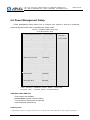
6.6 Power Management Setup
Power Management Setup allows you to configure your system to ensure an enhanced
power-saving effect when user is compliant with system mode.
Phoenix – AwardBIOS CMOS Setup Utility
Power Management Setup
Power Status After AC Fail
[Former Status]
ACPI Function
[Enabled]
Power Management
[User Define]
Video Off Method
[DPMS]
Video Off In Suspend
[Yes]
Suspend Type
[Stop Grant]
MODEM Use IRQ
▲
Item Help
Menu Level►
[3]
Suspend Mode
[Disabled]
HDD Power Down
[Disabled]
Soft-Off by PWR-BTTN
[Instant-Off]
Wake-Up by PCI card
[Enabled]
Power on by Ring
[Enabled]
Resume by Alarm
[Disabled]
X Date{Of Month} Alarm
0
X Time{hh:mm:ss} Alarm
0 :
0 :
0
** Reload Global Timer Events **
Primary IDE 0
[Disabled]
Primary IDE 1
[Disabled]
Secondary IDE 0
[Disabled]
Secondary IDE 0
[Disabled]
FDD,COM,LPT Port
[Disabled]
PCI PIRQ[A-D]#
↑↓→←:Move
Enter:Select
F5: Previous
Values
[Disabled]
+/-/PU/PD:Value
F6: Fail-Safe
F10:Save
Defaults
ESC:Exit
F1:General Help
F7: Optimized Defaults
PWR Status After PWR Fail
Three options are available:
Former Status (restore to former status)
Turn On (start up when power is restored)
Keep Off (remain powered off)
ACPI Function
* Specifications subject to change without notice. All brand names and trademark are their registered properties. *
15F-1, No. 186, Jian- Yi Road, Chung- Ho, Taipei 235, Taiwan R.O.C
Tel: + 886- 2- 8226 2881 Fax: + 886- 2- 8226 2883 www.aplex.com.tw
Page 32 of 49
This item allows you to enable/disable ACPI functions. Options are: Enabled and Disabled.
Power Management
This category allows you to select the type (or degree) of power saving and gives you direct
assess to the following modes:
1. Suspend Mode
2. HDD Power Down
Three options are available for Power Management, including two fixed modes.
User Define---It allows you to set each mode individually. When not disabled, each of the
ranges is from 1min to 15min.
Min Saving---Minimum power management. Suspend Mode=1hr and HDD Power
Down=15min.
Max Saving---Maximum power management. Suspend Mode=1min and HDD Power
Down=1min.
Video Off Method
This item determines the display type of monitor.
V/HSYNC+Blank
Blank Screen
This option turns off the vertical and horizontal synchronization ports
and writes blanks to the video buffer.
This option only writes blanks to the video buffer.
DPMS
This option controls initial display of power management signal.
Video Off In Suspend
This item determines the display type to be cleared by monitor.
Options are: Yes and No.
Suspend Type
This item is used to select suspend type. Options are: PWRON Suspend and Stop Grant.
Modem Use IRQ
This item determines the IRQ used by Modem.
Options are: 3, 4, 5, 67, 9, 10, 11 and NA.
Suspend Mode
When enabled, after the set time of system inactivity, all devices except the CPU will be shut
off. Options are: 1/2/4/8/12/20/30/40Min, 1Hour and Disabled.
HDD Power Down
When enabled and after the set time of system inactivity, the hard disk will be powered down
while all other devices remain active. Options are: 1/2/3/4/5/6/7/8/9/10/11/12/13/14/15Min and
Disabled.
Soft-Off by PWR-BTTN
* Specifications subject to change without notice. All brand names and trademark are their registered properties. *
15F-1, No. 186, Jian- Yi Road, Chung- Ho, Taipei 235, Taiwan R.O.C
Tel: + 886- 2- 8226 2881 Fax: + 886- 2- 8226 2883 www.aplex.com.tw
Page 33 of 49
Pressing the power button for more than 4 seconds forces the system to enter the Soft-Off
state. Options are: Delay4Sec and Instant-Off.
Wake-Up by PCI card
This item allows the system to be awakened by peripheral device connected to PCI card.
Options are: Enabled and Disabled.
Power On by Ring
When set to Disabled, the system will ignore any incoming Modem ring; when set to Enabled,
the system will be automatically started up in case of incoming Modem ring.
Resume by Alarm
This feature determines whether to power on the system at a desired time. When set to
Disabled, the feature is inactivated; when set to Enabled,date and time of power on can be set:
Date(of month) Alarm
Turn on the system at a specific time on each day or on a specific day
in a month. If set to 0,the system will be powered on once every day.
Time(hh:mm:ss) Alarm
automatically.
Set the time (hh:mm:ss) at which the system will be powered on
Note: You must restart the system after changing relevant settings, or the setting may not be
effective.
** Reload Global Timer Events **
This module contains six modules, all of which are provided with two options: Enable and Disable.
If set to Enable, the system will be awakened from sleep status when specific event occurs.
* Specifications subject to change without notice. All brand names and trademark are their registered properties. *
15F-1, No. 186, Jian- Yi Road, Chung- Ho, Taipei 235, Taiwan R.O.C
Tel: + 886- 2- 8226 2881 Fax: + 886- 2- 8226 2883 www.aplex.com.tw
Page 34 of 49
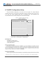
6.7 PnP/PCI Configurations Setup
This part describes configurations to be made on PCI bus system. PCI, namely Personal
Computer Interconnect, is a computer bus that allows I/O device to operate nearly as fast as CPU
in its own way. Some technical terms will be mentioned here. We recommend that
non-professional users not make changes from factory default settings.
Phoenix – AwardBIOS CMOS Setup Utility
PNP/PCI Configurations
Init Display First
[PCI Slot]
Reset Configuration Data
[Disabled]
Item Help
Menu Level
Resources Controlled By
[Auto(ESCD)]
X IRQ Resources
PCI/VGA Palette Snoop
Press Enter
[Disabled]
** PCI Express Relative Items **
Maximum Payload Size
[128]
↑↓→←:Move Enter:Select +/-/PU/PD:Value F10:Save ESC:Exit F1:General Help
F5: Previous Values
F6: Fail-Safe Defaults F7: Optimized Defaults
Init Display First
PCI Slot (PCI display device)
Onboard (Onboard display device)
PCiEx (PCIE device)
Reset Configuration Data
Normally, you should set this item to Disabled. If you have installed a new add-on and the
system reconfiguration has caused such a serious conflict that the operating system cannot boot
up, then select Enabled. This will reset the Extended System Configuration Data (ESCD) after
exiting from Setup. Options are: Enabled and Disabled.
Resource Controlled By
Award Plug and Play BIOS has the capacity to automatically configure all of the boot and Plug
* Specifications subject to change without notice. All brand names and trademark are their registered properties. *
15F-1, No. 186, Jian- Yi Road, Chung- Ho, Taipei 235, Taiwan R.O.C
Tel: + 886- 2- 8226 2881 Fax: + 886- 2- 8226 2883 www.aplex.com.tw
Page 35 of 49
and Play compatible devices. However, this capability means absolutely nothing unless you are
using a Plug and Play operating system such as Windows®95/98. If set to Manual, you may have
access into each submenu under this item (each submenu begins with "¾") and select specific
resource manually. Options are: Auto(ESCD) and Manual.
IRQ Resources
This item determines whether IRQ interrupt is assigned to Plug-and-Play device or
Non-Plug-and-Play ISA device.
PCI/VGA Palette Snoop
This item should be left Disabled. Options are: Enabled and Disabled.
** PCI Express Relative Items **
Maximum Payload Size
[128]
This item allows you to configure maximum payload size of TLP (Transition Layer Packet).
Options are: [128], [256], [512], [1024], [2048] and [4096].
* Specifications subject to change without notice. All brand names and trademark are their registered properties. *
15F-1, No. 186, Jian- Yi Road, Chung- Ho, Taipei 235, Taiwan R.O.C
Tel: + 886- 2- 8226 2881 Fax: + 886- 2- 8226 2883 www.aplex.com.tw
Page 36 of 49
6.8 PC Health Status
This item shows the current operation status of system.
Phoenix – AwardBIOS CMOS Setup Utility
PC Health Status
** Smart Fan Control(Thermal Cruise)**
CPU Fan Cruise Target
[65℃/149℉]
Fan Cruise Threshold
[5℃]
Item Help
Menu Level ►
** Onboard Health Sensor Status**
Current System Temperature
Current CPU Temperature
CPU Fan Speed
Vcore(V)
5Vcc (V)
Vbat (V)
5Vsb(V)
↑↓→←:Move
Enter:Select
F5: Previous
Values
+/-/PU/PD:Value
F10:Save
F6: Fail-Safe Defaults
ESC:Exit F1:General Help
F7: Optimized Defaults
This module mainly shows motherboard information on current operating voltage, CPU
temperature, system temperature and fan rotation speed. Refer to actual screen for name of each
column.
CPU Fan Cruise Target/Fan Cruise Threshold: this item determines the rotation condition of fan
when CPU temperature reaches preset value. Options of CPU Fan Cruise Target are: Disable,
55℃/131℉, 60℃/140℉ and 65℃/149℉; Options of Fan Cruise Threshold are ±2℃, ±3℃, ±4℃
and ±5℃.
For example, set CPU Fan Cruise Target to <65℃/149℉> and Fan Cruise Threshold to <±5℃>.
When CPU temperature rises to 70℃ (65℃+5℃), the fan will begin to rotate; when CPU
temperature drops to 60℃ (65℃-5℃), the fan will stop rotating.
* Specifications subject to change without notice. All brand names and trademark are their registered properties. *
15F-1, No. 186, Jian- Yi Road, Chung- Ho, Taipei 235, Taiwan R.O.C
Tel: + 886- 2- 8226 2881 Fax: + 886- 2- 8226 2883 www.aplex.com.tw
Page 37 of 49
6.9 Load Fail-Safe/Optimized Defaults
These two items allow users to load fail-safe or optimized defaults to restore BIOS. Optimized
defaults refer to the specific values set by motherboard manufacturer for optimized performance,
while fail-safe defaults stand for settings made by BIOS distributor for stable performance.
If you select Load Fail-Safe Defaults, the following information will be shown:
Phoenix – AwardBIOS CMOS Setup Utility
►Standard CMOS Features
Load Fail-Safe Defaults
►Advanced BIOS Features
Load Optimized Defaults
►Advanced Chipset Features
Set Administrator Password
►Integrated
Set User Password
Peripherals
►Power Management Setup
Save & Exit Setup
►PNP/PCI Configurations
Exit Without Saving
Load Fail-Safe Defaults (Y/N)?N
►PC Health Status
Esc : Quit
↑↓→← : Select Item
F10 : Save & Exit Setup
Load Fail-Safe Defaults
Press Y to load BIOS defaults for stable, but lower performance.
* Specifications subject to change without notice. All brand names and trademark are their registered properties. *
15F-1, No. 186, Jian- Yi Road, Chung- Ho, Taipei 235, Taiwan R.O.C
Tel: + 886- 2- 8226 2881 Fax: + 886- 2- 8226 2883 www.aplex.com.tw
Page 38 of 49
If you select Load Optimized Defaults, the following information will be shown:
Phoenix – AwardBIOS CMOS Setup Utility
►Standard CMOS Features
Load Fail-Safe Defaults
►Advanced BIOS Features
Load Optimized Defaults
►Advanced Chipset Features
Set
Administrator Password
►Integrated
Set
User
Peripherals
►Power Management Setup
Password
Save & Exit Setup
►PNP/PCI Configurations
Exit Without
Saving
Load Optimized Defaults
(Y/N)?N
►PC Health Status
Esc : Quit
↑↓→← : Select Item
F10 : Save & Exit Setup
Load Optimized Defaults
Press Y to load factory settings delivering optimized performance.
* Specifications subject to change without notice. All brand names and trademark are their registered properties. *
15F-1, No. 186, Jian- Yi Road, Chung- Ho, Taipei 235, Taiwan R.O.C
Tel: + 886- 2- 8226 2881 Fax: + 886- 2- 8226 2883 www.aplex.com.tw
Page 39 of 49
6.10 Set Administrator/User Password
When selecting this feature, the following information will be shown:
Phoenix – AwardBIOS CMOS Setup Utility
►Standard CMOS Features
Load Fail-Safe Defaults
►Advanced BIOS Features
Load Optimized Defaults
►Advanced Chipset Features
Set Administrator Password
►Integrated
Set User Password
Peripherals
►Power Management Setup
Save & Exit Setup
►PNP/PCI Configurations
Enter Password:
Exit Without Saving
►PC Health Status
Esc : Quit
↑↓→← : Select Item
F10 : Save & Exit Setup
Change/Set/Disable Password
Type the password with up to 8 characters and then press ½Enter¾ key. This will clear all
previously typed CMOS passwords. You will be requested to confirm the password. Type the
password again and press ½Enter¾ key. You may press ½Esc¾ key to abandon password entry
operation.
To clear the password, just press ½Enter¾ key when password input window pops up. A
confirmation message will be shown on the screen as to whether the password will be disabled.
You will have direct access to BIOS setup without typing any password after system reboot once
the password is disabled.
Once the password feature is used, you will be requested to type the password each time you
enter BIOS setup. This will prevent unauthorized persons from changing your system
configurations.
Also, the feature is capable of requesting users to enter the password prior to system boot to
control unauthorized access to your computer. Users may enable the feature in Security Option of
Advanced BIOS Features. If Security Option is set to System, you will be requested to enter the
password before system boot and when entering BIOS setup; if Security Option is set to Setup,
you will be requested for password for entering BIOS setup.
6.11 Save & Exit Setup
When selecting this item, the following information will be shown:
Phoenix – AwardBIOS CMOS Setup Utility
* Specifications subject to change without notice. All brand names and trademark are their registered properties. *
15F-1, No. 186, Jian- Yi Road, Chung- Ho, Taipei 235, Taiwan R.O.C
Tel: + 886- 2- 8226 2881 Fax: + 886- 2- 8226 2883 www.aplex.com.tw
►Standard CMOS Features
Load Fail-Safe Defaults
►Advanced BIOS Features
Load Optimized Defaults
►Advanced Chipset Features
Set Administrator Password
►Integrated
Set User Password
Peripherals
►Power Management Setup
Save & Exit Setup
►PNP/PCI Configurations
Exit Without Saving
Save to CMOS and Exit(Y/N) ?
►PC Health Status
Esc : Quit
Page 40 of 49
Y
↑↓→← : Select Item
F10 : Save & Exit Setup
Save Data to CMOS
Press Enter key to save the changes and exit from BIOS setup.
6.12 Exit Without Saving
When selecting this item, the following information will be shown:
Phoenix – AwardBIOS CMOS Setup Utility
►Standard CMOS Features
Load Fail-Safe Defaults
►Advanced BIOS Features
Load Optimized Defaults
►Advanced Chipset Features
Set Administrator Password
►Integrated
Set User Password
Peripherals
►Power Management Setup
Save & Exit Setup
►PNP/PCI Configurations
Exit Without Saving
Quit Without Saving (Y/N) ?
►PC Health Status
Esc : Quit
N
↑↓→← : Select Item
F10 : Save & Exit Setup
Save Data to CMOS
Press Y and then Enter key to exit from BIOS setup without saving the changes.
7 Examples of GPIO Programming
* Specifications subject to change without notice. All brand names and trademark are their registered properties. *
15F-1, No. 186, Jian- Yi Road, Chung- Ho, Taipei 235, Taiwan R.O.C
Tel: + 886- 2- 8226 2881 Fax: + 886- 2- 8226 2883 www.aplex.com.tw
Page 41 of 49
7.1 SuperIO Model: Winbond W83627UHG
•
•
GPIO OUT use GP 60~63
GPIO IN use GP 20~23
7.2 W83627UHG Access index port: 4Eh/4Fh
•
•
Index Address Port: 4Eh
Index Data Port: 4Fh
7.3 Configure GPIO register sequence
1.
2.
3.
4.
5.
6.
7.
8.
Enter the extended function mode
Select logic device number 8
Activate the logic device GPIO Port 6
Configure GPIO Port 6 register
Select logic device number 9
Activate the logic device GPIO Port 2
Configure GPIO Port 2 register
Exit the extended function mode
7.4 Read/write GPIO sequence
1.
2.
3.
4.
Enter the extended function mode
Select logic device number
Read/write GPIO register value
Exit the extended function mode
7.5 Software programming example
•
Enter the extended function mode
Writing 87h to index address port twice will enter the extended function mode.
Example x86 assembly code:
mov
dx, 4Eh
mov
al, 87h
out
dx, al
out
dx, al
Example C code:
* Specifications subject to change without notice. All brand names and trademark are their registered properties. *
15F-1, No. 186, Jian- Yi Road, Chung- Ho, Taipei 235, Taiwan R.O.C
Tel: + 886- 2- 8226 2881 Fax: + 886- 2- 8226 2883 www.aplex.com.tw
Page 42 of 49
outportb(0x4E, 0x87);
outportb(0x4E, 0x87);
•
Exit the extended function mode
Writing AAh to index address port will exit the extended function mode.
Example x86 assembly code:
mov
dx, 4Eh
mov
al, 0AAh
out
dx, al
Example C code:
outportb(0x4E, 0xAA);
•
Select logic device number
Example x86 assembly code:
mov
dx, 4Eh
mov
al, 007h
;LDN selection register
out
dx, al
mov
dx, 4Fh
mov
al, 008h
;Select LDN=8, GPIO Port6
;or Select LDN9, GPIO Port2
out
dx, al
Example C code:
outportb(0x4E, 0x07);
//LDN selection register
outportb(0x4F, 0x08); //Select LDN=8, GPIO Port6
or
outportb(0x4E, 0x07);
//LDN selection register
outportb(0x4F, 0x09); //Select LDN=9, GPIO Port2
•
Activate the logic device
Example x86 assembly code:
mov
dx, 4Eh
mov
al, 030h
;Logic device activation control reg.
out
dx, al
mov
dx, 4Fh
in
al, dx
or
al, 004h
;Set bit2 to enable GPIO Port6 if LDN=8
or
al, 002h
;Set bit1 to enable GPIO Port2 if LDN=9
out
dx, al
Example C code:
outportb(0x4E, 0x30);
//Logic device activation control
outportb(0x4F, (inportb(0x4F)|0x2));
* Specifications subject to change without notice. All brand names and trademark are their registered properties. *
15F-1, No. 186, Jian- Yi Road, Chung- Ho, Taipei 235, Taiwan R.O.C
Tel: + 886- 2- 8226 2881 Fax: + 886- 2- 8226 2883 www.aplex.com.tw
Page 43 of 49
//Set bit[1] to enable GPIO Port2 if LDN=9
Or
outportb(0x4E, 0x30);
//Logic device activation control
outportb(0x4F, (inportb(0x4F)|0x4));
//Set bit[2] to enable GPIO Port6 if LDN=8
•
Configure GPIO register
Example x86 assembly code:
mov
dx, 4Eh
mov
al, 0E6h
;GPIO inversion reg.
out
dx, al
mov
dx, 4Fh
mov
al, 000h
;0 – normal, 1 - inverted
out
dx, al
mov
mov
out
mov
mov
dx, 4Eh
al, 0E4h
dx, al
dx, 4Fh
al, 0FFh
out
dx, al
;GPIO I/O selection reg.
;0 – Output, 1 – Input
;or mov al, 0F0h to set output
Example C code:
outportb(0x4E, 0xE6);
//GPIO I/O selection reg.
outportb(0x4F, 0x0); //0 – normal, 1 - inverted
outportb(0x4E, 0xE4);
outportb(0x4F, 0xFF);
//GPIO inversion reg.
//0 – Output, 1 - Input
outportb(0x4E, 0xE4);
outportb(0x4F, 0xF0);
//GPIO inversion reg.
//0 – Output, 1 - Input
or
•
Read GPIO value
Example x86 assembly code:
mov
dx, 4Eh
mov
al, 0E5h
;GPIO data reg.
out
dx, al
mov
dx, 4Fh
in
al, dx
;Bit[3::0] = GPI[3::0] value
Example C code:
outportb(0x4E, 0xE5);
//GPIO data reg.
* Specifications subject to change without notice. All brand names and trademark are their registered properties. *
15F-1, No. 186, Jian- Yi Road, Chung- Ho, Taipei 235, Taiwan R.O.C
Tel: + 886- 2- 8226 2881 Fax: + 886- 2- 8226 2883 www.aplex.com.tw
GP = inportb(0x4F);
•
Page 44 of 49
//Bit[3::0] = GPI[3::0]
Write GPIO value
Example x86 assembly code:
;Set GPO62
mov
dx, 4Eh
mov
al, 0E5h
out
dx, al
mov
dx, 4Fh
in
al, dx
or
al, 00000100b
out
dx, al
;GPIO data reg.
;Bit2 = GPO62
;Clear GPO62
mov
dx, 4Eh
mov
al, 0E5h
;GPIO data reg.
out
dx, al
mov
dx, 4Fh
in
al, dx
and
al, not 00000100b
out
dx, al
Example C code:
//Set GPO62
outportb(0x4E, 0xE5);
Outportb(0x4F, (inportb(0x4F)|0x4));
//GPIO data reg.
//Set Bit[2]
//Clear GPO62
outportb(0x4E, 0xE5);
//GPIO data reg.
Outportb(0x4F, (inportb(0x4F)&0xFB)); //Clear Bit[2]
The followings are C language source code:
#include "stdio.h"
#include "conio.h"
//Super I/O index access port
#define INDEXP
0x4E
#define DATAP
0x4F
//Enter super I/O programming mode
#define ENTERPRG {
\
* Specifications subject to change without notice. All brand names and trademark are their registered properties. *
15F-1, No. 186, Jian- Yi Road, Chung- Ho, Taipei 235, Taiwan R.O.C
Tel: + 886- 2- 8226 2881 Fax: + 886- 2- 8226 2883 www.aplex.com.tw
Page 45 of 49
outportb(INDEXP, 0x87); \
outportb(INDEXP, 0x87);}
//Super I/O index write
#define WRITEREG(reg,val) { \
outportb(INDEXP, reg);
\
outportb(DATAP, val);}
//Exit super I/O programming mode
#define EXITPRG {
\
outportb(INDEXP, 0xAA);}
//Select logic device number
#define SELETDEV(ldn) {
outportb(INDEXP, 7); \
outportb(DATAP, ldn); }
\
//Initialize the GPIO port2
int InitGP2() {
//Start the super I/O chip programming
ENTERPRG
//Select the logical device 9, GP2
SELETDEV(9)
//Activate GP1
WRITEREG(0x30, (inportb(0x30)|0x2))
WRITEREG(0xE6, 0x0)
WRITEREG(0xE4, 0xFF)
//Exit the super I/O chip programming
EXITPRG
return 0;
}
//Initialize the GPIO port6
int InitGP6() {
//Start the super I/O chip programming
ENTERPRG
* Specifications subject to change without notice. All brand names and trademark are their registered properties. *
15F-1, No. 186, Jian- Yi Road, Chung- Ho, Taipei 235, Taiwan R.O.C
Tel: + 886- 2- 8226 2881 Fax: + 886- 2- 8226 2883 www.aplex.com.tw
Page 46 of 49
//Select the logical device 8, GP6
SELETDEV(8)
//Activate GP1
WRITEREG(0x30, (inportb(0x30)|0x4))
WRITEREG(0xE6, 0x0)
WRITEREG(0xE4, 0xF0)
//Exit the super I/O chip programming
EXITPRG
return 0;
}
//Read GPIO Port2
unsigned char ReadGP2() {
unsigned char cGP2;
//Start the super I/O chip programming
ENTERPRG
//Select the logical device 9, GP2
SELETDEV(9)
//Read GPIO Value
outportb(INDEXP, 0xE5);
cGP2 = inportb(DATAP);
cGP2 = cGP2 & 0xF;
//Exit the super I/O chip programming
EXITPRG
return cGP2;
}
//Write GPIO Port6
int WriteGP6(unsigned char cGP6) {
//Start the super I/O chip programming
ENTERPRG
* Specifications subject to change without notice. All brand names and trademark are their registered properties. *
15F-1, No. 186, Jian- Yi Road, Chung- Ho, Taipei 235, Taiwan R.O.C
Tel: + 886- 2- 8226 2881 Fax: + 886- 2- 8226 2883 www.aplex.com.tw
Page 47 of 49
//Select the logical device 8, GP6
SELETDEV(8)
//Write GP1 value
WRITEREG(0xE5, cGP6)
//Exit the super I/O chip programming
EXITPRG
return 0;
}
int main() {
unsigned char cGP;
//Initialize the GPIO port
InitGP2();
InitGP6();
//Read GPIO Port 2
cGP = ReadGP2();
printf("\nRead GPIO Port 2 Status: %X", cGP);
//Write GPIO Port 6
WriteGP6(cGP);
printf("\nSet GPIO Port 6 Status: %X", cGP);
return 0;
}
8 Watchdog Source Code
#include <windows.h>
#include <stdio.h>
#include "winio.h"
#define WDT_EFER 0x4E
#define WDT_EFIR 0x4E
#define WDT_EFDR 0x4F
#define WDT_EFCR 0x23
* Specifications subject to change without notice. All brand names and trademark are their registered properties. *
15F-1, No. 186, Jian- Yi Road, Chung- Ho, Taipei 235, Taiwan R.O.C
Tel: + 886- 2- 8226 2881 Fax: + 886- 2- 8226 2883 www.aplex.com.tw
Page 48 of 49
void enable_wd_1sec();
void disable_wd();
int main()
{
// Call InitializeWinIo to initialize the WinIo library.
bool bResult;
bResult = InitializeWinIo();
if (bResult)
{
enable_wd_1sec();
while(1)
{
;
}
}
else
{
printf("Error during initialization of WinIo.\n");
exit(1);
}
ShutdownWinIo();
return 0;
}
//===============================================
// Function : Enable Watch Dog Timer
// Enter
: None
// Return : None
//===============================================
void enable_wd_1sec()
{
SetPortVal((DWORD)WDT_EFER, 0x87,0);
SetPortVal((DWORD)WDT_EFER, 0x87,0);
SetPortVal((DWORD)WDT_EFER, 0x07,1);
SetPortVal((DWORD)WDT_EFDR, 0x08,1);
* Specifications subject to change without notice. All brand names and trademark are their registered properties. *
15F-1, No. 186, Jian- Yi Road, Chung- Ho, Taipei 235, Taiwan R.O.C
Tel: + 886- 2- 8226 2881 Fax: + 886- 2- 8226 2883 www.aplex.com.tw
Page 49 of 49
SetPortVal((DWORD)WDT_EFER, 0x30,1);
SetPortVal((DWORD)WDT_EFDR, 0x01,1);
SetPortVal((DWORD)WDT_EFER, 0xF5,1);
SetPortVal((DWORD)WDT_EFDR, 0x00,1);
SetPortVal((DWORD)WDT_EFER, 0xF6,1);
SetPortVal((DWORD)WDT_EFDR, 0x06,1);
SetPortVal((DWORD)WDT_EFER, 0xAA,1);
SetPortVal((DWORD)WDT_EFCR, 0x00,1);
}
void disable_wd()
{
SetPortVal((DWORD)WDT_EFER, 0x87,0);
SetPortVal((DWORD)WDT_EFER, 0x87,0);
SetPortVal((DWORD)WDT_EFER, 0x07,1);
SetPortVal((DWORD)WDT_EFDR, 0x08,1);
SetPortVal((DWORD)WDT_EFER, 0x30,1);
SetPortVal((DWORD)WDT_EFDR, 0x00,1);
SetPortVal((DWORD)WDT_EFER, 0xF6,1);
SetPortVal((DWORD)WDT_EFDR, 0x00,1);
SetPortVal((DWORD)WDT_EFER, 0xAA,1);
SetPortVal((DWORD)WDT_EFCR, 0x00,1);
}
* Specifications subject to change without notice. All brand names and trademark are their registered properties. *