1
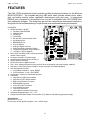
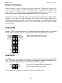
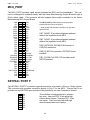
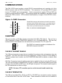
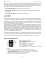
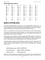
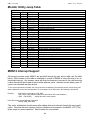
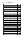
CML-12C32
Development Board for Freescale MC9S12C32
Axiom Manufacturing • 2813 Industrial Lane • Garland, TX 75041
Email: [email protected] Web: http://www.axman.com
C M L - 1 2 C 3 2
J U L Y
2 6 ,
2 0 0 4
CONTENTS
CAUTIONARY NOTES .........................................................................................4
TERMINOLOGY...................................................................................................................4
FEATURES ...........................................................................................................5
GETTING STARTED.............................................................................................6
REFERENCE DOCUMENTATION.......................................................................................6
INSTALLING THE SOFTWARE...........................................................................................7
BOARD STARTUP...............................................................................................................7
SUPPORT SOFTWARE.......................................................................................................8
SOFTWARE DEVELOPMENT.............................................................................................8
TUTORIAL.............................................................................................................8
CREATING SOURCE CODE ...............................................................................................8
ASSEMBLING SOURCE CODE ..........................................................................................9
EXECUTING APPLICATIONS ...........................................................................................10
OPTIONS and JUMPERS ...................................................................................11
MEM_EN............................................................................................................................11
MODE ................................................................................................................................11
NO_AUTO..........................................................................................................................11
RANGE ..............................................................................................................................11
JP1 POT_OUT_SEL ..........................................................................................................11
J2 LCD EXPANSION .........................................................................................................12
VRH_EN/VRL_EN..............................................................................................................12
CUT-TRACE OPTIONS .....................................................................................................12
PORTS AND CONNECTORS .............................................................................12
POWER CONNECTORS ...................................................................................................13
BUS_PORT........................................................................................................................13
BDM PORT ........................................................................................................................13
MCU_PORT .......................................................................................................................14
KEYPAD / PORT P ............................................................................................................14
COMMUNICATIONS..........................................................................................................15
Figure 1: COM1 Connector ................................................................................................15
CAN PORT.........................................................................................................................15
LCD PORT .........................................................................................................................16
Figure 2: LCD Connector ...................................................................................................16
J2 - LCD EXPANSION ......................................................................................................17
TEST POINTS....................................................................................................................17
TROUBLESHOOTING ........................................................................................17
TIPS AND SUGGESTIONS ...............................................................................................18
Utilities ...............................................................................................................................18
Code Execution..................................................................................................................19
LCD Codes .........................................................................................................19
LCD COMMAND CODES ..................................................................................................19
LCD CHARACTER CODES ...............................................................................................20
2
C M L - 1 2 C 3 2
J U L Y
2 6 ,
2 0 0 4
MON12 OPERATION ..........................................................................................20
AUTOSTART .....................................................................................................................21
MON12 MEMORY MAP .....................................................................................................21
MON12 MONITOR COMMANDS.......................................................................................22
MONITOR UTILITY JUMP TABLE.....................................................................................23
MON12 INTERRUPT SUPPORT .......................................................................................23
MONITOR INTERRUPT VECTOR TABLE.........................................................................24
BDM OPERATION ..............................................................................................25
APPENDIX A.......................................................................................................27
BILL OF MATERIALS ........................................................................................................27
3
C M L - 1 2 C 3 2
J U L Y
2 6 ,
2 0 0 4
CAUTIONARY NOTES
1) Electrostatic Discharge (ESD) prevention measures should be used when handling this
product. ESD damage is not a warranty repair item.
2) Axiom Manufacturing does not assume any liability arising out of the application or use of
any product or circuit described herein; neither does it convey any license under patent
rights or the rights of others.
3) EMC Information on the CML-12C32 development board:
a) This product as shipped from the factory with associated power supplies and cables, has
been verified to meet with requirements of CE and the FCC as a CLASS B product.
b) This product is designed and intended for use as a development platform for hardware
or software in an educational or professional laboratory.
c) In a domestic environment, this product may cause radio interference in which case the
user may be required to take adequate prevention measures.
d) Attaching additional wiring to this product or modifying the products operation from the
factory default as shipped may effect its performance and cause interference with nearby
electronic equipment. If such interference is detected, suitable mitigating measures
should be taken.
Terminology
This development board uses option selection jumpers and cut-traces to setup default configuration. Terminology for application of the option jumpers is as follows:
Jumper – a plastic shunt that connects 2 terminals electrically
Jumper on, in, or installed - jumper is installed such that 2 pins are connected together
Jumper off, out, or idle - jumper is installed on 1 pin only. It is recommended that jumpers be idled by installing on 1 pin so they will not be lost.
Cut-Trace – a circuit trace connection between component pads. The circuit trace may
be cut using a razor knife to break the default connection. To reconnect the circuit,
simply install a suitably sized 0-ohm resistor or attach a wire across the pads.
4
C M L - 1 2 C 3 2
J U L Y
2 6 ,
2 0 0 4
FEATURES
The CML-12C32 development board provides a stable development platform for the Motorola
MC9S12C32 MCU. The included wall plug, DB9 serial cable, sample software tools, examples, and debug monitor makes application development quick and easy. A background
DEBUG port is provided for development tool use and is compatible with HCS12 BDM interface cables and software. This board may be used as a stand-alone development platform or
along with the Axiom Manufacturing Project Board as an enhanced learning environment.
FEATURES:
♦ MC9S12C32 MCU, 48 QFP
♦ 32K Byte Flash EEPROM
♦ 2K Bytes RAM
♦ 60 I/O lines
♦ Timer/PWM
♦ SCI and SPI Communications Ports
♦ Key Wake-up Port
♦ BDM DEBUG Port
♦ CAN 2.0 Module
♦ Analog-to-Digital Converter
♦ 8 Mhz Internal Bus Operation Default
♦ 16 MHz Bus Operation using internal PLL
♦ +3.3VDC to +5VDC operation
♦ MCU_PORT and BUS_PORT connectors provide
access to MCU signals
♦ On-board, regulated +5V power supply
♦ Optional power output through connector J1
♦ 16 MHz Ceramic Oscillator
♦ RS-232 Serial Port w/ DB9 Connector
♦ 8-Ch, 10-bit, Analog-to-Digital Converter with full rail-to-rail operation and external trigger capability
♦ 8-Channel, 16-bit Timer with Input Capture, Output Compare, and PWM capabilities
♦ User Components Provided
♦ 3 Push Button Switches: 2 User, RESET
♦ 4 LED Indicators: 2 User, VDD, RESET
♦ Configuration Jumpers to setup board operation
♦ Connectors
♦ 60-pin MCU_PORT Socket Header
♦ 28-pin BUS_PORT Socket Header
♦ DB9 Communications Connector
♦ DEBUG BDM Connector
♦ 4-pin CAN_PORT Connector
♦ 8-pin Keypad Connector
♦ 14-pin LCD Connector
♦ 2.0mm Barrel Connector Power Input
♦ Solderless Breadboard Area, 3.5” x 1.75”
♦ Supplied with DB9 Serial Cable, Documentation (CD), Manual, and Wall plug type power supply.
Specifications:
Board Size 4.5” x 5.0”
Power Input: +9VDC @ 200 mA typical, +6 to +16VDC range
5
C M L - 1 2 C 3 2
J U L Y
2 6 ,
2 0 0 4
GETTING STARTED
The CML-12C32 single board computer is a fully assembled, fully functional development
board for the Motorola MC9S12C32 microcontroller. The board comes with a serial cable,
power supply, and installed binary monitor for stand-alone operation. Support software for this
development board is provided for Windows 95/98/NT/2000/XP operating systems.
Users should be familiar with the hardware and software operation of the target MCU. Refer to
the MC9S12C32 User Manual and Reference Manual for details on MCU operation. The
board’s purpose is to promote the features of the MC9S12C32 and to assist the user in quickly
developing an application in a known working environment. Users should be familiar with
memory mapping, memory types, and embedded software design for quick, successful, application development. The user should also be familiar with the various operation modes of the
MCU.
NOTE: With the MCU in expanded mode, the user can not access to Port A, Port B, or Port E.
Application development may be performed by using the embedded binary monitor, or any
compatible MCU BDM cable with supporting host software. The included monitor provides an
effective and low-cost debug method. Note that when a BDM cable is used for debugging, the
BDM pod should be powered from an external supply.
A debug monitor is loaded in the MC9S12C32 internal flash memory and uses some MCU resources for operation. User application may be executed by loading the program start address
into the Reset Vector (0xF7FE, 0xF7FF) and loading the program into device Flash Memory.
The monitor remains in protected flash memory for future use if needed.
Refer to the MC9S12C32 Reference Manual for details on using a BDM pod with the CSM12C32 board. Refer to Appendix A for a pin-out of the BDM_PORT connector.
Reference Documentation
Reference documents are provided on the support CD in Acrobat Reader format. More information can be found in the Application Notes section of the Motorola Web site.
CML12C32_SCH_C.pdf
CML12C32_UG.pdf
CML12_SerMon.phy
CML12_SerMon.sx
9S12C32DGV1.pdf
9S12C32_ZIP.zip
AN2548.pdf
CML-12C32 Board Schematic Rev B
CML-12C32 User Guide (this document)
Serial Monitor Physical Record Object Code File
Serial Monitor S-Record Object Code File
MC9S12C32 Device User Guide
Zip file containing Device Block User Guides
Serial Monitor Program for HCS12 MCU’s
6
C M L - 1 2 C 3 2
J U L Y
2 6 ,
2 0 0 4
Installing the Software
The following steps will help the user to get started quickly and verify the board is working
properly.
1. Insert the Axiom 68HC12 support CD in your PC. If the setup program does not start,
execute the file <D:>\SETUP.EXE where <D:> is the drive letter of the CD drive.
2. Follow the instructions on screen to install the support software onto your PC. At minimum, AxIDE for Windows software should be installed.
3. To compile designs correctly, the target MCU must be specified within the AxIDE utility.
Select the “CML12C32 MCU target to correctly compile application designs.
NOTE: If “CML12C32” is not available, select the "CML12SDP256" MCU target.
Board Startup
Follow these steps to connect and power-on the board for default Monitor operation. The following steps assume use of the AxIDE utility (installed in the previous section). If a different
terminal program is used, ensure the communications port settings are set to: 9600 bps, No
parity, 8 data bits, and 1 stop bit.
1. Set the CML-12C32 board Option jumpers to default positions:
MEM-EN
NOAUTO
RANGE
ON
ON
don’t care
2. Connect one end of the supplied 9-pin serial cable to an available serial COM port on your
PC. Connect the other end of the cable to the COM1 port on the CML-12C32 board.
3. Open the AxIDE program.
4. Apply power to the board by connecting the power adapter that came with the system.
5. If configured properly, the message “PRESS KEY TO START MONITOR…” should display in the terminal window. Press the SPACEBAR and you should see:
Axiom
MON12
HC12
Type "Help" for commands…
Monitor
/
Debugger
V32.0
> _
6. The board is now ready to use! If this message prompt is not displayed, or if the display is
meaningless, refer to the TROUBLESHOOTING section at the end of this manual.
7
C M L - 1 2 C 3 2
J U L Y
2 6 ,
2 0 0 4
Support Software
There are many programs and documents on the included HC12 support CD that support the
CML-12C32 board. Install any desired applications from the CD main menu. Documentation
and example code may be copied directly from the CD.
AT minimum, the AxIDE terminal program should be installed. AxIDE provides a simple terminal interface between the host PC and the CML-12C32 development board. The program integrates an assembler, a flash programming utility, and a serial communication interface.
Also on the disk are free assemblers AS12 and MCU-EZ, the open source GNU C/C++ compiler tools for HC11/12, example source code, and other useful software. The introductory tutorial in this manual uses the free AS12 assembler integrated into the AxIDE program. This is
a simple assembler with limited capability. For a more powerful assembly tool, install the Motorola MCUez program from the CD.
Software Development
Software development on the CML-12C32 can be performed using either the embedded
monitor installed in the MCU internal FLASH, a third party debugger (Debug12, NoICE,
CodeWarrior, etc.) or a Background Debug Module (BDM) connected to the BDM PORT connector. Any of these tools can be used to assist in creating and debugging programs stored in
RAM (see Memory Map).
After satisfactory operation running under a debugger, the program can be written to internal
Flash Memory using the included programming utilities. The embedded monitor relocates the
interrupt vectors to RAM memory and provides an AUTOSTART feature to launch applications.
Loaded programs will then run automatically whenever the board is powered or RESET is applied.
TUTORIAL
This section was written to help the user get started developing software for the CML-12C32
development board. Read rest of this User’s Guide and additional documentation on the CD
for further information.
The following sections illustrate the complete development cycle for a simple "hello world" program. This program sends the text string "Hello World" to the serial port. The following example assumes the use of the AxIDE interface and the free assembler, AS12. Both utilities are
provided on the software CD.
Creating Source Code
Source code may be created using any ASCII text editor, such as WindowsTM Notepad. Note,
the source file must be simple ASCII text with no document formatting. After the source code
is written and saved, the file must be assembled to a Motorola S-Record (hex) format. This
type of output file usually has a .MOT, .HEX or .S19 file extension and is in a format that can
8
C M L - 1 2 C 3 2
J U L Y
2 6 ,
2 0 0 4
be read by, and programmed into the development board MCU.
It is important the user understand the development board's use of addressing and memory
when writing source code. Program code must be located at a valid address. For instance, in
debug mode, program code should be located in external RAM. In assembly language, the
ORG statement is used to locate user code in memory. All program code following an ORG
statement will begin at the specified memory location, for example: ORG $4000; locates the
code starting at address $4000. DATA (or variables) must be located in RAM unused by program code, for example: ORG $800.
In debug mode the debugger utility handles all MCU configuration setup; CPU and STACK initialization, and interrupt vectors (reset, timers, etc) setup. When program development is
complete, the application code must be modified to include CPU and STACK initialization, and
interrupt vector setup. CPU setup initializes the bus frequency, bus mode, and Flash memory
programming clock rates, and other constraints. STACK setup initializes the stack pointer.
The STACK should be set to the top of available RAM, by default $0FFF. In assembly the appropriate instruction is LDS #$0FFF. The RESET vector must also be written to the User Reset Vector.
The installed monitor is not required when using a BDM interface. The BDM tool may have the
capability to erase and program the FLASH memory. If this is the case, MCU resources used
by the monitor are available to the user. The embedded monitor S-record (.S19) is provided
on the support CD to program into flash if required. The BDM allows locating programs in
memory and using monitor reserved resources.
A look at the example programs on the disk will make this clearer. If using a compiler instead
of an assembler, consult the compiler documentation for methods used to locate (MAP) code,
data, and stack.
Assembling Source Code
The example program HELLO.ASM is provided under the <D:>\EXAMPLES\CML12 directory
on the CD. If the AxIDE utility is installed, the example program can also be found in the
AxIDE3\EXAMPLE\HC12\D256 directory. You must use the example program for the target
MCU type. For this example, use the example code in the \D256 directory.
The AxIDE utility software provided with this board contains a simple interface to the AS12 assembler Follow these steps to assembly the test program;
1. In the AxIDE window, click the BUILD button. This will open an Assemble Code window.
2. In the Assemble Code window, click the BROWSE button to browse to the program file to
assemble. For this example, select the file AxIDE3\EXAMPLE\HC12\D256\Hello.asm.
3. In the Assemble Code window, select the OK button to assemble the test program.
NOTE: The correct target MCU must be selected from the pull-down selection or the file will
not assemble correctly. DO NOT use long path or file names (> 8 characters). AS12 is a DOS
based tool and does not understand long path or file name. The program code may not assemble correctly.
9
C M L - 1 2 C 3 2
J U L Y
2 6 ,
2 0 0 4
If the source code assembles with no fatal errors 2 output files are created:
HELLO.S19
a Motorola S-Record file that can be programmed into memory.
HELLO.LST
a common listing file which provides physical address information
with resulting opcode and operand information. Warnings and error
messages are provided with a summary at the end of this file.
The list (.LST) file is especially helpful when debugging. The list file shows each error encountered and its location. Fatal errors prevent the output files from being generated. A count
of errors and warnings encountered can be found at the end of the list file.
Executing Applications
After creating a Motorola S-Record file, "upload" it to the development board for a test run.
The provided example “HELLO.ASM” was created to run from external RAM. The embedded
monitor can be used to test the program without programming it into Flash.
If not already completed, verify that the CML-12C32 board is connected and operating properly
by following the steps under “GETTING STARTED” until you see the monitor prompt, then follow these steps to run your program:
1. Press and release the RESET button on the CML-12C32 board. You should see the
PRESS ANY KEY message. Press the letter E key to get the monitor prompt.
2. Type LOAD ↵
This will prepare the embedded monitor to receive a program.
3. Click the Upload button and when prompted for a file name select your assembled program file in S-record format that was created in the previous section called: HELLO.S19.
Your program will be sent to the board through the serial port.
4. When finished loading the > prompt returns. Type: GO 4000 ↵. This starts program
execution at address 4000h. This is the starting address of the test program.
5. If everything is working properly, the message “Hello World” will echo back to the terminal
screen. Press RESET to return to the monitor.
6. If this message is not displayed on the terminal monitor, see the TROUBLESHOOTING
section of this manual
The “Hello World” program can be easily modified to display other strings or perform other
functions. Procedures for assembling, uploading, and executing program code are the same.
The embedded monitor many features to support program debug such as breakpoints, memory dump and modify, and simple program trace (redirect of the PC is not followed). Type
HELP at the monitor prompt for a listing of commands or consult the monitor documentation on
the disk for more information.
10
C M L - 1 2 C 3 2
J U L Y
2 6 ,
2 0 0 4
OPTIONS and JUMPERS
MEM_EN
The MEM_EN option jumper is installed by default and enables access to the external SRAM
memory when the MCU is configured for expanded mode operation. Removing the MEM_EN
option jumper disables external memory access.
MODE
The MODE option jumper is not installed on the CML-12C32 board and is hard connected by
circuit copper trace for Single-chip Mode operation of the CPU. MODA and MODB signals are
terminated by this option. Single Chip Mode operation is selected by default because the MCU
internal flash memory provides the only nonvolatile program memory on the board. All other
Modes can be enabled under software control from this mode of operation.
The MODE option jumper may be installed by the user by cutting the circuit trace and installing
a 2-position header with a shunt jumper. With the shunt jumper removed, the Reset mode will
then be Normal Expanded Wide. External non-volatile memory must be added to support this
functionality.
NO_AUTO
The NO_AUTO jumper prevents the MCU from executing program code at start up. Enable
automatic program execution by removing this jumper. To use the auto-start feature, the correct reset vector must be loaded to point to the location of program code.
RANGE
The CML-12C32 board provides a 20-turn, 10 kΩ, precision, potentiometer (POT) with adjustable range for use in circuit prototyping. The RANGE jumper selection of output range. Installing the option jumper provides the full range output from the POT from GND to VDD. Removing the option jumper places a 10k Ω resistor in series with the POT limiting output from
GND to ½ VDD.
JP1 POT_OUT_SEL
The JP1 option jumper selects where the destination of the potentiometer. The output of the
POT may be routed to a MCU analog port input (PAD7/AN7) or to the BUS_PORT header for
use on prototyping area.
11
C M L - 1 2 C 3 2
J U L Y
1
2
3
PAD7/AN7 (U1-58)
POT
MCU_PORT-27
2 6 ,
2 0 0 4
Shunt across pins 1-2 to route POT output to the MCU.
Shunt across pins 2-3 to route POT output to the
MCU_PORT pin 27.
J2 LCD EXPANSION
The J2 option header is explained in detail in the LCD_PANEL section below.
VRH_EN/VRL_EN
The VRH_EN and VRL_EN option headers are not installed on the CML-12C32 board and are
hard connected by circuit copper trace for default operation. These jumpers provide voltage
reference inputs for the MCU analog to digital converter block. Alternative upper and lower
reference voltages may be used by cutting the circuit trace and attaching a jumper wire to the
appropriate pin of VRH_EN and VRL_EN. After cutting the circuit trace, use of default reference voltages will require installing a 2-position header with a shunt jumper. Refer to the PCB
schematic for further details.
CUT-TRACE OPTIONS
A CUT-TRACE is a component pad connected by a circuit trace. The cut-trace sets up default
board operation. Cut-trace options allow the user to disconnect or modify on-board resource
configurations. The cut-trace pad also allow for reestablishing the connection by installing
surface mount, 1206 size, 0-ohm resistors or mod-wire. Normal operation of the development
board generally does not require manipulating any CUT_TRACE option.
CT1: Removed – Not Used.
CT2: Removed – Not Used.
CT3: MCU Port M1/TXCAN signal to the CAN Controller Interface.
CT4: MCU Port M0/RXCAN signal to the CAN Controller Interface.
CT5: CAN Port Transceiver Enable. The default connections enables device output constantly. This connection enables the CAN Port transceiver output to the CAN bus. To
use slew rate control or MCU controlled enable on the transceiver, this option should be
cut and 1206 size resistor installed for slew rate control or a MCU I/O port attached for
output enable control. See the PCA82C250 data sheet for application information.
CT6: Vcc input to the LCD panel.
CT7: GND input to the LCD. panel.
PORTS AND CONNECTORS
12
C M L - 1 2 C 3 2
J U L Y
2 6 ,
2 0 0 4
Power Connectors
Power connectors J1 and TB1 provide power input to the board. Voltage input should be limited to the range of +6VDC to +16VDC with +9VDC typical. Voltage should be applied to the
board at either J1 or TB1 but not both. Applying input voltage to both input connectors at the
same time will cause a supply conflict and damage the CML-12C32 may result.
Connector J1 accepts a standard 2.1mm barrel plug connector with positive voltage center.
Connector TB1 accepts 18G – 24G solid copper wire. TB1 may also be used to gain access to
on-board power levels +Vin, GND, or +5VDC for off-board use. The +5VDC output may be
used to power off-board circuitry if desired. However, the voltage regulator output is internally
limited to 250 mA.
BUS_PORT
The BUS_PORT provides access to Port E signal and to latched address signals. Care should
be taken when using these signals. Excessive load may adversely affect MCU operation.
PE0/XIRQ*
PE2/RW*
PE4/ECLK
PE6/MODB
+5
A0
A2
A4
A6
A8
A10
A12
A14
POT
1
3
5
7
9
11
13
15
17
19
21
23
25
27
2
4
6
8
10
12
14
16
18
20
22
24
26
28
PE1/IRQ*
PE3/LSTRB*
PE5/MODA
PR7/XCLKS*
GND
A1
A3
A5
A7
A9
A11
A13
A15
GND
A[15..0] Latched Memory Addresses 0 to 15.
PE[7..0] MCU expanded bus control signals
BDM PORT
The BDM port is a 6-pin header compatible with the Motorola Background Debug Mode (BDM)
Pod. This allows the connection of a background debugger for software development, programming and debugging in real-time without using HC12 I/O resources.
BGND
NC
NC
1
3
5
2
4
6
GND
/RESET
+5V
See the HC12 Technical Reference Manual for
complete documentation of the BDM.
A Background Debug Module is available from the Axiom Manufacturing.
13
C M L - 1 2 C 3 2
J U L Y
2 6 ,
2 0 0 4
MCU_PORT
The MCU_PORT provides signal access between the MCU and the breadboard. This connector is designed to interface directly with the Axiom Manufacturing Project Board through a
60-pin ribbon cable. This connector will also support ribbon-cable connection to the Axiom
Manufacturing MCU Project Board.
GND
+5V
PP4
PAD3
PAD1
PAD7
PAD6
PAD5
PAD4
PA0
PA2
PA4
PA6
PT0
PT2
PT4
PT6
PP6
PM5/SCK
PM2/MISO
PS0/RXD
PE0/XIRQ*
PB7
PB5
PB3
PB1
PM1/TXCAN
PP7
PJ6
PS2
60
58
56
54
52
50
48
46
44
42
40
38
36
34
32
30
28
26
24
22
20
18
16
14
12
10
8
6
4
2
59
57
55
53
51
49
47
45
43
41
39
37
35
33
31
29
27
25
23
21
19
17
15
13
11
9
7
5
3
1
GND
+5V
PP5
PAD2
PAD0
PP3
PP2
PP1
PP0
PA1
PA3
PA5
PA7
PT1
PT3
PT5
PT7
PM3/SS*
PM4/MOSI
PS1/TXD
PE1/IRQ*
RESET*
PB6
PB4
PB2
PB0
PM0/RXCAN
PJ7
PS3
GND
The MCU_PORT provides access to the peripheral
features and I/O lines of the HCS12.
** Note signals with alternate connections on the development board:
PA[7..0]/AD[7..0] provide multiplexed address /
data on the expanded mode MCU.
PB[7..0]/AD[7..0] provide multiplexed address /
data on the expanded mode MCU.
PM[1..0]/[TXCAN, RXCAN] CAN channel to
CAN Port transceiver.
PM[5..0] (SPI Port) provides LCD PORT serial
interface.
PS[1..0] COM Port RXD, TXD provides serial
RS-232 interface.
KEYPAD / PORT P
The KEYPAD / PORT-P connector supports connection of a passive 12-key or 16-key keypad.
This connector also provides connection directly to Port P on the MCU. Current limit is not
provided on any KEYPAD input and should be provided by the user if needed or desired.
1
2
3
4
5
6
7
8
PP0
PP1
PP2
PP3
PP4
PP5
PP6
PP7
This interface is implemented as a software
key scan. Use pins PP[3..0] as active high
column driver outputs. Use pins PP[7..4] as
row inputs. Each row input will read high
when the associated row is active.
14
C M L - 1 2 C 3 2
J U L Y
2 6 ,
2 0 0 4
COMMUNICATIONS
The CML-12C32 board provides a single RS-232 communications port consisting of a 9-pin
DSUB connector and an RS-232 transceiver. The transceiver (U7) provides RS-232 signal
level to TTL/CMOS logic level translation. Serial communications signals TXD and RXD are
routed from the transceiver to MCU. The remaining signals are available at test points located
behind the COM connector. RTS has been biased properly to support 2-wire RS-232 communications.
Figure 1: COM1 Connector
1
6
TXD
2
RXD
3
7
RTS
8
CTS
9
N/C
4
GND
Female DB9 connector that interfaces to the MCU internal SCI
serial port via the RS232 transceiver (U7). It provides simple 2wire asynchronous serial communications without flow control.
Flow control is provided at test points on the board.
Pins 1, 4, and 6 are connected together.
5
CAN PORT
This port provides a CAN Bus interface associated with MCU CAN channel. The port has a
CAN Transceiver (Philips PCA82C250) capable of up to 1M Baud data rate. The user may
isolate the MCU CAN channel from the transceiver by cut-traces CT3, CT4, and CT5.
1
2
3
4
GND
CAN-H
CAN-L
+5V
The CAN Port connector provides an interface to the
MSCAN12 channel in the MCU.
CAN BUS TRANSMIT ENABLE
The CAN port transceiver transmit driver is enabled for maximum drive and minimum slew rate
by default. The drive and slew rate may be adjusted by cutting cut-trace CT6 and adding a
1206 size surface mount resistor, see the PCA82C250 data sheet for details on resistor value
selection.
CAN Bus Transceiver transmit enable control can be applied to the port using the RS tie pad.
The user should select an available MCU I/O port to perform the transmit enable function and
connect it from the MCU_PORT pin to the RS pad as required. The transmit enable signal to
the CAN transceivers is active low logic.
NOTE: Cut-trace, CT6, must be open to use the transmit enable control signal.
CAN BUS TERMINATION
The CAN port provides RC11, RC12, and RC13, 1206 SMT size, termination resistor locations
on the bottom side of the CML-12C32 board. These termination resistors are not installed at
15
C M L - 1 2 C 3 2
J U L Y
2 6 ,
2 0 0 4
the factory. The termination resistors provide optional bias and termination impedance for the
CAN bus connected to the CAN Port. Type of wire media, data rate, length of wire, and number of CAN bus nodes all effect the requirement or value of the termination for the CAN bus.
User should refer to particular application for termination requirements.
RC11 CAN-H Bias Resistor: Provides bias to ground potential.
RC12 CAN Termination Resistor: Provides end-point termination between CAN-H and
CAN-L signal.
RC13 CAN-L Bias Resistor: Provides bias to +5V potential.
LCD PORT
The LCD PORT interface is connected to the MCU SPI port and uses a serial shift register to
convert the data to parallel interface for LCD input. This is necessary due to the fast timing
characteristics of the MCU data bus and the slow timing of standard LCD Modules. Example
LCD Port assembly language driver software is provided on the support CD to demonstrate
typical LCD module operation using this technique.
The installed interface, in default configuration, supports all OPTREX™ DMC series and similar
displays with up to 80 characters in 4-bit bus mode and provides the most common pinout for a
dual row rear mounted display connector. The LCD module VEE or contrast potential is set 0
Volts on this board. This configuration requires the LCD module be TN style (Standard Twist)
and Reflective to support this VEE potential. The Axiom Mfg. HC-LCD is also compatible. The
LCD Module is configured for Write only mode. It is not possible to read current cursor position or the busy status back from the module.
Connector J2 located directly adjacent to the installed LCD connector support LCD panels up
to 160 characters in 4-bit bus mode. To implement a larger LCD panel, refer to the J2 descriptive text below for configuration information. Refer to the PCB schematic for further details.
Figure 2: LCD Connector
+5V 2
RS 4
EN 6
DB1 8
DB3 10
DB5 12
DB7 14
1
3
5
7
9
11
13
GND
VEE-GND
R/W-GND
DB0
DB2
DB4
DB6
SPI data bit definitions to LCD Port:
DB[7..4] – LCD data bits D[3..0]
DB[3..0] – Unused, 10K ohm pull-downs installed
EN – 1, LCD enable
R/W – Read/Write pin, set to 0 volts, Read only
EN – LCD enable input, 1 = LCD enable
VEE – LCD contrast input, set to 0 volts
RS – Register Select, 0 = LCD Command, 1 = LCD Data
NOTES:
1) The above connector shows connections for a standard 80-character LCD panel.
2) The LCD write requires 3 SPI transfers. Transfer 1 provides data 0 - 3 and RS (register select) value. Transfer 2 provides the same data with the EN (D7) bit set. Transfer 3 provides
same data with the EN bit clear.
3) Resistor R22 can be removed to apply and external VEE potential.
4) The LCD Port cannot be isolated from the MCU SPI port.
16
C M L - 1 2 C 3 2
J U L Y
2 6 ,
2 0 0 4
J2 - LCD EXPANSION
Header J2 allows the use of a 160-character LCD panel. Refer to LCD port section above for
details on the LCD PORT. To implement this option, modification wire from J2-2 to the LCD
panel must be installed. Also, the +5V and GND inputs on the LCD PORT connector must be
reversed. This is accomplished using CT6 and CT7. GND must be connected to LCD PORT2 and +5V must be connected to LCD PORT-1. Simply cut both cut-traces and use mod-wire
to route power as needed. To revert to a standard 40-character LCD panel simply remove the
installed mod-wire and 0-ohm, 1206 size, resistors across CT6 and CT7. A mod-wire jumper
across each cut-trace will also suffice. Refer to the PCB schematic and the OPTREXTM LCD
panel documentation for further details.
NC
1
2
EN1
EN1 – LCD enable input, 1 = LCD enable
TEST POINTS
The following test points are provided on the development board:
VDD1/VDD2: 2.5V digital logic voltage. Derived from the MCU internal voltage regulator.
XFC :
MCU PLL reference voltage and filter
VDDPLL :
2.5V input to PLL
+5V:
Regulated +5 voltage
GND:
Ground plane reference
RTS
COM1 flow control signal Ready To Send. TTL/CMOS logic level.
CTS
COM1 flow control signal Clear To Send. TTL/CMOS logic level.
RS
Slew rate control for CAN Port
Vref1
CAN Port reference voltage output
TROUBLESHOOTING
The CML-12C32 board is fully tested and operational before shipping. If it fails to function
properly, inspect the board for obvious physical damage first. Verify the communications setup
as described under GETTING STARTED and see the Tips and Suggestions section for more
information.
The most common problems are improperly configured communications parameters, and attempting to use the wrong COM port.
1. Verify the power source. You should measure a minimum of 6 volts between the GND and
+VIN connections on the TB1 power connector.
2. If no voltage is present, verify the wall plug connections to 115VAC outlet and the power
17
C M L - 1 2 C 3 2
J U L Y
2 6 ,
2 0 0 4
connector.
3. Verify the logic power source. Measure +5VDC between the GND and +5V connections
on the TB1 power connector. If the +VIN supply is present and the +5V output is not present, immediately disconnect power from the board. Contact [email protected] by
email for instructions; provide board name and problem.
4. Make sure that the RESET line is not being held low. Measure the voltage level at the
RESET* signal on the BUS_PORT connector.
5. Verify the communications port is working by substituting a known good serial device or by
doing a loop back diagnostic.
6. Ensure NO_AUTO jumper is installed. This will prevent any loaded program from executing at power-on or RESET.
7. Disconnect all external connections to the board except serial cable and the wall plug.
8. Verify the presence of a 16MHz clock signal at the EXTAL input pin.
9. Contact [email protected] by email for further assistance. Provide board name and
describe problem.
Tips and Suggestions
Following are a number of tips, suggestions, and answers to commonly asked questions that
will solve many problem users have with the CML-12C32 development system. You can
download the latest software from the Support section of our web page at:
www.axman.com
Utilities
•
Make sure all jumpers are set correctly if trying to program memory or start the utilities.
•
Make sure the serial cable is bi-directional and connected securely to both the PC and
the board.
•
Make sure the serial cable is connected to the correct serial port.
•
Make sure the power is supplied to the board. Only use a 9 volt, 200mA minimum wall
adapter, or DC power supply set to provide 9V output to the board. If applicable, make
sure the power strip is turned on.
•
Make sure you load your code to an address space that actually exists. See the Memory Map if you’re not sure. MCU mode (single chip or expanded) changes the memory
map.
•
If debugging under embedded monitor, make sure you're not over-writing reserved internal SRAM.
•
If running in a multi-tasking environment (such as Windows) close all programs in the
background to reduce the potential for conflicts.
18
C M L - 1 2 C 3 2
J U L Y
2 6 ,
2 0 0 4
Code Execution
•
Use the GO command to use breakpoints when executing under the monitor. Breakpoints may not be acknowledged if the CALL command is used.
•
If using Autostart, make sure program code is loaded at address $8000
•
When running code stand-alone, initialize ALL peripherals used by the micro, including
the Stack, Serial Port, and pseudo Interrupt vectors, etc.
•
Either reset the COP watchdog timer in the main program loop or disable it when not
running in monitor or BDM mode. The MCU may enable this by default and if not handled properly the MCU will reset periodically.
LCD Codes
LCD Command Codes control the operation of the LCD panel. The table below gives each
command code, its effect, and its execution time.
LCD COMMAND CODES
Command
Clear Display, Cursor to Home
Cursor to Home
Entry Mode:
Cursor Decrement, Shift off
Cursor Decrement, Shift on
Cursor Increment, Shift off
Cursor Increment, Shift on
Display Control:
Display, Cursor, and Cursor Blink off
Display on, Cursor and Cursor Blink off
Display and Cursor on, Cursor Blink off
Display, Cursor, and Cursor Blink on
Code
$01
$02
Delay
1.65ms
1.65ms
$04
$05
$06
$07
40us
40us
40us
40us
$08
$0C
$0E
$0F
40us
40us
40us
40us
$10
$14
$18
$1C
$3C
$40-$7F
$80- $FF
40us
40us
40us
40us
40us
40us
40us
LCD Command Codes (continued)
Cursor / Display Shift: (nondestructive move)
Cursor shift left
Cursor shift right
Display shift left
Display shift right
Display Function (default 2x40 size)
Character Generator Ram Address set
Display Ram Address and set cursor location
LCD Character Codes are the ASCII representations for the characters displayed on the LCD
panel. Many ASCII characters cannot be displayed and are used for other purposes. The table below lists the ASCII codes that can be displayed and the corresponding character produced.
19
C M L - 1 2 C 3 2
J U L Y
2 6 ,
2 0 0 4
LCD Character Codes
$20
$21
$22
$23
$24
$25
$26
$27
$28
$29
$2A
$2B
$2
C
$2
D
$2E
$2F
Space
!
“
#
$
%
&
‘
(
)
*
+
,
$30
$31
$32
$33
$34
$35
$36
$37
$38
$39
$3A
$3B
$3C
0
1
2
3
4
5
6
7
8
9
:
;
{
$40
$41
$42
$43
$44
$45
$46
$47
$48
$49
$4A
$4B
$4C
Time
A
B
C
D
E
F
G
H
I
J
K
L
$50
$51
$52
$53
$54
$55
$56
$57
$58
$59
$5A
$5B
$5C
P
Q
R
S
T
U
V
W
X
Y
Z
[
Yen
$60
$61
$62
$63
$64
$65
$66
$67
$68
$69
$6A
$6B
$6C
`
A
B
C
D
E
F
G
H
I
J
K
L
$70
$71
$72
$73
$74
$75
$76
$77
$78
$79
$7A
$7B
$7C
p
q
r
s
t
u
v
w
x
y
z
{
|
-
$3D
=
$4D
M
$5D
]
$6D
M
$7D
}
.
/
$3E
$3F
}
?
$4E
$4F
N
O
$5E
$5F
^
_
$6E
$6F
n
o
$7E
$7F
>
<
MON12 OPERATION
The following section describes the operation of the pre-loaded MON12 ASCII monitor. At
power-on or after RESET, the board will produce a text message at the connected terminal. If
no text message is produced, the board has been pre-loaded with a serial monitor. Refer to
Appendix A for details on the operation and functionality of the serial monitor.
Mon12 is an embedded monitor/debug utility that allows loading a compiled software program
(S-record) into Ram memory for testing and debug. The monitor may control the execution of
the software by using the SWI software interrupt service. Other features allow memory and
register locations to be examined or modified.
Communication with the monitor is provided through the MCU SCI0 serial port or COM port on
the development board. Default settings are 38.4 K bps with 8/n/1 bit settings. Flow control is
not provided so the host PC communication software should be set to None or Hardware flow
control. AxIDE utility software is recommended for use on a Windows based host PC.
The monitor relies on resources from the MCU target to provide the monitor environment. This
includes 16K bytes of flash memory and 512 bytes of internal ram memory. The user must respect the monitor's memory map when using the monitor to help debug code. Restricted
memory areas:
Monitor Program space: 0xC000 - 0xFFFF Flash.
Monitor Data space:
0x0E00 - 0x0FFF, Internal Ram.
Monitor Console:
COM Port and SCI0.
Monitor use redirects the interrupt vectors through a RAM based interrupt table, initializes the
SCI0 serial port, the MCU Flash and EPROM programming clock rates, the 8 MHz E-clock,
20
C M L - 1 2 C 3 2
J U L Y
2 6 ,
2 0 0 4
and detects auto-start enabled operation. The MCU memory map is fixed under monitor operation.
AUTOSTART
The embedded Monitor supports Autostart to launch user application code at Reset. If the
NO_AUTO jumper is removed at power-on, the monitor executes program code located at
FLASH location $8000. If program code at $8000 fails to execute as expected, follow the troubleshooting tips above to debug. The following steps illustrate how to execute user code out of
RESET or at power-on.
1. Relocate application code to address $8000.
2. Remove the No_Auto jumper
3. Apply power or press the RESET button.
MON12 Memory Map
ADDRESS
$0000 $03FF
$0400 $07FF
$0800 $0DFF
$0E00 $0F8B
$0F8A $0FFF
$1000 $7FFF
$8000 $BFFF
$C000 $FFFF
TYPE MEMORY
MCU Registers
MEMORY APPLICATION
Monitor or User access to control registers.
External Memory
Expanded Mode Development Memory
Internal RAM
Internal RAM memory.
Internal RAM
Monitor reserved ram memory. Stacks and
variables.
Ram Interrupt Vector Table
Internal RAM
External RAM
FLASH EEPROM
FLASH EEPROM
Expanded Mode Data / Program Memory
Space
User Program Memory. User Autostart Program Memory Space
Protected Monitor Space
Size
1K
bytes
1K
bytes
1.5K
bytes
512
bytes
28K
bytes
16K
bytes
16K
bytes
The monitor relocates hardware interrupt vectors in the monitor data space from 0x0F8A 0x0FFF. The vectors are in the same order as the default hardware table for the MCU located
at address 0xFF8A - 0XFFFF (see table). The Reset vector is reserved, user should use Auto
Start for to start applications from Reset.
MON12 operation notes:
1. At startup, the CML-12C32monitor allows the user to select operating mode. Type “E” at
the prompt to select Expanded Mode operation, any other key selects Single-Chip operation.
2. The monitor application configures target MCU for 8MHz E-clock, lower flash block disabled from memory map, and external access clock stretch set to 3 cycles. User can increase clock speed in an application by modifying PLL control and setting new baud rate
for serial port. Defaults monitor setup returns when the MCU is Reset.
21
C M L - 1 2 C 3 2
J U L Y
2 6 ,
2 0 0 4
3. Mon12 will not trace into interrupts. To trace an interrupt service set a breakpoint in the
service routine and then trace.
4. Mon12 trace is limited to expecting the next linear address. Program counter modification,
branches, calls, or subroutines will not trace correctly.
5. Monitor start-up procedure:
A)
Determine if Auto Start is enabled and execute code at address $8000.
B)
Set Stack, Initialize memory map, and SCI0 port and send prompt.
C)
Receive first character from Console port and execute monitor if ASCII text / command;
else start utility mode for programming services.
Mon12 Monitor Commands
BF <StartAddress> <EndAddress> [<data>]
BR [<Address>]
CALL [<Address>]
GO [<Address>]
HELP
LOAD [P]
MD <StartAddress> [<EndAddress>]
MM <Address>
MW <Address>
MOVE <StartAddress> <EndAddress> <DestAddress>
RD
OFFSET – [arg]
Proceed
RM
STOPAT <Address>
T [<count>]
Block Fill memory range with data
Set/Display user breakpoints
Call user subroutine at <Address>
Begin/continue execution of user code
Display the Mon12 command summary
Load S-Records into memory, P = Paged S2
Memory Display Bytes
Modify Memory Bytes (8 bit values)
Modify memory Words (16 bit values)
Move a block of memory
Display all CPU registers
Offset for download
Continue program execution
Modify CPU Register Contents
Trace until address
Trace <count> instructions
Items in Italics are not implemented at this time.
22
C M L - 1 2 C 3 2
J U L Y
2 6 ,
2 0 0 4
Monitor Utility Jump Table
ADDRESS
FF10
FF13
FF16
FF19
FF1c
FF1F
FF22
FF25
FF28
FF2B
FF2E
FF31
FF34
FF37
FF3A
FF3D
FF40
FF43
FF46
FF49
FF4C
FF4F
FF52
FF55
FF58
FF5B
FF5E
FF61
FF64
FF67
JMP
JMP
JMP
JMP
JMP
JMP
JMP
JMP
JMP
JMP
JMP
JMP
JMP
JMP
JMP
JMP
JMP
JMP
JMP
JMP
JMP
JMP
JMP
JMP
JMP
JMP
JMP
JMP
JMP
JMP
MAIN
BPCLR
RPRINT
HEXBIN
BUFFARG
TERMARG
CHGBYT
CHGWORD
READBUFF
INCBUFF
DECBUFF
WSKIP
CHKABRT
UPCASE
WCHEK
DCHEK
ONSCI0
INPUT
OUTPUT
OUTLHLF
OUTRHLF
OUTA
OUT1BYT
OUT1BSP
OUT2BSP
OUTCRLF
OUTSTRG
OUTSTRG0
INCHAR
VECINIT
warm start
clear breakpoint table
display user registers
convert ascii hex char to binary
build hex argument from buffer
read hex argument from terminal
modify memory byte at address in x
modify memory word at address in x
read character from buffer
increment buffer pointer
decrement buffer pointer
find non-whitespace char in buffer
check for abort from terminal
convert to upper case
check for white space
check for delimeter
initialize i/o device
low level input routine
low level output routine
display top 4 bits as hex digit
display bottom 4 bits as hex digit
output ascii character in A
display the hex value of byte at X
out1byt followed by space
display 2 hex bytes (word) at x and a space
carriage return, line feed to terminal
display string at X (term with $04)
outstrg with no initial cr
wait for and input a char from term
initialize RAM vector table
MON12 Interrupt Support
All interrupt services under MON12 are provided through the ram vector table, see the table
below. Each location in the table is initialized to a value of $0000 to cause the trap of an unscheduled interrupt. Any nonzero value will allow the interrupt to proceed to the user's service
routine that should be located at the provided address value. Interrupt service delay is plus 21
cycles over standard interrupt service.
To use vectors specified in the table, the user must insert the address of the interrupt service routine during software initialization into the ram interrupt table. For an example, for the IRQ vector, the following is performed:
Example:
IRQ Service routine label = IRQ_SRV
Ram Vector Table address is defined in table below, IRQ vector definition:
VIRQ EQU $3EF2
; define ram table vector location
Place IRQ service routine address in the table:
MOVW #IRQ_SRV,VIRQ
This vector initialization should remain after debug when auto start will launch the user's application. Note that the user interrupt service routines must be located in the $4000 - $7FFF address range for correct operation. See Autostart for more details.
23
C M L - 1 2 C 3 2
J U L Y
Monitor Interrupt Vector Table
MON12 Ram Interrupt
Vector
MCU Interrupt Vector
Address
0F8C
0F8E
0F90
0F92
0F94
0F96
0F98
0F9A
0F9C
0F9E
0FA0
0FA2
0FA4
0FA6
0FA8
0FAA
0FAC
0FAE
0FB0
0FB2
0FB4
0FB6
0FB8
0FBA
0FBC
0FBE
0FC0
0FC2
0FC4
0FC6
0FC8
0FCA
0FCC
0FCE
0FD0
0FD2
0FD4
0FD6
0FD8
0FDA
0FDC
0FDE
0FE0
0FE2
0FE4
0FE6
0FE8
0FEA
0FEC
0FEE
0FF0
0FF2
0FF4
FF8C
FF8E
FF90
FF92
FF94
FF96
FF98
FF9A
FF9C
FF9E
FFA0
FFA2
FFA4
FFA6
FFA8
FFAA
FFAC
FFAE
FFB0
FFB2
FFB4
FFB6
FFB8
FFBA
FFBC
FFBE
FFC0
FFC2
FFC4
FFC6
FFC8
FFCA
FFCC
FFCE
FFD0
FFD2
FFD4
FFD6
FFD8
FFDA
FFDC
FFDE
FFE0
FFE2
FFE4
FFE6
FFE8
FFEA
FFEC
FFEE
FFF0
FFF2
FFF4
MON12
TRAP code
02
04
06
08
0A
0C
0E
10
12
14
16
18
1A
1C
1E
20
22
24
26
28
2A
2C
2E
30
32
34
36
38
3A
3C
3E
40
42
44
46
48
4A
4C
4E
50
52
54
56
58
5A
5C
5E
60
62
64
66
68
6A
24
Vector
Source
PWME
PTPI
C4TX
C4RX
C4ERR
C4WU
C3TX
C3RX
C3ERR
C3WU
C2TX
C2RX
C2ERR
C2WU
C1TX
C1RX
C1ERR
C1WU
C0TX
C0RX
C0ERR
C0WU
FEPRG
EEPRG
SPI2
SPI1
I2C
BDLC
CRGC
CRGL
PACBO
MCNT
PTHI
PTJI
ADC1
ADC0
SCI1
SCI0
SPI0
PACAI
PACAO
TOF
TC7
TC6
TC5
TC4
TC3
TC2
TC1
TC0
RTI
IRQ
XIRQ
2 6 ,
2 0 0 4
C M L - 1 2 C 3 2
J U L Y
2 6 ,
2 0 0 4
MON12 Interrupt Table (continued)
0FF6
0FF8
0FFA
0FFC
0FFE
FFF6
FFF8
FFFA
FFFC
FFFE
6C
6E
70
72
74
SWI
TRAP
COP
CLM
RESERVED
BDM OPERATION
BDM operation on the CML-12C32 board emulates supported HC(S)12 internal flash memory
in external ram. This feature allows BDM’s (Background Debug Modules) such as the AXBDM12 to load and control the execution of code being developed without the necessity of the
internal flash memory being programmed repeatedly during the development process. This
feature improves update time and allows the use of software breakpoints instead of being limited to only 2 hardware breakpoints.
Operation Notes for BDM use:
1) The BDM initialization of the HC12 should set the correct operating MODE (expandedwide for external memory access). The LSTRB, RW, ROMEN, and Stretch configuration
bits should be set for proper external memory access operation. The Axiom support CD
contains sample set-up macros for the USB_BDM.
2) While using the BDM, the user has full control over the memory map and hardware resources of the HCS12. No MCU resources are reserved for monitor use and the MCU
interrupt vector table, located at 0xFF8C - 0xFFFF, may be used.
25
C M L - 1 2 C 3 2
J U L Y
2 6 ,
2 0 0 4
APPENDIX A
HCS12 SERIAL MONITOR OPERATION
This CML-12C32 contains the HCS12 Serial Monitor instead of the MON12 monitor mentioned in the User Guide.
This addendum provides a brief description of this serial monitor program. Further details may be found in Application Note AN2548 from Freescale Semiconductor. This board also contains a small demo program that flashes
LED1 and LED2 has been loaded to simulate application code startup.
The 2K byte serial monitor program provides RS-232 serial interface to a host PC. The monitor is compatible with
Metrowerks CodeWarrior and other serial monitor interface IDE’s. It is not compatible with ASCII interface programs such as hyperterm or AxIDE. The monitor supports 23 primitive commands to control the target MCU. To
allow a user to specify the address of each interrupt service routine, this monitor redirects interrupt vectors to an
unprotected portion of FLASH just before the protected monitor program.
The monitor uses the SCI0 serial interface to communicate with the host PC. The monitor must have exclusive
use of the serial port to work correctly. This monitor accommodates RS-232 serial communications through SCI0
at 115.2 K bps.
SERIAL MONITOR MEMORY MAP
0x0000 –
0x03FF
Registers
0x3800 –
0x3FFF
Internal RAM
0x8000 –
Fixed Flash EEPROM Block 1
16K bytes
0xBFFF
(visible at RESET)
0xC000 –
Fixed Flash EEPROM Block 2
0xF6FF
0xF780 –
User Vectors(Relocated)
16K bytes
0xF7FF
User Reset Vector F7FE:F7FF
0xF800 –
Vectors
0xFFFF
(Protected)
NOTE: Although the monitor does not support external memory, the user can enable external
memory accesses in the unfilled areas of the memory map.
CONFIGURATION
The CML-12C32 boots to user application code out of RESET if the pseudo-reset (F7FE:F7FF) vector is programmed. Pressing SW1 after user application code executes has no effect. A small demo program to flash
LED1 and LED2 has been preloaded at the factory.
To boot to the serial monitor, simply press and hold SW1 while applying power or pressing the RESET button.
The CML-12C32 will boot to monitor mode if the pseudo-reset vector is not programmed also.
26
C M L - 1 2 C 3 2
J U L Y
2 6 ,
2 0 0 4
APPENDIX B
BILL OF MATERIALS
Item Qty
Title
Top
BOM, CML12C32, AXM-0324
1
2 Cap, Mon, 22pF, 50V, 0805
2
3 Cap, Mon, .01uF, 50V, X7R, 5%, 0805
3 15 Cap, Mon, .1uF, 50V, 0805
Ref(m)
9
10
11
12
13
14
15
16
1 Res, Carbon, 100 ohm, 5%, 0805
2 Res, Carbon, 4.7K ohm, 5%, 0805
4 Res, Carbon, 1K ohm, 5%, 0805
2 Res, Carbon, 0 ohm, 5%, 0805
1 Res, Carbon, 10M 0hm, 5%, 0805
1 Res, Carbon, 5.1k ohm , 5%, 0805
1 Res, Pot, 10k ohm, Thru, Top Adj
0 Res, Do Not Install
C1, C2
C4, C9, C12
C3, C5, C6, C10, C19, C21, C22,
C23, C24, C25, C26, C27, C28,
C29, C30
C14, C15, C16, C17, C18
C7, C8, C11, C20
Cx1
Cx2
R3, R6, R7, R10, R11, R12, R14,
R16, R17, R18, R19, R20, R23,
R24, R25, R26
R22
R28, R29
R9, R13, R15, R27
R1, R21
R2
Rx1
RV1
RC11, RC12, RC13
17
18
19
20
21
22
23
24
25
2 Diode, Schottky, 30V, 200mA, BAT54C, Com. Cathode, SOT23
1 Diode, Rect, S1A, 1A, 50V, D0214AC
1 Diode, Trans. Sup., 5.0V, 600W, DO214AA, SMBJ5.0CA
3 LED, Green, w/reflector, 1206, SMT
1 LED, Red, w/reflector, 1206, SMT
1 Ind, 10uH, 1210, SMT
1 Xtal, Quartz, 16.00MHz, HC49-US, 20pF, SMT
1 VReg, LDO, 5.0V, 250mA, D-Pak (TO-252)
1 Lvl Det, 5V, 40mA, 5%, Open Drain, SOT23-3, DS1813
D1, D2,
D4
D3
Pwr, LED1, LED2
Reset
L1
Y1
VR1
LV1
4
5
6
7
8
5 Cap, Mon, 1uF, 16V, 0805
4 Cap, Tant, 10uF, 10V, SMA
1 Cap, Mon, 4700pF, 0805
1 Cap, Mon, 470pF, 50V, 5%, 0805
16 Res, Carbon, 10K ohm, 5%, 0805
27
Mfr
Mfr-P/N
NIC
Meritek
Meritek
NMC08NP0220J50M
MA0805XR103K500
MA080525U104M500
Avx
Kemet
Kemet
TAJA106K010R
C0805C472K5RACTU
C0805C471J5GAC7025
Vishay
Bat54C
STM
Rohm
Rohm
Vishay
Ecs Int'l.
STM
Dallas
SMBJ5.0CA
SML-010MTT86
SML-010LTT86
IMC1210SY100K
ECS-160-20-5P-TR
L4931CDT50
DS1813R-5
C M L - 1 2 C 3 2
J U L Y
2 6 ,
Semiconductor
Bill of Materials (continued)
26
27
28
29
30
31
1 IC, MCU, MC9S12C32, 16 MHz, 80QFP
2 IC, SRAM, 32K byte, 70ns, 28SOIC, CY62256-70SNC
1 IC, Dual 8b Latched Register, 48SSOP, 74FCT16374A
1 IC, 8b Shift Reg, Latch, 74HC595, 16SOIC
2 IC, Quad 2 Input NAND, 14 SOIC, 74ACT00
1 IC, Dual RS232 XCVR, 5V, 16SOIC
U1
U3, U4
U2
U6
U9, U10
U7
32
33
34
35
36
37
38
39
40
41
42
43
44
45
46
47
48
49
50
1 IC, CAN XCVR, 82C250, SO8, PCA82C250TD
3 Sw, PB, 5mm Sq, Thru
1 Conn, Term Block, 3.55mm, 3Pos, Thru
1 Conn, 2mm, Pwr Jack, Barrel, Thru, RA
1 Conn, Dsub, 9P, F, RA, PCB Mount
1 Conn, 1x1 Pin Header, .1" Ctr, Thru
2 Conn, 1x2 Pin Header, .1" Ctr, Thru
1 Conn, 1x3 Pin Header, .1" Ctr, Thru
1 Conn, 1x4 Pin Header, .1" Ctr, Thru
1 Conn, 1x8 Pin Header, .1" Ctr, Thru
2 Conn, 2x2 Pin Header, .1" Ctr, Thru
1 Conn, 2x7 Pin Header, .1" Ctr, Thru
1 Conn, 2x3 Pin Header, .1" Ctr, Thru
1 Conn, Hdr, Socket, 2x30, .1", Thru
1 Conn, Hdr, Socket, 2x14, .1", Thru
3 Hdw, Shunt, 2 Pos, .1"
4 Hdw. Rubber Bumper, .45"x.2", Hemisphere
1 Hdw, Proto Board, 3.3"x 1.8"
1 PCB, CML12C32 Board
U8
SW1, SW2, RESET
TB1
J1
COM1
GND
RANGE, J2
JP1
Can-Port
Keypad
NO_AUTO, MEM_EN
LCD PORT
Bdm_Port
MCU_PORT
BUS_PORT
28
Motorola
Cypress
IDT
STM
Fairchild
Intersil
Sipex
Philips
MC9S12C32CFU16
CY62256L-70SNC
74FCT16374ATPV
M74HC595B1R
74ACT00M
HIN202CBN
SP202ECN
PCA82C250TD-T
E-Call
165-40-3010
2 0 0 4