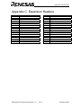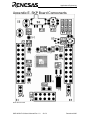
1
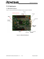
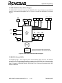
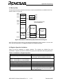
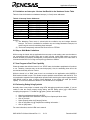
Applications EngineeringApplications Engineering
SKP16C/28 FLGA
User’s Manual
Rev. 1.0
December 2005
www.renesas.com
SKP16C28 FLGA User’s Manual Rev. 1.0
December 2005
Applications Engineering
Table of Contents
1.0 Introduction.............................................................................................................. 2
2.0 Contents of Product Package.................................................................................. 3
2.1 SKP16C28 FLGA StarterKit Plus Product List .................................................. 3
3.0 Limited Guarantee and Support .............................................................................. 4
4.0 System Connectivity.................................................................................................. 5
Figure 4-1 SKP16C28 FLGA System Connectivity......................................................................... 5
4.1 Host Computer Requirements.............................................................................. 5
4.2 SKP16C28 FLGA Board ....................................................................................... 5
4.3 In-Circuit Debugger (RTA-FoUSB-MON) ........................................................... 5
4.4 Software Development Tools ............................................................................... 5
4.4.1 HEW (High-performance Embedded Workshop) .......................................... 5
4.4.2 NC30WA Evaluation Version C Compiler ....................................................... 6
4.4.3 Hew Debug Interface.......................................................................................... 6
4.4.4 FoUSB (Flash-over-USBTM) Programmer....................................................... 6
5.0 Hardware ................................................................................................................. 7
5.1 SKP16C28 FLGA Board ....................................................................................... 7
5.2 SKP16C28 Board Block Diagram........................................................................ 8
5.3 M16C/28 Group of MCUs ..................................................................................... 8
5.4 SKP16C28 FLGA Board Jumper Configuration ................................................ 9
5.4.1 JP1: MCU (U1) Power............................................................................................................... 9
5.4.2 JP2: Xout.............................................................................................................. 9
5.4.3 Default Jumper Settings............................................................................................................ 9
6.0 System Operation & Limitations............................................................................ 10
Table 6-1 System Limitations (when debugging) ...................................................... 10
6.1 Kernel (ROM Monitor) Introduction ................................................................... 10
6.2 Pin and Peripheral Limitations ........................................................................... 10
Figure 6-2 M30280FA FLGA Memory Map with the Kernel Program ................................ 11
Table 6-3. Limitations on Register Operation ................................................................ 11
Table 6-4. Interrupt Vector Addresses........................................................................ 12
6.6 Stop or Wait Mode Limitations .................................................................................................. 12
6.7 User Program’s Real-Time Capability...................................................................................... 12
6.8 Performing Debug Using Symbols ........................................................................................... 12
7.0 SKP16C28 FLGA Board Specifications ............................................................... 13
7.1 Hardware Specifications ..................................................................................... 13
Table 7-1. SKP16C28 FLGA Board Specifications................................................... 13
Appendix A. Troubleshooting Guide ........................................................................... 14
Appendix B. Reference Manuals ................................................................................. 17
Appendix C. Expansion Headers................................................................................. 18
Appendix D. SKP16C28 FLGA Schematics .............................................................. 19
Appendix E. SKP Board Components ........................................................................ 20
Appendix F. RTA-FoUSB-MON (ICD) ........................................................................ 21
SKP16C28 FLGA User’s Manual Rev. 1.0
December 2005
Applications Engineering
1.0 Introduction
The SKP16C28 FLGA StarterKit Plus (SKP) is a low-cost development environment for
evaluating M16C/28 group microcontrollers (MCU) and Renesas software development tools. The
kit comes with a complete software development tool chain including, HEW (IDE, GUI,
Debugger), NC30WA (C-compiler, assembler, and linker), and FoUSB (Flash-over-USB™
Programmer).
A real-time, source-level debug environment is implemented using the HEW debugging interface
with the RTA-FoUSB-MON Flash Programmer/In-Circuit Debugger (ICD). The Flash-over-USBTM
(FoUSB) Programmer software, with the ICD, allows in-system programming of the M16C/28
flash MCU.
The ICD and firmware provide a convenient USB (Universal Serial Bus) interface between the
SKP16C28 FLGA board and the host PC. This interface reduces resource requirements on the
M16C/28 MCU, allows faster code downloads and, can also be used with many other Renesas
Flash MCU’s, SKP’s, and user’s target board.
SKP16C28 FLGA User’s Manual Rev. 1.0
2 / 21
December 2005
Applications Engineering
2.0 Contents of Product Package
This section describes the contents of the SKP16C28 FLGA product package. When unpacking
your SKP16C28 FLGA, please check to see that all products listed below are included.
2.1 SKP16C28 FLGA StarterKit Plus Product List
Table 2-1 lists the products included in the SKP16C28 FLGA.
Table 2-1 SKP16C28 FLGA Product List
Product Name
Quantity
SKP16C28 FLGA Board
1
RTA-FoUSB-MON (ICD)
1
6” 10-Pin Target Cable
1
6’ Mini USB Cable
SKP CD-ROM
1
1
Remark
M16C/28 FLGA SKP Board
HEW Debugger/ FoUSB
Programmer Interface Device
Connects SKP16C28 FLGA
Board (J1) and the ICD
Connects ICD to the Host PC
Auto-install program
HEW (IDE)
NC30WA (C-compiler,
assembler, and linker)
FoUSB Programmer
Manuals
Tutorials
Sample programs
2.1.1 SKP CD-ROM
The CD-ROM contains the electronic manuals and software necessary for developing programs.
Your computer must have Netscape Navigator® or Microsoft®’s Internet Explorer to view the
help files and Acrobat Reader to view the manuals.
Insert the enclosed CD into your computer and SKP installer will auto-start. The SKP installer
program will create a C:\Renesas and C:\Workspace folder on your machine. NC30WA, FoUSB
Programmer, Documentation, sample code, and other SKP related files are in the C:\Renesas.
HEW is installed in the C:\Program files folder by default.
If the SKP installer program does not start up, browse the CD’s root folder and double-click on
‘skp_installer.exe’ to start installation.
SKP16C28 FLGA User’s Manual Rev. 1.0
3 / 21
December 2005
Applications Engineering
3.0 Limited Guarantee and Support
Renesas Technology America, Inc., warrants the SKP16C28 FLGA to be free from component or
assembly defect for a period of 180 days from the date of purchase. Settlement is limited to repair
or replacement of the product only. Renesas Technology America, Inc., does not assume any
liability arising out of the application or use of any product, circuit or procedure described herein.
No other liability or warranty apply, expressed or implied. Software warranty is limited to
replacement of the CD only. While every attempt has been made to ensure accurate
documentation, Renesas Technology America, Inc., cannot be held responsible for error or
omissions and reserves the right to make changes without further notice.
“Flash-Over-USB” is a trademark of Renesas Technology America, Inc. All trademarks are the
property of their respective owners.
SKP16C28 FLGA User’s Manual Rev. 1.0
4 / 21
December 2005
Applications Engineering
4.0 System Connectivity
The following lists the hardware and software products required for using the SKP16C28 FLGA
StarterKit Plus.
•
•
•
•
•
•
Host Computer (supplied by user)
SKP16C28 FLGA Board
RTA-FoUSB-MON (ICD)
Mini USB Cable
Target Cable
Software Tools (HEW IDE, NC30 Compiler/Linker, FoUSB Programmer)
Figure 4-1 shows the system connectivity for the SKP16C28 FLGA.
Figure 4-1 SKP16C28 FLGA System Connectivity
4.1 Host Computer Requirements
The minimum requirement to be able to use the software that comes with the SKP16C28 FLGA is
a PC with a USB port and Microsoft Windows 98, ME, 2000, or XP.
4.2 SKP16C28 FLGA Board
The SKP16C28 FLGA board provides an evaluation and development environment for the
M16C/28 group MCUs. See section 5.0 ‘Hardware’ for more details.
4.3 In-Circuit Debugger (RTA-FoUSB-MON)
The ICD provides a plug-and-play debugging and programming interface to the SKP16C28 FLGA
board via the host computer’s Universal Serial Bus (USB). The USB port also provides power to
the SKP16C28 FLGA board and ICD thereby eliminating the need for an external power supply.
4.4 Software Development Tools
The SKP installer program installs all the development tools. For details on installation, see the
Quick Start Guide or instructions in the Appendix of this manual. A brief description of all the
included tools follows. Please refer to the individual Tool manuals for detailed information.
4.4.1 HEW (High-performance Embedded Workshop)
SKP16C28 FLGA User’s Manual Rev. 1.0
5 / 21
December 2005
Applications Engineering
HEW provides a Graphical User Interface (GUI) that integrates the software development tools
and includes the C-compiler, assembler, linker, debugger and editor.
4.4.2 NC30WA Evaluation Version C Compiler
The evaluation version of the M3T-NC30WA V.5.30 Release 02 is provided with the
same functionality as the commercial version except that link size will be restricted to 64
Kbytes on and after the 61st day from when you begin using the compiler. Contact your
local sales representative if you wish to purchase a full license.
4.4.3 Hew Debug Interface
HEW communicates with a kernel (i.e. a ROM monitor program) on the target MCU through the
ICD. This debug interface provides a highly efficient evaluation environment. Features include:
•
•
•
•
•
Source-line debug for assembly language C language
Single step command (does not limit number of breakpoints).
Run command with 6 breakpoints* for the M16C/28.
RAM monitor function
C variable “watch” window
Note: The number of breakpoints will vary depending on the M16C flash MCU used.
4.4.4 FoUSB (Flash-over-USB
TM
) Programmer
The Flash Over USB Programmer application provides In-System Programming capability for the
starter kit or any target board using an M16C family flash MCU (i.e.: R8C, M16C, M32C). Please
see the RTA-FoUSB-MON Users Manual for more details.
SKP16C28 FLGA User’s Manual Rev. 1.0
6 / 21
December 2005
Applications Engineering
5.0 Hardware
5.1 SKP16C28 FLGA Board
Figure 5-1 shows the SKP16C28 FLGA Board with major components identified.
Figure 5-1. SKP16C28 FLGA Board
SKP16C28 FLGA User’s Manual Rev. 1.0
7 / 21
December 2005
Applications Engineering
5.2 SKP16C28 FLGA Board Block Diagram
The SKP16C28 FLGA board incorporates an M30280FA FLGA (80-pin FLGA) from the M16C/28
group of microcontrollers designated as U1. Figure 5-2 shows the SKP16C28 FLGA block
diagram.
CDs Cell Thermistor
PWR
LED
D3
Y1
Y2
20MHz
32.768kHz
S3
RESET
JP2
Xin
E8
Connection
To
ICD
Xout
S1
S2
P8_3
R23
P8_4
AN1
RT1
AN0
XCin XCout
GREEN
LED
J2
U1
M30280FA
FLGA
MCU
J1
Vcc
RED
LED
YELLOW
LED
GREEN
LED
D1
D2
D4
P8_0
JP1
P8_1
P8_2
Vcc
MCU Power
for Icc
Measurements
Ports
J3, J4
Headers
Note: An external power supply is required if the
SKP16C28 FLGA Board is not connected to the ICD.
Figure 5-2. SKP16C28 FLGA Board Block Diagram
5.3 M16C/28 Group of MCUs
The M3028x group of 16-bit single-chip, flash microcontrollers (MCU) is part of the M16C/60
series CPU core. The hardware and software manuals for the M16C/28 group of microcontrollers
can be found under C:\Renesas\SKP16C28_FLGA\Docs folder in your PC or from the Start menu
(Start > Programs > RENESAS-TOOLS > SKP16C28 FLGA > Document Descriptions) after SKP
software installation.
SKP16C28 FLGA User’s Manual Rev. 1.0
8 / 21
December 2005
Applications Engineering
5.4 SKP16C28 FLGA Board Jumper Configuration
5.4.1 JP1: MCU (U1) Power
JP1 is used to connect the Vcc pins of the M16C/28 MCU to the Vcc/MCU Power of the board. It
can be used to measure current/power consumption of the MCU during various modes of
operation. For normal operations, JP1 must be shorted.
JP1 is shorted by default.
5.4.2 JP2: Xout
JP2 is used to connect the output of the MCU’s internal amplifier to the crystal for oscillation. It
can be used to disconnect Xout when an externally driven clock is connected to Xin. For normal
operations, JP2 must be shorted.
JP2 is shorted by default.
5.4.3 Default Jumper Settings
Jumper
Setting
JP1
MCU Power
Shorted
JP2
Xout
Shorted
SKP16C28 FLGA User’s Manual Rev. 1.0
9 / 21
December 2005
Applications Engineering
6.0 System Operation & Limitations
The SKP16C28 FLGA provides sophisticated debugging features at a low cost but it does have
some limitations when used with the debugger and ICD. Section 6.1 introduces the kernel (ROM
monitor) program and its purpose. The limitations when this kernel is running with the user
program are listed in table 6-1.
Table 6-1 System Limitations (when debugging)
Item
Please Refer To
6.2 Pin and Peripheral Limitations
6.3 Memory Map
User Limitations
6.4 Register Operation Limitations
6.5 Limitations on Interrupts
6.6 Stop or Wait Mode Limitations
Debugger Limitations
6.7 User Program’s Real-time Capability
6.1 Kernel (ROM Monitor) Introduction
During debug, a small program, called a kernel, is downloaded to the M16C/28. The kernel
communicates with HEW through the ICD regarding MCU status during user code debugging
operations.
There are no special steps required in the user program to make use of the ICD. The operation of
the kernel is transparent to the user but there are some limitations and these are discussed from
section 6.2.
After starting a HEW debug Session, the ICD downloads the kernel to the M16C/28 if it does not
exist (e.g. blank device or programmed with FoUSB Programmer). After downloading the kernel,
the M16C/28 is ready for downloading user code.
Connecting the ICD without starting HEW will not affect the lines connected between the ICD and
the M16C/28 – the ICD keeps the lines in high-impedance state. The ICD only drives the pins
after HEW or FoUSB Programmer attempts to connect.
After completing program debug and verification with HEW, you can create an image of your
code in Intel (.hex) or Motorola (.mot) file formats. This image can be programmed into the
M16C/28 using the FoUSB Programmer. This procedure erases the kernel and leaves only the
user program.
6.2 Pin and Peripheral Limitations
SIO/UART1 pins are used for communication between the M16C/28 kernel on the SKP16C28
FLGA board and HEW through the ICD. Do not connect these pins to any other circuit, as UART1
cannot be used in the user program while using the Debugger. For details, please see the RTAFoUSB-MON (ICD) User Manual on Target M16C ROM Monitor Resources or related ICD
application notes.
SKP16C28 FLGA User’s Manual Rev. 1.0
10 / 21
December 2005
Applications Engineering
6.3 Memory Map
The amount and memory locations of the kernel, used on the M16C/28 on the SKP16C28 FLGA
board is shown on Figure 6-2.
00000h
00400h
SFR Area
00400h
User RAM Area
= 8064 Bytes 0237Fh
02380h
Kernel RAM
Internal RAM
Area - 8kB
023FFh
(128 Bytes)
Reserved
0F000h
0F800h
023FFh
High E/W
2kB data block
Note: User programs must
not use shaded areas.
High E/W
2kB data block
10000h
Reserved
User Program
Area - 94kB
Special Page
Area
E8000h
FF900h
User
Flash ROM
Area - 96kB
Kernel
Program
FFE80h
FFFDCh
Fixed Vector
Area
FFFFFh
Figure 6-2 M30280FA FLGA Memory Map with the Kernel Program
Note: The kernel occupies memory associated with special-page vector numbers 18-19 and 192255. The user reset vector is re-mapped to address FFFD8h by the kernel.
6.4 Register Operation Limitations
Table 6-3 lists the limitations on register operation. The registers are inhibited from any
modification. If register contents are modified in any way, kernel operation cannot be guaranteed.
Table 6-3. Limitations on Register Operation
Register Name
User and Interrupt Stack Pointers
UART1 Transmit/Receive Mode Register
UART1 Transmit/Receive Control Register 0
UART1 Transmit/Receive Control Register 1
UART1 Interrupt Control Register 0
UART Transmit/Receive Control Register 2
UART1 Transmit Buffer Register
UART1 Receive Buffer Register
Port 6 and Port 6 DDR
SKP16C28 FLGA User’s Manual Rev. 1.0
Restriction
RAM memory range 02380H – 023FFH is used
by the kernel. Do not set stacks in this area.
Do not change
Do not change
Do not change bits 0 and 2
Do not write to this register
Do not read this register
To prevent changes on P6_4 data and direction,
use read-modify-write only instructions (BSET,
BCLR, AND, OR, etc)
11 / 21
December 2005
Applications Engineering
6.5 Limitations on Interrupts - Vectors that Reside in the Hardware Vector Table
Table 6-4 lists the limitations on hardware interrupt (i.e. fixed) vector addresses.
Table 6-4. Interrupt Vector Addresses
Interrupt Cause
M16C/28 Vector Address
Undefined
FFFDCH ~ FFFDFH
Overflow
FFFE0H ~ FFFE3H
BRK Instruction
FFFE4H ~ FFFE7H
Address Match
FFFE8H ~ FFFEBH
Single-step
FFFECH ~ FFFEFH
Watchdog Timer
FFFF0H ~ FFFF3H
DBC
FFFF4H ~ FFFF7H
NMI
FFFF8H ~ FFFFBH
RESET
FFFFCH ~ FFFFFH
Kit Specification
User available
User available
User inhibited
User inhibited
User inhibited
User available (Note 1)
User inhibited
User available
Reset vector (Note 2)
NOTES:
(1) The Watchdog Timer vector is shared with the oscillation stop and voltage detection
interrupt. The vector is available for oscillation stop and voltage detection interrupts, but
avoid using the vector for watchdog timer interrupts.
(2) The kernel transparently relocates the Reset vector to FFFD8H.
6.6 Stop or Wait Mode Limitations
While running the kernel with an application that uses stop or wait modes, care must be taken to
not communicate with the MCU while stop or wait is active (avoid RAM monitor or memory
window refreshes for example). Breakpoints (if used) should be set at points in the code where it
is known that the BCLK is running at a frequency greater than 250Khz.
6.7 User Program’s Real-Time Capability
Please be aware that while the kernel is in a “STOP” state, the hardware peripherals will continue
to run. Therefore, interrupts may not be serviced properly. Also, the watchdog timer will not be
serviced and will likely time out if active.
While the kernel is in a “RUN” state, there is no overhead on the application code UNLESS a
RAM monitor window is open. This window requires periodic communication with the MCU. This
communication suspends normal application operation while servicing the request (approximately
2000 BCLK cycles for each 16 bytes of data displayed in the window are used per window
update). The user must determine whether or not this behavior is acceptable.
6.8 Performing Debug Using Symbols
Normally when a new project is created using HEW, debugging symbols are enabled. If you are
unable to view the source properly during debug, add the debug option [-g] in HEW before
compiling the programs. To enable the [-g] option, perform the following:
•
•
•
•
•
•
Open the workspace and project in HEW.
Select [Renesas M16C Standard Toolchain] from Options pull-down menu.
Click on Link tab.
Select [Output] under the [Category] list box.
Click on checkbox for [-g] ‘Outputs source debug information….’
Click on [OK] button
For more information, see the HEW user’s manual.
SKP16C28 FLGA User’s Manual Rev. 1.0
12 / 21
December 2005
Applications Engineering
7.0 SKP16C28 FLGA Board Specifications
7.1 Hardware Specifications
Table 7-1 lists the specifications of the SKP16C28 FLGA Board.
Table 7-1. SKP16C28 FLGA Board Specifications
Item
Specification
MCU
M30280FA FLGA
Clocks
Main Clock: crystal 20MHz, PLL, or ring oscillator
Sub Clock: 32.768kHz crystal
Memory
RAM: 8kB (8064 Bytes user available due to kernel)
High E/W Data Block: 2kB x 2 (4096 Bytes)
(ICD)
Flash ROM: 96kB (94kB user available due to kernel)
Connectors
[J1]: Serial interface connector (UART1 for FoUSB-ICD)
[J2]: Serial interface connector (UART1 for E8)
[J3-J4]: 2, 16/18 pin headers (for user target connection)
Jumpers
[JP1]: MCU Power for Icc Measurements
[JP2]: Xout to main crystal Y2
Switches
[S1]: pushbutton (connected to P8_3)
[S2]: pushbutton (connected to P8_4)
[S3]: pushbutton (connected to Reset)
LED’s
[D1] (Red): User output (connected to P8_0)
[D2] (Yellow): User output (connected to P8_1)
[D4] (Green): User output (connected to P8_2)
7.2 Power Supply Requirements
The SKP16C28 FLGA Board will draw 35mA (max). With the ICD, the current draw will be about
85mA.
7.3 Operating Environment
Table 7-2 lists the environmental conditions for using and storing the SKP16C28 FLGA board.
When storing the board, place it in a conductive bag and then in the packing box your product
was shipped in from the factory.
Table 7-2. Operating Environment
Environmental Condition
Ambient Temperature
Operating
0 - 55°C
(No corrosive gas allowed)
Storage
-30 to 75°C
(No corrosive gas allowed)
SKP16C28 FLGA User’s Manual Rev. 1.0
13 / 21
Ambient Humidity
30 to 80% (non-condensing)
30 to 80% (non-condensing)
December 2005
Applications Engineering
Appendix A. Troubleshooting Guide
This section discusses possible problems you may encounter while installing the software (and
drivers) and while running the HEW debugger or FoUSB Programmer applications. This section
also discusses the countermeasures and solutions to resolve these problems.
If, for any reason, you cannot resolve the problem, please contact your Renesas representative
for assistance.
A.1 USB Driver Problems
This section discusses the usual problems with the driver installation and how to fix it. The most
common problem encountered is that Windows did not properly install the driver and so the ICD
is not recognized. This may also cause the device status to indicate that the device is not working
properly. An indication of this problem is the ICD status yellow LED - it blinks about 2-3 times a
second. When the driver is installed properly, the yellow LED should only blink every second.
Before trying the following steps, try restarting your PC and see if this resolves the problem. You
can check the status using the Device Manager. If the ICD appears under the Universal Serial
Bus Controllers with NO red X or yellow exclamation point, the driver was installed properly.
NOTE: If you are using Windows 2000 or XP, you need Administrator privileges to install
the drivers.
For cases where the ‘Device Status’ states the device is not working properly, please try the
following:
•
•
•
•
Double-click on ‘Renesas USB-Monitor’ and a Renesas USB-Monitor Properties dialog
box appears.
Click on ‘Driver’ tab and click on ‘Update Driver’ button.
Select ‘Display a list…’ and click on ‘Have Disk’ button.
Specify and locate the ‘C:\Renesas\FoUSB\USB Drivers’ folder on your PC and install
‘usbmon.sys’ driver.
If you encounter problems on installing the drivers, you can try the following.
(1) Windows 2000
i. Copy the fousb.inf and usbmon.inf files from \USB Drivers folder to
\WINNT\INF folder.
ii. Copy the fousb.sys and usbmon.sys files from \USB Drivers folder to
\WINNT\SYSTEM32\drivers folder.
(2) Windows 98 or XP
i. Copy the fousb.inf and usbmon.inf files from C:\Renesas\FoUSB\USB Drivers
folder to \WINDOWS\INF folder.
ii. Copy the fousb.sys and usbmon.sys files from C:\Renesas\FoUSB\USB
Drivers folder to WINDOWS\SYSTEM32\drivers folder.
SKP16C28 FLGA User’s Manual Rev. 1.0
14 / 21
December 2005
Applications Engineering
A.2 Debugging Problems
This section discusses the cause of the problem and countermeasures to resolve it. The common
problems encountered with debugging are:
• Erratic debug behavior
• Cannot connect to target
• Issues that may come up during debug operations
A.2.1 Erratic Debug Behavior
HEW allows you to launch multiple “Slave HEW’s”. If more that one HEW is opened in a debug
session and/or the FoUSB Programmer software is also running, erratic behavior can result.
Having more than one ICD installed can also cause erratic problems or cause HEW to crash.
A.2.2 Cannot Connect to Target
When the message ‘Can’t connect with the target’ is displayed when attempting to connect, there
are several reasons that may cause this message to appear. Each cause and the corresponding
countermeasure are discussed below.
•
The SKP is not connected correctly.
Please connect the ICD to your PC. Note: Regardless of whether the ICD is bus or targetpowered, please connect target board to ICD board first before plugging the USB cable to
your PC. Please see section 4 on system (SKP16C28 FLGA) connectivity.
•
The ICD has no power (Power LED on ICD is off).
Please ensure that the Power Mode switch on the ICD is on the ‘USB’ side. In ‘Target’
position, the ICD is powered from the target side.
•
USB was not selected on the Init dialog box.
Please select ‘USB’ from the Init dialog box that is displayed right after you start a debug
session.
•
The selected MCU on the ICD board and the actual target MCU (M16C/28) do not match.
Close the error message by clicking on ‘OK’ button, and then click on the ‘Cancel’ button of
the Init window. Make sure you select ‘M30280FA.mcu’. If the MCU loaded on the ICD is
different, HEW will re-program the ICD to match it.
•
The target MCU is damaged.
Try a different target board and see if the HEW will connect as you may have a damaged
board or MCU.
SKP16C28 FLGA User’s Manual Rev. 1.0
15 / 21
December 2005
Applications Engineering
A.2.3 Issues that may come up During Debug Operations
While debugging user code, some issues may come up because the limitations discussed in
section 6 were not satisfied. The common issues are listed on table A.2, including the
countermeasures.
Table A.2. Problems while Debugging
Problem
Possible Cause/s and Solution
After stepping a few
• Changes were made to UART1 SFR’s. Do NOT change
instructions, HEW cannot
UART1 SFRs in user program.
“stop”
Breakpoints do not seem to • System is in “FreeRun” mode. Change the RUN mode to
work
“Sampling” from the “Init” window (Emulator System icon).
HEW locks up (cannot stop • Changes were made to UART1 SFR’s. Do NOT change
program) or
UART1 SFRs in user program.
Communication error
• Ensure no limitations in Section 6 were violated.
message is displayed.
• Re-initialize the system without closing debug session. See
note below.
• Do a hardware reset. User-program runaway may be
corrupting the kernel (RAM, interrupt vectors, flags, etc.)
Close debug session, hit reset button on the SKP16C28
FLGA to reset the board, and then restart.
Download problems
• Filenames or directory names contain spaces or special
characters.
• HEW project not properly set up (startup files missing or out
of order, files added to wrong member, etc). Try creating a
new project and adding your source files to it. For details,
please see HEW user’s manual.
To re-initialize the system without closing a debug session, try the following:
•
•
•
•
Press the [OK] button on the error dialog box to close it.
When an Exit dialog box appears, press the [Cancel] button to close it.
Hit reset button on the SKP16C28 FLGA board.
Click HEW reset Icon.
After initialization, debugging can resume. However, it is recommended that you download your
program again before debugging.
Note: If it has been identified that there are problems with the ICD, please see the ICD’s (RTAFoUSB-MON) user’s manual and troubleshooting section of this manual.
SKP16C28 FLGA User’s Manual Rev. 1.0
16 / 21
December 2005
Applications Engineering
Appendix B. Reference Manuals
Title
Description
1.
2.
3.
Item
SKP16C28 FLGA Quick-Start Guide
SKP16C28 FLGA User's Manual
SKP16C28 FLGA Board Schematic
4.
SKP16C28 FLGA Board BOM
5.
6.
M16C/28 Group Hardware Manual
M16C/20/60 Series C-Language
Programming Manual
M16C/20/60 Series Assembler
Language Programming Manual
M16C/20/60 Series Software
Manual
M16C/20/60 Series Sample
Programs
HEW User's Manual
AS30 User's Manual
NC30 User's Manual
RTA-FoUSB-MON User's Manual
Gets you up and running with the SKP16C28 FLGA.
Installation and operation guide for the SKP16C28 FLGA.
Schematic diagram for the SKP16C28 FLGA Starter Kit
board.
Bill of materials for the SKP16C28 FLGA Starter Kit
board.
Operation and Specifications for the M16C/28 MCU.
ANSI C-language programming guide for the
M16C/20/60 series MCUs.
Assembly language programming guide for the
M16C/20/60 series MCUs.
Instruction set manual for the M16C/20/60 series CPU
cores.
Sample programs and application notes for the
M16C/20/60 series MCUs.
High-performance Embedded Workshop User’s Manual.
AS30 Assembler User’s Manual.
NC30 C-Compiler User’s Manual.
In-Circuit Debugger / Flash Programmer User’s Manual.
7.
8.
9.
10.
11.
12.
13.
SKP16C28 FLGA User’s Manual Rev. 1.0
17 / 21
December 2005
Applications Engineering
Appendix C. Expansion Headers
J3 Pin
1
2
3
4
5
6
7
8
9
10
11
12
13
14
15
16
17
18
Function
J4 Pin
1
2
3
4
5
6
7
8
9
10
11
12
13
14
15
16
Vcc
P7_2
P7_3
P7_4
P7_5
P8_0
P8_1
P8_5
P0_1
P0_0
P0_3
P0_2
P0_5
P0_4
P0_7
P0_6
P9_7
GND
SKP16C28 FLGA User’s Manual Rev. 1.0
18 / 21
Function
Vcc
P8_2
P2_0
P2_1
P2_2
P2_3
P2_4
P2_5
P2_6
P2_7
P7_0
P7_1
P9_0
P9_1
P9_2
GND
December 2005
Applications Engineering
Appendix D. SKP16C28 FLGA Schematics
SKP16C28 FLGA User’s Manual Rev. 1.0
19 / 21
December 2005
Applications Engineering
Appendix E. SKP Board Components
Note: Not to scale.
SKP16C28 FLGA User’s Manual Rev. 1.0
20 / 21
December 2005
Applications Engineering
Appendix F. RTA-FoUSB-MON (ICD)
For details on how to use the ICD, please see RTA-FoUSB-MON User’s Manual.
For SKP updates, see: www.renesas.com/skp
SKP16C28 FLGA User’s Manual Rev. 1.0
21 / 21
December 2005