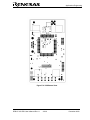
1
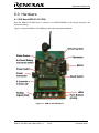
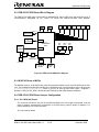
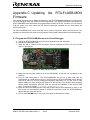
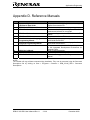
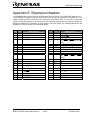
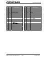
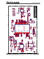
Applications Engineering
ZigBee Demo
Kit (ZDK)
RZB-CC16C-ZDK
User’s Manual
Rev. 1.1
December 2006
www.renesas.com
Applications Engineering
Table of Contents
1.0 Introduction ............................................................................................................................................. 4
2.0 Contents of Product Package................................................................................................................. 5
2.1. RZB-CC16C-ZDK ZigBee Demonstration Kit Item List ..................................................................... 5
2.1.1. CD-ROM...................................................................................................................................... 5
3.0 Limited Guarantee and Support ............................................................................................................. 6
4.0 System Connectivity ............................................................................................................................... 7
4.1. Host Computer Requirements ........................................................................................................... 8
4.2. RZB-CC16C-ZDK Boards.................................................................................................................. 8
4.3. RF Sniffer Interface (RFSI)................................................................................................................ 8
4.4. RF Sniffer Software and USB Driver ................................................................................................. 8
4.5. In-Circuit Debugger and Programmer (ICD)...................................................................................... 9
4.6. Software Development Tools ............................................................................................................ 9
4.6.1. HEW (High-performance Embedded Workshop)........................................................................ 9
4.6.2. NC30WA Evaluation Version C Compiler ................................................................................... 9
4.6.3. HEW Debug Interface ................................................................................................................. 9
4.6.4. FoUSB (Flash-over-USB™) Programmer ................................................................................... 9
5.0 ZigBee Evaluation Kit (ZEK)................................................................................................................. 10
5.1. Creating Your Own Program ........................................................................................................... 10
5.1.1. ZigBee Demo Configurations .................................................................................................... 10
5.1.2. ZEK_Demo.c File ...................................................................................................................... 11
5.1.3. Stack RAM Usage ..................................................................................................................... 11
5.1.4. Global Variable RAM Usage ..................................................................................................... 11
5.1.5. Customization of Settings.......................................................................................................... 12
5.2. Limitations of the ZigBee Evaluation System .................................................................................. 13
5.2.1. Timers........................................................................................................................................ 13
5.2.2. System Clock ............................................................................................................................ 13
5.2.3. Interrupts ................................................................................................................................... 13
5.2.4. Flash and RAM Usage .............................................................................................................. 13
5.2.5. MAC Address Area.................................................................................................................... 14
5.2.6. ZbROM Flash Size .................................................................................................................... 14
5.2.7. ZbROM RAM Size..................................................................................................................... 14
5.2.8. User Task Stack RAM ............................................................................................................... 14
5.2.9. User Global Variable RAM ........................................................................................................ 14
5.2.10. ZigBee Stack Table Sizes ....................................................................................................... 15
5.2.11. Other Limitations ..................................................................................................................... 15
6.0 Hardware .............................................................................................................................................. 16
6.1. ZDK Board (RZB-CC16C-ZDK)....................................................................................................... 16
6.2. RZB-CC16C-ZDK Board Block Diagram ......................................................................................... 17
6.3. M16C/28 Group of MCUs ................................................................................................................ 17
6.4. RZB-CC16C-ZDK Board Jumper Configuration.............................................................................. 17
6.4.1. JP1: MCU (U4) Power............................................................................................................... 17
6.4.2. JP2: Power LED (D4) and RS232 (U7) Transceiver Power...................................................... 18
6.4.3. Default Jumper Settings ............................................................................................................ 18
6.5. LCD (Liquid Crystal Display) ........................................................................................................... 18
6.6. ZigBee RF........................................................................................................................................ 18
7.0 System Operation & Limitations ........................................................................................................... 19
7.1. Kernel (ROM Monitor) Introduction.................................................................................................. 19
7.2. Pin and Peripheral Limitations......................................................................................................... 19
7.3. Memory Map.................................................................................................................................... 19
7.4. Register Operation Limitations ........................................................................................................ 20
7.5. Limitations on Interrupts - Vectors that Reside in the Hardware Vector Table ............................... 20
7.6. Stop or Wait Mode Limitations......................................................................................................... 21
RZB-CC16C-ZDK User’s Manual Rev 1.1
December 2006
Applications Engineering
7.7. User Program’s Real-Time Capability ............................................................................................. 21
7.8. Performing Debug Using Symbols .................................................................................................. 21
8.0 RZB-CC16C-ZDK Board Specifications ............................................................................................... 22
8.1. Hardware Specifications.................................................................................................................. 22
8.2. Power Supply Requirements ........................................................................................................... 22
8.3. Operating Environment.................................................................................................................... 22
Appendix A. Troubleshooting Guide........................................................................................................... 23
A.1 Manual Installation ........................................................................................................................... 23
A.2 USB Driver Problems ....................................................................................................................... 23
A.3 Debugging Problems........................................................................................................................ 24
A.3.1 Erratic Debug Behavior.............................................................................................................. 24
A.3.2 Cannot Connect to Target.......................................................................................................... 24
A.3.3 Issues that May Arise During Debug Operations ...................................................................... 25
Appendix B. Updating the ZigBee Development Kit (ZDK) Board Firmware ............................................. 27
B.1 Programming the ZDK Board with with ZigBee Demo Firmware..................................................... 27
Appendix C. Updating the RTA-FoUSB-MON Firmware............................................................................ 29
C.1 Program the RTA-FoUSB-Mon as an In-Circuit Debugger.............................................................. 29
Appendix D. Reference Manuals................................................................................................................ 31
Appendix E. Expansion Headers................................................................................................................ 32
Appendix F. Board Schematic & BOM ....................................................................................................... 34
Appendix G. RZB-CC16C-ZDK Printed Circuit Board............................................................................... 37
Appendix H. Other Resources.................................................................................................................... 39
RZB-CC16C-ZDK User’s Manual Rev 1.1
3/ 39
December 2006
Applications Engineering
1.0 Introduction
The RZB-CC16C-ZDK kit is a low-cost ZigBee demonstration kit for evaluating wireless ZigBee
connectivity solutions based on the Renesas M16C/28 group of microcontrollers (MCU).
A small ZigBee Personal Area Network (PAN) can be set up, monitored and analyzed with the included
hardware and software.
The kit contains an USB dongle that functions as an RF Sniffer Interface (RFSI). RF Sniffer software
installed on the PC allows you to record and analyze ZigBee data packets. The software can also display
the network topology of a ZigBee network. For more information on the RF Sniffer software and hardware,
see the RF Sniffer User’s Manual, accessible via Start > (All) Programs > Renesas > RF SnifferV.x.xx
A RTA-FoUSB-MON Flash Programmer and In-Circuit-Debugger (ICD) included in the kit allows you to
re-program the demo boards and to run and debug code. The ICD and firmware provide a convenient
Universal Serial Bus (USB) interface between the ZDK boards and the host PC. This interface reduces
resource requirements on the M16C/28 MCU and allows faster code downloads. It also can be used with
many other Renesas Flash MCUs, starter kits, and your own Renesas MCU-based target boards.
Three ZigBee Demonstration Kit (ZDK) boards come pre-programmed with demo software that enables
you to quickly set up a small ZigBee PAN comprised of a ZigBee network Coordinator and two ZigBee
network Routers.
The kit comes with a complete software development tool chain for Renesas MCUs, including Highperformance Embedded Workshop (HEW), which includes Integrated Development Environment (IDE),
Graphical User Interface (GUI) and Software Debugger; NC30WA C-compiler, assembler and linker; and
Flash-over-USB™ (FoUSB) Programming software.
A real-time, source-level debug environment is implemented using the HEW debugging interface with the
RTA-FoUSB-MON Flash Programmer/ICD. The Flash-over-USBTM (FoUSB) Programmer software, in
combination with the ICD, allows in-system programming of the M16C/28 Flash MCUs on the ZDK and
RF Sniffer target boards.
RZB-CC16C-ZDK User’s Manual Rev 1.1
4/ 39
December 2006
Applications Engineering
2.0 Contents of Product Package
This section describes the contents of the RZB-CC16C-ZDK product package. When unpacking your
RZB-CC16C-ZDK, please check to see that all items listed below are included.
2.1. RZB-CC16C-ZDK ZigBee Demonstration Kit Item List
Table 2-1 lists the items included in the RZB-CC16C-ZDK.
Table 2-1 RZB-CC16C-ZDK Item List
Item Name
Quantity
RZB-CC16C-ZDK Board
3
Integral USB Dongle
1
RTA-FoUSB-MON (ICD)
6” 10-Pin Target Cable
6’ Mini USB Cable
Battery Pack with 3 AA batteries
CD-ROM
1
1
1
3
Remarks
ZigBee Demo Kit (ZDK) Boards, pre-programmed with
demo software
Integral 2.4GHz RF Receiver USB Stick, used as the
RF Sniffer Interface (RFSI)
In-Circuit Debugger and Flash Programmer Interface
Connects ICD unit to ZDK boards
Connects ICD to Host PC
Powers the three ZDK boards
Auto-install program
RF Sniffer software
HEW (IDE & debugger)
NC30WA (C-compiler, assembler, and linker)
FoUSB Programmer
USB drivers
Manuals
Tutorials
Sample programs
2.1.1. CD-ROM
The CD-ROM contains the electronic manuals and software necessary for developing programs. Your
computer must have a web browser — like Mozilla Firefox, Netscape® Browser or Microsoft® Internet
Explorer — to view the help files, and Adobe® Acrobat® Reader® to view the manuals.
Insert the enclosed CD into your computer and the installer will auto-start. The installer program will
create C:\Renesas and C:\Workspace folders on your machine. NC30WA, FoUSB Programmer,
Documentation, sample code, and other ZDK-related files are in the C:\Renesas folder. HEW is
installed in the C:\Program Files folder by default.
If the installer program does not start, browse to the CD’s root folder and double-click on
ZDK_Installer.exe to start the installation.
RZB-CC16C-ZDK User’s Manual Rev 1.1
5/ 39
December 2006
Applications Engineering
3.0 Limited Guarantee and Support
Renesas Technology America, Inc., warrants the RZB-CC16C-ZDK to be free from component or
assembly defects for a period of 180 days from the date of purchase. Settlement is limited to repair or
replacement of the product only. Renesas Technology America, Inc., does not assume any liability arising
out of the application or use of any product, circuit or procedure described herein. No other liability or
warranty applies, expressed or implied. Software warranty is limited to replacement of the CD only. While
every attempt has been made to ensure accurate documentation, Renesas Technology America, Inc.,
cannot be held responsible for errors or omissions, and reserves the right to make changes without prior
notice.
“Flash-Over-USB” is a trademark of Renesas Technology America, Inc. All other trademarks are the
properties of their respective owners.
RZB-CC16C-ZDK User’s Manual Rev 1.1
6/ 39
December 2006
Applications Engineering
4.0 System Connectivity
The following lists the hardware and software products required for using the RZB-CC16C-ZDK ZigBee
Demonstration Kit.
•
•
•
•
•
Host Computer (supplied by user)
Three RZB-CC16C-ZDK Boards
Three battery packs with AA batteries
RF Sniffer USB Dongle
RF Sniffer software and USB driver
ZigBee
Coordinator
ZigBee
Router
ZigBee
Router
RF Sniffer
USB Dongle
Figure 4.1: ZigBee Demo Setup
Optional (only required if you want to update firmware and/or develop code).
•
•
•
•
In-Circuit Debugger and Programmer (ICD)
Mini USB cable for ICD
2×5 header target cable for ICD
Software Tools (HEW IDE, NC30 Compiler/Linker, FoUSB Programmer)
Figure 4-2 shows an ICD unit connected to a PC via USB and to a ZDK board via 2×5-pin ribbon cable.
RZB-CC16C-ZDK User’s Manual Rev 1.1
7/ 39
December 2006
Applications Engineering
RZB-CC16C-ZDK Board
PC with Windows ® 98SE,
2000, Me, or XP
Mini USB
Cable
ICD
10-pin
Target
Cable
Figure 4-2 ZDK Development System Connectivity
4.1. Host Computer Requirements
The minimum requirement to be able to use the software that comes with the RZB-CC16C-ZDK is a PC
with a USB port and Microsoft Windows 98, ME, 2000, or XP.
4.2. RZB-CC16C-ZDK Boards
The three RZB-CC16C-ZDK boards are pre-programmed with ZigBee demo firmware to provide a demo
and evaluation environment for wireless ZigBee connectivity based on Renesas MCUs. See section
“6.0Hardware” for more details.
4.3. RF Sniffer Interface (RFSI)
The RF Sniffer Interface (RFSI) is a 2.4GHz RF receiver USB dongle made by Integration. See the RF
Sniffer User’s Manual for more information on RF Sniffer usage and features.
4.4. RF Sniffer Software and USB Driver
The installer program offers you the option to install the ZDK demo software tools and the RF Sniffer
software. For details on installation, see the QuickStart Guide or instructions in the Appendix A of this
manual.
RZB-CC16C-ZDK User’s Manual Rev 1.1
8/ 39
December 2006
Applications Engineering
4.5. In-Circuit Debugger and Programmer (ICD)
The ICD provides a plug-and-play debugging and programming interface to the ZDK board via the host
computer’s Universal Serial Bus (USB). The USB port also provides power to the ZDK boards and ICD,
thereby eliminating the need for an external power supply. Use of the ICD is required only if you need to
update the firmware of the kit’s boards, or if you intend to develop and debug your own software. If not
powered by the ICD, the kit’s ZDK boards can be powered by the included battery packs.
4.6. Software Development Tools
The installer program offers you the option to install all the development tools. For details on installation,
see the QuickStart Guide or instructions in Appendix A of this manual. A brief description of all the
included tools follows. Please refer to the individual tool manuals for detailed information.
4.6.1. HEW (High-performance Embedded Workshop)
HEW provides a Graphical User Interface (GUI) that integrates the software development tools and
includes the C-compiler, assembler, linker, debugger and editor.
4.6.2. NC30WA Evaluation Version C Compiler
The evaluation version of the M3T-NC30WA C-compiler is provided with the same functionality as the
commercial version except that link size will be restricted to 64 Kbytes after 60 days from when you
begin using the compiler. Contact your local sales representative if you wish to purchase a full license.
4.6.3. HEW Debug Interface
HEW communicates with a kernel (i.e. a ROM monitor program) on the target MCU through the ICD.
This debug interface provides a highly efficient evaluation environment. Features include:
•
•
•
•
•
Source-level debugging for assembly and C language
Single-step command (unlimited breakpoints)
Run command with 6 breakpoints* for the M16C/28
RAM monitor function
C variable “watch” window
*Note: The number of breakpoints will vary depending on the M16C flash MCU used.
4.6.4. FoUSB (Flash-over-USB™) Programmer
The Flash Over USB Programmer application provides In-System Programming capability for the
starter kit or any target board using an M16C family flash MCU (e.g. R8C, M16C, M32C). Please see
the RTA-FoUSB-MON User’s Manual for more details.
RZB-CC16C-ZDK User’s Manual Rev 1.1
9/ 39
December 2006
Applications Engineering
5.0 ZigBee Evaluation Kit (ZEK)
The ZigBee Evaluation Kit (ZEK), which is included with the RZB-CC16C-ZDK kit, provides a ZigBee
stack and a real-time operating system (RTOS) for the stack in binary form. Your own application code
can interface to the ZigBee stack via documented Application Programming Interface (API) function calls.
Two
binary
files
are
provided
in
the
directory
C:\Renesas\RZB_CC16C_ZDK\Sample_Code\ZEK_ZbRom:
ZbRom_CC28_FFD_Vxx.mot contains the ZigBee stack and RTOS for Full Function Devices (FFD), i.e.
ZigBee Routers or Coordinators. The module also contains all necessary MCU initialization routines.
ZbRom_CC28_RFD_Vxx.mot contains the ZigBee stack and RTOS for Reduced Function Devices (RFD),
i.e. ZigBee End Devices. It has a smaller memory footprint than the FFD binary, leaving more memory
available for your own application code. The module also contains all necessary MCU initialization
routines.
Sample projects for the Renesas High-performance Embedded Workshop (HEW) allow you to quickly
create your own ZigBee coordinator, router or end device.
5.1. Creating Your Own Program
This section assumes that you have worked through the Quick Start Guide.
Please use the HEW project wizard as outlined in the “HEW (IDE) QuickStart” Section of the Quick Start
Guide to create your own ZEK application. Creating a ZigBee project from scratch is quite involved and
the detailed steps to do this are not discussed in this manual.
To create a new ZigBee application using the HEW project wizard you have two options:
1. You can use the ZEK Demo project that you created in the HEW (IDE) QuickStart section.
2. You can select “Empty Project” in the ZigBee M16C/28 Kit – Step 2” window instead.
We recommend that you start out by modifying the ZEK Demo project until you become more familiar with
the ZigBee APIs before attempting to create a project using the “Empty Project” generator.
See the ZigBee Stack API Specification document (Start > Programs > Renesas > RZB_CC16C_ZDK >
All Manuals and Documents) for a detailed description of the available ZigBee API functions.
Below are some specifics about the ZEK demo project that will help you get started.
5.1.1. ZigBee Demo Configurations
The demo code can be built to act as any of the following ZigBee device types by using the Build
configuration pull-down in HEW. Please note that you have to download the correct ZigBee stack image
separately as described in the section “Downloading the ZigBee Binary Using the Flash-over-USB™
Programmer” of the Quick Start Guide, before you use HEW to load/debug your own code.
Coord_Router
Device can function as a ZigBee Coordinator or Router (requires ZigBee stack
file ZbRom_CC28_FFD_Vxx.mot to be programmed into the ZDK board).
EndDevice
Device will function as a ZigBee End Device and can receive data from its parent
at any time (requires stack file ZbRom_CC28_RFD_Vxx.mot).
RZB-CC16C-ZDK User’s Manual Rev 1.1
10/ 39
December 2006
Applications Engineering
EndDevice_Polling
Device will function as a ZigBee End Device but will only receive data from its
parent when the End Device asks (polls). This configuration would be used for a
battery-powered device that “sleeps” most of the time and only wakes up
periodically
to
check
for
new
data
(requires
stack
file
ZbRom_CC28_RFD_Vxx.mot).
5.1.2. ZEK_Demo.c File
The file ZEK_Demo.c, in the C:\Renesas\RZB_CC16C_ZDK\Sample_Code\ZEK_Demo\ZEK_Demo
directory, contains the C-source code for the entire ZEK demo application.
Reset Initialization: After the MCU comes out of RESET, the RTOS and ZigBee stack are initialized and
then the user task function app_task() is called. This function would contain your user application code.
Program Flow: In the ZEK Demo program, the app_task() function first initializes the MCU peripheral
and stack settings. Next, the ZDK board’s LCD prompts the user to choose the board’s ZigBee device
type by pressing the corresponding pushbutton below the displayed device type options. Once a button
press is detected, the function MainLoop() is called. The MainLoop() function implements a loop that
will never return for the life of the program.
Receiving New Data: When a new ZigBee data packet is received, the function
AppDataIndication() is called by the ZigBee stack. Because not much time should be spent in this
function, the payload of the data is saved in a circular receive buffer. In MainLoop(), the function
ProcessNewData() is called periodically to deal with any new packets. The ProcessNewData()
function calls the function AppGetNextRxPacket() to retrieve the data payloads that were saved in the
circular buffer by the AppDataIndication() function. It is recommended that you follow the same
procedure for processing new data.
Address Book: After a node joins the network, it sends a message to the coordinator with its address.
The coordinator then adds that address to its address book, which it then broadcasts to every device in
the ZigBee network. You can send a ZigBee message to a specific device in the network by turning the
ZDK board’s potentiometer to scroll through the available list of addresses and selecting the address of
the desired destination device. If the selected destination address is the ZDK board’s own address, the
address will be changed to the network broadcast address 0xFFFF. The address book is not part of the
ZigBee specification; it is implemented in the ZEK Demo program simply as an application example.
5.1.3. Stack RAM Usage
Try to minimize the allocation of local variables that use stack space inside of functions. Remember that
your user application is running as a task in an RTOS with a limited amount of stack space allocated for it.
For this ZEK system, that value is fixed and cannot be changed. You must limit the RAM space used by
your local variables and function calls to less than 100 bytes.
5.1.4. Global Variable RAM Usage
You may create as many global variables for your user program as RAM space is available (896 bytes). A
virtual RAM section at the start of the debugger’s RAM has been created to warn you if you try to allocate
too much global RAM. Below is an example of the linker warning you will receive if you exceed the
available RAM space:
RZB-CC16C-ZDK User’s Manual Rev 1.1
11/ 39
December 2006
Applications Engineering
Phase M16C Linker starting
C:\WorkSpace\test\test\sect30_zek28.inc(186) : Warning (ln30):
C:\WorkSpace\test\test\Coord_Router\_ncrt0_zek28.r30 :
'DATA' section 'debugger_NE' is overlapped on the 'bss_NE' from 2380H to
2380H
5.1.5. Customization of Settings
The following definitions can be changed at the top of the ZEK_Demo.c file to fit your requirements.
/* ZigBee Configuration */
#define DEMO_CHANNEL 24
#define SCAN_CHANNELS ((DWORD)0x1 << DEMO_CHANNEL) /* Only scan our demo
channel */
//#define SCAN_CHANNELS 0x7FFF800 /* Scan every channel */
/* ASCII Input */
#define MAX_SERIAL_INPUT 20
/* Address Book */
// This array holds the addresses of all the nodes currently
// on the network. It is updated only by the coordinator.
#define MAX_BOOK_ENTRIES 32
/* RECEIVE BUFFER */
#define RX_BUFF_SIZE 256
/* Circular buffer size for data payload (all
data is held in this one buffer) */
#define RX_BUFF_ENTRIES 16 /* Number of buffered packet that can be
queued up */
RZB-CC16C-ZDK User’s Manual Rev 1.1
12/ 39
December 2006
Applications Engineering
5.2. Limitations of the ZigBee Evaluation System
The following is a list of limitations for the ZigBee Evaluation System (ZEK) platform. Due to the nature of
this evaluation system, the MCU resources that you can use for your own application development are
restricted. In addition, many of the configurations and customizations offered by the ZigBee protocol stack
are unavailable to you with the ZEK.
Please do not modify or disrupt any of the MCU resources used by the ZigBee stack:
5.2.1. Timers
Table 5-1: MCU Timer Usage
TA0
TA1
TA2
TA3
TA4
TB0
TB1
TB2
available
Used by ZigBee stack
Used by ZigBee stack
Used by ZigBee stack
Used by RTOS
Used by ZigBee stack
available
Used by ZigBee stack
5.2.2. System Clock
After reset, the main system clock (denoted in the spec as f1) is set up to run at 20MHz. The ZigBee
stack assumes that the MCU is running at this operating frequency. Please do not make any changes to
the clock.
5.2.3. Interrupts
The interrupt vector table is located in the ZigBee stack and real-time operating system (RTOS) program
memory area (ZbROM). Therefore, you cannot implement any interrupt sub-routines other than Timer A0
and UART 2 Receive. To implement your own sub-routines for those two interrupts, you need to re-direct
their respective interrupt vectors to the location of your interrupt service routines by calling the pre-defined
functions SetTimerA0Int() or SetUart2RxInt().
5.2.4. Flash and RAM Usage
The memory areas shaded in turquoise are available for your use.
Table 5-2: Flash Memory Usage
Flash Address Range
0xFF800-0xFFFFF
0xE8000-0xFF7FF
0xC0000-0xE7FFF
0x0F7FF-0x0FFFF
0x0F000-0x0F007
Usage
FoUSB Monitor Area (2KB)
User code/const space (30KB)
ZbROM Area (stack and RTOS) (64KB)
User Data Flash Area (2KB)
MAC Address (Don’t Erase Block)
RZB-CC16C-ZDK User’s Manual Rev 1.1
13/ 39
December 2006
Applications Engineering
Table 5-3: RAM Memory Usage
RAM Address Range
0x2380-0x23FF
0x2000-0x237F
0x0400-0x1FFF
0x0000-0x03FF
Usage
FoUSB Monitor Area
User global variable space (896 bytes)
ZbROM area, user task stack <100 bytes
MCU Register Area
We strongly recommend that you use the ZEK C start-up files located in the
C:\Renesas\RZB_CC16C_ZDK\Sample_Code\ZEK_Demo directory for your project. These start-up
files will greatly minimize the complexity of correctly initializing the MCU and locating your user program
code and data into the available memory areas.
5.2.5. MAC Address Area
Every 802.15.4 radio needs a globally unique 64-bit MAC address. Therefore, your ZDK boards have
been pre-programmed with such an address. Please do not erase the Flash block that contains this
address. If you accidentally do erase the MAC address, you can find .mot files with replacement
addresses in the C:\Renesas\RZB_CC16C_ZDK\Demos\Replacement MAC Addresses directory.
Program one of those addresses into your board using the FoUSB programming software. Please make
sure that the address you pick is unique and different from any address used by your other ZDK boards.
5.2.6. ZbROM Flash Size
The ZbROM area contains the ZigBee protocol stack and the RTOS used by the stack. The ZbROM
image occupies the two lower 32kBytes MCU Flash memory blocks for a total of 64kBytes. This allocation
was done to prevent the code from being erased by the debugger when downloading your user code. The
actual Flash memory size used by the ZigBee stack and RTOS will be less depending on ZigBee stack
configuration settings when using the full development environment.
5.2.7. ZbROM RAM Size
The RAM allocated for use by the ZigBee stack and RTOS is the maximum amount that would be used if
the device were to function as a ZigBee coordinator. The actual RAM size used by the ZigBee stack and
RTOS will be less for other ZigBee stack configurations when using the full development environment.
5.2.8. User Task Stack RAM
Your user code main program will run as an independent task of the RTOS, which means that your stack
is located in the same RAM area as the ZbROM RAM. Therefore, the user stack size available to you for
function calls and local variable storage is limited to under 100 bytes.
5.2.9. User Global Variable RAM
The amount of RAM left over after the allocation of RAM for the ZigBee stack, RTOS and the FoUSB InCircuit Debugger is 896 bytes at address 0x2000-0x237F. This address range can be used to store
global variables. The C-startup files for the compiler have been configured to create an ERROR message
if you try to allocate too much RAM at compile time.
RZB-CC16C-ZDK User’s Manual Rev 1.1
14/ 39
December 2006
Applications Engineering
5.2.10. ZigBee Stack Table Sizes
Table 5-4: ZigBee Stack Table Sizes
Neighbor Table
Router Table
Router Discovery Table
Broadcast Transmission Table
ZigBee Coordinator & Router
Number of Entries
15
15
15
20
ZigBee End Device
Number of Entries
4
0
0
20
5.2.11. Other Limitations
The RZB-CC16C-ZDK provides sophisticated debugging features at a low cost, but it does have some
limitations when used with the HEW software debugger and ICD. Those limitations are described in more
detail in the RZB-CC16C-ZDK User manual (Start > (All) Programs > Renesas > RZB_CC16_ZDK > All
Manuals and Documents).
RZB-CC16C-ZDK User’s Manual Rev 1.1
15/ 39
December 2006
Applications Engineering
6.0 Hardware
6.1. ZDK Board (RZB-CC16C-ZDK)
Note:The RZB-CC16C-ZDK board is referred to as RZB-CC28-BRD on the board's silkscreen and
schematic drawing.
Figure 5-1 shows the RZB-CC16C-ZDK Board with major components identified.
Figure 6-1: RZB-CC16C-ZDK Board
RZB-CC16C-ZDK User’s Manual Rev 1.1
16/ 39
December 2006
Applications Engineering
6.2. RZB-CC16C-ZDK Board Block Diagram
The RZB-CC16C-ZDK board incorporates an M30280FAHP (80-pin QFP) from the M16C/28 group of
microcontrollers designated as U4. Figure 5-2 shows the RZB-CC16C-ZDK block diagram.
Y1
10MHz
Y2
S1
S2
P10_4
8 characters
x 2 lines LCD
P0_0...6
J7
ICD Header
Xin Xout
S3
S4
R3
RT1
R44
32kHz
P10_5
P10_6 Reset
AN2
AN1
AN0
XCin XCout
UART 1
U4
M30280FAHP
MCU
RS232
Transceiver
UART 2
Red
LED
Yellow
LED
Green
LED
D1
D2
D3
P3_4
P3_5
P3_6
Vcc
JP2
D4
RS232
Power
Red
Power LED
JP1 Vcc
MCU Power
for Icc
Measurements
Ports
J1, J2, J3, J4
Headers
ZigBee
RF
Figure 6-2: RZB-CC16C-ZDK Block Diagram
6.3. M16C/28 Group of MCUs
The M3028x group of 16-bit single-chip, flash microcontrollers (MCU) is part of the M16C/60 series CPU
core. The hardware and software manuals for the M16C/28 group of microcontrollers can be found under
C:\Renesas\RZB_CC16C_ZDK\Docs folder on your PC or from the Start menu (Start > Programs >
Renesas > RZB_CC16C_ZDK > All Manuals and Documents) after ZDK software installation.
6.4. RZB-CC16C-ZDK Board Jumper Configuration
6.4.1. JP1: MCU (U4) Power
JP1 is used to connect the Vcc pins of the M16C/28 MCU to the 3.3V supply of the board. It can be
used to measure current/power consumption of the MCU during various modes of operation. For
normal operations, JP1 must be shorted.
JP1 is shorted by default.
RZB-CC16C-ZDK User’s Manual Rev 1.1
17/ 39
December 2006
Applications Engineering
6.4.2. JP2: Power LED (D4) and RS232 (U7) Transceiver Power
JP2 is used to connect the Vcc pin of the RS232 transceiver chip (U7) to the 3.3V supply of the board.
It also connects the red Power LED (D4) to the board’s supply. It can be used to reduce the board’s
power consumption by disconnecting the RS232 transceiver and Power LED. For normal operations,
JP2 must be shorted.
JP2 is shorted by default.
6.4.3. Default Jumper Settings
Table 6-1: Default Jumper Settings
Jumper
JP1: MCU Power
JP2: Power LED and RS232 Power
Default
Setting
Shorted
Shorted
6.5. LCD (Liquid Crystal Display)
The LCD is a 2-line by 8-character display with a KS0066 controller IC.
6.6. ZigBee RF
The ZigBee RF circuit utilizes a Chipcon CC2420, 2.4GHz, IEEE 802.15.4 compliant transceiver IC.
RZB-CC16C-ZDK User’s Manual Rev 1.1
18/ 39
December 2006
Applications Engineering
7.0 System Operation & Limitations
The RZB-CC16C-ZDK provides sophisticated debugging features at a low cost, but it does have some
limitations when used with the debugger and ICD. Section 6.1 introduces the kernel (ROM monitor)
program and its purpose. The limitations when this kernel is running with the user program are listed in
Table 7-1.
Table 7-1: System Limitations when Debugging
Item
Please Refer To
7.2 Pin and Peripheral Limitations
7.3 Memory Map
User Limitations
7.4 Register Operation Limitations
7.5 Limitations on Interrupts - Vectors that Reside in the Hardware
Vector Table
7.6 Stop or Wait Mode Limitations
Debugger Limitations
7.7 User Program’s Real-Time Capability
7.1. Kernel (ROM Monitor) Introduction
During debug, a small program called a kernel is uploaded to the M16C/28. The kernel communicates
with HEW through the ICD regarding MCU status during user code debugging operations.
There are no special steps required in the user program to make use of the ICD. The operation of the
kernel is transparent to the user, but there are some limitations. These are discussed from section 7.2
onward.
After starting a HEW debug session, the ICD uploads the kernel to the M16C/28 if it does not exist (e.g. a
blank device or a device that was programmed with the FoUSB Programmer). After downloading the
kernel, the M16C/28 is ready to download user code.
Connecting the ICD without starting HEW will not affect the signal lines connected between the ICD and
the M16C/28; the ICD keeps the signal lines in high-impedance state. The ICD only drives the pins after
HEW or the FoUSB Programmer attempts to connect.
After completing program debug and verification with HEW, you can create an image of your code in Intel
(.hex) or Motorola (.mot) file formats. This image can be programmed into the M16C/28 using the FoUSB
Programmer. This procedure erases the kernel and leaves only the user program.
7.2. Pin and Peripheral Limitations
SIO/UART1 pins are used for communication between the M16C/28 kernel on the RZB-CC16C-ZDK
board and HEW through the ICD. Do not connect these pins to any other circuit, as UART1 cannot be
used in the user program while using the Debugger. For details, please see the RTA-FoUSB-MON (ICD)
User’s Manual on Target M16C ROM Monitor Resources or related ICD application notes.
7.3. Memory Map
The amount and locations of memory used by the kernel on the RZB-CC16C-ZDK board’s M16C/28 MCU
are shown in Figure 7-1.
RZB-CC16C-ZDK User’s Manual Rev 1.1
19/ 39
December 2006
Applications Engineering
00000h
00400h
023FFh
SFR Area
00400h
User RAM Area
= 8064 Bytes 0237Fh
02380h
Kernel RAM
Internal RAM
Area - 8kB
(128 Bytes)
Reserved
0F000h
0F800h
10000h
High E/W
2kB data block
023FFh
Note: User programs must
not use shaded areas.
High E/W
2kB data block
Reserved
User Program
Area - 94kB
Special Page
Area
E8000h
User
Flash ROM
Area - 96kB
FF900h
Kernel
Program
FFE80h
FFFDCh
Fixed Vector
Area
FFFFFh
Figure 7-1: M30280FAHP Memory Map with the Kernel Program
Note: The kernel occupies memory associated with special-page vector numbers 18-19 and 192-255. The
user reset vector is re-mapped to address FFFD8h by the kernel.
7.4. Register Operation Limitations
Table 6-2 lists the limitations on register operation. The registers are inhibited from any modification. If
register contents are modified in any way, kernel operation cannot be guaranteed.
Table 7-2: Limitations on Register Operation
Register Name
User and Interrupt Stack Pointers
UART1 Transmit/Receive Mode Register
UART1 Transmit/Receive Control Register 0
UART1 Transmit/Receive Control Register 1
UART1 Interrupt Control Register 0
UART Transmit/Receive Control Register 2
UART1 Transmit Buffer Register
UART1 Receive Buffer Register
Port 6 and Port 6 DDR
Restriction
RAM memory range 02380H – 023FFH is used
by the kernel. Do not set stacks in this area.
Do not change.
Do not change.
Do not change bits 0 and 2.
Do not write to this register.
Do not read this register.
To prevent changes on P6_4 data and direction,
use read-modify-write only instructions (BSET,
BCLR, AND, OR, etc.).
7.5. Limitations on Interrupts - Vectors that Reside in the Hardware Vector Table
Table 7-3 lists the limitations on hardware interrupt (i.e. fixed) vector addresses.
RZB-CC16C-ZDK User’s Manual Rev 1.1
20/ 39
December 2006
Applications Engineering
Table 7-3: Interrupt Vector Addresses
Interrupt Cause
M16C/28 Vector Address
Undefined
FFFDCh ~ FFFDFh
Overflow
FFFE0h ~ FFFE3h
BRK Instruction
FFFE4h ~ FFFE7h
Address Match
FFFE8h ~ FFFEBh
Single-step
FFFECh ~ FFFEFh
Watchdog Timer
FFFF0h ~ FFFF3h
DBC
FFFF4h ~ FFFF7h
NMI
FFFF8h ~ FFFFBh
RESET
FFFFCh ~ FFFFFh
Kit Specification
User available
User available
User inhibited
User inhibited
User inhibited
User available (Note 1)
User inhibited
User available
Reset vector (Note 2)
NOTES:
(1) The Watchdog Timer vector is shared with the oscillation stop and voltage detection interrupts.
The vector is available for oscillation stop and voltage detection interrupts, but you must avoid using
the vector for watchdog timer interrupts.
(2) The kernel transparently relocates the Reset vector to FFFD8H.
7.6. Stop or Wait Mode Limitations
While running the kernel with an application that uses “STOP” or “WAIT” modes, care must be taken not
to communicate with the MCU while “STOP” or “WAIT” is active (avoid RAM monitor or memory window
refreshes, for example). Breakpoints (if used) should be set at points in the code where it is known that
the BCLK is running at a frequency greater than 250 kHz.
7.7. User Program’s Real-Time Capability
Please be aware that while the kernel is in a “STOP” state, the hardware peripherals will continue to run.
Therefore, interrupts may not be serviced properly. In addition, the watchdog timer will not be serviced
and will likely time out if active.
While the kernel is in a “RUN” state, there is no overhead on the application code unless a RAM monitor
window is open. This window requires periodic communication with the MCU. This communication
suspends normal application operation while servicing the request (approximately 2000 BCLK cycles for
each 16 bytes of data displayed in the window are used per window update). The user must determine
whether this behavior is acceptable.
7.8. Performing Debug Using Symbols
Normally when a new project is created using HEW, debugging symbols are enabled. If you are unable
to view the source properly during debug, add the debug option [-g] in HEW before compiling the
programs. To enable the [-g] option, perform the following:
•
•
•
•
•
•
Open the workspace and project in HEW.
Select [Renesas M16C Standard Toolchain] from the Options pull-down menu.
Click on the [Link] tab.
Select [Output] under the [Category] list box.
Click on the checkbox for [-g] ‘Outputs source debug information…’
Click on the [OK] button
For more information, see the HEW user’s manual.
RZB-CC16C-ZDK User’s Manual Rev 1.1
21/ 39
December 2006
Applications Engineering
8.0 RZB-CC16C-ZDK Board Specifications
8.1. Hardware Specifications
Table 8-1 lists the specifications of the RZB-CC16C-ZDK Board.
Table 8-1: RZB-CC16C-ZDK Board Specifications
Item
Specification
MCU
M30280FAHP
Clocks
Main Clock: crystal 10 MHz, PLL, or ring oscillator
Sub Clock: 32.768 kHz crystal
Memory
RAM: 8kB (8064 Bytes user available due to kernel)
(ICD)
High E/W Data Block: 2kB × 2 (4096 Bytes)
Flash ROM: 96kB (94kB user available due to kernel)
Connectors
[J1-J4]: Four 2×10-pin measurement test points connected to the MCU
pins. Can also be used to connect your own expansion boards via 2×10
headers.
[J7]: In-Circuit Debug connector (UART1 for FoUSB-ICD)
[P1]: 9-Sub-D RS232 connected via RS232 transceiver to UART2
Jumpers
[JP1]: MCU Power for Icc Measurements
[JP2]: Power LED and RS232 Power connect
Switches
[S1]: pushbutton (connected to P10_4)
[S2]: pushbutton (connected to P10_5)
[S3]: pushbutton (connected to P10_6)
[S4]: pushbutton (connected to Reset)
[SW1]: Power source select switch. If set toward the ICD connector: power
provided by ICD. If set toward the power connector: power provided via
power connector.
LEDs
[D1] (Red): User output (connected to P3_4)
[D2] (Yellow): User output (connected to P3_5)
[D3] (Green): User output (connected to P3_6)
[D4] (Red): Power On (if jumper JP2 shorted)
LCD
2-line × 8-character LCD with KS0066 controller IC
8.2. Power Supply Requirements
The RZB-CC16C-ZDK Board will draw about 35mA with no LEDs on. With the ICD powered from the
board, the current draw will be about 85mA.
The board has a 3.3V low dropout voltage regulator with an input voltage range from 3.4V to 16V.
8.3. Operating Environment
Table 8-2 lists the environmental conditions for using and storing the RZB-CC16C-ZDK board. Store the
board in a conductive bag inside the original factory packaging box.
Table 8-2: Operating Environment
Environmental Condition
Ambient Temperature
Operating
0 - 55°C
(No corrosive gas allowed)
Storage
-30 to 75°C
(No corrosive gas allowed)
RZB-CC16C-ZDK User’s Manual Rev 1.1
22/ 39
Ambient Humidity
30 to 80% (non-condensing)
30 to 80% (non-condensing)
December 2006
Applications Engineering
Appendix A. Troubleshooting Guide
This section discusses possible problems you may encounter while installing the development tool
software, USB drivers, or running the HEW debugger and FoUSB Programmer applications. This section
also discusses the countermeasures and solutions to resolve these problems.
For troubleshooting information on the RF Sniffer Interface and RF Sniffer board, see the RF Sniffer
User’s Manual.
If, for any reason, you cannot resolve the problem, please contact your Renesas representative for
assistance.
A.1 Manual Installation
Before connecting the In-Circuit Debugger to your PC, the driver files (.inf and .sys) and executables must
be copied to the C:\Renesas\FoUSB directory.
To do this, run FoUSB_Vx.xx.exe in the \Tools\FoUSB directory of the CD. After the FoUSB
Programmer install, assuming the default directory was used, a C:\Renesas\FoUSB subfolder should
have been created. The Windows USB drivers can be found under the USB Drivers folder, i.e.
fousb.inf, fousb.sys (driver files to run FoUSB Programmer), usbmon.inf, and usbmon.sys
(driver files to run HEW).
A.2 USB Driver Problems
This part discusses how to fix common problems that may occur with USB driver installation. The most
common problem is that Windows did not properly install the USB drivers, so that the ICD is not
recognized. An indication of this problem is the faster blink rate of the ICD’s yellow Status LED of about 23 times per second. When the driver is installed properly, the yellow Status LED only blinks every second.
Before trying the following steps, try re-starting your PC to see if this resolves the problem. You can check
the USB Driver status using the Windows Device Manager (Start > Control Panel > System Properties >
Hardware > Device Manager > Universal Serial Bus controllers). If the “Renesas FoUSB ICD” appears
under the Universal Serial Bus controllers with no red X or yellow exclamation point, the driver was
installed properly.
NOTE: If you are using Windows 2000 or XP, you will need Administrator privileges to be able to
install the drivers.
For cases where “Renesas FoUSB ICD” appears with a red X or yellow exclamation point in the Windows
Device Manager, please try the following:
1. Open the Windows Device Manager (Start > Control Panel > System Properties > Hardware >
Device Manager > Universal Serial Bus controllers).
2. Double-click on ‘Renesas FoUSB ICD’. A Renesas FoUSB ICD Properties dialog box appears.
3. Click on the ‘Driver’ tab and click the ‘Update Driver’ button.
4. Select ‘Display a list…’ and click on the ‘Have Disk’ button.
5. Browse to the C:\Renesas\FoUSB\USB Drivers directory and install the usbmon.sys
driver.
RZB-CC16C-ZDK User’s Manual Rev 1.1
23/ 39
December 2006
Applications Engineering
6. If this process does not work, please follow the instructions below.
If you encounter problems on installing the drivers, you can try the following:
Windows 2000
a. Copy the fousb.inf and usbmon.inf files from the C:\Renesas\FoUSB\USB
Drivers folder to the \WINNT\INF folder.
b. Copy the fousb.sys and usbmon.sys files from the C:\Renesas\FoUSB\USB
Drivers folder to the \WINNT\SYSTEM32\drivers folder.
Windows 98 or XP
a. Copy the fousb.inf and usbmon.inf files from the C:\Renesas\FoUSB\USB
Drivers folder to the \WINDOWS\INF folder.
b. Copy the fousb.sys and usbmon.sys files from the C:\Renesas\FoUSB\USB
Drivers folder to the \WINDOWS\SYSTEM32\drivers folder.
A.3 Debugging Problems
This section discusses the cause of the problem and countermeasures to resolve it. The common
problems encountered with debugging are:
• Erratic debug behavior
• Cannot connect to target
• Issues that may come up during debug operations
A.3.1 Erratic Debug Behavior
HEW allows you to launch multiple instances of itself. However, if more that one instance of HEW is open
during a debug session, erratic behavior can result. Running the FoUSB Programmer at the same time as
HEW can also result in erratic debug behavior. Lastly, having more than one ICD installed can also cause
erratic problems or cause HEW to crash.
A.3.2 Cannot Connect to Target
When the message “Can’t connect with the target” is displayed when attempting to connect, there are
several reasons that may have caused this message to appear. Each cause and its corresponding
countermeasure is discussed below.
•
The ZDK board or the ICD are not connected correctly.
Unplug the ICD from the USB cable. First connect the ZDK target board to the ICD via the supplied
2×5-header ribbon cable, then connect the ICD back to your PC’s USB port via the supplied mini USB
cable. Please see section “4.0 System Connectivity”.
•
The ICD has no power (Power LED of the ICD is off).
Please ensure that the Power Mode switch on the ICD is set to ‘USB’, and that the power switch on
the ZDK board is set toward the ICD connector, if you want to power the board from the ICD unit. If
you want to power the ICD from the ZDK target board, the ICD power mode switch must be in the
RZB-CC16C-ZDK User’s Manual Rev 1.1
24/ 39
December 2006
Applications Engineering
‘Target’ position. The target board then must be provided with its own power supply and the target
board’s power switch must be on in the correct position (toward the power connector).
•
USB was not selected on the HEW Init dialog box.
Please select ‘USB’ from the Init dialog box that is displayed right after you start a debug session.
•
The selected MCU on the ICD board and the actual target MCU (M16C/28) do not match.
Close the error message by clicking on the ‘OK’ button, then click on the ‘Cancel’ button of the Init
window. Make sure you select ‘M30280FA.mcu’. If the MCU loaded on the ICD is different, HEW will
re-program the ICD to match it.
•
The target MCU is damaged.
Try a different target board and see if the HEW will connect. You may have a damaged board or MCU.
A.3.3 Issues that May Arise During Debug Operations
While debugging user code, some issues may come up because the limitations discussed in section “7.0
System Operation & Limitations” were not satisfied. The common issues are listed in Table A.3, including
the countermeasures.
Table A.3
Problem
After
stepping
a
few
instructions, HEW cannot
“stop”
Breakpoints do not seem to
work
HEW locks up (cannot stop
program) or Communication
error message is displayed.
•
•
•
•
•
•
Download problems
•
•
Possible Cause/s and Solution
Changes were made to the UART1 Special Function
Registers (SFRs). Do not change UART1 SFRs in your
code.
System is in “FreeRun” mode. Change the RUN mode to
“Sampling” from the “Init” window (Emulator System icon).
Changes were made to the UART1 SFRs. Do not change
UART1 SFRs in your code.
Ensure that no limitations in Section 6 were violated.
Re-initialize the system without closing debug session. See
note below.
Do a hardware reset. User-program runaway may be
corrupting the kernel (RAM, interrupt vectors, flags, etc.).
Close the debug session, hit the reset button on the ZDK
board to reset the board, then restart.
Filenames or directory names contain spaces or special
characters.
HEW project was not properly set up (startup files missing or
out of order, files added to wrong member, etc.). Try
creating a new project and adding your source files to it. For
details, please see the HEW User’s Manual.
To re-initialize the system without closing a debug session, try the following:
RZB-CC16C-ZDK User’s Manual Rev 1.1
25/ 39
December 2006
Applications Engineering
•
•
•
•
Click the [OK] button on the error dialog box to close it.
When an Exit dialog box appears, click the [Cancel] button to close it.
Press the reset button on the ZDK board.
Click the HEW Reset icon.
After initialization, debugging can resume. However, it is recommended that you download your program
again before debugging.
RZB-CC16C-ZDK User’s Manual Rev 1.1
26/ 39
December 2006
Applications Engineering
Appendix B. Updating the ZigBee Development
Kit (ZDK) Board Firmware
Your ZigBee Development Kit contains three ZDK boards that come pre-programmed with ZigBee demo
firmware. In this chapter, we show you how you can update or replace this firmware. You can skip this
chapter if you do not intend to update the ZDK board’s firmware.
To update the firmware of the ZDK board, you need an RTA-FoUSB-Mon In-Circuit Debugger (ICD) .
B.1 Programming the ZDK Board with with ZigBee Demo Firmware
1. Connect the ICD’s 2×5 header ribbon cable to the ZDK board.
2. Make sure the ICD’s Power Mode switch is set to the USB position and the ZDK board’s power
switch is set toward the ICD connector.
3. Connect the ICD to the USB port of your PC
4. Start the FoUSB software (Start > All Programs > Renesas > Flash-Over-USB V.x.xx > FoUSB
Programmer).
To be able to program a target board successfully, both the selected MCU type of the FoUSB
programming software and the MCU Monitor Image (MMI) loaded into the ICD must be identical to
the MCU type that is on your target board. The FoUSB software remembers the type of the last MCU
you have programmed. If it detects a mismatch between the remembered MCU type and the MCU
type of the ICD’s MMI code (also called USB monitor code), it will prompt you to update that code.
However, before you click OK on the popup window that offers to update your ICD, you must
determine the correct course of action:
Is the ICD’s MCU type identical to your target board’s MCU type?
• If the answer is ‘yes’: Click No in the popup window that offers to update your ICD’s
USB monitor code. The FoUSB software will then prompt you to select the MCU.
Select the correct type that sits on your target board. FoUSB will connect to the
target board and unlock the MCU, then show it is connected as in the figure below.
Figure B-1: FoUSB Software Connected to Target Board
•
If the answer is ‘no’, then: Is the FoUSB software’s remembered MCU type
identical to your target board’s MCU type?
If the answer is ‘no’: Click No in the popup window that offers to update
your ICD’s USB monitor code. FoUSB will then prompt you to select the
MCU type. Select the correct type that sits on your target board. Now the
FoUSB software’s MCU type matches the one of your target board, but the
ICD’s MMI code still does not match. Consequently, FoUSB will again offer to
update the ICD. Continue with the ‘yes’ section below to update the ICD.
If the answer is ‘yes’: Update the ICD. Important: the ICD has to operate at
5V to update its MMI code. However, if the ICD is connected to the ZDK
target board, its voltage is pulled down to the 3.3V operating voltage of the
RZB-CC16C-ZDK User’s Manual Rev 1.1
27/ 39
December 2006
Applications Engineering
target board’s MCU. Therefore, disconnect the ZDK target from the ICD.
Now click OK to update the MMI code. After the MMI update has completed,
reset the ICD by unplugging the USB cable, reconnecting the ICD to the
target board and then reconnecting the USB cable.
5. The FoUSB software should now automatically detect and unlock the target board’s MCU and
display the MCU type without having to select the device. Click Open in the left of the FoUSB
program window and browse to the directory in which the demo firmware is stored
(C:\Renesas\RZB_CC16C_ZDK\Demo).Select the firmware file ZDK_Demo_Vxx.mot, where
xx is the version number of the code.
6. A popup window displays the ID code of the firmware file you just opened. Click OK.
7. Click Program in the left of the FoUSB program window.
8. In the Program Flash Window that pops up, make sure “Only Erase Blocks Needed” is checked.
Click Program. It is important that you only erase the blocks needed and not the entire Flash
memory, as each ZDK board stores a unique 8-byte MAC address that is factory programmed at
Flash memory address 0xF000. You do not want to erase the MAC address, because the board
will not be able to function without one.
RZB-CC16C-ZDK User’s Manual Rev 1.1
28/ 39
December 2006
Applications Engineering
Appendix C. Updating
Firmware
the
RTA-FoUSB-MON
This section discusses how to update the firmware of the RTA-FoUSB-MON hardware to function as an
In-Circuit-Debugger (ICD) and Flash-Over-USB Programmer. The ZigBee Development Kit contains an
RTA-FoUSB-MON unit that has been pre-programmed to function as an ICD. Therefore, you only need to
read this section if for some reason the ICD firmware should get corrupted and you must update the
firmware of the ICD.
The RTA-FoUSB-MON has a boot mode that can be used to program the MCU’s user Flash area. The
procedure to activate the boot mode to re-program the Flash firmware is described in the following steps.
C.1 Program the RTA-FoUSB-Mon as an In-Circuit Debugger
9. Unplug the RTA-FoUSB-MON unit from both its target and from the USB cable.
10. Remove the black plastic case.
11. Shunt JP1 with a 2.54mm (0.100 mil) jumper. This will configure the ICD to run in boot mode
when it is powered up.
Figure C-2: Boot Jumper Location
12. Make sure that the power switch is set to the USB position, so that the unit is powered via the
USB bus.
13. Plug the USB cable back in. The RTA-FoUSB-MON will now be in boot mode and will
communicate as a USB device to the PC. In boot mode, the RTA-FoUSB-MON uses a different
USB Driver than the In-Circuit Debugger/Programmer application, so you will need to load
another USB Driver when doing this procedure for the first time. The Windows New Hardware
Wizard should automatically start and guide you through the installation of the required USB
driver. The driver is located in C:\Renesas\FOUSB\USB Drivers.
14. Open the Flash-Over-USB program. Note that the MCU device name displayed in green on the
front screen will automatically change to M37641F8 (the MCU inside the RTA-FoUSB-Mon)
without having to select that device.
15. Click on the Load MMI button on the right. This opens a chip selection window.
RZB-CC16C-ZDK User’s Manual Rev 1.1
29/ 39
December 2006
Applications Engineering
Figure C-3: Load MMI Button
16. Select the MCU device of your target board to which you want to connect the RTA-FoUSB-Mon
as an In-Circuit Debugger (not the MCU of the RTA-FoUSB-Mon unit) and click the OK button to
load the selected MCU Monitor Image (MMI) to the RTA-FoUSB-Mon.
Figure C-4: Chip Selection Window
17. Unplug the USB Cable, remove the jumper and enclose the board back into its case. Now reattach the ribbon cable to your target board and re-connect the RTA-FoUSB-Mon unit to your PC
with the USB cable.
18. After you connect the RTA-FoUSB-Mon to the PC, the FoUSB Programmer should show the
target MCU device name you selected earlier.
RZB-CC16C-ZDK User’s Manual Rev 1.1
30/ 39
December 2006
Applications Engineering
Appendix D. Reference Manuals
Item
Title
Description
1.
Renesas ZigBee Demonstration Kit
(ZDK)Quick Start Guide
Document that will help you get started on using the
ZigBee Demonstration Kit.
2.
3.
RZB-CC16C-ZDK User’s Manual
RF Sniffer User's Manual
4.
ZDK Board Schematic
5.
6.
8.
ZDK Board BOM
M16C/20/60 Series C-Language
Programming Manual
M16C/20/60 Series Assembly
Language Programming Manual
HEW User's Manual
9.
10.
11.
AS30 User's Manual
NC30 User's Manual
RTA-FoUSB-MON User’s Manual
This document.
Document describing the ZigBee RF Sniffer
hardware and software in more detail.
Schematic diagram for the RF Sniffer and ZDK
boards.
Bill of materials for the ZDK board.
ANSI C-language programming guide for the
M16C/20/60 series MCU.
Assembly language programming guide for the
M16C/20/60 series MCUs.
This document describes installation and operation
of this Integrated Development Environment for
Renesas' Tools.
Guide for AS30 assembler.
Guide for NC30WA C-compiler.
In-Circuit Debugger and Programmer User’s
Manual.
7.
NOTE:
The installer will copy all these manuals during installation. They can be accessed using the Document
Descriptions file by clicking on Start > Programs > Renesas > RZB_CC16C_ZDK > Document
Descriptions.
RZB-CC16C-ZDK User’s Manual Rev 1.1
31/ 39
December 2006
Applications Engineering
Appendix E. Expansion Headers
The M30280FA MCU on the RZB-CC16C-ZDK target board is housed in an 80-pin QFP package. Pin 1
of the package is identified by a little white circle on the board’s top silkscreen. Connectors J1 to J4,
located around the MCU, provide access to almost all of the MCU’s pins. You can use J1-J4 as test
points to check MCU signals or, by mounting your own headers, connect your own expansion board. The
silkscreen identifying the connectors is at the bottom of the ZDK board. The following table shows the
mapping of J1-J4 pins to MCU pins and signal names.
J1
Pin
1
2
3
4
MCU
Pin
1
2
3
4
J2
Pin
1
2
3
4
MCU
Pin
21
22
23
24
P95/AN25/CLK4
P93/AN24
P92/TB2in
P91/TB1in
5
6
7
8
9
10
11
25
26
27
28
29
30
31
P85/ NMI / SD
12
13
14
32
33
34
P76/TA3out
P75/TA2in/ W
P74/TA2out/W
P73/ CTS 2 / RTS 2 /TA1in/ V
/TXD1
P72/CLK2/TA1out/V/RXD1
P71/RxD2/SCL/TA0in/CLK1
P70/TxD2/SDA/TA0out
P67/TxD1
P66/RxD1
P65/CLK1
P64/ CTS1 / RTS1 / CTS 0
/CLKS1
P37
P36
P35
5
6
7
8
9
10
11
5
P90/TB0in
11
Vss
12
13
14
13
14
Vcc
15
15
P84/ INT2 /Zphase
15
35
P34
16
16
P83/ INT1
16
36
P33
17
17
P82/ INT0
17
37
P32/SOUT3
18
18
18
38
P31/SIN3
19
20
19
20
P81/TA4in/ U
P80/TA4out/U
P77/TA3in
19
20
39
40
P30/CLK3
P63/TxD0
MCU Function
RZB-CC16C-ZDK User’s Manual Rev 1.1
32/ 39
MCU Function
December 2006
Applications Engineering
J3
Pin
1
2
3
MCU
Pin
41
42
43
J4
Pin
1
2
3
MCU
Pin
61
62
63
4
5
6
7
8
44
45
46
47
48
P62/RxD0
P61/CLK0
P60/ CTS 0 / RTS 0
P27/OUTC17/INPC17
P26/OUTC16/INPC16
P25/OUTC15/INPC15
P24/OUTC14/INPC14
P23/OUTC13/INPC13
P06/AN06
P05/AN05
P04/AN04
4
5
6
7
8
64
65
66
67
68
P03/AN03
P02/AN02
P01/AN01
P00/AN00
P107/AN7/ KI3
9
49
P22/OUTC12/INPC12
9
69
P106/AN6/ KI2
10
50
P21/OUTC11/INPC11/SCLMM
10
70
P105/AN5/ KI1
11
51
P20/OUTC10/INPC10/SDAMM
11
71
12
52
P17/ INT5 /INPC17/IDU
12
72
P104/AN4/ KI0
P103/AN3
13
53
P16/ INT4 /IDW
13
73
P102/AN2
14
54
14
74
P101/AN1
15
16
17
18
19
20
55
56
57
58
59
60
P15/ INT3 / AD TRG /IDV
P14
P13/AN23
P12/AN22
P11/AN21
P10/AN20
P07/AN07
15
16
17
18
19
20
75
76
AVss
P100/AN0
78
79
80
AVcc
P97/AN27/SIN4
P96/AN26/SOUT4
MCU Function
RZB-CC16C-ZDK User’s Manual Rev 1.1
33/ 39
MCU Function
December 2006
Applications Engineering
Appendix F. Board Schematic & BOM
Note:The RZB-CC16C-ZDK board is referred to as RZB-CC28-BRD on the board's silkscreen
and schematic drawing.
The circuit board schematic and Bill-Of-Materials (BOM) are available as separate PDF documents. They
can be accessed through Start > Programs > Renesas > RZB_CC16C_ZDK > Board Hardware, or by
browsing to the folder
C:\Renesas\RZB_CC16C_ZDK\Docs and opening the files:
RZB_CC28_BRD_BOM.pdf
RZB_CC28_BRD_Schematic.pdf
RZB-CC16C-ZDK User’s Manual Rev 1.1
34/ 39
December 2006
A
B
C
D
5
9
4
8
3
7
2
6
1
GND Point
TP1
J6
6
4
1
O
O
Tip
POT_ EN
R31
10 K
2
U8-1
NDS9956A
C24
0.1uF
13
8
14
7
6
2
R1IN
R2IN
5
2
R44
10 K
2
R10
10 K
2
3
4
12
9
11
10
5
TE MP_EN
U3-1
NDS9956A
RT1
t 10K
R7
7.32K 1%
MAX 202
R1OUT
R2OUT
T1IN
T2IN
C2-
C1C2+
C1+
4
1
3
R30
10K
4
U8-2
NDS9956A
R3
CdS Cell
AN0
AN1
AN2
0
R33
R17
10 K
0
0
R39
R37
C23
0.1uF
C21
0.1uF
2
5
7
2
3
5
CDS_EN
RS232_IN
4
S1
4
S2
LDO_OU T
CVout
GND
S3
J2-4
J2-7
J2-6
CNVss
Xcou t
J4-11
J4-10
J4-9
J4-16
J4-14
J4-13
CC_SFD
1
R15
0
19
18
17
16
15
14
27
26
25
24
23
22
21
20
43
42
41
40
31
30
29
28
R9
10 K
6
1
3
5
7
9
2
J1-13
CNVss
Vref
P100/AN0
P101/AN1
P102/AN2
P103/AN3
P104/AN4/KI0
P105/AN5/KI1
P106/AN6/KI2
P107/AN7/KI3
P90/TB0in
P91/TB1in
P92/TB2in
P93/AN24
P95/AN25/CLK4
P96/AN26/SOUT4
P97/AN27/SIN4
P80/TA4out/U
P81/TA4in/U
P82/INT0
P83/INT1
P84/INT2/Zphase
P85/NMI/SD
+
+
+
+
+
J7
103308 -1
+
+
+
+
+
2
4
6
8
10
3
ICD_BUSY
ICD_IN
VO LT_SEL
MCU_RES ET
ICD_OUT
J1-11
C41
2.2 uF
P30/CLK3
P31/SIN3
P32/SOUT3
P33
P34
P35
P36
P37
+
R11
0
R16
47 K
J4-15
9
S4
10
12
EVQ-PAC 04M
J2-16
J2-15
J2-14
J2-13
J2-12
2
J3-18
J3-17
J3-16
J3-15
J3-14
J3-13
J3-12
J3-19
R23
2
C17
0.1uF
100 K
BAT5 4C
D5
Date:
Size
B
Title
LCD0
LCD1
LCD2
LCD3
CC_VREG_EN
CC_RESETn
CC_CCA
CC_FIFO
0.1uF
C44
DVDD_3.3V
MCU_RESE T
Xcou t
Xc in
J4-7
LCD0
J4-6
LCD1
J4-5
LCD2
J4-4
LCD3
J4-3
LCD_RS
J4-2
LCD_EN
J4-1
LCD_R/W
J3-20
EN_5V
67
66
65
64
63
62
61
60
8
7
POT_ EN
CDS_EN
TE MP_EN
J3-5
J3-4
J3-10
J3-9
J3-8
J3-7
J3-6
J3-11
C43
0.1uF
LED_RED
LED_YEL
LED_GRN
J2-19
J2-18
J2-17
0.1uF
C42
59
58
57
56
55
54
53
52
51
50
49
48
47
46
45
44
39
38
37
36
35
34
33
32
RES ET
M30280Fx
RESET
Xout
Xin
P86/Xcout
P87/Xcin
P00/AN00
P01/AN01
P02/AN02
P03/AN03
P04/AN04
P05/AN05
P06/AN06
P07/AN07
P10/AN20
P11/AN21
P12/AN22
P13/AN23
P14
P15/INT3/ADtrg/IDW
P16/INT4/IDV
P17/INT5/INPC17/IDU
P20/OUTC10/INPC10/SDAMM
P21/OUTC11/INPC11/SCLMM
P22/OUTC12/INPC12
P23/OUTC13/INPC13
P24/OUTC14/INPC14
P25/OUTC15/INPC15
P26/OUTC16/INPC16
P27/OUTC17/INPC17
J4-18
DVDD_3.3V
M30280F
P70/TxD2/SDA/TA0out
P71/RxD2/SCL/TA0in/CLK1
P72/CLK2/TA1out/V/RXD1
P73/C •RTS2/TA1in/V/TXD1
P74/TA2out/W
P75/TA2in/W
P76/TA3out
P77/TA3in
P60/C •RTS0
P61/CLK0
P62/RxD0
P63/TxD0
P64/C •RTS1/CTS0/CLKS1
P65/CLK1
P66/RxD1
P67/TxD1
U4
JP1
3
MCU_POWER
1
In Circuit Debug port
CNVss
J4-8
J4-12
77
76
74
73
72
71
70
69
68
5
4
3
2
J1-2
J1-1 1
J4-20 80
J4-19 79
J1-5
J1-4
J1-3
J1-14
J1-15
J1-19
J1-18
J2-3
J2-2
J2-1
J1-20
FoUSB_PWR
ICD_CLK
2
AN0
AN1
AN2
RS232_R TS
RS232_O UT
RS232_IN
J2-5
ICD_BUSY
ICD_CLK
ICD_IN
ICD_OUT
C19
2.2uF
CC_CS
CC_CLK
CC_MISO
CC_MOSI
J3-3
J3-2
J3-1
J2-20
J2-11
J2-10
J2-9
J2-8
+
DVDD_5.0V
CC_FIFOP
J1-17
J1-16
4
6
8
DVDD_3.3V
REG711-5.0
C+
Enable
Vin
PGND
U6
RS232_OU T
RS232_RT S
GND
Vout
R25
10k
EN_5V
LP2992AIM5-3 .3
BYPASS
Vin
ON/OFF
U5
10uF
C18
DVDD_3.3V
1
RS232 POWER
1
JP2
C15
0.01uF
C16
10uF
INPUT_PWR
68 0
T1OUT
T2OUT
V-
V+
DVDD_3.3V
FoUSB_PWR
JP2-1
U7
R14
5
2
DVDD_3.3V
D5
2
3
1
SW1
POWER JACK
C22
0.1uF
D4
C25
0.1uF
DB9 Female
P1
RED
FoUSB_PWR
3.4V to
16.0V
Input
Voltage
3
16
VCC
GND
15
78
Power Source Select
1
3
8
7
1
1
2
7
8
1
5
6
3
13
Vcc
LDO_OUT
1
11
Vss
0
C38
33pF
D6
68 0
68 0
68 0
R38
10 K
18pF
Vo
Vcc
2
7
8 R40
9 1K
10
3
Y2
32kHz
R12
0
SLW-107-0 1-T-D
DB0
DB1
DB2
DB3
LCD1
C40
RS
EN
R/W
DB4
DB5
DB6
DB7
Wednesday, June 29, 2005
Sheet
1
1
SCH-0001-02.dsn
RZB-CC28-BRD
of
2
DVDD_3.3V
LCD, HEADER 2 X7
Xcou t
Xc in
4
6
5
11
12
13
14
0
R140
R43
R42
R41
1
TALON COMMUNICATIONS
10 MHZ
Y1
Document Number
C37
33pF
R13
R36
10 K
R28
R26
1.8K
1.8K
LCD_RS
LCD_EN
LCD_R/W
R32
R34
D2
D1
D3
DVDD_5.0V
GRN
YEL
RED
1.8K
1.8K
LED_GRN
LED_YEL
LED_RED
3.3K
3.3K
R19
R35
AVcc
1
3.3K
3.3K
R29
R27
C20
0.22uF
3
AVss
75
1
2
2
1
35/ 39
2
Vss
RZB-CC16C-ZDK User’s Manual Rev 1.1
1
5
B
Rev
C39
18pF
0.1uF
C45
A
B
C
D
Applications Engineering
December 2006
RZB-CC16C-ZDK User’s Manual Rev 1.1
36/ 39
A
5
Z2
FIDUCIAL
Z1
FIDUCIAL
FIDUCIAL
Z3
C112
0.1uF
4
FIDUCIAL
Z5
CC_RESETn
CC_VREG_EN
0
0
0
0
FIDUCIAL
Z4
R136
R137
R138
R139
C113
0.1uF
CC_FIFO
CC_FIFOP
CC_CCA
CC_SFD
C114
68pF
FIDUCIAL
Z6
46
47
21
41
31
32
33
34
30
29
28
27
17
18
20
26
35
11
12
13
36
40
16
25
CC2420
ATEST2
ATEST1
RESETn
VREG_EN
CSn
SCLK
SI
SO
FIFO
FIFOP
CCA
SFD
AVDD_ADC
DVDD_ADC
DGUARD
DVDD_1.8
DVDD_RAM
N/C
N/C
N/C
N/C
N/C
N/C
DVDD3.3
U2
C111
0.1uF
DVDD_3.3V
C147
10uF
R112
0
VDD_1.8V
2.4 GHz
3
DVDD_3.3V
RBIAS
VREG_OUT
VREG_IN
XOSC_Q1
XOSC_Q2
DGND_GUARD
DGND
DSUB_PADS
DSUB_CORE
CENTER GND
GND
RF_P
TXRX_SWITCH
RF_N
GND
VCO_GUARD
AVDD_VCO
AVDD_PRE
AVDD_RF1
AVDD_SW
AVDD_RF2
AVDD_IF2
AVDD_XOSC
AVDD_IF1
AVDD_CHP
45
42
43
39
38
19
22
23
24
49
5
6
7
8
9
1
2
3
4
10
14
15
37
44
48
R111
43K
C155
22pF
Y3
16 MH z
C115
0.1uF
B
CC_CS
CC_CLK
CC_MOSI
CC_MISO
VDD_1.8V
3
C144
22pF
L6 1
7.5nH
C116
0.1uF
C
4
C82
0.5pF
C81
0.5pF
VDD_1.8V
2
2
L6 2
10nH
C117
0.1uF
1
Date:
Size
B
Title
C62
10pF
C63
1pF
1
1
2
3
4
SMA
5
A1
Wednesday, June 29, 2005
Sheet
1
2
SCH-0001-02.dsn
RZB-CC28-BRD
of
TALON COMMUNICATIONS
L81
10nH
C61
5.6pF
Document Number
12X150 MIL TRACE
C71
10pF
12X150 MIL TRACE
C118
0.1uF
2
C119
68pF
1
2
D
5
2
B
Rev
A
B
C
D
Applications Engineering
December 2006
Applications Engineering
Appendix G. RZB-CC16C-ZDK
Board
Printed Circuit
Figure E-1: PCB Top View
RZB-CC16C-ZDK User’s Manual Rev 1.1
37/ 39
December 2006
Applications Engineering
Figure E-2: PCB Bottom View
RZB-CC16C-ZDK User’s Manual Rev 1.1
38/ 39
December 2006
Applications Engineering
Appendix H. Other Resources
1. For details on how to use the In-Circuit Debugger and Programmer, please see the RTA-FoUSB-MON
User’s Manual (Start > (All) Programs > Renesas > RZB_CC16C_ZDK > RTA-FoUSB-Mon Manual).
2. For updates and other evaluation tools and sample programs for the RZB-CC16C-ZDK Kit, see:
http://america.renesas.com/ZigBee.
RZB-CC16C-ZDK User’s Manual Rev 1.1
39/ 39
December 2006