1
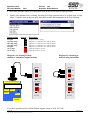
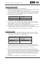
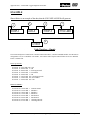
Application Note
Document Number:
Product:
5001
Link
Keywords: Halted Network
Objective
To help diagnose a network failure.
Equipment
Fiber-optic cable (CM056316U…), Fiber-optic connectors (CI055067, CI055068)
NOYES light meter (L5231), Fiber optic cutting tool (LA385204)
Comms cable (CM353470), PC with ConfigEd
Procedure
1. Verify the integrity of the network by updating the monitor list using Configed.
Note: If the Module List only shows one module in the network of multiple modules, there is
a possible break in the Fiber optic or the light level of a transmitter is too low for
operation.
Note: If Halted by co-pro or Network Failure is displayed on your Link Drive (590L, 620L)
or Operator Interface (L5392), verify the light intensity of the Link Modules using the
chart on page 2.
Note: If the Module List displays “PEER HALTED”, Link re-addressed a module due to a
possible duplicate address or other installation faults.
2. If the module list is ok. Then double-click on the individual module to enter the S.A.M. mode
3. Then double-click on the SYSTEM CONTROL block in the configuration to monitor the CRC Errors
and Fragments.
If you have questions, please call the Product Support Group at (704) 588-3246.
22-Sep-04
j:\app_note\5000 - link hardware\5001 ssd link network diagnostics.doc
Page 1 of 2
Application Note
Product:
Document Number:
5001
Link
Keywords: Halted Network
4. Next, hold down the <Shift> key and double-click on the Get Overruns or other get items.
5. Finally, if the Monitor List is counting, the integrity of Link System needs to be verified using a Light
Meter. Using the chart on the next page, determine possible bad components in the Link Network.
Signal quality
marginal
operating range
operating range
operating range
marginal
out of range
out of range
db level
-18
-21
-24
-27
-30
-33
-35
Description
full power-factory setting
half power is reached at each -3db increment
half power is reached at each -3db increment
half power is reached at each -3db increment
half power is reached at each -3db increment
signal too weak for receiver
signal too weak for receiver
Diagram 1 is a drawing to check
simulate a transmitter output intensity.
Diagram 2 is a drawing to
network using one module.
PRIMARY
PRIMARY
RCV
RCV
XMT
XMT
M L H
M L H
LAUNCH
POWER
LAUNCH
POWER
OPTICAL POWER METER
dB / dBm
SECONDARY
SET REF
RCV
RCV
XMT
XMT
M L H
M L H
ON/OFF
SECONDARY
LAUNCH
POWER
LAUNCH
POWER
OPM 4
L5311
L5311
NOYE
If you have questions, please call the Product Support Group at (704) 588-3246.
22-Sep-04
j:\app_note\5000 - link hardware\5001 ssd link network diagnostics.doc
Page 2 of 2
Application Note
Document Number:
Product:
5002
L52xx, L53xx
Keywords: Link 1, Link2
Objective
Provide a cross-reference from Link 1 to Link 2 modules.
Equipment
Link Hardware
Procedure
The following table lists the Link 1 hardware and their Link 2 replacements. Where there are no Link 2
replacements, the Link 1 hardware is still available and compatible with Link 2 products and software.
Module Type
Analog I/O Module
Digital I/O Module
Link 1
Link 2
L5201-2-02
L5341 LinkCard
5 I/Ps and 1 O/P
0-10 VDC and 4-20 mA
8 I/Ps and 2 O/Ps
±10 VDC (No 4-20mA)
L5202-2-01
L5331 LinkCard
12 I/Ps or O/Ps Active Low
(Sinking)
16 I/Ps or O/Ps (programmable)
Active High (Sourcing)
L5209-2-01
12 I/Ps Active High (Sourcing)
Processor Module
L5207-2-00
L5300 LinkRack
L5301 Remote LinkRack
Memory
L5300 > L5301 > L5207
Computer Interface Card
and Gateways
L5204-DDE-01
L5204-DDE-NT
L5204-XL
L5204-DDE-01
L5204-DDE-NT
L5204-XL
L5351 DeviceNet LinkCard
L5353 Profibus LinkCard
Serial Module
L5203-2-00
Logger or Serial Comms
Approx. 30-40 parameters
Link Repeater
L5206-2-00
L5206-2-00
Touchscreen Module
L5101-2-00 (obsolete)
L5102-2-00 (obsolete)
L5392 (color)
Memory
L5392/L5391 > L5390 > L510X
If you have questions, please call the Product Support Group at (704) 588-3246.
22-Sep-04
j:\app_note\5000 - link hardware\5002 ssd link hardware upgrade.doc
Page 1 of 1
Application Note
Document Number:
Product:
5501
X-LINK
Keywords: File Types
Objective
To understand the X-link File Structure.
Equipment
L5510
Procedure
1. *.XLK File
Note: The XLK file contains communication settings and mode setup.
The x-link serial number is embedded in the file. The file can not be used to talk to any other x-link.
When creating the XLK file, choose on-line or off-line mode. After the file is created::opened, the
kernel and the communication drivers must be loaded if not previously installed.
Note: The kernel and communication drivers must be installed in on-line and off-line modes.
The PC being used to program the x-link emulates the x-link in off-line mode.
2. *.CFG File
Note: The CFG file contains the data mappings created for the x-link.
Note: This file does not store communications data or driver information.
After loading or uploading mappings, the additional mappings can be added or inserted. After viewing
the mappings, select ‘SAVE AS’, the file needs to be saved as a .TXT file. The TXT file can be
edited using a text editor. The text editor is an easy way to create::modify large x-link mappings in a
short amount of time.
Note: Start new mapping by creating a single mapping using x-link configuration software.
Create one mapping for a PLC Integer Write, PLC Bit Write, PLC Integer Read and a PLC Bit Read.
Save the mapping as .TXT file. Open the .TXT file and copy::modify as needed. Ensure the syntax
and spacing on all mapping created with the text editor remains the same as the original mapping.
Once text mappings are complete, select load *.TXT. Once the loading is complete, save the file as a
*.CFG' file.
3. *.DMP File
Note: The DMP file contains all information stored in the x-link.
Create a DMP by selecting ‘UPLOAD CMOS’. The DMP file contains mappings, kernel, and
communication driver information. This file will be loaded in the event that the x-link has a hardware
fault and must be replaced.
If you have questions, please call the Product Support Group at (704) 588-3246.
22-Sep-04
j:\app_note\5000 - link hardware\5501 ssd xlink info.doc
Page 1 of 1
Application Note
Document Number:
Product:
5601
L590
Keywords: L570/590
Objective
After completing the upgrade of the existing 570L configuration, it can be installed into 590L.
Equipment
590L Digital DC Drive, 570L configuration, and computer with ConfigEd software (> v 5.10) installed.
Procedure
Note: This is a step by step procedure on converting a Link 570-drive configuration to a Link
590-drive configuration, with version 3.1 firmware.
Warning: Before performing this procedure, you should Export a copy of the project, that you
want to convert, to a floppy disk, in case some problems arise. This way you will
always have an original set of Link configurations. See the Manager User Manual
(RG352101) for this procedure.
1. You must have Read/Write privileges of the project that you want to convert.
Note: Some people may refer to it as “ Having the token “
2. To verify that you have Read/Write privileges, open Manager
3. Select the correct configurations under Project::Utilities to convert.
4. Verify the appropriate project from the Category::Project and window.
5. Verify that the Read/Write window is marked.
Note: The example below displays, the Category selected is AMER1601 and the Project is
LA350628.
6. The Read/Write box is marked; therefore this project has Read/Write privileges.
Note: If the Read Only box is marked, you DO NOT have the proper privileges to convert
the project. Contact your system designer to obtain the proper privileges.
7. Click the Done button to close the window
If you have questions, please call the Product Support Group at (704) 588-3246.
23-Nov-04
issue 1.0
s:\app_note\5000 - link hardware\56xxx - link drives\5601 ssd 570l to 590l upgrade.doc
Page 1 of 4
Application Note
Document Number:
Product:
5601
L590
Keywords: L570/590
8. Close the Manager program.
9. Open the ConfigEd software.
10. Go to Project::Manage, then double click open.
Note: The Manage window will appear as shown below.
11. Select the project in the Category column that you want to convert.
12. Select the project in the Project column that you want to convert.
13. In the example shown below, the Category selected is AMER1601 and the Project selected is
LA350628.
14. Verify that the Cat.Read-Only window is not checked.( See the example below )
15. If it is checked, click your mouse button on this check to remove it.
16. Click the Done button to close the Manage window.
17. Select the Project::Document. Highlight the 570L configurations that are being converted, then select
Document.
Note: This will document each of the 570-Link modules, parameter data. This file will be
called xxxxxxxx.doc, where xxxxxxxx indicates the project number, and is located
under the project number under the ConfigEd directory root directory
ssd_link::configs.
If you have questions, please call the Product Support Group at (704) 588-3246.
23-Nov-04
issue 1.0
s:\app_note\5000 - link hardware\56xxx - link drives\5601 ssd 570l to 590l upgrade.doc
Page 2 of 4
Application Note
Document Number:
Product:
5601
L590
Keywords: L570/590
18. Go to File::New...., the New window will appear as shown below.
19. Select L570-590 from the list as shown below.
20. Click the New button, then advance to the Restore window as shown below.
21. Under the Restore window, chose the appropriate Category:: Project and the desired Backup File to
convert, as shown below the Backup File selected is L570-123.bku from the Category AMER0601
and Project LA350628.
.
If you have questions, please call the Product Support Group at (704) 588-3246.
23-Nov-04
issue 1.0
s:\app_note\5000 - link hardware\56xxx - link drives\5601 ssd 570l to 590l upgrade.doc
Page 3 of 4
Application Note
Document Number:
Product:
5601
L590
Keywords: L570/590
22. Click the Convert button to advance to the next step
23. A User Input window will appear, as shown below. Enter in the new desired name.
Note: In the example below, the old name L570-123 will be renamed to
24. L590-123 will reflect the new hardware change.
25. Click the OK button.
26. The new converted L590-123 configuration will now appear, as shown below.
27. Print the document that was created in step 6 and compare the parameter data to the 590L
configurations just created. Make any changes if required.
This configuration can now be installed in the 590L drive.
If you have questions, please call the Product Support Group at (704) 588-3246.
23-Nov-04
issue 1.0
s:\app_note\5000 - link hardware\56xxx - link drives\5601 ssd 570l to 590l upgrade.doc
Page 4 of 4
Application Note
Document Number:
Product:
5004
Link Hardware
Keywords: Power Supply Ratings
Objective
Provide details of the loading or consumption for Link products.
Equipment
Link products
Procedure
Each of the LinkRacks L5300, L5301, and LinkStation L5392 make a certain amount of backplane power
available to drive LinkCards.
Note: The **user** must ensure that the expected total power consumption of all LinkCards
does not exceed the figure below.
Housing
Description
Max Backplane Rating
L5300
LinkRack
2600 mA
L5301
Remote LinkRack
2600 mA
L5390 (obsolete)
Monochrome Linkstation M1
2000 mA
L5391 (obsolete)
Monochrome LinkStation M2
2000 mA
L5392
Color LinkStation
1600 mA
LinkCard
Description
Max Backplane Consumption
L5311
RTN LinkCard
75 mA *
L5331
Digital I/O LinkCard
225 mA
L5341
Analog I/O LinkCard
620 mA **
L5351
DeviceNet® LinkCard
120 mA
L5352
EtherNet® LinkCard
500 mA
L5353
ProfiBus® LinkCard
275 mA
L5354
ControlNet® LinkCard
350 mA
L5355
ModbusPlus® LinkCard
310 mA
Note: *One L5311 card is always used on any housing to communicate with the LINK
network.
Note: ** For any L539x installation, a maximum of two L5341 Analog I/O LinkCards may be
fitted as part of any combination of LinkCards
If you have questions, please call the Product Support Group at (704) 588-3246.
22-Sep-04
j:\app_note\5000 - link hardware\5004 ssd link hardware power supply.doc
Page 1 of 1
App Note 5401 - L5203 NEP Logger Diagnostic Procedure
Purpose:
To assist with troubleshooting a suspected network problem with a LINK fiber-optic network.
Note: The NEP (Network Exceptions Logger) is a standard L5203 Serial Module with a
configuration that transmits all network exceptions to an RS-232 serial port.
Hardware required:
1 each
L5203-2-00 Serial I/O Module preloaded with Production/Ship
configuration (Addr. 600)
1 each
CM352581 Cable Assembly, DE-9S to Terminals L5203 to PC
or CM351435 Cable Assembly, DB-25P to Terminals L5203 to Printer
2 each
Fiber optic cables (4 each for redundant)
2 each
Wires for 24 VDC power supply for module
1 each
Computer with terminal emulation software or Windows installed
or RS-232 serial printer
Installation procedure:
1. Connect 24 VDC to terminals 3 or 4 of TB1 and the 0 VDC common to terminals 1 or 2 of
TB1.
Note: Preferably this supply is separate from the LINK system’s 24 VDC supply. Supplying the
L5203 with a separate supply allows any Network Exception to be recorded during
operation of the system.
2. Install a fiber optic jumper between FO1 and FO2 on the serial module.
3. Install the 3 terminal connections of either the CM352581 (computer) or CM351435 (printer)
cable to the RS-232 - Channel B.
Note: The cable terminals marked RCV, XMT, and G should be installed into terminals 9
(XMT), 10 (RCV), and 11 (CMN), respectively, on the L5203 module.
4. Apply power to the 24 VDC supply.
Note: The red LED on the L5203 should be on solid (not blinking). If the LED is blinking,
verify all connections before continuing.
5. The appropriate output device must be configured to support the RS-232 port on the L5203
serial module which is set for 9600 baud, 8 data bits, no parity, 1 stop bit.
Note: If using the CM351435 printer cable with a serial printer, refer to the printer’s User
Manual for setup of the printer port. Usually, this is accomplished through an array of
simple dip switches.
Note: If using the CM352581 computer cable, plug the connector into the serial port. Launch
the terminal emulation software on your computer and set up the appropriate port on your
computer to 9600, 8, N, 1.
App Note 5401 - L5203 NEP (Network Exceptions Protocol) Logger Diagnostic Procedure - Issue 2.3
Page 1 of 9
App Note 5401 - L5203 NEP Logger Diagnostic Procedure
Using Windows Hyper Terminal
A. Launch Hyper Terminal from the Accessories folder.
B. Select the program Hypertrm.exe A Connection Description window will appear. In the
Name: window enter something like L5203 Logger. Click OK.
C. A Connect To window will appear. For the Connect using selection, select the computer
comm port which will be used for the logger, probably Direct to Com1. Then click OK.
D. A Com Properties / Port Settings window will appear. In this dialog box, select the
following parameters and then click OK.
Bits per second: 9600
Data Bits: 8
Parity: None
Stop Bits: 1
Flow Control: XON/XOFF
E. A L5203 Logger – Hyper Terminal window will appear. Select the menu Transfer /
Capture Text. A Capture Text Window appear. Enter the path and file name of the log
file, something like C:\L5203Log.txt and click the Start button.
F. You should now be prepared to receive data through the serial port. To test you set-up,
unplug the fiber optic cable per step 6. Make sure the data is being logged.
G. To capture the data to a file, select Transfer /Capture Text / Stop. If this is not done, data
will not be saved to the file. You will need WordPad to view this file.
Using Windows Terminal
A. After starting Windows, launch the Terminal program from the Accessories folder.
B. Under the Menu Item Settings select Communications. After selected, a set-up dialog
box will appear. In this dialog box, select the following:
Baud Rate: 9600
Data Bits: 8
Parity: None
Flow
Control:XON/XOFF
Stop Bits: 1
Connector: COM1
(probably)
Carrier Detect: None
C. Under the Menu Item Transfer select Receive Text File. After selected, a Windows
dialog box will appear which will prompt you for a file name and a destination directory.
Enter the path and file name of the log file, something like C:\L5203Log.txt
D. After setting Terminal up in this mode, a Stop and Pause button will appear at the
bottom of the screen. Unless these buttons are pressed, all network exceptions reported
to the screen will be logged into the selected file. The Stop button will close the file from
further updates while the Pause button will suspend recording the data to the file until
logging is resumed. After pressing the Stop button, the log file may be printed using
WordPad .
E. You should now be prepared to receive data through the serial port. Go to step 6
App Note 5401 - L5203 NEP (Network Exceptions Protocol) Logger Diagnostic Procedure - Issue 2.3
Page 2 of 9
App Note 5401 - L5203 NEP Logger Diagnostic Procedure
6. Test for proper operation by unplugging the fiber optic cable from either the FO1 or FO2
connection of the L5203 module.
Note: If all connections are correct and the terminal emulation program (or printer) is setup properly, the serial port will output the following data:
0d
0d
0d
0d
0d
0d
0d
0d
0h
0h
0h
0h
0h
0h
0h
0h
0m
0m
0m
0m
0m
0m
0m
0m
31s
31s
33s
33s
33s
33s
33s
33s
753ms
775ms
210ms
237ms
261ms
286ms
310ms
334ms
(local)
(local)
(local)
(local)
addr 600
(local)
addr 600
addr 600
Forward Transition
Fragment
Forward Transition
Forward Transition
OK
Forward Transition
Network Warning
OK
(both fail)
(forward fail)
(both fail)
(forward fail)
where
0d
7.
0h
0m 31s
753ms (local)
is a time stamp since power was last applied to the
L5203 serial module’s 24 VDC power terminals
(day, hour, minute, second, millisecond)
(local)
is the L5203 NEP Logger module itself, reporting
the network exception.
Forward Transition
(forward fail)
is the network exception reported by the module
The L5203 NEP Logger may be placed in the LINK Network to diagnose Network
problems.
Note: The user will want to place the associated machinery in a safe condition prior installing
the logger. Once in the system, the logger is transparent to all other control logic which may be
installed in the system.
The network topology determines how many fiber optic jumpers are required to insert the
module into the network. Simply hook the module up in accordance with the network
topology supplied by the system designer
8. After inserting the logger into the network, resume normal operations of the equipment while
monitoring the output of the logger. Note: For printers, a hard copy of all network exceptions
will be recorded. For terminal emulators, the data being received will have to be stored to a
file for later printing.
App Note 5401 - L5203 NEP (Network Exceptions Protocol) Logger Diagnostic Procedure - Issue 2.3
Page 3 of 9
App Note 5401 - L5203 NEP Logger Diagnostic Procedure
EXAMPLE
Shown Below is an example of the data, that the L5203 NEP LOGGER will generate.
1
5
690P-1
2
620-2
L5203
590P-3
3
5392-400
4
Link Topology - Simple
The L5392-400 System Control blocks: “Restart on Network Failure”, “Restart on Module Failure” and “Restart on
configuration” are set to “Disabled”. The 690P-1, 620-2 & the 590P-3 System control blocks are all set to Enabled.
L5203 is address 600.
Power up Network:
0d
0d
0d
0d
0d
0d
0d
0d
0h
0h
0h
0h
0h
0h
0h
0h
0m
0m
0m
0m
0m
0m
0m
0m
0s
0s
0s
0s
0s
1s
1s
1s
43ms addr 600 OK
498ms addr 2 OK
892ms addr 3 Checking Network
915ms addr 3 Peer Halted
938ms addr 3 OK
181ms addr 400 Checking Network
219ms addr 400 Peer Halted
255ms addr 400 OK
REMOVE FIBER 5
0d
0d
0d
0d
0d
0d
0d
0d
0h
0h
0h
0h
0h
0h
0h
0h
2m 59s
2m 59s
2m 59s
2m 59s
2m 59s
2m 59s
2m 59s
2m 59s
343ms addr
367ms addr
390ms addr
413ms addr
436ms addr
459ms addr
863ms addr
937ms addr
1
1
3
2
3
1
1
3
Network Failure
Shutdown
Shutdown
Shutdown
Initialization
Initialization
Checking Network
Checking Network
App Note 5401 - L5203 NEP (Network Exceptions Protocol) Logger Diagnostic Procedure - Issue 2.3
Page 4 of 9
App Note 5401 - L5203 NEP Logger Diagnostic Procedure
REINSTALL FIBER 5
0d
0d
0d
0d
0d
0d
0d
0h
0h
0h
0h
0h
0h
0h
4m
4m
4m
4m
4m
4m
4m
5s
6s
6s
6s
8s
8s
8s
926ms addr
0ms addr
22ms addr
170ms addr
24ms addr
47ms addr
70ms addr
1
3
3
2
1
1
1
Peer Halted
Peer Halted
OK
OK
Checking Network
Peer Halted
OK
REMOVE 1 FIBER
0d
0d
0d
0d
0d
0d
0h
0h
0h
0h
0h
0h
5m 24s
5m 25s
5m 25s
5m 25s
5m 25s
5m 25s
375ms addr
377ms addr
401ms addr
424ms addr
446ms addr
953ms addr
2
2
3
2
3
3
Network Warning
Network Failure
Shutdown
Shutdown
Initialization
Checking Network
3
1
1
2
3
3
3
Peer Halted
Peer Halted
OK
OK
Checking Network
Peer Halted
OK
3
3
3
3
Network Failure
Shutdown
Initialization
Checking Network
3
1
2
3
3
3
1
1
1
Peer Halted
Peer Halted
OK
Checking Network
Peer Halted
OK
Checking Network
Peer Halted
OK
REINSTALL FIBER 1
0d
0d
0d
0d
0d
0d
0d
0h
0h
0h
0h
0h
0h
0h
6m 27s
6m 28s
6m 28s
6m 29s
6m 29s
6m 29s
6m 29s
820ms addr
797ms addr
820ms addr
775ms addr
919ms addr
941ms addr
965ms addr
REMOVE FIBER 2
0d
0d
0d
0d
0h
0h
0h
0h
8m
8m
8m
8m
1s
1s
1s
2s
669ms addr
693ms addr
716ms addr
192ms addr
REINSTALL FIBER 2
0d
0d
0d
0d
0d
0d
0d
0d
0d
0h
0h
0h
0h
0h
0h
0h
0h
0h
8m 49s
8m 49s
8m 49s
8m 51s
8m 51s
8m 51s
8m 51s
8m 51s
8m 51s
380ms addr
439ms addr
549ms addr
478ms addr
501ms addr
524ms addr
550ms addr
574ms addr
597ms addr
App Note 5401 - L5203 NEP (Network Exceptions Protocol) Logger Diagnostic Procedure - Issue 2.3
Page 5 of 9
App Note 5401 - L5203 NEP Logger Diagnostic Procedure
REMOVE FIBER 3
0d 0h 9m 30s 811ms addr 400 Network Failure
REINSTALL FIBER 3
0d
0d
0d
0d
0d
0d
0d
0d
0d
0d
0d
0d
0h 11m 23s
0h 11m 23s
0h 11m 23s
0h 11m 24s
0h 11m 24s
0h 11m 24s
0h 11m 25s
0h 11m 25s
0h 11m 25s
0h 11m 25s
0h 11m 25s
0h 11m 25s
522ms addr
583ms addr
723ms addr
248ms addr
422ms addr
576ms addr
621ms addr
644ms addr
667ms addr
693ms addr
717ms addr
740ms addr
3 Peer Halted
1 Peer Halted
400 OK
400 Network Failure
400 OK
2 OK
3 Checking Network
3 Peer Halted
3 OK
1 Checking Network
1 Peer Halted
1 OK
REMOVE FIBER 4
0d 0h 12m 2s 715ms (local)
Forward Transition (both fail)
REINSTALL FIBER 4
0d
0d
0d
0d
0d
0d
0d
0d
0d
0d
0d
0d
0d
0d
0d
0h 12m 52s
0h 12m 52s
0h 12m 52s
0h 12m 52s
0h 12m 52s
0h 12m 52s
0h 12m 52s
0h 12m 52s
0h 12m 52s
0h 12m 54s
0h 12m 54s
0h 12m 54s
0h 12m 54s
0h 12m 54s
0h 12m 54s
274ms (local) Forward Transition (forward fail)
301ms (local) Forward Transition (both fail)
326ms addr 600 OK
349ms addr 600 Network Warning
376ms (local) Forward Transition (forward fail)
399ms addr 600 OK
653ms addr 3 Peer Halted
713ms addr 1 Peer Halted
983ms addr 2 OK
751ms addr 3 Checking Network
774ms addr 3 Peer Halted
797ms addr 3 OK
823ms addr 1 Checking Network
847ms addr 1 Peer Halted
870ms addr 1 OK
REMOVE POWER TO 690P-1
0d
0d
0d
0d
0d
0d
0h 17m 38s
0h 17m 39s
0h 17m 39s
0h 17m 39s
0h 17m 39s
0h 17m 40s
906ms addr 2 Network Warning
907ms addr 2 Network Failure => => See Analysis of data, listed below
931ms addr 3 Shutdown
954ms addr 2 Shutdown
976ms addr 3 Initialization
490ms addr 3 Checking Network
App Note 5401 - L5203 NEP (Network Exceptions Protocol) Logger Diagnostic Procedure - Issue 2.3
Page 6 of 9
App Note 5401 - L5203 NEP Logger Diagnostic Procedure
RE – APPLYPOWER TO 690P-1
0d
0d
0d
0d
0d
0d
0d
0d
0d
0d
0h 19m 6s 474ms addr
0h 19m 8s 572ms addr
0h 19m 8s 595ms addr
0h 19m 8s 733ms addr
0h 19m 8s 756ms addr
0h 19m 8s 779ms addr
0h 19m 9s 633ms addr
0h 19m 10s 670ms addr
0h 19m 10s 693ms addr
0h 19m 10s 716ms addr
Analysis of data
3
3
3
1
1
1
2
3
3
3
Peer Halted
Checking Network
Peer Halted
Checking Network
Peer Halted
OK
OK
Checking Network
Peer Halted
OK
(see REMOVE POWER TO 690P-1, listed on previous page)
0d 0h 17m 39s 907ms addr 2
Network Failure
0d 0h 17m 39s 907ms
is a time stamp since power was last applied to the L5203
serial module’s 24 VDC power terminals (day, hour,
minute, second, millisecond)
addr 2
is the address reporting a problem
Network Failure
The Link network shut down because of a problem with
this module.
buffer overflow
So much data is being reported to the L5203 Logger, that the
buffer of this logger module overflowed. At this point, all of
the data in the L5203 is lost and the Link network may go
down because of a L Error occurring in this module. The
“baud rate” of the L5203 can be increased to prevent this
overflow.
In this example, address 2 is reporting a Network Failure. The Link network shut down because
of a problem with this module. This indicates that address 2 is receiving bad data or there is a
hardware problem with this Link module.(In this case power was removed from this module).
Thus the problem can be: the fiber optic receiver of address 690P-1, the fiber optic transmitter
of the module sending data to address 690P-1, the fiber optic cable, or the fiber optic
terminations between these 2 modules.
App Note 5401 - L5203 NEP (Network Exceptions Protocol) Logger Diagnostic Procedure - Issue 2.3
Page 7 of 9
App Note 5401 - L5203 NEP Logger Diagnostic Procedure
Appendix
Link Module States
The SSD LINK system defines thirteen primary states in which a module
can exist:
States
0
1
2
3
4
5
6
7
8
9
10
11
12
Initialization
Halted
Missing or Bad Configuration
Cr ashed
OS Er ror
Self-Test Failure
Shutdown
OK
Network Warning
Network Failure
Checking Network
Peer Halted
Duplicate Address Detected
(any state)
(any state)
P
(any state)
R
T
N
Self-test failed
Self-test OK, config not OK
Self-test OK, config OK, halt flag cleared
Self-test OK, config OK, halt flag set
Duplicate address de tected
Network pr esent
All modules r eady to run
Exception detected inside primitive ope ration
Exception detected by pr ogram
Module shutdown by pr ogram
Power fail war ning
Power OK
NCP Purge
NCP Stop, config not OK
NCP Start
Power OK
NCP Stop, config OK
Power off
B
2
A
0
D
C
5
1
S
Power
Off
10
E
F
U
M
12
Transitions
A
B
C
D
E
F
G
H
J
K
L
M
N
P
R
S
T
U
(any state)
11
6
G
K
L
7
(any state)
No rmal
Operating
States
8
J
4
9
H
3
App Note 5401 - L5203 NEP (Network Exceptions Protocol) Logger Diagnostic Procedure - Issue 2.3
Page 8 of 9
App Note 5401 - L5203 NEP Logger Diagnostic Procedure
Appendix
CM352581
Cable Assembly, DE-9S to Terminals L5203 to PC layout:
App Note 5401 - L5203 NEP (Network Exceptions Protocol) Logger Diagnostic Procedure - Issue 2.3
Page 9 of 9
Application Note
Document Number:
Product:
5101
L5300 / L5392
Keywords: Self-test
Objective
To diagnose a L5300 or L5392 has a possible hardware problem.
Equipment
L5300 Link Rack or L5392 Link Op Station and a PC
Procedure
1.
2.
3.
4.
5.
6.
7.
Open the TERMINAL program on your computer
Verify under settings that the baud rate is 2400
Select your Comm port
Disconnect the AC power to the Link 2 unit
Remove the back cover
Plug in the Comm cable to the Link unit
Apply AC power
The following should be displayed on the computer screen
SELF TEST
BOARD: OK L5392
EPROM: OK
SRAM: OK
NOVRAM: OK
FLASH: OK (USED)
65535: OK
VDRAM: OK
Done.
Note: If something like the following is displayed the Baud Rate is set incorrectly.
™ ? ˜? ˜? ˜? ˜? f˜xffæ˜fæ? ˜? ? 昆˜`˜˜˜? ˜˜f˜x†xæ? ˜? ˜f˜æ˜æ˜˜˜˜? ˜˜˜? ˜˜†˜ff˜˜˜˜? ˜˜˜? ˜þ˜xf˜f
f˜˜˜˜? ˜˜˜? `à˜æ˜˜˜ø˜˜? ˜†ff˜f``f†æ? ˜? f˜æ˜xf~˜˜? ˜˜˜? f`†˜ff˜˜ø˜˜? ˜˜˜? `æ? ø? f††æ? ˜? ˜? ˜
? æ? ˜?
8. Remove AC power
9. Install Back Cover to insure proper operation of Link unit
If you have questions, please call the Product Support Group at (704) 588-3246.
19-Nov-04
s:\app_note\5000 - link hardware\51xxx - operator stations\5101 ssd hardware test.doc
Page 1 of 1
Application Note
Document Number:
Product:
5003
Link 1 and Link 2 modules
Keywords: Resetting Link modules
Objective
Resetting Link 1 and Link 2 modules.
Equipment
Link modules requiring a reset and computer with ConfigEd software (> v 5.13) or DSD software
installed.
Procedure
1. Launch ConfigEd or DSD in wizard mode on the computer.
For ConfigEd: Hold down the <ALT> key immediately after double clicking on the ConfigEd icon.
For DSD: Hold down the <SHIFT> key while double clicking on the DSD icon.
Further details can be found in the ConfigEd manual RG353792
2. Remove the Link module to be reset from the Link fiber optic network. Install a small fiber optic
cable to jumper the transmitter and receiver on the primary port of the Link module.
3. Apply power to the Link module and connect the Link serial cable into the UDP/P1/RTNX port.
4. Select WINDOW::UPDATE partial to get a module list. The CE Module List window should contain
only the Link module to be reset. Highlight the Link module and then go to COMMAND::RESET
EAT. The program will ask you if you are sure; click on RESET.
5. Go to WINDOW::UPDATE PARTIAL to update the module list. In the CE Module List window
should show the following:
After Reset EAT
(3xxx)
(boot)
No Config
6. When the reset is finished the module is ready to accept a new configuration or to reload an existing
configuration. Be sure to confirm the module type and the configuration type prior to downloading to
the module. If the wrong type configuration is downloaded it is possible to cause PERMANENT
DAMAGE to the module.
Note: The program will download the configuration from a L5101/5102 into the L5392.
The L5392 will accept the older L5101/5102 configurations with no problems.
7. The module should no faults if the download was successful. If the module is an L5392 operator
station it may be necessary to hold the minus side of the contrast button until the screen lights up
enough to view the display. If the download is not successful, repeat Steps 2 through 5. If the
download is not successful after two tries, the module probably needs to be repaired.
If you have questions, please call the Product Support Group at (704) 588-3246.
22-Sep-04
j:\app_note\5000 - link hardware\5003 ssd resetting link modules.doc
Page 1 of 1
LA385204
FIBER OPTIC CABLE END PREPARATION KIT
FOR USE WITH SSD DRIVES ACRYLIC FIBER OPTIC CABLE
CM352278 OR CM059748
For use with SSD Drives acrylic fiber optic cable CM352278 or CM059748.
1.
2.
Fiber optic cable end preparation cutting kit (SSD Drives part number LA385204) includes one (1) cutting
fixture JA385201 and one (1) single edge cutting blade JA385205.
Insert fiber optic cable complete with sheath, into cutting fixture and cut off with blade as illustrated
in figure 1 and 2. For Optimum results fiber optic cable should pass through both sides of cutting fixture.
Figure 1.
Figure 2.
3.
When re-using several times, try to select an unused section of the cutting edge. Replace blade as often as
necessary. Care should be taken when discarding used single edge cutting blade.
4.
Assemblies using Thomas & Betts connectors, SSD Drives part number CI055069 (red) or CI055070 (black):
DO NOT use the cutting blade on the connector, or the T&B instruction sheet. Place the dressed end of fiber
optic cable into the fiber optic clamp until it touches the blade cutting area as shown in figure 3. The fiber optic
cable must be fully engaged before assembling the connector. While firmly holding fiber optic cable in place,
carefully press connector together until fully engaged (i.e. flush with the top of the plug housing). Discard the
end piece of the fiber clamp and inspect assembly to verify fiber optic cable is flush with end of plug housing as
shown in figure 4.
Figure 3.
5.
Figure 4.
Assemblies using Hardened Receivers, SSD Drives part number LA385169:
Loosen the two screws and insert the dressed end of the fiber optic cable into the receiver until it touches the
attenuator. While firmly holding fiber optic cable in place, tighten screws with proper pressure to hold the fiber
optic cable in place.
If you have any questions, please call Customer Service at (704) 588-3246.
HA385204U002 (Issue 2)
LINK Application Note
L5202/L5209 Link Module Frequency Counter Input:
Hardware Description:
The L5202 and L5209 modules provide in hardware the capability to count events and
measure frequency on channel 1 (terminal 1). Channel 2 provides a high speed
interface to a module's CPU for direction sensing. The hardware characteristics of the
frequency counter input are as follows:
• Single ended 0V to 5V input.
• Max. input frequency is designed to be 65.535kHz.
• Single direction counting on channel 1 (terminal 1) only. Counts occur on both
rising and falling edges.
• Digital i/o (L5202) or input (L5209) channels 3 - 12 are available for ordinary
logic functions.
Software Description:
A default Link configuration is provided to support frequency counting. The
configurable frequency counting parameters reside in the Handler2 function block. The
software provides the following features:
• Calculation of channel 1 input frequency.
• Max. input frequency configurable from 14 Hz to 65,535 Hz.
• Pseudo-bidirectional counting with direction sensed at ~1ms intervals.
• Count direction may be based upon a logic level or a quadrature signal.
• A divide by N square wave is available for Link software function blocks. The
frequency divider is configurable from 1 to 32500. A logic level specifying the
direction of the signal is also provided for Link function blocks.
• The update period for frequency calculations is configurable from 8 ms to 35 ms.
HR351009 issue C
1
LINK Application Note
Application Recommendations:
Applications recommended for L5202/L5209 frequency counter:
• Speed reference input to a Link based control system.
• Input to a Link system for operator display parameters.
• Medium precision counting, eg. feet of product produced, etc.
• Speed feedback for systems with mechanical BW less than 400Hz.
• Low speed (less than 20 Hz) single event counting may be implemented on any
digital i/o channel.
Applications not recommended for L5202/L5209 frequency counter:
• Absolute precision position counting.
• Position control.
• Very high performance speed control applications.
HR351009 issue C
2
LINK Application Note
Limitations of the Frequency Counter:
Several characteristics of the frequency counter must be evaluated when considering
the L5202/L5209 frequency counter for an application. The first considerations are
obviously the frequency range, accuracy, and electrical interface. The frequency range
of the counter is adequate for most industrial applications. While providing high
accuracy, the L5202/L5209 frequency counter has some unusual characteristics which
affect accuracy for some applications. A discussion of the accuracy of the counter is
provided in the last section of this document.
The electrical interface has a significant impact on the usefulness of the L5202 or L5209 in
a given application. The inputs are single ended rather than differential. Practically,
this severely limits the distance between the module and the electrical signal source
(encoder or repeater). At present, no specification exists for the distance to signal
source other than to recommend as short a distance as possible.
A single ended square wave of any voltage from 5V to 24V may be safely used with this
frequency counter. However, to provide the maximum noise immunity, it is
recommended that higher amplitude signals be attenuated to 5V with resistors. For the
L5209, series resistors may be used. For the L5202, which has 6mA active pullups on
each channel, a resistor between channel terminal and ground is also necessary.
R ≈ 0.7 * (Vmax - 5) kΩ
Series attenuation resistor for L5209
Rg ≈ 5 / ( 6 + Iin ) kΩ
Ground shunt resistor for L5202.
Rs ≈ ( Vmax - 5 ) / Iin kΩ Series attenuation resistor for L5202.
The active pullup channels of the L5202 may cause problems with low current signal
sources. Oscillation of signal source drivers at the wrong frequency have been observed
with low current CMOS drivers. The L5202 has been successfully tested with SSD's
5702/2 terminal repeater. Most encoders and repeaters designed for industrial
environments should provide adequate current drive capability to interface with the
L5202. The L5209 has no internal pullups, and therefore does not experience this
problem.
One significant electrical interface factor affecting the use of the L5202 or L5209 as a
frequency counter is power supply. The Link modules require +24V unregulated
supplies, while many frequency sources require +12V or +5V supplies. Due to its single
ended inputs, the Link module must be located near the frequency source. If the Link
HR351009 issue C
3
LINK Application Note
module is located with an encoder, it is likely that two power supplies must be
provided at that potentially remote location. Furthermore, it is unlikely that the
remaining logic i/o channels will be useful at the remote position. Locating the Link
module within an enclosure with drives or other Link modules is desirable, and power
is likely to be available. Unfortunately, the enclosure is not necessarily located near
enough to an encoder for single ended signal transmission. Thus the use of a signal
converter is likely, adding to hardware cost.
A paramount issue with the L5202/L5209 frequency counter is that the counter is not a
true bi-directional counter. Rather, the direction is sampled at ~1ms intervals. This
characteristic has two potential effects. First, upon direction changes, the frequency
value is defined to be zero. Any counts occuring within the 1ms interval of a direction
change are lost. Although a divide by n signal is available to software for counting, the
L5202 and L5209 cannot be used to measure position precisely in applications where direction
changes or repeated stopping occur. Furthermore, under no circumstances should the
frequency counter be used in closed loop position control. The frequency counter is very
good at measuring frequency; it is not intended as a position counter. Note that
applying the frequency counter to measuring length of run for a continuously produced
web is acceptable.
Another potential effect of sampled direction sensing is aliasing. Aliasing is likely if the
input frequency is modulated at or above 500Hz. In most drive applications, the
mechanical bandwidth will not approach 500Hz. Therefore, this frequency counter may
be safely used as a speed feedback device in many cases. In very high performance
applications such as servo systems, however, aliasing is a real possibility. Use of this
frequency counter in very high performance speed control applications is not
recommended.
Other direction sensing issues should be considered when using quadrature signals.
Dedicated quadrature direction sensing circuitry does not exist in the L5202/L5209.
Due to limitations in the hardware, quadrature direction sensing may fail at very high
frequencies with low slew rate inputs. The symptom is a markedly noisy frequency
measurement at higher frequencies. Quadrature direction sensing has been tested
successfully at frequencies beyond 66kHz with a 200ns rise time square wave.
Problems have been observed above 42kHz with a 2µs rise time square wave. Use of
the SSD 5702/2 terminal repeater unit is regarded as safe for quadrature signals up to
65,535 Hz.
The use of quadrature signals has another significant effect. If the quadrature signal is
lost on channel 2, the frequency counter is unable to determine the correct direction.
Because the software cannot continuously track the second phase of the signal, it cannot
detect loss of the quadrature phase. The result is that the frequency measurement
HR351009 issue C
4
LINK Application Note
degenerates into noise with variance rising with increasing signal frequency on channel
1.
Software Configuration Notes:
The software function block supporting the frequency input has been designed to
permit maximum flexibility. It is possible for the user to create a hardware / software
configuration which will be unable to operate due to cpu performance limitations. This section
describes how to avoid this problem.
The user may select the frequency measurement update time. This represents the real rate
at which frequency samples are sent by the Handler2 (digital i/o) function block to
other software function blocks. The first thing to note is that accumulating counts over
a longer interval provides a larger count value, ie. more resolution. Reducing the sample
interval (speeding up sampling) reduces the resolution, and therefore accuracy, of frequency
measurements. For example, 65.535 kHz sampled at 35ms yields resolution of ±0.0218%,
while reducing the sample time to 10ms yields resolution of ±0.0763%. (Accuracy and
resolution will be discussed in the last section).
The second consideration when selecting sample time is possible cpu overload. Each
software function block requires time to execute. In addition, each message sent
between function blocks requires processing time. The cpu can handle only a finite
number of function blocks and messages per second. Ordinarily, a configuration will
contain a control loop, and messages are propogated around the loop only as fast as the
cpu can manage. In these cases, the loop will run quickly or slowly depending upon the
necessary cpu overhead. If for some reason, a configuration of function blocks (within a
single Link module or a system) generates messages faster than an individual module's
cpu can process them, then that module will cease to operate (crash).
The use of frequency sampling can potentially cause a Link module to crash. A loop
configuration is inherently self-regulating, because messages which cause or "spawn"
other messages are themselves spawned again only after the loop processing is
complete. Frequency samples are not subject to this self regulating process: they occur
at a fixed rate regardless of whether the cpu is keeping up. If the update rate is too fast,
then the cpu will fall behind in processing until it finally crashes.
Thus there are two incentives to configure long frequency sample times: high resolution and
reduced likelihood of crashing a Link module. Obviously, control loop performance will be
enhanced by a shorter sample time, provided that the cpu can keep up.
The risk of crashing a module may be reduced in two ways: increase the frequency
sample time and severely limit the number of destinations (and hence the spawned
HR351009 issue C
5
LINK Application Note
messages) for the fast frequency output. For example, send the frequency sample
directly to a control loop, but send it through a Sampler function block running at a
slower rate to update an operator display.
The user may also select a frequency divider value for the "divide by n" output of the
Handler2 (digital i/o) software function block. It is very easy to crash a module by
failing to properly limit the value of the frequency divider (n). For example, specifying
a divide by 1 output with a maximum input frequency of 50kHz will force the cpu to try
to handle at least 100,000 messages per second (one per edge) in addition to its other
processing. The module will certainly crash -- immediately. For this reason, simple
guidelines are provided for choosing n:
n > 20 * max freq. (kHz)
Absolute limit on n (~20ms per cycle).
n > 50 * max freq. (kHz)
Recommended (~50ms per cycle).
It is the cpu speed which actually limits resolution when using counter function blocks
in software to count high frequency events. For example, if a 30kHz input is expected
from a 1000ppr encoder, the minimum value of n is 1500. This means that a counter
function block will increment every 1.5 revolutions or 3000 encoder edges. Such a
counter would be useful for recording meters or even feet of product on some drive
systems, but the measurement resolution will not extend to many (if any) decimal
places. Decreasing the input signal frequency decreases the count resolution of software
counter function blocks used with the divide by n feature.
Note that if the real frequency of an input signal is less than 0.020 kHz (20 Hz), then a
divide by one signal may be configured (n = 1). In this case, full resolution counting
may be implemented easily. In fact, any of the ordinary input channels could be used
in this case.
HR351009 issue C
6
LINK Application Note
Accuracy, Etc.
The algorithm used to compute frequency is as follows:
frequency =
actual freq. * scale
full scale freq.
=
actual counts * nominal time * scale
actual time * full scale counts
Note that this calculation involves two division operations. The remainder when
dividing the count measurement is retained. Thus no input counts are lost by the
calculation itself. The remainder when dividing the nominal time is used to round the
result.
The result is scaled. In the software, the scaling factor may be changed to alter what is
considered full scale. Full scale frequency may be selected between 14 and 65,535 Hz.
Some effects causing inaccuracy are independent of the maximum frequency selected,
while others are not. This is discussed below.
Characteristics of the frequency calculation and measurement which are not considered
in the accuracy specifications are as follows:
• Direction is sampled. When a direction change is encountered, the sampled
count value is defined to be zero. Thus counts may be lost on direction change.
Although this effect is not considered in the accuracy figure, awareness of this
effect is critical when evaluating this frequency counter for applications
• Due to the sampling of direction, frequency modulation (ie. rate of change) must
be limited to less than ~400Hz to prevent aliasing. Although this effect is not
considered in the accuracy figure, awareness of this effect is critical when
evaluating this frequency counter for applications.
• The measurement of a fixed frequency will fluctuate due to retention of the count
remainder. This actually improves the accuracy of the frequency measurement
averaged over time. In the absence of other sources of error, the average
frequency measurement would actually be perfect over a long time. A maximum
±0.4% fluctuation in calculated frequency is expected at 65.535 kHz. This effect is
not considered in the accuracy figure.
HR351009 issue C
7
LINK Application Note
Characteristics of the frequency calculation and measurement which affect accuracy are
as follows:
• Clock crystal tolerance is ±0.02778% with a ±0.05556% variation over full
temperature range (0° C to +50° C). Thus the crystal will introduce an extreme
worst case inaccuracy of ±0.08334% into the frequency calculation. This
figure is independent of what is considered the full scale frequency.
• Maximum roundoff error at full scale for a single sample is ±0.00153%. This
figure is independent of what is considered the full scale frequency.
• The minimum frequency which can be measured is 14.3 Hz (one count per 35ms)
yielding a maximum resolution of 0.022% at 65.535 kHz. The resolution is
affected by the selected full scale frequency. The quantization error in
percentage may be computed by
1
2
*
1
----------------------(sample interval)
*
1
---------------------------- * 100%
(full scale frequency)
where time is measured in milliseconds, and frequency in kHz.
The greatest source of inaccuracy in the algorithm is the resolution limit. The greatest
source of inaccuracy overall is the clock crystal. Thus the maximum error in a single
frequency calculation (assume 65.535 kHz sampled at 35ms) may be computed as follows:
+
+
+
0.00153%
0.02180%
0.02778%
0.05556%
Max. roundoff error in one sample.
Resolution error.
Clock crystal tolerance.
Clock crystal variation over temp. range.
=
0.10667%
Max. error including worst case crystal variation.
HR351009 issue C
8
LINK Application Note
Thus, at maximum 65.535 kHz sampled at 35 ms, frequency measurement accuracies
are given as follows:
• Excluding clock crystal variation:
±0.023%
• Including clock crystal tolerance at fixed temp.:
±0.051%
• Including worst case clock crystal variation: ±0.107%
Using the figures and equations provided, frequency measurement accuracies at
another maximum frequency, 30.0 kHz sampled at 35ms, are given as follows:
• Excluding clock crystal variation:
±0.049%
• Including clock crystal tolerance at fixed temp.:
±0.077%
• Including worst case clock crystal variation: ±0.132%
The variation of the clock crystal is not considered in many applications. This is
because the clock crystal will introduce an essentially constant error in all frequency
measurements, if it is assumed that the temperature variation is small or slow. In
contrast, the roundoff and resolution errors vary randomly with each frequency
measurement. It is important to note that if absolute frequency measurement is critical,
or if it is desired to compare frequency measurements from two different Link modules,
then the crystal variation must be considered. These considerations are necessary in
any system in which frequency is measured digitally.
Theoretically, a fixed frequency could be established which would cause a constant
roundoff error in measurement. In practice, however, there is jitter in the ~1 ms scan
time due to varying interrupt latency in the microprocessor, and the roundoff error is
reasonably assumed to be a random variable with a zero mean.
HR351009 issue C
9