1
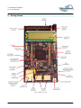
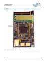
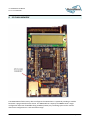
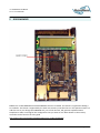
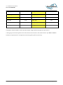
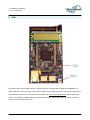
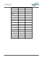
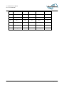
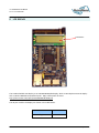
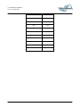
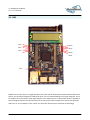
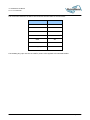
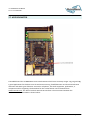
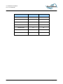
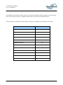
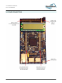
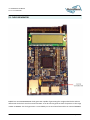
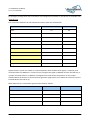
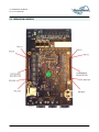
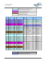
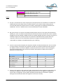
Bubble board User Manual
2012-02-06
RivieraWaves
http://www.rivierawaves.com/
RivieraWaves confidential. This document is copyrighted and released under CDA or NDA only. Do not copy or distribute without written
authorization from RivieraWaves. Please check with RivieraWaves that this document is the latest release.
Title: Bubble board User Manual
Release Date: 2012-02-06
Table of Contents
Table of Contents .............................................................................................................................. 2
List of Figures .................................................................................................................................... 4
List of Tables ...................................................................................................................................... 5
1
Introduction ................................................................................................................................. 6
2
Getting Started............................................................................................................................ 7
3
FPGA .......................................................................................................................................... 10
4
SPI FLASH MEMORY ............................................................................................................... 11
5
DDR3 MEMORY......................................................................................................................... 13
6
DIL HEADERS ........................................................................................................................... 16
7
USB ............................................................................................................................................ 19
8
TOP IDC HEADER ..................................................................................................................... 22
9
LCD DISPLAY ............................................................................................................................ 24
10
LEDS ........................................................................................................................................ 26
11
REAL TIME CLOCK ................................................................................................................ 28
12
POWER MONITOR AND MASTER RESET ........................................................................... 30
13
OSCILLATOR .......................................................................................................................... 31
14
SWITCHES .............................................................................................................................. 32
15
16k SERIAL EEPROM ............................................................................................................ 34
16
MICRO SD CARD HOLDER ................................................................................................... 36
17
ACCELEROMETER ................................................................................................................ 38
18
PS2 ........................................................................................................................................... 40
19
POWER CONNECTIONS ........................................................................................................ 42
20
POWER REGULATORS ......................................................................................................... 44
21
CLOCK GENERATOR ............................................................................................................ 46
Confidential – © 2012 RivieraWaves
Page 2 of 58
Title: Bubble board User Manual
Release Date: 2012-02-06
22
EXPANSION HEADERS ......................................................................................................... 48
23
Programming Bubble ............................................................................................................ 53
24
MECHANICAL ARRANGEMENT ........................................................................................... 56
Confidential – © 2012 RivieraWaves
Page 3 of 58
Title: Bubble board User Manual
Release Date: 2012-02-06
List of Figures
Figure 2.1 Bubble front View ............................................................................................................................ 7
Figure 2.2 Bubble Back View ............................................................................................................................. 8
Confidential – © 2012 RivieraWaves
Page 4 of 58
Title: Bubble board User Manual
Release Date: 2012-02-06
List of Tables
No table of figures entries found.
Confidential – © 2012 RivieraWaves
Page 5 of 58
Title: Bubble board User Manual
Release Date: 2012-02-06
1
Introduction
Welcome to your Bubble board. Bubble is a Spartan-6 based FPGA development board offering a highly
powerful, flexible and low cost approach to prototyping FPGA and System designs.
The aim of this manual is to assist in using the main features of Bubble.
There are features that are beyond the scope of the manual. Should you need to use these features then
please contact RivieraWaves for detailed instructions.
Bubble currently comes with a XC6SLX150-2FGG484C or XC6SLX75-2FGG484C Spartan-6.
Bubble is supported by the Ripple RF daughter board which contains a radio chip compliant with Bluetooth
4.0.
Confidential – © 2012 RivieraWaves
Page 6 of 58
Title: Bubble board User Manual
Release Date: 2012-02-06
2
Getting Started
Figure 2.1 Bubble front View
Confidential – © 2012 RivieraWaves
Page 7 of 58
Title: Bubble board User Manual
Release Date: 2012-02-06
Figure 2.2 Bubble Back View
The Bubble board can be supplied with either a Prog2 parallel port programming cable or a Prog3 USB port
programming cable.
Confidential – © 2012 RivieraWaves
Page 8 of 58
Title: Bubble board User Manual
Release Date: 2012-02-06
The full Xilinx toolset is required to build a design on the on board Spartan 6 LX150 FPGA.
ISE Webpack can be obtained directly from the Xilinx website at http://www.xilinx.com/ise. Registration
will be necessary to complete the download.
The full ISE toolset can also be purchased from the Xilinx website.
Once you have obtained your ISE tools:
(1) Connect your programming cable to the board and your PC hosting the Xilinx software.
(2) Connect the Bubble board to either a USB connector of a PC, a USB power supply or a 5V source
plugged into the 2.1mm Jack socket. Note that some Laptops and desktop computer USB ports have a
current limit of 100mA. Bubble can exceed this in some circumstances and should you have a problem
a powered USB hub or external mains to USB adaptor are recommended solutions. Check that the 5V
input selection jumper on J11 (situated adjacent to the 5V jack socket) is set to the correct position –
left for power from USB, right for power into Jack socket. Switch the power ON using the small
standby switch near J11.
(3) If using an external power brick switch on your power source.
Confidential – © 2012 RivieraWaves
Page 9 of 58
Title: Bubble board User Manual
Release Date: 2012-02-06
3
FPGA
Bubble supports Spartan-6 devices in the FGG484 package. Bubble is normally available with commercial
grade -2 speed devices fitted in the XC6SLX150 size.
Confidential – © 2012 RivieraWaves
Page 10 of 58
Title: Bubble board User Manual
Release Date: 2012-02-06
4
SPI FLASH MEMORY
The M25P128 SPI flash memory device configures the FPGA when it is powered providing a suitable
bitstream is programmed into the device. The M25P128 has a capacity of 128Mbits with a single
configuration bitstream for Bubble taking 4.1Mbits (LX150). Any remaining space can be used for
alternative configurations or code and data storage.
Confidential – © 2012 RivieraWaves
Page 11 of 58
Title: Bubble board User Manual
Release Date: 2012-02-06
After configuration the SPI Flash can be accessed via the following pins of the FPGA:
M25P128 FUNCTION
FPGA PIN
CCLK
Y21
MOSI
AB20
WRITE
V15
DIN
AA20
CSO_B
T5
The HOLD pin of this memory device is permanently connected to 3.3V.
The flash memory can be programmed using direct SPI programming from the 7x2 programming connector
J8. To achieve this the jumper J14 must be connected between pins 1 and 2 (left position). Otherwise the
jumper J14 should be connected between pins 2 and 3 (right position) so that normal JTAG programming
can be achieved.
The connections to the SPI flash can also be accessed via the USB interface. This option requires the jumper
J14 to be connected between pins 2 and 3 (left position). The connections between the USB interface and
the SPI flash memory are shown below:
M25P128 FUNCTION
USB SIGNAL NAME
FT2232 PIN
CCLK
BDBUS0
38
MOSI
BDBUS1
39
DIN
BDBUS2
40
CSO_B
BDBUS3
41
Confidential – © 2012 RivieraWaves
Page 12 of 58
Title: Bubble board User Manual
Release Date: 2012-02-06
5
DDR3 MEMORY
Bubble has a 1GBIT DDR3 Micron MT41J64M16LA device as standard. This device is organised as 8 Meg x
16 x 8 banks. This device is supported by the hard core memory controller that is in the Spartan-6 FPGA. To
add this core to your design the COREGEN tool, part of the ISE suite, will generate implementation
templates in VHDL or Verilog for the configuration that you want to use. More details on the memory
controller can be found in the user guide
http://www.xilinx.com/support/documentation/user_guides/ug388.pdf.
Confidential – © 2012 RivieraWaves
Page 13 of 58
Title: Bubble board User Manual
Release Date: 2012-02-06
The DDR3 has 12 address lines and 16 data lines to address all the available memory, which can be
accessed at speeds of 1.87ns. More details of the DDR3 can be found in
http://download.micron.com/pdf/datasheets/dram/ddr3/1Gb_DDR3_SDRAM.pdf.
For OEM applications we can fit bigger DDR3 parts subject to limitations of the memory controller.
The DDR3 site has the following connections to the FPGA:
DDR3 FUNCTION
FPGA PIN
DDR3 FUNCTION
FPGA PIN
DDR_A0
F21
DDR_DQ3
M22
DDR_A1
F22
DDR_DQ4
J20
DDR_A2
E22
DDR_DQ5
J22
DDR_A3
G20
DDR_DQ6
K21
DDR_A4
F20
DDR_DQ7
K22
DDR_A5
K20
DDR_DQ8
P21
DDR_A6
K19
DDR_DQ9
P22
DDR_A7
E20
DDR_DQ10
R20
DDR_A8
C20
DDR_DQ11
R22
DDR_A9
C22
DDR_DQ12
U20
DDR_A10
G19
DDR_DQ13
U22
DDR_A11
F19
DDR_DQ14
V21
DDR_A12
D22
DDR_DQ15
V22
DDR_A13
D19
DDR_LDM
L19
DDR_A14
D20
DDR_LDQS
L20
DDR_A15
B21
DDR_LDQS_N
L22
DDR_BA0
J17
DDR_UDM
M20
DDR_BA1
K17
DDR_UDQS
T21
DDR_BA2
H18
DDR_UDQS_N
T22
Confidential – © 2012 RivieraWaves
Page 14 of 58
Title: Bubble board User Manual
Release Date: 2012-02-06
DDR_CS_N
P20
DDR_ODT
G22
DDR_RAS_N
H2
DDR_CAS_N
H22
DDR_WE_N
H19
DDR_RESET_N
F18
DDR_DQ0
N20
DDR_CKE
D21
DDR_DQ1
N22
DDR_CLK_N
J19
DDR_DQ2
M21
DDR_CLK
H20
The signals shown shaded in yellow are terminated using suitable arrangements of resistors.
A timing loop has been implemented on the PCB and connected to the FPGA between pins R19 and P18 to
facilitate compensation for temperature and timing delays where necessary.
Confidential – © 2012 RivieraWaves
Page 15 of 58
Title: Bubble board User Manual
Release Date: 2012-02-06
6
DIL HEADERS
LEFT COLUMNS
OUTER PINS
ROW
FUNCTION
RIGHT COLUMNS
INNER
INNER
S6 PIN
PINS
PINS
OUTER PINS
FUNCTION
S6 PIN
1
IO_L65P_0
B18
0V
3.3V
IO_L2P_0
AA21
2
IO_L65N_0
A18
0V
3.3V
IO_L2N_0
AB21
3
IO_L63P_0
B16
0V
3.3V
IO_L5P_0
Y19
4
IO_L63N_0
A16
0V
3.3V
IO_L5N_0
AB19
5
IO_L50P_0
B14
0V
3.3V
IO_L14P_0
AA18
6
IO_L50N_0
A14
0V
3.3V
IO_L14N_0
AB18
7
IO_L37P_0
B12
0V
3.3V
IO_L15P_0
Y17
8
IO_L37N_0
A12
0V
3.3V
IO_L15N_0
AB17
9
IO_L35N_0
A11
0V
3.3V
IO_L19P_0
AA16
10
IO_L35P_0
C11
0V
3.3V
IO_L19N_0
AB16
11
IO_L34P_0
B10
0V
3.3V
IO_L31P_0
AA12
12
IO_L34N_0
A10
0V
3.3V
IO_L31N_0
AB12
13
IO_L6P_0
B8
0V
3.3V
IO_L45P_0
AA8
14
IO_L6N_0
A8
0V
3.3V
IO_L45N_0
AB8
15
IO_L4P_3
B6
0V
3.3V
IO_L49P_0
AB6
16
IO_L4N_3
A6
0V
3.3V
IO_L49N_0
AA6
17
IO_L5P_3
C7
0V
3.3V
IO_L57P_0
AA4
18
IO_L5N_3
A7
0V
3.3V
IO_L57N_0
AB4
19
IO_L32P_3
D7
0V
3.3V
IO_L64P_0
AA2
20
IO_L32N_3
D8
0V
3.3V
IO_L64N_0
AB2
Confidential – © 2012 RivieraWaves
Page 16 of 58
Title: Bubble board User Manual
Release Date: 2012-02-06
The DIL Headers provide a simple mechanical and electrical interface for add-on modules. There are twenty
I/O on each side of the DIL Header giving a total of 40 I/O available. Each of these I/O pins is protected by
bus switch technology to facilitate 5V tolerance on all of these pins. Bus switch technology has a minimal
effect on I/O timing with propagation times of less than 250ps through these devices. There are sites on
the reverse side of the Bubble where pull-up resistors (to 5v) may be fitted. Bubble is normally shipped
with these resistors not fitted.
The DIL Headers can also support up 20 pairs of LVDS signaling when not used for add-on modules. The
Spartan-6 FPGA can terminate any of these pairs. LVDS termination on individual signal pairs is a
programmable option that can be set in build constraints for the FPGA when using the ISE toolset. The
LVDS pairs are shown in the table above along with Spartan-6 pin numbers.
Confidential – © 2012 RivieraWaves
Page 17 of 58
Title: Bubble board User Manual
Release Date: 2012-02-06
The DIL Headers can support the use of add-on modules enhancing the capabilities of your Bubble board.
The DIL Header connectors are arranged on a standard 0.1inch (2.54mm) pitch. The horizontal pitch of the
DIL Headers is 1.6 inches between the outer rows of the headers. The inner pins of the header form
continuous power strips allowing a range of modules to be used together in one header subject to
sufficient pins being available. The right hand side header has an inner column of 3.3V pins. The LHS
header has an inner column of DGND (0V).
Confidential – © 2012 RivieraWaves
Page 18 of 58
Title: Bubble board User Manual
Release Date: 2012-02-06
7
USB
The USB interface on the Bubble board is achieved using an FT2232H USB 2.0 High Speed (480Mb/s) to
UART/FIFO device which can operate as a USB to dual serial / parallel ports with a variety of configurations.
The datasheet and drivers for this device are available from http://www.ftdichip.com. When appropriate
drivers are installed the Bubble USB port should be detected as a serial port. Alternative data optimized
drivers are also available from FTDI.
Confidential – © 2012 RivieraWaves
Page 19 of 58
Title: Bubble board User Manual
Release Date: 2012-02-06
The FT2232H is connected to the Spartan-6 and has the capability of being configured in a variety of
industry standard serial or parallel interfaces. It is supported by an AT93C46E 1Kbit serial EEPROM which is
used for configuration data.
The FT2232H device is also connected into the JTAG chain for the FPGA so that reconfiguration of the FPGA
over USB is possible. Jumper J14 will need to be set to the right position (between pins 2 and 3) for this to
be possible.
The connections between the USB device and the FPGA are shown below:
SIGNAL
FT2232H PIN
FPGA PIN
ADBUS0
16
M7
ADBUS1
17
N7
ADBUS2
18
N1
ADBUS3
19
N4
ADBUS4
21
N3
ADBUS5
22
P7
ADBUS6
23
P6
ADBUS7
24
P4
ACBUS0
26
P5
ACBUS1
27
R1
ACBUS2
28
R3
ACBUS3
29
R4
ACBUS4
30
T1
ACBUS5
32
T2
ACBUS6
33
T4
ACBUS7
34
U1
BDBUS0
38
TCK
Confidential – © 2012 RivieraWaves
Page 20 of 58
Title: Bubble board User Manual
Release Date: 2012-02-06
BDBUS1
39
TDI
BDBUS2
40
TDO
BDBUS3
41
TMS
BDBUS4
43
P3
BDBUS5
44
P2
BDBUS6
45
P1
BDBUS7
46
P8
BCBUS0
48
N6
BCBUS1
52
M2
BCBUS2
53
M5
BCBUS3
54
M6
BCBUS4
55
M8
BCBUS5
57
L3
BCBUS6
58
L1
BCBUS7
59
L6
#PWREN
60
K4
#SUSPEND
36
T3
Confidential – © 2012 RivieraWaves
Page 21 of 58
Title: Bubble board User Manual
Release Date: 2012-02-06
8
TOP IDC HEADER
IDC HEADER
At the top of the Bubble there is a 40 way IDC connector. This has 20 IO connections to the FPGA and 20
DGND(0V) connections. The IOs are wired directly to the Spartan-6 FPGA so signal voltage to these pins
should not exceed 3.3V.The connections between the IDC connector and the FPGA are shown below. Pin 1
of the IDC header is defined as the pin on the left of the lower row of pins, as viewed from the front of the
board. The odd numbered pins occupy the lower row of connections on the IDC header.
IDC
PIN
SIGNAL NAME
1
IDC_1
C5
3
IDC_2
5
IDC_3
FPGA PIN
IDC
SIGNAL NAME
FPGA PIN
21
IDC_11
D10
A5
23
IDC_12
C10
D6
25
IDC_13
Y15
PIN
Confidential – © 2012 RivieraWaves
Page 22 of 58
Title: Bubble board User Manual
Release Date: 2012-02-06
7
IDC_4
C6
27
IDC_14
AB15
9
IDC_5
Y9
29
IDC_15
AA14
11
IDC_6
AB9
31
IDC_16
AB14
13
IDC_7
D9
33
IDC_17
Y13
15
IDC_8
C8
35
IDC_18
AB13
17
IDC_9
C9
37
IDC_19
W12
19
IDC_10
A9
39
IDC_20
Y12
Confidential – © 2012 RivieraWaves
Page 23 of 58
Title: Bubble board User Manual
Release Date: 2012-02-06
9
LCD DISPLAY
LCD DISPLAY
The standard Bubble LCD display is an LCM-S01602DTR/M display, which is 16x2 alpha-numerical display
with a Hitachi HD44780 compatible chipset. More information on this at
http://www.lumex.com/specs/LCM-S01602DTR%20M.pdf.
The IO pins used for the display are shown in the table below:
FUNCTION
Backlight ON
Confidential – © 2012 RivieraWaves
FPGA PIN
V11
Page 24 of 58
Title: Bubble board User Manual
Release Date: 2012-02-06
Confidential – © 2012 RivieraWaves
RS
C14
R/W
C13
EN
D11
D0
C17
D1
A17
D2
D17
D3
E16
D4
A15
D5
C15
D6
D15
D7
D14
Page 25 of 58
Title: Bubble board User Manual
Release Date: 2012-02-06
10 LEDS
LED6
LED5
LED3
LED4
LED2
LED1
LED13
LED12
LED10
LED11
LED9
LED8
LED7
Bubble has 13 LEDs. There is a single red LED in the lower half of the board just below the Real Time Clock
device, and 12 LEDs arranged into 4 blocks of three, one of each block being red, orange and green. This is
to enable users to simulate a traffic light sequence. The LEDS may turn on dimly when power is applied to
the unconfigured board. The relevant IO pin for an LED needs to be asserted low to ensure the specified
LED turns on. The exception to this is LED7, for which the relevant IO pin should be asserted high.
Confidential – © 2012 RivieraWaves
Page 26 of 58
Title: Bubble board User Manual
Release Date: 2012-02-06
The LEDS are connected to the FPGA as indicated below:
LED
FPGA PIN
COLOUR
1
A20
RED
2
A21
ORANGE
3
B22
GREEN
4
F16
GREEN
5
F17
ORANGE
6
C19
RED
7
K7
RED (SINGLE)
8
P17
RED
9
V20
ORANGE
10
U19
GREEN
11
W22
GREEN
12
W20
ORANGE
13
T20
RED
Confidential – © 2012 RivieraWaves
Page 27 of 58
Title: Bubble board User Manual
Release Date: 2012-02-06
11 REAL TIME CLOCK
The Bubble has a Maxim DS1306EN+ Serial Alarm Real time clock device with a 32.768KHz crystal. Further
information and datasheets for this device can be found on http://ww.maxim-ic.com.
The DS1306EN+ can provide a 32.768KHz clock, timed interrupts, and data storage features. Please consult
the device datasheet for more details.
The DS1306EN+ is supported by a battery holder that can take CR1220/1225 battery types. We do not
normally supply the battery to avoid shipping issues with batteries.
Confidential – © 2012 RivieraWaves
Page 28 of 58
Title: Bubble board User Manual
Release Date: 2012-02-06
The connections between the Real Time Clock device and the FPGA are shown below:
SIGNAL
DS1306EN+ PIN
FPGA PIN
1HZ
9
F1
SDI
15
D1
INT1
8
F5
INT0#
7
F3
32KHZ
18
E1
SDO
16
E3
SCLK
14
C4
CE
12
B1
Confidential – © 2012 RivieraWaves
Page 29 of 58
Title: Bubble board User Manual
Release Date: 2012-02-06
12 POWER MONITOR AND MASTER RESET
The Bubble has a voltage monitor which monitors the 3.3V, 1.2V and 0.75V supplies within the board. If
any of these voltages are missing the reset signal is held active. Connector J2 (found at the very top left of
the board) provides a manual reset facility. Placing a jumper between the centre pin of J2 and the leftmost
pin (pin 1, 0V) will cause an active reset signal. This header can also be used for an external system reset
with a remote switch or relay wired across the pins. The signal from the voltage monitor is connected to
pin C12 of the FPGA.
Confidential – © 2012 RivieraWaves
Page 30 of 58
Title: Bubble board User Manual
Release Date: 2012-02-06
13 OSCILLATOR
The main oscillator on the Bubble is an ASEM 50MHz oscillator. The oscillator is situated as shown in and is
connected to the FPGA on PIN AB11. The Bubble board also has a Clock Generator (see below) fitted with a
25MHz oscillator.
The Spartan-6 has PLLs and DCMs to produce multiples, divisions and phases of the clock for specific
application requirements. Please consult the Spartan-6 datasheet available from the Xilinx website at
http://www.xilinx.com if multiple clock signals are required.
Confidential – © 2012 RivieraWaves
Page 31 of 58
Title: Bubble board User Manual
Release Date: 2012-02-06
14 SWITCHES
The Bubble has two push button switches and one 4 way DIP switch. To use these switches it is necessary
to set the IO pins connected to the switches to have a pull up resistor in the FPGA. This is set in FPGA
constraints file. Any switches pressed, or made, will then give a LOW signal at the FPGA otherwise a HIGH is
seen. The two push button switches are connected to the following IO pins.
Confidential – © 2012 RivieraWaves
PB1 (RIGHT)
PB2 (LEFT)
Y4
F7
Page 32 of 58
Title: Bubble board User Manual
Release Date: 2012-02-06
The four DIP switch bits are connected to the following IO pins.
BIT0
BIT1
BIT2
BIT3
M16
L15
M4
B3
Confidential – © 2012 RivieraWaves
Page 33 of 58
Title: Bubble board User Manual
Release Date: 2012-02-06
15 16k SERIAL EEPROM
The Bubble has an Atmel AT24C16 EEPROM device, which use a simple Parallel address and single serial
data line and clock. There is also a write protect line which can be used to electronically safeguard the
information contained in the device.
Confidential – © 2012 RivieraWaves
Page 34 of 58
Title: Bubble board User Manual
Release Date: 2012-02-06
This serial memory has 2048 words of 8 bits and employs a byte or page programming system. It can run at
speeds up to 400 kHz. The EEPROM has the following connections to the FPGA:
EEPROM PIN
FPGA PIN
SDA
H1
SCL
H2
WP
G1
The address pins on this device are wired to DGND(0V).
Confidential – © 2012 RivieraWaves
Page 35 of 58
Title: Bubble board User Manual
Release Date: 2012-02-06
16 MICRO SD CARD HOLDER
Further access to data can be achieved using the Micro SD Card Socket which is situated on the back of the
Bubble board. To use this socket in a design you may need to obtain a license from the SD Association at
http://www.sdcard.org/home/.
Confidential – © 2012 RivieraWaves
Page 36 of 58
Title: Bubble board User Manual
Release Date: 2012-02-06
The connections between the Micro SD Card Socket and the FPGA are shown below:
SDCARD SOCKET
FPGA PIN
DATA 0
Y2
DATA 1
W3
DATA 2
V1
DATA 3
V2
CMD
W1
CLK
V3
POWER_ON_N
M1
The POWER_ON_N pin must be set LOW for power to be supplied to the SDCARD Reader.
Confidential – © 2012 RivieraWaves
Page 37 of 58
Title: Bubble board User Manual
Release Date: 2012-02-06
17 ACCELEROMETER
The Bubble board has an MMA7455L 3 axis accelerometer which has 3 sensitivity ranges: ±2g, ±4g and ±8g.
Typical applications for this device are tilt and motion sensing, freefall detection and shock and vibration
detection and these types of devices are used in cell phones, anti-theft equipment, pedometers, ecompasses and for 3d gaming. The datasheet for this accelerometer can be obtained from
www.freescale.com. This device has both SPI and I2C interfaces. The connections between the
accelerometer and the FPGA are shown below:
Confidential – © 2012 RivieraWaves
Page 38 of 58
Title: Bubble board User Manual
Release Date: 2012-02-06
SIGNAL
ACC PIN
FPGA PIN
CS
7
J1
INT1/DRDY
8
J6
INT2
9
J7
SDO
12
K1
SDA/SDI/SDO
13
K2
SLC/SPC
14
K6
IADDR0
4
FIXED 0V
Confidential – © 2012 RivieraWaves
Page 39 of 58
Title: Bubble board User Manual
Release Date: 2012-02-06
18 PS2
14mm
13mm
Confidential – © 2012 RivieraWaves
Page 40 of 58
Title: Bubble board User Manual
Release Date: 2012-02-06
The Bubble has two PS2 ports which connect to the FPGA through bus switches and hence are 5V tolerant.
These can be used to connect to a keyboard and mouse or for other user-defined functions.
The connections to the FPGA are shown below. Connector 1 is defined as the connector on the left.
PS2
FPGA PIN
CONNECTOR1 PIN 1 (LEFT)
G4
CONNECTOR1 PIN 2
G3
CONNECTOR1 PIN 3
Wired to 0V
CONNECTOR1 PIN 5
Wired to 5V
CONNECTOR1 PIN 6
G7
CONNECTOR1 PIN 8
F2
CONNECTOR2 PIN 1 (RIGHT)
H5
CONNECTOR2 PIN 2
H4
CONNECTOR2 PIN 3
Wired to 0V
CONNECTOR2 PIN 5
Wired to 5V
CONNECTOR2 PIN 6
H6
CONNECTOR2 PIN 8
G6
Confidential – © 2012 RivieraWaves
Page 41 of 58
Title: Bubble board User Manual
Release Date: 2012-02-06
19 POWER CONNECTIONS
Confidential – © 2012 RivieraWaves
Page 42 of 58
Title: Bubble board User Manual
Release Date: 2012-02-06
Bubble is powered principally from the 2.1mm Jack socket. A limited supply can be provided using the USB
connector, but since the current available from a USB port can be as low as 100mA this should be avoided
unless you know that your design does not consume more current than this. A powered USB hub or a USB
power supply can also be used. Whatever power supply is used care should be taken not to exceed 5.5V
input as this can cause damage to the Bubble. The power from the jack connector is limited by a 2.6A
resettable fuse, and the power from the USB connector is limited by a 1.1A resettable fuse.
0V and 3.3V are available on the DIL headers to power add-on modules or the user’s hardware. The
maximum current available from the 3.3v regulator is 6 amps, however the actual maximum current
available will be limited by the fuse on the 5v supply.
Confidential – © 2012 RivieraWaves
Page 43 of 58
Title: Bubble board User Manual
Release Date: 2012-02-06
20 POWER REGULATORS
Bubble has four regulators supplying 3.3V, 1.5V, 1.2V and 0.75V power rails.
Confidential – © 2012 RivieraWaves
Page 44 of 58
Title: Bubble board User Manual
Release Date: 2012-02-06
WARNING – REGULATORS CAN BECOME HOT IN NORMAL OPERATION ALONG WITH THE BOARDS
THERMAL RELIEF. PLEASE DO NOT TOUCH OR PLACE HIGHLY FLAMABLE MATERIALS NEAR THESE DEVICES
WHILST THE BUBBLE BOARD IS IN OPERATION.
A Micrel MIC22600 regulator supplies 3.3V with a maximum current available of 6A. This powers the FPGA
general I/O, DIL Header and other devices such the Real Time Clock.
A Micrel MIC22600 regulator supplies 1.2V with a maximum current available of 6A. This is used for the
core voltage of the FPGA.
An Empirion EP5388QI regulator supplies 1.5V with a maximum current of 600mA for the DDR3 and related
FPGA I/O.
A National Semiconductor LP2996 push-pull regulator produces up to 1.5A at 0.75V. This supply is used as
reference and termination voltage for the DDR3 memory and related FPGA I/O.
There is a small Standby Switch near the Jack socket which disables the voltage regulators. A small residual
current into the board may be seen when the switch is in the ‘off’ position and the 5V supply to the board
will still be active.
Confidential – © 2012 RivieraWaves
Page 45 of 58
Title: Bubble board User Manual
Release Date: 2012-02-06
21 CLOCK GENERATOR
Bubble has an IDT5V19EE901NLGI clock generator capable of generating four single ended clocks and one
differential clock which are all connected to FPGA. It can be used to generate clock frequencies in the range
4.9KHz to 500MHz. The clock generator is controlled by an I2C serial interface and has an internal EEPROM
Confidential – © 2012 RivieraWaves
Page 46 of 58
Title: Bubble board User Manual
Release Date: 2012-02-06
for storage of configuration data. Information and configuration software for this device are available from
www.idt.com.
The connections between the Clock Generator and the FPGA are shown below:
IDT5V19EE901 Function
IDT5V19EE901 Pin
FPGA Pin
CLK C
24
K5
P-CLK (Differential Clock –ve)
11
J4
P+ CLK (Differential Clock +ve)
10
K3
CLKB
8
M3
CLKA
7
L4
SDAT
18
W4
SCLK
19
U4
SEL2/SUSPEND
26
AB3
SHUTDOWN/OE
29
U3
CLK_X
30
J3
Signals shown in yellow are routed via a 4 bit multiplexer which enables these signals, if required, to be
controlled from the USB device. In order for this to happen the signal on BCBUS4 must be asserted low, or
a jumper should be fitted to J7 (default). The legend on the PCB shows the positions for the jumper,
marked FPGA if the FPGA is to control the clock generator (right side of J7) or USB if the control is from the
FT2232H device (left side of J7).
When USB control is selected the signals will be routed as follows:
CLOCK GENERATOR SIGNAL
FT2232 PIN
USB SIGNAL
SHUTDOWN/OE
48
BCBUS0
SEL2/SUSPEND
52
BCBUS1
SCLK
53
BCBUS2
SDAT
54
BCBUS3
Confidential – © 2012 RivieraWaves
Page 47 of 58
Title: Bubble board User Manual
Release Date: 2012-02-06
22 EXPANSION HEADERS
Confidential – © 2012 RivieraWaves
Page 48 of 58
Title: Bubble board User Manual
Release Date: 2012-02-06
On the reverse side of Bubble are two CLP-130-02-L-D-A connectors which provide access to up to 38 LVDS
pairs/76 single ended IO on the FPGA. These connections are not available for all FPGA sizes but they are all
connected for the XC6SLX150 device. The connections between these expansion headers and the FPGA are
shown below. The suffix of the IO function denotes the FPGA Bank into which it connects.
J100
PIN
A1
A2
A3
A4
A5
A6
A7
A8
A9
A10
A11
A12
A13
A14
A15
A16
A17
A18
A19
A20
A21
A22
A23
A24
A25
A26
A27
A28
A29
A30
SIGNAL NAME
DGND
EXP_P35
EXP_N35
DGND
DGND
EXP_P7
EXP_N7
DGND
DGND
EXP_P10
EXP_N10
DGND
DGND
EXP_P2
EXP_N2
DGND
DGND
EXP_CLOCK1_P
EXP_CLOCK1_N
EXP_SUSPEND
EXP_SCP
PB1
PB2
REG1_EN
REG2_EN
DGND
DGND
DGND
DGND
DGND
FPGA
PIN
FUNCTION
T18
T17
IO_L4P_2
IO_L4N_2
E14
F15
IO_L47P_0
IO_L47N_0
H12
F12
IO_L44P_0
IO_L44N_0
E10
F10
IO_L17P_0
IO_L17N_0
(NOTE C)
(NOTE C)
N15 (NOTE A)
(NOTE B)
Y4
F7
(NOTE D)
(NOTE D)
J100
PIN
B1
B2
B3
B4
B5
B6
B7
B8
B9
B10
B11
B12
B13
B14
B15
B16
B17
B18
B19
B20
B21
B22
B23
B24
B25
B26
B27
B28
B29
B30
SIGNAL
NAME
EXP_P14
EXP_N14
EXP_P16
EXP_N16
EXP_P13
EXP_N13
EXP_P6
EXP_N6
EXP_P8
EXP_N8
EXP_P11
EXP_N11
EXP_P1
EXP_N1
EXP_P3
EXP_N3
EXP_P9
EXP_N9
EXP_P4
EXP_N4
EXP_P33
EXP_N33
EXP_P5
EXP_N5
EXP_P30
EXP_N30
EXP_P31
EXP_N31
EXP_P36
EXP_N36
FPGA
PIN
V19
V18
T16
T15
R16
R15
F14
H14
H13
G13
E12
D12
G11
H11
G9
H10
F13
D13
G8
F9
FUNCTION
IO_L9P_2
IO_L9N_2
IO_L7P_2
IO_L7N_2
IO_L10P_2
IO_L10N_2
IO_L48P_0
IO_L48N_0
IO_L46P_0
IO_L46N_0
IO_L43P_0
IO_L43N_0
IO_L18P_0
IO_L18N_0
IO_L16P_0
IO_L16N_0
IO_L45P_0
IO_L45N_0
IO_L15P_0
IO_L15N_0
E8
F8
T8
U8
U9
V9
W6
Y6
IO_L14P_0
IO_L14N_0
IO_L51P_2
IO_L51N_2
IO_L50P_2
IO_L50N_2
IO_L53P_2
IO_L53N_2
AVAILABLE ON LX150 , LX100
AVAILABLE ON LX150, LX100, LX75, LX25
AVAILABLE ON LX150, LX100, LX25
AVAILABLE ON LX150, LX100, LX75, LX45
Confidential – © 2012 RivieraWaves
Page 49 of 58
Title: Bubble board User Manual
Release Date: 2012-02-06
AVAILABLE ON LX150, LX100, LX45, LX25
AVAILABLE ON LX150, LX100, LX45
AVAILABLE ON LX150, LX45, LX25
AVAILABLE ON LX150, LX45
AVAILABLE ON ALL DEVICES
J101
PIN
A1
A2
A3
A4
A5
A6
A7
A8
A9
A10
A11
A12
A13
A14
A15
A16
SIGNAL
NAME
EXP_P12
EXP_N12
EXP_P15
EXP_N15
EXP_P19
EXP_N19
EXP_P20
EXP_N20
EXP_P18
EXP_N18
EXP_P32
EXP_N32
EXP_P22
EXP_N22
EXP_P23
EXP_N23
FPGA
PIN
V17
W17
U17
U16
Y16
W15
W14
Y14
V13
W13
T7
R7
T12
U12
R11
T11
FUNCTION
IO_L11P_2
IO_L11N_2
IO_L8P_2
IO_L8N_2
IO_L17P_2
IO_L17N_2
IO_L20P_2
IO_L20N_2
IO_L18P_2
IO_L18N_2
IO_L60P_2
IO_L60N_2
IO_L22P_2
IO_L22N_2
IO_L40P_2
IO_L40N_2
J101
PIN
B1
B2
B3
B4
B5
B6
B7
B8
B9
B10
B11
B12
B13
B14
B15
B16
A17
A18
A19
A20
A21
A22
A23
A24
A25
A26
A27
A28
A29
A30
EXP_P24
EXP_N24
EXP_P25
EXP_N25
EXP_P26
EXP_N26
EXP_P27
EXP_N27
EXP_P28
EXP_N28
EXP_P29
EXP_N29
EXP_P34
EXP_N34
W10
Y10
W9
Y9
W8
V7
Y5
AB5
Y7
AB7
T10
U10
U6
V5
IO_L44P_2
IO_L44N_2
IO_L47P_2
IO_L47N_2
IO_L46P_2
IO_L46N_2
IO_L54P_2
IO_L54N_2
IO_L48P_2
IO_L48N_2
IO_L52P_2
IO_L52N_2
IO_L63P_2
IO_L63N_2
B17
B18
B19
B20
B21
B22
B23
B24
B25
B26
B27
B28
B29
B30
SIGNAL NAME
DGND
EXP_P17
EXP_N17
DGND
DGND
EXP_P21
EXP_N21
DGND
DGND
EXP_P38
EXP_N38
EXP_CLK_SEL1
EXP_CLK_SEL0
EXP_P37
EXP_N37
EXP_CLOCK_SRC_
SEL
EXP_CLOCK
5V
5V
5V
5V
V5
5V_FEED_1
5V_FEED_1
5V_FEED_1
5V_FEED_1
5V_FEED_2
5V_FEED_2
5V_FEED_2
5V_FEED_2
FPGA
PIN
FUNCTION
W18
Y18
IO_L6P_2
IO_L6N_2
T14
R13
IO_L23P_2
IO_L23N_2
U14
U13
IO_L14P_2
IO_L14N_2
(NOTE C)
(NOTE C)
IO_L41P_2
IO_L41N_2
(NOTE C)
AA10
AB10
(NOTE C)
(NOTE E)
(NOTE E)
(NOTE E)
(NOTE E)
(NOTE E)
(NOTE E)
(NOTE E)
(NOTE E)
(NOTE E)
(NOTE E)
(NOTE E)
(NOTE E)
(NOTE E)
AVAILABLE ON LX150, LX100, LX45, LX25
AVAILABLE ON LX150, LX100, LX45
Confidential – © 2012 RivieraWaves
Page 50 of 58
Title: Bubble board User Manual
Release Date: 2012-02-06
AVAILABLE ON LX150, LX45, LX25
AVAILABLE ON LX150, LX45
AVAILABLE ON ALL DEVICES
NOTES
A. This pin is connected to the main suspend pin of the Spartan6 and is intended for use where the
FPGA needs to be shut down from an external device e.g. for power saving. Leaving this pin
unconnected allows the FPGA to function normally. Asserting the pin HIGH (3v3) will shut the
FPGA down. There is a 100ohm resistor connected between this pin and DGND.
B. EXP_SCP connects to 4 resistor sites (R204 to R207) which connect to the top 4 Left hand side DIL
Header pins. This is to allow an external device connected to J100 to connect with a user's module
plugged into the DIL Headers. Bubble boards are normally shipped with these resistors not fitted. If
customer requires any of these resistors to be fitted it is advised that they specify which are
required so that they can be fitted before the board is shipped. Enterpoint Ltd cannot be
responsible for damage to the Bubble board by poor soldering.
A. There are 6 connections between the expansion headers and the Clock Generator. This is to allow
an external device connected to the expansion headers to provide an alternative clock source to
the 25MHz oscillator provided on Bubble, to select the clock source and to access clock signals
from the Clock Generator. The connections between the Expansion headers and the Clock
Generator are shown below:
SIGNAL NAME
EXPANSION HEADER PIN
CLOCK GENERATOR PIN
EXP_CLOCK
B17
5
EXP_CLOCK_SRC_SEL
B16
20
EXP_CLOCK_SEL0
B13
28
EXP_CLOCK_SEL1
B12
27
EXP_CLK1_P
A18
14
EXP_CLK1_N
A19
15
D. There are two signals on the expansion header which allow the main regulators on the DN4 to be
shut down for purposes of power saving. REG1_EN controls the 1.2V regulator and REG2_EN
controls the 3.3V regulator. These signals should be asserted LOW to shut down a regulator,
leaving them unconnected allows the regulators to function normally.
Confidential – © 2012 RivieraWaves
Page 51 of 58
Title: Bubble board User Manual
Release Date: 2012-02-06
E. There is a choice of power sources for the expansion header 5v supply. The supply on pins 18-22 of
J101 is either from the Jack socket on Bubble (J13) or from the USB connection to Bubble
depending upon the setting of jumper J11. Pins B23 to B26 could, if required, it could be used to
supply 5v from the expansion headers to power the Bubble. Pins B27 to B30 could be used for a
second alternative power supply e.g. a solar panel or a battery. The Supply voltage should not
exceed 5.5V as this would cause irreparable damage to the Voltage Regulators on Bubble.
Confidential – © 2012 RivieraWaves
Page 52 of 58
Title: Bubble board User Manual
Release Date: 2012-02-06
23 Programming Bubble
The programming of the FPGA and SPI Flash parts on Bubble is achieved using the JTAG interface.
Principally it is anticipated that a JTAG connection will be used in conjunction with Xilinx ISE software
although other alternatives do exist including self re-programming. The Spartan-6 series needs to be
programmed using ISE 11 or higher. Versions of ISE prior to 11 do not support Spartan-6. The full version of
the Xilinx tools is required to program the XC6SLX150-2FGG484C.
There is a single JTAG chain on Bubble. The JTAG chain allows the programming of the Spartan-6 and SPI
Flash device.
Confidential – © 2012 RivieraWaves
Page 53 of 58
Title: Bubble board User Manual
Release Date: 2012-02-06
The JTAG connector has a layout as follows (top view):
GND
GND
GND
GND
GND
GND
GND
3V3
TMS
TCK
TDO
TDI
NC
NC
Using iMPACT Boundary Scan the JTAG chain appears like this:
1. Programming the FPGA directly.
Direct JTAG programming of the Spartan-6 FPGA is volatile and the FPGA will lose its configuration every
time the board power is cycled. For sustained use of an FPGA design programming the design into the Flash
memory is recommended (see 2 and 3 below).
Direct JTAG programming using .bit files is useful for fast, temporary programming during development of
FPGA programs. Right click the icon representing the Spartan-6 FPGA and choose ‘Assign New
Configuration File’. Navigate to your .bit file and choose ‘OPEN’. The next dialogue box will offer to add a
flash memory and you should decline. Right click the icon representing the Spartan-6 FPGA and choose
‘Program’. On the next dialogue box ensure that the ‘Verify’ box is not checked. (If it is you should uncheck
it, failure to do this will result in error messages being displayed). Click OK. The Spartan-6 will program. This
process is very quick (typically one second)
Confidential – © 2012 RivieraWaves
Page 54 of 58
Title: Bubble board User Manual
Release Date: 2012-02-06
2. Programming the SPI flash memory using Boundary Scan.
Once the SPI Flash memory has been programmed, the Spartan-6 device will automatically load from the
Flash memory at power up. Generation of suitable Flash memory files (.mcs) can be achieved using ISE
iMPACT’s Prom File Formatter.
Right click on the icon representing the Spartan-6 and choose ‘Add SPI/BPI Flash’ Navigate to your
programming file (.mcs) and click OPEN. Use the next dialogue box to select SPI flash and M25P128. Data
width should be set to 1. The flash memory should appear as shown below.
Right click on the icon representing the flash memory and choose ‘Program’ to load your program into the
device. It is recommended that options to ‘Verify’ and ‘Erase before programming’ are chosen. Otherwise
all defaults can be accepted. The programming operation will take some time (at least 3 or 4 minutes).
Depending upon the settings used when generating the bitfile using ISE, it will take up to 20 seconds for
the XC6LX150 to configure upon power-up. In order to decrease this time the following process can be
followed:
1. In the main ISE menu, right-click ‘Generate Programming file’. Choose Properties.
2. On the left hand side of the Process Properties Dialogue box, choose Configuration Options.
3. The first item on the menu which appears on the right hand side of the dialogue box is
‘Configuration Rate’. The default setting is 2. Increase this number. The maximum value we suggest
is 22. Choose ‘Apply’ and ‘OK’.
4. Generate the program file as normal.
Confidential – © 2012 RivieraWaves
Page 55 of 58
Title: Bubble board User Manual
Release Date: 2012-02-06
24 MECHANICAL ARRANGEMENT
The Dimensions on the drawings below are millimetres (mm). All sizes quoted are subject to manufacturing
tolerances and should only be used as a general guide.
Confidential – © 2012 RivieraWaves
Page 56 of 58
Title: Bubble board User Manual
Release Date: 2012-02-06
Locations of mounting holes and headers
The socket pins on the DIL headers are arranged on a 2.45mm (0.1inch) pitch
Location of Expansion headers (measured to holes for locating pegs)
Confidential – © 2012 RivieraWaves
Page 57 of 58
Title: Bubble board User Manual
Release Date: 2012-02-06
The heights of the components, measured from the lower surface of the board are as follows:
Upper surface of LCD display: 12.5mm
Ethernet connector: 15.3mm
USB connector: 5.5mm
PS2 connectors: 14.7mm
Micro SD card holder, measured from top surface of PCB to bottom of SD card holder:
2.6mm
The PCB is 1.6mm thick
Confidential – © 2012 RivieraWaves
Page 58 of 58