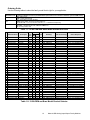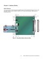
1
10623 Roselle Street, San Diego, CA 92121 (858) 550-9559 [email protected] www.accesio.com Fax (858) 550-7322 USB MULTI-CHANNEL HIGH-SPEED ANALOG I/O FAMILY MODEL USB-AIO16-xxx and USB-AIO12-xxx USER MANUAL File: MUSB-AIO FAMILY.B7i Notice The information in this document is provided for reference only. ACCES does not assume any liability arising out of the application or use of the information or products described herein. This document may contain or reference information and products protected by copyrights or patents and does not convey any license under the patent rights of ACCES, nor the rights of others. IBM PC, PC/XT, and PC/AT are registered trademarks of the International Business Machines Corporation. Copyright by ACCES I/O Products, Inc. 10623 Roselle Street, San Diego, CA 92121. All rights reserved. WARNING!! ALWAYS CONNECT AND DISCONNECT YOUR FIELD CABLING WITH THE COMPUTER POWER OFF. ALWAYS TURN COMPUTER POWER OFF BEFORE INSTALLING A BOARD. CONNECTING AND DISCONNECTING CABLES, OR INSTALLING BOARDS INTO A SYSTEM WITH THE COMPUTER OR FIELD POWER ON MAY CAUSE DAMAGE TO THE I/O BOARD AND WILL VOID ALL WARRANTIES, IMPLIED OR EXPRESSED. 2 Manual USB-Analog Input/Output Family Modules Warranty Prior to shipment, ACCES equipment is thoroughly inspected and tested to applicable specifications. However, should equipment failure occur, ACCES assures its customers that prompt service and support will be available. All equipment originally manufactured by ACCES which is found to be defective will be repaired or replaced subject to the following considerations. Terms and Conditions If a unit is suspected of failure, contact ACCES' Customer Service department. Be prepared to give the unit model number, serial number, and a description of the failure symptom(s). We may suggest some simple tests to confirm the failure. We will assign a Return Material Authorization (RMA) number which must appear on the outer label of the return package. All units/components should be properly packed for handling and returned with freight prepaid to the ACCES designated Service Center, and will be returned to the customer's/user's site freight prepaid and invoiced. Coverage First Three Years: Returned unit/part will be repaired and/or replaced at ACCES option with no charge for labor or parts not excluded by warranty. Warranty commences with equipment shipment. Following Years: Throughout your equipment's lifetime, ACCES stands ready to provide on-site or in-plant service at reasonable rates similar to those of other manufacturers in the industry. Equipment Not Manufactured by ACCES Equipment provided but not manufactured by ACCES is warranted and will be repaired according to the terms and conditions of the respective equipment manufacturer's warranty. General Under this Warranty, liability of ACCES is limited to replacing, repairing or issuing credit (at ACCES discretion) for any products which are proved to be defective during the warranty period. In no case is ACCES liable for consequential or special damage arriving from use or misuse of our product. The customer is responsible for all charges caused by modifications or additions to ACCES equipment not approved in writing by ACCES or, if in ACCES opinion the equipment has been subjected to abnormal use. "Abnormal use" for purposes of this warranty is defined as any use to which the equipment is exposed other than that use specified or intended as evidenced by purchase or sales representation. Other than the above, no other warranty, expressed or implied, shall apply to any and all such equipment furnished or sold by ACCES. 3 Manual USB-Analog Input/Output Family Modules TABLE OF CONTENTS Chapter 1: Introduction ........................................................................................................................................ 6 Features ............................................................................................................................................................. 6 Product Family Overview ................................................................................................................................. 7 Functional Description ..................................................................................................................................... 7 Analog Inputs .................................................................................................................................................... 8 A/D Conversion Start ........................................................................................................................................ 9 Oversample ...................................................................................................................................................... 10 Calibration ....................................................................................................................................................... 10 Analog Outputs ............................................................................................................................................... 10 Digital I/O ......................................................................................................................................................... 11 Counter/Timer.................................................................................................................................................. 11 Ordering Guide ................................................................................................................................................ 12 Chapter 2: Installation ........................................................................................................................................ 17 Software CD Installation ................................................................................................................................. 17 Hardware Installation ...................................................................................................................................... 17 Chapter 3: Hardware Details .............................................................................................................................. 18 Option Selection .............................................................................................................................................. 18 Chapter 4: USB Address Information ............................................................................................................... 20 Chapter 5: Programming ................................................................................................................................... 21 Chapter 6: Connector Pin Assignments........................................................................................................... 22 Chapter 7: Base Model Specifications ............................................................................................................. 24 Chapter 8: Analog Input Multiplexer Model AIMUX-64 ................................................................................... 26 Features ........................................................................................................................................................... 26 Functional Description ................................................................................................................................... 26 Programming Differences from Base Model ................................................................................................ 26 Exclusive Option for Models that include the AIMUX-64 ............................................................................ 27 Included with your board ............................................................................................................................... 27 Optional Accessories for Models that include the AIMUX-64 .................................................................... 27 Adding CJC when using thermocouples with the USB-AIO family ........................................................... 28 Specifications for AIMUX-64 .......................................................................................................................... 31 Chapter 9: Signal Conditioner Model AIMUX-32 ............................................................................................. 32 Features ........................................................................................................................................................... 32 Functional Description ................................................................................................................................... 32 Programming Differences from Base Model ................................................................................................ 33 Options for Models that include the AIMUX-32 ............................................................................................ 33 Optional Accessories for Models that include the AIMUX-32 .................................................................... 33 Front end circuit and connection diagrams ................................................................................................. 34 Adding CJC when using thermocouples with the AIMUX-32 ..................................................................... 36 AIMUX-32 Hardware Details ............................................................................................................................. 38 Powering the AIMUX-32 boards ..................................................................................................................... 40 AIMUX-32 Specification .................................................................................................................................. 44 Appendix A: Counter/Timer ............................................................................................................................... 45 Appendix B: Calibration ..................................................................................................................................... 47 System Calibration Utility .............................................................................................................................. 49 LIST OF FIGURES Figure 1-1: Block Diagram ................................................................................................................................... 8 Figure 6-1: 68-Pin SCSI Connector Pin Locations .......................................................................................... 22 Figure 8-1: AIMUX-64 Board with Connectors ................................................................................................. 27 Figure 8-2: AIMUX-64 Reference Junction Temp Sensor Diagram ............................................................... 28 Figure 8-3: 37-Pin Female Connector Pin Locations ...................................................................................... 29 Figure 8-4: 25-Pin Female Connector Pin Locations ...................................................................................... 30 Figure 9-1: C68M-X Multi-SCSI Cable Drawing ................................................................................................ 33 4 Manual USB-Analog Input/Output Family Modules Figure 9-2: Normal Inputs .................................................................................................................................. 34 Figure 9-3: RC Filter ........................................................................................................................................... 34 Figure 9-4: Attenuation ...................................................................................................................................... 34 Figure 9-5: Current Input Diagram .................................................................................................................... 35 Figure 9-6: Bridge Completion Diagram .......................................................................................................... 35 Figure 9-7: Thermocouple Input Diagram ........................................................................................................ 36 Figure 9-8: AIMUX-32 Reference Junction Temperature Sensor Diagram ................................................... 36 Figure 9-9: RTD Input Diagram .......................................................................................................................... 37 Figure 9-10: AIMUX-32 Option Selection Map ................................................................................................. 38 Figure 9-11: J5 DB25 Female Connector Pin Locations ................................................................................. 39 Figure 9-12: DB37 Connector Pin Locations ................................................................................................... 40 Figure 9-13: USB-AIOxx-128A Mechanical Drawing ....................................................................................... 43 Figure 9-14: Offset and Gain Error Graphs ...................................................................................................... 47 Figure 9-15: System Calibration Utility Screenshot 1 (setup) ........................................................................ 49 Figure 9-16: System Calibration Utility Screenshot 2 (range select) ............................................................ 49 Figure 9-17: System Calibration Utility Screenshot 3 (offset) ....................................................................... 50 Figure 9-18: System Calibration Utility Screenshot 4 (gain) .......................................................................... 50 Figure 9-19: System Calibration Utility Screenshot 5 (confirmation) ........................................................... 51 Figure 9-20: System Calibration Utility Screenshot 6 (finish and save) ....................................................... 51 LIST OF TABLES Table 1-1: 12-Bit OEM and Base Model Number Structure ............................................................................ 12 Table 1-2: 12-Bit OEM and Base Model Product Selector .............................................................................. 12 Table 1-3: 16-Bit OEM and Base Model Number Structure ............................................................................ 13 Table 1-4: 16-Bit OEM and Base Model Product Selector .............................................................................. 13 Table 1-5: 12-Bit DAQ-PACK Model Number Structure .................................................................................. 14 Table 1-6: 12-Bit DAQ-PACK Model Product Selector .................................................................................... 14 Table 1-7: 16-Bit DAQ-PACK Model Number Structure .................................................................................. 15 Table 1-8: 16-Bit DAQ-PACK Model Product Selector .................................................................................... 15 Table 3-1: Base Model Option Selection Map .................................................................................................. 18 Table 4-1: Product ID to Model Number ........................................................................................................... 20 Table 6-1: Base Model 68-pin SCSI Connector Pin Assignments ................................................................. 22 Table 6-2: Base Model Signal Name, Descriptions and Directions ............................................................... 23 Table 8-1: AIMUX-64 J3 37-Pin Female Connector Pin Assignments ........................................................... 29 Table 8-2: AIMUX-64 J4 37-Pin Female Connector Pin Assignments ........................................................... 30 Table 8-3: AIMUX-64 J2 DB25 Female Connector Pin Assignments ............................................................. 30 Table 8-4: AIMUX-64 Signal Names and Descriptions .................................................................................... 31 Table 9-1: AIMUX-32 J5 DB25 Female Connector Pin Assignments ............................................................. 39 Table 9-2: AIMUX-32 J5 Signal Names and Descriptions ............................................................................... 39 Table 9-3: AIMUX-32 P2 Power Connector (IDC-8) .......................................................................................... 40 Table 9-4: AIMUX-32 P2 Signal Names and Descriptions............................................................................... 40 Table 9-5: AIMUX-32 J3 Connector Pin Assignments (DB37F) ...................................................................... 40 Table 9-6: AIMUX-32 J3 Signal Names and Descriptions ............................................................................... 41 Table 9-7: AIMUX-32 J4 Connector Pin Assignments (DB37F) ...................................................................... 41 Table 9-8: AIMUX-32 J4 Signal Names and Descriptions ............................................................................... 41 Table 9-9: AIMUX-32 J3 DB37 Pin-outs w/CH# per Board Stack Position .................................................... 42 Table 9-10: AIMUX-32 J4 DB37 Pin-outs w/CH# per Board Stack Position .................................................. 42 5 Manual USB-Analog Input/Output Family Modules Chapter 1: Introduction The USB-AIO family of Data Acquisition Modules is an ideal solution for adding portable, easy-toinstall high-speed analog and digital I/O capabilities to any computer with a USB port. The unit is a USB 2.0 high-speed device and requires a USB 2.0 port to function. This manual describes the 120 analog I/O modules within the USB-AIO family. There are 60 OEM models that are shipped with no enclosure, and 60 more enclosed and integrated models. The enclosed models are named DAQ-PACK and DAQ-PACK M Series. OEM versions have model names beginning with USB, while the DAQ-PACK model names start with DPK. Each model varies in capabilities such as analog to digital (A/D) resolution and sampling speed, calibration hardware, number of channels, signal conditioning capabilities, and analog outputs. Where specific version or model information is referred to with an “xx”, the “xx” are substituted with the total number of channels available on that model. Please refer to Product Selector Tables 1-1 through 1-4 for a complete list of available models. Features High-speed USB 2.0 device From 16 single-ended or 8 differential (base models) up to 128 differential analog inputs 16-bit resolution versions: Sampling rate “16-xxA”: “Advanced version” 500ksamples/sec (max. aggregate) “16-xxE”: “Economy version” 250ksamples/sec (max. aggregate) Calibration Hardware “16-xxA”: Two on-board references + calibrated real-time output “16-xxE”: Two on-board references 12-bit resolution versions: Sampling rate “12-xxA”: “Advanced version” 500ksamples/sec (max. aggregate) “12-xx”: “Standard version” 250ksamples/sec (max. aggregate) “12-xxE”: “Economy version” 100ksamples/sec (max. aggregate) Calibration Hardware “12-xxA”: Two on-board references + calibrated real-time output “12-xx”: Two on-board references “12-xxE”: None System calibration program provided to calibrate entire system Channel-by-channel ranges of 0-1V, 0-2V, 0-5V, 0-10V, ±1V, ±2V, ±5V, ±10V (software selectable) Signal conditioning available on -32, -64, -96 and -128 input models for: RC filters on each input Voltage divider on each input 4-20mA and 10-50mA current inputs Thermocouple with break detect (includes Temp sensor for cold junction) RTD measurement Bridge completion Precision 10V excitation at each I/O connector for RTD and Bridge Completion A/D Conversion Start sources: Software, Timer, and External Trigger (edge software selectable) A/D Modes: Single Channel or Scan Noise reduction with Channel Oversampling 6 Manual USB-Analog Input/Output Family Modules Over-voltage protection of -40V to +55V Two 16-bit Digital to Analog (D/A) outputs (optional) D/A ranges of 0-5V, 0-10V, ±5V, ±10V (factory installed) 16 High-current Digital I/O lines 16-bit programmable counter/timer PC/104 module size and mounting compatibility Small (4" x 4" x 1.25") rugged industrial enclosure available for 16 input version models Onboard micro USB connector for embedded applications Applications Equipment monitoring Environmental measurements Embedded data acquisition Education/Laboratory Product Family Overview The base models within the product family consist of a USB-based A/D converter board with 16 single-ended (S.E.) or 8 differential (DIFF.) analog inputs, a counter/timer and 16 high-current digital I/O lines. The family is designed using a modular approach with a variety of bit resolutions & sampling speeds. Optionally, two 16-bit D/A outputs are factory installed for those applications requiring analog outputs. To increase the channel count of the base models from 16 S.E. or 8 DIFF. to 64 S.E. or 32 DIFF., a multiplexer board (AIMUX-64) is connected to the 68-pin SCSI connector of the A/D board with a ribbon cable. Alternately, to increase the channel count, introduce signal conditioning capabilities, and extra input gain options, from one to four signal conditioning/multiplexer boards (AIMUX-32) can be connected to the A/D board with a multi-SCSI ribbon cable for a maximum of 128 differential analog inputs. To find the model that is right for your application, refer to product tables 1-1 through 1-8. Functional Description This product is an A/D board that converts analog voltages or optionally 4-20/10-50mA to a 16 or 12bit value (depending on model). This board is capable of sampling speeds up to 500k, 250k, or 100k samples per second (depending on model). Sampling of the A/D can be enabled/disabled using an externally supplied input signal. Analog input channels are enabled as a consecutive set by software. Each channel within the set is independently configured by software to accept one of eight different analog input ranges. A/D conversion starts are issued one of three ways: Software Start, Timer Start, or External Trigger Start. A/D conversion starts are software configured to be either rising or falling edge. Additionally, A/D conversion starts are software configured to be Single Channel or Scan. Single Channel samples data once from the next consecutive channel within the enabled set. A Scan samples data from all channels within the set at the fastest possible rate. To minimize noise, the board implements a technique called Oversampling. High accuracy is achieved with two on-board reference voltages used in calibrating the board (does not apply to 12-xxE models). Furthermore, a real-time internal calibration system (‘A’ models only) allows the card to adjust for offset/gain errors at run-time, giving a more accurate reading. 7 Manual USB-Analog Input/Output Family Modules This board also has an option of adding two 16-bit D/A outputs. There are four factory installed output ranges available. There are 16 digital I/O lines accessible on the I/O connector. The digital I/O lines are grouped into two 8-bit bytes. Both digital I/O bytes are individually software selectable as input or output. A single, fully programmable, 8254 16-bit counter is provided with a maximum input frequency of 10MHz. The Counter Clock, Counter Gate, & Counter Output can be accessed externally for extended functionality. Figure 1-1: Block Diagram Analog Inputs Base models have a total of 16 S.E. or 8 DIFF analog inputs. A consecutive set of channels are enabled/disabled by software. This set of channels is constructed by a start and end channel. Sampling begins on the start channel and continues through every successive channel until the end channel is sampled. Once the end channel has been sampled, the process repeats again from the start channel. If only one channel is being sampled, the start and end channels would be the same. Each channel within the set is individually software configured as either S.E. or DIFF. This board allows a mix of both S.E. and DIFF inputs. One must note, however, that a differential signal requires a pair of channels. Thus, when channel 0 is programmed as a DIFF input, both channels 0 and 8 are used and not available as S.E. inputs. Refer to Chapter 6: Connector Pin Assignments, Table 6-1: for S.E. and DIFF pair inputs. 8 Manual USB-Analog Input/Output Family Modules Optionally on base models (16 S.E. or 8 DIFF. inputs), resistors can be factory installed on selected channels to accept 4-20mA or 10-50mA analog inputs. A mix of S.E. and DIFF current inputs are possible but they are factory configured in hardware and cannot be changed by software. 8 input ranges, 4 unipolar and 4 bipolar, are selectable by software for each individual channel. This channel-by-channel flexibility allows for up to 8 different input ranges being acquired on a single board. Unipolar ranges are 0-1V, 0-2V, 0-5V, and 0-10V. Bipolar ranges are ±1, ±2V, ±5V, and ±10V. Additional gains can be applied to these ranges using the AIMUX-32. Refer to chapter 9. Each channel input has a slight positive bias to facilitate measurement of signals close to analog ground (no signal information is lost due to negative offset of the ADC; does not apply to 12-xxE models). Each channel input has an over-voltage protection of -40V to +55V. A/D Conversion Start This board offers three software selectable sources for A/D Conversion Start: Software Start, Timer Start, and External Start Trigger. Software Start generates an A/D Conversion Start every time the software command is issued. The maximum frequency for a Software Start is roughly 4kHz. Timer Start uses the on-board timer to generate an A/D Conversion Start. Frequencies ranging from 2.33 * 10-3Hz to 500kHz are possible with Timer Start. External Start Trigger uses the External Trigger pin on the connector to generate an A/D Conversion Start. Frequencies up to 500kHz are allowed for External Start Trigger. *Note that the frequency of A/D conversion starts CANNOT exceed the speed of the A/D conversions. A/D Conversion Start is also software configured as rising or falling edge. Furthermore, it can be disabled by driving the A/D Conversion Start Enable pin on the connector low. By default, this signal is pulled high and A/D Conversion Start is enabled. If A/D Conversion Start Enable goes low during a conversion, the current channel (plus any oversampling; refer to the Oversample section) will complete all its conversions before A/D Conversion Start is disabled. Once A/D Conversion Start Enable returns high, conversions will begin on the next successive channel within the enabled set upon the following A/D Conversion Start. An A/D Conversion Start can be one of two software selectable types for this board: Single Channel or Scan. A/D conversion starts that are Single Channel sample one channel within the enabled set per A/D Conversion Start. This allows for total control over the time skew between channels. Scan, on the other hand, will sample all the channels within the enabled set per A/D Conversion Start. Channels are sampled at 500kHz, 250kHz, or 100kHz (depending on model) to minimize the time skew between channels. Furthermore, 'A' Models have the software selectable Scan option of sampling channels at 500kHz or 400kHz. The slower sampling rate mitigates crosstalk between analog input channels. 9 Manual USB-Analog Input/Output Family Modules Oversample Oversampling is a technique which continuously samples a channel multiple times at the board’s fastest speed. Quickly taking several samples from the same channel allows the signal to be averaged. Averaging a signal can greatly reduce the noise injected by both the signal and the board/system. The oversample range is from 0 to 255 (software selectable) and applies to every channel within the enabled set. A channel is always sampled once, plus the number of oversamples that was configured. Therefore an oversample of 0 will sample a channel once (initial sample plus 0 oversamples), oversample of 1 will sample a channel twice (initial sample plus 1 oversample), up to an oversample of 255 which will sample a channel 256 times (initial sample plus 255 oversamples). Each channel's oversamples are taken before sampling begins on the next consecutive channel within the enabled set. Calibration All ADC's suffer from offset and gain errors. To account for this, the board contains calibration hardware and software to adjust for the offset/gain errors. This is particularly helpful as aging occurs and/or operating temperature changes. There are two on-board hardware components used for calibration.The first hardware component uses two on-board known reference voltages that are accessible by software. The first reference voltage measures analog ground while the second reference voltage measures Vref, which is slightly below 10V. The results of sampling analog ground provides the information for correcting any offset errors present. Sampling Vref provides the information for correcting any gain errors present by comparing against Vref's known value which was accurately measured at the factory and stored onboard. Note: "12-xxE" boards do not contain the on-board reference voltages. The second hardware component, contained by 'A' models only, provides real-time calibrated data. This component uses the calibration file created from the two on-board reference voltages or a custom calibration file generated by the user (refer to the Software Reference manual for the file format). The calibration file is loaded onto the board and used by the real-time calibration hardware. The result is real-time calibrated data. Autocalibration is a function in software that, when called, will automatically sample the two on-board references, create the calibration file, and store the calibrated information onto the board. Autocalibration can be performed in milliseconds and is recommended to be performed periodically. For optimum calibrated data, the software function should be repeated anytime the temperature or environment changes. Appendix B describes calibration in greater detail. It gives thorough explanations and provides useful diagrams demonstrating the concepts of offset and gain errors as well as other common sources of error. It also provides equations used to calibrate out errors and how those equations were derived. Analog Outputs Optional analog outputs provide two singled-ended, 16-bit D/A outputs capable of a 4kHz conversion rate per channel. Both channels ship standard with a 0-10V range. Other ranges available as factory options are: 0-5V, ±5V, and ±10V. See Model Options for details on specifying the factory ranges. Output current is ±25mA per channel. 10 Manual USB-Analog Input/Output Family Modules Digital I/O There are 16 digital I/O lines (DIO0 to DIO15) available on the I/O connector. Both the low byte (DIO0-DIO7) and high byte (DIO8-DIO15) can be individually software configured as inputs or outputs. Each DIO line is buffered and capable of sourcing 32mA or sinking 64mA. Be sure to consult the Power section for total power limitations before operation. By default the DIO lines are pulled up with a 10KΩ resistor to 5V. DIO lines can also be factory configured as pulled down. Counter/Timer The highly versatile 8254 contains three independent counter/timers. Counter 0 is available for general purpose use as described below. Counters 1 and 2 are dedicated for use in timing A/D conversion starts. See Appendix A for detailed 8254 operational mode descriptions. Counter 0 is a fully programmable, 8254 16-bit counter is provided with the Counter Gate, Counter Clock, and Counter Output signals brought out to the connector. All three signals are buffered and capable of sourcing 32mA or sinking 64mA. Be sure to consult the Power section for total power limitations before operation. The Counter Gate, Counter Clock, and Counter Output are pulled up with a 10kΩ resistor to 5V. The Counter Clock input is software selectable between an internal 10MHz clock and the external Counter Clock. The maximum allowed frequency for the clock is 10MHz. 11 Manual USB-Analog Input/Output Family Modules Ordering Guide Use the following tables to select the family model that is right for your application. USB-XXX12-YYYZ XXX YYY Z 12-Bit Input OEM (no enclosures) and Base Models (board w/enclosure included as standard, option for OEM version) AI = Analog Inputs AIO = Analog Inputs/Outputs 16 = 16S.E./8DIFF Channels (No MUX) 64M = 64S.E./32DIFF Channels (Includes AIMUX-64) 32, 64, 96, 128 = 32, 64, 96, 128 DIFF Channels (1, 2, 3, 4 AIMUX-32 Respectively) A = Advanced Model; 500k, CALibration REFerence, Real-Time Cal. HW (constants stored on-board, update A/D values in real-time) No Letter = Standard Model; 250k, CALibration REFerence E = Economy Model; 100k Table 1-1: 12-Bit OEM and Base Model Number Structure 12-Bit Products 1 2 3 4 5 6 7 8 9 10 11 12 13 14 15 16 17 18 19 20 21 22 23 24 25 26 27 28 29 30 31 32 33 34 35 36 USB-AI12-16A USB-AI12-16 USB-AI12-16E USB-AI12-32A USB-AI12-32 USB-AI12-32E USB-AI12-64A USB-AI12-64 USB-AI12-64E USB-AI12-64MA USB-AI12-64M USB-AI12-64ME USB-AI12-96A USB-AI12-96 USB-AI12-96E USB-AI12-128A USB-AI12-128 USB-AI12-128E USB-AIO12-16A USB-AIO12-16 USB-AIO12-16E USB-AIO12-32A USB-AIO12-32 USB-AIO12-32E USB-AIO12-64A USB-AIO12-64 USB-AIO12-64E USB-AIO12-64MA USB-AIO12-64M USB-AIO12-64ME USB-AIO12-96A USB-AIO12-96 USB-AIO12-96E USB-AIO12-128A USB-AIO12-128 USB-AIO12-128E # of Inputs 16SE / 8 DIFF 16SE / 8 DIFF 16SE / 8 DIFF 32 DIFF 32 DIFF 32 DIFF 64 DIFF 64 DIFF 64 DIFF 64SE / 32 DIFF 64SE / 32 DIFF 64SE / 32 DIFF 96 DIFF 96 DIFF 96 DIFF 128 DIFF 128 DIFF 128 DIFF 16SE / 8 DIFF 16SE / 8 DIFF 16SE / 8 DIFF 32 DIFF 32 DIFF 32 DIFF 64 DIFF 64 DIFF 64 DIFF 64SE / 32 DIFF 64SE / 32 DIFF 64SE / 32 DIFF 96 DIFF 96 DIFF 96 DIFF 128 DIFF 128 DIFF 128 DIFF A/D Rate CAL (kHz) REF Real- D/A Time 500 250 100 500 250 100 500 250 100 500 250 100 500 250 100 500 250 100 500 250 100 500 250 100 500 250 100 500 250 100 500 250 100 500 250 100 YES YES NO YES YES NO YES YES NO YES YES NO YES YES NO YES YES NO YES YES NO YES YES NO YES YES NO YES YES NO YES YES NO YES YES NO YES NO NO YES NO NO YES NO NO YES NO NO YES NO NO YES NO NO YES NO NO YES NO NO YES NO NO YES NO NO YES NO NO YES NO NO 0 0 0 0 0 0 0 0 0 0 0 0 0 0 0 0 0 0 2 2 2 2 2 2 2 2 2 2 2 2 2 2 2 2 2 2 Board(s) A/D A/D A/D A/D, AIMUX-32 A/D, AIMUX-32 A/D, AIMUX-32 A/D, AIMUX-32(x2) A/D, AIMUX-32(x2) A/D, AIMUX-32(x2) A/D, AIMUX-64 A/D, AIMUX-64 A/D, AIMUX-64 A/D, AIMUX-32(x3) A/D, AIMUX-32(x3) A/D, AIMUX-32(x3) A/D, AIMUX-32(x4) A/D, AIMUX-32(x4) A/D, AIMUX-32(x4) A/D A/D A/D A/D, AIMUX-32 A/D, AIMUX-32 A/D, AIMUX-32 A/D, AIMUX-32(x2) A/D, AIMUX-32(x2) A/D, AIMUX-32(x2) A/D, AIMUX-64 A/D, AIMUX-64 A/D, AIMUX-64 A/D, AIMUX-32(x3) A/D, AIMUX-32(x3) A/D, AIMUX-32(x3) A/D, AIMUX-32(x4) A/D, AIMUX-32(x4) A/D, AIMUX-32(x4) I/O Connector(s) 68-Pin Male SCSI 68-Pin Male SCSI 68-Pin Male SCSI DB37 Female x 2 DB37 Female x 2 DB37 Female x 2 DB37 Female x 4 DB37 Female x 4 DB37 Female x 4 DB37 Female x 2 DB37 Female x 2 DB37 Female x 2 DB37 Female x 6 DB37 Female x 6 DB37 Female x 6 DB37 Female x 8 DB37 Female x 8 DB37 Female x 8 68-Pin Male SCSI 68-Pin Male SCSI 68-Pin Male SCSI DB37 Female x 2 DB37 Female x 2 DB37 Female x 2 DB37 Female x 4 DB37 Female x 4 DB37 Female x 4 DB37 Female x 2 DB37 Female x 2 DB37 Female x 2 DB37 Female x 6 DB37 Female x 6 DB37 Female x 6 DB37 Female x 8 DB37 Female x 8 DB37 Female x 8 Power Required 5V via USB or Ext Supply 5V via USB or Ext Supply 5V via USB or Ext Supply ±15V, +5V via AIMUX-32 ±15V, +5V via AIMUX-32 ±15V, +5V via AIMUX-32 ±15V, +5V via AIMUX-32 ±15V, +5V via AIMUX-32 ±15V, +5V via AIMUX-32 5V via USB or Ext Supply 5V via USB or Ext Supply 5V via USB or Ext Supply ±15V, +5V via AIMUX-32 ±15V, +5V via AIMUX-32 ±15V, +5V via AIMUX-32 ±15V, +5V via AIMUX-32 ±15V, +5V via AIMUX-32 ±15V, +5V via AIMUX-32 5V via USB or Ext Supply 5V via USB or Ext Supply 5V via USB or Ext Supply ±15V, +5V via AIMUX-32 ±15V, +5V via AIMUX-32 ±15V, +5V via AIMUX-32 ±15V, +5V via AIMUX-32 ±15V, +5V via AIMUX-32 ±15V, +5V via AIMUX-32 5V via USB or Ext Supply 5V via USB or Ext Supply 5V via USB or Ext Supply ±15V, +5V via AIMUX-32 ±15V, +5V via AIMUX-32 ±15V, +5V via AIMUX-32 ±15V, +5V via AIMUX-32 ±15V, +5V via AIMUX-32 ±15V, +5V via AIMUX-32 Table 1-2: 12-Bit OEM and Base Model Product Selector 12 Manual USB-Analog Input/Output Family Modules USB-XXX16-YYYZ XXX YYY Z 16-Bit Input OEM (no enclosures) and Base Models (board w/enclosure included as standard, option for OEM version) AI = Analog Inputs AIO = Analog Inputs/Outputs 16 = 16S.E./8DIFF Channels (No MUX) 64M = 64S.E./32DIFF Channels (Includes AIMUX-64) 32, 64, 96, 128 = 32, 64, 96, 128 DIFF Channels (1, 2, 3, 4 AIMUX-32 Respectively) A = Advanced Model; 500k, CALibration REFerence, Real-Time Cal. HW (constants stored on-board, update A/D values in real-time) E = Economy Model; 250k, CALibration REFerence Table 1-3: 16-Bit OEM and Base Model Number Structure 16-Bit Products 37 38 39 40 41 42 43 44 45 46 47 48 49 50 51 52 53 54 55 56 57 58 59 60 USB-AI16-16A USB-AI16-16E USB-AI16-32A USB-AI16-32E USB-AI16-64A USB-AI16-64E USB-AI16-64MA USB-AI16-64ME USB-AI16-96A USB-AI16-96E USB-AI16-128A USB-AI16-128E USB-AIO16-16A USB-AIO16-16E USB-AIO16-32A USB-AIO16-32E USB-AIO16-64A USB-AIO16-64E USB-AIO16-64MA USB-AIO16-64ME USB-AIO16-96A USB-AIO16-96E USB-AIO16-128A USB-AIO16-128E # of Inputs 16SE / 8 DIFF 16SE / 8 DIFF 32 DIFF 32 DIFF 64 DIFF 64 DIFF 64SE / 32 DIFF 64SE / 32 DIFF 96 DIFF 96 DIFF 128 DIFF 128 DIFF 16SE / 8 DIFF 16SE / 8 DIFF 32 DIFF 32 DIFF 64 DIFF 64 DIFF 64SE / 32 DIFF 64SE / 32 DIFF 96 DIFF 96 DIFF 128 DIFF 128 DIFF A/D Rate CAL (kHz) REF Real- D/A Time 500 250 500 250 500 250 500 250 500 250 500 250 500 250 500 250 500 250 500 250 500 250 500 250 YES YES YES YES YES YES YES YES YES YES YES YES YES YES YES YES YES YES YES YES YES YES YES YES YES NO YES NO YES NO YES NO YES NO YES NO YES NO YES NO YES NO YES NO YES NO YES NO 0 0 0 0 0 0 0 0 0 0 0 0 2 2 2 2 2 2 2 2 2 2 2 2 Board(s) A/D A/D A/D, AIMUX-32 A/D, AIMUX-32 A/D, AIMUX-32(x2) A/D, AIMUX-32(x2) A/D, AIMUX-64 A/D, AIMUX-64 A/D, AIMUX-32(x3) A/D, AIMUX-32(x3) A/D, AIMUX-32(x4) A/D, AIMUX-32(x4) A/D A/D A/D, AIMUX-32 A/D, AIMUX-32 A/D, AIMUX-32(x2) A/D, AIMUX-32(x2) A/D, AIMUX-64 A/D, AIMUX-64 A/D, AIMUX-32(x3) A/D, AIMUX-32(x3) A/D, AIMUX-32(x4) A/D, AIMUX-32(x4) I/O Connector(s) 68-Pin Male SCSI 68-Pin Male SCSI DB37 Female x 2 DB37 Female x 2 DB37 Female x 4 DB37 Female x 4 DB37 Female x 2 DB37 Female x 2 DB37 Female x 6 DB37 Female x 6 DB37 Female x 8 DB37 Female x 8 68-Pin Male SCSI 68-Pin Male SCSI DB37 Female x 2 DB37 Female x 2 DB37 Female x 4 DB37 Female x 4 DB37 Female x 2 DB37 Female x 2 DB37 Female x 6 DB37 Female x 6 DB37 Female x 8 DB37 Female x 8 Power Required 5V via USB or Ext Supply 5V via USB or Ext Supply ±15V, +5V via AIMUX-32 ±15V, +5V via AIMUX-32 ±15V, +5V via AIMUX-32 ±15V, +5V via AIMUX-32 5V via USB or Ext Supply 5V via USB or Ext Supply ±15V, +5V via AIMUX-32 ±15V, +5V via AIMUX-32 ±15V, +5V via AIMUX-32 ±15V, +5V via AIMUX-32 5V via USB or Ext Supply 5V via USB or Ext Supply ±15V, +5V via AIMUX-32 ±15V, +5V via AIMUX-32 ±15V, +5V via AIMUX-32 ±15V, +5V via AIMUX-32 5V via USB or Ext Supply 5V via USB or Ext Supply ±15V, +5V via AIMUX-32 ±15V, +5V via AIMUX-32 ±15V, +5V via AIMUX-32 ±15V, +5V via AIMUX-32 Table 1-4: 16-Bit OEM and Base Model Product Selector 13 Manual USB-Analog Input/Output Family Modules DPK-XXX12YYYZ XXX YYY Z 12-Bit Input DAQ-PACK Models (Enclosed and Integrated USB Data Acquisition Modules) AI = Analog Inputs AIO = Analog Inputs/Outputs 16 = 16S.E./8DIFF Channels 64M = 64S.E./32DIFF Channels (DAQ-PACK M Series) 32, 64, 96, 128 = 32, 64, 96, 128 DIFF Channels A = Advanced Model; 500k, CALibration REFerence, Real-Time Cal. HW (constants stored on-board, update A/D values in real-time) No Letter = Standard Model; 250k, CALibration REFerence E = Economy Model; 100k Table 1-5: 12-Bit DAQ-PACK Model Number Structure 61 62 63 64 65 66 67 68 69 70 71 72 73 74 75 76 77 78 79 80 81 82 83 84 85 86 87 88 89 90 91 92 93 94 95 96 12-Bit DAQPACK Models # of Inputs DPK-AI12-16A DPK-AI12-16 DPK-AI12-16E DPK-AI12-32A DPK-AI12-32 DPK-AI12-32E DPK-AI12-64A DPK-AI12-64 DPK-AI12-64E DPK-AI12-64MA DPK-AI12-64M DPK-AI12-64ME DPK-AI12-96A DPK-AI12-96 DPK-AI12-96E DPK-AI12-128A DPK-AI12-128 DPK-AI12-128E DPK-AIO12-16A DPK-AIO12-16 DPK-AIO12-16E DPK-AIO12-32A DPK-AIO12-32 DPK-AIO12-32E DPK-AIO12-64A DPK-AIO12-64 DPK-AIO12-64E DPK-AIO12-64MA DPK-AIO12-64M DPK-AIO12-64ME DPK-AIO12-96A DPK-AIO12-96 DPK-AIO12-96E DPK-AIO12-128A DPK-AIO12-128 DPK-AIO12-128E 16SE / 8 DIFF 16SE / 8 DIFF 16SE / 8 DIFF 32 DIFF 32 DIFF 32 DIFF 64 DIFF 64 DIFF 64 DIFF 64SE / 32 DIFF 64SE / 32 DIFF 64SE / 32 DIFF 96 DIFF 96 DIFF 96 DIFF 128 DIFF 128 DIFF 128 DIFF 16SE / 8 DIFF 16SE / 8 DIFF 16SE / 8 DIFF 32 DIFF 32 DIFF 32 DIFF 64 DIFF 64 DIFF 64 DIFF 64SE / 32 DIFF 64SE / 32 DIFF 64SE / 32 DIFF 96 DIFF 96 DIFF 96 DIFF 128 DIFF 128 DIFF 128 DIFF A/D Rate CAL (kHz) REF Real- D/A Time 500 250 100 500 250 100 500 250 100 500 250 100 500 250 100 500 250 100 500 250 100 500 250 100 500 250 100 500 250 100 500 250 100 500 250 100 YES YES NO YES YES NO YES YES NO YES YES NO YES YES NO YES YES NO YES YES NO YES YES NO YES YES NO YES YES NO YES YES NO YES YES NO YES NO NO YES NO NO YES NO NO YES NO NO YES NO NO YES NO NO YES NO NO YES NO NO YES NO NO YES NO NO YES NO NO YES NO NO 0 0 0 0 0 0 0 0 0 0 0 0 0 0 0 0 0 0 2 2 2 2 2 2 2 2 2 2 2 2 2 2 2 2 2 2 I/O Connector(s) 68-Pin Male SCSI 68-Pin Male SCSI 68-Pin Male SCSI DB37 Female x 2 DB37 Female x 2 DB37 Female x 2 DB37 Female x 4 DB37 Female x 4 DB37 Female x 4 DB37 Female x 2 DB37 Female x 2 DB37 Female x 2 DB37 Female x 6 DB37 Female x 6 DB37 Female x 6 DB37 Female x 8 DB37 Female x 8 DB37 Female x 8 68-Pin Male SCSI 68-Pin Male SCSI 68-Pin Male SCSI DB37 Female x 2 DB37 Female x 2 DB37 Female x 2 DB37 Female x 4 DB37 Female x 4 DB37 Female x 4 DB37 Female x 2 DB37 Female x 2 DB37 Female x 2 DB37 Female x 6 DB37 Female x 6 DB37 Female x 6 DB37 Female x 8 DB37 Female x 8 DB37 Female x 8 Power Required 5V via USB or Ext Supply 5V via USB or Ext Supply 5V via USB or Ext Supply ±15V, +5V ±15V, +5V ±15V, +5V ±15V, +5V ±15V, +5V ±15V, +5V 5V via USB or Ext Supply 5V via USB or Ext Supply 5V via USB or Ext Supply ±15V, +5V ±15V, +5V ±15V, +5V ±15V, +5V ±15V, +5V ±15V, +5V 5V via USB or Ext Supply 5V via USB or Ext Supply 5V via USB or Ext Supply ±15V, +5V ±15V, +5V ±15V, +5V ±15V, +5V ±15V, +5V ±15V, +5V 5V via USB or Ext Supply 5V via USB or Ext Supply 5V via USB or Ext Supply ±15V, +5V ±15V, +5V ±15V, +5V ±15V, +5V ±15V, +5V ±15V, +5V Table 1-6: 12-Bit DAQ-PACK Model Product Selector 14 Manual USB-Analog Input/Output Family Modules DPK-XXX16-YYYZ 16-Bit Input DAQ-PACK Models (Enclosed and Integrated USB Data Acquisition Modules) AI = Analog Inputs AIO = Analog Inputs/Outputs 16 = 16S.E./8DIFF Channels 64M = 64S.E./32DIFF Channels 32, 64, 96, 128 = 32, 64, 96, 128 DIFF Channels A = Advanced Model; 500k, CALibration REFerence, Real-Time Cal. HW XXX YYY (constants stored on-board, update A/D values in real-time) Z E = Economy Model; 250k, CALibration REFerence Table 1-7: 16-Bit DAQ-PACK Model Number Structure 97 98 99 100 101 102 103 104 105 106 107 108 109 110 111 112 113 114 115 116 117 118 119 120 16-Bit DAQPACK Models # of Inputs DPK-AI16-16A DPK-AI16-16E DPK-AI16-32A DPK-AI16-32E DPK-AI16-64A DPK-AI16-64E DPK-AI16-64MA DPK-AI16-64ME DPK-AI16-96A DPK-AI16-96E DPK-AI16-128A DPK-AI16-128E DPK-AIO16-16A DPK-AIO16-16E DPK-AIO16-32A DPK-AIO16-32E DPK-AIO16-64A DPK-AIO16-64E DPK-AIO16-64MA DPK-AIO16-64ME DPK-AIO16-96A DPK-AIO16-96E DPK-AIO16-128A DPK-AIO16-128E 16SE / 8 DIFF 16SE / 8 DIFF 32 DIFF 32 DIFF 64 DIFF 64 DIFF 64SE / 32 DIFF 64SE / 32 DIFF 96 DIFF 96 DIFF 128 DIFF 128 DIFF 16SE / 8 DIFF 16SE / 8 DIFF 32 DIFF 32 DIFF 64 DIFF 64 DIFF 64SE / 32 DIFF 64SE / 32 DIFF 96 DIFF 96 DIFF 128 DIFF 128 DIFF A/D Rate CAL REF Real- D/A Time I/O Connector(s) Power Required (kHz) 500 250 500 250 500 250 500 250 500 250 500 250 500 250 500 250 500 250 500 250 500 250 500 250 YES YES YES YES YES YES YES YES YES YES YES YES YES YES YES YES YES YES YES YES YES YES YES YES YES NO YES NO YES NO YES NO YES NO YES NO YES NO YES NO YES NO YES NO YES NO YES NO 68-Pin Male SCSI 68-Pin Male SCSI DB37 Female x 2 DB37 Female x 2 DB37 Female x 4 DB37 Female x 4 DB37 Female x 2 DB37 Female x 2 DB37 Female x 6 DB37 Female x 6 DB37 Female x 8 DB37 Female x 8 68-Pin Male SCSI 68-Pin Male SCSI DB37 Female x 2 DB37 Female x 2 DB37 Female x 4 DB37 Female x 4 DB37 Female x 2 DB37 Female x 2 DB37 Female x 6 DB37 Female x 6 DB37 Female x 8 DB37 Female x 8 5V via USB or Ext Supply 5V via USB or Ext Supply ±15V, +5V ±15V, +5V ±15V, +5V ±15V, +5V 5V via USB or Ext Supply 5V via USB or Ext Supply ±15V, +5V ±15V, +5V ±15V, +5V ±15V, +5V 5V via USB or Ext Supply 5V via USB or Ext Supply ±15V, +5V ±15V, +5V ±15V, +5V ±15V, +5V 5V via USB or Ext Supply 5V via USB or Ext Supply ±15V, +5V ±15V, +5V ±15V, +5V ±15V, +5V 0 0 0 0 0 0 0 0 0 0 0 0 2 2 2 2 2 2 2 2 2 2 2 2 Table 1-8: 16-Bit DAQ-PACK Model Product Selector Base Model Options -P -OEM -DIN -T External AC/DC adapter (power jack/regulator installed) Board only (no enclosure) DIN rail mounting provision Extended Temperature Operation (-40° to +85°C) To order specific, custom current input configurations which can be any combination of differential or single-ended 4-20mA or 10-50mA inputs please contact the factory at 800-326-1649. For options specific to models including AIMUX-64 or AIMUX-32 boards, refer to Chapter 8 and 9 respectively. 15 Manual USB-Analog Input/Output Family Modules Included with your board The following components are included with your shipment depending on model and options ordered. Please take time now to ensure that no items are damaged or missing. USB AIO Family Module installed in an enclosure with an anti-skid bottom 6’ USB cable Software Master CD (PDF user manual installed with product package) Printed USB I/O Quick-Start Guide Optional accessories CUSB-EMB-6 C68PS18L STB-68 STB-68-Kit 6’ USB Cable (type A to micro USB connector) For use with OEM versions. 68-Pin SCSI 18” shielded cable with one-touch latches Screw Terminal Board (mounted on standoffs) Screw Terminal Board with enclosure mounting and interconnecting ribbon cable. 16 Manual USB-Analog Input/Output Family Modules Chapter 2: Installation Software CD Installation The software provided with this board is contained on one CD and must be installed onto your hard disk prior to use. To do this, perform the following steps as appropriate for your operating system. Substitute the appropriate drive letter for your drive where you see D: in the examples below. WIN2000/XP/2003 a. b. c. Place the CD into your CD-ROM drive. The CD should automatically run the install program. If the install program does not run, click START | RUN and type , click OK or press . Follow the on-screen prompts to install the software for this board. LINUX a. Please refer to linux.htm on the CD-ROM for information on installing under linux. Hardware Installation Please install the software package before plugging the hardware into the system. The board can be installed in any USB 2.0 port. Please refer to the USB I/O Quick Start Guide which can be found on the CD, for specific, quick steps to complete the hardware and software installation. 17 Manual USB-Analog Input/Output Family Modules Chapter 3: Hardware Details Option Selection You may also refer to the setup program installed from the CD provided with the board. The only user selectable hardware option available is VUSB vs. VEXT which selects between USB powered or Externally powered. Table 3-1: Base Model Option Selection Map 18 Manual USB-Analog Input/Output Family Modules USB Connector (P1) The USB connector available via the outside of the enclosure (OEM product versions do not include enclosures) is a Type B and mates with the six-foot cable provided. The USB port provides communication signals along with +5 VDC power. The board can be powered from the USB port or an external power supply can be used. See the DC Power Jack description below for more details about using an external power.supply. Embedded USB Connector (P4) In applications where the OEM (board only, no enclosure) version of this board is used, it may be desirable to use the on-board micro USB connector, which is next to the Type B connector. LED The LED on the front of the enclosure is used to indicate power and data transmissions. When the LED is in an illuminated steady green state, this signifies that the board is successfully connected to the computer and has been detected and configured by the operating system. When the LED flashes continuously, this signifies that there is data being transmitted over the USB bus. DC Power Jack (Optional) Please note, not all boards will contain this option. This is an option for applications sourcing in excess of 150mA for the DIO (each DIO line is capable of sourcing up to 32mA). The DC jack has a 2.00mm post on board and is designed to be used with the 9* VDC AC/DC external power supply that ships with this option. The voltage regulator on board regulates the 9 VDC and provides 5 VDC to the onboard circuitry. When using external power, switch the jumper located near the USB connector to VEXT, otherwise when the jumper is in the VUSB position current is drawn from the USB port (please consult the option selection map for a visual reference). *OEM product versions require a +5 VDC external power supply instead of +9 VDC, which is provided with your shipment. 68-Pin I/O Connector (J1) The I/O is accessed via a 68-pin female SCSI Pin in Socket type connector with one-touch lock latches. Detailed pin assignments are listed in chapter 6, as well as a reference of pin functions printed on the enclosure label. 19 Manual USB-Analog Input/Output Family Modules Chapter 4: USB Address Information Use the provided driver to access the USB board. This driver will allow you to determine how many supported USB devices are currently installed, and each device’s type. This information is returned as a Vendor ID (VID), Product ID (PID) and Device Index. The board’s VID is “0x1605", and the PID for each model is listed below: For DAQ-PACK models substitute “DPK” for “USB”. 8040 8041 8042 8043 8044 8045 8046 8047 8048 8049 804A 804B 804C 804D 804E 804F 8050 8051 8052 8053 8054 8055 8056 8057 8058 8059 805A 805B 805C 805D USB-AI16-16A USB-AI16-16E USB-AI12-16A USB-AI12-16 USB-AI12-16E USB-AI16-64MA USB-AI16-64ME USB-AI12-64MA USB-AI12-64M USB-AI12-64ME USB-AI16-32A USB-AI16-32E USB-AI12-32A USB-AI12-32 USB-AI12-32E USB-AI16-64A USB-AI16-64E USB-AI12-64A USB-AI12-64 USB-AI12-64E USB-AI16-96A USB-AI16-96E USB-AI12-96A USB-AI12-96 USB-AI12-96E USB-AI16-128A USB-AI16-128E USB-AI12-128A USB-AI12-128 USB-AI12-128E 8140 8141 8142 8143 8144 8145 8146 8147 8148 8149 814A 814B 814C 814D 814E 814F 8150 8151 8152 8153 8154 8155 8156 8157 8158 8159 815A 815B 815C 815D USB-AIO16-16A USB-AIO16-16E USB-AIO12-16A USB-AIO12-16 USB-AIO12-16E USB-AIO16-64MA USB-AIO16-64ME USB-AIO12-64MA USB-AIO12-64M USB-AIO12-64ME USB-AIO16-32A USB-AIO16-32E USB-AIO12-32A USB-AIO12-32 USB-AIO12-32E USB-AIO16-64A USB-AIO16-64E USB-AIO12-64A USB-AIO12-64 USB-AIO12-64E USB-AIO16-96A USB-AIO16-96E USB-AIO12-96A USB-AIO12-96 USB-AIO12-96E USB-AIO16-128A USB-AIO16-128E USB-AIO12-128A USB-AIO12-128 USB-AIO12-128E Table 4-1: Product ID to Model Number The Device Index is determined by how many of the device you have in your system, and can provide a unique identifier* allowing you to access a specific board at will. * See the Software Reference Manual, installed on your system along with the board support package, for more information. 20 Manual USB-Analog Input/Output Family Modules Chapter 5: Programming The driver software provided with the board uses a 32-bit .dll front end compatible with any Windows programming language. Samples provided in Borland C++Builder, Borland Delphi, Microsoft Visual Basic, and Microsoft Visual C++ demonstrate use of the driver. Many functions are provided by the driver in Windows. These functions will allow you to read or write to the board. In addition, counter-timer functionality and board-level functions complete the driver package. For detailed information on each function refer to the .html Driver Manual located in the Win32 directory for this board. unsigned long ADC_GetScanV( - This simple function takes one scan of A/D data and converts it to voltage. It also averages oversamples for each channel. The array must contain one entry per A/D channel on the board, though only entries [start channel] through [end channel] are altered. unsigned long DeviceIndex - number from 0-31 indicating from which device you wish to get a scan of data double *pBuf - a pointer to the first of an array of double precision IEEE floating point numbers which will each receive the value read from one channel ) unsigned long ADC_SetConfig( unsigned long DeviceIndex - number from 0-31 indicating to which device you wish to set the A/D configuration unsigned char *pConfigBuf - a pointer to the first of an array of configuration bytes unsigned long *ConfigBufSize - a pointer to a variable holding the number of configuration bytes to write. Will be set to the number of configuration bytes written ) Software for AIMUX-xx models The software operation of the USB-AI(O) family when combined with the AIMUX-xx remains nearly identical. Several small things do change, however. 1) ADC_SetScanLimits() can accept channel numbers up to 128 for both the start and end channel. 2) If you choose to set your scan limits directly via the SetConfig() API, the array of configuration values has one extra byte. This byte contains the extra channel select bits for the start and end channel. Simply stated, the "high nybble" of the channel numbers are stored in the extra byte (array index 0x20). The high nybble can be calculated by dividing the channel number by 16 and dropping any fractions. In the same fashion as the normal start and end channel control index, the endchannel bits go in the top nybble, and the start channel bits go in the low nybble. 3) The data returned from any API including both ADC_BulkAcquire() and ADC_GetScanV(), just to name two, will consist of the data sequentially between the start channel and end channel, as specified in #1 or #2, above. 21 Manual USB-Analog Input/Output Family Modules Chapter 6: Connector Pin Assignments The base model uses a 68-pin Type 2 SCSI female with quick-release “one-touch” locking latches. The connector on the board is a TE Receptacle Assembly, Shielded, Right Angle, Railed, .050 Series, Amplimite, Part Number 1761028-4, or equivalent. Figure 6-1: 68-Pin SCSI Connector Pin Locations Pin Signal Name Pin Signal Name 1 Ch0 (SE) / Ch0+ (DIFF) 35 Ch8 (SE) / Ch0- (DIFF) 2 AGND 36 AGND 3 Ch1 (SE) / Ch1+ (DIFF) 37 Ch9 (SE) / Ch1- (DIFF) 4 AGND 38 AGND 5 Ch2 (SE) / Ch2+ (DIFF) 39 Ch10 (SE) / Ch2- (DIFF) 6 AGND 40 AGND 7 Ch3 (SE) / Ch3+ (DIFF) 41 Ch11 (SE) / Ch3- (DIFF) 8 AGND 42 AGND 9 Ch4 (SE) / Ch4+ (DIFF) 43 Ch12 (SE) / Ch4- (DIFF) 10 AGND 44 AGND 11 Ch5 (SE) / Ch5+ (DIFF) 45 Ch13 (SE) / Ch5- (DIFF) 12 AGND 46 AGND 13 Ch6 (SE) / Ch6+ (DIFF) 47 Ch14 (SE) / Ch6- (DIFF) 14 DAC0 (AIO) / AGND (AI) 48 AGND 15 Ch7 (SE) / Ch7+ (DIFF) 49 Ch15 (SE) / Ch7-(DIFF) 16 DAC1 (AIO) / AGND (AI) 50 AGND 17 AGND 51 -15V (Factory Use) 18 MUX CTL 52 +5V 19 AGND 53 +15V (Factory Use) 20 MUX CTL 54 +5V 21 MUX CTL 55 +5V 22 GND 56 GND 23 DIO14 57 DIO15 24 DIO12 58 DIO13 25 DIO10 59 DIO11 26 DIO8 60 DIO9 27 DIO6 61 DIO7 28 DIO4 62 DIO5 29 DIO2 63 DIO3 30 DIO0 64 DIO1 31 GND 65 GND 32 Counter Output 66 GND 33 Counter Clock 67 A/D Conversion Start Enable 34 Counter Gate 68 External Trigger Table 6-1: Base Model 68-pin SCSI Connector Pin Assignments 22 Manual USB-Analog Input/Output Family Modules Signal Name I/O Ch0 thru Ch7(SE)/Ch0+ thru Ch7+ (DIFF) I Ch8 thru Ch15(SE)/Ch0- thru Ch7-(DIFF) I AGND X Description Channel 0 thru Channel 7 Single-ended or Channel 0 thru Channel 7 Differential non-inverting input Channel 0 thru Channel 7 Single-ended current* (+) input or Channel 0 thru Channel 7 Differential non-inverting current* (+) input Channel 8 thru Channel 15 Single-ended or Channel 0 thru Channel 7 Differential inverting input Channel 8 thru Channel 15 Single-ended current* (+) input or Channel 0 thru Channel 7 Differential inverting current* (-) input Analog Ground Single-ended input return +5V from AIMUX-32 board used to provide power to the USB-AIO. If no AIMUX board present, available for use. (+5V @ 100mA) +5V I/O -15V O AIMUX-64M Power. Factory use only. Do not connect. +15V O AIMUX-64M Power. Factory use only. Do not connect. MUX CTL O Multiplexer control when AIMUX board(s) present DAC0 & DAC1 O D/A outputs for USB-AIO boards GND X Digital Ground DIO0 through DIO15 I/O Digital I/O Bits 0 through 15, two 8-bit bytes programmed as either inputs or outputs (pulled-up to 5V through 10k ohms) Counter Output O Output from 8254 ctr/tmr (pulled-up) Counter Clock I 8254 counter/timer clock input (pulled-up) Counter Gate I 8254 counter/timer gate input (pulled-up; active-high) A/D Conversion Start Enable I Enable Analog to Digital Conversion Starts (pulled-up; active-high) External Trigger I External Analog to Digital Conversion Start Trigger (pulled-up; software selectable rising/falling edge ) * = 4-20mA or 10-50mA Factory Optional Table 6-2: Base Model Signal Name, Descriptions and Directions 23 Manual USB-Analog Input/Output Family Modules Chapter 7: Base Model Specifications Analog Inputs ADC Type Resolution Sampling rate “16-16A” version “16-16E” version “12-16A” version “12-16” version “12-16E” version Number of channels Unipolar ranges Bipolar ranges 4-20mA or 10-50mA Calibration Hardware “16-16A” version “16-16E” version “12-16A” version “12-16” version “12-16E” version System Calibration Accuracy Uncalibrated Calibrated(1) Integral Nonlinearity Error No Missing Codes Input impedance A/D Conv. Start Sources Successive approximation 16-bit 12-bit 500k samples/sec (maximum aggregate) 250k samples/sec (maximum aggregate) 500k samples/sec (maximum aggregate) 250k samples/sec (maximum aggregate) 100k samples/sec (maximum aggregate) 16 single-ended or 8 differential (software selectable) 0-1V, 0-2V, 0-5V, 0-10V (software selectable) ±1V, ±2V, ±5V, ±10V (software selectable) Factory installed (optional) Two on-board references + calibrated real-time output Two on-board references Two on-board references+ calibrated real-time output Two on-board references None Program provided to calibrate entire system 0.094% Full-Scale (FS) 0.0015% FS 0.0046% FS 15 bits 1MΩ Software Start, Timer Start, and External Start Trigger (rising or falling edge; software selectable) A/D Conversion Start Enable Externally supplied (pulled-up; active-high) A/D Conversion Start Types Single Channel or Scan (software selectable) Channel Oversampling 0-255 consecutive samples/channel (software selectable) Overvoltage protection -40 to +55V Crosstalk -60dB @ 500kHz (1) To achieve best accuracy, one must calibrate to their own standard. Analog Outputs Number of Outputs: Type of Outputs: Resolution: Unipolar Ranges: Bipolar Ranges: Conversion Rate: Settling Time Output Current 2 Single-ended 16-bit 0-10V Standard, 0-5V (factory installed) ±5V, ±10V (factory installed) 4kHz per channel 4us typ, 7us max; 1/4 to 3/4 scale to ±2LSBs ±25mA per channel 24 Manual USB-Analog Input/Output Family Modules Digital I/O Lines Input voltage Input current Output voltage Output current 16, programmable as inputs or outputs in groups of 8 (pulled-up) Logic low: 0V(min) to 0.8V(max) Logic high: 2V(min) to 5V(max) ±20μA (max) Logic low: 0V(min) to 0.55V(max) Logic high: 2V(min) to 5V(max) Logic low 64mA(max) sink Logic high 32mA(max) source Counter/Timer Type Available Counters Input Frequency Counter size Clock Clock Period Clock Pulse Width High Clock Pulse Width Low Gate Output 82C54 programmable interval counter Counter 0 (CTR1 and CTR2 dedicated to A/D conversion starts) 10MHz (max) 16-bit Internal 10MHz or Externally supplied (software selectable; pulled-up) 100ns (min) 30ns (min) 40ns (min) Externally supplied (pulled-up; active-high) External (pulled-up) Input/Output Voltage/Current Same as Digital I/O Environmental Operating Temperature Storage Temperature Humidity Board Dimensions 0° to +70°C, optional -40° to +85°C -40° to +105°C 5% to 90% RH, without condensation PC/104 format, 3.550” by 3.775” and mounting holes Power Required +5V at 315mA typ1 1 USB 2.0 spec defines a device in terms of a unit load. A unit load is defined to be 100mA. Devices drawing an absolute maximum of one unit load are considered to be low-powered and devices drawing an absolute maximum of five unit loads are considered to be high-powered. Because this spec is not strictly adhered to, it is best to verify the USB port's power capabilities before operation. This card, according to the USB 2.0 spec, is a high-powered device. An optional external power supply can be ordered if the USB port cannot support high-powered devices. If using more than a total of 500mA, use optional 9 VDC (on board voltage regulator outputs +5 VDC to card) external power supply and remove VUSB jumper and place jumper on VEXT. Then plug in external power before plugging into USB port. This option will give you a total of 1000mA available. NOTE: External Power (-P) OEM product versions ship without an enclosure and have the regulator removed to eliminate heat-sinking concerns and to prevent breakage during shipment or handling. Use only the provided +5V regulated external power supply that ships with this option to avoid damaging your instrument. 25 Manual USB-Analog Input/Output Family Modules Chapter 8: Analog Input Multiplexer Model AIMUX-64 Features Designed to pair with any of the USB-AIO base series Multiplexes 64 single-ended or 32 differential analog inputs into the USB-AIO base board Optional Cold Junction Sensor for thermocouple measurement applications Optionally includes two 37-pin screw terminal board accessories External A/D and Counter control lines accessible from USB-AIO board Paired with base A/D board as OEM (no enclosure) or as DAQ-PACK M Series Data Acquisition Module Functional Description This board is an analog input multiplexer that mates with the USB-AIO base model series. There are a total of 64 single-ended or 32 differential analog inputs that are multiplexed down to 16 singleended or 8 differential outputs using 4:1 multiplexers (MUX). These outputs become the inputs to the USB-AIO board and are configured by software. Channel input ranges are the same as the USB-AIO board. These multi-board models are factory configured, integrated and tested and are not intended to be configured or expanded in the field. Inherently from the 4:1 MUX used, channels are grouped in 4's. The first group would consist of channels 0, 1, 2, 3, the next group consisting of channels 4, 5, 6, 7, etc. Therefore, the software configuration for the USB-AIO board channel 0 will apply to AIMUX-64 channels 0, 1, 2, 3, USB-AIO board channel 1 will apply to AIMUX-64 channels 4, 5, 6, 7, etc. Each group of 4 channels within the enabled set is individually software configured as either singleended or differential. This board allows a mix of both single-ended and differential inputs. One must note, however, that a differential signal requires a pair of single-ended channels. Thus, when channel 0 is programmed as a differential input, both channels 0 and 32 (Ch0+ DIFF and Ch0- DIFF respectively) are used and not available as singled-ended inputs. Also, because all four channels within a group contain the same configuration, channels 1 and 33 (Ch1+ DIFF and Ch1- DIFF respectively), 2 and 34 (Ch2+ DIFF and Ch2- DIFF respectively), and 3 and 35 (Ch3+ DIFF and Ch3DIFF respectively) would also be configured as differential channels. Refer to this chapter in Table 81 and 8-2 for single-ended and differential pair inputs. When connecting thermocouple inputs to this board, a temperature sensor is needed for Cold Junction Compensation (CJC). Channels 15 and 31 can accept a two-wire temperature sensor (LM335) to provide the CJC for the thermocouple. The AIMUX-64 connects to the USB-AIO board through a 68-pin SCSI ribbon cable. The mating connector used on the ribbon cables are AMP P/N 786090-7 or MOLEX P/N 70498-5068, or equivalent. Analog differential inputs are accessed via two right angle DB-37 female connectors. There is a right angle DB-25 female connector for the DIO and control signals. All other sections remain the same as described in the USB-AIO portion of this manual. Programming Differences from Base Model No other changes should be necessary when using the AIMUX-64. 26 Manual USB-Analog Input/Output Family Modules Figure 8-1: AIMUX-64 Board with Connectors Exclusive Option for Models that include the AIMUX-64 MTC Multiplexer Temperature Configuration includes an LM335 precision temperature sensor, with a 10k ohm resistor on one input channel to provide bias for the sensor. Also includes two universal screw terminal adaptors model ADAP-37. Included with your board Versions of this product that contain the AIMUX-64 ship installed in an enclosure, unless specified as –OEM, which is the board set only version. Optional Accessories for Models that include the AIMUX-64 ADAP37M Screw Terminal Adapter with female DB37 connector (2 needed) ADAP25M Screw Terminal Adapter with female DB25 connector Ribbon Cable assemblies Crimp Kit DB37 male crimp kit DIN-SNAP One foot length SNAP-TRACK with four clips 27 Manual USB-Analog Input/Output Family Modules Adding CJC when using thermocouples with the USB-AIO family For thermocouple inputs, a temperature sensor is needed for Cold Junction Compensation (CJC). The cold junction is the two points where the thermocouple wires attach to the connector. Each of these two points connect two dissimilar metals which, from the thermoelectric effect, cause a voltage potential (adds to thermocouple voltage and is therefore unwanted). This potential is compensated for by measuring the temperature at the terminal block using the installed temperature sensor (also known as the reference junction sensor). A look-up table is used to translate the measured temperature into a voltage. This voltage is then subtracted from the measured thermocouple voltage to compensate. When ordering this option, the MUX board will be configured with a factory installed 10k ohm bias resistor from +15V to channels 15 and 31 input for a reference junction sensor (LM335), which is included along with two 37 pin screw terminal blocks. Connect the first LM335 Precision Temperature Sensor lead 2 (cathode) to J3-17 (channel 15) and lead 3 (anode) to AGND (preferably J3-18). Connect the second LM335 lead 2 to J4-17 (channel 31) and lead 3 to AGND (preferably J4-18). Leave both LM335's lead 1 not connected. The Cold Junction Compensation voltage can be measured on channels 15 and 31 of the AIMUX-64. Figure 8-2: AIMUX-64 Reference Junction Temp Sensor Diagram 28 Manual USB-Analog Input/Output Family Modules Figure 8-3: 37-Pin Female Connector Pin Locations Pin Signal Name Pin Signal Name 1 CH0(SE) / CH0+(DIFF) 20 2 CH1(SE) / CH1+(DIFF) 21 CH32(SE) / CH0-(DIFF) CH33(SE) / CH1-(DIFF) 3 CH2(SE) / CH2+(DIFF) 22 CH34(SE) / CH2-(DIFF) 4 CH3(SE) / CH3+(DIFF) 23 CH35(SE) / CH3-(DIFF) 5 CH4(SE) / CH4+(DIFF) 24 CH36(SE) / CH4-(DIFF) 6 CH5(SE) / CH5+(DIFF) 25 CH37(SE) / CH5-(DIFF) 7 CH6(SE) / CH6+(DIFF) 26 CH38(SE) / CH6-(DIFF) 8 CH7(SE) / CH7+(DIFF) 27 CH39(SE) / CH7-(DIFF) 9 AGND 28 CH40(SE) / CH8-(DIFF) 10 CH8(SE) / CH8+(DIFF) 29 CH41(SE) / CH9-(DIFF) 11 CH9(SE) / CH9+(DIFF) 30 CH42(SE) / CH10-(DIFF) 12 CH10(SE) / CH10+(DIFF) 31 CH43(SE) / CH11-(DIFF) 13 CH11(SE) / CH11+(DIFF) 32 CH44(SE) / CH12-(DIFF) 14 CH12(SE) / CH12+(DIFF) 33 CH45(SE) / CH13-(DIFF) 15 CH13(SE) / CH13+(DIFF) 34 CH46(SE) / CH14-(DIFF) 16 35 CH47(SE) / CH15-(DIFF) 18 CH14(SE) / CH14+(DIFF) CH15(SE) / CH15+(DIFF) / LM335+ term. AGND / LM335- terminal 19 AGND 17 36 37 AGND AGND(AI) / DAC0 (AIO) Table 8-1: AIMUX-64 J3 37-Pin Female Connector Pin Assignments 29 Manual USB-Analog Input/Output Family Modules Pin 1 2 3 4 5 6 7 8 9 10 11 12 13 14 15 16 17 18 19 Signal Name CH16(SE) / CH16+(DIFF) CH17(SE) / CH17+(DIFF) CH18(SE) / CH18+(DIFF) CH19(SE) / CH19+(DIFF) CH20(SE) / CH20+(DIFF) CH21(SE) / CH21+(DIFF) CH22(SE) / CH22+(DIFF) CH23(SE) / CH23+(DIFF) AGND CH24(SE) / CH24+(DIFF) CH25(SE) / CH25+(DIFF) CH26(SE) / CH26+(DIFF) CH27(SE) / CH27+(DIFF) CH28(SE) / CH28+(DIFF) CH29(SE) / CH29+(DIFF) CH30(SE) / CH30+(DIFF) Ch31(SE)/Ch31+(DIFF) / LM335 + terminal AGND/ LM335 – terminal AGND Pin 20 21 22 23 24 25 26 27 28 29 30 31 32 33 34 35 36 37 Signal Name CH48(SE) / CH16-(DIFF) CH49(SE) / CH17-(DIFF) CH50(SE) / CH18-(DIFF) CH51(SE) / CH19-(DIFF) CH52(SE) / CH20-(DIFF) CH53(SE) / CH21-(DIFF) CH54(SE) / CH22-(DIFF) CH55(SE) / CH23-(DIFF) CH56(SE) / CH24-(DIFF) CH57(SE) / CH25-(DIFF) CH58(SE) / CH26-(DIFF) CH59(SE) / CH27-(DIFF) CH60(SE) / CH28-(DIFF) CH61(SE) / CH29-(DIFF) CH62(SE) / CH30-(DIFF) CH63(SE) / CH31-(DIFF) AGND AGND(AI)/DAC1(AIO) Table 8-2: AIMUX-64 J4 37-Pin Female Connector Pin Assignments Figure 8-4: 25-Pin Female Connector Pin Locations Pin 1 2 3 4 5 6 7 8 9 10 11 12 13 Signal Name DIO0 DIO1 DIO2 DIO3 DIO4 DIO5 DIO6 DIO7 GND DIO8 DIO9 DIO10 DIO11 Pin 14 15 16 17 18 19 20 21 22 23 24 25 Signal Name DIO12 DIO13 DIO14 DIO15 GND External Trigger A/D Conversion Start Enable Counter Gate Counter Clock Counter Output GND GND Table 8-3: AIMUX-64 J2 DB25 Female Connector Pin Assignments 30 Manual USB-Analog Input/Output Family Modules Signal Name I/O Description Channel 0 thru Channel 31 single-ended or Channel 0 thru Channel 31 differential non-inverting input Channel 32 thru Channel 63 single-ended or Channel 0 thru Channel 31 differential inverting input Temperature sensor + lead for reference junction or cold-junction compensation. When this option is ordered, Channel 1 is factory configured to provide a + bias to a provided LM335 precision temperature sensor, which should be connected to the also provided screw terminal adapter model UTBK-50. When this option is ordered, connect the – lead of the provided LM335 precision temperature sensor to the also provided screw terminal adapter model UTBK-50. Ch0 thru Ch31(SE)/Ch0+ thru Ch31+ (DIFF) I Ch32 thru Ch63(SE)/Ch0- thru Ch31-(DIFF) I LM335 + terminal I LM335 - terminal I DAC0 & DAC1 O Digital to Analog outputs AGND X Analog Ground, All single-ended AND differential signals must have a ground reference connected on one of these pins. GND X Digital Ground, Reference all digital signal devices to one of these connector pins. Digital I/O bits 0 through 7, software configured as either inputs or outputs (pulled-up to 5V through 10k ohms) Digital I/O bits 8 through 15, software configured as either inputs or outputs (pulled-up to 5V through 10k ohms) DIO0 through DIO7 I/O DIO8 through DIO15 O Counter Output O Output from 8254 CTR/TMR (pulled-up) Counter Clock I 8254 counter/timer clock input (pulled-up) Counter Gate I 8254 counter/timer gate input (pulled-up; active-high) A/D Conversion Start Enable I Enable Analog to Digital conversion starts (pulled-up; active-high) External Trigger I External Analog to Digital conversion start trigger (pulled-up; software selectable rising/falling edge ) N/C X Not Connected Table 8-4: AIMUX-64 Signal Names and Descriptions Specifications for AIMUX-64 Analog Inputs Number of channels 64 single-ended or 32 differential (software selectable) MUX type 4:1 Refer to Chapter 7: Base Model Specifications for detailed specs Analog Outputs Number of channels 2 Refer to Chapter 7: Base Model Specifications for detailed specs Digital I/O Lines 16 from USB-AIO board (DIO0-DIO15) Refer to Chapter 7: Base Model Specifications for detailed specs Counter/Timer Lines Gate, Clock, Output (from USB-AIO board) Refer to Chapter 7: Base Model Specifications for detailed specs Environmental Power required Supplied by USB-AIO board via included 68-pin ribbon cable All other environmental specifications, refer to Chapter 7: Base Model Specifications 31 Manual USB-Analog Input/Output Family Modules Chapter 9: Signal Conditioner Model AIMUX-32 Features Designed to pair with any of the USB-AIO base series 32 differential inputs (up to 4 boards for 128 differential inputs) Additional ranges of 0-100mV, 0-200mV, 0-400mV, 0-500mV, 0-2.5V, ±100mV, ±200mV, ±400mV, ±500mV, ±2.5V Factory input signal conditioning o Additional ranges of 0-1mV, 0-5mV, 0-10mV, 0-20mV, 0-50mV, ±1mV, ±5mV, ±10mV, ±20mV, ±50mV o RC filters o 4-20mA and 10-50mA current inputs o RTD measurement o Bridge completion o Thermocouple w/ break detect (Temp sensor for cold junction) o Voltage divider o +10V sensor excitation Functional Description This board is an analog signal conditioner/multiplexer designed for use with the USB-AIO base series of boards. There are 32 differential analog inputs that are multiplexed down to 4 single-ended outputs using 8:1 multiplexers (MUX). These outputs become the inputs to the USB-AIO board. The inputs to the standard AIMUX-32 can be voltages or optionally 4-20mA/10-50mA current inputs. There are 10 additional input ranges with this board. They are 0-100mV, 0-200mV, 0-400mV, 0500mV, 0-2.5V, ±100mV, ±200mV, ±400mV, ±500mV, and ±2.5V. A high gain option adds ranges of 0-1mV, 0-5mV, 0-10mV, 0-20mV, 0-50mV, ±1mV, ±5mV, ±10mV, ±20mV, and ±50mV. Furthermore, an optional voltage divider input can be factory installed for custom input ranges up to 30V. Analog inputs for the AIMUX-32 are configured and controlled by a combination of software and the gain jumpers. Up to four boards (128 differential inputs) can be used with each USB-AIO board. These multi-board models are factory configured, integrated and tested and are not intended to be configured or expanded in the field. Inherently from the 8:1 MUX used, channels are grouped in 8's. The first group would consist of channels 0,1,2,3,4,5,6,7, the next group consisting of channels 8,9,10,11,12,13,14,15, etc. Therefore, the software/jumper configuration for the USB-AIO board channel 0 will apply to AIMUX-32 channels 0,1,2,3,4,5,6,7, USB-AIO board channel 1 will apply to AIMUX-32 channels 8,9,10,11,12,13,14,15, etc. Each input can be factory configured to accept and condition a variety of input signals. These inputs consist of RC filters, voltage dividers, thermocouples (J, K, T, E, S, R, and B), thermocouple break detect, three-wire RTD’s (both 385 and 392), and installation of bridge completion resistors. A +10V source is provided for bridge and RTD excitation. To provide a reference junction compensation for the thermocouple, channel 8 can be jumpered to accept a two-wire temperature sensor (LM335). The AIMUX-32 connects to the USB-AIO board through a 68-pin SCSI ribbon cable. When using two or more AIMUX-32 boards a multi-SCSI ribbon cable is used. See Figure 9-1 for an illustration of this cable. Up to four AIMUX-32 boards may be connected to the USB-AIO board for a total of 128 differential analog inputs. Analog differential inputs are accessed via two right angle DB-37 female connectors. There is a right angle DB-25 female connector for the DIO and control signals. 32 Manual USB-Analog Input/Output Family Modules The AIMUX-32 boards require an external +5V and ±15V to operate. A right angle 8-pin IDC header is provided on the top AIMUX-32 board to feed this power. Figure 9-1: C68M-X Multi-SCSI Cable Drawing Programming Differences from Base Model The API functions that return voltage are unable to determine the positions of the gain jumpers as set on the submultiplexer boards. Please be aware that you would need to divide the floating-point voltage returned from these functions by the "gain factor" (x1, x2, x5, or x10) as selected for each channel's group on each AIMUX-32. It is not necessary to perform this step if you avoid the ...V() family of API functions, as all other functions return "counts", at either 12-bit or 16-bit resolution, without regard to the selected gain and range options. Options for Models that include the AIMUX-32 -RC -Ix -I10-50x -RTDx -BCx -TCx -BDx -HG -S0x RC filters; can be combined with any option or specified by itself x=1 (32 differential inputs accepting 4-20mA) x=2 (64 differential inputs accepting 4-20mA) x=3 (96 differential inputs accepting 4-20mA) x=4 (128 differential inputs accepting 4-20mA) x= as above except inputs accept 10-50mA x= as above except input accept RTDs x= as above except inputs interface with quarter bridge configurations x= as above except inputs accept thermocouples. Option includes 2 ADAP37M screw terminal adaptors and an LM335 temperature sensor per each of 32 inputs x= as above except providing thermocouple break detection for each multiple of 32 inputs configured with this option (combined w/ -TCx) High gain Special designator, contact factory to specify a voltage divider for your application, or to discuss any other special requirements Optional Accessories for Models that include the AIMUX-32 ADAP37M Screw Terminal Adapter with female DB37 connector (2 needed per AIMUX-32) ADAP25M Screw Terminal Adapter with female DB25 connector Cable Assembly Crimp Kit DB37 male crimp kit 33 Manual USB-Analog Input/Output Family Modules Front end circuit and connection diagrams Standard Configuration Accepts inputs up to ±10V. Figure 9-2: Normal Inputs RC Filter Option This option adds an RC filter to the inputs. It can also be added in conjunction with the other input options. Figure 9-3: RC Filter Input Voltage Divider (Attenuator) The standard model configuration is intended for voltage inputs of no more than ±10. This input option allows voltages up to 30V using resistive voltage dividers. Input values are specified by the customer. Figure 9-4: Attenuation 34 Manual USB-Analog Input/Output Family Modules 4-20mA/10-50mA Current Input A precision resistor is installed from the positive input to the negative input. The input is not offset, so that an input will be read as 1V to 5V. Readings below 1V provide fault detection, i.e. for a blown circuit fuse. Figure 9-5: Current Input Diagram Bridge Completion Configuration Three resistors are installed to form three-arms of a full Wheatstone bridge. The resistor values are specified by the customer. Figure 9-6: Bridge Completion Diagram 35 Manual USB-Analog Input/Output Family Modules Thermocouple Measurement with reference junction temperature sensor and optional Break Detect This option measures thermocouple inputs while also providing the temperature of the terminal block (cold junction) using a temperature sensor connected to channel 8. The optional break detect resistors can be installed to detect an open thermocouple condition (+10V on the input). Figure 9-7: Thermocouple Input Diagram Adding CJC when using thermocouples with the AIMUX-32 Connect the temperature sensor to J3 pin 28 for the + lead of LM335 and to pin 29 for – lead of LM335. This can be accomplished using the screw terminal adaptor ADAP37M or by soldering the temp sensor to the pins of the mating connector in your cabling. For background information regarding the need for a reference junction sensor, please refer to the section: Adding CJC when using thermocouples with the USB-AIO family on the page with Figure 8-4: AIMUX-64 Reference Junction Temperature Sensor Diagram. Figure 9-8: AIMUX-32 Reference Junction Temperature Sensor Diagram 36 Manual USB-Analog Input/Output Family Modules RTD Measurement The RTD option accommodates three-wire RTD's. A 66.5kΩ precision resistor in series with an RTD lead wire and the RTD sensor determines the sensor's resistance. The first 66.5kOhm resistor is connected between the +10V excitation voltage and the CH+ input. The second 66.5kΩ resistor is connected between the +10V excitation voltage and CH-. This is to provide lead length compensation. The voltage drops across the lead wires cancel at the differential signal input. Figure 9-9: RTD Input Diagram 37 Manual USB-Analog Input/Output Family Modules AIMUX-32 Hardware Details In most cases, all jumper selections will be made at the factory prior to shipping based on pre-sales application technical support. It may be necessary to set the GAIN jumpers in the field. In the case of thermocouple applications, it is usually only necessary to have one reference junction sensor connected to provide adequate compensation. The Ch 8 Temp jumper would be connected on the Stack Position 1 board in the stack. Option Selection The Stack Position jumpers illustrated below select the outputs from each of four 8:1 MUX per AIMUX-32 board, which become the inputs to the USB-AIO board. The first AIMUX-32 board must have the jumpers installed to Stack Position 1, the second to Stack Position 2, etc. The gain jumpers apply to all eight channels within the group (Group A applies to channels 0-7, Group B applies to channels 8-15, etc of the AIMUX-32 board). Install the Ch 8 Temp. Sensor Enable jumpers to use the temperature sensor. Figure 9-10: AIMUX-32 Option Selection Map Note that in the Option Selection Map the red pin for the IDC connectors indicates the location of pin 1 and the red arrows on the DB37 connectors indicates the pin 1 location. 38 Manual USB-Analog Input/Output Family Modules Controls Connectors and Indicators J5 P2 J1 J3 J4 DB25 Female 8-Pin Male Header 68-Pin SCSI DB37 Female DB37 Female A/D control and digital I/O +5V and 15V input power and ground Connects to USB-AIO board Channels 0-15 analog inputs and temp sensor Channels 16-31 analog inputs Figure 9-11: J5 DB25 Female Connector Pin Locations Pin 1 2 3 4 5 6 7 8 9 10 11 12 13 Signal Name DIO0 DIO1 DIO2 DIO3 DIO4 DIO5 DIO6 DIO7 GND DIO8 DIO9 DIO10 DIO11 Pin 14 15 16 17 18 19 20 21 22 23 24 25 Signal Name DIO12 DIO13 DIO14 DIO15 GND External Trigger A/D Conversion Start Enable Counter Gate Counter Clock Counter Output GND GND Table 9-1: AIMUX-32 J5 DB25 Female Connector Pin Assignments Signal Name AGND Counter Gate External Trigger A/D Conversion Start Enable Counter Clock Counter Output I/O Description x Analog Ground External A/D Enable / Counter Gate Input (pulled-up, I active-high) Ext A/D Conversion Start Trigger (pulled-up, SW I selectable for rising or falling edge) External A/D Conversion Start Enable (pulled-up, I active-high) I 8254 Counter/Timer Clock Input (pulled-up) O 8254 Counter/Timer Output (pulled-up) Table 9-2: AIMUX-32 J5 Signal Names and Descriptions 39 Manual USB-Analog Input/Output Family Modules Powering the AIMUX-32 boards The AIMUX-32 signal conditioning board uses more power than can be provided from the DC/DC converter installed on the USB-AIO family board over the 68 pin ribbon cable. The 8-pin header connector is used to provide the +5V and 15VDC that is required for the instrumentation amplifiers and multiplexer on the AIMUX-32 board. Pin 1 3 5 7 Signal Name -15V AGND +5V +15V Pin 2 4 6 8 Signal Name -15V AGND +5V +15V Table 9-3: AIMUX-32 P2 Power Connector (IDC-8) Signal Name -15V +5V +15V I/O I I I Description Power Supply Input -15VSS Power Supply Input +5VDC Power Supply Input +15VDD Table 9-4: AIMUX-32 P2 Signal Names and Descriptions Figure 9-12: DB37 Connector Pin Locations Pin Signal Name Pin Signal Name 1 CH0+ 20 CH0- 2 CH1+ 21 CH1- 3 CH2+ 22 CH2- 4 CH3+ 23 CH3- 5 CH4+ 24 CH4- 6 CH5+ 25 CH5- 7 CH6+ 26 CH6- 8 CH7+ 27 CH7- 9 AGND 28 10 CH8+ 29 11 CH9+ 30 CH9- 12 CH10+ 31 CH10- 13 CH11+ 32 CH11- 14 CH12+ 33 CH12- 15 TEMP+ (LM335) (CH8+) CH8TEMP- AGND CH13+ 34 CH13- 16 CH14+ 35 CH14- 17 CH15+ 36 CH15- 18 AGND / DAC1 return 37 DAC1 19 AGND Table 9-5: AIMUX-32 J3 Connector Pin Assignments (DB37F) 40 Manual USB-Analog Input/Output Family Modules Signal Name I/O Description CH0+ to CH15+ I Channel 0 through 15 differential non-inverting input CH0- to CH15- I Channel 0 through 15 differential inverting input AGND x TEMP+ (LM335) (CH8+) I DAC1 O AGND / DAC1 return x Analog Ground, All single-ended AND differential signals must have a ground reference connected on one of these pins. Temperature sensor input circuit (LM335 + lead) when TEMP1 jumper is installed. Connected to channel 8 differential non-inverting input Digital to Analog Output 1 DAC1's ground when installed. Otherwise, Analog Ground Table 9-6: AIMUX-32 J3 Signal Names and Descriptions Pin Signal Name Pin Signal Name 1 CH16+ 20 CH16- 2 CH17+ 21 CH17- 3 CH18+ 22 CH18- 4 CH19+ 23 CH19- 5 CH20+ 24 CH20- 6 CH21+ 25 CH21- 7 CH22+ 26 CH22- 8 CH23+ 27 CH23- 9 AGND 28 N/C 10 CH24+ 29 CH24- 11 CH25+ 30 CH25- 12 CH26+ 31 CH26- 13 CH27+ 32 CH27- 14 CH28+ 33 CH28- 15 CH29+ 34 CH29- 16 CH30+ 35 CH30- 17 CH31+ 36 CH31- 18 AGND / DAC0 return 37 DAC0 19 AGND Table 9-7: AIMUX-32 J4 Connector Pin Assignments (DB37F) Signal Name I/O Description CH16+ to CH 31+ I Channel 16 through 31 differential non-inverting inputs CH16- to CH31- I Channel 16 through 31 differential inverting inputs AGND x Analog Ground DAC0 O Digital to Analog Output 0 AGND / DAC0 return x DAC0's ground when installed. Otherwise, Analog Ground N/C I Not Connected Table 9-8: AIMUX-32 J4 Signal Names and Descriptions 41 Manual USB-Analog Input/Output Family Modules Refer to Table 9-9, Table 9-10 and Figure 9-13 for help in gaining an understanding of what channels are on what connectors and on which board in the integrated stack. Pin Stack Pos.1 Stack Pos.2 Stack Pos.3 Stack Pos.4 Pin Stack Pos.1 Stack Pos.2 Stack Pos.3 Stack Pos.4 1 CH0+ CH32+ CH64+ CH96+ 20 CH0- CH32- CH64- CH96- 2 CH1+ CH33+ CH65+ CH97+ 21 CH1- CH33- CH65- CH97- 3 CH2+ CH34+ CH66+ CH98+ 22 CH2- CH34- CH66- CH98- 4 CH3+ CH35+ CH67+ CH99+ 23 CH3- CH35- CH67- CH99- 5 CH4+ CH36+ CH68+ CH100+ 24 CH4- CH36- CH68- CH100- 6 CH5+ CH37+ CH69+ CH101+ 25 CH5- CH37- CH69- CH101- 7 CH6+ CH38+ CH70+ CH102+ 26 CH6- CH38- CH70- CH102- 8 CH7+ CH39+ CH71+ CH103+ 27 CH7- CH39- CH71- CH103- AGND AGND AGND CH40- CH72- CH104- 9 AGND AGND AGND AGND 28 10 CH8+ CH40+ CH72+ CH104+ 29 11 CH9+ CH41+ CH73+ CH105+ 30 TEMP+ (LM335) CH8(CH8+) TEMPAGND CH9- CH41- CH73- CH105- 12 CH10+ CH42+ CH74+ CH106+ 31 CH10- CH42- CH74- CH106- 13 CH11+ CH43+ CH75+ CH107+ 32 CH11- CH43- CH75- CH107- 14 CH12+ CH44+ CH76+ CH108+ 33 CH12- CH44- CH76- CH108- 15 CH13+ CH45+ CH77+ CH109+ 34 CH13- CH45- CH77- CH109- 16 CH14+ CH46+ CH78+ CH110+ 35 CH14- CH46- CH78- CH110- 17 CH15+ CH47+ CH79+ CH111+ 36 CH15- CH47- CH79- CH111- 18 AGND AGND AGND AGND 37 DAC1 DAC1 DAC1 DAC1 19 AGND AGND AGND AGND Table 9-9: AIMUX-32 J3 DB37 Pin-outs w/CH# per Board Stack Position Pin Stack Pos.1 Stack Pos.2 Stack Pos.3 Stack Pos.4 Pin Stack Pos.1 Stack Pos.2 Stack Pos.3 Stack Pos.4 1 CH16+ CH48+ CH80+ CH112+ 20 CH16- CH48- CH80- CH112- 2 CH17+ CH49+ CH81+ CH113+ 21 CH17- CH49- CH81- CH113- 3 CH18+ CH50+ CH82+ CH114+ 22 CH18- CH50- CH82- CH114- 4 CH19+ CH51+ CH83+ CH115+ 23 CH19- CH51- CH83- CH115- 5 CH20+ CH52+ CH84+ CH116+ 24 CH20- CH52- CH84- CH116- 6 CH21+ CH53+ CH85+ CH117+ 25 CH21- CH53- CH85- CH117- 7 CH22+ CH54+ CH86+ CH118+ 26 CH22- CH54- CH86- CH118- 8 CH23+ CH55+ CH87+ CH119+ 27 CH23- CH55- CH87- CH119- 9 AGND AGND AGND AGND 28 N/C N/C N/C N/C 10 CH24+ CH56+ CH88+ CH120+ 29 CH24- CH56- CH88- CH120- 11 CH25+ CH57+ CH89+ CH121+ 30 CH25- CH57- CH89- CH121- 12 CH26+ CH58+ CH90+ CH122+ 31 CH26- CH58- CH90- CH122- 13 CH27+ CH59+ CH91+ CH123+ 32 CH27- CH59- CH91- CH123- 14 CH28+ CH60+ CH92+ CH124+ 33 CH28- CH60- CH92- CH124- 15 CH29+ CH61+ CH93+ CH125+ 34 CH29- CH61- CH93- CH125- 16 CH30+ CH62+ CH94+ CH126+ 35 CH30- CH62- CH94- CH126- 17 CH31+ CH63+ CH95+ CH127+ 36 CH31- CH63- CH95- CH127- 18 AGND AGND AGND AGND 37 DAC0 DAC0 DAC0 DAC0 19 AGND AGND AGND AGND Table 9-10: AIMUX-32 J4 DB37 Pin-outs w/CH# per Board Stack Position 42 Manual USB-Analog Input/Output Family Modules Figure 9-13: USB-AIOxx-128A Mechanical Drawing 43 Manual USB-Analog Input/Output Family Modules AIMUX-32 Specification Analog Inputs Number of channels Voltage ranges Current inputs Max voltage (divider) Input impedance Sensor excitation voltage 32 differential per board; up to four boards or 128 differential Additional ranges of 0-100mV, 0-200mV, 0-400mV, 0-500mV, 0-2.5V, ±100mV, ±200mV, ±400mV, ±500mV, ±2.5V or 0-1mV, 0-5mV, 0-10mV, 0-20mV, 0-50mV, ±1mV, ±5mV, ±10mV, ±20mV, ±50mV 4-20mA, 10-50mA Up to 30V 1M +10V Environmental Operating Temperature Storage Temperature Humidity Board Dimensions 0° to +70°C, optional -40° to +85°C -40° to +105°C 5% to 90% RH, without condensation PC/104 format, 3.550” by 3.775” and mounting holes Power required +5V at 315mA typ. +15V at 39mA typ. -15V at 21mA typ. 44 Manual USB-Analog Input/Output Family Modules Appendix A: Counter/Timer This board contains a 82C54 16-bit counter/timer. It can be programmed to any count as low as 1 or 2, and up to 65,536, depending on the mode chosen. For those interested in more detailed information, a full description can be found in the Intel (or equivalent manufacturer's) data sheet, provided in the /chipdocs directory on the Software Master CD. In addition, the driver and firmware on the board requires a full 16-bit load operation; do not select “low -byte only” or “high-byte only” modes for the counters. Additional low-level information on the 82C54 can be found on the Software Master CD in the /chipdocs directory. Operational Modes The 8254 modes of operation are described in the following paragraphs to familiarize you with the versatility and power of this device. For those interested in m ore detailed information, a full description of the 8254 programmable interval timer can be found in the Intel (or equivalent manufacturers') data sheets. The following conventions apply for use in describing operation of the 8254 : Clock: A positive pulse into the counter's clock input Trigger: A rising edge input to the counter's gate input Counter Loading: Programming a binary count into the counter Mode 0: Pulse on Terminal Count After the counter is loaded, the output is set low and will remain low until the counter decrements to zero. The output then goes high and remains high until a new count is loaded into the counter. A trigger enables the counter to start decrementing. Mode 1: Retriggerable One-Shot The output goes low on the clock pulse following a trigger to begin the one-shot pulse and goes high when the counter reaches zero. Additional triggers result in reloading the count and starting the cycle over. If a trigger occurs before the counter decrements to zero, a new count is loaded. This forms a retriggerable one-shot. In mode 1, a low output pulse is provided with a period equal to the counter count-down time. Mode 2: Rate Generator This mode provides a divide-by-N capability where N is the count loaded into the counter. When triggered, the counter output goes low for one clock period after N counts, reloads the initial count, and the cycle starts over. This mode is periodic, the same sequence is repeated indefinitely until the gate input is brought low. This mode also works well as an alternative to mode 0 for event counting. 45 Manual USB-Analog Input/Output Family Modules Mode 3: Square Wave Generator This mode operates like mode 2. The output is high for half of the count and low for the other half. If the count is even, then the output is a symmetrical square wave. If the count is odd, then the output is high for (N+1)/2 counts and low for (N-1)/2 counts. Periodic triggering or frequency synthesis are two possible applications for this mode. Note that in this mode, to achieve the square wave, the counter decrements by two for the total loaded count, then reloads and decrements by two for the second part of the wave form. Mode 4: Software Triggered Strobe This mode sets the output high and, when the count is loaded, the counter begins to count down. When the counter reaches zero, the output will go low for one input period. The counter must be reloaded to repeat the cycle. A low gate input will inhibit the counter. Mode 5: Hardware Triggered Strobe In this mode, the counter will start counting after the rising edge of the trigger input and will go low for one clock period when the terminal count is reached. The counter is retriggerable. The output will not go low until the full count after the rising edge of the trigger. 46 Manual USB-Analog Input/Output Family Modules Appendix B: Calibration An inherent property of any ADC-based system is they all contain offset, gain, and others errors. Sources of these errors are multiplexers, amplifiers, ADC's, resistors, etc. These errors lead to inaccurate A/D data which is undesirable. The two most common error types is offset and gain. Positive Offset Errors are illustrated in the 2nd graph from the left in Figure 9-14 (assume a 16-bit ADC). Ideally, applying zero scale to the input would yield a code of 0x0000. Any deviation from a 0x0000 code when applying zero scale to the input is the offset error. Figure 9-14: Offset and Gain Error Graphs Gain errors are illustrated in graph (b) in Figure 9-14. The ideal slope for an ADC is a straight line passing through each point of a voltage and its associated code starting at zero scale and ending at full scale. Any deviation from a 0xFFFF code when applying full scale to the input yields a slope different than the ideal slope. The differences in these slopes is the gain error. Graph (d) in Figure 9-14 shows how the combination of offset and gain errors can cause the actual transfer characteristic to deviate a fair amount from the ideal transfer characteristic. To account for these errors, the board includes hardware that can be used to calibrate the data and give a more accurate reading. The first thing the hardware does is remove any negative offset error the board might have. Negative offset, shown in graph (a) in Figure 9-14, prevents the ability to measure a zero scale input. This means a 0x0000 code will be read until the input voltage exceeds the negative offset. Hardware on this board injects a small, positive, bias voltage that ensures the removal of any negative offset (“12xxE” do not include this hardware). Next, the board's hardware includes two on-board reference voltages (Note: "12-xxE" boards do not contain the on-board reference voltages) that can be sampled by software and used to calibrate out the offset and gain errors. The theory behind using two reference voltages to calibrate out offset and gain errors is the following: 47 Manual USB-Analog Input/Output Family Modules In an ideal ADC-based system, the input voltage to the ADC, x, would be equal to the value read, y, after sampling. So y = x However, the offset and gain error graphs in Figure 9-14 illustrate that actual data does not equal the expected (ideal) data. The difference in the actual data vs. the expected data is expressed by the equation y = mx + b where y -> calibrated value m -> gain factor x -> measured value b -> offset factor m and b are found by sampling a reference slightly above zero scale and a reference slightly below full scale. The reason for not using a reference equal to zero scale is to avoid any negative offset error that might be present as described above. The concept is similar for using a reference not equal to full scale. A gain error could cause a reference equal to full scale to be amplified above a voltage of full scale. This gain error would not be detected as the data would report a code of 0xFFFF (any value above full scale reports this code). Therefore, choosing a reference that is guaranteed to be slightly below full scale is necessary. This card's first on-board reference is analog ground which is used as the near zero scale reference. The small, positive, bias voltage mentioned above guarantees that the resulting data will read slightly above zero scale. This value is the offset factor and becomes the new calibrated "zero". It's represented in the equation above as b = negative value measured for analog ground The second on-board reference, Vref, is used as the near full scale reference. Vref is a value guaranteed to be slightly below full scale. The resulting data from sampling Vref is used to calculate m as m = [expected Vref] / [(measured Vref) - (measured analog ground value)] The exact value of Vref is measured at the factory with an accurate voltmeter and the value is stored on-board which is used for the expected Vref value. Once both references have been measured and the resulting values substituted into the equations earlier in this section, software can begin sampling channels. Software then performs some post processing by applying the equations to the sampled data and the result is accurate, calibrated data. Lastly, the 'A' model boards contain hardware that will provide real-time calibrated data. This hardware requires a file to be created by software with the offset and gain factor values. The file is then loaded onto the board and used by hardware to give real-time calibrated data. User-defined offset and gain factors can be used for custom calibration needs. Refer to the Software Reference manual for the file format. Autocalibration is a function in software that, when called, will automatically sample the two on-board references, create the calibration file, and store the calibrated information onto the board. Autocalibration can be performed in milliseconds and is recommended to be performed periodically. For optimum calibrated data, the software function should be repeated anytime the temperature or environment changes. 48 Manual USB-Analog Input/Output Family Modules System Calibration Utility This is a program provided to manually calibrate out offset, gain, and other errors for the entire system periodically. The system includes the USB-AIO board and such devices as sensors, signal conditioners, etc. These components contribute to errors in the system which lead to erroneous data. The System Calibration Utility corrects the errors for all the components in the system and provides accurate calibrated data. Following is a series of screenshots intended to provide an overview of what is involved in performing system calibration using this utility. Figure 9-15: System Calibration Utility Screenshot 1 (setup) Figure 9-16: System Calibration Utility Screenshot 2 (range select) 49 Manual USB-Analog Input/Output Family Modules Figure 9-17: System Calibration Utility Screenshot 3 (offset) Figure 9-18: System Calibration Utility Screenshot 4 (gain) 50 Manual USB-Analog Input/Output Family Modules Figure 9-19: System Calibration Utility Screenshot 5 (confirmation) Figure 9-20: System Calibration Utility Screenshot 6 (finish and save) 51 Manual USB-Analog Input/Output Family Modules Customer Comments If you experience any problems with this manual or just want to give us some feedback, please email us at: [email protected]. Please detail any errors you find and include your mailing address so that we can send you any manual updates. 10623 Roselle Street, San Diego CA 92121 Tel. (858)550-9559 FAX (858)550-7322 www.accesio.com 52 Manual USB-Analog Input/Output Family Modules