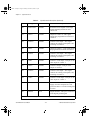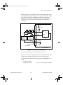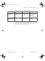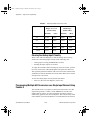
1
a.Title Page 1 Saturday, November 9, 1996 11:59 AM PC-LPM-16/PnP User Manual Multifunction I/O Board for the PC July 1996 Edition Part Number 320287B-01 Copyright 1990, 1996 National Instruments Corporation. All Rights Reserved. a.Title Page 2 Saturday, November 9, 1996 11:59 AM Internet Support GPIB: [email protected] DAQ: [email protected] VXI: [email protected] LabVIEW: [email protected] LabWindows: [email protected] HiQ: [email protected] VISA: [email protected] E-mail: [email protected] FTP Site: ftp.natinst.com Web Address: http://www.natinst.com Bulletin Board Support BBS United States: (512) 794-5422 or (800) 327-3077 BBS United Kingdom: 01635 551422 BBS France: 1 48 65 15 59 FaxBack Support (512) 418-1111 Telephone Support (U.S.) Tel: (512) 795-8248 Fax: (512) 794-5678 International Offices Australia 03 9 879 9422, Austria 0662 45 79 90 0, Belgium 02 757 00 20, Canada (Ontario) 519 622 9310, Canada (Québec) 514 694 8521, Denmark 45 76 26 00, Finland 90 527 2321, France 1 48 14 24 24, Germany 089 741 31 30, Hong Kong 2645 3186, Italy 02 413091, Japan 03 5472 2970, Korea 02 596 7456, Mexico 95 800 010 0793, Netherlands 0348 433466, Norway 32 84 84 00, Singapore 2265886, Spain 91 640 0085, Sweden 08 730 49 70, Switzerland 056 200 51 51, Taiwan 02 377 1200, U.K. 01635 523545 National Instruments Corporate Headquarters 6504 Bridge Point Parkway Austin, TX 78730-5039 Tel: (512) 794-0100 a.Book : b.Warranty Page 3 Monday, November 4, 1996 4:53 pm Important Information Warranty The PC-LPM-16 and PC-LPM-16PnP are warranted against defects in materials and workmanship for a period of one year from the date of shipment, as evidenced by receipts or other documentation. National Instruments will, at its option, repair or replace equipment that proves to be defective during the warranty period. This warranty includes parts and labor. The media on which you receive National Instruments software are warranted not to fail to execute programming instructions, due to defects in materials and workmanship, for a period of 90 days from date of shipment, as evidenced by receipts or other documentation. National Instruments will, at its option, repair or replace software media that do not execute programming instructions if National Instruments receives notice of such defects during the warranty period. National Instruments does not warrant that the operation of the software shall be uninterrupted or error free. A Return Material Authorization (RMA) number must be obtained from the factory and clearly marked on the outside of the package before any equipment will be accepted for warranty work. National Instruments will pay the shipping costs of returning to the owner parts which are covered by warranty. National Instruments believes that the information in this manual is accurate. The document has been carefully reviewed for technical accuracy. In the event that technical or typographical errors exist, National Instruments reserves the right to make changes to subsequent editions of this document without prior notice to holders of this edition. The reader should consult National Instruments if errors are suspected. In no event shall National Instruments be liable for any damages arising out of or related to this document or the information contained in it. EXCEPT AS SPECIFIED HEREIN, NATIONAL INSTRUMENTS MAKES NO WARRANTIES, EXPRESS OR IMPLIED, AND SPECIFICALLY DISCLAIMS ANY WARRANTY OF MERCHANTABILITY OR FITNESS FOR A PARTICULAR PURPOSE. CUSTOMER’S RIGHT TO RECOVER DAMAGES CAUSED BY FAULT OR NEGLIGENCE ON THE PART OF NATIONAL INSTRUMENTS SHALL BE LIMITED TO THE AMOUNT THERETOFORE PAID BY THE CUSTOMER. NATIONAL INSTRUMENTS WILL NOT BE LIABLE FOR DAMAGES RESULTING FROM LOSS OF DATA, PROFITS, USE OF PRODUCTS, OR INCIDENTAL OR CONSEQUENTIAL DAMAGES, EVEN IF ADVISED OF THE POSSIBILITY THEREOF. This limitation of the liability of National Instruments will apply regardless of the form of action, whether in contract or tort, including negligence. Any action against National Instruments must be brought within one year after the cause of action accrues. National Instruments shall not be liable for any delay in performance due to causes beyond its reasonable control. The warranty provided herein does not cover damages, defects, malfunctions, or service failures caused by owner’s failure to follow the National Instruments installation, operation, or maintenance instructions; owner’s modification of the product; owner’s abuse, misuse, or negligent acts; and power failure or surges, fire, flood, accident, actions of third parties, or other events outside reasonable control. Copyright Under the copyright laws, this publication may not be reproduced or transmitted in any form, electronic or mechanical, including photocopying, recording, storing in an information retrieval system, or translating, in whole or in part, without the prior written consent of National Instruments Corporation. Trademarks LabVIEW, NI-DAQ, DAQ-STC , and SCXI are trademarks of National Instruments Corporation. Product and company names listed are trademarks or trade names of their respective companies. WARNING REGARDING MEDICAL AND CLINICAL USE OF NATIONAL INSTRUMENTS PRODUCTS National Instruments products are not designed with components and testing intended to ensure a level of reliability suitable for use in treatment and diagnosis of humans. Applications of National Instruments products involving medical or clinical treatment can create a potential for accidental injury caused by product failure, or by errors on the part of the user or application designer. Any use or application of National Instruments products for or involving medical or clinical treatment must be performed by properly trained and qualified medical personnel, and all traditional medical safeguards, equipment, and procedures that are appropriate in the particular situation to prevent serious injury or death should always continue to be used when National Instruments products are being used. National Instruments products are NOT intended to be a substitute for any form of established process, procedure, or equipment used to monitor or safeguard human health and safety in medical or clinical treatment. a.Book : c.Table of Contents Page v Monday, November 4, 1996 4:53 pm Table of Contents About This Manual Organization of This Manual .........................................................................................ix Conventions Used in This Manual.................................................................................x National Instruments Documentation ............................................................................xi Related Documentation..................................................................................................xii Customer Communication .............................................................................................xii Chapter 1 Introduction About the PC-LPM-16/PnP............................................................................................1-1 What You Need to Get Started.......................................................................................1-2 Software Programming Choices ....................................................................................1-2 LabVIEW and LabWindows/CVI Application Software ................................1-2 NI-DAQ Driver Software ................................................................................1-3 Register-Level Programming...........................................................................1-4 Optional Equipment .......................................................................................................1-5 Custom Cables ...............................................................................................................1-5 Unpacking ......................................................................................................................1-6 Chapter 2 Installation and Configuration Hardware Installation .....................................................................................................2-1 Software Installation ......................................................................................................2-2 Board Configuration.......................................................................................................2-2 Plug and Play ...................................................................................................2-2 Base I/O Address and Interrupt Selection .........................................2-3 Non-Plug and Play...........................................................................................2-3 Chapter 3 Theory of Operation Functional Overview......................................................................................................3-1 PC I/O Channel Interface Circuitry................................................................................3-3 Analog Input and Data Acquisition Circuitry ................................................................3-4 National Instruments Corporation v PC-LPM-16/PnP User Manual a.Book : c.Table of Contents Page vi Monday, November 4, 1996 4:53 pm Table of Contents Analog Input Circuitry .................................................................................... 3-5 Data Acquisition Timing Circuitry ................................................................. 3-6 Single-Channel Data Acquisition ..................................................... 3-7 Multichannel Scanning Data Acquisition ......................................... 3-7 Data Acquisition Rates ..................................................................... 3-7 Digital I/O Circuitry ..................................................................................................... 3-8 Timing I/O Circuitry...................................................................................................... 3-9 Chapter 4 Signal Connections I/O Connector ................................................................................................................ 4-1 Signal Connection Descriptions .................................................................................... 4-3 Analog Input Signal Connections ................................................................... 4-5 Connections for Signal Sources........................................................ 4-5 Digital I/O Signal Connections ....................................................................... 4-6 Power Connections.......................................................................................... 4-7 Power Rating................................................................................................... 4-8 Timing Connections ........................................................................................ 4-8 Data Acquisition Timing Connections ............................................. 4-8 General-Purpose Timing Signal Connections and General-Purpose Counter Timing Signals .................................................................. 4-9 Appendix A Specifications Appendix B MSM82C53 Data Sheet Appendix C Using Your PC-LPM-16 (Non-PnP) Board Appendix D Register-Level Programming Appendix E Customer Communication PC-LPM-16/PnP User Manual vi National Instruments Corporation a.Book : c.Table of Contents Page vii Monday, November 4, 1996 4:53 pm Table of Contents Glossary Index Figures Figure 1-1. The Relationship between the Programming Environment, NI-DAQ, and Your Hardware ...............................................................1-4 Figure 3-1. Figure 3-2. Figure 3-3. Figure 3-4. Figure 3-5. Figure 3-6. PC-LPM-16PnP Block Diagram ...........................................................3-2 PC I/O Interface Circuitry Block Diagram ............................................3-3 Analog Input and Data Acquisition Circuitry Block Diagram ..............3-4 Digital I/O Circuitry Block Diagram .....................................................3-8 Timing I/O Circuitry Block Diagram ....................................................3-9 Counter Block Diagram .........................................................................3-10 Figure 4-1. Figure 4-2. Figure 4-3. Figure 4-4. Figure 4-5. Figure 4-6. Figure 4-7. PC-LPM-16PnP I/O Connector Pin Assignments .................................4-2 Analog Input Signal Connections ..........................................................4-6 Analog Input Signal Connections ..........................................................4-7 EXTCONV* Signal Timing ..................................................................4-9 Event-Counting Application with External Switch Gating ...................4-10 Frequency Measurement Application ....................................................4-11 General-Purpose Timing Signals ...........................................................4-12 Figure A-1. ADC Errors ............................................................................................A-6 Figure C-1. Figure C-2. Figure C-3. Figure C-4. Figure C-5. Figure C-6. Figure C-7. PC-LPM-16 Parts Locator Diagram ......................................................C-5 Example Base I/O Address Switch Settings ..........................................C-7 Interrupt Jumper Setting IRQ5 (Factory Setting) ..................................C-10 Interrupt Jumper Setting for Disabling Interrupts .................................C-10 Bipolar Input (±5 V) Jumper Configuration (Factory Setting) .............C-11 Bipolar Input (±2.5 V) Jumper Configuration .......................................C-11 Unipolar Input (0 to 10 V) Jumper Configuration .................................C-11 National Instruments Corporation vii PC-LPM-16/PnP User Manual a.Book : c.Table of Contents Page viii Monday, November 4, 1996 4:53 pm Table of Contents Tables Table 4-1. Signal Connection Descriptions ............................................................ 4-3 Table C-1. Table C-2. Table C-3. Comparison of Characteristics .............................................................. C-1 PC Bus Interface Factory Settings ........................................................ C-7 Switch Settings with Corresponding Base I/O Address and Base I/O Address Space ........................................................................ C-9 Table D-1. Table D-2. Table D-3. PC-LPM-16/PnP Register Map ............................................................ D-1 Unipolar Input Mode A/D Conversion Values ..................................... D-29 Bipolar Input Mode A/D Conversion Values ....................................... D-30 PC-LPM-16/PnP User Manual viii National Instruments Corporation a.Book : d.ATM Page ix Monday, November 4, 1996 4:53 pm About This Manual This manual describes the mechanical and electrical aspects of the PC-LPM-16PnP and contains information concerning its installation, operation, and programming. The PC-LPM-16PnP is a low-cost, lowpower analog input, digital, and timing I/O board for the IBM PC/XT, PC AT, Personal System/2 Models 25 and 30, and laptop compatible computers. This manual also applies to the PC-LPM-16, a non-Plug and Play board. The boards are identical in functionality, programming, and performance, except for the differences listed in Appendix C, Using Your PC-LPM-16 (Non-PnP) Board. Organization of This Manual The PC-LPM-16/PnP User Manual is organized as follows: • Chapter 1, Introduction, describes the PC-LPM-16/PnP, lists what you need to get started, software programming choices, and optional equipment, and explains how to unpack the PC-LPM-16/PnP. • Chapter 2, Installation and Configuration, describes the installation and configuration of the PC-LPM-16PnP. • Chapter 3, Theory of Operation, includes an overview of the PC-LPM-16PnP board and explains the operation of each functional unit making up the board. This chapter also explains the basic operation of the PC-LPM-16PnP circuitry. • Chapter 4, Signal Connections, describes how to make input and output signal connections to your PC-LPM-16PnP board via the I/O connector. • Appendix A, Specifications, lists the specifications of the PC-LPM-16PnP. • Appendix B, MSM82C53 Data Sheet, contains a manufacturer data sheet for the MSM82C53 CMOS programmable interval timer (OKI Semiconductor). National Instruments Corporation ix PC-LPM-16/PnP User Manual a.Book : d.ATM Page x Monday, November 4, 1996 4:53 pm About This Manual • Appendix C, Using Your PC-LPM-16 (Non-PnP) Board, describes the differences between the PC-LPM-16PnP and the PC-LPM-16 non-PnP boards, the PC-LPM-16 board configuration, and installing the PC-LPM-16 into your computer. • Appendix D, Register-Level Programming, describes in detail information related to register-level programming the PC-LPM-16/PnP. • Appendix E, Customer Communication, contains forms you can use to request help from National Instruments or to comment on our products. • The Glossary contains an alphabetical list and description of terms used in this manual, including abbreviations, acronyms, metric prefixes, mnemonics, and symbols. • The Index lists topics covered in this manual, including the page number where the topic can be found. Conventions Used in This Manual The following conventions are used in this manual: <> Angle brackets containing numbers separated by an ellipsis represent a range, signal, or port (for example, ACH<0..7> stands for ACH0 through ACH7). bold Bold text denotes menus, menu items, or dialog box buttons or options, and error messages. bold italic Bold italic text denotes a note, caution, or warning. italic Italic text denotes emphasis, a cross reference, or an introduction to a key concept. monospace Text in this font denotes text or characters that are to be literally input from the keyboard, sections of code, programming examples, and syntax examples. This font is also used for the proper names of disk drives, paths, directories, programs, subprograms, subroutines, device names, functions, operations, variables, filenames, and extensions, and for statements and comments taken from program code. NI-DAQ NI-DAQ refers to the NI-DAQ software for PC compatibles, unless otherwise noted. PC-LPM-16/PnP User Manual x National Instruments Corporation a.Book : d.ATM Page xi Monday, November 4, 1996 4:53 pm About This Manual Non-PnP Non-PnP (non-Plug and Play) means that the board requires you to manually configure the product’s base address and interrupt level with switches and jumpers. You must perform this configuration before installing the board into your computer. PC PC refers to the IBM PC/XT, PC AT, Personal System/2 Models 25 and 30, and laptop compatible computers. PC-LPM-16/PnP PC-LPM-16/PnP refers to both the Plug and Play and the non-Plug and Play versions of the board. PC-LPM-16PnP PC-LPM-16PnP refers to the Plug and Play version of the board. PC-LPM-16 PC-LPM-16 refers to the non-Plug and Play version of the board. PnP PnP (Plug and Play) means that the board is fully compatible with the industry-standard Plug and Play ISA Specification. All bus-related configuration is performed through software, freeing you from manually configuring jumpers or switches to set the product’s base address and interrupt level. Plug and Play systems automatically arbitrate and assign system resources to a PnP product. Abbreviations, acronyms, metric prefixes, mnemonics, symbols, and terms are listed in the Glossary. National Instruments Documentation The PC-LPM-16/PnP User Manual is one piece of the documentation set for your DAQ or SCXI system. You could have any of several types of manuals depending on the hardware and software in your system. Use the manuals you have as follows: • Getting Started with SCXI—If you are using SCXI, this is the first manual you should read. It gives an overview of the SCXI system and contains the most commonly needed information for the modules, chassis, and software. • Your SCXI hardware user manuals—If you are using SCXI, read these manuals next for detailed information about signal connections and module configuration. They also explain in greater detail how the module works and contain application hints. • Your DAQ hardware documentation—This documentation has detailed information about the DAQ hardware that plugs into or is connected to your computer. Use this documentation for hardware National Instruments Corporation xi PC-LPM-16/PnP User Manual a.Book : d.ATM Page xii Monday, November 4, 1996 4:53 pm About This Manual installation and configuration instructions, specification information about your DAQ hardware, and application hints. • Software documentation—Examples of software documentation you may have are the LabVIEW, LabWindows/CVI documentation sets, and the NI-DAQ documentation. After you set up your hardware system, use either the application software (LabVIEW or LabWindows/CVI) or the NI-DAQ documentation to help you write your application. If you have a large, complicated system, it is worthwhile to look through the software documentation before you configure your hardware. • Accessory installation guides or manuals—If you are using accessory products, read the terminal block and cable assembly installation guides. They explain how to physically connect the relevant pieces of the system. Consult these guides when you are making your connections. • SCXI Chassis User Manual—If you are using SCXI, read this manual for maintenance information on the chassis and for installation instructions. Related Documentation The following document contains information that you may find helpful as you read this manual: • Your computer user or technical reference manual Customer Communication National Instruments wants to receive your comments on our products and manuals. We are interested in the applications you develop with our products, and we want to help if you have problems with them. To make it easy for you to contact us, this manual contains comment and configuration forms for you to complete. These forms are in Appendix E, Customer Communication, at the end of this manual. PC-LPM-16/PnP User Manual xii National Instruments Corporation a.Book : e.chapter 1 Page 1 Monday, November 4, 1996 4:53 pm Chapter 1 Introduction This chapter describes the PC-LPM-16/PnP, lists what you need to get started, software programming choices, and optional equipment, and explains how to unpack the PC-LPM-16/PnP. About the PC-LPM-16/PnP The PC-LPM-16/PnP is a low-cost, low-power analog input, digital, and timing I/O board for the PC. The board contains a 12-bit, successive-approximation, self-calibrating ADC with 16 analog inputs, 8 lines of TTL-compatible digital input, and 8 lines of digital output. The PC-LPM-16/PnP also contains two 16-bit counter/timer channels for timing I/O. The low cost of a PC-LPM-16/PnP-based system makes it ideal for laboratory work in industrial and academic environments. The board’s low power consumption and small size make the PC-LPM-16/PnP especially suitable for laptop computers. The multichannel analog input is useful in signal analysis and data logging. The 12-bit ADC is useful in high-resolution applications such as chromatography, temperature measurement, and DC voltage measurement. You can use the 16 TTLcompatible digital I/O lines for switching external devices such as transistors and solid-state relays, for reading the status of external digital logic, and for generating interrupts. You can use the counter/timers to synchronize events, generate pulses, and measure frequency and time. The PC-LPM-16/PnP, used in conjunction with your computer, is a versatile, cost-effective platform for laboratory test, measurement, and control. National Instruments Corporation 1-1 PC-LPM-16/PnP User Manual a.Book : e.chapter 1 Page 2 Monday, November 4, 1996 4:53 pm Chapter 1 Introduction What You Need to Get Started To set up and use your PC-LPM-16/PnP board, you will need the following: ❏ PC-LPM-16/PnP board ❏ PC-LPM-16/PnP User Manual ❏ One of the following software packages and documentation: NI-DAQ for PC Compatibles LabVIEW for Windows LabWindows/CVI for Windows ❏ Your computer Software Programming Choices There are several options to choose from when programming your National Instruments DAQ and SCXI hardware. You can use LabVIEW, LabWindows/CVI, NI-DAQ, or register-level programming. LabVIEW and LabWindows/CVI Application Software LabVIEW and LabWindows/CVI are innovative program development software packages for data acquisition and control applications. LabVIEW uses graphical programming, whereas LabWindows/CVI enhances traditional programming languages. Both packages include extensive libraries for data acquisition, instrument control, data analysis, and graphical data presentation. LabVIEW features interactive graphics, a state-of-the-art user interface, and a powerful graphical programming language. The LabVIEW Data Acquisition VI Library, a series of VIs for using LabVIEW with National Instruments DAQ hardware, is included with LabVIEW. The LabVIEW Data Acquisition VI Library is functionally equivalent to the NI-DAQ software. LabWindows/CVI features interactive graphics, a state-of-the-art user interface, and uses the ANSI standard C programming language. The LabWindows/CVI Data Acquisition Library, a series of functions for using LabWindows/CVI with National Instruments DAQ hardware, is PC-LPM-16/PnP User Manual 1-2 National Instruments Corporation a.Book : e.chapter 1 Page 3 Monday, November 4, 1996 4:53 pm Chapter 1 Introduction included with the NI-DAQ software kit. The LabWindows/CVI Data Acquisition Library is functionally equivalent to the NI-DAQ software. Using LabVIEW or LabWindows/CVI software will greatly reduce the development time for your data acquisition and control application. NI-DAQ Driver Software The NI-DAQ driver software is included at no charge with all National Instruments DAQ hardware. NI-DAQ is not packaged with signal conditioning or accessory products. NI-DAQ has an extensive library of functions that you can call from your application programming environment. These functions include routines for analog input (A/D conversion), buffered data acquisition (high-speed A/D conversion), analog output (D/A conversion), waveform generation (timed D/A conversion), digital I/O, counter/timer operations, SCXI, RTSI, calibration, messaging, and acquiring data to extended memory. NI-DAQ has both high-level DAQ I/O functions for maximum ease of use and low-level DAQ I/O functions for maximum flexibility and performance. Examples of high-level functions are streaming data to disk or acquiring a certain number of data points. An example of a low-level function is writing directly to registers on the DAQ device. NI-DAQ does not sacrifice the performance of National Instruments DAQ devices because it lets multiple devices operate at their peak performance. NI-DAQ also internally addresses many of the complex issues between the computer and the DAQ hardware such as programming interrupts and DMA controllers. NI-DAQ maintains a consistent software interface among its different versions so that you can change platforms with minimal modifications to your code. Whether you are using conventional programming languages, LabVIEW, or LabWindows/CVI, your application uses the NI-DAQ driver software, as illustrated in Figure 1-1. National Instruments Corporation 1-3 PC-LPM-16/PnP User Manual a.Book : e.chapter 1 Page 4 Monday, November 4, 1996 4:53 pm Chapter 1 Introduction Conventional Programming Environment (PC, Macintosh, or Sun SPARCstation) LabVIEW (PC, Macintosh, or Sun SPARCstation) LabWindows/CVI (PC or Sun SPARCstation) NI-DAQ Driver Software Personal Computer or Workstation DAQ or SCXI Hardware Figure 1-1. The Relationship between the Programming Environment, NI-DAQ, and Your Hardware Register-Level Programming The final option for programming any National Instruments DAQ hardware is to write register-level software. Writing register-level programming software can be very time-consuming and inefficient and is not recommended for most users. Even if you are an experienced register-level programmer, consider using NI-DAQ, LabVIEW, or LabWindows/CVI to program your National Instruments DAQ hardware. Using the NI-DAQ, LabVIEW, or LabWindows/CVI software is as easy and as flexible as register-level programming and can save weeks of development time. PC-LPM-16/PnP User Manual 1-4 National Instruments Corporation a.Book : e.chapter 1 Page 5 Monday, November 4, 1996 4:53 pm Chapter 1 Introduction Optional Equipment National Instruments offers a variety of products to use with your PC-LPM-16/PnP board, including cables, connector blocks, and other accessories, as follows: • Cables and cable assemblies, shielded and ribbon • Connector blocks, shielded and unshielded with 50-pin screw terminals • SCXI modules and accessories for isolating, amplifying, exciting, and multiplexing signals for relays and analog output. With SCXI you can condition and acquire up to 3,072 channels. • Low channel-count signal conditioning modules, boards, and accessories, including conditioning for strain gauges and RTDs, simultaneous sample-and-hold circuitry, and relays For more specific information about these products, refer to your National Instruments catalogue or call the office nearest you. Custom Cables National Instruments currently offers a cable termination accessory, the CB-50, for use with the PC-LPM-16/PnP. This kit includes a terminated, 50-conductor, flat ribbon cable and a connector block. Signal input and output wires can be attached to screw terminals on the connector block and connected to the PC-LPM-16/PnP I/O connector. The CB-50 is useful for the initial prototyping of an application or in situations where PC-LPM-16/PnP interconnections are frequently changed. Once you develop a final field wiring scheme, however, you may want to develop your own cable. This section contains information and guidelines for the design of custom cables. The PC-LPM-16/PnP I/O connector is a 50-pin, male, ribbon cable header connector. The following list gives recommended part numbers for use with your PC-LPM-16/PnP board: • Electronic Products Division/3M (part number 3596-5002) • T&B/Ansley Corporation (part number 609-5007) National Instruments Corporation 1-5 PC-LPM-16/PnP User Manual a.Book : e.chapter 1 Page 6 Monday, November 4, 1996 4:53 pm Chapter 1 Introduction The mating connector for the PC-LPM-16/PnP is a 50-position, polarized, ribbon socket connector with strain relief. National Instruments uses a polarized (keyed) connector to prevent inadvertent upside-down connection to the PC-LPM-16/PnP. Recommended manufacturer part numbers for this mating connector are as follows: • Electronic Products Division/3M (part number 3425-7650) • T&B/Ansley Corporation (part number 609-5041CE) The following are the standard ribbon cables (50-conductor, 28 AWG, stranded) that can be used with these connectors: • Electronic Products Division/3M (part number 3365/50) • T&B/Ansley Corporation (part number 171-50) Unpacking Your PC-LPM-16/PnP board is shipped in an antistatic package to prevent electrostatic damage to the board. Electrostatic discharge can damage several components on the board. To avoid such damage in handling the board, take the following precautions: PC-LPM-16/PnP User Manual • Ground yourself via a grounding strap or by holding a grounded object. • Touch the antistatic package to a metal part of your computer chassis before removing the board from the package. • Remove the board from the package and inspect the board for loose components or any other sign of damage. Notify National Instruments if the board appears damaged in any way. Do not install a damaged board into your computer. • Never touch the exposed pins of connectors. 1-6 National Instruments Corporation a.Book : f.chapter 2 Page 1 Monday, November 4, 1996 4:53 pm Chapter Installation and Configuration 2 This chapter describes the installation and configuration of the PC-LPM-16PnP. For information on installing and configuring the PC-LPM-16, a non-PnP board, refer to Appendix C, Using Your PC-LPM-16 (Non-PnP) Board. Hardware Installation You can install the PC-LPM-16PnP in any available expansion slot in your computer. The following are general installation instructions, but consult your computer user manual or technical reference manual for specific instructions and warnings. 1. Turn off and unplug your computer. 2. Remove the top cover or access port to the I/O channel. 3. Remove the expansion slot cover on the back panel of the computer. 4. Insert the PC-LPM-16PnP board into any 8-bit or 16-bit slot. It may be a tight fit, but do not force the board into place. 5. Screw the mounting bracket of the PC-LPM-16PnP board to the back panel rail of the computer. 6. Replace the cover. 7. Plug in and turn on your computer. The PC-LPM-16PnP is installed. National Instruments Corporation 2-1 PC-LPM-16/PnP User Manual a.Book : f.chapter 2 Page 2 Monday, November 4, 1996 4:53 pm Chapter 2 Installation and Configuration Software Installation If you are using NI-DAQ, refer to your NI-DAQ release notes to install your driver software. Find the installation section for your operating system and follow the instructions given there. If you are using LabVIEW, refer to your LabVIEW release notes to install your application software. After you have installed LabVIEW, refer to the NI-DAQ release notes and follow the instructions given there for your operating system and LabVIEW. If you are using LabWindows/CVI, refer to your LabWindows/CVI release notes to install your application software. After you have installed LabWindows/CVI, refer to the NI-DAQ release notes and follow the instructions given there for your operating system and LabWindows/CVI. If you are a register-level programmer, refer to Appendix D, RegisterLevel Programming, for software configuration information. Board Configuration Plug and Play The PC-LPM-16PnP is fully compatible with the industry-standard Intel/Microsoft Plug and Play Specification version 1.0a. A Plug and Play system arbitrates and assigns resources through software, freeing you from manually setting switches and jumpers. These resources include the board base I/O address and interrupt channels. Each PC-LPM-16PnP is configured at the factory to request these resources from the Plug and Play Configuration Manager. The Configuration Manager receives all of the resource requests at startup, compares the available resources to those requested, and assigns the available resources as efficiently as possible to the Plug and Play boards. Application software can query the Configuration Manager to determine the resources assigned to each board without your involvement. The Plug and Play software is installed as a device driver or as an integral component of the computer BIOS. PC-LPM-16/PnP User Manual 2-2 National Instruments Corporation a.Book : f.chapter 2 Page 3 Monday, November 4, 1996 4:53 pm Chapter 2 Installation and Configuration Base I/O Address and Interrupt Selection You can configure your PC-LPM-16PnP to use base addresses in the range of 100 to FFF0 hex. The PC-LPM-16PnP occupies 16 bytes of address space and must be located on a 16-byte boundary. Therefore, valid addresses include 100, 110, 120…, FFE0, FFF0 hex. This selection is software-configured and does not require you to manually change any settings on the board. The PC-LPM-16PnP can use interrupt channels 3, 4, 5, 6, 7, and 9. There are different ways to assign the base address to your board: • For Windows 95, the base address and interrupt should be set automatically. However, if you want to view or change these settings, you can set the board resources using the Device Manager. Windows 95 will automatically allocate resources, but these can be changed in the Device Manager: a. Click the right mouse button on My Computer to bring up system properties. b. Select Device Manager. c. Select Data Acquisition Devices. d. Select the PC-LPM-16. You can change address and interrupt settings on the Resources page. • For Windows 3.10 or 3.11, you can use the NI-DAQ Configuration Utility (formerly WDAQCONF) to assign the board resources. If a standard configuration utility is present in the system, you will not be able to modify the board resources. • You can use a standard configuration utility like Intel ISA Configuration Utility (ICU). ICU dynamically assigns the base address to your board when you boot up the computer. You can also lock the board resources when you use ICU. For additional information on ICU, contact Intel Corporation for a copy of Plug and Play Specification version 1.0a. Non-Plug and Play To configure the non-Plug and Play PC-LPM-16 board, refer to Appendix C, Using Your PC-LPM-16 (Non-PnP) Board. National Instruments Corporation 2-3 PC-LPM-16/PnP User Manual a.Book : g.chapter 3 Page 1 Monday, November 4, 1996 4:53 pm Chapter Theory of Operation 3 This chapter includes an overview of the PC-LPM-16PnP board and explains the operation of each functional unit making up the board. This chapter also explains the basic operation of the PC-LPM-16PnP circuitry. Functional Overview The following are the major components making up the PC-LPM-16PnP: • PC I/O channel interface circuitry • Analog input and data acquisition circuitry • Digital I/O circuitry • Timing I/O circuitry You can execute data acquisition functions by using the analog input circuitry and some of the timing I/O circuitry. The internal data and control buses interconnect the components. The theory of operation for each of these components is explained in the remainder of this chapter. The block diagram in Figure 3-1 shows a functional overview of the PC-LPM-16PnP. National Instruments Corporation 3-1 PC-LPM-16/PnP User Manual a.Book : g.chapter 3 Page 2 Monday, November 4, 1996 4:53 pm Theory of Operation PC I/O Channel Interface 12-Bit Sampling ADC 256-Word FIFO Input Mux 16-Channel Single-Ended Buffer Scanning Counter Plug and Play OUT0 EXTCONV* PC I/O Channel A/D Timing 1 MHz 16 CLK0 MSM82C53 GATE<0..2> CLK<1..2> 3 OUT<0..2> 3 2 OUT1 Interrupt Interface OUT1* EXTINT* I/O Connector Chapter 3 FROM A/D FIFO 8 Digital I/O 8 +12 V +12 V 0.5 A -12 V +5 V -12 V +5 V 1.0 A Figure 3-1. PC-LPM-16PnP Block Diagram PC-LPM-16/PnP User Manual 3-2 National Instruments Corporation a.Book : g.chapter 3 Page 3 Monday, November 4, 1996 4:53 pm Chapter 3 Theory of Operation PC I/O Channel Interface Circuitry The PC I/O channel interface circuitry consists of an address bus, a data bus, interrupt lines, and several control and support signals. The components making up the PC-LPM-16PnP PC I/O channel interface circuitry are shown in Figure 3-2. PC I/O Channel Address Bus Control Lines Data Bus IRQ Plug and Play Circuitry Timing Interface Address Decoder Register Selects Read & Write Signals Data Buffers Internal Data Bus Plug and Play Interrupt Control Interrupt Requests Figure 3-2. PC I/O Interface Circuitry Block Diagram The circuitry consists of Plug and Play address decoders, data buffers, I/O channel interface timing control circuitry, and interrupt control circuitry. The circuitry monitors address lines SA4 through SA15 to generate the board enable signal, and uses lines SA0 through SA3 plus timing signals to generate the onboard register select signals and read/write signals. The data buffers control the direction of data transfer on the bidirectional data lines based on whether the transfer is a read or write operation. The interrupt control circuitry routes any enabled interrupts to the selected interrupt request line. The PC-LPM-16PnP has six interrupt National Instruments Corporation 3-3 PC-LPM-16/PnP User Manual a.Book : g.chapter 3 Page 4 Monday, November 4, 1996 4:53 pm Chapter 3 Theory of Operation request lines available: IRQ3, IRQ4, IRQ5, IRQ6, IRQ7, and IRQ9. The PC-LPM-16PnP generates interrupts in three different situations: • When an A/D conversion generates data that can be read from FIFO • When an active low-level signal is detected on the EXTINT* line • When a rising-edge signal is detected on counter 2 output The PC-LPM-16PnP individually enables and clears each one of these interrupts. For more detailed information on generating interrupts externally, see the EXTINTEN bit of the Command Register 1 description in Appendix D, Register-Level Programming. Analog Input and Data Acquisition Circuitry The PC-LPM-16PnP has 16 channels of analog input with 12-bit A/D conversion. Using the timing circuitry, the PC-LPM-16PnP can also automatically time multiple A/D conversions. Figure 3-3 shows a block diagram of the analog input and data acquisition circuitry. 8 256-Word FIFO 12-Bit Sampling ADC A/D Data Buffer Input Mux 16-Channel Single-Ended ACH<0..15> PC I/O Channel A/D RD CONVAVAIL 4 Scanning Counter Interrupt Interface 1 MHz 16 CLK0 OUT0 MSM82C53 A/D Timing I/O Connector PC I/O Channel Interface EXTCONV* Figure 3-3. Analog Input and Data Acquisition Circuitry Block Diagram PC-LPM-16/PnP User Manual 3-4 National Instruments Corporation a.Book : g.chapter 3 Page 5 Monday, November 4, 1996 4:53 pm Chapter 3 Theory of Operation Analog Input Circuitry The analog input circuitry consists of an input multiplexer, a jumperselectable gain stage, and a 12-bit sampling ADC. The 12-bit output is sign-extended to 16 bits before it is stored in a 256-word deep FIFO memory. The input multiplexer stage is made up of a CMOS analog input multiplexer and has 16 analog input channels (channels 0 through 15). With the input multiplexer stage, input overvoltage protection of ± 45 V is available powered on, or ± 35 V powered off. The PC-LPM-16PnP uses a successive-approximation analog-to-digital converter (ADC). Software-selectable gains of 0.5, 1, and 2 for the input signal combined with the ADC’s fixed input range of ±5 V yield four useful analog input signal ranges, 0 to 10 V, ±5 V, 0 to 5 V, and ±2.5 V. When an A/D conversion is complete, the ADC clocks the result into the A/D FIFO. The A/D FIFO is 16 bits wide and 256 words deep. This FIFO serves as a buffer to the ADC and has two benefits. First, any time an A/D conversion is complete, the A/D FIFO saves the value for later reading, and the ADC can start a new conversion. Secondly, the A/D FIFO can collect up to 256 A/D conversion values before losing any information, thus giving the software some extra time (256 times the sample interval) to catch up with the hardware. If the A/D FIFO stores more than 256 values without the A/D FIFO being read, an error condition called A/D FIFO Overflow occurs and A/D conversion information is lost. The A/D FIFO generates a signal that indicates when it contains conversion data. You can read the signal state from the PC-LPM-16PnP Status Register 1. The output from the ADC is in two’s complement format. In unipolar input mode (0 to 10 V or 0 to 5 V input range configuration), the data from the ADC is interpreted as a 12-bit positive number ranging from 0 to 4,095. In bipolar input mode (± 5 or ± 2.5 V input range configuration), the data from the ADC is interpreted as a two’s complement number ranging from -2,048 to +2047. The ADC’s output is always sign-extended to 16 bits by board circuitry so that data values read from the FIFO are 16 bits wide. The ADC on the PC-LPM-16PnP includes calibration circuitry that makes it possible to minimize zero, full-scale, and linearity errors. The National Instruments Corporation 3-5 PC-LPM-16/PnP User Manual a.Book : g.chapter 3 Page 6 Monday, November 4, 1996 4:53 pm Chapter 3 Theory of Operation ADC goes through a self-calibration cycle under software control. To properly use this ADC auto-calibration feature, you need an accurate input stage that does not introduce significant offset and gain errors. The analog input stage on the PC-LPM-16PnP maintains the required accuracy without trimpot adjustments. Data Acquisition Timing Circuitry A data acquisition operation refers to the process of carefully timing the interval between successive A/D conversions. This interval is called the sample interval. The data acquisition timing circuitry consists of various clocks and timing signals that perform this timing. The PC-LPM-16PnP can perform two types of data acquisition: singlechannel data acquisition and multichannel scanning data acquisition. Multichannel scanning data acquisition uses a counter to automatically switch between analog input channels during a data acquisition operation. Data acquisition timing consists of signals that initiate a data acquisition operation and generate scanning clocks. Sources for these signals are supplied mainly by timers on the PC-LPM-16PnP board. One of the three counters of the onboard MSM82C53 is reserved for this purpose. You can initiate an A/D conversion by a falling edge on the counter 0 output (OUT0) of the MSM82C53 onboard counter/timer chip, or by a rising edge on EXTCONV* input. The sample-interval timer is a 16-bit down-counter that uses the onboard 1 MHz clock to generate sample intervals from 20 to 65,535 µs (see Timing I/O Circuitry later in this chapter for more timing information). Each time the sample-interval timer reaches zero, it generates a pulse and reloads with the programmed sample-interval count. This operation continues until you reprogram the counter. As stated in Appendix D, Register-Level Programming, only counter 0 is required for data acquisition operations. The software must keep track of the number of conversions that have occurred and turn off counter 0 after it receives the required number of conversions. PC-LPM-16/PnP User Manual 3-6 National Instruments Corporation a.Book : g.chapter 3 Page 7 Monday, November 4, 1996 4:53 pm Chapter 3 Theory of Operation Single-Channel Data Acquisition During single-channel data acquisition, the channel-select bits in Command Register 1 select the analog input channel before data acquisition begins. This multiplexer setting remains constant during the entire data acquisition process; therefore, all A/D conversion data is read from a single channel. Multichannel Scanning Data Acquisition Multichannel data acquisition is performed when you enable scanned data acquisition. A scan counter on the board controls multichannel scanning. For multichannel scanning operations, the scan counter decrements from the highest channel which you select through channel 0. Thus, the board can scan any number of channels from 2 to 16. Notice that the same analog input range is used for all channels in the scan sequence. Data Acquisition Rates The maximum data acquisition rate (number of samples per second) is determined by the conversion period of the ADC plus the acquisition time of its track-and-hold stage. During multichannel scanning, the settling time of the input multiplexers and operational amplifier further limits the data acquisition rate. After the input multiplexers switch channels, the amplifier must be able to settle to the new input signal value to within 12-bit accuracy before performing an A/D conversion, or else it will not achieve 12-bit accuracy. The maximum data acquisition rate for both single-channel and multichannel operation is 50 kS/s. The signal will settle to ± 1 LSB for any range if you do not exceed a signal sampling frequency of 50 kS/s. If you exceed the recommended data acquisition rate, the analog input circuitry may not perform at 12-bit accuracy. If you exceed this rate, an error condition called overrun occurs and you will lose some conversion data. This recommended rate of 50 kS/s assumes that voltage levels on all the channels included in the scan sequence are within range and are driven by low-impedance sources. Signal levels outside the ranges on the channels included in the scan sequence adversely affect the input settling time. Similarly, channels driven by high-impedance signal sources should be allowed for greater settling time. National Instruments Corporation 3-7 PC-LPM-16/PnP User Manual a.Book : g.chapter 3 Page 8 Monday, November 4, 1996 4:53 pm Chapter 3 Theory of Operation Digital I/O Circuitry The PC-LPM-16PnP has 16 digital I/O lines that are TTL-compatible. Pins DIN<0..7> of the I/O connector are digital input lines, and pins DOUT<0..7> are digital output lines. These lines are monitored or driven by the Digital Input Register or the Digital Output Register, respectively. Reading the Digital Input Register returns the current state of the DIN<0..7> lines. Writing to the Digital Output Register drives the new value onto the DOUT<0..7> lines. The external device may drive the EXTINT* signal to indicate the readiness of data transfer. PC I/O Channel I/O RD 8 / I/O WR Digital Input Register Digital Output Register Status Register 1 8 / DIN <0..7> 8 / DOUT<0..7> I/O Connector 8 / EXTINT* Plug and Play Interrupt Interface Figure 3-4. Digital I/O Circuitry Block Diagram PC-LPM-16/PnP User Manual 3-8 National Instruments Corporation a.Book : g.chapter 3 Page 9 Monday, November 4, 1996 4:53 pm Chapter 3 Theory of Operation Timing I/O Circuitry The PC-LPM-16PnP uses an MSM82C53 Counter/Timer integrated circuit for data acquisition timing and for general-purpose timing I/O functions. Three counters on the circuit are available for general use, but the board can use only one of them, counter 0, internally for data acquisition timing. Figure 3-5 shows a block diagram of both groups of timing I/O circuitry. A/D Conversion Logic OUT0 GATE0 PC I/O Channel CLK0 1 MHz Clock CLK1 GATE1 OUT1 CLK2 GATE2 OUT2 8 / Data MSM82C53 Counter/Timer OUT0 GATE0 CLK1 GATE1 OUT1 OUT1* CLK2 GATE2 OUT2 I/O Connector CTR RD/WR Plug and Play Interrupt Interface Figure 3-5. Timing I/O Circuitry Block Diagram The MSM82C53 contains three independent 16-bit counter/timers and one 8-bit Mode Register. As shown in Figure 3-5, you can use counter 0 for data acquisition timing, and counters 1 and 2 are free for general use. You can program all three counter/timers to operate in several useful timing modes. The programming and operation of the MSM82C53 is presented in detail both in Appendix B, MSM82C53 Data Sheet, and Appendix D, Register-Level Programming. The timebase for counter 0 uses a 1 MHz clock generated from an onboard oscillator. You must externally supply the timebases for counters 1 and 2 through the 50-pin I/O connector. Figure 3-6 diagrams the 16-bit counters in the MSM82C53. National Instruments Corporation 3-9 PC-LPM-16/PnP User Manual a.Book : g.chapter 3 Page 10 Monday, November 4, 1996 4:53 pm Chapter 3 Theory of Operation CLK Counter OUT GATE Figure 3-6. Counter Block Diagram Each counter has a clock input pin, a gate input pin, and an output pin labeled CLK, GATE, and OUT, respectively. The MSM82C53 counters are numbered zero through two, and their GATE, CLK, and OUT pins are labeled GATEN, CLKN, and OUTN, where N is the counter number. PC-LPM-16/PnP User Manual 3-10 National Instruments Corporation a.Book : h.chapter 4 Page 1 Monday, November 4, 1996 4:53 pm Chapter 4 Signal Connections This chapter describes how to make input and output signal connections to your PC-LPM-16PnP board via the I/O connector. I/O Connector Figure 4-1 shows the pin assignments for the PC-LPM-16PnP I/O connector. This connector is located on the back panel of the board and is accessible from the back of your computer after you have properly installed the board. Installation instructions are in Chapter 2, Installation and Configuration. Warning: Connections that exceed any of the maximum ratings of input or output signals on the PC-LPM-16PnP can damage the board and the computer. This includes connecting any power signals to ground and vice versa. Each signal description in this section includes information about maximum input ratings. National Instruments is NOT liable for any damages resulting from any such signal connections. National Instruments Corporation 4-1 PC-LPM-16/PnP User Manual a.Book : h.chapter 4 Page 2 Monday, November 4, 1996 4:53 pm Chapter 4 Signal Connections AIGND ACH0 ACH1 ACH2 ACH3 ACH4 ACH5 ACH6 ACH7 DGND +12 V DIN1 DIN3 DIN5 DIN7 DOUT1 DOUT3 DOUT5 DOUT7 EXTINT* OUT0 OUT1 CLK1 GATE2 +5 V 1 3 5 7 9 11 13 15 17 19 21 2 4 6 8 10 12 14 16 18 20 22 AIGND ACH8 23 25 27 29 31 33 35 37 39 41 43 45 47 49 24 26 28 30 32 34 36 38 40 42 44 46 48 50 DIN2 DIN4 ACH9 ACH10 ACH11 ACH12 ACH13 ACH14 ACH15 -12 V DIN0 DIN6 DOUT0 DOUT2 DOUT4 DOUT6 OUT1* EXTCONV* GATE0 GATE1 OUT2 CLK2 DGND Figure 4-1. PC-LPM-16PnP I/O Connector Pin Assignments PC-LPM-16/PnP User Manual 4-2 National Instruments Corporation a.Book : h.chapter 4 Page 3 Monday, November 4, 1996 4:53 pm Chapter 4 Signal Connections Signal Connection Descriptions Table 4-1. Pin Signal Signal Connection Descriptions Reference Description 1–2 AIGND N/A Analog Input Ground—The pins are connected to the analog input ground signal. ACH<0..15> signals should be referenced to AIGND. 3–18 ACH<0..15> AGND Analog Input Channels 0 through 15— These channels are single-ended. 19 DGND N/A Digital Ground—This pin supplies the reference for the digital signals at the I/O connector as well as the +5 VDC supply. 20 -12 V DGND -12 VDC Power Supply Output Pin— The maximum current is 5.0 mA. 21 +12 V DGND +12 VDC Power Supply from the Computer Bus—This power line has a 0.5 A self-resetting fuse in series. 22–29 DIN<0..7> DGND Digital Input Data Lines—These signals are TTL-compatible, digital input lines. DIN7 is the MSB, DIN0 the LSB. 30–37 DOUT<0..7> DGND Digital Output Data Lines—These signals are TTL-compatible, digital output lines. DOUT7 is the MSB, DOUT0 the LSB. 38 OUT1* DGND Output of Counter 1—This signal outputs the inverted programmed waveform of counter 1. 39 EXTINT* DGND External Interrupt—This pin is used for input of the external interrupt signal. National Instruments Corporation 4-3 PC-LPM-16/PnP User Manual a.Book : h.chapter 4 Page 4 Monday, November 4, 1996 4:53 pm Chapter 4 Signal Connections Table 4-1. Signal Pin Signal Connection Descriptions (Continued) Reference Description 40 EXTCONV* DGND External Convert Signal—This input signal externally initiates an A/D conversion. 41 OUT0 DGND Output of Counter 0—This signal outputs the programmed waveform of counter 0. 42 GATE0 DGND Counter 0 Gate Input—This signal controls the starting, interruption, and restarting of counter 0. 43 OUT1 DGND Output of Counter 1—This signal outputs the programmed waveform of counter 1. 44 GATE1 DGND Counter 1 Gate Input—This signal controls the starting, interruption, and restarting of counter 1. 45 CLK1 DGND Counter 1 Clock Input—This pin is the clock input for counter 1. 46 OUT2 DGND Counter 2 Output—This pin is the output of counter 2. 47 GATE2 DGND Counter 2 Gate Input—This signal controls the starting, interruption, and restarting of counter 2. 48 CLK2 DGND Counter 2 Clock Input—This pin is the clock input for counter 2. 49 +5 V DGND +5 Volts—This is the +5 VDC power supply from the computer bus. This power line has a 1.0 A self-resetting fuse in series. 50 DGND N/A Digital Ground—This pin is connected to the digital ground signal. Note: An asterisk (*) indicates that the signal is active low. PC-LPM-16/PnP User Manual 4-4 National Instruments Corporation a.Book : h.chapter 4 Page 5 Monday, November 4, 1996 4:53 pm Chapter 4 Signal Connections The connector pins can be grouped into categories of analog input signal pins, digital I/O signal pins, and timing I/O signal pins. Signal connection guidelines for each of these groups follow. Analog Input Signal Connections Pins 3 through 18 are analog input signal pins for the ADC. Pins 1 and 2 are analog common signals. You can use these pins for a general analog power ground tie to the PC-LPM-16PnP. Pins 3 through 18 are tied to the 16 single-ended analog input channels of the input multiplexer through 4.7 kΩ series resistors. These resistors limit input current to the multiplexer. Pin 40 triggers conversions slightly after this signal makes a low-to-high transition. You can only use this pin to cause conversions, not as a monitor to detect conversions caused by the onboard sampleinterval timer. Refer to Figure 4-4 for more information about EXTCONV* timing. The following input ranges and maximum ratings apply to inputs ACH<0..15>: Input signal range Bipolar input: ± 5 V or ± 2.5 V Unipolar input: 0 to 10 V or 0 to 5 V Maximum input voltage rating ± 45 V powered on ± 35 V powered off Warning: Exceeding the input signal range, even on unused analog input channels, distorts other input signals. Exceeding the maximum input voltage rating can damage your board and the computer. National Instruments is NOT liable for any damages resulting from such signal connections. Connections for Signal Sources Figure 4-2 shows how to connect a signal source to your PC-LPM-16PnP. When you connect grounded signal sources, carefully observe the polarity to avoid shorting the signal source output. National Instruments Corporation 4-5 PC-LPM-16/PnP User Manual a.Book : h.chapter 4 Page 6 Monday, November 4, 1996 4:53 pm Chapter 4 Signal Connections ACH<0..15> 3 4 Signal Source 5 + + Vs1 V S3 VS2 - Operational Amplifier + - + 18 + Input Multiplexer 1, 2 VM - Measured Voltage AIGND - I/O Connector PC-LPM-16PnP Figure 4-2. Analog Input Signal Connections Digital I/O Signal Connections See Table 4-1 for the digital I/O pin descriptions. The following specifications and ratings apply to the digital I/O lines: PC-LPM-16/PnP User Manual • Absolute maximum voltage input rating +7.0 V with respect to DGND -0.5 V with respect to DGND • Digital input compatibility TTL-compatible • Input current (high or low level) ± 10 µA • Digital output compatibility • Output current source capability 8 mA, at VOH = 2.7 V • Output current sink capability 4-6 TTL-compatible 6 mA, at VOL = 0.5 V National Instruments Corporation a.Book : h.chapter 4 Page 7 Monday, November 4, 1996 4:53 pm Chapter 4 22 DIN 0 Signal Connections Digital Input TTL Signal 29 DIN 7 +5 V Port Debounced Switch* 19 +5 V Digital LED DGND Output 30 DOUT 0 Port I/O Connector PC-LPM-16PnP *Complex switch circuitry is not shown here in order to simplify the figure. Figure 4-3. Analog Input Signal Connections Figure 4-3 shows the connections of the digital input port and digital output port. Digital input applications include receiving TTL signals and sensing external device states such as the switch in Figure 4-3. Digital output applications include sending TTL signals and driving external devices such as the LED shown in Figure 4-3. Power Connections Pin 49 of the I/O connector supplies +5 V from the computer I/O channel power supply. Pin 20 of the I/O connector supplies +12 V from the computer I/O channel power supply. The -12 V is supplied from the computer I/O power supply with a resistor in series. These pins are referenced to DGND and can be used to power external digital circuitry. The +5 V supply at the I/O connector has a 1.0 A protection fuse in series. The +12 V supply at the I/O connector has a 0.5 A protection National Instruments Corporation 4-7 PC-LPM-16/PnP User Manual a.Book : h.chapter 4 Page 8 Monday, November 4, 1996 4:53 pm Chapter 4 Signal Connections fuse in series. Both fuses are self-resetting; simply remove the circuit causing the heavy current load and the fuse will reset itself. Power Rating The following table shows the maximum current for each power line at the I/O connector. Power Line Maximum Current +5 V (self-resetting fuse at 1.0 A) 1.0 A* +12 V (self-resetting fuse at 0.5 A) 0.5 A* -12 V 5.0 mA * The actual current available from these signals may be less, depending on your computer. Notice also that any current drawn from these lines adds to the power requirements from the computer. Timing Connections Pins 38 through 48 of the I/O connector are connections for timing I/O signals. The timing input and output of the PC-LPM-16PnP is designed around an MSM82C53 counter/timer integrated circuit. All three counters of the circuit are available at the I/O connector. One of these counters, counter 0, is used for data acquisition timing. Pin 39 carries an external signal that can be used for data acquisition timing in place of counter 0. Pins 38 and 41 through 48 carry general-purpose timing signals. These signals are explained in the General-Purpose Timing Signal Connections and General-Purpose Counter Timing Signals section later in this chapter. Data Acquisition Timing Connections Counter 0 on the MSM82C53 counter/timer is used as a sample-interval counter in timed A/D conversions. In addition to counter 0, EXTCONV* can externally time conversions. See Appendix D, Register-Level Programming, for the programming sequence needed to enable this input. Figure 4-4 shows the timing requirements for the EXTCONV* input. An A/D conversion is initiated by a rising edge on the EXTCONV*. The data from this conversion is latched into the FIFO memory within 20 µs. The EXTCONV* input is a TTL-compatible signal. PC-LPM-16/PnP User Manual 4-8 National Instruments Corporation a.Book : h.chapter 4 Page 9 Monday, November 4, 1996 4:53 pm Chapter 4 Signal Connections tw EXTCONV* V IH V t IL t t int w 200 ns min int 20 µs min (A/D interval) A/D Conversion Starts within 800 ns of this Edge Figure 4-4. EXTCONV* Signal Timing General-Purpose Timing Signal Connections and General-Purpose Counter Timing Signals The general-purpose timing signals include the GATE, CLK, and OUT signals for the three MSM82C53 counters, except CLK of counter 0 is not available on the I/O connector. You can use the counter/timers for general-purpose applications such as pulse and square wave generation, event counting, and pulse-width, time-lapse, and frequency measurement. For these applications, user signals sent from the I/O connector on the CLK and GATE pins go to the counters, and the counters are user-programmable for various operations. The single exception is counter 0, which has an internal 1 MHz clock. Chapter 3, Theory of Operation, briefly describes the MSM82C53 counter/timer. For detailed information on this counter/timer, see Appendix B, MSM82C53 Data Sheet. For pulse and square wave generation, program a counter to generate a timing signal at its OUT output pin. For event counting, program a counter to count the rising or falling edges applied to any of the MSM82C53 CLK inputs. You can then read the counter value to determine the number of edges that have occurred. You can gate the counter operation on and off during event counting. Figure 4-5 shows connections for a typical event-counting operation where a switch is used to gate the counter on and off. National Instruments Corporation 4-9 PC-LPM-16/PnP User Manual a.Book : h.chapter 4 Page 10 Monday, November 4, 1996 4:53 pm Chapter 4 Signal Connections +5 V 4.7 kW CLK OUT GATE Debounced Switch* Counter Signal Source 19 DGND I/O Connector PC-LPM-16PnP *Complex switch circuitry is not shown here in order to simplify the figure. Figure 4-5. Event-Counting Application with External Switch Gating Perform pulse-width measurement by level gating to trigger the counter. Apply the pulse to be measured to the counter GATE input. Load the counter with the known count and program it to count down while the signal at the GATE input is high. The pulse width equals the counter difference (loaded value minus read value) multiplied by the CLK period. For time-lapse measurement, program a counter to be edge-gated. Apply an edge to the counter GATE input to start the counter. You can program the counter to start counting after receiving a low-to-high edge. The time lapse since receiving the edge equals the counter value difference (loaded value minus read value) multiplied by the CLK period. For frequency measurement, program a counter to be level-gated and count the number of falling edges in a signal applied to a CLK input. The gate signal you apply to the counter GATE input is of known PC-LPM-16/PnP User Manual 4-10 National Instruments Corporation a.Book : h.chapter 4 Page 11 Monday, November 4, 1996 4:53 pm Chapter 4 Signal Connections duration. In this case, program the counter to count falling edges at the CLK input while the gate is applied. The frequency of the input signal then equals the count value divided by the gate period. Figure 4-6 shows the connections for a frequency measurement application. You could also use a second counter to generate the gate signal in this application. +5 V 4.7 kW CLK OUT GATE Signal Source Gate Source Counter 17 DGND I/O Connector PC-LPM-16PnP Figure 4-6. Frequency Measurement Application 4.7 kΩ resistors pull up the GATE and CLK pins to +5 V. Figure 4-7 shows the timing requirements for the GATE and CLK input signals and the timing specifications for the OUT output signals. The following specifications and ratings apply to the MSM82C53 I/O signals: • National Instruments Corporation Absolute maximum voltage input rating 4-11 -0.5 to 7.0 V with respect to DGND PC-LPM-16/PnP User Manual a.Book : h.chapter 4 Page 12 Monday, November 4, 1996 4:53 pm Chapter 4 Signal Connections MSM82C53 digital input specifications (referenced to DGND): • VIH input logic high voltage 2.2 V min • VIL input logic low voltage 0.8 V max • Input load current ± 10.0 µA max MSM82C53 digital output specifications (referenced to DGND): • VOH output logic high voltage 3.7 V min • VOL output logic low voltage 0.45 V max • IOH output source current, at VOH 1.0 mA max • IOL output sink current, at VOL 4.0 mA max tsc CLK tpwl VIL tgh tgsu GATE tpwh VIH VIH VIL tgwh OUT toutg VOH tgwl toutc VOL tsc tpwh tpwl tgsu tgh tgwh tgwl toutg toutc clock period clock high level clock lowlevel gate setup time gate hold time gate high level gate low level output delay from clock output delay from gate 125 ns min 60 ns min 60 ns min 60 ns min 60 ns min 60 ns min 60 ns min 60 ns min 60 ns min Figure 4-7. General-Purpose Timing Signals The GATE and OUT signals in Figure 4-7 are referenced to the rising edge of the CLK signal. PC-LPM-16/PnP User Manual 4-12 National Instruments Corporation a.Book : I.Appendix A Page 1 Monday, November 4, 1996 4:53 pm Appendix A Specifications This appendix lists the PC-LPM-16PnP specifications. These specifications are typical at 25° C unless otherwise specified. The operating temperature range is 0° to 70° C. PC-LPM-16PnP Board Analog Input Input Characteristics Number of channels ........................... 16 single-ended Type of ADC...................................... Successive approximation Resolution .......................................... 12 bits, 1 in 4,096 Max sampling rate .............................. 50 kS/s Input signal ranges ............................. ± 5 V, ± 2.5 V, 0 to 10 V, or 0 to 5 V, software-selectable Input coupling .................................... DC Overvoltage protection ....................... ± 45 V powered on, ± 35 V powered off Inputs protected ....................... ACH<0..15> FIFO buffer size ................................. 256 S Data transfers ..................................... Interrupts, programmed I/O Transfer Characteristics Relative accuracy .............................. ± 1.0 LSB typ, ± 1.5 LSB max Integral nonlinearity ........................... ± 0.5 LSB max Differential nonlinearity ..................... ± 1.0 LSB max (For more information on nonlinearity and quantization error, see the Explanation of Analog Input Specifications section) Offset error after calibration............... ± 1.0 LSB typ, ± 2.0 LSB max National Instruments Corporation A-1 PC-LPM-16/PnP User Manual a.Book : I.Appendix A Page 2 Monday, November 4, 1996 4:53 pm Appendix A Specifications Gain error (relative to calibration reference) After calibration 0 to 5 V and ± 5 V range ...............± 1.0 LSB typ, ± 2.0 LSB max All other ranges............................± 2.0 of reading typ, ± 4.0 max Note: LSB refers to the least significant bit of a 12-bit conversion value in the preceding specifications. LSB is equivalent to 2.44 mV in the 10 V range (0 to 10 V or ± 5 V) and 1.22 mV in the 5 V ranges (0 to 5 V or ± 2.5 V). Amplifier Characteristics Input impedance..................................0.1 GΩ in parallel with 40 pF typ Dynamic Characteristics Bandwidth Gain = (-3 dB) ..............................200 kHz typ Settling time to ± 1.0 LSB for full-scale step ................................20 µs max at all ranges System noise .......................................0.1 LSB rms for all ranges Stability Recommended warm-up time..............15 min. Onboard calibration reference Level ............................................5.000 V (± 2.5 mV) Temperature coefficient ...............20 ppm/°C max Long-term stability.......................15 ppm/ 1, 000 h typ Digital I/O Number of channels ............................8 input and 8 output Compatibility ......................................TTL Configuration......................................1 8-bit input port, 1 8-bit output port Absolute max ratings ..........................+7.0 V with respect to DGND; voltage input rating: -0.5 V with respect to DGND PC-LPM-16/PnP User Manual A-2 National Instruments Corporation a.Book : I.Appendix A Page 3 Monday, November 4, 1996 4:53 pm Appendix A Digital logic levels ............... Specifications Minimum Maximum Input low voltage 0V 0.8 V Input high voltage 2V 5.0 V Input low current (Vin = 0 V) — ±10 µA Input high current (Vin = 5 V) — ±10 µA Level Minimum Maximum Output low voltage (Iout = 4 mA) — 0.4 V Output high voltage (Iout = 4 mA) 3.7 V — Level Timing I/O Number of channels ........................... 3 counter/timers (1 dedicated to analog input) Resolution .......................................... 16 bits Compatibility ..................................... TTL, gate and source pulled high with 4.7 kΩ resistors Input logic low voltage....................... 0.8 V max Input logic high voltage...................... 2.2 V min Output logic low voltage at output current = 4.0 mA ................. 0.45 V max Output logic high voltage at output current = -1.0 mA ................ 3.7 V min Base clocks available ......................... 1 MHz ± 0.01% Max source frequency ........................ 8 MHz Min source pulse duration .................. 60 ns Min gate pulse duration ...................... 50 ns Data transfers ..................................... Programmed I/O National Instruments Corporation A-3 PC-LPM-16/PnP User Manual a.Book : I.Appendix A Page 4 Monday, November 4, 1996 4:53 pm Appendix A Specifications Bus Interface Type.................................................... Slave Power Requirement +5 VDC (± 10%).................................. 50 mA typ +12 VDC (± 5%).................................. 15 mA typ -12 VDC (± 5%) .................................. 15 mA typ Note: These numbers do not include an additional 1 A from the 5 V power supply. The 50-pin I/O connector can draw 0.5 A from the +12 V supply. Physical Dimensions ......................................... 11.0 by 9.9 cm (4.4 by 3.9 in.) I/O connector ...................................... 50-pin D male ribbon cable connector Environment Operating temperature......................... 0° to 70° C Storage temperature ............................ -55° to 150° C Relative humidity................................ 5% to 90% noncondensing Explanation of Analog Input Specifications Relative accuracy is a measure of the linearity of an ADC. However, relative accuracy is a tighter specification than a nonlinearity specification. Relative accuracy indicates the maximum deviation from a straight line for the analog-input-to-digital-output transfer curve. If a ADC has been calibrated perfectly, then this straight line is the ideal transfer function, and the relative accuracy specification indicates the worst deviation from the ideal that the ADC permits. A relative accuracy specification of ± 1 LSB is roughly equivalent to (but not the same as) a ± 1/2 LSB nonlinearity or integral nonlinearity specification because relative accuracy encompasses both nonlinearity and variable quantization uncertainty, a quantity often mistakenly assumed to be exactly ± 1/2 LSB. Although quantization uncertainty is ideally ± 1/2 LSB, it can be different for each possible digital code and is actually the analog width of each code. Thus, it is more specific to use relative accuracy as a measure of linearity than it is to use what is normally called nonlinearity, because relative accuracy ensures that the PC-LPM-16/PnP User Manual A-4 National Instruments Corporation a.Book : I.Appendix A Page 5 Monday, November 4, 1996 4:53 pm Appendix A Specifications sum of quantization uncertainty and A/D conversion error does not exceed a given amount. Integral nonlinearity in a ADC is an often ill-defined specification that is supposed to indicate a converter’s overall A/D transfer linearity. The manufacturers of the ADC chips used by National Instruments specify their integral nonlinearity by stating that the analog center of any code will not deviate from a straight line by more than ± 1 LSB. This specification is misleading because although a particularly wide code’s center may be found within ± 1 LSB of the ideal, one of its edges may be well beyond ± 1 LSB; thus, the ADC would have a relative accuracy of that amount. National Instruments tests its boards to ensure that they meet all three linearity specifications defined in this appendix; specifications for integral nonlinearity are included primarily to maintain compatibility with a convention of specifications used by other board manufacturers. Relative accuracy, however, is much more useful. Differential nonlinearity is a measure of deviation of code widths from their theoretical value of 1 LSB. The width of a given code is the size of the range of analog values that can be input to produce that code, ideally 1 LSB. A specification of ± 1 LSB differential nonlinearity ensures that no code has a width of 0 LSBs (that is, no missing codes) and that no code width exceeds 2 LSBs. System noise is the amount of noise seen by the ADC when there is no signal present at the input of the board. The amount of noise that is reported directly (without any analysis) by the ADC is not necessarily the amount of real noise present in the system, unless the noise is ≥0.5 LSB rms. Noise that is less than this magnitude produces varying amounts of flicker, and the amount of flicker seen is a function of how near the real mean of the noise is to a code transition. If the mean is near or at a transition between codes, the ADC flickers evenly between the two codes, and the noise is seen as very nearly 0.5 LSB. If the mean is near the center of a code and the noise is relatively small, very little or no flicker is seen, and the noise is reported by the ADC as nearly 0 LSB. From the relationship between the mean of the noise and the measured rms magnitude of the noise, the character of the noise can be determined. National Instruments has determined that the character of the noise in the PC-LPM-16PnP is fairly Gaussian, so the noise specifications given are the amounts of pure Gaussian noise required to produce our readings. National Instruments Corporation A-5 PC-LPM-16/PnP User Manual a.Book : I.Appendix A Page 6 Monday, November 4, 1996 4:53 pm Appendix A Specifications To illustrate these definitions, Figure A-1 shows a portion of the analog-input-to-digital-output transfer curve for an ideal, ADC overlaid on the transfer curve of a hypothetical, typical, ADC. As shown in Figure A-1, the relative accuracy is the deviation of the code transition voltage from the center of the code for an ideal ADC, expressed in terms of LSBs. Notice that in this case, an ideal ADC has a relative accuracy of ± 1/2 LSB, because this definition of relative accuracy encompasses both nonlinearity and quantization uncertainties. Integral nonlinearity is the worst case deviation of the center of the code from the ideal center, expressed in terms of LSBs. Finally, the differential nonlinearity is deviation of a code width from ideal code width, expressed in terms of LSBs. Output Code (LSB) 2 Cideal Cactual x x 1 INLe Vactual Re1 Re2 Videal -2 -1 1 Input Voltage (LSBs) -1 2 KEY Practical ADC analog-input-to-digital-output curve Ideal ADC analog-input-to-digital-output curve Cideal = Center of code1 for ideal ADC Cactual = Center of code1 for practical ADC INL error = INLe = Cactual-Cideal Relative Accuracy = Maximum (Rel, Re2) DNL error = Vactual-Videal Figure A-1. ADC Errors PC-LPM-16/PnP User Manual A-6 National Instruments Corporation a.Book : j.Appendix B Page 1 Monday, November 4, 1996 4:53 pm Appendix MSM82C53 Data Sheet B This appendix contains a manufacturer data sheet for the MSM82C53* CMOS programmable interval timer (OKI Semiconductor). This timer is used on the PC-LPM-16PnP board. *Copyright OKI Semiconductor 1995. Reprinted with permission of copyright owner. All rights reserved. OKI Semiconductor Data Book Microprocessor, Eighth Edition, January 1995. National Instruments Corporation B-1 PC-LPM-16/PnP User Manual a.Book : j.Appendix B Page 2 Monday, November 4, 1996 4:53 pm Appendix B MSM82C53 Data Sheet PC-LPM-16/PnP User Manual B-2 National Instruments Corporation a.Book : j.Appendix B Page 3 Monday, November 4, 1996 4:53 pm Appendix B National Instruments Corporation B-3 MSM82C53 Data Sheet PC-LPM-16/PnP User Manual a.Book : j.Appendix B Page 4 Monday, November 4, 1996 4:53 pm Appendix B MSM82C53 Data Sheet PC-LPM-16/PnP User Manual B-4 National Instruments Corporation a.Book : j.Appendix B Page 5 Monday, November 4, 1996 4:53 pm Appendix B National Instruments Corporation B-5 MSM82C53 Data Sheet PC-LPM-16/PnP User Manual a.Book : j.Appendix B Page 6 Monday, November 4, 1996 4:53 pm Appendix B MSM82C53 Data Sheet PC-LPM-16/PnP User Manual B-6 National Instruments Corporation a.Book : j.Appendix B Page 7 Monday, November 4, 1996 4:53 pm Appendix B National Instruments Corporation B-7 MSM82C53 Data Sheet PC-LPM-16/PnP User Manual a.Book : j.Appendix B Page 8 Monday, November 4, 1996 4:53 pm Appendix B MSM82C53 Data Sheet PC-LPM-16/PnP User Manual B-8 National Instruments Corporation a.Book : j.Appendix B Page 9 Monday, November 4, 1996 4:53 pm Appendix B National Instruments Corporation B-9 MSM82C53 Data Sheet PC-LPM-16/PnP User Manual a.Book : j.Appendix B Page 10 Monday, November 4, 1996 4:53 pm Appendix B MSM82C53 Data Sheet PC-LPM-16/PnP User Manual B-10 National Instruments Corporation a.Book : j.Appendix B Page 11 Monday, November 4, 1996 4:53 pm Appendix B National Instruments Corporation B-11 MSM82C53 Data Sheet PC-LPM-16/PnP User Manual a.Book : j.Appendix B Page 12 Monday, November 4, 1996 4:53 pm Appendix B MSM82C53 Data Sheet PC-LPM-16/PnP User Manual B-12 National Instruments Corporation a.Book : k.Appendix C Page 1 Monday, November 4, 1996 4:53 pm Appendix Using Your PC-LPM-16 (Non-PnP) Board C This appendix describes the differences between the PC-LPM-16PnP and the PC-LPM-16 non-PnP boards, the PC-LPM-16 board configuration, and installing the PC-LPM-16 into your computer. Differences between the PC-LPM-16PnP and the PC-LPM-16 The PC-LPM-16PnP is a Plug and Play upgrade from a legacy board, the PC-LPM-16. A National Instruments legacy product refers to an older board with switches and jumpers used to set the addresses. The original board has been replaced with a backwards-compatible, revised PC-LPM-16. This revised board has the same functionality as the Plug and Play version (except for the base address and interrupt selection), but differs somewhat from the legacy board. The following list compares the specifications and functionality of the newer boards with the obsolete board. Table C-1. Comparison of Characteristics Functional Changes Legacy PC-LPM-16 Revised PC-LPM-16 Assembly Number 181215-01 183527X-02 183527X-01 I/O Space Required 32 bytes 16 bytes 16 bytes I/O Base Address Selection Uses switches Uses switches Plug and Play compatible I/O Base Address Alignment Located on 32-byte boundary Located on 32-byte boundary Located on 16-byte boundary IRQ Selection Uses jumpers Uses jumpers Plug and Play compatible Gain Selection Selectable with jumpers Selectable with jumpers Software selectable National Instruments Corporation C-1 PC-LPM-16PnP PC-LPM-16/PnP User Manual a.Book : k.Appendix C Page 2 Monday, November 4, 1996 4:53 pm Appendix C Using Your PC-LPM-16 (Non-PnP) Board Table C-1. Comparison of Characteristics (Continued) Functional Changes Legacy PC-LPM-16 Revised PC-LPM-16 PC-LPM-16PnP Data FIFO Size 16 words 512 words 256 words Dummy reads to A/D and FIFO high-byte and low-byte registers after clearing data FIFO Required Not required, but allowed Not required, but allowed ADC FIFO Data Reading Order Low byte before high byte preferred Low byte must be read before high byte Low byte must be read before high byte Overflow Error Bit Location Status Register 1, bit 1 Status Register 1, bit 1 Status Register 2, bit 1 Overrun Error Bit Location Not implemented Not implemented Status Register 2, bit 0 Data Error Bit Location Not implemented Not implemented Status Register 1, bit 1 5 and 12 V Supply Fuses Nonresettable Self-resetting Self-resetting -12 V Supply Power Requirements 0 mA 15 mA typ 15 mA typ Performance Specification Changes INL ± 1 LSB max ± 0.5 LSB max ± 0.5 LSB max Gain Error, ±2.8 V or to 10 V Range ± 3 LSB typ, ± 7 LSB max ± 2 LSB typ, ± 4 LSB max ± 2 LSB typ, ± 4 LSB max Calibration Time 700 µs typ 10 ms typ 10 ms typ Overvoltage Protection or Analog Input Powered Off ± 45 V ± 35 V ± 35 V PC-LPM-16/PnP User Manual C-2 National Instruments Corporation a.Book : k.Appendix C Page 3 Monday, November 4, 1996 4:53 pm Appendix C Table C-1. Using Your PC-LPM-16 (Non-PnP) Board Comparison of Characteristics (Continued) Functional Changes Legacy PC-LPM-16 Revised PC-LPM-16 PC-LPM-16PnP Interrupt Enable/ Disable Control Through Command Register 1 Through Command Register 1 Through Plug and Play BIOS or NI-DAQ Configuration Utility Delay Between Rising EXTCONV* Edge and A/D Conversion 2–4 µs 800 ns max 800 ns max To determine which PC-LPM-16 board you have, refer to the Assembly Number row in Table C-1 and compare it to the assembly number displayed on your circuit board (see Figure C-1). National Instruments Corporation C-3 PC-LPM-16/PnP User Manual a.Book : k.Appendix C Page 4 Monday, November 4, 1996 4:53 pm Appendix C Using Your PC-LPM-16 (Non-PnP) Board Configuration and Installation of the PC-LPM-16 (non-PnP) Board Configuration The PC-LPM-16 contains three jumpers and one DIP switch to configure the PC bus interface and analog input settings. Use the DIP switch to set the base I/O address. Jumper W3 selects the interrupt level. Jumpers W1 and W2 configure the analog input circuitry. The DIP switch and jumpers are shown in the parts locator diagram in Figure C-1. The PC-LPM-16 is factory-configured to a base I/O address of hex 260 and to interrupt level 5. These settings (shown in Table C-1) are suitable for most systems. However, if your system has other hardware at this base I/O address or interrupt level, you need to change these settings on the PC-LPM-16 (as described in the following pages) or on the other hardware. Record your settings in the Hardware and Software Configuration Form in Appendix E, Customer Communication. PC-LPM-16/PnP User Manual C-4 National Instruments Corporation a.Book : k.Appendix C Page 5 Monday, November 4, 1996 4:53 pm Appendix C Using Your PC-LPM-16 (Non-PnP) Board 5 6 4 7 3 2 1 1 2 W3 Switch U26 3 4 W2 W1 5 6 Serial Number Assembly Number 7 Product Name Figure C-1. PC-LPM-16 Parts Locator Diagram National Instruments Corporation C-5 PC-LPM-16/PnP User Manual a.Book : k.Appendix C Page 6 Monday, November 4, 1996 4:53 pm Appendix C Using Your PC-LPM-16 (Non-PnP) Board Base I/O Address Selection The base I/O address for the PC-LPM-16 is determined by the switches at position U26 (see Figure C-2). The switches are set at the factory for the base I/O address hex 260. This factory setting is used as the default base I/O address value by National Instruments software packages for use with the PC-LPM-16. The PC-LPM-16 uses the base I/O address space hex 260 through 26F with the factory setting. See Table C-2 for the board factory settings. Table C-2. PC Bus Interface Factory Settings PC-LPM-16 Board Default Settings Base I/O Address Hex 260 Hardware Implementation U26 A9 A8 A7 A6 A5 Interrupt Level Interrupt level 5 selected (factory setting) W3: Row 5 Analog Input Bipolar input selected (±5 V) (factory setting) W1: B-C W2: B-C Verify that this base I/O address space is not already used by other equipment installed in your computer. Note: If any equipment in your computer already uses this base I/O address space, you must change the base I/O address of the PC-LPM-16 or of the other device. If you change the PC-LPM-16 base I/O address, you must make a corresponding change to any software packages you use with the PC-LPM-16. For more information about the I/O address of your computer, refer to your computer’s technical reference manual. PC-LPM-16/PnP User Manual C-6 National Instruments Corporation a.Book : k.Appendix C Page 7 Monday, November 4, 1996 4:53 pm Appendix C Using Your PC-LPM-16 (Non-PnP) Board Each switch in U26 corresponds to one of the address lines A9 through A5. Slide the switch to the side labeled A9 to A5 to select a binary value of zero for the corresponding address bit. Slide the switch to the side of the switch labeled ON to select a binary value of one for the corresponding address bit. Figure C-2 shows two possible switch settings. U26 –Slide to this side for 0 A9 A8 A7 A6 A5 –Slide to this side for 1 a. Switches Set to Base I/O Address of Hex 000 U26 –Slide to this side for 0 A9 A8 A7 A6 A5 –Slide to this side for 1 b. Switches Set to Base I/O Address of Hex 260 (Factory Setting) Figure C-2. Example Base I/O Address Switch Settings The PC-LPM-16 decodes the five LSBs of the address (A4 through A0) to select the appropriate PC-LPM-16 register. To change the base I/O address: 1. Remove the plastic cover on U26. 2. Slide each switch to the desired position. 3. Check each switch to verify that the switch is pressed entirely to the side. 4. Replace the plastic cover. Note the new PC-LPM-16 base I/O address for use when configuring the PC-LPM-16 software in the Hardware and Software Configuration Form in Appendix E, Customer Communication. Table C-3 lists the National Instruments Corporation C-7 PC-LPM-16/PnP User Manual a.Book : k.Appendix C Page 8 Monday, November 4, 1996 4:53 pm Appendix C Using Your PC-LPM-16 (Non-PnP) Board possible switch settings, the corresponding base I/O address, and the base I/O address space used for that setting. Table C-3. Switch Settings with Corresponding Base I/O Address and Base I/O Address Space Switch Setting Base I/O Address (hex) Base I/O Address Space Used (hex) A9 A8 A7 A6 A5 PC-LPM-16/PnP User Manual 0 1 0 0 0 100 100–10F 0 1 0 0 1 120 120–13F 0 1 0 1 0 140 140–14F 0 1 0 1 1 160 160–16F 0 1 1 0 0 180 180–18F 0 1 1 0 1 1A0 1A0–1AF 0 1 1 1 0 1C0 1C0–1CF 0 1 1 1 1 1E0 1E0–1EF 1 0 0 0 0 200 200–20F 1 0 0 0 1 220 220–22F 1 0 0 1 0 240 240–24F 1 0 0 1 1 260 260–26F 1 0 1 0 0 280 280–28F 1 0 1 0 1 2A0 2A0–2AF 1 0 1 1 0 2C0 2C0–2CF 1 0 1 1 1 2E0 2E0–2EF 1 1 0 0 0 300 300–30F 1 1 0 0 1 320 320–32F C-8 National Instruments Corporation a.Book : k.Appendix C Page 9 Monday, November 4, 1996 4:53 pm Appendix C Table C-3. Using Your PC-LPM-16 (Non-PnP) Board Switch Settings with Corresponding Base I/O Address and Base I/O Address Space (Continued) Switch Setting Base I/O Address (hex) Base I/O Address Space Used (hex) A9 A8 A7 A6 A5 Note: 1 1 0 1 0 340 340–34F 1 1 0 1 1 360 360–36F 1 1 1 0 0 380 380–38F 1 1 1 0 1 3A0 3A0–3AF 1 1 1 1 0 3C0 3C0–3CF 1 1 1 1 1 3E0 3E0–3EF Base I/O address values hex 000 through 0FF are reserved for system use. Base I/O address values hex 100 through 3FF are available on the I/O channel. Interrupt Selection The PC-LPM-16 connects to any one of the six interrupt lines of the computer I/O channel. A jumper selects the interrupt line on one of the double rows of pins located above the I/O slot edge connector on the PC-LPM-16 (see Figure C-1). To use the PC-LPM-16 interrupt capability, select an interrupt line and place the jumper in the appropriate position to enable that particular interrupt line. The interrupt lines that the PC-LPM-16 hardware supports are IRQ<3..7>, and IRQ9. Note: Using interrupt line 6 is not recommended. The diskette drive controller uses interrupt line 6 on most IBM PC and compatible computers. After you select an interrupt level, place the interrupt jumper on the appropriate pins to enable the interrupt line. The interrupt jumper setting is W3. The default interrupt line is IRQ5, which you select by placing the jumper on the pins in row 5, as shown in Figure C-3. To change to another line, remove the jumper from IRQ5 and place it on the new pins. National Instruments Corporation C-9 PC-LPM-16/PnP User Manual a.Book : k.Appendix C Page 10 Monday, November 4, 1996 4:53 pm Using Your PC-LPM-16 (Non-PnP) Board W3 Appendix C IRQ9 IRQ7 IRQ6 IRQ5 IRQ4 IRQ3 W2 Figure C-3. Interrupt Jumper Setting IRQ5 (Factory Setting) W3 If you do not want to use interrupts, set the jumper on W3 as shown in Figure C-4. This setting disables the PC-LPM-16 from asserting an interrupt line on the computer I/O channel. IRQ9 IRQ7 IRQ6 IRQ5 IRQ4 IRQ3 W2 Figure C-4. Interrupt Jumper Setting for Disabling Interrupts Analog Input Jumper Settings The PC-LPM-16 is factory-configured for the ± 5 V input range. Four ranges are available for analog input: bipolar ± 5 V, bipolar ± 2.5 V, unipolar 0 to 10 V, and unipolar 0 to 5 V. Jumpers W1 and W2 control the input range for all 16 analog input channels. Bipolar Input Selection 1 (±5 V) Select the bipolar (± 5 V) input configuration by setting jumpers W1 and W2 as shown in Figure C-5. PC-LPM-16/PnP User Manual C-10 National Instruments Corporation a.Book : k.Appendix C Page 11 Monday, November 4, 1996 4:53 pm Appendix C W1 Using Your PC-LPM-16 (Non-PnP) Board W2 A A B B C C Figure C-5. Bipolar Input (±5 V) Jumper Configuration (Factory Setting) Bipolar Input Selection 2 (±2.5 V) Select the bipolar (± 2.5 V) input configuration by setting jumpers W1 and W2 as shown in Figure C-6. W1 W2 A A B B C C Figure C-6. Bipolar Input (±2.5 V) Jumper Configuration Unipolar Input Selection 1 (0 to 10 V) Select the unipolar (0 to 10 V) input configuration by setting jumpers W1 and W2 as shown in Figure C-7. W1 W2 A A B B C C Figure C-7. Unipolar Input (0 to 10 V) Jumper Configuration National Instruments Corporation C-11 PC-LPM-16/PnP User Manual a.Book : k.Appendix C Page 12 Monday, November 4, 1996 4:53 pm Appendix C Using Your PC-LPM-16 (Non-PnP) Board Unipolar Input Selection 2 (0 to 5 V) Select the unipolar (0 to 5 V) input configuration by using the same setting as the ± 5 V range setting shown in Figure C-5. You can use this setting because the ADC is 12-bit. Therefore, 12-bit resolution data is obtained in both the 0 to +5 V signal range and the 0 to -5 V signal range while keeping the input configuration for ± 5 V input range. The jumper configuration for the 0 to 5 V and ± 5 V input signal ranges is the same. The software handles the distinction between the two ranges. Installation You can install the PC-LPM-16 in any available 8-bit or 16-bit expansion slot in your computer. To optimize the board noise performance, install the board away from the video card and leave a slot vacant on each side of the PC-LPM-16, if possible. After you make any necessary changes with the jumper and switch settings, you are ready to install the PC-LPM-16. The following are general installation instructions, but consult your computer user manual or technical reference manual for specific instructions and warnings. 1. Turn off and unplug your computer. 2. Remove the top cover or access port to the I/O channel. 3. Remove the expansion slot cover on the back panel of the computer. 4. Insert the PC-LPM-16 board into any 8-bit or 16-bit slot. It may be a tight fit, but do not force the board into place. 5. Screw the mounting bracket of the PC-LPM-16 board to the back panel rail of the computer. 6. Replace the cover. 7. Plug in and turn on your computer. The PC-LPM-16 is installed. PC-LPM-16/PnP User Manual C-12 National Instruments Corporation a.Book : l.Appendix D Page 1 Monday, November 4, 1996 4:53 pm Appendix Register-Level Programming D This appendix describes in detail information related to register-level programming the PC-LPM-16/PnP. Note: If you plan to use a programming software package such as NI-DAQ, LabVIEW, or LabWindows/CVI with your PC-LPM-16/PnP, you need not read this appendix. Base Address For information on the base address, see Chapter 2, Installation and Configuration. Register Map The register map for the PC-LPM-16/PnP is given in Table D-1. This table gives the register name, the register address offset from the board’s base address, the type of the register (read only, write only, or read and write), and the size of the register in bits. Table D-1. PC-LPM-16/PnP Register Map Offset Address (Hex) Type Size Configuration and Status Register Group Command Register 1 Command Register 2 Command Register 3 Status Register 1 Status Register 2* 0 7 5 0 1 Write-only Read-and-write Write-only Read-only Read-only 8-bit 8-bit 8-bit 8-bit 8-bit Analog Input Register Group A/D FIFO Low-Byte Register A/D FIFO High-Byte Register A/D Clear Register 2 3 1 Read-only Read-only Write-only 8-bit 8-bit 8-bit Register Name National Instruments Corporation D-1 PC-LPM-16/PnP User Manual a.Book : l.Appendix D Page 2 Monday, November 4, 1996 4:53 pm Appendix D Register-Level Programming Table D-1. PC-LPM-16/PnP Register Map (Continued) Offset Address (Hex) Type Size Counter/Timer (MSM82C53) Register Group Counter 0 Data Register Counter 1 Data Register Counter 2 Data Register Counter Mode Register Timer Interrupt Clear Register 8 9 A B 6 Read-and-write Read-and-write Read-and-write Write-only Write-only 8-bit 8-bit 8-bit 8-bit 8-bit Digital I/O Register Group Digital Output Register Digital Input Register 4 5 Write-only Read-only 8-bit 8-bit Register Name *PC-LPM-16PnP only. Register Size The PC-LPM-16/PnP registers are 8-bit registers. To transfer 16-bit data, you need two consecutive I/O read or write operations. For example, to read the 16-bit A/D conversion result, read the low byte of FIFO first, then the high byte of FIFO. Register Descriptions Table D-1 divides the PC-LPM-16/PnP registers into four different register groups. A bit description of each of the registers making up these groups is included later in this appendix. The Configuration and Status Register Group controls the overall operation of the PC-LPM-16/PnP and the D/A circuitry. The Analog Input Register Group reads output from the successive-approximation ADC. The Counter/Timer Register Group accesses the onboard MSM82C53 counter/timer integrated circuit. The Digital I/O Register Group consists of the digital output and input registers. PC-LPM-16/PnP User Manual D-2 National Instruments Corporation a.Book : l.Appendix D Page 3 Monday, November 4, 1996 4:53 pm Appendix D Register-Level Programming Register Description Format The remainder of this appendix discusses each of the PC-LPM-16/PnP registers in the order shown in Table D-1. Each register group is introduced, followed by an individual register description. The individual register description includes the address, type, word size, and bit map of the register. The register bit map shows a diagram of the register with the MSB (bit 7 for an 8-bit register) shown on the left, and the LSB (bit 0) shown on the right. Each bit is represented by a square with the bit name inside. An asterisk (*) after the bit name indicates that the bit is inverted (negative logic). In many of the registers, several bits are labeled with an X, indicating don’t care bits. When reading a register, these bits may appear set or cleared, but should be ignored because they have no significance. When writing to a register, setting or clearing these bit locations has no effect on the PC-LPM-16PnP hardware. Take special note of the bits labeled reserved for future use. The board may not function if you don’t write the designated value to these register bits. The bit map field for some write-only registers states not applicable, no bits used. Writing to these registers causes an event to occur on the PC-LPM-16PnP, such as clearing the analog input circuitry. The data is ignored when writing to these registers; therefore, any bit pattern will suffice. For a detailed bit description of each register concerning the MSM82C53 chip on the PC-LPM-16/PnP, refer to Appendix B, MSM82C53 Data Sheet. Configuration and Status Register Group The three registers making up the Configuration and Status Register Group allow general control and monitoring of the PC-LPM-16/PnP A/D circuitry. Command Register 1 and Command Register 2 contain bits that control the operation modes of the A/D circuitry and enable or disable the interrupt operations. Command Register 3 sets the board input range. The Status Register reports the A/D conversion status, A/D conversion error, and the interrupt status. Bit descriptions for the registers in the Configuration and Status Register Group are given on the following pages. National Instruments Corporation D-3 PC-LPM-16/PnP User Manual a.Book : l.Appendix D Page 4 Monday, November 4, 1996 4:53 pm Appendix D Register-Level Programming Command Register 1 Command Register 1 indicates the input channel to be read and the interrupt enable bits. Address: Base address + 00 (hex) Type: Write-only Word Size: 8-bit Bit Map: 7 6 5 4 3 2 1 0 SCANEN* CNTINTEN EXTINTEN FIFOINTEN MA3 MA2 MA1 MA0 Bit Name Description 7 SCANEN* Scan Enable Bit—This bit enables or disables multichannel scanning during data acquisition. The power-on value is 1. If this bit is cleared, analog channels MA<3..0> through 0 are sampled alternately. If this bit is set, a single analog channel selected by MA<3..0> is sampled during the entire data acquisition operation. In order to perform singlechannel sampling, the UP/DOWN bit in Command Register 2 must be clear before setting SCANEN* to 1. To set up a scanning mode, two consecutive writings of this register are necessary. First, write the desired valve to the UP/DOWN bit in Command Register 2 if the UP/DOWN bit is not currently set to its proper value. Then write MA<3..0> with SCANEN* set to load the scan counter. Then write MA<3..0> with SCANEN* cleared to enable scanning. For example, if the UP/DOWN bit is 0 and MA<3..0> is 0011 and SCANEN* is first set, then cleared, analog input channels 3 through 0 are sampled alternately during subsequent data conversions. If SCANEN* is set and is not cleared (with MA<3..0> still set to 0011), only analog input channel 3 is sampled during the subsequent data conversions. See the Programming Multiple A/D Conversions with Channel Scanning section later in this appendix for more information. PC-LPM-16/PnP User Manual D-4 National Instruments Corporation a.Book : l.Appendix D Page 5 Monday, November 4, 1996 4:53 pm Appendix D Register-Level Programming Command Register 1 (Continued) 6 CNTINTEN Counter Interrupt Enable Bit—With this bit, the counter 2 output can cause interrupts. The power-on value is 0. If this bit is set, an interrupt occurs when counter 2 output makes a low-to-high transition. Clear this interrupt by writing to the Timer Interrupt Clear Register. If this bit is cleared, interrupts from counter 2 output are ignored. 5 EXTINTEN External Interrupt Enable Bit—This bit enables and disables the generation of an interrupt when the EXTINT* signal on the I/O connector is asserted low externally. The power-on value is 0. When this bit is set, the external interrupt is enabled. The external device that asserts this signal is responsible for keeping EXTINT* low until the interrupt is acknowledged, and is then responsible for releasing it. EXTINT* is pulled up to +5 V on the board. 4 FIFOINTEN First In First Out Interrupt Enable Bit—This bit enables and disables the interrupt generation when A/D conversion results are available. The power-on value is 0. If FIFOINTEN is set, an interrupt is generated whenever an A/D conversion can be read from the FIFO. 3–0 MA<3..0> Channel Select Bits 3 through 0—These four bits select which of the 16 input channels are read. The power-on value is 0000. The analog input multiplexer depends on these four bits to select the input channel. The input channel is selected as follows: National Instruments Corporation D-5 MA<3..0> Selected Channel 0000 0 0001 1 0010 2 0011 3 PC-LPM-16/PnP User Manual a.Book : l.Appendix D Page 6 Monday, November 4, 1996 4:53 pm Appendix D Register-Level Programming Command Register 1 (Continued) MA<3..0> Selected Channel 0100 4 0101 5 0110 6 0111 7 1000 8 1001 9 1010 10 1011 11 1100 12 1101 13 1110 14 1111 15 If SCANEN* is cleared, analog channels MA<3..0> through channel 0 are sampled. Sampling order, whether from channel 0 to MA<3..0> or from MA<3..0> to channel 0, is determined by the SCANORDER bit in Command Register 2. If SCANEN* is set, a single analog channel specified by MA<3..0> is sampled during the entire data acquisition operation. See the Programming Multiple A/D Conversions with Channel Scanning section later in this appendix for the correct sequence involved in setting the SCANEN* bit. PC-LPM-16/PnP User Manual D-6 National Instruments Corporation a.Book : l.Appendix D Page 7 Monday, November 4, 1996 4:53 pm Appendix D Register-Level Programming Command Register 2 Command Register 2 contains only one bit that enables the auto-calibration operation of the ADC. Address: Base address + 07 (hex) Type: Read-and-write Word Size: 8-bit Bit Map: 7 6 5 4 3 2 1 0 0 0 0 0 0 SCANORDER DISABDAQ CALEN Bit Name Description 7–3 0 Reserved bits—These bits must be set to zero for future board compatibility. 2 SCANORDER Scan Order Bit—If this bit is cleared, the scan order is from the channel in Command Register 1 MA<3..0> to channel 0. The power-on value is 0. If this bit is set, the scan order begins with channel 0 and ends with the channel number in MA<3..0>. This bit is cleared upon power up. To ensure proper scanning, this bit should be correctly programmed before writing to the SCANEN* and Channel Selection bits in Command Register 1. This bit is only present on the PC-LPM-16PnP. Note: 1 The UP function is not yet supported by NI-DAQ. NI-DAQ will support the UP function in a future release. DISABDAQ National Instruments Corporation Disable Data Acquisition Bit—This bit is used to disable the data acquisition operation. The power-on value is 0. Upon startup, this bit is cleared and, as a result, the data acquisition operation is enabled. Writing a one to this bit disables both A/D conversion source signals OUT0* and EXTCONV*. D-7 PC-LPM-16/PnP User Manual a.Book : l.Appendix D Page 8 Monday, November 4, 1996 4:53 pm Appendix D Register-Level Programming Command Register 2 (Continued) Bit Name Description 0 CALEN Calibration Enable Bit—If this bit is set, the autocalibration of the 12 bit ADC is enabled. The poweron value is 0. To start the auto-calibration, first write one to this bit, then read this register. The result of the reading is ignored. An auto-calibration lasts about 10 ms. By checking the CONVPROG bit of the Status Register, the completion of auto-calibration can be detected. After the auto-calibration, you must clear this bit for the A/D conversion operation. PC-LPM-16/PnP User Manual D-8 National Instruments Corporation a.Book : l.Appendix D Page 9 Monday, November 4, 1996 4:53 pm Appendix D Register-Level Programming Command Register 3 Command Register 3 contains other range setting configuration bits. Address: 05 (hex) Type: Write-only Word Size: 8-bit Bit Map: 7 6 5 4 3 2 1 0 0 0 0 0 0 0 ARNG<1> ARNG<0> Bit Name Description 7–2 0 Reserved Bits—These bits must be set to zero. 1–0 ARNG<1..0> Analog Input Voltage Range—These bits control the analog input voltage range setting as follows: ARNG<1..0> Input Voltage Range 00 0 to 10 V 10 ±5 V, 0 to 5 V 11 ±2.5 V The power-on value for ARNG<1..0> is 10. National Instruments Corporation D-9 PC-LPM-16/PnP User Manual a.Book : l.Appendix D Page 10 Monday, November 4, 1996 4:53 pm Appendix D Register-Level Programming Status Register 1 Status Register 1 indicates the status of the current A/D conversion. The bits in this register determine if a conversion is being performed, if data is available, if any errors have been found, and the interrupt status. Address: Base address + 00 (hex) Type: Read-only Word Size: 8-bit Bit Map: 7 6 5 4 3 2 1 0 REVID X X CONVPROG EXTINT* CNTINT DATAERR/ OVERFLOW DAVAIL Bit Name Description 7 REVID Revision ID Bit—This bit identifies the board revision. If this bit is cleared, the board is a revision A legacy PC-LPM-16 board. If this bit is set, the board is a revision B or later PC-LPM-16 board. The revision B board has one more bit in Command Register 2 to disable the data acquisition operation. This bit is always set for the PC-LPM-16PnP board. 6–5 X Don’t care bits. 4 CONVPROG Conversion Progress Status Bit—When an A/D conversion is in progress or the auto-calibration operation of the ADC is in progress, this bit is set. Otherwise, it is cleared. PC-LPM-16/PnP User Manual D-10 National Instruments Corporation a.Book : l.Appendix D Page 11 Monday, November 4, 1996 4:53 pm Appendix D Register-Level Programming Status Register 1 (Continued) Bit Name Description 3 EXTINT* External Interrupt Status Bit—This bit reflects the status of the EXTINT* signal on the I/O connector. If the EXTINTEN bit in Command Register 1 is set and this bit is cleared, the external EXTINT* signal has caused the current interrupt. When the interrupt caused by the EXTINT* signal is served, your external device should drive EXTINT* to inactive state (logic high), or undrive it. 2 CNTINT Counter Interrupt Bit—This bit reflects the interrupt status caused by the counter 2 output signal. If the CNTINTEN bit in Command Register 3 is set, a lowto-high transition on counter 2 output sets this bit and generates an interrupt request. Clear this bit by writing to the CNTINTCLR Register. 1 DATAERR /OVERFLOW Data Error/Overflow Bit—This bit indicates if an overflow or overrun error has occurred. On the PC-LPM-16PnP, this bit is the data error bit. If this bit is cleared, no error was encountered. If this bit is set, the A/D FIFO has overflowed because the data acquisition servicing operation could not keep up with the sampling rate, or an A/D conversion was initiated before the previous A/D conversion was complete. To distinguish between the overflow and overrun error conditions, examine the OVERFLOW and OVERRUN bits in Status Register 2. Clear this bit by writing to the A/D Clear Register. On the PC-LPM-16PnP, this bit only indicates that an overflow has occurred. National Instruments Corporation D-11 PC-LPM-16/PnP User Manual a.Book : l.Appendix D Page 12 Monday, November 4, 1996 4:53 pm Appendix D Register-Level Programming 0 DAVAIL Data Available Bit—This bit indicates whether conversion output is available. If this bit is set, the ADC is finished with the last conversion and the result can be read from the FIFO. This bit is cleared if the FIFO is empty. Writing to the ADCLR Register sets this bit on the PC-LPM-16 only. You need a FIFO (low and high bytes) reading to completely empty the PC-LPM-16 FIFO. On the PC-LPM-16PnP, the DAVAIL bit always exactly represents whether data is in the FIFO. PC-LPM-16/PnP User Manual D-12 National Instruments Corporation a.Book : l.Appendix D Page 13 Monday, November 4, 1996 4:53 pm Appendix D Register-Level Programming Status Register 2 Status Register 2 contains supplementary error information. This register is only on the PC-LPM-16PnP. Address: 01(hex) Type: Read-only Word Size: 8-bit Bit Map: 7 6 5 4 3 2 1 0 X X X X X X OVERFLOW OVERRUN Bit Name Description 7–2 X Don’t care bits. 1 OVERFLOW Overflow Bit—This bit indicates if an overflow error has occurred. If this bit is cleared, no error was encountered. If this bit is set, the A/D FIFO has overflowed because the data acquisition servicing operation could not keep up with the sampling rate. To clear this bit, write to the A/D Clear Register. 0 OVERRUN Overrun Bit—This bit indicates whether an A/D conversion was initiated before the previous A/D conversion was complete. OVERRUN is an error condition that will occur if the data acquisition sample interval is too small (sample rate is too high). If OVERRUN is set, one or more conversions was skipped. If OVERRUN is cleared, no overrun condition has occurred. To clear this bit, write to the A/D Clear Register. National Instruments Corporation D-13 PC-LPM-16/PnP User Manual a.Book : l.Appendix D Page 14 Monday, November 4, 1996 4:53 pm Appendix D Register-Level Programming Analog Input Register Group The three registers that make up the Analog Input Register Group control the analog input circuitry and can be used to read the FIFO. Reading the FIFO Register returns stored A/D conversion results. Writing to the A/D Clear Register clears the data acquisition circuitry. Bit descriptions for the registers making up the Analog Input Register Group are given on the following pages. PC-LPM-16/PnP User Manual D-14 National Instruments Corporation a.Book : l.Appendix D Page 15 Monday, November 4, 1996 4:53 pm Appendix D Register-Level Programming A/D FIFO Low-Byte Register and A/D FIFO High-Byte Register The 13-bit A/D conversion results are sign-extended to 16-bit data in two’s complement format and are stored in a 16-word deep A/D FIFO buffer. Two 8-bit registers, the A/D FIFO Low-Byte Register and the A/D FIFO High-Byte Register, must be read to return an A/D conversion value stored in the A/D FIFO. The A/D FIFO Low-Byte Register, which must be read first, contains the low byte of the 16-bit value, and the A/D FIFO High-Byte Register contains the high byte of the 16-bit value. Note: The A/D FIFO Low-Byte Register MUST be read first. The value read is removed from the A/D FIFO, thereby freeing space to store another A/D conversion value. The A/D FIFO is empty after reading all the values it contains. The Status Register should be checked before the A/D FIFO Register is read. If the A/D FIFO contains one or more A/D conversion values, the DAVAIL bit is set in the Status Register, and the external device can read the A/D FIFO Register to retrieve a value. If the DAVAIL bit is cleared, the A/D FIFO is empty, in which case reading the A/D FIFO Register returns meaningless information. The values returned by reading the A/D FIFO Registers are available in two’s complement binary format. When the analog input range is unipolar, any small negative value returned from FIFO should be explained as zero. Address: A/D FIFO Low-Byte Register A/D FIFO High-Byte Register Base address + 02 (hex) Base address + 03 (hex) Type: Read-only Word Size: 8-bit Bit Map: Two’s complement binary mode High Byte 7 6 5 4 3 2 1 0 D15 D14 D13 D12 D11 D10 D9 D8 {---Sign and Sign Extension Bits---} Low Byte 7 6 5 4 3 2 1 0 D7 D6 D5 D4 D3 D2 D1 D0 National Instruments Corporation D-15 PC-LPM-16/PnP User Manual a.Book : l.Appendix D Page 16 Monday, November 4, 1996 4:53 pm Appendix D Register-Level Programming A/D FIFO Low-Byte Register and A/D FIFO High-Byte Register (Continued) Bit Name Description D<15..8> A/D Conversion Data Bits 15 through 8—These bits contain the high byte of the 16-bit, sign-extended two’s complement result of a 13-bit A/D conversion. Values made up of D<15..0>, therefore, range from -4096 to +4095 decimal (F000 to 0FFF hex). Two’s complement mode is useful for bipolar analog input readings because the values read reflect the polarity of the input signal. In unipolar mode only the positive value is used. D<7..0> A/D Conversion Data Bits 7 through 0—These bits contain the low byte of the 16-bit, sign-extended two’s complement result of a 12-bit A/D conversion. High Byte 7–0 Low Byte 7–0 Note: The ADC resolution is actually 13 bits, not 12 bits. NI-DAQ only returns a 12-bit value, and the PC-LPM-16/PnP boards are tested only to 12-bit accuracy. However, by writing register-level programming, you can use the full 13 bits. The ADC always returns values from -4,096 to +4,095. For unipolar mode, if you want 12-bit resolution instead of 13-bit, you should ignore any negative value, giving a range of 0 to +4.095. For bipolar mode, you can divide the value returned by the ADC by two, giving a range of -2,048 to +2.047. Refer to the A/D FIFO Output Binary Modes section in this appendix for more information about 13- and 12-bit conversions. PC-LPM-16/PnP User Manual D-16 National Instruments Corporation a.Book : l.Appendix D Page 17 Monday, November 4, 1996 4:53 pm Appendix D Register-Level Programming A/D Clear Register Write to this register to reset the ADC. This operation clears the data FIFO. All error bits in the Status Register are cleared as well. Address: Base address + 01 (hex) Type: Write-only Word Size: 8-bit Bit Map: Not applicable, no bits used National Instruments Corporation D-17 PC-LPM-16/PnP User Manual a.Book : l.Appendix D Page 18 Monday, November 4, 1996 4:53 pm Appendix D Register-Level Programming Counter/Timer (MSM82C53) Register Group The five registers making up the Counter/Timer Register Group access the onboard MSM82C53 counter/timer. The MSM82C53 has three counters: counter 0, counter 1, and counter 2. Counter 0 controls onboard data acquisition timing, and all three counters are available for general-purpose timing functions. The MSM82C53 has three independent 16-bit counters and one 8-bit Mode Register. The Mode Register sets the mode of operation for each of the three counters. Writing to the Timer Interrupt Clear Register clears the interrupt request asserted when a low pulse is detected on the output of counter 2. Bit descriptions for the registers in the Counter/Timer Register Group are given in the following pages. PC-LPM-16/PnP User Manual D-18 National Instruments Corporation a.Book : l.Appendix D Page 19 Monday, November 4, 1996 4:53 pm Appendix D Register-Level Programming Counter 0 Data Register Use the Counter 0 Data Register to load and read back contents of MSM82C53 counter 0. Address: Base address + 08 (hex) Type: Read-and-write Word Size: 8-bit Bit Map: 7 6 5 4 3 2 1 0 D7 D6 D5 D4 D3 D2 D1 D0 Bit Name Description 7–0 D<7..0> A/D Conversion Data Bits 7 through 0—8-bit counter 0 contents. National Instruments Corporation D-19 PC-LPM-16/PnP User Manual a.Book : l.Appendix D Page 20 Monday, November 4, 1996 4:53 pm Appendix D Register-Level Programming Counter 1 Data Register Use the Counter 1 Data Register to load and read back contents of MSM82C53 counter 1. Address: Base address + 09 (hex) Type: Read-and-write Word Size: 8-bit Bit Map: 7 6 5 4 3 2 1 0 D7 D6 D5 D4 D3 D2 D1 D0 Bit Name Description 7–0 D<7..0> A/D Conversion Data Bits 7 through 0—8-bit counter 1 contents. Counter 2 Data Register Use the Counter 2 Data Register to load and read back contents of MSM82C53 counter 2. Address: Base address + 0A (hex) Type: Read-and-write Word Size: 8-bit Bit Map: 7 6 5 4 3 2 1 0 D7 D6 D5 D4 D3 D2 D1 D0 Bit Name Description 7–0 D<7..0> A/D Conversion Data Bits 7 through 0—8-bit counter 2 contents. PC-LPM-16/PnP User Manual D-20 National Instruments Corporation a.Book : l.Appendix D Page 21 Monday, November 4, 1996 4:53 pm Appendix D Register-Level Programming Counter Mode Register The Counter Mode Register determines the operation mode for each of the three counters on the MSM82C53 chip. The Counter Mode Register selects the counter involved, the counter’s read/load mode, its operation mode (that is, any of the six operation modes of the MSM82C53), and the counting mode (binary or BCD). The Counter Mode Register is an 8-bit register. Bit descriptions for each of these bits are included in Appendix B, MSM82C53 Data Sheet. Address: Base address + 0B (hex) Type: Write-only Word Size: 8-bit Bit Map: 7 6 5 4 3 2 1 0 SC1 SC0 RL1 RL0 M2 M1 M0 BCD Bit Name Description 7–6 SC<1..0> Counter Select Bits—These bits select the counter on which the command operates. National Instruments Corporation SC1 SC0 0 0 Select counter 1 0 1 Select counter 2 1 0 Select counter 3 1 1 Read-back command D-21 Operation PC-LPM-16/PnP User Manual a.Book : l.Appendix D Page 22 Monday, November 4, 1996 4:53 pm Appendix D Register-Level Programming Counter Mode Register (Continued) 5–4 RL<1..0> Read/Write Select Bits—These bits select data written to or read from a counter, or these bits send a Counter Latch command. RL1 RL0 Operation 0 0 Counter Latch command 0 1 Read and write least significant byte only 1 0 Read and write most significant byte only 1 1 Read and write least significant byte then most significant byte The Counter Latch command latches the current count of the register selected by SC1 and SC0. The next read from the selected counter returns the latched data. PC-LPM-16/PnP User Manual D-22 National Instruments Corporation a.Book : l.Appendix D Page 23 Monday, November 4, 1996 4:53 pm Appendix D Register-Level Programming Counter Mode Register (Continued) 3–1 0 M<2..0> BCD National Instruments Corporation Counter Mode Select Bits—These bits select the counting mode of the selected counter. The following table lists six available modes and the corresponding bit settings. Refer to Appendix B, MSM82C53 Data Sheet, for additional information. M2 M1 M0 Mode 0 0 0 Mode 0—Interrupt on terminal count 0 0 1 Mode 1—Hardware retriggerable one shot 0 1 0 Mode 2—Rate generator 0 1 1 Mode 3—Square wave mode 1 0 0 Mode 4—Software retriggerable strobe 1 0 1 Mode 5—Hardware retriggerable strobe Binary Coded Decimal Select Bit—If BCD is set, the selected counter keeps count in BCD. If BCD is cleared, the selected counter keeps count in 16-bit binary. D-23 PC-LPM-16/PnP User Manual a.Book : l.Appendix D Page 24 Monday, November 4, 1996 4:53 pm Appendix D Register-Level Programming Timer Interrupt Clear Register Write to the Timer Interrupt Clear Register to clear the interrupt request asserted when a low pulse is detected on the counter 2 output. Address: Base address + 06 (hex) Type: Write-only Word Size: 8-bit Bit Map: Not applicable, no bits used. Digital I/O Register Group The Digital I/O Register Group contains two registers, the Digital Output Register and the Digital Input Register. The Digital Output Register drives the eight digital output lines of the I/O connector. The Digital Input Register returns the digital state of the eight digital input lines of the I/O connector. Bit descriptions for the register in the Digital I/O Register Group follow. Digital Output Register Write to the Digital Output Register to control the eight digital output lines of the I/O connector. The pattern contained in the Digital Output Register is driven onto the eight digital output lines of the I/O connector. Address: Base address + 04 (hex) Type: Write-only Word Size: 8-bit Bit Map: 7 6 5 4 3 2 1 0 D7 D6 D5 D4 D3 D2 D1 D0 Bit Name Description 7–0 D<7..0> 8-Bit Output Data 7 through 0—These eight bits control the digital output lines DOUT 0 through DOUT 7. PC-LPM-16/PnP User Manual D-24 National Instruments Corporation a.Book : l.Appendix D Page 25 Monday, November 4, 1996 4:53 pm Appendix D Register-Level Programming Digital Input Register Read the Digital Input Register to return the logic state of the I/O connector’s eight digital input lines. Address: Base address + 05 (hex) Type: Read-only Word Size: 8-bit Bit Map: 7 6 5 4 3 2 1 0 D7 D6 D5 D4 D3 D2 D1 D0 Bit Name Description 7–0 D<7..0> 8-Bit Input Data Bit—These eight bits represent the logic state of the digital input lines DIN 0 through DIN 7. National Instruments Corporation D-25 PC-LPM-16/PnP User Manual a.Book : l.Appendix D Page 26 Monday, November 4, 1996 4:53 pm Appendix D Register-Level Programming Programming Considerations Following are programming instructions for operating the circuitry on the PC-LPM-16/PnP. To program the PC-LPM-16/PnP, you must write to and read from the various registers on the board. The following programming instructions are language-independent; that is, they tell you to write a value to a given register, to set or clear a bit in a given register, or to detect whether a given bit is set or cleared without presenting the actual code. Register Programming Considerations The PC-LPM-16/PnP can only be used for 8-bit I/O transfers, so all the I/O read-and-write operations are 8-bit operations. Several write-only registers on the PC-LPM-16/PnP contain bits that control several independent pieces of the onboard circuitry. In the set or clear instructions provided, you should set or clear specific register bits without changing the current state of the remaining bits in the register. However, writing to these registers affects all register bits simultaneously. You cannot read these registers to determine which bits have been set or cleared in the past; therefore, you should maintain a software copy of the write-only registers. You can then read this software copy to determine the status of the write-only registers. To change the state of a single bit without disturbing the remaining bits, set or clear the bit in the software copy and then write the software copy to the register. Initializing the PC-LPM-16/PnP You must initialize the PC-LPM-16/PnP hardware for the circuitry to operate properly. To initialize the PC-LPM-16/PnP hardware, complete the following steps: PC-LPM-16/PnP User Manual 1. Write 00 (hex) to the Command Register 2. 2. Write 80 (hex) to the Command Register 1. 3. Write 34 (hex) to the Counter Mode Register. 4. Write 00 (hex) to the Timer Interrupt Clear Register. 5. Write 00 (hex) to the A/D Clear Register. D-26 National Instruments Corporation a.Book : l.Appendix D Page 27 Monday, November 4, 1996 4:53 pm Appendix D Register-Level Programming This sequence leaves the PC-LPM-16/PnP circuitry in the following state: • Counter 0 output is high. • Multichannel scan is disabled. • All interrupts are disabled. • Analog input circuitry is initialized to channel 0. • The A/D FIFO is cleared. For additional details concerning the MSM82C53 counter/timer, see Appendix B, MSM82C53 Data Sheet. Programming the A/D Calibration The ADC is a self-calibration converter and a self-calibration cycle adjusts positive linearity and full-scale errors. To start a self-calibration cycle, perform the following steps: 1. Write 01 to Command Register 2 to enable the self-calibration cycle. 2. Read Command Register 2 to start the self-calibration cycle and ignore the result of the reading. 3. Read the Status Register and check the CONVPROG bit. After starting the self-calibration, checking this bit can detect the completion of the self-calibration cycle. A one in this bit indicates the calibration is in progress, and zero indicates the completion of the calibration. 4. After the self-calibration cycle, write 0 to Command Register 2 to enable the A/D conversion. The ADC should be calibrated after the reference has stabilized, although you may recalibrate it later to adjust to changes over time or temperature. Programming the Analog Input Circuitry This section describes the analog input circuitry programming sequence and explains the A/D conversion results and how to clear the analog input circuitry. National Instruments Corporation D-27 PC-LPM-16/PnP User Manual a.Book : l.Appendix D Page 28 Monday, November 4, 1996 4:53 pm Appendix D Register-Level Programming Analog Input Circuitry Programming Sequence 1. Initiate an A/D conversion. A low to high transition on OUT0 or on EXTCONV* initiates A/D conversion. Clear the CALEN bit in Command Register 2 to enable counter 0 and the EXTCONV*. When an A/D conversion is initiated, the ADC stores the result in the A/D FIFO at the end of its conversion cycle. If EXTCONV* initiates the conversion, OUT0 must be set high. 2. Read the A/D conversion result. Read the A/D FIFO Register to get the A/D conversion results. Before you read the A/D FIFO, however, you must read the Status Register to determine whether the A/D FIFO contains any results. To read the A/D conversion results, complete the following steps: a. Read the Status Register (8-bit read). b. If the DAVAIL bit is set (bit 0), read the A/D FIFO Low-Byte Register first, then read the A/D FIFO High-Byte Register to get the result. The first reading returns the low byte of 16-bit data, and the second reading returns the high byte. Reading the Low and High-Byte A/D FIFO Registers removes the A/D conversion result from the A/D FIFO. The DAVAIL bit indicates whether one or more A/D conversion results are stored in the A/D FIFO. If the DAVAIL bit is cleared, the A/D FIFO is empty and reading the A/D FIFO Register returns meaningless data. When an A/D conversion is initiated, the DAVAIL bit should be set after 20 µs. If you use EXTCONV* for A/D timing, the DAVAIL bit should be set 20 µs after a rising edge in EXTCONV*. An A/D FIFO overflow condition occurs if you initiate more than 256 conversions and store them in the A/D FIFO before reading the A/D FIFO Register. If this condition occurs, the OVERFLOW bit is set in the Status Register 2 to indicate that one or more A/D conversion results have been lost because of FIFO overflow. Write to the A/D Clear Register to reset this error flag. PC-LPM-16/PnP User Manual D-28 National Instruments Corporation a.Book : l.Appendix D Page 29 Monday, November 4, 1996 4:53 pm Appendix D Register-Level Programming A/D FIFO Output Binary Modes The A/D conversion result stored in the A/D FIFO is a 16-bit two’s complement value. It is made of 13-bit magnitude and 3-bit sign extension. If the analog input range is unipolar 0 to +10 V or unipolar 0 to +5 V, use the positive values only, making the resolution 12-bit. If the analog input range is ±5 V or ±2.5 V, you can divide the result by two to yield a 12-bit resolution reading. Also, if you want, the full 13-bit resolution can be used with the bipolar ranges. Notice, however, that in Appendix A, Specifications, LSB refers to the least significant bit of a 12-bit conversion value. Table D-2 shows input voltage versus A/D conversion values for the 0 to +10 V input range. Table D-3 shows input voltage versus A/D conversion values for -5 to +5 V input range. Table D-2. Input Voltage A/D Conversion Result Range: 0 to +10 V (Decimal) (Hex) 0 0000 2.5 1,024 0400 5.0 2,048 0800 7.5 3,072 0C00 9.9976 4,095 0FFF 0 National Instruments Corporation Unipolar Input Mode A/D Conversion Values D-29 PC-LPM-16/PnP User Manual a.Book : l.Appendix D Page 30 Monday, November 4, 1996 4:53 pm Appendix D Register-Level Programming Table D-3. Input Voltage Bipolar Input Mode A/D Conversion Values A/D Conversion Result A/D Conversion Result Range: -5 to +5 V Divided by 2 (13-bit values) (12-bit values) (Decimal) (Hex) (Decimal) (Hex) -5.0 -4,096 F000 -2,048 F800 -2.5 -2,048 F800 -1,024 FC00 0 0 0000 0 0000 2.5 2,048 0800 1,024 0400 4.9976 4,095 0FFF 2,047 07FF Clearing the Analog Input Circuitry Write to the A/D Clear Register to clear the analog input circuitry, which leaves the analog input circuitry in the following state: • Analog input error flag OVERFLOW is cleared. • Pending interrupt requests are cleared. To empty the A/D FIFO before starting any A/D conversions, perform two 8-bit reads on the A/D FIFO Registers and ignore the data read. This operation guarantees that the A/D conversion results read from the A/D FIFO are from the initiated conversions rather than leftover results from previous conversions. To clear the analog input circuitry and the A/D FIFO: • Write 0 to the A/D Clear Register (8-bit write). Programming Multiple A/D Conversions on a Single Input Channel Using Counter 0 This manual refers to a sequence of timed A/D conversions as a data acquisition operation. Counter 0 of the MSM82C53 is used as the sample-interval counter. In a data acquisition operation, counter 0 continuously generates the conversion pulses. The software keeps track of the number of conversions that have occurred and turns off counter 0 PC-LPM-16/PnP User Manual D-30 National Instruments Corporation a.Book : l.Appendix D Page 31 Monday, November 4, 1996 4:53 pm Appendix D Register-Level Programming after getting the required number of conversions. The number of conversions in a single data acquisition operation in this case is unlimited. Counter 0 is clocked by a 1 MHz clock upon start up. Each of these programming steps is explained as follows. 1. Select the Analog Input Channel. Write to Command Register 1 to select the analog input channel. The SCANEN* bit must be set for data acquisition operations on a single channel. See the Command Register 1 bit descriptions earlier in this appendix for analog input channel bit patterns. Write to Command Register 1 only when the analog input channel, scanning mode, or interrupt mode needs to be changed. To enable the data acquisition operation, clear the CALEN bit of Command Register 2. 2. Program the Sample-Interval Counter (counter 0). Counter 0 of the MSM82C53 counter/timer is used as the sampleinterval counter. A low-to-high transition on OUT0 (counter 0 output) initiates a conversion. You can program counter 0 to generate a pulse once every N µs. N is referred to as the sample interval; that is, the time between successive A/D conversions. N can be between 20 and 65,535. The sample interval is equal to the period of the timebase clock used by counter 0 multiplied by N. A 1 MHz clock is internally connected to CLK0 (the clock used by counter 0). Use the following programming sequence to program counter 0, the sample-interval counter. All writes are 8-bit write operations. All values given are hexadecimal. 3. a. Write 34 to the Counter Mode Register (select counter 0, mode 2). b. Write the least significant byte of the sample interval to the Counter 0 Data Register. c. In Step a., writing to the Counter Mode Register forces OUT0 to high. To finish programming counter 0, you must also write the most significant byte. However, this writing starts the counting, so perform this writing in step 4. Clear the A/D circuitry. Before starting the data acquisition operation, empty the A/D FIFO to clear out any old A/D conversion results. You must do this after programming the counters in case any spurious edges were caused National Instruments Corporation D-31 PC-LPM-16/PnP User Manual a.Book : l.Appendix D Page 32 Monday, November 4, 1996 4:53 pm Appendix D Register-Level Programming during the programming. Write 0 to the A/D Clear Register to empty the FIFO (8-bit write), then read the low and high bytes from the A/D FIFO (PC-LPM-16 only). 4. Start and service the data acquisition operation. To start the data acquisition operation, write the most significant byte of the sample interval to the Counter 0 Data Register. This enables counter 0 to start counting. When the data acquisition operation starts, service the operation by reading the A/D FIFO Register every time an A/D conversion result becomes available. Perform the following sequence until you have read the desired number of conversion results: a. Read the Status Register (8-bit read). b. If the DAVAIL bit is set (bit 0), read the A/D FIFO Register to get the result. You can also use interrupts to service the data acquisition operation. This topic is discussed in the A/D Interrupt Programming section later in this appendix. An overflow error condition may occur during a data acquisition operation. This error condition is reported through the Status Register, and the overflow should be checked every time the Status Register is read. An overflow condition occurs if more than 256 A/D conversions have been stored in the A/D FIFO since the A/D FIFO was last read; that is, the A/D FIFO is full and cannot accept any more data. This condition occurs if the software loop reading the A/D FIFO Register is not fast enough to keep up with the A/D conversion rate. When an overflow occurs, at least one A/D conversion result is lost. An overflow condition has occurred if the OVERFLOW bit in the Status Register is set. Clear the OVERFLOW bit in the Status Register by writing to the A/D Clear Register. To stop the A/D conversion sequence, write 34 to the Counter 0 Mode Register. This stops the generation of pulses on OUT0. PC-LPM-16/PnP User Manual D-32 National Instruments Corporation a.Book : l.Appendix D Page 33 Monday, November 4, 1996 4:53 pm Appendix D Register-Level Programming Programming Multiple A/D Conversions Using External Timing You can use the external timing signal EXTCONV* for multiple A/D conversions. A low-to-high transition of EXTCONV* initiates an A/D conversion. Software can also initiate a data acquisition operation. Setting the DISABDAQ bit in Command Register 2 disables the EXTCONV* signal. Clearing the DISABDAQ bit in Command Register 2 enables the EXTCONV* signal and starts the data acquisition operation. To use the EXTCONV* signal, the OUT0 of counter 0 must be driven high. Otherwise, EXTCONV* is disabled. Each of these programming steps is explained as follows: 1. Disable the A/D conversion. Writing 2 to Command Register 2 to set the DISABDAQ bit disables the A/D conversion. The pulse on the EXTCONV* line is ignored. 2. Program counter 0. High output of counter 0 enables the EXTCONV* signal. Write 34 to the Counter Mode Register to force OUT0 high (enable EXTCONV*). Writing 30 to the Counter Mode Register forces OUT0 low, which disables the EXTCONV* and stops the data acquisition operation. 3. Select the analog input channel. Write to Command Register 1 to select the analog input channel. The SCANEN* bit must be set for data acquisition operation on a single channel. See Command Register 1 bit descriptions earlier in this appendix for analog input channel bit descriptions. 4. Clear the A/D circuitry. Before starting the data acquisition operation, empty the A/D FIFO to clear any old A/D conversion results. Write 0 to the A/D Clear Register and read the A/D FIFO Low- and High-Byte registers to empty the FIFO. Ignore the data. 5. Start and service the data acquisition operation. Clear the DISABDAQ bit in Command Register 2 to start the data acquisition sequence. National Instruments Corporation a. Write 0 to Command Register 2 to enable the A/D conversion. b. The next EXTCONV* signal initiates an A/D conversion. The operation must be serviced by reading the A/D FIFO Register every time an A/D conversion result becomes available. To D-33 PC-LPM-16/PnP User Manual a.Book : l.Appendix D Page 34 Monday, November 4, 1996 4:53 pm Appendix D Register-Level Programming service the data acquisition, perform the following sequence until you have read the desired number of conversion results: 1. Read the Status Register 2. If the DAVAIL bit is set, read the A/D FIFO Low-Byte Register first, then read the A/D FIFO High-Byte Register, to get the result. Interrupts can also be used to service the data acquisition operation. This topic is discussed under A/D Interrupt Programming later in this appendix. An overflow error condition may occur during a data acquisition operation. This error condition is reported through the Status Register and the OVERFLOW bit should be checked every time the Status Register is read to check the DAVAIL bit. An overflow condition occurs if more than 256 A/D conversions have been stored in the A/D FIFO since the A/D FIFO was last read; that is, the A/D FIFO is full and cannot accept any more data. This condition occurs if the software loop reading the A/D FIFO Register is not fast enough to keep up with the A/D conversion rate. When an overflow occurs, you lose at least one A/D conversion result. An overflow condition has occurred if you clear the OVERFLOW bit in the Status Register. Reset the OVERFLOW bit in the Status Register by writing to the A/D Clear Register. Programming Multiple A/D Conversions with Channel Scanning The data acquisition programming sequences given earlier in this appendix are for programming the PC-LPM-16PnP for multiple A/D conversions on a single input channel. You can also program the PC-LPM-16/PnP for scanning analog input channels during the data acquisition operation. Analog channels N through 0 can be scanned, where N can be 1 through 15. Also, 0 through N can be scanned. Programming scanned multiple A/D conversions involves the same sequence of steps as single-channel data acquisition operations except that the SCANEN* bit is cleared in Command Register 1. When the SCANEN* bit is cleared in Command Register 1, the analog channelselect bits MA<3..0> select the highest numbered channel in the scan sequence. For example, if MA<3..0> is 0011 (binary)—that is, channel 3 is selected and the SCANEN* bit is cleared, and the PC-LPM-16/PnP User Manual D-34 National Instruments Corporation a.Book : l.Appendix D Page 35 Monday, November 4, 1996 4:53 pm Appendix D Register-Level Programming UP/DOWN bit in Command Register 2 is cleared—the software uses the following scan sequence: channel 3, channel 2, channel 1, channel 0, channel 3, channel 2, channel 1, channel 0, channel 3, and so on. Perform the following steps to select the analog input channel: 1. Note: Program the UP/DOWN bit in Command Register 2 if the bit is not already set to the desired value. Common Register 2 must always be programmed before Command Register 1. The UP function is not yet supported by NI-DAQ. NI-DAQ will support the UP function in a future release. 2. Write the configuration value indicating the highest channel number in the scan sequence to Command Register 1. You must set the SCANEN* bit during this first write to Command Register 1. 3. Write the same configuration value again to Command Register 1. The SCANEN* bit, however, must be cleared during the second write to Command Register 1. Use either counter 0 or EXTCONV* to control the scanning interval. A/D Interrupt Programming You can use an interrupt to service the data acquisition operation. To use the conversion interrupt, set the FIFOINTEN bit in Command Register 1. If this bit is set, an interrupt is generated whenever the DAVAIL bit in the Status Register is set. Clear this interrupt condition by reading the FIFO, which empties its contents. Programming the Digital I/O Circuitry DIN0 through DIN7 (pins 22 through 29) of the I/O connector are dedicated digital input lines. They are monitored by the Digital Input Register. An 8-bit reading of the Digital Input Register returns the current state of these digital input lines. DOUT0 through DOUT7 (pins 30 through 37) of the I/O connector are dedicated digital output lines. These lines are always driven by the Digital Output Register. An 8-bit writing to the Digital Output Register drives the new digital value to these lines. At startup, all of the digital output lines are initiated to zero state. National Instruments Corporation D-35 PC-LPM-16/PnP User Manual a.Book : l.Appendix D Page 36 Monday, November 4, 1996 4:53 pm Appendix D Register-Level Programming Programming the MSM82C53 Counter/Timer Counters 0, 1, and 2 of the MSM82C53 counter/timer (except the CLK0 signal of counter 1) are available for general-purpose timing applications. Counter 0 has a fixed 1 MHz clock input and can be used as the sample interval counter of A/D conversion. Write and read operations to the MSM82C53 are 8-bit operations. For general programming details, refer to Appendix B, MSM82C53 Data Sheet. PC-LPM-16/PnP User Manual D-36 National Instruments Corporation a.Book : m.Appendix E Page 1 Monday, November 4, 1996 4:53 pm Appendix Customer Communication E For your convenience, this appendix contains forms to help you gather the information necessary to help us solve your technical problems and a form you can use to comment on the product documentation. When you contact us, we need the information on the Technical Support Form and the configuration form, if your manual contains one, about your system configuration to answer your questions as quickly as possible. National Instruments has technical assistance through electronic, fax, and telephone systems to quickly provide the information you need. Our electronic services include a bulletin board service, an FTP site, a FaxBack system, and e-mail support. If you have a hardware or software problem, first try the electronic support systems. If the information available on these systems does not answer your questions, we offer fax and telephone support through our technical support centers, which are staffed by applications engineers. Electronic Services Bulletin Board Support National Instruments has BBS and FTP sites dedicated for 24-hour support with a collection of files and documents to answer most common customer questions. From these sites, you can also download the latest instrument drivers, updates, and example programs. For recorded instructions on how to use the bulletin board and FTP services and for BBS automated information, call (512) 795-6990. You can access these services at: United States: (512) 794-5422 or (800) 327-3077 Up to 14,400 baud, 8 data bits, 1 stop bit, no parity United Kingdom: 01635 551422 Up to 9,600 baud, 8 data bits, 1 stop bit, no parity France: 1 48 65 15 59 Up to 9,600 baud, 8 data bits, 1 stop bit, no parity FTP Support To access our FTP site, log on to our Internet host, ftp.natinst.com, as anonymous and use your Internet address, such as [email protected], as your password. The support files and documents are located in the /support directories. National Instruments Corporation E-1 PC-LPM-16/PnP User Manual a.Book : m.Appendix E Page 2 Monday, November 4, 1996 4:53 pm FaxBack Support FaxBack is a 24-hour information retrieval system containing a library of documents on a wide range of technical information. You can access FaxBack from a touch-tone telephone at the following number: (512) 418-1111 E-Mail Support (currently U.S. only) You can submit technical support questions to the appropriate applications engineering team through e-mail at the Internet addresses listed below. Remember to include your name, address, and phone number so we can contact you with solutions and suggestions. GPIB: [email protected] LabVIEW: [email protected] DAQ: [email protected] HiQ: [email protected] VXI: [email protected] VISA: [email protected] LabWindows: [email protected] Fax and Telephone Support National Instruments has branch offices all over the world. Use the list below to find the technical support number for your country. If there is no National Instruments office in your country, contact the source from which you purchased your software to obtain support. Telephone Australia Austria Belgium Canada (Ontario) Canada (Quebec) Denmark Finland France Germany Hong Kong Italy Japan Korea Mexico Netherlands Norway Singapore Spain Sweden Switzerland Taiwan U.K. 03 9 879 9422 0662 45 79 90 0 02 757 00 20 519 622 9310 514 694 8521 45 76 26 00 90 527 2321 1 48 14 24 24 089 741 31 30 2645 3186 02 413091 03 5472 2970 02 596 7456 95 800 010 0793 0348 433466 32 84 84 00 2265886 91 640 0085 08 730 49 70 056 200 51 51 02 377 1200 01635 523545 Fax 03 9 879 9179 0662 45 79 90 19 02 757 03 11 514 694 4399 45 76 26 02 90 502 2930 1 48 14 24 14 089 714 60 35 2686 8505 02 41309215 03 5472 2977 02 596 7455 5 520 3282 0348 430673 32 84 86 00 2265887 91 640 0533 08 730 43 70 056 200 51 55 02 737 4644 01635 523154 a.Book : m.Appendix E Page 3 Monday, November 4, 1996 4:53 pm Technical Support Form Photocopy this form and update it each time you make changes to your software or hardware, and use the completed copy of this form as a reference for your current configuration. Completing this form accurately before contacting National Instruments for technical support helps our applications engineers answer your questions more efficiently. If you are using any National Instruments hardware or software products related to this problem, include the configuration forms from their user manuals. Include additional pages if necessary. Name __________________________________________________________________________ Company _______________________________________________________________________ Address ________________________________________________________________________ _______________________________________________________________________________ Fax (___ )___________________ Phone (___ ) ________________________________________ Computer brand ________________ Model ________________ Processor __________________ Operating system (include version number) ____________________________________________ Clock speed ______MHz RAM _____MB Mouse ___yes ___no Display adapter __________________________ Other adapters installed _______________________________________ Hard disk capacity _____ MB Brand ____________________________________________ Instruments used ________________________________________________________________ _______________________________________________________________________________ National Instruments hardware product model___________ Revision _______________________ Configuration ___________________________________________________________________ National Instruments software product____________________________ Version_____________ Configuration ___________________________________________________________________ The problem is: _________________________________________________________________ _______________________________________________________________________________ _______________________________________________________________________________ _______________________________________________________________________________ _______________________________________________________________________________ List any error messages: ___________________________________________________________ _______________________________________________________________________________ _______________________________________________________________________________ The following steps reproduce the problem: ___________________________________________ _______________________________________________________________________________ _______________________________________________________________________________ _______________________________________________________________________________ _______________________________________________________________________________ _______________________________________________________________________________ a.Book : m.Appendix E Page 5 Monday, November 4, 1996 4:53 pm PC-LPM-16/PnP Hardware and Software Configuration Form Record the settings and revisions of your hardware and software on the line to the right of each item. Complete a new copy of this form each time you revise your software or hardware configuration, and use this form as a reference for your current configuration. Completing this form accurately before contacting National Instruments for technical support helps our applications engineers answer your questions more efficiently. National Instruments Products DAQ hardware _______________________________________________________________ Interrupt level of hardware ______________________________________________________ DMA channels of hardware _____________________________________________________ Base I/O address of hardware ____________________________________________________ Programming choice ___________________________________________________________ NI-DAQ, LabVIEW, or LabWindows/CVI version ___________________________________ Other boards in system _________________________________________________________ Base I/O address of other boards _________________________________________________ DMA channels of other boards __________________________________________________ Interrupt level of other boards ___________________________________________________ Other Products Computer make and model ______________________________________________________ Microprocessor _______________________________________________________________ Clock frequency or speed _______________________________________________________ Type of video board installed ____________________________________________________ Operating system version _______________________________________________________ Operating system mode ________________________________________________________ Programming language _________________________________________________________ Programming language version __________________________________________________ Other boards in system _________________________________________________________ Base I/O address of other boards _________________________________________________ DMA channels of other boards __________________________________________________ Interrupt level of other boards ___________________________________________________ a.Book : m.Appendix E Page 7 Monday, November 4, 1996 4:53 pm Documentation Comment Form National Instruments encourages you to comment on the documentation supplied with our products. This information helps us provide quality products to meet your needs. Title: PC-LPM-16/PnP User Manual Edition Date: July 1996 Part Number: 320287B-01 Please comment on the completeness, clarity, and organization of the manual. _______________________________________________________________________________ _______________________________________________________________________________ _______________________________________________________________________________ _______________________________________________________________________________ _______________________________________________________________________________ _______________________________________________________________________________ _______________________________________________________________________________ If you find errors in the manual, please record the page numbers and describe the errors. _______________________________________________________________________________ _______________________________________________________________________________ _______________________________________________________________________________ _______________________________________________________________________________ _______________________________________________________________________________ _______________________________________________________________________________ _______________________________________________________________________________ Thank you for your help. Name _________________________________________________________________________ Title __________________________________________________________________________ Company _______________________________________________________________________ Address _______________________________________________________________________ _______________________________________________________________________________ Phone ( )_____________________________________________________________________ Mail to: Technical Publications National Instruments Corporation 6504 Bridge Point Parkway Austin, TX 78730-5039 Fax to: Technical Publications National Instruments Corporation (512) 794-5678 a.Book : n.Glossary Page 1 Monday, November 4, 1996 4:53 pm Glossary Prefix Meaning Value p- pico- 10-12 n- nano- 10-9 µ- micro- 10-6 m- milli- 10-3 k- kilo- 103 M- mega- 106 G- giga- 109 Symbols ˚ degrees – negative of, or minus Ω ohms / per % percent ± plus or minus + positive of, or plus square root of +5 V National Instruments Corporation +5 VDC source signal G-1 PC-LPM-16/PnP User Manual a.Book : n.Glossary Page 2 Monday, November 4, 1996 4:53 pm Glossary A A amperes AC alternating current ACH analog input channel signal A/D analog-to-digital ADC A/D converter AI analog input AIGATE analog input gate signal AIGND analog input ground signal AISENSE analog input sense signal ANSI American National Standards Institute AOGND analog output ground signal ASIC application-specific integrated circuit AWG American Wire Gauge B BBS bulletin board support BCD binary-coded decimal BIOS basic input/output system or built-in operating system C C Celsius cm centimeter CMOS complementary metal-oxide semiconductor PC-LPM-16/PnP User Manual G-2 National Instruments Corporation a.Book : n.Glossary Page 3 Monday, November 4, 1996 4:53 pm Glossary CTR counter D DAQ data acquisition DC direct current DMA direct memory access E EISA Extended Industry Standard Architecture ESP Engineering Software Package F F farads FIFO first-in-first-out ft feet H h hour hex hexadecimal Hz hertz I I/O input/output IOH current, output high IOL current, output low National Instruments Corporation G-3 PC-LPM-16/PnP User Manual a.Book : n.Glossary Page 4 Monday, November 4, 1996 4:53 pm Glossary ISA Industry Standard Architecture L LED light emitting diode LSB least significant bit M m meter MB megabytes of memory MSB most significant bit P PC personal computer R RAM random access memory rms root mean square S s seconds S samples SCANCLK scan clock signal SCXI Signal Conditioning eXtensions for Instrumentation SISOURCE SI counter clock signal STARTSCAN start scan signal PC-LPM-16/PnP User Manual G-4 National Instruments Corporation a.Book : n.Glossary Page 5 Monday, November 4, 1996 4:53 pm Glossary T TTL transistor-transistor logic V V volts VDC volts direct current VI virtual instrument VIH volts, input high VIL volts, input low Vin volts in VOH volts, output high VOL volts, output low National Instruments Corporation G-5 PC-LPM-16/PnP User Manual Index Numbers analog input jumper settings, PC-LPM-16, C-10 to C-12 bipolar input selection 1 (±5 V) C-10 to C-11 bipolar input selection 2 (±2.5 V) C-11 unipolar input selection 1 (0 to 10 V), C-11 unipolar input selection 2 (0 to 5 V), C-12 Analog Input Register Group A/D Clear Register, D-17 A/D FIFO Low-Byte Register and A/D FIFO High-Byte Register, D-15 to D-16 overview, D-14 register map, D-1 analog input signal connections, 4-5 to 4-6 connections for signal sources, 4-5 to 4-6 exceeding input signal range (warning), 4-5 input ranges and maximum ratings for ACH<0..15>, 4-5 pins, 4-5 analog input specifications, A-1 to A-2 ADC errors (figure), A-6 amplifier characteristics, A-2 differential nonlinearity, A-5 dynamic characteristics, A-2 explanation, A-4 to A-6 input characteristics, A-1 integral nonlinearity, A-5 relative accuracy, A-4 to A-5 stability, A-2 system noise, A-5 transfer characteristics, A-1 to A-2 analog-to-digiter converter (ADC), 3-5 ARNG<1..0> bits, D-9 +5 V signal (table), 4-4 +12 V signal (table), 4-3 -12 V signal (table), 4-3 A ACH<0..15> signal description (table), 4-3 input ranges and maximum ratings, 4-5 A/D calibration, programming, D-27 A/D Clear Register, D-17 A/D FIFO clearing, D-30 output binary modes, D-29 to D-30 bipolar input mode A/D conversion values (table), D-30 unipolar input mode A/D conversion values (table), D-29 overflow condition, D-28, D-32, D-34 theory of operation, 3-5 A/D FIFO High-Byte Register, D-15 to D-16 A/D FIFO Low-Byte Register, D-15 to D-16 A/D interrupt programming, D-35 ADC (analog-to-digiter converter), 3-5 ADC errors (figure), A-6 AIGND signal (table), 4-3 analog input circuitry block diagram, 3-4 programming, D-27 A/D FIFO output binary modes, D-29 to D-30 clearing the circuitry, D-30 programming sequence, D-28 theory of operation, 3-5 to 3-6 © National Instruments Corporation I -1 PC-LPM-16/PnP User Manual Index B board configuration. See configuration. bulletin board support, E-1 bus interface specifications, A-4 base I/O address selection PC-LPM-16, C-5 to C-9 example switch settings (figure), C-7 PC bus interface factory settings (table), C-6 switch settings with corresponding base I/O address (table), C-8 to C-9 PC-LPM-16PnP, 2-3 BCD bits, D-23 bipolar input selection 1 (±5 V) C-10 to C-11 bipolar input selection 2 (±2.5 V) C-11 bits ARNG<1..0>, D-9 BCD, D-23 CALEN, D-8, D-28 CNTINT, D-11 CNTINTEN, D-5 CONVPROG, D-10 D<7..0> Counter 0 Data Register, D-19 Counter 1 Data Register, D-20 Counter 2 Data Register, D-20 Digital Input Register, D-25 Digital Output Register, D-24 D<15..8>, D-16 DATAERR/OVERFLOW, D-11 DAVAIL, D-12, D-28, D-35 DISABDAQ, D-7, D-33 EXTINT*, D-11 EXTINTEN, D-5 FIFOINTEN, D-5, D-35 M<2..0>, D-23 MA<3..0>, D-5 to D-6, D-34 OVERFLOW, D-13, D-28, D-32, D-34 OVERRUN, D-13 REVID, D-10 RL<1..0>, D-22 SC<1..0>, D-21 SCANEN*, D-4, D-33, D-34 to D-35 SCANORDER, D-7 block diagram of PC-LPM-16PnP, 3-2 PC-LPM-16/PnP User Manual C cables, custom, 1-5 to 1-6 CALEN bit, D-8, D-28 calibration autocalibration, 3-5 to 3-6 programming A/D calibration, D-27 CLK signal counter block diagram, 3-10 general purpose timing and counter timing, 4-9 to 4-12 timing requirements for GATE and CLK input signals, 4-11 to 4-12 CLK1 signal (table), 4-4 CLK2 signal (table), 4-4 CNTINT bit, D-11 CNTINTEN bit, D-5 Command Register 1, D-4 to D-6 Command Register 2, D-7 to D-8 Command Register 3, D-9 configuration PC-LPM-16, C-4 to C-12 analog input jumper settings, C-10 to C-12 bipolar input selection 1 (±5 V), C-10 to C-11 bipolar input selection 2 (±2.5 V), C-11 unipolar input selection 1 (0 to 10 V), C-11 unipolar input selection 2 (0 to 5 V), C-12 base I/O address selection, C-5 to C-9 example switch settings (figure), C-7 PC bus interface factory settings (table), C-6 I -2 © National Instruments Corporation Index switch settings with corresponding base I/O address (table), C-8 to C-9 block diagram, revised, C-4 interrupt selection, C-9 to C-10 disabling interrupts (figure), C-10 IRQ5 factory setting (figure), C-10 overview, C-4 to C-5 parts locator diagram, revised, C-5 PC-LPM-16PnP. See also installation. base I/O address and interrupt selection, 2-3 Plug and Play compatibility, 2-2 to 2-3 Configuration and Status Register Group Command Register 1, D-4 to D-6 Command Register 2, D-7 to D-8 Command Register 3, D-9 overview, D-3 register map, D-1 Status Register 1, D-10 to D-12 Status Register 2, D-13 CONVPROG bit, D-10 Counter 0 Data Register description, D-19 programming multiple A/D conversions on single channel, D-30 to D-32 Counter 1 Data Register, D-20 Counter 2 Data Register, D-20 counter block diagram, 3-10 Counter Mode Register, D-21 to D-23 counter timing. See general purpose timing and counter timing. Counter/Timer (MSM82C53) Register Group Counter 0 Data Register, D-19, D-30 to D-32 Counter 1 Data Register, D-20 Counter 2 Data Register, D-20 Counter Mode Register, D-21 to D-23 overview, D-18 programming, D-36 © National Instruments Corporation register map, D-2 Timer Interrupt Clear Register, D-24 custom cables, 1-5 to 1-6 customer communication, xii, E-1 to E-2 D D<7..0> bits Counter 0 Data Register, D-19 Counter 1 Data Register, D-20 Counter 2 Data Register, D-20 Digital Input Register, D-25 Digital Output Register, D-24 D<15..8> bits, D-16 data acquisition timing circuitry, 3-6 to 3-7 block diagram, 3-5 data acquisition rates, 3-7 multichannel scanning data acquisition, 3-7 single channel data acquisition, 3-7 data acquisition timing connections, 4-8 to 4-9 EXTCONV* signal timing (figure), 4-9 DATAERR/OVERFLOW bit, D-11 DAVAIL bit A/D interrupt programming, D-35 analog input circuitry programming, D-28 description, D-12 DGND signal (table), 4-3, 4-4 differential nonlinearity, A-5 digital I/O circuitry programming, D-35 theory of operation, 3-8 Digital I/O Register Group Digital Input Register, D-25 Digital Output Register, D-24 overview, D-24 register map, D-2 digital I/O signal connections, 4-6 to 4-7 port connections (figure), 4-7 specifications and ratings, 4-6 digital I/O specifications, A-2 to A-3 DIN<0..7> signal description (table), 4-3 I -3 PC-LPM-16/PnP User Manual Index G digital I/O circuitry, 3-8 programming digital I/O circuitry, D-35 DISABDAQ bit, D-7, D-33 documentation conventions used in manual, x-xi National Instruments documentation, xi-xii organization of manual, ix-x related documentation, xii DOUT<0..7> signal description (table), 4-3 digital I/O circuitry, 3-8 programming digital I/O circuitry, D-35 GATE signal counter block diagram, 3-10 general purpose timing and counter timing, 4-9 to 4-12 timing requirements for GATE and CLK input signals, 4-11 to 4-12 GATE0 signal (table), 4-4 GATE1 signal (table), 4-4 GATE2 signal (table), 4-4 general purpose timing and counter timing, 4-9 to 4-12 event counting, 4-9 to 4-10 frequency measurement, 4-10 to 4-11 pulse and square wave generation, 4-9 pulse-width measurement, 4-10 specifications and ratings for MSM82C53 I/O signals, 4-11 to 4-12 time-lapse measurement, 4-10 timing requirements for GATE and CLK input signals, 4-11 to 4-12 timing specifications for OUT output signals, 4-11 to 4-12 E electronic support services, E-1 to E-2 e-mail support, E-2 environment specifications, A-4 equipment, optional, 1-5 event counting, 4-9 to 4-10 with external switch gating (figure), 4-10 EXTCONV* signal data acquisition timing circuitry, 3-6 data acquisition timing (figure), 4-9 description (table), 4-4 programming multiple A/D conversions, D-33 to D-34 EXTINT* bit, D-11 EXTINT* signal description (table), 4-3 digital I/O circuitry, 3-8 EXTINTEN bit, D-5 H hardware installation, 2-1 I initializing PC-LPM-16/PnP, D-26 to D-27 input multiplexer, 3-5 installation. See also configuration. PC-LPM-16, C-12 PC-LPM-16PnP hardware, 2-1 software, 2-2 unpacking, 1-6 integral nonlinearity, A-5 interrupt programming, A/D, D-35 F fax and telephone support, E-2 FaxBack support, E-2 FIFOINTEN bit, D-5, D-35 frequency measurement, 4-10 to 4-11 FTP support, E-1 fuse, self-resetting (table), 4-8 PC-LPM-16/PnP User Manual I -4 © National Instruments Corporation Index O interrupt selection PC-LPM-16, C-9 to C-10 disabling interrupts (figure), C-10 IRQ5 factory setting (figure), C-10 PC-LPM-16PnP, 2-3 I/O connector exceeding maximum ratings (warning), 4-1 pin assignments (figure), 4-2 operation of PC-LPM-16PnP. See theory of operation. OUT signal counter block diagram, 3-10 general purpose timing and counter timing, 4-9 to 4-12 timing specifications for OUT output signals, 4-11 to 4-12 OUT0 signal (table), 4-4 OUT1 signal (table), 4-4 OUT1* signal (table), 4-3 OUT2 signal (table), 4-4 OVERFLOW bit description, D-13 register-level programming, D-28, D-32, D-34 OVERRUN bit, D-13 J jumper settings. See configuration. L LabVIEW and LabWindows/CVI application software, 1-2 to 1-3 M P M<2..0> bits, D-23 MA<3..0> bits, D-5 to D-6, D-34 manual. See documentation. MSM82C53 Counter/Timer integrated circuit. See also Counter/Timer (MSM82C53) Register Group. data acquisition timing, 3-9 data sheet, B-1 to B-12 timing I/O circuitry, 3-9 multichannel data acquisition, 3-7 multiple A/D conversions, programming on single input channel using Counter 0, D-30 to D-32 using external timing, D-33 to D-34 with channel scanning, D-34 to D-35 multiplexer, input, 3-5 PC I/O channel interface circuitry, 3-3 to 3-4 block diagram, 3-3 PC-LPM-16 compared with PC-LPM-16PnP, C-1 to C-3 characteristics (table), C-1 to C-2 performance specification changes (table), C-2 to C-3 configuration. See configuration. installation, C-12 PC-LPM-16PnP. See also theory of operation. custom cables, 1-5 to 1-6 features, 1-1 optional equipment, 1-5 requirements for getting started, 1-2 software programming choices, 1-2 to 1-4 LabVIEW and LabWindows/CVI application software, 1-2 to 1-3 NI-DAQ driver software, 1-3 to 1-4 register-level programming, 1-4 unpacking, 1-6 physical specifications, A-4 N NI-DAQ driver software, 1-3 to 1-4 © National Instruments Corporation I -5 PC-LPM-16/PnP User Manual Index Plug and Play compatibility, 2-2 to 2-3 power connections, 4-7 power rating (table), 4-8 power requirement specifications, A-4 overview, D-3 Status Register 1, D-10 to D-12 Status Register 2, D-13 Counter/Timer (MSM82C53) Register Group Counter 0 Data Register, D-19, D-30 to D-32 Counter 1 Data Register, D-20 Counter 2 Data Register, D-20 Counter Mode Register, D-21 to D-23 overview, D-18 programming, D-36 Timer Interrupt Clear Register, D-24 Digital I/O Register Group Digital Input Register, D-25 Digital Output Register, D-24 overview, D-24 register map, D-1 to D-2 relative accuracy, A-4 to A-5 REVID bit, D-10 RL<1..0> bits, D-22 programming. See register-level programming. pulse and square wave generation, 4-9 pulse-width measurement, 4-10 R register-level programming, D-26 to D-36. See also registers. A/D calibration, D-27 A/D interrupt programming, D-35 analog input circuitry, D-27 A/D FIFO output binary modes, D-29 to D-30 clearing the circuitry, D-30 programming sequence, D-28 compared with application software, 1-4 digital I/O circuitry, D-35 initializing PC-LPM-16/PnP, D-26 to D-27 MSM82C53 counter/timer, D-36 multiple A/D conversions on single input channel using Counter 0, D-30 to D-32 using external timing, D-33 to D-34 with channel scanning, D-34 to D-35 overview, D-26 registers Analog Input Register Group A/D Clear Register, D-17 A/D FIFO Low-Byte Register and A/D FIFO High-Byte Register, D-15 to D-16 overview, D-14 Configuration and Status Register Group Command Register 1, D-4 to D-6 Command Register 2, D-7 to D-8 Command Register 3, D-9 PC-LPM-16/PnP User Manual S sample-interval timer, 3-6 SC<1..0> bits, D-21 SCANEN* bit description, D-4 programming multiple A/D conversions, D-33, D-34 to D-35 SCANORDER bit, D-7 signal connections analog input signal connections, 4-5 to 4-6 connections for signal sources, 4-5 to 4-6 digital I/O signal connections, 4-6 to 4-7 I/O connector exceeding maximum ratings (warning), 4-1 pin assignments (figure), 4-2 power connections, 4-7 to 4-8 I -6 © National Instruments Corporation Index T power rating (table), 4-8 signal descriptions (table), 4-3 to 4-4 timing connections, 4-8 to 4-12 data acquisition timing connections, 4-8 to 4-9 general purpose timing signal connections, 4-9 to 4-12 single-channel data acquisition, 3-7 software installation, 2-2 software programming choices, 1-2 to 1-4 LabVIEW and LabWindows/CVI application software, 1-2 to 1-3 NI-DAQ driver software, 1-3 to 1-4 register-level programming, 1-4 specifications analog input, A-1 to A-2 ADC errors (figure), A-6 amplifier characteristics, A-2 differential nonlinearity, A-5 dynamic characteristics, A-2 explanation, A-4 to A-6 input characteristics, A-1 integral nonlinearity, A-5 relative accuracy, A-4 to A-5 stability, A-2 system noise, A-5 transfer characteristics, A-1 to A-2 bus interface, A-4 digital I/O, A-2 to A-3 environment, A-4 physical, A-4 power requirements, A-4 timing I/O, A-3 square wave generation, 4-9 Status Register 1, D-10 to D-12 Status Register 2, D-13 switch settings. See configuration. system noise, A-5 © National Instruments Corporation technical support, E-1 to E-2 theory of operation analog input circuitry, 3-5 to 3-6 block diagram, 3-4 block diagram, 3-2 data acquisition timing circuitry, 3-6 to 3-7 block diagram, 3-5 data acquisition rates, 3-7 multichannel scanning data acquisition, 3-7 single channel data acquisition, 3-7 digital I/O circuitry, 3-8 functional overview, 3-1 PC I/O channel interface circuitry, 3-3 to 3-4 block diagram, 3-3 timing I/O circuitry, 3-9 to 3-10 counter block diagram, 3-10 time-lapse measurement, 4-10 Timer Interrupt Clear Register, D-24 timing connections, 4-8 to 4-12 data acquisition timing connections, 4-8 to 4-9 general purpose timing signal connections, 4-9 to 4-12 pins, 4-8 timing I/O circuitry, 3-9 to 3-10 counter block diagram, 3-10 timing I/O specifications, A-3 two's complement format, 3-5 U unipolar input selection 1 (0 to 10 V), C-11 unipolar input selection 2 (0 to 5 V), C-12 unpacking the PC-LPM-16PnP, 1-6 UP function, support for (note), D-35 I -7 PC-LPM-16/PnP User Manual