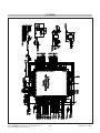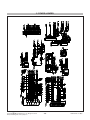
1
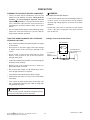
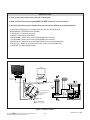
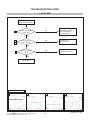
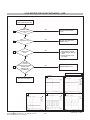
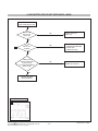
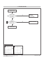
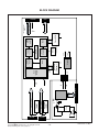
Internal Use Only
Website:http://biz.LGservice.com
COLOR MONITOR
SERVICE MANUAL
CHASSIS NO. : LM74B
MODEL:
L207WT(L207WT-PFS.A**HAP)
(
) **Same model for Service
CAUTION
BEFORE SERVICING THE UNIT,
READ THE SAFETY PRECAUTIONS IN THIS MANUAL.
*To apply the MSTAR Chip.
CONTENTS
CONTENTS .............................................................................................. 2
PRECAUTION ...........................................................................................3
SPECIFICATION ........................................................................................7
DISASSEMBLY ..........................................................................................9
ADJUSTMENT ........................................................................................11
SERVICE OSD .........................................................................................14
TROUBLE SHOOTING ............................................................................15
BLOCK DIAGRAM...................................................................................19
EXPLODED VIEW ...................................................................................22
REPLACEMENT PARTS LIST ............................................................... 24
SVC. SHEET ........................................................................................... 27
Copyright 2007 LG Electronics. Inc. All right reserved.
Only for training and service purposes
-2-
LGE Internal Use Only
PRECAUTION
WARNING FOR THE SAFETY-RELATED COMPONENT.
WARNING
• There are some special components used in LCD
monitor that are important for safety. These parts are
marked on the schematic diagram and the
replacement parts list. It is essential that these critical
parts should be replaced with the manufacturer’s
specified parts to prevent electric shock, fire or other
hazard.
• Do not modify original design without obtaining written
permission from manufacturer or you will void the
original parts and labor guarantee.
BE CAREFUL ELECTRIC SHOCK !
• If you want to replace with the new backlight (CCFL) or
inverter circuit, must disconnect the AC adapter
because high voltage appears at inverter circuit about
650Vrms.
• Handle with care wires or connectors of the inverter
circuit. If the wires are pressed cause short and may
burn or take fire.
Leakage Current Hot Check Circuit
TAKE CARE DURING HANDLING THE LCD MODULE
WITH BACKLIGHT UNIT.
AC Volt-meter
• Must mount the module using mounting holes arranged
in four corners.
• Do not press on the panel, edge of the frame strongly
or electric shock as this will result in damage to the
screen.
• Do not scratch or press on the panel with any sharp
objects, such as pencil or pen as this may result in
damage to the panel.
• Protect the module from the ESD as it may damage the
electronic circuit (C-MOS).
Good Earth Ground
such as WATER PIPE,
CONDUIT etc.
To Instrument's
exposed
METALLIC PARTS
1.5 Kohm/10W
• Make certain that treatment person’s body are
grounded through wrist band.
• Do not leave the module in high temperature and in
areas of high humidity for a long time.
• The module not be exposed to the direct sunlight.
• Avoid contact with water as it may a short circuit within
the module.
• If the surface of panel become dirty, please wipe it off
with a softmaterial. (Cleaning with a dirty or rough cloth
may damage the panel.)
CAUTION
Please use only a plastic screwdriver to protect yourself
from shock hazard during service operation.
Copyright 2007 LG Electronics. Inc. All right reserved.
Only for training and service purposes
-3-
LGE Internal Use Only
SERVICING PRECAUTIONS
CAUTION: Before servicing receivers covered by this
service manual and its supplements and addenda, read
and follow the SAFETY PRECAUTIONS on page 3 of this
publication.
NOTE: If unforeseen circumstances create conflict
between the following servicing precautions and any of the
safety precautions on page 3 of this publication, always
follow the safety precautions. Remember: Safety First.
General Servicing Precautions
1. Always unplug the receiver AC power cord from the AC
power source before;
a. Removing or reinstalling any component, circuit
board module or any other receiver assembly.
b. Disconnecting or reconnecting any receiver electrical
plug or other electrical connection.
c. Connecting a test substitute in parallel with an
electrolytic capacitor in the receiver.
CAUTION: A wrong part substitution or incorrect
polarity installation of electrolytic capacitors may
result in an explosion hazard.
d. Discharging the picture tube anode.
2. Test high voltage only by measuring it with an
appropriate high voltage meter or other voltage
measuring device (DVM, FETVOM, etc) equipped with
a suitable high voltage probe.
Do not test high voltage by "drawing an arc".
3. Discharge the picture tube anode only by (a) first
connecting one end of an insulated clip lead to the
degaussing or kine aquadag grounding system shield
at the point where the picture tube socket ground lead
is connected, and then (b) touch the other end of the
insulated clip lead to the picture tube anode button,
using an insulating handle to avoid personal contact
with high voltage.
4. Do not spray chemicals on or near this receiver or any
of its assemblies.
5. Unless specified otherwise in this service manual,
clean electrical contacts only by applying the following
mixture to the contacts with a pipe cleaner, cottontipped stick or comparable non-abrasive applicator;
10% (by volume) Acetone and 90% (by volume)
isopropyl alcohol (90%-99% strength)
CAUTION: This is a flammable mixture.
Unless specified otherwise in this service manual,
lubrication of contacts in not required.
6. Do not defeat any plug/socket B+ voltage interlocks
with which receivers covered by this service manual
might be equipped.
7. Do not apply AC power to this instrument and/or any of
its electrical assemblies unless all solid-state device
heat sinks are correctly installed.
8. Always connect the test receiver ground lead to the
receiver chassis ground before connecting the test
receiver positive lead.
Always remove the test receiver ground lead last.
Copyright 2007 LG Electronics. Inc. All right reserved.
Only for training and service purposes
9. Use with this receiver only the test fixtures specified in
this service manual.
CAUTION: Do not connect the test fixture ground strap
to any heat sink in this receiver.
Electrostatically Sensitive (ES) Devices
Some semiconductor (solid-state) devices can be
damaged easily by static electricity. Such components
commonly are called Electrostatically Sensitive (ES)
Devices. Examples of typical ES devices are integrated
circuits and some field-effect transistors and
semiconductor "chip" components. The following
techniques should be used to help reduce the incidence of
component damage caused by static by static electricity.
1. Immediately before handling any semiconductor
component or semiconductor-equipped assembly, drain
off any electrostatic charge on your body by touching a
known earth ground. Alternatively, obtain and wear a
commercially available discharging wrist strap device,
which should be removed to prevent potential shock
reasons prior to applying power to the unit under test.
2. After removing an electrical assembly equipped with
ES devices, place the assembly on a conductive
surface such as aluminum foil, to prevent electrostatic
charge buildup or exposure of the assembly.
3. Use only a grounded-tip soldering iron to solder or
unsolder ES devices.
4. Use only an anti-static type solder removal device.
Some solder removal devices not classified as "antistatic" can generate electrical charges sufficient to
damage ES devices.
5. Do not use freon-propelled chemicals. These can
generate electrical charges sufficient to damage ES
devices.
6. Do not remove a replacement ES device from its
protective package until immediately before you are
ready to install it. (Most replacement ES devices are
packaged with leads electrically shorted together by
conductive foam, aluminum foil or comparable
conductive material).
7. Immediately before removing the protective material
from the leads of a replacement ES device, touch the
protective material to the chassis or circuit assembly
into which the device will be installed.
CAUTION: Be sure no power is applied to the chassis
or circuit, and observe all other safety precautions.
8. Minimize bodily motions when handling unpackaged
replacement ES devices. (Otherwise harmless motion
such as the brushing together of your clothes fabric or
the lifting of your foot from a carpeted floor can
generate static electricity sufficient to damage an ES
device.)
-4-
LGE Internal Use Only
General Soldering Guidelines
1. Use a grounded-tip, low-wattage soldering iron and
appropriate tip size and shape that will maintain tip
temperature within the range or 500 F to 600 F.
2. Use an appropriate gauge of RMA resin-core solder
composed of 60 parts tin/40 parts lead.
3. Keep the soldering iron tip clean and well tinned.
4. Thoroughly clean the surfaces to be soldered. Use a
mall wire-bristle (0.5 inch, or 1.25cm) brush with a
metal handle.
Do not use freon-propelled spray-on cleaners.
5. Use the following unsoldering technique
a. Allow the soldering iron tip to reach normal
temperature.
(500 F to 600 F)
b. Heat the component lead until the solder melts.
c. Quickly draw the melted solder with an anti-static,
suction-type solder removal device or with solder
braid.
CAUTION: Work quickly to avoid overheating the
circuitboard printed foil.
6. Use the following soldering technique.
a. Allow the soldering iron tip to reach a normal
temperature (500 F to 600 F)
b. First, hold the soldering iron tip and solder the strand
against the component lead until the solder melts.
c. Quickly move the soldering iron tip to the junction of
the component lead and the printed circuit foil, and
hold it there only until the solder flows onto and
around both the component lead and the foil.
CAUTION: Work quickly to avoid overheating the
circuit board printed foil.
d. Closely inspect the solder area and remove any
excess or splashed solder with a small wire-bristle
brush.
IC Remove/Replacement
Some chassis circuit boards have slotted holes (oblong)
through which the IC leads are inserted and then bent flat
against the circuit foil. When holes are the slotted type,
the following technique should be used to remove and
replace the IC. When working with boards using the
familiar round hole, use the standard technique as
outlined in paragraphs 5 and 6 above.
Removal
1. Desolder and straighten each IC lead in one operation
by gently prying up on the lead with the soldering iron
tip as the solder melts.
2. Draw away the melted solder with an anti-static
suction-type solder removal device (or with solder
braid) before removing the IC.
Copyright 2007 LG Electronics. Inc. All right reserved.
Only for training and service purposes
Replacement
1. Carefully insert the replacement IC in the circuit board.
2. Carefully bend each IC lead against the circuit foil pad
and solder it.
3. Clean the soldered areas with a small wire-bristle
brush. (It is not necessary to reapply acrylic coating to
the areas).
"Small-Signal" Discrete Transistor
Removal/Replacement
1. Remove the defective transistor by clipping its leads as
close as possible to the component body.
2. Bend into a "U" shape the end of each of three leads
remaining on the circuit board.
3. Bend into a "U" shape the replacement transistor leads.
4. Connect the replacement transistor leads to the
corresponding leads extending from the circuit board
and crimp the "U" with long nose pliers to insure metal
to metal contact then solder each connection.
Power Output, Transistor Device
Removal/Replacement
1. Heat and remove all solder from around the transistor
leads.
2. Remove the heat sink mounting screw (if so equipped).
3. Carefully remove the transistor from the heat sink of the
circuit board.
4. Insert new transistor in the circuit board.
5. Solder each transistor lead, and clip off excess lead.
6. Replace heat sink.
Diode Removal/Replacement
1. Remove defective diode by clipping its leads as close
as possible to diode body.
2. Bend the two remaining leads perpendicular y to the
circuit board.
3. Observing diode polarity, wrap each lead of the new
diode around the corresponding lead on the circuit
board.
4. Securely crimp each connection and solder it.
5. Inspect (on the circuit board copper side) the solder
joints of the two "original" leads. If they are not shiny,
reheat them and if necessary, apply additional solder.
Fuse and Conventional Resistor
Removal/Replacement
1. Clip each fuse or resistor lead at top of the circuit board
hollow stake.
2. Securely crimp the leads of replacement component
around notch at stake top.
3. Solder the connections.
CAUTION: Maintain original spacing between the
replaced component and adjacent components and the
circuit board to prevent excessive component
temperatures.
-5-
LGE Internal Use Only
Circuit Board Foil Repair
Excessive heat applied to the copper foil of any printed
circuit board will weaken the adhesive that bonds the foil
to the circuit board causing the foil to separate from or
"lift-off" the board. The following guidelines and
procedures should be followed whenever this condition is
encountered.
At IC Connections
To repair a defective copper pattern at IC connections use
the following procedure to install a jumper wire on the
copper pattern side of the circuit board. (Use this
technique only on IC connections).
1. Carefully remove the damaged copper pattern with a
sharp knife. (Remove only as much copper as
absolutely necessary).
2. carefully scratch away the solder resist and acrylic
coating (if used) from the end of the remaining copper
pattern.
3. Bend a small "U" in one end of a small gauge jumper
wire and carefully crimp it around the IC pin. Solder the
IC connection.
4. Route the jumper wire along the path of the out-away
copper pattern and let it overlap the previously scraped
end of the good copper pattern. Solder the overlapped
area and clip off any excess jumper wire.
Copyright 2007 LG Electronics. Inc. All right reserved.
Only for training and service purposes
At Other Connections
Use the following technique to repair the defective copper
pattern at connections other than IC Pins. This technique
involves the installation of a jumper wire on the
component side of the circuit board.
1. Remove the defective copper pattern with a sharp
knife.
Remove at least 1/4 inch of copper, to ensure that a
hazardous condition will not exist if the jumper wire
opens.
2. Trace along the copper pattern from both sides of the
pattern break and locate the nearest component that is
directly connected to the affected copper pattern.
3. Connect insulated 20-gauge jumper wire from the lead
of the nearest component on one side of the pattern
break to the lead of the nearest component on the
other side.
Carefully crimp and solder the connections.
CAUTION: Be sure the insulated jumper wire is
dressed so the it does not touch components or sharp
edges.
-6-
LGE Internal Use Only
SPECIFICATIONS
1. LCD CHARACTERISTICS
Type
: TFT Color LCD Module
Active Display Area : 20.1 inch
Pixel Pitch
: 0.258 (H) x 0.258 (V)
Color Depth
: 16.7M colors(6bit + FRC data)
Size
: 459.4 (H) x 296.4 (V) x 16.6(D)
Electrical Interface
: LVDS
Surface Treatment
: Hard-coating(3H), Anti-Glare
Operating Mode
: Normally White
Backlight Unit
: 4-CCFL
4. Max. Resolution
D-sub Analog
Digital
: 1680 x 1050@60Hz
: 1680 x 1050@60Hz
5. POWER SUPPLY
5-1. Power : AC 100-240V~, 50/60Hz , 0.8A
5-2. Power Consumption
MODE
H/V SYNC VIDEO POWER CONSUMPTION LED COLOR
less than 45W(max)
POWER ON (NORMAL)
2. OPTICAL CHARACTERISTICS
2-1. Viewing Angle by Contrast Ratio ≥ 10
Left : -80° min., -85°(Typ) Right : +80° min., +85°(Typ)
Top :+80° min., +85°(Typ) Bottom : -80° min., -85°(Typ)
2-2. Luminance
2-3. Contrast Ratio
: 500(min), 1000(Typ) DFC -> 5000 :
1(TYP) -> 4250 : 1(MIN)
3. SIGNAL (Refer to the Timing Chart)
3-1. Sync Signal
• Type
: Separate Sync, Digital, SOG
3-2. Video Input Signal
1) Type
2) Voltage Level
a) Color 0, 0
b) Color 7, 0
c) Color 15, 0
3) Input Impedance
3-3. Operating Frequency
Horizontal(Analog)
Horizontal(Digital)
Vertical
: R, G, B Analog
: 0~0.71 V
: 0 Vp-p
: 0.467Vp-p
: 0.714Vp-p
: 75Ω
less than 40W(typ)
BLUE
STAND-BY
OFF/ON
OFF
less than 1 W
AMBER
SUSPEND
ON/OFF
OFF
less than 1 W
AMBER
DPMS OFF
OFF/OFF OFF
less than 1 W
AMBER
less than 1 W
OFF
POWER S/W OFF
: 180(Typ) (Typ. 30)-SRGB
: 220(min), 300(Typ) (Full White pattern, 0.70V) -6500K
: 150(min) (Full White pattern, 0.70V) -9300K
: 75%(min), 80%(typ)
ON/ON ACTIVE
-
-
6. ENVIRONMENT
6-1. Operating Temperature : 10°C~35°C (50°F~95°F)
(Ambient)
6-2. Relative Humidity
: 10%~80% (Non-condensing)
6-3. MTBF
: 50,000 HRS with 90% Confidence
Lamp Life
: 50,000 Hours(Min)
7. DIMENSIONS (with TILT/SWIVEL)
Width
Depth
Height
: 471.8 mm (18.57'')
: 230 mm (9.06'')
: 399.7 mm (15.74'')
8. WEIGHT (with TILT/SWIVEL)
Net. Weight
Gross Weight
: 3.9 kg (8.60 lbs)
: 5.0 kg (11.02 lbs)
: 30 ~ 83kHz
: 30 ~ 83kHz
: 56 ~ 75Hz
Copyright 2007 LG Electronics. Inc. All right reserved.
Only for training and service purposes
-7-
LGE Internal Use Only
TIMING CHART
VIDEO
A
E
D
B
SYNC
C
MODE
1
2
3
4
5
6
Sync
Polarity
Dot
Clock
Frequency
H(Pixels)
-
28.321
31.468
Total
Period
(E)
900
V(Lines)
+
70.08
449
H/V
H(Pixels)
-
V(Lines)
-
H(Pixels)
-
V(Lines)
-
H(Pixels)
+
V(Lines)
+
H(Pixels)
+
V(Lines)
+
H(Pixels)
-
V(Lines)
-
7
H(Pixels)
-
V(Lines)
-
8
H(Pixels)
+/-
V(Lines)
+/-
9
H(Pixels)
+
V(Lines)
+
10
H(Pixels)
+
V(Lines)
+
11
H(Pixels)
+
V(Lines)
-
12
H(Pixels)
-
V(Lines)
+
25.175
49.5
65.0
78.75
108.0
400
Front
Porch
(C)
108
Blanking
Time
(B)
54
12
2
35
31.469
800
640
16
96
48
59.94
525
480
10
2
33
37.5
840
640
16
64
120
75
500
480
1
3
16
31.5
40.0
Sync
Video
Duration
Active
(D)
Time ( A )
720
18
37.879
1056
800
40
128
88
60.317
628
600
1
4
23
46.875
1056
800
16
80
160
75.0
625
600
1
3
21
48.363
1344
1024
24
136
160
60.0
806
768
3
6
29
60.123
1312
1024
16
96
176
75.029
800
768
1
3
28
67.500
1600
1152
64
128
256
75.000
900
864
1
3
32
108.0
63.981
1688
1280
48
112
248
60.02
1066
1024
1
3
38
135.0
79.976
1688
1280
16
144
248
75.035
1066
1024
1
3
38
64.674
1840
1680
48
32
80
59.883
1080
1050
3
6
21
65.290
2240
1680
104
176
280
59.954
1089
1050
3
6
30
119
146.25
Copyright 2007 LG Electronics. Inc. All right reserved.
Only for training and service purposes
-8-
Resolution
720 X 400
640 x 480
640 x 480
800 x 600
800 x 600
1024 x 768
1024 x 768
1152 x 864
1280 x 1024
1280 x 1024
1680x1050
1680x1050
LGE Internal Use Only
DISASSEMBLY
#1
# 2-1
Disassemble Cable cover
# 2-2
Pushing Latch inside, Take the stand base from stand
body. (#2-1~2)
#3
Disassemble Stand Body
#4
#5
Remove the screws.
Copyright 2007 LG Electronics. Inc. All right reserved.
Only for training and service purposes
Remove the screws.
-9-
LGE Internal Use Only
#6
#7
1. Pull the front cover upward.
2. Then, let the latches are separated.
3. Put the front face down.
Copyright 2007 LG Electronics. Inc. All right reserved.
Only for training and service purposes
Disassemble back cover.
- 10 -
LGE Internal Use Only
ADJUSTMENT INSTRUCTION
1. Coverage
Apply to 20" Wide monitor made in Monitor Factory(Kumi
Korea) or made in accordance with the standard of Kumi
Factory process.
2. Appointment
2.1 Adjustment must be done as fixed sequence, and
adjustment sequence can be modified after agreement
with the responsible R&D engineer considering massproduction condition.
2.2 Power : AC100~240 Voltage (Free)
2.3 Input signal : As Product Standard (Signal ROM :
L204WT Ver1.1)
2.4 Warm-up Time : Over than 30 minutes
2.5 Adjustment equipment : White balance equipment (CA110/210), Display adjust equipment, VG-819(or VG828),
Oscilloscope, PC (More than 486 computer ) & White
balance adjust program. HDCP Adjusting Jig equipment
3. Adjustment
3.1 Overview
Use factory automation equipment and adjust automatic
movement. But, do via passivity adjust in error
occurrence.
3.2 Adjustment order(refer to the Adjustment standard and
adjustment command table)
3.2.1 Board Assembly Line
Connect input signal to 15pin D-sub.
Ready for adjustment : check whether adjustment
command works normally or not and the operating
state of each mode.
Check the display state of gray color when 256 gray
scale pattern is embodied.
Read by EEPROM Read Command to check
whether initial value is correct or not.
3.2.2 Total Assembly Line
Input analog signal. (1680x1050@60Hz)
Write HDCP Key to EEPROM(24C16) by using
DDC2AB protocol & HDCP Adjusting Jig equipment
(Address 0xAC 80, 289 bytes)
If error is occurred, write and check again.
Ready : Heat-run during 30 minutes in the state with
signal.
Connect input signal to D-sub.
Default value before adjustment : Contrast "70" ,
Brightness "100(Max)"
3.2.3 Adjustment of Horizontal/Verticality screen position,
Clock and Clock Phase at each Mode.
There is no special factory mode adjustment.
Writing initial value of EEPROM in Board Assembly
line is adjusting Preset Mode and Reset mode.
(EEPROM is initialized when AC Power is ON first.)
If the change of FOS data is needed after M.P, it is
possible by writing Mode Data with EEPROM write
command or modifying the Mode Data in MICOM
itself.
# Caution) Must keep power-on more than 3 seconds after
AC Power-on first time.
Copyright 2007 LG Electronics. Inc. All right reserved.
Only for training and service purposes
- 11 -
3.2.4 Color coordinates adjustment and Luminance
adjustment.
3.2.4.1 Color coordinates adjustment
Monitor Contrast / Brightness
- Contrast : 70
- Brightness : 100(Max)
CA-110 / CA-210 : Set "Channel 13" -> CA-210
for WCG panel
Signal Generator : At cut-off and drive -> 16 step
pattern for ADC
- Output Voltage : 700 mVp-p
- Output Mode : Mode 12 ( WSXGA 60 Hz)
mode Setting.
3.2.4.2.Adjustment : Board Assembly Line
Input 16 step pattern for ADC (Mode 12,Pattern
11). (Video level : 700mVp-p)
Adjust by commanding AUTO_COLOR_ADJUST
Confirm "Success" message in Screen or Check
the data of 0xFE,0xFF address of
EEPROM(0xA6) is 0xAA after waiting 5 seconds.
If there is "FAULT" message or the data of
0xFE,0xFF address of EEPROM(0xA6) is not
0xAA, do adjust again.
If all Adjustment is completed, the values of
6500K, User Color and 9300K are saved
automatically. Do not Adjust 6500K for L207WT.
3.2.4.3. Confirm at Total Assembly Line : adjustment
Check the data of 0xFE,0xFF address of
EEPROM(0xA6) is 0xAA.
If the data of 0xFE,0xFF address of
EEPROM(0xA6) is not 0xAA, do adjust again by
3.2.4.2.
3.2.4.4. Confirm PRESET 6500K Color coordinates and
Adjust PRESET 9300K Color coordinates .
Set as Aging mode ON, by commanding
AGING_ON/OFF command code.
Select Module that is being used in present
production by commanding MODULE SELECT.
Send SYSTEM RESET command to set Module
data.
Input Full White Pattern (Video level : 700 mVp-p)
Set
as
9300K
by
commanding
COLOR_MODE_CHANGE Command code.
Adjust to meet x = 0.283
0.004, y=0.298°
0.004, and confirm.
Save 9300K Color by commanding COLOR
SAVE Command code.
Input Full White Pattern (Video level : 700 mVp-p)
Set
as
6500K
by
commanding
COLOR_MODE_CHANGE Command code.
6500K color adjustment
Do not adjust for L207WT model.
It is adjust to meet x=0.313 0.03, y=0.329
0.03
Set
as
sRGB
by
commanding
COLOR_MODE_CHANGE Command code.
Adjust to meet Y = 180
10, and confirm.
LGE Internal Use Only
3.2.4.5. Confirm User color coordinates .
Confirm Whether User color is saved same as
6500K.
After confirming Color coordinates, Must return to
6500K.
Confirm whether user color is 50. If the value of
user color(R/G/B) is 30, do adjust again by
3.2.4.2.
3.2.5 Confirm Operation state.
3.2.5.1 Operation mode : Confirm whether each appointed
mode operate correctly or not.
3.2.5.2 Confirmation of Adjustment condition and
operation : Confirm whether it meet Auto/Manual
equipement Adjustment standard or not.
Confirm Analog screen state : Confirm screen
state at below mode.
Appointment mode : 640*480 @ 60Hz (Mode 2),
800*600@75Hz(Mode 5)
1 0 2 4 * 7 6 8 @ 6 0 H z ( M o d e 6 ) ,
1280*1024@60Hz(Mode 9),
1680*1024@60Hz(Mode 12)
SMPTE pattern(Check 0%,5%,95%,100%)
–Mode can be added.
Check HDCP signal screen by using Video
generator that generate HDCP signal
3.2.5.3. Confirm Auto adjustment operation.
Input Analog 1 Dot on/off & Rectangle Pattern at
Mode 12(1680*1050@60Hz).
Confirm adjustment operation by changing
Clock,Phase,H/V Position.
Check Clock,Phase by pressing AUTO Key.
Confirm first set of new lot by periods
3.2.5.4 Other quality
Confirm that each items satisfy under standard
condition that was written product spec.
Confirm Applying Module & MICOM Setting ->
Confirm with Service OSD
-> Confirm at Service OSD by "Menu + Powerkey" on
.(from Power off)
-> Confirm first set of new lot by periods, and confirm
periodically when there is Process change or
Adjustment setting change.
3.2.5.5. OSD & Adjustment device Confirmation : Confirm
operation mentioned as product spec.
Vary Brightness and Contrast and confirm the
variation of Luminance and display status.
Operate the F-engine function and confirm
variation of Luminance.
Make sure to do FACTORY RESET after
confirmation of OSD function.
3.2.5.6. Confirm the display state by inputting 8 color Bar
Pattern & 256 Gray Scale pattern.
Copyright 2007 LG Electronics. Inc. All right reserved.
Only for training and service purposes
- 12 -
3.2.5.7. DPM operation confirmation : Check if Power LED
Color and Power Consumption operates as
standard.
Measurement Condition : 230V@ 50Hz (Analog)
Confirm DPM operation at the state of screen
without Video Signal.(refer to Spec at Page 11)
3.2.5.8. DDC EDID Write ( Set as Aging mode ON, by
commanding AGING_ON/OFF command code. )
- Digital part EDID data
Confirm whether module selection is correct or
not on the self-diagnostics OSD with signal cable
disconnected.
Connect Digital Signal Cable to DVI-D wafer.
Write EDID DATA to EEPROM(24C02) by using
DDC2B protocol.
Check whether written EDID data is correct or
not. (refer to Product spec).-Analog part EDID
data
- Analog part EDID data
Connect analog Signal Cable to D-sub wafer.
Write EDID DATA to EEPROM(24C02) by using
DDC2B protocol.£®NOVATEK dual and odc
model£©
Write EDID DATA to EEPROM(24C02) by using
DDC2AB protocol.£®Mstar dual model£©
Check whether written EDID data is correct or
not. (refer to Product spec).
Connect analog Signal Cable to D-sub wafer.
Write EDID DATA to EEPROM(24C02) by using
DDC2B protocol.
Check whether written EDID data is correct or
not.(refer to Product spec).
-> After writing EDID, send Elapsed Time Clear
command. (Elapsed time should not be displayed,
after EDID writing)
: Confirm periodically (in the first set of new lot,
process change) whether module name and aging
time disappeared on the self-diagnostics OSD with
signal cable disconnected.
-> If Elapsed Time Clear command isn’t executed,
module name, aging time and TCO word appear on
the self-diagnostics OSD.(Module name and aging
time should not appear after writing EDID)
-> Make sure to do FACTORY RESET at the final
process.
3.2.5.9. Shipping condition
Contrast : 70
Power Switch : Off
Brightness : "100(Max)"
Color Select : Preset (6500K)
Language Select : Refer to product spec.
OSD Position : Center
Power indicator : ON
Flatron F-engine : Normal
LGE Internal Use Only
Windows EDID V1.0 User Manual
2. EDID Read & Write
1) Run WinEDID.exe
Operating System: MS Windows 98, 2000, XP
Port Setup: Windows 98 => Don’t need setup
Windows 2000, XP => Need to Port Setup.
This program is available to LCD Monitor only.
1. Port Setup
a) Copy “UserPort.sys” file to
“c:\WINNT\system32\drivers” folder
b) Run Userport.exe
2) Edit Week of Manufacture, Year of Manufacture,
Serial Number
a) Input User Info Data
b) Click “Update” button
c) Click “ Write” button
c) Remove all default number
d) Add 300-3FF
e) Click Start button.
f) Click Exit button.
Copyright 2007 LG Electronics. Inc. All right reserved.
Only for training and service purposes
- 13 -
LGE Internal Use Only
SERVICE OSD
1) Turn off the power switch at the front side of the display.
2) Wait for about 5 seconds and press MENU, POWER switch with 1 second interval.
3) The SVC OSD menu contains additional menus that the User OSD menu as described below.
a) Auto Color : W/B balance and Automatically sets the gain and offset value.
b) NVRAM INIT : EEPROM initialize.(24C08)
c) CLEAR ETI : To initialize using time.
d) AGING : Select Aging mode(on/off).
e) R/G/B-9300K : Allows you to set the R/G/B-9300K value manually.
f) R/G/B-6500K : Allows you to set the R/G/B-6500K value manually.
g) R/G/B-Offset : Allows you to set the R/G/B-Offset value manually.(Analog Only)
h) R/G/B-Gain : Allows you to set the R/G/B-Gain value manually.(Analog Only)
i) MODULE : To select applied module.
A
9
IBM
Compatible PC
Video Signal
Generator
15
10
5
11
6
1
6
1
5
C
d
PARALLEL PORT
tu
No
RS
23
2C
se
13
PA
RA
LL
EL
OFF
14
ON
F
Power inlet (required)
5V
220
A
WE
R
Power Select Switch
(110V/220V)
Power LED
PO
VG
S
MO
NI
TO
R
V-S
YN
CS
T
Control Line
5V
C
1
25
ON
4.7K
4.7K
5V
E
4.7K
OFF
74LS06
74LS06
E ST Switch
B
B
F V-Sync On/Off Switch
(Switch must be ON.)
Figure 1. Cable Connection
Copyright 2007 LG Electronics. Inc. All right reserved.
Only for training and service purposes
- 14 -
LGE Internal Use Only
TROUBLESHOOTING GUIDE
1. NO POWER
NO POWER
(POWER INDICATOR OFF)
1
CHECK J905 VOLTAGE
PIN5,6 (5V)?
CHECK POWER BOARD,
AND FIND OUT A SHORT
POINT AS OPENING
EACH POWER LINE
NO
YES
2
3
1
IS IC1 PIN2(3.3V)
U902 PIN2(1.8V)
NO
CHECK IC1(3.3V)
U902(1.8V) LINE
YES
4
1
CHECK X501 PIN127
PULSE
NO
CHECK CRYSTAL(X501)
YES
CHECK U501
Waveforms
1
J905-#5,6
2
IC1-#2
Copyright 2007 LG Electronics. Inc. All right reserved.
Only for training and service purposes
3
- 15 -
U902-#2
4
U501-#127
LGE Internal Use Only
2. NO RASTER (OSD IS NOT DISPLAYED) – LIPS
NO RASTER
(OSD IS NOT DISPLAYED)
1
CHECK J905
VOLTAGE PIN5,6
(5V)?
NO
CHECK POWER BOARD
(LIPS)
YES
NO
2
CHECK U501 INVERTER
ON/OFF PORT
J905 PIN9 3.3V?
YES
3
1. CONFIRM BRIGHTNESS
OSD CONTRL STATUS
2. CHECK SCALER DIM ADJ
PORT
3. CHECK SCALER LAMP
ADJ PORT
NO
CHECK J905
PIN10
YES
4
CHECK
PULSE AS
CONTACTING PROBE
TO THE LAMP
WIRE OF THE
LCD MODULE
NO
POWER BOARD (LIPS)
Waveforms
YES
1
J905-#5,6
2
J905-#9
3
J905-#10 (Brightness 0)
4
LAMP CURRENT
REPLACE LCD MODULE
3
J905-#9 (Brightness 100)
Copyright 2007 LG Electronics. Inc. All right reserved.
Only for training and service purposes
- 16 -
LGE Internal Use Only
3. NO RASTER (OSD IS NOT DISPLAYED) - MAIN
NO RASTER
(OSD IS NOT DISPLAYED)
CHECK U501
PIN114(3.3V)
PIN21(1.8V)
NO
CHECK U901(3.3V),
U902(1.8V)
YES
U501
PIN 127,128
14.3MHZ?
1
NO
1. CHECK PIN 127,128
SOLDERING CONDITION
2. CHECK X501
3. TROUBLE IN U501
YES
CHECK U501
PIN32(H-SYNC) AND
PIN33(V-SYNC).
IS PULSE APPEARED AT
SIGNAL PINS?
NO
CHECK CONNECTION LINE
FROM D-SUB TO U501
YES
TROUBLE IN CABLE
OR LCD MODULE
Waveforms
1
U501-#127
Copyright 2007 LG Electronics. Inc. All right reserved.
Only for training and service purposes
- 17 -
LGE Internal Use Only
4. TROUBLE IN DPM
TROUBLE IN DPM
NO
CHECK R718 AND
R719, SYNC
APPEARED?
CHECK PC
PC IS GOING
INTO DPM MODE
YES
1
2
CHECK
U501 PIN 32,33
SYNC PULSE
NO
CHECK H/V SYNC LINE
YES
TROUBLE IN U501
Waveforms
1
H-SYNC
2
V-SYNC
Copyright 2007 LG Electronics. Inc. All right reserved.
Only for training and service purposes
- 18 -
LGE Internal Use Only
Copyright 2007 LG Electronics. Inc. All right reserved.
Only for training and service purposes
D-Sub
DVI-D
Filter
LIPS
EEPROM
(EDID)
DVI(TMDS)
EEPROM
(EDID)
Analog I(R/G/B)
- 19 Inverter(4Lamps)
15V
15V
5V
1.8V
3.3V
5V
3.3
OSD
Regulator
EEPROM
(System)
SDA
/SCL
Dual
Interface
Engine
Display
Processing
Engine
1.8V
3.3V
14.318MHz
Crystal
Clock
Generator
DRAM
Response
Time
Enhancement
3.3V
Flash ROM
MCU
LVDS
Panel
Interface
Vcc
5V
LVDS
1680 X 1050@60Hz
146Mhz
Module
KEY
TSUMO58CWHJ
BLOCK DIAGRAM
LGE Internal Use Only
DESCRIPTION OF BLOCK DIAGRAM
1. Video Controller Part.
This part amplifies the level of video signal for the digital conversion and converts from the analog video signal to the
digital video signal using a pixel clock.
The pixel clock for each mode is generated by the PLL.
The range of the pixel clock is 146MHz In L207WT.
This part consists of the Scaler, ADC converter, TMDS receiver and LVDS transmitter.
The Scaler gets the video signal converted analog to digital, interpolates input to 1680X1050 resolution signal and
outputs 8-bit R, G, B signal to transmitter.
2. Power Part.
This part consists of the one 3.3V, and one 1.8V regulators to convert power which is provided 5V in Power board.
15V is provided for inverter in L207WT.
Also, 5V is converted 3.3V and 1.8V by regulator. Converted power is provided for IC in the main board.
The inverter converts from DC 15V to AC 700Vrms and operates back-light lamps of module in L207WT.
3. MICOM Part.
This part is include video controller part. And this part consists of EEPROM IC , control data, Reset IC and the Micom.
The Micom distinguishes polarity and frequency of the H/V sync are supplied from signal cable.
The controlled data of each modes is stored in EEPROM.
Copyright 2007 LG Electronics. Inc. All right reserved.
Only for training and service purposes
- 20 -
LGE Internal Use Only
LIPS Board Block Diagram
15V
50 ~ 60Hz
LINE
100 ~ 240V
EMI
COMPONENTS
INPUT RECTIFIER
AND FILTER
HVDC
SWITCHING
TRANSFORMER
67KHz
OUTPUT RECTIFIER
AND FILTER
5V
GND
PWM CONTROL
CIRCUIT
PHOTO-COUPLER
ISOLATION
PRIMARY
SIGNAL
COLLENTION
SECONDARY
Operation description_Power
1. EMI components.
This part contains of EMI components to comply with global marketing EMI standards like FCC,VCCI CISPR, the
circuit included a line-filter, across line capacitor and of course the primary protection fuse.
2. Input rectifier and filter.
This part function is for transfer the input AC voltage to a DC voltage through a bridge rectifier and a bulk capacitor.
3. Energy Transfer.
This part function is for transfer the primary energy to secondary through a power transformer.
4. Output rectifier and filter.
This part function is to make a pulse width modulation control and to provide the driver signal to power switch, to
adjust the duty cycle during different AC input and output loading condition to achieve the dc output stabilized, and
also the over power protection is also monitor by this part.
5. Photo-Coupler isolation.
This part function is to feed back the DC output changing status through a photo transistor to primary controller to
achieve the stabilized DC output voltage.
6. Signal collection.
This part function is to collect the any change from the DC output and feed back to the primary through photo
transistor.
Copyright 2007 LG Electronics. Inc. All right reserved.
Only for training and service purposes
- 21 -
LGE Internal Use Only
920
910
440
Copyright 2007 LG Electronics. Inc. All right reserved.
Only for training and service purposes
- 22 -
310
320
300
330
200
500
450
510
520
430
420
410
400
900
930
EXPLODED VIEW
LGE Internal Use Only
EXPLODED VIEW PARTS LIST
* Note: Safety mark
No.
Part No.
Description
200
EAJ39826101
LCD,Module-TFT, M201EW02 VC WSXGA 20.1INCH 1680X1050 300CD COLOR 92% 16/10 1000:1 AUO 20"W WCG(92%).Non-Glare, ZBD, 16.7M,Normally White mode, response time 5ms,Viewi
300
ACQ33735402
Cover Assembly, L207W . 20" Cabinet Ass'y_XG569(01-CKD)
310
MFB38581401
Lens, MOLD PMMA SAMSUNG TECHWIN LENS Lx72 / Lx7w lens , power LED Knob Double injection Power LED for L1972, Lxx7W
320
MCK38584101
Cover, MOLD ABS HF-350U L1972, Lx7W ABS L1972,LX7W PIECE DECO RING_VACUUM PLATING
330
MEY38582301
Knob, MOLD ABS HF-350U SUB TACK KNOB FOR LX7W, L1972 GLOBAL TACK, KNOB CONTROL
400
ACQ33735602
Cover Assembly,Rear, L207W . 20" Back Cover Ass'y,01-CKD
410
MGJ39028601
Plate,Metal, PRESS SPTE 0.3 SHIELD SPC L207W LAMP SHIELD
420
ADV33707206
Frame Assembly, L207W(AUO)/L227W(CMO) LM57B 20" Rear, Frame Assy
430
MCK38597501
Cover, MOLD PC+ABS L1972 ABS L1972 / L1954 / Lx7W - VESA BRACKET
440
MGJ38583701
Plate,Metal, PRESS SBHG 1.2 METAL EGI L207W PRESS SBHG 1.2 GUIDE Metal stand bracket
450
MCK38597701
Cover, MOLD PC+ABS L1972 ABS L1972 / L1954 / Lx7W - LIPS BRACKET
500
EBR38466401
PCB Assembly,Sub, CONTROL T.T LM74B L197WT-BFS AEUQQPX .
510
EAY38106001
Power Supply Assembly, AIP-0165 FREE L1954SM/L207W/L227W LCD Lienchang High Version LIEN CHANG ELECTRONIC CO. LTD.
520
EBU38495201
Main Total Assembly, L207WH-BFS BRAND LM74B
900
ACQ33707107
Cover Assembly, L1954T,L207W LM57B 20" Cover, Hinge Assy Normal Stand, 01-CKD
910
MCK38601903
Cover, MOLD ABS L1954/L207W ABS COVER, STAND BODY(01-CKD)
920
AAN33707002
Base Assembly, BASE L1954T LM57B Normal Stand Base Assy with swivel ring
930
MCK38602601
Cover MOLD ABS L1954 ABS L1954, COVER CABLE
Copyright 2007 LG Electronics. Inc. All right reserved.
Only for training and service purposes
- 23 -
LGE Internal Use Only
REPLACEMENT PARTS LIST
DATE: 2007. 08. 30.
LOC. NO.
PART NO.
DESCRIPTION / SPECIFICATION
LOC. NO.
PART NO.
DESCRIPTION / SPECIFICATION
ACCESSORY
C540
0CC080CK11A
"Capacitor,Ceramic,ChipC1608C0G1"
A1
SAB31087001
S/W PackageL197WH EUROPE
C541
0CC080CK11A
"Capacitor,Ceramic,ChipC1608C0G1"
A3
EAD37992102
Power CordEAD37992102 LP-34A LS
C701
0CC101CK41A
"Capacitor,Ceramic,ChipC1608C0G1"
A4
3171TZ1099T
S/W PackageALL MODEL FORTE MANA
C702
0CC101CK41A
"Capacitor,Ceramic,ChipC1608C0G1"
A5
68509F0003A
"Cable,AssemblyD-SUB TO D-SUB UL"
C703
0CC680CK41A
"Capacitor,Ceramic,ChipC1608C0G1"
A6
68509J0004A
"Cable,AssemblyDVI-D TO DVI-D UL"
C704
0CK104CK56A
"Capacitor,Ceramic,Chip0603B104K"
A7
3840TWL027A
CardPRINTING LCD/CRT ALL BRAND
C705
0CC680CK41A
"Capacitor,Ceramic,ChipC1608C0G1"
C706
0CK104CF56A
"Capacitor,Ceramic,Chip0603B104K"
C707
0CK104CF56A
"Capacitor,Ceramic,Chip0603B104K"
C708
0CK104CF56A
"Capacitor,Ceramic,Chip0603B104K"
CAPACITORs
C501
0CK104CF56A
"Capacitor,Ceramic,Chip0603B104K"
C709
0CK104CF56A
"Capacitor,Ceramic,Chip0603B104K"
C502
0CK473CH56A
"Capacitor,Ceramic,ChipC1608X7R1"
C710
0CK104CF56A
"Capacitor,Ceramic,Chip0603B104K"
C503
0CK473CH56A
"Capacitor,Ceramic,ChipC1608X7R1"
C711
0CK104CF56A
"Capacitor,Ceramic,Chip0603B104K"
C504
0CK473CH56A
"Capacitor,Ceramic,ChipC1608X7R1"
C712
0CK104CF56A
"Capacitor,Ceramic,Chip0603B104K"
C505
0CK473CH56A
"Capacitor,Ceramic,ChipC1608X7R1"
C713
0CK104CF56A
"Capacitor,Ceramic,Chip0603B104K"
C506
0CC102CK41A
"Capacitor,Ceramic,ChipC1608C0G1"
C714
0CC680CK41A
"Capacitor,Ceramic,ChipC1608C0G1"
C507
0CK473CH56A
"Capacitor,Ceramic,ChipC1608X7R1"
C715
0CC680CK41A
"Capacitor,Ceramic,ChipC1608C0G1"
C508
0CK473CH56A
"Capacitor,Ceramic,ChipC1608X7R1"
C716
0CK104CF56A
"Capacitor,Ceramic,Chip0603B104K"
C509
0CC270CK41A
"Capacitor,Ceramic,ChipC1608C0G1"
C717
0CK104CF56A
"Capacitor,Ceramic,Chip0603B104K"
C510
0CC270CK41A
"Capacitor,Ceramic,ChipC1608C0G1"
C718
0CK104CF56A
"Capacitor,Ceramic,Chip0603B104K"
C511
0CK103CK51A
"Capacitor,Ceramic,Chip0603B103K"
C719
0CK104CF56A
"Capacitor,Ceramic,Chip0603B104K"
C512
0CK103CK51A
"Capacitor,Ceramic,Chip0603B103K"
C720
0CK104CF56A
"Capacitor,Ceramic,Chip0603B104K"
C513
0CK104CF56A
"Capacitor,Ceramic,Chip0603B104K"
C723
0CK104CF56A
"Capacitor,Ceramic,Chip0603B104K"
C514
0CK224CF56A
"Capacitor,Ceramic,Chip0603B224K"
C724
0CK105CD56A
"Capacitor,Ceramic,ChipC1608X7R1"
C515
0CE106CF638
"Capacitor,AL,RadialSHL5.0TP16VB"
C725
0CC101CK41A
"Capacitor,Ceramic,ChipC1608C0G1"
C516
0CK104CF56A
"Capacitor,Ceramic,Chip0603B104K"
C901
0CK103CK51A
"Capacitor,Ceramic,Chip0603B103K"
C517
0CK104CF56A
"Capacitor,Ceramic,Chip0603B104K"
C902
0CE107EF610
"Capacitor,AL,RadialKMG16VB100M"
C518
0CK104CF56A
"Capacitor,Ceramic,Chip0603B104K"
C905
0CE107EF610
"Capacitor,AL,RadialKMG16VB100M"
C519
0CK104CF56A
"Capacitor,Ceramic,Chip0603B104K"
C906
0CE107EF610
"Capacitor,AL,RadialKMG16VB100M"
C520
0CK104CF56A
"Capacitor,Ceramic,Chip0603B104K"
C907
0CE107EF610
"Capacitor,AL,RadialKMG16VB100M"
C521
0CK104CF56A
"Capacitor,Ceramic,Chip0603B104K"
C908
0CK104CK56A
"Capacitor,Ceramic,Chip0603B104K"
C522
0CK104CF56A
"Capacitor,Ceramic,Chip0603B104K"
C909
0CK104CK56A
"Capacitor,Ceramic,Chip0603B104K"
C523
0CK104CF56A
"Capacitor,Ceramic,Chip0603B104K"
C910
0CK104CK56A
"Capacitor,Ceramic,Chip0603B104K"
C524
0CK104CF56A
"Capacitor,Ceramic,Chip0603B104K"
C911
0CK102CK56A
"Capacitor,Ceramic,Chip0603B102K"
C525
0CK104CF56A
"Capacitor,Ceramic,Chip0603B104K"
C912
0CK102CK56A
"Capacitor,Ceramic,Chip0603B102K"
C526
0CK104CF56A
"Capacitor,Ceramic,Chip0603B104K"
C913
0CK102CK56A
"Capacitor,Ceramic,Chip0603B102K"
C527
0CK104CF56A
"Capacitor,Ceramic,Chip0603B104K"
C914
0CE227EF610
"Capacitor,AL,RadialKMG16VB220M"
C528
0CK104CF56A
"Capacitor,Ceramic,Chip0603B104K"
C915
0CK105CD56A
"Capacitor,Ceramic,ChipC1608X7R1"
C529
0CK104CF56A
"Capacitor,Ceramic,Chip0603B104K"
C915
0CK475CC94A
"Capacitor,Ceramic,ChipC1608Y5V0"
C530
0CK104CF56A
"Capacitor,Ceramic,Chip0603B104K"
C531
0CK104CF56A
"Capacitor,Ceramic,Chip0603B104K"
C532
0CK104CF56A
"Capacitor,Ceramic,Chip0603B104K"
C533
0CK104CF56A
"Capacitor,Ceramic,Chip0603B104K"
D701
0DSIH00018A
"Diode,SwitchingENKMC2837-T112 1"
C534
0CK104CF56A
"Capacitor,Ceramic,Chip0603B104K"
D702
0DSIH00018A
"Diode,SwitchingENKMC2837-T112 1"
C535
0CK104CF56A
"Capacitor,Ceramic,Chip0603B104K"
D703
0DSIH00018A
"Diode,SwitchingENKMC2837-T112 1"
C536
0CK104CF56A
"Capacitor,Ceramic,Chip0603B104K"
D704
0DSIH00018A
"Diode,SwitchingENKMC2837-T112 1"
C537
0CK104CF56A
"Capacitor,Ceramic,Chip0603B104K"
D705
0DSIH00018A
"Diode,SwitchingENKMC2837-T112 1"
C538
0CK104CF56A
"Capacitor,Ceramic,Chip0603B104K"
D706
0DSIH00018A
"Diode,SwitchingENKMC2837-T112 1"
C539
0CC080CK11A
"Capacitor,Ceramic,ChipC1608C0G1"
D707
0DSIH00018A
"Diode,SwitchingENKMC2837-T112 1"
Copyright
2007 LG Electronics. Inc. All right reserved.
Only for training and service purposes
DIODEs
- 24 -
LGE Internal Use Only
LOC. NO.
PART NO.
D708
0DSIH00018A
D709
0DSIH00018A
D710
DESCRIPTION / SPECIFICATION
LOC. NO.
PART NO.
"Diode,SwitchingENKMC2837-T112 1"
R503
0RJ1000D677
"Resistor,ChipMCR03EZPJ101 100OH"
"Diode,SwitchingENKMC2837-T112 1"
R504
0RJ0562D677
"Resistor,ChipMCR03EZPJ560 56OHM"
0DSIH00018A
"Diode,SwitchingENKMC2837-T112 1"
R505
0RJ4700D677
"Resistor,ChipMCR03EZPJ471 470OH"
D711
0DSIH00018A
"Diode,SwitchingENKMC2837-T112 1"
R506
0RJ1000D677
"Resistor,ChipMCR03EZPJ101 100OH"
D712
0DSON00138A
"Diode,SchottkyMMBD301LT1G 600MV"
R507
0RJ0562D677
"Resistor,ChipMCR03EZPJ560 56OHM"
D713
0DD184009AA
Diode AssemblyKDS184 KDS184 TP
R508
0RJ4701D677
"Resistor,ChipMCR03EZPJ472 4.7KO"
D714
0DSON00138A
"Diode,SchottkyMMBD301LT1G 600MV"
R509
0RJ4701D677
"Resistor,ChipMCR03EZPJ472 4.7KO"
D715
0DD184009AA
Diode AssemblyKDS184 KDS184 TP
R510
0RJ4701D677
"Resistor,ChipMCR03EZPJ472 4.7KO"
ZD1
0DZ560009GB
"Diode,ZenerBZT52C5V6S-(F) 5.6V"
R511
0RJ4701D677
"Resistor,ChipMCR03EZPJ472 4.7KO"
ZD2
0DZ560009GB
"Diode,ZenerBZT52C5V6S-(F) 5.6V"
R512
0RJ4700D677
"Resistor,ChipMCR03EZPJ471 470OH"
ZD3
0DZ560009GB
"Diode,ZenerBZT52C5V6S-(F) 5.6V"
R513
0RJ4700D677
"Resistor,ChipMCR03EZPJ471 470OH"
ZD4
0DZ560009GB
"Diode,ZenerBZT52C5V6S-(F) 5.6V"
R516
0RJ3900D677
"Resistor,ChipMCR03EZPJ391 390OH"
ZD701
0DZ560009GB
"Diode,ZenerBZT52C5V6S-(F) 5.6V"
R517
0RJ1002D677
"Resistor,ChipMCR03EZPJ103 10KOH"
ZD702
0DZ560009GB
"Diode,ZenerBZT52C5V6S-(F) 5.6V"
R518
0RJ0000D677
"Resistor,ChipMCR03EZPJ000 0OHM"
ZD703
0DZ560009GB
"Diode,ZenerBZT52C5V6S-(F) 5.6V"
R519
0RJ1502D677
"Resistor,ChipMCR03EZPJ153 15KOH"
ZD704
0DZ560009GB
"Diode,ZenerBZT52C5V6S-(F) 5.6V"
R522
0RJ4701D677
"Resistor,ChipMCR03EZPJ472 4.7KO"
ZD705
0DZ560009GB
"Diode,ZenerBZT52C5V6S-(F) 5.6V"
R523
0RJ1000D677
"Resistor,ChipMCR03EZPJ101 100OH"
ZD708
0DZ560009GB
"Diode,ZenerBZT52C5V6S-(F) 5.6V"
R524
0RJ1002D677
"Resistor,ChipMCR03EZPJ103 10KOH"
ZD709
0DZ560009GB
"Diode,ZenerBZT52C5V6S-(F) 5.6V"
R525
0RJ4701D677
"Resistor,ChipMCR03EZPJ472 4.7KO"
ZD710
0DZ560009GB
"Diode,ZenerBZT52C5V6S-(F) 5.6V"
R526
0RJ0332D677
"Resistor,ChipMCR03EZPJ330 33OHM"
R527
0RJ0332D677
"Resistor,ChipMCR03EZPJ330 33OHM"
R530
0RJ1002D677
"Resistor,ChipMCR03EZPJ103 10KOH"
R6
0RJ1801D677
"Resistor,ChipMCR03EZPJ182 1.8KO"
ICs
IC1
DESCRIPTION / SPECIFICATION
0IPMGA0010A
"IC,LDO Voltage RegulatorAZ1117H"
R701
0RJ4701D677
"Resistor,ChipMCR03EZPJ472 4.7KO"
U501
0IPRP00784C
"IC,Video ProcessorsFE253MOH-LF"
R702
0RJ4701D677
"Resistor,ChipMCR03EZPJ472 4.7KO"
U502
EAN38496701
IC AssemblyL207WH-BFS Micom Ass
R703
0RJ0332D677
"Resistor,ChipMCR03EZPJ330 33OHM"
U503
0IMMRSG036B
"IC,EEPROMM24C16-WMN6TP 16KBIT 2"
R704
0RJ0102D677
"Resistor,ChipMCR03EZPJ100 10OHM"
U701
0IMMR00014A
"IC,EEPROMM24C02-RMN6TP 2KBIT 25"
R705
0RJ0102D677
"Resistor,ChipMCR03EZPJ100 10OHM"
U702
0IMMR00014A
"IC,EEPROMM24C02-RMN6TP 2KBIT 25"
R706
0RJ0102D677
"Resistor,ChipMCR03EZPJ100 10OHM"
U902
0IPMG78403A
"IC,LDO Voltage RegulatorAZ1086S"
R707
0RJ0102D677
"Resistor,ChipMCR03EZPJ100 10OHM"
R708
0RJ0102D677
"Resistor,ChipMCR03EZPJ100 10OHM"
R709
0RJ0102D677
"Resistor,ChipMCR03EZPJ100 10OHM"
R710
0RJ0332D677
"Resistor,ChipMCR03EZPJ330 33OHM"
FILTERs
L901
0LCML00003B
"Filter,BeadMLB-201209-0120P-N2"
R711
0RJ0000D677
"Resistor,ChipMCR03EZPJ000 0OHM"
L902
0LCML00003B
"Filter,BeadMLB-201209-0120P-N2"
R712
0RJ0102D677
"Resistor,ChipMCR03EZPJ100 10OHM"
L903
0LCML00003B
"Filter,BeadMLB-201209-0120P-N2"
R713
0RJ0102D677
"Resistor,ChipMCR03EZPJ100 10OHM"
R714
0RJ1001D677
"Resistor,ChipMCR03EZPJ102 1KOHM"
R715
0RJ0000D677
"Resistor,ChipMCR03EZPJ000 0OHM"
R716
0RJ0332D677
"Resistor,ChipMCR03EZPJ330 33OHM"
TRANSISTORs
Q501
0TR390409AE
"TR,BipolarKST3904 NPN 6V 60V 40"
R717
0RJ0752D677
"Resistor,ChipMCR03EZPJ750 75OHM"
Q701
0TR390609FA
"TR,BipolarKST3906-MTF PNP -5V -"
R718
0RJ0682D677
"Resistor,ChipMCR03EZPJ680 68OHM"
Q702
0TR390609FA
"TR,BipolarKST3906-MTF PNP -5V -"
R719
0RJ0682D677
"Resistor,ChipMCR03EZPJ680 68OHM"
Q901
EBK39150701
"TR,BipolarKTA1241 PNP -8V -35V"
R720
0RJ0332D677
"Resistor,ChipMCR03EZPJ330 33OHM"
Q902
0TR390409AE
"TR,BipolarKST3904 NPN 6V 60V 40"
R721
0RJ0752D677
"Resistor,ChipMCR03EZPJ750 75OHM"
R722
0RJ0752D677
"Resistor,ChipMCR03EZPJ750 75OHM"
R723
0RJ0000D677
"Resistor,ChipMCR03EZPJ000 0OHM"
R724
0RJ4701D677
"Resistor,ChipMCR03EZPJ472 4.7KO"
RESISTORs
R1
0RJ7501D677
"Resistor,ChipMCR03EZPJ752 7.5KO"
R725
0RJ4701D677
"Resistor,ChipMCR03EZPJ472 4.7KO"
R2
0RJ7501D677
"Resistor,ChipMCR03EZPJ752 7.5KO"
R726
0RJ4701D677
"Resistor,ChipMCR03EZPJ472 4.7KO"
R3
0RJ1201D677
"Resistor,ChipMCR03EZPJ122 1.2KO"
R727
0RJ4701D677
"Resistor,ChipMCR03EZPJ472 4.7KO"
R4
0RJ1801D677
"Resistor,ChipMCR03EZPJ182 1.8KO"
R728
0RJ4701D677
"Resistor,ChipMCR03EZPJ472 4.7KO"
R5
0RJ1201D677
"Resistor,ChipMCR03EZPJ122 1.2KO"
R729
0RJ4701D677
"Resistor,ChipMCR03EZPJ472 4.7KO"
R501
0RJ1000D677
"Resistor,ChipMCR03EZPJ101 100OH"
R730
0RJ2200D677
"Resistor,ChipMCR03EZPJ221 220OH"
R502
0RJ0562D677
"Resistor,ChipMCR03EZPJ560 56OHM"
R731
0RJ2200D677
"Resistor,ChipMCR03EZPJ221 220OH"
Copyright
2007 LG Electronics. Inc. All right reserved.
Only for training and service purposes
- 25 -
LGE Internal Use Only
LOC. NO.
PART NO.
DESCRIPTION / SPECIFICATION
LOC. NO.
PART NO.
DESCRIPTION / SPECIFICATION
R732
0RJ1000D677
"Resistor,ChipMCR03EZPJ101 100OH"
P5
3918TKK040A
Packing542*70 MAIN PCB(B)
R733
0RJ1000D677
"Resistor,ChipMCR03EZPJ101 100OH"
P6
3918TKK040B
Packing397*70 LB500J MAIN PCB(S
R735
0RJ2001D677
"Resistor,ChipMCR03EZPJ202 2KOHM"
P7
3918TKK007H
PackingBOX DW 1184 984 1100 1 C
R736
0RJ4701D677
"Resistor,ChipMCR03EZPJ472 4.7KO"
P8
3918TKK038J
Packing538*390 LB500J PCB
R737
0RJ4701D677
"Resistor,ChipMCR03EZPJ472 4.7KO"
P9
3918TKK038N
Packing(1200*940) OX93 FOR SONY
R738
0RJ4701D677
"Resistor,ChipMCR03EZPJ472 4.7KO"
X501
6212AA2004F
CrystalHC-49/U 14.31818MHZ 30PP
R739
0RJ4701D677
"Resistor,ChipMCR03EZPJ472 4.7KO"
R903
0RJ1002D677
"Resistor,ChipMCR03EZPJ103 10KOH"
R904
0RJ2001D677
"Resistor,ChipMCR03EZPJ202 2KOHM"
R904
0RJ3601D677
"Resistor,ChipMCR03EZPJ362 3.6KO"
R905
0RJ3900D677
"Resistor,ChipMCR03EZPJ391 390OH"
R906
0RH1002D622
"Resistor,ChipMCR10EZHJ103 10KOH"
R907
0RX0331K668
"Resistor,Metal Oxide FilmRSD02F"
R909
0RJ0000D677
"Resistor,ChipMCR03EZPJ000 0OHM"
R910
0RJ0000D677
"Resistor,ChipMCR03EZPJ000 0OHM"
R911
0RJ1002D677
"Resistor,ChipMCR03EZPJ103 10KOH"
R912
0RJ3900D677
"Resistor,ChipMCR03EZPJ391 390OH"
CONNECTORs
C1
6631900109A
"Harness,Single(FOOSUNG)DCE153B-"
C2
6631V12031A
"Harness,Single4P CONNECTOR ASSY"
C3
6631T20023J
"Harness,Single11P(2.0MM) SMH200"
C4
EAD30368603
"Harness,Singleconnector assy(L2"
J1
6602T12005E
"Connector,Wafer12505WR-06A00 6P"
J2
6602T12005C
"Connector,Wafer12505WR-04A00 4P"
J3
6602T12004C
"Connector,Wafer12505WS-04A00 4P"
J901
6630TGA005B
"Connector,DSUBQH11121-DN0-D DVI"
J902
6630TGA004F
"Connector,DSUBKCN-DS-3-0062 D-S"
J905
6602T20008K
"Connector,WaferSMW200-11P 11P 2"
J906
6630V90219A
"Connector,WaferSMW200-28C 28P 2"
J907
6602T12004E
"Connector,Wafer12505WS-06A00 6P"
SWITCHs
SW1
6600R00004C
"Switch,TactJTP1127WEM 1C1P 15VD"
SW2
6600R00004C
"Switch,TactJTP1127WEM 1C1P 15VD"
SW3
6600R00004C
"Switch,TactJTP1127WEM 1C1P 15VD"
SW4
6600R00004C
"Switch,TactJTP1127WEM 1C1P 15VD"
SW5
6600R00004C
"Switch,TactJTP1127WEM 1C1P 15VD"
SW6
6600R00004C
"Switch,TactJTP1127WEM 1C1P 15VD"
OTHERs
B1
3890TKD002P
BoxLB500J(PCB) BRAND 542*397*44
B2
3890TKD002P
BoxLB500J(PCB) BRAND 542*397*44
B3
MAY39104501
BoxBOX SW 523 140 397 2 COLOR L
D1
0DLBE0048AA
"LED,ChipBL-HKBB533B-TRB SUPER Y"
P1
3918TKK038Z
Packing(1140*1054) CARTON PLATE
P10
3918TKK040A
Packing542*70 MAIN PCB(B)
P11
3918TKK040B
Packing397*70 LB500J MAIN PCB(S
P2
407-Q31U
P3
MFZ38956601
PackingMOLD EPS L207WT EPS L207
P4
3918TKK038J
Packing538*390 LB500J PCB
PackingL=1084.0 SYNTHETIC-PAPER
Copyright
2007 LG Electronics. Inc. All right reserved.
Only for training and service purposes
- 26 -
LGE Internal Use Only
PRINTED CIRCUIT BOARD
MAIN (TOP)
MAIN (BOTTOM)
Copyright
2007 LG Electronics. Inc. All right reserved.
Only for training and service purposes
- 27 -
LGE Internal Use Only
CONTROL (TOP)
CONTROL (BOTTOM)
Copyright
2007 LG Electronics. Inc. All right reserved.
Only for training and service purposes
- 28 -
LGE Internal Use Only
1. SCALER
Copyright
2007 LG Electronics. Inc. All right reserved.
Only for training and service purposes
- 29 -
LGE Internal Use Only
2. POWER & WAFER
Copyright
2007 LG Electronics. Inc. All right reserved.
Only for training and service purposes
- 30 -
LGE Internal Use Only
3. CONTROL
Copyright
2007 LG Electronics. Inc. All right reserved.
Only for training and service purposes
- 31 -
LGE Internal Use Only
P/NO : MFL38456784
Jul. 2007
Printed in Korea