1
Service
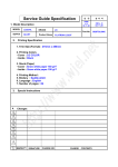
Service Guide
Guide Specification
Specification
1. Model Description
MODEL
SUFFIX
2.
L2010PM
ALEUQ
LG
BRAND
Part No.
3828TSL064F
Product Name FLATRON L2010P
Printing Specification
1. Trim Size (Format) : 215mm x 280 mm
2. Printing Colors
• Cover : LG COLORS
• Inside : Black
3. Stock (Paper)
• Cover : Snow White 150 g/
• Inside : Snow White 100 g/
4. Printing Method :
5. Bindery : Saddle stitch
6. Language : English
7. Number of pages : 32 ( Including blank 3page)
3.
Special Instructions
(1) Origin Notification
* LGEDI : Printed in Indonesia
* LGESP : Printed in Brazil
* LGENT : Printed in China
4.
* LGEWA : Printed in U.K.
* LGEMX : Printed in Mexico
* LGEIL : Printed in India
Changes
8
7
6
5
4
3
2
1
REV.
NO.
MM/DD/YY
CHANGE NO.
CHANGE
CONTENTS
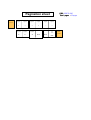
Pagination
Pagination sheet
sheet
English
English
English
English
English
English
2
3
4
5
….
…..
English
English
English
26
27
28
Cover
Rear
Cover
Inside
Blank
Blank
Blank
Rear
Cover
Website:http://biz.LGservice.com
E-mail:http://www.LGEservice.com/techsup.html
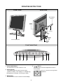
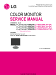
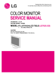
COLOR MONITOR
SERVICE MANUAL
CHASSIS NO. : CL-63
MODEL:
L2010P(L2010PM-AL**Q)
(
) **Same model for Service
CAUTION
BEFORE SERVICING THE UNIT,
READ THE SAFETY PRECAUTIONS IN THIS MANUAL.
LIGHT VIEW
AUTO
SOURCE
MENU
SELECT
CONTENTS
SPECIFICATIONS ................................................... 2
PRECAUTIONS ....................................................... 4
TIMING CHART ....................................................... 5
OPERATING INSTRUCTIONS ................................ 6
WIRING DIAGRAM ................................................. 9
BLOCK DIAGRAM ................................................. 10
DESCRIPTION OF BLOCK DIAGRAM...................11
ADJUSTMENT ...................................................... 13
TROUBLESHOOTING GUIDE .............................. 14
EXPLODED VIEW...................................................21
REPLACEMENT PARTS LIST ...............................23
SCHEMATIC DIAGRAM ......................................... 35
SPECIFICATIONS
1. LCD CHARACTERISTICS
Type
: TFT Color LCD Module
Size
: 20.1inch
Pixel Pitch
: 0.255(H) x 0.255(V)
Color Depth
: 8-bit, 16,777,216 colors
Electrical Interface
: LVDS
Surface Treatment
: Anti-Glare, Hard Coating(3H)
Operating Mode
: Normally Black
Backlight Unit
: Six-CCFL (Cold Cathode
Fluorescent Lamp)
4. MAX. RESOLUTION
Analog
Digital
5. POWER SUPPLY
5-1. Power Adaptor(Built-in Power)
Input
: AC 100-240V~, 50/60Hz , 1.2A
5-2. Power Consumption
MODE
2. OPTICAL CHARACTERISTICS
2-1. Viewing Angle by Contrast Ratio
Left
: -85° min., -88°(Typ)
Right : +85° min., +88°(Typ)
Top
: +85° min., +88°(Typ)
Bottom : -85° min., -88°(Typ)
≥ 10
2-2. Luminance
: 200(min), 250(Typ) -6500K
: more than 110cd/m2 -9300K
2-3. Contrast Ratio
: 400(Typ)
3-3. Operating Frequency
Horizontal
Vertical
H/V SYNC VIDEO POWER CONSUMPTION LED COLOR
POWER ON (NORMAL)
ON/ON
ACTIVE
less than 60 W
GREEN
STAND-BY
OFF/ON
OFF
less than 3 W
AMBER
SUSPEND MODE
ON/OFF
OFF
less than 3 W
AMBER
DPM OFF
OFF/OFF
OFF
less than 3 W
AMBER
POWER KEY OFF
-
-
less than 3 W
OFF
CUTOFF SWITCH OFF
-
-
less than 1 W
OFF
6. ENVIRONMENT
6-1. Operating Temperature: 10°C~35°C (50°F~95°F)
6-2. Relative Humidity
: 10%~80%
(Non-condensing)
6-3. MTBF
: 40,000 Hour(Min)
3. SIGNAL (Refer to the Timing Chart)
3-1. Sync Signal
• Type
: Separate, Positive/Negative
Composite, SOG (Sync On Green)
Digital
3-2. Video Input Signal
1) Type
2) Voltage Level
a) Color 0, 0
b) Color 7, 0
c) Color 15, 0
3) Input Impedance
: 1600 x 1200 60Hz
: 1600 x 1200 60Hz
1280 x 1024 70Hz
7. DIMENSIONS (with TILT/SWIVEL)
: R, G, B Analog
: 0~0.71 V
: 0 Vp-p
: 0.467 Vp-p
: 0.714 Vp-p
: 75 Ω
: 28 ~ 92kHz (Analog)
: 28 ~ 80kHz (Digital)
: 56 ~ 85Hz
Width
Depth
Height
: 446.0 mm (17.56'')
: 237.3 mm (9.34'')
: 445.6 mm (17.54'')
8. WEIGHT (with TILT/SWIVEL)
Net. Weight
Gross Weight
: 9.5kg (20.95 lbs)
: 12.0kg (26.46 lbs)
9. USB
Upstream : 1 port, Downstream : 2 port
Speed : Full-12Mbps, Low-1.5Mbps
-2-
Signal Connector Pin Assignment
• DVI-I Connector (Digital/Analog)
1
9
17
8 C1 C2
C5
16
24 C3 C4
Pin
1
2
3
4
5
6
7
8
9
10
11
12
13
14
15
Signal (DVI-I)
T. M. D. S. Data2T. M. D. S. Data2+
T. M. D. S. Data2/4 Shield
T. M. D. S. Data4T. M. D. S. Data4+
DDC Clock
DDC Data
Analog Vertical Sync.
T. M. D. S. Data1T. M. D. S. Data1+
T. M. D. S. Data1/3 Shield
T. M. D. S. Data3T. M. D. S. Data3+
+5V Power
Ground (return for +5V,
Pin
16
17
18
19
20
21
22
23
24
C1
C2
C3
C4
C5
Signal (DVI-I)
Hot Plug Detect
T. M. D. S. Data0T. M. D. S. Data0+
T. M. D. S. Data0/5 Shield
T. M. D. S. Data5T. M. D. S. Data5+
T. M. D. S. Clock Shield
T. M. D. S. Clock+
T. M. D. S. ClockAnalog Red
Analog Green
Analog Blue
Analog H. Sync.
Analog Ground
H. Sync. and V. Sync.)
T. M. D. S. (Transition Minimized Differential Signaling)
-3-
PRECAUTION
WARNING FOR THE SAFETY-RELATED COMPONENT.
WARNING
• There are some special components used in LCD
monitor that are important for safety. These parts are
marked on the schematic diagram and the
replacement parts list. It is essential that these critical
parts should be replaced with the manufacturer’s
specified parts to prevent electric shock, fire or other
hazard.
• Do not modify original design without obtaining written
permission from manufacturer or you will void the
original parts and labor guarantee.
TAKE CARE DURING HANDLING THE LCD MODULE
WITH BACKLIGHT UNIT.
• Must mount the module using mounting holes arranged
in four corners.
• Do not press on the panel, edge of the frame strongly
or electric shock as this will result in damage to the
screen.
• Do not scratch or press on the panel with any sharp
objects, such as pencil or pen as this may result in
damage to the panel.
• Protect the module from the ESD as it may damage the
electronic circuit (C-MOS).
• Make certain that treatment person’s body are
grounded through wrist band.
• Do not leave the module in high temperature and in
areas of high humidity for a long time.
• The module not be exposed to the direct sunlight.
• Avoid contact with water as it may a short circuit within
the module.
• If the surface of panel become dirty, please wipe it off
with a softmaterial. (Cleaning with a dirty or rough cloth
may damage the panel.)
CAUTION
Please use only a plastic screwdriver to protect yourself
from shock hazard during service operation.
-4-
BE CAREFUL ELECTRIC SHOCK !
• If you want to replace with the new backlight (CCFL) or
inverter circuit, must disconnect the AC adapter
because high voltage appears at inverter circuit about
650Vrms.
• Handle with care wires or connectors of the inverter
circuit. If the wires are pressed cause short and may
burn or take fire.
TIMING CHART
VIDEO
B
A
E
C
D
SYNC
F
<< Dot Clock (MHz), Horizontal Frequency (kHz), Vertical Frequency (Hz), Horizontal etc... (µs), Vertical etc... (ms) >>
Mode
1
2
3
4
5
6
7
8
9
10
11
12
13
14
15
16
17
18
19
H/V
Sort
Sync
Polarity
H
V
H
V
H
V
H
V
H
V
H
V
H
V
H
V
H
V
H
V
H
V
H
V
H
V
H
V
H
V
H
V
H
V
H
V
H
V
+
–
–
–
–
–
–
–
–
+
+
+
+
+
+
+
–
–
–
–
+
+
+
+
–
–
+/–
+/–
+
+
+
+
+
+
+
+
+
+
Dot
Clock
25.175
25.175
31.5
36.0
28.324
40.0
49.5
56.25
57.283
65.0
78.75
94.5
100.0
92.978
108.0
135.0
112.27
162
(Analog only)
130.89
(Digital only)
Frequency
31.47
70.09
31.47
59.94
37.5
75
43.27
85.01
31.47
70.08
37.88
60.32
46.88
75.0
53.67
85.06
49.72
74.55
48.36
60.0
60.02
75.03
68.68
85.0
68.68
75.06
61.80
65.96
63.98
60.02
79.98
75.02
62.11
60.00
75.0
60.00
73.53
60
Total Period Video Active Time
(E)
(A)
800
449
800
525
840
500
832
509
900
449
1056
628
1056
625
1048
631
1152
667
1344
806
1312
800
1376
808
1456
915
1504
937
1688
1066
1688
1066
1808
1040
2160
1250
1780
1225
640
350
640
480
640
480
640
480
720
400
800
600
800
600
800
600
832
624
1024
768
1024
768
1024
768
1152
870
1152
900
1280
1024
1280
1024
1600
1024
1600
1200
1600
1200
-5-
Front Porch
(C)
Sync Duration
(D)
Back Porch
(F)
Resolution
16
38
16
10
16
1
56
1
18
13
40
1
16
1
32
1
32
1
24
3
16
1
48
1
32
3
18
2
48
1
16
1
90
10
64
1
20
1
96
2
96
2
64
3
56
3
108
2
128
4
80
3
64
3
64
3
136
6
96
3
96
3
128
3
134
4
112
3
144
3
30
3
192
3
80
3
48
60
48
33
120
16
80
25
54
34
88
23
160
21
152
27
224
39
160
29
176
28
208
36
144
39
200
31
248
38
248
38
88
3
304
46
80
21
640x350
70Hz
640x480
60Hz
640x480
75Hz
640x480
85Hz
720x400
70Hz
800x600
60Hz
800x600
75Hz
800x600
85Hz
832x624
75Hz
1024x768
60Hz
1024x768
75Hz
1024x768
85Hz
1152x870
75Hz
1152x900
65Hz
1280x1024
60Hz
1280x1024
75Hz
1600x1024
60Hz
1600x1200
60Hz
1600x1200
60Hz
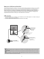
OPERATING INSTRUCTIONS
FRONT VIEW
REAR VIEW
D-Sub Signal
Connect
Power
Switch
LIGHT VIEW
AUTO
SOURCE
MENU
SELECT
DVI
Connect
Stand
lock
USB Down
Stream
Port
Front Control Panel
Power
Connect
USB Up
Stream
Port
Front Control Panel
6
7
8
3
4
1. Power ON/OFF Button
Use this button to turn the monitor on or off.
4.
2. Power Indicator
This indicator lights up green when the monitor
operates normally. If the display is in DPM(Energy
Saving)mode, this indicator color change to amber.
3. MENU Button
Use these button to enter or exit the On Screen Display.
-6-
5
1
2
Buttons
Use these button to choose or adjust items in the On
Screen Display.
Bring up contrast and brightness
adjustment.
100
100
Direct Access Function
5. SELECT Button
Use this buttons to enter a selection in the On Screen
Display.
8. SOURCE Selections:SOURCE
SELECT
Use this button to make DVI
digital, DVI analog or D-sub
DVI ANALOG
analog connector active.
DSUB ANALOG
This feature is used when two
computers are connected to the display. The default
setting is D-sub.
INPUT SELECT
DVI DIGITAL
6. LIGHT VIEW Button
This function optimizes the brightness, contrast of color
value to the surrounding conditions and settings
and enables you to enjoy the most suitable picture
by
adjusting
the
LIGHT VIEW
DAY
• DVI DIGITAL
• DVI ANALOG
• D-SUB ANALOG
TXT
MOVIE
PHOTO
NIGHT TEXT
MOVIE
PHOTO
USER MODE
.CONTROLS LOCKED /UNLOCKED: MENU &
CONTROLS LOCKED
surroundings(DAY/LIGHT/USER MODE).
• TEXT: For viewing letters
• MOVIE: For viewing movies
• PHOTO: For viewing pictures or the photographs
• USER MODE: This function memorizes the manual
adjustment-Brightness, Contrast color value on the On
Screen Display
CONTROLS UNLOCKED
Button
This function allows you to secure the
current control settings, so that they
cannot be inadvertently changed.
Press and hold the MENU button and
button for 3 seconds: the message
“CONTROLS LOCKED” appears.
You can unlock the OSD controls at any time by pushing the
MENU button and
button for 3 seconds:
the message “CONTROLS UNLOCKED” will appear.
7. AUTO Adjustment Button
AUTO IN PROGRESS
When adjusting your display settings, always press
the AUTO button before entering On Screen
Display(OSD). This will automatically adjust your
display image to the ideal settings for the current
screen resolution size(display mode).
The best display mode is 1600 x 1200@60Hz.
-7-
Making use of USB (Universal Serial Bus)*
USB (Universal Serial Bus) is an innovation in connecting your different desktop peripherals conveniently to your computer.
By using the USB, you will be able to connect your mouse, keyboard, and other peripherals to your display instead of
having to connect them to your computer. This will give you greater flexibility in setting up your system. USB allows you to
connect a chain of up to 120 devices on a single USB port; and you can “hot” plug (attach them while the computer is
running) or unplug them while maintaining the Plug and the Plug auto detection and configuration. This display has an
integrated BUS-powered USB hub, allowing up to 2 other USB devices to be attached it.
USB connection
1. Connect the upstream port of the display to the downstream port of the USB compliant PC or another hub using the
USB cable. (Computer must have a USB port)
2. Connect the USB compliant peripherals to the downstream ports of the display.
USB upstream Port
This is a simplified
representation
of rear view.
PUSH
To USB downstream port of
the USB compliant PC or
another hub cable
USB downstream Port
connect the cables from
USB compliant
peripherals-such as
keyboard, mouse, etc
Power ON/OFF
Switch of the monitor
NOTE
To activate the USB hub function, the display must be connected to a USB compliant PC(OS) or another hub with the USB
cable(enclosed).
When connecting the USB cable, check that the shape of the connector at the cable side matches the shape at the connecting
side.
Even if the display is in a power saving mode, USB compliant devices will function when they are connected the USB
ports(both the upstream and downstream) of the display.
-8-
WIRING DIAGRAM
Connector Ass’y P/N:
6631T20013P
Connector Ass’y P/N:
6631T25008Q
CN103
CN104
J302
J303
CN101
CN102
-9-
D-Sub
DVI-I
- 10 -
1.8V
2.5V
3.3V
12V-F ujitsu
18V-LPL
5V - AU O
5V
Analog
LAMP Connector
Inverter
Output
(6Lamp)
LIPS
Analog
switch
Filter
EEPR OM
(ED ID)
DVI(TMDS)
Analog II(R/G/B)
Analog I(R/G/B)
5.0V
5V
Regulator
Regulator
Regulator
Flash ROM
DVI Rx
PLL
ADC
1.8V
2.5V
3.3V
3.3V
OSD
Scaling
ROM
MICOM
gm1601
2.5V
DDR RAM
Real
colour
LVDS
Tx
EEPROM
(System)
Vcc
12 V-Fujitsu
18 V-LPL
5V -AUO
LVDS
Panel
KEY
EEPR OM
(ED ID)
BLOCK DIAGRAM
DESCRIPTION OF BLOCK DIAGRAM
1. Video Controller Part & Display Data Transmitter Part.
This part amplifies the level of video signal for the digital conversion and converts from the analog video signal to the
digital video signal using a pixel clock.
The pixel clock for each mode is generated by the PLL.
The range of the pixel clock is from 25MHz to 170MHz.
This part consists of the Scaler, Flash-ROM IC which stores program data, Reset IC.
The Scaler gets the video signal converted analog to digital, interpolates input to 1600 * 1200 resolution signal and
outputs 8-bit R, G, B signal to transmitter.
Especially pre-amp / ADC / Video controller/ Transmitter are merged to one chip "Gm1601" by Genesis.
This part transmit digital signal from the Scaler to the receiver of module.
2. Power Part
This part consists of the two 3.3V and one 2.5V and one 1.8Vregulators to convert power which is provided 12V in
LIPS Board V is provided for LCD Panel.
Also, 5V is converted 3.3V and 2.5V and 1.8V by regulator. Converted power is provided for IC in the main board.
- 11 -
12V
50 ~ 60Hz
EMI
COMPONENTS
INPUT RECTIFIER
AND FILTER
HVDC
ENERGY
TRANSFER
100KHz
OUTPUT RECTIFIER
AND FILTER
5V
GND
LINE
100 ~ 240V
PWM CONTROL
CIRCUIT
PRIMARY
12V
SIGNAL
COLLECTON
PHOTO-COUPLER
ISOLATION
SECONDARY
INVERTER CIRCUIT
High Voltage output
Operation description_Power
1. EMI components.
This part contains of EMI components to comply with global marketing EMI standards like FCC,VCCI CISPR, the
circuit included a line-filter, across line capacitor and of course the primary protection fuse.
2. Input rectifier and filter.
This part function is for transfer the input AC voltage to a DC voltage through a bridge rectifier and a bulk capacitor.
3. Energy Transfer.
This part function is for transfer the primary energy to secondary through a power transformer.
4. Output rectifier and filter.
This part function is to make a pulse width modulation control and to provide the driver signal to power switch,to
adjust the duty cycle during different AC input and output loading condition to achieve the dc output stabilized, and
also the over power protection is also monitor by this part.
5. Photo-Coupler isolation.
This part function is to feed back the dc output changing status through a photo transistor to primary controller to
achieve the stabilized dc output voltage.
6. Signal collection.
This part function is to collect the any change from the dc output and feed back to the primary through photo
transistor
7. Inverter
The inverter converts from DC12V to AC 700V and operate back-light lamp of module.
- 12 -
ADJUSTMENT
Windows EDID V1.0 User Manual
2. EDID Read & Write
1) Run WinEDID.exe
Operating System: MS Windows 98, 2000, XP
Port Setup: Windows 98 => Doesn’t need setup
Windows 2000, XP => Need to Port Setup.
This program is available for LCD Monitor only.
1. Port Setup
a) Copy “UserPort.sys” file to
“c:\WINNT\system32\drivers” folder
b) Run Userport.exe
2) Edit Week of Manufacture, Year of Manufacture,
Serial Number
a) Input User Info Data
b) Click “Update” button
c) Click “ Write” button
c) Remove all default number
d) Add 300-3FF
e) Click Start button.
f) Click Exit button.
A
9
IBM
Compatible PC
Video Signal
Generator
15
10
5
6
1
5
C
13
se
d
PARALLEL PORT
1
5V
RS
No
23
2C
tu
25
OFF
14
ON
LL
EL
F
RA
PA
5V
Power inlet (required)
ON
WE
R
220
VG
CS
T
MO
NIT
OR
B
Power Select Switch
(110V/220V)
Power LED
4.7K
OFF
74LS06
E ST Switch
B
F V-Sync On/Off Switch
(Switch must be ON.)
Figure 1. Cable Connection
- 13 -
4.7K
4.7K
5V
E
YN
A
PO
S
V-S
Control Line
C
11
6
1
74LS06
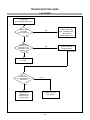
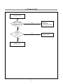
TROUBLESHOOTING GUIDE
1. NO POWER
NO POWER
(POWER INDICATOR OFF)
CHECK J302
VOLTAGE
PIN5, PIN6 (5V)?
NO
CHECK POWER
BOARD, AND FIND
OUT A SHORT POINT
AS OPENING
EACH POWER LINE
YES
CHECK
U207 PIN3 (3.3V)
U205 PIN4 (2.5V)
U202 PIN4 (1.8V)
Voltage ?
NO
NO PROBLEM
YES
CHECK REGULATOR
IC LINE
IS U101
PIN K17(1.8V)/
D17(3.3V)/H23(2.5V)
VOLTAGE ?
NO
YES
CHECK IIC LINE
CONNECTION
(U403(24LC16),
U303(24LC02))
CHECK 5VS LINE
(OPEN CHECK)
CHECK U101 VCC,
XTAL, RESET
- 14 -
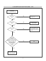
2. NO RASTER (OSD IS NOT DISPLAYED) – LIPS
NO RASTER
(OSD IS NOT DISPLAYED)
J302
PIN5, PIN 6
5V?
NO
CHECK LIPS
YES
J302 PIN9
5V?
NO
CHECK MICOM INV
ON/OFF PORT.
YES
J302 PIN10
5V?
NO
1. CONFIRM BRIGHTNESS
OSD CONTRL STATE.
2. CHECK MICOM DIM-ADJ
PORT
YES
CHECK
PULSE AS
CONTACTING SCOPE
PROBE TO CAUTION LABEL.
(CONTACT PROBE TO
CAUTION LABEL.
CAN YOU SEE PULSE
AT YOUR
SCOPE?
NO
YES
REPLACE CCFL LAMP
IN THE LCD MODULE
- 15 -
LIPS
3. NO RASTER (OSD IS NOT DISPLAYED)
NO RASTER
(OSD IS NOT DISPLAYED)
U207 PIN3
3.3V
CHECK?
NO
CHECK LIPS
YES
U101
PIN G3, G4
OSCILLATE AS
14.318MHZ?
NO
1. CHECK PIN122, 123
SOLDERING CONDITION
2. CHECK X101
3. TROUBLE IN U201
YES
U301
PIN24 IS H-SYNC(1)
PIN12 IS V-SYNC(1)
PIN23 IS H-SYNC(0)
PIN13 IS V-SYNC(0)
NO
YES
TROUBLE IN CABLE
OR LCD MODULE
- 16 -
CHECK CONNECTION LINE
FROM D-SUB TO U501
4. TROUBLE IN DPM
TROUBLE IN DPM
CHECK
R340(H0), R339(V0)
R330(H1), R328(V1)
(SYNC) ?
NO
CHECK PC
PC IS GOING
INTO DPM OFF MODE
NO
TROUBLE IN
SIGNAL CABLE
YES
CHECK
U501 PIN 24
(0V) ?
YES
TROUBLE IN PC
- 17 -
- 18 -
1
2
7
10
3
11
8
a
12
a
b
9
5
6
26
24
25
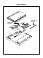
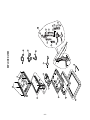
EXPLODED VIEW
14
15
c
13
20
23
18
19
4
17
22
21
16
EXPLODED VIEW PARTS LIST
Ref. No.
Part No.
Description
3091TKL049W
CABINET ASSEMBLY, L2010PM BRAND 051 IPS TCO03 USB
3091TKL113B
CABINET ASSEMBLY, L2010PM BRAND 051 IPS TCO03 USB RED LG(ALPAQ)
3091TKL113A
CABINET ASSEMBLY, L2010PM BRAND 051 IPS TCO03 USB US(ALUSQ)
6304FLP130A
LCD(LIQUID CRYSTAL DISPLAY) , "LM201U04-A3K5 LG PHILPS TFT COLOR UXGA,250NITS,8BITS,LVDS,4MASK"
3809TKL031J
BACK COVER ASSEMBLY, L2010BM 037A .
3809TKL031M
BACK COVER ASSEMBLY, L2010PM 037 US(ALUSQ)
4
3043TKK105D
TILT SWIVEL ASSEMBLY, L2010PM 222F USB
5
6871TST582A
"PWB(PCB) ASSEMBLY,SUB", L2010P(B)M CONTROL TOTAL BRAND CL-63
6
6631T11016J
CONNECTOR ASSEMBLY, 30P H-H 100MM UL20276 AWG30 LB200A LPL
7
4951TKK100G
METAL ASSEMBLY, FRAME L2010
8
6871TPT270B
"PWB(PCB) ASSEMBLY,POWER", "L2010 POWER TOTAL LIEN CHANG 20.1"" LIPS FOR LPL"
9
3313TL2020A
MAIN TOTAL ASSEMBLY, L2010P(B)M_LPL BRAND CL-63
10
4951TKK098G
METAL ASSEMBLY, REAR L2010B
11
6871TUT015A
"PWB(PCB) ASSEMBLY,USB", LB886F SUB TOTAL BRAND CL-29
12
6631T25005F
CONNECTOR ASSEMBLY, SWITCH(GY)+CONN ASSYP H-W 260MM UL 1617 AWG 22 LB200A
13
3550TKK220D
COVER, LB200A TOP FRONT POLYACETAL 87074
14
3550TKK218E
COVER, LB200A STAND FRONT ABS HF350U 87074
15
3550TKK222F
COVER, L1910PL BASE TOP HF350U 87074(USB)
16
3550TKK223E
COVER, LB200A CABLE COVER ABS HF350U 87074
17
3550TKK219E
COVER, LB200A STAND REAR ABS HF350U 87074
18
3550TKK221D
COVER, LB200A TOP REAR POLYACETAL 87074
19
3550TKK217E
COVER, LB200A HINGE REAR ABS HF350U 87074
20
3550TKK216E
COVER, LB200A HINGE TOP ABS HF350U 87074
21
4950TKK346A
METAL, "PLATE STOPPER,LB886F"
22
3550TKK224C
COVER, "LW900Z PIECE LOCK PC IDEMITSU IR1900, CRYSTAL"
23
4970TKK009A
"SPRING,COIL", COIL - FOR STAND T=4.5 LB200A
1
2
3
24
6866TDU002D
"CABLE,D-SUB", UL20276SB10P+2C AWG#30 DT 1870MM GRAY(85964) BRAND DM
25
6866TDV004C
"CABLE,DVI", UL20276 DT 2000MM GRAY(85964) LB885C DM
26
6850TD9001J
"CABLE,D-SUB", UL 2990-9C(7.5) DT 1870MM PEARL WH T541K DM
a
1SZZTER001G
"SCREW,DRAWING", D3.0 L6.0 MSWR/BK .
b
332-113S
"SCREW,DRAWING", D3.0 L12.0 MSWR/BK .
c
332-105G
"SCREW,DRAWING", PVS+4*10(MSWR/BK)
- 19 -
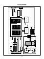
REPLACEMENT PARTS LIST
CAUTION: BEFORE REPLACING ANY OF THESE COMPONENTS,
READ CAREFULLY THE SAFETY PRECAUTIONS IN THIS MANUAL.
* NOTE : S SAFETY Mark
AL ALTERNATIVE PARTS
*S *AL LOC. NO.
PART NO.
DATE: 2004. 03. 23.
DESCRIPTION / SPECIFICATION
*S *AL LOC. NO.
MAIN BOARD
CAPACITORS
C101
C103
C104
C105
C106
C107
C109
C110
C111
C112
C113
C114
C115
C116
C117
C118
C119
C120
C121
C122
C123
C124
C125
C126
C127
C128
C129
C130
C131
C135
C136
C137
C138
C140
C141
C147
C148
C149
C150
C151
C152
C155
C165
C169
C170
C201
C203
C204
C205
C206
C207
C208
0CE107EF610
0CK104CK56A
0CC220CK41A
0CK104CK56A
0CC220CK41A
0CK104CK56A
0CH3104K566
0CH3104K566
0CH3104K566
0CH3104K566
0CH3104K566
0CH3104K566
0CK103CK51A
0CH3104K566
0CK103CK51A
0CK103CK51A
0CH3104K566
0CH3104K566
0CH3104K566
0CH3104K566
0CH3104K566
0CH3104K566
0CH3104K566
0CH3104K566
0CH3104K566
0CH3104K566
0CH3104K566
0CH3104K566
0CH3104K566
0CH3104K566
0CH3104K566
0CH3104K566
0CH3104K566
0CH3104K566
0CH3104K566
0CH3104K566
0CH3104K566
0CH3104K566
0CH3104K566
0CH3104K566
0CH3104K566
0CH3104K566
0CH3104K566
0CH6102K406
0CC102CK41A
0CK105DK94A
0CZZTAT005D
0CZZTAT005D
0CK103CK51A
0CK103CK51A
0CE107EF610
0CK104CK56A
C209
C210
C211
C212
C213
C214
C215
C217
C219
C220
C221
C222
C224
C225
C227
C229
C230
C231
C233
C301
C302
C303
C304
C305
C306
C307
C308
C309
C310
C311
C312
C313
C314
C315
C316
C317
C318
C319
C320
C321
C322
C323
C324
C325
C326
C327
C328
C330
C333
C334
C335
C337
C341
C342
"100UF KMG,RD 16V 20% FL BULK"
0.1UF 1608 50V 10% R/TP X7R
22PF 1608 50V 5% R/TP NP0
0.1UF 1608 50V 10% R/TP X7R
22PF 1608 50V 5% R/TP NP0
0.1UF 1608 50V 10% R/TP X7R
0.1UF 50V 10% X7R 2012 R/TP
0.1UF 50V 10% X7R 2012 R/TP
0.1UF 50V 10% X7R 2012 R/TP
0.1UF 50V 10% X7R 2012 R/TP
0.1UF 50V 10% X7R 2012 R/TP
0.1UF 50V 10% X7R 2012 R/TP
0.01UF 1608 50V 10% R/TP B(Y5
0.1UF 50V 10% X7R 2012 R/TP
0.01UF 1608 50V 10% R/TP B(Y5
0.01UF 1608 50V 10% R/TP B(Y5
0.1UF 50V 10% X7R 2012 R/TP
0.1UF 50V 10% X7R 2012 R/TP
0.1UF 50V 10% X7R 2012 R/TP
0.1UF 50V 10% X7R 2012 R/TP
0.1UF 50V 10% X7R 2012 R/TP
0.1UF 50V 10% X7R 2012 R/TP
0.1UF 50V 10% X7R 2012 R/TP
0.1UF 50V 10% X7R 2012 R/TP
0.1UF 50V 10% X7R 2012 R/TP
0.1UF 50V 10% X7R 2012 R/TP
0.1UF 50V 10% X7R 2012 R/TP
0.1UF 50V 10% X7R 2012 R/TP
0.1UF 50V 10% X7R 2012 R/TP
0.1UF 50V 10% X7R 2012 R/TP
0.1UF 50V 10% X7R 2012 R/TP
0.1UF 50V 10% X7R 2012 R/TP
0.1UF 50V 10% X7R 2012 R/TP
0.1UF 50V 10% X7R 2012 R/TP
0.1UF 50V 10% X7R 2012 R/TP
0.1UF 50V 10% X7R 2012 R/TP
0.1UF 50V 10% X7R 2012 R/TP
0.1UF 50V 10% X7R 2012 R/TP
0.1UF 50V 10% X7R 2012 R/TP
0.1UF 50V 10% X7R 2012 R/TP
0.1UF 50V 10% X7R 2012 R/TP
0.1UF 50V 10% X7R 2012 R/TP
0.1UF 50V 10% X7R 2012 R/TP
1000PF 50V J SL 2012 R/TP
1000PF 1608 50V 5% R/TP NP0
"1UF 2012 50V 80%,-20% R/TP F("
RJ4-16V471MX ELNA 16V 470UF 2
RJ4-16V471MX ELNA 16V 470UF 2
0.01UF 1608 50V 10% R/TP B(Y5
0.01UF 1608 50V 10% R/TP B(Y5
"100UF KMG,RD 16V 20% FL BULK"
0.1UF 1608 50V 10% R/TP X7R
- 20 -
PART NO.
0CK103CK51A
0CK103CK51A
0CE477EH618
0CK104CK56A
0CK104CK56A
0CK103CK51A
0CH6102K406
0CE107EF610
0CE107EF610
0CE477EH618
0CK104CK56A
0CZZTAT005D
0CK104CK56A
0CZZTAT005G
0CK103CK51A
0CK104CK56A
0CE107EF610
0CK104CK56A
0CZZTAT005C
0CK104CK56A
0CK105CF94A
0CK103CK51A
0CK103CK51A
0CE107EF610
0CK103CK51A
0CC471CK41A
0CK103CK51A
0CZZTAT008D
0CK103CK51A
0CE107EF610
0CK474CH94A
0CK103CK51A
0CK103CK51A
0CZZTAT008D
0CC101CK41A
0CZZTAT008D
0CC680CK41A
0CK103CK51A
0CH3103K516
0CK103CK51A
0CK103CK51A
0CC680CK41A
0CC101CK41A
0CZZTAT008D
0CC680CK41A
0CZZTAT008D
0CK104CK56A
0CH3103K516
0CH3103K516
0CH3103K516
0CH3103K516
0CK104CK56A
0CC680CK41A
0CZZTAT008D
DATE: 2004. 03. 23.
DESCRIPTION / SPECIFICATION
0.01UF 1608 50V 10% R/TP B(Y5
0.01UF 1608 50V 10% R/TP B(Y5
470UF KMG 25V M FL TP 5
0.1UF 1608 50V 10% R/TP X7R
0.1UF 1608 50V 10% R/TP X7R
0.01UF 1608 50V 10% R/TP B(Y5
1000PF 50V J SL 2012 R/TP
"100UF KMG,RD 16V 20% FL BULK"
"100UF KMG,RD 16V 20% FL BULK"
470UF KMG 25V M FL TP 5
0.1UF 1608 50V 10% R/TP X7R
RJ4-16V471MX ELNA 16V 470UF 2
0.1UF 1608 50V 10% R/TP X7R
RJ4-16V221MF3#-T36 ELNA 16V 2
0.01UF 1608 50V 10% R/TP B(Y5
0.1UF 1608 50V 10% R/TP X7R
"100UF KMG,RD 16V 20% FL BULK"
0.1UF 1608 50V 10% R/TP X7R
RJ4-25V101MX ELNA 25V 100UF 2
0.1UF 1608 50V 10% R/TP X7R
"1UF 1608 16V 80%,-20% R/TP F("
0.01UF 1608 50V 10% R/TP B(Y5
0.01UF 1608 50V 10% R/TP B(Y5
"100UF KMG,RD 16V 20% FL BULK"
0.01UF 1608 50V 10% R/TP B(Y5
470PF 1608 50V 5% R/TP NP0
0.01UF 1608 50V 10% R/TP B(Y5
RVS-6V470MU-R ELNA 6.3V 47UF
0.01UF 1608 50V 10% R/TP B(Y5
"100UF KMG,RD 16V 20% FL BULK"
"0.47UF 1608 25V 80%,-20% R/TP"
0.01UF 1608 50V 10% R/TP B(Y5
0.01UF 1608 50V 10% R/TP B(Y5
RVS-6V470MU-R ELNA 6.3V 47UF
100PF 1608 50V 5% R/TP NP0
RVS-6V470MU-R ELNA 6.3V 47UF
68PF 1608 50V 5% R/TP NP0
0.01UF 1608 50V 10% R/TP B(Y5
10000PF 50V 10% B(Y5P) 2012 R
0.01UF 1608 50V 10% R/TP B(Y5
0.01UF 1608 50V 10% R/TP B(Y5
68PF 1608 50V 5% R/TP NP0
100PF 1608 50V 5% R/TP NP0
RVS-6V470MU-R ELNA 6.3V 47UF
68PF 1608 50V 5% R/TP NP0
RVS-6V470MU-R ELNA 6.3V 47UF
0.1UF 1608 50V 10% R/TP X7R
10000PF 50V 10% B(Y5P) 2012 R
10000PF 50V 10% B(Y5P) 2012 R
10000PF 50V 10% B(Y5P) 2012 R
10000PF 50V 10% B(Y5P) 2012 R
0.1UF 1608 50V 10% R/TP X7R
68PF 1608 50V 5% R/TP NP0
RVS-6V470MU-R ELNA 6.3V 47UF
*S *AL LOC. NO.
PART NO.
DATE: 2004. 03. 23.
DESCRIPTION / SPECIFICATION
*S *AL LOC. NO.
PART NO.
DATE: 2004. 03. 23.
DESCRIPTION / SPECIFICATION20
ICs
C343
C344
C345
C346
C347
C349
C350
C352
C354
C357
C358
C360
C361
C362
C363
C364
C365
C401
C402
C403
C404
C405
C406
C407
C408
C409
C410
C411
C412
C611
0CC101CK41A
0CC101CK41A
0CK105DK94A
0CK105DK94A
0CK105DK94A
0CK104CK56A
0CH3103K516
0CH3103K516
0CC080CK11A
0CK103CK51A
0CK103CK51A
0CK105CF94A
0CK103CK51A
0CC080CK11A
0CK105DK94A
0CH5100K416
0CH5100K416
0CK104CK56A
0CK104CK56A
0CK104CK56A
0CK104CK56A
0CK104CK56A
0CE107EF610
0CH3104K566
0CH3104K566
0CK104CK56A
0CK104CK56A
0CK104CK56A
0CK104CK56A
0CK104CK56A
100PF 1608 50V 5% R/TP NP0
100PF 1608 50V 5% R/TP NP0
"1UF 2012 50V 80%,-20% R/TP F("
"1UF 2012 50V 80%,-20% R/TP F("
"1UF 2012 50V 80%,-20% R/TP F("
0.1UF 1608 50V 10% R/TP X7R
10000PF 50V 10% B(Y5P) 2012 R
10000PF 50V 10% B(Y5P) 2012 R
8PF 1608 50V 0.5 PF R/TP NP0
0.01UF 1608 50V 10% R/TP B(Y5
0.01UF 1608 50V 10% R/TP B(Y5
"1UF 1608 16V 80%,-20% R/TP F("
0.01UF 1608 50V 10% R/TP B(Y5
8PF 1608 50V 0.5 PF R/TP NP0
"1UF 2012 50V 80%,-20% R/TP F("
10PF 50V 5% NP0 2012 R/TP
10PF 50V 5% NP0 2012 R/TP
0.1UF 1608 50V 10% R/TP X7R
0.1UF 1608 50V 10% R/TP X7R
0.1UF 1608 50V 10% R/TP X7R
0.1UF 1608 50V 10% R/TP X7R
0.1UF 1608 50V 10% R/TP X7R
"100UF KMG,RD 16V 20% FL BULK"
0.1UF 50V 10% X7R 2012 R/TP
0.1UF 50V 10% X7R 2012 R/TP
0.1UF 1608 50V 10% R/TP X7R
0.1UF 1608 50V 10% R/TP X7R
0.1UF 1608 50V 10% R/TP X7R
0.1UF 1608 50V 10% R/TP X7R
0.1UF 1608 50V 10% R/TP X7R
0DS226009AA
0DS226009AA
0DS226009AA
0DD184009AA
0DD184009AA
0DS226009AA
0DS226009AA
0DS226009AA
0DZ560009DA
0DZ560009DA
0DZ560009DA
0DZ560009DA
0DZ560009DA
0DZ560009DA
0DZ560009DA
0DZ560009DA
0DZ560009DA
0DZ560009DA
0DZ560009DA
0DZ560009DA
0DZ560009DA
0DZ560009DA
0DZ560009DA
0DZ560009DA
0DZ560009DA
0DZ560009DA
0DZ560009DA
0DZ560009DA
0DZ560009DA
KDS226 TP KEC SOT-23 80V 300
KDS226 TP KEC SOT-23 80V 300
KDS226 TP KEC SOT-23 80V 300
KDS184 TP KEC - 85V - - - 300
KDS184 TP KEC - 85V - - - 300
KDS226 TP KEC SOT-23 80V 300
KDS226 TP KEC SOT-23 80V 300
KDS226 TP KEC SOT-23 80V 300
UDZ S 5.6B TP ROHM-K SOD323 2
UDZ S 5.6B TP ROHM-K SOD323 2
UDZ S 5.6B TP ROHM-K SOD323 2
UDZ S 5.6B TP ROHM-K SOD323 2
UDZ S 5.6B TP ROHM-K SOD323 2
UDZ S 5.6B TP ROHM-K SOD323 2
UDZ S 5.6B TP ROHM-K SOD323 2
UDZ S 5.6B TP ROHM-K SOD323 2
UDZ S 5.6B TP ROHM-K SOD323 2
UDZ S 5.6B TP ROHM-K SOD323 2
UDZ S 5.6B TP ROHM-K SOD323 2
UDZ S 5.6B TP ROHM-K SOD323 2
UDZ S 5.6B TP ROHM-K SOD323 2
UDZ S 5.6B TP ROHM-K SOD323 2
UDZ S 5.6B TP ROHM-K SOD323 2
UDZ S 5.6B TP ROHM-K SOD323 2
UDZ S 5.6B TP ROHM-K SOD323 2
UDZ S 5.6B TP ROHM-K SOD323 2
UDZ S 5.6B TP ROHM-K SOD323 2
UDZ S 5.6B TP ROHM-K SOD323 2
UDZ S 5.6B TP ROHM-K SOD323 2
U101
U102
U201
U202
U204
U205
U206
U207
U301
U303
U304
U305
U306
U307
U401
U402
U403
"GM1601,A&D&VIDEO GENESIS 416P"
KIA7042AP TO-92 TP 4.2 VOLT.
IRF7316 INTERNATIONAL RECTIFI
FAN1117AS-1.8 FAIRCHILD 4P SO
FAIRCHILD FDC6326L R/TP SOT-6
FAN1086-1.5A FAIRCHILD SOT252
BA033FP-E2 MOLD-3 TP REGULATO
BA033FP-E2 MOLD-3 TP REGULATO
"BA7657F 24P,SOP TP INPUT SIG."
"M24C02-WMN6T SGS-THOMSON 8P,S"
"M24C02-WMN6T SGS-THOMSON 8P,S"
CM1213-08MS CAMD R/TP MSOP 10
CM1213-08MS CAMD R/TP MSOP 10
CM1213-08MS CAMD R/TP MSOP 10
MACRONIX/ATMEL 32PIN PLCC ST
"AT49BV040A-70JI ATMEL 32P,PLC"
M24C16-WMN6T SGS-THOMSON 8PIN
COILs & COREs
L101
L102
L201
L202
L203
L204
L206
L207
L208
L209
L210
L211
L212
L301
L307
L308
L309
DIODEs
D301
D302
D303
D304
D316
D317
D318
D319
ZD301
ZD302
ZD303
ZD304
ZD305
ZD306
ZD307
ZD308
ZD309
ZD310
ZD311
ZD312
ZD315
ZD316
ZD317
ZD318
ZD319
ZD320
ZD321
ZD322
ZD323
0IPRPGN007A
0IKE704200H
0TFIR80009B
0IPMGFA003D
0TFFC80009A
0IPMGFA003E
0IRH033200A
0IRH033200A
0IRH765700B
0IMMRSG036A
0IMMRSG036A
0DRCE00028A
0DRCE00028A
0DRCE00028A
0IZZTSZ432A
0IMMRAL035A
0IMMRSG036B
6210TCE001E
6210TCE001E
6210TCE001G
6210TCE001G
6210TCE001G
6210TCE001G
6210TCE001G
6210TCE001G
6210TCE001G
6210TCE001G
6210TCE001G
6210TCE001G
6210TCE001G
6210TCE001S
6210TCE001G
0RH0000D622
0RH0000D622
HB-1M2012-800JT CERATEC 2012M
HB-1M2012-800JT CERATEC 2012M
HH-1M3216-501 CERATEC 3216MM
HH-1M3216-501 CERATEC 3216MM
HH-1M3216-501 CERATEC 3216MM
HH-1M3216-501 CERATEC 3216MM
HH-1M3216-501 CERATEC 3216MM
HH-1M3216-501 CERATEC 3216MM
HH-1M3216-501 CERATEC 3216MM
HH-1M3216-501 CERATEC 3216MM
HH-1M3216-501 CERATEC 3216MM
HH-1M3216-501 CERATEC 3216MM
HH-1M3216-501 CERATEC 3216MM
HU-1M2012-121 CERATECH 2012MM
HH-1M3216-501 CERATEC 3216MM
0 1/10W P-TYPE TAPPING
0 1/10W P-TYPE TAPPING
TRANSISTOR
Q201
Q301
Q302
Q303
Q304
Q305
Q306
Q307
Q308
0TR162309CA
0TR390409AE
0TR390409AE
0TR390409AE
0TR390409AE
0TR390409AE
0TR390409AE
0TR390409AE
0TR390409AE
KSC1623 TP SAMSUNG SOT23 NPN
FAIRCHILD KST3904(LGEMTF) TP
FAIRCHILD KST3904(LGEMTF) TP
FAIRCHILD KST3904(LGEMTF) TP
FAIRCHILD KST3904(LGEMTF) TP
FAIRCHILD KST3904(LGEMTF) TP
FAIRCHILD KST3904(LGEMTF) TP
FAIRCHILD KST3904(LGEMTF) TP
FAIRCHILD KST3904(LGEMTF) TP
RESISTORs
R101
R104
R105
R106
R108
R110
R111
R112
R115
- 21 -
0RJ0332D677
0RH3301D622
0RH1002D622
0RH1002D622
0RH3301D622
0RJ0000D677
0RJ0000D677
0RJ0000D677
0RJ0000D677
33 OHM 1/10 W 5% 1608 R/TP
3.3K 1/10W 5 D.R/TP
10K OHM 1 / 10 W 2012 5.00% D
10K OHM 1 / 10 W 2012 5.00% D
3.3K 1/10W 5 D.R/TP
0 OHM 1/10 W 5% 1608 R/TP
0 OHM 1/10 W 5% 1608 R/TP
0 OHM 1/10 W 5% 1608 R/TP
0 OHM 1/10 W 5% 1608 R/TP
*S *AL LOC. NO.
R116
R117
R119
R120
R121
R122
R123
R126
R127
R128
R131
R132
R134
R135
R136
R137
R138
R139
R140
R142
R143
R147
R148
R151
R152
R153
R154
R155
R156
R157
R158
R163
R164
R165
R170
R202
R203
R206
R208
R209
R210
R221
R222
R223
R224
R225
R226
R227
R228
R229
R230
R300
R301
R303
R305
R307
R308
R309
R310
R311
R312
R313
PART NO.
0RJ0000D677
0RJ0000D677
0RJ1001D677
0RJ0222D677
0RJ0000D677
0RJ0000D677
0RJ0000D677
0RJ0000D677
0RJ0000D677
0RJ0000D677
0RJ0000D677
0RJ0000D677
0RH0000D622
0RH0000D622
0RH0000D622
0RH0000D622
0RH0000D622
0RH0000D622
0RH2700D622
0RJ0222D677
0RJ0222D677
0RH2701D622
0RH0000D622
0RJ0000D677
0RJ0000D677
0RJ0000D677
0RJ1002D677
0RJ0000D677
0RJ0000D677
0RJ3302D677
0RJ1002D677
0RJ0000D677
0RJ0000D677
0RJ0000D677
0RH0472D622
0RH1002D622
0RJ1002D677
0RJ0000D677
0RH0000D622
0RJ1500D677
0RJ1500D677
0RH0471D622
0RH0471D622
0RH0471D622
0RH0471D622
0RH0471D622
0RH0471D622
0RH0471D622
0RH0471D622
0RH0471D622
0RH0471D622
0RH0000D622
0RH0000D622
0RJ0000D677
0RJ1001D677
0RJ4701D677
0RJ4701D677
0RJ4701D677
0RJ1000D677
0RJ1000D677
0RJ1000D677
0RJ0562D677
DATE: 2004. 03. 23.
DESCRIPTION / SPECIFICATION
*S *AL LOC. NO.
0 OHM 1/10 W 5% 1608 R/TP
0 OHM 1/10 W 5% 1608 R/TP
1K OHM 1/10 W 5% 1608 R/TP
22 OHM 1/10 W 5% 1608 R/TP
0 OHM 1/10 W 5% 1608 R/TP
0 OHM 1/10 W 5% 1608 R/TP
0 OHM 1/10 W 5% 1608 R/TP
0 OHM 1/10 W 5% 1608 R/TP
0 OHM 1/10 W 5% 1608 R/TP
0 OHM 1/10 W 5% 1608 R/TP
0 OHM 1/10 W 5% 1608 R/TP
0 OHM 1/10 W 5% 1608 R/TP
0 1/10W P-TYPE TAPPING
0 1/10W P-TYPE TAPPING
0 1/10W P-TYPE TAPPING
0 1/10W P-TYPE TAPPING
0 1/10W P-TYPE TAPPING
0 1/10W P-TYPE TAPPING
270 1/10W 5 D.R/TP
22 OHM 1/10 W 5% 1608 R/TP
22 OHM 1/10 W 5% 1608 R/TP
2.7K 1/10W 5 D.R/TP
0 1/10W P-TYPE TAPPING
0 OHM 1/10 W 5% 1608 R/TP
0 OHM 1/10 W 5% 1608 R/TP
0 OHM 1/10 W 5% 1608 R/TP
10K OHM 1/10 W 5% 1608 R/TP
0 OHM 1/10 W 5% 1608 R/TP
0 OHM 1/10 W 5% 1608 R/TP
33K OHM 1/10 W 5% 1608 R/TP
10K OHM 1/10 W 5% 1608 R/TP
0 OHM 1/10 W 5% 1608 R/TP
0 OHM 1/10 W 5% 1608 R/TP
0 OHM 1/10 W 5% 1608 R/TP
47 1/10W 5 D.R/TP
10K OHM 1 / 10 W 2012 5.00% D
10K OHM 1/10 W 5% 1608 R/TP
0 OHM 1/10 W 5% 1608 R/TP
0 1/10W P-TYPE TAPPING
150 OHM 1/10 W 5% 1608 R/TP
150 OHM 1/10 W 5% 1608 R/TP
4.7 1/10W 5 D.R/TP
4.7 1/10W 5 D.R/TP
4.7 1/10W 5 D.R/TP
4.7 1/10W 5 D.R/TP
4.7 1/10W 5 D.R/TP
4.7 1/10W 5 D.R/TP
4.7 1/10W 5 D.R/TP
4.7 1/10W 5 D.R/TP
4.7 1/10W 5 D.R/TP
4.7 1/10W 5 D.R/TP
0 1/10W P-TYPE TAPPING
0 1/10W P-TYPE TAPPING
0 OHM 1/10 W 5% 1608 R/TP
1K OHM 1/10 W 5% 1608 R/TP
4.7K OHM 1/10 W 5% 1608 R/TP
4.7K OHM 1/10 W 5% 1608 R/TP
4.7K OHM 1/10 W 5% 1608 R/TP
100 OHM 1/10 W 5% 1608 R/TP
100 OHM 1/10 W 5% 1608 R/TP
100 OHM 1/10 W 5% 1608 R/TP
56 OHM 1/10 W 5% 1608 R/TP
R314
R315
R316
R317
R318
R319
R320
R321
R322
R323
R324
R325
R326
R327
R328
R329
R330
R331
R332
R333
R334
R335
R336
R337
R338
R339
R340
R341
R342
R343
R344
R345
R346
R347
R348
R349
R350
R351
R353
R354
R355
R356
R357
R358
R359
R360
R361
R363
R364
R365
R366
R367
R368
R370
R371
R372
R373
R374
R376
R378
R379
R380
- 22 -
PART NO.
0RJ0472D677
0RJ1001D677
0RJ4701D677
0RJ1001D677
0RJ4701D677
0RH6802D622
0RH2001D622
0RJ4703D677
0RJ1001D677
0RJ1001D677
0RJ1001D677
0RJ1001D677
0RJ0752D677
0RJ0752D677
0RJ4701D677
0RJ1000D677
0RJ0682D677
0RJ0752D677
0RH0222D622
0RJ0222D677
0RJ0222D677
0RH4701D622
0RJ1000D677
0RJ1000D677
0RJ4701D677
0RJ4701D677
0RJ0682D677
0RH4701D622
0RJ0222D677
0RJ0222D677
0RJ0222D677
0RJ0222D677
0RJ0222D677
0RJ0222D677
0RJ0102D677
0RJ0752D677
0RJ0752D677
0RJ0752D677
0RJ4701D677
0RJ4701D677
0RJ0332D677
0RJ0332D677
0RJ1001D677
0RJ0000D677
0RJ0102D677
0RJ0102D677
0RJ4701D677
0RJ1000D677
0RJ4700D677
0RJ4701D677
0RJ4701D677
0RJ0332D677
0RJ0332D677
0RJ0000D677
0RJ4701D677
0RJ4701D677
0RJ4701D677
0RH1500D622
0RH1500D622
0RH1500D622
0RJ0472D677
0RJ4701D677
DATE: 2004. 03. 23.
DESCRIPTION / SPECIFICATION
47 OHM 1/10 W 5% 1608 R/TP
1K OHM 1/10 W 5% 1608 R/TP
4.7K OHM 1/10 W 5% 1608 R/TP
1K OHM 1/10 W 5% 1608 R/TP
4.7K OHM 1/10 W 5% 1608 R/TP
68K 1/10W 5 D.R/TP
2.0K 1/10W 5 D.R/TP
470K OHM 1/10 W 5% 1608 R/TP
1K OHM 1/10 W 5% 1608 R/TP
1K OHM 1/10 W 5% 1608 R/TP
1K OHM 1/10 W 5% 1608 R/TP
1K OHM 1/10 W 5% 1608 R/TP
75 OHM 1/10 W 5% 1608 R/TP
75 OHM 1/10 W 5% 1608 R/TP
4.7K OHM 1/10 W 5% 1608 R/TP
100 OHM 1/10 W 5% 1608 R/TP
68 OHM 1/10 W 5% 1608 R/TP
75 OHM 1/10 W 5% 1608 R/TP
22 OHM 1 / 10 W 2012 5.00% D
22 OHM 1/10 W 5% 1608 R/TP
22 OHM 1/10 W 5% 1608 R/TP
4.7K 1/10W 5 D.R/TP
100 OHM 1/10 W 5% 1608 R/TP
100 OHM 1/10 W 5% 1608 R/TP
4.7K OHM 1/10 W 5% 1608 R/TP
4.7K OHM 1/10 W 5% 1608 R/TP
68 OHM 1/10 W 5% 1608 R/TP
4.7K 1/10W 5 D.R/TP
22 OHM 1/10 W 5% 1608 R/TP
22 OHM 1/10 W 5% 1608 R/TP
22 OHM 1/10 W 5% 1608 R/TP
22 OHM 1/10 W 5% 1608 R/TP
22 OHM 1/10 W 5% 1608 R/TP
22 OHM 1/10 W 5% 1608 R/TP
10 OHM 1/10 W 5% 1608 R/TP
75 OHM 1/10 W 5% 1608 R/TP
75 OHM 1/10 W 5% 1608 R/TP
75 OHM 1/10 W 5% 1608 R/TP
4.7K OHM 1/10 W 5% 1608 R/TP
4.7K OHM 1/10 W 5% 1608 R/TP
33 OHM 1/10 W 5% 1608 R/TP
33 OHM 1/10 W 5% 1608 R/TP
1K OHM 1/10 W 5% 1608 R/TP
0 OHM 1/10 W 5% 1608 R/TP
10 OHM 1/10 W 5% 1608 R/TP
10 OHM 1/10 W 5% 1608 R/TP
4.7K OHM 1/10 W 5% 1608 R/TP
100 OHM 1/10 W 5% 1608 R/TP
470 OHM 1/10 W 5% 1608 R/TP
4.7K OHM 1/10 W 5% 1608 R/TP
4.7K OHM 1/10 W 5% 1608 R/TP
33 OHM 1/10 W 5% 1608 R/TP
33 OHM 1/10 W 5% 1608 R/TP
0 OHM 1/10 W 5% 1608 R/TP
4.7K OHM 1/10 W 5% 1608 R/TP
4.7K OHM 1/10 W 5% 1608 R/TP
4.7K OHM 1/10 W 5% 1608 R/TP
150 1/10W 5 D.R/TP
150 1/10W 5 D.R/TP
150 1/10W 5 D.R/TP
47 OHM 1/10 W 5% 1608 R/TP
4.7K OHM 1/10 W 5% 1608 R/TP
*S *AL LOC. NO.
R382
R383
R384
R385
R386
R387
R389
R391
R392
R393
R394
R395
R396
R398
R399
R400
R401
R402
R403
R404
R405
R406
R407
R408
R409
R410
R412
R413
R414
R415
R416
R417
R418
R419
R450
R451
PART NO.
DATE: 2004. 03. 23.
DESCRIPTION / SPECIFICATION
0RJ0000D677
0RJ0472D677
0RJ4701D677
0RJ0000D677
0RJ0000D677
0RJ0000D677
0RJ0000D677
0RJ0102D677
0RJ0102D677
0RJ0102D677
0RH0000D622
0RH0000D622
0RH0000D622
0RJ0102D677
0RJ0102D677
0RH0000D622
0RJ1500D677
0RJ1002D677
0RJ1002D677
0RJ1002D677
0RJ1002D677
0RJ1002D677
0RJ1002D677
0RJ1002D677
0RJ4701D677
0RJ4701D677
0RJ1002D677
0RJ1002D677
0RJ1002D677
0RJ1002D677
0RH1002D622
0RJ1000D677
0RJ1000D677
0RH0000D622
0RJ0000D677
0RJ0000D677
0 OHM 1/10 W 5% 1608 R/TP
47 OHM 1/10 W 5% 1608 R/TP
4.7K OHM 1/10 W 5% 1608 R/TP
0 OHM 1/10 W 5% 1608 R/TP
0 OHM 1/10 W 5% 1608 R/TP
0 OHM 1/10 W 5% 1608 R/TP
0 OHM 1/10 W 5% 1608 R/TP
10 OHM 1/10 W 5% 1608 R/TP
10 OHM 1/10 W 5% 1608 R/TP
10 OHM 1/10 W 5% 1608 R/TP
0 1/10W P-TYPE TAPPING
0 1/10W P-TYPE TAPPING
0 1/10W P-TYPE TAPPING
10 OHM 1/10 W 5% 1608 R/TP
10 OHM 1/10 W 5% 1608 R/TP
0 1/10W P-TYPE TAPPING
150 OHM 1/10 W 5% 1608 R/TP
10K OHM 1/10 W 5% 1608 R/TP
10K OHM 1/10 W 5% 1608 R/TP
10K OHM 1/10 W 5% 1608 R/TP
10K OHM 1/10 W 5% 1608 R/TP
10K OHM 1/10 W 5% 1608 R/TP
10K OHM 1/10 W 5% 1608 R/TP
10K OHM 1/10 W 5% 1608 R/TP
4.7K OHM 1/10 W 5% 1608 R/TP
4.7K OHM 1/10 W 5% 1608 R/TP
10K OHM 1/10 W 5% 1608 R/TP
10K OHM 1/10 W 5% 1608 R/TP
10K OHM 1/10 W 5% 1608 R/TP
10K OHM 1/10 W 5% 1608 R/TP
10K OHM 1 / 10 W 2012 5.00% D
100 OHM 1/10 W 5% 1608 R/TP
100 OHM 1/10 W 5% 1608 R/TP
0 1/10W P-TYPE TAPPING
0 OHM 1/10 W 5% 1608 R/TP
0 OHM 1/10 W 5% 1608 R/TP
0RHZTCZ001D
0RHZTCZ001D
0RHZTCZ001D
0RHZTCZ001D
0RHZTCZ001D
0RHZTCZ001D
0RHZTCZ001D
0RHZTCZ001D
0RHZTCZ001D
0RHZTCZ001D
0RHZTCZ001D
6202TST001A
RCA86TRJ22R0 SMART 22OHM 1/16
RCA86TRJ22R0 SMART 22OHM 1/16
RCA86TRJ22R0 SMART 22OHM 1/16
RCA86TRJ22R0 SMART 22OHM 1/16
RCA86TRJ22R0 SMART 22OHM 1/16
RCA86TRJ22R0 SMART 22OHM 1/16
RCA86TRJ22R0 SMART 22OHM 1/16
RCA86TRJ22R0 SMART 22OHM 1/16
RCA86TRJ22R0 SMART 22OHM 1/16
RCA86TRJ22R0 SMART 22OHM 1/16
RCA86TRJ22R0 SMART 22OHM 1/16
"SX-1 SUNNY ,SMS, 14.31818MHZ"
*S *AL LOC. NO.
SW1
SW10
SW2
SW3
SW4
SW5
SW7
SW8
SW9
ZD1
ZD2
ZD3
ZD4
ZD5
C1
C18
C2
C23
C24
C25
C27
C28
C31
C32
C37
C38
C39
C6
C8
C9
D1
L13
L14
L15
L16
L17
L18
L19
L20
L4
L5
R1
R19
R2
R21
R22
R23
R24
R25
R26
R28
R30
R31
R32
R34
R35
R37
R40
R41
CONTROL BOARD
LED1
R1
R2
R3
R4
R5
R6
R7
0DLRH0058AA
0RJ1501D677
0RJ1501D677
0RJ1501D677
0RJ2701D677
0RJ2701D677
0RJ2701D677
0RJ7501D677
140-058E
140-058E
140-058E
140-058E
140-058E
140-058E
140-058E
140-058E
140-058E
0DZ560009DA
0DZ560009DA
0DZ560009DA
0DZ560009DA
0DZ560009DA
DATE: 2004. 03. 23.
DESCRIPTION / SPECIFICATION
SKHV10910B LGEC NON 12V 20A H
SKHV10910B LGEC NON 12V 20A H
SKHV10910B LGEC NON 12V 20A H
SKHV10910B LGEC NON 12V 20A H
SKHV10910B LGEC NON 12V 20A H
SKHV10910B LGEC NON 12V 20A H
SKHV10910B LGEC NON 12V 20A H
SKHV10910B LGEC NON 12V 20A H
SKHV10910B LGEC NON 12V 20A H
UDZ S 5.6B TP ROHM-K SOD323 2
UDZ S 5.6B TP ROHM-K SOD323 2
UDZ S 5.6B TP ROHM-K SOD323 2
UDZ S 5.6B TP ROHM-K SOD323 2
UDZ S 5.6B TP ROHM-K SOD323 2
USB BOARD
OTHERs
RA101
RA102
RA103
RA104
RA105
RA106
RA107
RA108
RA109
RA110
RA111
X101
PART NO.
ROHM SML-521MYWT86 R/TP GREEN
1.5K OHM 1/10 W 5% 1608 R/TP
1.5K OHM 1/10 W 5% 1608 R/TP
1.5K OHM 1/10 W 5% 1608 R/TP
2.7K OHM 1/10 W 5% 1608 R/TP
2.7K OHM 1/10 W 5% 1608 R/TP
2.7K OHM 1/10 W 5% 1608 R/TP
7.5K OHM 1/10 W 5% 1608 R/TP
- 23 -
0CH8107F611
0CK104CK56A
0CK103CK51A
0CH8107F611
0CC470CK41A
0CC470CK41A
0CH8107F611
0CK103CK51A
0CK104CK56A
0CK104CK56A
0CH8107F611
0CC470CK41A
0CC470CK41A
0CH3105F946
0CC150CK41A
0CC150CK41A
0DS181009AA
6210TCE001B
6210TCE001P
6210TCE001P
6210TCE001P
6210TCE001P
6210TCE001B
6210TCE001P
6210TCE001P
6210TCE001P
6210TCE001P
0RJ0000D677
0RJ1502D677
0RJ1001D677
0RJ0222D677
0RJ0222D677
0RJ1502D677
0RJ1502D677
0RJ0000D677
0RJ1002D677
0RJ0222D677
0RJ0222D677
0RJ1502D677
0RJ1502D677
0RJ0222D677
0RJ0222D677
0RJ1501D677
0RJ1501D677
0RJ1002D677
100UF 16V M 85STD(CYL) R/TP
0.1UF 1608 50V 10% R/TP X7R
0.01UF 1608 50V 10% R/TP B(Y5
100UF 16V M 85STD(CYL) R/TP
47PF 1608 50V 5% R/TP NP0
47PF 1608 50V 5% R/TP NP0
100UF 16V M 85STD(CYL) R/TP
0.01UF 1608 50V 10% R/TP B(Y5
0.1UF 1608 50V 10% R/TP X7R
0.1UF 1608 50V 10% R/TP X7R
100UF 16V M 85STD(CYL) R/TP
47PF 1608 50V 5% R/TP NP0
47PF 1608 50V 5% R/TP NP0
1UF 16V Z F 2012 R/TP
15PF 1608 50V 5% R/TP NP0
15PF 1608 50V 5% R/TP NP0
KDS181 TP KEC SOT-23 80V 30
HH-1H3216-500JT CERATEC 3216M
HB-1S2012-121JT CERATECH 2012
HB-1S2012-121JT CERATECH 2012
HB-1S2012-121JT CERATECH 2012
HB-1S2012-121JT CERATECH 2012
HH-1H3216-500JT CERATEC 3216M
HB-1S2012-121JT CERATECH 2012
HB-1S2012-121JT CERATECH 2012
HB-1S2012-121JT CERATECH 2012
HB-1S2012-121JT CERATECH 2012
0 OHM 1/10 W 5% 1608 R/TP
15K OHM 1/10 W 5% 1608 R/TP
1K OHM 1/10 W 5% 1608 R/TP
22 OHM 1/10 W 5% 1608 R/TP
22 OHM 1/10 W 5% 1608 R/TP
15K OHM 1/10 W 5% 1608 R/TP
15K OHM 1/10 W 5% 1608 R/TP
0 OHM 1/10 W 5% 1608 R/TP
10K OHM 1/10 W 5% 1608 R/TP
22 OHM 1/10 W 5% 1608 R/TP
22 OHM 1/10 W 5% 1608 R/TP
15K OHM 1/10 W 5% 1608 R/TP
15K OHM 1/10 W 5% 1608 R/TP
22 OHM 1/10 W 5% 1608 R/TP
22 OHM 1/10 W 5% 1608 R/TP
1.5K OHM 1/10 W 5% 1608 R/TP
1.5K OHM 1/10 W 5% 1608 R/TP
10K OHM 1/10 W 5% 1608 R/TP
*S *AL LOC. NO.
R8
R9
U1
U2
U3
X1
ZD1
ZD11
ZD12
ZD4
ZD7
ZD8
PART NO.
0RJ1002D677
0RJ1501D677
0IRH033200A
0IPRPTI007A
0ITI204200B
6202TST001C
0DZ560009DA
0DZ560009DA
0DZ560009DA
0DZ560009DA
0DZ560009DA
0DZ560009DA
DATE: 2004. 03. 23.
DESCRIPTION / SPECIFICATION
10K OHM 1/10 W 5% 1608 R/TP
1.5K OHM 1/10 W 5% 1608 R/TP
BA033FP-E2 MOLD-3 TP REGULATO
TUSB2036 TEXAS INSTRUMENT 32P
TPS2042ADR TEXAS INSTRUMENT 8
"SX-1, SUNNY SMD, 6.0MHZ ,50PP"
UDZ S 5.6B TP ROHM-K SOD323 2
UDZ S 5.6B TP ROHM-K SOD323 2
UDZ S 5.6B TP ROHM-K SOD323 2
UDZ S 5.6B TP ROHM-K SOD323 2
UDZ S 5.6B TP ROHM-K SOD323 2
UDZ S 5.6B TP ROHM-K SOD323 2
- 24 -
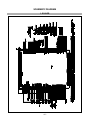
SCHEMATIC DIAGRAM
1. SCALER
- 25 -
2. MICOM
- 26 -
3. POWER
- 27 -
4. CONNECTOR/JACKS
- 28 -
Blank Page1
Blank Page2
P/NO : 3828TSL064F
May. 2004
Printed in Korea