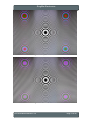
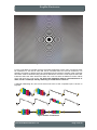
1
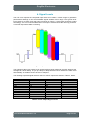
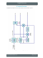
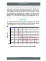
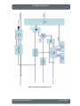
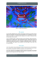
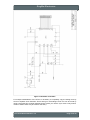
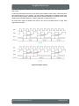
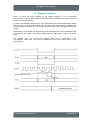
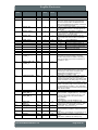
SingMai Electronics PT5 User Manual Multi-standard Video Decoder IP core with sample rate converter and 3D comb filter Revision 1.0 22nd May 2015 PT5 User Manual Revision 1.0 Page 1 of 33 SingMai Electronics Contents 1. Introduction ............................................................................................................................ 3 2. PT5 File Structure .................................................................................................................. 5 3. Signal Interconnections ......................................................................................................... 6 4. Signal Levels ......................................................................................................................... 9 5. Technical Overview ............................................................................................................. 10 PT5_Register_control.v ....................................................................................................... 11 Vid_nco.v ............................................................................................................................. 11 BLO.v .................................................................................................................................. 11 Demod.v .............................................................................................................................. 12 Demod_LPF.v ..................................................................................................................... 13 Remod.v .............................................................................................................................. 14 SPG.v .................................................................................................................................. 14 Line_delays.v ...................................................................................................................... 16 Comb_filter.v ....................................................................................................................... 16 HF_remod.v ......................................................................................................................... 20 Proc_amp.v ......................................................................................................................... 20 6. 3D comb filter and SDRAM interface .................................................................................. 21 7. Analogue interface ............................................................................................................... 22 8. Synchronising modes .......................................................................................................... 25 10. Register interface .............................................................................................................. 27 11. Register descriptions ......................................................................................................... 28 12. Specification ...................................................................................................................... 31 Tables Table 1 PT5 File Structure ......................................................................................................... 5 Table 2 PT5 Signal Interconnections ........................................................................................ 8 Table 3 YCbCr Output Signal Levels......................................................................................... 9 Table 4 PT5 Register description. ........................................................................................... 30 Table 5 PT5 Specification ........................................................................................................ 31 Figures Figure 1 PT5 Block Symbol. ...................................................................................................... 6 Figure 2 Input CVBS codes. ...................................................................................................... 9 Figure 3 PT5 block diagram (Part 1). ...................................................................................... 10 Figure 4 Demodulation low pass filter frequency response 0-6.75MHz .................................. 13 Figure 5 PT5 block diagram (Part 2). ...................................................................................... 15 Figure 6 Zone plate: Notch filter .............................................................................................. 17 Figure 7 Zone Plate: Line comb .............................................................................................. 17 Figure 8 Zone Plate: Frame comb ........................................................................................... 18 Figure 9 NTSC comb failure .................................................................................................... 18 Figure 10 Comb Failure display 1 ............................................................................................ 19 Figure 11 Comb Failure display 2 ............................................................................................ 20 Figure 12 PT5 Analogue input stage schematic. ..................................................................... 23 Figure 13 PT5 ADC schematic. ............................................................................................... 24 Figure 14 PT5 External VCO Schematic ................................................................................. 25 Figure 15 Output Timing .......................................................................................................... 26 Figure 16 PT5 Register timing ................................................................................................. 27 Figure 17 NTSC 75% Colour Bars .......................................................................................... 32 Figure 18 NTSC K-factor ......................................................................................................... 32 Figure 19 NTSC Multiburst ...................................................................................................... 33 Figure 20 NTSC Component Noise ......................................................................................... 33 PT5 User Manual Revision 1.0 Page 2 of 33 SingMai Electronics 1. Introduction PT5 is a video decoder accepting all NTSC and PAL encoded composite video inputs, including 960H – 36MHz sampling, and 1280H – 54MHz sampling, and producing an adaptive 2D/3D combed component output with 12 bit Y and 10 bit Cb/Cr outputs (4:4:4 or 4:2:2). The input to the IP core is 10 or 12 bit digital composite video. PT5 has two synchronization modes: 1. The PT5 provides a PWM output to control an analogue voltage controlled oscillator at a nominal frequency of 27MHz. All sync separation is performed by the PT5. This is the default mode of operation. 2. The input is fixed 27MHz clock frequency. The PT5 rate converts this internally using a sample rate converter and digital PLL. This allows the PT5 to accept inputs from video demodulators without re-sampling as well as accepting wide range inputs such as from a VCR or laser disc. All sync separation is also performed internally to the PT5. The composite video input is passed through a decimating sample rate converter (in sync mode 2 – in sync mode 1 this is bypassed) which interpolates the data down to an average 13.5MHz output locked to the video line frequency. A numerical controlled oscillator determines the phase of the interpolation. The output from the SRC is the 13.5MHz interpolated video and a video enable signal which indicates a valid sample. The decoder is a complementary design. The colour burst from the input composite video is used to phase lock the subcarrier oscillator which then addresses a sine and cosine LUT. These waveforms are used to demodulate the colour component of the composite waveform. The resulting U and V colour components are then low pass filtered and re-modulated using the delayed sine and cosine waveforms. This combined chroma signal is then subtracted from the delayed composite signal to create a notched luminance signal. The U and V signals are then combed using a 3 line comb filter and a symmetric 3D frame comb filter whilst the notched luminance is applied to compensating line delays for the comb adaptation. The amplitude difference across the comb filter taps are compared to determine which of the modes has the least error – the notch mode or one of the two combed modes. The comb mode is selected on a pixel by pixel basis. The difference is then taken between the U/V inputs to the comb and the selected output of the comb filter. If the filter is combing correctly that difference will be the high frequency luma signal. This HF luma is then remodulated using the delayed sine and cosine waveforms and added to the line delayed notched luma to create a full bandwidth luma output, (when in comb mode). This luma signal and the combed U and V are then amplified and scaled in the processing amplifier before being output as YCbCr outputs at 13.5MHz suitable for driving a DAC or for further video processing. The notched luma signal is also used to derive the timing signals. The luma is sliced at the mid point sync pulse amplitude and multiplied by 15 coefficients that are designed such that when the midpoint of the falling edge of the line sync pulse is coincident with the midpoint of the filter coefficients the summed output of the multiplier over that window is zero. This forms our horizontal phase detector for the line locked clock. The error value is then added to a fixed value input to a ratio counter. The lower bits of the ratio counter form a phase word which is used to drive the input sample rate interpolator or converted to a PWM output to drive the control voltage of the external voltage controlled oscillator. PT5 User Manual Revision 1.0 Page 3 of 33 SingMai Electronics The composite video is also filtered and the horizontal line locked counter is used to extract the vertical sync and determine the odd/even frame information. This ‘raw’ horizontal and vertical sync information is fed to a sync pulse generator which produces all the synchronising signals required for the decoder. Control and status registers are written to and read from using a conventional 8 bit wide microprocessor interface. PT5 User Manual Revision 1.0 Page 4 of 33 SingMai Electronics 2. PT5 File Structure PT5 is supplied as a flat file structure but the design is hierarchical. The top level design file is called PT5.v, a Verilog file; all inputs and outputs to the decoder come from this file. The design is hierarchical with PT5 instantiating three Verilog modules; PT5_Register_control.v, Vdec.v and SDRAM_control.v (for the external 3D comb memory). Register_control.v provides the control interface to PT5. Vdec.v is the main decoder module and instantiates 17 modules, three of which instantiate a fourth level of modules. The PT5 module hierarchy is shown in Table 1. Top Level Second Level Third Level Fourth level PT5_Register Control.v Vid_nco.v PT5.v HPLL.v SPG.v BLO.v Demod.v Demod_LPF.v (UDemod_LPF.v, VDemod_LPF.v) Remod.v Line_delays.v Vdec.v time_nco.v vid.v rnd_sat.v CosSin_ROM.v Vdec_rams.v Ram_infer_generic.v Comb_filter.v HF_remod.v Proc_amp.v Table 1 PT5 File Structure PT5 User Manual Revision 1.0 Page 5 of 33 SingMai Electronics 3. Signal Interconnections The PT5 graphic block symbol is shown in Figure 1. Figure 1 PT5 Block Symbol. The PT5 signal interconnections are described in Table 2, below. Inputs Signal CVBS_in[11:0] Clk27 PT5 User Manual Revision 1.0 Description Digitised composite 12 bit straight binary video input. The data should be valid during the rising edge of the 27MHz clock. If the input is less than 12 bit the bottom unused bits should be connected to ground. This is the free-running 27MHz to PT5 (if using the sample rate converter) or the voltage controlled oscillator input (nominal 27MHz). The rising edge of this clock is used to latch the CVBS_in data. For 960H operation the clock Page 6 of 33 SingMai Electronics Clk54 Clk108 Reg_Clk RESETn A[7:0] Din[7:0] PT5_CSn PT5_WRn Y_framecomb1[11:0] U_framecomb1[9:0] V_framecomb1[9:0] Y_framecomb2[11:0] U_framecomb2[9:0] V_framecomb2[9:0] should be 36MHz and for 1280H operation the clock should be 54MHz. Twice input clock input (54/72/108MHz) used to generate the write enables for the line comb memories. The rising edge of this clock should be coincident with the rising edge of Clk27. 108MHz input clock used by the SDRAM controller (and is the main clock to the SDRAM). The rising edge of this clock should be coincident with the rising edge of Clk27. Clock to the register control module. May be connected to the Clk27 input if that clock is continuous and stable. Active low reset signal for all flip flops. Asserting this input sets all the control registers to their default value. Control address bus input used to select the control register to be written to/read from. Control data input bus. Control chip select input, active low. Used in combination with the WRn input to control writing to the control registers. Active low write enable input. Used in combination with the PT5_CSn input to control writing to the control registers. Input from first frame delay (external memory). Input from first frame delay (external memory). Input from first frame delay (external memory). Input from second frame delay (external memory). Input from second frame delay (external memory). Input from second frame delay (external memory). Outputs Signal Y_out[11:0] Cb_out[9:0] Cr_out[9:0] Clamp Hout Clamp PT5_Active_video PT5_FFlag PT5_VFlag Clk_en VCO_PWM PT5_S625_525n PAL_NTSCn Burstgate Y_comb_delay_out[11:0] U_comb_delay_out[11:0] V_comb_delay_out[11:0] PT5_Register_out[7:0] PT5 User Manual Revision 1.0 Description Luma (Y) output from PT5. Data is valid on the rising edge of Clk27 if Clk_en is high. Chroma (Cb) output from PT5. Data is valid on the rising edge of Clk27 if Clk_en is high. Chroma (Cr) output from PT5. Data is valid on the rising edge of Clk27 if Clk_en is high. Programmable clamp pulse to analogue input stage. Horizontal sync output pulse. Programmable clamp output pulse for black level analogue clamping if required. Active video flag (conforms to BT656 specification). Frame flag output (conforms to BT656 specification). Field flag output (conforms to BT656 specification). Data enable signal for the Y, Cb and Cr outputs (nominal 13.5MHz). See Chapter 7, ‘Synchronising Modes’. Pulse width modulated output used for the control of a voltage controlled oscillator in sync mode 1.. Signal used to indicate whether 525 line (=0) or 625 line (=1) is selected. Signal used to indicate whether PAL (PAL/PAL-N/PAL-M = 1) or NTSC (=0) decoding is selected. Horizontal timing output used for external SDRAM controller. Output to external frame comb memory. Output to external frame comb memory. Output to external frame comb memory. Control output data bus. Outputs the control/status register data selected by the A[7:0] bus, independent of PT5_CSn or Reg_clk. Page 7 of 33 SingMai Electronics PT5_Test[1:0] Test outputs. Do not connect. Table 2 PT5 Signal Interconnections The Verilog instantiation for PT5 is shown below: // Instantiate video decoder PT5 PT5_inst ( .CVBS_in(CVBS_in_sig) , .Clk27(Clk27_sig) , .Clk54(Clk54_sig) , .Clk108(Clk108_sig) , .Reg_clk(Reg_clk_sig) , .RESETn(RESETn_sig) , .A(A_sig) , .Din(Din_sig) , .PT5_CSn(PT5_CSn_sig) , .PT5_WRn(PT5_WRn_sig) , .Y_framecomb1(Y_framecomb1_sig) , .U_framecomb1(U_framecomb1_sig) , .V_framecomb1(V_framecomb1_sig) , .Y_framecomb2(Y_framecomb2_sig) , .U_framecomb2(U_framecomb2_sig) , .V_framecomb2(V_framecomb2_sig) , .Y_out(Y_out_sig) , .Cb_out(Cb_out_sig) , .Cr_out(Cr_out_sig) , .Clamp(Clamp_sig) , .Hout(Hout_sig) , .PT5_Active_video(PT5_Active_video_sig) , .PT5_FFlag(PT5_FFlag_sig) , .PT5_VFlag(PT5_VFlag_sig) , .Clk_en(Clk_en_sig) , .VCO_PWM(VCO_PWM_sig) , .PT5_S625_525n(PT5_S625_525n_sig) , .PAL_NTSCn(PAL_NTSCn_sig) , .Burstgate(Burstgate_sig) , .Y_comb_delay_out(Y_comb_delay_out_sig) , .U_comb_delay_out(U_comb_delay_out_sig) , .V_comb_delay_out(V_comb_delay_out_sig) , .PT5_Register_out(PT5_Register_out_sig) , .PT5_test(PT5_test_sig) ); PT5 User Manual Revision 1.0 // input [11:0] CVBS_in_sig // input Clk27_sig // input Clk54_sig // input Clk108_sig // input Reg_clk_sig // input RESETn_sig // input [7:0] A_sig // input [7:0] Din_sig // input PT5_CSn_sig // input PT5_WRn_sig // input [11:0] Y_framecomb1_sig // input [9:0] U_framecomb1_sig // input [9:0] V_framecomb1_sig // input [11:0] Y_framecomb2_sig // input [9:0] U_framecomb2_sig // input [9:0] V_framecomb2_sig // output [11:0] Y_out_sig // output [9:0] Cb_out_sig // output [9:0] Cr_out_sig // output Clamp_sig // output Hout_sig // output PT5_Active_video_sig // output PT5_FFlag_sig // output PT5_VFlag_sig // output Clk_en_sig // output VCO_PWM_sig // output PT5_S625_525n_sig // output PAL_NTSCn_sig // output Burstgate_sig // output [11:0] Y_comb_delay_out_sig // output [9:0] U_comb_delay_out_sig // output [9:0] V_comb_delay_out_sig // output [7:0] PT5_Register_out_sig // output [1:0] PT5_test_sig Page 8 of 33 SingMai Electronics 4. Signal Levels The PT5 core requires the composite input levels to be within a certain range to guarantee performance although it can accommodate signals outside of this range. The typical 10-bit input codes for a 100% colour bar input are shown in Figure 2. 12 bit inputs should be scaled accordingly. It is not recommended that an 8 bit input is used because this will only produce a 7 bit luma output with visible contouring. Figure 2 Input CVBS codes. The analogue video input needs to be clamped before being applied to the ADC because the average DC varies widely. A sync tip clamp is adequate as the PT5 restores the black level automatically. A suitable circuit is shown in Chapter 7. The resulting expected signal levels for the PT5 YCbCr outputs are shown in Table 3, below. 10-bit YCbCr signal Levels 100/0/100/0 Y White 940 Yellow 840 Cyan 678 Green 578 Magenta 426 Red 326 Blue 164 Black 64 Cb 512 64 663 215 809 361 960 512 Cr 512 585 64 137 887 960 439 512 Table 3 YCbCr Output Signal Levels PT5 User Manual Revision 1.0 Page 9 of 33 SingMai Electronics 5. Technical Overview A simplified block diagram of the PT5 video decoder front end is shown in Figure 3. Figure 3 PT5 block diagram (Part 1). PT5 User Manual Revision 1.0 Page 10 of 33 SingMai Electronics Each of the PT5 Verilog modules is each briefly discussed below. The input to the PT5 should be 12-bit composite video input sampled at 27MHz (NTSC/PAL), 36MHz (960H) or 54MHz (1280H), with typical input levels as shown in Figure 2. The technical description will assume 27MHz (NTSC/PAL) operation. PT5_Register_control.v PT5 is controlled via a conventional 8 bit microprocessor control bus. The register interface is discussed in Chapter 10 and the register descriptions can be found in Chapter 11. Writing to a register involves setting up the required register address and strobing both PT5_CSn and PT5_WRn low. Data is written during the PT5_WRn low period synchronous with the Reg_Clk rising edge. All of the control registers and the status registers are read asynchronously using the A[7:0] input to select the register. Strobing RESETn low loads the default values into the registers. Vid_nco.v The role of the sample rate converter depends on the synchronisation mode selected. In lock mode [1] the sample rate converter is bypassed and it acts only as a decimating filter, allow us to sample drop the 27MHz input to 13.5MHz. In lock mode [2] the front end is running at a fixed 27MHz clock rate. The sample rate converter clocks a ratio counter at 27MHz and provides a 13.5MHz enable output used to gate the back end of the decoder. The ratio counter also provide a phase word which is used to interpolate the ‘mid-point’ of the video samples and map the incoming video onto the new line locked clock domain. The ratio counter is adjusted by adding/subtracting a phase error signal – generated by the horizontal phase detector in the HPLL.v module – to the seed value. The interpolator uses a Farrow structure; the output from the sample rate converter is an average 13.5MHz enable signal (Clk_en) and the interpolated composite video. Note that the PT5 is clocked at 27MHz (Clk27) which enabled with Clk_en (nominally 13.5MHz). Later description will refer to this as the ’13.5MHz clock’. BLO.v The subcarrier frequency appropriate to the selected colour standard is generated using a 32 bit ratio counter clocked from the 13.5MHz line locked clock. ratio Fsc θ sc subcarrier seed phase change per line pixels per line 13.5MHz 360 232 The top 11 bits of this ratio counter (the phase word) are used by the demodulator to generate the sine and cosine waveforms. For the demodulation to correctly operate the generated subcarrier must be frequency and phase locked to the composite video subcarrier which is done by measuring the amplitude of the demodulated and low pass filtered V output during the colour burst. If the frequency and PT5 User Manual Revision 1.0 Page 11 of 33 SingMai Electronics phase of the free-running subcarrier and the colour burst are the same then this error will be zero. The reference for the BLO is the demodulated and filtered V output from the Demod_LPF. 32 samples of this waveform are taken during the burst pulse; the burst gate pulse from the SPG is used for this purpose. After the 32 samples the accumulated V demod value is stored for one line Two lines are then added for a degree of noise suppression and an error signal is then formed using fractions of the proportional signal and also a recursively filtered (integral) version. The sign of the demodulated V burst is also used by the sync pulse generator to lock up the PAL switch in the case of PAL standards. The seed word is thus modified using the phase error signal until the input colour burst and the ratio counter are phase locked. The subcarrier seed is selected automatically with the colour standard selected. Demod.v The NTSC chroma signal is originally generated as follows: chroma U sinωt V cosωt When the burst lock loop (BLO) is in lock, the frequency and phase will be the same as when the signal was being modulated. Thus, multiplying the composite video by the sine and cosine of the same frequency and phase gives the following: U ' U sin ωt V cos ωt sin ωt U ' U sin 2 ωt V sin ωt cos ωt 1 cos 2 ωt V U ' U 2 2 sin ωt cos ωt 2 U ' U U cos 2 ωt V sin 2 ωt 2 2 2 …and for the V component: V ' U sin ωt V cos ωt cos ωt V ' U sin ωt cos ωt V cos 2 ωt V ' U 1 cos 2 ωt 2 sin ωt cos ωt V 2 2 V ' U sin 2 ωt V V cos 2 ωt 2 2 2 PT5 User Manual Revision 1.0 Page 12 of 33 SingMai Electronics The lower 9 bits of the 11-bit phase output from the BLO, (burst locked oscillator), are used to address sine and cosine lookup tables. These 9 bits comprise the phase angle, at subcarrier frequency, within a single quadrant and the top two bits are the quadrant – this method saves memory by only requiring a single quadrant to be stored in the LUT. The output of the CosSin_ROM.v LUT is a 24 bit word; 12 bits cosine and 12 bits sine. The quadrant signs are used to manipulate the sine and cosine data such as to construct a full waveform. The signs are also modified by the PAL switch signal from the SPG in the case of PAL colour standards. The reconstructed sine and cosine waveforms are then multiplied by the 13.5MHz line-locked composite video from the sample rate converter. The output of the sine channel is the demodulated U signal and the cosine channel output is the demodulated V output. Two overrange bits are catered for at the output to allow for twice subcarrier frequency components (removed by the subsequent low pass filter) and for cross-colour components (removed by the comb filter). Demod_LPF.v The output of the demodulator comprises twice frequency components and cross colour as well as the required base-band demodulated chroma. The output is therefore low pass filtered using a 23 tap FIR filter with a nominal -3dB bandwidth of 1.3MHz. The filter provides better than -50dB rejection of all out of band component signals. The output of the filter is the clean ‘simple’ demodulated U and V. The low pass filter responses are shown below. In p h a s e F ilt e r F r e q u e n c y R e s p o n s e 0 -10 Magnitude in dB -20 -30 -40 -50 -60 -70 -80 -90 -100 0 1 2 3 4 5 6 7 F r e q u e n c y in M H z Figure 4 Demodulation low pass filter frequency response 0-6.75MHz PT5 User Manual Revision 1.0 Page 13 of 33 SingMai Electronics Remod.v The demodulated and low pass filtered chroma signal is then frequency shifted back to the subcarrier frequency and subtracted from the composite video to form a notched luma signal. The complementary nature of this architecture ensures there is no missing information through to the comb filter. The sine and cosine waveforms from the demodulator are delayed to compensate for the demodulator low pass filter delay; the waveforms are then multiplied by the ’simple’ U and V outputs of the low pass filter and then added together to reconstruct a chrominance signal centred on the CVBS referenced subcarrier waveform. This chrominance signal is then subtracted from the delayed composite video which provides a clean, notched luma signal with a notch bandwidth equal to the demodulator low pass filter bandwidth of 1.3MHz. This notched luma and the ‘simple’ demodulated U and V chroma are then applied to the comb filter. SPG.v The SPG (sync pulse generator) module provides all of the control signals for the PT5. The horizontal and frame outputs of the HPLL are used to synchronise two counters, one vertical and one horizontal. From these counters various outputs are decoded; some of the outputs are programmable from the control registers. Outputs include: Burstgate: A 32 pixel wide pulse used to accumulate demodulated V_demod outputs during the colour burst for the burst locked loop. Active_video: A moveable position/ fixed width (1440 clock periods) horizontal output pulse used for the BT656 formatting. D1_VFlag: Vertical field pulse used for the BT656 formatting. D1_FFlag: Vertical frame pulse used for the BT656 formatting. Clamp: A programmable output pulse intended for black level or sync tip clamping for the analogue front end. A simplified block diagram of the PT5 video decoder back end is shown in Figure 5. PT5 User Manual Revision 1.0 Page 14 of 33 SingMai Electronics Figure 5 PT5 block diagram (Part 2). PT5 User Manual Revision 1.0 Page 15 of 33 SingMai Electronics Line_delays.v The notched luma and the U and V demodulated outputs are applied to the comb delay memory. The line delays are formed by separate instantiations of the Vdec_ram.v block which in turn call the generic single port RAM module, ram_infer_generic.v. This avoids the memory being device or vendor specific. The RAM is addressed a 10 bit line locked counter address and a read before write operation is performed on the RAM using a delayed version of the horizontal counter LSB signal as the control line. The 54MHz clock is used to create the write enable signals to avoid using both edges of the 27MHz. The 3D comb uses an external SDRAM device and the description of the external memory requirements can be found in Chapter 6. Comb_filter.v The demodulated ‘simple’ U and V outputs also contain high frequency luma information, (cross colour). This can removed as the chroma information has a known line based phase relationship whereas the HF luma and cross colour does not. The comb filter provides this filtering operation. The comb filter is a chrominance comb in that it reinforced the chroma signals whilst canceling the cross colour components. The 3D comb filter, (using external memory), is a symmetric frame comb; for example the frame tap delay for NTSC/PAL-M is 525 lines and for PAL/PAL-N it is 625 lines. The frame comb filter for NTSC is (1/4*0F + 1/2*1F + 1/4*2F) (1 frame spacing) and for PAL (1/4*0F + 1/2*1F + 1/4*2F) + [(0F – 2F) * PALswitch] (crosstalk cancellation). The use of the crosstalk cancellation in PAL permits single frame taps (than the usual 2 frame taps) with a much closer aperture giving more effective combing when there is motion. The line comb filter operates on the centre tap of the frame comb delay; i.e. 1 frame delayed from the input video). The line comb filter for NTSC is (1/4*0H + 1/2*1H + 1/4*2H) (1 line spacing) and for PAL (1/4*0H + 1/2*1H + 1/4*2H) + [(0H – 2H) * PALswitch] (crosstalk cancellation). The use of the crosstalk cancellation in PAL permits a 3 line comb (than the usual 5 line comb) with a much closer aperture giving more effective combing. The zone plate images for each of the PT5 comb filter modes are shown in Figures 6-8. PT5 User Manual Revision 1.0 Page 16 of 33 SingMai Electronics Figure 6 Zone plate: Notch filter Figure 7 Zone Plate: Line comb PT5 User Manual Revision 1.0 Page 17 of 33 SingMai Electronics Figure 8 Zone Plate: Frame comb For the comb filters to operate correctly the phase relationship of the colour component must be maintained. If not the HF luma will not be cancelled and can even be reinforced. It is therefore necessary to detect when the comb filters fail and switch to a better mode. Normally this failure mode is detected using luminance differences across the comb taps but there are instances where the same luminance value can occur but there are different chroma values which still cause the comb to fail. The PT5 comb adaptation detects value differences in luma, U and V comb taps thereby detecting all comb failure instances. A diagram illustrating why this occurs across two lines of the composite input is shown in Figure 9. C00041.CDR Figure 9 NTSC comb failure PT5 User Manual Revision 1.0 Page 18 of 33 SingMai Electronics The failure value of each comb mode (including notch mode) is compared and the lowest error mode selected on a pixel by pixel basis. The chosen U and V outputs from the filter are input to the processing amplifier. If the U and V outputs of the comb filter is subtracted from the delayed ‘simple’ U and V inputs to the comb (delayed by the comb filter delay) the output will be the recovered high frequency luma. This high frequency luminance signal is then sent to the HF luma module to be added to the notched luma. The chosen comb mode may also be displayed on the output by enabling the view comb fail bit in register $03. The image in Figure 10 shows a frame of video with little motion. The green areas are where the frame comb is being used, the blue areas show where the line comb is selected and the red areas show where the notch filter is used. Figure 10 Comb Failure display 1 In Figure 11 there is faster motion and in these areas the line comb is mostly used, (blue). PT5 User Manual Revision 1.0 Page 19 of 33 SingMai Electronics Figure 11 Comb Failure display 2 HF_remod.v The comb filter separates the non coherent high frequency luma from the coherent chroma signal. The high frequency luma may then be remodulated onto the delayed sine and cosine waveforms and added to the delayed notched luma to form the full bandwidth luma signal. When the comb filter is in ‘simple’ mode the bandwidth of the chroma is reduced so some luma bandwidth is still recovered. The HF remodulator works in exactly the same way as the Remod.v module except that it uses the one line delayed sine, cosine (regenerated from the delayed phase word) and notched luma as these are the centre point of the comb filter. The sine and cosine are multiplied by the high frequency U’ and V’ respectively, added together and then added to the notched luma. Because the decoder is a completely complementary design, in comb mode, the full bandwidth luma signal is then recovered. This luma signal is then input to the processing amplifier. Proc_amp.v The U and V outputs of the comb filter and the luminance output of the HF_remod module are then co-timed in the processing amplifier, Proc-amp.v. The luma signal then has the black level restored by having the sync offset removed (black level, back porch value). The U and V signals are also amplified and blanking signals are also applied. The horizontal and vertical window and comb adaptation mode may also be viewed and the colour bars patterns are also multiplexed into the output if selected. PT5 User Manual Revision 1.0 Page 20 of 33 SingMai Electronics 6. 3D comb filter and SDRAM interface The 3D frame comb filter utilizes the same phase relationship in the subcarrier but a pixel accurate frame delay ensures the pixels are exactly spatially aligned. Even on the most complex images near perfect, artefact free decoding is the result: (I say near perfect because frame combs are very sensitive to clock jitter and clock jitter as little as 1ns over the frame delay period can result in residual subcarrier. PAL also has an addition subcarrier offset of 25Hz which means perfect cancellation cannot occur even with a frame comb). But of course, the frame comb does not answer all our problems. We are now looking across comb filter taps of one frame, a delay of 40ms in the case of PAL. Whereas any difference spatially across 2 lines (with interlace) caused the line comb filter to fail; now any difference temporally across 40ms will cause the frame comb to fail, with similar artefacts being created. The 3D comb filter is a symmetrical frame comb i.e. two frame delays are required. One write port and two read ports are required. The output to the 3D comb is a 32 bit data bus, 12 bits of Y and 10 bits each of Cb and Cr (Y_comb_delay_out[11:0], U_comb_delay_out[9:0], V_comb_delay_out[9:0]. The data is valid on the rising edge of the 27MHz when the Clk_en output (13.5MHz average) is high. (See the output timing, Figure 20). The inputs from the comb filter delay are also 32 bits, one for the first frame delay (Y_framecomb1[11:0], U_framecomb1[9:0], V_framecomb1[9:0]) and one for the second frame delay (Y_framecomb2[11:0], U_framecomb2[9:0], V_framecomb2[9:0] ) -total delay 2 frames. The first frame delay requires an exact delay of ((525 lines x 858 pixels) – 6 pixels) for NTSC and ((625 lines x 864 pixels) – 6 pixels) for PAL. The second frame delay requires an exact delay of ((1050 lines x 858 pixels) – 6 pixels) for NTSC and ((1250 lines x 864 pixels) – 6 pixels) for PAL. The PAL_NTSC output from the PT5 can be used to select the delay. The field delay requires an exact delay of ((262 lines x 858 pixels) – 6 pixels) for NTSC and ((312 lines x 864 pixels) – 6 pixels) for PAL. The 6 pixel offset is to allow for the comb signal processing in the PT5. The easiest way to provide the external delay is to use the SingMai PT20 SDRAM controller which was designed for this purpose. It seamlessly interfaces to the PT5 and provides both the field and frame comb delays for both NTSC and PAL. It was designed for the Micron MT48LC16M16 SDRAM (2 devices) and supports the full 32 bit data bus but other SDRAM devices can also be accepted. The 3D frame comb filter utilizes the same phase relationship in the subcarrier but a pixel accurate frame delay ensures the pixels are exactly spatially aligned. Even on the most complex images near perfect, artifact free decoding is the result: (I say near perfect because frame combs are very sensitive to clock jitter and clock jitter as little as 1ns over the frame delay period can result in residual subcarrier. PAL also has an addition subcarrier offset of 25Hz which means perfect cancellation cannot occur even with a frame comb). PT5 User Manual Revision 1.0 Page 21 of 33 SingMai Electronics 7. Analogue interface Figures 12 and 13 illustrate an example analogue front end interface for the PT5 (as used on the SB9 evaluation board). The composite video input is terminated in 75Ω and then AC coupled into a single supply amplifier, U8, which is biased using a mid-rail reference voltage from U10. D2 prevents over and under-voltage excursions of the video affecting the amplifier input stage. U20 forms an anti-aliasing filter. To simplify the design of the filter, for NTSC/PAL operation, the ADC is over-sampled at 54MHz (instead of 27MHz) and immediately decimated to 27MHz in the PT5. The anti-aliasing filter is flat to 12MHz (for 1280H operation) and rejects >15dB at 18MHz (for 960H operation). The anti-aliasing filter also has gain to match the input to the ADC. If the PT5 is to be used for NTSC/PAL only the filter values can be altered to match and the ADC sampled at 27MHz. Because the input is AC coupled it need to be DC restored before the ADC. U9 forms a synctip clamp, clamping the most negative part of the video waveform to the VCLAMP voltage (the negative reference of the ADC). This ensures that the PT5 will separate the syncs correctly. The black level value of the input is determined by the PT5 and corrected internally ensuring stable blacks in the output luma. To facilitate other front end architectures a clamp pulse output from the PT5 is provided; it is programmable in position and width. It may be used provide a sync tip clamp, as implemented in the AD9845B, or a black level clamp to a fixed value, which should be approximately 10 bit digital value 25610 or 12 bit value 102410. In the latter case the auto black level feature of the PT5 should be turned off. The ADC (U12) is an ADI AD9237. For 1280H operation the 65MHz version should be used – for NTSC/PAL and 960H operation, the 40MHz version is adequate. The output of the ADC is 12 bit straight binary composite video at 27/36/54MHz which may be applied directly to the PT5 video decoder. PT5 User Manual Revision 1.0 Page 22 of 33 SingMai Electronics Figure 12 PT5 Analogue input stage schematic. PT5 User Manual Revision 1.0 Page 23 of 33 SingMai Electronics Figure 13 PT5 ADC schematic. For multiple instantiations of the PT5 it is necessary to completely copy the design as they work on separate clock domains. Some saving on the analogue front end can be made by using a dual ADC (but it needs separate clocks unless you use the sync mode 2 only when a common 27MHz clock may be used for the ADC). PT5 User Manual Revision 1.0 Page 24 of 33 SingMai Electronics 8. Synchronising modes There are two synchronizing modes for the PT5. In modes [1] and [2] the sync separation and the horizontal phase locked loop (HPLL) are internal to the PT5; they differ only in the control of the output frequency. In the first method the PT5 controls the frequency of an external voltage controlled oscillator (VCO); see Figure 14. Figure 14 PT5 External VCO Schematic The PT5 generates a free-running horizontal sync pulse at the correct frequency for the standard selected. It compares the phase of the falling edge of this pulse with the falling edge of the horizontal sync pulse generates a correlation error ‘voltage’ which is used to adjust the 27MHz clock input such that the pulses are coincident. The error output from the PT5 is available as a pulse width modulated signal at the VCO_PWM port. In Figure 19 this output is buffered to avoid logic level variations affecting the loop and then filtered and buffered before driving the analogue input of a crystal VCO. The output from the VCO is then the 27MHz input (Clk27) of the PT5. When using the VCO the Clk_en output is at a fixed rate of 13.5MHz, see Figure 20. It is possible to force the VCO to maximum, minimum, and 50% values using control register 3. When using the VCO the sample rate converter must be bypassed, (control register 3, bit 2). It is necessary to use a crystal VCO to ensure the jjitter is low enough for the 3D comb filters to work. However some inputs, such as from a VCR tape source or a mechanically scanned laserdisc, can have a horizontal frequency too far out of range or are too unstable in the short term for the VCO to be able to lock. Under these circumstances another synchronization mode is available. This mode uses a sample rate converter (SRC). The VCO_PWM (if used) should be set to its fixed 50% value or if the VCO is not used a fixed crystal 27MHz clock may be used. The HPLL phase error is fed directly to the sample rate converter which modulates the Clk_en output such there are the correct number of samples in the line and so that the recovered horizontal sync and the internally generated horizontal sync are aligned. Fine adjustment of the phase is performed by interpolating the video to a sub-pixel accuracy using the phase word value and a Farrow filter as the interpolator. Using the sample rate converter means there is not a constant rate of video values appearing at the output of the PT5. Although the average value of the Clk_en is 13.5MHz the peak value is 27MHz; however the correct number of samples will always be present in any one video PT5 User Manual Revision 1.0 Page 25 of 33 SingMai Electronics line (864 for 625 line or 858 for 525 line standards). See Figure 15 for the output timing in SRC mode. To latch the data output from the PT5 in either synchronization mode a latch, clocked at Clk27 and enabled with Clk_en is required. The luma output is effectively at 13.5MHz sample rate, as are the chroma outputs, but these may also be sample dropped to 6.75MHz as they have already been bandwidth limited to 1.3MHz (-3dB) and no aliasing will occur. All modes also require a 54MHz clock input to the PT5 (2x 27MHz) which is rising edge aligned with the Clk27. Figure 15 Output Timing PT5 User Manual Revision 1.0 Page 26 of 33 SingMai Electronics 10. Register interface Figure 16 shows the timing diagram for the register interface; it is a conventional microprocessor interface. Each register is selected via an 8 bit address bus. Writes to unused register locations are ignored. To write to the selected register the PT5_CSn (chip select) input must be asserted low. Whilst this is low the PT5_WRn must be taken low. An internal write enable pulse is created at the next rising edge of the Reg_clk clock and writing occurs at the next clock edge following that enable. For the write to occur reliably the address (A[7:0]) and data (Din[7:0]) must be stable and valid during the PT5_WRn pulse. The minimum width of the PT5_WRn pulse is 110ns for a 27MHz clock. The address input also selects the register data that is presented on the PT5_Register_out[7:0] bus. This output is independent of the other control signals or the Reg_clk clock. Figure 16 PT5 Register timing PT5 User Manual Revision 1.0 Page 27 of 33 SingMai Electronics 11. Register descriptions The following table lists all of the control and status registers. All of the registers are 8 bit wide although some are concatenated together to create longer words. Asserting the RESETn input sets all the registers to their default values. Unused bits read back as ‘0’s. Note that if the Auto_register_select bit is set to ‘1’ (Control register 1, bit 7), most of the timing and gain registers will not affect the PT5 as the default values will be used instead. However the registers will still be loaded with new values if written to and the reading will reflect the programmed values and not the default values. Register Offset Register Name R/W Control 1 Auto register select R/W Bit Value Default Value Description Control $00 Auto Colour Standard Colour standard $01 Control 2 View comb fail 7 1 6 5 0 0 4-0 000 7 0 6 5 0 0 4 3 2-0 0 0 100 If set to ‘1’ the timing and gain values for each colour standard (in auto or manual mode) are automatically programmed to their default values. If set to ‘0’ the timing and gain registers may be programmed by the user (for example for standards such as PAL60 or NTSC443). Not used If ‘1’ selects the colour standard based on the detected line standard and the control register 1 bit 1 status. If ‘0’ the colour standard is manually set using control register 1 bits [4:0]. Line standard Bit 1 Auto standard 525 0 NTSC 525 1 PAL-M 625 0 PAL 625 1 PAL-N Bits [4:0] Colour standard 00000 NTSC-M 00001 NTSC-J 00010 PAL-M 00100 PAL 00110 PAL-N 01000 960H (NTSC) 01100 960H (PAL) 10000 1280H (NTSC) 10100 1280H (PAL) R/W Frame comb disable Comb mode PT5 User Manual Revision 1.0 Allows the selected comb mode to be displayed if set to ‘1’. Comb mode Displayed colour Simple (notch) Red Line comb Blue Frame comb Green Not used If set to ‘1’ the frame comb is disabled (comb adapts between line and notch. Not used. Not used Bits [2:0] Comb mode 000 Forces notch only mode 001 Forces line comb only mode 010 Forces frame comb only mode 011 Not used 1xx Automatically selects the comb mode from all of the above modes, (subject to the status of bit 5). Page 28 of 33 SingMai Electronics Register Offset $02 Register Name Bit Value Default Value Description 7-6 5 00 1 Demod_VBI 4 0 Bypass_demod 3 0 Bypass_SRC 2 1 PWM_control 1-0 00 Not used Enables the automatic black level if set to ‘1’. The back porch value is measured and subtracted from the composite video. If enabled the luma offset control (Registers $04 and $05) is added to the measured black level offset. If set to a ‘1’ the vertical blanking interval signals are demodulated. If set to ‘0’ the VBI signals are passed ‘flat’. If = ‘1’ the chroma demodulator is bypassed (Cb/Cr outputs set to blanking levels and the luma is passed flat i.e. composite video). Bypasses the sample rate converter if set to ‘1’ (VCO mode). Else uses the SRC for horizontal lock. Bits [1:0] VCO_PWM output 00 Error output (VCO lock mode) 01 Force VCO_PWM output to ‘0’. 10 Force VCO_PWM output to ‘1’. 11 Force VCO_PWM output to 50%. (SRC lock mode value) Control 3 R/W R/W ABL SPG $10 Active_video_star t_value_1 R/W 7-0 0 $11 Active_video_star t_value_2 R/W 1-0 0 $12 Burst Start value R/W 7-0 82 $13 Clamp start value R/W 7-0 0 $14 Clamp end value R/W 7-0 0 $15 Sub Luma Value_ABL_1 Sub Luma Value_ABL_2 R/W 7-0 R/W 1-0 0 R/W 7-0 38 R/W 1-0 0 $19 Sub Luma Value_1 Sub Luma Value_2 Luma Gain 1 R/W 7-0 42 $1A Luma Gain 2 R/W 1-0 2 $1B $1C U Gain 1 U Gain 2 R/W R/W 7-0 1-0 95 1 $16 $17 $18 PT5 User Manual Revision 1.0 Proc Amp 38 Start position of the active video. The width of the active video is preset according to the video standard. Start position is relative to 0H (falling edge of horizontal sync) and is in increments of 1/13.5MHz = 74ns. Start position of the burst gate pulse (used to sample the demodulated U and V burst signals for the BLO loop). Start position is relative to 0H (falling edge of horizontal sync) and is in increments of 1/13.5MHz = 74ns. Start position of the clamp output pulse (used to provide sync tip or black level clamping of the analogue composite video prior to the ADC). Start position is relative to 0H (falling edge of horizontal sync) and is in increments of 1/13.5MHz = 74ns. End position of the clamp output .Start position is relative to 0H (falling edge of horizontal sync) and is in increments of 1/13.5MHz = 74ns. Note if the end value is smaller than the start value the output pulse will be inverted. Value added to the measured black level offset setup (if the ABL - Register $02 bit 5 - is enabled). As such for PAL it will normally be set to ‘0’ and for NTSC it will be set to 3810 (remove NTSC setup pedestal) 10 bit value = (SublumaABL2[1..0],SubLumaABL1[7..0]). Value subtracted from the processed CVBS output to remove sync and set the black level to 0. (ABL Register $02 bit 5 - is disabled). 10 bit value = (Subluma2[1..0],SubLuma1[7..0]). Gain value for the luma (Y) output. Scaling between processed Y output and BT656 Y output. 10 bit value = (LumaGain2[1..0],LumaGain1[7..0]). Scaling between processed U output and Cb output. 10 bit value = (UGain2[1..0],UGain1[7..0]). Page 29 of 33 SingMai Electronics Register Offset Register Name R/W Bit Value Default Value R/W R/W 7-0 1-0 246 0 7-2 1 $1D $1E V Gain 1 V Gain 2 $20 Status R $21 IP core Version No. R 0 7-0 Status 0 0 7 Description Scaling between processed V output and Cr output. 10 bit value = (VGain2[1..0],VGain1[7..0]). Not used. Auto Line. Indicates if the detected line standard is 625 = 1, or 525 =0. Not used. IP Version number Table 4 PT5 Register description. PT5 User Manual Revision 1.0 Page 30 of 33 SingMai Electronics 12. Specification The PT5 decoder was measured using a SingMai SM03 platform with an Altera 3C16 FPGA which was programmed with the PT5 video decoder IP core and the PT9 video encoder IP core (YPbPr outputs). The source was the composite output of a Tektronix TG2000 video test generator which was fed through an AD9845B 12 bit ADC which also provides sync tip clamping. An overhead of 2dB is provided for in the design which is compensated for by the PT5 proc-amp. The BT656 parallel output of the PT5 is frame synchronized on the SM03 and serialized using a Gennum GS9002 for an SDI output and also converted to YPbPr analogue components using two AD9765 DACs. Analogue outputs were measured using a Tektronix VM700 video measurement set and the SDI outputs measured using a Tektronix WFM700M. Parameter Component Levels Component Noise Luminance K-factor Luminance Frequency response Luminance linearity Y <> Cb/Cr delay Specification Y - 100IRE ± 1% Cb - 75IRE ± 1% Cr - 75IRE ± 1% Y - < -55dB Cb - < -65dB Cr - > -65dB <0.7% 0-5MHz ± 0.2dB <±10ns Notes SMPTE 75% colour bars SMPTE 75% colour bars SMPTE 75% colour bars 50% flat field unified weighting 50% flat field unweighted 50% flat field unweighted NTC7 Composite 60IRE Multiburst 5 step luminance 75% colour bars Table 5 PT5 Specification PT5 User Manual Revision 1.0 Page 31 of 33 SingMai Electronics Figure 17 NTSC 75% Colour Bars Figure 18 NTSC K-factor PT5 User Manual Revision 1.0 Page 32 of 33 SingMai Electronics Figure 19 NTSC Multiburst Figure 20 NTSC Component Noise PT5 User Manual Revision 1.0 Page 33 of 33