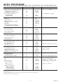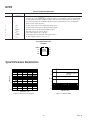
1
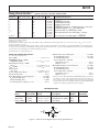
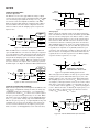
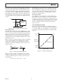
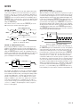
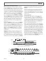
AD7810 Timing Characteristics1, 2 (–40ⴗC to +105ⴗC, V REF = VDD, unless otherwise noted) Parameter VDD = 5 V ⴞ 10% VDD = 3 V ⴞ 10% Unit Conditions/Comments t1 t2 t3 t4 t5 3 t6 3 t7 3 t83, 4 2.3 20 25 25 5 10 5 20 10 1.5 2.3 20 25 25 5 10 5 20 10 1.5 µs (max) ns (min) ns (min) ns (min) ns (min) ns (max) ns (max) ns (max) ns (min) µs (max) Conversion Time Mode 1 Operation (High Speed Mode) CONVST Pulsewidth SCLK High Pulsewidth SCLK Low Pulsewidth CONVST Rising Edge to SCLK Rising Edge Set-Up Time SCLK Rising Edge to DOUT Data Valid Delay Data Hold Time after Rising Edge SCLK Bus Relinquish Time after Falling Edge of SCLK tPOWER UP Power-Up Time after Rising Edge of CONVST NOTES 1 Sample tested to ensure compliance. 2 See Figures 14, 15 and 16. 3 These numbers are measured with the load circuit of Figure 1. They are defined as the time required for the o/p to cross 0.8 V or 2.4 V for V DD = 5 V ± 10% and 0.4 V or 2 V for V DD = 3 V ± 10%. 4 Derived from the measured time taken by the data outputs to change 0.5 V when loaded with the circuit of Figure 1. The measured number is then extrapolated back to remove the effects of charging or discharging the 50 pF capacitor. This means that the time, t8, quoted in the Timing Characteristics is the true bus relinquish time of the part and as such is independent of external bus loading capacitances. Specifications subject to change without notice. ABSOLUTE MAXIMUM RATINGS* SOIC Package, Power Dissipation . . . . . . . . . . . . . . . 450 mW θJA Thermal Impedance . . . . . . . . . . . . . . . . . . . . 160°C/W θJC Thermal Impedance . . . . . . . . . . . . . . . . . . . . . 56°C/W Lead Temperature, Soldering Vapor Phase (60 sec) . . . . . . . . . . . . . . . . . . . . . . 215°C Infrared (15 sec) . . . . . . . . . . . . . . . . . . . . . . . . . . 220°C MicroSOIC Package, Power Dissipation . . . . . . . . . . 450 mW θJA Thermal Impedance . . . . . . . . . . . . . . . . . . . . 206°C/W θJC Thermal Impedance . . . . . . . . . . . . . . . . . . . . . 44°C/W Lead Temperature, Soldering Vapor Phase (60 sec) . . . . . . . . . . . . . . . . . . . . . . 215°C Infrared (15 sec) . . . . . . . . . . . . . . . . . . . . . . . . . . 220°C (TA = 25°C unless otherwise noted) VDD to GND . . . . . . . . . . . . . . . . . . . . . . . . . . –0.3 V to +7 V Digital Input Voltage to GND (CONVST, SCLK) . . . . . . . . . . . . . . –0.3 V, VDD + 0.3 V Digital Output Voltage to GND (DOUT) . . . . . . . . . . . . . . . . . . . . . . . . –0.3 V, VDD + 0.3 V VREF to GND . . . . . . . . . . . . . . . . . . . . . . –0.3 V, VDD + 0.3 V Analog Inputs (VIN+, VIN–) . . . . . . . . . . . . . . . . . . . . –0.3 V, VDD + 0.3 V Storage Temperature Range . . . . . . . . . . . . –65°C to +150°C Junction Temperature . . . . . . . . . . . . . . . . . . . . . . . . . 150°C Plastic DIP Package, Power Dissipation . . . . . . . . . . 450 mW θJA Thermal Impedance . . . . . . . . . . . . . . . . . . . . 125°C/W θJC Thermal Impedance . . . . . . . . . . . . . . . . . . . . . 50°C/W Lead Temperature Soldering (10 sec) . . . . . . . . . . . 260°C *Stresses above those listed under Absolute Maximum Ratings may cause permanent damage to the device. This is a stress rating only; functional operation of the device at these or any other conditions above those listed in the operational sections of this specification is not implied. Exposure to absolute maximum rating conditions for extended periods may affect device reliability. ORDERING GUIDE Model Linearity Error (LSB) Temperature Range Package Description Package Options Branding Information AD7810YN AD7810YR AD7810YRM ± 1 LSB ± 1 LSB ± 1 LSB –40°C to +105°C –40°C to +105°C –40°C to +105°C Plastic DIP Small Outline IC (SOIC) microSOIC N-8 SO-8 RM-8 C1Y IOL 200A TO OUTPUT PIN 1.6V CL 50pF IOH 200A Figure 1. Load Circuit for Digital Output Timing Specifications REV. B –3–